1
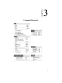
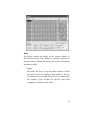
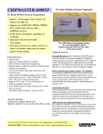
CHAPTER
1
General Information
1
Introduction
The DATAMAN-48XP is an intelligent high performance,
PC-based universal programmer that works through your PC′s
parallel port. It features a 48-pin ZIF socket and supports many
of the programmable chips on the market. These include CPLD,
EPROM, EEPOM, Serial EEPROM, Flash memory and MCU.
The D48XP has an extremely high throughput, supports both
5V and 3V devices in both Vcc and I/O. Lower voltage chips
(for example 1.8V Vcc and I/O) can also be programmed
through a special adapter. Device insertion and continuity
checks are also part of the PC-based design. Device support
updates are issued through our software, giving our customers
quick and easy access to new device support without hardware
upgrades.
Features
Universal adapter up to 48 pin
The DATAMAN-48XP is designed to meet your future needs in
high density Flash chips. Using the resources of your PC, it
supports 32K bit up to over 1G bit memory chips without
upgrading its hardware. The DATAMAN-48XP also has
universal adapters that accommodate 48-pin TSOP, 44-pin
PLCC, 40-pin TSOP or 32-pin TSOP packages. Each adaptor
supports all the chips in a package regardless of pin swapping.
This is possible due to the universal pin driver technology on
the DATAMAN-48XP, eliminating the need to buy multiple
adapters and saving you money.
Unbeatable speed
The DATAMAN-48XP′s on-board intelligence reduces system
overhead to a minimum. It can program Flash devices within
2.5 seconds per Mbit (for example, AMD29DL323 can be
2
programmed by DATAMAN-48XP within 80 seconds). An
experienced operator can program thousands of high-density
chips per day.
Device-insertion and continuity checks – No mistakes!
The DATAMAN-48XP performs device-insertion and
continuity checks before programming each device. It can
detect poor pin contact, upside-down device insertion, incorrect
position, and pin number mismatch. This function prevents
expensive chip damage caused by operator error.
Auto-sensing and self-programming
The DATAMAN-48XP has implemented patented technology
to meet mass-production requirements. When a chip is inserted
into the ZIF socket, the DATAMAN-48XP will start to program
automatically, the operator just needs to follow the LEDs to
know when to remove the chip and insert a new one without
them needing to press any keys.
Project file “Save and Load”
You can save the program configuration project to a file that
contains the device selection, the buffer data, and all of the
program setup options. This file can be recalled at any time for
future use without having to go through the setup procedure
again. This allows you to pass your design file to the
production department without mistakes.
Variable VCC with one or two-pass verification
The DATAMAN-48XP allows users to select the verification
voltage after programming is complete, e.g., Vcc +/-5%,
Vcc+/-10%, Vcc can range from 2V to 7.5V. Verification
ensures that the chips have been properly programmed with no
data retention problems.
3
Device support summary
Over 5000 devices are currently supported on the D48XP and
you can increase the chip support by downloading software
updates from www.dataman.com. Normally we add more than
100 new devices in each quarter’s software update.
For details of updates and added device support, please visit
our website: www.dataman.com
Using the DATAMAN-48XP Software
Menus
Accessing the menus can be done in two ways:
1. Use the mouse and click on the menu option displayed at
the top of the screen. A drop-down menu will appear, and
you can select your desired option by clicking on it.
2. If you do not have a mouse available, you can also use the
keyboard to access the menus. Press [F10] to activate the
main menu bar. Select the sub-menu that you want to use
with the left and right arrow keys, and press <ENTER> to
activate the sub-menu. Use the up and down arrows to
select an option to execute. Press <ENTER> to execute the
command.
Hot keys
Most of the options available on the menus can also be
executed by pressing the hot key associated with that option.
To see what the hot key is for a certain option, look on the
menu where the option is located. If a hot key is available, it
will be displayed next to the option name.
4
CHAPTER
2
Installation
5
Minimum PC System Requirements
Windows 95/98/ME/2000/XP/NT 4.0 or latest (NT, need
System Admin privileges to install the software).
CPU: 486 and above.
RAM: 8MB minimum, 32 MB recommended.
HD: 16 MB of free hard disk space.
Interface: D-25 connector with standard parallel port,
(ECP, EPP or Bi-directional).
CD ROM Drive.
Installing the DATAMAN-48XP Hardware
1. Connect the power cable to the DATAMAN-48XP power
socket.
2. Connect the DATAMAN-48XP to a parallel port using the
cable supplied.
3. Turn the DATAMAN-48XP on.
4. The DATAMAN-48XP will perform a self test, the green
LED will be on (good) if the system has passed the self
test.
Installing the DATAMAN-48XP Software
1. Go to ‘My Computer’ and double-click the CD-ROM
drive containing the D48XP CD.
2. Double click the ‘Setup’ icon to begin installation.
6
3. Following installation, run the software by doubleclicking the DATAMAN-48XP icon. The screen will
display the DATAMAN-48XP firmware version and
indicate which parallel port the DATAMAN-48XP has
been discovered on.
Upgrading the DATAMAN-48XP Software
Dataman provide official quarterly releases of the
DATAMAN-48XP software which are available on our
website; please download all software updates from
www.dataman.com
7
CHAPTER
3
Command Hierarchy
8
DATAMAN-48XP Command Hierarchy
System command
Operation command
Hot Key
File (ALT-F)
Save Buffer
Load File
Exit
Save Project
Load Project
Change
Edit
Read
Blank Check
Program/Auto
Verify
Erase
Compare
Configuration
Modify Programming Parameter
Device Operation Options
Parallel Port Selection
Statistics
Self Test
Help Topic
About
ALT-S
ALT-L
ALT-X
ALT-F1
ALT-F2
ALT-C
ALT-E
ALT-R
ALT-B
ALT-P
ALT-V
Ctrl-F1
Ctrl-F3
ALT-G
F3
F4
F5
F6
F7
Project (ALT-J)
Device (ALT-D)
Options (ALT-O)
Diagnostic
Help (ALT-H)
9
CHAPTER
4
Operation
10
LED Display
The DATAMAN-48XP has a three LED display to indicate the
status of the socket. Read this section carefully to avoid
possible damage to chips.
Warning: Do not insert or remove a device from the socket
while the yellow ’Busy’ LED is on!
Green LED on (Good) the last operation was successful.
Yellow LED on (Busy) The socket is busy; do not insert or
remove devices from the ZIF socket
before green LED or red LED is on.
Red LED on (Error)
the last operation resulted in failure.
Flashing LED at 5Hz frequency. This only applies to mass
production mode. The chip has passed the program and
verify cycle and is waiting for the operator to remove it and
insert a new one.
File Commands
Save Buffer to File
Menu
File / Save Buffer
Hot key
Alt-S
This option is used to save the memory buffer to a file on the
hard disk. Select a file using the mouse, or type a filename in
the box provided. You can also type in a file extension. (e.g.
*.hex) at the ‘Name’ prompt. This will display all the files of
the specified type. You can then select the required file to
overwrite.
11
12
File name
Specify the filename and destination you
want to save to.
File format
Select the file format of your output file. To
display a list of available file formats, click
on the down arrow to the right of the text
field. Supported file formats include:
Binary, HP64000ABS, Intel Hex, MOS
Technology Hex,
Motorola S format,
Tektronic Hex, and Straight Hex.
Buffer mode
This Buffer mode is to split your buffer
according to the mode selection, details of
the split function are explained below.
Normal (default)
Every byte is written to the output file.
Odd
Every Odd byte is written to the output file.
Even
Every Even byte is written to the output file. The
following four options are used to write the buffer into
four different files:
1st byte of 4
This writes the bytes 1,5,9,13, … into the output file.
2nd byte of 4
This writes the bytes 2,6,10,14, ... into the output file.
13
3rd byte of 4
This writes the bytes 3,7,11,15, ... into the output file.
4th byte of 4
This writes the bytes 4,8,12,16, … into the output file.
From Buffer address
Buffer size
This specifies the start address of
the buffer you want to save to the
file, default is from 0000h, any
address (from 0h to the Max. of
the buffer address can be
selected)
The buffer size depends on the chip you
select, for example if you select 29F010 (the
buffer size will be 1Mbit which is 20000h)
Load File to Buffer
Menu
File / Load File
Hot key
Alt-L
This option loads a file from disk into the memory buffer. The
type of files that can be loaded for a device depends on the
device type.
Select a file to load using the mouse, or type the filename in
the box provided. You can also type in a file extension. (e.g.
*.hex) at the name prompt. This will display all the files of the
specified type, and you can then select the required file to load.
14
15
16
Filename
This specifies the file name and its destination
Auto Format Detected
The software automatically detects the format of the file that
is to be loaded. If the desired format of the file is different
from the format detected, select the correct file format by
moving the cursor to the selection menu and changing it to
the desired file format. Available file formats include: Binary,
HP64000ABS, Intel Hex, MOS Tech Hex, Motorola S
format, TEK Hex, and Straight Hex.
From File to Buffer
This option indicates which bytes must be read from the
input file. By default it will load the entire file into the buffer.
You can specify that the file be loaded in the following ways:
Even (loads the even bytes into the buffer), Odd (loads the
odd bytes into the buffer), also 1st byte of 4, 2nd byte of 4, 3rd
byte of 4, 4th byte of 4. For details, see the “Save Buffer to
File” section of this manual.
To Buffer
This option indicates where the previously read byte is to be
written. This enables you to ‘build’ the memory buffer from
several files. By default, the whole file will be loaded into
the buffer. Even means the file will be loaded as every even
byte in the buffer. Odd means the file will be loaded as every
odd byte in the buffer. The other options are 1st of 4 byte, 2nd
of 4 byte, 3rd of the 4 byte, and 4th of the 4 byte.
From File Address
Only a selected range of the file will be loaded into the
buffer, enter the address that contains the first byte into this
box, this is the starting address of the section of the file to be
loaded.
17
To Buffer Address
Starting address of the buffer to load the file into. If the data
is to be copied into a specific area of the buffer, enter the
starting address here.
Size
This box contains the buffer size. By default, it is the same
size as the device selected on the DATAMAN-48XP main
screen. If you want to download a file into the memory that
is bigger than the active device, enter the size here (or in
Options | Operation Options).
Clear Buffer Options
Four options are available while loading data into the buffer.
The default option is to clear the buffer to its blank state
prior to loading data.
Disable
This option leaves the original buffer data unchanged, but
then overwrites it with the contents of the newly loaded
file.
Blank state (default)
This option clears the buffer to the devices blank state,
(using command 00 or FF, depending on device selection),
then overwrites the buffer during file loading.
0x00
First clears the buffer of its contents using command 00,
then overwrites the buffer with the new file contents
0xFF
First clears the buffer of its contents using command FF,
then over-writes the buffer with the new file contents.
18
Exit
Menu
File / Exit
Hot key
Alt-X
Quit the DATAMAN-48XP program
19
Project File Commands
Save Project
Menu
Project / Save Project
Hot key
Alt-F1
This option saves the current setup of the DATAMAN-48XP
software into a project file. The file includes selected devices,
buffer data, operation setup, and device configuration setup.
You can also attach a footnote to the project file. The project
file acts as a macro, eliminating the need to go through the
whole setup procedure during future programming sessions.
Load Project
Menu
Project / Load Project File
Hot key
Alt-F2
This option loads the desired project file. After the project file
has been loaded, you can immediately program a device using
the preset data and setup functions from the Project file.
Device Commands
Change Device
Menu
Hot key
Device / Change Device
Alt-C
20
This option is used to select a new active device. It is important
to select the correct device, as the algorithms used to program
devices are device-specific. The following screen will appear:
Figure 4.1 Screen for selecting Change Device
Special note in device package and its selection
In the above screen, you can find both AT89C51 and
AT89C51*44 selections, the AT89C51 means this is a 40 pin
DIP chip, no adapter is required and 89C51*44 means the chip
is 44 pin PLCC or QFP/TQFP, adaptor required. After selecting
the 89C51*44, at the bottom of the software screen will be
displayed chip information and the adapter requirement. In this
example, it shows SDP-UNIV-44 as the recommend adapter, it
means for a 44 pin PLCC chip, you need the 44 pin PLCC
universal adapter, if your chip is 44 QFP or TQFP, you will
need a 44pin QFP (SDP-UNIV-44TQ) or a 44pin TQFP
(SDP-UNIV-44TQ) adapter.
If you have a 3rd party 44 pin PLCC adapter that swaps the 44
21
pin PLCC chip into a 40 pin DIP (emulate the 44 pin PLCC as
a 40 pin DIP), you can select the 89C51 in device selection and
use this 3rd party adapter.
Other useful examples in device, package and adapter.
1) For example a 1M bit flash (29F010), this chip has three
kinds of package, 32 pin DIP, 32 pin PLCC and 32 pin
TSOP, in the DATAMAN-48XP software, it is only
available in DIP package under device selection, to
program a 32 PLCC chip, you will need a 32 pin DIP to 32
pin PLCC one to one pin swap adapter (PLCC 3232-11),
for 32 pin TSOP, you will need a SDP-UNIV-32TS.
2) For example, a GAL22V10 chip, this chip has two
packages (24 pin DIP or 28 pin PLCC),
DATAMAN-48XP only shows 24 pin DIP in device
selection, to program the 28 pin PLCC, a 28 pin PLCC
to 24 pin DIP adapter to emulate the 24 pin DIP chip is
required (PLCC 2824-04).
3) 27C128/256 EPROM chip, this chip is available in 28
pin DIP and 32 pin PLCC, to program the 32 pin PLCC,
you need a 32 pin PLCC to 28 pin DIP adapter, it
emulates the 32 pin PLCC as a 28 pin DIP, this adapter
is PLCC 3228-11.
4) Other SOIC chips may have the DIP/SOIC package, if
the chip has the same pin out and pin count in DIP and
SOIC, select the DIP with universal SOIC adapter
which will program the SOIC chip (for example
Pic16F73 with SDP-UNIV-28SO/300 adapter will
program a 16F73 SOIC chip).
22
1. Select the type of device that will be the active device.
Mouse
Click on “All”, “EPROM” or “MPU”.
Keyboard
Press TAB until the cursor is flashing in the “Type” box.
Use the up and down arrows to go to the appropriate type.
Press the space bar to select the type.
2. Enter the part number, the manufacturer number, or parts of
both in the “Search” box.
Mouse
Click on “Search”. Type in the characters.
Keyboard
Press TAB until the cursor flashes in the “Search” box.
Type in the known characters. All the devices that satisfy
this partial information will be displayed. Use the mouse to
select a device, and click “OK”. If you are not using a
mouse, use the TAB key to skip between the various
screens, and use the arrow keys to move around in each
screen.
Auto Select EPROM
Menu
Device/ Auto Select EPROM
Hot key
Alt-A
This function allows the user to detect which EPROM/Flash
chip has been inserted in the DATAMAN-48XP ZIF socket, all
the EPROM or Flash memory devices have a manufacturers ID
and device ID in the chips (hardware ID). When performing
this function, the DATAMAN-48XP applies a 12V high voltage
to the A9 location on the chip, then reads back the chip’s
23
hardware ID and compares it to the library then display the
possible chip in the window.
This Auto ID is only available for 32 pin or 28 pin EPROM
and Flash memory chips, it can not be applied to MCU, PLD or
other serial PROM, EPROM/Flash. Chips with over 40 pins do
not have this function since the A9 location is not standardized
for chips over 40 pins, using such a function may damage the
chip since a 12V high voltage is applied to the chip which can
cause damage to the chip by accident.
Mass-production Mode
Menu
Device / Mass Produce
The DATAMAN-48XP can be used as a mass-production
programmer for manufacturing. When in mass production
mode, all keyboard and mouse functions are disabled. The
operator needs only to insert the chip into the ZIF socket, wait
until the green LED next to the socket flashes, remove the
programmed chip and insert a new chip. Anyone can do the job
without special training or skills. Since all keyboard and mouse
functions are disabled, the possibility of errors being caused by
pressing the wrong keys or changing the buffer′s contents are
eliminated.
In mass production mode, the DATAMAN-48XP first performs
an insertion test and an ID check on a newly inserted chip. It
then automatically programs the chip.
Note: The insertion test must be enabled in operation option
set up in mass-production mode to ensure yield rate of
programming.
Necessary set up in mass production mode.
After entering mass production mode a series of screens will
24
display asking the user to complete the set up and confirm it,
first you need to fill out the operation set up menu (for
operation set up, please reference to the device operation
option section) then the configuration set up menu (this
configuration set up menu is device specific, only chips with a
configuration register have this menu and the contents are
different from chip to chip), reference to device configuration
section. The last set up menu is statistic configuration, for set
up details of the statistics please refer to the statistics section of
this manual.
Mass Production Mode
After the user has completed the setup above, the Mass
Production screen (figure 4.2) will be displayed. When the user
inserts a device into the ZIF socket, the white segments on the
diagram of the ZIF will change to green. If a segment remains
white, this indicates poor or no contact on the corresponding
pin.
Once contact is established on all pins the device can be
programmed. When programming is complete the green LED
on the programmer will flash and the PC will generate an
audible alert. The operator can then remove the device and
insert a new one into the ZIF.
Any error in programming will be signified by the contact
segments on the diagram of the ZIF turning red and the PC
generating a two tone alert. Once the error has been resolved,
programming will continue until either the target quantity or
the maximum failure rate (set in the Statistic Setup) has been
reached.
25
Figure 4.2 mass production mode screen
Editing the Buffer (memory device )
Menu
Device / Edit
Hot key
Alt-E
This function is used to edit the memory buffer. The memory
buffer contains the last file downloaded from disk into memory.
If no file has been downloaded from disk into memory since
the DATAMAN-48XP was switched on, the memory buffer
will contain random data or the previous contents from when
you last exited the software.
The screen that is displayed is dependent on the type of device
that is currently active.
26
Radix
This button controls the display of the memory address in
Hex/Decimal format. If the address is currently displayed in
decimal format, clicking this button will convert and display
the address in Hex.
Swap
This allow the user to swap the buffer contents of high
byte and low byte, the default of word width is 1, the user
can change the word width from 1/2/3/4 etc, following is
the example of the original file and the result after
swapping to a different word width.
27
Original file
01 23 45 67 89 AB CD EF
after swap with word width 2.
23 01 67 45 AB 89 EF CD
Original file
01 23 45 67 89 AB CD EF
after swap with word width 3.
45 23 01 AB 89 67 FF EF
Original file
01 23 45 67 89 AB CD EF
after swap with word width 4.
67 45 23 01 EF CD AB 89
Fill
This option is used to fill a block of memory with a
specified value. It needs the starting address, the ending
address and the value to be copied into this block of
memory.
Copy
This function copies a block in memory to a new address.
It requires the starting address, the ending address and the
address the block must be copied to.
28
Search
This function searches for a specified ′′string′′. The search
string can be text code or hex code, it can search forwards from
the cursor position or backwards from the cursor position.
Next
This command is to find the next string that matches the search
string in the buffer.
Undo
As you make changes to the memory buffer, the changes on the
current page are highlighted. If you choose this option, it will
reverse all changes made to the highlighted areas.
As soon as the changed memory positions move off the screen,
or get deselected by another command, the Undo command
will no longer undo the changes.
Check Sum
This function allows you to calculate the checksum of a
specific range of data in the buffer, you can enter the from
and to address then click Checksum, the checksum will
be shown in the display.
Edit the buffer (logical device only)
When GAL, PALCE and other logical devices are selected
as active, the main memory buffer will contain a fuse map
instead of hexadecimal value.
The screen will appear as the following:
29
In this mode, “X” refers to a blown fuse, and “-“ refers to
an intact fuse. The purpose of the buttons are as follows:
Radix
This button controls the display of the memory address in
Hex/Decimal format, if the address is currently displayed
in decimal format, clicking this button will convert and
display the address in Hex.
Fill
This option is used to fill a block of memory with a fuse
value. It needs the starting address, ending address and the
value to be copied into this Block of memory.
Modify Vector (only available when selecting PLD)
Menu
Device / Modify vector
Hot Key
Alt-V
This command is only available when a PLD has been selected
as the active device, the option is used to modify the vectors
30
that will be used to test a device after the logical chip has been
programmed, this test vector is usually generated by 3rd party
PLD design tools when the circuit diagram and layout for the
chip is done. The JEDEC file is downloaded into the
DATAMAN-48XP, and it also contains the test vector that will
be used to test the device for correct programming and function.
The following screen will be displayed when you are viewing
the Vectors:
The purpose of the buttons are as follows:
Undo
When the changes are made, the changed areas are highlighted.
If you wish to undo this change, just click this button. It will
restore the value prior to editing. When a position that is
highlighted scrolls off the screen the changes made become
permanent and you cannot reverse them by clicking this button.
Insert
You can insert a line of vectors by clicking this button. The
31
position where the line will be inserted depends on the position
of the cursor. The line will be inserted before the line the cursor
is on. The contents of the “editing clipboard” are shown at the
bottom of the editing screen. The contents of the clipboard will
be inserted when this button is clicked.
Copy
This button copies the line the cursor is on to the editor
clipboard.
Cut
This button copies the current line to the clipboard, and also
removes it from the memory. Use this button in conjunction
with “insert” to move the contents of a line to another position.
Edit the test vector
Vectors are input in standard JEDEC format. The vector buffer
is arranged in rows and columns. The following test condition
codes can be use as the test vector/s.
0
Driver input low
1
C
F
H
K
L
N
X
Z
Driver input high
Driver input low, high, low (clock)
Float input or output
Test output high
Driver input high, low, high (clock)
Test output low
Power pin and the outputs not test
Output not tested, input default level
Test input/output with high impedance
32
Blank Checking a Device
Menu
Device / Blank Check
Hot key
Alt-B
This option checks if the active device is in its erased state. It
will return a message stating “Device not blank!” at the first
occurrence of data in the device. The address where the data is
found will also be displayed.
Reading a Device
Menu
Device / Read
Hot key
Alt-R
This option reads a master chip into the memory buffer for
duplication of a master chip. Prior to executing this command,
the chip must be selected in the software, and then a
corresponding chip should be inserted into the socket to be
programmed.
Programming a Device
Menu
Device / Program / Auto
Hot key
Alt-P
This option programs the active device with the contents of the
memory buffer, when the programming is complete,
verification will take place. The type of verification depends on
the “verification options” set in the options | Operation menu.
33
Figure 4-4 Programming progress screen
Verifying a Device
Menu
Device / Verify
Hot key
Alt- V
This function compares the contents of the active device with
the contents of the memory buffer. It will display an error
message and the address if it finds an address where the data
differs. It will also abort the process when this happens.
34
Figure 4-5 Device verification screen
Memory Protect/program configuration
Menu
Device / Memory Protect
Hot key
ALT-U (PLD only)
This function is a device-specific command; it appears on the
main menu only when chips that have this capability are
selected.
For example GAL, CEPAL, Microprocessor, and some Flash
memory, this function must be configured before use. When
you have enabled the configuration (ALT-G), you can set the
desired value and status in the buffer then performing this
command will program the configuration data into the chips,
most users will program the main memory first then program
the configuration (two steps). However in Mass production
mode, the user can enable the memory protect / program
configuration in the device operation menu, after the main
memory buffer has been loaded and configuration byte data has
35
been set to the desired value, the programmer will
automatically program the main memory and set the
configuration byte in a single command (program or mass
production mode program).
Special note for program configuration/ memory protect
This option only applies to devices with configuration registers
or if it has a read protect function on it. Enabling this option
will automatically program the main buffer into the chip
without the need to perform memory protect separately.
Enabling this option only protects the chip if you have set the
lock bit to enabled in the configuration setup menu.
Function Test (only available for logic chip)
Menu
Device/ Function test
Hot key
Alt-T
This function is only available when a logical device has been
selected, it applies the test vector to the device and compares
the outputs with the expected outputs. It tests if the logical chip
has been programmed correctly after the chip has been secured
and the fuse map is not readable again. It displays a message
indicating success or failure, if there is a failure it displays the
vector number and which pin did not match the expect result.
Before performing the memory test, you can modify the vector
and set up the options in the operation screen.
First
Enable the function test or function test after secure
in options.
Second
Select the function test voltage with once or twice.
Third
Define the “X” don’t care state in the vector;
High/Low or high impedance
Fourth
Select the error display format.
36
Important notice in function test
To perform function test after programming a PLD chip, the
input file must contain the test vectors or the user has to have
created the vectors by himself, in the options under the
operation menu, function test is enabled by default, which
means after programming the PLD, the DATAMAN-48XP will
perform the function test automatically, if no vector is in the
buffer, the DATAMAN-48XP will report “no test vector in
buffer”, if the test vector does not match the behavior of the
chip after the vector test, an error will be displayed along with
vector number and which pin expected low/high but received
high/low. For PLD devices in PLCC packages (GAL 20V8 as
example), the DATAMAN-48XP software only supports 24 pin
in DIP if you need to program a 28 PLCC chip with a PLCC
adapter, the DATAMAN-48XP will program the chip but the
function test will fail since the pin is mismatched with the chip
(the chip is 28 pin but is emulated as a 24 pin chip with the
adapter), the vector data will not match the device data in pin
out.
Erasing a Device
Menu
Device / Erase
Hot key
Ctrl-F1
This function is a device-specific command; it appears on the
main menu only after electronically erasable chips have been
selected. The function can be used to erase a specific memory
range from a chip.
Compare
Menu
Device/compare
Hot Key
Ctrl-F3
This command is only available for memory devices, the
37
compare command is to compare the buffer data with the
device data, when the first data difference is found, the
software will stop and report the difference between the data in
the buffer and the data in the device, pressing the next button in
the software screen will continue the compare process.
Device Configuration
Menu
Device / Configuration
Hot key
Alt-G
This function is a device-specific command for devices with
configuration registers available in the chip, a configuration
register is used as a special function register for the chip, it
changes the behavior of the chip such as, OSC type, watch dog
enable, code protection, and other functions. To write the
configuration register into the chip, edit the configuration menu
to your desired value then perform memory protect/ program
configuration.
Figure 4-6 Example of device-specific configuration screen
38
Options
Modify Programming Parameters
Menu
Options / parameters modify
Hot key
F3
This function allows a user to modify the programming
parameters of the chip being programmed. With the
programming parameters for the selected chip appearing on
screen, the user activates the “modify algorithm screen” and
changes the parameters by moving the cursor to the
corresponding field and changing the value to the desired value.
If a value entered exceeds the allowable limits for a given
parameter, a warning will be displayed, together with allowable
limits, after the user attempts to confirm the setting by pressing
“OK”.
Warning: Only experienced users should use this option, as it
can damage the device if the voltage exceeds the Max tolerance
of the device.
As the programming parameters are for temporary use only,
they cannot be saved. After you select a new device or exit the
DATAMAN-48XP software the original parameters will
automatically be restored.
Device Operation Options
Menu
Hot key
Options / Operation options
F4
39
Figure 4-8 Example screen: Device-specific operation options
The following options can be set:
Start address, End address
This is the start and the end address of the edit buffer. If you
want to program a certain area of a device, you can change
the start and end addresses accordingly.
This option is only displayed when the device can be
programmed in this way.
When the end address is calculated, it divides the buffer size
by (device-bits/8-bits). A 16-bit device, of which the buffer
40
size is 80 (Hex), will therefore have an end address of 3F.
When selecting a start or an end-address, you should align the
buffer on the right boundary: single-word for 8-bit devices,
double word for 16-bit devices, etc.
Buffer size
This is the memory buffer in the DATAMAN-48XP software,
once the chip is selected, the software opens the buffer to
match the chip size, the user can edit this buffer size to
enlarge it to 256 M bit Max (4000000h).
Auto increment start/end address
This function allows the user to program memory chips with
different serial numbers in specific locations without having
to edit the buffer each time. Specifying the serial number
location is done by editing the auto increment start address
and auto increment end address, editing the initial contents
with buffer edit and setting up the increment value and format
is done through this menu.
Auto increment value
This set each increment value after initial value.
Auto increment data format selection
Binary increment format example
0, 1, 10,11,100, 101,110,111, 1000,1001,1010,1011,1100
ASCII Hex format example
0,1,2,3,4,5,6,7,8,9,A,B,C,D,E,F,10,11,12, …
ASCII Decimal Hex format example
0,1,2,3,4,5,6,7,8,9,10,11,12,13,14,15,16,17, …
Modulo-26 format example
A,B,C,D,E,F, … ,Z,AA,AB,AC, ….
41
Insertion Test
This option performs a device-insertion check of the chip in
the socket. The insertion check includes poor pin contact, pin
count mismatch (the pin count of the chip designated in the
software does not match the pin count of the actual chip in the
socket), device in wrong position, device upside-down;
short-circuit between pins, and chip damage. Result is
displayed at the socket′s LED’s.
Device ID Check
This option performs a device signature and manufacturer
match test. With the chip selected and plugged into the socket,
DATAMAN-48XP checks the device ID and displays the
results of each check on the LED display.
Verify Passes
Checking this option will instruct the DATAMAN-48XP to
perform device verification with the buffer data when
programming is complete. When verify passes is enabled, one
of the three verify options (as described below) must be set.
Verifying Options
The following three options are available for verification of
data retention following programming: verify twice with Vcc
±5%, verify twice with Vcc ±10% , and verify once with Vcc.
These options will only be enabled if the ‘Verify passes’
option (see above) is enabled.
(.
. ) Twice Vcc ±5%
When this option is selected, the DATAMAN-48XP will do
two verify passes on the device: one using Vcc+5%, the other
Vcc-5%.
42
Example:
If Vcc is 5.0 V, the DATAMAN-48XP will do one verify pass
using a Vcc of 4.75 V, and one using a Vcc of 5.25 V.
(.
. )Twice Vcc ±10%
When this option is selected, the DATAMAN-48XP will do
two verify passes on the device: one using Vcc+10%, the other
Vcc –10%.
Example:
If Vcc is 5.0 V, the DATAMAN-48XP will do one verify pass
using a Vcc of 4.5 V, and one using a Vcc of 5.5 V.
(.)Once
If this option is selected, the DATAMAN-48XP will do one
verify pass-using Vcc.
Blank Check
This option performs a device blank check test before
programming. This option can be disabled for brand new
chips to save time. For electronically erasable chips, enabling
the
auto-erase/overwrite
option
will
allow
the
DATAMAN-48XP to automatically erase the chips if they are
not blank initially.
Program configuration/memory protect
This option only applies to devices with configuration
registers or if it has a read protect function on it, enabling this
option will automatically program the main buffer into the
chip then program the configuration set up without the need to
perform memory protect separately. Enabling this option only
protects the chip if in the configuration set up menu, you have
set the lock bit to enabled.
43
Auto-Erase/Overwrite Option
This option only applies to chips, which are electronically
erasable for example Flash memory, Flash based MCU or GAL
and so on. It causes the DATAMAN-48XP to automatically
erase a non-blank chip prior to programming (there will be no
warning message “Device is not blank, are you going to
program”).
Auto increment (only available to memory device)
This enables the auto increment function that allows a user to
program different serial numbers into the chip without editing
the buffer each time, for setup of auto increment, please refer
to the auto increment start address /end address, increment
value and format section.
Parallel Port Selection
Menu
options / parallel port
Hotkey
F5
This command allows the user to select which parallel port the
DATAMAN-48XP device programmer is connected to. Default
setting is auto search, after executing the DATAMAN-48XP
software, it auto detects which LPT port the DATAMAN-48XP
programmer is connected to, the user can select the LPT port
manually by specifying LPT port to avoid possible conflict
with drivers of another LPT device that is attached to the PC.
44
Statistic
Menu
Hot key
Options / Statistics
F6
Action
Enables either the counter or alarm when the target count or
maximum failure count reaches the preset limit.
Active
Specifies the action you want to count in the statistics function.
Mass production enable:
Counts the mass production quantity (chips) into the
statistic display.
Program enable:
Counts the program activities into the statistic display.
Verify enable:
Counts the number of verify operations into the display.
Blank check enable:
Counts the blank check activities into the statistic display
45
Erase enable:
Counts the erase activities into the statistic display.
Memory protect enable:
Count the memory protect activities into the statistic
display.
Operation count
Counts the total number of operations and sets the target
quantities.
Failure count
Counts the total chip failure and sets the max chip failure
allowed. When the operation exceeds the maximum failure
count or reaches the target count an alarm or warning message
is displayed on the screen (depending on the action set in this
page).
Diagnostic
46
Dataman recommends that the user runs the self-test feature of
the Dataman-48XP prior to each day’s operation. The self-test
routine including testing the parallel port, LED display, Pin
driver, TTL driver, relay, D/A converter’s voltage drop and
other parameters, the following is an example test results
screen.
Any unexpected states are displayed with a purple color and
any error messages are reported at the end of the self-test, if an
error is highlighted you will need to return your
DATAMAN-48XP programmer to your distributor for repair.
47
The DAC (four DAC in DATAMAN-48XP) test result and its
meaning
DAC0
25 34 36 38 40 44 46
27 27 27 27 27 27 27
(this is the out put pin for DAC 0)
this means the DAC0 output level
(0-255 in 8 bit DAC) to reach logic
high for the input circuit to detect the
high.
Rest of DAC 1/2/3 has the same meaning, the output high level
for individual DAC units, does not affect the overall
performance of the unit.
Help
Help Topics
Click this ICON and selecting a topic will
display the on-line help for the topic.
About
Clicking this ICON will display the current
DATAMAN-48XP software revision.
48
CHAPTER
5
Using Adapters
49
Adapter Requirements
DATAMAN-48XP supports universal 48-pin TSOP, 44-pin
PLCC, 44 pin QFP, 44 pin TQFP, 44 pin SOP, 40-pin TSOP
and 32-pin TSOP pin packages and more. You will need to
order an adapter for non-DIL chip packages. Following is the
list of adapters available to fit your needs. More new adapters
will become available when new chips are release. Please
contact your local distributor for the latest adapter availability.
Users can build adaptors themselves; details of adapter pin
swapping can be downloaded from our website:
www.dataman.com
PLCC2020-01
20 pin PLCC adapter for 20 pin PLCC GAL/PAL
PLCC2824-04
28 pin PLCC adapter (NC =1, 8,15,22) for 28 pin
PLCC GAL/PAL
PLCC3228-11
32 pin PLCC adapter (NC= 1,12,17,26) for
E/EEPROM below 512 K
PLCC3232-11
32 pin PLCC adapter for E/EEPROM with 1M
and up
PLCC4440-01
44 pin PLCC adapter (NC= 1,13,23,33) for 44
pin PLCC 16 bit EPROM
PLCC4440-02
44 pin PLCC adapter (NC= 1,12,23,34) for 44
pin PLCC 875X processor
SDP-UNIV-16/TS
16 pin TSOP universal adapter for 8-16 pin
TSOP
SDP-UNIV-16SO
16 pin SOIC (150mil) universal adapter for 8-16
pin SOIC
50
SDP-UNIV-16SO/170 16 pin SOIC (173 mil) universal adapter 1.27m
pitch
SDP-UNIV-20SO/200 20 pin SOIC (207mil) universal adapter for 8-20
pin SOIC
SDP-UNIV-20SO
20 pin SOIC (300mil) universal adapter for 1620 pin SOIC
SDP-UNIV-28SO/300 28 pin SOIC (300mil) universal adapter for 2428 pin SOIC
SDP-UNIV-28SS/200
28 pin SSOP universal adapters for 200mil x
0.65mm pitch
SDP-PIC-20SS/200
20pin SSOP universal adapter for PIC MCU
200mil x 0.65mm pitch
SDP-UNIV-24SS/150
24 pin SSOP universal adapter for 150mil x
0.635mm pitch
SDP-UNIV-48SS/300
48 pin SSOP universal adapter for 300mil x
0.635mm pitch
SDP-UNIV-28TS
28 pin TSOP (8mm x 14mm) universal adapter
for 28 pin TSOP Flash memory
SDP-UNIV-28TSS/170 28 pin TSSOP (173 mil) universal adapter pitch
0.65mm
SDP-UNIV-32TS
32 pin TSOP (8mm x 20mm) universal adapter
for 32 pin TSOP Flash memory
SDP-UNIV-32TS/W
32 pin TSOP (8mm x 14mm) universal adapter
for 32 pin TSOP Flash memory
SDP-UNIV-32TQ
32 pin TQFP universal adapter
SDP-UNIV-40TS
40 pin TSOP (10mm x 20mm) universal adapter
for 40 pin TSOP Flash memory
51
SDP-UNIV-40TS/W
40 pin TSOP (10mm x 14mm) universal adapter
for 40 pin TSOP Flash memory
SDP-UNIV-40TSS
40 pin TSSOP universal adapter for 40 pin
TSSOP Flash memory
SDP-UNIV-44TS
44 pin TSOP universal adapter for Samsung
/Toshiba 44pin TSOP NAND Flash memory
SDP-UNIV-44
44 pin PLCC universal adapter
SDP-UNIV-44TQ
44 pin TQFP universal adapter
SDP-UNIV-44PSO
44 pin PSOP universal adapter for 44 pin PSOP
Flash memory
SDP-UNIV-44Q
44 pin PQFP universal adapter
SDP-UNIV-48TS
48 pin TSOP (12mm x 20mm) universal adapter
for 48 pin TSOP Flash memory
SDP-UNIV-48TS/W
48 pin TSOP (12mm x 14mm) universal adapter
for 48 pin TSOP Flash memory
SDP-UNIV-48TSS
48 pin TSSOP (10mm x 14mm) with 0.4mm
pitch universal adapter for Flash memory
SDP-UNIV-44C
44 pin PLCC (clamshell socket) universal
adapter
SDP-UNIV-42SD
42 pin Shrink DIP universal adapter
SDP-5128-68
68 pin PLCC adapter for ALTERA 5128/A
SDP-7064-68
68 pin PLCC adapter for ALTERA 7064/7096
SDP-5192-84
84 pin PLCC adapter for ALTERA 5192/A
SDP-7064-84
84 pin PLCC adapter for ALTERA 7064/7096
SDP-7128-84
84 pin PLCC adapter for ALTERA 7128/E
SDP-7160-84
84 pin PLCC adapter for ALTERA 7160/E
SDP-7064-100Q
100 pin QFP adapter for ALTERA 7064
52
SDP-7096-100Q
100 pin QFP adapter for ALTERA 7096
SDP-7128-100Q
100 pin QFP adapter for ALTERA 7128/E
SDP-7160-100Q
100 pin QFP adapter for ALTERA 7160/E
SDP-M120-68
68 pin PLCC adapter for AMD MACH 12X/22X
SDP-M130-84
84 pin PLCC adapter for AMD MACH
13X/23X/435 and M4/128
SDP-M131-100Q
100 pin QFP adapter for AMD MACH
131/231SP
SDP-9572-84
84 pin PLCC adapter for XILINX XC9572
SDP-95108-84
84 pin PLCC adapter for XILINX XC95108
SDP-95108-100Q
100 pin QFP adapter for XILINX XC95108
SDP-6811-52B
52 pin PLCC adapter for Motorola 68 HC11
A1/E9/E1/E2, 68 HC711E9/E20
SDP-908AS-52
52 pin PLCC adapter for Motorola 68HC908AS
SDP-705B-52
52 pin PLCC adapter for Motorola
68705B5/B16/B32
SDP-C530-52
52 pin PLCC adapter for Dallas 87C530
SDP-7552-68
68 pin PLCC adapter for Philips 87C552
SDP-7592-68
68 pin PLCC adapter for Philips 87C592
SDP-11L6-68
68 pin PLCC adapter for Motorola
MC68HC711L6
SDP-11F1-68
68 pin PLCC adapter for Motorola 68HC11F1
SDP-196K-68
68 pin PLCC adapter for Intel
87C196KB/KD/KC
SDP-196J-68
68 pin PLCC adapter for Intel 87C196KR/KQ/JR
SDP-320E-68
68 pin PLCC adapter for TI TMS320E25
SDP-C752-68
68 pin PLCC PIC 17C752/6 adapter
53
SDP-C923-68
68 pin PLCC adapter for Microchip PIC
16C923/924
SDP-11K1-84
84 pin PLCC adapter for Motorola
XC68HC11K1/K4
SDP-96MH-84
84 pin PLCC adapter for Intel 87C196MH/MC
SDP-AD816-52Q
52 pin QFP adapter for Analog device
AduC812/816 MCU
SDP-705X-64Q
64 pin QFP adapter for Motorola 68HC705X32
SDP-C923-64TQ
64 pin TQFP adapter for PIC 16C923/4
SDP-C508-64Q
64 QFP adapter for Infineon C508-4E
SDP-C515-80Q
80pin QFP adapter for Infineon C515/C505L
SDP-908AZ-64Q
64QFP adapter for Motorola 68HC908AZ60
SDP-1024-68
68 pin PLCC adapter for LATTICE PLSI1024
SDP-1032-84
84 pin PLCC adapter for LATTICE
PLSI1032/2064
SDP-i320-48U
48 pin uBGA adapter for Intel 28F320B3/C3,
28F160B3/C3 (0.75mm pitch)
SDP-i320-48VF
48 pin VFBGA adapter for Intel 28F320B3C,
28F320C3C, 28F160C3C
SDP-i640-48VF
48 ball VFBGA adapter for Intel GE28F640C3
SDP-S160-48U
48 pin UBGA adapter for SHARP 28F160BJE
SDP-ST320-48U
48 pin UBGA (0.75mm pitch) adapter for
ST28W320CT
LVT-320D18-56U
uBGA adapter for Intel 28F320D18 (1.8Vcc,I/O)
LVT-128W18-56U
56 ball VFBGA adapter for Intel GE28F128W18
LVT-128W30-56U
56 ball VFBGA adapter for Intel GE28F128W30
LVT-128K3-56U
56 ball VFBGA adapter for Intel GE28F128K3
54
LVT-640W18-56U
uBGA adapter for Intel 28F320/640/128W18
(1.8Vcc, I/O)
LVT-640W30-56U
uBGA adapter for Intel 28F320/640W30
(1.8Vcc, 3V I/O)
LVT-6408W30-80F
80 pin uBGA adapter for Intel 28F6408W18 CSP
Flash
SDP-F256-80F
80 ball VFBGA adapter for Intel
RD28F256SJ3AM, D28F192SJ3AM,
RD28F128SJ3AM
SDP-EBGA-001
72 pin EBGA (1.0mm pitch) adapter for Intel
28F800/160/320F3/C3
SDP-EBGA-002
72 pin Easy BGA (1.0mm pitch) adapter for
Intel28F320/640/128J3A
SDP-F1316-64F
72 pin FBGA (0.8mm pitch) adapter for SHARP
LRS1306/1316A
SDP-1329-64F
72 pin CSP (8mm x11mm) adapter for SHARP
LRS1329/1340/1349/1356
SDP-1331-64F
72 pin CSP (8mm x 11mm) adapter for SHARP
LRS1331/37/41/42,LRS1357/58,LRS1362/63/
64/65
SDP-1826-64F
64 ball FBGA adapter for SHARP LRS1826 and
ATMEL AT52BR3244/3248
SDP-3204-64F
72 pin CSP adapter for Intel
RD28F1604/RD28F3204
SDP-3208-64F
64 pin uBGA adapter for Intel RD28F3208
SDP-A320-48F
48 pin uBGA adapter for AMD
29DL32X (6x12mm size)
55
SDP-A320-63F
63 pin uBGA adapter for AMD29DL32X
(8x14mm size)
SDP-41DL16-69F
69 ball FBGA adapter for AMD 41DL16xxMCP
SDP-42DL32-73F
73 ball FBGA adapter for AMD 41DL32xxMCP
SDP-ST064-56TS
56 pin TSOP adapter for ST 58LW064A
SDP-F400-56TS
56 pin TSOP adapter for Intel 28F400/28F200
SDP-F160-56SS
56 PIN SSOP adapter for Intel 28F160F3
SDP-F320-56SS
56 PIN SSOP adapter for Intel 28F160/320S3/S5
SDP-BL802-56SS
56 PIN SSOP adapter for
AMD29BL802C/1602C
SDP-A160-48F
FBGA adapter for AMD 29LV160 (0.8mm pitch)
SDP-A640-48F
FBGA adapter (0.8mm pitch) adapter for AMD
29DL640D
SDP-A800-48F
FBGA adapter for AMD 29LV800 (0.8mm pitch)
SDP-FU160-46SON
46 SON adapter for Fujitsu 29LV800/160
LVT-ADS323-48TS
1.8V low voltage adapter for AMD 29DS32X
(48TSOP)
GDP-1305-48TSS
48 pin TSSOP adapter for SHARP LRS1305
GDP-130X-48TSS
48 pin TSSOP adapter for SHARP LRS 1306/8
GDP-F016-56TS
56 pin TSOP adapter for Intel 28F016/032S3/S5
GDP-F320-56SS
56 pin SSOP adapter for Intel
28F320/640/128J5/J3
GDP-F640-56TS
56 pin TSOP adapter for Intel 28F320/640J5/J3
SDP-3224-100Q
100 pin QFP adapter for STV0680
56
APPENDIX
A
Error Messages
57
Error Messages
Could not open file – nnnn!
The file does not exist. You might have typed the wrong filename or
you might be in a different directory.
Verify the filename and the directory, and change to the correct
directory before typing in the filename.
Data file version unmatched!
This message will be displayed if one of the data-files used by the
DATAMAN-48XP software is of the wrong version.
This error occurs if Dataman-48XP.exe is updated, and the data files
are not updated. This might happen if the installation procedure did
not complete.
Re-install the latest release of the DATAMAN-48XP software.
Device Code unmatched!
This error message is returned when the DATAMAN-48XP does a
device ID check.
The device code found on the device is not as expected. You might
have selected an incorrect device as the active device, or the device
is an older/newer version than the device supported by the
DATAMAN-48XP. Disable the ID check in device operation option
can be a temporary solution to the programming the chip if the chip
ID is missing. Select the correct device as the active device.
If the error still occurs, download the latest release of software from
our website. If you are sure that the device you are using uses the
same programming algorithm as a device that is supported, you can
use this device as the active device. You can then disable device
code checking by setting the Operating Options.
58
Device inserted backwards or damaged already!
The DATAMAN-48XP detected that the device has been inserted
the wrong way round, or that the device has been damaged.
Verify that the device has been inserted correctly. If not, try another
device to verify that you are using the correct algorithm etc. to
program the device.
Device inserted upwards %d slot(s)!
The DATAMAN-48XP has detected that the device has been
inserted incorrectly. Remove the device and insert it correctly.
Device insertion error or damaged already!
The DATAMAN-48XP detected a device in socket, but several pins
do not respond as expected (poor contact). This indicates that a
device has been inserted incorrectly or that the device has been
damaged. Verify that the device has been inserted correctly. If not,
try another device to verify that you are using the correct algorithm
etc. to program the device.
File write error!
The DATAMAN-48XP detected an error when writing a file to disk.
Check that there is enough space on the disk to hold the file. Also
check that the disk is not write-protected.
This might happen on a network if you are a user that does not have
rights to the directory you want to save the file to. Use another
directory or disk.
Function code has not been initialized yet!
This message indicates that the data file is corrupt. We suggest a
re-install of the DATAMAN-48XP software and removal of all the
DATAMAN-48XP files on your hard disk before installation.
59
DATAMAN-48XP not found!
The DATAMAN-48XP software does not detect
DATAMAN-48XP on any of the parallel ports, or
DATAMAN-48XP may have failed and requires to be repair.
the
the
Make sure the power on the DATAMAN-48XP is on. Also check the
parallel connection between the PC and the DATAMAN-48XP. If
the DATAMAN-48XP shares the parallel port with another device,
remove the other device or move the DATAMAN-48XP to its own
port.
DATAMAN-48XP power off or disconnected from PC!
The DATAMAN-48XP software has not
DATAMAN-48XP on any of the parallel ports.
detected
the
Make sure the power on the DATAMAN-48XP is on. Also check the
parallel connection between the PC and the DATAMAN-48XP. If
the DATAMAN-48XP shares the parallel port with another device,
remove the other device or move the DATAMAN-48XP to its own
port.
MOS Technology hex file can be 64KB maximum!
This error is displayed when you want to save the buffer to a file,
and the buffer is bigger than 64KB.
The buffer can still be saved to disk, but only the first 64 KB will be
saved. The rest will be lost. Choose another file format if you need
to save the whole buffer.
Manufacturer’s Code unmatched!
This error message is returned when the DATAMAN-48XP does a
device ID check.
The device code found on the device is not as expected. You might
60
have selected an incorrect device as active device, or the device is
an older/newer version than the device supported by the
DATAMAN-48XP.
Select the correct device as active device. If the error still occurs,
download the latest release of the software from our website. If you
are sure that the device you are using uses the same programming
algorithm as a device that is supported, you can use that device as
the active device. You can then disable device code checking by
setting the Operating Options.
No device on socket!
The DATAMAN-48XP has not detected a device in the socket.
The inserted device may be damaged. Replace it with a similar
device and try again.
No test version in the buffer!
The memory buffer does not contain any test vectors. When the
DATAMAN-48XP tries to verify/function test a PLD, it displays
this message.
Download a file that contains test vectors before doing a function
test. Test vectors are usually included in JEDEC files.
Not enough memory available to complete operation!
There isn’t enough memory available to complete the requested
operation. Free some memory and retry the operation.
Over current detected!
A current higher than expected was found. This might indicate that
the device has been damaged or is in short-circuit.
Check the socket or replace the device.
61
Poor contact at pin %s!
The DATAMAN-48XP does an
programming/erasing etc. any device.
insertion
test
before
This message indicates that the socket may be dirty; the device may
have been damaged etc. Clean the socket or replace the device with
another.
Record checksum/length error!
Usually this error indicates that a wrong file format has been
selected. It could also indicate that the input file has a record that
has been corrupted.
Selected the correct file format, or obtain a new copy of the input
file.
Tektronic hex file can be 64KB maximum!
This error is displayed when you want to save the buffer to a file,
and the buffer is bigger than 64KB.
The buffer can still be saved to disk, but only the first 64KB will be
saved. The rest will be lost.
Choose another file format if you need to save the whole buffer.
The pin number of test vectors in the buffer unmatched!
This message indicates that the test vectors in the buffer indicate a
different number of pins than actually found on the device.
This is caused when the wrong device is selected as the active
device, or the wrong file with test vectors is loaded into memory.
This error is also caused when an adapter is required for devices
with more than 48-pins. The test vectors try to drive the pins
directly, and this causes an error. Make sure that the file and device
correspond, and do not use test vectors on devices that need
62
adapters.
The system is in demo mode!
The DATAMAN-48XP was not found when the software was started
up, and went into “Demo mode”. You can still run the program
(some of it) but you cannot execute any hardware functions.
This function is not supported in demo mode!
The DATAMAN-48XP was not found when the software was started
up, and went into “Demo mode”. This function is not supported in
Demo Mode.
Time-out error!
The DATAMAN-48XP has not responded to a request for a long
time. This error may also happen when performing an erase on a
flash memory chip, when the chip does not erase successfully
within the time period, this message will be display, it means your
chip can not be erased, try a new chip.
Unexpected code/data/end-of-file/run-time instruction reached!
The input file is corrupt or of the wrong format.
User break!
This message is displayed whenever you “cancel” an operation.
Wrong file format or file is corrupt!
An input file with the wrong format was selected. Select the right
format for the input file.
63