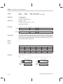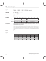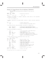
1
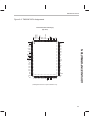
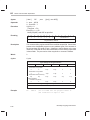
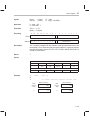
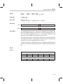
TMS320C2x
User's Guide
1604907-9761 revision C
January 1993
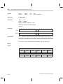
Read This First
About This Manual
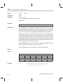
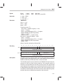
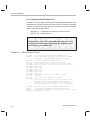
The purpose of this user’s guide is to serve as a reference book for the
TMS320C2x digital signal processors. Chapters 2 through 6 provide specific
information about the architecture and operation of the devices. Appendices
A through E furnish electrical specifications and mechanical data.
How to Use This Manual
This document contains the following chapters:
Chapter 1
Introduction
Description and key features of the TMS320C2x generation of digital signal
processors.
Chapter 2
Pinouts and Signal Descriptions
Package drawings for TMS320C2x devices. Functional listings of the signals,
their pin locations, and descriptions.
Chapter 3
Architecture
TMS320C2x design description, hardware components, and device
operation. Functional block diagram and internal hardware summary table.
Chapter 4
Assembly Language Instructions
Addressing modes and format descriptions. Instruction set summary listed
according to function. Alphabetized individual instruction descriptions with
examples.
Chapter 5
Software Applications
Software application examples for the use of various TMS320C2x instruction
set features.
Chapter 6
Hardware Applications
Hardware design techniques and application examples for interfacing to
memories, peripherals, or other microcomputers/microprocessors. XDS
design considerations. System applications.
iii
How to Use This Manual
Eleven appendices are included to provide additional information.
Appendix A
TMS320C25 Digital Signal Processor
Electrical specifications, timing, and mechanical data for the TMS320C25
devices.
Appendix B
TMS320C26 Digital Signal Processor
Data sheet information for the TMS320C26 digital signal processor.
Appendix C
TMS320C28 Digital Signal Processor
Data sheet information for the TMS320C28 digital signal processor.
Appendix D
SMJ320C2x Digital Signal Processors
Data sheet information for the SMJ320C2x digital signal processors family.
Appendix E
Instruction Cycle Timings
Listings of the number of cycles for an instruction to execute in a given memory
configuration on the TMS320C25.
Appendix F
TMS320E25 EPROM Programming
Programming hardware description and methodology.
Appendix G Analog Interface Peripherals and Applications
Discussion of various analog input/output devices that interface directly to
TMS320 DSPs and their applications.
iv
Appendix H
Memories, Analog Converters, Sockets, and Crystals
Listings of the TI memories, analog converters, and sockets available to
support the TMS320C2x devices in DSP applications. Crystal specifications
and vendors.
Appendix I
ROM Codes
Discussion of ROM codes (mask options) and the procedure for
implementation.
Appendix J
Quality and Reliability
Discussion of Texas Instruments quality and reliability criteria for evaluating
performance.
Appendix K
Development Support
Listings of the hardware and software available to support the TMS320C2x
devices.
Read This First
Style and Symbol Conventions
Style and Symbol Conventions
This document uses the following conventions.
-
Program listings, program examples, interactive displays, filenames, and
symbol names are shown in a special typeface similar to a
typewriter’s. Examples use a bold version of the special typeface for
emphasis; interactive displays use a bold version of the special
typeface to distinguish commands that you enter from items that the
system displays (such as prompts, command output, error messages,
etc.).
Here is a sample program listing:
0011
0012
0013
0014
0005
0005
0005
0006
0001
0003
0006
.field
.field
.field
.even
1, 2
3, 4
6, 3
Here is an example of a system prompt and a command that you might
enter:
-
C: csr –a /user/ti/simuboard/utilities
In syntax descriptions, the instruction, command, or directive is in a bold
typeface font and parameters are in an italic typeface. Portions of a syntax
that are in bold should be entered as shown; portions of a syntax that are
in italics describe the type of information that should be entered. Here is
an example of a directive syntax:
.asect ”section name”, address
-
.asect is the directive. This directive has two parameters, indicated by
section name and address. When you use .asect, the first parameter must
be an actual section name, enclosed in double quotes; the second
parameter must be an address.
Square brackets ( [ and ] ) identify an optional parameter. If you use an
optional parameter, you specify the information within the brackets; you
don’t enter the brackets themselves. Here’s an example of an instruction
that has an optional parameter:
LALK 16-bit constant [, shift]
The LALK instruction has two parameters. The first parameter, 16-bit
constant, is required. The second parameter, shift, is optional. As this
syntax shows, if you use the optional second parameter, you must
precede it with a comma.
Square brackets are also used as part of the pathname specification for
VMS pathnames; in this case, the brackets are actually part of the
pathname (they are not optional).
{ * | *+ | *– }
This provides three choices: *, *+, or *–.
v
Style and Symbol Conventions / Information About Cautions
-
Braces ( { and } ) indicate a list. The symbol | (read as or) separates items
within the list. Here’s an example of a list:
Unless the list is enclosed in square brackets, you must choose one item
from the list.
Some directives can have a varying number of parameters. For example,
the .byte directive can have up to 100 parameters. The syntax for this
directive is:
.byte value1 [, ... , valuen ]
This syntax shows that .byte must have at least one value parameter, but
you have the option of supplying additional value parameters, separated
by commas.
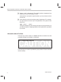
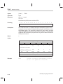
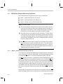
Information about Cautions
This book may contain cautions. A caution describes a situation that could
potentially damage your software or equipment.
This is what a caution looks like.
The information in a caution is provided for your protection. Please read each
caution carefully.
vi
Read This First
Related Documentation From Texas Instruments
Related Documentation From Texas Instruments
General Digital Signal Processing:
Antoniou, Andreas, Digital Filters: Analysis and Design. New York, NY:
McGraw-Hill Company, Inc., 1979.
Brigham, E. Oran, The Fast Fourier Transform. Englewood Cliffs, NJ:
Prentice-Hall, Inc., 1974.
Burrus, C.S. and Parks, T.W., DFT/FFT and Convolution Algorithms. New
York, NY: John Wiley and Sons, Inc., 1984.
Digital Signal Processing Applications with the TMS320 Family, Texas
Instruments, 1986; Prentice-Hall, Inc., 1987.
Gold, Bernard and Rader, C.M., Digital Processing of Signals. New York, NY:
McGraw-Hill Company, Inc., 1969.
Hamming, R.W., Digital Filters. Englewood Cliffs, NJ: Prentice-Hall, Inc., 1977.
IEEE ASSP DSP Committee (Editor), Programs for Digital Signal Processing.
New York, NY: IEEE Press, 1979.
Jackson, Leland B., Digital Filters and Signal Processing. Hingham, MA:
Kluwer Academic Publishers, 1986.
Jones, D.L. and Parks, T.W., A Digital Signal Processing Laboratory Using the
TMS32010. Englewood Cliffs, NJ: Prentice-Hall, Inc., 1987.
Lim, Jae and Oppenheim, Alan V. (Editors), Advanced Topics in Signal
Processing. Englewood Cliffs, NJ: Prentice-Hall, Inc., 1988.
Morris, L. Robert, Digital Signal Processing Software. Ottawa, Canada:
Carleton University, 1983.
Oppenheim, Alan V. (Editor), Applications of Digital Signal Processing.
Englewood Cliffs, NJ: Prentice-Hall, Inc., 1978.
Oppenheim, Alan V. and Schafer, R.W., Digital Signal Processing. Englewood
Cliffs, NJ: Prentice-Hall, Inc., 1975.
Oppenheim, Alan V. and Willsky, A.N. with Young, I.T., Signals and Systems.
Englewood Cliffs, NJ: Prentice-Hall, Inc., 1983.
Parks, T.W. and Burrus, C.S., Digital Filter Design. New York, NY: John Wiley
and Sons, Inc., 1987.
Rabiner, Lawrence R., Gold and Bernard, Theory and Application of Digital
Signal Processing. Englewood Cliffs, NJ: Prentice-Hall, Inc., 1975.
Treichler, J.R., Johnson, Jr., C.R. and Larimore, M.G., A Practical Guide to
Adaptive Filter Design. New York, NY: John Wiley and Sons, Inc., 1987.
vii
Related Documentation From Texas Instruments
Speech:
Gray, A.H. and Markel, J.D., Linear Prediction of Speech. New York, NY:
Springer-Verlag, 1976.
Jayant, N.S. and Noll, Peter, Digital Coding of Waveforms. Englewood Cliffs,
NJ: Prentice-Hall, Inc., 1984.
Papamichalis, Panos, Practical Approaches to Speech Coding. Englewood
Cliffs, NJ: Prentice-Hall, Inc., 1987.
Rabiner, Lawrence R. and Schafer, R.W., Digital Processing of Speech
Signals. Englewood Cliffs, NJ: Prentice-Hall, Inc., 1978.
Image Processing:
Andrews, H.C. and Hunt, B.R., Digital Image Restoration. Englewood Cliffs,
NJ: Prentice-Hall, Inc., 1977.
Gonzales, Rafael C. and Wintz, Paul, Digital Image Processing. Reading, MA:
Addison-Wesley Publishing Company, Inc., 1977.
Pratt, William K., Digital Image Processing. New York, NY: John Wiley and
Sons, 1978.
Digital Control Theory:
Jacquot, R., Modern Digital Control Systems. New York, NY: Marcel Dekker,
Inc., 1981.
Katz, P., Digital Control Using Microprocessors. Englewood Cliffs, NJ:
Prentice-Hall, Inc., 1981.
Kuo, B.C., Digital Control Systems. New York, NY: Holt, Reinholt and Winston,
Inc., 1980.
Moroney, P., Issues in the Implementation of Digital Feedback Compensators.
Cambridge, MA: The MIT Press, 1983.
Phillips, C. and Nagle, H., Digital Control System Analysis and Design.
Englewood Cliffs, NJ: Prentice-Hall, Inc., 1984.
Trademarks
MS, and MS-DOS are trademarks of Microsoft Corp.
VAX, VMS, and Ultrix are trademarks of Digital Equipment Corp.
PC-DOS is a trademark of International Business Machines Corp.
Sun 3 is a trademark of Sun Microsystems, Inc.
UNIX is a registered trademark of UNIX Systems Laboratories.
XDS is a trademark of Texas Instruments Incorporated.
viii
Read This First
If You Need Assistance
If You Need Assistance. . .
If you want to. . .
Do this. . .
Request more information about
Texas Instruments Digital Signal
Processing (DSP) products
Write to:
Texas Instruments Incorporated
Market Communications Manager, MS 736
P.O. Box 1443
Houston, Texas 77251–1443
Order Texas Instruments
documentation
Call the TI Literature Response Center:
(800) 477–8924
Ask questions about product
operation or report suspected
problems
Call the DSP hotline:
(713) 274–2320
Report mistakes in this document
or any other TI documentation
Send your comments to:
Texas Instruments Incorporated
Technical Publications Manager, MS 702
P.O. Box 1443
Houston, Texas 77251–1443
ix
x
Read This First
Contents
Contents
1
Introduction . . . . . . . . . . . . . . . . . . . . . . . . . . . . . . . . . . . . . . . . . . . . . . . . . . . . . . . . . . . . . . . . . . . . .
1.1
General Description . . . . . . . . . . . . . . . . . . . . . . . . . . . . . . . . . . . . . . . . . . . . . . . . . . . . . . . . .
1.2
Key Features . . . . . . . . . . . . . . . . . . . . . . . . . . . . . . . . . . . . . . . . . . . . . . . . . . . . . . . . . . . . . .
1.3
Typical Applications . . . . . . . . . . . . . . . . . . . . . . . . . . . . . . . . . . . . . . . . . . . . . . . . . . . . . . . . .
1-1
1-2
1-6
1-8
2
Pinouts and Signal Descriptions . . . . . . . . . . . . . . . . . . . . . . . . . . . . . . . . . . . . . . . . . . . . . . . . . . 2-1
2.1
TMS320C2x Pinouts . . . . . . . . . . . . . . . . . . . . . . . . . . . . . . . . . . . . . . . . . . . . . . . . . . . . . . . . 2-2
2.2
TMS320C2x Signal Descriptions . . . . . . . . . . . . . . . . . . . . . . . . . . . . . . . . . . . . . . . . . . . . . . 2-4
3
Architecture . . . . . . . . . . . . . . . . . . . . . . . . . . . . . . . . . . . . . . . . . . . . . . . . . . . . . . . . . . . . . . . . . . . . . 3-1
3.1
Architectural Overview . . . . . . . . . . . . . . . . . . . . . . . . . . . . . . . . . . . . . . . . . . . . . . . . . . . . . . 3-2
3.2
Functional Block Diagram . . . . . . . . . . . . . . . . . . . . . . . . . . . . . . . . . . . . . . . . . . . . . . . . . . . . 3-6
3.3
Internal Hardware Summary . . . . . . . . . . . . . . . . . . . . . . . . . . . . . . . . . . . . . . . . . . . . . . . . . 3-9
3.4
Memory Organization . . . . . . . . . . . . . . . . . . . . . . . . . . . . . . . . . . . . . . . . . . . . . . . . . . . . . . 3-12
3.4.1 Data Memory . . . . . . . . . . . . . . . . . . . . . . . . . . . . . . . . . . . . . . . . . . . . . . . . . . . . . . 3-12
3.4.2 Program Memory . . . . . . . . . . . . . . . . . . . . . . . . . . . . . . . . . . . . . . . . . . . . . . . . . . . 3-12
3.4.3 TMS320C2x Memory Maps . . . . . . . . . . . . . . . . . . . . . . . . . . . . . . . . . . . . . . . . . . 3-15
3.4.4 TMS320C26 Memory Maps . . . . . . . . . . . . . . . . . . . . . . . . . . . . . . . . . . . . . . . . . . 3-16
3.4.5 Memory-Mapped Registers . . . . . . . . . . . . . . . . . . . . . . . . . . . . . . . . . . . . . . . . . . 3-22
3.4.6 Auxiliary Registers . . . . . . . . . . . . . . . . . . . . . . . . . . . . . . . . . . . . . . . . . . . . . . . . . . 3-22
3.4.7 Memory Addressing Modes . . . . . . . . . . . . . . . . . . . . . . . . . . . . . . . . . . . . . . . . . . 3-25
3.4.8 Memory-to-Memory Moves . . . . . . . . . . . . . . . . . . . . . . . . . . . . . . . . . . . . . . . . . . 3-27
3.5
Central Arithmetic Logic Unit (CALU) . . . . . . . . . . . . . . . . . . . . . . . . . . . . . . . . . . . . . . . . . 3-28
3.5.1 Scaling Shifter . . . . . . . . . . . . . . . . . . . . . . . . . . . . . . . . . . . . . . . . . . . . . . . . . . . . . 3-30
3.5.2 ALU and Accumulator . . . . . . . . . . . . . . . . . . . . . . . . . . . . . . . . . . . . . . . . . . . . . . . 3-30
3.5.3 Multiplier, T and P Registers . . . . . . . . . . . . . . . . . . . . . . . . . . . . . . . . . . . . . . . . . 3-32
3.6
System Control . . . . . . . . . . . . . . . . . . . . . . . . . . . . . . . . . . . . . . . . . . . . . . . . . . . . . . . . . . . . 3-35
3.6.1 Program Counter and Stack . . . . . . . . . . . . . . . . . . . . . . . . . . . . . . . . . . . . . . . . . 3-35
3.6.2 Pipeline Operation . . . . . . . . . . . . . . . . . . . . . . . . . . . . . . . . . . . . . . . . . . . . . . . . . . 3-37
3.6.3 Reset . . . . . . . . . . . . . . . . . . . . . . . . . . . . . . . . . . . . . . . . . . . . . . . . . . . . . . . . . . . . . 3-47
3.6.4 Status Registers . . . . . . . . . . . . . . . . . . . . . . . . . . . . . . . . . . . . . . . . . . . . . . . . . . . . 3-49
3.6.5 Timer Operation . . . . . . . . . . . . . . . . . . . . . . . . . . . . . . . . . . . . . . . . . . . . . . . . . . . . 3-52
3.6.6 Repeat Counter . . . . . . . . . . . . . . . . . . . . . . . . . . . . . . . . . . . . . . . . . . . . . . . . . . . . 3-53
3.6.7 Powerdown Modes (TMS320C25) . . . . . . . . . . . . . . . . . . . . . . . . . . . . . . . . . . . . 3-53
3.7
External Memory and I/O Interface . . . . . . . . . . . . . . . . . . . . . . . . . . . . . . . . . . . . . . . . . . . 3-54
3.7.1 Memory Combinations . . . . . . . . . . . . . . . . . . . . . . . . . . . . . . . . . . . . . . . . . . . . . . 3-54
3.7.2 Internal Clock Timing Relationships . . . . . . . . . . . . . . . . . . . . . . . . . . . . . . . . . . . 3-56
3.7.3 General-Purpose I/O Pins (BIO and XF) . . . . . . . . . . . . . . . . . . . . . . . . . . . . . . . 3-56
xi
Contents
3.8
3.9
3.10
3.11
3.12
Interrupts . . . . . . . . . . . . . . . . . . . . . . . . . . . . . . . . . . . . . . . . . . . . . . . . . . . . . . . . . . . . . . . . .
3.8.1 Interrupt Operation . . . . . . . . . . . . . . . . . . . . . . . . . . . . . . . . . . . . . . . . . . . . . . . . .
3.8.2 External Interrupt Interface . . . . . . . . . . . . . . . . . . . . . . . . . . . . . . . . . . . . . . . . . .
Serial Port . . . . . . . . . . . . . . . . . . . . . . . . . . . . . . . . . . . . . . . . . . . . . . . . . . . . . . . . . . . . . . . .
3.9.1 Transmit and Receive Operations . . . . . . . . . . . . . . . . . . . . . . . . . . . . . . . . . . . .
3.9.2 Timing and Framing Control . . . . . . . . . . . . . . . . . . . . . . . . . . . . . . . . . . . . . . . . .
3.9.3 Burst-Mode Operation . . . . . . . . . . . . . . . . . . . . . . . . . . . . . . . . . . . . . . . . . . . . . . .
3.9.4 Continuous Operation Using Frame Sync Pulses (TMS320C25) . . . . . . . . . .
3.9.5 Continuous Operation Without Frame Sync Pulses (TMS320C25) . . . . . . . .
3.9.6 Initialization of Continuous Operation Without Frame Sync Pulses . . . . . . . .
Multiprocessing and Direct Memory Access (DMA) . . . . . . . . . . . . . . . . . . . . . . . . . . . . .
3.10.1 Synchronization . . . . . . . . . . . . . . . . . . . . . . . . . . . . . . . . . . . . . . . . . . . . . . . . . . . .
3.10.2 Global Memory . . . . . . . . . . . . . . . . . . . . . . . . . . . . . . . . . . . . . . . . . . . . . . . . . . . . .
3.10.3 The Hold Function . . . . . . . . . . . . . . . . . . . . . . . . . . . . . . . . . . . . . . . . . . . . . . . . . .
General Description of the TMS320C26 . . . . . . . . . . . . . . . . . . . . . . . . . . . . . . . . . . . . . .
General Description of the TMS320C28 . . . . . . . . . . . . . . . . . . . . . . . . . . . . . . . . . . . . . .
3-59
3-59
3-60
3-63
3-65
3-67
3-68
3-69
3-71
3-73
3-75
3-75
3-76
3-78
3-82
3-83
4
Assembly Language Instructions . . . . . . . . . . . . . . . . . . . . . . . . . . . . . . . . . . . . . . . . . . . . . . . . . 4-1
4.1
Memory Addressing Modes . . . . . . . . . . . . . . . . . . . . . . . . . . . . . . . . . . . . . . . . . . . . . . . . . . 4-2
4.1.1 Direct Addressing Mode . . . . . . . . . . . . . . . . . . . . . . . . . . . . . . . . . . . . . . . . . . . . . . 4-2
4.1.2 Indirect Addressing Mode . . . . . . . . . . . . . . . . . . . . . . . . . . . . . . . . . . . . . . . . . . . . . 4-4
4.1.3 Immediate Addressing Mode . . . . . . . . . . . . . . . . . . . . . . . . . . . . . . . . . . . . . . . . . . 4-8
4.2
Instruction Set . . . . . . . . . . . . . . . . . . . . . . . . . . . . . . . . . . . . . . . . . . . . . . . . . . . . . . . . . . . . . 4-11
4.2.1 Symbols and Abbreviations . . . . . . . . . . . . . . . . . . . . . . . . . . . . . . . . . . . . . . . . . . 4-11
4.2.2 Instruction Set Summary . . . . . . . . . . . . . . . . . . . . . . . . . . . . . . . . . . . . . . . . . . . . 4-13
4.3
Individual Instruction Descriptions . . . . . . . . . . . . . . . . . . . . . . . . . . . . . . . . . . . . . . . . . . . . 4-18
5
Software Applications . . . . . . . . . . . . . . . . . . . . . . . . . . . . . . . . . . . . . . . . . . . . . . . . . . . . . . . . . . . 5-1
5.1
Processor Initialization . . . . . . . . . . . . . . . . . . . . . . . . . . . . . . . . . . . . . . . . . . . . . . . . . . . . . . 5-2
5.1.1 TMS320C26 Download/Bootstrapping Modes . . . . . . . . . . . . . . . . . . . . . . . . . . . 5-6
5.2
Program Control . . . . . . . . . . . . . . . . . . . . . . . . . . . . . . . . . . . . . . . . . . . . . . . . . . . . . . . . . . . 5-22
5.2.1 Subroutines . . . . . . . . . . . . . . . . . . . . . . . . . . . . . . . . . . . . . . . . . . . . . . . . . . . . . . . . 5-22
5.2.2 Software Stack . . . . . . . . . . . . . . . . . . . . . . . . . . . . . . . . . . . . . . . . . . . . . . . . . . . . . 5-24
5.2.3 Timer Operation . . . . . . . . . . . . . . . . . . . . . . . . . . . . . . . . . . . . . . . . . . . . . . . . . . . . 5-25
5.2.4 Single-Instruction Loops . . . . . . . . . . . . . . . . . . . . . . . . . . . . . . . . . . . . . . . . . . . . . 5-26
5.2.5 Computed GOTOs . . . . . . . . . . . . . . . . . . . . . . . . . . . . . . . . . . . . . . . . . . . . . . . . . . 5-28
5.3
Interrupt Service Routine . . . . . . . . . . . . . . . . . . . . . . . . . . . . . . . . . . . . . . . . . . . . . . . . . . . 5-29
5.3.1 Context Switching . . . . . . . . . . . . . . . . . . . . . . . . . . . . . . . . . . . . . . . . . . . . . . . . . . 5-29
5.3.2 Interrupt Priority . . . . . . . . . . . . . . . . . . . . . . . . . . . . . . . . . . . . . . . . . . . . . . . . . . . . 5-32
5.4
Memory Management . . . . . . . . . . . . . . . . . . . . . . . . . . . . . . . . . . . . . . . . . . . . . . . . . . . . . . 5-33
5.4.1 Block Moves . . . . . . . . . . . . . . . . . . . . . . . . . . . . . . . . . . . . . . . . . . . . . . . . . . . . . . . 5-33
5.4.2 Configuring On-Chip RAM . . . . . . . . . . . . . . . . . . . . . . . . . . . . . . . . . . . . . . . . . . . 5-35
5.4.3 Using On-Chip RAM for Program Execution . . . . . . . . . . . . . . . . . . . . . . . . . . . . 5-38
5.5
Fundamental Logical and Arithmetic Operations . . . . . . . . . . . . . . . . . . . . . . . . . . . . . . . 5-43
5.5.1 Status Register Effect on Data Processing . . . . . . . . . . . . . . . . . . . . . . . . . . . . . 5-43
5.5.2 Bit Manipulation . . . . . . . . . . . . . . . . . . . . . . . . . . . . . . . . . . . . . . . . . . . . . . . . . . . . 5-44
xii
Table of Contents
Contents
5.6
5.7
6
Advanced Arithmetic Operations . . . . . . . . . . . . . . . . . . . . . . . . . . . . . . . . . . . . . . . . . . . . .
5.6.1 Overflow Management . . . . . . . . . . . . . . . . . . . . . . . . . . . . . . . . . . . . . . . . . . . . . .
5.6.2 Scaling . . . . . . . . . . . . . . . . . . . . . . . . . . . . . . . . . . . . . . . . . . . . . . . . . . . . . . . . . . . .
5.6.3 Shifting Data . . . . . . . . . . . . . . . . . . . . . . . . . . . . . . . . . . . . . . . . . . . . . . . . . . . . . . .
5.6.4 Moving Data . . . . . . . . . . . . . . . . . . . . . . . . . . . . . . . . . . . . . . . . . . . . . . . . . . . . . . .
5.6.5 Multiplication . . . . . . . . . . . . . . . . . . . . . . . . . . . . . . . . . . . . . . . . . . . . . . . . . . . . . . .
5.6.6 Division . . . . . . . . . . . . . . . . . . . . . . . . . . . . . . . . . . . . . . . . . . . . . . . . . . . . . . . . . . .
5.6.7 Floating-Point Arithmetic . . . . . . . . . . . . . . . . . . . . . . . . . . . . . . . . . . . . . . . . . . . .
5.6.8 Indexed Addressing . . . . . . . . . . . . . . . . . . . . . . . . . . . . . . . . . . . . . . . . . . . . . . . . .
5.6.9 Extended-Precision Arithmetic . . . . . . . . . . . . . . . . . . . . . . . . . . . . . . . . . . . . . . .
Application-Oriented Operations . . . . . . . . . . . . . . . . . . . . . . . . . . . . . . . . . . . . . . . . . . . . .
5.7.1 Companding . . . . . . . . . . . . . . . . . . . . . . . . . . . . . . . . . . . . . . . . . . . . . . . . . . . . . . .
5.7.2 FIR/IIR Filtering . . . . . . . . . . . . . . . . . . . . . . . . . . . . . . . . . . . . . . . . . . . . . . . . . . . .
5.7.3 Adaptive Filtering . . . . . . . . . . . . . . . . . . . . . . . . . . . . . . . . . . . . . . . . . . . . . . . . . . .
5.7.4 Fast Fourier Transforms (FFT) . . . . . . . . . . . . . . . . . . . . . . . . . . . . . . . . . . . . . . .
5.7.5 PID Control . . . . . . . . . . . . . . . . . . . . . . . . . . . . . . . . . . . . . . . . . . . . . . . . . . . . . . . .
5-46
5-46
5-47
5-47
5-51
5-53
5-57
5-60
5-62
5-62
5-68
5-68
5-70
5-71
5-75
5-82
Hardware Applications . . . . . . . . . . . . . . . . . . . . . . . . . . . . . . . . . . . . . . . . . . . . . . . . . . . . . . . . . . . 6-1
6.1
System Control Circuitry . . . . . . . . . . . . . . . . . . . . . . . . . . . . . . . . . . . . . . . . . . . . . . . . . . . . . 6-2
6.1.1 Powerup Reset Circuit . . . . . . . . . . . . . . . . . . . . . . . . . . . . . . . . . . . . . . . . . . . . . . . 6-2
6.1.2 Crystal Oscillator Circuit . . . . . . . . . . . . . . . . . . . . . . . . . . . . . . . . . . . . . . . . . . . . . . 6-5
6.1.3 User Target Design Considerations for the XDS . . . . . . . . . . . . . . . . . . . . . . . . . 6-7
6.2
Interfacing Memories . . . . . . . . . . . . . . . . . . . . . . . . . . . . . . . . . . . . . . . . . . . . . . . . . . . . . . . 6-11
6.2.1 Interfacing PROMs . . . . . . . . . . . . . . . . . . . . . . . . . . . . . . . . . . . . . . . . . . . . . . . . . 6-12
6.2.2 Wait-State Generator . . . . . . . . . . . . . . . . . . . . . . . . . . . . . . . . . . . . . . . . . . . . . . . 6-19
6.2.3 Interfacing EPROMs . . . . . . . . . . . . . . . . . . . . . . . . . . . . . . . . . . . . . . . . . . . . . . . . 6-22
6.2.4 Interfacing Static RAMs . . . . . . . . . . . . . . . . . . . . . . . . . . . . . . . . . . . . . . . . . . . . . 6-26
6.2.5 Interface Timing Analysis . . . . . . . . . . . . . . . . . . . . . . . . . . . . . . . . . . . . . . . . . . . . 6-29
6.3
Direct Memory Access (DMA) . . . . . . . . . . . . . . . . . . . . . . . . . . . . . . . . . . . . . . . . . . . . . . . 6-32
6.4
Global Memory . . . . . . . . . . . . . . . . . . . . . . . . . . . . . . . . . . . . . . . . . . . . . . . . . . . . . . . . . . . . 6-35
6.5
Interfacing Peripherals . . . . . . . . . . . . . . . . . . . . . . . . . . . . . . . . . . . . . . . . . . . . . . . . . . . . . 6-37
6.5.1 Combo-Codec Interface . . . . . . . . . . . . . . . . . . . . . . . . . . . . . . . . . . . . . . . . . . . . . 6-37
6.5.2 AIC Interface . . . . . . . . . . . . . . . . . . . . . . . . . . . . . . . . . . . . . . . . . . . . . . . . . . . . . . . 6-40
6.5.3 Digital-to-Analog (D/A) Interface . . . . . . . . . . . . . . . . . . . . . . . . . . . . . . . . . . . . . . 6-42
6.5.4 Analog-to-Digital (A/D) Interface . . . . . . . . . . . . . . . . . . . . . . . . . . . . . . . . . . . . . . 6-43
6.5.5 I/O Ports . . . . . . . . . . . . . . . . . . . . . . . . . . . . . . . . . . . . . . . . . . . . . . . . . . . . . . . . . . 6-46
6.6
System Applications . . . . . . . . . . . . . . . . . . . . . . . . . . . . . . . . . . . . . . . . . . . . . . . . . . . . . . . 6-48
6.6.1 Echo Cancellation . . . . . . . . . . . . . . . . . . . . . . . . . . . . . . . . . . . . . . . . . . . . . . . . . . 6-48
6.6.2 High-Speed Modem . . . . . . . . . . . . . . . . . . . . . . . . . . . . . . . . . . . . . . . . . . . . . . . . 6-48
6.6.3 Voice Coding . . . . . . . . . . . . . . . . . . . . . . . . . . . . . . . . . . . . . . . . . . . . . . . . . . . . . . 6-49
6.6.4 Graphics and Image Processing . . . . . . . . . . . . . . . . . . . . . . . . . . . . . . . . . . . . . . 6-50
6.6.5 High-Speed Control . . . . . . . . . . . . . . . . . . . . . . . . . . . . . . . . . . . . . . . . . . . . . . . . . 6-51
6.6.6 Instrumentation and Numeric Processing . . . . . . . . . . . . . . . . . . . . . . . . . . . . . . 6-51
xiii
Contents
A
TMS320C25 Digital Signal Processors . . . . . . . . . . . . . . . . . . . . . . . . . . . . . . . . . . . . . . . . . . . . A-1
B
TMS320C26 Digital Signal Processor . . . . . . . . . . . . . . . . . . . . . . . . . . . . . . . . . . . . . . . . . . . . . . B-1
C
TMS320C28 Digital Signal Processor . . . . . . . . . . . . . . . . . . . . . . . . . . . . . . . . . . . . . . . . . . . . . . C-1
D
SMJ320C2x Digital Signal Processors . . . . . . . . . . . . . . . . . . . . . . . . . . . . . . . . . . . . . . . . . . . . . D-1
E
Instruction Cycle Timings . . . . . . . . . . . . . . . . . . . . . . . . . . . . . . . . . . . . . . . . . . . . . . . . . . . . . . . . E-1
E.1 TMS320C2x Instruction Cycle Timings . . . . . . . . . . . . . . . . . . . . . . . . . . . . . . . . . . . . . . . . E-2
F
TMS320E25 EPROM Programming . . . . . . . . . . . . . . . . . . . . . . . . . . . . . . . . . . . . . . . . . . . . . . . . F-1
F.1
Using the EPROM Programmer Adapter Socket . . . . . . . . . . . . . . . . . . . . . . . . . . . . . . . . F-2
F.1.1 Supplying External Power . . . . . . . . . . . . . . . . . . . . . . . . . . . . . . . . . . . . . . . . . . . . F-2
F.2
Programming and Verification . . . . . . . . . . . . . . . . . . . . . . . . . . . . . . . . . . . . . . . . . . . . . . . . F-4
F.2.1 Erasure . . . . . . . . . . . . . . . . . . . . . . . . . . . . . . . . . . . . . . . . . . . . . . . . . . . . . . . . . . . . F-7
F.2.2 FAST Programming . . . . . . . . . . . . . . . . . . . . . . . . . . . . . . . . . . . . . . . . . . . . . . . . . . F-7
F.2.3 SNAP! Pulse Programming . . . . . . . . . . . . . . . . . . . . . . . . . . . . . . . . . . . . . . . . . . . F-8
F.2.4 Program Verify . . . . . . . . . . . . . . . . . . . . . . . . . . . . . . . . . . . . . . . . . . . . . . . . . . . . . . F-8
F.2.5 Program Inhibit . . . . . . . . . . . . . . . . . . . . . . . . . . . . . . . . . . . . . . . . . . . . . . . . . . . . . F-11
F.2.6 Read . . . . . . . . . . . . . . . . . . . . . . . . . . . . . . . . . . . . . . . . . . . . . . . . . . . . . . . . . . . . . F-11
F.2.7 Output Disable . . . . . . . . . . . . . . . . . . . . . . . . . . . . . . . . . . . . . . . . . . . . . . . . . . . . . F-11
F.3
EPROM Protection and Verification . . . . . . . . . . . . . . . . . . . . . . . . . . . . . . . . . . . . . . . . . . F-12
F.3.1 EPROM Protection . . . . . . . . . . . . . . . . . . . . . . . . . . . . . . . . . . . . . . . . . . . . . . . . . F-12
F.3.2 How the RBIT Works . . . . . . . . . . . . . . . . . . . . . . . . . . . . . . . . . . . . . . . . . . . . . . . . F-14
F.3.3 Protect Verify . . . . . . . . . . . . . . . . . . . . . . . . . . . . . . . . . . . . . . . . . . . . . . . . . . . . . . F-15
G
Analog Interface Peripherals and Applications . . . . . . . . . . . . . . . . . . . . . . . . . . . . . . . . . . . . . G-1
G.1 Multimedia Applications . . . . . . . . . . . . . . . . . . . . . . . . . . . . . . . . . . . . . . . . . . . . . . . . . . . . . G-2
G.1.1 System Design Considerations . . . . . . . . . . . . . . . . . . . . . . . . . . . . . . . . . . . . . . . . G-2
G.1.2 Multimedia-Related Devices . . . . . . . . . . . . . . . . . . . . . . . . . . . . . . . . . . . . . . . . . . G-4
G.2 Telecommunications Applications . . . . . . . . . . . . . . . . . . . . . . . . . . . . . . . . . . . . . . . . . . . . . G-5
G.3 Dedicated Speech Synthesis Applications . . . . . . . . . . . . . . . . . . . . . . . . . . . . . . . . . . . . G-10
G.4 Servo Control/Disk Drive Applications . . . . . . . . . . . . . . . . . . . . . . . . . . . . . . . . . . . . . . . . G-12
G.5 Modem Applications . . . . . . . . . . . . . . . . . . . . . . . . . . . . . . . . . . . . . . . . . . . . . . . . . . . . . . . G-15
G.6 Advanced Digital Electronics Applications for Consumers . . . . . . . . . . . . . . . . . . . . . . . G-18
H
Memories, Analog Converters, Sockets, and Crystals . . . . . . . . . . . . . . . . . . . . . . . . . . . . . .
H.1 Memories and Analog Converters . . . . . . . . . . . . . . . . . . . . . . . . . . . . . . . . . . . . . . . . . . . . .
H.2 Sockets . . . . . . . . . . . . . . . . . . . . . . . . . . . . . . . . . . . . . . . . . . . . . . . . . . . . . . . . . . . . . . . . . . .
H.3 Crystals . . . . . . . . . . . . . . . . . . . . . . . . . . . . . . . . . . . . . . . . . . . . . . . . . . . . . . . . . . . . . . . . . . .
I
ROM Codes . . . . . . . . . . . . . . . . . . . . . . . . . . . . . . . . . . . . . . . . . . . . . . . . . . . . . . . . . . . . . . . . . . . . . . I-1
J
Quality and Reliability . . . . . . . . . . . . . . . . . . . . . . . . . . . . . . . . . . . . . . . . . . . . . . . . . . . . . . . . . . . J-1
J.1
Reliability Stress Tests . . . . . . . . . . . . . . . . . . . . . . . . . . . . . . . . . . . . . . . . . . . . . . . . . . . . . . J-2
K
Development Support . . . . . . . . . . . . . . . . . . . . . . . . . . . . . . . . . . . . . . . . . . . . . . . . . . . . . . . . . . . . K-1
K.1 Device and Development Support Tool Nomenclature . . . . . . . . . . . . . . . . . . . . . . . . . . . K-2
xiv
H-1
H-2
H-3
H-4
Table of Contents
Figures
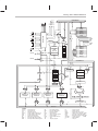
Figures
1–1
2–1
2–2
3–1
3–2
3–3
3–4
3–5
3–6
3–7
3–8
3–9
3–10
3–11
3–12
3–13
3–14
3–15
3–16
3–17
3–18
3–19
3–20
3–21
3–22
3–23
3–24
3–25
3–26
3–27
3–28
3–29
3–30
3–31
3–32
3–33
3–34
3–35
3–36
TMS320 Device Evolution . . . . . . . . . . . . . . . . . . . . . . . . . . . . . . . . . . . . . . . . . . . . . . . . . . . . . . 1-3
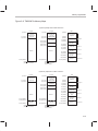
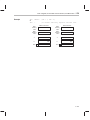
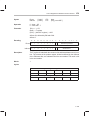
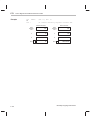
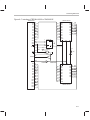
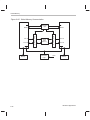
TMS320C2x Pin Assignments . . . . . . . . . . . . . . . . . . . . . . . . . . . . . . . . . . . . . . . . . . . . . . . . . . 2-2
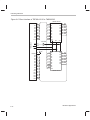
TMS320C28 Pin Assignments . . . . . . . . . . . . . . . . . . . . . . . . . . . . . . . . . . . . . . . . . . . . . . . . . . 2-3
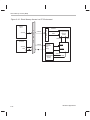
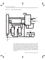
TMS320C2x Simplified Block Diagram . . . . . . . . . . . . . . . . . . . . . . . . . . . . . . . . . . . . . . . . . . . 3-3
TMS320C25/E25 Block Diagram . . . . . . . . . . . . . . . . . . . . . . . . . . . . . . . . . . . . . . . . . . . . . . . . 3-7
TMS320C26 Block Diagram . . . . . . . . . . . . . . . . . . . . . . . . . . . . . . . . . . . . . . . . . . . . . . . . . . . . 3-8
TMS320C2x On-Chip Data Memory . . . . . . . . . . . . . . . . . . . . . . . . . . . . . . . . . . . . . . . . . . . . 3-13
TMS320C26 On-Chip Data Memory . . . . . . . . . . . . . . . . . . . . . . . . . . . . . . . . . . . . . . . . . . . . 3-14
Comparison of Internal RAM Configured as Data Space . . . . . . . . . . . . . . . . . . . . . . . . . . 3-18
Comparison of Internal RAM Configured as Program Space . . . . . . . . . . . . . . . . . . . . . . . 3-18
TMS320C2x Memory Maps . . . . . . . . . . . . . . . . . . . . . . . . . . . . . . . . . . . . . . . . . . . . . . . . . . . 3-19
TMS320C26 Memory Maps . . . . . . . . . . . . . . . . . . . . . . . . . . . . . . . . . . . . . . . . . . . . . . . . . . . 3-20
Indirect Auxiliary Register Addressing Example . . . . . . . . . . . . . . . . . . . . . . . . . . . . . . . . . . 3-23
Auxiliary Register File . . . . . . . . . . . . . . . . . . . . . . . . . . . . . . . . . . . . . . . . . . . . . . . . . . . . . . . . 3-24
Methods of Instruction Operand Addressing . . . . . . . . . . . . . . . . . . . . . . . . . . . . . . . . . . . . . 3-26
Central Arithmetic Logic Unit (CALU), TMS320C2x . . . . . . . . . . . . . . . . . . . . . . . . . . . . . . . 3-29
Examples of TMS320C25 Carry Bit Operation . . . . . . . . . . . . . . . . . . . . . . . . . . . . . . . . . . . 3-31
Program Counter, Stack, and Related Hardware . . . . . . . . . . . . . . . . . . . . . . . . . . . . . . . . . 3-35
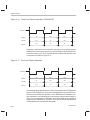
Three-Level Pipeline Operation (TMS320C25) . . . . . . . . . . . . . . . . . . . . . . . . . . . . . . . . . . . 3-38
Two-Level Pipeline Operation . . . . . . . . . . . . . . . . . . . . . . . . . . . . . . . . . . . . . . . . . . . . . . . . . . 3-38
TMS320C25 Standard Pipeline Operation . . . . . . . . . . . . . . . . . . . . . . . . . . . . . . . . . . . . . . . 3-39
Pipeline Operation of ADD Followed by SACL . . . . . . . . . . . . . . . . . . . . . . . . . . . . . . . . . . . 3-41
Pipeline Operation With Wait States . . . . . . . . . . . . . . . . . . . . . . . . . . . . . . . . . . . . . . . . . . . . 3-42
Pipeline With External Data Bus Conflict . . . . . . . . . . . . . . . . . . . . . . . . . . . . . . . . . . . . . . . . 3-43
Pipeline Operation of Branch to On-Chip RAM . . . . . . . . . . . . . . . . . . . . . . . . . . . . . . . . . . . 3-44
Pipeline Operation of RET From On-Chip RAM . . . . . . . . . . . . . . . . . . . . . . . . . . . . . . . . . . 3-45
TMS320C2x Status Register Organization . . . . . . . . . . . . . . . . . . . . . . . . . . . . . . . . . . . . . . . 3-49
TMS320C26 Status Register Organization . . . . . . . . . . . . . . . . . . . . . . . . . . . . . . . . . . . . . . 3-50
Timer Block Diagram . . . . . . . . . . . . . . . . . . . . . . . . . . . . . . . . . . . . . . . . . . . . . . . . . . . . . . . . . 3-52
Four-Phase Clock . . . . . . . . . . . . . . . . . . . . . . . . . . . . . . . . . . . . . . . . . . . . . . . . . . . . . . . . . . . . 3-56
BIO Timing Diagram . . . . . . . . . . . . . . . . . . . . . . . . . . . . . . . . . . . . . . . . . . . . . . . . . . . . . . . . . . 3-57
External Flag Timing Diagram . . . . . . . . . . . . . . . . . . . . . . . . . . . . . . . . . . . . . . . . . . . . . . . . . 3-58
Interrupt Mask Register (IMR) . . . . . . . . . . . . . . . . . . . . . . . . . . . . . . . . . . . . . . . . . . . . . . . . . 3-60
Internal Interrupt Logic Diagram . . . . . . . . . . . . . . . . . . . . . . . . . . . . . . . . . . . . . . . . . . . . . . . . 3-61
Interrupt Timing Diagram (TMS320C25) . . . . . . . . . . . . . . . . . . . . . . . . . . . . . . . . . . . . . . . . . 3-62
The DRR and DXR Registers . . . . . . . . . . . . . . . . . . . . . . . . . . . . . . . . . . . . . . . . . . . . . . . . . . 3-64
Serial Port Block Diagram . . . . . . . . . . . . . . . . . . . . . . . . . . . . . . . . . . . . . . . . . . . . . . . . . . . . . 3-65
Serial Port Transmit Timing Diagram . . . . . . . . . . . . . . . . . . . . . . . . . . . . . . . . . . . . . . . . . . . . 3-66
Serial Port Receive Timing Diagram . . . . . . . . . . . . . . . . . . . . . . . . . . . . . . . . . . . . . . . . . . . . 3-67
xv
Figures
3–37
3–38
3–39
3–40
3–41
3–42
3–43
3–44
3–45
3–46
3–47
3–48
4–1
4–2
5–1
5–2
5–3
5–4
5–5
5–6
5–7
5–8
5–9
5–10
5–11
5–12
5–13
5–14
6–1
6–2
6–3
6–4
6–5
6–6
6–7
6–8
6–9
6–10
6–11
6–12
6–13
6–14
6–15
6–16
6–17
xvi
Burst-Mode Serial Port Transmit Operation . . . . . . . . . . . . . . . . . . . . . . . . . . . . . . . . . . . . . . 3-68
Burst-Mode Serial Port Receive Operation . . . . . . . . . . . . . . . . . . . . . . . . . . . . . . . . . . . . . . 3-68
Byte-Mode DRR Operation (TMS320C25) . . . . . . . . . . . . . . . . . . . . . . . . . . . . . . . . . . . . . . . 3-69
Serial Port Transmit Continuous Operation (FSM = 1) . . . . . . . . . . . . . . . . . . . . . . . . . . . . . 3-70
Serial Port Receive Continuous Operation (FSM = 1) . . . . . . . . . . . . . . . . . . . . . . . . . . . . . 3-70
Serial Port Transmit Continuous Operation (FSM = 0) . . . . . . . . . . . . . . . . . . . . . . . . . . . . . 3-72
Serial Port Receive Continuous Operation (FSM = 0) . . . . . . . . . . . . . . . . . . . . . . . . . . . . . 3-72
Continuous Transmit Operation Initialization . . . . . . . . . . . . . . . . . . . . . . . . . . . . . . . . . . . . . 3-74
Continuous Receive Operation Initialization . . . . . . . . . . . . . . . . . . . . . . . . . . . . . . . . . . . . . . 3-74
Synchronization Timing Diagram (TMS320C25) . . . . . . . . . . . . . . . . . . . . . . . . . . . . . . . . . . 3-76
Global Memory Access Timing . . . . . . . . . . . . . . . . . . . . . . . . . . . . . . . . . . . . . . . . . . . . . . . . . 3-77
TMS320C25 Hold Timing Diagram . . . . . . . . . . . . . . . . . . . . . . . . . . . . . . . . . . . . . . . . . . . . . 3-80
Direct Addressing Block Diagram . . . . . . . . . . . . . . . . . . . . . . . . . . . . . . . . . . . . . . . . . . . . . . . 4-3
Indirect Addressing Block Diagram . . . . . . . . . . . . . . . . . . . . . . . . . . . . . . . . . . . . . . . . . . . . . . 4-4
BIO–XF Handshake . . . . . . . . . . . . . . . . . . . . . . . . . . . . . . . . . . . . . . . . . . . . . . . . . . . . . . . . . . . 5-7
Sequence for 8-Bit Transfers . . . . . . . . . . . . . . . . . . . . . . . . . . . . . . . . . . . . . . . . . . . . . . . . . . . 5-8
Sequence for 16-Bit Transfers . . . . . . . . . . . . . . . . . . . . . . . . . . . . . . . . . . . . . . . . . . . . . . . . . . 5-8
Building LENGTH From STATUS and PROGRAM LENGTH Words . . . . . . . . . . . . . . . . . . 5-9
RS232 Connection to the TMS320C26 . . . . . . . . . . . . . . . . . . . . . . . . . . . . . . . . . . . . . . . . . . 5-11
Sequence for RS232 Transfer (8 Data Bits Only) . . . . . . . . . . . . . . . . . . . . . . . . . . . . . . . . . 5-13
Building LENGTH From STATUS and PROGRAM LENGTH Words . . . . . . . . . . . . . . . . . 5-14
External Memory Byte Ordering . . . . . . . . . . . . . . . . . . . . . . . . . . . . . . . . . . . . . . . . . . . . . . . . 5-16
On-Chip RAM Configurations . . . . . . . . . . . . . . . . . . . . . . . . . . . . . . . . . . . . . . . . . . . . . . . . . . 5-36
MACD Operation . . . . . . . . . . . . . . . . . . . . . . . . . . . . . . . . . . . . . . . . . . . . . . . . . . . . . . . . . . . . . 5-52
Execution Time vs. Number of Multiply-Accumulates (TMS320C25) . . . . . . . . . . . . . . . . 5-55
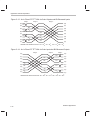
Program Memory vs. Number of Multiply-Accumulates . . . . . . . . . . . . . . . . . . . . . . . . . . . . 5-56
An In-Place DIT FFT With In-Order Outputs and Bit-Reversed Inputs . . . . . . . . . . . . . . . 5-76
An In-Place DIT FFT With In-Order Inputs but Bit-Reversed Outputs . . . . . . . . . . . . . . . . 5-76
Powerup Reset Circuit . . . . . . . . . . . . . . . . . . . . . . . . . . . . . . . . . . . . . . . . . . . . . . . . . . . . . . . . . 6-3
Voltage on TMS320C25 Reset Pin . . . . . . . . . . . . . . . . . . . . . . . . . . . . . . . . . . . . . . . . . . . . . . 6-4
Crystal Oscillator Circuit . . . . . . . . . . . . . . . . . . . . . . . . . . . . . . . . . . . . . . . . . . . . . . . . . . . . . . . 6-5
Magnitude of Impedance of Oscillator LC Network . . . . . . . . . . . . . . . . . . . . . . . . . . . . . . . . . 6-6
Direct Interface of TBP38L165-35 to TMS320C25 . . . . . . . . . . . . . . . . . . . . . . . . . . . . . . . . 6-14
Interface Timing of TBP38L165-35 to TMS320C25 . . . . . . . . . . . . . . . . . . . . . . . . . . . . . . . 6-15
Interface of TBP38L165-35 to TMS320C25 . . . . . . . . . . . . . . . . . . . . . . . . . . . . . . . . . . . . . . 6-17
Interface Timing of TBP38L165-35 to TMS320C25 (Address Decoding) . . . . . . . . . . . . . 6-18
One Wait-State Memory Access Timing . . . . . . . . . . . . . . . . . . . . . . . . . . . . . . . . . . . . . . . . . 6-20
Wait-State Generator Design . . . . . . . . . . . . . . . . . . . . . . . . . . . . . . . . . . . . . . . . . . . . . . . . . . 6-21
Wait-State Generator Timing . . . . . . . . . . . . . . . . . . . . . . . . . . . . . . . . . . . . . . . . . . . . . . . . . . 6-22
Interface of WS57C65F-12 to TMS320C25 . . . . . . . . . . . . . . . . . . . . . . . . . . . . . . . . . . . . . . 6-23
Interface Timing of WS57C65F-12 to TMS320C25 . . . . . . . . . . . . . . . . . . . . . . . . . . . . . . . 6-24
Interface of TMS27C64-20 to TMS320C25 . . . . . . . . . . . . . . . . . . . . . . . . . . . . . . . . . . . . . . 6-25
Interface Timing of TMS27C64-20 to TMS320C25 . . . . . . . . . . . . . . . . . . . . . . . . . . . . . . . . 6-26
Interface of CY7C169-25 to TMS320C25 . . . . . . . . . . . . . . . . . . . . . . . . . . . . . . . . . . . . . . . . 6-28
Interface Timing of CY7C169-25 to TMS320C25 . . . . . . . . . . . . . . . . . . . . . . . . . . . . . . . . . 6-29
Table of Contents
Figures
6–18
6–19
6–20
6–21
6–22
6–23
6–24
6–25
6–26
6–27
6–28
6–29
6–30
6–31
6–32
6–33
6–34
6–35
6–36
F–1
F–2
F–3
F–4
F–5
F–6
F–7
F–8
F–9
F–10
G–1
G–2
G–3
G–4
G–5
G–6
G–7
G–8
G–9
G–10
G–11
G–12
G–13
G–14
H–1
I–1
K–1
K–2
Direct Memory Access Using a Master-Slave Configuration . . . . . . . . . . . . . . . . . . . . . . . . 6-33
Direct Memory Access in a PC Environment . . . . . . . . . . . . . . . . . . . . . . . . . . . . . . . . . . . . . 6-34
Global Memory Communication . . . . . . . . . . . . . . . . . . . . . . . . . . . . . . . . . . . . . . . . . . . . . . . . 6-36
Interface of TMS320C25 to TCM29C16 Codec . . . . . . . . . . . . . . . . . . . . . . . . . . . . . . . . . . . 6-38
Interface of TLC32040 to TMS320C2x . . . . . . . . . . . . . . . . . . . . . . . . . . . . . . . . . . . . . . . . . . 6-41
Synchronous Timing of TLC32040 to TMS320C2x . . . . . . . . . . . . . . . . . . . . . . . . . . . . . . . . 6-41
Asynchronous Timing of TLC32040 to TMS320C2x . . . . . . . . . . . . . . . . . . . . . . . . . . . . . . . 6-42
Interface of TLC7524 to TMS320C2x . . . . . . . . . . . . . . . . . . . . . . . . . . . . . . . . . . . . . . . . . . . 6-42
Interface Timing of TLC7524 to TMS320C2x . . . . . . . . . . . . . . . . . . . . . . . . . . . . . . . . . . . . . 6-43
Interface of TLC0820 to TMS320C2x . . . . . . . . . . . . . . . . . . . . . . . . . . . . . . . . . . . . . . . . . . . 6-44
Interface Timing of TLC0820 to TMS320C2x . . . . . . . . . . . . . . . . . . . . . . . . . . . . . . . . . . . . . 6-45
I/O Port Addressing . . . . . . . . . . . . . . . . . . . . . . . . . . . . . . . . . . . . . . . . . . . . . . . . . . . . . . . . . . 6-46
I/O Port Processor-to-Processor Communication . . . . . . . . . . . . . . . . . . . . . . . . . . . . . . . . . 6-47
Echo Canceler . . . . . . . . . . . . . . . . . . . . . . . . . . . . . . . . . . . . . . . . . . . . . . . . . . . . . . . . . . . . . . . 6-48
High-Speed Modem . . . . . . . . . . . . . . . . . . . . . . . . . . . . . . . . . . . . . . . . . . . . . . . . . . . . . . . . . . 6-49
Voice Coding System . . . . . . . . . . . . . . . . . . . . . . . . . . . . . . . . . . . . . . . . . . . . . . . . . . . . . . . . . 6-49
Graphics System . . . . . . . . . . . . . . . . . . . . . . . . . . . . . . . . . . . . . . . . . . . . . . . . . . . . . . . . . . . . . 6-50
Robot Axis Controller Subsystem . . . . . . . . . . . . . . . . . . . . . . . . . . . . . . . . . . . . . . . . . . . . . . 6-51
Instrumentation System . . . . . . . . . . . . . . . . . . . . . . . . . . . . . . . . . . . . . . . . . . . . . . . . . . . . . . . 6-51
EPROM Programming Adapter Socket . . . . . . . . . . . . . . . . . . . . . . . . . . . . . . . . . . . . . . . . . . . F-2
VCC and VPP Jumper Settings for External Power . . . . . . . . . . . . . . . . . . . . . . . . . . . . . . . . . F-3
EPROM Programming Data Format . . . . . . . . . . . . . . . . . . . . . . . . . . . . . . . . . . . . . . . . . . . . . F-4
TMS320E25 EPROM Conversion to TMS27C64 EPROM Pinout . . . . . . . . . . . . . . . . . . . . F-5
FAST Programming Flowchart . . . . . . . . . . . . . . . . . . . . . . . . . . . . . . . . . . . . . . . . . . . . . . . . . . F-9
SNAP! Pulse Programming Flowchart . . . . . . . . . . . . . . . . . . . . . . . . . . . . . . . . . . . . . . . . . . F-10
Programming Timing . . . . . . . . . . . . . . . . . . . . . . . . . . . . . . . . . . . . . . . . . . . . . . . . . . . . . . . . . F-11
EPROM Protection Flowchart . . . . . . . . . . . . . . . . . . . . . . . . . . . . . . . . . . . . . . . . . . . . . . . . . . F-13
How the RBIT Fits Into the TMS320E25 Block Diagrams . . . . . . . . . . . . . . . . . . . . . . . . . . F-14
EPROM Protection Timing . . . . . . . . . . . . . . . . . . . . . . . . . . . . . . . . . . . . . . . . . . . . . . . . . . . . F-15
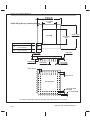
System Block Diagram . . . . . . . . . . . . . . . . . . . . . . . . . . . . . . . . . . . . . . . . . . . . . . . . . . . . . . . . . G-2
Multimedia Speech Encoding and Modem Communication . . . . . . . . . . . . . . . . . . . . . . . . . G-3
TMS320C25 to TLC32047 Interface . . . . . . . . . . . . . . . . . . . . . . . . . . . . . . . . . . . . . . . . . . . . . G-3
Typical DSP/Combo Interface . . . . . . . . . . . . . . . . . . . . . . . . . . . . . . . . . . . . . . . . . . . . . . . . . . . G-6
DSP/Combo Interface Timing . . . . . . . . . . . . . . . . . . . . . . . . . . . . . . . . . . . . . . . . . . . . . . . . . . . G-7
General Telecom Applications . . . . . . . . . . . . . . . . . . . . . . . . . . . . . . . . . . . . . . . . . . . . . . . . . . G-9
Generic Telecom Application . . . . . . . . . . . . . . . . . . . . . . . . . . . . . . . . . . . . . . . . . . . . . . . . . . . G-9
Generic Servo Control Loop . . . . . . . . . . . . . . . . . . . . . . . . . . . . . . . . . . . . . . . . . . . . . . . . . . . G-12
Disk Drive Control System Block Diagram . . . . . . . . . . . . . . . . . . . . . . . . . . . . . . . . . . . . . . . G-13
TMS320C14 – TLC32071 Interface . . . . . . . . . . . . . . . . . . . . . . . . . . . . . . . . . . . . . . . . . . . . . G-14
High-Speed V.32 Bis and Multistandard Modem With the TLC320AC01 AIC . . . . . . . . . G-16
Applications Performance Requirements . . . . . . . . . . . . . . . . . . . . . . . . . . . . . . . . . . . . . . . . G-18
Video Signal Processing Basic System . . . . . . . . . . . . . . . . . . . . . . . . . . . . . . . . . . . . . . . . . G-19
Typical Digital Audio Implementation . . . . . . . . . . . . . . . . . . . . . . . . . . . . . . . . . . . . . . . . . . . . G-19
Crystal Connection . . . . . . . . . . . . . . . . . . . . . . . . . . . . . . . . . . . . . . . . . . . . . . . . . . . . . . . . . . . . H-4
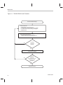
TMS320 ROM Code Flowchart . . . . . . . . . . . . . . . . . . . . . . . . . . . . . . . . . . . . . . . . . . . . . . . . . . I-2
TMS320 Device Nomenclature . . . . . . . . . . . . . . . . . . . . . . . . . . . . . . . . . . . . . . . . . . . . . . . . . . K-3
TMS320 Development Tool Nomenclature . . . . . . . . . . . . . . . . . . . . . . . . . . . . . . . . . . . . . . . . K-4
xvii
Tables
Tables
1–1
1–2
2–1
3–1
3–2
3–3
3–4
3–5
3–6
3–7
3–8
3–9
4–1
4–2
4–3
4–4
5–1
5–2
5–3
5–4
6–1
6–2
6–3
6–4
6–5
6–6
E–1
E–2
E–3
F–1
F–2
F–3
G–1
G–2
G–3
G–4
xviii
TMS320C2x Processors Overview . . . . . . . . . . . . . . . . . . . . . . . . . . . . . . . . . . . . . . . . . . . . . . 1-4
Typical Applications of the TMS320 Family . . . . . . . . . . . . . . . . . . . . . . . . . . . . . . . . . . . . . . . 1-8
TMS320C2x Signal Descriptions . . . . . . . . . . . . . . . . . . . . . . . . . . . . . . . . . . . . . . . . . . . . . . . . 2-4
TMS320C2x Internal Hardware . . . . . . . . . . . . . . . . . . . . . . . . . . . . . . . . . . . . . . . . . . . . . . . . . 3-9
TMS320C25/26 Memory Blocks . . . . . . . . . . . . . . . . . . . . . . . . . . . . . . . . . . . . . . . . . . . . . . . . 3-17
Memory-Mapped Registers . . . . . . . . . . . . . . . . . . . . . . . . . . . . . . . . . . . . . . . . . . . . . . . . . . . . 3-22
PM Shift Modes . . . . . . . . . . . . . . . . . . . . . . . . . . . . . . . . . . . . . . . . . . . . . . . . . . . . . . . . . . . . . . 3-33
Instruction Pipeline Sequence . . . . . . . . . . . . . . . . . . . . . . . . . . . . . . . . . . . . . . . . . . . . . . . . . 3-40
Status Register Field Definitions . . . . . . . . . . . . . . . . . . . . . . . . . . . . . . . . . . . . . . . . . . . . . . . 3-50
Interrupt Locations and Priorities . . . . . . . . . . . . . . . . . . . . . . . . . . . . . . . . . . . . . . . . . . . . . . . 3-59
Serial Port Bits, Pins, and Registers . . . . . . . . . . . . . . . . . . . . . . . . . . . . . . . . . . . . . . . . . . . . 3-63
Global Data Memory Configurations . . . . . . . . . . . . . . . . . . . . . . . . . . . . . . . . . . . . . . . . . . . . 3-77
Indirect Addressing Arithmetic Operations . . . . . . . . . . . . . . . . . . . . . . . . . . . . . . . . . . . . . . . . 4-6
Bit Fields for Indirect Addressing . . . . . . . . . . . . . . . . . . . . . . . . . . . . . . . . . . . . . . . . . . . . . . . . 4-7
Instruction Symbols . . . . . . . . . . . . . . . . . . . . . . . . . . . . . . . . . . . . . . . . . . . . . . . . . . . . . . . . . . 4-12
Instruction Set Summary . . . . . . . . . . . . . . . . . . . . . . . . . . . . . . . . . . . . . . . . . . . . . . . . . . . . . . 4-14
Program Space and Time Requirements for µ-/A-Law Companding . . . . . . . . . . . . . . . . . 5-69
256-Tap Adaptive Filtering Memory Space and Time Requirements . . . . . . . . . . . . . . . . . 5-74
Bit-Reversal Algorithm for an 8-Point Radix-2 DIT FFT . . . . . . . . . . . . . . . . . . . . . . . . . . . . 5-77
FFT Memory Space and Time Requirements . . . . . . . . . . . . . . . . . . . . . . . . . . . . . . . . . . . . 5-81
Timing Parameters of TBP38L165-35 Direct Interface to TMS320C25 . . . . . . . . . . . . . . . 6-15
Timing Parameters of TBP38L165-35 to TMS320C25 (Address Decoding) . . . . . . . . . . 6-19
Wait States Required for Memory/Peripheral Access . . . . . . . . . . . . . . . . . . . . . . . . . . . . . . 6-20
Timing Parameters of WS57C64F-12 Interface to TMS320C25 . . . . . . . . . . . . . . . . . . . . . 6-24
Timing Parameters of TMS27C64-20 Interface to TMS320C25 . . . . . . . . . . . . . . . . . . . . . 6-26
Timing Parameters of CY7C169-25 Interface to TMS320C25 . . . . . . . . . . . . . . . . . . . . . . 6-27
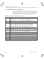
TMS320C2x Instructions by Cycle Class . . . . . . . . . . . . . . . . . . . . . . . . . . . . . . . . . . . . . . . . . E-2
Cycle Timings for Cycle Classes When Not in Repeat Mode . . . . . . . . . . . . . . . . . . . . . . . . E-3
Cycle Timings for Cycle Classes When in Repeat Mode . . . . . . . . . . . . . . . . . . . . . . . . . . . . E-5
Pin Nomenclature (TMS320E25) . . . . . . . . . . . . . . . . . . . . . . . . . . . . . . . . . . . . . . . . . . . . . . . . F-5
TMS320E25 Programming Mode Levels . . . . . . . . . . . . . . . . . . . . . . . . . . . . . . . . . . . . . . . . . F-6
TMS320E25 EPROM Protect and Protect Verify Mode Levels . . . . . . . . . . . . . . . . . . . . . . F-12
Data Converter ICs . . . . . . . . . . . . . . . . . . . . . . . . . . . . . . . . . . . . . . . . . . . . . . . . . . . . . . . . . . . . G-4
Switched-Capacitor Filter ICs . . . . . . . . . . . . . . . . . . . . . . . . . . . . . . . . . . . . . . . . . . . . . . . . . . . G-4
Telecom Devices . . . . . . . . . . . . . . . . . . . . . . . . . . . . . . . . . . . . . . . . . . . . . . . . . . . . . . . . . . . . . . G-8
Switched-Capacitor Filter ICs . . . . . . . . . . . . . . . . . . . . . . . . . . . . . . . . . . . . . . . . . . . . . . . . . . . G-8
Table of Contents
Tables
G–5
G–6
G–7
G–8
G–9
G–10
H–1
J–1
J–2
Voice Synthesizers . . . . . . . . . . . . . . . . . . . . . . . . . . . . . . . . . . . . . . . . . . . . . . . . . . . . . . . . . . . G-10
Speech Memories . . . . . . . . . . . . . . . . . . . . . . . . . . . . . . . . . . . . . . . . . . . . . . . . . . . . . . . . . . . . G-10
Switched-Capacitor Filter ICs . . . . . . . . . . . . . . . . . . . . . . . . . . . . . . . . . . . . . . . . . . . . . . . . . . G-11
Control-Related Devices . . . . . . . . . . . . . . . . . . . . . . . . . . . . . . . . . . . . . . . . . . . . . . . . . . . . . . G-13
Modem AFE Data Converters . . . . . . . . . . . . . . . . . . . . . . . . . . . . . . . . . . . . . . . . . . . . . . . . . . G-15
Audio/Video Analog/Digital Interface Devices . . . . . . . . . . . . . . . . . . . . . . . . . . . . . . . . . . . . G-20
Commonly Used Crystal Frequencies . . . . . . . . . . . . . . . . . . . . . . . . . . . . . . . . . . . . . . . . . . . . H-4
Microprocessor and Microcontroller Tests . . . . . . . . . . . . . . . . . . . . . . . . . . . . . . . . . . . . . . . . J-5
TMS320C2x Transistors . . . . . . . . . . . . . . . . . . . . . . . . . . . . . . . . . . . . . . . . . . . . . . . . . . . . . . . J-5
xix
Examples
Examples
5–1
5–2
5–3
5–4
5–5
5–6
5–7
5–8
5–9
5–10
5–11
5–12
5–13
5–14
5–15
5–16
5–17
5–18
5–19
5–20
5–21
5–22
5–23
5–24
5–25
5–26
5–27
5–28
5–29
5–30
5–31
5–32
5–33
5–34
5–35
5–36
xx
Processor Initialization (TMS320C25) . . . . . . . . . . . . . . . . . . . . . . . . . . . . . . . . . . . . . . . . . . . . 5-3
Processor Initialization (TMS320C26) . . . . . . . . . . . . . . . . . . . . . . . . . . . . . . . . . . . . . . . . . . . . 5-4
BIO–XF Transfer Protocol . . . . . . . . . . . . . . . . . . . . . . . . . . . . . . . . . . . . . . . . . . . . . . . . . . . . . . 5-7
RS232 Transfer Protocol . . . . . . . . . . . . . . . . . . . . . . . . . . . . . . . . . . . . . . . . . . . . . . . . . . . . . . 5-12
TMS320C26BFNL Bootloader . . . . . . . . . . . . . . . . . . . . . . . . . . . . . . . . . . . . . . . . . . . . . . . . . 5-17
Subroutines . . . . . . . . . . . . . . . . . . . . . . . . . . . . . . . . . . . . . . . . . . . . . . . . . . . . . . . . . . . . . . . . . 5-22
Software Stack Expansion . . . . . . . . . . . . . . . . . . . . . . . . . . . . . . . . . . . . . . . . . . . . . . . . . . . . 5-24
Clock Divider Using Timer (TMS320C25) . . . . . . . . . . . . . . . . . . . . . . . . . . . . . . . . . . . . . . . . 5-26
Instruction Repeating . . . . . . . . . . . . . . . . . . . . . . . . . . . . . . . . . . . . . . . . . . . . . . . . . . . . . . . . . 5-27
Computed GOTO . . . . . . . . . . . . . . . . . . . . . . . . . . . . . . . . . . . . . . . . . . . . . . . . . . . . . . . . . . . . 5-28
Context Save (TMS320C25) . . . . . . . . . . . . . . . . . . . . . . . . . . . . . . . . . . . . . . . . . . . . . . . . . . . 5-30
Context Restore (TMS320C25) . . . . . . . . . . . . . . . . . . . . . . . . . . . . . . . . . . . . . . . . . . . . . . . . 5-31
Interrupt Service Routine . . . . . . . . . . . . . . . . . . . . . . . . . . . . . . . . . . . . . . . . . . . . . . . . . . . . . . 5-32
Moving External Data to Internal Data Memory With BLKD . . . . . . . . . . . . . . . . . . . . . . . . 5-33
Moving Program Memory to Data Memory With BLKP . . . . . . . . . . . . . . . . . . . . . . . . . . . . 5-33
Moving Program Memory to Data Memory With TBLR . . . . . . . . . . . . . . . . . . . . . . . . . . . . 5-34
Moving Internal Data Memory to Program Memory With TBLW . . . . . . . . . . . . . . . . . . . . . 5-34
Moving Data From I/O Space Into Data Memory With IN . . . . . . . . . . . . . . . . . . . . . . . . . . 5-34
Moving Data From Data Memory to I/O Space With OUT . . . . . . . . . . . . . . . . . . . . . . . . . . 5-35
Configuring and Using On-Chip RAM . . . . . . . . . . . . . . . . . . . . . . . . . . . . . . . . . . . . . . . . . . . 5-37
Program Execution From On-Chip Memory . . . . . . . . . . . . . . . . . . . . . . . . . . . . . . . . . . . . . . 5-39
Program Execution From On-Chip Memory (TMS320C26) . . . . . . . . . . . . . . . . . . . . . . . . . 5-41
Using BIT and BBZ . . . . . . . . . . . . . . . . . . . . . . . . . . . . . . . . . . . . . . . . . . . . . . . . . . . . . . . . . . . 5-45
Using BITT and BBNZ . . . . . . . . . . . . . . . . . . . . . . . . . . . . . . . . . . . . . . . . . . . . . . . . . . . . . . . . 5-45
Bit-Reversed Carry Addition . . . . . . . . . . . . . . . . . . . . . . . . . . . . . . . . . . . . . . . . . . . . . . . . . . . 5-48
FFT Bit Reversals . . . . . . . . . . . . . . . . . . . . . . . . . . . . . . . . . . . . . . . . . . . . . . . . . . . . . . . . . . . . 5-48
Using the AR0 Test Bit to Calculate the Square Root of a Long Integer . . . . . . . . . . . . . . 5-50
Using MACD for Moving Data . . . . . . . . . . . . . . . . . . . . . . . . . . . . . . . . . . . . . . . . . . . . . . . . . . 5-52
Multiply . . . . . . . . . . . . . . . . . . . . . . . . . . . . . . . . . . . . . . . . . . . . . . . . . . . . . . . . . . . . . . . . . . . . . 5-53
Multiply-Accumulate Using the MAC Instruction (TMS320C25) . . . . . . . . . . . . . . . . . . . . . 5-54
Multiply-Accumulate Using the LTA-MPY Instruction Pair . . . . . . . . . . . . . . . . . . . . . . . . . . 5-54
Using SQRA . . . . . . . . . . . . . . . . . . . . . . . . . . . . . . . . . . . . . . . . . . . . . . . . . . . . . . . . . . . . . . . . 5-57
Divide 33 by 5 . . . . . . . . . . . . . . . . . . . . . . . . . . . . . . . . . . . . . . . . . . . . . . . . . . . . . . . . . . . . . . . 5-58
Using SUBC for Integer Division . . . . . . . . . . . . . . . . . . . . . . . . . . . . . . . . . . . . . . . . . . . . . . . 5-59
Using SUBC for Fractional Division . . . . . . . . . . . . . . . . . . . . . . . . . . . . . . . . . . . . . . . . . . . . . 5-59
Using NORM for Floating-Point Multiply . . . . . . . . . . . . . . . . . . . . . . . . . . . . . . . . . . . . . . . . . 5-61
Table of Contents
Examples
5–37
5–38
5–39
5–40
5–41
5–42
5–43
5–44
5–45
5–46
5–47
Using LACT for Denormalization . . . . . . . . . . . . . . . . . . . . . . . . . . . . . . . . . . . . . . . . . . . . . . .
Row Times Column . . . . . . . . . . . . . . . . . . . . . . . . . . . . . . . . . . . . . . . . . . . . . . . . . . . . . . . . . .
64-Bit Addition . . . . . . . . . . . . . . . . . . . . . . . . . . . . . . . . . . . . . . . . . . . . . . . . . . . . . . . . . . . . . . .
64-Bit Subtraction . . . . . . . . . . . . . . . . . . . . . . . . . . . . . . . . . . . . . . . . . . . . . . . . . . . . . . . . . . . .
32 × 32-Bit Multiplication . . . . . . . . . . . . . . . . . . . . . . . . . . . . . . . . . . . . . . . . . . . . . . . . . . . . . .
Implementing an IIR Filter . . . . . . . . . . . . . . . . . . . . . . . . . . . . . . . . . . . . . . . . . . . . . . . . . . . . .
256-Tap Adaptive FIR Filter . . . . . . . . . . . . . . . . . . . . . . . . . . . . . . . . . . . . . . . . . . . . . . . . . . .
Adaptive Filter Routine Concluded . . . . . . . . . . . . . . . . . . . . . . . . . . . . . . . . . . . . . . . . . . . . .
FFT Macros . . . . . . . . . . . . . . . . . . . . . . . . . . . . . . . . . . . . . . . . . . . . . . . . . . . . . . . . . . . . . . . . .
An 8-Point DIT FFT . . . . . . . . . . . . . . . . . . . . . . . . . . . . . . . . . . . . . . . . . . . . . . . . . . . . . . . . . .
PID Control . . . . . . . . . . . . . . . . . . . . . . . . . . . . . . . . . . . . . . . . . . . . . . . . . . . . . . . . . . . . . . . . .
5-61
5-62
5-64
5-65
5-66
5-70
5-73
5-74
5-79
5-81
5-83
xxi
xxii
Table of Contents
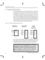
Running Title—Attribute Reference
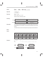
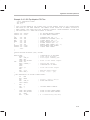
Chapter 1
Introduction
The TMS320 family of 16/32-bit single-chip digital signal processors combines
the flexibility of a high-speed controller with the numerical capability of an array
processor, offering an inexpensive alternative to custom VLSI and multichip
bit-slice processors for signal processing.
The TMS32010, the first digital signal processor in the TMS320 family, was
introduced in 1982. Since that time, the TMS320 family has established itself
as the industry standard for digital signal processing. The powerful instruction
set, inherent flexibility, high-speed number-crunching capabilities, and innovative architecture make these high-performance, cost-effective processors
ideal for many telecommunications, computer, commercial, industrial, and military applications.
Note:
Throughout this document, TMS320C2x refers to the TMS320C25,
TMS320C25-33, TMS320C25-50, TMS320E25, TMS320C26, and
TMS320C28 unless stated otherwise. Where applicable, ROM includes the
on-chip EPROM of the TMS320E25.
Topics in this chapter include
Topic
Page
1.1
General Description . . . . . . . . . . . . . . . . . . . . . . . . . . . . . . . . . . . . . . . . . . . 1-2
1.2
Key Features . . . . . . . . . . . . . . . . . . . . . . . . . . . . . . . . . . . . . . . . . . . . . . . . . 1-6
1.3
Typical Applications . . . . . . . . . . . . . . . . . . . . . . . . . . . . . . . . . . . . . . . . . . . 1-8
1-1
General Description
1.1
General Description
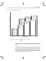
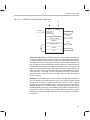
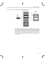
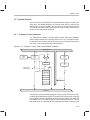
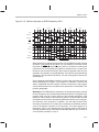
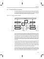
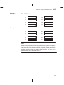
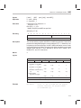
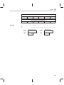
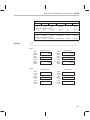
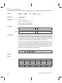
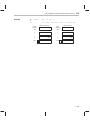
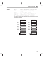
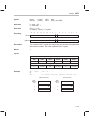
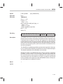
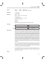
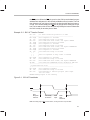
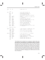
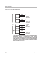
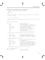
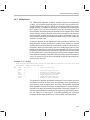
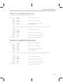
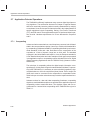
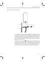
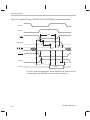
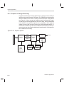
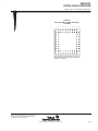
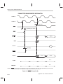
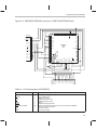
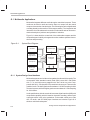
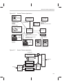
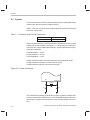
The TMS320 family currently consists of five generations: TMS320C1x,
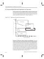
TMS320C2x, TMS320C3x, TMS320C4x, and TMS320C5x (see Figure 1–1).
The family expansion includes enhancements of existing generations and
more powerful new generations of digital signal processors. Many features are
common among these generations. Some specific features are added in each
processor to provide different cost/performance tradeoffs. Software compatibility is maintained throughout the family to protect the user’s investment in architecture. Each processor has software and hardware tools to facilitate rapid
design.
This document discusses the TMS320C2x devices:
-
1-2
TMS320C25, a CMOS 40-MHz digital signal processor capable of twice
the performance of the TMS320C1x devices
TMS320C25-33 a CMOS 33-MHz version of the TMS32025
TMS320C25-50, a CMOS enhanced-speed (50-MHz) version of the
TMS320C25
TMS320E25, a version of the TMS320C25 (40-MHz) with on-chip ROM
replaced by secure, on-chip EPROM
TMS320C26, a version of the TMS320C25 (40-MHz) with expanded configurable program/data RAM
The TMS320C28, a version of the TMS320C25 (40-MHz) with expanded
8K-word on-chip ROM and an added power-down mode.
Introduction
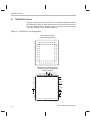
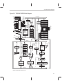
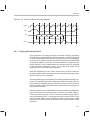
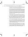
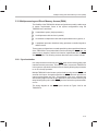
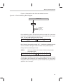
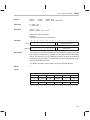
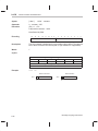
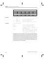
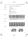
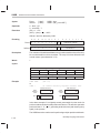
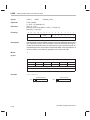
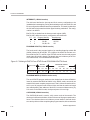
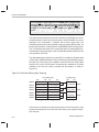
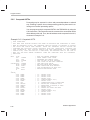
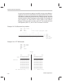
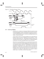
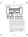
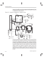
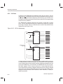
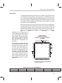
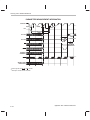
General Description
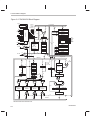
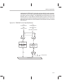
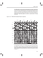
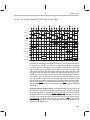
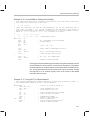
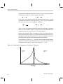
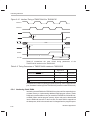
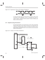
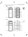
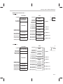
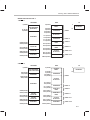
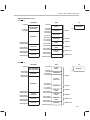
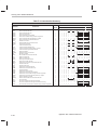
Figure 1–1. TMS320 Device Evolution
P
E
R
F
O
R
M
A
N
C
E
M
I
P
S
/
M
F
L
O
P
S
ÇÇÇÇÇ
ÇÇÇÇÇÇÇÇÇÇÇ
ÇÇÇÇÇÇ
ÇÇÇÇÇ
ÇÇÇÇÇÇ
ÇÇÇÇÇÇ
ÇÇÇÇÇ
ÇÇÇÇÇÇ
ÇÇÇÇÇÇ
ÇÇÇÇÇ
ÇÇÇÇÇÇ
ÇÇÇÇÇÇÇÇÇÇÇ
ÇÇÇÇÇÇ
ÇÇÇÇÇÇ
ÇÇÇÇÇ
ÇÇÇÇÇÇ
ÇÇÇÇÇÇ
ÇÇÇÇÇ
ÇÇÇÇÇÇ
ÇÇÇÇÇÇ
ÇÇÇÇÇ
ÇÇÇÇÇÇ
ÇÇÇÇÇÇ
ÇÇÇÇÇ
ÇÇÇÇÇÇ
ÇÇÇÇÇÇ
ÇÇÇÇÇ
ÇÇÇÇÇÇ
ÇÇÇÇÇÇ
ÇÇÇÇÇ
ÇÇÇÇÇÇ
ÇÇÇÇÇÇÇÇÇÇÇ
ÇÇÇÇÇÇ
ÇÇÇÇÇÇ
ÇÇÇÇÇ
ÇÇÇÇÇÇ
ÇÇÇÇÇÇ
ÇÇÇÇÇ
ÇÇÇÇÇÇ
ÇÇÇÇÇÇ
ÇÇÇÇÇ
ÇÇÇÇÇÇ
ÇÇÇÇÇÇ
ÇÇÇÇÇ
ÇÇÇÇÇÇ
ÇÇÇÇÇÇÇÇÇÇÇ
TMS320C4x
TMS320C3x
TMS320C30
TMS320C30-27
TMS320C30-40
TMS320C31
TMS320C31-27
TMS320C31-40
TMS320C31PQA
TMS320C40
TMS320C40-40
TMS320C5x
TMS320C50
TMS320C51
TMS320C53
TMS320C2x
TMS320C1x
TMS320C10
TMS320C10-14/-25
TMS320C14
TMS320E14/P14
TMS320C15/LC15
TMS320E15/P15
TMS320C15-25
TMS320E15-25
TMS320C16
TMS320C17/LC17
TMS320E17/P17
TMS320C25
TMS320E25
TMS320C25-33
TMS320C25-50
TMS320C26
TMS320C28
GENERATION
Fixed-Point Generations
ÇÇ
ÇÇ
Floating-Point Generations
Plans for expansion of the TMS320 family include more spinoffs of the existing
generations as well as more powerful future generations of digital signal processors.
The TMS320 family combines the high performance and specialized features
necessary in digital signal processing (DSP) applications with an extensive
program of development support, including hardware and software development tools, product documentation, textbooks, newsletters, DSP design workshops, and a variety of application reports. See Appendix K for a discussion
of the wide range of development tools available.
1-3
General Description
The combination of the TMS320’s Harvard-type architecture (separate program and data buses) and its special digital signal processing instruction set
provide speed and flexibility to execute 12.8 MIPS (million instructions per second). The TMS320 family optimizes speed by implementing functions in
hardware that other processors implement through software or microcode.
This hardware-intensive approach provides the design engineer with power
previously unavailable on a single chip.
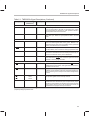
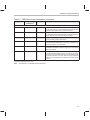
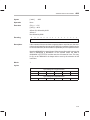
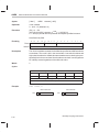
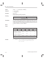
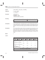
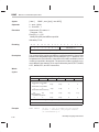
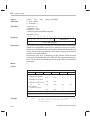
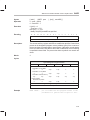
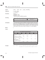
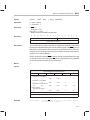
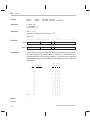
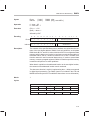
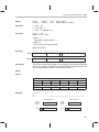
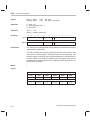
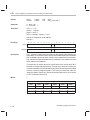
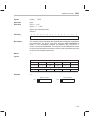
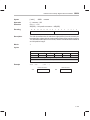
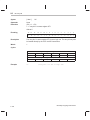
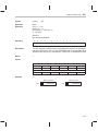
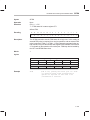
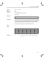
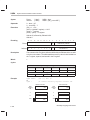
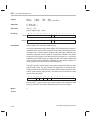
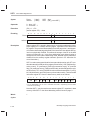
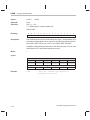
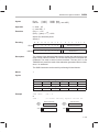
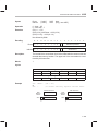
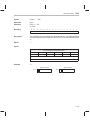
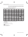
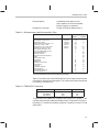
The TMS320C2x generation includes six members: TMS320C25,
TMS320C25-33, TMS320C25-50, TMS320E25, TMS320C26, and
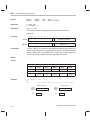
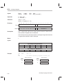
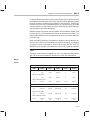
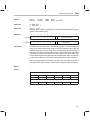
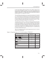
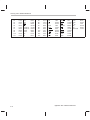
TMS320C28. Table 1–1 provides an overview of the TMS320C2x generation
of processors with comparisons of memory, I/O, cycle timing, and package
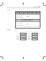
type.
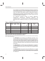
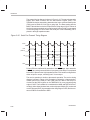
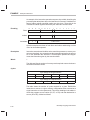
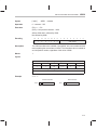
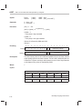
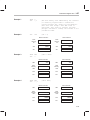
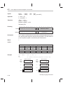
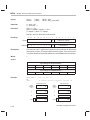
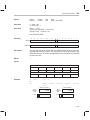
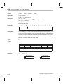
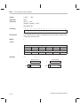
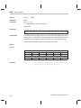
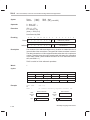
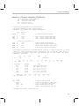
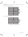
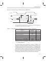
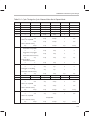
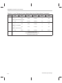
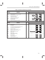
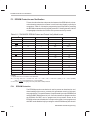
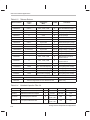
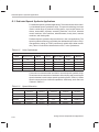
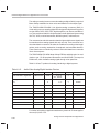
Table 1–1. TMS320C2x Processors Overview
Device
On-chip
RAM
Memory
ROM/
EPROM
I/O Ports †
Off-chip
Prog Data
Ser
Par
DMA
Cycle
Time
(ns)
Package
Type*
PGA PLCC CER QFP
TMS320C25‡
544
4K
64K 64K
Yes
16 × 16 Con
100
68
68
—
—
TMS320C25-33
544
4K
64K 64K
Yes
16 × 16 Con
120
—
68
—
—
TMS320C25-50§
544
4K
64K 64K
Yes
16 × 16 Con
80
—
68
—
—
TMS320E25§
544
4K
64K 64K
Yes
16 × 16 Con
100
—
—
68 80
TMS320C26
1568
256
64K 64K
Yes
16 × 16 Con
100
—
68
—
—
TMS320C28
544
8K
64K 64K
Yes
16 × 16 Con
100
—
68
—
80
†Ser = serial; Par = parallel; DMA = direct memory access; Con = concurrent DMA.
‡Military version available; contact nearest TI Field Sales Office for availability.
§Military version planned; contact nearest TI Field Sales Office for details.
*PGA = 68-pin grid array; PLCC = plastic-leaded chip carrier; CER = surface mount ceramic-leaded chip carrier (CER-QUAD);
QFP = plastic quad flat package
The TMS320C25, like all members of the TMS320C2x generation, is processed in CMOS technology. The TMS320C25 is capable of executing 10 million instructions per second. Enhanced features such as 24 additional instructions (133 total), eight auxiliary registers, an eight-level hardware stack, 4K
words of on-chip program ROM, a bit-reversed indexed addressing mode, and
the low power dissipation inherent to the CMOS process contribute to the high
performance.
The TMS320C25-33 is a 33-MHz version of the TMS320C25. It is capable of
an instruction cycle of 120 ns. It is architecturally identical to the 40-MHz version of the TMS320C25 and is pin-for-pin and object-code compatible with the
TMS320C25.
The TMS320C25-50 is a high-speed version of the TMS320C25. It is capable
of an instruction cycle time of 80 ns. It is architecturally identical to the 40-MHz
version of the TMS320C25 and is pin-for-pin and object-code compatible with
the TMS320C25.
1-4
Introduction
General Description
The TMS320E25 is identical to the TMS320C25, except that the on-chip
4K-word program ROM is replaced with a 4K-word on-chip program EPROM.
On-chip EPROM allows realtime code development and modification for immediate evaluation of system performance.
The TMS320C26 is pin-for-pin and object-code compatible (except for RAM
configuration instructions) with the TMS320C25. It is capable of an instruction
cycle time of 100 ns. The enhancement over the TMS320C25 consists of a
larger, configurable, on-chip RAM divided into 4 blocks, for a total 1568-word
program/data space. The TMS320C26 is similar to the TMS320C25 except for
its internal memory configuration. This is discussed in Section 3.4 and in Appendix B.
The TMS320C28 is object code-compatible with the TMS320C25. It is capable
of an instruction cycle time of 100 ns. The TMS320C28 contains an expanded
8K words of on-chip program ROM and an added power-down mode, which
conserves power while saving the contents of on-chip SRAM (B0, B1, and B2).
1-5
Key Features
1.2
Key Features
Key features of the TMS320C2x devices are listed below. Those that pertain
to a particular device are followed by the device name within parentheses.
-
Instruction cycle timing:
80-ns (TMS320C25-50)
100-ns (TMS320C25, TMS320E25, TMS320C26, and TMS320C28)
120-ns (TMS320C25-33)
1-6
544-word programmable on-chip data RAM
1568-word configurable program/data RAM (TMS320C26 only)
4K-word on-chip program ROM (TMS320C25, TMS302C25-33, and
TMS320C25-50)
8K-word on-chip program ROM (TMS320C28 only)
Secure 4K-word on-chip program EPROM (TMS320E25)
128K-word total data/program memory space
32-bit ALU/accumulator
16- ×16-bit parallel multiplier with a 32-bit product
Single-cycle multiply/accumulate instructions
Repeat instructions for efficient use of program space and enhanced
execution
Block moves for data/program management
On-chip timer for control operations
Up to eight auxiliary registers with dedicated arithmetic unit
Up to eight-level hardware stack
Sixteen input and sixteen output channels
16-bit parallel shifter
Wait states for communication to slower off-chip memories/peripherals
Serial port for direct codec interface
Synchronization input for synchronous multiprocessor configurations
Introduction
Key Features
-
-
Global data memory interface
TMS320C1x source-code upward compatibility
Concurrent DMA using an extended hold operation
Instructions for adaptive filtering, FFT, and extended-precision arithmetic
Bit-reversed indexed-addressing mode for radix-2 FFT
On-chip clock generator
Single 5-V supply
Power-down mode (TMS320C28 only)
Device packaging:
68-pin PGA (TMS320C25)
68-lead PLCC (TMS320C25, TMS320C26, and TMS320C28)
68-lead CER-QUAD (TMS320E25)
80-pin QFP (TMS320C28)
Commercial and military versions available
1-7
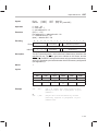
Typical Applications
1.3
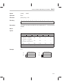
Typical Applications
The TMS320 family’s unique versatility and realtime performance offer flexible
design approaches in a variety of applications. In addition, TMS320 devices
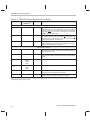
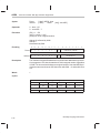
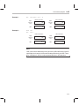
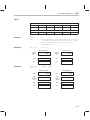
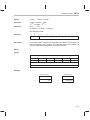
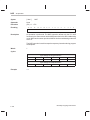
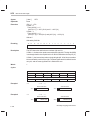
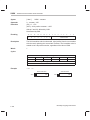
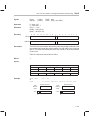
can simultaneously provide the multiple functions often required in those complex applications. Table 1–2 lists typical TMS320 family applications.
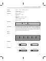
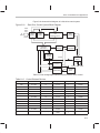
Table 1–2. Typical Applications of the TMS320 Family
General-Purpose DSP
Digital Filtering
Convolution
Correlation
Hilbert Transforms
Fast Fourier Transforms
Adaptive Filtering
Windowing
Waveform Generation
Graphics/Imaging
3-D Rotation
Robot Vision
Image Transmission/
Compression
Pattern Recognition
Image Enhancement
Homomorphic Processing
Workstations
Animation/Digital Map
Voice/Speech
Control
Voice Mail
Speech Vocoding
Speech Recognition
Speaker Verification
Speech Enhancement
Speech Synthesis
Text-to-Speech
Disk Control
Servo Control
Robot Control
Laser Printer Control
Engine Control
Motor Control
Telecommunications
Echo Cancellation
ADPCM Transcoders
Digital PBXs
Line Repeaters
Channel Multiplexing
1200 to 19200-bps Modems
Adaptive Equalizers
DTMF Encoding/Decoding
Data Encryption
Consumer
Radar Detectors
Power Tools
Digital Audio/TV
Music Synthesizer
Toys and Games
Solid-State Answering
Machines
Instrumentation
Spectrum Analysis
Function Generation
Pattern Matching
Seismic Processing
Transient Analysis
Digital Filtering
Phase-Locked Loops
Military
Secure Communications
Radar Processing
Sonar Processing
Image Processing
Navigation
Missile Guidance
Radio Frequency Modems
Automotive
FAX
Cellular Telephones
Speaker Phones
Digital Speech
Interpolation (DSI)
X.25 Packet Switching
Video Conferencing
Spread Spectrum
Communications
Industrial
Robotics
Numeric Control
Security Access
Power Line Monitors
Engine Control
Vibration Analysis
Antiskid Brakes
Adaptive Ride Control
Global Positioning
Navigation
Voice Commands
Digital Radio
Cellular Telephones
Medical
Hearing Aids
Patient Monitoring
Ultrasound Equipment
Diagnostic Tools
Prosthetics
Fetal Monitors
Many of the TMS320C2x features, such as single-cycle multiply/accumulate
instructions, 32-bit arithmetic unit, large auxiliary register file with a separate
arithmetic unit, and large on-chip RAM and ROM make the device particularly
applicable in digital signal processing systems. At the same time, general-purpose applications are greatly enhanced by the large address spaces, on-chip
timer, serial port, multiple interrupt structure, provision for external wait states,
and capability for multiprocessor interface and direct memory access.
1-8
Introduction
Typical Applications
The TMS320C2x has the flexibility to be configured to satisfy a wide range of
system requirements. This allows the device to be applied in systems currently
using costly bit-slice processors or custom ICs. These are examples of such
system configurations:
-
A standalone system using on-chip memory,
Parallel multiprocessing systems with shared global data memory, or
Host/peripheral coprocessing using interface control signals.
1-9
1-10
Introduction
Running Title—Attribute Reference
Chapter 2
Pinouts and Signal Descriptions
The TMS320C2x generation digital signal processors are available in one or
more of four package types. The TMS320C25 (40-MHz version only) is available in a 68-pin grid array (PGA) package. The TMS320C25 (33-MHz,
40-MHz, and 50-MHz versions) and the TMS320C26 are available in a plastic
68-lead chip carrier (PLCC) package. The TMS320E25 is packaged in a ceramic surface mount 68-lead chip carrier (CER-QUAD) package. The
TMS320C28 is available in a 80-pin quad flat package (QFP). All TMS320
packages conform to JEDEC specifications.
Conversion sockets that accept PLCC and CER-QUAD packages and have
a PGA footprint are commercially available. For more information, refer to Appendix D.
When using the XDS emulator, refer to subsection 6.1.3 for user target design
considerations.
The TMS320C26 is similar to the TMS320C25 except for its internal memory
configuration. This is discussed in Section 3.4 and in Appendix B.
Topics in this chapter include
Topic
Page
2.1
TMS320C2x Pinouts . . . . . . . . . . . . . . . . . . . . . . . . . . . . . . . . . . . . . . . . . . . 2-2
2.2
TMS320C2x Signal Descriptions . . . . . . . . . . . . . . . . . . . . . . . . . . . . . . . . 2-4
2-1
TMS320C2x Pinouts
2.1
TMS320C2x Pinouts
Figure 2–1 shows pinouts of the PGA, PLCC, and CER-QUAD packages for
the TMS320C2x devices. Note that the pinout and external dimensions of
PLCC and CER-QUAD are identical. Figure 2–2 shows preliminary pinouts
of the QFP package for the TMS320C28 device.
Figure 2–1. TMS320C2x Pin Assignments
68-Pin GB Pin Grid Array
Ceramic Package (Top View)
1
2
3
4
5
6
7
8
9
10
11
A
B
C
D
E
F
G
H
J
K
L
10
11
12
13
14
15
16
17
18
19
20
21
22
23
24
25
26
CLKR
CLKX
V CC
V CC
9 8 7 6 5 4 3 2 1 68 67 66 65 64 63 62 61
60
59
58
57
56
55
54
53
52
51
50
49
48
47
46
45
44
27 28 29 30 31 32 33 34 35 36 37 38 39 40 41 42 43
IACK
MSC
CLKOUT1
CLKOUT2
XF
HOLDA
DX
FSX
X2 CLKIN
X1
BR
STRB
R/W
PS
IS
DS
VSS
V SS
A1
A2
A3
A4
A5
A6
A7
V CC
A8
A9
A10
A11
A12
A13
A14
A15
VSS
D7
D6
D5
D4
D3
D2
D1
D0
SYNC
INT0
INT1
INT2
VCC
DR
FSR
A0
READY
D8
D9
D10
D11
D12
D13
D14
D15
68-Pin FN Plastic Leaded Chip Carrier
Package and 68-Pin FZ CER-QUAD
Package (Top View)
2-2
Pinouts and Signal Descriptions
TMS320C2x Pinouts
Figure 2–2. TMS320C28 Pin Assignments
MSC
CLKOUT1
CLKOUT2
XF
HOLDA
VSS
DX
FSX
X2/CLKIN
X1
BR
STRB
R/W
PS
IS
DS
80-Pin PH Quad Flat Package †
(Top View)
80 79 78 77 76 75 74 73 72 71 70 69 68 67 66 65
64
2
63
3
62
4
61
5
60
6
59
7
58
8
57
9
56
10
55
11
54
12
53
13
52
14
51
15
50
16
49
17
48
18
47
19
46
20
45
21
44
43
23 25 26 27 28 29 30 31 32 33 34 35 36 37 38 39 4042
22
24
41
WAKEUP
VSS
A15
A14
A13
A12
VSS
A11
A10
A9
A8
VCC
VCC
A7
A6
VSS
A5
A4
A3
A2
A1
PDACK
VSS
A0
ADVANCE INFORMATION
1
D7
D6
D5
D4
D3
D2
VSS
D1
D0
SYNC
INT0
INT1
INT2
VCC
DR
FSR
IACK
PDI
VCC
VCC
CLKX
VSS
CLKR
RS
READY
HOLD
BIO
MP/MC
D15
VSS
D14
D13
VCC
D12
D11
D10
D0
D6
VSS
VSS
† Packages are shown for pinout reference only.
2-3
TMS320C2x Signal Descriptions
2.2
TMS320C2x Signal Descriptions
The signal descriptions for the TMS320C2x devices are provided in this section. Table 2–1 lists each signal, its pin location (PGA, PLCC, and CERQUAD), function, and operating mode(s): that is, input, output, or high-impedance state as indicated by I, O, or Z. The signals in Table 2–1 are grouped according to function and alphabetized within that grouping.
Table 2–1. TMS320C2x Signal Descriptions
Pin
(PGA/PLCC†)
I/O/Z‡
A15 MSB
A14
A13
A12
A11
A10
A9
A8
A7
A6
A5
A4
A3
A2
A1
A0 LSB
L10/43
K9/42
L9/41
K8/40
L8/39
K7/38
L7/37
K6/36
K5/34
L5/33
K4/32
L4/31
K3/30
L3/29
K2/28
K1/26
O/Z
Parallel address bus A15 (MSB) through A0 (LSB).
Multiplexed to address external data/program memory or I/O.
Placed in high-impedance state in the hold mode.
D15 MSB
D14
D13
D12
D11
D10
D9
D8
D7
D6
D5
D4
D3
D2
D1
D0 LSB
B6/2
A5/3
B5/4
A4/5
B4/6
A3/7
B3/8
A2/9
B2/11
C1/12
C2/13
D1/14
D2/15
E1/16
E2/17
F1/ 18
I/O/Z
Parallel data bus D15 (MSB) through D0 (LSB). Multiplexed to
transfer data between the TMS320C2x and external data/program memory or I/O devices. Placed in the high-impedance state
when not outputting or when RS or HOLD is asserted.
Signal
Description
Address/Data Buses
Interface Control Signals
DS
PS
IS
K10/45
J10/47
J11/46
O/Z
Data, program, and I/O space select signals. Always high unless
low level asserted for communicating to a particular external
space. Placed in high-impedance state in the hold mode.
READY
B8/66
I
Data ready input. Indicates that an external device is prepared for
the bus transaction to be completed. If the device is not ready
(READY = 0), the TMS320C2x waits one cycle and checks
READY again. READY also indicates a bus grant to an external
device after a BR (bus request) signal.
† Pin numbers apply to CER-QUAD as well as to PLCC.
‡ Input/Output/High-impedance state.
2-4
Pinouts and Signal Descriptions
TMS320C2x Signal Descriptions
Table 2–1. TMS320C2x Signal Descriptions (Continued)
Signal
Pin
(PGA/PLCC†)
I/O/Z‡
Description
Interface Control Signals (Continued)
R/W
H11/48
O/Z
Read/write signal. Indicates transfer direction when communicating to an external device. Normally in read mode (high), unless
low level asserted for performing a write operation. Placed in
high-impedance state in the hold mode.
STRB
H10/49
O/Z
Strobe signal. Always high unless asserted low to indicate an external bus cycle. Placed in high-impedance state in the hold
mode.
BR
G11/50
O
Bus request signal. Asserted when the TMS320C2x requires access to an external global data memory space. READY is asserted to the device when the bus is available and the global data
memory is available for the bus transaction.
HOLD
A7/67
I
Hold input. When this signal is asserted, the TMS320C2x places
the data, address, and control lines in the high-impedance state.
HOLDA
E10/55
O
Hold acknowledge signal. Indicates that the TMS320C2x has
gone into the hold mode and that an external processor may access the local external memory of the TMS320C2x.
SYNC
F2/19
I
Synchronization input. Allows clock synchronization of two or
more TMS320C2xs. SYNC is an active-low signal and must be
asserted on the rising edge of CLKIN.
BIO
B7/68
I
Branch control input. Polled by BIOZ instruction. If BIO is low, the
TMS320C2x executes a branch. This signal must be active during
the BIOZ instruction fetch.
IACK
B11/60
O
Interrupt acknowledge signal. Output is valid only while
CLKOUT1 is low. Indicates receipt of an interrupt and that the program is branching to the interrupt-vector location designated by
A15–A0.
INT2
INT1
INT0
H1/22
G2/21
G1/20
I
External user interrupt inputs. Prioritized and maskable by the interrupt mask register and the interrupt mode bit.
A6/1
I
Microprocessor/microcomputer mode select pin for the
TMS320C25. When asserted low (microcomputer mode), the pin
causes the internal ROM to be mapped into the lower 4K words
of the program memory map. In the microprocessor mode, the
lower 4K words of program memory are external.
Multiprocessing Signals
Interrupt and Miscellaneous Signals
MP/MC
† Pin numbers apply to CER-QUAD as well as to PLCC.
‡ Input/Output/High-impedance state.
2-5
TMS320C2x Signal Descriptions
Table 2–1. TMS320C2x Signal Descriptions (Continued)
Signal
Pin
(PGA/PLCC†)
I/O/Z‡
Description
Interrupt and Miscellaneous Signals (Continued)
MSC
C10/59
O
Microstate complete signal. Asserted low and valid only during
CLKOUT1 low when the TMS320C2x has just completed a
memory operation, such as an instruction fetch or a data memory
read/write. MSC can be used to generate a one wait-state
READY signal for slow memory.
RS
A8/65
I
Reset input. Causes the TMS320C2x to terminate execution and
forces the program counter to zero. When RS is brought to a high
level, execution begins at location zero of program memory. RS
affects various registers and status bits.
XF
D11/56
O
External flag output (latched software-programmable signal).
Used for signaling other processors in multiprocessor configurations or as a general-purpose output pin.
CLKOUT1
C11/58
O
Master clock output signal (CLKIN frequency/4). CLKOUT1 rises
at the beginning of quarter-phase 3 (Q3) and falls at the beginning
of quarter-phase 1 (Q1).
CLKOUT2
D10/57
O
A second clock output signal. CLKOUT2 rises at the beginning of
quarter-phase 2 (Q2) and falls at the beginning of quarter-phase
4 (Q4).
VCC
A10/61
B10/62
H2/23
L6/35
I
Four 5-V supply pins, tied together externally.
VSS
B1/10
K11/44
L2/27
I
Three ground pins, tied together externally.
X1
G10/51
O
Output pin from the internal oscillator for the crystal. If a crystal is
not used, this pin should be left unconnected.
X2/CLKIN
F11/52
I
Input pin to the internal oscillator from the crystal. If crystal is not
used, a clock may be input to the device on this pin
Supply/Oscillator Signals
† Pin numbers apply to CER-QUAD as well as to PLCC.
‡ Input/Output/High-impedance state.
2-6
Pinouts and Signal Descriptions
TMS320C2x Signal Descriptions
Table 2–1. TMS320C2x Signal Descriptions (Continued)
Pin
(PGA/PLCC†)
I/O/Z‡
CLKR
B9/64
I
Receive clock input. External clock signal for clocking data from
the DR (data receive) pin into the RSR (serial port receive shift
register). Must be present during serial port transfers.
CLKX
A9/63
I
Transmit clock input. External clock signal for clocking data from
the XSR (serial port transmit shift register) to the DX (data transmit) pin. Must be present during serial port transfers.
DR
J1/24
I
Serial data receive input. Serial data is received in the RSR (serial
port receive shift register) via the DR pin.
DX
E11/54
O/Z
Serial data transmit output. Serial data transmitted from the XSR
(serial port transmit shift register) via the DX pin. Placed in highimpedance state when not transmitting.
FSR
J2/25
I
Frame synchronization pulse for receive input. The falling edge
of the FSR pulse initiates the data-receive process, beginning the
clocking of the RSR.
FSX
F10/53
I/O
Frame synchronization pulse for transmit input/output. The falling
edge of the FSX pulse initiates the data- transmit process, beginning the clocking of the XSR. Following reset, the default operating condition of FSX is as an input. This pin may be selected by
software to be an output when the TXM bit in the status register
is set to 1.
Signal
Description
Serial Port Signals
† Pin numbers apply to CER-QUAD as well as to PLCC.
‡ Input/Output/High-impedance state.
Note: See Appendix C for TMS320C28 signal descriptions.
2-7
2-8
Pinouts and Signal Descriptions
a
Chapter 3
Architecture
The architectural design of the TMS320C2x emphasizes overall system
speed, communication, and flexibility in processor configuration. Control signals and instructions provide block memory transfers, communication to slower off-chip devices, and multiprocessing implementations. Single-cycle multiply/accumulate instructions, two large on-chip RAM Blocks, eight auxiliary
registers with a dedicated arithmetic unit, a serial port, a hardware timer, and
a faster I/O for data-intensive signal processing are features that increase
throughput for DSP applications.
The TMS320C26 is similar to the TMS320C25 except for its internal memory
configuration. This is discussed in Section 3.4 and in Appendix B.
Topics in this chapter include:
Topic
Page
3.1
Architectural Overview . . . . . . . . . . . . . . . . . . . . . . . . . . . . . . . . . . . . . . . . 3-2
3.2
Functional Block Diagram . . . . . . . . . . . . . . . . . . . . . . . . . . . . . . . . . . . . . 3-6
3.3
Internal Hardware Summary . . . . . . . . . . . . . . . . . . . . . . . . . . . . . . . . . . . 3-9
3.4
Memory Organization . . . . . . . . . . . . . . . . . . . . . . . . . . . . . . . . . . . . . . . . 3-12
3.5
Central Arithmetic Logic Unit (CALU) . . . . . . . . . . . . . . . . . . . . . . . . . . 3-28
3.6
System Control . . . . . . . . . . . . . . . . . . . . . . . . . . . . . . . . . . . . . . . . . . . . . . 3-35
3.7
External Memory and I/O Interface . . . . . . . . . . . . . . . . . . . . . . . . . . . . . 3-55
3.8
Interrupts . . . . . . . . . . . . . . . . . . . . . . . . . . . . . . . . . . . . . . . . . . . . . . . . . . . 3-60
3.9
Serial Port . . . . . . . . . . . . . . . . . . . . . . . . . . . . . . . . . . . . . . . . . . . . . . . . . . . 3-64
3.10 Multiprocessing and Direct Memory Access (DMA) . . . . . . . . . . . . . 3-76
3.11 General Description of the TMS320C26 . . . . . . . . . . . . . . . . . . . . . . . . 3-83
3.12 General Description of the TMS320C28 . . . . . . . . . . . . . . . . . . . . . . . . 3-84
3-1
Architectural Overview
3.1
Architectural Overview
Harvard Architecture. The TMS320C2x high-performance digital signal processors, like the TMS320C1x devices, implement a Harvard-type architecture
that maximizes processing power by maintaining two separate memory bus
structures, program and data, for full-speed execution. Instructions are included to provide data transfers between the two spaces. Externally, the program and data memory can be multiplexed over the same bus so as to maximize the address range for both spaces while minimizing the pin count of the
device.
On-Chip Memory. The TMS320C25 provides increased flexibility in system
design by two large on-chip data RAM blocks (a total of 544 16-bit words), one
of which is configurable either as program or data memory (see Figure 3–1).
The TMS320C26 provides three large on-chip RAM blocks, configurable either as separate program and data spaces or as three continuous data blocks,
to provide increased flexibility in system design. An off-chip 64K-word directly
addressable data memory address space is included to facilitate implementations of DSP algorithms.
The large on-chip 4K-word masked ROM on the TMS320C25 can reduce the
cost of systems, thus providing for a true single-chip DSP solution (see
Figure 3–1). Programs of up to 4K words can be masked into the internal program ROM. The remainder of the 64K-word program memory space is located
externally. Large programs can execute at full speed from this memory space.
Programs may also be downloaded from slow external memory to on-chip
RAM for full-speed operation.
The 4K-word on-chip EPROM on the TMS320E25 allows realtime code development and modification for immediate evaluation of system performance.
Instructions can be executed from the EPROM at full speed. The EPROM is
equipped with a security mechanism allowing you to protect proprietary information. A programming adapter socket is available from Texas Instruments
that provides 68- to 28-pin conversion for programming with standard PROM
programmers. Refer to Appendix F for details.
3-2
Architecture
Architectural Overview
Figure 3–1. TMS320C2x Simplified Block Diagram
Interrupts
+5 V
Gnd
Data/Prog
RAM
256-Word
(1568-Word
TMS320C26)
Data RAM
288-Word
4-K Words ROM/EPROM
(TMS320C25/E25)
Data (16)
Multiprocessor
Interface
Multiplier
32-Bit ALU/ACC
Serial
Interface
Shifters
Address (16)
Timer
Arithmetic Logic Unit. The TMS320C2x performs 2s-complement arithmetic
using the 32-bit ALU and accumulator. The ALU is a general-purpose arithmetic unit that operates using 16-bit words taken from data RAM or derived from
immediate instructions or using the 32-bit result of the multiplier’s product register. In addition to the usual arithmetic instructions, the ALU can perform Boolean operations, providing the bit manipulation ability required of a high-speed
controller. The accumulator stores the output from the ALU and is the second
input to the ALU. The accumulator is 32 bits in length and is divided into a highorder word (bits 31 through 16) and a low-order word (bits 15 through 0).
Instructions are provided for storing the high- and low-order accumulator
words in memory.
Multiplier. The multiplier performs a 16 × 16-bit 2s-complement multiplication
with a 32-bit result in a single instruction cycle. The multiplier consists of three
elements: the T register, P register, and multiplier array. The 16-bit T register
temporarily stores the multiplicand; the P register stores the 32-bit product.
Multiplier values come from data memory, from program memory when using
the MAC/MACD instructions, or immediately from the MPYK (multiply immediate) instruction word. The fast on-chip multiplier allows the device to perform
efficiently the fundamental DSP operations such as convolution, correlation,
and filtering.
3-3
Architectural Overview
The TMS320C2x scaling shifter has a 16-bit input connected to the data bus
and a 32-bit output connected to the ALU. The scaling shifter produces a leftshift of 0 to 16 bits on the input data, as programmed in the instruction. The
LSBs of the output are filled with zeros, and the MSBs may be either filled with
zeros or sign-extended, depending upon the state of the sign-extension mode
bit of status register ST1. Additional shift capabilities enable the processor to
perform numerical scaling, bit extraction, extended arithmetic, and overflow
prevention.
Memory Interface. The TMS320C2x local memory interface consists of a
16-bit parallel data bus (D15–D0), a 16-bit address bus (A15–A0), three pins
for data/program memory or I/O space select (DS, PS, and IS), and various
system control signals. The R/W signal controls the direction of a data transfer,
and the STRB signal provides a timing signal to control the transfer. When using on-chip program RAM, ROM/EPROM, or high-speed external program
memory, the TMS320C2x runs at full speed without wait states. The use of a
READY signal allows wait-state generation for communicating with slower offchip memories.
Up to eight levels of hardware stack are provided for saving the contents of the
program counter during interrupts and subroutine calls. Instructions are available for saving the device’s complete context. PUSH and POP instructions
permit a level of nesting restricted only by the amount of available RAM. The
interrupts used in these devices are maskable.
All control operations are supported on the TMS320C2x by an on-chip
memory-mapped 16-bit timer, a repeat counter, three external maskable user
interrupts, and internal interrupts generated by serial port operations or by the
timer. A built-in mechanism protects from instructions that are repeated or become multicycle due to the READY signal and from holds and interrupts.
Serial Port. An on-chip full-duplex serial port provides direct communication
with serial devices such as codecs, serial A/D converters, and other serial systems. The interface signals are compatible with codecs and many other serial
devices with a minimum of external hardware. The two serial port memorymapped registers (the data transmit/receive registers) may be operated in either an 8-bit byte or 16-bit word mode. Each register has an external clock input, a framing synchronization input, and associated shift registers.
Multiprocessing Applications. The TMS320C2x has the capability of allocating global data memory space and communicating with that space via the
BR (bus request) and READY control signals. The 8-bit memory-mapped
global memory allocation register (GREG) specifies up to 32K words of the
TMS320C2x data memory as global external memory. The contents of the register determine the size of the global memory space. If the current instruction
addresses an operand within that space, BR is asserted to request control of
the bus. The length of the memory cycle is controlled by the READY line.
3-4
Architecture
Architectural Overview
Direct Memory Access. The TMS320C2x supports direct memory access
(DMA) to its external program/data memory using the HOLD and HOLDA signals. Another processor can take complete control of the TMS320C2x external
memory by asserting HOLD low. This causes the TMS320C2x to place its address, data, and control lines in the high-impedance state. Signaling between
the external processor and the TMS320C2x can be performed by using interrupts. On the TMS320C2x, two modes are available: a mode in which execution is suspended during assertion of HOLD, and a concurrent DMA mode in
which the TMS320C2x continues to execute its program while operating from
internal RAM or ROM, thus greatly increasing throughput in data-intensive applications.
3-5
Functional Block Diagram
3.2
Functional Block Diagram
The functional block diagram shown in Figure 3–2 and Figure 3–3 outlines the
principal blocks and data paths within the TMS320C2x processors. Further
details of the functional blocks are provided in the succeeding sections. Refer
to Section 3.3, Internal Hardware Summary, for definitions of the symbols used
in Figure 3–2. The block diagram also shows all of the TMS320C2x interface
pins. Figure 3–3 shows the block diagram of the TMS320C26.
The TMS320C2x architecture is built around two major buses: the program
bus and the data bus. The program bus carries the instruction code and immediate operands from program memory. The data bus interconnects various
elements, such as the central arithmetic logic unit (CALU) and the auxiliary
register file, to the data RAM. Together, the program and data buses can carry
data from on-chip data RAM and internal or external program memory to the
multiplier in a single cycle for multiply/accumulate operations.
The TMS320C2x has a high degree of parallelism; for example, while the data
is being operated upon by the CALU, arithmetic operations may also be implemented in the auxiliary register arithmetic unit (ARAU). Such parallelism results in a powerful set of arithmetic, logic, and bit-manipulation operations that
may all be performed in a single machine cycle.
LEGEND:
ACCH = Accumulator high
ACCL = Accumulator low
ALU
= Arithmetic logic unit
ARAU = Auxiliary register arithmetic unit
ARB
= Auxiliary register pointer buffer
ARP
= Auxiliary register pointer
DP
= Data memory page pointer
DRR
= Serial port data receive register
DXR
= Serial port data transmit register
3-6
IFR
IMR
IR
MCS
QIR
PR
PRD
TIM
TR
= Interrupt flag register
= Interrupt mask register
= Instruction register
= Microcall stack
= Queue instruction register
= Product register
XSR
= Period register for timer
= Timer
=Temporary register
PC
= Program Counter
PFC
= Prefetch counter
RPTC
= Repeat instruction counter
GREG
= Global memory allocation register
RSR
= Serial port receive shift register
= Serial port transmit shift register
AR0-AR
= Auxiliary registers
ST0.ST
= Status registers
C
= Carry bit
Architecture
Functional Block Diagram
Figure 3–2. TMS320C25/E25 Block Diagram
Program Bus
X1
X2/CLKIN
CLKOUT1
CLKOUT2
SYNC
IS
DS
PS
16
16
R/W
STRB
READY
BR
XF
HOLD
HOLDA
MSC
BIO
RS
IACK
16
16
PFC(16)
QIR(16)
IR(16)
16
Controller
ST1(16)
16
16
16
3
16
IFR(6)
8
16
(8 x 16)
RSR(16)
XSR(16)
16
16
16
MUX
16
D15-D0
DRR(16)
16
Instruction
RBIT
DR
CLKR
FSR
DX
CLKX
FSX
16
Stack
Program
ROM/
EPROM
(4096 × 16)
MUX
16
A15-A0
16
Address
INT(2-0)
RPTC(8)
16
PC(16)
MCS(16)
12
MP/MC
STO(16)
MUX
16
DXR(16)
16
TIM(16)
16
PRD(16)
6
IMR(6)
8
GREG(8)
16
16
Program Bus
Data Bus
16
16
16
16
AR0(16)
AR2(16)
ARP(3)
16
16
MUX
DP(9)
Shifter(0-16)
9
AR4(16)
16
Multiplier
AR3(16)
3
16
TR(16)
7 LSB
From IR
AR1(16)
3
16
9
3
AR5(16)
PR(32)
AR6(16)
32
32
AR7(16)
16
ARB(3)
Shifter(–6, 0, 1, 4)
16
3
16
MUX
ARAU(16)
32
MUX
16
16
MUX
32
MUX
16
16
32
ALU(32)
32
DATA/PROG
RAM (256 × 16)
Block B0
Block B2
(32 × 16)
Data RAM
Block B1
(256 × 16)
C
16
16
ACCL(16)
32
MUX
16
ACCH(16)
Shifter(0-7)†
16
16
Data Bus
NOTE: Shaded areas indicate a bus.
3-7
Functional Block Diagram
Figure 3–3. TMS320C26 Block Diagram
Program Bus
X1
X2/CLKIN
CLKOUT1
CLKOUT2
SYNC
IS
DS
PS
16
16
R/W
STRB
READY
BR
XF
HOLD
HOLDA
MSC
BIO
RS
IACK
16
16
PFC(16)
QIR(16)
IR(16)
16
Controller
16
A15-A0
MUX
16
16
8
16
(8 × 16)
RSR(16)
XSR(16)
16
Instruction
16
D15-D0
16
MUX
16
DR
CLKR
FSR
DX
CLKX
FSX
16
Stack
Bootload
Program
ROM
(256 × 16)
16
IFR(6)
PC(16)
Address
3
RPTC(8)
16
MCS(16)
16
MP/MC
ST1(16)
16
8
INT(2-0)
STO(16)
MUX
16
DRR(16)
16
DXR(16)
16
16
PRD(16)
TIM(16)
6
IMR(6)
8
GREG(8)
16
16
Program Bus
Data Bus
16
16
16
16
9
3
AR0(16)
ARP(3)
AR2(16)
16
16
Multiplier
Shifter(0-16)
9
AR4(16)
16
MUX
DP(9)
AR3(16)
3
16
TR (16)
7 LSB
From IR
AR1(16)
3
16
AR5(16)
PR(32)
AR6(16)
32
AR7(16)
ARB(3)
32
16
16
Shifter(–6, 0, 1, 4)
ARAU(16)
3
16
32
MUX
MUX
32
MUX
MUX
16
DATA
RAM (32 × 16)
Block B2
MUX
16
16
DATA/PROG
RAM (512 × 16)
Block B3
MUX
DATA/PROG
RAM (512 × 16)
Block B1
16
ALU(32)
DATA/PROG
RAM (512 × 16)
Block B0
32
32
C
ACCH(16)
ACCL(16)
32
MUX
MUX
MUX
Shifter(0-7)
16
16
16
16
16
16
Data Bus
NOTE: Shaded areas indicate a bus.
3-8
Architecture
Internal Hardware Summary
3.3
Internal Hardware Summary
The TMS320C2x internal hardware implements functions that other processors typically perform in software or microcode. For example, the device contains hardware for single-cycle 16 × 16-bit multiplication, data shifting, and address manipulation. This hardware-intensive approach provides computing
power previously unavailable on a single chip.
Table 3–1 presents a summary of the TMS320C2x internal hardware. This
summary table, which includes the internal processing elements, registers,
and buses, is alphabetized within each functional grouping. All of the symbols
used in this table correspond to the symbols used in the block diagram of
Section 3.2, the succeeding block diagrams in this section, and the text
throughout this document.
Table 3–1. TMS320C2x Internal Hardware
Unit
Symbol
Function
ACC (31–0)
ACCH (31–16)
ACCL (15–0)
A 32-bit accumulator split in two halves: ACCH (accumulator high) and
ACCL (accumulator low). Used for storage of ALU output.
ALU
A 32-bit twos-complement arithmetic logic unit having two 32-bit input
ports and one 32-bit output port feeding the accumulator.
ARAU
A 16-bit unsigned arithmetic unit used to perform operations on auxiliary register data.
Auxiliary Register File
AR0–AR7
(15–0)
A register file containing eight 16-bit auxiliary registers (AR0–AR7),
used for addressing data memory, temporary storage, or integer arithmetic processing through the ARAU.
Auxiliary Register File Bus
AFB(15–0)
A 16-bit bus that carries data from the AR pointed to by the ARP.
Auxiliary Register Pointer
ARP(2–0)
A 3-bit register used to select one of five or eight auxiliary registers.
Auxiliary
Buffer
ARB(2–0)
A 3-bit register used to buffer the ARP. Each time the ARP is loaded,
the old value is written to the ARB, except during an LST (load status
register) instruction. When the ARB is loaded with an LST1, the same
value is also copied into ARP.
CALU
The grouping of the ALU, multiplier, accumulator, and scaling shifter.
Accumulator
Arithmetic Logic Unit
Auxiliary Register Arithmetic
Unit
Register
Pointer
Central Arithmetic Logic Unit
Data Bus
D(15–0)
A 16-bit bus used to route data.
Data Memory Address Bus
DAB(15–0)
Data Memory Page Pointer
DP(8–0)
A 9-bit register pointing to the address of the current page. Data pages
are 128 words each, resulting in 512 pages of addressable data
memory space (some locations are reserved).
Direct Data Memory Address
Bus
DRB(15–0)
A 16-bit bus that carries the direct address for the data memory, which
is the concatenation of the DP register with the seven LSBs of the
instruction.
Global Memory
Register
GREG(7–0)
An 8-bit memory-mapped register for allocating the size of the global
memory space.
Allocation
A 16-bit bus that carries the data memory address.
3-9
Internal Hardware Summary
Table 3–1. TMS320C2x Internal Hardware (Continued)
Unit
Symbol
Function
Instruction Register
IR(15–0)
A 16-bit register used to store the currently executing instruction.
Interrupt Flag Register
IFR(5–0)
A 6-bit flag register used to latch the active-low external user interrupts
INT(2–0), the internal interrupts XINT/RINT (serial port transmit/receive), and TINT (timer) interrupts. The IFR is not accessible through
software.
Interrupt Mask Register
IMR(5–0)
A 6-bit memory-mapped register used to mask interrupts.
Microcall Stack
Multiplier
MCS (15–0)
MULT
A single-word stack that temporarily stores the contents of the PFC
while the PFC is being used to address data memory with the block
move (BLKD/BLKP), multiply-accumulate (MAC/MACD), and table
read/write (TBLR/TBLW)and table read/write (TBLR/TBLW) instruction
A 16 × 16-bit parallel multiplier.
Period Register
PRD (15–0)
A 16-bit memory-mapped register used to reload the timer.
Prefetch Counter
PFC (15–0)
A 16-bit counter used to prefetch program instructions. The PFC contains the address of the instruction currently being prefetched. It is updated when a new prefetch is initiated. The PFC is also used to address
program memory when using the block move (BLKP), multiply-accumulate (MAC/MACD), and table read/write (TBLR/TBLW) instructions
and to address data memory when using the block move (BLKD)
instruction.
Product Register
PR(31–0)
A 32-bit product register used to hold the multiplier product. The PR can
also be accessed as the most or least significant words by using the
SPH/SPL (store P register high/low) instructions.
P(15–0)
A 16-bit bus used to route instructions (and data for the MAC and MACD
instructions).
Program Counter
PC (15–0)
A 16-bit program counter used to address program memory. The PC
always contains the address of the next instruction to be executed. The
PC contents are updated following each instruction decode operation.
Program Memory Address
Bus
PAB(15–0)
A 16-bit bus that carries the program memory address.
Queue Instruction Register
QIR(15–0)
A 16-bit register used to store prefetched instructions.
Random Access Memory
(data or program)
RAM (B0)
A RAM block with 256 × 16 locations configured as either data or program memory. (512 × 16 for TMS320C26)
Random Access Memory
(data only)
RAM (B1)
A data RAM block, organized as 256 × 16 locations. (512 × 16 can be
configured as program or data for TMS320C26)
Random Access Memory
(data only)
RAM (B2)
A data RAM block, organized as 32 × 16 locations.
Random Access Memory
(data or program)
RAM (B3)
(TMS320C26 only)
A RAM block with 512 × 16 locations configured as either data or program memory (TMS320C26 only).
ROM
A ROM block, 4096 × 16 (256 × 16 for TMS320C26; 8192 × 16 for
TMS320C28).
Repeat Counter
RPTC (7–0)
An 8-bit counter to control the repeated execution of a single instruction.
Serial Port Data
Receive Register
DRR(15–0)
A 16-bit memory-mapped serial port data receive register. Only the
eight LSBs are used in the byte mode.
Serial Port Data Transmit
Register
DXR(15–0)
A 16-bit memory-mapped serial port data transmit register. Only the
eight LSBs are used in the byte mode.
Program Bus
Read Only Memory
3-10
Architecture
Internal Hardware Summary
Table 3–1. TMS320C2x Internal Hardware (Concluded)
Unit
Symbol
Function
Serial Port Receive Shift
Register
RSR(15–0)
A 16-bit register used to shift in serial port data from the RX pin. RSR
contents are sent to the DRR after a serial transfer is completed. RSR
is not directly accessible through software.
Serial Port Transmit Shift
Register
XSR(15–0)
A 16-bit register used to shift out serial port data onto the DX pin. XSR
contents are loaded from DXR at the beginning of a serial port transmit
operation. XSR is not directly accessible through software.
—
Shifters are located at the ALU input, the accumulator output, and the
product register output. Also, an in-place shifter is located within the accumulator.
Stack(15–0)
A 4 × 16 or 8 × 16 hardware stack used to store the PC during interrupts
or calls. The ACCL and data memory values may also be pushed onto
and popped from the stack.
Status Registers Temporary
Register
ST0,ST1
(15–0)
Two 16-bit status registers that contain status and control bits. A 16-bit
register that holds either an operand for the multiplier or a shift code for
the scaling shifter.
Temporary Register
TR(15–0)
A 16-bit register that holds either an operand for the multiplier or a shift
code for the scaling shifter.
Shifters
Stack
Timer
TIM (15–0)
A 16-bit memory-mapped timer (counter) for timing control.
3-11
Memory Organization
3.4
Memory Organization
The TMS320C2x provides a total of 544 16-bit words of on-chip data RAM, of
which 288 words are always data memory and the remaining 256 words may
be configured as either program or data memory. The TMS320C26 provides
a total of 1568 words of 16 bit on-chip RAM, divided into four separate bolcks
(B0, B1, B2, and B3). The TMS320C25 also provides 4K words of maskable
program ROM, while the TMS320E25 provides 4K words of EPROM. This section explains memory management using the on-chip data and program
memory, memory maps, memory-mapped registers, auxiliary registers,
memory addressing modes, and memory-to-memory moves.
3.4.1
Data Memory
The 544 words of on-chip data RAM are divided into three separate blocks (B0,
B1, and B2), as shown in Figure 3–4. Of the 544 words, 256 words (block B0)
are configurable as either data or program memory by instructions provided
for that purpose; 288 words (blocks B1 and B2) are always data memory. A
data memory size of 544 words allows the TMS320C2x to handle a data array
of 512 words (256 words if on-chip RAM is used for program memory), while
still leaving 32 locations for intermediate storage. See subsection 3.4.3 for
memory map configurations.
In the TMS320C26, of the 1568 words, 32 words (block B2) are always data
memory, and all other words are programmable as either data or program
memory, as shown in Figure 3–5. A data memory size of 1568 words allows
the TMS320C26 to handle a data array of 1536 words, while still leaving 32
locations for intermediate storage. When using B0, B1, or B3 as program
memory, instructions can be downloaded from external program memory into
on-chip RAM, and then executed.
The TMS320C2x can address a total of 64K words of data memory. The onchip data memory and internally reserved locations are mapped into the lower
1K words of the data memory space. Data memory is directly expandable up
to 64K words while still maintaining full-speed operation. A READY line is provided for interface to slower, less expensive memories, such as DRAMs.
3.4.2
Program Memory
On-chip program RAM, ROM/EPROM, or high-speed external program
memory can be used at full speed with no wait states. Alternatively, the READY
line can interface the TMS320C2x to slower, less expensive external memory.
A total of 64K words of memory space is available. Internal RAM block B0 can
be configured as program memory using instructions for that purpose. Execution from this block can be initiated after the memory space has been reconfigured. See subsection 3.7.1 for a description of instruction execution using
various memory configurations.
3-12
Architecture
Memory Organization
Additionally, the TMS320C25 is internally equipped with 4K words of programmable ROM. This on-chip program ROM can be mask programmed at the factory with a customer’s program. The TMS320E25 provides a 4K-word, on-chip
EPROM. Either on-chip ROM or EPROM allows program execution at full
speed without the need for high-speed external program memory. The use of
this memory also allows the external data bus to be freed for access of external
data memory.
Figure 3–4. TMS320C2x On-Chip Data Memory
From
Program Counter
or
From
Prefetch Counter
From
Auxiliary Registers
or
Data Page Pointer
and
Direct Memory Address
16
16
MUX
16
MUX
16
16
Block B2
(32 × 16)
Data RAM
Block B1
(256 × 16)
Data/Prog
RAM (256 × 16)
Block B0
16
MUX
16
16
16
To Program Bus
Data Bus (16)
3-13
Memory Organization
Figure 3–5. TMS320C26 On-Chip Data Memory
From Auxiliary
Registers
From Data Memory
Page Pointer
From Program
Counter
MUX
MUX
MUX
16
Data
RAM (32 × 16)
Block B2
MUX
16
MUX
16
16
Data/Prog
RAM (512 × 16)
Block B3
Data/Prog
RAM (512 × 16)
Block B1
Data/Prog
RAM (512 × 16)
Block B0
MUX
MUX
MUX
16
16
16
16
16
To Program Bus
Data Bus
Mapping of the first 4K-word block of off-chip/on-chip program memory is userselectable by means of the MP/MC (microprocessor/microcomputer) pin on
the TMS320C2x. Setting MP/MC to a high maps in the block of off-chip
memory; holding the pin at a low maps in the block of on-chip ROM. Consequently, compatible products that depend upon external memory from the
ROM can be manufactured in a shorter time frame than the TMS320C2x.
Eventually, the off-chip memory device can be replaced by an on-chip memory
device at a lower cost because the PC board will not require any modification.
In another mapping technique, the XF (external flag) pin is used to toggle the
MP/MC pin by dynamically enabling or disabling the on-chip ROM. Note that
care must be taken and the instruction pipeline operation (see subsection
3.6.2) must be understood when using this method.
3-14
Architecture
Memory Organization
3.4.3
TMS320C2x Memory Maps
The TMS320C2x provides three separate address spaces for program
memory, data memory, and I/O, as shown in Figure 3–8. These spaces are
distinguished externally by means of the PS, DS, and IS (program, data, and
I/O space select) signals. The PS, DS, IS, and STRB signals are active only
for external bus accesses. During an internal addressing cycle, these signals
remain inactive high, thus preventing conflicts in memory addressing, for example, when block B0 is configured as program memory.
The on-chip memory blocks (B0, B1, and B2) consist of a total of 544 words
of RAM. Program/data RAM block B0 (256 words) resides in pages 4 and 5
of the data memory map when configured as data RAM and at addresses
0FF00h to 0FFFFh when configured as program RAM. Block B1 (always data
RAM) resides in pages 6 and 7, while block B2 resides in the upper 32 words
of page 0. Note that the remainder of page 0 is composed of the memorymapped registers and internally reserved locations, and pages 1–3 of the data
memory map consist of internally reserved locations. The internally reserved
locations may not be used for storage, and their contents are undefined when
read. See subsection 3.4.4 for further information on the memory-mapped registers.
The on-chip RAM is mapped into either the 64K-word data memory or program
memory space, depending on the memory configuration (see Figure 3–5).
The CNFD/CNFP instructions are used to configure block B0 as either data
or program memory, respectively. The BLKP (block move from program
memory to data memory) instruction may be used to download program information to block B0 when it is configured as data RAM. Then a CNFP (configure block as program memory) instruction may be used to convert it to program
RAM (see the code example in subsection 5.4.2). Regardless of the configuration, you may still execute from external program memory. Note that when
accessing internal program memory, external control lines remain inactive.
Reset configures all internal RAM as data. Note that, due to internal pipelining,
when the CNFD or CNFP instruction is used to remap RAM block B0, there is
a delay before the new configuration becomes effective. This delay is one fetch
cycle if execution is from internal program RAM. On the TMS320C2x, there is
a delay of two fetch cycles if execution is from ROM or external program
memory. This is particularly important if program execution is from the locations around 0FF00h. Accordingly, a CNFP instruction must be placed at location 0FEFDh in external memory if execution is to continue from the first location in block B0. If a CNFP is placed at location 0FEFDh, and the instruction
at location 0FEFFh is a two-word instruction, the second word of the instruction
will be fetched from the first location in block B0. If execution is from above
location 0FF00h and block B0 is reconfigured, care must be taken to assure
that execution resumes at the appropriate point in a new configuration.
3-15
Memory Organization
The on-chip program ROM can be mapped into the lower 4K words of program
memory. This ROM is enabled when MP/MC is set to a logic low. To disable
the on-chip ROM and use these lower addresses externally, MP/MC must be
set to a logic high. If all internal RAM blocks are configured as data memory,
a program address in the range FF00 to FFFFh accesses external program
memory.
3.4.4
TMS320C26 Memory Maps
The memory map of the TMS320C26 is similar to that of the TMS320C25 and
is shown in Figure 3–9. The on-chip memory-mapped register and block B2
with 32 words on page 0 are unchanged.
The ROM is reduced to 256 words and contains a multi-purpose bootloader.
(See Subsection 5.1.1 and Appendix B.) Additional RAM is included, making
the TMS320C26 ideal for many applications.
If the TMS320C26 is in microcomputer mode, the address space from 0 to
0FFFh is internal. External program memory, selected via PS (Program Select), can be used starting at address 1000h. The missing space from 0100h
to 0FFFh, which would correspond to the larger ROM of the ’C25/E25, is also
reserved. If one or more of the blocks B0, B1, or B3 is configured as program
memory, the program address space from hexadecimal FA00h to FFFFh is internally reserved for these blocks and can not access external program
memory. If all internal RAM blocks are configured as data memory, a program
address in the range FA00h to FFFFh accesses external program memory.
The external data memory, selected with DS (Data Select), always starts at
address 800h (2048 decimal), regardless of the configuration mode of the internal memory.
Because internal memory blocks B0, B1, and B3 (new) are of different size,
the internal data memory blocks of the TMS320C26 reside in pages 0 and 4
to 15, while those of the TMS320C25 reside in, pages 0 and 4 to 7. Table 3–2
shows both processors and their internal memory locations. Program memory
is also affected by the different block sizes, and the results are given in
Table 3–2.
3-16
Architecture
Memory Organization
Table 3–2. TMS320C25/26 Memory Blocks
Configured As Data Memory
TMS320C26
Block
Pages
Address
Decimal
TMS320C25
Address
Hexadecimal
Pages
Address
Decimal
Address
Hexadecimal
B2
0
96–127
0060h–00F7h
0
96–127
0060h–007Fh
B0
4–7
512–1023
0200h–03FFh
4–5
512–768
0200h–02FFh
B1
8–11
1024–1536
0400h–05FFh
6–7
769–1024
0300h–03FFh
B3
12–15
1537–2048
0600h–07FFh
B3 does not exist
Configured As Program Memory
TMS320C26
Block
Pages
B2
Address
Decimal
TMS320C25
Address
Hexadecimal
Pages
B2 is not configurable
Address
Decimal
Address
Hexadecimal
B2 is not configurable
B0
500–503
64000–64511
FA00h–FBFFh
B1
504–507
64512–65023
FC00h–FDFFh
510–511
65280–65535
B1 is not configurable
FF00h–FFFFh
B3
508–511
65024–65535
FE00h–FFFFh
B3 does not exist
As shown in Table 3–2 along with Figure 3–6 and Figure 3–7, there is no
difference between the TMS320C25/26 data spaces except for the location of
memory blocks; therefore, no data memory modification is necessary.
However for an internal program (such as relocatable code), the start and stop
addresses of each RAM block must be considered.
3-17
Memory Organization
Figure 3–6. Comparison of Internal RAM Configured as Data Space
0
05h
06h
TMS320C25
TMS320C28
TMS320C26
Memory-Mapped
Registers
Memory-Mapped
Registers
Reserved
Reserved
B2
B2
Reserved
Reserved
01FFh
0200h
07Fh
080h
01FFh
0200h
B0
2FFh
300h
03FFh
0400h
05h
06h
05Fh
060h
05Fh
060h
07Fh
080h
0
B0
B1
03FFh
0400h
B1
05FFh
0600h
External
B3
New RAM Block
07FFh
0800h
External
FFFF
Figure 3–7. Comparison of Internal RAM Configured as Program Space
TMS320C25
TMS320C28
TMS320C26
External/ROM
External/ROM
External
FBFF
FA00
B0
External
FBFF
FC00
B1
New Block
FDFF
FE00
FEFF
B3
FF00
New Block
B0
FFFF
3-18
FFFF
Architecture
Memory Organization
Figure 3–8. TMS320C2x Memory Maps
(a) Memory Maps After a CNFD Instruction
Program
0 (0000h )
31 (001Fh )
32 (0020h )
Program
0 (0000h )
Interrupts
and Reserved
(External)
31 (001Fh )
32 (0020h )
4015 (0FAFh )
4016 (0FB0h )
4095 (0FFFh )
4096 (1000h )
Interrupts
and Reserved
(On-Chip
ROM/EPROM)
On-Chip
EPROM/ROM
Reserved
Data
0 (0000h )
5 (0005h )
6 (0006h )
95 (005Fh )
96 (0060h )
127 (007Fh )
128 (0080h )
511 (01FFh )
512 (0200h )
External
External
767 (02FFh )
768 (0300h )
1023 (03FFh )
1024 (0400h )
On-Chip
Memory-Mapped
Registers
Reserved
On-Chip
Block B2
Reserved
Pages 1–3
On-Chip
Block B0
Pages 4–5
On-Chip
Block B1
Pages 6–7
External
65,535 (0FFFFh )
65,535 (0FFFFh )
If MP/MC = 1
(Microprocessor Mode)
Page 0
Pages 8–511
65,535 (0FFFFh )
If MP/MC = 0
(Microcomputer Mode
on TMS320C25)
(b) Memory Maps After a CNFP Instruction
Program
0 (0000h )
31 (001Fh )
32 (0020h )
Program
0 (0000h )
Interrupts
and Reserved
(External)
31 (001Fh )
32 (0020h )
4015 (0FAFh )
4016 (0FB0h )
4095 (0FFFh )
4096 (1000h )
Interrupts
and Reserved
(On-Chip
ROM/EPROM)
On-Chip
ROM/EPROM
Reserved
Data
0 (0000h )
5 (0005h )
6 (0006h )
Reserved
95 (005Fh )
96 (0060h )
127 (007Fh )
128 (0080h )
511 (01FFh )
512 (0200h )
External
65,279 (0FEFFh )
65,280 (0FF00h )
External
65,279 (0FEFFh )
65,280 (0FF00h )
On-Chip
Block B0
65,535 (0FFFFh )
If MP/MC = 1
(Microprocessor Mode)
On-Chip
Block B0
65,535 (0FFFFh )
On-Chip
Memory-Mapped
Registers
767 (02FFh )
768 (0300h )
Page 0
On-Chip
Block B2
Reserved
Pages 1–3
Does Not
Exist
Pages 4–5
On-Chip
Block B1
Pages 6–7
External
Pages 8–511
1023 (03FFh )
1024 (0400h )
65,535 (0FFFFh )
If MP/MC = 0
(Microcomputer Mode
on TMS320C25)
3-19
Memory Organization
Figure 3–9. TMS320C26 Memory Maps
Program
(001Fh)
(0020h )
Program
(0000h )
(0000h )
Interrupts
and Reserved
(External)
(00FFh)
(0100h )
Data
(0000h )
Interrupts
and Reserved
Bootload ROM
Reserved
(0FFFh)
(1000h )
On-Chip
Memory-Mapped
Registers
(0005h )
(0006h )
(005Fh)
(0060h )
(007Fh)
(0080h )
(01FFh)
(0200h )
External
External
(03FFh)
(0400h )
(05FFh)
(0600h )
(07FFh)
(0800h )
(FFFFh)
Page 0
On-Chip
Block B2
Reserved
Pages 1–3
On-Chip
Block B0
Pages 4–7
On-Chip
Block B1
Pages 8 – 11
On-Chip
Block B3
Pages 12–15
External
Pages 16–511
(FFFFh)
(FFFFh)
If MP/MC = 1
(Microprocessor Mode)
Reserved
If MP/MC = 0
(Microcomputer Mode)
(a) Memory Maps After a CONF 0 Instruction and After Reset
Program
(0000h )
(001Fh)
(0020h )
Program
Interrupts
and Reserved
(External)
(00FFh)
(0100h )
Interrupts
and Reserved
Bootload ROM
Reserved
(0FFFh)
(1000h )
(007Fh)
(0080h )
External
(FBFFh)
(FC00h)
On-Chip
Block B0
External
(FDFFh)
(FE00h)
External
(FFFFh)
If MP/MC = 1
(Microprocessor Mode)
(0005h )
(0006h )
(005Fh)
(0060h )
External
(F9FFh)
(FA00h)
Data
(0000h )
(0000h )
(F9FFh)
(FA00h)
(03FFh)
(0400h )
On-Chip
Block B0
(FBFFh)
(FC00h)
(FDFFh)
(FE00h)
(FFFFh)
(01FFh)
(0200h )
External
External
(05FFh)
(0600h )
(07FFh)
(0800h )
On-Chip
Memory-Mapped
Registers
Reserved
Page 0
On-Chip
Block B2
Reserved
Pages 1–3
Does Not
Exist
Pages 4–7
On-Chip
Block B1
Pages 8 – 11
On-Chip
Block B3
Pages 12–15
External
Pages 16–511
(FFFFh)
If MP/MC = 0
(Microcomputer Mode
(a) Memory Maps After a CONF 1 Instruction
3-20
Architecture
Memory Organization
Figure 3–9. TMS320C26 Memory Maps (continued)
Program
(0000h )
(001Fh)
(0020h )
Interrupts
and Reserved
(External)
Program
(0000h )
(00FFh)
(0100h )
Interrupts
and Reserved
Bootload ROM
Reserved
(0FFFh)
(1000h )
External
(FBFFh)
(FC00h)
(FDFFh)
(FE00h)
On-Chip
Block B0
On-Chip
Block B1
(F9FFh)
(FA00h)
(FBFFh)
(FC00h)
(FDFFh)
(FE00h)
External
If MP/MC = 1
(Microprocessor Mode)
(005Fh)
(0060h )
On-Chip
Block B0
On-Chip
Block B1
On-Chip
Memory-Mapped
Registers
Reserved
Page 0
On-Chip
Block B2
Reserved
Pages 1–3
Does Not
Exist
Pages 4–7
Does Not
Exist
Pages 8 – 11
On-Chip
Block B3
Pages 12–15
External
Pages 16–511
(01FFh)
(0200h )
(03FFh)
(0400h )
(05FFh)
(0600h )
(07FFh)
(0800h )
External
(FFFFh)
(FFFFh)
(0005h )
(0006h )
(007Fh)
(0080h )
External
(F9FFh)
(FA00h)
Data
(0000h )
(FFFFh)
If MP/MC = 0
(Microcomputer Mode)
(c) Memory Maps After a CONF 2 Instruction
Program
(001Fh)
(0020h )
Program
(0000h )
(0000h )
Interrupts
and Reserved
(External)
(00FFh)
(0100h )
(0FFFh)
(1000h )
External
Data
(0000h )
Interrupts
and Reserved
Bootload ROM
Reserved
External
(0005h )
(0006h )
(005Fh)
(0060h )
(007Fh)
(0080h )
(01FFh)
(0200h )
(F9FFh)
(FA00h)
(FBFFh)
(FC00h)
(FDFFh)
(FE00h)
(FFFFh)
On-Chip
Block B0
On-Chip
Block B1
On-Chip
Block B3
If MP/MC = 1
(Microprocessor Mode)
(F9FFh)
(FA00h)
(FBFFh)
(FC00h)
(FDFFh)
(FE00h)
(FFFFh)
(03FFh)
(0400h )
On-Chip
Block B0
On-Chip
Block B1
On-Chip
Block B3
(05FFh)
(0600h )
(07FFh)
(0800h )
On-Chip
Memory-Mapped
Registers
Reserved
Page 0
On-Chip
Block B2
Reserved
Pages 1–3
Does Not
Exist
Pages 4–7
Does Not
Exist
Pages 8 – 11
Does Not
Exist
Pages 12–15
External
Pages 16–511
(FFFFh)
If MP/MC = 0
(Microcomputer Mode
(d) Memory Maps After a CONF 3 Instruction
3-21
Memory Organization
3.4.5
Memory-Mapped Registers
The six registers mapped into the data memory space are listed in Table 3–2
and are shown in the block diagram of Figure 3–2.
The memory-mapped registers may be accessed in the same manner as any
other data memory location, with the exception that block moves using the
BLKD (block move from data memory to data memory) instruction cannot be
performed from the memory-mapped registers.
Table 3–3. Memory-Mapped Registers
3.4.6
Register
Name
Address
Location
DRR(15–0)
DXR(15–0)
TIM(15–0)
PRD(15–0)
IMR (5–0)
GREG(7–0)
0
1
2
3
4
5
Definition
Serial port data receive register
Serial port data transmit register
Timer register
Period register
Interrupt mask register
Global memory allocation register
Auxiliary Registers
The TMS320C2x provides a register file containing eight auxiliary registers
(AR0–AR7). This section discusses each register’s function and how an auxiliary register is selected and stored.
The auxiliary registers may be used for indirect addressing of data memory or
for temporary data storage. Indirect auxiliary register addressing (see
Figure 4–2) allows placement of the data memory address of an instruction
operand into one of the auxiliary registers. These registers are pointed to by
a three-bit auxiliary register pointer (ARP) that is loaded with a value from 0
through 7, designating AR0 through AR7, respectively. The auxiliary registers
and the ARP may be loaded either from data memory or by an immediate operand defined in the instruction. The contents of these registers may also be
stored in data memory. (Chapter 4 describes the programming of the indirect
addressing mode.)
3-22
Architecture
Memory Organization
Figure 3–10. Indirect Auxiliary Register Addressing Example
Auxiliary Register File
Auxiliary
Register
Pointer
(in ST0)
ARP
0
1
1
AR0
0 5 3 7 h
AR1
5 1 5 0 h
Data
Memory
Map
Location
000h
03FFh
0400h
AR2
0 E 9 F C h
AR3
0 F F 3 A h
0FF3Ah
AR4
1 0 3 B h
0FFFFh
AR5
2 6 B 1 h
AR6
0 0 0 8 h
AR7
8 4 3 D h
Internal
External
3 1
2 1 h
The auxiliary register files (AR0–AR7 on the TMS320C2x) are connected to
the auxiliary register arithmetic unit (ARAU), shown in Figure 3–11. The ARAU
may autoindex the current auxiliary register while the data memory location is
being addressed. Indexing by either 1 or by the contents of AR0 may be performed. As a result, accessing tables of information does not require the central arithmetic logic unit (CALU) for address manipulation, thus freeing it for
other operations.
3-23
Memory Organization
Figure 3–11. Auxiliary Register File
Auxiliary Register 7 (AR7) (16)
Auxiliary Register 6 (AR6) (16)
Auxiliary Register 5 (AR5) (16)
Auxiliary Register 4 (AR4) (16)
Auxiliary Register 3 (AR3) (16)
Auxiliary Register 2 (AR2) (16)
Auxiliary Register 1 (AR1) (16)
Auxiliary
Register
Pointer
(ARP) (3)
3
8 LSB
or IR†
16
3
Auxiliary
Register
Buffer
(ARP) (3)
Auxiliary Register 0 (AR0) (16)
16
16
16
3
MUX
MUX
In B
Out
In A
Auxiliary Register Arithmetic
Unit (ARAU) (16)
Auxiliary Register File Bus (AFB)
3
3
16
3
3 MSB
3 LSB
or IR
3 MSB
Data Bus (16)
16
Data Bus (16)
As shown in Figure 3–11, auxiliary register 0 (AR0) or the eight LSBs of the
instruction registers can be connected to one of the inputs of the ARAU. The
other input is fed by the current AR (being pointed to by ARP). AR(ARP) refers
to the contents of the current AR pointed to by ARP. The ARAU performs the
following functions:
AR(ARP) + AR0 → AR(ARP)
Index the current AR by adding a 16-bit
integer contained in AR0.
AR(ARP) – AR0 → AR(ARP)
Index the current AR by subtracting a
16-bit integer contained in AR0.
AR(ARP) + 1 → AR(ARP)
Increment the current AR by one.
AR(ARP) – 1 → AR(ARP)
Decrement the current AR by one.
AR(ARP) → AR(ARP)
AR(ARP) is unchanged.
In addition to the above functions, the ARAU on the TMS320C25 performs
functions as follows:
3-24
AR(ARP) + IR( 7–0) → AR(ARP)
Add 8-bit immediate value to the
current AR.
AR(ARP) – IR(7 – 0) → AR(ARP)
Subtract 8-bit immediate value to the
current AR.
Architecture
Memory Organization
AR(ARP) + rcAR0 → AR(ARP)
Bit-reversed indexing, add AR0 with
reverse-carry (rc) propagation (see
subsection 4.1.2)
AR(ARP) – rcAR0 → AR(ARP)
Bit-reversed indexing, subtract AR0
with reverse-carry (rc) propagation
(see subsection 4.1.2).
Although the ARAU is useful for address manipulation in parallel with other operations, it may also serve as an additional general-purpose arithmetic unit,
since the auxiliary register file can directly communicate with data memory.
The ARAU implements 16-bit unsigned arithmetic, whereas the CALU implements 32-bit 2s-complement arithmetic. Instructions provide branches dependent on the comparison of the auxiliary register pointed to by ARP with AR0.
The BANZ instruction permits the auxiliary registers to be used also as loop
counters.
The three-bit auxiliary register pointer buffer (ARB), shown in Figure 3–8, provides storage for the ARP on subroutine calls and interrupts.
3.4.7
Memory Addressing Modes
The TMS320C2x can address a total of 64K words of program memory and
64K words of data memory. The on-chip data memory is mapped into the 64Kword data memory space. The on-chip ROM in the TMS320C25 is mapped
into the program memory space when in the microcomputer mode. The
memory maps, which change with the configuration of block B0, B1, and B3,
are described in detail in subsections 3.4.3 and 3.4.4.
The 16-bit data address bus (DAB) addresses data memory in one of the following two ways:
1) By the direct address bus (DRB) using the direct addressing mode (for
example, ADD 10h), or
2) By the auxiliary register file bus (AFB) using the indirect addressing mode
(for example, ADD *).
Operands are also addressed by the contents of the program counter in the
immediate addressing mode.
Figure 3–12 illustrates operand addressing in the direct, indirect, and immediate addressing modes.
3-25
Memory Organization
Figure 3–12. Methods of Instruction Operand Addressing
Instruction
Direct Addressing
Opcode
dma
DP
9
7
16
Operand
Instruction
Indirect Addressing
Opcode
ARP
3
AR (ARP)
16
Operand
Instruction
Immediate Operand
Opcode
Operand
PC
or
PC+1
Instruction
Operand
In the direct addressing mode, the 9-bit data memory page pointer (DP) points
to one of 512 pages, each page consisting of 128 words. The data memory
address (dma), specified by the seven LSBs of the instruction, points to the
desired word within the page. The address on the direct address bus (DRB)
is formed by concatenating the 9-bit DP with the 7-bit dma.
In the indirect addressing mode, the currently selected 16-bit auxiliary register
AR(ARP) addresses the data memory through the auxiliary register file bus
(AFB). While the selected auxiliary register provides the data memory address
and the data is being manipulated by the CALU, the contents of the auxiliary
register may be manipulated through the ARAU. See Figure 3–12 for an example of indirect auxiliary register addressing. The direct and indirect addressing modes are described in detail in Section 4.1.
When an immediate operand is used, it is contained either within the instruction word itself or, in the case of 16-bit immediate operands, in the word following the instruction opcode.
3-26
Architecture
Memory Organization
3.4.8
Memory-to-Memory Moves
The TMS320C2x provides instructions for data and program block moves and
for data move functions that efficiently utilize the configurable on-chip RAM.
The BLKD instruction moves a block within data memory, and the BLKP
instruction moves a block from program memory to data memory. When used
with the repeat instructions (RPT/RPTK), the BLKD/BLKP instructions efficiently perform block moves from on- or off-chip memory.
Implemented in on-chip RAM, the DMOV (data move) function on the
TMS320C2x is equivalent to that of the TMS320C1x. DMOV allows a word to
be copied from the currently addressed data memory location in on-chip RAM
to the next higher location while the data from the addressed location is being
operated upon in the same cycle (for example, by the CALU). An ARAU operation may also be performed in the same cycle when using the indirect addressing mode. The DMOV function is useful for implementing algorithms that use
the z – 1 delay operation, such as convolutions and digital filtering where data
is being passed through a time window. The data move function can be used
anywhere within blocks B0, B1, and B2 (and block B3 with the TMS320C26).
It is continuous across the boundary of blocks B0 and B1 but cannot be used
with off-chip data memory. The MACD (multiply and accumulate with data
move) and the LTD (load T register, accumulate previous product, and move
data) instructions use the data move function.
The TBLR/TBLW (table read/write) instructions allow words to be transferred
between program and data spaces. TBLR is used to read words from on-chip
ROM or off-chip program ROM/RAM into the data RAM. TBLW is used to write
words from on-chip data RAM to off-chip program RAM.
3-27
Central Arithmetic Logic Unit (CALU)
3.5
Central Arithmetic Logic Unit (CALU)
The TMS320C2x central arithmetic logic unit (CALU) contains a 16-bit scaling
shifter, a 16 × 16-bit parallel multiplier, a 32-bit arithmetic logic unit (ALU), a
32-bit accumulator (ACC), and additional shifters at the outputs of both the accumulator and the multiplier. This section describes the CALU components
and their functions. Figure 3–13 is a block diagram showing the components
of the CALU. In the figure, note that SFL and SFR indicate shifts to the left or
right, respectively.
The following steps occur in the implementation of a typical ALU instruction:
1) Data is fetched from the RAM on the data bus,
2) Data is passed through the scaling shifter and the ALU where the arithmetic is performed, and
3) The result is moved into the accumulator.
One input to the ALU is always provided from the accumulator, and the other
input may be transferred from the product register (PR) of the multiplier or from
the scaling shifter that is loaded from data memory.
3-28
Architecture
Central Arithmetic Logic Unit (CALU)
Figure 3–13.
Central Arithmetic Logic Unit (CALU), TMS320C2x
Program Bus
16
16
Data Bus
16
16
MUX
16
TR(16)
SX or 0
Shifter
(0-16)
16
16
0
Multiplier
PR(32)
Shifter(–6, 0, 1, 4)
SX
0
MUX
32
32
MUX
32
SX
or 0
32
A
32
B
ALU(32)
16
C
ACCH(16)
ACCL(16)
0
32
SFL(0-7)
Data Bus
16
16
3-29
Central Arithmetic Logic Unit (CALU)
3.5.1
Scaling Shifter
The TMS320C2x provides a scaling shifter that has a 16-bit input connected
to the data bus and a 32-bit output connected to the ALU (see Figure 3–13).
The scaling shifter produces a left shift of 0 to 16 bits on the input data, as programmed in the instruction. The LSBs of the output are filled with zeros, and
the MSBs may be either filled with zeros or sign-extended, depending upon
the status programmed into the SXM (sign-extension mode) bit of status register ST1.
The TMS320C2x also contains several other shifters, which allow it to perform
numerical scaling, bit extraction, extended-precision arithmetic, and overflow
prevention. These shifters are connected to the output of the multiplier and the
accumulator.
3.5.2
ALU and Accumulator
The TMS320C2x 32-bit ALU and accumulator implement a wide range of arithmetic and logical functions, the majority of which execute in a single clock
cycle. Once an operation is performed in the ALU, the result is transferred to
the accumulator where additional operations such as shifting may occur. Data
that is input to the ALU may be scaled by the scaling shifter.
The ALU is a general-purpose arithmetic unit that operates on 16-bit words
taken from data RAM or derived from immediate instructions. In addition to the
usual arithmetic instructions, the ALU can perform Boolean operations that
make possible the bit manipulation required of a high-speed controller. One
input to the ALU is always provided from the accumulator, and the other input
may be provided from the product register (PR) of the multiplier or the input
scaling shifter that has fetched data from the RAM on the data bus. After the
ALU has performed the arithmetic or logical operations, the result is stored in
the accumulator.
The 32-bit accumulator (see Figure 3–13) is split into two 16-bit segments for
storage in data memory: ACCH (accumulator high) and ACCL (accumulator
low). Shifters at the output of the accumulator provide a left-shift of 0 to 7
places on the TMS320C2x. This shift is performed while the data is being
transferred to the data bus for storage. The contents of the accumulator remain unchanged. When the ACCH data is shifted left, the LSBs are transferred
from the ACCL, and the MSBs are lost. When ACCL is shifted left, the LSBs
are zero-filled, and the MSBs are lost.
The TMS320C2x supports floating-point operations for applications requiring
a large dynamic range. The NORM (normalization) instruction performs left
shifts to normalize fixed-point numbers contained in the accumulator. The
LACT (load accumulator with shift specified by the T register) instruction denormalizes a floating-point number by arithmetically left-shifting the mantissa
through the input scaling shifter. The shift count, in this case, is the value of
3-30
Architecture
Central Arithmetic Logic Unit (CALU)
the exponent specified by the four low-order bits of the T register (TR). ADDT
and SUBT (add to/subtract from accumulator with shift specified by the T register) instructions have also been provided to allow additional arithmetic operations.
The accumulator overflow saturation mode may be programmed through the
SOVM and ROVM (set/reset overflow mode) instructions. When the accumulator is in the overflow saturation mode and an overflow occurs, the overflow
flag is set and the accumulator is loaded with either the most positive or the
most negative number, depending upon the direction of overflow. The value
of the accumulator upon saturation is 7FFFFFFFh (positive) or 80000000h
(negative). If the OVM (overflow mode) status register bit is reset and an overflow occurs, the overflowed results are loaded into the accumulator without
modification. (Note that logical operations cannot result in overflow.)
The TMS320C2x can execute a variety of branch instructions that depend on
the status of the ALU and accumulator. These instructions include the BV
(branch on overflow) and BZ (branch on accumulator equal to zero). In addition, the BACC (branch to address in accumulator) instruction provides the
ability to branch to an address specified by the accumulator. Bit test instructions (BIT and BITT), which do not affect the accumulator, allow the testing of
a specified bit of a word in data memory.
The accumulator on the TMS320C25 also has an associated carry bit that is
set or reset, depending on various operations within the device. The carry bit
allows more efficient computation of extended-precision products and additions or subtractions. It is also useful in overflow management. The carry bit
is affected by most arithmetic instructions as well as the shift and rotate instructions. It is not affected by loading the accumulator, logical operations, or other
such nonarithmetic or control instructions. It is also not affected by the multiply
(MPY, MPYK, and MPYU) instructions, but is affected by the accumulation process in the MAC and MACD instructions. Examples of carry bit operation are
shown in Figure 3–14.
Figure 3–14. Examples of TMS320C25 Carry Bit Operation
C
MSB
X
+
F
1
0
0
0
0
0
0
0
0
X
+
7
F
F
F
F
F
F
F
1
0
8
0
0
0
0
0
0
0
1
+
0
0
0
0
0
0
0
0
0
0
0
F
0
LSB
F
0
F
0
F
0
F
0
F
0
F
1
1
C
ACC
MSB
X
LSB
0
0
0
0
0
0
0
0
1
F
F
F
F
F
F
F
F
8
0
0
0
0
0
0
0
1
7
F
F
F
F
F
F
F
F
F
F
F
F
F
F
F
0
F
F
F
F
F
F
F E
–
0
ACC
(OVM=0)
X
–
1
ACC
(ADD
Instruction)
0
–
1
ACC
ACC
(OVM=0)
ACC
(SUBB
Instruction)
3-31
Central Arithmetic Logic Unit (CALU)
The value added to or subtracted from the accumulator, shown in the examples of Figure 3–14, may come from either the input scaling shifter or the shifter at the output of the P register. The carry bit is set if the result of an addition
or accumulation process generates a carry; it is reset to zero if the result of a
subtraction generates a borrow. Otherwise, it is reset after an addition or set
after a subtraction.
The ADDC (add to accumulator with carry) and SUBB (subtract from accumulator with borrow) instructions provided on the TMS320C25 use the previous
value of carry in their addition/subtraction operation (see these instructions in
Chapter 4 for more detailed information).
The one exception to operation of the carry bit, as shown in Figure 3–14, is in
the use of the ADDH (add to high accumulator) and SUBH (subtract from high
accumulator) instructions. The ADDH instruction can set the carry bit only if
a carry is generated, and the SUBH instruction can reset the carry bit only if
a borrow is generated; otherwise, neither instruction can affect it.
Two branch instructions, BC and BNC, can execute branching on the status
of the carry bit. The SC, RC, and LST1 instructions can also be used to load
the carry bit. The carry bit is set to one on a hardware reset.
The SFL and SFR (in-place one-bit shift to the left/right) instructions on the
TMS320C2x and the ROL and ROR (rotate to the left/right) instructions on the
TMS320C25 implement shifting or rotating of the contents of the accumulator
through the carry bit. The SXM bit affects the definition of the SFR (shift accumulator right) instruction. When SXM = 1, SFR performs an arithmetic right
shift, maintaining the sign of the accumulator data. When SXM = 0, SFR performs a logical shift, shifting out the LSB and shifting in a zero for the MSB. The
SFL (shift accumulator left) instruction is not affected by the SXM bit and behaves the same in both cases, shifting out the MSB and shifting in a zero. Repeat (RPT or RPTK) instructions may be used with the shift and rotate instructions for multiple shift counts.
3.5.3
Multiplier, T and P Registers
The TMS320C2x utilizes a 16 × 16-bit hardware multiplier, which is capable
of computing a signed or unsigned 32-bit product in a single machine cycle.
All multiply instructions, except the MPYU (multiply unsigned) instruction on
the TMS320C25, perform a signed multiply operation in the multiplier. That is,
the two numbers being multiplied are treated as 2s complement numbers, and
the result is a 32-bit 2s complement number. As shown in Figure 3–13, the following two registers are associated with the multiplier:
3-32
A 16-bit temporary register (TR) that holds one of the operands for the
multiplier,
A 32-bit product register (PR) that holds the product.
Architecture
Central Arithmetic Logic Unit (CALU)
The output of the product register can be left-shifted 1 or 4 bits. This is useful
for implementing fractional arithmetic or justifying fractional products. The output of the PR can also be right-shifted 6 bits to enable the execution of up to
128 consecutive multiply/accumulates without the possibility of overflow.
An LT (load T register) instruction normally loads the TR to provide one operand (from the data bus), and the MPY (multiply) instruction provides the second operand (also from the data bus). A multiplication can also be performed
with an immediate operand using the MPYK instruction. In either case, a product can be obtained every two cycles.
Two multiply/accumulate instructions (MAC and MACD) fully utilize the computational bandwidth of the multiplier, allowing both operands to be processed
simultaneously. The data for these operations may reside anywhere in internal
or external memory or can be transferred to the multiplier each cycle via the
program and data buses. This provides for single-cycle multiply/accumulates
when used with repeat (RPT/RPTK) instructions. Note that the DMOV portion
of the MACD instruction will not function with external data memory addresses. On the TMS320C2x, the MAC and MACD instructions can be used with
both operands in either internal or external memory or one each in on-chip
RAM. The SQRA (square/add) and SQRS (square/subtract) instructions pass
the same value to both inputs of the multiplier for squaring a data memory value.
The MPYU instruction on the TMS320C2x performs an unsigned multiplication, which greatly facilitates extended-precision arithmetic operations. The
unsigned contents of the T register are multiplied by the unsigned contents of
the addressed data memory location, with the result placed in the P register.
This allows operands of greater than 16 bits to be broken down into 16-bit
words and processed separately to generate products of greater than 32 bits.
After the multiplication of two 16-bit numbers, the 32-bit product is loaded into
the PR on the TMS320C2x. The product from the PR may be transferred to
the ALU.
Four product shift modes (PM) are available at the PR output and are useful
when performing multiply/accumulate operations and fractional arithmetic, or
when justifying fractional products. The PM field of status register ST1 specifies the PM shift mode, as shown in Table 3–4.
Table 3–4. PM Shift Modes
If PM Is:
00
01
10
11
Result
No shift
Left shift of 1 bit
Left shift of 4 bits
Right shift of 6 bits
3-33
Central Arithmetic Logic Unit (CALU)
Left shifts specified by the PM value are useful for implementing fractional
arithmetic or justifying fractional products. For example, the product of either
two normalized, 16-bit, 2s-complement numbers or two Q15 numbers contains two sign bits, one of which is redundant. Q15 format, one of the various
types of Q format, is a number representation commonly used when performing operations on noninteger numbers (see subsection 5.6.7 for an explanation and examples of Q15 representation). The single-bit left shift eliminates
this extra sign bit from the product when it is transferred to the accumulator.
This results in the accumulator contents being formatted in the same manner
as the multiplicands. Similarly, the product of either a normalized, 16-bit, 2scomplement or Q15 number and a 13-bit, 2s-complement constant contains
five sign bits, four of which are redundant. This is the case, for example, when
using the MPYK instruction. Here the four-bit shift properly aligns the result as
it is transferred to the accumulator.
Using the right-shift PM value allows the execution of up to 128 consecutive
multiply/accumulate operations without the threat of an arithmetic overflow,
thereby avoiding the overhead of overflow management. The shifter can be
disabled to cause no shift in the product when working with integer or 32-bit
precision operations. This allows compatibility with TMS320C1x code to be
maintained. Note that the PM right shift is always sign-extended, regardless
of the state of SXM.
The four least significant bits of the T register (TR) also define a variable shift
through the scaling shifter for the LACT/ADDT/SUBT (load/add-to/subtractfrom accumulator with shift specified by the TR) instructions. These instructions are useful in floating-point arithmetic where a number needs to be denormalized, that is, floating-point to fixed-point conversion. The BITT (bit test)
instruction allows testing of a single bit of a word in data memory based on the
value contained in the four LSBs of the TR.
3-34
Architecture
System Control
3.6
System Control
System control on the TMS320C2x is supported by the program counter, hardware stack, PC-related hardware, the external reset signal, interrupts (see
Section 3.8), the status registers, the on-chip timer, and the repeat counter.
The following sections describe the function of each of these components in
system control and pipeline operation.
3.6.1
Program Counter and Stack
The TMS320C2x contains a 16-bit program counter (PC) and a hardware
stack of eight locations for PC storage (see Figure 3–15). The program counter addresses internal and external program memory in fetching instructions.
The stack is used during interrupts and subroutines.
Figure 3–15. Program Counter, Stack, and Related Hardware
Program Bus
16
16
16
MCS
(16)
PFC
(16)
QIR
(16)
MUX
16
16
16
PC (16)
16
To Program
Address Bus
IR
(16)
16
Stack
(8 × 16)
16
16
16
16
Data Bus
The program counter addresses program memory, either on-chip or off-chip,
via the program address bus (PAB). Through the PAB, an instruction is fetched
from program memory and loaded into the instruction register (IR). When the
IR is loaded, the PC is ready to start the next instruction fetch cycle. The PC
may address any on-chip RAM blocks configured as program memory, or the
3-35
System Control
on-chip ROM provided on the TMS320C25. The PC also addresses off-chip
program memory through the external address bus A15–A0 and the external
data bus D15–D0.
Data memory is addressed by the program counter during a BLKD instruction,
which moves data blocks from one section of data memory to another. The
contents of the accumulator may be loaded into the PC to implement computed GOTO operations. This can be accomplished using the BACC (branch
to address in accumulator) or CALA (call subroutine indirect) instructions.
To start a new fetch cycle, the PC is loaded either with PC+1 or with a branch
address (for instructions such as branches, calls, or interrupts). In the case of
conditional branches where the branch is not taken, the PC is incremented
once more beyond the location of the branch address.
The TMS320C2x also has a feature that allows the execution of the next single
instruction N+1 times. N is defined by loading an 8-bit counter RPTC (repeat
counter). If this repeat feature is used, the instruction is executed, and the
RPTC is decremented until the RPTC goes to zero. This feature is useful with
many instructions, such as NORM (normalize contents of accumulator),
MACD (multiply and accumulate with data move), and SUBC (conditional subtract). When used with some multicycle instructions, such as MACD, the repeat features can result in these instructions effectively executing in a single
cycle.
The stack is 16 bits wide and eight levels deep. The PC stack is accessible
through the use of the PUSH and POP instructions. Whenever the contents
of the PC are pushed onto the top of the stack, the previous contents of each
level are pushed down, and the bottom (eighth) location of the stack is lost.
Therefore, data will be lost if more than eight successive pushes occur before
a pop. The reverse happens on pop operations. Any pop after seven sequential pops yields the value at the bottom stack level. All of the stack levels then
contain the same value. Two additional instructions, PSHD and POPD, push
a data memory value onto the stack or pop a value from the stack to data
memory. These instructions allow a stack to be built in data memory for the
nesting of subroutines/interrupts beyond four/eight levels.
Note that on the TMS320C2x, the TBLR/TBLW, MAC/MACD, and BLKD/BLKP
instructions use a separate stack, MCS (microcall stack); no level of the PC
stack is used.
3-36
Architecture
System Control
3.6.2
Pipeline Operation
Instruction pipelining consists of the sequence of external bus operations that
occurs during instruction execution. The prefetch-decode-execute pipeline is
essentially invisible to the user, except in some cases where the pipeline must
be broken (such as for branch instructions). In the operation of the pipeline,
the prefetch, decode, and execute operations are independent, which allows
instruction executions to overlap. Thus, during any given cycle, three different
instructions can be active, each at a different stage of completion, resulting in
the three-level pipeline on the TMS320C2x.
The difference in pipeline levels does not necessarily affect instruction execution speed, but merely changes the fetch/decode sequence. Most instructions
execute in the same number of cycles, regardless of whether they are
executed from internal RAM, ROM, or external program memory. The effects
of pipelining are included in the instruction cycle timings for the TMS320C25
listed in Appendix D.
Additional PC-related hardware (see Figure 3–15) is provided on the
TMS320C25 to allow three-level pipelining for higher performance. Included
in the related hardware are the prefetch counter (PFC), the 16-bit microcall
stack (MCS) register, the instruction register (IR), and the queue instruction
register (QIR).
In the three-level pipeline on the TMS320C25, the PFC contains the address
of the next instruction to be prefetched. Once an instruction is prefetched, the
instruction is loaded into the IR, unless the IR still contains an instruction currently executing, in which case the prefetched instruction is stored in the QIR.
The PFC is then incremented, and after the current instruction has completed
execution, the instruction in the QIR is loaded into the IR to be executed.
The PC contains the address of the next instruction to be executed and is not
used directly in instruction fetch operations, but merely serves as a reference
pointer to the current position within the program. The PC is incremented as
each instruction is executed. When interrupts or subroutine call instructions
occur, the contents of the PC are pushed onto the stack to preserve return linkage to the previous program context.
The prefetch, decode, and execute operations of the pipeline are independent,
thus allowing instruction executions to overlap. During any given cycle, three
different instructions can be active, each at a different stage of completion.
Figure 3–16 shows the operation of the three-level pipeline for single-word,
single-cycle instructions executing from either internal program ROM or external memory with no wait states.
3-37
System Control
Figure 3–16. Three-Level Pipeline Operation (TMS320C25)
CLKOUT1
prefetch
decode
execute
N
N+1
N+2
N-1
N
N+1
N-2
N-1
N
Pipelining is reduced to two levels when execution is from internal program
RAM due to the fact that an instruction in internal RAM can be fetched and decoded in the same cycle. Thus, separate prefetch and decode operations are
not required, as shown in Figure 3–17.
Figure 3–17. Two-Level Pipeline Operation
CLKOUT1
prefetch
decode
execute
N
N+1
N+2
N
N+1
N+2
N-1
N
N+1
The following paragraphs describe, in detail, the operation of the TMS320C25
pipeline. This description, in conjunction with Appendix D, gives sufficient information for predicting the operation of the TMS320C25 for hardware interface optimization, accurate program cycle counting, and simulation modelling.
Often, it is not necessary to understand the intricate detail of the pipeline to
design with the TMS320C25. Therefore, if you are not specifically interested
in these details, you can skip this description.
3-38
Architecture
System Control
The TMS320C25 executes most of its instructions in a single cycle because
all the instructions are straight decodes and highly pipelined as opposed to microcode. The basic pipeline operation is 3.25 cycles deep where the device
sequence on any given cycle is fetching the third instruction, decoding the second instruction, and executing the first. Figure 3–18 shows the internal operation of the TMS320C25 pipeline in reference to quarter phases 1 through
4 (Q1–Q4).
Figure 3–18. TMS320C25 Standard Pipeline Operation
Cycle 1
Q3
Q2
Cycle 2
Q4
Q1
Q2
Q3
Cycle 3
Q4
Q1
Q2
Q3
Q4
Q1
Clock
CLKOUT1
CLKOUT2
STRB
Address
INST1
Data
Decode
INST1
RAMWR
INST3
INST1
INST2
INST0
INST
INST2
ACC
Status
AUXREG
INST3
INST2
INST0
RAMRD
Execute
INST2
INST0
ACC
INST
0/1
INST
INST0 ARAU
LOAD
INST1 ARAU
LOAD
INST
1/2
INST2 ARAU
LOAD
INST1
The TMS320C25 machine cycle, externally referenced by the falling edges of
the CLKOUT1 signal, consists of four internal cycles (or CLKIN cycles). This
allows internal operations of the pipeline to execute as fast as 1/4 the machine
cycle. The sequence of a general instruction execution in the pipeline is shown
in Table 3–5.
3-39
System Control
Table 3–5. Instruction Pipeline Sequence
Cycle
Q Phase
Operation
1
1
2
3
4
New PC is output on address bus
External read of instruction
External read of instruction
External read of instruction
2
1
2
3
4
Instruction decode
Instruction decode/ARAU execution
On-chip RAM access/ARAU execution
3
1
2
3
4
On-chip RAM access/load new AR value/update ARP
ALU execution
ALU execution
Load accumulator
4
1
Load status register
When using an add instruction (for example, ADD *+,12,AR4), the device
fetches the instruction in cycle 1. During Q2 and Q3 of cycle 2, the instruction
is decoded. This includes the ALU command decode as well as generation of
the data operand fetch address. In this case, the address comes from an auxiliary register. During Q4 of cycle 2 and Q1 of cycle 3, the operand is fetched
from the RAM location. The increment of the auxiliary register is performed
during Q3 and Q4 of cycle 2, and the value is loaded into the auxiliary register
in Q1 of cycle 3. The ARP is also updated in Q1 of cycle 3. During Q2 and Q3
of cycle 3, the data is passed through the barrel shifter to execute the 12-bit
left-shift, and the data is added by the ALU to the contents in the accumulator.
In Q4 of the third cycle, the ALU result is loaded into the accumulator. The status of the ALU operation is loaded into the status register in Q1 of the fourth
cycle. The bits being loaded into the status register at this time consist of the
current ALU status and the ARP associated with the next instruction.
In the case of a store instruction (for example, SACL *0–,3,AR2), the device
operates the first two cycles in the same manner as the ADD instruction. In Q1
and Q2 of the third cycle, the data in the accumulator is passed through a barrel
shifter, left-shifted 3 bits, and zero-filled. The lower 16 bits of the shifted value
are written to the address specified by the current auxiliary register. During Q3
and Q4 of the third cycle, the index register (AR0) is added to the contents of
the current auxiliary register and loaded back into the current auxiliary register
in Q1 of the fourth phase. In Q1 of the fourth cycle, the auxiliary register pointer
is changed to AR2. There is no execution phase of this instruction. Figure 3–19
shows the ADD and SACL instructions operating back-to-back in a program
sequence. It is assumed that both instructions reside in external, zero waitstate memory and that the data resides in on-chip RAM.
3-40
Architecture
System Control
Figure 3–19. Pipeline Operation of ADD Followed by SACL
Cycle 1
Q2
Q3
Cycle 2
Q4
Q1
Q2
Q3
Cycle 3
Q4
Q1
Q2
Q3
Cycle 4
Q4
Q1
Q2
Q3
Cycle 5
Q4
Q1
Q2
Q3
Clock
CLKOUT1
CLKOUT2
STRB
Address
ADD *+12, AR4
SACL *0,3, AR2
Data
Decode
RAM
ADD
SACL
ADD/Read
ADD
Execute
AUXREG
SACL Write
ARx +1
Load
ACC
AR4-AR0
Dummy
Load
When the device is reading instructions out of on-chip ROM, the basic internal
operation of the pipeline is the same. The only difference is that the control
lines (that is, STRB, PS, and R/W) are inactive. If the device is fetching the
instructions from on-chip RAM, the pipeline is shortened to 2.5 cycles, since
the device can fetch the instruction in half a cycle as opposed to the full cycle
required in an external or on-chip ROM fetch. The instruction is fetched during
Q4 and Q1, then decoded in Q2 and Q3. The rest of the pipeline tracks as described above.
Some operations add additional machine cycles to the instruction execution
without damaging the integrity of the program or hardware. External wait
states, multiplexed data bus conflicts, two-word instructions, and program
counter discontinuities are included in these operations, as described in the
following paragraphs.
Wait States. The TMS320C25 is designed to be interfaced to slower external
devices through the use of hardware-generated wait states. This applies to the
program, data, and I/O memory spaces of the Harvard architecture. Wait
states are a direct delay on the instruction pipeline. Each wait state inserted
during the instruction fetch contributes an additional machine cycle in the pipeline execution of the instruction. In addition, any wait state incurred when
accessing external data or I/O space also contributes an additional machine
cycle to the pipeline execution of the instruction. This factor applies to all
instructions. Figure 3–20 describes how the pipeline reacts to wait states in
external program memory. Note that the wait state added in cycle 2 results in
a no-execution operation in cycle 4.
3-41
System Control
Figure 3–20. Pipeline Operation With Wait States
Cycle 1
Q2
Q3
Cycle 2
Q4
Q1
Q2
Q3
Cycle 3
Q4
Q1
Q2
Q3
Cycle 4
Q4
Q1
Q2
Q3
Cycle 5
Q4
Q1
Q2
Q3
Clock
CLKOUT1
CLKOUT2
STRB
Address
ADD *+,12, AR4
Wait State
SACL *0,3, AR2
Wait State
OR *+
Data
Decode
RAM
ADD
SACL
ADD Read
Execute
AUXREG
SACL/Write
ADD
ARx +1
Load
ACC
Dummy
AR4-AR0
Load
Multiplexed External Data Bus. The external data bus is multiplexed to support all three memory spaces of the TMS320C25. Therefore, external fetches
to multiple spaces in the same instruction add additional machine cycles to the
pipeline execution of the instruction. This is due to the fact that the external
fetch takes a full cycle, whereas the internal equivalent takes two quarter
phases and can be included in the execution stage of the three-deep pipeline.
Accessing the data memory space is controlled by setting of the data page
pointer or the value contained in the auxiliary register used in any instruction.
Also affecting the pipeline is the access of the I/O bus or the tables in program
memory (that is, IN, OUT, TBLR, and TBLW). Figure 3–21 shows how the pipeline processes an instruction with external program and data access.
3-42
Architecture
System Control
Figure 3–21. Pipeline With External Data Bus Conflict
Cycle 1
Q2
Q3
Cycle 2
Q4
Q1
Q2
Q3
Cycle 3
Q4
Q1
Q2
Q3
Cycle 4
Q4
Q1
Q2
Q3
Cycle 5
Q4
Q1
Q2
Q3
Clock
CLKOUT1
CLKOUT2
STRB
PS
DS
Address
SACL *0-,3, AR2
LAC *+
Data Space
Data
Decode
Data Space
Read
Write
SACL
LAC
EXTRAM
LAC Read
SACL Write
Dummy
Execute
AUXREG
AR4-AR0
Load
AR2 +1
LAC
Load
Two-Word Instructions. All two-word instructions take an additional cycle to
fetch the 16-bit immediate operand following the instruction mnemonic. The
first set of instructions for which this applies is the long immediate instructions.
The instruction mnemonic is followed by a 16-bit immediate operand to be
executed in the ALU. The second set applies to those instructions that use the
PFC register as a second data addressing unit on some optimized instructions—for example, the multiply/accumulate and block move instructions
(MAC, MACD, BLKP, and BLKD). In the second set, the extra cycle appears
only once in a repeat loop. The third set involves conditional branches not taken.
Program Counter Discontinuities. Because the TMS320C25 is pipelined,
a change (other than an increment) in the program counter requires that the
pipeline be flushed. This applies to all branches, subroutine calls, software
traps, interrupt traps, and returns. The pipeline, being three deep, has the next
instruction already loaded when the branch occurs. At this point, this instruction will not affect any data or registers, so it is cleared from the pipeline. Therefore, two dead execution cycles are inserted while waiting for the pipeline to
reload. The device takes only one additional cycle if the destination of the
branch is in on-chip RAM block 0. The pipeline is only two-deep in this case
and takes only one cycle to reload. Figure 3–22 shows a branch from normal
execution to an address in on-chip RAM, and Figure 3–23 shows an example
of a return executed from on-chip RAM to a location in off-chip memory.
3-43
System Control
Figure 3–22. Pipeline Operation of Branch to On-Chip RAM
Cycle 1
Q2
Q3
Cycle 2
Q4
Q1
Q2
Q3
Cycle 3
Q4
Q1
Q2
Q3
Cycle 4
Q4
Q1
Q2
Cycle 5
Q3
Q4
Q1
Q2
Q3
Clock
CLKOUT1
CLKOUT2
STRB
Address
BV
0FF00h
ADD *+, 12,AR4
Data
Decode
BV
ADDH
SUB
SUB*-,12,AR4
ADDH *+
INTRAM
SUB Read
DATARAM
BV
Status
Execute
AUXREG
3-44
BV
SUB
ARx -1
Load
Architecture
System Control
Figure 3–23. Pipeline Operation of RET From On-Chip RAM
Cycle 1
Q2
Q3
Cycle 2
Q4
Q1
Q2
Q3
Cycle 3
Q4
Q1
Q2
Q3
Cycle 4
Q4
Q1
Q2
Cycle 5
Q3
Q4
Q1
Q2
Q3
Clock
CLKOUT1
CLKOUT2
STRB
ADD *+, 12, AR4
Address
SUB *0-, 3, AR2
OR *+
Data
Decode
INTRAM
RET
SUB
ADD
RET
ADD
DATARAM
Status
Execute
AUXREG
RET
ADD
ARx +1
Load
Interrupts are hardware-generated discontinuities to the sequential accessing
of the program counter. The interrupt is executed based upon instruction
execution complete, rather than memory operation complete. The instruction
that is currently executing at the time of an interrupt executes completely. The
interrupt traps following the completion of that instruction before the start of the
execution of the next instruction. In this case, the repeated instruction is considered one execution; therefore, the repeat loop finishes before the interrupt
trap is taken. This gives priority to the algorithm over the interrupt service. The
interrupt operation in reference to the pipeline execution is illustrated in the
data sheet timing diagrams (see Appendix A). Note that when interrupt vectors
reside in external memory running with one wait state, there are two interrupt
acknowledge (IACK) pulses. If this is a problem, the IACK line should be gated
with READY.
Hardware Aspects of the Pipeline. Viewing these effects on the pipeline at
the hardware level requires additional explanation due to the lack of visibility
of on-chip operations or optimization of the pipeline execution. The following
paragraphs describe the effects of HOLD/HOLDA, RS, interrupts, accumulator store, on-chip program access, external data access, and repeats as they
are visible from the pins of the device. In the cases of RS, interrupts, and
HOLD/HOLDA, the effects on the pipeline are shown in the data sheet timing
diagrams (see Appendix A).
3-45
System Control
Reset. The reset interrupt is a totally nonmaskable interrupt. When executed,
it stops operation of the pipeline and flushes the unexecuted parts. The reset
pulse must be at least three CLKOUT cycles wide. After the second CLKOUT
cycle has completed (before the third rising edge of CLKOUT1), the device has
brought all outputs into a high-impedance state. After the rising edge of RS,
the device begins to fetch the reset vector. Since the pipeline is empty, it does
not execute the reset vector branch until two cycles later. If the HOLD line is
brought low during the active reset, the device does not start the fetch of the
reset vector until after the active HOLD is removed and the device deactivates
the HOLDA line. When HOLD is activated with RS to allow bootloading of the
code, the HOLDA line will go active low in three cycles, regardless of whether
or not the RS line has gone high. This is useful in that the HOLDA line can be
used to enable the release of the RS line and guarantee the required threecycle reset.
Interrupts. The effects of an interrupt become apparent on the hardware
when a interrupt acknowledge (IACK) signal is valid on the rising edge of
CLKOUT2. This signifies the fetch of the first word of the interrupt vector. If wait
states are generated in the memory segment where the interrupt vector resides, an additional IACK pulse occurs for each wait state added. If this causes
a problem with the external interface, IACK can be gated with READY to accept only the last interrupt acknowledge pulse. Note that the BIOZ instruction
tests the level of the BIO pin during the instruction fetch phase of the pipeline.
Hold/Hold Acknowledge.The hold operation, like that of interrupt, takes second priority to algorithm execution; therefore, the hold will not be acknowledged until after the currently running instruction is completed (a minimum of
three cycles). This includes repeated instructions. The next instruction, after
the final instruction executed before HOLDA, is latched into the pipeline and
executed two cycles after the HOLDA line goes inactive high. The second
instruction after the last instruction executed is fetched two cycles again after
the HOLDA line goes inactive high. If the HM bit of status register ST1 is set
high, the TMS320C25 stops execution and sits idle until the hold is removed.
This lowers power consumption by removing the drive of the memory address
and control lines and also stopping major parts of the internal CPU circuits from
switching and drawing power. This can be used as a hardware powerdown
mode. If the HM bit is low, the TMS320C25 continues executing any instruction
that can be executed with on-chip resources only. This means both program
and data reside in on-chip memory. The device will continue to operate normally unless an off-chip access is required by an instruction, at which time the processor adds wait states until the hold state is removed. When running from onchip resources with HM = 0, the processor acknowledges HOLD with HOLDA
during a multicycle instruction.
On-Chip Program Access. When you execute from on-chip resources, the
pipeline is visible only in the MSC line, which signals microstate complete
when active low on the rising edge of CLKOUT2. Note that executing from onchip program memory does not allow instruction accessing of external data
3-46
Architecture
System Control
memory to run in a single cycle. The normal operation of the instruction takes
only two quarter phases of the execution cycle to fetch the on-chip data
memory, whereas off-chip access requires all four quarter phases. The pipeline is, however, optimized to handle a repeated instruction that accesses external data memory with only one extra cycle for the first external fetch.
External Program/Data Access. Visibility of the pipeline when using external
program and data memory requires a monitoring of the MSC, STRB, PS, and
DS lines. The MSC line indicates at the rising edge of CLKOUT2 whether or
not the cycle is the beginning of a new instruction fetch; that is, MSC active low
indicates the completion of an instruction and the acquisition of another
instruction. The PS (program select) line indicates that the data bus is currently
being used to fetch an instruction. A step in the pipeline is not indicated, since
the PS line remains while the pipeline is fetching instructions externally. To
track the fetches, the STRB line, which frames external accesses, must be
monitored.
The PS line being active low does not necessarily mean that the device is
fetching an instruction. In the cases of table read/write (TBLR/TBLW), multiply/
accumulate (MAC/MACD), and block transfer (BLKP) instructions, the device
uses the PS line active low to access tables.
To monitor external data memory fetches, watch the data select (DS) line in
conjunction with the STRB line. An active low on the DS line indicates the data
bus is currently being used to access data memory space. This line remains
low for two memory fetches in the case of an accumulator store followed by
an ALU instruction, both operating with off-chip memory. However, two STRB
pulses will identify the individual access. Likewise, the line remains low for
many cycles in the case of a repeated instruction. I/O space access operates
similarily to data space operation with the OUT and IN instructions replacing
the save and ALU instruction.
A clear understanding of this information in conjunction with the data in Appendix E should be sufficient to predict the operation of the TMS320C25 pipeline.
3.6.3
Reset
Reset (RS) is a nonmaskable external interrupt that can be used at any time
to put the TMS320C2x into a known state. Reset is typically applied after powerup when the machine is in a random state.
Driving the RS signal low causes the TMS320C2x to terminate execution and
forces the program counter to zero. RS affects various registers and status
bits. At powerup, the state of the processor is undefined. For correct system
operation after powerup, a reset signal must be asserted low for at least three
clock cycles to guarantee a reset of the device (see Section 5.1 for other important reset considerations). Processor execution begins at location 0, which
normally contains a B (branch) statement to direct program execution to the
system initialization routine (also see Section 5.1 for an initialization routine
example). Section 6.1 provides system control circuitry design examples.
3-47
System Control
When an RS signal is received, the following actions take place:
1) RAM configuration bits are set so that all on-chip RAM resides in data
space.
2) The program counter (PC) is set to 0, and the address bus A15–A0 is driven with all zeros while RS is low.
3) The data bus D15–D0 is placed in the high-impedance state.
4) All memory and I/O space control signals (PS, DS, IS, R/W, STRB, and
BR) are deasserted by setting them to high levels while RS is low.
5) All interrupts are disabled by setting the INTM (interrupt mode) bit to 1.
(Note that RS is nonmaskable.) The interrupt flag register (IFR) is reset to
all zeros.
6) Status bits are set:
For all TMS320C2x devices, 0 → OV, 1 → XF, 0 → FO, 0 → TXM,
0 → CNF (0 → CNF0, 0 → CNF1 for the TMS320C26), 1 → SXM, 0 → PM,
1 → HM, 1 → C, and 1 → FSM. The remaining status bits on the
TMS320C2x are unchanged.
7) The global memory allocation register (GREG) is cleared to make all
memory local.
8) The RPTC (repeat counter) is cleared.
9) The DX (data transmit) pin is placed in the high-impedance state. Any
transmit/receive operations on the serial port are terminated, and the TXM
(transmit mode) bit is reset to a low level. This configures the FSX framing
pulse to be an input. A transmit/receive operation may be started by framing pulses only after the removal of RS.
10) The TIM register is set to the maximum value (0FFFFh) on reset. Also, the
PRD register on the TMS320C25 is initialized by reset to 0FFFFh. (See
Example 5–1). The TIM register begins decrementing only after RS is
deasserted.
11) The IACK (interrupt acknowledge) signal is generated in the same manner
as a maskable interrupt.
12) The state of the RAM is undefined following RS.
13) The ARB, ARP, DP, IMR, OVM, and TC bits are not initialized by reset.
Therefore, it is critical that you initialize these bits in software following reset.
3-48
Architecture
System Control
Execution starts from location 0 of program memory when the RS signal is taken high. Note that if RS is asserted while in the hold mode, normal reset operation occurs internally, but all buses and control lines remain in the high-impedance state. Upon release of HOLD and RS, execution starts from location zero.
The TMS320C2x can be held in the reset state indefinitely.
Note:
Reset does not have internal Schmidt hysteresis. To insure proper reset operation, avoid slow rise and fall times.
3.6.4
Status Registers
Two status registers, ST0 and ST1, contain the status of various conditions
and modes. The status registers can be stored into data memory and loaded
from data memory, thus allowing the status of the machine to be saved and
restored for interrupts and subroutines. All status bits are written to and read
from using LST/LST1 and SST/SST1 instructions, respectively (with the exception of INTM, which cannot be loaded via an LST instruction).
Figure 3–24 shows the organization of both status registers, indicating all status bits contained in each. Note that the DP, ARP, and ARB registers are shown
as separate registers in the processor block diagram of Figure 3–2. Because
these registers do not have separate instructions for storing them into RAM,
they are included in the status registers. As shown in Figure 3–24, several bits
in the status registers are reserved and read as logic 1s by the LST and LST1
instructions.
Figure 3–24. TMS320C2x Status Register Organization
15
15
ST1
14
13
ARP
ST0
14
ARB
13
12
11
10
9
OV
OVM
1
INTM
8
7
6
5
4
12
11
10
9
8
7
6
5
4
CNF
TC
SXM
C
1
1
HM
FSM
XF
3
2
1
3
2
1
0
DP
FO TXM
0
PM
The status register ST1 of the TMS320C26 uses one of the unused bits and
the CNF bit of the TMS320C25 to define the four configuration modes as described above. The bits are named CNF0 and CNF1 and can be set by the
instruction CONF const, where const is a number between 0 and 3. This twobit constant is loaded into the two status register bits CNF0 and CNF1.
Some additional instructions or functions may affect the status bits, as indicated in Table 3–6.
The bits can also be modified by the LST1 instruction, and both are set to 0
by RESET. If TMS320C26 designs are started by using the TMS320C25 as a
base, consider defining the mask for loading the status register ST1 with the
instruction LST1 in such a way that the TMS320C26 is also configured as desired.
3-49
System Control
Figure 3–25 shows the two status registers of the TMS320C26. All bits, besides the redefined CNF0 (CNF in the TMS320C25) and the new CNF1 bit, are
unchanged.
Figure 3–25. TMS320C26 Status Register Organization
15
13
ARP
ST:
15
ST1:
14
14
12
11
OV OVM
13
ARB
12
11
10
9
1
INTM
10
8
7
6
5
4
3
2
1
0
1
0
DP
9
8
CNF0 TC SXM C
1
7
6
5
4
CNF1 HM FSM XF
3
2
FO TXM
PM
Table 3–6. Status Register Field Definitions
3-50
Field
Function
ARB
Auxiliary register pointer buffer. Whenever the ARP is loaded, the old ARP
value is copied to the ARB except during an LST instruction. When the ARB
is loaded via an LST1 instruction, the same value is also copied to the ARP.
ARP
Auxiliary register pointer. This three-bit field selects the AR to be used in indirect addressing. When ARP is loaded, the old ARP value is copied to the ARB
register. ARP may be modified by memory-reference instructions when using indirect addressing, and by the LARP, MAR, and LST instructions. ARP
is also loaded with the same value as ARB when an LST1 instruction is
executed.
C
Carry bit. This bit is set to 1 if the result of an addition generates a carry, or
reset to 0 if the result of a subtraction generates a borrow. Otherwise, it is reset after an addition or set after a subtraction, except if the instruction is
ADDH or SUBH. ADDH can only set and SUBH only reset the carry bit, but
cannot affect it otherwise. These instructions will also affect this bit: SC, RC,
LST1, shift, and rotate. Two branch instructions, BC and BNC, have been
provided to branch on the status of C. C is set to 1 on a reset.
CNF
On-chip ram configuration control bit. If set to 0, block B0 is configured as
data memory; otherwise, block B0 is configured as program memory. The
CNF may be modified by the CNFD, CNFP, and LST1 instructions. RS resets
the CNF to 0.
DP
Data memory page pointer. The 9-bit DP register is concatenated with the 7
LSBs of an instruction word to form a direct memory address of 16 bits. DP
may be modified by the LST, LDP, and LDPK instructions.
CNFX
X = 0 or 1: CNF0 and CNF1 are the on-chip RAM configuration control bits
for the TMS320C26. Depending on the status of these 2 bits, one of the 4 configuration modes can be selected. RS resets both CNF0 and CNF1 to 0.
FO
Format bit. When set to 0, the serial port registers are configured as 16-bit
registers. When set to 1, the port registers are configured to receive and
transmit eight-bit bytes. FO may be modified by the FORT and LST1 instructions. FO is reset to 0.
FSM
Frame synchronization mode bit. This bit indicates whether the serial port operates with or without frame sync pulses. When FSM = 1, the serial port operation is initiated following a frame sync pulse on the FSX/FSR inputs. When
FSM = 0, the FSX/FSR inputs are ignored and the serial port operates continuously with no frame sync pulses required. The bit is set to 1 by a reset.
Architecture
System Control
Table 3–6. Status Register Field Definitions (Continued)
Field
Function
HM
Hold mode bit. When HM = 1, the processor halts internal execution when
acknowledging an active HOLD. When HM = 0, the processor may continue
execution out of internal program memory but puts its external interface in
a high-impedance state. This bit is set to 1 by a reset.
INTM
Interrupt mode bit. When set to 0, all unmasked interrupts are enabled. When
set to 1, all maskable interrupts are disabled. INTM is set and reset by the
DINT and EINT instructions. RS and IACK also set INTM. INTM has no effect
on the unmaskable RS interrupt. Note that INTM is unaffected by the LST
instruction.
OV
Overflow flag bit. As a latched overflow signal, OV is set to 1 when overflow
occurs in the ALU. Once an overflow occurs, the OV remains set until a reset,
BV, BNV, or LST instruction clears the OV.
OVM
Overflow mode bit. When set to 0, overflowed results overflow normally in the
accumulator. When set to 1, the accumulator is set to either its most positive
or its most negative value upon encountering an overflow. The SOVM and
ROVM instructions set and reset this bit, respectively. LST may also be used
to modify the OVM.
PM
Product shift mode. If these two bits are 00, the multiplier’s 32-bit product is
loaded into the ALU with no shift. If PM = 01, the PR output is left-shifted one
place and loaded into the ALU, with the LSBs zero-filled. If PM = 10, the PR
output is left-shifted by four bits and loaded into the ALU, with the LSBs zerofilled. PM = 11 produces a right shift of six bits, sign-extended. Note that the
PR contents remain unchanged. The shift takes place when transferring the
contents of the PR to the ALU. PM is loaded by the SPM and LST1 instructions. The PM bits are cleared by RS.
SXM
Sign-extension mode bit. SXM = 1 produces sign extension on data as it is
passed into the accumulator through the scaling shifter. SXM = 0 suppresses
sign extension. SXM does not affect the definition of certain instructions; for
example, the ADDS instruction suppresses sign extension regardless of
SXM. This bit is set and reset by the SSXM and RSXM instructions, and may
also be loaded by LST1. SXM is set to 1 by RS.
TC
Test/control flag bit. The TC bit is affected by the BIT, BITT, CMPR, LST1, and
NORM instructions. The TC bit is set to a 1 if a bit tested by BIT or BITT is
a 1, if a compare condition tested by CMPR exists between AR0 and another
AR pointed to by ARP, or if the exclusive-OR function of the two MSBs of the
accumulator is true when tested by a NORM instruction. Two branch instructions, BBZ and BBNZ, provide branching on the status of the TC.
TXM
Transmit mode bit. TXM = 1 configures the serial port’s FSX pin to be an output. In this mode, a pulse is produced on FSX when DXR is loaded. Transmission then starts on the DX pin. TXM = 0 configures the FSX pin to be an input.
TXM is set and reset by the STXM and RTXM instructions and may also be
loaded by LST1. RS resets TXM to 0.
XF
XF pin status bit. This status bit indicates the state of the XF pin, a generalpurpose output pin. XF is set and reset by the SXF and RXF instructions or
may be loaded by LST1. XF is set to 1 by RS.
3-51
System Control
3.6.5
Timer Operation
The TMS320C2x provides a memory-mapped 16-bit timer (TIM) register and
a 16-bit period (PRD) register, as shown in Figure 3–26. The on-chip timer is
a down counter that is continuously clocked by CLKOUT1.
Figure 3–26. Timer Block Diagram
Data Bus
16
PRD (16)
16
16
Crystal
or
External
Clock
Divide by
Four
Clock
(Load)
TIM (16)
16
CLKOUT1
Zero
Detect
Tint
The TIM register is set to the maximum value (0FFFFh) on reset for the
TMS320C25. The PRD register on the TMS320C25 is also initialized by reset
to 0FFFFh. (See Example 5–1). The TIM register begins decrementing only
after RS is deasserted. Following this, the TIM and PRD registers may be reloaded under program control. See subsection 3.6.3 for reset information.
The TIM register, data memory location 2, holds the current count of the timer.
At every CLKOUT1 cycle the TIM register is decremented by one. The PRD
register, data memory location 3, holds the starting count for the timer. A timer
interrupt (TINT) is generated every time the timer decrements to zero. The timer is reloaded with the value contained in the period (PRD) register within the
next cycle after it reaches zero so that interrupts can be programmed to occur
at regular intervals of (PRD + 1) cycles of CLKOUT1. This feature is useful for
control operations and for synchronously sampling or writing to peripherals.
By programming the PRD register from 1 to 65,535 (0FFFFh), a TINT can be
generated every 2 to 65,536 cycles on the TMS320C25. A PRD register value
of zero is not allowed.
The timer and period registers can be read from or written to on any cycle. The
count can be monitored by reading the TIM register. A new counter period can
be written to the period register without disturbing the current timer count. The
timer will then start the new period after the current count is complete. If both
the PRD and TIM registers are loaded with a new period, the timer begins
decrementing the new period without generating an interrupt. Thus, the programmer has complete control of the current and next periods of the timer.
3-52
Architecture
System Control
If the timer is not used, either TINT is to be masked or all maskable interrupts
are to be disabled by a DINT instruction. The PRD register can then be used
as a general-purpose data memory location. If TINT is used, the PRD and TIM
registers are to be programmed before unmasking the TINT.
3.6.6
Repeat Counter
The repeat counter (RPTC) is an 8-bit counter, which, when loaded with a number N, causes the next single instruction to be executed N + 1 times. The RPTC
can be loaded with a number from 0 to 255 using either the RPT (repeat) or
RPTK (repeat immediate) instructions. This results in a maximum of 256
executions of a given instruction. RPTC is cleared by reset.
The repeat feature can be used with instructions such as multiply/accumulates
(MAC/MACD), block moves (BLKD/BLKP), I/O transfers (IN/OUT), and table
read/writes (TBLR/TBLW). These instructions, which are normally multicycle,
are pipelined when using the repeat feature, and effectively become singlecycle instructions. For example, the table read instruction may take three or
more cycles to execute, but when repeated, a table location can be read every
cycle. Note that not all instructions can be repeated (see Section 4.3 and
Appendix E for more information).
3.6.7
Powerdown Modes (TMS320C25)
When operated in either of two powerdown modes, the TMS320C25 enters a
dormant state and requires approximately one-half the power normally needed to supply the device (see the data sheet, Appendix A). Depending upon the
application, one powerdown mode is invoked by executing an IDLE instruction
while the other mode is invoked by driving the HOLD input low while the HM
status bit is set to one.
While in a powerdown condition, all of the internal contents of the TMS320C25
are retained. This allows the operation to continue unaltered after the powerdown condition is terminated. If the powerdown mode was entered by driving
HOLD low with HM = 1, the data and address buses and the interface control
signals (PS, DS, IS, STRB, and R/W) are all maintained in the high-impedance
state. If the mode was entered by the IDLE instruction, only the data bus goes
to the high-impedance state; address bus and interface control signals are
maintained in a steady-state condition and can still be driven. In accordance
with the execution process, the powerdown mode may be terminated either
by removing the HOLD input or by applying an interrupt signal during the IDLE
operation. For application and other information, refer to the descriptions of the
IDLE instruction in Chapter 4 and the hold function in subsection 3.10.3.
3-53
External Memory and I/O Interface
3.7
External Memory and I/O Interface
The TMS320C2x supports a wide range of system interfacing requirements.
Data, program, and I/O address spaces provide interfacing to memory and I/O,
thus maximizing system throughput. The local memory interface consists of:
-
A 16-bit parallel data bus (D15–D0),
A 16-bit address bus (A15–A0),
Data, program, and I/O space select (DS, PS, and IS) signals, and
Various system control signals.
The R/W (read/write) signal controls the direction of the transfer, and STRB
(strobe) provides a timing signal to control the transfer.
The TMS320C2x I/O space consists of 16 input and 16 output ports. These
ports provide the full 16-bit parallel I/O interface via the data bus on the device.
A single input or output operation, using the IN or OUT instructions, typically
takes two cycles; however, when used with the repeat counter, the operation
becomes single-cycle.
I/O design is simplified by having I/O treated the same way as memory. I/O devices are mapped into the I/O address space using the processor’s external
address and data buses in the same manner as memory-mapped devices.
When addressing internal memory, the data bus must be in the high-impedance state and the control signals go to an inactive state (logic high). Refer to
Chapter 5 for the effect instructions have on I/O.
Interfacing to memory and I/O devices of varying speeds is accomplished by
using the READY line. When communicating with slower devices, the
TMS320C2x processor waits until the other device completes its function,
signals the processor via the READY line, and continues execution
(see Chapter 6).
3.7.1
Memory Combinations
The exact sequence of operations performed as instructions execute depends
on the areas in memory where the instructions and operands are located.
There are eight possible combinations of program and data memory because
information can be located in internal RAM, external memory, or internal ROM/
EPROM (available on TMS320C25 /TMS320E25). The eight possible combinations are:
1) Program Internal RAM/Data Internal (PI/DI)
2) Program Internal RAM/Data External (PI/DE)
3) Program External/Data Internal (PE/DI)
3-54
Architecture
External Memory and I/O Interface
4) Program External/Data External (PE/DE)
5) Program Internal ROM/Data Internal (PR/DI) on the TMS320C25
6) Program Internal EPROM/Data Internal (PR/DI) on the TMS320E25
7) Program Internal ROM/Data External (PR/DE) on the TMS320C25
8) Program Internal EPROM/Data External (PR/DE) on the TMS320E25
Appendix E provides cycle timings for instructions, both when repeated and
when not repeated. The following is a summary of program execution, organized according to memory configuration.
PI/DI or PR/DI
When both program and data memory are on-chip,
the processor runs at full speed with no wait states.
Note that IN and OUT instructions have different
cycle timings when program memory is internal; IN
requires two cycles to execute, whereas OUT requires only one cycle.
PE/DI
If external program memory is sufficiently fast, this
memory mode can run at full speed because internal
data operations can occur coincidentally with external program memory accesses. If external program
memory is not fast enough, wait states may be generated by using the READY input.
PI/DE, PE/DE, or PR/DE
Additional cycles are required to execute instructions
that reference an external data memory space. At
least two cycles are required to execute read from external data memory instructions such as ADD, LAR,
etc. Further additional cycles may be required because of wait states if external data memory is not
fast enough to be accessed within a single cycle.
Note, however, that the TMS320C2x has the capability of executing write to external data memory instructions in a single cycle when program memory is internal (two cycles are required if program memory is
also external). Additional cycles are also required in
this case if external data memory is not sufficiently
fast.
In all memory configurations where the same bus is used to communicate with
external data, program, or I/O space, the number of cycles required to execute
a particular instruction may further vary, depending on whether the next
instruction fetch is from internal or external program memory. Instruction
execution and operation of the pipeline are discussed in subsection 3.6.2 and
in the succeeding subsections.
3-55
External Memory and I/O Interface
3.7.2
Internal Clock Timing Relationships
The crystal or external clock source frequency is divided to produce an internal
four-phase clock. The four phases are defined by CLKOUT1 and CLKOUT2,
as shown in Figure 3–27.
Figure 3–27. Four-Phase Clock
Phase #
Q3
Q4
Q1
Q2
Q3
Q4
CLKOUT1
CLKOUT2
Q1
Q2
Q3
Q4
3.7.3
General-Purpose I/O Pins (BIO and XF)
The TMS320C2x has two general-purpose pins that are software-controlled.
The BIO pin is a branch control input pin, and the XF pin is an external flag output pin.
The BIO pin is useful for monitoring peripheral device status. It is especially
useful as an alternative to using an interrupt when it is necessary not to disturb
time-critical loops. When the BIO input pin is active (low), execution of the
BIOZ instruction causes a branch to occur.
3-56
Architecture
External Memory and I/O Interface
In Figure 3–28, BIO is sampled at the end of Q4. The timing diagram shown
is for a sequence of single-cycle, single-word instructions without branches located in external memory. Because of variations in pipelining due to instructions prior to and following the BIOZ instruction, this timing may vary. Therefore, it is recommended that several cycles of setup be provided if BIO is to be
recognized on a particular cycle.
Figure 3–28. BIO Timing Diagram
CLKOUT1
CLKOUT2
STRB
A15–A0
fetch
BIO
Valid
(BIOZ)
N
Valid
(Branch
Address)
N+1
Valid
(Next
Instruction)
N+2
Valid
(Next Instruction)
N+3 or Branch
Address
Valid
The XF (external flag) output pin is set to a high level by the SXF (set external
flag) instruction and reset to a low level by the RXF (reset external flag) instruction. XF is set high by RS.
The relationship between the time the SXF/RXF instruction is fetched before
the XF pin is set or reset is shown in Figure 3–29. As with BIO, the timing
shown for XF is for a sequence of single-cycle, single-word instructions located in external memory. Actual timing may vary with different instruction sequences.
3-57
External Memory and I/O Interface
Figure 3–29. External Flag Timing Diagram
CLKOUT1
STRB
A15–A0
fetch
Valid
(SXF or RXF)
N
Valid
N+1
Valid
N+2
Valid
N+3
XF
(SXF)
XF
(RXF)
Notes:
1) N is the program memory location for the current instruction.
2) This example shows only the execution of single-cycle instructions fetched from external program memory.
3-58
Architecture
Interrupts
3.8
Interrupts
The TMS320C2x has three external maskable user interrupts (INT2–INT0),
available for external devices that interrupt the processor. Internal interrupts
are generated by the serial port (RINT and XINT), by the timer (TINT), and by
the software interrupt (TRAP) instruction. Interrupts are prioritized with reset
(RS) having the highest priority and the serial port transmit interrupt (XINT)
having the lowest priority.
3.8.1
Interrupt Operation
This subsection explains details interrupt organization and management. Vector locations and priorities for all internal and external interrupts are shown in
Table 3–7. The TRAP instruction, used for software interrupts, is not prioritized
but is included here because it has its own vector location. Each interrupt address has been spaced apart by two locations so that branch instructions can
be accommodated in those locations if desired.
Table 3–7. Interrupt Locations and Priorities
Interrupt
Name
Memory
Location
RS
INT0
INT1
INT2
0h
1h
2h
3h
8–17h
18h
1Ah
1Ch
1Eh
TINT
RINT
XINT
TRAP
Priority
1 (highest)
2
3
4
5
6
7 (lowest)
N/A
Function
External reset signal
External user interrupt #0
External user interrupt #1
External user interrupt #2
Reserved locations
Internal timer interrupt
Serial port receive interrupt
Serial port transmit interrupt
TRAP instruction address
When an interrupt occurs, it is stored in the 6-bit interrupt flag register (IFR).
This register is set by the external user interrupts INT(2–0) and the internal interrupts RINT, XINT, and TINT. Each interrupt is stored in the IFR until it is recognized, and then automatically cleared by the IACK (interrupt acknowledge)
signal or the RS (reset) signal. The RS signal is not stored in the IFR. No
instructions are provided for reading from or writing to the IFR.
The TMS320C2x has a memory-mapped interrupt mask register (IMR) for
masking external and internal interrupts. The layout of the register is shown
in Figure 3–30. A 1 in bit positions 5 through 0 of the IMR enables the corresponding interrupt, provided that INTM = 0. The IMR is accessible with both
read and write operations but cannot be read using BLKD. When the IMR is
read, the unused bits (15 through 6) are read as 1s. The lower six bits are used
to write to or read from the IMR. Note that RS is not included in the IMR, and
therefore the IMR has no effect on reset.
3-59
Interrupts
Figure 3–30. Interrupt Mask Register (IMR)
15
14
13
12
11
10
RESERVED
9
8
7
6
5
4
3
2
1
0
XINT RINT TINT INT2 INT1 INT0
The INTM (interrupt mode) bit, which is bit 9 of status register ST0, enables
or disables all maskable interrupts. INTM = 0 enables all the unmasked interrupts, and INTM = 1 disables these interrupts. The INTM is set to 1 by the IACK
(interrupt acknowledge) signal, the DINT instruction, or a reset. This bit is reset
to 0 by the EINT instruction. Note that the INTM does not actually modify the
IMR or IFR.
The TMS320C2x has a built-in mechanism for protecting multicycle instructions from interrupts. If an interrupt occurs during a multicycle instruction, the
interrupt is not processed until the instruction is completed. This mechanism
also applies to instructions that become multicycle due to the READY signal.
In addition, the device does not allow interrupts to be processed when an
instruction is being repeated via the RPT or RPTK instructions. The interrupt
is stored in the IFR until the repeat counter (RPTC) decrements to zero, and
then the interrupt is processed. Even if the interrupt is not used while the
TMS320C2x is processing the RPT or RPTK, the interrupt will still be latched
by IFR and pending until RPTC decrements to zero.
If both the HOLD line and an interrupt go active during a multicycle instruction
or a repeat loop, the HOLD takes control of the processor at the end of the
instruction or loop. When HOLD is released, the interrupt is acknowledged.
Interrupts cannot be processed between EINT and the next instruction in a
program sequence. For example, if an interrupt occurs during an EINT instruction execution, the device always completes EINT as well as the following
instruction before the pending interrupt is processed. This insures that a RET
can be executed before the next interrupt is processed, assuming that a RET
instruction follows the EINT. The state of the machine, upon receiving an interrupt, may be saved and restored (see subsection 5.3.1).
3.8.2
External Interrupt Interface
Interrupts may be asynchronously edge- or level-triggered. In the functional
logic organization for INT(2–0), shown in Figure 3–31, the external interrupt
INT0 is connected to an edge-triggered flip-flop. The INT0 signal is ORed with
the interrupt edge flip-flop Q output and synchronized with internal quarterphases 1 and 2 to produce an interrupt signal. In this way, the device can handle both edge-triggered and level-triggered interrupts.
3-60
Architecture
Interrupts
Figure 3–31. Internal Interrupt Logic Diagram
IACK
IACK
RS
DINT
Q
+5 V
D
Interrupt
Mask
Register
CLR
D
From
Data
Bus
Q
Interrupt
Mode
(INTM)
Interrupt
Edge
FF
INT
(0, 1,
or 2)
S
Q
R
Idle
EINT
IACK
CLK
D
Q
D
SYNC
FF
Interrupt
Flag
Register
CLK
Q2
Q
CLK
Priority
Decode
To
PC
Interrupt
Processor
Interrupt
Active
Machine
State
Q1
Logic for each external interrupt
From
Internal
Interrupts
Due to the level sensitivity of the external interrupts and the synchronization
of the interrupts (first on Q2, then on Q1 of the following machine cycle), the
INT line must be set to an inactive high at least two cycles before the enabling
interrupts (EINT). If this criteria is not met, the TMS320C25 will immediately
take the interrupt trap following the EINT plus the next instruction.
If the INTM bit and mask register have been properly enabled, the interrupt signal is accepted by the processor. An IACK (interrupt acknowledge) signal is
then generated. The IACK clears the appropriate interrupt edge flip-flop and
disables the INTM latch. The logic is the same for INT1 and INT2.
In a typical interrupt (INT2–INT0) operation, the interrupt is generated by a
negative-going edge, and the IFR bit is set. Because INTM is disabled when
the interrupt is acknowledged, the level may continue to be present on the INT
input without generating further interrupts. If the level is removed before an
EINT instruction is executed, no further interrupts are generated. If a low level
continues to be present after the EINT, another interrupt is generated after the
EINT/next instruction sequence. In addition, if the INT pin is pulsed between
the previous IACK and EINT, another interrupt is generated after EINT/RET
because the corresponding IFR bit is again set.
3-61
Interrupts
Figure 3–32 shows an interrupt, interrupt acknowledge, and various other signals for the special case of single-cycle instructions. An interrupt generated
during the current (N) fetch cycle still allows the fetch and execution of that
instruction. The N+1 and N+2 instructions are also fetched, then discarded,
and the address N+1 is pushed onto the top of the stack. The instruction is
fetched again upon a return command from the interrupt routine.
Figure 3–32. Interrupt Timing Diagram (TMS320C25)
CLKOUT1
CLKOUT2
STRB
INT2–INT0
A15–A0
fetch
execute
N
N+1
N+2
N
N+1
N+2
N-2
N-1
N
N+3
Dummy
I
I+1
I+2
I
I+1
I+2
Dummy
Dummy
I
N+1
Top of Stack
IACK
Notes:
1) N is the program memory location for the current instruction.
2) I is the interrupt vector location in program memory for the active interrupt.
3) For simplicity, this example shows only the execution of single-cycle instructions
fetched from external program memory, rather than multicycle instructions.
Three dummy execute cycles occur on an interrupt, as shown in the timing diagram for the TMS320C25 (Figure 3–32). The IACK signal is asserted low during CLKOUT1 low when the device initiates a fetch from the interrupt location
I. Note that IACK is a valid signal only when CLKOUT1 is low. An external device can determine which interrupt had occurred by latching the address bus
value present on A4–A1 with the rising edge of CLKOUT2 when IACK is low.
3-62
Architecture
Serial Port
3.9
Serial Port
A full-duplex on-chip serial port provides direct communication with serial devices such as codecs, serial A/D converters, and other serial systems. The interface signals are compatible with codecs and many other serial devices with
a minimum of external hardware. The serial port may also be used for intercommunication between processors in multiprocessing applications.
Both receive and transmit operations are double-buffered on the TMS320C2x,
thus allowing a continuous bit stream even if FSX is an output. The use of the
frame sync mode (FSM) bit provides continuous operation that, once initiated,
requires no further frame synchronization pulses. No minimum CLKR/CLKX
frequency (fmin = 0 Hz) is required for serial port operation.
The bits, pins, and registers that control serial port operation are listed in
Table 3–8. Availability of a function on a particular device is also indicated.
Table 3–8. Serial Port Bits, Pins, and Registers
Serial Port Bits/Pins/Registers
TMS320C25
FO
TXM
FSM
Format bit
Transmit mode bit
Frame synchronization mode bit
Yes
Yes
Yes
CLKX
CLKR
DX
DR
FSX
FSR
Transmit clock signal
Receive clock signal
Transmitted serial data signal
Received serial data signal
Transmit framing synchronization signal
Receive framing synchronization signal
Yes
Yes
Yes
Yes
Yes
Yes
DXR
DRR
XSR
RSR
Data transmit register
Data receive register
Transmit shift register
Receive shift register
Yes
Yes
Yes
Yes
The serial port uses two memory-mapped registers: the data transmit register
(DXR) that holds the data to be transmitted by the serial port, and the data receive register (DRR) that holds the received data (see Figure 3–33). Both registers operate in either the 8-bit byte mode or 16-bit word mode, and may be
accessed in the same manner as any other data memory location. Each register has an external clock, a framing synchronization pulse, and associated
shift registers. Any instruction accessing data memory can be used to read
from or write to these registers; however, the BLKD (block move from data
memory to data memory) instruction cannot be used to read these registers.
The DXR and DRR registers are mapped into locations 0 and 1 in the data address space. The XSR and RSR registers are not directly accessible through
software.
3-63
Serial Port
Figure 3–33. The DRR and DXR Registers
Address
MSB
LSB
0000h
DRR
0001h
DXR
If the serial port is not being used, the DXR and DRR registers can be used
as general-purpose registers. In this case, the CLKR or FSR should be connected to a logic low to prevent a possible receive operation from being initiated.
Three bits in status register ST1 are used to control the serial port operation:
FO, TXM, and FSM. The FO (format) bit defines whether data to be transmitted
and received is an 8-bit byte or a 16-bit word. If FO = 0, the data is formatted
in 16-bit words. If FO = 1, the data is formatted in 8-bit bytes. In the 8-bit mode,
only the eight least significant bits are used for transmit/receive operations.
The FO bit is loaded by the FORT (format serial port registers) instruction. On
reset, FO is set to 0.
The TXM (transmit mode) bit is used to determine if the frame synchronization
pulse for the transmit operation is generated externally or internally. If TXM =
1, the FSX pin becomes an output pin, and a framing pulse is produced on the
FSX pin every time the DXR register is loaded. This framing pulse is synchronized with the rising edge of CLKX. If TXM = 0, the FSX pin becomes an input
pin. The TMS320C2x then waits for an external synchronization pulse before
beginning transmission. On a reset, TXM is set to zero, configuring FSX to be
an input. The TXM bit can be loaded by the LST1, STXM, or RTXM instructions.
The FSM (frame synchronization mode) status register bit is used to determine
whether frame sync pulses are required for each serial port transfer. When
FSM = 1, frame sync pulses are required; consequently, they are not required
when FSM = 0. FSM is set by the SFSM (set frame synchronization mode)
instruction and cleared by the RFSM (reset frame synchronization mode)
instruction. When FSM = 1 and frame sync pulses are required, an FSX pulse
will cause the XSR to be loaded with data from the DXR, and transmission will
begin. If an FSX is presented prior to the last bit of the current transmission,
the XSR will be reloaded from the DXR, thus aborting the current transmission
and immediately beginning a new one.
The frame sync mode is useful in communicating to PCM highways. For ATT
T1 and CCITT G711/712 lines, the processor can communicate directly in
these formats by counting the transmitted/received bytes in software and performing SFSM/RFSM instructions as needed to set/reset the FSM bit.
3-64
Architecture
Serial Port
3.9.1
Transmit and Receive Operations
The transmit and receive sections of the serial port are implemented separately to allow independent transmit and receive operations. Externally, the serial
port interface is implemented using the six serial port pins. Figure 3–34 shows
the registers and pins used in transmit and receive operations.
Figure 3–34. Serial Port Block Diagram
Data Bus
16
DRR (16)
16
16
Load
Control
Logic
(Load)
Load
Control
Logic
DXR (16)
(Load)
RSR (16)
(Carry)
Byte/Word Counter
XSR (16)
(Carry)
(Carry)
(Clear)
(Clear)
FSR
DR
RINT
16
(Carry)
Byte/Word Counter
FSX
CLKR CLKX
XINT
DX
Data is clocked onto the DX pin from the XSR of the TMS320C25 by a CLKX
signal. Data is clocked into the RSR of the TMS320C25 from the DR pin by a
CLKR signal. CLKX and CLKR are required to be present only during actual
serial port transfers, and may be stopped (at a valid logic level) when no data
is being transferred. Data bits can be transferred in either 8-bit bytes or 16-bit
words. Data is clocked out to DX on the rising edges of CLKX, while data is
clocked in from DR on the falling edges of CLKR. The MSB of the data is transferred first.
The XSR and RSR are connected to the DXR and DRR, respectively. For
transmit operations, the contents of DXR are transferred to XSR when a new
transmission begins. For a receive operation, the contents of RSR are transferred to DRR when all of the bits have been received. Thus, the serial port is
double-buffered because data may be transferred to or from the DXR or DRR
while another transmit or receive operation is being performed.
Serial port transfers on the TMS320C25 are generally initiated by a frame sync
pulse. The exception to this is when the continuous mode of operation is used
with FSM = 0, as described in a subsequent paragraph. Frame sync pulses are
input on FSX for transmit operations and on FSR for receive operations.
3-65
Serial Port
The transmit timing diagram is shown in Figure 3–35. The transmit operation
begins when data is written into the data transmit register (DXR). The
TMS320C2x begins transmitting data when the frame synchronization pulse
(FSX) goes low while CLKX is high or going high. The data, starting with the
MSB, is then shifted out via the DX pin with the rising edge of CLKX. When all
bits have been transmitted, an internal transmit interrupt (XINT) is generated
on the rising edge of CLKX. When the serial port is not transmitting, DX is
placed in the high-impedance state.
Figure 3–35. Serial Port Transmit Timing Diagram
CLKX
FSX
(TXM=1)
DX
MSB
LSB
8 or 16 Bits
XINT
DX and FSX are unaffected by assertion of the HOLD input. Upon assertion
of HOLD, any serial port transmission in progress on the DX pin is completed
before DX is placed in the high-impedance state. FSX remains configured as
either an input or output, remaining low if it is an output.
The receive operation is similar to the transmit operation. The receive timing
diagram is shown in Figure 3–36. Reception is initiated by a frame synchronization pulse on the FSR pin. After FSR goes low, data on the DR pin is
clocked into the RSR register on the TMS320C25 on every negative-going
edge of CLKR. The first data bit is considered the MSB, and RSR is filled accordingly. After all the bits have been received (as specified by FO), an internal
receive interrupt (RINT) is generated on the rising edge of CLKR, and the contents of RSR are transferred to DRR.
3-66
Architecture
Serial Port
Figure 3–36. Serial Port Receive Timing Diagram
CLKR
FSR
DR
MSB
LSB
8 or 16 Bits
RINT
3.9.2
Timing and Framing Control
Upon completion of a serial port transfer, an internal interrupt is generated.
The RINT interrupt is generated for a receive operation, and XINT is generated
for a transmit operation. RINT and XINT are generated on the rising edge of
CLKR and CLKX, respectively, after the last bit is transferred. Note that if DRR
is read before a RINT is received, it will contain the data from the previous operation. Similarly, if DXR is loaded more than once after an XINT is generated
(in the continuous transmission mode), only the last value written will be
loaded into XSR for the next transmit operation.
When the TMS320C2x is reset, TXM is cleared to zero, and DX is placed in
the high-impedance state. Any transmit or receive operation that is in progress
when the reset occurs is terminated.
The transmit framing synchronization pulse can be generated internally or externally. The maximum speed of the serial port is 5 MHz. The timing of the serial port signals is compatible with the TI/Intel 29C1x series codecs. The timing
is also compatible with the AMI S3506 series codecs if the frame synchronization signals are inverted.
Serial port transfers on the TMS320C25 are generally initiated by a frame sync
pulse, except when the continuous mode of operation is used with FSM = 0.
Frame sync pulses are input on FSX for transmit operations and on FSR for
receive operations. If FSM = 1, frame sync pulses are required; if FSM = 0, they
are not required. FSM is set by the SFSM (set frame synchronization mode)
instruction and cleared by the RFSM (reset frame synchronization mode)
instruction.
3-67
Serial Port
3.9.3
Burst-Mode Operation
In burst-mode serial port operation, transfers are separated in time by periods
of no serial port activity (the serial port does not operate continuously). For
burst-mode operation, FSM must be set to one. Timing of the serial port in this
mode of operation is shown in Figure 3–37 and Figure 3–38.
Figure 3–37. Burst-Mode Serial Port Transmit Operation
CLKX
FSX
(TXM=1)
DX
(F0=1)
A1
MSB
A2
A3
A4
A5
A6
A7
A8
LSB
B1
XINT
DXR
Loaded
DXR
Reloaded
XSR
Loaded
(During CLKX Low)
XSR
Reloaded
Figure 3–38. Burst-Mode Serial Port Receive Operation
CLKR
FSR
DR
(F0=1)
A1
MSB
A2
A3
A4
A5
A6
A7
A8
LSB
B1
RINT
DRR
Loaded
From RSR
3-68
Architecture
Serial Port
When TXM = 1 (FSX is an output) and the serial port register DXR is loaded,
a framing pulse is generated on the next rising edge of CLKX. The XSR is
loaded with the current contents of DXR while FSX is high and CLKX is low.
Transmission begins when FSX goes low while CLKX is high or is going high.
Figure 3–37 shows the timing for the byte mode (FO = 1). XINT is generated
on the rising edge of CLKX after all 8 or 16 bits have been transmitted and DX
is placed in the high-impedance state. If DXR is reloaded before the next rising
edge of CLKX after XINT, FSX will again be generated as shown, and XSR will
be reloaded.
The receive operation is similar to the transmit operation. The contents of RSR
are loaded into DRR while CLKR is low, just after reception of the last bit sent
by the transmitting device (see Figure 3–38). RINT is generated on the next
rising edge of CLKR, and DRR may be read at any time before the reception
of the final bit of the next transmission. When operating in the byte mode, the
eight MSBs of the DRR are the contents of the eight LSBs of the DRR prior to
reception of the current byte, as shown in Figure 3–39 for the TMS320C25.
Figure 3–39. Byte-Mode DRR Operation (TMS320C25)
MSB
3.9.4
LSB
Initial
Condition
X
Y
After 1st Receive
(Byte ’A’)
Y
A
After 2nd Receive
(Byte ’B’)
A
B
Continuous Operation Using Frame Sync Pulses (TMS320C25)
The TMS320C25 provides two modes of operation that allow the use of a continuous stream of serial data. When FSM = 1, frame sync pulses are required.
Because DXR is double-buffered, continuous operation is achieved even if
TXM = 1. Writing to DXR during a serial port transmission does not abort the
transmission in progress, but, instead, DXR stores that data until XSR can be
reloaded. As long as DXR is reloaded before the CLKX rising edge on the final
bit being transmitted, the FSX pulse will go high on the rising edge of CLKX
during the transmission of the final bit and fall on the next rising edge when
transmission of the word just loaded begins. If DXR is not reloaded within this
period and FSM = 1, the DX pin will be placed in a high-impedance state for
at least one CLKX cycle until DXR is reloaded (as described in the previous
section). Figure 3–40 and Figure 3–41 show the timing diagrams for the continuous operation with frame sync pulses.
3-69
Serial Port
Figure 3–40. Serial Port Transmit Continuous Operation (FSM = 1)
CLKX
FSX
(TXM=1)
DX
(F0=1)
A7
A8
B1
MSB
B2
B3
B4
B5
B6
B7
B8
LSB
C1
C2
XINT
DXR
XSR
Loaded Loaded
With B
DXR
Loaded
With C
XSR
Loaded
Figure 3–41. Serial Port Receive Continuous Operation (FSM = 1)
CLKR
FSR
DR
(F0=1)
A7
A8
B1
MSB
B2
B3
B4
B5
B6
B8
LSB
B7
C1
C2
RINT
Read
DRR
DRR
Loaded
From RSR
Read
DRR
DRR
Loaded
From RSR
Continuous receive operation with FSM = 1 is identical to that of burst-mode
operation with the exception that FSR is pulsed during reception of the final
bit.
3-70
Architecture
Serial Port
3.9.5
Continuous Operation Without Frame Sync Pulses (TMS320C25)
The continuous mode of operation on the TMS320C25 allows transmission
and reception of a continuous bit stream without requiring frame sync pulses
every 8 or 16 bits. This mode is selected by setting FSM = 0.
Figure 3–42 and Figure 3–43 show operation of the serial port for both states
of TXM to illustrate differences in operation for each case. FSM is initially set
to one, and frame sync pulses are required to initiate serial transfers. Before
the completion of the transmission (that is, before the next serial port interrupt),
the FSM must be reset to zero by means of an RFSM (reset FSM) instruction.
RFSM can occur either before or after the write to DXR or read from DRR.
From this point on, the FSX and FSR inputs are ignored, with transmission occurring every CLKX cycle and reception occurring every CLKR cycle as long
as those clocks are present.
If FSX is configured as an output, it will remain low until FSM is set back to one
and DXR is reloaded. If DXR is not reloaded with new data every XINT (every
8 or 16 CLKX cycles, depending on FO), the last value loaded will be transmitted on DX continuously. Note that this is different from the case with
FSM = 1 where DX is placed into a high-impedance state if DXR is not reloaded
before transmission of the last bit of the current word in XSR. For example, if
byte C is not loaded into DXR as indicated in Figure 3–42, bits of byte B
(B1–B8) will be retransmitted instead of bits of byte C as shown.
For receive operations, DRR is loaded from RSR (and an RINT is generated)
every 8 or 16 CLKR cycles (depending on FO), regardless of whether or not
DRR has been read. An overrun of DRR is also possible with FSM = 1 if DRR
is not read before the next RINT. The only way to stop continuous transmission
or reception once started, when FSM = 0, is either to stop CLKX or CLKR or
to perform an SFSM (set FSM) instruction.
Continuous transmission without frame sync pulses is very useful in communicating directly to telephone system PCM highways. For ATT T1 and CCITT
G711/712 lines, FSX and FSR pulses are generated only every 24 or 32 bytes.
By counting the transmitted and received bytes in software after an initial FSX
or FSR and performing SFSM and RFSM instructions as required, the
TMS320C25 can easily be made to communicate in these formats.
3-71
Serial Port
Figure 3–42. Serial Port Transmit Continuous Operation (FSM = 0)
CLKX
FSX
(TXM=1)
FSX
(TXM=0)
DX
(F0=1)
A8
A7
B1
MSB
B2
B3
B4
B5
B6
B7
C1
C2
C1
C2
B8
LSB
XINT
DXR
Loaded
With B
RFSM
XSR
Loaded
From DXR
DXR
Loaded
With C
XSR
Loaded
Figure 3–43. Serial Port Receive Continuous Operation (FSM = 0)
CLKR
FSR
DR
(F0=1)
A7
A8
B1
B2
B3
B4
B5
B6
B7
B8
LSB
MSB
RINT
Read
DRR
DRR
Loaded
From RSR
3-72
RFSM
Read
DRR
DRR
Loaded
From RSR
Architecture
Serial Port
3.9.6
Initialization of Continuous Operation Without Frame Sync Pulses
FSM is normally initialized during an XINT or RINT service routine to enable
or disable FSX and FSR, respectively, for the next serial port operation. It is
necessary to start this mode with FSM = 1 so that the first data transferred out
of the serial port is the data written to the DXR register. Otherwise, the serial
port starts transmitting the contents of the shift register before loading it with
the value stored in the DXR register. Upon each completion of a data packet
transmission, it loads the data contained in the DXR register into the shift register and continues transmitting. After the first frame pulse has been generated
by or sent to the TMS320C25, the FSM bit must be reset to 0 using the RFSM
instruction. This must be done before the next serial port interrupt to ensure
continuous transmission. If continuous transmission is stopped via software,
this initiation sequence must be repeated to restart the continuous mode operation.
As shown in Figure 3–44 and Figure 3–45, RFSM may occur before a write to
DXR, regardless of the state of TXM. If TXM = 1, FSX is generated in a normal
manner on the next rising edge of CLKX, but only once. If TXM = 0, the
TMS320C25 waits to transmit until FSX is pulsed, but from then on, the FSX
input is ignored. Note that just as in the case of continuous-mode operation
without sync pulses described in subsection 3.9.5, the first data written to DXR
(byte A) is output twice unless DXR is reloaded before the second transmission is started. It is important to consider this dummy cycle when using continuous-mode serial operation.
The receive timings are the same as those for the transmit operations with
TXM = 0. The TMS320C25 waits to receive data until FSR is pulsed, but thereafter the FSR input is ignored. No dummy cycle is associated with the receive
operation; this is because DRR has a post-buffering nature as opposed to the
prebuffering nature of DXR.
3-73
Serial Port
Figure 3–44. Continuous Transmit Operation Initialization
CLKX
FSX
(TXM=1)
FSX
(TXM=0)
DX
(F0=1)
A1
MSB
A2
A3
A4
A5
A6
A7
A8
LSB
A1
A2
B1
B2
XINT
RFSM
XSR
Loaded
XSR
Reloaded
DXR
Loaded
With A
Figure 3–45. Continuous Receive Operation Initialization
CLKR
FSR
DR
(F0=1)
A1
MSB
A2
A3
A4
A5
A6
A7
A8
LSB
RINT
RFSM
3-74
DRR
Loaded
From RSR
Architecture
Multiprocessing and Direct Memory Access (DMA)
3.10 Multiprocessing and Direct Memory Access (DMA)
The flexibility of the TMS320C2x allows configurations to satisfy a wide range
of system requirements. Some of the system configurations using the
TMS320C2x are as follows:
-
A standalone system (single processor),
A multiprocessor with devices in parallel,
A host/slave multiprocessor with shared global data memory space, or
A peripheral processor interfaced using processor-controlled signals to
another device.
These system configurations are made possible by three specialized features
of the TMS320C2x: the synchronization function utilizing the SYNC input, the
global memory interface, and the hold function implemented with the HOLD
and HOLDA pins. The following sections describe these functions in detail.
3.10.1 Synchronization
In a multiprocessor environment, the SYNC input can be used to greatly ease
interface between processors. This input is used to cause each TMS320C2x
in the system to synchronize its internal clock, thereby allowing the processors
to run in lock-step operation.
Multiple TMS320C2x devices are synchronized by using common SYNC and
external clock inputs. A negative transition on SYNC sets each processor to
internal quarter-phase one (Q1). This transition must occur synchronously
with the rising edge of CLKIN. On the TMS320C25, there is a two-CLKIN-cycle
delay following the cycle in which SYNC goes low, before the synchronized Q1
occurs.
The timing diagram for the SYNC input is shown in Figure 3–46 for the
TMS320C2x.
3-75
Multiprocessing and Direct Memory Access (DMA)
Figure 3–46. Synchronization Timing Diagram (TMS320C25)
CLKIN
SYNC
CLKOUT1
CLKOUT2
Normally, SYNC is applied while RS is active. If SYNC is asserted after a reset,
the following can occur:
1) The processor machine cycle is reset to Q1, provided that the timing requirements for SYNC are met. If SYNC is asserted at the beginning of Q1,
Q3, or Q4, the current instruction is improperly executed. If SYNC is asserted at the beginning of Q2, the current instruction is executed properly.
2) If SYNC does not meet the timing requirements, unpredictable processor
operation occurs. A reset should then be executed to place the processor
back in a known state.
3.10.2 Global Memory
For multiprocessing applications, the TMS320C2x is capable of allocating
global data memory space and communicating with that space via the BR (bus
request) and READY control signals.
Global memory is memory shared by more than one processor; therefore, access to it must be arbitrated. When using global memory, the processor’s address space is divided into local and global sections. The local section is used
by the processor to perform its individual function, and the global section is
used to communicate with other processors.
A memory-mapped global memory allocation register (GREG) specifies part
of the TMS320C2x’s data memory as global external memory. GREG, which
is memory-mapped at data memory address location 5, is an eight-bit register
connected to the eight LSBs of the internal D bus. The upper eight bits of location 5 are nonexistent and read as 1s.
3-76
Architecture
Multiprocessing and Direct Memory Access (DMA)
The contents of GREG determine the size of the global memory space. The
legal values of GREG and corresponding global memory spaces are shown
in Table 3–9. Note that values other than those listed in the table lead to fragmented memory maps.
Table 3–9. Global Data Memory Configurations
GREG Value
000000XX
10000000
11000000
11100000
11110000
11111000
11111100
11111110
11111111
Local Memory
Range
# Words
0h
0h
0h
0h
0h
0h
0h
0h
0h
–
–
–
–
–
–
–
–
–
0FFFFh
07FFFh
0BFFFh
0DFFFh
0EFFFh
0F7FFh
0FBFFh
0FDFFh
0FEFFh
65,536
32,768
49,152
57,344
61,440
63,488
64,512
65,024
65,280
Global Memory
Range
# Words
–––––––––––––
08000h – 0FFFFh
0C000h – 0FFFFh
0E000h – 0FFFFh
0F000h – 0FFFFh
0F800h – 0FFFFh
0FC00h – 0FFFFh
0FE00h – 0FFFFh
0FF00h – 0FFFFh
0
32,768
16,384
8,192
4,096
2,048
1,024
512
256
When a data memory address, either direct or indirect, corresponds to a global
data memory address (as defined by GREG), BR is asserted low with DS to
indicate that the processor wishes to make a global memory access. External
logic then arbitrates for control of the global memory, asserting READY when
the TMS320C2x has control. The length of the memory cycle is controlled by
the READY line. One wait-state timing is shown in Figure 3–47. Note that all
signals not shown have the same timing as in the normal read or write case.
Figure 3–47. Global Memory Access Timing
CLKOUT1
STRB
A15–A0
Valid
BR, DS
R/W
Valid
READY
3-77
Multiprocessing and Direct Memory Access (DMA)
3.10.3 The Hold Function
The TMS320C2x supports direct memory access (DMA) to its local (off-chip)
program, data, and I/O spaces. Two signals, HOLD and HOLDA, are provided
to allow another device to take control of the processor’s buses. Upon receiving a HOLD signal from an external device, the processor acknowledges by
bringing HOLDA low. The processor then places its address and data buses
as well as all control signals (PS, DS, IS, R/W, and STRB) in the high-impedance state. The serial port output pins, DX and FSX, are not affected by HOLD.
Signaling between the external processor and the TMS320C2x can be performed by using interrupts.
The timing for the HOLD and HOLDA signals is shown in Figure 3–48. HOLD
has the same setup time as READY and is sampled at the beginning of quarter-phase 3. If the setup time is met, it takes three machine cycles before the
buses and control signals go to the high-impedance state. Note that unlike the
external interrupts (INT2 – INT0), HOLD is not a latched input. The external
device must keep HOLD low until it receives a HOLDA from the TMS320C2x.
If the TMS320C2x is in the middle of a multicycle instruction, it will finish the
instruction before entering the hold state. After the instruction is completed,
the buses are placed in the high-impedance state. This also applies to instructions that become multicycle due to insertion of wait states or to the use of RPT/
RPTK instructions.
After HOLD is deasserted, program execution resumes from the same point
at which it was halted. HOLDA is removed synchronously with HOLD, as
shown in Figure 3–48. If the setup time is met, two machine cycles are required
before the buses and control signals become valid.
HOLD is not treated as an interrupt. If the TMS320C2x was executing the IDLE
instruction before entering the hold state, it resumes executing IDLE once it
leaves the hold state.
The hold function on the TMS320C25 has two distinct operating modes:
-
3-78
A mode in which execution is suspended during assertion of HOLD, and
A TMS320C25 concurrent DMA mode, in which the TMS320C25 continues to execute its program while operating from internal RAM or ROM,
thus greatly increasing throughput in data-intensive applications.
Architecture
Multiprocessing and Direct Memory Access (DMA)
The operating mode is selected by the HM (hold mode) status register bit on
the TMS320C25. The HOLD signal is pulled low, as shown in the first part of
Figure 3–48. When HM = 1, the TMS320C25 halts program execution and enters the hold state directly. When HM = 0, the processor enters the hold state
directly, as shown in Figure 3–48, if program execution is from external
memory or if external data memory is being accessed. If program execution
is from internal memory, however, and if no external data memory accesses
are required, the processor enters the hold state externally, but program
execution continues internally. This allows more efficient system operation because a program may continue executing while an external DMA operation is
being performed.
Program execution ceases until HOLD is removed if the processor is in a hold
state with HM = 0 and an internally executing program requires an external access, or if the program branches to an external address. Also, if a repeat
instruction that requires the use of the external bus is executing with HM = 0
and a hold occurs, the hold state is entered after the current bus cycle. If this
situation occurs with HM = 1, the hold state will not be entered until the repeat
count is completed. HM is set and reset by the SHM (set hold mode) and RHM
(reset hold mode) instructions, respectively.
All interrupts are disabled while HOLD is active with HM = 1. If an interrupt is
received during this period, the interrupt is latched and remains pending.
Therefore, HOLD itself does not affect any interrupt flags or registers. When
HM = 0, interrupts function normally.
3-79
Multiprocessing and Direct Memory Access (DMA)
Figure 3–48. TMS320C25 Hold Timing Diagram
CLKOUT1
STRB
HOLD
A15–A0
N
N+1
PS, DS,
or IS
Valid
Valid
IN
IN
N+2
R/W
D15–D0
fetch
execute
N
N+1
-
-
N-2
N-1
N
-
HOLDA
Notes:
1) N is the program memory location for the current instruction.
2) This example shows only the execution of single-cycle instructions fetched from external program memory.
3-80
Architecture
Multiprocessing and Direct Memory Access (DMA)
Figure 3–48. TMS320C25 Hold Timing Diagram (Continued)
CLKOUT1
STRB
HOLD
N+2
A15–A0
PS, DS,
or IS
N+2
N+3
N+4
Valid
Valid
Valid
R/W
D15-D0
fetch
execute
IN
-
-
IN
IN
-
N+2
N+3
N+4
-
N+1
Dummy
N+2
HOLDA
Notes:
3) N is the program memory location for the current instruction.
4) This example shows only the execution of single-cycle instructions fetched from external program memory.
3-81
General Description of the TMS320C26
3.11 General Description of the TMS320C26
The TMS320C26 is a spin-off of the TMS320C25. It is processed in CMOS
technology, is capable of an instruction cycle time of 100 ns, and is pin-for-pin
and object code-compatible with the TMS320C25, with the exception of the
instructions for on-chip-memory configuration. The TMS320C26’s enhancement over the TMS320C25 is basically the larger on-chip RAM (see the block
diagram in Figure 3–3), divided into 4 blocks with 1568 words altogether. The
three blocks, B0, B1, and B3 —each with 512 × 16 bits —are configurable as
data or program memory. The block B2 with 32 × 16 bits is identical with the
same block of the TMS320C25 and is usable as data memory. The ROM of
the TMS320C26 consists of 256 words with a factory-programmed bootloader.
In many applications, the large internal memory of the TMS320C26 allows you
to build single-chip solutions with all data and programs internal and the option
to reload programs or algorithms. A memory size of 1568 words allows the
TMS320C26 to handle a data array of, for example, 1024 words with an onchip program RAM of 512 words and additional 32 words of data RAM. When
using internal blocks as program memory, instructions can be downloaded
from external program memory into on-chip RAM and then executed. The
TMS320C26 allows the DMOV function in all internal data memory blocks. AnFIR filter programmed with the MAC or MACD instructions can use the internal
program RAM for storing the coefficients.
3-82
Architecture
General Description of the TMS320C28
3.12 General Description of the TMS320C28
The TMS320C28 is the newest member of the TMS320C2x family. Like the
TMS320C26, it is also processed in CMOS technology, is capable of 100-ns
instruction cycle time, and is object code-compatible with the TMS320C25.
The enhancements of the TMS320C28 over the TMS320C25 are the larger
on-chip ROM (8K words) and a new powerdown mode. The TMS320C28
comes in an 80-pin QFP package that includes three new pins (PDI, PDACK,
and WAKEUP) to support the powerdown feature. This mode decreases the
current to about 100 µA compared with the 50-mA current in the TMS320C25
idle mode. See Appendix C for more details about the TMS320C28 powerdown feature. The TMS320C28 has more on-chip memory (8K-word ROM
and 544-word RAM) than the TMS320C26. The 8K-word on-chip ROM reduces system cost and allows large programs to execute at full speed from
memory. The large internal memory and the powerdown feature of the
TMS320C28 allow you to build a single-chip solution with all data and programs internal, while conserving power.
3-83
3-84
Architecture
Running Title—Attribute Reference
Chapter 4
Assembly Language Instructions
The TMS320C2x instruction set supports numeric-intensive signal processing
operations as well as general-purpose applications, such as multiprocessing
and high-speed control. TMS320C1x source code is upward-compatible with
TMS320C2x source code.
The TMS320C26 is similar to the TMS320C25 except for its internal memory
configuration. This is discussed in Section 3.4 and in Appendix B.
This chapter describes the assembly language instructions for the
TMS320C2x microprocessor. Topics include:
Topic
Page
4.1
Memory Addressing Modes . . . . . . . . . . . . . . . . . . . . . . . . . . . . . . . . . . . . 4-2
4.2
Instruction Set . . . . . . . . . . . . . . . . . . . . . . . . . . . . . . . . . . . . . . . . . . . . . . . 4-11
4.3
Individual Instruction Descriptions . . . . . . . . . . . . . . . . . . . . . . . . . . . . 4-18
4-1
Memory Addressing Modes
4.1
Memory Addressing Modes
The TMS320C2x instruction set provides three memory addressing modes:
-
Direct addressing mode
Indirect addressing mode
Immediate addressing mode
Both direct and indirect addressing can be used to access data memory. Direct
addressing concatenates seven bits of the instruction word with the nine bits
of the data memory page pointer to form the 16-bit data memory address. Indirect addressing accesses data memory through the auxiliary registers. In immediate addressing, the data is based on a portion of the instruction word(s).
The following sections describe each addressing mode and give the opcode
formats and some examples for each mode.
4.1.1
Direct Addressing Mode
In the direct memory addressing mode, the instruction word contains the lower
seven bits of the data memory address (dma). This field is concatenated with
the nine bits of the data memory page pointer (DP) register to form the full
16-bit data memory address. Thus, the DP register points to one of 512 possible 128-word data memory pages, and the 7-bit address in the instruction
points to the specific location within that data memory page. The DP register
is loaded through the LDP (load data memory page pointer), LDPK (load data
memory page pointer immediate), or LST (load status register ST0) instructions.
Note:
The data page pointer is not initialized by reset and is therefore undefined
after powerup. The TMS320C2x development tools, however, utilize default
values for many parameters, including the data page pointer. Because of
this, programs that do not explicitly initialize the data page pointer may
execute improperly, depending on whether they are executed on a
TMS320C2x device or by using a development tool. Thus, it is critical that
all programs initialize the data page pointer in software.
4-2
Assembly Language Instructions
Memory Addressing Modes
Figure 4–1 illustrates how the 16-bit data address is formed.
Figure 4–1. Direct Addressing Block Diagram
Data Bus (16)
9
DP (9)
9
7
7 LSBs From
Instruction
Register (IR)
16
Direct addressing can be used with all instructions except CALL, the branch
instructions, immediate operand instructions, and instructions with no operands. The direct addressing format is as follows:
15
14
13
12
11
10
9
8
7
6
5
4
0
Opcode
3
2
1
0
dma
Bits 15 through 8 contain the opcode. Bit 7 = 0 defines the addressing mode
as direct, and bits 6 through 0 contain the data memory address (dma).
Example of Direct Addressing Format:
ADD 9,5
Add to accumulator the contents of data memory location
9 left-shifted 5 bits.
15
14
13
12
11
10
9
8
7
6
5
4
3
2
1
0
0
0
0
0
0
1
0
1
0
0
0
0
1
0
0
1
The opcode of the ADD 9,5 instruction is 05h and appears in bits 15 through
8. The notation nnh indicates nn is a hexadecimal number. The shift count of
5h appears in bits 11 through 8 of the opcode. The data memory address 09h
appears in bits 6 through 0.
4-3
Memory Addressing Modes
4.1.2
Indirect Addressing Mode
The auxiliary registers (AR) provide flexible and powerful indirect addressing.
Eight auxiliary registers (AR0–AR7) are provided on the TMS320C2x. To select a specific auxiliary register, the auxiliary register pointer (ARP) is loaded
with a value from 0 through 7 designating AR0 through AR7 (see Figure 4–2).
Figure 4–2. Indirect Addressing Block Diagram
Data Bus (16)
3
3
Auxiliary
Registers
3
ARB (3)
ARP (3)
(ARP = 2)
AR0 (16)
AR1 (16)
3
AR2 (16)
AR3 (16)
AR4 (16)
AR5 (16)
AR6 (16)
16
AR7 (16)
16
16
ARAU (16)
16-Bit Data Address
The contents of the auxiliary registers may be operated upon by the auxiliary
register arithmetic unit (ARAU), which implements 16-bit unsigned arithmetic.
The ARAU performs auxiliary register arithmetic operations in the same cycle
as the execution of the instruction. (Note that the increment or decrement of
the indicated AR is always executed after the use of that AR in the instruction.)
In indirect addressing, any location in the 64K data memory space can be accessed via the 16-bit addresses contained in the auxiliary registers. These can
be loaded by the instructions LAR (load auxiliary register), LARK (load auxiliary register immediate), and LRLK (load auxiliary register long immediate). The
auxiliary registers on the TMS320C2x can be modified by ADRK (add to auxiliary register short immediate) or SBRK (subtract from auxiliary register short
immediate). The TMS320C2x auxiliary registers can also be modified by the
MAR (modify auxiliary register) instruction or, equivalently, by the indirect addressing field of any instruction supporting indirect addressing. AR(ARP) denotes the auxiliary register selected by ARP.
4-4
Assembly Language Instructions
Memory Addressing Modes
The following symbols are used in indirect addressing, including bit-reversed
(BR) addressing:
*
Contents of AR(ARP) are used as the data memory address.
*–
Contents of AR(ARP) are used as the data memory address, then decremented after the access.
*+
Contents of AR(ARP) are used as the data memory address, then incremented after the access.
*0–
Contents of AR(ARP) are used as the data memory address, and the contents of AR0 subtracted from it after the
access.
*0+
Contents of AR(ARP) are used as the data memory address, and the contents of AR0 added to it after the access.
*BR0–
Contents of AR(ARP) are used as the data memory address, and the contents of AR0 subtracted from it, with reverse carry (rc) propagation, after the access.
*BR0+
Contents of AR(ARP) are used as the data memory address, and the contents of AR0 added to it, with reverse
carry (rc) propagation, after the access.
There are two main types of indirect addressing with indexing:
-
Regular indirect addressing with increment or decrement, and
Indirect addressing with indexing based on the value of AR0:
Indexing by adding or subtracting the contents of AR0, or
Indexing by adding or subtracting the contents of AR0 with the carry
propagation reversed (for FFTs on the TMS320C2x).
In either case, the contents of the auxiliary register pointed to by the ARP register are used as the address of the data memory operand. Then, the ARAU performs the specified mathematical operation on the indicated auxiliary register.
Additionally, the ARP may be loaded with a new value. All indexing operations
are performed on the current auxiliary register in the same cycle as the original
instruction.
Indirect auxiliary register addressing allows for post-access adjustments of the
auxiliary register pointed to by the ARP. The adjustment may be an increment
or decrement by one, or it may be based upon the contents of AR0.
Bit-reversed addressing modes on the TMS320C2x allow efficient I/O to be
performed for the resequencing of data points in a radix-2 FFT program. The
direction of carry propagation in the ARAU is reversed when this mode is selected and AR0 is added to/subtracted from the current auxiliary register. Typical use of this addressing mode requires that AR0 first be set to a value corre-
4-5
Memory Addressing Modes
sponding to one-half of the array size, and AR(ARP) be set to the base address
of the data (the first data point). See subsection 5.7.4 for an FFT example using
bit-reversed addressing modes.
Indirect addressing can be used with all instructions except immediate operand instructions and instructions with no operands. The indirect addressing
format is as follows:
15 14
13 12
11
Opcode
10 9
8
7
6
1
IDV
5
4
3
INC
DEC
NAR
2
1
0
Y
Bits 15 through 8 contain the opcode, and bit 7 = 1 defines the addressing
mode as indirect. Bits 6 through 0 contain the indirect addressing control bits.
Bit 6 contains the increment/decrement value (IDV). The IDV determines
whether AR0 will be used to increment or decrement the current auxiliary register. If bit 6 = 0, an increment or decrement (if any) by one occurs to the current
auxiliary register. If bit 6 = 1, AR0 may be added to or subtracted from the current auxiliary register as defined by bits 5 and 4.
Bits 5 and 4 control the arithmetic operation to be performed with AR(ARP) and
AR0. When set, bit 5 indicates that an increment is to be performed. If bit 4 is
set, a decrement is to be performed. Table 4–1 shows the correspondence of
bit pattern and arithmetic operation.
Table 4–1. Indirect Addressing Arithmetic Operations
6
Bits
5
4
Arithmetic Operation
0
0
0
0
1
1
1
1
0
0
1
1
0
0
1
1
0
1
0
1
0
1
0
1
No operation on AR(ARP)
AR(ARP) – 1 → AR(ARP)
AR(ARP) + 1 → AR(ARP)
Reserved
AR(ARP) – AR0 → AR(ARP) [reverse carry propagation]
AR(ARP) – AR0 → AR(ARP)
AR(ARP) + AR0 → AR(ARP)
AR(ARP) + AR0 → AR(ARP) [reverse carry propagation]
Bit 3 and bits 2 through 0 control the auxiliary register pointer (ARP). Bit 3
(NAR) determines if a new value is loaded into the ARP. If bit 3 = 1, the contents
of bits 2 through 0 (Y = next ARP) are loaded into the ARP. If bit 3 = 0, the contents of the ARP remain unchanged.
4-6
Assembly Language Instructions
Memory Addressing Modes
Table 4–2 shows the bit fields, notation, and operation used for indirect addressing. For some instructions, the notation in Table 4–2 includes a shift
code: for example, *0+,8,3 where 8 is the shift code and Y = 3.
Table 4–2. Bit Fields for Indirect Addressing
Instruction Field Bits
15
–
8 7 6 5 4 3 2 1 0
Notation
Operation
← Opcode → 1 0 0 0 0 ← Y →
*
No manipulation of ARs/ARP
← Opcode → 1 0 0 0 1 ← Y →
*,Y
Y → ARP
← Opcode → 1 0 0 1 0 ← Y →
*–
AR(ARP) –1 → AR(ARP)
← Opcode → 1 0 0 1 1 ← Y →
*–,Y
AR(ARP) –1 → AR(ARP) Y → ARP
← Opcode → 1 0 1 0 0 ← Y →
*+
AR(ARP) +1 → AR(ARP)
← Opcode → 1 0 1 0 1 ← Y →
*+,Y
AR(ARP)+1 → AR(ARP) Y → ARP
← Opcode → 1 1 0 0 0 ← Y →
*BR0–
AR(ARP)–rcAR0 → AR(ARP)
← Opcode → 1 1 0 0 1 ← Y →
*BR0–,Y
AR(ARP)–rcAR0 → AR(ARP)
Y → ARP
← Opcode → 1 1 0 1 0 ← Y →
*0–
AR(ARP)–AR0 → AR(ARP)
← Opcode → 1 1 0 1 1 ← Y →
*0–,Y
AR(ARP)–AR0 → AR(ARP)
Y → RP
← Opcode → 1 1 1 0 0 ← Y →
*0+
AR(ARP)+AR0 → AR(ARP)
← Opcode → 1 1 1 0 1 ← Y →
*0+,Y
AR(ARP)+AR0 → AR(ARP)
Y → ARP
← Opcode → 1 1 1 1 0 ← Y →
*BR0+
AR(ARP)+rcAR0 → AR(ARP)
← Opcode → 1 1 1 1 1 ← Y →
*BR0+,Y
AR(ARP)+rcAR0 → AR(ARP)
Y → ARP
The CMPR (compare auxiliary register with AR0), and BBZ/BBNZ (branch if
TC bit equal/not equal to zero) instructions facilitate conditional branches
based on comparisons between the contents of AR0 and the contents of
AR(ARP).
The auxiliary registers may also be used for temporary storage via the load and
store auxiliary register instructions, LAR and SAR, respectively.
4-7
Memory Addressing Modes
The following examples illustrate the indirect addressing format:
Example 1 ADD *+,8
Add to the accumulator the contents of the data
memory address defined by the contents of the current auxiliary
register. This data is left-shifted 8 bits before being added. The current auxiliary register is autoincremented by one. The opcode is
08A0h, as shown below.
15
14
13
12
11
10
9
8
7
6
5
4
3
2
1
0
0
0
0
0
1
0
0
0
1
0
1
0
0
0
0
0
Example 2 ADD *,8
As in Example 1, but with no autoincrement; the
opcode is 0880h.
Example 3 ADD *–,8
As in Example 1, except that the current auxiliary
register is decremented by one; the opcode is 0890h.
Example 4 ADD *0+,8
As in Example 1, except that the contents of auxiliary register AR0 are added to the current auxiliary register; the opcode is 08E0h.
Example 5 ADD *0–,8
As in Example 1, except that the contents of auxiliary register AR0 are subtracted from the current auxiliary register;
the opcode is 08D0h.
Example 6 ADD *+,8,3
As in Example 1, except that the auxiliary register
pointer (ARP) is loaded with the value 3 for subsequent instructions;the opcode is 08ABh.
Example 7 ADD *BR0–,8
The contents of auxiliary register AR0 are subtracted from the current auxiliary register with reverse carry propagation; the opcode is 08C0h.
Example 8 ADD *BR0+,8
The contents of auxiliary register AR0 are added
to the current auxiliary register with reverse carry propagation; the
opcode is 08F0h.
4.1.3
Immediate Addressing Mode
In immediate addressing, the instruction word(s) contains the value of the immediate operand. The TMS320C2x has both single-word (8-bit and 13-bit
constant) short immediate instructions and two-word (16-bit constant) long immediate instructions. The immediate operand is contained within the instruction word itself in short immediate instructions. In long immediate instructions,
the word following the instruction opcode is used as the immediate operand.
The following short immediate instructions contain the immediate operand in
the instruction word and execute within a single instruction cycle. The length
of the constant operand is instruction-dependent.
4-8
Assembly Language Instructions
Memory Addressing Modes
ADDK
Add to accumulator short immediate (8-bit absolute
constant)
ADRK
Add to auxiliary register short immediate (8-bit absolute
constant)
LACK
Load accumulator short immediate (8-bit absolute
constant)
LARK
Load auxiliary register short immediate (8-bit absolute
constant)
LARP
Load auxiliary register pointer (3-bit constant)
LDPK
Load data memory page pointer immediate (9-bit
constant)
MPYK
Multiply immediate (13-bit 2s-complement constant)
RPTK
Repeat instruction as specified by immediate value (8-bit
constant)
SBRK
Subtract from auxiliary register short immediate (8-bit
absolute constant)
SUBK
Subtract from accumulator short immediate (8-bit absolute
constant).
Example of short immediate addressing format:
RPTK 99
Execute the instruction following this instruction 100 times.
With the RPTK instruction, the immediate operand is contained as a part of the
instruction opcode. The instruction format for RPTK is as follows:
15
14
13
12
11
10
9
8
1
1
0
0
1
0
1
1
7
6
5
4
3
2
1
0
8-Bit Constant
For long immediate instructions, the constant is a 16-bit value in the word following the opcode. The 16-bit value can be optionally used as an absolute
constant or as a 2s-complement value.
ADLK
Add to accumulator long immediate with shift (absolute or
2s complement)
ANDK
AND immediate with accumulator with shift
LALK
Load accumulator long immediate with shift (absolute or 2s
complement)
LRLK
Load auxiliary register long immediate
ORK
OR immediate with accumulator with shift
SBLK
Subtract from accumulator long immediate with shift (absolute or 2s complement)
XORK
Exclusive-OR immediate with accumulator with shift.
4-9
Memory Addressing Modes
Example of long immediate addressing format:
ADLK 16384,2
Add to the accumulator the value 16384 with a shift to the
left of two, effectively adding 65536 to the contents of the
accumulator.
The ADLK instruction uses the word following the instruction opcode as the
immediate operand. The instruction format for ADLK is as follows:
15
14
13
12
1
1
0
1
11
10
9
Shift
8
7
6
5
4
3
2
1
0
0
0
0
0
0
0
1
0
16-Bit Constant
4-10
Assembly Language Instructions
Instruction Set
4.2
Instruction Set
The following sections list the symbols and abbreviations used in the instruction set summary and in the instruction descriptions. The complete instruction
set summary is organized according to function. A detailed description of each
instruction is listed in the instruction set summary.
4.2.1
Symbols and Abbreviations
Table 4–3 lists symbols and abbreviations used in the instruction set summary
(in Table 4–4) and the individual instruction descriptions.
4-11
Instruction Set
Table 4–3. Instruction Symbols
Symbol
A
ACC
ARB
ARn
ARP
B
BIO
C
CM
CNF
D
DATn
dma
DP
FO
FSM
HM
INTM
K
M
MCS
nnh
OV
OVM
P
PA
PC
PFC
PM
pma
PRGn
R
RPTC
S
STn
SXM
T
TC
TOS
TXM
X
XF
4-12
Meaning
Port address
Accumulator
Auxiliary register pointer buffer
Auxiliary register n (AR0, AR1 assembler symbols equal to 0 or 1)
Auxiliary register pointer
4-bit field specifying a bit code
Branch control input
Carry bit
2-bit field specifying compare mode
On-chip RAM configuration control bit
Data memory address field
Label assigned to data memory location n
Data memory address
Data page pointer
Format status bit
Frame synchronization mode bit
Hold mode bit
Interrupt mode flag bit
Immediate operand field
Addressing mode bit
Microcall stack
nnh = hexadecimal number (others are decimal values)
Overflow mode flag bit
Overflow mode bit
Product register
Port address (PA0–PA15 assembler symbols equal to 0 through 15)
Program counter
Prefetch counter
2-bit field specifying P register output shift code
Program memory address
Label assigned to program memory location n
3-bit operand field specifying auxiliary register
Repeat counter
4-bit left-shift code
Status register n (ST0 or ST1)
Sign-extension mode bit
Temporary register
Test control bit
Top of stack
Transmit mode bit
3-bit accumulator left-shift field
XF pin status bit
Assembly Language Instructions
Instruction Set
Table 4–3. Instruction Symbols (Continued)
Symbol
→
||
italics
[]
()
{ }
4.2.2
Meaning
Is assigned to
An absolute value
User-defined items
Optional items
Contents of
Alternative items, one of which must be entered
Blanks or spaces must be entered where shown.
Instruction Set Summary
Table 4–4 shows the instruction set summary for the TMS320C2x processor,
which is a superset of the TMS320C1x instruction set. Included in the instruction set are four special groups of instructions to improve overall processor
throughput and ease of use.
-
Extended-precision arithmetic (ADDC, SUBB, MPYU, BC, BNC, SC, and
RC)
Adaptive filtering (MPYA, MPYS, and ZALR)
Control and I/O (RHM, SHM, RTC, STC, RFSM, and SFSM)
Accumulator and register (SPH, SPL, ADDK, SUBK, ADRK, SBRK, ROL,
and ROR).
The instruction set summary is arranged according to function and alphabetized within each functional grouping. Additional information is presented in the
individual instruction descriptions in the following section.
4-13
Instruction Set
Table 4–4. Instruction Set Summary
ACCUMULATOR MEMORY REFERENCE INSTRUCTIONS
Mnemonic and Description
Words
16-Bit Opcode
MSB
ABS
ADD
ADDC
ADDH
ADDK
ADDS
ADDT
ADLK
AND
ANDK
CMPL
LAC
LACK
LACT
LALK
NEG
NORM
OR
ORK
ROL
ROR
SAC
SACL
SBLK
SFL
SFR
SUB
SUBB
SUBC
SUBH
SUBK
SUBS
SUBT
XOR
XORK
ZAC
ZALH
ZALR
ZALS
4-14
Absolute value of accumulator
Add to accumulator with shift
Add to accumulator with carry
Add to high accumulator
Add to accumulator short immediate
Add to low accumulator with sign-extension suppressed
Add to accumulator with shift specified by T register
Add to accumulator long immediate with shift
AND with accumulator
AND immediate with accumulator with shift
Complement accumulator
Load accumulator with shift
Load accumulator short immediate
Load accumulator with shift specified by T register
Load accumulator long immediate with shift
Negate accumulator
Normalize contents of accumulator
OR with accumulator
OR immediate with accumulator with shift
Rotate accumulator left
Rotate accumulator right
Store high accumulator with shift
Store low accumulator with shift
Subtract from accumulator long immediate with shift
Shift accumulator left
Shift accumulator right
Subtract from accumulator with shift
Subtract from accumulator with borrow
Conditional subtract
Subtract from high accumulator
Subtract from accumulator short immediate
Subtract from low accumulator with sign extension
suppressed
Subtract from accumulator with shift specified by
T register
Exclusive-OR with accumulator
Exclusive-OR immediate with accumulator with
shift
Zero accumulator
Zero low accumulator and load high accumulator
Zero low accumulator and load high accumulator
with rounding
Zero accumulator and load low accumulator with
sign extension suppressed
LSB
1
1
1
1
1
1
1
2
1
2
1
1
1
1
2
1
1
1
2
1
1
1
1
2
1
1
1
1
1
1
1
1100
0000
0100
0100
1100
0100
0100
1101
0100
1101
1100
0010
1100
0100
1101
1100
1100
0100
1101
1100
1100
0110
0110
1101
1100
1100
0001
0100
0100
0100
1100
0100
1110
SSSS
0011
1000
1100
1001
1010
SSSS
1110
SSSS
1110
SSSS
1010
0010
SSSS
1110
1110
1101
SSSS
1110
1110
1XXX
0XXX
SSSS
1110
1110
SSSS
1111
0111
0100
1101
0101
0001
MDDD
MDDD
MDDD
KKKK
MDDD
MDDD
0000
MDDD
0000
0010
MDDD
KKKK
MDDD
0000
0010
1010
MDDD
0000
0011
0011
MDDD
MDDD
0000
0001
0001
MDDD
MDDD
MDDD
MDDD
KKKK
MDDD
1011
DDDD
DDDD
DDDD
KKKK
DDDD
DDDD
0010
DDDD
0100
0111
DDDD
KKKK
DDDD
0001
0011
0010
DDDD
0101
0100
0101
DDDD
DDDD
0011
1000
1001
DDDD
DDDD
DDDD
DDDD
KKKK
DDDD
1
0100
0110 MDDD
DDDD
1
2
0100
1101
1100 MDDD
SSSS 0000
DDDD
0110
1
1
1
1100
0100
0111
1010 0000
0000 MDDD
1011 MDDD
0000
DDDD
DDDD
1
0100
0001 MDDD
DDDD
Assembly Language Instructions
Instruction Set
Table 4–4. Instruction Set Summary (Continued)
AUXILIARY REGISTERS AND DATA PAGE POINTER INSTRUCTIONS
Mnemonic and Description
Words
16-Bit Opcode
MSB
ADRK
CMPR
LAR
LARK
LARP
LDP
LDPK
LRLK
MAR
SAR
SBRK
Add to auxiliary register short immediate
Compare auxiliary register with auxiliary
register AR0
Load auxiliary register
Load auxiliary register short immediate
Load auxiliary register pointer
Load data memory page pointer
Load data memory page pointer immediate
Load auxiliary register long immediate
Modify auxiliary register
Store auxiliary register
Subtract from auxiliary register short immediate
LSB
1
1
0111
1100
1110 KKKK
1110 0101
KKKK
00KK
1
1
1
1
1
2
1
1
1
0011
1100
0101
0101
1100
1101
0101
0111
0111
0RRR
0RRR
0101
0010
100K
0RRR
0101
0RRR
1111
DDDD
KKKK
1RRR
DDDD
KKKK
0000
DDDD
DDDD
KKKK
MDDD
KKKK
1000
MDDD
KKKK
0000
MDDD
MDDD
KKKK
T REGISTER, P REGISTER, AND MULTIPLY INSTRUCTIONS
Mnemonic and Description
Words
16-Bit Opcode
MSB
APAC
LPH
LT
LTA
LTD
LTP
LTS
MAC
MACD
MPY
MPYA
MPYK
MPYS
MPYU
PAC
SPAC
SPH
SPL
SPM
SQRA
SQRS
Add P register to accumulator
Load high P register
Load T register
Load T register and accumulate previous product
Load T register, accumulate previous product and
move data
Load T register and store P register in accumulator
Load T register and subtract previous product
Multiply and accumulate
Multiply and accumulate with data move
Multiply (with T register, store product in P register)
Multiply and accumulate previous product
Multiply immediate
Multiply and subtract previous product
Multiply unsigned
Load accumulator with P register
Subtract P register from accumulator
Store high P register
Store low P register
Set P register output shift mode
Square and accumulate
Square and subtract previous product
LSB
1
1
1
1
1
1100
0101
0011
0011
0011
1110
0011
1100
1101
1111
0001
MDDD
MDDD
MDDD
MDDD
0101
DDDD
DDDD
DDDD
DDDD
1
1
2
2
1
1
1
1
1
1
1
1
1
1
1
1
0011
0101
0101
0101
0011
0011
101K
0011
1100
1100
1100
0111
0111
1100
0011
0101
1110
1011
1101
1100
1000
1010
KKKK
1011
1111
1110
1110
1101
1100
1110
1001
1010
MDDD
MDDD
MDDD
MDDD
MDDD
MDDD
KKKK
MDDD
MDDD
0001
0001
MDDD
MDDD
0000
MDDD
MDDD
DDDD
DDDD
DDDD
DDDD
DDDD
DDDD
KKKK
DDDD
DDDD
0100
0110
DDDD
DDDD
10KK
DDDD
DDDD
4-15
Instruction Set
Table 4–4. Instruction Set Summary (Continued)
BRANCH/CALL INSTRUCTIONS
Mnemonic and Description
Words
16-Bit Opcode
MSB
LSB
I/O AND DATA MEMORY OPERATIONS
B
BACC
BANZ
BBNZ
BBZ
BC
BGEZ
BGZ
BIOZ
BLEZ
BLZ
BNC
BNV
BNZ
BV
BZ
CALA
CALL
RET
TRAP
Branch unconditionally
Branch to address specified by accumulator
Branch on auxiliary register not zero
Branch if TC bit ≠ 0
Branch if TC bit = 0
Branch on carry
Branch if accumulator ≠ 0
Branch if accumulator > 0
Branch on I/O status = 0
Branch if accumulator ≤ 0
Branch if accumulator < 0
Branch on no carry
Branch if no overflow
Branch if accumulator ≠ 0
Branch on overflow
Branch if accumulator = 0
Call subroutine indirect
Call subroutine
Return from subroutine
Software interrupt
2
1
2
2
2
2
2
2
2
2
2
2
2
2
2
2
1
2
1
1
1111
1100
1111
1111
1111
0101
1111
1111
1111
1111
1111
0101
1111
1111
1111
1111
1100
1111
1100
1100
1111
1110
1011
1001
1000
1110
0100
0001
1010
0010
0011
1111
0111
0101
0000
0110
1110
1110
1110
1110
1DDD
0010
1DDD
1DDD
1DDD
1DDD
1DDD
1DDD
1DDD
1DDD
1DDD
1DDD
1DDD
1DDD
1DDD
1DDD
0010
1DDD
0010
0001
DDDD
0101
DDDD
DDDD
DDDD
DDDD
DDDD
DDDD
DDDD
DDDD
DDDD
DDDD
DDDD
DDDD
DDDD
DDDD
0100
DDDD
0110
1110
I/O AND DATA MEMORY OPERATIONS
Mnemonic and Description
Words
16-Bit Opcode
MSB
BLKD
BLKP
DMOV
FORT
IN
OUT
RFSM
RTXM
RXF
SFSM
STXM
SXF
TBLR
TBLW
4-16
Block move from data memory to data memory
Block move from program memory to data memory
Data move in data memory
Format serial port registers
Input data from port
Output data to port
Reset serial port frame synchronization mode
Reset serial port transmit mode
Reset external flag
Set serial port frame synchronization mode
Set serial port transmit mode
Set external flag
Table read
Table write
2
2
1
1
1
1
1
1
1
1
1
1
1
1
1111
1111
0101
1100
1000
1110
1100
1100
1100
1100
1100
1100
0100
0101
LSB
1101
1100
0110
1110
AAAA
AAAA
1110
1110
1110
1110
1110
1110
1000
1001
MDDD
MDDD
MDDD
0000
MDDD
MDDD
0011
0010
0000
0011
0010
0000
MDDD
MDDD
DDDD
DDDD
DDDD
111K
DDDD
DDDD
0110
0000
1100
0111
0001
1101
DDDD
DDDD
Assembly Language Instructions
Instruction Set
Table 4–4. Instruction Set Summary (Continued)
CONTROL INSTRUCTIONS
Mnemonic and Description
Words
16-Bit Opcode
MSB
BIT
BITT
CNFD†
CNFP†
CONF†
DINT
EINT
IDLE
LST
LST1
NOP
POP
POPD
PSHD
PUSH
RC
RHM
ROVM
RPT
RPTK
RSXM
RTC
SC
SHM
SOVM
SST
SST1
SSXM
STC
†)
Test bit
Test bit specified by T register
Configure block as data memory
Configure block as program memory
Configure block as data/program memory
Disable interrupt
Enable interrupt
Idle until interrupt
Load status register ST0
Load status register ST1
No operation
Pop top of stack to low accumulator
Pop top of stack to data memory
Push data memory value onto stack
Push low accumulator onto stack
Reset carry bit
Reset hold mode
Reset overflow mode
Repeat instruction as specified by data memory
value
Repeat instruction as specified by immediate value
Reset sign-extension mode
Reset test/control flag
Set carry bit
Set hold mode
Set overflow mode
Store status register ST0
Store status register ST1
Set sign-extension mode
Set test/control flag
LSB
1
1
1
1
1
1
1
1
1
1
1
1
1
1
1
1
1
1
1
1001
0101
1100
1100
1100
1100
1100
1100
0101
0101
0101
1100
0111
0101
1100
1100
1100
1100
0100
BBBB
0111
1110
1110
1110
1110
1110
1110
0000
0001
0101
1110
1010
0100
1110
1110
1110
1110
1011
MDDD
MDDD
0000
0000
0011
0000
0000
0001
MDDD
MDDD
0000
0001
MDDD
MDDD
0001
0011
0011
0000
MDDD
DDDD
DDDD
0100
0101
11KK
0001
0000
1111
DDDD
DDDD
0000
1101
DDDD
DDDD
1100
0000
1000
0010
DDDD
1
1
1
1
1
1
1
1
1
1
1100
1100
1100
1100
1100
1100
0111
0111
1100
1100
1011
1110
1110
1110
1110
1110
1000
1001
1110
1110
KKKK
0000
0011
0011
0011
0000
MDDD
MDDD
0000
0011
KKKK
0110
0010
0001
1001
0011
DDDD
DDDD
0111
0011
The CONF instruction is specific to the TMS320C26 instruction set; the instructions CNFD and CNFP are undefined.
4-17
Individual Instruction Descriptions
4.3
Individual Instruction Descriptions
Each instruction in the instruction set summary is described in the following
pages. Instructions are listed in alphabetical order. Information, such as assembler syntax, operands, operation, encoding, description, words, cycles,
and examples, is provided for each instruction. An example instruction is provided to familiarize you with the special format used and to explain its content.
Refer to Section 4.1 for further information on memory addressing. Code examples using many of the instructions are given in Chapter 5, Software
Applications.
4-18
Assembly Language Instructions
Example Instructions
Syntax
Direct:
[ label ]
Indirect:
[ label ]
Immediate: [ label ]
EXAMPLE
EXAMPLE
EXAMPLE
EXAMPLE
dma [, shift ]
{ind} [, shift [ next ARP ]]
[ constant ]
Each instruction begins with an assembler syntax expression. The optional
comment field that concludes the syntax is not included in the syntax expression. Space(s) are required between each field ( label, command, operand,
and comment fields) as shown in the syntax. The syntax example illustrates
both direct and indirect addressing, as well as immediate addressing in which
the operand field includes constant.
The indirect addressing operand options, including bit-reversed (BR) addressing, are as follows:
TMS320C25:
Operands
{ * | * + | * – | * 0 + | * 0 – | * BRO + | * BRO –}
0 ≤ dma ≤ 127
0 ≤ next ARP ≤ 7
0 ≤ constant ≤ 255
Operands may be constants or assembly-time expressions referring to
memory, I/O and register addresses, pointers, shift counts, and a variety of
constants. The operand values used in the example syntax are shown.
Execution
(PC) + 1 → PC
(ACC) + [(dma) × 2 shift ] → ACC
If SXM = 1:
Then (dma) is sign-extended.
If SXM = 0:
Then (dma) is not sign-extended.
Affects OV; affected by OVM and SXM.
Affects C.
4-19
EXAMPLE Example Instructions
An example of the instruction operation sequence is provided, describing the
processing that takes place when the instruction is executed. Conditional effects of status register specified modes are also given. Those bits in the
TMS320C2x status registers affected by the instruction are also listed.
15
14
13
12
Direct:
0
0
0
0
shift
0
Data Memory Address
Indirect:
0
0
0
0
shift
1
See Section 4.1
Immediate:
1
0
0
Encoding
11
10
9
8
7
6
5
4
3
2
1
0
13-Bit Constant
Opcode examples are shown of both direct and indirect addressing or of the
use of an immediate operand.
Description
Instruction execution and its effect on the rest of the processor or memory contents are described. Any constraints on the operands imposed by the processor or the assembler are discussed. The description parallels and supplements the information given by the execution block.
Words
1
The digit specifies the number of memory words required to store the instruction and its extension words.
Cycles
Cycle Timings for a Single Instruction
PI/DI
PI/DE
PE/DI
PE/DE
PR/DI
PR/DE
1
1
1+p
1+p
1
1
n
n
n
n
Cycle Timings for a Repeat Execution
n+p
n+p
The table shows the number of cycles required for a given TMS320C2x
instruction to execute in a given memory configuration when executed as a
single instruction or in the repeat mode. The column headings in the tables indicate the program source location (PI, PE, or PR) and data destination or
source (DI or DE), defined as follows:
4-20
Assembly Language Instructions
Example Instructions
EXAMPLE
PI
The instruction executes from internal program memory (RAM).
PR
The instruction executes from internal program memory (ROM).
PE
The instruction executes from external program memory.
DI
The instruction executes using internal data memory.
DE
The instruction executes using external data memory.
The number of cycles required for each instruction is given in terms of the program/data memory and I/O access times as defined in the following listing:
p
Program memory wait states. Represents the number of clock cycles
the device waits for external program memory to respond to an access. Tac is the access time, in nanoseconds, (maximum) required by
the TMS320C2x for an external memory access to be made with no
wait states. Tmem is the memory device access time, and Tp is the
clock period (4/crystal frequency).
p = 0; If Tmem ≤ Tac
p = 1; If Tac < Tmem ≤ (Tp + Tac)
p = 2; If (Tp + Tac) < Tmem ≤ (Tp × 2 + Tac)
p = k; If [Tp × (k–1) + Tac] < Tmem ≤ (Tp × k + Tac)
d
Data memory wait states. Represents the number of cycles the device
must wait for external data memory to respond to an access. This
number is calculated in the same way as the p number.
i
I/O memory wait states. Represents the number of cycles the device
must wait for external I/O memory to respond to an access. This number is calculated in the same way as the p number.
Other abbreviations used in the tables and their meanings are as follows:
br
Branch from ...
int
Internal program memory.
INT
Interrupt.
ext
External program memory.
n
The number of times an instruction is executed when using the RPT
or RPTK instruction.
Refer to Appendix D for further information on instruction cycle classifications
and timings.
4-21
EXAMPLE Example Instructions
Example
ADD
DAT1,3
;(DP = 10)
*,3
;If current auxiliary register contains 1281.
or
ADD
Before Instruction
Data
Memory
1281
ACC
X
C
After Instruction
8h
Data
Memory
1281
2h
ACC
8h
0
42h
C
The sample code presented in the above format shows the effect of the code
on memory and/or registers. The use of the carry bit (C) provided on the
TMS320C25 is shown in the small box.
4-22
Assembly Language Instructions
Absolute Value of Accumulator
Syntax
[ label ]
Operands
None
Execution
(PC) + 1 → PC
|(ACC)| → ACC
ABS
ABS
Affects OV; affected by OVM.
Affects C.
Not affected by SXM.
Encoding
Description
15
14
13
12
11
10
9
8
7
6
5
4
3
2
1
0
1
1
0
0
1
1
1
0
0
0
0
1
1
0
1
1
If the contents of the accumulator are greater than or equal to zero, the accumulator is unchanged by the execution of ABS. If the contents of the accumulator are less than zero, the accumulator is replaced by its 2s-complement value.
Note that 80000000h is a special case. When the overflow mode is not set, the
ABS of 80000000h is 80000000h. In the overflow mode, the ABS of
80000000h is 7FFFFFFFh. In either case, the OV status bit is set. The carry
bit (C) on the TMS320C2x is always reset to zero by the execution of this
instruction.
Words
1
Cycles
Cycle Timings for a Single Instruction
PI/DI
PI/DE
PE/DI
PE/DE
PR/DI
PR/DE
1
1
1+p
1+p
1
1
n
n
Cycle Timings for a Repeat Execution
n
n
n+p
n+p
4-23
ABS Absolute Value of Accumulator
Example
ABS
Before Instruction
ACC
X
1234h
After Instruction
ACC
C
ACC
X
C
4-24
0
1234h
C
0FFFFFFFFh
ACC
0
1h
C
Assembly Language Instructions
Add to Accumulator With Shift
[ label ]
[ label ]
ADD
dma[, shift ]
{ind} [, shift [, next ARP ]]
Syntax
Direct:
Indirect:
ADD
ADD
Operands
0 ≤ dma ≤ 127
0 ≤ next ARP ≤ 7
0 ≤ shift ≤ 15 (defaults to 0)
Execution
(PC) + 1 → PC
(ACC) + [(dma) x 2 shift ] → ACC
If SXM = 1:
Then (dma) is sign-extended.
If SXM = 0:
Then (dma) is not sign-extended.
Affects OV; affected by OVM and SXM.
Affects C.
15
14
13
12
Direct:
0
0
0
0
shift
0
Data Memory Address
Indirect:
0
0
0
0
shift
1
See Section 4.1
Encoding
11
10
9
8
7
6
5
4
3
2
1
0
Description
The contents of the addressed data memory location are left- shifted and added to the accumulator. During shifting, low-order bits are zero-filled. High-order
bits are sign-extended if SXM = 1 and zero-filled if SXM = 0. The result is
stored in the accumulator.
Words
1
Cycles
Cycle Timings for a Single Instruction
PI/DI
PI/DE
PE/DI
PE/DE
PR/DI
PR/DE
1
2+d
1+p
2+d+p
1
2+d
n
1+n+nd
n
1+n+nd
Cycle Timings for a Repeat Execution
n+p
1+n+nd+p
4-25
ADD Add to Accumulator With Shift
Example
ADD DAT1,3
;(DP = 10)
or
ADD *,3
;If current auxiliary register contains 1281.
Before Instruction
Data
Memory
1281
ACC
X
C
4-26
After Instruction
8h
Data
Memory
1281
2h
ACC
8h
0
42h
C
Assembly Language Instructions
ADDC
Add to Accumulator With Carry
[ label ]
[ label ]
ADDC dma
ADDC {ind} [, next ARP ]
Syntax
Direct:
Indirect:
Operands
0 ≤ dma ≤127
0 ≤ next ARP ≤ 7
Execution
(PC) + 1 → PC
(ACC) + (dma) + (C) → ACC
Affects OV and C; affected by OVM.
15
14
13
12
11
10
9
8
7
Direct:
0
0
0
0
0
0
1
1
0
Data Memory Address
Indirect:
0
1
0
0
0
0
1
1
1
See Section 4.1
Encoding
Description
6
5
4
3
2
1
0
The contents of the addressed data memory location and the value of the carry
bit are added to the accumulator. The carry bit is then affected in the normal
manner.
The ADDC instruction can be used in performing multiple-precision arithmetic.
Words
1
Cycles
Cycle Timings for a Single Instruction
PI/DI
PI/DE
PE/DI
PE/DE
PR/DI
PR/DE
1
2+d
1+p
2+d+p
1
2+d
n
1+n+nd
Cycle Timings for a Repeat Execution
n
Example 1
1+n+nd
ADDC DAT5
n+p
1+n+nd+p
;(DP = 8)
or
ADDC *
;If current auxiliary register contains 1029.
Before Instruction
Data
Memory
1029
ACC
1
C
After Instruction
4h
Data
Memory
1029
13h
ACC
4h
0
18h
C
4-27
ADDC Add to Accumulator With Carry
Example 2
ADDC DAT5
;(DP = 8)
or
ADDC *
;If current auxiliary register contains 1029.
Before Instruction
Data
Memory
1029
ACC
0h
1
C
4-28
0FFFFFFFFh
After Instruction
Data
Memory
1029
ACC
0h
1
0h
C
Assembly Language Instructions
ADDH
Add to High Accumulator
[ label ]
[ label ]
ADDH dma
ADDH {ind} [, next ARP ]
Syntax
Direct:
Indirect:
Operands
0 ≤ dma ≤ 127
0 ≤ next ARP ≤ 7
Execution
(PC) + 1 → PC
(ACC) + [(dma) × 216] → ACC
Affects OV; affected by OVM.
Affects C.
Low-order bits of the ACC not affected.
15
14
13
12
11
10
9
8
7
Direct:
0
1
0
0
1
0
0
0
0
Data Memory Address
Indirect:
0
1
0
0
1
0
0
0
1
See Section 4.1
Encoding
Description
6
5
4
3
2
1
0
The contents of the addressed data memory location are added to the upper
half of the accumulator (bits 31 through 16). Low-order bits are unaffected by
ADDH. The carry bit (C) on the TMS320C2x is set if the result of the addition
generates a carry; otherwise, C is unaffected. The carry bit can only be set, not
reset, by the ADDH instruction.
The ADDH instruction may be used in performing 32-bit arithmetic.
Words
1
Cycles
Cycle Timings for a Single Instruction
PI/DI
PI/DE
PE/DI
PE/DE
PR/DI
PR/DE
1
2+d
1+p
2+d+p
1
2+d
n
1+n+nd
Cycle Timings for a Repeat Execution
n
1+n+nd
n+p
1+n+nd+p
4-29
ADDH Add to High Accumulator
Example
ADDH DAT5
;(DP = 8)
or
ADDH *
;If current auxiliary register contains 1029.
Before Instruction
Data
Memory
1029
ACC
1
C
4-30
After Instruction
4h
Data
Memory
1029
13h
ACC
4h
1
40013h
C
Assembly Language Instructions
ADDK
Add to Accumulator Short Immediate
Syntax
[ label ]
constant
Operands
0 ≤ constant ≤ 255
Execution
(PC) + 1 → PC
(ACC) + 8-bit positive constant → ACC
ADDK
Affects OVM and C; affected by OVM.
Not affected by SXM.
Encoding
15
14
13
12
11
10
9
8
1
1
0
0
1
1
0
0
7
6
5
4
3
2
1
0
8-Bit constant
Description
The 8-bit immediate value is added, right-justified, to the accumulator with the
result replacing the accumulator contents. The immediate value is treated as
an 8-bit positive number, regardless of the value of SXM.
Words
1
Cycles
Cycle Timings for a Single Instruction
PI/DI
PI/DE
PE/DI
PE/DE
PR/DI
PR/DE
1
1
1+p
1+p
1
1
Cycle Timings for a Repeat Execution
not repeatable
Example
ADDK 5h
Before Instruction
ACC
X
C
79B2E1h
After Instruction
ACC
0
79B2E6h
C
4-31
ADDS Add to Accumulator With Sign-Extension Suppressed
Syntax
Direct:
Indirect:
[ label ] ADDS dma
[ label ]
ADDS
{ind}[, next ARP ]
Operands
0 ≤ dma ≤127
0 ≤ next ARP ≤ 7
Execution
(PC) + 1 → PC
(ACC) + (dma) → ACC
(dma) is a 16-bit unsigned number.
Affects OV; affected by OVM.
Affects C.
Not affected by SXM.
15
14
13
12
11
10
9
8
7
Direct:
0
1
0
0
1
0
0
1
0
Data Memory Address
Indirect:
0
1
0
0
1
0
0
1
1
See Section 4.1
Encoding
6
5
4
3
2
1
0
Description
The contents of the specified data memory location are added with sign-extension suppressed. The data is treated as a 16-bit unsigned number, regardless
of SXM. The accumulator behaves as a signed number. Note that ADDS produces the same results as an ADD instruction with SXM = 0 and a shift count
of 0.
Words
1
Cycles
Cycle Timings for a Single Instruction
PI/DI
PI/DE
PE/DI
PE/DE
PR/DI
PR/DE
1
2+d
1+p
2+d+p
1
2+d
n
1+n+nd
Cycle Timings for a Repeat Execution
n
4-32
1+n+nd
n+p
1+n+nd+p
Assembly Language Instructions
Add to Accumulator With Sign-Extension Suppressed
Example
ADDS DAT11
ADDS
;(DP = 6)
or
ADDS *
;If current auxiliary register contains 779.
Before Instruction
Data
Memory
779
ACC
0F006h
X
C
3h
After Instruction
Data
Memory
779
ACC
0F006h
0
0F009h
C
4-33
ADDT
Add to Accumulator With Shift Specified by T Register
[ label ]
[ label ]
Syntax
Direct:
Indirect:
Operands
0 ≤ dma ≤ 127
0 ≤ next ARP ≤ 7
Execution
(PC) + 1 → PC
ADDT dma
ADDT {ind} [, next ARP ]
(ACC) + [(dma) × 2T register(3–0)] → (ACC)
If SXM = 1:
Then (dma) is sign-extended.
If SXM = 0:
Then (dma) is not sign-extended.
Affects OV; affected by SXM and OVM.
Affects C.
15
14
13
12
11
10
9
8
7
Direct:
0
1
0
0
1
0
1
0
0
Data Memory Address
Indirect:
0
1
0
0
1
0
1
0
1
See Section 4.1
Encoding
6
5
4
3
2
1
0
Description
The data memory value is left- shifted and added to the accumulator, with the
result replacing the accumulator contents. The left- shift is defined by the four
LSBs of the T register, resulting in shift options from 0 to 15 bits. Sign extension
on the data memory value is controlled by SXM.
Words
1
Cycles
Cycle Timings for a Single Instruction
PI/DI
PI/DE
PE/DI
PE/DE
PR/DI
PR/DE
1
2+d
1+p
2+d+p
1
2+d
n
1+n+nd
n
1+n+nd
Cycle Timings for a Repeat Execution
4-34
n+p
1+n+nd+p
Assembly Language Instructions
Add to Accumulator With Shift Specified by T Register
Example
ADDT DAT127
ADDT
;(DP = 4)
or
ADDT *
;If current auxiliary register contains 639.
Before Instruction
Data
Memory
639
9h
T
ACC
X
C
After Instruction
Data
Memory
639
0FF94h
T
0F715h
ACC
9h
0FF94h
0
0F7A5h
C
4-35
ADLK
Add to Accumulator Long Immediate With Shift
Syntax
[ label ]
constant [, shift ]
Operands
16-bit constant
0 ≤ shift ≤ 15 (defaults to 0)
Execution
(PC) + 2 → PC
(ACC) + [ constant x 2 shift ] → ACC
ADLK
If SXM = 1:
Then –32768 ≤ constant ≤ 32767.
If SXM = 0:
Then 0 ≤ constant ≤ 65535.
Affects OV; affected by OVM and SXM.
Affects C.
Encoding
15
14
13
12
1
1
0
1
11
10
9
shift
8
7
6
5
4
3
2
1
0
0
0
0
0
0
00
1
0
16-Bit Constant
Description
The 16-bit immediate value, left- shifted as specified, is added to the accumulator. The result replaces the accumulator contents. SXM determines whether
the constant is treated as a signed 2s-complement number or as an unsigned
number. The shift count is optional and defaults to zero.
Words
2
Cycles
Cycle Timings for a Single Instruction
PI/DI
PI/DE
PE/DI
PE/DE
PR/DI
PR/DE
2
2
2+2p
2+2p
2
2
Cycle Timings for a Repeat Execution
not repeatable
Example
ADLK 5,8
Before Instruction
ACC
X
C
4-36
10EFh
After Instruction
ACC
0
15EFh
C
Assembly Language Instructions
ADRK
Add to Auxiliary Register Short Immediate
Syntax
[ label ]
Operands
0 ≤ constant ≤ 255
Execution
(PC) + 1 → PC
AR(ARP) + 8-bit positive constant → AR(ARP)
Encoding
Direct:
constant
ADRK
15
14
13
12
11
10
9
8
0
1
1
1
1
1
1
0
7
6
5
4
3
2
1
0
8-Bit constant
Description
The 8-bit immediate value is added, right-justified, to the currently selected
auxiliary register with the result replacing the auxiliary register contents. The
addition takes place in the ARAU, with the immediate value treated as an 8-bit
positive integer.
Words
1
Cycles
Cycle Timings for a Single Instruction
PI/DI
PI/DE
PE/DI
PE/DE
PR/DI
PR/DE
1
1
1+p
1+p
1
1
Cycle Timings for a Repeat Execution
not repeatable
Example
ADRK 80h
;(ARP = 5)
Before Instruction
AR5
4321h
After Instruction
AR5
43A1h
4-37
AND AND With Accumulator
[ label ]
[ label ]
dma
{ind} [, next ARP ]
Syntax
Direct:
Indirect:
AND
AND
Operands
0 ≤ dma ≤127
0 ≤ next ARP ≤ 7
Execution
(PC) + 1 → PC
(ACC(15–0)) AND (dma) → ACC(15–0)
0 → ACC(31–16)
Not affected by SXM.
15
14
13
12
11
10
9
8
7
Direct:
0
1
0
0
1
1
1
0
0
Data Memory Address
Indirect:
0
1
0
0
1
1
1
0
1
See Section 4.1
Encoding
6
5
4
3
2
1
0
Description
The lower half of the accumulator is ANDed with the contents of the addressed
data memory location. The upper half of the accumulator is ANDed with all zeroes. Therefore, the upper half of the accumulator is always zeroed by the AND
instruction.
Words
1
Cycles
Cycle Timings for a Single Instruction
PI/DI
PI/DE
PE/DI
PE/DE
PR/DI
PR/DE
1
2+d
1+p
2+d+p
1
2+d
n
1+n+nd
Cycle Timings for a Repeat Execution
n
4-38
1+n+nd
n+p
1+n+nd+p
Assembly Language Instructions
AND With Accumulator
Example
AND DAT16
AND
;(DP = 4)
or
AND *
;If current auxiliary register contains 528.
Before Instruction
Data
Memory
528
ACC
0FFh
X
C
12345678h
After Instruction
Data
Memory
528
ACC
0FFh
X
00000078h
C
4-39
ANDK AND Immediate With Accumulator With Shift
Syntax
[ label ]
constant [, shift ]
Operands
16-bit constant
0 ≤ shift ≤ 15 (defaults to 0)
Execution
(PC) + 2 → PC
(ACC(30–0)) AND [( constant × 2 shift )] → ACC(30–0)
0 → ACC(31) and all other bit positions unoccupied by shifted constant.
ANDK
Not affected by SXM.
Encoding
Direct:
15
14
13
12
1
1
0
1
11
10
9
shift
Indirect:
8
7
6
5
4
3
2
1
0
0
0
0
0
0
10
0
0
16-Bit constant
Description
The 16-bit immediate constant is left-shifted as specified and ANDed with the
accumulator. The result is left in the accumulator. Low-order bits below and
high-order bits above the shifted value are treated as zeros, clearing the corresponding bits in the accumulator. Note that the accumulator’s most-significant
bit is always zeroed regardless of the shift-code value.
Words
2
Cycles
Cycle Timings for a Single Instruction
PI/DI
PI/DE
PE/DI
PE/DE
PR/DI
PR/DE
2
2
2+2p
2+2p
2
2
Cycle Timings for a Repeat Execution
not repeatable
Example
ANDK
0FFFFh,12
Before Instruction
ACC
X
C
4-40
12345678h
After Instruction
ACC
X
02345000h
C
Assembly Language Instructions
APAC
Add P Register to Accumulator
Syntax
[ label ] APAC
Operands
None
Execution
(PC) + 1 → PC
(ACC) + ( shifted P register) → ACC
Affects OV; affected by PM and OVM.
Affects C.
Not affected by SXM.
Encoding
Description
15
14
13
12
11
10
9
8
7
6
5
4
3
2
1
0
1
1
0
0
1
1
1
0
0
0
0
1
0
1
0
1
The contents of the P register are shifted as defined by the PM status bits and
added to the contents of the accumulator. The result is left in the accumulator.
APAC is not affected by the SXM bit of the status register; the P register is always sign-extended.
The APAC instruction is a subset of the LTA, LTD, MAC, MACD, MPYA, and
SQRA instructions.
Words
1
Cycles
Cycle Timings for a Single Instruction
PI/DI
PI/DE
PE/DI
PE/DE
PR/DI
PR/DE
1
1
1+p
1+p
1
1
n
n
Cycle Timings for a Repeat Execution
n
Example
n
APAC
n+p
n+p
;(PM = 0)
Before Instruction
P
ACC
X
C
After Instruction
40h
P
20h
ACC
40h
0
60h
C
4-41
B Branch Unconditionally
Syntax
[ label ]
Operands
0 ≤ pma ≤ 65535
0 ≤ next ARP ≤ 7
Execution
pma → PC
Modify AR(ARP) and ARP as specified.
Encoding
B
pma [,{ind} [, next ARP ] ]
15
14
13
12
11
10
9
8
7
1
1
1
1
1
1
1
1
1
6
5
4
3
2
1
0
See Section 4.1
Program Memory Address
Description
The current auxiliary register and ARP are modified as specified, and control
passes to the designated program memory address (pma). Note that no AR
or ARP modification occurs if nothing is specified in those fields. The pma can
be either a symbolic or a numeric address.
Words
2
Cycles
Cycle Timings for a Single Instruction
PI/DI
PI/DE
PE/DI
PE/DE
PR/DI
PR/DE
2+2p
2+2p
2
2
3
3
3+2p
Destination external memory:
3+2p
3
3
3+3p
3+p
3+p
Destination on-chip RAM:
2
2
Destination on-chip ROM:
3+p
3+p
3+3p
Cycle Timings for a Repeat Execution
not repeatable
Example
4-42
B
PRG191
;191 is loaded into the program counter,
;and the program continues running from
;that location.
Assembly Language Instructions
BACC
Branch to Address Specified by Accumulator
Syntax
[ label ]
Operands
None
Execution
(ACC(15–0)) → PC
Encoding
BACC
15
14
13
12
11
10
9
8
7
6
5
4
3
2
1
0
1
1
0
0
1
1
1
0
0
0
1
0
0
1
0
1
Description
The branch uses the lower half of the accumulator (bits 15 – 0) for the branch
address.
Words
1
Cycles
Cycle Timings for a Single Instruction
PI/DI
PI/DE
PE/DI
PE/DE
PR/DI
PR/DE
2
2
Destination on-chip ROM:
2+p
2+p
2
2
3
3
Destination external memory:
3+p
3+p
3
3
3+2p
3+2p
3+p
3+p
Destination on-chip RAM:
3+p
3+p
Cycle Timings for a Repeat Execution
not repeatable
Example
BACC
Before Instruction
PC
ACC
16E4h
X
C
0F7FF9545h
After Instruction
PC
ACC
9545h
X
0F7FF9545h
C
4-43
BANZ
Branch on Auxiliary Register Not Zero
Syntax
[ label ] BANZ pma [,{ind} [, next ARP ]]
Operands
0 ≤ pma ≤ 65535
0 ≤ next ARP ≤ 7
Execution
If AR (ARP) ≠ 0:
Then pma → PC;
Else (PC) + 2 → PC.
Modify AR (ARP) as specified.
Encoding
15
14
13
12
11
10
9
8
7
1
1
1
1
1
0
1
1
1
6
5
4
3
2
1
0
See Section 4.1
Program Memory Address
Description
Control is passed to the designated program memory address (pma) if the current auxiliary register is not equal to zero. Otherwise, control passes to the next
instruction. The current auxiliary register and ARP are also modified as specified.
Description
The current auxiliary register is either incremented or decremented from zero
when the branch is not taken. Note that the AR modification defaults to *(decrement current AR by one) when nothing is specified, making it compatible with the TMS320C1x. The pma can be either a symbolic or a numeric address.
Words
2
Cycles
Cycle Timings for a Single Instruction
PI/DI
PI/DE
PE/DI
PE/DE
PR/DI
PR/DE
2+2p
2+2p
2
2
3
3
3+2p
Destination external memory:
3+2p
3
3
3+3p
3+3p
3+p
3+p
2+2p
2+2p
2
2
True Conditions:
Destination on-chip RAM:
2
2
Destination on-chip ROM:
3+p
3+p
False Condition:
Destination anywhere:
2
2
Cycle Timings for a Repeat Execution
not repeatable
4-44
Assembly Language Instructions
Branch on Auxiliary Register Not Zero
Example 1
BANZ
BANZ
PRG35, * —
Before Instruction
After Instruction
AR
1h
AR
0h
PC
46h
PC
35h
AR
0h
AR
0FFFFh
PC
46h
PC
48h
or
Example 2
BANZ
PRG64, * +
Before Instruction
After Instruction
AR
0FFFFh
AR
PC
117h
PC
64h
AR
0h
AR
1h
PC
117h
PC
119h
0h
or
Note:
BANZ is designed for loop control using the auxiliary registers as loop counters. Using *0 + or *0 – allows modification of the loop counter by a variable
step size. Care must be exercised when doing this, however, because the
auxiliary registers behave as modulo 65 536 counters, and zero may be
passed without being detected if ARO > 1.
4-45
BBNZ
Branch on TC Bit Not Equal to Zero
Syntax
[ label ]
BBNZ pma [,{ind} [, next ARP ]]
Operands
0 ≤ pma ≤ 65536
0 ≤ next ARP ≤ 7
Execution
If test/control (TC) status = 1:
Then pma → PC;
Else (PC) + 2 → PC.
Modify AR (ARP) and ARP as specified.
Affected by TC bit
Encoding
15
14
13
12
11
10
9
8
7
1
1
1
1
1
0
0
1
1
6
5
4
3
2
1
0
See Section 4.1
Program Memory Address
Description
The current auxiliary register and ARP are modified as specified. Control then
passes to the designated program memory address if TC = 1. Otherwise, control passes to the next instruction. Note that no AR or ARP modification occurs
if nothing is specified in those fields. The pma can be either a symbolic or numeric address. Note that the TC bit may be affected by the BIT, BITT, CMPR,
LST1, NORM, RTC, and STC instructions.
Words
2
Cycles
Cycle Timings for a Single Instruction
PI/DI
PI/DE
PE/DI
PE/DE
PR/DI
PR/DE
2+2p
2+2p
2
2
3
3
3+2p
Destination external memory:
3+2p
3
3
3+3p
3+3p
3+p
3+p
2+2p
2+2p
2
2
True Conditions:
Destination on-chip RAM:
2
2
Destination on-chip ROM:
3+p
3+p
False Condition:
Destination anywhere:
2
2
Cycle Timings for a Repeat Execution
not repeatable
Example
4-46
BBNZ
PRG650
;If TC = 1, 650 is loaded into the program
;counter ; otherwise, the program counter
;is incremented by 2.
Assembly Language Instructions
Branch on TC Bit Equal to Zero
Syntax
[ label ]
Operands
0 ≤ pma ≤ 65536
0 ≤ next ARP ≤ 7
Execution
If test/control (TC) status bit = 0:
Then pma → PC;
Else (PC) + 2 → PC.
Modify AR (ARP) and ARP as specified.
BBZ
pma [,{ind} [, next ARP ]]
BBZ
Affected by TC bit
Encoding
15
14
13
12
11
10
9
8
7
1
1
1
1
1
0
0
0
1
6
5
4
3
2
1
0
See Section 4.1
Program Memory Address
Description
The current auxiliary register and ARP are modified as specified. Control then
passes to the designated program memory address if TC = 0. Otherwise, control passes to the next instruction. No AR or ARP modification occurrs if nothing is speciified in those fields. The pma can be either a symbolic or a numeric
address. Note that the TC bit is affected by the BIT, BITT, CMPR, LST1,
NORM, RTC, and STC instructions.
Words
2
Cycles
Cycle Timings for a Single Instruction
PI/DI
PI/DE
PE/DI
PE/DE
PR/DI
PR/DE
2+2p
2+2p
2
2
3
3
3+2p
Destination external memory:
3+2p
3
3
3+3p
3+3p
3+p
3+p
2+2p
2+2p
2
2
True Conditions:
Destination on-chip RAM:
2
2
Destination on-chip ROM:
3+p
3+p
False Condition:
Destination anywhere:
2
2
Cycle Timings for a Repeat Execution
not repeatable
Example
BBZ PRG325
;If TC = 0, 325 is loaded into the program
;counter; otherwise, the program counter
;is incremented by 2.
4-47
BC Branch on Carry
Syntax
[ label ]
pma
Operands
0 ≤ pma ≤ 65536
0 ≤ next ARP ≤ 7
Execution
If carry bit C = 1:
Then pma → PC;
Else (PC) + 2 → PC.
Modify AR (ARP) and ARP as specified.
BC
[,{ind} [, next ARP ]]
Affected by TC bit
Encoding
15
14
13
12
11
10
9
8
7
0
1
0
1
1
1
1
0
1
6
5
4
3
2
1
0
See Section 4.1
Program Memory Address
Description
The current auxiliary register and ARP are modified as specified. Control then
passes to the designated program memory address if the carry bit C is high.
Otherwise, control passes to the next instruction. Note that no AR or ARP modification occurs if nothing is specified in those fields. The pma can be either a
symbolic or a numeric address.
Note that the carry bit C is affected by all add, subtract, and accumulate
instructions as well as the ABS, LST1, NEG, RC, SC, rotate, and shift instructions. The carry bit is not affected by execution of BC, BNC, or nonarithmetic
instructions.
Words
2
Cycles
Cycle Timings for a Single Instruction
PI/DI
PI/DE
PE/DI
PE/DE
PR/DI
PR/DE
2+2p
2+2p
2
2
3
3
3+2p
Destination external memory:
3+2p
3
3
3+3p
3+3p
3+p
3+p
2+2p
2+2p
2
2
True Conditions:
Destination on-chip RAM:
2
2
Destination on-chip ROM:
3+p
3+p
False Condition:
Destination anywhere:
2
2
Cycle Timings for a Repeat Execution
not repeatable
Example
4-48
BC
PRG512
;If the carry bit C = 1, 512 is loaded into the
;program counter. Otherwise, the PC is
;incremented by 2.
Assembly Language Instructions
BGEZ
Branch if Accumulator Greater Than or Equal to Zero
Syntax
[ label ]
Operands
0 ≤ pma ≤ 65536
0 ≤ next ARP ≤ 7
Execution
If (ACC) ≥ 0:
Then pma → PC;
Else (PC) + 2 → PC.
Modify AR (ARP) and ARP as specified.
Encoding
BGEZ pma
[ , {ind} [ , next ARP ]]
15
14
13
12
11
10
9
8
7
1
1
1
1
0
1
0
0
1
6
5
4
3
2
1
0
See Section 4.1
Program Memory Address
Description
The current auxiliary register and ARP are modified as specified. Control then
passes to the designated program memory address (pma) if the contents of
the accumulator are greater than or equal to zero. Otherwise, control passes
to the next instruction. Note that no AR or ARP modification occurs if nothing
is specified in those fields. The pma can be either a symbolic or a numeric address.
Words
2
Cycles
Cycle Timings for a Single Instruction
PI/DI
PI/DE
PE/DI
PE/DE
PR/DI
PR/DE
2+2p
2+2p
2
2
3
3
3+2p
Destination external memory:
3+2p
3
3
3+3p
3+3p
3+p
3+p
2+2p
2+2p
2
2
True Conditions:
Destination on-chip RAM:
2
2
Destination on-chip ROM:
3+p
3+p
False Condition:
Destination anywhere:
2
2
Cycle Timings for a Repeat Execution
not repeatable
Example
BGEZ
PRG217
;217 is loaded into the program counter if the
;accumulator is greater than or equal to zero.
4-49
BGZ
Branch if Accumulator Greater Than Zero
Syntax
[ label ]
Operands
0 ≤ pma ≤ 65536
0 ≤ next ARP ≤ 7
Execution
If (ACC) > 0:
Then pma → PC;
Else (PC) + 2 → PC.
Modify AR (ARP) and ARP as specified.
Encoding
pma
BGZ
[ , {ind} [ , next ARP ] ]
15
14
13
12
11
10
9
8
7
1
1
1
1
0
0
0
1
1
6
5
4
3
2
1
0
See Section 4.1
Program Memory Address
Description
The current auxiliary register and ARP are modified as specified. Control then
passes to the designated program memory address (pma) if the contents of
the accumulator are greater than zero. Otherwise, control passes to the next
instruction. Note that no AR or ARP modification occurs if nothing is specified
in those fields. The pma can be either a symbolic or a numeric address.
Words
2
Cycles
Cycle Timings for a Single Instruction
PI/DI
PI/DE
PE/DI
PE/DE
PR/DI
PR/DE
2+2p
2+2p
2
2
3
3
3+2p
Destination external memory:
3+2p
3
3
3+3p
3+3p
3+p
3+p
2+2p
2+2p
2
2
True Conditions:
Destination on-chip RAM:
2
2
Destination on-chip ROM:
3+p
3+p
False Condition:
Destination anywhere:
2
2
Cycle Timings for a Repeat Execution
not repeatable
Example
4-50
BGZ
PRG342
;342 is loaded into the program counter if the
;accumulator is greater than or equal to zero.
Assembly Language Instructions
BIOZ
Branch on I/O Status Equal to Zero
Syntax
[ label ]
Operands
0 ≤ pma ≤ 65536
0 ≤ next ARP ≤ 7
Execution
If BIO = 0:
Then pma → PC;
Else (PC) + 2 → PC.
Modify AR (ARP) and ARP as specified.
Encoding
pma
BIOZ
[ , {ind} [ , next ARP ] ]
15
14
13
12
11
10
9
8
7
1
1
1
1
1
0
1
0
1
6
5
4
3
2
1
0
See Section 4.1
Program Memory Address
Description
The current auxiliary register and ARP are modified as specified. Control then
passes to the designated program memory address (pma) if the BIO pin is low.
Otherwise, control passes to the next instruction. Note that no AR or ARP modification occurs if nothing is specified in those fields. The pma can be either a
symbolic or a numeric address.
BIOZ in conjunction with the BIO pin can be used to test if a peripheral is ready
to send or receive data. Polling the BIO pin by using BIOZ may be preferable
to an interrupt when executing time-critical loops.
Words
2
Cycles
Cycle Timings for a Single Instruction
PI/DI
PI/DE
PE/DI
PE/DE
PR/DI
PR/DE
2+2p
2+2p
2
2
3
3
3+2p
Destination external memory:
3+2p
3
3
3+3p
3+3p
3+p
3+p
2+2p
2+2p
2
2
True Conditions:
Destination on-chip RAM:
2
2
Destination on-chip ROM:
3+p
3+p
False Condition:
Destination anywhere:
2
2
Cycle Timings for a Repeat Execution
not repeatable
Example
BIOZ
PRG64
;If the BIO pin is active (low), then a branch
;to location 64 occurs.
4-51
BIT
Test Bit
[ label ]
[ label ]
BIT dma , bit code
BIT {ind} , bit code [, next ARP ]
Syntax
Direct:
Indirect :
Operands
0 ≤ dma ≤ 127
0 ≤ next ARP ≤ 7
0 ≤ bit code ≤ 15
Execution
(PC) + → PC
(dma bit at bit address (15-bit code) ) → TC.
Affects TC.
15
14
13
12
Direct:
1
0
0
1
Bit Code
0
Data Memory Address
Indirect:
1
0
0
1
Bit Code
1
See Section 4.1
Encoding
Description
11
9
8
7
6
5
4
3
2
1
0
The BIT instruction copies the specified bit of the data memory value to the TC
bit of status register ST1. Note that the BITT, CMPR, LST1, and NORM instructions also affect the TC bit in status register ST1. A bit code value is specified
that corresponds to a certain bit address in the instruction, as given by the following table:
Bit Address
(LSB) 0
1
2
3
4
5
6
7
8
9
10
11
12
13
14
(MSB) 15
Words
10
Bit Code
11 10 9 8
1 1 1 1
1 1 1 0
1 1 0 1
1 1 0 0
1 0 1 1
1 0 1 0
1 0 0 1
1 0 0 0
0 1 1 1
0 1 1 0
0 1 0 1
0 1 0 0
0 0 1 1
0 0 1 0
0 0 0 1
0 0 0 0
1
Cycles
4-52
Assembly Language Instructions
Test Bit
BIT
Cycle Timings for a Single Instruction
PI/DI
PI/DE
PE/DI
PE/DE
PR/DI
PR/DE
1
2+d
1+p
2+d+p
1
2+d
n
1+n+nd
Cycle Timings for a Repeat Execution
n
Example
BIT
1+n+nd
n+p
1+n+nd+p
0h, 8h
;(DP = 488)
*,8
;If current auxiliary register contains 0F400h.
or
BIT
Data
Memory
F400h
Before Instruction
TC
0h
7E98h
Data
Memory
F400h
After Instruction
TC
1h
7E98h
4-53
BITT
Test Bit Specified by T Register
[ label ]
[ label ]
BITT dma
BITT {ind} [, next ARP ]
Syntax
Direct:
Indirect:
Operands
0 ≤ dma ≤127
0 ≤ next ARP ≤ 7
Execution
(PC) + 1 → PC
(dma bit at bit address (15–T register(3–0) )) → TC
Affects TC.
15
14
13
12
11
10
9
8
7
Direct:
0
1
0
1
0
1
1
1
0
Data Memory Address
Indirect:
0
1
0
1
0
1
1
1
1
See Section 4.1
Encoding
Description
6
5
4
3
2
1
0
The BITT instruction copies the specified bit of the data memory value to the
TC bit of status register ST1. Note that the BIT, CMPR, LST1, and NORM
instructions also affect the TC bit in status register ST1. The bit address is specified by a bit code value contained in the LSBs of the T register, as given in
the following table:
Bit Code
Bit Address
(LSB) 0
1
2
3
4
5
6
7
8
9
10
11
12
13
14
(MSB) 15
Words
3 2 1 0
1
1
1
1
1
1
1
1
0
0
0
0
0
0
0
0
1
1
1
1
0
0
0
0
1
1
1
1
0
0
0
0
1
1
0
0
1
1
0
0
1
1
0
0
1
1
0
0
1
0
1
0
1
0
1
0
1
0
1
0
1
0
1
0
1
Cycles
4-54
Assembly Language Instructions
Test Bit Specified by T Register
BITT
Cycle Timings for a Single Instruction
PI/DI
PI/DE
PE/DI
PE/DE
PR/DI
PR/DE
1
2+d
1+p
2+d+p
1
2+d
n
1+n+nd
Cycle Timings for a Repeat Execution
n
Example
BITT
1+n+nd
n+p
1+n+nd+p
0h
;Value in T register
;data word (DP = 240).
points
to
bit
14
of
*
;If current auxiliary register contains 7800h.
or
BITT
Before Instruction
Data
Memory
7800h
4DC8h
TR
TC
1h
0h
After Instruction
Data
Memory
7800h
4DC8h
TR
TC
1h
1h
4-55
BLEZ
Branch if Accumulator Less Than or Equal to Zero
Syntax
[ label ]
Operands
0 ≤ pma ≤ 65535
0 ≤ next ARP ≤ 7
Execution
If (ACC) ≤ 0:
Then pma → PC;
Else (PC) + 2 → PC.
Modify AR(ARP) and ARP as specified.
Encoding
BLEZ
pma [,{ind} [, next ARP ]]
15
14
13
12
11
10
9
8
7
1
1
1
1
0
0
1
0
1
6
5
4
3
2
1
0
See Section 4.1
Program Memory Address
Description
The current auxiliary register and ARP are modified as specified. Control then
passes to the designated program memory address (pma) if the contents of
the accumulator are less than or equal to zero. Otherwise, control passes to
the next instruction. Note that no AR or ARP modification occurs if nothing is
specified in those fields. The pma can be either a symbolic or a numeric address.
Words
2
Cycles
Cycle Timings for a Single Instruction
PI/DI
PI/DE
PE/DI
PE/DE
PR/DI
PR/DE
2+2p
2+2p
2
2
3
3
3+2p
Destination external memory:
3+2p
3
3
3+3p
3+3p
3+p
3+p
2+2p
2+2p
2
2
True Conditions:
Destination on-chip RAM:
2
2
Destination on-chip ROM:
3+p
3+p
False Condition:
Destination anywhere:
2
2
Cycle Timings for a Repeat Execution
not repeatable
Example
4-56
BLEZ
PRG63
;63 is loaded into the program counter if the
;accumulator is less than or equal to zero.
Assembly Language Instructions
Block Move From Data Memory to Data Memory
[ label ]
[ label ]
Syntax
Direct:
Indirect:
Operands
0 ≤ dma1 ≤ 65535
0 ≤ dma2 ≤127
0 ≤ next ≤ ARP ≤ 7
Execution
(PC) + 2 → PC
(PFC) → MCS
dma1 → PFC
BLKD
BLKD
BLKD
dma1 , dma2
dma1 ,{ind} [, next ARP]
If (repeat counter) ≠ 0:
Then (dma1, addressed by PFC) → dma2,
Modify AR(ARP) and ARP as specified,
(PFC) + 1 → PFC,
(repeat counter) – 1 → repeat counter.
Else (dma1, addressed by PFC) → dma2
Modify AR(ARP) and ARP as specified.
(MCS) → PFC
4-57
BLKD
Block Move From Data Memory to Data Memory
Encoding
15
14
13
12
11
10
9
8
7
1
1
1
1
1
1
0
1
0
Direct:
6
5
4
3
2
1
0
Data Memory Address
Data Memory Address 1
Indirect:
1
1
1
1
1
1
0
1
1
See Section 4.1
Data Memory Address 1
Description
Consecutive memory words are moved from a source data memory block to
a destination data memory block. The starting address (lowest) of the source
block is defined by the second word of the instruction. The starting address
of the destination block is defined by either the dma contained in the opcode
(for direct addressing) or the current AR (for indirect addressing). In the indirect addressing mode, both the current AR and ARP may be modified in the
usual manner. In the direct addressing mode, dma2 is used as the destination
address for the block move but is not modified upon repeated executions of
the instruction. Thus, the contents of memory at the dma2 address will be the
same as the contents of memory at the last dma1 address in a repeat sequence.
RPT or RPTK must be used with the BLKD instruction, in the indirect addressing mode, if more than one word is to be moved. The number of words to be
moved is one greater than the number contained in the repeat counter RPTC
at the beginning of the instruction. At the end of this instruction, the RPTC contains zero and, if using indirect addressing, AR(ARP) will be modified to contain the address after the end of the destination block. Note that the source
and destination blocks do not have to be entirely on-chip or off-chip. However,
BLKD cannot be used to transfer data from a memory-mapped register to any
other location in data memory.
The PC points to the instruction following BLKD after execution. Interrupts are
inhibited during a BLKD operation used with RPT or RPTK.
Words
2
Cycles
4-58
Assembly Language Instructions
BLKD
Block Move From Data Memory to Data Memory
Cycle Timings for a Single Instruction
PI/DI
PI/DE
PE/DI
Source data in on-chip RAM:
3
3+d
3+2p
Source data in external memory:
4+d
4+2d
4+d+2p
PE/DE
PR/DI
PR/DE
3+d+2p
3
3+d
4+2d+2p
4+d
4+2d
2+n+nd+2p
2+n
2+n+nd
2+2n+2nd+ 2p
3+n+nd
2+2n+2nd
Cycle Timings for a Repeat Execution
Source data in on-chip RAM:
2+n
2+n+nd
2+n+2p
Source data in external memory:
3+n+nd
2+n+ nd
3+n+nd+2p
Example
RPTK
BLKD
2
0F400h,*+ ;If current auxiliary register contains 1030.
dma1
Before Instruction
Data
Memory
62464
After Instruction
7F98h
Data
Memory
62464
7F98h
Data
Memory
62465
0FFE6h
Data
Memory
62465
0FFE6h
Data
Memory
62466
9522h
Data
Memory
62466
9522h
dma2
Before Instruction
After Instruction
Data
Memory
1030
7F98h
Data
Memory
1030
7F98h
Data
Memory
1031
9315h
Data
Memory
1031
0FFE6h
Data
Memory
1032
2531h
Data
Memory
1032
9522h
4-59
BLKP Block Move From Program Memory to Data Memory
[ label ]
[ label ]
Syntax
Direct:
Indirect:
Operands
0 ≤ pma ≤ 65535
0 ≤ dma ≤127
0 ≤ next ARP ≤ 7
Execution
(PC) + 2 → PC
(PFC) → MCS
pma → PFC
pma, dma
pma,{ind}[, next ARP]
BLKP
BLKP
If (repeat counter) ≠ 0:
Then (pma, addressed by PFC) → dma,
Modify AR(ARP) and ARP as specified,
(PFC) + 1 → PFC,
(repeat counter) – 1 → repeat counter.
Else (pma, addressed by PFC) → dma
Modify AR(ARP) and ARP as specified.
(MCS) → PFC
Encoding
Direct:
15
14
13
12
11
10
9
8
7
1
1
1
1
1
1
0
0
0
6
5
4
3
2
1
0
Data Memory Address
Program Memory Address
Indirect:
1
1
1
1
1
1
0
0
1
See Section 4.1
Program Memory Address
Description
Consecutive memory words are moved from a source program memory block
to a destination data memory block. The starting address (lowest) of the
source block is defined by the second word of the instruction. The starting address of the destination block is defined by either the dma contained in the opcode (for direct addressing) or the current AR (for indirect addressing). In the
indirect addressing mode, both the ARP and the current AR may be modified
in the usual manner. In the direct addressing mode, dma is used as the destination address for the block move but is not modified by repeated executions
of the instruction. Thus, the contents of memory at the dma address will be
the same as the contents of memory at the last pma address in a repeat sequence.
RPT or RPTK must be used with the BLKP instruction if more than one word
is to be moved. The number of words to be moved is one greater than the number contained in the repeat counter RPTC at the beginning of the instruction.
At the end of this instruction, the RPTC contains zero and, if using indirect addressing, AR(ARP) will be modified to contain the address after the end of the
destination block. Note that source and destination blocks do not have to be
entirely on-chip or off-chip.
4-60
Assembly Language Instructions
Block Move From Program Memory to Data Memory
BLKP
The PC points to the instruction following BLKP after execution. Interrupts are
inhibited during a BLKP operation.
If the MP/MC pin on the TMS320C25 is low at the time of execution of this
instruction and the program memory address used is less than 4096, an onchip ROM location will be read.
Words
2
Cycles
Cycle Timings for a Single Instruction
PI/DI
PI/DE
PE/DI
PE/DE
PR/DI
PR/DE
3
3+d
Table in on-chip ROM:
4+2p
4+d+2p
4
4+d
4
4+d
Table in external memory:
4+2p
4+d+2p
4
4+d
4+3p
4+d+3p
4+p
4+d+p
Table in on-chip RAM:
4+p
4+d+p
Cycle Timings for a Repeat Execution
Table in on-chip RAM:
2+n
2+n+nd
Table in on-chip ROM:
2+n+2p
2+n+nd+2p
—
—
3+n
3+n+nd
Table in external memory:
3+n+2p
3+n+nd+2p
3+n
3+n+nd
3+n+np+2p
2+2n+nd+ np+2p
3+n+n p
2+2n+nd+np
3+n+np
2+2n+nd+np
4-61
BLKP Block Move From Program Memory to Data Memory
Example
RPTK
BLKP
2
65120,*+ ;If current auxiliary register contains 2048.
pma
Before Instruction
Data
Memory
65120
After Instruction
0A089h
Data
Memory
65120
0A089h
Data
Memory
65121
2DCEh
Data
Memory
65121
2DCEh
Data
Memory
65122
3A9Fh
Data
Memory
65122
3A9Fh
dma
Before Instruction
4-62
After Instruction
Data
Memory
2048
1234h
Data
Memory
2048
0A089h
Data
Memory
2049
2005h
Data
Memory
2049
2DCEh
Data
Memory
2050
0E98Ch
Data
Memory
2050
3A9Fh
Assembly Language Instructions
Branch if Accumulator Less Than Zero
Syntax
[ label ]
Operands
0 ≤ pma ≤ 65535
0 ≤ next ARP ≤ 7
Execution
If (ACC) < 0:
Then pma → PC;
Else (PC) + 2 → PC.
Modify AR(ARP) and ARP as specified.
Encoding
pma
BLZ
BLZ
[,{ind} [, next ARP]]
15
14
13
12
11
10
9
8
7
1
1
1
1
0
0
1
1
1
6
5
4
3
2
1
0
See Section 4.1
Program Memory Address
Description
The current auxiliary register and ARP are modified as specified. Control then
passes to the designated program memory address (pma) if the contents of
the accumulator are less than zero. Otherwise, control passes to the next
instruction. Note that no AR or ARP modification occurs when nothing is specified in those fields. The pma can be either a symbolic or a numeric address.
Words
2
Cycles
Cycle Timings for a Single Instruction
PI/DI
PI/DE
PE/DI
PE/DE
PR/DI
PR/DE
2+2p
2+2p
2
2
3
3
3+2p
Destination external memory:
3+2p
3
3
3+3p
3+3p
3+p
3+p
2+2p
2+2p
2
2
True Conditions:
Destination on-chip RAM:
2
2
Destination on-chip ROM:
3+p
3+p
False Condition:
Destination anywhere:
2
2
Cycle Timings for a Repeat Execution
not repeatable
Example
BLZ
PRG481
;481 is loaded into the program counter if
;the accumulator is less than zero.
4-63
BNC Branch on No Carry
Syntax
[ label ]
pma
Operands
0 ≤ pma ≤ 65535
0 ≤ next ARP ≤ 7
Execution
If carry bit C = 0:
Then pma → PC;
Else (PC) + 2 → PC.
Modify AR(ARP) and ARP as specified.
BNC
[,{ind} [, next ARP]]
Affected by C.
Encoding
15
14
13
12
11
10
9
8
7
0
1
0
1
1
1
1
1
1
6
5
4
3
2
1
0
See Section 4.1
Program Memory Address
Description
The current auxiliary register and ARP are modified as specified. Control then
passes to the designated program memory address if the carry bit C is low.
Otherwise, control passes to the next instruction. Note that no AR or ARP
modification occurs when nothing is specified in those fields. The pma can be
either a symbolic or a numeric address.
Note that the carry bit C is affected by all add, subtract, and accumulate
instructions as well as the ABS, LST1, NEG, RC, SC, rotate, and shift instructions. The carry bit is not affected by execution of the BC, BNC, or nonarithmetic instructions.
Words
2
Cycles
Cycle Timings for a Single Instruction
PI/DI
PI/DE
PE/DI
PE/DE
PR/DI
PR/DE
2+2p
2+2p
2
2
3
3
3+2p
Destination external memory:
3+2p
3
3
3+3p
3+3p
3+p
3+p
2+2p
2+2p
2
2
True Conditions:
Destination on-chip RAM:
2
2
Destination on-chip ROM:
3+p
3+p
False Condition:
Destination anywhere:
2
2
Cycle Timings for a Repeat Execution
not repeatable
Example
4-64
BNC
PRG325
;If the carry bit C = 0, 325 is loaded into
;program counter. Otherwise, the PC is the
;incremented by 2.
Assembly Language Instructions
Branch if No Overflow
Syntax
[ label ]
pma
Operands
0 ≤ pma ≤ 65535
0 ≤ next ARP ≤ 7
Execution
If overflow OV status bit = 0:
Then pma → PC;
Else (PC) + 2 → PC and 0 → OV.
Modify AR(ARP) and ARP as specified.
BNV
BNV
[,{ind} [, next ARP]]
Affects OV; affected by OV.
Encoding
15
14
13
12
11
10
9
8
7
1
1
1
1
0
1
1
1
1
6
5
4
3
2
1
0
See Section 4.1
Program Memory Address
Description
The current auxiliary register and ARP are modified as specified. Control then
passes to the designated program memory address (pma) if the OV (overflow
flag) is clear. Otherwise, the OV is cleared, and control passes to the next
instruction. Note that no AR or ARP modification occurs if nothing is specified
in those fields. The pma can be either a symbolic or a numeric address.
Words
2
Cycles
Cycle Timings for a Single Instruction
PI/DI
PI/DE
PE/DI
PE/DE
PR/DI
PR/DE
2+2p
2+2p
2
2
3
3
3+2p
Destination external memory:
3+2p
3
3
3+3p
3+3p
3+p
3+p
2+2p
2+2p
2
2
True Conditions:
Destination on-chip RAM:
2
2
Destination on-chip ROM:
3+p
3+p
False Condition:
Destination anywhere:
2
2
Cycle Timings for a Repeat Execution
not repeatable
Example
BNV
PRG315
;315 is loaded into the program counter if the
;overflow flag is clear. OV is cleared.
4-65
BNZ
Branch if Accumulator Not Equal to Zero
Syntax
[ label ]
Operands
0 ≤ pma ≤ 65535
0 ≤ next ARP ≤ 7
Execution
If (ACC) ≠ 0:
Then pma → PC;
Else (PC) + 2 → PC.
Modify AR(ARP) and ARP as specified.
Encoding
pma
BNZ
[,{ind} [, next ARP]]
15
14
13
12
11
10
9
8
7
1
1
1
1
0
1
0
1
1
6
5
4
3
2
1
0
See Section 4.1
Program Memory Address
Description
The current auxiliary register and ARP are modified as specified. Control then
passes to the designated program memory address (pma) if the contents of
the accumulator are not equal to zero. Otherwise, control passes to the next
instruction. Note that no AR or ARP modification occurs if nothing is specified
in those fields. The pma can be either a symbolic or a numeric address.
Words
2
Cycles
Cycle Timings for a Single Instruction
PI/DI
PI/DE
PE/DI
PE/DE
PR/DI
PR/DE
2+2p
2+2p
2
2
3
3
3+2p
Destination external memory:
3+2p
3
3
3+3p
3+3p
3+p
3+p
2+2p
2+2p
2
2
True Conditions:
Destination on-chip RAM:
2
2
Destination on-chip ROM:
3+p
3+p
False Condition:
Destination anywhere:
2
2
Cycle Timings for a Repeat Execution
not repeatable
Example
4-66
BNZ
PRG320
;320 is loaded into the program counter if the
;accumulator does not equal zero.
Assembly Language Instructions
Branch on Overflow
Syntax
[ label ]
pma
Operands
0 ≤ pma ≤ 65535
0 ≤ next ARP ≤ 7
Execution
If overflow (OV) status bit = 1:
Then pma → PC and 0 → OV;
Else (PC) + 2 → PC.
Modify AR(ARP) and ARP as specified.
BV
BV
[,{ind} [, next ARP]]
Affects OV; affected by OV.
Encoding
15
14
13
12
11
10
9
8
7
1
1
1
1
0
0
0
0
1
6
5
4
3
2
1
0
See Section 4.1
Program Memory Address
Description
The current auxiliary register and ARP are modified as specified, and the overflow flag is cleared. Control passes to the designated program memory address (pma) if the OV (overflow flag) is set. Otherwise, control passes to the
next instruction. Note that no AR or ARP modification occurs if nothing is specified in those fields. The pma can be either a symbolic or a numeric address.
Words
2
Cycles
Cycle Timings for a Single Instruction
PI/DI
PI/DE
PE/DI
PE/DE
PR/DI
PR/DE
2+2p
2+2p
2
2
3
3
3+2p
Destination external memory:
3+2p
3
3
3+3p
3+3p
3+p
3+p
2+2p
2+2p
2
2
True Conditions:
Destination on-chip RAM:
2
2
Destination on-chip ROM:
3+p
3+p
False Condition:
Destination anywhere:
2
2
Cycle Timings for a Repeat Execution
not repeatable
Example
BV
PRG610
;If an overflow has occurred since the overflow
;flag was last cleared, then 610 is loaded in
;the program counter and OV is cleared.
4-67
BZ
Branch if Accumulator Equals Zero
Syntax
[ label ]
Operands
0 ≤ pma ≤ 65535
0 ≤ next ARP ≤ 7
Execution
If (ACC) = 0:
Then pma → PC;
Else (PC) + 2 → PC.
Modify AR(ARP) and ARP as specified.
Encoding
pma
BZ
[,{ind} [, next ARP]]
15
14
13
12
11
10
9
8
7
1
1
1
1
0
1
1
0
1
6
5
4
3
2
1
0
See Section 4.1
Program Memory Address
Description
The current auxiliary register and ARP are modified as specified. Control then
passes to the designated program memory address (pma) if the contents of
the accumulator are equal to zero. Otherwise, control passes to the next
instruction. Note that no AR or ARP modification occurs if nothing is specified
in those fields. The pma can be either a symbolic or a numeric address.
Words
2
Cycles
Cycles
Cycle Timings for a Single Instruction
PI/DI
PI/DE
PE/DI
PE/DE
PR/DI
PR/DE
2+2p
2+2p
2
2
3
3
3+2p
Destination external memory:
3+2p
3
3
3+3p
3+3p
3+p
3+p
2+2p
2+2p
2
2
True Conditions:
Destination on-chip RAM:
2
2
Destination on-chip ROM:
3+p
3+p
False Condition:
Destination anywhere:
2
2
Cycle Timings for a Repeat Execution
not repeatable
Example
4-68
BZ
PRG102
;102 is loaded into the program counter if
;the accumulator is equal to zero.
Assembly Language Instructions
CALA
Call Subroutine Indirect
Syntax
[ label ]
Operands
None
Execution
(PC) + 1 → TOS
(ACC(15–0)) → PC
Encoding
Description
CALA
15
14
13
12
11
10
9
8
7
6
5
4
3
2
1
0
1
1
0
0
1
1
1
0
0
0
1
0
0
1
0
0
The current program counter is incremented and pushed onto the top of the
stack. Then, the contents of the lower half of the accumulator are loaded into
the PC. The carry bit on the TMS320C25 is unaffected by this instruction.
The CALA instruction is used to perform computed subroutine calls.
Words
1
Cycles
Cycle Timings for a Single Instruction
PI/DI
PI/DE
PE/DI
PE/DE
PR/DI
PR/DE
2
2
Destination on-chip ROM:
2+p
2+p
2
2
3
3
Destination external memory:
3+p
3+p
3
3
3+2p
3+2p
3+p
3+p
Destination on-chip RAM:
3+p
3+p
Cycle Timings for a Repeat Execution
not repeatable
4-69
CALA
Call Subroutine Indirect
Example
CALA
Before Instruction
4-70
After Instruction
PC
25h
PC
83h
ACC
83h
ACC
83h
Stack
32h
Stack
26h
75h
32h
84h
75h
49h
84h
0h
49h
0h
0h
0h
0h
0h
0h
Assembly Language Instructions
CALL
Call Subroutine
Syntax
[ label ]
Operands
0 ≤ pma ≤ 65535
0 ≤ next ARP ≤ 7
Execution
(PC) + 2 → TOS
pma → PC
Encoding
15
14
13
12
11
10
9
8
7
1
1
1
1
1
1
1
0
1
CALL
pma
[,{ind} [, next ARP]]
6
5
4
3
2
1
0
See Section 4.1
Program Memory Address
Description
The current auxiliary register and ARP are modified as specified, and the PC
(program counter) is incremented by two and pushed onto the top of the stack.
The specified program memory address (pma) is then loaded into the PC.
Note that no AR or ARP modification occurs if nothing is specified in those
fields. The pma can be either a symbolic or a numeric address.
Words
2
Cycles
Cycle Timings for a Single Instruction
PI/DI
PI/DE
PE/DI
PE/DE
PR/DI
PR/DE
2+2p
2+2p
2
2
3
3
3+2p
Destination external memory:
3+2p
3
3
3+3p
3+p
3+p
Destination on-chip RAM:
2
2
Destination on-chip ROM:
3+p
3+p
3+3p
Cycle Timings for a Repeat Execution
not repeatable
4-71
CALL
Call Subroutine
Example
CALL
PRG109
pma
Before Instruction
4-72
After Instruction
PC
33h
PC
6Dh
Stack
71h
Stack
35h
48h
71h
16h
48h
80h
16h
0h
80h
0h
0h
0h
0h
0h
0h
Assembly Language Instructions
CMPL
Complement Accumulator
Syntax
[ label ]
Operands
None
Execution
(PC) + 1 → PC
(ACC) → ACC
Encoding
CMPL
15
14
13
12
11
10
9
8
7
6
5
4
3
2
1
0
1
1
0
0
1
1
1
0
0
0
1
0
0
1
1
1
Description
The contents of the accumulator are replaced with its logical inversion (1s
complement).
Words
1
Cycles
Cycle Timings for a Single Instruction
PI/DI
PI/DE
PE/DI
PE/DE
PR/DI
PR/DE
1
1
1+p
1+p
1
1
n
n
n
n
Cycle Timings for a Repeat Execution
Example
n+p
n+p
CMPL
Before Instruction
ACC
X
C
0F7982513h
After Instruction
ACC
X
0867DAECh
C
4-73
CMPR Compare Auxiliary Register With Auxiliary Register AR0
Syntax
[ label ]
CMPR constant
Operands
0 ≤ CM ≤ 3
Execution
(PC) + 1 → PC
Compare AR(ARP) to AR0, placing result in TC bit of status register ST1.
Affects TC.
Not affected by SXM; does not affect SXM.
Encoding
Description
15
14
13
12
11
10
9
8
7
6
5
4
3
2
1
1
0
0
1
1
1
0
0
1
0
1
0
0
1
0
CM
The CMPR instruction performs the following comparisons dependent on the
value of CM:
If CM = 00, test if AR(ARP) = AR0
If CM = 01, test if AR(ARP) < AR0
If CM = 10, test if AR(ARP) > AR0
If CM = 11, test if AR(ARP) ≠ AR0
If the result of a test is true, a one is loaded into the TC status bit. Otherwise,
TC is loaded with a zero. The auxiliary registers are treated as unsigned integers in the comparison.
Words
1
Cycles
Cycle Timings for a Single Instruction
PI/DI
PI/DE
PE/DI
PE/DE
PR/DI
PR/DE
1
1
1+p
1+p
1
1
n
n
n
n
Cycle Timings for a Repeat Execution
Example
CMPR
2
n+p
n+p
;(ARP = 4)
Before Instruction
AR0
0FFFFh
AR0
0FFFFh
AR4
7FFFh
AR4
7FFFh
TC
4-74
After Instruction
1h
TC
0h
Assembly Language Instructions
CNFD
Configure Block as Data Memory
Syntax
[ label ]
Operands
None
Execution
(PC) + 1 → PC
0 → RAM configuration control (CNF) status bit
CNFD
Affects CNF.
Encoding
Description
15
14
13
12
11
10
9
8
7
6
5
4
3
2
1
0
1
1
0
0
1
1
1
0
0
0
0
0
0
1
0
0
On-chip RAM block 0 is configured as data memory. The block is mapped to
locations 512 through 767 in data memory. This instruction is the complement
of the CNFP instruction and sets the CNF bit in status register ST1 to a zero.
CNF is also loaded by the CNFP and LST1 instructions.
On the TMS320C25, the next two instruction fetches immediately following a
CNFD or CNFP instruction use the old value of CNF.
On the TMS320C26 this instruction is not valid and is undefined.
Words
1
Cycles
Cycle Timings for a Single Instruction
PI/DI
PI/DE
PE/DI
PE/DE
PR/DI
PR/DE
1
1
1+p
1+p
1
1
n
n
Cycle Timings for a Repeat Execution
n
Example
CNFD
n
n+p
n+p
;A zero is loaded into the CNF status bit,
;thus configuring block B0 as data memory
;(see memory maps in Section 3.4).
4-75
CNFP Configure Block as Program Memory
Syntax
[ label ]
Operands
None
Execution
(PC) + 1 → PC
1 → RAM configuration control (CNF) status bit
CNFP
Affects CNF.
Encoding
Description
15
14
13
12
11
10
9
8
7
6
5
4
3
2
1
0
1
1
0
0
1
1
1
0
0
0
0
0
0
1
0
1
On-chip RAM block 0 is configured as program memory. The block is mapped
to locations 65280 through 65535 in program memory space. This instruction
is the complement of the CNFD instruction and sets the CNF bit in status register ST1 to a one. CNF is also loaded by the CNFD and LST1 instruction.
Configuring this block as program memory allows the use of the program
counter as an address generator to access data from on-chip RAM. Used in
conjunction with the repeat instructions, this allows two data memory locations
to be addressed simultaneously, one from the auxiliary registers and one from
the program counter. Instructions that take advantage of this feature are the
MAC, MACD, BLKD, and BLKP instructions.
On the TMS320C25, the next two instruction fetches immediately following a
CNFD or CNFP instruction use the old value of CNF.
On the TMS320C26, this instruction is not valid and is undefined.
Words
1
Cycles
Cycle Timings for a Single Instruction
PI/DI
PI/DE
PE/DI
PE/DE
PR/DI
PR/DE
1
1
1+p
1+p
1
1
n
n
n
n
Cycle Timings for a Repeat Execution
Example
4-76
CNFP
n+p
n+p
;The CNF bit is set to a logic 1, thus
;configuring block B0 as program memory
;(see memory maps in Section 3.4).
Assembly Language Instructions
CONF
Configure Blocks as Data/Program Memory (TMS320C26 Only)
Syntax
[ label ]
Operands
o ≤ constant ≤ 3
Execution
(PC) + 1 → PC
Constant → program/data memory configuration mode status bits
Encoding
CONF constant
15
14
13
12
11
10
9
8
7
6
5
4
3
2
1
0
1
1
0
0
1
1
1
0
0
0
1
1
1
1 CNF1 CNF0
Description
The two low-order CNF bits of the instruction word are copied into the CNF0
and CNF1 field of status register ST1. The CNF0 and CNF1 status bits configure the on-chip RAM blocks into program or data memory. The bit combinations and their meanings are shown below in the CONF mode decoding table.
Words
1
Cycles
Cycle Timings for a Single Instruction
TMS320C26
PI/DI
PI/DE
PE/DI
PE/DE
PR/DI
PR/DE
1
1
1+p
1+p
1
1
n
n
Cycle Timings for a Repeat Execution
TMS320C26
n
n
n+p
n+p
CONF Mode Decoding Table
Example
CNF1
CNF0
B0
B1
B2
B3
0
0
data
data
data
data
0
1
program
data
data
data
1
0
program
program
data
data
1
1
program
program
data
program
CONF 2
;Status register
;Status register
;configuring the
;program memory,
bit CNF1 is set to 1 and
bit CNF0 is set to 0, thus
blocks B0 and B1 as
B2 and B3 as data memory.
4-77
DINT
Disable Interrupt
Syntax
[ label ]
Operands
None
Execution
(PC) + 1 → PC
1 → interrupt mode (INTM) status bit
DINT
Affects INTM.
Encoding
Description
15
14
13
12
11
10
9
8
7
6
5
4
3
2
1
0
1
1
0
0
1
1
1
0
0
0
0
0
0
0
0
1
The interrupt mode (INTM) status bit is set to logic 1. Maskable interrupts are
disabled immediately after the DINT instruction executes. Note that the LST
instruction does not affect INTM.
The unmaskable interrupt, RS, is not disabled by this instruction, and the interrupt mask register (IMR) is unaffected. Interrupts are also disabled by a reset.
Words
1
Cycles
Cycle Timings for a Single Instruction
PI/DI
PI/DE
PE/DI
PE/DE
PR/DI
PR/DE
1
1
1+p
1+p
1
1
n
n
Cycle Timings for a Repeat Execution
n
Example
4-78
DINT
n
n+p
n+p
;Maskable interrupts are disabled, and INTM is
;set to one.
Assembly Language Instructions
Data Move in Data Memory
[ label ]
[ label ]
Syntax
Direct:
Indirect:
Operands
0 ≤ dma ≤ 127
0 ≤ next ARP ≤ 7
Execution
(PC) + 1 → PC
(dma) → dma + 1
DMOV
DMOV dma
DMOV {ind} [,<next ARP>]
Affected by CNF.
15
14
13
12
11
10
9
8
7
Direct:
0
1
0
1
0
1
1
0
0
Data Memory Address
Indirect:
0
1
0
1
0
1
1
0
1
See Section 4.1
Encoding
Description
6
5
4
3
2
1
0
The contents of the specified data memory address are copied into the contents of the next higher address. DMOV works only within the on-chip data
RAM blocks B0, B1, and B2. It works within block B0 if it is configured as data
memory and the data move function is continuous across the boundaries of
blocks B0 and B1; that is, it works for locations 512 to 1023. The data move
function cannot be used on external data memory. If used on external data
memory or memory-mapped registers, DMOV will read the specified memory
location but will perform no other operations.
When data is copied from the addressed location to the next higher location,
the contents of the addressed location remain unaltered.
The data move function is useful in implementing the z–1 delay encountered
in digital signal processing. The DMOV function is included in the LTD and
MACD instructions (see the LTD and MACD instructions or more information).
Words
1
Cycles
Cycle Timings for a Single Instruction
PI/DI
PI/DE
PE/DI
PE/DE
PR/DI
PR/DE
1
2+d
1+p
2+d+p
1
2+d
n
1+n+nd
Cycle Timings for a Repeat Execution
n
1+n+nd
n+p
1+n+nd+p
4-79
DMOV Data Move in Data Memory
Example
DMOV
DAT8
;(DP=4)
*
;If current auxiliary register contains 520.
or
DMOV
Before Instruction
4-80
Data
Memory
520
Data
Memory
521
After Instruction
43h
Data
Memory
520
43h
2h
Data
Memory
521
43h
Assembly Language Instructions
EINT
Enable Interrupt
Syntax
[ label ]
Operands
None
Execution
(PC) + 1 → PC
0 → interrupt-mode (INTM) status bit
EINT
Affects INTM.
Encoding
15
14
13
12
11
10
9
8
7
6
5
4
3
2
1
0
1
1
0
0
1
1
1
0
0
0
0
0
0
0
0
0
Description
The interrupt-mode flag (INTM) in the status register is cleared to logic 0.
Maskable interrupts are enabled after the instruction following EINT executes.
This allows an interrupt service routine to re-enable interrupts and execute a
RET instruction before any other pending interrupts are processed. Note that
the LST instruction does not affect INTM. (See the DINT instruction for further
information.)
Words
1
Cycles
Cycle Timings for a Single Instruction
PI/DI
PI/DE
PE/DI
PE/DE
PR/DI
PR/DE
1
1
1+p
1+p
1
1
n
n
Cycle Timings for a Repeat Execution
n
Example
EINT
n
n+p
n+p
;Unmasked interrupts are enabled, and INTM is
;set to zero.
4-81
FORT
Format Serial Port Registers
Syntax
[ label ]
FORT constant
Operands
Constant = 0 or 1
Execution
(PC) + 1 → PC
Constant → format (FO) status bit
Affects FO.
Encoding
15
14
13
12
11
10
9
8
7
6
5
4
3
2
1
0
1
1
0
0
1
1
1
0
0
0
0
0
1
1
1
FO
Description
The format (FO) status bit is loaded by the instruction with the LSB specified
in the instruction. The FO bit is used to control the formatting of the transmit
and receive shift registers of the serial port. If FO = 0, the registers are configured to receive/transmit 16-bit words. If FO = 1, the registers are configured
to receive/transmit 8-bit bytes. FO is set to zero on a reset.
Words
1
Cycles
Cycle Timings for a Single Instruction
PI/DI
PI/DE
PE/DI
PE/DE
PR/DI
PR/DE
1
1
1+p
1+p
1
1
n
n
Cycle Timings for a Repeat Execution
n
Example
4-82
FORT
1
n
n+p
n+p
;The FO status bit is loaded with 1, making the
;bit length of the serial port 8 bits.
Assembly Language Instructions
IDLE
Idle Until Interrupt
Syntax
[ label ]
Operands
None
Execution
TMS320C25:
(PC) + 1 → PC
0 → interrupt mode (INTM) status bit
IDLE
Affects INTM.
Encoding
15
14
13
12
11
10
9
8
7
6
5
4
3
2
1
0
1
1
0
0
1
1
1
0
0
0
0
1
1
1
1
1
Description
The IDLE instruction forces the program being executed to wait until an interrupt or reset occurs. The PC is incremented only once, and the device remains
in an idle state until interrupted. On the TMS320C25, INTM is automatically set
to zero. Execution of the IDLE instruction causes the TMS320C25 to enter the
powerdown mode (see subsection 3.6.7). The on-chip timer continues to operate normally after execution of an IDLE instruction.
Words
1
Cycles
Cycle Timings for a Single Instruction
PI/DI
PI/DE
PE/DI
PE/DE
PR/DI
PR/DE
(Interrupt) destination on-chip ROM
3 (min waits for INT)
(Interrupt) destination external memory:
3+2p (min waits for INT)
Cycle Timings for a Repeat Execution
not repeatable
Example
IDLE
;The processor idles until a reset or
;unmasked interrupt occurs.
4-83
IN Input Data From Port
[ label ]
[ label ]
IN dma,PA
IN {ind}, PA [, next ARP ]
Syntax
Direct:
Indirect:
Operands
0 ≤ dma ≤127
0 ≤ next ARP ≤ 7
0 ≤ port address PA ≤ 15
Execution
(PC) + 1 → PC
Port address → address bus A3–A0
0 → address bus A15–A4
Data bus D15–D0 → dma
15
14
13
12
Direct:
1
0
0
0
Port Address
0
Data Memory Address
Indirect:
1
0
0
0
Port Address
1
See Section 4.1
Encoding
11
10
9
8
7
6
5
4
3
2
1
0
Description
The IN instruction reads a 16-bit value from one of the external I/O ports into
the specified data memory location. The IS line goes low to indicate an I/O access, and the STRB, R/W, and READY timings are the same as for an external
data memory read.
Words
1
Cycles
Cycle Timings for a Single Instruction
PI/DI
PI/DE
PE/DI
PE/DE
PR/DI
PR/DE
2+i
2+d+i
2+p+i
3+d+p+i
2+i
2+d+i
1+n+ni
2n+nd+ni
1+n+ni
2n+nd+ni
Cycle Timings for a Repeat Execution
Example
IN STAT,PA5
1+n+p+ni
1+2n+nd+p+
ni
;Read in word from peripheral on port address
;5. Store in data memory location STAT.
or
LRLK
LARP
IN
4-84
1,520
;Load AR1 with decimal 520.
1
;Load ARP with decimal 520.
*–,PA1,0 ;Read in word from peripheral on port address
;1. Store in data memory location 520.
;Decrement AR1 to 519.
;Load the ARP with 0.
Assembly Language Instructions
Load Accumulator With Shift
[ label ]
[ label ]
Syntax
Direct:
Indirect :
Operands
0 ≤ dma ≤ 127
0 ≤ next ARP ≤ 7
0 ≤ shift ≤ 15 (defaults to 0)
Execution
(PC) + 1 → PC
(dma) x 2 shift → ACC
LAC
dma [, shift ]
{ind} [, shift [, next ARP ]]
LAC
LAC
If SXM = 1:
Then (dma) is sign-extended.
If SXM = 0:
Then (dma) is not sign-extended.
Affected by SXM.
15
14
13
12
Direct:
0
0
1
0
Shift
0
Data Memory Address
Indirect:
0
0
1
0
Shift
1
See Section 4.1
Encoding
11
10
9
8
7
6
5
4
3
2
1
0
Description
The contents of the specified data memory address are left-shifted and loaded
into the accumulator. During shifting, low-order bits are zero-filled. High-order
bits are sign-extended if SXM = 1 and zeroed if SXM = 0.
Words
1
Cycles
Cycle Timings for a Single Instruction
PI/DI
PI/DE
PE/DI
PE/DE
PR/DI
PR/DE
1
2+d
1+p
2+d+p
1
2+d
n
1+n+nd
n
1+n+nd
Cycle Timings for a Repeat Execution
Example
LAC DAT6,4
n+p
1+n+nd+p
;(DP = 8)
or
LAC *,4
;If current auxiliary register contains 1030.
Before Instruction
Data
Memory
1030
ACC
1h
X
C
12345678h
After Instruction
Data
Memory
1030
ACC
1h
X
10h
C
4-85
LACK
Load Accumulator Immediate Short
Syntax
[ label ]
LACK constant
Operands
0 ≤ constant ≤ 255
Execution
(PC) + 1 → PC
8-bit positive constant → ACC
Not affected by SXM.
Encoding
15
14
13
12
11
10
9
8
1
1
0
0
1
0
1
0
7
6
5
4
3
2
1
0
8-Bit Constant
Description
The 8-bit constant is loaded into the accumulator right-justified. The upper 24
bits of the accumulator are zeroed (that is, sign extension is suppressed).
Words
1
Cycles
Cycle Timings for a Single Instruction
PI/DI
PI/DE
PE/DI
PE/DE
PR/DI
PR/DE
1
1
1+p
1+p
1
1
Cycle Timings for a Repeat Execution
not repeatable
Example
LACK
15h
Before Instruction
ACC
X
C
4-86
31h
After Instruction
ACC
X
15h
C
Assembly Language Instructions
LACT
Load Accumulator With Shift Specified by T Register
[ label ]
[ label ]
dma
{ind} [, next ARP ]
Syntax
Direct:
Indirect:
LACT
LACT
Operands
0 ≤ dma ≤ 127
0 ≤ next ARP ≤ 7
Execution
(PC) + 1 → PC
(dma) x 2T register(3–0) → ACC
If SXM = 1:
Then (dma) is sign-extended.
If SXM = 0:
Then (dma) is not sign-extended.
Affected by SXM.
15
14
13
12
11
10
9
8
7
Direct:
0
1
0
0
0
0
1
0
0
Data Memory Address
Indirect:
0
1
0
0
0
0
1
0
1
See Section 4.1
Encoding
Description
6
5
4
3
2
1
0
The LACT instruction loads the accumulator with a data memory value that has
been left-shifted. The left-shift is specified by the four LSBs of the T register,
resulting in shift options from 0 to 15 bits. Using the T register’s contents as
a shift code provides a variable shift mechanism.
LACT may be used to denormalize a floating-point number if the actual exponent is placed in the four LSBs of the T register and the mantissa is referenced
by the data memory address. Note that this method of denormalization can be
used only when the magnitude of the exponent is four bits or less.
Words
1
Cycles
Cycle Timings for a Single Instruction
PI/DI
PI/DE
PE/DI
PE/DE
PR/DI
PR/DE
1
2+d
1+p
2+d+p
1
2+d
n
1+n+nd
Cycle Timings for a Repeat Execution
n
1+n+nd
n+p
1+n+nd+p
4-87
LACT
Load Accumulator With Shift Specified by T Register
Example
LACT
DAT1
;(DP = 6)
*
;If current auxiliary register contains 769.
or
LACT
Before Instruction
Data
Memory
769
ACC
1376h
X
98F7EC83h
After Instruction
Data
Memory
769
ACC
C
T
4-88
1376h
X
13760h
C
3014h
T
3014h
Assembly Language Instructions
LALK
Load Accumulator Long Immediate With Shift
Syntax
[ label ]
constant [, shift ]
Operands
16-bit constant
0 ≤ shift ≤ 15 (defaults to 0)
Execution
(PC) + 2 → PC
Constant x 2shift → ACC
LALK
If SXM = 1:
Then –32768 ≤ constant ≤ 32767.
If SXM = 0:
Then 0 ≤ constant ≤ 65535.
Affected by SXM.
Encoding
15
14
13
12
1
1
0
1
11
10
9
shift
8
7
6
5
4
3
2
1
0
0
0
0
0
0
00
0
1
16-Bit Constant
Description
The left-shifted 16-bit immediate value is loaded into the accumulator. The
shifted 16-bit constant is sign-extended if SXM = 1; otherwise, the high-order
bits of the accumulator (past the shift) are set to zero. Note that the MSB of the
accumulator can be set only if SXM = 1 and a negative number is loaded. The
shift count is optional and defaults to zero.
Words
2
Cycles
Cycle Timings for a Single Instruction
PI/DI
PI/DE
PE/DI
PE/DE
PR/DI
PR/DE
2
2
2+2p
2+2p
2
2
Cycle Timings for a Repeat Execution
not repeatable
Example 1
LALK
0F794h,8
;(SXM=1):
Before Instruction
ACC
X
12345678h
After Instruction
ACC
C
Example 2
LALK
0F794h,8
X
C
;(SXM=0):
Before Instruction
ACC
X
C
0FFF79400h
12345678h
After Instruction
ACC
X
0F79400h
C
4-89
LAR
Load Auxiliary Register
Syntax
Direct: [ label ]
Indirect:[ label ]
Operands
0 ≤ dma ≤ 127
0 ≤ auxiliary register AR ≤ 7
0 ≤ next ARP ≤ 7
Execution
(PC) + 1 → PC
(dma) → auxiliary register AR
15
14
13
12
11
Direct:
0
0
1
1
0
AR
0
Data Memory Address
Indirect:
0
0
1
1
0
AR
1
See Section 4.1
Encoding
Description
AR dma
AR, {ind} [, next ARP ]
LAR
LAR
10
9
8
7
6
5
4
3
2
1
0
The contents of the specified data memory address are loaded into the designated auxiliary register (AR).
The LAR and SAR (store auxiliary register) instructions can be used to load
and store the auxiliary registers during subroutine calls and interrupts. If an
auxiliary register is not being used for indirect addressing, LAR and SAR enable the register to be used as an additional storage register, especially for
swapping values between data memory locations without affecting the contents of the accumulator.
Words
1
Cycles
Cycle Timings for a Single Instruction
PI/DI
PI/DE
PE/DI
PE/DE
PR/DI
PR/DE
1
2+d
1+p
2+d+p
1
2+d
n
2n+nd
n
2n+nd
Cycle Timings for a Repeat Execution
4-90
n+p
2n+nd+p
Assembly Language Instructions
Load Auxiliary Register
Example 1
LAR
AR0,DAT10 ;(DP = 4)
Before Instruction
Example 2
LAR
After Instruction
Data
Memory
522
18h
Data
Memory
522
18h
AR0
6h
AR0
18h
LARP
LAR
AR4
AR4,*–
Before Instruction
After Instruction
Data
Memory
617
32h
Data
Memory
617
32h
AR4
617h
AR4
32h
Note:
LAR, in the indirect addressing mode, ignores any AR modifications if the AR
specified by the instruction is the same as that pointed to by the ARP. Therefore, in Example 2, AR4 is not decremented after the LAR instruction.
4-91
LARK
Load Auxiliary Register Immediate Short
Syntax
[ label ]
Operands
0 ≤ constant ≤ 255
0 ≤ auxiliary register AR ≤ 7
Execution
(PC) + 1 → PC
8-bit constant → auxiliary register AR
Encoding
Description
AR, constant
LARK
15
14
13
12
11
1
1
0
0
0
10
9
8
7
6
5
4
3
2
1
0
8-Bit Constant
AR
The 8-bit positive constant is loaded into the designated auxiliary register (AR)
right-justified and zero-filled (that is, sign-extension suppressed).
LARK is useful for loading an initial loop counter value into an auxiliary register
for use with the BANZ instruction.
Words
1
Cycles
Cycle Timings for a Single Instruction
PI/DI
PI/DE
PE/DI
PE/DE
PR/DI
PR/DE
1
1
1+p
1+p
1
1
Cycle Timings for a Repeat Execution
not repeatable
Example
LARK
AR0,15
Before Instruction
AR0
4-92
0h
After Instruction
AR0
15h
Assembly Language Instructions
LARP
Load Auxiliary Register Pointer
Syntax
[ label ]
LARP constant
Operands
0 ≤ constant ≤ 7
Execution
(PC) + 1 → PC
(ARP) → ARB
Constant → ARP
Affects ARP and ARB.
Encoding
Description
15
14
13
12
11
10
9
8
7
6
5
4
3
0
1
0
1
0
1
0
1
1
0
0
0
1
2
1
0
ARP
The auxiliary register pointer is loaded with the contents of the three LSBs of
the instruction (a 3-bit constant identifying the desired auxiliary register). The
old ARP is copied to the ARB field of status register ST1. ARP can also be modified by the LST, LST1, and MAR instructions, as well as any instruction that
is used in the indirect addressing mode.
The LARP instruction is a subset of MAR; that is, the opcode is the same as
MAR in the indirect addressing mode. The following instruction has the same
effect as LARP:
MAR *,constant
Words
1
Cycles
Cycle Timings for a Single Instruction
PI/DI
PI/DE
PE/DI
PE/DE
PR/DI
PR/DE
1
1
1+p
1+p
1
1
n
n
Cycle Timings for a Repeat Execution
n
Example
LARP
1
n
n+p
n+p
;Any succeeding instructions will use auxiliary
;register AR1 for indirect addressing.
4-93
LDP Load Data Memory Page Pointer
[ label ]
[ label ]
dma
{ind} [, next ARP ]
Syntax
Direct:
Indirect:
LDP
LDP
Operands
0 ≤ dma ≤127
0 ≤ next ARP ≤ 7
Execution
(PC) + 1 → PC
Nine LSBs of (dma) → data page pointer register (DP) status bits
Affects DP.
15
14
13
12
11
10
9
8
7
Direct:
0
1
0
1
0
0
1
0
0
Data Memory Address
Indirect:
0
1
0
1
0
0
1
0
1
See Section 4.1
Encoding
6
5
4
3
2
1
0
Description
The nine LSBs of the contents of the addressed data memory location are
loaded into the DP (data memory page pointer) register. The DP and 7-bit data
memory address are concatenated to form 16-bit data memory addresses.
The DP may also be loaded by the LST and LDPK instructions.
Words
1
Cycles
Cycle Timings for a Single Instruction
PI/DI
PI/DE
PE/DI
PE/DE
PR/DI
PR/DE
1
2+d
1+p
2+d+p
1
2+d
n
2n+nd
Cycle Timings for a Repeat Execution
n
Example
LDP
2n+nd
n+p
2n+nd+p
DAT127
;(DP = 511)
*
;If current auxiliary register contains 65535.
or
LDP
Before Instruction
Data
Memory
65535
DP
4-94
0FEDCh
1FFh
After Instruction
Data
Memory
65535
DP
0FEDCh
0DCh
Assembly Language Instructions
LDPK
Load Data Memory Page Pointer Immediate
Syntax
[ label ]
LDPK constant
Operands
0 ≤ constant ≤ 511
Execution
(PC) + 1 → PC
Constant → data memory page pointer (DP) status bits
Affects DP.
Encoding
15
14
13
12
11
10
9
1
1
0
0
1
0
0
8
7
6
5
4
3
2
1
0
DP
Description
The DP (data memory page pointer) register is loaded with a 9-bit constant.
The DP and 7-bit data memory address are concatenated to form 16-bit direct
data memory addresses. DP ≥ 8 specifies external data memory. DP = 4
through 7 specifies on-chip RAM blocks B0 or B1. Block B2 is located in the
upper 32 words of page 0. DP may also be loaded by the LST and LDP instructions.
Words
1
Cycles
Cycle Timings for a Single Instruction
PI/DI
PI/DE
PE/DI
PE/DE
PR/DI
PR/DE
1
1
1+p
1+p
1
1
Cycle Timings for a Repeat Execution
not repeatable
Example
LDPK
64
;The data page pointer is set to 64.
4-95
LPH Load High P Register
[ label ]
[ label ]
Syntax
Direct:
Indirect:
Operands
0 ≤ dma ≤127
0 ≤ next ARP ≤ 7
Execution
(PC) + 1 → PC
(dma) → P register (31 – 16)
15
14
13
12
11
10
9
8
7
Direct:
0
1
0
1
0
0
1
1
0
Data Memory Address
Indirect:
0
1
0
1
0
0
1
1
1
See Section 4.1
Encoding
Description
dma
{ind} [, next ARP ]
LPH
LPH
6
5
4
3
2
1
0
The P register high-order bits are loaded with the contents of data memory.
The low-order P register bits are unaffected.
The LPH instruction is particularly useful for restoring the high-order bits of the
P register after subroutine calls or interrupts.
Words
1
Cycles
Cycle Timings for a Single Instruction
PI/DI
PI/DE
PE/DI
PE/DE
PR/DI
PR/DE
1
2+d
1+p
2+d+p
1
2+d
n
1+n+nd
Cycle Timings for a Repeat Execution
n
Example
LPH
1+n+nd
n+p
1+n+nd+p
DAT0
;(DP = 4)
*
;If current auxiliary register contains 512.
or
LPH
Data
Memory
512
P
4-96
Before Instruction
0F79Ch
30079844h
Data
Memory
512
P
After Instruction
0F79Ch
F79C9844h
Assembly Language Instructions
LRLK
Load Auxiliary Register Long Immediate
Syntax
[ label ]
AR,
Operands
0 ≤ auxiliary register ≤ 7
0 ≤ constant ≤ 65535
Execution
(PC) + 2 → PC
Constant → AR
LRLK
constant
Not affected by SXM; does not affect SXM.
Encoding
15
14
13
12
11
1
1
0
1
0
10
9
AR
8
7
6
5
4
3
2
1
0
0
0
0
0
0
0
0
0
16-Bit Constant
Description
The 16-bit immediate value is loaded into the auxiliary register specified by the
AR field. The specified constant must be an unsigned integer, and its value is
not affected by SXM.
Words
2
Cycles
Cycle Timings for a Single Instruction
PI/DI
PI/DE
2
PE/DI
2
2+2p
PE/DE
PR/DI
PR/DE
2+2p
2
2
Cycle Timings for a Repeat Execution
not repeatable
Example
LRLK
AR3,3080h
Before Instruction
AR3
7F80h
After Instruction
AR3
3080h
4-97
LST
Load Status Register ST0
[ label ]
[ label ]
Syntax
Direct:
Indirect:
Operands
0 ≤ dma ≤ 127
0 ≤ next ARP ≤ 7
Execution
(PC) + 1 → PC
(dma) → status register ST0
dma
{ind} [, next ARP ]
LST
LST
Affects ARP, OV, OVM, and DP.
Does not affect INTM or ARB.
15
14
13
12
11
10
9
8
7
Direct:
0
1
0
1
0
0
0
0
0
Data Memory Address
Indirect:
0
1
0
1
0
0
0
0
1
See Section 4.1
Encoding
Description
6
5
4
3
2
1
0
Status register ST0 is loaded with the addressed data memory value. Note that
the INTM (interrupt mode) bit is unaffected by LST. ARB is also unaffected
even though a new ARP is loaded. If a next ARP value is specified via the indirect addressing mode, the specified value is ignored. Instead, ARP is loaded
with the value contained within the addressed data memory word.
The LST instruction is used to load status register ST0 after interrupts and subroutine calls. The ST0 contains the status bits: OV (overflow flag) bit, OVM
(overflow mode) bit, INTM (interrupt mode) bit, ARP (auxiliary register pointer),
and DP (data memory page pointer). These bits were stored (by the SST
instruction) in the data memory word as follows:
15
14
ARP
Words
13
12
11
OV
OVM
10
9
8
7
6
1 INTM
5
4
3
2
1
0
DP
1
Cycles
Cycle Timings for a Single Instruction
PI/DI
PI/DE
PE/DI
PE/DE
PR/DI
PR/DE
1
2+d
1+p
2+d+p
1
2+d
n
2n+nd
Cycle Timings for a Repeat Execution
n
4-98
2n+nd
n+p
2n+nd+p
Assembly Language Instructions
Load Status Register ST0
Example 1
Example 2
LARP
LST
0
*,1
LST
60h
;The data memory word addressed by the contents
;of auxiliary register AR0 is loaded into
;status register ST0, except for the INTM bit.
;Note that even though a next ARP value is
;specified, that value is ignored, and even
;though a new ARP is loaded, the old ARP is not
;loaded into ARB.
;(DP = 0)
Before Instruction
Example 3
Data
Memory
96
After Instruction
2404h
Data
Memory
96
2404h
ST0
6E00h
ST0
2604h
ST1
0580h
ST1
0580h
LARP
LST
AR4
*–
;(AR4 = 3FFh)
Before Instruction
AR4
Example 4
3FFh
After Instruction
AR4
3FEh
Data
Memory
1023
0CE06h
Data
Memory
1023
0CE06h
ST0
0FC04h
ST0
0CC06h
ST1
0E780h
ST1
0E780h
LARP
LST
AR4
*–,1
;(AR4= 3FFh)
Before Instruction
AR4
LST
3FFh
After Instruction
AR4
3FEh
Data
Memory
1023
0EE04h
Data
Memory
1023
0EE04h
ST0
0EE00h
ST0
0EE04h
ST1
0F780h
ST1
0F780h
4-99
LST1
Load Status Register ST1
[ label ]
[ label ]
Syntax
Direct:
Indirect:
Operands
0 ≤ dma ≤ 127
0 ≤ next ARP ≤ 7
Execution
(PC) + 1 → PC
(dma) → status register ST1
(ARB) → ARP
dma
{ind} [, next ARP ]
LST1
LST1
Affects ARP, ARB, CNF, TC, SXM, XF, FO, TXM, and PM.
Affects C, HM, and FSM (TMS320C25)
15
14
13
12
11
10
9
8
7
Direct:
0
1
0
1
0
0
0
1
0
Data Memory Address
Indirect:
0
1
0
1
0
0
0
1
1
See Section 4.1
Encoding
Description
6
5
4
3
2
1
0
Status register ST1 is loaded with the data memory value. The bits of the data
memory value, which are loaded into ARB, are also loaded into ARP to facilitate context switching. Note that if a next ARP value is specified via the indirect
addressing mode, the specified value is ignored.
LST1 is used to load status bits after interrupts and subroutine calls. ST1 contains these status bits: ARB (auxiliary register pointer buffer), CNF (RAM configuration control), TC (test/control), SXM (sign-extension mode), XF (external
flag), FO (serial port format), TXM (transmit mode), and the PM (product register shift mode). ST1 on the TMS320C25 also contains status bits: C (carry),
HM (hold mode), and FSM (frame synchronization mode). The bits loaded into
status register ST1 from the data memory word are as follows:
15
14
ARB
13
12
11
CNF † TC
10
9
8
7
SXM
C
1
1†
6
5
HM FSM
4
3
2
XF FO TXM
1
0
PM
† On the TMS320C26, bits 12 and 7 hold CONF0 and CNF1, respectively (see the CONF
instruction for decoding).
Words
4-100
1
Assembly Language Instructions
Load Status Register ST1
LST1
Cycles
Cycle Timings for a Single Instruction
PI/DI
PI/DE
PE/DI
PE/DE
PR/DI
PR/DE
1
2+d
1+p
2+d+p
1
2+d
n
2n+nd
Cycle Timings for a Repeat Execution
n
Example 1
Example 2
LARP
LST1
3
*–
LST1
61h
2n+nd
n+p
2n+nd+p
;The data memory word addressed by the contents
;of auxiliary register AR3 replaces the status
;bits of status register ST1, and AR3 is
;decremented.
;(DP = 0)
Before Instruction
Data
Memory
97
Example 3
0580h
After Instruction
Data
Memory
97
0580h
ST0
0AC00h
ST0
0C00h
ST1
0581h
ST1
0580h
LARP
LST1
AR4
*–
;(AR4 = 3FEh)
Before Instruction
After Instruction
AR4
3FEh
AR4
3FDh
Data
Memory
1022
4F90h
Data
Memory
1022
4F90h
ST0
0FC04h
ST0
5C04h
ST1
0E780h
ST1
4F90h
4-101
LST1
Load Status Register ST1
Example 4
LARP
LST1
AR4
*–,1
;(AR4 = 3FEh)
Before Instruction
4-102
After Instruction
AR4
3FEh
AR4
3FDh
Data
Memory
1022
6190h
Data
Memory
1022
6190h
ST0
0FE04h
ST0
7E04h
ST1
0593h
ST1
6190h
Assembly Language Instructions
LT
Load T Register
[ label ]
[ label ]
Syntax
Direct:
Indirect:
Operands
0 ≤ dma ≤ 127
0 ≤ next ARP ≤ 7
Execution
(PC) + 1 → PC
(dma) → T register
LT dma
LT {ind} [, next ARP ]
15
14
13
12
11
10
9
8
7
Direct:
0
0
1
1
1
1
0
0
0
Data Memory Address
Indirect:
0
0
1
1
1
1
0
0
1
See Section 4.1
Encoding
6
5
4
3
2
1
0
Description
The T register is loaded with the contents of the specified data memory address (dma). The LT instruction may be used to load the T register in preparation for multiplication. See the LTA, LTD, LTP, LTS, MPY, MPYK, MPYA, MPYS,
and MPYU instructions.
Words
1
Cycles
Cycle Timings for a Single Instruction
PI/DI
PI/DE
PE/DI
PE/DE
PR/DI
PR/DE
1
2+d
1+p
2+d+p
1
2+d
n
1+n+nd
Cycle Timings for a Repeat Execution
n
Example
LT
1+n+nd
n+p
1+n+nd+p
DAT24
;(DP = 8)
*
;If current auxiliary register contains 1048.
or
LT
Before Instruction
Data
Memory
1048
T
62h
3h
After Instruction
Data
Memory
1048
62h
T
62h
4-103
LTA Load T Register and Accumulate Previous Product
[ label ]
[ label ]
dma
{ind} [, next ARP ]
Syntax
Direct:
Indirect:
LTA
LTA
Operands
0 ≤ dma ≤ 127
0 ≤ next ARP ≤ 7
Execution
(PC) + 1 → PC
(dma) → T register
(ACC) + (shifted P register) → ACC
Affects OV; affected by OVM and PM.
Affects C.
15
14
13
12
11
10
9
8
7
Direct:
0
0
1
1
1
1
0
1
0
Data Memory Address
Indirect:
0
0
1
1
1
1
0
1
1
See Section 4.1
Encoding
Description
6
5
4
3
2
1
0
The T register is loaded with the contents of the specified data memory address (dma). The contents of the product register, shifted as defined by the PM
status bits, are added to the accumulator, with the result left in the accumulator.
The function of the LTA instruction is included in the LTD instruction.
Words
1
Cycles
Cycle Timings for a Single Instruction
PI/DI
PI/DE
PE/DI
PE/DE
PR/DI
PR/DE
1
2+d
1+p
2+d+p
1
2+d
n
1+n+nd
Cycle Timings for a Repeat Execution
n
4-104
1+n+nd
n+p
1+n+nd+p
Assembly Language Instructions
Load T Register and Accumulate Previous Product
Example
LTA
LTA
DAT36
;(DP = 6, PM = 0)
*
;If current auxiliary register contains 804.
or
LTA
Before Instruction
Data
Memory
804
62h
After Instruction
Data
Memory
804
62h
T
3h
T
62h
P
0Fh
P
0Fh
ACC X
C
5h
ACC 0
14h
C
4-105
LTD
Load T Register, Accumulate Previous Product, and Move Data
[ label ]
[ label ]
dma
{ind} [, next ARP ]
Syntax
Direct:
Indirect:
LTD
LTD
Operands
0 ≤ dma ≤ 127
0 ≤ next ARP ≤ 7
Execution
(PC) + 1 → PC
(dma) → T register
(dma) → dma + 1
(ACC) + (shifted P register) → ACC
Affects OV; affected by OVM and PM.
Affects C.
15
14
13
12
11
10
9
8
7
Direct:
0
0
1
1
1
1
1
1
0
Data Memory Address
Indirect:
0
0
1
1
1
1
1
1
1
See Section 4.1
Encoding
Description
6
5
4
3
2
1
0
The T register is loaded with the contents of the specified data memory address (dma). The contents of the P register, shifted as defined by the PM status
bits, are added to the accumulator, and the result is placed in the accumulator.
The contents of the specified data memory address are also copied to the next
higher data memory address.
This instruction is valid for blocks B1 and B2 and is also valid for block B0 if
block B0 is configured as data memory. The data move function is continuous
across the boundary of blocks B0 and B1 but cannot be used with external data
memory or memory-mapped registers. This function is described under the
instruction DMOV. Note that if used with external data memory, the function
of LTD is identical to that of LTA.
Words
1
Cycle Timings for a Single Instruction
PI/DI
PI/DE
PE/DI
PE/DE
PR/DI
PR/DE
1
2+d
1+p
2+d+p
1
2+d
n
1+n+nd
Cycle Timings for a Repeat Execution
n
4-106
1+n+nd
n+p
1+n+nd+p
Assembly Language Instructions
Load T Register, Accumulate Previous Product, and Move Data
Example
LTD
LTD
DAT126
;(DP = 7, PM = 0)
*
;If current auxiliary register contains 1022.
or
LTD
Before Instruction
Data
Memory
1022
After Instruction
62h
Data
Memory
1022
62h
Data
Memory
1023
0h
Data
Memory
1023
62h
T
3h
T
62h
P
0Fh
P
0Fh
ACC X
C
5h
ACC 0
14h
C
4-107
LTP Load T Register and Store P Register in Accumulator
[ label ]
[ label ]
Syntax
Direct:
Indirect:
Operands
0 ≤ dma ≤ 127
0 ≤ next ARP ≤ 7
Execution
(PC) + 1 → PC
(dma) → T register
(shifted P register) → ACC
dma
{ind} [, next ARP ]
LTP
LTP
Affected by PM.
15
14
13
12
11
10
9
8
7
Direct:
0
0
1
1
1
1
1
0
0
Data Memory Address
Indirect:
0
0
1
1
1
1
1
0
1
See Section 4.1
Encoding
6
5
4
3
2
1
0
Description
The T register is loaded with the contents of the addressed data memory location, and the product register is stored in the accumulator. The shift at the output of the product register is controlled by the PM status bits.
Words
1
Cycles
Cycle Timings for a Single Instruction
PI/DI
PI/DE
PE/DI
PE/DE
PR/DI
PR/DE
1
2+d
1+p
2+d+p
1
2+d
n
1+n+nd
Cycle Timings for a Repeat Execution
n
Example
LTP
1+n+nd
n+p
1+n+nd+p
DAT36
;(DP = 6, PM = 0)
*
;If current auxiliary register contains 804.
or
LTP
Before Instruction
Data
Memory
804
62h
62h
T
3h
T
62h
P
0Fh
P
0Fh
ACC X
C
4-108
After Instruction
Data
Memory
804
5h
ACC X
Fh
C
Assembly Language Instructions
LTS
Load T Register and Subtract Previous Product
[ label ]
[ label ]
dma
[ind] [, next ARP ]
Syntax
Direct:
Indirect:
LTS
LTS
Operands
0 ≤ dma ≤ 127
0 ≤ next ARP ≤ 7
Execution
(PC) + 1 → PC
(dma) → T register
(ACC) – (shifted P register) → ACC
Affects OV; affected by PM and OVM.
Affects C.
15
14
13
12
11
10
9
8
7
Direct:
0
1
0
1
1
0
1
1
0
Data Memory Address
Indirect:
0
1
0
1
1
0
1
1
1
See Section 4.1
Encoding
6
5
4
3
2
1
0
Description
The T register is loaded with the contents of the addressed data memory location. The contents of the product register, shifted as defined by the contents
of the PM status bits, are subtracted from the accumulator. The result is left
in the accumulator.
Words
1
Cycles
Cycle Timings for a Single Instruction
PI/DI
PI/DE
PE/DI
PE/DE
PR/DI
PR/DE
1
2+d
1+p
2+d+p
1
2+d
n
1+n+nd
Cycle Timings for a Repeat Execution
n
1+n+nd
n+p
1+n+nd+p
4-109
LTS Load T Register and Subtract Previous Product
Example
LTS
DAT36
;(DP = 6, PM = 0)
or
LTS *
;If current auxiliary register contains 804.
Before Instruction
Data
Memory
804
62h
62h
T
3h
T
62h
P
0Fh
P
0Fh
ACC X
C
4-110
After Instruction
Data
Memory
804
5h
ACC 0
0FFFFFFF6h
C
Assembly Language Instructions
MAC
Multiply and Accumulate
[ label ]
[ label ]
Syntax
Direct:
Indirect:
Operands
0 ≤ pma ≤ 65535
0 ≤ dma ≤127
0 ≤ next ARP ≤ 7
TMS320C25:
Execution
pma, dma
pma, {ind} [, next ARP ]
MAC
MAC
(PC) + 2 → PC
(PFC) → MCS
(pma) → PFC
If (repeat counter) ≠ 0:
Then (ACC) + (shifted P register) → ACC,
(dma) → T register,
(dma) × (pma, addressed by PFC) → P register,
Modify AR(ARP) and ARP as specified,
(PFC) + 1 → PFC,
(repeat counter) – 1 → repeat counter.
Else (ACC) + (shifted P register) → ACC
(dma) → T register
(dma) × (pma, addressed by PFC) → P register
Modify AR(ARP) and ARP as specified.
(MCS) → PFC
Affects C and OV; affected by OVM and PM.
Encoding
Direct:
15
14
13
12
11
10
9
8
7
0
1
0
1
1
1
0
1
0
6
5
4
3
2
1
0
Data Memory Address
Program Memory Address
Indirect:
0
1
0
1
1
1
0
1
1
See Section 4.1
Program Memory Address
Description
The MAC instruction multiplies a data memory value (specified by dma) by a
program memory value (specified by pma). It also adds the previous product,
shifted as defined by the PM status bits, to the accumulator.
The data and program memory locations on the TMS320C25 may be any nonreserved, on-chip or off-chip memory locations. If the program memory is
block B0 of on-chip RAM, then the CNF bit must be set to one. Note that the
upper eight bits of the program memory address should be set to 0FFh in order
to address B0 program RAM, and the upper six bits of dma should be set to
0 to address a location below 1024. When used in the direct addressing mode,
the dma cannot be modified during repetition of the instruction.
4-111
MAC
Multiply and Accumulate
When the MAC instruction is repeated, the program memory address contained in the PC/PFC is incremented by one during its operation. This enables
accessing a series of operands in memory. MAC is useful for long sum-ofproducts operations, since MAC becomes a single-cycle instruction once the
RPT pipeline is started.
Words
2
Cycles
Cycle Timings for a Single Instruction
PI/DI
PI/DE
PE/DI
PE/DE
PR/DI
PR/DE
4+2p
5+d+2p
4
5+d
4+2p
5+d+2p
4
5+d
4+3p
5+d+3p
4+p
5+d+p
Table in on-chip RAM:
3
4+d
Table in on-chip ROM:
4
5+d
Table in external memory:
4+p
5+d+p
Cycle Timings for a Repeat Execution
Table in on-chip RAM:
2+n
2+2n+nd
3+n+2p
3+2n+nd+2p
3+n
3+2n+nd
3+n+2p
3+2n+nd+2p
3+n
3+2n+nd
3+n+np
+2p
3+2n+nd+p
+2p
3+n+np
3+2n+nd
+np
Table in on-chip ROM:
3+n
3+2n+nd
Table in external memory:
3+n+np
4-112
3+2n+nd
+np
Assembly Language Instructions
MAC
Multiply and Accumulate
Example
SPM
CNFP
LARP
LRLK
RPTK
MAC
3
;Select a shift-right-by-6 mode on PR output.
;on PR output.
;Configure block B0 as program memory
;(0FFXXh).
1
;Use AR1 to address block B1.
1,768
;Point to lowest location in RAM block B1
255
;Compute 256 sum-of-product operations.
0FF00h,*+ ;Multiply/accumulate and increment AR1.
The following example shows register and memory contents before and after
the third step repeat loop:
Before Instruction
After Instruction
AR1
302h
AR1
303h
RPT
0FDh
RPT
0FCh
PC/PFC
0FF02h
PC/PFC
0FF03h
Data
Memory
770
23h
Data
Memory
770
23h
Program
Memory
65282
0FAAAh
Program
Memory
65282
0FAAAh
P
458972h
P
ACC X
C
723EC41h
0FFFF453Eh
ACC 0
7250266h
C
4-113
MACD
Multiply and Accumulate With Data Move
Syntax
Direct:
Indirect:
Operands
0 ≤ pma ≤ 65535
0 ≤ dma ≤ 127
0 ≤ next ARP ≤ 7
TMS320C25:
Execution
[ label ]
[ label ]
MACD pma, dma
MACD pma, {ind} [, next ARP]
(PC) + 2 → PC
(PFC) → MCS
(pma) → PFC
If (repeat counter) ≠ 0:
Then (ACC) + (shifted P register) → ACC,
(dma) → T register,
(dma) × (pma, addressed by PFC) → P register,
(dma) → dma + 1,
Modify AR(ARP) and ARP as specified,
(PFC) + 1 → PFC,
(repeat counter) – 1 → repeat counter.
Else (ACC) + (shifted P register) → ACC
(dma) → T register,
(dma) × (pma, addressed by PFC) → P register
(dma) → dma + 1,
Modify AR(ARP) and ARP as specified.
(MCS) → PFC
Affects C and OV; affected by OVM and PM.
Encoding
Direct:
15
14
13
12
11
10
9
8
7
0
1
0
1
1
1
0
0
0
6
5
4
3
2
1
0
Data Memory Address
Program Memory Address
Indirect:
0
1
0
1
1
1
0
0
1
See Section 4.1
Program Memory Address
Description
The MACD instruction multiplies a data memory value (specified by dma) by
a program memory value (specified by pma). It also adds the previous product,
shifted as defined by the PM status bits, to the accumulator.
The data and program memory locations on the TMS320C25 may be any nonreserved, on-chip or off-chip memory locations. If the program memory is
block B0 of on-chip RAM, then the CNF bit must be set to one. Note that the
upper eight bits of the program memory address should be set to 0FFh in order
4-114
Assembly Language Instructions
Multiply and Accumulate With Data Move
MACD
to address B0 program RAM, and the upper six bits of dma should be set to
0 to address a location below 1024. When used in the direct addressing mode,
the dma cannot be modified during repetition of the instruction. If MACD addresses one of the memory-mapped registers or external memory as a data
memory location, the effect of the instruction will be that of a MAC instruction
(see the DMOV instruction description).
MACD functions in the same manner as MAC, with the addition of data move
for block B0, B1, or B2. Otherwise, the effects are the same as for MAC. This
feature makes MACD useful for applications such as convolution and transversal filtering.
When the MACD instruction is repeated, the program memory address contained in the PC/PFC is incremented by one during its operation. This enables
accessing a series of operands in memory. When used with RPT or RPTK,
MACD becomes a single-cycle instruction, once the RPT pipeline is started.
Note:
The data move function for MACD can occur only within the data blocks
B0 – B2 of the on-chip RAM. B3 can also be used for the TMS320C26.
Words
2
Cycles
Cycle Timings for a Single Instruction
PI/DI
PI/DE
PE/DI
PE/DE
PR/DI
PR/DE
4+2p
5+d+2p
4
5+d
4+2p
5+d+2p
4
5+d
4+3p
5+d+3p
4+p
5+d+p
Table in on-chip RAM:
3
4+d
Table in on-chip ROM:
4
5+d
Table in external memory:
4+p
5+d+p
Cycle Timings for a Repeat Execution
Table in on-chip RAM:
2+n
2+2n+nd
3+n+2p
3+2n+nd+2p
3+n
3+2n+nd
3+n+2p
3+2n+nd+2p
3+n
3+2n+nd
3+n+np
+2p
3+2n+nd+np
+2p
3+n+np
3+2n+nd
+np
Table in on-chip ROM:
3+n
3+2n+nd
Table in external memory:
3+n+np
3+2n+nd
+np
4-115
MACD
Example
Multiply and Accumulate With Data Move
SPM
SOVM
CNFP
0
LARP
LRLK
RPTK
3
3,1023
255
MACD
0FF00h,*–
;Select no shift mode on PR output.
;Set overflow mode.
;Configure
block
B0
as
program
memory
;(0FFXXh).
;Use AR3 to address block B1.
;Point to highest location in RAM block B1.
;Compute
1
sample
of
a
length-256
;convolution.
;Multiply/accumulate, shift data word in
;block B1 and decrement AR3.
The following example shows register and memory contents before and after
the third step repeat loop:
Before Instruction
AR1
3FDh
AR1
3FCh
RPT
0FDh
RPT
0FCh
PC/PFC
0FF02h
PC/PFC
0FF03h
Data
Memory
1021
23h
Data
Memory
1021
23h
Data
Memory
1022
7FCh
Data
Memory
1022
23h
Program
Memory
65282
0FAAAh
Program
Memory
65282
0FAAAh
P
458972h
P
ACC X
C
4-116
After Instruction
723EC41h
0FFFF453Eh
ACC 0
76975B3h
C
Assembly Language Instructions
MAR
Modify Auxiliary Register
[ label ]
[ label ]
dma
{ind} [, next ARP ]
Syntax
Direct:
Indirect:
Operands
0 ≤ dma ≤127
0 ≤ next ARP ≤ 7
(PC) + 1 → PC
Modifies ARP, AR(ARP) as specified by the indirect addressing field (acts as
a NOP in direct addressing).
Execution
15
14
13
12
11
10
9
8
7
Direct:
0
1
0
1
0
1
0
1
0
Data Memory Address
Indirect:
0
1
0
1
0
1
0
1
1
See Section 4.1
Encoding
Description
MAR
MAR
6
5
4
3
2
1
0
The MAR instruction acts as a no-operation instruction in the direct addressing
mode. In the indirect addressing mode, the auxiliary registers and the ARP are
modified; however, no use is made of the memory being referenced. MAR is
used only to modify the auxiliary registers or the ARP. If a next ARP is specified,
the old ARP is copied to the ARB field of status register ST1. Note that any operation that MAR performs can also be performed with any instruction that supports indirect addressing. ARP may also be loaded by an LST instruction.
In the direct addressing mode, MAR is a NOP. Also, the instruction LARP is
a subset of MAR (that is, MAR *,4 performs the same function as LARP 4).
Words
1
Cycles
Cycle Timings for a Single Instruction
PI/DI
PI/DE
PE/DI
PE/DE
PR/DI
PR/DE
1
1
1+p
1+p
1
1
n
n
Cycle Timings for a Repeat Execution
n
n
n+p
n+p
4-117
MAR
Modify Auxiliary Register
Example 1
MAR
*,1
;Load the ARP with 1.
Before Instruction
ARP
Example 2
MAR
After Instruction
0
*–
ARP
;Decrement current auxiliary register (in this
;case, AR1).
Before Instruction
AR1
Example 3
MAR
After Instruction
35h
*+,5
AR1
34h
;Increment current auxiliary register (AR1) and
;load ARP with 5.
Before Instruction
4-118
1
After Instruction
AR1
34h
AR1
35h
ARP
1
ARP
5
Assembly Language Instructions
Multiply
[ label ]
[ label ]
dma
{ind} [, next ARP]
Syntax
Direct:
Indirect:
Operands
0 ≤ dma ≤ 127
0 ≤ next ARP ≤ 7
(PC) + 1 → PC
(T register) × (dma) → P register
Execution
MPY
MPY
15
14
13
12
11
10
9
8
7
Direct:
0
0
1
1
1
0
0
0
0
Data Memory Address
Indirect:
0
0
1
1
1
0
0
0
1
See Section 4.1
Encoding
MPY
6
5
4
3
2
1
0
Description
The contents of the T register are multiplied by the contents of the addressed
data memory location. The result is placed in the P register.
Words
1
Cycles
Cycle Timings for a Single Instruction
PI/DI
PI/DE
PE/DI
PE/DE
PR/DI
PR/DE
1
2+d
1+p
2+d+p
1
2+d
n
1+n+nd
Cycle Timings for a Repeat Execution
n
Example
MPY
1+n+nd
n+p
1+n+nd+p
DAT13
;(DP = 8)
*
;If current auxiliary register contains 1037.
or
MPY
Before Instruction
After Instruction
Data
Memory
1037
7h
Data
Memory
1037
7h
T
6h
T
6h
P
36h
P
2Ah
4-119
MPYA Multiply and Accumulate Previous Product
[ label ]
[ label ]
MPYA dma
MPYA {ind} [, next ARP]
Syntax
Direct:
Indirect:
Operands
0 ≤ dma ≤ 127
0 ≤ next ARP ≤ 7
(PC) + 1 → PC
(ACC) + (shifted P register) → ACC
(T register) × (dma) → P register
Execution
Affects C and OV; affected by OVM and PM.
15
14
13
12
11
10
9
8
7
Direct:
0
0
1
1
1
0
1
0
0
Data Memory Address
Indirect:
0
0
1
1
1
0
1
0
1
See Section 4.1
Encoding
6
5
4
3
2
1
0
Description
The contents of the T register are multiplied by the contents of the addressed
data memory location. The result is placed in the P register. The previous product, shifted as defined by the PM status bits, is also added to the accumulator.
Words
1
Cycles
Cycle Timings for a Single Instruction
PI/DI
PI/DE
PE/DI
PE/DE
PR/DI
PR/DE
1
2+d
1+p
2+d+p
1
2+d
n
1+n+nd
Cycle Timings for a Repeat Execution
n
Example
MPYA
1+n+nd
n+p
1+n+nd+p
DAT13
;(DP = 6, PM = 0)
*
;If current auxiliary register contains 781.
or
MPYA
Before Instruction
7h
Data
Memory
781
7h
T
6h
T
6h
P
36h
P
2Ah
ACC X
C
4-120
After Instruction
Data
Memory
781
54h
ACC 0
8Ah
C
Assembly Language Instructions
MPYK
Multiply Immediate
Syntax
[ label ]
Operands
–4096 ≤ constant ≤ 4095
–212 ≤ constant ≤ 212 – 1
(PC) + 1 → PC
(T register) × constant → P register
Execution
MPYK constant
Not affected by SXM.
Encoding
15
14
13
1
0
1
12
11
10
9
8
7
6
5
4
3
2
1
0
13-Bit Constant
Description
The contents of the T register are multiplied by the signed, 13-bit constant. The
result is loaded into the P register. The immediate field is right-justified and
sign-extended before multiplication, regardless of SXM.
Words
1
Cycles
Cycle Timings for a Single Instruction
PI/DI
PI/DE
PE/DI
PE/DE
PR/DI
PR/DE
1
1
1+p
1+p
1
1
Cycle Timings for a Repeat Execution
not repeatable
Example
MPYK
–9
Before Instruction
After Instruction
T
7h
T
7h
P
2Ah
P
0FFFFFFC1h
4-121
MPYS Multiply and Subtract Previous Product
[ label ]
[ label ]
MPYS dma
MPYS {ind} [, next ARP]
Syntax
Direct:
Indirect:
Operands
0 ≤ dma ≤ 127
0 ≤ next ARP ≤ 7
(PC) + 1 → PC
(ACC) – (shifted P register) → ACC
(T register) × (dma) → P register
Execution
Affects C and OV; affected by OVM and PM.
15
14
13
12
11
10
9
8
7
Direct:
0
0
1
1
1
0
1
1
0
Data Memory Address
Indirect:
0
0
1
1
1
0
1
1
1
See Section 4.1
Encoding
6
5
4
3
2
1
0
Description
The contents of the T register are multiplied by the contents of the addressed
data memory location. The result is placed in the P register. The previous product, shifted as defined by the PM status bits, is also subtracted from the accumulator.
Words
1
Cycles
Cycle Timings for a Single Instruction
PI/DI
PI/DE
PE/DI
PE/DE
PR/DI
PR/DE
1
2+d
1+p
2+d+p
1
2+d
n
1+n+nd
n
1+n+nd
Cycle Timings for a Repeat Execution
Example
MPYS DAT13
n+p
1+n+nd+p
;(DP = 6, PM = 0)
or
MPYS *
;If current auxiliary register contains 781.
Before Instruction
7h
Data
Memory
781
7h
T
6h
T
6h
P
36h
P
2Ah
ACC X
C
4-122
After Instruction
Data
Memory
781
54h
ACC 0
1Eh
C
Assembly Language Instructions
Multiply Unsigned
[ label ]
[ label ]
MPYU dma
MPYU {ind} [, next ARP ]
Syntax
Direct:
Indirect :
Operands
0 ≤ dma ≤ 127
0 ≤ next ARP ≤ 7
(PC) + 1 → PC
Unsigned (T register) × unsigned (dma) → P register
Execution
15
14
13
12
11
10
9
8
7
Direct:
1
1
0
0
1
1
1
1
0
Data Memory Address
Indirect:
1
1
0
0
1
1
1
1
1
See Section 4.1
Encoding
Description
MPYU
6
5
4
3
2
1
0
The unsigned contents of the T register are multiplied by the unsigned contents of the addressed data memory location. The result is placed in the P register. Note that the multiplier acts as a 17 ×17-bit signed multiplier for this
instruction, with the MSB of both operands forced to zero.
The shifter at the output of the P register will always invoke sign-extension on
the P register when PM = 3 (right-shift by 6 mode). Therefore, this shift mode
should not be used if unsigned products are desired.
The MPYU instruction is particularly useful for computing multiple-precision
products, such as when multiplying two 32-bit numbers to yield a 64-bit product.
Words
1
Cycles
Cycle Timings for a Single Instruction
PI/DI
PI/DE
PE/DI
PE/DE
PR/DI
PR/DE
1
2+d
1+p
2+d+p
1
2+d
n
1+n+nd
Cycle Timings for a Repeat Execution
n
1+n+nd
n+p
1+n+nd+p
4-123
MPYU Multiply Unsigned
Example
MPYU
DAT16
;(DP = 4)
*
;If current auxiliary register contains 528.
or
MPYU
Before Instruction
4-124
Data
Memory
528
After Instruction
0FFFFh
Data
Memory
528
0FFFFh
T
0FFFFh
T
0FFFFh
P
1h
P
0FFFE0001h
Assembly Language Instructions
Negate Accumulator
Syntax
[ label ]
Operands
Execution
None
(PC) + 1 → PC
(ACC) × –1 → ACC
NEG
NEG
Affects OV; affected by OVM.
Affects C.
Encoding
15
14
13
12
11
10
9
8
7
6
5
4
3
2
1
0
1
1
0
0
1
1
1
0
0
0
1
0
0
0
1
1
Description
The contents of the accumulator are replaced with its arithmetic complement
(2s complement). The OV bit is set when taking the NEG of 80000000h. If
OVM = 1, the accumulator contents are replaced with 7FFFFFFFh. If
OVM = 0, the result is 80000000h. The carry bit C on the TMS320C2x is reset
to zero by this instruction for all nonzero values of the accumulator and is set
to one if the accumulator equals zero.
Words
1
Cycles
Cycle Timings for a Single Instruction
PI/DI
PI/DE
PE/DI
PE/DE
PR/DI
PR/DE
1
1
1+p
1+p
1
1
n
n
n
n
Cycle Timings for a Repeat Execution
Example
n+p
n+p
NEG
Before Instruction
ACC X
C
0FFFFF228h
After Instruction
ACC 0
0DD8h
C
4-125
NOP No Operation
Syntax
[ label ]
Operands
Execution
None
(PC) + 1 → PC
Encoding
Description
NOP
15
14
13
12
11
10
9
8
7
6
5
4
3
2
1
0
0
1
0
1
0
1
0
1
0
0
0
0
0
0
0
0
No operation is performed. The NOP instruction affects only the PC. NOP
functions in the same manner as the MAR instruction in the direct addressing
mode; NOP has the same opcode as MAR in the direct addressing mode with
dma = 0.
The NOP instruction is useful as a pad or temporary instruction during program
development.
Words
1
Cycles
Cycle Timings for a Single Instruction
PI/DI
PI/DE
PE/DI
PE/DE
PR/DI
PR/DE
1
1
1+p
1+p
1
1
n
n
Cycle Timings for a Repeat Execution
n
Example
4-126
n
n+p
n+p
NOP
Assembly Language Instructions
Normalize Contents of Accumulator
Syntax
[ label ] NORM
Operands
Execution
None
TMS320C25:
NORM
{ind} (TMS320C25)
(PC) + 1 → PC
If (ACC) = 0:
Then 1 → TC;
Else, if (ACC(31)) XOR (ACC(30)) = 0:
Then 0 → TC,
(ACC) × 2 → ACC,
Modify AR(ARP) as specified;
Else 1 → TC.
Affects TC.
Encoding
Description
15
14
13
12
11
10
9
8
7
1
1
0
0
1
1
1
0
1
6
5
4
Modify AR
3
2
1
0
0
0
1
0
The NORM instruction is provided for normalizing a signed number that is contained in the accumulator. Normalizing a fixed-point number separates it into
a mantissa and an exponent. To do this, the magnitude of a sign-extended
number must be found. ACC bit 31 is exclusive-ORed with ACC bit 30 to determine if bit 30 is part of the magnitude or part of the sign extension. If they are
the same, they are both sign bits, and the accumulator is left-shifted to eliminate the extra sign bit.
The AR(ARP) is modified as specified to generate the magnitude of the exponent. It is assumed that AR(ARP) is initialized before the normalization begins.
The default modification of the AR(ARP) is an increment.
Multiple executions of the NORM instruction may be required to completely
normalize a 32-bit number in the accumulator. Although using NORM with
RPT or RPTK does not cause execution of NORM to fall out of the repeat loop
automatically when the normalization is complete, no operation is performed
for the remainder of the repeat loop. Note that NORM functions on both positive and negative 2s-complement numbers.
Words
1
Cycles
4-127
NORM
Normalize Contents of Accumulator
Cycle Timings for a Single Instruction
PI/DI
PI/DE
PE/DI
PE/DE
PR/DI
PR/DE
1
1
1+p
1+p
1
1
n
n
Cycle Timings for a Repeat Execution
n
Example 1
n+p
n+p
31-Bit Normalization:
LOOP
Example 2
n
LARP
1
LARK
1,0
NORM *+
BBZ
LOOP
;Use AR1 for exponent storage.
;Clear out exponent counter.
;One bit is normalized.
;If TC = 0, magnitude not found yet.
15-Bit Normalization:
ARP 1
LARK 1,15
RPTK 14
NORM *–
;Use AR1 to store the exponent.
;Initialize exponent counter.
;15-bit normalization is specified
;(yielding
a
4-bit
exponent
and
;16-bit mantissa).
;NORM automatically stops shifting
;when the first significant magnitude
;bit is found, performing NOPs for
;the remainder of the repeat loop.
The first method is used to normalize a 32-bit number and yields a 5-bit exponent magnitude. The second method is used to normalize a 16-bit number and
yields a 4-bit exponent magnitude. If the number requires only a small amount
of normalization, the first method may be preferable to the second. This results
because Example 1 runs only until normalization is complete. Example 2 always executes all 15 cycles of the repeat loop. Specifically, Example 1 is more
efficient if the number requires five or less shifts. If the number requires six or
more shifts, Example 2 is more efficient.
4-128
Assembly Language Instructions
[ label ]
[ label ]
OR
5
0
dma
{ind} [, next ARP]
Syntax
Direct:
Indirect:
Operands
0 ≤ dma ≤ 127
0 ≤ next ARP ≤ 7
(PC) + 1 → PC
(ACC(15–0)) OR dma → ACC(15–0)
(ACC(31–16)) → ACC(31–16)
Execution
OR With Accumulator
OR
OR
Not affected by SXM.
15
14
13
12
11
10
9
8
7
Direct:
0
1
0
0
1
1
0
1
0
Data Memory Address
Indirect:
0
1
0
0
1
1
0
1
1
See Section 4.1
Encoding
6
4
3
2
1
Description
The low-order bits of the accumulator are ORed with the contents of the addressed data memory location. The high-order bits of the accumulator are
ORed with all zeros. Therefore, the upper half of the accumulator is unaffected
by this instruction.
Words
1
Cycles
Cycle Timings for a Single Instruction
PI/DI
PI/DE
PE/DI
PE/DE
PR/DI
PR/DE
1
2+d
1+p
2+d+p
1
2+d
n
1+n+nd
Cycle Timings for a Repeat Execution
n
Example
OR
1+n+nd
DAT8
n+p
1+n+nd+p
;(DP = 8)
or
OR*
;Where
;1032.
current
auxiliary
Before Instruction
Data
Memory
1032
ACC X
C
register
contains
After Instruction
0F000h
Data
Memory
1032
100002h
ACC
0F000h
10F002h
C
4-129
ORK OR Immediate With Accumulator With Shift
Syntax
[ label ]
Operands
16-bit constant
0 ≤ shift ≤ 15 (defaults to 0)
(PC) + 2 → PC
(ACC(30–0)) OR [constant x 2shift ] → ACC(30–0)
(ACC(31)) → ACC(31)
Execution
constant
ORK
[,shift ]
Not affected by SXM.
Encoding
15
14
13
12
1
1
0
1
11
10
9
8
Shift
7
6
5
4
3
2
1
0
0
0
0
0
0
1
0
1
16-Bit Constant
Description
The left-shifted 16-bit immediate constant is ORed with the accumulator. The
result is left in the accumulator. Low-order bits below and high-order bits above
the shifted value are treated as zeroes. The corresponding bits of the accumulator are unaffected. Note that the most significant bit of the accumulator is not
affected, regardless of the shift code value.
Words
2
Cycles
Cycle Timings for a Single Instruction
PI/DI
PI/DE
PE/DI
PE/DE
PR/DI
PR/DE
2
2
2+2p
2+2p
2
2
Cycle Timings for a Repeat Execution
not repeatable
Example
ORK
0FFFFh,8
Before Instruction
ACC X
C
4-130
12345678h
After Instruction
ACC X
12FFFF78h
C
Assembly Language Instructions
Output Data to Port
[ label ]
[ label ]
dma, PA
{ind}, PA [, next ARP ]
Syntax
Direct:
Indirect:
Operands
0 ≤ dma ≤ 127
0 ≤ next ARP ≤ 7
0 ≤ port address PA ≤ 15
(PC) + 1 → PC
Port address PA → address bus A3 – A0
0 → address bus A15 – A4
(dma) → data bus D15 – D0
Execution
OUT
OUT
15
14
13
12
Direct:
1
1
1
0
Port Address
0
Data Memory Address
Indirect:
1
1
1
0
Port Address
1
See Section 4.1
Encoding
11
10
OUT
9
8
7
6
5
4
3
2
1
0
Description
The OUT instruction writes a 16-bit value from a data memory location to the
specified I/O port. The IS line goes low to indicate an I/O access, and the
STRB, R/W, and READY timings are the same as for an external data memory
write. OUT is a single-cycle instruction when in the PI/DI memory configuration
(see Appendix D).
Words
1
Cycles
Cycle Timings for a Single Instruction
PI/DI
PI/DE
PE/DI
PE/DE
PR/DI
PR/DE
1+i
2+d+i
2+p+i
3+d+p+i
1+i
2+d+i
n+ni
2n+nd+ni
n+ni
2n+nd+ni
Cycle Timings for a Repeat Execution
Example
OUT
1+n+p+ni
1+2n+nd+p
+ni
78h,7
;(DP = 4) Output data word stored in data
;memory location 78h to peripheral on port
;address 7.
*,0Fh
;Output data word referenced by current
;auxiliary register to peripheral on port
;address 0Fh.
or
OUT
4-131
PAC Load Accumulator With P Register
Syntax
[ label ]
Operands
Execution
None
(PC) + 1 → PC
(shifted P register) → ACC
PAC
Affected by PM.
Encoding
15
14
13
12
11
10
9
8
7
6
5
4
3
2
1
0
1
1
0
0
1
1
1
0
0
0
0
1
0
1
0
0
Description
The contents of the P register are loaded into the accumulator, shifted as specified by the PM status bits.
Words
1
Cycles
Cycle Timings for a Single Instruction
PI/DI
PI/DE
PE/DI
PE/DE
PR/DI
PR/DE
1
1
1+p
1+p
1
1
n
n
Cycle Timings for a Repeat Execution
n
Example
n
PAC
n+p
n+p
;(PM = 0)
Before Instruction
P
144h
ACC X
C
4-132
23h
After Instruction
P
144h
ACC X
144h
C
Assembly Language Instructions
Pop Top of Stack to Low Accumulator
Syntax
[ label ]
Operands
Execution
None
(PC) + 1 → PC
(TOS) → ACC(15 – 0)
0 → ACC(31 –16)
Pop stack one level.
Encoding
Description
POP
POP
15
14
13
12
11
10
9
8
7
6
5
4
3
2
1
0
1
1
0
0
1
1
1
0
0
0
0
1
1
1
0
1
The contents of the top of the stack (TOS) are copied to the low accumulator,
and the stack is popped after the contents are copied. The upper half of the
accumulator is set to all zeros.
The hardware stack is a last-in, first-out stack with eight (TMS320C2x) locations. Any time a pop occurs, every stack value is copied to the next higher
stack location, and the top value is removed from the stack. After a pop, the
bottom two stack words will have the same value. Because each stack value
is copied, if more than seven pops (due to POP, POPD, or RET instructions)
occur before any pushes occur, all levels of the stack contain the same value.
No provision exists to check stack underflow.
Words
1
Cycles
Cycle Timings for a Single Instruction
PI/DI
PI/DE
PE/DI
PE/DE
PR/DI
PR/DE
1
1
1+p
1+p
1
1
n
n
n
n
Cycle Timings for a Repeat Execution
Example
n+p
n+p
POP
Before Instruction
ACC X
82h
After Instruction
ACC 0
C
Stack
45h
C
45h
16h
7h
33h
42h
56h
37h
61h
Stack
16h
7h
33h
42h
56h
37h
61h
61h
4-133
POPD Pop Top of Stack to Data Memory
[ label ]
[ label ]
Syntax
Direct:
Indirect:
Operands
0 ≤ dma ≤ 127
0 ≤ next ARP ≤ 7
Execution
(PC) + 1 → PC
(TOS) → dma
POP stack one level.
POPD dma
POPD {ind} [, next ARP]
15
14
13
12
11
10
9
8
7
Direct:
0
1
1
1
1
0
1
0
0
Data Memory Address
Indirect:
0
1
1
1
1
0
1
0
1
See Section 4.1
Encoding
6
5
4
3
2
1
0
Description
The value from the top of the stack is transferred into the data memory location
specified by the instruction. The values are also popped in the lower seven
locations (TMS320C2x) of the stack. The hardware stack is described in the
previous instruction POP. The lowest stack location remains unaffected. No
provision exists to check stack underflow.
Words
1
Cycles
Cycle Timings for a Single Instruction
PI/DI
PI/DE
PE/DI
PE/DE
PR/DI
PR/DE
1
1+d
1+p
2+d+p
1
1+d
n
n+nd
Cycle Timings for a Repeat Execution
n
Example
POPD
n+nd
n+p
1+n+nd+p
DAT100
;(DP = 8)
*
;If current auxiliary register contains 1124.
or
POPD
Before Instruction
Data
Memory
1124
Stack
55h
92h
72h
8h
44h
81h
75h
32h
0AAh
4-134
After Instruction
Data
Memory
1124
Stack
92h
72h
8h
44h
81h
75h
32h
0AAh
0AAh
Assembly Language Instructions
PSHD
Push Data Memory Value Onto Stack
[ label ]
[ label ]
PSHD dma
PSHD {ind} [, next ARP ]
Syntax
Direct:
Indirect:
Operands
0 ≤ dma ≤ 127
0 ≤ next ARP → 7
Execution
(dma) → TOS
(PC) + 1 → PC
Push all stack locations down one level.
15
14
13
12
11
10
9
8
7
Direct:
0
1
0
1
0
1
0
0
0
Data Memory Address
Indirect:
0
1
0
1
0
1
0
0
1
See Section 4.1
Encoding
6
5
4
3
2
1
0
Description
The value from the data memory location specified by the instruction is transferred to the top of the stack. The values are also pushed down in the lower
seven locations (TMS320C2x) of the stack, as described in the instruction
PUSH. The lowest stack location is lost.
Words
1
Cycles
Cycle Timings for a Single Instruction
PI/DI
PI/DE
PE/DI
PE/DE
PR/DI
PR/DE
1
2+d
1+p
2+d+p
1
2+d
n
1+n+nd
n
1+n+nd
Cycle Timings for a Repeat Execution
Example
PSHD
n+p
1+n+nd+p
DAT127
;(DP = 3)
*
;If current auxiliary register contains 511.
or
PSHD
Before Instruction
Data
Memory
511
Stack
65h
2h
33h
78h
99h
42h
50h
0h
0h
After Instruction
Data
Memory
511
Stack
65h
65h
2h
33h
78h
99h
42h
50h
0h
4-135
PUSH Push Low Accumulator Onto Stack
Syntax
[ label ]
Operands
Execution
None
(PC) + 1 → PC
Push all stack locations down one level.
(ACC(15–0)) → TOS
Encoding
15
14
1
Description
PUSH
1
13
0
12
11
0
10
9
8
7
6
5
4
3
2
1
0
1
1
0
0
0
0
1
1
1
0
0
1
The contents of the lower half of the accumulator are copied onto the top of
the hardware stack. The stack is pushed down before the accumulator value
is copied.
The hardware stack is a last-in, first-out stack with eight locations
(TMS320C2x). If more than eight pushes (due to CALA, CALL, PSHD, PUSH,
or TRAP instructions) occur before a pop, the first data values written will be
lost with each succeeding push.
Words
1
Cycles
Cycle Timings for a Single Instruction
PI/DI
PI/DE
PE/DI
PE/DE
PR/DI
PR/DE
1
1
1+p
1+p
1
1
n
n
Cycle Timings for a Repeat Execution
n
Example
n
n+p
n+p
PUSH:
Before Instruction
ACC
X
7h
After Instruction
ACC
Stack
2h
5h
3h
0h
12h
86h
54h
3Fh
4-136
X
7h
C
C
Stack
7h
2h
5h
3h
0h
12h
86h
54h
Assembly Language Instructions
RC
Reset Carry Bit
Syntax
[ label ]
Operands
Execution
None
(PC) + 1 → PC
0 → carry bit C in status register ST1
RC
Affects C.
Encoding
15
14
13
12
11
10
9
8
7
6
5
4
3
2
1
0
1
1
0
0
1
1
1
0
0
0
1
1
0
0
0
0
Description
The carry bit C in status register ST1 is reset to logic zero. The carry bit may
also be loaded directly by the LST1 and SC instructions.
Words
1
Cycles
Cycle Timings for a Single Instruction
PI/DI
PI/DE
PE/DI
PE/DE
PR/DI
PR/DE
1
1
1+p
1+p
1
1
n
n
Cycle Timings for a Repeat Execution
n
Example
RC
n
n+p
n+p
;The carry bit C is reset to logic zero.
4-137
RET Return From Subroutine
Syntax
[ label ]
Operands
None
Execution
(TOS) → PC
Pop stack one level.
Encoding
RET
15
14
13
12
11
10
9
8
7
6
5
4
3
2
1
0
1
1
0
0
1
1
1
0
0
0
1
0
0
1
1
0
Description
The contents of the top stack register are copied into the program counter. The
stack is then popped one level. RET is used with CALA and CALL for subroutines.
Words
1
Cycles
Cycle Timings for a Single Instruction
PI/DI
PI/DE
PE/DI
PE/DE
PR/DI
PR/DE
2+p
2+p
2
2
3+p
3+p
3
3
3 + 2p
3 + 2p
3+p
3+p
Destination on-chip RAM:
2
2
Destination on-chip ROM:
3
3
Destination external memory:
3+p
3+p
Cycle Timings for a Repeat Execution
not repeatable
Example
RET
Before Instruction
PC
96h
PC
37h
Stack
37h
45h
75h
21h
3Fh
45h
Stack
45h
75h
21h
3Fh
45h
6Eh
6Eh
6Eh
4-138
After Instruction
6Eh
6Eh
Assembly Language Instructions
RFSM
Reset Serial Port Frame Synchronization Mode
Syntax
[ label ]
Operands
Execution
None
(PC) + 1 → PC
0 → FSM status bit in status register ST1
RFSM
Affects FSM.
Encoding
15
14
13
12
11
10
9
8
7
6
5
4
3
2
1
0
1
1
0
0
1
1
1
0
0
0
1
1
0
1
1
0
Description
The RFSM status bit resets the FSM status bit to logic zero. In this mode, external FSR pulses are not required to initiate the receive operation for each word
received, but rather only one FSR pulse is required to initiate a continuous
mode of operation. The same holds true for FSX when TXM = 0. After the first
FSR/FSX pulse, these inputs are then in a don’t care state. If TXM = 1, FSX
is pulsed the first time DXR is loaded but remains low thereafter. See Section
3.9 for further details on the operation of the serial port. FSM may also be
loaded by the LST1 and SFSM instructions.
Words
1
Cycles
Cycle Timings for a Single Instruction
PI/DI
PI/DE
PE/DI
PE/DE
PR/DI
PR/DE
1
1
1+p
1+p
1
1
n
n
Cycle Timings for a Repeat Execution
n
Example
RFSM
n
n+p
n+p
;FSM is reset, putting the serial port in a
;mode of operation where frame
;synchronization pulses are not required.
;This allows a continuous bit stream to be
;transmitted/received without FSX/FSR pulses
;every 8/16 bits.
4-139
RHM
Reset Hold Mode
Syntax
[ label ]
Operands
Execution
None
(PC) + 1 → PC
0 → HM status bit in status register ST1
RHM
Affects HM.
Encoding
Description
15
14
13
12
11
10
9
8
7
6
5
4
3
2
1
0
1
1
0
0
1
1
1
0
0
0
1
1
1
0
0
0
The RHM instruction clears internal execution when acknowledging an active
HOLD (HM = 1). When HM = 0, the processor may continue execution out of
internal memory but puts its external interface in a high-impedance state.
HM can also be loaded by the LST1 and SHM instructions.
Words
1
Cycles
Cycle Timings for a Single Instruction
PI/DI
PI/DE
PE/DI
PE/DE
PR/DI
PR/DE
1
1
1+p
1+p
1
1
n
n
n
n
Cycle Timings for a Repeat Execution
Example
4-140
RHM
n+p
n+p
;HM is reset, implementing the TMS320C25 hold
;mode for on-chip program execution.
Assembly Language Instructions
Rotate Accumulator Left
Syntax
[ label ]
Operands
Execution
None
(PC) + 1 → PC
(ACC(31)) → C
(ACC(30 – 0)) → ACC(31 –1)
(C, before ROL) → ACC(0)
ROL
ROL
Affects C.
Not affected by SXM.
Encoding
15
14
13
12
11
10
9
8
7
6
5
4
3
2
1
0
1
1
0
0
1
1
1
0
0
0
1
1
0
1
0
0
Description
The ROL instruction rotates the accumulator left one bit. The MSB is shifted
into the carry bit, and the value of the carry bit from before the execution of the
instruction is shifted into the LSB.
Words
1
Cycles
Cycle Timings for a Single Instruction
PI/DI
PI/DE
PE/DI
PE/DE
PR/DI
PR/DE
1
1
1+p
1+p
1
1
n
n
Cycle Timings for a Repeat Execution
n
Example
n
n+p
n+p
ROL
Before Instruction
ACC 1
C
0B0001234h
After Instruction
ACC 1
060002469h
C
4-141
ROR Rotate Accumulator Right
Syntax
[ label ]
Operands
Execution
None
(PC) + 1 → PC
(ACC(0)) → C
(ACC(31–1)) → ACC(30–0)
(C, before ROR) → ACC(31)
ROR
Affects C.
Not affected by SXM.
Encoding
15
14
13
12
11
10
9
8
7
6
5
4
3
2
1
0
1
1
0
0
1
1
1
0
0
0
1
1
0
1
0
1
Description
The ROR instruction rotates the accumulator right one bit. The LSB is shifted
into the carry bit, and the value of the carry bit from before the execution of the
instruction is shifted into the MSB.
Words
1
Cycles
Cycle Timings for a Single Instruction
PI/DI
PI/DE
PE/DI
PE/DE
PR/DI
PR/DE
1
1
1+p
1+p
1
1
n
n
Cycle Timings for a Repeat Execution
n
Example
n
n+p
n+p
ROR
Before Instruction
ACC 0
C
4-142
0B0001234h
After Instruction
ACC 0
5800091Ah
C
Assembly Language Instructions
Reset Overflow Mode
Syntax
[ label ]
Operands
Execution
None
(PC) + 1 → PC
0 → OVM status bit in status register ST0
ROVM
ROVM
Affects OVM.
Encoding
Description
15
14
13
12
11
10
9
8
7
6
5
4
3
2
1
0
1
1
0
0
1
1
1
0
0
0
0
0
0
0
1
0
The OVM status bit is reset to logic zero, which disables the overflow mode.
If an overflow occurs with OVM reset, the OV (overflow flag) is set, and the
overflowed result is placed in the accumulator.
OVM may also be loaded by the LST and SOVM instructions.
Words
1
Cycles
Cycle Timings for a Single Instruction
PI/DI
PI/DE
PE/DI
PE/DE
PR/DI
PR/DE
1
1
1+p
1+p
1
1
n
n
n
n
Cycle Timings for a Repeat Execution
Example
ROVM
n+p
n+p
;The overflow mode bit OVM is reset, disabling
;the overflow mode on any subsequent arithmetic
;operations.
4-143
RPT Repeat Instructions as Specified by Data Memory Value
[ label ]
[ label ]
Syntax
Direct:
Indirect:
Operands
0 ≤ dma ≤ 127
0 ≤ next ARP ≤ 7
Execution
(PC) + 1 → PC
(dma(7–0)) → RPTC
15
14
13
12
11
10
9
8
7
Direct:
0
1
0
0
1
0
1
1
0
Data Memory Address
Indirect:
0
1
0
0
1
0
1
1
1
See Section 4.1
Encoding
Description
dma
{ind} [,next ARP ]
RPT
RPT
6
5
4
3
2
1
0
The eight LSBs of the addressed data memory value are loaded into the repeat
counter (RPTC). This causes the following instruction to be executed one time
more than the number loaded into the RPTC (provided that it is a repeatable
instruction). Interrupts are masked out until the next instruction has been
executed the specified number of times. (Interrupts cannot be allowed during
the RPT/next instruction sequence, because the RPTC cannot be saved during a context switch.) The RPTC counter is cleared on a RS.
RPT and RPTK are especially useful for repeating instructions, such as BLKP,
BLKD, IN, MAC, MACD, NORM, OUT, TBLR, TBLW, and others.
Words
1
Cycles
Cycle Timings for a Single Instruction
PI/DI
PI/DE
PE/DI
PE/DE
PR/DI
PR/DE
1
2+d
1+p
2+d+p
1
2+d
Cycle Timings for a Repeat Execution
not repeatable
Example
RPT
SFR
DAT127
;(DP = 31)
*
;If current auxiliary register contains 4095.
or
RPT
SFR
Before Instruction
Data
Memory
4095
ACC X
C
4-144
After Instruction
0Ch
Data
Memory
4095
0Ch
12345678h
ACC 0
12345h
C
Assembly Language Instructions
RPTK
Repeat Instructions as Specified by Immediate Value
Syntax
[ label ]
Operands
Execution
0 ≤ constant ≤ 255
(PC) + 1 → PC
Constant → RPTC
Encoding
Description
RPTK constant
15
14
13
12
11
10
9
8
1
1
0
0
1
0
1
1
7
6
5
4
3
2
1
0
8–Bit Constant
The 8-bit immediate value is loaded into the RPTC (repeat counter). This
causes the following instruction to be executed one time more than the number
loaded into the RPTC (provided that it is a repeatable instruction). Interrupts
are masked out until the next instruction has been executed the specified number of times. (Interrupts cannot be allowed during the RPT/next instruction sequence, because the RPTC cannot be saved during a context switch.) The
RPTC is cleared on a RS.
RPT and RPTK are especially useful for repeating instructions, such as BLKP,
BLKD, IN, MAC, MACD, NORM, OUT, TBLR, TBLW, and others.
Words
1
Cycles
Cycle Timings for a Single Instruction
PI/DI
PI/DE
PE/DI
PE/DE
PR/DI
PR/DE
1
1
1+p
1+p
1
1
Cycle Timings for a Repeat Execution
not repeatable
Example
LRLK
LARP
ZAC
MPYK
RPTK
SQRA
APAC
AR2,200h ;Load AR2 with the address of X.
2
;Clear the accumulator.
0
;Clear the P register.
2
;Repeat next instruction 3 times.
*+
;Compute X**2 + Y**2 + Z**2.
4-145
RSXM Reset Sign-Extension Mode
Syntax
[ label ]
Operands
Execution
None
(PC) + 1 → PC
0 → SXM sign-extension mode status bit
RSXM
Affects SXM.
Encoding
Description
15
14
13
12
11
10
9
8
7
6
5
4
3
2
1
0
1
1
0
0
1
1
1
0
0
0
0
0
0
1
1
0
The RSXM instruction resets the SXM status bit to logic zero, which suppresses sign-extension on shifted data memory values for the following arithmetic instructions: ADD, ADDT, ADLK, LAC, LACT, LALK, SBLK, SUB, and
SUBT.
The RSXM instruction affects the definition of the SFR instruction. SXM may
also be loaded by the LST1 and SSXM instructions.
Words
1
Cycles
Cycle Timings for a Single Instruction
PI/DI
PI/DE
PE/DI
PE/DE
PR/DI
PR/DE
1
1
1+p
1+p
1
1
n
n
Cycle Timings for a Repeat Execution
n
Example
4-146
RSXM
n
n+p
n+p
;SXM is reset, disabling sign-extension on
;subsequent instructions.
Assembly Language Instructions
Reset Test/Control Flag
Syntax
[ label ]
Operands
Execution
None
(PC) + 1 → PC
0 → TC test/control flag in status register ST1
RTC
RTC
Affects TC.
Encoding
15
14
13
12
11
10
9
8
7
6
5
4
3
2
1
0
1
1
0
0
1
1
1
0
0
0
1
1
0
0
1
0
Description
The TC (test/control) flag in status register ST1 is reset to logic zero. TC can
also be loaded by the LST1 and STC instructions.
Words
1
Cycles
Cycle Timings for a Single Instruction
PI/DI
PI/DE
PE/DI
PE/DE
PR/DI
PR/DE
1
1
1+p
1+p
1
1
n
n
Cycle Timings for a Repeat Execution
n
Example
RTC
n
n+p
n+p
;TC (test/control) flag is reset to logic zero.
4-147
RTXM
Reset Serial Port Transmit Mode
Syntax
[ label ]
Operands
Execution
None
(PC) + 1 → PC
0 → TXM transmit mode status bit
RTXM
Affects TXM mode bit.
Encoding
15
14
13
12
11
10
9
8
7
6
5
4
3
2
1
0
1
1
0
0
1
1
1
0
0
0
1
0
0
0
0
0
Description
The RTXM instruction resets the TXM status bit, which configures the serial
port transmit section in a mode where it is controlled by an FSX (external framing pulse). The transmit operation is started when an external FSX pulse is applied. TXM may also be loaded by the LST1 and STXM instructions.
Words
1
Cycles
Cycle Timings for a Single Instruction
PI/DI
PI/DE
PE/DI
PE/DE
PR/DI
PR/DE
1
1
1+p
1+p
1
1
n
n
Cycle Timings for a Repeat Execution
n
Example
4-148
RTXM
n
n+p
n+p
;TXM is reset, configuring FSX as an input.
Assembly Language Instructions
RXF
Rest External Flag
Syntax
[ label ]
Operands
Execution
None
(PC) + 1 → PC
0 → XF external flag pin and status bit
RXF
Affects XF.
Encoding
15
14
13
12
11
10
9
8
7
6
5
4
3
2
1
0
1
1
0
0
1
1
1
0
0
0
0
0
1
1
0
0
Description
The XF pin and XF status bit in status register ST1 are reset to logic zero. XF
may also be loaded by the LST1 and SXF instructions.
Words
1
Cycles
Cycle Timings for a Single Instruction
PI/DI
PI/DE
PE/DI
PE/DE
PR/DI
PR/DE
1
1
1+p
1+p
1
1
n
n
Cycle Timings for a Repeat Execution
n
Example
RXF
n
n+p
n+p
;XF pin and status bit are reset to logic zero.
4-149
SACH Store High Accumulator With Shift
[ label ]
[ label ]
SACH dma [, shift ]
SACH {ind} [, shift [, next ARP ]]
Syntax
Direct:
Indirect:
Operands
0 ≤ dma ≤127
0 ≤ next ARP ≤ 7
0 ≤ shift ≤ 7 (defaults to 0)
(PC) + 1 → PC
16 MSBs of (ACC) x 2shift → dma
Execution
Not affected by SXM.
15
14
13
12
11
Direct:
0
1
1
0
1
Shift
0
Data Memory Address
Indirect:
0
1
1
0
1
Shift
1
See Section 4.1
Encoding
10
9
8
7
6
5
4
3
2
1
0
Description
The SACH instruction copies the entire accumulator into a shifter, where it
shifts the entire 32-bit number anywhere from 0 to 7 bits on the TMS320C2x.
It then copies the upper 16 bits of the shifted value into data memory. The accumulator itself remains unaffected.
Words
1
Cycles
Cycle Timings for a Single Instruction
PI/DI
PI/DE
PE/DI
PE/DE
PR/DI
PR/DE
1
1+d
1+p
2+d+p
1
1+d
n
n+nd
n
n+nd
Cycle Timings for a Repeat Execution
Example
SACH
n+p
1+n+nd+p
DAT10,4
;(DP = 4)
*,4
;If current auxiliary register contains 522.
or
SACH
Before Instruction
ACC
Data
Memory
522
4-150
X
4208001h
C
0h
After Instruction
ACC
X
C
Data
Memory
522
4208001h
4208h
Assembly Language Instructions
SACL
Store Low Accumulator With Shift
[ label ]
[ label ]
SACL dma [ , shift ]
SACL {ind} [, shift [, next ARP ]]
Syntax
Direct:
Indirect:
Operands
0 ≤ dma ≤127
0 ≤ next ARP ≤ 7
0 ≤ shift ≤ 7 (defaults to 0)
(PC) + 1 → PC
16 LSBs of (ACC) × 2shift → dma
Execution
Not affected by SXM.
15
14
13
12
11
Direct:
0
1
1
0
0
Shift
0
Data Memory Address
Indirect:
0
1
1
0
0
Shift
1
See Section 4.1
Encoding
10
9
8
7
6
5
4
3
2
1
0
Description
The low-order bits of the accumulator are shifted left 0 to 7 bits on the
TMS320C2x, as specified by the shift code, and stored in data memory. The
low-order bits are filled with zeros, and the high-order bits are lost. The accumulator itself is unaffected.
Words
1
Cycles
Cycle Timings for a Single Instruction
PI/DI
PI/DE
PE/DI
PE/DE
PR/DI
PR/DE
1
1+d
1+p
2+d+p
1
1+d
n
n+nd
n
n+nd
Cycle Timings for a Repeat Execution
Example
n+p
1+n+nd+p
SACL DAT11,1
or
;(DP = 4)
SACL
;If current auxiliary register contains 523.
*,1
Before Instruction
ACC
Data
Memory
523
X
7C638421h
C
5h
After Instruction
ACC X
C
Data
Memory
523
7C638421h
842h
4-151
SAR Store Auxiliary Register
[ label ]
[ label ]
Syntax
Direct:
Indirect:
Operands
0 ≤ dma ≤ 127
0 ≤ auxiliary register AR ≤ 7
0 ≤ next ARP ≤ 7
(PC) + 1 → PC
(AR) → dma
Execution
15
14
13
12
11
Direct:
0
1
1
1
0
AR
0
Data Memory Address
Indirect:
0
1
1
1
0
AR
1
See Section 4.1
Encoding
Description
AR , dma
AR , {ind} [, next ARP ]
SAR
SAR
10
9
8
7
6
5
4
3
2
1
0
The contents of the designated auxiliary register (AR) are stored in the addressed data memory location.
When you are modifying the contents of the current auxiliary register in the indirect addressing mode, SAR ARn (when n = ARP) stores the value of the auxiliary register contents before it is incremented, decremented, or indexed by
AR0.
Words
1
Cycles
Cycle Timings for a Single Instruction
PI/DI
PI/DE
PE/DI
PE/DE
PR/DI
PR/DE
1
1+d
1+p
2+d+p
1
1+d
n
n+nd
Cycle Timings for a Repeat Execution
n
4-152
n+nd
n+p
1+n+nd+p
Assembly Language Instructions
Store Auxiliary Register
Example 1
SAR
SAR
AR0,DAT30 ;(DP = 6)
or
SAR
AR0,*
;If current auxiliary register contains 798.
Before Instruction
Example 2
After Instruction
AR0
37h
AR0
37h
Data
Memory
798
18h
Data
Memory
798
37h
LARP
SAR
AR0
AR0,*0+
Before Instruction
AR0
Data
Memory
1025
401h
0h
After Instruction
AR0
802h
Data
Memory
1025
401h
4-153
SBLK Subtract From Accumulator Long Immediate With Shift
Syntax
[ label ]
Operands
16-bit constant
0 ≤ shift ≤ 15 (defaults to 0)
(PC) + 2 → PC
(ACC) –[constant × 2shift] → ACC
Execution
constant [, shift ]
SBLK
If SXM = 1:
Then –32768 ≤ constant ≤ 32767.
If SXM = 0:
Then 0 ≤ constant ≤ 65535.
Affects OV; affected by OVM and SXM.
Affects C.
Encoding
15
14
13
12
1
1
0
1
11
10
9
Shift
8
7
6
5
4
3
2
1
0
0
0
0
0
0
0
1
1
16-Bit Constant
Description
The immediate field of the instruction is subtracted from the accumulator. The
result replaces the accumulator contents. SXM determines whether the
constant is treated as a signed 2s-complement number or as an unsigned
number. The shift count is optional and defaults to zero.
Words
2
Cycles
Cycle Timings for a Single Instruction
PI/DI
PI/DE
PE/DI
PE/DE
PR/DI
PR/DE
2
2
2+2p
2+2p
2
2
Cycle Timings for a Repeat Execution
not repeatable
Example
SBLK
5,12
Before Instruction
ACC X
C
4-154
3FC0EFh
After Instruction
ACC 1
3F70EFh
C
Assembly Language Instructions
SBRK
Subtract From Auxiliary Register Short Immediate
Syntax
[ label ]
Operands
Execution
0 ≤ constant ≤ 255
(PC) + 1 → PC
AR(ARP) – 8-bit positive constant → AR(ARP)
Encoding
constant
SBRK
15
14
13
12
11
10
9
8
0
1
1
1
1
1
1
1
7
6
5
4
3
2
1
0
8-Bit Constant
Description
The 8-bit immediate value is subtracted, right-justified, from the currently selected auxiliary register with the result replacing the auxiliary register contents.
The subtraction takes place in the ARAU, with the immediate value treated as
an 8-bit positive integer.
Words
1
Cycles
Cycle Timings for a Single Instruction
PI/DI
PI/DE
PE/DI
PE/DE
PR/DI
PR/DE
1
1
1+p
1+p
1
1
Cycle Timings for a Repeat Execution
not repeatable
Example
SBRK
0FFh
;(ARP = 7)
Before Instruction
AR7
0h
After Instruction
AR7
0FF01h
4-155
SC Set Carry Bit
Syntax
[ label ]
Operands
Execution
None
(PC) + 1 → PC
1 → carry bit C in status register ST1
SC
Affects C.
Encoding
15
14
13
12
11
10
9
8
7
6
5
4
3
2
1
0
1
1
0
0
1
1
1
0
0
0
1
1
0
0
0
1
Description
The carry bit C in status register ST1 is set to logic one. The carry bit may also
be loaded directly by the LST1 and RC instructions.
Words
1
Cycles
Cycle Timings for a Single Instruction
PI/DI
PI/DE
PE/DI
PE/DE
PR/DI
PR/DE
1
1
1+p
1+p
1
1
n
n
Cycle Timings for a Repeat Execution
n
Example
4-156
SC
n
n+p
n+p
;Carry bit C is set to logic one.
Assembly Language Instructions
SFL
Shift Accumulator Left
Syntax
[ label ]
Operands
Execution
None
(PC) + 1 → PC
(ACC(31) ) → C
(ACC(30–0) ) → ACC(31–1)
0 → ACC(0)
SFL
Affects C.
Not affected by SXM bit.
Encoding
15
14
13
12
11
10
9
8
7
6
5
4
3
2
1
0
1
1
0
0
1
1
1
0
0
0
0
1
1
0
0
0
Description
The SFL instruction shifts the entire accumulator left one bit. The least significant bit is filled with a zero. On the TMS320C2x, the most significant bit is
shifted into the carry bit (C). Note that SFL, unlike SFR, is unaffected by SXM.
Words
1
Cycles
Cycle Timings for a Single Instruction
PI/DI
PI/DE
PE/DI
PE/DE
PR/DI
PR/DE
1
1
1+p
1+p
1
1
n
n
Cycle Timings for a Repeat Execution
n
Example
n
n+p
n+p
SFL
Before Instruction
ACC X
C
0B0001234h
After Instruction
ACC 1
060002468h
C
4-157
SFR Shift Accumulator Right
Syntax
[ label ]
Operands
Execution
None
(PC) + 1 → PC
If SXM = 0:
Then (ACC(0)) → C
(ACC(31–1)) → ACC (30–0) and 0 → ACC(31)
If SXM = 1:
Then (ACC(0)) → C
(ACC(31–1)) → ACC(30–0) and (ACC(31)) → ACC(31)
SFR
Affects C.
Affected by SXM bit.
Encoding
Description
15
14
13
12
11
10
9
8
7
6
5
4
3
2
1
0
1
1
0
0
1
1
1
0
0
0
0
1
1
0
0
1
The SFR instruction shifts the accumulator right one bit.
If SXM = 1, the instruction produces an arithmetic right shift. The sign bit (MSB)
is unchanged and is also copied into bit 30. Bit 0 is shifted into the carry bit (C).
If SXM = 0, the instruction produces a logical right shift. All of the accumulator
bits are shifted by one bit to the right. The least significant bit is shifted into the
carry bit, and the most significant bit is filled with a zero.
Words
1
Cycles
Cycle Timings for a Single Instruction
PI/DI
PI/DE
PE/DI
PE/DE
PR/DI
PR/DE
1
1
1+p
1+p
1
1
n
n
Cycle Timings for a Repeat Execution
n
Example 1
n
SFR
n+p
n+p
;(SXM = 0)
Before Instruction
ACC X
0B0001234h
C
Example 2
SFR
After Instruction
ACC 0
C
;(SXM = 1)
Before Instruction
ACC X
C
4-158
5800091Ah
0B0001234h
After Instruction
ACC 0
0D800091Ah
C
Assembly Language Instructions
SFSM
Set Serial Port Frame Synchronization Mode
Syntax
SFSM
Operands
Execution
None
(PC) + 1 → PC
1 → FSM status bit in status register ST1
Affects FSM.
Encoding
15
14
13
12
11
10
9
8
7
6
5
4
3
2
1
0
1
1
0
0
1
1
1
0
0
0
1
1
0
1
1
1
Description
The SFSM instruction sets the FSM status bit to logic one. In this mode, an
external FSR pulse is required for a receive operation, and an external FSX
pulse is required if TXM = 0. If TXM = 1, FSX pulses are generated in the normal manner every time the transmit shift register XSR is loaded. See Section
3.7 for details on the operation of the serial port. FSM may also be loaded by
the LST1 and RFSM instructions.
Words
1
Cycles
Cycle Timings for a Single Instruction
PI/DI
PI/DE
PE/DI
PE/DE
PR/DI
PR/DE
1
1
1+p
1+p
1
1
n
n
Cycle Timings for a Repeat Execution
n
Example
SFSM
n
n+p
n+p
;FSM is set, putting the serial port in a mode
;of operation where frame synchronization
;pulses are required for each word to be
;transmitted or received.
4-159
SHM Set Hold Mode
Syntax
[ label ]
Operands
Execution
None
(PC) + 1 → PC
1 → HM status bit in status register ST1
SHM
Affects HM.
Encoding
15
14
13
12
11
10
9
8
7
6
5
4
3
2
1
0
1
1
0
0
1
1
1
0
0
0
1
1
1
0
0
1
Description
The SHM instruction halts internal execution when acknowledging an active
HOLD (HM = 1). When HM = 0, the processor may continue execution out of
internal memory but puts its external interface in a high-impedance state. This
bit is set to 1 by a reset.
Words
1
Cycles
Cycle Timings for a Single Instruction
PI/DI
PI/DE
PE/DI
PE/DE
PR/DI
PR/DE
1
1
1+p
1+p
1
1
n
n
Cycle Timings for a Repeat Execution
n
Example
4-160
SHM
n
n+p
n+p
;HM is set
Assembly Language Instructions
Set Overflow Mode
Syntax
[ label ]
Operands
Execution
None
(PC) + 1 → PC
1 → overflow mode (OVM) status bit
SOVM
SOVM
Affects OVM.
Encoding
Description
15
14
13
12
11
10
9
8
7
6
5
4
3
2
1
0
1
1
0
0
1
1
1
0
0
0
0
0
0
0
1
1
The OVM status bit is set to logic one, which enables the overflow (saturation)
mode. If an overflow occurs with OVM set, the overflow flag OV is set, and the
accumulator is set to the largest representable 32-bit positive (7FFFFFFFh)
or negative (80000000h) number according to the direction of overflow.
OVM may also be loaded by the LST and ROVM instructions.
Words
1
Cycles
Cycle Timings for a Single Instruction
PI/DI
PI/DE
PE/DI
PE/DE
PR/DI
PR/DE
1
1
1+p
1+p
1
1
n
n
n
n
Cycle Timings for a Repeat Execution
Example
SOVM
n+p
n+p
;The overflow mode bit OVM is set, enabling the
;overflow mode on any subsequent arithmetic
;operations.
4-161
SPAC Subtract P Register From Accumulator
Syntax
[ label ]
Operands
Execution
None
PC) + 1 → PC
(ACC) – (shifted P register) → ACC
SPAC
Affects OV; affected by PM and OVM.
Affects C.
Not affected by SXM.
Encoding
Description
15
14
13
12
11
10
9
8
7
6
5
4
3
2
1
0
1
1
0
0
1
1
1
0
0
0
0
1
0
1
1
0
The contents of the P register, shifted as defined by the PM status bits, are subtracted from the contents of the accumulator. The result is stored in the accumulator. Note that SPAC is unaffected by SXM; the P register is always signextended.
The SPAC instruction is a subset of LTS, MPYS, and SQRS.
Words
1
Cycles
Cycle Timings for a Single Instruction
PI/DI
PI/DE
PE/DI
PE/DE
PR/DI
PR/DE
1
1
1+p
1+p
1
1
n
n
n
n
Cycle Timings for a Repeat Execution
Example
SPAC
n+p
n+p
;(PM = 0)
Before Instruction
P
24h
ACC X
C
4-162
3Ch
After Instruction
P
24h
ACC 1
18h
C
Assembly Language Instructions
Store High P Register
[ label ]
[ label ]
dma
{ind} [, next ARP ]
Syntax
Direct:
Indirect:
Operands
0 ≤ dma ≤ 127
0 ≤ next ARP ≤ 7
(PC) + 1 → PC
(PR shifter output (31–16)) → dma
Execution
SPH
SPH
SPH
Affected by PM.
15
14
13
12
11
10
9
8
7
Direct:
0
1
1
1
1
1
0
1
0
Data Memory Address
Indirect:
0
1
1
1
1
1
0
1
1
See Section 4.1
Encoding
6
5
4
3
2
1
0
Description
The high-order bits of the P register, shifted as specified by the PM bits, are
stored in data memory. Neither the P register nor the accumulator are affected
by this instruction. High-order bits are sign-extended when the right-shift by 6
mode is selected. Low-order bits are taken from the low P register when leftshifts are selected.
Words
1
Cycles
Cycle Timings for a Single Instruction
PI/DI
PI/DE
PE/DI
PE/DE
PR/DI
PR/DE
1
1+d
1+p
2+d+p
1
1+d
n
n + nd
n
n + nd
Cycle Timings for a Repeat Execution
Example
SPH
n+p
1 + n +nd +p
DAT3
;(DP = 4, PM = 2)
*
;If current auxiliary register contains 515.
or
SPH
Before Instruction
P
Data
Memory
515
0FE079844h
4567h
After Instruction
P
Data
Memory
515
0FE079844h
0E079h
4-163
SPL Store Low P Register
[ label ]
[ label ]
dma
{ind} [, next ARP ]
Syntax
Direct:
Indirect:
Operands
0 ≤ dma ≤ 127
0 ≤ next ARP ≤ 7
(PC) + 1 → PC
(PR shifter output (15–0)) → dma
Execution
SPL
SPL
Affected by PM.
15
14
13
12
11
10
9
8
7
Direct:
0
1
1
1
1
1
0
0
0
Data Memory Address
Indirect:
0
1
1
1
1
1
0
0
1
See Section 4.1
Encoding
6
5
4
3
2
1
0
Description
The low-order bits of the P register, shifted as specified by the PM bits, are
stored in data memory. Neither the P register nor the accumulator are affected
by this instruction. High-order bits are taken from the high P register when the
right-shift by 6 mode is selected. Low-order bits are zero-filled when left-shifts
are selected.
Words
1
Cycles
Cycle Timings for a Single Instruction
PI/DI
PI/DE
PE/DI
PE/DE
PR/DI
PR/DE
1
1+d
1+p
2+d+p
1
1+d
n
n+nd
Cycle Timings for a Repeat Execution
n
Example
SPL
n+nd
n+p
1+n+nd+p
DAT3
;(DP = 4, PM = 2)
*
;If current auxiliary register contains 515.
or
SPL
Before Instruction
P
Data
Memory
515
4-164
0FE079844h
4567h
After Instruction
P
0FE079844h
Data
Memory
515
9844h
Assembly Language Instructions
SPM
Set P Register Output Shift Mode
Syntax
[ label ]
constant
Operands
Execution
0 ≤ constant ≤ 3
(PC) + 1 → PC
Constant → product register shift mode (PM) status bits
SPM
Affects PM.
Encoding
Description
15
14
13
12
11
10
9
8
7
6
5
4
3
2
1
1
0
0
1
1
1
0
0
0
0
0
1
0
1
0
PM
The two low-order bits of the instruction word are copied into the PM field of
status register ST1. The PM status bits control the P register output shifter.
This shifter has the ability to shift the P register output either one or four bits
to the left or six bits to the right, or to perform no shift. The bit combinations and
their meanings are shown below.
PM
00
01
10
11
ACTION
No shift of multiplier output
Output left-shifted 1 place and zero-filled
Output left-shifted 4 places and zero-filled
Output right-shifted 6 places, sign-extended; LSB bits lost.
The left-shifts allow the product to be justified for fractional arithmetic. The
right-shift by six bits has been incorporated to implement up to 128 multiply–
accumulate processes without the possibility of overflow occurring. PM may
also be loaded by an LST1 instruction.
Words
1
Cycles
Cycle Timings for a Single Instruction
PI/DI
PI/DE
PE/DI
PE/DE
PR/DI
PR/DE
1
1
1+p
1+p
1
1
Cycle Timings for a Repeat Execution
not repeatable
Example
SPM
3
;Product register shift mode 3 is selected,
;causing all subsequent transfers from the
;product register to the ALU to be shifted
;to the right six places.
4-165
SQRA Square and Accumulate Previous Product
[ label ]
[ label ]
SQRA dma
SQRA {ind} [, next ARP ]
Syntax
Direct:
Indirect:
Operands
0 ≤ dma ≤ 127
0 ≤ next ARP ≤ 7
(PC) + 1 → PC
(ACC) + (shifted P register) → ACC
(dma) → T register
(dma) × (dma) → P register
Execution
Affects OV; affected by PM and OVM.
Affects C.
15
14
13
12
11
10
9
8
7
Direct:
0
0
1
1
1
0
0
1
0
Data Memory Address
Indirect:
0
0
1
1
1
0
0
1
1
See Section 4.1
Encoding
6
5
4
3
2
1
0
Description
The contents of the P register, shifted as defined by the PM status bits, are added to the accumulator. The addressed data memory value is then loaded into
the T register, squared, and stored in the P register.
Words
1
Cycles
Cycle Timings for a Single Instruction
PI/DI
PI/DE
PE/DI
PE/DE
PR/DI
PR/DE
1
2+d
1+p
2+d+p
1
2+d
n
1+n+nd
Cycle Timings for a Repeat Execution
n
Example
SQRA
1+n+nd
n+p
1+n+nd+p
DAT30
;(DP = 6, PM = 0)
*
;If current auxiliary register contains 798.
or
SQRA
Before Instruction
Data
Memory
798
0Fh
0Fh
T
3h
T
0Fh
P
12Ch
P
0E1h
ACC
X
C
4-166
After Instruction
Data
Memory
798
1F4h
ACC 0
320h
C
Assembly Language Instructions
SQRS
Square and Subtract Previous Product
[ label ]
[ label ]
SQRS dma
SQRS {ind} [, next ARP ]
Syntax
Direct:
Indirect:
Operands
0 ≤ dma ≤127
0 ≤ next ARP ≤ 7
Execution
(PC) + 1 → PC
(ACC) – (shifted P register) → ACC
(dma) → T register
(dma) × (dma) → P register
Affects OV; affected by PM and OVM.
Affects C.
15
14
13
12
11
10
9
8
7
Direct:
0
1
0
1
1
0
1
0
0
Data Memory Address
Indirect:
0
1
0
1
1
0
1
0
1
See Section 4.1
Encoding
6
5
4
3
2
1
0
Description
The contents of the P register, shifted as defined by the PM status bits, are subtracted from the accumulator. The addressed data memory value is then
loaded into the T register, squared, and stored into the P register.
Words
1
Cycles
Cycle Timings for a Single Instruction
PI/DI
PI/DE
PE/DI
PE/DE
PR/DI
PR/DE
1
2+d
1+p
2+d+p
1
2+d
n
1+n+nd
Cycle Timings for a Repeat Execution
n
Example
SQRS
1+n+nd
n+p
1+n+nd+p
DAT9
;(DP = 6, PM = 0)
*
;If current auxiliary register contains 777.
or
SQRS
Before Instruction
Data
Memory
777
8h
After Instruction
Data
Memory
777
8h
T
1124h
T
8h
P
190h
P
40h
ACC
X
C
1450h
ACC 1
12C0h
C
4-167
SST Store Status Register ST0
[ label ]
[ label ]
Syntax
Direct:
Indirect:
Operands
0 ≤ dma ≤127
0 ≤ next ARP ≤ 7
Execution
(PC) + 1 → PC
(status register ST0) → dma
15
14
13
12
11
10
9
8
7
Direct:
0
1
1
1
1
0
0
0
0
Data Memory Address
Indirect:
0
1
1
1
1
0
0
0
1
See Section 4.1
Encoding
Description
dma
{ind} [, next ARP ]
SST
SST
6
5
4
3
2
1
0
Status register ST0 is stored in data memory.
In the direct addressing mode, status register ST0 is always stored in page 0,
regardless of the value of the DP register. The processor automatically forces
the page to be 0, and the specific location within that page is defined in the
instruction. Note that the DP register is not physically modified. This allows
storage of the DP register in the data memory on interrupts, etc., in the direct
addressing mode without having to change the DP. In the indirect addressing
mode, the data memory address is obtained from the auxiliary register selected. (See the LST instruction for more information.)
The SST instruction can be used to store status register ST0 after interrupts
and subroutine calls. The ST0 contains the status bits: OV (overflow flag),
OVM (overflow mode), INTM (interrupt mode), ARP (auxiliary register pointer),
and DP (data memory page pointer). The status bits are stored in the data
memory word as follows:
15
14
ARP
13
12
11
10
OV
OVM
1
9
INTM
8
7
6
5
4
3
2
1
0
DP
Note that SST * may be used to store status register ST0 anywhere in data
memory, while SST in the direct addressing mode is forced to page 0.
Words
1
Cycles
4-168
Assembly Language Instructions
SST
Store Status Register ST0
Cycle Timings for a Single Instruction
PI/DI
PI/DE
PE/DI
PE/DE
PR/DI
PR/DE
1
1+d
1+p
2+d+p
1
1+d
n
n+nd
Cycle Timings for a Repeat Execution
n
Example
SST
n+nd
n+p
1+n+nd+p
DAT96
;(DP = don’t care)
*
;If current auxiliary register contains 96.
or
SST
Before Instruction
Status
Register
STO
Data
Memory
96
After Instruction
0A408h
Status
Register
STO
0A408h
0Ah
Data
Memory
96
0A408h
4-169
SST1 Store Status Register ST1
[ label ]
[ label ]
Syntax
Direct:
Indirect :
Operands
0 ≤ dma ≤127
0 ≤ next ARP ≤ 7
Execution
(PC) + 1 → PC
(status register ST1) → dma
15
14
13
12
11
10
9
8
7
Direct:
0
1
1
1
1
0
0
1
0
Data Memory Address
Indirect:
0
1
1
1
1
0
0
1
1
See Section 4.1
Encoding
Description
dma
{ind} [, next ARP ]
SST1
SST1
6
5
4
3
2
1
0
Status register ST1 is stored in data memory. In the direct addressing mode,
status register ST1 is always stored in page 0, regardless of the value of the
DP register. The processor automatically forces the page to be 0, and the specific location within that page is defined in the instruction. Note that the DP register is not physically modified. This allows the storage of the DP in the data
memory on interrupts, etc., in the direct addressing mode without having to
change the DP. In the indirect addressing mode, the data memory address is
obtained from the auxiliary register selected. (See the LST1 instruction for
more information.)
SST1 is used to store status bits after interrupts and subroutine calls. ST1 contains the status bits: ARB (auxiliary register pointer buffer), CNF (RAM configuration control), TC (test/control), SXM (sign-extension mode), XF (external
flag), FO (serial port format), TXM (transmit mode), and the PM (product register shift mode). ST1 on the TMS320C2x also contains the status bits: C (carry)
bit, HM (hold mode), and FSM (frame synchronization mode). The bits loaded
into status register ST1 from the data memory word are as follows:
15 14
ARB
13
12
11
10
9
8
7
CNF †
TC
SXM
C
1
1†
6
5
HM FSM
4
XF
3
2
FO TXM
1
0
PM
† On the TMS320C26, bits 12 and 7 hold CNF0 and CNF1, respectively (see the CONF
instruction for decoding).
Note that SST1 * may be used to store status register ST1 anywhere in data
memory, while SST1 in the direct addressing mode is forced to page 0.
Words
1
Cycles
4-170
Assembly Language Instructions
Store Status Register ST1
SST1
Cycle Timings for a Single Instruction
PI/DI
PI/DE
PE/DI
PE/DE
PR/DI
PR/DE
1
1+d
1+p
2+d+p
1
1+d
n
n+nd
Cycle Timings for a Repeat Execution
n
Example
SST1
n+nd
n+p
1+n+nd+p
DAT97
;(DP = don’t care)
*
;If current auxiliary register contains 97.
or
SST1
Before Instruction
Status
Register
ST1
Data
Memory
97
After Instruction
0A7E0h
Status
Register
ST1
0A7E0h
0Bh
Data
Memory
97
0A7E0h
4-171
SSXM Set Sign-Extension Mode
Syntax
[ label ]
Operands
None
Execution
(PC) + 1 → PC
1 → SXM status bit in status register ST1
SSXM
Affects SXM.
Encoding
Description
15
14
13
12
11
10
9
8
7
6
5
4
3
2
1
0
1
1
0
0
1
1
1
0
0
0
0
0
0
1
1
1
The SSXM instruction sets the SXM status bit to logic 1, which enables signextension on shifted data memory values for the following arithmetic instructions: ADD, ADDT, ADLK, LAC, LACT, LALK, SBLK, SUB, and SUBT.
In addition, SSXM affects the definition of the SFR instruction. You can load
SXM with the LST1 and RSXM instructions, as well.
Words
1
Cycles
Cycle Timings for a Single Instruction
PI/DI
PI/DE
PE/DI
PE/DE
PR/DI
PR/DE
1
1
1+p
1+p
1
1
n
n
Cycle Timings for a Repeat Execution
n
Example
4-172
SSXM
n
n+p
n+p
;SXM is set, enabling sign extension on
;subsequent instructions.
Assembly Language Instructions
STC
Set Test/Control Flag
Syntax
[ label ]
Operands
None
Execution
(PC) + 1 → PC
1 → TC test/control flag in status register ST1
STC
Affects TC.
Encoding
15
14
13
12
11
10
9
8
7
6
5
4
3
2
1
0
1
1
0
0
1
1
1
0
0
0
1
1
0
0
1
1
Description
The TC (test/control) flag in status register ST1 is set to logic one. TC may also
be loaded by the LST1 and RTC instructions.
Words
1
Cycles
Cycle Timings for a Single Instruction
PI/DI
PI/DE
PE/DI
PE/DE
PR/DI
PR/DE
1
1
1+p
1+p
1
1
n
n
n
n
Cycle Timings for a Repeat Execution
Example
STC
n+p
n+p
;TC (test/control) flag is set to logic one.
4-173
STXM
Set Serial Port Transmit Mode
Syntax
[ label ]
Operands
Execution
None
(PC) + 1 → PC
1 → TXM status bit in status register ST1
STXM
Affects TXM.
Encoding
15
14
13
12
11
10
9
8
7
6
5
4
3
2
1
0
1
1
0
0
1
1
1
0
0
0
1
0
0
0
0
1
Description
The STXM instruction sets the TXM status bit to logic 1, which configures the
serial port transmit section to a mode where the FSX pin behaves as an output.
A pulse is produced on the FSX pin each time the DXR register is loaded internally. The transmission is initiated by the negative edge of this pulse. TXM may
also be loaded by the LST1 and RTXM instructions. If the FSM status bit is a
logic zero and serial port operation has already started, the FSX pin will be driven low if TXM = 1.
Words
1
Cycles
Cycle Timings for a Single Instruction
PI/DI
PI/DE
PE/DI
PE/DE
PR/DI
PR/DE
1
1
1+p
1+p
1
1
n
n
Cycle Timings for a Repeat Execution
n
Example
4-174
STXM
n
n+p
n+p
;TXM is set, configuring FSX as an output.
Assembly Language Instructions
Subtract from Accumulator with Shift
[ label ]
[ label ]
dma [, shift ]
{ind} [, shift [ next ARP ]]
Syntax
Direct:
Indirect:
Operands
0 ≤ dma ≤ 127
0 ≤ next ARP ≤ 7
0 ≤ shift ≤ 15 (defaults to 0)
(PC) + 1 → PC
(ACC) – [(dma) × 2shift] → ACC
Execution
SUB
SUB
SUB
If SXM = 1:
Then (dma) is sign-extended.
If SXM = 0:
Then (dma) is not sign-extended.
Affects OV; affected by OVM and SXM.
Affects C.
15
14
13
12
Direct:
0
0
0
1
Shift
0
Data Memory Address
Indirect:
0
0
0
1
Shift
1
See Section 4.1
Encoding
11
10
9
8
7
6
5
4
3
2
1
0
Description
The contents of the addressed data memory location are left-shifted and subtracted from the accumulator. During shifting, low-order bits are zero-filled.
High-order bits are sign-extended if SXM is high and zero-filled if SXM is low.
The result is stored in the accumulator.
Words
1
Cycles
Cycle Timings for a Single Instruction
PI/DI
PI/DE
PE/DI
PE/DE
PR/DI
PR/DE
1
2+d
1+p
2+d+p
1
2+d
n
1+n+nd
Cycle Timings for a Repeat Execution
n
Example
SUB
1+n+nd
n+p
1+n+nd+p
DAT80
;(DP = 8)
*
;If current auxiliary register contains 1104.
or
SUB
Before Instruction
Data
Memory
1104
ACC X
C
After Instruction
11h
Data
Memory
1104
11h
24h
ACC 1
13h
C
4-175
SUBB Subtract from Accumulator with Borrow
[ label ]
[ label ]
SUBB dma
SUBB {ind} [, next ARP ]
Syntax
Direct:
Indirect :
Operands
0 ≤ dma ≤127
0 ≤ next ARP ≤ 7
(PC) + 1 → PC
(ACC) – (dma) – (C) → ACC
Execution
Affects C and OV; affected by OVM.
15
14
13
12
11
10
9
8
7
Direct:
0
1
0
0
1
1
1
1
0
Data Memory Address
Indirect:
0
1
0
0
1
1
1
1
1
See Section 4.1
Encoding
6
5
4
3
2
1
0
Description
The contents of the addressed data memory location and the value of the carry
bit are subtracted from the accumulator. The carry bit is then affected in the
normal manner (see subsection 3.5.2).
Words
1
Cycles
Cycle Timings for a Single Instruction
PI/DI
PI/DE
PE/DI
PE/DE
PR/DI
PR/DE
1
2+d
1+p
2+d+p
1
2+d
n
1+n+nd
Cycle Timings for a Repeat Execution
n
Example
SUBB
1+n+nd
n+p
1+n+nd+p
DAT5
;(DP = 8)
*
;If current auxiliary register contains 1029.
or
SUBB
Before Instruction
Data
Memory
1029
ACC 0
C
After Instruction
6h
Data
Memory
1029
6h
6h
ACC 0
0FFFFFFFFh
C
In the above example, C is originally zeroed, presumably from the result of a
previous subtract instruction that performed a borrow. The effective operation
performed was 6 – 6 – (0)–1, generating another borrow (and resetting carry
again) in the process.
The SUBB instruction can be used in performing multiple-precision arithmetic.
4-176
Assembly Language Instructions
SUBC
Conditional Subtract
[ label ]
[ label ]
SUBC dma
SUBC {ind} [, next ARP ]
Syntax
Direct:
Indirect:
Operands
0 ≤ dma ≤127
0 ≤ next ARP ≤ 7
Execution
(PC) + 1 → PC
(ACC) – [(dma) × 215] → ALU output
If ALU output ≥ 0:
Then (ALU output) × 2 + 1 → ACC;
Else (ACC) × 2 → ACC.
Affects OV.
Affects C.
Not affected by OVM (no saturation); is affected by SXM.
15
14
13
12
11
10
9
8
7
Direct:
0
1
0
0
0
1
1
1
0
Data Memory Address
Indirect:
0
1
0
0
0
1
1
1
1
See Section 4.1
Encoding
Description
6
5
4
3
2
1
0
The SUBC instruction performs conditional subtraction, which may be used for
division. The 16-bit numerator is placed in the low accumulator, and the high
accumulator is zeroed. The denominator is in data memory. SUBC is executed
16 times for 16-bit division. After completion of the last SUBC, the quotient of
the division is in the lower-order 16-bit field of the accumulator, and the remainder is in the high-order 16 bits of the accumulator. SUBC provides the normally
expected results for division when both the denominator and numerator are
positive. The denominator is affected by the SXM bit. If SXM=1, then the denominator must have a 0 value in the MSB. If SXM=0, then any 16-bit denominator value will produce the expected results. The numerator, which is in the
accumulator, must initially be positive (that is, bit 31 must be 0) and must remain positive following the accumulator shift, which occurs during the SUBC
operation.
If the 16-bit numerator contains less than 16 significant bits, the numerator
may be placed in the accumulator left-shifted by the number of leading nonsignificant zeroes. The number of executions of SUBC is reduced from 16 by that
number. One leading zero is always significant.
Note that SUBC affects OV but is not affected by OVM, and therefore the accumulator does not saturate upon positive or negative overflows when this
instruction is executed.
Words
1
4-177
SUBC Conditional Subtract
Cycles
Cycle Timings for a Single Instruction
PI/DI
PI/DE
PE/DI
PE/DE
PR/DI
PR/DE
1
2+d
1+p
2+d+p
1
2+d
n
1+n+nd
Cycle Timings for a Repeat Execution
n
Example
RPTK
SUBC
1+n+nd
n+p
1+n+nd+p
15
DAT2
;(DP = 4)
15
*
;If current auxiliary register contains 514.
or
RPTK
SUBC
Before Instruction
Data
Memory
514
ACC X
C
4-178
After Instruction
7h
Data
Memory
514
7h
41h
ACC 1
20009h
C
Assembly Language Instructions
SUBH
Subtract from High Accumulator
[ label ]
[ label ]
SUBH dma
SUBH {ind} [, next ARP ]
Syntax
Direct:
Indirect:
Operands
0 ≤ dma ≤ 127
0 ≤ next ARP ≤ 7
Execution
(PC) + 1 → PC
(ACC) – [(dma) × 216] → ACC
Affects OV; affected by OVM
Affects C.
15
14
13
12
11
10
9
8
7
Direct:
0
1
0
0
0
1
0
0
0
Data Memory Address
Indirect:
0
1
0
0
0
1
0
0
1
See Section 4.1
Encoding
Description
6
5
4
3
2
1
0
The contents of the addressed data memory location are subtracted from the
upper 16 bits of the accumulator. The 16 low-order bits of the accumulator are
unaffected. The result is stored in the accumulator. The carry bit C on the
TMS320C2x is reset if the result of the subtraction generates a borrow; otherwise, C is unaffected.
The SUBH instruction can be used for performing 32-bit arithmetic.
Words
1
Cycles
Cycle Timings for a Single Instruction
PI/DI
PI/DE
PE/DI
PE/DE
PR/DI
PR/DE
1
2+d
1+p
2+d+p
1
2+d
n
1+n+nd
Cycle Timings for a Repeat Execution
n
Example
SUBH
1+n+nd
n+p
1+n+nd+p
DAT33
;(DP = 6)
*
;If current auxiliary register contains 801.
or
SUBH
Before Instruction
Data
Memory
801
ACC x
C
After Instruction
4h
Data
Memory
801
4h
0A0013h
ACC 1
60013h
C
4-179
SUBK Subtract from Accumulator Short Immediate
Syntax
[ label ]
SUBK constant
Operands
0 ≤ constant ≤ 255
Execution
(PC) + 1 → PC
(ACC) – 8-bit positive constant → ACC
Affects C and OV: affected by OVM.
Not affected by SXM.
Encoding
15
14
13
12
11
10
9
8
1
1
0
0
1
1
0
1
7
6
5
4
3
2
1
0
8-Bit Constant
Description
The 8-bit immediate value is subtracted, right-justified, from the accumulator
with the result replacing the accumulator contents. The immediate value is
treated as an 8-bit positive number, regardless of the value of SXM.
Words
1
Cycles
Cycle Timings for a Single Instruction
PI/DI
PI/DE
PE/DI
PE/DE
PR/DI
PR/DE
1
1
1+p
1+p
1
1
Cycle Timings for a Repeat Execution
not repeatable
Example
SUBK
12h
Before Instruction
ACC X
C
4-180
37h
After Instruction
ACC 1
25h
C
Assembly Language Instructions
SUBS
Subtract from Low Accumulator with Sign-Extension Supressed
[ label ]
[ label ]
Syntax
Direct:
Indirect:
Operands
0 ≤ dma ≤ 127
0 ≤ next ARP ≤ 7
(PC) + 1 → PC
(ACC) – (dma) → ACC
Execution
dma
{ind} [, next ARP ]
SUBS
SUBS
Affects OV; affected by OVM.
Affects C.
Not affected by SXM.
15
14
13
12
11
10
9
8
7
Direct:
0
1
0
0
0
1
0
1
0
Data Memory Address
Indirect:
0
1
0
0
0
1
0
1
1
See Section 4.1
Encoding
6
5
4
3
2
1
0
Description
The contents of the addressed data memory location are subtracted from the
accumulator with sign-extension suppressed. The data is treated as a 16-bit
unsigned number, regardless of SXM. The accumulator behaves as a signed
number. SUBS produces the same result as a SUB instruction with SXM = 0
and a shift count of 0.
Words
1
Cycles
Cycle Timings for a Single Instruction
PI/DI
PI/DE
PE/DI
PE/DE
PR/DI
PR/DE
1
2+d
1+p
2+d+p
1
2+d
n
1+n+nd
Cycle Timings for a Repeat Execution
n
Example
SUBS
1+n+nd
n+p
1+n+nd+p
DAT2
;(DP = 16)
*
;If current auxiliary register contains 2050.
or
SUBS
Before Instruction
Data
Memory
2050
0F003h
After Instruction
Data
Memory
2050
Before Instruction
ACC X
C
0F105h
0F003h
After Instruction
ACC 1
102h
C
4-181
SUBT Subtract from Accumulator with Shift Specified by T Register
[ label ]
[ label ]
SUBT dma
SUBT {ind} [, next ARP ]
Syntax
Direct:
Indirect:
Operands
0 ≤ dma ≤127
0 ≤ next ARP ≤ 7
(PC) + 1 → PC
(ACC) - [(dma) × 2 T register (3 – 0)] → (ACC)
Execution
If SXM = 1:
Then (dma) is sign-extended.
If SXM = 0:
Then (dma) is not sign-extended.
Affects OV; affected by SXM and OVM.
Affects C.
15
14
13
12
11
10
9
8
7
Direct:
0
1
0
0
0
1
1
0
0
Data Memory Address
Indirect:
0
1
0
0
0
1
1
0
1
See Section 4.1
Encoding
6
5
4
3
2
1
0
Description
The data memory value is left-shifted and subtracted from the accumulator.
The left-shift is defined by the four LSBs of the T register, resulting in shift options from 0 to 15 bits. The result replaces the accumulator contents. Sign-extension on the data memory value is controlled by the SXM status bit.
Words
1
Cycles
Cycle Timings for a Single Instruction
PI/DI
PI/DE
PE/DI
PE/DE
PR/DI
PR/DE
1
2+d
1+p
2+d+p
1
2+d
n
1+n+nd
n
1+n+nd
Cycle Timings for a Repeat Execution
Example
SUBT
DAT127
n+p
1+n+nd+p
;(DP = 4)
or
SUBT
*
;If current auxiliary register contains 639.
Before Instruction
Data
Memory
639
6h
T
0FF98h
ACC X
C
4-182
0FDA5h
After Instruction
Data
Memory
639
T
6h
0FF98h
ACC 1
0F7A5h
C
Assembly Language Instructions
SXF
Set External Flag
Syntax
[ label ]
Operands
Execution
None
(PC) + 1 → PC
1 → external flag (XF) pin and status bit
SXF
Affects XF.
Encoding
15
14
13
12
11
10
9
8
7
6
5
4
3
2
1
0
1
1
0
0
1
1
1
0
0
0
0
0
1
1
0
1
Description
The XF pin and the XF status bit in status register ST1 are set to logic 1. XF
may also be loaded by the LST1 and RXF instructions.
Words
1
Cycles
Cycle Timings for a Single Instruction
PI/DI
PI/DE
PE/DI
PE/DE
PR/DI
PR/DE
1
1
1+p
1+p
1
1
n
n
Cycle Timings for a Repeat Execution
n
Example
SXF
n
n+p
n+p
;The XF pin and status bit are set to logic 1.
4-183
TBLR
Table Read
[ label ]
[ label ]
Syntax
Direct:
Indirect:
Operands
0 ≤ dma ≤ 127
0 ≤ next ARP ≤ 7
(PC) + 1 → PC
(PFC) → MCS
(ACC(15–0)) → PFC
Execution
dma
{ind} [, next ARP ]]
TBLR
TBLR
If (repeat counter) ≠ 0:
Then (pma, addressed by PFC) → dma,
Modify AR(ARP) and ARP as specified,
(PFC) + 1 → PFC,
(repeat counter) – 1 → repeat counter.
Else (pma, addressed by PFC) → dma
Modify AR(ARP) and ARP as specified.
(MCS) → PFC
15
14
13
12
11
10
9
8
7
Direct:
0
1
0
1
1
0
0
0
0
Data Memory Address
Indirect:
0
1
0
1
1
0
0
0
1
See Section 4.1
Encoding
Description
6
5
4
3
2
1
0
The TBLR instruction transfers a word from a location in program memory to
a data memory location specified by the instruction. The program memory address is defined by the low-order 16 bits of the accumulator. For this operation,
a read from program memory is performed, followed by a write to data memory.
In the repeat mode, TBLR effectively becomes a single-cycle instruction, and
the program counter that contains the ACCL is incremented once each cycle.
If the MP/MC pin on the TMS320C25 is low at the time of execution of this
instruction and the program memory address used is less than 4096, an onchip ROM location will be read.
Words
4-184
1
Assembly Language Instructions
Table Read
TBLR
Cycles
Cycle Timings for a Single Instruction
PI/DI
PI/DE
PE/DI
PE/DE
PR/DI
PR/DE
2
2+d
Table in on-chip ROM:
3+p
3+d+p
3
3+d
3
3+d
Table in external memory:
4+p
4+d+p
4
4+d
4+2p
4+d+2p
4+p
4+d+p
Table in on-chip RAM:
3+p
3+d+p
Cycle Timings for a Repeat Execution
Table in on-chip RAM:
1+n
1+n+nd
Table in on-chip ROM:
2+n+p
2+n+nd+p
2+n
2+n+nd
2+n
2+n+nd
Table in external memory:
3+n+p
3+n+nd+p
3+n
3+n+nd
3+n+np+p
2+2n+nd+np
+p
3+n+np
2+2n+nd+np
2+n+np
Example
TBLR
1+2n+nd+np
DAT6
;(DP = 4)
*
;If current auxiliary register contains 518.
or
TBLR
Before Instruction
After Instruction
ACC
23h
ACC
23h
Program
Memory
23
306h
Program
Memory
23
306h
Data
Memory
518
75h
Data
Memory
518
306h
4-185
TBLW Table Write
[ label ]
[ label ]
Syntax
Direct:
Indirect:
Operands
0 ≤ dma ≤ 127
0 ≤ next ARP ≤ 7
(PC) + 1 → PC
(PFC) → MCS
(ACC(15–0)) → PFC
Execution
TBLW dma
TBLW {ind} [, next ARP ]
If (repeat counter) ≠ 0:
Then dma → (pma, addressed by PFC),
Modify AR(ARP) and ARP as specified,
(PFC) + 1 → PFC,
(repeat counter) – 1 → repeat counter.
Else dma → (pma, addressed by PFC),
Modify AR(ARP) and ARP as specified.
(MCS) → PFC
15
14
13
12
11
10
9
8
7
Direct:
0
1
0
1
1
0
0
1
0
Data Memory Address
Indirect:
0
1
0
1
1
0
0
1
1
See Section 4.1
Encoding
Description
6
5
4
3
2
1
0
The TBLW instruction transfers a word in data memory to program memory.
The data memory address is specified by the instruction, and the program
memory address is specified by the lower 16 bits of the accumulator. A read
from data memory is followed by a write to program memory to complete the
instruction. In the repeat mode, TBLW effectively becomes a single-cycle
instruction, and the program counter that contains the ACCL is incremented
once each cycle.
If the MP/MC pin on the TMS320C25 is low at the time of execution of this
instruction and the program memory address used is less than 4096, an onchip ROM location will be addressed but not written to.
Words
4-186
1
Assembly Language Instructions
Table Write
TBLW
Cycles
Cycle Timings for a Single Instruction
PI/DI
PI/DE
PE/DI
PE/DE
PR/DI
PR/DE
3+p
4+d+p
3
4+d
3+p
4+d+p
2+n
3+n+nd
2+n+np
2+2n+nd+np
Table in on-chip RAM:
2
3+d
Table in on-chip ROM:
not applicable
Table in external memory:
2+p
3+d+p
3+2p
4+d+2p
Cycle Timings for a Repeat Execution
Table in on-chip RAM:
1+n
2+n+nd
Table in on-chip ROM:
2+n+p
3+n+nd+p
not applicable
Table in external memory:
1+n+np
Example
TBLW
1+2n+nd+np
2+n+np+p
2+2n+nd+np
+p
DAT5
;(DP = 32)
*
;If current auxiliary register contains 4101.
or
TBLW
Before Instruction
After Instruction
ACC
257h
ACC
257h
Data
Memory
4101
4339h
Data
Memory
4101
4339h
Program
Memory
257
306h
Program
Memory
257
4339h
4-187
TRAP Software Interrupt
Syntax
[ label ]
Operands
Execution
None
(PC) + 1 → stack
30 → PC
TRAP
Not affected by INTM; does not affect INTM.
Encoding
15
14
13
12
11
10
9
8
7
6
5
4
3
2
1
0
1
1
0
0
1
1
1
0
0
0
0
1
1
1
1
0
Description
The TRAP instruction is a software interrupt that transfers program control
to program memory location 30 and pushes the program counter plus one onto
the hardware stack. The instruction at location 30 may contain a branch
instruction to transfer control to the TRAP routine. Putting PC + 1 onto the stack
enables an RET instruction to pop the return PC (points to instruction after the
TRAP) from the stack.
Words
1
Cycles
Cycle Timings for a Single Instruction
PI/DI
PI/DE
PE/DI
PE/DE
PR/DI
PR/DE
2+p
2+p
2
2
3+p
3+p
3
3
3+2p
3+2p
3+p
3+p
Destination on-chip RAM:
2
2
Destination on-chip ROM:
3
3
Destination external memory:
3+p
3+p
Cycle Timings for a Repeat Execution
not repeatable
Example
4-188
TRAP
;Control is passed to program memory location
;30. PC + 1 is pushed on to the stack.
Assembly Language Instructions
Exclusive-OR with Accumulator
[ label ]
[ label ]
dma
{ind} [, next ARP ]
Syntax
Direct:
Indirect:
Operands
0 ≤ dma ≤ 127
0 ≤ next ARP ≤ 7
(PC) + 1 → PC
(ACC(15–0)) XOR dma → ACC(15–0)
(ACC(31–16)) → ACC(31–16)
Execution
XOR
XOR
XOR
Not affected by SXM.
15
14
13
12
11
10
9
8
7
Direct:
0
1
0
0
1
1
0
0
0
Data Memory Address
Indirect:
0
1
0
0
1
1
0
0
1
See Section 4.1
Encoding
6
5
4
3
2
1
0
Description
The low half of the accumulator is exclusive-ORed with the contents of the addressed data memory location. The upper half of the accumulator is not affected by this instruction.
Words
1
Cycles
Cycle Timings for a Single Instruction
PI/DI
PI/DE
PE/DI
PE/DE
PR/DI
PR/DE
1
2+d
1+p
2+d+p
1
2+d
n
1+n+nd
n
1+n+nd
Cycle Timings for a Repeat Execution
Example
XOR
n+p
1+n+nd+p
DAT127
;(DP = 511)
*
;If current auxiliary register contains 65535.
or
XOR
Before Instruction
Data
Memory
65535
0F0F0h
ACC X
C
12345678h
After Instruction
Data
Memory
65535
0F0F0h
ACC X
1234A688h
C
4-189
XORK XOR Immediate with Accumulator with Shift
Syntax
[ label ]
Operands
16-bit constant
0 ≤ shift ≤ 15 (defaults to 0)
(PC) + 2 → PC
(ACC(30–0)) XOR [constant × 2shift] → ACC(30–0)
(ACC(31)) → ACC(31)
Execution
Encoding
constant [, shift ]
XORK
15
14
13
12
1
1
0
1
11
10
9
Shift
8
7
6
5
4
3
2
1
0
0
0
0
0
0
1
1
0
16-Bit Constant
Description
The left-shifted 16-bit immediate constant is exclusive-ORed with the accumulator, leaving the result in the accumulator. Low-order bits below and high-order bits above the shifted value are treated as zeros, thus not affecting the corresponding bits of the accumulator. Note that the MSB, most significant bit, of
the accumulator is not affected, regardless of the shift code value.
Words
2
Cycles
Cycle Timings for a Single Instruction
PI/DI
PI/DE
PE/DI
PE/DE
PR/DI
PR/DE
2
2
2+2p
2+2p
2
2
Cycle Timings for a Repeat Execution
not repeatable
Example
XORK
0FFFFh,8
Before Instruction
ACC X
C
4-190
012345678h
After Instruction
ACC X
12CBA978h
C
Assembly Language Instructions
Zero Accumulator
Syntax
[ label ]
Operands
Execution
None
(PC) + 1 ≤ PC
0 ≤ ACC
Encoding
ZAC
ZAC
15
14
13
12
11
10
9
8
7
6
5
4
3
2
1
0
1
1
0
0
1
0
1
0
0
0
0
0
0
0
0
0
Description
The contents of the accumulator are replaced with zero. The ZAC instruction
has been implemented as a special case of LACK. (ZAC assembles as LACK
0.)
Words
1
Cycles
Cycle Timings for a Single Instruction
PI/DI
PI/DE
PE/DI
PE/DE
PR/DI
PR/DE
1
1
1+p
1+p
1
1
Cycle Timings for a Repeat Execution
not repeatable
Example
ZAC
Before Instruction
ACC X
C
0A5A5A5A5h
After Instruction
ACC X
0h
C
4-191
ZALH
Zero Low Accumulator and Load High Accumulator
[ label ]
[ label ]
Syntax
Direct:
Indirect:
Operands
0 ≤ dma ≤127
0 ≤ next ARP ≤ 7
(PC) + 1 → PC
0 → ACC(15–0)
(dma) → ACC(31–16)
Execution
15
14
13
12
11
10
9
8
7
Direct:
0
1
0
0
0
0
0
0
0
Data Memory Address
Indirect:
0
1
0
0
0
0
0
0
1
See Section 4.1
Encoding
Description
dma
[ {ind} [, next ARP ]
ZALH
ZALH
6
5
4
3
2
1
0
ZALH loads a data memory value into the high-order half of the accumulator.
The low-order bits of the accumulator are zeroed.
ZALH is useful for 32-bit arithmetic operations.
Words
1
Cycles
Cycle Timings for a Single Instruction
PI/DI
PI/DE
PE/DI
PE/DE
PR/DI
PR/DE
1
2+d
1+p
2+d+p
1
2+d
n
1+n+nd
n
1+n+nd
Cycle Timings for a Repeat Execution
Example
ZALH
n+p
1+n+nd+p
DAT3
;(DP = 32)
*
;If current auxiliary register contains 4099.
or
ZALH
Before Instruction
Data
Memory
4099
3F01h
ACC X
C
4-192
77FFFFh
After Instruction
Data
Memory
4099
3F01h
ACC X
3F010000h
C
Assembly Language Instructions
ZALR
Zero Low Accumulator, Load High Accumulator with Rounding
[ label ]
[ label ]
Syntax
Direct:
Indirect:
Operands
0 ≤ dma ≤127
0 ≤ next ARP ≤ 7
(PC) + 1 → PC
8000h → ACC(15–0)
(dma) → ACC(31–16)
Execution
15
14
13
12
11
10
9
8
7
Direct:
0
1
1
1
1
0
1
1
0
Data Memory Address
Indirect:
0
1
1
1
1
0
1
1
1
See Section 4.1
Encoding
Description
dma
{ind} [, next ARP ]
ZALR
ZALR
6
5
4
3
2
1
0
The ZALR instruction loads a data memory value into the high-order half of the
accumulator and rounds the value by adding 1/2 LSB; that is, the 15 low bits
(bits 0 –14) of the accumulator are set to zero, and bit 15 of the accumulator
is set to one.
ZALR is a derivative instruction from ZALH.
Words
1
Cycles
Cycle Timings for a Single Instruction
PI/DI
PI/DE
PE/DI
PE/DE
PR/DI
PR/DE
1
2+d
1+p
2+d+p
1
2+d
n
1+n+nd
n
1+n+nd
Cycle Timings for a Repeat Execution
Example
ZALR
n+p
1+n+nd+p
DAT3
;(DP = 32)
*
;If current auxiliary register contains 4099.
or
ZALR
Before Instruction
Data
Memory
4099
3F01h
ACC X
C
77FFFFh
After Instruction
Data
Memory
4099
3F01h
ACC X
3F018000h
C
4-193
ZALS
Zero Accumulator, Load Low Accumulator with Sign-Extension Suppressed
[ label ]
[ label ]
Syntax
Direct:
Indirect:
Operands
0 ≤ dma ≤127
0 ≤ next ARP ≤ 7
(PC) + 1 → PC
0 → ACC(31–16)
(dma) → ACC(15–0)
Execution
dma
{ind} [ next ARP ]
ZALS
ZALS
Not affected by SXM.
15
14
13
12
11
10
9
8
7
Direct:
0
1
0
0
0
0
0
1
0
Data Memory Address
Indirect:
0
1
0
0
0
0
0
1
1
See Section 4.1
Encoding
Description
6
5
4
3
2
1
0
The contents of the addressed data memory location are loaded into the 16
low-order bits of the accumulator. The upper half of the accumulator is zeroed.
The data is treated as a 16-bit unsigned number rather than a 2s-complement
number. Therefore, there is no sign-extension with this instruction, regardless
of the state of SXM. (ZALS behaves the same as a LAC instruction with no
shift, and SXM = 0.)
ZALS is useful for 32-bit arithmetic operations.
Words
1
Cycles
Cycle Timings for a Single Instruction
PI/DI
PI/DE
PE/DI
PE/DE
PR/DI
PR/DE
1
2+d
1+p
2+d+p
1
2+d
n
1+n+nd
Cycle Timings for a Repeat Execution
n
Example
ZALS
1+n+nd
n+p
1+n+nd+p
DAT1
;(DP = 6)
*
;If current auxiliary register contains 769.
or
ZALS
Before Instruction
Data
Memory
769
0F7FFh
ACC X
C
4-194
7FF00033h
After Instruction
Data
Memory
769
0F7FFh
ACC X
0F7FFh
C
Assembly Language Instructions
Chapter 5
Software Applications
The TMS320C2x microprocessor/microcomputer design emphasizes overall
speed, communication, and flexibility. Many instructions are tailored to digital
signal processing tasks and provide single-cycle multiply/accumulates, adaptive filtering support, and many other features. General-purpose instructions
support floating-point, extended-precision, logical processing, and control applications.
This chapter provides explanations of how to use the various TMS320C2x processor and instruction set features along with assembly language coding examples. More information about specific applications can be found in the book,
Digital Signal Processing Applications with the TMS320 Family (literature
number SPRA012A).
The assembly source code examples in this chapter contain directives and
commands specific to the Texas Instruments Assembly Language Tools. Publication TMS320 Fixed-Point DSP Assembly Language Tools (literature number SPRU018B) is highly recommended as a reference.
The TMS320C26 is similar to the TMS320C25 except for its internal memory
configuration. This is discussed in Section 3.4 and in Appendix B.
Topics in this chapter include:
Topic
Page
5.1
Processor Initialization . . . . . . . . . . . . . . . . . . . . . . . . . . . . . . . . . . . . . . . . 5-2
5.2
Program Control . . . . . . . . . . . . . . . . . . . . . . . . . . . . . . . . . . . . . . . . . . . . . 5-22
5.3
Interrupt Service Routine . . . . . . . . . . . . . . . . . . . . . . . . . . . . . . . . . . . . . 5-29
5.4
Memory Management . . . . . . . . . . . . . . . . . . . . . . . . . . . . . . . . . . . . . . . . 5-33
5.5
Fundamental Logical and Arithmetic Operations . . . . . . . . . . . . . . . 5-43
5.6
Advanced Arithmetic Operations . . . . . . . . . . . . . . . . . . . . . . . . . . . . . . 5-46
5.7
Application-Oriented Operations . . . . . . . . . . . . . . . . . . . . . . . . . . . . . . 5-68
5-1
Processor Initialization
5.1 Processor Initialization
Prior to the execution of a digital signal processing algorithm, it is necessary
to initialize the processor. Generally, initialization takes place anytime the processor is reset.
When reset is activated by applying a low level voltage to the RS (reset) input
for at least three cycles, the TMS320C2x terminates execution and forces the
program counter (PC) to zero. Program memory location 0 normally contains
a B (branch) instruction to direct program execution to the system initialization
routine. The hardware reset also initializes various registers and status bits.
After reset, the processor should be initialized to meet the requirements of the
system. Instructions should be executed that set up operational modes,
memory pointers, interrupts, and the remaining functions necessary to meet
system requirements.
To configure the processor after reset, the following internal functions should
be initialized:
-
Memory-mapped registers
Interrupt structure
Mode control (OVM, SXM, FO, TXM, PM; plus HM and FSM on
TMS320C25)
Memory control (CNF)
Auxiliary registers and the auxiliary register pointer (ARP)
Data memory page pointer (DP)
The OVM (overflow mode), TC (test/control flag), and IMR (interrupt mask register) bits are not initialized by reset. The auxiliary register pointer (ARP), auxiliary register pointer buffer (ARB), and data memory page pointer (DP) are also
not initialized by reset.
Example 5–1, and Example 5–2 show coding for initializing the TMS320C25,
and TMS320C26, respectively, to the following machine state, in addition to
the initialization performed during the hardware reset:
5-2
All interrupts enabled
OVM disabled
DP set to zero
ARP set to seven (TMS320C25 and TMS320C26)
Internal memory filled with zeros
Software Applications
Processor Initialization
Example 5–1.Processor Initialization (TMS320C25)
.title
.def
.def
.ref
.ref
’PROCESSOR INITIALIZATION’
RESET,INT0,INT1,INT2
TINT,RINT,XINT,USER
ISR0,ISR1,ISR2
TIME,RCV,XMT,PROC
*
* PROCESSOR INITIALIZATION FOR THE TMS320C25.
* RESET AND INTERRUPT VECTOR SPECIFICATION.
* BRANCHES FOR EXTERNAL AND INTERNAL INTERRUPTS.
*
.sect ”vectors”
RESET B
INIT
; RS– BEGINS PROCESSING HERE.
*
INT0
B
ISR0
; INT0– BEGINS PROCESSING HERE.
INT1
B
ISR1
; INT1– BEGINS PROCESSING HERE.
INT2
B
ISR2
; INT2– BEGINS PROCESSING HERE.
*
.space (18h–($–RESET))*16
TINT
B
TIME
; TIMER INTERRUPT PROCESSING.
RINT
B
RCV
; SERIAL PORT RECEIVE PROCESSING.
XINT
B
XMT
; SERIAL PORT TRANSMIT PROCESSING.
*
USER
B
PROC
; TRAP VECTOR PROCESSING BEGINS.
*
* THE BRANCH INSTRUCTION AT PROGRAM MEMORY LOCATION 0 DIRECTS EXECUTION TO BEGIN
* HERE FOR RESET PROCESSING THAT INITIALIZES THE PROCESSOR. WHEN RESET IS
* APPLIED,THE FOLLOWING CONDITIONS ARE ESTABLISHED FOR THE STATUS AND OTHER
* INTERNAL
REGISTERS:
*
*
ARP
OV
OVM
1
INTM
DP
* ST0:
XXX
0
X
1
1
XXXXXXXXX
*
*
ARB
CNF
TC
SXM C
11
HM
FSM
XF
FO TXM
PM
* ST1: XXX
0
X
1
1
11
1
1
1
0
0
00
*
* REGISTER
ADDRESS
DATA
*
DRR
0000h
XXXX XXXX XXXX XXXX
*
DXR
0001h
XXXX XXXX XXXX XXXX
*
TIM
0002h
1111 1111 1111 1111
*
PRD
0003h
1111 1111 1111 1111
*
IMR
0004h
1111 1111 11XX XXXX
*
GREG
0005h
1111 1111 0000 0000
*
*
RESERVED XINT
RINT
TINT INT2
INT1
INT0
* MR: 1111111111 X
X
X
X
X
X
*
.text
INIT ROVM
; DISABLE OVERFLOW MODE.
LDPK
0
; POINT DP REGISTER TO DATA PAGE 0.
LARP
7
; POINT TO AUXILIARY REGISTER 7.
LACK
3Fh
; LOAD ACCUMULATOR WITH 3Fh.
SACL
4
; ENABLE ALL INTERRUPTS VIA IMR.
*
* INTERNAL DATA MEMORY INITIALIZATION.
*
5-3
Processor Initialization
ZAC
LARK
RPTK
SACL
AR7,60h
31
*+
LRLK
RPTK
SACL
AR7,200h
255
*+
LRLK
RPTK
SACL
AR7,300h
255
*+
; ZERO THE ACCUMULATOR.
; POINT TO BLOCK B2.
; STORE ZERO IN ALL 32 LOCATIONS.
*
; POINT TO BLOCK B0.
; ZERO ALL OF PAGES 4 AND 5.
*
*
*
*
; POINT TO BLOCK B1.
; ZERO ALL OF PAGES 6 AND 7.
THE PROCESSOR IS INITIALIZED. THE REMAINING APPLICATION-DEPENDENT
THE SYSTEM (BOTH ON- AND OFF-CHIP) SHOULD NOW BE INITIALIZED.
PART
OF
*
EINT
; ENABLE ALL INTERRUPTS.
Example 5–2.Processor Initialization (TMS320C26)
.title
.title
.width
.option
.def
.def
.ref
.ref
’INIT26’
’TMS320C26 PROCESSOR INITIALIZATION’
100
×
RESET,INT0,INT1,INT2
TINT,RINT,XINT,USER
ISR0,ISR1,ISR2
TIME,RCV,XMT,PROC
*
*
RESET AND INTERRUPT VECTOR SPECIFICATION:
BRANCHES FOR EXTERNAL AND INTERNAL INTERRUPTS
*
*
RESET
*
INT0
INT1
INT2
TINT
RINT
XINT
USER
B
INIT
B ISR0
B ISR1
B ISR2
.space 16*16
B TIME
B RCV
B XMT
B PROC
; RS- will begin processing here
;
;
;
;
;
;
;
;
INT0– PROCESSING
INT1– PROCESSING
INT2– PROCESSING
RESERVED TIME
TIMER INTERRUPT PROCESSING
SERIAL PORT RECEIVE PROCESSING
SERIAL PORT TRANSMIT PROCESSING
TRAP VECTOR PROCESSING
*
* THE BRANCH INSTRUCTION AT LOCATION 0 DIRECTS EXECUTION TO BEGIN HERE FOR
RESET
* PROCESSING TO INITIALIZE THE PROCESSOR. WHEN RESET IS APPLIED, THE FOLLOWING
* CONDITIONS ARE ESTABLISHED FOR THE STATUS AND OTHER INTERNAL REGISTER.
*
*
IN THIS EXAMPLE THE BRANCH INCLUDES THAT THE ARP IS SET TO 7.
*
THE AUXILIARY REGISTIER POINTER IS NOT SET FROM RESET.
*
5-4
Software Applications
Processor Initialization
*
* ST0:
ARP
111
OV
0
OVM
X
1
1
INTM
1
DP
XXXXXXXXX
*
* ARB
CNF0
TC
SXM
C
* ST1: XXX
X
1
1
*
* REGISTER
ADDRESS
*
DRR
0000h
*
DXR
0001h
*
TIM
0002h
*
PRD
0003h
*
IMR
0004h
*
GREG
0005h
*
*
RESERVED XINT
RINT
IMR: 1111111111
X
X
*
def
INIT
B0
.set
0200h
B2
.set
0060H
IMR
.set
4
.TEXT
INIT
ROVM
LDPK
0
LARP
7
CONF
0
LACK
SACL
*
*
*
03FH
IMR
1
1
CNF1
0
XXXX
XXXX
1111
XXXX
1111
1111
HM
1
DATA
XXXX XXXX
XXXX XXXX
1111 1111
XXXX XXXX
1111 11XX
1111 0000
TINT INT2
X
X
FSM
1
XF
1
F0
0
TXM
0
PM
00
XXXX
XXXX
1111
XXXX
XXXX
0000
INT1
X
INT0
X
; DATA MEMORY BLOCK B0
; DATA MEMORY BLOCK B2
; INTERRUPT MASK REGISTER
;
;
;
;
;
;
;
DISABLE OVERFLOW MODE
POINT TO DATA MEMORY PAGE 0
POINT TO AUXILIARY REGISTER 7
CONFIGURE ALL INTERNAL RAM
BLOCKS AS DATA MEMORY
LOAD ACCUMULATOR WITH INTERRUPT MASK
ENABLE ALL INTERRUPTS
INTERNAL DATA MEMORY INITIALIZATION
.sect
ZAC
LARK
RPTK
SACL
”INIT_RAM”
AR7,B2
31
*+
; ZERO THE ACCUMULATOR
; POINT TO BLOCK B2
; STORE ZERO IN ALL 32 LOCATIONS
*
LRLK
AR7,B0
; POINT TO BLOCK B0
LARK
AR6,5
; REPEAT LOOP1 6 TIMES
LOOP1: RPTK
255
; ZEROING BLOCK B0, B1 AND B3
SACL
*+
; ZERO THE PAGES: 4–15
LARP
AR6
BANZ
LOOP1,*–,AR7
; REPEAT 6 TIMES
*
* THE PROCESSOR IS INITIALIZED. THE REMAINING APPLICATION DEPENDENT PART OF THE
SYSTEM (BOTH ON- AND OFF-CHIP) SHOULD NOW BE INITIALIZED.
*
EINT
; ENABLE ALL INTERRUPTS
5-5
Processor Initialization
5.1.1
TMS320C26 Download/Bootstrapping Modes
The TMS320C26 boot program allows three types of download:
-
Mode 1: parallel download from an I/O port
Mode 2: serial download from an RS232 port
Mode 3: external memory (EPROM) download.
Note: In all three modes,
-
5.1.1.1
The download begins at data block B0 (0200h) in internal space and continues until the length specified by the download mode is reached. The
appropriate memory blocks are then configured as program, and execution transfers to the first address in program block B0 (0FA00h).
The ROM interrupt vector table uses AR modification. To save context
on an interrupt, the user-defined vector table in program block B0 should
not modify the auxiliary registers. This is especially important in external
global memory downloads in which an unmodified B(ranch) instruction
is used to identify valid code.
If the RS signal is not a clean TTL signal, the various processor sections
may not be properly synchronized with each other. This is because the
RS pin does not have an internal Schmidt trigger built into it. It is therefore recomended that you use a Schmidt-triggered gate with an RC time
constant and external switch to avoid this.
Mode 1: Parallel Download From an I/O Port
You can perform a parallel download through a parallel interface to a host processor via parallel I/O port zero (PA0). Both 8- and 16-bit wide data words can
be transferred. BIO and XF are used as handshake signals to the host.
If the BIO signal is low at reset, a parallel I/O mode download will be initiated.
Otherwise, bootloader control passes to modes 2 and 3. The BIOZ (BIO pin)
test is made 36+2d cycles after reset, but it is recommended that the BIO pin
be initialized at power-up or reset. The value of d is the number of wait states
used at global memory address 08000h. In this case, a read of memory location 08000h is used as a delay and is part of the global EPROM download option. However, the status of that test is not used until after the BIO pin has been
polled.
Each transfer of program data from the host is accomplished through a BIO
and XF handshake with the host. A data transfer is initiated by the host, driving
5-6
Software Applications
Processor Initialization
the BIO pin low. When the BIO pin goes low, the C26 inputs the data from port
address zero and stores it in the currently available memory location. The C26
then drives the XF pin high to indicate to the host that the data has been received. The C26 then waits for the BIO pin to go high before setting the XF pin
low. The low status of the XF line can then be polled by the host to indicate that
the C26 is ready for another piece of data.
Example 5–3. BIO–XF Transfer Protocol
BIO low
;at reset initiates parallel I/O mode
;–––––––––––––––––––––––––––––––––––––––––––––––––––––
BIO high
;host requests to transmit
XF low
;C26 indicates ready to receive
BIO low
;host indicates data valid; C26 inputs STATUS
XF high
;C26 indicates word was received
BIO high
;host requests to transmit
XF low
;C26 indicates ready to receive
BIO low
;host indicates data valid; C26 inputs INTERRUPT
XF high
;C26 indicates word was received
BIO high
;host requests to transmit
XF low
;C26 indicates ready to receive
: :
;
: :
;This is repeated as many times as needed
: :
;
BIO high
;host requests to transmit
XF low
;C26 indicates ready to receive
BIO low
;host indicates data valid; C26 inputs CHECKSUM
XF/PA0
;C26 indicates CHECKSUM status; HIGH=pass LOW=fail
;–––––––––––––––––––––––––––––––––––––––––––––––––––––
; Synchronization word
;–––––––––––––––––––––––––––––––––––––––––––––––––––––
BIO high
;host requests transmit
XF low
;C26 indicates ready to receive
BIO low
;C26 branches to execute program (data input
but not used)
BRANCH PROG;program is now running
Figure 5–1. BIO–XF Handshake
BIO
XF
Host
Requests
Transmit
’C26 Ready
to Receive
Data
Input
Data
Was
Received
Repeat
Note: The falling edge of BIO acts like a latch, causing the C26 to input the data.
5-7
Processor Initialization
Figure 5–2. Sequence for 8-Bit Transfers
15
8
7
0
X X X X X X X X
STATUS WORD
X X X X X X X X
INTERRUPT WORD
X X X X X X X X
PROGRAM LENGTH
X X X X X X X X
PROG WORD 1 LOW
X X X X X X X X
PROG WORD 1 HIGH
X X X X X X X X
PROG WORD 2 LOW
X X X X X X X X
PROG WORD 2 HIGH
X X X X X X X X
REPEAT
X X X X X X X X
CHECKSUM LOW
X X X X X X X X
CHECKSUM HIGH
X X X X X X X X
SYNCHRO (DUMMY)
2× Length Transfers
Figure 5–3. Sequence for 16-Bit Transfers
15
8
7
0
X X X X X X X X
STATUS WORD
X X X X X X X X
INTERRUPT WORD
X X X X X X X X
PROGRAM LENGTH
PROGRAM WORD 1
PROGRAM WORD 2
Length Transfers
REPEAT
CHECKSUM
X X X X X X X X
SYNCHRO (DUMMY)
Note: In all transfers, the XF pin can be ignored as long as the host allows
sufficient time for the C26 to get ready for the next transfer.
5-8
Software Applications
Processor Initialization
Configuration Word Definitions
STATUS (1 BIO–XF transfer)
This is the first word sent to the C26. The bit fields for this word are given below.
Bits D0, D1, D2 are the MSBs of the program length.
Bit D3 selects the reset/download mode:
0 = reset only (no download)
1 = start download of the program
Bit D4 selects the transmission/memory format:
0 = 8-bit format
1 = 16-bit format (not allowed in serial mode)
Bits D5–D7 should be set low (Do not use them.)
INTERRUPT (1 BIO–XF transfer)
This word defines the interrupt and final memory configuration to be installed
after bootstrapping. During the bootload process, blocks B0, B1, and B3 are
configured as data and always loaded first. This word is loaded into the C26
by a single transfer with the upper bits being masked off. The configuration is
as follows.
Bits D0–D5 are loaded into the interrupt mask register (IMR).
Bits D6 & D7 define the memory configuration after download:
Data Memory
D7 D6 Program Memory
0
0
B0
B1, B2, B3
0
1
B0, B1
B2, B3
1
0
B0, B1, B3
B2
PROGRAM LENGTH (1 BIO–XF transfer)
The third word to be transferred is the program length, starting at block B0
(0200h) followed by B1 and B3. The 8 LSBs of the LENGTH word are combined with bits D0, D1, and D2 of the STATUS word to form the total program
length (up to 2K words in length). The length does not include any of the control, CHECKSUM, or SYNCHRONIZATION words.
Figure 5–4. Building LENGTH From STATUS and PROGRAM LENGTH Words
Don’t Care
X X X X X
STATUS
Word Bits
D2 D1 D0
LA
L9
L8
D7
PROGRAM LENGTH
Word Bits
D6 D5 D4 D3 D2
D1
D0
L7
L6
L1
L0
L5
L4
L3
L2
5-9
Processor Initialization
PROGRAM WORD (1 or 2 BIO–XF transfers)
The next LENGTH program words are then loaded into the internal RAM followed by external data RAM at 0800h. In the 8-bit mode, two words are transferred for each complete program word. That is, 4K transfers will result in up
to 2K program words received. Also note that the maximum length can extend
past the last address of block B3, into external data memory, by 512 words.
In the 8-bit mode, the byte sequence is low to high.
CHECKSUM (1 or 2 BIO–XF transfers)
The CHECKSUM word verifies the correct result of the transfer. The checksum
is defined as the lower 16 bits of the sum of all program words transferred. The
checksum does not include any control words or the final checksum sent by
the host. After completing the program transfer, the host transmits a precalculated checksum, and the C26 returns the status on the XF line and port PA0.
The checksum status definitions are shown below. In the 8-bit mode, the byte
sequence is low to high.
XF=0 or PA0= 00h, indicates a checksum error.
XF=1 or PA0=0FFh, indicates a correct checksum.
Note: If a checksum error occurs, this will cause the normal BIO–XF handshake to fail. A host timeout (loop count) can be used to verify a failed
handshake and is a good method to detect a failed checksum as well.
SYNCHRONIZATION (1 BIO–XF transfer)
After loading the CHECKSUM, the value previously transmitted in the configuration word reconfigures the internal memory and interrupts. The C26 then
waits for a falling edge on the BIO pin before program control is passed to the
first address of B0. If a checksum error has occurred, this allows the host to
check the status and possibly reboot the system. When BIO goes low, program
control is always passed to the first address of program block B0, regardless
of the checksum status.
Note: Because the XF pin is used as a handshake signal during transfers with
the host, suitable software control must verify the correct sumcheck
status.
5-10
Software Applications
Processor Initialization
5.1.1.2
Mode 2: Serial Download From an RS232 Port (8 Data Bits, 2 Stop Bits, 1 Start Bit)
If the BIO signal is found to be high 39+2d cycles after reset, a test is made
to determine if external global memory (EPROM, mode 3) is present. If this
fails, a serial download is performed. It is recommended that you initialize the
BIO pin at reset to avoid inadvertently selecting the wrong mode. The value
of d is the number of wait states for global memory address 08000h and becomes part of the delay before polling the BIO pin.
The presence of an unmodified B instruction in the global data space (but not
in normal data space) determines whether there is an external EPROM in global memory. For more information, refer to subsection 5.1.1.3.
The serial link is RS232 standard, using TTL levels at the BIO and XF pins. In
this case, the BIO pin receives the data from the host via an RS232 line receiver, and the XF pin sends status back to the host via a line driver. The receive
levels and data format are shown below.
Figure 5–5. RS232 Connection to the TMS320C26
RS232 (DB25)
TMS320C26
1/4 75189
2
TX
BIO
1/4 75188
3
RX
XF
7
GND
Vss
C26 BIO PIN (RS232 TRANSMIT DATA ’TX’)
Stop Bits
Start Bit
Data Bits
Stop
Bits
=
=
=
Start
Bit
TTL logic high (1)
TTL logic low (0)
MSB received first
Data
(D7)
MSB
D6
D5
5-11
Processor Initialization
C26 XF PIN (RS232 RECEIVE DATA ’RX’)
On reset, XF is driven high, indicating that a transfer has been initiated. If the
download is not successful and the checksum fails, XF is driven low, indicating
a failure. The host should wait until this time to poll the checksum verification
status. The levels are given below.
Logic high (1) = Transmission in progress or checksum valid
Logic low (0) = Checksum error
RS232 line levels are not TTL-compatible. RS232 line drivers and
receivers, such as the Texas Instruments 75188 and 75189, must be
used to interface to the RS232 level.
Example 5–4. RS232 Transfer Protocol
BIO high
;at reset signals either serial or EPROM load
EPROM ?
;Global and normal data space is checked for an EPROM
:
:
;signiture. If found mode 3 download is entered.
:
:
;––––––––––––––––––––––––––––––––––––––––––––––
BIO high
;stop bit (has been high since reset)
BIO low
;start bit, this bit is timed for baud rate
BIO DATA_7 ;high, signals end of start bit for baud rate detect
BIO DATA_6 ;rest of data bits for baud rate detect are don’t care
BIO DATA_5 ;don’t care
BIO DATA_4 ;don’t care
BIO DATA_3 ;don’t care
BIO DATA_2 ;don’t care
BIO DATA_1 ;don’t care
BIO DATA_0 ;don’t care
BIO high
;stop bit 1, end of baud rate detect transfer
BIO high
;stop bit 2,
BIO low
;start bit, begin STATUS word transfer
BIO DATA_7 ;
:
:
;This process is repeated until all the control words,
:
:
;program words and checksum have been transferred.
:
:
;Finally, one final word (SYNCH) is used to hold the
:
:
;C26 momentarily before execution of the users program.
:
:
;
BIO high
;stop bit, signals end of CHECKSUM HIGH transfer
XF/PA0
;C26 indicates CHECKSUM status HIGH=pass Low=fail
BIO low
;C26 branches to execute program (data input but not used)
BRANCH PROG;program is now running
5-12
Software Applications
Processor Initialization
Figure 5–6. Sequence for RS232 Transfer (8 Data Bits Only)
BAUD DETECT WORD
STATUS WORD
INTERRUPT WORD
PROGRAM LENGTH
PROG WORD 1 LOW
PROG WORD 1 HIGH
PROG WORD 2 LOW
2× Length Transfers
PROG WORD 2 HIGH
REPEAT
CHECKSUM LOW
CHECKSUM HIGH
SYNCHRO (DUMMY)
Configuration Word Definitions
BAUD DETECT (1 RS232 transfer)
The first word transmitted by the host detects the baud rate by sampling the
low period of the start bit. In this case, the stop bits have been previously holding the BIO line high, and the start bit drives the line low. The next bit is data
and must be driven high. Since the data is received MSB first, the synchronization word sent to the serial port may be 1xxxxxxx. The low period of the start
bit is sampled by using a software timing loop. The C26 then times out the remaining data bits (dummy bits) and waits for the next start bit (BIO going low).
Note that the serial link is not interrupt driven and therefore uses all of the available processor overhead for timing the incoming data stream.
STATUS (1 RS232 transfer)
The second word sent to the C26 is the 8-bit STATUS word. The bit fields are
given below.
Bits D0, D1, and D2 are the MSBs of the program length.
Bit D3 selects the reset/download mode:
0 = reset only (no download)
1 = start download of the program
Bit D4 selects the transmission/memory format:
0 = 8-bit format
1 = 16-bit format (not allowed in serial mode)
Bits D4–D7 should be set low. (Do not use them).
5-13
Processor Initialization
INTERRUPT (1 RS232 transfer)
The third word defines the interrupt and final memory configuration to be
installed after bootstrapping. During the bootload process, blocks B0, B1 and
B3 are configured as data and are always loaded first. This word is loaded into
the C26 with a single transfer with the upper bits being masked off. The configuration is as follows.
Bits D0–D5 are loaded into the interrupt mask register (IMR)
Bits D6 & D7 define the memory configuration after download
Data Memory
D7 D6 Program Memory
0
0
B0
B1, B2, B3
0
1
B0, B1
B2, B3
1
0
B0, B1, B3
B2
PROGRAM LENGTH (1 RS232 transfer)
The fourth word is the program length to be transferred starting at block B0
(0200h) followed by B1 and B3. The 8 LSBs of the LENGTH word are combined with bits D0, D1, and D2 of the STATUS word to form the total program
length (up to 2K words in length). The length does not include any of the control, CHECKSUM, or SYNCHRONIZATION words.
Figure 5–7. Building LENGTH From STATUS and PROGRAM LENGTH Words
Don’t Care
X X X X X
STATUS
Word Bits
D2 D1 D0
LA
L9
D7
PROGRAM LENGTH
Word Bits
D6 D5 D4 D3 D2
D1
D0
L7
L6
L1
L0
L8
L5
L4
L3
L2
PROGRAM WORD (2 RS232 transfers each)
The next LENGTH program words are then loaded into the internal RAM followed by external data RAM at 0800h. In the RS232 mode, two words are
transferred for each complete program word. That is, 4K word transfers will result in up to 2K program words received. Also note that the maximum length
can extend past the last address of block B3, into external data memory, by
512 words. In the RS232 mode, the byte sequence is low to high.
CHECKSUM (2 RS232 transfers)
The CHECKSUM word is used to verify correct result of the transfer. The
checksum is defined as the lower 16 bits of the sum of all program words transferred. The checksum does not include any control words or the final checksum sent by the host. After completing the program transfer, the host transmits
5-14
Software Applications
Processor Initialization
a precalculated checksum, and the C26 returns the status on the XF line and
port PA0. The checksum status definitions are shown below. In the RS232
mode, the byte sequence is low to high.
XF=0 or PA0= 00h, indicates a checksum error.
XF=1 or PA0=0FFh, indicates a correct checksum.
SYNCHRONIZATION (1 RS232 transfer)
After loading the CHECKSUM, the value previously transmitted in the configuration word reconfigures the internal memory and interrupts. The C26 then
waits for a falling edge on the BIO pin before program control is passed to the
first address of B0. If a checksum error has occurred, this allows the host to
check the status and possibly reboot the system. When BIO goes low, program
control is always passed to the first address of program block B0, regardless
of the checksum status.
Note: XF is driven high by reset and remains high to indicate that a transfer
is in progress. A high level on XF also indicates that a checksum is correct. If needed, a host timeout can be used to determine if the XF status
indicates a transfer is in progress or a correct checksum has been received.
5.1.1.3
Mode 3: External Memory (EPROM) Download
If the BIO signal is found to be high 39+2d cycles after reset, a test is made
to determine if external global memory is present. If this fails, a serial download
(mode 2) is performed. It is recommended that BIO pin be initialized at powerup or reset to avoid inadvertently selecting the wrong mode. The value of d is
the number of wait states used at global memory address 08000h and becomes part of the delay before polling the status of BIO.
The presence of an EPROM is determined by a test pattern check for an unmodified B instruction in the first download location. Both global and normal
data spaces are checked. The test pattern must be found in the global data
space but not in normal data space.
This bit pattern test was chosen because the ROM-coded vector table uses
ARP modification while branching to your vector table in block B0. If your program were also to use ARP modification, the ARP buffer (ARB) would be overwritten, and ARP recovery during an interrupt service routine would not be possible. The conclusion is that the unmodified B instruction is an excellent test
because you should never modify it. Furthermore, since most systems do not
decode the global memory space when selecting external memory, a random
bit pattern resembling an unmodified branch instruction will be rejected as a
valid EPROM signature. Global memory decoding must therefore be used to
download from external memory (EPROM).
5-15
Processor Initialization
It is impossible to download from an EPROM if the global memory
select pin BR (bus request) is not used to enable the EPROM. The
advantage of this method is that BR can also be ORed with MSC to
generate a one-wait state ready condition for global memory
access.
The signature test subtracts the value of a B instruction (0FF80h) from the resulting combined 16 bits of the first two words in location 08000h. If a zero is
returned in the accumulator, it indicates that a branch was found. The
TMS320C26 performs this test in global memory by setting GREG=080h. If a
B instruction is present, it indicates that a valid EPROM may have been found.
The ’C26 performs the same test in normal data space by setting GREG=0h.
If a B instruction is present again, mode 3 is aborted and mode 2 (RS232 serial
port) operation is entered.
The downloading then continues until all of B0, B1, and B3 are filled with data
(1536 words). If additional data recovery is needed, your downloaded program
can take over. The memory to be loaded is recovered from the lower 8 data
bits (D0–D7) in a HI,LO,HI,LO order. The upper byte is masked out. The byte
ordering for the first few words, including the test branch, is shown in
Figure 5–8.
Figure 5–8. External Memory Byte Ordering
Ext_Global_Mem
D15
D8
D7
Int_Data_Mem
D0
08000h
XXXXXXXX
11111111
08001h
XXXXXXXX
10000000
08002h
XXXXXXXX
PA High
08003h
XXXXXXXX
PA Low
08004h
XXXXXXXX
11111111
08005h
XXXXXXXX
10000000
08006h
XXXXXXXX
11111111
..
..
D15
D0
B (0FF80h)
0200h
Prog_Addr
0201h
B (0FF80)
0202h
..
..
In this mode, no checksum is performed because no host connection is used
to perform the download. If you still want a checksum, your program can perform this task.
5-16
Software Applications
Processor Initialization
Example 5–5.TMS320C26BFNL Bootloader
;–––––––––––––––––––––––––––––––––––––––––––––––––––––––––;
;
;
; TMS320C26BFNL Bootloader
1/15/92
;
;
;
;–––––––––––––––––––––––––––––––––––––––––––––––––––––––––;
.text
.title ”*** Texas Instruments TMS320C26 Bootloader ***”
.mmregs
*––––––––––––––––––––––––––––––––––––––––––––––––––
MEMORY: .set 060h ;Temporary Register
LENGTH: .set 061h ;Program–Length
CHECK: .set 062h ;Checksum
MASKFF: .set 063h ;Low–Byte–Mask
WORD8L: .set 064h ;Low–Byte Data Word
WORD8H: .set 065h ;High–Byte Data Word
BITLEN: .set 066h ;RS232 bit length
MODE:
.set 067h ;Functional mode
STATUS: .set 07Eh ;Statusword
INTER: .set 07Fh ;Interrupt–Word
***************************************************
POSST: .set
0Bh
;Statusbit–Position
POSRD: .set
0Ch
;Reset\Downl.–Bit–Pos
BCB1:
.set
09h
;Block–Config–Bit1–Po
BCB2:
.set
08h
;Block–Config–Bit2–Po
ADRESS: .set
0200h
;Data–Adress of B0
PROG:
.set
0FA00h
;Prog–Adress of B0
EPROM: .set
08000h
;EPROM address
LEPROM: .set
0BFFh
;EPROM length
*–––––––––––––––––––––––––––––––––––––––––––––––––*
*
RESET AND INTERRUPTS
*
*–––––––––––––––––––––––––––––––––––––––––––––––––*
B
START,*,AR7 ;Reset
B
PROG+2,*,AR0 ;Interrupt 0
B
PROG+4,*,AR0 ;Interrupt 1
B
PROG+6,*,AR0 ;Interrupt 2
.space 16 * 16
;reserve 16 words
B
PROG+8,*,AR0 ;Timer–Interrupt
B
PROG+10,*,AR0;Serial–Port–Int.
B
PROG+12,*,AR0;Serial–Port–Int.
B
PROG+14,*,AR0;Software–Interrupt
*–––––––––––––––––––––––––––––––––––––––––––––––––*
*
DOWNLOAD PROGRAM AREA
*
*–––––––––––––––––––––––––––––––––––––––––––––––––*
GLITCH:
;
START
ldpk 0
;
rsxm
;
lack 0FFh
;Clear Checksum and load Mask
sacl MASKFF
;
sach CHECK
;
lark AR1,0
;Load AR1+1 words (last in accum)
call Test_Load1
;Test GLOBAL EPROM(must return 0)
*––––––––––––––––––––––––––––––––––––––––––––––––––
5-17
Processor Initialization
* READ FUNCTIONAL MODE 36+2d CYCLES AFTER RESET
*
BIO = 0 –––> COPROCESSOR (PARALLEL I/O) LOAD
*
BIO = 1 –––> MULTIPROCESSOR (SERIAL) MODE
*
–OR– BYTE WIDE EPROM LOAD <–– NEW
*––––––––––––––––––––––––––––––––––––––––––––––––––
bioz COPRO1
;BIO low –> COPROCESSOR
bnz
MULTI
;Zero indicates B –>PASS
lark AR1, 0
;if pass test NORMAL data space
call Test_Load2
;
bz
MULTI
;Zero indicates B –>FAIL
call Full_Load
;OK to load EPROM
conf 3
;B0, B1 & B3 as program
;NOP
;NOP adds extra latency
B
NEED2
;Double B for CONF 3 latency
MULTI:
;––––––––––––––––––––––––––––––––––––––––––––––;
; MULTIPROCESSOR (SERIAL) MODE (BIO=INPUT)
;
;
*** WARNING ***
;
; First word must be 1 (ONE)to synchronize low ;
; period. Treated as a dummy word. (Not used) ;
;––––––––––––––––––––––––––––––––––––––––––––––;
lark
AR1,0
;init. bitlen counter
LACK
1
;MODE=1 MULTIPROCESSOR/UART
AUTOBO
bioz
STBIT,*,AR1 ;wait for start bit
b
AUTOBO
;
STBIT
BIOZ
STBIT,*+
;Bit length = 3*(AR0) cycles
SAR
AR1,BITLEN
;
LARK
AR2,9
;wait for 8 bits + 2 stop bit
SACL
MODE
; MODE=1 (MULTIPROCESSOR)
AUTOB2
LAR
AR1, BITLEN ;
BANZ
$,*–
;wait (BITLEN +2) cycles
LARP
AR2
;
BANZ
AUTOB2,*–,AR1;last bit in word?
B
COMMON
;execute common download PG
COPRO1
;–––––––––––––––––––––––––––––––––––––––––––––––
; COPROCESSOR (PARALLEL I/O) MODE
;–––––––––––––––––––––––––––––––––––––––––––––––
BIOZ
COPRO
;BIO low –> COPROCESSOR
B
GLITCH
;BIO high –> Made mistake
COPRO
LACK
0
;
SACL
MODE
;init MODE 0=COPROCESSOR
COMMON: ;–––––––––––––––––––––––––––––––––––––––––––––––
CALL
READ
;read status word
SACL
MEMORY
;
BIT
MEMORY,POSRD ;D3 (download) = high?
BBZ
BLOCK
;No, then >BLOCK CONFIG
LAC
MEMORY
;Store Statusword in
SACL
STATUS
;STATUS
CALL
READ
;read interrupt mask
SACL
INTER
;
CALL
READ
;Read Program–Length
AND
MASKFF
;mask unused bit
SACL
LENGTH
;
LAC
STATUS,8
;high–Byte
ANDK
0700h
;mask unused bit
OR
LENGTH
;High–Byte and Low–Byte
5-18
Software Applications
Processor Initialization
SACL
LENGTH
;into Program–Length
LRLK
AR7,ADRESS
;Init. address
LAR
AR6,LENGTH
;Init. counter value
BIT
STATUS,POSST ;D4 (16 bit format)= high?
BBZ
LOW8L,*,AR7 ;No, then go to LOW8L
ZAC
;
LOW16
BIOZ
LOW16
;BIO–Input = high?
RXF
;Set Ready–Signal
HIGH16
BIOZ
READ16
;BIO–Input = low?
B
HIGH16
;
READ16
IN
*,PA0
;Read Program–Data
SXF
;Reset Ready–Signal
ADD
*+,0,AR6
;Accumulate Checksum
BANZ
LOW16,*–,AR7 ;Last Word?
SACL
CHECK
;
CALL
READ
;read checksum
CALL
CHKSUM
;test checksum
B
BLOCK
;
LOW8L
CALL
READ
;Read Program–Data LSB
AND
MASKFF
;mask unused bit
SACL
WORD8L
;––> Low–Byte
CALL
READ
;Read Program–Data MSB
SACL
WORD8H
;––> high–Byte
LAC
CHECK
;
ADD
WORD8L
;Accumulate Checksum
ADD
WORD8H,8
;Accumulate Checksum
SACL
CHECK
;
LAC
WORD8H,8
;Modify Program–Data
OR
WORD8L
;––> High–Byte+Low–Byte
SACL
*+,0,AR6
;Store Block B0\1\3
BANZ
LOW8L,*–,AR7 ;Last Word?
CHKRID
CALL
READ
;read checksum LSB
AND
MASKFF
;mask unused bit
SACL
WORD8L
;
CALL
READ
;read checksum MSB
SACL
WORD8H
;
LAC
WORD8H,8
;
OR
WORD8L
;––> High–Byte+Low–Byte
CALL
CHKSUM
; test checksum
*–––––––––––––––––––––––––––––––––––––––––––––*
* CONFIGURE B0, B1 & B3 AND THEN WAIT FOR
*
* FOR START SIGNAL (BIO=0) TO JUMP TO PROGRAM *
*–––––––––––––––––––––––––––––––––––––––––––––*
BLOCK
BIT
INTER,BCB2
;Block–Config–Bit2=1?
conf
3
;Set all Prog.–Memory
bbnz
POINT0
;
BIT
INTER,BCB1
;Block–Config–Bit1=1?
conf
2
;Set B0,B1 Prog.–Mem.
bbnz
POINT0
;
CONF
1
;Set B0 Prog.–Memory
POINT0
LAC
INTER
;init Interrupts
SACL
IMR
;of Interrupt–Word
CALL
READ
;dummy read for synchro
NEED2
SSXM
;
5-19
Processor Initialization
B
PROG,*,AR0
;branch to user prog (B0)
;–––––––––––––––––––––––––––––
READ
LAC
MODE
;
BZ
READP
;MODE ?
READS:
;MULTIPROCESSOR–>RS232 link
LARK AR2,0
;init. byte value
WSTBIT
BIOZ STOK,*,AR1
;wait for start bit falling edge
B
WSTBIT
;
;–––––––––––––––––––––––––––––––––––––––––––––––––;
; Note: The following sequence uses a shift and
;
; decriment arangement to scale BITLEN for proper ;
; RS232 timing. In this case the time in the
;
; loop is 1/2 the length of the start bit
;
;–––––––––––––––––––––––––––––––––––––––––––––––––;
STOK
lac
BITLEN,6
;BITLEN is scaled and
half_len subk 171
;decremented by 8/3 for
bgz
half_len
;BITLEN/2 wait
;––––––––––––––––––––––––––––––––––––––––––––
LARK AR3,7
;number of bits – 1
LARK AR0,1
;bit number 1 value
WTBIT
CALL BIT
;wait for a bit
BANZ WTBIT,*–,AR1 ;last bit ?
LARK AR0,0
;stop bit value
CALL BIT
;wait for stop bit
SAR
AR2,MEMORY
;
LAC
MEMORY
;ACC == RS232 byte value
LARP AR7
;
RET
;ACC = read value
BIT
LAR
AR1,BITLEN
;
BANZ $,*–
;wait for a bit
BIOZ ZEROBT,*,AR2 ;test bit value = 0 ?
MAR
*0+
;add bit value
ZEROBT
LARP AR0
;
MAR
*0+,AR3
;dble bit val for next bit
RET
;
;–––––––––––––––––––––––––––––––––––––––––––––––
READP:
;COPROCESSOR –>par intface
BIOZ READP
;BIO–Input = high?
RXF
;Set Ready–Signal
HIGHST
BIOZ READP2
;BIO–Input = low?
B
HIGHST
;
READP2
IN
MEMORY,PA0
;Read value
SXF
;Reset Ready–Signal
LAC
MEMORY
;ACC = read value
RET
;
CHKSUM:
;–––––––––––––––––––––––––––––––––––––––––––––
SXF
; XF =
1 –>checksum OK
LARK AR6,0FFh
;AR6 = >FF –>checksum OK
SUB
CHECK
;
BZ
CHKOK
;checksum OK ?
RXF
;XF =
0 –>checksum error
LARK AR6,00h
;AR6 = >00 –>checksum error
CHKOK
SAR
AR6,MEMORY
;
OUT
MEMORY,PA0
;OUTPUT PORT–>checksum flag
RET
;
5-20
Software Applications
Processor Initialization
***********************************************************
*
EPROM BOOTLOAD
*
***********************************************************
Full_Load: lrlk
AR1, LEPROM
;
Test_Load1: lark
AR2, 080h
; Entry = Global DS
sar
AR2, GREG
; Load length = AR1
Test_Load2: lrlk
AR7, EPROM–1
; Entry = Norm DS
lrlk
AR3, ADRESS
; load destination
moreEPROM: adrk
2
; point to LOW word
lac
MASKFF
; only load lower 8 bits
and
*–
; get upper 8 bits
add
*+,8,AR3
; store value
sacl
*
; reloading clears MSB’s
lac
*+,AR1
; Mask upper bits
banz
moreEPROM,*–,AR7 ; Finished load?
sach
GREG
; Set normal DS
sblk
0FF80h
; Accu = B(ranch)?
ret
;
5-21
Program Control
5.2 Program Control
To facilitate the use of the TMS320C2x in general-purpose high-speed processing, a variety of instructions are provided for software stack expansion, subroutine calls, timer operation, single-instruction loops, and external branch
control. Descriptions and examples of how to use these features of the
TMS320C2x are given in this section.
5.2.1
Subroutines
The TMS320C2x has a 16-bit program counter (PC) and a eight-level hardware stack for PC storage. The CALL and CALA subroutine calls store the current contents of the program counter on the top of the stack. The RET (return
from subroutine) instruction then pops the top of the stack to the program
counter.
Example 5–6 illustrates the use of a subroutine to determine the square root
of a 16-bit number. Processing proceeds in the main routine to the point where
the square root of a number should be taken. At this point a CALL is made to
the subroutine, transferring control to that section of the program memory for
execution and then returning to the calling routine via the RET instruction when
execution has completed.
Example 5–6.Subroutines
* AUTOCORRELATION
*
* THIS ROUTINE PERFORMS A CORRELATION OF TWO VECTORS AND THEN CALLS A SQUARE ROOT
* SUBROUTINE THAT WILL DETERMINE THE RMS AMPLITUDE OF THE WAVEFORM.
*
AUTOC
.
.
.
LAC
ENERGY
CALL
SQRT
SACL
ENERGY
.
.
.
*
* SQUARE ROOT
*
* THIS SUBROUTINE DETERMINES THE SQUARE ROOT OF A NUMBER X THAT IS LOCATED IN THE
* LOW HALF OF THE ACCUMULATOR WHEN THE ROUTINE IS CALLED. THE FRACTIONAL SQUARE
* ROOT OF XS TAKEN, WHERE 0 < X < 1 AND WHERE 1 IS REPRESENTED BY 7FFFh. THE
* RESULT IS RETURNED TO THE CALLING ROUTINE IN THE ACCUMULATOR.
*
ST0
.set 60h
; SAVED STATUS REGISTER ST0 ADDRESS
ST1
.set 61h
; SAVED STATUS REGISTER ST1 ADDRESS
NUMBER .set 62h
; NUMBER X WHOSE SQUARE ROOT IS TAKEN
TEMPR .set 63h
; INTERMEDIATE ROOTS
5-22
Software Applications
Program Control
GUESS .set 64h
; SQUARE ROOT OF X*
*
.text
SQRT SST
SST1
LDPK
SSXM
SPM 1
SACL
LARP
LARK
LALK
SACL
SACL
SACH
LAC
SBLK
BLZ
LAC
SACL
SACL
LARK
*
*
SQUARE
*
SQRTLP SQRA
ZALH
SPAC
BLZ
ZALH
SACH
NEXTLP LAC
SACH
ADDH
SACH
BANZ
LAC
LST1
LST
RET
ST0
ST1
0
;
;
;
;
;
;
;
;
;
;
;
;
;
;
;
;
;
;
;
NUMBER
AR1
AR1,11
800h
GUESS
TEMPR
ROOT
NUMBER
200h
SQRTLP
GUESS,3
GUESS
TEMPR
AR1,14
SAVE STATUS REGISTER ST0.
SAVE STATUS REGISTER ST1.
LOAD DATA PAGE POINTER = 0.
SET SIGN-EXTENSION MODE.
LEFT-SHIFT PR OUTPUT TO ACCUMULATOR.
SAVE X.
INITIALIZE VARIABLES FOR SQUARE ROOT.
12 ITERATIONS
ASSUME X IS LESS THAN 200h.
SET INITIAL GUESS TO 800h.
SET FIRST INTERMEDIATE ROOT TO 800h.
SET SQUARE ROOT VALUE TO 0.
LOAD X INTO THE ACCUMULATOR.
TEST IF X IS LESS THAN 200h.
IF YES, TAKE THE ROOT;
IF NO, THEN REINITIALIZE.
SET INITIAL GUESS TO 4000h.
SET FIRST INTERMEDIATE ROOT TO 4000h.
15 ITERATIONS
ROOT LOOP
TEMPR
NUMBER
; SQUARE TEMPORARY (INTERMEDIATE) ROOT.
; CHECK IF RESULT IS LESS THAN X.
NEXTLP
TEMPR
ROOT
GUESS,15
GUESS
ROOT
TEMPR
SQRTLP
ROOT
ST1
ST0
; IF IT’S NOT, SKIP ROOT UPDATE.
; IF IT IS, SET ROOT EQUAL TEMPR.
; SCALE DOWN GUESS BY 2 TO CONVERGE.
;
;
;
;
;
;
ADD CURRENT ROOT ESTIMATE.
UPDATE TEMPORARY ROOT VALUE.
REPEAT SPECIFIED NO. OF ITERATIONS.
LOAD THE ROOT OF X.
RESTORE STATUS REGISTER ST1.
RESTORE STATUS REGISTER ST0.
The hardware stack is allocated for use in interrupts, subroutine calls, pipelined instructions, and debugging. The TMS320C2x disables all interrupts
when it takes an interrupt trap. If interrupts are enabled more than one instruction before the return of the interrupt service routine, the routine can also be
interrupted, thus using another level of the hardware stack. This condition
should be considered when managing the use of the stack. When nesting subroutine calls, each call uses a level of the stack. The number of levels used by
the interrupt must be remembered as well as the depth of the nesting of subroutines. One level of the stack is reserved for debugging, to be used for breakpoint/single-step operations. If debugging is not used, this extra level is available for internal use.
5-23
Program Control
5.2.2
Software Stack
Provisions have been made on the TMS320C2x for extending the hardware
stack into data memory. This is useful for deep subroutine nesting or stack
overflow protection.
Use the PUSH and POP instructions to access the hardware stack via the accumulator. Two additional instructions, PSHD and POPD, are included in the
instruction set so that the stack may be directly stored to and recovered from
data memory.
A software stack can be implemented by using the POPD instruction at the beginning of each subroutine in order to save the PC in data memory. Then before returning from a subroutine, a PSHD is used to put the proper value back
onto the top of the stack.
When the stack has seven values stored on it and two or more values are to
be put on the stack before any other values are popped off, a subroutine that
expands the stack is needed, such as shown in Example 5–7. In this example,
the main program stores the stack starting location in memory in AR2 and indicates to the subroutine whether to push data from memory onto the stack or
pop data from the stack to memory. If a zero is loaded into the accumulator
before calling the subroutine, the subroutine pushes data from memory to the
stack. If a one is loaded into the accumulator, the subroutine pops data from
the stack to memory.
Because the CALL instruction uses the stack to save the program counter, the
subroutine pops this value into the accumulator and utilizes the BACC (branch
to address specified by accumulator) instruction to return to the main program.
This prevents the program counter from being stored into a memory location.
The subroutine in Example 5–7 uses the BANZ (branch on auxiliary register
not zero) instruction to control all of its loops.
Example 5–7.Software Stack Expansion
* THIS ROUTINE EXPANDS THE STACK WHILE LETTING THE MAIN PROGRAM DETERMINE WHERE
* TO STORE THE STACK CONTENTS OR FROM WHERE TO RECOVER THEM.
*
STACK LARP 2
; USE AR2.
BNZ
PO
; IF POPD IS NEEDED, GO TO PO.
POP
; ELSE, SAVE PROGRAM COUNTER.
RPTK 6
; LOAD REPEAT COUNTER.
PSHD *+
; PUT MEMORY IN STACK.
BACC
; RETURN TO MAIN PROGRAM.
PO
POP
; SAVE PROGRAM COUNTER.
MAR
*–
; ALIGN STACK POINTER.
RPTK 6
; LOAD REPEAT COUNTER.
POPD *–
; PUT STACK IN MEMORY.
MAR
*+
; REALIGN STACK POINTER.
BACC
; RETURN TO MAIN PROGRAM.
5-24
Software Applications
Program Control
5.2.3
Timer Operation
The TMS320C2x 16-bit on-chip timer and its associated interrupt perform various functions at regular time intervals. On the TMS320C25, the timer is a down
counter that is continuously clocked by CLKOUT1 and counts (PRD + 1)
cycles of CLKOUT1. By programming the period (PRD) register from 1 to
65,535 (0FFFFh), a timer interrupt (TINT) can be generated every 2 to 65,536
cycles. (A period register value of zero is not allowed.)
Two memory-mapped registers operate the timer. The timer (TIM) register,
data memory location 2, holds the current count of the timer. At every
CLKOUT1 cycle, the TIM register is decremented by one. The PRD register,
data memory location 3, holds the starting count for the timer. When the TIM
register decrements to zero, a timer interrupt (TINT) is generated. In the following cycle, the contents of the PRD register are loaded into the TIM register. In
this way, a TINT is generated every (PRD + 1) cycles of CLKOUT1 on the
TMS320C25.
You can read from or write to the timer and period registers on any cycle. You
can monitor the count by reading the TIM register and write a new counter period to the PRD register without disturbing the current timer count. The timer will
then start the new period after the current count is complete. If both the PRD
and TIM registers are loaded with a new period, the timer begins decrementing
the new period without generating an interrupt. Thus, you have complete control of the current and next periods of the timer.
For the TMS320C25, the TIM register is set to the maximum value on reset
(0FFFFh), and the PRD register is also initialized by reset to 0FFFFh. The TIM
register begins decrementing only after RS is deasserted. If the timer is not
used, TINT should be masked. The PRD register can then be used as a general-purpose data memory location. If you use TINT, you should program the
PRD and TIM registers before unmasking the TINT.
Example 5–8 shows the assembly code that implements the timer to divide
down the CLKOUT1 signal. To generate a 9600-Hz clock signal, load the PRD
register with 520. In the timer interrupt service routine, the XF line is toggled.
The XF output is used also as an input for BIO in this example. The output of
XF will provide a 50-percent duty cycle clock signal as long as the main routine
or other interrupt routines do not disable interrupts. Interrupts may be disabled
by direct or implied use of DINT or by executing instructions in the repeat
mode. The value for the PRD register is calculated as follows:
TMS320C25:
CLKOUT1/(PRD + 1) = 2 × frequency of signal
10 MHz/(520 + 1) = 2 × 9600 Hz (= 9597 Hz for divided signal)
5-25
Program Control
Example 5–8.Clock Divider Using Timer (TMS320C25)
* SETUP FOR
*
LALK
SACL
LACK
OR
SACL
EINT
.
.
.
*
I/O
*
TIME BIOZ
RXF
EINT
RET
SET1 SXF
EINT
RET
5.2.4
INTERRUPT SERVICE ROUTINE.
520
DMA3
8
DMA4
DMA4
; LOAD THE PERIOD REGISTER.
; ENABLE THE TIMER INTERRUPT.
; ENABLE INTERRUPTS.
SERVICE ROUTINE.
SET1
;
;
;
;
;
;
;
CHECK THE CURRENT XF STATE.
XF WAS HIGH; SET IT LOW.
ENABLE INTERRUPTS.
RETURN TO INTERRUPTED CODE.
XF WAS LOW; SET IT HIGH.
ENABLE INTERRUPTS.
RETURN TO INTERRUPTED CODE.
Single-Instruction Loops
When programming time-critical high-computational tasks, it is often necessary to repeat the same operation many times. For these tasks, the
TMS320C2x has repeat instructions that allow the execution of the next single
instruction N+1 times. N is defined by an eight-bit repeat counter (RPTC),
which is loaded by the RPT or RPTK instructions. The instruction immediately
following is then executed, and the RPTC is decremented until it reaches zero.
When you use the repeat feature, the instruction being repeated is fetched
only once. As a result, many multicycle instructions become single-cycle when
repeated. This is especially useful for I/O instructions, such as TBLR/TBLW,
IN/OUT, or BLKD/BLKP.
Since the instruction is fetched and internally latched, the program bus can be
used to fetch or write a second operand in parallel to operations using the data
bus. With the instruction latched for repeated execution, the program counter
can be loaded with a data address and incremented on succeeding executions
to fetch data in successive memory locations. As an example, the MAC
instruction fetches the multiplicand from program memory via the program
bus. Simultaneously with the program bus fetch, the second multiplicand is
fetched from data memory via the data bus. In addition to these data fetches,
preparation is made for accesses in the following cycles by incrementing the
program counter and by indexing the auxiliary register. TBLR is another example of an instruction that benefits from simultaneous transfers of data on both
the program and data buses. In this case, data values from a table in program
memory may be read and transferred to data memory. When repeated, the
program overhead of reading the instruction from program memory must be
executed only once, thus allowing the rest of the executions to operate in a
single cycle.
5-26
Software Applications
Program Control
Programs, such as those implementing digital filters, require loops that
execute in a minimum amount of time. Example 5–9 shows the use of the RPT
or RPTK instructions.
Example 5–9.Instruction Repeating
* THIS ROUTINE USES THE RPT
* THE FOLLOWING EQUATION IS
* 10
* –––––
* \
X(I) x Y(I)
* /
* –––––
* I = 1
*
* THIS ROUTINE ASSUMES THAT
* THE Y VALUES IN BLOCK B1.
* EXECUTE THE SAME WAY.
*
SERIES LARP AR4
CNFP
LACK 9
SACL NUM
LRLK AR4,300h
MPYK 0h
ZAC
RPT
NUM
MAC
0FF00h,*+
APAC
RET
INSTRUCTION TO SET UP THE LOOP COUNTER IN ONE CYCLE.
IMPLEMENTED IN THIS ROUTINE:
THE X VALUES ARE LOCATED IN ON-CHIP RAM BLOCK B0, AND
WHEN REPLACING RPT NUM WITH RPTK 9, THE PROGRAM WILL
;
;
;
;
;
;
;
;
CONFIG BLOCK B0 AS PROGRAM MEMORY.
SET COUNTER TO 9.
(NUM) = 9.
POINT AT BEGINNING OF DATA.
CLEAR P REGISTER.
CLEAR ACCUMULATOR.
EXECUTE NEXT INSTRUCTION 10 TIMES.
MULTIPLY-ACCUMULATE; INCREMENT AR4.
; RETURN TO MAIN PROGRAM.
5-27
Program Control
5.2.5
Computed GOTOs
Processing may be executed in a time- and process-dependent or selected
way. Following a specific time or data processing path may then result in selecting one of several processing options.
You can program a simple computed GOTO in the TMS320C2x by using the
CALA instruction. This instruction uses the contents of the accumulator as the
direct address of the call. Thus, the call address can be computed in the ALU,
as shown in Example 5–10.
Example 5–10. Computed GOTO
* TASK CONTROLLER
*
* THIS MAIN TASK ROUTINE CONTROLS THE ORDER OF EXECUTION AND SCHEDULING OF TASKS.
* WHEN AN INTERRUPT OCCURS, THE INTERRUPT SERVICE ROUTINE IS EXECUTED TO PROCESS
* THE INPUT AND OUTPUT DATA SAMPLES. AFTER THE INTERRUPT SERVICE ROUTINE HAS
* COMPLETED,THE PROCESSOR BEGINS EXECUTION WITH THE INSTRUCTION FOLLOWING THE
* IDLE INSTRUCTION. THIS ROUTINE SELECTS THE TASK APPROPRIATE FOR THE CURRENT
* SAMPLE CYCLE, CALLS THE TASK AS A SUBROUTINE, AND BRANCHES BACK TO THE IDLE TO
* WAIT FOR THE NEXT SAMPLE INTERRUPT WHEN THE SCHEDULED TASK HAS COMPLETED
* EXECUTION.
*
WAIT
IDLE
; WAIT FOR SAMPLE INTERRUPT.
LAC
SAMPLE
; FETCH SAMPLE COUNT VALUE.
SUB
ONE
; DECREMENT THE SAMPLE COUNT.
BGEZ
OVRSAM
; TEST FOR END OF BAUD INTERVAL.
LACK
15
; INIT COUNT FOR NEW BAUD INTERVAL.
OVRSAM SACL
SAMPLE
; SAVE NEW COUNT VALUE.
ADLK
TSKSEQ
; ADD TASK TABLE BASE ADDRESS.
TBLR
TEMP
; READ SUBROUTINE TASK ADDRESS.
LAC
TEMP
; LOAD ACCUMULATOR FOR TASK CALL.
CALA
; EXECUTE APPROPRIATE TASK.
B
WAIT
*
TSKSEQ
.word DUMMY
; 15 – UNUSED CYCLE
.word DUMMY
; 14 – UNUSED CYCLE
.word DUMMY
; 13 – UNUSED CYCLE
.word DUMMY
; 12 – UNUSED CYCLE
.word BDCLK2
; 11 – COMPUTE ENERGY E(11)
.word DUMMY
; 10 – UNUSED CYCLE
.word OUT
; 9 – COMMUNICATE WITH U-CONTROLLER
.word DECODE
; 8 – DECODE/GET SCRAMBLED DIBIT
.word DEMODB
; 7 – DEMODULATE IN MIDDLE OF BAUD
.word DUMMY
; 6 – UNUSED CYCLE
.word AGCUPT
; 5 – UPDATE AGC EVERY 3RD BAUD
.word DUMMY
; 4 – UNUSED CYCLE
.word BDCLK1
; 3 – COMPUTE ENERGY E(3)
.word DUMMY
; 2 – UNUSED CYCLE
.word DUMMY
; 1 – UNUSED CYCLE
.word DUMMY
; 0 – UNUSED CYCLE
5-28
Software Applications
Interrupt Service Routine
5.3 Interrupt Service Routine
Interrupts on the TMS320C2x are prioritized and vectored. When an interrupt
occurs, the corresponding flag is set in the interrupt flag register (IFR). If the
corresponding bit in the interrupt mask register (IMR) is set and interrupts are
enabled (INTM=0), then interrupt processing begins.
When the interrupt vector is loaded into the program counter, interrupts are
disabled (INTM=1) and a branch is made to the appropriate routine via the
branch instruction stored at the associated vector location. Since all interrupts
are disabled, interrupt processing will proceed without further interruption unless the interrupt service routine (ISR) re-enables interrupts.
Unless the interrupt service routines are simple I/O handlers, the processing
in each ISR generally must assure that the processor context is preserved during execution. The context must be saved before the routine executes and
must be restored when the routine is finished. A common routine or routines
individualized for each interrupt may be used to secure the context of the processor during interrupt processing. Context switching is also useful for subroutine calls, especially when extensive use is made of the stack or auxiliary registers. Code examples of context switching and an interrupt service routine are
provided in this section.
5.3.1
Context Switching
Context switching, commonly required when processing a subroutine call or
interrupt, may be quite extensive or simple, depending on the system requirements. On the TMS320C2x, the program counter is stored automatically on
the hardware stack. If there is any important information in the other
TMS320C2x registers, such as the status or auxiliary registers, these must be
saved by software command. A stack in data memory, identified by an auxiliary
register, is useful for storing the machine state when processing interrupts.
Example 5–11 and Example 5–12 show how to save and restore the state of
the TMS320C25. Auxiliary register 7 (AR7) in both examples is the stack pointer. As the stack grows, it expands into lower memory addresses. The status
registers (ST0 and ST1), accumulator (ACCH and ACCL), product register
(PR), temporary register (TR), all eight levels of the hardware stack, and the
auxiliary registers (AR0 through AR6) are saved.
The routines in Example 5–11 and Example 5–12 are protected against interrupts, allowing context switches to be nested. This is accomplished by the use
of the MAR*– and MAR*+ instructions at the beginning of the context save and
context restore routines, respectively. Note that the last instruction of the context save decrements AR7, while the context restore is completed with an additional increment of AR7. This prevents the loss of data if a context save or restore routine is interrupted.
5-29
Interrupt Service Routine
Example 5–11. Context Save (TMS320C25)
.title ’CONTEXT SAVE’
.def SAVE
*
* CONTEXT SAVE ON SUBROUTINE CALL OR INTERRUPT.
*
* ASSUME AR7 IS THE STACK POINTER AND AR7 = 128.
*
SAVE LARP
AR7
;(ARP) → ARB, 7 → ARP,
MAR
*–
;
*
* SAVE THE STATUS REGISTERS.
SST1
*–
; ST1 → (127),
SST
*–
; ST0 → (126),
*
* SAVE THE ACCUMULATOR.
SACH
*–
; ACCH → (125),
SACL
*–
; ACCL → (124),
*
* SAVE THE P REGISTER.
SPM
0
; NO SHIFT ON PR OUTPUT
SPH
*–
; PRH → (123),
SPL
*–
; PRL → (122),
*
* SAVE THE T REGISTER.
MPYK
1
; PR = TR
SPL
*–
; TR → (121),
*
* SAVE ALL EIGHT LEVELS OF THE HARDWARE STACK.
RPTK
7
POPD
*–
; TOS (8) → (120),
*
; STACK(7) → (119),
*
; STACK(6) → (118),
*
; STACK(5) → (117),
*
; STACK(4) → (116),
*
; STACK(3) → (115),
*
; STACK(2) → (114),
*
; BOS (1) → (113),
*
* SAVE AUXILIARY REGISTERS AR0 THROUGH AR6.
SAR
AR0,*–
; AR0 → (112),
SAR
AR1,*–
; AR1 → (111),
SAR
AR2,*–
; AR2 → (110),
SAR
AR3,*–
; AR3 → (109),
SAR
AR4,*–
; AR4 → (108),
SAR
AR5,*–
; AR5 → (107),
SAR
AR6,*–
; AR6 → (106),
*
* SAVE IS COMPLETE.
*
5-30
AR7 = 128
AR7 = 127
AR7 = 126
AR7 = 125
AR7 = 124
AR7 = 123
AR7 = 122
AR7 = 121
AR7 = 120
AR7
AR7
AR7
AR7
AR7
AR7
AR7
AR7
=
=
=
=
=
=
=
=
119
118
117
116
115
114
113
112
AR7
AR7
AR7
AR7
AR7
AR7
AR7
=
=
=
=
=
=
=
111
110
109
108
107
106
105
Software Applications
Interrupt Service Routine
Example 5–12. Context Restore (TMS320C25)
.title ’CONTEXT RESTORE’
.def RESTOR
*
* CONTEXT RESTORE AT THE END OF A SUBROUTINE OR INTERRUPT.
*
* ASSUME AR7 IS THE STACK POINTER AND AR7 = 105.
*
AR7 = 105
RESTOR
LARP AR7
; (ARP), → ARB, 7 → ARP,
MAR *+
;
AR7 = 106
*
* RESTORE AUXILIARY REGISTERS AR0 THROUGH AR6.
AR7 = 107
LAR AR6,*+
; (106) → AR6,
LAR AR5,*+
; (107) → AR5,
AR7 = 108
LAR AR4,*+
; (108) → AR4,
AR7 = 109
AR7 = 110
LAR AR3,*+
; (109) → AR3,
LAR AR2,*+
; (110) → AR2,
AR7 = 111
LAR AR1,*+
; (111) → AR1,
AR7 = 112
AR7 = 113
LAR AR0,*+
; (112) → AR0,
*
* RESTORE ALL EIGHT LEVELS OF THE HARDWARE STACK.
RPTK 7
AR7 = 114
PSHD *+
; (113) → BOS (1),
; (114) → STACK(2),
AR7 = 115
AR7 = 116
; (115) → STACK(3),
*
; (116) → STACK(4),
AR7 = 117
AR7 = 118
*
; (117) → STACK(5),
*
; (118) → STACK(6),
AR7 = 119
*
; (119) → STACK(7),
AR7 = 120
AR7 = 121
*
; (120) → TOS (8),
*
* THE RETURN PC IS NOW ON TOP OF THE STACK FOR THE RET INSTRUCTION. THE LOWER 16
* BITS OF THE P REGISTER MUST BE LOADED VIA THE T REGISTER AND THE STACK POINTER
* BE POINTING AT THE VALUE TO BE LOADED IN THE T REGISTER.
*
* RESTORE THE LOW P REGISTER.
MAR *+
; SKIP T REGISTER,
AR7 = 122
AR7 = 121
LT
*–
; (122) → TR,
MPYK 1
; (TR) → PRL
*
* RESTORE THE T REGISTER.
AR7 = 122
LT
*+
; (121) → TR,
MAR *+
; SKIP P REGISTER LOW,
AR7 = 123
*
* RESTORE THE HIGH P REGISTER.
AR7 = 124
LPH *+
; (123) → PRH,
*
* RESTORE THE ACCUMULATOR.
AR7 = 125
ZALS *+
; (124) → ACCL,
ADDH *+
; (125) → ACCH,
AR7 = 126
*
* RESTORE THE STATUS REGISTERS.
AR7 = 127
LST *+
; (126) → ST0,
LST1 *+
; (127) → ST1,
AR7 = 128
*
* RESTORE IS COMPLETE.
EINT
; ENABLE INTERRUPTS.
RET
; RETURN TO INTERRUPTS OR
; CALLING ROUTINE.
5-31
Interrupt Service Routine
5.3.2
Interrupt Priority
Interrupts on the TMS320C2x are prioritized in hardware. This allows interrupts that occur simultaneously to be serviced in a prioritized order. Sometimes priority may be determined by frequency or rate of occurrence. An infrequent, but lengthy, ISR might need to be interrupted by a more frequently occurring interrupt. In the routine of Example 5–13, the ISR for INT1 temporarily
modifies the IMR to permit interrupt processing when an interrupt on INT0 (but
no other interrupt) occurs. When the routine has finished processing, the IMR
is restored to its original state.
Example 5–13. Interrupt Service Routine
.title ’INTERRUPT SERVICE ROUTINE’
.def
ISR1
.ref
IMR
*
* INTERRUPT PROCESSING FOR EXTERNAL INTERRUPT INT1–.
*
* THIS ROUTINE MAY BE INTERRUPTED BY AN INTERRUPT FROM THE EXTERNAL INTERRUPT
* INT0–, BUT NO OTHER.
*
*
ISR1 LARP
AR7
; 7 → ARP
MAR
*–
;
AR7 = AR7 – 1
AR7 = AR7 – 1
SST1
*–
; ST1 → *AR7,
SST
*–
; ST0 → *AR7,
AR7 = AR7 – 1
AR7 = AR7 – 1
SACH
*–
; ACCH → *AR7,
SACL
*–
; ACCL → *AR7,
AR7 = AR7 – 1
LDPK
0
; DP = 0
PSHD
IMR
; IMR → TOS
LACK
0001h
; MASK FOR INT0–
AND
IMR
; MASK CURRENT IMR CONTENTS.
SACL
IMR
; ACC → IMR
EINT
; ENABLE INTERRUPTS.
*
* MAIN PROCESSING SECTION FOR ISR1.
.
.
.
*
DINT
; DISABLE INTERRUPTS.
LDPK
0
; DP = 0
POPD
IMR
; TOS → IMR
LARP
AR7
; AR7 → ARP
MAR
*+
;
AR7 = AR7 + 1
AR7 = AR7 + 1
ZALS
*+
; *AR7 → ACCL,
ADDH
*+
; *AR7 → ACCH,
AR7 = AR7 + 1
AR7 = AR7 + 1
LST
*+
; *AR7 → ST0,
LST1
*+
; *AR7 → ST1,
AR7 = AR7 + 1
EINT
; ENABLE INTERRUPTS.
RET
5-32
Software Applications
Memory Management
5.4 Memory Management
The structure of the TMS320C2x memory map is programmable and can vary
for each application. Instructions are provided for moving blocks of data or program memory, configuring a block of on-chip data RAM as program memory,
and defining part of external data memory as global. Explanations and examples of moving, configuring, and manipulating memory are provided in this
section.
5.4.1
Block Moves
Since the TMS320C2x directly addresses a large amount of memory, blocks
of data or program code can be stored off-chip in slow memories and then
loaded on-chip for faster execution. Data can also be moved from on-chip to
off-chip for storage or for multiprocessor data transfers.
The BLKD and BLKP instructions facilitate memory-to-memory block moves
on the TMS320C2x. The BLKD instruction moves a block within data memory
as shown in Example 5–14. Data may also be transferred between data
memory and program memory by means of the TBLR and TBLW instructions.
The instructions IN and OUT are used to transfer data between the data
memory and the I/O space.
Example 5–14. Moving External Data to Internal Data Memory With BLKD
* THIS ROUTINE USES THE BLKD INSTRUCTION TO MOVE A BLOCK OF EXTERNAL DATA MEMORY
* (DATA PAGES 8 AND 9) TO INTERNAL BLOCK B1 (DATA PAGES 6 AND 7).
*
MOVED LARP
AR2
LRLK
AR2,300h
; DESTINATION IS BLOCK B1 IN RAM.
RPTK
255
; REPEAT NEXT INSTRUCTION 256 TIMES.
BLKD
400h,*+
; MOVE EXTERNAL BLOCK TO BLOCK B1.
RET
; RETURN TO MAIN PROGRAM.
For systems that have external program memory but no external data memory,
BLKP can be used to move program memory blocks into data memory.
Example 5–15 demonstrates how to use the BLKP instruction.
Example 5–15. Moving Program Memory to Data Memory with BLKP
* THIS ROUTINE USES THE BLKP INSTRUCTION TO MOVE DATA VALUES FROM PROGRAM MEMORY
* INTO DATA MEMORY. SPECIFICALLY, THE VALUES IN LOCATIONS 2, 3, 4, AND 5 IN
* PROGRAM MEMORY ARE MOVED TO LOCATIONS 512, 513, 514, AND 515 IN DATA MEMORY.
*
MOVEP LARP
AR2
; SET REFERENCE FOR INDIRECT ADDRESSING.
LRLK
AR2,512
; LOAD BEGINNING OF BLOCK B0 IN AR2.
RPTK
3
; SET UP LOOP.
BLKP
2h,*+
; PUT DATA INTO DATA RAM.
RET
; RETURN TO MAIN PROGRAM.
5-33
Memory Management
The TBLR instruction is another method for transferring data from program
memory into data memory. When the TBLR instruction is used, a calculated,
rather than predetermined, location of a block of data in program memory may
be specified for transfer. A routine using this approach is shown in
Example 5–16.
Example 5–16. Moving Program Memory to Data Memory With TBLR
* THIS ROUTINE USES THE TBLR INSTRUCTION TO MOVE DATA VALUES FROM PROGRAM MEMORY
* INTO DATA MEMORY. BY USING THIS ROUTINE, THE PROGRAM MEMORY LOCATION IN THE
* ACCUMULATOR FROM WHICH DATA IS TO BE MOVED TO A SPECIFIC DATA MEMORY LOCATION
* CAN BE SPECIFIED. ASSUME THAT THE ACCUMULATOR CONTAINS THE ADDRESS IN PROGRAM
* MEMORY FROM WHICH TO TRANSFER THE DATA.
*
TABLER
LARP
AR3
LRLK
AR3,380
; DESTINATION ADDRESS = PAGE 7.
RPTK
127
; TRANSFER 128 VALUES.
TBLR
*+
; MOVE DATA INTO DATA RAM.
RET
; RETURN TO CALLING PROGRAM.
In cases where systems require that temporary storage be allocated in the program memory, TBLW can be used to transfer data from internal data memory
to external program memory. The code in Example 5–17 demonstrates how
to do this.
Example 5–17. Moving Internal Data Memory to Program Memory With TBLW
* THIS ROUTINE USES THE TBLW INSTRUCTION TO MOVE DATA VALUES FROM INTERNAL DATA
* MEMORY TO EXTERNAL PROGRAM MEMORY. THE CALLING ROUTINE MUST SPECIFY THE
* DESTINATION PROGRAM MEMORY ADDRESS IN THE ACCUMULATOR. ASSUME THAT THE
* ACCUMULATOR CONTAINS THE ADDRESS IN PROGRAM MEMORY INTO WHICH THE DATA IS
* TRANSFERRED.
*
*
*
*
*
*
TABLEW
LARP
AR4
LRLK
AR4,380
; SOURCE ADDRESS = PAGE 7.
RPTK
127
; TRANSFER 128 VALUES.
TBLW
*+
; MOVE DATA TO EXTERNAL PROGRAM RAM.
RET
; RETURN TO CALLING PROGRAM.
The IN and OUT instructions are used to transfer data between the data
memory and the I/O space, as shown in Example 5–18 and Example 5–19.
Example 5–18. Moving Data From I/O Space Into Data Memory With IN
* THIS ROUTINE USES THE IN INSTRUCTION TO MOVE DATA VALUES FROM THE I/O SPACE
* INTO DATA MEMORY. DATA ACCESSED FROM I/O PORT 15 IS TRANSFERRED TO SUCCESSIVE
* MEMORY LOCATIONS ON DATA PAGE 5.
*
INPUT LARP
AR2
LRLK
AR2,2C0h
; DESTINATION ADDRESS = PAGE 5.
RPTK
63
; TRANSFER 64 VALUES.
IN
*+,PA15
; MOVE DATA INTO DATA RAM.
RET
; RETURN TO CALLING PROGRAM.
5-34
Software Applications
Memory Management
Example 5–19. Moving Data From Data Memory to I/O Space With OUT
* THIS ROUTINE USES THE OUT INSTRUCTION TO MOVE DATA VALUES FROM THE DATA MEMORY
* TO THE I/O SPACE. DATA IS TRANSFERRED TO I/O PORT 8 FROM SUCCESSIVE MEMORY
* LOCATIONS ON DATA PAGE 4.
*
OUTPUT
LARP
AR4
LRLK
AR4,200h
; SOURCE ADDRESS = PAGE 4.
RPTK
63
; TRANSFER 64 VALUES.
OUT
*+,PA8
; MOVE DATA FROM DATA RAM.
RET
; RETURN TO CALLING PROGRAM.
5.4.2
Configuring On-Chip RAM
TMS320C2x
The large amount of external memory and the configurability of on-chip RAM
simplify the downloading of data or program memory into the TMS320C2x.
Also, since data in the RAM is preserved when redefining on-chip RAM, block
B0 can be configured dynamically as either data or program memory.
Figure 5–9 illustrates the changes in on-chip RAM when switching configurations.
On-chip memory is configured by a reset or by the CNFD and CNFP instructions. Block B0 is configured as data memory by executing CNFD or reset. A
CNFP instruction configures block B0 as program memory.
TMS320C26
The reconfigurable memory space of the TMS320C26 is different in both the
number of configurable blocks and the size of the blocks. For the TMS320C2x,
only 256 words in Block B0 are reconfigurable using the CNFD and CNFP
instructions. The TMS320C26 has three reconfigurable blocks —B0, B1 and
B3—each 512 words in length.
Four possible configurations for the three blocks of the TMS320C26 are set
with the immediate instruction CONF. The configuration instructions CNFD
and CNFP are not defined for the TMS320C26, and CONF is not defined for
the TMS320C2x.
Because the start and stop addresses of internal memory are not the same,
applications using the reconfigurable memory of the TMS320C2x will need to
be redefined. The memory maps and block descriptions are given in subsection 3.4.3 and in Appendix B.
5-35
Memory Management
Figure 5–9. On-Chip RAM Configurations
Program
Bus
Data
Bus
Memory
Locations
Memory-Mapped
Registers
Block B2
Block B0
Block B1
Program
Bus
Data 0–5
(0000h–0005h)
Data 96–127
(0060h–007Fh)
Data 512–767
(0200h–02FFh)
Data 768–1023
(0300h–03FFh)
Memory
Locations
Data
Bus
Memory-Mapped
Registers
Block B2
Block B0
Block B1
Data 0–5
(0000h–0005h)
Data 96–127
(0060h–007Fh)
Prog 65280–65535
(0FF00h–0FFFFh)
Data 768–1023
(0300h–03FFh)
Configuring block B0 as program memory is useful for implementing adaptive
filters or similar applications at full speed with only on-chip memories.
Example 5–20 illustrates the use of the configuration modes to utilize block B0
as data and program memory while executing from its on-chip program ROM.
Note that a more definitive example of the use of the TMS320C25 for adaptive
filtering is provided in subsection 5.7.3.
5-36
Software Applications
Memory Management
Example 5–20. Configuring and Using On-Chip RAM
.title ’ADAPTIVE FILTER’
.def
ADPFIR
.def
X, Y
*
* THIS 128-TAP ADAPTIVE FIR FILTER USES ON-CHIP MEMORY BLOCK B0 FOR COEFFICIENTS
* AND BLOCK B1 FOR DATA SAMPLES. THE NEWEST INPUT SHOULD BE IN MEMORY LOCATION X
* WHEN CALLED. THE OUTPUT WILL BE IN MEMORY LOCATION Y WHEN RETURNED.
*
COEFFP .set
0FF00h
; B0 PROGRAM MEMORY ADDRESS
COEFFD .set
0200h
; B0 DATA MEMORY ADDRESS
ONE
.set
7Ah
; CONSTANT ONE (DP = 6)
BETA
.set
7Bh
; ADAPTATION CONSTANT (DP = 6)
ERR
.set
7Ch
; SIGNAL ERROR (DP = 6)
ERRF
.set
7Dh
; ERROR FUNCTION (DP = 6)
Y
.set
7Eh
; FILTER OUTPUT (DP = 6)
X
.set
7Fh
; NEWEST DATA SAMPLE (DP = 6)
FRSTAP .set
0380h
; NEXT NEWEST DATA SAMPLE
LASTAP .set
03FFh
; OLDEST DATA SAMPLE
*
* FINITE IMPULSE RESPONSE (FIR) FILTER.
*
ADPFIR CNFP
; CONFIGURE B0 AS PROGRAM:
MPYK
0
; CLEAR THE P REGISTER.
LAC
ONE,14
; LOAD OUTPUT ROUNDING BIT.
LARP
AR3
LRLK
AR3,LASTAP
; POINT TO THE OLDEST SAMPLE.
FIR
RPTK
127
MACD
COEFFP, *–
; 128-TAP FIR FILTER.
CNFD
; CONFIGURE B0 AS DATA:
APAC
SACH
Y,1
; STORE THE FILTER OUTPUT.
NEG
ADD
X,15
; ADD THE NEWEST INPUT.
SACH
ERR,1
; ERR(N) = X(N) – Y(N)
*
* LMS ADAPTATION OF FILTER COEFFICIENTS.
*
LT
ERR
MPY
BETA
; 128-TAP FIR FILTER.
PAC
; ERRF(N) = BETA * ERR(N)
ADD
ONE,14
; ROUND THE RESULT.
SACH
ERRF,1
LARP
AR3
LARK
AR1,127
; 128 COEFFICIENTS TO UPDATE.
LRLK
AR2,COEFFD
; POINT TO THE COEFFICIENTS.
LRLK
AR3,LASTAP
; POINT TO THE DATA SAMPLES.
DMOV
X
; INCLUDE NEWEST SAMPLE.
LT
ERRF
MPY
*–,AR2
; P = 2*BETA*ERR(N)*X(N – K)
*
ADAPT ZALH
*,AR3
; LOAD ACCH WITH AK(N).
ADD
ONE,15
; LOAD ROUNDING BIT.
APAC
; AK(N + 1) = AK(N) + P
*
MPY
*–,AR2
; P = 2*BETA*ERR(N)*X(N–K)
SACH
*+,0,AR1
; STORE AK(N + 1).
BANZ
ADAPT,*–,AR2
; END OF LOOP TEST.
RET
; RETURN TO CALLING ROUTINE.
5-37
Memory Management
5.4.3
Using On-Chip RAM for Program Execution
To use on-chip memory (block B0) for program execution, you must first load
this memory with executable code from external memories while it is configured as data memory. On-chip execution is initiated by using the CNFP instruction to reconfigure block B0 as program memory and performing a branch or
call to an on-chip RAM address. By configuring block B0 as program memory
and executing from this internal memory, you can achieve full-speed execution
in systems using slower external memory. Example 5–21 illustrates how to
write a program to be loaded into and executed from on-chip memory.
One group of instructions, the branch/call instructions, are impacted by the
location of execution. Normally, by using labels, the assembler properly determines the location to which a branch is taken. Because the code is relocated
prior to execution from on-chip memory, it is necessary to alter the address determined by the assembler for branch instructions. This alteration is necessary
so that the branch address that is determined can be consistent with the address space used during execution. In Example 5–21, this is accomplished by
use of the .asect directive. The .asect directive simply indicates that the named
section is to be assembled as if it were at the specified address. The addresses
defined within this named section are absolute with respect to the specified address. The section may, then, be placed in any area of program memory by
the linker and relocated at runtime to its fixed location for execution as is shown
in this example. The code in Example 5–22 for the TMS320C26 is equivalent
to the code in Example 5–21 written for the rest of the TMS320C2x.
5-38
Software Applications
Memory Management
Example 5–21. Program Execution from On-Chip Memory
.title ”ON-CHIP RAM PROGRAM EXECUTION EXAMPLE”
.width 96
.option X
.text
RESET B
INIT
*
* BRANCHES FOR EXTERNAL OR INTERNAL INTERRUPTS FOLLOW HERE AT THE DESIGNATED
* LOCATIONS AS REQUIRED.
*
*
.space (32–($–RESET))*16
*
* A BRANCH INSTRUCTION AT PROGRAM MEMORY LOCATION 0 DIRECTS PROCESSOR EXECUTION
* HERE.
*
*
* INITIALIZE THE PROCESSOR.
*
INIT ROVM
; DISABLE OVERFLOW MODE.
SSXM
; SET SIGN EXTENSION.
LDPK
0
; POINT DP REGISTER TO DATA MEMORY PAGE 0.
SPM
0
; NO SHIFT ON PRODUCT REGISTER OUTPUT.
LARP
AR4
; USE AUXILIARY REGISTER 4 (SET ARP = 4).
LARK
AR4,PRD
; POINT AR4 TO PERIOD REGISTER.
LALK
0FFFFh
; SET ACCUMULATOR TO 0000FFFFh.
SACL
*+
; LOAD PERIOD REGISTER WITH MAXIMUM VALUE.
SACL
*+
; ENABLE ALL INTERRUPTS VIA IMR.
ZAC
; CLEAR ACCUMULATOR.
SACH
*
; CLEAR GREG TO MAKE ALL MEMORY LOCAL.
*
* LOAD TIME-CRITICAL CODE FROM EXTERNAL SLOW MEMORY TO INTERNAL RAM
*
LARP
AR1
; USE AUXILIARY REGISTER 1 (SET ARP = 1).
LRLK
AR1,PROGR
; POINT AR1 TO RECONFIGURABLE BLOCK B0.
RPTK
PROGL–1
; LOAD REPEAT COUNTER WITH BLOCK LENGTH.
BLKP
P1_START,*+
; MOVE CODE FROM PROG MEMORY TO ON-CHIP RAM
*
* INITIALIZE PARAMETERS FOR EXECUTION.
*
LDPK
6
; POINT DP REGISTER TO DATA MEMORY PAGE 6.
LACK
1
; SET ACCUMULATOR TO 0001h.
SACL
ONE
; STORE VALUE OF 1.
LRLK
AR1,COEFF
; POINT AR1 TO INTERNAL MEMORY ADDRESS.
RPTK
COEFL–1
; LOAD REPEAT COUNTER WITH BLOCK LENGTH.
BLKP
C1_START,*+
; MOVE DATA FROM PROG MEMORY TO ON-CHIP RAM.
CNFP
; CONFIGURE BLOCK B0 AS PROGRAM MEMORY.
LALK
LPTS
; LOAD ACC WITH PROG ADDR IN INTERNAL RAM.
BACC
; BRANCH TO ON-CHIP EXECUTION ADDRESS.
*
* SIGNAL PROCESSING CODE TO BE EXECUTED FROM ON-CHIP RAM.
*
.asect ”on-chip”,0FF00h
PROG .label P1_START
LPTS BIOZ
GET
; WAIT FOR INPUT SIGNAL.
B
LPTS
; BRANCH IF NO SIGNAL.
5-39
Memory Management
GET
OUT
FILOUT,PA2
; OUTPUT LAST FILTER OUTPUT.
IN
FILIN,PA2
; INPUT NEW SIGNAL SAMPLE.
LRLK
AR1,SIGNAL
; POINT AR1 TO SIGNAL DATA TO PROCESS.
ZAC
; CLEAR THE ACCUMULATOR.
MPYK
0
; CLEAR THE P REGISTER.
RPTK
15
; REPEAT MACD INSTRUCTION FOR 16 TAPS.
MACD
COEF,*–
; MULTIPLY, ACCUMULATE, SAMPLE DELAY.
APAC
; ACCUMULATE THE LAST PRODUCT.
SACH
FILOUT,1
; SAVE THE RESULT.
B
PTS
; LOOP TO WAIT FOR NEXT SAMPLE.
PROGE .label P1_END
PROGL .equ
PROGE–PROG
; PROGRAM CODE LENGTH.
*
* COEFFICIENT DATA TO BE LOADED INTO ON-CHIP RAM.
*
COEF .label C1_START
.word 385,–1196,1839,–2009
.word 1390,407,–4403,19958
.word 19958,–4403,407,1390
.word –2009,1839,–1196,385
COEFE .label C1_END
COEFL .equ
COEFE-COEF
; COEFFICIENT DATA LENGTH.
* DATA PAGE 0 (BLOCK B2) – DATA MEMORY LABELS.
*
.bss
DRR,1
; SERIAL PORT DATA RECEIVE REGISTER.
.bss
DXR,1
; SERIAL PORT DATA TRANSMIT
.bss
TIM,1
; TIMER REGISTER.
.bss
PRD,1
; PERIOD REGISTER.
.bss
IMR,1
; INTERRUPT MASK REGISTER.
.bss
GREG,1
; GLOBAL MEMORY ALLOCATION REGISTER.
*
.bss
RSVRD0,05Ah
*
.bss
B2,020h
*
.bss
RSVRD1,0180h
*
* DATA PAGE 4 (BLOCK B0) – DATA MEMORY LABELS.
*
B0
.bss
PROGR,PROGL
; LOCATIONS FOR INTERNAL PROGRAM CODE.
.bss
COEFF,COEFL
; LOCATIONS FOR COEFFICIENT MEMORY.
.bss
FREE0,0100h–(PROGL+COEFL)
*
* DATA PAGE 6 (BLOCK B1) – DATA MEMORY LABELS.
*
B1
5-40
.bss
.bss
.bss
.bss
.bss
.end
ONE,1
FILOUT,1
FILIN,1
SIG,13
SIGNAL,1
; RESERVED FOR DATA VALUE OF 1.
; FILTER OUTPUT SIGNAL VALUE.
; FILTER INPUT SIGNAL VALUE.
; LAST SIGNAL DELAY VALUE.
Software Applications
Memory Management
Example 5–22. Program Execution From On-Chip Memory (TMS320C26)
.file onchip26
.title ON-CHIP RAM PROGRAM EXECUTION EXAMPLE FOR THE TMS320C26
.width 96
.option
X
PGMBO .set
0FA00h
;
BLKSIZ .set
00200h
; BLOCKSIZE OF TMS320C26
.text
RESET B
INIT,*,AR1
; ARP = AR1
*
* BRANCHES FOR EXTERNAL OR INTERNAL INTERRUPTS FOLLOW HERE AT THE DESIGNATED
* LOCATIONS AS REQUIRED.
*
.space (32-($-RESET))*16
*
* A BRANCH INSTRUCTION AT PROGRAM MEMORY LOCATION 0 DIRECTS PROCESSOR EXECUTION
* HERE.
*
*
INIT ROVM
; DISABLE OVERFLOW MODE
LDPK
0
; POINT DP REGISTER TO DATA MEMORY PAGE 0
*
* LOAD TIME-CRITICAL CODE FROM EXTERNAL SOW MEMORY TO INTERNAL RAM
*
LRLK
AR1,PROGR
; POINT AR1 INTO RECONFIGURABLE BLOCK B0
RPTK
PROGL-1
; LOAD REPEAT COUNTER WITH BLOCK LENGTH
BLKP
P1_START,*+
; MOVE CODE FROM PROGRAM MEMORY TO ON-CHIP RAM
*
* INITIALIZE PARAMETERS FOR EXECUTION.
*
LDPK
8
; POINT DP REGISTER TO DATA MEMORY PAGE 8
LACK
1
; SET ACCUMULATOR TO 0001h
SACL
ONE
; STORE VALUE OF 1
LRLK
AR1,COEFF
; POINT AR1 TO INTERNAL MEMORY ADDRESS
RPTK
COEFL-1
; LOAD REPEAT COUNTER WITH BLOCK LENGTH
CONF
1
; BLOCK B0 = PROGRAM MEMORY / B1, B3 = DATA MEMORY
B
LPTS
; BRANCH TO ON-CHIP EXECUTION ADDRESS
*
* SIGNAL PROCESSING CODE TO BE EXECUTED FROM ON-CHIP RAM.
*
.asect ”ONCHIP”, PGMBO
PROG .LABEL P1_START
LPTS BIOZ
GET
; WAIT FOR SIGNAL = LOW
B
LPTS
; BRANCH IF SIGNAL = HIGH
GET
OUT
FILOUT,PA2
; OUTPUT LAST FILTER OUTPUT
IN
FILIN,PA2
; INPUT NEW SIGNAL SAMPLE
LRLK
AR1,SIGNAL
; POINT AR1 TO SIGNAL DATA TO PROCESS
ZAC
; CLEAR THE ACCUMULATOR
MPYK
0
; CLEAR THE P REGISITER
RPTK
15
; REPEAT MACD INSTRUCTION FOR 16 TAPS
MACD
COEF,*–
; MULTIPLY/ACCUMULATE, SAMPLE DELAY
APAC
; Accumulate the last product
SACH
FILOUT,1
; Save the result
B
LPTS
; Loop to wait for next sample
PROGE .label P1_END
PROGL .equ
PROGE-PROG
; Program code lenth
*
* Coefficient data to be loaded into on-chip RAM
*
5-41
Memory Management
COEF .label C1_START
.word 385,-1196,1839,-2009
.word 1390,407,-4403,19958
.word 19958,-4403,407,1390
.word -2009,1839,-1196,385
COEFE .label C1_END
COEFL .equ
COEFE-COEF
; Coefficient data length
*
* Data page 0 (Block B2) – Data memory labels.
*
.bss
DRR,1
; Serial port data receive register
.bss
DXR,1
; Serial port data transmit register
.bss
TIM,1
; Timer register
.bss
PRD,1
; Period register
.bss
IMR,1
; Interrupt mask register
.bss
GREG,1
; Global memory allocation register
*
.bss
RSVRD0,05Ah
*
.bss
B2,020h
*
.bss
RSVRD1,0180h
*
* Data page 4 (Block B0) – Data memory labels.
*
B0
.bss
PROGR,PROGL
; Location for internal program code
.bss
COEFF,COEFL
; Location for coefficent memory
.bss
FREE0,0100h – (PROGL + COEFL)
*
* Data page 6 (block B1) – data memory labels
B1
.bss
ONE,1
; Reserved for data value of 1
.bss
FILOUT,1
; Filter output signal value
.bss
FILIN,1
; Filter input signal value
.bss
SIG,13
.bss
SIGNAL,1
; Last signal delay value
.end
5-42
Software Applications
Fundamental Logical and Arithmetic Operations
5.5 Fundamental Logical and Arithmetic Operations
Although the TMS320C2x instruction set is oriented toward digital signal processing, the same fundamental operations of a general-purpose processor
are included. This section explains basic operations of the TMS320C2x central arithmetic logic unit (CALU), particularly accumulator operations, the status register effect on data processing, and bit manipulation.
The TMS320C2x provides a complete set of logical operations, including
AND, OR, XOR, and CMPL (complement) instructions. This enables the device to perform any logical function. These instructions can convert sign magnitude to 2s complement or the reverse.
You can store the contents of the accumulator in data memory with the SACH
and SACL instructions or in the stack with the PUSH instruction. You can load
the accumulator from data memory with the ZALH and ZALS instructions,
which zero the accumulator before loading the data value. The ZAC instruction zeros the accumulator. POP can be used to restore the accumulator contents from the stack.
The accumulator is also affected by the ABS and NEG instructions. ABS replaces the contents of the accumulator with the absolute value of its contents.
NEG generates the arithmetic complement of the accumulator in complement
form.
5.5.1
Status Register Effect on Data Processing
Three data processing options allow the ALU to automatically suppress sign
extension, manage overflow, or scale product accumulations. These options
are enabled or disabled through bits in the status registers and function in parallel with normal execution of the instructions. They cause no additional machine cycles and therefore no performance overhead.
The sign-extension mode option is used to determine whether or not the
shifted data values fetched for ALU operations should be sign-extended. The
SXM status bit controls this operation. The SSXM instruction sets this bit to 1
for enabling sign extension, and the RSXM instruction sets it to 0 for suppressing sign extension. This operation affects all the instructions that include a
shift of the incoming data value, that is, ADD, ADDT, ADLK, LAC, LACT, LALK,
SBLK, SFR, SUB, and SUBT.
The overflow mode option minimizes the effects of an arithmetic overflow by
forcing the accumulator to saturate at the largest positive value (or in the case
of underflow, the largest negative value). The OVM status bit controls this operation. The overflow mode is enabled by setting the OVM bit to a 1 with the
SOVM instruction, and reset with the ROVM instruction. This feature affects
all arithmetic operations in the ALU.
5-43
Fundamental Logical and Arithmetic Operations
The product register shift mode option forces all products to be shifted before
they are accumulated. The products can be left-shifted one bit to delete the
extra sign bit when two 16-bit signed numbers are multiplied. The products can
be left-shifted four bits to delete the extra sign bits in multiplying a 16-bit data
value by a 13-bit constant. The product shifter can also be used to shift all products six bits to the right to allow up to 128 product accumulations without the
threat of an arithmetic overflow, thereby avoiding the overhead of overflow
management. The shifter can be disabled to cause no shift in the product when
working with integer or 32-bit precision operations. This also maintains compatibility with TMS320C1x code. These operations are controlled by the value
contained in the PM bits of status register ST1. The SPM instruction sets the
PM bits. This feature affects all the instructions that use the product of the multiplier, that is, APAC, LTA, LTD, LTP, LTS, MAC, MACD, MPYA, MPYS, PAC,
SPAC, SPH, SPL, SQRA, and SQRS.
5.5.2
Bit Manipulation
The BIT instruction tests any of the 16 bits of the addressed data word. The
specified bit is copied into the TC of the status register. The bit tested is specified by a bit code in the opcode of the instruction. Both the BBZ (branch on TC
bit = 0) and BBNZ (branch on TC bit = 1) instructions check the bit and allow
branching to a service routine.
Bit testing is useful in control applications where a number of states or conditions may be latched externally and read into the TMS320C2x via an IN
instruction. At this point, individual bits can be tested and branches taken for
appropriate processing.
Because the BIT instruction requires the bit code to be specified with the
instruction, it cannot be placed in a loop to test several different bits of a data
word or bits determined by prior processing for efficient use. The TMS320C2x
also has a BITT instruction in which the bit code is specified in the T register.
Because the T register can easily be modified, BITT may be used to test all
bits of a data word if placed within a loop or to test a bit location determined
by past processing.
5-44
Software Applications
Fundamental Logical and Arithmetic Operations
Example 5–23. Using BIT and BBZ
* THIS ROUTINE USES THE BIT INSTRUCTION TO TEST THE CONDITION OF AN EXTERNAL MUX.
* BIT 4 DETERMINES THE UTILITY OF THE REMAINING DATA. IF ZERO, A COUNTER IS
* INCREMENTED. IF ONE, ADDITIONAL PROCESSING OCCURS AND THE COUNTER IS CLEARED.
* THE ROUTINE IS INVOKED WHENEVER A TIMER INTERRUPT OCCURS.
*
TIME SST
ST0
; SAVE STATUS REGISTER ST0.
LDPK
0
LARP
AR3
IN
DAT,PA8
; READ IN VALUE.
BIT
DAT,0Bh
; TEST BIT 4.
BBZ
INCR
; BRANCH AND INCREMENT IF POSITIVE.
.
.
.
LARK
AR3,0
; CLEAR THE COUNTER.
LST
ST0
; RELOAD THE STATUS REGISTER.
EINT
; ENABLE INTERRUPTS.
RET
; RETURN TO INTERRUPTED ROUTINE.
*
INCR MAR
*+
; INCREMENT THE COUNTER.
LST
ST0
; RELOAD THE STATUS REGISTER.
EINT
; ENABLE INTERRUPTS.
RET
; RETURN TO INTERRUPTED ROUTINE.
Example 5–24. Using BITT and BBNZ
* THIS ROUTINE USES THE BITT INSTRUCTION TO TEST THE CONDITION OF AN EXTERNAL
* MUX. A BIT IN THE MUX IS SIGNIFICANT ONLY WHEN PRIOR PROCESSING HAS DESIGNATED
* THE BIT TO BE ACTIVE. INDIVIDUAL PROCESSING WILL TAKE PLACE BASED UPON THE
* STATE OF THE TESTED BIT. THE BITS ARE TESTED EACH TIME A TIMER INTERRUPT
* OCCURS.
*
TIME
SST
ST0
; SAVE STATUS REGISTER ST0.
LDPK 0
LARP AR3
LAR
AR3,BCNT
; LOAD COUNT OF ACTIVE BITS.
LRLK AR4,BTBL
; LOAD THE BIT TABLE ADDRESS.
IN
DAT,PA8
; READ IN VALUE.
B
LTEST,*–,4
TMLOOP LT
*+,3
; LOAD BIT CODE.
BITT DAT
; TEST SPECIFIED BIT.
BBNZ LTEST
; BRANCH IF BIT IS ONE.
.
.
.
LTEST BANZ TMLOOP,*–,4
LST
ST0
; RELOAD THE STATUS REGISTER.
EINT
; ENABLE INTERRUPTS.
RET
; RETURN TO INTERRUPTED ROUTINE.
5-45
Advanced Arithmetic Operations
5.6 Advanced Arithmetic Operations
The TMS320C2x provides instructions, such as MACD, SQRA, SUBC, and
NORM, that facilitate efficient execution of arithmetic-intensive DSP algorithms. Explanations and examples of how to use these instructions with overflow management and for data move, multiplication-accumulation, division,
floating-point arithmetic, indexed addressing, and extended-precision arithmetic are included in this section.
5.6.1
Overflow Management
The TMS320C2x has four features that can be used to handle overflow management: the branch on overflow conditions, accumulator saturation (overflow
mode), product register right shift, and accumulator right shift. These features
provide several options for overflow protection within an algorithm.
A program can branch to an error handler routine on an overflow of the accumulator by using the BV (branch on overflow) instruction or bypass an error
handler by using the BNV (branch if no overflow) instruction. These instructions can be performed after any ALU operation that may cause an accumulator overflow.
The overflow mode is a useful feature for DSP applications. This mode simulates the saturation effect characteristic of analog systems. When enabled,
any overflow in the accumulator results in the accumulator contents being replaced with the largest positive value (7FFFFFFFh) if the overflowed number
is positive, or the largest negative value (80000000h) if negative. The overflow
mode is controlled by the OVM bit of status register ST0 and can be changed
by the SOVM (set overflow mode), ROVM (reset overflow mode), or LST (load
status register) instructions. Overflows can be detected in software by testing
the OV (overflow) bit in status register ST0. When a branch is used to test the
overflow bit, OV is automatically reset. Note that the OV bit does not function
as a carry bit. It is set only when the absolute value of a number is too large
to be represented in the accumulator, and it is not reset except by specific
instructions.
Another method of overflow management, which applies to multiply-accumulate operations, is the use of the right shifter of the product register. The right
shifter, which operates with no cycle overhead, allows up to 128 accumulations without the possibility of an overflow. The least significant six bits of the
product are lost, and the MSBs are filled with sign bits. This feature is initiated
by setting the PM bits of status register ST1 to 11 with the SPM or LST1 instructions.
The TMS320C2x also has a right shift of the accumulator (using the SFR
instruction) to scale down the accumulator when it nears overflow.
5-46
Software Applications
Advanced Arithmetic Operations
5.6.2
Scaling
Scaling the data coming into the accumulator or already in the accumulator is
useful in signal processing algorithms. This is frequently necessary in adaptation or other algorithms that must compute and apply correction factors or
normalize intermediate results. Scaling and normalizing are implemented on
the TMS320C2x via right and left shifts in the accumulator and shifts of data
on the incoming path to the accumulator.
Right and left shifts of the accumulator can be performed using the SFL and
SFR instructions. SFL performs a logical left shift. SFR performs logical or
arithmetic right shifts depending on the state of the SXM bit in the status register. A one in the SXM bit, corresponding to sign-extension enabled, causes an
arithmetic shift to be performed.
In addition to the shift instructions, data can be left-shifted 0 to 15 bits when
the accumulator is loaded by using a LAC instruction, and left-shifted 0 to 7 bits
on the TMS320C2x when storing from the accumulator by using SACH or
SACL instructions. These shifts can be used for loading numbers into the high
16 bits of the accumulator and renormalizing the result of a multiply. The incoming left shift of 0 to 15 bits can be supplied in the instruction itself or can
be taken from the lowest four bits of the T register. Left shifts of data fetched
from data memory are available for loading the accumulator (LAC/LACT), adding to the accumulator (ADD/ADDT), and subtracting from the accumulator
(SUB/SUBT). The contents of the P register may also be shifted prior to accumulation.
5.6.3
Shifting Data
You can perform a logical right or left shift on the TMS320C25 in parallel with
another instruction without disturbing the accumulator, multiplier or any other
part of the ALU. Two important features of the ARAU — besides its capacity
to increment, decriment, and index — make this possible.
First, to double the value of a number, you need only to add it to itself. Simply
stated, the ARAU can have the current ARP=0 such that a *0+ modification will
add AR0 to itself. The code would look this way:
lrlk
larp
mar
AR0,Value
AR0
*0+
; load a value into AR0
; point the current ARP to AR0
; add AR0 to itself (logical left shift!)
5-47
Advanced Arithmetic Operations
Second, for bit-reversed carry addition in the ARAU, the logic of the ARAU propogates the carries from any half adder to the right, instead of left as in a normal addition. In otherwords, bit-reversed carry addition works as if you were
looking at the inputs and outputs with a mirror; it reverses the order. Note that
this also causes the LSBs to swap places with the MSBs. Two examples are
given. Example 5–25 shows AR0 bit reverse added to itself (ARP=0).
Example 5–26 shows what is normally used in FFT bit reversals and other
DSP algorithms (ARP != 0), with a “mirror” line drawn for reference.
Example 5–25. Bit-Reversed Carry Addition
LRLK
LARP
MAR
AR0,07191h
AR0
*BR0+
C C
0 1 1 1
+ 0 1 1 1
0 0 1 1
C> C> C>
;
;
; Note carries propogate right
C
0 0 0 1
0 0 0 1
1 0 0 0
C>
C
1
1
1
C>
C
1
0 0 1 0 0 0 1 <–– AR0
0 0 1 0 0 0 1 <–– AR0
1 0 0 1 0 0 0 <–– New AR0
C>
C>
(last carry
is lost)
Example 5–26. FFT Bit Reversals
LRLK
LRLK
LARP
RPTK
MAR
AR1,0800h
AR0,0080h
AR1
7
*BR0+
Mirror
Line
LSB
MSB
0000100000000000
*BR0+ 0000000010000000
AR1 Bits
0000100000000000
0000100010000000
0000100001000000
0000100011000000
0000100000100000
0000100010100000
0000100001100000
0000100011100000
0000100000010000
Bit Reversed carry –––>>
5-48
MSB
LSB
0000000000010000
+ 0000000100000000
0000000000010000
0000000100010000
0000001000010000
0000001100010000
0000010000010000
0000010100010000
0000011000010000
0000011100010000
0000100000010000
<<––– Normal carry
Software Applications
Advanced Arithmetic Operations
Bit-reversed carry addition is effective as a logical shifter that does not use the
accumulator in any way. Here are some other applications:
-
-
Suppose you want to do a decimation in frequency FFT. In this case, the
DFT block size decreases by one-half for every stage of the FFT. When
finished, the DFT block size will be two, and the address will be offset by
one. If you use a BANZ Not_done,*BR0+, excess code is eliminated in a
tightly looped and reasonably efficient FFT. Also, the value of AR0 can be
used at the same time to access a bit-reversed twiddle table lookup. The
advantage here is that the same lookup table will work for any size FFT
smaller than the overall size of the table permits.
In another application, AR0 can be loaded with a single bit. This bit is then
shifted during each pass through the main loop and used as a test bit. This
test is a successive approximation approach to calculating the square root
of a 32-bit integer. Example 5–27 shows what the code will look like.
Compare this to the same algorithm in subsection 5.2.1.
5-49
Advanced Arithmetic Operations
Example 5–27. Using the AR0 Test Bit to Calculate the Square Root of a Long Integer
***********************************************************
* LNG_SQRT.ASM Calculates the 16 bit sqrt of a long int *
*
*
* long lng_sqrt(long);
/* C prototype */
*
*
*
*
s
|–––––––––––|
This routine uses a succesive
*
*
t
|
AR0
|
approximation technique that
*
*
a
|–––––––––––|
holds both the test bit and
*
*
c
|
AR2
|
the guess in ARx registers
*
*
k
|–––––––––––|
*
* entry> |
guess
|
mem config
|pi/di|
*
*
|–––––––––––|
–––––––––––––|–––––|
*
*
| input hi |
cycles (pos) | 243 |
*
*
|–––––––––––|
(0/neg) |
7 |
*
*
| input lo |
*
*
|–––––––––––|
*
***********************************************************
.global _lng_sqrt
_lng_sqrt:
blez ret_0
;
adrk 2
;
>AR0
sar
AR0,*–
;store AR0
>AR2
sar
AR2,*–
;store AR2
>AR3
lrlk AR0,08000h
;initial test bit
lrlk AR2,08000h
;initial guess 0
;––––––––––––––––––––––––––––––––––––––––––––––––;
; This section performs successive aproximation ;
;––––––––––––––––––––––––––––––––––––––––––––––––;
more:
sar
AR2,*
;store guess
lt
*
;square guess (unsigned)
mpyu *–
;
pac
;
subh *–
;ACCU = guess – input
subs *+
;
mar
*+,AR0
;
bgz
too_hi,*BR0+,AR2 ;AR0>>1; guess^2 > input?
too_low mar
*0+,AR0
;add test bit if guess too low
banz more,*,AR1
;more test bits?
b
done
;
too_hi: mar
*0–,AR0
;sub test bit if guess too
high
banz more,*,AR1
;more test bits
larp AR2
;Always +1 LSB error
mar
*–,AR1
;subtract LSB
done:
sar
AR2,*
;store final guess (result)
zals *+
;load result in ACCU
lar
AR2,*+
;restore AR0 & AR2
lar
AR0,*
;
sbrk 2
;restore AR1
ret
;
ret_0:
zac
;if input <=0
ret
;then return 0
.end
5-50
Software Applications
Advanced Arithmetic Operations
5.6.4
Moving Data
Many DSP applications must perform convolution operations or other operations similar in form. These operations require data to be shifted or delayed.
The DMOV, LTD, and MACD instructions can perform the needed data moves
for convolution.
The data move function allows a word to be copied from the currently addressed data memory location in on-chip RAM to the next higher location while
the data from the addressed location is being operated upon (that is, by the
CALU). The data move and the CALU operation are performed in the same
cycle. In addition, an ARAU operation may also be performed in the same
cycle when using the indirect addressing mode. The data move function is useful in implementing algorithms, such as convolutions and digital filtering, where
data is being passed through a time window. It models the z – 1 delay operation
encountered in those applications. The data move function is continuous
across the boundary of the on-chip data memory blocks B0, B1, and B2. However, the data move function cannot be used if off-chip memory is referenced.
In Example 5–28, the following equation is implemented:
Y(n)
+
ȍ+
2
k
0
H(k)X(n
* k)
where the H values stay the same, and the X values are shifted each time the
microprocessor performs one of the following series of multiplications (similar
to operations performed in FIR filters):
First Series:
Y(2) = (H0) (X2) + (H1) (X1) + (H2) (X0)
Second Series:
Y(3) = (H0) (X3) + (H1 )(X2) + (H2) (X1)
Third Series:
Y(4) = (H0) (X4) + (H1) (X3) + (H2) (X2)
The MACD instruction, which combines accumulate and multiply operations
with a data move, is tailored to the type of calculation shown in the summation
equation above. In order to use MACD, the H values have been stored in block
B0 and configured as program RAM; the X values have been read into block
B1 of data RAM as shown in Figure 5–10.
5-51
Advanced Arithmetic Operations
Figure 5–10. MACD Operation
Program
Block B0
PC
Data
Block B1
H2
0FF00h
300h
X2
H1
0FF01h
301h
X1
H0
0FF02h
302h
X0
(Coefficients)
AR1
(Samples)
Also, in Example 5–28, the summation in the above equation is performed in
the reverse order, that is, from K = 2 to 0, because of the operation of the data
move function. This results in the oldest X value being used and discarded first.
If the MACD instruction is replaced with the following two instructions, then the
MAC instruction can be utilized with the same results.
MAC *
DMOV *–
In cases where many more than three MACD instructions are required, the
RPT or RPTK instructions may be used with MACD, yielding the same computational results but using less assembly code.
Example 5–28. Using MACD for Moving Data
* THIS ROUTINE IMPLEMENTS A SINGLE PASS OF A THIRD-ORDER FIR FILTER. IT IS
* ASSUMED THAT THE H AND X VALUES HAVE ALREADY BEEN LOADED INTO THEIR RESPECTIVE
* MEMORY LOCATIONS, THAT THE ACCUMULATOR AND P REGISTER ARE BOTH RESET TO ZERO,
* AND THAT AR1 IS POINTING AT X0. NOTE THAT THE MACD INSTRUCTION MAY BE USED IN
* THE REPEAT MODE, BUT IT IS NOT IMPLEMENTED HERE.
*
*
FIR
CNFP
; CONFIGURE BLOCK B0 AS PROGRAM MEMORY.
LARP
1
; AR1 SHOULD POINT AT THE X VALUES.
MAC
0FF00h,*–
; P = (X0)(H2)
MACD
0FF01h,*–
; ACC = (X0)(H2)
MACD
0FF02h,*
; ACC = (X0)(H2) + (X1)(H1)
APAC
; ACC = (X0)(H2) + (X1)(H1) + (X2)(H0)
CNFD
; CONFIGURE BLOCK B0 AS DATA MEMORY.
RET
; RETURN TO MAIN PROGRAM.
5-52
Software Applications
Advanced Arithmetic Operations
5.6.5
Multiplication
The TMS320C2x hardware multiplier normally performs 2s-complement
16-bit by 16-bit multiplies and produces a 32-bit result in one processor cycle.
A single TMS320C2x instruction, MPYU, can be used to multiply two 16-bit unsigned numbers. To multiply two operands, one operand must be loaded into
the T register (TR). The second operand is moved by the multiply instruction
to the multiplier, which then produces the product in the P register (PR). Before
another multiply can be performed, the contents of the PR must be moved to
the accumulator. A single-multiply program is shown in Example 5–29. Pipelining multiplies and PR moves makes it possible to perfom most multiply operations in a single cycle.
A common operation in DSP algorithms is the summation of products. The
MAC instruction, normally performed in multiple cycles, adds the contents of
the PR to the accumulator and then simultaneously reads two values and multiplies them. When you use the MAC instruction, a data memory value is multiplied by a program memory value. One of the operands can come from block
B1 or B2 in on-chip data memory while the other operand may come from block
B0. Block B0 must be configured as program memory when it supplies the second operand. Pipelining of the MAC instruction with a repeat instruction results in an execution time for each succeeding multiply-and-accumulate operation of only one cycle.
Example 5–29. Multiply
* THIS ROUTINE MULTIPLIES TWO VALUES IN DATA MEMORY LOCATIONS 200h AND 201h WITH
* THE RESULT STORED IN 202h AND 203h.
*
MUL
LRLK
AR1,200h
; POINT AT BLOCK B0.
LARP
1
LT
*+
; GET FIRST VALUE AT 200h.
MPY
*+
; MULTIPLY BY VALUE AT 201h.
PAC
; PUT RESULT IN ACCUMULATOR.
SACL
*+
; STORE LOW WORD AT 202h.
SACH
*
; STORE HIGH WORD AT 203h.
RET
; RETURN TO MAIN PROGRAM.
The pipelining of the MAC and MACD instructions incurs a certain amount of
overhead in execution. In those cases where speed is more critical than program memory, it may be beneficial to use LTA or LTD and MPY instructions
rather than MAC or MACD. Example 5–30 and Example 5–31 show an implementation of multiply-accumulates using the MAC instruction. Example 5–31
shows an implementation of multiply-accumulates using the LTA-MPY instruction pair. Figure 5–11 and Figure 5–12 provide graphically the information
necessary to determine the efficiency of use for each of the techniques.
5-53
Advanced Arithmetic Operations
Example 5–30. Multiply-Accumulate Using the MAC Instruction (TMS320C25)
*
*
*
LARP
LRLK
CNFP
ZAC
MPYK
RPTK
MAC
APAC
CLOCK
CYCLES
AR1
AR1,300h
0
N–1
0FF00h,*+
;
;
;
;
;
;
;
;
1
2
1
1
1
1
3 + N
1
TOTAL CLOCK
CYCLES
11 + N
PROGRAM
MEMORY
TOTAL PROGRAM
MEMORY
1
2
1
1
1
1
2
1
10
Example 5–31. Multiply-Accumulate Using the LTA-MPY Instruction Pair
*
*
*
ZAC
LT
MPY
LTA
MPY
.
.
.
LTA
MPY
APAC
5-54
CLOCK
CYCLES
D1
C1
D2
C2
DN
CN
;
;
;
;
;
TOTAL CLOCK
CYCLES
1
1
1
1
1
;
;
; 1
; 1
; 1
PROGRAM
MEMORY
TOTAL PROGRAM
MEMORY
1
1
1
1
1
2N
2+2N
2N
1
1
1
2+2N
Software Applications
Advanced Arithmetic Operations
Figure 5–11. Execution Time vs. Number of Multiply-Accumulates (TMS320C25)
24
22
X
Execution in Clock Cycles
20
18
16
14
12
10
8
6
= MAC Implementation
= LTA-MPY Implementation
X = Break-Even Point
4
2
1
2
3
4
5
6
7
8
9
10
11
Number of Multiply-Accumulates to Be Performed
5-55
Advanced Arithmetic Operations
Figure 5–12. Program Memory vs. Number of Multiply-Accumulates
24
22
Program Memory in Words
20
18
16
14
12
X
10
8
6
= MAC Implementation
= LTA-MPY Implementation
X = Break-Even Point
4
2
1
2
3
4
5
6
7
8
9
10
11
Number of Multiply-Accumulates to Be Performed
In numerical analysis, it is often necessary to square numbers as well as add
or subtract. The TMS320C2x has two instructions, SQRA and SQRS, that accomplish this in a single machine cycle. The result of the previous operation
in the PR is first added to the accumulator if SQRA is used, or subtracted from
the accumulator if SQRS is used. Then the data value addressed is squared,
and the result is stored in the PR. Example 5–32 uses the SQRA instruction
to perform the computation.
5-56
Software Applications
Advanced Arithmetic Operations
Example 5–32. Using SQRA
* THIS ROUTINE USES THE SQRA INSTRUCTION TO COMPUTE THE SQUARE OF THE DISTANCE
* BETWEEN TWO POINTS WHERE D**2 IS DEFINED AS FOLLOWS:
*
* D**2 = (XA – XB)**2 + (YA – YB)**2
*
DIST LAC
XA
SUB
XB
SACL
XT
; XT = XA – XB
*
LAC
YA
SUB
YB
SACL
YT
; YT = YA – YB
*
SQRA
XT
; (P) = XT**2
ZAC
; (ACC) = 0
SQRA
YT
; (P) = YT**2, (ACC) = XT**2
APAC
; (ACC) = XT**2 + YT**2 = D**2
*
RET
; RETURN TO MAIN PROGRAM.
When performing multiply-and-accumulate operations, you may choose to
shift the product before adding it to the accumulator. You can do both simultaneously with the MAC instruction by using the product shift mode on the
TMS320C2x. This mode, controlled by two bits in the PM field of status register
ST1, shifts the value from the PR while it is transferred to the accumulator. The
contents of the PR are not shifted.
5.6.6
Division
Division is implemented on the TMS320C2x by repeated subtractions using
SUBC, a special conditional subtract instruction. Given a 16-bit positive numerator and denominator, the repetition of the SUBC command 16 times produces a 16-bit quotient in the low accumulator and a 16-bit remainder in the
high accumulator.
SUBC implements binary division in the same manner as is commonly done
in long division. The numerator is shifted until subtracting the denominator no
longer produces a negative result. For each subtraction that does not produce
a negative answer, a one is put in the LSB of the quotient and then shifted. The
shifting of the remainder and quotient after each subtraction produces the separation of the quotient and remainder in the low and high halves of the accumulator.
There are similarities between long division and the SUBC method of division.
Both methods are used to divide 33 by 5 in Example 5–33.
The condition of the denominator, less than the shifted numerator, is determined by the sign of the result; both the numerator and denominator must be
positive when you use the SUBC command. Thus, you must determine the
sign of the quotient and compute the quotient with the absolute value of the
numerator and denominator.
5-57
Advanced Arithmetic Operations
Integer and fractional division can be implemented with the SUBC instruction
as shown in Example 5–34 and Example 5–35, respectively. When you implement a divide algorithm, it is important to know if the quotient can be represented as a fraction and the degree of accuracy to which the quotient is to be
computed. For integer division, the absolute value of the numerator must be
greater than the absolute value of the denominator. For fractional division, the
absolute value of the numerator must be less than the absolute value of the
denominator.
Example 5–33. Divide 33 by 5
Long Division:
Quotient
000000000000110
)000000000100001
–101
110
–101
11
0000000000000101
Remainder
SUBC Method:
32
LOW ACC
HIGH ACC
0
| |
|
0000000000000000
–10
–10
|
Comment
|
0000000000100001
1000000000000000
0111111111011111
| |
0000000000000000
–10
–10
| |
0000000000000100
–10
0000000000000001
|
Numerator is loaded into ACC. The
denominator is left-shifted 15 and
subtracted from ACC. The subtractraction is negative, so discard the
result and shift the ACC left one bit.
(2)
2nd subtract produces negative answer, so discard result and shift ACC
(numerator) left.
•
•
•
|
0000000001000010
1000000000000000
0111111110111110
•
•
•
|
(1)
|
0010000000000000
1000000000000000
1010000000000000
(14) 14th SUBC command. The result is
positive. Shift result left and replace
LSB with 1.
| |
|
0100000000000001 (15) Result is again positive. Shift result
1000000000000000
left and replace LSB with 1.
11000000000000001
|
| |
|
0000000000000001
1000000000000011 (16) Last subtract. Negative answer, so
–10
1000000000000000
discard result and shift ACC left.
– 1111111111111101
0000000000000011
–10
0000000000000000
0000000000000011
|
5-58
Remainder
0000000000000110
| |
Quotient
Answer reached after 16 SUBC
instructions.
|
Software Applications
Advanced Arithmetic Operations
Example 5–34. Using SUBC for Integer Division
*
*
THIS ROUTINE IMPLEMENTS INTEGER DIVISION.
DN1
*
*
*
LT
MPY
PAC
SACH
LAC
ABS
SACL
LAC
ABS
NUMERA
DENOM
; GET SIGN OF QUOTIENT.
TEMSGN
DENOM
; SAVE SIGN OF QUOTIENT.
DENOM
NUMERA
; MAKE DENOMINATOR POSITIVE.
; ALIGN NUMERATOR.
IF denominator AND numerator ARE ALIGNED, DIVISION CAN START HERE.
RPTK 15
SUBC
DENOM
SACL
QUOT
LAC
TEMSGN
BGEZ
DONE
ZAC
SUB
QUOT
SACL
QUOT
DONE LAC
QUOT
RET
; 16-CYCLE DIVIDE LOOP.
; DONE IF SIGN IS POSITIVE.
; NEGATE QUOTIENT IF NEGATIVE.
; RETURN TO MAIN PROGRAM.
Example 5–35. Using SUBC for Fractional Division
* THIS ROUTINE IMPLEMENTS FRACTIONAL DIVISION.
*
DN1
LT
NUMERA
; GET SIGN OF QUOTIENT.
MPY
DENOM
PAC
SACH
TEMSGN
; SAVE SIGN OF QUOTIENT.
LAC
DENOM
ABS
SACL
DENOM
; MAKE DENOMINATOR POSITIVE.
ZALH
NUMERA
; ALIGN NUMERATOR.
ABS
*
*
IF denominator AND numerator ARE ALIGNED, DIVISION CAN START HERE.
*
RPTK
SUBC
SACL
LAC
BGEZ
ZAC
SUB
SACL
DONE LAC
RET
14
DENOM
QUOT
TEMSGN
DONE
QUOT
QUOT
QUOT
; 15-CYCLE DIVIDE LOOP.
; DONE IF SIGN IS POSITIVE.
; NEGATE QUOTIENT IF NEGATIVE.
; RETURN TO MAIN PROGRAM.
5-59
Advanced Arithmetic Operations
5.6.7
Floating-Point Arithmetic
Floating-point numbers are often represented on microprocessors in a twoword format of mantissa and exponent. The mantissa is stored in one word.
The exponent, the second word, indicates how many bit positions from the left
the decimal point is located. If the mantissa is 16 bits, a 4-bit exponent is sufficient to express the location of the decimal point. Because of its 16-bit word
size, the 16/4-bit floating-point format functions most efficiently on the
TMS320C2x. The theory and implementation of floating-point arithmetic has
been presented in an application report in the book, Digital Signal Processing
Applications with the TMS320 Family (literature number SPRA012A).
Operations in the TMS320C2x central ALU are performed in 2s-complement
fixed-point notation. To implement floating-point arithmetic, operands must be
converted to fixed point for arithmetic operations, and then converted back to
floating point.
Conversion to floating-point notation is performed by normalizing the input
data, that is, shifting the MSB of the data word into the MSB of the internal
memory word. The exponent word then indicates how many shifts are required. To multiply two floating-point numbers, the mantissas are multiplied
and the exponents added. The resulting mantissa must be renormalized; since
the input operands are normalized, no more than one left shift is required to
renormalize the result.
Floating-point addition or subtraction requires shifting the mantissa so that the
exponents of the two operands match. The difference between the exponents
is used to left-shift the lower power operand before adding. Then, the output
of the add must be renormalized.
TMS320C2x instructions useful in floating-point operations are the NORM,
LACT, ADDT, and SUBT instructions. NORM may be used to convert fixedpoint numbers to floating-point. LACT may be used to convert back to fixedpoint numbers. Addition and subtraction can be computed in floating point by
using ADDT and SUBT.
Example 5–36 shows a floating-point multiply on the TMS320C25. The mantissas are assumed to be in Q15 format. Q15, one of the various types of Q
format, is a number representation commonly used when performing operations on noninteger numbers. In Q format, the Q number (15 in Q15) denotes
how many digits are located to the right of the binary point. A 16-bit number
in Q15 format, therefore, has an assumed binary point immediately to the right
of the most significant bit. Since the most significant bit constitutes the sign of
the number, the numbers in Q15 may take on values from +1 (represented by
+0.99997...) to –1.
5-60
Software Applications
Advanced Arithmetic Operations
Example 5–36. Using NORM for Floating-Point Multiply
* THIS SUBROUTINE PERFORMS A FLOATING-POINT MULTIPLY USING THE NORM INSTRUCTION.
* THE INPUTS AND OUTPUTS ARE OF THE FORM:
*
*
C = MC * 2**EC
*
* SINCE THE MANTISSAS, MA AND MB, ARE NORMALIZED, MC CAN BE NORMALIZED WITH A
* LEFT SHIFT OF EITHER 0 OR 1 IN THE ACCUMULATOR. THE EXPONENT OF THE RESULT IS
* ADJUSTED APPROPRIATELY. FOR EXAMPLE, MULTIPLICATION OF THE TWO NUMBERS A AND B,
* WHERE A = 0.1 * 2**2 AND B = 0.1 * 2**4, PROCEEDS AS FOLLOWS:
*
*
1)
A * B = 0.01 * 2**6
*
2)
A * B = 0.1 * 2**5
(NORMALIZED RESULT)
*
MULT LAC
EA
ADD
EB
; EC = EXPONENT OF RESULT BEFORE
SACL
EC
; NORMALIZATION.
LT
MA
MPY
MB
PAC
; (ACC) = MA * MB
*
SFL
; TAKES CARE OF REDUNDANT SIGN BIT.
LARP
AR5
LAR
AR5,EC
; AR5 IS INITIALIZED WITH EC.
*
NORM
*–
; FINDS MSB AND MODIFIES AR5.
*
SACH
MC
; MC = MA * MB (NORMALIZED)
SAR
AR5,EC
RET
; RETURN TO MAIN PROGRAM.
Floating-point implementation programs often require denormalization as well
as normalization to return results in a 16-bit format. Example 5–37 illustrates
the denormalizing of numbers that were normalized with the NORM instruction. This program assumes that the mantissa is in the accumulator and that
the exponent is in an auxiliary register, which is the format of the NORM
instruction after execution.
Example 5–37. Using LACT for Denormalization
* THIS ROUTINE DENORMALIZES NUMBERS NORMALIZED BY THE NORM INSTRUCTION (NORM *–).
* THE DENORMALIZED NUMBER WILL BE IN THE ACCUMULATOR
*
DENORM LARP 1
; USE AR1 TO POINT AT BLOCK B0.
LRLK AR1,200h
SAR
AR4,*+
; STORE EXPONENT AT 200h.
SACH *–
; STORE MANTISSA AT 201h.
*
LAC
*
; LOAD ACCUMULATOR WITH EXPONENT.
BZ
OUT
; CHECK FOR ZERO EXPONENT.
LT
*+
LACT *
; DENORMALIZE NUMBER.
RET
; RETURN TO MAIN PROGRAM.
OUT
MAR
*+
; POINT TO MANTISSA.
ZALH *
; LOAD ACCUMULATOR WITH RESULT.
RET
; RETURN TO MAIN PROGRAM.
5-61
Advanced Arithmetic Operations
5.6.8
Indexed Addressing
The auxiliary register arithmetic unit (ARAU) makes it possible to calculate the
next indirect address by increment/decrement or by indexed addressing in
parallel to the current arithmetic operation. For example, in the multiplication
of two matrices, the operation requires addressing across the rows (incrementing the address by one) or down the columns (incrementing by n).
Example 5–38 gives the code for multiplying a row times a column of two
10×10 matrices. The first matrix resides in data RAM block B1, and the second
matrix resides in block B0.
Example 5–38. Row Times Column
LARK
LARP
LRLK
CNFP
ZAC
MPYK
RPTK
MAC
APAC
0,0Ah
1
1,300h
0
9
0FF00h,*0+
;
;
;
;
;
;
;
;
;
;
SET INDEX TO 10.
AR1 FOR ADDRESSING THE COLUMN.
POINT AR1 TO THE START OF BLOCK B1.
SET B0 TO PROG ADDRESS FOR PIPELINE.
INITIALIZE THE ACCUMULATOR.
CLEAR THE PRODUCT REGISTER.
REPEAT 10 TIMES AS MATRIX DIMENSION.
MULTIPLY ROW TIMES COLUMN.
EXECUTE FINAL ACCUMULATION.
ACCUMULATOR CONTAINS PRODUCT.
The algorithm in Example 5–38 executes in 22 machine cycles. The key to this
performance is the parallel addressing of both multiplicands simultaneously.
The operation is made possible by the use of the data bus to fetch one multiplicand and the program bus to fetch the other. The auxiliary register indexes
down the column of one matrix while the PC generates incremental addressing of each row of the other matrix. Each cycle of the repeat loop performs
the following operations:
1) Accumulates the previous product,
2) Multiplies the row element times the column element,
3) Increments the row address, and
4) Indexes the column address.
5.6.9
Extended-Precision Arithmetic
Numerical analysis, floating-point computations, or other operations may require arithmetic to be executed with more than 32 bits of precision. Since the
TMS320C2x processors are 16/32-bit fixed-point devices, software is required
for the extended-precision of arithmetic operations. A subroutine that performs
the extended-arithmetic function for the TMS320C25 is provided in the examples of this section. The technique consists of performing the arithmetic by
parts, similar to the way in which longhand arithmetic is done.
5-62
Software Applications
Advanced Arithmetic Operations
The TMS320C25 has two features that help to make extended-precision calculations more efficient. One of the features is the carry status bit. This bit is
affected by all arithmetic operations of the accumulator (ABS, ADD, ADDC,
ADDH, ADDK, ADDS, ADDT, ADLK, APAC, LTA, LTD, LTS, MAC, MACD,
MPYA, MPYS, NEG, SBLK, SPAC, SQRA, SQRS, SUB, SUBB, SUBC, SUBH,
SUBK, SUBS, and SUBT). The carry bit is also affected by the rotate and shift
accumulator instructions (ROL, ROR, SFL, and SFR) or may be explicitly modified by the load status register ST1 (LST1), reset carry (RC), and set carry
(SC) instructions. For proper operation, the overflow mode bit should be reset
(OVM = 0) so that the accumulator results will not be loaded with the saturation
value. Note that this means that some additional code may be required if overflow of the most significant portion of the result is expected.
The carry bit is set whenever the addition of a value from the input scaling shifter or the P register to the accumulator contents generates a carry out of bit 31.
Otherwise, the carry bit is reset because the carry out of bit 31 is a zero. One
exception to this case is the ADDH instruction, which can only set, not reset,
the carry bit. This allows the accumulation to generate the proper single carry
when the addition to either the lower or upper half of the accumulator actually
causes the carry. The following examples help to demonstrate the significance
of the carry bit on the TMS320C25 for additions:
C
MSB
X
+
F
1
0
0
0
0
0
0
0
0
X
+
7
F
F
F
F
F
F
F
1
0
8
0
0
0
0
0
0
0
X
+
8
0
0
0
0
0
0
0
1
0
8
0
0
0
0
0
0
1
1
+
0
0
0
0
0
0
0
0
0
0
0
0
0
0
0
0
0
1
1
+
8
0
0
0
0
0
0
0
F
0
F
0
F
0
F
0
1
8
0
0
0
F
F
F
F
F
LSB
F
F
F
F
F
F
1
C
ACC
MSB
X
+
1
ACC
X
+
1
ACC
X
+
1
ACC
(ADDC)
ACC
(ADDH)
LSB
F
F
F
F
F
F
F
F
F
F
F
F
F
F
F
F
F
F
F
F
F F
F E
7
F
F
F
F
F
F
F
7
F
F
F
F
F
F
F
F
F
F
F F
F E
8
0
0
0
0
0
0
0
F
7
F
F
F
F
F
F
F
F
F
F
F
F
F
F
ACC
F
ACC
ACC
1
+
F
F
F
F
F
F
F F
0
1
0
0
0
0
0
0
0 0
1
+
8
7
0
F
0
F
0
F
F
0
F
0
F
0
F
0
1
F
F
F
F
F
F
F
F
ACC
(ADDC)
ACC
(ADH)
5-63
Advanced Arithmetic Operations
Example 5–39 shows an implementation of two 64-bit numbers added to each
other to obtain a 64-bit result. This example adds 32-bit parts and generates
a carry (C) bit in the accumulator.
Example 5–39. 64-Bit Addition
* TWO 64-BIT NUMBERS ARE ADDED
* NUMBERS X (X3,X2,X1,X0) AND
* (W3,W2,W1,W0).
*
*
*
*
X3 X2 X1 X0
* + Y3 Y2 Y1 Y0
*
–––––––––––––
*
W3 W2 W1 W0
*
ADD64 ZALH
X1
;
ADDS
X0
;
ADDS
Y0
;
ADDH
Y1
;
SACL
W0
SACH
W1
ZALH
X3
;
ADDC
X2
;
ADDS
Y2
;
ADDH
Y3
;
SACL
W2
SACH
W3
RET
TO EACH OTHER PRODUCING A 64-BIT RESULT. THE
Y (Y3,Y2,Y1,Y0) ARE ADDED RESULTING IN W
ACC
ACC
ACC
ACC
=
=
=
=
X1
X1
X1
X1
00
X0
X0 + 00 Y0
X0 + Y1 Y0 = W1 W0
ACC
ACC
ACC
ACC
=
=
=
=
X3
X3
X3
X3
00
X2 + C
X2 + 00 Y2 + C
X2 + Y3 Y2 + C = W3 W2
As in addition, the carry bit on the TMS320C25 is reset whenever the input
scaling shifter or the P-register value subtracted from the accumulator contents generates a borrow into bit 31. Otherwise, the carry bit is set because no
borrow into bit 31 is required. One exception to this case is the SUBH instruction, which can only reset the carry bit. This allows the generation of the proper
single carry when the subtraction from either the lower or upper half of the accumulator actually causes the borrow. The following examples help to demonstrate the significance of the carry bit for subtractions:
5-64
Software Applications
Advanced Arithmetic Operations
C
MSB
X
–
0
0
F
F
F
F
F
F
F
F
X
–
7
F
F
F
F
F
F
F
1
1
7
F
F
F
F
F
F E
X
–
8
0
0
0
0
0
0
1
7
F
F
F
F
F
F
F
0
–
0
0
0
0
0
0
0
0
0
0
F
F
F
F
F
F
F
F
0
–
8
0
0
0
0
0
0
1
F
0
F
0
F
0
F
0
0
7
F
F
F
F
F
F
F
0
LSB
0
0
0
0
0
0
1
0
1
C
ACC
MSB
X
–
0
ACC
X
–
0
ACC
X
–
0
ACC
(SUBB)
ACC
(SUBH)
LSB
0
0
0
0
0
0
0
0
F
0
F
0
F
0
F
0
F
0
F
0
F
0
F
1
7
F
F
F
F
F
F
F
F
8
F
0
F
0
F
0
F
0
F
0
F
0
F
0
8
0
0
0
0
0
0
0
F F
8 0
F F
0 0
F F
0 0
ACC
ACC
ACC
F F
0 1
0
–
F
F
F
F
F
F
F F
0
1
F
F
F
F
F
F
F E
0
–
8
F
0
F
0
F
0
F
F
0
F
0
F
0
F
0
0
8
0
0
1
F
F
F
F
ACC
(SUBB)
ACC
(SUBH)
The coding in Example 5–40 shows the advantage of using the carry (C) status bit on the TMS320C25.
Example 5–40. 64-Bit Subtraction
* TWO 64-BIT NUMBERS ARE SUBTRACTED, PRODUCING A 64-BIT RESULT. THE NUMBER Y
* (Y3,Y2,Y1,Y0) IS SUBTRACTED FROM X (X3,X2,X1,X0) RESULTING IN W (W3,W2,W1,W0).
*
*
X3 X2 X1 X0
* – Y3 Y2 Y1 Y0
*
–––––––––––––
*
W3 W2 W1 W0
*
SUB64 ZALH
X1
; ACC = X1 00
ADDS
X0
; ACC = X1 X0
SUBS
Y0
; ACC = X1 X0 – 00 Y0
SUBH
Y1
; ACC = X1 X0 – Y1 Y0 = W1 W0
SACL
W0
SACH
W1
ZALS
X2
; ACC = 00 X2
SUBB
Y2
; ACC = 00 X2 – 00 Y2 – C
ADDH
X3
; ACC = X3 X2 – 00 Y2 – C
SUBH
Y3
; ACC = X3 X2 – Y3 Y2 – C = W3 W2
SACL
W2
SACH
W3
RET
5-65
Advanced Arithmetic Operations
The second feature of the TMS320C25 that assists in extended-precision calculations is the MPYU (unsigned multiply) instruction. The MPYU instruction
allows two unsigned 16-bit numbers to be multiplied and the 32-bit result to be
placed in the product register in a single cycle. Efficiency is gained by generating partial products from the 16-bit portions of a 32-bit or larger value instead
of having to split the value into 15-bit or smaller parts.
Example 5–41 shows the implementation of multiplying two 32-bit numbers to
obtain a 64-bit result. The advantage in using the MPYU instruction can be observed when executed on the TMS320C25.
Example 5–41. 32 × 32-Bit Multiplication
* TWO 32-BIT NUMBERS ARE MULTIPLIED, PRODUCING A 64-BIT RESULT. THE NUMBERS X
* (X1,X0) AND Y (Y1,Y0) ARE MULTIPLIED RESULTING IN W (W3,W2,W1,W0).
*
*
X1 X0
*
x Y1 Y0
*
––––––––––––––
*
X0*Y0
*
X1*Y0
*
X0*Y1
*
X1*Y1
*
–––––––––––
*
W3 W2 W1 W0
*
* DETERMINE THE SIGN OF THE PRODUCT.
*
MPY32 ZALS X1
; ACCL = S X X X XX X XX X X XX X X
X
XOR
Y1
; ACCL = S - - - -- - -- - - -- - SACH SIGN,1
; SAVE THE PRODUCT SIGN 0 = +, 1 = –.
*
* TAKE THE
*
ABSX ZALH
ADDS
ABS
SACH
SACL
ABSY ZALH
ADDS
ABS
SACH
SACL
*
* MULTIPLY
*
MULT LT
MPYU
SPL
SPH
MPYU
LTP
MPYU
ADDS
5-66
ABSOLUTE VALUE OF BOTH X AND Y.
X1
X0
; ACC = X1 00
; ACC = X1 X0
X1
X0
Y1
Y0
;
;
;
;
Y1
Y0
; SAVE Y1 .
; SAVE Y0 .
SAVE X1 .
SAVE X0 .
ACC = Y1 00
ACC = Y1 Y0
|X| AND |Y| TO PRODUCE | W |.
X0
Y0
W0
W1
Y1
X1
Y0
W1
;
;
;
;
;
;
;
;
T = X0
T = X0, P = X0*Y0
SAVE W0 .
SAVE PARTIAL W1 .
T = X0, P = X0*Y1
T = X1, P = X0*Y0, ACC = X0*Y1
T = X1, P = X1*Y0, ACC = X0*Y1
T = X1, P = X1*Y0,
Software Applications
Advanced Arithmetic Operations
*
MPYA
Y1
SACL
SACH
ZALS
W1
W2
W2
BNC
ADDH
APAC
SACL
SACH
SUM
ONE
*
*
SUM
*
*
*
W2
W3
;
;
;
;
;
;
;
;
ACC = X0*Y1 + X0*Y0*2**–16
T = X1, P = X1*Y1,
ACC = X1*Y0 + X0*Y1 + X0*Y0*2**–16
SAVE W1 .
SAVE PARTIAL W2 .
P = X1*Y1,
ACC = (X1*Y0 + X0*Y1)*2**–16
TEST FOR CARRY FROM W2.
; ACC = X1*Y1 + (X1*Y0 + X0*Y1)*2**–16
; SAVE W2 .
; SAVE W3 .
TEST THE SIGN OF THE PRODUCT; NEGATE IF NEGATIVE.
LAC
BZ
SIGN
DONE
; RETURN IF POSITIVE.
W1
W0
; ACC = W1
; ACC = W1
ONE
W0
W1
W2
W3
;
;
;
;
;
ZERO
W2
W3
; ACC = W3 W2
; SAVE W2 .
; SAVE W3 .
*
ZALH
ADDS
CMPL
ADD
SACL
SACH
ZALS
ADDH
CMPL
ADDC
SACL
SACH
DONE RET
00
W0
ACC = W1 W0 AND CARRY GENERATION
SAVE W0.
SAVE W1.
ACC = 00 W2
ACC = W3 W2
5-67
Application-Oriented Operations
5.7 Application-Oriented Operations
The TMS320C2x efficiently implements many common digital signal processing algorithms. The architecture discussed in Chapter 3 supports features
that solve numerically intensive problems usually characterized by multiply/
accumulates. Some device-specific features that aid in the implementation of
specific algorithms include companding, filtering, Fast Fourier Transforms
(FFT), and PID control. These applications require I/O performed either in parallel or serial. Hardware requirements for I/O are discussed in Chapters 3
and 6.
5.7.1
Companding
In the area of telecommunications, one of the primary concerns is the I/O bandwidth in the communications channel. One way to minimize this bandwidth is
by companding (COMpress/exPAND). Companding is defined by two international standards, A-law and µ-law, both based on the compression of the
equivalent of 13 bits of dynamic range into an 8-bit code. The standard
employed in the United States and Japan is µ-law; the European standard is
A-law. Detailed descriptions and code examples of both types are presented
in an application report on companding routines included in the book, Digital
Signal Processing Applications with the TMS320 Family (literature number
SPRA012A).
The technique of companding allows the digital sample information corresponding to a 13-bit dynamic range to be transmitted as 8-bit data. For processing in the TMS320C2x, it is necessary to convert the 8-bit (logarithmic) signmagnitude data to a 16-bit 2s-complement (linear) format. Prior to output, the
linear result must be converted to the compressed or companded format.
Table lookup or conversion subroutines may be used to implement these functions.
Software routines for µ-law and A-law companding, flowcharts, companding
algorithms, and detailed descriptions are provided in the application report on
companding routines mentioned above. The algorithm space and time requirements for µ-law and A-law companding on the TMS320C25 are given in
Table 5–1.
5-68
Software Applications
Application-Oriented Operations
Table 5–1. Program Space and Time Requirements for µ-/A-Law Companding
Function
Memory Words
Program
Data
Program Cycles
Initialization Loop ‡
Time (µs) Required†
TMS320C25
µ-Law:
Compression
Expansion
74
276
8
2
19
14
45
5
4.5
0.5
A-Law:
Compression
Expansion
100
276
8
2
19
14
50
5
5
0.5
† Assuming initialization
‡ Worst case
In expanding from the 8-bit data to the 13-bit linear representation, table lookup is very effective because the table length is only 256 words. This is especially true for a microcomputer design because the TMS320C25 has 4K words of
mask-programmable ROM, and the TMS320E25 has 4K words of EPROM.
The table lookup technique requires three instructions (four words of program
memory), one data memory location, 256 words of table memory, and seven
instruction cycles (program in on-chip ROM) to execute.
LAC
SAMPLE
ADLK MUTABL
TBLR SAMPLE
;LOAD 8-BIT DATA.
;ADD THE CONVERSION TABLE BASE ADDRESS.
;READ THE CORRESPONDING LINEAR VALUE.
The above conversion could be programmed as a subroutine. This would eliminate the need for a table but would increase execution time and require additional data memory locations.
When the output data has been determined in a system transmitting companded data, a compression of the data must be performed. The compression reduces the data back to the 8-bit format. Unless memory for a table of length
16384 is acceptable, the table lookup approach must be abandoned for conversion routines. Details of these implementations may be found in the application report on companding.
Access to new companding code as it becomes available is provided via the
TMS320 DSP Bulletin Board Service. The bulletin board contains TMS320
source code from application reports included in Digital Signal Processing Applications with the TMS320 Family (literature number SPRA012A). See the
TMS320 Family Development Support Reference Guide (literature number
SPRU011A) for information on how to access the bulletin board.
5-69
Application-Oriented Operations
5.7.2
FIR/IIR Filtering
Digital filters are a common requirement for digital signal processing systems.
The filters fall into two basic categories: finite impulse response (FIR) and Infinite impulse response (IIR) filters. For either category of filter, the coefficients
of the filter (weighting factors) may be fixed or adapted during the course of
the signal processing. Presented in Digital Signal Processing Applications
with the TMS320 Family (literature number SPRA012A), an application report
discusses the theory and implementation of digital filters.
The 100-ns instruction cycle time of the TMS320C25 reduces the execution
time of all filters —especially the IIR filters —because fewer multiply/accumulate routines are required. Correspondingly, the amount of data memory for
samples and coefficients is not usually the limiting factor. Because of sensitivity to quantization of the coefficients themselves, IIR filters are usually implemented in cascaded second-order sections. This translates to instruction code
consisting of LTD-MPY instruction pairs rather than MACDs. Example 5–42
illustrates an implementation of a second-order IIR filter.
Example 5–42. Implementing an IIR Filter
*
* THE FOLLOWING EQUATIONS ARE USED TO IMPLEMENT AN IIR FILTER:
*
* d(n) = x(n) + d(n – 1)a1 + d(n – 2)a2
* y(n) = d(n)b0 + d(n – 1)b1 + d(n – 2)b2
*
START IN
XN,PA0
; INPUT NEW VALUE XN
LAC
XN,15
; LOAD ACCUMULATOR WITH XN
*
LT
DNM1
MPY
A1
*
LTD
DNM2
MPY
A2
*
APAC
SACH
DN,1
; d(n) = x(n) + d(n – 1)a1 + d(n – 2)a2
ZAC
MPY
B2
*
LTD
DNM1
MPY
B1
*
LTD
DN
MPY
B0
*
APAC
SACH
YN,1
; y(n) = d(n)b0 + d(n – 1)b1 + d(n – 2)b2
OUT
YN,PA1
; YN IS THE OUTPUT OF THE FILTER
5-70
Software Applications
Application-Oriented Operations
FIR filters also benefit from the faster instruction cycle time. An FIR filter requires many more multiply/accumulates than does the IIR filter with equivalent
sharpness at the cutoff frequencies and distortion and attenuation in the passbands and stopbands. The TMS320C2x can help solve this problem by making longer filters feasible to implement. This is accomplished by allowing the
coefficients to be fetched from program memory at the same time as a sample
is being fetched from data memory. The simple implementation of this process
uses the MACD instruction with the RPT/RPTK instruction.
RPTK 255
MACD COEFFP,*–
The coefficients on the TMS320C25 may be stored anywhere in program
memory (reconfigurable on-chip RAM, on-chip ROM, or external memories).
When the coefficients are stored in on-chip ROM or externally, the entire onchip data RAM may be used to store the sample sequence. Ultimately, this allows filters of up to 512 taps to be implemented on the TMS320C25. The filter
executes at full speed or 100 ns per tap as long as the memory supports fullspeed execution.
5.7.3
Adaptive Filtering
With FIR/IIR filtering, the filter coefficients may be fixed or adapted. If the coefficients are adapted or updated with time, then another factor impacts the computational capacity. This factor is the requirement to adapt each of the coefficients, usually with each sample. The MPYA or MPYS and ZALR instructions
on the TMS320C25 aid with this adaptation to reduce the execution time.
A means of adapting the coefficients on the TMS320C2x is the least-meansquare (LMS) algorithm given by the following equation:
bk (i + 1) = bk(i) + 2B e(i) ×(i–k)
where e(i) = x(i) – y(i)
and y(i)
+
ȍ+*
N
1
K
0
b kx(i
* k)
Quantization errors in the updated coefficients can be minimized if the result
is obtained by rounding rather than truncating. For each coefficient in the filter
at a given point in time, the factor 2*B*e(i) is a constant. This factor can then
be computed once and stored in the T register for each of the updates. Thus,
the computational requirement has become one multiply/accumulate plus
rounding. Without the new instructions, the adaptation of each coefficient is
five instructions corresponding to five clock cycles. This is shown in the following instruction sequence:
5-71
Application-Oriented Operations
LRLK
LRLK
LARP
LT
.
.
.
ZALH
ADD
MPY
APAC
SACH
.
.
.
AR2,COEFFD ; LOAD ADDRESS OF COEFFICIENTS.
AR3,LASTAP ; LOAD ADDRESS OF DATA SAMPLES.
AR2
ERRF
; errf = 2*B*e(i)
*,AR3
ONE,15
*–,AR2
*+
; ACC = bk(i)*2**16
; ACC = bk(i)*2**16 + 2**15
; ACC = bk(i)*2**16 + errf*x(i – k) + 2**15
; SAVE bk(i + 1).
When the MPYA and ZALR instructions on the TMS320C25 are used, the
adaptation reduces to three instructions corresponding to three clock cycles,
as shown in the following instruction sequence. Note that the processing order
has been slightly changed to incorporate the use of the MPYA instruction. This
is due to the fact that the accumulation performed by the MPYA is the accumulation of the previous product.
LRLK
LRLK
LARP
LT
.
.
.
ZALR
MPYA
AR2,COEFFD ; LOAD ADDRESS OF COEFFICIENTS.
AR3,LASTAP ; LOAD ADDRESS OF DATA SAMPLES.
AR2
ERRF
; errf = 2*B*e(i)
SACH
.
.
.
*+
*,AR3
*–,AR2
;
;
;
;
ACC = bk(i)*2**16 + 2**15
ACC = bk(i)*2**16 + errf*x(i – k) + 2**15
PREG = errf*x(i – k + 1)
SAVE bk(i + 1).
Example 5–43 shows a routine to filter a signal and update the coefficients.
Example 5–44 provides the conclusion to the adaptive FIR filter routine for the
TMS320C25.
Adaptive filter length is restricted both by execution time and memory. Due to
the adaptation, there is more processing to be completed per sample , and the
adaptation itself dictates that the coefficients be stored in the reconfigurable
block of on-chip RAM. Thus, the practical limit of an adaptive filter with no external data memory is 256 taps.
5-72
Software Applications
Application-Oriented Operations
Example 5–43. 256-Tap Adaptive FIR Filter
.title ’ADAPTIVE FILTER’
.def ADPFIR
.def X,Y
*
* THIS 256-TAP ADAPTIVE FIR FILTER USES ON-CHIP MEMORY BLOCK B0 FOR COEFFICIENTS
* AND BLOCK B1 FOR DATA SAMPLES. THE NEWEST INPUT SHOULD BE IN MEMORY LOCATION X
* WHEN CALLED. THE OUTPUT WILL BE IN MEMORY LOCATION Y WHEN RETURNED. ASSUME THAT
* THE DATA PAGE IS 0 WHEN THE ROUTINE IS CALLED.
*
COEFFP .set 0FF00h
; B0 PROGRAM MEMORY ADDRESS
COEFFD .set 0200h
; B0 DATA MEMORY ADDRESS
*
ONE
.set 7Ah
; CONSTANT ONE (DP = 0)
BETA
.set 7Bh
; ADAPTATION CONSTANT (DP = 0)
ERR
.set 7Ch
; SIGNAL ERROR (DP = 0)
ERRF
.set 7Dh
; ERROR FUNCTION (DP = 0)
Y
.set 7Eh
; FILTER OUTPUT (DP = 0)
X
.set 7Fh
; NEWEST DATA SAMPLE (DP = 0)
FRSTAP .set 0300h
; NEXT NEWEST DATA SAMPLE
LASTAP .set 03FFh
; OLDEST DATA SAMPLE
.text
*
*
FINITE IMPULSE RESPONSE (FIR) FILTER.
*
ADPFIR CNFP
; CONFIGURE B0 AS PROGRAM:
MPYK 0
; Clear the P register.
LAC
ONE,14
; Load output rounding bit.
LARP AR3
LRLK AR3,LASTAP
; Point to the oldest sample.
FIR
RPTK 255
MACD COEFFP,*–
; 256-tap FIR filter.
CNFD
; CONFIGURE B0 AS DATA:
APAC
SACH Y,1
; Store the filter output.
NEG
ADD
X,15
; Add the newest input.
SACH ERR,1
; err(i) = x(i) – y(i)
*
* LMS ADAPTATION OF FILTER COEFFICIENTS.
*
LT
ERR
MPY
BETA
PAC
; errf(i) = beta * err(i)
ADD
ONE,14
; ROUND THE RESULT.
SACH ERRF,1
*
MAR
*+
LAC
X
; INCLUDE NEWEST SAMPLE.
SACL *
*
LRLK AR2,COEFFD
; POINT TO THE COEFFICIENTS.
LRLK AR3,LASTAP
; POINT TO THE DATA SAMPLES.
LT
ERRF
MPY
*–,AR2
; P = 2*beta*err(i)*x(i–255)
5-73
Application-Oriented Operations
Example 5–44. Adaptive Filter Routine Concluded
*
ADAPT ZALR
MPYA
*
SACH
*
ZALR
MPYA
*
SACH
*
ZALR
MPYA
*
SACH
.
.
ZALR
MPYA
*
SACH
*
ZALR
APAC
SACH
*
RET
*,AR3
*–,AR2
*+
*,AR3
*–,AR2
*+
*,AR3
*–,AR2
*+
*,AR3
*–,AR2
*+
*
*+
;
;
;
;
LOAD ACCH WITH b255(i) & ROUND.
b255(i + 1) = b255(i) + P
P = 2*beta*err(i)*x(i–254)
STORE b255(i + 1).
;
;
;
;
LOAD ACCH WITH b254(i) & ROUND.
b254(i + 1) = b254(i) + P
P = 2*beta*err(i)*x(i–253)
STORE b254(i + 1).
;
;
;
;
LOAD ACCH WITH b253(i) & ROUND.
b253(i + 1) = b253(i) + P
P = 2*beta*err(i)*x(i–252)
STORE b253(i + 1).
;
;
;
;
LOAD ACCH WITH b1(i) & ROUND.
b1(i + 1) = b1(i) + P
P = 2*beta*err(i)*x(i – 0)
STORE b1(i + 1).
; LOAD ACCH WITH b0(i) & ROUND.
; b0(i + 1) = b0(i) + P
; STORE b0(i + 1).
; RETURN TO CALLING ROUTINE.
Table 5–2 provides data memory, program memory, and CPU cycles for a
256-tap adaptive FIR filter implementation using the TMS320C25. Note that
n = 256 in the table.
Table 5–2. 256-Tap Adaptive Filtering Memory Space and Time Requirements
Device
TMS320C25
5-74
Words In Memory
Data
Program
5 + 2n
30 + 3n
CPU Cycles
33 + 4n
Software Applications
Application-Oriented Operations
5.7.4
Fast Fourier Transforms (FFT)
Fourier transforms are an important tool used often in digital signal processing
systems. The purpose of the transform is to convert information from the time
domain to the frequency domain. The inverse Fourier transform converts information back to the time domain from the frequency domain. Implementations of Fourier transforms that are computationally efficient are known as Fast
Fourier Transforms (FFTs). The theory and implementation of FFTs has been
discussed in an application report in the book, Digital Signal Processing Applications with the TMS320 Family (literature number SPRA012A).
The TMS320C25 reduces the execution time of all FFTs by virtue of its 100-ns
instruction cycle time. In addition to the shorter cycle time, an addressing feature has been added to the TMS320C25, which provides execution speed and
program memory enhancements for radix-2 FFTs. As demonstrated in
Figure 5–13 and Figure 5–14, the inputs or outputs of an FFT are not in sequential order —that is, they are scrambled. The scrambling of the data addressing is a direct result of the radix-2 FFT derivation. Observation of the figures and the relationship of the input and output addressing in each case reveal that the address indexing is a bit-reversed order, as shown in Table 5–3.
As a result, either the data input sequence or the data output sequence must
be scrambled in association with the execution of the FFT.
5-75
Application-Oriented Operations
Figure 5–13. An In-Place DIT FFT With In-Order Outputs and Bit-Reversed Inputs
Stage 1
Stage 2
Stage 3
x(0)
x(0)
x(4)
W0
x(2)
x(6)
x(1)
W0
W0
x(2)
W2
x(3)
W0
x(1)
x(5)
x(3)
x(7)
W0
x(4)
W1
W0
W0
W2
W2
W3
x(5)
x(6)
x(7)
0
1
2
3
W
W
W
LEGEND FOR TWIDDLE FACTOR: W0 = W
8 W2 =
8 W3 =
8
8 W1 =
Figure 5–14. An In-Place DIT FFT With In-Order Inputs but Bit-Reversed Outputs
Stage 1
Stage 2
Stage 3
x(0)
x(0)
W0
x(1)
x(2)
W0
x(3)
x(4)
x(5)
x(6)
x(7)
x(4)
W0
x(2)
W2
x(6)
W0
x(1)
W1
W0
W0
W2
W0
W2
x(5)
x(3)
W3
x(7)
0
1
2
3
W
W
W
LEGEND FOR TWIDDLE FACTOR: W0 = W
8 W1 =
8 W2 =
8 W3 =
8
5-76
Software Applications
Application-Oriented Operations
Table 5–3. Bit-Reversal Algorithm for an 8-Point Radix-2 DIT FFT
Index
Bit Pattern
Bit-reversed Pattern
Bit-reversed Index
0
1
2
3
4
5
6
7
000
001
010
011
100
101
110
111
000
100
010
110
001
101
011
111
0
4
2
6
1
5
3
7
An addressing feature that uses reverse carry-bit propagation allows the
TMS320C25 to scramble the inputs or outputs while it is performing the I/O.
The addressing mode is part of the indirect addressing implemented with the
auxiliary registers and the associated arithmetic unit. In this mode (a derivative
of indexed addressing), a value (index) contained in AR0 is either added to or
subtracted from the auxiliary register being pointed to by the ARP. However,
the carry bit is propagated in the reverse direction rather than the forward
direction. The result is a scrambling in the address access.
The procedure for generating the bit-reversal address sequence is to load AR0
with a value corresponding to one-half the length of the FFT and to load another auxiliary register, for example, AR1, with the base address of the data array.
Implementations of FFTs involve complex arithmetic; as a result, there are two
data memory locations (one real and one imaginary) associated with every
data sample. Generally, the samples are stored in memory in pairs with the real
part in the even address locations and the imaginary part in the odd address
location. This means that the offset from the base address for any given sample is twice the sample index. Real input data is easily transferred into the data
memory and stored in the scrambled order, with every other location in the data
memory representing the imaginary part of the data.
5-77
Application-Oriented Operations
The following list shows the contents of auxiliary register AR1 when AR0 is initialized with a value of 8 (8-point FFT) and when data is being transferred by
the code that follows.
MSB
LSB
AR0:
0000
0000
0000
1000
8-Point FFT
AR1
0000
0010
0000
0000
Base Address
RPTK
IN
7
*BR0+,PA0
AR1:
0000
0010
0000
0000
XR(0)
AR1:
0000
0010
0000
1000
XR(4)
AR1:
0000
0010
0000
0100
XR(2)
AR1:
0000
0010
0000
1100
XR(6)
AR1:
0000
0010
0000
0010
XR(1)
AR1:
0000
0010
0000
1010
XR(5)
AR1:
0000
0010
0000
0110
XR(3)
AR1:
0000
0010
0000
1110
XR(7)
Example 5–45 consists of lists of macros used in the implementation of FFTs.
5-78
Software Applications
Application-Oriented Operations
Example 5–45. FFT Macros
COMBO $MACRO
R1,I1,R2,I2,R3,I3,R4,I4
* CALCULATE PARTIAL TERMS FOR R3, R4, I3, AND I4.
LAC
:R3:,14
; ACC
: = (1/4) (R3)
ADD
:R4:,14
; ACC
: = (1/4) (R3 + R4)
SACH :R3:,1
; R3
: = (1/2) (R3 + R4)
SUB
:R4:,15
; ACC
: = (1/4) (R3 + R4)–(1/2)(R4)
SACH :R4:,1
; R4
: = (1/2) (R3 – R4)
LAC
:I3:,14
; ACC
: = (1/4) (I3)
ADD
:I4:,14
; ACC
: = (1/4) (I3 + I4)
SACH :I3:,1
; I3
: = (1/2) (I3 + I4)
SUB
:I4:,15
; ACC
: = (1/4) (I3 + I4)–(1/2)(I4)
SACH :I4:,1
; I4
: = (1/2) (I3 – I4)
* CALCULATE PARTIAL TERMS FOR R2, R4, I2, AND I4.
LAC
:R1:,14
; ACC
: = (1/4) (R1)
ADD
:R2:,14
; ACC
: = (1/4) (R1 + R2)
SACH :R1:,1
; R1
: = (1/2) (R1 + R2)
SUB
:R2:,15
; ACC
: = (1/4) (R1 + R2) – (1/2)(R2)
ADD
:I4:,15
; ACC
: = (1/4) [(R1 – R2) + (I3 – I4)]
SACH :R2:
; R2
: = (1/4) [(R1 – R2) + (I3 – I4)]
SUBH :I4:
; ACC
: = (1/4) [(R1 – R2) – (I3 – I4)]
DMOV :R4:
; I4
: = R4 = (1/2)(R3–R4)
SACH :R4:
; R4
: = (1/4) (R1 – R2) – (I3 – I4)]
LAC
:I1:,14
; ACC
: = (1/4) (I1)
ADD
:I2:,14
; ACC
: = (1/4) (I1 + I2)
SACH :I1:,1
; I1
: = (1/2) (I1 + I2)
SUB
:I2:,15
; ACC
: = (1/4) (I1 + I2) – (1/2) (I2)
SUB
:I4:,15
; ACC
: = (1/4) [(I1 – I2) – (I3 – I4)]
SACH :I2:
; I2
: = (1/4) [(I1 – I2) – (I3 – I4)]
ADDH :I4:
; ACC
: = (1/4) [(I1 – I2) + (I3 – I4)]
SACH :I4:
; 14
: = (1/4) [(I1 – I2) + (I3 – I4)]
* CALCULATE PARTIAL TERMS FOR R1, R3, I1, AND I3.
LAC
:R1:,15
; ACC
: = (1/4) (R1+R2)
ADD
:R3:,15
; ACC
: = (1/4) [(R1 + R2) + (R3 + R4)]
SACH :R1:
; R1
: = (1/4) [(R1 + R2) + (R3 + R4)]
SUBH :R3:
; ACC
: = (1/4) [(R1 + R2) – (R3 + R4)]
SACH :R3:
; R3
: = (1/4) [(R1 + R2) – (R3 + R4)]
LAC
:I1:,15
; ACC
: = (1/4) (I1 + I2)
ADD
:I3:,15
; ACC
: = (1/4) [(I1 + I2) + (I3 + I4)]
SACH :I1:
; I1
: = (1/4) [(I1 + I2) + (I3 + I4)]
SUBH :I3:
; ACC
: = (1/4) [(I1 + I2) – (I3 + I4)]
SACH :I3:
; I3
: = (1/4) [(I1 + I2) – (I3 + I4)]
$END
ZERO
$MACRO
PR,PI,QR,QI
* CALCULATE Re[P+Q] AND Re[P–Q]
LAC
:PR:,15
: ACC
: = (1/2) (PR)
ADD
:QR:,15
; ACC
: = (1/2) (PR + QR)
SACH :PR:
; PR
: = (1/2) (PR + QR)
SUBH :QR:
; ACC
: = (1/2) (PR + QR) – (QR)
SACH :QR:
; QR
: = (1/2) (PR – QR)
SUBH :QI:
; ACC
: = (1/2) (PI + QI) – (QI)
SACH :QI:
; QI
: = (1/2) (PI – QI)
$END
PIBY4 $MACRO
PR,PI,QR,QI,W
* CALCULATE Im[P+Q] AND Im[P–Q]
LAC
:PI:,15
; ACC
: = (1/2) (PI)
ADD
:QI:,15
; ACC
: = (1/2) (PI + QI)
SACH :PI:
; PI
: = (1/2) (PI + QI)
LT
:W:
; T REGISTER : = W = COS(PI/4) = SIN(PI/4)
LAC
:QI:,14
; ACC
: = (1/4) (QI)
SUB
:QR:,14
; ACC
: = (1/4) (QI – QR)
5-79
Application-Oriented Operations
Example 5–45. FFT Macros (Continued)
SACH
:QI:,1
; QI
: = (1/2) (QI – QR)
ADD
:QR:,15
; ACC
: = (1/4) (QI + QR)
SACH
:QR:,1
; QR
: = (1/2) (QI + QR)
LAC
:PR:,14
; ACC
: = (1/4) (PR)
MPY
:QR:
; P REGISTER : = (1/4) (QI – QR) *W
APAC
; ACC
: = (1/4) [PR + (QI + QR) *W]
SACH
:PR:,1
; PR
: = (1/2) [PR + (QI + QR) *W]
SPAC
; ACC
: = (1/4) (PR)
SPAC
; ACC
: = (1/4) [PR – (QI + QR) *W]
SACH
:QR:,1
: QR
: = (1/2) [PR – (QI + QR) *W]
LAC
:PI:,14
; ACC
: = (1/4) (PI)
MPY
:QI:
; P REGISTER : = (1/4) (QI – QR) *W
APAC
; ACC
: = (1/4) [PI + (Q1 – QR) *W]
SACH
:PI:,1
; PI
: = (1/2) [PI + (QI – QR) *W]
SPAC
; ACC
: = (1/4) (PI)
SPAC
; ACC
: = (1/4) [PI – (QI – QR) *W]
SACH
:QI:,1
; QI
: = (1/2) [PI – (QI – QR) *W]
$END
PIBY2 $MACRO
PR,PI,QR,QI
* CALCULATE Re[P+jQ] AND Re[P–jQ]
LAC
:PI:,15
; ACC
: = (1/2) (PI)
SUB
:QR:,15
; ACC
: = (1/2) (PI – QR)
SACH
:PI:
; PI
: = (1/2) (PI – QR)
ADDH
:QR:
; ACC
: = (1/2) (PI – QR) + (QR)
SACH
:QR:
; QR
: = (1/2) (PI + QR)
* CALCULATE Im[P+jQ] AND Im[P–jQ]
LAC
:PR:,15
; ACC
: = (1/2) (PR)
ADD
:QI:,15
; ACC
: = (1/2) (PR + QI)
SACH
:PR:
; PR
: = (1/2) (PR + QI)
SUBH
:QI:
; ACC
: = (1/2) (PR + QI) – (QI)
→ QI
DMOV
:QR:
; QR
SACH
:QR:
; QR
: = (1/2) (PR – QI)
$END
PI3BY4 $MACRO PR,PI,QR,QI,W
LT
:W:
; T REGISTER : = W = COS (PI/4) = SIN (PI/4)
LAC
:QI:,14
; ACC
: = (1/4) (QI)
SUB
:QR:,14
; ACC
: = (1/4) (QI – QR)
SACH
:QI:,1
; QI
: = (1/2) (QI – QR)
ADD
:QR:,15
; ACC
: = (1/4) (QI + QR)
SACH
:QR:,1
; QR
: = (1/2) (QI + QR)
LAC
:PR:,14
; ACC
: = (1/4) (PR)
MPY
:QI:
; P REGISTER : = (1/4) (QI – QR) *W
APAC
; ACC
: = (1/4) [PR + (QI – QR) *W]
SACH
:PR:,1
; PR
: = (1/2) [PR + (QI – QR) *W]
SPAC
; ACC
: = (1/4) (PR)
SPAC
; ACC
: = (1/4) [PR – (QI – QR) *W]
MPY
:QR:
; P REGISTER : = (1/4) (QI + QR) *W
SACH
:QR:,1
; QR
: = (1/2) [PR – (QI – QR) *W]
LAC
:PI:,14
; ACC
: = (1/4) (PI)
SPAC
; ACC
: = (1/4) [PI – (QI + QR) *W]
SACH
:PI:,1
; PI
: = (1/2) [PI – (QI + QR) *W]
APAC
; ACC
: = (1/4) (PI)
APAC
; ACC
: = (1/4) [PI + (QI + QR) *W]
SACH
:QI:,1
; QI
: = (1/2) [PI + (QI + QR) *W]
$END
5-80
Software Applications
Application-Oriented Operations
Example 5–46. An 8-Point DIT FFT
X0R
X0I
X1R
X1I
X2R
X2I
X3R
X3I
X4R
X4I
X5R
X5I
X6R
X6I
X7R
X7I
W
WVALUE
.set 00
.set 01
.set 02
.set 03
.set 04
.set 05
.set 06
.set 07
.set 08
.set 09
.set 10
.set 11
.set 12
.set 13
.set 14
.set 15
.set 16
.set 5A82h
; VALUE FOR SIN(45) OR COS(45)
.text*
* INITIALIZE FFT PROCESSING.
FFT
SPM
0
; NO SHIFT OF PR OUTPUT
SSXM
; SET SIGN-EXTENSION MODE.
ROVM
; RESET OVERFLOW MODE.
LDPK
4
; SET DATA PAGE POINTER TO 4.
LALK
WVALUE
; GET TWIDDLE FACTOR VALUE.
SACL
W
; STORE SIN(45) OR COS(45).
* INPUT SAMPLES, STORING IN BIT-REVERSED ORDER.
*
LARK
AR0,8
; LOAD LENGTH OF FFT IN AR0.
LRLK
AR1,200h
; LOAD AR1 WITH DATA PAGE 4 ADDRESS.
LARP
AR1
RPTK
7
IN
*BR0+,PA0
; ONLY REAL-VALUED INPUT
*
* 1ST & 2ND STAGES COMBINED WITH DIVIDE-BY-4 INTERSTAGE SCALING.
COMBO X0R,X0I,X1R,X1I,X2R,X2I,X3R,X3I,
COMBO X4R,X4I,X5R,X5I,X6R,X6I,X7R,X7I.
*
* 3RD STAGE WITH DIVIDE-BY-2 INTERSTAGE SCALING.
ZERO
X0R,X0I,X4R,X4I
PIBY4
X1R,X1I,X5R,X5I,W
PIBY2
X2R,X2I,X6R,X6I
PI3BY4
X3R,X3I,X7R,X7I,W
* OUTPUT SAMPLES, SUPPLYING IN SEQUENTIAL ORDER.
LRLK
AR1,200h
; LOAD AR1 WITH DATA PAGE 4 ADDRESS.
RPTK
15
OUT
*+,PA0
; COMPLEX-VALUED OUTPUT
RET
Table 5–4 shows execution speed, program memory, and data memory for an
8-point DIT FFT implementation using the TMS320C25.
Table 5–4. FFT Memory Space and Time Requirements
Device
TMS320C25
Words In Memory
Data
Program
17
153
CPU Cycles
Time
(µs)
178
17.8
5-81
Application-Oriented Operations
5.7.5
PID Control
Control systems are concerned with regulating a process and achieving a desired behavior or output from the process. A control system consists of three
main components: sensors, actuators, and a controller. Sensors measure the
behavior of the system. Actuators supply the driving force to ensure the desired behavior. The controller generates actuator commands corresponding
to the error conditions observed by the sensors and the control algorithms programmed in the controller. The controller typically consists of an analog or digital processor.
Analog control systems are usually based on fixed components and are not
programmable. They are also limited to using single-purpose characteristics
of the error signal, such as P (proportional), I (integral), and D (derivative), or
a combination. These limitations, along with other disadvantages of analog
systems, such as component aging and temperature drift, are reasons why
digital control systems increasingly replace analog systems in most control applications.
Digital control systems that use a microprocessor/microcontroller are able to
implement more sophisticated algorithms of modern control theory, such as
state models, deadbeat control, state estimation, optimal control, and adaptive
control. Digital control algorithms deal with the processing of digital signals
and are similar to DSP algorithms. The TMS320C2x instruction set can therefore be used very effectively in digital control systems.
The most commonly used algorithm in both analog and digital control systems
is the PID (Proportional, Integral, and Derivative) algorithm. The classical PID
algorithm is given by
u(t)
+ K e(t) ) K
p
i
ŕ
edt
) K dedt
d
The PID algorithm must be converted into a digital form for implementation on
a microprocessor. Using a rectangular approximation for the integral, the PID
algorithm can be approximated as
u(n) = u(n–1) + K1 e(n) + K2 e(n–1) + K3 e(n–2)
This algorithm is implemented in Example 5–47.
5-82
Software Applications
Application-Oriented Operations
Example 5–47. PID Control
.title ’PID CONTROL’
.def PID
*
*
*
UN
E0
E1
E2
K1
K2
K3
THIS ROUTINE IMPLEMENTS A PID ALGORITHM.
.set
.set
.set
.set
.set
.set
.set
.text
0
1
2
3
4
5
6
;
;
;
;
;
;
;
OUTPUT OF CONTROLLER
LATEST ERROR SAMPLE
PREVIOUS ERROR SAMPLE
OLDEST ERROR SAMPLE
GAIN CONSTANT
GAIN CONSTANT
GAIN CONSTANT
*
* ASSUME DATA PAGE 0 IS SELECTED.
*
PID
IN
E0,PA0
; READ NEW ERROR SAMPLE
LAC
UN
; ACC = u(n–1)
LT
E2
; LOAD T REG WITH OLDEST SAMPLE
MPY
K2
; P = K2*e(n – 2)
LTD
E1
; ACC = u(n – 1) + K2*e(n – 2)
MPY
K1
; P = K1*e(n – 1)
LTD
E0
; ACC = u(n – 1) + K1*e(n – 1) + K2*e(n – 2)
MPY
K0
; P = K0*e(n)
APAC
; ACC = u(n – 1) + K0*e(n) + K1*e(n – 1)
*
;
+K2*e(n – 2)
SACH
UN,1
; STORE OUTPUT
OUT
UN,PA1
; SEND IT
The PID loop takes 13 cycles to execute (1.3 µs at a 40-MHz clock rate). The
TMS320 can also be used to implement more sophisticated algorithms, such
as state modeling, adaptive control, state estimation, Kalman filtering, and optimal control. Other functions that can be implemented are noise filtering, stability analysis, and additional control loops.
5-83
5-84
Software Applications
Chapter 6
Hardware Applications
The TMS320C2x has the power and flexibility to satisfy a wide range of system
requirements. The 128K-word address space for program and data memory
can be used to interface external memories or to implement single-chip solutions. Peripheral devices can be interfaced to the TMS320C2x to perform analog signal acquisition at different levels of signal quality.
Information and examples on how to interface the TMS320C2x to external devices are presented in this section. The examples given are general enough
to be adapted easily for a particular system requirement. For more detailed information, refer to the application reports included in the book, Digital Signal
Processing Applications with the TMS320 Family, Volume I (literature number
SPRA012A). Refer also to the application report, Hardware Interfacing
to the TMS320C25 (literature number SPRA014A), published separately.
Appendix G discusses analog interface peripherals and their applications, and
Appendix H provides listings and brief information regarding TI memories and
analog conversion devices that are used in many of the applications in this
chapter.
The TMS320C26 is similar to the TMS320C25 except for its internal memory
configuration. This is discussed in Section 3.4 and in Appendix B.
Topics in this chapter include:
Topic
Page
6.1
System Control Circuitry . . . . . . . . . . . . . . . . . . . . . . . . . . . . . . . . . . . . . . 6-2
6.2
Interfacing Memories . . . . . . . . . . . . . . . . . . . . . . . . . . . . . . . . . . . . . . . . . 6-11
6.3
Direct Memory Access (DMA) . . . . . . . . . . . . . . . . . . . . . . . . . . . . . . . . . 6-32
6.4
Global Memory . . . . . . . . . . . . . . . . . . . . . . . . . . . . . . . . . . . . . . . . . . . . . . 6-35
6.5
Interfacing Peripherals . . . . . . . . . . . . . . . . . . . . . . . . . . . . . . . . . . . . . . . 6-37
6.6
Systems Applications . . . . . . . . . . . . . . . . . . . . . . . . . . . . . . . . . . . . . . . . 6-48
6-1
System Control Circuitry
6.1 System Control Circuitry
The system control circuitry performs functions that are critical for proper system initialization and operation. A powerup reset circuit design and a crystal
oscillator circuit design are presented in this chapter. The powerup reset circuit
assures that a reset of the part occurs only after the oscillator is running and
stabilized. This oscillator circuit allows the use of third-overtone crystals, which
are readily available at frequencies above 20 MHz. For a more detailed discussion of system control circuitry, refer to the application report, Hardware Interfacing to the TMS320C25 (literature number SPRA014A).
6.1.1
Powerup Reset Circuit
The reset circuit shown in Figure 6–1 performs a powerup reset, that is, the
TMS320C2x is reset when power is applied. Note that the switch circuit must
include debounce circuitry. Driving the RS signal low initializes the processor.
Reset affects several registers and status bits (see subsection 3.6.2 for a detailed description of the effect of reset on processor status).
Note:
Reset does not have internal Schmidt hysterisis. Avoid slow rise and fall
times to insure proper reset operation.
6-2
Hardware Applications
System Control Circuitry
Figure 6–1. Powerup Reset Circuit
TMS320C25
RS
+5 V
A8
R1 = 1 MΩ
C1 = 0.47 µF
DGND
For proper system initialization, the reset signal must be applied for at least
three CLKOUT cycles, that is, 300 ns for a TMS320C25 operating at 40 MHz.
Upon powerup, it can take from several to hundreds of milliseconds before the
system oscillator reaches a stable operating state. Therefore, the powerup reset circuit should generate a low pulse on the reset line until the oscillator is
stable (that is, 100 to 200 ms).
The voltage on the reset pin RS is controlled by the R1C1 network (see
Figure 6–1). After a reset, this voltage rises exponentially according to the time
constant R1C1, as shown in Figure 6–2. The Schmidt-Trigger inverter in this
case could be a 74HC14. If a TTL device were used, the low-level input current
(IIL) would initially cause the voltage on C1 to rise faster than expected.
6-3
System Control Circuitry
Figure 6–2. Voltage on TMS320C25 Reset Pin
Voltage
V = VCC (1 – e – t / τ )
VCC
V1
t 0 = 0 t1
Time
The duration of the low pulse on the reset pin is approximately t1, which is the
time it takes for the capacitor C1 to be charged to 1.5 V. This is approximately
the voltage at which the reset input switches from a logic level 0 to a logic level
1. The capacitor voltage is given by
V
+V
CC
ƪ* ƫ
1
t
e *t
(1)
ƪ ƫ
where τ = R1C1 is the reset circuit time constant. Solving (1) for τ gives
t
+ * R C ln 1 * VV
1
1
(2)
CC
For example, setting the following:
R1 = 1 MΩ
C1 = 0.47 µF
VCC = 5 V
V = V1 = 1.5 V
gives t = t1 = 167 ms. In this case, the reset circuit of Figure 6–1 can generate
a low pulse of long enough duration (167 ms) to ensure the stabilization of the
oscillator upon powerup in most systems.
6-4
Hardware Applications
System Control Circuitry
6.1.2
Crystal Oscillator Circuit
The crystal oscillator circuit shown in Figure 6–3 is designed to operate at
40.96 MHz. Since crystals with fundamental oscillation frequencies of 30 MHz
and above are not readily available, a parallel-resonant third-overtone oscillator is used. If a packed clock oscillator is used, oscillator design is of no concern.
The master clock frequency of 40.96 MHz is chosen because it can be conveniently converted to the timing signals of interface circuits used by the communications industry. A combo-codec example is given in subsection 6.5.1.
Figure 6–3. Crystal Oscillator Circuit
TMS320C25
fcrystal
+5 V
74AS04
F11
10 KΩ
4.7 kΩ
CLKIN
74AS04
47 pF
10 kΩ
C=
20 pF
0.1 µF
L = 1.8 µH
= Digital Ground
The 74AS04 inverter in Figure 6–3 provides the 180-degree phase shift that
a parallel oscillator requires. The 4.7-kΩ resistor provides the negative feedback that keeps the oscillator in a stable state; that is, the poles of the system
are constrained in a narrow region about the jω axis of the s-plane (analog domain). The 10-kΩ potentiometer is used to bias the 74AS04 in the linear region.
In a third-overtone oscillator, the crystal fundamental frequency must be attenuated so that oscillation is at the third harmonic. This is achieved with an LC
circuit that filters out the fundamental.
The impedance of the LC network must be inductive below and capacitive
above the second harmonic. The impedance of the LC circuit is given by
z(w)
+ jƪwL *
L
C
1
wC
ƫ
(3)
Therefore, the LC circuit has a pole at
wp + Ǹ 1
(4)
LC
6-5
System Control Circuitry
At frequencies significantly lower than ωp , the 1/(ωC) term in (3) becomes the
dominating term, while ωL can be neglected. This gives
z(w)
+ jwL
for
w
ttw
(5)
p
In (5), the LC circuit appears inductive at frequencies lower than ωp. On the
other hand, at frequencies much higher than ωp, the ωL term is the dominant
term in (3), and 1/(ωC) can be neglected. This gives
z(w)
+ jw1C
for
w
uuw
(6)
p
The LC circuit in (6) appears increasingly capacitive as frequency increases
above ωp. This is shown in Figure 6–4, which is a plot of the magnitude of the
impedance of the LC circuit of Figure 6–3 versus frequency.
Based on the discussion above, the design of the LC circuit proceeds as follows: choose the pole frequency ωp approximately halfway between the crystal fundamental and the third harmonic. The circuit now appears inductive at
the fundamental frequency and capacitive at the third harmonic.
In the oscillator of Figure 6–3, ωp = 26.5 MHz, which is approximately halfway
between the fundamental and the third harmonic; The values used in this case
are determined by using C = 20 pF; then, using (4), L = 1.8 µH.
Figure 6–4. Magnitude of Impedance of Oscillator LC Network
| z (ω) |
Inductive
Region
Capacitive
Region
wp + Ǹ 1
ω
(rad/s)
LC
6-6
Hardware Applications
System Control Circuitry
6.1.3
User Target Design Considerations for the XDS
The architecture for the TMS320C2x emulator (XDS) maximizes speed and
performance. No external serial logic levels have been added to any of the address, data, or control signals other than those added to the setup times of
READY, RS, BIO, and HOLD, and the propagation delay of HOLDA (hold acknowledge). The additional loading on outputs induced by the XDS is comprehended in the XDS and TMS320C2x device design, thus allowing the user the
full drive as specified in the TMS320C2x device data sheet. The DC loading
characteristics of inputs is defined in Chapter 9 of the XDS/22 TMS320C2x
Emulator User’s Guide (literature number SPDU055).
The emulator architecture works closely with the user’s system design to allow
the user’s memory to have maximum access times. Areas of close interaction
between the emulator and target system are:
-
Bus control
READY timing and memory substitution
Reset and hold
Miscellaneous considerations
Bus Control
When the emulator is halted from the keyboard or any of the breakpoint functions, the current state of the device being emulated is extracted by the control
processor. This processor communicates with the emulated device over the
emulated device’s data bus. Additional communication is generated by commands entered from the keyboard.
Before communication between the control processor and the device being
emulated begins, the control processor generates an interlock sequence on
the emulated device’s HOLD input in order to define data bus ownership. Once
the target HOLD is deactivated, this interlock prevents the target system from
receiving an active HOLDA until the emulator has completed accessing the
processor resources. The emulator will not attempt to use the data bus until
the interlock is successful, thus guaranteeing that it will not try to use the data
bus when HOLDA is asserted to the target system.
When communication between the control processor and the device being
emulated is complete, the hold interlock is released, and the target system can
again receive hold acknowledge when HOLD is asserted. At this point, the
emulator is waiting for another command from the keyboard. Communication
between the device being emulated and the control process occurs when DS,
PS, IS, and HOLDA are all high.
6-7
System Control Circuitry
The target system should drive the data bus only when the following conditions
are met:
-
HOLDA is active, or
DS, PS, or IS is active and R/W is high.
The XDS hardware uses the data bus only while the above signals are inactive.
When these rules are not followed, the XDS gives a PROCESSOR SYNC
LOST 1160 error. This error may also be caused by signal-to-signal shorts in
the target system, misalignment of the target connector, poor grounding of the
target connector, or wiring errors on the target system.
READY and Memory Substitution
Because the XDS adds one internal level of 7 ns in series with the READY input, your system is left with only 10 ns to generate READY. This can be accomplished by generating READY with a 10-ns TIBPAL16R4 device. READY
should be generated from DS, PS, or IS and the decode of the address lines.
The target system must present a valid READY high on each external access,
even when using the XDS substitution memory. Suggested implementation of
READY logic on the target system should hold READY high until target
memory requiring wait states is addressed.
The XDS provides two types of memory substitution: fast static RAM at a fixed
address and slower dynamic RAM at mappable addresses. You are is responsible for deselecting target memory residing in the same address of the emulator’s fast static memory if this emulator memory is mapped in. (Note that the
target should not drive the data bus on a read.) This fast static emulator substitution memory consists of 8K words of fast static RAM, which can be individually mapped in as 4K words of program memory starting at address 0000 and
4K words of data memory starting at location 0000. In this case, the target system cannot drive the data bus even though DS or PS is active. Although this
emulator static RAM can operate with zero wait states, you can model target
wait states by using the target READY signal. However, this requires the target
system to eventually respond with a valid READY high. The emulator generates wait states until it does.
The slower dynamic RAM controls bus access through the DS or PS control
signals. The target system can drive the data bus when PS or IS is asserted.
Emulator logic assures that DS, PS, and IS are returned to their inactive state
when the dynamic RAM substitution memory uses the data bus on reads.
6-8
Hardware Applications
System Control Circuitry
The dynamic RAM substitution memory always uses more than one clock to
return data. An access to address space mapped to the dynamic substitution
memory is accompanied by the assertion of DS or PS, and STRB. When the
target logic generates a READY high condition, the device appears to complete the memory cycle by driving DS, PS, IS, or STRB to their inactive states
at their normal switching times. The device under emulation is held not ready
for at least one extra clock cycle or until the memory substitution data is available. The memory substitution data is then driven onto the data bus on reads
while all bus control signals at the target connector are high.
Additional wait states can be added with the use of the target READY line. In
this case, the memory control lines model the target access timing. However,
the program cycle count is affected by the additional cycles internal to the emulator’s access of the dynamic RAM. Since the system responds to the READY
line, the target must eventually return a valid READY high on each access.
Miscellaneous Considerations
When the XDS is powered up, the device under emulation is placed in the run
mode with all memory substitution turned off. The control processor does not
attempt to communicate with the device under emulation until you communicate with the emulator. If the target system is asserting RS, HOLD, or not
READY continuously to the device under emulation, the control processor
cannot gain control of the device under emulation and reports a PROCESSOR
SYNC LOST 1160 error. This condition can be caused by a powered-up emulator plugged into a powered-down target system. Although the RS, HOLD,
and READY are pulled up with resistors on the emulator, the impedance of the
powered-down target system can assert a control signal or load the data bus
so that the XDS cannot function properly.
The conductive foam on the XDS target cable must be removed along with the
foam on the logic show pod prior to XDS powerup. Failure to do so can also
cause the PROCESSOR SYNC LOST 1160 error.
TMS320C25 Designs Using HOLD and HOLDA. When the target system asserts HOLD active low while the emulator is processing user-invoked commands requiring access of the device-under-emulation resources, the target
will not receive HOLDA until the command is complete.
When interfacing to dynamic RAM in the target system, use READY rather
than HOLD to insert refresh cycles. A user-invoked command could hold off
HOLDA long enough to lose charge in the dynamic cells. Likewise, if the address lines to the DRAMs are not buffered, the refresh cycle in a RAS ONLY
REFRESH system could conflict with the emulator system that controls addressing during command processing.
6-9
System Control Circuitry
Stack Usage. An interrupt is used to halt the device being emulated, thereby
using one of the emulated device stack locations. When an XDS is to be used,
the applications programmer should reserve one level of the stack for code development.
Transmission Line Phenomena. Because the XDS target cable is approximately 20 inches, use of advanced CMOS or fast/advanced Schottky TTL may
cause line reflections (ringing above input thresholds) on input lines to the
XDS. Series termination resistors (22 to 68 ohms) can help eliminate this problem. In some cases where significant additional signal length is added to XDS
outputs, the series resistors on the XDS may not be sufficient to control reflections. In this case, additional corrective actions may be necessary.
Clock Source. The XDS does not support the use of a crystal in the target system. The emulator’s clock source can be selected from three sources:
-
6-10
A clock (with TTL levels) driven up the target cable on pin F11 (PGA) or
pin 35 (PLCC),
A socketed changeable crystal on the emulator board (Y1), or
A socketed changeable canned TTL oscillator on the EMU (U9).
Hardware Applications
Interfacing Memories
6.2 Interfacing Memories
The following buses, port, and control signals provide system interface to the
TMS320C2x processor:
-
16-bit address bus (A15 – A0)
16-bit data bus (D15 – D0)
Serial port
PS, DS, IS (program, data, I/O space select)
R/W (read/write) and STRB (strobe)
READY and MSC (microstate complete)
HOLD and HOLDA (hold acknowledge)
INT (2–0) and IACK (interrupt acknowledge)
BIO (branch control) and XF (external flag)
SYNC (synchronization) and BR (bus request)
The TMS320C2x can be interfaced with PROMs, EPROMs, and static RAMs.
The speed, cost, and power limitations imposed by a particular application determine the selection of a specific memory device. If speed and maximum
throughput are desired, the TMS320C2x can run with no wait states. In this
case, memory accesses are performed in a single machine cycle. Alternatively, slower memories can be accessed by introducing an appropriate number
of wait states or slowing down the system clock. The latter approach is more
appropriate when interfacing to memories with access times slightly longer
than those required by the TMS320C2x at full speed.
When wait states are required, the number of wait states depends on the
memory access time (see subsection 6.2.3). With no wait states, the READY
input to the TMS320C2x can be pulled high. If one or more wait states are required, the READY input must be driven low during the cycles in which the
TMS320C2x enters a wait state.
The TMS320C2x implements two separate and distinct memory spaces: program space (64K words) and data space (64K words). Distinction between the
two spaces is made through the use of the PS (program space) and DS (data
space) pins. A third space, the I/O space, is also available for interfacing with
peripherals. This space is selected by the IS (I/O space) pin, and is discussed
in Section 6.5.
6-11
Interfacing Memories
The following brief discussion describes the TMS320C2x read and write
cycles. For the memory read and write timing diagrams, refer to the
TMS320C2x Data Sheets in Appendix A. For further information about read
and write operation, see subsection 3.7.3 . Throughout this chapter, Q is used
to indicate the duration of a quarter phase of the output clock (CLKOUT1 or
CLKOUT2). Memory interfaces discussed in this chapter assume that the
TMS320C2x is running at 40 MHz; that is, Q = 25 ns.
In a read cycle, the following sequence occurs:
1) Near the beginning of the machine cycle (CLKOUT1 goes low), the address bus and one of the memory select signals (PS, DS, or IS) becomes
valid. R/W goes high to indicate a read cycle.
2) STRB goes low no less than tsu(A) = Q –12 ns after the address bus is valid.
3) Early in the second half of the cycle, the READY input is sampled. READY
must be stable (low or high) at the TMS320C25 no later than td(SL–R) =
Q–20 ns after STRB goes low.
4) With no wait states (READY is high), data must be available no later than
ta(SL) = ta(A) – tsu(A) = 2Q – 23 ns after STRB goes low.
The sequence of events that occurs during an external write cycle is the same
as the above, with the following differences:
1) R/W goes low to indicate a write cycle.
2) The data bus begins to be driven approximately concurrently with STRB
going low.
3) After STRB goes high, the data bus must enter a high-impedance state no
later than tdis(D) = Q+15 ns.
6.2.1
Interfacing PROMs
Program memory in a TMS320C2x system can be implemented through the
use of PROMs. Two different approaches for interfacing PROMs to the
TMS320C2x can be taken, depending on whether or not any of the memories
in the system require wait states. When no wait states are required for any of
the memories, READY can be tied high, and the interface to the PROMs becomes a direct connection. In this first approach, address decoding is not required, because the system contains only a small amount of one type of
memory. When some of the system memories require wait states, address decoding must be performed to distinguish between two or more memory types
with different access times. In the second approach, a valid READY signal that
6-12
Hardware Applications
Interfacing Memories
meets the TMS320C2x timing requirements must be provided. An efficient
method of accomplishing this is to use one section of circuitry to generate the
address decode, and a second, independent section to generate the READY
signal. These two approaches are discussed in this section. For more detailed
information, see Hardware Interfacing to the TMS320C25 (literature number
SPRA014A).
An example of a no-wait-state memory system is the direct PROM interface
design shown in Figure 6–5. In this design, the TMS320C25 is interfaced with
the Texas Instruments TBP38L165-35, a low-power 2K × 8-bit PROM. The interface timing for the design of Figure 6–5 is shown in Figure 6–6. The same
techniques can be used with all TMS320C2x devices.
The TMS320C25 expects data to be valid no later than 2Q–23 ns after STRB
goes low. (This is 27 ns for a TMS320C25 operating at 40 MHz.) The access
times of the TBP38L165-35 are 35 ns maximum from address ta(A), and 20 ns
maximum from chip enable ta(S). On the TMS320C25, address becomes valid
a minimum of tsu(A) = Q–12 ns = 13 ns before STRB goes low. Therefore, the
data appears on the data bus within 27 ns after STRB goes low, as required
by the TMS320C25.
When a read cycle is followed by a write cycle, take care to avoid bus conflict.
Bus conflict also may occur when a TMS320C25 write cycle is followed by a
memory read cycle. In this case, the TMS320C25 data lines must be in a highimpedance state before the memory starts driving the data bus.
6-13
Interfacing Memories
Figure 6–5. Direct Interface of TBP38L165-35 to TMS320C25
TBP38L165-35
TMS320C25
A0
A1
A2
A3
A4
A5
A6
A7
A8
A9
A10
74ALS04
PS
STRB
R/W
READY
D0
D1
D2
D3
D4
D5
D6
D7
D8
D9
D10
D11
D12
D13
D14
D15
6-14
8
7
6
5
4
3
2
1
23
22
21
K1
K2
L3
K3
L4
K4
L5
K5
K6
L7
K7
J10
A0
A1
A2
A3
A4
A5
A6
A7
A8
A9
A10
G1
20
Q0
Q1
Q2
Q3
Q4
Q5
Q6
Q7
G2
18
G3
19
18
G2
19
G3
Q0
Q1
Q2
Q3
Q4
Q5
Q6
Q7
9
10
11
13
14
15
16
17
D0
D1
D2
D3
D4
D5
D6
D7
9
10
11
13
14
15
16
17
D8
D9
D10
D11
D12
D13
D14
D15
H10
H11
+5 V
B8
F1
E2
E1
D2
D1
C2
C1
B2
A2
B3
A3
B4
A4
B5
A5
B6
1k Ω
20
G1
8 A0
7 A1
6 A2
5
A3
4
A4
3
A5
2 A6
1
A7
23 A8
22
A9
21 A10
TBP38L165-35
Hardware Applications
Interfacing Memories
Figure 6–6. Interface Timing of TBP38L165-35 to TMS320C25
CLKOUT1
ta(SL)
STRB
tsu(A)
Valid
A15–A0,
PS
tdis
ta(A)
D15–D0
Data In
The most critical timing parameters of the TBP38L165 -35 direct interface to
the TMS320C25 are summarized in Table 6–1.
Table 6–1. Timing Parameters of TBP38L165-35 Direct Interface to TMS320C25
Description
Symbol Used in
Figure 6–6
Value
TMS320C25 address setup before strobe low
tsu(A)
13 ns (min)
TMS320C25 data setup time after strobe low
ta(SL)
27 ns (max)
TMP38L165-35 disable time
tdis
15 ns (max)
TMP38L165-35 access time from address
ta(A)
35 ns (max)†
TMP38L165-35 access time from chip enable
ta(S)
20 ns (max)
74ALS04 inverter rise time
tPLH
11 ns (max)
Total address access time = ta(A) – tsu(A)
ta(A–SL)
22 ns (max)†
Total enable access time = ta(S) + tPLH– tsu(A)
ta(E–SL)
18 ns (max)†
† Because ta(E–SL) < ta(A–SL), the specification ta(A) dominates performance. All timing comparisons are made from strobe low.
The second design example illustrates the interface of PROMs to the
TMS320C25 using address decoding. An approach that can be used to meet
the READY timing requirements is shown in Figure 6–7. This design utilizes
one address decoding scheme to generate READY, and a second address decoding scheme to enable the different memory banks. In this design, the memories with no wait states are mapped at the upper half (upper 32K) of the program space. The lower half is used for memories with one or more wait states.
This decoding is implemented with the 74AS20 four-input NAND gate.
6-15
Interfacing Memories
Address decoding is implemented by the 74AS138. This decoding separates
the program space into eight segments of 8K words each. The first four of
these segments (lower 32K of address space) are enabled by the Y0, Y1, Y2,
and Y3 outputs of the 74AS138. These segments are used for memories with
one or more wait states. The other four segments select memories with no wait
states (the TBP38L165s are mapped in segment 5, starting at address 8000h).
Note that in Figure 6–7, R/W is used to enable the 74AS138. This prevents a
bus conflict from occurring if an attempt is made to write to the PROMs.
Figure 6–8 shows the timing for the circuit shown in Figure 6–7. READY goes
high 10 ns (worst case) after the address has become valid.
6-16
Hardware Applications
Interfacing Memories
Figure 6–7. Interface of TBP38L165-35 to TMS320C25
TMS320C25
A0
A1
A2
A3
A4
A5
A6
A7
A8
A9
A10
A13
A14
A15
PS
R/W
TBP38L165-35
8
7
6
5
4
3
2
1
23
22
21
K1
K2
L3
K3
L4
K4
L5
K5
K6
L7
K7
L9
K9
L10
J10
H11
74AS138
A
5
G2B
B
C
G2A
11
Y4
G1
1
2
3
4
6
A0
A1
A2
A3
A4
A5
A6
A7
A8
A9
A10
G1
20
Q0
Q1
Q2
Q3
Q4
Q5
Q6
Q7
G2
18
K10
DS
J11
IS
D0
D1
D2
D3
D4
D5
D6
D7
G3
19
MEMSEL
1 kΩ
+5 V
9
10
11
13
14
15
16
17
+5 V
74AS20
1 kΩ
74AS30
READY
STRB
D0
D1
D2
D3
D4
D5
D6
D7
D8
D9
D10
D11
D12
D13
D14
D15
B8
H10
F1
E2
E1
D2
D1
C2
C1
B2
A2
B3
A3
B4
A4
B5
A5
B6
74AS04
MEMSTRB
8
7
6
5
4
3
2
1
23
22
21
20
G1
A0
A1
A2
A3
A4
A5
A6
A7
A8
A9
A10
18
G2
19
G3
Q0
Q1
Q2
Q3
Q4
Q5
Q6
Q7
9
10
11
13
14
15
16
17
D8
D9
D10
D11
D12
D13
D14
D15
TBP38L165-35
6-17
Interfacing Memories
Figure 6–8. Interface Timing of TBP38L165-35 to TMS320C25 (Address Decoding)
CLKOUT1
CLKOUT2
ta(SL)
STRB
tsu(A)
t1
MEMSTRB
ta(S)
PS, DS, IS,
A15–A0
t1
Valid
t2
MEMSEL
t3
READY
tdis
t4
D15–D0
Data In
The most critical timing parameters of the TBP38L165-35 interface with address decoding to the TMS320C25 are summarized in Table 6–2.
6-18
Hardware Applications
Interfacing Memories
Table 6–2. Timing Parameters of TBP38L165-35 to TMS320C25 (Address Decoding)
Description
Symbol Used in
Figure 6–8
Value
Propagation delay through the 74AS04
t1
5 ns (max)
Propagation delay through the 74AS138
t2
10 ns (max)
Address valid to READY
TBP38L165-35 disable time
TBP38L165-35 address access time
6.2.2
t3
10 ns (max)
tdis
15 ns (max)
t4
35 ns (max)
TBPL165-35 enable access time
ta(S)
20 ns (max)
Data latch setup time after strobe low
ta(SL)
27 ns (max)
Wait-State Generator
The READY input of the TMS320C2x allows it to interface with memory and
peripherals that cannot be accessed in a single cycle. The number of cycles
in a memory or I/O access is determined by the state of the READY input. If
READY is high when the TMS320C2x samples the READY input, the memory
access ends at the next falling edge of CLKOUT1. If READY is low, the
memory cycle is extended by one machine cycle, and all other signals remain
valid. Figure 6–9 shows a one-wait-state memory access. Note that for onchip program and data memory accesses, the READY input is ignored. Refer
to Hardware Interfacing to the TMS320C25 for detailed information regarding
wait-state generation.
You can automatically generate one wait state by using the microstate complete (MSC) signal. The MSC output is asserted low during CLKOUT1 low to
indicate the beginning of an internal or external memory or I/O operation (see
Figure 6–9). By gating MSC with the address and PS, DS, and/or IS, you can
generate a one-wait state READY signal. Note that MSC is a valid signal only
when CLKOUT1 is low; see page A–44.
A wait-state generator is an alternative approach for generating wait states
when interfacing with memories and peripherals. In this design, READY must
be valid (low or high) no later than Q–20 ns = 5 ns after STRB goes low. If
READY is high, then the memory/peripheral access is completed with the
present machine cycle. If READY is low, the access is extended to the next
machine cycle; that is, a wait state is introduced. The number of wait states
required depends on the access time ta of the particular memory device or peripheral. If ta < 40 ns, no wait states are required. If 40 ns < ta < 140 ns, one
wait state must be inserted. In general, N wait states are required for a particular access if
TMS320C25:
[100 (N–1) + 40] ns < ta ≤ [100N + 40] ns
6-19
Interfacing Memories
Figure 6–9. One Wait-State Memory Access Timing
CLKOUT1
STRB
Valid
A15–A0,
PS, DS,
or IS
R/W
Valid
Ready
D15–D0
(For Read
Operation)
D15–D0
(For Write
Operation)
Data In
Data Out
MSC
The information on the number of wait states required for a memory or peripheral access is summarized in Table 6–3.
Table 6–3. Wait States Required for Memory/Peripheral Access
Number Of Wait
States Required
TMS320C25
Access Time
0
1
2
3
4
ta < 40 ns
40 ns < ta < 140 ns
140 ns < ta < 240 ns
240 ns < ta < 340 ns
340 ns < ta < 440 ns
Design and timing of a wait-state generator are shown in Figure 6–10 and
Figure 6–11, respectively. In the case of one wait state, time t1 in Figure 6–11
is the time from address valid to memory select of the particular device that
requires the wait state. This corresponds to the propagation delay through the
address decode logic. For a 74AS138 decoder, t1 = 10 ns (max).
Time t2 is the time from memory select going low to CLKOUT2 going low.
t2 = tp + tsu = 11 ns + 20 ns = 31 ns
Time t3 is the time from CLKOUT2 going low to READY going high.
t3 = 19 ns + 5 ns = 24 ns
6-20
Hardware Applications
Interfacing Memories
READY must remain high until it is sampled again, shortly after CLKOUT1
goes high. In Figure 6–10, READY remains high well after CLKOUT1 goes
high. On the falling edge of CLKOUT2, J = 1 and K = Q = 1 are the inputs to
the J-K flip-flop; this places the flip-flop in a toggle mode. When CLKOUT2
goes low, Q goes back to logic 1. READY goes low and stays low until one of
the inputs of the 74AS30 is pulled low.
To implement two wait states, a second J-K flip-flop is utilized as shown in
Figure 6–10. This delays READY going high by an additional machine cycle
(see Figure 6–11). If more wait states are required, additional J-K flip-flops
must be included in the wait-state generator design.
Figure 6–10. Wait-State Generator Design
1 kΩ
+5 V
1
†
2
4
5
1/2 74ALS20A
From
TMS320C25:
CLKOUT2
RS
1/2 74ALS20A
9
4
6
PRE
3
J
Q
13
2
K
‡
10
12
13
6
Q
CLR
1 1/2 74ALS114A
10 1/2 74ALS114A
PRE
8
11
8 11
J
Q
2
13
3
12
9
4
Q
K
5
§
CLR
6
1
1
12
74AS30
8 Ready to
TMS320C25
† Connections to other devices in the system that require two wait states. (Inputs not used by other devices
should be pulled up.)
‡ Connections to other devices in the system that require one wait state. (Inputs not used by other devices should
be pulled up.)
§ Connections to other devices in the system that require zero wait states. (Inputs not used by other devices
should be pulled up.)
6-21
Interfacing Memories
Figure 6–11. Wait-State Generator Timing
CLKOUT1
CLKOUT2
t2
A15–A0,
PS, DS, IS
Valid
One Wait
State
MEMSEL
t3
READY
t1
A15–A0,
PS, DS, IS
Valid
Two Wait
States
MEMSEL
READY
6.2.3
Interfacing EPROMs
EPROMs can be a valuable tool for debugging TMS320C2x algorithms during
the prototyping stages of a design, and may even be desirable for production.
Two different EPROM interfaces to the TMS320C2x are discussed: a direct interface of an EPROM that requires no wait states, and EPROM interfaces that
require one and two wait states.
A direct interface similar to that used for PROMs may be implemented when
EPROM access time meets the TMS320C2x timing specifications. A Texas
Instruments TMS27C292-35 2K × 8-bit EPROM can interface directly to the
TMS320C25 with no wait states. The TMS27C292-35 is a CMOS EPROM with
access times of 35 ns from valid address and 25 ns from chip select.
When slower, less costly EPROMs are used, a simple flip-flop circuit (see subsection 6.2.2 for wait-state generator design) can be used to generate one or
more wait states. Figure 6–12 shows an EPROM interface with one wait state,
where Wafer Scale WS57C64F-12 8K × 8-bit EPROMs are interfaced to the
TMS320C25. The WS57C64F-12 is the slowest member of the WS57C64F
EPROM series but still meets the specifications for one wait state. With slower
EPROMs, however, data output turnoff can be slow and must be taken into
consideration in the design. The WS57C64F-12s are mapped at address
2000h. Figure 6–13 provides the interface timing diagram.
6-22
Hardware Applications
Interfacing Memories
Figure 6–12. Interface of WS57C65F-12 to TMS320C25
WS57C64F-12
TMS320C25
A0
A1
A2
A3
A4
A5
A6
A7
A8
A9
A10
A11
A12
A13
A14
A15
PS
R/W
STRB
D0
D1
D2
D3
D4
D5
D6
D7
D8
D9
D10
D11
D12
D13
D14
D15
READY
K1
K2
L3
K3
L4
K4
L5
K5
K6
L7
K7
L8
K8
L9
K9
L10
J10
H11
H10
F1
E2
E1
D2
D1
C2
C1
B2
A2
B3
A3
B4
A4
B5
A5
B6
B8
74AS138
1
2
3
4
6
10
9
8
7
6
5
4
3
25
24
21
23
2
11
D0
O0
A0
D1
12
O1
A1
13
D2
O2
A2
15
D3
O3
A3
16
D4
O4
A4
17
D5
O5
A5
D6
18
O6
A6
D7
19
O7
A7
A8
+5 V
A9
A10
1 kΩ
A11 PGM
27
A12
CE OE
20
22
A
B
14 MEMSEL
Y1
C
74AS32
G2A G2B 5
G1
20
Wait-State
Generator
(One Wait State)
74AS30
10
9
8
7
6
5
4
3
25
24
21
23
2
DTSTR
22
OE
CE
11
D8
O0
A0
12
D9
O1
A1
13 D10
O2
A2
15 D11
O3
A3
16 D12
O4
A4
17 D13
O5
A5
18 D14
O6
A6
19 D15
O7
A7
A8
+5 V
A9
A10
1 kΩ
A11 PGM
27
A12
WS57C64F-12
6-23
Interfacing Memories
Figure 6–13. Interface Timing of WS57C65F-12 to TMS320C25
CLKOUT1
CLKOUT2
STRB
t2
DTSTR
PS, R/W,
A15–A0
Valid
t1
MEMSEL
READY
t3
t4
Valid
D15–D0
Table 6–4 summarizes the most critical timing parameters of the
WS57C64F-12 interface to the TMS320C25.
Table 6–4. Timing Parameters of WS57C64F-12 Interface to TMS320C25
Description
Address valid to MEMSEL low
Symbol Used in
Figure 6–13
Value
t1
10 ns (max)
STRB low to DTSTR low)
t2
5.8 ns (max)
TMS320C25 address valid to WS57C64F-12 data
valid
t3
130 ns (max)
STRB high to WS57C64F-12 output disable
t4
40.8 ns (max)
An EPROM interface with two wait states is shown in Figure 6–14, in which the
TMS27C64-20 is interfaced to the TMS320C25. The TMS27C64-20 is a
CMOS 8K × 8-bit EPROM with an access time of 200 ns. The timing diagram
is shown in Figure 6–15.
6-24
Hardware Applications
Interfacing Memories
Figure 6–14. Interface of TMS27C64-20 to TMS320C25
A0
A1
A2
A3
A4
A5
A6
A7
A8
A9
A10
A11
A12
A13
A14
A15
PS
R/W
STRB
D0
D1
D2
D3
D4
D5
D6
D7
D8
D9
D10
D11
D12
D13
D14
D15
READY
74ALS244A
TMS27C64-20
TMS320C25
K1
K2
L3
K3
L4
K4
L5
K5
K6
L7
K7
L8
K8
L9
K9
L10
J10
H11
H10
F1
E2
E1
D2
D1
C2
C1
B2
A2
B3
A3
B4
A4
B5
A5
B6
B8
74AS138
1
2
3
4
6
10
9
8
7
6
5
4
3
25
24
21
23
2
A
B
14 MEMSEL
Y0
C
G2A G2B 5
G1
Wait-State
Generator
(Two Wait
States)
74AS30
11
2
Q1
A0
12
4
Q2
A1
13
6
Q3
A2
15
8
Q4
A3
16
11
Q5
A4
17
13
Q6
A5
18
15
Q7
A6
19
17
Q8
A7
+5 V
A8
A9
1 kΩ
A10 PGM
27
A11
22
G
A12
E
20
1A1
1A2
1A3
1A4
2A1
2A2
2A3
2A4
1G
1
18
1Y1
16
1Y2
14
1Y3
12
1Y4
9
2Y1
7
2Y2
5
2Y3
3
2Y4
2G
19
D0
D1
D2
D3
D4
D5
D6
D7
74AS32
DTSTR
10
9
8
7
6
5
4
3
25
24
21
23
2
20
E
Q1
Q2
Q3
Q4
Q5
Q6
Q7
Q8
11
2
A0
12
4
A1
13
6
A2
15
8
A3
16
11
A4
17
13
A5
18
15
A6
19
17
A7
+5 V
A8
A9
1 kΩ
A10 PGM
27
A11
22
A12
G
1
1G
1A1
1A2
1A3
1A4
2A1
2A2
2A3
2A4
19
2G
1Y1
1Y2
1Y3
1Y4
2Y1
2Y2
2Y3
2Y4
18
16
14
12
9
7
5
3
D8
D9
D10
D11
D12
D13
D14
D15
74ALS244A
TMS27C64-20
6-25
Interfacing Memories
Figure 6–15. Interface Timing of TMS27C64-20 to TMS320C25
CLKOUT1
CLKOUT2
STRB
t2
DTSTR
PS, R/W,
A15–A0
Valid
t1
MEMSEL
READY
t3
t4
Valid
D15–D0
Table 6–5 summarizes the most critical timing parameters of the
TMS27C64-20 interface to the TMS320C25.
Table 6–5. Timing Parameters of TMS27C64-20 Interface to TMS320C25
Description
Address valid to MEMSEL low
Symbol Used In
Figure 6–15
Value
t1
10 ns (max)
STRB low to DTSTR low
t2
5.8 ns (max)
TMS320C25 address valid to TMS27C64-20 data
valid
t3
220 ns (max)
STRB high to TMS27C64-20 output disable
t4
18.8 ns (max)
For detailed information regarding EPROM interfacing, see the application report, Hardware Interfacing to the TMS320C25 (literature number SPRA014A).
6.2.4
Interfacing Static RAMs
Interfacing external RAM to the TMS320C2x can be useful for expanding internal data memory or implementing additional RAM program memory. Static
RAM can be used as data memory to extend the TMS320C2x 544-word internal RAM. When used as program memory, object code can be downloaded
into the RAM and executed. In the first case, the static RAM is mapped into
the data space, while in the second case it is mapped into the program space.
6-26
Hardware Applications
Interfacing Memories
In cases where RAMs of different speeds are used, separate schemes for address decoding and READY generation can be used to meet READY timing
requirements in a manner similar to that used for the PROM interface described in subsection 6.2.1. RAMs with similar access times may then be
grouped together in one segment of memory.
The static RAM for this interface is the Cypress Semiconductor CY7C169-25
4K × 4-bit static RAM. This RAM has a 25-ns access time from address ta(A)
and a 15-ns access time from chip enable ta(CE). Note that these access times
are fast enough so that a wait-state generator is not required for this interface.
If, however, RAMs that require wait states are used in the system, the waitstate generator described in subsection 6.2.2 can be used.
The design shown in Figure 6–16 utilizes an approach similar to the one described in subsections 6.2.1 and 6.2.3; that is, one address decoding scheme
is used to generate READY, and a second address decoding scheme enables
the static RAM. In this design, RAMs with no wait states are mapped at the lower half (lower 32K words) of the TMS320C25 data space. The upper half is
used for memories with one or more wait states. Figure 6–17 shows the timing
for memory read and write cycles.
Table 6–6 summarizes the most critical timing parameters of the CY7C169-25
interface to the TMS320C25.
Table 6–6. Timing Parameters of CY7C169-25 Interface to TMS320C25
Description
Symbol Used In
Figure 6–17
Value
Address valid to READY valid
t1
10.8 ns (max)
STRB low to MEMSEL low
t2
8.5 ns (max)
STRB high to MEMSEL high
t3
7.5 ns (max)
CLKOUT1 low to TMS320C25 data bus entering the
high-impedance state
t4
15 ns (max)
MEMSEL low to CY7C169-25 driving the data bus
t5
5 ns (min)
MEMSEL low to CY7C169-25 data valid
t6
15 ns (max)
MEMSEL high to CY7C169-25 entering the high-impedance state
t7
15 ns (max)
Data setup time for a write
t8
32 ns (min)
Data hold time
t9
7.5 ns (min)
6-27
Interfacing Memories
Figure 6–16. Interface of CY7C169-25 to TMS320C25
CY7C169-25
TMS320C25
A0
A1
A2
A3
A4
A5
A6
A7
A8
A9
A10
A11
READY
K1
K2
L3
K3
L4
K4
L5
K5
K6
L7
K7
L8
B8
15
I/O1
14
I/O2
13
I/O3
12
I/O4
74AS30
DS
K10
74AS32
L10
A15
K9
A14
L9
A13
H10
STRB
H11
R/W
F1
D0
E2
D1
E1
D2
D2
D3
D1
D4
C2
D5
C1
D6
B2
D7
A2
D8
B3
D9
A3
D10
B4
D11
A4
D12
B5
D13
A5
D14
B6
D15
6-28
3
2
1
4
5
74AS138
14
A
Y1
B
+5 V
C
G2A
1 kΩ
G2B G1
6
MEMSEL
A0
A1
A2
A3
A4
A5
A6
A7
A8
A9
A10
A11
16
17
18
19
1
2
3
4
5
6
7
8
9
11
A0
A1
A2
A3
A4
A5
A6
A7
A8
A9
A10
A11
E/S
W
15
I/O1
14
I/O2
13
I/O3
12
I/O4
15
I/O1
14
I/O2
13
I/O3
12
I/O4
15
I/O1
14
I/O2
13
I/O3
12
I/O4
D0
D1
D2
D3
D4
D5
D6
D7
D8
D9
D10
D11
D12
D13
D14
D15
Hardware Applications
Interfacing Memories
Figure 6–17. Interface Timing of CY7C169-25 to TMS320C25
CLKOUT1
DS,
A15–A0
Valid
t1
READY
STRB
R/W
t2
t3
MEMSEL
t4
Read
Cycle
TMS320C25
D15–D0
t6
t7
t5
CY7C169-25
D15–D0
R/W
MEMSEL
t8
t9
Write
Cycle
TMS320C25
D15–D0
CY7C169-25
I/O4–I/O1
6.2.5
Interface Timing Analysis
When interpreting TMS320C25 timing specifications, particularly in the area
of memory interface timing, it is necessary to understand clock input and clock
timing relationships shown in timing diagrams as compared with the actual
data sheet specifications. If interpreted incorrectly, the specifications may suggest that interfacing to the device is more constrained than necessary. Without
exception, the TMS320C25 meets every specification given in the data sheet
(Appendix A). Some timings are specified more conservatively than others,
due to yield distributions, etc.; but each TMS320C25 is guaranteed by Texas
Instruments to conform explicitly with the minimum values as stated in the
tables and shown in the timing diagrams of the data sheet.
6-29
Interfacing Memories
Clock input and internal clock timing relationships must be considered in the
interpretation of output timing characteristics and requirements. At the clock
input to the device, only the rising edges of the clock are used to initiate transitions on internal clocks and output signals. Thus, with an input clock of a stable
frequency (regardless of duty cycle variation within specifications), extremely
symmetric timing is exhibited throughout the device. A significant consequence of this is that CLKOUT1, CLKOUT2, and STRB timing skew with respect to each other, and high and low pulse widths are integer multiples of Q
(the input clock period or one-fourth of the output clock period) to within a few
nanoseconds. This occurs because transitions on the output signals are initiated directly from the internal clocks (Q1–Q4) and driven through identical output buffer circuits. Since the internal clocks are very symmetric, close tracking
of these outputs results. The large skews in these timings, as shown in the data
sheet, are a factor of temperature and process. Because there is no variation
in process and negligible variation in temperature across a single device, the
skew of the outputs relative to the inputs is consistent for all outputs. Regardless of the magnitude of such skews, interfaces to the TMS320C25 can be designed independently of these skews in most cases.
This section discusses three interface timings: READY, memory read, and
MSC. For READY, there are two pairs of related timings; one timing can be met
without the other one being met, and the device still guaranteed to function
properly. These pairs of timings are td(SL–R) and td(C2H–R), and th(SL–R) and
th(C2H–R). These front-end and back-end READY timings are specified with respect to STRB and CLKOUT2. For zero wait-state accesses, READY is referenced to STRB, but for wait-state accesses, STRB remains low and another
timing reference is required. Note that the actual timings for each of these parameter pairs are identical, and the timings with respect to CLKOUT2 and
STRB are equivalent. Therefore, if READY timing meets the requirements with
respect to one of these references (but not necessarily the other), the timing
requirements of the device are satisfied regardless of the actual skews between the two signals. For the purpose of interface timing, td(C2–S) can be assumed to be 0 ns with respect to other signals on the TMS320C25. The same
is also true of td(C1–S) and tw(SL); these timings can be assumed to be Q and
2Q, respectively. These relationships are accounted for in specifications and
device testing.
In memory read operations, the two key timings, ta(A) and tsu(D)R, are related
by ta(A) = tsu(A) + tw(SL) – tsu(D)R. However, when the worst case tw(SL) specifications are used in this equation to generate an expression for ta(A), the result
differs from the specification for ta(A) in the data sheet. Both the specification
for ta(A) and tsu(D)R are tested explicitly on the device and guaranteed. This
again justifies the assumption of tw(SL) to be 2Q with respect to other signals
on the device. This is confirmed by the fact that if tw(SL) = 2Q is used to calcu6-30
Hardware Applications
Interfacing Memories
late ta(A), consistency results in all of these related timings. If an interface is
designed where tsu(D)R is met but ta(A) is not met because of actual signal
skews, the interface is still guaranteed to function with the TMS320C25. The
same is true (but is not as likely) if an interface is designed where ta(A) is met
but tsu(D)R is not. Thus, even if tw(SL) is actually less than 2Q, meeting either
ta(A) or tsu(D)R is still sufficent to guarantee a valid memory cycle because both
parameters are guaranteed independently.
Note that when considered in the absolute sense, timings such as tw(SL) will
have some finite tolerance, although considerably less than that specified. For
example, if STRB is used to generate a WE pulse for a device that specifies
a minimum WE low pulse width, the data sheet specification for STRB low
pulse width must be used for a worst-case design.
When you design a multiwait-state generator and use the CLKOUT1 and
CLKOUT2 signals for sequencing a state machine, specifications td(C2H–R)
and th(C2H–R) must be met. Note that these signals are measured from
CLKOUT2. If you design a single wait state, you can logically combine MSC
with the address and memory strobes to generate READY. In the latter, the parameters td(M–R) and th(M–R) must be met. In either case, both sets of parameters are tested and guaranteed.
Note that td(MSC) is also a parameter. As such, td(MSC) is given to locate MSC
with respect to CLKOUT1 and CLKOUT2 for a multiwait-state design. In this
case, it would be inappropriate to relate the READY timing requirements from
the CLKOUT1 signal when considering a single wait state generated directly
from MSC.
6-31
Direct Memory Access (DMA)
6.3 Direct Memory Access (DMA)
Some advanced hardware design concepts supported by the TMS320C2x include direct memory access (DMA) and global memory (see Section 6.4). Direct memory access can be used for multiprocessing by temporarily halting the
execution of one or more processors to allow another processor to read from
or write to the halted processor’s local off-chip memory. Direct memory access
to external program/data memory is performed by using the HOLD and HOLDA signals.
Multiprocessing is typically a master-slave configuration where the master
may initialize a slave by downloading a program into its program memory
space and/or by providing the slave with the necessary data to complete a
task. In a typical TMS320C2x direct memory access scheme, the master may
be a general-purpose CPU, another TMS320C2x, or perhaps even an analogto-digital converter. A simple TMS320C2x master-slave configuration is
shown in Figure 6–18. The master TMS320C2x takes complete control of the
slave’s external memory by asserting HOLD low via its external flag (XF). This
causes the slave to place its address, data, and control lines in a high-impedance state. By asserting RS in conjunction with HOLD, the master processor
can load the slave’s local program memory with the necessary initialization
code on reset or powerup. The two processors can be synchronized by using
the SYNC pin to make the transfer over the memory bus faster and more efficient.
After control of the slave’s buses is given up to the master processor, the slave
alerts the master to this fact by asserting HOLDA. This signal may be tied to
the master TMS320C2x’s BIO pin. The slave’s XF pin may be used to indicate
to the master when it has finished performing its task and needs to be reprogrammed or requires additional data to continue processing. In a multiple
slave configuration, priority of each slave’s task may be determined by tying
the slave’s XF signals to the appropriate INT(2–0) pin on the master
TMS320C2x.
6-32
Hardware Applications
Direct Memory Access (DMA)
Figure 6–18. Direct Memory Access Using a Master-Slave Configuration
TMS320C2x
(Master)
TMS320C2x
(Slave)
XF
HOLD
HOLDA
BIO
INT0-INT2
XF
IACK
BIO
A15–A0
R/W
Master
Data
Memory
(RAM)
A15–A0
Buffer
and
Logic
D15–D0
Master
Program
Memory
(ROM)
D15–D0
Slave
Program
Memory
(RAM)
Slave
Data
Memory
(RAM)
A PC environment presents another example of a potential direct memory access scheme in which a system bus (the PC bus) is used for data transfer. In
this configuration, either the master CPU or a disk controller may place data
onto the system bus, which can be downloaded into the local memory of the
TMS320C2x. Here, the TMS320C2x acts more like a peripheral processor
with multifunction capability. In a speech application, for example, the master
can load the TMS320C2x’s program memory with algorithms to perform such
tasks as speech analysis, synthesis, or recognition, and fill the TMS320C2x’s
data memory with the required speech templates. In another application example, the TMS320C2x can serve as a dedicated graphics engine. Programs
can be stored in TMS320C2x program ROM or downloaded via the system bus
into program RAM. Data can come from PC disk storage or provided directly
by the master CPU.
Figure 6–19 depicts a direct memory access using a PC environment. In this
configuration, decode and arbitration logic is used to control the direct memory
access. When the address on the system bus resides in the local memory of
the peripheral TMS320C2x, this logic asserts the HOLD signal of the
TMS320C2x while sending the master a not-ready indication to allow wait
states. After the TMS320C2x acknowledges the direct memory access by asserting HOLDA, READY is asserted and the information transferred.
6-33
Direct Memory Access (DMA)
Figure 6–19. Direct Memory Access in a PC Environment
Master
CPU
Address
Address
Disk
Controller
S
Y
S
T
E
M
Address
Data
Data
Data
Decode/
Arbitration
Logic
HOLD
Ready
HOLDA
Local
Program/Data
Memory
(RAM)
6-34
Local
Program/Data
Memory
(RAM)
Address
B
U
S
Address
Address
B
U
F
F
E
R
Address
Data
Hardware Applications
Global Memory
6.4 Global Memory
For multiprocessing applications, the external memory of the TMS320C2x can
be divided into local and global sections. Special registers and pins included
on the TMS320C2x allow multiple processors to share up to 32K words of global data memory space. This implementation facilitates efficient shared data
multiprocessing in which data is transferred between two or more processors.
Unlike a direct memory access (DMA) scheme, reading or writing global
memory does not require one of the processors to be halted.
Global memory can be used in various digital signal processing tasks such as
filters or modems, where the algorithm being implemented may be divided into
sections with a distinct processor dedicated to each section. In this multiprocessor scheme, the first and second processors may share global data
memory, as well as the second and third, the third and fourth, etc. Arbitration
logic is required to determine which section of the algorithm is executing and
which processor has access to the global memory. With multiple processors
dedicated to distinct sections of the algorithm, throughput may be increased
via pipelined execution.
By loading the global register (GREG), you can program the size of the global
memory between 256 and 32K locations in data memory. After global memory
is defined in the GREG, the TMS320C2x asserts the BR (bus request) signal
before each global memory access. The BR signal stays low on back-to-back
cycles in the TMS320C25. The processor then inserts wait states until a bus
grant is given by asserting the READY line. Figure 6–20 illustrates such a global memory interface. Because the processors can be synchronized by using
the SYNC pin, the arbitration logic can be simplified, and the address and data
bus transfers can be more efficient (see subsection 3.10.1 for information on
synchronization).
The SYNC pin on the TMS320C2x may also be used to synchronize several
processors to allow for execution of redundant fail-safe systems. SYNC permits instruction broadcasting between several processors and lock-step
execution after initial synchronization.
6-35
Global Memory
Figure 6–20. Global Memory Communication
TMS320C2x
TMS320C2x
BR
A15–A0
D15–D0
BR
Arbitration
Logic
READY
B
U
F
F
E
R
S
Global
Data
Memory
READY
B
U
F
F
E
R
S
6-36
D15–D0
SYNC
SYNC
Program
Memory
A15–A0
Sync
Generation
Logic
Clock
Program
Memory
Hardware Applications
Interfacing Peripherals
6.5 Interfacing Peripherals
Most DSP systems implement some amount of I/O by using peripherals in
addition to any memory included in the system. This usually includes analog
input and output, which can be performed through the parallel and serial I/O
ports on the TMS320C2x.
When you access the external parallel I/O ports, the access to the data bus
is multiplexed over the same pins as for a program/data memory access. The
I/O space is selected by the IS signal going active low, and the address of the
port is placed on address bits A3–A0. Address bits A15–A4 are held low.
This section describes hardware interfaces to a TCM29C16 combo-codec, a
TLC32040 analog interface circuit (AIC), a digital-to-analog (D/A) converter,
and an analog-to-digital (A/D).
6.5.1
Combo-Codec Interface
Some areas of speech, telecommunications, and many other applications require low-cost analog-to-digital (A/D) and digital-to-analog (D/A) converters.
Combo-codecs are most effective in serving DSP system data-conversion requirements. Combo-codecs are single-chip pulse-code-modulated encoders
and decoders (PCM codecs), designed to perform the encoding (A/D conversion) and decoding (D/A conversion), as well as the antialiasing and smoothing filtering functions. Since combo-codecs perform these functions in a single
300-mil DIP package at low cost, they are extremely economical for providing
system data-conversion functions.
Combo-codecs interface directly to the TMS320C2x by means of the serial
port and provide a companded, PCM-coded digital representation of analog
input samples. This PCM code is easily translated into linear form by the
TMS320C2x for use in processing. The design discussed here and shown in
Figure 6–21 uses a Texas Instruments TCM29C16 codec, interfaced through
using the serial port of the TMS320C25.
The TMS320C2x serial port provides direct synchronous communication with
serial devices. The interface signals are compatible with codecs and other serial components so that minimal external hardware is required. Externally, the
serial port interface is implemented via the following pins on the TMS320C25:
-
DX (transmitted serial data)
CLKX (transmit clock)
FSX (transmit framing synchronization signal)
DR (received serial data)
CLKR (receive clock)
FSR (receive framing synchronization signal)
6-37
Interfacing Peripherals
Data on DX and DR are clocked by CLKX and CLKR, respectively. These
clocks are required only during serial transfers on the TMS320C25. Note that
the TMS320C25 is double-buffered.
Figure 6–21. Interface of TMS320C25 to TCM29C16 Codec
+5 V
TMS320C25
500 kΩ
16
4
VCC PDN
TCM29C16
AIN–
14
0.01 µF
100 kΩ
11
J1
GSX
DR
PCMOUT
6
F11
PWRD+
DX
PCMIN
A9
DCLKR
CLKX
B9 MCLK 9
VBB
CLKR
CLKR/X
FSX FSR AGND DGND
J2
FSR
10 7
13 8
F10 FP
FSX
15
2
5
1
0.05 µF
100 kΩ
100 kΩ
–
TL072
+
100
kΩ
Analog
Input
Analog
Output
100 kΩ
–5 V
74ALS04A
74AS74
2
+5 V CLKIN
RS
R1=
A8
1 MΩ
3
F11
Q
D
CLK Q
CLR
1
6
5
74HC390
1
3
1CKA 1QA
7
1QD
4
1CKB
1CLR
10 kΩ
+5 V
+5 V
C1=
0.47 µF
74AS869
14
1
2
11
23
CLK
RCO
S0
H
S1
G
ENT
F
ENP
E
A B C D
3 4 5 6
13
10
9
8
7
40.96 MHz
10 kΩ
4.7 kΩ
0.1 µF
74HC04
= Analog Ground
= Digital Ground
10 kΩ
47 pF
74AS04
C=20 pF
L=1.8 µH
Serial port transfers are initiated by framing pulses on the FSX and FSR pins
for transmit and receive operations, respectively. For transmit operations, the
FSX pin can be configured as an input or an output. This option is selected by
the transmit mode (TXM) bit of status register ST1. In this design, FSX is assumed to be configured as an input; therefore, transmit operations are initiated
by a framing pulse on the FSX pin. Upon completion of receive and transmit
operations, an RINT (serial port receive interrupt) and an XINT (serial port
transmit interrupt) are generated, respectively. Interface timing of the
TMS320C25 to the TCM29C16 corresponds to the burst-mode serial port
transmit and receive operations shown in Figure 3–37 and Figure 3–38, respectively. Continuous-mode operation with or without framing pulses is also
possible.
6-38
Hardware Applications
Interfacing Peripherals
The format (FO) bit of status register ST1 is used to select the format (8-bit byte
or 16-bit word) of the data to be received or transmitted. For interfacing the
TMS320C25 to a codec, the format bit should be set to 1, formatting the data
in 8-bit bytes.
The TMS320C25 interfaces directly to the codec, as shown in Figure 6–21,
with no additional logic required. The PCM µ-law data generated by the codec
at the PCMOUT pin is read by the TMS320C25 from the data receive (DR) pin,
which is internally connected to the receive serial register (RSR). The data
transmitted from the data transmit (DX) pin of the TMS320C25 is received by
the PCMIN input of the codec. During the digital-to-analog conversion, this
µ-law companded data must be converted back to a linear representation for
use in the TMS320C25. The resulting analog waveform is lowpass-filtered by
the codec’s internal smoothing filter. Therefore, no additional filtering is required at the codec output (PWRO+). Software companding routines appropriate for use on the TMS320C25 are provided in the book, Digital Signal Processing Applications with the TMS320 Family (literature number SPRA012A).
The software required to initialize the TMS320C25-codec interface is provided
in the combo-codec interface section of the application report, Hardware Interfacing to the TMS320C25 (literature number SPRA014A). This report also
presents detailed information regarding codec interfacing.
A combo-codec configured in the fixed-data-rate mode requires the following
external clock signals:
-
A 2.048-MHz clock to be used as the master clock, and
8-kHz framing pulses to initialize the data transfers.
Both of these signals can be derived from the 40.96-MHz system clock with
appropriate divider circuitry. This is the primary justification for selecting 40.96
MHz as the system clock frequency. The clock divider circuit consists of a
74AS74 D-type flip-flop, a 74HC390 decade counter, and a 74AS869 8-bit up/
down counter. The hardware connections between these devices are shown
in Figure 6–21.
To generate the 2.048-MHz master clock for the combo-codec, a division by
20 of the 40.96-MHz system clock is required. The 74HC390 contains on-chip
two divide-by-2 and two divide-by-5 counters. Because the 74HC390 cannot
be clocked with frequencies above approximately 27 MHz, a 74AS74 configured as a divide-by-2 of the 40.96-MHz clock is used.
The 74AS869 is configured to generate the 8-kHz clock pulse (the ripple carry
output is 2.048 MHz/256 = 8 kHz). This pulse is used by the TMS320C25 and
codec as a framing pulse to initiate data transfers.
6-39
Interfacing Peripherals
The level of the analog input signal is controlled by using the TL072 opamp
connected in the inverting configuration (see Figure 6–21). Using the 500-kΩ
potentiometer, the gain of this circuit can be varied from 0 to 5. The output of
the 0.01-µF coupling capacitor drives the TCM29C16’s internal opamp. This
opamp is connected in the inverting configuration with unity gain (feedback
and input impedances having the same value of 100 kΩ).
6.5.2
AIC Interface
For applications such as modems, speech, control, instrumentation, and analog interface for DSPs, a complete analog-to-digital (A/D) and digital-to-analog
(D/A) input/output system on a single chip may be desired. The TLC32040
analog interface circuit (AIC) integrates on a single monolithic CMOS chip a
bandpass, switched-capacitor, antialiasing-input filter, 14-bit resolution A/D
and D/A converters, and a lowpass, switched-capacitor, output-reconstruction
filter. The TLC32040 offers numerous combinations of master clock input frequencies and conversion/sampling rates, which can be changed via digital
processor control.
Four serial port modes on the TLC32040 allow direct interface to TMS320C2x
processors. When the transmit and receive sections of the AIC are operating
synchronously, it can interface to two SN54299 or SN74299 serial-to-parallel
shift registers. These shift registers can then interface in parallel to the
TMS320C2x, to other TMS320 digital signal processors, or to external FIFO
circuitry. Output data pulses are emitted to inform the processor that data
transmission is complete or to allow the DSP to differentiate between two
transmitted bytes. A flexible control scheme is provided so that the functions
of the AIC can be selected and adjusted coincidentally with signal processing
via software control. Refer to the TLC32040 data sheet for detailed information
on timing and device functions.
The AIC is easily interfaced to the TMS320C2x serial ports, as shown in
Figure 6–22. The TMS320C2x can communicate with the AIC either synchronously or asynchronously, depending on the information in the control register.
The operating sequence for synchronous communication with the
TMS320C2x, shown in Figure 6–23, is as follows:
1) The FSX or FSR pin is brought low.
2) One 16-bit word is transmitted, or one 16-bit word is received.
3) The FSX or FSR pin is brought high.
4) The EODX or EODR pin emits a low-going pulse.
6-40
Hardware Applications
Interfacing Peripherals
For asynchronous communication, the operating sequence is similar, but FSX
and FSR do not occur at the same time (see Figure 6–24). For proper operation, the TXM bit in the TMS320C2x control register should be set to 0 so that
the FSX pin of the TMS320C2x is configured as an input, the format (FO) status bit is set to 0, and the AIC WORD/BYTE pin is at logic high. After each receive and transmit operation, the TMS320C2x asserts an internal receive
(RINT) and transmit (XINT) interrupt, which may be used to control program
execution.
Figure 6–22. Interface of TLC32040 to TMS320C2x
TMS320C2x
TLC32040
CLKOUT
MSTR CLK
FSX
FSX
DX
DX
FSR
FSR
DR
DR
CLKX
Shift CLK
CLKR
Figure 6–23. Synchronous Timing of TLC32040 to TMS320C2x
SHIFT CLK
FSR, FSX
DR
DX
D15
D15
D14
D13
D12
D11
D2
D1
D0
D14
D13
D12
D11
D2
D1
D0
EODR, EODX
6-41
Interfacing Peripherals
Figure 6–24. Asynchronous Timing of TLC32040 to TMS320C2x
FSX
FSR
For further information regarding the AIC interface, see page 11–196 of Linear
and Interface Circuits Applications, Volume 3: Peripheral Drivers, Data Acquisition Systems, Hall-Effect Devices (literature number SLYA003), published by Texas Instruments.
6.5.3
Digital-to-Analog (D/A) Interface
The high-speed operation of the internal logic circuitry of the TLC7524 8-bit
digital-to-analog (D/A) converter allows an interface to the TMS320C2x with
a minimum of external circuitry. Figure 6–25 shows the interface circuitry,
which consists of one SN74ALS138 3-to-8-line decoder used to decode the
address of the peripheral.
Figure 6–25. Interface of TLC7524 to TMS320C2x
TMS320C2x
A15–A0
Address Bus (16)
74ALS138
A0
+5 V
D
A1
A2
V0
B
C
Where D = Digital Input
A3
G2B
G1
ref 256
TLC7524
G2A
IS
+*V
A
Y0
CS
Vref
REF
RFB
STRB
D0–D7
WR
8
D0–D7 OUT1
OUT2
6-42
+
V0
Hardware Applications
Interfacing Peripherals
When the TMS320C2x executes an OUT instruction (see Figure 6–28), the
peripheral address is placed on the address bus and the IS line goes low, indicating that the address on the bus corresponds to an I/O port and not external
data or program memory. A low level at IS enables the 74ALS138 decoder, and
the Y-output, corresponding to the address on the bus, is brought low. When
the Y-output is brought low, the TLC7524 is enabled and the data appearing
on the data bus is latched into the D/A converter by STRB. The controlling software for the D/A interface is given on page 11-204 of Linear and Interface Circuits Applications, Volume 3: Peripheral Drivers, Data Acquisition Systems,
Hall-Effect Devices (literature number SLYA003), published by Texas Instruments.
Figure 6–26. Interface Timing of TLC7524 to TMS320C2x
A15–A0, IS
Valid
CS
WR, STRB
D15–D0
6.5.4
Data Out
Analog-to-Digital (A/D) Interface
The TMS320C2x can be interfaced to 8-bit A/D converters, such as the
TLC0820. However, because the control circuitry of the TLC0820 operates
much more slowly than the TMS320C2x, it cannot be directly interfaced. In the
TLC0820 to TMS320C2x interface design shown in Figure 6–27, the following
logic devices are used in the interface circuit:
-
A 3-line to 8-line decoder (SN74ALS138)
A quad 2-input NAND gate (SN74LS00)
A hex inverter (SN74LS04)
A quad 2-input OR gate (SN74LS32)
A quad D-type flip-flop (SN74LS175)
6-43
Interfacing Peripherals
Figure 6–27. Interface of TLC0820 to TMS320C2x
Address Bus
A15–A0
/ 16
74ALS138
IS
+5 V
A
B
C
G2B
G2A Y1
Y0
G1
TLC0820
Mode
+5 V
CS
INT
To TMS320C2x
R/W
RD
WR
STRB
D
Q
Q
CLR
D
Q
Q
CLR
D
Q
D0
D1
D2
D3
D4
D5
D6
D7
Q
CLR
CLKOUT1
READY
D15–D0
8
Data Bus
/ 16
The 74LS138 decodes the addresses assigned to the TLC0820. One of the
addresses is used for a write operation; the other is used for a read operation.
The two different addresses are necessary to ensure that the correct number
of wait states is provided for the write and read operations. The controlling software for the A/D interface is given on page 11–206 of Linear and Interface Circuits Applications, Volume 3: Peripheral Drivers, Data Acquisition Systems,
Hall-Effect Devices (literature number SLYA003), published by Texas Instruments.
6-44
Hardware Applications
Interfacing Peripherals
With the TMS320C2x running at 20 MHz and the TLC0820 configured as slow
memory, three wait states are necessary to provide a write pulse of sufficient
length. After conversion has begun (with the rising edge of the WR signal), the
TMS320C2x must wait at least 600 ns before the conversion result can be
read. Sufficient delay should be provided in software. To read the conversion
result, an adequate number of wait states must be provided to allow for the
data access time (320 ns minimum) of the TLC0820. As shown in the IN
instruction timing diagram of Figure 6–28, two wait states are provided when
accessing port 1.
Figure 6–28. Interface Timing of TLC0820 to TMS320C2x
CLKOUT1
CLKOUT2
STRB
A15–A0
IS, R/W
Address Valid
Y
RD, WR
CS
READY
D15–D0
Data In
6-45
Interfacing Peripherals
6.5.5
I/O Ports
I/O design on the TMS320C2x is treated the same way as memory. The I/O
address space is distinguished from the local program/data memory space by
the IS signal. IS goes low at the beginning of the memory cycle. All other control signals and timing parameters are the same as those for the program/data
external memory interface.
The TMS320C2x software instructions can access 16 input and 16 output
ports. The four least significant bits of the address bus specify the particular
port being accessed. A pair of 74AS138s can be used to fully decode these
address bits (see Figure 6–29).
Figure 6–29. I/O Port Addressing
74AS138
A3
Y7
I/O PORT 15
G2A
Y6
I/O PORT 14
G2B
Y5
I/O PORT 13
Y4
I/O PORT 12
G1
IS
Y3
I/O PORT 11
A2
C
Y2
I/O PORT 10
A1
B
Y1
I/O PORT 9
A0
A
Y0
I/O PORT 8
+5 V
TMS320C2x
Signals
74AS138
G1
Y7
I/O PORT 7
IS
G2A
Y6
I/O PORT 6
A3
G2B
Y5
I/O PORT 5
Y4
I/O PORT 4
Y3
I/O PORT 3
A2
C
Y2
I/O PORT 2
A1
B
Y1
I/O PORT 1
A0
A
Y0
I/O PORT 0
A simple interface between two processors can be implemented by using up
to 16 bidirectional I/O ports connected to the TMS320C2x. An interprocessor
communication path can be formed by memory-mapping peripherals to the I/O
ports of the TMS320C2x. In this manner, the TMS320C2x can connect to parallel A/Ds, registers, FIFOs, two-port memories, or other peripheral devices.
In a multiprocessing scheme, intelligent peripherals can be memory-mapped
into the I/O ports. Here the TMS320C2x can communicate with UARTs, general-purpose microprocessors, disk controllers, video controllers, or other peripheral processors.
6-46
Hardware Applications
Interfacing Peripherals
Using an 8-bit general-purpose microprocessor, such as TI’s TMS70C42, for
a keyboard interface is an example of a TMS320C2x I/O-port multiprocessing
scheme, as shown in Figure 6–30. The TMS70C42 may be mapped into the
TMS320C2x I/O space by using latches to store the transferred data. In a
single or multiple I/O-port multiprocessing configuration, the four LSBs of the
address bus are decoded to determine which of the 16 I/O ports on the
TMS320C2x is being accessed. The TMS320C2x selects the I/O space (IS)
for its external bus and reads/writes data using the IN/OUT instructions.
Processor-controlled signals between the TMS320C2x and the peripheral device indicate when data is available to be read. This interprocessor communication is facilitated by using the input and output pins of the TMS70C42 (or
other peripheral processor). In an I/O multiprocessing configuration, the I/O
port address space is limited, and data transfers are relatively slow compared
to a direct memory access or global memory configuration.
Figure 6–30. I/O Port Processor-to-Processor Communication
TMS320C2x
IS
TMS70C42
PA3–PA0
Decode
Logic
D15–D0
L
A
T
C
H
Program
Memory
Control
Pins
Data
L
A
T
C
H
6-47
System Applications
6.6 System Applications
The TMS320C2x is used in a wide variety of systems. Several applications in
the areas of telecommunications, graphics and image processing, high-speed
control, instrumentation, and numeric processing are described in the following paragraphs to illustrate basic approaches to system design with the
TMS320C2x.
6.6.1
Echo Cancellation
Digital signal processing is extensively used in telecommunications applications. In echo cancellation, an adaptive FIR filter performs the modeling routine and signal modifications required to adaptively cancel the echo caused by
impedance mismatches in telephone transmission lines. The TMS320C25’s
large on-chip RAM of 544 words and on-chip ROM of 4K words allow it to
execute a 256-tap adaptive filter (32-ms echo cancellation) without external
data or program memory. Figure 6–31 shows a common configuration for an
echo canceller that uses a TCM29C16 codec interface.
Figure 6–31. Echo Canceler
TMS29C16
TMS320C25
6.6.2
Line
Interface
CODEC
High-Speed Modem
In high-speed modems, a signal processor performs functions such as modulation/demodulation, adaptive equalization, and echo cancellation. The
TMS320C2x large memory space allows it to support multiple standards such
as Bell 103, Bell 212A, V.22 bis, V.29, V.32, and V.33, as well as proprietary
algorithms. The modem shown in Figure 6–32 consists of the host interface,
controller, DSP, and analog front-end.
6-48
Hardware Applications
System Applications
Figure 6–32. High-Speed Modem
DSP
Controller
Bus
Host
Interface
TMS70C42
Controller
Digital
I/O
TMS320C2x
Analog
TLC32040
AIC
DAA/
Hybrid
Phone
Lines
6.6.3
Voice Coding
Voice coding techniques, such as full-duplex 32-kbps adaptive differential
pulse-code modulation (CCITT G.721), 16-kbps sub-band coding, and linear
predictive coding, are frequently used in voice transmission and storage. The
speed of the TMS320C2x in performing arithmetic computations, normalization, and bit manipulation enables it to implement these functions usually internally (that is, with no external devices). Figure 6–33 shows a voice coding system consisting of a TMS320C2x DSP, TCM29C16 codec or TLC32040 AIC,
and optional external memory.
Figure 6–33. Voice Coding System
TMS320C2x
TCM29C16
Codec
or
TLC32040
AIC
Analog
Interface
External
Data
Memory
(Optional)
6-49
System Applications
6.6.4
Graphics and Image Processing
In graphics and image processing applications, a signal processor’s ability to
interface with a host processor is important. The TMS320C2x multiprocessor
interface enables it to be used in a variety of host/coprocessor configurations
(see Figure 6–34 for an example of a graphics system configuration). Graphics and image processing applications can use the large, directly addressable
external data memory space and global memory capability to share graphical
images in memory with a host processor, thus minimizing data transfers. Indexed indirect addressing modes on the TMS320C2x allow matrices to be processed row by row when matrix multiplication is performed for 3-D image rotation, translation, and scaling.
Figure 6–34. Graphics System
Control
H
o
s
t
TMS320C2x
DSP
Address
Display
Interface
TMS34010
GSP
Data
B
u
s
Memory
PROM
or
SRAM
(Optional)
6-50
TMS4256
DRAM
Display
TMS34070
Color
Palette
TMS4461
VRAM
Hardware Applications
System Applications
6.6.5
High-Speed Control
High-speed control applications, such as robotics, use the TMS320C2x general-purpose features for bit manipulation, logical operations, timing synchronization, and fast data transfers (10 million 16-bit words per second). In addition to the numeric-intensive control functions typical of robotic applications,
the TMS320C2x provides a host interface whereby a robot can communicate
to a central host processor (see Figure 6–35). The TMS320C2x is also used
in the closed-loop systems of disk drives for signal conditioning, filtering, highspeed computing, and multichannel multiplexing.
Figure 6–35. Robot Axis Controller Subsystem
Robot Arm
System
Manager
TMS320C2x
Controller
CPU
Memory
PROM
or SRAM
(Optional)
6.6.6
Position
I/O
Interface
Pressure
A/D – D/A
Amp
Wait State/
Address
Decode
To Peripherals
Shaft Encoder
Motor
Axis
1
.
.
.
Axis
n
Instrumentation and Numeric Processing
Instrumentation, such as spectrum analyzers, requires a large data memory
space and a processor, such as the TMS320C2x, that is capable of performing
long-length FFTs and generating high-precision functions with minimal external hardware. Figure 6–36 shows an example of an instrumentation system.
Numeric processing applications benefit from the high throughput, multiprocessing, and data memory expansion capabilities of the TMS320C2x.
Figure 6–36. Instrumentation System
Host
CPU
Data
Memory
TMS320C2x
I/O
Interface
A/D – D/A
Analog
Interface
6-51
6-52
Hardware Applications
Appendix A
TMS320C25 and TMS320E25
Digital Signal Processors
This appendix contains data sheet information on the TMS320C25 digital signal processors family, which includes the following devices:
-
TMS320C25
TMS320C25-33
TMS320C25-50
TMS320E25
Refer to Appendix B for data sheet information on the TMS320C26, to Appendix C for the TMS320C28, and to Appendix D for the military versions.
A-1
TMS320C25 and TMS320E25 Digital Signal Processors
A-2
TMS320C25 and TMS320E25 Digital Signal Processors
Appendix B
TMS320C26 Digital Signal Processor
This appendix contains data sheet information on the TMS320C26 digital signal processor.
B-1
TMS320C26 Digital Signal Processor
B-2
TMS320C26 Digital Signal Processor
Appendix C
TMS320C28 Digital Signal Processor
This appendix contains data sheet information on the TMS320C28 digital signal processor.
C-1
TMS320C28 Digital Signal Processor
C-2
TMS320C28 Digital Signal Processor
Appendix D
Instruction Cycle Timings
This appendix details the instruction cycle timings for the TMS320C2x processor. Instructions are first listed in a table according to cycle classification. Then
each class of instructions is listed in another table, showing the number of
cycles required for a TMS320C2x instruction to execute in a given memory
configuration singly or in repeat mode. The column headings in the tables indicate the program source location (PI, PE, or PR) and data destination or
source (DI or DE), defined as follows:
PI
PR
PE
DI
DE
The instruction executes from internal program memory (RAM).
The instruction executes from internal program memory (ROM).
The instruction executes from external program memory.
The instruction executes using internal data memory.
The instruction executes using external data memory.
The number of cycles required for each instruction is given in terms of the program/data memory and I/O access times as defined in the following listing:
p
Program memory wait states. Represents the number of clock cycles the
device waits for external program memory to respond to an access. Tac is
the TMS320C2x access time, in nanoseconds (maximum), required for
an external memory access with no wait states. Tmem is the memory access time, and Tp is the clock period (4/crystal frequency).
p = 0; If Tmem ≤ Tac
p = 1; If Tac < Tmem ≤ (Tp + Tac )
p = 2; If (Tp + Tac ) < Tmem ≤ (Tp × 2 + Tac)
p = k; If [Tp × (k – 1) + Tac] < Tmem ≤ (Tp × k + Tac)
d
Data memory wait states. Represents the number of cycles the device
must wait for external data memory to respond to an access. This number is calculated in the same way as the p number.
i
I/O memory wait states. Represents the number of cycles the device
must wait for external I/O memory to respond to an access. This number
is calculated in the same way as the p number.
Other abbreviations used in the tables and their meanings are as follows:
br Branch from ...
int Internal program memory.
INT Interrupt.
ext External program memory.
n
The number of times an instruction is executed when using the RPT or
RPTK instruction.
D-1
TMS320C2x Instruction Cycle Timings
D.1 TMS320C2x Instruction Cycle Timings
Table D–1 lists the TMS320C2x instructions according to cycle classification.
Table D–2 and Table D–3 show the number of cycles required for a given
TMS320C2x instruction to execute in a given memory configuration when
executed as a single instruction or in the repeat mode, respectively.
Table D–1. TMS320C2x Instructions by Cycle Class
CLASS
D-2
INSTRUCTION
I
ADD
LACT
MPYU
SUBS
ADDC
LPH
PSHD
SUBT
ADDH
LT
OR
XOR
ADDS
LTA
RPT
ZALH
II
LAR
LDP
LST
LST1
SACL
SAR
ADDT
LTD
SQRA
ZALR
AND
LTP
SQRS
ZALS
BIT
BITT
DMOV
LTS
MPY
MPYA
SUB
SUBB SUBC
(RPT not repeatable)
SPH
SPL
SST
LAC
MPYS
SUBH
III
POPD SACH
IV
ABS
ADDK ADRK APAC
CMPL CMPR CNFD CNFP DINT
EINT
FORT LACK LARK LARP
LDPK MAR
MPYK NEG
NOP
NORM
PAC
POP
PUSH RC
RFSM RHM
ROL
ROR
ROVM RPTK
RSXM RTC
RTXM RXF
SBRK SC
SFL
SFR
SFSM SHM
SOVM SPAC SPM
SSXM
STC
STXM SUBK SXF
ZAC
(ADDK, ADRK, LACK, LARK, LDPK, MPYK, RPTK, SBRK, SPM, SUBK, and ZAC not repeatable)
SST1
V
ADLK
ANDK
VI
MAC
MACD
VI
B
BNC
BANZ
BNV
VIII
BACC CALA
IX
IN
X
OUT
XI
TBLR
LALK
LRLK
ORK
SBLK
XORK (all not repeatable)
BBNZ
BNZ
BBZ
BV
BC
BZ
BGEZ
CALL
BGZ
BIOZ
BLEZ
(all not repeatable)
RET
TRAP
(all not repeatable)
XII
TBLW (table in ROM not applicable)
XIII
BLKD
XIV
BLKP
XV
IDLE (not repeatable)
BLZ
Instruction Cycle Timings
TMS320C2x Instruction Cycle Timings
Table D–2. Cycle Timings for Cycle Classes When Not in Repeat Mode
CLASS
PI/DI
PI/DE
PE/DI
PE/DE
PR/DI
PR/DE
I
1
2+d
1+p
2+d+p
1
2+d
II
1
2+d
1+p
2+d+p
1
2+d
III
1
1+d
1+p
2+d+p
1
1+d
IV
1
1
1+p
1+p
1
1
V
2
2
2+2p
2+2p
2
2
4+2p
5+d+2p
4
5+d
4+2p
5+d+2p
4
5+d
4+3p
5+d+3p
4+p
5+d+p
2+2p
2+2p
2
2
3+2p
3+2p
3
3
3+3p
3+3p
3+p
3+p
2+2p
2+2p
2
2
2+p
2+p
2
2
3+p
3+p
3
3
3+2p
3+2p
3+p
3+p
VI
VII
VIII
Table in on-chip RAM:
3
4+d
Table in on-chip ROM:
4
5+d
Table in external memory:
4+p
5+d+p
True Conditions:
Destination on-chip RAM:
2
2
Destination on-chip ROM:
3
3
Destination external memory:
3+p
3+p
False Condition:
Destination anywhere:
2
2
Destination on-chip RAM:
2
2
Destination on-chip ROM:
3
3
Destination external memory:
3+p
3+p
IX
2+i
2+d+i
2+p+i
3+d+p+i
2+ i
2+d+i
X
1+i
2+d+i
2+p+i
3+d+p+i
1+i
2+d+i
3+p
3+d+p
3
3+d
4+p
4+d+p
4
4+d
4+2p
4+d+2p
4+p
4+d+p
3+p
4+d+p
3
4+d
3+p
4+d+p
XI
Table in on-chip RAM:
2
2+ d
Table in on-chip ROM:
3
3+d
Table in external memory:
3+p
XII
3+d+p
Table in on-chip RAM:
2
3+d
Table in on-chip ROM:
not applicable
Table in external memory:
2+p
3+d+p
3+2p
4+d+2p
D-3
TMS320C2x Instruction Cycle Timings
Table D–2. Cycle Timings for Cycle Classes When Not in Repeat Mode (Concluded)
CLASS
XIII
PI/DI
PI/DE
PE/DI
PE/DE
PR/DI
PR/DE
3+2p
3+d+2p
3
3+d
4+2d
4+d+2p
4+2d+2p
4+d
4+2d
3+d
4+2p
4+d+2p
4
4+d
4+d
4+2p
4+d+2p
4
4+d
4+3p
4+d+3p
4+p
4+d+p
Source data in on-chip RAM:
3
3+d
Source data in external memory:
4+d
XIV
Table in on-chip RAM:
3
Table in on-chip ROM:
4
Table in external memory:
4+p
XV
D-4
4+d+p
(Interrupt) destination on-chip ROM
3 (minimum waits for INT)
(Interrupt) destination external memory
3+2p (minimum waits for INT)
Instruction Cycle Timings
TMS320C2x Instruction Cycle Timings
Table D–3. Cycle Timings for Cycle Classes When in Repeat Mode
CLASS
PI/DI
PI/DE
PE/DI
PE/DE
PR/DI
PR/DE
I
n
1+n+nd
n+p
1+n+nd+p
n
1+n+nd
II
n
2n+nd
n+p
2n+nd+p
n
2n+nd
III
n
n+nd
n+p
1+n+nd+p
n
n+nd
IV
n
n
n+p
n+p
n
n
3+n+2p
3+2n+nd+2p
3+n
3+2n+nd
3+n+2p
3+2n+nd+2p
3+n
3+2n+nd
3+n+np+2p
3+2n+nd+np
+2p
3+n+np
3+2n+nd+np
V
VI
not repeatable
Table in on-chip RAM:
2+n
2+2n+nd
Table in on-chip ROM:
3+n
3+2n+nd
Table in external memory:
3+n+np
3+2n+nd+np
VII
not repeatable
VIII
not repeatable
IX
1+n+ni
2n+nd+ni
1+n+p+ni
1+2n+nd+p
+ni
1+n+ni
2n+nd+ni
X
n+ni
2n+nd+ni
1+n+p+ni
1+2n+nd+p
+ni
n+ni
2n+nd+ni
2+n+p
2+n+nd+p
2+n
2+n+nd
3+n+p
3+n+nd+p
3+n
3+n+nd
3+n+np+p
2+2n+nd+np
+p
3+n+np
2+2n+nd+np
2+n+p
3+n+nd+p
2+n
3+n+nd
XI
XII
Table in on-chip RAM:
1+n
1 + n + nd
Table in on-chip ROM:
2+n
2+n+nd
Table in external memory:
2+n+np
1+2n+nd+np
Table in on-chip RAM:
1+n
2+n+nd
Table in on-chip ROM:
not applicable
Table in external memory:
1+n+np
1+2n+nd+np
XIII
XIV
XV
Source data in on-chip RAM:
2+n
2+n+nd
Source data in external memory:
3+n+nd
2+2n+2nd
Table in on-chip RAM:
2+n
2+n+nd
Table in on-chip ROM:
3+n
3+n+nd
Table in external memory:
3+n+np
2+2n+nd+np
2+n+np+p
2+2n+nd+np+p
2+n+np
2+2n+nd+np
2+n+2p
2+n+nd+2p
2+n
2+n+nd
3+n+nd+2p
2+2n+2nd
+2p
3+n+nd
2+2n+2nd
3+n+2p
3+n+nd+2p
3+n
3+n+nd
3+n+2p
3+n+nd+2p
3+n
3+n+nd
3+n+np+2p
2+2n+nd+np
+2p
3+n+np
2+2n+nd+np
not repeatable
D-5
D-6
Instruction Cycle Timings
Appendix E
SMJ320C2x Digital Signal Processors
This appendix contains data sheet information on the SMJ320C2x digital signal processors family.
E-1
SMJ320C2x Digital Signal Processors
E-2
SMJ320C2x Digital Signal Processors
SMJ320C26
DIGITAL SIGNAL PROCESSOR
SGUS016–APRIL 1990–REVISED NOVEMBER 1992
68-PIN GB
PIN GRID ARRAY CERAMIC PACKAGE†
(TOP VIEW)
1
2
3
4
5
6
7
8
9
10
11
A
B
C
D
E
F
G
H
J
K
L
†See Pin Assignments Table (Page 2) and Pin
Nomenclature Table (Page 3) for location and
description of all pins.
Copyright 1992, Texas Instruments Incorporated
PRODUCTION DATA information is current as of publication date.
Products conform to specifications per the terms of Texas
Instruments standard warranty. Production processing does not
necessarily include testing of all parameters.
POST OFFICE BOX 1443
• HOUSTON, TEXAS 77001
E-3
Running Title—Attribute Reference
•
•
•
•
•
•
•
•
•
•
•
•
•
•
•
•
•
•
•
•
•
•
E-4
•
100-ns Instruction Cycle Time
1568 Words of Configurable On-Chip
Data/Program RAM
256 Words of On-Chip Program ROM
128K Words of Data/Program Space
Pin-for-Pin Compatible with the SMJ320C25
16 Input and 16 Output Channels
16-Bit Parallel Interface
Directly Accessible External Data Memory
Space
Global Data Memory Interface
16-Bit Instruction and Data Words
32-Bit ALU and Accumulator
Single-Cycle Multiply/Accumulate
Instructions
0 to 16-Bit Scaling Shifter
Bit Manipulation and Logical Instructions
Instruction Set Support for Floating-Point
Operations, Adaptive Filtering, and
Extended-Precision Arithmetic
Block Moves for Data/Program
Management
Repeat Instructions for Efficient Use of
Program Space
Eight Auxiliary Registers and Dedicated
Arithmetic Unit for Indirect Addressing
•
•
•
•
•
Programmable Output Pin for Signalling
External Devices
1.6-µm CMOS Technology
Single 5-V Supply
Packaging:
– 68-Pin Leaded Ceramic Chip Carrier
(FJ Suffix)
– 68-Pin Leadless Ceramic Chip Carrier
(FD Suffix)
Serial Port for Direct Codec Interface
Synchronization Input for Multiprocessor
Configurations
Wait States for Communications to Slow
Off-Chip Memories/Peripherals
Input Pin Polled by Software Branch
Instruction
– 68-Pin Grid Array Ceramic Package
(GB Suffix)
•
Military Operating Temperature
Range . . . – 55° to 125°C
On-Chip Timer for Control Operations
Three External Maskable User Interrupts
Appendix Title—Attribute Reference
Running Title—Attribute Reference
description
The SMJ320C26 Digital Signal Processor is a member of the TMS320 family
of VLSI digital signal processors and peripherals. The TMS320 family supports a wide range of digital signal processing applications, such as telecommunications, modems, image processing, speech processing, spectrum analysis, audio processing, digital filtering, high-speed control, graphics, and other
computation intensive applications.
D8
D9
D10
D11
D12
D13
D14
D15
MP/MC
BIO
HOLD
READY
RS
CLKR
CLKX
VCC
VCC
With a 100-ns instruction cycle time and an innovative memory configuration,
the SMJ320C26 performs operations necessary for many real time digital signal processing algorithms. Since most instructions require only one cycle, the
SMJ320C26 is capable of executing ten million instructions per second. Onchip programmable data/program RAM of 1568 words of 16 bits, on-chip program
ROM
of
256-words,
direct
addressing of up to 64K-words of
external program and 64K-words of
data memory space, and multipro68-PIN FJ AND FD
cessor interface features for sharing
LEADED AND LEADLESS
CERAMIC CHIP CARRIER PACKAGES†
global memory minimize unneces(TOP VIEW)
sary data transfers to take full
advantage of the capabilities of the
processor.
The SMJ320C26 scaling shifter has
a 16-bit input connected to the data
bus and a 32-bit output connected to
the ALU. The scaling shifter produces a left shift of 0 to 16 bits on the
input data, as programmed in the
instruction. The LSBs of the output
are filled with zeroes, and the MSBs
may be either filled with zeroes or
sign-extended, depending upon the
status programmed into the SXM
(sign-extension mode) bit of status
register ST1.
10
11
12
13
14
15
16
9 8 7 6 5 4 3 2 1 68 67 66 65 64 63 62 61
60
59
58
57
56
55
54
53
17
52
18
51
19
50
20
49
21
48
22
47
23
46
24
45
25
44
26
27 28 29 30 31 32 33 34 35 36 37 38 39 40 41 42 43
IACK
MSC
CLKOUT1
CLKOUT2
XF
HOLDA
DX
FSX
X2/CLKIN
X1
BR
STRB
R/W
PS
IS
DS
VSS
VSS
A1
A2
A3
A4
A5
A6
A7
VCC
A8
A9
A10
A11
A12
A13
A14
A15
VSS
D7
D6
D5
D4
D3
D2
D1
D0
SYNC
INT0
INT1
INT2
VCC
DR
FSR
A0
† See Pin Assignments Table (Page 2) and Pin
Nomenclature Table (Page 3) for location and
description of all pins.
PGA/LCCC/JLCC PIN ASSIGNMENTS
FUNCTION
PIN
A0
K1/26
FUNCTION
A12
PIN
K8/40
FUNCTION
PIN
D2
E1/16
FUNCTION
D14
PIN
A5/3
FUNCTION
INT2
PIN
H1/22
FUNCTION
VCC
E-5
PIN
H2/23
Running Title—Attribute Reference
A1
A2
A3
A4
A5
A6
A7
A8
A9
A10
A11
E-6
K2/28
L3/29
K3/30
L4/31
K4/32
L5/33
K5/34
K6/36
L7/37
K7/38
L8/39
A13
A14
A15
BIO
BR
CLKOUT1
CLKOUT2
CLKR
CLKX
D0
D1
L9/41
K9/42
L10/43
B7/68
G11/50
C11/58
D10/57
B9/64
A9/63
F1/18
E2/17
D3
D4
D5
D6
D7
D8
D9
D10
D11
D12
D13
D2/15
D1/14
C2/13
C1/12
B2/11
A2/9
B3/8
A3/7
B4/6
A4/5
B5/4
D15
DR
DS
DX
FSR
FSX
HOLD
HOLDA
IACK
INT0
INT1
B6/2
J1/24
K10/45
E11/54
J2/25
F10/53
A7/67
E10/55
B11/60
G1/20
G2/21
IS
MP/MC
MSC
PS
READY
RS
R/W
STRB
SYNC
VCC
VCC
J11/46
A6/1
C10/59
J10/47
B8/66
A8/65
H11/48
H10/49
F2/19
A10/61
B10/62
VCC
VSS
VSS
VSS
XF
X1
X2/CLKIN
Appendix Title—Attribute Reference
L6/35
B1/10
K11/44
L2/27
D11/56
G10/51
F11/52
Running Title—Attribute Reference
PIN NOMENCLATURE
NAME
I/O/Z†
DEFINITION
VCC
VSS
I
5-V supply pins.
I
Ground pins.
X1
O
Output from internal oscillator for crystal.
X2/CLKIN
I
Input to internal oscillator from crystal or external clock.
CLKOUT1
O
Master clock output (crystal or CLKIN frequency/4).
O
A second clock output signal.
CLKOUT2
D15–D0
I/O/Z
16-bit data bus D15 (MSB) through D0 (LSB). Multiplexed between program, data and I/O spaces.
A15–A0
O/Z
16-bit address bus A15 (MSB) through A0 (LSB).
PS, DS, IS
O/Z
Program, data and I/O space select signals.
R/W
O/Z
Read/write signal.
STRB
O/Z
Strobe signal.
RS
I
Reset input.
INT2, INT1, INT0
I
External user interrupt inputs.
MP/MC
I
Microprocessor/microcomputer mode select pin.
MSC
O
Microstate complete signal.
IACK
O
Interrupt acknowledge signal.
READY
I
Data ready input. Asserted by external logic when using slower devices to indicate that the current bus transaction
is complete.
BR
O
Bus request signal. Asserted when the SMJ320C26 requires access to an external global data memory space.
XF
O
External flag output (latched software – programmable signal).
HOLD
I
Hold input. When asserted, SMJ320C26 goes into an idle mode and places the data address and control lines
in the high-impedance state.
HOLDA
O
Hold acknowledge signal.
SYNC
I
Synchronization input.
BIO
I
Branch control input. Polled by BIOZ instruction.
DR
I
Serial data receive input.
CLKR
I
Clock input for serial port receiver.
I
Frame synchronization pulse for receive input.
FSR
DX
CLKX
O/Z
I
Serial data transmit output.
Clock input for serial port transmitter.
FSX
I/O/Z
Frame synchronization pulse for transmit. May be configured as either an input or an output.
† I/O/Z denotes input/output/high-impedance state.
E-7
Running Title—Attribute Reference
functional block diagram
E-8
Appendix Title—Attribute Reference
Running Title—Attribute Reference
PS
DS
IS
SYNC
X1
X2/CLKIN
CLKOUT1
CLKOUT2
PROGRAM BUS
16
16
QIR(16)
IR(16)
ST0(16)
ST1(16)
RPTC(8)
IFR(6)
16
16
16
R/W
STRB
READY
BR
XF
HOLD
HOLDA
MSC
BIO
RS
IACK
CONTROLLER
PFC(16)
16
MCS(16)
16
STACK
(8 - 16)
ADDRESS
16
MUX
16
A15–A0
16
PROGRAM
ROM
(256 x 16)
3
INT(2-0)
DR
CLKR
FSR
DX
CLKX
FSX
16
PC(16)
16
16
16
MP/MC
16
16 MUX
16
16
16
INSTRUCTION
6
8
16
16
MUX
16
D15–D0
16
16
RSR(16)
XSR(16)
DRR(16)
DXR(16)
TIM(16)
PRD(16)
IMR(6)
GREG(8)
16
PROGRAM BUS
DATA BUS
16
16
16
16
3
ARP(3)
16
16
AR0(16)
AR1(16)
AR2(16)
AR3(16)
AR4(16)
AR5(16)
AR6(16)
AR7(16)
3
3
ARS(3)
SHIFTER(0–16)
9
16
MULTIPLIER
DP(9)
9
7 LSB
FROM
IR
PR(32)
32
32
16
16
3
SHIFTER (6.0.1.4)
ARAU(16)
MUX
16
MUX
MUX
MUX
16
MUX
16
DATA
RAM (32 x 16)
BLOCK B2
MUX
TR(16)
DATA/PROG
RAM (512 x 16)
BLOCK B3
32
MUX
16
16
DATA/PROG
RAM (512 x 16)
BLOCK B1
DATA/PROG
RAM (512 x 16)
BLOCK B0
ALU(32)
32
32
C
ACCH(16)
ACCL(16)
32
MUX
MUX
MUX
SHIFTERS (0–7)
16
16
16
16
16
16
DATA BUS
LEGEND:
ACCH =
ACCL =
ALU
=
ARAU =
ARS
=
ARP
=
DP
=
DRR
=
DXR
=
Accumulator high
Accumulator low
Arithmetic logic unit
Auxiliary register arithmetic unit
Auxiliary register pointer buffer
Auxiliary register pointer
Data memory page pointer
Serial port data receive register
Serial port data trademark register
IFR
IMR
IR
MCS
QIR
PR
PRD
TIM
TR
=
=
=
=
=
=
=
=
=
Interrupt flag register
Interrupt mask register
Instruction register
Microcall stack
Queue instruction register
Product register
Product register for timer
Timer
Temporary register
PC
PFC
RPTC
GREG
RSR
XSR
AR0–AR7
ST0, ST1
C
=
=
=
=
=
=
=
=
=
Program counter
Prefetch counter
Repeat instruction counter
Global memory allocation register
Serial port receive shift register
Serial port to transmit shift register
Auxiliary registers
E-9
Status registers
Carry bit
Running Title—Attribute Reference
architecture
The SMJ320C26 architecture is based on the SMJ320C25 with a different internal RAM and ROM configuration. The SMJ320C26 integrates 256 words of
on-chip ROM and 1568 words of on-chip RAM compared to 4K words of onchip ROM and 544 words of on-chip RAM for the SMJ320C25. The
SMJ320C26 is pin for pin compatible with the SMJ320C25.
Increased throughput on the SMJ320C26 for many DSP applications is accomplished by means of single cycle multiply/accumulate instructions with a
data move option, eight auxiliary registers with a dedicated arithmetic unit, and
faster I/O necessary for data intensive signal processing.
The architectural design of the SMJ320C26 emphasizes overall speed, communication, and flexibility in the processor configuration. Control signals and
instructions provide floating point support, block memory transfers, communication to slower off-chip devices, and multiprocessing implementations.
Three large on-chip RAM blocks, configurable either as separate program and
data spaces or as three contiguous data blocks, provide increased flexibility
in system design. Programs of up to 256 words can be masked into the internal
program ROM. The remainder of the 64K-word program memory space is located externally. Large programs can execute at full speed from this memory
space. Programs can also be downloaded from slow external memory to high
speed on-chip RAM. A data memory address space of 64K words is included
to facilitate implementation of DSP algorithms. The VLSI implementation of
the SMJ320C26 incorporates all of these features as well as many others, including a hardware timer, serial port, and block data transfer capabilities.
32-bit ALU accumulator
The SMJ320C26 32-bit Arithmetic Logic Unit (ALU) and accumulator perform
a wide range of arithmetic and logic instructions, the majority of which execute
in a single clock cycle. The ALU executes a variety of branch instructions dependent on the status of the ALU or a single bit in a word. These instructions
provide the following capabilities:
-
Branch to an address specified by the accumulator.
Normalize fixed point numbers contained in the accumulator.
Test a specified bit of a word in data memory.
One input to the ALU is always provided from the accumulator, and the other
input may be provided from the Product Register (PR) of the multiplier or the
input scaling shifter which has fetched data from the RAM on the data bus. After the ALU has performed the arithmetic or logical operations, the result is
stored in the accumulator.
E-10
Appendix Title—Attribute Reference
Running Title—Attribute Reference
The 32-bit accumulator is split into two 16-bit segments for storage in data
memory. Additional shifters at the output of the accumulator perform shifts
while the data is being transferred to the data bus for storage. The contents
of the accumulator remain unchanged.
scaling shifter
The SMJ320C26 scaling shifter has a 16-bit input connected to the data bus
and a 32-bit output connected to the ALU. The scaling shifter produces a left
shift of 0 to 16-bits on the input data, as specified in the instruction word. The
LSBs of the output are filled with zeroes, and the MSBs may be either filled with
zeroes or sign extended, depending upon the value of the SXM (sign extension
mode) bit of status register STO.
16 × 16 bit parallel multiplier
The SMJ320C26 has a 16 × 16 bit-hardware multiplier, which is capable of
computing a signed or unsigned 32-bit product in a single machine cycle. The
multiplier has the following two associated registers:
-
A 16-bit Temporary Register (TR) that holds one of the operands for the
multiplier, and
A 32-bit Product Register (PR) that holds the product.
Incorporated into the SMJ320C26 instruction set are single-cycle multiply/accumulate instructions that allow both operands to be fetched simultaneously.
The data for these operations may reside anywhere in internal or external
memory, and can be transferred to the multiplier each cycle via the program
and data buses.
Four product shift modes are available at the Product Register (PR) output that
are useful when performing multiply/accumulate operations, fractional arithmetic, or justifying fractional products.
timer
The SMJ320C26 provides a memory mapped 16-bit timer for control operations. The on-chip timer (TIM) register is a down counter that is continuously
clocked by CLKOUT1. A timer interrupt (TINT) is generated every time the timer decrements to zero, provided the timer interrupt is enabled. The timer is reloaded with the value contained in the period (PRD) register within the next
cycle after it reaches zero so that interrupts may be programmed to occur at
regular intervals of PRD + 1 cycles of CLKOUT1.
memory control
The SMJ320C26 provides a total of 1568 words of 16 bit on-chip RAM, divided
into four separate blocks (B0, B1, B2, and B3). Of the 1568 words, 32 words
E-11
Running Title—Attribute Reference
(block B2) are always data memory, and all other blocks are programmable as
either data or program memory. A data memory size of 1568 words allows the
SMJ320C26 to handle a data array of 1536 words, while still leaving 32 locations for intermediate storage. When using B0, B1, or B3 as program memory,
instructions can be downloaded from external memory into on-chip RAM, and
then executed.
When using on-chip program RAM, ROM, or high speed external program
memory, the SMJ320C26 runs at full speed without wait states. However, the
READY line can be used to interface the SMJ320C26 to slower, less expensive external memory. Downloading programs from slow off-chip memory to
on-chip program RAM speeds processing and cuts overall system costs.
The SMJ320C26 provides three separate address spaces for program
memory, data memory, and I/O. The on-chip memory is mapped into either the
data memory or program memory space, depending upon the choice of
memory configuration.
The instruction configuration (parameter) is used as follows to configure the
blocks B0, B1, and B3 as program or as data memory.
CONFIGURATION
B0
B1
B3
0
1
2
3
Data
Program
Program
Program
Data
Data
Program
Program
Data
Data
Data
Program
Regardless of the configuration, the user may still execute from external program memory.
The SMJ320C26 provides a ROM of 256 words. The ROM is sufficient to allow
the programming of a bootstrap program and interrupt handler, or to implement self test routines.
The SMJ320C26 has six registers that are mapped into the data memory
space at the locations 0–5; a serial port data receive register, serial port data
transmit register, timer register, period register, interrupt mask register, and
global memory allocation register.
E-12
Appendix Title—Attribute Reference
Running Title—Attribute Reference
MEMORY MAPS AFTER A RESET OR CONF 0
1 MP/MC = 1
PROGRAM
0 (0000h)
INTERRUPTS
AND RESERVED
(EXTERNAL)
31 (001Fh)
32 (0020h)
5 (0005h)
6 (0006h)
95 (005Fh)
96 (0060h)
127 (007Fh)
128 (0080h)
511 (01FFh)
512 (0200h)
EXTERNAL
I/
DATA
0 (0000h)
1023 (03FFh)
1024 (0400h)
1535 (05FFh)
1536 (0600h)
2047 (07FFh)
2048 (0800h)
0
ON-CHIP
MMRs
EXTER
15
RESERVED
PAGE 0
ON-CHIP
BLOCK B2
RESERVED
PAGE 1-3
ON-CHIP
BLOCK B0
PAGE 4-7
ON-CHIP
BLOCK B1
PAGE 8-11
ON-CHIP
BLOCK B3
PAGE 12-15
EXTERNAL
PAGE 16-511
65535 (FFFFh)
65535 (FFFFh)
2 MP/MC = 0
PROGRAM
0 (0000h)
INTERRUPTS
AND RESERVED
BOOTLOAD ROM
255 (00FFh)
256 (0100h)
5 (0005h)
6 (0006h)
95 (005Fh)
96 (0060h)
RESERVED
127 (007Fh)
128 (0080h)
4095 (0FFFh)
4096 (1000h)
511 (01FFh)
512 (0200h)
1023 (03FFh)
1024 (0400h)
EXTERNAL
1535 (05FFh)
1536 (0600h)
2047 (07FFh)
2048 (0800h)
65535 (FFFFh)
I/
DATA
0 (0000h)
0
ON-CHIP
MMRs
EXTER
15
RESERVED
PAGE 0
ON-CHIP
BLOCK B2
RESERVED
PAGE 1-3
ON-CHIP
BLOCK B0
PAGE 4-7
ON-CHIP
BLOCK B1
PAGE 8-11
ON-CHIP
BLOCK B3
PAGE 12-15
EXTERNAL
PAGE 16-511
65535 (FFFFh)
E-13
Running Title—Attribute Reference
Figure 1A. Memory Maps
E-14
Appendix Title—Attribute Reference
Running Title—Attribute Reference
MEMORY MAPS AFTER CONF 1
1 MP/MC = 1
PROGRAM
0 (0000h)
31 (001Fh)
32 (0020h)
INTERRUPTS
AND RESERVED
(EXTERNAL)
5 (0005h)
6 (0006h)
95 (005Fh)
96 (0060h)
EXTERNAL
127 (007Fh)
128 (0080h)
511 (01FFh)
512 (0200h)
63999 (F9FFh)
64000 (FA00h)
64511 (FBFFh)
64512 (FC00h)
ON-CHIP
BLOCK B0
EXTERNAL
65023 (FDFFh)
65024 (FE00h)
EXTERNAL
65535 (FFFFh)
I/
DATA
0 (0000h)
1023 (03FFh)
1024 (0400h)
1535 (05FFh)
1536 (0600h)
2047 (07FFh)
2048 (0800h)
0
ON-CHIP
MMRs
EXTER
15
RESERVED
PAGE 0
ON-CHIP
BLOCK B2
RESERVED
PAGE 1-3
DOES NOT
EXIST
PAGE 4-7
ON-CHIP
BLOCK B1
PAGE 8-11
ON-CHIP
BLOCK B3
PAGE 12-15
EXTERNAL
PAGE 16-511
65535 (FFFFh)
2 MP/MC = 0
255 (00FFh)
256 (0100h)
INTERRUPTS
AND RESERVED
BOOTLOAD ROM
RESERVED
4095 (0FFFh)
4096 (1000h)
0 (0000h)
5 (0005h)
6 (0006h)
95 (005Fh)
96 (0060h)
127 (007Fh)
128 (0080h)
EXTERNAL
63999 (F9FFh)
64000 (FA00h)
64511 (FBFFh)
64512 (FC00h)
65023 (FDFFh)
65024 (FE00h)
65535 (FFFFh)
511 (01FFh)
512 (0200h)
1023 (03FFh)
1024 (0400h)
ON-CHIP
BLOCK B0
EXTERNAL
I/
DATA
PROGRAM
0 (0000h)
1535 (05FFh)
1536 (0600h)
2047 (07FFh)
2048 (0800h)
EXTERNAL
0
ON-CHIP
MMRs
EXTER
15
RESERVED
PAGE 0
ON-CHIP
BLOCK B2
RESERVED
PAGE 1-3
DOES NOT
EXIST
PAGE 4-7
ON-CHIP
BLOCK B1
PAGE 8-11
ON-CHIP
BLOCK B3
PAGE 12-15
EXTERNAL
PAGE 16-511
65535 (FFFFh)
E-15
Running Title—Attribute Reference
Figure 1B. Memory Maps
E-16
Appendix Title—Attribute Reference
Running Title—Attribute Reference
MEMORY MAPS AFTER CONF 2
1 MP/MC = 1
PROGRAM
0 (0000h)
31 (001Fh)
32 (0020h)
INTERRUPTS
AND RESERVED
(EXTERNAL)
5 (0005h)
6 (0006h)
95 (005Fh)
96 (0060h)
EXTERNAL
64511 (FBFFh)
64512 (FC00h)
65023 (FDFFh)
65024 (FE00h)
ON-CHIP
BLOCK B0
ON-CHIP
BLOCK B1
EXTERNAL
65535 (FFFFh)
1023 (03FFh)
1024 (0400h)
1535 (05FFh)
1536 (0600h)
2047 (07FFh)
2048 (0800h)
0
ON-CHIP
MMRs
EXTERNAL
15
RESERVED
PAGE 0
ON-CHIP
BLOCK B2
127 (007Fh)
128 (0080h)
511 (01FFh)
512 (0200h)
63999 (F9FFh)
64000 (FA00h)
I/O
DATA
0 (0000h)
RESERVED
PAGE 1-3
DOES NOT
EXIST
PAGE 4-7
DOES NOT
EXIST
PAGE 8-11
ON-CHIP
BLOCK B3
PAGE 12-15
EXTERNAL
PAGE 16-511
65535 (FFFFh)
2 MP/MC = 0
DATA
PROGRAM
0 (0000h)
255 (00FFh)
256 (0100h)
INTERRUPTS
AND RESERVED
BOOTLOAD ROM
RESERVED
4095 (0FFFh)
4096 (1000h)
0 (0000h)
5 (0005h)
6 (0006h)
I/O
0
ON-CHIP
MMRs
EXTERNAL
15
RESERVED
95 (005Fh)
96 (0060h)
PAGE 0
ON-CHIP
BLOCK B2
EXTERNAL
127 (007Fh)
128 (0080h)
511 (01FFh)
512 (0200h)
63999 (F9FFh)
64000 (FA00h)
64511 (FBFFh)
64512 (FC00h)
65023 (FDFFh)
65024 (FE00h)
1023 (03FFh)
1024 (0400h)
ON-CHIP
BLOCK B0
ON-CHIP
BLOCK B1
EXTERNAL
65535 (FFFFh)
1535 (05FFh)
1536 (0600h)
RESERVED
PAGE 1-3
DOES NOT
EXIST
PAGE 4-7
DOES NOT
EXIST
PAGE 8-11
ON-CHIP
BLOCK B3
PAGE 12-15
EXTERNAL
PAGE 16-511
2047 (07FFh)
2048 (0800h)
65535 (FFFFh)
E-17
Running Title—Attribute Reference
Figure 1C. Memory Maps
E-18
Appendix Title—Attribute Reference
Running Title—Attribute Reference
MEMORY MAPS AFTER CONF 3
1 MP/MC = 1
PROGRAM
0 (0000h)
31 (001Fh)
32 (0020h)
INTERRUPTS
AND RESERVED
(EXTERNAL)
5 (0005h)
6 (0006h)
95 (005Fh)
96 (0060h)
EXTERNAL
64511 (FBFFh)
64512 (FC00h)
65023 (FDFFh)
65024 (FE00h)
ON-CHIP
BLOCK B0
ON-CHIP
BLOCK B1
ON-CHIP
BLOCK B3
65535 (FFFFh)
1023 (03FFh)
1024 (0400h)
1535 (05FFh)
1536 (0600h)
2047 (07FFh)
2048 (0800h)
0
ON-CHIP
MMRs
EXTERNAL
15
RESERVED
PAGE 0
ON-CHIP
BLOCK B2
127 (007Fh)
128 (0080h)
511 (01FFh)
512 (0200h)
63999 (F9FFh)
64000 (FA00h)
I/O
DATA
0 (0000h)
RESERVED
PAGE 1-3
DOES NOT
EXIST
PAGE 4-7
DOES NOT
EXIST
PAGE 8-11
DOES NOT
EXIST
PAGE 12-15
EXTERNAL
PAGE 16-511
65535 (FFFFh)
2 MP/MC = 0
PROGRAM
0 (0000h)
255 (00FFh)
256 (0100h)
INTERRUPTS
AND RESERVED
BOOTLOAD ROM
RESERVED
4095 (0FFFh)
4096 (1000h)
DATA
0 (0000h)
5 (0005h)
6 (0006h)
I/O
0
ON-CHIP
MMRs
EXTERNAL
15
RESERVED
95 (005Fh)
96 (0060h)
PAGE 0
ON-CHIP
BLOCK B2
EXTERNAL
127 (007Fh)
128 (0080h)
511 (01FFh)
512 (0200h)
63999 (F9FFh)
64000 (FA00h)
64511 (FBFFh)
64512 (FC00h)
65023 (FDFFh)
65024 (FE00h)
65535 (FFFFh)
ON-CHIP
BLOCK B0
ON-CHIP
BLOCK B1
ON-CHIP
BLOCK B3
1023 (03FFh)
1024 (0400h)
1535 (05FFh)
1536 (0600h)
2047 (07FFh)
2048 (0800h)
RESERVED
PAGE 1-3
DOES NOT
EXIST
PAGE 4-7
DOES NOT
EXIST
PAGE 8-11
DOES NOT
EXIST
PAGE 12-15
EXTERNAL
PAGE 16-511
65535 (FFFFh)
E-19
Running Title—Attribute Reference
Figure 1D. Memory Maps
E-20
Appendix Title—Attribute Reference
Running Title—Attribute Reference
interrupts and subroutines
The SMJ320C26 has three external maskable user interrupts INT2–INT0,
available for external devices that interrupt the processor. Internal interrupts
are generated by the serial port (RINT and XINT), by the timer (TINT), and by
the software interrupt (TRAP) instruction. Interrupts are prioritized with reset
(RS) having the highest priority and the serial port transmit interrupt (XINT)
having the lowest priority. All interrupt locations are on two-words boundaries
so that branch instructions can be accommodated in those locations if desired.
A built in mechanism protects multicycle instructions from interrupts. If an interrupt occurs during a multicycle instruction, the interrupt is not processed until the instruction is completed. This mechanism applies both to instructions
that are repeated or become multicycle due to the READY signal.
external interface
The SMJ320C26 supports a wide range of system interfacing requirements.
Program, data, and I/O address spaces provide interface to memory and I/O,
thus maximizing system throughput. I/O design is simplified by having I/O
treated the same way as memory. I/O devices are mapped into the I/O address
space using the processor’s external address and data busses in the same
manner as memory-mapped devices. Interface to memory and I/O devices of
varying speeds is accomplished by using the READY line. When transactions
are made with slower devices, the SMJ320C26 processor waits until the other
device completes its function and signals the processor via the READY line,
the SMJ320C26 then continues execution.
A serial port provides communication with serial devices, such as codecs, serial A/D converters, and other serial systems. The interface signals are compatible with codecs and many other serial devices with a minimum of external
hardware. The serial port may also be used for intercommunication between
processors in multiprocessing applications.
The serial port has two memory mapped registers; the data transmit register
(DXR) and the data receive register (DRR). Both registers operate in either the
byte mode or 16-bit word mode, and may be accessed in the same manner
as any other data memory location. Each register has an external clock, a
framing signal, and associated shift registers. One method of multiprocessing
may be implemented by programming one device to transmit while the others
are in the receive mode.
E-21
Running Title—Attribute Reference
multiprocessing
The flexibility of the SMJ320C26 allows configurations to satisfy a wide range
of system requirements. The SMJ320C26 can be used as follows:
-
A standalone processor.
A multiprocessor with devices in parallel.
A multiprocessor with global memory space.
A peripheral processor interfaced via processor controlled signals to
another device.
For multiprocessing applications, the SMJ320C26 has the capability of allocating global data memory space and communicating with that space via the
BR (bus request) and READY control signals. Global memory is data memory
shared by more than one processor. Global data memory access must be arbitrated. The 8-bit memory mapped GREG (global memory allocation register)
specifies part of the SMJ320C26’s data memory as global external memory.
The contents of the register determine the size of the global memory space.
If the current instruction addresses a location within that space, BR is asserted
to request control of the data bus. The length of the memory cycle is controlled
by the READY line.
The SMJ320C26 supports DMA (direct memory access) to its external program/data memory using the HOLD and HOLDA signals. Another processor
can take complete control of the SMJ320C26’s external memory by asserting
HOLD low. This causes the SMJ320C26 to place its address, data, and control
lines in a high impedance state, and assert HOLDA.
addressing modes
The SMJ320C26 instruction set provides three memory addressing modes; direct, indirect, and immediate addressing.
Both direct and indirect addressing can be used to access data memory. In direct addressing, seven bits of the instruction word are concatenated with the
nine bits of the data memory page pointer to form the 16-bit data memory address. Indirect addressing accesses data memory through the eight auxiliary
registers. In immediate addressing, the data is embedded in the instruction
word(s).
In direct addressing, the instruction word contains the lower seven bits of the
data memory address. This field is concatenated with the nine bits of the data
memory page pointer to form the full 16-bit address. Thus, memory is paged
E-22
Appendix Title—Attribute Reference
Running Title—Attribute Reference
in the direct addressing mode with a total of 512 pages, each page containing
128 words.
E-23
Running Title—Attribute Reference
Eight auxiliary registers (AR0–AR7) provide flexible and powerful indirect addressing. To select a specific auxiliary register, the Auxiliary Register Pointer
(ARP) is loaded with a value from 0 through 7 for AR0 through AR7 respectively.
There are seven types of indirect addressing: auto increment, auto decrement,
post indexing by either adding or subtracting the contents of AR0, single indirect addressing with no increment or decrement and bit reversal addressing
(used in FFTs) with increment or decrement. All operations are performed on
the current auxiliary register in the same cycle as the original instruction, followed by an ARP update.
repeat feature
A repeat feature, used with instructions such as multiply/accumulates, block
moves, I/O transfers, and table read/writes, allows a single instruction to be
executed up to 256 times. The repeat counter (RPTC) is loaded with either a
data memory value (RPT instruction) or an immediate value (RPTK instruction). The value of this operand is one less than the number of times that the
next instruction is executed. Those instructions that are normally multicycle
are pipelined when using the repeat feature, and effectively become singlecycle instructions.
instruction set
The SMJ320C26 microprocessor implements a comprehensive instruction set
that supports both numeric intensive signal processing operations as well as
general purpose applications, such as multiprocessing and high speed control.
For maximum throughput, the next instruction is prefetched while the current
one is being executed. Since the same data lines are used to communicate
to external data/program or I/O space, the number of cycles may vary depending upon whether the next data operand fetch is from internal or external program memory. Highest throughput is achieved by maintaining data memory
on-chip and using either internal or fast program memory.
Table 1 lists the symbols and abbreviations used in Table 2, the instruction set
summary. Table 2 consists primarily of single-cycle, single-word instructions.
Infrequently used branch, I-O, and CALL instructions are multicycle. The instruction set summary is arranged according to function and alphabetized
within each functional grouping. The symbol (‡) indicates instructions that are
not included in the SMJ320C25 instruction set.
Table F–1. Instruction Symbols
SYMBOL
B
E-24
MEANING
4-bit field specifying a bit code
Appendix Title—Attribute Reference
Running Title—Attribute Reference
CM
2-bit field specifying compare mode
D
Data memory address field
FO
Format status bit
M
Addressing mode bit
K
Immediate operand field
PA
Port address (PA0 through PA 15 are predefined assembler
symbols equal to 0 through 15 respectively).
PM
2-bit field specifying P register output shift code
R
3-bit operand field specifying auxiliary register
S
4-bit left-shift code
CNF
Internal RAM configuration bits
X
3-bit accumulator left-shift field
E-25
Running Title—Attribute Reference
Table F–2. Instruction Set Summary
ACCUMULATOR MEMORY REFERENCE INSTRUCTIONS
MNEMONIC
ABS
ADD
ADDC
ADDH
ADDK
ADDS
ADDT†
ADLK†
AND
ANDK†
CMPL†
LAC
LACK
LACT†
LALK†
NEG†
NORM†
OR
ORK†
ROL
ROR
SACH
SACL
SBLK†
SFL†
SFR†
SUB
SUBB
SUBC
SUBH
SUBK
SUBS
SUBT†
XOR
XORK†
ZAC
ZALH
ZALR
ZALS
DESCRIPTION
Absolute value of accumulator
Add to accumulator with shift
Add to accumulator with carry
Add to high accumulator
Add to accumulator short immediate
Add to low accumulator with sign extension suppressed
Add to accumulator with shift specified by T register
Add to accumulator long immediate with shift
AND with accumulator
AND immediate with accumulator with shift
Complement accumulator
Load accumulator with shift
Load accumulator immediate short
Load accumulator with shift specified by T register
Load accumulator long immediate with shift
Negate accumulator
Normalize contents of accumulator
OR with accumulator
OR immediate with accumulator with shift
Rotate accumulator left
Rotate accumulator right
Store high accumulator with shift
Store low accumulator with shift
Subtract from accumulator long immediate with shift
Shift accumulator left
Shift accumulator right
Subtract from accumulator with shift
Subtract from accumulator with borrow
Conditional subtract
Subtract from high accumulator
Subtract from accumulator short immediate
Subtract from low accumulator with sign extension suppressed
Subtract from accumulator with shift specified by T register
Exclusive-OR with accumulator
Exclusive-OR immediate with accumulator with shift
Zero accumulator
Zero low accumulator and load high accumulator
Zero low accumulator and load high accumulator with rounding
Zero accumulator and load low accumulator with sign extension suppressed
INSTRUCTION BIT CODE
NO.
WORDS
15
14
13
12
11
10
9
8
7
6
5
4
3
2
1
0
1
1
1
1
1
1
1
2
1
2
1
1
1
1
2
1
1
1
2
1
1
1
1
2
1
1
1
1
1
1
1
1
1
1
2
1
1
1
1
1
0
0
0
1
0
0
1
0
1
1
0
1
0
1
1
1
0
1
1
1
0
0
1
1
1
0
0
0
0
1
0
0
0
1
1
0
0
0
1
0
1
1
1
1
1
1
1
1
1
0
1
1
1
1
1
1
1
1
1
1
1
1
1
1
0
1
1
1
1
1
1
1
1
1
1
1
1
0
0
0
0
0
0
0
0
0
0
0
1
0
0
0
0
0
0
0
0
0
1
1
0
0
0
0
0
0
0
0
0
0
0
0
0
0
1
0
0
0
0
0
0
0
0
1
0
1
0
0
0
0
1
0
0
0
1
0
0
0
0
1
0
0
1
0
0
0
0
0
0
0
1
0
0
1
0
1
1
1
0
0
0
1
1
0
1
1
0
1
1
1
1
S
0
0
1
0
0
1
0
0
0
1
S
1
0
0
1
0
1
1
1
0
0
1
0
0
0
0
M
M
M
1
S
1
1
0
0
0
1
1
0
1
0
1
1
0
S
0
0
S
1
1
0
1
1
1
1
1
1
0
0
0
0
0
0
0
0
1
1
1
1
0
0
0
0
1
1
1
0
0
0
1
0
1
0
1
1
0
0
0
1
0
0
1
0
1
0
0
1
0
1
0
0
0
1
1
1
1
1
1
0
S
1
1
1
1
0
0
1
0
0
X
X
1
1
S
1
1
1
1
0
0
1
0
0
1
0
0
1
S
1
1
1
1
1
1
1
1
1
0
0
0
1
0
1
1
0
1
1
0
0
1
0
1
0
S
0
0
0
0
1
0
1
0
0
0
1
1
M
M
0
M
0
0
M
M
0
0
M
M
0
0
0
M
M
0
0
0
M
M
M
M
M
M
M
0
0
M
M
M
D
D
D
K
D
D
0
0
D
0
0
0
1
0
0
D
K
D
0
0
X
0
1
X
0
0
X
0
0
0
0
1
1
0
1
1
D
D
D
0
0
0
0
0
0
0
1
1
D
D
D
D
K
D
D
D
0
0
0
0
† These instructions are not included in the SMJ32010 instruction set.
E-26
0
Appendix Title—Attribute Reference
0
0
D
D
D
Running Title—Attribute Reference
Table 2. Instruction Set Summary (continued)
AUXILIARY REGISTERS AND DATA PAGE POINTER INSTRUCTIONS
MNEMONIC
ADRK
CMPR†
LAR
LARK
LARP
LDP
LDPK
LRLK†
MAR
SAR
SBRK
DESCRIPTION
Add to auxiliary register short immediate
Compare auxiliary register with auxiliary register AR0
Load auxiliary register
Load auxiliary register short immediate
Load auxiliary register pointer
Load data memory page pointer
Load data memory page pointer immediate
Load auxiliary register long immediate
Modify auxiliary register
Store auxiliary register
Subtract from auxiliary register short immediate
INSTRUCTION BIT CODE
NO.
WORDS
15
14
13
12
11
10
9
8
1
1
1
1
1
1
1
2
1
1
1
0
1
0
1
0
0
1
1
0
0
0
1
1
0
1
1
1
1
1
1
1
1
1
0
1
0
0
0
0
0
0
1
1
1
0
1
0
1
1
0
1
1
1
1
1
1
R0
R0
0
0
1
R0
0
R0
1
1
1
1
1
0
0
1
0
0
0
1
0
7
0
M
1
0
M
M
0
M
M
6
K
1
5
4
3
2
1
0
0
1 CM
0
0
0
0R 1
0
0
0
0
0
0
D
K
0
D
DP
1
0
1
1
1
1
0
D
D
K
T REGISTER, P REGISTER, AND MULTIPLY INSTRUCTIONS
MNEMONIC
APAC
LPH†
LT
LTA
LTD
LTP†
LTS†
MAC†
MACD†
MPY
MPYA
MPYK
MPYS
MPYU
PAC
SPAC
SPH
SPL
SPM†
SQRA†
SQRS†
DESCRIPTION
Add P register to accumulator
Load high P register
Load T register
Load T register and accumulator previous product
Load T register, accumulate previous product, and move data
Load T register and store P register in accumulator
Load T register and subtract previous product
Multiply and accumulate
Multiply and accumulate with data move
Multiply (with T register, store product in P register)
Multiply and accumulate previous product
Multiply immediate
Multiply and subtract previous product
Multiply unsigned
Load accumulator with P register
Subtract P register from accumulator
Store high P register
Store low P register
Set P register output shift mode
Square and accumulate
Square and subtract previous product
INSTRUCTION BIT CODE
NO.
WORDS
15
14
13
12
11
10
9
8
7
6
5
4
3
2
1
0
1
1
1
1
1
1
1
2
2
1
1
1
1
1
1
1
1
1
1
1
1
1
0
0
0
0
0
0
0
0
0
0
1
0
1
1
1
0
0
1
0
0
1
1
0
0
0
0
1
1
1
0
0
0
0
1
1
1
1
1
1
0
1
0
0
1
1
1
1
0
0
0
1
1
1
1
0
0
0
1
1
0
1
0
0
1
1
1
1
1
1
1
1
1
1
1
0
1
1
1
1
1
1
1
1
1
1
0
1
1
1
1
0
1
1
0
0
1
1
0
0
1
1
1
0
0
0
1
0
1
0
1
1
0
1
1
0
0
0
0
M
M
M
M
M
M
M
M
M
M
0
0
1
0
1
0
1
1
0
0
0
1
1
0
1
1
1
1
1
1
1
1
1
1
1
0
1
1
1
1
1
1
0
0
1
1
1
1
0
0
1
0
1
1
1
0
0
1
0
0
1
0
M
M
0
0
M
M
0
M
M
0
0
1
1
0
0
1
1
0
1
0
0
0
0 PM
1
0
D
D
D
D
D
D
D
D
D
D
K
D
D
0
0
D
D
0
D
D
† These instructions are not included in the SMJ32010 instruction set.
E-27
Running Title—Attribute Reference
Table 2. Instruction Set Summary (continued)
BRANCH/CALL INSTRUCTIONS
MNEMONIC
INSTRUCTION BIT CODE
NO.
DESCRITPION
WORDS
15
14
13
12
11
10
9
8
7
2
1
2
1
1
1
1
1
1
1
0
1
1
0
1
1
1
1
1
1
0
1
1
1
1
0
1
1
0
1
6
5
4
3
2
1
0
0
1
0
1
1
D
0 0
1
0
0
1
D
0 0
1
1
0
5
4
3
2
1
0
0
D
D
D
0 1
1
1
FO
1
1
0
1
1
0
D
D
1
0
0
1
0
0
1
0
1
1
0
1
1
0
0
1
0
0
B
BACC†
BANZ
BBNZ†
Branch unconditionally
Branch to address specified by accumulator
Branch on auxiliary register not zero
Branch if TC bit ≠ 0
2
1
1
1
1
1
0
0
1
1
D
D
BBZ†
BC
Branch if TC bit = 0
Branch on carry
2
2
1
0
1
1
1
0
1
1
1
1
0
1
0
1
0
0
1
1
BGEZ
Branch if accumulator ≥ 0
D
2
1
1
1
1
0
1
0
0
1
D
BGZ
Branch if accumulator > 0
2
1
1
1
1
0
0
0
1
1
D
BIOZ
Branch on I/O status = 0
2
1
1
1
1
1
0
1
0
1
BLEZ
Branch if accumulator ≤ 0
2
1
1
1
1
0
0
1
0
1
D
D
BLZ
Branch if accumulator < 0
2
1
1
1
1
0
0
1
1
1
D
BNC
BNV†
Branch on no carry
Branch if no overflow
2
2
0
1
1
1
0
1
1
1
1
0
1
1
1
1
1
1
1
1
D
BNZ
Branch if accumulator ≠ 0
2
1
1
1
1
0
1
0
1
1
BV
BZ
CALA
CALL
RET
Branch on overflow
Branch if accumulator = 0
Call subroutine indirect
Call subroutine
Return from subroutine
2
2
1
2
1
1
1
1
1
1
1
1
1
1
1
1
1
0
1
0
1
1
0
1
0
0
0
1
1
1
0
1
1
1
1
0
1
1
1
1
0
0
0
0
0
1
1
0
1
0
D
0
1
0
D
D
D
D
0
0
I/O AND DATA MEMORY OPERATIONS
MNEMONIC
BLKD
BLKP†
DMOV
FORT†
IN
OUT
RFSM
RTXM†
RXF†
SFSM
STXM†
SXF†
TBLR
TBLW
DESCRITPION
Block move from data memory to data memory
Block move from program memory to data memory
Data move in data memory
Format serial port registers
Input data from port
Output data to port
Reset serial port frame synchronization mode
Reset serial port transmit mode
Reset external flag
Set serial port frame synchronization mode
Set serial port transmit mode
Set external flag
Table read
Table write
INSTRUCTION BIT CODE
NO.
WORDS
15
14
13
12
11
10
9
8
7
2
2
1
1
1
1
1
1
1
1
1
1
1
1
1
1
0
1
1
1
1
1
1
1
1
1
0
0
1
1
1
1
0
1
1
1
1
1
1
1
1
1
1
1
0
0
0
1
0
0
0
0
0
0
0
0
1
1
1
0
0
0
0
0
0
0
0
0
1
1
1
1
0
1
1
1
1
1
0
0
1
1
1
0
0
0
1
1
1
1
1
1
1
1
PA
PA
1
1
1
1
1
1
0
0
M
M
M
0
M
M
0
0
0
0
0
0
M
M
1
1
1
1
1
1
0
0
0
0
0
0
0
0
0
1
6
0
0
0
0
0
0
0
† These instructions are not included in the SMJ32010 instruction set.
E-28
Appendix Title—Attribute Reference
D
D
0
0
1
0
0
1
0
0
0
1
1
1
Running Title—Attribute Reference
Table 2. Instruction Set Summary (concluded)
CONTROL INSTRUCTIONS
MNEMONIC
BIT†
BITT†
CONF‡
DINT
EINT
IDLE†
LST
LST1†
NOP
POP
POPD†
PSHD†
PUSH
RC
RHM
ROVM
RPT†
RPTK†
RSXM†
RTC
SC
SHM
SOVM
SST
SST1†
SSXM†
STC
TRAP†
DESCRIPTION
Test bit
Test bit specified by T register
Configure RAM blocks as Data or program
Disable interrupt
Enable interrupt
Idle until interrupt
Load status register ST0
Load status register ST1
No operation
Pop top of stack to low accumulator
Pop top of stack to data memory
Push data memory value onto stack
Push low accumulator onto stack
Reset carry bit
Reset hold mode
Reset overflow mode
Repeat instruction as specified by data memory value
Repeat instruction as specified by immediate value
Reset sign-extension mode
Reset test/control flag
Set carry bit
Set hold mode
Set overflow mode
Store status register ST0
Store status register ST1
Set sign-extension mode
Set test/control flag
Software interrupt
INSTRUCTION BIT CODE
NO.
WORDS
15
14
13
12
11
1
1
1
1
1
1
1
1
1
1
1
1
1
1
1
1
1
1
1
1
1
1
1
1
1
1
1
1
1
0
1
1
1
1
0
0
0
1
0
0
1
1
1
1
0
1
1
1
1
1
1
0
0
1
1
1
0
1
1
1
1
1
1
1
1
1
1
1
1
1
1
1
1
1
1
1
1
1
1
1
1
1
1
1
0
0
0
0
0
0
0
0
0
0
1
0
0
0
0
0
0
0
0
0
0
0
0
1
1
0
0
0
1
1
0
0
0
0
1
1
1
0
1
1
0
0
0
0
0
0
0
0
0
0
0
1
1
0
0
0
D
0
1
1
1
1
0
0
0
1
1
0
1
1
1
1
1
1
1
1
1
1
1
1
1
1
1
1
10
1
1
1
1
1
0
0
1
1
0
1
1
1
1
1
0
0
1
1
1
1
1
0
0
1
1
1
9
1
1
1
1
1
0
0
0
1
1
0
1
1
1
1
1
1
1
1
1
1
1
0
0
1
1
1
8
1
0
0
0
0
0
1
1
0
0
0
0
0
0
0
1
1
0
0
0
0
0
0
1
0
0
0
7
M
M
0
0
0
0
M
M
0
0
M
M
0
0
0
0
M
6
5
4
3
2
1
0
0
1
1
0
0
1
0
0
1
1
0
1
D
D
1
0
0
0
D
0
0
0
0
1
0
0
1
1
CN
F0
0
0
D
0
0
0
1
0
1
0
1
0
0
0
1
0
0
0
0
D
D
0
1
1
0
1
1
1
0
1
0
1
0
1
0
0
0
0
0
0
1
0
0
0
0
0
1
1
1
0
0
0
0
1
0
1
0
0
0
0
1
1
0
0
1
0
0
1
1
1
0
1
1
0
0
1
1
0
1
1
1
1
1
1
0
D
K
0
0
0
0
0
M
M
0
0
0
0
0
0
0
0
0
1
1
1
0
D
0
0
0
D
0
1
0
† These instructions are not included in the SMJ32010 instruction set.
‡ This instruction replaces CNFD and CNFP in the SMJ320C25 instruction set.
E-29
Running Title—Attribute Reference
development support
Together, Texas Instruments and its authorized third-party suppliers offer an
extensive line of development support products to assist the user in all aspects
of TMS320 second-generation-based design and development. These products range from development and application software to complete hardware
development and evaluation systems. Table 3 lists the development support
products for the second-generation TMS320 devices.
System development may begin with the use of the simulator, Software Development System (SWDS), or emulator (XDS) along with an assembler/linker.
These tools give the TMS320 user various means of evaluation, from software
simulation of the second-generation TMS320s (simulator) to full-speed in-circuit emulation with hardware and software breakpoint trace and timing capabilities (XDS).
Software and hardware can be developed simultaneously by using the macro
assembler/linker, C compiler, and simulator for software development, the
XDS for hardware development, and the Software Development System for
both software development and limited hardware development.
Many third-party vendors offer additional development support for the secondgeneration TMS320s, including assembler/linkers, simulators, high-level languages, applications software, algorithm development tools, applications
boards, software development boards, and in-circuit emulators. Refer to the
TMS320 Family Development Support Reference Guide (SPRU011A) for further information about TMS320 development support products offered by both
Texas Instruments and its third-party suppliers.
Additional support for the TMS320 products consists of an extensive library of
product and applications documentation. Three-day DSP design workshops
are offered by the TI Regional Technology Centers (RTCs). These workshops
provide insight into the architecture and the instruction set of the second-generation TMS320s as well as hands-on training with the TMS320 development
tools. When technical questions arise regarding the TMS320 family, contact
the Texas Instruments TMS320 Hotline at (713) 274–2320. Or, keep informed
on the latest TI and third-party development support tools by accessing the
DSP Bulletin Board Service (BBS) at (713) 274–2323. The BBS serves 2400-,
1200-, and 300-bps modems. Also, TMS320 application source code may be
downloaded from the BBS.
Table 3 gives a complete list of SMJ320C26 software and hardware development tools.
E-30
Appendix Title—Attribute Reference
Running Title—Attribute Reference
Table F–3. Software and Hardware Support
MACRO ASSEMBLER/LINKER
HOST COMPUTER
DEC VAX
IBM PC
VAX
SUN 3
OPERATING SYSTEMS
PART NUMBER
VMS
TMDS3242250-0
8
MS/PS DOS
TMDS3242850-0
2
ULTRIX
TMDS3242260-0
8
UNIX
TMDS3242550-0
8
C COMPILER AND MACRO ASSEMBLER/LINKER
HOST COMPUTER
DEC VAX
IBM PC
VAX
SUN 3
OPERATING SYSTEMS
PART NUMBER
VMS
TMDS3242255-0
8
MS/PC DOS
TMDS3242855-0
2
ULTRIX
TMDS3242265-0
8
UNIX
TMDS3242555-0
8
SIMULATOR
HOST COMPUTER
DEC VAX
IBM PC
OPERATING SYSTEMS
PART NUMBER
VMS
TMDS3242251-0
8
MS/PC DOS
TMDS3242851-0
2
EMULATOR
MODEL
XDS/22
POWER SUPPLY
INCLUDED
PART NUMBER
TMDS3262292
SOFTWARE DEVELOPMENT SYSTEM ON PC
HOST COMPUTER
OPERATING SYSTEMS
IBM PC
MS/PC DOS
IBM PC
MS/PC DOS
PART NUMBER
TMDX3268828
TMDX3268821†
† Includes assembler/linker
E-31
Running Title—Attribute Reference
absolute maximum ratings over specified temperature range (unless otherwise noted)†
Supply voltage range, VCC‡ . . . . . . . . . . . . . . . . . . . . . . . . . . . . . . . . . . . . . . . . . . . . – 0.3 V to 7 V
Input voltage range . . . . . . . . . . . . . . . . . . . . . . . . . . . . . . . . . . . . . . . . . . . . . . . . . . . – 0.3 V to 7 V
Output voltage range . . . . . . . . . . . . . . . . . . . . . . . . . . . . . . . . . . . . . . . . . . . . . . . . . . – 0.3 V to 7 V
Continuous power dissipation . . . . . . . . . . . . . . . . . . . . . . . . . . . . . . . . . . . . . . . . . . . . . . . . . 1.0 W
Storage temperature range . . . . . . . . . . . . . . . . . . . . . . . . . . . . . . . . . . . . . . . . . . . – 55°C to 150°C
† Stresses beyond those listed under “absolute maximum ratings” may cause permanent damage to the device. This is a stress
rating only, and functional operation of the device at these or any other conditions beyond those indicated in the “recommended
operating conditions” section of this specification is not implied. Exposure to absolute-maximum-rated conditions for extended
periods may affect device reliability.
‡ All voltages are with respect to VSS.
This device contains circuits to protect its inputs and outputs against damage due to high static voltages or
electrostatic fields. These circuits have been qualified to protect this device against electrostatic discharges (ESD)
of up to 2 kV according to MIL-STD-883C, Method 3015; however, it is advised that precautions be taken to avoid
application of any voltage higher than maximum-rated voltages to these high-impedance circuits. During storage
or handling, the device leads should be shorted together or the device should be placed in conductive foam. In a
circuit, unused inputs should always be connected to an appropriated logic voltage level, preferably either VCC or
ground. Specific guidelines for handling devices of this type are contained in the publication Guidelines for Handling
Electrostatic-Discharge-Sensitive (ESDS) Devices and Assemblies available from Texas Instruments.
recommended operating conditions
VCC
VSS
Supply voltage
NOM
MAX
4.5
5
5.5
Supply voltage
0
D15–D0, FSX
VIH
MIN
High-level input voltage
UNIT
V
V
2.2
CLKIN, CLKR, CLKX
3.50
All others
3.00
V
D15–D0, FSX, CLKIN, CLKR, CLKX
0.8
All others
0.7
µA
VIL
Low level input voltage
Low-level
IOH
IOL
High-level output current
300
µA
Low-level output current
2
mA
TA
Minimum operating free-air temperature
TC
Maximum operating case temperature
°C
– 55
125
°C
electrical characteristics over specified free-air temperature range (unless otherwise
noted)
PARAMETER
TEST CONDITIONS
VOH
High-level output voltage
VCC = MIN, IOH =
MAX
VOL
Low-level output voltage
VCC = MIN, IOL =
MAX
E-32
MIN
TYP§
2.4
3
0.3
MAX
UNIT
V
0.6
V
Appendix Title—Attribute Reference
Running Title—Attribute Reference
IOZ
II
High-impedance-state output leakage current
Input current
Normal
VCC = MAX
VI = VSS to VCC
± 20
µA
± 10
µA
VCC = MAX,, fx =
MAX
185
ICC
Supply current
CI
Input capacitance
15
pF
CO
Output capacitance
15
pF
Idle/HOLD
100
mA
§ All typical values are at VCC = 5 V, TA = 25°C.
E-33
Running Title—Attribute Reference
CLOCK CHARACTERISTICS AND TIMING
The SMJ320C26 can use either its internal oscillator or an external frequency
source for a clock.
internal clock option
The internal oscillator is enabled by connecting a crystal across X1 and
X2/CLKIN (see Figure 2). The frequency of CLKOUT1 is one-fourth the crystal
fundamental frequency. The crystal should be either fundamental or overtone
mode, and parallel resonant, with an effective series resistance of 30 ohms,
a
power
dissipation
of
1 mW, and be specified at a load capacitance of 20 pF. Note that overtone crystals require an additional tuned LC circuit (see the application report, Hardware Interfacing to the TMS320C25).
PARAMETER
fx Input clock frequency†
C1, C2
TEST CONDITIONS
MIN
TA = – 55°C MIN
TC = 125°C MAX
6.7
TYP
10
† This parameter is not production tested.
X1
X2/CLKIN
CRYSTAL
C1
C2
Figure 1. Internal Clock Option
external clock option
An external frequency source can be used by injecting the frequency directly
into X2/CLKIN with X1 left unconnected. The external frequency injected must
conform to the specifications listed in the table below.
switching characteristics over recommended operating conditions (see Note 1)
PARAMETER
tc(C)
E-34
CLKOUT1/CLKOUT2 cycle time
MIN
100
TYP†
MAX
UNIT
600
ns
Appendix Title—Attribute Reference
MAX
UNIT
40.0
MHz
pF
Running Title—Attribute Reference
td(CIH-C)
tf(C)
CLKIN high to CLKOUT1/CLKOUT2/STRB high/low
5
32
ns
tr(C)
tw(CL)
CLKOUT1/CLKOUT2/STRB fall time
5
ns
CLKOUT1/CLKOUT2/STRB rise time
5
CLKOUT1/CLKOUT2 low pulse duration
2Q – 8
ns
2Q
2Q + 8
ns
tw(CH)
td(C1-C2)
CLKOUT1/CLKOUT2 high pulse duration
CLKOUT1 high to CLKOUT2 low, CLKOUT2 high to CLKOUT1 high, etc.
2Q – 8
2Q
2Q + 8
ns
Q–6
Q
Q+6
ns
† This parameter is not production tested.
NOTE 1: Q = 1/4tc(C)
E-35
Running Title—Attribute Reference
timing requirements over recommended operating conditions (see Note 1)
MAX
UNIT
tc(CI)
tw(CIL)
CLKIN cycle time
MIN
25
150
ns
CLKIN low pulse duration, tc(C) = 25 ns (see Note 2)
10
15
ns
tw(CIH)
tsu(S)
CLKIN high pulse duration, tc(CI) = 25 ns (see Note 2)
10
15
ns
5
Q–5
ns
SYNC setup time before CLKIN low
NOM
th(S)
SYNC hold time from CLKIN low
8
NOTES: 1. Q = 1/4tc(C)
2. CLKIN duty cycle [tr(CI) + tw(CIH)]/tc(CI) must be within 40-60%. CLKIN rise and fall times must be less than 5 ns.
IOH/IOL
From Output
Under Test
Test
Point
CL = 80 pF
E-36
Appendix Title—Attribute Reference
ns
Running Title—Attribute Reference
Figure 2. Test Load Circuit
90%
VIH (MIN)
10%
VIL (MAX)
0
(a) Input
2.4 V
VOH (MIN)
2.2 V
0.8 V
0
VOL (MAX)
0.6 V
(b) Outputs
Figure 3. Voltage Reference Levels
MEMORY AND PERIPHERAL INTERFACE TIMING
switching characteristics over recommended operating conditions (see Note 1)
PARAMETER
td(C1-S)
td(C2-S)
STRB from CLKOUT1 (if STRB is present)
tsu(A)
th(A)
Address setup time before STRB low (see Note 3)
tw(SL)
tw(SH)
STRB low pulse duration (no wait states, see Note 4)
tsu(D)W
th(D)W
Data write setup time before STRB high (no wait states)
ten(D)
tdis(D)
Data bus starts being driven after STRB low (write cycle)
td(MSC)
MSC valid from CLKOUT1
CLKOUT2 to STRB (if STRB is present)
Address hold time after STRB high (see Note 3)
MIN
TYP
MAX
UNIT
Q–6
Q
Q+6
ns
–6
0
6
ns
Q – 12
ns
Q–8
ns
2Q – 5
STRB high pulse duration (between consecutive cycles, see Note 4)
2Q
2Q + 5
2Q
ns
2Q – 20
Data write hold time from STRB high
Q – 10
0†
Data bus three-state after STRB high (write cycle)
– 10†
ns
Q
ns
ns
Q
Q+15†
ns
0
10
ns
timing requirements over recommended operating conditions (see Note 1)
MIN
ta(A)
Read data access time from address time (read cycle) (see Notes 3
and 5)
NOM
MAX
3Q – 40
ns
UNIT
ns
E-37
Running Title—Attribute Reference
tsu(D)R
th(D)R
Data read setup time before STRB high
td(SL-R)
td(C2H-R)
READY valid after STRB low (no wait states)
th(SL-R)
th(C2H-R)
READY hold time after STRB low (no wait states)
td(M-R)
th(M-R)
Data read hold time from STRB high
23
ns
0
ns
Q – 22
Q – 22†
READY valid after CLKOUT2 high
Q+3
ns
2Q –25†
READY valid after MSC valid
0†
READY hold time after MSC valid
ns
ns
Q + 3†
READY hold after CLKOUT2 high
ns
ns
ns
RS, INT, BIO, AND XF TIMING
switching characteristics over recommended operating conditions (see Note 1)
PARAMETER
td(RS)
td(IACK)
CLKOUT1 to IACK valid
td(XF)
XF valid before falling edge of STRB
MIN
TYP
MAX
22†
– 8†
0
8
CLKOUT1 low to reset state entered
Q – 12
UNIT
ns
ns
ns
timing requirements over recommended operating conditions (see Note 1)
MIN
tsu(IN)
th(IN)
INT/BIO/RS setup before CLKOUT1 high (see Note 6)
INT/BIO/RS hold after CLKOUT1 high (see Note 6)
NOM
0
ns
HOLD TIMING
switching characteristics over recommended operating conditions (see Note 1)
td(C1L-AL)
tdis(AL-A)
HOLDA low after CLKOUT1 low
MIN
0†
HOLDA low to address three-state
tdis(C1L-A)
td(HH-AH)
Address three-state after CLKOUT1 low (HOLD mode) (see Note 7)
ten(A-C1L)
Address driven before CLKOUT1 low (HOLD mode) (see Note 7)
TYP
MAX
10
0
UNIT
ns
ns
HOLD high to HOLDA high
20†
ns
25
8†
ns
ns
timing requirements over recommended operating conditions (see Note 1)
MIN
td(C2H-H)
E-38
HOLD valid after CLKOUT2 high
NOM
UNIT
ns
tw(IN)
NT/BIO low pulse duration
tc(C)
tw(RS)
RS low pulse duration
3tc(C)
† This parameter is not production tested.
NOTES: 1. Q = 1/4tc(C)
3. A15–A0, PS, DS, IS, R/W, and BR timings are all included in timings referenced as “address.”
4. Delays between CLKOUT1/CLKOUT2 edges and STRB edges track each other, resulting in tw(SL) and tw(SH) being
2Q with no wait states.
5. Read data access time is defined as ta(A) = tsu(A) + tw(SL) – tsu(D)R.
6. RS, INT, and BIO are asynchronous inputs and can occur at any time during a clock cycle. However, if the specified
setup time is met, the exact sequence shown in the timing diagram will occur. INT/BIO fall time must be less than
8 ns.
PARAMETER
MAX
32
MAX
UNIT
Q – 24
ns
Appendix Title—Attribute Reference
ns
ns
Running Title—Attribute Reference
NOTES: 1. Q = 1/4tc(C)
7. A15–A0, PS, DS, IS, STRB, and R/W timings are all included in timings referenced as “address.”
SERIAL PORT TIMING
switching characteristics over recommended operating conditions (see Note 1)
PARAMETER
MIN
TYP
MAX
UNIT
td(CH-DX)
td(FL-DX)
DX valid after CLKX rising edge (see Note 8)
80
ns
DX valid after FSX falling edge (TXM = 0) (see Note 8)
45
ns
td(CH-FS)
FSX valid after CLKX rising edge (TXM = 1)
45
ns
timing requirements over recommended operating conditions (see Note 1)
MIN
NOM
MAX
UNIT
kHz
fsx
tc(SCK)
Serial port frequency
1.25
5,000
Serial port clock (CLKX/CLKR) cycle time
200
800,000
tw(SCK)
tw(SCK)
Serial port clock (CLKX/CLKR) low pulse duration (see Note 9)
80
ns
Serial port clock (CLKX/CLKR) high pulse duration (see Note 9)
80
ns
tsu(FS)
th(FS)
FSX/FSR setup time before CLKX/CLKR falling edge (TXM = 0)
18
ns
FSX/FSR hold time after CLKX/CLKR falling edge (TXM = 0)
20
ns
tsu(DR)
th(DR)
DR setup time before CLKR falling edge
10
ns
DR hold time after CLKR falling edge
20
ns
ns
NOTES: 1. Q = 1/4tc(C)
8. The last occurrence of FSX falling and CLKX rising.
9. The duty cycle of the serial port clock must be within 40–60%. Serial port clock (CLKX/CLKR) rise and fall times
must
be
less
than
25 ns.
E-39
Running Title—Attribute Reference
PARAMETER MEASUREMENT INFORMATION
Timing measurements are referenced to and from a low voltage of 0.8 volts
and a high voltage of 2.2 volts unless otherwise noted.
tc(CI)
tf(CI)
tr(CI)
X/2CLKIN
th(S)
tsu(S)
tsu(S)
tw(CIL)
tw(CIH)
SYNC
td(CIH-C)
tc(C)
td(CIH-C)
tw(CL)
CLKOUT1
tw(CH)
td(CIH-C)
tr(C)
tf(C)
STRB
tc(C)
td(CIH-C)
tw(CL)
CLKOUT2
td(C1-C2)
td(C1-C2)
td(C1-C2)
tw(CH)
td(C1-C2)
tf(C)
Figure 4. Clock Timing
E-40
Appendix Title—Attribute Reference
tr(C)
Running Title—Attribute Reference
PARAMETER MEASUREMENT INFORMATION
td(C1-S)
CLKOUT1
td(C1-S)
CLKOUT2
td(C2-S)
td(C2-S)
STRB
A15–A0,
BR, PS, DS,
OR IS
tw(SL)
tsu(A)
tw(SH)
th(A)
VALID
ta(A)
R/W
td(SL-R)
tsu(D)R
READY
th(D)R
th(SL-R)
D15–D0
DATA IN
Figure 5. Memory Read Timing
E-41
Running Title—Attribute Reference
PARAMETER MEASUREMENT INFORMATION
CLKOUT1
CLKOUT2
STRB
tsu(A)
A15–A0,
BR, PS, DS,
OR IS
th(A)
VALID
R/W
READY
th(D)W
tsu(D)W
D15–D0
DATA OUT
ten(D)
tdis(D)
Figure 6. Memory Write Timing
E-42
Appendix Title—Attribute Reference
Running Title—Attribute Reference
PARAMETER MEASUREMENT INFORMATION
CLKOUT1
CLKOUT2
STRB
A15–A0, BR
PS, DS, R/W,
OR IS
VALID
th(C2H-R)
td(C2H-R)
td(C2H-R)
th(C2H-R)
READY
D15–D0,
(FOR READ
OPERATION)
td(M-R)
th(M-R)
td(M-R)
th(M-R)
DATA IN
D15–D0,
(FOR WRITE
OPERATION)
MSC
td(MSC)
td(MSC)
Figure 7. One Wait-State Memory Access Timing
E-43
Running Title—Attribute Reference
PARAMETER MEASUREMENT INFORMATION
CLKOUT1
tsu(IN)
td(RS)
tsu(IN)
th(IN)
RS
tw(RS)
A15–A0
FETCH
LOCATION 0
D15–D0
VALID
PS
BEGIN
PROGRAM
EXECUTION
STRB
CONTROL
SIGNALS†
IACK
SERIAL PORT
CONTROLS‡
† Control signals are DS, IS, R/W, and XF.
‡ Serial port controls are DX and FSX.
E-44
Appendix Title—Attribute Reference
Running Title—Attribute Reference
Figure 8. Reset Timing
CLKOUT1
STRB
tsu(IN)
tw(N)
th(IN)
INT2–INT0
tf(IN)
A15–A0
FETCH N
td(IACK)
FETCH N + 1
FETCH N + 2
FETCH 1
td(IACK)
IACK
Figure 9. Interrupt Timing
E-45
Running Title—Attribute Reference
PARAMETER MEASUREMENT INFORMATION
CLKOUT1
STRB
FETCH BIOZ
FETCH BRANCH
ADDRESS
FETCH NEXT
INSTRUCTION
A15–A0
PC = N
tsu(IN)
BIO
PC = N + 1
PC = N + 2
th(IN)
PC = N + 3
OR BRANCH ADDRESS
VALID
Figure 10. BIO Timing
CLKOUT1
STRB
td(XF)
A15–A0
FETCH
SXF/RXF
VALID
VALID
VALID
PC = N
PC = N + 1
PC = N + 2
PC = N + 3
XF
VALID
Figure 11. External Flag Timing
E-46
Appendix Title—Attribute Reference
Running Title—Attribute Reference
PARAMETER MEASUREMENT INFORMATION
CLKOUT1
CLKOUT2
STRB
td(C2H-H) (see note A)
HOLD
A15–A0
N
N+1
PS, DS,
OR IS
VALID
VALID
N+2
R/W
tdis(C1L-A)
IN
D15–D0
IN
tdis(AL-A)
HOLDA
td(C1L-AL)
FETCH
N
N+1
–
–
N– 2
N – 1
N
–
EXECUTE
NOTE A: HOLD is an asynchronous input that can occur at any time during a clock cycle. If the specified timing is met, the exact
sequence shown will occur; otherwise, a delay of one CLKOUT2 cycle will occur.
Figure 12. HOLD Timing (Part A)
E-47
Running Title—Attribute Reference
PARAMETER MEASUREMENT INFORMATION
CLKOUT1
CLKOUT2
ten(A-C1L)
STRB
td(C2H-H) (see note A)
HOLD
PS, DS,
OR IS
VALID
R/W
IN
D15–D0
td(HH-AH)
HOLDA
N+2
A15–A0
N+2
–
–
–
N+2
–
–
–
N+1
FETCH
EXECUTE
NOTE A: HOLD is an asynchronous input that can occur at any time during a clock cycle. If the specified timing is met, the exact
sequence shown will occur; otherwise, a delay of one CLKOUT2 cycle will occur.
Figure 13. HOLD Timing (Part B)
E-48
Appendix Title—Attribute Reference
Running Title—Attribute Reference
PARAMETER MEASUREMENT INFORMATION
tc(SCK)
tw(SCK)
tr(SCK)
CLKR
th(FS)
th(DR)
tf(SCK)
tw(SCK)
FSR
tsu(FS)
tsu(DR)
N = 8, 16
DR
Figure 14. Serial Port Receive Timing
tc(SCK)
tr(SCK)
tw(SCK)
CLKX
tw(SCK)
tf(SCK)
th(FS)
td(CH-DX)
FSX
(INPUT, TXM = 0)
tsu(FS)
td(FL-DX)
tsu(FS)
td(CH-DX)
N=1
DX
td(CH-FS)
N = 8, 16
td(CH-FS)
FSX
(OUTPUT, TXM = 1)
Figure 15. Serial Port Transmit Timing
E-49
Running Title—Attribute Reference
25,40 (1.000)
24,89 (0.980)
24,38 (0.960)
23,88 (0.940)
MECHANICAL DATA
FJ package leaded chip carrier package
20,52 (0.808)
20,19 (0.795)
TOP VIEW
PARAMETER
1,98 (0.078)
1,07 (0.042)
MAX
UNIT
RθJA
Junction-to-free-air
thermal resistance
50
°C/W
RθJC
Junction-to-case
thermal resistance
7
°C/W
0,38 (0.015) MIN.
C
L C
L
2,41 (0.095)
1,91 (0.075)
1,27 (0.050) NOM.
0,28 (0.011)
0,18 (0.007)
C
L
2,16 (0.085)
1,65 (0.065)
Lid
0,38 (0.015)
0,13(0.005)
0,58 (0.023)
0,33 (0.013)
24,13 (0.950)
23,11 (0.910)
0,51 (0.020)
0,25 (0.010)
1,27 (0.050)
0,76 (0.030)
0,89 (0.035)
0,64 (0.025)
0,81 (0.032)
0,51 (0.020)
3,43 (0.135)
2,92 (0.115)
ALL DIMENSIONS ARE IN MILLIMETERS AND PARENTHETICALLY IN INCHES.
E-50
Appendix Title—Attribute Reference
Running Title—Attribute Reference
24, 38 (0.960)
23, 88 (0.940)
MECHANICAL
21,89 (0.862) MAX
DATA
FD ceramic leadless (pad) chip carrier package
24, 38 (0.960)
23, 88 (0.940)
TOP VIEW
21,89 (0.862)
MAX
INDEX CORNER
20, 57 (0.810)
20, 07 (0.790)
É
É
ÉÉ
É
ÉÉ
É
É
ÉÉ
É
É
ÉÉ
É
ÉÉ
É
É
ÉÉ
É
ÉÉ
ÉÉ
É
É
ÉÉ
É
ÉÉ
É
É
ÉÉ
É
É
ÉÉ
É
ÉÉ
É
É
ÉÉ
É
ÉÉ
ÉÉ
ÉÉ
ÉÉ
ÉÉ
ÉÉ
ÉÉ
ÉÉ
ÉÉ
ÉÉ
ÉÉ
ÉÉ
ÉÉ
ÉÉ
ÉÉ
ÉÉ
ÉÉ
ÉÉ
ÉÉÉ
ÉÉÉ
ÉÉÉÉ
ÉÉÉÉ
ÉÉÉ
ÉÉÉÉ
ÉÉÉ
É
ÉÉ
ÉÉÉ
ÉÉÉ
ÉÉÉÉ
ÉÉÉÉ
ÉÉÉ
ÉÉÉÉ
ÉÉ
PARAMETER
MAX
UNIT
RθJA
Junction-to-free-air
thermal resistance
39.9
°C/W
RθJC
Junction-to-case
thermal resistance
7
°C/W
C
L
2, 36 (0.093)
1, 96 (0.077)
0, 71 (0.028)
0, 56 (0.022)
1,27 (0.050)
TYP
1, 40 (0.055)
1, 14 (0.045)
C
L
0,20 (0.008) R
TYP.
1, 27 (0.050)
0, 77 (0.030)
C
L
X45° CHAM
TYP., 3PLS.
0, 76 (0.030)
0, 25 (0.010)
X45° CHAM
C
L
ÉÉ
ÉÉ
ÉÉ
ÉÉ
ÉÉ
ÉÉ
ÉÉ
ÉÉ
ÉÉ
ÉÉ
ÉÉ
3, 050 (0.120)
2, 08 (0.082)
ALL DIMENSIONS ARE IN MILLIMETERS AND PARENTHETICALLY IN INCHES WITH THE INCHES GOVERNING
E-51
Running Title—Attribute Reference
28,448 (1.120)
27,422
(1.080)
MECHANICAL
DATA
15,37 (0.605)
NOM
68-pin GB grid array ceramic package
TOP VIEW
PARAMETER
MAX
UNIT
RθJA
Junction-to-free-air
thermal resistance
36
°C/W
RθJC
Junction-to-case
thermal resistance
6
°C/W
15,37 (0.605)
NOM
4,572 (0.180)
2,794 (0.110)
3,556 (0.140)
3,048 (0.120)
28,448 (1.120)
27,422 (1.080)
1,397 (0.055)
1,143 (0.045)
1,575 (0.062)
1,473 (0.058)
0,508 (0.020)
0,406 (0.016)
2,54 (0.100) T.P.
L
K
2,54 (1.00) T.P.
J
H
G
BOTTOM VIEW
F
E
D
1,778 (0.070) NOM
68 PLACES
C
B
1,27 (0.050) NOM
A
1
2
3
4
5
6
7
8
9
10 11
ALL LINEAR DIMENSIONS ARE IN MILLIMETERS AND PARENTHETICALLY IN INCHES
E-52
Appendix Title—Attribute Reference
Appendix F
TMS320E25 EPROM Programming
This appendix describes the TMS320E25 EPROM cell. The TMS320E25 incorporates a 4K × 16-bit EPROM, which is implemented from a standard
TMS27C64 EPROM cell. This expands the capabilities of the TMS320E25 in
the areas of prototyping, early field testing, and production.
Key features of the EPROM cell include standard programming techniques
with verification capability of all bits. The EPROM cell features an internal
mechanism for security purposes. This prevents all proprietary data from being read and, thereby, protects privileged information against possible copyright violations. The mechanism also prevents the EPROM contents from being read. An adapter socket (part number TMDX3270120) provides the 68-pin
to 28-pin conversion that is necessary when programming the TMS320E25.
Refer to the data sheet in Appendix A.
This appendix describes erasure, programming and verification, and EPROM
protection and verification. The major topics are as follows:
Topic
Page
F.1
Using the EPROM Programmer Adapter Socket . . . . . . . . . . . . . . . . . F-2
F.2
Programming and Verification . . . . . . . . . . . . . . . . . . . . . . . . . . . . . . . . . . F-4
F.3
EPROM Protection and Verification . . . . . . . . . . . . . . . . . . . . . . . . . . . . F-12
F-1
Using the EPROM Programmer Adapter Socket
F.1 Using the EPROM Programmer Adapter Socket
Most EPROM programmers have a 28-pin DIP-type socket for use with
EPROM devices such as the TMS27C64. In order to use this type of programmer to program a TMS320 40-pin DIP or PLCC/CLCC, you must use a special
adapter that converts the programmer socket into a socket that can accept a
TMS320E25 device.
Figure F–1 shows an example of a PLCC/CLCC-type adapter socket so that
you can see the socket for the device and the portion that plugs into the
EPROM programmer.
Figure F–1. EPROM Programming Adapter Socket
TMS320E25 device plugs
into this socket
Plugs into an EPROM programmer
or the R-bit programmer
F.1.1
Supplying External Power
The adapter socket has two sets of jumpers that indicate whether the power
supply is internal (from the EPROM programmer) or external. The adapter
socket is shipped from the factory with the jumpers at the internal power setting. In some cases, the EPROM programmer cannot supply the VCC power
needs of the TMS320E25 device, so it becomes necessary to supply external
VCC.
The following conditions will determine whether external power is needed.
-
F-2
The TMS320E25’s clock must be disabled during programming. Because
the device uses a dynamic logic for much of its internal circuitry, the ICC
requirements for VCC are significantly greater than a typical 27C64-type
EPROM. As a result, many EPROM programmers sense this condition
and erroneously indicate that the chip is plugged in backwards. To prevent
this from occurring, a jumper connection and test point are available for
an external 5-V logic supply. This effectively bypasses the EPROM programmer’s ICC test and allows the device to be programmed.
TMS320E25 EPROM Programming
Using the EPROM Programmer Adapter Socket
-
Additionally, a jumper and test point are available for the VPP supply. The
VPP signal is a pulsed signal and fully complies with the standards for a
27C64 EPROM device. This option is never needed, and the jumpers
should be left in the internal position at all times.
To supply external VCC:
1) Find the jumper nearest the VCC pin and move the jumper so that it is over
the EXT and center pins.
2) Connect the external VCC to the pin labeled VCC.
Figure F–2 shows the jumper setting placement for internal and external power. The VCC and VPP pins are also shown.
Figure F–2. VCC and VPP Jumper Settings for External Power
VCC Setting
VPP Setting
VCC
VPP
EXT
EXT
INT
INT
Whenever supplying an external VCC, you must connect a common
ground lead between the power supply and the programmer
adapter.
F-3
Programming and Verification
F.2 Programming and Verification
The TMS320E25 EPROM cell is similar to the TMS27C64 8K × 8-bit EPROM.
Their memories can be erased by using an ultraviolet light source and electrically programmed by using the same family and device codes. The
TMS320E25, like the TMS27C64, requires a 5-V supply for reading and a
12.5-V supply for programming. All programming signals are TTL level. Locations may be systematically or randomly programmed as a singular or blocked
address. Unlike some EPROM cells that may require the high byte before the
low byte, each byte of data must be loaded into the TMS320E25 EPROM cell
with the low byte preceding the high byte (see Figure F–3). To avoid memorization of the proper order, an inverter is placed in the circuit of Figure F–4 and
performs the necessary byte reversal for the TMS320E25.
Figure F–3. EPROM Programming Data Format
TMS320C25 On-Chip
Program Memory
(Word Format)
0(0000h)
1(0001h)
2(0002h)
3(0003h
.
.
.
4095(0FFFh)
1234h
5678h
9ABCh
DEF0h
.
.
.
TMS320C25 On-Chip
Program Memory
(Byte Format)
0(0000h)
1(0001h)
2(0002h)
3(0003h)
4(0004h)
5(0005h)
6(0006h)
7(0007h)
.
.
.
34h
12h
78
56
BCh
9Ah
F0h
DEh
.
.
.
EPROM
Programmer
Memory
Byte Format with
Adapter Socket
0(0000h)
1(0001h)
2(0002h)
3(0003h)
4(0004h)
5(0005h)
6(0006h)
7(0007h)
.
.
.
8191(1FFFh)
12h
34h
56h
78h
9Ah
BCh
DEh
F0h
.
.
.
Figure F–4 shows the wiring diagram when the TMS320E25 is programmed
with the TMS27C64 in its 28-pin output form. The illustration furnishes a table
for each pin nomenclature on the TMS27C64 with a description of that pin. Programming the code into the device should be done in the serial mode.
Although acceptable by some EPROM programmers, the signature
mode cannot be used on any TMS320C25 device. The signature
mode will input a high-level voltage (12.5 VDC) onto pin A9. Since
the TMS320E25 EPROM cell is not designed for high voltage, the
cell will be damaged. To prevent an accidental application of
voltage, Texas Instruments has inserted a 3.9-kΩ resistor between
A9 of the TI programmer socket and the programmer itself.
F-4
TMS320E25 EPROM Programming
Programming and Verification
A8 25
17 D1
22
61
62
63
A1
46
45
44
3.9 K
27
26
42 G
25
47
41 PGM
15
24
40 A12
Q4
48
23
A0
VSS
39 A11
16
49
22 E
38 A10
Q5
VPP
37 A9
17
50
21
36 A8
Q6
EPT
35 V CC
18
20
34 A7
Q7
51
19
33 A6
19
53
CLKIN 52
32 A5
Q8
54
18 D0
A10 21
20
55
TMS320E25
68 PIN
(FZ)
16 D2
A11 23
E
56
15 D3
A9 24
G
57
14 D4
31 A4
26
30 A3
EPT
58
13 D5
29 A2
27
59
12 D6
28
PGM
60
43
VCC 28
64
66
11 D7
RS 65
10
TMS27C64
67
1
68
2
3
4
5
6
7
8
9
Figure F–4. TMS320E25 EPROM Conversion to TMS27C64 EPROM Pinout
GND 14
9
A1
Q3 13
8
A2
Q2 12
7
A3
Q1 11
6
A4
A0 10
5
A5
3
A7
4
2
A12
A6
1
TMS27C64
V PP
8
Table G–1. Pin Nomenclature (TMS320E25)
Signals
A12(MSB)–A0 (LSB)
CLKIN
E
EPT
G
GND
PGM
Q8(MSB)–Q1(LSB)
RS
VCC
VPP
I/O
I
I
I
I
I
I
I
I/O
I
I
I
Definition
On-chip EPROM programming address lines
Clock oscillator input
EPROM chip select
EPROM test mode select
EPROM read/verify select
Ground
EPROM write/program select
Data lines for byte-wide programming of on-chip 8K bytes of EPROM
Reset for initializing the device
5-V power supply
12.5-V power supply
F-5
Programming and Verification
Table G–2 shows the programming levels that are required when programming, verifying, and reading the EPROM cell. Following the table are individual
descriptions of each programming level.
Table G–2. TMS320E25 Programming Mode Levels
Signal
Name†
TMS320E25
Pin
TMS27C64
Pin
Program
Program
Verify
Read
EPROM
Protect
Protect
Verify
E
22
20
VIL
VIL
VIL
VIH
VIL
G
42
22
VIH
PULSE
PULSE
VIH
VIL
PGM
41
27
PULSE
VIH
VIH
VIH
VIH
VPP
25
1
VPP
VPP
VCC
VPP
VCC + 1
VCC
61,35
28
VCC + 1
VCC + 1
VCC
VCC + 1
VCC + 1
VSS
27,44,10
14
VSS
VSS
VSS
VSS
VSS
CLKIN
52
14
VSS
VSS
VSS
VSS
VSS
RS
65
14
VSS
VSS
VSS
VSS
VSS
EPT
24
26
VSS
VSS
VSS
VPP
VPP
Q8–Q1
11–18
19–15,13–11
DIN
QOUT
QOUT
Q8=PULSE
Q8=RBIT
A12–A7
40–36,34
2,23,21,
24,25,3
ADDR
ADDR
ADDR
X
X
A6
33
4
ADDR
ADDR
ADDR
X
VIL
A5
32
5
ADDR
ADDR
ADDR
X
X
A4
31
6
ADDR
ADDR
ADDR
VIH
X
A3–A0
30–28,26
7–10
ADDR
ADDR
ADDR
X
X
LEGEND:
† =TMS320E25 EPROM programming mode produces these TMS27C64 signals.
VIH = TTL high level
VIL = TTL low level
ADDR = byte address bit
VPP = 12.5 ± 0.25 V (FAST) or 13 ± 0.25 V (SNAP!)
VCC = 5 ± 0.25 V
VCC + 1 = 6 ± 0.25 V (FAST) or 6.5 V ± 0.25 V (SNAP!)
X = don’t care
PULSE = low-going TTL pulse
DIN = byte to be programmed at ADDR
QOUT = byte stored at ADDR
F-6
TMS320E25 EPROM Programming
Programming and Verification
F.2.1
Erasure
Before programming, the memory must be erased by exposing high-intensity
ultraviolet light (wavelength = 2537 angstroms) into the chip through its transparent lid. Note that normal ambient light contains the correct wavelength for
erasure. Therefore, the window should be covered with an opaque label after
programming the TMS320E25. The recommended minimum exposure dose
(UV intensity × exposure time) is 15 watt-seconds per square centimeter. If located about 2.5 centimeters above the transparent lid, a typical filterless UV
lamp with a 12-milliwatt-per-square-centimeter output will erase the memory
in 21 minutes. After the memory is erased, all bits are in a high state.
F.2.2
FAST Programming
After erasure, all memory bits in the cell are a logic one. Logic zeros must now
be programmed into their desired location. The FAST programming algorithm,
shown in Figure F–5, is normally used to program the entire EPROM contents,
although individual locations may be programmed separately. A programmed
logic zero can be erased only by ultraviolet light. Data is presented in parallel
(eight bits) from pins D7–D0 of the TMS320E25 to pins Q8–Q1 of the
TMS27C64. Once addresses and data are stable, PGM is pulsed. The programming mode is achieved when VPP = 12.5 V, PGM = VIL, VCC = 6.0 V, G
= VIH, and E = VIL. More than one TMS320E25 can be programmed if these
devices are connected in parallel with each other. Locations can be programmed in any order.
FAST programming uses two types of programming pulses: prime and final.
The length of the prime pulse is 1 ms. After each prime pulse, the byte being
programmed is verified. If correct data is read, the final programming pulse is
applied; if correct data is not read, an additional 1-ms prime pulse is applied
up to a maximum of 25 times. The final programming pulse is 3x times the number of prime programming pulses applied. This sequence of programming and
verifying is performed at VCC = 6.0 V, and VPP = 12.5 V. When the full FAST
programming routine has been completed, all bits are verified with VCC = VPP
= 5 V.
F-7
Programming and Verification
F.2.3
SNAP! Pulse Programming
The EPROM can be programmed by using the TI SNAP! pulse programming
algorithm; as illustrated in the flowchart of Figure F–6, programming time is
greatly reduced to a nominal duration of one second. Actual programming time
varies as a function of the programmer that is being used. Data is presented
in parallel (eight bits) on pins Q8 through Q1. Once addresses and data are
stable, PGM is pulsed.
The SNAP! pulse programming algorithm uses pulses of 100 microseconds,
followed by a byte verification to determine if the addressed byte has been successfully programmed. Up to ten 100-microsecond pulses per byte are verified
before a failure is recognized.
The programming mode is achieved when VPP = 13.0 V, VCC = 6.5 V, and G
= VIH, and E = VIL. More than one TMS320E25 can be programmed by connecting the devices in parallel with each other. Locations may be programmed
in any order. When the SNAP! pulse programming routine has been completed, all bits are verified with VCC = VPP = 5 V.
F.2.4
Program Verify
Programmed bits may be verified with VPP = 12.5 V when G = VIL, E = VIL, and
PGM = VIH. Figure F–7 shows the timing of the program and verification operations for both FAST and SNAP! pulse programming.
F-8
TMS320E25 EPROM Programming
Programming and Verification
Figure F–5. FAST Programming Flowchart
Start
Address =
First Location
VCC = 6 ± 0.25 V
VPP = 12.5 V ± 0.25 V
X=0
Program One
1-ms Pulse
Increment X
No
Yes
Fail
X = 25
Verify
One Byte
Pass
Program One
Pulse of 3X-ms
Duration
Device
Failed
Last
Address?
No
Increment
Address
Yes
VCC = VPP = 5 V ± 0.25 V
Fail
Compare
All Bytes to
Original Data
Pass
Device
Passed
F-9
Programming and Verification
Figure F–6. SNAP! Pulse Programming Flowchart
Start
Address = First Location
VCC = 6.5, VPP = 13.0 V
Program
Mode
Program One Pulse = tw = 100 µs
Last
Address?
Increment Address
No
Yes
Address = First Location
X=0
Program One Pulse = tw = 100 µs
No
Verify
One Byte
Increment
Address
Fail
X=X+1
Interactive
Mode
Yes
Pass
No
X = 10?
Last
Address?
Yes
VCC = VPP = 5.0 V ± 10%
Compare
All Bytes to
Original
Data
Device Failed
Final
Verification
Fail
Pass
Device
Passed
F-10
TMS320E25 EPROM Programming
Programming and Verification
Figure F–7. Programming Timing
Verify
Program
VIH
A12–A0
Address Stable
Q8–Q1
Data In Stable
HI-Z
Data Out Valid
Address N+1
VIL
VIH/VOH
VIL/VOL
VPP
VPP
VCC
VCC + 1
VCC
VCC
VIH
E
VIL
VIH
PGM
VIL
VIH
G
VIL
F.2.5
Program Inhibit
Programming can be inhibited by maintaining a high-level input on the E pin
or PGM pin.
F.2.6
Read
The EPROM contents can be read outside of the programming cycle if the
RBIT (ROM protect bit) has not been programmed. The read mode is accomplished by setting E to zero and pulsing G low. The contents of the EPROM
location, selected by the value on the address inputs, appear on D7–D0.
F.2.7
Output Disable
During the EPROM programming process, the EPROM data outputs can be
disabled, if desired, by setting the output disable mode. Depending upon the
application, the output disable mode can be selected by setting either the G
or the E pin on the TMS320E25 high. The selection of the pin determines the
duration for which the outputs, pins Q8–Q1, of the TMS27C64 are in the highimpedance state. During this mode, pins D7–D0 on the TMS320E25 are in the
high-impedance state.
F-11
EPROM Protection and Verification
F.3 EPROM Protection and Verification
This section describes the code protection feature of the EPROM cell; an internal mechanism protects the customer’s code from being illegally copied by its
competitors. Table G–3 shows the programming levels required for protecting
the EPROM contents and verifying that protection. Following the table, individual paragraphs describe the function of the protect and verify modes.
Table G–3. TMS320E25 EPROM Protect and Protect Verify Mode Levels
SIGNAL†
TMS320E25 PIN
TMS27C64 PIN
EPROM PROTECT
PROTECT VERIFY
E
22
20
VIH
VIL
G
42
22
VIH
VIL
PGM
41
27
VIH
VIH
VPP
25
1
VPP
VCC + 1
VCC
61,35
28
VCC + 1
VCC + 1
VSS
27,44,10
14
VSS
VSS
CLKIN
52
14
VSS
VSS
RS
65
14
VSS
VSS
EPT
24
26
VPP
VPP
Q8–Q1
11–18
9–15,13–11
Q8=PULSE
Q8=RBIT
A12–A10
40–38
2,23,21
X
X
A9–A7
37,36,34
24,25,3
X
X
A6
33
4
X
VIL
A5
32
5
X
X
A4
31
6
VIH
X
A3–A0
30–28,26
7–10
X
X
LEGEND:
† = Signal names are in accordance with TMS27C64.
VIH = TTL high level; VIL = low-level TTL; VCC = 5 ± 0.25 V; VPP = 12.5± 0.25 V (FAST); or 13 ± 0.25 V (SNAP!);
VCC + 1 = 6 ± 0.25 V (FAST) or 6.5 ± 0.25 V (SNAP!);
X = don’t care; PULSE = low-going TTL level pulse; RBIT = ROM protect bit
F.3.1
EPROM Protection
The EPROM protection mechanism is used to prevent an intentional or accidental reading of the memory contents; this guarantees security of all proprietary algorithms. This special feature is implemented by a unique EPROM cell
called the RBIT (ROM protect bit) cell. Once the contents are programmed into
the EPROM, the RBIT can be programmed, this prevents access to the
EPROM contents and disables the microprocessor mode. Once programmed,
the RBIT can be disabled only by erasing the entire EPROM array with ultravio-
F-12
TMS320E25 EPROM Programming
EPROM Protection and Verification
let light, thereby maintaining security of all proprietary algorithms. Programming of the RBIT is accomplished by the EPROM protection cycle, which
consists of setting the E, G, PGM, and A4 pins to a high level, applying
12.5 ± 0.25 V to both VPP and EPT, and pulsing the Q8 pin to a low level. The
complete sequence of operations for programming the RBIT is shown in the
flowchart of Figure F–8. The required setups in the figure are detailed in
Table G–3. For more detailed information about how the RBIT works,
see
subsection F.3.2.
Figure F–8. EPROM Protection Flowchart
Start
Program One
Pulse of 3X-ms
Duration
X=0
EPROM
Protect
Setup
Protect
Verify
Setup
Program One
1-ms Pulse
Device
Failed
Fail
Verify
RBIT
Pass
Device
Passed
X=X+1
X = 25?
Yes
No
Protect
Verify
Setup
Fail
Verify
RBIT
Pass
EPROM
Protect
Setup
F-13
EPROM Protection and Verification
F.3.2
How the RBIT Works
When enabled, the RBIT disconnects the internal program memory bus
(PBUS) from the MUX that combines the internal data bus (DBUS) to create
the external program/data bus. This disconnect takes place at the MUX. For
the TMS320E25, the internal nodes are left floating.
Figure F–9 shows a portion of the TMS320C2x block diagram and includes the
RBIT to show how it disconnects the external and internal program spaces.
Figure F–9. How the RBIT Fits Into the TMS320E25 Block Diagrams
4K × 16
program
EPROM
Program Bus
External
Program/
Data Bus
MUX
R-bit
cell
Data Bus
TREG
16 × 16
Multiplier
PREG
Programming the RBIT has some side effects that may, at first, give the appearance that the device isn’t operating properly. However, because enabling
the RBIT protects the EPROM space, this is normal operation. These side effects include:
-
Instructions. Some instructions that use the external program space for
storage will not operate in the same manner when the RBIT is set.
For example, on the TMS320E25, TBLW, BLKP, and similar commands
may seem to work when used to transfer external program memory to the
internal data space connected to DBUS. However, a transfer from the internal program space to the external bus will not work. This happens because the RBIT feature is protecting this memory space.
Similarly, the MAC instruction cannot read tables stored in external program space. In this case, the data and program must be swapped, sacrificing one cycle per repeated instruction.
F-14
TMS320E25 EPROM Programming
EPROM Protection and Verification
F.3.3
Invalid microprocessor mode. Microprocessor mode can’t be used after
enabling the RBIT, because the PBUS is disconnected from the external
program space.
Protect Verify
Following the EPROM protect mode, the protect verify mode reviews and verifies the programming of the RBIT (see Figure F–8) for accuracy. When using
this mode, D7 outputs the state of the RBIT. When RBIT = 1, the EPROM is
unprotected; when RBIT = 0, the EPROM is protected. The EPROM protection
and verification timings are shown in Figure F–10.
Figure F–10. EPROM Protection Timing
Verify
Protect
VIH
A4
VIL
VPP
VPP
VCC
VCC + 1
VCC
VCC
VIH
E
VIL
VIH
PGM
VIL
VIH
G
VIL
HI-Z
Q8
HI-Z
HI-Z
VIH/VOH
VIL/VOL
EPT
VPP
VSS
A6
VIL
VIH
† 12.5 V = VPP and 6.0 V = VCC for FAST Programming; for SNAP! Programming, 13.0 V = VPP and 6.5 V = VCC.
F-15
F-16
TMS320E25 EPROM Programming
Appendix G
Analog Interface Peripherals and
Applications
Texas Instruments offers many products for total system solutions, including
memory options, data acquisition, and analog input/output devices. This appendix describes a variety of devices that interface directly to the TMS320
DSPs in rapidly expanding applications.
Topic
Page
G.1
Multimedia Applications . . . . . . . . . . . . . . . . . . . . . . . . . . . . . . . . . . . . . . . G-2
G.2
Telecommunications Applications . . . . . . . . . . . . . . . . . . . . . . . . . . . . . . G-5
G.3
Dedicated Speech Synthesis Applications . . . . . . . . . . . . . . . . . . . . G-10
G.4
Servo Control/Disk Drive Applications . . . . . . . . . . . . . . . . . . . . . . . . G-12
G.5
Modem Analog Front-End Applications . . . . . . . . . . . . . . . . . . . . . . . G-15
G.6
Advanced Digital Electronics Applications for Consumers . . . . G-18
G-1
Multimedia App[lications
G.1 Multimedia Applications
Multimedia integrates different media through a centralized computer. These
media can be visual or audio and can be input to or output from the central
computer via a number of technologies. The technologies can be digital based
or analog based (such as audio or video tape recorders). The integration and
interaction of media enhances the transfer of information and can accommodate both analysis of problems and synthesis of solutions.
Figure G–1 shows both the central role of the multimedia computer and the
multimedia system’s ability to integrate the various media to optimize information flow and processing.
Figure G–1.
System Block Diagram
CD ROM
Operator Input
Video Input
Image Sensor
Modem
Video Monitor
Multimedia
Computer
Microphone
Music Input
(MIDI)
Facsimile/Modem
Speakers
Slides and Printing
G.1.1 System Design Considerations
Multimedia systems can include various grades of audio and video quality. The
most popular video standard currently used (VGA) covers 640 × 480 pixels
with 1, 2, 4, and 8-bit memory-mapped color. Also, 24-bit true color is supported, and 1024 × 768 (beyond VGA) resolution has emerged. There are two
grades of audio. The lower grade accommodates 11.25-kHz sampling for 8-bit
monaural systems, while the higher grade accommodates 44.1-kHz sampling
for 16-bit stereo.
Audio specifications include a musical instrument digital interface (MIDI) with
compression capability, which is based on keystroke encoding, and an input/
output port with a 3-disc voice synthesizer. In the media control area, video
disc, CD audio, and CD ROM player interfaces are included. Figure G–2
shows a multimedia subsystem.
G-2
Analog Interface Peripherals and Applications
Multimedia Applications
The TLC32047 wide-band analog interface circuit (AIC) is well suited for multimedia applications because it features wide-band audio and up to 25-kHz
sampling rates. The TLC32047 is a complete analog-to-digital and digital-toanalog interface system for the TMS320 DSPs. The nominal bandwidths of the
filters accommodate 11.4 kHz, and this bandwidth is programmable. The
application circuit shown in Figure G–2 handles both speech encoding and
modem communication functions, which are associated with multimedia applications.
Figure G–2.
Multimedia Speech Encoding and Modem Communication
Vocoder (Speech Analysis)
9600-bps Modem (V.32 bis)
TMS320
TMS320
TMS320
TLC32047
AIC
DSP
DSP
Encrypt/
Decrypt
DSP
AIC
Handset
TLC32047
DAA
Phone
Line
HYB
TMS320 DSP/
TLC32047
Interface
Controller
Memory
Figure G–3 shows the interfacing of the TMS320C25 DSP to the TLC32047
AIC that constitutes the building blocks of the 9600-bps V.32 bis modem
shown in Figure G–2.
Figure G–3.
TMS320C25 to TLC32047 Interface
TLC32047
TMS320C25
CLKOUT
MSTR CLK
FSX
FSX
DX
DX
FSR
FSR
DR
DR
CLKR
SHIFT CLK
VCC+
REF
0.2 µF Cer.
5V
0.2 µF Cer.
ANLG GND
0.2 µF Cer.
BAT 42
VCC–
–5 V
VDD
+5 V
0.1 µF
CLKX
DGTL GND
D
A
G-3
Multimedia Applications
G.1.2 Multimedia-Related Devices
As shown in Table H–1, TI provides a complete array of analog and graphics
interface devices. These devices support the TMS320 DSPs for complete multimedia solutions.
Table H–1. Data Converter ICs
I/O
Resolution
(Bits)
Conversion
CLK Rate
Device
Description
TLC320AC01
Analog interface (5 V only)
Serial
14
43.2 kHz
Portable modem and
speech, multimedia
TLC32047
Analog interface
(11.4 kHz BW) (AIC)
Serial
14
25 kHz
Speech, modem, and
multimedia
TLC32046
Analog interface (AIC)
Serial
14
25 kHz
Speech and modems
TLC32044
Analog interface (AIC)
Serial
14
19.2 kHz
Speech and modems
TLC32040
Analog interface (AIC)
Serial
14
19.2 kHz
Speech and modems
TLC34075/6
Video palette
Parallel
Triple 8
135 MHz
Graphics
TLC34058
Video palette
Parallel
Triple 8
135 MHz
Graphics
TLC5502/3
Flash ADC
Parallel
8
20 MHz
Video
TLC5602
Video DAC
Parallel
8
20 MHz
Video
TLC5501
Flash ADC
Parallel
6
20 MHz
Video
TLC5601
Video DAC
Parallel
6
20 MHz
Video
TLC1550/1
ADC
Parallel
10
150 kHz
Servo ctrl / speech
TLC32071
Analog interface (AIC)
Parallel
8
1 MHz
TMS57013/4
Dual audio DAC+ digital
filter
Serial
16/18
32, 37.8,
44.1, 48 kHz
Application
Servo ctrl / disk drive
Digital audio
Table H–2. Switched-Capacitor Filter ICs
Device
Function
Order
Roll-Off
Power Out
Power Down
TLC2470
Differential audio filter amplifier
4
5 kHz
500 mW
Yes
TLC2471
Differential audio filter amplifier
4
3.5 kHz
500 mW
Yes
TLC10/20
General-purpose dual filter
2
CLK ÷ 50
CLK ÷ 100
N/A
No
TLC04/14
Low pass, Butterworth filter
4
CLK ÷ 50
CLK ÷ 100
N/A
No
For application assistance or additional information, please call TI Linear
Applications at (214) 997–3772.
G-4
Analog Interface Peripherals and Applications
Telecommunications Applications
G.2 Telecommunications Applications
The TI linear product line focuses on three primary telecommunications application areas: subscriber instruments (telephones, modems, etc.), central office line card products, and personal communications. Subscriber instruments
include the TCM508x DTMF tone encoder family, the TCM150x tone ringer
family, the TCM1520 ring detector, and the TCM3105 FSK modem. Central office line card products include the TCM29Cxx combo (combined PCM filter
plus codec) family, the TCM420x subscriber line control circuit family, and the
TCM1030/60 line card transient protector. Personal communication (PCN)
and cellular products include the TCM320AC3x family of 5-volt voice-band audio processors (VBAP).
TI continues to develop new telecom integrated circuits, such as a high-performance 3-volt combo family for personal communications applications, and an
RF power amplifier family for hand-held and mobile cellular phones.
System Design Considerations. The size, network complexity, and compatibility requirements of telecommunications central office systems create
demanding performance requirements. Combo voice-band filter performance
is typically ± 0.15 dB in the passband. Idle channel noise must be on the order
of 15 dBrnc0. Gain tracking (S/Q) and distortion must also meet stringent requirements. The key parameters for a SLIC device are gain, longitudinal balance, and return loss.
G-5
Telecommunications Applications
Figure G–4.
Typical DSP/Combo Interface
TMS320C25
16
GND
TCM320AC36
DR J1
DX E11
13 DOUT
8
DIN
A9
F10
B9
J2
CLKX
FSX
CLKR
FSR
14 DCLKX
9
FSR
12
FSX
11
CLK
PDN
1 kΩ
5V
1 kΩ
10
7
CLK
2
1 kΩ
+5 V
CLK
2
Codec
OUT
5V
7
1 kΩ
10
2.048 MHz
390 Ω
Y1
390 Ω
1 kΩ
+5 V
6
5 4
U3
+5 V
5
Codec
IN
DCLKR
ENP ENT
15
3
A
RCO
4
B
5
C U2
6
D
1 74S161 9
CLR LOAD
ENP ENT
15
3
A
RCO
4
B
5
C U1
6
D
9
1 74S161
CLR LOAD
A8
VDD
1
7
RS
20 kΩ
18
ANLGIN
19
MIC_GS
20 kΩ
2
EAR_A
3
EAR_B
74S04
3
U3
74S04
2
5
U3
0.01 nF
74S04
Reset
The TCM320AC36 combo interfaces directly to the TMS320C25 serial port
with a minimum of external components, as shown in Figure G–4. Half of hex
inverter U3 and crystal Y1 form an oscillator that provides clock timing to the
TCM320AC36. The synchronous 4-bit counters U1 and U2 generate an 8-kHz
frame sync signal. DCLKR on the TCM320AC36 is connected to VDD, placing
the combo in fixed data-rate mode. Two 20-kΩ resistors connected to ANLGIN
and MIC_GS set the gain of the analog input amplifier to 1. The timing is shown
in Figure G–5.
G-6
Analog Interface Peripherals and Applications
Telecommunications Applications
Figure G–5.
DSP/Combo Interface Timing
CLKR/CLKX
FSX/FSR
DR/DOUT
A8
Bit 1
Bit 2
Bit 3
...
MSB
DX/PCMIN
A8
Bit 1
MSB
Bit 8
Receive
Timing
LSB
Bit 2
Bit 3
...
Bit 8
Transmit
Timing
LSB
Telecommunications-Related Devices. Data sheets for the devices in
Table H–3 are contained in the 1991 Telecommunications Circuits Databook
(literature number SCTD001B). To request your copy, contact your nearest
Texas Instruments field sales office or call the Literature Response Center at
(800) 477–8924.
For further information on these telecommunications products, please call TI
Linear Applications at (214) 997–3772.
G-7
Telecommunications Applications
Table H–3. Telecom Devices
Device Number
Coding
Law
Clock Rates
MHz†
TCM29C13
A and µ
1.544, 1.536, 2.048
8
C.O. and PBX line cards
TCM29C14
A and µ
1.544, 1.536, 2.048
8
Includes 8th-bit signal
TCM29C16
µ
2.048
8
16-pin package
TCM29C17
A
2.048
8
16-pin package
TCM29C18
µ
2.048
8
Low-cost DSP interface
TCM29C19
µ
1.536
8
Low-cost DSP interface
TCM29C23
A and µ
Up to 4.096
8
Extended frequency range
TCM29C26
A and µ
Up to 4.096
8
Low-power TCM29C23
TCM320AC36
µ and Linear
Up to 4.096
8 and 13
Single voltage (+5) VBAP
TCM320AC37
A and Linear
Up to 4.096
8 and 13
Single voltage (+5) VBAP
TCM320AC38
µ and Linear
Up to 4.096
8 and 13
Single voltage (+5) GSM
TCM320AC39
A and Linear
Up to 4.096
8 and 13
Single voltage (+5) GSM
TP3054/64
µ
1.544, 1.536, 2.048
8
National Semiconductor
second source
TP3054/67
A
1.544, 1.536, 2.048
8
National Semiconductor
second source
TLC320AC01
Linear
43.2 kHz
14
5-volt-only analog interface
TLC32040/1
Linear
Up to 19.2-kHz sampling
14
For high-dynamic linearity
TLC32044/5
Linear
Up to 19.2-kHz sampling
14
For high-dynamic linearity
TLC32046
Linear
Up to 25-kHz sampling
14
For high-dynamic linearity
TLC32047
Linear
Up to 25-kHz sampling
14
For high-dynamic linearity
TCM1030
Transient suppressor for SLIC-based line card
(30 A max)
TCM1060
Transient suppressor for SLIC-based line card
(60 A max)
# of Bits
Comments
Codec/Filter
Transient Suppressor
† Unless otherwise noted
Table H–4. Switched-Capacitor Filter ICs
Device
Function
Order
Roll-Off
Power Out
Power Down
TLC2470
Differential audio filter amplifier
4
5 kHz
500 mW
Yes
TLC2471
Differential audio filter amplifier
4
3.5 kHz
500 mW
Yes
TLC10/20
General-purpose dual filter
2
CLK ÷ 50
CLK ÷ 100
N/A
No
TLC04/14
Low pass, Butterworth filter
4
CLK ÷ 50
CLK ÷ 100
N/A
No
G-8
Analog Interface Peripherals and Applications
Telecommunications Applications
Figure G–6.
General Telecom Applications
Analog
Phones
TCM5087 Tone
TCM5089 Encoder
TCM5092
TCM5094
TCM153x Ringer
Neighborhood
Concentrator
Cellular
Phone
HVLI/HCombo
TCM1060/1030
Cell Base
Station
TGAP901
Answering
Machine
Central Office
TCM1520 Detector
TSP50C1x Speech Synthesis
LowSpeed
Modem
TCM1520
TCM5089
TCM3105
TCM29C23 Combo
TMS320xx DSP
TGAP90x
TCM320AC3X VBAP Combo
Toll Office
TCM29C13 Combo
TP3054 Combo
TCM1060/30 Transient Suppressors
TCM9050/51 HVLI/HCombo
DSP/Memory/Logic
PBX
TP305x
TCM29Cxx
DSP
Modem
Phones
TMS320xx DSP
TCM291x Combo
Figure G–7.
Phones
TCM29Cxx Combo
Generic Telecom Application
TLC320AC01
ADC and DAC
–
+
+
Fine Tune
Echo-Cancel
D
A
A
TMS320C25
Telephone
Line
Echo Canceler
Transmitter
RS-232
I/F
Serial
I/O
Control
TMS320C25
ADC
and
DAC
Receiver
TLC320AC01
G-9
Dedicated Speech Synthesis Applications
G.3 Dedicated Speech Synthesis Applications
For dedicated speech synthesis applications, Texas Instruments offers a family of dedicated speech synthesizer chips. This speech technology has been
used in a wide range of products including games, toys, burglar alarms, fire
alarms, automobiles, airplanes, answering machines, voice mail, industrial
control machines, office machines, advertisements, novelty items, exercise
machines, and learning aids.
Dedicated speech synthesis chips are effective in low-cost applications. The
speech synthesis technology provided by the dedicated chips is either LPC (linear-predictive coding) or CVSD (continuously variable slope delta modulation). Table H–5 shows the characteristics of the TI voice synthesizers.
Table H–5. Voice Synthesizers
TI Voice Synthesizers:
Device
Microprocessor
Synthesis
Method
I/O Pins
On-Chip
Memory (Bits)
External
Memory
Data Rate
(Bits/Sec)
TSP50C4x
8-bit
LPC–10
20/32
64K/128K
VROM
1200–2400
TSP50C1x
8-bit
LPC–12
10
64K/128K
VROM
1200–2400
TSP53C30
8-bit
LPC–10
20
N/A
From host µP
1200–2400
TSP50C20
8-bit
LPC–10
32
N/A
EPROM
1200–2400
TMS3477
N/A
CVSD
2
None
DRAM
16K–32K
TI has low-cost memories that are ideal to use with speech synthesis chips.
Texas Instruments can also be of assistance in developing and processing the
speech data that is used in these speech synthesis systems. Table H–6 shows
speech memory devices of different capabilities. Additionally, audio filters are
outlined in Table H–7.
Table H–6. Speech Memories
TSP60Cxx Family of Speech ROMs
Size
No. of Pins
Interface
For use with:
G-10
TSP60C18
TSP60C19
TSP60C20
TSP60C80
TSP60C81
256K
256K
256K
1M
1M
16
16
28
28
28
Parallel 4-bit
Serial
Parallel/serial
8-bit
Serial
Parallel 4-bit
TSP50C1x
TSP50C4x
TSP50C4x
TSP50C4x
TSP50C1x
Analog Interface Peripherals and Applications
Dedicated Speech Synthesis Applications
Table H–7. Switched-Capacitor Filter ICs
Order
Roll-Off
Power Out
Power Down
TLC2470
Device
Differential audio filter amplifier
Function
4
5 kHz
500 mW
Yes
TLC2471
Differential audio filter amplifier
4
3.5 kHz
500 mW
Yes
TLC10/20
General-purpose dual filter
2
CLK ÷ 50
CLK ÷ 100
N/A
No
TLC04/14
Low pass, Butterworth filter
4
CLK ÷ 50
CLK ÷ 100
N/A
No
Speech Synthesis Development Tools
Software:
EVM
Speech:
SAB
SD85000
Code development tool
Speech audition board
PC-based speech analysis
system
System:
SEB
SEB60Cxx
System emulator board
System emulator boards for speech
memories
For further information on these speech synthesis products, please call TI Linear Applications at
(214) 997–3772.
G-11
Servo Control/Disk Drive Applications
G.4 Servo Control/Disk Drive Applications
Several years ago, most servo control systems used only analog circuitry.
However, the growth of digital signal processing has made digital control
theory a reality. Figure G–8 shows a block diagram of a generic digital control
system using a DSP, along with an ADC and DAC.
Figure G–8.
Generic Servo Control Loop
r(n) +
e(n)
Sum
TMS320-Based
Digital Controller
u(n)
u(t)
y(t)
DAC
Plant
ADC
Sensor
y(n)
In a DSP-based control system, the control algorithm is implemented via software. No component aging or temperature drift is associated with digital control systems. Additionally, sophisticated algorithms can be implemented and
easily modified to upgrade system performance.
System Design Considerations. TMS320 DSPs have facilitated the development of high-speed digital servo control for disk drive and industrial control applications. Disk drives have increased storage capacity from 5 megabytes to over 1 gigabyte in the past decade, which equates to a 23,900 percent
growth in capacity. To accommodate these increasingly higher densities, the
data on the servo platters, whether servo-positioning or actual storage information, must be converted to digital electronic signals at increasingly closer
points in relation to the platter “pick-off” point. The ADC must have increasingly
higher conversion rates and greater resolution to accommodate the increasing
bandwidth requirements of higher storage densities. In addition, the ADC conversion rates must increase to accommodate the shorter data retrieval access
time.
G-12
Analog Interface Peripherals and Applications
Servo Control/Disk Drive Applications
Figure G–9 shows a block diagram of a disk drive control system.
Figure G–9.
Disk Drive Control System Block Diagram
SCSI
Data
Bus
To
Host
SCSI
Interface
Buffer Control
and
Data Sequencer
RAM
Buffer
Control
Disk Drive Motor
Controller
TMS320C14
Data
Separator
EPROM
TMS2764
Servo
Demodulator
Address
Decode
Disk Head
Select
Control
Control
TLC32071
To/From Disk Heads
To
SN74LS393
From
Spindle
Motor
Table H–8 lists analog/digital interface devices used for servo control.
Table H–8. Control-Related Devices
Function
Device
Bits
Speed
Channels
Interface
ADC
TLC1550
10
3–5 µs
1
Parallel
TLC1551
10
3–5 µs
1
Parallel
TLC5502/3
8
50 ns (flash)
1
Parallel
TLC0820
8
1.5 µs
1
Parallel
TLC1225
13
12 µs
1 (Diff.)
Parallel
TLC1558
10
3–5 µs
8
Parallel
TLC1543
10
21 µs
11
Serial
TLC1549
10
21 µs
1
Serial
TLC7524
8
9 MHz
1
Parallel
TLC7628
8
9 MHz
(Dual)
Parallel
TLC5602
8
30 MHz
1
Parallel
8 (ADC)
1 µs
9 MHz
8
1
Parallel
DAC
AIC
TLC32071
G-13
Servo Control/Disk Drive Applications
Figure G–10 shows the interfacing of the TMS320C14 and the TLC32071.
Figure G–10. TMS320C14 – TLC32071 Interface
D0–D7
A2
A1
A0
Address Decode Logic
CSCNTRL
CSAN
WE
DEN
RESET
WE
DEN
TMS320C14
TLC32071
For further information on these servo control products, please call TI Linear
Applications at (214) 997–3772.
G-14
Analog Interface Peripherals and Applications
Modem Applications
G.5 Modem Applications
High-speed modems (9,600 bps and above) require a great deal of analog signal processing in addition to digital signal processing. Designing both highspeed capabilities and slower fall-back modes poses significant engineering
challenges. TI offers a number of analog front-end (AFE) circuits to support
various high-speed modem standards.
The TLC32040, TLC32044, TLC32046, TLC32047, and TLC320AC01 analog
interface circuits (AIC) are especially suited for modem applications by the integration of an input multiplexer, switched capacitor filters, high resolution
14-bit ADC and DAC, a four-mode serial port, and control and timing logic.
These converters feature adjustable parameters, such as filtering characteristics, sampling rates, gain selection, (sin x)/x correction (TLC32044,
TLC32046, and TLC32047 only), and phase adjustment. All these parameters
are software programmable, making the AIC suitable for a variety of applications. Table H–9 has the description and characteristics of these devices.
Table H–9. Modem AFE Data Converters
Device
Description
I/O
Resolution
(Bits)
Conversion
Rate
TLC32040
Analog interface chip (AIC)
Serial
14
19.2 kHz
TLC32041
AIC without on-board VREF
Serial
14
19.2 kHz
TLC32044
Telephone speed/modem AIC
Serial
14
19.2 kHz
TLC32045
Low-cost version of the TLC32044
Serial
14
19.2 kHz
TLC32046
Wide-band AIC
Serial
14
25 kHz
TLC32047
AIC with 11.4-kHz BW
Serial
14
25 kHz
TLC320AC01
5-volt-only AIC
Serial
14
43.2 kHz
TCM29C18
Companding codec/filter
PCM
8
8 kHz
TCM29C23
Companding codec/filter
PCM
8
16 kHz
TCM29C26
Low-power codec/filter
PCM
8
16 kHz
Single-supply codec/filter
PCM
and
Linear
8
25 kHz
TCM320AC36
The AIC interfaces directly with serial-input TMS320 DSPs, which execute the
modem’s high-speed encoding and decoding algorithms. The TLC3204x family performs level-shifting, filtering, and A/D and D/A data conversion. The
DSP’s many software-programmable features provide the flexibility required
for modem operations and make it possible to modify and upgrade systems
easily. Under DSP control, the AIC’s sampling rates permit designers to include fall-back modes without additional analog hardware in most cases.
Phase adjustments can be made in real time so that the A/D and D/A conversions can be synchronized with the upcoming signal. In addition, the chip has
a built-in loopback feature to support modem self-test requirements.
G-15
Modem Applications
For further information or application assistance, please call TI Linear Applications at (214) 997–3772.
Figure G–11. High-Speed V.32 Bis and Multistandard Modem With the TLC320AC01 AIC
TLC320AC01
ADC and DAC
–
+
+
Fine Tune
Echo-Cancel
D
A
A
TMS320C25/C5x
Telephone
Line
Echo Canceler
Transmitter
RS–232
I/F
Serial
I/O
Control
TMS320C25/C5x
ADC
and
DAC
Receiver
TLC320AC01
Figure G–11 shows a V.32 bis modem implementation using the TMS320C25
and a TLC320AC01. The upper TMS320C25 performs echo cancellation and
transmit data functions, while the lower TMS320C25 performs receive data
and timing recovery functions. The echo canceler simulates the telephone
channel and generates an estimated echo of the transmit data signal. The
TLC320AC01 performs the following functions:
G-16
Upper TLC320AC01 D/A Path:
Converts the estimated echo, as computed by the upper TMS320C25, into an
analog signal, which is subtracted from
the receive signal.
Upper TLC320AC01 A/D Path:
Converts the residual echo to a digital signal for purposes of monitoring the residual echo and continuously training the echo
canceler for optimum performance. The
converted signal is sent to the upper
TMS320C25.
Analog Interface Peripherals and Applications
Modem Applications
Lower TLC320AC01 D/A Path:
Converts the upper TMS320C25 transmit
output to an analog signal, performs a
smoothing filter function, and drives the
DAC.
Lower TLC320AC01 D/A Path:
Converts the echo-free receive signal to
a digital signal, which is sent to the lower
TMS320C25 to be decoded.
Note: Modem Implementation in Figure G–11
The example in Figure G–11 is for illustration only. In reality, one single
TMS320C5x DSP can implement high-speed modem functions.
G-17
Advanced Digital Electronics Applications for Consumers
G.6 Advanced Digital Electronics Applications for Consumers
With the extensive use of the TMS320 DSPs in consumer electronics, much
electromechanical control and signal processing can be done in the digital domain. Digital systems generally require some form of analog interface, usually
in the form of high-performance ADCs and DACs. Figure G–12 shows the
general performance requirements for a variety of applications.
Figure G–12. Applications Performance Requirements
MSPS
300
S
a
m
p
l
i
n
g
F
r
e
q
u
e
n
c
y
Instrumentation
100
HDTV
30
Broadcasting
ADTV
DVTR
10
Fax/PC
Bits
4
5
6
7
8
9
10
Performance/Application
Advanced Television System Design Considerations. Advanced
Digital Television (ADTV) is a technology that uses digital signal processing to
enhance video and audio presentations and to reduce noise and ghosting. Because of these DSP techniques, a variety of features can be implemented, including frame store, picture-in-picture, improved sound quality, and zoom. The
bandwidth requirements remain at the existing 6-MHz television allocation.
From the IF(intermediate frequency) output, the video signal is converted by
an 8-bit video ADC. The digital output can be processed in the digital domain
to provide noise reduction, interpolation or averaging for digitally increased
sharpness, and higher quality audio. The DSP digital output is converted back
to analog by a video DAC, as shown in Figure G–13.
G-18
Analog Interface Peripherals and Applications
Advanced Digital Electronics Applications for Consumers
Figure G–13. Video Signal Processing Basic System
TV IF
Amplifier
ADC
TMS320
DSP
Buffer
DAC
Video
Signal
CRT
System
Controller
Field
Memory
Clock
Generator
VCRs, compact disc and DAT players, and PCs are a few of the products that
have taken a major position in the marketplace in the last ten years. The audio
channels for compact disc and DAT require 16-bit A/D resolution to meet the
distortion and noise standards. See Figure G–14 for a block diagram of a typical digital audio system.
Figure G–14. Typical Digital Audio Implementation
Third
Overtone
Circuit
384fs
128fs
Oscillator
1024fs
1fs
TMS57001
Digital Audio
Sound
Processor
L
Data
TMS57013/4 Dual 16/18
Bit DAC+ Digital Filter
PWM
R
L
Analog
Power
Amplifier
Analog
Output
R
The motion and motor control systems usually use 8- to 10-bit ADCs for the
lower frequency servo loop. Tape or disc systems use motor or motion control
for proper positioning of the record or playback heads. With the storage medium compressing data into an increasingly smaller physical size, the positioning systems require more precision.
G-19
Advanced Digital Electronics Applications for Consumers
The audio processing becomes more demanding as higher fidelity is required.
Better fidelity translates into lower noise and distortion in the output signal.
The TMS57013DW/57014DW 1-bit digital-to-analog converters (DAC) include an 8 times over sampling digital filter designed for digital audio systems,
such as CDPs, DATs, CDIs, LDPs, digital amplifiers, car stereos, and BS tuners. They are also suitable for all systems that include digital sound processing
like TVs, VCRs, musical instruments, NICAM systems, multimedia, etc.
The converters have dual channels so that the right and left stereo signals can
be transformed into analog signals with only one chip. There are some functions that allow the customers to select the conditions according to their applications, such as muting, attenuation, de-emphasis, and zero data detection.
These functions are controlled by external 16-bit serial data from a controller
like a microcomputer.
The TMS5703DW/57014DW adopt 129-tap FIR filter and third-order ∆ Σ modulation to get –75-dB stop band attenuation and 96-dB SNR. The output is
PWM wave, which facilitates analog signal through a low-pass filter.
Table H–10 lists TI products for analog interfacing to digital systems.
Table H–10.
Audio/Video Analog/Digital Interface Devices
Function
Device
Bits
Dual audio DAC+ digital filter
TMS57013/4
16/18
Analog interface
A/D
D/A
TLC32071
A/D
Speed
Channels
Interface
32, 37.8,
44.1, 48 kHz
2
Serial
8
8
2 µs
15 µs
8
1
Parallel
Parallel
TLC1225
12
12 µs
1
Parallel
A/D
TLC1550
10
6 µs
1
Parallel
Video D/A
TLC5602
8
50 ns
1
Parallel
Video D/A
TL5602
8
50 ns
1
Parallel
Triple video D/A
TL5632
8
16 ns
3
Parallel
Triple flash A/D
TLC5703
8
70 ns
3
Parallel
Flash A/D
TLC5503
8
100 ns
1
Parallel
Flash A/D
TLC5502
8
50 ns
1
Parallel
For further information or application assistance, please call TI Linear Applications at (214) 997–3772.
G-20
Analog Interface Peripherals and Applications
Appendix H
Memories, Analog Converters,
Sockets, and Crystals
This appendix provides product information regarding memories, analog converters, and sockets, which are manufactured by Texas Instruments and are
compatible with the TMS320C2x. Information is also given regarding crystal
frequencies, specifications, and vendors.
The contents of the major areas in this appendix are listed below.
Topic
Page
H.1
Memories and Analog Converters . . . . . . . . . . . . . . . . . . . . . . . . . . . . . . H-2
H.2
Sockets . . . . . . . . . . . . . . . . . . . . . . . . . . . . . . . . . . . . . . . . . . . . . . . . . . . . . . H-3
H.3
Crystals . . . . . . . . . . . . . . . . . . . . . . . . . . . . . . . . . . . . . . . . . . . . . . . . . . . . . . H-4
H-1
Memories and Analog Converters
H.1 Memories and Analog Converters
This section provides product information for EPROM memories, codecs, analog interface circuits, and A/D and D/A converters.
All of these devices can be interfaced with TMS320C2x processors (see
Chapter 6 for hardware interface designs). Refer to Digital Signal Processing
Applications with the TMS320 Family for additional information on interfaces
using memories and analog conversion devices.
The following paragraphs give the name of each device and where the data
sheet for that device is located in order to obtain further specification information if desired.
Data sheets for EPROM memories are located in the MOS Memory Data Book
(literature number SMYD008).
TMS27C64
TMS27C128
TMS27C256
TMS27C512
Another EPROM memory, TMS27C291/292, is described in a data sheet ((literature number SMLS291A).
The TCM29C13/14/16/17 codecs and filters are described in the data sheet
beginning on page 2–111 of the Telecommunications Circuits Data Book (literature number SCT001). An analog interface for the DSP using a codec and
filter is provided by the TCM29C18/19 data sheet (literature number SCT021).
The data sheet for the TLC32040 analog interface circuit is provided in the Interface Circuits Data Book (literature number SLYD002).
In the same book are data sheets for A/D and D/A converters. The names of
the devices are as follows:
TLC0820
TLC1205/1225
TLC7524
H-2
Memories, Analog Converters, Sockets, and Crystals
Sockets
H.2 Sockets
The sockets produced by Texas Instruments are designed for high-density
packaging needs. The production sockets and burn-in/test sockets for PGA,
PLCC, and CER-QUAD packages are compatible with the TMS320C2x
devices.
For additional information about TI sockets, contact the nearest TI sales office
or:
Texas Instruments Incorporated
Connector Systems Dept, M/S 14–3
Attleboro, MA 02703
(617) 699–5242/5269
Telex: 92–7708
H-3
Crystals
H.3 Crystals
This section lists the commonly used crystal frequencies, crystal specification
requirements, and the names of suitable vendors.
Table I–1 lists the commonly used crystal frequencies and the devices with
which they can be used.
Table I–1. Commonly Used Crystal Frequencies
Device
Frequency
TMS320C25
40.96 MHz
When connected across X1 and X2/CLKIN of the TMS320 processor, a crystal
enables the internal oscillator; see Figure F–1. The frequency of CLKOUT is
one-fourth the crystal fundamental frequency. Crystal specification requirements are listed below.
Load capacitance = 20 pF
Series resistance = 30 ohm
Power dissipation = 1 mW
Parallel resonant crystals of 20 MHz and below use fundamental mode.
25-MHz operation may require a third-overtone crystal.
40-MHz operation requires a third-overtone crystal.
Figure H–1.Crystal Connection
X1
X2/CLKIN
Crystal
C1
C2
The TMS320C25 operating at 40.96 MHz requires a parallel-resonant thirdovertone oscillator (see subsection 6.1.2 for a detailed description of this oscillator design). If a packed clock oscillator is used, oscillator design is of no concern.
H-4
Memories, Analog Converters, Sockets, and Crystals
Crystals
Vendors of crystals suitable for use with TMS320 devices are listed below.
RXD, Inc.
Norfolk, NB
(800) 228–8108
N.E.L. Frequency Controls, Inc.
Burlington, WI
(414) 763–3591
CTS Knight, Inc.
Contact the local distributor.
H-5
H-6
Memories, Analog Converters, Sockets, and Crystals
Appendix I
ROM Codes
The size of a printed circuit board must be considered in many DSP applications. To fully utilize the board space, Texas Instruments offers two options that
reduce the chip count and provide a single-chip solution to its customers.
These options incorporate 4K words of on-chip program from either a mask
programmable ROM or an EPROM. This allows the customer to use a codecustomized processor for a specific application while taking advantage of the
following:
-
Greater memory expansion
Lower system cost
Less hardware and wiring
Smaller PCB
If used often, the routine or entire algorithm can be programmed into the onchip ROM of a TMS320 DSP. TMS320 programs can also be expanded by using external memory; this reduces chip count and allows for a more flexible
program memory. Multiple functions are easily implemented by a single device, thus enhancing system capabilities.
TMS320 Development Tools are used to develop, test, refine, and finalize the
algorithms. The microprocessor/microcomputer (MP/MC) mode is available
on all ROM-coded TMS320 DSP devices when accessing either on-chip or offchip memory is required. The microprocessor mode is used to develop, test,
and refine a system application. In this mode of operation, the TMS320 acts
as a standard microprocessor by using external program memory. When the
algorithm has been finalized, the designer may submit the code to Texas
Instruments for masking into the on-chip program ROM. At that time, the
TMS320 becomes a microcomputer that executes customized programs out
of the on-chip ROM. Should the code need changing or upgrading, the
TMS320 may once again be used in the microprocessor mode. This shortens
the field upgrade time and avoids the possibility of inventory obsolescence.
Figure I–1 illustrates the procedural flow for TMS320 masked parts. When ordering, there is a one-time/nonrefundable charge for mask-tooling. A minimum
production order per year is required for any masked-ROM device. ROM
codes will be deleted from the TI system one year after the last delivery.
A digital signal processor with the EPROM option is the solution for low-volume
production orders. The EPROM option allows for form-factor emulation. Field
upgrades and changes are possible with the EPROM option.
I-1
ROM Codes
Figure I–1. TMS320 ROM Code Flowchart
Customer TMS320 Design
Customer Submits:
— TMS320 New Code Release Form
— Print Evaluation and Acceptance Form (PEAF)
— Purchase Order for Mask Charge Prototypes
— TMS320 Code
Texas Instruments Responds:
— Customer Code Input into TI System
— Code Sent Back to Customer for Verification
No
Customer
Approves
Algorithm
Yes
TI Produces Prototypes
No
Customer
Approves
Prototypes (Minimum
Production Order
Required)
Yes
TMS320 Production
I-2
ROM Codes
ROM Codes
A TMS320 ROM code may be submitted in one of the following formats (the
preferred media is 5 1/4-in floppies):
5 1/4-in Floppy:
TI-tagged or COFF format from cross-assembler
EPROM (TMS320): TMS320E14, TMS320E15, TMS320E17, TMS320E25
EPROM (others):
TMS27C64
PROM:
TBP28S166, TBP28S86
Modem (BBS):
TI-tagged or COFF format from cross-assembler
When a code is submitted to Texas Instruments for masking, the code is reformatted to accommodate the TI mask generation system. System-level verification by the customer is therefore necessary. Although the code has been reformatted, it is important that the changes remain transparent to the user and
do not affect the execution of the algorithm. The formatting changes involve
the removal of address relocation information (the code address begins at the
base address of the ROM in the TMS320 device and progresses without gaps
to the last address of the ROM on the TMS320 device) and the addition of data
in the reserved locations of the ROM for device ROM test. Note that because
these changes have been made, a checksum comparison is not a valid means
of verification.
With each masked device order, the customer must sign a disclaimer stating:
”The units to be shipped against this order were assembled, for expediency
purposes, on a prototype (that is, non-production qualified) manufacturing
line, the reliability of which is not fully characterized. Therefore, the anticipated inherent reliability of these prototype units cannot be expressly defined.”
and a release stating:
”Any masked ROM device may be resymbolized as TI standard product
and resold as though it were an unprogrammed version of the device at the
convenience of Texas Instruments.”
Contact the nearest TI Field Sales Office for more information on procedures,
leadtimes, and cost.
I-3
I-4
ROM Codes
Appendix J
Quality and Reliability
The quality and reliability performance of Texas Instruments Microprocessor
and Microcontroller Products, which include the five generations of TMS320
digital signal processors, relies on feedback from:
-
Our customers
Our total manufacturing operation from front-end wafer fabrication to final
shipping inspection
Product quality and reliability monitoring.
Our customer’s perception of quality must be the governing criterion for judging performance. This concept is the basis for Texas Instruments Corporate
Quality Policy, which is as follows:
“For every product or service we offer, we shall define the requirements that
solve the customer’s problems, and we shall conform to those requirements
without exception.”
Texas Instruments offers a leadership reliability qualification system, based on
years of experience with leading-edge memory technology as well as years
of research in customer requirements. Quality and reliability programs at TI
are therefore based on customer input and internal information to achieve
constant improvement in quality and reliability.
Note:
Texas Instruments reserves the right to make changes in MOS semiconductor test limits, procedures, or processing without notice. Unless prior arrangements for notification have been made, TI advises all customers to reverify current test and manufacturing conditions prior to relying on published
data.
J-1
Reliability Stress Tests
J.1 Reliability Stress Tests
Accelerated stress tests are performed on new semiconductor products and
process changes to ensure product reliability excellence. The typical test environments used to qualify new products or major changes in processing are:
-
High-temperature operating life
Storage life
Temperature cycling
Biased humidity
Autoclave
Electrostatic discharge
Package integrity
Electromigration
Channel-hot electrons (performed on geometries less than 2.0µm).
Typical events or changes that require internal requalification of product include:
-
New die design, shrink, or layout
Wafer process (baseline/control systems, flow, mask, chemicals, gases,
dopants, passivation, or metal systems)
Packaging assembly (baseline control systems or critical assembly
equipment)
Piece parts (such as lead frame, mold compound, mount material, bond
wire, or lead finish)
Manufacturing site.
TI reliability control systems extend beyond qualification. Total reliability controls and management include a product reliability monitor and final product
release controls. MOS memories, utilizing high-density active elements, serve
as leading indicators in wafer-process integrity at TI MOS fabrication sites, enhancing all MOS logic device yields and reliability. Thousands of logic devices
per month are randomly tested to ensure product reliability and excellence.
J-2
Quality and Reliability
Reliability Stress Tests
Table K–1 lists the microprocessor and microcontroller reliability tests, the
duration of the test, and sample size. The following terms define or describe
these tests:
AOQ (Average Outgoing Quality)
Amount of defective product in a population, usually expressed in terms of parts per million (PPM).
FIT (Failure in Time)
Estimated field failure rate in number of failures
per billion power-on device hours; 1000 FIT =
0.1% failure per 1000 device hours.
Operating lifetest
Device dynamically exercised at a high ambient
temperature (usually 125°C) to simulate field
usage that would expose the device to a much
lower ambient temperature (such as 55°C). Using
a derived high temperature, a 55° C ambient failure rate can be calculated.
High-temperature storage
Device exposed to 150°C unbiased condition.
Bond integrity is stressed in this environment.
Biased humidity
Moisture and bias used to accelerate corrosiontype failures in plastic packages. Conditions must
include 85°C ambient temperature with an 85%
relative humidity (RH). Typical bias voltage is +5V
and ground on alternating pins.
Autoclave (pressure cooker)
Plastic-packaged devices exposed to moisture at
121° C using a pressure of one atmosphere above
normal pressure. The pressure forces moisture
permeation of the package and accelerates corrosion mechanisms (if present) on the device. External package contaminants can also be activated
and caused to generate inter-pin current leakage
paths.
Temperature cycle
Device exposed to severe temperature extremes
in an alternating fashion (–65°C for 15 minutes
and 150°C for 15 minutes per cycle) for at least
1000 cycles. Package strength, bond quality, and
consistency of assembly process are stressed in
this environment.
Thermal shock
Test similar to the temperature cycle test, but involving a liquid-to-liquid transfer, per MILSTD-883C, Method 1011.
PIND
Particle Impact Noise Detection test. A nondestructive test to detect loose particles inside a device cavity.
J-3
Reliability Stress Tests
Mechanical Sequence:
Fine and gross leak
Mechanical shock
PIND (optional)
Vibration, variable frequency
Constant acceleration
Fine and gross leak
Electrical test
Per MIL-STD-883C, Method 1014.5
Per MIL-STD-883C, Method 2002.3,
1500g, 0.5 ms, Condition B
Per MIL-STD-883C, Method 2020.4
Per MIL-STD-883C, Method 2007.1,
20g, Condition A
Per MIL-STD-883C, Method 2001.2,
20 kg, Condition D, Y1 Plane min
Per MIL-STD-883C, Method 1014.5
To data sheet limits
Thermal Sequence:
Fine and gross leak
Solder heat (optional)
Temperature cycle
(10 cycles minimum)
Thermal shock
(10 cycles minimum)
Moisture resistance
Fine and gross leak
Electrical test
Per MIL-STD-883C, Method 1014.5
Per MIL-STD-750C, Method 1014.5
Per MIL-STD-883C, Method 1010.5,
–65 to +150°C, Condition C
Per MIL-STD-883C, Method 1011.4,
–55 to +125°C, Condition B
Per MIL-STD-883C, Method 1004.4
Per MIL-STD-883C, Method 1014.5
To data sheet limits
Thermal/Mechanical Sequence:
Fine and gross leak
Temperature cycle
(10 cycles minimum)
Constant acceleration
Fine and gross leak
Electrical test
Electrostatic discharge
Solderability
Solder heat
Salt atmosphere
Lead pull
Lead integrity
J-4
Per MIL-STD-883C, Method 1014.5
Per MIL-STD-883C, Method 1010.5,
-65 to +150°C, Condition C
Per MIL-STD-883C, Method 2001.2,
30 kg, Y1 Plane
Per MIL-STD-883C, Method 1014.5
To data sheet limits
Per MIL-STD-883C, Method 3015
Per MIL-STD-883C, Method 2003.3
Per MIL-STD-750C, Method 2031,
10 sec
Per MIL-STD-883C, Method 1009.4,
Condition A, 24 hrs min
Per MIL-STD-883C, Method 2004.4,
Condition A
Per MIL-STD-883C, Method 2004.4,
Condition B1
Quality and Reliability
Reliability Stress Tests
Electromigration
Resistance to solvents
Accelerated stress testing of conductor patterns to ensure acceptable
lifetime of power-on operation
Per MIL-STD-883C, Method 2015.4
Table K–1.Microprocessor and Microcontroller Tests
Test
Operating life, 125°C, 5.0 V
Operating life, 150°C, 5.0 V
Storage life, 150°C
Biased 85°C/85 percent RH, 5.0 V
Autoclave, 121°C, 1 ATM
Temperature cycle, -65 to 150°C
Thermal shock, -65 to 150°C
Electrostatic discharge ± 2 kV
Latch-up (CMOS devices only)
Mechanical sequence
Thermal sequence
Thermal/mechanical sequence
PIND
Internal water vapor
Solderability
Solder heat
Resistance to solvents
Lead integrity
Lead pull
Lead finish adhesion
Salt atmosphere
Flammability (UL94-V0)
Thermal impedance
Duration
1000 hrs
1000 hrs
1000 hrs
1000 hrs
240 hrs
1000 cyc
500 cyc
Sample Size
Plastic
Ceramic
129
77†
77
129
77
129
77
15
5
–
–
–
–
–
22
22
15
15
22
15
15
3
5
129
77
77
–
–
129
77
15
5
38
38
38
45
3
22
22
15
15
–
15
15
–
5
† If junction temperature does not exceed plasticity of package.
Table K–2 provides a list of the TMS320C2x devices, the approximate number
of transistors, and the equivalent gates. The numbers have been determined
from design verification runs.
Table K–2.TMS320C2x Transistors
Device
CMOS: TMS320C25
TMS320E25
TMS320C26
# Transistors
# Gates
160K
160K
160K
40K
40K
40K
TI qualification test updates are available upon request at no charge. TI will
consider performing any additional reliability test(s), if requested. For more information on TI quality and reliability, programs, contact the nearest TI Field
Sales Office.
J-5
J-6
Quality and Reliability
Appendix K
Development Support
Texas Instruments offers an extensive line of development tools for the
TMS320C2x generation of DSPs, including tools to evaluate the performance
of the processors, generate code, develop algorithm implementations, and fully integrate and debug software and hardware modules.
The following products support development of TMS320C2x-based applications:
Code Generation Tools:
Optimizing ANSI C compiler (TMS320C25 only)
Macro assembler/linker
Digital filter design package
System Integration and Debug Tools:
Simulator
Evaluation module (EVM)
In-circuit emulator (XDS/22)
Analog interface board (AIB2)
Each TMS320C2x support product is described in the TMS320 Family Development Support Reference Guide (literature number SPRU011C). In addition,
more than 100 TMS320 third-party developers provide support products to
complement TI’s offering. For more information on third-party support refer to
the TMS320 Third Party Reference Guide (literature number SPRU052A). To
request a copy of either document, contact the TI Literature Response Center
at (800) 477–8924.
For information on pricing and availability, contact the nearest TI Field Sales
Office or authorized distributor.
K-1
Device and Development Support Tool Nomenclature
K.1
Device and Development Support Tool Nomenclature
To designate the stages in the product development cycle, Texas Instruments
assigns prefixes to the part numbers of all TMS320 devices and support tools.
Each TMS320 member has one of three prefixes: TMX, TMP, and TMS. Texas
Instruments recommends two of three possible prefix designators for its support tools: TMDX and TMDS. These prefixes represent evolutionary stages of
product development from engineering prototypes (TMX/TMDX) through fully
qualified production devices/tools (TMS/TMDS). This development flow is defined below.
Device Development Evolutionary Flow:
TMX
Experimental device that is not necessarily representative of the final
device’s electrical specifications.
TMP
Final silicon die that conforms to the device’s electrical specifications
but has not completed quality and reliability verification.
TMS
Fully qualified production device.
Support Tool Development Evolutionary Flow:
TMDX Development support product that has not yet completed Texas
Instruments internal qualification testing.
TMDS Fully qualified development support product.
TMX and TMP devices and TMDX development support tools are shipped
against the following disclaimer:
“Developmental product is intended for internal evaluation purposes.”
TMS devices and TMDS development support tools have been fully characterized, and the quality and reliability of the device has been fully demonstrated.
Texas Instruments standard warranty applies.
Note:
Predictions show that prototype devices (TMX or TMP) will have a greater
failure rate than the standard production devices. Texas Instruments recommends that these devices not be used in any production system because
their expected end-use failure rate is still undefined. Only qualified production devices are to be used.
TI device nomenclature also includes a suffix with the device family name. This
suffix indicates the package type (for example, N, FN, or GB) and temperature
range (for example, L). Figure K–1 provides a legend for reading the complete
device name for any TMS320 family member.
K-2
Development Support
Device and Development Support Tool Nomenclature
Figure K–1.TMS320 Device Nomenclature
TMS 320 C 25 GB
PREFIX
TMX = experimental device
TMP = prototype device
TMS = qualified device
SMJ = MIL–STD–883C
DEVICE FAMILY
320 = TMS320 Family
TECHNOLOGY
C = CMOS
E = CMOS EPROM
L
TEMPERATURE RANGE
H = 0 to 50°C
L = 0 to 70°C
S = -55 to 100°C
M = -55 to 125°C
A = -40 to 85°C
PACKAGE TYPE
N = plastic DIP
J = ceramic CER-DIP
JD = ceramic DIP
side-brazed
GB = ceramic PGA
FZ = ceramic CER-QUAD
FN = plastic leaded CC
FD = ceramic leadless CC
QFP = quad flat pack
DEVICE
C1x DSP:
10
14
15
16
17
C2x DSP:
25
26
28
C3x DSP:
30
31
C4x DSP:
40
C5x DSP:
50
51
53
K-3
Device and Development Support Tool Nomenclature
Figure K–2 provides a legend for reading the part number for any TMS320
hardware or software development tool.
Figure K–2.TMS320 Development Tool Nomenclature
TMDS 32 4 28 1
0 –0 2
QUALIFICATION STATUS
TMDX = prototype
TMDS = qualified
MEDIUM†
2 = 5-1/4” floppy disk
8 = 1600 BPI magnetic tape
DEVICE FAMILY
32 = TMS320 family
S/W FORMAT†
0 = object code
1 = source code
PRODUCT TYPE
4 = software
6 = hardware
8 = upgrade
SEQUENCE NUMBER‡
MODEL‡
11 = XDS/11
22 = XDS/22
88 = upgrade kits
GENERATION‡
1 = C1x
2 = C2x
3 = C3x
4 = C4x
5 = C5x
FORMAT†
OPERATING SYSTEM†
02 = C1x VAX/VMS
08 = C1x IBM MS/PC-DOS
22 = C2x VAX/VMS
28 = C2x IBM MS/PC-DOS
32 = C3x VAX/VMS
38 = C3x IBM MS/PC-DOS
42 = C4x VAX/VMS
48 = C4x IBM MS/PC-DOS
52 = C5x VAX/VMS
58 = C5x IBM MS/PC-DOS
1 = TI-tagged
5 = COFF
† Software only.
‡ Hardware only.
K-4
Development Support
Index
Index
A
A/D interface, 6-43–6-45
A-law, 5-68
ABS, 4-23
ACC, 3-9
accumulator, 3-9, 3-30
carry bit, 3-31
adapter socket. See EPROM programmer
adaptive filtering, 5-71
ADD, 4-25
ADDC, 4-27
ADDH, 4-29
addition, 3-31
’C25 and ’C26, 5-64
ADDK, 4-9, 4-31
address bus, 3-9
address bus (A15–A0), 2-4
addressing modes, 3-25, 3-26
direct, 3-25
indirect, 3-25
ADDS, 4-32
ADDT, 4-34
ADLK, 4-9, 4-36
ADRK, 4-9, 4-37
ADTV, G-18
AFB, 3-9
AIB2, K-1
ALU, 3-9, 3-30
analog converters, H-2
analog interface peripherals
advanced digital applications, G-18–G-20
audio/video analog/digital interface devices,
G-20
digital audio, G-19
video signal processing, G-19
applications, G-1–G-20
disk drive applications, G-12–G-14
modem applications, G-15–G-17
data converters, G-15
multimedia, G-2–G-4
modem communication, G-3
related devices, G-4
speech encoding, G-3
system design consideration, G-2
servo control, G-12–G-14
related devices, G-13
speech synthesis, G-10
development tools, G-11
memory, G-10
voice synthesizers, G-10
telecommunications, G-5–G-9
general applications, G-9
related devices, G-7
telecom devices, G-8
AND, 4-38
ANDK, 4-9, 4-40
APAC, 4-41
application-oriented operations, 5-68
adaptive filtering, 5-71–5-76
bit-reversed addressing, 5-77
companding, 5-68
fast Fourier transforms, 5-75–5-81
FFT inputs and outputs, 5-76
FFT macros, 5-79
FIR/IIR filters, 5-70
PID control, 5-82
applications, 1-8
AR, 3-9, 3-24
Index-1
Index
ARAU, 3-9
ARB, 3-9
architectural overview, 3-2
arithmetic logic unit (ALU), 3-3
diagram, 3-3
direct memory access, 3-5
memory interface, 3-4
multiplier, 3-3
multiprocessing, 3-4
on-chip memory, 3-2
serial port, 3-4
architecture, 3-1
arithmetic logic unit (ALU), 3-3, 3-9, 3-30
arithmetic operations, 5-46–5-67
division, 5-57–5-59
using SUBC, 5-57–5-59
extended-precision arithmetic, 5-62–5-67
addition, 5-64
multiplication, 5-66
subtraction, 5-65
floating-point, 5-60–5-62
denormalization, 5-61
using LACT, 5-61
using NORM, 5-61
indexed addressing, 5-62
moving data, 5-51
using MACD, 5-52
multiplication, 5-53–5-57
measuring efficiency, 5-55
using LTA–MPY, 5-54
using MAC, 5-54
using SQRA, 5-57
overflow management, 5-46
scaling, 5-47
shifting data, 5-47–5-50
bit-reversed carry addition, 5-48
FFT bit reversals, 5-48
other applications, 5-49
ARP, 3-9
assembly language instructions, 4-1
auxiliary register, arithmetic unit, 3-9
auxiliary registers, 3-9, 3-22–3-25
bus, 3-9
pointer, 3-9
pointer buffer, 3-9
Index-2
B
B, 4-42
BACC, 4-43
BANZ, 4-44
BBNZ, 4-46, 5-45
BBZ, 4-47, 5-45
BC, 4-48
BGEZ, 4-49
BGZ, 4-50
BIO, 2-5, 4-56
BIOZ, 4-51
BIT, 4-52, 5-44, 5-45
bit manipulation, 5-44
bit-reversed (BR) addressing, 5-77
BITT, 4-54, 5-45
BLEZ, 4-56
BLKD, 3-27, 4-57, 5-33
BLKP, 4-60, 5-33
block B0, 5-38
block diagram
’C26, 3-8
’C2x, 3-7
block moves, 3-27, 5-33
BLZ, 4-63
BNC, 4-64
BNV, 4-65
BNZ, 4-66
bootloader, 5-6–5-21
configuration words
BAUD DETECT, 5-13
CHECKSUM, 5-10, 5-14
INTERRUPT, 5-9, 5-14
PROGRAM LENGTH, 5-9, 5-14
PROGRAM WORD, 5-10, 5-14
STATUS, 5-9, 5-13
SYNCHRONIZATION, 5-10, 5-15
external memory (EPROM) download, 5-15–5-21
byte ordering, 5-16
parallel download, 5-6–5-10
16-bit transfer sequence, 5-8
8-bit transfer sequence, 5-8
BIO–XF handshake example, 5-7
BIO–XF transfer protocol, 5-7
configuration words, 5-9, 5-13–5-15
program length, 5-9
Index
bootloader (continued), 5-6–5-21
serial download, 5-11–5-15
program length, 5-14
RS232 serial link, 5-11
RS232 transfer protocol, 5-12
RS232 transfer sequence, 5-13
software listing, 5-17–5-21
types of download, 5-6
BR, 2-5
branches, 3-32
BV, 4-67
byte mode, DRR operation, 3-69
BZ, 4-68
companding, 5-68
comparison of internal RAM, 3-18
computed GOTO, 5-28
CONF, 4-77
configuring on-chip RAM, 5-35–5-37
diagram, 5-36
example, 5-37, 5-39
consumer electronics
advanced digital applications, G-18
advanced digital television, G-18
digital audio, G-19
video signal processing, G-19
context restore, ’C25, 5-31
context save, ’C25, 5-30
C
context switching, 5-29
continuous mode operation, 3-69–3-74
CAL, 5-22
CALA, 4-69, 5-22
CALL, 4-71
CALU, 3-28
components of, 3-28–3-34
central arithmetic logic unit (CALU), 3-9, 3-28
ALU and accumulator, 3-30
components of, 3-28–3-34
diagram, 3-29
multiplier, 3-32
scaling shifter, 3-30
shift modes, 3-33
T and P registers, 3-32
CLKOUT1, 2-6, 3-56
CLKOUT2, 2-6, 3-56
CLKR, 2-7
CLKX, 2-7
clock divider, ’C25, 5-26
clock phases, 3-56
clock timing, 3-56
CMPL, 4-73
CMPR, 4-74
CNFD, 4-75
CNFP, 4-76
code generation tools, K-1
assembler/linker, K-1
C compiler, K-1
digital filter design package, K-1
combo-codec interface, 6-37–6-40
control circuitry, 6-2
crystal oscillator, 6-5
emulator architecture, 6-7–6-10
powerup reset, 6-2
crystal oscillator circuit, 6-5
crystals, H-4
frequencies, H-4
specifications, H-4
vendors, H-4
D
D/A interface, 6-42
DAB, 3-9
DAC, G-20
data bus, 2-4, 3-9
data bus (D15–D0), 2-4, 3-9
data memory, 3-17
data moves, 3-27, 5-51
data pointer, 3-9
data sheets
SMJ320C2x, 4-1
TMS320C25, A-1
TMS320C26, B-1
TMS320C28, C-1
TMS320E25, A-1
debugging tools, K-1
development support, K-1–K-4
Index-3
Index
development systems, K-1
analog interface board (AIB2), K-1
emulator (XDS/22), K-1
evaluation module (EVM), K-1
simulator, K-1
development tool nomenclature, K-4
device evolution, K-2
TMP, K-2
TMS, K-2
TMX, K-2
device nomenclature, K-3
digital audio, G-19
DINT, 4-78
direct addressing, 4-2
diagram, 4-3
direct memory access (DMA), 3-5, 3-75
See also DMA
DIT, 5-81
division, 5-57–5-59
DMA, 3-75, 6-32
in a PC environment, 6-34
master-slave configuration, 6-33
DMOV, 3-27, 4-79
download/bootstrapping mode (’C26).
See bootloader
DP, 3-9
DR, 2-4, 2-7
DRB, 3-9
DRR, 3-10
DS, 3-16
DSP hotline, ix
DX, 2-7
DXR, 3-10
E
echo cancellation, 6-48
EINT, 4-81
emulator (XDS), 6-7
bus control, 6-7
miscellaneous considerations, 6-9
READY and memory substitution, 6-8
TMS320C25 designs, 6-9
EPROM, adapter socket, F-2
EPROM programmer, F-2
Index-4
EPROM programming, F-1
code protection, F-12–F-15
data format, F-4
erasure, F-7
FAST programming, F-7, F-9
output disable, F-11
pin nomenclature, F-5
program inhibit, F-11
program verify, F-8
programming modes, F-6
programming the RBIT, F-12–F-15
protect verify, F-15
RBIT operation, F-14
RBIT side effects, F-14
read mode, F-11
SNAP! pulse programming, F-8, F-10
timing, F-11
verification, F-4
wiring diagram, F-5
EPROMs, 6-22–6-26
EVM, K-1
EXAMPLE, 4-19
extended-precision arithmetic, 5-62–5-67
addition, 5-64
multiplication, 5-66
subtraction, 5-65
external memory interface, 3-54–3-58
clock timing, 3-56
I/O pins, 3-56
memory combinations, 3-54
external program/data access, 3-47
F
fast Fourier transforms (FFT), 5-75
FAST programming, F-7
flowchart, F-9
FFT, 5-81
FFT macros, 5-79
FFT requirements, 5-81
filtering, 5-70
FIR filters, 5-70
floating-point arithmetic, 5-60
denormalization, 5-61
using LACT, 5-61
using NORM, 5-61
floating-point multiply, ’C25, 5-61
FORT, 4-82
Index
Fourier transforms, 5-75
framing control, 3-67
FSR, 2-7
FSX, 2-7
functional block diagram, 3-6–3-8
G
gates, J-5
global memory, 3-76, 6-35
access timing, 3-77
communication, 6-36
configurations, 3-77
global memory allocation register (GREG), 3-77
global register, 3-9
graphics and image processing, 6-50
GREG, 3-9, 3-77
ground pin, 2-6
H
hardware applications, 6-1
direct memory access (DMA), 6-32–6-34
global memory, 6-35
interfacing memories, 6-11–6-30
interfacing peripherals, 6-37–6-47
system applications, 6-48–6-52
Harvard architecture, 3-2
HOLD, 2-5, 3-46, 3-78, 6-9
hold function, 3-78
hold operation, 3-46
hold timing, 3-80
HOLDA, 2-5, 3-46, 3-78, 6-9
hotline, ix
I
I/O
addressing, 6-46
pins, 3-56
ports, 6-46
processor communication, 6-47
IACK, 2-5
IDLE, 4-83
IIR filters, 5-70
immediate addressing, 4-8–4-10
IMR, 3-10, 3-60
IN, 4-84, 5-34
indexed addressing, 5-62
indirect addressing, 4-4–4-8
arithmetic operations, 4-6
bit fields, 4-7
diagram, 4-4
format examples, 4-8
symbols used, 4-5
types of, 4-5
initialization, 5-2
’C25, 5-3
’C26, 5-4
examples, 5-3–5-5
processor configuration, 5-2
TMS320C26, download/bootstrapping mode.
See bootloader
instruction cycle timings, ’C25, 5-2
instruction register, 3-10
instruction set, 4-11
example, 4-19–4-22
ABS, 4-23
ADD, 4-25
ADDC, 4-27
ADDH, 4-29
ADDK, 4-31
ADDS, 4-32
ADDT, 4-34
ADLK, 4-36
ADRK, 4-37
AND, 4-38
ANDK, 4-40
APAC, 4-41
B, 4-42
BACC, 4-43
BANZ, 4-44
BBNZ, 4-46
BBZ, 4-47
BC, 4-48
BGEZ, 4-49
BGZ, 4-50
BIOZ, 4-51
BIT, 4-52
BITT, 4-54
BLEZ, 4-56
BLKD, 4-57
BLKP, 4-60
BLZ, 4-63
Index-5
Index
instruction set (continued), 4-11
BNC, 4-64
BNV, 4-65
BNZ, 4-66
BV, 4-67
BZ, 4-68
CALA, 4-69
CALL, 4-71
CMPL, 4-73
CMPR, 4-74
CNFD, 4-75
CNFP, 4-76
CONF, 4-77
DINT, 4-78
DMOV, 4-79
EINT, 4-81
FORT, 4-82
IDLE, 4-83
IN, 4-84
LAC, 4-85
LACK, 4-86
LACT, 4-87
LALK, 4-89
LAR, 4-90
LARK, 4-92
LARP, 4-93
LDP, 4-94
LDPK, 4-95
LPH, 4-96
LRLK, 4-97
LST, 4-98
LST1, 4-100
LT, 4-103
LTA, 4-104
LTD, 4-106
LTP, 4-108
LTS, 4-109
MAC, 4-111
MACD, 4-114
MAR, 4-117
MPY, 4-119
MPYA, 4-120
MPYK, 4-121
MPYS, 4-122
MPYU, 4-123
NEG, 4-125
NOP, 4-126
NORM, 4-127
OR, 4-129
ORK, 4-130
Index-6
instruction set (continued), 4-11
OUT, 4-131
PAC, 4-132
POP, 4-133
POPD, 4-134
PSHD, 4-135
PUSH, 4-136
RC, 4-137
RET, 4-138
RFSM, 4-139
RHM, 4-140
ROL, 4-141
ROR, 4-142
ROVM, 4-143
RPT, 4-144
RPTK, 4-145
RSXM, 4-146
RTC, 4-147
RTXM, 4-148
RXF, 4-149
SACH, 4-150
SACL, 4-151
SAR, 4-152
SBLK, 4-154
SBRK, 4-155
SC, 4-156
SFL, 4-157
SFR, 4-158
SFSM, 4-159
SHM, 4-160
SOVM, 4-161
SPAC, 4-162
SPH, 4-163
SPL, 4-164
SPM, 4-165
SQRA, 4-166
SQRS, 4-167
SST, 4-168
SST1, 4-170
SSXM, 4-172
STC, 4-173
STXM, 4-174
SUB, 4-175
SUBB, 4-176
SUBC, 4-177
SUBH, 4-179
SUBK, 4-180
SUBS, 4-181
SUBT, 4-182
SXF, 4-183
Index
instruction set (continued), 4-11
TBLR, 4-184
TBLW, 4-186
TRAP, 4-188
XOR, 4-189
XORK, 4-190
ZAC, 4-191
ZALH, 4-192
ZALR, 4-193
ZALS, 4-194
instruction set summary, 4-13–4-17
special groups, 4-13
instructions
accumulator, 4-14
auxiliary register/page pointer, 4-15
branch/call, 4-16
control, 4-17
I/O and memory, 4-16
individual descriptions, 4-18–4-194
register and multiply, 4-15
instrumentation, 6-51
interface
AIC, 6-40–6-42
analog-to-digital (A/D), 6-43–6-45
combo-codec, 6-37–6-40
digital-to-analog (D/A), 6-42
interface timing analysis, 6-29–6-31
interfacing memories, 6-11
EPROMs, 6-22–6-26
port, buses, and control signals, 6-11
PROMs, 6-12–6-19
read and write cycles, 6-12
SRAMs, 6-26–6-29
timing analysis, 6-29–6-31
wait-state generator, 6-19
interfacing peripherals, 6-37
interfacing PROMs, address decoding, 6-12–6-19
internal hardware, 3-9–3-11
interrupt, flag register, 3-10
interrupt acknowledge, 2-5
interrupt mask register, 3-10
interrupt mask register (IMR), 3-60
interrupt service routine (ISR), 5-29–5-32
interrupts, 2-5, 3-46, 3-59–3-62
external interface, 3-60
locations, 3-59
logic diagram, 3-61
operation, 3-59
priorities, 3-59, 5-32
timing diagram, 3-62
IR, 3-10
IS, 2-4
K
key features, 1-6
L
LAC, 4-85
LACK, 4-9, 4-86
LACT, 4-87
LALK, 4-9, 4-89
LAR, 4-90
LARK, 4-9, 4-92
LARP, 4-93
LC circuit, 6-5
LDP, 4-94
LDPK, 4-9, 4-95
Literature Response Center, ix
logical and arithmetic operations, 5-43
long immediate addressing, 4-10
LPH, 4-96
LRLK, 4-9, 4-97
LST, 4-98
LST1, 4-100
LT, 4-103
LTA, 4-104, 5-54
LTD, 4-106
LTP, 4-108
LTS, 4-109
Index-7
Index
M
µ-law, 5-68
MAC, 4-111
MACD, 4-114
MACD operation, 5-52
MAR, 4-117
masked parts, I-1
MCS, 3-10
memories, H-2
memory
’C26 maps, 3-16, 3-20
’C2x maps, 3-15, 3-19
addressing modes, 4-2
blocks, 3-12, 3-16, 3-17
combinations, 3-54
data, 3-12
DMA, 3-5
global, 3-76
interface, 3-4
management, 5-33
organization, 3-12
program, 3-12
memory organization, 3-12
data memory, 3-12
memory maps, 3-15
program memory, 3-12–3-14
’C26 diagram, 3-14
’C2x diagram, 3-13
memory-mapped registers, 3-22
microcall stack, 3-10
microcall stack (MCS) register, 3-36
microcomputer mode, 2-5
microprocessor mode, 2-5
military data sheets, D-1
modem, 6-48
modem applications, G-15
data converters, G-15
MP/MC, 2-5
MPY, 4-119, 5-54
MPYA, 4-120
MPYK, 4-9, 4-121
MPYS, 4-122
MPYU, 4-123
MSC, 2-6
MULT, 3-10
Index-8
multimedia applications, G-2
multimedia-related devices, G-8
multiplexed external data bus, 3-42
multiplication, 5-53–5-57
’C25, 5-66
multiplier, 3-3, 3-10, 3-32
multiprocessing, 3-75–3-81
global memory, 3-76
hold function, 3-78–3-81
synchronization, 3-75
N
NEG, 4-125
NOP, 4-126
NORM, 4-127
numeric processing, 6-51
O
on-chip EPROM, 3-12
on-chip memory, 3-2
on-chip program access, 3-46
on-chip program execution, example, 5-41
on-chip RAM, 3-12
configuration, 5-35–5-37
configuration diagram, 5-36
program execution, 5-38
on-chip ROM, 3-12, I-1
OR, 4-129
ORK, 4-9, 4-130
oscillator circuit
diagram, 6-5
LC circuit, 6-5
magnitude of impedance, 6-6
OUT, 4-131, 5-35
overflow management, 5-46
P
P, 3-10
P register (PR), 3-32
PAB, 3-10
PAC, 4-132
PC, 3-10
period register, 3-10
Index
PFC, 3-10
PIC, ix
PID control, 5-82
pin assignments, 2-2
pinouts, 2-1
pipeline hardware, 3-45
pipeline operation, 3-37–3-47
ADD followed by SACL, 3-41
branch to on-chip RAM, 3-44
’C25, 3-39
decode, 3-37
execute, 3-37
fetch, 3-37
instruction sequence, 3-40
prefetch, 3-37
RET from on-chip RAM, 3-45
three-level, 3-38
two-level, 3-38
wait states, 3-41
with external data bus conflict, 3-43
PLCC/CLCC adapter socket, F-2
POP, 4-133
POPD, 4-134
powerdown modes (’C25), 3-53
powerup reset, 6-2–6-4
PR, 3-10
PRD, 3-10
prefetch counter, 3-10
processors overview, 1-4
Product Information Center, ix
product register, 3-10
program bus, 3-10
program control, 5-22
program counter (PC), 3-10, 3-35, 3-43
program execution, 5-38
program memory, 3-17
address bus, 3-10
program verify, F-8
PS, 2-4
PSHD, 4-135
pulse programming, F-8
PUSH, 4-136
Q
QIR, 3-10
quality and reliability, J-1–J-5
queue instruction register, 3-10
R
R/W, 2-5
RAM(B0), 3-10
RAM(B1), 3-10
random access memory
data only, 3-10
data or program, 3-10
RBIT, F-12
RC, 4-137
read only memory, 3-10
READY, 2-4
registers
auxiliary, 3-22
DRR, 3-64
DXR, 3-64
indirect addressing, 3-23
memory-mapped, 3-22
serial port, 3-63
reliability stress tests, J-2
microcontroller tests, J-5
microprocessor tests, J-5
test environments, J-2
types of tests, J-3
repeat counter, 3-10
repeat counter (RPTC), 3-53
reset, 2-6, 3-46, 3-47
reset circuit, 6-2–6-4
diagram, 6-3
RET, 4-138
RFSM, 4-139
RHM, 4-140
robotics, 6-51
ROL, 4-141
ROM, 3-10
ROM code flowchart, I-2
ROM code media, I-3
ROM codes, I-1–I-3
ROM protect bit, F-12
ROR, 4-142
Index-9
Index
ROVM, 4-143
RPT, 4-144, 5-27
RPTC, 3-10
RPTK, 4-9, 4-145
RS, 2-6
RSR, 3-11
RSXM, 4-146
RTC, 4-147
RTXM, 4-148
RXF, 4-149
S
SACH, 4-150
SACL, 4-151
SAR, 4-152
SBLK, 4-9, 4-154
SBRK, 4-9, 4-155
SC, 4-156
scaling, 5-47
scaling shifter, 3-30
second generation devices, 1-2
serial port, 3-4, 3-63–3-74
block diagram, 3-65
burst mode, 3-68
continuous mode, 3-69–3-74
data receive register, 3-10
data transmit register, 3-10
framing, 3-67
receive timing diagram, 3-67
registers, 3-63
shift register, 3-11
timing, 3-67
transmit and receive, 3-65–3-67, 3-68, 3-70
transmit shift register, 3-11
transmit timing diagram, 3-66
servo control/disk drive applications, G-12
servo control-related devices, G-13
SFL, 4-157
SFR, 4-158
SFSM, 4-159
shift modes, 3-33
shifters, 3-11
shifting data, 5-47–5-50
SHM, 4-160
Index-10
short immediate addressing, 4-9
signal descriptions, 2-4–2-7
single-instruction loops, 5-26
SMJ320C2x, data sheets, D-1
SNAP! pulse programming, F-8
flowchart, F-10
sockets, H-3
software stack, 5-24
software stack expansion, 5-24
SOVM, 4-161
SPAC, 4-162
speech
development tools, G-11
memories, G-10
synthesis applications, G-10
SPH, 4-163
SPL, 4-164
SPM, 4-165
SQRA, 4-166, 5-57
SQRS, 4-167
SST, 4-168
SST1, 4-170
SSXM, 4-172
ST0, 3-11, 3-49
ST1, 3-11, 3-49
stack, 3-11, 3-35
static RAMs, 6-26–6-29
status registers, 3-49
data processing, 5-43
field definitions, 3-50
temporary register, 3-11
STC, 4-173
STRB, 2-5
STXM, 4-174
SUB, 4-175
SUBB, 4-176
SUBC, 4-177
fractional division, 5-59
integer division, 5-59
SUBH, 4-179
SUBK, 4-9, 4-180
subroutines, 5-22
example, 5-22
SUBS, 4-181
SUBT, 4-182
Index
supply voltage pin, 2-6
support tool evolution
TMDS, K-2
TMDX, K-2
support tools nomenclature, K-2
SXF, 4-183
symbols, 3-10
symbols and abbreviations, 4-11–4-13
SYNC, 2-5, 3-75
synchronization, 3-75
timing (’C25), 3-76
system applications, 6-48
echo cancellation, 6-48
graphics and image processing, 6-50
high-speed control, 6-51
instrumentation, 6-51
modem, 6-48
numeric processing, 6-51
voice coding, 6-49
system control, 3-35–3-53
See also control circuitry
’C25 powerdown modes, 3-53
diagram, 3-35
hardware stack, 3-35
pipeline operation, 3-37–3-47
program counter, 3-35
repeat counter, 3-53
reset, 3-47
status registers, 3-49–3-52
timer, 3-52
T
T register (TR), 3-32
TBLR, 4-184, 5-34
TBLW, 4-186, 5-34
telecom devices, G-8
telecommunications applications, G-5
DSP/combo, G-6
temporary register, 3-11
TIM, 3-11
TIM register, 3-52
timer, 3-11, 5-25
timer block diagram, 3-52
timer operation, 3-52
timing
BIO, 3-57
external flag (XF), 3-58
memory, 3-80
timing control, 3-67
TLC32046, G-3
TLC32070, G-14
TMS320C25, 1-4
data sheets, A-1
TMS320C25-33, 1-4
TMS320C25-50, 1-4
TMS320C26, 1-4
data sheet, B-1
TMS320C26 block diagram, 3-8
TMS320C26 description,
TMS320C28, 1-1–1-7, 2-3,
data sheet, C-1
TMS320C2x, instruction cycle timings, E-2
TMS320C2x block diagram, 3-7
TMS320E25, 1-4
TR, 3-11
transistors, J-5
TRAP, 4-188
two-word instructions, 3-43
U
user design considerations, 6-7–6-10
V
VCC, 2-6
video signal processing, G-19
voice coding, 6-49
voice synthesizers, G-10
VSS, 2-6
W
wait-state generator, 6-19
design, 6-21
memory/peripheral access, 6-20
timing, 6-22
Index-11
Index
X
X1, 2-6
X2/CLKIN, 2-6
XDS/22, K-1
XF, 2-6, 3-56
XOR, 4-189
XORK, 4-9, 4-190
XSR, 3-11
Index-12
Z
ZAC, 4-191
ZALH, 4-192
ZALR, 4-193
ZALS, 4-194
Running Title—Attribute Reference
IMPORTANT NOTICE
Texas Instruments (TI) reserves the right to make changes to its products or to discontinue any
semiconductor product or service without notice, and advises its customers to obtain the latest
version of relevant information to verify, before placing orders, that the information being relied
on is current.
TI warrants performance of its semiconductor products and related software to the specifications
applicable at the time of sale in accordance with TI’s standard warranty. Testing and other quality
control techniques are utilized to the extent TI deems necessary to support this warranty.
Specific testing of all parameters of each device is not necessarily performed, except those
mandated by government requirements.
Certain applications using semiconductor products may involve potential risks of death,
personal injury, or severe property or environmental damage (“Critical Applications”).
TI SEMICONDUCTOR PRODUCTS ARE NOT DESIGNED, INTENDED, AUTHORIZED, OR
WARRANTED TO BE SUITABLE FOR USE IN LIFE-SUPPORT APPLICATIONS, DEVICES
OR SYSTEMS OR OTHER CRITICAL APPLICATIONS.
Inclusion of TI products in such applications is understood to be fully at the risk of the customer.
Use of TI products in such applications requires the written approval of an appropriate TI officer.
Questions concerning potential risk applications should be directed to TI through a local SC
sales office.
In order to minimize risks associated with the customer’s applications, adequate design and
operating safeguards should be provided by the customer to minimize inherent or procedural
hazards.
TI assumes no liability for applications assistance, customer product design, software
performance, or infringement of patents or services described herein. Nor does TI warrant or
represent that any license, either express or implied, is granted under any patent right, copyright,
mask work right, or other intellectual property right of TI covering or relating to any combination,
machine, or process in which such semiconductor products or services might be or are used.
Copyright 1997, Texas Instruments Incorporated
K-14
Appendix Title—Attribute Reference