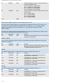
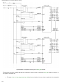
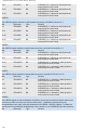
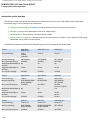
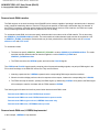
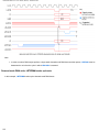
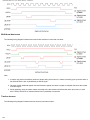
1
ADM-XRC SDK User Guide - family_t
ADM-XRC SDK 4.9.3 User Guide (Win32)
© Copyright 2001-2009 Alpha Data
The family_t datatype
The family_t datatype is used to symbolically represent a particular Xilinx FPGA family and is defined as follows:
type family_t is (
family_virtex,
family_virtex2,
family_virtex2p,
family_virtex4,
family_virtex5);
1
------
Virtex/Virtex-E/Virtex-EM
Virtex-II
Virtex-II Pro
Virtex-4
Virtex-5
ADM-XRC SDK User Guide - Common Memory Ports
ADM-XRC SDK 4.9.3 User Guide (Win32)
© Copyright 2001-2009 Alpha Data
The ddr2sram_port component
Overview
HDL source code
Parameters
Signals
Performance
Overview
The ddr2sram_port component is part of the memif package and implements an interface to a bank of DDR-II SSRAM
memory. This component follows the generic user interface for memory ports, but also has a few additional parameters
and sideband signals, as shown in the following figure:
2
ADM-XRC SDK User Guide - Common Memory Ports
HDL source code
Projects making use of this component must include all of the following source files (relative to root of SDK installation):
fpga/vhdl/chipscope/src/ilap_pkg.vhd
fpga/vhdl/chipscope/src/ilacombo_sim.vhd
fpga/vhdl/common/memif/memif_pkg.vhd
fpga/vhdl/common/memif/memif_int_pkg.vhd
fpga/vhdl/common/memif/memif_def_synth.vhd OR fpga/vhdl/common/memif/memif_def_sim.vhd
fpga/vhdl/common/memif/cmd_fifo.vhd
fpga/vhdl/common/memif/ddr2sram/ddr2sram_port.vhd
If synthesizing, the file fpga/vhdl/common/memif/memif_def_synth.vhd must be included. If simulating, the file
fpga/vhdl/common/memif/memif_def_sim.vhd must be included instead.
Parameters
Name
a_width
Type
natural
d_width
natural
Function
Width in bits of the port logical address, a.
Note
4
pinout
3
Width in bits of the port data in and out, d and q
respectively.
ddr2sram_pinout_t This value specifies the physical configuration of the
memory port. For convenience, an application may map it
to one of the predefined constants.
ra_width
natural
Width in bits of the memory device address bus, ra.
1
rc_width
natural
Width in bits of the memory device control bus, rc.
2
rd_width
natural
Width in bits of the memory device data bus, rd.
3
tag_width
natural
Width in bits of the tag in and out, tag and qtag
respectively.
Notes:
1. The ra_width parameter is a property of the printed circuit board, indicating how many wires are physically present,
rather than indicating how many of the ra lines are used by a particular DDR-II SSRAM device.
2. The memory device control bus, rc, is composed of various fields in this memory port, with the widths of certain fields
specified by the pinout and rd_width parameters. The following figure illustrates the fields that comprise the rc bus:
The order of the fields within rc is always the same, but some models may lack certain fields.
3
ADM-XRC SDK User Guide - Common Memory Ports
3. The rd_width parameter is the number of physical DQ wires making up the data bus of the DDR-II SSRAM bank. This
memory port transfers two words of data on the DQ wires for each command entered via the ce signal. Accordingly, the
d_width parameter, which is the width of d and q, is typically specified by the user application as being two times
rd_width. However, other values can be passed for d_width:
❍
❍
❍
If d_width > (2 * rd_width), then the memory port simply truncates d internally so that its width is (2 *
rd_width). Data read from the memory devices is zero-extended so that its width is d_width before being
returned on q.
d_width = (2 * rd_width) is the optimal usage case.
If d_width < (2 * rd_width), then the memory port zero-extends d internally so that its width is (2 *
rd_width).
4. The a_width parameter is the width of the logical address bus, a. Generally, it must be sufficiently wide to be able to
address all of the memory in a DDR-II SSRAM bank. Hence, the required value of a_width depends on what memory
devices are actually in use. As an example, consider a DDR-II SSRAM device with 20 address bits. Since "logical"
memory locations are two times as wide as the physical memory locations, one must subtract 1, giving a value of 19 for
the minimum value of a_width. When a_width is larger than actually required, the top few unused bits of a are ignored
by the memory port. In practice, one should determine the value of a_width assuming that the largest possible memory
devices are in use.
Signals
The signals of this interface to and from the user application are as follows:
Signal
a
Type
in
Function
Logical address
Note
User code must place a valid address on a when it asserts ce.
Since a memory port effectively represents a memory device as a
linear array of words of width d_width, this address is a logical
address, rather than anything resembling what one might see on the
ra bus.
be
burst_len
in
Byte enables to memory
in
User code must place valid byte enables on be whenever a write
command is entered (ce and w both asserted). A logic 1 in a given
bit of be means that the corresponding byte within be will be written
to memory, while a zero means that the corresponding byte will not
be written to memory.
6
Burst length select (sideband signal)
This input selects whether the DDR-II SSRAM devices are burst
length 2 (BL2) or burst length 4 (BL4) devices:
0 => BL2
1 => BL2/BL4
If BL2/BL4 is selected, the memory port will be compatible with BL2
and BL4 devices, although a performance penalty may apply
depending on how the user application uses the memiry port. If BL2
is selected, the memory will not be compatible with BL4 devices. If
the burst length is unknown at build time, one should select BL4.
Refer to the section below for a discussion of performance.
4
ADM-XRC SDK User Guide - Common Memory Ports
ce
in
Command entry
User code asserts this signal to enter a new read or write command
into the memory port. When asserted, a and w must be valid. When
asserted along with w, tag must also be valid.
User code must not assert ce when ready is deasserted.
Other than that, there are no restrictions on how few or how many
clock cycles ce can remain asserted. It can be pulsed for single clk0
cycles, or asserted for many clk0 cycles (ready permitting).
The address, byte enables, tag etc. of a command need not bear
any relationship to that of the previous command, but refer to the
section below for a discussion of performance.
clk0
in
Clock for user interface
5
All other signals except rst are synchronous to clk0.
clk90
clk180
clk270
d
in
High speed clock, phase 90
5
in
This clock must be the same frequency as clk0 but 90 degrees
behind.
High speed clock, phase 180
5
in
This clock must be the same frequency as clk0 but 180 degrees
behind.
High speed clock, phase 270
5
in
This clock must be the same frequency as clk0 but 270 degrees
behind.
Data to memory
User code must place valid data on d whenever a write command is
entered (ce and w both asserted).
dll_off
in
DLL disable (sideband signal)
User code should drive this input with 0 for normal operation, but
driving it with 1 causes the DOFF# field within rc to be asserted.
q
out
Data from memory
When valid is asserted by the memory port (as a result of a read
command), q reflects the data read from memory.
qtag
out
Tag out
When valid is asserted by the memory port (as a result of a read
command), qtag reflects the tag value that was assocated with that
read command.
ready
out
Port ready
When the memory port asserts ready, user code is permitted to
assert ce. Certain types of memory port may unconditionally assert
ready, whereas other types of memory port may sometimes
deassert ready depending on several factors.
For example, a DDR-II SDRAM port is capable of buffering a certain
number of commands internally, but if its command buffer is filled
while it executes a refresh cycle, it will deassert ready.
5
6
ADM-XRC SDK User Guide - Common Memory Ports
rst
sr
tag
valid
in
Asynchronous reset for memory port
in
May be tied to logic 0 if not required.
Synchronous reset for memory port
in
May be tied to logic 0 if not required.
Tag in
out
When user code asserts ce with w deasserted, it must also place a
valid tag on the tag signal. When, as a result of the read command,
the memory port asserts valid, the qtag output reflects the tag value
originally passed. This is intended to facilitate sharing of a memory
port between several data sources or data sinks, where each source
or sink recognizes a particular set of tags.
Read data valid
When the memory port asserts valid, it does so as a result of a read
command (user code asserted ce with w deasserted). When valid
is asserted, both q and qtag are valid.
w
in
Write select
When user code asserts ce, it must place either a logic 1 on the w
signal in order to select a write command, or 0 in order to select a
read command.
Notes:
5. The phase and frequency relationships between the four clock phases are illustrated by the following figure:
Also shown is the DDR-II SSRAM clock, K. Its frequency is the same as clk0, but its phase is indeterminate.
6. For correction operation, all sideband inputs must be static while the memory port is not idle.
The signals of this interface to and from the memory device(s) are as follows:
Signal
ra
Type
in
Function
Memory device address bus
This bus carries address information to from the memory port
to the memory device(s).
6
ADM-XRC SDK User Guide - Common Memory Ports
rc
inout
Memory device control bus
This bus carries control signals between the memory port and
the memory device(s), and is composed of various fields.
These signals are bundled together into the rc bus so that, for
the most part, the user application need not care what they
are.
Refer to note 2 for the mapping of the rc bus to device pins.
rd
inout
Memory device data bus
This bus carries data between the memory port and the
memory device(s). For each command entered via ce, two
words are transferred on rd, which determines the relationship
between the rd_width and d_with parameters. Refer to note 3
for details.
Performance
This memory port features an internal command buffer capable of buffering about 10 commands before deasserting the
ready signal. Most of the time, the rate of consumption of commands from the command buffer is at least as fast as
production of new commands by the user application. Certain usage patterns, however, may result in a accumulated backlog
in the command buffer.
A DDR-II SSRAM device has a burst length of two or four (i.e. two or four words on transferred on the rd bus). This
component supports burst length four (BL4) devices, but is compatible with burst length 2 devices without modification (to
see why this is so, one must understand the signalling protocol used by generic DDR-II SSRAM devices).
There are two potential performance penalties in this memory port:
●
●
Every access to a BL4 DDR-II SSRAM device must transfer 4 physical words, whose addresses are "consecutive", on
the rd bus. Because this takes two clk0 cycles, random accesses to unrelated addresses when burst_len is driven with
1 (to select BL4) incur a one cycle performance penalty. However, when burst_len is driven with 0 (to select BL2), this
performance penalty does not apply.
Turning the rd bus around when a read command and a write command are entered in consecutive clock cycles
requires one clk0 cycle. Thus it incurs a one cycle performance penalty. This penalty occurs only if a write command is
entered in the one-cycle window following entry of a read command.
Latency for read commands is fairly deterministic, since the penalties described above are limited to one cycle (although
these penalties may be accumulated by successive commands). The best-case latency from entry of a read command (ce
asserted with w deasserted) to valid asserted is approximately 9 clk0 cycles. Worst case latencies may be computed by
adding the above penalties to the best-case latency.
The optimal usage pattern for this memory port is blocks of accesses of the same type (read or write) with addresses that
increment by one on each successive access. When used optimally, a 32-bit wide DDR-II SSRAM memory port operating at
a clk0 frequency of 133MHz) can sustain approximately 1GB/s.
7
ADM-XRC SDK User Guide - Common Memory Ports
ADM-XRC SDK 4.9.3 User Guide (Win32)
© Copyright 2001-2009 Alpha Data
The ddrsdram_port component
Overview
HDL source code
Parameters
Signals
Row / column address selection
Performance
Overview
The ddrsdram_port component is part of the memif package and implements an interface to a bank of DDR SDRAM
memory. This component follows the generic user interface for memory ports, but also has a few additional parameters
and sideband signals, as shown in the following figure:
8
ADM-XRC SDK User Guide - Common Memory Ports
HDL source code
Projects making use of this component must include all of the following source files (relative to root of SDK installation):
fpga/vhdl/chipscope/src/ilap_pkg.vhd
fpga/vhdl/chipscope/src/ilacombo_sim.vhd
fpga/vhdl/common/memif/memif_pkg.vhd
fpga/vhdl/common/memif/memif_int_pkg.vhd
fpga/vhdl/common/memif/memif_def_synth.vhd OR fpga/vhdl/common/memif/memif_def_sim.vhd
fpga/vhdl/common/memif/cmd_fifo.vhd
fpga/vhdl/common/memif/ddrsdram/ddrsdram_clkfw.vhd
fpga/vhdl/common/memif/ddrsdram/ddrsdram_ctrl.vhd
fpga/vhdl/common/memif/ddrsdram/ddrsdram_data.vhd
fpga/vhdl/common/memif/ddrsdram/ddrsdram_data_dqs.vhd
fpga/vhdl/common/memif/ddrsdram/ddrsdram_dqs.vhd
9
ADM-XRC SDK User Guide - Common Memory Ports
fpga/vhdl/common/memif/ddrsdram/ddrsdram_dm.vhd
fpga/vhdl/common/memif/ddrsdram/ddrsdram_init.vhd
fpga/vhdl/common/memif/ddrsdram/ddrsdram_port.vhd
If synthesizing, the file fpga/vhdl/common/memif/memif_def_synth.vhd must be included. If simulating, the file
fpga/vhdl/common/memif/memif_def_sim.vhd must be included instead.
Parameters
Name
a_width
Type
natural
auto_train
boolean
d_width
pinout
Function
Width in bits of the port logical address, a.
Note
4
If true, the memory port automatically trains itself after
reset is deasserted. If false, the memory port does not
train itself. This parameter has a default value of true, and
in normal usage an application should rely on the default
value, and not map it to any particular value.
3
natural
Width in bits of the port data in and out, d and q
respectively.
ddrsdram_pinout_t This value specifies the physical configuration of the
memory port. For convenience, an application may map it
to one of the predefined constants.
ra_width
natural
Width in bits of the memory device address bus, ra.
1
rc_width
natural
Width in bits of the memory device control bus, rc.
2
rd_width
natural
Width in bits of the memory device data bus, rd.
3
tag_width
natural
Width in bits of the tag in and out, tag and qtag
respectively.
ddrsdram_timing_t This value specifies the timing of the memory port. For
convenience, an application may map it to one of the
predefined constants.
timing
Notes:
1. The memory device address bus, ra, is composed of two fields in this memory port, with the widths of each field
specified by the num_addr_bits and num_bank_bits of the pinout parameter. Therefore, ra_width is the sum of these
two values. The following figure illustrates this for the case where num_addr_bits = 13 and num_bank_bits = 2:
Note that ra_width and pinout are properties of the printed circuit board, indicating how many wires are physically
present. On the other hand, the DDR SDRAM devices actually fitted to the printed circuit board may have less pins
connected. The purpose of the row, col, bank and pbank signals is to specify at runtime the properties of the DDR
SDRAM devices actually in use.
2. The memory device control bus, rc, is composed of various fields in this memory port, with the widths of certain fields
specified by the pinout and rd_width parameters. The following figure illustrates an example that puts rc_width at 17:
10
ADM-XRC SDK User Guide - Common Memory Ports
The order of the fields within rc is always the same; only the field widths may differ from one model to another.
3. The rd_width parameter is the number of physical DQ wires making up the data bus of the DDR SDRAM bank. This
memory port transfers two words of data on the DQ wires for each command entered via the ce signal. Accordingly, the
d_width parameter, which is the width of d and q, is typically specified by the user application as being twice rd_width.
However, other values can be passed for d_width:
❍
❍
❍
If d_width > (2 * rd_width), then the memory port simply truncates d internally so that its width is (2 *
rd_width). Data read from the memory devices is zero-extended so that its width is d_width before being
returned on q.
d_width = (2 * rd_width) is the optimal usage case.
If d_width < (2 * rd_width), then the memory port zero-extends d internally so that its width is (2 *
rd_width).
4. The a_width parameter is the width of the logical address bus, a. Generally, it must be sufficiently wide to be able to
address all of the memory in a DDR SDRAM bank. Hence, the required value of a_width depends on what memory
devices are actually in use. As an example, consider two physical banks of DDR SDRAM devices that use 13 row bits,
10 column bits and 2 internal bank address bits. The number of address bits is:
13 (row address bits) +
10 (column address bits) +
2 (internal bank address bits) +
1 (2 physical banks / CS# pins) =
26
We must now subtract 1, because "logical" memory locations are twice as wide as the physical memory locations, due
to transferring two words on the DQ pins for every command entered on ce. Hence a_width for this configuration should
be at least 25. When a_width is larger than actually required, the top few unused bits of a are ignored by the memory
port. In practice, one should determine the value of a_width assuming that the largest possible memory devices are in
use.
Signals
The signals of this interface to and from the user application are as follows:
Signal
11
Type
Function
Note
ADM-XRC SDK User Guide - Common Memory Ports
a
in
Logical address
User code must place a valid address on a when it asserts ce.
Since a memory port effectively represents a memory device as a
linear array of words of width d_width, this address is a logical
address, rather than anything resembling what one might see on the
ra bus.
bank
be
ce
in
Bank address width select (sideband signal)
in
This input selects number of internal bank address bits for the DDR
SDRAM devices in use:
00 => no internal bank address bits
01 => 1 internal bank address bits
10 => 2 internal bank address bits
11 => 3 internal bank address bits
Byte enables to memory
in
User code must place valid byte enables on be whenever a write
command is entered (ce and w both asserted). A logic 1 in a given
bit of be means that the corresponding byte within be will be written
to memory, while a zero means that the corresponding byte will not
be written to memory.
Command entry
6, 8
User code asserts this signal to enter a new read or write command
into the memory port. When asserted, a and w must be valid. When
asserted along with w, tag must also be valid.
User code must not assert ce when ready is deasserted.
Other than that, there are no restrictions on how few or how many
clock cycles ce can remain asserted. It can be pulsed for single clk0
cycles, or asserted for many clk0 cycles (ready permitting).
The address, byte enables, tag etc. of a command need not bear
any relationship to that of the previous command, but refer to the
section below for a discussion of how to maximize performance.
clk0
in
Clock for user interface
7
All other signals except rst are synchronous to clk0.
clk90
clk180
clk270
col
in
High speed clock, phase 90
7
in
This clock must be the same frequency as clk0 but lagging by 90
degrees.
High speed clock, phase 180
7
in
This clock must be the same frequency as clk0 but lagging by 180
degrees.
High speed clock, phase 270
7
in
This clock must be the same frequency as clk0 but lagging by 270
degrees.
Column address width select (sideband signal)
6, 8
This input selects the number of column address bits to use. Along
with the row input, it specifies the row/column geometry of the DDR
SDRAM device, as defined here.
12
ADM-XRC SDK User Guide - Common Memory Ports
d
in
Data to memory
User code must place valid data on d whenever a write command is
entered (ce and w both asserted).
pbank
q
in
Physical bank select (sideband signal)
out
This input selects the number of physical banks (chip-selects) in use
for the DDR SDRAM devices:
00 => 1 physical bank / 1 CS#
01 => 2 physical bank / 2 CS#
10 => 4 physical bank / 4 CS#
11 => 8 physical bank / 8 CS#
Data from memory
6, 8
When valid is asserted by the memory port (as a result of a read
command), q reflects the data read from memory.
qtag
ready
out
Tag out
out
When valid is asserted by the memory port (as a result of a read
command), qtag reflects the tag value that was assocated with that
read command.
Port ready
When the memory port asserts ready, user code is permitted to
assert ce. Certain types of memory port may unconditionally assert
ready, whereas other types of memory port may sometimes
deassert ready depending on several factors.
For example, a DDR SDRAM port is capable of buffering a certain
number of commands internally, but if its command buffer is filled
while it executes a refresh cycle, it will deassert ready.
regd
in
Registered / unregistered select (sideband signal)
6, 8
This input selects whether the memory port expects registered DDR
SDRAM memory or unregistered DDR SDRAM memory:
row
in
0 => unregistered
1 => registered
Row address width select (sideband signal)
This input selects the number of row address bits to use. Along with
the col input, it specifies the row/column geometry of the DDR
SDRAM device, as defined here.
rst
in
Asynchronous reset for memory port
sr
in
May be tied to logic 0 if not required.
Synchronous reset for memory port
tag
in
May be tied to logic 0 if not required.
Tag in
When user code asserts ce with w deasserted, it must also place a
valid tag on the tag signal. When, as a result of the read command,
the memory port asserts valid, the qtag output reflects the tag value
originally passed. This is intended to facilitate sharing of a memory
port between several data sources or data sinks, where each source
or sink recognizes a particular set of tags.
13
6, 8
ADM-XRC SDK User Guide - Common Memory Ports
trained
(sideband
signal)
out
Training success flag
valid
out
When the memory port asserts trained, it indicates that training of
the memory port was successful. When deasserted, either training
is not yet complete or training was unsuccessful.
Read data valid
When the memory port asserts valid, it does so as a result of a read
command (user code asserted ce with w deasserted). When valid
is asserted, both q and qtag are valid.
w
x4
in
Write select
in
When user code asserts ce, it must place either a logic 1 on the w
signal in order to select a write command, or 0 in order to select a
read command.
X4 device select (sideband signal)
9
This input selects whether devices with 8- or 16-bit data or devices
with 4-bit data are in use. Generally applicable to DIMM DDR
SDRAM memory. In this version of the memory port, it must be
zero.
Notes:
5. The delay from deassertion of reset to completion of training (trained asserted) may be as long as 350ms. This is
because a large post-reset delay is used in order to ensure that the memory port properly initializes the DDR SDRAM
devices that it is controlling after power-on.
For simulation, however, the memory port uses a much smaller post-reset delay, with the result that the delay from
deassertion of reset to completion of training is dominated by the time spent training. This is in the order of 150
microseconds of simulation time at a clk0 frequency of 133MHz.
6. Certain properties of a DDR SDRAM device, such as number of row and column address bits, might not be known at the
time of building an FPGA design. Therefore, this memory port allows certain properties to be specified "at runtime". An
application might interrogate some Vital Product Data in order to determine the proper values to drive on the row, col,
bank, and pbank signals.
Alternatively, if the designer can guarantee that the properties of the DDR SDRAM devices are known when building the
FPGA design, these signals can be driven with constant values. This has the advantage of lower slice utilization.
In any case, for reliable operation, these signals must not change unless the memory port is idle.
The purpose of these signals should not be confused with that of the pinout parameter. The pinout parameter specifies
properties of the circuit board on which the FPGA and DDR SDRAM devices are mounted. In general, the number of
physical wires on the circuit board provided for addressing the DDR SDRAM devices can be greater than the number
actually used by a particular DDR SDRAM device.
7. The phase and frequency relationships between the four clock phases are illustrated by the following figure:
14
ADM-XRC SDK User Guide - Common Memory Ports
Also shown is the DDR SDRAM clock, CK. Its frequency is the same as clk0, but its phase is indeterminate.
8. For correction operation, all sideband inputs must be static while the memory port is not idle.
9. In this version, the x4 sideband input must be driven with a constant.
The signals of this interface to and from the memory device(s) are as follows:
Signal
ra
Type
in
Function
Memory device address bus
This bus carries address information to from the memory port
to the memory device(s). For devices with a nontrivial
addressing scheme, this address may be composed of various
fields. These fields are bundled together into the ra bus so
that, for the most part, the user application need not care what
they are.
Refer to note 1 for the mapping of the ra bus to device pins.
rc
inout
Memory device control bus
This bus carries control signals between the memory port and
the memory device(s), and is composed of various fields.
These signals are bundled together into the rc bus so that, for
the most part, the user application need not care what they
are.
Refer to note 2 for the mapping of the rc bus to device pins.
rd
inout
Memory device data bus
This bus carries data between the memory port and the
memory device(s). For each command entered via ce, two
words are transferred on rd, which determines the relationship
between the rd_width and d_width parameters. Refer to note
3 for details.
Row / column address selection
The row and col sideband inputs together determine the number address bits used for row and column addresses, as in the
following table:
row[1:0]
15
col[1:0]
No. of row bits used
No. of column bits used
ADM-XRC SDK User Guide - Common Memory Ports
00
00
00
00
01
01
01
01
10
10
10
10
11
11
11
11
00
01
10
11
00
01
10
11
00
01
10
11
00
01
10
11
12
12
12
12
13
13
13
13
14
14
14
14
15
15
15
15
8
9
10
11
9
10
11
12
10
11
12
13
11
12
13
14
Performance
This memory port features an internal command buffer capable of buffering about 10 commands before deasserting the
ready signal. Most of the time, the rate of consumption of commands from the command buffer is at least as fast as
production of new commands by the user application. Periodically, however, the memory port must refresh the DDR SDRAM
devices it is controlling, which may result in an accumulated backlog of buffered commands, and deassertion of the ready
signal. Certain usage patterns, such as alternating between read and write commands, may also have the same effect.
The architecture of DDR SDRAM device consists of a number of internal banks which are in turn divided into a number of
pages. At any moment, a given bank may be "closed", or may have a given page "open". Opening or closing a bank takes a
finite number of clock cycles. In this memory port, the following performance penalties exist for memory accesses falling into
the following patterns:
●
●
●
Several clk0 cycles for changing from read to write or write to read within the same page and bank.
In the order of 8 clk0 cycles for consecutive accesses that fall within different pages of the same bank, or within different
banks.
In the order of 8-20 clk0 cycles for an access that occurs while the memory port is performing a refresh.
Latency for read commands is nondeterministic due to the penalties described above, particularly because of the need to
refresh, but the best-case latency from entry of a read command (ce asserted with w deasserted) to valid asserted is
approximately 11 clk0 cycles. This can be modified somewhat by tightening or relaxing the timing as specified by the timing
parameter. Worst case latencies may be computed by adding the above penalties to the best-case latency.
The optimal usage pattern for this memory port is blocks of accesses of the same type (read or write) to the same bank and
page. A linearly incrementing address is an example of an optimal usage pattern. When used optimally, this memory port
with 32 physical data bits (rd is 32) operating at a clk0 frequency of 133MHz can sustain approximately 1GB/s.
16
ADM-XRC SDK User Guide - PLXSIM Package
ADM-XRC SDK 4.9.3 User Guide (Win32)
© Copyright 2001-2009 Alpha Data
PLXSIM VHDL reference
Datatypes
Constants
Functions and procedures
Components
This section documents the VHDL implementation of the PLXSIM package. This package consists datatypes, constants,
functions, procedures and components designed to speed up development of a VHDL testbench centered around the local
bus interface of an FPGA design.
Datatypes
Name
Purpose
byte_enable_t
byte_t
A vector type used to pass the byte enables for a local bus
transfer
A type that can hold a single byte of data
byte_vector_t
A vector type used to hold the data for a local bus transfer
integer_vector_t
A vector type used to hold an array of integers
locbus_ddma_in_t
A record type used to make a bundle of the demand-mode
DMA signals for a particular DMA channel that are input by a
stimulus process
A record type used to make a bundle of the demand-mode
DMA signals for a particular DMA channel that are driven by a
stimulus process
A record type used to make a bundle of the local bus signals
that are input by a stimulus process
A record type used to make a bundle of the local bus signals
that are driven by a stimulus process
locbus_ddma_out_t
locbus_in_t
locbus_out_t
Constants
Name
Purpose
init_locbus_ddma_out
A constant that can be used to initialize variables/signals of
type locbus_ddma_out_t
init_locbus_out
A constant that can be used to initialize variables/signals of
type locbus_out_t
Functions and procedures
17
ADM-XRC SDK User Guide - PLXSIM Package
Name
Purpose
conv_byte_vector
A function for converting values to the byte_vector_t type
conv_integer
A function for converting values to the integer type
conv_integer_signed
conv_std_logic_vector
A function for converting signed binary values to the integer
type
A function for converting unsigned binary values to the integer
type
A function for converting values to the std_logic_vector type
conv_string
A function for converting values to the string type
conv_string_hex
A function for converting values to the string type, in
hexadecimal form
A procedure for performing a basic read transfer on the local
bus
A procedure for performing a basic read transfer with constant
local address on the local bus
A procedure for performing a basic demand-mode DMA read
transfer with constant local address on the local bus
A procedure for performing a basic demand-mode DMA read
transfer on the local bus
A procedure for requesting or relinquishing access to the local
bus
A procedure for delaying execution for a particular number of
local bus clock cycles
A procedure for waiting until the FPGA requests a demandmode DMA transfer
A procedure for performing a basic write transfer on the local
bus
A procedure for performing a basic write transfer with constant
local address on the local bus
A procedure for performing a basic demand-mode DMA write
transfer with constant local address on the local bus
A procedure for performing a basic demand-mode DMA write
transfer on the local bus
conv_integer_unsigned
plxsim_read
plxsim_read_const
plxsim_read_const_demand
plxsim_read_demand
plxsim_request_bus
plxsim_wait_cycles
plxsim_wait_demand
plxsim_write
plxsim_write_const
plxsim_write_const_demand
plxsim_write_demand
Components
Name
Purpose
lbpcheck
A component that can be instantiated in a testbench in order to
flag local bus protocol violations
A component that can be instantiated in order to connect a
stimulus process to the demand-mode DMA signals for a
particular DMA channel
A component that can be instantiated in order to connect a
stimulus process to a 32-bit multiplexed address/data local bus
A component that can be instantiated in order to connect a
stimulus process to a 64-bit multiplexed address/data local bus
A component that can be instantiated in order to connect a
stimulus process to a 32-bit nonmultiplexed address/data local
bus
locbus_agent_ddma
locbus_agent_mux32
locbus_agent_mux64
locbus_agent_nonmux
18
ADM-XRC SDK User Guide - PLXSIM Package
locbus_arb
19
A component that can be instantiated in order to arbitrate
between stimulus processes for local bus access
ADM-XRC SDK 4.9.3 User Guide (Win32)
ADM-XRC SDK 4.9.3 User
Guide (Win32)
Document version: 4.9.3.1
© Copyright 2001-2009 Alpha Data
20
ADM-XRC SDK 4.9.3 User Guide (Win32) - Introduction
ADM-XRC SDK 4.9.3 User Guide (Win32)
© Copyright 2001-2009 Alpha Data
Introduction
Please choose one of the following topics:
About the ADM-XRC SDK
Hardware supported
List of changes
Upgrades to the SDK
Sales and support
21
ADM-XRC SDK 4.9.3 User Guide (Win32) - About the ADM-XRC SDK
ADM-XRC SDK 4.9.3 User Guide (Win32)
© Copyright 2001-2009 Alpha Data
About the ADM-XRC SDK
The ADM-XRC SDK is a set of resources including an application-programming interface (API) intended to assist the user
in creating an application using one of Alpha Data's range of reconfigurable computing cards. The API is a thin layer in user
space that makes the necessary open, close and device I/O control calls to a kernel-mode device driver provided by Alpha
Data as a related package.
The ADM-XRC SDK consists of the following components:
22
●
ADM-XRC SDK documentation (this document).
●
Documentation for PLX Technology's PCI9080 and PCI9656.
●
Sample applications in source and binary form.
●
Sample FPGA designs in source and bitstream form.
●
A primer on the local bus used by Alpha Data's reconfigurable computing cards.
●
FPGA pinouts in the form of constraints (UCF) files.
●
API header files.
●
API import libraries.
ADM-XRC SDK 4.9.3 User Guide (Win32) - Hardware supported
ADM-XRC SDK 4.9.3 User Guide (Win32)
© Copyright 2001-2009 Alpha Data
Hardware supported in this version of the SDK
This version of the SDK supports the following models in Alpha Data's reconfigurable computing range:
●
ADM-XRC
●
ADM-XRC-P
●
ADM-XRC-II-Lite
●
ADM-XRC-II
●
ADM-XPL
●
ADM-XP
●
ADP-WRC-II
●
ADP-DRC-II
●
ADP-XPI
●
ADM-XRC-4LX
●
ADM-XRC-4SX
●
ADM-XRC-4FX (and ADM-XMC-4FX)
●
ADPE-XRC-4FX
●
ADM-XRC-5LX
●
ADM-XRC-5T1
●
ADM-XRC-5T2
●
ADM-XRC-5T2-ADV
●
ADM-XRC-5TZ
●
ADM-XRC-5T-DA1
This version of the SDK supports the above cards fitted with any of the following FPGAs:
●
●
23
Virtex family:
❍
XCV400BG560
❍
XCV600BG560
❍
XCV800BG560
❍
XCV1000BG560
Virtex-E family:
❍
XCV1000EBG560
❍
XCV1600EBG560
ADM-XRC SDK 4.9.3 User Guide (Win32) - Hardware supported
❍
●
●
●
●
●
24
XCV2000EBG560
Virtex-EM family:
❍
XCV405EBG560
❍
XCV812EBG560
Virtex-II family:
❍
XC2V1000FG456
❍
XCV2V3000FF1152
❍
XCV2V4000FF1152
❍
XCV2V6000FF1152
❍
XCV2V8000FF1152
❍
XCV2V6000FF1517
❍
XCV2V8000FF1517
Virtex-II Pro family:
❍
XC2VP7FF896
❍
XC2VP20FF896
❍
XC2VP30FF896
❍
XC2VP70FF1704
❍
XC2VP100FF1704
Virtex-4 family:
❍
XC4VLX60FF1148
❍
XC4VLX80FF1148
❍
XC4VLX100FF1148
❍
XC4VLX160FF1148
❍
XC4VSX55FF1148
❍
XC4VFX100FF1517
❍
XC4VFX140FF1517
Virtex-5 family:
❍
XC5VLX110FF1153
❍
XC5VFX70TFF1136
❍
XC5VFX100TFF1136
❍
XC5VFX100TFF1738
❍
XC5VFX130TFF1738
❍
XC5VFX200TFF1738
❍
XC5VLX110TFF1136
❍
XC5VLX110TFF1738
❍
XC5VLX155TFF1136
❍
XC5VLX155TFF1738
ADM-XRC SDK 4.9.3 User Guide (Win32) - Hardware supported
25
❍
XC5VLX220TFF1738
❍
XC5VLX330TFF1738
❍
XC5VSX95TFF1136
❍
XC5VSX240TFF1738
ADM-XRC SDK 4.9.3 User Guide (Win32) - Changes
ADM-XRC SDK 4.9.3 User Guide (Win32)
© Copyright 2001-2009 Alpha Data
List of changes
For a detailed list of changes, please refer to the file changes.txt in the base directory of the SDK.
26
ADM-XRC SDK 4.9.3 User Guide (Win32) - Upgrades to the SDK
ADM-XRC SDK 4.9.3 User Guide (Win32)
© Copyright 2001-2009 Alpha Data
Upgrades to the ADM-XRC SDK
From time to time, newer versions of the SDK will become available on the Alpha Data FTP site at ftp://ftp.alpha-data.com,
in the pub/admxrc/windows directory.
Backwards source and binary compatibility will be maintained in the API whenever possible. Alpha Data reserves the right to
change the sample applications and FPGA designs as part of a policy of continual improvement.
27
ADM-XRC SDK 4.9.3 User Guide (Win32) - Sales and support
ADM-XRC SDK 4.9.3 User Guide (Win32)
© Copyright 2001-2009 Alpha Data
How to get support
Alpha Data's FTP site, containing resources for customers, is ftp.alpha-data.com.
Alpha Data technical personnel may be contacted by phone, fax or e-mail:
US
Rest of World
Phone:
Fax:
E-mail:
(408) 916 5713
(408) 436 5524
[email protected]
+44 131 558 2600
+44 131 558 2700
[email protected]
Web:
www.alpha-data.com
www.alpha-data.com
28
ADM-XRC SDK 4.9.3 User Guide (Win32) - Installation
ADM-XRC SDK 4.9.3 User Guide (Win32)
© Copyright 2001-2009 Alpha Data
Installation
Please choose one of the following topics:
Before installation
After installation
29
ADM-XRC SDK 4.9.3 User Guide (Win32) - Before installation
ADM-XRC SDK 4.9.3 User Guide (Win32)
© Copyright 2001-2009 Alpha Data
Before installation
Beginning with release 4.5.1, the ADM-XRC SDK for Windows package installs by default to a folder that contains the
release number. The default installation folder for this release is:
%SystemDrive%\ADMXRC_SDK4.9.3
In many cases, %SystemDrive% simply equates to C:. Since the SDK release number forms a part of the name of the
installation folder, it is possible to keep several versions of the SDK on one system. A folder at the root of the system drive is
chosen rather than a folder such as "Program Files" because, as of writing, some of the Xilinx ISE tools do not permit
spaces in filenames.
It is not necessary to install the ADM-XRC driver before installing the SDK, although it will not be possible to run any
applications until you have done so. The recommended ADM-XRC driver version for this version of the SDK is 3.16 or later.
After installation
30
ADM-XRC SDK 4.9.3 User Guide (Win32) - After installation
ADM-XRC SDK 4.9.3 User Guide (Win32)
© Copyright 2001-2009 Alpha Data
After installation tasks
After installation of the ADM-XRC SDK, in order to start developing applications, you will need to configure your C compiler
to use the API header files and libraries:
Configuring the MSVC IDE
Configuring the Borland C++ command line tools
This release of the SDK does not provide Xilinx Project Navigator files, because as of ISE 7.1i, Xilinx adopted a binary file
format that stores absolute pathnames. However, a script is provided that creates project files for all sample FPGA designs,
and this can be executed after installing the SDK. For further information, see:
Generating ISE Project Navigator files for sample FPGA designs
31
ADM-XRC SDK 4.9.3 User Guide (Win32) - Configuring the MSVC IDE
ADM-XRC SDK 4.9.3 User Guide (Win32)
© Copyright 2001-2009 Alpha Data
Configuring the MSVC IDE
In order to build applications using the ADM-XRC SDK, the compiler must be able to locate the API header file, and the
linker must be able to locate the appropriate version of the API library. There are two ways to accomplish this with the
Microsoft Visual C++ Integrated Development Environment (MSVC IDE):
MSVC IDE global options
MSCV IDE per-project options
32
ADM-XRC SDK 4.9.3 User Guide (Win32) - MSVC IDE global options
ADM-XRC SDK 4.9.3 User Guide (Win32)
© Copyright 2001-2009 Alpha Data
Configuring the MSVC IDE, global options
This section assumes that that the ADM-XRC SDK has been installed in the default
location, namely
C:\ADMXRC_SDK4.9.3
The search paths that are applied when building any application in MSVC can be changed. If you decide to use this method
of configuring MSVC, bear in mind that the ADM-XRC header files and import libraries will become visible for inclusion to all
applications that you subsequently build using the IDE.
1. Select Tools->Options from the menu within the MSVC IDE.
2. In the Options dialogue box, select the C/C++ tab, and then select Include files from the Show directories for list.
Add this path:
C:\ADMXRC_SDK4.9.3\include
3. Select Library files from the Show directories for list. Add this path:
C:\ADMXRC_SDK4.9.3\lib\msvc
4. Click OK to apply the changes.
The new include and library search paths will apply to any project subsequently built with the MSVC++ IDE. Note that you
will need to specify the API library to the linker on a per-project basis. To do this, follow these steps:
1. Select Project->Settings from the menu. Ensure that the correct project is highlighted on the left hand side of the
Project Settings dialog box.
2. Select the configuration(s) you want to change - Win32 Debug, Win32 Release or All Configurations - from the
Settings for list.
3. Select the Link tab and add the API library to the list of .lib files in the Object/Library modules field.
4. Add either admxrc.lib (Release version) or admxrcd.lib (Debug version).
5. Click OK to apply the changes.
33
ADM-XRC SDK 4.9.3 User Guide (Win32) - MSVC IDE per-project options
ADM-XRC SDK 4.9.3 User Guide (Win32)
© Copyright 2001-2009 Alpha Data
Configuring the MSVC IDE, per-project options
This section assumes that that the ADM-XRC SDK has been installed in the default
location, namely
C:\ADMXRC_SDK4.9.3
Altering the global MSVC options may not desirable. In this case, the ADM-XRC API header and library files may be added
to the search paths on a per-project basis. To do this, follow these steps:
1. Select Project->Settings from the menu. Ensure that the correct project is highlighted on the left hand side of the
Project Settings dialog box.
2. Select the configuration(s) you want to change - Win32 Debug, Win32 Release or All Configurations - from the
Settings for list.
3. Select the C/C++ tab and then select Preprocessor from the Category list.
4. Add the path
C:\ADMXRC_SDK4.9.3\include
to the Additional include directories field.
5. Select the Link tab and then select Input from the Category list.
6. Add the path
C:\ADMXRC_SDK4.9.3\lib\msvc
to the Additional library path field.
7. Add the API library to the list of .lib files in the Object/Library modules field. This must be admxrc.lib (to use the
Release version) or admxrcd.lib (to use the Debug version).
8. Click OK to apply the changes, which will require the project to be completely rebuilt in order to take effect.
34
ADM-XRC SDK 4.9.3 User Guide (Win32) - Configuring Borland C++ command line tools
ADM-XRC SDK 4.9.3 User Guide (Win32)
© Copyright 2001-2009 Alpha Data
Configuring the Borland C++ command line tools
This section assumes that that the ADM-XRC SDK has been installed in the default location, namely:
C:\ADMXRC_SDK4.9.3
In order to build applications using the ADM-XRC SDK, the compiler must be able to locate the API header file, and the
linker must be able to locate the appropriate version of the API library. The Borland C++ command line tools allow the library
and include file search paths to be customized via the BCC32.CFG and ILINK32.CFG files, which are usually located in the
bin\ directory of the Borland C++ tools installation.
Add this line to BCC32.CFG:
-I"C:\ADMXRC_SDK4.9.3\include"
Add this line to ILINK32.CFG:
-L"C:\ADMXRC_SDK4.9.3\lib\Borland"
Important note: there appears to be a bug in the Borland C++ command line tools, manifested when specifying a quoted
paths with spaces in configuration files such as BCC32.CFG. In order for the tools to correctly pick up these paths, there
must be at least one space at the end of such lines in the configuration file. To illustrate this, let + denote a space character.
A BCC32.CFG file including this workaround would look like:
-IC:\borland\bcc55\include
-I"C:\some+path\include"+
-j10
35
ADM-XRC SDK 4.9.3 User Guide (Win32) - Installable packages
ADM-XRC SDK 4.9.3 User Guide (Win32)
© Copyright 2001-2009 Alpha Data
Installable packages
In order to develop applications for an Alpha Data reconfigurable computing card on a Windows platform, the package
admxrc-sdk-win32-4.9.3 should be installed:
Package
Platforms supported
admxrc-sdk-win32-4.9.3
Windows 98
Windows ME
Windows NT 4.0
Windows 2000
Windows XP
Windows Server 2003
In order to run applications on an Alpha Data reconfigurable computing card on a Windows platform, the appropriate driver
package should be installed:
Package
Platforms supported
admxrc-driver-win2k-3.16
Windows 2000
Windows XP (x86)
Windows XP (x86_64)
Windows Server 2003 (x86)
Windows Server 2003 (x86_64)
Windows NT 4.0 + Service Pack 6
admxrc-driver-winnt4-3.16
It is recommended that the most up to date driver version currently available be installed. At the time of writing, this is version
3.16.
36
ADM-XRC SDK 4.9.3 User Guide (Win32) - Sample applications
ADM-XRC SDK 4.9.3 User Guide (Win32)
© Copyright 2001-2009 Alpha Data
Sample applications
A number of sample applications, written in C, are included with the SDK. Some of these use the sample FPGA designs
included with the SDK.
Running the sample applications
Rebuilding the sample applications
Sample application list
37
ADM-XRC SDK 4.9.3 User Guide (Win32) - Running the sample applications
ADM-XRC SDK 4.9.3 User Guide (Win32)
© Copyright 2001-2009 Alpha Data
Running the sample applications
ADMXRC_SDK4 environment variable
Some of the sample applications, for example memtest, require bitstreams from the sample FPGA designs in order to run.
In order that these applications can locate any required bitstreams, the environment variable ADMXRC_SDK4 must be
correctly set to point to the base directory of where the SDK has been installed. For example:
set ADMXRC_SDK4=C:\ADMXRC_SDK4.9.3
Normally, this variable is set automatically during installation of the SDK, but users may wish to set it manually (if, for
example, it is desirable to have more than one version of the SDK installed).
Command line invocation
Binaries for the sample applications are provided prebuilt in the bin\ directory of the SDK, and can be invoked from the
command line. For example:
C:
cd C:\ADMXRC_SDK4.9.3\bin
memtest
38
ADM-XRC SDK 4.9.3 User Guide (Win32) - Building the sample applications
ADM-XRC SDK 4.9.3 User Guide (Win32)
© Copyright 2001-2009 Alpha Data
Rebuilding the sample applications
The sample applications are supplied in source code form in the apps\ directory of the SDK. They may be compiled using
the MSVC command line tools, the MSVC IDE or the Borland C++ command line tools.
Building the sample applications using MSVC
Building the sample applications using Borland C++ command line tools
39
ADM-XRC SDK 4.9.3 User Guide (Win32) - MSVC
ADM-XRC SDK 4.9.3 User Guide (Win32)
© Copyright 2001-2009 Alpha Data
Building the sample applications with MSVC
The workspace apps\apps.dsw contains all of the sample applications. In order to build all of the applications, follow these
steps:
1. Open the workspace apps\apps.dsw.
2. Select Build->Batch Build from the menu, and click "Build All". This will build both the Debug and Release versions of
the applications.
The executables for each application are found in the Debug and Release folders. Normally one runs the Release version,
and by way of example, the executables for the DMA application are located as follows:
40
Executable file
Configuration
apps\dma\debug\dma.exe
apps\dma\release\dma.exe
MSVC Debug version
MSVC Release version
ADM-XRC SDK 4.9.3 User Guide (Win32) - Borland C++ command line tools
ADM-XRC SDK 4.9.3 User Guide (Win32)
© Copyright 2001-2009 Alpha Data
Building the sample applications with Borland C++ command line tools
To build all of the sample applications, Borland C++ command line users can change directory to the apps\ directory of the
SDK and then invoke MAKE as follows:
make -fmakefile.bcc
This will build the Borland versions of all the applications, located in the Borland\ subdirectory. For example, the Borlandcompiled executable for the DMA application will be located as follows:
41
Executable file
Configuration
apps\dma\borland\dma.exe
Borland C++ command line version
ADM-XRC SDK 4.9.3 User Guide (Win32) - Sample application list
ADM-XRC SDK 4.9.3 User Guide (Win32)
© Copyright 2001-2009 Alpha Data
Sample application list
The table below lists the sample applications and the FPGA bitstream required for each, if applicable:
Name
FPGA design
(Verilog)
Clock
FPGA design
(VHDL)
Bitstream
directory
Purpose
Clock
bit\clock
Utility to program clock generators and
measure clock frequencies.
Demonstrates using Delay-locked loops
(DLLs) in Virtex/Virtex-E/Virtex-EM
devices and Digital Clock Managers
(DCMs) in Virtex-II, Virtex-IIPro, Virtex-4
and Virtex-5 devices.
Demonstrates using the DMA engines on
the ADM-XRC series of cards.
DLL
DLL
DLL
bit\dll
DMA
DDMA
DDMA64
DDMA
DDMA64
bit\ddma
bit\ddma64
EPTest
Flash
FrontIO
FrontIO
FrontIO
bit\frontio
ITest
ITest
ITest
bit\itest
Master
Master
Master
bit\master
Memory
Memory
Memory64
bit\memory
bit\memory64
MemoryF
Memory
Memory64
bit\memory
bit\memory64
Demonstrates host access to memories
Info
42
A utility to read and write the
configuration EEPROM on the ADM-XRC
series of cards.
A utility for programming the Flash
memory on the ADM-XRC.
Demonstrates use of the front panel I/O
connector.
A utility to display information about a
card.
Demonstrates generation and handling of
FPGA interrupts on the host.
Demonstrates direct master access by
FPGA to host memory.
Demonstrates host access to memories
Memtest
ZBT
ZBT64
ZBT
ZBT64
bit\zbt
bit\zbt64
Demonstrates host access to ZBT
SSRAM.
RearIO
RearIO
RearIO
bit\reario
Simple
Simple
Simple64
Simple
Simple64
bit\simple
bit\simple64
Demonstrates use of the rear panel I/O
connector.
Demonstrates direct slave access by host
to registers in the FPGA.
ADM-XRC SDK 4.9.3 User Guide (Win32) - Clock
ADM-XRC SDK 4.9.3 User Guide (Win32)
© Copyright 2001-2009 Alpha Data
Clock utility
Model support
Overview
Command-line syntax
Description
FPGA design
Model support
Model
ADM-XRC
ADM-XRC-P
ADM-XRC-II-Lite
ADM-XRC-II
ADM-XPL
ADM-XP
ADP-WRC-II
ADP-DRC-II
ADP-XPI
ADM-XRC-4LX
ADM-XRC-4SX
ADM-XRC-4FX
ADPE-XRC-4FX
ADM-XRC-5LX
ADM-XRC-5T1
ADM-XRC-5T2
Supported
ADM-XRC-5T2-ADV
ADM-XRC-5TZ
ADM-XRC-5T-DA1
Overview
The Clock utility serves two purposes:
●
●
Syntax
43
Programming the onboard clock generators on a reconfigurable computing card with an arbitrary clock frequency.
Measuring the approximate frequencies of the clocks present at the various clock inputs on a reconfigurable computing
card.
ADM-XRC SDK 4.9.3 User Guide (Win32) - Clock
clock [options ...] [clock input] [frequency]
Options
Option
-card
-index
-measure
Argument type
base 10 integer
base 10 integer
Meaning
ID of card to open
Index of card to open
Disables measurement of approximate
frequency.
Enables measurement of approximate
frequency (default)
+measure
Description
When run with no arguments, the Clock utility displays a list of clock inputs and their 1-based indices. For example, on an
ADM-XRC-5T2 card, running Clock with no arguments produces the following output:
Clock pins available on specified card:
Clock input
Programmable
Clock generator index
1
2
3
4
5
6
7
Yes
Yes
Yes
No
No
No
No
0
1
1
N/A
N/A
N/A
N/A
LCLK
MCLKA
MCLKB
REFCLK
XRM_CLKIN
XRM_MGTREF
PCIE100A
This indicates that of the seven clock inputs, only LCLK (1), MCLKA (2) and MCLKB (3) are programmable. LCLK
corresponds to clock generator 0, and MCLKA and MCLKB are copies of the output of clock generator 1.
To measure the frequency of a particular clock input, specify the index of the clock input as the first argument. For example,
to measure the local bus clock frequency, run Clock as follows:
clock 1
This produces output in the following form (actual measured values may vary depending on what LCLK frequency has
previously been programmed, if any):
Measuring frequency of clock input 1 (LCLK)...
Initial counter value = 625869
Final counter value
= 40624672, delta = 39998803
In this case, the 'delta' value indicates that the frequency of the local bus clock, LCLK, is approximately 40 MHz. Note that
since the above command-line only measures the local bus clock frequency (without programming the clock generator), the
measured frequency depends upon whatever the current local bus clock frequency happens to be.
The final mode in which Clock can be run both programs a clock generator and measures the resulting frequency. For
example, to program the MCLKA/MCLKB clock generator on an ADM-XRC-5T2 card for a frequency of 250 MHz, the
following command-line would suffice:
44
ADM-XRC SDK 4.9.3 User Guide (Win32) - Clock
clock 2 250
and this produces output in the following form (actual measured values may vary slightly):
Programming clock generator 1 for 250.00 MHz...
Actual programmed frequency = 250000000.00 Hz
Measuring frequency of clock input 2 (MCLKA)...
Initial counter value = 7709995
Final counter value
= 257703771, delta = 249993776
Here, the 'delta' value indicates that the measured frequency of MCLKA is as expected, approximately 250 MHz.
FPGA Design
This application uses the Clock sample FPGA design (VHDL).
45
ADM-XRC SDK 4.9.3 User Guide (Win32) - DLL
ADM-XRC SDK 4.9.3 User Guide (Win32)
© Copyright 2001-2009 Alpha Data
DLL sample application
Model support
Model
ADM-XRC
ADM-XRC-P
ADM-XRC-II-Lite
ADM-XRC-II
ADM-XPL
ADM-XP
ADP-WRC-II
ADP-DRC-II
ADP-XPI
ADM-XRC-4LX
ADM-XRC-4SX
ADM-XRC-4FX
ADPE-XRC-4FX
ADM-XRC-5LX
ADM-XRC-5T1
ADM-XRC-5T2
ADM-XRC-5T2-ADV
ADM-XRC-5TZ
ADM-XRC-5T-DA1
Supported
Overview
The DLL sample application demonstrates the clock doubling capability of DLLs and DCMs. The user specifies a frequency
for the local bus clock on the command line. The application programs the local bus clock generator to the specified
frequency, which is doubled and used to clock a 32-bit counter. The application reads the counter once per second,
displaying the difference between the current and last readings.
Syntax
dll [options ...] <frequency>
Options
Option
-card
-index
46
Argument type
base 10 integer
base 10 integer
Meaning
ID of card to open
Index of card to open
ADM-XRC SDK 4.9.3 User Guide (Win32) - DLL
FPGA Design
The DLL sample application makes use of the DLL sample FPGA design (Verilog, VHDL).
47
ADM-XRC SDK 4.9.3 User Guide (Win32) - DMA
ADM-XRC SDK 4.9.3 User Guide (Win32)
© Copyright 2001-2009 Alpha Data
DMA sample application
Model support
Model
ADM-XRC
Supported
ADM-XRC-P
ADM-XRC-II-Lite
ADM-XRC-II
ADM-XPL
ADM-XP
ADP-WRC-II
ADP-DRC-II
ADP-XPI
ADM-XRC-4LX
ADM-XRC-4SX
ADM-XRC-4FX
ADPE-XRC-4FX
ADM-XRC-5LX
ADM-XRC-5T1
ADM-XRC-5T2
ADM-XRC-5T2-ADV
ADM-XRC-5TZ
ADM-XRC-5T-DA1
Overview
The DMA sample application demonstrates demand-mode DMA, transferring data to the target FPGA and back into CPU
memory in a "loopback" operation.
Syntax
dma [options ...]
Options
Option
-card
-index
-lclk
Argument type
base 10 integer
base 10 integer
real number
Meaning
ID of card to open
Index of card to open
Local bus clock frequency to use, in MHz
(default 33.0)
-size
base 10 integer
Size of data blocks to transfer, in bytes; must
be a multiple of 4 (default 65536)
48
ADM-XRC SDK 4.9.3 User Guide (Win32) - DMA
-64
+64
Operate local bus in 32-bit mode (default)
Operate local bus in 64-bit mode
Description
On startup, the application performs the following steps:
1. Loads the DDMA bitstream into the FPGA, using a DMA transfer.
2. Creates two user-space buffers, one for the 'send' direction (CPU memory to FPGA) and one for the receive direction
(FPGA to CPU memory). The API call ADMXRC2_SetupDMA is used to lock down the user-space buffers in physical
memory.
3. Creates a 'sender' thread, which performs demand-mode DMA transfers from the host to the FPGA, using the host-toFPGA DMA buffer.
4. Creates a 'receiver' thread, which performs demand-mode DMA transfers from the FPGA to the host, using the FPGA-tohost DMA buffer. This thread also performs some simple checks for correctness on the received data.
Once initialized, the application enters a loop where it expects a string to be entered by the user. Entering anything but "q"
(including an empty string) causes the current data transfer counts to be displayed, and entering "q" causes the application to
clean up and then terminate.
Clean up consists of terminating the threads created on startup, unlocking the user-space buffers using the
ADMXRC2_UnsetupDMA API call, and frees the user-space buffers.
FPGA Design
Normally, this application uses the DDMA sample FPGA design (Verilog, VHDL). However, if the +64 option is specified on
the command line, the DDMA64 sample FPGA design (Verilog, VHDL) is used instead. It is important to note that when the
64-bit version is used, the application does nothing different apart from configuring the FPGA local bus space to operate in
64-bit mode (see ADMXRC2_SetSpaceConfig) and specifying 64-bit operation when calling
ADMXRC2_BuildDMAModeWord.
49
ADM-XRC SDK 4.9.3 User Guide (Win32) - EPTest
ADM-XRC SDK 4.9.3 User Guide (Win32)
© Copyright 2001-2009 Alpha Data
EPTest utility
WARNING
Care should be exercised when using EPTest. Modifying certain locations may render
the card inoperative. The utility does not by default allow EEPROM locations used to
store the adapter PCI configuration to be changed.
Model support
Model
ADM-XRC
ADM-XRC-P
ADM-XRC-II-Lite
ADM-XRC-II
ADM-XPL
ADM-XP
ADP-WRC-II
ADP-DRC-II
ADP-XPI
ADM-XRC-4LX
ADM-XRC-4SX
ADM-XRC-4FX
ADPE-XRC-4FX
ADM-XRC-5LX
ADM-XRC-5T1
ADM-XRC-5T2
ADM-XRC-5T2-ADV
ADM-XRC-5TZ
Supported
ADM-XRC-5T-DA1
Overview
EPTest is a utility that allows modification of the nonvolatile configuration memory of a reconfigurable computing card. Care
should be exercised because this memory generally contains Vital Product Data (as reported by the Info utility). Overwriting
the memory with invalid data may render a card inoperable.
Should you wish to modify the Vital Product Data of your card, the format of the configuration memory is available on request
from [email protected].
Syntax
eptest [options ...]
50
ADM-XRC SDK 4.9.3 User Guide (Win32) - EPTest
eptest [options ...] <location>
eptest [options ...] <location> <value>
Options
Option
-card
-f
Argument type
base 10 integer
n/a
+f
-index
-unlock
n/a
base 10 integer
n/a
+unlock
n/a
Meaning
ID of card to open
DO prompt for confirmation when writing
(default)
DON'T prompt for confirmation when writing
Index of card to open
Do not allow PCI configuration to be changed
(default)
Allow PCI configuration to be changed
Description
The EPTest utility can be run in one of three different ways. The first is when no arguments are given, which causes the
configuration memory to be dumped to the console, resulting in output of the form:
Selected card ID is 109(0x6d)
[0x00]
[0x01]
[0x02]
[0x03]
[0x04]
[0x05]
[0x06]
[0x07]
[0x08]
[0x09]
[0x0A]
[0x0B]
[0x0C]
[0x0D]
[0x0E]
[0x0F]
[0x10]
[0x11]
[0x12]
[0x13]
[0x14]
[0x15]
[0x16]
[0x17]
[0x18]
[0x19]
[0x1A]
[0x1B]
[0x1C]
[0x1D]
[0x1E]
[0x1F]
51
=
=
=
=
=
=
=
=
=
=
=
=
=
=
=
=
=
=
=
=
=
=
=
=
=
=
=
=
=
=
=
=
0x00100000
0x00000000
0x00000000
0x00000000
0x0BEBC200
0x017D7840
0x01954FC4
0x00000000
0x00190019
0x00190019
0x00140014
0xFFFFFFFF
0x0000006D
0x0000006D
0x1010008C
0xFFFFFFFF
0xFFFFFFFF
0xFFFFFFFF
0xFFFFFFFF
0xFFFFFFFF
0xFFFFFFFF
0xFFFFFFFF
0xFFFFFFFF
0xFFFFFFFF
0xFFFFFFFF
0xFFFFFFFF
0xFFFFFFFF
0xFFFFFFFF
0xFFFFFFFF
0xFFFFFFFF
0xFFFFFFFF
0xFFFFFFFF
[0x20]
[0x21]
[0x22]
[0x23]
[0x24]
[0x25]
[0x26]
[0x27]
[0x28]
[0x29]
[0x2A]
[0x2B]
[0x2C]
[0x2D]
[0x2E]
[0x2F]
[0x30]
[0x31]
[0x32]
[0x33]
[0x34]
[0x35]
[0x36]
[0x37]
[0x38]
[0x39]
[0x3A]
[0x3B]
[0x3C]
[0x3D]
[0x3E]
[0x3F]
=
=
=
=
=
=
=
=
=
=
=
=
=
=
=
=
=
=
=
=
=
=
=
=
=
=
=
=
=
=
=
=
0xFFFFFFFF
0xFFFFFFFF
0xFFFFFFFF
0xFFFFFFFF
0xFFFFFFFF
0xFFFFFFFF
0xFFFFFFFF
0xFFFFFFFF
0xFFFFFFFF
0xFFFFFFFF
0xFFFFFFFF
0xFFFFFFFF
0xFFFFFFFF
0xFFFFFFFF
0xFFFFFFFF
0xFFFFFFFF
0xFFFFFFFF
0xFFFFFFFF
0xFFFFFFFF
0xFFFFFFFF
0xFFFFFFFF
0xFFFFFFFF
0xFFFFFFFF
0xFFFFFFFF
0xFFFFFFFF
0xFFFFFFFF
0xFFFFFFFF
0xFFFFFFFF
0xFFFFFFFF
0xFFFFFFFF
0xFFFFFFFF
0xFFFFFFFF
ADM-XRC SDK 4.9.3 User Guide (Win32) - EPTest
Running EPTest this way is unconditionally safe and does not modify any of the configuration data.
The second way to run EPTest is to read a specific location, by specifying the location to read as the first argument. For
example, the command line
eptest 0x4
will display the following assuming the same card is used as above:
Selected card ID is 109(0x6d)
[0x4] = 0x0bebc200
This is also unconditionally safe because it does not modify any of the configuration data.
The third way to run EPTest is to write a specific location, specifying the location to write as the first argument and the data
as the second argument:
eptest 0xA 0x00150015
The above command modifies the word whose index is 0xA (whose value is 0x00140014 according to the above example) to
have the new value 0x00150015. This form of the command-line is NOT unconditionally safe and should be used only
when the expected result is known and understood, as it is possible to modify the configuration in such a way that
recovery is not possible using EPTest. The output from this form of the command is:
Selected card ID is 109(0x6d)
Warning: this will write the value 1376277/0x150015 to EEPROM location 0xa
Are you sure you want to continue (y/n)? y
The application will ask you to confirm that you really want to modify the configuration memory, and entering "y" will cause
EPTest to proceed and update the configuration memory.
52
ADM-XRC SDK 4.9.3 User Guide (Win32) - Flash
ADM-XRC SDK 4.9.3 User Guide (Win32)
© Copyright 2001-2009 Alpha Data
Flash utility
WARNING
Care should be exercised when using the Flash utility. Storing an invalid bitstream in
the Flash memory may cause a card to be damaged when the FPGA loads from
Flash on power-up.
Model support
Model
ADM-XRC
ADM-XRC-P
ADM-XRC-II-Lite
ADM-XRC-II
ADM-XPL
ADM-XP
ADP-WRC-II
ADP-DRC-II
ADP-XPI
ADM-XRC-4LX
ADM-XRC-4SX
ADM-XRC-4FX
ADPE-XRC-4FX
ADM-XRC-5LX
ADM-XRC-5T1
ADM-XRC-5T2
ADM-XRC-5T2-ADV
ADM-XRC-5TZ
Supported
ADM-XRC-5T-DA1
Overview
Flash is a utility that allows programming, verification and erasing of the Flash memory on a reconfigurable computing card.
The utility can be used to blank-check the Flash, erase the Flash, program a bitstream into the Flash or verify that a
particular bitstream has been programmed into the Flash.
Syntax
flash
flash
flash
flash
53
[options
[options
[options
[options
...]
...]
...]
...]
chkblank
erase
program <BIT filename>
verify <BIT filename>
ADM-XRC SDK 4.9.3 User Guide (Win32) - Flash
Options
Option
-card
-failsafe
Argument type
base 10 integer
n/a
+failsafe
n/a
-index
base 10 integer
Meaning
ID of card to open
Command applies to normal image (default,
see below)
Command applies to failsafe image (see
below)
Index of card to open
Description
The Flash utility has four commands:
●
chkblank - Verifies that the image is blank. This command has no additional arguments.
●
erase - Erases the image. This command has no additional arguments.
●
●
program - Erases the image and then programs a .BIT file into it. This command requires one additional argument,
which is the name of the .BIT file to be programmed into the image.
verify - Verifies that image contains a particular .BIT file, and that the image has not been corrupted. This command
requires one additional argument, which is the name of the .BIT file against which the image is to be verified.
An "image" is defined to be a region of Flash memory designated for holding an FPGA bitstream that is used to configure the
target FPGA at power-on. If the image is empty, then the target FPGA is not configured from it at power-on (unless the
failsafe image is non-empty - see below).
Some models feature a failsafe image that is automatically loaded at power-on, should the normal image be blank. The
failsafe image is a "null bitstream" that does nothing but configure the DCMs in a Virtex-4 device, and on Virtex-4 FX
devices, also configures the MGTs. This bitstream is required because of NBTI issues in Virtex-4. On applicable models,
Alpha Data programs a factory default "null bitstream" into the failsafe image, and overwriting it is not recommended. For an
overview of the NBTI issue in Virtex-4, refer to Xilinx answer 21127. On such models, the normal and failsafe images can
be blank-checked, erased, programmed and verified independently of each other. In other words, performing a blank-check,
erase, program or verification on one image has no effect on the other image. Therefore, in day-to-day operation, end users
should not need to use the +failsafe option.
54
ADM-XRC SDK 4.9.3 User Guide (Win32) - FrontIO
ADM-XRC SDK 4.9.3 User Guide (Win32)
© Copyright 2001-2009 Alpha Data
FrontIO sample application
Model support
Model
ADM-XRC
ADM-XRC-P
ADM-XRC-II-Lite
ADM-XRC-II
ADM-XPL
ADM-XP
ADP-WRC-II
ADP-DRC-II
ADP-XPI
ADM-XRC-4LX
ADM-XRC-4SX
ADM-XRC-4FX
ADPE-XRC-4FX
ADM-XRC-5LX
ADM-XRC-5T1
ADM-XRC-5T2
ADM-XRC-5T2-ADV
ADM-XRC-5TZ
ADM-XRC-5T-DA1
Supported
Overview
The FrontIO sample application configures the target FPGA with a bitstream that outputs a walking '1' bit on the front panel
I/O connector. As soon as the target FPGA has been configured with the bitstream, the application terminates.
Syntax
frontio [options ...]
Options
Option
-card
-index
FPGA Design
55
Argument type
base 10 integer
base 10 integer
Meaning
ID of card to open
Index of card to open
ADM-XRC SDK 4.9.3 User Guide (Win32) - FrontIO
The FrontIO sample application uses the FrontIO sample design (Verilog, VHDL).
56
ADM-XRC SDK 4.9.3 User Guide (Win32) - Info
ADM-XRC SDK 4.9.3 User Guide (Win32)
© Copyright 2001-2009 Alpha Data
Info utility
Model support
Model
ADM-XRC
ADM-XRC-P
ADM-XRC-II-Lite
ADM-XRC-II
ADM-XPL
ADM-XP
ADP-WRC-II
ADP-DRC-II
ADP-XPI
ADM-XRC-4LX
ADM-XRC-4SX
ADM-XRC-4FX
ADPE-XRC-4FX
ADM-XRC-5LX
ADM-XRC-5T1
ADM-XRC-5T2
ADM-XRC-5T2-ADV
ADM-XRC-5TZ
ADM-XRC-5T-DA1
Supported
Overview
Info is a utility that displays information including the Vital Product Data for a reconfigurable computing card.
Syntax
info [options ...]
Options
Option
-card
-index
Argument type
base 10 integer
base 10 integer
Description
The Info utility produces output in the following form:
57
Meaning
ID of card to open
Index of card to open
ADM-XRC SDK 4.9.3 User Guide (Win32) - Info
API ver
Driver ver
4.14
3.14
Board Type
Card ID
Serial Number
Board/Logic Rev
FPGA
ADM-XP
115 (0x0073)
115 (0x00000073)
2.0/1.5
Virtex-II Pro 2VP100 [FF1704]
Number of clock generators
Number of DMA channels
Number of spaces
1
2
2
Space 0 (FPGA):
Physical base
Local range
Virtual range
Space 1 (control):
Physical base
Local range
Virtual range
Number of RAM banks
Bank presence bitmap
RAM Bank 00
RAM Bank 01
RAM Bank 02
RAM Bank 03
RAM Bank 04
RAM Bank 05
58
0xDA400000
0x00000000 - 0x003FFFFF
0x00900000 - 0x00CFFFFF
0xD9400000
0x00800000 - 0x00BFFFFF
0x00D00000 - 0x010FFFFF
6
0x0000003F
DDR-II SRAM 256kword x 64bits (2048kB)
DDR-II SRAM 256kword x 64bits (2048kB)
DDR-II SRAM 256kword x 64bits (2048kB)
DDR-II SRAM 256kword x 64bits (2048kB)
DDR SDRAM 8192kword x 64bits (65536kB)
DDR SDRAM 8192kword x 64bits (65536kB)
ADM-XRC SDK 4.9.3 User Guide (Win32) - ITest
ADM-XRC SDK 4.9.3 User Guide (Win32)
© Copyright 2001-2009 Alpha Data
ITest sample application
Model support
Model
ADM-XRC
ADM-XRC-P
ADM-XRC-II-Lite
ADM-XRC-II
ADM-XPL
ADM-XP
ADP-WRC-II
ADP-DRC-II
ADP-XPI
ADM-XRC-4LX
ADM-XRC-4SX
ADM-XRC-4FX
ADPE-XRC-4FX
ADM-XRC-5LX
ADM-XRC-5T1
ADM-XRC-5T2
ADM-XRC-5T2-ADV
ADM-XRC-5TZ
ADM-XRC-5T-DA1
Supported
Overview
The ITest sample application demonstrates how to handle interrupts from the FPGA in at application-level.
Syntax
itest [options ...]
Options
Option
-card
-index
Argument type
base 10 integer
base 10 integer
Meaning
ID of card to open
Index of card to open
Description
On startup, the ITest sample application performs the following steps:
59
ADM-XRC SDK 4.9.3 User Guide (Win32) - ITest
1. A Win32 event is created and registered for FPGA interrupts using the ADMXRC2_RegisterInterruptEvent API call.
2. An interrupt thread is started. The interrupt thread waits, in a loop, for the event to be signalled. Each time the event is
signalled, the interrupt thread wakes up and performs the following:
1. Reads the ISTAT FPGA register to discover which of the 32 FPGA interrupts are pending.
2. Clears all pending FPGA interrupts by writing to the ISTAT FPGA register.
3. Rearms FPGA interrupts by writing a dummy value to the IARM FPGA register.
4. Increments a count of FPGA interrupts received.
3. Interrupts are enabled by writing to the IMASK FPGA register.
Once initialized, the application waits for input from the user:
❍
❍
When the user enters something other than "q", the application writes to a register in the FPGA, which
simulates some event occurring within the FPGA that generates an interrupt. The interrupt thread maintains a
count of how many interrupts it has handled.
When the user enters "q", the application cleans up and displays the number of FPGA interrupts that were
handled, which should be equal to the number of interrupts generated. The application then terminates.
Output from a typical run might look like:
Enter 'q' to quit, or anything else to generate an interrupt:
Interrupt thread started
Enter 'q' to quit, or anything else to generate an interrupt:
Enter 'q' to quit, or anything else to generate an interrupt:
Enter 'q' to quit, or anything else to generate an interrupt:
Enter 'q' to quit, or anything else to generate an interrupt:
Enter 'q' to quit, or anything else to generate an interrupt:
q
Generated 5 interrupts
Interrupt thread saw 5 interrupt(s)
FPGA Design
The ITest example application uses the ITest sample FPGA design (Verilog, VHDL).
60
ADM-XRC SDK 4.9.3 User Guide (Win32) - Master
ADM-XRC SDK 4.9.3 User Guide (Win32)
© Copyright 2001-2009 Alpha Data
Master sample application
Model support
Model
ADM-XRC
ADM-XRC-P
ADM-XRC-II-Lite
ADM-XRC-II
ADM-XPL
ADM-XP
ADP-WRC-II
ADP-DRC-II
ADP-XPI
ADM-XRC-4LX
ADM-XRC-4SX
ADM-XRC-4FX
ADPE-XRC-4FX
ADM-XRC-5LX
ADM-XRC-5T1
ADM-XRC-5T2
ADM-XRC-5T2-ADV
ADM-XRC-5TZ
ADM-XRC-5T-DA1
Supported
Overview
The Master sample application demonstrates access to host memory by the target FPGA using direct master cycles.
Syntax
master [options ...]
Options
Option
-card
-index
Type
base 10 integer
base 10 integer
Meaning
ID of card to open
Index of card to open
Description
On startup, the application allocates a user-space buffer, and calls ADMXRC2_SetupDMA to lock it in memory. It then
61
ADM-XRC SDK 4.9.3 User Guide (Win32) - Master
obtains a scatter-gather map of the buffer, by calling ADMXRC2_MapDirectMaster. It initializes the user-space buffer to
contain known data, and then waits for the user to enter commands, which can be the following:
●
i meaning "initialize the user-space buffer to known data"
●
q meaning "quit"
●
r meaning "command the FPGA to read from a specified location in the user buffer"
●
s meaning "show the contents of the user-space buffer"
●
w meaning "command the FPGA to write specified data to specified a location in the user-space buffer"
FPGA Design
The Master sample application makes use of the Master sample FPGA design (Verilog, VHDL).
62
ADM-XRC SDK 4.9.3 User Guide (Win32) - Memory
ADM-XRC SDK 4.9.3 User Guide (Win32)
© Copyright 2001-2009 Alpha Data
MEMORY sample application
Model support
Model
ADM-XRC
ADM-XRC-P
ADM-XRC-II-Lite
ADM-XRC-II
ADM-XPL
ADM-XP
ADP-WRC-II
ADP-DRC-II
ADP-XPI
ADM-XRC-4LX
ADM-XRC-4SX
ADM-XRC-4FX
ADPE-XRC-4FX
ADM-XRC-5LX
ADM-XRC-5T1
ADM-XRC-5T2
ADM-XRC-5T2-ADV
ADM-XRC-5TZ
ADM-XRC-5T-DA1
Supported
Overview
The Memory sample application is a host-driven memory test that verifies the memories on a reconfigurable computing card.
Syntax
memory [options ...]
Options
Option
-banks
Type
hexadecimal integer
-card
-index
-lclk
base 10 integer
base 10 integer
real number
63
Meaning
Bitmask of banks to test (default
0xFFFFFFFF)
ID of card to open
Index of card to open
Local bus clock frequency to use, in MHz
(default depends upon type of card)
ADM-XRC SDK 4.9.3 User Guide (Win32) - Memory
-mask
Hexadecimal integer
-mclk
real number
-perf
+perf
-refclk220
+refclk220
-repeat
-retry
base 10 integer
+retry
-usedma
+usedma
-usepio
+usepio
-64
+64
Specifies optional mask to be applied during
memory tests (default all ones)
Memory clock frequency to use, in MHz
(default depends upon type of card)
Do not measure host memory acess
throughput
Measure host memory acess throughput
(default)
Do not enable Virtex-5 IDELAYCTRL
reference clock workaround (default)
Enable Virtex-5 IDELAYCTRL reference
clock workaround
Number of times to perform tests (default 1)
Do not retry reads if data verification errors
occur (default)
Retry reads if data verification errors occur;
can be used to gather evidence about
whether errors are occurring when reading or
when writing
Do not perform tests using DMA transfers
Perform tests using DMA transfers (default)
Do not perform tests using programmed I/O
transfers (default)
Perform tests using programmed I/O
transfers
Operate local bus in 32 bit mode (default)
Operate local bus in 64 bit mode
Description
The Memory sample application tests all banks of on-board memory on a reconfigurable computing card. Unlike the
Memtest application that it supersedes, the Memory sample application tests all banks of memory on a card regardless of
the type of memory and whether or not a mixture of memory types are present.
When run, the Memory sample application performs a memory test consisting of the following phases:
1. 0x55 / 0xAA pattern written to memory, for detecting data bits stuck at 0, 1 or shorted to other signals. The pattern is
designed to result in all of the data lines for a given bank toggling at the maximum possible frequency during a burst of
memory accesses.
2. Own address pattern written to memory, for detecting address bits stuck at 0, 1 or shorted to other signals.
3. Bit-reversed own address pattern written to memory, for detecting address bits stuck at 0, 1 or shorted to other signals.
4. Random data written to memory, for detecting pattern-sensitive failures.
5. DMA throughput between each on-board memory bank and CPU memory is measured the two directions: (i) CPU
memory to on-board memory and (ii) on-board memory to CPU memory.
The +64 option causes the application to operate the local bus in 64-bit mode. This is valid only for models that support a 64bit local bus. Using the local bus in 64-bit mode increases the available bandwidth for data transfer, generally resulting in
higher measured throughput in phase 5 (above).
A subset of the memory banks on a card can be tested by passing a bitmask of banks to test via the -banks option. For
64
ADM-XRC SDK 4.9.3 User Guide (Win32) - Memory
example, -banks 0xD would specify that only banks 0, 2 and 3 should be tested.
The local bus clock frequency used for the memory test can be specified on the command-line using the -lclk option. For
example, -lclk 45 specifies a local bus clock frequency of 45 MHz. If the -lclk option is not specified on the command-line,
the Memory application programs a sensible default frequency (for the model on which the application is run) into the local
bus clock generator. For example, the default LCLK frequency when running Memory on an ADM-XRC-II is 66 MHz.
The -mask option enables a specific set of bits within a logical memory word to be tested. The mask defaults to all ones, but
can be overridden on the command-line. For example, to test bits 0 to 29 inclusive while ignoring bits 30 and 31 of the data
on an ADM-XRC-4SX card, the following would suffice: -mask 3fffffff. The mask is applied to all banks tested on a given run
of Memory, so if different masks must be applied to different banks, use the -banks option and test each bank separately.
By default, the Memory application programs the MCLK clock generator to an appropriate frequency for the memory clock
domain. This may be changed on the command-line using the -mclk option, although it is advisable that the user
understands the relationship between the freqency at the target FPGA's MCLK pin (i.e. what is programmed into the clock
generator) and the frequency of the internal clock within the FPGA. For example, with an ADM-XRC-4FX card, passing the
option -mclk 210 on the command-line would result in the DDR-II SDRAM devices on the card operating at 210 MHz (DDR
420) and the memory clock domain within the target FPGA operating at 105 MHz. With an ADM-XRC-4LX card, passing the
option -mclk 140 on the command-line would result in the ZBT SSRAM devices on the card operating at 140 MHz and the
memory clock domain within the target FPGA also operating at 140 MHz.
FPGA Design
The Memory sample application normally uses the Memory sample FPGA design (VHDL), but when the +64 option is
specified, it uses the Memory64 sample FPGA design (VHDL).
65
ADM-XRC SDK 4.9.3 User Guide (Win32) - MemoryF
ADM-XRC SDK 4.9.3 User Guide (Win32)
© Copyright 2001-2009 Alpha Data
MEMORYF sample application
Model support
Model
ADM-XRC
ADM-XRC-P
ADM-XRC-II-Lite
ADM-XRC-II
ADM-XPL
ADM-XP
ADP-WRC-II
ADP-DRC-II
ADP-XPI
ADM-XRC-4LX
ADM-XRC-4SX
ADM-XRC-4FX
ADPE-XRC-4FX
ADM-XRC-5LX
ADM-XRC-5T1
ADM-XRC-5T2
ADM-XRC-5T2-ADV
ADM-XRC-5TZ
ADM-XRC-5T-DA1
Supported
Overview
The MemoryF sample application performs a fast, chip-driven memory test that verifies the memories on a reconfigurable
computing card.
Syntax
memoryf [options ...]
Options
Option
-banks
Type
hexadecimal integer
-card
-index
base 10 integer
base 10 integer
66
Meaning
Bitmask of banks to test (default
0xFFFFFFFF)
ID of card to open
Index of card to open
ADM-XRC SDK 4.9.3 User Guide (Win32) - MemoryF
-lclk
real number
-mclk
real number
-refclk220
+refclk220
-repeat
-64
+64
base 10 integer
Local bus clock frequency to use, in MHz
(default depends upon type of card)
Memory clock frequency to use, in MHz
(default depends upon type of card)
Do not enable Virtex-5 IDELAYCTRL
reference clock workaround (default)
Enable Virtex-5 IDELAYCTRL reference
clock workaround
Number of times to perform tests (default 1)
Operate local bus in 32 bit mode (default)
Operate local bus in 64 bit mode
Description
The MemoryF sample application tests all banks of on-board memory on a reconfigurable computing card. Unlike the
Memory application, MemoryF performs a chip-driven memory test. The CPU initiates the test and waits for completion, but
does not actively participate in the memory test. This reduces the runtime for the test by at least one order of magnitude
compared to the Memory application.
When run, the MemoryF sample application commands the target FPGA to perform a consisting of the following phases:
1. Constant 0x55 pattern written to memory, for detecting data bits stuck at 0, 1 or shorted to other signals.
2. Constant 0xAA pattern written to memory, for detecting data bits stuck at 0, 1 or shorted to other signals.
3. Alternating 0x55 / 0xAA pattern written to memory, for detecting data bits stuck at 0, 1 or shorted to other signals. The
pattern is designed to toggle all of the data lines for a given bank at the maximum possible frequency during a burst of
memory accesses.
4. Own address pattern written to memory, for detecting address bits stuck at 0, 1 or shorted to other signals.
5. Bit-reversed own address pattern written to memory, for detecting address bits stuck at 0, 1 or shorted to other signals.
6. Random data written to memory, for detecting pattern-sensitive failures.
The +64 option causes the application to operate the local bus in 64-bit mode. This is valid only for models that support a 64bit local bus.
A subset of the memory banks on a card can be tested by passing a bitmask of banks to test via the -banks option. For
example, -banks 0xD would specify that only banks 0, 2 and 3 should be tested.
The local bus clock frequency used for the memory test can be specified on the command-line using the -lclk option. For
example, -lclk 45 specifies a local bus clock frequency of 45 MHz. If the -lclk option is not specified on the command-line,
the MemoryF application programs a sensible default frequency (for the model on which the application is run) into the local
bus clock generator. For example, the default LCLK frequency when running MemoryF on an ADM-XRC-II is 66 MHz.
By default, the MemoryF application programs the MCLK clock generator to an appropriate frequency for the memory clock
domain. This may be changed on the command-line using the -mclk option, although it is advisable that the user
understands the relationship between the freqency at the target FPGA's MCLK pin (i.e. what is programmed into the clock
generator) and the frequency of the internal clock within the FPGA. For example, with an ADM-XRC-4FX card, passing the
option -mclk 210 on the command-line would result in the DDR-II SDRAM devices on the card operating at 210 MHz (DDR
420) and the memory clock domain within the target FPGA operating at 105 MHz. With an ADM-XRC-4LX card, passing the
option -mclk 140 on the command-line would result in the ZBT SSRAM devices on the card operating at 140 MHz and the
memory clock domain within the target FPGA also operating at 140 MHz.
67
ADM-XRC SDK 4.9.3 User Guide (Win32) - MemoryF
FPGA Design
The MemoryF sample application normally uses the Memory sample FPGA design (VHDL), but when the +64 option is
specified, it uses the Memory64 sample FPGA design (VHDL).
68
ADM-XRC SDK 4.9.3 User Guide (Win32) - Memtest
ADM-XRC SDK 4.9.3 User Guide (Win32)
© Copyright 2001-2009 Alpha Data
Memtest sample application
Model support
Model
ADM-XRC
ADM-XRC-P
ADM-XRC-II-Lite
ADM-XRC-II
ADM-XPL
ADM-XP
ADP-WRC-II
ADP-DRC-II
ADP-XPI
ADM-XRC-4LX
ADM-XRC-4SX
ADM-XRC-4FX
ADPE-XRC-4FX
ADM-XRC-5LX
ADM-XRC-5T1
ADM-XRC-5T2
ADM-XRC-5T2-ADV
ADM-XRC-5TZ
ADM-XRC-5T-DA1
Supported
Overview
Note: this application has been effectively superseded by the Memory sample application, since the latter is more general
and works on a larger number of models.
The Memtest sample application tests the ZBT SSRAM on a reconfigurable computing card.
Syntax
memtest [options ...]
Options
Option
-banks
Type
hexadecimal integer
-card
base 10 integer
69
Meaning
Bitmask of banks to test (default
0xFFFFFFFF)
ID of card to open
ADM-XRC SDK 4.9.3 User Guide (Win32) - Memtest
-index
-lclk
base 10 integer
real number
-repeat
-speed
+speed
-usedma
+usedma
-64
+64
base 10 integer
Index of card to open
Local bus clock frequency to use, in MHz
(default 33.0)
Number of times to perform tests (default 1)
Do not test SSRAM access speed
Test SSRAM access speed (default)
Use programmed I/O for tests
Use DMA for tests (default)
Operate local bus in 32 bit mode (default)
Operate local bus in 64 bit mode
Description
The Memtest sample application supports only models that use ZBT SSRAM memory. It tests the ZBT SSRAM memory in
several phases:
1. 0x55 pattern written to entire memory, for detecting data bits stuck at 1 or 0, or shorted to other signals.
2. 0xAA pattern written to entire memory, for detecting data bits stuck at 1 or 0, or shorted to other signals.
3. Own address pattern written to entire memory, for detecting address bits stuck at 1 or 0, or shorted to other signals.
4. Bit-reversed own address pattern written to entire memory, for detecting address bits stuck at 1 or 0, or shorted to other
signals.
5. Writes individual bytes in order to detect incorrect handling of byte enables or faulty byte enable signals.
6. Measures throughput for data transfer in the two possible directions: CPU memory to ZBT SSRAM, and ZBT SSRAM to
CPU memory.
Depending on whether the +usedma option or the +usedma option is specified on the command-line, Memtest uses either
programmed I/O or DMA to transfer data to and from the ZBT SSRAM. DMA is efficient for bulk data transfers and hence the
default is to use DMA transfers. However, because DMA transfers carry a certain set up overhead, programmed I/O is
efficient for very small data transfers or random access to registers within the FPGA.
A subset of the memory banks on a card can be tested by passing a bitmask of banks to test via the -banks option. For
example, -banks 0xD would specify that only banks 0, 2 and 3 should be tested.
The +64 option causes the application to operate the local bus in 64-bit mode. This is valid only for models that support a 64bit local bus. Using the local bus in 64-bit mode increases the available bandwidth for data transfer, generally resulting in
higher measured throughput in phase 6 (above).
FPGA Design
The Memtest sample application normally uses the ZBT sample FPGA design (Verilog, VHDL), but when the +64 option is
specified, it uses the ZBT64 sample FPGA design (Verilog, VHDL).
70
ADM-XRC SDK 4.9.3 User Guide (Win32) - RearIO
ADM-XRC SDK 4.9.3 User Guide (Win32)
© Copyright 2001-2009 Alpha Data
RearIO sample application
Model support
Model
ADM-XRC
ADM-XRC-P
ADM-XRC-II-Lite
ADM-XRC-II
ADM-XPL
ADM-XP
ADP-WRC-II
ADP-DRC-II
ADP-XPI
ADM-XRC-4LX
ADM-XRC-4SX
ADM-XRC-4FX
ADPE-XRC-4FX
ADM-XRC-5LX
ADM-XRC-5T1
ADM-XRC-5T2
ADM-XRC-5T2-ADV
ADM-XRC-5TZ
ADM-XRC-5T-DA1
Supported
Overview
The RearIO example application configures the target FPGA with a bitstream that outputs a walking '1' bit on the rear panel
I/O connector. As soon as the bitstream has been loaded, the application terminates.
Syntax
reario [options ...]
Options
Option
-card
-index
FPGA Design
71
Type
base 10 integer
base 10 integer
Meaning
ID of card to open
Index of card to open
ADM-XRC SDK 4.9.3 User Guide (Win32) - RearIO
The RearIO example application uses the RearIO sample FPGA design (Verilog, VHDL).
72
ADM-XRC SDK 4.9.3 User Guide (Win32) - Simple
ADM-XRC SDK 4.9.3 User Guide (Win32)
© Copyright 2001-2009 Alpha Data
Simple sample application
Model support
Model
ADM-XRC
ADM-XRC-P
ADM-XRC-II-Lite
ADM-XRC-II
ADM-XPL
ADM-XP
ADP-WRC-II
ADP-DRC-II
ADP-XPI
ADM-XRC-4LX
ADM-XRC-4SX
ADM-XRC-4FX
ADPE-XRC-4FX
ADM-XRC-5LX
ADM-XRC-5T1
ADM-XRC-5T2
ADM-XRC-5T2-ADV
ADM-XRC-5TZ
ADM-XRC-5T-DA1
Supported
Overview
The Simple sample application demonstrates how to implement registers in the FPGA that are accessible from the host
using direct slave cycles.
Syntax
simple [options ...]
Options
Option
-card
-index
-64
+64
73
Type
base 10 integer
base 10 integer
Meaning
ID of card to open
Index of card to open
Operate local bus in 32 bit mode (default)
Operate local bus in 64 bit mode
ADM-XRC SDK 4.9.3 User Guide (Win32) - Simple
Description
The user enters hexadecimal values, which the application writes to a register in the FPGA. The application reads the values
back from the FPGA and displays them. However, the FPGA nibble-reverses the values before returning them.
FPGA Design
Normally, this application uses the Simple sample FPGA design (Verilog, VHDL). However, if the +64 option is specified on
the command line, the Simple64 sample FPGA design (Verilog, VHDL) is used instead. It is important to note that when the
64-bit version is used, the application does nothing different apart from configuring the FPGA local bus space to operate in
64-bit mode (see ADMXRC2_SetSpaceConfig).
74
ADM-XRC SDK 4.9.3 User Guide (Win32) - Sample FPGA designs
ADM-XRC SDK 4.9.3 User Guide (Win32)
© Copyright 2001-2009 Alpha Data
Sample FPGA designs
The sample FPGA designs are supplied in Verilog versions and VHDL versions.
●
The Verilog versions are located in the fpga\verilog\ directory relative to the base of the SDK.
●
The VHDL versions are located in the fpga\vhdl\ directory relative to the base of the SDK.
For simulation, the PLXSIM package (currently in VHDL only) provides primitives that allow a testbench to be rapidly
constructed.
●
75
The VHDL version of the PLXSIM source code is located in the fpga\vhdl\plxsim\ directory relative to the base of the
SDK.
ADM-XRC SDK 4.9.3 User Guide (Win32) - Generating ISE project files
ADM-XRC SDK 4.9.3 User Guide (Win32)
© Copyright 2001-2009 Alpha Data
Generating ISE Project files
As of Xilinx ISE 7.1i, project files for Project Navigator (.ISE extension) are binary files. Furthermore, filenames are stored as
absolute paths regardless of whether or not the filenames were added to the project as relative or absolute paths. For this
reason, project files are in general not portable between users or workstations as different users tend do their work in
different locations. In this release of the SDK, Project Navigator files are not supplied but can be generated after installation
by running a script (requires ISE tools to be in user's PATH). There are several choices for the user when deciding how to
run this script:
1. Generate Project Navigator files for all sample VHDL and Verilog designs.
2. Generate Project Navigator files for all sample VHDL designs.
3. Generate Project Navigator files for all sample Verilog designs.
4. Generate Project Navigator files for a specific Verilog or VHDL design.
NOTE
The scripts used to generate Project Navigator files are known to be compatible with
ISE 10.1i. They will not work with any ISE version earlier than 10.1i, and are not
guaranteed to work correctly with any ISE version later than 10.1i.
1. Generate Project Navigator files for all sample VHDL and Verilog designs
To generate project files for all sample designs in the SDK, both VHDL and Verilog, start a shell and issue the following
commands:
cd /d %ADXMRC_SDK4%\fpga
projnav mkproj
Because this process creates hundreds of .ISE files, it may take from minutes to hours to run to completion. The user should
also verify that at least 550MB of disk space are available before entering these commands.
2. Generate Project Navigator files for all sample VHDL designs
To generate project files for all sample VHDL designs in the SDK, start a shell and issue the following commands:
cd /d %ADXMRC_SDK4%\fpga\vhdl
projnav mkproj
Because this process creates hundreds of .ISE files, it may take from minutes to hours to run to completion. The user should
also verify that at least 400MB of disk space are available before entering these commands.
3. Generate Project Navigator files for all sample Verilog designs
76
ADM-XRC SDK 4.9.3 User Guide (Win32) - Generating ISE project files
To generate project files for all sample Verilog designs in the SDK, start a shell and issue the following commands:
cd /d %ADXMRC_SDK4%\fpga\verilog
projnav mkproj
Because this process creates hundreds of .ISE files, it may take from minutes to hours to run to completion. The user should
also verify that at least 150MB of disk space are available before entering these commands.
4. Generate Project Navigator files for a specific VHDL or Verilog design
To generate project files for a specific sample VHDL or Verilog design, start a shell and issue the following commands:
cd /d %ADXMRC_SDK4%\fpga\<language>\<design>
projnav mkproj
where <language> is either 'vhdl' or 'verilog', and <design> is one of the sample FPGA designs, for example 'ddma'.
Because this process may create dozens of .ISE files, it may take a few minutes to run to completion and may consume up
to 40 MB of disk space.
77
ADM-XRC SDK 4.9.3 User Guide (Win32) - Building
ADM-XRC SDK 4.9.3 User Guide (Win32)
© Copyright 2001-2009 Alpha Data
Building the sample FPGA designs
Bitstreams for all supported combinations of design, model and device are supplied prebuilt in the bit\ directory of the SDK.
This directory is to the sample FPGA designs what the bin\ directory is to the sample applications. All of the sources from
which the bitstreams were built are supplied in the fpga\ directory, so these bitstreams can be rebuilt from sources if
necessary. Note that after rebuilding a particular bitstream, it will not automatically be picked up by the sample applications;
the bitstream must be manually copied to the appropriate directory, namely bit\<design>\ relative to the root directory of the
SDK. If built using Xilinx Project Navigator, the bitstream must be renamed to the form <design>-<model>-<device>.bit
For serious work, it is recommended that the user set up his own directory structure and naming convention for bitstreams in
order to avoid the need to copy files.
The ADM-XRC SDK provides several ways to build the sample FPGA designs:
1. Using ISE Project Navigator to build a bitstream
2. Using a Makefile to build all VHDL and Verilog bitstreams
3. Using a Makefile to build all VHDL bitstreams
4. Using a Makefile to build all Verilog bitstreams
5. Using a Makefile to build all bitstreams for a specific VHDL or Verilog design
6. Using a Makefile to build a bitstream for a specific VHDL or Verilog design, model and device combination
Using ISE Project Navigator to build a bitstream
ISE Project Navigator files can be generated after installation of the SDK for all supported <design>-<model>-<device>
combinations. Once the project files have been generated, navigate to the appropriate directory and double-click the project
file to open it in Project Navigator. The following examples illustrate where the project files are located:
Language
Verilog
VHDL
Design
DLL
Simple
For model
ADM-XPL
ADM-XRC-II
Device
2VP20
2V3000
Project file located at...
fpga\verilog\dll\projnav\xpl\2vp20\
fpga\vhdl\simple\projnav\xrc2\2v3000\
Note that Xilinx Project Navigator generally gives the bitstreams it generates the same filename as the top-level entity in the
project, but with a .BIT extension. In order to use the rebuilt bitstream with the example applications, it must be copied to the
bit\<design>\ directory and renamed to the form <design>-<model>-<device>.bit.
Using a Makefile to build all VHDL and Verilog bitstreams
A Makefile in the fpga\ directory is provided for building all of the bitstreams in the SDK, in both Verilog and VHDL versions.
Since this generates hundreds of bitstreams, the runtime may be several hours. The following commands would rebuild all of
the bitstreams in the SDK:
78
ADM-XRC SDK 4.9.3 User Guide (Win32) - Building
cd /d %ADMXRC_SDK4%\fpga
make clean all
Using a Makefile to build all VHDL bitstreams
The Makefile in the fpga\vhdl\ directory is provided for building all of the VHDL bitstreams from sources. Since this
generates hundreds of bitstreams, the runtime may be several hours:
cd /d %ADMXRC_SDK4%\fpga\vhdl
make clean all
Using a Makefile to build all Verilog bitstreams
The Makefile in the fpga\verilog\ directory is provided for building all of the Verilog bitstreams from sources. Since this
generates hundreds of bitstreams, the runtime may be several hours:
cd /d %ADMXRC_SDK4%\fpga\verilog
make clean all
Using a Makefile to build all bitstreams for a specific VHDL or Verilog design
The Makefile in each design directory may be used to build all bitstreams for that design. For example, to build the
bitstreams for all model-device combinations of the VHDL version of the SIMPLE design, issue the following commands:
cd /d %ADMXRC_SDK4%\fpga\vhdl\simple
make clean all
Using a Makefile to build a bitstream for a specific VHDL or Verilog design, model and device
combination
The Makefile in each design directory may also be used to build a bitstream specifically for a certain design-model-device
combination. For example, the following commands would build the Verilog version of the ZBT design for an ADM-XRC-II
fitted with a 2V6000 device:
cd /d %ADMXRC_SDK4%\fpga\verilog\zbt
make bit_xrc2_2v6000
The full path and filename of bitstreams built this way will be (relative to the root directory of the SDK):
79
●
fpga\verilog\<design>\output\<design>-<model>-<device>.bit (for Verilog designs)
●
fpga\vhdl\<design>\output\<design>-<model>-<device>.bit (for VHDL designs)
ADM-XRC SDK 4.9.3 User Guide (Win32) - VHDL designs
ADM-XRC SDK 4.9.3 User Guide (Win32)
© Copyright 2001-2009 Alpha Data
Sample VHDL FPGA designs
A number of sample VHDL FPGA designs are included with the SDK. The purpose of these designs is to demonstrate
functionality available on the ADM-XRC series of cards and also to serve as customisable starting points for user-developed
applications. The designs are intentionally trivial so that code that implements the functionality being demonstrated can
easily be seen.
The sample FPGA designs are used by the sample applications, which demonstrate how software running on the host
CPU can interact with an FPGA design.
The table below lists the sample FPGA designs and the sample applications that use them:
80
Design name
Used by application(s)
Purpose
Clock
Clock
DLL
DLL
DDMA
DMA
DDMA64
DMA
FrontIO
FrontIO
ITest
ITest
Measures approximate frequencies at the clock
input pins of a reconfigurable computing card.
Demonstrates clock doubling using Virtex DLLs and
Virtex-II DCMs
Demonstrates use of the DMA engines in demandmode, with bursting on the local bus.
Demonstrates use of the DMA engines in demandmode, with bursting and 64-bit mode on the local
bus.
A trivial design that walks a '1' bit up the front panel
I/O pins.
Sample logic for generating FPGA interrupts.
Master
Master
Memory
Memory
Memory64
Memory
RearIO
RearIO
Simple
Simple
Simple64
Simple
ZBT
Memtest
ZBT64
Memtest
Demonstrates how to implement a direct master
capability in an FPGA design.
A reference design featuring an interface to the
onboard memories that permits access by both the
CPU (via a 32-bit local bus) and a processing block
within the FPGA.
A reference design featuring an interface to the
onboard memories that permits access by both the
CPU (via a 64-bit local bus) and a processing block
within the FPGA.
A trivial design that walks a '1' bit up the rear panel
I/O pins.
Demonstrates how to implement host-readable
registers.
Demonstrates how to implement host-readable
registers, with 64-bit local bus interface.
Demonstrates host access to the ZBT SSRAM.
Demonstrates host access to the ZBT SSRAM, with
64-bit local bus interface.
ADM-XRC SDK 4.9.3 User Guide (Win32) - Clock
ADM-XRC SDK 4.9.3 User Guide (Win32)
© Copyright 2001-2009 Alpha Data
Clock sample VHDL FPGA design
Model support
Location
Synopsis
FPGA space usage
Source files
Project Navigator files
Modelsim scripts
Model support
Model
ADM-XRC
ADM-XRC-P
ADM-XRC-II-Lite
ADM-XRC-II
ADM-XPL
ADM-XP
ADP-WRC-II
ADP-DRC-II
ADP-XPI
ADM-XRC-4LX
ADM-XRC-4SX
ADM-XRC-4FX
ADPE-XRC-4FX
Supported
ADM-XRC-5LX
ADM-XRC-5T1
ADM-XRC-5T2 / ADM-XRC-5T2-ADV
ADM-XRC-5TZ
ADM-XRC-5T-DA1
Note: the ADM-XRC-5T2-ADV version of this design uses the same source files and bitstreams as the ADM-XRC-5T2, so
separate files are not included within this SDK.
Location
%ADMXRC_SDK4%\fpga\vhdl\clock
Synopsis
81
ADM-XRC SDK 4.9.3 User Guide (Win32) - Clock
The Clock FPGA design can be used to approximately measure the frequencies of the signals present at the 'standard'
clock pins of the target FPGA. It consists of a number of cycle counters that can be read via the local bus interface of the
target FPGA.
FPGA Space Usage
The following registers are accessible via the FPGA space:
READ (read count command register, local bus address 0x0)
Bits
Mnemonic
Type
Function
31:0
DO
WO/RAX
Writing a '1' to a particular bit of this field initiates a
read of the corresponding cycle counter.
STATUS (status register, local bus address 0x4)
Bits
Mnemonic
Type
31:0
DONE
RO
Function
A '1' in a particular bit of this field indicates that either
no read command has been issued to the
corresponding cycle counter, or that the last read
command issues to the corresponding cycle counter
has been completed.
COUNT (cycle count registers, local bus addresses 0x80 - 0xFC)
Each 32-bit register in the range 0x80 - 0xFC returns the number of elapsed cycles for the corresponding
cycle counter.
Bits
Mnemonic
Type
Function
31:0
N
RO
Returns the number of cycles that have elapsed for a
particular clock input.
To read a cycle counter, the following procedure should be used:
1. Issue a command to read the cycle counter for the clock input of interest via the READ register. For example, to read
the cycle counter for the LCLK input, which is the first cycle counter on all models, write the value 0x00000001 to the
READ register.
2. Poll the STATUS register until the bit corresponding to the clock input of interest returns '1'. This should be the same bit
as in step 1 above. For example, when bit 0 of the STATUS register returns '1', the read of the cycle counter
corresponding to the LCLK input has been completed.
3. Read the cycle counter corresponding to the clock input of interest. For the LCLK input, this is the first cycle counter, at
local bus address 0x80.
Source files
For a list of the VHDL source files, refer to the appropriate XST project file, as referenced in the following table:
Model
ADM-XRC with
Virtex
ADM-XRC with
Virtex-E
82
XST script file
clock-xrc-v.scr
XST project file
clock-xrc-v.prj
UCF file
clock-xrc.ucf
clock-xrc-ve.scr
clock-xrc-ve.prj
clock-xrc.ucf
ADM-XRC SDK 4.9.3 User Guide (Win32) - Clock
ADM-XRC-P with
Virtex
ADM-XRC-P with
Virtex-E
ADM-XRC-II-Lite
ADM-XRC-II
ADM-XPL
ADM-XP
ADP-WRC-II
ADP-DRC-II
ADP-XPI
ADM-XRC-4LX
ADM-XRC-4SX
ADM-XRC-4FX
with 4VFX100
ADM-XRC-4FX
with 4VFX140
ADPE-XRC-4FX
with 4VFX100
ADPE-XRC-4FX
with 4VFX140
ADM-XRC-5LX
ADM-XRC-5T1
with FXT
ADM-XRC-5T1
with LXT
ADM-XRC-5T1
with SXT
ADM-XRC-5T2 or
ADM-XRC-5T2ADV with
5VFX100T
ADM-XRC-5T2 or
ADM-XRC-5T2ADV with
5VFX130T
ADM-XRC-5T2 or
ADM-XRC-5T2ADV with
5VFX200T
ADM-XRC-5T2 or
ADM-XRC-5T2ADV with
5VLX110T,
5VLX155T or
5VLX220T
ADM-XRC-5T2 or
ADM-XRC-5T2ADV with
5VLX330T
ADM-XRC-5T2 or
ADM-XRC-5T2ADV with
5VSX240T
83
clock-xrcp-v.scr
clock-xrcp-v.prj
clock-xrcp.ucf
clock-xrcp-ve.scr
clock-xrcp-ve.prj
clock-xrcp.ucf
clock-xrc2l-v2.scr
clock-xrc2-v2.scr
clock-xpl-v2p.scr
clock-xp-v2p.scr
clock-wrc2-v2.scr
clock-drc2-v2.scr
clock-xpi-v2p.scr
clock-xrc4lx-v4lx.scr
clock-xrc4sx-v4sx.scr
clock-xrc4fx-v4fx.scr
clock-xrc2l-v2.prj
clock-xrc2-v2.prj
clock-xpl-v2p.prj
clock-xp-v2p.prj
clock-wrc2-v2.prj
clock-drc2-v2.prj
clock-xpi-v2p.prj
clock-xrc4lx-v4lx.prj
clock-xrc4sx-v4sx.prj
clock-xrc4fx-v4fx.prj
clock-xrc2l.ucf
clock-xrc2.ucf
clock-xpl.ucf
clock-xp.ucf
clock-wrc2.ucf
clock-drc2.ucf
clock-xpi.ucf
clock-xrc4lx.ucf
clock-xrc4sx.ucf
clock-xrc4fx-4vfx100.ucf
clock-xrc4fx-v4fx.scr
clock-xrc4fx-v4fx.prj
clock-xrc4fx-4vfx140.ucf
clock-xrce4fx-v4fx.scr
clock-xrce4fx-v4fx.prj
clock-xrce4fx-v4fx.scr
clock-xrce4fx-v4fx.prj
clock-xrc5lx-v5lx.scr
clock-xrc5lx-v5lx.prj
clock-xrce4fx4vfx100.ucf
clock-xrce4fx4vfx140.ucf
clock-xrc5lx.ucf
clock-xrc5t1-v5fxt.scr
clock-xrc5t1-v5fxt.prj
clock-xrc5t1-5vfxt.ucf
clock-xrc5t1-v5lxt.scr
clock-xrc5t1-v5lxt.prj
clock-xrc5t1.ucf
clock-xrc5t1-v5sxt.scr
clock-xrc5t1-v5sxt.prj
clock-xrc5t1.ucf
clock-xrc5t2-v5fxt.scr
clock-xrc5t2-v5fxt.prj
clock-xrc5t25vfx100t.ucf
clock-xrc5t2-v5fxt.scr
clock-xrc5t2-v5fxt.prj
clock-xrc5t25vfx130t.ucf
clock-xrc5t2-v5fxt.scr
clock-xrc5t2-v5fxt.prj
clock-xrc5t25vfx200t.ucf
clock-xrc5t2-v5lxt.scr
clock-xrc5t2-v5lxt.prj
clock-xrc5t2-5vlx110t.ucf
clock-xrc5t2-v5lxt.scr
clock-xrc5t2-v5lxt.prj
clock-xrc5t2-5vlx330t.ucf
clock-xrc5t2-v5sxt.scr
clock-xrc5t2-v5sxt.prj
clock-xrc5t25vsx240t.ucf
ADM-XRC SDK 4.9.3 User Guide (Win32) - Clock
ADM-XRC-5TZ
with 5VFX100T
ADM-XRC-5TZ
with 5VFX130T
ADM-XRC-5TZ
with 5VFX200T
ADM-XRC-5TZ
with 5VLX110T,
5VLX155T or
5VLX220T
ADM-XRC-5TZ
with 5VLX330T
ADM-XRC-5TZ
with 5VSX240T
ADM-XRC-5TDA1 with FXT
ADM-XRC-5TDA1 with LXT
ADM-XRC-5TDA1 with SXT
clock-xrc5tz-v5fxt.scr
clock-xrc5tz-v5fxt.prj
clock-xrc5tz-5vfx100t.ucf
clock-xrc5tz-v5fxt.scr
clock-xrc5tz-v5fxt.prj
clock-xrc5tz-5vfx130t.ucf
clock-xrc5tz-v5fxt.scr
clock-xrc5tz-v5fxt.prj
clock-xrc5tz-5vfx200t.ucf
clock-xrc5tz-v5lxt.scr
clock-xrc5tz-v5lxt.prj
clock-xrc5tz-5vlx110t.ucf
clock-xrc5tz-v5lxt.scr
clock-xrc5tz-v5lxt.prj
clock-xrc5tz-5vlx330t.ucf
clock-xrc5tz-v5sxt.scr
clock-xrc5tz-v5sxt.prj
clock-xrc5tda1-v5fxt.scr
clock-xrc5tda1-v5fxt.prj
clock-xrc5tz5vsx240t.ucf
clock-xrc5tda1-5vfxt.ucf
clock-xrc5tda1-v5lxt.scr
clock-xrc5tda1-v5lxt.prj
clock-xrc5tda1.ucf
clock-xrc5tda1-v5sxt.scr
clock-xrc5tda1-v5sxt.prj
clock-xrc5tda1.ucf
Project Navigator files
Project Navigator projects can be found in the projnav directory as follows:
Model
ADM-XRC
Project Navigator project file
projnav\xrc\<device>
ADM-XRC-P
projnav\xrcp\<device>
ADM-XRC-II-Lite
projnav\xrc2l\<device>
ADM-XRC-II
projnav\xrc2\<device>
ADM-XPL
projnav\xpl\<device>
ADM-XP
projnav\xp\<device>
ADP-WRC-II
projnav\wrc2\<device>
ADP-DRC-II
projnav\drc2\<device>
ADP-XPI
projnav\xpi\<device>
ADM-XRC-4LX
projnav\xrc4lx\<device>
ADM-XRC-4SX
projnav\xrc4sx\<device>
ADM-XRC-4FX
projnav\xrc4fx\<device>
ADPE-XRC-4FX
projnav\xrce4fx\<device>
ADM-XRC-5LX
projnav\xrc5lx\<device>
ADM-XRC-5T1
projnav\xrc5t1\<device>
ADM-XRC-5T2
ADM-XRC-5T2-ADV
ADM-XRC-5TZ
projnav\xrc5t2\<device>
ADM-XRC-5T-DA1
projnav\xrc5tda1\<device>
projnav\xrc5tz\<device>
Modelsim scripts
Example Modelsim-compatible script files for simulating this design are provided. Refer to the following table for the
appropriate command line for a particular model:
84
ADM-XRC SDK 4.9.3 User Guide (Win32) - Clock
Model
ADM-XRC
ADM-XRC-P
ADM-XRC-II-Lite
ADM-XRC-II
ADM-XPL
ADM-XP
ADP-WRC-II
ADP-DRC-II
ADP-XPI
ADM-XRC-4LX
ADM-XRC-4SX
ADM-XRC-4FX
ADPE-XRC-4FX
ADM-XRC-5LX
ADM-XRC-5T1
ADM-XRC-5T2
ADM-XRC-5T2-ADV
ADM-XRC-5TZ
ADM-XRC-5T-DA1
85
Shell command
vsim -do "do clock-xrc.do"
vsim -do "do clock-xrc.do"
vsim -do "do clock-xrc.do"
vsim -do "do clock-xrc.do"
vsim -do "do clock-xpl.do"
vsim -do "do clock-xpl.do"
vsim -do "do clock-wrc2.do"
vsim -do "do clock-drc2.do"
vsim -do "do clock-xpi.do"
vsim -do "do clock-xrc4lx.do"
vsim -do "do clock-xrc4lx.do"
vsim -do "do clock-xrc4fx.do"
vsim -do "do clock-xrce4fx.do"
vsim -do "do clock-xrc5lx.do"
vsim -do "do clock-xrc5t1.do"
vsim -do "do clock-xrc5t1.do"
vsim -do "do clock-xrc5t1.do"
vsim -do "do clock-xrc5tda1.do"
ADM-XRC SDK 4.9.3 User Guide (Win32) - DDMA
ADM-XRC SDK 4.9.3 User Guide (Win32)
© Copyright 2001-2009 Alpha Data
DDMA sample VHDL FPGA design
Model support
Location
Synopsis
FPGA space usage
Source files
Project Navigator files
Modelsim scripts
Model support
Model
ADM-XRC
ADM-XRC-P
ADM-XRC-II-Lite
ADM-XRC-II
ADM-XPL
ADM-XP
ADP-WRC-II
ADP-DRC-II
ADP-XPI
ADM-XRC-4LX
ADM-XRC-4SX
ADM-XRC-4FX
ADPE-XRC-4FX
Supported
ADM-XRC-5LX
ADM-XRC-5T1
ADM-XRC-5T2 / ADM-XRC-5T2-ADV
ADM-XRC-5TZ
ADM-XRC-5T-DA1
Note: the ADM-XRC-5T2-ADV version of this design uses the same source files and bitstreams as the ADM-XRC-5T2, so
separate files are not included within this SDK.
Location
%ADMXRC_SDK4%\fpga\vhdl\ddma
Synopsis
86
ADM-XRC SDK 4.9.3 User Guide (Win32) - DDMA
The DDMA FPGA design demonstrates demand-mode DMA with bursting. Data is read from an application buffer in host
memory and then simply written back to another application buffer unchanged (a 'loopback' operation). In order to use
demand-mode DMA, the host must specify the appropriate mode when performing DMA transfers. This is demonstrated by
the DMA sample application.
●
●
Data is read from host memory using DMA channel 0 in demand-mode. An instance of the PLXDDSM module controls
the DMA channel.
Data is written to host memory using DMA channel 1 in demand-mode. An instance of the PLXDDSM module controls
the DMA channel.
●
A 512 word by 32 bit FIFO is used to buffer data.
●
Bursting is allowed on the local bus.
●
Flow control is implemented by holding off the demand-mode DMA request signals LDREQ#[1:0] when the FIFO is
nearly full or nearly empty.
FPGA Space Usage
The design assumes that any DMA transfer on DMA channel 0 is transferring data into the FIFO; hence any direct-slave
write where LDACK#[0] is asserted will write data into the FIFO. Similarly, any DMA transfer on DMA channel 1 is assumed
to be reading data out of the FIFO; hence any read where LDACK#[1] is asserted will remove data from the FIFO. The local
bus address is ignored during these demand-mode DMA transfers. In other words, the FIFO is visible over the entire FPGA
space during demand-mode DMA transfers.
There are registers that reside in the FPGA direct-slave space. These registers must be written by the host with a DMA
transfer count that matches the size of the DMA transfer being performed, prior to the host starting the DMA transfer. Note
that these registers cannot be inadvertantly overwritten by demand-mode DMA transfers, as the design qualifies FPGA
register accesses using LDACK#[1:0].
Inbound count register (ICOUNT, local bus address 0x0)
Bits
Mnemonic
Type
Function
1:0
MBZ
31:2
N
WO
Inbound DMA transfer count, in 32-bit words
The inbound count register (ICOUNT) specifies how many words will be transferred in the next DMA transfer in channel 0, in
order to transfer data into the FPGA's FIFO. When ICOUNT.N is zero, the FPGA will not assert LDREQ#[0]. The FPGA
decrements ICOUNT.N whenever a word of data is transferred on DMA channel 0.
Outbound count register (OCOUNT, local bus address 0x4)
Bits
Mnemonic
Type
Function
1:0
MBZ
31:2
N
WO
Outbound DMA transfer count, in 32-bit words
The outbound count register (OCOUNT) specifies how many words will be transferred in the next DMA transfer in channel 1,
in order to transfer data into the FPGA's FIFO. When OCOUNT.N is zero, the FPGA will not assert LDREQ#[1]. The FPGA
decrements OCOUNT.N whenever a word of data is transferred on DMA channel 1.
Source files
For a list of the VHDL source files, refer to the appropriate XST project file, as referenced in the following table:
87
ADM-XRC SDK 4.9.3 User Guide (Win32) - DDMA
Model
ADM-XRC with
Virtex
ADM-XRC with
Virtex-E
ADM-XRC-P with
Virtex
ADM-XRC-P with
Virtex-E
ADM-XRC-II-Lite
ADM-XRC-II
ADM-XPL
ADM-XP
ADP-WRC-II
ADP-DRC-II
ADP-XPI
ADM-XRC-4LX
ADM-XRC-4SX
ADM-XRC-4FX
with 4VFX100
ADM-XRC-4FX
with 4VFX140
ADPE-XRC-4FX
with 4VFX100
ADPE-XRC-4FX
with 4VFX140
ADM-XRC-5LX
ADM-XRC-5T1
with FXT
ADM-XRC-5T1
with LXT
ADM-XRC-5T1
with SXT
ADM-XRC-5T2 or
ADM-XRC-5T2ADV with FXT
ADM-XRC-5T2 or
ADM-XRC-5T2ADV with LXT
ADM-XRC-5T2 or
ADM-XRC-5T2ADV with SXT
ADM-XRC-5TZ
with FXT
ADM-XRC-5TZ
with LXT
ADM-XRC-5TZ
with SXT
ADM-XRC-5TDA1 with FXT
ADM-XRC-5TDA1 with LXT
88
XST script file
ddma-xrc-v.scr
XST project file
ddma-xrc-v.prj
UCF file
ddma-xrc.ucf
ddma-xrc-ve.scr
ddma-xrc-ve.prj
ddma-xrc.ucf
ddma-xrcp-v.scr
ddma-xrcp-v.prj
ddma-xrcp.ucf
ddma-xrcp-ve.scr
ddma-xrcp-ve.prj
ddma-xrcp.ucf
ddma-xrc2l-v2.scr
ddma-xrc2-v2.scr
ddma-xpl-v2p.scr
ddma-xp-v2p.scr
ddma-wrc2-v2.scr
ddma-drc2-v2.scr
ddma-xpi-v2p.scr
ddma-xrc4lx-v4lx.scr
ddma-xrc4sx-v4sx.scr
ddma-xrc4fx-v4fx.scr
ddma-xrc2l-v2.prj
ddma-xrc2-v2.prj
ddma-xpl-v2p.prj
ddma-xp-v2p.prj
ddma-wrc2-v2.prj
ddma-drc2-v2.prj
ddma-xpi-v2p.prj
ddma-xrc4lx-v4lx.prj
ddma-xrc4sx-v4sx.prj
ddma-xrc4fx-v4fx.prj
ddma-xrc2l.ucf
ddma-xrc2.ucf
ddma-xpl.ucf
ddma-xp.ucf
ddma-wrc2.ucf
ddma-drc2.ucf
ddma-xpi.ucf
ddma-xrc4lx.ucf
ddma-xrc4sx.ucf
ddma-xrc4fx-4vfx100.ucf
ddma-xrc4fx-v4fx.scr
ddma-xrc4fx-v4fx.prj
ddma-xrc4fx-4vfx140.ucf
ddma-xrce4fx-v4fx.scr
ddma-xrce4fx-v4fx.prj
ddma-xrce4fx-v4fx.scr
ddma-xrce4fx-v4fx.prj
ddma-xrc5lx-v5lx.scr
ddma-xrc5t1-v5fxt.scr
ddma-xrc5lx-v5lx.prj
ddma-xrc5t1-v5fxt.prj
ddma-xrce4fx4vfx100.ucf
ddma-xrce4fx4vfx140.ucf
ddma-xrc5lx.ucf
ddma-xrc5t1-5vfxt.ucf
ddma-xrc5t1-v5lxt.scr
ddma-xrc5t1-v5lxt.prj
ddma-xrc5t1.ucf
ddma-xrc5t1-v5sxt.scr
ddma-xrc5t1-v5sxt.prj
ddma-xrc5t1.ucf
ddma-xrc5t2-v5fxt.scr
ddma-xrc5t2-v5fxt.prj
ddma-xrc5t2-5vfxt.ucf
ddma-xrc5t2-v5lxt.scr
ddma-xrc5t2-v5lxt.prj
ddma-xrc5t2.ucf
ddma-xrc5t2-v5sxt.scr
ddma-xrc5t2-v5sxt.prj
ddma-xrc5t2.ucf
ddma-xrc5tz-v5fxt.scr
ddma-xrc5tz-v5fxt.prj
ddma-xrc5tz-5vfxt.ucf
ddma-xrc5tz-v5lxt.scr
ddma-xrc5tz-v5lxt.prj
ddma-xrc5tz.ucf
ddma-xrc5tz-v5sxt.scr
ddma-xrc5tz-v5sxt.prj
ddma-xrc5tz.ucf
ddma-xrc5tda1-v5fxt.scr
ddma-xrc5tda1-v5fxt.prj
ddma-xrc5tda1-5vfxt.ucf
ddma-xrc5tda1-v5lxt.scr
ddma-xrc5tda1-v5lxt.prj
ddma-xrc5tda1.ucf
ADM-XRC SDK 4.9.3 User Guide (Win32) - DDMA
ADM-XRC-5TDA1 with SXT
ddma-xrc5tda1-v5sxt.scr
ddma-xrc5tda1-v5sxt.prj
ddma-xrc5tda1.ucf
Project Navigator files
Project Navigator projects can be found in the projnav directory as follows:
Model
ADM-XRC
Project Navigator project file
projnav\xrc\<device>
ADM-XRC-P
projnav\xrcp\<device>
ADM-XRC-II-Lite
projnav\xrc2l\<device>
ADM-XRC-II
projnav\xrc2\<device>
ADM-XPL
projnav\xpl\<device>
ADM-XP
projnav\xp\<device>
ADP-WRC-II
projnav\wrc2\<device>
ADP-DRC-II
projnav\drc2\<device>
ADP-XPI
projnav\xpi\<device>
ADM-XRC-4LX
projnav\xrc4lx\<device>
ADM-XRC-4SX
projnav\xrc4sx\<device>
ADM-XRC-4FX
projnav\xrc4fx\<device>
ADPE-XRC-4FX
projnav\xrce4fx\<device>
ADM-XRC-5LX
projnav\xrc5lx\<device>
ADM-XRC-5T1
projnav\xrc5t1\<device>
ADM-XRC-5T2
ADM-XRC-5T2-ADV
ADM-XRC-5TZ
projnav\xrc5t2\<device>
ADM-XRC-5T-DA1
projnav\xrc5tda1\<device>
projnav\xrc5tz\<device>
Modelsim scripts
Example Modelsim-compatible script files for simulating this design are provided. Refer to the following table for the
appropriate command line for a particular model:
Model
ADM-XRC
ADM-XRC-P
ADM-XRC-II-Lite
ADM-XRC-II
ADM-XPL
ADM-XP
ADP-WRC-II
ADP-DRC-II
ADP-XPI
ADM-XRC-4LX
ADM-XRC-4SX
ADM-XRC-4FX
ADPE-XRC-4FX
ADM-XRC-5LX
89
Shell command
vsim -do "do ddma.do"
vsim -do "do ddma.do"
vsim -do "do ddma-xrc2l.do"
vsim -do "do ddma-xrc2.do"
vsim -do "do ddma-xpl.do"
vsim -do "do ddma-xpl.do"
vsim -do "do ddma-wrc2.do"
vsim -do "do ddma-wrc2.do"
vsim -do "do ddma-xpi.do"
vsim -do "do ddma-xrc4lx.do"
vsim -do "do ddma-xrc4lx.do"
vsim -do "do ddma-xrc4fx.do"
vsim -do "do ddma-xrce4fx.do"
vsim -do "do ddma-xrc5.do"
ADM-XRC SDK 4.9.3 User Guide (Win32) - DDMA
ADM-XRC-5T1
ADM-XRC-5T2
ADM-XRC-5T2-ADV
ADM-XRC-5TZ
ADM-XRC-5T-DA1
90
vsim -do "do ddma-xrc5.do"
vsim -do "do ddma-xrc5.do"
vsim -do "do ddma-xrc5.do"
vsim -do "do ddma-xrc5.do"
ADM-XRC SDK 4.9.3 User Guide (Win32) - DDMA64
ADM-XRC SDK 4.9.3 User Guide (Win32)
© Copyright 2001-2009 Alpha Data
DDMA64 sample VHDL FPGA design
Model support
Location
Synopsis
FPGA space usage
Source files
Project Navigator files
Modelsim scripts
Model support
Model
ADM-XRC
ADM-XRC-P
ADM-XRC-II-Lite
ADM-XRC-II
ADM-XPL
Supported
2VP20, 2VP30 only
ADM-XP
ADP-WRC-II
ADP-DRC-II
ADP-XPI
ADM-XRC-4LX
ADM-XRC-4SX
ADM-XRC-4FX
ADPE-XRC-4FX
ADM-XRC-5LX
ADM-XRC-5T1
ADM-XRC-5T2 / ADM-XRC-5T2-ADV
ADM-XRC-5TZ
ADM-XRC-5T-DA1
Note: the ADM-XRC-5T2-ADV version of this design uses the same source files and bitstreams as the ADM-XRC-5T2, so
separate files are not included within this SDK.
Location
%ADMXRC_SDK4%\fpga\vhdl\ddma64
Synopsis
91
ADM-XRC SDK 4.9.3 User Guide (Win32) - DDMA64
The DDMA64 FPGA design demonstrates demand-mode DMA with local bus bursting in 64-bit mode. Data is read from an
application buffer in host memory and then simply written back to another application buffer unchanged (a 'loopback'
operation). In order to use demand-mode DMA, the host must specify the appropriate mode when performing DMA transfers.
This is demonstrated by the DMA sample application.
●
●
Data is read from host memory using DMA channel 0 in demand-mode. An instance of the PLXDDSM module controls
the DMA channel.
Data is written to host memory using DMA channel 1 in demand-mode. An instance of the PLXDDSM module controls
the DMA channel.
●
Two 512 word by 32-bit FIFOs are used to obtain a 64-bit wide FIFO for buffering data.
●
Bursting is allowed on the local bus.
●
Flow control is implemented by holding off the demand-mode DMA request signals LDREQ#[1:0] when the FIFO is
nearly full or nearly empty.
FPGA Space Usage
The design assumes that any DMA transfer on DMA channel 0 is transferring data into the FIFO; hence any direct-slave
write where LDACK#[0] is asserted will write data into the FIFO. Similarly, any DMA transfer on DMA channel 1 is assumed
to be reading data out of the FIFO; hence any read where LDACK#[1] is asserted will remove data from the FIFO. The local
bus address is ignored during these demand-mode DMA transfers. In other words, the FIFO is visible over the entire FPGA
space during demand-mode DMA transfers.
There are registers that reside in the FPGA direct-slave space. These registers must be written by the host with a DMA
transfer count that matches the size of the DMA transfer being performed, prior to the host starting the DMA transfer. Note
that these registers cannot be inadvertantly overwritten by demand-mode DMA transfers, as the design qualifies FPGA
register accesses using LDACK#[1:0].
Inbound count register (ICOUNT, local bus address 0x0)
Bits
Mnemonic
Type
Function
2:0
MBZ
31:3
N
WO
Inbound DMA transfer count, in 64-bit words
The inbound count register (ICOUNT) specifies how many words will be transferred in the next DMA transfer in channel 0, in
order to transfer data into the FPGA's FIFO. When ICOUNT.N is zero, the FPGA will not assert LDREQ#[0]. The FPGA
decrements ICOUNT.N whenever a word of data is transferred on DMA channel 0.
Outbound count register (OCOUNT, local bus address 0x4)
Bits
Mnemonic
Type
Function
2:0
MBZ
31:3
N
WO
Outbound DMA transfer count, in 64-bit words
The outbound count register (OCOUNT) specifies how many words will be transferred in the next DMA transfer in channel 1,
in order to transfer data into the FPGA's FIFO. When OCOUNT.N is zero, the FPGA will not assert LDREQ#[1]. The FPGA
decrements OCOUNT.N whenever a word of data is transferred on DMA channel 1.
Source files
For a list of the VHDL source files, refer to the appropriate XST project file, as referenced in the following table:
92
ADM-XRC SDK 4.9.3 User Guide (Win32) - DDMA64
Model
ADM-XPL
ADM-XP
ADP-XPI
ADM-XRC-4FX
with 4vfx100
ADM-XRC-4FX
with 4vfx140
ADPE-XRC-4FX
with 4VFX100
ADPE-XRC-4FX
with 4VFX140
ADM-XRC-5LX
ADM-XRC-5T1
with FXT
ADM-XRC-5T1
with LXT
XST script file
ddma64-xpl-v2p.scr
ddma64-xp-v2p.scr
ddma64-xpi-v2p.scr
ddma64-xrc4fx-v4fx.scr
XST project file
ddma64-xpl-v2p.prj
ddma64-xp-v2p.prj
ddma64-xpi-v2p.prj
ddma64-xrc4fx-v4fx.prj
ddma64-xrc4fx-v4fx.scr
ddma64-xrc4fx-v4fx.prj
ddma64-xrce4fx-v4fx.scr
ddma64-xrce4fx-v4fx.prj
ddma64-xrce4fx-v4fx.scr
ddma64-xrce4fx-v4fx.prj
ddma64-xrc5lx-v5lx.scr
ddma64-xrc5t1-v5fxt.scr
ddma64-xrc5lx-v5lx.prj
ddma64-xrc5t1-v5fxt.prj
UCF file
ddma64-xpl.ucf
ddma64-xp.ucf
ddma64-xpi.ucf
ddma64-xrc4fx4vfx100.ucf
ddma64-xrc4fx4vfx140.ucf
ddma64-xrce4fx4vfx100.ucf
ddma64-xrce4fx4vfx140.ucf
ddma64-xrc5lx.ucf
ddma64-xrc5t1-5vfxt.ucf
ddma64-xrc5t1-v5lxt.scr
ddma64-xrc5t1-v5lxt.prj
ddma64-xrc5t1.ucf
ADM-XRC-5T1
with SXT
ADM-XRC-5T2 or
ADM-XRC-5T2ADV with FXT
ADM-XRC-5T2 or
ADM-XRC-5T2ADV with LXT
ADM-XRC-5T2 or
ADM-XRC-5T2ADV with SXT
ddma64-xrc5t1-v5sxt.scr
ddma64-xrc5t1-v5sxt.prj
ddma64-xrc5t1.ucf
ddma64-xrc5t2-v5fxt.scr
ddma64-xrc5t2-v5fxt.prj
ddma64-xrc5t2-5vfxt.ucf
ddma64-xrc5t2-v5lxt.scr
ddma64-xrc5t2-v5lxt.prj
ddma64-xrc5t2.ucf
ddma64-xrc5t2-v5sxt.scr
ddma64-xrc5t2-v5sxt.prj
ddma64-xrc5t2.ucf
Project Navigator files
Project Navigator projects can be found in the projnav directory as follows:
ADM-XPL
Model
Project Navigator project file
projnav\xpl\<device>
ADM-XP
projnav\xp\<device>
ADP-XPI
projnav\xpi\<device>
ADM-XRC-4FX
projnav\xrc4fx\<device>
ADPE-XRC-4FX
projnav\xrce4fx\<device>
ADM-XRC-5LX
projnav\xrc5lx\<device>
ADM-XRC-5T1
projnav\xrc5t1\<device>
ADM-XRC-5T2
ADM-XRC-5T2-ADV
projnav\xrc5t2\<device>
Modelsim scripts
Example Modelsim-compatible script files for simulating this design are provided. Refer to the following table for the
appropriate command line for a particular model:
Model
93
Shell command
ADM-XRC SDK 4.9.3 User Guide (Win32) - DDMA64
ADM-XPL
ADM-XP
ADP-XPI
ADM-XRC-4FX
ADPE-XRC-4FX
ADM-XRC-5LX
ADM-XRC-5T1
ADM-XRC-5T2
ADM-XRC-5T2-ADV
94
vsim -do "do ddma64-xpl.do"
vsim -do "do ddma64-xpl.do"
vsim -do "do ddma64-xpi.do"
vsim -do "do ddma64-xrc4fx.do"
vsim -do "do ddma64-xrce4fx.do"
vsim -do "do ddma64-xrc5.do"
vsim -do "do ddma64-xrc5.do"
vsim -do "do ddma64-xrc5.do"
ADM-XRC SDK 4.9.3 User Guide (Win32) - DLL
ADM-XRC SDK 4.9.3 User Guide (Win32)
© Copyright 2001-2009 Alpha Data
DLL sample VHDL FPGA design
Model support
Location
Synopsis
FPGA space usage
Source files
Project Navigator files
Modelsim scripts
Model support
Model
ADM-XRC
ADM-XRC-P
ADM-XRC-II-Lite
ADM-XRC-II
ADM-XPL
ADM-XP
ADP-WRC-II
ADP-DRC-II
ADP-XPI
ADM-XRC-4LX
ADM-XRC-4SX
ADM-XRC-4FX
ADPE-XRC-4FX
Supported
ADM-XRC-5LX
ADM-XRC-5T1
ADM-XRC-5T2 / ADM-XRC-5T2-ADV
ADM-XRC-5TZ
ADM-XRC-5T-DA1
Note: the ADM-XRC-5T2-ADV version of this design uses the same source files and bitstreams as the ADM-XRC-5T2, so
separate files are not included within this SDK.
Location
%ADMXRC_SDK4%\fpga\vhdl\dll
Synopsis
95
ADM-XRC SDK 4.9.3 User Guide (Win32) - DLL
The DLL FPGA design demonstrates the clock doubling capability of Virtex DLLs and Virtex-II / Virtex-IIPro / Virtex-4 / Virtex5 DCMs. The local bus clock (LCLK) is input through a clock IOB and doubled using a DLL (Virtex/-E/-EM) or DCM (Virtex-II,
Virtex-IIPro, Virtex-4 or Virtex-5). A 32-bit host-readable counter is clocked by a 2X multiple of LCLK.
FPGA Space Usage
Count register (COUNT, local bus address 0x0)
Bits
Mnemonic
Type
31:0
N
R/W
Function
Number of elapsed cycles of 2X multiple of LCLK
The COUNT register returns the number of elapsed cycles of the 2X multiple of LCLK. It can be preset to a particular value
by writing to it.
Source files
For a list of the VHDL source files, refer to the appropriate XST project file, as referenced in the following table:
Model
ADM-XRC with
Virtex
ADM-XRC with
Virtex-E
ADM-XRC-P with
Virtex
ADM-XRC-P with
Virtex-E
ADM-XRC-II-Lite
ADM-XRC-II
ADM-XPL
ADM-XP
ADP-WRC-II
ADP-DRC-II
ADP-XPI
ADM-XRC-4LX
ADM-XRC-4SX
XST script file
dll-xrc-v.scr
XST project file
dll-xrc-v.prj
UCF file
dll-xrc.ucf
dll-xrc-ve.scr
dll-xrc-ve.prj
dll-xrc.ucf
dll-xrcp-v.scr
dll-xrcp-v.prj
dll-xrcp.ucf
dll-xrcp-ve.scr
dll-xrcp-ve.prj
dll-xrcp.ucf
dll-xrc2l-v2.scr
dll-xrc2-v2.scr
dll-xpl-v2p.scr
dll-xp-v2p.scr
dll-wrc2-v2.scr
dll-drc2-v2.scr
dll-xpi-v2p.scr
dll-xrc4lx-v4lx.scr
dll-xrc4sx-v4sx.scr
dll-xrc2l-v2.prj
dll-xrc2-v2.prj
dll-xpl-v2p.prj
dll-xp-v2p.prj
dll-wrc2-v2.prj
dll-drc2-v2.prj
dll-xpi-v2p.prj
dll-xrc4lx-v4lx.prj
dll-xrc4sx-v4sx.prj
dll-xrc2l.ucf
dll-xrc2.ucf
dll-xpl.ucf
dll-xp.ucf
dll-wrc2.ucf
dll-drc2.ucf
dll-xpi.ucf
dll-xrc4lx.ucf
dll-xrc4sx.ucf
ADM-XRC-4FX
with 4VFX100
ADM-XRC-4FX
with 4VFX140
ADPE-XRC-4FX
with 4VFX100
ADPE-XRC-4FX
with 4VFX140
ADM-XRC-5LX
ADM-XRC-5T1
with FXT
ADM-XRC-5T1
with LXT
ADM-XRC-5T1
with SXT
dll-xrc4fx-v4fx.scr
dll-xrc4fx-v4fx.prj
dll-xrc4fx-4vfx100.ucf
dll-xrc4fx-v4fx.scr
dll-xrc4fx-v4fx.prj
dll-xrc4fx-4vfx140.ucf
dll-xrce4fx-v4fx.scr
dll-xrce4fx-v4fx.prj
dll-xrce4fx-4vfx100.ucf
dll-xrce4fx-v4fx.scr
dll-xrce4fx-v4fx.prj
dll-xrce4fx-4vfx140.ucf
dll-xrc5lx-v5lx.scr
dll-xrc5t1-v5fxt.scr
dll-xrc5lx-v5lx.prj
dll-xrc5t1-v5fxt.prj
dll-xrc5lx.ucf
dll-xrc5t1-5vfxt.ucf
dll-xrc5t1-v5lxt.scr
dll-xrc5t1-v5lxt.prj
dll-xrc5t1.ucf
dll-xrc5t1-v5sxt.scr
dll-xrc5t1-v5sxt.prj
dll-xrc5t1.ucf
96
ADM-XRC SDK 4.9.3 User Guide (Win32) - DLL
ADM-XRC-5T2 or dll-xrc5t2-v5fxt.scr
ADM-XRC-5T2ADV with FXT
ADM-XRC-5T2 or dll-xrc5t2-v5lxt.scr
ADM-XRC-5T2ADV with LXT
ADM-XRC-5T2 or dll-xrc5t2-v5sxt.scr
ADM-XRC-5T2ADV with SXT
dll-xrc5t2-v5fxt.prj
dll-xrc5t2-5vfxt.ucf
dll-xrc5t2-v5lxt.prj
dll-xrc5t2.ucf
dll-xrc5t2-v5sxt.prj
dll-xrc5t2.ucf
Project Navigator files
Project Navigator projects can be found in the projnav directory as follows:
Model
ADM-XRC
Project Navigator project file
projnav\xrc\<device>
ADM-XRC-P
projnav\xrcp\<device>
ADM-XRC-II-Lite
projnav\xrc2l\<device>
ADM-XRC-II
projnav\xrc2\<device>
ADM-XPL
projnav\xpl\<device>
ADM-XP
projnav\xp\<device>
ADP-WRC-II
projnav\wrc2\<device>
ADP-DRC-II
projnav\drc2\<device>
ADP-XPI
projnav\xpi\<device>
ADM-XRC-4LX
projnav\xrc4lx\<device>
ADM-XRC-4SX
projnav\xrc4sx\<device>
ADM-XRC-4FX
projnav\xrc4fx\<device>
ADPE-XRC-4FX
projnav\xrce4fx\<device>
ADM-XRC-5LX
projnav\xrc5lx\<device>
ADM-XRC-5T1
projnav\xrc5t1\<device>
ADM-XRC-5T2
ADM-XRC-5T2-ADV
projnav\xrc5t2\<device>
Modelsim scripts
Example Modelsim-compatible script files for simulating this design are provided. Refer to the following table for the
appropriate command line for a particular model:
Model
ADM-XRC
ADM-XRC-P
ADM-XRC-II-Lite
ADM-XRC-II
ADM-XPL
ADM-XP
ADP-WRC-II
ADP-DRC-II
ADP-XPI
ADM-XRC-4LX
97
Shell command
vsim -do "do dll.do"
vsim -do "do dll.do"
vsim -do "do dll-xrc2.do"
vsim -do "do dll-xrc2.do"
vsim -do "do dll-xpl.do"
vsim -do "do dll-xpl.do"
vsim -do "do dll-wrc2.do"
vsim -do "do dll-wrc2.do"
vsim -do "do dll-xpi.do"
vsim -do "do dll-xrc4lx.do"
ADM-XRC SDK 4.9.3 User Guide (Win32) - DLL
ADM-XRC-4SX
ADM-XRC-4FX
ADPE-XRC-4FX
ADM-XRC-5LX
ADM-XRC-5T1
ADM-XRC-5T2
ADM-XRC-5T2-ADV
98
vsim -do "do dll-xrc4lx.do"
vsim -do "do dll-xrc4fx.do"
vsim -do "do dll-xrce4fx.do"
vsim -do "do dll-xrc5.do"
vsim -do "do dll-xrc5.do"
vsim -do "do dll-xrc5.do"
ADM-XRC SDK 4.9.3 User Guide (Win32) - FrontIO
ADM-XRC SDK 4.9.3 User Guide (Win32)
© Copyright 2001-2009 Alpha Data
FrontIO sample VHDL FPGA design
Model support
Location
Synopsis
FPGA space usage
Source files
Project Navigator files
Model support
Model
ADM-XRC
ADM-XRC-P
ADM-XRC-II-Lite
ADM-XRC-II
ADM-XPL
ADM-XP
ADP-WRC-II
ADP-DRC-II
ADP-XPI
ADM-XRC-4LX
ADM-XRC-4SX
ADM-XRC-4FX
ADPE-XRC-4FX
ADM-XRC-5LX
ADM-XRC-5T1
ADM-XRC-5T2 / ADM-XRC-5T2-ADV
ADM-XRC-5TZ
ADM-XRC-5T-DA1
Supported
Location
%ADMXRC_SDK4%\fpga\vhdl\frontio
Synopsis
The FrontIO FPGA design simply outputs a walking '1' bit on the front panel I/O pins.
FPGA Space Usage
99
ADM-XRC SDK 4.9.3 User Guide (Win32) - FrontIO
The FrontIO design does not have a local bus interface; thus there are no registers defined in the FPGA space.
Source files
For a list of the VHDL source files, refer to the appropriate XST project file, as referenced in the following table:
Model
ADM-XRC with
Virtex
XST script file
frontio-xrc-v.scr
XST project file
frontio-xrc-v.prj
UCF file
frontio-xrc.ucf
ADM-XRC with
Virtex-E
ADM-XRC-II-Lite
ADM-XRC-II
frontio-xrc-ve.scr
frontio-xrc-ve.prj
frontio-xrc.ucf
frontio-xrc2l-v2.scr
frontio-xrc2-v2.scr
frontio-xrc2l-v2.prj
frontio-xrc2-v2.prj
frontio-xrc2l.ucf
frontio-xrc2.ucf
Project Navigator files
Project Navigator projects can be found in the projnav directory as follows:
Model
ADM-XRC
Project Navigator project file
projnav\xrc\<device>
ADM-XRC-II-Lite
projnav\xrc2l\<device>
ADM-XRC-II
projnav\xrc2\<device>
100
ADM-XRC SDK 4.9.3 User Guide (Win32) - ITest
ADM-XRC SDK 4.9.3 User Guide (Win32)
© Copyright 2001-2009 Alpha Data
ITest sample VHDL FPGA design
Model support
Location
Synopsis
FPGA space usage
Source files
Project Navigator files
Modelsim scripts
Model support
Model
ADM-XRC
ADM-XRC-P
ADM-XRC-II-Lite
ADM-XRC-II
ADM-XPL
ADM-XP
ADP-WRC-II
ADP-DRC-II
ADP-XPI
ADM-XRC-4LX
ADM-XRC-4SX
ADM-XRC-4FX
ADPE-XRC-4FX
Supported
ADM-XRC-5LX
ADM-XRC-5T1
ADM-XRC-5T2 / ADM-XRC-5T2-ADV
ADM-XRC-5TZ
ADM-XRC-5T-DA1
Note: the ADM-XRC-5T2-ADV version of this design uses the same source files and bitstreams as the ADM-XRC-5T2, so
separate files are not included within this SDK.
Location
%ADMXRC_SDK4%\fpga\vhdl\itest
Synopsis
101
ADM-XRC SDK 4.9.3 User Guide (Win32) - ITest
The ITest FPGA design implements logic for generating FPGA interrupts on the host. The scheme used is explained in
application note AN-XRC06, which can be found in the doc\ directory of this SDK. The ITest sample application shows
how to capture and handle FPGA interrupts on the host.
FPGA Space Usage
The design implements several registers for generating and acknowledging interrupts.
Interrupt Mask register (IMASK, local bus address 0x0)
Bits
Mnemonic
Type
Function
31:0
MASK
R/W
Bit vector that unmasks or masks one of 32 interrupt
sources in the FPGA. A '1' in a bit position masks
(disables) the corresponding interrupt source.
The IMASK register allows individual interrupt sources to be enabled (unmasked) or disabled (masked). A disabled
(masked) interrupt source cannot generate a local bus interrupt via the FINTI# signal.
Interrupt Status register (ISTAT, local bus address 0x4)
Bits
Mnemonic
Type
Function
31:0
STAT
R/W1C
When read, returns a bit vector that indicates which of
the 32 interrupt sources within the FPGA are active. A
'1' in a particular bit position indicates that the
corresponding interrupt source is active.
When written, a '1' in a particular bit position sets the
corresponding interrupt source to inactive.
The ISTAT register indicates which of 32 interrupt sources in the FPGA are active. If an interrupt is active, a '1' will be read in
the corresponding bit position of ISTAT, regardless of whether it is enabled or disabled via IMASK. Writing to a '1' to a
particular bit position sets the corresponding interrupt to inactive.
Interrupt Arm register (IARM, local bus address 0x8)
Bits
Mnemonic
Type
Function
31:0
n/a
WO
Writing to this register forces the FINTI# signal high
for one clock cycle.
The IARM register must be used to 'rearm' the edge-sensitive FINTI# signal. Writing to IARM forces FINTI# high for one
cycle. Consider the following sequence of events:
1. FPGA interrupt source 0 becomes active; FINTI# transitions low.
2. Host interrupt handler executes, and samples ISTAT, determining that interrupt source 0 is active.
3. FPGA interrupt source 1 becomes active.
4. Host interrupt handler takes whatever action is necessary to make interrupt source 0 inactive, and finishes.
5. FINTI# does NOT transition high, because interrupt source 1 is still active.
Unfortunately, the host did not see interrupt source 1 become active. As far as it is concerned, no more interrupts have
arrived; yet interrupt source 1 is now active and will not be handled, as FINTI# is still low. Note that FINTI# is an edgetriggered signal. The solution is simply for the host's interrupt handler to write to IARM just before exiting:
102
ADM-XRC SDK 4.9.3 User Guide (Win32) - ITest
1. FPGA interrupt source 0 becomes active; FINTI# transitions low.
2. Host interrupt handler executes, and samples ISTAT, determining that interrupt source 0 is active.
3. FPGA interrupt source 1 becomes active.
4. Host interrupt handler takes whatever action is necessary to make interrupt source 0 inactive.
5. Host interrupt handler writes a dummy value to IARM, and finishes.
6. FINTI# transitions high for one cycle then low again since interrupt source 1 is still active.
At this point, the host will be interrupted again, and notice that interrupt source 1 is active.
Interrupt Test register (TEST, local bus address 0xC)
Bits
Mnemonic
Type
Function
31:0
TEST
WO
Writing a 1 to a particular bit of this register makes the
corresponding interrupt source active.
The TEST register can be used to test the interrupt handler on the host. By writing a 1 to a particular bit position, the
corresponding interrupt source is set active.
Count register (COUNT, local bus address 0x10)
Bits
Mnemonic
Type
31:0
NCYCLE
R/W
Function
This register counts local bus clock (LCLK) cycles
when ISTAT[0] is '1'. When ISTAT[0] is '0', it may be
written in order to initialize its value.
The COUNT register can be used to measure interrupt response time. It can be initialized to zero when ISTAT[0] is '0', and
increments when ISTAT[0] is '1'.
Source files
For a list of the VHDL source files, refer to the appropriate XST project file, as referenced in the following table:
Model
ADM-XRC with
Virtex
ADM-XRC with
Virtex-E
ADM-XRC-P with
Virtex
ADM-XRC-P with
Virtex-E
ADM-XRC-II-Lite
ADM-XRC-II
ADM-XPL
ADM-XP
ADP-WRC-II
ADP-DRC-II
ADP-XPI
ADM-XRC-4LX
103
XST script file
itest-xrc-v.scr
XST project file
itest-xrc-v.prj
UCF file
itest-xrc.ucf
itest-xrc-ve.scr
itest-xrc-ve.prj
itest-xrc.ucf
itest-xrcp-v.scr
itest-xrcp-v.prj
itest-xrcp.ucf
itest-xrcp-ve.scr
itest-xrcp-ve.prj
itest-xrcp.ucf
itest-xrc2l-v2.scr
itest-xrc2-v2.scr
itest-xpl-v2p.scr
itest-xp-v2p.scr
itest-wrc2-v2.scr
itest-drc2-v2.scr
itest-xpi-v2p.scr
itest-xrc4lx-v4lx.scr
itest-xrc2l-v2.prj
itest-xrc2-v2.prj
itest-xpl-v2p.prj
itest-xp-v2p.prj
itest-wrc2-v2.prj
itest-drc2-v2.prj
itest-xpi-v2p.prj
itest-xrc4lx-v4lx.prj
itest-xrc2l.ucf
itest-xrc2.ucf
itest-xpl.ucf
itest-xp.ucf
itest-wrc2.ucf
itest-drc2.ucf
itest-xpi.ucf
itest-xrc4lx.ucf
ADM-XRC SDK 4.9.3 User Guide (Win32) - ITest
ADM-XRC-4SX
ADM-XRC-4FX
with 4VFX100
ADM-XRC-4FX
with 4VFX140
ADPE-XRC-4FX
with 4VFX100
ADPE-XRC-4FX
with 4VFX140
ADM-XRC-5LX
ADM-XRC-5T1
with FXT
ADM-XRC-5T1
with LXT
ADM-XRC-5T1
with SXT
ADM-XRC-5T2 or
ADM-XRC-5T2ADV with FXT
ADM-XRC-5T2 or
ADM-XRC-5T2ADV with LXT
ADM-XRC-5T2 or
ADM-XRC-5T2ADV with SXT
ADM-XRC-5TZ
with FXT
ADM-XRC-5TZ
with LXT
ADM-XRC-5TZ
with SXT
ADM-XRC-5TDA1 with FXT
ADM-XRC-5TDA1 with LXT
ADM-XRC-5TDA1 with SXT
itest-xrc4sx-v4sx.scr
itest-xrc4fx-v4fx.scr
itest-xrc4sx-v4sx.prj
itest-xrc4fx-v4fx.prj
itest-xrc4sx.ucf
itest-xrc4fx-4vfx100.ucf
itest-xrc4fx-v4fx.scr
itest-xrc4fx-v4fx.prj
itest-xrc4fx-4vfx140.ucf
itest-xrce4fx-v4fx.scr
itest-xrce4fx-v4fx.prj
itest-xrce4fx-4vfx100.ucf
itest-xrce4fx-v4fx.scr
itest-xrce4fx-v4fx.prj
itest-xrce4fx-4vfx140.ucf
itest-xrc5lx-v5lx.scr
itest-xrc5t1-v5fxt.scr
itest-xrc5lx-v5lx.prj
itest-xrc5t1-v5fxt.prj
itest-xrc5lx.ucf
itest-xrc5t1-5vfxt.ucf
itest-xrc5t1-v5lxt.scr
itest-xrc5t1-v5lxt.prj
itest-xrc5t1.ucf
itest-xrc5t1-v5sxt.scr
itest-xrc5t1-v5sxt.prj
itest-xrc5t1.ucf
itest-xrc5t2-v5fxt.scr
itest-xrc5t2-v5fxt.prj
itest-xrc5t2-5vfxt.ucf
itest-xrc5t2-v5lxt.scr
itest-xrc5t2-v5lxt.prj
itest-xrc5t2.ucf
itest-xrc5t2-v5sxt.scr
itest-xrc5t2-v5sxt.prj
itest-xrc5t2.ucf
itest-xrc5tz-v5fxt.scr
itest-xrc5tz-v5fxt.prj
itest-xrc5tz-5vfxt.ucf
itest-xrc5tz-v5lxt.scr
itest-xrc5tz-v5lxt.prj
itest-xrc5tz.ucf
itest-xrc5tz-v5sxt.scr
itest-xrc5tz-v5sxt.prj
itest-xrc5tz.ucf
itest-xrc5tda1-v5fxt.scr
itest-xrc5tda1-v5fxt.prj
itest-xrc5tda1-5vfxt.ucf
itest-xrc5tda1-v5lxt.scr
itest-xrc5tda1-v5lxt.prj
itest-xrc5tda1.ucf
itest-xrc5tda1-v5sxt.scr
itest-xrc5tda1-v5sxt.prj
itest-xrc5tda1.ucf
Project Navigator files
Project Navigator projects can be found in the projnav directory as follows:
Model
ADM-XRC
Project Navigator project file
projnav\xrc\<device>
ADM-XRC-P
projnav\xrcp\<device>
ADM-XRC-II-Lite
projnav\xrc2l\<device>
ADM-XRC-II
projnav\xrc2\<device>
ADM-XPL
projnav\xpl\<device>
ADM-XP
projnav\xp\<device>
ADP-WRC-II
projnav\wrc2\<device>
ADP-DRC-II
projnav\drc2\<device>
104
ADM-XRC SDK 4.9.3 User Guide (Win32) - ITest
ADP-XPI
projnav\xpi\<device>
ADM-XRC-4LX
projnav\xrc4lx\<device>
ADM-XRC-4SX
projnav\xrc4sx\<device>
ADM-XRC-4FX
projnav\xrc4fx\<device>
ADPE-XRC-4FX
projnav\xrce4fx\<device>
ADPE-XRC-4FX
projnav\xrce4fx\<device>
ADM-XRC-5LX
projnav\xrc5lx\<device>
ADM-XRC-5T1
projnav\xrc5t1\<device>
ADM-XRC-5T2
ADM-XRC-5T2-ADV
ADM-XRC-5TZ
projnav\xrc5t2\<device>
ADM-XRC-5T-DA1
projnav\xrc5tda1\<device>
projnav\xrc5tz\<device>
Modelsim scripts
Example Modelsim-compatible script files for simulating this design are provided. Refer to the following table for the
appropriate command line for a particular model:
Model
ADM-XRC
ADM-XRC-P
ADM-XRC-II-Lite
ADM-XRC-II
ADM-XPL
ADM-XP
ADP-WRC-II
ADP-DRC-II
ADP-XPI
ADM-XRC-4LX
ADM-XRC-4SX
ADM-XRC-4FX
ADPE-XRC-4FX
ADM-XRC-5LX
ADM-XRC-5T1
ADM-XRC-5T2
ADM-XRC-5T2-ADV
ADM-XRC-5TZ
ADM-XRC-5T-DA1
105
Shell command
vsim -do "do itest.do"
vsim -do "do itest.do"
vsim -do "do itest.do"
vsim -do "do itest.do"
vsim -do "do itest-xpl.do"
vsim -do "do itest-xpl.do"
vsim -do "do itest-wrc2.do"
vsim -do "do itest-wrc2.do"
vsim -do "do itest-xpi.do"
vsim -do "do itest-xrc4lx.do"
vsim -do "do itest-xrc4lx.do"
vsim -do "do itest-xrc4fx.do"
vsim -do "do itest-xrce4fx.do"
vsim -do "do itest-xpl.do"
vsim -do "do itest-xpl.do"
vsim -do "do itest-xpl.do"
vsim -do "do itest-xpl.do"
vsim -do "do itest-xpl.do"
ADM-XRC SDK 4.9.3 User Guide (Win32) - Master
ADM-XRC SDK 4.9.3 User Guide (Win32)
© Copyright 2001-2009 Alpha Data
Master sample VHDL FPGA design
Model support
Location
Synopsis
FPGA space usage
Source files
Project Navigator files
Model support
Model
ADM-XRC
ADM-XRC-P
ADM-XRC-II-Lite
ADM-XRC-II
ADM-XPL
ADM-XP
ADP-WRC-II
ADP-DRC-II
ADP-XPI
ADM-XRC-4LX
ADM-XRC-4SX
ADM-XRC-4FX
ADPE-XRC-4FX
ADM-XRC-5LX
ADM-XRC-5T1
ADM-XRC-5T2 / ADM-XRC-5T2-ADV
ADM-XRC-5TZ
ADM-XRC-5T-DA1
Supported
Location
%ADMXRC_SDK4%\fpga\vhdl\master
Synopsis
The Master FPGA design demonstrates direct master access by the FPGA to host memory.
FPGA Space Usage
106
ADM-XRC SDK 4.9.3 User Guide (Win32) - Master
The design implements several registers for generating Direct Master transfers to and from host memory:
Address register (ADDR, local bus address 0x0)
Bits
Mnemonic
Type
1:0
MBZ
31:2
ADDR
WO
Function
This field holds the local bus address to be used for
the next Direct Master transfer. Writing to bits [31:24]
initiates a Direct Master transfer, so this register
should be written after the other registers have been
initialized.
Write data register (WDATA, local bus address 0x4)
Bits
Mnemonic
Type
Function
31:0
VAL
WO
For Direct Master write transfers, this register holds
the 32-bit data value that should be written.
Configuration register (CFG, local bus address 0x8)
Bits
Mnemonic
Type
Function
0
WRITE
WO
When this field is '1', the next Direct Master transfer is
a write; otherwise it is a read.
31:1
MBZ
Read data register (RDATA, local bus address 0xC)
Bits
Mnemonic
Type
Function
31:0
VAL
RO
This register contains the 32-bit value read on the last
Direct Master read.
Status register (STAT, local bus address 0x10)
Bits
Mnemonic
Type
0
BUSY
RO
31:1
Function
When this field returns '1', it indicates that a Direct
Master transfer is in progress.
MBZ
Source files
For a list of the VHDL source files, refer to the appropriate XST project file, as referenced in the following table:
Model
ADM-XRC with
Virtex
ADM-XRC with
Virtex-E
ADM-XRC-P with
Virtex
ADM-XRC-P with
Virtex-E
ADM-XRC-II-Lite
ADM-XRC-II
107
XST script file
master-xrc-v.scr
XST project file
master-xrc-v.prj
UCF file
master-xrc.ucf
master-xrc-ve.scr
master-xrc-ve.prj
master-xrc.ucf
master-xrcp-v.scr
master-xrcp-v.prj
master-xrcp.ucf
master-xrcp-ve.scr
master-xrcp-ve.prj
master-xrcp.ucf
master-xrc2l-v2.scr
master-xrc2-v2.scr
master-xrc2l-v2.prj
master-xrc2-v2.prj
master-xrc2l.ucf
master-xrc2.ucf
ADM-XRC SDK 4.9.3 User Guide (Win32) - Master
Project Navigator files
Project Navigator projects can be found in the projnav directory as follows:
Model
ADM-XRC
Project Navigator project file
projnav\xrc\<device>
ADM-XRC-P
projnav\xrcp\<device>
ADM-XRC-II-Lite
projnav\xrc2l\<device>
ADM-XRC-II
projnav\xrc2\<device>
108
ADM-XRC SDK 4.9.3 User Guide (Win32) - Memory
ADM-XRC SDK 4.9.3 User Guide (Win32)
© Copyright 2001-2009 Alpha Data
MEMORY sample VHDL FPGA design
Model support
Location
Synopsis
FPGA space usage
Explanation of design
Source files
Project Navigator files
Modelsim scripts
Model support
Model
Supported
ADM-XRC
ADM-XRC-P
ADM-XRC-II-Lite
ADM-XRC-II
ADM-XPL
ADM-XP
ADP-WRC-II
ADP-DRC-II
ADP-XPI
ADM-XRC-4LX
ADM-XRC-4SX
ADM-XRC-4FX
ADPE-XRC-4FX
ADM-XRC-5LX
ADM-XRC-5T1
ADM-XRC-5T2 / ADM-XRC-5T2-ADV
ADM-XRC-5TZ
ADM-XRC-5T-DA1
Note: the ADM-XRC-5T2-ADV version of this design uses the same source files and bitstreams as the ADM-XRC-5T2, so
separate files are not included within this SDK.
Location
%ADMXRC_SDK4%\fpga\vhdl\memory
109
ADM-XRC SDK 4.9.3 User Guide (Win32) - Memory
Synopsis
The MEMORY FPGA design is a refernce design demonstrating how to implement an interface to the on-board memory on a
reconfigurable computing card so that it is effectively dual-ported. Thus, a program running on the host can access the
memory, and at the same time a "user application" block can also access the memory.
This example demonstrates the following:
●
●
A bursting local bus interface in the FPGA.
Bursting, if supported, need not be supported over the entire FPGA space. In this design, only the 2MB SSRAM window
supports bursting.
●
Implementing a local bus interface that is compatible with both Direct Slave transfers and DMA transfers.
●
Use of the *_port common VHDL modules for interfacing various types of memory to the FPGA.
●
Use of the arbiter_2 common VHDL module for sharing a memory bank between two clients.
●
For models with ZBT memory, generation of deskewed copies of the local bus clock (LCLK) that are driven off-chip to
the ZBT SSRAMs, using DLLs (Virtex/-E/-EM) or DCMs (Virtex-II/-IIPro, Virtex-4 and Virtex-5). This technique is used to
ensure that ZBT SSRAM devices and the logic within the FPGA operate from clocks that are both phase- and frequencymatched.
This design currently supports 15 models in Alpha Data's range of reconfigurable computing cards, which use a total of five
different types of memory:
●
●
Flowthrough ZBT SSRAM, on the ADM-XRC and ADM-XRC-P.
Pipelined ZBT SSRAM, on the ADM-XRC-II-Lite, ADM-XRC-II, ADM-XPL, ADM-XRC-4LX, ADM-XRC-4SX and ADMXRC-5TZ.
●
DDR SDRAM, on the ADM-XPL and ADM-XP.
●
DDR-II SSRAM, on the ADM-XP, ADM-XRC-5T1, ADM-XRC-5T2, ADM-XRC-5T2-ADV and ADM-XRC-5T-DA1.
●
DDR-II SDRAM, on the ADM-XRC-4FX, ADPE-XRC-4FX, ADM-XRC-5LX, ADM-XRC-5T1, ADM-XRC-5T2, ADM-XRC5T2-ADV and ADM-XRC-5T-DA1.
FPGA Space Usage
The FPGA space is divided into two regions:
●
●
A 2MB register region, beginning at local bus address 0x0. The registers within the FPGA are accessible via this region.
A 2MB memory access window, beginning at local bus address 0x200000. The currently selected page of the currently
selected bank is accessible via this region.
The following registers exist in the 2MB register region, which begins at local bus address 0x0:
Bank register (BANK, local bus address 0x0)
Bits
Mnemonic
Type
3:0
BANK
R/W
31:4
110
RO/MBZ
Function
Selects which bank is currently available via the
memory access window at local bus address
0x200000.
(Reserved)
ADM-XRC SDK 4.9.3 User Guide (Win32) - Memory
Page register (PAGE, local bus address 0x4)
Bits
Mnemonic
Type
12:0
PAGE
R/W
31:13
RO/MBZ
Function
Value that selects which 2MB page of memory is
currently available via the memory access window at
local bus address 0x200000.
(Reserved)
Memory control register (MEMCTL, local bus address 0x8)
Bits
Mnemonic
Type
Function
0
RST
R/W
While this field is 1, the entire memory subsystem is
held in reset. An application should NOT attempt to
access memory while this field is 1.
When 0, the memory subsystem is not held in reset.
31:1
RO/MBZ
(Reserved)
Status register (STATUS, local bus address 0x10)
This register indicates the general health of the FPGA in the form of lock flags from DLL, DCMs and PLLs
as well as training flags from any self-training memory banks.
Bits
Mnemonic
Type
Function
0
LLOCK
RO
When 1, indicates that the DLL or DCM that distributes
LCLK within the FPGA is locked. If, 500ms or later
after configuration of the FPGA, this field is not 1, the
application should consider this a fatal error.
0
SLLOCK
7:2
R/W1C
RO/MBZ
15:8
MLOCK
RO
23:16
SMLOCK
R/W1C
31:24
RO/MBZ
Sticky loss of lock flag. When 1, indicates that the DLL
or DCM that distributes LCLK within the FPGA has
lost lock at some point. When written with 1, this field
is cleared to 0.
(Reserved)
Each bit of this field represents a DCM, DLL or PLL. A
1 indicates that lock has been achieved. Depending
on the model in use, not all 8 bits may be used. For
the precise meaning of the bits in this field, refer to the
table below describing differences between models for
this design.
Sticky loss of lock/training flags. Each bit of this field
returns 1 if the corresponding DCM, DLL or PLL lost
lock. Note that unused bits of this field (because there
is no corresponding DCM, DLL or PLL) will always
return 1.
(Reserved)
Status register MLOCK field (STATUS, local bus address 0x10)
This table describes the STATUS.MLOCK field for each supported model.
ADM-XRC
Bits
Mnemonic
Type
Function
8
BANK01
RO
When 1, indicates that the DLL that deskews the
SSRAM clocks for memory banks 0 and 1 is locked.
9
BANK23
RO
When 1, indicates that the DLL that deskews the
SSRAM clocks for memory banks 2 and 3 is locked.
15:10
RO/MBZ
(Reserved)
ADM-XRC-P
111
ADM-XRC SDK 4.9.3 User Guide (Win32) - Memory
Bits
8
Mnemonic
BANK0123
Type
RO
15:9
ADM-XRC-II-Lite
Bits
Mnemonic
8
MCLKX2
RO/MBZ
9
BANK01
RO
10
BANK23
RO
15:11
ADM-XRC-II
Bits
8
Type
RO
Function
When 1, indicates that the DLL that deskews the clock
for all memory banks is locked.
(Reserved)
Function
When 1, indicates that the DCM that doubles the
frequency of MCLK is locked
When 1, indicates that the DCM that deskews the
SSRAM clocks for physical banks 0 and 1 is locked.
When 1, indicates that the DCM that deskews the
SSRAM clocks for physical banks 2 and 3 is locked.
RO/MBZ
(Reserved)
Mnemonic
MCLKX2
Type
RO
9
BANK01
RO
10
BANK23
RO
Function
When 1, indicates that the DCM that doubles the
frequency of MCLK is locked
When 1, indicates that the DCM that deskews the
SSRAM clocks for physical banks 0, 1 and 2 is locked.
When 1, indicates that the DCM that deskews the
SSRAM clocks for physical banks 3, 4 and 5 is locked.
(Reserved)
15:11
ADM-XPL
Bits
8
RO/MBZ
Mnemonic
MEMCLK
Type
RO
Function
When 1, indicates that the DCM that generates the
clock for the memory clock domain is locked.
9
BANK0
RO
When 1, indicates that the DCM that deskews the ZBT
SSRAM clock is locked.
(Reserved)
15:10
ADM-XP
Bits
8
RO/MBZ
Mnemonic
MEMCLK
Type
RO
15:9
RO/MBZ
ADM-XRC-4LX and ADM-XRC-4SX
Bits
8
Mnemonic
MEMCLK
Type
RO
9
ZBT
RO
15:10
RO/MBZ
ADM-XRC-4FX and ADPE-XRC-4FX
Bits
Mnemonic
Type
8
MEMCLK
RO
Function
When 1, indicates that the DCM that generates the
clock for the memory clock domain is locked.
(Reserved)
Function
When 1, indicates that the DCM that generates the
clock for the memory clock domain is locked.
When 1, indicates that the DCM that deskews the
clock for the ZBT SSRAMs is locked.
(Reserved)
Function
When 1, indicates that the DCM that generates the
clock for the memory clock domain is locked.
9
IDELAY
RO
When 1, indicates that the IDELAYCTRL instances
are locked to the IDELAY reference clock.
15:10
RO/MBZ
(Reserved)
ADM-XRC-5LX, ADM-XRC-5T1, ADM-XRC-5T2, ADM-XRC-5T2-ADV and ADM-XRC-5T-DA1
Bits
Mnemonic
Type
Function
112
ADM-XRC SDK 4.9.3 User Guide (Win32) - Memory
8
MEMCLK
RO
9
IDELAY
RO
15:10
ADM-XRC-5TZ
RO/MBZ
Bits
8
Mnemonic
MEMCLK
Type
RO
9
RAMCLK
RO
10
IDELAY
RO
15:11
RO/MBZ
When 1, indicates that the PLL that generates the
clocks for the memory clock domain is locked.
When 1, indicates that the IDELAYCTRL instances
are locked to the IDELAY reference clock.
(Reserved)
Function
When 1, indicates that the DCM that buffers the clock
for the memory clock domain is locked.
When 1, indicates that the DCM that deskews the
clocks driven to the ZBT SSRAM devices is locked.
When 1, indicates that the IDELAYCTRL instances
are locked to the IDELAY reference clock.
(Reserved)
Memory status register (MEMSTAT, local bus address 0x18)
This register indicates whether or not training of memory banks has been successful. The precise bit-field
definitions depend upon the model in use.
Bits
Mnemonic
Type
Function
ADM-XRC, ADM-XRC-P and ADM-XRC-4SX
3:0
ZBT
RO
This field always returns 0xf, because the ZBT
SSRAM ports do not require training.
31:4
RO/MBZ
(Reserved)
ADM-XRC-II-Lite
1:0
ZBT
RO
This field always returns 0x3, because the ZBT
SSRAM ports do not require training.
31:2
RO/MBZ
(Reserved)
ADM-XRC-II, ADM-XRC-4LX and ADM-XRC-5TZ
5:0
ZBT
RO
This field always returns 0x3F, because the ZBT
SSRAM ports do not require training.
31:6
RO/MBZ
(Reserved)
ADM-XPL
0
ZBT
RO
This field always returns 1, because the ZBT SSRAM
port does not require training.
1
SDRAM
RO
This field returns 1 if the DDR SDRAM has completed
training successfully, otherwise 0.
31:2
RO/MBZ
(Reserved)
ADM-XP
3:0
SSRAM
RO
This field returns a 1 in a bit position if the
corresponding DDR-II SSRAM port has completed
training successfully, otherwise 0.
5:4
SDRAM
RO
This field returns a 1 in a bit position if the
corresponding DDR SDRAM port has completed
training successfully, otherwise 0.
31:6
RO/MBZ
(Reserved)
ADM-XRC-4FX, ADPE-XRC-4FX and ADM-XRC-5LX
3:0
SDRAM
RO
This field returns a 1 in a bit position if the
corresponding DDR-II SDRAM port has completed
training successfully, otherwise 0.
31:4
RO/MBZ
(Reserved)
ADM-XRC-5T1
113
ADM-XRC SDK 4.9.3 User Guide (Win32) - Memory
1:0
SDRAM
RO
2
SSRAM
RO
31:3
RO/MBZ
ADM-XRC-5T2 and ADM-XRC-5T2-ADV
3:0
SDRAM
RO
5:4
SSRAM
RO
This field returns a 1 in a bit position if the
corresponding DDR-II SDRAM port has completed
training successfully, otherwise 0.
This field returns 1 if the DDR-II SSRAM port has
completed training successfully, otherwise 0.
(Reserved)
This field returns a 1 in a bit position if the
corresponding DDR-II SDRAM port has completed
training successfully, otherwise 0.
This field returns 1 in a bit position if the
corresponding DDR-II SSRAM port has completed
training successfully, otherwise 0.
31:6
ADM-XRC-5T-DA1
RO/MBZ
(Reserved)
1:0
SDRAM
RO
3:2
SSRAM
RO
This field returns a 1 in a bit position if the
corresponding DDR-II SDRAM port has completed
training successfully, otherwise 0.
This field returns 1 if a bit position if the corresponding
DDR-II SSRAM port has completed training
successfully, otherwise 0.
(Reserved)
31:4
RO/MBZ
Memory bank mode registers (MODE0...MODE15, local bus address 0x40...0x7C)
There are a total of 16 MODE registers, occupying local bus addresses 0x40 to 0x7C inclusive. The
interpretation of the fields in a mode register depends upon the type of memory that the register
corresponds to.
ZBT SSRAM
Bits
0
Mnemonic
PIPELINE
Type
R/W
31:1
DDR-II SSRAM
Bits
Mnemonic
MBZ
Function
When this field is 0, the memory port expects the ZBT
SSRAM to be operating in flowthrough mode. When
this field is 1, the memory port expects the ZBT
SSRAM to be operating in pipelined mode.
(Reserved)
Type
Function
0
BLEN
R/W
DLLOFF
MBZ
R/W
When this field is 0, the memory port expects the DDRII SSRAM device to be a burst length 2 device. When
this field is 1, the memory port expects the DDR-II
SSRAM device to be a burst length 2 or 4 device.
(Reserved)
When this field is 0, the memory port enables the DLL
(delay locked loop) within the DDR-II SDRAM device
(this is the normal mode of operation). When this field
is 1, the memory port disables the DLL (not
recommended).
(Reserved)
1
2
31:3
DDR SDRAM
Bits
0
114
MBZ
Mnemonic
REG
Type
R/W
Function
When this field is 0, the memory port expects the DDR
SDRAM to be unregistered. When this field is 1, the
memory port expects the DDR SDRAM to be
registered.
ADM-XRC SDK 4.9.3 User Guide (Win32) - Memory
1
MBZ
3:2
ROWS
R/W
5:4
COLS
R/W
7:6
BANKS
R/W
9:8
PBANKS
R/W
31:10
DDR-II SDRAM
Bits
Mnemonic
0
MBZ
1
MBZ
Type
R/W
3:2
ROWS
R/W
5:4
COLS
R/W
115
Reserved for implementing X4 DDR SDRAM device
support (must be zero in this release of the SDK).
This field specifies the number of row address bits in
the DDR SDRAM devices:
0x0 => 12 bits
0x1 => 13 bits
0x2 => 14 bits
0x3 => 15 bits
This field specifies the number of column address bits
in the DDR SDRAM devices. The number of column
address bits depends on this field and also the ROWS
field, as follows:
0x0 => (#rows - 4)
0x1 => (#rows - 3)
0x2 => (#rows - 2)
0x3 => (#rows - 1)
For example, if ROWS = 0x1 and COLS = 0x1, then
the number of column address bits is (13 - 3) = 10.
This field selects the number of bank address bits in
the DDR SDRAM devices:
0x0 => no bank bits, 1 internal bank
0x1 => 1 bank bit, 2 internal banks
0x2 => 2 bank bits, 4 internal banks
0x3 => 3 bank bits, 8 internal banks
This field selects the number of chip select pins in the
memory bank:
0x0 => 1 physical bank
0x1 => 2 physical banks
0x2 => 4 physical banks
0x3 => 8 physical banks
Function
This field is reserved for implementing registered DDRII SDRAM support (must be zero in this release of the
SDK).
This field is reserved for implementing X4 DDR-II
SDRAM device support (must be zero in this release
of the SDK).
This field specifies the number of row address bits in
the DDR-II SDRAM devices:
0x0 => 12 bits
0x1 => 13 bits
0x2 => 14 bits
0x3 => 15 bits
This field specifies the number of column address bits
in the DDR-II SDRAM devices. The number of column
address bits depends on this field and also the ROWS
field, as follows:
0x0 => (#rows - 4)
0x1 => (#rows - 3)
0x2 => (#rows - 2)
0x3 => (#rows - 1)
For example, if ROWS = 0x1 and COLS = 0x1, then
the number of column address bits is (13 - 3) = 10.
ADM-XRC SDK 4.9.3 User Guide (Win32) - Memory
7:6
BANKS
R/W
9:8
PBANKS
R/W
31:10
This field selects the number of bank address bits in
the DDR-II SDRAM devices:
0x0 => no bank bits, 1 internal bank
0x1 => 1 bank bit, 2 internal banks
0x2 => 2 bank bits, 4 internal banks
0x3 => 3 bank bits, 8 internal banks
This field selects the number of chip select pins in the
memory bank:
0x0 => 1 physical bank
0x1 => 2 physical banks
0x2 => 4 physical banks
0x3 => 8 physical banks
MBZ
USER registers (USER0...USER63, local bus address 0x100...0x1FF)
There are a total of 64 USER registers, occupying local bus addresses 0x100 to 0x1FF inclusive. The
interpretation of the USER registers depends upon the logic within the user_app module, and the
description below applies only to the unmodified user_app module that ships with this SDK.
USER0 - USER15
The first 16 user registers specify the starting addresses, counting in logical data words, where the chipdriven memory test should begin testing each memory bank.
Bits
Mnemonic
Type
Function
31:0
OFFSET
R/W
Specifies the starting address at which to begin testing
a particular memory bank.
USER16 - USER31
The next 16 user registers specify the number of logical data words that the chip-driven memory test
should test in each bank.
Bits
Mnemonic
Type
Function
31:0
LENGTH
R/W
Specifies the number of logical data words to test in a
particular memory bank, minus 1. For example, to test
1 megaword, write the value 0xFFFFF.
USER48
The USER48 register indicates on which phase the memory test failed for banks 0 to 3.
Bits
Mnemonic
Type
Function
7:0
EPHASE0
RO
If ERROR[0] is 1, indicates on which phase the
memory test for bank 0 failed.
15:8
EPHASE1
RO
If ERROR[1] is 1, indicates on which phase the
memory test for bank 1 failed.
23:16
EPHASE2
RO
31:24
EPHASE3
RO
If ERROR[2] is 1, indicates on which phase the
memory test for bank 2 failed.
If ERROR[3] is 1, indicates on which phase the
memory test for bank 3 failed.
USER49
The USER48 registers indicates on which phase the memory test failed for banks 4 to 7.
Bits
Mnemonic
Type
Function
7:0
EPHASE4
RO
If ERROR[4] is 1, indicates on which phase the
memory test for bank 4 failed.
15:8
EPHASE5
RO
If ERROR[5] is 1, indicates on which phase the
memory test for bank 5 failed.
116
ADM-XRC SDK 4.9.3 User Guide (Win32) - Memory
23:16
EPHASE6
RO
31:24
EPHASE7
RO
If ERROR[6] is 1, indicates on which phase the
memory test for bank 6 failed.
If ERROR[7] is 1, indicates on which phase the
memory test for bank 7 failed.
USER50
The USER50 register indicates on which phase the memory test failed for banks 8 to 11.
Bits
Mnemonic
Type
Function
7:0
EPHASE8
RO
15:8
EPHASE9
RO
23:16
EPHASE10
RO
31:24
EPHASE11
RO
If ERROR[8] is 1, indicates on which phase the
memory test for bank 8 failed.
If ERROR[9] is 1, indicates on which phase the
memory test for bank 9 failed.
If ERROR[10] is 1, indicates on which phase the
memory test for bank 10 failed.
If ERROR[11] is 1, indicates on which phase the
memory test for bank 11 failed.
USER51
The USER50 register indicates on which phase the memory test failed for banks 12 to 15.
Bits
Mnemonic
Type
Function
7:0
EPHASE12
RO
If ERROR[12] is 1, indicates on which phase the
memory test for bank 12 failed.
15:8
EPHASE13
RO
If ERROR[13] is 1, indicates on which phase the
memory test for bank 13 failed.
23:16
EPHASE14
RO
If ERROR[14] is 1, indicates on which phase the
memory test for bank 14 failed.
31:24
EPHASE15
RO
If ERROR[11] is 1, indicates on which phase the
memory test for bank 15 failed.
USER63
The USER63 register is used to initiate the chip-driven memory test, as well as check the status of the
memory test. When one of the low 16 bits is written with 1, it initiates the memory test for the
corresponding memory bank, using the parameters in the USER0 - USER31 registers. To initiate the
memory test on several banks simultaneously, write a number of 1s to USER63[15:0] at the same time.
Bits
Mnemonic
Type
Function
15:0
DONE (R)
R/W
When read, returns 1 for a particular bit if the memory
GO (W)
test for the corresponding bank is not running. Banks
that are nonexistent or unused always return 1.
When written with 1, initiates the memory test for the
corresponding memory bank. For example, writing
0xB would initiate the memory test for banks 0, 1 and
3 only. Writing a 1 to a bit that corresponds to a
nonexistent or unused bank has no effect.
31:16
ERROR
RO
Returns a 1 for a particular bit if one or more errors
occurred during the memory test for the corresponding
memory bank. Valid only when the corresponding bit
of the DONE field is 1. For each bit of ERROR
indicates that failure, the corresponding EPHASE field
may be inspected in order to discover the phase of the
memory test in which the first failure occurred.
Explanation of design
At the highest level of abstraction, the design consists of 3 logical blocks:
117
ADM-XRC SDK 4.9.3 User Guide (Win32) - Memory
High-level view of the MEMORY reference design.
The local bus interface enables the CPU to read and write the memory banks. At the same time, the "user application"
module can also read and write the memory banks. The local bus interface and the user application also communicate with
each other via a set of registers. The user application as supplied in this SDK is in fact a chip-driven memory test, which can
test all memory banks simultaneously on command from the host. The user can rewrite the user application, replacing the
memory test logic with whatever processing logic he or she requires.
Because the FPGA space is limited to 4MB on most models, the local bus interface of the design divides the FPGA space
into a lower 2MB region for registers and an upper 2MB window for accessing the memory. A bank register selects which
bank is currently being accessed, and a page register is provided so that all of a large memory bank can be accessed even
though the window through which it is accessed is 2MB in size. The "user application", on the other hand, has no such
restrictions. It can access all banks of memory simultaneously without need for page or bank selection.
Explanation of memory_main module
The following is a block diagram of the memory_main module, which is not specific to any model and has been written in
such a way that it expects to be wrapped up by a model-specific wrapper. It implements the local bus interface and the
FPGA registers. It also contains the one and only instance of the memory_banks module as well as the one and only
instance of the user_app module.
118
ADM-XRC SDK 4.9.3 User Guide (Win32) - Memory
The memory_main module.
As a brief aside, the wrapper for the module memory_main is model-specific, and is also the top-level of the design. For
example, there is an an ADM-XPL-specific wrapper module in the source file xpl/memory-xpl.vhd that instantiates the one
and only instance of the memory_main module and takes care of some ADM-XPL-specific details, such as inputting global
clocks.
Explanation of memory_banks module
As mentioned above, the memory_main module encloses one instance of the memory_banks module. The
memory_banks module is entirely model-specific and comes in several versions, one per model. Its job is fourfold:
1. To present a uniform interface in the local bus clock domain to the memory_main module no matter what type of
memory devices are present for a given model.
2. To decouple the local bus clock domain from the memory clock domain, as the two clock domains are generally
independent in phase and frequency.
3. To instantiate memory ports that are appropriate to the model. For example, the ADM-XRC-4FX version of the
memory_banks module instantiates four DDR-II SDRAM ports.
4. To handle any difference in the width of the local bus data (32 bits) and the width of the logical data written to and read
from the memory ports:
❍
❍
119
For inbound data (that is, writes to the memory), the port_repl module is instantiated for some models,
since a logical memory data word may be wider than a 32-bit local bus data word. This is effectively a latch
that enables a complete memory word plus byte enables to be assembled before it is actually committed to
memory.
For outbound data (that is, reads from the memory), a multiplexor called port_mux selects a 32-bit word
from the logical memory data depending on the low couple of local bus address bits.
ADM-XRC SDK 4.9.3 User Guide (Win32) - Memory
5. To share the memory ports between the local bus interface and the user application by instantiating one arbitration
module (arbiter_2) per memory port.
The following figure illustrates the data flow within xrc4fx/memory_banks-xrc4fx.vhd. This is the ADM-XRC-4FX specific
version of the memory_banks module:
Data flow within the memory_banks module.
When data is written to a memory bank, the port_repl module takes 32-bit data words from the local bus interface on
mem_d and and assembles them into words suitable for the memory ports (in this case, DDR-II SDRAM ports whose logical
data with is 128). A set of async_port instances bridge the local bus clock domain and the memory clock domain. In the
120
ADM-XRC SDK 4.9.3 User Guide (Win32) - Memory
memory clock domain, a set of arbiter_2 instances connect together both the preceding async_port instances and the user
application to the memory ports (ddr2sdram_port instances).
When data is read from a memory bank, logical data words flow from the memory ports, through the arbiter_2 instances,
and through the async_port instances. A multiplexor selects the data from a particular async_port according to the current
value of the BANK register. Finally, the port_mux instance performs width conversion from logical data words (128 bits) to
the local bus data width (32 bits), outputting the data on mem_q.
Explanation of memory_banks module - inbound datapath
Continuing with the ADM-XRC-4FX version as an example, the following figure shows detail for the data path from the local
bus interface to the memory banks:
Detail of inbound datapath in the memory_banks module.
The currently selected bank is available as a one-hot vector sel_bank_1h. This is used to ensure that at most one set of
port_p* signals can be active at a given moment, in turn ensuring that at most one async_port instance can be active at any
time. The port_p* signals are generated in a fairly trivial manner from the mem_* signals, which work as follows:
●
●
●
121
mem_ce - pulsed by the local bus interface for one clock cycle at the beginning of a burst, when the local bus interface
wants to access a memory bank, whether for a read or for a write.
mem_a - qualified by mem_ce and carries the starting address (in terms of 32-bit words) in memory that the local bus
interface wishes to access.
mem_cw - qualified by mem_ce and is asserted by the local bus interface for a write access.
ADM-XRC SDK 4.9.3 User Guide (Win32) - Memory
●
●
mem_term - pulsed by the local bus interface for one clock cycle to terminate the burst.
mem_wr - when asserted by the local bus interface, indicates that mem_d and mem_be carry 32-bit data and byte
enables to be written to memory. May be asserted for multiple consecutive clock cycles during a burst.
●
mem_d - carries data from the local bus interface to be written to memory.
●
mem_be - byte enables that accompany mem_d.
●
mem_wpf - asserted by the memory_banks module when the async_port instance selected by sel_bank_1h cannot
accept more data to be written to memory. The local bus interface uses this signal to hold off the local bus LREADY#
signal during a burst so that the FIFOs within the async_port instances cannot overflow.
Explanation of memory_banks module - outbound datapath
122
ADM-XRC SDK 4.9.3 User Guide (Win32) - Memory
Detail of outbound datapath in the memory_banks module.
As in the inbound datapath, the one-hot bank-select vector sel_bank_1h is used to ensure that at most one set of port_p*
signals can be active at a given moment, in turn ensuring that at most one async_port instance can be active at any time.
When the local bus interface reads a memory bank, the mem_* signals work as follows:
●
●
mem_ce - pulsed by the local bus interface for one clock cycle at the beginning of a burst, when the local bus interface
wants to access a memory bank, whether for a read or for a write.
mem_a - qualified by mem_ce and carries the starting address (in terms of 32-bit words) in memory that the local bus
interface wishes to access.
●
mem_cw - qualified by mem_ce and is deasserted by the local bus interface for a read access.
●
mem_term - pulsed by the local bus interface for one clock cycle to terminate the burst.
●
●
●
●
mem_adv - when asserted by the local bus interface, indicates that the next 32-bit word of data should be presented on
mem_q. This signal enters the port_mux instance. For the case of the ADM-XRC-4FX, port_mux asserts the
port_plast signal once per 4 cycles in which mem_adv is asserted. This ensures that each 128-bit word of logical
memory data corresponds to 4 32-bit words on the local bus.
mem_q - carries data read from memory to the local bus interface.
mem_re - asserted by the memory_banks module when the async_port instance selected by sel_bank_1h has no
data remaining in its FIFO. This signal is used by the local bus interface to hold off the local bus LREADY# signal until
data has been fetched from memory.
mem_rpe - asserted by the memory_banks module when the async_port instance selected by sel_bank_1h is
running out of data in its FIFO. This signal is used by the local bus interface to terminate the current burst on the local
bus in order to avoid undefined data being read by the CPU.
Explanation of memory_banks module - memory arbitration
The final figure in this discussion shows how each memory port is shared between the local bus interface (represented by an
async_port and the user_app module, with reference to the ADM-XRC-4FX:
123
ADM-XRC SDK 4.9.3 User Guide (Win32) - Memory
Detail of logic for sharing a memory bank within the memory_banks module.
In the above figure, only the logic for a single memory bank is shown, but each memory bank has an identical set of logic
consisting of an async_port, an arbiter_2 and a ddr2sdram_port. There are a number of generic signals that work in the
same way regardless of the type of memory to which the memory port interfaces. These signals work as follows:
●
●
●
●
●
124
The ce signal instructs the memory port to perform an access to the memory devices. In each clock cycle that ce is
asserted, one command is issued to the memory port.
The w signal is qualified by ce, and specifies whether a memory access should be a read (0) or a write (1).
The a signal is qualified by ce, and specifies the word of memory that should be accessed. This address is not a byte
address; rather it should be considered to be an index into an array of words whose width is the native memory width
(for example, 128 bits for a DDR-II SDRAM port in the ADM-XRC-4FX).
The tag signal is qualified by the logical AND of ce and not w, and is a value to be associated with a particular read
command. The tag value and width is at the discretion of the designer, and can be whatever he or she wants. When the
memory port asserts valid for a given read command (i.e. assertion of ce in a particular clock cycle), the qtag signal
reflects the tag value that was present on the tag input when ce was asserted. One application of the tag signal is in the
async_port module - it uses the tag to avoid returning stale data to the local bus clock domain when one read ends and
another one begins.
The d signal is qualiied by the logical AND of ce and w, and carries the data for a write command.
ADM-XRC SDK 4.9.3 User Guide (Win32) - Memory
●
The be signal is qualiied by the logical AND of ce and w, and carries the active high byte enables for a write command.
When bit i of beis 1, byte i will be written. When bit i of beis 0, byte i will not be written.
●
The q signal is the data read from the memory devices for a particular read command, and is qualified by valid.
●
The qtag signal is the tag value associated with a particular read command, and is qualified by valid.
●
●
The valid signal indicates that data read from the memory devices is present on q, along with the associated tag value
on qtag.
The ready signal indicates that the memory port is able to accept commands. When ready is zero, the ce signal must
be deasserted.
In addition to the generic memory port signals, a particular type of memory port may have one or more sideband signals that
are specific to that particular type of memory port. In the above figure, the ddr2sdram_port module has four sideband
signals that specify the paramters of the memory devices that it is controlling. They are: row, col, bank and pbank, and their
values are determined by the bit fields in the MODE register that is described above, for the case of a DDR-II SDRAM
memory bank.
Explanation of user_app module
The user_app module is intended to be a starting point for the end-user to add his or her own logic to perform some useful
data processing function. As shipped in this SDK, it contains logic to perform a chip-driven memory test of all banks of onboard memory. See the MemoryF example application for details on how to run the chip-driven memory test.
125
ADM-XRC SDK 4.9.3 User Guide (Win32) - Memory
Implementation of chip-driven memory test in user_app module.
The end-user can remove, modify and add logic as desired in order to create a customized user_app module. In doing so, a
few points to remember are:
●
126
The ports a, be, ce, d, q, qtag, ready, tag, valid and w are a bundle of vectors, where a particular slice through this
ADM-XRC SDK 4.9.3 User Guide (Win32) - Memory
bundle forms an interface to a memory bank and functions as in the generic memory interface. For example, q(2),
qtag(2) and valid(2) are part of the interface to memory bank 2. Because each slice is independent of the other slices,
some or all of the memory banks may be operated simultaneously if desired.
●
●
Because the memory banks are shared with the local bus interface, user code must drive the req vector. Asserting a
particular bit of this vector indicates that the user_app module wishes to access the corresponding memory bank. For
example, assering req(3) causes the arbiter for memory bank 3 (within the memory_banks module) to (eventually)
assert ready(3). Once the user_app module sees ready(3) asserted, it may assert the ce(3) signal in order to access
memory bank 3.
The chip-driven memory test logic in the user_app module as shipped in this SDK runs entirely within the memory clock
domain. If, for a custom application, the user_app logic must run in a different clock domain, techniques such as
asynchronous FIFOs and handshaking can be used to decouple the custom user_app logic from the memory clock
domain.
A facility for the local bus interface to communicate with the user_app module and vice-versa is provided by the three
signals reg_in, reg_wr and reg_out. Within the local bus address space, there is provision for 64 32-bit registers, totalling
256 bytes of registers. When the CPU writes to a USER register in the range local bus addresses 0x100 to 0x1FF, the write
is reflected in the values of reg_in and reg_wr. For example, if the CPU writes a 16-bit value to the address 0x13e, the 16bit value is reflected in reg_in[31:16], while bits 62 and 63 (only) of reg_wr pulse asserted for exactly one memory / user
clock cycle. When such an event occurs, the user_app module can, at its discretion, elect to store the value on reg_in
somewhere.
The user_app module can drive the reg_out vector, which is 256 bytes in size, with arbitrary status information. This status
information is visible in the USER registers when the CPU reads local bus addresses 0x100 to 0x1FF.
Note that synchronizing logic in the reg_sync module results in a round-trip delay of approximately 12 local bus clock cycles
whenever some information must be communicated between the local bus interface and the user_app module. Hence, if the
CPU writes something to a USER register, reading the same or another USER register is not guaranteed to return a value
that reflects what was just written until approximately 12 local bus clock cycles have elapsed.
Source files
For a list of the VHDL source files, refer to the appropriate XST project file, as referenced in the following table:
Model
ADM-XRC with
Virtex
ADM-XRC with
Virtex-E/-EM
ADM-XRC-P with
Virtex
XST script file
memory-xrc-v.scr
XST project file
memory-xrc-v.prj
UCF file
xrc/memory-xrc-v.ucf
memory-xrc-ve.scr
memory-xrc-ve.prj
xrc/memory-xrc-ve.ucf
memory-xrcp-v.scr
memory-xrcp-v.prj
xrcp/memory-xrcp-v.ucf
ADM-XRC-P with memory-xrcp-ve.scr
Virtex-E/-EM
ADM-XRC-II-Lite memory-xrc2l-v2.scr
memory-xrcp-ve.prj
xrcp/memory-xrcp-ve.ucf
memory-xrc2l-v2.prj
xrc2l/memory-xrc2l.ucf
ADM-XRC-II
ADM-XPL with
2VP7
ADM-XPL with
2VP20 or 2VP30
memory-xrc2-v2.scr
memory-xpl-v2p.scr
memory-xrc2-v2.prj
memory-xpl-v2p.prj
xrc2/memory-xrc2.ucf
xpl/memory-xpl-2vp7.ucf
memory-xpl-v2p.scr
memory-xpl-v2p.prj
xpl/memory-xpl2vp20.ucf
ADM-XP with
2VP70
ADM-XP with
2VP100
memory-xp-v2p.scr
memory-xp-v2p.prj
xp/memory-xp-2vp70.ucf
memory-xp-v2p.scr
memory-xp-v2p.prj
xp/memory-xp2vp100.ucf
127
ADM-XRC SDK 4.9.3 User Guide (Win32) - Memory
ADM-XRC-4LX
ADM-XRC-4SX
memory-xrc4lx-v4lx.scr
memory-xrc4sx-v4sx.scr
memory-xrc4lx-v4lx.prj
memory-xrc4sx-v4sx.prj
ADM-XRC-4FX
with 4VFX100
ADM-XRC-4FX
with 4VFX140
ADPE-XRC-4FX
with 4VFX100
ADPE-XRC-4FX
with 4VFX140
ADM-XRC-5LX
memory-xrc4fx-v4fx.scr
memory-xrc4fx-v4fx.prj
memory-xrc4fx-v4fx.scr
memory-xrc4fx-v4fx.prj
memory-xrce4fx-v4fx.scr
memory-xrce4fx-v4fx.prj
memory-xrce4fx-v4fx.scr
memory-xrce4fx-v4fx.prj
memory-xrc5lx-v5lx.scr
memory-xrc5lx-v5lx.prj
ADM-XRC-5T1
with V5FXT
ADM-XRC-5T1
with V5LXT
ADM-XRC-5T1
with V5SXT
ADM-XRC-5T2 or
ADM-XRC-5T2ADV with
V5LX110T,
V5LX155T or
V5LX220T
ADM-XRC-5T2 or
ADM-XRC-5T2ADV with
V5LX330T
ADM-XRC-5T2 or
ADM-XRC-5T2ADV with
V5FX100T
ADM-XRC-5T2 or
ADM-XRC-5T2ADV with
V5FX130T
ADM-XRC-5T2 or
ADM-XRC-5T2ADV with
V5FX200T
ADM-XRC-5T2 or
ADM-XRC-5T2ADV with
V5SX240T
ADM-XRC-5TZ
with V5LX110T,
V5LX155T or
V5LX220T
ADM-XRC-5TZ
with V5LX330T
ADM-XRC-5TZ
with V5FX100T
ADM-XRC-5TZ
with V5FX130T
memory-xrc5t1-v5fxt.scr
memory-xrc5t1-v5fxt.prj
memory-xrc5t1-v5lxt.scr
memory-xrc5t1-v5lxt.prj
memory-xrc5t1-v5sxt.scr
memory-xrc5t1-v5sxt.prj
memory-xrc5t2v5lxt_4banks.scr
memory-xrc5t2v5lxt_4banks.prj
xrc5t1/memory-xrc5t15vfxt.ucf
xrc5t1/memoryxrc5t1.ucf
xrc5t1/memoryxrc5t1.ucf
xrc5t2/memory-xrc5t25vlx110t.ucf
memory-xrc5t2v5lxt_6banks.scr
memory-xrc5t2v5lxt_6banks.prj
xrc5t2/memory-xrc5t25vlx330t.ucf
memory-xrc5t2v5fxt_4banks.scr
memory-xrc5t2v5fxt_4banks.prj
xrc5t2/memory-xrc5t25vfx100t.ucf
memory-xrc5t2v5fxt_4banks.scr
memory-xrc5t2v5fxt_4banks.prj
xrc5t2/memory-xrc5t25vfx130t.ucf
memory-xrc5t2v5fxt_6banks.scr
memory-xrc5t2v5fxt_6banks.prj
xrc5t2/memory-xrc5t25vfx200t.ucf
memory-xrc5t2v5sxt_6banks.scr
memory-xrc5t2v5sxt_6banks.prj
xrc5t2/memory-xrc5t25vsx240t.ucf
memory-xrc5tz-v5lxt.scr
memory-xrc5tz-v5lxt.prj
xrc5t2/memory-xrc5tz5vlx110t.ucf
memory-xrc5tz-v5lxt.scr
memory-xrc5tz-v5lxt.prj
memory-xrc5tz-v5fxt.scr
memory-xrc5tz-v5fxt.prj
memory-xrc5tz-v5fxt.scr
memory-xrc5tz-v5fxt.prj
xrc5t2/memory-xrc5tz5vlx330t.ucf
xrc5t2/memory-xrc5tz5vfx100t.ucf
xrc5t2/memory-xrc5tz5vfx130t.ucf
128
xrc4lx/memory-xrc4lx.ucf
xrc4sx/memoryxrc4sx.ucf
xrc4fx/memory-xrc4fx4vfx100.ucf
xrc4fx/memory-xrc4fx4vfx140.ucf
xrce4fx/memory-xrce4fx4vfx100.ucf
xrce4fx/memory-xrce4fx4vfx140.ucf
xrc5lx/memory-xrc5lx.ucf
ADM-XRC SDK 4.9.3 User Guide (Win32) - Memory
ADM-XRC-5TZ
with V5FX200T
ADM-XRC-5TZ
with V5SX240T
ADM-XRC-5TDA1 with V5FXT
ADM-XRC-5TDA1 with V5LXT
ADM-XRC-5TDA1 with V5SXT
memory-xrc5tz-v5fxt.scr
memory-xrc5tz-v5fxt.prj
memory-xrc5tz-v5sxt.scr
memory-xrc5tz-v5sxt.prj
memory-xrc5tda1-v5fxt.scr
memory-xrc5tda1-v5fxt.prj
memory-xrc5tda1-v5lxt.scr
memory-xrc5tda1-v5lxt.prj
memory-xrc5tda1-v5sxt.scr
memory-xrc5tda1-v5sxt.prj
xrc5t2/memory-xrc5tz5vfx200t.ucf
xrc5t2/memory-xrc5tz5vsx240t.ucf
xrc5tda1/memoryxrc5tda1-5vfxt.ucf
xrc5tda1/memoryxrc5tda1.ucf
xrc5tda1/memoryxrc5tda1.ucf
Project Navigator files
Project Navigator projects can be found in the projnav directory as follows:
Model
ADM-XRC
Project Navigator project file
projnav\xrc\<device>
ADM-XRC-P
projnav\xrcp\<device>
ADM-XRC-II-Lite
projnav\xrc2l\<device>
ADM-XRC-II
projnav\xrc2\<device>
ADM-XPL
projnav\xpl\<device>
ADM-XP
projnav\xp\<device>
ADM-XRC-4LX
projnav\xrc4lx\<device>
ADM-XRC-4SX
projnav\xrc4sx\<device>
ADM-XRC-4FX
projnav\xrc4fx\<device>
ADPE-XRC-4FX
projnav\xrce4fx\<device>
ADM-XRC-5LX
projnav\xrc5lx\<device>
ADM-XRC-5T1
projnav\xrc5t1\<device>
ADM-XRC-5T2
ADM-XRC-5T2-ADV
ADM-XRC-5TZ
projnav\xrc5t2\<device>
ADM-XRC-5T-DA1
projnav\xrc5tda1\<device>
projnav\xrc5tz\<device>
Modelsim scripts
Example Modelsim-compatible script files for simulating this design are provided. First change directory to where this
design is located, and then refer to the following table for the appropriate shell commands for a particular model.
These simulations make use of behavioural memory models supplied by Micron and Hynix. These models are available from
the websites of the respective vendors, but for legal reasons, Alpha Data does not supply these models with this SDK. The
models in question are:
129
●
MT55L256L36F (Micron flowthrough ZBT SSRAM)
●
MT55L512L18P (Micron pipelined ZBT SSRAM)
●
MT55L256L36P (Micron pipelined ZBT SSRAM)
●
MT46V16M16 (Micron DDR SDRAM)
●
HY5PS121621F (Hynix DDR-II SDRAM)
ADM-XRC SDK 4.9.3 User Guide (Win32) - Memory
Note that simulations targetting models that use DDR-II SDRAM memory may require as much as 200 microseconds of
simulated time for DLL/DCM/PLL locking and memory bank training to complete. This may result in long periods of inactivity
on the local bus. Such periods of inactivity do not necesary indicate that the simulation is not working as expected. Some
warnings may be emitted by memory models, DCMs, DLLs and PLLs. These relate to startup and can safely be ignored, as
the design is held in reset until clocks have stabilized.
Model
ADM-XRC
ADM-XRC-P
ADM-XRC-II-Lite
ADM-XRC-II
ADM-XPL
ADM-XP
ADM-XRC-4LX
ADM-XRC-4SX
ADM-XRC-4FX
ADPE-XRC-4FX
ADM-XRC-5LX
ADM-XRC-5T1
ADM-XRC-5T2
ADM-XRC-5T2-ADV
ADM-XRC-5TZ
ADM-XRC-5T-DA1
130
Shell command
cd xrc
vsim -do "do memory-xrc.do"
cd xrcp
vsim -do "do memory-xrcp.do"
cd xrc2l
vsim -do "do memory-xrc2l.do"
cd xrc2
vsim -do "do memory-xrc2.do"
cd xpl
vsim -do "do memory-xpl.do"
cd xp
vsim -do "do memory-xp.do"
cd xrc4lx
vsim -do "do memory-xrc4lx.do"
cd xrc4sx
vsim -do "do memory-xrc4sx.do"
cd xrc4fx
vsim -do "do memory-xrc4fx.do"
cd xrce4fx
vsim -do "do memory-xrce4fx.do"
cd xrc5lx
vsim -do "do memory-xrc5lx.do"
cd xrc5t1
vsim -do "do memory-xrc5t1.do"
cd xrc5t2
vsim -do "do memory-xrc5t2.do"
cd xrc5tz
vsim -do "do memory-xrc5tz.do"
cd xrc5tda1
vsim -do "do memory-xrc5tda1.do"
ADM-XRC SDK 4.9.3 User Guide (Win32) - Memory64
ADM-XRC SDK 4.9.3 User Guide (Win32)
© Copyright 2001-2009 Alpha Data
MEMORY64 sample VHDL FPGA design
Model support
Location
Synopsis
FPGA space usage
Explanation of design
Source files
Project Navigator files
Modelsim scripts
Model support
Model
Supported
ADM-XRC
ADM-XRC-P
ADM-XRC-II-Lite
ADM-XRC-II
ADM-XPL
ADM-XP
ADP-WRC-II
ADP-DRC-II
ADP-XPI
ADM-XRC-4LX
ADM-XRC-4SX
ADM-XRC-4FX
ADPE-XRC-4FX
ADM-XRC-5LX
ADM-XRC-5T1
ADM-XRC-5T2 / ADM-XRC-5T2-ADV
ADM-XRC-5TZ
ADM-XRC-5T-DA1
Note: the ADM-XRC-5T2-ADV version of this design uses the same source files and bitstreams as the ADM-XRC-5T2, so
separate files are not included within this SDK.
Location
%ADMXRC_SDK4%\fpga\vhdl\memory
131
ADM-XRC SDK 4.9.3 User Guide (Win32) - Memory64
Synopsis
The MEMORY64 FPGA design is a reference design demonstrating how to implement an interface to the on-board memory
on a reconfigurable computing card so that it is effectively dual-ported. Thus, a program running on the host can access the
memory, and at the same time a "user application" block can also access the memory.
This example demonstrates the following:
●
●
A bursting local bus interface in the FPGA.
Bursting, if supported, need not be supported over the entire FPGA space. In this design, only the 2MB SSRAM window
supports bursting.
●
Implementing a local bus interface that is compatible with both Direct Slave transfers and DMA transfers.
●
Use of the *_port common VHDL modules for interfacing various types of memory to the FPGA.
●
Use of the arbiter_2 common VHDL module for sharing a memory bank between two clients.
●
For models with ZBT memory, generation of deskewed copies of the local bus clock (LCLK) that are driven off-chip to
the ZBT SSRAMs, using DLLs (Virtex/-E/-EM) or DCMs (Virtex-II/-IIPro, Virtex-4 and Virtex-5). This technique is used to
ensure that ZBT SSRAM devices and the logic within the FPGA operate from clocks that are both phase- and frequencymatched.
This design currently supports 6 models in Alpha Data's range of reconfigurable computing cards, which use various types of
memory:
●
●
DDR-II SSRAM on the ADM-XRC-5T1, ADM-XRC-5T2 and ADM-XRC-5T2-ADV.
DDR-II SDRAM on the ADM-XRC-4FX, ADPE-XRC-4FX, ADM-XRC-5LX, ADM-XRC-5T1, ADM-XRC-5T2 and ADMXRC-5T2-ADV.
FPGA Space Usage
The FPGA space is divided into two regions:
●
●
A 2MB register region, beginning at local bus address 0x0. The registers within the FPGA are accessible via this region.
A 2MB memory access window, beginning at local bus address 0x200000. The currently selected page of the currently
selected bank is accessible via this region.
The following registers exist in the 2MB register region, which begins at local bus address 0x0:
Bank register (BANK, local bus address 0x0)
Bits
3:0
Mnemonic
BANK
31:4
Type
R/W
RO/MBZ
Function
Selects which bank is currently available via the
memory access window at local bus address
0x200000.
(Reserved)
Page register (PAGE, local bus address 0x4)
Bits
132
Mnemonic
Type
Function
ADM-XRC SDK 4.9.3 User Guide (Win32) - Memory64
12:0
PAGE
31:13
R/W
RO/MBZ
Value that selects which 2MB page of memory is
currently available via the memory access window at
local bus address 0x200000.
(Reserved)
Memory control register (MEMCTL, local bus address 0x8)
Bits
Mnemonic
Type
Function
0
RST
R/W
While this field is 1, the entire memory subsystem is
held in reset. An application should NOT attempt to
access memory while this field is 1.
When 0, the memory subsystem is not held in reset.
31:1
RO/MBZ
(Reserved)
Status register (STATUS, local bus address 0x10)
This register indicates the general health of the FPGA in the form of lock flags from DLL, DCMs and PLLs
as well as training flags from any self-training memory banks.
Bits
Mnemonic
Type
Function
0
LLOCK
RO
0
SLLOCK
R/W1C
7:2
15:8
MLOCK
RO/MBZ
RO
23:16
SMLOCK
R/W1C
31:24
RO/MBZ
When 1, indicates that the DLL or DCM that distributes
LCLK within the FPGA is locked. If, 500ms or later
after configuration of the FPGA, this field is not 1, the
application should consider this a fatal error.
Sticky loss of lock flag. When 1, indicates that the DLL
or DCM that distributes LCLK within the FPGA has
lost lock at some point. When written with 1, this field
is cleared to 0.
(Reserved)
Each bit of this field represents a DCM, DLL or PLL. A
1 indicates that lock has been achieved. Depending
on the model in use, not all 8 bits may be used. For
the precise meaning of the bits in this field, refer to the
table below describing differences between models for
this design.
Sticky loss of lock/training flags. Each bit of this field
returns 1 if the corresponding DCM, DLL or PLL lost
lock. Note that unused bits of this field (because there
is no corresponding DCM, DLL or PLL) will always
return 1.
(Reserved)
Status register MLOCK field (STATUS, local bus address 0x10)
This table describes the STATUS.MLOCK field for each supported model.
ADM-XRC-4FX and ADPE-XRC-4FX
Bits
Mnemonic
Type
Function
8
MEMCLK
RO
When 1, indicates that the DCM that generates the
clock for the memory clock domain is locked.
9
IDELAY
RO
When 1, indicates that the IDELAYCTRL instances
are locked to the IDELAY reference clock.
15:10
RO/MBZ
(Reserved)
ADM-XRC-5LX, ADM-XRC-5T1, ADM-XRC-5T2 and ADM-XRC-5T2-ADV
Bits
Mnemonic
Type
Function
133
ADM-XRC SDK 4.9.3 User Guide (Win32) - Memory64
8
MEMCLK
RO
9
IDELAY
RO
15:10
RO/MBZ
When 1, indicates that the PLL that generates the
clocks for the memory clock domain is locked.
When 1, indicates that the IDELAYCTRL instances
are locked to the IDELAY reference clock.
(Reserved)
Memory status register (MEMSTAT, local bus address 0x18)
This register indicates whether or not training of memory banks has been successful. The precise bit-field
definitions depend upon the model in use.
Bits
Mnemonic
Type
Function
ADM-XRC-4FX, ADPE-XRC-4FX and ADM-XRC-5LX
3:0
SDRAM
RO
This field returns a 1 in a bit position if the
corresponding DDR-II SDRAM port has completed
training successfully, otherwise 0.
31:4
RO/MBZ
(Reserved)
ADM-XRC-5T1
1:0
SDRAM
RO
This field returns a 1 in a bit position if the
corresponding DDR-II SDRAM port has completed
training successfully, otherwise 0.
2
SSRAM
RO
This field returns 1 if the DDR-II SSRAM port has
completed training successfully, otherwise 0.
31:3
RO/MBZ
(Reserved)
ADM-XRC-5T2 and ADM-XRC-5T2-ADV
3:0
SDRAM
RO
This field returns a 1 in a bit position if the
corresponding DDR-II SDRAM port has completed
training successfully, otherwise 0.
5:4
SSRAM
RO
This field returns 1 in a bit position if the
corresponding DDR-II SSRAM port has completed
training successfully, otherwise 0.
31:6
RO/MBZ
(Reserved)
Memory bank mode registers (MODE0...MODE15, local bus address 0x40...0x7C)
There are a total of 16 MODE registers, occupying local bus addresses 0x40 to 0x7C inclusive. The
interpretation of the fields in a mode register depends upon the type of memory that the register
corresponds to.
ZBT SSRAM
Bits
Mnemonic
Type
Function
0
PIPELINE
R/W
When this field is 0, the memory port expects the ZBT
SSRAM to be operating in flowthrough mode. When
this field is 1, the memory port expects the ZBT
SSRAM to be operating in pipelined mode.
31:1
MBZ
(Reserved)
DDR-II SSRAM
Bits
Mnemonic
Type
Function
0
BLEN
R/W
When this field is 0, the memory port expects the DDRII SSRAM device to be a burst length 2 device. When
this field is 1, the memory port expects the DDR-II
SSRAM device to be a burst length 2 or 4 device.
1
MBZ
(Reserved)
134
ADM-XRC SDK 4.9.3 User Guide (Win32) - Memory64
2
DLLOFF
31:3
DDR SDRAM
Bits
0
Mnemonic
REG
1
R/W
When this field is 0, the memory port enables the DLL
(delay locked loop) within the DDR-II SDRAM device
(this is the normal mode of operation). When this field
is 1, the memory port disables the DLL (not
recommended).
MBZ
(Reserved)
Type
R/W
Function
When this field is 0, the memory port expects the DDR
SDRAM to be unregistered. When this field is 1, the
memory port expects the DDR SDRAM to be
registered.
Reserved for implementing X4 DDR SDRAM device
support (must be zero in this release of the SDK).
This field specifies the number of row address bits in
the DDR SDRAM devices:
0x0 => 12 bits
0x1 => 13 bits
0x2 => 14 bits
0x3 => 15 bits
This field specifies the number of column address bits
in the DDR SDRAM devices. The number of column
address bits depends on this field and also the ROWS
field, as follows:
0x0 => (#rows - 4)
0x1 => (#rows - 3)
0x2 => (#rows - 2)
0x3 => (#rows - 1)
For example, if ROWS = 0x1 and COLS = 0x1, then
the number of column address bits is (13 - 3) = 10.
This field selects the number of bank address bits in
the DDR SDRAM devices:
0x0 => no bank bits, 1 internal bank
0x1 => 1 bank bit, 2 internal banks
0x2 => 2 bank bits, 4 internal banks
0x3 => 3 bank bits, 8 internal banks
This field selects the number of chip select pins in the
memory bank:
0x0 => 1 physical bank
0x1 => 2 physical banks
0x2 => 4 physical banks
0x3 => 8 physical banks
MBZ
3:2
ROWS
R/W
5:4
COLS
R/W
7:6
BANKS
R/W
9:8
PBANKS
R/W
31:10
DDR-II SDRAM
Bits
Mnemonic
0
MBZ
Type
R/W
Function
This field is reserved for implementing registered DDRII SDRAM support (must be zero in this release of the
SDK).
1
MBZ
This field is reserved for implementing X4 DDR-II
SDRAM device support (must be zero in this release
of the SDK).
135
ADM-XRC SDK 4.9.3 User Guide (Win32) - Memory64
3:2
ROWS
R/W
5:4
COLS
R/W
7:6
BANKS
R/W
9:8
PBANKS
R/W
31:10
This field specifies the number of row address bits in
the DDR-II SDRAM devices:
0x0 => 12 bits
0x1 => 13 bits
0x2 => 14 bits
0x3 => 15 bits
This field specifies the number of column address bits
in the DDR-II SDRAM devices. The number of column
address bits depends on this field and also the ROWS
field, as follows:
0x0 => (#rows - 4)
0x1 => (#rows - 3)
0x2 => (#rows - 2)
0x3 => (#rows - 1)
For example, if ROWS = 0x1 and COLS = 0x1, then
the number of column address bits is (13 - 3) = 10.
This field selects the number of bank address bits in
the DDR-II SDRAM devices:
0x0 => no bank bits, 1 internal bank
0x1 => 1 bank bit, 2 internal banks
0x2 => 2 bank bits, 4 internal banks
0x3 => 3 bank bits, 8 internal banks
This field selects the number of chip select pins in the
memory bank:
0x0 => 1 physical bank
0x1 => 2 physical banks
0x2 => 4 physical banks
0x3 => 8 physical banks
MBZ
USER registers (USER0...USER63, local bus address 0x100...0x1FF)
There are a total of 64 USER registers, occupying local bus addresses 0x100 to 0x1FF inclusive. The
interpretation of the USER registers depends upon the logic within the user_app module, and the
description below applies only to the unmodified user_app module that ships with this SDK.
USER0 - USER15
The first 16 user registers specify the starting addresses, counting in logical data words, where the chipdriven memory test should begin testing each memory bank.
Bits
Mnemonic
Type
Function
31:0
OFFSET
R/W
Specifies the starting address at which to begin testing
a particular memory bank.
USER16 - USER31
The next 16 user registers specify the number of logical data words that the chip-driven memory test
should test in each bank.
Bits
Mnemonic
Type
Function
31:0
LENGTH
R/W
Specifies the number of logical data words to test in a
particular memory bank, minus 1. For example, to test
1 megaword, write the value 0xFFFFF.
USER48
The USER48 register indicates on which phase the memory test failed for banks 0 to 3.
Bits
Mnemonic
Type
Function
7:0
EPHASE0
RO
If ERROR[0] is 1, indicates on which phase the
memory test for bank 0 failed.
136
ADM-XRC SDK 4.9.3 User Guide (Win32) - Memory64
15:8
EPHASE1
RO
23:16
EPHASE2
RO
31:24
EPHASE3
RO
If ERROR[1] is 1, indicates on which phase the
memory test for bank 1 failed.
If ERROR[2] is 1, indicates on which phase the
memory test for bank 2 failed.
If ERROR[3] is 1, indicates on which phase the
memory test for bank 3 failed.
USER49
The USER48 registers indicates on which phase the memory test failed for banks 4 to 7.
Bits
Mnemonic
Type
Function
7:0
EPHASE4
RO
If ERROR[4] is 1, indicates on which phase the
memory test for bank 4 failed.
15:8
EPHASE5
RO
If ERROR[5] is 1, indicates on which phase the
memory test for bank 5 failed.
23:16
EPHASE6
RO
If ERROR[6] is 1, indicates on which phase the
memory test for bank 6 failed.
31:24
EPHASE7
RO
If ERROR[7] is 1, indicates on which phase the
memory test for bank 7 failed.
USER50
The USER50 register indicates on which phase the memory test failed for banks 8 to 11.
Bits
Mnemonic
Type
Function
7:0
EPHASE8
RO
If ERROR[8] is 1, indicates on which phase the
memory test for bank 8 failed.
15:8
EPHASE9
RO
If ERROR[9] is 1, indicates on which phase the
memory test for bank 9 failed.
23:16
EPHASE10
RO
If ERROR[10] is 1, indicates on which phase the
memory test for bank 10 failed.
31:24
EPHASE11
RO
If ERROR[11] is 1, indicates on which phase the
memory test for bank 11 failed.
USER51
The USER50 register indicates on which phase the memory test failed for banks 12 to 15.
Bits
Mnemonic
Type
Function
7:0
EPHASE12
RO
If ERROR[12] is 1, indicates on which phase the
memory test for bank 12 failed.
15:8
EPHASE13
RO
If ERROR[13] is 1, indicates on which phase the
memory test for bank 13 failed.
23:16
EPHASE14
RO
If ERROR[14] is 1, indicates on which phase the
memory test for bank 14 failed.
31:24
EPHASE15
RO
If ERROR[11] is 1, indicates on which phase the
memory test for bank 15 failed.
USER63
The USER63 register is used to initiate the chip-driven memory test, as well as check the status of the
memory test. When one of the low 16 bits is written with 1, it initiates the memory test for the
corresponding memory bank, using the parameters in the USER0 - USER31 registers. To initiate the
memory test on several banks simultaneously, write a number of 1s to USER63[15:0] at the same time.
Bits
Mnemonic
Type
Function
137
ADM-XRC SDK 4.9.3 User Guide (Win32) - Memory64
15:0
DONE (R)
GO (W)
R/W
31:16
ERROR
RO
When read, returns 1 for a particular bit if the memory
test for the corresponding bank is not running. Banks
that are nonexistent or unused always return 1.
When written with 1, initiates the memory test for the
corresponding memory bank. For example, writing
0xB would initiate the memory test for banks 0, 1 and
3 only. Writing a 1 to a bit that corresponds to a
nonexistent or unused bank has no effect.
Returns a 1 for a particular bit if one or more errors
occurred during the memory test for the corresponding
memory bank. Valid only when the corresponding bit
of the DONE field is 1. For each bit of ERROR
indicates that failure, the corresponding EPHASE field
may be inspected in order to discover the phase of the
memory test in which the first failure occurred.
Explanation of design
At the highest level of abstraction, the design consists of 3 logical blocks:
High-level view of the MEMORY reference design.
The local bus interface enables the CPU to read and write the memory banks. At the same time, the "user application"
module can also read and write the memory banks. The local bus interface and the user application also communicate with
each other via a set of registers. The user application as supplied in this SDK is in fact a chip-driven memory test, which can
test all memory banks simultaneously on command from the host. The user can rewrite the user application, replacing the
memory test logic with whatever processing logic he or she requires.
Because the FPGA space is limited to 4MB on most models, the local bus interface of the design divides the FPGA space
into a lower 2MB region for registers and an upper 2MB window for accessing the memory. A bank register selects which
bank is currently being accessed, and a page register is provided so that all of a large memory bank can be accessed even
though the window through which it is accessed is 2MB in size. The "user application", on the other hand, has no such
restrictions. It can access all banks of memory simultaneously without need for page or bank selection.
Explanation of memory_main module
138
ADM-XRC SDK 4.9.3 User Guide (Win32) - Memory64
The following is a block diagram of the memory_main module, which is not specific to any model and has been written in
such a way that it expects to be wrapped up by a model-specific wrapper. It implements the local bus interface and the
FPGA registers. It also contains the one and only instance of the memory_banks module as well as the one and only
instance of the user_app module.
The memory_main module.
As a brief aside, the wrapper for the module memory_main is model-specific, and is also the top-level of the design. For
example, there is an an ADM-XRC-4FX-specific wrapper module in the source file xrc4fx/memory64-xrc4fx.vhd that
instantiates the one and only instance of the memory_main module and takes care of some details specific to the ADMXRC-4FX, such as inputting global clocks.
Explanation of memory_banks module
As mentioned above, the memory_main module encloses one instance of the memory_banks module. The
memory_banks module is entirely model-specific and comes in several versions, one per model. Its job is fourfold:
1. To present a uniform interface in the local bus clock domain to the memory_main module no matter what type of
memory devices are present for a given model.
2. To decouple the local bus clock domain from the memory clock domain, as the two clock domains are generally
independent in phase and frequency.
3. To instantiate memory ports that are appropriate to the model. For example, the ADM-XRC-4FX version of the
memory_banks module instantiates four DDR-II SDRAM ports.
4. To handle any difference in the width of the local bus data (64 bits) and the width of the logical data written to and read
from the memory ports:
❍
139
For inbound data (that is, writes to the memory), the port_repl module is instantiated for some models,
ADM-XRC SDK 4.9.3 User Guide (Win32) - Memory64
since a logical memory data word may be wider than a 64-bit local bus data word. This is effectively a latch
that enables a complete memory word plus byte enables to be assembled before it is actually committed to
memory.
❍
For outbound data (that is, reads from the memory), a multiplexor called port_mux selects a 64-bit word
from the logical memory data depending on the low couple of local bus address bits.
5. To share the memory ports between the local bus interface and the user application by instantiating one arbitration
module (arbiter_2) per memory port.
The following figure illustrates the data flow within xrc4fx/memory_banks-xrc4fx.vhd. This is the ADM-XRC-4FX specific
version of the memory_banks module:
140
ADM-XRC SDK 4.9.3 User Guide (Win32) - Memory64
Data flow within the memory_banks module.
When data is written to a memory bank, the port_repl module takes 64-bit data words from the local bus interface on
mem_d and and assembles them into words suitable for the memory ports (in this case, DDR-II SDRAM ports whose logical
data with is 128). A set of async_port instances bridge the local bus clock domain and the memory clock domain. In the
memory clock domain, a set of arbiter_2 instances connect together both the preceding async_port instances and the user
application to the memory ports (ddr2sdram_port instances).
When data is read from a memory bank, logical data words flow from the memory ports, through the arbiter_2 instances,
and through the async_port instances. A multiplexor selects the data from a particular async_port according to the current
value of the BANK register. Finally, the port_mux instance performs width conversion from logical data words (128 bits) to
the local bus data width (64 bits), outputting the data on mem_q.
Explanation of memory_banks module - inbound datapath
Continuing with the ADM-XRC-4FX version as an example, the following figure shows detail for the data path from the local
bus interface to the memory banks:
Detail of inbound datapath in the memory_banks module.
The currently selected bank is available as a one-hot vector sel_bank_1h. This is used to ensure that at most one set of
port_p* signals can be active at a given moment, in turn ensuring that at most one async_port instance can be active at any
time. The port_p* signals are generated in a fairly trivial manner from the mem_* signals, which work as follows:
●
141
mem_ce - pulsed by the local bus interface for one clock cycle at the beginning of a burst, when the local bus interface
wants to access a memory bank, whether for a read or for a write.
ADM-XRC SDK 4.9.3 User Guide (Win32) - Memory64
●
mem_a - qualified by mem_ce and carries the starting address (in terms of 64-bit words) in memory that the local bus
interface wishes to access.
●
mem_cw - qualified by mem_ce and is asserted by the local bus interface for a write access.
●
mem_term - pulsed by the local bus interface for one clock cycle to terminate the burst.
●
mem_wr - when asserted by the local bus interface, indicates that mem_d and mem_be carry 64-bit data and byte
enables to be written to memory. May be asserted for multiple consecutive clock cycles during a burst.
●
mem_d - carries data from the local bus interface to be written to memory.
●
mem_be - byte enables that accompany mem_d.
●
mem_wpf - asserted by the memory_banks module when the async_port instance selected by sel_bank_1h cannot
accept more data to be written to memory. The local bus interface uses this signal to hold off the local bus LREADY#
signal during a burst so that the FIFOs within the async_port instances cannot overflow.
Explanation of memory_banks module - outbound datapath
142
ADM-XRC SDK 4.9.3 User Guide (Win32) - Memory64
Detail of outbound datapath in the memory_banks module.
As in the inbound datapath, the one-hot bank-select vector sel_bank_1h is used to ensure that at most one set of port_p*
signals can be active at a given moment, in turn ensuring that at most one async_port instance can be active at any time.
When the local bus interface reads a memory bank, the mem_* signals work as follows:
●
●
mem_ce - pulsed by the local bus interface for one clock cycle at the beginning of a burst, when the local bus interface
wants to access a memory bank, whether for a read or for a write.
mem_a - qualified by mem_ce and carries the starting address (in terms of 64-bit words) in memory that the local bus
interface wishes to access.
●
mem_cw - qualified by mem_ce and is deasserted by the local bus interface for a read access.
●
mem_term - pulsed by the local bus interface for one clock cycle to terminate the burst.
●
●
●
●
mem_adv - when asserted by the local bus interface, indicates that the next 64-bit word of data should be presented on
mem_q. This signal enters the port_mux instance. For the case of the ADM-XRC-4FX, port_mux asserts the
port_plast signal once per 2 cycles in which mem_adv is asserted. This ensures that each 128-bit word of logical
memory data corresponds to 2 64-bit words on the local bus.
mem_q - carries data read from memory to the local bus interface.
mem_re - asserted by the memory_banks module when the async_port instance selected by sel_bank_1h has no
data remaining in its FIFO. This signal is used by the local bus interface to hold off the local bus LREADY# signal until
data has been fetched from memory.
mem_rpe - asserted by the memory_banks module when the async_port instance selected by sel_bank_1h is
running out of data in its FIFO. This signal is used by the local bus interface to terminate the current burst on the local
bus in order to avoid undefined data being read by the CPU.
Explanation of memory_banks module - memory arbitration
The final figure in this discussion shows how each memory port is shared between the local bus interface (represented by an
async_port and the user_app module, with reference to the ADM-XRC-4FX:
143
ADM-XRC SDK 4.9.3 User Guide (Win32) - Memory64
Detail of logic for sharing a memory bank within the memory_banks module.
In the above figure, only the logic for a single memory bank is shown, but each memory bank has an identical set of logic
consisting of an async_port, an arbiter_2 and a ddr2sdram_port. There are a number of generic signals that work in the
same way regardless of the type of memory to which the memory port interfaces. These signals work as follows:
●
●
●
●
●
144
The ce signal instructs the memory port to perform an access to the memory devices. In each clock cycle that ce is
asserted, one command is issued to the memory port.
The w signal is qualified by ce, and specifies whether a memory access should be a read (0) or a write (1).
The a signal is qualified by ce, and specifies the word of memory that should be accessed. This address is not a byte
address; rather it should be considered to be an index into an array of words whose width is the native memory width
(for example, 128 bits for a DDR-II SDRAM port in the ADM-XRC-4FX).
The tag signal is qualified by the logical AND of ce and not w, and is a value to be associated with a particular read
command. The tag value and width is at the discretion of the designer, and can be whatever he or she wants. When the
memory port asserts valid for a given read command (i.e. assertion of ce in a particular clock cycle), the qtag signal
reflects the tag value that was present on the tag input when ce was asserted. One application of the tag signal is in the
async_port module - it uses the tag to avoid returning stale data to the local bus clock domain when one read ends and
another one begins.
The d signal is qualiied by the logical AND of ce and w, and carries the data for a write command.
ADM-XRC SDK 4.9.3 User Guide (Win32) - Memory64
●
The be signal is qualiied by the logical AND of ce and w, and carries the active high byte enables for a write command.
When bit i of beis 1, byte i will be written. When bit i of beis 0, byte i will not be written.
●
The q signal is the data read from the memory devices for a particular read command, and is qualified by valid.
●
The qtag signal is the tag value associated with a particular read command, and is qualified by valid.
●
●
The valid signal indicates that data read from the memory devices is present on q, along with the associated tag value
on qtag.
The ready signal indicates that the memory port is able to accept commands. When ready is zero, the ce signal must
be deasserted.
In addition to the generic memory port signals, a particular type of memory port may have one or more sideband signals that
are specific to that particular type of memory port. In the above figure, the ddr2sdram_port module has four sideband
signals that specify the paramters of the memory devices that it is controlling. They are: row, col, bank and pbank, and their
values are determined by the bit fields in the MODE register that is described above, for the case of a DDR-II SDRAM
memory bank.
Explanation of user_app module
The user_app module is intended to be a starting point for the end-user to add his or her own logic to perform some useful
data processing function. As shipped in this SDK, it contains logic to perform a chip-driven memory test of all banks of onboard memory. See the MemoryF example application for details on how to run the chip-driven memory test.
145
ADM-XRC SDK 4.9.3 User Guide (Win32) - Memory64
Implementation of chip-driven memory test in user_app module.
The end-user can remove, modify and add logic as desired in order to create a customized user_app module. In doing so, a
few points to remember are:
146
ADM-XRC SDK 4.9.3 User Guide (Win32) - Memory64
●
●
●
The ports a, be, ce, d, q, qtag, ready, tag, valid and w are a bundle of vectors, where a particular slice through this
bundle forms an interface to a memory bank and functions as in the generic memory interface. For example, q(2),
qtag(2) and valid(2) are part of the interface to memory bank 2. Because each slice is independent of the other slices,
some or all of the memory banks may be operated simultaneously if desired.
Because the memory banks are shared with the local bus interface, user code must drive the req vector. Asserting a
particular bit of this vector indicates that the user_app module wishes to access the corresponding memory bank. For
example, assering req(3) causes the arbiter for memory bank 3 (within the memory_banks module) to (eventually)
assert ready(3). Once the user_app module sees ready(3) asserted, it may assert the ce(3) signal in order to access
memory bank 3.
The chip-driven memory test logic in the user_app module as shipped in this SDK runs entirely within the memory clock
domain. If, for a custom application, the user_app logic must run in a different clock domain, techniques such as
asynchronous FIFOs and handshaking can be used to decouple the custom user_app logic from the memory clock
domain.
A facility for the local bus interface to communicate with the user_app module and vice-versa is provided by the three
signals reg_in, reg_wr and reg_out. Within the local bus address space, there is provision for 64 32-bit registers, totalling
256 bytes of registers. When the CPU writes to a USER register in the range local bus addresses 0x100 to 0x1FF, the write
is reflected in the values of reg_in and reg_wr. For example, if the CPU writes a 16-bit value to the address 0x13e, the 16bit value is reflected in reg_in[63:48], while bits 62 and 63 (only) of reg_wr pulse asserted for exactly one memory / user
clock cycle. When such an event occurs, the user_app module can, at its discretion, elect to store the value on reg_in
somewhere.
The user_app module can drive the reg_out vector, which is 256 bytes in size, with arbitrary status information. This status
information is visible in the USER registers when the CPU reads local bus addresses 0x100 to 0x1FF.
Note that synchronizing logic in the reg_sync module results in a round-trip delay of approximately 12 local bus clock cycles
whenever some information must be communicated between the local bus interface and the user_app module. Hence, if the
CPU writes something to a USER register, reading the same or another USER register is not guaranteed to return a value
that reflects what was just written until approximately 12 local bus clock cycles have elapsed.
Source files
For a list of the VHDL source files, refer to the appropriate XST project file, as referenced in the following table:
Model
ADM-XRC-4FX
with 4VFX100
ADM-XRC-4FX
with 4VFX140
ADPE-XRC-4FX
with 4VFX100
XST script file
memory64-xrc4fx-v4fx.scr
XST project file
memory64-xrc4fx-v4fx.prj
memory64-xrc4fx-v4fx.scr
memory64-xrc4fx-v4fx.prj
memory64-xrce4fx-v4fx.scr
memory64-xrce4fx-v4fx.prj
ADPE-XRC-4FX
with 4VFX140
ADM-XRC-5LX
memory64-xrce4fx-v4fx.scr
memory64-xrce4fx-v4fx.prj
memory64-xrc5lx-v5lx.scr
memory64-xrc5lx-v5lx.prj
ADM-XRC-5T1
with V5FXT
ADM-XRC-5T1
with V5LXT
ADM-XRC-5T1
with V5SXT
memory64-xrc5t1-v5fxt.scr
memory64-xrc5t1-v5fxt.prj
memory64-xrc5t1-v5lxt.scr
memory64-xrc5t1-v5lxt.prj
memory64-xrc5t1-v5sxt.scr
memory64-xrc5t1-v5sxt.prj
147
UCF file
xrc4fx/memory64-xrc4fx4vfx100.ucf
xrc4fx/memory64-xrc4fx4vfx140.ucf
xrce4fx/memory64xrce4fx-4vfx100.ucf
xrce4fx/memory64xrce4fx-4vfx140.ucf
xrc5lx/memory64xrc5lx.ucf
xrc5t1/memory64-xrc5t15vfxt.ucf
xrc5t1/memory64xrc5t1.ucf
xrc5t1/memory64xrc5t1.ucf
ADM-XRC SDK 4.9.3 User Guide (Win32) - Memory64
ADM-XRC-5T2 or
ADM-XRC-5T2ADV with
V5LX110T,
V5LX155T or
V5LX220T
ADM-XRC-5T2 or
ADM-XRC-5T2ADV with
V5LX330T
ADM-XRC-5T2 or
ADM-XRC-5T2ADV with
V5FX100T
ADM-XRC-5T2 or
ADM-XRC-5T2ADV with
V5FX130T
ADM-XRC-5T2 or
ADM-XRC-5T2ADV with
V5FX200T
ADM-XRC-5T2 or
ADM-XRC-5T2ADV with
V5SX240T
memory64-xrc5t2v5lxt_4banks.scr
memory64-xrc5t2v5lxt_4banks.prj
xrc5t2/memory64-xrc5t25vlx110t.ucf
memory64-xrc5t2v5lxt_6banks.scr
memory64-xrc5t2v5lxt_6banks.prj
xrc5t2/memory64-xrc5t25vlx330t.ucf
memory64-xrc5t2v5fxt_4banks.scr
memory64-xrc5t2v5fxt_4banks.prj
xrc5t2/memory64-xrc5t25vfx100t.ucf
memory64-xrc5t2v5fxt_4banks.scr
memory64-xrc5t2v5fxt_4banks.prj
xrc5t2/memory64-xrc5t25vfx130t.ucf
memory64-xrc5t2v5fxt_6banks.scr
memory64-xrc5t2v5fxt_6banks.prj
xrc5t2/memory64-xrc5t25vfx200t.ucf
memory64-xrc5t2v5sxt_6banks.scr
memory64-xrc5t2v5sxt_6banks.prj
xrc5t2/memory64-xrc5t25vsx240t.ucf
Project Navigator files
Project Navigator projects can be found in the projnav directory as follows:
Model
ADM-XRC-4FX
Project Navigator project file
projnav\xrc4fx\<device>
ADPE-XRC-4FX
projnav\xrce4fx\<device>
ADM-XRC-5LX
projnav\xrc5lx\<device>
ADM-XRC-5T1
projnav\xrc5t1\<device>
ADM-XRC-5T2
ADM-XRC-5T2-ADV
projnav\xrc5t2\<device>
Modelsim scripts
Example Modelsim-compatible script files for simulating this design are provided. First change directory to where this
design is located, and then refer to the following table for the appropriate shell commands for a particular model.
These simulations make use of behavioural memory models supplied by Micron and Hynix. These models are available from
the websites of the respective vendors, but for legal reasons, Alpha Data does not supply these models with this SDK. The
models in question are:
148
●
MT55L256L36F (Micron flowthrough ZBT SSRAM)
●
MT55L512L18P (Micron pipelined ZBT SSRAM)
●
MT55L256L36P (Micron pipelined ZBT SSRAM)
ADM-XRC SDK 4.9.3 User Guide (Win32) - Memory64
●
MT46V16M16 (Micron DDR SDRAM)
●
HY5PS121621F (Hynix DDR-II SDRAM)
Note that simulations targetting models that use DDR-II SDRAM memory may require as much as 200 microseconds of
simulated time for DLL/DCM/PLL locking and memory bank training to complete. This may result in long periods of inactivity
on the local bus. Such periods of inactivity do not necesary indicate that the simulation is not working as expected. Some
warnings may be emitted by memory models, DCMs, DLLs and PLLs. These relate to startup and can safely be ignored, as
the design is held in reset until clocks have stabilized.
Model
ADM-XRC-4FX
ADPE-XRC-4FX
ADM-XRC-5LX
ADM-XRC-5T1
ADM-XRC-5T2
ADM-XRC-5T2-ADV
149
Shell command
cd xrc4fx
vsim -do "do memory64-xrc4fx.do"
cd xrce4fx
vsim -do "do memory64-xrce4fx.do"
cd xrc5lx
vsim -do "do memory64-xrc5lx.do"
cd xrc5t1
vsim -do "do memory64-xrc5t1.do"
cd xrc5t2
vsim -do "do memory64-xrc5t2.do"
ADM-XRC SDK 4.9.3 User Guide (Win32) - RearIO
ADM-XRC SDK 4.9.3 User Guide (Win32)
© Copyright 2001-2009 Alpha Data
RearIO sample VHDL FPGA design
Model support
Location
Synopsis
FPGA space usage
Source files
Project Navigator files
Model support
Model
ADM-XRC
ADM-XRC-P
ADM-XRC-II-Lite
ADM-XRC-II
ADM-XPL
ADM-XP
ADP-WRC-II
ADP-DRC-II
ADP-XPI
ADM-XRC-4LX
ADM-XRC-4SX
ADM-XRC-4FX
ADPE-XRC-4FX
ADM-XRC-5LX
ADM-XRC-5T1
ADM-XRC-5T2 / ADM-XRC-5T2-ADV
ADM-XRC-5TZ
ADM-XRC-5T-DA1
Supported
Location
%ADMXRC_SDK4%\fpga\vhdl\reario
Synopsis
FPGA Space Usage
The RearIO design does not have a local bus interface; thus there are no registers defined in the FPGA space.
150
ADM-XRC SDK 4.9.3 User Guide (Win32) - RearIO
Source files
For a list of the VHDL source files, refer to the appropriate XST project file, as referenced in the following table:
Model
XST script file
ADM-XRC-P with reario-xrcp-v.scr
Virtex
ADM-XRC-P with reario-xrcp-ve.scr
Virtex-E
XST project file
reario-xrcp-v.prj
UCF file
reario-xrcp.ucf
reario-xrcp-ve.prj
reario-xrcp.ucf
ADM-XRC-II
reario-xrc2-v2.prj
reario-xrc2.ucf
reario-xrc2-v2.scr
Project Navigator files
Project Navigator projects can be found in the projnav directory as follows:
Model
ADM-XRC
Project Navigator project file
projnav\xrc\<device>
ADM-XRC-II-Lite
projnav\xrc2l\<device>
ADM-XRC-II
projnav\xrc2\<device>
151
ADM-XRC SDK 4.9.3 User Guide (Win32) - Simple
ADM-XRC SDK 4.9.3 User Guide (Win32)
© Copyright 2001-2009 Alpha Data
Simple sample VHDL FPGA design
Model support
Location
Synopsis
FPGA space usage
Source files
Project Navigator files
Modelsim scripts
Model support
Model
ADM-XRC
ADM-XRC-P
ADM-XRC-II-Lite
ADM-XRC-II
ADM-XPL
ADM-XP
ADP-WRC-II
ADP-DRC-II
ADP-XPI
ADM-XRC-4LX
ADM-XRC-4SX
ADM-XRC-4FX
ADPE-XRC-4FX
Supported
ADM-XRC-5LX
ADM-XRC-5T1
ADM-XRC-5T2 / ADM-XRC-5T2-ADV
ADM-XRC-5TZ
ADM-XRC-5T-DA1
Note: the ADM-XRC-5T2-ADV version of this design uses the same source files and bitstreams as the ADM-XRC-5T2, so
separate files are not included within this SDK.
Location
%ADMXRC_SDK4%\fpga\vhdl\simple
Synopsis
152
ADM-XRC SDK 4.9.3 User Guide (Win32) - Simple
The Simple FPGA design demonstrates how to implement host-accessible registers in an FPGA design. The registers can
be accessed via the ADMXRC2_Read and ADMXRC2_Write API calls, or via a memory-mapped region. The latter method
is demonstrated by the Simple sample application.
FPGA Space Usage
Nibble-reversed data register (REVDATA, local bus address 0x0)
Bits
Mnemonic
Type
Function
31:0
VAL
R/W
When read, this register returns the nibble-reversed
version of the last value written to it.
Nibble-reversed data register (DATA, local bus address 0x4)
Bits
Mnemonic
Type
Function
31:0
VAL
R/W
When read, this register returns the last value written
to it.
Source files
For a list of the VHDL source files, refer to the appropriate XST project file, as referenced in the following table:
Model
ADM-XRC with
Virtex
ADM-XRC with
Virtex-E
ADM-XRC-P with
Virtex
ADM-XRC-P with
Virtex-E
ADM-XRC-II-Lite
ADM-XRC-II
ADM-XPL
ADM-XP
ADP-WRC-II
ADP-DRC-II
ADP-XPI
ADM-XRC-4LX
ADM-XRC-4SX
ADM-XRC-4FX
with 4VFX100
ADM-XRC-4FX
with 4VFX140
ADPE-XRC-4FX
with 4VFX100
ADPE-XRC-4FX
with 4VFX140
ADM-XRC-5LX
ADM-XRC-5T1
with FXT
153
XST script file
simple-xrc-v.scr
XST project file
simple-xrc-v.prj
UCF file
simple-xrc.ucf
simple-xrc-ve.scr
simple-xrc-ve.prj
simple-xrc.ucf
simple-xrcp-v.scr
simple-xrcp-v.prj
simple-xrcp.ucf
simple-xrcp-ve.scr
simple-xrcp-ve.prj
simple-xrcp.ucf
simple-xrc2l-v2.scr
simple-xrc2-v2.scr
simple-xpl-v2p.scr
simple-xp-v2p.scr
simple-wrc2-v2.scr
simple-drc2-v2.scr
simple-xpi-v2p.scr
simple-xrc4lx-v4lx.scr
simple-xrc4sx-v4sx.scr
simple-xrc4fx-v4fx.scr
simple-xrc2l-v2.prj
simple-xrc2-v2.prj
simple-xpl-v2p.prj
simple-xp-v2p.prj
simple-wrc2-v2.prj
simple-drc2-v2.prj
simple-xpi-v2p.prj
simple-xrc4lx-v4lx.prj
simple-xrc4sx-v4sx.prj
simple-xrc4fx-v4fx.prj
simple-xrc4fx-v4fx.scr
simple-xrc4fx-v4fx.prj
simple-xrce4fx-v4fx.scr
simple-xrce4fx-v4fx.prj
simple-xrce4fx-v4fx.scr
simple-xrce4fx-v4fx.prj
simple-xrc5lx-v5lx.scr
simple-xrc5t1-v5fxt.scr
simple-xrc5lx-v5lx.prj
simple-xrc5t1-v5fxt.prj
simple-xrc2l.ucf
simple-xrc2.ucf
simple-xpl.ucf
simple-xp.ucf
simple-wrc2.ucf
simple-drc2.ucf
simple-xpi.ucf
simple-xrc4lx.ucf
simple-xrc4sx.ucf
simple-xrc4fx4vfx100.ucf
simple-xrc4fx4vfx140.ucf
simple-xrce4fx4vfx100.ucf
simple-xrce4fx4vfx140.ucf
simple-xrc5lx.ucf
simple-xrc5t1-5vfxt.ucf
ADM-XRC SDK 4.9.3 User Guide (Win32) - Simple
ADM-XRC-5T1
with LXT
ADM-XRC-5T1
with SXT
ADM-XRC-5T2 or
ADM-XRC-5T2ADV with FXT
ADM-XRC-5T2 or
ADM-XRC-5T2ADV with LXT
ADM-XRC-5T2 or
ADM-XRC-5T2ADV with SXT
ADM-XRC-5TZ
with FXT
ADM-XRC-5TZ
with LXT
ADM-XRC-5TZ
with SXT
simple-xrc5t1-v5lxt.scr
simple-xrc5t1-v5lxt.prj
simple-xrc5t1.ucf
simple-xrc5t1-v5sxt.scr
simple-xrc5t1-v5sxt.prj
simple-xrc5t1.ucf
simple-xrc5t2-v5fxt.scr
simple-xrc5t2-v5fxt.prj
simple-xrc5t2-5vfxt.ucf
simple-xrc5t2-v5lxt.scr
simple-xrc5t2-v5lxt.prj
simple-xrc5t2.ucf
simple-xrc5t2-v5sxt.scr
simple-xrc5t2-v5sxt.prj
simple-xrc5t2.ucf
simple-xrc5tz-v5fxt.scr
simple-xrc5tz-v5fxt.prj
simple-xrc5tz-5vfxt.ucf
simple-xrc5tz-v5lxt.scr
simple-xrc5tz-v5lxt.prj
simple-xrc5tz.ucf
simple-xrc5tz-v5sxt.scr
simple-xrc5tz-v5sxt.prj
simple-xrc5tz.ucf
ADM-XRC-5TDA1 with FXT
ADM-XRC-5TDA1 with LXT
ADM-XRC-5TDA1 with SXT
simple-xrc5tda1-v5fxt.scr
simple-xrc5tda1-v5fxt.prj
simple-xrc5tda1-v5lxt.scr
simple-xrc5tda1-v5lxt.prj
simple-xrc5tda15vfxt.ucf
simple-xrc5tda1.ucf
simple-xrc5tda1-v5sxt.scr
simple-xrc5tda1-v5sxt.prj
simple-xrc5tda1.ucf
Project Navigator files
Project Navigator projects can be found in the projnav directory as follows:
Model
ADM-XRC
Project Navigator project file
projnav\xrc\<device>
ADM-XRC-P
projnav\xrcp\<device>
ADM-XRC-II-Lite
projnav\xrc2l\<device>
ADM-XRC-II
projnav\xrc2\<device>
ADM-XPL
projnav\xpl\<device>
ADM-XP
projnav\xp\<device>
ADP-WRC-II
projnav\wrc2\<device>
ADP-DRC-II
projnav\drc2\<device>
ADM-ADP-XPI
projnav\xpi\<device>
ADM-XRC-4LX
projnav\xrc4lx\<device>
ADM-XRC-4SX
projnav\xrc4sx\<device>
ADM-XRC-4FX
projnav\xrc4fx\<device>
ADPE-XRC-4FX
projnav\xrce4fx\<device>
ADM-XRC-5LX
projnav\xrc5lx\<device>
ADM-XRC-5T1
projnav\xrc5t1\<device>
ADM-XRC-5T2
ADM-XRC-5T2-ADV
ADM-XRC-5TZ
projnav\xrc5t2\<device>
ADM-XRC-5T-DA1
projnav\xrc5tda1\<device>
154
projnav\xrc5tz\<device>
ADM-XRC SDK 4.9.3 User Guide (Win32) - Simple
Modelsim scripts
Example Modelsim-compatible script files for simulating this design are provided. Refer to the following table for the
appropriate command line for a particular model:
Model
ADM-XRC
ADM-XRC-P
ADM-XRC-II-Lite
ADM-XRC-II
ADM-XPL
ADM-XP
ADP-WRC-II
ADP-DRC-II
ADP-XPI
ADM-XRC-4LX
ADM-XRC-4SX
ADM-XRC-4FX
ADPE-XRC-4FX
ADM-XRC-5LX
ADM-XRC-5T1
ADM-XRC-5T2
ADM-XRC-5T2-ADV
ADM-XRC-5TZ
ADM-XRC-5T-DA1
155
Shell command
vsim -do "do simple.do"
vsim -do "do simple.do"
vsim -do "do simple.do"
vsim -do "do simple.do"
vsim -do "do simple-xpl.do"
vsim -do "do simple-xpl.do"
vsim -do "do simple-wrc2.do"
vsim -do "do simple-wrc2.do"
vsim -do "do simple-xpi.do"
vsim -do "do simple-xrc4lx.do"
vsim -do "do simple-xrc4lx.do"
vsim -do "do simple-xrc4fx.do"
vsim -do "do simple-xrce4fx.do"
vsim -do "do simple-xpl.do"
vsim -do "do simple-xpl.do"
vsim -do "do simple-xpl.do"
vsim -do "do simple-xpl.do"
vsim -do "do simple-xpl.do"
ADM-XRC SDK 4.9.3 User Guide (Win32) - Simple64
ADM-XRC SDK 4.9.3 User Guide (Win32)
© Copyright 2001-2009 Alpha Data
Simple64 sample VHDL FPGA design
Model support
Location
Synopsis
FPGA space usage
Source files
Project Navigator files
Modelsim scripts
Model support
Model
ADM-XRC
ADM-XRC-P
ADM-XRC-II-Lite
ADM-XRC-II
ADM-XPL
Supported
2VP20, 2VP30 only
ADM-XP
ADP-WRC-II
ADP-DRC-II
ADP-XPI
ADM-XRC-4LX
ADM-XRC-4SX
ADM-XRC-4FX
ADPE-XRC-4FX
ADM-XRC-5LX
ADM-XRC-5T1
ADM-XRC-5T2 / ADM-XRC-5T2-ADV
ADM-XRC-5TZ
ADM-XRC-5T-DA1
Note: the ADM-XRC-5T2-ADV version of this design uses the same source files and bitstreams as the ADM-XRC-5T2, so
separate files are not included within this SDK.
Location
%ADMXRC_SDK4%\fpga\vhdl\simple64
Synopsis
156
ADM-XRC SDK 4.9.3 User Guide (Win32) - Simple64
The Simple64 FPGA design demonstrates how to implement host-accessible registers in an FPGA design with a 64-bit local
data bus. It is a 64-bit version of the Simple FPGA design.
The registers described below are located at addresses 0x0 and 0x4 respectively on the local bus. This means that they
are visible in the lower and upper 32-bit halves of the local bus data LAD[63:0]. Because the design uses the local bus byte
enables LBE#[7:0] to qualify direct slave writes, these registers can be written independently of each other even though they
are packed into a single 64-bit word.
From the host's point of view, the registers in the FPGA are the same as in the Simple FPGA design. They can be
accessed via the ADMXRC2_Read and ADMXRC2_Write API calls, or via a memory-mapped region. The latter method is
demonstrated by the Simple sample application.
FPGA Space Usage
Nibble-reversed data register (REVDATA, local bus address 0x0)
Bits
Mnemonic
Type
Function
31:0
VAL
R/W
When read, this register returns the nibble-reversed
version of the last value written to it.
Nibble-reversed data register (DATA, local bus address 0x4)
Bits
Mnemonic
Type
Function
31:0
VAL
R/W
When read, this register returns the last value written
to it.
Source files
For a list of the VHDL source files, refer to the appropriate XST project file, as referenced in the following table:
Model
ADM-XPL
ADM-XP
ADP-XPI
ADM-XRC-4FX
with 4VFX100
ADM-XRC-4FX
with 4VFX140
ADPE-XRC-4FX
with 4VFX100
ADPE-XRC-4FX
with 4VFX140
ADM-XRC-5LX
ADM-XRC-5T1
with FXT
ADM-XRC-5T1
with LXT
ADM-XRC-5T1
with SXT
157
XST script file
simple64-xpl-v2p.scr
simple64-xp-v2p.scr
simple64-xpi-v2p.scr
simple64-xrc4fx-v4fx.scr
XST project file
simple64-xpl-v2p.prj
simple64-xp-v2p.prj
simple64-xpi-v2p.prj
simple64-xrc4fx-v4fx.prj
simple64-xrc4fx-v4fx.scr
simple64-xrc4fx-v4fx.prj
simple64-xrce4fx-v4fx.scr
simple64-xrce4fx-v4fx.prj
simple64-xrce4fx-v4fx.scr
simple64-xrce4fx-v4fx.prj
simple64-xrc5lx-v5lx.scr
simple64-xrc5t1-v5fxt.scr
simple64-xrc5lx-v5lx.prj
simple64-xrc5t1-v5fxt.prj
simple64-xrc5t1-v5lxt.scr
simple64-xrc5t1-v5lxt.prj
UCF file
simple64-xpl.ucf
simple64-xp.ucf
simple64-xpi.ucf
simple64-xrc4fx4vfx100.ucf
simple64-xrc4fx4vfx140.ucf
simple64-xrce4fx4vfx100.ucf
simple64-xrce4fx4vfx140.ucf
simple64-xrc5lx.ucf
simple64-xrc5t15vfxt.ucf
simple64-xrc5t1.ucf
simple64-xrc5t1-v5sxt.scr
simple64-xrc5t1-v5sxt.prj
simple64-xrc5t1.ucf
ADM-XRC SDK 4.9.3 User Guide (Win32) - Simple64
ADM-XRC-5T2 or simple64-xrc5t2-v5fxt.scr
ADM-XRC-5T2ADV with FXT
ADM-XRC-5T2 or simple64-xrc5t2-v5lxt.scr
ADM-XRC-5T2ADV with LXT
ADM-XRC-5T2 or simple64-xrc5t2-v5sxt.scr
ADM-XRC-5T2ADV with SXT
simple64-xrc5t2-v5fxt.prj
simple64-xrc5t25vfxt.ucf
simple64-xrc5t2-v5lxt.prj
simple64-xrc5t2.ucf
simple64-xrc5t2-v5sxt.prj
simple64-xrc5t2.ucf
Project Navigator files
Project Navigator projects can be found in the projnav directory as follows:
Model
ADM-XPL
Project Navigator project file
projnav\xpl\<device>
ADM-XP
projnav\xp\<device>
ADP-XPI
projnav\xpi\<device>
ADM-XRC-4FX
projnav\xrc4fx\<device>
ADPE-XRC-4FX
projnav\xrce4fx\<device>
ADM-XRC-5LX
projnav\xrc5lx\<device>
ADM-XRC-5T1
projnav\xrc5t1\<device>
ADM-XRC-5T2
ADM-XRC-5T2-ADV
projnav\xrc5t1\<device>
Modelsim scripts
Example Modelsim-compatible script files for simulating this design are provided. Refer to the following table for the
appropriate command line for a particular model:
Model
ADM-XPL
ADM-XP
ADM-XPI
ADM-XRC-4FX
ADPE-XRC-4FX
ADM-XRC-5LX
ADM-XRC-5T1
ADM-XRC-5T2
ADM-XRC-5T2-ADV
158
Shell command
vsim -do "do simple64-xpl.do"
vsim -do "do simple64-xpl.do"
vsim -do "do simple64-xpi.do"
vsim -do "do simple64-xrc4fx.do"
vsim -do "do simple64-xrce4fx.do"
vsim -do "do simple64-xpl.do"
vsim -do "do simple64-xpl.do"
vsim -do "do simple64-xpl.do"
ADM-XRC SDK 4.9.3 User Guide (Win32) - ZBT
ADM-XRC SDK 4.9.3 User Guide (Win32)
© Copyright 2001-2009 Alpha Data
ZBT sample VHDL FPGA design
Model support
Location
Synopsis
FPGA space usage
Source files
Project Navigator files
Modelsim scripts
Model support
Model
ADM-XRC
ADM-XRC-P
ADM-XRC-II-Lite
ADM-XRC-II
ADM-XPL
ADM-XP
ADP-WRC-II
ADP-DRC-II
ADP-XPI
ADM-XRC-4LX
ADM-XRC-4SX
ADM-XRC-4FX
ADPE-XRC-4FX
ADM-XRC-5LX
ADM-XRC-5T1
ADM-XRC-5T2 / ADM-XRC-5T2-ADV
ADM-XRC-5TZ
ADM-XRC-5T-DA1
Supported
Location
%ADMXRC_SDK4%\fpga\vhdl\zbt
Synopsis
Note: this FPGA design has been effectively superseded by the Memory sample FPGA design (VHDL), since the latter is
more general and supports a larger number of models and types of memory.
159
ADM-XRC SDK 4.9.3 User Guide (Win32) - ZBT
The ZBT FPGA design demonstrates how to implement a host interface to the SSRAM in an FPGA design. The design
divides the 4MB FPGA space into a lower 2MB region for register and an upper 2MB window for accessing the SSRAM. A
page register is provided so that all of the SSRAM on a card is available to the host.
This example demonstrates the following:
●
A bursting local bus interface in the FPGA.
●
Interfacing of ZBT SSRAMs to the FPGA.
●
●
●
Bursting, if supported, need not be supported over the entire FPGA space. In this design, only the 2MB SSRAM window
supports bursting.
Since the FPGA does not distinguish between a direct slave burst initiated by the host CPU and a burst initiated by a
DMA engines in the local bus bridge, the host can use programmed I/O or DMA to transfer data.
Generation of deskewed copies of the local bus clock (LCLK) that are driven off-chip to the SSRAMs, using DLLs
(Virtex/-E/-EM) or DCMs (Virtex-II/-IIPro). This technique is used to ensure that the ZBT SSRAM devices and the FPGA
operate using the same clock.
The design accomodates pipelined or flowthrough JEDEC-compliant ZBT SSRAM devices. Some ZBT devices are capable
of operating in either pipelined or flowthrough mode, depending on the level on a mode-select pin. The FPGA design
therefore contains a register that selects pipelined or flowthrough operation.
The design maps the data pins of each physical SSRAM bank to the 32-bit local data bus. The manner in which this is done
depends upon the number and width of the physical SSRAM banks on a card:
●
●
●
●
The ADM-XRC and ADM-XRC-P have four physical 36-bit SSRAM banks. The 4 parity bits are dropped and the 32 data
bits are mapped to one 32-bit logical SSRAM bank. This results in four logical SSRAM banks.
The ADM-XRC-II has six physical 36-bit SSRAM banks. The 4 parity bits are dropped and the 32 data bits are mapped
to one 32-bit logical SSRAM bank. This results in six logical SSRAM banks.
The ADM-XRC-II-Lite uses 18-bit SSRAMs. Two physical banks are put together to form a 36-bit bank. The 4 parity bits
are then dropped, and the 32 data bits are mapped to one 32-bit logical SSRAM bank. This results in two logical
SSRAM banks.
The ADM-XPL has a single 64-bit SSRAM device. The low 32 bits are mapped to one 32-bit logical SSRAM bank. This
results in a single logical SSRAM bank.
●
The ADM-XRC-4LX has six physical 32-bit SSRAM banks. This results in six logical SSRAM banks.
●
The ADM-XRC-4SX has four physical 32-bit SSRAM banks. This results in four logical SSRAM banks.
The design also contains a register that selects the number of address bits in the logical SSRAM banks. Address lengths of
17, 18, 19 and 20 bits are accomodated.
The page register augments the limited address space (2MB) allotted to accessing the SSRAM. The following figure
illustrates this for an ADM-XRC-II with six 512k x 36 ZBT SSRAM devices fitted:
160
ADM-XRC SDK 4.9.3 User Guide (Win32) - ZBT
FPGA Space Usage
The following registers exist in the 2MB register region:
Page register (PAGE, local bus address 0x0)
Bits
Mnemonic
Type
7:0
PAGE
R/W
31:8
MBZ
Mode register (MODE, local bus address 0x4)
Bits
Mnemonic
Type
0
PIPELINED
R/W
31:1
161
Function
Value that selects the mode in which to operate the
ZBT SSRAM devices:
0 => flowthrough
1 => pipelined
MBZ
Size register (SIZE, local bus address 0x8)
Bits
Mnemonic
Type
1:0
SIZE
R/W
31:2
Function
Value that augments bits [20:2] of the local bus
address, when accessing the SSRAM.
MBZ
Function
Value that specifies the number of address bits in a
logical SSRAM bank:
0 => 17 (128k words)
1 => 18 (256k words)
2 => 19 (512k words)
3 => 20 (1M words)
ADM-XRC SDK 4.9.3 User Guide (Win32) - ZBT
Information register (INFO, local bus address 0x10)
Bits
Mnemonic
Type
Function
23:0
BANKSIZE
RO
Returns size, in words, of each logical SSRAM bank.
31:24
NUMBANK
RO
Number of logical SSRAM banks in the design.
Status register (STATUS, local bus address 0x14)
Bits
Mnemonic
Type
0
LCLK_LOCKED
RO
n:1
RAMCLK_LOCKED RO
31:n+1
Function
Returns '1' if the local bus clock (LCLK) DCM/DLL is
currently locked.
If n is the number of SSRAM clock signals in the
design, this register returns '1' in a particular bit if
the DCM/DLL for that clock signal is currently
locked. Bit 1 corresponds to SSRAM clock 0.
RAX
Source files
For a list of the VHDL source files, refer to the appropriate XST project file, as referenced in the following table:
Model
ADM-XRC with
Virtex
ADM-XRC with
Virtex-E/-EM
ADM-XRC-P with
Virtex
ADM-XRC-P with
Virtex-E/-EM
ADM-XRC-II-Lite
ADM-XRC-II
ADM-XPL
ADM-XRC-4LX
ADM-XRC-4SX
XST script file
zbt-xrc-v.scr
XST project file
zbt-xrc-v.prj
UCF file
zbt-xrc-v.ucf
zbt-xrc-ve.scr
zbt-xrc-ve.prj
zbt-xrc-ve.ucf
zbt-xrcp-v.scr
zbt-xrcp-v.prj
zbt-xrcp-v.ucf
zbt-xrcp-ve.scr
zbt-xrcp-ve.prj
zbt-xrcp-ve.ucf
zbt-xrc2l-v2.scr
zbt-xrc2-v2.scr
zbt-xpl-v2p.scr
zbt-xrc4lx-v4lx.scr
zbt-xrc4sx-v4sx.scr
zbt-xrc2l-v2.prj
zbt-xrc2-v2.prj
zbt-xpl-v2p.prj
zbt-xrc4lx-v4lx.prj
zbt-xrc4sx-v4sx.prj
zbt-xrc2l.ucf
zbt-xrc2.ucf
zbt-xpl.ucf
zbt-xrc4lx.ucf
zbt-xrc4sx.ucf
Project Navigator files
Project Navigator projects can be found in the projnav directory as follows:
Model
ADM-XRC
Project Navigator project file
projnav\xrc\<device>
ADM-XRC-P
projnav\xrcp\<device>
ADM-XRC-II-Lite
projnav\xrc2l\<device>
ADM-XRC-II
projnav\xrc2\<device>
ADM-XPL
projnav\xpl\<device>
ADM-XRC-4LX
projnav\xrc4lx\<device>
ADM-XRC-4SX
projnav\xrc4sx\<device>
Modelsim scripts
162
ADM-XRC SDK 4.9.3 User Guide (Win32) - ZBT
Example Modelsim-compatible script files for simulating this design are provided. Refer to the following table for the
appropriate command line for a particular model. Some warnings may be emitted by memory models, DCMs, DLLs and
PLLs. These relate to startup and can safely be ignored, as the design is held in reset until clocks have stabilized.
Model
ADM-XRC
ADM-XRC-P
ADM-XRC-II-Lite
ADM-XRC-II
ADM-XPL
ADM-XRC-4LX
ADM-XRC-4SX
163
Shell command
vsim -do "do zbt-xrc.do"
vsim -do "do zbt-xrcp.do"
vsim -do "do zbt-xrc2l.do"
vsim -do "do zbt-xrc2.do"
vsim -do "do zbt-xpl.do"
vsim -do "do zbt-xrc4lx.do"
vsim -do "do zbt-xrc4sx.do"
ADM-XRC SDK 4.9.3 User Guide (Win32) - ZBT64
ADM-XRC SDK 4.9.3 User Guide (Win32)
© Copyright 2001-2009 Alpha Data
ZBT64 sample VHDL FPGA design
Model support
Location
Synopsis
FPGA space usage
Source files
Project Navigator files
Modelsim scripts
Model support
Model
ADM-XRC
ADM-XRC-P
ADM-XRC-II-Lite
ADM-XRC-II
ADM-XPL
Supported
2VP20, 2VP30 only
ADM-XP
ADP-WRC-II
ADP-DRC-II
ADP-XPI
ADM-XRC-4LX
ADM-XRC-4SX
ADM-XRC-4FX
ADPE-XRC-4FX
ADM-XRC-5LX
ADM-XRC-5T1
ADM-XRC-5T2 / ADM-XRC-5T2-ADV
ADM-XRC-5TZ
ADM-XRC-5T-DA1
Location
%ADMXRC_SDK4%\fpga\vhdl\zbt64
Synopsis
Note: this FPGA design has been effectively superseded by the Memory64 sample FPGA design (VHDL), since the latter is
more general and supports a larger number of models and types of memory.
164
ADM-XRC SDK 4.9.3 User Guide (Win32) - ZBT64
The ZBT64 FPGA design demonstrates how to implement a 64-bit host interface to the SSRAM in an FPGA design. The
design divides the 4MB FPGA space into a lower 2MB region for register and an upper 2MB window for accessing the
SSRAM. A page register is provided so that all of the SSRAM on a card is available to the host.
This example demonstrates the following:
●
A bursting local bus interface in the FPGA.
●
Interfacing of ZBT SSRAMs to the FPGA.
●
●
●
Bursting, if supported, need not be supported over the entire FPGA space. In this design, only the 2MB SSRAM window
supports bursting.
Since the FPGA does not distinguish between a direct slave burst initiated by the host CPU and a burst initiated by a
DMA engines in the local bus bridge, the host can use programmed I/O or DMA to transfer data.
Generation of deskewed copies of the local bus clock (LCLK) that are driven off-chip to the SSRAMs, using DLLs
(Virtex/-E/-EM) or DCMs (Virtex-II/-IIPro). This technique is used to ensure that the ZBT SSRAM devices and the FPGA
operate using the same clock.
The design accomodates pipelined or flowthrough JEDEC-compliant ZBT SSRAM devices. Some ZBT devices are capable
of operating in either pipelined or flowthrough mode, depending on the level on a mode-select pin. The FPGA design
therefore contains a register that selects pipelined or flowthrough operation.
The design maps the data pins of each physical SSRAM bank to the 64-bit local data bus. Currently, only the ADM-XPL is
capable of operating with a 64-bit local bus. The ADM-XPL has a single 64-bit SSRAM device, and so this device's data bits
can be mapped one-to-one to the local data bus bits.
The design also contains a register that selects the number of address bits in the logical SSRAM banks. Address lengths of
17, 18, 19 and 20 bits are accomodated.
The page register augments the limited address space (2MB) allotted to accessing the SSRAM. The following figure
illustrates this on an ADM-XPL with a 1M x 64 ZBT SSRAM device fitted:
165
ADM-XRC SDK 4.9.3 User Guide (Win32) - ZBT64
FPGA Space Usage
The following registers exist in the 2MB register region:
Page register (PAGE, local bus address 0x0)
Bits
Mnemonic
Type
7:0
PAGE
R/W
31:8
MBZ
Mode register (MODE, local bus address 0x4)
Bits
Mnemonic
Type
0
PIPELINED
R/W
31:1
166
Function
Value that selects the mode in which to operate the
ZBT SSRAM devices:
0 => flowthrough
1 => pipelined
MBZ
Size register (SIZE, local bus address 0x8)
Bits
Mnemonic
Type
1:0
SIZE
R/W
31:2
Function
Value that augments bits [20:3] of the local bus
address, when accessing the SSRAM.
MBZ
Function
Value that specifies the number of address bits in a
logical SSRAM bank:
0 => 17 (128k words)
1 => 18 (256k words)
2 => 19 (512k words)
3 => 20 (1M words)
ADM-XRC SDK 4.9.3 User Guide (Win32) - ZBT64
Information register (INFO, local bus address 0x10)
Bits
Mnemonic
Type
Function
23:0
BANKSIZE
RO
Returns size, in words, of each logical SSRAM bank.
31:24
NUMBANK
RO
Number of logical SSRAM banks in the design.
Status register (STATUS, local bus address 0x14)
Bits
Mnemonic
Type
0
LCLK_LOCKED
RO
n:1
RAMCLK_LOCKED RO
31:n+1
Function
Returns '1' if the local bus clock (LCLK) DCM/DLL is
currently locked.
If n is the number of SSRAM clock signals in the
design, this register returns '1' in a particular bit if
the DCM/DLL for that clock signal is currently
locked. Bit 1 corresponds to SSRAM clock 0.
RAX
Source files
For a list of the VHDL source files, refer to the appropriate XST project file, as referenced in the following table:
Model
ADM-XPL
XST script file
zbt64-xpl-v2p.scr
XST project file
zbt64-xpl-v2p.prj
UCF file
zbt64-xpl.ucf
Project Navigator files
Project Navigator projects can be found in the projnav directory as follows:
Model
ADM-XPL
Project Navigator project file
projnav\xpl\<device>
Modelsim scripts
Example Modelsim-compatible script files for simulating this design are provided. Refer to the following table for the
appropriate command line for a particular model. Some warnings may be emitted by memory models, DCMs, DLLs and
PLLs. These relate to startup and can safely be ignored, as the design is held in reset until clocks have stabilized.
Model
ADM-XPL
167
Shell command
vsim -do "do zbt64-xpl.do"
ADM-XRC SDK 4.9.3 User Guide (Win32) - Verilog designs
ADM-XRC SDK 4.9.3 User Guide (Win32)
© Copyright 2001-2009 Alpha Data
Sample Verilog FPGA designs
A number of example Verilog FPGA designs are included with the SDK. The purpose of these designs is to demonstrate
functionality available on the ADM-XRC series of cards and also to serve as customisable starting points for user-developed
applications. The designs are intentionally trivial so that code that implements the functionality being demonstrated can
easily be seen.
The sample FPGA designs are used by the sample applications, which demonstrate how software running on the host
CPU can interact with an FPGA design.
The table below lists the sample FPGA designs and the sample applications that use them:
168
Design name
Used by application(s)
Purpose
DLL
DLL
DDMA
DMA
DDMA64
DMA
FrontIO
FrontIO
ITest
ITest
Demonstrates clock doubling using Virtex DLLs and
Virtex-II DCMs
Demonstrates use of the DMA engines in demandmode, with bursting on the local bus.
Demonstrates use of the DMA engines in demandmode, with bursting and 64-bit mode on the local bus.
A trivial design that walks a '1' bit up the front panel I/O
pins.
Sample logic for generating FPGA interrupts.
Master
Master
RearIO
RearIO
Simple
Simple
Simple64
Simple
ZBT
Memtest
ZBT64
Memtest
Demonstrates how to implement a direct master
capability in an FPGA design.
A trivial design that walks a '1' bit up the rear panel I/O
pins.
Demonstrates how to implement host-readable registers.
Demonstrates how to implement host-readable registers,
with 64-bit local bus interface.
Demonstrates host access to the ZBT SSRAM.
Demonstrates host access to the ZBT SSRAM, with 64bit local bus interface.
ADM-XRC SDK 4.9.3 User Guide (Win32) - DDMA
ADM-XRC SDK 4.9.3 User Guide (Win32)
© Copyright 2001-2009 Alpha Data
DDMA sample Verilog FPGA design
Model support
Location
Synopsis
FPGA space usage
Source files
Project Navigator files
Model support
Model
ADM-XRC
ADM-XRC-P
ADM-XRC-II-Lite
ADM-XRC-II
ADM-XPL
ADM-XP
ADP-WRC-II
ADP-DRC-II
ADP-XPI
ADM-XRC-4LX
ADM-XRC-4SX
ADM-XRC-4FX
ADPE-XRC-4FX
ADM-XRC-5LX
ADM-XRC-5T1
ADM-XRC-5T2 / ADM-XRC-5T2-ADV
ADM-XRC-5TZ
ADM-XRC-5T-DA1
Supported
Location
%ADMXRC_SDK4%\fpga\verilog\ddma
Synopsis
The DDMA FPGA design demonstrates demand-mode DMA with bursting. Data is read from an application buffer in host
memory and then simply written back to another application buffer unchanged (a 'loopback' operation). In order to use
demand-mode DMA, the host must specify the appropriate mode when performing DMA transfers. This is demonstrated by
the DMA sample application.
169
ADM-XRC SDK 4.9.3 User Guide (Win32) - DDMA
●
●
Data is read from host memory using DMA channel 0 in demand-mode. An instance of the PLXDDSM module controls
the DMA channel.
Data is written to host memory using DMA channel 1 in demand-mode. An instance of the PLXDDSM module controls
the DMA channel.
●
A 512 word by 32 bit FIFO is used to buffer data.
●
Bursting is allowed on the local bus.
●
Flow control is implemented by holding off the demand-mode DMA request signals LDREQ#[1:0] when the FIFO is
nearly full or nearly empty.
FPGA Space Usage
The design assumes that any DMA transfer on DMA channel 0 is transferring data into the FIFO; hence any direct-slave
write where LDACK#[0] is asserted will fill the FIFO with data. Similarly, any DMA transfer on DMA channel 1 is assumed to
tbe emptying the FIFO; hence any read where LDACK#[1] is asserted will empty the FIFO of data. The local bus address is
ignored during these demand-mode DMA transfers. In other words, the FIFO is visible over the entire FPGA space during
demand-mode DMA transfers.
There are two write-only registers that reside in the FPGA direct-slave space. These registers must be written by the host
with a DMA transfer count that matches the size of the DMA transfer being performed, prior to the host starting the DMA
transfer. Note that these registers cannot be inadvertantly overwritten by demand-mode DMA transfers, as the design
qualifies FPGA register accesses using LDACK#[1:0].
Inbound count register (ICOUNT, local bus address 0x0)
Bits
Mnemonic
Type
Function
1:0
MBZ
31:2
N
WO
Inbound DMA transfer count, in 32-bit words
The inbound count register (ICOUNT) specifies how many words will be transferred in the next DMA transfer in channel 0, in
order to transfer data into the FPGA's FIFO. When ICOUNT.N is zero, the FPGA will not assert LDREQ#[0]. The FPGA
decrements ICOUNT.N whenever a word of data is transferred on DMA channel 0.
Outbound count register (OCOUNT, local bus address 0x4)
Bits
Mnemonic
Type
Function
1:0
MBZ
31:2
N
WO
Outbound DMA transfer count, in 32-bit words
The outbound count register (OCOUNT) specifies how many words will be transferred in the next DMA transfer in channel 1,
in order to transfer data into the FPGA's FIFO. When OCOUNT.N is zero, the FPGA will not assert LDREQ#[1]. The FPGA
decrements OCOUNT.N whenever a word of data is transferred on DMA channel 1.
Source files
For a list of the Verilog source files, refer to the appropriate XST project file, as referenced in the following table:
Model
ADM-XRC with
Virtex
170
XST script file
ddma-xrc-v.scr
XST project file
ddma-xrc-v.prj
UCF file
ddma-xrc.ucf
ADM-XRC SDK 4.9.3 User Guide (Win32) - DDMA
ADM-XRC with
Virtex-E
ADM-XRC-P with
Virtex
ADM-XRC-P with
Virtex-E
ADM-XRC-II-Lite
ADM-XRC-II
ADM-XPL
ADM-XP
ADP-WRC-II
ADP-DRC-II
ddma-xrc-ve.scr
ddma-xrc-ve.prj
ddma-xrc.ucf
ddma-xrcp-v.scr
ddma-xrcp-v.prj
ddma-xrcp.ucf
ddma-xrcp-ve.scr
ddma-xrcp-ve.prj
ddma-xrcp.ucf
ddma-xrc2l-v2.scr
ddma-xrc2-v2.scr
ddma-xpl-v2p.scr
ddma-xp-v2p.scr
ddma-wrc2-v2.scr
ddma-drc2-v2.scr
ddma-xrc2l-v2.prj
ddma-xrc2-v2.prj
ddma-xpl-v2p.prj
ddma-xp-v2p.prj
ddma-wrc2-v2.prj
ddma-drc2-v2.prj
ddma-xrc2l.ucf
ddma-xrc2.ucf
ddma-xpl.ucf
ddma-xp.ucf
ddma-wrc2.ucf
ddma-drc2.ucf
Project Navigator files
Project Navigator projects can be found in the projnav directory as follows:
Model
ADM-XRC
Project Navigator project file
projnav\xrc\<device>
ADM-XRC-P
projnav\xrcp\<device>
ADM-XRC-II-Lite
projnav\xrc2l\<device>
ADM-XRC-II
projnav\xrc2\<device>
ADM-XPL
projnav\xpl\<device>
ADM-XP
projnav\xp\<device>
ADP-WRC-II
projnav\wrc2\<device>
ADP-DRC-II
projnav\drc2\<device>
171
ADM-XRC SDK 4.9.3 User Guide (Win32) - DDMA64
ADM-XRC SDK 4.9.3 User Guide (Win32)
© Copyright 2001-2009 Alpha Data
DDMA64 sample Verilog FPGA design
Model support
Location
Synopsis
FPGA space usage
Source files
Project Navigator files
Model support
Model
ADM-XRC
ADM-XRC-P
ADM-XRC-II-Lite
ADM-XRC-II
ADM-XPL
Supported
2VP20, 2VP30 only
ADM-XP
ADP-WRC-II
ADP-DRC-II
ADP-XPI
ADM-XRC-4LX
ADM-XRC-4SX
ADM-XRC-4FX
ADPE-XRC-4FX
ADM-XRC-5LX
ADM-XRC-5T1
ADM-XRC-5T2 / ADM-XRC-5T2-ADV
ADM-XRC-5TZ
ADM-XRC-5T-DA1
Location
%ADMXRC_SDK4%\fpga\verilog\ddma64
Synopsis
The DDMA64 FPGA design demonstrates demand-mode DMA with local bus bursting in 64-bit mode. Data is read from an
application buffer in host memory and then simply written back to another application buffer unchanged (a 'loopback'
operation). In order to use demand-mode DMA, the host must specify the appropriate mode when performing DMA transfers.
This is demonstrated by the DMA sample application.
172
ADM-XRC SDK 4.9.3 User Guide (Win32) - DDMA64
●
●
Data is read from host memory using DMA channel 0 in demand-mode. An instance of the PLXDDSM module controls
the DMA channel.
Data is written to host memory using DMA channel 1 in demand-mode. An instance of the PLXDDSM module controls
the DMA channel.
●
Two 512 word by 32-bit FIFOs are used to obtain a 64-bit wide FIFO for buffering data.
●
Bursting is allowed on the local bus.
●
Flow control is implemented by holding off the demand-mode DMA request signals LDREQ#[1:0] when the FIFO is
nearly full or nearly empty.
FPGA Space Usage
The design assumes that any DMA transfer on DMA channel 0 is transferring data into the FIFO; hence any direct-slave
write where LDACK#[0] is asserted will fill the FIFO with data. Similarly, any DMA transfer on DMA channel 1 is assumed to
tbe emptying the FIFO; hence any read where LDACK#[1] is asserted will empty the FIFO of data. The local bus address is
ignored during these demand-mode DMA transfers. In other words, the FIFO is visible over the entire FPGA space during
demand-mode DMA transfers.
There are two write-only registers that reside in the FPGA direct-slave space. These registers must be written by the host
with a DMA transfer count that matches the size of the DMA transfer being performed, prior to the host starting the DMA
transfer. Note that these registers cannot be inadvertantly overwritten by demand-mode DMA transfers, as the design
qualifies FPGA register accesses using LDACK#[1:0].
Inbound count register (ICOUNT, local bus address 0x0)
Bits
Mnemonic
Type
Function
1:0
MBZ
31:2
N
WO
Inbound DMA transfer count, in 32-bit words
The inbound count register (ICOUNT) specifies how many words will be transferred in the next DMA transfer in channel 0, in
order to transfer data into the FPGA's FIFO. When ICOUNT.N is zero, the FPGA will not assert LDREQ#[0]. The FPGA
decrements ICOUNT.N whenever a word of data is transferred on DMA channel 0.
Outbound count register (OCOUNT, local bus address 0x4)
Bits
Mnemonic
Type
Function
1:0
MBZ
31:2
N
WO
Outbound DMA transfer count, in 32-bit words
The outbound count register (OCOUNT) specifies how many words will be transferred in the next DMA transfer in channel 1,
in order to transfer data into the FPGA's FIFO. When OCOUNT.N is zero, the FPGA will not assert LDREQ#[1]. The FPGA
decrements OCOUNT.N whenever a word of data is transferred on DMA channel 1.
Source files
For a list of the Verilog source files, refer to the appropriate XST project file, as referenced in the following table:
Model
ADM-XPL
ADM-XP
173
XST script file
ddma64-xpl-v2p.scr
ddma64-xp-v2p.scr
XST project file
ddma64-xpl-v2p.prj
ddma64-xp-v2p.prj
UCF file
ddma64-xpl.ucf
ddma64-xp.ucf
ADM-XRC SDK 4.9.3 User Guide (Win32) - DDMA64
Project Navigator files
Project Navigator projects can be found in the projnav directory as follows:
Model
ADM-XPL
Project Navigator project file
projnav\xpl\<device>
ADM-XP
projnav\xp\<device>
174
ADM-XRC SDK 4.9.3 User Guide (Win32) - DLL
ADM-XRC SDK 4.9.3 User Guide (Win32)
© Copyright 2001-2009 Alpha Data
DLL sample Verilog FPGA design
Model support
Location
Synopsis
FPGA space usage
Source files
Project Navigator files
Model support
Model
ADM-XRC
ADM-XRC-P
ADM-XRC-II-Lite
ADM-XRC-II
ADM-XPL
ADM-XP
ADP-WRC-II
ADP-DRC-II
ADP-XPI
ADM-XRC-4LX
ADM-XRC-4SX
ADM-XRC-4FX
ADPE-XRC-4FX
ADM-XRC-5LX
ADM-XRC-5T1
ADM-XRC-5T2 / ADM-XRC-5T2-ADV
ADM-XRC-5TZ
ADM-XRC-5T-DA1
Supported
Location
%ADMXRC_SDK4%\fpga\verilog\dll
Synopsis
The DLL FPGA design demonstrates the clock doubling capability of Virtex DLLs and Virtex-II DCMs. The local bus clock
(LCLK) is input through a clock IOB and doubled using a DLL (Virtex/-E/-EM) or DCM (Virtex-II or Virtex-IIPro). A 32-bit hostreadable counter is clocked by a 2X multiple of LCLK.
175
ADM-XRC SDK 4.9.3 User Guide (Win32) - DLL
FPGA Space Usage
Count register (COUNT, local bus address 0x0)
Bits
Mnemonic
Type
31:0
N
R/W
Function
Number of elapsed cycles of 2X multiple of LCLK
The COUNT register returns the number of elapsed cycles of the 2X multiple of LCLK. It can be preset to a particular value
by writing to it.
Source files
For a list of the Verilog source files, refer to the appropriate XST project file, as referenced in the following table:
Model
ADM-XRC with
Virtex
ADM-XRC with
Virtex-E
ADM-XRC-P with
Virtex
ADM-XRC-P with
Virtex-E
XST script file
dll-xrc-v.scr
XST project file
dll-xrc-v.prj
UCF file
dll-xrc.ucf
dll-xrc-ve.scr
dll-xrc-ve.prj
dll-xrc.ucf
dll-xrcp-v.scr
dll-xrcp-v.prj
dll-xrcp.ucf
dll-xrcp-ve.scr
dll-xrcp-ve.prj
dll-xrcp.ucf
ADM-XRC-II-Lite
ADM-XRC-II
ADM-XPL
ADM-XP
ADP-WRC-II
ADP-DRC-II
dll-xrc2l-v2.scr
dll-xrc2-v2.scr
dll-xpl-v2p.scr
dll-xp-v2p.scr
dll-wrc2-v2.scr
dll-drc2-v2.scr
dll-xrc2l-v2.prj
dll-xrc2-v2.prj
dll-xpl-v2p.prj
dll-xp-v2p.prj
dll-wrc2-v2.prj
dll-drc2-v2.prj
dll-xrc2l.ucf
dll-xrc2.ucf
dll-xpl.ucf
dll-xp.ucf
dll-wrc2.ucf
dll-drc2.ucf
Project Navigator files
Project Navigator projects can be found in the projnav directory as follows:
Model
ADM-XRC
Project Navigator project file
projnav\xrc\<device>
ADM-XRC-P
projnav\xrcp\<device>
ADM-XRC-II-Lite
projnav\xrc2l\<device>
ADM-XRC-II
projnav\xrc2\<device>
ADM-XPL
projnav\xpl\<device>
ADM-XP
projnav\xp\<device>
ADP-WRC-II
projnav\wrc2\<device>
ADP-DRC-II
projnav\drc2\<device>
176
ADM-XRC SDK 4.9.3 User Guide (Win32) - FrontIO
ADM-XRC SDK 4.9.3 User Guide (Win32)
© Copyright 2001-2009 Alpha Data
FrontIO sample Verilog FPGA design
Model support
Location
Synopsis
FPGA space usage
Source files
Project Navigator files
Model support
Model
ADM-XRC
ADM-XRC-P
ADM-XRC-II-Lite
ADM-XRC-II
ADM-XPL
ADM-XP
ADP-WRC-II
ADP-DRC-II
ADP-XPI
ADM-XRC-4LX
ADM-XRC-4SX
ADM-XRC-4FX
ADPE-XRC-4FX
ADM-XRC-5LX
ADM-XRC-5T1
ADM-XRC-5T2 / ADM-XRC-5T2-ADV
ADM-XRC-5TZ
ADM-XRC-5T-DA1
Supported
Location
%ADMXRC_SDK4%\fpga\verilog\frontio
Synopsis
The FrontIO FPGA design simply outputs a walking '1' bit on the front panel I/O pins.
FPGA Space Usage
177
ADM-XRC SDK 4.9.3 User Guide (Win32) - FrontIO
The FrontIO design does not have a local bus interface; thus there are no registers defined in the FPGA space.
Source files
For a list of the Verilog source files, refer to the appropriate XST project file, as referenced in the following table:
Model
ADM-XRC with
Virtex
XST script file
frontio-xrc-v.scr
XST project file
frontio-xrc-v.prj
UCF file
frontio-xrc.ucf
ADM-XRC with
Virtex-E
ADM-XRC-II-Lite
ADM-XRC-II
frontio-xrc-ve.scr
frontio-xrc-ve.prj
frontio-xrc.ucf
frontio-xrc2l-v2.scr
frontio-xrc2-v2.scr
frontio-xrc2l-v2.prj
frontio-xrc2-v2.prj
frontio-xrc2l.ucf
frontio-xrc2.ucf
Project Navigator files
Project Navigator projects can be found in the projnav directory as follows:
Model
ADM-XRC
Project Navigator project file
projnav\xrc\<device>
ADM-XRC-II-Lite
projnav\xrc2l\<device>
ADM-XRC-II
projnav\xrc2\<device>
178
ADM-XRC SDK 4.9.3 User Guide (Win32) - ITest
ADM-XRC SDK 4.9.3 User Guide (Win32)
© Copyright 2001-2009 Alpha Data
ITest sample Verilog FPGA design
Model support
Location
Synopsis
FPGA space usage
Source files
Project Navigator files
Model support
Model
ADM-XRC
ADM-XRC-P
ADM-XRC-II-Lite
ADM-XRC-II
ADM-XPL
ADM-XP
ADP-WRC-II
ADP-DRC-II
ADP-XPI
ADM-XRC-4LX
ADM-XRC-4SX
ADM-XRC-4FX
ADPE-XRC-4FX
ADM-XRC-5LX
ADM-XRC-5T1
ADM-XRC-5T2 / ADM-XRC-5T2-ADV
ADM-XRC-5TZ
ADM-XRC-5T-DA1
Supported
Location
%ADMXRC_SDK4%\fpga\verilog\itest
Synopsis
The ITest FPGA design implements logic for generating FPGA interrupts on the host. The scheme used is explained in
application note AN-XRC06, which can be found in the doc\ directory of this SDK. The ITest sample application shows
how to capture and handle FPGA interrupts on the host.
179
ADM-XRC SDK 4.9.3 User Guide (Win32) - ITest
FPGA Space Usage
The design implements several registers for generating and acknowledging interrupts.
Interrupt Mask register (IMASK, local bus address 0x0)
Bits
Mnemonic
Type
Function
31:0
MASK
R/W
Bit vector that unmasks or masks one of 32 interrupt
sources in the FPGA. A '1' in a bit position masks
(disables) the corresponding interrupt source.
The IMASK register allows individual interrupt sources to be enabled (unmasked) or disabled (masked). A disabled
(masked) interrupt source cannot generate a local bus interrupt via the FINTI# signal.
Interrupt Status register (ISTAT, local bus address 0x4)
Bits
Mnemonic
Type
Function
31:0
STAT
R/W1C
When read, returns a bit vector that indicates which of
the 32 interrupt sources within the FPGA are active. A
'1' in a particular bit position indicates that the
corresponding interrupt source is active.
When written, a '1' in a particular bit position sets the
corresponding interrupt source to inactive.
The ISTAT register indicates which of 32 interrupt sources in the FPGA are active. If an interrupt is active, a '1' will be read in
the corresponding bit position of ISTAT, regardless of whether it is enabled or disabled via IMASK. Writing to a '1' to a
particular bit position sets the corresponding interrupt to inactive.
Interrupt Arm register (IARM, local bus address 0x8)
Bits
Mnemonic
Type
Function
31:0
n/a
WO
Writing to this register forces the FINTI# signal high
for one clock cycle.
The IARM register must be used to 'rearm' the edge-sensitive FINTI# signal. Writing to IARM forces FINTI# high for one
cycle. Consider the following sequence of events:
1. FPGA interrupt source 0 becomes active; FINTI# transitions low.
2. Host interrupt handler executes, and samples ISTAT, determining that interrupt source 0 is active.
3. FPGA interrupt source 1 becomes active.
4. Host interrupt handler takes whatever action is necessary to make interrupt source 0 inactive, and finishes.
5. FINTI# does NOT transition high, because interrupt source 1 is still active.
Unfortunately, the host did not see interrupt source 1 become active. As far as it is concerned, no more interrupts have
arrived; yet interrupt source 1 is now active and will not be handled, as FINTI# is still low. Note that FINTI# is an edgetriggered signal. The solution is simply for the host's interrupt handler to write to IARM just before exiting:
1. FPGA interrupt source 0 becomes active; FINTI# transitions low.
2. Host interrupt handler executes, and samples ISTAT, determining that interrupt source 0 is active.
3. FPGA interrupt source 1 becomes active.
180
ADM-XRC SDK 4.9.3 User Guide (Win32) - ITest
4. Host interrupt handler takes whatever action is necessary to make interrupt source 0 inactive.
5. Host interrupt handler writes a dummy value to IARM, and finishes.
6. FINTI# transitions high for one cycle then low again since interrupt source 1 is still active.
At this point, the host will be interrupted again, and notice that interrupt source 1 is active.
Interrupt Test register (TEST, local bus address 0xC)
Bits
Mnemonic
Type
Function
31:0
TEST
WO
Writing a 1 to a particular bit of this register makes the
corresponding interrupt source active.
The TEST register can be used to test the interrupt handler on the host. By writing a 1 to a particular bit position, the
corresponding interrupt source is set active.
Count register (COUNT, local bus address 0x10)
Bits
Mnemonic
Type
31:0
NCYCLE
R/W
Function
This register counts local bus clock (LCLK) cycles
when ISTAT[0] is '1'. When ISTAT[0] is '0', it may be
written in order to initialize its value.
The COUNT register can be used to measure interrupt response time. It can be initialized to zero when ISTAT[0] is '0', and
increments when ISTAT[0] is '1'.
Source files
For a list of the Verilog source files, refer to the appropriate XST project file, as referenced in the following table:
Model
ADM-XRC with
Virtex
ADM-XRC with
Virtex-E
ADM-XRC-P with
Virtex
ADM-XRC-P with
Virtex-E
ADM-XRC-II-Lite
ADM-XRC-II
ADM-XPL
ADM-XP
ADP-WRC-II
ADP-DRC-II
XST script file
itest-xrc-v.scr
XST project file
itest-xrc-v.prj
UCF file
itest-xrc.ucf
itest-xrc-ve.scr
itest-xrc-ve.prj
itest-xrc.ucf
itest-xrcp-v.scr
itest-xrcp-v.prj
itest-xrcp.ucf
itest-xrcp-ve.scr
itest-xrcp-ve.prj
itest-xrcp.ucf
itest-xrc2l-v2.scr
itest-xrc2-v2.scr
itest-xpl-v2p.scr
itest-xp-v2p.scr
itest-wrc2-v2.scr
itest-drc2-v2.scr
itest-xrc2l-v2.prj
itest-xrc2-v2.prj
itest-xpl-v2p.prj
itest-xp-v2p.prj
itest-wrc2-v2.prj
itest-drc2-v2.prj
itest-xrc2l.ucf
itest-xrc2.ucf
itest-xpl.ucf
itest-xp.ucf
itest-wrc2.ucf
itest-drc2.ucf
Project Navigator files
Project Navigator projects can be found in the projnav directory as follows:
Model
181
Project Navigator project file
ADM-XRC SDK 4.9.3 User Guide (Win32) - ITest
ADM-XRC
projnav\xrc\<device>
ADM-XRC-P
projnav\xrcp\<device>
ADM-XRC-II-Lite
projnav\xrc2l\<device>
ADM-XRC-II
projnav\xrc2\<device>
ADM-XPL
projnav\xpl\<device>
ADM-XP
projnav\xp\<device>
ADP-WRC-II
projnav\wrc2\<device>
ADP-DRC-II
projnav\drc2\<device>
182
ADM-XRC SDK 4.9.3 User Guide (Win32) - Master
ADM-XRC SDK 4.9.3 User Guide (Win32)
© Copyright 2001-2009 Alpha Data
Master sample Verilog FPGA design
Model support
Location
Synopsis
FPGA space usage
Source files
Project Navigator files
Model support
Model
ADM-XRC
ADM-XRC-P
ADM-XRC-II-Lite
ADM-XRC-II
ADM-XPL
ADM-XP
ADP-WRC-II
ADP-DRC-II
ADP-XPI
ADM-XRC-4LX
ADM-XRC-4SX
ADM-XRC-4FX
ADPE-XRC-4FX
ADM-XRC-5LX
ADM-XRC-5T1
ADM-XRC-5T2 / ADM-XRC-5T2-ADV
ADM-XRC-5TZ
ADM-XRC-5T-DA1
Supported
Location
%ADMXRC_SDK4%\fpga\verilog\master
Synopsis
The Master FPGA design demonstrates direct master access by the FPGA to host memory.
FPGA Space Usage
183
ADM-XRC SDK 4.9.3 User Guide (Win32) - Master
The design implements several registers for generating Direct Master transfers to and from host memory:
Address register (ADDR, local bus address 0x0)
Bits
Mnemonic
Type
1:0
MBZ
31:2
ADDR
WO
Function
This field holds the local bus address to be used for
the next Direct Master transfer. Writing to bits [31:24]
initiates a Direct Master transfer, so this register
should be written after the other registers have been
initialized.
Write data register (WDATA, local bus address 0x4)
Bits
Mnemonic
Type
Function
31:0
VAL
WO
For Direct Master write transfers, this register holds
the 32-bit data value that should be written.
Configuration register (CFG, local bus address 0x8)
Bits
Mnemonic
Type
Function
0
WRITE
WO
When this field is '1', the next Direct Master transfer is
a write; otherwise it is a read.
31:1
MBZ
Read data register (RDATA, local bus address 0xC)
Bits
Mnemonic
Type
Function
31:0
VAL
RO
This register contains the 32-bit value read on the last
Direct Master read.
Status register (STAT, local bus address 0x10)
Bits
Mnemonic
Type
0
BUSY
RO
31:1
Function
When this field returns '1', it indicates that a Direct
Master transfer is in progress.
MBZ
Source files
For a list of the Verilog source files, refer to the appropriate XST project file, as referenced in the following table:
Model
ADM-XRC with
Virtex
ADM-XRC with
Virtex-E
ADM-XRC-P with
Virtex
ADM-XRC-P with
Virtex-E
ADM-XRC-II-Lite
ADM-XRC-II
184
XST script file
master-xrc-v.scr
XST project file
master-xrc-v.prj
UCF file
master-xrc.ucf
master-xrc-ve.scr
master-xrc-ve.prj
master-xrc.ucf
master-xrcp-v.scr
master-xrcp-v.prj
master-xrcp.ucf
master-xrcp-ve.scr
master-xrcp-ve.prj
master-xrcp.ucf
master-xrc2l-v2.scr
master-xrc2-v2.scr
master-xrc2l-v2.prj
master-xrc2-v2.prj
master-xrc2l.ucf
master-xrc2.ucf
ADM-XRC SDK 4.9.3 User Guide (Win32) - Master
Project Navigator files
Project Navigator projects can be found in the projnav directory as follows:
Model
ADM-XRC
Project Navigator project file
projnav\xrc\<device>
ADM-XRC-P
projnav\xrcp\<device>
ADM-XRC-II-Lite
projnav\xrc2l\<device>
ADM-XRC-II
projnav\xrc2\<device>
185
ADM-XRC SDK 4.9.3 User Guide (Win32) - RearIO
ADM-XRC SDK 4.9.3 User Guide (Win32)
© Copyright 2001-2009 Alpha Data
RearIO sample Verilog FPGA design
Model support
Location
Synopsis
FPGA space usage
Source files
Project Navigator files
Model support
Model
ADM-XRC
ADM-XRC-P
ADM-XRC-II-Lite
ADM-XRC-II
ADM-XPL
ADM-XP
ADP-WRC-II
ADP-DRC-II
ADP-XPI
ADM-XRC-4LX
ADM-XRC-4SX
ADM-XRC-4FX
ADPE-XRC-4FX
ADM-XRC-5LX
ADM-XRC-5T1
ADM-XRC-5T2 / ADM-XRC-5T2-ADV
ADM-XRC-5TZ
ADM-XRC-5T-DA1
Supported
Location
%ADMXRC_SDK4%\fpga\verilog\reario
Synopsis
FPGA Space Usage
The RearIO design does not have a local bus interface; thus there are no registers defined in the FPGA space.
186
ADM-XRC SDK 4.9.3 User Guide (Win32) - RearIO
Source files
For a list of the Verilog source files, refer to the appropriate XST project file, as referenced in the following table:
Model
XST script file
ADM-XRC-P with reario-xrcp-v.scr
Virtex
ADM-XRC-P with reario-xrcp-ve.scr
Virtex-E
XST project file
reario-xrcp-v.prj
UCF file
reario-xrcp.ucf
reario-xrcp-ve.prj
reario-xrcp.ucf
ADM-XRC-II
reario-xrc2-v2.prj
reario-xrc2.ucf
reario-xrc2-v2.scr
Project Navigator files
Project Navigator projects can be found in the projnav directory as follows:
Model
ADM-XRC
Project Navigator project file
projnav\xrc\<device>
ADM-XRC-II-Lite
projnav\xrc2l\<device>
ADM-XRC-II
projnav\xrc2\<device>
187
ADM-XRC SDK 4.9.3 User Guide (Win32) - Simple
ADM-XRC SDK 4.9.3 User Guide (Win32)
© Copyright 2001-2009 Alpha Data
Simple sample Verilog FPGA design
Model support
Location
Synopsis
FPGA space usage
Source files
Project Navigator files
Model support
Model
ADM-XRC
ADM-XRC-P
ADM-XRC-II-Lite
ADM-XRC-II
ADM-XPL
ADM-XP
ADP-WRC-II
ADP-DRC-II
ADP-XPI
ADM-XRC-4LX
ADM-XRC-4SX
ADM-XRC-4FX
ADPE-XRC-4FX
ADM-XRC-5LX
ADM-XRC-5T1
ADM-XRC-5T2 / ADM-XRC-5T2-ADV
ADM-XRC-5TZ
ADM-XRC-5T-DA1
Supported
Location
%ADMXRC_SDK4%\fpga\verilog\simple
Synopsis
The Simple FPGA design demonstrates how to implement host-accessible registers in an FPGA design. The registers can
be accessed via the ADMXRC2_Read and ADMXRC2_Write API calls, or via a memory-mapped region. The latter method
is demonstrated by the Simple sample application.
188
ADM-XRC SDK 4.9.3 User Guide (Win32) - Simple
FPGA Space Usage
Nibble-reversed data register (REVDATA, local bus address 0x0)
Bits
Mnemonic
Type
Function
31:0
VAL
R/W
When read, this register returns the nibble-reversed
version of the last value written to it.
Nibble-reversed data register (DATA, local bus address 0x4)
Bits
Mnemonic
Type
Function
31:0
VAL
R/W
When read, this register returns the last value written
to it.
Source files
For a list of the Verilog source files, refer to the appropriate XST project file, as referenced in the following table:
Model
XST script file
XST project file
UCF file
ADM-XRC with
Virtex
ADM-XRC with
Virtex-E
ADM-XRC-P with
Virtex
ADM-XRC-P with
Virtex-E
ADM-XRC-II-Lite
ADM-XRC-II
ADM-XPL
ADM-XP
ADP-WRC-II
ADP-DRC-II
simple-xrc-v.scr
simple-xrc-v.prj
simple-xrc.ucf
simple-xrc-ve.scr
simple-xrc-ve.prj
simple-xrc.ucf
simple-xrcp-v.scr
simple-xrcp-v.prj
simple-xrcp.ucf
simple-xrcp-ve.scr
simple-xrcp-ve.prj
simple-xrcp.ucf
simple-xrc2l-v2.scr
simple-xrc2-v2.scr
simple-xpl-v2p.scr
simple-xp-v2p.scr
simple-wrc2-v2.scr
simple-drc2-v2.scr
simple-xrc2l-v2.prj
simple-xrc2-v2.prj
simple-xpl-v2p.prj
simple-xp-v2p.prj
simple-wrc2-v2.prj
simple-drc2-v2.prj
simple-xrc2l.ucf
simple-xrc2.ucf
simple-xpl.ucf
simple-xp.ucf
simple-wrc2.ucf
simple-drc2.ucf
Project Navigator files
Project Navigator projects can be found in the projnav directory as follows:
Model
ADM-XRC
Project Navigator project file
projnav\xrc\<device>
ADM-XRC-P
projnav\xrcp\<device>
ADM-XRC-II-Lite
projnav\xrc2l\<device>
ADM-XRC-II
projnav\xrc2\<device>
ADM-XPL
projnav\xpl\<device>
ADM-XP
projnav\xp\<device>
ADP-WRC-II
projnav\wrc2\<device>
ADP-DRC-II
projnav\drc2\<device>
189
ADM-XRC SDK 4.9.3 User Guide (Win32) - Simple64
ADM-XRC SDK 4.9.3 User Guide (Win32)
© Copyright 2001-2009 Alpha Data
Simple64 sample Verilog FPGA design
Model support
Location
Synopsis
FPGA space usage
Source files
Project Navigator files
Model support
Model
ADM-XRC
ADM-XRC-P
ADM-XRC-II-Lite
ADM-XRC-II
ADM-XPL
Supported
2VP20, 2VP30 only
ADM-XP
ADP-WRC-II
ADP-DRC-II
ADP-XPI
ADM-XRC-4LX
ADM-XRC-4SX
ADM-XRC-4FX
ADPE-XRC-4FX
ADM-XRC-5LX
ADM-XRC-5T1
ADM-XRC-5T2 / ADM-XRC-5T2-ADV
ADM-XRC-5TZ
ADM-XRC-5T-DA1
Location
%ADMXRC_SDK4%\fpga\verilog\simple64
Synopsis
The Simple64 FPGA design demonstrates how to implement host-accessible registers in an FPGA design with a 64-bit local
data bus. It is a 64-bit version of the Simple FPGA design.
190
ADM-XRC SDK 4.9.3 User Guide (Win32) - Simple64
The registers described below are located at addreses 0x0 and 0x4 respectively on the local bus. This means that they are
visible in the lower and upper 32-bit halves of the local bus data LAD[63:0]. Because the design uses the local bus byte
enables LBE#[7:0] to qualify direct slave writes, these registers can be written independently of each other even though they
are packed into a single 64-bit word.
From the host's point of view, the registers in the FPGA are the same as in the Simple FPGA design. They can be
accessed via the ADMXRC2_Read and ADMXRC2_Write API calls, or via a memory-mapped region. The latter method is
demonstrated by the Simple sample application.
FPGA Space Usage
Nibble-reversed data register (REVDATA, local bus address 0x0)
Bits
Mnemonic
Type
Function
31:0
VAL
R/W
When read, this register returns the nibble-reversed
version of the last value written to it.
Nibble-reversed data register (DATA, local bus address 0x4)
Bits
Mnemonic
Type
Function
31:0
VAL
R/W
When read, this register returns the last value written
to it.
Source files
For a list of the Verilog source files, refer to the appropriate XST project file, as referenced in the following table:
Model
ADM-XPL
ADM-XP
XST script file
simple-xpl-v2p.scr
simple-xp-v2p.scr
XST project file
simple-xpl-v2p.prj
simple-xp-v2p.prj
Project Navigator files
Project Navigator projects can be found in the projnav directory as follows:
Model
ADM-XPL
Project Navigator project file
projnav\xpl\<device>
ADM-XP
projnav\xp\<device>
191
UCF file
simple-xpl.ucf
simple-xp.ucf
ADM-XRC SDK 4.9.3 User Guide (Win32) - ZBT
ADM-XRC SDK 4.9.3 User Guide (Win32)
© Copyright 2001-2009 Alpha Data
ZBT sample Verilog FPGA design
Model support
Location
Synopsis
FPGA space usage
Source files
Project Navigator files
Model support
Model
ADM-XRC
ADM-XRC-P
ADM-XRC-II-Lite
ADM-XRC-II
ADM-XPL
ADM-XP
ADP-WRC-II
ADP-DRC-II
ADP-XPI
ADM-XRC-4LX
ADM-XRC-4SX
ADM-XRC-4FX
ADPE-XRC-4FX
ADM-XRC-5LX
ADM-XRC-5T1
ADM-XRC-5T2 / ADM-XRC-5T2-ADV
ADM-XRC-5TZ
ADM-XRC-5T-DA1
Supported
Location
%ADMXRC_SDK4%\fpga\verilog\zbt
Synopsis
Note: this FPGA design has been effectively superseded by the Memory sample FPGA design (VHDL), since the latter is
more general and supports a larger number of models and types of memory.
192
ADM-XRC SDK 4.9.3 User Guide (Win32) - ZBT
The ZBT FPGA design demonstrates how to implement a host interface to the SSRAM in an FPGA design. The design
divides the 4MB FPGA space into a lower 2MB region for register and an upper 2MB window for accessing the SSRAM. A
page register is provided so that all of the SSRAM on a card is available to the host.
This example demonstrates the following:
●
A bursting local bus interface in the FPGA.
●
Interfacing of ZBT SSRAMs to the FPGA.
●
●
●
Bursting, if supported, need not be supported over the entire FPGA space. In this design, only the 2MB SSRAM window
supports bursting.
Since the FPGA does not distinguish between a direct slave burst initiated by the host CPU and a burst initiated by a
DMA engines in the local bus bridge, the host can use programmed I/O or DMA to transfer data.
Generation of deskewed copies of the local bus clock (LCLK) that are driven off-chip to the SSRAMs, using DLLs
(Virtex/-E/-EM) or DCMs (Virtex-II/-IIPro). This technique is used to ensure that the ZBT SSRAM devices and the FPGA
operate using the same clock.
The design accomodates pipelined or flowthrough JEDEC-compliant ZBT SSRAM devices. Some ZBT devices are capable
of operating in either pipelined or flowthrough mode, depending on the level on a mode-select pin. The FPGA design
therefore contains a register that selects pipelined or flowthrough operation.
The design maps the data pins of each physical SSRAM bank to the 32-bit local data bus. The manner in which this is done
depends upon the number and width of the physical SSRAM banks on a card:
●
●
●
●
The ADM-XRC and ADM-XRC-P have four physical 36-bit SSRAM banks. The 4 parity bits are dropped and the 32 data
bits are mapped to one 32-bit logical SSRAM bank. This results in four logical SSRAM banks.
The ADM-XRC-II has six physical 36-bit SSRAM banks. The 4 parity bits are dropped and the 32 data bits are mapped
to one 32-bit logical SSRAM bank. This results in six logical SSRAM banks.
The ADM-XRC-II-Lite uses 18-bit SSRAMs. Two physical banks are put together to form a 36-bit bank. The 4 parity bits
are then dropped, and the 32 data bits are mapped to one 32-bit logical SSRAM bank. This results in two logical
SSRAM banks.
The ADM-XPL has a single 64-bit SSRAM device. The low 32 bits are mapped to one 32-bit logical SSRAM bank. This
results in a single logical SSRAM bank.
The design also contains a register that selects the number of address bits in the logical SSRAM banks. Address lengths of
17, 18, 19 and 20 bits are accomodated.
The page register augments the limited address space (2MB) allotted to accessing the SSRAM. The following figure
illustrates this for an ADM-XRC-II with six 512k x 36 ZBT SSRAM devices fitted:
193
ADM-XRC SDK 4.9.3 User Guide (Win32) - ZBT
FPGA Space Usage
The following registers exist in the 2MB register region:
Page register (PAGE, local bus address 0x0)
Bits
Mnemonic
Type
7:0
PAGE
R/W
31:8
MBZ
Mode register (MODE, local bus address 0x4)
Bits
Mnemonic
Type
0
PIPELINED
R/W
31:1
194
Function
Value that selects the mode in which to operate the
ZBT SSRAM devices:
0 => flowthrough
1 => pipelined
MBZ
Size register (SIZE, local bus address 0x8)
Bits
Mnemonic
Type
1:0
SIZE
R/W
31:2
Function
Value that augments bits [20:2] of the local bus
address, when accessing the SSRAM.
MBZ
Function
Value that specifies the number of address bits in a
logical SSRAM bank:
0 => 17 (128k words)
1 => 18 (256k words)
2 => 19 (512k words)
3 => 20 (1M words)
ADM-XRC SDK 4.9.3 User Guide (Win32) - ZBT
Information register (INFO, local bus address 0x10)
Bits
Mnemonic
Type
Function
23:0
BANKSIZE
RO
Returns size, in words, of each logical SSRAM bank.
31:24
NUMBANK
RO
Number of logical SSRAM banks in the design.
Status register (STATUS, local bus address 0x14)
Bits
Mnemonic
Type
0
LCLK_LOCKED
RO
n:1
RAMCLK_LOCKED RO
31:n+1
Function
Returns '1' if the local bus clock (LCLK) DCM/DLL is
currently locked.
If n is the number of SSRAM clock signals in the
design, this register returns '1' in a particular bit if
the DCM/DLL for that clock signal is currently
locked. Bit 1 corresponds to SSRAM clock 0.
RAX
Source files
For a list of the Verilog source files, refer to the appropriate XST project file, as referenced in the following table:
Model
ADM-XRC with
Virtex
ADM-XRC with
Virtex-E/-EM
ADM-XRC-P with
Virtex
ADM-XRC-P with
Virtex-E/-EM
ADM-XRC-II-Lite
ADM-XRC-II
ADM-XPL
XST script file
zbt-xrc-v.scr
XST project file
zbt-xrc-v.prj
UCF file
zbt-xrc-v.ucf
zbt-xrc-ve.scr
zbt-xrc-ve.prj
zbt-xrc-ve.ucf
zbt-xrcp-v.scr
zbt-xrcp-v.prj
zbt-xrcp-v.ucf
zbt-xrcp-ve.scr
zbt-xrcp-ve.prj
zbt-xrcp-ve.ucf
zbt-xrc2l-v2.scr
zbt-xrc2-v2.scr
zbt-xpl-v2p.scr
zbt-xrc2l-v2.prj
zbt-xrc2-v2.prj
zbt-xpl-v2p.prj
zbt-xrc2l.ucf
zbt-xrc2.ucf
zbt-xpl.ucf
Project Navigator files
Project Navigator projects can be found in the projnav directory as follows:
Model
ADM-XRC
Project Navigator project file
projnav\xrc\<device>
ADM-XRC-P
projnav\xrcp\<device>
ADM-XRC-II-Lite
projnav\xrc2l\<device>
ADM-XRC-II
projnav\xrc2\<device>
ADM-XPL
projnav\xpl\<device>
195
ADM-XRC SDK 4.9.3 User Guide (Win32) - ZBT64
ADM-XRC SDK 4.9.3 User Guide (Win32)
© Copyright 2001-2009 Alpha Data
ZBT64 sample Verilog FPGA design
Model support
Location
Synopsis
FPGA space usage
Source files
Project Navigator files
Model support
Model
ADM-XRC
ADM-XRC-P
ADM-XRC-II-Lite
ADM-XRC-II
ADM-XPL
Supported
2VP20, 2VP30 only
ADM-XP
ADP-WRC-II
ADP-DRC-II
ADP-XPI
ADM-XRC-4LX
ADM-XRC-4SX
ADM-XRC-4FX
ADPE-XRC-4FX
ADM-XRC-5LX
ADM-XRC-5T1
ADM-XRC-5T2 / ADM-XRC-5T2-ADV
ADM-XRC-5TZ
ADM-XRC-5T-DA1
Location
%ADMXRC_SDK4%\fpga\verilog\zbt64
Synopsis
Note: this FPGA design has been effectively superseded by the Memory64 sample FPGA design (VHDL), since the latter is
more general and supports a larger number of models and types of memory.
196
ADM-XRC SDK 4.9.3 User Guide (Win32) - ZBT64
The ZBT64 FPGA design demonstrates how to implement a 64-bit host interface to the SSRAM in an FPGA design. The
design divides the 4MB FPGA space into a lower 2MB region for register and an upper 2MB window for accessing the
SSRAM. A page register is provided so that all of the SSRAM on a card is available to the host.
This example demonstrates the following:
●
A bursting local bus interface in the FPGA.
●
Interfacing of ZBT SSRAMs to the FPGA.
●
●
●
Bursting, if supported, need not be supported over the entire FPGA space. In this design, only the 2MB SSRAM window
supports bursting.
Since the FPGA does not distinguish between a direct slave burst initiated by the host CPU and a burst initiated by a
DMA engines in the local bus bridge, the host can use programmed I/O or DMA to transfer data.
Generation of deskewed copies of the local bus clock (LCLK) that are driven off-chip to the SSRAMs, using DLLs
(Virtex/-E/-EM) or DCMs (Virtex-II/-IIPro). This technique is used to ensure that the ZBT SSRAM devices and the FPGA
operate using the same clock.
The design accomodates pipelined or flowthrough JEDEC-compliant ZBT SSRAM devices. Some ZBT devices are capable
of operating in either pipelined or flowthrough mode, depending on the level on a mode-select pin. The FPGA design
therefore contains a register that selects pipelined or flowthrough operation.
The design maps the data pins of each physical SSRAM bank to the 64-bit local data bus. Currently, only the ADM-XPL is
capable of operating with a 64-bit local bus. The ADM-XPL has a single 64-bit SSRAM device, and so this device's data bits
can be mapped one-to-one to the local data bus bits.
The design also contains a register that selects the number of address bits in the logical SSRAM banks. Address lengths of
17, 18, 19 and 20 bits are accomodated.
The page register augments the limited address space (2MB) allotted to accessing the SSRAM. The following figure
illustrates this on an ADM-XPL with a 1M x 64 ZBT SSRAM device fitted:
197
ADM-XRC SDK 4.9.3 User Guide (Win32) - ZBT64
FPGA Space Usage
The following registers exist in the 2MB register region:
Page register (PAGE, local bus address 0x0)
Bits
Mnemonic
Type
7:0
PAGE
R/W
31:8
Function
Value that augments bits [20:3] of the local bus
address, when accessing the SSRAM.
MBZ
Mode register (MODE, local bus address 0x4)
Bits
Mnemonic
Type
0
PIPELINED
R/W
31:1
Function
Value that selects the mode in which to operate the
ZBT SSRAM devices:
0 => flowthrough
1 => pipelined
MBZ
Size register (SIZE, local bus address 0x8)
Bits
Mnemonic
Type
1:0
SIZE
R/W
31:2
Function
Value that specifies the number of address bits in a
logical SSRAM bank:
0 => 17 (128k words)
1 => 18 (256k words)
2 => 19 (512k words)
3 => 20 (1M words)
MBZ
Information register (INFO, local bus address 0x10)
Bits
Mnemonic
Type
Function
23:0
BANKSIZE
RO
Returns size, in words, of each logical SSRAM bank.
31:24
NUMBANK
RO
Number of logical SSRAM banks in the design.
Status register (STATUS, local bus address 0x14)
Bits
Mnemonic
Type
0
LCLK_LOCKED
RO
n:1
RAMCLK_LOCKED RO
31:n+1
Function
Returns '1' if the local bus clock (LCLK) DCM/DLL is
currently locked.
If n is the number of SSRAM clock signals in the
design, this register returns '1' in a particular bit if
the DCM/DLL for that clock signal is currently
locked. Bit 1 corresponds to SSRAM clock 0.
RAX
Source files
For a list of the Verilog source files, refer to the appropriate XST project file, as referenced in the following table:
Model
198
XST script file
XST project file
UCF file
ADM-XRC SDK 4.9.3 User Guide (Win32) - ZBT64
ADM-XPL
zbt64-xpl-v2p.scr
zbt64-xpl-v2p.prj
Project Navigator files
Project Navigator projects can be found in the projnav directory as follows:
Model
ADM-XPL
199
Project Navigator project file
projnav\xpl\<device>
zbt64-xpl.ucf
ADM-XRC SDK 4.9.3 User Guide (Win32) - Running the Xilinx tools
ADM-XRC SDK 4.9.3 User Guide (Win32)
© Copyright 2001-2009 Alpha Data
Running the Xilinx ISE tools
When building an FPGA bitstream that targets an ADM-XRC series card, certain options must be passed to the Xilinx tools.
The following table describes the options that should be used with the ISE 10.1i SP3 toolset:
Tool
Command-line option
Project Navigator option
When to apply
MAP
-pr b
This option is available via the
properties for the "Map" process:
Use this to achieve best IOB setup
time and clock-to-output times by
allowing MAP to pack eligible flipflops into IOBs. In rare cases
where this is not desirable, this
behaviour can be overriden by
attributes embedded in a design,
or by IOB = FALSE constraints in
a .UCF file.
This option causes MAP to
generate functions of the maximum
number of variables when
possible. Although it increases the
runtime of MAP, it generally
improves quality of results.
Pack I/O Registers/Latches into
IOBs = For Inputs and Outputs
MAP
MAP
MAP
Virtex/-E/-EM:
-k 6
This option is available via the
properties for the "Map" process:
Virtex-II/-II Pro:
-k 8
Virtex/-E/-EM:
Map To Input Functions = 6
Virtex-4:
-k 8
Virtex-II/-II Pro:
Map To Input Functions = 8
Virtex-5:
do not use*
Virtex-4:
Map To Input Functions = 8
-timing
This option is available via the
properties for the "Map" process:
-ol high
* Note that this option is disabled in
versions of the Xilinx ISE tools
later than 10.1i, and thus Alpha
Data no longer recommends
applying it for Virtex-5 devices.
Perform Timing-Driven Packing
and Placement = True
This option causes MAP to use
timing constraints from the .UCF
file (or those embedded in a design
when mapping a design. It
increases the runtime of MAP but
generally improves quality of
results significantly.
This option is available via the
properties for the "Map" process:
Note that this option does not
apply to the Virtex/-E/-EM
architecture.
This option causes MAP to spend
extra time mapping a design. It
increases the runtime of MAP but
generally improves quality of
results significantly.
Map Effort Level = High
Note that this option does not
apply to the Virtex/-E/-EM
architecture.
200
ADM-XRC SDK 4.9.3 User Guide (Win32) - Running the Xilinx tools
PAR
-ol high
This option is available via the
properties for the "Place & Route"
process:
Place & Route Effort Level
(Overall) = High
BITGEN -g drivedone:yes
This option is available via the
properties for the "Generate
Programming File" process:
Drive Done Pin High = True
BITGEN -g unusedpin:pullnone This option is available via the
properties for the "Generate
Programming File" process:
Unused IOB Pins = Float
BITGEN -g compress
This option is available via the
properties for the "Generate
Programming File" process:
Enable BitStream Compression
= True
This option causes PAR to spend
extra time both on the placement
phase and the routing phase. It
increases the runtime of PAR but
generally improves quality of
results significantly.
This option causes the bitstream to
be generated such that the DONE
pin is driven high (as opposed to
floating), once configuration is
completed. This option should be
used for all bitstreams that target
Alpha Data reconfigurable
computing cards.
This option prevents unused pins
from being pulled up or pulled
down, and should be used for all
bitstreams that target Alpha Data
reconfigurable computing cards.
This option enables compression
of the bitstream, which generally
reduces the size of a .BIT file. It
can be applied to Virtex and later
architectures.
Tips for running the Xilinx tools
1. When running PAR in ISE 4.2i or later, check that PAR reports the expected number of LOC'ed IOBs. Early on during
the execution of PAR, you should see a message of the form:
Device utilization summary:
Number of External GCLKIOBs
Number of External IOBs
Number of LOCed External IOBs
1 out of 4
45 out of 404
45 out of 45
25%
11%
100%
Number of SLICEs
2612 out of 6912
38%
Number of GCLKs
Number of TBUFs
1 out of 4
320 out of 7104
25%
5%
Generally, "Number of LOCed External IOBs" should be 100%. If not, it implies that one or more IOBs will be
placed on arbitrary pins, which may cause problems. The .PAD file, which is produced along with the routed
.NCD file, can be used to find out which I/O signals do not have location constraints.
2. The following Xilinx answer explains that Project Navigator in ISE 5.1i does not display the "Active pullup" option in the
properties for "Generate Programming File":
Answer Record #15812: 5.1i Project Navigator - The "DriveDone" startup option for Virtex-II devices
is not present
A workaround for this issue is given by the following Xilinx answer:
Answer Record #11088: 5.1i ISE- How do I specify advanced command line options in the Project
Navigator GUI? (An attribute or option is not available in the GUI)
201
ADM-XRC SDK 4.9.3 User Guide (Win32) - Running the Xilinx tools
This answer can be summarised as follows:
1. In Windows, create or set the environment variable XIL_PROJNAV_BITGEN_OPTION, whose value is 1.
2. Start Project Navigator.
3. Select "Edit->Preferences" from the Project Navigator main menu.
4. In the "Preferences" dialog, click on the "Processes" tab.
5. Set "Property Display Level" to "Advanced".
6. Click "Ok" to dismiss the "Preferences" dialog.
7. Right click on "Generate Programming File" in the "Processes for Current Source" panel.
8. Select "Properties".
9. Click on the "General Options" tab. You should now see a text field entitled "Other Bitgen Command Line
Options".
10. Enter "-g drivedone:yes" in the "Other Bitgen Command Line Options" field.
202
ADM-XRC SDK 4.9.3 User Guide (Win32) - FPGA constraints files
ADM-XRC SDK 4.9.3 User Guide (Win32)
© Copyright 2001-2009 Alpha Data
FPGA constraints files
Master constraints files for each supported board can be found in the ucf directory of the SDK. These files contain:
●
Mandatory constraints, eg. pin location constraints and IOB pullup constraints
●
Recommended constraints, eg. IOB slew rate constraints
●
Suggested constraints, eg. how to constrain a DLL to a particular location
When working on an FPGA design, a user can copy and paste the relevant sections of the appropriate master constraints file
into his or her own constraints file and then modify as necessary.
203
ADM-XRC SDK 4.9.3 User Guide (Win32) - Building designs for Virtex-II ES
ADM-XRC SDK 4.9.3 User Guide (Win32)
© Copyright 2001-2009 Alpha Data
Building designs for Virtex-II engineering samples
At the time of writing, Alpha Data suggests the following guidelines for users wishing to implement a design for a Virtex-II ES
device:
●
●
●
●
The environment variable XIL_BITGEN_VIRTEX2ES must be set to 1 when running bitgen.exe for a Virtex-II ES
device. Note that a bitstream generated for a Virtex-II ES device is compatible with a Virtex-II production device.
Use of Xilinx Foundation 4.1i+SP3 or later is strongly recommended when building bitstreams for Virtex-II ES devices.
If Xilinx Foundation 4.1i+SP2 or earlier is used to generate a bitstream using DCMs for a Virtex-II ES device, Alpha Data
cannot guarantee that a correctly working bitstream will be generated.
Xilinx Foundation 3.1i+SP8, 4.1i, 4.1i+SP1 or 4.1i+SP2 may safely be used to implement Virtex-II ES designs that do
not use DCMs.
A patch, available from the Xilinx website, must be applied to Xilinx Foundation 3.1i+SP8 in order for bitgen.exe to
recognise the XIL_BITGEN_VIRTEX2ES environment variable.
Customers who require help implementing a design for a Virtex-II ES device should contact Alpha Data support.
204
ADM-XRC SDK 4.9.3 User Guide (Win32) - Synplify/Synplify Pro issues
ADM-XRC SDK 4.9.3 User Guide (Win32)
© Copyright 2001-2009 Alpha Data
Synplify/Synplify Pro issues
There are several issues that affect users of Synplify/Synplify Pro when rebuilding the example FPGA designs in the SDK:
1. Bus nomenclature in netlist
XST names busses as signal<n>, whereas Synplify names busses by default as signal[n]. This causes
ngdbuild to fail if the .UCF files supplied with the SDK are used. Users of Synplify/Synplify Pro include the file
synpro_bus.sdc, in the directory %ADMXRC_SDK4%\vhdl\common, in their projects to make
Synplify/Synplify Pro use a signal<n> nomenclature.
2. Hierarchical separator character
XST uses the _ (underscore) character as a hierarchy separator, whereas Synplify/Synplify Pro uses a /
(forward slash) character. It is possible to work around this problem, as far as constraints in .UCF files go, by
using the ? wildcard (match any single character) in the .UCF file.
3. Hierarchical net naming in netlist
XST names nets that are not at the top level differently to Synplify/Synplify Pro. A full description of the XST
naming convention can be found in the XST user guide. Synplify Pro names net strictly according to their name
and the highest hierarchy level in which that net is found. Fortunately, it is often possible to avoid needing to
reference nets that are not in the top level in a .UCF file.
4. Hierarchical primitive instance naming in netlist
XST names certain types of primitive, for example clock buffers, according to their hierarchy level, their label
and their type. Synplify/Synplify Pro names an instance strictly according to its label and hierarchy level.
205
ADM-XRC SDK 4.9.3 User Guide (Win32) - FPGA Express issues
ADM-XRC SDK 4.9.3 User Guide (Win32)
© Copyright 2001-2009 Alpha Data
FPGA Express issues
There are two several issues that affect users of FPGA Express when building the example designs in the SDK:
1. Hierarchical separator character
XST uses the _ (underscore) character as a hierarchy separator, whereas FPGA Express uses a / (forward
slash) character. It is possible to work around this problem, as far as constraints in .UCF files go, by using the ?
wildcard (match any single character) in the .UCF file.
2. Hierarchical net naming in netlist
XST names nets that are not at the top level differently to FPGA Express. A full description of the XST naming
convention can be found in the XST user guide. FPGA Express names a net strictly according to its name and
the highest hierarchy level in which that net is found. Fortunately, it is often possible to avoid needing to
reference nets that are not in the top level in a .UCF file.
3. Hierarchical primitive instance naming in netlist
XST names certain types of primitive, for example clock buffers, according to their hierarchy level, their label
and their type. FPGA Express names an instance strictly according to its label and hierarchy level.
206
ADM-XRC SDK 4.9.3 User Guide (Win32) - Other documentation
ADM-XRC SDK 4.9.3 User Guide (Win32)
© Copyright 2001-2009 Alpha Data
Other documentation
The ADM-XRC series of cards utilise the PCI9080 and PCI9656 high performance IOPs from PLX Technology, Inc.
●
PCI9080 (ADM-XRC, ADM-XRC-P and ADM-XRC-II-Lite)
●
PCI9656 (ADM-XRC-II, ADP-WRC-II, ADP-DRC-II, ADM-XRC-4LX and ADM-XRC-4SX)
Data books for these devices are included in PDF form in the doc\ directory of the ADM-XRC SDK. Please visit
www.plxtech.com to obtain the latest and most up-to-date data books on the PCI9080 and PCI9656. We also recommend
reading the errata and design notes for these devices, also available at www.plxtech.com.
At the time of writing, a preliminary version (0.90b) of the PCI9656 data book is
included. PLX Technology, Inc. are committed to a policy of continual improvement of
their documentation.
207
ADM-XRC SDK 4.9.3 User Guide (Win32) - Introduction to the local bus
ADM-XRC SDK 4.9.3 User Guide (Win32)
© Copyright 2001-2009 Alpha Data
Introduction to the local bus
This section provides a brief primer to the protocol used on the local bus common to the Alpha Data Xilinx Reconfigurable
Coprocessor range. The key features of the local bus are:
●
Supports multiple masters - an arbitration protocol permits more than one master on the local bus.
●
Burstable - the basic unit of data transfer is a burst of variable length.
●
Word addressed - byte granularity is achieved via byte enables.
●
Asynchronous to host I/O bus - the clock frequency of the local bus can be varied to a suit a particular FPGA design,
independent of host (PCI/PCI-X) bus interface.
The differences between the models in the ADM-XRC range can be summarized by the following table:
Feature
ADM-XRC-II-Lite
ADM-XRC-II
Virtex-II
Virtex-II
ZBT SSRAM
40.0MHz
ZBT SSRAM
66.67MHz
Multiplexed address/data on No
local bus
Supported data widths on
32 bits
local bus
PCI to local bus bridge
PCI9080
No
No
32 bits
32 bits
PCI9080
PCI9656
Feature
FPGA technology
Memory technology
ADP-WRC-II
Virtex-II
DDR SDRAM
ADM-XPL
Virtex-II Pro
DDR SDRAM
ZBT SSRAM
80.0MHz
(see note 1 below)
Yes
FPGA technology
Memory technology
Max. local bus frequency
Max. local bus frequency
ADM-XRC
ADM-XRC-P
Virtex
Virtex-E
Virtex-EM
ZBT SSRAM
40.0MHz
ADP-DRC-II
Virtex-II
DDR SDRAM DIMM
DDR-II SSRAM
66.67MHz
66.67MHz
Multiplexed address/data on No
local bus
Supported data widths on
32 bits
local bus
PCI to local bus bridge
PCI9656
No
Feature
FPGA technology
Memory technology
ADP-XPI
Virtex-II Pro
DDR SDRAM DIMM
DDR-II SSRAM
80.0MHz
Max. local bus frequency
208
ADM-XP
Virtex-II Pro
DDR SDRAM
DDR-II SSRAM
80.0MHz
32 bits
PCI9656
32 bits
64 bits
Virtex-II
ADM-XRC-4LX
Virtex-4 LX
ZBT SSRAM
66.67MHz
ADM-XRC SDK 4.9.3 User Guide (Win32) - Introduction to the local bus
Multiplexed address/data on
local bus
Supported data widths on
local bus
PCI to local bus bridge
Yes
Yes
No
32 bits
64 bits
Virtex-II
32 bits
64 bits
Virtex-II
32 bits
Feature
FPGA technology
Memory technology
Max. local bus frequency
Multiplexed address/data on
local bus
Supported data widths on
local bus
PCI to local bus bridge
ADM-XRC-4SX
Virtex-4 SX
ZBT SSRAM
66.67MHz
No
ADM-XRC-4FX
Virtex-4 FX
DDR-II SDRAM
80.0MHz
Yes
ADPE-XRC-4FX
Virtex-4 FX
DDR-II SDRAM
80.0MHz
Yes
32 bits
32 bits
64 bits
Virtex-4 LX
32 bits
64 bits
Virtex-4 FX
(PCI Express)
Feature
FPGA technology
ADM-XRC-5LX
Virtex-5 LX
ADM-XRC-5T1
Virtex-5 LXT
Virtex-5 SXT
Memory technology
DDR-II SDRAM
Max. local bus frequency
Multiplexed address/data on
local bus
Supported data widths on
local bus
PCI to local bus bridge
80.0MHz
Yes
DDR-II SDRAM
DDR-II SSRAM
80.0MHz
Yes
ADM-XRC-5T2
Virtex-5 FXT
Virtex-5 LXT
Virtex-5 SXT
DDR-II SDRAM
DDR-II SSRAM
80.0MHz
Yes
32 bits
64 bits
Virtex-4 LX
32 bits
64 bits
Virtex-4 LX
32 bits
64 bits
Virtex-4 LX
PCI9656
PCI9656
Note 1: If logic revision from INFO utility is 1.2 or greater, max. LCLK frequency is 80MHz; otherwise 66.67MHz.
Click on one of the following topics for more information:
Local bus signals
Direct slave transfers
DMA transfers
Arbitration
Direct master transfers
Tips on local bus interface design
209
ADM-XRC SDK 4.9.3 User Guide (Win32) - Generic local bus signals
ADM-XRC SDK 4.9.3 User Guide (Win32)
© Copyright 2001-2009 Alpha Data
Generic local bus signals
The FPGA and the local bus bridge on an ADM-XRC series card are connected by a local bus. This bus consists of signals
in two categories:
●
Bussed signals, which can be driven by either the FPGA or the local bus bridge
●
Sideband signals, which provide a means for the FPGA to generate interrupts and make use of demand-mode DMA.
While the underlying protocol is the same for each model in the XRC range, there are some differences in the names and
number of local bus signals, due to the different devices used for the local bus bridge. The following topic provides details
about the differences between models:
Model-specific signals
210
ADM-XRC SDK 4.9.3 User Guide (Win32) - Bussed signals
ADM-XRC SDK 4.9.3 User Guide (Win32)
© Copyright 2001-2009 Alpha Data
Local bus signals
The table below lists the signals that comprise the local bus. There are some variations, between models in the ADM-XRC
range, in the naming and number of signals. Refer to the notes for each signal for details.
Note
Signal
HOLD
Driven by
a local bus
agent
Description
Hold
HOLD is asserted by a local bus agent in order to arbitrate
for ownership of the local bus. It is not a bussed signal; each
local bus agent that is capable of becoming a bus master
has its own HOLD signal, which is an input to the local bus
arbiter. When the arbiter grants ownership of the local bus, it
asserts HOLDA.
An agent should not assert HOLD unless it intends to
perform a burst as a master, and once it asserts HOLD, it
should not deassert it until it has finished with the bus (for
example, by completing a burst).
On an ADM-XRC series card, there are two local bus agents
capable of performing local bus bursts as masters:
●
●
HOLDA
bus arbiter
The HOLD signal for the local bus bridge is
named LHOLD.
The HOLD signal for the FPGA is named
FHOLD.
Hold Acknowledge
HOLDA is asserted by the bus arbiter to indicate that the
bus has been granted to a particular local bus agent. It is not
a bussed signal; each local bus agent that is capable of
becoming a bus master has its own HOLDA signal, which is
driven by the local bus arbiter.
The arbiter will not deassert a master's HOLDA until that
master indicates that it has finished with the bus by
deasserting its HOLD signal. An agent must not attempt to
perform a local bus cycle as a master unless it has sampled
its own HOLDA signal asserted.
On an ADM-XRC series card, there are two local bus agents
capable of performing local bus bursts as masters:
●
●
211
The HOLDA signal for the local bus bridge is
named LHOLDA.
The HOLDA signal for the FPGA is named
ADM-XRC SDK 4.9.3 User Guide (Win32) - Bussed signals
FHOLDA.
LADS#
1
LA
master
Local Address Strobe
master
LADS# is asserted for exactly one cycle to mark the
beginning of a burst. When LADS# is asserted, the local bus
address is guaranteed to be valid on LA (for a
nonmultiplexed address bus) or LAD (for a multiplexed
address/data bus).
Local Address
LA carries the local bus address of the current word of the
current burst. It is valid for all cycles of a burst. When a word
of data is transferred, the master normally increments LA,
although a master may choose not to increment.
1
LAD
master, slave
LA is present only on cards that have a nonmultiplexed
address bus.
Local Address/Data
LAD is qualified by the following events:
●
Assertion of LADS# by the master; LAD[31:0]
carries the byte address of first word of burst. If
the L64# signal exists on the bus and is
asserted, then LAD[2:0] will be zero.
Otherwise, LAD[1:0] will be zero.
●
Assertion of LBTERM# by the slave.
●
Assertion of LREADY# by the slave.
If the current transfer is 32 bits wide (L64# does not exist on
the bus or is deasserted), then only LAD[31:0] carry data. If
the current transfer is 64 bits wide (L64# exists on the bus
and is asserted), then LAD[63:0] carry data.
LBE#
master
LAD is present only on cards that have a multiplexed
address/data bus.
Local Byte Enables
LBE# accompanies the LD or LAD signal, indicating which
bytes of the data are valid. Together with the local bus
address from LA or LAD, LBE# permits addressing of
individual bytes.
LBE# is qualified by the following events:
●
Assertion of LBTERM# by the slave.
●
Assertion of LREADY# by the slave.
If the current transfer is 32 bits wide (L64# does not exist on
the bus or is deasserted), then only LBE#[3:0] carry data. If
the current transfer is 64 bits wide (L64# exists on the bus
212
ADM-XRC SDK 4.9.3 User Guide (Win32) - Bussed signals
LBLAST#
master
and is asserted), then LBE#[7:0] carry data.
Local Burst Last
LBLAST# is asserted by the master to indicate that the
current word is the final word of the burst. When LREADY#
is asserted along with LBLAST#, the current burst ends.
LBLAST# is valid for every cycle of a burst.
2
LBTERM#
slave
Local Burst Terminate
LBTERM# is asserted by the slave to terminate the current
burst immediately. The word of data on the LD or LAD bus is
transferred, and the current burst ends, regardless of
LREADY# and LBLAST#.
LCLK
central
resources
Local Bus Clock
LCLK is the local bus clock. All other local bus signals, with
the exception of LRESET#, are synchronous to LCLK.
The frequency of LCLK is normally under the control of an
application running on the host.
1
LD
master, slave
Local Data
LD is qualified by the following events:
3
4
●
Assertion of LBTERM# by the slave.
●
Assertion of LREADY# by the slave.
LD is present only on cards that have a nonmultiplexed
address bus.
Local Ready
LREADY#
slave
LRESET#
LREADY# is asserted by the slave to indicate that the word
of data currently on the LD or LAD bus has been
transferred. If LBLAST# is also asserted, the current burst
ends.
local bus bridge Local Bus Reset
LWRITE
master
LRESET# is asserted asynchronously by the local bus
bridge in order to cause all agents on the local bus to return
to a known state, where they are not driving the local bus.
Local Write
LWRITE indicates whether the current burst is a read or a
write. If it is asserted, then the cycle is a write (the master
drives data onto LD or LAD). LWRITE is valid for every
cycle of a burst.
213
ADM-XRC SDK 4.9.3 User Guide (Win32) - Bussed signals
5
L64#
master
Local bus 64 bits
L64# indicates whether the current burst is a 32 bits or 64
bits wide. If it is asserted, then the cycle is a 64-bit burst
where the master drives data onto LD[63:0] or LAD[63:0]).
If it is deasserted, then the cycle is 32-bit burst where the
master drives data onto LD[31:0] or LAD[31:0]. L64# is
valid for every cycle of a burst.
This signal is not present in all models of the ADM-XRC
range.
Note 1 - LA, LD & LAD
The ADM-XPL, ADM-XP, ADP-XPI, ADM-XRC-4FX, ADM-XRC-5LX and ADM-XRC-5T1 do not have the LA or LD busses.
Instead, they have the LAD bus, which carries multiplexed address and data.
Note 2 - LBTERM# & LBTERMO#
Models featuring a PCI9080 as the local bus bridge (ADM-XRC, ADM-XRC-P, ADM-XRC-II-Lite) do not have a bussed
LBTERM# signal. Instead, there is a pair of signals LBTERM# and LBTERMO# whose usage is as follows:
●
When the FPGA is a slave (ie. the PCI9080 is the master), the FPGA drives LBTERM# to the PCI9080.
●
When the PCI9080 is a slave (ie. the FPGA is the master), the PCI9080 drives LBTERMO# to the FPGA.
This pair of signals therefore performs the same function as a bussed LBTERM# signal, given that one of them is always
unused in any particular cycle. In all other models, this arrangement has been rationalized into a single LBTERM# signal that
can be driven by either the local bus bridge or the FPGA, depending on which is the master.
Note 3 - LREADY#, LREADYI# & LREADYO#
Models featuring a PCI9080 as the local bus bridge (ADM-XRC, ADM-XRC-P, ADM-XRC-II-Lite) do not have a bussed
LREADY# signal. Instead, there is a pair of signals LREADYI# and LREADYO# whose usage is as follows:
●
When the FPGA is a slave (ie. the PCI9080 is the master), the FPGA drives LREADYI# to the PCI9080.
●
When the PCI9080 is a slave (ie. the FPGA is the master), the PCI9080 drives LREADYO# to the FPGA.
This pair of signals therefore performs the same function as a bussed LREADY# signal, given that one of them is always
unused in any particular cycle. In all other models, this arrangement has been rationalized into a single LREADY# signal that
can be driven by either the local bus bridge or the FPGA, depending on which is the master.
Note 4 - LRESET#
In models featuring a PCI9080 (ADM-XRC, ADM-XRC-P, ADM-XRC-II-Lite), this signal is connected to the LRESETO# pin
of the PCI9080. In all other, this signal is connected to the LRESET# pin of the PCI9656.
Note 5 - L64#
214
ADM-XRC SDK 4.9.3 User Guide (Win32) - Bussed signals
Only the following models are capable of 64-bit local bus operation and have the L64# signal: ADM-XPL, ADM-XP, ADPXPI, ADM-XRC-4FX, ADM-XRC-5LX and ADM-XRC-5T1 .
215
ADM-XRC SDK 4.9.3 User Guide (Win32) - Sideband signals
ADM-XRC SDK 4.9.3 User Guide (Win32)
© Copyright 2001-2009 Alpha Data
Local bus sideband signals
The table below lists the sideband signals available to the FPGA on an ADM-XRC series card for special functions such as
Demand-mode DMA and interrupt generation.
Note
Signal
FINTI#
Driven by
FPGA
Description
FPGA interrupt line
LDACK#
The FINTI# signal allows the FPGA to generate an interrupt
on the host. It is negative-edge sensitive. If FINTI# remains
asserted after the initial high-to-low transition, further
interrupts will cannot be generated until FINTI# transitions
high again.
PCI-to-local bus DMA acknowledge
bridge
One bit of LDACK# is asserted in a one-hot manner by the
PCI-to-local bus bridge at the same time as LADS# in order
to indicate that the current burst is a Demand-mode DMA
burst. It remains asserted until the end of the burst.
Each bit of LDACK# corresponds to a DMA channel in the
PCI-to-local bus bridge. At most one DMA channel may be
performing a burst on the local bus at any time; hence at
most one bit of LDACK# may be asserted at any time.
LDREQ#
FPGA
DMA request
Any bit or all bits of LDREQ# may be asserted by the FPGA
to request a Demand-mode DMA burst.
Each bit of LDREQ# corresponds to a DMA channel in the
PCI-to-local bus bridge. Provided that the host has started
(via the driver) a demand-mode DMA operation on a
particular channel, asserting LDREQ# for that DMA channel
will eventually result in the DMA engine in the PCI-to-local
bus bridge performing a burst with LDACK# for that channel
asserted.
While a demand-mode DMA burst is in progress (ie. a bit of
LDACK# is asserted), the burst can be terminated by
deasserting the corresponding bit of LDREQ#. This is known
as "pausing the demand-mode DMA", and will cause the PCIto-local bus bridge to assert LBLAST# as soon as possible.
When a demand-mode DMA burst has completed and either
●
●
216
the PCI-to-local bus bridge has transferred all
data in its FIFO, or
the demand-mode DMA was paused
ADM-XRC SDK 4.9.3 User Guide (Win32) - Sideband signals
then the PCI-to-local bus bridge will not initiate another burst
on the local bus for that DMA channel until the
corresponding bit of LDREQ# is reasserted.
LEOT#
FPGA
End of transfer
This signal may be asserted during a burst that has been
initiated by one of the PCI-to-local bus bridge's DMA engines
in order to prematurely terminate a DMA transfer (before the
requested number of bytes has been transferred). To use
LEOT#, a DMA engine must be operating in LEOT mode.
217
ADM-XRC SDK 4.9.3 User Guide (Win32) - Model-specific signals
ADM-XRC SDK 4.9.3 User Guide (Win32)
© Copyright 2001-2009 Alpha Data
Model-specific signals
While the local bus protocol is in general the same in each of the models in Alpha Data's reconfigureable computing range,
in earlier models such as the ADM-XRC, some signals in the generic model of the local bus are actually two different
signals that driven by the FPGA and the local bus bridge respectively. The function of these signals however, is the same.
This section details the differences between the models of the XRC range:
ADM-XRC and ADM-XRC-P
ADM-XRC-II-Lite
ADM-XRC-II
ADM-XPL, ADM-XP and ADP-XPI
ADP-WRC-II and ADP-DRC-II
ADM-XRC-4LX and ADM-XRC-4SX
ADM-XRC-4FX, ADM-XRC-5LX, ADM-XRC-5T1, ADM-XRC-5T2 and ADM-XRC-5T2-ADV
ADM-XRC-5TZ and ADM-XRC-5T-DA1
ADM-XRC and ADM-XRC-P
The following figure shows the connections between the PCI9080 local bus bridge and the FPGA in an ADM-XRC or ADMXRC-P card:
218
ADM-XRC SDK 4.9.3 User Guide (Win32) - Model-specific signals
ADM-XRC-II-Lite
The following figure shows the connections between the PCI9080 local bus bridge and the FPGA in an ADM-XRC-II-Lite
card:
219
ADM-XRC SDK 4.9.3 User Guide (Win32) - Model-specific signals
ADM-XRC-II
The following figure shows the connections between the PCI9656 local bus bridge and the FPGA in an ADM-XRC-II:
220
ADM-XRC SDK 4.9.3 User Guide (Win32) - Model-specific signals
ADM-XPL, ADM-XP and ADP-XPI
The following figure shows the connections between the local bus bridge and the FPGA in an ADM-XPL, ADM-XP or ADPXPI card; note that the local bus is capable of operating in 32-bit or 64-bit mode:
221
ADM-XRC SDK 4.9.3 User Guide (Win32) - Model-specific signals
ADP-WRC-II and ADP-DRC-II
The following figure shows the connections between the PCI9656 local bus bridge and the FPGA in an ADP-WRC-II or ADPDRC-II card:
222
ADM-XRC SDK 4.9.3 User Guide (Win32) - Model-specific signals
ADM-XRC-4LX and ADM-XRC-4SX
The following figure shows the connections between the PCI9656 local bus bridge and the FPGA in an ADM-XRC-4LX or
ADM-XRC-4SX card:
223
ADM-XRC SDK 4.9.3 User Guide (Win32) - Model-specific signals
ADM-XRC-4FX, ADM-XRC-5LX, ADM-XRC-5T1, ADM-XRC-5T2 and ADM-XRC-5T2-ADV
The following figure shows the connections between the local bus bridge and the FPGA in an ADM-XRC-4FX, ADM-XRC5LX, ADM-XRC-5T1, ADM-XRC-5T2 or ADM-XRC-5T2-ADV card; note that the local bus is capable of operating in 32-bit or
64-bit mode:
224
ADM-XRC SDK 4.9.3 User Guide (Win32) - Model-specific signals
ADM-XRC-5TZ and ADM-XRC-5T-DA1
The following figure shows the connections between the local bus bridge and the FPGA in an ADM-XRC-5TZ or ADM-XRC5T-DA1 card:
225
ADM-XRC SDK 4.9.3 User Guide (Win32) - Model-specific signals
226
ADM-XRC SDK 4.9.3 User Guide (Win32) - Direct slave transfers
ADM-XRC SDK 4.9.3 User Guide (Win32)
© Copyright 2001-2009 Alpha Data
Direct slave transfers
Direct slave transfers are the basic method of transferring data to and from the FPGA on an ADM-XRC series card. The local
bus bridge is the master, and the FPGA is the slave. Direct slave transfers are normally the result of calling functions from
the API such as ADMXRC2_Read and ADMXRC2_DoDMA.
This section contains timing diagrams that illustrate the local bus protocol:
Single word read and write
Burst read, normal termination
Burst write, normal termination
Burst read, terminated by LBTERM#
Burst write, terminated by LBTERM#
Multiplexed address/data bus
Single word read and write
The following timing diagram illustrates a single word read followed by a single word write followed by another single word
read, all terminated normally (LBLAST# and LREADY# are both asserted).
Note:
227
ADM-XRC SDK 4.9.3 User Guide (Win32) - Direct slave transfers
1. The red lines indicate signals that the master may drive.
2. The blue lines indicate signals that the currently addressed slave may drive. A slave must not drive these signals unless
it has been addressed in the cycle when LADS# was asserted.
3. It is recommended that the slave actively drive LREADY# and LBTERM# high for one cycle at the end of a burst,
because resistive pullups on these lines may not cause them to transition high in time for the next burst (which may
address a different slave). Cycles where this should be done are indicated by the
symbols.
4. It is recommended that a slave keeps its LREADY# and LBTERM# pins tristated in the cycle following LADS#, to avoid
the possibility of contention with a previous slave that is slow to tristate its LREADY# and LBTERM# pins.
5. Some models may assert LBLAST# in the same cycle as LADS# when a single word transfer is being performed.
Applications should avoid being sensitive to this behavior.
6. With a nonmultiplexed address bus, the same master may a new cycle (marked by the assertion of LADS#) immediately
after the current cycle terminates. Compare with multiplexed address/data bus.
Burst read, normal termination
The following diagram illustrates a burst read, terminated normally (LBLAST# and LREADY# are both asserted).
Burst write, normal termination
The following diagram illustrates a burst write, terminated normally (LBLAST# and LREADY# are both asserted).
228
ADM-XRC SDK 4.9.3 User Guide (Win32) - Direct slave transfers
Burst read, terminated by LBTERM#
The following diagram illustrates a burst read, terminated by LBTERM#.
Note:
1. LBTERM# overrides LREADY# and LBLAST#.
Burst write, terminated by LBTERM#
The following diagram illustrates a burst write, terminated by LBTERM#.
229
ADM-XRC SDK 4.9.3 User Guide (Win32) - Direct slave transfers
Note:
1. LBTERM# overrides LREADY# and LBLAST#.
Multiplexed address/data bus
The following diagram illustrates the difference in the local bus protocol on models with a multiplexed address/data bus.
Note:
1. LAD replaces LA and LD. The slave must internally track the local bus address as each word of data is transferred.
230
ADM-XRC SDK 4.9.3 User Guide (Win32) - Direct slave transfers
2. When a master performs a burst read, the slave must not drive LAD in the cycle following the assertion of LADS# and
must not assert LBTERM# or LREADY# in that cycle.
3. In order to allow LAD to turn around, a master must not attempt to begin a new burst (by asserting LADS# and driving
LAD) in the cycle following the final cycle of a read. For simplicity, a master may elect to also apply this rule to writes.
231
ADM-XRC SDK 4.9.3 User Guide (Win32) - DMA transfers
ADM-XRC SDK 4.9.3 User Guide (Win32)
© Copyright 2001-2009 Alpha Data
DMA transfers
DMA (Direct Memory Access) is an efficient way to transfer a block of data into the host computer's memory with as little
burden on the CPU as possible. Bus-mastering PCI devices contain dedicated logic for performing DMA transfers. To
perform a DMA transfer, the CPU first programs the PCI device's registers where to transfer the data, how much data to
transfer and which direction the data should travel in. It then kicks off the DMA transfer, and typically, the CPU is interrupted
by the device once the transfer has been completed. The advantage of DMA then, is that the CPU can perform other tasks
while the PCI device performs the data transfer.
Alpha Data recommends using DMA transfers (that is, performed by the PCI device) for large blocks of data, and using
Direct Slave transfers (that is, performed by the CPU) for random access or for access to FPGA registers. On many
platforms, having the CPU perform bulk data transfer is highly inefficient. For example, most x86 chipsets do not perform
bursting at all when the CPU performs reads of a PCI device.
The local bus bridge (PCI9080/PCI9656 etc.) in an ADM-XRC series card contains one or more DMA engines. Software
running on the host can use these DMA engines for the rapid transfer of data to and from the FPGA, using API functions
such as ADMXRC2_DoDMA and ADMXRC2_DoDMAImmediate .
The local bus protocol of a DMA-initiated burst is the same as that of a direct slave burst. Assuming demand-mode DMA is
not used, a DMA-initiated burst is indistinguishable from a direct slave burst. This can be a useful property, as it often
permits an FPGA design to be tested first using direct slave transfers (for convenience), and later on with DMA transfers (for
throughput).
The following figure illustrates the differences between Direct Slave transfers (CPU-initiated) and DMA transfers:
232
ADM-XRC SDK 4.9.3 User Guide (Win32) - DMA transfers
In (a) and (b) above, the flow of data is from the host to the FPGA in both cases, but they differ with respect to which entity
initiates the transfers on the PCI bus.
233
ADM-XRC SDK 4.9.3 User Guide (Win32) - DMA transfers
In (c) and (d) above, the flow of data is from the FPGA to the host in both cases, but they differ with respect to which entity
initiates the transfers on the PCI bus. To sum up the differences between DMA and Direct Slave transfers:
Local bus master is...
Local bus slave is...
PCI bus master (initiator) is...
PCI bus slave (target) is...
Constant addressing mode
LEOT mode
Demand mode
Direct Slave
Bridge (PCI9080/PCI9656 etc.)
FPGA
Host CPU
Bridge (PCI9080/PCI9656 etc.)
implemented by driver
N/A
N/A
DMA
Bridge (PCI9080/PCI9656 etc.)
FPGA
Bridge (PCI9080/PCI9656 etc.)
Host CPU
yes
yes
yes
The DMA engines are configurable to operate in a variety of modes. For a discussion of these modes, click on the following
topics:
Constant addressing mode
Demand mode
LEOT mode
234
ADM-XRC SDK 4.9.3 User Guide (Win32) - DMA transfers
The following topics provide further details about the practicalities of DMA transfers on an ADM-XRC series card:
What happens during a DMA transfer?
Caveats of DMA transfers
235
ADM-XRC SDK 4.9.3 User Guide (Win32) - What happens during a DMA transfer?
ADM-XRC SDK 4.9.3 User Guide (Win32)
© Copyright 2001-2009 Alpha Data
What happens during a DMA transfer?
Every DMA transfer must be set up by the CPU, and when it has finished, must also be torn down by the CPU. Most
operating systems attempt to hide the details of this process from the user (and even from drivers), but the setup and teardown of a DMA transfer can be fairly involved on some platforms. The steps taken by the CPU for a DMA transfer in an
idealised operating system are as follows:
1. Make sure all virtual memory pages of the user-space buffer are memory-resident and locked down (ie. cannot be
swapped out to disk). This is important to ensure that the user-space buffer doesn't "disappear" in the middle of the
DMA transfer. In operating systems which do not use virtual memory, this step is a no-op.
2. Make sure that the now memory-resident and locked-down pages can actually be "seen" by the PCI device. On many
platforms, this step is a no-op. However, with 64-bit platforms becoming more common and allowing more than 4GB of
physical memory, not all of the memory in a system can be accessed by a PCI device whose addresses are 32 bits
long. In such cases, the operating system maintains a pool of "bounce buffers" in a region of memory that is guaranteed
to be visible to PCI devices. If a page of memory can't be seen by a PCI device, the operating system uses a bounce
buffer for that page of the DMA transfer. If the direction of the DMA transfer is memory-to-PCI, the OS copies the userspace data into bounce buffers at this point.
3. Some platforms do not automatically maintain cache coherence during a DMA transfers*. Data caches are typically
flushed at this point, either entirely or selectively for the specific pages of physical memory used in the DMA transfer.
4. At last, the CPU can program the PCI device with the DMA transfer parameters and kick off the DMA transfer. The
thread of execution that kicked off the DMA transfer typically moves onto some other task or goes to sleep.
5. When the PCI device interrupts the CPU, the CPU may need to make its data caches coherent with memory again. This
step is not required on all platforms, particularly those that automatically maintain cache coherency during DMA
transfers*.
6. On platforms that use bounce-buffers, the system may need to copy data out of bounce buffers into the user-space
buffer, if the direction of the DMA transfer was PCI-to-memory.
7. The system now unlocks the pages of the user-space buffer, so that its pages become swappable again. In operating
systems which do not use virtual memory, this step is a no-op.
* Cache coherent-DMA can be implemented by having the chipset invalidate the cache lines involved in a DMA transfer, as it
actually happens, via signals that are brought out on the CPU.
Note that steps 1 and 7 are not performed by the Alpha Data ADM-XRC driver when the ADMXRC2_DoDMA API function is
used. This is because applications typically call ADMXRC2_SetupDMA during initialization, which effectively performs step
1. Similarly, applications typically call ADMXRC2_UnsetupDMA as they wind-down, which effectively performs step 7. If you
know you will reuse a buffer for several DMA transfers, use of ADMXRC2_DoDMA can remove the nondeterminism and
latency associated with steps 1 and 7.
Even with these potential overheads, DMA transfers are still a far better choice than Direct Slave transfers for bulk data
transfer in almost all situations. The following figure illustrates a DMA transfer from host memory to a PCI device, on a
fictitious platform with 8GB of memory, requiring the use of bounce buffers:
236
ADM-XRC SDK 4.9.3 User Guide (Win32) - What happens during a DMA transfer?
In this fictitious platform, the first 3GB of memory are accessible to PCI devices. In the figure above, one of the pages of the
user buffer falls within the first 3GB of memory. Thus, that page need not be copied before the DMA transfer is kicked off on
the PCI device. The other 3 pages, however, lie above the 3GB boundary, and thus are copied to bounce buffers. The
bounce buffers lie below the 3GB boundary. It should be noted that on many platforms, a driver is presented with an abstract
kernel-level DMA programming interface and thus has little choice about whether or not bounce buffers are used.
Large DMA transfers, from the point of view of the user application, might not be performed as a single DMA transfer. In fact,
they may be performed in several chunks by the Alpha Data ADM-XRC driver. The operating system's resources for creating
bounce buffers, scatter-gather tables etc. are finite and thus there is a limit on the size of a "chunk" of DMA transfer. On all
supported platforms, the Alpha Data ADM-XRC driver attempts to make this chunk limit at least ~64kB. The driver splits
large DMA transfers into chunks and performs each chunk sequentially, which means that there may be a short gap in the
data transfer between chunks where the driver is setting up the next chunk:
237
ADM-XRC SDK 4.9.3 User Guide (Win32) - What happens during a DMA transfer?
●
On the first chunk, the driver performs steps 1* to 6.
●
On second and subsequent chunks except the final chunk, the driver performs steps 2 to 6.
●
On the final chunk, the driver performs steps 2 to 7*.
* Steps 1 and 7 not performed if ADMXRC2_DoDMA is used.
Because of this, applications must not rely on DMA transfers being continuous from start to finish. In any case, there are
other latencies besides the inter-chunk gap that can affect DMA transfers, and these arise from both the hardware and the
operating system. The inter-chunk gap is merely one of the larger latencies; even if it were not present, the other latencies
would remain and thus an application could still fail should it rely upon DMA transfers being continuous.
238
ADM-XRC SDK 4.9.3 User Guide (Win32) - Caveats of DMA transfers
ADM-XRC SDK 4.9.3 User Guide (Win32)
© Copyright 2001-2009 Alpha Data
Caveats of DMA transfers
This section details a few practices regarding DMA that should be avoided or used with care.
DMA write to host memory may not update application buffer until complete
Unaligned DMA transfer to/from non-memorylike local bus region, assuming 32 bit local data bus
Unaligned DMA transfer to/from non-memorylike local bus region, assuming 64 bit local data bus
DMA write to host memory may not update application buffer until complete
When a DMA transfer writes data to host memory, ie. the direction of the transfer is from the local bus to the PCI bus,
applications must not rely on being able to see the data as it is written by the PCI device byte-by-byte. This is for two
reasons:
1. On platforms that use bounce-buffers, the PCI device may in fact be targetting bounce buffers rather than the
application's buffer.
2. On some platforms, CPU cache coherency is not maintained during DMA transfers. The CPU's caches may be made
coherent at the end of the DMA transfer, but not during the DMA transfer.
In short, an application's buffer is guaranteed to contain valid data only after the DMA transfer has completed (ie. the
call to ADMXRC2_DoDMA or ADMXRC2_DoDMAImmediate has returned).
Unaligned DMA transfer to/from non-memorylike local bus region, assuming 32 bit local data bus
A memorylike region on the local bus is defined to be a range of the local bus address space in which reads and writes have
no side-effects. The only effect of performing a write within such a range is to update zero or more byte locations (depending
on the value of the byte enables, LBE#) with new data.
A non-memorylike region on the local bus is defined to be a range of the local bus address space where reads and writes
have "side-effects". For example, an FPGA design may implement a FIFO whose read and/or write ports are mapped to a
particular local bus addresses. Reading or writing these ports causes the FIFO's internal state to change, which is
considered to be a side-effect.
When performing DMA transfers to non-memorylike regions, unaligned DMA transfers should be used with great care. An
unaligned DMA transfer is one where the host memory buffer for the DMA transfer does not begin at an aligned address. If a
32 bit wide local bus is being used, then an aligned address is one whose lower two bits are zero. If a 64-bit wide local bus is
being used, then an aligned address is one whose lower three bits are zero.
First, consider the following DWORD-aligned DMA transfer, assuming that the local bus has 32 bit wide data:
●
●
239
There is a 32 bit wide FIFO mapped to local bus address 0x100.
The application performs a DMA write into this FIFO, from a 28 byte long buffer in host memory whose address is
DWORD (4 byte) aligned, and just happens to cross a physical page boundary.
ADM-XRC SDK 4.9.3 User Guide (Win32) - Caveats of DMA transfers
In this case, the data will be transferred correctly; The 7 DWORDs in the user-space buffer resulted in 7 DWORDs written
into the FIFO.
Now consider the following unaligned DMA transfer, again assuming that the local bus has 32 bit wide data:
●
●
There is a 32 bit wide FIFO mapped to local bus address 0x100.
The application performs a DMA write into this FIFO, from a 28 byte long buffer in host memory whose address is not
DWORD (4 byte) aligned, and just happens to cross a physical page boundary.
The required 28 bytes are written into the FIFO, but 8 rather than 7 DWORDs in total are written into the FIFO. Two of those
DWORDs have partial byte enables, and this may represent a problem. There are a couple of ways in which to address this
issue:
1. Ensure that DMA transfers are performed using buffers that are aligned to a DWORD (4 byte) boundary. This may not
be possible; for instrance, if the application does not control how memory is allocated.
2. A better solution, assuming that the length of block of data in a DMA transfer is always a multiple of 4 bytes, is to use
LBE#[3] (see the LBE# local bus signal) to qualify actually committing the data to the FIFO. When a word is written to
the FPGA with LBE#[3] deasserted, the FPGA latches the data for those byte enables that are asserted, but does not
yet commit the data to the FIFO. Eventually, the DMA transfer will pick up where it left off and assert LBE#[3] along with
the data when it begins the next block in the linked-list DMA transfer. At this point, the FPGA commits the completed
word to the FIFO. This does not result in any restrictions on the alignment of buffers in host memory.
Unaligned DMA transfer to/from non-memorylike local bus region, assuming 64 bit local data bus
240
ADM-XRC SDK 4.9.3 User Guide (Win32) - Caveats of DMA transfers
If the local bus has 64 bit wide data, then an aligned host memory buffer is one that begins at an address whose lower 3 bits
are zero. By a similar process of reasoning to the 32 bit case above, the issues related to unaligned DMA transfers can be
addressed in the following ways:
1. Ensure that DMA transfers are performed using buffers that are aligned to a QWORD (8 byte) boundary. This may not
be possible; for instance if the application does not control how memory is allocated.
2. A better solution, assuming that the length of block of data in a DMA transfer is always a multiple of 8 bytes, is to use
LBE#[7] (see the LBE# local bus signal) to qualify actually committing the data to the FIFO. When a word is written to
the FPGA with LBE#[7] deasserted, the FPGA latches the data for those byte enables that are asserted, but does not
yet commit the data to the FIFO. Eventually, the DMA transfer will pick up where it left off and assert LBE#[7] along with
the data when it begins the next block in the linked-list DMA transfer. At this point, the FPGA commits the completed
word to the FIFO. This does not result in any restrictions on the alignment of buffers in host memory.
241
ADM-XRC SDK 4.9.3 User Guide (Win32) - Constant address mode
ADM-XRC SDK 4.9.3 User Guide (Win32)
© Copyright 2001-2009 Alpha Data
Constant address mode DMA transfers
In a constant address mode DMA transfer, the local bus address that is presented on LA or LAD is held constant for the
entire DMA transfer. This is useful for accessing a register that is actually the head or tail of a FIFO memory that is mapped
at a particular local bus address. Instead of the local bus address incrementing automatically, it remains constant, both
during a burst and from one local bus burst to the next. Note that this is completely unrelated to PCI addressing, as the PCI
specification does not allow for constant PCI addressing.
Constant address mode may be freely mixed with the other DMA modes, such as demand mode and LEOT mode.
To use LEOT mode, the host must specify ADMXRC2_DMAMODE_FIXEDLOCAL in a call to
ADMXRC2_BuildDMAModeWord. The mode word that includes constant address mode can then be supplied in a call to
ADMXRC2_DoDMA and ADMXRC2_DoDMAImmediate.
This following topics illustrate the local bus protocol when constant address mode is used:
Constant address mode in local bus with nonmultiplexed address/data
Constant address mode in local bus with multiplexed address/data
Tracking the local bus address during a burst
Constant address mode, nonmultiplexed address/data
Here, the local bus address is constant throughout each burst and constant from one burst to the next.
Constant address mode, multiplexed address/data
242
ADM-XRC SDK 4.9.3 User Guide (Win32) - Constant address mode
Here, the local bus address is implicitly constant throughout each burst and constant from one burst to the next.
Tracking the local bus address during a burst
At first glance, it would appear that in a local bus with multiplexed address/data, there is no way to know whether or not
constant local address mode is in use, since the address is presented on LAD only in the address phase. However, a
designer can simply define some conventions that are observed by both the FPGA design and the application software on
the host; for example:
●
●
A particular local bus address or address range shall always be accessed in constant address mode by the application
software running on the host. Then, in order to determine whether or not a given local bus burst uses a constant
address, the FPGA need merely decode the address.
If using demand-mode DMA with a FIFO, demand-mode DMA shall always be used in constant address mode. (ie. the
assertion of LDACK# during a local bus burst) implies a constant local address. Then, in order to determine whether or
not a given local bus burst uses a constant address, the FPGA need merely check whether or not LDACK# is asserted
at the beginning of a burst. This can be implemented selectively on a per-DMA channel basis, since there is one
LDREQ#/LDACK# pair per DMA channel.
Such conventions are equally applicable to a local bus with nonmultiplexed data. Although the local bus address is provided
on the LA signal throughout a burst, using it within the FPGA is discouraged because it may be difficult to meet timing
constraints at higher frequencies of the local bus clock. A far better method is to capture the local bus address internally into
a loadable counter on the assertion of LADS#, and increment it when a word of data is transferred AND the current burst is
known use an incrementing address. The following circuit illustrates this technique:
243
ADM-XRC SDK 4.9.3 User Guide (Win32) - Constant address mode
The output of the circuit is the current local bus address, ie. a mirror of LA, with the advantage of having far better timing
margins associated with it. It does, however, require that the application software running on the host and the FPGA design
agree about how to distinguish between a constant address mode burst and an incrementing address mode burst.
For a 64-bit wide local bus, instead of loading the counter with LA[23:2] or LAD[31:2], simply use LA[23:3] or LAD[31:3].
244
ADM-XRC SDK 4.9.3 User Guide (Win32) - Demand mode
ADM-XRC SDK 4.9.3 User Guide (Win32)
© Copyright 2001-2009 Alpha Data
Demand-mode DMA transfers
The DMA engines on the local bus bridge of an ADM-XRC series card are capable of operating in demand-mode. In demandmode, instead of transferring data to or from the FPGA as fast as possible, a DMA engine will transfer data "on-demand" of
the FPGA. For example, in a design which contains a FIFO whose data is read out via the local bus, the FPGA can request
that the DMA engine transfer some data only when the FIFO is not empty.
To use demand-mode DMA, the host must specify demand-mode in the mode word for a DMA transfer. This is done using
the ADMXRC2_BuildDMAModeWord function. The mode word that includes demand-mode can then be supplied in a call
to ADMXRC2_DoDMA, for example. Demand-mode may be freely mixed with the other DMA modes, such as constant
address mode and LEOT mode.
To use demand mode:
●
●
The host must specify ADMXRC2_DMAMODE_DEMAND in a call to ADMXRC2_BuildDMAModeWord. The mode
word that includes demand mode can then be supplied in a call to ADMXRC2_DoDMA and
ADMXRC2_DoDMAImmediate.
The FPGA must drive the LDREQ# signals, and monitor the LDACK# signals.
The LDREQ# and LDACK# signals actually comprise pairs of request-acknowledge signals, one pair per DMA engine in the
PCI-to-local bus bridge on an ADM-XRC series card. They work as follows:
1. Asserting a particular bit of LDREQ# requests that the corresponding DMA engine transfer some data.
2. When the local bus bridge performs a burst in response to that request, it asserts the corresponding bit of LDACK#.
3. The FPGA can stop the transfer, "pausing" the DMA engine, by deasserting LDREQ#. Once paused, the DMA engine
will not attempt to transfer more data until the FPGA reasserts LDREQ#.
This following topics illustrate the local bus protocol when demand-mode DMA is used:
Demand-mode DMA burst read, LDREQ# kept asserted
Demand-mode DMA burst read, LDREQ# deasserted to pause transfer
Demand-mode DMA single word read, LDREQ# deasserted early
Demand-mode DMA write, LBTERM# breaks up bursts
Demand-mode DMA read, LDREQ# kept asserted
In this example, LDREQ#n is kept asserted.
245
ADM-XRC SDK 4.9.3 User Guide (Win32) - Demand mode
Note:
1. As long as LDREQ#n kept asserted, DMA engine n continues to generate bursts on the local bus.
Demand-mode DMA read, LDREQ# deasserted to pause transfer
In this example, LDREQ#n is deasserted mid-burst in order to "pause" the DMA transfer.
246
ADM-XRC SDK 4.9.3 User Guide (Win32) - Demand mode
Note:
1. This assumes that the assertion of LBLAST# was caused by deassertion of LDREQ#n, not because the DMA engine
temporarily filled its FIFO.
2. DMA engine n is "paused" at the end of the burst. It will not initiate another burst on the local bus until LDREQ#n is
reasserted.
Demand-mode DMA single word read, LDREQ# deasserted early
In this example, LDREQ#n is deasserted early in order to perform a single word demand-mode DMA burst.
247
ADM-XRC SDK 4.9.3 User Guide (Win32) - Demand mode
Note:
1. In order to make a DMA engine perform a single word demand-mode DMA burst and then pause, LDREQ#n must be
deasserted on or before the cycle in which LDACK#n is asserted.
Demand-mode DMA write, LBTERM# breaks up bursts
In this example, LBTERM# breaks up the demand-mode DMA bursts.
248
ADM-XRC SDK 4.9.3 User Guide (Win32) - Demand mode
Note:
1. Asserting LBTERM# does not in itself pause a DMA engine - it merely breaks up the bursts.
249
ADM-XRC SDK 4.9.3 User Guide (Win32) - LEOT mode
ADM-XRC SDK 4.9.3 User Guide (Win32)
© Copyright 2001-2009 Alpha Data
LEOT mode DMA transfers
LEOT mode offers a way for the FPGA on an ADM-XRC series card to terminate a DMA transfer before the programmed
number of bytes of data has been transferred. Normally, calls ADMXRC2_DoDMA and ADMXRC2_DoDMAImmediate do
not return until the requested number of bytes has been transferred. In some applications, this is undesirable since an
application may not know in advance how many bytes of data to transfer to or from the FPGA.
In LEOT mode, the FPGA can assert the LEOT# signal along with LREADY# and/or LBTERM# during a local bus burst, in
order to prematurely terminate a DMA transfer. The DMA engine that is performing the current local bus burst will complete
the burst as quickly as possible, and then terminate the DMA transfer. The status of the DMA transfer will be that it was
completed without error, and the host will receive a DMA interrupt as normal (this DMA interrupt should not be confused with
the FPGA interrupt). However, less than the programmed number of bytes will have been transferred.
LEOT mode may be freely mixed with the other DMA modes, such as constant address mode and demand mode.
In order for the host to know how many bytes of data were transferred, it is recommended that a host-readable register be
implemented within the FPGA, indicating the number of bytes transferred. After the call to ADMXRC2_DoDMA and
ADMXRC2_DoDMAImmediate returns, the host can inspect this register to determine how much data was transferred.
What happens to any data that might be remaining in a DMA engine's FIFOs when the DMA transfer is terminated using
LEOT#? This depends upon the direction of the DMA transfer:
●
●
If the direction of the DMA transfer is PCI-to-local, there may be data remaining the inbound DMA FIFO for that DMA
channel. This data is discarded.
If the direction of the DMA transfer is local-to-PCI, then all of the data that has been read on the local bus, up to and
including the final burst in which LEOT# is asserted, is guaranteed to be written on the PCI bus.
When a DMA transfer whose direction is PCI-to-local bus is terminated using LEOT#, there may be data remaining the
inbound DMA FIFO for that DMA channel. This data is discarded.
To use LEOT mode:
●
●
The host must specify ADMXRC2_DMAMODE_USEEOT in a call to ADMXRC2_BuildDMAModeWord. The mode
word that includes LEOT mode can then be supplied in a call to ADMXRC2_DoDMA and
ADMXRC2_DoDMAImmediate.
The FPGA design must drive the LEOT# signal and assert it at the appropriate moment during a local bus burst. If
LEOT# is asserted during a non-DMA burst, or when LEOT mode has not been specified by the host, it will have no
effect.
This following topics illustrate the local bus protocol when LEOT mode is used:
LEOT#, not bursting
LEOT#, bursting
250
ADM-XRC SDK 4.9.3 User Guide (Win32) - LEOT mode
LEOT# and LBTERM#
LEOT# in nonburst transfer
In this example, LEOT# is asserted during a nonburst local bus cycle.
Note:
1. In this example, since LBLAST# is asserted when LEOT# is asserted, the current local bus cycle ends immediately.
When the cycle in which LEOT# is asserted ends, so does the DMA transfer.
LEOT# in burst transfer
In this example, LEOT# is asserted during a burst local bus cycle.
251
ADM-XRC SDK 4.9.3 User Guide (Win32) - LEOT mode
Note:
1. When LEOT# is sampled asserted by the bridge, the bridge asserts LBLAST# and the current local bus cycle
terminates, also ending the DMA transfer, after one extra word has been transferred.
LEOT# asserted with LBTERM#
In this example, LEOT# is asserted coincident with LBTERM# during a burst local bus cycle.
Note:
1. In this example, LEOT# is sampled asserted by the bridge along with LBTERM#. Hence the current local bus cycle
252
ADM-XRC SDK 4.9.3 User Guide (Win32) - LEOT mode
terminates immediately, also ending the DMA transfer. This is the simplest way to guarantee that no extra data is
transferred after the assertion of LEOT#.
253
ADM-XRC SDK 4.9.3 User Guide (Win32) - Arbitration
ADM-XRC SDK 4.9.3 User Guide (Win32)
© Copyright 2001-2009 Alpha Data
Local bus arbitration
The local bus protocol permits multiple master-capable agents to reside on the local bus. The bus arbiter on an ADM-XRC
series card permits at most one master-capable agent on the local bus to be a master at any time. This section describes the
arbitration protocol.
Each master-capable agent on the local bus has a pair of signals HOLD and HOLDA. These are not bussed to other agents;
each agent has its own pair. These signals work as follows:
●
●
●
●
HOLD is driven by a local bus agent to the arbiter, and must be asserted when that agent wishes to initiate one or more
bursts on the local bus.
HOLDA is driven by the bus arbiter to a local bus agent, and is asserted when ownership of the bus is granted to that
agent.
The length of its tenure on the local bus is at the discretion of an agent, and a local bus agent must voluntarily give up
the bus by deasserting its HOLD signal when it has finished. On some models, sideband signals connected between
agents can cause a master to relinquish the bus at the request of another agent.
Once an agent deasserts its HOLD signal, it must wait for the arbiter to deassert its HOLDA signal before reasserting
HOLD.
In an ADM-XRC series card, the respective HOLD/HOLDA pairs are given different names to avoid confusion between the
two:
●
●
The FPGA's pair are named FHOLD and FHOLDA. The FPGA should generally use !FHOLDA to qualify the assertion
of LADS# when deciding whether or not to respond to a burst as a slave.
The local bus bridge's pair are named LHOLD and LHOLDA.
The HDL source code samples use this convention.
The following timing diagrams illustrate the arbitration protocol:
Single-burst bus tenure
Multi-burst bus tenure
Two bus tenures
Single-burst bus tenure
The following timing diagram illustrates a bus tenure that consists of a single burst.
254
ADM-XRC SDK 4.9.3 User Guide (Win32) - Arbitration
Multi-burst bus tenure
The following timing diagram illustrates a bus tenure that consists of a more than one burst.
Note:
1. A master may perform an arbitrary number of bursts during its bus tenure. A master voluntarily gives up the bus when it
has finished with the bus, by deasserting its HOLD signal.
2. On some models, sideband signals connected between agents can cause an agent to relinquish the bus at the request
of another agent.
3. Strictly speaking, since the master retains ownership of the bus between the bursts that make up its tenure, it could
drive LADS#, LBLAST# etc. between bursts with no possibility of contention.
Two bus tenures
The following timing diagram illustrates two bus tenures by the same master.
255
ADM-XRC SDK 4.9.3 User Guide (Win32) - Arbitration
Note:
1. After an agent transitions HOLD, it must wait for the arbiter to acknowledge the change via HOLDA, before transitioning
HOLD again.
256
ADM-XRC SDK 4.9.3 User Guide (Win32) - Direct master transfers
ADM-XRC SDK 4.9.3 User Guide (Win32)
© Copyright 2001-2009 Alpha Data
Direct master transfers
Direct master transfers will be documented in a future release of the SDK.
257
ADM-XRC SDK 4.9.3 User Guide (Win32) - Tips for local bus interface design
ADM-XRC SDK 4.9.3 User Guide (Win32)
© Copyright 2001-2009 Alpha Data
Tips for local bus interface design
The following tips may help designers new to the local bus protocol:
1. Beware of unintentionally permitting bursting in your FPGA design. Some platforms can generate PCI reads and writes
that result in bursts on the local bus, while others cannot. If your FPGA design cannot handle bursting on the local bus, it
must prevent bursting or risk failing unexpectedly on certain platforms. See tip 2 below.
2. The simplest way to prevent your FPGA design bursting on the local bus is to always assert LBTERM# along with
LREADY#.
3. It is not unnecessary to support bursting over the entire region of local bus space that your design uses. For instance, if
you have implemented (a) a set of registers in one region and (b) a memory region, it may not be worthwhile going to
the effort of supporting bursting in the register region, as typically the host is performing random accesses to the
registers rather than performing bulk data transfer. However, designing the memory region to support bursting is
probably worthwhile, as it is likely to be used for bulk data transfer. See tip 2 above.
4. Latch the local bus address on the rising edge of LCLK when LADS# is asserted, and then increment the address
internally within the FPGA each time you assert LREADY#. Use of an address generated within the FPGA as opposed
to taking the address combinatorially from the LA pins can make it easier to meet timing specifications when operating
LCLK at a high frequency.
5. LBTERM# and LREADY# should not be continuously driven by the FPGA, as on some models in the ADM-XRC range
there may be other slaves on the local bus. These signals should be driven only when the FPGA has positively decoded
the address following the assertion of LADS#.
6. At the end of a cycle, ensure that the FPGA drives LBTERM# and LREADY# high for a cycle or half of a cycle before
being tristated. This will prevent problems due to these signals being resistively pulled up at too slow a rate. The
plxdssm module used by many of the sample FPGA designs in the SDK does this.
7. LBTERM# implies ready. In other words, assertion of LBTERM# serves to transfer the current word of data and
terminate the burst. Put another way, in an application where bursting is not required, LREADY# need never be
asserted while LBTERM# can serve as the "ready" signal.
8. The normal termination condition for a burst is "(LREADY# = 0 and LBLAST# = 0) or LBTERM# = 0".
9. Unlike a PCI bus burst, there is no mechanism for terminating a local bus burst without transferring any data. When a
burst is initiated, at least one word of data must be transferred.
258
ADM-XRC SDK 4.9.3 User Guide (Win32) - PLXDSSM - a practical example
ADM-XRC SDK 4.9.3 User Guide (Win32)
© Copyright 2001-2009 Alpha Data
PLXDSSM - A practical example
PLXDSSM module definition
PLXDSSM state diagram
PLXDSSM timing diagrams
This section describes the PLXDSSM state machine that is used in most of the sample FPGA designs. It is used as a building block in the
implementation of a local bus interface that responds to Direct Slave transfers.
PLXDSSM module definition
PLXDSSM can be visualized as the following module:
The upper section of the module shows general signals such as clock, asynchronous reset and synchronous reset (either or both types of reset
may be used). Below those, on the left hand section of the module, are the local bus signals, possibly qualified in some manner which is discussed
below. The signals on the right hand are signals to and from the application logic. The functions of the signals are as follows:
Signal
clk
Direction
IN
Description
This signal is the local bus clock.
rst
IN
Asynchronous reset; if used, should be derived from the local bus reset
signal LRESET#.
sr
IN
Synchronous reset; if used, should be derived from the local bus reset signal
LRESET#.
qlads
IN
This signal must be a suitably qualified active-high version of the local bus
address strobe LADS#. Typically obtained from a combinatorial function such
as
qlads <= !LADS# and !LA[23] and !FHOLDA
lblast
IN
lwrite
IN
259
This signal should simply be an active-high version of the local bus LBLAST#
signal.
This signal should simply be the local bus LWRITE signal.
ADM-XRC SDK 4.9.3 User Guide (Win32) - PLXDSSM - a practical example
lready_o_l
OUT
This signal should normally be driven onto the local bus as LREADY# when
lready_oe_l is asserted.
lready_oe_l
OUT
This signal is the active-low output enable for the local bus LREADY# signal.
lbterm_o_l
OUT
This signal should normally be driven onto the local bus as LTERM# when
lbterm_oe_l is asserted.
lbterm_oe_l
OUT
This signal is the active-low output enable for the local bus LBTERM# signal.
ld_oe_l
OUT
When this active-low signal is asserted, the user application should drive the
local data bus, which is LD on models with a nonmultiplexed local bus and
LAD on models with a multiplexed local bus.
eld_oe
OUT
ready
IN
stop
IN
This signal is an active high, early version of ld_oe_l. Functionally, ld_oe_l is
obtained by inverting this signal and registering it in a flip-flop. Applications
requiring the best possible clock-to-output time for the LD or LAD bus can
generate their own output enables using this signal.
This signal informs the PLXDSSM module that the user application is ready
to transfer data. Asserting ready causes lready_o_l to be asserted on the
next cycle, assuming that a Direct Slave transfer is in progress.
This signal informs the PLXDSSM module that the user application wishes to
terminate the current transfer. Assuming that a Direct Slave transfer is in
progress, asserting stop may or may not cause lbterm_o_l to be asserted
on the next cycle, depending on whether or not ready has already been
asserted.
idle
OUT
This signal indicates that the state machine is currently idle. idle is never
asserted at the same time as decode or transfer
decode
OUT
This signal indicates that a new Direct Slave transfer has started, and that the
user application should perform address decoding based upon a registered
version of the local bus address. It is a single cycle pulse that occurs one
cycle after qlads is asserted. decode also indicates that PLXDSSM is now
sensitive to the ready and stop signals.
write
OUT
This signal indicates whether the current Direct Slave transfer is a read (0) or
a write (1). It changes only on cycles when qlads is asserted.
transfer
OUT
This signal indicates that data is being transferred in the current cycle, and
mirrors lready_o_l (except that it is active high, whereas lready_o_l is active
low). Clock enables for data registers are typically derived from this signal.
Further explanation of the relationship between the ready, stop, lready_o_l and lbterm_o_l signals is warranted. The following rules govern their
behavior:
1. ready and stop are ignored by PLXDSSM when no Direct Slave transfer is in progress. The earliest that ready and stop are checked is when
decode is asserted.
2. If a Direct Slave transfer is in progress, asserting ready will result in the assertion of lready_o_l on the next clock cycle.
3. Once lready_o_l is asserted by PLXDSSM, it cannot be asserted until the current Direct Slave transfer ends. Thus, ready can be pulsed or
held asserted.
4. If a Direct Slave transfer is in progress, and stop is asserted before ready is asserted, PLXDSSM will remember that stop has been asserted
even if stop is deasserted before ready is subsequently asserted. Once ready is asserted, PLXDSSM will assert both lready_o_l and
lbterm_o_l on the next cycle. stop can be pulsed or held asserted.
5. If a Direct Slave transfer is in progress, and stop is asserted coincident with, or after ready, PLXDSSM will assert lbterm_o_l on the next
cycle.
It follows from these rules that when using PLXDSSM, LREADY# cannot be asserted and then deasserted in the middle of a transfer - the proper
way to make the local bus master wait is to terminate the burst, rather than attempt to hold it off by deasserting LREADY#. In some applications,
this has the advantage of giving other local bus masters a chance to utilise the bus instead of wasting cycles, increasing bus efficiency.
In very simple applications, ready and stop may simply be tied high, so that the application never permits bursting on the local bus and all local bus
transfers last for exactly 3 clock cycles.
PLXDSSM state diagram
The implementation of the PLXDSSM module is a hybrid Mealy/Moore state machine:
260
ADM-XRC SDK 4.9.3 User Guide (Win32) - PLXDSSM - a practical example
As indicated in the state diagram,
●
lbterm_o_l, lbterm_oe_l, ld_oe_l, lready_o_l, lready_oe_l, stopping and write are generated Mealy-style.
●
decode, idle and transfer are generated Moore-style.
A couple of points should be noted about this implementation:
1. In the transition from XFER to IDLE, lready_oe_l remains asserted while lready_o_l and lbterm_o_l are deasserted. This ensures that
LREADY# and LBTERM# are driven high for one cycle at the end of each transfer.
2. For convenience, the stop signal need only be pulsed for a single clock cycle, even when the user application has not yet asserted ready. The
state machine remembers that stop has been asserted via the stopping signal that is internal to the machine.
PLXDSSM timing diagrams
Here, a read and a write are shown. In the case of the write, ready is used to insert two extra wait cycles:
261
ADM-XRC SDK 4.9.3 User Guide (Win32) - PLXDSSM - a practical example
Notes:
1. Asserting stop coincident with or earlier than ready always results in the transfer being terminated by LBTERM# with exactly one word of data
transferred.
2. ready and stop are ignored until PLXDSSM asserts decode.
3. In the read transfer, ready and stop are asserted coincident with each other at the earliest possible time, namely when decode is asserted.
4. In the write transfer, stop is asserted early, and PLXDSSM "remembers" until ready is asserted. It is not necessary to keep stop asserted until
ready is asserted.
Here, a burst read is shown. ready is used to insert one extra wait cycle, and stop is asserted sometime after ready in order to terminate the burst.
262
ADM-XRC SDK 4.9.3 User Guide (Win32) - PLXDSSM - a practical example
Notes:
1. Once ready has been asserted, it is not necessary to keep it asserted for the remainder of the burst. LREADY# cannot be deasserted except
by ending the burst.
263
ADM-XRC SDK 4.9.3 User Guide (Win32) - Common HDL components
ADM-XRC SDK 4.9.3 User Guide (Win32)
© Copyright 2001-2009 Alpha Data
Common HDL components
This section documents the common HDL components that are used by the sample FPGA designs.
●
264
Local bus interface package (VHDL) for making an FPGA design accessible by an application running on the host, via
the local bus.
●
Memory interface package (VHDL) for using the onboard memory on a reconfigurable computing card.
●
PLXSIM simulation package (VHDL) for building a testbench for an FPGA design's local bus interface.
ADM-XRC SDK 4.9.3 User Guide (Win32) - Local bus interface package (VHDL)
ADM-XRC SDK 4.9.3 User Guide (Win32)
© Copyright 2001-2009 Alpha Data
The localbus package
Overview of this package
Components
Overview
The localbus package consists of a number of components designed to simplify the task of adding a local bus interface to
an FPGA design. A local bus interface enables a software application running on the host to communicate and exchange
data with the FPGA design using API functions such as ADMXRC2_DoDMA and ADMXRC2_Read.
Components
Name
plxddsm
Function
Demand-mode DMA state machine
plxdssm
Direct-slave state machine
265
ADM-XRC SDK 4.9.3 User Guide (Win32) - plxddsm (deprecated)
ADM-XRC SDK 4.9.3 User Guide (Win32)
© Copyright 2001-2009 Alpha Data
The plxddsm component
Overview
HDL source code
Signals
Usage
Overview
NOTE: this component has been superseded by the plxddsm2 component.
The plxddsm component is part of the localbus package and provides the control mechanism for a demand-mode DMA channel in a
local bus interface within an FPGA design. This component cannot be used in isolation; it cooperates with the plxdssm component in
order to provide a complete local bus interface with the capability to perform demand-mode DMA.
HDL source code
Projects making use of this component must include all of the following source files (relative to root of SDK installation):
fpga/vhdl/common/localbus/localbus_pkg.vhd
fpga/vhdl/common/localbus/plxddsm.vhd
Signals
The signals of this interface to and from the user application are as follows:
Signal
clk
Type
in
Function
Local bus clock
This port must be driven by the clock that drives the local bus interface of
the FPGA design.
266
Note
ADM-XRC SDK 4.9.3 User Guide (Win32) - plxddsm (deprecated)
idle
out
Interface idle
This status output indicates whether or not the plxddsm instance is
currently handling a demand-mode DMA local bus cycle. It may be
asserted for two reasons:
1. There is no cycle in progress on the local bus.
2. There is a cycle in progress on the local bus, but the qlads
signal was not asserted at the beginning of the cycle,
meaning that the FPGA determined that it was not the target
of a demand-mode DMA local bus cycle.
lblast
lbterm
ldreq_o_l
in
LBLAST# in
in
This input must be driven by an active high version of the LBLAST# signal
from the local bus.
LBTERM# in
out
This input must be driven by an active high version of the LBTERM#
signal from the local bus.
LDREQ# out
This output must drive one of the LDREQ# pins on the local bus.
qlads
in
Qualified address strobe
This input should be pulsed for one clock cycle, when a local bus cycle
begins. This signal is typically generated by qualifying the LADS# signal
by simple address decoding along with the corresponding LDACK# signal.
In most cases, the FHOLDA signal is also used.
ready
in
Data ready
The user application should assert this signal when it is ready to transfer
data during a local bus cycle. This signal should be the same as the ready
signal that is input to the associated plxdssm instance.
request
in
Request demand-mode DMA local bus cycle from PCI-to-local bus Bridge
The user application should assert this signal when it wishes to initiate a
demand-mode DMA cycle. request may be pulsed for as little as one
clock cycle; such a pulse will result in ldreq_o_l remaining asserted until
the PCI-to-local bus Bridge initiates the desired demand-mode DMA local
bus cycle. Alternatively, should the FPGA wish to perform many demandmode DMA local bus cycles, request may be held asserted for an arbitary
period.
The purpose of this signal is different to that of the ready signal. The
ready signal permits data transfer to occur in a local bus cycle that has
already started. The request signal, on the other hand, is used to control
whether or not the PCI-to-local bus generates demand-mode DMA local
bus cycles.
rst
sr
in
Deasserting request prevents the PCI-to-local bus Bridge from generating
further demand-mode DMA cycles for a given DMA channel, while
asserting request allows the PCI-to-local bus Bridge to generate demandmode DMA cycles for that DMA channel.
Asynchronous reset
in
This port may be driven by an asynchronous reset for the local bus
interface, or tied to logic 0 (if not required).
Synchronous reset
This port may be driven by a synchronous reset for the local bus interface,
or tied to logic 0 (if not required).
267
ADM-XRC SDK 4.9.3 User Guide (Win32) - plxddsm (deprecated)
stop
in
Terminate local bus cycle
The user application should assert this signal when it wishes to terminate
the current local bus cycle. This signal should be the same as the stop
signal that is input to the associated plxdssm instance.
Usage
For each DMA channel that is to be used in demand-mode, there must be one instance of plxddsm. Each instance of plxddsm is
associated with one bit of the LDACK# and LDREQ# busses. Regardless of how many instances of plxddsm are required, exactly one
instance of plxdssm is also required in order to complete the local bus interface.
The following figure illustrates a plxddsm instance connected to the one and only plxdssm instance, along with connections to the local
bus and backend.
There are a couple of things to note about the above example:
1. The generation of qlads causes the plxddsm instance to ignore local bus cycles for which the FPGA is not the target, or for which
are not demand-mode DMA cycles. This generally requires only the simplest of address decoders, and an expression such as
dd_qlads(0) <= not lads_l and not ldack_l(0) and not fholda and not la(23)
268
ADM-XRC SDK 4.9.3 User Guide (Win32) - plxddsm (deprecated)
often suffices. The above example uses bit 0 of LDACK# to qualify LADS#, implying that DMA channel 0 is being used. If DMA
channel 1 were being used, the following expression could be used instead:
dd_qlads(1) <= not lads_l and not ldack_l(1) and not fholda and not la(23)
In other words, each plxddsm instance requires its own qlads signal, which should not be same as the qlads signal for the
plxdssm instance.
2. The control logic for generating the ready and stop inputs should be that of the plxdssm instance. The ready and stop signals
should be same ones that are input to the plxdssm
instance.
3. The logic for generating request depends on whether a given demand-mode DMA channel is being used to (a) read or (b) write the
FPGA:
❍
❍
For reads, the FPGA must typically determine whether or not sufficient data is available, in a FIFO or some other
buffer, in order to allow demand-mode DMA to proceed. If there is, the FPGA asserts request.
For writes, the FPGA must typically determine whether or not there is sufficient space for further data, in some FIFO or
buffer, in order to allow demand-mode DMA to proceed. If there is, the FPGA asserts request.
4. To add an additional demand-mode DMA channel, everything within the shaded area of the above figure should be replicated, and a
different LDACK# and LDREQ# pair chosen.
269
ADM-XRC SDK 4.9.3 User Guide (Win32) - plxddsm2
ADM-XRC SDK 4.9.3 User Guide (Win32)
© Copyright 2001-2009 Alpha Data
The plxddsm2 component
Overview
HDL source code
Signals
Usage
Overview
NOTE: this component supersedes the plxddsm component.
The plxddsm2 component is part of the localbus package and provides the control mechanism for a demand-mode DMA channel in a
local bus interface within an FPGA design. This component cannot be used in isolation; it cooperates with the plxdssm component in
order to provide a complete local bus interface with the capability to perform demand-mode DMA.
HDL source code
Projects making use of this component must include all of the following source files (relative to root of SDK installation):
fpga/vhdl/common/localbus/localbus_pkg.vhd
fpga/vhdl/common/localbus/plxddsm2.vhd
Signals
The signals of this interface to and from the user application are as follows:
Signal
burst
Type
in
Function
Allow bursting during demand-mode DMA local bus cycle
This signal is ignored unless a local bus cycle is in progress.
If this signal is asserted while a demand-mode DMA local bus cycle is in
progress, ldreq_o_l remains asserted. If this signal is deasserted while a
demand-mode DMA local bus cycle is in progress, ldreq_o_l is
deasserted.
270
Note
1
ADM-XRC SDK 4.9.3 User Guide (Win32) - plxddsm2
clk
idle
in
Local bus clock
out
This port must be driven by the clock that drives the local bus interface of
the FPGA design.
Interface idle
This status output indicates whether or not the plxddsm2 instance is
currently handling a demand-mode DMA local bus cycle. It may be
asserted for two reasons:
1. There is no cycle in progress on the local bus.
2. There is a cycle in progress on the local bus, but the qlads
signal was not asserted at the beginning of the cycle,
meaning that the FPGA determined that it was not the target
of a demand-mode DMA local bus cycle.
lblast
in
LBLAST# in
This input must be driven by an active high version of the LBLAST# signal
from the local bus.
lbterm
in
LBTERM# in
ldreq_o_l
out
This input must be driven by an active high version of the LBTERM#
signal from the local bus.
LDREQ# out
lready
in
LREADY# in
in
This input must be driven by an active high version of the LREADY# signal
from the local bus.
Qualified address strobe
This output must drive one of the LDREQ# pins on the local bus.
qlads
This input should be pulsed for one clock cycle, when a local bus cycle
begins. This signal is typically generated by qualifying the LADS# signal
by simple address decoding along with the corresponding LDACK# signal.
In most cases, the FHOLDA signal is also used.
ready
in
Data ready
The user application should assert this signal when it is ready to transfer
data during a local bus cycle. This signal should be the same as the ready
signal that is input to the associated plxdssm instance.
request
in
Request demand-mode DMA local bus cycle
This signal is ignored when a demand-mode DMA local bus cycle is in
progress.
The user application should assert this signal when it wishes to initiate a
demand-mode DMA cycle. If request is asserted while no demand-mode
DMA local bus cycle is in progress, plxddsm2 will assert ldreq_o_l.
rst
sr
in
request should be held asserted until the requested demand-mode DMA
cycle occurs, and may be held asserted over multiple demand-mode DMA
cycles if desired.
Asynchronous reset
in
This port may be driven by an asynchronous reset for the local bus
interface, or tied to logic 0 (if not required).
Synchronous reset
This port may be driven by a synchronous reset for the local bus interface,
or tied to logic 0 (if not required).
271
1, 2
ADM-XRC SDK 4.9.3 User Guide (Win32) - plxddsm2
Notes
1. Both the request and burst signals are used to generate ldreq_o_l, but which one is used at a given moment depends on whether
or not there is a demand-mode DMA local bus cycle in progress. If no cycle is in progress, ldreq_o_l is generated from request. If a
cycle is in progress, ldreq_o_l is generated from burst.
2. The purpose of the request signal is different to that of the ready signal. The ready signal permits data transfer to occur in a local
bus cycle that has already started. The request signal, on the other hand, is used to control whether or not the PCI-to-local bus
Bridge generates demand-mode DMA local bus cycles.
Deasserting request prevents plxddsm2 from asserting ldreq_o_l which in turn prevents the PCI-to-local bus Bridge from
generating further demand-mode DMA cycles for a given DMA channel. Asserting request causes plxddsm2 to assert ldreq_o_l,
which in turns allows the PCI-to-local bus Bridge to generate demand-mode DMA cycles for a given DMA channel.
Usage
This component works by snooping on demand-mode DMA local bus cycles. When no demand-mode DMA local bus cycle is in progress,
plxddsm2 asserts ldreq_o_l if and only if its request input is asserted. During a demand-mode DMA local bus cycle, plxddsm2 asserts
ldreq_o_l if and only if its burst input is asserted. Thus, the possible values of request and burst yield the following behaviour:
request
0
1
burst
X
0
Behavior
Not requesting a demand-mode DMA cycle.
Requesting a demand-mode DMA cycle, but after the demand-mode DMA cycle
begins, pause the DMA transfer as early as possible by deasserting ldreq_o_l.
1
1
Requesting a demand-mode DMA cycle, and keep ldreq_o_l asserted so as not
to pause the DMA transfer.
The purpose of request and burst is to enable a data source or sink within the target FPGA to exercise control over the burst length.
This is necessary when, for example, data is being sourced onto the local bus from a FIFO, and the FIFO is almost empty. FIFO
underflow must be prevented by limiting the burst length of the next demand-mode DMA cycle. For a typical application where a FIFO
sources data that is being read by demand-mode DMA cycles, the request and burst signals might work as follows:
●
request is asserted when the FIFO contains data.
●
burst is asserted when the FIFO level is above a certain threshold.
Another way that the target FPGA can control burst length is via the stop signal of the plxdssm component. That signal can be used to
terminate a demand-mode DMA local bus cycle (although it doesn't necessarily pause a demand-mode transfer), and together with
request and burst, offers the most flexibility in controlling a demand-mode DMA transfer.
For each DMA channel that is to be used in demand-mode, there must be one instance of plxddsm2. Each instance of plxddsm2 is
associated with one bit of the LDACK# and LDREQ# busses. Regardless of how many instances of plxddsm2 are required, exactly one
instance of plxdssm is also required in order to complete the local bus interface.
The following figure illustrates a plxddsm2 instance connected to the one and only plxdssm instance, along with connections to the
local bus and backend.
272
ADM-XRC SDK 4.9.3 User Guide (Win32) - plxddsm2
There are a couple of things to note about the above example:
3. The generation of qlads causes the plxddsm2 instance to ignore local bus cycles for which the FPGA is not the target, or for which
are not demand-mode DMA cycles. This generally requires only the simplest of address decoders, and an expression such as
dd_qlads(0) <= not lads_l and not ldack_l(0) and not fholda and not la(23)
often suffices. The above example uses bit 0 of LDACK# to qualify LADS#, implying that DMA channel 0 is being used. If DMA
channel 1 were being used, the following expression could be used instead:
dd_qlads(1) <= not lads_l and not ldack_l(1) and not fholda and not la(23)
In other words, each plxddsm2 instance requires its own qlads signal, which should not be same as the qlads signal for the
plxdssm instance.
4. The control logic for generating the ready should be that of the plxdssm instance. The ready signal should be the same one that is
input to the plxdssm instance.
5. The logic for generating request depends on whether a given demand-mode DMA channel is being used to (a) read or (b) write the
FPGA:
❍
273
For reads, the FPGA must typically determine whether or not sufficient data is available, in a FIFO or some other
ADM-XRC SDK 4.9.3 User Guide (Win32) - plxddsm2
buffer, in order to allow demand-mode DMA to proceed. If there is, the FPGA asserts request.
❍
For writes, the FPGA must typically determine whether or not there is sufficient space for further data, in some FIFO or
buffer, in order to allow demand-mode DMA to proceed. If there is, the FPGA asserts request.
6. To add an additional demand-mode DMA channel, everything within the shaded area of the above figure should be replicated, and a
different LDACK# and LDREQ# pair chosen.
274
ADM-XRC SDK 4.9.3 User Guide (Win32) - plxdssm
ADM-XRC SDK 4.9.3 User Guide (Win32)
© Copyright 2001-2009 Alpha Data
The plxdssm component
Overview
HDL source code
Signals
Usage
Overview
The plxdssm component is part of the localbus package and provides the control mechanism for a local bus interface within an FPGA design.
HDL source code
Projects making use of this component must include all of the following source files (relative to root of SDK installation):
fpga/vhdl/common/localbus/localbus_pkg.vhd
fpga/vhdl/common/localbus/plxdssm.vhd
Signals
The signals of this interface to and from the user application are as follows:
Signal
clk
Type
in
Function
Local bus clock
This port must be driven by the clock that drives the local bus interface of the FPGA
design.
decode
eld_oe
out
Address decoding pulse
out
This output pulses for exactly one clock cycle, in the cycle following the assertion of
qlads. Typically, the address presented on the local bus by the current local bus
master is captured in a register whose contents are valid in the cycle following the
qlads pulse. The FPGA can use the decode pulse to as an indication that the
captured local bus address is valid, so that it may perform further decoding of the
address.
Early LD / LAD output enable
This output shows the same waveform as ld_oe_l, but is active high and one cycle
early compared to ld_oe_l.
275
Note
ADM-XRC SDK 4.9.3 User Guide (Win32) - plxdssm
idle
out
Interface idle
This status output indicates whether or not the plxdssm module is currently
handling a local bus cycle. It may be asserted for two reasons:
1. There is no cycle in progress on the local bus.
2. There is a cycle in progress on the local bus, but the qlads signal was
not asserted at the beginning of the cycle, meaning that the FPGA
determined that it was not the target of the local bus cycle.
lblast
in
LBLAST# in
This input must be driven by an active high version of the LBLAST# signal from the
local bus.
lbterm
in
LBTERM# in
This input must be driven by an active high version of the LBTERM# signal from the
local bus.
lbterm_o_l
out
LBTERM# out
This output must drive the LBTERM# signal on the local bus whenever
lbterm_oe_l is asserted.
lbterm_oe_l
out
LBTERM# output enable
Whenever this output is asserted (logic 0), the FPGA must drive the LBTERM# pin
with the current value of the lbterm_o_l output.
ld_oe_l
out
LD / LAD output enable
This is an active low output enable signal for the LAD / LD pins. When asserted
(logic 0), the LAD / LD pins should be driven by the FPGA.
lready_o_l
out
LREADY# out
This output must drive the LREADY# signal on the local bus whenever the
lready_oe_l is asserted.
lready_oe_l
out
LREADY# output enable
Whenever this output is asserted (logic 0), the FPGA must drive the LREADY# pin
with the current value of the lready_o_l output.
lwrite
in
qlads
in
LWRITE in
This input must be driven by the LWRITE signal from the local bus.
Qualified address strobe
This input should be pulsed for one clock cycle, when a local bus cycle begins. This
signal is typically generated by qualifying the LADS# signal by simple address
decoding, which may also include FHOLDA.
ready
in
Data ready
The user application should assert this signal when it is ready to transfer data
during a local bus cycle. As a result of asserting ready, the plxdssm module
asserts the lready_o_l output in the next clock cycle. The ready input may be
pulsed for as little as one cycle cycle; lready_o_l however remains asserted until
the end of the current local bus cycle.
Asserting ready also permits the plxdssm module to assert lbterm_o_l, according
to the following rules given in the description for stop.
rst
sr
in
Asynchronous reset
in
This port may be driven by an asynchronous reset for the local bus interface, or tied
to logic 0 (if not required).
Synchronous reset
This port may be driven by a synchronous reset for the local bus interface, or tied to
logic 0 (if not required).
276
ADM-XRC SDK 4.9.3 User Guide (Win32) - plxdssm
stop
in
Terminate local bus cycle
The user application should assert this signal when it wishes to terminate the
current local bus cycle. If stop is asserted, the plxdssm module may or may not
assert lbterm_o_l in the next clock cycle, according to the following rules:
1. If the user application asserts or pulses stop on or before the cycle in
which ready is asserted, lbterm_o_l will be asserted coincident with
lready_o_l. In this case, it is ready that determines the precise
moment at which lbterm_o_l is asserted.
2. If the user application asserts or pulses stop after the cycle in which
ready is asserted, lbterm_o_l will be asserted in the next clock cycle.
In this case, it is stop that determines the precise moment at which
lbterm_o_l is asserted.
As with ready, stop need only be pulsed for as little as one clock cycle in order to
take effect.
transfer
out
Transfer indication
This output is asserted on every clock cycle in which data is transferred on the local
bus. For a bursting local bus cycle, this output may be asserted for many
consecutive clock cycles.
write
out
Write indication
This output is asserted to indicate that the current local bus cycle is a write (that is,
the data is transferred from the local bus master to the local bus slave).
Usage
In a typical FPGA design, there is exactly one instance of plxdssm. It provides the control mechanism that enables the FPGA to respond to local bus
cycles, but does not provide the datapath. A typical usage scenario is presented in the following figure:
277
ADM-XRC SDK 4.9.3 User Guide (Win32) - plxdssm
There are a couple of things to note about the above example:
1. The primary address decoding causes the plxdssm module to ignore local bus cycles for which the FPGA is not the target. This generally requires
only the simplest of address decoders, and an expression such as
qlads <= not lads_l and not fholda and not la(23)
often suffices.
2. The control logic for generating the ready and stop inputs to the plxdssm module may be as simple as tying one or both of these two signals high.
ready can be tied to a static logic 1 if the FPGA never need insert any waitstates, and stop can be tied to a static logic 1 if the FPGA must always
prevent bursting during local bus cycles. However, in a nontrivial FPGA design, the generation of ready and stop might depend upon the latched local
bus address, current FIFO levels, current operating mode etc.
278
ADM-XRC SDK 4.9.3 User Guide (Win32) - Memory interface package (VHDL)
ADM-XRC SDK 4.9.3 User Guide (Win32)
© Copyright 2001-2009 Alpha Data
The memif package
Overview of this package
Components
Datatypes
Constants
Generic memory port user interface
Overview
The memif package consists of a number of components providing memory ports for several types of memory device. The
purpose of the memif package is twofold:
1. To hide any complexity present in a given memory type from the user application, so that the user application may treat
it as a array of randomly-accessible memory locations.
2. To provide memory port components whose user interfaces are as similar as possible.
From the point of view of client code, the above components all present a similar interface to the user. This generic user
interface is described below. The components, datatypes and constants exported by the memif package are listed in the
sections below.
Components
Name
arbiter_2
Function
Two port multiplexor for a memory port
arbiter_3
Three port multiplexor for a memory port
arbiter_4
Four port multiplexor for a memory port
ddr2sdram_port
DDR-II SDRAM memory port, for Virtex-4 and Virtex-5
ddr2sram_port_v2
DDR-II SSRAM memory port, for Virtex-2 and Virtex-2 Pro
ddr2sram_training_v2 DDR-II SSRAM training module, for Virtex-2 and Virtex-2 Pro
ddr2sram_port_v4
DDR-II SSRAM memory port, for Virtex-4 and Virtex-5
ddrsdram_port_v2
DDR SDRAM memory port, for Virtex-2 and Virtex-2 Pro
ddrsdram_training_v2 DDR SDRAM training module, for Virtex-2 and Virtex-2 Pro
zbtsram_port
ZBT SSRAM memory port, for all FPGA families
Datatypes
Name
Function
ddr2sdram_pinout_t Record type that describes the physical configuration of a DDR-II SDRAM port.
279
ADM-XRC SDK 4.9.3 User Guide (Win32) - Memory interface package (VHDL)
ddr2sdram_timing_t Record type that describes the timing of a DDR-II SDRAM port.
ddrsdram_pinout_t
Record type that describes the physical configuration of a DDR SDRAM port.
ddrsdram_timing_t
Record type that describes the timing of a DDR SDRAM port.
ddr2sram_pinout_t
Record type that describes the physical configuration of a DDR-II SSRAM port.
family_t
Enumerated type that represents an FPGA family.
zbtsram_pinout_t
Record type that describes the physical configuration of a ZBT SSRAM port.
Constants
Name
(Datatype)
ddr2sdram_pinout_admxrc4fx
(ddr2sdram_pinout_t)
Function
ddr2sdram_pinout_adpexrc4fx
(ddr2sdram_pinout_t)
Pinout for an ADPE-XRC-4FX DDR-II SDRAM bank.
ddr2sdram_pinout_admxrc5lx
(ddr2sdram_pinout_t)
Pinout for an ADM-XRC-5LX DDR-II SDRAM bank.
ddr2sdram_pinout_admxrc5t1
(ddr2sdram_pinout_t)
Pinout for an ADM-XRC-5T1 DDR-II SDRAM bank.
ddr2sdram_pinout_admxrc5t2
(ddr2sdram_pinout_t)
Pinout for an ADM-XRC-5T2 / ADM-XRC-5T2-ADV DDRII SDRAM bank.
ddr2sdram_pinout_admxrc5tda1
(ddr2sdram_pinout_t)
Pinout for an ADM-XRC-5T-DA1 DDR-II SDRAM bank.
ddrsdram_pinout_admxpl
(ddrsdram_pinout_t)
Pinout for an ADM-XPL DDR SDRAM bank.
ddrsdram_pinout_admxp
(ddrsdram_pinout_t)
Pinout for an ADM-XP DDR SDRAM bank.
ddr2sram_pinout_admxp
(ddr2sram_pinout_t)
Pinout for an ADM-XP DDR-II SSRAM bank.
ddr2sram_pinout_admxrc5t1
(ddr2sram_pinout_t)
Pinout for an ADM-XRC-5T1 DDR-II SSRAM bank.
ddr2sram_pinout_admxrc5t2
(ddr2sram_pinout_t)
Pinout for an ADM-XRC-5T2 / ADM-XRC-5T2-ADV DDRII SSRAM bank.
ddr2sram_pinout_admxrc5tda1
(ddr2sram_pinout_t)
Pinout for an ADM-XRC-5T-DA1 DDR-II SSRAM bank.
zbtsram_pinout_admxrc
(zbtsram_pinout_t)
Pinout for an ADM-XRC ZBT SSRAM bank.
zbtsram_pinout_admxrcp
(zbtsram_pinout_t)
Pinout for an ADM-XRC-P ZBT SSRAM bank.
zbtsram_pinout_admxrc2l
(zbtsram_pinout_t)
Pinout for an ADM-XRC-II-Lite ZBT SSRAM bank.
zbtsram_pinout_admxrc2
(zbtsram_pinout_t)
Pinout for an ADM-XRC-II ZBT SSRAM bank.
zbtsram_pinout_admxpl
(zbtsram_pinout_t)
Pinout for an ADM-XPL ZBT SSRAM bank.
zbtsram_pinout_admxrc4lx
(zbtsram_pinout_t)
Pinout for an ADM-XRC-4LX ZBT SSRAM bank.
280
Pinout for an ADM-XRC-4FX DDR-II SDRAM bank.
ADM-XRC SDK 4.9.3 User Guide (Win32) - Memory interface package (VHDL)
zbtsram_pinout_admxrc4sx
(zbtsram_pinout_t)
Pinout for an ADM-XRC-4SX ZBT SSRAM bank.
zbtsram_pinout_admxrc5tz
(zbtsram_pinout_t)
Pinout for an ADM-XRC-5TZ ZBT SSRAM bank.
ddr2sdram_timing_266
(ddr2sdram_timing_t)
Timing for a generic 266MHz DDR-II SDRAM device (also
known as DDR533). This corresponds to a clk0
frequency of 133MHz.
Timing for a generic CL2.5 133MHz DDR SDRAM device
(also known as DDR266 or PC2100). This corresponds to
a clk0 frequency of 133MHz.
ddrsdram_timing_cl25_133
(ddrsdram_timing_t)
Generic user interface
In general, the memory ports can be represented as a black box as in the following figure:
The parameters of this interface are as follows:
Name
ra_width
Type
natural
Function
Width in bits of the memory device address bus, ra.
Refer to the documentation for a specific type of memory port
for the details of the the relationship between ra_width and
a_width.
281
ADM-XRC SDK 4.9.3 User Guide (Win32) - Memory interface package (VHDL)
rc_width
natural
Width in bits of the memory device control bus, rc.
Refer to the documentation for a specific type of memory port
for details of how to specify a legal value for rc_width.
rd_width
natural
Width in bits of the memory device data bus, rd.
Refer to the documentation for a specific type of memory port
for the details of the the relationship between rd_width and
d_width.
a_width
natural
Width in bits of the port logical address, a.
Refer to the documentation for a specific type of memory port
for the details of the the relationship between ra_width and
a_width.
d_width
natural
Width in bits of the port data in and out, d and q respectively.
Also determines the width of the byte enables, be.
Refer to the documentation for a specific type of memory port
for the details of the the relationship between rd_width and
d_width.
tag_width
natural
Width in bits of the tag in and out, tag and qtag respectively.
The signals of this interface to and from the user application are as follows:
Signal
a
Type
in
Function
Logical address
User code must place a valid address on a when it asserts ce.
Since a memory port effectively represents a memory device
as an array of words of width d_width, this address is a logical
address, because the address that eventually appears on the
ra bus may not necessarily be the same as whatever user
code placed on the a bus.
be
ce
in
Byte enables to memory
in
User code must place valid byte enables on be whenever a
write command is entered (ce and w both asserted). A logic 1
in a given bit of be means that the corresponding byte within
be will be written to memory, while a zero means that the
corresponding byte will not be written to memory.
Command entry
User code asserts this signal to enter a new read or write
command into the memory port. When asserted, a and w must
be valid. When asserted along with w, tag must also be valid.
User code must not assert ce when ready is deasserted.
Other than that, there are no restrictions on how few or how
many clock cycles ce can remain asserted. It can be pulsed for
single clk0 cycles, or asserted for many clk0 cycles (ready
permitting).
The address, byte enables, tag etc. of a command need not
bear any relationship to that of the previous command, but for
some memory types, it may be beneficial for performance to
avoid certain patterns of addressing, or to avoid frequently
changing from a read command to a write command on every
282
ADM-XRC SDK 4.9.3 User Guide (Win32) - Memory interface package (VHDL)
clk0
in
cycle. Performance issues are discussed in detail for each type
of memory port.
Clock for user interface
All other signals except rst are synchronous to clk0.
d
in
Data to memory
User code must place valid data on d whenever a write
command is entered (ce and w both asserted).
q
out
Data from memory
When valid is asserted by the memory port (as a result of a
read command), q reflects the data read from memory.
qtag
ready
out
Tag out
out
When valid is asserted by the memory port (as a result of a
read command), qtag reflects the tag value that was
assocated with that read command.
Port ready
When the memory port asserts ready, user code is permitted
to assert ce. Certain types of memory port may unconditionally
assert ready, whereas other types of memory port may
sometimes deassert ready depending on several factors.
For example, a DDR-II SDRAM port is capable of buffering a
certain number of commands internally, but if its command
buffer is filled while it executes a refresh cycle, it will deassert
ready.
rst
sr
tag
valid
in
Asynchronous reset for memory port
in
May be tied to logic 0 if not required.
Synchronous reset for memory port
in
May be tied to logic 0 if not required.
Tag in
out
When user code asserts ce with w deasserted, it must also
place a valid tag on the tag signal. When, as a result of the
read command, the memory port asserts valid, the qtag output
reflects the tag value originally passed. This is intended to
facilitate sharing of a memory port between several data
sources or data sinks, where each source or sink recognizes a
particular set of tags.
Read data valid
When the memory port asserts valid, it does so as a result of a
read command (user code asserted ce with w deasserted).
When valid is asserted, both q and qtag are valid.
w
in
Write select
When user code asserts ce, it must place either a logic 1 on
the w signal in order to select a write command, or 0 in order to
select a read command.
The signals of this interface to and from the memory device(s) are as follows:
Signal
283
Type
Function
ADM-XRC SDK 4.9.3 User Guide (Win32) - Memory interface package (VHDL)
ra
in
Memory device address bus
This bus carries address information to from the memory port
to the memory device(s). For devices with a nontrivial
addressing scheme, this address may be composed of various
fields. These fields are bundled together into the ra bus so
that, for the most part, the user application need not care what
they are.
rc
rd
inout
For example, with SDRAM devices, this bus may sometimes
carry a column address, and at other times row and bank
addresses. The correspondence between bits of ra and the
various pins found on a given type of memory device is
discussed in the documentation for that type of memory port.
Memory device control bus
inout
This bus carries control signals between the memory port and
the memory device(s), and is composed of various fields.
These signals are bundled together into the rc bus so that, for
the most part, the user application need not care what they
are. The correspondence between bits of rc and the various
pins found on a given type of memory device is discussed in
the documentation for that type of memory port.
Memory device data bus
This bus carries data between the memory port and the
memory device(s).
284
ADM-XRC SDK 4.9.3 User Guide (Win32) - ddr2sdram_pinout_t
ADM-XRC SDK 4.9.3 User Guide (Win32)
© Copyright 2001-2009 Alpha Data
The ddr2sdram_pinout_t datatype
The ddr2sdram_pinout_t datatype is exported by the memif package, and is used to specify the physical configuration of
an instance of ddr2sdram_port.
It is a record type, defined as follows:
type ddr2sdram_pinout_t is
record
family
: family_t;
ck_width
: natural;
cke_width
: natural;
odt_width
: natural;
num_phys_bank : natural;
num_bank_bits : natural;
num_addr_bits : natural;
end record;
This datatype can normally treated as an abstract datatype, since the user application need typically only use one of the
predefined constants of type ddr2sdram_pinout_t. However, should it be necessary to create a new value, the members
are defined as follows:
Member
family
Type
family_t
Function
Specifies the FPGA family that the memory port targets.
ck_width
natural
Number of CK / CK# pairs present in the rc bus.
cke_width
natural
Number of CKE# pins present in the rc bus.
odt_width
natural
Number of ODT# pins present in the rc bus.
num_phys_bank
natural
Specifies the number of physical banks being driven by the
memory port, which is also the number CS# pins present in the
rc bus.
num_bank_bits
natural
num_addr_bits
natural
Specifies the number of BA bits (internal bank bits) on the
devices being driven by the memory port.
Specifies the number of A bits (row / column address bank
bits) on the devices being driven by the memory port.
The value of ddr2sdram_pinout_t passed in the pinout parameter of a ddr2sdram_port determines the proper values to
pass for the ra_width and rc_width parameters. The relevant formulae are:
ra_width = num_bank_bits + num_addr_bits
rc_width = 3 * (rd_width / 8) + 2 * num_ck + cke_width + odt_width + num_phys_bank + 3
285
ADM-XRC SDK 4.9.3 User Guide (Win32) - ddr2sdram_timing_t
ADM-XRC SDK 4.9.3 User Guide (Win32)
© Copyright 2001-2009 Alpha Data
The ddr2sdram_timing_t datatype
The ddr2sdram_timing_t datatype is exported by the memif package, and is used to specify the timing parameters of an instance
of ddr2sdram_port.
It is a record type, defined as follows:
type ddr2sdram_timing_t is
record
t_refresh : natural; -t_mrd
: natural; -t_dllr
: natural; -t_rp
: natural; -t_rfc
: natural; -t_act
: natural; -t_wtr
: natural; -t_rtw
: natural; -t_rtp
: natural; -t_wtp
: natural; -t_ras
: natural; -end record;
Average
Minimum
Minimum
Minimum
Minimum
Minimum
Minimum
Minimum
Minimum
Minimum
Minimum
periodic refresh interval
time between mode register set commands
time between DLL leaving reset and first read command
time between row precharge and row activate commands
time between refresh command and any other command
time between row activate command and any read/write command
time between write command and read command, assuming same row
time between read command and write command, assuming same row
time between read command and precharge command
time between write command and precharge command
number of cycles that a row must be open
This datatype can normally treated as an abstract datatype, since the user application need typically only use one of the predefined
constants of type ddr2sdram_timing_t. However, should it be necessary to create a new value, the members are defined as
follows:
Member
t_refresh
Type
natural
Function
Average periodic refresh interval, in clk0 cycles.
t_mrd
natural
Mode register set command period, in clk0 cycles.
t_dllr
natural
Minimum number of clk0 cycles between DLL reset deasserted to
first memory access.
t_rp
natural
Minimum number of clk0 cycles between PRE (precharge) and
ACT (row activation) or REF (refresh) commands.
Number of clk0 cycles for completion of a REF (refresh) operation.
t_rfc
natural
t_act
natural
t_wtr
natural
t_rtw
natural
t_rtp
natural
t_wtp
natural
t_ras
natural
Minimum number of clk0 cycles between ACT (row activate) and a
read or write command.
Minimum number of clk0 cycles between a write and a read
command.
Minimum number of clk0 cycles between a read and a write
command.
Minimum number of clk0 cycles between a read and a PRE
(precharge) command.
Minimum number of clk0 cycles between a write and a PRE
(precharge) command.
Minimum number of clk0 cycles between ACT (row activate) and
PRE (precharge) command.
All values in the above table are numbers of clk0 cycles. Thus:
286
ADM-XRC SDK 4.9.3 User Guide (Win32) - ddr2sdram_timing_t
●
●
287
For parameters that are specified as delays in nanoseconds on a DDR-II SDRAM datasheet, the values should be computed by
dividing the datasheet parameters by the clk0 period (e.g. 7.5 ns) and rounding up to the nearest integer. An example of such a
parameter is t_rp.
For parameters that are specified in numbers of DDR-II memory clock cycles, the datasheet values should simply be divided by
2 and rounded up. An example of such a parameter is t_dllr.
ADM-XRC SDK 4.9.3 User Guide (Win32) - ddrsdram_pinout_t
ADM-XRC SDK 4.9.3 User Guide (Win32)
© Copyright 2001-2009 Alpha Data
The ddrsdram_pinout_t datatype
The memif_ddrsdram_pinout_t datatype is exported by the memif package, and is used to specify the physical
configuration of an instance of ddrsdram_port.
It is a record type, defined as follows:
type ddrsdram_pinout_t is
record
family
: family_t;
flight_time
: natural;
dqs_dq_delay : boolean;
dqs_dm_delay : boolean;
ck_width
: natural;
cke_width
: natural;
num_phys_bank : natural;
num_bank_bits : natural;
num_addr_bits : natural;
end record;
This datatype can normally treated as an abstract datatype, since the user application need typically only use one of the
predefined constants of type ddrsdram_pinout_t. However, should it be necessary to create a new value, the members are
defined as follows:
Member
family
Type
family_t
Function
Specifies the FPGA family that the memory port targets.
flight_time
dqs_dq_delay
natural
boolean
dqs_dm_delay
boolean
ck_width
natural
Round trip DQ delay in 1/4 clock cycles.
If true, specifies that DQS PCB traces have additional delay
with respect to DQ PCB traces.
If true, specifies that DQS PCB traces have additional delay
with respect to DM PCB traces.
Number of CK / CK# pairs present in the rc bus.
cke_width
natural
Number of CKE# pins present in the rc bus.
num_phys_bank
natural
Specifies the number of physical banks being driven by the
memory port, which is also the number CS# pins present in the
rc bus.
num_bank_bits
natural
num_addr_bits
natural
Specifies the number of BA bits (internal bank bits) on the
devices being driven by the memory port.
Specifies the number of A bits (row / column address bank
bits) on the devices being driven by the memory port.
The value of ddrsdram_pinout_t passed in the pinout parameter of a ddrsdram_port determines the proper values to
pass for the ra_width and rc_width parameters. The relevant formulae are:
ra_width = num_bank_bits + num_addr_bits
288
ADM-XRC SDK 4.9.3 User Guide (Win32) - ddrsdram_pinout_t
rc_width = 2 * (rd_width / 8) + 2 * num_ck + cke_width + num_phys_bank + 3
289
ADM-XRC SDK 4.9.3 User Guide (Win32) - ddr2sram_pinout_t
ADM-XRC SDK 4.9.3 User Guide (Win32)
© Copyright 2001-2009 Alpha Data
The ddr2sram_pinout_t datatype
The ddr2sram_pinout_t datatype is exported by the memif package, and is used to specify the physical configuration of an
instance of ddr2sram_port.
It is a record type, defined as follows:
type ddr2sram_pinout_t is
record
family
: family_t;
has_c
: boolean;
has_cq
: boolean;
capture_180
: boolean;
end record;
This datatype can normally treated as an abstract datatype, since the user application need typically only use one of the
predefined constants of type ddr2sram_pinout_t. However, should it be necessary to create a new value, the members are
defined as follows:
Member
family
Type
family_t
Function
Specifies the FPGA family that the memory port targets.
has_c
boolean
If true, the rc bus of the memory port includes the C / C# pins.
has_cq
boolean
capture_180
boolean
If true, the rc bus of the memory port includes the CQ / CQ#
pins.
If true, the memory port uses the clk180 clock phase to
capture DQ for reads. If false, the memory port uses the clk90.
The value of ddr2sram_pinout_t passed in the pinout parameter of a ddr2sram_port determines the proper value to pass
for the rc_width parameter. The relevant formula is:
A = (rd_width / 8)
B = 2 if has_c else 0
C = 2 if has_cq else 0
rc_width = A + B + C + 5
290
ADM-XRC SDK 4.9.3 User Guide (Win32) - ddrsdram_timing_t
ADM-XRC SDK 4.9.3 User Guide (Win32)
© Copyright 2001-2009 Alpha Data
The ddrsdram_timing_t datatype
The ddrsdram_timing_t datatype is exported by the memif package, and is used to specify the timing parameters of an
instance of ddrsdram_port.
It is a record type, defined as follows:
type ddrsdram_timing_t is
record
cas_latency : natural;
t_refresh
: natural;
t_mrd
: natural;
t_dllr
: natural;
t_rp
: natural;
t_rfc
: natural;
t_act
: natural;
t_wtr
: natural;
t_rtw
: natural;
t_rtp
: natural;
t_wtp
: natural;
t_ras
: natural;
end record;
This datatype can normally treated as an abstract datatype, since the user application need typically only use one of the
predefined constants of type ddrsdram_timing_t. However, should it be necessary to create a new value, the members are
defined as follows:
Member
cas_latency
Type
natural
t_refresh
natural
Function
CAS latency, in half clock cycles. The only supported value is
5, representing CL2.5.
Average periodic refresh interval, in clk0 cycles.
t_mrd
natural
Mode register set command period, in clk0 cycles.
t_dllr
natural
t_rp
natural
t_rfc
natural
t_act
natural
t_wtr
natural
t_rtw
natural
t_rtp
natural
Minimum number of clk0 cycles between DLL reset
deasserted to first memory access.
Minimum number of clk0 cycles between PRE (precharge) and
ACT (row activation) or REF (refresh) commands.
Number of clk0 cycles for completion of a REF (refresh)
operation.
Minimum number of clk0 cycles between ACT (row activate)
and a read or write command.
Minimum number of clk0 cycles between a write and a read
command.
Minimum number of clk0 cycles between a read and a write
command.
Minimum number of clk0 cycles between a read and a PRE
(precharge) command.
291
ADM-XRC SDK 4.9.3 User Guide (Win32) - ddrsdram_timing_t
t_wtp
natural
t_ras
natural
Minimum number of clk0 cycles between a write and a PRE
(precharge) command.
Minimum number of clk0 cycles between ACT (row activate)
and PRE (precharge) command.
All values in the above table are numbers of clk0 cycles. Thus:
●
●
292
For parameters that are specified as delays in nanoseconds on a DDR SDRAM datasheet, the values should be
computed by dividing the datasheet parameters by the clk0 period (e.g. 7.5 ns) and rounding up to the nearest integer.
An example of such a parameter is t_rp.
For parameters that are specified in numbers of DDR memory clock cycles, the datasheet values can be used as-is. An
example of such a parameter is t_dllr.
ADM-XRC SDK 4.9.3 User Guide (Win32) - zbtsram_pinout_t
ADM-XRC SDK 4.9.3 User Guide (Win32)
© Copyright 2001-2009 Alpha Data
The zbtsram_pinout_t datatype
The zbtsram_pinout_t datatype is exported by the memif package, and is used to specify the physical configuration of an
instance of zbtsram_port.
It is a record type, defined as follows:
type zbtsram_pinout_t is
record
family
: family_t;
has_ce2
: boolean;
has_ce2_l
: boolean;
has_cke_l
: boolean;
end record;
This datatype can normally treated as an abstract datatype, since the user application need typically only use one of the
predefined constants of type zbtsram_pinout_t. However, should it be necessary to create a new value, the members are
defined as follows:
Member
family
Type
family_t
Function
Specifies the FPGA family that the memory port targets.
has_ce2
boolean
If true, the rc bus of the memory port includes the CE2 pin.
has_ce2_l
boolean
If true, the rc bus of the memory port includes the CE2# pin.
has_cke_l
boolean
If true, the rc bus of the memory port includes the CKE# pin.
The value of zbtsram_pinout_t passed in the pinout parameter of a zbtsram_port determines the proper value to pass for
the rc_width parameter. The relevant formula is:
A = (rd_width / 8)
B = 1 if has_ce2 else 0
C = 1 if has_ce2_l else 0
D = 1 if has_cke_l else 0
rc_width = A + B + C + D + 4
293
ADM-XRC SDK 4.9.3 User Guide (Win32) - arbiter_2
ADM-XRC SDK 4.9.3 User Guide (Win32)
© Copyright 2001-2009 Alpha Data
The arbiter_2 component
Overview
HDL source code
Parameters
Signals
Performance
Overview
The arbiter_2 component is part of the memif package and enables a memory port to be shared by two clients. The component follows the
generic user interface for memory ports, so that as far each client is concerned, it appears to be communicating with a memory port.
294
ADM-XRC SDK 4.9.3 User Guide (Win32) - arbiter_2
The arbiter_2 module requires a client to assert its request signal reqi when the client wishes to access the memory port. In response, the
arbiter_2 (eventually) grants access to the memory port by asserting readyi. Once the client sees readyi asserted, it is permitted to issue
commands to the memory port by asserting cei, subject to the timing rules for readyi and cei as described in note 5 below.
HDL source code
Projects making use of this component must include all of the following source files (relative to root of SDK installation):
fpga/vhdl/common/memif/memif_pkg.vhd
fpga/vhdl/common/memif/memif_int_pkg.vhd
fpga/vhdl/common/memif/memif_def_synth.vhd OR fpga/vhdl/common/memif/memif_def_sim.vhd
fpga/vhdl/common/memif/arbiter_4.vhd
fpga/vhdl/common/memif/arbiter_2.vhd
If synthesizing, the file fpga/vhdl/common/memif/memif_def_synth.vhd must be included. If simulating, the file
fpga/vhdl/common/memif/memif_def_sim.vhd must be included instead.
Parameters
Name
a_width
Type
natural
Function
Width in bits of the logical address busses a, a0 and a1.
Note
1
bias
natural
d_width
natural
If unfair is true, specifies which client (0 or 1) to favor, otherwise 2
ignored.
Width in bits of the logical data busses d, d0, d1, q, q0 and q1. 3
latency
natural
ready_delay
natural
registered
boolean
tag_width
natural
unfair
boolean
4
Specifies the number of consecutive clock cycles for which a
client is granted access to the memory port before access can be
granted to a different client.
5
Specifies both the maximum number of clock cycles of delay
permitted between the deassertion of readyi and the deassertion
of cei, and the minimum number of clock cycles of delay
permitted between the assertion of readyi and the assertion of
cei.
Specifies whether or not the memory port signals (ce, w etc.) are 6
registered in order to improve timing.
Width in bits of the tag values tag, tag0, tag1, qtag, qtag0 and
qtag1.
If true, specifies that the client identified by bias should be given 7
absolute priority over the other clients.
Notes:
1. The a_width parameter is the width of the logical address busses a, a0 and a1. Generally, it must be sufficiently wide to be able to
address all of the memory in a memory bank. Hence, the required value of a_width depends on what type of memory devices are in use
and their density.
2. Assuming that the unfair parameter is true, the bias parameter specifies the favored client, i.e. which client is given priority access to the
memory port. The favored client can interrupt a burst of memory accesses by one of the unfavored clients regardless of the value of
latency. A value of 0 represents client 0 and a value of 1 represents client 1. If the unfair parameter is false, however, bias is ignored and
there is no favored client.
3. The d_width parameter is the width of the logical data busses d, d0, d1, q, q0 and q1. It is generally determined by the physical data
width of the memory bank and the type of memory devices in use. DDR memory devices in particular generally have a logical data width
that is 2 or 4 times the physical data width.
4. The latency parameter is the minimum number of consecutive clock cycles that a particular client is awarded access to the memory port
without being interrupted by another unfavored client. The purpose of this parameter is to enable a reasonable efficiency to be achieved
for memory types that benefit from bursting and locality of access, for example DDR and DDR-II SDRAM. Note however, that if unfair is
true and the favored client requests access to the memory port, the favored client will be granted access to the memory port regardless of
the value of latency and regardless of any unfavored clients.
5. The ready_delay parameter specifies the timing relationship between a client's readyi signal and its cei signal. ready_delay must be at
295
ADM-XRC SDK 4.9.3 User Guide (Win32) - arbiter_2
least 0 and no greater than 4. The following figures illustrate this relationship:
Relationship between ready0 and ce0 when ready_delay = 0
Relationship between ready0 and ce0 when ready_delay = 1
Relationship between ready0 and ce0 when ready_delay = 2
6. If the registered parameter is false, the memory port output signals ce, w etc. are generated combinatorially from the client port input
signals ce0, w0, ce1, w1 etc. If the registered parameter is true, the memory port output signals ce, w etc. are registered before being
output. This adds one cycle of latency but is recommended for ease of timing closure. This parameter has no effect on the timing
relationship between readyi and cei.
7. If the unfair parameter is true, the client identified by the bias parameter is given priority access to the memory port. This overrides the
latency parameter, meaning that the favored client can interrupt a burst of memory accesses by one of the unfavored clients.
Signals
296
ADM-XRC SDK 4.9.3 User Guide (Win32) - arbiter_2
The arbiter_2 module has the following infrastructure ports:
Signal
clk
Type
in
Function
Clock
Note
All other signals except rst are synchronous
to clk.
rst
sr
in
Asynchronous reset.
in
This port should be mapped to the
asynchronous reset signal, if there is one, or
to a constant logic 0 signal if an
asynchronous reset is not required.
Synchronous reset.
This port should be mapped to the
synchronous reset signal, if there is one, or
to a constant logic 0 signal if a synchronous
reset is not required.
The interface presented to clients by the arbiter_2 module is as follows:
Signal
a0
a1
Type
in
Function
Client logical address
A client must place a valid address on ai when it asserts cei.
be0
be1
ce0
ce1
in
Client byte enables to memory
in
A client must place valid byte enables on bei whenever a write
command is entered (cei and wi both asserted). A logic 1 in a
given bit of be means that the corresponding byte within bei will
be written to memory, while a zero means that the corresponding
byte will not be written to memory.
Client command entry
A client asserts this signal to enter a new read or write command
into the memory port. When asserted, ai and wi must be valid.
When asserted along with wi, tagi must also be valid.
A client must observe the rules for assertion of cei with respect to
readyi, as illustrated by note 5 above.
Other than that, there are no restrictions on how few or how
many clock cycles cei can remain asserted. It can be pulsed for
single clk cycles, or asserted for many clk cycles (readyi
permitting).
d0
d1
in
The address, byte enables, tag etc. of a command need not bear
any relationship to that of the previous command, but the
performance of certain types of memory (for example, DDR
SDRAM) benefits from locality of access.
Client data to memory
A client must place valid data on di whenever a write command is
entered (cei and wi both asserted).
q0
q1
qtag0
qtag1
out
Client data from memory
out
When validi is asserted is asserted by the memory port (as a
result of a read command), qi reflects the data read from
memory.
Client tag out
When validi is asserted by the memory port (as a result of a read
command), qtagi reflects the tag value that was assocated with
that read command.
297
Note
ADM-XRC SDK 4.9.3 User Guide (Win32) - arbiter_2
ready0
ready1
out
Client ready
When readyi is asserted, a client is permitted to assert cei.
The readyi signal for a client is asserted when two conditions are
met: the arbiter grants access to the memory port for that client,
and the memory port itself is asserting ready.
req0
req1
in
Client request
A client asserts reqi in order to request access to the memory
port. When the arbiter grants access to the client, it will assert
readyi.
tag0
tag1
valid0
valid1
note 8
in
Client tag in
out
When a client asserts cei with wi deasserted, it must also place a
valid tag on the tagi signal. When, as a result of the read
command, the memory port asserts validi, the qtagi output
reflects the tag value originally passed.
note 9
Client read data valid
When validi is asserted by the memory port, it is as a result of a
read command (client asserted cei with wi deasserted). When
validi is asserted, both qi and qtagi are valid.
w0
w1
in
Client write select
When a client asserts cei, it must place either a logic 1 on the wi
signal in order to select a write command, or 0 in order to select a
read command.
Notes:
8. In order for a client to be able to correctly identify data from its own read commands, a client must use a set of tags that is completely
disjoint from the set of tags used by another client. For example, if client 0 uses the set of 4-bit tags { "0000", "0001", "0010" }, then no
other client may use those tags. If client 1 uses the set of tags { "0100", "0101", "0110", "0111" }, then there is no risk that client 0's reads
can be confused for client 1's reads, and vice versa.
9. The valid0 and valid1 outputs are always asserted together by arbiter_2. If one of the validi signals is asserted, then all must be
asserted. This is because it is the responsibility of each client to recognize its own tags. The arbiter_2 module does not attempt to decode
the qtag signal (see below) in order to determine which client issued the corresponding read command. The following figure illustrates a
read command issued by client 1:
All validi signals are always asserted together.
298
ADM-XRC SDK 4.9.3 User Guide (Win32) - arbiter_2
With reference to the above figure, client 1 issues the read and recognizes its own data by decoding qtag1. However, clients 0 must also
decode qtag0 and determine that the data does not belong to it. Depending on how many clients there are, decoding a tag may be as
simple as checking the top bit or top couple of bits of a qtagi value.
The interface presented to the shared memory port by the arbiter_2 module is as follows:
Signal
Type
Function
a
out
Memory port logical address
The arbiter_2 module drives this signal with a valid address
when asserts ce in order to access the memory port on behalf of
a client.
be
ce
out
Memory port byte enables
out
The arbiter_2 module drives this signal with a valid set of byte
enables when it asserts ce and w together in order to perform a
write to the memory port on behalf of a client. A logic 1 in a given
bit of be means that the corresponding byte within be will be
written to memory, while a zero means that the corresponding
byte will not be written to memory.
Memory port command entry
The arbiter_2 module asserts this signal when it must access the
memory port on behalf of a client. When arbiter_2 asserts ce, it
also drives valid values on a and w. Depending on whether or not
w is asserted along with ce, arbiter_2 also drives either tag or
be and d with valid values.
d
q
out
Memory port write data
in
The arbiter_2 module drives this signal with a valid set of byte
enables when it asserts ce and w together in order to perform a
write to the memory port on behalf of a client.
Memory port read data
This signal carries the data read from the memory port as a result
of arbiter_2 reading the memory port on behalf of a client. It is
qualified by the valid signal.
qtag
in
Memory port returned tag
This signal carries the tag that accompanies data read from the
memory port as a result of arbiter_2 reading the memory port on
behalf of a client. It is qualified by the valid signal.
ready
in
Memory port ready
When ready is asserted, the memory port is ready to accept
commands. The arbiter_2 module uses this signal in generating
the ready0 and ready1 signals for the clients.
tag
out
Memory port tag
The arbiter_2 module drives this signal with a valid tag when it
asserts ce with w deasserted in order to perform a read of the
memory port on behalf of a client.
valid
in
Memory port data valid
When valid is asserted, it is as a result of arbiter_2 performing a
read of the memory port on behalf of a client. The signals q and
qtag are both qualified by valid.
w
out
Memory port write select
The arbiter_2 module asserts this signal along with ce when it
performs a write to the memory port on behalf of a client.
299
Note
ADM-XRC SDK 4.9.3 User Guide (Win32) - arbiter_3
ADM-XRC SDK 4.9.3 User Guide (Win32)
© Copyright 2001-2009 Alpha Data
The arbiter_3 component
Overview
HDL source code
Parameters
Signals
Performance
Overview
The arbiter_3 component is part of the memif package and enables a memory port to be shared by up to three clients. The component
follows the generic user interface for memory ports, so that as far each client is concerned, it appears to be communicating with a memory
port.
300
ADM-XRC SDK 4.9.3 User Guide (Win32) - arbiter_3
The arbiter_3 module requires a client to assert its request signal reqi when the client wishes to access the memory port. In response, the
arbiter_3 (eventually) grants access to the memory port by asserting readyi. Once the client sees readyi asserted, it is permitted to issue
commands to the memory port by asserting cei, subject to the timing rules for readyi and cei as described in note 5 below.
HDL source code
Projects making use of this component must include all of the following source files (relative to root of SDK installation):
fpga/vhdl/common/memif/memif_pkg.vhd
fpga/vhdl/common/memif/memif_int_pkg.vhd
fpga/vhdl/common/memif/memif_def_synth.vhd OR fpga/vhdl/common/memif/memif_def_sim.vhd
fpga/vhdl/common/memif/arbiter_4.vhd
fpga/vhdl/common/memif/arbiter_3.vhd
If synthesizing, the file fpga/vhdl/common/memif/memif_def_synth.vhd must be included. If simulating, the file
fpga/vhdl/common/memif/memif_def_sim.vhd must be included instead.
Parameters
Name
a_width
Type
natural
Function
Width in bits of the logical address busses a, a0, a1 and a2.
Note
1
bias
natural
d_width
natural
latency
natural
ready_delay
natural
If unfair is true, specifies which client (0 to 2) to favor, otherwise 2
ignored.
3
Width in bits of the logical data busses d, d0, d1, d2, q, q0, q1
and q2.
4
Specifies the number of consecutive clock cycles for which a
client is granted access to the memory port before access can be
granted to a different client.
5
Specifies both the maximum number of clock cycles of delay
permitted between the deassertion of readyi and the deassertion
of cei, and the minimum number of clock cycles of delay
permitted between the assertion of readyi and the assertion of
cei.
registered
boolean
tag_width
natural
unfair
boolean
Specifies whether or not the memory port signals (ce, w etc.) are 6
registered in order to improve timing.
Width in bits of the tag values tag, tag0, tag1, tag2, qtag, qtag0,
qtag1 and qtag2. respectively.
If true, specifies that the client identified by bias should be given 7
absolute priority over the other clients.
Notes:
1. The a_width parameter is the width of the logical address busses a, a0, a1 and a2. Generally, it must be sufficiently wide to be able to
address all of the memory in a memory bank. Hence, the required value of a_width depends on what type of memory devices are in use
and their density.
301
ADM-XRC SDK 4.9.3 User Guide (Win32) - arbiter_3
2. Assuming that the unfair parameter is true, the bias parameter specifies the favored client, i.e. which client is given priority access to the
memory port. The favored client can interrupt a burst of memory accesses by one of the unfavored clients regardless of the value of
latency. A value of 0 represents client 0 and a value of 2 represents client 2. If the unfair parameter is false, however, bias is ignored and
there is no favored client.
3. The d_width parameter is the width of the logical data busses d, d0, d1, d2, q, q0, q1 and q2. It is generally determined by the physical
data width of the memory bank and the type of memory devices in use. DDR memory devices in particular generally have a logical data
width that is 2 or 4 times the physical data width.
4. The latency parameter is the minimum number of consecutive clock cycles that a particular client is awarded access to the memory port
without being interrupted by another unfavored client. The purpose of this parameter is to enable a reasonable efficiency to be achieved
for memory types that benefit from bursting and locality of access, for example DDR and DDR-II SDRAM. Note however, that if unfair is
true and the favored client requests access to the memory port, the favored client will be granted access to the memory port regardless of
the value of latency and regardless of any unfavored clients.
5. The ready_delay parameter specifies the timing relationship between a client's readyi signal and its cei signal. ready_delay must be at
least 0 and no greater than 4. The following figures illustrate this relationship:
Relationship between ready0 and ce0 when ready_delay = 0
Relationship between ready0 and ce0 when ready_delay = 1
302
ADM-XRC SDK 4.9.3 User Guide (Win32) - arbiter_3
Relationship between ready0 and ce0 when ready_delay = 2
6. If the registered parameter is false, the memory port output signals ce, w etc. are generated combinatorially from the client port input
signals ce0, w0, ce1, w1 etc. If the registered parameter is true, the memory port output signals ce, w etc. are registered before being
output. This adds one cycle of latency but is recommended for ease of timing closure. This parameter has no effect on the timing
relationship between readyi and cei.
7. If the unfair parameter is true, the client identified by the bias parameter is given priority access to the memory port. This overrides the
latency parameter, meaning that the favored client can interrupt a burst of memory accesses by one of the unfavored clients.
Signals
The arbiter_3 module has the following infrastructure ports:
Signal
Type
Function
clk
in
Clock
Note
All other signals except rst are synchronous
to clk.
rst
sr
in
Asynchronous reset.
in
This port should be mapped to the
asynchronous reset signal, if there is one, or
to a constant logic 0 signal if an
asynchronous reset is not required.
Synchronous reset.
This port should be mapped to the
synchronous reset signal, if there is one, or
to a constant logic 0 signal if a synchronous
reset is not required.
The interface presented to clients by the arbiter_3 module is as follows:
Signal
Type
Function
a0
a1
a2
in
Client logical address
be0
be1
be2
in
303
A client must place a valid address on ai when it asserts cei.
Client byte enables to memory
A client must place valid byte enables on bei whenever a write
command is entered (cei and wi both asserted). A logic 1 in a
given bit of be means that the corresponding byte within bei will
be written to memory, while a zero means that the corresponding
byte will not be written to memory.
Note
ADM-XRC SDK 4.9.3 User Guide (Win32) - arbiter_3
ce0
ce1
ce2
in
Client command entry
A client asserts this signal to enter a new read or write command
into the memory port. When asserted, ai and wi must be valid.
When asserted along with wi, tagi must also be valid.
A client must observe the rules for assertion of cei with respect to
readyi, as illustrated by note 5 above.
Other than that, there are no restrictions on how few or how
many clock cycles cei can remain asserted. It can be pulsed for
single clk cycles, or asserted for many clk cycles (readyi
permitting).
The address, byte enables, tag etc. of a command need not bear
any relationship to that of the previous command, but the
performance of certain types of memory (for example, DDR
SDRAM) benefits from locality of access.
d0
d1
d2
in
Client data to memory
q0
q1
q2
out
Client data from memory
qtag0
qtag1
qtag2
out
When validi is asserted is asserted by the memory port (as a
result of a read command), qi reflects the data read from
memory.
Client tag out
ready0
ready1
ready2
out
A client must place valid data on di whenever a write command is
entered (cei and wi both asserted).
When validi is asserted by the memory port (as a result of a read
command), qtagi reflects the tag value that was assocated with
that read command.
Client ready
When readyi is asserted, a client is permitted to assert cei.
The readyi signal for a client is asserted when two conditions are
met: the arbiter grants access to the memory port for that client,
and the memory port itself is asserting ready.
req0
req1
req2
in
tag0
tag1
tag2
in
valid0
valid1
valid2
out
w0
w1
w2
in
Client request
A client asserts reqi in order to request access to the memory
port. When the arbiter grants access to the client, it will assert
readyi.
Client tag in
note 8
When a client asserts cei with wi deasserted, it must also place a
valid tag on the tagi signal. When, as a result of the read
command, the memory port asserts validi, the qtagi output
reflects the tag value originally passed.
Client read data valid
note 9
When validi is asserted by the memory port, it is as a result of a
read command (client asserted cei with wi deasserted). When
validi is asserted, both qi and qtagi are valid.
Client write select
When a client asserts cei, it must place either a logic 1 on the wi
signal in order to select a write command, or 0 in order to select a
read command.
Notes:
8. In order for a client to be able to correctly identify data from its own read commands, a client must use a set of tags that is completely
disjoint from the set of tags used by another client. For example, if client 0 uses the set of 4-bit tags { "0000", "0001", "0010" }, then no
other client may use those tags. If client 1 uses the set of tags { "0100", "0101", "0110", "0111" }, then there is no risk that client 0's reads
can be confused for client 1's reads, and vice versa.
304
ADM-XRC SDK 4.9.3 User Guide (Win32) - arbiter_3
9. The valid0, valid1 and valid2 outputs are always asserted together by arbiter_3. If one of the validi signals is asserted, then all must be
asserted. This is because it is the responsibility of each client to recognize its own tags. The arbiter_3 module does not attempt to decode
the qtag signal (see below) in order to determine which client issued the corresponding read command. The following figure illustrates a
read command issued by client 1:
All validi signals are always asserted together.
With reference to the above figure, client 1 issues the read and recognizes its own data by decoding qtag1. However, clients 0 and 2 must
also respectively decode qtag0 and qtag2 and determine that the data does not belong to them. Depending on how many clients there
are, decoding a tag may be as simple as checking the top bit or top couple of bits of a qtagi value.
The interface presented to the shared memory port by the arbiter_3 module is as follows:
Signal
a
be
ce
Type
out
Function
Memory port logical address
out
The arbiter_3 module drives this signal with a valid address
when asserts ce in order to access the memory port on behalf of
a client.
Memory port byte enables
out
The arbiter_3 module drives this signal with a valid set of byte
enables when it asserts ce and w together in order to perform a
write to the memory port on behalf of a client. A logic 1 in a given
bit of be means that the corresponding byte within be will be
written to memory, while a zero means that the corresponding
byte will not be written to memory.
Memory port command entry
The arbiter_3 module asserts this signal when it must access the
memory port on behalf of a client. When arbiter_3 asserts ce, it
also drives valid values on a and w. Depending on whether or not
w is asserted along with ce, arbiter_3 also drives either tag or
be and d with valid values.
305
Note
ADM-XRC SDK 4.9.3 User Guide (Win32) - arbiter_3
d
q
out
Memory port write data
in
The arbiter_3 module drives this signal with a valid set of byte
enables when it asserts ce and w together in order to perform a
write to the memory port on behalf of a client.
Memory port read data
This signal carries the data read from the memory port as a result
of arbiter_3 reading the memory port on behalf of a client. It is
qualified by the valid signal.
qtag
in
Memory port returned tag
This signal carries the tag that accompanies data read from the
memory port as a result of arbiter_3 reading the memory port on
behalf of a client. It is qualified by the valid signal.
ready
in
Memory port ready
When ready is asserted, the memory port is ready to accept
commands. The arbiter_3 module uses this signal in generating
the ready0, ready1 and ready2 signals for the clients.
tag
valid
out
Memory port tag
in
The arbiter_3 module drives this signal with a valid tag when it
asserts ce with w deasserted in order to perform a read of the
memory port on behalf of a client.
Memory port data valid
When valid is asserted, it is as a result of arbiter_3 performing a
read of the memory port on behalf of a client. The signals q and
qtag are both qualified by valid.
w
out
Memory port write select
The arbiter_3 module asserts this signal along with ce when it
performs a write to the memory port on behalf of a client.
306
ADM-XRC SDK 4.9.3 User Guide (Win32) - arbiter_4
ADM-XRC SDK 4.9.3 User Guide (Win32)
© Copyright 2001-2009 Alpha Data
The arbiter_4 component
Overview
HDL source code
Parameters
Signals
Performance
Overview
The arbiter_4 component is part of the memif package and enables a memory port to be shared by up to four clients. The component follows
the generic user interface for memory ports, so that as far each client is concerned, it appears to be communicating with a memory port.
307
ADM-XRC SDK 4.9.3 User Guide (Win32) - arbiter_4
The arbiter_4 module requires a client to assert its request signal reqi when the client wishes to access the memory port. In response, the
arbiter_4 (eventually) grants access to the memory port by asserting readyi. Once the client sees readyi asserted, it is permitted to issue
commands to the memory port by asserting cei, subject to the timing rules for readyi and cei as described in note 5 below.
HDL source code
Projects making use of this component must include all of the following source files (relative to root of SDK installation):
fpga/vhdl/common/memif/memif_pkg.vhd
fpga/vhdl/common/memif/memif_int_pkg.vhd
fpga/vhdl/common/memif/memif_def_synth.vhd OR fpga/vhdl/common/memif/memif_def_sim.vhd
fpga/vhdl/common/memif/arbiter_4.vhd
If synthesizing, the file fpga/vhdl/common/memif/memif_def_synth.vhd must be included. If simulating, the file
fpga/vhdl/common/memif/memif_def_sim.vhd must be included instead.
Parameters
Name
Type
Function
a_width
natural
Width in bits of the logical address busses a, a0, a1, a2 and a3.
bias
natural
d_width
natural
latency
natural
ready_delay
natural
If unfair is true, specifies which client (0 to 3) to favor, otherwise 2
ignored.
Width in bits of the logical data busses d, d0, d1, d2, d3, q, q0, 3
q1, q2 and q3.
4
Specifies the number of consecutive clock cycles for which a
client is granted access to the memory port before access can be
granted to a different client.
5
Specifies both the maximum number of clock cycles of delay
permitted between the deassertion of readyi and the deassertion
of cei, and the minimum number of clock cycles of delay
permitted between the assertion of readyi and the assertion of
cei.
308
Note
1
ADM-XRC SDK 4.9.3 User Guide (Win32) - arbiter_4
registered
boolean
tag_width
natural
unfair
boolean
Specifies whether or not the memory port signals (ce, w etc.) are 6
registered in order to improve timing.
Width in bits of the tag values tag, tag0, tag1, tag2, tag3, qtag,
qtag0, qtag1, qtag2 and qtag3. respectively.
If true, specifies that the client identified by bias should be given 7
absolute priority over the other clients.
Notes:
1. The a_width parameter is the width of the logical address busses a, a0, a1, a2 and a3. Generally, it must be sufficiently wide to be able to
address all of the memory in a memory bank. Hence, the required value of a_width depends on what type of memory devices are in use
and their density.
2. Assuming that the unfair parameter is true, the bias parameter specifies the favored client, i.e. which client is given priority access to the
memory port. The favored client can interrupt a burst of memory accesses by one of the unfavored clients regardless of the value of
latency. A value of 0 represents client 0 and a value of 3 represents client 3. If the unfair parameter is false, however, bias is ignored and
there is no favored client.
3. The d_width parameter is the width of the logical data busses d, d0, d1, d2, d3, q, q0, q1, q2 and q3. It is generally determined by the
physical data width of the memory bank and the type of memory devices in use. DDR memory devices in particular generally have a
logical data width that is 2 or 4 times the physical data width.
4. The latency parameter is the minimum number of consecutive clock cycles that a particular client is awarded access to the memory port
without being interrupted by another unfavored client. The purpose of this parameter is to enable a reasonable efficiency to be achieved
for memory types that benefit from bursting and locality of access, for example DDR and DDR-II SDRAM. Note however, that if unfair is
true and the favored client requests access to the memory port, the favored client will be granted access to the memory port regardless of
the value of latency and regardless of any unfavored clients.
5. The ready_delay parameter specifies the timing relationship between a client's readyi signal and its cei signal. ready_delay must be at
least 0 and no greater than 4. The following figures illustrate this relationship:
Relationship between ready0 and ce0 when ready_delay = 0
Relationship between ready0 and ce0 when ready_delay = 1
309
ADM-XRC SDK 4.9.3 User Guide (Win32) - arbiter_4
Relationship between ready0 and ce0 when ready_delay = 2
6. If the registered parameter is false, the memory port output signals ce, w etc. are generated combinatorially from the client port input
signals ce0, w0, ce1, w1 etc. If the registered parameter is true, the memory port output signals ce, w etc. are registered before being
output. This adds one cycle of latency but is recommended for ease of timing closure. This parameter has no effect on the timing
relationship between readyi and cei.
7. If the unfair parameter is true, the client identified by the bias parameter is given priority access to the memory port. This overrides the
latency parameter, meaning that the favored client can interrupt a burst of memory accesses by one of the unfavored clients.
Signals
The arbiter_4 module has the following infrastructure ports:
Signal
Type
Function
clk
in
Clock
Note
All other signals except rst are synchronous
to clk.
rst
sr
in
Asynchronous reset.
in
This port should be mapped to the
asynchronous reset signal, if there is one, or
to a constant logic 0 signal if an
asynchronous reset is not required.
Synchronous reset.
This port should be mapped to the
synchronous reset signal, if there is one, or
to a constant logic 0 signal if a synchronous
reset is not required.
The interface presented to clients by the arbiter_4 module is as follows:
Signal
Type
Function
a0
a1
a2
a3
be0
be1
be2
be3
in
Client logical address
310
A client must place a valid address on ai when it asserts cei.
in
Client byte enables to memory
A client must place valid byte enables on bei whenever a write
command is entered (cei and wi both asserted). A logic 1 in a
given bit of be means that the corresponding byte within bei will
be written to memory, while a zero means that the corresponding
byte will not be written to memory.
Note
ADM-XRC SDK 4.9.3 User Guide (Win32) - arbiter_4
ce0
ce1
ce2
ce3
in
Client command entry
A client asserts this signal to enter a new read or write command
into the memory port. When asserted, ai and wi must be valid.
When asserted along with wi, tagi must also be valid.
A client must observe the rules for assertion of cei with respect to
readyi, as illustrated by note 5 above.
Other than that, there are no restrictions on how few or how
many clock cycles cei can remain asserted. It can be pulsed for
single clk cycles, or asserted for many clk cycles (readyi
permitting).
in
d0
d1
d2
d3
q0
q1
q2
q3
The address, byte enables, tag etc. of a command need not bear
any relationship to that of the previous command, but the
performance of certain types of memory (for example, DDR
SDRAM) benefits from locality of access.
Client data to memory
A client must place valid data on di whenever a write command is
entered (cei and wi both asserted).
out
Client data from memory
When validi is asserted is asserted by the memory port (as a
result of a read command), qi reflects the data read from
memory.
qtag0
qtag1
qtag2
qtag3
out
ready0
ready1
ready2
ready3
out
req0
req1
req2
req3
in
tag0
tag1
tag2
tag3
in
valid0
valid1
valid2
valid3
out
w0
w1
w2
w3
in
Client tag out
When validi is asserted by the memory port (as a result of a read
command), qtagi reflects the tag value that was assocated with
that read command.
Client ready
When readyi is asserted, a client is permitted to assert cei.
The readyi signal for a client is asserted when two conditions are
met: the arbiter grants access to the memory port for that client,
and the memory port itself is asserting ready.
Client request
A client asserts reqi in order to request access to the memory
port. When the arbiter grants access to the client, it will assert
readyi.
Client tag in
note 8
When a client asserts cei with wi deasserted, it must also place a
valid tag on the tagi signal. When, as a result of the read
command, the memory port asserts validi, the qtagi output
reflects the tag value originally passed.
Client read data valid
note 9
When validi is asserted by the memory port, it is as a result of a
read command (client asserted cei with wi deasserted). When
validi is asserted, both qi and qtagi are valid.
Client write select
When a client asserts cei, it must place either a logic 1 on the wi
signal in order to select a write command, or 0 in order to select a
read command.
Notes:
8. In order for a client to be able to correctly identify data from its own read commands, a client must use a set of tags that is completely
disjoint from the set of tags used by another client. For example, if client 0 uses the set of 4-bit tags { "0000", "0001", "0010" }, then no
other client may use those tags. If client 1 uses the set of tags { "0100", "0101", "0110", "0111" }, then there is no risk that client 0's reads
311
ADM-XRC SDK 4.9.3 User Guide (Win32) - arbiter_4
can be confused for client 1's reads, and vice versa.
9. The valid0, valid1, valid2 and valid3 outputs are always asserted together by arbiter_4. If one of the validi signals is asserted, then all
must be asserted. This is because it is the responsibility of each client to recognize its own tags. The arbiter_4 module does not attempt
to decode the qtag signal (see below) in order to determine which client issued the corresponding read command. The following figure
illustrates a read command issued by client 1:
All validi signals are always asserted together.
With reference to the above figure, client 1 issues the read and recognizes its own data by decoding qtag1. However, clients 0, 2 and 3
must also respectively decode qtag0, qtag2 and qtag3 and determine that the data does not belong to them. Depending on how many
clients there are, decoding a tag may be as simple as checking the top bit or top couple of bits of a qtagi value.
The interface presented to the shared memory port by the arbiter_4 module is as follows:
Signal
a
Type
out
Function
Memory port logical address
The arbiter_4 module drives this signal with a valid address
when asserts ce in order to access the memory port on behalf of
a client.
be
out
Memory port byte enables
The arbiter_4 module drives this signal with a valid set of byte
enables when it asserts ce and w together in order to perform a
write to the memory port on behalf of a client. A logic 1 in a given
bit of be means that the corresponding byte within be will be
written to memory, while a zero means that the corresponding
byte will not be written to memory.
312
Note
ADM-XRC SDK 4.9.3 User Guide (Win32) - arbiter_4
ce
out
Memory port command entry
The arbiter_4 module asserts this signal when it must access the
memory port on behalf of a client. When arbiter_4 asserts ce, it
also drives valid values on a and w. Depending on whether or not
w is asserted along with ce, arbiter_4 also drives either tag or
be and d with valid values.
d
q
out
Memory port write data
in
The arbiter_4 module drives this signal with a valid set of byte
enables when it asserts ce and w together in order to perform a
write to the memory port on behalf of a client.
Memory port read data
This signal carries the data read from the memory port as a result
of arbiter_4 reading the memory port on behalf of a client. It is
qualified by the valid signal.
qtag
in
Memory port returned tag
This signal carries the tag that accompanies data read from the
memory port as a result of arbiter_4 reading the memory port on
behalf of a client. It is qualified by the valid signal.
ready
in
Memory port ready
When ready is asserted, the memory port is ready to accept
commands. The arbiter_4 module uses this signal in generating
the ready0, ready1, ready2 and ready3 signals for the clients.
tag
valid
out
Memory port tag
in
The arbiter_4 module drives this signal with a valid tag when it
asserts ce with w deasserted in order to perform a read of the
memory port on behalf of a client.
Memory port data valid
When valid is asserted, it is as a result of arbiter_4 performing a
read of the memory port on behalf of a client. The signals q and
qtag are both qualified by valid.
w
out
Memory port write select
The arbiter_4 module asserts this signal along with ce when it
performs a write to the memory port on behalf of a client.
313
ADM-XRC SDK 4.9.3 User Guide (Win32) - ddr2sdram_port
ADM-XRC SDK 4.9.3 User Guide (Win32)
© Copyright 2001-2009 Alpha Data
The ddr2sdram_port component (Virtex-4 / Virtex-5 only)
Overview
HDL source code
Parameters
Signals
Row / column address selection
Performance
Overview
The ddr2sdram_port component is part of the memif package and implements an interface to a bank of DDR-II SDRAM
memory. This component follows the generic user interface for memory ports, but also has a few additional parameters
and sideband signals, as shown in the following figure:
314
ADM-XRC SDK 4.9.3 User Guide (Win32) - ddr2sdram_port
HDL source code
Projects making use of this component must include all of the following source files (relative to root of SDK installation):
fpga/vhdl/common/memif/memif_pkg.vhd
fpga/vhdl/common/memif/memif_int_pkg.vhd
fpga/vhdl/common/memif/memif_def_synth.vhd OR fpga/vhdl/common/memif/memif_def_sim.vhd
fpga/vhdl/common/memif/cmd_fifo.vhd
fpga/vhdl/common/memif/ddr2sdram/ddr2sdram_iserdes_dq.vhd
fpga/vhdl/common/memif/ddr2sdram/ddr2sdram_oserdes_dq.vhd
fpga/vhdl/common/memif/ddr2sdram/ddr2sdram_oserdes_dqs.vhd
fpga/vhdl/common/memif/ddr2sdram/ddr2sdram_clkfw.vhd
fpga/vhdl/common/memif/ddr2sdram/ddr2sdram_ctrl.vhd
fpga/vhdl/common/memif/ddr2sdram/ddr2sdram_dm.vhd
fpga/vhdl/common/memif/ddr2sdram/ddr2sdram_dq_in.vhd
fpga/vhdl/common/memif/ddr2sdram/ddr2sdram_dq_in_dc.vhd
fpga/vhdl/common/memif/ddr2sdram/ddr2sdram_dq_out.vhd
315
ADM-XRC SDK 4.9.3 User Guide (Win32) - ddr2sdram_port
fpga/vhdl/common/memif/ddr2sdram/ddr2sdram_dqs_in.vhd
fpga/vhdl/common/memif/ddr2sdram/ddr2sdram_dqs_out.vhd
fpga/vhdl/common/memif/ddr2sdram/ddr2sdram_training_dc.vhd
fpga/vhdl/common/memif/ddr2sdram/ddr2sdram_init.vhd
fpga/vhdl/common/memif/ddr2sdram/ddr2sdram_odt.vhd
fpga/vhdl/common/memif/ddr2sdram/ddr2sdram_port.vhd
If synthesizing, the file fpga/vhdl/common/memif/memif_def_synth.vhd must be included. If simulating, the file
fpga/vhdl/common/memif/memif_def_sim.vhd must be included instead.
Parameters
Name
a_width
Type
natural
auto_train
boolean
d_width
pinout
Function
Width in bits of the port logical address, a.
Note
4
If true, the memory port automatically trains itself after
reset is deasserted. If false, the memory port does not
train itself. This parameter has a default value of true,
and in normal usage an application should rely on the
default value, and not map it to any particular value.
3
natural
Width in bits of the port data in and out, d and q
respectively.
ddr2sdram_pinout_t This value specifies the physical configuration of the
memory port. For convenience, an application may map
it to one of the predefined constants.
ra_width
natural
Width in bits of the memory device address bus, ra.
1
rc_width
natural
Width in bits of the memory device control bus, rc.
2
rd_width
natural
Width in bits of the memory device data bus, rd.
3
tag_width
natural
Width in bits of the tag in and out, tag and qtag
respectively.
ddr2sdram_timing_t This value specifies the timing of the memory port. For
convenience, an application may map it to one of the
predefined constants.
timing
Notes:
1. The memory device address bus, ra, is composed of two fields in this memory port, with the widths of each field
specified by the num_addr_bits and num_bank_bits of the pinout parameter. Therefore, ra_width is the sum of these
two values. The following figure illustrates this for the case where num_addr_bits = 15 and num_bank_bits = 3:
Note that ra_width and pinout are properties of the printed circuit board, indicating how many wires are physically
present. On the other hand, the DDR-II SDRAM devices actually fitted to the printed circuit board may have less pins
connected. The purpose of the row, col, bank and pbank signals is to specify at runtime the properties of the DDR-II
SDRAM devices actually in use.
2. The memory device control bus, rc, is composed of various fields in this memory port, with the widths of certain fields
specified by the pinout and rd_width parameters. The following figure illustrates this for the case where pinout is
316
ADM-XRC SDK 4.9.3 User Guide (Win32) - ddr2sdram_port
mapped to the predefined constant ddr2sdram_pinout_admxrc5lx and rd_width is 32, which puts rc_width at 22:
The order of the fields within rc is always the same; only the field widths may differ from one model to another.
3. The rd_width parameter is the number of physical DQ wires making up the data bus of the DDR-II SDRAM bank. This
memory port transfers four words of data on the DQ wires for each command entered via the ce signal. Accordingly, the
d_width parameter, which is the width of d and q, is typically specified by the user application as being four times
rd_width. However, other values can be passed for d_width:
❍
❍
❍
If d_width > (4 * rd_width), then the memory port simply truncates d internally so that its width is (4 *
rd_width). Data read from the memory devices is zero-extended so that its width is d_width before being
returned on q.
d_width = (4 * rd_width) is the optimal usage case.
If d_width < (4 * rd_width), then the memory port zero-extends d internally so that its width is (4 *
rd_width).
4. The a_width parameter is the width of the logical address bus, a. Generally, it must be sufficiently wide to be able to
address all of the memory in a DDR-II SDRAM bank. Hence, the required value of a_width depends on what memory
devices are actually in use. As an example, consider two physical banks of DDR-II SDRAM devices that use 13 row bits,
10 column bits and 3 internal bank address bits. The number of address bits is:
13 (row address bits) +
10 (column address bits) +
3 (internal bank address bits) +
1 (2 physical banks / CS# pins) =
27
We must now subtract 2, because "logical" memory locations are 4 times as wide as the physical memory locations, due
to transferring 4 words on the DQ pins for every command entered on ce. Hence a_width for this configuration should
be at least 25. When a_width is larger than actually required, the top few unused bits of a are ignored by the memory
port. In practice, one should determine the value of a_width assuming that the largest possible memory devices are in
use.
Signals
The signals of this interface to and from the user application are as follows:
Signal
317
Type
Function
Note
ADM-XRC SDK 4.9.3 User Guide (Win32) - ddr2sdram_port
a
in
Logical address
User code must place a valid address on a when it asserts ce.
Since a memory port effectively represents a memory device as a
linear array of words of width d_width, this address is a logical
address, rather than anything resembling what one might see on the
ra bus.
bank
be
ce
in
Bank address width select (sideband signal)
in
This input selects number of internal bank address bits for the DDRII SDRAM devices in use:
00 => no internal bank address bits
01 => 1 internal bank address bits
10 => 2 internal bank address bits
11 => 3 internal bank address bits
Byte enables to memory
in
User code must place valid byte enables on be whenever a write
command is entered (ce and w both asserted). A logic 1 in a given
bit of be means that the corresponding byte within be will be written
to memory, while a zero means that the corresponding byte will not
be written to memory.
Command entry
6, 8
User code asserts this signal to enter a new read or write command
into the memory port. When asserted, a and w must be valid. When
asserted along with w, tag must also be valid.
User code must not assert ce when ready is deasserted.
Other than that, there are no restrictions on how few or how many
clock cycles ce can remain asserted. It can be pulsed for single clk0
cycles, or asserted for many clk0 cycles (ready permitting).
The address, byte enables, tag etc. of a command need not bear
any relationship to that of the previous command, but refer to the
section below for a discussion of how to maximize performance.
clk0
in
Clock for user interface
7
All other signals except rst are synchronous to clk0.
clk2x0
in
High speed clock, phase 0
7
This clock must be in phase with clk0 but double the frequency.
clk2x90
in
High speed clock, phase 90
7
This clock must the same frequency as clk2x0 but must its phase
must be 90 degrees ahead of clk2x0.
clk45
in
Auxilliary clock, phase 45
7
This clock must the same frequency as clk0 but must its phase
must be 45 degrees ahead of clk0.
col
in
Column address width select (sideband signal)
This input selects the number of column address bits to use. Along
with the row input, it specifies the row/column geometry of the DDRII SDRAM device, as defined here.
318
6, 8
ADM-XRC SDK 4.9.3 User Guide (Win32) - ddr2sdram_port
d
in
Data to memory
User code must place valid data on d whenever a write command is
entered (ce and w both asserted).
pbank
q
in
Physical bank select (sideband signal)
out
This input selects the number of physical banks (chip-selects) in use
for the DDR-II SDRAM devices:
00 => 1 physical bank / 1 CS#
01 => 2 physical bank / 2 CS#
10 => 4 physical bank / 4 CS#
11 => 8 physical bank / 8 CS#
Data from memory
6, 8
When valid is asserted by the memory port (as a result of a read
command), q reflects the data read from memory.
qtag
ready
out
Tag out
out
When valid is asserted by the memory port (as a result of a read
command), qtag reflects the tag value that was assocated with that
read command.
Port ready
When the memory port asserts ready, user code is permitted to
assert ce. Certain types of memory port may unconditionally assert
ready, whereas other types of memory port may sometimes
deassert ready depending on several factors.
For example, a DDR-II SDRAM port is capable of buffering a certain
number of commands internally, but if its command buffer is filled
while it executes a refresh cycle, it will deassert ready.
row
in
Row address width select (sideband signal)
6, 8
This input selects the number of row address bits to use. Along with
the col input, it specifies the row/column geometry of the DDR-II
SDRAM device, as defined here.
rst
in
Asynchronous reset for memory port
sr
in
May be tied to logic 0 if not required.
Synchronous reset for memory port
in
May be tied to logic 0 if not required.
Tag in
tag
When user code asserts ce with w deasserted, it must also place a
valid tag on the tag signal. When, as a result of the read command,
the memory port asserts valid, the qtag output reflects the tag value
originally passed. This is intended to facilitate sharing of a memory
port between several data sources or data sinks, where each source
or sink recognizes a particular set of tags.
trained
out
Training success flag (sideband signal)
When the memory port asserts trained, it indicates that training of
the memory port was successful. When deasserted, either training
is not yet complete or training was unsuccessful.
319
5
ADM-XRC SDK 4.9.3 User Guide (Win32) - ddr2sdram_port
valid
out
Read data valid
When the memory port asserts valid, it does so as a result of a read
command (user code asserted ce with w deasserted). When valid
is asserted, both q and qtag are valid.
w
in
Write select
When user code asserts ce, it must place either a logic 1 on the w
signal in order to select a write command, or 0 in order to select a
read command.
Notes:
5. The delay from deassertion of reset to completion of training trained asserted) may be as long as 350ms. This is
because a large post-reset delay is used in order to ensure that the memory port properly initializes the DDR-II SDRAM
devices that it is controlling after power-on.
For simulation, however, the memory port uses a much smaller post-reset delay, with the result that the delay from
deassertion of reset to completion of training is dominated by the time spent training. This is in the order of 150
microseconds of simulation time at a clk0 frequency of 133MHz.
6. Certain properties of a DDR-II SDRAM device, such as number of row and column address bits, might not be known at
the time of building an FPGA design. Therefore, this memory port allows certain properties to be specified "at runtime".
An application might interrogate some Vital Product Data in order to determine the proper values to drive on the row,
col, bank, and pbank signals.
Alternatively, if the designer can guarantee that the properties of the DDR-II SDRAM devices are known when building
the FPGA design, these signals can be driven with constant values. This has the advantage of lower slice utilization.
In any case, for reliable operation, these signals must not change unless the memory port is idle.
The purpose of these signals should not be confused with that of the pinout parameter. The pinout parameter specifies
properties of the circuit board on which the FPGA and DDR-II SDRAM devices are mounted. In general, the number of
physical wires on the circuit board provided for addressing the DDR-II SDRAM devices can be greater than the number
actually used by a particular DDR-II SDRAM device.
7. The phase and frequency relationships between the four clock phases are illustrated by the following figure:
Also shown is the DDR-II SDRAM clock, CK. Its frequency is the same as clk2x0, but its phase is indeterminate.
8. For correction operation, all sideband inputs must be static while the memory port is not idle.
The signals of this interface to and from the memory device(s) are as follows:
Signal
320
Type
Function
ADM-XRC SDK 4.9.3 User Guide (Win32) - ddr2sdram_port
ra
in
Memory device address bus
This bus carries address information to from the memory port
to the memory device(s). For devices with a nontrivial
addressing scheme, this address may be composed of various
fields. These fields are bundled together into the ra bus so
that, for the most part, the user application need not care what
they are.
Refer to note 1 for the mapping of the ra bus to device pins.
rc
inout
Memory device control bus
This bus carries control signals between the memory port and
the memory device(s), and is composed of various fields.
These signals are bundled together into the rc bus so that, for
the most part, the user application need not care what they
are.
Refer to note 2 for the mapping of the rc bus to device pins.
rd
inout
Memory device data bus
This bus carries data between the memory port and the
memory device(s). For each command entered via ce, four
words are transferred on rd, which determines the relationship
between the rd_width and d_width parameters. Refer to note
3 for details.
Row / column address selection
The row and col sideband inputs together determine the number address bits used for row and column addresses, as in the
following table:
row[1:0]
00
00
00
00
01
01
01
01
10
10
10
10
11
11
11
11
Performance
321
col[1:0]
00
01
10
11
00
01
10
11
00
01
10
11
00
01
10
11
No. of row bits used
12
12
12
12
13
13
13
13
14
14
14
14
15
15
15
15
No. of column bits used
8
9
10
11
9
10
11
12
10
11
12
13
11
12
13
14
ADM-XRC SDK 4.9.3 User Guide (Win32) - ddr2sdram_port
This memory port features an internal command buffer capable of buffering about 10 commands before deasserting the
ready signal. Most of the time, the rate of consumption of commands from the command buffer is at least as fast as
production of new commands by the user application. Periodically, however, the memory port must refresh the DDR-II
SDRAM devices it is controlling, which may result in an accumulated backlog of buffered commands, and deassertion of the
ready signal. Certain usage patterns, such as alternating between read and write commands, may also have the same
effect.
The architecture of DDR-II SDRAM device consists of a number of internal banks which are in turn divided into a number of
pages. At any moment, a given bank may be "closed", or may have a given page "open". Opening or closing a bank takes a
finite number of clock cycles. In this memory port, the following performance penalties exist for memory accesses falling into
the following patterns:
●
●
●
Several clk0 cycles for changing from read to write or write to read within the same page and bank.
In the order of 8 clk0 cycles for consecutive accesses that fall within different pages of the same bank, or within different
banks.
In the order of 8-20 clk0 cycles for an access that occurs while the memory port is performing a refresh.
Latency for read commands is nondeterministic due to the penalties described above, particularly because of the need to
refresh, but the best-case latency from entry of a read command (ce asserted with w deasserted) to valid asserted is
approximately 13 clk0 cycles. This can be modified somewhat by tightening or relaxing the timing as specified by the timing
parameter. Worst case latencies may be computed by adding the above penalties to the best-case latency.
The optimal usage pattern for this memory port is blocks of accesses of the same type (read or write) to the same bank and
page. A linearly incrementing address is an example of an optimal usage pattern. When used optimally, this memory port
with 32 physical data bits (rd is 32) operating at a clk0 frequency of 133MHz can sustain approximately 2GB/s.
322
ADM-XRC SDK 4.9.3 User Guide (Win32) - ddrsdram_port_v2
ADM-XRC SDK 4.9.3 User Guide (Win32)
© Copyright 2001-2009 Alpha Data
The ddrsdram_port_v2 component
Overview
HDL source code
Parameters
Signals
Row / column address selection
Performance
Overview
The ddrsdram_port_v2 component is part of the memif package and implements an interface to a bank of DDR SDRAM
memory. A related component is the ddrsdram_training_v2 component, which provides infrastructure for training one or
more instances of ddrsdram_port_v2. This component follows the generic user interface for memory ports, but also has a
few additional parameters and sideband signals, as shown in the following figure:
323
ADM-XRC SDK 4.9.3 User Guide (Win32) - ddrsdram_port_v2
HDL source code
Projects making use of this component must include all of the following source files (relative to root of SDK installation):
fpga/vhdl/common/memif/memif_pkg.vhd
fpga/vhdl/common/memif/memif_int_pkg.vhd
fpga/vhdl/common/memif/memif_def_synth.vhd OR fpga/vhdl/common/memif/memif_def_sim.vhd
324
ADM-XRC SDK 4.9.3 User Guide (Win32) - ddrsdram_port_v2
fpga/vhdl/common/memif/cmd_fifo.vhd
fpga/vhdl/common/memif/ddrsdram_v2/ddrsdram_clkfw.vhd
fpga/vhdl/common/memif/ddrsdram_v2/ddrsdram_ctrl.vhd
fpga/vhdl/common/memif/ddrsdram_v2/ddrsdram_data.vhd
fpga/vhdl/common/memif/ddrsdram_v2/ddrsdram_dqs.vhd
fpga/vhdl/common/memif/ddrsdram_v2/ddrsdram_dm.vhd
fpga/vhdl/common/memif/ddrsdram_v2/ddrsdram_init.vhd
fpga/vhdl/common/memif/ddrsdram_v2/ddrsdram_port_v2.vhd
If synthesizing, the file fpga/vhdl/common/memif/memif_def_synth.vhd must be included. If simulating, the file
fpga/vhdl/common/memif/memif_def_sim.vhd must be included instead.
Parameters
Name
a_width
Type
natural
auto_train
boolean
d_width
pinout
Function
Width in bits of the port logical address, a.
Note
4
If true, the memory port automatically trains itself after
reset is deasserted. If false, the memory port does not
train itself. This parameter has a default value of true, and
in normal usage an application should rely on the default
value, and not map it to any particular value.
3
natural
Width in bits of the port data in and out, d and q
respectively.
ddrsdram_pinout_t This value specifies the physical configuration of the
memory port. For convenience, an application may map it
to one of the predefined constants.
ra_width
natural
Width in bits of the memory device address bus, ra.
1
rc_width
natural
Width in bits of the memory device control bus, rc.
2
rd_width
natural
Width in bits of the memory device data bus, rd.
3
tag_width
natural
Width in bits of the tag in and out, tag and qtag
respectively.
ddrsdram_timing_t This value specifies the timing of the memory port. For
convenience, an application may map it to one of the
predefined constants.
timing
Notes:
1. The memory device address bus, ra, is composed of two fields in this memory port, with the widths of each field
specified by the num_addr_bits and num_bank_bits of the pinout parameter. Therefore, ra_width is the sum of these
two values. The following figure illustrates this for the case where num_addr_bits = 13 and num_bank_bits = 2:
Note that ra_width and pinout are properties of the printed circuit board, indicating how many wires are physically
present. On the other hand, the DDR SDRAM devices actually fitted to the printed circuit board may have less pins
connected. The purpose of the row, col, bank and pbank signals is to specify at runtime the properties of the DDR
SDRAM devices actually in use.
325
ADM-XRC SDK 4.9.3 User Guide (Win32) - ddrsdram_port_v2
2. The memory device control bus, rc, is composed of various fields in this memory port, with the widths of certain fields
specified by the pinout and rd_width parameters. The following figure illustrates an example that puts rc_width at 17:
The order of the fields within rc is always the same; only the field widths may differ from one model to another.
3. The rd_width parameter is the number of physical DQ wires making up the data bus of the DDR SDRAM bank. This
memory port transfers two words of data on the DQ wires for each command entered via the ce signal. Accordingly, the
d_width parameter, which is the width of d and q, is typically specified by the user application as being twice rd_width.
However, other values can be passed for d_width:
❍
❍
❍
If d_width > (2 * rd_width), then the memory port simply truncates d internally so that its width is (2 *
rd_width). Data read from the memory devices is zero-extended so that its width is d_width before being
returned on q.
d_width = (2 * rd_width) is the optimal usage case.
If d_width < (2 * rd_width), then the memory port zero-extends d internally so that its width is (2 *
rd_width).
4. The a_width parameter is the width of the logical address bus, a. Generally, it must be sufficiently wide to be able to
address all of the memory in a DDR SDRAM bank. Hence, the required value of a_width depends on what memory
devices are actually in use. As an example, consider two physical banks of DDR SDRAM devices that use 13 row bits,
10 column bits and 2 internal bank address bits. The number of address bits is:
13 (row address bits) +
10 (column address bits) +
2 (internal bank address bits) +
1 (2 physical banks / CS# pins) =
26
We must now subtract 1, because "logical" memory locations are twice as wide as the physical memory locations, due
to transferring two words on the DQ pins for every command entered on ce. Hence a_width for this configuration should
be at least 25. When a_width is larger than actually required, the top few unused bits of a are ignored by the memory
port. In practice, one should determine the value of a_width assuming that the largest possible memory devices are in
use.
Signals
The signals of this interface to and from the user application are as follows:
Signal
326
Type
Function
Note
ADM-XRC SDK 4.9.3 User Guide (Win32) - ddrsdram_port_v2
a
in
Logical address
User code must place a valid address on a when it asserts ce.
Since a memory port effectively represents a memory device as a
linear array of words of width d_width, this address is a logical
address, rather than anything resembling what one might see on the
ra bus.
bank
be
ce
in
Bank address width select (sideband signal)
in
This input selects number of internal bank address bits for the DDR
SDRAM devices in use:
00 => no internal bank address bits
01 => 1 internal bank address bits
10 => 2 internal bank address bits
11 => 3 internal bank address bits
Byte enables to memory
in
User code must place valid byte enables on be whenever a write
command is entered (ce and w both asserted). A logic 1 in a given
bit of be means that the corresponding byte within be will be written
to memory, while a zero means that the corresponding byte will not
be written to memory.
Command entry
6, 8
User code asserts this signal to enter a new read or write command
into the memory port. When asserted, a and w must be valid. When
asserted along with w, tag must also be valid.
User code must not assert ce when ready is deasserted.
Other than that, there are no restrictions on how few or how many
clock cycles ce can remain asserted. It can be pulsed for single clk0
cycles, or asserted for many clk0 cycles (ready permitting).
The address, byte enables, tag etc. of a command need not bear
any relationship to that of the previous command, but refer to the
section below for a discussion of how to maximize performance.
cedge (training in
signal)
Capture edge
10
This signal is normally driven directly by an instance of the
component ddrsdram_training_v2, and contains information
instructing ddrsdram_port_v2 how to retime the data captured from
the SSRAM device using clkc0 and clkc180 into the clk0 domain.
clk0
in
Clock for user interface
7
All other signals except rst are synchronous to clk0.
clk90
clk180
clk270
in
High speed clock, phase 90
7
in
This clock must be the same frequency as clk0 but lagging by 90
degrees.
High speed clock, phase 180
7
in
This clock must be the same frequency as clk0 but lagging by 180
degrees.
High speed clock, phase 270
7
This clock must be the same frequency as clk0 but lagging by 270
degrees.
327
ADM-XRC SDK 4.9.3 User Guide (Win32) - ddrsdram_port_v2
clkc0
clkc180
col
in
Capture clock, phase 0
7, 11
in
This clock is normally driven directly by the component
ddrsdram_training_v2 and is used by ddrsdram_port_v2 to
capture data read from the SDRAM device in the FPGA's IOBs.
Capture clock, phase 180
7, 11
in
This clock is normally driven directly by the component
ddrsdram_training_v2 and is used by ddrsdram_port_v2 to
capture data read from the SDRAM device in the FPGA's IOBs.
Column address width select (sideband signal)
6, 8
This input selects the number of column address bits to use. Along
with the row input, it specifies the row/column geometry of the DDR
SDRAM device, as defined here.
d
in
Data to memory
User code must place valid data on d whenever a write command is
entered (ce and w both asserted).
pbank
q
in
Physical bank select (sideband signal)
out
This input selects the number of physical banks (chip-selects) in use
for the DDR SDRAM devices:
00 => 1 physical bank / 1 CS#
01 => 2 physical bank / 2 CS#
10 => 4 physical bank / 4 CS#
11 => 8 physical bank / 8 CS#
Data from memory
6, 8
When valid is asserted by the memory port (as a result of a read
command), q reflects the data read from memory.
qtag
ready
out
Tag out
out
When valid is asserted by the memory port (as a result of a read
command), qtag reflects the tag value that was assocated with that
read command.
Port ready
When the memory port asserts ready, user code is permitted to
assert ce. Certain types of memory port may unconditionally assert
ready, whereas other types of memory port may sometimes
deassert ready depending on several factors.
For example, a DDR SDRAM port is capable of buffering a certain
number of commands internally, but if its command buffer is filled
while it executes a refresh cycle, it will deassert ready.
regd
in
Registered / unregistered select (sideband signal)
6, 8
This input selects whether the memory port expects registered DDR
SDRAM memory or unregistered DDR SDRAM memory:
0 => unregistered
1 => registered
row
in
Row address width select (sideband signal)
This input selects the number of row address bits to use. Along with
the col input, it specifies the row/column geometry of the DDR
SDRAM device, as defined here.
328
6, 8
ADM-XRC SDK 4.9.3 User Guide (Win32) - ddrsdram_port_v2
rst
in
Asynchronous reset for memory port
in
May be tied to logic 0 if not required.
Synchronous reset for memory port
in
May be tied to logic 0 if not required.
Tag in
tstcomp
(training
signal)
in
When user code asserts ce with w deasserted, it must also place a
valid tag on the tag signal. When, as a result of the read command,
the memory port asserts valid, the qtag output reflects the tag value
originally passed. This is intended to facilitate sharing of a memory
port between several data sources or data sinks, where each source
or sink recognizes a particular set of tags.
10
Capture edge
tstdo (training
signal)
in
This signal is normally driven directly by an instance of the
component ddrsdram_training_v2, and informs the
ddrsdram_port_v2 that training is complete and that normal
operation can begin.
Do readback test
10
tstdone
(training
signal)
out
This signal is normally driven directly by an instance of the
component ddrsdram_training_v2, and instructs the
ddrsdram_port_v2 to perform a readback experiment during the
training sequence.
Done readback test
10
tstok (training
signal)
out
Readback test OK
out
This signal is normally connected directly to an instance of the
component ddrsdram_training_v2, and informs the
ddrsdram_training_v2 instance whether or not the most recent
readback experiment was successful. It is qualified by the tstdone
output.
Read data valid
sr
tag
valid
This signal is normally connected directly to an instance of the
component ddrsdram_training_v2, and informs the
ddrsdram_training_v2 instance that the ddrsdram_port_v2 has
completed a readback experiment (during the training sequence). It
qualifies the tstok output.
10
When the memory port asserts valid, it does so as a result of a read
command (user code asserted ce with w deasserted). When valid
is asserted, both q and qtag are valid.
w
x4
in
Write select
in
When user code asserts ce, it must place either a logic 1 on the w
signal in order to select a write command, or 0 in order to select a
read command.
X4 device select (sideband signal)
This input selects whether devices with 8- or 16-bit data or devices
with 4-bit data are in use. Generally applicable only to DIMM DDR
SDRAM memory. In this version of the memory port, it must be
zero.
Notes:
329
9
ADM-XRC SDK 4.9.3 User Guide (Win32) - ddrsdram_port_v2
5. The delay from deassertion of reset to completion of training (trained asserted) may be as long as 350ms. This is
because a large post-reset delay is used in order to ensure that the memory port properly initializes the DDR SDRAM
devices that it is controlling after power-on.
For simulation, however, the memory port uses a much smaller post-reset delay, with the result that the delay from
deassertion of reset to completion of training is dominated by the time spent training. This is in the order of 150
microseconds of simulation time at a clk0 frequency of 133MHz.
6. Certain properties of a DDR SDRAM device, such as number of row and column address bits, might not be known at the
time of building an FPGA design. Therefore, this memory port allows certain properties to be specified "at runtime". An
application might interrogate some Vital Product Data in order to determine the proper values to drive on the row, col,
bank, and pbank signals.
Alternatively, if the designer can guarantee that the properties of the DDR SDRAM devices are known when building the
FPGA design, these signals can be driven with constant values. This has the advantage of lower slice utilization.
In any case, for reliable operation, these signals must not change unless the memory port is idle.
The purpose of these signals should not be confused with that of the pinout parameter. The pinout parameter specifies
properties of the circuit board on which the FPGA and DDR SDRAM devices are mounted. In general, the number of
physical wires on the circuit board provided for addressing the DDR SDRAM devices can be greater than the number
actually used by a particular DDR SDRAM device.
7. The phase and frequency relationships between the four clock phases are illustrated by the following figure:
Also shown are the related clocks: the DDR-II SDRAM clock pair, CK and CK#, and the capture clock pair clkc0 and
clkc180. Their frequencies are the same as clk0, but their phases are indeterminate with respect to clk0.
8. For correction operation, all sideband inputs must be static while the memory port is not idle.
9. In this version, the x4 sideband input must be driven with a constant.
10. The connections between an instance of the training module ddrsdram_training_v2 and an instance of
ddrsdram_port_v2 form a private communication channel. The information carried by this channel is generally not of
interest to the user, but brief descriptions of each signal in the channel are provided for information only. Training of
ddrsdram_port_v2, from deassertion of reset to completion of training (tstcomp asserted) takes no more than 1
millisecond at a clk0 frequency of 133MHz.
11. The ddrsdram_training_v2 component works by varying the phase of the capture clocks clkc0 and clkc180 in order to
find a window in which data from the SSRAM device's DQ pins can be reliably captured. Hence these clocks are the
same frequency as clk0 etc. but the required phase relationship is discovered during the training sequence.
330
ADM-XRC SDK 4.9.3 User Guide (Win32) - ddrsdram_port_v2
The signals of this interface to and from the memory device(s) are as follows:
Signal
ra
Type
in
Function
Memory device address bus
This bus carries address information to from the memory port
to the memory device(s). For devices with a nontrivial
addressing scheme, this address may be composed of various
fields. These fields are bundled together into the ra bus so
that, for the most part, the user application need not care what
they are.
Refer to note 1 for the mapping of the ra bus to device pins.
rc
inout
Memory device control bus
This bus carries control signals between the memory port and
the memory device(s), and is composed of various fields.
These signals are bundled together into the rc bus so that, for
the most part, the user application need not care what they
are.
Refer to note 2 for the mapping of the rc bus to device pins.
rd
inout
Memory device data bus
This bus carries data between the memory port and the
memory device(s). For each command entered via ce, two
words are transferred on rd, which determines the relationship
between the rd_width and d_width parameters. Refer to note
3 for details.
Row / column address selection
The row and col sideband inputs together determine the number address bits used for row and column addresses, as in the
following table:
row[1:0]
00
00
00
00
01
01
01
01
10
10
10
10
11
11
11
11
331
col[1:0]
00
01
10
11
00
01
10
11
00
01
10
11
00
01
10
11
No. of row bits used
12
12
12
12
13
13
13
13
14
14
14
14
15
15
15
15
No. of column bits used
8
9
10
11
9
10
11
12
10
11
12
13
11
12
13
14
ADM-XRC SDK 4.9.3 User Guide (Win32) - ddrsdram_port_v2
Performance
This memory port features an internal command buffer capable of buffering about 10 commands before deasserting the
ready signal. Most of the time, the rate of consumption of commands from the command buffer is at least as fast as
production of new commands by the user application. Periodically, however, the memory port must refresh the DDR SDRAM
devices it is controlling, which may result in an accumulated backlog of buffered commands, and deassertion of the ready
signal. Certain usage patterns, such as alternating between read and write commands, may also have the same effect.
The architecture of DDR SDRAM device consists of a number of internal banks which are in turn divided into a number of
pages. At any moment, a given bank may be "closed", or may have a given page "open". Opening or closing a bank takes a
finite number of clock cycles. In this memory port, the following performance penalties exist for memory accesses falling into
the following patterns:
●
●
●
Several clk0 cycles for changing from read to write or write to read within the same page and bank.
In the order of 8 clk0 cycles for consecutive accesses that fall within different pages of the same bank, or within different
banks.
In the order of 8-20 clk0 cycles for an access that occurs while the memory port is performing a refresh.
Latency for read commands is nondeterministic due to the penalties described above, particularly because of the need to
refresh, but the best-case latency from entry of a read command (ce asserted with w deasserted) to valid asserted is
approximately 11 clk0 cycles. This can be modified somewhat by tightening or relaxing the timing as specified by the timing
parameter. Worst case latencies may be computed by adding the above penalties to the best-case latency.
The optimal usage pattern for this memory port is blocks of accesses of the same type (read or write) to the same bank and
page. A linearly incrementing address is an example of an optimal usage pattern. When used optimally, this memory port
with 32 physical data bits (rd is 32) operating at a clk0 frequency of 133MHz can sustain approximately 1GB/s.
332
ADM-XRC SDK 4.9.3 User Guide (Win32) - ddrsdram_training_v2
ADM-XRC SDK 4.9.3 User Guide (Win32)
© Copyright 2001-2009 Alpha Data
The ddrsdram_training_v2 component
Overview
HDL source code
Parameters
Signals
Performance
Overview
The ddrsdram_training_v2 component is part of the memif package and implements the training algorithm for one or more
instances of the ddrsdram_port_v2 component.
This module works by sweeping the phase of a capture clock clkc0, which clocks data from the memory devices into the
FPGA's IOBs, from -180 degrees to +180 degrees. During the sweep, the associated memory ports that are being trained are
instructed to perform readback experiments in order to find a window where data can be reliably captured from the memory
devices. A number of sweeps are performed because, as well as varying the phase, the amount of coarse-grained delay must
also be varied in order to determine the delay between issuing a command to the memory devices and valid data being
captured. The training algorithm can be expressed in pseudocode as:
trained := 0
tstcomp := 0
best_cedge := invalid
best_window := 0
best_phase := invalid
for cedge in 0 to 7 loop
window_start := invalid
window_stop := invalid
in_window := false
333
ADM-XRC SDK 4.9.3 User Guide (Win32) - ddrsdram_training_v2
for phase in -180 to +180 do
set phase of clkc0 to 'phase'
instruct memory ports to perform readback experiment via 'tstdo' signal
if 'tstdone' and 'tstok' indicate experiment was successful for all memory ports then
if not in_window then
// Start of window detected
window_start := phase
in_window := true
end if
else
if in_window then
// End of window detected
window_stop := phase
window_length := window_stop - window_start
if window_length > some_minimum_window and window_length > best_window
// This is the new best window
best_window := window_length
best_cedge := cedge
best_phase := (window_stop + window_start) / 2
end if
in_window := false
end if
end if
end if
if in_window then
// Handle special case where we're still inside window at end of phase sweep
window_stop := +180
window_length := window_stop - window_start
if window_length > some_minimum_window and window_length > best_window
// This is the new best window
best_window := window_length
best_cedge := cedge
best_phase := (window_stop + window_start) / 2
end if
end if
end loop
// Training completed
tstcomp := 1
if best_window > 0 then
trained := 1
// Training completed and successful, so set operating parameters
set phase of clkc0 to 'best_phase'
cedge := best_cedge
end if
HDL source code
Projects making use of this component must include all of the following source files (relative to root of SDK installation):
fpga/vhdl/common/memif/memif_pkg.vhd
fpga/vhdl/common/memif/memif_int_pkg.vhd
fpga/vhdl/common/memif/memif_def_synth.vhd OR fpga/vhdl/common/memif/memif_def_sim.vhd
fpga/vhdl/common/memif/ddrsdram_v2/ddrsdram_training_v2.vhd
If synthesizing, the file fpga/vhdl/common/memif/memif_def_synth.vhd must be included. If simulating, the file
fpga/vhdl/common/memif/memif_def_sim.vhd must be included instead.
334
ADM-XRC SDK 4.9.3 User Guide (Win32) - ddrsdram_training_v2
Parameters
Name
num_port
Type
natural
Function
This is the width in bits of the tstdone and tstok ports.
Note
1
Notes:
1. A single instance of ddrsdram_training_v2 can be used to train more than one instance of ddrsdram_port_v2,
provided that the banks of memory are reasonably well-matched. When instantiating ddrsdram_training_v2, the value of
the num_port parameter is the number of instances of ddrsdram_port_v2 whose training will be controlled by that
instance of ddrsdram_training_v2.
Signals
The signals of this interface to and from the user application are as follows:
Signal
cedge
clk
Type
in
Function
Capture edge
Note
in
This should be connected directly to the cedge ports of one or more
instances of ddrsdram_port_v2, and carries information about how
to retime data captured using the clkc0 and clkc180 clocks into the
memory ports' user interface clock domain.
Clock
2, 3
All ports except rst, clkc, clkc0 and clkc180 are synchronous to clk.
clkc
in
Capture clock in
4
This clock is used to generate the two capture clock phases clkc0
and clkc180.
clkc0
clkc180
out
Capture clock phase 0
4
out
This clock should be connected directly to the clkc0 ports of one or
more instances of ddrsdram_port_v2, and is used to clock data
read from the DDR SDRAM devices into the FPGA's IOBs.
Capture clock phase 180
4
This clock is the same frequency as clkc0 but 180 degrees out of
phase, and should be connected directly to the clkc180 ports of one
or more instances of ddrsdram_port_v2. It is used to clock data
read from the DDR SDRAM devices into the FPGA's IOBs.
rst
sr
in
Asychronous reset
in
Asserting this signal returns the module to its default state, so that it
will begin the training sequence when rst is deasserted. This port
may be tied to logic 0 if not required.
Sychronous reset
Asserting this signal returns the module to its default state, so that it
will begin the training sequence when sr is deasserted. This port
may be tied to logic 0 if not required.
335
ADM-XRC SDK 4.9.3 User Guide (Win32) - ddrsdram_training_v2
tstcomp
tstdo
out
Training complete to memory port
out
This signal should be connected directly to the tstcomp ports of one
or more instances of ddrsdram_port_v2, and notifies those ports
that training is complete and normal operation should begin.
Do readback experiment
This signal should be connected directly to the tstdo ports of one or
more instances of ddrsdram_port_v2, and instructs those ports to
perform a readback experiment (as part of the training sequence).
tstdone
tstok
trained
in
Done readback experiment
in
This signal is a vector where each bit of the vector should be
connected directly to the tstdone port of an instance of
ddrsdram_port_v2. The ddrsdram_port_v2 instance pulses this
signal when it has completed a readback experiment (as part of the
training sequence).
Readback experiment successful
out
This signal is a vector where each bit of the vector should be
connected directly to the tstok port of an instance of
ddrsdram_port_v2. The ddrsdram_port_v2 instance asserts this
signal, qualified by the corresponding bit of the tstdone vector, when
a readback experiment is completed without error.
Training successful
This signal is asserted when training has been completed for all
associated ddrsdram_port_v2 instances and was successful (i.e. a
data capture window was found for all memory ports). If training is
completed but was unsuccessful (i.e. a data capture window could
not be found for one or more of the memory ports), this signal will
remain deasserted even though training has been completed.
Notes:
2. There is no required relationship between clk and the capture clocks clkc0 and clkc180, and no required relationship
between clk and clkc. However, depending on the needs of the application, clk and clkc may or may not be exactly the
same signal.
3. The signal used to clock an instance of ddrsdram_training_v2 via its clk input must be the same, or an exact copy of,
the signal used to clock any associated instances of ddrsdram_port_v2 via their clk0 inputs.
4. The relationship between clkc and the capture clocks clkc0 (and hence clkc180) is as follows:
❍
❍
clkc0 and clkc180 have the same frequency as clkc.
The phase of clkc0 with respect to clk is determined dynamically by the training sequence as detailed
above.
Performance
Using this component to train one or more ddrsdram_port_v2 instances takes no more than 1.5 milliseconds assuming a clk
frequency of 133 MHz. This time is measured from deassertion of rst or sr to assertion of trained. The number of memory
ports does not affect the time required to train them.
336
ADM-XRC SDK 4.9.3 User Guide (Win32) - ddr2sram_port_v2
ADM-XRC SDK 4.9.3 User Guide (Win32)
© Copyright 2001-2009 Alpha Data
The ddr2sram_port_v2 component (Virtex-II / Virtex-II Pro only)
Overview
HDL source code
Parameters
Signals
Performance
Overview
The ddr2sram_port_v2 component is part of the memif package and implements an interface to a bank of DDR-II SSRAM
memory. A related component is the ddr2sram_training_v2 component, which provides infrastructure for training one or
more instances of ddr2sram_port_v2. This component follows the generic user interface for memory ports, but also has a
few additional parameters and sideband signals, as shown in the following figure:
337
ADM-XRC SDK 4.9.3 User Guide (Win32) - ddr2sram_port_v2
HDL source code
Projects making use of this component must include all of the following source files (relative to root of SDK installation):
fpga/vhdl/common/memif/memif_pkg.vhd
fpga/vhdl/common/memif/memif_int_pkg.vhd
fpga/vhdl/common/memif/memif_def_synth.vhd OR fpga/vhdl/common/memif/memif_def_sim.vhd
fpga/vhdl/common/memif/cmd_fifo.vhd
fpga/vhdl/common/memif/ddr2sram_v2/ddr2sram_port_v2.vhd
If synthesizing, the file fpga/vhdl/common/memif/memif_def_synth.vhd must be included. If simulating, the file
fpga/vhdl/common/memif/memif_def_sim.vhd must be included instead.
338
ADM-XRC SDK 4.9.3 User Guide (Win32) - ddr2sram_port_v2
Parameters
Name
a_width
Type
natural
d_width
natural
Function
Width in bits of the port logical address, a.
Note
4
pinout
3
Width in bits of the port data in and out, d and q
respectively.
ddr2sram_pinout_t This value specifies the physical configuration of the
memory port. For convenience, an application may map it
to one of the predefined constants.
ra_width
natural
Width in bits of the memory device address bus, ra.
1
rc_width
natural
Width in bits of the memory device control bus, rc.
2
rd_width
natural
Width in bits of the memory device data bus, rd.
3
tag_width
natural
Width in bits of the tag in and out, tag and qtag
respectively.
Notes:
1. The ra_width parameter is a property of the printed circuit board, indicating how many wires are physically present,
rather than indicating how many of the ra lines are used by a particular DDR-II SSRAM device.
2. The memory device control bus, rc, is composed of various fields in this memory port, with the widths of certain fields
specified by the pinout and rd_width parameters. The following figure illustrates the fields that comprise the rc bus:
The order of the fields within rc is always the same, but some models may lack certain fields.
3. The rd_width parameter is the number of physical DQ wires making up the data bus of the DDR-II SSRAM bank. This
memory port transfers two words of data on the DQ wires for each command entered via the ce signal. Accordingly, the
d_width parameter, which is the width of d and q, is typically specified by the user application as being two times
rd_width. However, other values can be passed for d_width:
❍
❍
❍
If d_width > (2 * rd_width), then the memory port simply truncates d internally so that its width is (2 *
rd_width). Data read from the memory devices is zero-extended so that its width is d_width before being
returned on q.
d_width = (2 * rd_width) is the optimal usage case.
If d_width < (2 * rd_width), then the memory port zero-extends d internally so that its width is (2 *
rd_width).
4. The a_width parameter is the width of the logical address bus, a. Generally, it must be sufficiently wide to be able to
address all of the memory in a DDR-II SSRAM bank. Hence, the required value of a_width depends on what memory
devices are actually in use. As an example, consider a DDR-II SSRAM device with 20 address bits. Since "logical"
memory locations are two times as wide as the physical memory locations, one must subtract 1, giving a value of 19 for
the minimum value of a_width. When a_width is larger than actually required, the top few unused bits of a are ignored
by the memory port. In practice, one should determine the value of a_width assuming that the largest possible memory
339
ADM-XRC SDK 4.9.3 User Guide (Win32) - ddr2sram_port_v2
devices are in use.
Signals
The signals of this interface to and from the user application are as follows:
Signal
a
Type
in
Function
Logical address
Note
User code must place a valid address on a when it asserts ce.
Since a memory port effectively represents a memory device as a
linear array of words of width d_width, this address is a logical
address, rather than anything resembling what one might see on the
ra bus.
be
burst_len
ce
in
Byte enables to memory
in
User code must place valid byte enables on be whenever a write
command is entered (ce and w both asserted). A logic 1 in a given
bit of be means that the corresponding byte within be will be written
to memory, while a zero means that the corresponding byte will not
be written to memory.
8
Burst length (sideband signal)
in
If this input is 0, then the SSRAM devices being driven must be
burst length 2 devices. If this input is 1, then the SSRAM devices
being driven may be burst length 2 or burst length 4 devices.
Command entry
User code asserts this signal to enter a new read or write command
into the memory port. When asserted, a and w must be valid. When
asserted along with w, tag must also be valid.
User code must not assert ce when ready is deasserted.
Other than that, there are no restrictions on how few or how many
clock cycles ce can remain asserted. It can be pulsed for single clk0
cycles, or asserted for many clk0 cycles (ready permitting).
The address, byte enables, tag etc. of a command need not bear
any relationship to that of the previous command, but refer to the
section below for a discussion of how to maximize performance.
cedge (training in
signal)
Capture edge
7
This signal is normally driven directly by an instance of the
component ddr2sram_training_v2, and contains information
instructing ddr2sram_port_v2 how to retime the data captured from
the SSRAM device using clkc0 and clkc180 into the clk0 domain.
clk0
in
Clock for user interface
5
All other signals except rst are synchronous to clk0.
clk90
in
Clock, phase 90
This clock must be the same frequency as clk0 but 90 degrees
behind in phase.
340
5
ADM-XRC SDK 4.9.3 User Guide (Win32) - ddr2sram_port_v2
clk180
in
Clock, phase 180
5
This clock must the same frequency as clk0 but 180 degrees
behind in phase.
clk270
clkc0
clkc180
d
in
Clock, phase 270
5
in
This clock must the same frequency as clk0 but 270 degrees
behind in phase.
Capture clock, phase 0
5, 9
in
This clock is normally driven directly by the component
ddr2sram_training_v2 and is used by ddr2sram_port_v2 to
capture data read from the SSRAM device in the FPGA's IOBs.
Capture clock, phase 180
5, 9
in
This clock is normally driven directly by the component
ddr2sram_training_v2 and is used by ddr2sram_port_v2 to
capture data read from the SSRAM device in the FPGA's IOBs.
Data to memory
User code must place valid data on d whenever a write command is
entered (ce and w both asserted).
dll_off
in
DLL disable (sideband signal)
User code should drive this input with 0 for normal operation, but
driving it with 1 causes the DOFF# field within rc to be asserted.
q
out
Data from memory
When valid is asserted by the memory port (as a result of a read
command), q reflects the data read from memory.
qtag
out
Tag out
When valid is asserted by the memory port (as a result of a read
command), qtag reflects the tag value that was assocated with that
read command.
ready
out
Port ready
When the memory port asserts ready, user code is permitted to
assert ce.
rst
in
Asynchronous reset for memory port
sr
in
May be tied to logic 0 if not required.
Synchronous reset for memory port
tag
in
May be tied to logic 0 if not required.
Tag in
When user code asserts ce with w deasserted, it must also place a
valid tag on the tag signal. When, as a result of the read command,
the memory port asserts valid, the qtag output reflects the tag value
originally passed. This is intended to facilitate sharing of a memory
port between several data sources or data sinks, where each source
or sink recognizes a particular set of tags.
341
6
ADM-XRC SDK 4.9.3 User Guide (Win32) - ddr2sram_port_v2
tstcomp
(training
signal)
in
Capture edge
7
tstdo (training
signal)
in
This signal is normally driven directly by an instance of the
component ddr2sram_training_v2, and informs the
ddr2sram_port_v2 that training is complete and that normal
operation can begin.
Do readback test
7
tstdone
(training
signal)
out
This signal is normally driven directly by an instance of the
component ddr2sram_training_v2, and instructs the
ddr2sram_port_v2 to perform a readback experiment during the
training sequence.
Done readback test
7
tstok (training
signal)
out
Readback test OK
out
This signal is normally connected directly to an instance of the
component ddr2sram_training_v2, and informs the
ddr2sram_training_v2 instance whether or not the most recent
readback experiment was successful. It is qualified by the tstdone
output.
Read data valid
This signal is normally connected directly to an instance of the
component ddr2sram_training_v2, and informs the
ddr2sram_training_v2 instance that the ddr2sram_port_v2 has
completed a readback experiment (during the training sequence). It
qualifies the tstok output.
valid
7
When the memory port asserts valid, it does so as a result of a read
command (user code asserted ce with w deasserted). When valid
is asserted, both q and qtag are valid.
w
in
Write select
When user code asserts ce, it must place either a logic 1 on the w
signal in order to select a write command, or 0 in order to select a
read command.
Notes:
5. The phase and frequency relationships between the four clock phases are illustrated by the following figure:
342
ADM-XRC SDK 4.9.3 User Guide (Win32) - ddr2sram_port_v2
Also shown are the related clocks: the DDR-II SSRAM clock pair, K and K#, and the capture clock pair clkc0 and
clkc180. Their frequencies are the same as clk0, but their phases are indeterminate with respect to clk0.
6. For correction operation, all sideband inputs must be static while the memory port is not idle.
7. The connections between an instance of the training module ddr2sram_training_v2 and an instance of
ddr2sram_port_v2 form a private communication channel. The information carried by this channel is generally not of
interest to the user, but brief descriptions of each signal in the channel are provided for information only. Training of
ddr2sram_port_v2, from deassertion of reset to completion of training (tstcomp asserted) takes no more than 1
millisecond at a clk0 frequency of 133MHz.
8. When it is known that burst length 2 devices are being used, driving the burst_len input with 0 results in fewer cycles
being wasted when random reads and writes are performed in quick succession. However, driving the burst_len with 1
is "safe" in that it enables SSRAM devices of burst length 2 or 4 to be used interchangeably. Alpha Data recommends
driving burst_len with 1 unless the application demands the maximum possible bandwidth from the SSRAM devices.
9. The ddr2sram_training_v2 component works by varying the phase of the capture clocks clkc0 and clkc180 in order to
find a window in which data from the SSRAM device's DQ pins can be reliably captured. Hence these clocks are the
same frequency as clk0 etc. but the required phase relationship is discovered during the training sequence.
The signals of this interface to and from the memory device(s) are as follows:
Signal
ra
rc
Type
in
Function
Memory device address bus
inout
This bus carries address information to from the memory port
to the memory device(s).
Memory device control bus
This bus carries control signals between the memory port and
the memory device(s), and is composed of various fields.
These signals are bundled together into the rc bus so that, for
the most part, the user application need not care what they
are.
Refer to note 2 for the mapping of the rc bus to device pins.
343
ADM-XRC SDK 4.9.3 User Guide (Win32) - ddr2sram_port_v2
rd
inout
Memory device data bus
This bus carries data between the memory port and the
memory device(s). For each command entered via ce, two
words are transferred on rd, which determines the relationship
between the rd_width and d_with parameters. Refer to note 3
for details.
Performance
This memory port features an internal command buffer capable of buffering about 10 commands before deasserting the
ready signal. Most of the time, the rate of consumption of commands from the command buffer is at least as fast as
production of new commands by the user application. Certain usage patterns, however, may result in a accumulated backlog
in the command buffer.
There is one performance penalty in this memory port:
●
Turning the rd bus around when a read command and a write command are entered in consecutive clock cycles
requires one clk0 cycle. Thus it incurs a one cycle performance penalty. This penalty occurs only if a write command is
entered in the one-cycle window following entry of a read command.
Latency for read commands is fairly deterministic, since the penalties described above are limited to one cycle (although
these penalties may be accumulated by successive commands). The best-case latency from entry of a read command (ce
asserted with w deasserted) to valid asserted is approximately 10 clk0 cycles. Worst case latencies may be computed by
adding the above penalties to the best-case latency.
The optimal usage pattern for this memory port is blocks of accesses of the same type (read or write) with addresses that
increment by one on each successive access. When used optimally, this memory port with 32 physical data bits (rd is 32)
operating at a clk0 frequency of 133MHz can sustain approximately 1GB/s.
344
ADM-XRC SDK 4.9.3 User Guide (Win32) - ddr2sram_training_v2
ADM-XRC SDK 4.9.3 User Guide (Win32)
© Copyright 2001-2009 Alpha Data
The ddr2sram_training_v2 component
Overview
HDL source code
Parameters
Signals
Performance
Overview
The ddr2sram_training_v2 component is part of the memif package and implements the training algorithm for one or more
instances of the ddr2sram_port_v2 component.
This module works by sweeping the phase of a capture clock clkc0, which clocks data from the memory devices into the
FPGA's IOBs, from -180 degrees to +180 degrees. During the sweep, the associated memory ports that are being trained are
instructed to perform readback experiments in order to find a window where data can be reliably captured from the memory
devices. A number of sweeps are performed because, as well as varying the phase, the amount of coarse-grained delay must
also be varied in order to determine the delay between issuing a command to the memory devices and valid data being
captured. The training algorithm can be expressed in pseudocode as:
trained := 0
tstcomp := 0
best_cedge := invalid
best_window := 0
best_phase := invalid
for cedge in 0 to 7 loop
window_start := invalid
window_stop := invalid
in_window := false
345
ADM-XRC SDK 4.9.3 User Guide (Win32) - ddr2sram_training_v2
for phase in -180 to +180 do
set phase of clkc0 to 'phase'
instruct memory ports to perform readback experiment via 'tstdo' signal
if 'tstdone' and 'tstok' indicate experiment was successful for all memory ports then
if not in_window then
// Start of window detected
window_start := phase
in_window := true
end if
else
if in_window then
// End of window detected
window_stop := phase
window_length := window_stop - window_start
if window_length > some_minimum_window and window_length > best_window
// This is the new best window
best_window := window_length
best_cedge := cedge
best_phase := (window_stop + window_start) / 2
end if
in_window := false
end if
end if
end if
if in_window then
// Handle special case where we're still inside window at end of phase sweep
window_stop := +180
window_length := window_stop - window_start
if window_length > some_minimum_window and window_length > best_window
// This is the new best window
best_window := window_length
best_cedge := cedge
best_phase := (window_stop + window_start) / 2
end if
end if
end loop
// Training completed
tstcomp := 1
if best_window > 0 then
trained := 1
// Training completed and successful, so set operating parameters
set phase of clkc0 to 'best_phase'
cedge := best_cedge
end if
HDL source code
Projects making use of this component must include all of the following source files (relative to root of SDK installation):
fpga/vhdl/common/memif/memif_pkg.vhd
fpga/vhdl/common/memif/memif_int_pkg.vhd
fpga/vhdl/common/memif/memif_def_synth.vhd OR fpga/vhdl/common/memif/memif_def_sim.vhd
fpga/vhdl/common/memif/ddr2sram_v2/ddr2sram_training_v2.vhd
If synthesizing, the file fpga/vhdl/common/memif/memif_def_synth.vhd must be included. If simulating, the file
fpga/vhdl/common/memif/memif_def_sim.vhd must be included instead.
346
ADM-XRC SDK 4.9.3 User Guide (Win32) - ddr2sram_training_v2
Parameters
Name
num_port
Type
natural
Function
This is the width in bits of the tstdone and tstok ports.
Note
1
Notes:
1. A single instance of ddr2sram_training_v2 can be used to train more than one instance of ddr2sram_port_v2, provided
that the banks of memory are reasonably well-matched. When instantiating ddr2sram_training_v2, the value of the
num_port parameter is the number of instances of ddr2sram_port_v2 whose training will be controlled by that instance
of ddr2sram_training_v2.
Signals
The signals of this interface to and from the user application are as follows:
Signal
cedge
clk
Type
in
Function
Capture edge
Note
in
This should be connected directly to the cedge ports of one or more
instances of ddr2sram_port_v2, and carries information about how
to retime data captured using the clkc0 and clkc180 clocks into the
memory ports' user interface clock domain.
Clock
2, 3
All ports except rst, clkc, clkc0 and clkc180 are synchronous to clk.
clkc
in
Capture clock in
4
This clock is used to generate the two capture clock phases clkc0
and clkc180.
clkc0
clkc180
out
Capture clock phase 0
4
out
This clock should be connected directly to the clkc0 ports of one or
more instances of ddr2sram_port_v2, and is used to clock data
read from the DDR-II SSRAM devices into the FPGA's IOBs.
Capture clock phase 180
4
This clock is the same frequency as clkc0 but 180 degrees out of
phase, and should be connected directly to the clkc180 ports of one
or more instances of ddr2sram_port_v2. It is used to clock data
read from the DDR-II SSRAM devices into the FPGA's IOBs.
rst
sr
in
Asychronous reset
in
Asserting this signal returns the module to its default state, so that it
will begin the training sequence when rst is deasserted. This port
may be tied to logic 0 if not required.
Sychronous reset
Asserting this signal returns the module to its default state, so that it
will begin the training sequence when sr is deasserted. This port
may be tied to logic 0 if not required.
347
ADM-XRC SDK 4.9.3 User Guide (Win32) - ddr2sram_training_v2
tstcomp
tstdo
out
Training complete to memory port
out
This signal should be connected directly to the tstcomp ports of one
or more instances of ddr2sram_port_v2, and notifies those ports
that training is complete and normal operation should begin.
Do readback experiment
This signal should be connected directly to the tstdo ports of one or
more instances of ddr2sram_port_v2, and instructs those ports to
perform a readback experiment (as part of the training sequence).
tstdone
tstok
trained
in
Done readback experiment
in
This signal is a vector where each bit of the vector should be
connected directly to the tstdone port of an instance of
ddr2sram_port_v2. The ddr2sram_port_v2 instance pulses this
signal when it has completed a readback experiment (as part of the
training sequence).
Readback experiment successful
out
This signal is a vector where each bit of the vector should be
connected directly to the tstok port of an instance of
ddr2sram_port_v2. The ddr2sram_port_v2 instance asserts this
signal, qualified by the corresponding bit of the tstdone vector, when
a readback experiment is completed without error.
Training successful
This signal is asserted when training has been completed for all
associated ddr2sram_port_v2 instances and was successful (i.e. a
data capture window was found for all memory ports). If training is
completed but was unsuccessful (i.e. a data capture window could
not be found for one or more of the memory ports), this signal will
remain deasserted even though training has been completed.
Notes:
2. There is no required relationship between clk and the capture clocks clkc0 and clkc180, and no required relationship
between clk and clkc. However, depending on the needs of the application, clk and clkc may or may not be exactly the
same signal.
3. The signal used to clock an instance of ddr2sram_training_v2 via its clk input must be the same, or an exact copy of,
the signal used to clock any associated instances of ddr2sram_port_v2 via their clk0 inputs.
4. The relationship between clkc and the capture clocks clkc0 (and hence clkc180) is as follows:
❍
❍
clkc0 and clkc180 have the same frequency as clkc.
The phase of clkc0 with respect to clk is determined dynamically by the training sequence as detailed
above.
Performance
Using this component to train one or more ddr2sram_port_v2 instances takes no more than 1.5 milliseconds assuming a clk
frequency of 133 MHz. This time is measured from deassertion of rst or sr to assertion of trained. The number of memory
ports does not affect the time required to train them.
348
ADM-XRC SDK 4.9.3 User Guide (Win32) - ddr2sram_port_v4
ADM-XRC SDK 4.9.3 User Guide (Win32)
© Copyright 2001-2009 Alpha Data
The ddr2sram_port_v4 component (Virtex 4 / Virtex 5 only)
Overview
HDL source code
Parameters
Signals
Performance
Overview
The ddr2sram_port_v4 component is part of the memif package and implements an interface to a bank of DDR-II SSRAM
memory. This component follows the generic user interface for memory ports, but also has a few additional parameters
and sideband signals, as shown in the following figure:
349
ADM-XRC SDK 4.9.3 User Guide (Win32) - ddr2sram_port_v4
HDL source code
Projects making use of this component must include all of the following source files (relative to root of SDK installation):
fpga/vhdl/common/memif/memif_pkg.vhd
fpga/vhdl/common/memif/memif_int_pkg.vhd
fpga/vhdl/common/memif/memif_def_synth.vhd OR fpga/vhdl/common/memif/memif_def_sim.vhd
fpga/vhdl/common/memif/cmd_fifo.vhd
fpga/vhdl/common/memif/ddr2sram_v4/ddr2sram_iserdes_dq.vhd
fpga/vhdl/common/memif/ddr2sram_v4/ddr2sram_oserdes_dq.vhd
fpga/vhdl/common/memif/ddr2sram_v4/ddr2sram_bwe.vhd
fpga/vhdl/common/memif/ddr2sram_v4/ddr2sram_dq_in.vhd
fpga/vhdl/common/memif/ddr2sram_v4/ddr2sram_dq_out.vhd
fpga/vhdl/common/memif/ddr2sram_v4/ddr2sram_training.vhd
fpga/vhdl/common/memif/ddr2sram_v4/ddr2sram_port_v4.vhd
If synthesizing, the file fpga/vhdl/common/memif/memif_def_synth.vhd must be included. If simulating, the file
fpga/vhdl/common/memif/memif_def_sim.vhd must be included instead.
Parameters
Name
a_width
Type
natural
d_width
natural
Function
Width in bits of the port logical address, a.
Note
4
pinout
3
Width in bits of the port data in and out, d and q
respectively.
ddr2sram_pinout_t This value specifies the physical configuration of the
memory port. For convenience, an application may map it
to one of the predefined constants.
ra_width
natural
Width in bits of the memory device address bus, ra.
1
rc_width
natural
Width in bits of the memory device control bus, rc.
2
rd_width
natural
Width in bits of the memory device data bus, rd.
3
tag_width
natural
Width in bits of the tag in and out, tag and qtag
respectively.
Notes:
1. The ra_width parameter is a property of the printed circuit board, indicating how many wires are physically present,
rather than indicating how many of the ra lines are used by a particular DDR-II SSRAM device.
2. The memory device control bus, rc, is composed of various fields in this memory port, with the widths of certain fields
specified by the pinout and rd_width parameters. The following figure illustrates the fields that comprise the rc bus:
350
ADM-XRC SDK 4.9.3 User Guide (Win32) - ddr2sram_port_v4
The order of the fields within rc is always the same, but some models may lack certain fields.
3. The rd_width parameter is the number of physical DQ wires making up the data bus of the DDR-II SSRAM bank. This
memory port transfers four words of data on the DQ wires for each command entered via the ce signal. Accordingly, the
d_width parameter, which is the width of d and q, is typically specified by the user application as being four times
rd_width. However, other values can be passed for d_width:
❍
❍
❍
If d_width > (4 * rd_width), then the memory port simply truncates d internally so that its width is (4 *
rd_width). Data read from the memory devices is zero-extended so that its width is d_width before being
returned on q.
d_width = (4 * rd_width) is the optimal usage case.
If d_width < (4 * rd_width), then the memory port zero-extends d internally so that its width is (4 *
rd_width).
4. The a_width parameter is the width of the logical address bus, a. Generally, it must be sufficiently wide to be able to
address all of the memory in a DDR-II SSRAM bank. Hence, the required value of a_width depends on what memory
devices are actually in use. As an example, consider a DDR-II SSRAM device with 21 address bits. Since "logical"
memory locations are four times as wide as the physical memory locations, one must subtract 2, giving a value of 19 for
the minimum value of a_width. When a_width is larger than actually required, the top few unused bits of a are ignored
by the memory port. In practice, one should determine the value of a_width assuming that the largest possible memory
devices are in use.
Signals
The signals of this interface to and from the user application are as follows:
Signal
a
Type
in
Function
Logical address
User code must place a valid address on a when it asserts ce.
Since a memory port effectively represents a memory device as a
linear array of words of width d_width, this address is a logical
address, rather than anything resembling what one might see on the
ra bus.
be
ce
in
Byte enables to memory
in
User code must place valid byte enables on be whenever a write
command is entered (ce and w both asserted). A logic 1 in a given
bit of be means that the corresponding byte within be will be written
to memory, while a zero means that the corresponding byte will not
be written to memory.
Command entry
User code asserts this signal to enter a new read or write command
into the memory port. When asserted, a and w must be valid. When
asserted along with w, tag must also be valid.
User code must not assert ce when ready is deasserted.
Other than that, there are no restrictions on how few or how many
clock cycles ce can remain asserted. It can be pulsed for single clk0
cycles, or asserted for many clk0 cycles (ready permitting).
The address, byte enables, tag etc. of a command need not bear
any relationship to that of the previous command, but refer to the
section below for a discussion of how to maximize performance.
351
Note
ADM-XRC SDK 4.9.3 User Guide (Win32) - ddr2sram_port_v4
clk0
in
Clock for user interface
5
All other signals except rst are synchronous to clk0.
clk2x0
in
High speed clock, phase 0
5
This clock must be in phase with clk0 but double the frequency.
clk2x90
in
High speed clock, phase 90
5
This clock must the same frequency as clk2x0 but must its phase
must be 90 degrees ahead of clk2x0.
clk45
in
Auxilliary clock, phase 45
5
This clock must the same frequency as clk0 but must its phase
must be 45 degrees ahead of clk0.
d
in
Data to memory
User code must place valid data on d whenever a write command is
entered (ce and w both asserted).
dll_off
in
DLL disable (sideband signal)
6
User code should drive this input with 0 for normal operation, but
driving it with 1 causes the DOFF# field within rc to be asserted.
q
out
Data from memory
When valid is asserted by the memory port (as a result of a read
command), q reflects the data read from memory.
qtag
ready
out
Tag out
out
When valid is asserted by the memory port (as a result of a read
command), qtag reflects the tag value that was assocated with that
read command.
Port ready
When the memory port asserts ready, user code is permitted to
assert ce.
rst
in
Asynchronous reset for memory port
sr
in
May be tied to logic 0 if not required.
Synchronous reset for memory port
tag
in
May be tied to logic 0 if not required.
Tag in
out
When user code asserts ce with w deasserted, it must also place a
valid tag on the tag signal. When, as a result of the read command,
the memory port asserts valid, the qtag output reflects the tag value
originally passed. This is intended to facilitate sharing of a memory
port between several data sources or data sinks, where each source
or sink recognizes a particular set of tags.
7
Training success flag (sideband signal)
out
When the memory port asserts trained, it indicates that training of
the memory port was successful. When deasserted, either training
is not yet complete or training was unsuccessful.
Read data valid
trained
valid
When the memory port asserts valid, it does so as a result of a read
command (user code asserted ce with w deasserted). When valid
is asserted, both q and qtag are valid.
352
ADM-XRC SDK 4.9.3 User Guide (Win32) - ddr2sram_port_v4
w
in
Write select
When user code asserts ce, it must place either a logic 1 on the w
signal in order to select a write command, or 0 in order to select a
read command.
Notes:
5. The phase and frequency relationships between the four clock phases are illustrated by the following figure:
Also shown is the DDR-II SSRAM clock, K. Its frequency is the same as clk0, but its phase is indeterminate.
6. For correction operation, all sideband inputs must be static while the memory port is not idle.
7. The delay from deassertion of reset to completion of training (trained asserted) is approximately 150 microseconds at a
clk0 frequency of 133MHz.
The signals of this interface to and from the memory device(s) are as follows:
Signal
ra
rc
Type
in
Function
Memory device address bus
inout
This bus carries address information to from the memory port
to the memory device(s).
Memory device control bus
This bus carries control signals between the memory port and
the memory device(s), and is composed of various fields.
These signals are bundled together into the rc bus so that, for
the most part, the user application need not care what they
are.
Refer to note 2 for the mapping of the rc bus to device pins.
rd
inout
Memory device data bus
This bus carries data between the memory port and the
memory device(s). For each command entered via ce, four
words are transferred on rd, which determines the relationship
between the rd_width and d_with parameters. Refer to note 3
for details.
Performance
353
ADM-XRC SDK 4.9.3 User Guide (Win32) - ddr2sram_port_v4
This memory port features an internal command buffer capable of buffering about 10 commands before deasserting the
ready signal. Most of the time, the rate of consumption of commands from the command buffer is at least as fast as
production of new commands by the user application. Certain usage patterns, however, may result in a accumulated backlog
in the command buffer.
A specific DDR-II SSRAM device from a given vendor is one of two varieties: burst length two (BL2) or burst length four
(BL4). This is the number of words that are be transferred on the device's DQ pins from a single command entered via the
device's LD# pin. This component supports burst length four (BL4) devices, but is also compatible with burst length two
(BL2) devices without modification, which is a consequence of the signalling protocol used by DDR-II SSRAM devices.
There is one performance penalty in this memory port:
●
Turning the rd bus around when a read command and a write command are entered in consecutive clock cycles
requires one clk0 cycle. Thus it incurs a one cycle performance penalty. This penalty occurs only if a write command is
entered in the one-cycle window following entry of a read command.
Latency for read commands is fairly deterministic, since the penalties described above are limited to one cycle (although
these penalties may be accumulated by successive commands). The best-case latency from entry of a read command (ce
asserted with w deasserted) to valid asserted is approximately 10 clk0 cycles. Worst case latencies may be computed by
adding the above penalties to the best-case latency.
The optimal usage pattern for this memory port is blocks of accesses of the same type (read or write) with addresses that
increment by one on each successive access. When used optimally, this memory port with 32 physical data bits (rd is 32)
operating at a clk0 frequency of 133MHz can sustain approximately 2GB/s.
354
ADM-XRC SDK 4.9.3 User Guide (Win32) - zbtsram_port
ADM-XRC SDK 4.9.3 User Guide (Win32)
© Copyright 2001-2009 Alpha Data
The zbtsram_port component
Overview
HDL source code
Parameters
Signals
Performance
Overview
The zbtsram_port component is part of the memif package and implements an interface to a bank of DDR-II SSRAM
memory. This component follows the generic user interface for memory ports, but also has a few additional parameters
and sideband signals, as shown in the following figure:
HDL source code
Projects making use of this component must include all of the following source files (relative to root of SDK installation):
355
ADM-XRC SDK 4.9.3 User Guide (Win32) - zbtsram_port
fpga/vhdl/common/memif/memif_pkg.vhd
fpga/vhdl/common/memif/memif_int_pkg.vhd
fpga/vhdl/common/memif/memif_def_synth.vhd OR fpga/vhdl/common/memif/memif_def_sim.vhd
fpga/vhdl/common/memif/zbtsram/zbtsram_port.vhd
If synthesizing, the file fpga/vhdl/common/memif/memif_def_synth.vhd must be included. If simulating, the file
fpga/vhdl/common/memif/memif_def_sim.vhd must be included instead.
Parameters
Name
a_width
Type
natural
Function
Width in bits of the port logical address, a.
Note
4
d_width
natural
pinout
zbtsram_pinout_t
3
Width in bits of the port data in and out, d and q
respectively.
This value specifies the physical configuration of the
memory port. For convenience, an application may map it
to one of the predefined constants.
ra_width
natural
Width in bits of the memory device address bus, ra.
1
rc_width
natural
Width in bits of the memory device control bus, rc.
2
rd_width
natural
Width in bits of the memory device data bus, rd.
3
tag_width
natural
Width in bits of the tag in and out, tag and qtag
respectively.
Notes:
1. The ra_width parameter is a property of the printed circuit board, indicating how many wires are physically present,
rather than indicating how many of the ra lines are used by a particular ZBT SSRAM device.
2. The memory device control bus, rc, is composed of various fields in this memory port, with the widths of certain fields
specified by the pinout and rd_width parameters. The following figure illustrates the fields that comprise the rc bus:
The order of the fields within rc is always the same, but some models may lack certain fields.
3. The rd_width parameter is the number of physical DQ wires making up the data bus of the DDR-II SSRAM bank. This
memory port transfers one word of data on the DQ wires for each command entered via the ce signal. Accordingly, the
d_width parameter, which is the width of d and q, is typically specified by the user application as being the same as
rd_width. However, other values can be passed for d_width:
❍
356
If d_width > rd_width, then the memory port simply truncates d internally so that its width is rd_width.
Data read from the memory devices is zero-extended so that its width is d_width before being returned on
q.
ADM-XRC SDK 4.9.3 User Guide (Win32) - zbtsram_port
❍
d_width = rd_width is the optimal usage case.
❍
If d_width < rd_width, then the memory port zero-extends d internally so that its width is rd_width.
4. The a_width parameter is the width of the logical address bus, a. Generally, it must be sufficiently wide to be able to
address all of the memory in a ZBT SSRAM bank. Hence, the required value of a_width depends on what memory
devices are actually in use. As an example, consider a ZBT SSRAM device with 20 address bits. Since "logical" memory
locations are the same width as the physical memory locations, 20 is also the minimum value of a_width. When
a_width is larger than actually required, the top few unused bits of a are ignored by the memory port. In practice, one
should determine the value of a_width assuming that the largest possible memory devices are in use.
Signals
The signals of this interface to and from the user application are as follows:
Signal
a
Type
in
Function
Logical address
User code must place a valid address
on a when it asserts ce. Unlike certain
other types of memory, where the
address driven on ra is some function
of what is entered via a, for ZBT
SSRAM devices the logical address
can be observed on the ra bus
(delayed by a few clk cycles).
be
ce
in
Byte enables to memory
in
User code must place valid byte
enables on be whenever a write
command is entered (ce and w both
asserted). A logic 1 in a given bit of be
means that the corresponding byte
within be will be written to memory,
while a zero means that the
corresponding byte will not be written to
memory.
Command entry
User code asserts this signal to enter a
new read or write command into the
memory port. When asserted, a and w
must be valid. When asserted along
with w, tag must also be valid.
User code must not assert ce when
ready is deasserted.
Other than that, there are no
restrictions on how few or how many
clock cycles ce can remain asserted. It
can be pulsed for single clk0 cycles, or
asserted for many clk0 cycles (ready
permitting).
The address, byte enables, tag etc. of a
command need not bear any
relationship to that of the previous
357
Note
ADM-XRC SDK 4.9.3 User Guide (Win32) - zbtsram_port
command, but refer to the section
below for a discussion of
performance.
clk0
in
Clock for user interface
All other signals except rst are
synchronous to clk0.
d
in
Data to memory
User code must place valid data on d
whenever a write command is entered
(ce and w both asserted).
pipeline
in
Pipelined mode select (sideband
signal)
User code should drive this input in
order to select the expected operating
mode of the ZBT SSRAM device:
q
qtag
ready
out
0 => flowthrough mode
1 => pipelined mode
Data from memory
out
When valid is asserted by the memory
port (as a result of a read command), q
reflects the data read from memory.
Tag out
out
When valid is asserted by the memory
port (as a result of a read command),
qtag reflects the tag value that was
assocated with that read command.
Port ready
When the memory port asserts ready,
user code is permitted to assert ce.
This memory port unconditionally
asserts ready.
rst
in
Asynchronous reset for memory port
sr
in
May be tied to logic 0 if not required.
Synchronous reset for memory port
tag
in
May be tied to logic 0 if not required.
Tag in
When user code asserts ce with w
deasserted, it must also place a valid
tag on the tag signal. When, as a result
of the read command, the memory port
asserts valid, the qtag output reflects
the tag value originally passed. This is
intended to facilitate sharing of a
memory port between several data
sources or data sinks, where each
source or sink recognizes a particular
set of tags.
358
5
ADM-XRC SDK 4.9.3 User Guide (Win32) - zbtsram_port
valid
out
Read data valid
When the memory port asserts valid, it
does so as a result of a read command
(user code asserted ce with w
deasserted). When valid is asserted,
both q and qtag are valid.
w
in
Write select
When user code asserts ce, it must
place either a logic 1 on the w signal in
order to select a write command, or 0 in
order to select a read command.
Notes:
5. For correction operation, all sideband inputs must be static while the memory port is not idle.
The signals of this interface to and from the memory device(s) are as follows:
Signal
ra
rc
Type
in
Function
Memory device address bus
inout
This bus carries address information to from the memory port
to the memory device(s).
Memory device control bus
This bus carries control signals between the memory port and
the memory device(s), and is composed of various fields.
These signals are bundled together into the rc bus so that, for
the most part, the user application need not care what they
are.
Refer to note 2 for the mapping of the rc bus to device pins.
rd
inout
Memory device data bus
This bus carries data between the memory port and the
memory device(s). For each command entered via ce, one
word is transferred on rd, which determines the relationship
between the rd_width and d_with parameters. Refer to note 3
for details.
Performance
There are no performance penalties in this memory port for any particular pattern of usage.
Latency from entry of a read command (ce asserted with w deasserted) to valid asserted depends upon the current mode:
●
4 clk0 cycles in flowthrough mode (pipeline driven with 0).
●
5 clk0 cycles in pipelined mode (pipeline driven with 1).
A 32-bit wide ZBT SSRAM port with a clk0 frequency of 133MHz can sustain approximately 533MB/s.
359
ADM-XRC SDK 4.9.3 User Guide (Win32) - PLXSIM package (VHDL)
ADM-XRC SDK 4.9.3 User Guide (Win32)
© Copyright 2001-2009 Alpha Data
The plxsim package
Overview
A simple testbench
A multithreaded testbench
Overview
plxsim is a package of HDL datatypes, constants, functions, procedures and components designed to speed up
development of a testbench centered around the local bus interface of an FPGA design. It is currently implemented only for
VHDL-93 or later, but a Verilog-2001 version is on the roadmap. PLXSIM provides:
●
Datatypes representing bytes and arrays of bytes
●
Procedures for performing various types of transfer on the local bus
●
Functions for converting between datatypes
●
A local bus protocol checker component
●
An arbiter component
●
A local bus agent component for a nonmultiplexed 32-bit local bus
●
A local bus agent component for a multiplexed 32-bit local bus
●
A local bus agent component for a multiplexed 64-bit local bus
Some example testbenches are provided with the sample FPGA designs. Example Modelsim scripts that compile and run
these testbenches are also provided. Please refer to the documentation for the individual sample FPGA designs for details.
A simple testbench
A simple testbench using the plxsim package consists of the unit under test (the FPGA design), a stimulus process, a local
bus agent and the arbiter. The following figure illustrates this:
360
ADM-XRC SDK 4.9.3 User Guide (Win32) - PLXSIM package (VHDL)
Here, the stimulus process might represent the Host CPU performing Direct Slave reads and writes of the FPGA. This
process is not provided by the plxsim package; rather it must be written by the user of the plxsim package in order to drive
the local bus agent. The stimulus process uses the procedures provided by the plxsim package and this enables it to be
written in a logical, procedural way.
The local bus agent is a component provided by the plxsim package. There are several types of local bus agent. For
example, a simulation targetting the ADM-XRC-II card requires the locbus_agent_nonmux agent, while a simulation
targetting the ADM-XPL requires the locbus_agent_mux32 agent or the locbus_agent_mux64 agent depending on
whether your design expects a 32 bit or 64 bit local bus. The purpose of a local bus agent is threefold:
●
●
●
To bundle the local bus signals together so that manually and repeatedly typing the names of numerous local bus
signals can be avoided. This is done on grounds of convenience.
To drive the local bus in a tristatable manner, so that multiple local bus agents can be connected to the local bus.
Although the example above shows only one agent, the next example (see below) shows multiple local bus agents
connected to the local bus.
To hide the details of the local bus from the stimulus process. In other words, a stimulus process need not know or care
whether it is driving an multiplexed or nonmultiplexed address/data style local bus, for example.
Note the signals connecting the stimulus process to the local bus agent; there are four types: locbus_ddma_in_t,
locbus_ddma_out_t, locbus_in_t and locbus_out_t. These are in fact bundles of signals that enable the stimulus process
to drive the local bus agent.
The arbiter is another component provided by the plxsim package. Its job is to ensure that no more than one local bus agent
drives the local bus at a given moment. Since there is only one local bus agent in the above example, the arbiter's job is
trivial. However, the next example (see below) shows multiple local bus agents connected to the local bus.
The Simple sample FPGA design includes a testbench that works in the manner described above.
A multithreaded testbench
Sometimes, it is necessary to simulate multiple threads of execution that access the FPGA. For example, there may be two
stimulus processes representing the DMA channels built into the PCI interface of an ADM-XRC series card, and one
stimulus process representing the Host CPU, for a total of three threads. This arrangement is illustrated by the following
figure:
361
ADM-XRC SDK 4.9.3 User Guide (Win32) - PLXSIM package (VHDL)
Demand-DMA agents, which are instances of a component provided by the plxsim package, are optional and are used
when a stimulus process must perform demand-mode DMA transfers on the local bus. Generally, there is one demand-DMA
agent per DMA channel that is used in demand-mode by the FPGA design. An FPGA design that does not use demandmode DMA need not include any demand-DMA agents.
This multithreaded approach is demonstrated by the testbench for the DDMA sample FPGA design.
362
ADM-XRC SDK 4.9.3 User Guide (Win32) - byte_enable_t
ADM-XRC SDK 4.9.3 User Guide (Win32)
© Copyright 2001-2009 Alpha Data
PLXSIM VHDL reference - byte_enable_t
Declaration
Synopsis
Description
Declaration
type byte_enable_t is array(natural range <>) of std_logic;
Synopsis
byte_enable_t is a vector type used to hold byte enables for a local bus transfer.
Description
Use this vector type to hold the byte enables for a local bus transfer in a call to one of the following functions:
●
plxsim_read
●
plxsim_read_const
●
plxsim_read_demand
●
plxsim_read_const_demand
●
plxsim_write
●
plxsim_write_const
●
plxsim_write_demand
●
plxsim_write_const_demand
Each element of the vector corresponds to one byte of data, and normally the length of the vector should be same as the
length of the byte_vector_t it is associated with. A '1' results in the corresponding bit of the local bus signal LBE# being
asserted low.
To avoid confusion and problems related to ascending vs. descending ranges, the range of any objects of type
byte_enable_t should always be ascending; for example:
variable data : byte_enable_t(0 to 15); -- Ok
variable data : byte_enable_t(9 downto 3); -- NOT OK
363
ADM-XRC SDK 4.9.3 User Guide (Win32) - byte_t
ADM-XRC SDK 4.9.3 User Guide (Win32)
© Copyright 2001-2009 Alpha Data
PLXSIM VHDL reference - byte_t
Declaration
Synopsis
Description
Declaration
subtype byte_t is std_logic_vector(7 downto 0);
Synopsis
A byte_t holds a single byte value.
Description
The type byte_t is used to construct the byte_vector_t type. Since it is a subtype of std_logic_vector, many standard
VHDL functions can be used to manipulate values of this type.
364
ADM-XRC SDK 4.9.3 User Guide (Win32) - byte_vector_t
ADM-XRC SDK 4.9.3 User Guide (Win32)
© Copyright 2001-2009 Alpha Data
PLXSIM VHDL reference - byte_vector_t
Declaration
Synopsis
Description
Declaration
type byte_vector_t is array(natural range <>) of byte_t;
Synopsis
byte_vector_t is a vector type used to hold data for a local bus transfer.
Description
Use this vector type to hold the data for a local bus transfer in a call to one of the following functions:
●
plxsim_read
●
plxsim_read_const
●
plxsim_read_demand
●
plxsim_read_const_demand
●
plxsim_write
●
plxsim_write_const
●
plxsim_write_demand
●
plxsim_write_const_demand
Each element of the vector is a byte of data, and normally the length of a byte_vector_t value should be same as the length
of the byte_enable_t value it is associated with. For writes, each element of the vector will be driven onto one of the byte
lanes of the local bus LD or LAD signals during a transfer. For reads, each element of the vector is obtained from one of the
byte lanes of the local bus LD or LAD signals during a transfer.
To avoid confusion and problems related to ascending vs. descending ranges, the range of any objects of type
byte_vector_t should always be ascending; for example:
variable data : byte_vector_t(0 to 15); -- Ok
variable data : byte_vector_t(9 downto 3); -- NOT OK
365
ADM-XRC SDK 4.9.3 User Guide (Win32) - integer_vector_t
ADM-XRC SDK 4.9.3 User Guide (Win32)
© Copyright 2001-2009 Alpha Data
PLXSIM VHDL reference - integer_vector_t
Declaration
Synopsis
Description
Declaration
type integer_vector_t is array(natural range <>) of integer;
Synopsis
integer_vector_t is a vector of integers.
Description
Use this type to specify the priorities for the arbiter component.
366
ADM-XRC SDK 4.9.3 User Guide (Win32) - locbus_ddma_in_t
ADM-XRC SDK 4.9.3 User Guide (Win32)
© Copyright 2001-2009 Alpha Data
PLXSIM VHDL reference - locbus_ddma_in_t
Declaration
Synopsis
Description
Declaration
type locbus_ddma_in_t is record
....
end record;
Synopsis
locbus_ddma_in_t is an opaque record type used to bundle together the signals required for demand-mode DMA local bus
transfers.
Description
A locbus_agent_ddma component is connected to the demand-mode DMA pins of the FPGA (unit under test), and outputs
a signal of type locbus_ddma_in_t. The stimulus process then uses this signal in calls to the procedures provided by the
PLXSIM package in order to perform demand-mode DMA local bus transfers. The arrangement is shown here in simplified
form:
The following procedures input a signal of type locbus_ddma_in_t:
367
ADM-XRC SDK 4.9.3 User Guide (Win32) - locbus_ddma_in_t
●
plxsim_read_const_demand
●
plxsim_read_demand
●
plxsim_wait_demand
●
plxsim_write_const_demand
●
plxsim_write_demand
Since it is an opaque datatype, the members of locbus_ddma_in_t should not be accessed, as they are subject to change
in future versions of the PLXSIM package.
368
ADM-XRC SDK 4.9.3 User Guide (Win32) - locbus_ddma_out_t
ADM-XRC SDK 4.9.3 User Guide (Win32)
© Copyright 2001-2009 Alpha Data
PLXSIM VHDL reference - locbus_ddma_out_t
Declaration
Synopsis
Description
Declaration
type locbus_ddma_out_t is record
....
end record;
Synopsis
locbus_ddma_out_t is an opaque record type used to bundle together the signals required for demand-mode DMA local
bus transfers.
Description
The stimulus process uses the functions provided by the PLXSIM package to drive a signal of type locbus_ddma_out_t.
This signal is then input by a locbus_agent_ddma component, which is in turn connected to the demand-mode DMA pins of
the FPGA (unit under test). The arrangement is shown here in simplified form:
The following procedures output a signal of type locbus_ddma_out_t:
●
369
plxsim_read_const_demand
ADM-XRC SDK 4.9.3 User Guide (Win32) - locbus_ddma_out_t
●
plxsim_read_demand
●
plxsim_write_const_demand
●
plxsim_write_demand
Since it is an opaque datatype, the members of locbus_ddma_out_t should not be accessed, as they are subject to change
in future versions of the PLXSIM package.
370
ADM-XRC SDK 4.9.3 User Guide (Win32) - locbus_in_t
ADM-XRC SDK 4.9.3 User Guide (Win32)
© Copyright 2001-2009 Alpha Data
PLXSIM VHDL reference - locbus_in_t
Declaration
Synopsis
Description
Declaration
type locbus_in_t is record
....
end record;
Synopsis
locbus_in_t is an opaque record type used to bundle together the signals required for local bus transfers.
Description
A locbus_agent_nonmux, locbus_agent_mux32 or locbus_agent_mux64 component, connected to the local bus,
outputs a signal of type locbus_in_t. The stimulus process then uses this signal in calls to the procedures provided by the
PLXSIM package in order to perform local bus transfers. The arrangement is shown here in simplified form:
The following procedures input a signal of type locbus_in_t:
371
●
plxsim_read
●
plxsim_read_const
●
plxsim_read_const_demand
ADM-XRC SDK 4.9.3 User Guide (Win32) - locbus_in_t
●
plxsim_read_demand
●
plxsim_wait_demand
●
plxsim_write
●
plxsim_write_const
●
plxsim_write_const_demand
●
plxsim_write_demand
Since it is an opaque datatype, the members of locbus_in_t should not be accessed, as they are subject to change in future
versions of the PLXSIM package.
372
ADM-XRC SDK 4.9.3 User Guide (Win32) - locbus_out_t
ADM-XRC SDK 4.9.3 User Guide (Win32)
© Copyright 2001-2009 Alpha Data
PLXSIM VHDL reference - locbus_out_t
Declaration
Synopsis
Description
Declaration
type locbus_out_t is record
....
end record;
Synopsis
locbus_out_t is an opaque record type used to bundle together the signals required for local bus transfers.
Description
The stimulus process uses the functions provided by the PLXSIM package to drive a signal of type locbus_out_t. This
signal is then input by a locbus_agent_nonmux, locbus_agent_mux32 or locbus_agent_mux64 component, which is in
turn connected to the local bus itself. The arrangement is shown here in simplified form:
The following procedures output a signal of type locbus_out_t:
373
●
plxsim_read
●
plxsim_read_const
●
plxsim_read_const_demand
ADM-XRC SDK 4.9.3 User Guide (Win32) - locbus_out_t
●
plxsim_read_demand
●
plxsim_write
●
plxsim_write_const
●
plxsim_write_const_demand
●
plxsim_write_demand
Since it is an opaque datatype, the members of locbus_ddma_out_t should not be accessed, as they are subject to change
in future versions of the PLXSIM package.
374
ADM-XRC SDK 4.9.3 User Guide (Win32) - init_locbus_ddma_out
ADM-XRC SDK 4.9.3 User Guide (Win32)
© Copyright 2001-2009 Alpha Data
PLXSIM VHDL reference - init_locbus_ddma_out
Declaration
Synopsis
Description
Declaration
constant init_locbus_ddma_out : locbus_ddma_out_t := (....);
Synopsis
init_locbus_ddma_out_t is a constant that can be used to initialize a value of type locbus_ddma_out_t to its initial inactive
state.
Description
This constant may assigned to a value of type init_locbus_ddma_out_t in order to set it to an initial inactive state. This
initialization is required somewhere in the testbench in order to prevent undefined values being driven onto the FPGA's
demand-mode DMA pins. Typically, init_locbus_ddma_out_t is applied at the declaration of a signal; for example:
signal ddma_out0, ddma_out1 : locbus_ddma_out_t := init_locbus_ddma_out;
Since locbus_ddma_out_t is an opaque datatype, the members of init_locbus_ddma_out_t should not be accessed, as
they are subject to change in future versions of the PLXSIM package.
375
ADM-XRC SDK 4.9.3 User Guide (Win32) - init_locbus_out
ADM-XRC SDK 4.9.3 User Guide (Win32)
© Copyright 2001-2009 Alpha Data
PLXSIM VHDL reference - init_locbus_out
Declaration
Synopsis
Description
Declaration
constant init_locbus_out : locbus_out_t := (....);
Synopsis
init_locbus_out_t is a constant that can be used to initialize a value of type locbus_out_t to its initial inactive state.
Description
This constant may assigned to a value of type init_locbus_out_t in order to set it to an initial inactive state. This initialization
is required somewhere in the testbench in order to prevent undefined values being driven onto the local bus. Typically,
init_locbus_out_t is applied at the declaration of a signal; for example:
signal bus_out : locbus_out_t := init_locbus_out;
Since locbus_out_t is an opaque datatype, the members of init_locbus_out_t should not be accessed, as they are subject
to change in future versions of the PLXSIM package.
376
ADM-XRC SDK 4.9.3 User Guide (Win32) - conv_byte_vector
ADM-XRC SDK 4.9.3 User Guide (Win32)
© Copyright 2001-2009 Alpha Data
PLXSIM VHDL reference - conv_byte_vector
Declaration
Synopsis
Description
Declaration
function conv_byte_vector(
constant slv : in std_logic_vector)
return byte_vector_t;
Synopsis
Converts a std_logic_vector to a byte_vector_t (vector of bytes).
Description
The slv parameter is left-padded to a multiple of 8 elements, and then chopped up at 8-element intervals. Each 8-element
segment becomes one element of the returned byte_vector_t.
377
ADM-XRC SDK 4.9.3 User Guide (Win32) - conv_integer
ADM-XRC SDK 4.9.3 User Guide (Win32)
© Copyright 2001-2009 Alpha Data
PLXSIM VHDL reference - conv_integer
Declaration
Synopsis
Description
Declaration
function conv_integer(
constant bv : in byte_vector_t)
return natural;
Synopsis
Converts a byte_vector_t (vector of bytes) to an integer.
Description
The bv parameter is converted to a natural, treating the vector as an unsigned multibyte value where bv(0) is the least
significant byte. It is the caller's responsibility to ensure that the result does not overflow a natural value.
378
ADM-XRC SDK 4.9.3 User Guide (Win32) - conv_integer_signed
ADM-XRC SDK 4.9.3 User Guide (Win32)
© Copyright 2001-2009 Alpha Data
PLXSIM VHDL reference - conv_integer_signed
Declaration
Synopsis
Description
Declaration
function conv_integer_signed(
constant slv : in std_logic_vector)
return integer;
Synopsis
Converts a std_logic_vector to an integer.
Description
The slv parameter is converted to an integer, treating it as a two's complement signed value. It is the caller's responsibility
to ensure that the result does not overflow an integer.
379
ADM-XRC SDK 4.9.3 User Guide (Win32) - conv_integer_unsigned
ADM-XRC SDK 4.9.3 User Guide (Win32)
© Copyright 2001-2009 Alpha Data
PLXSIM VHDL reference - conv_integer_unsigned
Declaration
Synopsis
Description
Declaration
function conv_integer_unsigned(
constant slv : in std_logic_vector)
return natural;
Synopsis
Converts a std_logic_vector to an natural.
Description
The slv parameter is converted to a natural, treating it as a unsigned value. It is the caller's responsibility to ensure that the
result does not overflow a natural.
380
ADM-XRC SDK 4.9.3 User Guide (Win32) - conv_std_logic_vector
ADM-XRC SDK 4.9.3 User Guide (Win32)
© Copyright 2001-2009 Alpha Data
PLXSIM VHDL reference - conv_std_logic_vector
Declaration
Synopsis
Description
Declaration
function conv_std_logic_vector(
constant bv : in byte_vector_t)
return std_logic_vector;
Synopsis
Converts a byte_vector_t (vector of bytes) to a std_logic_vector.
Description
The bv parameter whose length is n is converted to a std_logic_vector with a range (n*8-1 downto 0), where each 8element slice of the result is obtained from the corresponding element of bv. The slice (7 downto 0) of the result is obtained
from bv(0).
381
ADM-XRC SDK 4.9.3 User Guide (Win32) - conv_string
ADM-XRC SDK 4.9.3 User Guide (Win32)
© Copyright 2001-2009 Alpha Data
PLXSIM VHDL reference - conv_string
Declaration
Synopsis
Description
Declaration
function conv_string(
constant val : in time)
return string;
function conv_string(
constant val : in integer)
return string;
function conv_string(
constant val : in real)
return string;
function conv_string(
constant val : in boolean)
return string;
Synopsis
Overloaded function for converting values of various types to string values.
Description
These functions return string values in a format appropriate to the type of val:
382
●
A time value is returned as a string such as "44.0 ns"
●
An integer value is returned as a string such as "-27"
●
A real value is returned as a string such as "3.14159265"
●
A boolean value is returned as the string "true" or "false"
ADM-XRC SDK 4.9.3 User Guide (Win32) - conv_string_hex
ADM-XRC SDK 4.9.3 User Guide (Win32)
© Copyright 2001-2009 Alpha Data
PLXSIM VHDL reference - conv_string_hex
Declaration
Synopsis
Description
Declaration
function conv_string_hex(
constant val : in byte_vector_t)
return string;
function conv_string_hex(
constant val : in integer)
return string;
function conv_string_hex(
constant val : in std_logic_vector)
return string;
Synopsis
Overloaded function for converting values of various types to string values.
Description
These functions return string values in a hexadecimal format. A prefix such as "0x" is not prepended.
In the case of a byte_vector_t, val(0) appears as the leftmost two digits of the returned string, assuming that val(0) has an
ascending range.
In the case of a std_logic_vector, val is left-padded to a multiple of 4 elements before being converted to a hexadecimal
string. Element 1 of the result string corresponds to the rightmost 4 bits of val. For example, "100101" becomes "25".
383
ADM-XRC SDK 4.9.3 User Guide (Win32) - plxsim_read
ADM-XRC SDK 4.9.3 User Guide (Win32)
© Copyright 2001-2009 Alpha Data
PLXSIM VHDL reference - plxsim_read
Declaration
Synopsis
Description
Declaration
procedure plxsim_read(
order
:
multiburst :
address
:
be
:
data
:
nxfered
:
signal bus_in
:
signal bus_out
:
in
in
in
in
out
out
in
out
natural;
boolean;
std_logic_vector;
byte_enable_t;
byte_vector_t;
natural;
locbus_in_t;
locbus_out_t);
Synopsis
Performs a basic local bus read transfer with incrementing local bus address.
Description
This procedure uses the bus_in and bus_out signals to drive a local bus agent as shown in this figure, where the stimulus
process makes calls to plxsim_read:
The order parameter specifies the width of the local data bus. Valid values are:
●
384
2 for a 32-bit local data bus
ADM-XRC SDK 4.9.3 User Guide (Win32) - plxsim_read
●
3 for a 64-bit local data bus
The multiburst parameter specifies the action taken if the target of the transfer terminates the burst before the desired
number of bytes has been transferred:
●
●
When false, the procedure will return if the burst is terminated, and nxfered will reflect the actual number of bytes
transferred.
When true, the procedure will perform transfers on the local bus until the desired number of bytes has been transferred.
In this case, nxfered will be set to the length of data.
The address parameter specifies the starting local bus byte address of the transfer, which will be incremented during the
transfer. It need not be aligned to the word size of the local data bus. The manner in which the address is output on the local
bus depends upon the type of local bus agent being used:
●
●
●
For a nonmultiplexed 32-bit local bus, LA[31:2] carries the high 30 bits of the address, and LBE#[3:0] effectively
encodes the low 2 bits of the address.
For a multiplexed 32-bit local bus, LAD[31:2] carries the high 30 bits of the address, and LBE#[3:0] effectively encodes
the low 2 bits of the address.
For a multiplexed 64-bit local bus, LAD[31:3] carries the high 29 bits of the address, and LBE#[7:0] effectively encodes
the low 3 bits of the address.
The be parameter specifies the byte enables to be used for the transfer. They are active high, and so a '1' in a particular
element of be results in a '0' in the corresponding bit of LBE#. The length of be must be the same as the length of data.
The data parameter returns the data read from the local bus. For a nonmultiplexed address/data bus, the data comes from
the LD signal, whereas for a multiplexed address/data bus, the data comes from the LAD signal. The length of data must be
the same as the length of be.
The nxfered parameter returns the actual number of bytes read from the local bus.
385
ADM-XRC SDK 4.9.3 User Guide (Win32) - plxsim_read_const
ADM-XRC SDK 4.9.3 User Guide (Win32)
© Copyright 2001-2009 Alpha Data
PLXSIM VHDL reference - plxsim_read_const
Declaration
Synopsis
Description
Declaration
procedure plxsim_read_const(
order
: in
multiburst : in
address
: in
be
: in
data
: out
nxfered
: out
signal bus_in
: in
signal bus_out
: out
natural;
boolean;
std_logic_vector;
byte_enable_t;
byte_vector_t;
natural;
locbus_in_t;
locbus_out_t);
Synopsis
Performs a basic local bus read transfer with constant local bus address.
Description
This procedure uses the bus_in and bus_out signals to drive a local bus agent as shown in this figure, where the stimulus
process makes calls to plxsim_read_const:
The order parameter specifies the width of the local data bus. Valid values are:
●
386
2 for a 32-bit local data bus
ADM-XRC SDK 4.9.3 User Guide (Win32) - plxsim_read_const
●
3 for a 64-bit local data bus
The multiburst parameter specifies the action taken if the target of the transfer terminates the burst before the desired
number of bytes has been transferred:
●
●
When false, the procedure will return if the burst is terminated, and nxfered will reflect the actual number of bytes
transferred.
When true, the procedure will perform transfers on the local bus until the desired number of bytes has been transferred.
In this case, nxfered will be set to the length of data.
The address parameter specifies the local bus byte address of the transfer, which will not be incremented during the
transfer. The address need not be aligned to the word size of the local data bus, although an unaligned address generally
makes little sense when using constant addressing. The manner in which the address is output on the local bus depends
upon the type of local bus agent being used:
●
●
●
For a nonmultiplexed 32-bit local bus, LA[31:2] carries the high 30 bits of the address, and LBE#[3:0] effectively
encodes the low 2 bits of the address.
For a multiplexed 32-bit local bus, LAD[31:2] carries the high 30 bits of the address, and LBE#[3:0] effectively encodes
the low 2 bits of the address.
For a multiplexed 64-bit local bus, LAD[31:3] carries the high 29 bits of the address, and LBE#[7:0] effectively encodes
the low 3 bits of the address.
After the first word of data has been transferred, LBE# will revert to being determined by the be parameter, and on the last
word of the transfer, also determined by any residual bytes that do not comprise a full word of data.
The be parameter specifies the byte enables to be used for the transfer. They are active high, and so a '1' in a particular
element of be results in a '0' in the corresponding bit of LBE#. The length of be must be the same as the length of data.
The data parameter returns the data read from the local bus. For a nonmultiplexed address/data bus, the data comes from
the LD signal, whereas for a multiplexed address/data bus, the data comes from the LAD signal. The length of data must be
the same as the length of be.
The nxfered parameter returns the actual number of bytes read from the local bus.
387
ADM-XRC SDK 4.9.3 User Guide (Win32) - plxsim_read_const_demand
ADM-XRC SDK 4.9.3 User Guide (Win32)
© Copyright 2001-2009 Alpha Data
PLXSIM VHDL reference - plxsim_read_const_demand
Declaration
Synopsis
Description
Declaration
procedure plxsim_read_const_demand(
order
: in
natural;
address
: in
std_logic_vector;
be
: in
byte_enable_t;
data
: out
byte_vector_t;
nxfered
: out
natural;
signal bus_in
: in
locbus_in_t;
signal bus_out
: out
locbus_out_t;
signal dd_in
: in
locbus_ddma_in_t;
signal dd_out
: out
locbus_ddma_out_t);
Synopsis
Performs a demand-mode DMA local bus read transfer with constant local bus address.
Description
This procedure uses the bus_in, bus_out, dd_in, and dd_out signals to drive a local bus agent as shown in this figure,
where the stimulus process makes calls to plxsim_read_const_demand:
388
ADM-XRC SDK 4.9.3 User Guide (Win32) - plxsim_read_const_demand
Before calling this procedure, a stimulus process should ensure that the FPGA (ie. the unit under test) has asserted
LDREQ#. This can be accomplished by calling plxsim_wait_demand before calling plxsim_read_const_demand. When
called, the procedure will continue to perform transfers until one of two conditions is met:
1. The FPGA (unit under test) deasserts LDREQ# in order to pause the DMA transfer, or
2. All of the data has been transferred; the length of the data vector specifies how many bytes must be transferred.
During the transfer(s), LDACK# will be asserted with the proper timing with respect to LADS# etc.
The order parameter specifies the width of the local data bus. Valid values are:
●
2 for a 32-bit local data bus
●
3 for a 64-bit local data bus
The address parameter specifies the local bus byte address of the transfer, which will not be incremented during the
transfer. The address need not be aligned to the word size of the local data bus, although an unaligned address generally
makes little sense when using constant addressing. The manner in which the address is output on the local bus depends
upon the type of local bus agent being used:
●
●
●
For a nonmultiplexed 32-bit local bus, LA[31:2] carries the high 30 bits of the address, and LBE#[3:0] effectively
encodes the low 2 bits of the address.
For a multiplexed 32-bit local bus, LAD[31:2] carries the high 30 bits of the address, and LBE#[3:0] effectively encodes
the low 2 bits of the address.
For a multiplexed 64-bit local bus, LAD[31:3] carries the high 29 bits of the address, and LBE#[7:0] effectively encodes
the low 3 bits of the address.
After the first word of data has been transferred, LBE# will revert to being determined by the be parameter, and on the last
word of the transfer, also determined by any residual bytes that do not comprise a full word of data.
The data parameter returns the data read from the local bus. For a nonmultiplexed address/data bus, the data comes from
the LD signal, whereas for a multiplexed address/data bus, the data comes from the LAD signal. The length of data must be
the same as the length of be.
The nxfered parameter returns the actual number of bytes read from the local bus.
389
ADM-XRC SDK 4.9.3 User Guide (Win32) - plxsim_read_demand
ADM-XRC SDK 4.9.3 User Guide (Win32)
© Copyright 2001-2009 Alpha Data
PLXSIM VHDL reference - plxsim_read_demand
Declaration
Synopsis
Description
Declaration
procedure plxsim_read_demand(
order
: in
address
: in
be
: in
data
: out
nxfered
: out
signal bus_in
: in
signal bus_out
: out
signal dd_in
: in
signal dd_out
: out
natural;
std_logic_vector;
byte_enable_t;
byte_vector_t;
natural;
locbus_in_t;
locbus_out_t;
locbus_ddma_in_t;
locbus_ddma_out_t);
Synopsis
Performs a demand-mode DMA local bus read transfer with incrementing local bus address.
Description
This procedure uses the bus_in, bus_out, dd_in, and dd_out signals to drive a local bus agent as shown in this figure,
where the stimulus process makes calls to plxsim_read_demand:
390
ADM-XRC SDK 4.9.3 User Guide (Win32) - plxsim_read_demand
Before calling this procedure, a stimulus process should ensure that the FPGA (ie. the unit under test) has asserted
LDREQ#. This can be accomplished by calling plxsim_wait_demand before calling plxsim_read_demand.
When called, plxsim_read_demand will continue to perform transfers until one of two conditions is met:
1. The FPGA (unit under test) deasserts LDREQ# in order to pause the DMA transfer, or
2. All of the data has been transferred; the length of the data vector specifies how many bytes must be transferred.
During the transfer(s), LDACK# will be asserted with the proper timing with respect to LADS# etc.
The order parameter specifies the width of the local data bus. Valid values are:
●
2 for a 32-bit local data bus
●
3 for a 64-bit local data bus
The address parameter specifies the starting local bus byte address of the transfer, which will be incremented during the
transfer. It need not be aligned to the word size of the local data bus. The manner in which the address is output on the local
bus depends upon the type of local bus agent being used:
●
●
●
For a nonmultiplexed 32-bit local bus, LA[31:2] carries the high 30 bits of the address, and LBE#[3:0] effectively
encodes the low 2 bits of the address.
For a multiplexed 32-bit local bus, LAD[31:2] carries the high 30 bits of the address, and LBE#[3:0] effectively encodes
the low 2 bits of the address.
For a multiplexed 64-bit local bus, LAD[31:3] carries the high 29 bits of the address, and LBE#[7:0] effectively encodes
the low 3 bits of the address.
The be parameter specifies the byte enables to be used for the transfer. They are active high, and so a '1' in a particular
element of be results in a '0' in the corresponding bit of LBE#. The length of be must be the same as the length of data.
The data parameter returns the data read from the local bus. For a nonmultiplexed address/data bus, the data comes from
the LD signal, whereas for a multiplexed address/data bus, the data comes from the LAD signal. The length of data must be
the same as the length of be.
The nxfered parameter returns the actual number of bytes read from the local bus.
391
ADM-XRC SDK 4.9.3 User Guide (Win32) - plxsim_request_bus
ADM-XRC SDK 4.9.3 User Guide (Win32)
© Copyright 2001-2009 Alpha Data
PLXSIM VHDL reference - plxsim_request_bus
Declaration
Synopsis
Description
Declaration
procedure plxsim_request_bus(
request
: in
boolean;
signal bus_in
: in
locbus_in_t;
signal bus_out
: out
locbus_out_t);
Synopsis
Performs the local bus arbitration protocol, either requesting or relinquishing the bus.
Description
This procedure manipulates the bus_in and bus_out signals to perform the local bus arbitration protocol via HOLD and
HOLDA, relinquishing or requesting the local bus according to the request parameter.
The request parameter should be:
●
true to request access to the local bus
●
false to relinquish access to the local bus
Once the bus has been requested/relinquished, the procedure returns.
392
ADM-XRC SDK 4.9.3 User Guide (Win32) - plxsim_wait_cycles
ADM-XRC SDK 4.9.3 User Guide (Win32)
© Copyright 2001-2009 Alpha Data
PLXSIM VHDL reference - plxsim_wait_cycles
Declaration
Synopsis
Description
Declaration
procedure plxsim_wait_cycles(
n
: in
natural;
signal bus_in
: in
locbus_in_t);
Synopsis
Waits for the specified number of local bus clock cycles.
Description
Call this procedure to wait for a number of local bus clock cycles. The parameter n specifies the number of cycles.
393
ADM-XRC SDK 4.9.3 User Guide (Win32) - plxsim_wait_demand
ADM-XRC SDK 4.9.3 User Guide (Win32)
© Copyright 2001-2009 Alpha Data
PLXSIM VHDL reference - plxsim_wait_demand
Declaration
Synopsis
Description
Declaration
procedure plxsim_wait_demand(
signal bus_in
: in
locbus_in_t;
signal dd_in
: in
locbus_ddma_in_t);
Synopsis
Waits for the FPGA (unit under test) to request a demand-mode DMA local bus transfer.
Description
Call this procedure in order to wait for the FPGA (unit under test) to assert LDREQ#, before calling one of the following
procedures:
394
●
plxsim_read_const_demand
●
plxsim_read_demand
●
plxsim_write_const_demand
●
plxsim_write_demand
ADM-XRC SDK 4.9.3 User Guide (Win32) - plxsim_write
ADM-XRC SDK 4.9.3 User Guide (Win32)
© Copyright 2001-2009 Alpha Data
PLXSIM VHDL reference - plxsim_write
Declaration
Synopsis
Description
Declaration
procedure plxsim_write(
order
:
multiburst :
address
:
be
:
data
:
nxfered
:
signal bus_in
:
signal bus_out
:
in
in
in
in
in
out
in
out
natural;
boolean;
std_logic_vector;
byte_enable_t;
byte_vector_t;
natural;
locbus_in_t;
locbus_out_t);
Synopsis
Performs a basic local bus write transfer with incrementing local bus address.
Description
This procedure uses the bus_in and bus_out signals to drive a local bus agent as shown in this figure, where the stimulus
process makes calls to plxsim_write:
The order parameter specifies the width of the local data bus. Valid values are:
●
395
2 for a 32-bit local data bus
ADM-XRC SDK 4.9.3 User Guide (Win32) - plxsim_write
●
3 for a 64-bit local data bus
The multiburst parameter specifies the action taken if the target of the transfer terminates the burst before the desired
number of bytes has been transferred:
●
●
When false, the procedure will return if the burst is terminated, and nxfered will reflect the actual number of bytes
transferred.
When true, the procedure will perform transfers on the local bus until the desired number of bytes has been transferred.
In this case, nxfered will be set to the length of data.
The address parameter specifies the starting local bus byte address of the transfer, which will be incremented during the
transfer. It need not be aligned to the word size of the local data bus. The manner in which the address is output on the local
bus depends upon the type of local bus agent being used:
●
●
●
For a nonmultiplexed 32-bit local bus, LA[31:2] carries the high 30 bits of the address, and LBE#[3:0] effectively
encodes the low 2 bits of the address.
For a multiplexed 32-bit local bus, LAD[31:2] carries the high 30 bits of the address, and LBE#[3:0] effectively encodes
the low 2 bits of the address.
For a multiplexed 64-bit local bus, LAD[31:3] carries the high 29 bits of the address, and LBE#[7:0] effectively encodes
the low 3 bits of the address.
The be parameter specifies the byte enables to be used for the transfer. They are active high, and so a '1' in a particular
element of be results in a '0' in the corresponding bit of LBE#. The length of be must be the same as the length of data.
The data parameter specifies the data to be written on local bus. For a nonmultiplexed address/data bus, the data is output
on the LD signal, whereas for a multiplexed address/data bus, the data is output on the LAD signal. The length of data must
be the same as the length of be.
The nxfered parameter returns the actual number of bytes written on the local bus.
396
ADM-XRC SDK 4.9.3 User Guide (Win32) - plxsim_write_const
ADM-XRC SDK 4.9.3 User Guide (Win32)
© Copyright 2001-2009 Alpha Data
PLXSIM VHDL reference - plxsim_write_const
Declaration
Synopsis
Description
Declaration
procedure plxsim_write_const(
order
: in
multiburst : in
address
: in
be
: in
data
: in
nxfered
: out
signal bus_in
: in
signal bus_out
: out
natural;
boolean;
std_logic_vector;
byte_enable_t;
byte_vector_t;
natural;
locbus_in_t;
locbus_out_t);
Synopsis
Performs a basic local bus write transfer with constant local bus address.
Description
This procedure uses the bus_in and bus_out signals to drive a local bus agent as shown in this figure, where the stimulus
process makes calls to plxsim_write_const:
The order parameter specifies the width of the local data bus. Valid values are:
●
397
2 for a 32-bit local data bus
ADM-XRC SDK 4.9.3 User Guide (Win32) - plxsim_write_const
●
3 for a 64-bit local data bus
The multiburst parameter specifies the action taken if the target of the transfer terminates the burst before the desired
number of bytes has been transferred:
●
●
When false, the procedure will return if the burst is terminated, and nxfered will reflect the actual number of bytes
transferred.
When true, the procedure will perform transfers on the local bus until the desired number of bytes has been transferred.
In this case, nxfered will be set to the length of data.
The address parameter specifies the local bus byte address of the transfer, which will not be incremented during the
transfer. The address need not be aligned to the word size of the local data bus, although an unaligned address generally
makes little sense when using constant addressing. The manner in which the address is output on the local bus depends
upon the type of local bus agent being used:
●
●
●
For a nonmultiplexed 32-bit local bus, LA[31:2] carries the high 30 bits of the address, and LBE#[3:0] effectively
encodes the low 2 bits of the address.
For a multiplexed 32-bit local bus, LAD[31:2] carries the high 30 bits of the address, and LBE#[3:0] effectively encodes
the low 2 bits of the address.
For a multiplexed 64-bit local bus, LAD[31:3] carries the high 29 bits of the address, and LBE#[7:0] effectively encodes
the low 3 bits of the address.
After the first word of data has been transferred, LBE# will revert to being determined by the be parameter, and on the last
word of the transfer, also determined by any residual bytes that do not comprise a full word of data.
The be parameter specifies the byte enables to be used for the transfer. They are active high, and so a '1' in a particular
element of be results in a '0' in the corresponding bit of LBE#. The length of be must be the same as the length of data.
The data parameter specifies the data to be written on the local bus. For a nonmultiplexed address/data bus, the data is
output on the LD signal, whereas for a multiplexed address/data bus, the data is output on the LAD signal. The length of
data must be the same as the length of be.
The nxfered parameter returns the actual number of bytes written on the local bus.
398
ADM-XRC SDK 4.9.3 User Guide (Win32) - plxsim_write_const_demand
ADM-XRC SDK 4.9.3 User Guide (Win32)
© Copyright 2001-2009 Alpha Data
PLXSIM VHDL reference - plxsim_write_const_demand
Declaration
Synopsis
Description
Declaration
procedure plxsim_write_const_demand(
order
: in
natural;
address
: in
std_logic_vector;
be
: in
byte_enable_t;
data
: in
byte_vector_t;
nxfered
: out
natural;
signal bus_in
: in
locbus_in_t;
signal bus_out
: out
locbus_out_t;
signal dd_in
: in
locbus_ddma_in_t;
signal dd_out
: out
locbus_ddma_out_t);
Synopsis
Performs a demand-mode DMA local bus write transfer with constant local bus address.
Description
This procedure uses the bus_in, bus_out, dd_in, and dd_out signals to drive a local bus agent as shown in this figure,
where the stimulus process makes calls to plxsim_write_const_demand:
399
ADM-XRC SDK 4.9.3 User Guide (Win32) - plxsim_write_const_demand
Before calling this procedure, a stimulus process should ensure that the FPGA (ie. the unit under test) has asserted
LDREQ#. This can be accomplished by calling plxsim_wait_demand before calling plxsim_write_const_demand. When
called, the procedure will continue to perform transfers until one of two conditions is met:
1. The FPGA (unit under test) deasserts LDREQ# in order to pause the DMA transfer, or
2. All of the data has been transferred; the length of the data vector specifies how many bytes must be transferred.
During the transfer(s), LDACK# will be asserted with the proper timing with respect to LADS# etc.
The order parameter specifies the width of the local data bus. Valid values are:
●
2 for a 32-bit local data bus
●
3 for a 64-bit local data bus
The address parameter specifies the local bus byte address of the transfer, which will not be incremented during the
transfer. The address need not be aligned to the word size of the local data bus, although an unaligned address generally
makes little sense when using constant addressing. The manner in which the address is output on the local bus depends
upon the type of local bus agent being used:
●
●
●
For a nonmultiplexed 32-bit local bus, LA[31:2] carries the high 30 bits of the address, and LBE#[3:0] effectively
encodes the low 2 bits of the address.
For a multiplexed 32-bit local bus, LAD[31:2] carries the high 30 bits of the address, and LBE#[3:0] effectively encodes
the low 2 bits of the address.
For a multiplexed 64-bit local bus, LAD[31:3] carries the high 29 bits of the address, and LBE#[7:0] effectively encodes
the low 3 bits of the address.
After the first word of data has been transferred, LBE# will revert to being determined by the be parameter, and on the last
word of the transfer, also determined by any residual bytes that do not comprise a full word of data.
The data parameter holds the data to be written on the local bus. For a nonmultiplexed address/data bus, the data is output
on the LD signal, whereas for a multiplexed address/data bus, the data is output on the LAD signal. The length of data must
be the same as the length of be.
The nxfered parameter returns the actual number of bytes written on the local bus.
400
ADM-XRC SDK 4.9.3 User Guide (Win32) - plxsim_write_demand
ADM-XRC SDK 4.9.3 User Guide (Win32)
© Copyright 2001-2009 Alpha Data
PLXSIM VHDL reference - plxsim_write_demand
Declaration
Synopsis
Description
Declaration
procedure plxsim_write_demand(
order
: in
natural;
address
: in
std_logic_vector;
be
: in
byte_enable_t;
data
: in
byte_vector_t;
nxfered
: out
natural;
signal bus_in
: in
locbus_in_t;
signal bus_out
: out
locbus_out_t;
signal dd_in
: in
locbus_ddma_in_t;
signal dd_out
: out
locbus_ddma_out_t);
Synopsis
Performs a demand-mode DMA local bus write transfer with incrementing local bus address.
Description
This procedure uses the bus_in, bus_out, dd_in, and dd_out signals to drive a local bus agent as shown in this figure,
where the stimulus process makes calls to plxsim_write_demand:
401
ADM-XRC SDK 4.9.3 User Guide (Win32) - plxsim_write_demand
Before calling this procedure, a stimulus process should ensure that the FPGA (ie. the unit under test) has asserted
LDREQ#. This can be accomplished by calling plxsim_wait_demand before calling plxsim_write_demand.
When called, plxsim_read_demand will continue to perform transfers until one of two conditions is met:
1. The FPGA (unit under test) deasserts LDREQ# in order to pause the DMA transfer, or
2. All of the data has been transferred; the length of the data vector specifies how many bytes must be transferred.
During the transfer(s), LDACK# will be asserted with the proper timing with respect to LADS# etc.
The order parameter specifies the width of the local data bus. Valid values are:
●
2 for a 32-bit local data bus
●
3 for a 64-bit local data bus
The address parameter specifies the starting local bus byte address of the transfer, which will be incremented during the
transfer. It need not be aligned to the word size of the local data bus. The manner in which the address is output on the local
bus depends upon the type of local bus agent being used:
●
●
●
For a nonmultiplexed 32-bit local bus, LA[31:2] carries the high 30 bits of the address, and LBE#[3:0] effectively
encodes the low 2 bits of the address.
For a multiplexed 32-bit local bus, LAD[31:2] carries the high 30 bits of the address, and LBE#[3:0] effectively encodes
the low 2 bits of the address.
For a multiplexed 64-bit local bus, LAD[31:3] carries the high 29 bits of the address, and LBE#[7:0] effectively encodes
the low 3 bits of the address.
The be parameter specifies the byte enables to be used for the transfer. They are active high, and so a '1' in a particular
element of be results in a '0' in the corresponding bit of LBE#. The length of be must be the same as the length of data.
The data parameter holds the data to be written on local bus. For a nonmultiplexed address/data bus, the data is output on
the LD signal, whereas for a multiplexed address/data bus, the data is output on the LAD signal. The length of data must be
the same as the length of be.
The nxfered parameter returns the actual number of bytes written on the local bus.
402
ADM-XRC SDK 4.9.3 User Guide (Win32) - lbpcheck
ADM-XRC SDK 4.9.3 User Guide (Win32)
© Copyright 2001-2009 Alpha Data
PLXSIM VHDL reference - lbpcheck
Declaration
Synopsis
Description
Declaration
component lbpcheck
generic(
multiplexed
wide
port(
lclk
lreset_l
lads_l
l64_l
la
lad_lo
lad_hi
lbe_lo_l
lbe_hi_l
lwrite
lblast_l
lready_l
lbterm_l
end component;
: in
: in
boolean;
boolean);
:
:
:
:
:
:
:
:
:
:
:
:
:
std_logic;
std_logic;
std_logic;
std_logic;
std_logic_vector(31 downto 2);
std_logic_vector(31 downto 0);
std_logic_vector(63 downto 32);
std_logic_vector(3 downto 0);
std_logic_vector(7 downto 4);
std_logic;
std_logic;
std_logic;
std_logic);
in
in
in
in
in
in
in
in
in
in
in
in
in
Synopsis
Non-synthesizable testbench component that flags local bus protocol errors.
403
ADM-XRC SDK 4.9.3 User Guide (Win32) - lbpcheck
Description
This component can be instantiated in a testbench to verify the local bus protocol. It is fully passive and cannot interfere with
the operation of the local bus. The generics should be mapped as follows:
Generic
Map to...
multiplexed
●
true if the local bus has multiplexed address/data
●
false if the local bus has nonmultiplexed address/data.
●
true if the local data bus is (up to) 64 bits wide
●
false if the local data bus is 32 bits wide.
wide
The ports should be mapped to local bus signals as follows:
Port
Map to...
lclk
The signal corresponding to LCLK in the testbench.
lreset_l
The signal corresponding to LRESET# in the testbench.
lads_l
The signal corresponding to LADS# in the testbench.
l64_l
404
●
The signal corresponding to L64#, if the wide generic is true.
●
Anything, if the wide generic is false. The port will be ignored.
ADM-XRC SDK 4.9.3 User Guide (Win32) - lbpcheck
la
●
●
lad_lo
●
●
lad_hi
●
●
●
lbe_lo_l
The signal corresponding to LA[31:2] in the testbench if the multiplexed
generic is false.
The signal corresponding to LAD[31:2] in the testbench if the
multiplexed generic is true.
The signal corresponding to LD[31:0] in the testbench if the multiplexed
generic is false.
The signal corresponding to LAD[31:0] in the testbench if the
multiplexed generic is true.
Anything, typically a vector of constant zeroes, if the wide generic is
false. The port will be ignored.
The signal corresponding to LD[63:32] in the testbench if the wide
generic is true and the multiplexed generic is false (note: currently no
model in the ADM-XRC range supports such a configuration).
The signal corresponding to LAD[63:32] in the testbench if the wide
generic is true and the multiplexed generic is true.
The signal corresponding to LBE#[3:0] in the testbench.
lbe_hi_l
●
●
Anything, typically a vector of constant zeroes, if the wide generic is
false. The port will be ignored.
The signal corresponding to LBE#[7:4] in the testbench if the wide
generic is true.
lwrite
The signal corresponding to LWRITE in the testbench.
lblast_l
The signal corresponding to LBLAST# in the testbench.
lready_l
The signal corresponding to LREADY# in the testbench.
lbterm_l
The signal corresponding to LBTERM# in the testbench.
405
ADM-XRC SDK 4.9.3 User Guide (Win32) - locbus_agent_ddma
ADM-XRC SDK 4.9.3 User Guide (Win32)
© Copyright 2001-2009 Alpha Data
PLXSIM VHDL reference - locbus_agent_ddma
Declaration
Synopsis
Description
Declaration
component locbus_agent_ddma
generic(
tco_p2p
: in
time := 5 ns);
port(
ldreq_l
: in
std_logic;
ldack_l
: out
std_logic;
dd_in
: out
locbus_ddma_in_t;
dd_out
: in
locbus_ddma_out_t);
end component;
Synopsis
Non-synthesizable testbench component that connects a stimulus process to a set of demand mode DMA pins on the FPGA
(unit under test).
Description
This demand-mode DMA agent component can be instantiated in a testbench to provide demand-mode DMA stimulus to
the FPGA. One instance of locbus_ddma_agent is normally required per demand-mode DMA channel used by the FPGA,
and each instance is normally associated with a stimulus process. In the figure above, the signals on the right should be
connected to the FPGA, while the signals on the left are driven by the stimulus process.
The generics should be mapped as follows:
Generic
Map to...
tco_p2p
A value of type time that represents the desired local bus clock-to-output delay for
signals such as LDACK#). This parameter has a suitable default value so it need not
be specified.
406
ADM-XRC SDK 4.9.3 User Guide (Win32) - locbus_agent_ddma
The first group of ports must be mapped to signals driven or used by the stimulus process associated with the local bus
agent:
Port
Map to...
dd_in
A signal of type locbus_ddma_in_t, used by the stimulus process
dd_out
A signal of type locbus_ddma_out_t, driven by the stimulus process
The second group of ports must be mapped to signals driven or input by the local bus arbiter:
Port
Map to...
ldack_l
A signal in the testbench that is input by the FPGA, corresponding to LDACK#
ldreq_l
A signal in the testbench that is driven by the FPGA, corresponding to LDREQ#
407
ADM-XRC SDK 4.9.3 User Guide (Win32) - locbus_agent_mux32
ADM-XRC SDK 4.9.3 User Guide (Win32)
© Copyright 2001-2009 Alpha Data
PLXSIM VHDL reference - locbus_agent_mux32
Declaration
Synopsis
Description
Declaration
component locbus_agent_mux32
generic(
tco_bussed : in
time := 5 ns;
tco_p2p
: in
time := 5 ns);
port(
lreset_l
: in
std_logic;
lclk
: in
std_logic;
lad
: inout std_logic_vector(31 downto 0);
lads_l
: inout std_logic;
lbe_l
: inout std_logic_vector(3 downto 0);
lblast_l
: inout std_logic;
lbterm_l
: inout std_logic;
lready_l
: inout std_logic;
lwrite
: inout std_logic;
lhold
: out
std_logic;
lholda
: in
std_logic;
bus_in
: out
locbus_in_t;
bus_out
: in
locbus_out_t);
end component;
Synopsis
Non-synthesizable testbench component that drives the local bus.
408
ADM-XRC SDK 4.9.3 User Guide (Win32) - locbus_agent_mux32
Description
This local bus agent component can be instantiated in a testbench to drive a local bus that has a 32-bit multiplexed
address/data bus. Each local bus agent is normally associated with a stimulus process. In the figure above, the signals on
the right comprise the local bus, while the signals on the left are driven by the stimulus process.
The generics should be mapped as follows:
Generic
Map to...
tco_bussed
A value of type time that represents the desired local bus clock-to-output delay for the
bussed signals (such as LADS#). This parameter has a suitable default value so it
need not be specified.
A value of type time that represents the desired local bus clock-to-output delay for
point to point signals (such as LHOLD). This parameter has a suitable default value
so it need not be specified.
tco_p2p
The first group of ports must be mapped to signals driven or used by the stimulus process associated with the local bus
agent:
Port
Map to...
bus_in
A signal of type locbus_in_t, used by the stimulus process.
bus_out
A signal of type locbus_out_t, driven by the stimulus process.
The second group of ports must be mapped to signals driven or input by the local bus arbiter:
Port
409
Map to...
ADM-XRC SDK 4.9.3 User Guide (Win32) - locbus_agent_mux32
lhold
lholda
A signal corresponding to LHOLD that is input by the bus arbiter. There should be
one such signal per local bus agent.
A signal corresponding to LHOLDA that is driven by the bus arbiter. There should be
one such signal per local bus agent.
The remaining ports should be mapped to local bus signals as follows:
Port
Map to...
lads_l
The signal corresponding to LADS# in the testbench
lad
The signal corresponding to LAD[31:0] in the testbench
lbe_l
The signal corresponding to LBE#[3:0] in the testbench.
lclk
The signal corresponding to LCLK in the testbench
lblast_l
The signal corresponding to LBLAST# in the testbench.
lbterm_l
The signal corresponding to LBTERM# in the testbench.
lready_l
The signal corresponding to LREADY# in the testbench.
lreset_l
The signal corresponding to LRESET# in the testbench
lwrite
The signal corresponding to LWRITE in the testbench.
410
ADM-XRC SDK 4.9.3 User Guide (Win32) - locbus_agent_mux64
ADM-XRC SDK 4.9.3 User Guide (Win32)
© Copyright 2001-2009 Alpha Data
PLXSIM VHDL reference - locbus_agent_mux64
Declaration
Synopsis
Description
Declaration
component locbus_agent_mux64
generic(
tco_bussed : in
time := 5 ns;
tco_p2p
: in
time := 5 ns);
port(
lreset_l
: in
std_logic;
lclk
: in
std_logic;
lad
: inout std_logic_vector(63 downto 0);
lads_l
: inout std_logic;
lbe_l
: inout std_logic_vector(7 downto 0);
l64_l
: inout std_logic;
lblast_l
: inout std_logic;
lbterm_l
: inout std_logic;
lready_l
: inout std_logic;
lwrite
: inout std_logic;
lhold
: out
std_logic;
lholda
: in
std_logic;
bus_in
: out
locbus_in_t;
bus_out
: in
locbus_out_t);
end component;
Synopsis
Non-synthesizable testbench component that drives the local bus.
411
ADM-XRC SDK 4.9.3 User Guide (Win32) - locbus_agent_mux64
Description
This local bus agent component can be instantiated in a testbench to drive a local bus that has a 64-bit multiplexed
address/data bus. Each local bus agent is normally associated with a stimulus process. In the figure above, the signals on
the right comprise the local bus, while the signals on the left are driven by the stimulus process.
The generics should be mapped as follows:
Generic
Map to...
tco_bussed
A value of type time that represents the desired local bus clock-to-output delay for the
bussed signals (such as LADS#). This parameter has a suitable default value so it
need not be specified.
A value of type time that represents the desired local bus clock-to-output delay for
point to point signals (such as LHOLD). This parameter has a suitable default value
so it need not be specified.
tco_p2p
The first group of ports must be mapped to signals driven or used by the stimulus process associated with the local bus
agent:
Port
Map to...
bus_in
A signal of type locbus_in_t, used by the stimulus process.
bus_out
A signal of type locbus_out_t, driven by the stimulus process.
The second group of ports must be mapped to signals driven or input by the local bus arbiter:
Port
412
Map to...
ADM-XRC SDK 4.9.3 User Guide (Win32) - locbus_agent_mux64
lhold
lholda
A signal corresponding to LHOLD that is input by the bus arbiter. There should be
one such signal per local bus agent.
A signal corresponding to LHOLDA that is driven by the bus arbiter. There should be
one such signal per local bus agent.
The remaining ports should be mapped to local bus signals as follows:
Port
Map to...
l64_l
The signal corresponding to L64# in the testbench
lads_l
The signal corresponding to LADS# in the testbench
lad
The signal corresponding to LAD[63:0] in the testbench
lbe_l
The signal corresponding to LBE#[3:0] in the testbench.
lclk
The signal corresponding to LCLK in the testbench
lblast_l
The signal corresponding to LBLAST# in the testbench.
lbterm_l
The signal corresponding to LBTERM# in the testbench.
lready_l
The signal corresponding to LREADY# in the testbench.
lreset_l
The signal corresponding to LRESET# in the testbench
lwrite
The signal corresponding to LWRITE in the testbench.
413
ADM-XRC SDK 4.9.3 User Guide (Win32) - locbus_agent_nonmux
ADM-XRC SDK 4.9.3 User Guide (Win32)
© Copyright 2001-2009 Alpha Data
PLXSIM VHDL reference - locbus_agent_nonmux
Declaration
Synopsis
Description
Declaration
component locbus_agent_nonmux
generic(
tco_bussed : in
time := 5 ns;
tco_p2p
: in
time := 5 ns);
port(
lreset_l
: in
std_logic;
lclk
: in
std_logic;
la
: inout std_logic_vector(31 downto 2);
lads_l
: inout std_logic;
lbe_l
: inout std_logic_vector(3 downto 0);
lblast_l
: inout std_logic;
lbterm_l
: inout std_logic;
ld
: inout std_logic_vector(31 downto 0);
lready_l
: inout std_logic;
lwrite
: inout std_logic;
lhold
: out
std_logic;
lholda
: in
std_logic;
bus_in
: out
locbus_in_t;
bus_out
: in
locbus_out_t);
end component;
Synopsis
Non-synthesizable testbench component that drives the local bus.
414
ADM-XRC SDK 4.9.3 User Guide (Win32) - locbus_agent_nonmux
Description
This local bus agent component can be instantiated in a testbench to drive a local bus that has 32-bit nonmultiplexed
address and data busses. Each local bus agent is normally associated with a stimulus process. In the figure above, the
signals on the right comprise the local bus, while the signals on the left are driven by the stimulus process.
The generics should be mapped as follows:
Generic
Map to...
tco_bussed
A value of type time that represents the desired local bus clock-to-output delay for the
bussed signals (such as LADS#). This parameter has a suitable default value so it
need not be specified.
A value of type time that represents the desired local bus clock-to-output delay for
point to point signals (such as LHOLD). This parameter has a suitable default value
so it need not be specified.
tco_p2p
The first group of ports must be mapped to signals driven or used by the stimulus process associated with the local bus
agent:
Port
Map to...
bus_in
A signal of type locbus_in_t, used by the stimulus process.
bus_out
A signal of type locbus_out_t, driven by the stimulus process.
The second group of ports must be mapped to signals driven or input by the local bus arbiter:
Port
415
Map to...
ADM-XRC SDK 4.9.3 User Guide (Win32) - locbus_agent_nonmux
lhold
lholda
A signal corresponding to LHOLD that is input by the bus arbiter. There should be
one such signal per local bus agent.
A signal corresponding to LHOLDA that is driven by the bus arbiter. There should be
one such signal per local bus agent.
The remaining ports should be mapped to local bus signals as follows:
Port
Map to...
lads_l
The signal corresponding to LADS# in the testbench
la
The signal corresponding to LA[31:2] in the testbench
lbe_l
The signal corresponding to LBE#[3:0] in the testbench.
lclk
The signal corresponding to LCLK in the testbench
lblast_l
The signal corresponding to LBLAST# in the testbench.
lbterm_l
The signal corresponding to LBTERM# in the testbench.
ld
The signal corresponding to LD[31:0] in the testbench
lready_l
The signal corresponding to LREADY# in the testbench.
lreset_l
The signal corresponding to LRESET# in the testbench
lwrite
The signal corresponding to LWRITE in the testbench.
416
ADM-XRC SDK 4.9.3 User Guide (Win32) - locbus_arb
ADM-XRC SDK 4.9.3 User Guide (Win32)
© Copyright 2001-2009 Alpha Data
PLXSIM VHDL reference - locbus_arb
Declaration
Synopsis
Description
Declaration
component locbus_arb
generic(
tco_p2p : in
n_arb
: in
priority : in
port(
lreset_l : in
lclk
: in
lhold
: in
lholda
: out
end component;
time := 5 ns;
natural;
integer_vector_t);
std_logic;
std_logic;
std_logic_vector(n_arb - 1 downto 0);
std_logic_vector(n_arb - 1 downto 0));
Synopsis
Non-synthesizable testbench component that performs access arbitration on the local bus.
Description
This component can be instantiated in a testbench to arbitrate between several local bus agents for access to the local bus.
The arbitration scheme works as follows:
●
●
An agent of a given priority can always preempt an agent of lower priority, no matter how long ago the lower priority
agent was granted access to the bus.
Given two agents of the same priority, the one that was least recently granted access to the bus can preempt the other.
The generics should be mapped as follows:
417
ADM-XRC SDK 4.9.3 User Guide (Win32) - locbus_arb
Generic
Map to...
tco_p2p
A value of type time that represents the desired local bus clock-to-output delay for
signals such as LDACK#). This parameter has a suitable default value so it need not
be specified.
An integer whose value is the number of local bus agents in the testbench. This value
is also the length of the vectors lhold and lholda, since there must be one pair of
signals per local bus agent.
An integer vector (type integer_vector_t) that specifies the priorities for each local
bus agent, where a numerically higher value represents higher priority. The length of
this vector must be equal to n_arb.
n_arb
priority
The ports must be mapped to signals as follows:
Port
Map to...
lclk
A signal equivalent to the local bus clock LCLK
lhold
A vector that carries the bus request signals for all of the local bus agents in the
design. Each element of the vector corresponds to the HOLD signal for a particular
local bus agent.
A vector that carries the bus grant signals for all of the local bus agents in the design.
Each element of the vector corresponds to the HOLDA signal for a particular local
bus agent.
A signal equivalent to the local bus signal LRESET#
lholda
lreset_l
418
ADM-XRC SDK 4.9.3 User Guide (Win32) - API reference
ADM-XRC SDK 4.9.3 User Guide (Win32)
© Copyright 2001-2009 Alpha Data
ADM-XRC API reference
The ADM-XRC API exposes a number of functions to software running on the host. To use the API, an application must
include the API header file and be linked with the appropriate API import library. Two revisions of the API exist:
●
The current ADMXRC2 interface
●
The legacy ADMXRC interface
Alpha Data recommends use of the ADMXRC2 interface in all new applications. The ADMXRC interface is supported for
backwards compatibility with older applications.
419
ADM-XRC SDK 4.9.3 User Guide (Win32) - API header files
ADM-XRC SDK 4.9.3 User Guide (Win32)
© Copyright 2001-2009 Alpha Data
ADM-XRC API header files
The API header files are located in the include\ directory of the SDK and are compatible with Microsoft Visual C++ 5/6 and
the free Borland C++ command line tools.
In any source file requiring visibility of the ADM-XRC API, include a line such as
#include <admxrc2.h>
or, to use the legacy ADMXRC interface,
#include <admxrc.h>
In order for the compiler to be able to locate the API header files, the compiler must be configured to search the include\
directory of the SDK:
Configuring the MSVC IDE
Configuring the Borland C++ command line tools
420
ADM-XRC SDK 4.9.3 User Guide (Win32) - API import libraries
ADM-XRC SDK 4.9.3 User Guide (Win32)
© Copyright 2001-2009 Alpha Data
ADM-XRC API import libraries
The API import library files are located in the lib\ directory of the SDK and are supplied in several versions:
File
Purpose
lib\msvc\admxrcd.lib
lib\msvc\admxrc.lib
lib\borland\admxrc.lib
Microsoft Visual C++ 5/6 Debug
Microsoft Visual C++ 5/6 Release
Borland C++ command line tools.
In order for the compiler to be able to locate the API import libraries, the compiler must be configured to search the lib\
directory of the SDK:
Configuring the MSVC IDE
Configuring the Borland C++ command line tools
421
ADM-XRC SDK 4.9.3 User Guide (Win32) - ADMXRC2 interface
ADM-XRC SDK 4.9.3 User Guide (Win32)
© Copyright 2001-2009 Alpha Data
ADMXRC2 interface
The ADMXRC2 interface is recommended for new applications. This interface offers a higher level of abstraction of
hardware features compared to the depreciated ADMXRC interface. Note that the ADMXRC2 interface supports all models
in the ADM-XRC range:
●
ADM-XRC
●
ADM-XRC-P
●
ADM-XRC-II-Lite
●
ADM-XRC-II
●
ADM-XPL
●
ADM-XP
●
ADP-DRC-II
●
ADP-WRC-II
●
ADP-XPI
●
ADM-XRC-4LX
●
ADM-XRC-4SX
●
ADM-XRC-4FX
●
ADPE-XRC-4FX
●
ADM-XRC-5LX
●
ADM-XRC-5T1
●
ADM-XRC-5T2
Calls to the ADMXRC2 interface must not be mixed with calls to the ADMXRC interface using the same card handle. A
card handle obtained using the ADMXRC2_OpenCard function should not be used in any calls to the legacy ADMXRC
interface. Applications should assume that the API will enforce this rule.
Cards of any model in the ADM-XRC range may be opened by the ADMXRC2_OpenCard function. In general, applications
designed for the ADMXRC2 interface should include appropriate code to check what type of card they have opened and
take appropriate action, such as loading the correct bitstream.
ADMXRC2 functions by group
ADMXRC2 structures
ADMXRC2 datatypes
422
ADM-XRC SDK 4.9.3 User Guide (Win32) - Multithreading issues
ADM-XRC SDK 4.9.3 User Guide (Win32)
© Copyright 2001-2009 Alpha Data
Multithreading issues (ADMXRC2 interface)
The ADM-XRC API is thread-safe (except for any error handler function installed). The ADMXRC2 interface functions can
be divided into two groups:
●
Functions that cannot block the calling thread, and
●
Functions that are capable of blocking the calling thread
The latter group of functions, those which are capable of blocking the calling thread, require a valid Win32 event (of type
HANDLE) to be passed. Unless great care is taken to ensure that no two threads use the same event at the same time, this
event must be private to each thread using the API.
Note that this is different to the ADMXRC interface, which requires a PHANDLE parameter in the blocking functions rather
than a HANDLE parameter.
The requirement for a per-thread event stems from the need to specify an event in overlapped DeviceIoControl calls (see
Win32 API). The Microsoft Platform SDK documentation states that events used in an overlapped DeviceIoControl call
must be manual-reset events. A code fragment for creating a suitable event for use with the blocking ADM-XRC API calls is:
/* Create a manual reset Win32 event */
event = CreateEvent(NULL, TRUE, FALSE, NULL);
if (event == NULL) {
/* Error handling */
....
}
423
ADM-XRC SDK 4.9.3 User Guide (Win32) - Differences between ADMXRC2 and ADMXRC interfaces
ADM-XRC SDK 4.9.3 User Guide (Win32)
© Copyright 2001-2009 Alpha Data
Differences between ADMXRC2 and ADMXRC interfaces
The major differences between the ADMXRC2 and ADMXRC interfaces are as follows:
●
●
●
●
●
●
●
●
●
●
●
424
In the ADMXRC interface, functions capable of blocking the calling thread require a pointer to a Win32 event handle (of
type PHANDLE) which could be NULL. If this pointer is NULL, a Win32 event is created on the calling thread's behalf.
This is not the case in the ADMXRC2 interface. The ADMXRC2 functions that can block the calling thread always
require a valid manual reset Win32 event handle (of type HANDLE) to be passed.
The ADMXRC2_InstallErrorHandler function has been simplified in the interests of API reliability. The API no longer
treats an installed error handler routine as a critical section. It is now the application programmer's responsibility to
ensure that problems do not occur if the installed error handler function is called from multiple threads.
The ADMXRC2_LoadBitstream and ADMXRC2_UnloadBitstream functions replace the ADMXRC_FindImageOffset,
ADMXRC_LoadFpgaFile, ADMXRC_ReverseBytes and ADMXRC_UnloadFpgaFile functions. The
ADMXRC2_LoadBitstream function loads only the SelectMap data into memory, reversing its bit order if necessary,
instead of requiring the application to make several API calls to prepare the SelectMap data. The data loaded by
ADMXRC2_LoadBitstream can be sent without modification to the FPGA's SelectMap port.
The ADMXRC2_OpenCard function can open an instance of any of the following models: ADM-XRC, ADM-XRC-P,
ADM-XRC-II-Lite, ADM-XRC-II, ADM-XPL, ADM-XP, ADP-DRC-II, ADP-WRC-II, ADP-XPI, ADM-XRC-4LX, ADM-XRC4SX, ADM-XRC-4FX, ADM-XRC-5LX and ADM-XRC-5T1. ADMXRC_OpenCard can open only instances of the ADMXRC or ADM-XRC-P models.
The ADMXRC2_OpenCardByIndex function, not present in the ADMXRC interface, can open a card based on its index
within the system as opposed to its Card ID.
Functions in the ADMXRC2 interface that require a parameter that specifies the DMA channel to use, accept an
unsigned int value for the DMA channel, whereas the ADMXRC interface functions used an enumerated type. The
following functions from the ADMXRC2 interface are affected:
❍
ADMXRC2_ConfigureFromBufferDMA
❍
ADMXRC2_ConfigureFromFileDMA
❍
ADMXRC2_DoDMA
❍
ADMXRC2_DoDMAImmediate
There is no function equivalent to ADMXRC_GetClockType in the ADMXRC2 interface. This is because applications
should not rely on a particular reference oscillator being fitted to a card (there may not be one at all), and the API takes
care of programming the clock generators on a card.
The ADMXRC_ReadReg and ADMXRC_WriteReg functions are not present in the ADMXRC2 interface as
ADMXRC2_Read and ADMXRC2_Write with the appropriate parameters achieve the same effect.
The ADMXRC2_ReadConfig and ADMXRC2_WriteConfig functions are new to the ADMXRC2 interface, and allow the
configuration EEPROM on a card to be read and written.
The ADMXRC2_GetSpaceInfo function is equivalent to ADMXRC_GetBaseAddress from the ADMXRC interface.
The ADMXRC_CARD_INFO structure of the ADMXRC interface has been replaced by the ADMXRC2_CARD_INFO ,
ADMXRC2_SPACE_INFO and ADMXRC2_BANK_INFO structures of the ADMXRC2 interface. The latter two
ADM-XRC SDK 4.9.3 User Guide (Win32) - Differences between ADMXRC2 and ADMXRC interfaces
structures offer an increased level of abstraction of hardware features. The virtual address of the FPGA space must now
be obtained using ADMXRC2_GetSpaceInfo.
●
The ADMXRC2_SetClockRate function differs from ADMXRC_SetClockRate in two ways:
1. The Clock parameter is now an integer as opposed to a member of an enumerated type. The value 0
always represents the local bus clock.
2. A parameter Actual has been added, which can return the actual clock frequency programmed.
425
ADM-XRC SDK 4.9.3 User Guide (Win32) - Functions
ADM-XRC SDK 4.9.3 User Guide (Win32)
© Copyright 2001-2009 Alpha Data
ADMXRC2 interface functions
The ADMXRC2 interface can be divided into the following function groups:
Group
Initialization
Consists of...
ADMXRC2_CloseCard
ADMXRC2_OpenCard
ADMXRC2_OpenCardByIndex
ADMXRC2_SetSpaceConfig
Information
ADMXRC2_GetBankInfo
ADMXRC2_GetCardInfo
ADMXRC2_GetSpaceConfig
ADMXRC2_GetSpaceInfo
ADMXRC2_GetVersionInfo
FPGA configuration
ADMXRC2_ConfigureFromBuffer
ADMXRC2_ConfigureFromBufferDMA
ADMXRC2_ConfigureFromFile
ADMXRC2_ConfigureFromFileDMA
ADMXRC2_LoadBitstream
ADMXRC2_UnloadBitstream
Clock generation
ADMXRC2_SetClockRate
Data transfer
ADMXRC2_BuildDMAModeWord
ADMXRC2_DoDMA
ADMXRC2_DoDMAImmediate
ADMXRC2_MapDirectMaster
ADMXRC2_Read
ADMXRC2_ReadConfig
ADMXRC2_SetupDMA
ADMXRC2_SyncDirectMaster
ADMXRC2_UnsetupDMA
ADMXRC2_Write
ADMXRC2_WriteConfig
Interrupt handling
ADMXRC2_RegisterInterruptEvent
ADMXRC2_UnregisterInterruptEvent
Error handling
ADMXRC2_GetStatusString
ADMXRC2_InstallErrorHandler
ADMXRC2_StatusToString
426
ADM-XRC SDK 4.9.3 User Guide (Win32) - ADMXRC2_BuildDMAModeWord
ADM-XRC SDK 4.9.3 User Guide (Win32)
© Copyright 2001-2009 Alpha Data
ADMXRC2_BuildDMAModeWord
Prototype
DWORD
ADMXRC2_BuildDMAModeWord(
ADMXRC2_BOARD_TYPE BoardType,
ADMXRC2_IOWIDTH
Width,
unsigned int
WaitStates,
DWORD
MiscFlags);
Arguments
Argument
BoardType
Width
WaitStates
MiscFlags
Type
In
In
In
In
Purpose
Type of card being used
Width of operation on local bus
Number of wait states to be introduced by PCI9080/PCI9656
Miscellaneous mode flags
Return value
If the parameters are valid, a DMA mode word is returned. If the parameters supplied are not valid, the invalid mode word
0xFFFFFFFF is returned.
Description
This function differs from most API functions in that no card handle parameter is required, and the return value is not of type
ADMXRC2_STATUS.
ADMXRC2_BuildDMAModeWord constructs a value that may later be passed to the DMA functions such as
ADMXRC2_DoDMA and ADMXRC2_DoDMAImmediate. Provided that the DMA mode does not need to be changed, the
DMA mode word can be pre-computed and used for many DMA transfers.
The BoardType parameter should correspond to the type of the board on which DMA is to be performed, a value of the
enumerated type ADMXRC2_BOARD_TYPE.
The Width parameter should be one value of the enumerated type ADMXRC2_IOWIDTH.
The WaitStates parameter should be in the inclusive range 0 to 15 for the ADM-XRC, ADM-XRC-P, ADM-XRC-II-Lite, ADMXRC-II, ADP-WRC-II, ADP-DRC-II, ADM-XRC-4LX and ADM-XRC-4SX cards. For other cards it must be 0. For portability
reasons, Alpha Data recommends always specifying 0 for WaitStates, and designing local bus interface logic into the FPGA
that uses the LREADY# and/or LBTERM# signals to implement a waitstate mechanism.
The MiscFlags parameter can be any combination of:
427
ADM-XRC SDK 4.9.3 User Guide (Win32) - ADMXRC2_BuildDMAModeWord
Flag
ADMXRC2_DMAMODE_USEREADY
ADMXRC2_DMAMODE_USEBTERM
ADMXRC2_DMAMODE_BURSTENABLE
ADMXRC2_DMAMODE_FIXEDLOCAL
Meaning
Use local bus READYI# signal
Use local bus BTERM# signal
Allow bursting on local bus
Operate in constant address mode
ADMXRC2_DMAMODE_DEMAND
Operate in demand mode
ADMXRC2_DMAMODE_USEEOT
Operate in LEOT mode
428
ADM-XRC SDK 4.9.3 User Guide (Win32) - ADMXRC2_CloseCard
ADM-XRC SDK 4.9.3 User Guide (Win32)
© Copyright 2001-2009 Alpha Data
ADMXRC2_CloseCard
Prototype
ADMXRC2_STATUS
ADMXRC2_CloseCard(
ADMXRC2_HANDLE Card);
Arguments
Argument
Card
Type
In
Purpose
Handle to card to be closed
Return value
Value
ADMXRC2_SUCCESS
ADMXRC2_INVALID_HANDLE
Meaning
The card was successfully closed
Card is not a valid handle to a card
Description
This function closes a handle to a card, freeing the card for use by other applications. Card must be a valid handle returned
by ADMXRC2_OpenCard.
429
ADM-XRC SDK 4.9.3 User Guide (Win32) - ADMXRC2_ConfigureFromBuffer
ADM-XRC SDK 4.9.3 User Guide (Win32)
© Copyright 2001-2009 Alpha Data
ADMXRC2_ConfigureFromBuffer
Prototype
ADMXRC2_STATUS
ADMXRC2_ConfigureFromBuffer(
ADMXRC2_HANDLE Card,
const void*
Buffer,
unsigned long Length);
Arguments
Argument
Card
Type
In
Purpose
Handle of card to configure
Buffer
Length
In
In
FPGA configuration data
Length of FPGA configuration data
Return value
Value
ADMXRC2_SUCCESS
ADMXRC2_INVALID_HANDLE
Meaning
The FPGA was successfully configured
Card is not a valid handle to a card
ADMXRC2_INVALID_PARAMETER
An invalid parameter was passed
Description
This function is used to configure the FPGA on a card from a buffer of SelectMap data, using programmed I/O. Since there is
no file I/O to be performed, this is a deterministic method of configuring the FPGA. This routine does not allow the FPGA to
be partially configured on each call; all of the data necessary to configure the FPGA must be supplied in a single call.
Warning
Ensure that Buffer contains valid configuration data for the target FPGA, as data
transferred this way to the FPGA's SelectMap port cannot be validated by the API.
The card to be configured is specified by the Card parameter.
The Buffer parameter should point to a buffer containing the configuration data for the FPGA. The data must be supplied in
a form directly writable to the FPGA's SelectMap port, and care should be taken to ensure that the bit-ordering of the data is
correct. The ADMXRC2_LoadBitstream function can be used to obtain SelectMap data in the correct form.
The Length parameter specifies the number of bytes of configuration data to be written to the FPGA's SelectMap port.
430
ADM-XRC SDK 4.9.3 User Guide (Win32) - ADMXRC2_ConfigureFromBufferDMA
ADM-XRC SDK 4.9.3 User Guide (Win32)
© Copyright 2001-2009 Alpha Data
ADMXRC2_ConfigureFromBufferDMA
Prototype
ADMXRC2_STATUS
ADMXRC2_ConfigureFromBufferDMA(
ADMXRC2_HANDLE Card,
const void*
Buffer,
unsigned long Length,
unsigned int
Channel,
HANDLE
Event);
Arguments
Argument
Card
Buffer
Length
Channel
Event
Type
In
In
In
In
In
Purpose
Handle of card to configure
FPGA configuration data
Length of FPGA configuration data
DMA channel to use for the operation
Event to use to wait for completion
Return value
Value
ADMXRC2_SUCCESS
ADMXRC2_INVALID_HANDLE
Meaning
The FPGA was successfully configured
Card is not a valid handle to a card
ADMXRC2_INVALID_PARAMETER
ADMXRC2_NO_DMADESC
An invalid parameter was passed
A DMA descriptor could not be allocated
Description
This function is used to configure the FPGA on a card from a buffer of SelectMap data, using DMA. Since there is no file I/O
to be performed, this is a deterministic method of configuring the FPGA. As DMA is used to configure the FPGA, this method
is also the fastest. This routine does not allow the FPGA to be partially configured on each call; all of the data necessary to
configure the FPGA must be supplied in a single call.
Warning
Ensure that Buffer contains valid configuration data for the target FPGA, as data
transferred this way to the FPGA's SelectMap port cannot be validated by the API.
The card to be configured is specified by the Card parameter.
431
ADM-XRC SDK 4.9.3 User Guide (Win32) - ADMXRC2_ConfigureFromBufferDMA
The Buffer parameter should point to a buffer containing the configuration data for the FPGA. The data must be supplied in
a form directly writable to the FPGA's SelectMap port, and care should be taken to ensure that the bit-ordering of the data is
correct. The ADMXRC2_LoadBitstream function can be used to obtain SelectMap data in the correct form.
The Length parameter specifies the number of bytes of configuration data to be written to the FPGA's SelectMap port.
The Channel parameter specifies which DMA channel should be used for the operation. If ADMXRC2_DMACHAN_ANY is
specified, the DMA transfer will be performed on the first available DMA channel. However, pending DMA transfers on a
specific a DMA channel will always be given priority. It is possible for a DMA transfer that specifies
ADMXRC2_DMACHAN_ANY to be delayed indefinitely if all DMA channels are kept busy by other threads.
The Event parameter should be a valid manual-reset Win32 event handle. See multithreading issues for further
information.
432
ADM-XRC SDK 4.9.3 User Guide (Win32) - ADMXRC2_ConfigureFromFile
ADM-XRC SDK 4.9.3 User Guide (Win32)
© Copyright 2001-2009 Alpha Data
ADMXRC2_ConfigureFromFile
Prototype
ADMXRC2_STATUS
ADMXRC2_ConfigureFromFile(
ADMXRC2_HANDLE Card,
const char*
Filename);
Arguments
Argument
Card
Filename
Type
In
In
Purpose
Handle of card to configure
Name of .BIT file
Return value
Value
Meaning
ADMXRC2_SUCCESS
The FPGA was successfully configured
ADMXRC2_FILE_NOT_FOUND The file Filename could not be opened
ADMXRC2_INVALID_FILE
The file Filename appears not to be a valid bitstream
ADMXRC2_NO_MEMORY
There is not enough free memory to temporarily load the bitstream into memory
ADMXRC2_FPGA_MISMATCH The device targetted by the bitstream file did not match the device fitted to the
card
ADMXRC2_INVALID_HANDLE Card is not a valid handle to a card
Description
This function is used to configure the FPGA on a card from a Xilinx bitstream file (.BIT), using programmed I/O. If
deterministic runtime is required, the ADMXRC2_ConfigureFromBuffer or ADMXRC2_ConfigureFromBufferDMA
functions should be used instead since ADMXRC2_ConfigureFromFile performs file I/O in order to load the bitstream into
memory.
The card to be configured is specified by the Card parameter.
The bitstream file to load into the FPGA is specified by the Filename parameter.
433
ADM-XRC SDK 4.9.3 User Guide (Win32) - ADMXRC2_ConfigureFromFileDMA
ADM-XRC SDK 4.9.3 User Guide (Win32)
© Copyright 2001-2009 Alpha Data
ADMXRC2_ConfigureFromFileDMA
Prototype
ADMXRC2_STATUS
ADMXRC2_ConfigureFromFileDMA(
ADMXRC2_HANDLE Card,
const char*
Filename,
unsigned int
Channel,
HANDLE
Event);
Arguments
Argument
Card
Filename
Channel
Event
Type
In
In
In
In
Purpose
Handle of card to configure
Name of .BIT file
DMA channel to use for the operation
Event to use to wait for completion
Return value
Value
ADMXRC2_SUCCESS
ADMXRC2_FILE_NOT_FOUND
ADMXRC2_INVALID_FILE
ADMXRC2_NO_MEMORY
ADMXRC2_FPGA_MISMATCH
ADMXRC2_INVALID_HANDLE
Meaning
The FPGA was successfully configured
The file could not be opened
The file appeared not to be a valid bitstream
There is not enough free memory to temporarily load the bitstream into
memory
The device targetted by the bitstream file did not match the device fitted to
the card
Card is not a valid handle to a card
ADMXRC2_INVALID_PARAMETER An invalid parameter was passed
ADMXRC2_NO_DMADESC
A DMA descriptor could not be allocated
Description
This function is used to configure the FPGA on a card from a Xilinx bitstream file (.BIT), using DMA. If deterministic runtime
is required, the ADMXRC2_ConfigureFromBuffer or ADMXRC2_ConfigureFromBufferDMA functions should be used
instead since ADMXRC2_ConfigureFromFileDMA performs file I/O in order to load the bitstream into memory.
The card to be configured is specified by the Card parameter.
The bitstream file to load into the FPGA is specified by the Filename parameter.
434
ADM-XRC SDK 4.9.3 User Guide (Win32) - ADMXRC2_ConfigureFromFileDMA
The Channel parameter specifies which DMA channel should be used for the operation. If ADMXRC2_DMACHAN_ANY is
specified, the DMA transfer will be performed on the first available DMA channel. However, pending DMA transfers on a
specific a DMA channel will always be given priority. It is possible for a DMA transfer that specifies
ADMXRC2_DMACHAN_ANY to be delayed indefinitely if all DMA channels are kept busy by other threads.
The Event parameter should be a valid manual-reset Win32 event handle. See multithreading issues for further
information.
435
ADM-XRC SDK 4.9.3 User Guide (Win32) - ADMXRC2_DoDMA
ADM-XRC SDK 4.9.3 User Guide (Win32)
© Copyright 2001-2009 Alpha Data
ADMXRC2_DoDMA
Prototype
ADMXRC2_STATUS
ADMXRC2_DoDMA(
ADMXRC2_HANDLE
ADMXRC2_DMADESC
unsigned long
unsigned long
DWORD
ADMXRC2_DMADIR
unsigned int
DWORD
DWORD
unsigned long*
HANDLE
Card,
DmaDesc,
Offset,
Length,
Local,
Direction,
Channel,
DMAModeWord,
Flags,
Timeout,
Event);
Arguments
Argument
Card
Type
In
Purpose
Handle of card to configure
DmaDesc
Offset
Length
Local
Direction
Channel
DMAModeWord
Flags
Timeout
Event
In
In
In
In
In
In
In
In
In/out
In
Handle to DMA descriptor representing application buffer
Offset within application buffer
Number of bytes to transfer
Address of beginning of transfer on local bus
Direction of DMA transfer
DMA channel to use for the transfer
Mode word to use for the DMA transfer
Miscellaneous flags
Timeout for DMA transfer
Event to use to wait for completion
Return value
Value
ADMXRC2_SUCCESS
ADMXRC2_INVALID_HANDLE
Meaning
The DMA transfer was performed successfully
Card is not a valid handle to a card
ADMXRC2_INVALID_DMADESC
DMADesc is not a valid DMA descriptor
ADMXRC2_INVALID_PARAMETER
ADMXRC2_DEVICE_BUSY
An invalid parameter was passed
Could not begin DMA immediately as requested
Description
436
ADM-XRC SDK 4.9.3 User Guide (Win32) - ADMXRC2_DoDMA
This function is used to perform a DMA transfer from an application buffer to the FPGA or from the FPGA to an application
buffer. DMA transfers are queued in a first come, first served manner unless the Flags parameter (see below) specifies
otherwise. When a thread calls ADMXRC2_DoDMA, it is blocked until the DMA transfer has been completed.
The DmaDesc parameter must be a valid DMA descriptor obtained via a call to ADMXRC2_SetupDMA. This, along with
Offset, implicitly specifies the application buffer that is the source or destination of data for the DMA transfer.
The Offset parameter is the offset into the user buffer at where the DMA transfer is to begin transferring data. This permits
one DMA descriptor to map a large buffer; DMA transfers can then be performed on subregions of the large buffer by
specifying appropriate Offset and Length values.
The Length parameter specifies the number of bytes of data to transfer.
The Local parameter specifies the starting local bus address of the transfer. The DMAModeWord parameter may specify
that the local bus address is invariant for the duration of the DMA transfer - see ADMXRC2_BuildDMAModeWord.
The Direction parameter specifies whether the transfer is from application buffer to FPGA or FPGA to application buffer, and
should be a value from the enumerated type ADMXRC2_DMADIR.
The Channel parameter is a zero-based index that specifies which DMA channel should be used for the operation. The
number of DMA channels provided by a card is given by the NumDMAChan member of the ADMXRC2_CARD_INFO
structure. Unless ADMXRC2_DMACHAN_ANY is specified, the maximum legal value of Channel is (NumDMAChan - 1).
If ADMXRC2_DMACHAN_ANY is specified for Channel, the DMA transfer will be performed on the first available DMA
channel. However, pending DMA transfers on a specific a DMA channel will always be given priority. It is possible for a DMA
transfer that specifies ADMXRC2_DMACHAN_ANY to be delayed indefinitely if all DMA channels are kept busy by other
threads.
The DMAModeWord parameter is a word that is programmed into the DMA hardware to specify the mode of operation for
the DMA channel specified by the Channel parameter. The ADMXRC2_BuildDMAModeWord function should be used to
obtain a suitable value for this parameter.
The Flags parameter may be any combination of the following:
Flag
Meaning
ADMXRC2_DMAFLAG_DONOTQUEUE If the DMA operation cannot be started immediately, the error
ADMXRC_DEVICE_BUSY is returned rather than queuing the DMA
operation.
The Timeout parameter must currently be NULL, as timeouts on DMA operations are not yet supported.
The Event parameter should be a valid manual-reset Win32 event handle. See multithreading issues for further
information.
437
ADM-XRC SDK 4.9.3 User Guide (Win32) - ADMXRC2_DoDMAImmediate
ADM-XRC SDK 4.9.3 User Guide (Win32)
© Copyright 2001-2009 Alpha Data
ADMXRC2_DoDMAImmediate
Prototype
ADMXRC2_STATUS
ADMXRC2_DoDMAImmediate(
ADMXRC2_HANDLE
Card,
void*
Buffer,
unsigned long
Length,
DWORD
Local,
ADMXRC2_DMADIR
Direction,
unsigned int
Channel,
DWORD
DMAModeWord,
DWORD
Flags,
unsigned long*
Timeout,
HANDLE
Event);
Arguments
Argument
Card
Buffer
Length
Local
Direction
Channel
DMAModeWord
Flags
Timeout
Event
Type
In
In
In
In
In
In
In
In
In/out
In
Purpose
Handle of card to configure
Pointer to application buffer
Number of bytes to transfer
Address of beginning of transfer on local bus
Direction of DMA transfer
DMA channel to use for the transfer
Mode word to use for the DMA transfer
Miscellaneous flags
Timeout for DMA transfer
Event to use to wait for completion
Return value
Value
ADMXRC2_SUCCESS
ADMXRC2_INVALID_HANDLE
Meaning
The DMA transfer was performed successfully
Card is not a valid handle to a card
ADMXRC2_INVALID_PARAMETER
ADMXRC2_DEVICE_BUSY
ADMXRC2_NO_DMADESC
An invalid parameter was passed
Could not begin DMA immediately as requested
A DMA descriptor could not be allocated
Description
This function behaves as a call to ADMXRC2_SetupDMA followed by a call to ADMXRC2_DoDMA followed by a call to
ADMXRC2_UnsetupDMA.
438
ADM-XRC SDK 4.9.3 User Guide (Win32) - ADMXRC2_DoDMAImmediate
The Buffer and Length parameters effectively replace the DmaDesc, Offset and Length parameters from
ADMXRC2_DoDMA in specifying the region of application memory over which the DMA transfer takes place. The other
parameters Local, Direction, Channel, DMAModeWord, Flags, Timeout and Event all function in the same way as in
ADMXRC2_DoDMA.
This function cannot guarantee deterministic runtime as the process of locking down a user buffer using
ADMXRC2_SetupDMA may require disk I/O for the operating system to make all pages of a user buffer resident in physical
memory.
439
ADM-XRC SDK 4.9.3 User Guide (Win32) - ADMXRC2_GetBankInfo
ADM-XRC SDK 4.9.3 User Guide (Win32)
© Copyright 2001-2009 Alpha Data
ADMXRC2_GetBankInfo
Prototype
ADMXRC2_STATUS
ADMXRC2_GetBankInfo(
ADMXRC2_HANDLE
Card,
unsigned int
Index,
ADMXRC2_BANK_INFO* Info);
Arguments
Argument
Card
Type
In
Purpose
Handle of card about which to return bank information
Index
Info
In
Out
Specifies the bank about which to return information
Structure to be filled in with information about the specified bank
Return value
Value
ADMXRC2_SUCCESS
ADMXRC2_INVALID_HANDLE
Meaning
The information was obtained successfully
Card is not a valid handle to a card
ADMXRC2_INVALID_PARAMETER
Index was not valid
Description
This function returns information about a bank of memory in an ADMXRC2_BANK_INFO stucture.
The Index parameter specifies the bank about which to return information, and the Info parameter must point to the
ADMXRC2_BANK_INFO stucture which is to receive the information.
440
ADM-XRC SDK 4.9.3 User Guide (Win32) - ADMXRC2_GetCardInfo
ADM-XRC SDK 4.9.3 User Guide (Win32)
© Copyright 2001-2009 Alpha Data
ADMXRC2_GetCardInfo
Prototype
ADMXRC2_STATUS
ADMXRC2_GetCardInfo(
ADMXRC2_HANDLE
Card,
ADMXRC2_CARD_INFO* Info);
Arguments
Argument
Card
Info
Type
In
Out
Purpose
Handle of card about which to return information
Structure to be filled in with information about card
Return value
Value
ADMXRC2_SUCCESS
ADMXRC2_INVALID_HANDLE
Meaning
The information was obtained successfully
Card is not a valid handle to a card
Description
The ADMXRC2_GetCardInfo function returns information about a card.
The Info parameter must point to the ADMXRC2_CARD_INFO stucture which is to receive the information.
441
ADM-XRC SDK 4.9.3 User Guide (Win32) - ADMXRC2_GetSpaceInfo
ADM-XRC SDK 4.9.3 User Guide (Win32)
© Copyright 2001-2009 Alpha Data
ADMXRC2_GetSpaceInfo
Prototype
ADMXRC2_STATUS
ADMXRC2_GetSpaceInfo(
ADMXRC2_HANDLE
Card,
unsigned int
Index,
ADMXRC2_SPACE_INFO* Info);
Arguments
Argument
Card
Type
In
Purpose
Handle of card about which to return space information
Index
Info
In
Out
Specifies the local bus space about which to return information
Structure to be filled in with information about the specified local bus
space
Return value
Value
ADMXRC2_SUCCESS
ADMXRC2_INVALID_HANDLE
Meaning
The information was obtained successfully
Card is not a valid handle to a card
ADMXRC2_INVALID_PARAMETER
Index was not valid
Description
This function returns information about a region of local bus space in an ADMXRC2_SPACE_INFO stucture.
The Index parameter specifies the region of local bus space about which to return information. An Index of 0 always refers
to the FPGA space (the region of local bus space for the FPGA).
The Info parameter must point to the ADMXRC2_SPACE_INFO stucture which is to receive the information.
442
ADM-XRC SDK 4.9.3 User Guide (Win32) - ADMXRC2_GetSpaceConfig
ADM-XRC SDK 4.9.3 User Guide (Win32)
© Copyright 2001-2009 Alpha Data
ADMXRC2_GetSpaceConfig
Prototype
ADMXRC2_STATUS
ADMXRC2_GetSpaceConfig(
ADMXRC2_HANDLE Card,
unsigned int
SpaceIndex,
DWORD*
Flags);
Arguments
Argument
Card
Type
In
Purpose
Handle of card
SpaceIndex
Flags
In
Out
The index of the space whose configuration is to be returned
Flags indicating configuration
Return value
Value
ADMXRC2_SUCCESS
ADMXRC2_INVALID_HANDLE
Meaning
The space configuration was successfully retrieved
The Card handle was not valid
ADMXRC2_NOT_SUPPORTED
An invalid space was specified via SpaceIndex
Description
This function returns the current configuration of a local bus space.
The SpaceIndex parameter is a zero-based index that specifies the local bus space whose configuration is to be returned.
The Flags parameter returns the current configuration for the local bus space, and is constructed from the flags in the
following table:
Flag
ADMXRC2_SPACE_WIDTH_8
ADMXRC2_SPACE_WIDTH_16
ADMXRC2_SPACE_WIDTH_32
ADMXRC2_SPACE_WIDTH_64
ADMXRC2_SPACE_PREFETCH_MINIMUM
Meaning
8 bit local bus width
16 bit local bus width
32 bit local bus width
64 bit local bus width
The minimum amount of prefetching on the local bus; on some
models, this equates to no prefetching
ADMXRC2_SPACE_PREFETCH_NORMAL A nominal amount of prefetching on the local bus
ADMXRC2_SPACE_PREFETCH_MAXIMUM The maximum amount of prefetching on the local bus; on some
models, this may equate to unlimited prefetching
443
ADM-XRC SDK 4.9.3 User Guide (Win32) - ADMXRC2_GetSpaceConfig
ADMXRC2_SPACE_BURST_DISABLED
ADMXRC2_SPACE_BURST_ENABLED
444
Non-bursting local bus behaviour
Bursting local bus behaviour
ADM-XRC SDK 4.9.3 User Guide (Win32) - ADMXRC2_GetStatusString
ADM-XRC SDK 4.9.3 User Guide (Win32)
© Copyright 2001-2009 Alpha Data
ADMXRC2_GetStatusString
Prototype
const char*
ADMXRC2_GetStatusString(
ADMXRC2_STATUS Code);
Arguments
Argument
Code
Type
In
Purpose
The error code to convert to a string
Return value
Unlike most API functions, ADMXRC2_GetStatusString returns a pointer to a NULL terminated string that describes the
error code.
Description
This function returns a textual description of the error code passed in the Code parameter. The returned string should be
treated as read-only since it is statically allocated. If the Code parameter contains a code that is not one of the members of
the enumerated type ADMXRC2_STATUS, the string returned will be
"unknown ADMXRC2_STATUS code"
445
ADM-XRC SDK 4.9.3 User Guide (Win32) - ADMXRC2_GetVersionInfo
ADM-XRC SDK 4.9.3 User Guide (Win32)
© Copyright 2001-2009 Alpha Data
ADMXRC2_GetVersionInfo
Prototype
ADMXRC2_STATUS
ADMXRC2_GetVersionInfo(
ADMXRC2_HANDLE
Card,
ADMXRC2_VERSION_INFO* Info);
Arguments
Argument
Card
Info
Type
In
Out
Purpose
Handle of card about which to return information
Structure to be filled in with version information
Return value
Value
ADMXRC2_SUCCESS
ADMXRC2_INVALID_HANDLE
Meaning
The information was obtained successfully
Card is not a valid handle to a card
Description
This function returns version information about the API library and driver. A pointer to an ADMXRC2_VERSION_INFO
structure should be passed in the Info parameter.
446
ADM-XRC SDK 4.9.3 User Guide (Win32) - ADMXRC2_InstallErrorHandler
ADM-XRC SDK 4.9.3 User Guide (Win32)
© Copyright 2001-2009 Alpha Data
ADMXRC2_InstallErrorHandler
Prototype
ADMXRC2_STATUS
ADMXRC2_InstallErrorHandler(
ADMXRC2_ERROR_HANDLER Routine)
Arguments
Argument
Routine
Type
In
Purpose
The error handler routine to install
Return value
Value
ADMXRC2_SUCCESS
Meaning
The error handler routine was successfully installed
Description
This function is used to install a user-defined error handler function that will be called whenever the ADM-XRC function must
return an error condition. The error handler function should be of type ADMXRC2_ERROR_HANDLER:
void
MyErrorHandler(
const char*
FunctionName,
ADMXRC2_STATUS Code);
If Routine is non-NULL, it must point to a function of the same type as MyErrorHandler above. If Routine is NULL, any
error handler function currently installed will be uninstalled.
A failed call to the ADMXRC2_InstallErrorHandler function does not result in in any currently installed error handler
function being called.
The error handler function is always called just before the API function generating the error returns. When the error handler
is called, FunctionName will point to a NULL terminated string containing the name of the API function which failed and
Code will contain the error code.
An installed error handler may itself make calls to the ADM-XRC API. However, it is the application programmer's
responsibility to ensure that:
447
●
Installation/uninstallation of the error handler routine is correctly synchronized to other ADM-XRC API calls that may fail.
●
If the error handler is called reentrantly, as a result of the error handler routine itself making calls to the ADM-XRC API,
ADM-XRC SDK 4.9.3 User Guide (Win32) - ADMXRC2_InstallErrorHandler
infinite recursion/stack overflow does not occur.
448
ADM-XRC SDK 4.9.3 User Guide (Win32) - ADMXRC2_LoadBitstream
ADM-XRC SDK 4.9.3 User Guide (Win32)
© Copyright 2001-2009 Alpha Data
ADMXRC2_LoadBitstream
Prototype
ADMXRC2_STATUS
ADMXRC2_LoadBitstream(
ADMXRC2_HANDLE Card,
const char*
Filename,
ADMXRC2_IMAGE* Image,
unsigned long* ImageSize);
Arguments
Argument
Card
Filename
Image
ImageSize
Type
In
In
Out
Out
Purpose
Handle of card that the bitstream targets
Name of bitstream file to load
Loaded bitstream data
Size in bytes of loaded bitstream data
Return value
Value
ADMXRC2_SUCCESS
ADMXRC2_FILE_NOT_FOUND
ADMXRC2_INVALID_FILE
ADMXRC2_NO_MEMORY
ADMXRC2_FPGA_MISMATCH
Meaning
The bitstream file was successfully loaded
The file could not be opened
The file appeared not to be a valid bitstream
There was insufficient free memory to load the bitstream
The device targetted by the bitstream file did not match the device fitted to the
card
ADMXRC2_INVALID_HANDLE Card is not a valid handle to a card
Description
This function loads the SelectMap data from a Xilinx bitstream (.BIT) file into memory and returns a pointer to it. The data
returned is in correct bit order for sending to an FPGA's SelectMap port.
The Card parameter specifies the card that the bitstream targets. This information is used to check that the bitstream
matches the FPGA fitted to the card.
The bitstream file to load into memory is specified by the Filename parameter.
The Image parameter must point to a variable of type ADMXRC2_IMAGE. A pointer to the buffer that contains the loaded
SelectMap data, allocated by ADMXRC2_LoadBitstream, is returned. The ADMXRC2_UnloadBitstream function should
be used to free the memory used by the SelectMap data when no longer required.
449
ADM-XRC SDK 4.9.3 User Guide (Win32) - ADMXRC2_LoadBitstream
The ImageSize parameter must point to an unsigned long variable which receives the length of the SelectMap data.
450
ADM-XRC SDK 4.9.3 User Guide (Win32) - ADMXRC2_MapDirectMaster
ADM-XRC SDK 4.9.3 User Guide (Win32)
© Copyright 2001-2009 Alpha Data
ADMXRC2_MapDirectMaster
Prototype
ADMXRC2_STATUS
ADMXRC2_MapDirectMaster(
ADMXRC2_HANDLE
Card,
ADMXRC2_DMADESC
Buffer,
unsigned long
Offset,
unsigned long
Length,
ADMXRC2_BUFFERMAP* Map);
Arguments
Argument
Card
Buffer
Offset
Length
Map
Type
In
In
In
In
In/Out
Purpose
Handle of card that the bitstream targets
Specifies application buffer to map
Where to begin mapping within the application buffer
Size of region of application buffer to map
Structure to receive map information
Return value
Value
ADMXRC2_SUCCESS
ADMXRC2_INVALID_HANDLE
Meaning
The bitstream file was successfully loaded
The Card parameter did not refer to an open card
ADMXRC2_INVALID_DMADESC
The DMA descriptor representing the application buffer was not valid
ADMXRC2_INVALID_PARAMETER The Offset or Length parameters were outside the bounds of the application
buffer
Description
This function builds an array of PCI addresses of the pages of memory that comprise a buffer in the application's address
space.
The Card parameter should be the handle of the card that was used to create the DMA descriptor DmaDesc. DMA
descriptors are obtained via the ADMXRC2_SetupDMA API call.
The Offset and Length parameters identify a region within the buffer that DmaDesc refers to.
The Map parameter must point to an ADMXRC2_BUFFERMAP structure.
If the call to ADMXRC2_MapDirectMaster is successful, the array of page addresses may used by the FPGA in order to
451
ADM-XRC SDK 4.9.3 User Guide (Win32) - ADMXRC2_MapDirectMaster
allow the FPGA to perform direct master access to the user buffer represented by DmaDesc. It is up to the application
programmer to provide a mechanism by which the returned PCI page addresses are transferred to the FPGA. A simple
mechanism is a bank of registers within the FPGA; the host simply writes the PCI page addresses to these registers using
direct slave transfers.
Prior to calling ADMXRC2_MapDirectMaster, the MaxPages and PagesPci members must be initialized by the application.
PagesPci should point to an application-allocated buffer that will receive the PCI addresses of the pages comprising the
specified region of the application buffer. This region is specified by the Offset and Length parameters. MaxPages should
be initialized to the number of unsigned long elements in the array that PagesPci points to.
If ADMXRC2_MapDirectMaster succeeds, the PageLength, PagesSpanned, BytesSpanned and InitOffset members of
the ADMXRC2_BUFFERMAP that Map points to will be filled in with valid values.
It is possible that the number of pages in the array Map->PagesPci will not be sufficient to map the entire region specified by
Length and Offset. There are two cases:
●
●
452
MaxPages is equal to or greater than the actual number of pages spanned by the region in the user buffer specified by
Length and Offset. The function will map all of the specified region. In this case, the entire region is mapped and
BytesSpanned will be equal to Length.
MaxPages is less than the actual number of pages spanned by the region in the user buffer specified by Length and
Offset. The function will only map the first MaxPages. In this case, PagesSpanned will be equal to MaxPages and
BytesSpanned will be less than the Length parameter.
ADM-XRC SDK 4.9.3 User Guide (Win32) - ADMXRC2_MapDirectMaster
453
ADM-XRC SDK 4.9.3 User Guide (Win32) - ADMXRC2_OpenCard
ADM-XRC SDK 4.9.3 User Guide (Win32)
© Copyright 2001-2009 Alpha Data
ADMXRC2_OpenCard
Prototype
ADMXRC2_STATUS
ADMXRC2_OpenCard(
ADMXRC2_CARDID CardID,
ADMXRC2_HANDLE* Card);
Arguments
Argument
CardID
Card
Type
In
Out
Purpose
ID of card to open
Handle to opened card
Return value
Value
ADMXRC2_SUCCESS
ADMXRC2_CARD_NOT_FOUND
Meaning
The card was successfully opened
The card was in use or not physically present
Description
This function is used to open and obtain a handle to an ADM-XRC card.
The particular card to open is identified by its card ID, passed via the CardID parameter. If there is more than one card in the
system with the same ID, the function will open the first free card found with the specified ID. If the special value 0 is used for
CardID, the first card found that is not in use will be opened, regardless of its ID.
The handle returned in the Card parameter should be used in all further API calls that need to access this card. When
access to the card is no longer required, call ADMXRC2_CloseCard to close the handle and free the card.
454
ADM-XRC SDK 4.9.3 User Guide (Win32) - ADMXRC2_OpenCardByIndex
ADM-XRC SDK 4.9.3 User Guide (Win32)
© Copyright 2001-2009 Alpha Data
ADMXRC2_OpenCardByIndex
Prototype
ADMXRC2_STATUS
ADMXRC2_OpenCardByIndex(
unsigned int
Index,
ADMXRC2_HANDLE* Card);
Arguments
Argument
Index
Card
Type
In
Out
Purpose
Index of card to open
Handle to opened card
Return value
Value
ADMXRC2_SUCCESS
ADMXRC2_CARD_NOT_FOUND
Meaning
The card was successfully opened
The card was in use or not physically present
Description
This function is used to open and obtain a handle to an ADM-XRC card.
The particular card to open is identified by the Index parameter. The cards in a system are enumerated in a systemdependent order, and the order of enumeratation may vary depending upon the system's bus topology. Applications should
not rely upon a particular order of enumeration.
The handle returned in the Card parameter should be used in all further API calls that need to access this card. When
access to the card is no longer required, call ADMXRC2_CloseCard to close the handle and free the card.
455
ADM-XRC SDK 4.9.3 User Guide (Win32) - ADMXRC2_Read
ADM-XRC SDK 4.9.3 User Guide (Win32)
© Copyright 2001-2009 Alpha Data
ADMXRC2_Read
Prototype
ADMXRC2_STATUS
ADMXRC2_Read(
ADMXRC2_HANDLE
ADMXRC2_IOWIDTH
DWORD
DWORD
void*
unsigned long
Card,
Width,
Flags,
Local,
Buffer,
Length);
Arguments
Argument
Card
Width
Flags
Local
Buffer
Type
In
In
In
In
Out
Purpose
Handle of card from which the read is to take place
Width of operation
Miscellaneous flags
Local bus address at which to begin reading
Buffer to receive data read
Length
In
Number of bytes to read
Return value
Value
ADMXRC2_SUCCESS
ADMXRC2_INVALID_HANDLE
Meaning
The data was read successfully
Card is not a valid handle to a card
ADMXRC2_INVALID_PARAMETER
An invalid parameter was passed
Description
The ADMXRC2_Read function reads a number of bytes from the local bus using direct slave cycles or from the PLX
registers. The local bus space encompasses FPGA space, the FPGA flash memory, and the control registers.
The Width parameter specifies the width of the operation, and must be one of the values from the enumerated type
ADMXRC2_IOWIDTH.
The Flags parameter modifies the semantics of the operation. Normally, the read is performed in local bus space with an
incrementing address, but this behavior can be modified by any combination of the following:
Flag
ADMXRC2_IOFIXED
456
Meaning
The local bus address is not incremented during the transfer
ADM-XRC SDK 4.9.3 User Guide (Win32) - ADMXRC2_Read
ADMXRC2_IOADAPTER The read is performed from the card's PCI interface registers rather than the local bus
If the ADMXRC2_IOADAPTER flag is not specified, the Local parameter specifies the starting local bus address from which
the data will be read. Otherwise, the Local parameter specifies the starting adapter register (PCI9080/PCI9656) offset from
which the data will be read. If the ADMXRC2_IOFIXED flag was specified, this address will not increment as the data is
read. Otherwise, the address is incremented as the data is read.
The Buffer parameter specifies the buffer to receive the data read.
The Length parameter specifies how many bytes are to be read, and should be a multiple of the width specified by the
Width parameter. For example, if Width is ADMXRC2_IOWIDTH_16, the Length parameter should be a multiple of 2.
457
ADM-XRC SDK 4.9.3 User Guide (Win32) - ADMXRC2_ReadConfig
ADM-XRC SDK 4.9.3 User Guide (Win32)
© Copyright 2001-2009 Alpha Data
ADMXRC2_ReadConfig
Prototype
ADMXRC2_STATUS
ADMXRC2_ReadConfig(
ADMXRC2_HANDLE Card,
unsigned long Index,
DWORD*
Value);
Arguments
Argument
Card
Type
In
Purpose
Handle of card on which the read is to take place
Index
Value
In
Out
Index of EEPROM location to read
Value read from EEPROM location
Return value
Value
ADMXRC2_SUCCESS
ADMXRC2_INVALID_HANDLE
Meaning
The data was read successfully
Card is not a valid card handle
ADMXRC2_INVALID_PARAMETER
Index was out of range.
Description
The ADMXRC2_ReadConfig function reads the EEPROM on an ADM-XRC series card. This function is intended for
advanced users who need to change the configuration of their card from the factory defaults.
The Index parameter specifies the index of the EEPROM location to read.
The Value parameter must point to the variable that is to receive the value read from the specified location.
The number of EEPROM locations and the width in bits of each location is dependent on the board type. The value returned
is the data read from the specified EEPROM location, zero-extended by adding MSBs to 32 bits. The table below shows
EEPROM size and width for each supported card:
Card
ADM-XRC
ADM-XRC-P
ADM-XRC-II-Lite
ADM-XRC-II
ADM-XPL
458
Number of locations
64
64
64
256
256
Bit-width of locations
16
16
16
16
32
ADM-XRC SDK 4.9.3 User Guide (Win32) - ADMXRC2_ReadConfig
ADM-XP
ADP-WRC-II
ADP-DRC-II
ADP-XPI
ADM-XRC-4LX
ADM-XRC-4SX
ADM-XRC-4FX
ADPE-XRC-4FX
ADM-XRC-5LX
ADM-XRC-5T1
ADM-XRC-5T2
ADM-XRC-5T2-ADV
ADM-XRC-5TZ
ADM-XRC-5T-DA1
459
256
256
256
256
256
256
256
256
256
256
256
256
256
256
32
16
16
32
16
16
32
32
32
32
32
32
32
32
ADM-XRC SDK 4.9.3 User Guide (Win32) - ADMXRC2_RegisterInterruptEvent
ADM-XRC SDK 4.9.3 User Guide (Win32)
© Copyright 2001-2009 Alpha Data
ADMXRC2_RegisterInterruptEvent
Prototype
ADMXRC2_STATUS
ADMXRC2_RegisterInterruptEvent(
ADMXRC2_HANDLE Card,
HANDLE
Event);
Arguments
Argument
Card
Event
Type
In
In
Purpose
Handle of card for which to register the event
Specifies the event to register for interrupts
Return value
Value
ADMXRC2_SUCCESS
ADMXRC2_INVALID_HANDLE
Meaning
The event was successfully registered
The Card handle or Event handle was not valid
Description
This function registers a Win32 event for capturing interrupts from the FPGA.
Event must be a valid Win32 event handle. The type of the event can be manual or auto reset, depending on the needs of
the application.
After an event is registered using ADMXRC2_RegisterInterruptEvent, it is signalled by the driver whenever an FPGA
interrupt occurs. Applications can thus be notified of interrupts from the FPGA by waiting on a registered event. Any number
of events can be registered this way, but typically only one is ever required by an application.
To unregister an event, specify the same event in a call to ADMXRC2_UnregisterInterruptEvent.
460
ADM-XRC SDK 4.9.3 User Guide (Win32) - ADMXRC2_SetClockRate
ADM-XRC SDK 4.9.3 User Guide (Win32)
© Copyright 2001-2009 Alpha Data
ADMXRC2_SetClockRate
Prototype
ADMXRC2_STATUS
ADMXRC2_SetClockRate(
ADMXRC2_HANDLE Card,
unsigned int
Index,
double
Rate,
double*
Actual);
Arguments
Argument
Card
Index
Rate
Actual
Type
In
In
In
Out
Purpose
Handle of card for which to program the clock
The index of the clock generator to program
The desired frequency
The actual frequency programmed
Return value
Value
ADMXRC2_SUCCESS
ADMXRC2_INVALID_HANDLE
Meaning
The clock generator was successfully programmed
The Card handle was not valid
ADMXRC2_INVALID_PARAMETER
The Index or Rate parameters were out of range
Description
This function programs a clock generator on a card to output the specified frequency.
The Index parameter is a zero-based index that specifies which clock generator to program. A value of 0 or
ADMXRC2_CLOCK_LCLK refers to the local bus clock. The number of programmable clock generators on a card can be
obtained from the NumClock member in the ADMXRC2_CARD_INFO structure. The maximum legal value of Index is
(NumClock - 1)
The Rate parameter specifies the desired clock frequency, in Hz. This frequency should be within the limits specified in the
table below, and also within the limits imposed by any bitstream that has been loaded into the FPGA.
The Actual parameter may either be NULL, or point to a variable of type double that is to receive the actual clock frequency
programmed (in Hz). Since a digitally programmable clock generator device is used, the actual frequency programmed may
not be exactly the same as the desired frequency.
The clock generators on the various models in the ADM-XRC range are as follows:
461
ADM-XRC SDK 4.9.3 User Guide (Win32) - ADMXRC2_SetClockRate
Card
ADM-XRC
ADM-XPL
Clock index
0
1
0
1
0
1
0
1
0
Name
LCLK
MCLK
LCLK
MCLK
LCLK
MCLK
LCLK
MCLK
LCLK
ADM-XP
0
LCLK
Range
400kHz-40MHz
400kHz-100MHz
400kHz-40MHz
400kHz-100MHz
400kHz-40MHz
400kHz-100MHz
400kHz-66MHz
400kHz-100MHz
6MHz-80MHz
See note 1 below.
6MHz-80MHz
ADP-WRC-II
0
1
0
1
0
LCLK
MCLK
LCLK
MCLK
LCLK
400kHz-66MHz
400kHz-100MHz
400kHz-66MHz
400kHz-100MHz
6MHz-80MHz
0
1
0
1
0
1
0
1
0
1
0
1
0
1
0
1
LCLK
MCLK
LCLK
MCLK
LCLK
MCLK
LCLK
MCLK
LCLK
MCLK
LCLK
MCLK
LCLK
MCLK
LCLK
MCLK
400kHz-66MHz
33MHz-500MHz
400kHz-66MHz
33MHz-500MHz
32MHz-80MHz
31MHz-640MHz
6MHz-80MHz
33MHz-500MHz
32MHz-80MHz
33MHz-500MHz
32MHz-80MHz
31MHz-640MHz
32MHz-80MHz
31MHz-640MHz
32MHz-80MHz
31MHz-640MHz
Function
Local bus clock
General purpose
Local bus clock
General purpose
Local bus clock
General purpose
Local bus clock
General purpose
Local bus clock
Note that MCLK = 2 * LCLK
Local bus clock
Note that MCLK = 2 * LCLK
Local bus clock
General purpose
Local bus clock
General purpose
Local bus clock
Note that MCLK = 2 * LCLK
Local bus clock
General purpose
Local bus clock
General purpose
Local bus clock
General purpose
Local bus clock
General purpose
Local bus clock
General purpose
Local bus clock
General purpose
Local bus clock
General purpose
Local bus clock
General purpose
0
1
0
1
LCLK
MCLK
LCLK
MCLK
32MHz-80MHz
31MHz-640MHz
32MHz-80MHz
31MHz-640MHz
Local bus clock
General purpose
Local bus clock
General purpose
ADM-XRC-P
ADM-XRC-II-Lite
ADM-XRC-II
ADP-DRC-II
ADP-XPI
ADM-XRC-4LX
ADM-XRC-4SX
ADM-XRC-4FX
ADPE-XRC-4FX
ADM-XRC-5LX
ADM-XRC-5T1
ADM-XRC-5T2
ADM-XRC-5T2-ADV
ADM-XRC-5TZ
ADM-XRC-5T-DA1
Note 1: If logic revision from INFO utility is 1.2 or greater, maximum LCLK frequency is 80MHz; otherwise 66.67MHz.
462
ADM-XRC SDK 4.9.3 User Guide (Win32) - ADMXRC2_SetSpaceConfig
ADM-XRC SDK 4.9.3 User Guide (Win32)
© Copyright 2001-2009 Alpha Data
ADMXRC2_SetSpaceConfig
Prototype
ADMXRC2_STATUS
ADMXRC2_SetSpaceConfig(
ADMXRC2_HANDLE Card,
unsigned int
SpaceIndex,
DWORD
Flags);
Arguments
Argument
Card
Type
In
Purpose
Handle of card
SpaceIndex
Flags
In
In
The index of the space to be configured
Flags specifying configuration
Return value
Value
ADMXRC2_SUCCESS
ADMXRC2_INVALID_HANDLE
Meaning
The space was successfully configured.
The Card handle was not valid
ADMXRC2_INVALID_PARAMETER Flags did not consist entirely of valid flags
ADMXRC2_NOT_SUPPORTED
An invalid space was specified via SpaceIndex or the requested
configuration, specified via Flags, is not supported on the card
Description
This function configures a local bus space.
The SpaceIndex parameter is a zero-based index that specifies the local bus space to configure.
The Flags parameter specifies the desired configuration for the local bus space, and should be constructed by bitwise ORing
together flags from the following table:
Flag
ADMXRC2_SPACE_SET_WIDTH
ADMXRC2_SPACE_WIDTH_DEFAULT
ADMXRC2_SPACE_WIDTH_8
ADMXRC2_SPACE_WIDTH_16
463
Meaning
The bus width for the local bus space is specified; must be
accompanied by one of the ADMXRC2_SPACE_WIDTH_XXX flags
The model-specific default bus width is requested; equates to one of
the other ADMXRC2_SPACE_WIDTH_XXX flags, depending on the
model
8 bit local bus width is requested
16 bit local bus width is requested
ADM-XRC SDK 4.9.3 User Guide (Win32) - ADMXRC2_SetSpaceConfig
ADMXRC2_SPACE_WIDTH_32
ADMXRC2_SPACE_WIDTH_64
ADMXRC2_SPACE_SET_PREFETCH
32 bit local bus width is requested
64 bit local bus width is requested
The prefetch behaviour for the local bus space is specified; must be
accompanied by one of the ADMXRC2_SPACE_PREFETCH_XXX
flags
ADMXRC2_SPACE_PREFETCH_DEFAULT The model-specific default prefetch behaviour is requested;
corresponds to one of the other
ADMXRC2_SPACE_PREFETCH_XXX flags, depending on the
model
ADMXRC2_SPACE_PREFETCH_MINIMUM The minimum amount of prefetching is requested; on some models,
this equates to no prefetching
ADMXRC2_SPACE_PREFETCH_NORMAL A nominal amount of prefetching is requested
ADMXRC2_SPACE_PREFETCH_MAXIMUM The maximum amount of prefetching is requested; on some models,
this may equate to unlimited prefetching
ADMXRC2_SPACE_SET_BURST
The bursting behaviour for the local bus space is specified; must be
accompanied by one of the ADMXRC2_SPACE_BURST_XXX flags
ADMXRC2_SPACE_BURST_DEFAULT
The model-specific default burst behaviour is requested;
corresponds to one of the other ADMXRC2_SPACE_BURST_XXX
flags, depending on the model
ADMXRC2_SPACE_BURST_DISABLED
ADMXRC2_SPACE_BURST_ENABLED
464
Non-bursting (single word transfer) behaviour is requested
Bursting (multiword transfer) behaviour is requested
ADM-XRC SDK 4.9.3 User Guide (Win32) - ADMXRC2_SetupDMA
ADM-XRC SDK 4.9.3 User Guide (Win32)
© Copyright 2001-2009 Alpha Data
ADMXRC2_SetupDMA
Prototype
ADMXRC2_STATUS
ADMXRC2_SetupDMA(
ADMXRC2_HANDLE
const void*
unsigned long
DWORD
ADMXRC2_DMADESC*
Card,
Buffer,
Size,
Flags,
DMADesc);
Arguments
Argument
Card
Buffer
Size
Flags
DMADesc
Type
In
In
In
In
Out
Purpose
Handle of card
The application buffer to lock down
The size of the application buffer
Miscellaneous flags
The DMA descriptor returned
Return value
Value
ADMXRC2_SUCCESS
ADMXRC2_INVALID_HANDLE
Meaning
The application buffer was successfully locked down and a DMA descriptor
returned
The Card handle was not valid
ADMXRC2_INVALID_PARAMETER Flags was not valid
ADMXRC2_NO_DMADESC
All DMA descriptors were in use
Description
This function locks down and maps an application buffer, returning a descriptor which can subsequently be used to identify
the buffer to the DMA API functions such as ADMXRC2_DoDMA and ADMXRC2_DoDMAImmediate.
The Buffer parameter must point to the application buffer to be mapped.
The Size parameter specifies the size, in bytes, of the application buffer to be mapped.
The Flags parameter must currently be 0.
The DMADesc parameter must point to a variable of type ADMXRC2_DMADESC. If ADMXRC2_SetupDMA succeeds, this
variable will contain a DMA descriptor on return.
465
ADM-XRC SDK 4.9.3 User Guide (Win32) - ADMXRC2_SetupDMA
The application buffer is locked down (made non-swappable) so that the system cannot swap any page of physical memory
spanned by the buffer out to disk. Locking down a very large region of memory under low memory conditions should be
avoided.
There are a limited number of DMA descriptors, and each successful call to ADMXRC2_SetupDMA commits a descriptor,
until freed by a matching call to ADMXRC2_UnsetupDMA.
466
ADM-XRC SDK 4.9.3 User Guide (Win32) - ADMXRC2_StatusToString
ADM-XRC SDK 4.9.3 User Guide (Win32)
© Copyright 2001-2009 Alpha Data
ADMXRC2_StatusToString
Prototype
ADMXRC2_STATUS
ADMXRC2_StatusToString(
ADMXRC_STATUS Status,
char*
Buffer,
unsigned long Max);
Arguments
Argument
Status
Type
In
Purpose
Error code
Buffer
Max
In
In
Buffer to receive textual description
The size of Buffer in bytes
Return value
Value
ADMXRC2_SUCCESS
ADMXRC2_NULL_POINTER
Meaning
A description of the error was successfully returned
Buffer was NULL
ADMXRC2_INVALID_PARAMETER
Status was not a valid error code
Description
This function returns in a textual description of an error in Buffer. At most Max characters, including the NULL terminator,
are written to Buffer.
467
ADM-XRC SDK 4.9.3 User Guide (Win32) - ADMXRC2_SyncDirectMaster
ADM-XRC SDK 4.9.3 User Guide (Win32)
© Copyright 2001-2009 Alpha Data
ADMXRC2_SyncDirectMaster
Prototype
ADMXRC2_STATUS
ADMXRC2_SyncDirectMaster(
ADMXRC2_HANDLE
Card,
ADMXRC2_DMADESC DMADesc,
unsigned long
Offset,
unsigned long
Length,
ADMXRC2_SYNCMODE Mode);
Arguments
Argument
Card
DMADesc
Offset
Length
Mode
Type
In
In
In
In
In
Purpose
Handle of card
A DMA descriptor identifying a buffer
Offset of region within buffer to sync
Region within buffer to sync
The kind of synchronisation to perform
Return value
Value
ADMXRC2_SUCCESS
ADMXRC2_INVALID_HANDLE
Meaning
The buffer region was successfully synchronized
Card was not valid
ADMXRC2_INVALID_DMADESC
DMADesc was not a valid DMA descriptor
ADMXRC2_INVALID_PARAMETER
Mode was not valid, or Offset and Length were out of bounds
Description
The ADMXRC2_SyncDirectMaster function serves the purpose of ensuring that coherency is maintained in hardware-level
buffers and caches, when the FPGA accesses host memory in direct master mode. Proper use of this function ensures that:
●
●
data written to memory by the CPU has propagated through all caches, write buffers and bridges, so that the changes
are visible to the FPGA, and
data written to memory by the FPGA using Direct Master access has propagated through all caches, write buffers and
bridges, so that the changes are visible to the CPU.
In practice, this means observing the following rules:
●
468
Call ADMXRC2_SyncDirectMaster specifying ADMXRC2_SYNC_CPUTOFPGA for Mode after the CPU has set up an
application buffer and before signalling the FPGA to operate on the buffer.
ADM-XRC SDK 4.9.3 User Guide (Win32) - ADMXRC2_SyncDirectMaster
●
Call ADMXRC2_SyncDirectMaster specifying ADMXRC2_SYNC_FPGATOCPU for Mode after the FPGA has
operated on an application buffer and before the CPU examines the data in the buffer.
By the time ADMXRC2_SyncDirectMaster returns, modifications made to an application buffer will be visible to the FPGA,
and vice-versa.
The Offset and Length parameters identify a region within the application buffer which DmaDesc refers to. This region
should cover the parts of the user buffer which have been operated upon by the CPU or FPGA.
The Mode parameter should be one of members of the ADMXRC2_SYNCMODE enumerated type.
NOTE
This function is not required by an application which uses only direct slave transfers
(programmed I/O and DMA transfers via ADMXRC2_DoDMA and
ADMXRC2_DoDMAImmediate).
469
ADM-XRC SDK 4.9.3 User Guide (Win32) - ADMXRC2_UnloadBitstream
ADM-XRC SDK 4.9.3 User Guide (Win32)
© Copyright 2001-2009 Alpha Data
ADMXRC2_UnloadBitstream
Prototype
ADMXRC2_STATUS
ADMXRC2_UnloadBitstream(
ADMXRC2_IMAGE Image);
Arguments
Argument
Image
Type
In
Purpose
Bitstream image to unload
Return value
Value
ADMXRC2_SUCCESS
Meaning
The bitstream file was successfully unloaded
Description
This function frees the memory used to hold the SelectMap data of an FPGA bitstream.
Image should be a value of type ADMXRC2_IMAGE, obtained from an earlier call to ADMXRC2_LoadBitstream.
470
ADM-XRC SDK 4.9.3 User Guide (Win32) - ADMXRC2_UnregisterInterruptEvent
ADM-XRC SDK 4.9.3 User Guide (Win32)
© Copyright 2001-2009 Alpha Data
ADMXRC2_UnregisterInterruptEvent
Prototype
ADMXRC2_STATUS
ADMXRC2_UnregisterInterruptEvent(
ADMXRC2_HANDLE Card,
HANDLE
Event);
Arguments
Argument
Card
Type
In
Purpose
Handle of card to which Event is registered
Event
In
Specifies the event to unregister
Return value
Value
Meaning
ADMXRC2_SUCCESS
The event was successfully unregistered
ADMXRC2_INVALID_HANDLE Card is not a valid handle to a card or Event is not a valid Win32 event handle
Description
This function unregisters a Win32 event previously registered with ADMXRC2_RegisterInterruptEvent, so that the event
will no longer be signaled when an FPGA interrupt occurs.
The Event parameter should be the handle of the Win32 event to unregister.
471
ADM-XRC SDK 4.9.3 User Guide (Win32) - ADMXRC2_UnsetupDMA
ADM-XRC SDK 4.9.3 User Guide (Win32)
© Copyright 2001-2009 Alpha Data
ADMXRC2_UnsetupDMA
Prototype
ADMXRC2_STATUS
ADMXRC2_UnsetupDMA(
ADMXRC2_HANDLE Card,
ADMXRC2_DMADESC DMADesc);
Arguments
Argument
Card
DMADesc
Type
In
In
Purpose
Handle of card
The DMA descriptor to free
Return value
Value
ADMXRC2_SUCCESS
ADMXRC2_INVALID_HANDLE
Meaning
The DMA descriptor was successfully freed
Card was not a valid handle to card
ADMXRC2_INVALID_DMADESC
DMADesc was not a valid DMA descriptor
Description
This function undoes a call to ADMXRC2_SetupDMA. When a DMA descriptor is no longer required, it should be freed
using ADMXRC2_UnsetupDMA. Provided that no other DMA descriptors exist for the buffer, the application buffer
associated with the DMA descriptor is returned to an unlocked (swappable) state.
The DMADesc parameter specifies the DMA descriptor to free.
472
ADM-XRC SDK 4.9.3 User Guide (Win32) - ADMXRC2_Write
ADM-XRC SDK 4.9.3 User Guide (Win32)
© Copyright 2001-2009 Alpha Data
ADMXRC2_Write
Prototype
ADMXRC2_STATUS
ADMXRC2_Write(
ADMXRC2_HANDLE
ADMXRC2_IOWIDTH
DWORD
DWORD
const void*
unsigned long
Card,
Width,
Flags,
Local,
Buffer,
Length);
Arguments
Argument
Card
Width
Flags
Local
Buffer
Type
In
In
In
In
In
Purpose
Handle of card on which the write is to take place
Width of operation
Miscellaneous flags
Local bus address at which to begin writing
Buffer containing data to write
Length
In
Number of bytes to write
Return value
Value
ADMXRC2_SUCCESS
ADMXRC2_INVALID_HANDLE
Meaning
The data was written successfully
Card is not a valid handle to a card
ADMXRC2_INVALID_PARAMETER
An invalid parameter was passed
Description
The ADMXRC2_Write function writes a number of bytes from an application buffer to the local bus using direct slave cycles
or to the PLX registers. The local bus space encompasses FPGA space, the FPGA flash memory, and the control registers.
The Width parameter specifies the width of the operation, and must be one of the values from the enumerated type
ADMXRC2_IOWIDTH.
The Flags parameter modifies the semantics of the operation. Normally, the write is performed to local bus space with an
incrementing address, but this behavior can be modified by any combination of the following:
Flag
ADMXRC2_IOFIXED
473
Meaning
The local bus address is not incremented during the transfer
ADM-XRC SDK 4.9.3 User Guide (Win32) - ADMXRC2_Write
ADMXRC2_IOADAPTER The read is performed from the card's PCI interface registers rather than the local bus
If the ADMXRC2_IOADAPTER flag is not specified, the Local parameter specifies the starting local bus address to which
the data will be written. Otherwise, the Local parameter specifies the starting adapter register (PCI9080/PCI9656) offset to
which the data will be written. If the ADMXRC2_IOFIXED flag was specified, this address will not increment as the data is
written. Otherwise, the address is incremented as the data is written.
The Buffer parameter specifies the buffer containing the data to be written.
The Length parameter specifies how many bytes are to be written, and should be a multiple of the width specified by the
Width parameter. For example, if Width is ADMXRC2_IOWIDTH_16, the Length parameter should be a multiple of 2.
474
ADM-XRC SDK 4.9.3 User Guide (Win32) - ADMXRC2_WriteConfig
ADM-XRC SDK 4.9.3 User Guide (Win32)
© Copyright 2001-2009 Alpha Data
ADMXRC2_WriteConfig
Prototype
ADMXRC2_STATUS
ADMXRC2_WriteConfig(
ADMXRC2_HANDLE Card,
unsigned long Index,
DWORD
Value);
Arguments
Argument
Card
Type
In
Purpose
Handle of card on which the write is to take place
Index
Value
In
In
Index of EEPROM location to write
Value to write to EEPROM location
Return value
Value
ADMXRC2_SUCCESS
ADMXRC2_INVALID_HANDLE
Meaning
The data was written successfully
Card is not a valid card handle
ADMXRC2_INVALID_PARAMETER
Index was out of range.
Description
The ADMXRC2_WriteConfig function writes to the configuration EEPROM on an ADM-XRC series card. This function is
intended for advanced users who need to change the configuration of their card from the factory defaults.
The Index parameter specifies the index of the EEPROM location to write.
The Value parameter is the value to write to the specified EEPROM location.
The number of EEPROM locations and the width in bits of each location is dependent on the board type. The actual value
written to the specified EEPROM location is Value, truncated by removing MSBs to the width of the EEPROM. The table
below shows EEPROM size and width for each supported card:
Card
ADM-XRC
ADM-XRC-P
ADM-XRC-II-Lite
ADM-XRC-II
ADM-XPL
475
Number of locations
64
64
64
256
256
Bit-width of locations
16
16
16
16
32
ADM-XRC SDK 4.9.3 User Guide (Win32) - ADMXRC2_WriteConfig
ADM-XP
ADP-WRC-II
ADP-DRC-II
ADP-XPI
ADM-XRC-4LX
ADM-XRC-4SX
ADM-XRC-4FX
ADPE-XRC-4FX
ADM-XRC-5LX
ADM-XRC-5T1
ADM-XRC-5T2
ADM-XRC-5T2-ADV
ADM-XRC-5TZ
ADM-XRC-5T-DA1
476
256
256
256
256
256
256
256
256
256
256
256
256
256
256
32
16
16
32
16
16
32
32
32
32
32
32
32
32
ADM-XRC SDK 4.9.3 User Guide (Win32) - Structures
ADM-XRC SDK 4.9.3 User Guide (Win32)
© Copyright 2001-2009 Alpha Data
ADMXRC2 interface structures
This section describes the composite datatypes of the ADMXRC2 interface.
Name
ADMXRC2_BANK_INFO
Purpose
Information about a bank of memory
ADMXRC2_BUFFERMAP
Contains a physical page map of an application buffer
ADMXRC2_CARD_INFO
Information about a card
ADMXRC2_SPACE_INFO
Information about local bus region
ADMXRC2_VERSION_INFO
Information about the API and driver version
477
ADM-XRC SDK 4.9.3 User Guide (Win32) - ADMXRC2_BANK_INFO
ADM-XRC SDK 4.9.3 User Guide (Win32)
© Copyright 2001-2009 Alpha Data
ADMXRC2_BANK_INFO
Declaration
typedef struct _ADMXRC2_BANK_INFO
{
unsigned long Type;
unsigned long Width;
unsigned long Size;
BOOLEAN
Fitted;
} ADMXRC2_BANK_INFO;
Description
The ADMXRC2_BANK_INFO structure is returned by ADMXRC2_GetBankInfo and contains information about a bank of
memory fitted to a card.
Some applications may require this information in order, for example, to make the correct decisions when programming
FPGA registers that deal with memory access. Simpler applications may do nothing more than check that the memory
configuration on a card is as expected.
The Fitted member indicates whether devices are physically present on the card. If TRUE, the other three members of the
structure are valid. If FALSE, the other three members of the structure are not valid and should be ignored.
The Type member identifies the type of memory comprising the bank. It is a bitmask of flags, and a memory bank may be
capable of operating in more than one mode, depending on the devices fitted:
Flag
ADMXRC2_RAM_ZBTFT
ADMXRC2_RAM_ZBTP
ADMXRC2_RAM_SDRAM_SDR
ADMXRC2_RAM_SDRAM_DDR
ADMXRC2_RAM_SRAM_DDR2
ADMXRC2_RAM_SDRAM_DDR2
Meaning
The bank is ZBT SSRAM, capable of operating in flowthrough mode.
The bank is ZBT SSRAM, capable of operating in pipelined mode.
The bank is SDR SDRAM.
The bank is DDR SDRAM.
The bank is DDR-II SSRAM.
The bank is DDR-II SRAM.
The Width member gives the width of the bank, in bits. The bank width can also be inferred from the BoardType member in
the ADMXRC2_CARD_INFO structure, as it is constant for a given type of board. For DDR memory types, the width is given
in logical bits, where one physical wire carries two logical data bits on each clock cycle. For example, a DDR memory that is
64 physical bits wide is treated logically as a 128-bit wide memory.
The Size member gives the number of logical memory locations in the bank, counted in words (not bytes). This value is 2n
where n is the number of address lines used by the bank.
478
ADM-XRC SDK 4.9.3 User Guide (Win32) - ADMXRC2_BUFFERMAP
ADM-XRC SDK 4.9.3 User Guide (Win32)
© Copyright 2001-2009 Alpha Data
ADMXRC2_BUFFERMAP
Declaration
typedef struct _ADMXRC2_BUFFERMAP
{
unsigned long MaxPages;
DWORD*
PagesPci;
unsigned long PageLength;
unsigned long PageBits;
unsigned long PagesSpanned;
unsigned long BytesSpanned;
unsigned long InitOffset;
} ADMXRC2_BUFFERMAP;
Description
The ADMXRC2_BUFFERMAP structure is filled in by ADMXRC2_MapDirectMaster with a scatter-gather map of an
application buffer.
The first two members are always initialized by the application:
●
●
The PagesPci member must point to an application-supplied array of unsigned long. This array is filled in with the PCI
addresses of pages making up the application buffer.
The MaxPages member must be initialized to the maximum number of pages that the PagesPci member points to.
The other five members are filled in by ADMXRC2_MapDirectMaster:
●
●
●
●
●
The PageLength member is the length in bytes of a page of physical memory. For example, in the x86 architecture, this
member is 4096.
The PageBits member is the number of address bits in a page offset. For example, in the x86 architecture, this member
is 12.
The PagesSpanned member is the number of pages of physical memory spanned by the PagesPci array.
The BytesSpanned member is the number of bytes of physical memory spanned by the PagesPci array and takes
InitOffset into account.
The InitOffset member is the offset within the first mapped page of the beginning of the region of the user buffer.
The following figures illustrate the relationship between the members of the ADMXRC2_BUFFERMAP structure, in two
possible cases:
●
479
Here, when ADMXRC2_MapDirectMaster is called, the MaxPages member of the ADMXRC2_BUFFERMAP structure
passed is greater than or equal to the number of pages spanned by the application buffer.
ADM-XRC SDK 4.9.3 User Guide (Win32) - ADMXRC2_BUFFERMAP
●
480
Here, when ADMXRC2_MapDirectMaster is called, the MaxPages of the ADMXRC2_BUFFERMAP structure passed
is 2, less than the number of pages spanned by the application buffer.
ADM-XRC SDK 4.9.3 User Guide (Win32) - ADMXRC2_BUFFERMAP
481
ADM-XRC SDK 4.9.3 User Guide (Win32) - ADMXRC2_CARD_INFO
ADM-XRC SDK 4.9.3 User Guide (Win32)
© Copyright 2001-2009 Alpha Data
ADMXRC2_CARD_INFO
Declaration
typedef struct _ADMXRC2_CARD_INFO
{
ADMXRC2_CARDID
CardID;
DWORD
SerialNum;
ADMXRC2_BOARD_TYPE BoardType;
ADMXRC2_FPGA_TYPE
FPGAType;
unsigned long
NumClock;
unsigned long
NumDMAChan;
unsigned long
NumRAMBank;
unsigned long
NumSpace;
DWORD
RAMBanksFitted;
BYTE
BoardRevision;
BYTE
LogicRevision;
} ADMXRC2_CARD_INFO;
Description
The ADMXRC2_CARD_INFO structure is returned by ADMXRC2_GetCardInfo and contains information about a card.
Some applications may require this information in order, for example, to load the correct bitstream for the FPGA fitted to the
card.
The CardID member, of type ADMXRC2_CARDID, is the ID of the card. This value returned is read from an EEPROM on
the card.
The SerialNum member is the serial number of the card.
The BoardType member identifies the model (ADM-XRC, ADM-XRC-P, ADM-XRC-II-Lite etc.) and is of the enumerated
type ADMXRC2_BOARD_TYPE. BoardType also implicitly defines the package of the FPGA fitted to the card:
Model
ADM-XRC
ADM-XRC-P
ADM-XRC-II-Lite
ADM-XRC-II
ADM-XPL
ADP-WRC-II
ADP-DRC-II
ADP-XPI
ADM-XRC-4LX
ADM-XRC-4SX
ADM-XRC-4FX
482
FPGA package
BG560
BG560
FG456
FF1152
FF896
FF1517
FF1152
FF1704
FF1148
FF1148
FF1517
ADM-XRC SDK 4.9.3 User Guide (Win32) - ADMXRC2_CARD_INFO
ADPE-XRC-4FX
ADM-XRC-5LX
ADM-XRC-5T1
ADM-XRC-5T2
ADM-XRC-5T2-ADV
ADM-XRC-5T-DA1
FF1517
FF1153
FF1136
FF1738
FF1738
FF1136
The FPGAType member, of the enumerated type ADMXRC2_FPGA_TYPE identifies the type of FPGA fitted to the card. To
be precise, it identifies the FPGA family and size, but not the package.
The NumClock member is the number of programmable clock generators available on the card.
The NumDMAChan member is the number of DMA channels provided by the card.
The NumRAMBank member is the number of RAM banks on the card, whether fitted or not. This value is obtained by
reading the EEPROM on the card. This value can be also be implied from the model:
The NumSpace member is the regions of local bus space that the card provides.
The RAMBanksFitted is a bitmap indicating which RAM banks are fitted on the card. A 1 bit indicates "fitted" and a 0 bit
indicates "not fitted". RAMBanksFitted[n] corresponds to bank n. This value is obtained by reading the EEPROM on the
card.
The BoardRevision member is the revision of the board, as a two digit number 0xAB where A is the major revision and B is
the minor revision.
The LogicRevision member is the revision of the control logic on the board, as a two digit number 0xAB where A is the
major revision and B is the minor revision.
Although the number of clock generators, the number of RAM banks, and the number of spaces provided by a card can be
obtained from the NumClock and NumRAMBank, they can also be implied from the model:
Model
ADM-XRC
ADM-XRC-P
NumClock
2
2
NumRAMBank
4
4
NumSpace
2
2
ADM-XRC-II-Lite
ADM-XRC-II
ADM-XPL
ADP-WRC-II
ADP-DRC-II
ADP-XPI
ADM-XRC-4LX
ADM-XRC-4SX
ADM-XRC-4FX
ADPE-XRC-4FX
ADM-XRC-5LX
ADM-XRC-5T1
ADM-XRC-5T2
2
2
1
2
2
1
2
2
2
2
2
2
2
4
6
2
2
5
5
6
4
4
4
4
3
6
2
2
2
2
2
2
2
2
2
2
2
2
2
483
ADM-XRC SDK 4.9.3 User Guide (Win32) - ADMXRC2_CARD_INFO
ADM-XRC-5T2-ADV
ADM-XRC-5T-DA1
484
2
2
6
4
2
2
ADM-XRC SDK 4.9.3 User Guide (Win32) - ADMXRC2_SPACE_INFO
ADM-XRC SDK 4.9.3 User Guide (Win32)
© Copyright 2001-2009 Alpha Data
ADMXRC2_SPACE_INFO
Declaration
typedef struct _ADMXRC2_SPACE_INFO
{
void*
VirtualBase;
unsigned long VirtualSize;
DWORD
PhysicalBase;
DWORD
LocalBase;
unsigned long LocalSize;
} ADMXRC2_SPACE_INFO;
Description
The ADMXRC2_SPACE_INFO structure is returned by ADMXRC2_GetSpaceInfo and contains information about a region
of local bus space on a card.
The PhysicalBase member is the address of the region in the address space of the bus on which the card resides. For
example, an ADM-XRC card is a PCI Mezzanine Card so this value would represent the PCI address of the beginning of the
region.
The LocalBase member is the address of the region in the local bus address space of the card.
The LocalSize member is the size, in bytes, of the FPGA space in the local bus address space of the card.
The VirtualBase member is the address, in the application's address space, by which the region may be accessed using
pointers. This member may be NULL, meaning that the region is not mapped into the application's address space.
The VirtualSize member is the size in bytes of the region, in the application's address space. When LocalSize is very large,
eg. 256MB, LocalSize may differ from VirtualSize, indicating that the driver was unable to map all of the region into the
application's address space. If VirtualBase is NULL, then VirtualSize is 0
Only the local bus space is mapped into the application's address space. In other words, any call to
ADMXRC2_GetSpaceInfo with an index other than 0 will return an ADMXRC2_SPACE_INFO structure whose VirtualBase
member is NULL and VirtualSize member is 0.
485
ADM-XRC SDK 4.9.3 User Guide (Win32) - ADMXRC2_VERSION_INFO
ADM-XRC SDK 4.9.3 User Guide (Win32)
© Copyright 2001-2009 Alpha Data
ADMXRC2_VERSION_INFO
Declaration
typedef struct _ADMXRC2_VERSION_INFO
{
BYTE DriverMinor;
BYTE DriverMajor;
BYTE APIMinor;
BYTE APIMajor;
} ADMXRC2_VERSION_INFO;
Description
The ADMXRC2_VERSION_INFO structure is returned by ADMXRC2_GetVersionInfo and indicates the API library revision
level and the driver revision level.
DriverMajor and DriverMinor respectively indicate the ADM-XRC device driver major and minor revision levels.
APIMajor and APIMinor respectively indicate the API library major and minor revision levels. The API library is implemented
a set of dynamic-link libraries (DLLs) that are part of the installable driver package.
486
ADM-XRC SDK 4.9.3 User Guide (Win32) - Types
ADM-XRC SDK 4.9.3 User Guide (Win32)
© Copyright 2001-2009 Alpha Data
ADMXRC2 interface types
This section describes the atomic datatypes of the ADMXRC2 interface.
Name
ADMXRC2_CARDID
Purpose
A value that identifies a particular card in a system
ADMXRC2_DMADESC
A DMA descriptor, identifying a locked application buffer
ADMXRC2_DMADIR
ADMXRC2_ERROR_HANDLER
A value that indicates in which direction a DMA transfer should
transfer data
A pointer to an application-defined error handler function
ADMXRC2_FPGA_TYPE
A value representing the type of an FPGA fitted to a card
ADMXRC2_HANDLE
A handle to an ADM-XRC series card
ADMXRC2_IMAGE
A FPGA bitstream image, containing SelectMap data
ADMXRC2_IOWIDTH
A value that specifies the byte width of IO and DMA transfers
ADMXRC2_STATUS
A value that indicates the success or failure of a call to an API
function
A value specifying what kind of memory coherency synchronisation
to perform
ADMXRC2_SYNCMODE
487
ADM-XRC SDK 4.9.3 User Guide (Win32) - ADMXRC2_BOARD_TYPE
ADM-XRC SDK 4.9.3 User Guide (Win32)
© Copyright 2001-2009 Alpha Data
ADMXRC2_BOARD_TYPE
Declaration
typedef enum _ADMXRC2_BOARD_TYPE
{
ADMXRC2_BOARD_ADMXRC
ADMXRC2_BOARD_ADMXRC_P
ADMXRC2_BOARD_ADMXRC2_LITE
ADMXRC2_BOARD_ADMXRC2
ADMXRC2_BOARD_ADMXP
ADMXRC2_BOARD_ADMXPL
ADMXRC2_BOARD_ADPWRC2
ADMXRC2_BOARD_ADPDRC2
ADMXRC2_BOARD_ADPXPI
ADMXRC2_BOARD_ADMXRC4LS
ADMXRC2_BOARD_ADMXRC4LX
ADMXRC2_BOARD_ADMXRC4SX
ADMXRC2_BOARD_ADPEXRC4FX
ADMXRC2_BOARD_ADMXRC4FX
ADMXRC2_BOARD_ADMXRC5LX
ADMXRC2_BOARD_ADMXRC5T1
ADMXRC2_BOARD_ADMXRC5T2
ADMXRC2_BOARD_ADCPXRC4LX
ADMXRC2_BOARD_ADMAMC5A2
ADMXRC2_BOARD_ADMXRC5TZ
ADMXRC2_BOARD_ADCBBP
ADMXRC2_BOARD_ADMXRC5T2ADV
ADMXRC2_BOARD_ADMXRC5TDA1
ADMXRC2_BOARD_UNKNOWN
} ADMXRC2_BOARD_TYPE;
=
=
=
=
=
=
=
=
=
=
=
=
=
=
=
=
=
=
=
=
=
=
=
=
0,
1,
2,
3,
4,
5,
6,
7,
8,
9,
10,
11,
12,
13,
14,
15,
16,
17,
18,
19,
20,
21,
22,
23
/*
/*
/*
/*
/*
/*
/*
/*
/*
/*
/*
/*
/*
/*
/*
/*
/*
/*
/*
/*
/*
/*
/*
ADM-XRC
ADM-XRC-P
ADM-XRC-II-Lite
ADM-XRC-II
ADM-XP
ADM-XPL
ADP-WRC-II
ADP-DRC-II
ADP-XPI
ADM-XRC4LS
ADM-XRC4LX
ADM-XRC4SX
ADPE-XRC-4FX
ADM-XRC-4FX
ADM-XRC-5LX
ADM-XRC-5T1
ADM-XRC-5T2
ADCP-XRC-4LX
ADM-AMC-5A2
ADM-XRC-5TZ
ADC-BBP
ADM-XRC-5T2-ADV
ADM-XRC-5T-DA1
*/
*/
*/
*/
*/
*/
*/
*/
*/
*/
*/
*/
*/
*/
*/
*/
*/
*/
*/
*/
*/
*/
*/
Description
This type enumerates the models (types of boards) supported by the API, and certain API functions require knowledge of
which model is being used in order to operate. The type of a board can be obtained from the ADMXRC2_CARD_INFO
structure returned by ADMXRC2_GetCardInfo.
488
ADM-XRC SDK 4.9.3 User Guide (Win32) - ADMXRC2_CARDID
ADM-XRC SDK 4.9.3 User Guide (Win32)
© Copyright 2001-2009 Alpha Data
ADMXRC2_CARDID
Declaration
typedef unsigned long ADMXRC2_CARDID;
Description
A value of type ADMXRC2_CARDID identifies a particular card in a system and is used primarily with the
ADMXRC2_OpenCard function.
489
ADM-XRC SDK 4.9.3 User Guide (Win32) - ADMXRC2_DMADESC
ADM-XRC SDK 4.9.3 User Guide (Win32)
© Copyright 2001-2009 Alpha Data
ADMXRC2_DMADESC
Declaration
typedef unsigned long ADMXRC2_DMADESC;
Description
A value of type ADMXRC2_DMADESC is a DMA descriptor, representing a locked down (non-swappable) application buffer.
DMA descriptors are allocated and freed by ADMXRC2_SetupDMA and ADMXRC2_UnsetupDMA. They are used with the
ADMXRC2_DoDMA, ADMXRC2_DoDMAImmediate, ADMXRC2_MapDirectMaster, and ADMXRC2_SyncDirectMaster
functions.
490
ADM-XRC SDK 4.9.3 User Guide (Win32) - ADMXRC2_DMADIR
ADM-XRC SDK 4.9.3 User Guide (Win32)
© Copyright 2001-2009 Alpha Data
ADMXRC2_DMADIR
Declaration
typedef enum _ADMXRC2_DMADIR
{
ADMXRC2_PCITOLOCAL = 0,
ADMXRC2_LOCALTOPCI = 1
} ADMXRC2_DMADIR;
Description
The ADMXRC2_DMADIR enumerated type specifies the direction of data transfer in a DMA transfer, for the
ADMXRC2_DoDMA and ADMXRC2_DoDMAImmediate functions. It is one of the following values:
Value
ADMXRC2_PCITOLOCAL
ADMXRC2_LOCALTOPCI
491
Meaning
Data is transferred from host to FPGA
Data is transferred from FPGA to host
ADM-XRC SDK 4.9.3 User Guide (Win32) - ADMXRC2_FPGA_TYPE
ADM-XRC SDK 4.9.3 User Guide (Win32)
© Copyright 2001-2009 Alpha Data
ADMXRC2_FPGA_TYPE
Declaration
typedef enum _ADMXRC2_FPGA_TYPE
{
ADMXRC2_FPGA_RESVD0
= 0,
ADMXRC2_FPGA_RESVD1
= 1,
ADMXRC2_FPGA_RESVD2
= 2,
ADMXRC2_FPGA_RESVD3
= 3,
ADMXRC2_FPGA_V1000
= 4,
ADMXRC2_FPGA_V400
= 5,
ADMXRC2_FPGA_V600
= 6,
ADMXRC2_FPGA_V800
= 7,
ADMXRC2_FPGA_V2000E
= 8,
ADMXRC2_FPGA_V1000E
= 9,
ADMXRC2_FPGA_V1600E
= 10,
ADMXRC2_FPGA_V3200E
= 11,
ADMXRC2_FPGA_V812E
= 12,
ADMXRC2_FPGA_V405E
= 13,
ADMXRC2_FPGA_RESVD14
= 14,
ADMXRC2_FPGA_RESVD15
= 15,
ADMXRC2_FPGA_RESVD16
= 16,
ADMXRC2_FPGA_RESVD17
= 17,
ADMXRC2_FPGA_RESVD18
= 18,
ADMXRC2_FPGA_RESVD19
= 19,
ADMXRC2_FPGA_RESVD20
= 20,
ADMXRC2_FPGA_RESVD21
= 21,
ADMXRC2_FPGA_RESVD22
= 22,
ADMXRC2_FPGA_RESVD23
= 23,
ADMXRC2_FPGA_RESVD24
= 24,
ADMXRC2_FPGA_RESVD25
= 25,
ADMXRC2_FPGA_RESVD26
= 26,
ADMXRC2_FPGA_RESVD27
= 27,
ADMXRC2_FPGA_RESVD28
= 28,
ADMXRC2_FPGA_RESVD29
= 29,
ADMXRC2_FPGA_RESVD30
= 30,
ADMXRC2_FPGA_RESVD31
= 31,
ADMXRC2_FPGA_2V1000
= 32,
ADMXRC2_FPGA_2V1500
= 33,
ADMXRC2_FPGA_2V2000
= 34,
ADMXRC2_FPGA_2V3000
= 35,
ADMXRC2_FPGA_2V4000
= 36,
ADMXRC2_FPGA_2V6000
= 37,
ADMXRC2_FPGA_2V8000
= 38,
ADMXRC2_FPGA_2V10000
= 39,
ADMXRC2_FPGA_RESVD40
= 40,
ADMXRC2_FPGA_RESVD41
= 41,
ADMXRC2_FPGA_RESVD42
= 42,
ADMXRC2_FPGA_RESVD43
= 43,
ADMXRC2_FPGA_RESVD44
= 44,
ADMXRC2_FPGA_RESVD45
= 45,
492
ADM-XRC SDK 4.9.3 User Guide (Win32) - ADMXRC2_FPGA_TYPE
ADMXRC2_FPGA_RESVD46
ADMXRC2_FPGA_RESVD47
ADMXRC2_FPGA_RESVD48
ADMXRC2_FPGA_RESVD49
ADMXRC2_FPGA_RESVD50
ADMXRC2_FPGA_RESVD51
ADMXRC2_FPGA_RESVD52
ADMXRC2_FPGA_RESVD53
ADMXRC2_FPGA_RESVD54
ADMXRC2_FPGA_RESVD55
ADMXRC2_FPGA_RESVD56
ADMXRC2_FPGA_RESVD57
ADMXRC2_FPGA_RESVD58
ADMXRC2_FPGA_RESVD59
ADMXRC2_FPGA_RESVD60
ADMXRC2_FPGA_RESVD61
ADMXRC2_FPGA_RESVD62
ADMXRC2_FPGA_RESVD63
ADMXRC2_FPGA_2VP2
ADMXRC2_FPGA_2VP4
ADMXRC2_FPGA_2VP7
ADMXRC2_FPGA_2VP20
ADMXRC2_FPGA_2VP30
ADMXRC2_FPGA_2VP40
ADMXRC2_FPGA_2VP50
ADMXRC2_FPGA_2VP100
ADMXRC2_FPGA_2VP125
ADMXRC2_FPGA_2VP70
ADMXRC2_FPGA_RESVD74
ADMXRC2_FPGA_RESVD75
ADMXRC2_FPGA_RESVD76
ADMXRC2_FPGA_RESVD77
ADMXRC2_FPGA_RESVD78
ADMXRC2_FPGA_RESVD79
ADMXRC2_FPGA_RESVD80
ADMXRC2_FPGA_RESVD81
ADMXRC2_FPGA_RESVD82
ADMXRC2_FPGA_RESVD83
ADMXRC2_FPGA_RESVD84
ADMXRC2_FPGA_RESVD85
ADMXRC2_FPGA_RESVD86
ADMXRC2_FPGA_RESVD87
ADMXRC2_FPGA_RESVD88
ADMXRC2_FPGA_RESVD89
ADMXRC2_FPGA_RESVD90
ADMXRC2_FPGA_RESVD91
ADMXRC2_FPGA_RESVD92
ADMXRC2_FPGA_RESVD93
ADMXRC2_FPGA_RESVD94
ADMXRC2_FPGA_RESVD95
ADMXRC2_FPGA_4VLX15
ADMXRC2_FPGA_4VLX25
ADMXRC2_FPGA_4VLX40
ADMXRC2_FPGA_4VLX60
ADMXRC2_FPGA_4VLX100
ADMXRC2_FPGA_4VLX160
ADMXRC2_FPGA_4VLX200
ADMXRC2_FPGA_4VLX80
ADMXRC2_FPGA_4VSX25
ADMXRC2_FPGA_4VSX35
ADMXRC2_FPGA_4VSX55
493
=
=
=
=
=
=
=
=
=
=
=
=
=
=
=
=
=
=
=
=
=
=
=
=
=
=
=
=
=
=
=
=
=
=
=
=
=
=
=
=
=
=
=
=
=
=
=
=
=
=
=
=
=
=
=
=
=
=
=
=
=
46,
47,
48,
49,
50,
51,
52,
53,
54,
55,
56,
57,
58,
59,
60,
61,
62,
63,
64,
65,
66,
67,
68,
69,
70,
71,
72,
73,
74,
75,
76,
77,
78,
79,
80,
81,
82,
83,
84,
85,
86,
87,
88,
89,
90,
91,
92,
93,
94,
95,
96,
97,
98,
99,
100,
101,
102,
103,
104,
105,
106,
ADM-XRC SDK 4.9.3 User Guide (Win32) - ADMXRC2_FPGA_TYPE
ADMXRC2_FPGA_RESVD107
ADMXRC2_FPGA_RESVD108
ADMXRC2_FPGA_RESVD109
ADMXRC2_FPGA_RESVD110
ADMXRC2_FPGA_RESVD111
ADMXRC2_FPGA_4VFX12
ADMXRC2_FPGA_4VFX20
ADMXRC2_FPGA_4VFX40
ADMXRC2_FPGA_4VFX60
ADMXRC2_FPGA_4VFX100
ADMXRC2_FPGA_4VFX140
ADMXRC2_FPGA_RESVD118
ADMXRC2_FPGA_RESVD119
ADMXRC2_FPGA_RESVD120
ADMXRC2_FPGA_RESVD121
ADMXRC2_FPGA_RESVD122
ADMXRC2_FPGA_RESVD123
ADMXRC2_FPGA_RESVD124
ADMXRC2_FPGA_RESVD125
ADMXRC2_FPGA_RESVD126
ADMXRC2_FPGA_RESVD127
ADMXRC2_FPGA_5VLX30
ADMXRC2_FPGA_5VLX50
ADMXRC2_FPGA_5VLX85
ADMXRC2_FPGA_5VLX110
ADMXRC2_FPGA_5VLX220
ADMXRC2_FPGA_5VLX330
ADMXRC2_FPGA_RESVD134
ADMXRC2_FPGA_RESVD135
ADMXRC2_FPGA_5VLX30T
ADMXRC2_FPGA_5VLX50T
ADMXRC2_FPGA_5VLX85T
ADMXRC2_FPGA_5VLX110T
ADMXRC2_FPGA_5VLX330T
ADMXRC2_FPGA_5VLX220T
ADMXRC2_FPGA_5VLX155T
ADMXRC2_FPGA_RESVD143
ADMXRC2_FPGA_5VSX35T
ADMXRC2_FPGA_5VSX50T
ADMXRC2_FPGA_5VSX95T
ADMXRC2_FPGA_5VSX240T
ADMXRC2_FPGA_RESVD148
ADMXRC2_FPGA_RESVD149
ADMXRC2_FPGA_RESVD150
ADMXRC2_FPGA_RESVD151
ADMXRC2_FPGA_5VFX100T
ADMXRC2_FPGA_5VFX130T
ADMXRC2_FPGA_5VFX200T
ADMXRC2_FPGA_5VFX30T
ADMXRC2_FPGA_5VFX70T
ADMXRC2_FPGA_UNKNOWN
ADMXRC2_FPGA_FORCE32BITS
} ADMXRC2_FPGA_TYPE;
=
=
=
=
=
=
=
=
=
=
=
=
=
=
=
=
=
=
=
=
=
=
=
=
=
=
=
=
=
=
=
=
=
=
=
=
=
=
=
=
=
=
=
=
=
=
=
=
=
=
=
=
107,
108,
109,
110,
111,
112,
113,
114,
115,
116,
117,
118,
119,
120,
121,
122,
123,
124,
125,
126,
127,
128,
129,
130,
131,
132,
133,
134,
135,
136,
137,
138,
139,
140,
141,
142,
143,
144,
145,
146,
147,
148,
149,
150,
151,
152,
153,
154,
155,
156,
157,
0x7FFFFFFFU
Description
This type represents the FPGA device fitted to a card. Certain API functions require knowledge of what FPGA device is fitted
in order to operate. The type of FPGA fitted to a card can be obtained from the ADMXRC2_CARD_INFO structure returned
by ADMXRC2_GetCardInfo.
494
ADM-XRC SDK 4.9.3 User Guide (Win32) - ADMXRC2_FPGA_TYPE
This type contains no information about the FPGA package. The FPGA package is inferred from the BoardType member of
the ADMXRC2_CARD_INFO structure.
495
ADM-XRC SDK 4.9.3 User Guide (Win32) - ADMXRC2_HANDLE
ADM-XRC SDK 4.9.3 User Guide (Win32)
© Copyright 2001-2009 Alpha Data
ADMXRC2_HANDLE
Declaration
typedef HANDLE ADMXRC2_HANDLE;
Description
An ADMXRC2_HANDLE is a handle to a card in a system. Most API functions require a parameter of type
ADMXRC2_HANDLE in order to identify the card on which the operation is to be performed. The ADMXRC2_OpenCard
and ADMXRC2_CloseCard functions open and close card handles.
496
ADM-XRC SDK 4.9.3 User Guide (Win32) - ADMXRC2_ERROR_HANDLER
ADM-XRC SDK 4.9.3 User Guide (Win32)
© Copyright 2001-2009 Alpha Data
ADMXRC2_ERROR_HANDLER
Declaration
typedef void (*ADMXRC2_ERROR_HANDLER)(
const char*
FnName,
ADMXRC2_STATUS Status);
Description
An ADMXRC2_ERROR_HANDLER function is an application-defined error handler routine called when an API function fails
for some reason. The routine must be installed or uninstalled using ADMXRC2_InstallErrorHandler.
497
ADM-XRC SDK 4.9.3 User Guide (Win32) - ADMXRC2_IMAGE
ADM-XRC SDK 4.9.3 User Guide (Win32)
© Copyright 2001-2009 Alpha Data
ADMXRC2_IMAGE
Declaration
typedef void* ADMXRC2_IMAGE;
Description
An ADMXRC2_IMAGE holds data that can be written to an FPGA's SelectMap port.
ADMXRC2_LoadBitstream and ADMXRC2_UnloadBitstream can be used to load SelectMap data from a file into an
ADMXRC2_IMAGE variable. As ADMXRC2_LoadBitstream allocates memory to hold the data, it is the application's
responsibility to free the memory when no longer required using ADMXRC2_UnloadBitstream.
A variable of type ADMXRC2_IMAGE can be used directly with ADMXRC2_ConfigureFromBuffer and
ADMXRC2_ConfigureFromBufferDMA.
498
ADM-XRC SDK 4.9.3 User Guide (Win32) - ADMXRC2_IOWIDTH
ADM-XRC SDK 4.9.3 User Guide (Win32)
© Copyright 2001-2009 Alpha Data
ADMXRC2_IOWIDTH
Declaration
typedef enum _ADMXRC2_IOWIDTH
{
ADMXRC2_IOWIDTH_8 = 0,
ADMXRC2_IOWIDTH_16 = 1,
ADMXRC2_IOWIDTH_32 = 2,
ADMXRC2_IOWIDTH_64 = 3
} ADMXRC2_IOWIDTH;
Description
The ADMXRC2_IOWIDTH enumerated type determines the width of a programmed I/O or DMA transfer in the following API
functions:
●
ADMXRC2_BuildDMAModeWord
●
ADMXRC2_Read
●
ADMXRC2_Write
When used with ADMXRC2_Read or ADMXRC2_Write, the ADMXRC2_IOWIDTH type specifies the size of each item of
data read or written on the local bus, and may be 8, 16, or 32. For performance reasons, use ADMXRC2_IOWIDTH_32
wherever possible.
When used with ADMXRC2_BuildDMAModeWord, the ADMXRC2_IOWIDTH type specifies the width of the DMA transfer
on the local bus. The following table shows what values are permissible for DMA transfers:
Model
ADM-XRC
ADM-XRC-P
ADM-XRC-II-Lite
ADM-XRC-II
ADM-XPL
ADM-XP
ADP-WRC-II
ADP-DRC-II
ADP-XPI
ADM-XRC-4LX
ADM-XRC-4SX
ADM-XRC-4FX
ADPE-XRC-4FX
ADM-XRC-5LX
499
8
yes
yes
yes
yes
no
no
yes
yes
no
yes
yes
no
no
no
16
yes
yes
yes
yes
no
no
yes
yes
no
yes
yes
no
no
no
32
yes
yes
yes
yes
yes
yes
yes
yes
yes
yes
yes
yes
yes
yes
64
no
no
no
no
yes
yes
no
no
yes
no
no
yes
yes
yes
ADM-XRC SDK 4.9.3 User Guide (Win32) - ADMXRC2_IOWIDTH
ADM-XRC-5T1
ADM-XRC-5T2
ADM-XRC-5T2-ADV
ADM-XRC-5TZ
ADM-XRC-5T-DA1
no
no
no
no
no
no
no
no
no
no
yes
yes
yes
yes
yes
yes
yes
yes
no
no
For performance reasons, use ADMXRC2_IOWIDTH_32 or ADMXRC2_IOWIDTH_64 wherever possible when using DMA
transfers.
500
ADM-XRC SDK 4.9.3 User Guide (Win32) - ADMXRC2_STATUS
ADM-XRC SDK 4.9.3 User Guide (Win32)
© Copyright 2001-2009 Alpha Data
ADMXRC2_STATUS
Declaration
typedef enum _ADMXRC2_STATUS
{
ADMXRC2_SUCCESS
ADMXRC2_INTERNAL_ERROR
501
= 0,
/* No error */
= 0x1000, /* An error in the API logic occurred */
ADMXRC2_NO_MEMORY,
/* Couldn't allocate memory required to
complete operation */
ADMXRC2_CARD_NOT_FOUND,
/* Failed to open the card with specified
CardID */
ADMXRC2_FILE_NOT_FOUND,
/* Failed to open bitstream file */
ADMXRC2_INVALID_FILE,
/* The bitstream file appears to be corrupt */
ADMXRC2_FPGA_MISMATCH,
/* The bitstream file does not match the FPGA
on the card */
ADMXRC2_INVALID_HANDLE,
/* The handle to the card passed was
invalid */
ADMXRC2_TIMEOUT,
/* The operation was not completed within the
timeout period */
ADMXRC2_CARD_BUSY,
/* Card could not be opened because it was
already open */
ADMXRC2_INVALID_PARAMETER,
/* An invalid parameter was supplied to the
call */
ADMXRC2_CLOSED,
/* The card was closed before the operation
was completed */
ADMXRC2_CARD_ERROR,
/* A hardware error occurred on the card */
ADMXRC2_NOT_SUPPORTED,
/* An operation was requested which is not
supported or implemented */
ADMXRC2_DEVICE_BUSY,
/* The requested device or resource was in
use */
ADMXRC2_INVALID_DMADESC,
/* The DMA descriptor passed was invalid */
ADMXRC2_NO_DMADESC,
/* No free DMA descriptors left */
ADMXRC2_FAILED,
/* The operation failed */
ADMXRC2_PENDING,
/* The operation is still in progress */
ADMXRC2_UNKNOWN_ERROR,
/* The operation failed for reasons unknown */
ADM-XRC SDK 4.9.3 User Guide (Win32) - ADMXRC2_STATUS
ADMXRC2_NULL_POINTER,
/* A null pointer was supplied in the call */
ADMXRC2_CANCELLED,
/* The operation was cancelled because
requesting thread terminated */
ADMXRC2_BAD_DRIVER
} ADMXRC2_STATUS;
/* The driver revision level is too low */
Description
A variable of the enumerated type ADMXRC2_STATUS holds a code indicating the success or failure of a call to an ADMXRC API function.
502
ADM-XRC SDK 4.9.3 User Guide (Win32) - ADMXRC2_SYNCMODE
ADM-XRC SDK 4.9.3 User Guide (Win32)
© Copyright 2001-2009 Alpha Data
ADMXRC2_SYNCMODE
Declaration
typedef enum _ADMXRC2_SYNCMODE
{
ADMXRC2_SYNC_CPUTOFPGA = 0x1,
ADMXRC2_SYNC_FPGATOCPU = 0x2
} ADMXRC2_SYNCMODE;
Description
The ADMXRC2_SYNCMODE type is used with the ADMXRC2_SyncDirectMaster function to specify the direction in which
changes made to a buffer must be propagated across any hardware-level caches or write buffers:
Value
Meaning
ADMXRC2_SYNC_CPUTOFPGA Indicates that the CPU has modified a buffer that the FPGA is expected to
access.
ADMXRC2_SYNC_FPGATOCPU Indicates that the FPGA has modified a buffer that the CPU is expected to
access.
503
ADM-XRC SDK 4.9.3 User Guide (Win32) - ADMXRC (legacy) interface
ADM-XRC SDK 4.9.3 User Guide (Win32)
© Copyright 2001-2009 Alpha Data
ADMXRC legacy interface
The ADMXRC interface is included in the SDK for backwards compatibility with older applications. It is not recommended for
new applications. This interface has been depreciated because it contains implicit assumptions specific to the ADM-XRC
and ADM-XRC-P models, which do not hold for other models.
Calls to the ADMXRC interface must not be mixed with calls to the ADMXRC2 interface interface using the same card
handle. A card handle obtained using the legacy ADMXRC_OpenCard function should not be used in any calls to the
ADMXRC2 interface. Applications should assume that the API will enforce this rule.
Only ADM-XRC or ADM-XRC-P cards may be opened by ADMXRC_OpenCard. This is a safeguard to allow applications
designed for the ADM-XRC or ADM-XRC-P cards to fail gracefully in the event, for example, that an inadvertant attempt is
made to run them on an ADM-XRC-II-Lite card.
ADMXRC functions by group
ADMXRC structures
ADMXRC datatypes
504
ADM-XRC SDK 4.9.3 User Guide (Win32) - Multithreading issues
ADM-XRC SDK 4.9.3 User Guide (Win32)
© Copyright 2001-2009 Alpha Data
Multithreading issues (ADMXRC interface)
The ADM-XRC SDK is designed to be thread-safe. The ADMXRC interface functions can be divided into two groups:
●
Functions that cannot block the calling thread, and
●
Functions that are capable of blocking the calling thread
The latter group of functions, those which are capable of blocking the calling thread, require a pointer to a Win32 event
(PHANDLE) to be passed. Unless great care is taken to ensure that no two threads use the same event at the same time,
this event must be private to each thread using the API.
The requirement for a per-thread event stems from the need to specify an event in overlapped DeviceIoControl calls (see
Win32 API). The Microsoft Platform SDK documentation states that events used in an overlapped DeviceIoControl call
must be manual-reset events. A code fragment for creating a suitable event for use with the blocking ADM-XRC API calls is:
/* Create a manual reset Win32 event */
event = CreateEvent(NULL, TRUE, FALSE, NULL);
if (event == NULL) {
/* Error handling */
....
}
A pointer to the event, event, can then be passed to the blocking API functions.
The API also allows the user to specify a NULL value for the PHANDLE. In that case, the API creates and returns a manualreset event, on the calling thread's behalf. This is intended simply as a shortcut to remove the need for the above code
fragment. It is good practice for a thread to close its event using the Win32 CloseHandle function before terminating,
although any open handles that remain are closed automatically when the parent process of the thread terminates.
505
ADM-XRC SDK 4.9.3 User Guide (Win32) - Functions
ADM-XRC SDK 4.9.3 User Guide (Win32)
© Copyright 2001-2009 Alpha Data
ADMXRC interface functions
The ADMXRC interface can be divided into the following function groups:
Group
Initialization
Consists of...
ADMXRC_CloseCard
ADMXRC_OpenCard
Information
ADMXRC_GetBaseAddress
ADMXRC_GetClockType
ADMXRC_GetVersionInfo
FPGA configuration
ADMXRC_ConfigureFromBuffer
ADMXRC_ConfigureFromBufferDMA
ADMXRC_ConfigureFromFile
ADMXRC_ConfigureFromFileDMA
ADMXRC_FindImageOffset
ADMXRC_LoadFpgaFile
ADMXRC_ReverseBytes
ADMXRC_UnloadFpgaFile
Clock generation
ADMXRC_SetClockRate
Data transfer
ADMXRC_BuildDMAModeWord
ADMXRC_DoDMA
ADMXRC_DoDMAImmediate
ADMXRC_MapDirectMaster
ADMXRC_Read
ADMXRC_ReadReg
ADMXRC_SetupDMA
ADMXRC_SyncDirectMaster
ADMXRC_UnsetupDMA
ADMXRC_Write
ADMXRC_WriteReg
Interrupt handling
ADMXRC_RegisterInterruptEvent
ADMXRC_UnregisterInterruptEvent
Error handling
ADMXRC_GetStatusString
ADMXRC_InstallErrorHandler
ADMXRC_StatusToString
506
ADM-XRC SDK 4.9.3 User Guide (Win32) - ADMXRC_BuildDMAModeWord
ADM-XRC SDK 4.9.3 User Guide (Win32)
© Copyright 2001-2009 Alpha Data
ADMXRC_BuildDMAModeWord
Prototype
DWORD
ADMXRC_BuildDMAModeWord(
DWORD Width,
DWORD WaitStates,
DWORD MiscFlags);
Arguments
Argument
Width
Type
In
Purpose
Width of operation on local bus
WaitStates
MiscFlags
In
In
Number of wait states to be introduced by PCI9080
Miscellaneous mode flags
Return value
If the parameters are valid, a DMA mode word is returned. If the parameters supplied are not valid, the invalid mode word
0xFFFFFFFF is returned.
Description
This function differs from most API functions in that no card handle parameter is required, and the return value is not of type
ADMXRC_STATUS.
ADMXRC_BuildDMAModeWord constructs a DWORD value that may later be passed to the DMA functions such as
ADMXRC_DoDMA and ADMXRC_DoDMAImmediate. Provided that the DMA mode does not need to be changed, the
DMA mode word can be pre-computed and used for many DMA transfers.
The Width parameter should be one value of the enumerated type ADMXRC_DMA_WIDTH.
The WaitStates parameter should be in the inclusive range 0 to 15.
The MiscFlags parameter can be any combination of:
Flag
ADMXRC_DMAMODE_USEREADY
ADMXRC_DMAMODE_USEBTERM
ADMXRC_DMAMODE_BURSTENABLE
ADMXRC_DMAMODE_FIXEDLOCAL
ADMXRC_DMAMODE_DEMAND
507
Meaning
Use local bus READYI# signal
Use local bus BTERM# signal
Allow bursting on local bus
Local bus address does not increment
Operate in demand mode
ADM-XRC SDK 4.9.3 User Guide (Win32) - ADMXRC_CloseCard
ADM-XRC SDK 4.9.3 User Guide (Win32)
© Copyright 2001-2009 Alpha Data
ADMXRC_CloseCard
Prototype
ADMXRC_STATUS
ADMXRC_CloseCard(
ADMXRC_HANDLE Card);
Arguments
Argument
Card
Type
In
Purpose
Handle to card to be closed
Return value
Value
ADMXRC_SUCCESS
ADMXRC_INVALID_HANDLE
Meaning
The card was successfully closed
Card is not a valid handle to a card
Description
This function closes a handle to a card, freeing the card for use by other applications. Card must be a valid handle returned
by ADMXRC_OpenCard.
508
ADM-XRC SDK 4.9.3 User Guide (Win32) - ADMXRC_ConfigureFromBuffer
ADM-XRC SDK 4.9.3 User Guide (Win32)
© Copyright 2001-2009 Alpha Data
ADMXRC_ConfigureFromBuffer
Prototype
ADMXRC_STATUS
ADMXRC_ConfigureFromBuffer(
ADMXRC_HANDLE Card,
void*
Buffer,
DWORD
Length);
Arguments
Argument
Card
Type
In
Purpose
Handle of card to configure
Buffer
Length
In
In
FPGA configuration data
Length of FPGA configuration data
Return value
Value
ADMXRC_SUCCESS
ADMXRC_INVALID_HANDLE
Meaning
The FPGA was successfully configured
Card is not a valid handle to a card
ADMXRC_INVALID_PARAMETER
An invalid parameter was passed
Description
This function is used to configure the FPGA on a card from a buffer of SelectMap data, using programmed I/O. Since there is
no file I/O to be performed, this is a deterministic method of configuring the FPGA. This routine does not allow the FPGA to
be partially configured on each call; all of the data necessary to configure the FPGA must be supplied in a single call.
Warning
Ensure that Buffer contains valid configuration data for the target FPGA, as data
transferred this way to the FPGA's SelectMap port cannot be validated by the API.
The card to be configured is specified by the Card parameter.
The Buffer parameter should point to a buffer containing the configuration data for the FPGA. The data must be supplied in
a form directly writable to the FPGA's SelectMap port, and care should be taken to ensure that the bit-ordering of the data is
correct. The functions ADMXRC_LoadFpgaFile, ADMXRC_FindImageOffset and ADMXRC_ReverseBytes can be used
to obtain SelectMap data in the correct form.
The Length parameter specifies the number of bytes of configuration data to be written to the FPGA's SelectMap port.
509
ADM-XRC SDK 4.9.3 User Guide (Win32) - ADMXRC_ConfigureFromBufferDMA
ADM-XRC SDK 4.9.3 User Guide (Win32)
© Copyright 2001-2009 Alpha Data
ADMXRC_ConfigureFromBufferDMA
Prototype
ADMXRC_STATUS
ADMXRC_ConfigureFromBufferDMA(
ADMXRC_HANDLE Card,
void*
Buffer,
DWORD
Length,
DWORD
DmaChan,
PHANDLE
Event);
Arguments
Argument
Card
Buffer
Length
Channel
Event
Type
In
In
In
In
In/out
Purpose
Handle of card to configure
FPGA configuration data
Length of FPGA configuration data
DMA channel to use for the operation
Event to use to wait for completion
Return value
Value
ADMXRC_SUCCESS
ADMXRC_INVALID_HANDLE
Meaning
The FPGA was successfully configured
Card is not a valid handle to a card
ADMXRC_INVALID_PARAMETER
ADMXRC_NO_DMADESC
An invalid parameter was passed
A DMA descriptor could not be allocated
Description
This function is used to configure the FPGA on a card from a buffer of SelectMap data, using DMA. Since there is no file I/O
to be performed, this is a deterministic method of configuring the FPGA. As DMA is used to configure the FPGA, this method
is also the fastest. This routine does not allow the FPGA to be partially configured on each call; all of the data necessary to
configure the FPGA must be supplied in a single call.
Warning
Ensure that Buffer contains valid configuration data for the target FPGA, as data
transferred this way to the FPGA's SelectMap port cannot be validated by the API.
The card to be configured is specified by the Card parameter.
The Buffer parameter should point to a buffer containing the configuration data for the FPGA. The data must be supplied in
510
ADM-XRC SDK 4.9.3 User Guide (Win32) - ADMXRC_ConfigureFromBufferDMA
a form directly writable to the FPGA's SelectMap port, and care should be taken to ensure that the bit-ordering of the data is
correct. The functions ADMXRC_LoadFpgaFile, ADMXRC_FindImageOffset and ADMXRC_ReverseBytes can be used
to obtain SelectMap data in the correct form.
The Length parameter specifies the number of bytes of configuration data to be written to the FPGA's SelectMap port.
The Channel parameter specifies which DMA channel should be used for the operation. If ADMXRC_DMACHAN_ANY is
specified, the DMA transfer will be performed on the first available DMA channel. However, pending DMA transfers on a
specific a DMA channel will always be given priority. It is possible for a DMA transfer that specifies
ADMXRC_DMACHAN_ANY to be delayed indefinitely if all DMA channels are kept busy by other threads.
The Event parameter should be a pointer to a Win32 event handle. See multithreading issues for further information.
511
ADM-XRC SDK 4.9.3 User Guide (Win32) - ADMXRC_ConfigureFromFile
ADM-XRC SDK 4.9.3 User Guide (Win32)
© Copyright 2001-2009 Alpha Data
ADMXRC_ConfigureFromFile
Prototype
ADMXRC_STATUS
ADMXRC_ConfigureFromFile(
ADMXRC_HANDLE Card,
char*
Filename);
Arguments
Argument
Card
Filename
Type
In
In
Purpose
Handle of card to configure
Name of .BIT file
Return value
Value
Meaning
ADMXRC_SUCCESS
The FPGA was successfully configured
ADMXRC_FILE_NOT_FOUND The file Filename could not be opened
ADMXRC_INVALID_FILE
The file Filename appears not to be a valid bitstream
ADMXRC_NO_MEMORY
There is not enough free memory to temporarily load the bitstream into memory
ADMXRC_FPGA_MISMATCH The device targetted by the bitstream file did not match the device fitted to the card
ADMXRC_INVALID_HANDLE Card is not a valid handle to a card
Description
This function is used to configure the FPGA on a card from a Xilinx bitstream file (.BIT), using programmed I/O. If
deterministic runtime is required, the ADMXRC_ConfigureFromBuffer or ADMXRC_ConfigureFromBufferDMA functions
should be used instead since ADMXRC_ConfigureFromFile performs file I/O in order to load the bitstream into memory.
The card to be configured is specified by the Card parameter.
The bitstream file to load into the FPGA is specified by the Filename parameter.
512
ADM-XRC SDK 4.9.3 User Guide (Win32) - ADMXRC_ConfigureFromFileDMA
ADM-XRC SDK 4.9.3 User Guide (Win32)
© Copyright 2001-2009 Alpha Data
ADMXRC_ConfigureFromFileDMA
Prototype
ADMXRC_STATUS
ADMXRC_ConfigureFromFileDMA(
ADMXRC_HANDLE Card,
char*
Filename,
DWORD
Channel,
PHANDLE
Event);
Arguments
Argument
Card
Filename
Channel
Event
Type
In
In
In
In/out
Purpose
Handle of card to configure
Name of .BIT file
DMA channel to use for the operation
Event to use to wait for completion
Return value
Value
ADMXRC_SUCCESS
ADMXRC_FILE_NOT_FOUND
ADMXRC_INVALID_FILE
ADMXRC_NO_MEMORY
ADMXRC_FPGA_MISMATCH
ADMXRC_INVALID_HANDLE
Meaning
The FPGA was successfully configured
The file could not be opened
The file appeared not to be a valid bitstream
There was not enough free memory to temporarily load the bitstream into
memory
The device targetted by the bitstream file did not match the device fitted to the
card
Card is not a valid handle to a card
ADMXRC_INVALID_PARAMETER An invalid parameter was passed
ADMXRC_NO_DMADESC
A DMA descriptor could not be allocated
Description
This function is used to configure the FPGA on a card from a Xilinx bitstream file (.BIT), using DMA. If deterministic runtime
is required, the ADMXRC_ConfigureFromBuffer or ADMXRC_ConfigureFromBufferDMA functions should be used
instead since ADMXRC_ConfigureFromFileDMA performs file I/O in order to load the bitstream into memory.
The card to be configured is specified by the Card parameter.
The bitstream file to load into the FPGA is specified by the Filename parameter.
513
ADM-XRC SDK 4.9.3 User Guide (Win32) - ADMXRC_ConfigureFromFileDMA
The Channel parameter specifies which DMA channel should be used for the operation. If ADMXRC_DMACHAN_ANY is
specified, the DMA transfer will be performed on the first available DMA channel. However, pending DMA transfers on a
specific a DMA channel will always be given priority. It is possible for a DMA transfer that specifies
ADMXRC_DMACHAN_ANY to be delayed indefinitely if all DMA channels are kept busy by other threads.
The Event parameter should be a pointer to a Win32 event handle. See multithreading issues for further information.
514
ADM-XRC SDK 4.9.3 User Guide (Win32) - ADMXRC_DoDMA
ADM-XRC SDK 4.9.3 User Guide (Win32)
© Copyright 2001-2009 Alpha Data
ADMXRC_DoDMA
Prototype
ADMXRC_STATUS
ADMXRC_DoDMA(
ADMXRC_HANDLE
ADMXRC_DMADESC
unsigned long
unsigned long
DWORD
DWORD
DWORD
DWORD
DWORD
DWORD*
PHANDLE
Card,
DmaDesc,
Offset,
Length,
Local,
Direction,
Channel,
DMAModeWord,
Flags,
Timeout,
Event);
Arguments
Argument
Card
Type
In
Purpose
Handle of card to configure
DmaDesc
Offset
Length
Local
Direction
Channel
DMAModeWord
Flags
Timeout
Event
In
In
In
In
In
In
In
In
In/out
In/out
Handle to DMA descriptor representing application buffer
Offset within application buffer
Number of bytes to transfer
Address of beginning of transfer on local bus
Direction of DMA transfer
DMA channel to use for the transfer
Mode word to use for the DMA transfer
Miscellaneous flags
Timeout for DMA transfer
Event to use to wait for completion
Return value
Value
ADMXRC_SUCCESS
ADMXRC_INVALID_HANDLE
Meaning
The DMA transfer was performed successfully
Card is not a valid handle to a card
ADMXRC_INVALID_DMADESC
DMADesc is not a valid DMA descriptor
ADMXRC_INVALID_PARAMETER
ADMXRC_DEVICE_BUSY
An invalid parameter was passed
Could not begin DMA immediately as requested
Description
515
ADM-XRC SDK 4.9.3 User Guide (Win32) - ADMXRC_DoDMA
This function is used to perform a DMA transfer from an application buffer to the FPGA or from the FPGA to an application
buffer. DMA transfers are queued in a first come, first served manner unless the Flags parameter (see below) specifies
otherwise. When a thread calls ADMXRC_DoDMA, it is blocked until the DMA transfer has been completed.
The DmaDesc parameter must be a valid DMA descriptor obtained via a call to ADMXRC_SetupDMA. This, along with
Offset, implicitly specifies the application buffer that is the source or destination of data for the DMA transfer.
The Offset parameter is the offset into the user buffer at where the DMA transfer is to begin transferring data. This permits
one DMA descriptor to map a large buffer; DMA transfers can then be performed on subregions of the large buffer by
specifying appropriate Offset and Length values.
The Length parameter specifies the number of bytes of data to transfer.
The Local parameter specifies the starting local bus address of the transfer. The DMAModeWord parameter may specify
that the local bus address is invariant for the duration of the DMA transfer - see ADMXRC_BuildDMAModeWord.
The Direction parameter specifies whether the transfer is from application buffer to FPGA or FPGA to application buffer, and
should be a value from the enumerated type ADMXRC_DMA_DIRECTION.
The Channel parameter is a zero-based index that specifies which DMA channel should be used for the operation. The
number of DMA channels provided by a card is given by the NumDMAChan member of the ADMXRC_CARD_INFO
structure. Unless ADMXRC_DMACHAN_ANY is specified, the maximum legal value of Channel is (NumDMAChan - 1).
If ADMXRC_DMACHAN_ANY is specified for Channel, the DMA transfer will be performed on the first available DMA
channel. However, pending DMA transfers on a specific a DMA channel will always be given priority. It is possible for a DMA
transfer that specifies ADMXRC_DMACHAN_ANY to be delayed indefinitely if all DMA channels are kept busy by other
threads.
The DMAModeWord parameter is a word that is programmed into the DMA hardware to specify the mode of operation for
the DMA channel specified by the Channel parameter. The ADMXRC_BuildDMAModeWord function should be used to
obtain a suitable value for this parameter.
The Flags parameter may be any combination of the following:
Flag
Meaning
ADMXRC_DMAFLAG_DONOTQUEUE If the DMA operation cannot be started immediately, the error
ADMXRC_DEVICE_BUSY is returned rather than queuing the DMA
operation.
The Timeout parameter must currently be NULL, as timeouts on DMA operations are not yet supported.
The Event parameter should be a pointer to a Win32 event handle. See multithreading issues for further information.
516
ADM-XRC SDK 4.9.3 User Guide (Win32) - ADMXRC_DoDMAImmediate
ADM-XRC SDK 4.9.3 User Guide (Win32)
© Copyright 2001-2009 Alpha Data
ADMXRC_DoDMAImmediate
Prototype
ADMXRC_STATUS
ADMXRC_DoDMAImmediate(
ADMXRC_HANDLE Card,
void*
Buffer,
unsigned long Length,
DWORD
Local,
DWORD
Direction,
DWORD
Channel,
DWORD
Mode,
DWORD
Flags,
DWORD*
Timeout,
PHANDLE
Event);
Arguments
Argument
Card
Buffer
Length
Local
Direction
Channel
DMAModeWord
Flags
Timeout
Event
Type
In
In
In
In
In
In
In
In
In/out
In/out
Purpose
Handle of card to configure
Pointer to application buffer
Number of bytes to transfer
Address of beginning of transfer on local bus
Direction of DMA transfer
DMA channel to use for the transfer
Mode word to use for the DMA transfer
Miscellaneous flags
Timeout for DMA transfer
Event to use to wait for completion
Return value
Value
ADMXRC_SUCCESS
ADMXRC_INVALID_HANDLE
Meaning
The DMA transfer was performed successfully
Card is not a valid handle to a card
ADMXRC_INVALID_PARAMETER
ADMXRC_DEVICE_BUSY
ADMXRC_NO_DMADESC
An invalid parameter was passed
Could not begin DMA immediately as requested
A DMA descriptor could not be allocated
Description
This function behaves as a call to ADMXRC_SetupDMA followed by a call to ADMXRC_DoDMA followed by a call to
ADMXRC_UnsetupDMA.
517
ADM-XRC SDK 4.9.3 User Guide (Win32) - ADMXRC_DoDMAImmediate
The Buffer and Length parameters effectively replace the DmaDesc, Offset and Length parameters from
ADMXRC_DoDMA in specifying the region of application memory over which the DMA transfer takes place. The other
parameters Local, Direction, Channel, DMAModeWord, Flags, Timeout and Event all function in the same way as in
ADMXRC_DoDMA.
This function cannot guarantee deterministic runtime as the process of locking down a user buffer using
ADMXRC_SetupDMA may require disk I/O for the operating system to make all pages of a user buffer resident in physical
memory.
518
ADM-XRC SDK 4.9.3 User Guide (Win32) - ADMXRC_FindImageOffset
ADM-XRC SDK 4.9.3 User Guide (Win32)
© Copyright 2001-2009 Alpha Data
ADMXRC_FindImageOffset
Prototype
ADMXRC_STATUS
ADMXRC_FindImageOffset(
ADMXRC_FPGA_TYPE FpgaType,
ADMXRC_IMAGE
Image,
ULONG
Size,
ULONG*
Offset);
Arguments
Argument
FPGAType
Image
Size
Offset
Type
In
In
In
In/out
Purpose
The FPGA device expected in the bitstream
A buffer containing the bitstream file, loaded into memory
The length of the bitstream file, in bytes
Filled in with the offset of the SelectMap data
Return value
Value
ADMXRC_SUCCESS
ADMXRC_INVALID_FILE
ADMXRC_FPGA_MISMATCH
Meaning
The offset of the SelectMap data was returned successfully
The bitstream appears not to be valid
The bitstream does not target the expected device
Description
This function scans a bitstream file that has been loaded into memory and determines the offset, from the beginning of the
buffer, of the SelectMap data.
The FPGAType parameter, of the enumerated type ADMXRC_FPGA_TYPE, should be the FPGA that the bitstream targets.
Typically, the value used is obtained from the FPGAType member of the ADMXRC_CARD_INFO structure.
The Image parameter should point to a variable of type ADMXRC_IMAGE which was obtained from an earlier call to
ADMXRC_LoadFpgaFile.
The Length parameter should be the length of the bitstream file, returned by an earlier call to ADMXRC_LoadFpgaFile.
The Offset parameter must point to a ULONG variable, which receives the byte offset within Image at which the SelectMap
data begins.
519
ADM-XRC SDK 4.9.3 User Guide (Win32) - ADMXRC_GetBaseAddress
ADM-XRC SDK 4.9.3 User Guide (Win32)
© Copyright 2001-2009 Alpha Data
ADMXRC_GetBaseAddress
Prototype
ADMXRC_STATUS
ADMXRC_GetBaseAddress(
ADMXRC_HANDLE Card,
void**
BaseAddress);
Arguments
Argument
Card
Image
Type
In
Out
Purpose
The handle of the card whose base address is required
Variable to receive a pointer to the FPGA space
Return value
Value
ADMXRC_SUCCESS
ADMXRC_INVALID_HANDLE
Meaning
The address of the FPGA space was returned successfully.
Card was not a valid card handle
Description
This function returns a pointer by which the application may access the FPGA using direct slave local bus cycles.
The BaseAddress parameter must point to a variable of type void* that is filled in with the base address (in the application's
address space) of the FPGA space.
Closing a card using ADMXRC_CloseCard will cause the FPGA space to be unmapped from the application's address
space. Any threads attempting to access FPGA space after the call to ADMXRC_CloseCard will subsequently access
invalid virtual addresses, resulting in an access violation. This cannot crash the system but is generally fatal to an
application.
520
ADM-XRC SDK 4.9.3 User Guide (Win32) - ADMXRC_GetCardInfo
ADM-XRC SDK 4.9.3 User Guide (Win32)
© Copyright 2001-2009 Alpha Data
ADMXRC_GetCardInfo
Prototype
ADMXRC_STATUS
ADMXRC_GetCardInfo(
ADMXRC_HANDLE
Card,
ADMXRC_CARD_INFO* Info);
Arguments
Argument
Card
Info
Type
In
Out
Purpose
Handle of card about which to return information
Structure to be filled in with information about card
Return value
Value
ADMXRC_SUCCESS
ADMXRC_INVALID_HANDLE
Meaning
The information was obtained successfully
Card is not a valid handle to a card
Description
The ADMXRC_GetCardInfo function returns information about a card.
The Info parameter must point to the ADMXRC_CARD_INFO stucture which is to receive the information.
521
ADM-XRC SDK 4.9.3 User Guide (Win32) - ADMXRC_GetClockType
ADM-XRC SDK 4.9.3 User Guide (Win32)
© Copyright 2001-2009 Alpha Data
ADMXRC_GetClockType
Prototype
ADMXRC_STATUS
ADMXRC_GetClockType(
ADMXRC_HANDLE
Card,
ADMXRC_CLOCK_TYPE* ClockType);
Arguments
Argument
Card
ClockType
Type
In
Out
Purpose
The handle of the card whose reference clock type is required
Variable to receive the reference clock type
Return value
Value
ADMXRC_SUCCESS
ADMXRC_INVALID_HANDLE
Meaning
The reference clock type was returned successfully.
Card was not a valid card handle
Description
This function returns the type of reference clock oscillator fitted to the card. An application does not required knowledge of
the reference clock oscillator in order to program the clocks.
The ClockType parameter points to a variable of type ADMXRC_CLOCK_TYPE that is filled in with the type of clock
oscillator fitted.
522
ADM-XRC SDK 4.9.3 User Guide (Win32) - ADMXRC_GetStatusString
ADM-XRC SDK 4.9.3 User Guide (Win32)
© Copyright 2001-2009 Alpha Data
ADMXRC_GetStatusString
Prototype
const char*
ADMXRC_GetStatusString(
ADMXRC_STATUS Code);
Arguments
Argument
Code
Type
In
Purpose
The error code to convert to a string
Return value
Unlike most API functions, ADMXRC_GetStatusString returns a pointer to a NULL terminated string that describes the error
code.
Description
This function returns a textual description of the error code passed in the Code parameter. The returned string should be
treated as read-only since it is statically allocated. If the Code parameter contains a code that is not one of the members of
the enumerated type ADMXRC_STATUS, the string returned will be
"unknown ADMXRC2_STATUS code"
523
ADM-XRC SDK 4.9.3 User Guide (Win32) - ADMXRC_GetVersionInfo
ADM-XRC SDK 4.9.3 User Guide (Win32)
© Copyright 2001-2009 Alpha Data
ADMXRC_GetVersionInfo
Prototype
ADMXRC_STATUS
ADMXRC_GetVersionInfo(
ADMXRC_HANDLE
Card,
ADMXRC_VERSION_INFO* Info);
Arguments
Argument
Card
Info
Type
In
Out
Purpose
Handle of card about which to obtain information
Structure to be filled in with version information
Return value
Value
ADMXRC_SUCCESS
ADMXRC_INVALID_HANDLE
Meaning
The information was obtained successfully
Card is not a valid handle to a card
Description
This function returns version information about the API library and driver. A pointer to an ADMXRC_VERSION_INFO
structure should be passed in the Info parameter.
524
ADM-XRC SDK 4.9.3 User Guide (Win32) - ADMXRC_InstallErrorHandler
ADM-XRC SDK 4.9.3 User Guide (Win32)
© Copyright 2001-2009 Alpha Data
ADMXRC_InstallErrorHandler
Prototype
ADMXRC_STATUS
ADMXRC_InstallErrorHandler(
ADMXRC_HANDLER_FUNCTION Routine)
Arguments
Argument
Routine
Type
In
Purpose
The error handler routine to install
Return value
Value
Meaning
ADMXRC_SUCCESS The error handler routine was successfully installed or uninstalled
ADMXRC_FAILED
The error handler routine could not be installed because another thread held the error
Mutex for an excessive period of time
Description
This function is used to install a user-defined error handler function that will be called whenever the ADM-XRC function must
return an error condition. The error handler function should be of type ADMXRC_HANDLER_FUNCTION:
void
MyErrorHandler(
const char*
FunctionName,
ADMXRC_STATUS Code);
If Routine is non-NULL, it must point to a function of the same type as MyErrorHandler above. If Routine is NULL, any
error handler function currently installed will be uninstalled.
A failed call to the ADMXRC_InstallErrorHandler function does not result in any currently installed handler function being
called.
The error handler function is always called just before the API function generating the error returns. When the error handler
is called, FunctionName will point to a NULL terminated string containing the name of the API function which failed and
Code will contain the error code.
Due to the multithreaded nature of the API, mutual exclusion is enforced when the error handler is installed or called. When
the error handler is installed, the API attempts to take a Win32 Mutex object, waiting for at most 1000 milliseconds for the
wait to succeed. If the mutex wait fails due to timeout, ADMXRC_InstallErrorHandler returns ADMXRC_FAILED.
525
ADM-XRC SDK 4.9.3 User Guide (Win32) - ADMXRC_InstallErrorHandler
When the API calls the user specified error handler, the API attempts to take the same mutex in order to prevent the error
handler being entered in a reentrant fashion. Therefore, the error handler routine should:
●
●
526
Avoid taking an excessive period of time to execute, as this will delay the calling of the error handler for other threads.
Avoid calling API functions that may result in the error handler routine being called reentrantly, as this may cause the
thread to hang.
ADM-XRC SDK 4.9.3 User Guide (Win32) - ADMXRC_LoadFpgaFile
ADM-XRC SDK 4.9.3 User Guide (Win32)
© Copyright 2001-2009 Alpha Data
ADMXRC_LoadFpgaFile
Prototype
ADMXRC_STATUS
ADMXRC_LoadFpgaFile(
UCHAR*
Filename,
ADMXRC_IMAGE* Image,
ULONG*
ImageSize);
Arguments
Argument
Filename
Type
In
Purpose
Name of bitstream file to load
Image
ImageSize
Out
Out
Loaded bitstream data
Size in bytes of loaded bitstream file
Return value
Value
ADMXRC_SUCCESS
ADMXRC_FILE_NOT_FOUND
ADMXRC_INVALID_FILE
ADMXRC_NO_MEMORY
Meaning
The bitstream file was successfully loaded
The file could not be opened
The file appeared not to be a valid bitstream
There was insufficient free memory to hold the bitstream
Description
This function loads the SelectMap data from a Xilinx bitstream (.BIT) file into memory and returns a pointer to it. The data
returned is in correct bit order for sending to an FPGA's SelectMap port.
The Card parameter specifies the card that the bitstream targets. This information is used to check that the bitstream
matches the FPGA fitted to the card.
The bitstream file to load into memory is specified by the Filename parameter.
The Image parameter must point to a variable of type ADMXRC_IMAGE. A pointer to the buffer that contains the loaded
bitstream file, allocated by ADMXRC_LoadFpgaFile, is returned. The ADMXRC_UnloadFpgaFile function should be used
to free the memory used by the bitstream when no longer required.
The ImageSize parameter must point to a ULONG variable which receives the length of the file.
527
ADM-XRC SDK 4.9.3 User Guide (Win32) - ADMXRC_MapDirectMaster
ADM-XRC SDK 4.9.3 User Guide (Win32)
© Copyright 2001-2009 Alpha Data
ADMXRC_MapDirectMaster
Prototype
ADMXRC_STATUS
ADMXRC_MapDirectMaster(
ADMXRC_HANDLE
Card,
ADMXRC_DMADESC
DMADesc,
unsigned long
Offset,
unsigned long
Length,
ADMXRC_BUFFERMAP* Map);
Arguments
Argument
Card
Buffer
Offset
Length
Map
Type
In
In
In
In
In/Out
Purpose
Handle of card that the bitstream targets
Specifies application buffer to map
Where to begin mapping within the application buffer
Size of region of application buffer to map
Structure to receive map information
Return value
Value
ADMXRC_SUCCESS
ADMXRC_INVALID_HANDLE
Meaning
The bitstream file was successfully loaded
The Card parameter did not refer to an open card
ADMXRC_INVALID_DMADESC
The DMA descriptor representing the application buffer was not valid
ADMXRC_INVALID_PARAMETER The Offset or Length parameters were outside the bounds of the application
buffer
Description
This function builds an array of PCI addresses of the pages of memory that comprise a buffer in the application's address
space.
The Card parameter should be the handle of the card that was used to create the DMA descriptor DmaDesc. DMA
descriptors are obtained via the ADMXRC_SetupDMA API call.
The Offset and Length parameters identify a region within the buffer that DmaDesc refers to.
The Map parameter must point to an ADMXRC_BUFFERMAP structure.
If the call to ADMXRC_MapDirectMaster is successful, the array of page addresses may used by the FPGA in order to
528
ADM-XRC SDK 4.9.3 User Guide (Win32) - ADMXRC_MapDirectMaster
allow the FPGA to perform direct master access to the user buffer represented by DmaDesc. It is up to the application
programmer to provide a mechanism by which the returned PCI page addresses are transferred to the FPGA. A simple
mechanism is a bank of registers within the FPGA; the host simply writes the PCI page addresses to these registers using
direct slave transfers.
Prior to calling ADMXRC_MapDirectMaster, the MaxPages and PagesPci members must be initialized by the application.
PagesPci should point to an application-allocated buffer that will receive the PCI addresses of the pages comprising the
specified region of the application buffer. This region is specified by the Offset and Length parameters. MaxPages should
be initialized to the number of unsigned long elements in the array that PagesPci points to.
If ADMXRC_MapDirectMaster succeeds, the PageLength, PagesSpanned, BytesSpanned and InitOffset members of
the ADMXRC_BUFFERMAP that Map points to will be filled in with valid values.
It is possible that the number of pages in the array Map->PagesPci will not be sufficient to map the entire region specified by
Length and Offset. There are two cases:
●
●
529
MaxPages is equal to or greater than the actual number of pages spanned by the region in the user buffer specified by
Length and Offset. The function will map all of the specified region. In this case, the entire region is mapped and
BytesSpanned will be equal to Length.
MaxPages is less than the actual number of pages spanned by the region in the user buffer specified by Length and
Offset. The function will only map the first MaxPages. In this case, PagesSpanned will be equal to MaxPages and
BytesSpanned will be less than the Length parameter.
ADM-XRC SDK 4.9.3 User Guide (Win32) - ADMXRC_MapDirectMaster
530
ADM-XRC SDK 4.9.3 User Guide (Win32) - ADMXRC_OpenCard
ADM-XRC SDK 4.9.3 User Guide (Win32)
© Copyright 2001-2009 Alpha Data
ADMXRC_OpenCard
Prototype
ADMXRC_STATUS
ADMXRC_OpenCard(
ADMXRC_DEVICE_NUM CardID,
ADMXRC_HANDLE*
Card);
Arguments
Argument
CardID
Card
Type
In
Out
Purpose
ID of card to open
Handle to opened card
Return value
Value
ADMXRC_SUCCESS
ADMXRC_CARD_NOT_FOUND
Meaning
The card was successfully opened
The card was in use or not physically present
Description
This function is used to open and obtain a handle to an ADM-XRC card.
The particular card to open is identified by its card ID, passed via the CardID parameter. If there is more than one card in the
system with the same ID, the function will open the first free card found with the specified ID. If the special value 0 is used for
CardID, the first card found that is not in use will be opened, regardless of its ID.
The handle returned in the Card parameter should be used in all further API calls that need to access this card. When
access to the card is no longer required, call ADMXRC_CloseCard to close the handle and free the card.
531
ADM-XRC SDK 4.9.3 User Guide (Win32) - ADMXRC_Read
ADM-XRC SDK 4.9.3 User Guide (Win32)
© Copyright 2001-2009 Alpha Data
ADMXRC_Read
Prototype
ADMXRC_STATUS
ADMXRC_Read(
ADMXRC_HANDLE
unsigned long
unsigned long
DWORD
void*
unsigned long
Card,
Width,
Flags,
Local,
Buffer,
Length);
Arguments
Argument
Card
Width
Flags
Local
Buffer
Type
In
In
In
In
Out
Purpose
Handle of card from which the read is to take place
Width of operation
Miscellaneous flags
Local bus address at which to begin reading
Buffer to receive data read
Length
In
Number of bytes to read
Return value
Value
ADMXRC_SUCCESS
ADMXRC_INVALID_HANDLE
Meaning
The data was read successfully
Card is not a valid handle to a card
ADMXRC_INVALID_PARAMETER
An invalid parameter was passed
Description
The ADMXRC_Read function reads a number of bytes from the local bus using direct slave cycles or from the PLX registers.
The local bus space encompasses FPGA space, the FPGA flash memory, and the control registers.
The Width parameter specifies the width of the operation, and must be one of the following values:
Value
ADMXRC_IOBYTE
ADMXRC_IOWORD
ADMXRC_IOLONG
Meaning
BYTE (8 bit) width
WORD (16 bit) width
DWORD (32 bit) width
The Flags parameter modifies the semantics of the operation. Normally, the read is performed in local bus space with an
532
ADM-XRC SDK 4.9.3 User Guide (Win32) - ADMXRC_Read
incrementing address, but this behavior can be modified by any combination of the following:
Flag
ADMXRC_IOFIXED
ADMXRC_IOPLX
Meaning
The local bus address is not incremented during the transfer
The read is performed from the card's PCI interface registers rather than the local bus
If the ADMXRC_IOPLX flag is not specified, the Local parameter specifies the starting local bus address from which the
data will be read. Otherwise, the Local parameter specifies the starting PLX register offset from which the data will be read.
If the ADMXRC_IOFIXED flag was specified, this address will not increment as the data is read. Otherwise, the address is
incremented as the data is read.
The Buffer parameter specifies the buffer to receive the data read.
The Length parameter specifies how many bytes are to be read, and should be a multiple of the width specified by the
Width parameter. For example, if Width is ADMXRC_IOWORD, the Length parameter should be a multiple of 2.
533
ADM-XRC SDK 4.9.3 User Guide (Win32) - ADMXRC_ReadReg
ADM-XRC SDK 4.9.3 User Guide (Win32)
© Copyright 2001-2009 Alpha Data
ADMXRC_ReadReg
Prototype
ADMXRC_STATUS
ADMXRC_ReadReg(
ADMXRC_HANDLE Card,
unsigned char Index,
unsigned char* Value);
Arguments
Argument
Card
Type
In
Purpose
Handle of card on which the read is to take place
Index
Value
In
Out
Index of control register to read
Byte read from control register
Return value
Value
ADMXRC_SUCCESS
ADMXRC_INVALID_HANDLE
Meaning
The data was read successfully
Card is not a valid card handle
ADMXRC_INVALID_PARAMETER
Index was out of range.
Description
The ADMXRC_ReadReg function reads the byte-wide control registers on an ADM-XRC or ADM-XRC-P card.
The Index parameter specifies the index of the register to read. Please refer to the user manual for your card for a map of
the control registers.
The Value parameter must point to the variable that is to receive the value read from the specified register.
534
ADM-XRC SDK 4.9.3 User Guide (Win32) - ADMXRC_RegisterInterruptEvent
ADM-XRC SDK 4.9.3 User Guide (Win32)
© Copyright 2001-2009 Alpha Data
ADMXRC_RegisterInterruptEvent
Prototype
ADMXRC_STATUS
ADMXRC_RegisterInterruptEvent(
ADMXRC_HANDLE Card,
HANDLE
Event);
Arguments
Argument
Card
Event
Type
In
In
Purpose
Handle of card for which to register the event
Specifies the event to register for interrupts
Return value
Value
ADMXRC_SUCCESS
ADMXRC_INVALID_HANDLE
Meaning
The event was successfully registered
The Card handle or Event handle was not valid
Description
This function registers a Win32 event for capturing interrupts from the FPGA.
Event must be a valid Win32 event handle. The type of the event can be manual or auto reset, depending on the needs of
the application.
After an event is registered using ADMXRC_RegisterInterruptEvent, it is signalled by the driver whenever an FPGA
interrupt occurs. Applications can thus be notified of interrupts from the FPGA by waiting on a registered event. Any number
of events can be registered this way, but typically only one is ever required by an application.
To unregister an event, specify the same event in a call to ADMXRC_UnregisterInterruptEvent.
535
ADM-XRC SDK 4.9.3 User Guide (Win32) - ADMXRC_ReverseBytes
ADM-XRC SDK 4.9.3 User Guide (Win32)
© Copyright 2001-2009 Alpha Data
ADMXRC_ReverseBytes
Prototype
void
ADMXRC_ReverseBytes(
ADMXRC_IMAGE Image,
ULONG
Offset,
ULONG
Length);
Arguments
Argument
Image
Type
In/out
Purpose
The bitstream image containing the SelectMap data to reverse
Offset
In
The position within Image at which the SelectMap data is located
Length
In
The length of the SelectMap data within Image
Return value
This function has no return value.
Description
This function reverses the bit order of the bytes that comprise a bitstream. The Xilinx bitgen program outputs a file whose
bytes are logically flipped with respect to what is required by a Virtex FPGA's SelectMap port.
The Image parameter should be a variable of type ADMXRC_IMAGE, obtained from an earlier call to
ADMXRC_LoadFpgaFile.
The Offset parameter should be the offset value returned by an earlier call to ADMXRC_FindImageOffset.
The Length parameter should be the length of the SelectMap data, returned by the call to ADMXRC_FindImageOffset.
536
ADM-XRC SDK 4.9.3 User Guide (Win32) - ADMXRC_SetClockRate
ADM-XRC SDK 4.9.3 User Guide (Win32)
© Copyright 2001-2009 Alpha Data
ADMXRC_SetClockRate
Prototype
ADMXRC_STATUS
ADMXRC_SetClockRate(
ADMXRC_HANDLE Card,
ADMXRC_CLOCK Index,
double
Rate);
Arguments
Argument
Card
Type
In
Purpose
Handle of card for which to program the clock
Index
Rate
In
In
Specifies which clock generator to program
The desired frequency
Return value
Value
ADMXRC_SUCCESS
ADMXRC_INVALID_HANDLE
Meaning
The clock generator was successfully programmed
The Card handle was not valid
ADMXRC_INVALID_PARAMETER
The Index or Rate parameters were out of range
Description
This function programs a clock generator on a card to output the specified frequency.
The Index parameter, of type ADMXRC_CLOCK, specifies which clock generator to program:
Value
ADMXRC_VCLK1
ADMXRC_MCLK
Clock name
LCLK
MCLK
Range
400kHz-40MHz
400kHz-100MHz
The Rate parameter specifies the desired clock frequency, in Hz.
537
Function
Local bus clock
General purpose
ADM-XRC SDK 4.9.3 User Guide (Win32) - ADMXRC_SetupDMA
ADM-XRC SDK 4.9.3 User Guide (Win32)
© Copyright 2001-2009 Alpha Data
ADMXRC_SetupDMA
Prototype
ADMXRC_STATUS
ADMXRC_SetupDMA(
ADMXRC_HANDLE
void*
unsigned long
DWORD
ADMXRC_DMADESC*
Card,
Buffer,
Size,
Flags,
DMADesc);
Arguments
Argument
Card
Buffer
Size
Flags
DMADesc
Type
In
In
In
In
Out
Purpose
Handle of card
The application buffer to lock down
The size of the application buffer
Miscellaneous flags
The DMA descriptor returned
Return value
Value
ADMXRC_SUCCESS
ADMXRC_INVALID_HANDLE
Meaning
The application buffer was successfully locked down and a DMA descriptor
returned
The Card handle was not valid
ADMXRC_INVALID_PARAMETER Flags was not valid
ADMXRC_NO_DMADESC
All DMA descriptors were in use
Description
This function locks down and maps an application buffer, returning a descriptor which can subsequently be used to identify
the buffer to the DMA API functions such as ADMXRC_DoDMA and ADMXRC_DoDMAImmediate.
The Buffer parameter must point to the application buffer to be mapped.
The Size parameter specifies the size, in bytes, of the application buffer to be mapped.
The Flags parameter must currently be 0.
The DMADesc parameter must point to a variable of type ADMXRC_DMADESC. If ADMXRC_SetupDMA succeeds, this
variable will contain a DMA descriptor on return.
538
ADM-XRC SDK 4.9.3 User Guide (Win32) - ADMXRC_SetupDMA
The application buffer is locked down (made non-swappable) so that the system cannot swap any page of physical memory
spanned by the buffer out to disk. Locking down a very large region of memory under low memory conditions should be
avoided.
There are a limited number of DMA descriptors, and each successful call to ADMXRC_SetupDMA commits a descriptor,
until freed by a matching call to ADMXRC_UnsetupDMA.
539
ADM-XRC SDK 4.9.3 User Guide (Win32) - ADMXRC_StatusToString
ADM-XRC SDK 4.9.3 User Guide (Win32)
© Copyright 2001-2009 Alpha Data
ADMXRC_StatusToString
Prototype
ADMXRC_STATUS
ADMXRC_StatusToString(
ADMXRC_STATUS Status,
char*
Buffer,
unsigned long Max);
Arguments
Argument
Status
Type
In
Purpose
Error code
Buffer
Max
In
In
Buffer to receive textual description
The size of Buffer in bytes
Return value
Value
ADMXRC_SUCCESS
ADMXRC_NULL_POINTER
Meaning
A description of the error was successfully returned
Buffer was NULL
ADMXRC_INVALID_PARAMETER
Status was not a valid error code
Description
This function returns in a textual description of an error in Buffer. At most Max characters, including the NULL terminator,
are written to Buffer.
540
ADM-XRC SDK 4.9.3 User Guide (Win32) - ADMXRC_SyncDirectMaster
ADM-XRC SDK 4.9.3 User Guide (Win32)
© Copyright 2001-2009 Alpha Data
ADMXRC_SyncDirectMaster
Prototype
ADMXRC_STATUS
ADMXRC_SyncDirectMaster(
ADMXRC_HANDLE Card,
ADMXRC_DMADESC DMADesc,
unsigned long Offset,
unsigned long Length,
DWORD
Syncmode);
Arguments
Argument
Card
DMADesc
Offset
Length
Mode
Type
In
In
In
In
In
Purpose
Handle of card
A DMA descriptor identifying a buffer
Offset of region within buffer to sync
Region within buffer to sync
The kind of synchronisation to perform
Return value
Value
ADMXRC_SUCCESS
ADMXRC_INVALID_HANDLE
Meaning
The buffer region was successfully synchronized
Card was not valid
ADMXRC_INVALID_DMADESC
DMADesc was not a valid DMA descriptor
ADMXRC_INVALID_PARAMETER
Mode was not valid, or Offset and Length were out of bounds
Description
The ADMXRC_SyncDirectMaster function serves the purpose of ensuring that coherency is maintained in hardware-level
buffers and caches, when the FPGA accesses host memory in direct master mode. Proper use of this function ensures that:
●
●
data written to memory by the CPU has propagated through all caches, write buffers and bridges, so that the changes
are visible to the FPGA, and
data written to memory by the FPGA using Direct Master access has propagated through all caches, write buffers and
bridges, so that the changes are visible to the CPU.
In practice, this means observing the following rules:
●
541
Call ADMXRC_SyncDirectMaster specifying ADMXRC_SYNC_CPUTOFPGA for Mode after the CPU has set up an
application buffer and before signalling the FPGA to operate on the buffer.
ADM-XRC SDK 4.9.3 User Guide (Win32) - ADMXRC_SyncDirectMaster
●
Call ADMXRC_SyncDirectMaster specifying ADMXRC_SYNC_FPGATOCPU for Mode after the FPGA has operated
on an application buffer and before the CPU examines the data in the buffer.
By the time ADMXRC_SyncDirectMaster returns, modifications made to an application buffer will be visible to the FPGA,
and vice-versa.
The Offset and Length parameters identify a region within the application buffer which DmaDesc refers to. This region
should cover the parts of the user buffer which have been operated upon by the CPU or FPGA.
The Mode parameter should be one of members of the ADMXRC_SYNCMODE enumerated type.
NOTE
This function is not required by an application which uses only direct slave transfers
(programmed I/O and DMA transfers via ADMXRC_DoDMA and
ADMXRC_DoDMAImmediate).
542
ADM-XRC SDK 4.9.3 User Guide (Win32) - ADMXRC_UnloadFpgaFile
ADM-XRC SDK 4.9.3 User Guide (Win32)
© Copyright 2001-2009 Alpha Data
ADMXRC_UnloadFpgaFile
Prototype
ADMXRC_STATUS
ADMXRC_UnloadFpgaFile(
ADMXRC_IMAGE Image);
Arguments
Argument
Image
Type
In
Purpose
Bitstream file to remove from memory
Return value
Value
ADMXRC_SUCCESS
Meaning
The bitstream file was successfully unloaded
Description
This function frees the memory used to hold the SelectMap data of an FPGA bitstream.
Image should be a value of type ADMXRC_IMAGE, obtained from an earlier call to ADMXRC_LoadFpgaFile.
543
ADM-XRC SDK 4.9.3 User Guide (Win32) - ADMXRC_UnregisterInterruptEvent
ADM-XRC SDK 4.9.3 User Guide (Win32)
© Copyright 2001-2009 Alpha Data
ADMXRC_UnregisterInterruptEvent
Prototype
ADMXRC_STATUS
ADMXRC_UnregisterInterruptEvent(
ADMXRC_HANDLE Card,
HANDLE
Event);
Arguments
Argument
Card
Type
In
Purpose
Handle of card to which Event is registered
Event
In
Specifies the event to unregister
Return value
Value
Meaning
ADMXRC_SUCCESS
The event was successfully unregistered
ADMXRC_INVALID_HANDLE Card is not a valid handle to a card or Event is not a valid Win32 event handle
Description
This function unregisters a Win32 event previously registered with ADMXRC_RegisterInterruptEvent, so that the event will
no longer be signaled when an FPGA interrupt occurs.
The Event parameter should be the handle of the Win32 event to unregister.
544
ADM-XRC SDK 4.9.3 User Guide (Win32) - ADMXRC_UnsetupDMA
ADM-XRC SDK 4.9.3 User Guide (Win32)
© Copyright 2001-2009 Alpha Data
ADMXRC_UnsetupDMA
Prototype
ADMXRC_STATUS
ADMXRC_UnsetupDMA(
ADMXRC_HANDLE Card,
ADMXRC_DMADESC DMADesc);
Arguments
Argument
Card
DMADesc
Type
In
In
Purpose
Handle of card
The DMA descriptor to free
Return value
Value
ADMXRC_SUCCESS
ADMXRC_INVALID_HANDLE
Meaning
The DMA descriptor was successfully freed
Card was not a valid handle to card
ADMXRC_INVALID_DMADESC
DMADesc was not a valid DMA descriptor
Description
This function undoes a call to ADMXRC_SetupDMA. When a DMA descriptor is no longer required, it should be freed using
ADMXRC_UnsetupDMA. Provided that no other DMA descriptors exist for the buffer, the application buffer associated with
the DMA descriptor is returned to an unlocked (swappable) state.
The DMADesc parameter specifies the DMA descriptor to free.
545
ADM-XRC SDK 4.9.3 User Guide (Win32) - ADMXRC_Write
ADM-XRC SDK 4.9.3 User Guide (Win32)
© Copyright 2001-2009 Alpha Data
ADMXRC_Write
Prototype
ADMXRC_STATUS
ADMXRC_Write(
ADMXRC_HANDLE
unsigned long
unsigned long
DWORD
void*
unsigned long
Card,
Width,
Flags,
Local,
Data,
Length);
Arguments
Argument
Card
Width
Flags
Local
Buffer
Type
In
In
In
In
In
Purpose
Handle of card on which the write is to take place
Width of operation
Miscellaneous flags
Local bus address at which to begin writing
Buffer containing data to write
Length
In
Number of bytes to write
Return value
Value
ADMXRC_SUCCESS
ADMXRC_INVALID_HANDLE
Meaning
The data was written successfully
Card is not a valid handle to a card
ADMXRC_INVALID_PARAMETER
An invalid parameter was passed
Description
The ADMXRC_Write function writes a number of bytes from an application buffer to the local bus using direct slave cycles or
to the PLX registers. The local bus space encompasses FPGA space, the FPGA flash memory, and the control registers.
The Width parameter specifies the width of the operation, and must be one of the following values:
Value
ADMXRC_IOBYTE
ADMXRC_IOWORD
ADMXRC_IOLONG
Meaning
BYTE (8 bit) width
WORD (16 bit) width
DWORD (32 bit) width
The Flags parameter modifies the semantics of the operation. Normally, the write is performed to local bus space with an
546
ADM-XRC SDK 4.9.3 User Guide (Win32) - ADMXRC_Write
incrementing address, but this behavior can be modified by any combination of the following:
Flag
ADMXRC_IOFIXED
ADMXRC_IOPLX
Meaning
The local bus address is not incremented during the transfer
The read is performed from the card's PCI interface registers rather than the local bus
If the ADMXRC_IOPLX flag is not specified, the Local parameter specifies the starting local bus address to which the data
will be written. Otherwise, the Local parameter specifies the starting PLX register offset to which the data will be written. If
the ADMXRC_IOFIXED flag was specified, this address will not increment as the data is written. Otherwise, the address is
incremented as the data is written.
The Buffer parameter specifies the buffer containing the data to be written.
The Length parameter specifies how many bytes are to be written, and should be a multiple of the width specified by the
Width parameter. For example, if Width is ADMXRC_IOWORD, the Length parameter should be a multiple of 2.
547
ADM-XRC SDK 4.9.3 User Guide (Win32) - ADMXRC_WriteReg
ADM-XRC SDK 4.9.3 User Guide (Win32)
© Copyright 2001-2009 Alpha Data
ADMXRC_WriteReg
Prototype
ADMXRC_STATUS
ADMXRC_WriteReg(
ADMXRC_HANDLE Card,
unsigned char Index,
unsigned char Value);
Arguments
Argument
Card
Type
In
Purpose
Handle of card on which the write is to take place
Index
Value
In
In
Index of control register to write
Byte to write to control register
Return value
Value
ADMXRC_SUCCESS
ADMXRC_INVALID_HANDLE
Meaning
The data was written successfully
Card is not a valid card handle
ADMXRC_INVALID_PARAMETER
Index was out of range.
Description
The ADMXRC_WriteReg function writes to the byte-wide control registers on an ADM-XRC or ADM-XRC-P card.
The Index parameter specifies the index of the register to write to. Please refer to the user manual for your card for a map of
the control registers.
The Value parameter is the value to write to the specified register.
548
ADM-XRC SDK 4.9.3 User Guide (Win32) - Structures
ADM-XRC SDK 4.9.3 User Guide (Win32)
© Copyright 2001-2009 Alpha Data
ADMXRC interface structures
This section describes the composite datatypes of the ADMXRC interface.
Name
ADMXRC_BUFFERMAP
Purpose
Contains a physical page map of an application buffer
ADMXRC_CARD_INFO
Information about a card
ADMXRC_VERSION_INFO
Information about the API and driver version
549
ADM-XRC SDK 4.9.3 User Guide (Win32) - ADMXRC_BUFFERMAP
ADM-XRC SDK 4.9.3 User Guide (Win32)
© Copyright 2001-2009 Alpha Data
ADMXRC_BUFFERMAP
Declaration
typedef struct _ADMXRC_BUFFERMAP
{
unsigned long MaxPages;
unsigned long* PagesPci;
unsigned long PageLength;
unsigned long PageBits;
unsigned long PagesSpanned;
unsigned long BytesSpanned;
unsigned long InitOffset;
} ADMXRC_BUFFERMAP;
Description
The ADMXRC_BUFFERMAP structure is filled in by ADMXRC_MapDirectMaster with a scatter-gather map of an
application buffer.
The first two members are always initialized by the application:
●
●
The PagesPci member must point to an application-supplied array of unsigned long. This array is filled in with the PCI
addresses of pages making up the application buffer.
The MaxPages member must be initialized to the maximum number of pages that the PagesPci member points to.
The other five members are filled in by ADMXRC_MapDirectMaster:
●
The PageLength member is the length of a page of physical memory, for information purposes. For the x86
architecture, this value is 4096.
●
The PageBits member is the number of address bits in a page offset. For the x86 architecture, this value is 12.
●
The PagesSpanned member is the number of pages of physical memory spanned by the PagesPci array.
●
●
The BytesSpanned member is the number of bytes of physical memory spanned by the PagesPci array and takes
InitOffset into account.
The InitOffset member is the offset within the first mapped page of the beginning of the region of the user buffer.
The following figures illustrate the relationship between the members of the ADMXRC_BUFFERMAP structure, in two
possible cases:
●
550
Here, when ADMXRC_MapDirectMaster is called, the MaxPages member of the ADMXRC_BUFFERMAP structure
passed is greater than or equal to the number of pages spanned by the application buffer.
ADM-XRC SDK 4.9.3 User Guide (Win32) - ADMXRC_BUFFERMAP
●
551
Here, when ADMXRC_MapDirectMaster is called, the MaxPages of the ADMXRC_BUFFERMAP structure passed is
2, less than the number of pages spanned by the application buffer.
ADM-XRC SDK 4.9.3 User Guide (Win32) - ADMXRC_BUFFERMAP
552
ADM-XRC SDK 4.9.3 User Guide (Win32) - ADMXRC_CARD_INFO
ADM-XRC SDK 4.9.3 User Guide (Win32)
© Copyright 2001-2009 Alpha Data
ADMXRC_CARD_INFO
Declaration
typedef struct _ADMXRC_CARD_INFO
{
ADMXRC_DEVICE_NUM CardID;
unsigned long
RAMBankFitted[4];
ADMXRC_FPGA_TYPE FPGAType;
unsigned long
PhysicalMemoryBase;
unsigned long*
MemoryBase;
unsigned long
BoardRevision;
unsigned long
LogicRevision;
unsigned long
SerialNum;
unsigned long
Timeout;
} ADMXRC_CARD_INFO;
Description
The ADMXRC_CARD_INFO structure is returned by ADMXRC_GetCardInfo and contains information about a card. Some
applications may require this information in order, for example, to load the correct bitstream for the FPGA fitted to the card.
The CardID member, of type ADMXRC_DEVICE_NUM, is the ID of the card. This value returned is read from an EEPROM
on the card.
Each element of the RAMBankFitted array bitmap indicates the size of particular RAM bank on the card, in words. A size of
zero indicates that the bank is not fitted. The memory on an ADM-XRC or ADM-XRC-P card is 36 bit wide flow-through ZBT
synchronous SRAM.
The FPGAType member, of the enumerated type ADMXRC_FPGATYPE, identifies the type of FPGA fitted to the card. The
FPGA package is BG560 on ADM-XRC and ADM-XRC-P cards.
The PhysicalMemoryBase member is the address of the FPGA space in the physical address space of the bus on which
the card resides. For example, an ADM-XRC card is a PCI Mezzanine Card so this value would represent the PCI address of
the beginning of FPGA space.
The MemoryBase member is the address, in the application's address space, by which the FPGA may be accessed using
pointers as a memory-mapped device.
The BoardRevision member is the revision of the board, as a two digit number 0xAB where A is the major revision and B is
the minor revision.
The LogicRevision member is the revision of the control logic on the board, as a two digit number 0xAB where A is the
major revision and B is the minor revision.
The SerialNum member is the serial number of the card.
553
ADM-XRC SDK 4.9.3 User Guide (Win32) - ADMXRC_CARD_INFO
The Timeout member should be ignored.
554
ADM-XRC SDK 4.9.3 User Guide (Win32) - ADMXRC_VERSION_INFO
ADM-XRC SDK 4.9.3 User Guide (Win32)
© Copyright 2001-2009 Alpha Data
ADMXRC_VERSION_INFO
Declaration
typedef struct _ADMXRC_VERSION_INFO
{
UCHAR DriverMinor;
UCHAR DriverMajor;
UCHAR APIMinor;
UCHAR APIMajor;
} ADMXRC_VERSION_INFO;
Description
The ADMXRC_VERSION_INFO structure is returned by ADMXRC_GetVersionInfo and indicates the API library revision
level and the driver revision level.
DriverMajor and DriverMinor respectively indicate the ADM-XRC device driver major and minor revision levels.
APIMajor and APIMinor respectively indicate the API library major and minor revision levels. The API library is implemented
a set of dynamic-link libraries (DLLs) that are part of the installable driver package.
555
ADM-XRC SDK 4.9.3 User Guide (Win32) - Types
ADM-XRC SDK 4.9.3 User Guide (Win32)
© Copyright 2001-2009 Alpha Data
ADMXRC interface types
This section describes the atomic datatypes of the ADMXRC interface.
Name
ADMXRC_CLOCK
Purpose
A value that identifies a particular programmable clock
ADMXRC_CLOCK_TYPE
A value that specifies the frequency of the reference oscillator
ADMXRC_DEVICE_NUM
A value that identifies a particular card in a system
ADMXRC_DMADESC
A DMA descriptor, identifying a locked application buffer
ADMXRC_DMA_CHANNEL
ADMXRC_DMA_WIDTH
A value that indicates upon which DMA channel a DMA transfer
should take place
A value that indicates in which direction a DMA transfer should
transfer data
A value that indicates the width, in bytes, of a DMA transfer
ADMXRC_FPGA_TYPE
A value representing the type of an FPGA fitted to a card
ADMXRC_HANDLE
A handle to an ADM-XRC or ADM-XRC-P card
ADMXRC_HANDLER_FUNCTION
A pointer to an application-defined error handler function
ADMXRC_IMAGE
A FPGA bitstream image, containing SelectMap data
ADMXRC_STATUS
A value that indicates the success or failure of a call to an API
function
A value specifying what kind of memory coherency synchronisation
to perform
ADMXRC_DMA_DIRECTION
ADMXRC_SYNCMODE
556
ADM-XRC SDK 4.9.3 User Guide (Win32) - ADMXRC_CLOCK
ADM-XRC SDK 4.9.3 User Guide (Win32)
© Copyright 2001-2009 Alpha Data
ADMXRC_CLOCK
Declaration
typedef enum _ADMXRC_CLOCK
{
ADMXRC_MCLK,
ADMXRC_VCLK,
ADMXRC_PCICLK,
ADMXRC_VCLK1,
ADMXRC_VCLK2,
ADMXRC_VCLK3
} ADMXRC_CLOCK;
Description
This type specifies which clock generator should be programmed in a call to ADMXRC_SetClockRate. It should be one of:
Value
ADMXRC_VCLK1
ADMXRC_MCLK
Other values should not be used.
557
Meaning
Local bus clock
General purpose clock
ADM-XRC SDK 4.9.3 User Guide (Win32) - ADMXRC_CLOCK_TYPE
ADM-XRC SDK 4.9.3 User Guide (Win32)
© Copyright 2001-2009 Alpha Data
ADMXRC_CLOCK_TYPE
Declaration
typedef enum _ADMXRC_CLOCK_TYPE
{
ADMXRC_CLOCKTYPE_16 = 0,
ADMXRC_CLOCKTYPE_14 = 1
} ADMXRC_CLOCK_TYPE;
Description
This type indicates the frequency of the reference oscillator fitted to a card, as returned by ADMXRC_GetClockType, and is
one of the following values:
Value
ADMXRC_CLOCKTYPE_16
ADMXRC_CLOCKTYPE_14
558
Meaning
16.667MHz
14.318MHz
ADM-XRC SDK 4.9.3 User Guide (Win32) - ADMXRC_DEVICE_NUM
ADM-XRC SDK 4.9.3 User Guide (Win32)
© Copyright 2001-2009 Alpha Data
ADMXRC_DEVICE_NUM
Declaration
typedef unsigned long ADMXRC_DEVICE_NUM;
Description
A value of type ADMXRC_DEVICE_NUM identifies a particular card in a system and is used primarily with the
ADMXRC_OpenCard function.
559
ADM-XRC SDK 4.9.3 User Guide (Win32) - ADMXRC_DMADESC
ADM-XRC SDK 4.9.3 User Guide (Win32)
© Copyright 2001-2009 Alpha Data
ADMXRC_DMADESC
Declaration
typedef unsigned long ADMXRC_DMADESC;
Description
A value of type ADMXRC_DMADESC is a DMA descriptor, representing a locked down (non-swappable) application buffer.
DMA descriptors are allocated and freed by ADMXRC_SetupDMA and ADMXRC_UnsetupDMA. They are used with the
ADMXRC_DoDMA, ADMXRC_DoDMAImmediate, ADMXRC_MapDirectMaster, and ADMXRC_SyncDirectMaster
functions.
560
ADM-XRC SDK 4.9.3 User Guide (Win32) - ADMXRC_DMA_CHANNEL
ADM-XRC SDK 4.9.3 User Guide (Win32)
© Copyright 2001-2009 Alpha Data
ADMXRC_DMA_CHANNEL
Declaration
typedef enum _ADMXRC_DMA_CHANNEL
{
ADMXRC_DMACHAN_0
= 0,
ADMXRC_DMACHAN_1
= 1,
ADMXRC_DMACHAN_ANY = 0xFFU
} ADMXRC_DMA_CHANNEL;
Description
This type specifies which DMA channel should be used to perform a DMA transfer, used primarily with the
ADMXRC_DoDMA and ADMXRC_DoDMAImmediate functions. It must be one of the following values:
Value
ADMXRC_DMACHAN_0
ADMXRC_DMACHAN_1
ADMXRC_DMACHAN_ANY
561
Meaning
Use PCI9080 DMA channel 0
Use PCI9080 DMA channel 1
Use any available PCI9080 DMA channel
ADM-XRC SDK 4.9.3 User Guide (Win32) - ADMXRC_DMA_DIRECTION
ADM-XRC SDK 4.9.3 User Guide (Win32)
© Copyright 2001-2009 Alpha Data
ADMXRC_DMA_DIRECTION
Declaration
typedef enum
{
ADMXRC_PCI2LOCAL = 0,
ADMXRC_LOCAL2PCI = 1
} ADMXRC_DMA_DIRECTION;
Description
The ADMXRC_DMA_DIRECTION enumerated type specifies the direction of data transfer in a DMA transfer, for the
ADMXRC_DoDMA and ADMXRC_DoDMAImmediate functions. It is one of the following values:
Value
ADMXRC_PCI2LOCAL
ADMXRC_PCI2LOCAL
562
Meaning
Data is transferred from host to FPGA
Data is transferred from FPGA to host
ADM-XRC SDK 4.9.3 User Guide (Win32) - ADMXRC_DMA_WIDTH
ADM-XRC SDK 4.9.3 User Guide (Win32)
© Copyright 2001-2009 Alpha Data
ADMXRC_DMA_WIDTH
Declaration
typedef enum _ADMXRC_DMA_WIDTH
{
ADMXRC_DMAWIDTH_8 = 0,
ADMXRC_DMAWIDTH_16 = 1,
ADMXRC_DMAWIDTH_32 = 2
} ADMXRC_DMA_WIDTH;
Description
The ADMXRC_DMA_WIDTH enumerated type determines the width of a DMA transfer in the
ADMXRC_BuildDMAModeWord function. The ADM-XRC and ADM-XRC-P cards support BYTE, WORD and DWORD wide
transfers:
Value
ADMXRC_DMAWIDTH_8
ADMXRC_DMAWIDTH_16
ADMXRC_DMAWIDTH_32
563
Meaning
BYTE wide (8 bit) transfers
WORD wide (16 bit) transfers
DWORD wide (32 bit) transfers
ADM-XRC SDK 4.9.3 User Guide (Win32) - ADMXRC_FPGA_TYPE
ADM-XRC SDK 4.9.3 User Guide (Win32)
© Copyright 2001-2009 Alpha Data
ADMXRC_FPGA_TYPE
Declaration
typedef enum _ADMXRC_FPGA_TYPE
{
ADMXRC_FPGA_4085XL,
ADMXRC_FPGA_40150XV,
ADMXRC_FPGA_40200XV,
ADMXRC_FPGA_40250XV,
ADMXRC_FPGA_V1000,
ADMXRC_FPGA_V400,
ADMXRC_FPGA_V600,
ADMXRC_FPGA_V800,
ADMXRC_FPGA_V2000E,
ADMXRC_FPGA_V1000E,
ADMXRC_FPGA_V1600E,
ADMXRC_FPGA_V3200E,
ADMXRC_FPGA_V812E,
ADMXRC_FPGA_V405E,
ADMXRC_FPGA_UNKNOWN
} ADMXRC_FPGA_TYPE;
Description
This type represents the FPGA device fitted to a card. Certain API functions require knowledge of what FPGA device is fitted
in order to operate. The type of FPGA fitted to a card can be obtained from the ADMXRC_CARD_INFO structure returned
by ADMXRC_GetCardInfo.
564
ADM-XRC SDK 4.9.3 User Guide (Win32) - ADMXRC_HANDLE
ADM-XRC SDK 4.9.3 User Guide (Win32)
© Copyright 2001-2009 Alpha Data
ADMXRC_HANDLE
Declaration
typedef HANDLE ADMXRC_HANDLE;
Description
An ADMXRC_HANDLE is a handle to a card in a system. Most API functions require a parameter of type
ADMXRC_HANDLE in order to identify the card on which the operation is to be performed. The ADMXRC_OpenCard and
ADMXRC_CloseCard functions open and close card handles.
565
ADM-XRC SDK 4.9.3 User Guide (Win32) - ADMXRC_HANDLER_FUNCTION
ADM-XRC SDK 4.9.3 User Guide (Win32)
© Copyright 2001-2009 Alpha Data
ADMXRC_HANDLER_FUNCTION
Declaration
typedef void (*ADMXRC_HANDLER_FUNCTION)(
const char*
FnName,
ADMXRC_STATUS Status);
Description
An ADMXRC_HANDLER_FUNCTION function is an application-defined error handler routine called when an API function
fails for some reason. The routine must be installed or uninstalled using ADMXRC_InstallErrorHandler.
566
ADM-XRC SDK 4.9.3 User Guide (Win32) - ADMXRC_IMAGE
ADM-XRC SDK 4.9.3 User Guide (Win32)
© Copyright 2001-2009 Alpha Data
ADMXRC_IMAGE
Declaration
typedef void* ADMXRC_IMAGE;
Description
An ADMXRC_IMAGE variable holds a Xilinx bitstream file (.BIT) loaded from disk.
ADMXRC_LoadFpgaFile and ADMXRC_UnloadFpgaFile can be used to load a Xilinx bitstream into an ADMXRC_IMAGE
variable. As ADMXRC2_LoadFpgaFile allocates memory to hold the data, it is the application's responsibility to free the
memory when no longer required using ADMXRC_UnloadFpgaFile.
The ADMXRC_FindImageOffset function should be used to find the beginning of SelectMap data within a loaded bitstream,
and its bit-order must be reversed with ADMXRC_ReverseBytes before using it to configure the FPGA using
ADMXRC_ConfigureFromBuffer or ADMXRC_ConfigureFromBufferDMA.
567
ADM-XRC SDK 4.9.3 User Guide (Win32) - ADMXRC_STATUS
ADM-XRC SDK 4.9.3 User Guide (Win32)
© Copyright 2001-2009 Alpha Data
ADMXRC_STATUS
Declaration
typedef enum
{
ADMXRC_SUCCESS
ADMXRC_INTERNAL_ERROR
ADMXRC_NO_MEMORY,
ADMXRC_CARD_NOT_FOUND,
ADMXRC_FILE_NOT_FOUND,
ADMXRC_INVALID_FILE,
ADMXRC_FPGA_MISMATCH,
ADMXRC_INVALID_HANDLE,
ADMXRC_TIMEOUT,
ADMXRC_CARD_BUSY,
ADMXRC_INVALID_PARAMETER,
ADMXRC_CLOSED,
ADMXRC_CARD_ERROR,
ADMXRC_NOT_SUPPORTED,
ADMXRC_DEVICE_BUSY,
ADMXRC_INVALID_DMADESC,
ADMXRC_NO_DMADESC,
ADMXRC_FAILED,
ADMXRC_PENDING,
ADMXRC_UNKNOWN_ERROR,
ADMXRC_NULL_POINTER,
ADMXRC_CANCELLED,
ADMXRC_BAD_DRIVER,
} ADMXRC_STATUS;
= 0,
/* No error */
= 0x1000, /* An error in the API logic occurred */
/* Couldn't allocate memory required to
complete operation */
/* Failed to open the card with specified
CardID */
/* Failed to open bitstream file */
/* The bitstream file appears to be corrupt */
/* The bitstream file does not match the FPGA
on the card */
/* The handle to the card passed was invalid */
/* The operation was not completed within the
timeout period */
/* Card could not be opened because it was
already open */
/* An invalid parameter was supplied to the
call */
/* The card was closed before the operation was
completed */
/* A hardware error occurred on the card */
/* An operation was requested which is not
supported or implemented */
/* The requested device or resource was in
use */
/* The DMA descriptor passed was invalid */
/* No free DMA descriptors left */
/* The operation failed */
/* The operation is still in progress */
/* The operation failed for reasons unknown */
/* A null pointer was supplied in the call */
/* The operation was cancelled because
requesting thread terminated */
/* The driver revision level is too low */
Description
A variable of the enumerated type ADMXRC_STATUS holds a code indicating the success or failure of a call to an ADMXRC API function.
568
ADM-XRC SDK 4.9.3 User Guide (Win32) - ADMXRC_SYNCMODE
ADM-XRC SDK 4.9.3 User Guide (Win32)
© Copyright 2001-2009 Alpha Data
ADMXRC_SYNCMODE
Declaration
typedef enum _ADMXRC_SYNCMODE
{
ADMXRC_SYNC_CPUTOFPGA = 0x1,
ADMXRC_SYNC_FPGATOCPU = 0x2
} ADMXRC2_SYNCMODE;
Description
The ADMXRC_SYNCMODE type is used with the ADMXRC_SyncDirectMaster function to specify the direction in which
changes made to a buffer must be propagated across any hardware-level caches or write buffers:
Value
Meaning
ADMXRC_SYNC_CPUTOFPGA Indicates that the CPU has modified a buffer that the FPGA is expected to
access.
ADMXRC_SYNC_FPGATOCPU Indicates that the FPGA has modified a buffer that the CPU is expected to
access.
569