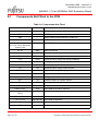
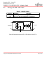
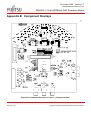
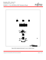
1
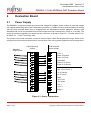
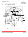
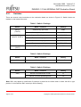
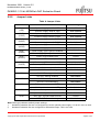
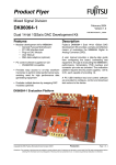
User Manual
November 1999
DK86061-3
Version 3.2
12-bit 400MSa/s DAC Evaluation Board
Fujitsu’s DK86061-3 12-bit 400MSa/s DAC Evaluation Board
provides a simple and effective means of evaluating the
MB86061 12-bit 400MSa/s DAC. This enables faster device
evaluation without incurring the time and cost penalties of inhouse PCB design and manufacture.
FME/MS/SFDAC1E/UM_1/4133
EVALUATION BOARD
The board provides a complete evaluation environment for the
DAC device. A selectable single-ended or transformercoupled differential analog output interface is provided onboard to simplify integration into target application and
development environments. The clock is sourced from a
transformer coupled RF source. 12-bit ECL data is input via
a 40way IDC header, or optional SMA/SMB connectors.
The MB86061 device is a single 12-bit DAC enclosed in a 64
pin QFP package with a 0.65mm pin pitch.
Features
• 12-bit ECL data input via a choice of connectors
• Transformer-coupled differential output via BNC
• Transformer-coupled RF clock input via BNC
• Requires DC power supplies of +3.3V and -2V
Copyright © 1999 Fujitsu Microelectronics Europe GmbH
Page 1 of 26
November 1999 Version 3.2
FME/MS/SFDAC1E/UM_1/4133
DK86061-3 12-bit 400MSa/s DAC Evaluation Board
CAUTION
ELECTROSTATIC DISCHARGE SENSITIVE DEVICE
High electrostatic charges can accumulate in the human body
and discharge without detection. Ensure proper ESD
procedures are followed when handling this device.
Copyright © 1999 Fujitsu Limited
Tokyo, Japan, Fujitsu
Microelectronics Europe GmbH,
and Fujitsu Microelectronics Inc.
USA. All Rights Reserved.
The information contained in this
document has been carefully
checked and is believed to be
entirely reliable. However,
Fujitsu and its subsidiaries
assume no responsibility for
inaccuracies.
Fujitsu Limited and its
subsidiaries reserve the right to
change products or
specifications without notice.
No part of this publication may be
copied or reproduced in any form
or by any means or transferred to
any third party without the prior
consent of Fujitsu.
The information contained in this
document does not convey any
license under the copyrights,
patent rights or trademarks
claimed and owned by Fujitsu.
Page 2 of 26
Copyright © 1999 Fujitsu Microelectronics Europe GmbH
November 1999 Version 3.2
FME/MS/SFDAC1E/UM_1/4133
DK86061-3 12-bit 400MSa/s DAC Evaluation Board
1
Overview . . . . . . . . . . . . . . . . . . . . . . . . . . . . . . . . . . . . . . . . . . . . . . . . . .5
2
Evaluation Board . . . . . . . . . . . . . . . . . . . . . . . . . . . . . . . . . . . . . . . . . . . .6
2.1 Power Supply . . . . . . . . . . . . . . . . . . . . . . . . . . . . . . . . . . . . . . . . . . .6
2.2 Board and Interface Controls . . . . . . . . . . . . . . . . . . . . . . . . . . . . . . .7
2.2.1 Switches. . . . . . . . . . . . . . . . . . . . . . . . . . . . . . . . . . . . . . . . .8
2.2.2 Jumper Links . . . . . . . . . . . . . . . . . . . . . . . . . . . . . . . . . . . . .9
3
Getting Started . . . . . . . . . . . . . . . . . . . . . . . . . . . . . . . . . . . . . . . . . . . .11
4
Testing . . . . . . . . . . . . . . . . . . . . . . . . . . . . . . . . . . . . . . . . . . . . . . . . . . .12
Appendix A Evaluation Board Circuit Diagrams . . . . . . . . . . . . . . . . . . . . .13
A.1
Components Not Fitted to the PCB . . . . . . . . . . . . . . . . .18
A.2
Changes to PCB Schematics. . . . . . . . . . . . . . . . . . . . . .19
Appendix B Component Overlays. . . . . . . . . . . . . . . . . . . . . . . . . . . . . . . . .20
Appendix C Connector Pin Functions . . . . . . . . . . . . . . . . . . . . . . . . . . . . .22
Appendix D Prototype Area . . . . . . . . . . . . . . . . . . . . . . . . . . . . . . . . . . . . . .24
Copyright © 1999 Fujitsu Microelectronics Europe GmbH
Page 3 of 26
November 1999 Version 3.2
FME/MS/SFDAC1E/UM_1/4133
DK86061-3 12-bit 400MSa/s DAC Evaluation Board
This page left intentionally blank
Page 4 of 26
Copyright © 1999 Fujitsu Microelectronics Europe GmbH
November 1999 Version 3.2
FME/MS/SFDAC1E/UM_1/4133
DK86061-3 12-bit 400MSa/s DAC Evaluation Board
1
Overview
The DK86061-3 evaluation board allows users to evaluate and demonstrate the different operational
modes of the MB86061 12-bit 400MSa/s DAC. The evaluation board consists of an MB86061 device with
support circuitry for single-ended or differential analog output interfaces, a clock input interface and a clock
output interface. This will enable simple connection of measurement equipment. For convenience
customer evaluation boards have been configured using soldered zero-ohm links for transformer-coupled
differential output only.
The ECL input data interface has a 40way IDC header, with selectable termination to VEE or DVSS.
Separate SMA/SMB connectors for individual data bit connections are also available (but not normally
fitted), with selectable termination to VEE or DVSS. Provision is made to multiplex data onto the input data
interface from two speed limited but phase adjustable data generators. For this a second set of SMA/SMB
connectors (again not normally fitted - SMA not recommended due to insufficient space to rotate the body)
are also available. The setup of the device is controlled by on-board DIP switches, but these controls can
be accessed and overridden via a male D type connector if remote control is required.
The evaluation board has been designed to address requirements of both automatic and conventional
bench testing. Standard evaluation boards feature a simplified build state where certain components and
connectors are omitted. These omissions are documented in Appendix A with the evaluation board
schematics.
This User Manual is intended to document the DK86061-3 Development Kit PCB titled 'MB86061 DAC
TEST CARD - ISSUE 3' only.
Copyright © 1999 Fujitsu Microelectronics Europe GmbH
Page 5 of 26
November 1999 Version 3.2
FME/MS/SFDAC1E/UM_1/4133
DK86061-3 12-bit 400MSa/s DAC Evaluation Board
2
Evaluation Board
2.1
Power Supply
The DK86061-3 evaluation board requires two low voltage DC supplies, and a number of other low voltage
DC supplies depending upon build configuration (marked †). A cable mounting socket suitable for mating
with the PCB mounted power plug is supplied with the development board. Additional sockets, type
Weidmüller BL3.5/16 may be obtained from RS Components (http://rswww.com), Stock no. 216-2683. The
power should be connected to the board via this connector, as shown in Figure 2.1. Flexible cable of 16 28 AWG, 0.5 - 1.5mm 2 should be used.
The format of the power connector is common across Fujitsu’s DAC Development Kit range. Some of the
supply pins are connected to test points for convenience if the user requires supplies for the prototype area.
Standard
Requirement
Cable Mounting
Socket
PCB mounted
power header
-5.2V †
Data -2V Sense
Data -2V Force
Data GND
Data +3.3V Force
Data +3.3V Sense
Opt. +3.3V Sense †
Opt. +3.3V Force †
+3.3V Sense
+3.3V Force
GND
-2V Force
-2V Sense
+5V †
+12V †
Relay †
Pin 16
Figure 2.1: Power Connections
Page 6 of 26
Copyright © 1999 Fujitsu Microelectronics Europe GmbH
November 1999 Version 3.2
FME/MS/SFDAC1E/UM_1/4133
DK86061-3 12-bit 400MSa/s DAC Evaluation Board
2.2
Board and Interface Controls
SW1
PL1
PL2
SW2
SW3
Clock Out
Power
Clock In
Differential Out
Figure 2.2: Evaluation Board Component Side Layout
Copyright © 1999 Fujitsu Microelectronics Europe GmbH
Page 7 of 26
November 1999 Version 3.2
FME/MS/SFDAC1E/UM_1/4133
DK86061-3 12-bit 400MSa/s DAC Evaluation Board
2.2.1
Switches
There are several control switches on the evaluation board, as shown in Figure 2.2. Switch idents are
marked on the board silk screen.
Table 1: Switch 1 Settings
Switch
Mode / Function
Settings
SW1[1]
(TWOC)
Offset binary input data
VSS
2’s Compliment input data
VDD
Segment Shuffling disabled
VSS, VSS
Random - every 4 cycles
VDD, VSS
Random - every 8 cycles
VSS, VDD
Random - every 16 cycles
VDD, VDD
Factory Use Only
VSS
SW1[2:3]
(SHUF0, SHUF1)
SW1[4]
(TEST)
Table 2: Switch 2 Settings
Switch
Mode / Function
Setting
SW2
Device Reset
Push to Reset
Table 3: Switch 3 Settings
Switch
Mode / Function
Setting
SW3
Device in forced RESET mode
B
Device in normal operating mode
A
Note: SW1 may appear to malfunction if pressure is placed on the slider when in either the left or right
position. In this case the DAC control pin will be floating.
Page 8 of 26
Copyright © 1999 Fujitsu Microelectronics Europe GmbH
November 1999 Version 3.2
FME/MS/SFDAC1E/UM_1/4133
DK86061-3 12-bit 400MSa/s DAC Evaluation Board
2.2.2
Jumper Links
Table 4: Jumper Links
Link Name
Mode / Function
Setting
LK1A†
(VDD)
Optional supply used for VDD
1 to 2 linked
Common supply used for VDD
2 to 3 linked
Optional supply used for CVDD
1 to 2 linked
Common supply used for CVDD
2 to 3 linked
Optional supply used for RVDD
1 to 2 linked
Common supply used for RVDD
2 to 3 linked
Optional supply used for AVDD
1 to 2 linked
Common supply used for AVDD
2 to 3 linked
LK2†
(PSRR)
Power supply ripple rejection disabled
Linked
Power supply ripple rejection enabled
Not Linked
LK3‡
(SEOUT)
Select single-ended output
Linked
Select differential output
Not linked
LK4
(CMRR)
Centre tap of T1 linked to AVSS
Linked
Centre tap of T1 decoupled to AVSS
Not linked
LK5
CLK IN Ground linked to CVSS
Linked
CLK IN Ground floating
Not Linked
CLK OUT biasing enabled
Linked
CLK OUT biasing disabled
Not Linked
CLK OUT Ground linked to VSS
Linked
CLK OUT Ground floating
Not Linked
DAC input terminated to DVSS
1 to 2 Linked
DAC input terminated to VEE
2 to 3 Linked
Multiplexer data input terminated to DVSS
1 to 2 Linked
Multiplexer data input terminated to VEE
2 to 3 Linked
DIFF OUT Ground linked to AVSS
Linked
DIFF OUT Ground floating
Not Linked
LK1B†
(CVDD)
LK1C†
(RVDD)
LK1D†
(AVDD)
LK6
LK7
LK8
LK9
LK10
Note: Bold type indicates default jumper settings.
†
‡
Standard Evaluation Kits are not configured to use the optional power supply. LK1 & LK2 are not used.
Standard Evaluation Kits are configured for Differential output. LK3 is not used.
Copyright © 1999 Fujitsu Microelectronics Europe GmbH
Page 9 of 26
November 1999 Version 3.2
FME/MS/SFDAC1E/UM_1/4133
DK86061-3 12-bit 400MSa/s DAC Evaluation Board
This page left intentionally blank
Page 10 of 26
Copyright © 1999 Fujitsu Microelectronics Europe GmbH
November 1999 Version 3.2
FME/MS/SFDAC1E/UM_1/4133
DK86061-3 12-bit 400MSa/s DAC Evaluation Board
3
Getting Started
This Chapter documents the basic steps to powering up and starting to use the DK86061-3 Evaluation
Board. Component references may be cross-referenced with the component overlay in Appendix B.
Step 1. Configure board for data input format
The data input format must be configured to either Offset Binary or 2’s Complement. Use configuration
switch SW1[1] to select.
The device control signals should be set to the default conditions shown in Section 2.2. Use configuration
switch SW1 to select.
Jumper links LK4 to LK7 inclusive, and LK10, should be 'Not linked', and LK8 and LK9 should be set to '2
to 3' linked. Switch SW3 should be set to position 'A'.
Step 2. Connect data input & analog output connectors to the board
The input data should be connected via the 40 way IDC header PL1, or if fitted the SMA/SMB connectors
J20 to J42 inclusive (evens only). See Table C1: for the pin description of the IDC header.
The output is provided as a transformer-coupled differential signal, via a BNC connector.
• Differential Output signal (J7). (50Ω source resistance)
The DAC is coupled to a single output connector using a transmission line and a 1:1 balun
transformer. Signal swing is ±0.5V with a high impedance load, or ±0.25V with an external 50Ω
load. For sinusoidal signals, this corresponds to approximately -2dBm into a 50Ω external load.
Step 3. Connect clock
The clock input is provided to the device through a transmission line transformer, via a BNC connector.
• RF clock (J12). (50Ω input impedance)
The DAC is coupled to a single input connector using a transmission line transformer. Sine wave or
square wave input signals between -10dBm and +10dBm are acceptable, depending on clock
frequency and required output jitter / phase noise.
Step 4. Connect power header to power supplies
Ensure that the power supplies are connected according to Figure 2.1. Connect the power header to the
board and turn power supplies on.
Step 5. Press Reset
Press the Reset button to ensure that the device is in the correct operating condition. Press Reset every
time a configuration change is made.
Copyright © 1999 Fujitsu Microelectronics Europe GmbH
Page 11 of 26
November 1999 Version 3.2
FME/MS/SFDAC1E/UM_1/4133
DK86061-3 12-bit 400MSa/s DAC Evaluation Board
4
Testing
This section provides a brief introduction to testing with the DK86061-3 12-bit 400MSa/s DAC Evaluation
Board.
The MB86061 incorporates a 12-bit, 400MSa/s digital to analog converter designed to give excellent SFDR
performance. Traditional 12-bit converters have been speed limited, in particular when considering CMOS
solutions, and applications have tended to be limited to around 100MSa/s. In certain applications it is now
possible to consider using the MB86061 with a 400MSa/s DAC conversion rate, even though the generated
signal band may only be, for example, up to 40MHz or less. In theory a 100MSa/s converter would be
sufficient to reproduce this 40MHz signal band, but according to Nyquist the converters performance will
tend to be limited due to step-size and sinx/x roll-off, as a result of the converters sample & hold output
stage. A 400MSa/s DAC conversion rate will significantly reduces effects due to both of these. Sinx/x rolloff is reduced from -4dB to -0.22dB, and the increased oversampling [DAC conversion rate / signal rate]
reduces step sizes to give a direct improvement in spurious performance. The limitation of adopting a high
DAC conversion rate then becomes data generation.
These issues should be considered when testing the MB86061 and measurements should be obtained at
different conversion rates to establish the most appropriate operating conditions for the target application.
For convenience the board has been configured using soldered zero-ohm links as a transformer coupled
differential output. To enable single-ended outputs changes to the soldered zero-ohm links would be
required. For rise/fall-time tests, the transformer-coupled output should not be used since the transformer
response will limit the dV/dt. The DAC current switches are designed to give the best possible differential
performance, at the expense of some single ended performance, so there is a noticeable difference
between the two configurations. The revised analog output circuit uses an additional transmission line
transformer to improve rejection of common-mode distortion at the DAC output.
If a spectrum analyser is used to measure the output spectrum this must have very good noise and
distortion, for example HP8562E or R&S FSEA30. In addition, the input attenuator setting should be
chosen such that input mixer distortion does not limit the measurements (e.g. 30dB RF attenuation). This
implies that narrow resolution bandwidths and/or averaging are required to obtain low enough
measurement noise floor.
Input data can be generated with an Arbitrary Waveform Generator, for example a Sony/Tektronix
AWG520. This can produce 10-bit ECL data (set the digital output to +0.2V to -0.8V) and a data clock. Care
should be taken to ensure that the data cables and the clock cable are the same length, so as to avoid any
shift in the clock to data timing relationship. However, the phase of the AWGs clock-out may be outside the
DACs allowable range. If so, a low noise signal generator such as the Marconi 2042 could be used to
provide the clock. This has the facility to adjust the phase of the output signal compared with its frequency
standard output (which is driving the AWGs 10MHz reference input).
Page 12 of 26
Copyright © 1999 Fujitsu Microelectronics Europe GmbH
November 1999 Version 3.2
FME/MS/SFDAC1E/UM_1/4133
DK86061-3 12-bit 400MSa/s DAC Evaluation Board
Appendix A Evaluation Board Circuit Diagrams
Appendix A shows the circuit diagrams of the DK86061-3 evaluation board. Note that these diagrams are
for reference only and that some components fitted to the board may be of a different value to the
schematics or not fitted at all. Fujitsu has undertaken to document these changes where possible. The
schematic is divided over four pages for clarity. Two 12-bit wide data busses are used to minimize diagram
complexity, and are referred to as the Data bus [D0A, D0B to D11A, D11B] and the Multiplexer Data bus
[MD0 to MD11].
• Sheet 1 - Main DAC support circuitry, including analog output interfaces [covers 2 pages]
• Sheet 2 - ECL data input multiplexers, including SMA/SMB input data connectors [covers 2 pages]
Copyright © 1999 Fujitsu Microelectronics Europe GmbH
Page 13 of 26
November 1999 Version 3.2
FME/MS/SFDAC1E/UM_1/4133
DK86061-3 12-bit 400MSa/s DAC Evaluation Board
ST1
1
4
2
SW1
M-5.2V
-5.2V
ST2
1
2
C1
4
VEE
9
3
1
ST3
C2
150u
5
150u
2
4
J1
2
3
3
R2
C4
6
ST7
3
C5
1
SGND
+5V
TP1
TP11
5
4
3
3
4
5
5
AVSS
TP10
100R
R11
R16
T1
1
A1
6
A3
P5
1K
3
AVDD
P7
1
-2V
A4
2
P2
P1
R6
50R
R7
0R
R8
0R
2
6
A4
R10
+12V
RCON
RF103-12
51R
TP9
A2
J46
AVSS
AVSS
1
LK4
2
AVDD
C22
100n
AVSS
4
8
RL1
1
AVSS
R17
0R
1
2
3
4
5
6
7
8
9
10
11
12
13
14
15
16
C21
100n
7
R15
J6
C23
100n
AVSS
C78
4
R
R
E
F
C20
100n
AVSS
AVDD
2
5
LK10
J5
BNC
AVSS
R142
1
C8
ANALOGUE
APP.GND
1
AVSS
6 6 6 6 6 5 5 5 5 5 5 5 5 5 5 4
4 3 2 1 0 9 8 7 6 5 4 3 2 1 0 9
RVSS
A2
C9
3
10K
R32
RVSS
3
5
100n
0R
R33
4
+5V
51R
C10
C11
100n
100n
C34
R34
100n
RVDD
AVDD
A3
C18
RVSS
J17
AVSS
J8
RVSS
R48
J18
5
R9
J7
BNC
VSS
AVSS
CVSS
-2V
-5.2V
P9
AVSS
6
CVEE
AVSS
P8
R47
R35
51R
P4
P3
3
1
D1
TC04BCZM
2
ST9
1
150u
R39
1K
100n
6
4
RVDD
C12
A1
2
P6
AVSS
0R
RVSS
C7
2
ST10
J4
R5
R41
R36
RVDD
2
TP2
0R
CVDD
100n
C6
+12V
0R
R4
J2
LK2
RCON
R3
2
150u
R43
0R
AVDD
5
4
3
1
ST8
VD
C35
VDD
4
1
3
VS
5
2
3
R46
4PCO
AVDD
R45
150u
ST6
2
RVDD
R44
100n
0R
1
2
CVDD
R42
3
DVDD
R1
1
R40
4
C3
150u
4
2
12
5
2
ST4
LK1D
1
VDD
3
6
J3
BNC
2
ST5
LK1C
1
DVSS
1
1
LK1B
1
3
1
2
3
4
5
6
7
8
9
10
11
12
13
14
15
16
1
2
4
5
7
8
10
11
6
LK1A
-5.2V
D-2VS
D-2VF
DGND
D+3.3VF
D+3.3VS
OPTS
OPTF
+3.3VS
+3.3VF
SGND
-2VF
-2VS
+5V
+12V
RELAY
3
VDD
3
2
AVDD
CVDD
SGND
LK3
R12
0R
R13
0R
R14
50R
CVSS
C24
100n
V
R
E
F
RVSS
RVDD
AVDD
AVSS
IOUTB
IOUTB
AVSS
AVDD
AVDD
AVSS
IOUT
IOUT
AVSS
AVDD
CVDD
CVSS
R
V
S
S
/
T
E
S
T
S
H
U
F
1
S
H
U
F
0
A
S
U
B
D V V N T V V V D
S D S / WD S T 0
U D S C OD S H
B
C
S
O
U
T
V
DV
DV
V
DV
DV
C
L
K
B
C25
100n
B
G
A
P
C
C C
V C V V
E L S D
E K S D
R
E
S
E
T
B
C
S
U
B
C
L
K
D
O
S V V U
U D S T
B D S B
C
L
K
OV V D D
U D S 1 1
T D S 1 0
1 1 1 2 2 2 2 2 2 2 2 2 2 3 3 3
7 8 9 0 1 2 3 4 5 6 7 8 9 0 1 2
U1
MB86061
C28
CVEE
100n
AVSS
CVSS
CVEE
100n
1
J12
BNC
CVSS
C14
J11
R24
51R
LK5
2
1
R22
51R
T3
ADTL1-12
J13
R20
10K
0R
C16
R23
51R
J14
R26
100n
R21
51R
100n
1
Page 14 of 26
J10
C13
100n
2
J16
R27
10K
R19
10K
VDD
1
VR1
100R
2
0R
R37
R29
6
75R
5
LK6
1
10K
200R
R38
10K
R28
4
75R
ADT4-1WT
C17
CVSS
CLKIN_GND
APP.GND
T4
3
6
R31
VSS
BNC
J15
4
C27
100n
100n
R30
R25
10K
C15
CVSS
3
C26
CVDD
3
CLKOUT_GND
APP.GND
100n
LK7
1
2
VSS
Copyright © 1999 Fujitsu Microelectronics Europe GmbH
V
November 1999 Version 3.2
FME/MS/SFDAC1E/UM_1/4133
DK86061-3 12-bit 400MSa/s DAC Evaluation Board
PL2
SW1
3
VDD
6
9
LK1C
LK1D
1
12
1
2
CVDD
2
RVDD
3
VSS
1
2
4
5
7
8
10
11
DVSS
R40
10K
R42
10K
R44
10K
R46
10K
40
39
38
37
36
35
34
33
32
31
30
29
28
27
26
25
24
23
22
21
20
19
18
17
16
15
14
13
12
11
10
9
8
7
6
5
4
3
2
1
PL1
1 2 1 2 1 2 1 2
2
2
1
1
1
1
1
1
3 5 2 4 1 3 0 2 9 1 8 0 7 9 6 8 5 7 4 6 3 5 2 4 1
VSS
4PCO
AVDD
3
VDD
C35
TP3
TP5
TP4
TP7
TP6
TP8
100n
VSS
VDD
RESETB
R45
200R
RVSS/TEST
R43
200R
SHUF1
R41
200R
R39
1K
200R
0R
MD2
R80
0R
MD3
R81
0R
MD4
R82
0R
MD5
R83
0R
MD6
R84
0R
MD7
R85
0R
MD8
R86
0R
MD9
R87
0R
MD10
R88
0R
MD11
R89
0R
TWOC
RVDD
RVSS
J19
D1
TC04BCZM
R47
R35
51R
0R
R48
VSS
R50
10K
0R
R51
10K
R52
VEE
10K
J18
VDD
C34
R34
RVSS
C19
100n
100n
VSS
0R
100n
0R
R79
NC/SOUT
R36
RVDD
C18
R78
MD1
SHUF0
AVDD
CVDD
MD0
DVSS
R33
J17
10K
R32
RVSS
R54
1K
DVSS
6 6 6 6 6 5 5 5 5 5 5 5 5 5 5 4
4 3 2 1 0 9 8 7 6 5 4 3 2 1 0 9
24R
R55
C32
100n
R
R
E
F
C20
100n
1
2
3
4
5
6
7
8
9
10
11
12
13
14
15
16
C21
100n
C22
100n
C24
100n
V
R
E
F
RVSS
RVDD
AVDD
AVSS
IOUTB
IOUTB
AVSS
AVDD
AVDD
AVSS
IOUT
IOUT
AVSS
AVDD
CVDD
CVSS
C
L
K
B
C25
100n
B
G
A
P
R
V
S
S
/
T
E
S
T
S
H
U
F
1
C
C C
V C V V
E L S D
E K S D
S
H
U
F
0
R
E
S
E
T
B
A
S
U
B
C
S
U
B
D V V N T V V V D
S D S / WD S T 0
U D S C OD S H
B
C
S
O
U
T
C
L
K
D
O
S V V U
U D S T
B D S B
C
L
K
OV V D D
U D S 1 1
T D S 1 0
24R
R56
DVDD
24R
R57
48
47
46
45
44
43
42
41
40
39
38
37
36
35
34
33
D1
VEE
D2
DVSS
D3
D4
DVDD
D5
VEE
D6
DVSS
D7
D8
DVDD
D9
VEE
VEE
24R
R58
24R
R59
VEE
24R
R60
24R
R61
24R
R62
VEE
DVSS
24R
R63
C30
24R
R64
100n
1 1 1 2 2 2 2 2 2 2 2 2 2 3 3 3
7 8 9 0 1 2 3 4 5 6 7 8 9 0 1 2
U1
MB86061
DVDD
24R
R65
C28
CVEE
VSS
MD0
R66
MD0
MD1
51R
R67
MD1
MD2
MD2
MD3
MD3
MD4
MD4
MD5
MD5
MD6
MD6
51R
R68
51R
R71
51R
R72
MD8
MD9
MD9
MD10
MD10
MD11
MD11
51R
R75
51R
R76
C26
VDD
VSS
100n
VDD
R30
R31
0R
0R
R37
DVSS
DVSS
C43
100n
DVSS
C44
100n
DVSS
C45
100n
DVSS
DVSS
100n
51R
R77
C47
100n
51R
DVSS
VEE/DVSS
C27
100n
CVDD
DVSS
C41
100n
C46
100n
CVSS
DVSS
C40
100n
100n
51R
R74
24R
DVSS
C39
100n
C42
51R
R73
MD7
DVSS
100n
51R
R70
MD8
DVSS
C37
100n
C38
51R
R69
MD7
C36
100n
VEE
C29
C33
C31
100n
100n
100n
2
LK8
1
DVSS
VSS
3
DVSS
VEE
VSS
MD[0..11]
MD[0..11]
RESETB
T4
3
1
2
VDD
1
VR1
100R
2
200R
FUJITSU MICROELECTRONICS EUROPE
VSS
75R
5
LK6
1
R29
6
R38
10K
4
VDD
SW2
C17
3
_GND
D
100n
1
2
3
BERKSHIRE, SL6 4FT
75R
ADT4-1WT
NETWORK HOUSE
NORREYS DRIVE
MAIDENHEAD
SW3
R28
1PCO
Title
1
LK7
1
MB86061 DAC TEST CARD
2
2
3
VSS
SPDT
VSS
Size
B
Date:
Copyright © 1999 Fujitsu Microelectronics Europe GmbH
Document Number
REV
CAD DATA C9906
September 15, 1999
3
Sheet
1
of
2
Page 15 of 26
November 1999 Version 3.2
FME/MS/SFDAC1E/UM_1/4133
DK86061-3 12-bit 400MSa/s DAC Evaluation Board
VEE/DVSS
MD[0..11]
MD[0..11]
M
D
3
R117
51R
R129
0R
M
D
2
R116
51R
R128
0R
M
D
1
R127
0R
M
D
0
R126
0R
D2A
D2B
M
D
7
R115
51R
R114
51R
2
5
D
4
A
D3A
D3B
26
D1A
27
D1B
28
1
M-5.2V
C72
2
100n
3
DVSS
2
4
D
3
B
D4B
SR4
D2A
0R
2
3
D
3
A
2
2
V
C
C
0
2
0
Q
4
Q
4
U3
MC10E158
V
C
C
O
Q3
D2B
0R
VCC
VEE
SR2
Q2
0R
SR1
D0B
0R
D
1
A
D
1
B
5
V
C
C
0
6
Q2
7
Q
0
8
26
D5A
27
R132
0R
2
4
16
D5B
28
1
M-5.2V
14
C73
2
13
100n
3
DVSS
D
3
B
D4B
SR8
D2A
0R
R131
0R
2
3
D
3
A
2
2
2
1
V
C
C
0
Q
4
1
9
V
C
C
O
D2B
0R
VCC
VEE
SR6
Q2
0R
D0A
SR5
D0B
0R
1
1
D
1
B
5
18
Q3
SEL
4
2
0
Q
4
Q3
D
1
A
D0A
D0B
R130
0R
SR7
Q
1
1
0
9
D7B
17
12
Q1
Q
0
18
15
VCC0
V
C
C
0
2
5
D
4
A
D7A
SR3
D0A
R120
51R
M
D
4
DVSS
1
9
Q3
SEL
4
2
1
R133
0R
M
D
5
D6A
D6B
DVSS
U2
MC10E158
R121
51R
M
D
6
V
C
C
0
6
17
16
15
14
Q2
13
VCC0
12
Q1
Q
0
7
Q
0
8
V
C
C
0
1
0
9
Q
1
1
1
D4A
D4B
DVSS
DVSS
DVSS
VEE
1
3
LK9
2
R90
51R
R91
51R
D
0
A
R92
51R
R93
51R
D
0
B
D
1
A
R94
51R
R95
51R
R96
51R
D
2
A
D
1
B
D
2
B
R97
51R
D
3
A
R98
51R
D
3
B
R99
51R
R100
51R
D
4
A
R101
51R
D
4
B
D
5
A
C60
C61
C62
C63
C64
C65
C66
C67
100n
100n
100n
100n
100n
100n
100n
100n
R102
51R
D
5
B
R103
51R
D
6
A
R104
51R
R105
51R
D
6
B
D
7
A
D
7
A
D
7
B
R106
51R
R107
51R
D
7
B
R108
51R
D
8
A
D
8
B
R109
51R
D
9
A
R1
5
D
9
B
50R
D
0
A
D
0
B
J20
SMB
D0A
D
1
A
D
1
B
J22
SMB
D1A
J21
SMB
D0B
D
2
A
D
2
B
J24
SMB
D2A
J23
SMB
D1B
D
3
A
D
3
B
J26
SMB
D3A
J25
SMB
D2B
D
4
A
D
4
B
J28
SMB
D4A
J27
SMB
D3B
D
5
A
D
5
B
J30
SMB
D5A
J29
SMB
D4B
D
6
A
D
6
B
J32
SMB
D6A
J31
SMB
D5B
J34
SMB
D7A
J33
SMB
D6B
D
8
A
D
8
B
J36
SMB
D8A
J35
SMB
D7B
D
9
A
D
9
B
J38
SMB
D9A
J37
SMB
D8B
D
1
0
A
J40
SMB
D10A
J39
SMB
D9B
D
1
0
B
D
1
1
A
J42
SMB
D11A
J41
SMB
D10B
DVSS
Page 16 of 26
Copyright © 1999 Fujitsu Microelectronics Europe GmbH
November 1999 Version 3.2
FME/MS/SFDAC1E/UM_1/4133
DK86061-3 12-bit 400MSa/s DAC Evaluation Board
M
D
7
R121
51R
R133
0R
M
D
6
R120
51R
R132
0R
M
D
5
R131
0R
M
D
4
R130
0R
M
D
1
1
R119
51R
R118
51R
2
5
2
4
D
4
A
26
27
28
1
C73
2
100n
3
D
3
B
D4B
SR8
D2A
0R
2
3
D
3
A
2
2
2
1
V
C
C
0
Q
4
Q
4
U4
MC10E158
V
C
C
O
Q3
D2B
0R
VCC
VEE
SR6
Q2
0R
SR5
D0B
0R
D
1
A
D
1
B
5
V
C
C
0
6
Q2
7
Q
0
8
1
0
9
D11B
26
17
D9A
27
16
D9B
28
1
M-5.2V
14
C74
2
13
100n
3
DVSS
12
Q1
Q
0
18
15
VCC0
V
C
C
0
R136
0R
2
5
2
4
D
4
A
D11A
SR7
D0A
R124
51R
R135
0R
M
D
8
R134
0R
R123
51R
R122
51R
DVSS
1
9
Q3
SEL
4
2
0
R137
0R
M
D
9
D10A
D10B
DVSS
U3
MC10E158
R125
51R
M
D
1
0
4
D
3
B
D4B
SR12
D2A
0R
2
3
D
3
A
2
2
2
1
V
C
C
0
Q
4
2
0
Q
4
1
9
V
C
C
O
D2B
0R
VEE
SR10
D0A
SR9
D0B
0R
D
1
A
1
1
D
1
B
5
6
V
C
C
0
17
Q3
16
VCC
15
Q2
0R
SEL
Q
1
18
Q3
SR11
14
Q2
13
VCC0
12
Q1
Q
0
7
Q
0
8
9
V
C
C
0
1
0
Q
1
1
1
D8A
D8B
DVSS
DVSS
DVSS
U5
MC10E107
DVSS
n
C61
C62
C63
C64
C65
C66
C67
C68
C69
C70
C71
100n
100n
100n
100n
100n
100n
100n
100n
100n
100n
100n
103
51R
R104
51R
R105
51R
D
6
B
D
7
A
D
7
A
D
7
B
R106
51R
R107
51R
D
7
B
R108
51R
D
8
A
D
8
B
R109
51R
D
9
A
R110
51R
D
9
B
R111
51R
D
1
0
A
R112
51R
R113
51R
D
1
0
B
D
1
1
A
D
8
A
D
8
B
D
9
A
D
9
B
D
1
0
A
D
1
0
B
D
1
1
A
D
1
1
B
C75
QQV QQQQ
4 4 C 3 3 2 2
C
19
20
21
22
23
24
25
F
F
VCC0
NC
D4A
D4B
D3A
100n
VCC0
Q1
Q1
Q0
Q0
VCC0
D0B
11
10
9
8
7
6
5
R139
51R
J44
SMB
DVSS
D D D V D D D
3 2 2 E 1 1 0
B A B E A B A
D
1
1
B
2 2 2
6 7 8 1 2 3 4
D
6
B
R138
51R
1 1 1 1 1 1 1
8 7 6 5 4 3 2
50R
XCLKB
R140
51R
C76
DVSS
DVSS
C77
100n
R141
51R
DVSS
J45
SMB
100n
M-5.2V
50R
XCLK
DVSS
J34
SMB
D7A
J33
SMB
D6B
J36
SMB
D8A
J35
SMB
D7B
J38
SMB
D9A
J37
SMB
D8B
J40
SMB
D10A
J39
SMB
D9B
J42
SMB
D11A
J41
SMB
D10B
FUJITSU MICROELECTRONICS EUROPE
NETWORK HOUSE
NORREYS DRIVE
MAIDENHEAD
J43
SMB
D11B
BERKSHIRE, SL6 4FT
Title
MB86061 DAC TEST CARD (MULTIPLEXER)
Size
Document Number
B
Date:
Copyright © 1999 Fujitsu Microelectronics Europe GmbH
REV
CAD DATA C9906
September 15, 1999
3
Sheet
2
of
2
Page 17 of 26
November 1999 Version 3.2
FME/MS/SFDAC1E/UM_1/4133
DK86061-3 12-bit 400MSa/s DAC Evaluation Board
A.1
Components Not Fitted to the PCB
Table A1: Components Not Fitted
Reference
Value
LK1a, b, c, d
-
Power supply selection jumper links
LK2
-
PSRR jumper link
LK3
-
Single-ended output selection jumper link
LK9
-
Input data termination selection jumper link
J2, J4, J6, J8, J10, J11,
J13, J14, J16 to J20 to J44
(evens), J45
SMA/SMB
J3, J5
BNC
BNC connectors
D1
TC04BCZM
Reference diode
RL1
RF103-12
C4
150uF
Optional power supply decoupling capacitor
C9, C78
33pF
Analog output RC network capacitors
C60 to C61, C72 to C77
100nF
Decoupling capacitors
R1
0R
Optional power supply PSRR resistor
R7, R12
0R
Single-ended output relay bypass resistors
R9, R13
51R
Single-ended output termination resistors
R16, R132
51R
Analog output RC network resistors
R17
0R
CMRR jumper link bypass resistor
R35
51R
Reference series resistor
R36
1K
Reference current limit resistor
R90 to R113
51R
Input data termination resistors
R126 to R137, SR1 to
SR12
0R
Input data multiplexers selection and bypass resistors
R138 to R141
51R
XCLK termination resistors
U2, U3, U4
MC10E158
Input data multiplexers
U5
MC10E107
Input data multiplexer quad XOR
T2
-
Page 18 of 26
Description
SMA/SMB connectors
Output selection relay
Optional analog output circuit transformer
Copyright © 1999 Fujitsu Microelectronics Europe GmbH
November 1999 Version 3.2
FME/MS/SFDAC1E/UM_1/4133
DK86061-3 12-bit 400MSa/s DAC Evaluation Board
A.2
Changes to PCB Schematics
Table A2: Schematic Changes
Reference
New Value
Description
T1(a)
ADTT1-1
Mini-Circuits 1:1 analog output transformer
T1(b)
ADTL1-12
Mini-Circuits transmission line transformer
1
6
To DAC
To Output
T1b
3
4
T1a
5
Figure A1 Replacement Schematic For T1 (Pin Numbers Refer To T1)
Copyright © 1999 Fujitsu Microelectronics Europe GmbH
Page 19 of 26
November 1999 Version 3.2
FME/MS/SFDAC1E/UM_1/4133
DK86061-3 12-bit 400MSa/s DAC Evaluation Board
Appendix B Component Overlays
Figure B1 Component Overlay For Layer 1, (Component Side)
Page 20 of 26
Copyright © 1999 Fujitsu Microelectronics Europe GmbH
November 1999 Version 3.2
FME/MS/SFDAC1E/UM_1/4133
DK86061-3 12-bit 400MSa/s DAC Evaluation Board
Figure B2 Component Overlay For Layer 4, (Solder Side)
Copyright © 1999 Fujitsu Microelectronics Europe GmbH
Page 21 of 26
November 1999 Version 3.2
FME/MS/SFDAC1E/UM_1/4133
DK86061-3 12-bit 400MSa/s DAC Evaluation Board
Appendix C Connector Pin Functions
Table C1: Data Connector PL2 Pin Functions
1
39
Page 22 of 26
2
40
Pin
Function
1
Data Bit 11 (MSB)
3
Data Bit 10
5
Data Bit 9
7
Data Bit 8
9
Data Bit 7
11
Data Bit 6
13
Data Bit 5
15
Data Bit 4
17
Data Bit 3
19
Data Bit 2
21
Data Bit 1
23
Data Bit 0 (LSB)
25
Not Used
27
Not Used
29
Not Used
31
Not Used
33
Not Used
35
Not Used
37
Not Used
39
Not Used
2 to 40 (Even numbers only)
Data Ground (DVSS)
Copyright © 1999 Fujitsu Microelectronics Europe GmbH
November 1999 Version 3.2
FME/MS/SFDAC1E/UM_1/4133
DK86061-3 12-bit 400MSa/s DAC Evaluation Board
Table C2: Control Connector PL1 Pin Functions
†
‡
Pin
Function
1 to 13
Digital Ground (VSS)
14
TWOC
15‡
SOUT (O/P)
16
SHUF0
17
SHUF1
18‡
TEST
19
RESETB
20†
Test point 8
21†
Test point 7
22†
Test point 6
23†
Test point 5
24†
Test point 4
25†
Test point 3
These pins are connected to test points so that connections to the prototype area can be made via
the control connector.
These pins are for factory test purposes only.
Copyright © 1999 Fujitsu Microelectronics Europe GmbH
Page 23 of 26
November 1999 Version 3.2
FME/MS/SFDAC1E/UM_1/4133
DK86061-3 12-bit 400MSa/s DAC Evaluation Board
Appendix D Prototype Area
A prototype area has been introduced into the DK86061-3 development kit PCB. This area takes the form
of a matrix of pads with plated through holes on a 2.54mm pitch. The pads are made square to allow for
0805 format surface mount devices to be fitted between adjacent pads. The matrix area has four rows
individually linked together to act as power rails. These rows are arranged as two pairs, with connections
to the internal planes (layers 2 and 3) made to each of the rows. The internal plane regions only occupy
the prototype area, and are not linked to any other area of the PCB. The prototype area layout is shown in
Figure D1.
Layer 2 would typically be used as the ground plane, and layer 3 as the power plane, with signals routed
on layer 1. However the choice in the prototype area is free as the planes are entirely separate to the rest
of the PCB.
Layer 2
Layer 3
Layer 2
Layer 3
Figure D1 Prototype Area Layout
Page 24 of 26
Copyright © 1999 Fujitsu Microelectronics Europe GmbH
November 1999 Version 3.2
FME/MS/SFDAC1E/UM_1/4133
DK86061-3 12-bit 400MSa/s DAC Evaluation Board
This page left intentionally blank
Copyright © 1999 Fujitsu Microelectronics Europe GmbH
Page 25 of 26
November 1999 Version 3.2
FME/MS/SFDAC1E/UM_1/4133
DK86061-3 12-bit 400MSa/s DAC Evaluation Board
Worldwide Headquarters
Japan
Fujitsu Limited
Asia
Fujitsu Microelectronics Asia
Pte Limited
Tel: +81 44 754 3753
Fax: +81 44 754 3329
1015 Kamikodanaka 4-1-1
Nakahara-ku
Kawasaki-shi
Kanagawa-ken 211-88
Japan
Tel:
Fax:
151 Lorong Chuan
#05-08 New Tech Park
Singapore 556741
http://www.fujitsu.co.jp/
+65 281 0770
+65 281 0220
http://www.fmap.com.sg/
USA
Fujitsu Microelectronics Inc
Europe
Fujitsu Microlectronics Europe
GmbH
Tel: +1 408 922 9000
Fax: +1 408 922 9179
3545 North First Street
San Jose CA 95134-1804
USA
Tel: +49 6103 6900
Fax: +49 6103 690122
Am Siebenstein 6-10
D-63303 Dreieich-Buchschlag
Germany
Tel: +1 800 866 8608
Fax: +1 408 922 9179
Customer Response Center
Mon-Fri: 7am-5pm (PST)
http://www.fujitsu-fme.com/
http://www.fujitsumicro.com/
The contents of this document are subject to change without notice. Customers are advised to consult with FUJITSU sales
representatives before ordering.
The information and circuit diagrams in this document presented as examples of semiconductor device applications, and are not intended
to be incorporated in devices for actual use. Also, FUJITSU is unable to assume responsibility for infringement of any patent rights or
other rights of third parties arising from the use of this information or circuit diagrams.
FUJITSU semiconductor devices are intended for use in standard applications (computers, office automation and other office equipment,
industrial, communications, and measurement equipment, personal or household devices, etc.). CAUTION: Customers considering the
use of our products in special applications where failure or abnormal operation may directly affect human lives or cause physical injury
or property damage, or where extremely high levels of reliability are demanded (such as aerospace systems, atomic energy controls, sea
floor repeaters, vehicle operating controls, medical devices for life support, etc.) are requested to consult with FUJITSU sales
representatives before such use. The company will not be responsible for damages arising from such use without prior approval.
Any semiconductor devices have inherently a certain rate of failure. You must protect against injury, damage or loss from such failures
by incorporating safety design measures into your facility and equipment such as redundancy, fire protection, and prevention of overcurrent levels and other abnormal operating conditions.
If any products described in this document represent goods or technologies subject to certain restrictions on export under the Foreign
Exchange and Foreign Trade Control Law of Japan, the prior authorization by Japanese government should be required for export of
those products from Japan.
FME/MS/SFDAC1E/UM_1/4133 - 3.2
Page 26 of 26
Copyright © 1999 Fujitsu Microelectronics Europe GmbH