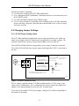
1
To our customers, Old Company Name in Catalogs and Other Documents On April 1st, 2010, NEC Electronics Corporation merged with Renesas Technology Corporation, and Renesas Electronics Corporation took over all the business of both companies. Therefore, although the old company name remains in this document, it is a valid Renesas Electronics document. We appreciate your understanding. Renesas Electronics website: http://www.renesas.com April 1st, 2010 Renesas Electronics Corporation Issued by: Renesas Electronics Corporation (http://www.renesas.com) Send any inquiries to http://www.renesas.com/inquiry. Notice 1. 2. 3. 4. 5. 6. 7. All information included in this document is current as of the date this document is issued. Such information, however, is subject to change without any prior notice. Before purchasing or using any Renesas Electronics products listed herein, please confirm the latest product information with a Renesas Electronics sales office. Also, please pay regular and careful attention to additional and different information to be disclosed by Renesas Electronics such as that disclosed through our website. Renesas Electronics does not assume any liability for infringement of patents, copyrights, or other intellectual property rights of third parties by or arising from the use of Renesas Electronics products or technical information described in this document. No license, express, implied or otherwise, is granted hereby under any patents, copyrights or other intellectual property rights of Renesas Electronics or others. You should not alter, modify, copy, or otherwise misappropriate any Renesas Electronics product, whether in whole or in part. Descriptions of circuits, software and other related information in this document are provided only to illustrate the operation of semiconductor products and application examples. You are fully responsible for the incorporation of these circuits, software, and information in the design of your equipment. Renesas Electronics assumes no responsibility for any losses incurred by you or third parties arising from the use of these circuits, software, or information. When exporting the products or technology described in this document, you should comply with the applicable export control laws and regulations and follow the procedures required by such laws and regulations. You should not use Renesas Electronics products or the technology described in this document for any purpose relating to military applications or use by the military, including but not limited to the development of weapons of mass destruction. Renesas Electronics products and technology may not be used for or incorporated into any products or systems whose manufacture, use, or sale is prohibited under any applicable domestic or foreign laws or regulations. Renesas Electronics has used reasonable care in preparing the information included in this document, but Renesas Electronics does not warrant that such information is error free. Renesas Electronics assumes no liability whatsoever for any damages incurred by you resulting from errors in or omissions from the information included herein. Renesas Electronics products are classified according to the following three quality grades: “Standard”, “High Quality”, and “Specific”. The recommended applications for each Renesas Electronics product depends on the product’s quality grade, as indicated below. You must check the quality grade of each Renesas Electronics product before using it in a particular application. You may not use any Renesas Electronics product for any application categorized as “Specific” without the prior written consent of Renesas Electronics. Further, you may not use any Renesas Electronics product for any application for which it is not intended without the prior written consent of Renesas Electronics. Renesas Electronics shall not be in any way liable for any damages or losses incurred by you or third parties arising from the use of any Renesas Electronics product for an application categorized as “Specific” or for which the product is not intended where you have failed to obtain the prior written consent of Renesas Electronics. The quality grade of each Renesas Electronics product is “Standard” unless otherwise expressly specified in a Renesas Electronics data sheets or data books, etc. “Standard”: 8. 9. 10. 11. 12. Computers; office equipment; communications equipment; test and measurement equipment; audio and visual equipment; home electronic appliances; machine tools; personal electronic equipment; and industrial robots. “High Quality”: Transportation equipment (automobiles, trains, ships, etc.); traffic control systems; anti-disaster systems; anticrime systems; safety equipment; and medical equipment not specifically designed for life support. “Specific”: Aircraft; aerospace equipment; submersible repeaters; nuclear reactor control systems; medical equipment or systems for life support (e.g. artificial life support devices or systems), surgical implantations, or healthcare intervention (e.g. excision, etc.), and any other applications or purposes that pose a direct threat to human life. You should use the Renesas Electronics products described in this document within the range specified by Renesas Electronics, especially with respect to the maximum rating, operating supply voltage range, movement power voltage range, heat radiation characteristics, installation and other product characteristics. Renesas Electronics shall have no liability for malfunctions or damages arising out of the use of Renesas Electronics products beyond such specified ranges. Although Renesas Electronics endeavors to improve the quality and reliability of its products, semiconductor products have specific characteristics such as the occurrence of failure at a certain rate and malfunctions under certain use conditions. Further, Renesas Electronics products are not subject to radiation resistance design. Please be sure to implement safety measures to guard them against the possibility of physical injury, and injury or damage caused by fire in the event of the failure of a Renesas Electronics product, such as safety design for hardware and software including but not limited to redundancy, fire control and malfunction prevention, appropriate treatment for aging degradation or any other appropriate measures. Because the evaluation of microcomputer software alone is very difficult, please evaluate the safety of the final products or system manufactured by you. Please contact a Renesas Electronics sales office for details as to environmental matters such as the environmental compatibility of each Renesas Electronics product. Please use Renesas Electronics products in compliance with all applicable laws and regulations that regulate the inclusion or use of controlled substances, including without limitation, the EU RoHS Directive. Renesas Electronics assumes no liability for damages or losses occurring as a result of your noncompliance with applicable laws and regulations. This document may not be reproduced or duplicated, in any form, in whole or in part, without prior written consent of Renesas Electronics. Please contact a Renesas Electronics sales office if you have any questions regarding the information contained in this document or Renesas Electronics products, or if you have any other inquiries. (Note 1) “Renesas Electronics” as used in this document means Renesas Electronics Corporation and also includes its majorityowned subsidiaries. (Note 2) “Renesas Electronics product(s)” means any product developed or manufactured by or for Renesas Electronics. User’s Manual LCE-K0 Emulator User’s Manual Preliminary Preliminary Version Sept. 10, 2001 Document No. U18151EU1V0UM00 (1st edition) 2001 NEC Electronics Inc. All rights reserved. Printed in U.S.A. LCE-K0 Emulator User’s Manual No part of this document may be copied or reproduced in any form or by any means without the prior written consent of NEC Electronics Inc. (NECEL). The information in this document is subject to change without notice. All devices sold by NECEL are covered by the provisions appearing in NECEL's Terms and Conditions of Sales only, including the limitation of liability, warranty, and patent provisions. NECEL makes no warranty, express, statutory, implied or by description, regarding information set forth herein or regarding the freedom of the described devices from patent infringement. NECEL assumes no responsibility for any errors that may appear in this document. NECEL makes no commitments to update or to keep current information contained in this document. The devices listed in this document are not suitable for use in applications such as, but not limited to, aircraft control systems, aerospace equipment, submarine cables, nuclear reactor control systems and life support systems. “Standard” quality grade devices are recommended for computers, office equipment, communication equipment, test and measurement equipment, machine tools, industrial robots, audio and visual equipment, and other consumer products. For automotive and transportation equipment, traffic control systems, anti-disaster and anti-crime systems, it is recommended that the customer contact the responsible NECEL salesperson to determine the reliability requirements for any such application and any cost adder. NECEL does not recommend or approve use of any of its products in life support devices or systems or in any application where failure could result in injury or death. If customers wish to use NECEL devices in applications not intended by NECEL, customers must contact the responsible NECEL salespeople to determine NECEL's willingness to support a given application. ii LCE-K0 Emulator User’s Manual Contents Chapter 1 INTRODUCTION.............................................................................................. 1 1.1 Overview of LCE-K0 System................................................................................... 1 1.2 Features ..................................................................................................................... 2 1.3 Shipping Contents..................................................................................................... 3 1.3.1 LCE-78K0 Motherboard Package...................................................................... 3 1.3.2 LCE-780xxx-EM Daughterboard Package ........................................................ 3 1.3.3 Optional Accessories ......................................................................................... 3 1.4 LCE-78K0 Motherboard........................................................................................... 4 1.4.1 Power Adapter ................................................................................................... 4 1.4.2 Parallel Cable ..................................................................................................... 5 1.5 LCE-780xxx-EM Daughter Board............................................................................ 5 1.5.1 Ribbon Cables.................................................................................................... 6 1.5.2 Emulation Probes ............................................................................................... 6 1.5.3 Emulation Conversion Socket............................................................................ 7 1.5.4 Flash Adapter ..................................................................................................... 7 Chapter 2 LCE-78K0 HARDWARE SETUP..................................................................... 9 2.1 Removing and Replacing the LCE-78K0 Cover ...................................................... 9 2.2 LCE-78K0 Jumper and Component Locations....................................................... 10 2.3 Changing Jumper Settings ...................................................................................... 11 2.3.1 JP1 DC Power Configuration........................................................................... 11 2.3.2 JP2 VDD Power Selection ............................................................................... 12 2.3.3 JP3 VDD_FLSH Power Jumper ...................................................................... 13 2.4 Connecting User Target Power Supply Using J8 for XVDD ................................. 13 2.5 Providing an Alternate Clock Oscillator................................................................. 14 Chapter 3 LCE-K0 System Assembly .............................................................................. 16 3.1 Connect LCE-78K0 Motherboard to Daughter Board............................................ 16 3.1.1 Connect Probe Cables to LCE-780xxx-EM Daughter Board .......................... 16 3.1.2 Connect LCE-78K0 Motherboard to LCE-780xxx-EM Daughter Board........ 16 3.2 Connect Probe Cables to User Target..................................................................... 17 3.3 Connect LCE-K0 System to Host Computer .......................................................... 18 3.4 Power-On Sequence................................................................................................ 18 3.5 Power-Off Sequence and Disconnect ..................................................................... 18 Chapter 4 SOFTWARE INSTALLATION ...................................................................... 19 4.1 Obtaining a Password ............................................................................................. 19 4.2 Running The CD START Program......................................................................... 19 4.3 Installing ID78K0-LCE .......................................................................................... 21 4.4 Installing A Device File Package............................................................................ 25 4.5 Installing RA78K0 and CC78K0 Evaluation Software .......................................... 28 4.6 Viewing Documentation ......................................................................................... 28 4.7 Exiting The CD START Program........................................................................... 29 4.8 Removing Software ................................................................................................ 29 iii LCE-K0 Emulator User’s Manual Chapter 5 OPERATION EXAMPLE ............................................................................... 31 5.1 Preparing A Program For Debugging ..................................................................... 31 5.2 Starting The ID78K0-LCE Debugger..................................................................... 32 5.3 Setting the Configuration in the Configuration Dialog........................................... 32 5.3.1 Setting the Target Chip to Emulate.................................................................. 33 5.3.2 Setting Internal Memory Sizes......................................................................... 33 5.3.3 Setting Main and Subclock Source and Frequency ......................................... 34 5.3.4 Peripheral Break Option .................................................................................. 34 5.3.5 Masking of Target RESET Signal ................................................................... 34 5.3.6 Mapping External Memory and Stack Mapping.............................................. 35 5.3.7 Mapping of Special Function Registers........................................................... 38 5.3.8 Loading a Project From the Configuration Dialog .......................................... 38 5.3.9 Initialization of LCE-K0 After Configuration ................................................. 38 5.3.10 Possible Errors on Initialization Resulting in No Communication................ 39 5.3.11 Possible Error – Selecting the Wrong Device File ........................................ 40 5.3.12 Initialization of ID78K0-LCE After Selecting Project File........................... 41 5.4 Downloading a Load Module File .......................................................................... 42 5.5 Setting a Breakpoint................................................................................................ 44 5.6 Running The Program............................................................................................. 45 5.7 Viewing the Trace Window .................................................................................... 47 5.8 Other Windows ....................................................................................................... 48 5.9 Menus and Menu Items........................................................................................... 49 5.10 Exiting the ID78K0-LCE Debugger, Saving Project Files................................... 50 Chapter 6 FLASH PROGRAMMING.............................................................................. 52 6.1 Flash Programming Overview ................................................................................ 52 6.2 Connection of Flash Device.................................................................................... 53 6.2.1 Flash Programming Using Flash Adaptor Boards ........................................... 54 6.2.2 Flash Programming Using DB9 Connector To Target System ....................... 54 6.3 Flash Programming Software ................................................................................. 55 6.3.1 Starting The FLASHDLL Program ................................................................. 55 6.3.2 Starting The Flash Programming Dialog in ID78K0-LCE .............................. 56 6.3.3 Selecting .PRC Parameter File......................................................................... 57 6.3.4 Checking Emulation Hardware Capabilities against PRC File Requirements 57 6.3.5 Check for Flash Device Communication......................................................... 58 6.3.6 Check for Flash Device Matching PRC File.................................................... 59 6.4 Operation of Flash Programming Functions........................................................... 60 6.4.1 Main Window of FLASHDLL or Flash Programming Dialog........................ 60 6.4.2 Flash Device Signature Check ......................................................................... 60 6.4.3 Blank Check..................................................................................................... 60 6.4.4 Erase................................................................................................................. 61 6.4.5 Write and Internal Verify................................................................................. 61 6.4.6 Verify Against File .......................................................................................... 61 6.4.7 Complete Programming Cycle......................................................................... 62 6.4.8 Repeated Programming with New Device....................................................... 62 6.4.9 Programming with a Different Flash Device ................................................... 62 6.4.10 Exiting the FLASHDLL Program.................................................................. 63 iv LCE-K0 Emulator User’s Manual Chapter 7 SPECIFICATIONS .......................................................................................... 64 7.1 Functional Specifications........................................................................................ 64 7.2 Connector Pinouts................................................................................................... 65 7.2.1 J2 Host PC DB-25 Connector .......................................................................... 65 7.2.2 J6 Flash Programming DB-9 Connector.......................................................... 65 7.2.3 J8 External VDD Connector ............................................................................ 66 7.3 Mating Connectors for Ribbon Cables ................................................................... 66 7.4 Suggested Suppliers for Alternate Oscillator.......................................................... 66 v LCE-K0 Emulator User’s Manual Chapter 1 INTRODUCTION 1.1 Overview of LCE-K 0 System The LCE-K0 is a comprehensive, low cost, full function In-Circuit Emulator (ICE) for developing embedded systems based on NEC’s 78K0 family of microcontroller products. The LCE-K0 supports full-featured ICE functions and an on-board Flash Programming Interface. Figure 1-1 LCE-K0 Emulator System The LCE-K0 system consists of two printed circuit boards plus additional cables and control software. The LCE-78K0 motherboard provides base functions for emulation of all 78K0 microcontrollers, and flash programming circuitry. A removable daughter board or emulation board, such as the LCE-780034-EM, provides emulation functions specific to a particular 78K0 sub-family of microcontrollers. The LCE-K0 system is a PC-based ICE, connecting to a host PC via a bi-directional parallel port. The LCE-K0 system is operated using the ID78K0-LCE debugger program under the Microsoft Windows 95/98/NT/2000 operating system. A separate program, FLASHDLL, is provided for operating Flash programming features of the LCE-K0 without needing to invoke the ID78K0-LCE debugger. 1 LCE-K0 Emulator User’s Manual Debugger ID78K0-LCE & Device File DF78K0 Host PC with Windows 95/98/NT Straight-Through Parallel Cable Power adapter LCE-78K0 Motherboard Daughter Board Flash Adapter FA-xxxx-xxx (sold separately) LCE-780xxx-EM (sold separately) Emulation Probe (sold separately) Ribbon cables (provided with daughter board) Conversion Socket (sold separately) Figure 1-2 LCE-K0 System Configuration 1.2 Features ! ! ! ! ! ! ! ! ! Real-time in-circuit emulation Fully equipped flash programmer RAM-based control software for easy upgrade of control software versions 5- or 3-volt power on-board, use of off-board voltage at other levels Parallel interface to PC via DB25 connector Windows-based integrated debugger Source-level debugging in C language or Assembly language Emulation memory • Up to 60 KB internal ROM • Up to 1 KB internal RAM • External memory may be emulated on-board, mapped as ROM or RAM Breakpoint settings • Up to 100 program fetch breakpoints • Up to 5 data access breakpoints • Break on read, write, and read/write, optionally qualified with data values 2 LCE-K0 Emulator User’s Manual ! ! ! • Guard breaks on access to illegal memory, write to ROM, stack out of bounds Trace capabilities • 48 bits per frame by 64K frames, traced on every fetch, read or write access • Trace shows reads and writes to internal RAM and peripheral registers • Trace window that displays assembly code or mixed C and assembly code • Three tracing modes: Unconditional, Qualified (if an event condition is satisfied), Sectional (starts and ends by event triggering) Window synchronizing: frames displayed in the Trace View window are highlighted in the Source Code window Time stamping in Trace, or measurement for Run-Break • Resolution: 100 ns or 200 ns • Maximum time: 7.15 minutes (at 100 ns) or 14.32 minutes (at 200 ns) 1.3 Shipping Contents The LCE-K0 system is sold as in two main packages, one containing the LCE-78K0 motherboard, and one containing a specific daugherboard. This combination includes everything necessary for device emulation. There are additional optional accessories available for the system. 1.3.1 LCE-78K0 Motherboar d Package • • • • • LCE-78K0 Motherboard 110V AC power adapter LCE-K0 Emulator User’s Manual (this manual) DB25 straight-through cable ID78K0-LCE User’s Manual 1.3.2 LCE-780xxx-EM Daug hterboard Package • • • • Daughterboard One or two ribbon cables CD-ROM containing software and documentation Daughterboard user’s manual 1.3.3 Optional Accessories • • • Emulation probe Emulation conversion sockets Flash adapter 3 LCE-K0 Emulator User’s Manual 1.4 LCE-78K0 Motherb oard The main platform board, the motherboard, provides functions common to all K0 microcontrollers, as well as flash programming circuitry and tracing capability. A clear plastic cover on top of the system protects it from fluid spills. Figure 1-3 LCE-78K0 Motherboard The main emulation functions are provide by the uPD780009 emulation chip, or 78K0 Evachip. This chip provides all CPU functions, plus some standard peripheral functions common to all 78K0 family devices. The combination of the 78K0 Evachip plus a peripheral emulator chip on a daughter board provides emulation for a particular subfamily of 78K0 microcontrollers. The 78K0 Evachip allows internal resources of the target device to be examined and modified, such as ROM program memory, internal RAM memory, general purpose registers, and Special Function Registers (SFRs) controlling all peripheral devices. The LCE-78K0 motherboard contains control circuitry for interface to the host computer, and event detection and breakpoint logic for controlling user program execution. The motherboard contains 64K of memory for emulation of the internal ROM of the microcontroller, or optionally to emulate external memory in the target system. Trace memory holds records of user program execution gathered in real time, allowing the user to examine past execution history for debugging. 1.4.1 Power Adapter The main power supply for the LCE-K0 is a 110V AC power adapter that generates +5 volts (Figure 1-4). It does not provide power to the user target. 4 LCE-K0 Emulator User’s Manual Figure 1-4 Power Adapter 1.4.2 Parallel Cable The parallel cable is a 25-pin straight-through cable that connects the LCE-K0 to the host computer via a parallel port. Figure 1-5 Parallel Cable 1.5 LCE-780xxx-EM Da ughter Board The daughter board connects to the bottom of the motherboard and provides peripheral functionality for a specific subseries of K0 microcontrollers. Each daughter board supports a number of target devices in a particular subfamily of 78K0 microcontrollers. The daughter board contains a chip providing emulation of the peripherals in the supported subfamily plus necessary circuitry and connectors for interfacing to the emulation chip on the LCE-78K0 motherboard. It includes switches and jumpers allowing options to be set controlling the emulation of target devices, and connectors for ribbon cables or emulation probes to bring target device signals to the user’s target system. 5 LCE-K0 Emulator User’s Manual Figure 1-6 LCE-780xxx-EM Daughter Board 1.5.1 Ribbon Cables The ribbon cables are one or two 50-pin female-to-female cables that connects the LCEK0 to the user target. These cables carry the signals emulationg the target device plus ground lines. For target devices whose pin count is under 50, only one cable will be needed; for target devices with pin counts over 50, two cables will be needed. The appropriate number of cables will be provided with each daughter board. In order to attach the ribbon cables to the user target, one or two mating 50-pin headers need to be mounted on the user target system. See the Appendix for specifications on the mating connectors. Figure 1-7 Ribbon Cable 1.5.2 Emulation Probes The emulation probe, sold separately, is an alternative way to connect the daughterboard to a user target. One end of the probe connects to the 120-pin KEL connector on the daughterboard; the other end connects to a special socket on the user target. This combination allows the LCE-K0 system to attach to a user’s target system in the exact location where target devices will be mounted. 6 LCE-K0 Emulator User’s Manual The documentation for the daughter board will provide a list of the possible emulation probes which may be used. Figure 1-8 Emulation Probe 1.5.3 Emulation Conversion Socket In order to attach the emulation probe to the user target system in the exact location where the target device will be mounted, it may be necessary to mount an emulation conversion socket on the target system. For example, if the target device is in a surface-mount package such as a PQFP (plastic quad flat pack), the user cannot easily attach and detach a probe directly to the surface mount footprint. In this case, the emulation conversion socket will have surface mount pins on the bottom in the same configuration, and a recepticle on top where the emulation probe fits in. For some pin configurations of target devices, such as DIP or shrink DIP, standard device sockets may be used. Please refer to the daughter board documentation for specifics on emulation conversion sockets. Figure 1-9 Emulation Conversion Socket 1.5.4 Flash Adapter A flash adapter is used to program a flash microcontroller (F igure1-9). The adapter, a printed circuit board with a clam-shell socket and DB9 connector, must be wired so that 7 LCE-K0 Emulator User’s Manual the programming signals are transmitted to the connector. The DB9 connector may be used to connect the flash adapter to the LCE-K0 directly, or through the flash programming cable included with the flash adapter. Figure 1-10 Flash Adapter 8 LCE-K0 Emulator User’s Manual Chapter 2 LCE-78K0 HARD WARE SETUP This section explains the connections, jumper settings, and other hardware for configuration of the LCE-78K0 motherboard. 2.1 Removing and Rep lacing the LCE-78K0 Cover In order to make changes to jumpers or components on the LCE-78K0 motherboard, you must first remove the protective plexiglas cover. Do not remove the screws on top of the plexiglas cover. Instead, remove the cover by unscrewing the spacers underneath the LCE-78K0 motherboard. 1) At the end of the LCE-78K0 with the DB-25 connector, unscrew the two long legs with rubber feet by grasping the spacer and rotating it to unscrew, keeping the spacer and rubber foot together. 2) Unscrew the two spacers below the corners on the other end of the LCE-78K0 by grasping the spacer and rotating it to unscrew, keeping the spacer together with the washers and screw at the bottom of the spacer. 3) Lift the cover and the attached spacers and screws off the top of the LCE-78K0, exposing the surface of the motherboard. 4) After making jumper or component changes, replace the cover by reinserting the screws into the spacer holes on the four corners of the LCE-78K0. Reattach the cover to the LCE-78K0 motherboard by screwing the combined spacer and rubber foot onto the screws at the end of the motherboard with the power switch, and by screwing the combined spacer, washers, and screw onto the screws at the other end. 9 LCE-K0 Emulator User’s Manual 2.2 LCE-78K0 Jumper and Component Locations The LCE-78K0 motherboard has the following jumpers and components for configuration and connection. J8 J1 J3 JP3 JP1 S1 U35 U1 78K0 Evachip J2 J5 S2 J4 J6 Connectors: 1) J1 is the power connector for the DC output of the AC power adapter. 2) J2 is the DB-25 female connector, for connection to the parallel port of the host PC. 3) J3 and J4, on the underside of the LCE-78K0 motherboard, are for connection to an emulation board, or daughter board. For standard LCE-78K0 motherboards, connector position J5 will be empty; for some specialized configurations of LCE78K0 motherboard and daughter board, connector J5 will be inserted. 4) J6 is the DB-9 female connector for flash programming connections, mounted on the underside of the board. 5) J8 is the connection for an external VDD power supply from the user’s target system. Jumpers: 1) JP1 allows the LCE-78K0 motherboard to be configured for either a center-positive or center-negative DC power supply 2) JP2 selects the source of the VDD power to the Emulation chip: on-board 5VDC, onboard 3.3VDC, or an off-board target power supply. 3) JP3 allows the flash programming voltage to be jumpered as always on; this option is not normally necessary. 10 LCE-K0 Emulator User’s Manual Switches and Other Components: 1) S1 is the power switch for the LCE-78K0 motherboard. 2) S2 is a momentary RESET pushbutton. In normal operation, it is not necessary to use the S2 RESET switch. 3) U1 is the uPD780009 emulation chip (78K0 Evachip). 4) U35 is a socket location for an alternate clock oscillator for the LCE-78K0 emulation chip set, allowing a frequency other than the on-board 5MHz clock, or the user target clock to be selected. 2.3 Changing Jumper Settings 2.3.1 JP1 DC Power Configu ration The LCE-78K0 motherboard implements a power supply protection circuit, which can detect an AC adapter whose DC output is the wrong polarity or too high a voltage. The indicator LEDs for this circuit are located in the middle of one side, near JP3. The red LED will flash when the wrong polarity power supply is connected to the unit. The yellow LED will flash when a power supply with higher than 5 VDC is connected to the unit. Reverse Polarity Detect J1 2 4 6 S1 Vcc Red Light Flashes When Reverse Polarity Detected JP1 High Voltage Detect 1 3 Flashing Red Yellow Light Flashes When High Voltage Detected 5 GND Flashing Yellow For Center-Positive Supply Connect 1-3, 2-4 For Center-Negative Supply Connect 3-5, 4-6 GND GND Figure 2-1 Power Protection Circuit The AC adapter supplied with the LCE-78K0 motherboard has a 5V DC output, in the center positive configuration. JP1 is configured at the factory to match the supplied AC adapter, so no changes should be necessary to JP1 on initial setup. If you want to use another 5V DC power supply, configure JP1 as follows depending on the polarity of the supply. 11 LCE-K0 Emulator User’s Manual Table 2-1 JP1 Settings for DC Supply Polarity Supply Polarity Center Positive * JP1 Settings JP1-1 to JP1-3 * JP1-2 to JP1-4 * JP1-3 to JP1-5 JP1-4 to JP1-6 Center Negative * factory default After configuring JP1, test the power to the LCE-78K0 Motherboard as follows: 1) Make sure that power switch S1 is in the OFF position 2) Connect the AC adapter to the J1 connector of the LCE-78K0 3) Plug in or turn on the AC adapter to supply DC power If the Red LED is blinking, STOP. Do NOT turn on the power switch. Turn off the AC power, and remove the adapter from the LCE-78K0. The DC voltage is the wrong polarity for the current JP1 configuration. Check the adapter documentation again, and if necessary, change the settings of JP1 as shown above. Repeat steps 1-3. If the Yellow LED is blinking, STOP. Do NOT turn on the power switch. Turn off the AC adaptor, and remove the adapter from the LCE-78K0. This adaptor has a DC output whose voltage is too high for the LCE-78K0 motherboard. Locate and use an AC adapter of the correct voltage. 4) If neither LED is blinking, turn on power switch S1. The small green LED labelled PWR next to S2 should be on, indicating power to the board. If the PWR LED is not on, STOP. Turn off the S1 power switch, and remove the adapter from the LCE-78K0 motherboard. Check the output voltage of the DC portion of the adapter with a voltmeter for possible under-voltage. 2.3.2 JP2 VDD Power Selec tion JP2 controls the selection of the VDD power supply to the emulation circuitry. The selected VDD voltage level will be used to power the I/O logic of the 78K0 Evachip and the peripheral emulator chip on the daughter board. The VDD voltage should be set for the intended voltage level of the target system. Three choices are possible for VDD, selected with JP2. Two are on-board power sources, one of 5V and one of 3.3V. The third is the XVDD voltage brought on to the board by connection to J8. 12 LCE-K0 Emulator User’s Manual Table 2-2 JP2 Settings for VDD Power Selection VDD Power Selection 5V * 3.3V XVDD from J8 * factory default JP2 Setting JP2-2 to JP2-x * JP2-2 to JP2-x JP2-2 to JP2-x CAUTION: When using XVDD to supply power to the emulation circuitry, do NOT turn target system power on unless the LCE-78K0 is powered. See the sections below on connection on J8, and the section on power-up sequence. ALWAYS make sure target power is off before turning LCE78K0 power off. 2.3.3 JP3 VDD_FLSH Power Jumper During flash programming, the VDD power to the device being programmed may be supplied from the on-board 5V VCC power supply, or may be supplied to the device by its own target power supply. The VDD_FLSH power is the VDD voltage supplied at the DB9 flash programming connector. Under normal operation, the software controlling the LCE-K0 system will switch VDD_FLSH on and off automatically for flash programming operations. The JP3 jumper connects VDD_FLSH to the 5V VCC power supply, bypassing the switching circuit which turns VDD_FLSH on and off. JP3 should be left open. Do not insert a jumper for JP3 unless instructed to do so by NEC Electronics application support personnel. 2.4 Connecting User T arget Power Supply Using J8 for XVDD If you intend to use the same power supply voltage level for both the target system and for the emulation chip set on the LCE-K0 system, it is possible to connect the target system VDD to the LCE-78K0 motherboard, by bringing in target power on the J8 connector.. In the user target system, make sure there is sufficient power wattage to supply the LCE78K0 system. Since the power requirements of the emulation chip set may vary depending on the LCE-780xxx-EM daughter board connected, a minimum of 10 watts (2 amps at 5VDC) is recommended. Make sure there are sufficient power and bypass capacitors in the user target system near the connection for the supply to J8. If possible, connect J8 XVDD and GND wires to the same point where the power supply enters the target system. 13 LCE-K0 Emulator User’s Manual J8 is located on the side of the LCE-78K0 motherboard, near the JP1 jumpers. It has screw terminals accepting wire connections. The wire accepted may be stranded or solid, in the range AWG 26 to 20; use as large a gauge as possible for power connection. When making the connection from the target system to J8, make sure that the power supplies are OFF for both the LCE-78K0 motherboard and the target system. Connect the target system ground to the GND terminal of J8 first, then connect the target system VDD power to the XVDD terminal of J8. CAUTION: WHEN J8 IS USED TO CONNECT THE TARGET SYSTEM SUPPLY TO THE LCE78K0, DO NOT TURN TARGET SYSTEM POWER ON BEFORE THE LCE-78K0 POWER (FROM AC ADAPTER AND S1 SWITCH IS TURNED ON. ALWAYS TURN OFF TARGET POWER SUPPLY BEFORE TURNING OFF LCE-78K0 POWER. SEE THE SECTION BELOW ON POWER-ON AND POWER-OFF SEQUENCES. 2.5 Providing an Altern ate Clock Oscillator The LCE-78K0 has an on-board clock oscillator which supplies a 5MHz driven clock to the X1 input of the 78K0 Evachip, emulating a 5MHz crystal or driven clock oscillator in the target system. By using this on-board clock, it is not necessary to mount a crystal or oscillator in the target system to begin emulation. It is also possible to operate the 78K0 Evachip by supplying a driven clock signal from the user target system. This clock must be the output of an oscillator, and applied to the X1 pin of the ribbon cable or emulation probe. However, since this clock signal must be driven through the ribbon cable or probe, through daughter board circuitry, and through a connector to the LCE-78K0 motherboard, it is possible for unwanted noise to be introduced to the clock signal. To provide a clean clock signal of a frequency other than 5MHz, it is possible to mount an alternate clock oscillator directly on the LCE-78K0 motherboard, and have the output of this oscillator supplied to the 78K0 Evachip. By mounting this oscillator directly on the 78K0 motherboard, noise on the clock line will be reduced. The frequency of the oscillator should not exceed 10MHz as an absolute maximum for the 78K0 Evachip. The frequency used for emulation of a particular target device should not exceed the maximum frequency for the device. Refer to the device Data Sheet for clock specifications. The oscillator should be a CMOS-output device in a half-size 4-pin package, with pins 1, 4, 5, and 8 of an 8-pin DIP package. The power supply to the oscillator is 5V. When inserting the device, make sure pin 1 of the oscillator is oriented correctly, according to the pin 1 indicator on the LCE-78K0 motherboard. Only insert or remove the oscillator while power is off. 14 LCE-K0 Emulator User’s Manual After inserting the oscillator, the frequency output may be checked by attaching an oscilloscope to test point TP10 and turning power on to the LCE-78K0 motherboard. The selection of the alternate oscillator as the operating frequency of the 78K0 emulation chip set is done in the Configuration Dialog of the ID78K0-LCE debugger. Please see the section below on starting ID78K0-LCE. 15 LCE-K0 Emulator User’s Manual Chapter 3 LCE-K0 System Assembly This section explains how to assemble the components of the LCE-K0 system, attach the system to a host PC and user target, and power up the system. 3.1 Connect LCE-78K0 Motherboard to Daughter Board 3.1.1 Connect Probe Cables to LCE-780xxx-EM Daughter Board Connect the probe or the ribbon cables to the respective connectors on the LCE-780034EM. Refer to the Users Manual for the daughter board for details. Ribbon Cables OR Emulation Probe 3.1.2 Connect LCE-78K0 Mo therboard to LCE-780xxx-EM Daughter Board Turn off the power from the LCE-78K0 motherboard. Remove the AC power adapter from the J1 power input on the LCE-78K0 motherboard. At the end of the LCE-78K0 with the J3 and J4 connectors, remove the two screws at the bottom of the stand-offs as shown. 16 LCE-K0 Emulator User’s Manual With the LCE-780xxx-EM daughter board on a stable surface, connect the motherboard to the daughter board by gently applying pressure on the mating connectors. Avoid applying pressure on the plastic cover. You should feel and hear the connectors on the motherboard and daughter board snap together. Apply pressure on the motherboard For a secure connection, replace the screws, threading them up through the daughter board into the spacers on the motherboard. 3.2 Connect Probe Cab les to User Target Make sure that power for the user target is off. Connect the other end of the probe or ribbon cable to the user target. Refer to Appendix A for pin assignments for both connectors. Reconnect the AC power adapter to the LCE-78K0. 17 LCE-K0 Emulator User’s Manual 3.3 Connect LCE-K0 S ystem to Host Computer Connect the LCE-K0 system to the host computer with a 25-pin male-to-male parallel cable included with the motherboard. Rear side of the LCE- Host PC Bi-directional Parallel Cable 3.4 Power-On Sequenc e When applying power to the systems connected above, follow the sequence below. 1) Turn on the host computer system. 2) Turn the power switch on the LCE-78K0 motherboard to the ON position. This will cause the green LED to turn on indicating power is being supplied to the system. 3) Turn on power to the user target system. 4) Run the ID78K0-LCE debugger on the host PC. 3.5 Power-Off Sequenc e and Disconnect When turning power off and disconnecting, follow the reverse sequence: 1) 2) 3) 4) 5) Turn power off to the user target system. Turn the power switch on the LCE-78K0 motherboard off. Disconnect the LCE-K0 system from the host PC. Disconnect the AC adapter from the LCE-K0 system. Disconnect the LCE-K0 system from the user target. 18 LCE-K0 Emulator User’s Manual Chapter 4 SOFTWARE INSTALLATION This chapter describes the installation process for the software located on the ID78K0LCE CD-ROM. The software includes the ID78K0-LCE debugger, device files, documentation, and evaluation versions of the RA78K0 Assembler package and the CC78K0 C Compiler package. 4.1 Obtaining a Passw ord Before installing the software, obtain a password from NEC Electronics Inc. You will need to provide your company information and the exact serial number of the LCE-78K0 motherboard to obtain the password for your system. You may register the software and obtain a password on-line at: www.necel.com/register/microcontrollers/tools or you may register over the phone: Call 1-800-366-9782. Press 3 for technical support, then press 2 to be connected with a representative who will help you with LCE-K0 registration. 4.2 Running The CD S TART Program Load the CD-ROM into the drive. If the autorun feature is enabled in your CD-ROM drive, the CD START Screen appears automatically after a few seconds (Figure 4-1). Figure 4-1 CD START Screen 19 LCE-K0 Emulator User’s Manual Alternatively, you may run the executable from the Start menu. Click Run->Browse, and select the CD-ROM drive letter to view the contents of the CD-ROM. Select START.EXE, click Open, and then click OK. The START program provides overall access to the information on the CD. Once the main Start Screen appears, you will see a menu of selections: Software: Readme information, install software tools Documentation: View manuals for software and hardware tools Contact NEC: How to contact NEC Electronics Exit: Exits the START program Passing the cursor over one of these options will drop down a list of items. Select the Software item, and a list of programs to install will appear (Figure 4-2). Figure 4-2 START Software Menu The menu offers the option to view updated information on the software and installation process. Please check this item by clicking on the “Read First” menu item. The Software menu allows you to install the ID78K0-LCE debugger to control the LCEK0 system, evaluation versions of the RA78K0 assembler and CC78K0 C compiler packages, and device files. Device files are used by the software components to know the characteristics of a particular device, such as ROM and RAM size and location of Special Function Registers. We suggest you install the software in the following order: 1) ID78K0-LCE 2) RA78K0 Evaluation 3) CC78K0 Evaluation 4) Device file package which supports your particular device and daughter board. 20 LCE-K0 Emulator User’s Manual 4.3 Installing ID78K0-L CE Pass the cursor over the Software menu item labelled Integrated Debugger (ID78K0LCE). The following screen should appear. Figure 4-3 START Screen for ID78K0-LCE If you have obtained a password for your system, click on the area labelled “click here to continue”. This will start the ID78K0-LCE Installer. Figure 4-4 ID78K0-LCE Installer Registration Dialog The first screen of the ID78K0-LCE Installer is the Registration Dialog. You are prompted to enter the serial number for your LCE-78K0 motherboard, and the password you obtained from NEC Electronics. Enter the information in the appropriate boxes, and click Next. 21 LCE-K0 Emulator User’s Manual At any point in the installation, you can click the Back button to return to a previous screen, or the Cancel button to exit the installation. If you do exit the installation, you may need to restart the CD START program as described above. Figure 4-5 ID78K0-LCE Installer Welcome Screen You will next see the installer’s welcome screen; click Next to continue. Figure 4-6 ID78K0-LCE Installer License Agreement Screen You will next see a screen showing the text of the User License Agreement (ULA). Use the Page Down key, or the scroll bar on the right, to see the complete text of the ULA. If you agree to the terms of the ULA, click the Yes key. If you do not click the Yes key, and instead click No to indicate you do not agree with the terms of the ULA, the installer will exit without installing the software. 22 LCE-K0 Emulator User’s Manual Figure 4-7 ID78K0-LCE Installer Select Components Screen If you have agreed to the terms of the ULA by clicking Yes, the Select Components screen will appear. The only component to select is the ID78K0-LCE Debugger; leave the check box selected to install the software. The “Destination Folder” box will show the base directory location where the ID78K0LCE debugger will be installed. The default is C:\Nectools; the installer will create subdirectories below this base. If you wish to install in a different directory, click the Browse… button and select a directory. Note that in installing device files or other software, you will need to locate those files with the same base directory as selected here. The size of the disk space needed to install the ID78K0-LCE debugger is shown, and the amount of free disk space on the selected drive. If you plan to install on a different drive, clicking on the Disk Space… button will allow you to check the free space on other drives. When all options are set, click on the Next button. Figure 4-8 ID78K0-LCE Installer Select Program Folder Screen The ID78K0-LCE Installer will create shortcuts for running the ID78K0-LCE debugger and the LCE Flash Programmer software in a particular program folder. Select the program folder for the installer to create these shorteuts in the dialog box. You can either 23 LCE-K0 Emulator User’s Manual enter the name of a new program folder to be created, or select an existing one. The default is to create (or use if already created) the program folder”NEC Tools”. Select the folder desired, and click Next. Figure 4-9 ID78K0-LCE Installer Start Copying Files Screen The installer will show the selected option to install, the directory to install in, and the program folder for shortcuts. Review your settings, and use the Back button to return to previous screens to alter any items. Click the Next button to begin copying files. Clicking Cancel at this point will stop the installation without copying any files. Figure 4-10 Installer Copying Files Screen The installer will show the names of files being copied, and a progress bar to show the percentage of file copying done. Clicking Cancel during this process will abort the installation with only part of the files being installed. If this is done, it would be necessary to restart the installation from the beginning. 24 LCE-K0 Emulator User’s Manual Figure 4-11 ID78K0-LCE Installer Finish Screen The above screen is shown when the ID78K0-LCE installation is complete. Click Finish to return to the CD START program. 4.4 Installing A Device File Package On the Software menu in the CD START program, select the Device Files (DF78K0) item. A window will be shown listing the available device file packages available for installation. Click on the desired device file package. The installer for the device file package will start and display the license agreement screen. 25 LCE-K0 Emulator User’s Manual Figure 4-12 Device File Installer License Click on Yes to accept the license agreement and install the device files. Clicking on No will abort the installation process without installing any files. Figure 4-13 Device File Product Selection Dialog In the Device File Product Selection box, make sure the check box for the device files is selected. If you will be using the device file with the SM78K0 simulator, also select the box for the DLL File for SM78K0. Click Continue to proceed. Figure 4-14 Device File Location Dialog The next screen shows the location where the device files will be installed. The Root directory shown at the top of the screen should be the same location as selected in installing ID78K0-LCE. If you installed ID78K0-LCE in another directory, enter the 26 LCE-K0 Emulator User’s Manual directory in the Root selection box. The device files will be installed in the .\DEV directory under the Root. Click Continue to proceed. Figure 4-15 Device File Program Group Dialog The Device File installer will create a shortcut to information about the device files in a Program Group (or Folder). This is the NEC Tools folder by default. Select the Program Group (or Folder) for the shortcuts and click Continue to proceed. Figure 4-16 Device File Copy Start Dialog The above dialog is shown, allowing you to either proceed with the installation of the device files, change the options with the Back button, or exit the install process without copying files by clicking Exit. Click the Continue button to proceed. Figure 4-17 Device File Copying Files Dialog The Copying Files dialog will be shown, with a progress bar to indicate the portion of the installation process completed. Clicking the Cancel button at this point will abort the installation with an incomplete set of files installed. Figure 4-18 Device File Installation Complete The above box is shown when the installation process is complete. 27 LCE-K0 Emulator User’s Manual 4.5 Installing RA78K0 and CC78K0 Evaluation Software To install evaluation versions of the RA78K0 Assembler Package and the CC78K0 C Compiler package, select the appropriate items on the CD START program Software menu. Install RA78K0 before installing CC78K0. Follow the installation instructions for these products on the screen. 4.6 Viewing Document ation To view the documentation provided on the CD, select the Documentation menu item in the START program. Figure 4-19 CD START Documentation Screen The START Documentation screen will show several selections for documents which are provided on the CD. These are arranged in sub-menus by topic, such as the LCE-K0 emulator, RA78K0 assembler, and so forth. The documentation on the CD is provided in Adobe Acrobat PDF format. If you already have Adobe Acrobat Reader installed on your computer, you can view the documentation by clicking on the menu item for the desired document. If you do not have the Adobe Acrobat Reader, you can install it by running the Acrobat installer provided on the CD. On the Start menu, select Start->Run, browse to the AR40ENG.EXE program in the \Acrobat directory, and run the installer. Follow the instructions on the screen to install. 28 LCE-K0 Emulator User’s Manual 4.7 Exiting The CD STA RT Program Once installation of all items is complete, you can exit the CD START program by clicking on the Exit menu item. 4.8 Removing Softwar e To remove software installed above, open the Start menu from your desktop. Click Settings->Control Panel, and select the Add/Remove Programs item in the Control Panel. Figure 4-20 Control Panel Select the Install/Uninstall tab, and scroll to the item for the installed software, for example “NEC ID78K0-LCE Vx.xx” for the ID78K0-LCE debugger. Figure 4-21 Add/Remove Programs Properties Click the Add/Remove button to uninstall the selected item. 29 LCE-K0 Emulator User’s Manual Figure 4-22 Add/Remove Warning A dialog box will be shown to warn that proceeding will remove the selected application from the computer. If this is not what you wish to do, click No to abort the uninstallation process. Click Yes to continue with the uninstallation. Figure 4-23 Uninstallation Complete The uninstaller will show a dialog box indicating the progress of the uninstalltion. When the uninstallation is complete, the above dialog box will be shown. Click OK, then close the Add/Remove dialog box by clicking OK, and then close the Control Panel. 30 LCE-K0 Emulator User’s Manual Chapter 5 OPERATION EXA MPLE This chapter describes how to use the ID78K0-LCE Debugger to control the LCE-K0 system for debugging of a program for a 78K0 microcontroller. This chapter will give an overview of ID78K0-LCE features; for more detailed information, please refer to the ID78K0-LCE Users Manual. The ID78K0-LCE debugger also has on-line help available, either by clicking on the Help button in most windows, by pressing the F1 key, or by selecting an item from the Help menu. 5.1 Preparing A Progra m For Debugging In order to debug a program, it must first be written as source code in either assembly language, the C programming language, or both. Source files in assembly language typically have the extension “.asm” to the file name; source files written in C typically have the extension “.c”. The source file or files for the program are assembled or compiled into object code modules, which contain program instructions plus symbol and file information about the source file from which they were generated. These object files are sometimes called relocatable object files, because the final addresses for the instructions they contain are not yet decided, and therefore instructions such as CALL or BR do not yet have the final destination address included in the instruction. Translation of assembly language source code files into object files is done by the RA78K0 assembler; translation of C language source to object files is done by the CC78K0 C compiler. The LK78K0 linker is used to combine several separate object modules into a single file, called a load module file. The linker resolves interfile references, searches library files for necessary modules to be brought in, assigns absolute addresses for instruction to reside at, and fixes up the destination addresses in call and branch instructions. The load module file will usually have the extension “.lmf” or “.lnk”. This file contains all of the instructions specified in the source files, plus symbol and file information about the sources. At this point, the program is ready to be loaded into the ID78K0-LCE debugger for execution on the LCE-K0 system. An additional step, not necessary for debugging but necessary for flash programming, is to convert the load module file into a hexadecimal format object file, using the OC78K0 object converter. The hexadecimal object file, typically with the extension “.hex”, contains all of the instructions and data of the program, but none of the symbol information. The entire process of editing source code, assembling or compiling the sources, linking the object files, debugging the load module file, and converting to a hexadecimal format file must be done many times during program development. This process is aided by the 31 LCE-K0 Emulator User’s Manual NEC Project Manager program, which simplifies and automates a large part of this process. The Project Manager is installed along with the RA78K0 assembler. For more information on the process of program development, please see the RA78K0 and CC78K0 Users Manuals. Each of these is divided into a Language Reference, describing source code structure, and an Operation Manual, describing how to use the tools. The Project Manager is described in the RA78K0 Users Manual. 5.2 Starting The ID78K 0-LCE Debugger With power applied to the LCE-K0, from the Start menu, click Programs -> NEC Tools -> ID78K0-LCE to start the ID78K0-LCE debugger. The debugger will load, and then show its Main window, plus the Configuration dialog box, if 78K0 family device files have been installed. If no device files have been installed, the ID78K0-LCE debugger will display the main screen plus the error message: Figure 5-1 Error On No Device Files Installed In this case, click the OK button to close the ID78K0-LCE debugger, and re-run the CD START program to install device files. 5.3 Setting the Configu ration in the Configuration Dialog The Configuration dialog box is used to display and set the operating environment of the LCE-K0. The target chip to emulate is selected here, along with memory sizes and types for both internal and external memory, and options for clock sources and frequecies, and other options. The dialog box opens automatically upon power-up. It can also be opened in the Main window to change some of the settings during debugging.. From the Option menu, select Configuration… to re-display the Configuration dialog. Once configuration settings have been made, they can be saved to a project file; this project file can be loaded at this point by the debugger, to avoid having to re-enter information on start-up. 32 LCE-K0 Emulator User’s Manual Figure 5-2 Configuration Dialog 5.3.1 Setting the Target Chip to Emulate In the Configuration dialog box, the Chip box at the top of the dialog will present a dropdown list of 78K0 family devices available to emulate. This list will be based on the device files installed. Select the device to emulate from the list. If you do not see the device you wish to emulate, you may not have installed the correct device file set. Check the device file installation process again. The target chip selected must also match the set of devices supported by the LCE780xxx-EM daughter board attached. Refer to the documentation on the daughter board for the list of devices supported. Once the target chip has been selected in the initial dialog box, or by loading a project at the initial configuration time, it cannot be changed without exiting ID78K0-LCE and restarting. 5.3.2 Setting Internal Memo ry Sizes The Internal ROM/RAM box shows the default sizes of internal ROM memory and internal RAM memory available on the selected device. Unless you wish to restrict your program to use less than the available resources in order to reserve resources for later use, it is not recommended to change the default values for internal ROM or RAM. Selecting internal ROM or RAM values higher than those available on the actual target chip could 33 LCE-K0 Emulator User’s Manual allow a program to run on the LCE-K0 emulator that will not fit into the mask ROM of the target device, or which will not run in the target device. 5.3.3 Setting Main and Subc lock Source and Frequency The Clock selection box allows you to set the source and frequency of the main clock and subclock to the 78K0 emulation chip set. The Main drop down list box offers four choices for the clock to be applied to the emulation chip set X1 input. Clock Main Entry 5 MHz 10 MHz Alternate User Resulting Clock To X1 Input a standard 5MHz clock on the LCE-78K0 motherboard a 10MHz clock on the LCE-78K0 motherboard The oscillator inserted in the Alternate Oscillator socket The clock at the X1 input pin of the target probe NOTE: selecting the Alternate main clock if there is no oscillator in the Alternate oscillator socket, or selecting User for the main clock if there is no clock from the target, will cause the LCE-K0 not to function. Make sure that the Alternate or User oscillation sources are operating before selecting them in the Configuration dialog. The Sub drop down list box in the Clock selection box selects the source of the subclock to the 78K0 emulation chip set XT1 input. Clock Main Entry Resulting Clock To XT1 Input 32 KHz A standard 32.768 KHz clock on the LCE-78K0 motherboard User The clock at the XT1 input pin of the target probe 5.3.4 Peripheral Break Optio n The Peripheral Break radio buttons select whether peripheral registers such as timer/counters and serial I/O continue to run while the user program is stopped at a breakpoint. Once this option is set in the initial Configuration dialog, it cannot be changed later. 5.3.5 Masking of Target RES ET Signal The Mask box allows the RESET signal from the target system to be masked out or not masked. If the check box is checked, the target system RESET signal will be masked, and will have no effect on the operation of the user program. If the check box is unchecked, the RESET signal will not be masked. A low level on the RESET input on the probe will reset the emulation CPU if the user program is running at the time. An active RESET pulse will have no effect if the user program is stopped at a breakpoint, unless it remains active until the user program resumes execution. 34 LCE-K0 Emulator User’s Manual 5.3.6 Mapping External Mem ory and Stack Mapping The 78K0 family of microcontrollers can access internal ROM and RAM for instructions and data. The devices can also access external memory, by using ports P4, P5, and P6 as address, data and control lines. The details of which port pins are used depend on the programming of registers which control external memory access. Please refer to the Users Manual for the target device specifics. The LCE-K0 system supports access to external memory through these ports, as a function of the 78K0 emulation chip set. It also supports emulation of the target memory by using memory on the LCE-78K0 motherboard in place of the target memory. This is an aid to development of hardware prototypes; it is possible to use the emulation memory on the LCE-78K0 before hardware prototypes are completed. When the LCE-K0 system is configured for the amount of memory, both intenal and external, in the target system, it can detect accesses to memory locations which are not available, and break program execution. This is called a Guarded Access breakpoint. The LCE-K0 can also detect stack accesses, and break execution if the stack pointer goes outside the designated RAM memory area. The mapping of external memory addresses to particular types of memory is done in the Memory Mapping box of the Configuration dialog. The internal ROM and RAM mapping are controlled by the ROM and RAM size boxes above. The Memory Mapping box can set external memory as Emulation ROM (external ROM memory, emulated in the LCE-K0), Emulation RAM (external RAM memory, emulated in the LCE-K0), and Target (external memory, located in the user target system). To map memory as one of these types, select the type of memory in the drop down list box labelled Memory Attribute, enter the start and end addresses of the area of memory in the Mapping Address boxes, and click the Add button. The LCE-K0 can map these areas only in 8K blocks, and will adjust the addresses to fit 8K block sizes, and add the memory mapping information to the display list. It is then possible to adjust the size of the mapped 8K block by mapping some portion of it as I/O Protect; this will make accesses to this area illegal, and reduce the size of the mapped memory appropriately. As an example, let’s say the target system is using an uPD780034, which has 32K of internal ROM (from 0000 to 7FFF). The target system will eventually have a small external ROM of 2K bytes, located from 8000 to 8FFF, and an external RAM of 8K at C000 to DFFF. In addition, the user would like to restrict the stack to the area of internal RAM from FE80 to FEFF, to avoid writing over variables stored below this area. First the user would enter the mapping for the external ROM area, by selecting External ROM, and entering the addresses 8000 and 87FF: 35 LCE-K0 Emulator User’s Manual Figure 5-3 Memory Mapping Example (1) The ID78K0-LCE debugger would assign the block from 8000-9FFF as Emulation ROM, and show this area in the display list: Figure 5-4 Memory Mapping Example (2) To restrict access to only the portion 8000-87FF, the user then maps the area from 88009FFF as I/O protect. Note that when this is added, the size of Emulation ROM is reduced to the 8000-87FF area desired. Figure 5-5 Memory Mapping Example (3) Similarly, the user would add the RAM area and the Stack mapping: 36 LCE-K0 Emulator User’s Manual Figure 5-6 Memory Mapping Example (4) If the user adds a Stack mapping area, either in the internal RAM or in external RAM, the LCE-K0 will break if memory outside this area is accessed in a stack operation. These include push of return address for a call instruction, pop of return address for a return instruction, or PUSH or POP instructions. If no Stack mapping is added, stack access will be allowed in any RAM area. Only one Stack mapping area may be defined at any one time. Once memory has been mapped as Emulation ROM, Emulation RAM, or Target, with secions marked as guarded by I/O Protect, or to stack accesses by Stack, the LCE-K0 system will break or not on such accesses as follows. Table 5-1 Memory Mapping Types and Action on Access Memory Attribute Internal ROM Action on Type of Access Read Write OK Guard Break OK Guard Break OK OK Instruction Fetch OK External ROM OK External RAM (no Stack mapping) External RAM (mapped as Stack) External RAM (not mapped as Stack) Target (no Stack mapping) Target (mapped as Stack) Target (not mapped as Stack) Internal RAM (no Stack mapping) Internal RAM (mapped as Stack) Internal RAM (not mapped as Stack) I/O Protect OK Stack Guard Break Guard Break OK OK OK OK OK OK OK OK OK OK OK Guard Break OK OK OK OK OK OK OK OK OK OK OK Guard Break OK OK OK OK OK OK OK OK Guard Break Guard Break Guard Break Guard Break Guard Break 37 LCE-K0 Emulator User’s Manual If mapping has been set incorrectly, you may delete and re-enter items in the Mapping display area. Click on the item you want to delete, and it will be highlighted; then click on the Delete button to remove this mapping area. 5.3.7 Mapping of Special Fu nction Registers In addition to the above mapping done explicitly by the user, the ID78K0-LCE uses information in the device file to determine which Special Function Registers (SFRs) are available in the selected target device to emulate. The SFRs are the registers which control the peripherals of the target device, and are located in the area FF00-FFFF. Not all locations in this memory area contain SFRs; in addition, the set of SFRs available will vary from device to device. Usually devices within the same sub-family will have the same set of SFRs and peripherals; but devices in other sub-families will have a different set of peripherals, and therefore different SFRs. For example, the 780078 sub-family, containing devices such as the uPD780076 and uPD78F0078 and emulated by the LCE-780078-EM daughter board, has a single-bit parallel I/O port pin P80. This port pin is controlled by the SFR for the port, P8, located at FF08, and the SFR for the port mode register, PM8 at FF28. The 780034 sub-family, containg devices such as the uPD780031 and uPD78F0034 and emulated by the LCE-780034-EM daughter board, does not have this port pin, and so has no SFRs for P8 or PM8 at FF08 or FF28 respectively. When a particular device is selected in the Configuration dialog, the ID78K0-LCE debugger reads the SFR information, and maps the area from FF00-FFFF appropriately for the set of SFRs in the selected chip. Access to a location in this area which does not contain an SFR will result in a Guard Break. SFRs may be Read/Write, Read-Only, or Write-Only. Write access to a Read-Only SFR will result in a Guard Break; Read access to a Write-Only SFR will also result in a Guard Break. 5.3.8 Loading a Project Fro m the Configuration Dialog In order to automate the process of setting the Configuration items, as well as other debugging environment items, the ID78K0-LCE debugger can load a Project file at initial start-up. Project files are created by saving the environment once the configuration is done. To load a previously saved project file, click on the Project button in the Configuration dialog, and select the desired file. 5.3.9 Initialization of LCE-K 0 After Configuration After all desired items are set in the Configuration dialog, click on the OK button to accept the configuration and start initialization of the LCE-K0 system to match the configuration set. 38 LCE-K0 Emulator User’s Manual Initialization of the system will take a few seconds; during this time the ID78K0-LCE will show the message: “Emulator Initializing…”. After initialization is complete, the ID78K0-LCE will display its Main window, and wait for further user control, such as downloading a program. Figure 5-7 ID78K0-LCE Main Window After Initialization 5.3.10 Possible Errors on Ini tialization Resulting in No Communication At this point, the ID78K0-LCE debugger tries to establish communication with the LCEK0 system over the bi-directional parallel port LPT1: of the PC. There are some common errors which will cause problems at this point. If the ID78K0-LCE cannot establish communication with the LCE-K0 system, the following dialog box will be displayed: Figure 5-8 Initialization Error - Not Communicating 39 LCE-K0 Emulator User’s Manual Click Yes to close this dialog box and exit the ID78K0-LCE debugger. This error can be caused by the following problems: • Power is not turned on to the LCE-K0 system • Parallel cable is not connected to the LCE-K0 • Parallel cable is not connected to the PC • Parallel cable is connected to the wrong port on the PC • LPT1: is not configured properly as Standard Bi-directional port • Main Clock is selected as Alternate or User, and no clock is present Check the power, cabling, and connections and restart the ID78K0-LCE debugger. If this error still occurs, check the settings of LPT1:. The method of doing this varies from PC system to PC system. it is usually necessary to reboot the system and activate the BIOS setup functions to check or change parallel port settings; some systems provide Windows programs to do this, but will require that the PC be rebooted for changes to take effect. In the BIOS configuration or hardware setup program, check that LPT1: exists, that it is assigned address 0378, and that it is configured as Bi-directional. Depending on the system, LPT1: may be able to be configured as “Output Only”, “Bi-directional”, “ECP mode”, “EPP mode”, or “ECP/EPP mode”. The LCE-K0 is designed to operate with LPT1: configured as Bi-directional; it will not operate if LPT1: is output only. If you are trying to use an Alternate Oscillator as the clock by selecting Alternate in the Main Clock selection box, or the clock from the target system by selecting User, try selecting 5MHz, which is the default operating clock. 5.3.11 Possible Error – Selec ting the Wrong Device File When the ID78K0-LCE initializes the LCE-K0 hardware, it check which LCE-780xxxEM daughter board is attached, and checks whether that board supports the device selected. If the LCE-780xxx-EM board and the device file do not match, the following error message is displayed: Figure 5-9 Initialization Error - Wrong Device File Click OK to return to the Configuration dialog, and select a device file supported by the LCE-780xxx-EM daughter board you are using. Check the daughter board documentation for devices it supports. 40 LCE-K0 Emulator User’s Manual 5.3.12 Initialization of ID78K0 -LCE After Selecting Project File If a project file is selected, the ID78K0-LCE debugger will read that project file to set all of the items in the Configuarion dialog, and then begin initialization. The same message, “Emulator Initializing…” will be displayed. If there is no communication to the LCEK0, the same errors as listed above may occur. After initialization of the LCE-K0, if the project included a Load Module File to load, this program will then be loaded to memory. After program loading, all previously set breakpoints or other events will be set again, and debugging windows will be opened and displayed as they were at the point the Project was saved. A typical display after project file loading would look as follows. Figure 5-10 ID78K0-LCE After Project Load Note that the setting for target Chip to emulate and the Peripheral Break items are read from the Project file, and override any selections that are made in the Configuration dialog. It is not possible to change these items after initialization. If you desire a different target Chip or Peripheral Break setting than in the Project file, select the desired Chip and/or Peripheral Break setting, and click OK. The debugger will initialize and show the main window. At this point, you can load your Project file; you will see a warning that the chip in the Project file does not match the current 41 LCE-K0 Emulator User’s Manual configuration. After the project is loaded, you may save it again, and will have a new Project file with the proper settings for Chip or Peripheral Break. 5.4 Downloading a Loa d Module File If a project is not loaded from the Configuration dialog, the next step after initialization would usually be to download a Load Module File into the LCE-K0 program memory. Example code is included during installation for demonstration. To download a load module file (containing source debugging information) or a hex file to the emulator, click File on the menu bar to open the File menu. Figure 5-11 File Menu Click Download . . . to open the Download dialog box. 42 LCE-K0 Emulator User’s Manual Figure 5-12 Download File Dialog Box Select a load module or hex file and click Open to load the file. The object information (instructions and data) will be loaded into the appropriate memory areas in the LCE-K0 system. Symbol information will be read into tables in the ID78K0-LCE debugger, allowing access to source files and names for program and data storage locations. The ID78K0-LCE will display the main source file of the program in the Source window after loading the program. Figure 5-13 Source Window After Download The Source window will display the text of the source file. To see the actual instructions generated for C language statements, click the View menu and then Mix. This will 43 LCE-K0 Emulator User’s Manual display the original source statements followed by the disassembled instructions produced by the compiler. Figure 5-14 Source Window in Mix Mode Clicking View -> Mix again will turn off the display of instructions. 5.5 Setting a Breakpoi nt From the Source window, you can set a breakpoint by moving your cursor to a line in the source and then clicking the asterisk to the far left. This step causes a red B to appear at the breakpoint location; the source line is also highlighted in red. To delete the breakpoint, click the red B. The asterisk indicates a valid location for a breakpoint. 44 LCE-K0 Emulator User’s Manual Figure 5-15 Source Window with Breakpoint Set 5.6 Running The Progr am To execute the loaded program, you can use either the Run menu, or the buttons on the Toolbar below the menu bar, or shortcut keys for Run menu items. To execute the code at full speed in real time, select the Run menu and then click Go. The program will begin execution. When the program counter (PC) reaches the breakpoint, program execution terminates and the Source window shows the current PC value, shown as “>” in the second column. The source line is also highlighted in yellow. 45 LCE-K0 Emulator User’s Manual Figure 5-16 Source Stopped at Breakpoint The following table lists the Run menu functions, shortcut keys, and equivalent Toolbar buttons, with a brief explanation of the functions for execution. If there is no entry in the table for toolbar button, the function must executed with the menu or shortcut key; if there is no shortcut key or toolbar button (for example, Slowmotion), the function must be executed from the Run menu. Table 5-2 Run Menu Functions, Shortcuts, and Buttons Run Menu Function Restart Shortcut Key F4 Toolbar Button Description Resets the CPU and runs the program Stop F2 Halts an executing program Go F5 Runs a stopped program Return Out F7 Step In F8 Next Over F10 For C language functions, runs to the point after the call to the function Step one instruction os source line; if function call or CALL instruction, step into the function Step one instruction or source line; if function call or CALL instruction, run to the point after the call Change the PC to the line in the Source window with the cursor, and run Set a temporary breakpoint at the curson location and run Start From Here Come Here Shift+F6 F6 46 LCE-K0 Emulator User’s Manual Run Menu Function Go & Go Shortcut Key Toolbar Button Run the program; when a breakpoint is hit, update windows and run again. Use Stop/F2 to cancel Go & Go Repeatedly step instructions or source lines. Use Stop/F2 to cancel Slowmotion Reset the CPU, halt at start of program Slowmotion CPU Reset F3 Change PC Ctrl+F9 Break Point F9 Set the Program Counter to the cursor location Set or clear a breakpoint at the cursor location Trace all instruction fetches and data accesses Trace only selected events, or trace between Trace On and Trace Off events When checked, no breakpoints are set when Run is issued; when unchecked, breakpoints are active Uncond Trace ON Cond Trace ON Ignore Breakpoint Description F12 5.7 Viewing the Trace Window To view tracing information in the Trace window, select Browse and then click Trace. The Trace window will display, showing a history of execution. Figure 5-17 Trace Window The LCE-K0 has a trace buffer 64K frames deep. Each trace frame stores the execution status, address, data, and relative real-time clock stamp. The Trace window shows these items by displaying the activity of the program in order of execution, with each frame taking one line in the display. 47 LCE-K0 Emulator User’s Manual In the example above, frame 10 shows the fetch of the first byte of an instruction (M1 cycle) from location 0088; the byte fetched is 8E; the instruction starting at this address is “MOV A,!wlen”, reading location “wlen” into the A register. The next two frames, 11 and 12, show the fetch of the second and third bytes of this instruction (OP cycles) from locations 0089 and 008A. Frame 13 shows the fetch of the single-byte instruction “MOV C,A” from location 008B; the opcode for this instruction is 72. The next frame, 14, shows a memory access. There is no data in the fetch address or fetch data columns; instead the data access address 0042 and the data access data 80 are shown, along with the type of access, R for read. This read of memory is the result of the execution of the instruction “MOV A,!wlen”, reading the data 80 from location “wlen” which is location 42. The fetch of the instruction at 008B took place before the read. When it is the active window, the Trace window may be configured to show or hide any of its columns by clicking the View menu, then Select; this will bring up the Trace Select dialog to control what items are displayed. This may also be done by right-clicking in the Trace window to bring up a context menu for the Trace Window. The Trace window can also be used to search backwards or forwards for trace frames matching a search setting; click the Search button at the top ot the Trace window. Once a search setting has been made, the Trace window can be set to display only the trace frames matching that setting by clicking the View menu and then Pick Up. Please refer to the ID78K0-LCE Users Manual for more detail on Trace window functions. 5.8 Other Windows The ID78K0-LCE can display the following windows by selecting them from the Browse menu. A brief description is given here; more detail is available in the ID78K0-LCE Users Manual, or in the on-line help functions for the ID78K0-LCE debugger. Open one of the windows and press F1 to get help on that window’s functions. Table 5-3 ID78K0-LCE Windows and Functions Window Source Text Assemble Memory Watcb Register SFR Function Displays the active source file used to create the program. Shows LCE-K0 program memory in disassembled form. It is possible to change memory by entering instructions in mnemonic format. Displays LCE-K0 memory as nibbles, bytes, words or double words, in binary, octal, decimal or hexadecimal bases; can display ASCII values of memory location. Shows selected program variables, updating the values shown as the program executes. Shows the general purpose registers and their values, in either their functional names (A, HL, etc.) or absolute names (R0, R1, RP2, etc.) Shows Special Function Register (peripheral registers) values. The 48 LCE-K0 Emulator User’s Manual Window Local Variable Stack Trace Trace Find in Files Function SFR window can show all of the SFRs, or be customized to show only a subset of the SFRs For C language functions, shows the variable names and values for the current function. For C language programs, shows the nested function calls to the current depth, and local variables of each function. Displays the hardware trace frames showing execution history Allows searching for strings in multiple files and multiple directories 5.9 Menus and Menu It ems The ID78K0-LCE debugger has the following menus; each menu contains several items to control debugger operation. A brief description of the functions available on each menu are given here; for more information on menu items, refer to the ID78K0-LCE Users Manual, or the on-line help of the debugger. Highlight a menu item and press the F1 key to get help on that item. Menu File Edit View Option Run Event Browse Jump Window Help Functions Available Download programs Load or save Project files Save memory information or window contents to disk files Run Flash Programmer functions Reset or exit the debugger Select text, copy to clipboard Fill, Copy and Compare memory areas Change view mode of current active window Search for items in active window Do Quick Watch of variable, or add to Watch window Switch stepping between Source Mode, Instruction Mode, or Auto Change hardware Configuration items Change debugger behavior Reset, run, step functions Control conditional trace on or off Set and manage events Associate events with breakpoint, trace, link, and snapshot actions Open ID78K0-LCE windows for viewing Transfer from Source, Assembly, or Memory to another, showing the corresponding data at the cursor address Control window placement within ID78K0-LCE main window Bring selected window to the front Help topics, help on current window, ID78K0-LCE version information 49 LCE-K0 Emulator User’s Manual 5.10 Exiting the ID78K0 -LCE Debugger, Saving Project Files On exit, the ID78K0-LCE debugger will offer the option to save a Project file, preserving the current debugging environment. The Project file includes current window placements, breakpoint and other event settings, debugger options, and the downloaded Load Module File. After modifying a program, the Project file can be reloaded to bring up the same debugging environment with the new code, speeding up debugging. To exit the ID78K0-LCE debugger, click the menu item File -> Exit. If the user program is currently running, the following dialog box will be displayed. Figure 5-18 Error Message on Exit If Running Click OK; stop the program execution with the Stop button, the F2 key, or the Run -> Stop menu item; and click File -> Exit again. The following dialog box will be displayed. Figure 5-19 Option to Save Project On Exit If no Project file was loaded or saved during debugging, the Save Project file check box will be unchecked. Clicking OK at this point will exit the debugger without saving the curreent configuration. If you want to save the configuration, check the check box and click OK. A file save dialog will come up, allowing to save the current configuration in a Project file. If a Project file was loaded at the start, or created by saving a Project file during debugging, the check box next to Save Project file will be checked. Clicking OK will save the current environment in the Project file last loaded, overwriting it with the current configuration. If this is not what you want, and instead want to preserve the Project file as loaded, uncheck the box and then click OK. The debugger will exit, and the Project file will not be overwritten. 50 LCE-K0 Emulator User’s Manual If you want to save the current configuration to a different Project file, click Cancel to abort the exit of the debugger, click File -> Project -> Save As, and enter a new name and/or storage location for the Project file. The current configuration will be saved to the new Project file, and the old one will not be overwritten. You may now exit; saving or not saving the Project file at this point will make no difference, as the current configuration has already been saved. 51 LCE-K0 Emulator User’s Manual Chapter 6 FLASH PROGRA MMING 6.1 Flash Programmin g Overview The LCE-K0 system can perform flash programming functions for NEC microcontrollers in the 78K0 family, or in other families, depending on the characteristics of the device to be programmed. The flash programming circuitry and connectors are mounted on the LCE-78K0 motherboard and will support flash programming of the devices in the 78K0 and 78K0S families of microcontrollers. For different NEC processor families, the VDD and VPP voltages used for programming may be different. For example, the uPD70F3017A in the V850/SA1 family requires VDD at 3.3 VDC and VPP at 7.6 VDC. The LCE-78K0 motherboard contains flash programming circuitry with VDD at 5 VDC and VPP at 10 VDC, and will program devices in the 78K0 and 78K0S families of 8-bit microcontrollers. It will also program the uPD70F3025A and other V853A family devices requiring these voltages. It will not program the uPD70F3017A, which requires VDD at 3.3 VDC and VPP at 7.6 VDC, or other devices with VDD or VPP requirements other than those provided. The algorithms and timing characteristics of flash programming operations vary from device to device. In order to support a wide range of devices, NEC supplies flash programming parameter files, with the extension .PRC, containing algorithm and timing information for a specific device. The flash programming software for the LCE-K0 system uses the .PRC file for programming; please obtain the correct parameter file for your device from NEC before starting flash programming. 52 LCE-K0 Emulator User’s Manual 6.2 Connection of Flas h Device The LCE-K0 system supports programming of a flash device using the DB-9 Flash programming connector, J6, for off-board programming of devices. Off-board devices may either be in the user’s target system, or in a flash programming adapter such as the PA-80GG. The following table lists the pins of the J6 DB-9 connector, their signal names, the I/O direction relative to the LCE-K0 system, and the function and usual connection of the signals. The connection of signals to flash devices can vary depending on the exact device. Please consult the flash programming section of the Data Sheet or Users Manual for the device you wish to program before connecting to the LCE-K0 through J6. Improper connection can damage the flash device, the programming circuitry on the LCE-K0, or both. The LCE-K0 system supports only the 3-wire serial I/O method of programming (VPP pulses = 0). Table 6-1 Flash Programming Signals on J6 DB-9 Connector J6 Pin 1 2 Signal Name GND SI I/O --In 3 SO Out 4 SCK Out 5 CLK Out 6 RESET Out 7 VDD_FLASH Out 8 VPP Out 9 OPEN --- Function Ground reference Serial input to LCE-K0 from Flash device Connect to Flash device SO pin Serial output from LCE-K0 to Flash device Connect to Flash device SI pin Serial Clock from LCE-K0 to Flash device Connect to Flash device SCK pin Main clock signal for Flash device Connect to X1 clock pin of Flash device (optional) Reset signal to Flash device Connect to RESET input of Flash device Switched VDD power (5VDC) for Flash device (optional) Connect to VDD of Flash device if not powered Do not connect if device is in powered target Switched VPP power (10VDC) for Flash device Connect to VPP pin of Flash device Not used 53 LCE-K0 Emulator User’s Manual 6.2.1 Flash Programming U sing Flash Adaptor Boards To use this interface to program devices in a flash programming adapter, the adapter must be correctly wired for the target device to be programmed. Please see the User’s Manual for the flash programming adapter to be used, and consult NEC Electronics for the proper wiring of the adapter. The flash programming adapter will have a male DB-9 connector; plug this connector directly into the J6 DB-9 connector on the LCE-78K0 motherboard. Since the device socket is not powered unless a flash operation is in progress, you may insert or remove a device at any time that a flash programming operation is not being done. The yellow VPP LED indicates when VPP is applied to the device; do not insert or remove a device while VPP is on. 6.2.2 Flash Programming U sing DB9 Connector To Target System To use this interface to program a target device soldered or socketed in a target system, the target system must support the proper connection and isolation of flash programming signals from target system signals. When a target device is in operation, its VPP, RESET, X1, X2, SI, SO, and SCK pins will normally be connected to target system resources. For connection of the flash programming interface, these signals must be disconnected from the target system and connected to the flash programming interface, by changing jumpers or other methods of switching signals. The LCE-K0 system will support VDD to the flash device driven either from the LCE-K0 system itself, or by the target system. This is the VDD_FLSH signal on pin 7 of the DB9 connector. On initialization of the software, the LCE-K0 system will sense whether there is already a VDD voltage applied to the target, by sensing a non-zero voltage on the VDD_FLSH pin. If VDD_FLSH is non-zero, the LCE-K0 system will not drive this pin. If VDD_FLSH is zero, the LCE-K0 will drive VDD_FLSH at the start of a flash programming operation with the appropriate VDD voltage. For connection of the flash programming signals to a target device in a target system, please see the flash programming section of the appropriate device data sheet. 54 LCE-K0 Emulator User’s Manual 6.3 Flash Programmin g Software The LCE-K0 flash programming circuitry can be operated either by the Flash Programming dialog in the ID78K0-LCE debugger, or by the standalone LCE Flash Programmer program. The standalone program can be used to avoid start-up times necessary when initializing the LCE-K0 hardware with the ID78K0-LCE debugger. The standalone program is named FLASHDLL.EXE; it is activated by the Start menu shortcut named “LCE Flash Programmer” created during the install process for the ID78K0-LCE debugger. FLASHDLL is a 32-bit Windows-based program used to operate the flash programming circuitry of the LCE-K0; it also supports other emulators supplied by NEC, such as the LCE-78K0S or SS-V850. The FLASHDLL program operates independantly of the software debuggers available for the LCE-K0 system. The FLASHDLL program should not be operated while the LCEK0 system is under control of the ID78K0-LCE debugger; use the Flash Programming dialog instead. The ID78K0-LCE debuggers should not be operated while the LCE-K0 system is under control of the FLASHDLL program. 6.3.1 Starting The FLASHDL L Program The FLASHDLL program may be started either by clicking on the installed shortcut LCE Flash Programmer on the Start Menu, by issuing a command line in a DOS box, or by double-clicking on the executable file in Windows Explorer. When run with the shortcut as described in the previous section, FLASHDLL will start and load the K0LCE.DLL component automatically for access to the LCE-K0 hardware.. To execute FLASHDLL from the command line in a DOS box, enter the command: FLASHDLL K0LCE.DLL This will start the program and load the K0LCE.DLL component. To execute FLASHDLL.EXE from Windows Explorer, double-click on the executable file FLASHDLL.EXE. The FLASHDLL program will run. Since a DLL file is not specified, the FLASHDLL program will then request you to specify it with a dialog box. When FLASHDLL is run without the .DLL file to use specified on the command line, it will show a file open dialog box listing the available DLL files to be loaded. Select the file K0LCE.DLL and click the OK button. Note that the name and location of the last .DLL file loaded are remembered from the previous invocation of FLASHDLL. 55 LCE-K0 Emulator User’s Manual Figure 6-1 Manual Selection of DLL in FLASHDLL After the K0LCE.DLL file is selected, the FLASHDLL program will attempt to communicate with the LCE-K0 system. If communication is not successful, the following dialog box will be shown: Click on the YES button; the FLASHDLL program will terminate. Check that the power to the LCE-K0 is connected and turned on, and that the LCE-K0 has been properly connected to the PC. If communication is established with the LCE-K0, the FLASHDLL will continue on ad request you to specify a parameter file. Please skip down to section 6.3.3 on selecting the parameter file. 6.3.2 Starting The Flash Pro gramming Dialog in ID78K0-LCE With ID78K0-LCE running, make sure the connections are made to the flash adapter or target system, and that power can be applied to the flash device. Click on the File -> Flash Programming menu item to start the Flash Programming dialog. The Flash Programming dialog will first request you to specify a .PRC parameter file for the target device. 56 LCE-K0 Emulator User’s Manual At this point in the flash programming process, the FLASHDLL standalone program and the Flash Programming dialog in the ID78K0-LCE debugger look and operate identically. For convenience, the following sections will refer only to the FLASHDLL program, however the same information is valid for the ID78K0-LCE Flash Programming dialog. Where the text says “click OK to exit the FLASHDLL program”, clicking OK in the Flash Programming dialog will return control to the ID78K0-LCE debugger. 6.3.3 Selecting .PRC Param eter File After the K0LCE.DLL file is loaded, the FLASHDLL program will then request you to specify a .PRC parameter file, which specifies the programming characteristics of the flash device to be programmed. Select the parameter file appropriate for the flash device you are programming. Note that the name and location of the last .PRC file loaded are remembered from the previous invocation of FLASHDLL. 6.3.4 Checking Emulation H ardware Capabilities against PRC File Requirements After the parameter file is selected, the FLASHDLL program will check the required values for VDD and VPP for the selected flash device (which are specified in the parameter file) against the VDD and VPP voltages supplied on the LCE-78K0 motherboard. If the VDD voltage on the motherboard (5VDC) does not match that specified for the device in the parameter file, the following message will be displayed. 57 LCE-K0 Emulator User’s Manual Click Ok to terminate the FLASHDLL program. If the VDD voltage supported by the LCE-K0 matches, but the VPP voltage does not match, the resulting action will depend on how far apart the LCE-K0 VPP and the device VPP are. If the VPP voltages differ by more than 0.3 volts, the following error message will be shown: Click OK to terminate the FLASHDLL program in this case. If the VPP voltages are within 0.3 volts of each other, it may be possible to program the target device, depending on device specifications, since there is typically a range of at least +/-0.3V for VPP on NEC flash devices. Check the data sheet for the device you are programming for allowed VPP voltages. The voltages will be shown in the following message, and the user can choose to ignore the mismatch: If the NO button is clicked, the FLASHDLL program will exit. If the YES button is clicked, the FLASHDLL program will continue, ignoring the VPP mismatch.. 6.3.5 Check for Flash Devic e Communication After initialization of the communication with the LCE-K0 system and selection of the parameter file, the FLASHDLL program will check for communication with a flash device. If no flash device is found in the clamshell socket on the flash adapter or connected to the DB9 connector, the following message box will be shown: 58 LCE-K0 Emulator User’s Manual Click on the OK button. The FLASHDLL program will exit. If a flash device was inserted in the clamshell socket on a flash adapter or connected to the DB9 connector, check for proper pin orientation or signal connection. Since parameters for initialization of the flash device are taken from the .PRC file, it may be possible that a device which is different from the .PRC file specified cannot be initialized with those parameters. Check that the .PRC file you are specifying matches the device in the socket or connected to the DB9 connector. 6.3.6 Check for Flash Devic e Matching PRC File If the device can be initialized, but the silicon signature in the device does not match that specified in the .PRC file, the following message will be shown: This shows that the actual device detected is a 70F3025A, but the selected PRC file was for a 78F9177. In this case, you may try selecting another .PRC file by clicking the YES button. The FLASHDLL program will return to the selection box for the .PRC file as above. If the NO button is clicked, the FLASHDLL program will exit. 59 LCE-K0 Emulator User’s Manual 6.4 Operation of Flash Programming Functions 6.4.1 Main Window of FLAS HDLL or Flash Programming Dialog Once the FLASHDLL program has verified communication with the flash device and that the proper PRC file has been selected, the main program window will be shown: This view is identical for the Flash Programming dialog in the ID78K0-LCE debugger. Once the FLASHDLL main window is shown, the individual functions of Signature Check, Blank Check, Erase, Write and Internal Verify, and Verify Against File may be done by clicking on the appropriate buttons. A sequence of programmings operations may be done with the Program Sequence button. 6.4.2 Flash Device Signatur e Check Click on the SSig Chk button to check the silicon signature of the device. The flash programmer checks the signature of the device against the specified parameter file, and displays the part number in the Device box. The Status box will briefly show “Ssig Checking…” while the operation is in process. If the device signature does not match the parameter file, an error message is shown and the Device box will be blank. 6.4.3 Blank Check To perform a blank check on the device, click the Blank Chk button. The Status box will show “Blank checking…”. 60 LCE-K0 Emulator User’s Manual If the device is blank, the Status box will show “Blank” at the completion of the check. If the device is not blank, a dialog box will be shown with the message “Device is not blank”. Click Ok on the dialog; the Status box will then show “Not Blank”. 6.4.4 Erase To erase the entire device, click on the Erase button. The Status box will show “Erasing…”. When the device is erased, the Status box will show “Erased”. If there is an error in erasing, a message indicating the type of error will be shown, and the Status box will show “Erase failed”. 6.4.5 Write and Internal Ver ify To program the device, a file containing data for writing must be specified. Click on the Browse.. button, and select a file containing data. The FLASHDLL program currently supports two types of files. A file with the extension .BIN will be assumed to contain a binary image of the data to be written, starting at address 000000 and continuing through the end of the data to be written. A file with the extension .HEX will be assumed to contain data in Intel HEX format, which specifies individual records of data with addresses and checksums. Once the file has been selected, click on Write to program the device. The Status box will show “Writing…”. Programming time will vary depending on the size of the file being written. After the data in the file is written, an internal verify is done on the device. After the completion of writing and internal verify, the Status box will show “Written and verified”. If an error is detected in writing or internally verifying, an error message will be shown, and the Status box will show “Write failed”. 6.4.6 Verify Against File To verify the contents of a device against a file, select the file with the Browse.. button, and click the Verify button. The status box will show “Verifying…”. When this method of verifying is selected, data must be sent to the flash device for all areas of memory, even those outside of the area specified by the file. The verify time will be the same as 61 LCE-K0 Emulator User’s Manual the time to write the entire device, and will generally be longer than the time needed to write a file. After all the data is sent to the flash device for verification, the Status box will display either “Verified” or “Verify failed”, depending on whether the contents of the file exactly match the data in the flash device. 6.4.7 Complete Programmin g Cycle To automate the programming sequence described above, click Program Sequence to execute the silicon signature check, blank check, erase (if necessary), and write operations in sequential order. The status box will show “Ssig Checing”, “Blank Checking…”, “Erasing…” (if the device was not blank), and “Writing…”. After completion of the programming sequence, the Status box will display “Written and verified”. If an error is encountered in any step in the sequence, an error message will be displayed and the process is halted at that step. 6.4.8 Repeated Programmin g with New Device Once any operation or sequence of operations is complete, the VDD_FLSH and VPP power is turned off to the clamshell socket and to the DB9 connector. The device may be safely be removed by opening the clamshell socket. A new device may then be inserted, and an operation selected. A signature check is done on the device before every operation, so an incorrect device not matching the parameter file will be detected and reported. Several devices may be programmed with the same data by following these steps: 1) 2) 3) 4) Select a file to be written Insert a device in the clamshell socket Click the Program Sequence button When programming is complete, remove the programmed device, and return to step (2). 6.4.9 Programming with a D ifferent Flash Device While the current PRC file is selected, the signature of the device inserted in the clamshell socket or connected to the DB9 connector is checked before every operation, to guard against accidentally programming a different device. 62 LCE-K0 Emulator User’s Manual If you wish to program a different device from the currently selected .PRC file, click the Change Device Type button. The .PRC file selection box will be shown, and you may select a new .PRC file to match the new device. 6.4.10 Exiting the FLASHDLL Program To exit the FLASHDLL program, click on the Ok button in the main window. If running the Flash Programming dialog in the ID7K0-LCE debugger, clicking OK will return to the debugger. 63 LCE-K0 Emulator User’s Manual Chapter 7 SPECIFICATIONS 7.1 Functional Specific ations Parameter System operating voltage System operating Frequencies Host interface Flash programming interface Program memory and data memory Probe connection to user system Break event detection Event integration Trace memory Real-time clock Platform board dimensiona Specifications Main power supply Real chip VCC = 5V +/- 5%, wall-mounted power supply VDD = 5V or 3.3V (internally generated) XVDD = 2.5V to 5V (from target system) Flash program VPP = 10V (internally generated) Main clock 5 MHz or 10 MHz (internally supplied) User: clock from user target, max 5MHz Alternate: mounted clock oscillator, max 10 MHz 32.768 kHz (internally generated) Subclock User: subclock from user target, max 100 KHz Bidirectional parallel port Connect LCE-K0 to host PC using 25-pin straight-through DB25 cable Connect program adapter to DB-9 connector on the motherboard Connect target system for on-board programming through DB-9 connector on the motherboard Program memory up to 60 KB; provided by K0 Evachip Data memory up to 1 KB; provided by K0 Evachip Cable probe Socket connector to socket connector; 6-inch cable Special probe Socket connector to device socket (option) Program execution status detection, break on fetch 60K possible in hardware; limited to 100 fetch breaks in software Bus event detection: address or address range, optionally qualitied with data 5 events available for break, trace on, trace off, trace qualify Linking events Snapshot of memory, SFR, registers 48 bits per frame by 64K frames Trace status, address, data, and 8-LSB of real-time clock stamp Time stamp for measuring 7.15 min. @ 100 ns count rate or, execution time 14.32 min. @ 200 ns count rate Motherboard 7.0” x 4.5” (17.8 cm x 11.5 cm) Daughterboard 5.0” x 4.5” (12.7 cm x 11.5 cm) Combined 9” (L) x 4.5” (W) x 2.0” (H) (22.9 cm x 11.5 cm x 5.1 cm) 64 LCE-K0 Emulator User’s Manual 7.2 Connector Pinouts 7.2.1 J2 Host PC DB-25 Con nector J2 Pin 1 2 3 4 5 6 7 8 9 10 11 12-13 14 15 16 17 18-25 Signal Name USTB UPD0 UPD1 UPD2 UPD3 UPD4 UPD5 UPD6 UPD7 n.c. UBUSY n.c. UALE n.c. URST URWB GND I/O In I/O I/O I/O I/O I/O I/O I/O I/O -Out -In -In In -- Function Data strobe from PC Data bit 0 from/to PC Data bit 1 from/to PC Data bit 2 from/to PC Data bit 3 from/to PC Data bit 4 from/to PC Data bit 5 from/to PC Data bit 6 from/to PC Data bit 7 from/to PC No connect LCE-78K0 busy indicator to PC No connect Address strobe from PC No connect System Reset from PC Data direction from PC Ground reference 7.2.2 J6 Flash Programming DB-9 Connector J6 Pin 1 2 Signal Name GND SI I/O --In 3 SO Out 4 SCK Out 5 CLK Out 6 RESET Out 7 VDD_FLASH Out 8 VPP Out 9 OPEN --- Function Ground reference Serial input to LCE-K0 from Flash device Connect to Flash device SO pin Serial output from LCE-K0 to Flash device Connect to Flash device SI pin Serial Clock from LCE-K0 to Flash device Connect to Flash device SCK pin Main clock signal for Flash device Connect to X1 clock pin of Flash device (optional) Reset signal to Flash device Connect to RESET input of Flash device Switched VDD power (5VDC) for Flash device (optional) Connect to VDD of Flash device if not powered Do not connect if device is in powered target Switched VPP power (10VDC) for Flash device Connect to VPP pin of Flash device Not used 65 LCE-K0 Emulator User’s Manual 7.2.3 J8 External VDD Conn ector J8 Pin 1 2 Signal Name XVDD GND I/O ---- Function External VDD voltage supply from target Ground reference 7.3 Mating Connectors for Ribbon Cables The LCE-780xxx-EM daughter boards will contain one or more male ribbon cable connectors and mating female-to-female ribbon cables for connection of the LCE-K0 system to the user target. The user target system should contain mating male connectors. The ribbon cables are standard 50-conductor flat cable on 0.050” centers. The female connectors are 50-pin receptacles, arranged as two rows of 25 pins each. Male connectors on the target system should consist of two rows of 25 pins on 0.010” centers. The pins should be 0.025” square pins. The following are suggested mating connectors. Type of connector Solder-tail Wire-wrap Manufacturer AMP 3M CW Industries CW Industries P/N 1-102153-0, 1-102155-0 2550-6002UB. 3443-6002 CWN-350-50-0000 CWN-370-50-0000 7.4 Suggested Supplie rs for Alternate Oscillator The alternate oscillator location at U35 will accept a four-pin, half-size oscillator. This oscillator should fit a DIP footprint for an 8-pin DIP, with 0.300” between rows and 0.100 spacing between pins. The oscillator should implement pins 1, 4, 5 and 8, with the following pinout: Pin 1 4 5 8 Signal NC GND Output +5 VDC The maximum frequency of an alternate oscillator is 10 MHz. Sample alternate oscillators are shown below. Manufacturer ECS Inc Epson Electronics Frequency 4.000 MHz 8.192 MHz P/N OECS-2200B-040 SG-531P 8.192MC 66