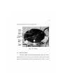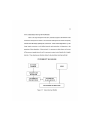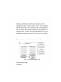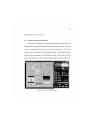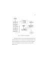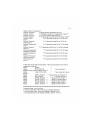
1
The author of this thesis has granted the University of Calgary a non-exclusive
license to reproduce and distribute copies of this thesis to users of the University
of Calgary Archives.
Copyright remains with the author.
Theses and dissertations available in the University of Calgary Institutional
Repository are solely for the purpose of private study and research. They may
not be copied or reproduced, except as permitted by copyright laws, without
written authority of the copyright owner. Any commercial use or publication is
strictly prohibited.
The original Partial Copyright License attesting to these terms and signed by the
author of this thesis may be found in the original print version of the thesis, held
by the University of Calgary Archives.
The thesis approval page signed by the examining committee may also be found
in the original print version of the thesis held in the University of Calgary
Archives.
Please contact the University of Calgary Archives for further information,
E-mail: [email protected]
Telephone: (403) 220-7271
Website: http://www.ucalgary.ca/archives/
UNIVERSITY OF CALGARY
Design and Construction of an Infra-Red Camera for Use at the
Rothney Astrophysical Observatory
by
Susanna Elaine Johnson
A THESIS
SUBMITTED TO THE F A C U L T Y OF G R A D U A T E STUDIES
IN PARTIAL FULFILMENT OF THE REQUIREMENTS FOR THE
D E G R E E OF M A S T E R OF SCIENCE IN ASTROPHYSICS
D E P A R T M E N T OF PHYSICS A N D A S T R O N O M Y
CALGARY, ALBERTA
D E C E M B E R , 2001
© Susanna Elaine Johnson, 2001
ABSTRACT
This thesis describes the design and construction of an infrared camera for
astronomical use at the Rothney Astrophysical Observatory, based on a 128 by 128 pixel IR
array. The array is sensitive in the 2.0 urn to 5.0 um range. Construction details for the
detector itself are given, and details of the software for the array controller and for the host
computer are given, with source code listings.
iii
Acknowledgements:
First, the technical acknowledgements. There is Fred Babott, who is the technical
cohesive force behind the R A O and who knows his onions. He did a great deal of the circuit
design, layout, and fabrication. Then there is Dr. David Fry, who let me have my head but
was able to direct my energies in the appropriate direction. Finally, there is Pat Irwin who
allowed me to commandeer laboratory space in which to assemble the IR camera. These
three gentlemen are the unsung heros of the Physics Department at the University of
Calgary.
Then, the personal acknowledgements. There are Richard and Patricia Pierson, who
funded this effort and provided moral support, and Sybil Lemyre, who listened to me at all
hours and under all circumstances. Finally, there is my husband, Larry Harding, who put up
with everything that went on and who still manfully refrained from committing justifiable
homicide.
iv
Dedication:
To all those who gave comfort, support, love, encouragement, and hope to
an abused and frightened child.
v
TABLE OF CONTENTS
Approval page
Abstract
Acknowledgements
Dedication
Table of Contents
List of Tables
List of Figures
Glossary
Epigraph
ii
i»
iv
v
vi
xiii
xiv
xvi
xxiii
CHAPTER ONE: INTRODUCTION
1.0 Introduction
CHAPTER TWO: G E N E R A L CHARACTERISTICS OF D A T A
ACQUISITION SYSTEMS
2.0 Introduction
2.1 Requirements for an Advanced Data Acquisition
System
2.2 Elements of an Advanced Data Acquisition System
2.2.1 Microprocessor Options
2.2.2 Memory Options
2.2.2.1 R A M
2.2.2.2 R O M
2.2.2.3 R M M
2.2.2.4 Flash Memory
2.2.3 Reconfigurable Logic
2.2.4 Building The Platform
2.3 IR Arrays and Charge-Coupled Devices
2.3.1 Operating Considerations for an IR Array
2.4 IR Labs Controller
2.4.1 Timing Card
2.4.2 Clock Generator Card
2.4.3 Analog Input Card
2.5 Host
2.6 Details of System
vi
1
3
16
18
18
20
20
23
23
24
25
25
26
28
28
30
32
32
33
33
34
34
CHAPTER THREE: TR C A M E R A ELECTRONICS A N D C A B L I N G
3.0 Introduction
3.1 Dewar Electronics
3.1.1 Rockwell TCM-1000C Array
3.1.2 Dewar Electronics
3.1.3 Microswitch
3.2 R A O Designed Support Electronics
3.2.1 Preamplifier
3.2.2 Bias Generator Board
3.2.3 Logic Board
3.2.4 Solenoid Driver Board
3.3 IR Labs Controller
3.3.1 Timing Board
3.3.2. Clock Generator Board
3.3.3 Analog Input Board
3.3.4 Utility Board
3.4 Spectral Instruments Model 1826 PCI C A R D
3.5 Cabling
35
37
37
38
40
40
42
43
44
45
45
46
47
49
50
51
52
52
CHAPTER FOUR: M E C H A N I C A L A S S E M B L Y OF D E W A R
4.0 Introduction
4.1 Filter Wheel Assembly
4.2 Cold Plate
4.3 IR Array Assembly
4.4 Inner Assembly
4.5 Outer Assembly
4.6 Final Assembly
54
56
56
60
61
63
70
73
vii
CHAPTER FIVE: G E N E R A L CHARACTORISTICS OF A R E A L TIME S Y S T E M
5.0 Introduction
5.1 Environment
5.2 Definition of Real Time Operation
5.2.1 Time Constant
5.2.2 Ability to Stay in Real-Time
5.3 Mission of the Real-Time System
5.3.1 Control of the Process
5.3.2 Control of the Instrument
5.3.3 Take Data
5.3.4 Interpret Commands
5.3.5 Respond to Real-World-Events
5.3.6 Respond to the Communication Subsystem
5.3.7 Respond to N M I Emergencies
5.4 Internal Structure of the Real-Time System
5.4.1 Interface to Hardware (BIOS)
5.4.1.1 Physical I/O Control Subsystem
5.4.1.2 Logical I/O Control Subsystem
5.4.2 Interface to Communication Subsystem
5.4.2.1 Tick-Tock
5.4.2.1.1 Transmission
5.4.2.1.2 Receiving
5.4.3 Message Cracker
5.4.3.1 Message Cracker Takes Direct Action
5.4.3.2 Message Cracker Sets Event Queue
5.4.4 Interrupt Handlers
5.4.4.1 Clock/Timer Interrupt Service Routine
5.4.5 Process Control Routine
5.4.6 Background Loop
5.4.7 Virtual Machine
5.5 Commercially Available Real-Time Operating Systems
5.6 Roll-Your-Own Operating Systems
viii
75
77
77
78
79
79
79
79
80
80
80
80
81
81
81
82
82
83
83
85
85
87
86
87
88
89
90
91
92
93
94
96
CHAPTER SLX: IR L A B S CONTROLLER P R O G R A M
6.0 Introduction
6.1 Structure of DSP Program
6.1.1 Loader
6.1.2 Kernel
6.1.2.1 Communication Subsystem
6.1.2.2 Timer Driver
6.1.2.3 Load New Overlay Function
6.1.2.4 Load Word
6.1.2.5 Read Word
6.1.3 Application Program
6.1.3.1 PON-Power On
6.1.3.2 POF-Power Off.
6.1.3.3 S B V - Set Bias Voltage
6.1.3.4 SB2 - Set Video Board Video Offset
6.1.3.5 S G N - S e t Gain
6.1.3.6 S T P - Stop Video Mode
6.1.3.7 R D A - Read Array
6.1.3.8 R R R - Read, Reset, Read
6.1.3.9 M R A - Multiple Read of Array
6.1.3.10 A B R - Abort Read
6.1.3.11 D O N - D o n e
6.1.3.12 TST - Communication Test
6.1.3.13 S E X - Set Exposure Time
6.1.3.14 L D W - Load Word
6.1.3.15 OSH-Open Shutter
6.1.3.16 C S H - Close Shutter
ix
97
99
102
103
104
104
107
108
108
108
109
HI
112
112
112
113
113
113
114
114
115
115
115
116
116
116
117
CHAPTER S E V E N : HOST P R O G R A M
7.0 Introduction
7.1 Program Structure
7.1.1 Structure of Graphic User Interface
7.1.2 Structure of the Background Loop
7.1.3 Structure of Communication Subsystem
7.1.3.1 Interface to Spectral Instruments
PCI-1826 Card
7.1.3.2 Serial Communication Channel
7.1.3.3 D M A Channel
7.1.4 Real-Time Clock
7.1.5 Image Storage
7.1.6 Filter Wheel Control
7.2 Host Program Auxiliary Systems
7.2.1 Help Subsystem
7.3 Dynamic Linked Libraries
7.3.1 Generating LIB files from D L L Files
7.3.2 FITS Library
7.4 A C C E S S I/O DIO-128
7.5 White Rat
7.6 Errors
7.6.1 Fatal Error
7.6.2 Correctable Error
7.6.3 FITS Library Error
CHAPTER EIGHT: CONCLUSION
8.0 Overview
8.1 Status As Of This Writing
8.2 There And Back Again
8.2.1 The Controller Incident
8.2.2 The Computer Factory
8.2.3 Problems with the IR Labs Controller
8.2.4 Problems with the Spectral Instruments 1826
Interface Card
8.2.5 Problems with the IR Labs Host Program
8.2.6 Problems with the DSP56002 Software
8.3 Recommended Work
8.4 Summary
x
118
120
120
122
123
125
125
126
127
127
128
129
129
129
130
130
131
132
133
134
134
135
135
136
138
139
139
141
144
145
145
146
146
147
148
REFERENCES
150
APPENDIX A: Schematics for R A O Designed Electronics Package
Figure A - l . Infrared Detector Shutter and Mounting Plate
Figure A-2. Wiring Harness Card for Dewar Electronics
Figure A-3. Preamplifier and Bias Voltage Board Layouts
Figure A-4. Preamplifier Schematic
Figure A-5. Bias Voltage Generator Schematic
Figure A-6. Logic Board Layout
Figure A-7. Logic Board Schematic (partial)
Figure A-8. Shutter Solenoid Driver Board Schematic
160
161
162
163
164
165
166
167
168
APPENDIX B: Dewar Connector Pinouts and IR Labs Controller
Pinout
B. 1 External Preamplifier Connector
B.2 Dewar to Preamplifier Connector
B.3 Clock Generator Board DB-37 Connector
B.4 DB-37 for Controller to External Preamplifier Pinout
B. 5 DB-25 for Controller to Filter Wheel Controller Pinout
169
170
171
172
173
174
APPENDIX C: Narrow Band Filter Characteristics
C. l l H Filter
C . 2 i K Filter
C.3 iL Filter
C.4 Standard M Filter
C.5 TCM-1000C Response Curve with iK, iLp, and M Filter
Passbands Overlaid
xi
175
176
177
178
179
180
APPENDIX D: Source Code Listings
D . l Host Program
D. 1.1 List of Program Files in Host Program
D.1.2 Listing of host.Prj
D.l.3 Listing of dllmaLprj
D.l.4 Listing of host.c
D.l.5 Listing of xlate.c
D.1.6 Listing of xlate.h
D.1.7 Listing of global.h
D.l.8 Listing ofsvid.h
D.2 DSP Program
D.2.1 Bootstrap.asm as supplied by IR Labs
D.2.2 App.asm as supplied by IR Labs
D.2.3 Bootstrap.asm as modified by University
of Calgary
D.2.4 App.asm as modified by University of Calgary
D.2.5 Assembly Script for Motorola Assembler
Under MS-DOS
182
183
183
185
196
199
288
291
292
293
300
300
314
APPENDIX E: Host Program Error Codes
364
APPENDIX F: FITS Error Codes
369
xi i
329
344
363
LIST OF TABLES
Table 2-1.
Table 3-1.
Table 6-1.
Table B - l .
Table B-2.
Table B-3.
Table B-4.
Table B-5.
Table C - l .
Examples of Microprocessor Architecture
Design Criteria for Hybrid Focal Plane Arrays
Tasks Available in R A O Application
External Preamplifier Pinout
Dewar to Preamplifier Pinout
Clock Generator Board Pinout
DB-37 for Controller to External Preamplifer Pinout
DB-25 for Controller to Filter Wheel Controller Pinout
Central Wavelengths and Zero Magnitude Fluxes at
Different Photometric Bands
xiii
22
39
Ill
170
171
172
173
174
181
LIST OF FIGURES
Figure 1-1. N G C 4631 in Visible Light
Figure 1-2. Trapezium in L-Band
Figure 1-3. Contour Maps of Equivalent Visual Extinction,
Northern Streamer
Figure 1-4. Solar Flare at Near-IR Wavelengths, 6 September 2001
Figure 1-5. PICNIC Spectral Response Curve
Figure 1-6. Relative Response as a Function of Wavelength for
TCM-1000CIR Array
Figure 2-1. Block Diagram of Data Acquisition System
Figure 2-2. Types of Microprocessors
Figure 3-1. Relative Response as a Function of Wavelength for
TCM-1000CIR Array
Figure 3-2. Schematic of Dewar Electronics from IR Labs
Documentation
Figure 4-1. Schematic Drawing of Filter Wheel
Figure 4-2. Front View of Filter Wheel Assembly
Figure 4-3. Reverse Side of Filter Wheel Assembly
Figure 4-4. Cold Plate
Figure 4-5. Exploded View of IR Array Assembly
Figure 4-6. Assembled IR Array Assembly
Figure 4-7. Filter Wheel Assembly and IR Assembly on Cold Plate
Figure 4-8. Top View of Dewar with Inner Shell in Place
Figure 4-9. Outer Shell Bolt Tightening Sequence
Figure 4-10. Drive Train Mount
Figure 4-11. Drive Train with Setscrews
Figure 4-12. Top View of Inner Assembly of TR Camera
Figure 4-13. Stepper Motor and Reduction Gear Housing
Figure 4-14. Interior View of Assembled Stepper Motor
Reduction Gear Housing
Figure 4-15. View of Completed Filter Wheel Drive with Stepper
Motor, Reduction Gear Housing, and Stepper Motor
Controller
Figure 4-16. Completed Camera in Mount
xiv
5
8
10
12
14
15
19
21
38
41
57
58
59
61
62
63
64
66
67
68
69
70
71
72
73
74
Figure
Figure
Figure
Figure
Figure
Figure
Figure
5-1.
5-2.
5-3.
5-4.
5-5.
5-6.
5-7.
Figure 6-1.
Figure 6-2.
Figure 6-3.
Figure 6-4.
Figure 7-1.
Figure 7-2.
Figure 7-3.
Figure 7-4.
Figure 8-1.
Figure 8-2.
Figure 8-3.
Figure A-1.
Figure A-2.
Figure A-3.
Figure A-4.
Figure A-5.
Figure A-6.
Figure A-7.
Figure A-8.
Figure C-1.
Figure C-2.
Figure C-3.
Figure C-4.
Figure C-5.
Block Diagram of Real-Time System
Basic Input/Output Subsystem Block Diagram
Typical Double-Buffered Communication Subsystem
Typical Message Cracker
Typical Interrupt Handler
PID Control Loop Equation
Linkage Sequence for Virtual Machine in RTOS in N R C
DRM-210
Motorola 56002 Architecture
Motorola 56000 Family Floating Point/Arithmetic Unit
Loader Block Diagram
Block Structure of Kernel
Host Program Background Loop
Typical Control Window
Program Flow Upon Initialization
Error Screen
Why the Preamplifier is Necessary
Cost Estimate of Proposed In-House Controller Design
Block Diagram, Proposed TMS320C30 Based Controller
Infrared Detector Shutter and Mounting Plate
Wiring Harness Card for Dewar Electronics
Preamplifier and Bias Voltage Board Layouts
Preamplifier Schematic
Bias Voltage Generator Schematic
Logic Board Layout
Logic Board Schematic (partial)
Shutter Solenoid Driver Board Schematic
iH Filter Passband
i K Filter Passband
iL Filter Passband
Standard M Band Filter Passband
TCM-1000C Response Curve with iK, iLp, and M Filter
Passbands Overlaid
xv
78
83
84
89
90
93
95
100.
101
102
105
121
122
124
124
142
143
143
160
161
162
163
164
165
166
167
173
174
175
176
177
GLOSSARY
2016
An early type of R O M , organized as 8 bits wide by 2 K bytes long. It could be
programmed only at the factory.
8051
An INTEL 8-bit microcontroller with a Harvard architecture. It is a very
successful design and is widely used. The design specifications may be licenced
from INTEL for inclusion as a component in a CPLD or FPGA design.
A / D converter
Analog-to-Digital converter
ADC
See A / D converter
ARCT
A. R. Cross Telescope. The 1.8 metre telescope at the RAO.
ASIC
Application Specific Integrated Circuit. A n integrated circuit designed by or for a
customer for a specific purpose.
Bang-bang controller
A controller which has two states only: full on and full off.
BCD
Binary Coded Decimal.
Bit Bucket-Brigade
A technique for unloading CCDs and IR arrays in which the charge is moved
from pixel to pixel until it arrives at the output port.
Boot-block
A portion of a flash memory that cannot be rewritten under program control.
This is usually used to store critical code which i f damaged would prevent the
system from operating at all.
xvi
Canned System
A system purchased from a vendor as a package.
Canned Software
Software purchased from a vendor as a package.
CCD
Charge Coupled Device.
CMOS
Complementary Metal Oxide Semiconductor. A low current-drain logic
technology based on FETs instead of junction transistors.
COFF
Common Output File Format. A widely used file format for output from
compilers, linkage editors, and other system tools.
COSMAC
A line of R C A microprocessors. Their chief characteristic is their extremely low
power consumption, making them ideal for use in handheld or battery powered
equipment.
CPLD
Complex Programmable Logic Device.
CRC
Cyclic Redundancy Check. A method of detecting single-bit errors in a data
stream.
D/A converter
Digital-to-Analog converter.
DAC
See D/A converter.
xvii
DLL
Dynamic Linked Library. This is a technique wherein required functions are not
linked into a program until run time. This decreases the size of the program at
the cost of having to load more than one package into memory. This technique is
extensively used by Microsoft operating systems and software written to run on
Microsoft operating systems.
DMA
Direct Memory Access.
DRAM
Dynamic Random Access Memory
DSP
Digital Signal Processor
Dynamic R A M
See D R A M
EEPROM
Electrically Erasable Programmable Read Only Memory. Sometimes written
E PROM.
2
FITS
Flexible Image Transport System. A file transfer format extensively used in
astronomical and astrophysical work.
Flash memory
Nonvolatile memory which can be erased in situ and then reprogrammed, also in
situ, using normal voltages.
FPGA
Field Programmable Gate Array. A gate array that can be programmed and/or
reprogrammed by the end user, often under program control.
FWHM
Full width, half maximum
xviii
GUI
Graphic User Interface
Harvard Architecture
A computer technology wherein the program memory and the data memory are
separate data spaces.
Indium-bump technology
A technique for mating two wafers. On one or both the wafers the intended
connections have indium deposited on them. The mating faces are then aligned
and brought together under pressure. If all goes well the indium will deform and
form good electrical connections. Also known as "Flip-Chip" technology.
IR Array
A photosensitive CCD-like array designed to be sensitive to various wavelengths
or bands of infra-red light.
ISR
Interrupt Service Routine.
Masked memory
A type of R O M in which the information is loaded during construction of the
wafer by means of a deposition mask. This is an obsolete technology.
Mezzanine board
A circuit board mounted over another circuit board in order to gain board space
(real estate) in a tight environment.
NASA
National Aeronautics and Space Agency. The United States Space Agency.
NMI
Non-Maskable Interrupt. A n interrupt which can not be disabled.
Orthogonal Instruction Set
A n instruction set where all instructions are available for all register
combinations (or at least the register combinations that make sense).
xix
OTP
One-Time Programmable.
Packed B C D
B C D digits, which take 4 bits each, packed two to a byte.
Page-mode
A type of flash memory where erasure is done a page at a time.
PAH
Poly-aromatic hydrocarbon.
PJD
A control loop. The acronym means Proportional-Integral-Differential.
Platform
A computer, or microprocessor with all support systems: a complete entity.
PLD
Programmable Logic Device. A gate array.
PROM
Programmable Read Only Memory
Pseudo-ops
Computer instructions which look like machine language but for which there is
no hardware to execute them. A n interpreter is required for execution. This is a
technique frequently used when putting together sequences of complex functions
for which there is no direct hardware counterpart and where conservation of
program space is more important than raw execution speed.
RAM
Random Access Memory
RAO
Rothney Astrophysical Observatory. The observatory operated by the Physics and
Astronomy Department of the University of Calgary.
xx
RCA
Radio Corporation of America.
RISC
Reduced Instruction Set Computer. A microprocessor optimized for speed of
execution and/or minimum die size. These devices have small, non-orthogonal
instruction sets but they execute at high speed.
RMM
Read Mostly Memory. See Flash Memory
ROM
Read Only Memory
RTD
A type of temperature sensor.
RTI
Return from interrupt. Since an interrupt is an asynchronous event, The return
command must perform a complete context restore. Usually this consists of
restoring selected registers before reloading the program counter with the address
that the processor was executing from when the interrupt occurred.
Scratchpad memory
A small amount of R A M , usually located on-chip in a microcontroller. Since it is
on-chip, access times are short.
SCSI
Small Computer System Interface. A computer interconnect standard.
SDRAM
Synchronous D R A M . A type of dynamic ram in which the refresh has been
synchronized with the access to increase the speed of the part. These parts have
become competitive with static R A M
Software Package
A set of software working for a specific purpose.
xxi
SRAM
See Static Ram
Static R A M
Random access memory in which the data is present, without refresh, for as long
as power is applied. It is characterised by high cost, high speed, and low density.
UART
Universal Asynchronous Receiver-Transmitter. A serial device which does not
require a clock signal from the device it is communicating with. It derives the
clock from the data stream.
UVPROM
Ultra Violet Programmable Read Only Memory. A type of field programmable
R O M which can be erased by the application of U V light.
Von Neumann Architecture
A computer architecture in which the data memory and the program memory
utilize the same address space.
VME
A digital backplane standard originally developed by Motorola but now widely
used. It is characterized by multiple address spaces and high speed. The most
common V M E card formats are 3U and 6U. A 3U card has one V M E connector
only. A 6U card has two V M E connectors, with the second connector an
auxiliary bus such as V X I , V X D , or VSE.. The actual V M E standard is a five
volt digital standard. The auxiliary bus may be either digital or analog.
VXD
(1)
(2)
A n auxiliary digital bus used in a 6U V M E backplane.
A device driver written for Microsoft Windows 9x or later operating
system.
xxii
EPIGRAPH
Thy merchants chase the morning down the sea,
Their topmasts gilt by sunset, tho' their sails be whipped to rags.
Who raced the wind around the world come reeling home again.
With ivory, apes, and peacocks loaded, memories and brags.
To sell for this high profit:
Knowing fully they are men.
Poul Anderson
xxiii
1
CHAPTER ONE
INTRODUCTION
2
The Moon! The Moon is to blame!
Drug addled cry frequently heard in Golden Gate Park. San
Francisco, late 1960's.
Ah, yes. Must be the moon.
And reply.
3
1.0 INTRODUCTION
This thesis concerns itself with the design and construction of an infra-red camera
built around a Rockwell TCM-1000C infra-red array, and intended for astronomical
observation at the Rothney Astrophysical Observatory (RAO) at the University of Calgary.
It is not a thesis concerning the science which can be done with such a camera, rather it is
a chronicle of the engineering effort required to assemble such a device from disparate
pieces.
As an example, the controller for the camera was obtained from Infrared Laboratories
(ER. Labs) in Tucson, Arizona, as was the dewar in which IR array is mounted.
Some
electronics for the array are derived from an original Rockwell design whereas other
electronics were designed and built at the University of Calgary.
Some thousands of lines of C language were written specifically for this application
at the University of Calgary, as well as approximately 1000 lines of assembler for the
controller, not to mention an approximate 750 kilobyte (source) library downloaded from
N A S A and modified for the application.
The resulting instrument has utility in its own right as a scientific instrument, and is
intended to be used as such. However, in many ways it is a pilot project, in that it
demonstrates that the University of Calgary has the capability to design and deploy such
instruments, and will serve as the springboard for the design and construction of infrared
cameras with extended capabilities, including higher resolution, extended sensitivity range,
and automated modes of operation.
4
Due to the fact that this thesis is more of an engineering paper describing an
instrument than a scientific paper, it is divided into two major sections. These two sections
are about the hardware design (chapters 2,3 and 4), and the software design (chapters 5, 6
and 7). The hardware section consists of one chapter discussing general principles of data
acquisition systems, followed by a chapter on the mechanical design of the IR camera, and
by a chapter on the electronics in the camera. The software section consists of one chapter
discussing general principles of real-time operating systems, followed by one chapter
describing the real-time system running on the DSP in the IR Labs controller, and one
chapter describing, on a high level, the host program running on the PC class computer and
driving the camera.
The 1.8 metre telescope at the R A O is equipped with an IR detector capable of quite
good photometric measurements, but only of point objects. Extended bodies cannot be
investigated in detail with this detector for several reasons, including that as a point detector
it was never designed for the investigation of extended bodies. Any attempt to obtain data
concerning an extended body will result in data from an area which is the equivalent of a
1
single pixel and from which all spatial information has been lost. This is not satisfactory.
2
Four possible applications for an imaging array at the RAO come to mind. The first,
1
You could image with the InSb detector, but this would require exposing one pixel
(equivalent) at a time. Not only is this not possible given the present state of the ARCT,
but it would be painfully slow.
2
There are many more than four, but we shall discuss only these.
5
which is a photometric application and which can be done fairly simply, is to observe
3
Seyfert galaxies and then to make isothermal maps. This would entail observations with
NGC 4631 & NGC 4627 in Canes Venatici
16 A p r i l 1 9 9 9 , C 1 4 , f . / 6 . S . f = 2 . 3 m , E x p o s u r e 4:<s.00s=4Q m i l l . , S B I G S T - 8 ( A B ' 3 ) . I m a g e b y B e r n d K o c h ,
Solingen
Figure 1-1. N G C 4631 in Visible Light.
various filters, the construction of pointwise colour value plots, and possibly the correlation
of IR photometric data with data from other sources and for other portions of the spectrum.
The second application which comes to mind is the observation of planetary nebulae.
Such as NGC 4631, shown here as Figure 1-1, in a photo taken from the collection of
Bernd Koch, at the University of Bonn, Germany, (http://www.astrofoto.com/astro/).
6
The difficulty of studying these objects with a point detector is that a point detector provides
at best data only from the equivalent of one pixel, when it is the detail of the image which
is of the essence. With a planetary nebula, there is an outer shell of gas and dust and a hot
point object in the centre which is the star. The shell is formed when the older, low-velocity
stellar wind from the star is impacted from behind by a high-velocity wind, also from the
star. An examination of the temperature of the gas, and in particular an examination of the
shock zone, could reveal details concerning the velocity of the high-speed gas and dust and
thereby details concerning the star within.
The next application is the observation of protoplanetary disks. Areas such as the
4
Trapezium have dust clouds of various optical depths. Protostars are forming in these
regions, however even those protostars which have already achieved hydrogen ignition are
difficult to see in the optical portion of the spectrum due to the dust. They are quite visible
in the infra red, but an imaging camera is required to resolve the protostar from the
obscuring dust and gas.
As remarked in the paper cited above, an efficient technique for performing a census
of circumstellar disks around young stars is to obtain infrared imaging surveys of the stellar
clusters in which these stars are forming. This information can then be used as a preliminary
step in determining the frequency of planetary systems in the Milky Way. Since
4
Lada, Muench, Haisch, Lada, Alves, Tollestrup and Willner, Reference 22. The
Trapezium is a hotbed of circumstellar disks, candidate protostars and dust clouds.
Imaging in J, H, K, and L bands indicates a high level of detail.
7
circumstellar disks are bright IR emitters and have an IR excess over that of the
photospheres of young stars, they are particularly amenable to measurement with a near-IR
imaging camera such as the one which is the topic of this thesis. Colour-colour diagrams
can then be constructed, using data obtained from the camera and from other imaging
sources, and these diagrams are known to be useful in the identification of objects displaying
infrared excesses, and in identifying candidate circumstellar disks.
There is also evidence which indicates that the frequency of sources exhibiting
excess in the J, H, and K bands decreases as a function of the cluster age, with time frames
of a few million years.
This may be associated with constraints on the lifetimes of
circumstellar disks and the time frame available for planetary formation.
Since protostars are thought to display large L-band excesses and colours indicating
that they are embedded in dust clouds, the camera is well suited to the observation of these
objects. However, as the above cited paper points out, due to background variations in the
5
L-band and other problems with observation, the quality of the data (taken 1997) was poor.
Though further data was taken (in 1998) to augment the data obtained the previous year, the
situation was still somewhat unsatisfactory, indicating the need for further observations.
This, the IR camera can do.
An example of the type of infrared imaging which can be done is shown overleaf as
Figure 1-2. This is a mosaic image of the Trapezium, from the Lada, et al. paper, showing
3
Reportedly due to window dust, instrument/telescope flexure, and detector anomalies, as
well as significant L-band emission due to H n regions in the field of view.
8
Interesting features which are pointed out in the paper include the bright bar seen in
the southeast, and emission from dust at 3.3 micrometers, due to small P A H grains which
6
This is Figure lb in the original paper, which in colour in that paper. It is reduced to
grayscale in this reproduction for the purpose of printing.
9
are stimulated by U V radiation from the early stars in the cluster.
7
In 1994 Lada, et al . showed that a technique was available which allowed the
8
mapping of dust distributions in cold molecular clouds . This technique used data obtained
in near-IR imaging surveys, combining direct measurements of ER colour excess along
narrow beams with sampling procedures. While this technique requires the observation of
a great many stars behind the cloud being investigated, it does allow the derivation of the
spatial distribution of extinction and the mapping of dust column densities across the cloud.
In the 1994 paper they report having produced an extinction map with an angular resolution
of 90 arc-seconds. They also report having found a positive linear correlation between the
mean extinction and its measured dispersion, and were able to show that the data obtained
is not compatible with cloud models having uniform extinction or with having many small,
discrete, high-extinction areas.
9
In a later paper Lada, et al discuss the application of this technique to an
investigation of the Northern Streamer portion of IC 5146. In this paper they discuss work
done in 1995 at Kitt Peak National Observatory using the 2.1 metre reflector, with a
10
NICMOS HI array as the detector. They report that with this equipment they were able to
7
Lada, C. J., Lada, E. A., Clemons, D., & Bally, J. 1994, ApJ, 429, 694
g
Their test case was IC 5146.
9
Lada, C. J., Alves, J., Lada, E. A . 1999, ApJ 512, 250
10
The NICMOS III chip is a 256 by 256 HgCdTe IR array manufactured by Rockwell
10
11
obtain a F W H M spatial resolution of 1 pixel approximately equal to 1". 09 . With this, after
the application of some spatial filtering and other data extraction techniques, they were able
to obtain the first distance estimate to the Northern Streamer (approx 460 pc). They were
also able to derive detailed contour maps of the equivalent visual extinction in the Northern
Streamer (their Figure 4 reproduced here as Figure 1-3).
327
336.8
RA
(2000.0)
326.6
336.4
Figure 1-3. Contour Maps of Equivalent Visual Extinction, Northern Streamer
Scientific Corporation. It was replaced in 1996 by the PICNIC chip, which also is 256 by
256 and which has the same spectral range. The spectral response curve for the PICNIC
is shown at the end of this chapter as Figure 1-5. While the NICMOS III and PICNIC
detectors are descendents of the TCM-1000C they have a different spectral range than
does the TCM-1000C. The spectral response curve for the TCM-1000C is shown at then
end of this chapter as Figure 1-6, and is included for comparison.
n
In our case, with the A R C T at the R A O and an estimated field of view of 55 arc-seconds
across 128 pixels, we are estimating a spatial resolution of 0.43" per pixel.
11
12
A l l the above applications are deep-field applications requiring the 1.8 metre
13
telescope at the RAO. However, there is a heliostat at the RAO, and with the aid of a
suitable neutral-density filter it can be used for solar observations. Images such as that
shown in Figure 1-4 (overleaf) are possible to obtain by means of this camera.
In the wild-eyed-idea department, there is a continuously variable infra-red filter
14
available for the 2 to 4 micrometer range . While this author has not seen the device and
has no data on its operation, it is reported to be able to slice its operating range into
15
approximately fifty bands . If so, it might be possible to construct an infra-red camera using
the Rockwell TCM-1000C (or another IR array), the continuously variable filter, and to use
this , for example, to obtain information concerning the makeup of the gas and dust clouds
surrounding protoplanetary disks as previously discussed. Preliminary discussions indicate
that the existing dewar cannot house both the IR array and the continuously variable filter,
and there is some concern about the optics required to use this filter with an imaging
12
The Cassegrain focus on the 41 cm telescope at the R A O is f/20, which is much too slow
for the IR camera. It is therefore either the A R C T or the heliostat, if the IR camera is to
be used at the RAO.
13
The heliostat has to be assembled and mounted, but all the pieces are on site, and the
instrument has been used at the R A O before.
14
Personal communication, Dr. T. Alan Clark.
15
Personal communication, Dr. D. J. I. Fry.
ure 1-4. Solar flare at Near-IR Wavelengths, 6 September 2001.
Courtesy Dr. T. A. Clark.
13
16
detector .
Another possiblity is the concept of using an imaging array, a slit, a diffraction
17
grating, and some optics to devise a synthetic-aperture imaging spectrometer .
This would allow great precision for spectroscopic data while at the same time preserving
spatial information. While this concept has not progressed beyond the back-of-the-envelope
stage, it has been marked for further investigation and will likely result in a white paper.
16
There are species in gas that have transitions in the IR (Kwok, Sun, "Physics and
Chemistry of the Interstellar Medium", draft version, January 2000). If the filter bands
are narrow enough that these transitions do not overlap, data concerning what is present
and where it is present can be obtained. Assuming the filter resolution is good enough, it
might be possible to use Doppler broadening and line shifts to get information
concerning gas and dust temperature and velocity. However, as pointed out by Dr. D. J.
I. Fry, the continuously variable filter is designed for a point detector, and the passband is
a function of where on the filter the light hits it. Thus, it might not be suitable for a plane
array detector, and in any case would require careful optics design to guarantee
uniformity of response.
17
Personal communication, Dr. D. J. I. Fry. The idea is to scan the image using the slit,
project the light onto the grating, and then project the resulting two dimensional entity
onto the IR array. By then turning the scanner at right angle to the original scan direction
and doing it again, it should be possible to obtain enough information to be able to back
out images at wavelengths of your choice. To do this successfully would require great
precision in the pointing of the telescope (see Chapter 8) and some degree of proficiency
with tomographic techniques.
RSC Imaging Sensors
PICNIC
focal f l a n u Arrays, Electronics, a n d Camera Systems
256 x 256 SWIR QE Spectrum
70
i
1
i i i | i i i i | i i i I
r r | r r r r ;
i
i I i [ 1 i I I [
60
£
o
J
o
5 0
i
40
MM
LU
£
3
C
(0
30
10 t
T = 77K
f
800
i
<i1
t
1050
•
i
i
!iii iI
i
ii iIii
1300 1550 1800
•Ii ••iI
i
2050
•
2300
•
,• n
2550
Wavelength (nm)
Figure 1-5. PICNIC Spectral Response Curve
IX
From Rockwell RSC website, http://www.rsc.rockwell.com/imaging/picnic/256qe.html.
15
19
From Rockwell engineering report SC87004.FR, Reference 53.
16
CHAPTER TWO
GENERAL CHARACTERISTICS OF DATA ACQUISITION SYSTEMS
17
Set the controls for the heart of the sun.
Roger Waters
18
CHAPTER 2.
GENERAL CHARACTERISTICS OF DATA ACQUISITION SYSTEMS
2.0 Introduction
In general terms, a data acquisition system can be considered to be a transducer
linked to a recording device. The transducer can be as simple as a voltmeter, and the
recording device can be as simple as a person with a timer, pencil, and paper. It is not the
business of the data acquisition system to interpret the data, simply to acquire and record.
Good examples of basic data acquisition systems include chart recorders, recording
meters, and strip chart recorders.
More complex data acquisition systems can automate the data recording function,
releasing the person who would otherwise be engaged in recording the data displayed by the
transducer. A n advanced data acquisition system can be equipped not only with local
storage capability but with remote reporting capability, using a variety of wired and wireless
transmission technologies. However to perform remote reporting effectively requires that
the data acquisition system have some degree of local intelligence in the form of a
microprocessor or microcontroller, and to equip a data acquisition system with such a
processor opens up a whole new level of capability not possible with simple recorders.
2.1 Requirements for an Advanced Data Acquisition System
An advanced data acquisition system will have one or more of the following features:
communication to a host; remote operation capability; process control capability; stored
19
SENSOR
PACKAGE
PROCESSOR
f1
r
CONTROL
OUTPUT
r
COMM
SYSTEM
MEMORY
(ROM)
MEMORY
(RAM)
*-i
f
i
1
LOCAL
CONTROL
GLUE
LOGIC
Figure 2-1. Block Diagram Of Data Acquisition System
program update capability; and hardware reconfigurability. It is not necessary for a data
acquisition system to be powered from a mains supply as advances in CMOS technology
have made available devices with very low power consumption requirements.
1
Data
acquisition systems constructed with this technology can be battery powered, and can be
combined with wireless reporting capability to produce an instrumentation package that can
be placed in a remote location. Often such packages, especially i f mass-produced or i f
adapted from mass-produced packages, can be produced cheaply enough that they can be
used in situations where recovery of the package is not expected to occur.
For example, the APTEC-NRC DRM-300/600 series radiation meters. These are handheld recording ratemeters built around an R C A COSMAC-1800 series microprocessor,
which are battery powered, and have many of the features described above.
20
2.2
Elements of an Advanced Data Aquisition System
As remarked above and as illustrated in Figure 1-1, an advanced data acquisition
system is equipped with an embedded microprocessor or microcontroller. It will have local
data storage capability but may also have data transmission capability, and will have stored
program capability. It may have the capability to receive program downloads from a host,
2
and advanced systems may have the capability to download hardware reconfigurations and
change their hardware characteristics on command. Frequently, data acquisition systems
3
have process control capability and can run a single-point control loop or a more complex
control algorithm independent of the host computer.
2.2.1
Microprocessor Options
There are numerous choices for the microprocessor, and the selection should be
made on the basis of unit cost, required flexibility, expected production volume, required
performance,
and projected
availability of the
component.
Some classes of
microprocessor/microcontroller are more difficult to design with, and are more difficult to
2
Systems equipped with SRAM-based FPGA logic can do this.
3
Omega Corporation, for example, has an extensive line of rack-mountable single-point
PID and bang-bang controllers. These controllers are microprocessor based and are
equipped with serial ports, (RS-232, RS-422/423, RS-485) so that they can be tied to a
host. Although they are designed primarily for temperature control using thermocouple,
thermistor or RTD, some will accept a voltage input. These last can be re-programmed
from the host to operate as general-purpose single-point controllers running a self-tuning
PID loop and reporting to the host via the serial link.
21
program for, than others, an aspect which will drive up the engineering cost, but the unit
cost, especially in volume, may be such that for large production volumes it is cost effective
to utilize such a device. Generally, the Harvard architectures are more difficult to
TYPES OF MICROPROCESSORS
• SINGLE ADDRESS SPACE F O R P R O G R A M AND
D A T A (VON N E U M A N N A R C H I T E C T U R E )
• M U L T I P L E ADDRESS SPACES, S E P A R A T E FOR
P R O G R A M AND D A T A ( H A R V A R D
ARCHITECTURE)
• SINGLE-BUS S T R U C T U R E , WITH OR W I T H O U T
INTEGRAL DMA
•
M U L T I P L E - B U S S T R U C T U R E , WITH I N T E G R A L
CONCURRENT OPERATION DMA
• M U L T I P O R T PINOUT
Figure 2-2. Types Of Microprocessors
program for, but they usually have a cost advantage and are useful in applications where the
code is relatively static over time. This class of processors may also have issues concerning
4
differences in word size between the data memory and the program memory which make
4
The Analog Devices ADSP-2100 family, for example, has this characteristic.
22
downloading new code from a host difficult. If the data memory and the program memory
5
are brought off-chip through separate ports , or if there is autonomous D M A capability for
both data memory and program memory coupled with sufficient internal scratchpad, then
Harvard architecture microprocessors will enjoy a speed advantage over Von Neumann
machines. Examples of cost/feature tradeoff for various microcroprocessors
ARCHITECTURE
DEVICE
COST
C L O C K SPEED
VON
NEUMANN
I N T E L 80C51
CHEAP
(±$1.00 E A )
SLOW
(1-5 M H Z )
HARVARD
ANALOG
D E V I C E S 2800
MODERATE
(±$2.50 E A )
MODERATE
(12 M H Z )
SINGLE-BUS
WITH D M A
TI320C16
MODERATE
(±$10.00 E A )
MODERATE
(20-33 M H Z )
MULTIPLE BUS
WITH D M A
TI 320C30/40/50 H I G H
(±$30-150 E A )
FAST
(33-100 M H Z )
MULTIPORT
PINOUT
TI 320C30
FAST
(33-100 M H Z )
HIGH
(±$30-50 E A )
Table 2-1. Examples of Microprocessor Architecture
The Motorola DSP56000 family of processors uses a Harvard architecture with two data
memories and one program memory. There are reasonable but not overly generous onboard S R A M scratchpads for each memory, but then all memories are accessed through a
single bus structure. From an electrical engineering point of view this prevents an
"explosion of pins" with associated fabrication problems and also holds the unit cost
down, however it has the effect of driving off-chip access times up. This family of
processors also is not orthogonal in the sense that the instruction set is register-specific.
These problems among others make writing high-performance code difficult at best.
23
are shown in Table 2-1.
2.2.2
Memory Options
There are two types of memory to be considered. The first type of memory to be
considered is read/write memory, commonly known as R A M . The second type of memory
to be considered is read-only memory, commonly known as R O M .
2.2.2.1
RAM
Read/write memory is available in two major types. First, there is static R A M
6
(SRAM), which uses a full six-transistor flip-flop structure for each bit. This type of
7
memory is quite fast but due to the cell structure utilized on the chip it is relatively low
8
density. It is therefore best suited to smaller systems or as cache memory in larger systems,
coupled to mass memory via an explicit memory manager.
The other major type of R A M is dynamic R A M (DRAM), which uses only one
transistor and a capacitor cell for each bit. The great advantage of this type of memory is
9
that it can be made very cheaply and has very high densities but the disadvantage is that
6
Micron Semiconductor
7
3 nanosecond access times are common, 5 nanosecond access time components are
becoming very reasonably priced.
8
E.g., systems with a 16-bit address space.
9
64 M by 1 bit memories in a single package are common.
24
dynamic R A M must be periodically refreshed. Aside from the power requirement for
refreshing the memory, there are the issues of the hardware required for the refresh, the
requirement for an explicit memory manager to handle the D R A M and to keep the static
10
cache and the D R A M synchronized, and finally the access time for the D R A M .
2.2.2.2
ROM
Read only memory (ROM) has come a long way since its inception. A few years
ago, R O M was available from the vendor as only masked memory, and the vendor was
happy to sell you a thousand pieces with your program hardwired into the memory. It was
not changeable, and what you got was what you got.
Field programmable memory (PROM) changed all that. While this type of memory
could be programmed only once, it could be programmed by the user in the field and it was
not necessary to provide a bitmap to the chip vendor and to purchase a large number of
pieces in order to get a R O M .
As the technology improved, ultraviolet erasable stored-
charge devices (UVPROM) became available, and it was possible and very affordable to
purchase a device that could be programmed, erased, and then reprogrammed.
10
Ten years ago (1990) 60-nanosecond access times for D R A M were considered blindingly
fast. At the turn of the millennium, with synchronous D R A M (SDRAM), 7 nanosecond
access times are available, though you will pay for it.
25
2.2.2.3
RMM
However while the U V P R O M was the dominant technology, a new technology,
referred to as Read-Mostly Memory, or R M M was emerging. These were devices with
limited storage and a limited number of erase and write cycles, but they could be erased
electrically and written to electrically, and data stored in them was not volatile. Digital
designs
11
in the late 1980's and early 1990's used these devices to store configuration
information unique to each unit and which could not be determined at design time, so that
this information was available immediately on boot.
2.2.2.4
Flash Memory
12
A n outgrowth of R M M is flash memory . Flash memory is a non-volatile mass
storage medium with the attribute of erasability while in-circuit and either an unlimited or
13
a very high number of erase-and-write cycles . Modern devices have advanced features
14
allowing erasure of only selected portions of the memory , thus allowing critical data to be
protected against inadvertent erasure during reloading of the device. This attribute makes
11
Such as the A P T E C - N R C ADM-300 ratemeter.
12
Such as the Intel 28F010 memory and similar devices.
13
Advanced Micro Devices, with their Standard™ family of flash memory are
guaranteeing one million write cycles per sector and 20 years of data retention. Devices
in this family are available for 1.8 volt, 3.0 volt, and 5.0 volt logic.
14
Specifically boot-block and page-mode devices
26
these devices ideal for storage of firmware in systems which will be deployed in remote or
inaccessible locations and which must also deal with firmware updates from a remote host,
2.2.3
Reconfigurable Logic
With the advent of complex programmable logic devices (CPLDs) it became possible
15
to purchase a generic high-density logic device , include it in a design, and then program
it in-situ after the design was built This technology obviated the need for ASICs in all but
the most specialized designs while still allowing the advantages inherent in cell-based
complex logic. The problem with a CPLD however is that it can be programmed only once.
While the fact that it is programmable at all allows great flexibility in the utilization of the
device, the fact that it is programmable only once means that the structure impressed on the
CPLD by the programming cannot be updated.
There are two ways out of this dilemma. The first way is to use flash memory
16
17
instead of an OTP configuration. Then, the device can be reprogrammed, although not
usually in the field. However, the configuration data is non-volatile and is available on
power-up.
15
E.g.,a22V10or 16L8
16
A good example of this is a XILINX 5200 series CPLD or one of the A T M E L flash
memory based offerings.
17
One Time Program
27
18
The second way is to employ a static R A M (SRAM) based cell structure in the
CPLD.
This results in a field programmable gate array (FPGA). The disadvantages to this
approach are that, since the configuration is in S R A M , it is volatile and is not available at
19
power-up, and also that at least one more component must be included in the design to hold
the configuration data and to make it available to the FPGA on boot. The real advantage,
at least from the system designer's point of view, comes with the realization that while the
vendor is quite willing to sell serial memories which will mate seamlessly with their FPGAs,
the FPGA will also accept byte-wide programming. This means that the configuration port
for the FPGA can be put on the data bus for the microprocessor, and although there must be
some non-volatile logic holding everything together during boot, the FPGA can be
programmed after microprocessor boot and therefore
under the control of the
microprocessor. The great advantage of this is that it is now possible to reconfigure
and update the operation of the data acquisition system while it is in operation, and in the
field. It is further possible to reconfigure or update the data acquisition system remotely via
is
The most successful S R A M based devices are the XC4000 family FPGAs and their
derivatives, available from XILINX. These devices are not cheap in themselves,
however they do offer some extremely high logic densities, and in some of the larger
parts it is possible to stuff an entire 8051 core into the part. Since this same part is
available with 2 nanosecond or better delay times, a very powerful system can be built at
low cost.
19
XILINX offers a X17Cxx line of OTP memories which are expressly designed to mate
with their FPGAs. These are serial-download devices which will download their contents
to the FPGA under the control of a hardwired FPGA protocol. A T M E L sells a similar
device, except that theirs is based on flash memory and is therefore reconfigurable.
28
the data link, and to store the new hardware configuration in flash memory for later use.
2.2.6
Building The Platform
Referring once again to Figure 2-1, we see that by use of the building blocks
described above it is possible to design a data acquisition system with an embedded
microprocessor, capable of running autonomously i f required but also equipped with (an
optional) communication subsystem, and capable of great flexibility in terms of both
hardware and firmware configuration. With all this capability available however, the precise
design will depend on the mission statement for the data acquisition system, coupled with
such other factors as size of production run, availability of components over the projected
lifetime of the system, and any management-imposed constraints.
2.3
IR Arrays and Charge-Coupled Devices
At first glance the difference between a charge-coupled device and an IR array is
somewhat artificial in that they both employ a photovoltaic sensitive element coupled to a
storage well and readout electronics. The major difference between the two is that generally
a C C D is oriented toward the visible portion of the spectrum whereas an IR array is not
sensitive (or at least not deliberately so) in the visible portion of the spectrum but rather is
designed to operate in various portions of the 1 to 10 micrometre region of the spectrum.
Another difference, though a difference in implementation rather than a difference in basic
technology, is that while CCDs generally operate at temperatures ranging
29
from ambient to -100 °C it is always necessary to cool an IR array and the enclosure in
which it is mounted in order to cut down on noise and extraneous current. This last means
that the design of an IR array is somewhat different from that of a C C D and that the
materials used in the manufacture must be materials that will have the desired electrical
properties at the operating temperature, and independent of what their electrical properties
are at room temperature.
The fabrication of IR arrays is also somewhat different from that of CCDs. A CCD
usually is a high-production-volume device, and if a designer wants to design a system using
a C C D she can find a plethora of devices available off-the-shelf and there is little need to
design her own. However, the market for IR arrays is somewhat more restricted and the
operating conditions are somewhat more stringent, so it is not uncommon for such a device
to be fabricated as two components (one being the sensitive element and the other being the
support electronics) and then for the two components to be mated using something akin to
indium-bump fusing technology . The combination of low production volume for DR. arrays,
20
20
The R E N A chip (Nova Research, Riverside, California) was fabricated this way. In this
case the region of interest in the spectrum was in the M e V range [for an instrument to
detect gamma-ray bursters], and the sensitive element was a material appropriate for this
portion of the spectrum. The support portion of the device was an ASIC fabricated as an
N M O S wafer and the sensitive element was mated to the ASIC using indium bump.
There are several vendors which will accept academic and/or prototype designs and run
them through a low-volume silicon foundry. A n example is the 0.35 micron MOSIS
process available to and in use by the University of Alberta Microelectronics Centre,
among others.
30
combined with somewhat lower yields for a more complex process results in detectors which
are very expensive when compared to the cost of the mass-market CCD.
However, the C C D is itself under pressure from CMOS image sensors. While these
devices have somewhat poorer performance than CCDs, they can be fabricated using normal
CMOS technology, which means that any silicon foundry can make them, and quite cheaply.
Further, since they are CMOS, their power consumption is much lower than that of a CCD.
Finally, they can be designed so that each pixel can be accessed separately rather than
through a shift register setup, which makes for ease of design of the support electronics.
They are in the classic sense cheaper than anything better and good enough to do the job for
most applications.
2.3.1
Operating Considerations for an TR Array
The quantum efficiency of an IR Array is quite high - figures of 85 percent are not
21
uncommon . However, they must be operated at cryogenic temperatures, which means that
a dewar with all the associated plumbing must be supplied. Further, while they can be fairly
21
Jobin Yvon, Inc. offers, in their IGA3000 line of near infrared array detectors, devices
with spectral coverage of 0.8 um to 1.7 um as linear arrays of 128, 256, or 512 pixels.
They quote 85 percent quantum efficiency for these detectors. The telephone number is
732-549-5125.
31
22
23
large the number of available output ports is limited and the output ports are analog. This
requires that support electronics be supplied in order to buffer and amplify the output, and
to convert the output from analog to digital. This also requires that a relatively complex set
of timing and control signals be provided to the array. At a minimum, a frame line, a synch
24
line, and a clock must be provided .
There are also voltage and power considerations. Due to the nature of the technology
there are several bias voltages driving the photodetector section. These must be supplied
from stable, clean sources, external to the dewar. The readout electronics also do not use
standard logic levels, requiring level shifters in the support electronics.
The method of output of either an IR array or a C C D is referred to as the BucketBrigade technique. In this technique, the charge accumulated for each pixel is successively
shifted to the next pixel until it arrives at the output line. It then enters an integrator where
it is developed as a voltage. This voltage is then presented to an A D C , and the output of the
A D C is stored as the value for that pixel. The array incorporates a shift register so that each
time the synch line is strobed it will step to the next line in the array, allowing the entire
array to be read out. The array shifts charges on the leading edge of the clock and the
22
256 by 256 arrays are readily available, and these can be and are assembled into larger
mosaics.
23
The IR Labs NICMOS array has four output ports, the Rockwell TCM-1000C has two.
24
e.g., the Rockwell TCM-1000C
32
output is valid on the trailing edge of the clock.
All of this then requires a controller to handle the IR array, and this controller is in
the classic sense a data acquisition system. In our case the controller is an IR Labs purposebuilt array controller based on a Motorola DSP56002 microprocessor, resident in a 3U V M E
25
26
chassis and communicating with a host computer via a parallel interface .
2.4
ER Labs Controller
The IR Labs controller is housed in a six-slot 3U V M E chassis with an on-board
power supply which supplies digital power as well as ±10 volt analog supplies. There are
three cards in the controller. These cards are the Timing Card, the Clock Generator Card,
and the Analog Input Card.
2.4.1
Timing Card
The timing card has on it the Motorola DSP56002 and support for the DSP, including
the U V P R O M which holds the program loaded into the microprocessor at boot. There are
several programmable logic devices on the card, however the configuration of these devices
is not accessible to the DSP and they are used to achieve a high level of integration of the
glue logic on the board. They are non-volatile. The timing card has a low-speed serial
25
This is not a standard 3U V M E backplane. A l l lines have been redefined for the purpose.
26
This is a SCSI interface with lines redefined for the purpose. IR Labs has supplanted this
technology with a fibre-optic link between controller and host in later designs.
33
channel to the host and a high-speed parallel channel to the host.
The firmware in the timing card is resident in a U V P R O M
27
and is loaded into an
28
on-board R A M program memory in the DSP on boot . The timing card generates all timing
and control signals for the Rockwell array.
2.4.2
Clock Generator Card
The clock generator card has a set of D/A converters for each output line and a set
of analog switches for each output line. The timing board can set the outputs of the D/A
converters, and then can toggle between the voltage outputs of two D / A converters to
generate a digital signal. Because the clock generator card is organized into groups of lines
it is possible to generate either single-ended or differential digital signals, depending on what
is required.
2.4.3
Analog Input Card
The analog input card is a two channel card. Each channel consists of an analog to
27
In the incarnation used at the University of Calgary. The card will also support
EEPROMs and if these devices are used then the timing card can download and store
programs from the host as required.
28
There are several modes of operation for the DSP56002. In the mode of operation
implemented in the IR Labs controller, an address overflow of the program memory will
cause the DSP to reach out through its external port to a static R A M on the card. This
allows programs larger than the size of the scratchpad memory to be run on the DSP. The
problem is, both data memories also use that same port, and there are bus contention
problems and timing issues which result when off-chip memory is accessed.
34
digital converter for conversion of the signal from the IR array or CCD, with upstream
integrator, variable gain amplifier, and offset voltage adjust. This card also is equipped with
29
D/A converters to generate the bias voltages to drive the array. The output from the A / D
converters is 16 bits wide and is directly transferred to the host via the high-speed parallel
link under the control of a PLD. The host then stores the data in a buffer using D M A .
2.5 Host
The host for this system is a Pentium III class personal computer running under
Windows 98 and equipped with a Spectral Instruments® Model 1862 Parallel Interface card.
This card is a PCI card and forms the nether end of the link with the IR Labs controller. The
host runs custom software to drive the controller and the Rockwell TCM-1000C via the
IR Labs controller.
2.6 Details of System.
The electrical and mechanical features of the ER camera will be discussed in
Chapters 3 and 4 of this thesis. The structure of the host software running on the PC, and
the firmware running on the Motorola DSP56002 microprocessor will be described in detail
in Chapters 6 and 7.
29
Not used at the University of Calgary with the Rockwell TCM-1000C
CHAPTER THREE
HI CAMERA ELECTRONICS AND CABLING
The fault, dear Brutus, lies not in the stars but in ourselves,
that we are men.
Wm. Shakespeare
37
CHAPTER 3.
IR CAMERA ELECTRONICS AND CABLING
3.0 Introduction
There are four major electronic subsystems in the IR camera. These subsystems are
1
the dewar electronics, including the Rockwell TCM-1000C array and support electronics;
2
the R A O designed preamplifier and support electronics; the IR Labs array controller, and
the personal computer that drives the camera. The first three subsystems will be discussed
3
in this chapter, and the Spectral Instruments 1826 card in the computer will be discussed
as well. The balance of the computer will be ignored except to note that it is an Intel
Pentium III system running under Microsoft Windows 98.
3.1
Dewar Electronics
The dewar electronics subsystem is composed of the Rockwell TCM-1000C array,
the support package for the array, and a Honeywell microswitch. There are also two
4
Guardian solenoids in the dewar to work the shutter, as shown in Chapter 4.
Rockwell International Science Center, now Rockwell Scientific Company, L L C . P.O.
Box 1085, Thousand Oaks, C A , 91358, USA. 805-373-4545
2
th
Infrared Laboratories, 1808 E. 17 St, Tucson, A Z , 85710-6505, USA. 520-622-7074.
3
Spectral Instruments, 1802 West Grant Road, Suite 110, Tucson, A Z , 85745, USA. 520884-8821.
4
Part number LT6X12C24D
38
3.1.1
Rockwell TCM-1000C Array.
5
The Rockwell TCM-1000C array is a prototype manufactured for IR Labs sometime
around 1987 by mating a PACE-1 HgCdTe-on sapphire detector array to a TCM-1000C
readout circuit using indium-bump technology. The array i s a l 2 8 b y l 2 8 pixel format with
a 60 micrometre square pixel size. It is sensitive to short wavelength infrared in the range
of 2.0 to 5.0 um with about a 40 percent spectral response at the short end, peak sensitivity
at about 4.6 um and rapidly falling off thereafter. The response curve from the Rockwell
documentation is reproduced as Figure 3-1, below.
Figure 3-1. Relative Response as a Function of Wavelength for TCM-1000C IR Array
IR Labs purchase order 7597 as reported in Rockwell report SC87004.FR, Reference 53.
39
The design criteria for the PACE-1 chip are shown below as Table 3-1.
Charge Capacity
Readout Noise
Maximum Readout Rate
Operating Temperature
Integration Time
Peak Quantum Efficiency
Pixel Operability
Waveband Of Response (MWIR)
6
30 x 10 electrons
< 500 electrons
2 MHz
77K
30 ms
> 70 %
95%
2.0-5.0 jim
Table 3-1. Design Criteria for Hybrid Focal Plane Arrays
6
The TCM-1000C incorporates an on-board integration capacitor and standard bit
bucket-brigade output. This is described in detail in the Rockwell report included in the
appendix. The output timing sequence requires three inputs to the chip: master clock (CLK);
y-shift register (YSYN), and a framing pulse (FRAME). There are two outputs, however it
is possible to read the entire array through only one output by not asserting the F R A M E line
every 64 clocks, but rather every 128 clocks. The timing diagram for reading the chip is
shown in detail in the Rockwell report.
One final feature of note with the TCM-1000C array is the inclusion of an on-chip
temperature sensor. This temperature sensor is stated in the report to be uncalibrated,
For further data about the PACE-1 chip, including dark current data, see the Rockwell
report. Dark current is reported to be less than 1 electron per second per pixel at 77K.
40
however there is a curve showing resistance as a function of temperature (dated 6 March
1979). The output of this temperature sensor is buffered in the RAO-designed preamplifier
7
package and sent to the filter wheel controller where it meets an A D C . The signal giving
the temperature of the chip eventually is passed to the host program running on the PC via
a parallel interface card as packed BCD.
3.1.2
Dewar electronics
The TCM-1000C is mounted on a 68-pin carrier which is in turn mounted on a cold
finger to keep it at 77 K during operation. However, the 68-pin carrier is integral with an
electronics package which provides capacitive decoupling of the bias supplies and rails, and
current limiting for the clock inputs. This package has a mini DB-21 connector for which
it was necessary to obtain a mate and fabricate a carrier board in order to wire the dewar.
8
The schematic, taken from the IR Labs documentation dated October 1989, is
reproduced overleaf as Figure 3-2.
3.1.3
Micro Switch
The filter wheel assembly in the dewar is equipped with a micro switch whose
actuator slides along the ring gear, as described in Chapter 4. The purpose of this micro
7
The filter wheel controller is a microprocessor based assembly designed by Fred Babott.
It is not documented in this report.
8
Reference 14
41
7<TM ' 10*
iSaa. /if
"LA.."?
PLC..
5&
53
I l l
1 -.)
T
JTT
5"
52
'.'JY..
T+
I
[*
i « ,
•
f — -
>
p W / ^ A r V V j ^1
l1
C'ISTLA/ A A ~ F A A / A .
JJ-
-it-
_
J
re «.
4fl
Cj)
/o«.
- / ' / / / —
too
49
-/.y\yyL
'00
(0
31
.'2
33
i
;tr
i
arz
•AAV
f
40
I2J±AAM
45
OUT
Z
1 vc
T
"
1
7 - 6-, Qry-P&C.
f-'
NOT
AT
SWiTiKEr
~1
ioTc
'do
ri.~.fJE
.
. . j i t ,
4.
1 ~
i
Figure 3-2. Schematic of Dewar Electronics from IR Labs documentation
(best available copy)
42
switch is to provide indication of when the filter wheel is in position. Normal micro
switches are not rated to operate at cryogenic temperatures, however Honeywell
9
manufactures a line of cryogenic rated micro switches. There is one difficulty with their
product, in that the switch is lever actuated and not roller actuated. This requires that the
filter wheel turn in one direction only in order to avoid jamming the switch. The output of
the switch is not buffered at all in the dewar and is processed in the RAO-designed
preamplifier.
3.2
10
RAO Designed Support Electronics
The ER camera is designed to be mounted on the 1.8 metre ARCT, on an instrument
cube, one of whose major purposes is to accommodate this camera. However the control
room, which is where the controller electronics are located, is several metres distant from
the camera. It is therefore necessary to have some support electronics local to the camera
to drive the Rockwell TCM-1000C and to buffer the output from this IR array.
The R A O designed support electronics consists of four subassemblies. These are the
11
preamplifier ; a bias voltage generator for the Rockwell IR array; a logic board; and a driver
9
Honeywell part number 109HM1
10
This electronics package was designed in-house by Fred Babott and the author. Layout
and assembly was performed by Fred Babott.
11
Actually, a two-channel preamplifier. Detailed description is in Section 3.2.1, next page.
43
board for the shutter solenoids.
The electronics package is mounted on the side of the ER camera dewar and requires
a clean bipolar power supply of ±12 to 15 volts DC.
The individual subassemblies in this package are discussed in detail below; the
schematics and fabrication drawings used in the manufacture of the package are shown in
12
Appendix A .
3.2.1
Preamplifier
The preamplifier has two channels to accommodate the possibility that the Rockwell
13
chip may be run in dual-output mode . The channels are identical. Each channel consists
of a two-stage amplifier with an AD743 op-amp set up as a voltage follower feeding an
LM6181, also set up as a voltage follower, as a line driver. The LM6181 is terminated with
a 51 ohm resistor in series with the output, to match the characteristic impedance of the RG174/U coaxial cable used to connect the preamplifier to the electronics in the control room.
12
Photocopy of best copy available.
13
The wiring is in place for running the chip in dual-output mode. The software as
of this writing is intended to drive the chip in single-output mode. In order to run the
chip in dual-output mode, the waveform table in the controller code must be revised and
the host software must be modified to de-interlace the outputs and to assemble them into
an image.
The advantage to running in dual-output mode is that the chip can be read at
twice the rate. The disadvantage is that doing so places an additional software burden on
the host. This may be done at a later time, when everything is working.
44
The preamplifier board also has the circuit for the temperature sensor on it. This
circuit uses an Analog Devices AD581 voltage reference to generate a stable voltage for the
temperature sensor on the Rockwell chip. The output of the AD5 81 is buffered by an OP-27
op-amp configured as a non-inverting amplifier. A voltage divider drops the supply voltage
to the temperature sensor to 3.4 volts when the TCM-1000C is at 77 K.
The output of the temperature sensor is buffered by another OP-27 op-amp and
14
passed on to the filter wheel controller , where it is converted to a digital signal and is
transmitted to the host program via a path not discussed in this report.
There is an amplifier enable line (digital) which must be asserted by the LR Labs
controller in order to turn on the preamplifiers. This uses half of a 74HC04 package (located
on the digital board) and a 2N2222A transistor to turn on the preamplifier.
3.2.2
Bias Generator Board
The bias generator board consists of an LM199 voltage reference, buffered by an
Analog Devices OP-27 set up as a non-inverting amplifier. The OP-27 has a 5 K ohm trim
pot for fine adjustment. The output of the OP-27 goes to a five-output divider stack, with
each divider having a 1N4448 diode used as a snubber and with a 10 K ohm trim pot. Final
decoupling for all outputs is with a 10 uF tantalum capacitor. The output voltages are as
shown on the schematic in Appendix A.
14
The filter wheel controller is a stand-alone rack-mounted assembly designed by Fred
Babott, and includes other functions not discussed here.
45
3.2.3
Logic Board
The logic board is a mezzanine board mounted in the preamplifier assembly, over
the preamplifier board. It has on it the level shifters for the logic and also the LM317 and
15
LM7805 regulators for the local power supplies. The 74HC04 used to buffer the micro
switch is located on this board as well.
The local power supplies are standard configurations as supplied in the sample
circuits from National Semiconductor or other vendors.
The level shifters, of which there are four, are TC427 noninverting buffers. Each
level shifter has a 1 K ohm current limiting resistor followed by a pair of 1N4456 diodes as
snubbers. The purpose of the level shifters is to convert the digital output levels from the
ER Labs controller to the requirements for the Rockwell IR array.
3.2.4
Solenoid Driver Board
Since the solenoids driving the camera shutter operate at 77 K , the nominal coil
16
resistance of 5 K ohms (at room temperature) drops to a few tens of ohms. Thus, the
operating voltage required is much less than that of the room temperature value of 24 volts.
This allows the shutter solenoids to be operated with very low voltages. On the other hand,
15
Half of the 74HC04 package is used to turn on the preamplifier. The other half is used to
buffer the micro switch output.
16
5 K ohms according to the published datasheet, 136 ohms at room temperature as
measured with a D M M , 24.6 ohms as measured at 77 K.
46
the ER camera is mounted on the back of a telescope that can be pointed in any direction.
Thus, not only must the solenoids pull the shutter into the desired position but they must
hold it in this position against gravity.
To do this, there are four solenoid drivers. The solenoid drivers are grouped in pairs,
with each pair consisting of a throw driver and a holding driver. The drivers are operated
by the IR Labs controller which causes the throw driver to assert a high ( 3 volt) voltage
pulse to move the shutter, and then which causes the holding driver to assert a low (0.5 volt)
holding voltage to hold the shutter in position against gravity.
Each solenoid driver consists of a TIP 120 N P N transistor in a common-emitter
configuration with the solenoid coil as the load. There is a 1N4007 diode across the emitter
and collector of the transistor to serve as a kickback diode.
3.3
ER Labs Controller
17
The ER Labs controller is a microprocessor based system with two channels of
communication to the host computer, and two channels of input from the ER array. It
generates the timing signals for the ER array, as well as generating the control signals to gate
the preamplifier and to drive the shutter solenoids.
The physical format of the ER Labs controller is that of a 3U V M E chassis, however
the backplane is not V M E as all pins have been redefined to produce a custom bus. The
chassis includes power conditioning, however the power supply is an outboard assembly.
Schematics are available from ER Labs directly or from their website.
47
In theory the controller can drive up to 16 2-channel analog input boards, making a
total of 32 channels of input from one or more arrays. This capability is useful when driving
cameras built by making a mosaic of IR or optical arrays.
There are four types of boards available from IR Labs for this controller. These are:
timing board; analog input board; clock generator board; and utility board. The controller
to hand uses the first three but is not equipped with a utility board.
3.3.1
Timing Board
18
The timing board has the microprocessor , R A M , R O M , some glue logic, and the
19
communication interface with the host. There can be only one timing board in a controller
backplane. The timing board controls the system by communicating with the other boards
in the system via the backplane.
The communication interface with the host is designed to mate to a Spectral
Instrument Model 1826 PCI card in the host. It has two channels. The first channel is an
RS-423 bidirectional serial link running at 9600 baud, and this channel is used to transfer
control information between the controller and the host. The second channel is a 16-bit wide
18
Motorola DSP56002 running at 50 MHz.
19
The timing board described in this document is a Rev. 3C timing board with wired
communication with the host. When dealing with this system it is important to make
sure the revision level of the documentation is the same as the revision level for the
hardware, and to be aware of various undocumented features of the hardware as received
by the R A O from IR Labs (the system they supplied was a design prototype).
48
parallel channel which, on the controller side feeds directly from the analog input cards
20
under the control of a PLD and on the host side feeds into a D M A device and memory .
Both channels use differential line drivers and receivers. The physical format for the cable
between the Spectral Instruments 1826 card and the IR Labs controller is that of a SCSI-3
connector but here, as in the case of the V M E bus, all pins have been redefined for the
purpose.
There are two types of timing board available from IR Labs. The first type uses the
SCSI-3 connector as described above, and is the type used in the camera system described
in this report. The second type uses a fibre optic link between the host and the controller.
There is only the one interface card available for the host if the SCSI-3 format is used, which
requires that the host have a PCI backplane. However, for the fibre optic link, there are
several interface cards for several types of hosts ( V M E , SBUS, PCI), allowing a wide range
of machines to serve as the host.
There are some electrical advantages to be derived from the fibre optic link. Since
this is an optical link, ground loops, hum, and noise from the copper connection are
eliminated. Additionally, the distance restriction between host and controller, placed on the
system by the SCSI-3 cable, is removed. Finally, with the optical link, the IR Labs controller
may be mounted directly on the telescope near the camera, minimizing hum and pickup.
20
Working with this requires dealing with a V X D device driver (under Windows 98) and a
DLL. Details are given in Chapter 7..
49
3.3.2
Clock Generator Board.
21
The clock generator board consists of 24 channels of output. The voltage of each
output can be set under program control, and the board is designed so that the outputs may
be paired up to form differential sets. Alternatively, the outputs can be referenced to
common. There are six blocks of channels on the board, along with some multiplexers and
isolation amplifiers intended for troubleshooting. There are also conditioned reference
22
voltage generators, supplying ±5 volts .
Each block of channels consists of two Analog Devices DAC8240 serial-load D/A
converters. These DACs have four channels of output, and are preset by the timing board
during boot or when commanded to do so by the host. After they are set their output
voltages do not change.
The outputs from the DAC8240 is then fed to a pair of Siliconix DG613
23
four-
channel analog switches, with the channels in four groups of two. From here, groups of two
are summed with a summing amplifier/buffer, passed through a Siliconix DG408A analog
switch used as an isolation switch, and to the load.
Output from the board is via a DB-27 connector and as stated before there are
21
The board described in this report is Revision 4A.
22
There are jumpers that can be used to set either or both reference voltages to common.
23
The logic of the DG613 is such that one channel of each pair is closed when the gate is
asserted, and the other channel is closed when the gate is deasserted.
50
multiplexers which are under program control and which can be used for test and
troubleshooting.
There are four DIP blocks into which the user can solder protective devices such as
diodes i f desired. These diodes are referenced to ground through 100 K ohm resistor
networks.
3.3.3
Analog Input Board
The analog input board described herein is a design prototype board originally
24
intended to work with the PICNIC ER. array. The identification on the board describes it
as Revision 2C with a layout date of 23 August 1996, however this information may not be
correct. The production board uses Datel ADS-937 ADCs whereas the prototype boards
25
uses Analogic ADC4325 ADCs.
Each of the two channels on the analog input board is independent, and the two
26
channels are identical. Each channel consists of a programmable gain stage, followed by
24
This is another Rockwell IR array, currently (October 2001) in production.
25
The boards at the R A O are the only two boards like this. Of the two, one is believed by
this narrator to have a defective channel. The designer of the boards (Dr. Robert Leach,
San Diego State University) was unable to recall the reason for making the change from
the Analogic to the Datel parts. He did state however that the microprogramming for the
production boards is identical to that for the prototype boards, so there should be no
problem i f it becomes necessary to install production boards in place of the boards now
in the possession of the RAO.
26
Except for address on the backplane. Each channel is individually addressable.
51
a stage which can inject a DC offset, followed by the A D C . The A D C can run under either
direct DSP control or under the control of the on-board CPLD, the mode used for doing highspeed transfer to the host.
There are also two DAC8240 D/A converters. These converters, which are serialload four-channel converters, feed voltage followers. Each group of four channels then
passes through a Siliconix DG408A analog switch used as final isolation, and then off-board
via a DB-15 connector. The purpose of this circuit is to provide bias voltages for the
27
arrays .
3.3.4
Utility Board
ER Labs sells a utility card for their system which can be used to generate high (± 30)
voltages, support secondary communication channels, and for other purposes. The prototype
system this document describes is not equipped with such a card.
3.4
Spectral Instruments Model 1826 PCI Card
The Spectral Instruments Model 1826 card is a PCI card designed to facilitate block
transfer of 16-bit words over a differential pair parallel interface. The card has D M A
capability, and can write (or, less commonly, read) a specified number of words to or from
a specified location in memory.
27
Not used in the application described herein. The bias voltages are made with the R A O
designed package.
52
The card also has a second, low-speed serial channel consisting of an RS-423
interface and an on-board UART. The U A R T is programmable for a variety of speeds and
formats but the standard when dealing with IR Labs equipment is 9600 baud 8N1. It is not
necessary to use the on-board U A R T as there are jumpers and a header that allow an external
U A R T to be connected i f desired. If this is done then the card merely provides an RS232/RS-423 translator.
In a Windows 98 system the card is driven by a V X D driver which is loaded at run
28
time and which must be in a directory in the system path. The driver interfaces to a D L L
which has calls that an application can access. This is described in Chapter 6 of this
document.
3.5
Cabling
The R A O designed electronics package has two gas-tight circular connectors. One
connector is for coupling to the electronics inside the dewar, and the other connector is for
coupling to the controller. Additionally, two video cables in RG-174/U carry the output of
the IR array to the video input card of the IR Labs controller. Pinouts for these connectors
are given in Appendix B.
The DB-37 connector on the clock generator board in the IR Labs controller supplies
eight digital signals and their returns. The pinout for this DB-37 connector is also given itt
28
It unloads automatically when the calling program exits.
53
Appendix B.
There is a DB-37 connector and a DB-25 connector on the back of the IR Labs
controller. The DB-37 connector mates to the cable which goes to the R A O designed
electronics package, and the DB-25 connector mates to the cable (not supplied by the author)
which goes to the R A O filter wheel controller and the ±15 volt power supplies. Wiring
internal to the controller runs between the DB-37 connector and the DB-25 connector in
order to match everything up. Pinouts for these connectors is given in Appendix B.
•i
CHAPTER FOUR
MECHANICAL ASSEMBLY OF DEWAR
Lord, thou has made this world below
The shadow of a dream,
And taught by time I tak' it soExceptin' always steam.
From coupler-flange to spindle-guide
I see thy hand Oh God Predestination in the stride
o'yon connecting rod..
Rudvard Kipling
56
CHAPTER 4.
MECHANICAL ASSEMBLY OF DEWAR
4.0 Introduction
The IR array is housed in a dewar along with a filter wheel, some support electronics,
an activated charcoal getter, and a shutter assembly. Since the array is designed to be
sensitive into the M band, it must be operated at liquid nitrogen temperatures.
Because the mechanical components of the camera were either obtained from other
sources or were developed in the machine shop, engineering drawings of the assembly do
not exist. To get around this, photos were taken during assembly. These photos and this
narrative are intended to provide the necessary information should reassembly of the camera
be required.
4.1
Filter Wheel Assembly.
Refer to Figure 4-1'. This is a schematic drawing of the filter wheel. There are six
positions for filters on the filter wheel. The filter wheel has a ring gear on the outer edge,
which engages a spur gear that is turned by a stepper motor. There are notches in the ring
2
gear into which a micro switch drops when the filter is in position. The closure from the
micro switch is used to indicate that the filter is in position, and an outboard controller then
1
Drawing courtesy Fred Babott.
2
This is a Honeywell cryogenic rated micro switch, part number 109HM1. Because this
microswitch uses a sliding lever and not a roller, the filter wheel is constrained to mm in
only one direction.
57
Index
Figure 4-1. Schematic Drawing of Filter Wheel (courtesy F. Babott)
stops the filter wheel precession. The fiducial position is indicated by two notches. There
3
are four filters in the filter wheel at this writing, with the remaining two positions being a
blank plate and an open position.
The housing for the filter wheel contains two sets of bearings. The first bearing is
for the spur gear which turns the filter wheel, and consists of a bushing only. The second
3
The filters are ih, ik, il, and M . Except for the M filter, these filters are narrow-band
filters not in the Johnson-Cousins system. Characteristics for these filters are given in
Appendix C.
58
4
bearing is for the filter wheel itself. This second bearing is a ball bearing assembly with the
ball bearings running in a groove. On the opposite side of the filter wheel from the ball
bearings is a teflon thrust washer and a compression spring made from 0.006 inch shim
5
stock. Figure 4-2 shows the front of the filter wheel assembly.
FILTER
WHEEt—
BEARING
DRIVE J
BELLOWS*!
Figure 4-2. Front View of Filter Wheel Assembly
4
If it becomes necessary to disassemble the filter wheel housing you will lose the ball
bearings onto the bench you are working over. You should disassemble the housing over
a cloth so that the bearings are caught by the cloth. When reassembling the housing, set
it up in a Palmer vise so that the race is up and the housing is level. Load the ball
bearings into the groove and then mount the filter wheel. The bearings are 1 millimetre
in diameter and are available from stock from several vendors.
5
Front is defined as the side facing the light source.
59
Note the shutter assembly. This assembly consists of an aluminum shutter mounted between
two guide rails and driven by two solenoids. There is a teflon spacer mounted on one of the
solenoid plungers. This spacer is sized so that when the shutter is opened the hole in the
shutter will line up with the IR array.
Note also the spur gear and drive bellows. Inside the filter wheel assembly the gear
on the end of the shaft engages the ring gear on the filter wheel, while on the outside of the
assembly, two spur gears connect the drive bellows to the stepper motor. The purpose of the
drive bellows is to insert some give into the drive train to allow for thermal expansion and
misalignment of the drive train. Figure 4-3 shows the reverse side of the filter wheel
SHUTTER
SOLENOID
EXIT PORT
SHUTTER
SOLENOID
I
FILTER
-WHEEL
BEARING
SPUR
GEAR—!
BEARING
MOUNTING
FLANGE
Figure 4-3. Reverse Side of Filter Wheel Assembly
60
assembly, including the mounting flange.
If it becomes necessary to disassemble the IR camera, the filter wheel assembly is
the last assembly which should be removed and the first assembly to be reinstalled. It should
be possible to mount the filter wheel assembly to the cold plate while the inner and outer
dewar sides are in place. A quarter-inch drive set with extensions and a universal joint is
6
recommended, along with a set of Allen wrenches . The cold plate is drilled and tapped to
accept 2-56 bolts. Do not use bolts longer than 54 inch when mounting the filter wheel
assembly.
4.2
Cold Plate
The cold plate is a copper plate which serves as the chassis for the IR camera. This
plate is mounted on a bellows assembly which in turn is mounted inside another bellows
assembly which supports the inner shield for the camera.
It is imperative that the bellows be subjected to as little mechanical stress as possible
during assembly of the camera. For this reason it is recommended that during assembly both
the cold plate itself and the outer shell ring be immobilized using wooden shims. After the
7
inner shell is mounted to its ring it will be attached to the cold plate via the G-10 standoffs,
and the inner shell and the cold plate will form a rigid assembly. Figure 4-4 shows the cold
6
Such as a Chapman Mfg. Co. 1316 tool set.
7
G-10 is an epoxy/glass- weave material from which printed circuits are manufactured. It
is used here for its thermal insulation properties. See Page 56.
61
plate,with mounting hole locations and wooden shims.
GETTER
MOUNT
ARRAY
MOUNT
INNER SHELL_
MOUNTING RING
FILTER
WHEEL
MOUNT
WOOD
SHIMS
Figure 4-4. Cold Plate
4.3
IR Array Assembly
The IR array assembly consists of a thermal and mechanical link to the cold plate,
support electronics for the IR array itself, the chip carrier, a light shield, and assembly
hardware. The disassembled view of the IR array assembly is shown in Figure 4-5, overleaf.
62
TOP
PILLOW
BLOCKS
LIGHT
SHIELD
CHIP
CARRIER
'•
«
-~~\
vvvvvvvv.
.
BOTTOM
PILLOW
BLOCKS
•,
ELECTRONICS
ASSEMBLY
MOUNT
TO COLD
PLATE
Figure 4-5. Exploded View of IR Array Assembly
Note that the top pillow blocks are not the same size as the bottom pillow blocks, and
must not be confused during assembly. The light shield has been notched to clear the shutter
solenoid plungers when the assembly is mounted on the cold plate, and care must be taken
to ensure that the IR array is parallel to the filter wheel assembly and perpendicular to the
light path. The chip carrier will mount only one way in the electronics assembly but the
electronics assembly will mount in two ways onto the mount to the cold plate. If the
electronics assembly is oriented such that the connector points to the left when mounted to
63
the mount to the cold plate is as shown in Figure 4-5, a shorter wiring path to the out-ofdewar connector will result. The IR array is not shown in this photograph.
Figure 4-6 below shows the assembled IR array assembly. The scale shown in the
photograph is in inches, and the coin shown for size is a Canadian two-dollar coin.
CONNECTOR
CHIP
CARRIER
LIGHT SHIELD
NOTE CLEARANCE
NOTCHES
Figure 4-6. Assembled IR Array Assembly
4.4
Inner Assembly
The top assembly of the IR camera consists of mounting the filter wheel assembly
onto the cold plate, followed by mounting the inner and outer shells, followed by mounting
the drive train for the filter wheel. The IR array assembly may then be mounted, and the
64
light shield for the IR array may be mounted.
The stepper motor and stepper motor
controller are external to the dewar and will be discussed in the next section.
Figure 4-7 below shows the filter wheel assembly and the IR array assembly mounted
on the cold plate without the inner or outer shells. While this violates the order of assembly
described in the previous paragraph, the photograph is instructive in that it shows details of
both assemblies and their relationship when mounted on the cold plate.
FILTER
WHEEL
ASSY
SHUTTER
SOLENOID
IR ARRAY
ASSY
SPUR GEAR
ASSEMBLY
COLD
PLATE
INNER
RING
OUTER
SHELL
Figure 4-7. Filter Wheel Assembly and IR Array Assembly On Cold Plate
65
Note that while the filter wheel assembly is mounted to the cold plate with short
bolts, the pedestal for the IR array assembly is thicker and requires the longer bolts. These
bolts may not be interchanged.
The reason that the order of assembly precludes mounting the inner and outer shells
while the IR array assembly is in place is because the setscrews for the filter wheel drive
train are not accessible when the IR array assembly is in place. The drive train must be
mounted into holes in the inner and outer shells, and then the drive shaft connected to the
drive bellows. Only then can the IR array assembly be mounted.
After the filter wheel assembly has been mounted on the cold plate, the inner and
outer shields should be mounted. The inner shell is mounted on the inner ring (as shown in
Figure 4-7) which is, as described previously, mounted on a bellows not connected to the
cold plate.
There are three pieces of 4-40 running thread made from G-10, about 3 centimetres
long. These pieces of running thread are used to mount the cold plate rigidly to the inner
8
shell. These pieces of running thread should be mounted with one and only one nut and one
star washer on the outside of the inner shell. The running thread is then mounted in the
standoffs on the cold plate with washers and two nuts. Figure 4-8, overleaf, shows a top
view of the dewar at this stage of assembly, with filter wheel, inner shell, and running thread
in place.
8
If you try to use a jam nut on the running thread on the outside of the inner shell there
will not be sufficient clearance to get the outer shell into place.
66
Figure 4-8. Top View O f Dewar With Inner Shell In Place.
The next stage in the assembly is the mounting of the outer shell and the drive train
for the filter wheel.
9
The outer shell seals to the baseplate (not the cold plate) with an O-ring and vacuum
grease. If the plan is to reuse the existing O-ring, it must be carefully removed from its
groove in the baseplate. A nonmetallic tool such as a toothpick should be used in order to
avoid nicking the O-ring. The ring should then be cleaned and carefully inspected for nicks,
cuts, and other defects which would prevent it from making a vacuum-tight seal between the
9
This O-ring sizes as a #271 but is actually a #270.
67
baseplate and the bottom of the outer shell. The groove in the baseplate into which the O10
ring seats should then carefully be cleaned of all foreign matter and old vacuum grease .
The O-ring should then be lubricated with a coating of vacuum grease and re-seated, and the
sealing surface should be coated with a thin film of vacuum grease. The outer shell may
then be mounted on the baseplate and secured using the bolt tightening pattern shown in
Figure 4-9.
Figure 4-9. Outer Shell Bolt Tightening Sequence
With the inner and outer shells in place, the drive train may now be mounted. The
drive train consists of a spindle mounted on a bearing assembly, an O-ring with seal, and a
10
Ethanol is a suitable solvent.
68
gland assembly. The housing for the gland assembly seals to the side of the outer shell with
the O-ring, and is mounted by four bolts as shown in Figure 4-10. As was done when
mounting the outer shell to the baseplate, the O-ring must be removed from its groove, and
the groove and all mounting surfaces must then be cleaned. After carefully inspecting the
O-ring for nicks, cuts, and other defects, the O-ring should be lightly lubricated with a thin
film of vacuum grease and re-seated, and all sealing surfaces should be coated with a thin
film of vacuum grease.
Figure 4-10. Drive Train Mount.
The drive spindle is tipped with a plastic adapter sleeve which mates with the drive
bellows on the filter wheel assembly. There are two setscrews in the bellows and one
69
setscrew in the plastic adapter sleeve. Although the setscrews for the bellows may be
tightened without regard to orientation, the setscrew in the plastic adapter sleeve goes into
the drive spindle and all holes must be aligned before this setscrew may be inserted. Care
must also be taken not to drive the setscrew too far into the plastic adapter sleeve, since if
it is driven past the end of the thread, it may not be recoverable, or recoverable only with
difficulty. Figure 4-11 shows the dewar with the drive train in place, and shows the location
of the setscrews.
R T ^
"1
''JcPPfSSte
INNER
* ' £'»*ti0$Bf\
:
SHELL'
SETSCREWS
\
SHELL-
S
S
Y
IR ARRAY
I
1
_^ j K f W j g S
OUTER
WHEEL
A
' i ^ ' m ^ ^ ^ ^ J
k\
FILTER
ASSY
IR ARRAY
MOUNT
GETTER
MOUNT
DRIVE
SPINDLE
PLASTIC
ADAPTER
Figure 4-11. Drive Train With Setscrews.
Having mounted the drive train, one can mount the IR array assembly. Care must
be taken to ensure that this assembly is mounted square to the filter wheel assembly,
70
that it is mounted perpendicular to the light path, and that it does not obstruct the operation
of the shutter solenoids.
The light pipe and wiring harness may be installed at this time, as shown in Figure
4-12. The getter is not installed until the dewar is ready to be closed up.
FILTER
WHEEL
WIRING
WIRING
SHUTTER
Figure 4-12. Top View of Inner Assembly of IR Camera
4.5
Outer Assembly
The outer assembly consists of the stepper motor assembly for the drive train and
associated electronics.
The stepper motor assembly is mounted to the outer shell of the dewar by four brass
71
standoffs threaded into the shell with 6-32 studs. The motor itself is mounted on the
reduction gear housing (as shown in Figure 4-13). The gear train for the stepper motor
cannot be assembled until the housing is mounted on its standoffs to the outer shell of the
dewar.
STEPPER
OUTER
SHELL
STANDOFFS
DRIVE TRAIN
GLAND
DRIVE
SPINDLE
Figure 4-13. Stepper Motor and Reduction Gear Housing
After the reduction gear housing is mounted to the dewar, the reduction gear, drive
sprocket, and chain may be mounted inside the housing as shown in Figure 4-14 (overleaf).
In this figure, the cover plate for the housing (which has mounted on it a potentiometer for
the stepper motor controller) is swung aside and may be seen on the right of the figure.
72
CONNECTOR
TO MOTOR
CONTROLLE
DRIVE
SPROCKET
DRIVE
CHAIN
REDUCTION
GEAR
FRONT
PLATE
(SWUNG OPEN)
Figure 4-14. Interior View of Assembled Stepper Motor Reduction Gear Housing.
The shaft of the potentiometer on the cover plate for the reduction gear housing
engages a shaft on the reduction gear and is held in place with a setscrew. In order to tighten
this setscrew it is necessary to reach up from underneath into the reduction gear housing
with the appropriate wrench while observing the work with a mirror.
The controller for the stepper motor is mounted below the stepper motor reduction
gear housing as shown in Figure 4-15.
73
Figure 4-15. View of Completed Filter Wheel Drive With Stepper Motor,
Reduction Gear Housing, and Stepper Motor Controller.
4.6
Final Assembly
After the inner and outer assemblies are completed, the getter should be heated in
an oven to 150 C for 24 hours. Immediately after it is removed from the oven it should be
mounted on the getter mount inside the dewar, and the inner and outer cover plates placed
on the dewar. Instructions for preparation of the O-ring for the outer cover, and for
preparation of the cover-to-outer-shell interface are the same as for mounting the outer shell
74
to the baseplate. Tighten the cover bolts using the tightening sequence shown in Figure 4-9.
Invert the dewar so that it is resting on the outer cover plate, connect it to a vacuum
pump, pump it down, and check for leaks. If it holds a vacuum then load the inner and outer
dewar chambers with liquid nitrogen, let the camera chill down and continue to check for
leaks. If there are no leaks then the camera is ready for use. Figure 4-16 shows the
completed camera, with electronics package and in its mount.
Figure 4-16. Completed Camera In Mount
CHAPTER FIVE
GENERAL CHARACTERISTICS OF A REAL-TIME SYSTEM
76
When shall we meet again?
In riot, strike or stopping train?
When the hurly-burly's done,
When the insurrection's lost or won.
Barbara Garson, MacBird
77
CHAPTER 5.
GENERAL CHARACTERISTICS OF A REAL-TIME SYSTEM
5.0 Introduction
Broadly speaking, a real-time system is a software package operating on a platform
1
and controlling or monitoring a process . This software package is dedicated to that
particular process, and runs in a loop sufficiently tight that it can respond to drifts in the
process within the time constant of the process so that the software package can apply
corrective guidance to the process and keep the process within an allowed tolerance band
for a desired setpoint. To do this, the software package must obtain information about the
parameters of the process it is controlling. It must then calculate any required corrective
action based upon those parameters and upon information obtained from whatever is
controlling the software package, apply this correction action if necessary, and report what
it sees upstream to whatever is monitoring the software package.
5.1 Environment
2
Most real-time systems are embedded systems , although it is not unusual to find a
real-time system resident on a general-purpose computer equipped with data acquisition
1
Wilkes, Ref. 60
2
Embedded Systems Magazine, Ref. 6
78
MEMORY
(ROM)
SENSOR
/^PACKAGE
MEMORY
(RAM)
J
*
r
CONTROL
OUTPUT
(
COMM
SYSTEM
:
r
LOCAL
CONTROL
GLUE
LOGIC
PROCESS
Figure 5-1. Block Diagram of Real-Time System
devices. However, all real-time systems will have a sensor package, local memory, and one
or more of the following: communication package; provision for local control; provision for
remote control; and the ability to control the process (see Figure 5-1).
5.2 Definition of Real Time Operation
3
There is no universally accepted definition of real-time operation , however if a
system (software package and platform) has the characteristics listed in this chapter it is
generally considered to be a real-time system.
3
Wilkes, Op. Cit.
79
5.2.1
Time Constant
All processes have a time constant. This time constant is a parameter of the process,
not a parameter of the real-time system.
5.2.2
Ability To Stay In Real-Time
The ability to stay in real-time means having the ability to respond properly to the
demands of the process under control within the time constant of the process. If this does
not happen the system will be deemed to have lost real-time.
5.3 Mission of the Real-Time System
4
Any real-time system has a mission . This mission requires the ability to perform the
tasks listed below.
5.3.1 Control of the Process
This is interpreted as specified above, to keep the process associated with the system
5
within a specified error-band of a specified set point e.g., as discussed by Ott .
Higgens, Ref. 10.
5
Ott, Ref. 51. goes into great detail on statistical methods for process control. A technique
he discusses which is particularly useful concerns control charts and how to determine i f
a process is within tolerance limits.
80
5.3.2 Control of the Instrument
A real-time system can be considered to be an instrument. Within this context, there
is housekeeping to be done to keep everything running. This housekeeping is considered to
be operational overhead, is a fixed demand on the resources of the system, and must be
accounted for when budgeting the resources of the system.
5.3.3 Take Data.
In order to control a process, the system must be able to acquire data concerning
what the process is doing at any given time.
5.3.4 Interpret Commands
The system must be able to receive and interpret commands from whatever is
controlling the system, and to implement them. This will require additional machinery
within the system in the form of message crackers, task dispatchers, communication
subsystems, or other features as appropriate to the system.
5.3.5 Respond to Real-World Events
Not every situation that arises with a process can wait until the system gets around,
in the fullness of time, to monitoring it. Transients and other events can occur which require
immediate attention and prompt corrective action of some type. This requires that the
81
system be able to deal with emergencies and anomalies so that the process stays under
control.
5.3.6 Respond to the Communication Subsystem
Usually in a real-time system the communication package is a subsystem. This
subsystem is frequently interrupt driven and such interrupts must be dealt with promptly.
The interrupts that the communication subsystem generates are not emergencies, but are
service requests. However the resource requirements of the communication subsystem must
be accounted for when budgeting the resources of the system.
5.3.7 Respond to NMI Emergencies
A n N M I (Non Maskable Interrupt) is an emergency interrupt of the highest order.
This interrupt is reserved for catastrophic failure of some nature, and is almost invariably
a shut-down signal. When this interrupt occurs, the system must attempt to put the process
into a safe mode, put itself into a recoverable state, communicate to its controller that it is
going down, and wait for the end.
5.4 Internal Structure of the Real-Time System
In order to accomplish its mission, the system will require the following major
6
functional blocks . Implicit in this discussion but not directly addressed are such functional
6
Reference 56
82
entities such as queues (circular and FIFO) and stacks (LUO) or the fact that there is a high
degree of communication between these functional blocks.
5.4.1 Interface To Hardware (BIOS)
A BIOS (Basic Input/Output Subsystem) such as specified by Microsoft
7
is an
interface between the hardware and the real-time system itself. The BIOS can take the form
of code resident in non-volatile memory and included as a component of the platform, or as
a fixed component of the real-time system. A typical BIOS (e.g., the System/360 DOS/VSE
8
BIOS ) has two layers. The first layer is known as the Physical I/O Control Subsystem
(PIOCS). The second layer is known as the Logical I/O Control Subsystem (LIOCS). Both
the PIOCS and the LIOCS are open structures in the sense that the real-time system can
access any function in either layer as required. A block diagram of the BIOS is shown
overleaf as Figure 5-2.
5.4.1.1 Physical I/O Control Subsystem.
The Physical I/O Control subsystem is that portion of the BIOS that interfaces with
the hardware and that deals with the specific characteristics of each device. This is the layer
in which all the low-level data manipulation occurs, and it provides a low-level standardized
interface to the rest of the system. It does not however provide any advanced
'Reference 30
Reference 16
83
functions. If the hardware configuration changes, it is this layer which must be changed in
order to accommodate the changes in the platform.
BASIC INPUT/OUTPUT
SUBSYSTEM
• P H Y S I C A L I/O C O N T R O L S U B S Y S T E M (PIOCS)
• L O G I C A L I/O C O N T R O L S U B S Y S T E M (LIOCS)
BACKGROUND
A
LIOCS
IRQ
HANDLER
|—
I
I
PIOCS
'
s
J
OUTSIDE
Figure 5-2. Basic Input/Output Subsystem Block Diagram
5.4.1.2 Logical I/O Control Subsystem
The Logical I/O Control Subsystem is that portion of the BIOS which provides
advanced functions to the real-time system (or other application). This layer provides a
high-level interface between the standardized low-level interface provided by the LIOCS and
the real-time system. Often the LIOCS provides extensive capabilities not possible to a
simple device driver.
84
5.4.2
Interface to Communication Subsystem
The communication subsystem (such as the system used in the Texas Instruments
9
TMS320C6000 ) can be anything from a simple parallel interface to a 100BaseT ethernet
connection. Whatever it is, this interface (which works in conjunction with the BIOS) deals
with the physical layer and presents message packets to the real-time system. It also takes
message packets generated by the real-time system and passes them on to the
communication subsystem for transmission upstream. In the following discussion we shall
not discuss advanced features such as multiple buffers and message queues, except to note
that if the message traffic is sufficiently high, such techniques are available and useful. A
block diagram of a typical double-buffered communication subsystem is shown below as
Figure 5-3.
BUFFER
ISR
BUFFER
BUFFER
ISR
BUFFER
T
M E S S A G E
C R A C K E R
M E S S A G E
F O R M E R
BACKGROUND
LOOP
Figure 5-3. Typical Double-Buffered Communication Subsystem
Reference 58.
85
5.4.2.1 Tick-Tock.
10
The Tick-tock is the name given to the interrupt handler routine associated with the
communication subsystem. It is given this name because transmission or receiving of data
is controlled by interrupt.
5.4.2.1.1 Transmission
In the case of transmission, the device buffer is initially empty, which would
normally result in a device-ready interrupt, except that this interrupt is kept disabled by the
communication subsystem. When a message is ready for transmission, the message is
loaded into a buffer and the interrupt is enabled. This results in a Device-Ready interrupt,
and the interrupt service routine loads as much of the message into the device buffer as the
device is designed to handle (byte or packet, depending upon the nature of the device). The
interrupt service routine then leaves the interrupt enabled and executes an RTI command.
When the device buffer empties, another Device-Ready interrupt will occur and
another portion of the message will be loaded into the device buffer by the interrupt service
routine, which will execute an RTI command, leaving the interrupt enabled.
This sequence will continue until the entire message has been transmitted. When the
device buffer empties and the message buffer is empty, the interrupt service routine will
disable the Device-Ready interrupt and execute an RTI command.
Note that it is the responsibility of the routine generating the message to ensure that
^Reference 18.
86
the interrupt is initially enabled. After that, the communication subsystem will take care of
everything else.
5.4.2.1.2 Receiving
In the case of receiving a message, the receive interrupt is always enabled. The
device incoming buffer will fill as data (byte or packet) is picked up from the outside. When
this buffer is full, the receive interrupt will be triggered and the interrupt service routine will
unload the device buffer to a message buffer. The interrupt service routine will then inspect
the message buffer to determine if a complete message is present, if any transmission errors
have occurred, and if the message is internally consistent (i.e., if checksums and CRCs are
valid). If a complete message is present and it passes all validity checks then a messageavailable flag is set and the buffer is released to the real-time system (usually the message
cracker) for further processing.
5.4.3
Message Cracker
11
The message cracker is that portion of the real-time system which interprets
incoming messages and determines what they mean. There are two major variants to the
type of action the message cracker can take upon decoding a message. A C-language
example of a typical message cracker is shown overleaf as Figure 5-4.
1
'Reference 52.
87
5.4.3.1 Message Cracker Takes Direct Action
In this case, the message cracker, after decoding the incoming message, directly
executes the action requested by the message. This requires that the message cracker
incorporate a task dispatcher to ensure that a routine which will perform the requested action
is invoked.
while(bfin_cracker == TRUE)
{
switch(inmessage)
{
case turn_on_pump:
{
bfpump_on = T R U E ;
bfmsg_avail= T R U E ;
break;
}
case turnoffpump:
}
}
{
bfpump_on = F A L S E ;
bfmsg_avail = T R U E ;
break;
}
/* end of switch */
/* end of message cracker */
Figure 5-4. Typical Message Cracker
While this approach is conceptually the simplest and isfrequentlyimplemented, it
has the disadvantages of not allowing for priority based execution of requested actions and
88
of the possibility that the system can lose real-time if incoming message traffic is sufficiently
high that the real-time system cannot keep up.
5.4.3.2 Message Cracker Sets Event Queue
In this case, the message cracker does not incorporate a task dispatcher but loads an
event queue with a request flag. The dispatcher is then part of the background loop. The
salient feature of this approach is that a prioritizer can be included in the message cracker
which can take into account any tasks already in the event queue; the state of the real-time
system, and any other pertinent information, and which can shuffle the sequencing of the
events in the event queue so as to best conform with the requirements of the mission. The
background loop will then pull tasks off the event queue and run them through the
dispatcher, which will then invoke the routine to perform the requested action.
Note that while this approach is more flexible than that of the previous section it
carries with it a certain amount of overhead which must be accounted for when budgeting
system resources. Note also that there is a certain execution latency in this approach which,
while deterministic in the sense that the latency is a function of the time required to crack
the message, load the event queue, take the event off the queue and execute it, is not
deterministic in the sense that, because of the presence of the prioritizer, the latency is a
function of whatever else may be happening to the system. For this reason, one thing the
prioritizer must monitor (if a prioritizer is present) is the age of the event - the older an event
is, the higher its priority must become.
89
5.4.4
Interrupt Handlers
There are certain interrupts which are required as part of the structure of the real-
time system. These interrupts are the communication subsystem interrupts (either one or
two, depending on the structure of the communication subsystem); the clock/timer interrupt;
and the non-maskable interrupt. There may be other interrupts present as required by the
mission of the system.
Whenever the system is dealing with an interrupt, it is not in real-time. A l l resources
of the system are devoted to dealing with the interrupt, and all other functions are blocked.
Usually, this blockage extends to the servicing of other interrupts as well (most processors,
for example, enter the interrupt service routine with all interrupts disabled).
For these
reasons, it is of the essence that interrupt handlers be kept as short as possible, that they do
only what is required to handle the event which caused the interrupt, and that they return as
quickly as possible to the normal flow of execution.
Normally, an interrupt service routine will clear the condition which caused the
interrupt, set an event flag in the appropriate queue for further processing, re-enable the
interrupt, and exit. The event flag is now what is known as a "soft interrupt", and is handled
by the background loop in a less immediate manner than in an interrupt service routine. A
block diagram of a typical interrupt handler is shown overleaf as Figure 4-6.
90
5.4.4.1 Clock/Timer Interrupt Service Routine
There is one major exception to the above, and that exception is the structure of the
clock/timer interrupt service routine. The clock/timer interrupt service routine is frequently
used for more than simply updating the system clock. Certain control algorithms (e.g., PEO
loops) require execution at well defined intervals and timing jitter is deleterious to the
operation of these algorithms. More precisely, it is necessary to obtain data as to the state
of the process at regular intervals, and it is necessary to output control signals also at regular
intervals. These functions are therefore linked to the clock/timer interrupt such that
INTERRUPT HANDLER
OUTSIDE
WORLD
NMI
HARDWARE
HANDLER
INTERRUPT
PRIORITIZER
•<—•
INTERRUPT
FLAGS QUEUE
B A C K G R O U N D ROUTINE
Figure 5-5. Typical Interrupt Handler
91
12
they occur on the tick and with as little jitter as practicable. The calculations that make
up the control algorithm can be performed under the control of the background loop with the
sole caveat that they be done and the control output ready by the time of the next clock
interrupt. Failure to have the control output ready by the next tick will result in losing realtime.
Another use for the clock/timer interrupt is to queue events in a virtual machine.
This topic will be discussed later in this report.
5.4.5
Process Control Routine
As remarked in Section 5.4, data is acquired concerning the state of the controlled
process on the tick. This data is then processed by the control algorithm and is output to the
process on the next tick.
A frequently encountered control algorithm is the PID
13
(Proportional-Integral-Differential) control loop such as that given by Franklin and Powell .
In this loop (see Equation 5-1 of Figure 5-6), the proportional term is a measure of what the
process is doing at the time t, with a control multiplier of k
v
The integral term, with
multiplier k , contains the memory of the PID loop, and allows a momentum in the phase
2
12
That is, at a regular interval as defined by the frequency of operation of the timer
interrupt. The standard PC timer frequency is 18.3 Hz, but the PC has an Intel 8253
timer with three channels. One channel normally is used for the memory refresh and one
channel is used for the timer. This leaves a spare channel that can be used for user
applications. The Microsoft Visual C++ compiler has intrinsic timer routines in its
libraries.
'Reference 3.
92
space of the control loop to exist, without which the algorithm cannot meet the target value.
The differential term, with multiplier k , is there to deal with transients and usually serves
3
as a transient damping term. The multipliers k k , and k are usually under operator
b
2
14
3
control and are used to tune the operation of the control loop.
The Laplace Transform form of the PID loop is shown as Equation 5-2 of Figure 5-6.
In this form we see that the PID algorithm takes the form of a quadratic equation, and indeed
in Equation 5-3 this equation can be factored into the form shown, where a and ^ represent
(
time constants. If k is zero then the remaining time constant is k / k and this is the critical
3
2
b
time constant, in the sense that this time constant must be less than the intrinsic time
constant of the process being controlled in order to prevent runaway.
Other control algorithms are possible: the above is simply an example.
5.4.6
Background Loop
The background loop is where the real-time system is when it is not actually handling
an interrupt. The background loop interrogates the event queues and, i f so equipped, runs
a task dispatcher to execute the tasks requested by the items in the event queue.
Additionally, it runs the control algorithm and the message cracker. It may also have
additional functions as required by the mission, such as display controller, operator
14
In a manually tuned PID loop. Once the tuning parameters are set they usually do not
change. However, PID controllers which have autotune capability are becoming
increasingly common.
93
interface, or other tasks.
PID C O N T R O L E Q U A T I O N
f(t)=
kii(t)+
r
k2]i(t)dt+
to
cat 5-d
/
(E<1- - )
1
V
'
d
k3-—i(t)
dt
A
out
2
7
5
2
1
(Eq. 5-3)
Figure 5-6. PID Control Loop Equations
5.4.7
15
Virtual Machine
The virtual machine is a concept wherein the request flag in the event queue does not
result in a simple operation, but rather in the execution of a series of events, under
16
timer/clock interrupt control. In the form implemented in the DRM-210 , this system used
strings of pseudo-ops which were inserted into a special event queue one at a time by the
15
Reference 50.
"Reference 18.
94
timer/clock interrupt service routine. The background loop would unload these events from
the event queue and perform the simple task specified by the pseudo-op. This system works
well and allows execution of quite complex strings of events with the transmission of a
single command from the control source.
Variants of this system can be found in software associated with real-time digital
signal processing, and with other control applications.
The linkage sequence for the DRM-210 virtual machine is shown as Figure 5-7,
overleaf.
5.5
Commercially Available Real-Time Operating Systems.
Commercially produced real-time operating systems are available for almost all
DSPs and microprocessors on the market. These operating systems are true operating
systems in that they provide all the services listed above. They are intended for applications
where the environment is such that the system can afford the performance overhead in using
a canned system, and where the application is sufficiently complex that it is not costeffective to develop a custom system. They also generally provide for real-time task reload,
in that one more control program can be loaded and executed, or control programs can be
downloaded from the control source or otherwise specified at or during runtime. There is
the advantage that these systems generally allow the developer to write code in a high level
language such as C, C++ or ADA. This has the further advantage from a cost perspective
in that large portions of the system can be tested in environments other than in the target
*
*
THELINKAGE SEQUENCE
*
HASHTABLE :
*
*
*
HASHTABL:
*
[] HASHCODE
|
*
*
(incoming)
*
> [ ] [ ] [ ] [ ] MNEMONIC
|-- [] RESULT CODE
|
| x 128
_|
|
*
*
VIRTUAL MACHINE: |
|
*
*
|
VIRTTABL:\/
*
*
|
[][] VIRTUAL PSEUDO-OP STRING ADDRESS
*
*
I
*
*
I
|
(PSEUDO-OP STRING ADDRESS):
> [ ] [ ] [ ] [ ] [ ] [ ] [ ] PSEUDO-OPS
*
I
I
*
I
*
I
A
VIRTUAL MACHINE PROGRAM COUNTER
|
VIRTREAL:
[] []
*
I
*
|
[] []
>[] []
> REAL MACHINE ROUTINE WHICH ACTUALLY
*
*
DOES THE WORK
*
*
ENDIT
*
Figure 5-7. Linkage Sequence for Virtual Machine in RTOS in NRC DRM-210
17
Taken from code listing copyright © 1990, Susanna Johnson. Assigned to Nuclear
Research Corporation. A l l rights reserved.
96
environment.
18
19
20
Examples of this class of operating system include SpoX , V R T X , and R T O S .
5.6
Roll-Your-Own Operating Systems
Strictly speaking, a roll-your-own system should be considered only when one or
more of the following conditions obtain:
(1)
Expected low production volume causes the develop/purchase tradeoff to be
such that it is more cost-effective to do in-house development.
(2)
The task is so simple that a purchased system cannot be justified.
(3)
The characteristics of the embedded microprocessor/DSP/microcontroller are
such that it is not feasible to use a commercial product.
(4)
Performance constraints are such that it is not feasible to use a commercial
product.
In these cases, the developer will be required to develop in assembler language (there
is no getting around this), and possibly C. Assemblers are available for all devices, and in
most if not all cases, a C compiler is also available.
18
Spectron Microsystems, Reference 56
19
Mentor Graphics
20
Q N X Software Systems, Ltd.
Never listen to or take the advice of anyone under 30 as they
may have listened to or taken the advice of someone over 30.
Anonymous graffiti, corner of Haight Street and Asburv Avenue.
San Francisco, 1969
99
CHAPTER 6.
TR LABS CONTROLLER PROGRAM
6.0
Introduction
The ER Labs controller is built around a Motorola 56002 DSP operating at a 50 MHz
clock rate. This processor employs a modified Harvard architecture in that program memory
and data memory are separate, however there is not one but two data spaces. There is onboard workspace for program memory and both data spaces and, from the programming
1
perspective a seamless transition between on-board memory and external memory. The
processor uses a fractional-decimal floating point arithmetic, is pipelined, and has a small
dedicated stack. It uses a fixed word size of 24 bits, with the smallest addressable entity
2
being one word and has a 16-bit address space. There are two sets offloatingpoint registers
(each of which can be concatenated to make a 56-bit entity), there are four 24-bit registers,
and there is a set of 8 16-bit index registers. Hardware facilities exist to instantiate inhardware rings and circular queues. There are a total of 68 operands, making this a RISC
processor. The instruction set is not orthogonal across the register set, and this is stated in
3
the Motorola literature to be due to die size constraints. However, the instruction set is
i
This is not true if timing is of the essence. A l l external data space accesses share the
same physical port, which can cause serious slowdown and bus contention problems i f
not carefully handled.
2
There are instructions to set, clear and test individual bits within a word.
3
Reference 37.
100
heavily parallelled, with the second instruction usually a move. The processor has numerous
vectored interrupts, including a software interrupt (SWI), and appropriate mask registers.
On reset, as implemented in the IR Labs controller, this device expects to find an 8-bit
wide E P R O M at $C000 in the program space. A n on-board firmware loader will pull 1536
bytes from the E P R O M and place it, starting at $0000, in the program space, and then branch
to that address. The program space in the range of $0000 to $01FF is internal. Both data
spaces are internal in the range of $0000 to $00FF. Registers are memory-mapped into one
4
of the data spaces. Figure 6-1 , below, shows the architecture of the Motorola 56002 DSP.
|
-fr |
1
6
24-ba
Sync
Drm i
24-bit
56000 DSP
Core
3
\ !5
. 18-M Sua
, 24-bit Sua
Kens*
Y Dala
Memory
Comm.
Emm
(SSi)
(SCI)
Counts.-
ortto
crUQ
Addrest
512 x 24 RAM
m
64 « 24 ROM
Memory
256 • 24 RAM
256x 24 ROM
aUQ 111
PAB
Ganenfcan
25a * 24 RAM
2BS.« M R O U
3
Address
10
Uiiil
Swilefi
JUL
Bxtarnal
Data
Bua
Bus
Swtlch
swiicrt
T
Program Control UM
Dala ALU
24 X 24 • 56 •> S6-M MAC
two 58-M Aeojnulistas
31IS
coiwa
Figure 6-1. Motorola DSP56002 Architecture
4
Adiitesti
From Motorola 56002 DSP User's Manual Figure 1-2. Reference 36
U
Cctilrol
-f10
101
.X 0 A T A 8 U S
V
D A T A
B U S
24
24
KD
24
24
c
3 H F T E R I U M I T ER
24
24
Figure 6-2. Motorola DSP56000 Family Floating Point/Arithmetic Unit
5
The LR Labs designation for the board upon which the DSP is resident is the 'Timing
Board".
5
The timing board is equipped with either a parallel hard-wired connection to the
Motorola DSP56000 Family Manual Figure 3-2, Reference 36.
102
6
Spectral Instruments PCI-1826 card or a fibre optic connection to a PCI transceiver . The
parallel design incorporates a 16-line parallel interface for fast data transfer and a 9600 baud
7
serial interface for control transfer. The timing board also is equipped with static R A M for
program and data space overflow, and memory-maps various addresses from one of the data
spaces onto the backplane in which the board is resident. It is equipped with CPLD logic
which has been set up to run various transfers semi-autonomously when properly started by
the DSP. There is one on-board timer with interrupt, and a programmable serial I/O port.
Figure 6-2 shows the structure of the accumulator/floating point unit.
6.1
Structure of DSP program
When operating, the DSP program consists of two portions. There is the kernel,
which includes various service routines including the communication subsystem, the timer
driver, the command interpreter, and associated functions. The kernel is a static entity. Then
there is the application program, which is brought in from E P R O M as an overlay, and which
can be replaced at will. The kernel resident on the DSP is a fairly standard small-system realtime executive, written in 56002 assembler and optimized to stay, as far as possible, within
a restricted portion of the on-board program memory. By restricting the size of the overlay
to use only the balance of the on-board program memory, performance can be optimized.
6
The version used in this design is the Rev. 3C board with the hard-wired connection.
7
RS-423.
103
However, i f the functions required of the DSP are sufficiently complex, this may not be
possible.
6.1.1
Loader
A portion of the DSP program which is executed only once, and on reset, is the
loader.
The loader does all the things which must normally be done to initialize an
embedded system. This includes properly selecting the memory modes, masking unused
interrupts, setting up the timer, and setting up the communication system. Figure 6-3 shows
the block diagram for the loader.
SJ£T UP
MEMORY
APPLICATION
INIT L O C A L
SERIAL
t
UNMASK
INTERRUPTS
INIT HOST
SERIAL
SET LOAD
BRANCH TO
BGRD LOOP
+
INIT PORTS
•
LOAD DATA
MEMORIES
LOAD
REGISTERS
Figure 6-3. Loader Block Diagram
104
The loader also arranges for the kernel to load the first overlay from E P R O M into onboard memory. Since the loader will be executed only once, it is located in the overlay area.
Thus, when the application program which is the first overlay is loaded, it is loaded onto the
loader. This does not matter however, as the loader has done its job and has passed control
to the kernel.
6.1.2
Kernel
The kernel consists of a collection of service routines, including the serial port
routines, the command interpreter, the timer driver, and various service routines.
The
8
structure of the kernel is centred about a command table of fixed length . When a command
is received from the serial port, it is compared against the command table. If a match is
found, then a branch to the address associated with that command is performed. If no match
is found, then an error message is returned to the host. A block diagram of the kernel is
shown overleaf as Figure 6-4.
6.1.2.1 Communication Subsystem
The communication subsystem is an interesting hybrid of interrupt driven tick-tock
and direct feed of the serial port. The receive system is driven by a tick-tock as described in
Chapter 5. However, the transmit system sends the message one byte at a time and is not
8
The IR Labs code has 24 slots for commands, however this has been increased to 32 slots
in the R A O code to allow additional functionality in the application programs.
105
interrupt driven. It uses the interrupt flag, but only to determine when to load the next byte
into the transmit register. It does not return to the background loop between bytes.
The minimum record length that it can recognize as a valid command is two words.
9
The second word must be of a particular format for the incoming record to be compared
against the command.
RECEIVE
SUBSYSTEM
1
DISPATCHER
COMMAND
TABLE
a
TRANSMIT
SUBSYSTEM
LOAD NEW
OVERLAY
LOAD WORD
F R O M HOST
SEND W O R D
T O HOST
TIMER
DRIVER
Figure 6-4. Block Structure of Kernel
6.1.2.2 Timer Driver
The hardware timer/counter is loaded such that with a 50 M H z clock it generates ticks
at the rate of once per millisecond. This, therefore is the resolution of the timer. This
9
0x20200d
106
timer is not used as a clock but is used as an interval timer during exposure, and also to time
various wait periods required by mechanical assemblies to move, or for electronics to ramp
up.
The timer runs only when it is invoked and is not interrupt driven. A count is loaded
into a register, the timer is enabled, and the number of ticks specified by the count is counted
out. When this occurs, the routine exits. Thus, the DSP is trapped in this routine for the
duration of the count. The only exception is i f an event occurs on the serial link. This is
monitored by the timer routine, and if a command is received then it will be processed by the
dispatcher.
6.1.2.3 Load New Overlay Function
There are two ways to load application programs into the DSP. The first is to load
an application program from E P R O M under control of the kernel. The second is to download
an application program from the host. This section addresses the first function.
The E P R O M for this system is a 27C256 E P R O M , which is a 32,768 byte device.
The loader and kernel take up only 1536 bytes, so there is unused space in the E P R O M for
other material. Since the E P R O M is in the top half of the program space, it can be accessed
by the kernel, and can be used to store material other than the loader and kernel. Specifically,
it can be used to store one or more application programs.
The kernel code as supplied by ER Labs includes a loader which will load a 272 word
application program into the internal program memory, a 16 task command table for this
107
application program, and 128 words of data to one of the data memories. In the R A O
10
application the kernel has been modified to have a 24 task command table , and a 528 word
application program, with 128 words of data to be loaded.
Each application is assigned a block of space in the E P R O M , and requires 1024
words (3092 bytes) of space. Each application is assigned a number, starting with "1". There
is room in the E P R O M under this scheme for nine application programs, numbered one
through ten, with six missing as it overlays the loader and kernel.
To load a new application program you merely specify the desired application
11
program number, with the load command to the kernel, and it will take care of the rest.
Note that the IR Labs software is loaded only to the internal program memory. The
R A O loader will load an application of approximately twice the size of that loaded by the IR
Labs loader, and the overflow will appear in the static R A M . This does not mean that you
are required to have an application program that spills into the static R A M but if you do it
will be properly loaded and will execute.
12
10
There are 32 slots in the command table but eight of them are taken up by the kernel,
leaving 24 for the application program.
n
e . g . , " L D A 001".
12
Due to the fact that all three memories access external memory through the same port,
there can be bus contention and access problems. If execution time is a critical
consideration then access to external memory should be carefully planned.
108
6.1.2.4 Load Word
The Load Word function is the second way to load an application program into the
DSP. It is a task listed in the command table of the kernel and can be invoked from the host.
It will load the word included in the command from the host to the specified address in either
13
data space, the program space, or the E P R O M . Repeated sequences of this command can
be used to load applications and other data as required
14
6.1.2.5 Read Word
The Read Word function is the companion to the Load Word function. It is a task
listed in the command table of the kernel, to be invoked from the host. It will transmit to the
host the contents of the word specified by the address given in the command received from
the host. A l l memories are addressable including the E P R O M , although we point out that the
E P R O M occupies the top half of the program space, so it is accessed by accessing the top half
of the program space.
13
This requires a byte-erasable E E P R O M , which the timing board will support if properly
jumpered. However the R A O host program described elsewhere in this document does
not support writes to the E E P R O M .
14
However, this requires that the host program be able to interpret the COFF file generated
by the linkage editor in order to be able to put everything at the correct addresses and in
the correct memories. This feature is planned for the host program and a stub exists in
the structure, but writing a COFF interpreter is a major task and was not implemented in
the version of the host program discussed in this report, due to time constraints.
109
6.1.3
Application Program
This discussion concerns the application program for the R A O as derived from the
IR Labs supplied application program. This program is application O N E
15
as stored on the
E P R O M , and is the application program loaded by default on reset. The command table for
this application consists of sixteen tasks and is spliced into the command table by the kernel
when the application is brought into program memory from the EPROM. There are eight
spare slots in the command table, and approximately 260 spare words for expansion as
required.
The control requirements of the Rockwell TCM-1000C IR array are fairly simple as
compared to other arrays. In the case of the Rockwell array, it is possible to read the array
out through a single analog-to-digital converter, and the timing signals use only three lines.
One additional line is required to gate power to the preamplifier, and four additional lines are
required to control the shutter solenoids.
The readout routines supplied by ER Labs in their application program generate timing
16
signals by outputting bitmaps in accordance with tables . The core readout routines have
been retained in the R A O application but the driving routines have been modified and
15
See Section 5.1.2.3 concerning application program numbering and layout.
16
The timing tables in the application code are quite short but contain bit patterns that the
DSP puts onto the backplane and which the clock generator board passes on to the IR
array. The code takes advantage of the fact that the array is rectangular to run loops to
output the bit patterns.
The bit patterns, which appear at regular intervals, comprise the pulse pattern required to
read the chip, gate the preamplifier, and to open and close the shutter.
110
the tables entirely replaced in order to accommodate the needs of the TCM-1000C. The
requirements that the power control and the shutter control lines be held constant while the
timing signals are generated, but that all of the lines be asserted through the same port, means
that masks be kept in memory and logical OR'ed with the timing signals before the timing
signals are asserted to the port.. This was not a feature of the IR Labs code.
The IR Labs code also included two continuous-run video modes which transmitted
images via the D M A link to the host automatically and regularly. While this code may prove
useful at a future date, it is not applicable to the IR camera in its present incarnation as a
stare mode instrument, so this code has been excised in its entirety. Approximately 80
percent of the IR Labs code has been replaced, including some new diagnostic code,
appropriate to the operation of a stare mode instrument.
Since the R A O application has a specific purpose, a number of details have been
hard-coded into the application. Specifically, the application expects the timing board to
have the address of0x0000; that the clock generator board have the address of 0x0002; that
the video board has the address of 0x0000; and that only Channel A of the video board is
used.
A complete list of the tasks available are shown in Table 6-1, overleaf.
Ill
MNEMONIC
FUNCTION
PON
Turn low voltage power on to the timing signals
and preamplifier
Turn low voltage power off
Set clock generator board bias voltages
Set video board video offset
Set video board gain
Stop video mode (left in from IR Labs code)
Read array. Results in D M A transfer.
Reset array, read, expose, read. Results in D M A transfer.
Multiple read of array. Results in D M A transfer
Abort. Stops interval timer and returns.
Immediate return, included to trap bad command.
Returns "TST" to host. Communication test.
Set exposure timer. Writes to counter for interval timer.
Load word. Loads word to output port for diagnostic
Open shutter.
Close shutter.
POF
SBV
SB2
SGN
STP
RDA
RRR
MRA
ABR
DON
TST
SEX
LDW
OSH
CSH
Table 6-1. Tasks Available in R A O Application as of October, 2001
6.1.3.1 P O N - Power O n
The power on command loads the clock generator board DACs, which are serial
D A C S , using tables which are loaded as part of the application program. The tables supplied
by IR Labs have been rewritten to define values and functions appropriate to the R A O
application. This command will initialize all DACs, turn on the D C low-voltage supply, wait
out all ramp timings, and apply power to the preamplifier. It incorporates the Set Bias
Voltage (SBV) task as a subtask. It returns " D O N " to the host program.
112
6.1.3.2 POF - Power Off
The power off command simply shuts off the low-voltage power supply. It returns
a " D O N " to the host program.
6.1.3.3 SBV - Set Bias Voltage.
The Set Bias Voltage command loads the clock generator board DACs using the R A O
tables which are loaded as part of the application program. While this task has an entry in
the command table it is not directly accessible to the host program. In the application
program it is instantiated as an entry point in the power on (PON) task. A major difference
between the IR Labs implementation and the R A O implementation is that the IR Labs
implementation uses bias voltage generators on the video board to supply various bias
voltages to the IR array. In the R A O implementation these bias voltage generators are not
used and the IR array is fed from fixed-output bias voltage generators located in the
preamplifier. This command returns a " D O N " to the host program.
6.1.3.4 SB2 - Set Video Board Video Offset.
There are two A D C channels on each video board, of which one is used in the R A O
application. These channels are each equipped with an input bias voltage offset generator.
The purpose of this command is to set the bias voltage. Since in the R A O application only
Channel A of Board 0 is used, this task is hard-coded to set only that channel. Also, the set
range of this task is restricted to ±5000 millivolts in order to protect the analog to digital
113
converter. This command returns a " D O N " to the host program.
6.1.3.5 SGN - Set Gain
The video board A D C channels each have a selectable gain amplifier upstream from
the A D C . Though the gains are selectable under program control, they are fixed in the sense
that you have your choice of four. The available gains are 1.0X, 2.OX, 4.75X and 9.5X.
This command returns a " D O N " to the host program.
6.1.3.6 STP - Stop Video Mode
This command is a leftover from the original IR Labs code. It has been left in
because it sets some flags which may prove important in the future. It is not expected to be
executed. This command returns a " D O N " to the host program.
6.1.3.7 RDA - Read Array
The Read Array command is a derivative of the original IR Labs code. It has been
modified to mate up to the Rockwell TCM-1000C array. This command performs an
immediate read of the array. Invoking it will result in a D M A transfer of data from the IR
Labs controller to the host. In the R A O application it was retained for possible use as a
diagnostic tool, but the version of the host program descnbed in this report does not make use
of it. It returns a " D O N " to the host program, along with the D M A transfer.
114
6.1.3.8 R R R - Read, Reset, Read
The R R R command is a derivative of the original ER Labs code. This is the main data
acquisition task. It has been modified to mate up to the Rockwell TCM-1000C array. As
originally implemented, it would result in a D M A transfer of data from the ER Labs controller
to the host for each read, for a total of two transfers. However, the first read has been
modified to a clear array and does not result in a D M A transfer. Additional modifications
include forcing the shutter closed before the clear, then opening the shutter before the interval
timer is invoked and closing the shutter after the interval timer times out and before the read
which results in the D M A transfer. A further feature of this task not in the ER Labs code is
that when the interval timer is set to zero, the shutter is not opened at all. This allows the
17
acquisition of dark images . This command is instantiated as an alternate entry, with a read
count of ONE, to the M R A task described below. It returns a " D O N " to the host program,
along with the D M A transfer.
6.1.3.9 M R A - Multiple Read of Array
The Multiple Read of Array task will read the array the number of times specified in
the command received from the host program. The read count is in the word after the
command word. This task is instantiated as the principal entry for the main data acquisition
task, and the task itself has been modified to meet the needs of the Rockwell TCM-1000C
array, as described above. This particular entry, while included in the command table, is not
17
Also called bias images.
115
directly used by the host program described in this report.
6.1.3.10
ABR - Abort Read
The Abort Read task works only when an exposure (RRR or M R A , described above)
is underway. This task works by forcing the interval timer counter to zero, thereby causing
the interval timer to return. The D M A transfer which is part of the read array tasks will still
occur, but the read array task will not complete. A precursor to this task, with the same
mnemonic, is found in the IR Labs supplied code, but works somewhat differently. This task
does not return anything to the host, but the read array task will return "DON".
6.1.3.11
DON - Done
This entry in the command table is actually a trap for strings which might be
generated by the host program in error. It is in the IR Labs code and was retained in the R A O
code. It branches directly to the background loop and returns nothing to the host program.
6.1.3.12
TST - Communication Test
This task has no counterpart in the ER Labs supplied code. It was originally inserted
into the application program as a diagnostic, but is useful in testing whether the serial data
link is operational, and if the controller is operational. It echoes "TST" back to the host via
the serial link. It does not return "DON".
116
6.1.3.13
SEX - Set Exposure Time
This task has no counterpart in the ER Labs supplied code. Requesting SEX will cause
the word following the command word in the DSP input buffer to be loaded into the timer
target time counter. The timer is not started however. This command returns a " D O N " to
the host program.
6.1.3.14
LDW - Load Word
The Load Word task has no counterpart in the ER. Labs supplied code. This task was
originally inserted into the application program as a diagnostic tool, and is retained as such.
Invoking this task will result in the word following the command word in the DSP input
buffer to be loaded to the SS (Switch State) lines on the backplane. It returns a " D O N " to
the host program.
6.1.3.15
OSH - Open Shutter
The Open Shutter task is broken into two parts. The task started by the entry in the
command table merely calls a subroutine, and it is the subroutine which does the work. The
table was set up this way because it makes the subroutine available for inclusion in other
tasks, specifically the RRR task (described above). The task uses a mask which can be
logical OR'ed with control words that are put Out by array read routines, and sets bits in this
117
18
mask to force the solenoids to move the shutter, and to hold the shutter. The task works by
setting and clearing the appropriate bits in the mask, and then loading this mask to the output
port. This task will result in hardware movement, and will return a " D O N " to the host
program.
6.1.3.16
CSH - Close Shutter
The Open Shutter task is broken into two parts. The task started by the entry in the
command table merely calls a subroutine, and it is the subroutine which does the work. This
routine operates in a manner similar to that of the Open Shutter routine, described above.
This task will result in hardware movement, and will return a " D O N " to the host program.
18
There are two solenoids, one for open shutter and one for close shutter. Because the
camera can be at any orientation, it is not sufficient that the shutter be moved to one
position and then the solenoid be depowered. A small current through the solenoid is
required as a holding current. The solenoid mask must reflect all this.
CHAPTER SEVEN
HOST PROGRAM
There are three kinds of lies: lies, damn lies, and statistics.
Benjamin Disraeli. 1874
120
CHAPTER 7.
HOST PROGRAM
7.0
Introduction
The host program is a control program written in ANSI C to run under Microsoft
Windows 9.x or better. There are roughly 45 files associated with the source code, including
test images, GUI files, DLLs, libraries, include files, source code files, and ancillary items.
The purpose of the host program is to provide a user interface for the operation of the infrared camera, to provide the capability of controlling the filter wheel assembly within the
camera, and to provide image storage capability with FITS format files. The host program
communicates with the IR Labs array controller via a proprietary channel utilizing a PCI
1
card. A development feature (white rat ) has been deliberately left in the release code to
facilitate modification of the host program as required. The host program is dependent upon
a number of external libraries and packages. These libraries and packages will be discussed
in this chapter. The source code for the host program is included in this report as Appendix
D.
7.1
Program Structure
The host program was written using a National Instruments compiler and GUI tools
and utilizes libraries unique to this compiler family. The GUI tools are capable of
i
See Section 7.5
121
2
instantiating callback function capability but they also incorporate a function to
interrogate the user interface outside of a callback. There are several direct callback
functions in the host program. However, these are used only for menu bar callbacks and
some timer functions. The user interface is coupled to the program through the GUI
interrogation function. In order to avoid having global variables, an object (typedef
3
D A T A B L O C K ) is defined during initialization, as well as a pointer to this object which is
used by the host program as the handle to the object. A l l items which are shared by all
functions are within this object and the pointer to this object is passed during execution. A
high-level block diagram of the background loop, showing program flow and
send_serial()
BGRD LOOP
receive_serialO
main_cracker()
image_cracker()
debug_cracker()
setup_cracker()
file_cracker()
filter_cracker()
crack_incoming()
run_dma()
run_utc_clock()
error_crackerQ
about_cracker()
run_filterwheel()
cvicallback
light timerQ
cvicallback
timeout timerQ
cvicallback
cvhelpQ
cvicallback
cbhelpQ
cvicallback
cblegalQ
Figure 7-1. Host Program Background Loop
2
GetUserEvent(), Reference 48.
3
See Appendix D.
122
direct callbacks, is shown as Figure 7-1.
7.1.1
Structure of Graphic User Interface
The Graphic User Interface (GUI) consists of a collection of windows which were
developed using the appropriate National Instruments tools within the compiler. When such
a window is developed and saved, the window itself will be saved as a file with the
extension UIR, and an include file will be generated as well. This include file must be
referenced in the host program for the host program to be able to access objects within the
window. One window is the parent window, all other windows are child windows of the
w, |R CAMERA MAIN MENU
HELP!
ABOUT!
LEGAL!
C H A N G E
HISTORY!
SAVE SELECT
iUTC OFFSET!
RIGHT ASCENSION 6SS
SAVE ACTIVE FRAME
0
DISPLAY IMAGE
"
AUTO
OECUNATON ate
A I R MASS
FLAT-.-
5B_
BACK-i
MAN
L0A13 TEST R A M P
08
LOAD TEST PATTERN
OBJECT NAME
SET)
pima'Ptaak
r
EXPOSURE TIME |MSI - |
a r r r r
12
' SET) ARRAY DC BIAS (mV)
3
4
READ PREAMP
•
GAIN AT A D C
1 0
_0jcj
HZE1
@
ESJira
Q
—11
@
liiiMiiaanii'i'i
@
—BBI
BUMP FILTER
*6
INTEGRATION
SET)
5 s
QJC ]
20
4.75
9.5
On
SLOW
FRAME 2
FRAME SELECT
FRAME 1
. | FRAME 2
0
rmmm
mmm. wmas^m
HOUR 21 MIN 7 SEC 30
YR2001 MO 10 DY31
ACTIVE
ft
Figure 7-2. Typical Control Window
123
parent. The image control window, shown in Figure 7-2, is a typical control window.
Each window has a handle associated with it, and the value of that handle is
dependent upon the sequence in which the windows are created. Because the values of the
handle are dependent upon the order in which the windows are created, there are define
statements within the host program which must be synchronized with the window setup
routine to ensure proper operation of the host program. The windows are not displayed until
a function is invoked to display that window explicitly. Further, a window may be removed
from the display without removing it from memory by invocation of the appropriate
function.
7.1.2
Structure of the Background Loop
After initialization, the host program drops into a background loop (forever loop),
4
which it can leave only if there is an error or the operator requests the program to exit. The
background loop performs several tasks and then interrogates the GUI. If there is a user
event on the GUI, it obtains the handle of the window generating the GUI. It then executes
a switch statement on this handle to select the correct handler for the window generating the
user event. It is this switch statement which requires the define statements referenced in the
previous section to be synchronized with the order in which the windows are created. Each
case within the switch statement corresponds to a different window.
4
Error code meanings are given in Appendix E.
124
^NTRY)
initwindowsQ
ERROR EXIT
initspectralQ
allocatebu ffers()
gethomedirfj
NORMAL
EXIT
DISPLAY ERR
MESSAGE
EXIT
HOUSEKEEPING
configreadQ
Figure 7-3. Program Flow On Initialization
Within the case statement, a function is invoked which is specific to the window
which has generated the user event. This function receives the identity of the object in the
window which generated the user event and executes a switch statement on this identity.
Finally, the case statements for this last switch contain calls to the functions which
actually do the work.
125
7.1.3
Structure of Communication Subsystem
5
The communication subsystem is built around a Spectral Instruments PCI-1826
interface card. This card has a U A R T on board and also a level shifter to generate RS422/423 differential signals. It also has an on-board D M A controller which receives data
from the IR Labs controller. The serial link is a control channel but does not pass image
data from the camera. The D M A channel is a 16-bit parallel channel but does not pass
control data.
7.1.3.1
Interface to Spectral Instruments PCI-1826 card.
The Spectral Instruments card is a PCI card capable of seizing a D M A channel and
which can also generate interrupts. In a Windows environment it requires a device driver
(VxD) which must be present in the C:\WTNDOWS\SYSTEM directory. This driver
dynamically loads and links to the card on host program startup and unloads on host program
exit. The interface between the device driver and the host program is via a DLL, and this
D L L can be anywhere in the path on the host machine. The installation program however
will install the D L L with the executable in the host program directory.
A l l software and documentation will be found on the associated C D - R O M as listed in
Appendix H. The material associated with the PCI-1826 is copyright (c) Spectral
Instruments and is the property of the copyright holders. Permission to duplicate must be
obtained from Spectral Instruments Corporation.
126
7.1.3.2
Serial Communication Channel
The serial communication channel is locked at 9600 baud, 8N1. This can be changed
in the host program by changing the appropriate parameters in the include file (svid.h) and
recompiling, however the code in the IR Labs controller must be changed. The serial
communication channel is set up as a tick-tock, as described in Section 4.4.2.1 of this paper.
The communication system on the host side uses single buffers, however there is an
underlying layer provided by the DLL which allows latency, so a multiple buffer scheme is
not necessary.
A l l functions called by the background loop (as a result of a user event which
generates strings for transmission to the ER. Labs controller) load the transmit buffer and then
set a flag which indicates that there is a message to be sent. The background loop then
strobes the contents of the buffer out, resets all pointers, and clears the flag.
The IR Labs controller will respond to a transmitted string with one of a set of
responses. If the controller does not respond within ten seconds then an indicator is
displayed on the GUI to show that a communication failure has occurred. If the controller
responds but with an error message, an indicator is displayed to indicate this as well. If the
controller responds with the expected message, an indicator is displayed to indicate that the
handshake occurred successfully and all timers are shut off.
There are very few strings which the host can send to the controller which will result
in other than one of the above mentioned set of responses. For this reason, the message
cracker for strings received from the controller is somewhat rudimentary.
127
7.1.3.3
D M A Channel
6
The D M A channel is reserved for data transfer. The D L L has a set of functions for
dealing explicitly with the D M A channel, including a function which tells the D M A
controller the address of the buffer into which it should drop the transferred data. There also
is a function which can be used to determine when the transfer is completed, and this
function is used by a function called by the background loop to monitor the status of the
transfer and to set the colour of an indicator in accordance with the status of the transfer.
This channel is double buffered within the host program but there is no automatic
select between the buffers. Rather, in one of the windows in the GUI there are two display
7
objects . Between them there is a bat-handle switch to select the desired display object.
Each display object is associated with a D M A buffer, and selecting the display object also
selects the D M A buffer. However, the contents of the buffer are not displayed in the display
object until the user requests that this be done.
Having the D M A channel double buffered allows the user to obtain one image, then
switch to the other buffer and work there while using the first image as a reference. A time
stamp is associated with each buffer. This time stamp is the time that the image was
uploaded from the controller.
6
For information on how to access a V X D driver via a D L L see Hazzah (Reference 8).
7
Figure 5-2.
128
7.1.4
Real-Time Clock
The host program is designed to run on a Pentium II or better PC with a real-time
8
clock. The development platform has access to the Internet and has a utility which runs
periodically to synchronize the internal PC clock with a national time standard. The utility
takes into account the transmission delay and claims to be able to ensure an accuracy of
within 100 milliseconds. The host program uses the internal PC clock and information
supplied by the user to offset the value of the clock to recover U T C
It then displays the
UTC time and date on the GUI, and also uses this information as the timestamp when an
image upload occurs from the IR Labs controller.
7.1.5
Image Storage
The host program will store images on request. It will change to a working directory,
which it can create if necessary. The user can specify the name of the working directory,
including drive letter, from the GUI. The host program will then create within the working
directory four subdirectories, to wit, FLATS, D A R K S , IMAGES, B A C K S . There is a fourposition select in the GUI which selects which of these subdirectories to which the image
being saved is spooled. The host program assigns file names sequentially, but it is up to the
user to maintain proper logs so that he knows which image is which.
A l l files are in FITS format, and all files are tagged with header information as
supplied by the user via the GUI.
8
Automachron, which is available from One Guy Coding for download as freeware.
129
7.1.6
Filter Wheel Control
The filter wheel is controlled via a ACCESS® DIO-128© parallel interface card.
This card uses several Intel 8255 chips and is a PCI card. The card requires a V x D and the
V x D communicates with the host program via a DLL. The DIO-128 does not control the
filter wheel directly. Rather, it communicates with an in-house designed module which
receives information from the DIO-128 and directly controls the stepper motor which turns
the filter wheel. This module also returns to the DIO-128 an indication of the filter wheel
location, and also temperature information (in the form of packed BCD) concerning the
temperature of the Rockwell TCM-1000C LR array.
The temperature information is
displayed on the GUI in degrees K. The filter wheel control also houses the power monitor
for the array preamplifier, which is used to indicate to the user that the preamplifier does
indeed have power.
7.2
Host Program Auxiliary Systems
The host program utilizes a number of services available from the Windows 9x
environment. Among these are the use of an HTML-capable browser, which is used by the
host program for displaying an HTML-based on-line help facility.
7.2.1
Help Subsystem
The host program is equipped with on-line help feature which can be started by
clicking on the task bar at the top of the main window. This help feature is written in
130
9
H T M L and will allow the user to understand and use the various features of the host
10
program. Other features are available from the taskbar.
7.3
Dynamic Linked Libraries
The National Instruments CVI C compiler uses the Microsoft API call structure.
This call structure has been superseded by another Microsoft call structure automatically
generated by the Microsoft Visual C++ Version 5.0 compiler, and higher versions. In order
to use DLLs generated by the Microsoft compiler or which were obtained from other
sources, a library (LIB) file must be generated to match the the particular DLL, and then
included in the fileset used by the National Instruments compiler.
7.3.1
Generating LD3 files From DLL Files
National Instruments is aware of the problem of incompatibility between the two
forms of Microsoft call structures, and has engineered into their tools features which allow
for the generation of LIB files from third-party DLL files. In order to do this it is necessary
to make a separate project using the National Instruments project manager, and to acquire
9
The H T M L source code for the help function is found in Appendix G.
10
ABOUT, L E G A L , and C H A N G E HISTORY. Clicking on A B O U T will display
ownership and version information. Clicking on L E G A L will display the conditions of
usage for this program. Clicking on C H A N G E HISTORY will display the history of the
changes for this program. The H T M L source code for these features is found in
Appendix G.
131
or write an include (.h)
file
which has
the
correct
declaratives
(e.g.,
void
declspec(dllexport) foobar(int);) for all functions within the DLL. Then, by following the
procedure given in the documentation it will be possible to obtain a LIB file for the CVI
compiler. This LIB file must be included in the fileset used by the National Instruments
compiler during the build.
7.3.2
FITS Library
The FITS library used was downloaded from N A S A Office of Science and
Technology", and was originally written for the Sun Solaris platform. Solaris is a unix
variant and does not use D L L files so, although this library was written in ANSI C, it was
not set up for use as a DLL. Further, it employs library functions which are part of the ANSI
C specification for unix platforms but which are not included in the National Instruments
compiler library. These library functions are, however, part of the Microsoft Visual C++
run-time library.
The solution to this dilemma is to compile the FITS library as a D L L using the
12
Microsoft Visual C++ compiler . By doing so, a stand-alone executable incorporating all
required functions can be obtained.
1
'http://fits. gsfc.nasa. gov.
12
If this compiler is used to generate a DLL, that D L L will have all external references
resolved, and will be a true executable. This gets around the problems with the linkage
editor.
132
However, the FITS library, having been originally written for a platform for which
the concept of a D L L does not pertain, does not have the proper declaratives in its function
specifications and header files. Due to the size of the library (75 OK bytes of source code)
it was deemed not practical to convert all functions to have the proper declaratives for use
as a D L L .
The solution was to utilize wrapper functions. At some slight performance cost (one
more stack frame and some clock cycles lost on another call) wrapper functions which do
incorporate the proper declaratives were added to the FITS library build. The include file
specifying the wrapper functions was then written and the whole library was compiled as a
DLL. The LIB file was obtained as specified in Section 7.3.1.
Error codes for errors specific to the FITS package are given in Appendix F.
7.4
A C C E S S I/O DIO-128
The ACCESS I/O DIO-128 is a parallel I/O card equipped with 5 Intel 8255 parallel
output devices. The driver for the board must be installed by running the software obtained
from A C C E S S via their CD. This installation software will find the card and return
information needed by the host program, including the address of the port. This address
must be loaded into the host program setup menu. However, once loaded it can be stored
in the CONFIG.DAT file and need not be reloaded.
The base address returned by the installation software will be only for the first 8255
133
13
output device. Each 8255 output device has four ports, of which three are user
configurable general-purpose I/O, the fourth being the control port for the first three ports.
Since there are five 8255 devices on each DIO-128, the addresses of the ports are
incremented in multiples of 4 to cover all the devices on the board.
The DIO-128 is used by the host program to transmit data to the filter wheel
controller and to obtain filter wheel position, detector temperature information, and
preamplifier power status. To do this requires the use of only one 8255 device and at that
there are a few spare lines, so there is room for expansion for other uses.
7.5
White Rat
14
The white rat is a debugging feature which is deliberately left in the release code
for the host program to facilitate code development for both the host program and for the IR
15
Labs Motorola DSP. It requires a dumb terminal attached to C O M 1, and set to 9600 baud,
8 data bits, one stop bit, no parity (9600 8N1).
There is a switch in the D E B U G M E N U screen that enables the white rat. When the
white rat is enabled it will echo all traffic both to the IR Labs controller and from the IR
13
Programming instructions for this part are freely available on the Internet.
14
In naval shipboard sound-powered telephone systems, officers will clip on to the circuits
with an amplifier and speaker so they can hear the traffic on the system without alerting
personnel using the system that they are listening in. These devices are known as "White
Rats".
15
Or anything that looks like a dumb terminal.
134
Labs controller to the dumb terminal. The software is not set up to display characters,
rather it will display the hexadecimal code for the characters transmitted.
7.6
Errors
There are three possible types of errors which can occur. These are fatal error
condition, correctable error condition, and error arising from within the FITS library.
Figure 7-4. Error Screen
7.6.1
Fatal Error.
If the host program encounters a fatal error then the program will immediately abort
and display a message to S Y S E R R
16
stating the application screen number and the control
number which generated the error. These errors are caused by coding errors or bugs and
16
If SYSERR is not available the CVI run-time package will open a window for SYSERR.
135
should be reported as displayed to the author
7.6.2
of the code.
Correctable E r r o r
18
If the host program encounters a correctable error condition during operation it will
display a special screen (such as that seen in Figure 7-4) which states the error and gives the
user the option of continuing (by clicking on OK) or of exiting immediately. If the user opts
to continue, she should be aware that performance will be degraded by the condition which
caused the error.
7.6.3
FITS Library E r r o r
As stated above, the FITS library is a canned library obtained from N A S A and
written for another platform. The encapsulation around this library and the integration with
the host program is believed to be fairly good, however there exists the possibility that the
FITS library will generate an error condition. If this occurs, the error will be displayed on
the same screen as that shown in Figure 7-4, with the notation FITS ERROR X X X X , where
X X X X is the number internal to the FITS library and which denotes the nature of the error.
The error codes obtained with the library are reproduced in Appendix F.
17
Try goanna@,shaw.ca or goanna@,postmaster.co.uk.
18
Examples of error conditions include the Spectral Instruments card not present, critical
files not available, and errors in the configuration file data.
CHAPTER EIGHT
CONCLUSION
Dulce et decorum est pro patria mori
Horace
Like hell.
Country Joe McDonald
138
C H A P T E R 8.
CONCLUSION
8.0
Overview
The objective of the research was to build an infra-red camera, image objects with
the camera, and to investigate the characteristics of these objects. Preliminary work at the
R A O using the 41 cm telescope indicated that it would be ideal for photometry on extended
objects. One particularly appealing task was the possibility of doing temperature maps of
1
Seyfert galaxies and other objects with active galactic nuclei. About three months of work
went into this effort, using both the 41 cm telescope and the A R C T , and the feasibility of
2
such an effort has been shown . This investigation was run in parallel with the task of
assembling the components for the LR camera.
Unfortunately, due to the complexity of the actual assembly of the camera and
support systems as well as the sequence of events described below, it was not possible to
do any photometry using the camera.
One particularly appealing object is NGC 4631. This object covers three arc-minutes,
and covers an entire plate on the 41 cm telescope. To image this object with the A R C T
would be difficult at best given the present condition of the ARCT.
2
There are some considerations concerning the mounting of the telescope at the ARCT.
These considerations will not be addressed in this document.
139
8.1
Status As Of This Writing
As of this writing (late October, 2001) the IR camera has yet to see first light. The
camera is at this writing completely assembled, save some wiring on the dewar plug and the
cabling between the controller and the preamplifier assembly.
The filters that are in place are not what had been hoped for. The filters now in place
are not filters that are in the Johnson-Cousins system. They have narrow passbands, and are
designed to remove, as far as is possible, the effects of water vapour in the atmosphere.
While this is very commendable, they have not been properly characterized, and their
3
response as a function of water vapour relative to standard filters is not known . After some
difficulty in placing the order, standard filters were ordered but had not been received by the
time this report was written.
The software for the IR Labs controller is patterned on the software as supplied by
IR Labs for use with the PICNIC array, but has been completely rewritten for the T C M 1000C array. It is known that the software works, but it has as yet to be tested against the
array.
The software for the host is operational and has been tested against the IR Labs
controller. It appears to be fully functional.
3
The performance of the narrow-band filters is expected to be significantly better than the
Johnson-Cousins filters.
140
8.2
There And Back Again
4
The original job of work was described as "Do a little soldering, and you can do
5
some observation and have a nice little thesis ". What was not mentioned in this description
was that the IR spectrometer as well as the IR camera were, at the time the job was started,
a collection of dusty parts in a disused section of the R A O laboratory. The original intent
was to build an ER spectrometer using an Aerojet linear array. As this instrument would
have been suitable for the study of point objects it would have mated well with the A R C T
6
as it stands. Unfortunately, due to the history of the array, this effort was deemed not
feasible early on, and the focus was shifted to the Rockwell ER array.
With attention shifted to the Rockwell TCM-1000C, it seemed important to
7
determine the suitability of such a camera at the RAO. This resulted in many nights at the
41 cm telescope doing imaging, and at the 1.8 metre telescope doing ER photometry, to
determine if the construction of an ER camera using the Rockwell array is a reasonable
Section title from J. R. R. Tolkien, "The ffobbit".
5
E. F. Milone, June 2000.
6
Without going into the intricate details of what happened when the author attempted to
get technical information from the manufacturer, suffice it to say that the array is an
artifact of the Cold War, is on the list of materials which may not leave the US or be in
the hands of non-US citizens. They want it back, never mind that it is 20 years old.
7
Dr. David Fry, Fred Babott, Larry Harding, and the author in attendance, in various
combinations at various times.
141
proposition. The data derived shows that the sky, while marginal in the M band, does not
make observation in this band out of the question, and in the H, K, and L bands the seeing
can be quite good. The data also indicates that with a field of view of 55 arc-seconds, in
order to use the IR camera on the A R C T it would be necessary to mosaic the images, with
ramifications discussed elsewhere in this report. However, an imaging IR camera would
give the R A O the capability of studying extended objects in the medium wave IR, which
heretofore it did not have. Accordingly the decision was made to press on with the
development of the camera.
8.2.1
The Controller Incident
Early in the work with the Rockwell array, it was realized that we did not have all
8
the pieces . This led to discussions on how to obtain a controller, and various proposals
were put forth, including building a controller. Investigation of the possibility of building
our own controller led to numerous discussions concerning the features desirable in such a
controller, and several times concerns were voiced as to whether the controller was desirable
at all. Eventually, a preliminary design based on a Texas Instruments TMS320C30 was
developed by the author, with the objective of the design being able to do the job at a low
8
Actually, this was not true. One of us (F. Babott) had realized some years earlier, when
the array was first received from IR Labs, that we did not have all the pieces. At that
time he designed a controller and a preamplifier, but these pieces were never built.
142
9
cost, yet having sufficient headroom in the design to allow for "function creep" .
U N I V E R S I T Y OF C A L G A R Y
2-5 M I C R O N C A M E R A P R O J E C T
•
W H Y THIS PIECE IS N E C E S S A R Y
THIS PIECE IS MISSING
Figure 8-1. Why the Preamplifier is Necessary
10
It was indicated that the cost estimate for the controller was not reasonable, and the
author offered to fund the construction of the controller out of her own pocket. This offer
was declined.
Eventually a controller was obtained at no cost from ER Labs. The controller was a
design prototype, and the documentation available from ER Labs did not match the hardware.
9
See Figures 8-2 and 8-3, overleaf.
10
Figures 8-1, 8-2, and 8-3 are from a presentation given in July, 2000 concerning the need
for a controller and preamplifier.
UNIVERSITY OF
2 - 5 MICRON
OPTION
C A L G A R Y
CAMERA
PROJECT
OPTION 2 -
1 -
M I N I M U M
FULL
SYSTEM
SYSTEM
-
COST:
-
CAPABILITIES:
•
S800USD
MINIMAL
-
C O S T : S1200USD
-
CAPABILITIES:
•
INCLUDES
•
C A N N O T BE
EXPANDED
•
CAN H A N D L E
C O M P L E X
TASKS
DSP
•
RISK OF
UNDERDESIGN
•
H E A D R O O M FOR
FUNCTION CREEP
Fig 8-2. Cost Estimate of Proposed In-House Controller Design
A M P , SIO C O N D
R A W PIXEL D A T A
CONTROL
SIGNALS T O
CAMERA
DIGITIZED
DATA
S T O R E S DSP P R O G R A M
GATE
ARRAY
©yyjn
Ll®@0©
ML
TO CABLES,
L W E DRIVER,
PC IN C O N T R O L
ROOM
S T O R E S I M A G E IN
DIGITAL F O R M
CONVERTS TO APPROPRIATE
VOLTAGE LEVEL
CONTROL
SIGNALS TO
CAMERA
Figure 8-3. Block Diagram, Proposed TMS320C30 Based Controller
144
However, this difficulty was overcome and in May of 2001 a functioning array controller
was in-house.
While all this was going on, Fred Babott and the author of this thesis analyzed the
Rockwell IR array and designed support electronics, which Fred Babott subsequently built.
8.2.2
The Computer Factory
In September, 2000 the need was recognized for a computer for software
development and to serve as a platform for integrating the various components of the IR
camera. A computer was in fact purchased, but it became the data acquisition computer at
rd
the A R C T and was not available for use as a development platform. On January 3 ' 2001,
therefore, the author gathered up the contents of her computer graveyard, scavenged other
11
bits, added new components , commandeered a laboratory, and started building computers.
12
She built four, altogether .
n
The out-of-pocket expense, exclusive of what was pulled out of the graveyard, was
approximately $1500.00CDN. Additional software licence expenditures of
approximately $8000USD were committed to the project. These figures are disputed
however documentation exists showing that they are approximately correct. The figure
for the software also includes the purchase price for the support tools for the DSP56002
microprocessor in the IR Labs controller.
12
Two were traded as a quid-quo-pro for laboratory space. The third (glimdrop) serves as a
file transfer node, and the fourth (abscam) is the development platform. Glimdrop and
Abscam are the computer names.
145
8.2.3
Problems with the IR Labs Controller
As received, the controller did not work. After the author read, sorted and digested
the available documentation, she stripped out the IR Labs controller, removing all boards
except for the timing board. Work with the timing board indicated that it was defective,
13
although this was not readily apparent . When the fact that the timing board was defective
14
was finally determined, it was returned to IR Labs for replacement . The replacement board
is of a later version, for which correct documentation is available.
8.2.4
Problems with the Spectral Instruments 1826 Interface Card
As it turns out, there was nothing wrong with the interface card, and the
documentation was correct. However, the documentation was for a 16-bit MS-DOS device
15
driver, and as the host computer runs under Windows 98, this device driver will not work .
It was therefore necessary to contact Spectral Instruments, obtain their VxD driver (written
in Visual Basic), and to write an interface DLL. This was done, and at that point the card
became accessible to software written at the University of Calgary, with the result that it was
possible to communicate with the IR Labs controller.
13
The DSP56002 would do everything except assert the /WR strobe.
14
Since the controller was "loaned" to the University of Calgary by IR Labs, the timing
board was swapped as a no-cost exchange by IR Labs. There is an invoice however
which indicates that the University did in fact pay $2500USD for the replacement board
15
Except i f it is run in DOS mode, which is not an acceptable option.
146
8.2.5
Problems with the BR Labs Host Program
The IR Labs host program was written in 1996 and was intended to run on a PC
running under MS-DOS only and equipped with a 640 by 480 resolution V G A video adapter
16
card only . In order to run the host program under Windows 98, it had to be completely
rewritten. It was also intended to control a completely different instrument, and had features
completely inappropriate to what was needed.
That the rewrite had to be done in any event to accommodate the Spectral
Instruments driver only forced the issue. The result is that the host program presented in this
report is a complete rewrite of the original ER Labs host program, comprises some 4000 lines
of code, and took approximately four months to develop.
8.2.6
Problems with the DSP56002 Software
The DSP software supplied by ER Labs was not for the version of the timing board
supplied, and it was for a completely different array. It was therefore necessary to analyse
the supplied software, strip out the portions which were not appropriate for the hardware
available, and then to rewrite the DSP software to suit the University of Calgary application.
This required an estimated 80 percent rewrite, and while the code described in this report
is patterned on the code originally supplied by ER Labs, it is substantially different.
Approximately 1000 lines of code were rewritten.
16
And accept no substitutes. The ER Labs host program will not work correctly with an
AGP video adapter card.
147
8.3
Recommended Work
17
Aside from completing the assembly of the camera and an end-to-end test of the
entire system, the host software should be augmented to allow automatic operation. The
present software is designed for full manual operation and is not capable of taking sequences
of images with filter rotation between the images. This can be done with a moderate degree
of effort and without disturbing the interface between the host computer and the IR Labs
controller.
The host software was developed on a Windows computer using a 1024 by 764
18
resolution monitor and the font size on the development platform was set on SMALL.
While this may seem to be a minor point, the software must be tested against the actual
target platform in order to ensure that there are no problems with screen size or font size,
19
and that all virtual controls in the host software work correctly on the target platform .
There has been some discussion concerning the user interface for the host program.
Current thinking for the automated version is to include a game controller such as is found
20
on a Sony PlayStation . This approach has yet to be explored.
17
Expected to be complete by New Year, 2002
18
Actually, a 1024 x 768 window on a 19-inch 1600 x 1200 monitor.
19
These are standard problems when porting software from a development system to a
target system, and there are utilities in the development compiler to deal with these
problems. But they are issues which must be addressed.
20
This controller will not mate with the PC however Microsoft makes a USB clone of the
148
The platform originally intended as the target platform is equipped with an ZIP
21
drive to facilitate software transfers. However with the uncertainty concerning the actual
place of use of the IR camera this has become moot, and alternate delivery vehicles may be
22
necessary .
8.4
Summary
The BR. camera was intended as an instrument for the A R C T , and the investigation
surrounding the construction of the camera has highlighted several issues concerning the use
of this camera on the A R C T .
While the camera was intended to be a final product, it has also served as a pilot
project for other efforts. These include the possibility of mounting another, "store-bought"
IR camera with extended sensitivity, and the possibility of upgrades to the RAO. Regardless
of the merits of the camera described in this report, the R A O now has the expertise required
Sony controller that will mate with the PC. The Microsoft controller has numerous
buttons and also two thumb-operated joysticks for analog input and cursor positioning.
To make use of a game controller would require assembling another D L L using the
Microsoft Visual C++ compiler, but opens up possibilities concerning ease of object
selection and positioning of the telescope.
(Update, 2 Dec 2001). A D L L for the game controller has been made from code
extracted from the Microsoft Visual C++ compiler. There are other tasks with higher
priority.
21
IOMEGA 100 M B ZIP drive.
22
A CD burner is available i f needed.
to install, service, and operate infrared cameras.
150
REFERENCES
1
Bach, Maurice J. "The Design of the Unix Operating System", Prentice-Hall, Inc.,
Englewood Cliffs, NJ, 1986
2
Barron, D. W. "Assemblers and Loaders", American Elsevier, Inc., New York,
1969
3
Franklin, Gene F. and Powell, J. David, "Digital Control of Dynamic Systems",
Addison-Wesley Publishing Company, Menlo Park, CA., 1980
4
Gircys, Gintaras R. "Understanding and Using COFF", O'Reilly & Associates,
Inc., Sebastopol, C A , 1988
5
nd
Graham, Ian S., "The H T M L Sourcebook, 2 Ed.", John Wiley & Sons, Inc., New
York, 1996
6
Gomez, Martin, "Embedded State Machine Implementation", Embedded Systems
Magazine, Dec. 2000
151
7
Haisch, Karl E., Lada, Elizabeth A., and Lada, Charles J., " A Near-Infrared LBand survey of the Young Embedded Cluster 2024", Astro. Journal 120:13961409, 2000 Dec.
8
Hazzah, Karen, "Writing Windows VxDs and Device Drivers: Programming
Secrets for Virtual Device Drivers", C M P Books, Lawrence, KS, 1997
9
H E A S A R C , "CFITSIO User's Guide: A n Interface to FITS Format Files for C
Programmers, Version 2.2", H E A S A R C , Code 662, Greenbelt, M D . , 2001
10
Higgens, Richard J., "Digital Signal Processing in VLSI", Prentice-Hall,
Englewood Cliffs, NJ., 1990
11
Infrared Labs DSP Software, dtd 19 Jan 1998 (unpublished)
12
Infrared Labs Generation II Timing Board, dtd 25 May 1998 (unpublished)
13
Infrared Labs System Description (undated) (unpublished)
14
Infrared Labs TCM-1000C Support Electronics, dtd October 1989, internal report
(unpublished)
15
Infrared Labs Video Processor Board Description, dtd 16 Nov 1998 (unpublished)
152
I B M Corporation, "System/360 DOS/VSE System Programmer's Guide", I B M
Press, New York, 1969.
I B M Corporation, "DOS/VSE F O R T R A N G Compiler Data Structures", I B M
Press, New York, 1969
Johnson, Susanna., "DRM-210 Operating System Design". Nuclear Research
Corporation internal report, 1990.
Kauler, Barry; "Windows Assembly Language and Systems Programming", C M P
Books, Lawrence, KS, 1997
Kernighan, Brian W. and Ritchie, Dennis M . , "The C Programming Language",
Prentice-Hall, Englewood Cliffs, NJ, 1978
Lada, Charles J., Alves, Joao and Lada, Elizabeth A., "Infrared extinction and the
Structure of the IC 5146 Dark Cloud", ApJ 512:250-259, 1999 Feb 10.
153
22
Lada, Charles J., Muensch, August A., Haisch, Karl E., Lada, Elizabeth A.,
Alves, Joao F., Tollestrup, Eric V. and Willner, S. P, "Infrared L-Band
Observations of the Trapezium Cluster: A Census of Circumstellar Disks and
Candidate Protostars", Astronomical Journal, 120:3162-3176,2000 Dec.
23
Leach, Robert, "Analog Board", San Diego State University, San Diego, CA.,
undated internal report
24
Leach, Robert, " C C D Controller User's Manual", San Diego State University,
San Diego, CA., undated internal report
25
Leach, Robert, "DSP Software, Revision 2.30", San Diego State University, San
Diego, CA., undated internal report
26
Leach, Robert, "Optical and Infrared Cameral Electronics User's Manual", San
Diego State University, San Diego, CA., undated internal report
27
Leach, Robert, "Power Control Board, Revision 3B", San Diego State University,
San Diego, CA., dtd 3 Jan 1997, internal report
154
28
Leach, Robert, "Timing Board, Revision 6B", San Diego State University, San
Diego, CA., undated internal report
29
Leach, Robert, "Utility Board, Revision 4B", San Diego State University, San
Diego, CA., undated internal report
30
Microsoft Corporation, "Microsoft MS-DOS Programmer's Reference",
Microsoft Press, Redmond, W A , 1986
31
Microsoft Corporation, "Microsoft Foundation Class Library Reference",
Microsoft Press, Redmond, WA., 1995
32
Microsoft Corporation, "Microsoft Visual C++ Language Reference", Microsoft
Press, Redmond, WA., 1997
33
Microsoft Corporation, "Microsoft Visual C++ Run-Time Library Reference",
Microsoft Press, Redmond, WA., 1997
155
34
Morrison, Michael, " M F C In 24 Hours", Sams Publishing, Indianapolis, IN, 1999
35
Morrison, Ralph, "Grounding and Shielding Techniques in Instrumentation, 2
nd
Ed.", John Wiley & Sons, New York, 1977
36
Motorola Corporation, "DSP 56002 24-bit Digital Signal Processor User's
Manual", Motorola, Inc. Semiconductor Products Sector, DSP Division, Austin,
T X , 1995
37
Motorola Corporation, "Motorola DSP Assembler Reference Manual", Motorola,
Inc., Semiconductor Products Sector, DSP Division, Austin, TX., 1996
38
Motorola Corporation, "Motorola DSP Linker/Librarian Reference Manual",
Motorola, Inc., Semiconductor Products Sector, DSP Division, Austin, T X , 1996
39
Musciano, Chuck and Kennedy, B i l l , " H T M L , The Definitive Guide", O'Reilley
& Associates, Inc., Sebastopol, CA., 1996
156
40
National Aeronautics and Space Administration, "Definition of the Flexible
Image Transport System", NOST 100-2.0, NASA/Science Office of Standards
and Technology, Greenbelt, M D , 1999
41
Neou, Vivian and Recker, Mimi, " H T M L CD, A n Internet Publishing Toolkit for
Windows", Prentice Hall PTR, Upper Saddle River, NJ, 1996
42
National Instruments Corporation, "Lab Windows/CVI Master Index", National
Instruments Corporation, Austin, TX., 1996
43
National Instruments Corporation, "Lab Windows/CVI Advanced Analysis
Library Reference Manual", National Instruments Corporation, Austin, TX., 1996
44
National Instruments Corporation, "Getting Started with Lab Windows/CVI",
National Instruments Corporation, Austin, T X , 1996
45
National Instruments Corporation, "Lab Windows/CVI Instrument Driver
Developers Guide", National Instruments Corporation, Austin, TX., 1996
157
46
National Instruments Corporation, "Lab Windows/CVI Programmer Reference
Manual", National Instruments Corporation, Austin, TX., 1996
47
National Instruments Corporation, "Lab Windows/CVI Standard Libraries
Reference Manual", National Instruments Corporation, Austin, T X , 1996
48
National Instruments Corporation, "Lab Windows/CVI User Interface Reference
Manual", National Instruments Corporation, Austin, TX., 1996
49
National Instruments Corporation, "Lab Windows/CVI User Manual", National
Instruments Corporation, Austin, TX., 1996
50
Oppenheim, Alan V. and Schafer, Ronald W. "Discrete-Time Signal Processing",
Prentice-Hall, Englewood Cliffs, NJ, 1989
51
Ott, Ellis R. "Process Quality Control: Troubleshooting and Interpretation of
Data", McGraw-Hill, New York, 1990
52
Petzold, Charles, "Programming Windows 95", Microsoft Press, Redmond, WA.,
1996
158
53
Rockwell International, untitled report on IR Labs P.O. 7597, reference number
SC87004.FR, unpublished internal report dtd 1987
54
Rockwell International, "The C R L 128 x 128 Pixel Infrared Camera", internal
report dtd 1 Jun 1988
55
Spectral Instruments, Inc., "PDCI Camera Interface Manual", internal report dtd
1999
56
Spectron Microsystems, "SpoX Internal Design", Spectron Microsystems, Santa
Barbara, CA., 1993
57
Stone, Harold S., "Introduction to Computer Organization and Data Structures",
McGraw-Hill, Inc., New York, 1972
58
Texas Instruments, "TMS320C6000 TCP/TP Stack Library Architectural
Overview", Texas Instruments, Austin, T X , 1999
159
Walker, H . J., Heinrichsen, L., Richards, P. J., Klass, U. and Rasmussen, L. L.:
"ISOPHOT Observations of R CrB: A Star Caught Smoking", Astron Astrophys,
315: L249-L252 (1996)
Wilkes, M . V., "Time-Sharing Computer Systems", American Elsevier Publishing
Company, New York, 1968
APPENDIX A. SCHEMATICS FOR RAO DESIGNED
ELECTRONICS PACKAGE
Ml
I | Mi II .. -I . . . . . , . .
I
»
~"
nSfc.,.,,.1.—, I,,. •)
s
'I.I • | -
II
• ...i • I I. —
I
I*
•A
f
V
Figure A-l. Infrared Detector Shutter and Mounting Plate (courtesy F. Babott)
(2000-10-22)
whi te/broun
u»h i t e / r e d
+-6U frPOWER ^
10U
white
©
-0XCLOCK
«
y s y N
f
M b
21
©
oooooooooo
CCD HEAD PLUG
•0
ru
L
-QAMP
0UT2Q
12
Of
ui
n
TJ
TJ
n
LG2Q-
Qreen/uh i tm
*+ 2.2V
LG1Q. bIue/wh i tm -< + 2 . 2 U
IG1
G0
I G 2
X3
3
Q Q Q Q Q O O Q Q Qgr idQgr id Q
b I u e / b I a c k
•range/bIack
+1 . 1V
•4 + 2 , 4 g
0UT1
grid grid
0 6
Qj D
f
a
QJ
o
QJ—
m
n
QJ
TJ
en
h-
gnd
CD
L
0)
Q.
PONER
gnd
Figure A-2. Wiring Harness Card for Dewar Electronics (courtesy F. Babott)
163
a.
v
r: *
1$
J5"i
XI X I
Va
IG2
LG2
LG1
IG1
+6.03V +2.40V +2.17V +2.16V +1.10V
O
o
10uF
[black/
uh i be
10K
0.15uF
a
o
10uF
10uF
1BK
10K
gnd
10K
gnd
*
M b
©(2000-13-23)
1 gnd
1
OFFSET POT
ft - orange/red < h i gh)
B- white/black/red <«id
C- black/white (ground)
o-cQ
B22pF
black
black
•blue
c
_o
OFFSET ADJUST
red
Uoutl -
0
®Vo1
(co-ax>
0.1uF
CZ>0.1uF
Q 3uF
3
B.luF
©gn
3uf ~P35R[—
-032Rrfcfsaur -5MS}-
22ur
-ffK00l-
Wtn1 -
!co-ax)
Vi f
(<H
0T2
r 9 0 UBi®
(B0iB0Tl0f22)
y in2
co-ax >
< C
gnd@AMP
C 2 0 0 1 - 0 1 - 1 2 )
Figure A-3. Preamplifier and Bias Voltage Board Layouts (courtesy F. Babott)
W05
r-vW-
->AAA—,
«*»R
0.47nr
J T
3 L« ° »
C107|
22
our
UW1B1
(CUU
DRIVER A)
1
FB102
-O -
I i v
it
i—\AAAI
R205
^AA/*—i
«S»R
__/YYY\_
«.7»H
<aoa
31
I
!CAil£
it
o.47ar
C208
DIU7EH
IS!
3. Jnf
c2i; i
i
-O C217
_/YYTL
T
CZ14
9T
0.3Juf
Figure A-4. Preamplifier Schematic (courtesy F. Babott)
1 S T
165
IB1«
• I5V
O"
-\AAA-
(•7CV)
vVv*
SI.
C -!
•vW
AV*-
•BH314
M
M
10OR
SIAS
"J"
977K
fWj » «.MV» JflCVtor l a w m
i—AAA
J_
WOK
irgi
(»2ITV)
<5 UM
R3t6
C30S_
R317
AAA-
44AAA-
24K
.
_L
X O
0*
CJ3B
WHO
MUM
tOuF
KM
K K
O<90K to4CK|
A*A-
(*i.iav)
<07K
/
TEMPERATURE nREJMP
too**
-O w
vAAA-
taw
T « * < >
"luf
X
1M<*>
-vAAA-
-Qvo
CJ04
wuricn
R309
•o-
X
race
-2.40VI
«3»6
<AA/
VOLT«3E REFERENCE
1
UM
CPA BIAS VOLTAGES
Figure A-5. Bias Voltage Generator Schematic (courtesy F. Babott)
W»1
166
1N445G a 11 Diodes
01
—
g n d
•*
XCLOCK
O
XCLOCK >
0~O2
FRAME
F I L T E R •*
gnd
+15V
HO-
F R A M E l>
uSwifcch
09
[1 0 0
«
7805
uSw i t e n /
FILTER
M P I
i
EnabIe
gnd
>
R
Fier
>
5utQ1
g n d
P O W E R
Figure A-6. Logic Board Layout (courtesy F. Babott)
— g n d
167
Figure A-7. Logic Board Schematic (partial) (courtesy F. Babott)
(MOVE)
(MOt&>
vw*
O
-T3V
O
\AAA
VOiTAGE REGULATOR
Figure A-8. Shutter Solenoid Driver Board Schematic (courtesy F. Babott)
APPENDIX B. DEWAR CONNECTOR PLNOUTS AND
TR LABS CONTROLLER PINOUT
170
Table B-l.External Preamplifier Pinout
Pin
Type
Colour
Signal
A
B
C
D
E
F
G
H
I
J
K
L
M
N
P
R
S
T
U
V
w
X
Y
Z
a
b
Logic
Logic
Logic
Logic
Logic
Spare
Spare
Spare
Spare
Spare
Spare
Solenoid
Solenoid
Solenoid
Solenoid
Spare
Solenoid
Logic
Spare
Spare
Spare
Logic
Bias
Bias
Bias
Bias
WT/BK
WT/BN
WT/RD
WT/OR
WT/YL
GND
LSI
LS2
LS3
LS4
WT/BN
WT/RD
WT/OR
WT/YL
DVR1
DVR2
DVR3
DVR4
WT/BK
PU
GND
Filter switch
WT
RD
BK7WT
BK
BU
Amplifier enable
+ 15
GND
GND
-15
171
Table B-2. Preamplifier to Dewar Pinout
Pin
Type
Colour
Signal
A
B
C
D
E
F
G
H
J
K
L
M
N
P
R
S
U
V
w
X
Y
z
a
b
c
d
e
f
Logic
Logic
Logic
Temp
Temp
Spare
Logic
Spare
Logic
Bias
Spare
Video
Video
Video
Spare
Bias
Bias
Bias
Bias
Bias
Bias
Bias
Logic
Logic
Logic
Logic
Logic
Solenoid
Solenoid
Solenoid
Solenoid
GN
GY
BU
GN
BK
GND
FI (Microswitch)
Microswitch
VB1 (TSENS)
GND
GN
GND
WT
OR
A M P Out (switched +10)
VDD(+10)
coax
coax
coax
VID2
GND
VTD1
BK
OR
OR/BK
GN
BU/WT
BU/BK
BK
BK
BN
RD
OR
YL
GY
BU
PU
GN
GND
VO
IG2
LG2
LG1
IG1
GND
GND
LSI (XCLK)
LS2 (YSYNC)
LS3 (FRAME)
LS4
GND
4&3
GND
1 &2
g
h
J
172
Table B-3. Clock Generator Board DB-37 Connector
Pin
Designator
Function
1
2
3
4
5
6
7
8
9
10
11
12
13
14
15
16
17
18
19
20
21
22
23
24
25
26
27
28
29
30
31
32
33
34
35
36
37
CLKO
CLK1
CLK2
CLK3
CLK4
CLK5
CLK6
CLK7
CLK8
CLK9
CLK10
CLK11
CLK12
CLK13
CLK14
CLK15
CLK16
CLK17
CLK18
+12 Volts
-12 Volts
GND
GND
GND
GND
GND
GND
GND
GND
GND
GND
GND
CLK19
CLK20
CLK21
CLK22
CLK23
CLK
YSYN
FRAME
Preamp Power
Close shutter throw
Close shutter hold
Open shutter throw
Open shutter hold
Not populated
Not populated
Not populated
Not populated
Spare
Spare
Spare
Spare
Not populated
Not populated
Not populated
Rail
Rail
Not
Not
Not
Not
Not
populated
populated
populated
populated
populated
Table B-4. DB-37 for Controller to External Preamplifer Pinout
Pin
Designator
Function
1
2
3
4
5
6
7
8
9
10
11
12
13
14
15
16
17
18
19
20
21
22
23
24
25
26
27
28
29
30
31
32
33
34
35
36
37
CLK
YSYN
FRAME
POWER
CSH
CSHH
OSH
OSHH
spare
spare
+15VDC
+15VDC
-15VDC
-15VDC
GND
GND
spare
spare
spare
+15VDC
-15VDC
GND
GND
GND
GND
GND
GND
GND
GND
GND
GND
GND
spare
spare
amp power on
spare
microswitch
Array clock
Row Sync
Frame
Amp/chip enable
close shutter
close shutter hold
open shutter
open shutter hold
Table B-5. DB-25 for Controller to Filter Wheel Controller Pinout
Pin
Designator
Function
1
2
3
4
5
6
7
8
9
10
11
12
13
14
15
16
17
18
19
20
21
22
23
24
25
+15VDC
+15VDC
unused
-15VDC
-15VDC
unused
GND
GND
spare
spare
spare
spare
spare
spare
spare
spare
spare
spare
spare
spare
spare
amp power on
spare
gnd
microswitch
DC PWR
DC PWR
do not use
DC PWR
D C PWR
do not use
DC PWR
DC PWR
to filter cntl
to filter cntl
to filter cntl
APPENDIX C. NARROW BAND FILTER CHARACTERISTICS
176
iH
Band,
1622/152,
20
°C
4256
'CO
80 4
Wavelength (nm)
Figure C-1. i H Filter Passband
1
Data for iH, iK, and iL filter passbands courtesy Custom Scientific, 50 West Ocotillo
Road, Phoenix, A Z , 85013. Voice and fax, 602-241-1668. E-mail,
customsci@,delphi.com.
177
Ik Band
4153
100
IC
Figure C-2. iK Filter Passband
178
iLp Band
3900 nm
4 2 5 6
100
Wavelenath ( n m )
Figure C-3. iL Filter Passband
179
Comments: Filter scanned at 93 K and normal to the light path
Sorting Filter #1, Batch: 301199
3000
3200
3400
3600
3800
400C
4200
4400
4600
4600
at 93K
5000
5200
5400
5600
Wavelength (nm)
Figure C-4. Standard M Band Filter Passband
2
2
Courtesy University of Hawaii Gemini Facility Near Infra Red Imager (NIRI).
http://www.gemini.edu/sciops/instruments/niri/
5$C0
3000
180
Figure C-5. TCM-1000C Response Curve with
iK, iLp, and M Filter Passbands Overlaid
3
3
i H filter passband is not overlaid because it is out of the range for this detector.
181
Table C - l . Central Wavelengths and Zero Magnitude Fluxes at
4
Different Photometric Bands .
Filter
4
Kwok, Sun, Op. Cit.
K (nm)
F (Jy)
U
0.365
1720
B
0.440
4490
V
0.55
3360
R
0.70
2780
I
0.90
2240
J
1.25
1580
H
1.65
980
K
2.20
632
L
3.8
274
M
4.8
156
N
10.5
38.4
Q
20
9.8
z
25
6.5
vo
APPENDIX D. SOURCE CODE LISTINGS
D. 1.1. List of Program Files in Host Program
SIW95DLL.dll
SIW95DLL.lib
SIW95VXD.vxd
SIW95DLL.h
host.c
GLOBAL.H
host.prj
dllmak.prj
main.uir
main.h
debugmenu.uir
debugmenu.h
safety, h
xlate.h
xlate.c
filemenu.h
imagemenu.h
filemenu.uir
FITSLIB.lib
imagemenu.uir
iob.h
errmenu.h
cfitsio.def
errmenu.uir
fitsio.h
longnam.h
setupmenu.h
filtermenu.h
setupmenu.uir
filtermenu.uir
msctype.c
msctype.h
iob.h. bak
ACCES32.h
startup, h
ACCES32.DLL
CBACCES.lib
startup.uir
indian.raw
mod-testbwl.jpg
host.ico
ircamera.exe
IR Camera. Ink
IR C A M E R A , ico
wrapper.dll
config.dat
fitslib.h
mod-test800.gif
Lndian_Head_320j pg
tcf_sydney.jpg
Sydney, raw
wtindian.raw
about, h
about, uir
svidh
D. 1.2 Listing of hostPrj
[Project Header]
Version = 501
Platform Code = 4
Pathname = 7f7milone/host/host.prj"
CVI Dir = "/d/cvi"
VXIplug&play Framework Dir = 7C/VXTPNP/win95"
Number of Files =18
Sort Type = "No Sort"
Target Type = "Executable"
Flags =16
Drag Bar Left = 165
Window Top = 169
Window Left = 194
Window Bottom = 569
Window Right = 854
[File 0001]
File Type = "Unknown"
Path = "/f/milone/host/IR C A M E R A , ico"
Res Id = 1
Exclude = False
Disk Date = 3075329814
Project Flags = 0
Window Top = 0
Window Left = 0
Window Height = 0
Window Width = 0
Source Window State = "0,0,0,0,0,0,0,0,0,0,0,0,0,0,0,0,0,0,0,0,"
[File 0002]
File Type = "Unknown"
Path = '7fVmilone/host/IR Camera.lnk"
Res Id = 2
Exclude = False
Disk Date = 3075331662
Project Flags = 0
Window Top = 0
Window Left = 0
Window Height = 0
186
Window Width = 0
Source Window State = "0,0,0,0,0,0,0,0,0,0,0,0,0,0,0,0,0,0,0,0,"
[File 0003]
File Type = "Include"
Path = 7f/milone/host/SIW95DLL.h"
Res Id = 3
Exclude = False
Disk Date = 3072967304
Project Flags = 0
Window Top = 140
Window Left = 66
Window Height = 0
Window Width = 0
Source Window State = "1,0,0,0,0,0,0,0,0,80,0,0,0,0,0,25,0,0,6,31,"
[File 0004]
File Type = "Library"
Path = "/f/milone/host/SIW95DLL.lib"
Res Id = 4
Exclude = False
Disk Date = 3072967760
Project Flags = 0
Window Top = 0
Window Left = 0
Window Height = 0
Window Width = 0
[File 0005]
File Type = "CSource"
Path = 7f/milone/host/host.c"
Res Id =5
Exclude = False
Disk Date = 3079112322
Project Flags = 0
Window Top = 23
Window Left = 0
Window Height = 0
Window Width = 0
Source Window State = "1,1392,1397,1392,0,-1,0,0,0,124,0,1,0,1,0,46,920,0,931,12,"
Header Dependencies LineOOOl =
"1,2,3,4,5,6,7,8,9,10,11,12,13,14,15,16,17,18,19,20,21,22,23,24,25,26,27,28,29,30"
Header Dependencies Line0002 = ",31,32,33,34,35,36,37,38,"
[File 0006]
File Type = "Library"
Path = "/f/milone/host/CBACCES.lib"
Res Id = 6
Exclude = False
Disk Date = 3023254800
Project Flags = 0
Window Top = 0
Window Left = 0
Window Height = 0
Window Width = 0
[File 0007]
File Type = "CSource"
Path = "/f/milone/host/xlate.c"
Res Id = 7
Exclude = False
Disk Date = 3075244476
Project Flags = 0
Window Top = 85
Window Left = 5
Window Height = 0
Window Width = 0
Source Window State = "1,2,2,2,0,15,16,0,0,80,0,1,0,1,0,25,49,0,61,7,"
Header Dependencies = "1,2,3,5,6,7,8,9,10,11,12,13,14,15,16,17,18,19,20,39,"
[File 0008]
File Type = "CSource"
Path = 7 f milone/host/msctype.c"
Res Id = 8
Exclude = False
Disk Date = 3075237850
Project Flags = 0
Window Top = 23
Window Left = 0
Window Height = 0
Window Width = 0
Source Window State = "1,14,14,14,0,14,15,0,0,126,0,0,0,0,0,38,0,0,13,26,"
Header Dependencies = "39,"
[File 0009]
File Type = "Library"
Path = '7f7milone/host/FITSLIB.lib"
Res Id = 9
Exclude = False
Disk Date = 3075467186
Project Flags = 0
Window Top = 0
Window Left = 0
Window Height = 0
Window Width = 0
[File 0010]
File Type = "User Interface Resource"
Path = 7f/milone/host/errmenu.uir"
Res Id= 10
Exclude = False
Disk Date - 3075290604
Project Flags = 0
Window Top = 209
Window Left = 102
Window Height = 400
Window Width = 660
[File 0011]
File Type = "User Interface Resource"
Path = "/f/milone/host/debugmenu.uir"
Res Id = 11
Exclude = False
Disk Date = 3079026060
Project Flags = 0
Window Top = 94
Window Left = 42
Window Height = 400
Window Width = 676
[File 0012]
File Type = "User Interface Resource"
Path = 7f/milone/host/filemenu.uir"
Res Id= 12
Exclude = False
Disk Date-3075306526
Project Flags = 0
Window Top =117
Window Left = 54
Window Height = 400
Window Width = 660
[File 0013]
File Type = "User Interface Resource"
Path = "/f/milone/host/fdtermenu.uir"
Res Id = 13
Exclude = False
Disk Date = 3076010050
Project Flags = 0
Window Top = 94
Window Left = 42
Window Height = 400
Window Width = 660
[File 0014]
File Type = "User Interface Resource"
Path = "/f/milone/host/imagemenu.uir"
Res Id - 14
Exclude = False
Disk Date = 3079033344
Project Flags = 0
Window Top = 94
Window Left = 42
Window Height = 400
Window Width = 660
[File 0015]
File Type = "User Interface Resource"
Path = "/f/milone/host/main.uir"
Res Id = 15
Exclude = False
Disk Date = 3079018116
Project Flags = 0
Window Top = 94
Window Left = 42
Window Height = 400
Window Width = 660
[File 0016]
File Type = "User Interface Resource"
Path = "/f/milone/host/setupmenu.uir"
Res Id= 16
Exclude = False
Disk Date = 3077128012
Project Flags = 0
Window Top =163
Window Left = 78
Window Height = 400
Window Width = 660
[File 0017]
File Type = "User Interface Resource"
Path = 7f/milone/host/startup.uir"
Res Id= 17
Exclude = False
Disk Date = 3079097350
Project Flags = 0
Window Top = 48
Window Left = 18
Window Height = 400
Window Width = 660
[File 0018]
File Type = "User Interface Resource"
Path = 7f/milone/host/about.uir"
Res Id = 18
Exclude = False
Disk Date = 3079035078
Project Flags = 0
Window Top = 278
Window Left = 138
Window Height = 400
Window Width = 660
[Compiler Options]
Default Calling Convention = "cdecl"
Max Number Of Errors = 100
Require Prototypes = True
Require Return Values = True
Enable Pointer Mismatch Warning = False
Enable Unreachable Code Warning = False
Track Include File Dependencies = True
Prompt For Missing Includes = True
Stop On First Error File = False
Bring Up Err Win For Warnings = True
Show Build Dialog = True
[Run Options]
Stack Size = 250000
Debugging Level = "None"
Save Changes Before Running = "Ask"
Break On Library Errors = True
Hide Windows = False
Unload DLLs After Each Run = True
Check Disk Dates Before Each Run = True
Break At First Statement = False
[Build Options]
D L L Debugging Level = "None"
[Compiler Defines]
Compiler Defines = "/DWTN32_LEAN_AND_MEAN"
[Command Line Args]
Command Line Args = ""
[Included Headers]
Header 0026 = "/f/milone/host/SIW95DLL.h"
Header 0001 = "/d/cvi/include/utility.h"
Header 0002 = "/d/cvi/include/cvidef.h"
Header 0003 = "/d/cvi/include/cvirte.h"
Header 0004 = 7d/cvi/include/rs232.h"
Header 0005 = 7d/cvi/include/ansi_c.h"
Header 0006 = "/d/cvi/include/ansi/assert.h"
Header 0007 = "/d/cvi/include/ansi/ctype.h"
Header 0008 = "/d/cvi/include/ansi/ermo.h"
Header 0009 = 7d/cvi/include/ansi/float.h"
Header 0010 = "/d/cvi/include/ansi/limits.h"
Header 0011 = "/d/cvi/include/ansi/locale.h"
Header 0012 = "/d/cvi/include/ansi/math.h"
Header 0013 = "/d/cvi/include/ansi/setjmp.h"
Header 0014 = "/d/cvi/include/ansi/signal.h"
Header 0015 = "/d/cvi/include/ansi/stdarg.h"
Header 0016 = "/d/cvi/include/ansi/stddef.h"
Header 0017 = "/d/cvi/include/ansi/stdio.h"
Header 0018 = 7d/cvi/include/ansi/stdlib.h"
Header 0019 = "/d/cvi/include/ansi/string.h"
Header 0020 = "/d/cvi/include/ansi/time.h"
Header 0021 = "/d/cvi/include/formatio.h"
Header 0022 = "/d/cvi/include/userint.h"
Header 0023 = 7f7milone/host/GLOBAL.H"
Header 0024 = 7f/milone/host/svid.h"
Header 0025 = 7f/milone/host/xlate.h"
Header 0027 = 7f/milone/host/fitslib.h"
Header 0028 = 'Vf/milone/host/longnam.h"
Header 0029 = 7f/milone/host/ACCES32.h"
Header 0030 = 7i7milone/host/startup.h"
Header 0031 = 7f/milone/host/main.h'
Header 0032 = 7f7milone/host/filemenu.h"
Header 0033 = '7f/milone/host/debugmenu.h"
Header 0034 = 7f/milone/host/errrnenu.h"
Header 0035 = "/f/milone/host/imagemenu.h"
Header 0036 - 'Vf/milone/host/setupmenu.h"
Header 0037 = 7f7milone/host/filtermenu.h"
Header 0038 = 7r7milone/host/about.h"
Header 0039 = 7f7milone/host/msctype.h "
Max Header Number = 39
,
,
[Create Executable]
Executable File = "/f/milone/host/ircamera.exe"
Icon File = "/f/milone/host/TR C A M E R A , ico"
Application Title = "IR C A M E R A "
Numeric File Version = "1,0,0,0"
Numeric Prod Version = "1,0,0,0"
Comments =""
Company Name = "UNIVERSITY OF C A L G A R Y "
File Version = "0.14 TEST"
Legal Copyright = "Copyright ® Quantum Magnetics, 2001"
Legal Trademarks = "Copyright (c) 2001 UNIVERSITY OF C A L G A R Y "
Private Build - " "
Product Version = "0.14 TEST"
Special Build =""
D L L Exports = "Include File Symbols"
D L L Import Library Choice = "Gen Lib For Current Mode"
Use VXIPNP Subdirectories for Import Libraries = False
Use Dflt Import Lib Base Name = True
Where to Copy D L L = "Do not copy"
Add Type Lib To D L L = False
Include Type Lib Help Links = False
Type Lib FP File = ""
Type Lib Guid = ""
Instrument Driver Support Only = False
[External Compiler Support]
Create UIR Callbacks File = False
Using LoadExternalModule = False
Create Project Symbols File = True
UIR Callbacks Obj File = ""
Project Symbols H File =
Project Symbols Obj File =""
[DLL Debugging Support]
External Process Path = ""
[DLLs Used By Executable]
D L L 0001 = "/f/milone/host/SrW95DLL.dll"
D L L 0002 = 7f/miIone/host/ACCES32.DLL"
D L L 0003 = "/f/milone/host/wrapper.dll"
[Distribution Kit]
Installation Directory = "ircamera"
Install Run-Time Engine = True
Install Low-Level Support Driver = True
Media Size = 3
kBytes Reserved on First Disk = 0
Target Path = 7f/milone/host/build"
Language = "English"
Core Group Index = 1
D L L Group Index = 2
Project File 0001 = "/f/milone/host/errmenu.uir"
Project File 0002 = "/f7milone/host/debugmenu.uir"
Project File 0003 = "/f7milone/host/filemenu.uir"
Project File 0004 = "/f7milone/host/fdtermenu.uir"
Project File 0005 = "/f/milone/host/imagemenu.uir"
Project File 0006 = "/f/milone/host/main.uir"
Project File 0007 = "/f/milone/host/setupmenu.uir"
Project File 0008 = "/f/milone/host/startup.uir"
Project File 0009 = 7f/milone/host/about.uir"
Project File 0010 = "/f/milone/host/ircamera.exe"
Project File 0011 = 7f/milone/hostySIW95DLL.dH"
Project File 0012 = 7f/milone/host/ACCES32.DLL"
Project File 0013 = 'Vf/milone/host/wrapper.dll"
Use Custom Script = False
Run Executable After Setup Group Index = -1
Run Executable After Setup File Index = -1
Use Default Program Group Name = True
194
Use Default Installation Name = True
pistribution Kit File Group 001]
Group Name = "IR C A M E R A Files"
Destination Directory = "Application"
Use Relative Path = False
Install Icons = True
Distribute Multiple Objects = False
Replace Mode = "Ask"
File 0001 - 7f7milone/host/ircamera.exe"
[Distribution Kit File Group 002]
Group Name = "DLL Files"
Destination Directory = "Application"
Use Relative Path = False
Install Icons = False
Distribute Multiple Objects = False
Replace Mode = "Ask"
File 0001 = 7f7milone/host/ACCES32.DLL"
File 0002 = "/f/milone/host/SIW95DLL.dll"
File 0003 = "/fVmilone/host/wrapper.dll"
Pistribution Kit File Group 003]
Group Name = " V X D FILES"
Destination Directory = "Windows System"
Use Relative Path = False
Install Icons = False
Distribute Multiple Objects = False
Replace Mode = "Ask"
File 0001 = "/f/milone/host/SIW95VXD.vxd"
Pistribution Kit File Group 004]
Group Name = "TEST IMAGES"
Destination Directory = "Application"
Use Relative Path = False
Install Icons = False
Distribute Multiple Objects = False
Replace Mode = "Ask"
File 0001 = 7f/milone/host/indian.raw
File 0002 = "/f/milone/host/sydney.raw"
File 0003 = "/f/milone/host/wtindian.raw"
M
pistribution Kit File Group 005]
Group Name = "LINK"
Destination Directory = "Windows"
Use Relative Path = True
Relative Path = "desktop"
Install Icons = False
Distribute Multiple Objects = False
Replace Mode = "Ask"
File 0001 = "/f/milone/host/TR Camera.lnk"
Pistribution Kit File Group 006]
Group Name = "HELPFILES"
Destination Directory = "Application"
Use Relative Path = True
Relative Path = "hip"
Install Icons = False
Distribute Multiple Objects = False
Replace Mode = "Ask"
File 0001 = "/f7milone/host/hlp/directory.html"
File 0002 = "/f/milone/host/hlp/help.html"
File 0003 = "/f/milone/host/hlp/history.html"
File 0004 = "/f7milone/host/hlp/index.html"
File 0005 = "/f/milone/host/hlp/intro.html"
File 0006 = "/f7milone/host/hlp/legal.html"
File 0007 = "/f/milone/host/hlp/pagel.html"
Pistribution Kit File Group 007]
Group Name = "UTR"
Destination Directory = "Application"
Use Relative Path = False
Install Icons = False
Distribute Multiple Objects = False
Replace Mode = "Ask"
File 0001 = 7f/milone/host/about.uir"
File 0002 = 7f7milone/host/debugmenu.uir"
File 0003 = 7f/milone/hostyerrmenu.uir"
File 0004 = 7f7milone/host/filemenu.uir"
File 0005 = "/f/milone/host/fdtermenu.uir"
File 0006 - 7f7milone/host/imagemenu.uir"
File 0007 = 7f7milone/host/main.uir"
File 0008 = "/f/milone/host/setupmenu.uir"
File 0009 = "/f7milone/host/startup.uir"
D. 1.3 Listing of dllmak.prj
[Project Header]
Version = 501
Platform Code = 4
Pathname = "/f/milone/host/dllmak.prj"
CVI Dir = 7d/cvi"
VXIplug&play Framework Dir = 7C/VXIPNP/win95"
Number of Files = 1
Sort Type = "No Sort"
Target Type = "Dynamic Link Library"
Flags =16
Drag Bar Left= 165
Window Top = 24
Window Left = 5
Window Bottom = 424
Window Right = 665
[File 0001]
File Type = "Include"
Path = "/f/milone/host/SIW95DLL.h"
Res Id= 1
Exclude = False
Disk Date = 3072967304
Project Flags = 0
Window Top = 94
Window Left = 42
Window Height = 0
Window Width = 0
Source Window State = "1,0,0,0,0,0,0,0,0,80,0,0,0,0,0,25,0,0,0,0,"
[Compiler Options]
Default Calling Convention = "cdecl"
Max Number Of Errors =100
Require Prototypes = True
Require Return Values = True
Enable Pointer Mismatch Warning = True
Enable Unreachable Code Warning = True
Track Include File Dependencies = True
Prompt For Missing Includes = True
Stop On First Error File = False
Bring Up Err Win For Warnings = True
Show Build Dialog = True
[Run Options]
Stack Size = 250000
Debugging Level = "None"
Save Changes Before Running = "Ask"
Break On Library Errors = True
Hide Windows = False
Unload DLLs After Each Run = True
Check Disk Dates Before Each Run = True
Break At First Statement = False
[Build Options]
D L L Debugging Level = "None"
[Compiler Defines]
Compiler Defines = "/DWIN32_LEAN_AND_MEAN"
[Command Line Args]
Command Line Args = ""
[Included Headers]
Max Header Number = 0
[Create Executable]
Executable File =""
Icon File =""
Application Title =""
D L L Exports = "Include File Symbols"
D L L Import Library Choice = "Gen Lib For Current Mode"
Use VXrPNP Subdirectories for Import Libraries = False
Use Dflt Import Lib Base Name = True
Where to Copy D L L = "Do not copy"
Add Type Lib To D L L = False
Include Type Lib Help Links = False
Type Lib FP File = ""
Type Lib Guid = ""
Instrument Driver Support Only = False
[External Compiler Support]
Create UTR Callbacks File = False
Using LoadExternalModule = False
Create Project Symbols File = True
UIR Callbacks Obj File = ""
Project Symbols H File - ""
Project Symbols Obj File = ""
[DLL Debugging Support]
External Process Path = ""
199
D. 1.4 Listing of host.c
*
* SVID.C - This is the main routine for the IRL Spectral Interface display
*
program. That is to say... START HERE!!!
*
*
main()
The main camera program
*
Rewritten at the University of Calgary by Anna Johnson to compile under
*
a National Instruments CVI ANSI C compiler under Windows 9x, and to
*
control a 128 by 128 array at the Rothney Astrophysical Observatory.
*
Date of rewrite 23 March 2001
*
NOTE: Some modules (specifically the 16-bit PCI routines) were
*
rewritten using in-line assembler and were compiled using Microsoft
*
Visual C++ Version 5.0. Various Microsoft libraries were also referenced
*
so if you work with this code you will need both compilers. The GUIs
*
are generated using the CVI compiler.
*
NOTE: A 32-bit V X D was obtained from Spectral Instruments. This driver
*
requires a D L L and the V X D must be in C:\WINDOWS\SYSTEM as it is
dynamically
*
loaded. If you mess with this driver be aware that CVI requires the old-style
*
API calls, and cannot use the new non-compatible Microsoft calls. However,
there
*
does exist a facility in CVI for blowing off a new *.LIB file if you have the
*
D L L and the include file. See the CVI Programmer's Guide for further details.
* $Id: svid.c 1.0 1996/03/27 K R S Exp $
* $Id: svid.c 2.0 2001/03/23 SEJ Exp $
* $Id: svid.c 2.01
2001/05/17 SEJ Exp $
/
^/* ************************** **********************************************
* INCLUDES & DEFINES
******************************************************
200
#define S V T D C
#include <utility.h>
#include <rs232.h>
#include <ansi_c.h>
#include <formatio.h>
#include <userint.h>
#include <ctype.h>
#include <stdio.h>
#include <stdarg.h>
#include <stddef.h>
#include <math.h>
#include <string.h>
#include <time.h>
#ifndef Bool
#define Bool unsigned char
#defme
TRUE 1
#define
FALSE
0
#endif
/* Truth, lies, and other delusions */
/* stuff to make the file handlers happy */
#define
CARD_SIZE 80
/* shades of the I B M 1620...
*/
/* stuff to define the
#defme
#define
#define
#defme
#define
Spectral Systems card */
DEVICE_ID 0x80B6
V E N D O R E D 0xl0E8
INDEXID
0x0000
TIMEOUT_TIME
LIGHT_TIME
(double) 10
(double)2
/* stuff associated with the 8255 parallel port for the filter wheel */
#defme
PORTAOFFSET
0
#define
PORTBOFFSET
1
#define
PORT_C_OFFSET
2
#define
PORT D OFFSET
3
#define
P O R T C O N T R O L M A S K 0x8B
include "global.h"
include "svid.h"
#include "xlate.h"
/* global defines and variables */
/* translates some ANSI calls, not in the CVI
201
library, to their CVI equivalents */
#include "siw95dll.h"
/* Spectral Systems API interface to DLL*/
#include "fitslib.h"
/* FITS library include file as modified with wrappers */
^include "acces32.h"
/* ACCESS I/O parallel port include file */
#include "startup.h"
/* CVI generated include file for GUI for startup screen */
#include "main.h"
/* CVI generated include file for GUI for main
menu*/
#include "filemenu.h"
/* CVI generated include file for GUI for file
control menu */
#include "debugmenu.h"
/* CVI generated include file for GUI for debug
menu */
#include "errmenu.h"
/* CVI generated include file for GUI for error message
window */
#include "imagemenu.h"
/* CVI generated include file for GUI for image
maniuplation window */
#include "setupmenu.h"
/* CVI generated include file for GUI for setup
menu */
#include "filtermenu.h"
/* CVI generated include file for GUI for filter
wheel control menu */
#include "about.h"
/* CVI generated include file for GUI for about
screen */
/* don't mess with the order of these defines. They must correspond with the order of
creation of the windows */
#define
ERROR
-1
#define
M A I N SOURCE
1
/* used as selector in
background loop portion of message cracker */
#define
STARTUP_SOURCE
2
/* never called, but it has to
be here */
D E B U G SOURCE 3 /* debug and low-level functions */
#define
FILE SOURCE
4
#define
1* file open and close */
#define
ERROR SOURCE 5
/* handler for error window */
IMAGE_SOURCE
6
#define
/* handler for image displays */
SETUP_SOURCE
7
/* handler for setup window */
#define
#define
FILTER SOURCE 8
1*handler for filter window */
A B O U T SOURCE 9
#define
1*handle for about window */
4c 3{C 9(B 3(C 3fC 2(C
*
*
*
*
^fC 3{C
3fC 3fC 3(C 3fC 3fC 3fC
3fC 3|C 3|C 3fC 3fC 3§C
3fC -3(C 3fC 3|C 3fC 3^C SfC 3fC 3(C
3^C 9|C 3fC 3fC 3fC 9fE 3(G
9fG 3|C 3jE
9fC 3jfi *(S 3ft *lS SfS 3f( 9|C 3(S
program strategy - just so you know.
The main routine does all the works, but it is a background loop in a
classic real-time system. What it does depends on flags that it runs
in to which have been set by callbacks invoked by the GUI. This is to
3j(
if*- ?JC
'
f
r
' 'S^'
202
*
*
*
*
say, if the operator wants to do something, he clicks on an item. This
results in a flag being set (and a value being changed, mayhaps). The
flag is interrogated in the fullness of the time by the background loop
which dispatches a task to do the operation requested.
* There are two sets of nested switches, although if you look at main()
* you will see only one. The first switch, which is in main(), pulls an
* event out of the event queue and determines only which menu generated
* the event. It then invokes a message cracker specific for that menu.
* The message cracker for the menu pulls the event flag out of the queue
* and dispatches tasks according to what the event flag is. The cracker
* will do other stuff as well as required to support the dispatched tasks.
* A l l inter-task communication is done through an object known as Block.
* There is a pointer to Block (named block, what else?) that everything gets
* passed to it. A l l the goodies are in the typedef struct D A T A B L O C K .
*
*
*
*
*
*
Regarding communication with the 8255 PIO in the digital I/O card. The
port assignments are as follows: Port A , 8 bits out, bit 0 LSB. Bits 2,1,0
are the filter number to be turned to. Bit 3 is the command bit. Port B, 8 bits
in. Bits 2,1,0 are the filter number where the wheel is now. Bit 4 is used
to indicate the wheel is moving. Port C, 8 bits in. Bits 7,6,5,4 M S B , bits 3,2,1,0
LSB, packed B C D for the detector temperature.
*
*
*
*
*
*
*
*
Because the temperature has to update once per second, the driver for this display
is put in with the clock update. It doesn't change often so shouldn't have to
update often. If it overranges then it just sticks at 100 K. But you don't want
it writing continuously to the display because this takes a long time to do and
is a resource drain. Better that it be in the clock update and run only once
per second.
Also, the filter wheel stuff is updated on the screen only when there is a change for
the same reason.
*
*
int
m_ecode;
int
source;
generated the command */
int
incntl;
referenced by switch */
int
work;
/* return code from setup routines */
/* comes through circular ring, marks which menu
/* marks which control was toggled - used in crackers
/* standard work variables */
203
int
work2;
DATABLOCK
various routines */
DATABLOCK
happen */
Block;
*block;
/* datablock, gets passed around between
/* the pointer that allows this to
/* on entry, must set up pointers, as everything else works out of these objects */
block = &Block;
/* set pointer
to the data block */
/* initial system setup */
/* this is all there is to the initial system setup.
* The user has the opportunity to set the working
* directory, and to read (or store) a new configuration
*/
m_ecode = init_windows(block);
*/
mecode = initspectral(block);
Instruments card */
m_ecode = allocate_buffers(block);
m_ecode = get_home_dir(block);
home directory is */
mecode = irritobject(block);
object */
m_ecode = configread(block);
configuration file */
/* end initial system setup */
/* open all the screens
/* set up the Spectral
/* set up the video buffers */
/* find out where the
/* initialize the block
/* read the
y* *************
*
* BEGIN B A C K G R O U N D LOOP
*************
mecode = 0;
while(m_ecode = 0)
{
sendserial(block);
character out */
/* Send a
204
receiveserial(block);
character in */
crack_incoming(block);
serial port message cracker */
rundma(block);
the D M A transfer routine */
runutcclock(block);
system date and time and display the clock */
run_filterwheel(block);
filter wheel control routine */
if(GetUserEvent(0,&source,&incntl)==TRUE)
switch(source)
case M A I N _ S O U R C E :
{
mecode = main_cracker(incntl, block);
break;
}
case D E B U G _ S O U R C E :
{
mecode = debug_cracker(incntl, block);
break;
}
case F I L E _ S O U R C E :
{ "
m_ecode = file_cracker(incntl, block);
break;
}
case E R R O R S O U R C E :
{
m_ecode = error_cracker(incntl, block);
break;
}
case J J M A G E _ S O U R C E :
{
mecode = image_cracker(incntl, block);
break;
}
case S E T U P _ S O U R C E :
{
m_ecode = setup_cracker(incntl, block);
/* get a
/* run the
/* run
/* get the
/* run the
205
break;
}
case FTLTER_SOURCE:
{
mecode = filter_cracker(incntl, block);
break;
}
case ABOUT_SOURCE:
{
mecode = about_cracker(incntl, block);
break;
}
default:
{
error_message(block,"FATAL ERROR - B A D SELECT IN
M A I N SWITCH");
break;
}
}
}
}
j
sfc sfc s|c s|c 3|c sjc sff s|c 4* ^(c
sfc s(c
*
* E N D B A C K G R O U N D LOOP
*
*************j
if(m_ecode =
EXIT)
{
return;
}
printf("\n A B E N D O C C U R R E D , ERROR CODE IS %d",m_ecode);
printf("\n WINDOW C O D E IS %d, CONTROL CODE IS %d",source,incntl);
return;
}
y************************************************************
*
*
THIS IS THE E N D OF THE M A I N ROUTINE
*
***********************************************************^/
206
*
*
int
Filter Wheel Handler
run_filterwheel(DATABLOCK *block)
{
unsigned short invalue;
unsigned short uswork;
invalue = InPort(block->port_base + PORT_B_OFFSET);
Read the port */
uswork = invalue;
/* save for power-on check */
/*
invalue = invalue & 0x0004;
/* mask, leaving only the run flag */
if(invalue = FALSE)
{
SetCtrlVal(block->mainmenu, MAINfilterjpower, FALSE);
hardware sez filter is not moving, put that up */
/* i f
}
else
{
SetCtrlVal(block->mainmenu, MAIN_filter_power, TRUE);
hardware sez filter is moving, put that up */
}
uswork = uswork & 0x0008;
/* mask, leaving the power-on flag */
if(us_work = FALSE)
{
SetCtrlAttribute(block->mainmenu,
MAINcampwr, ATTR_ON_COLOR, V A L _ R E D ) ;
}
else
{
SetCtrlAttribute(block->mainmenu,
MATN_campwr,ATTR_ON_COLOR,VAL_GREEN);
/* i f
207
}
if(block->filter_moving = FALSE)
/* i f we are not commanding a filter movement */
{
/* then force a stop and exit */
DeassertFilterPower(block);
return(O);
}
if(block->filter_moving
= TRUE)
/* i f we are commanding a filter movement */
{
/* then assert the command line */
AssertFilterPower(block);
}
invalue = InPort(block->port_base + P O R T B O F F SET);
the current filter position number */
if( (invalue & OxOOOf) = 1);
/* i f it is the fiducial, then light the home light */
/* Get
{
b!ock->home_found = TRUE;
block->active_filter_number = 1;
SetCtrlVal(block->filtermenu, F I L T E R h o m e f o u n d J e d , TRUE);
}
if( (invalue & OxOOOf) != block->active_filter_number)
filter number has changed */
/* if the active
{
block->active_filter_number = (invalue & OxOOOf);
active filter number */
ClearFilterlndicators(block);
/* clear the lights */
SetActiveFilterlndicator(block);
/* show the new filter number light */
/* get the new
}
if(block->active_filter_number = block->active_filter_target)
the target */
{
block->filter_moving == FALSE;
/* turn off the logic */
/* If we have found
208
SetCtrlAttribute(block->imagemenu,IMAGE_bump_filter
ATTR_C]Vn3_BUTTON_COLOR, V A L _ L T _ G R A Y);
/* make sure that the button in the image menu is reset */
DeassertFilterPower(block);
/* and pass this on to the hardware immediately */
}
3
return(O);
}
/* service routines for filter wheel handler */
void DeassertFilterPower(DATABLOCK *block)
{
unsigned short outvalue;
outvalue = block->active_filter_target;
outvalue = outvalue & 0x0007;
OutPort(block->port_base + PORT_A_OFFSET, outvalue);
return;
}
void AssertFilterPower(DATABLOCK *block)
{
unsigned short outvalue;
outvalue = block->active_filter_target;
outvalue = outvalue & 0x0007;
outvalue = outvalue | 0x0008;
OutPort(block->port_base,outvalue);
return;
}
void
ClearFilterIndicators(DATABLOCK *block)
{
/* first, clear the set in the filter wheel menu */
SetCtrlVal(block->filtermenu,FILTER_blankJed,
SetCtrlVal(block->filtermenu,FILTER_empty_led,
SetCtrlVal(block->filtermenu,FILTER_filter_l_led,
SetCtrlVal(block->filtermenu,FILTER_filter_2_led,
SetCtrlVal(block->filtermenu,FILTER_filter_3_led,
SetCtrlVal(block->filtermenu,FILTER_filter_4Jed,
FALSE)
FALSE):
FALSE):
FALSE):
FALSE):
FALSE);
209
/* now, clear the set in the image menu */
SetCtrlAttribute(block->imagemenu,IMAGE
_WHITE);
SetCtrlAttribute(block->imagemenu,IMAGE
_WHJTE);
SetCtrlAttribute(block->imagemenu,IMAGE
_VVHITE);
SetCtrlAttribute(block->imagemenu,IMAGE
JVVHITE);
SetCtrlAttribute(block->imagemenu,IMAGE
_WHITE);
SetCtrlAttribute(block->imagemenu,EMAGE
_WHITE);
f l , ATTR_CMD_BUTTON_COLOR, V A L
f2,ATTR_CMD_BUTT0N_C0L0R,VAL
O,ATTR_CMD_BUTT0N_C0L0R,VAL
f4,ATTR_CMD_BUTT0N_C0L0R,VAL
f5, ATTR_CMD_BUTTON_COLOR, V A L
f6,ATTR_CMD_BUTT0N_C0L0R,VAL
return;
}
void
SetActiveFilterIndicator(DATABLOCK *block)
{
switch(block->activefilter_number)
{
case
1:
{
SetCtrlVal(block->filtermenu,FILTER_blank_led, TRUE);
SetCtrlAttribute(block->imagemenu,IMAGE_fl,ATTR_CMD_BUTTON
_COLOR,VAL_RED);
break;
}
case
2:
{
SetCtrlVal(block->filtermenu,FILTER_empty_led, TRUE);
SetCtrlAttribute(block->imagemenu,IMAGE_f2,ATTR_CMD_BUTTON
_COLOR,VAL_RED);
break;
}
case
3:
{
SetCtrlVal(block->fdtermenu,FE.TER_fdter_l_led,
TRUE);
SetCtrlAttribute(block->imagemenu,IMAGE_B,ATTR_CMD_BUTTON
_COLOR,VAL_RED);
break;
case
4:
{
SetCtrlVal(block->filtermenu,FILTER_filter_2Jed,
TRUE);
SetCtrlAttribute(block->imagemenu,IMAGE_f4,ATTR_CMD_BUTTON
_COLOR,VAL_RED);
break;
}
case
5:
{
SetCtrlVal(block->filtermenu,Fn.TER_filter_3_led,
TRUE);
SetCtrlAttribute(block->imagemenu,IMAGE_f5,ATTR_CMD_BUTTON
_COLOR,VAL_RED);
break;
}
case
6:
{
SetCtrlVal(block->filtermenu,FILTER_filter_4Jed,
TRUE);
SetCtrLA.ttribute(block->imagemenu,IMAGE_f6,ATTR_CMD_B
_COLOR,VAL_RED);
break;
}
}
return;
}
/************************************************************
*
*
E N D FILTER W H E E L H A N D L E R
*
/************************************************************
*
*
U T C Clock Handler
*
***********************************************************/
int run_utc_clock(DATABLOCK *block)
211
(
char
outbuffer[80];
int year;
int day;
int month;
int hours;
int minutes;
int seconds;
int utc_offset;
unsigned short work;
int temperature;
/* making this a time-and-temperature sign */
unsigned long portaddress;
/* hardware port address */
GetSystemDate( &month, &day, &year);
/* get local time */
GetSystemTime( &hours, &minutes, &seconds);
/* Display is intensive. So, we want to update only on
* a seconds change. The following will do it
*/
if(seconds = block->oldseconds)
{
return(O);
}
block->oldseconds = seconds;
/* temperature handler */
portaddress = block->port_base + PORT_C_OFFSET;
address */
block->port_c = InPort(portaddress);
work = block->port_c & OxOOOf;
block->portc = block->port_c/16;
work += block->port_c * 10;
to convert from packed B C D to hex */
SetCtrlVal(block->mainmenu,MAIN_temp,work);
/* get temperature port
/* read port */
/* move over LSB */
/* shift right 4 */
/* mult by 10 and add
/* display temperature */
212
GetCtrlVal(block->imagemenu,IMAGE_utc_offset,&utc_offset);
/* get offset */
hours = hours - utc_offset;
/* the simple part - a negative offset will A D D to the local clock */
iffhours > 23 )
{
hours = hours - 24;
day ++;
}"
if(hours <0)
{
hours = hours + 24;
day --;
}
switch (month)
/* this is the calendar correction. It is really */
{
/* ugly, but the Gregorial calendar is that way */
case 1:
/* January has 31 days */
{
if(day = 32)
{
month++;
day= 1;
}
if(day = 0)
{
month =12;
day = 31;
year - ;
}
break;
}
case 2:
/* February */
{
if((year%4)=0)
213
/* on non-leap years use this branch */
{
if(day = 29)
{
month ++;
day= 1;
}
if(day = 0)
{
month = 1;
day = 31;
}
}
else
{
/* on leap years use this branch */
ifTday = 30)
{
month ++;
day = 1;
}
if(day = 0)
{
month = 1;
day = 31;
}
}
break;
}
case 3:
{
if(day — 32)
{
month ++;
day= 1;
}
if(day = 0)
{
month = 2;
day
= 28;
break;
if((year%4) = 0)
}
day++
;
}
case 4:
{
if(day = 31)
{
month ++;
day= 1;
}
if(day == 0)
{
month = 3;
day = 31;
}
break;
}
case 5:
{
if(day = 32)
{
month ++;
day= 1;
}
if(day = 0)
{
month = 4;
day = 30;
} '
break;
}
case 6:
{
if(day = 31)
{
month ++;
day= 1;
}
month
if(day = 0) = 5;
day = 31;
{
}
break;
}
case 7:
{
if(day = 32)
{
month ++;
day= 1;
}
if(day = 0)
{
month = 6;
day = 30;
}
break;
}
case 8:
{
if(day = 32)
{
month ++;
day= 1;
}
if(day = 0)
{
month = 7;
day = 31;
}
break;
}
case 9:
{
if(day = 31)
{
month ++;
day= 1;
}
if(day ==
0) = 8;
month
{ = 31;
day
}
break;
}
case 10:
216
{
if(day = 32)
{
month ++;
day= 1;
}
if(day = 0)
{
month = 9;
day = 30;
}
break;
}
case 11:
{
if(day==31)
{
month ++;
day= 1;
}
if(day — 0)
{
month =10;
day = 31;
}
break;
}
case 12:
{
if(day = 32)
{
month = 1;
day= 1;
year ++;
}
if(day = 0)
{
month
=11;
day = 30;
}
break;
}
/* so now we
217
have the corrected calendar. */
sprintf(outbuffer,"YR %d M O %d D Y %d",year,month,day);
/* this is the display */
SetCtrlVal(block->mainmenu,MArN_utc_date,outbuffer);
sprintf(outbuffer,"HOUR %2d MTN %2d SEC %2d",hours, minutes, seconds);
SetCtrlVal(block->mainmenu,MATN_utc_time,outbuffer);
sprintf(block->timehack,"%04d-%02d-%02dT%02d:%02d:%02d",year,month,day,hours,
minutes,seconds);
/* make up the FITS timestamp */
return(O);
}
*
*
Spectral Instruments serial port handlers
int
{
send_serial(DATABLOCK *block)
char
whiteratbuffer [80];
if(block->whiterat = TRUE)
/* first, process the white rat */
{
if((block->outarm)=TRTJE)
{
sprintf(whiteratbuffer,"\n\rFROM HOST, H E X V A L %x",*block->outptr);
ComWrt( 1 ,whiteratbuffer,strlen( whiteratbuffer));
}
}
if((block->outarm)==TRUE)
/* then, process the SS card */
{
send_char(*(block->outptr));
/* send char to Spectral Systems card */
218
block->outptr++;
block->outcount~;
if(block->outcount=0)
{
block->outarm = F A L S E ;
block->outptr=block->outbuffer;
}
}
return(O);
}
int
receive_serial(DATABLOCK *block)
{
char
whiteratbuffer[80];
if(chars_avail()! =0)
{
*(block->inptr)=get_char();
if(block->whiterat = TRUE)
{
sprintf(whiteratbuffer,"\n\r
F R O M CNTL, H E X V A L
%x",*block->inptr);
Com Wrt( 1 ,whiteratbuffer,strlen(whiteratbuffer));
}
block->inptr++;
block->incount++;
block->inarm=TRUE;
)
return(O);
}
int crackjncoming ( D A T A B L O C K *block)
{
char
whiteratbuffer[80];
char tmpchr;
int
work;
219
if(block->inarm =
TRUE)
/* i f nothing coming in then skip */
{
if(block->incount>=4)
/* i f length too small then skip */
{
/* set for fourth byte is C R */
tmpchr = block->inbuffer[3];
/* Hazeltine 1500 inserts leading 1 */
tmpchr = tmpchr & 0x7F;
if(tmpchr != OxOd)
/* i f length right but no CR then err */
{
/* so light button and return
*/
iiTblock->whiterat =
TRUE)
{
sprintf(whiteratbuffer,"\n\rNO CARRIAGE R E T U R N
TRAP, LNCOUNT IS %d",block->incount);
ComWrt( 1 ,whiteratbuffer,strlen(whiteratbuffer));
}
SetCtrlVal(block->mairunenu,MATN_errlight,TRUE);
SetCtrlAttribute(block->mainmenu,MA^
block->inarm = FALSE;
block->incount = 0;
block->inptr = block->inbuffer;
return(0);
}
if(block->return_expected == TRUE)
/* very first thing to do is check for return */
{
work=block->inbuffer[0]*256*256 + block->inbuffer[l]*256 +
block->inbuffer[2];
SetCtrlVal(block->remmj)tr.menu,block->return_ptr.item,work);
block->return_expected = F A L S E ;
block->inarm = F A L S E ;
block->incount = 0;
block->inptr = block->inbuffer;
SetCtrlVal(block->mainmenu,MATN_donelight,TRUE);
/* Now need to toggle lights */
220
SetCtjlAttribute(blo^
SetCtrlAttribute(block->mainmenu,MAJ^_lightJimer,AT
E);
SetCtrlAttribute(block->mairimenu,^
SetCtrlAttribute(block->mairmienu,MAlN_timeout_timer,
A T T R J E N A B L E D , FALSE);
return(O);
}
tmpchr = block->inbuffer[3j;
/* put a 0x00 so can use strcmp */
block->inbuffer[3]=0x00;
/* but save char - may need later */
if(block->whiterat = TRUE)
{
block->inbuffer[0] &= 0x7F;
/* Hazeltine 1500 sends strange stuff*/
block->inbuffer[l] &= 0x7F;
block->inbuffer[2] &= 0x7F;
}
if(strcmp(block->inbuffer,"ERR")=FALSE)
/* if ERR came back light button */
{
SetCtrlVal(block->mainmenu,MAIN_errlight,TRUE);
SetCtrlAttribute(block->mainmenu,M^
SetCtrlAttribute(block->mairmienu,MAIN_timeout_timer,
A T T R E N A B L E D , FALSE);
SetCtrlAttribute(block->mainmenu,MArN_timeout_timer,
A T T R E N A B L E D , FALSE);
}
if(strcmp(block->inbuffer,"DON")=FALSE)
/* if D O N came back then normal return */
{
/* so light button but start
timer */
SetCtrlVal(block->mainmenu,MAIN_donelight,TRUE);
SetCtrlAttribute(block->mainmenu,MA^
SetCtrlAttribute(block->main^
221
E);
SetCtrlAttribute(blo^
SetCtrlAttribute(block->mainmenu,MAIN_tim
A T T R E N A B L E D , FALSE);
SetCtrlAttribute(block->mairm^
}
,,
,,
if(strcmp(block->inbuffer, TST )=FALSE)
/* i f TST came back is normal but */
{
/* require manual reset so no
timer */
SetCtrlVal(block->mairimenu,MArN_tstlight,TRUE);
SetCfrlAttribute(blo^
SetCtrlAttribute(block->mainmenu,MAIN_timeout_timer,
A T T R E N A B L E D , FALSE);
}
block->inarm = FALSE;
/* in all cases, reset incoming */
block->incount = 0;
/* ticktock */
block->inptr = block->inbuffer;
retura(O);
}
}
return(O);
}
*
Spectral Instruments D M A handler
*
int run_dma(DATABLOCK *block)
{
WORD
int
*dmaptr;
cols;
222
int
rows;
if(block->dma_running =
{
TRUE)
switch(dma_done())
{
case DMA_TRANSFER_IN_PROGRESS:
{
return(O);
break;
}
case D M A _ E R R O R :
{
SetCtrlAttribute(block->mainmenu,MAIN_dma_led,ATTR_OFF_COLOR,VAL_RED);
end_dma();
block->dma_running = FALSE;
return(ERROR);
break;
}
case D M A C O M P L E T E :
{
SetCtrlAttribute(block->mainmenu>lAIN^^
);
end_dma();
block->dma_running = FALSE;
if(block->frame l_active)
/* copy over time hacks */
{
strcpy(block->timehack,block->timestamp 1);
}
if(block->frame2_active)
/* copy to frame buffer */
{
strcpy(block->timehack,block->timestamp2);
}
break;
}
default:
{
223
error_message(block,"DMA TRANSFER ERROR,");
}
}
}
return(SUCCESS);
}
*
M E N U C A L L B A C K EVENT HANDLERS A R E HERE
*****************************************************
int C V I C A L L B A C K light_timer (int panel, int control, int event, void *ptrl, int duml, int
dum2)
{
/* This is cheating. This
makes use */
/* of the fact that the timer is
on the */
/* same panel (MAIN) as the
light. */
/* Beware of this if you
change the code */
SetCtrlVal(panel,MAIN_donelight,FALSE);
/* shut off the light*/
SetCtrlAttribute(panel,MArN_donelight,ATTR_LABEL_VISIBLE,FALSE);
SetCtrlAttribute(panel,MAIjNJight_timer,ATTR_ENABLED,FALSE);
/* turn the timer off */
return(O);
}
int C V I C A L L B A C K timeout_timer(int panel, int control, int event, void *ptrl, int duml,
int dum2)
/* same trick as above */
{
224
SetCtrlVal(panel,MAIN_timeout,TRUE);
SetCtrlAttribute^^
SetCtrlAttribute(panel,MAIN_abort,ATTR_DIMMED,TRUE);
SetCtrlAttribute(panel, MATN_timeout_timer, A T T R E N A B L E D , FALSE);
return(O);
}
void C V I C A L L B A C K cbhist(int menubar, int menuitem, void *block, int panel)
{
int status;
char workstr[80];
status = LaunchExecutable("explorer.exe hlpWhistory.html");
if(status != FALSE)
{
sprintf(workstr,"NO HIST FORKING. CODE IS %d", status);
error_message(block,workstr);
}
return;
}
void C V I C A L L B A C K cbhelp(int menubar, int menuitem, void *block, int panel)
{
int status;
char workstr[80];
status=LaunchExecutable("explorer.exe hlpWindex.html");
if(status != FALSE)
{
sprintf(workstr,"NO HELP FORKING. CODE IS %d",status);
error_message(block,workstr);
}
return;
}
void C V I C A L L B A C K cbabout(int menubar, int menuitem, void *voidptr, int panel)
{
DATABLOCK
*block;
block = ( D A T A B L O C K *)voidptr;
DisplayPanel(block->aboutmenu);
225
return;
}
void C V I C A L L B A C K cblegal(int menubar, int menuitem, void *block, int panel)
{
int status;
char workstr[80];
status = LaunchExecutable ("explorer.exe hlpWlegal.html");
if(status != FALSE)
{
sprintf(workstr,"NO L E G A L FORKING. C O D E IS %d",status);
error_message(block, workstr);
}
return;
}
*
* Message crackers follow. These are the dispatch routines. They
* are called by the switch in main().
* * * * * * * * * * * * *^ *fr
/"•^
* Message cracker for M A I N menu
*
*
*
9JC 3|C *
3JC
* 3|c *
sfG 3|C 3|C *
3JC 3JC 9§C *
^
int main_cracker(int event, D A T A B L O C K *block)
{
int source;
int mecode;
int work;
switch(event)
{
case M A I N e x i t :
{
close_program(block);
return(EXIT);
/* main: exit */
226
break;
}
case MAIN_file_menu:
menu */
{
DisplayPanel(block->filemenu);
break;
}
case MAIN_debug_menu:
menu */
{
DisplayPanel(block->debugmenu);
break;
}
case MAIN_image_menu:
handling menu */
/* main: start file
/* main: start debug
/* main: start image
{
DisplayPanel(block->imagemenu);
break;
}
case MATN_setup_menu:
{
DisplayPanel(block->setupmenu);
break;
}
case M A J N f i l t e r m e n u :
{
DisplayPanel(block->filtermenu);
break;
}
case MATNrstbuffers:
{
clear_buff();
block->inarm = FALSE;
block->incount = 0;
block->inptr = block->inbuffer;
block->outarm = FALSE;
block->outcount = 0;
block->outptr = block->outbuffer;
/* next,
need to toggle the D O N E light so that the user
227
knows that something actually did happen.
*/
SetCtrlVal(block->mainmenu,MAIN_donelightJRUE);
SetCfrlAttribute(block^
SetCtrlAttribute(block->mainmenu,MA^^
E);
SetCtrlAttribute(block->^
SetCtrlAt1ribute(block->mainmenu,MArN_timeout_timer,
A T T R _ E N A B L E D , FALSE);
break;
}
case MATNcampwr:
camera power */
/* M A I N : toggle
{
GetCtrlVal(block->maimnenu,MAIN_campwr,&work);
if(work = 1 )
{
mecode = sendcon(block);
/* turn camera power O N */
}"
else
{
mecode = send_cof(block);
/* turn camera power OFF */
>~
break;
}
case MAIN_cntlpwr:
I* M A I N : toggle
controller power */
{
GetCtrlVal(block->mainmenu,MAIN_cntlpwr,&work);
if(work
1 )
{
m_ecode = send_pon(block);
}"
else
{
m_ecode = send_pof(block);
break;
r
228
}
case MATN_shutter:
/* main: start exposure */
{
SetCtrlAttribute(block->mainmenu,MAM_abortATTR_DIMMED,FALSE);
//
SetCtrlAttribute(block->mairimenu,]ViA[N_dma_led,
ATTR_OFF_COLOR,VAL_YELLOW);
SetCtrlVal
(block->mainmenu,MAIN_shutter,FALSE);
bIock->dma_running = TRUE;
dodma(block);
sendrrr(block);
break;
}
case MAIN_abort:
{
m_ecode=send_abr(block);
/* main: abort exposure */
SetCtrlAttribute(block->mairmienu,MAm_abort,ATTR_DIMMED,TRUE);
SetCtrlAttribute(block->mairimenu,MA[N_timeout_timer,
A T T R _ E N A B L E D , FALSE);
break;
}
case MAIN_reset:
/* reset comm indicator lights
*/
{
SetCtrlAttribute(block->mairimenu,MAIN_errlight,
ATTR_LABEL_VISIBLE, FALSE);
SetCtrlAttxibute(block->mainmenu,MAIN_errlight, A T T R _ D I M M E D ,
FALSE);
SetCtrlAltjibute(block->maimnenu,MAIN_tstlight,
ATTR_LABEL_VISIBLE, FALSE);
SetCtrlAttjibute(block->mainmenu,MAIN_tstlight, A T T R _ D I M M E D ,
FALSE);
SetCtrlAttribute(block->mairimenu,MAIN_timeout,
ATTR_LABEL_VISrBLE, FALSE);
SetCtrlAttribute(block->mairmienu,MAIN_timeout, A T T R D I M M E D ,
FALSE);
SetCtrlVal(block->mainmenu,MAIN_errlight,FALSE);
SetCtrlVal(block->mainmenu,MAIN_tstlight,FALSE);
SetCtrlVal(block->mairimenu,MArN_timeout,FALSE);
SetCtrlAttribute(block->mairimenu,MArN_timeout,ATTR_LABEL_VISIBLE, FALSE);
229
SetCtrlAttribute(W^
SetCtrlAttribute(block->mainmenu,MAIN_overmn^
FALSE);
SetCtrlVal(block->mainmenu,MAIN_overrun,FALSE);
FALSE);
SetCtrlAttribute(block->mainmenu,MA^^
SetCtrlAttribute(block->mainmenu,MAIN_timeout_timer,
A T T R E N A B L E D , FALSE);
SetCtrlAttribute(block->n^
block->incount=0;
block->outcount=0;
break;
}
default:
/* default trap */
{
error_message(block/T^EATURE NOT IMPLEMENTED THIS
VERSION");
break;
}
/* takes care of stubs not yet implemented */
}
if(m_ecode = ERROR)
{
SetCtrlVal(block->mairnrienu>lAIJvi_overrunJRUE);
SetCtrlAttribute(block->mainmenu>lAIN_overrun,ATTR_LA^
}
retura(O);
}
* E N D M E S S A G E C R A C K E R FOR M A I N M E N U
230
/*******************
*
* Message cracker for FILE menu
*
int file_cracker(int event, D A T A B L O C K *block)
{
int source;
int mecode;
int work;
switch( event)
{
case FILEMENU_return:
/* FILE: return */
{
HidePanel(block->fdemenu);
return(O);
break;
}
case FILEMENU_write_config:
file * /
/* FILE: write config
{
GetTextBoxLineLength(block->filemenu, FILEMENU_config_fde, 0,
&m_ecode);
if(m_ecode <= 0)
{
error_message(block,"WRITE_CONFIG: INVALID FILE
NAME");
retura(O);
}
m_ecode = GetTextBoxLine(block->filemenu, FILEMENU_config_file,
0, block->instring);
m_ecode = config_write(block);
break;
}
case FILEMENU_read_config:
/* FILE: read config
file */
{
GetTextBoxLineLength(block->filemenu, FILEMENU_config_file, 0,
&m_ecode);
if(m_ecode <= 0)
231
{
error_message(block,"READ_CONFIG: INVALID FILE
NAME");
rerurn(O);
}
mecode = GetTextBoxLine(block->filemenu, FBLEMENUconfigfile,
0, block->instring);
mecode = configread(block);
break;
}
case FILEMENU_set_wd:
directory */
/* FILE: set working
{
GetTextBoxLineLength(block->filemenu, FILEMENU_setwd, 0,
&m_ecode);
if(m_ecode <= 0)
{
m_ecode = estab_dir(block);
/* on dropthru make data dirs in local */
return(O);
/* directory */
}
m_ecode =
GetTextBoxLine(block->filemenu,FILEMENU_setwd,0,block->wdname);
/* get full name */
work=strlen(block->wdname);
/* ensure trailing backslash */
work--;
if(block->wdname[work]!=BACKSLASH) strcat(block->wdname,"\\");
SplitPath(block->wdname,block->wddrive,block->wddir,block->wdfile);
/* break it out */
strcat(block->wddir,block->wdfile);
/* make sure wddir has full dir name */
if(strlen(block->wddrive)>0)
/* i f another drive, set drive letter */
{
if(block->wddrive[0]>0x60)
/* they don't make it easy */
232
{
block->wddrive[0] -= 0x60;
}
else
{
block->wddrive[0] -= 0x40;
}
SetDrive((int)(block->wddrive[0]));
}
mecode = SetDir(block->wddir);
/* try to set the directory. If it fails *7
if(m_ecode = FAILCODE)
/* then make the directory and set it
*/
{
MakeDir(block->wddir);
SetDir(block->wddir);
}
m_ecode = estabdir(block);
/* after all of that, make the data dirs */
if(m_ecode =
{
*
PASSED)
block->fileset_open = TRUE;
}
else
{
error_message(block,"ERROR O N CREATING
SUBDIRECTORIES");
}
break;
}
default:
/* default trap */
{
break;
}
never happen but we'll ignore that for the moment */
}
if(m_ecode = ERROR)
{
SetCtrlVal(block->mainmenu,]VL\IN_overrun,TRIJE);
SetCtrlAttribute(block->maiiimenu,MAIN^
/* should
}
return(O);
}
* E N D M E S S A G E C R A C K E R FOR FILE M E N U
*
Message cracker for ERROR menu
******************/
int error_cracker(int event, D A T A B L O C K *block)
{
int source;
int mecode;
int work;
switch(event)
{
case ERRMSG_clear:
/* error: return */
{
HidePanel(block->errormenu);
return(O);
break;
}
case ERRMSG_exit:
{
HidePanel(block->errormenu);
close_program(block);
return(-l);
/* error: exit right now */
234
}
default:
{}
never happen but we'll ignore that for the moment */
/* default trap */
/* should
}
return(O);
}
/* This is a service routine, not a cracker. However, it is a special case, so it is put here,
not elsewhere in
* the code. This routine displays the error message, as given to it by the routine which
had the error.
*/
void error_message(DATABLOCK *block, char *inmsg)
{
DisplayPanel(block->errormenu);
ResetTextBox(block->errormenu,ERRMSG_msg,inmsg);
return;
}
/********************
*
* E N D M E S S A G E C R A C K E R FOR ERROR M E N U
*
*******************/
*
* Message cracker for IMAGE menu
*
int image_cracker(int event, D A T A B L O C K *block)
{
int
int
source;
m_ecode;
235
int
work;
int
work2;
int
work3;
WORD
*wordptr;
int
bytecolour;
int
colour;
FILE *fps_indian;
char
bjnbyte;
long dummy;
char csworkstr [80];
float fwork;
switch(event)
i
case M A G E b u m p f i l t e r :
lights */
/* the filter lights are just
{
block->filter_moving = TRUE;
/* start the filter moving */
block->active_filter_target++;
/* select the next filter */
if(block->active_filter_target>6) block->active_filter_target = 1;
SetCtrlAttribute(block->imagemenu^MAGE_bump_filter,ATTR_CMD_BUTTON_COL
OR,VAL_GREEN);
break;
}
case IMAGE_return:
/* IMAGE: return */
{
HidePanel(block->imagemenu);
return(O);
break;
}
case IMAGE_save_frame:
frame */
{
if(block->fileset_open =
/* IMAGE: save the active
FALSE)
{
error_message(block, "ERROR - FILE SET HAS NOT B E E N
INITIALIZED");
return(O);
}
m_ecode= MakeFits(block);
break;
}
:
236
case EvlAGE_load_ramp:
{
if(block->framel_active = TRUE) wordptr=block->dmal_array;
if(block->frame2_active = TRUE) wordptr=block->dma2_array;
work3=0;
for(work=0;work<NCOLS*NROWS;work++)
{
* wordptr=( WORD)work3;
wordptr++;
work3+=4;
}
break;
}
case IMAGE_send_sex:
timer */
/* IMAGE: set the exposure
{
GetCtrlVal(block->imagemenu,IMAGE_exp_tim,&(block->exp_tim));
SetCtrlVal(block->debugmenu,DEBUG_exp_tim,block->exp_tim);
mecode = sendsex(block);
break;
}
case IMAGE_auto_sel:
{
SetCtrlVal(block->imagemenu,IMAGE_auto_sel,FALSE);
error_message(block,"CANNOT A U T O L O A D POSITION: FUNCTION
NOT IMPLEMENTED");
return(O);
break;
}
case IMAGE_send_sb2:
/* set video board bias */
{
/* this routine
assumes 110V bias voltage */
GetCtrlVal(block->imagemenu,IMAGE_bias, &work);
/* get
the value in millivolts */
fwork = work;
/* convert to floating point */
fwork = fwork / 1000.0;
/* convert to volts */
fwork += 5.0;
/* add offset 7
fwork = fwork /10.0;
/* correct for range */
fwork = fwork * 4096;
237
/* convert to bits */
work = fwork;
/* convert to fixed point */
work = work & OxOOOOOFFF;
/* ensure it is properly masked */
block->bias = work;
/* save */
send_sb2(block);
/* and send */
break;
}
case IMAGE_send_sgn:
up the integration
/* Set A D C gain. Since this word also picks
* speed and the Read
Preamp Voltage, those are read from the
* display as well
*/
{
GetCtrlVal(block->imagemenu,IMAGE_gain, &work);
switch(work)
/* this gets the gain */
{
case
case
1:
/* unity gain */
{
block->gain = 0x00000007;
break;
}
2:
/* gain of 2.0 */
{
block->gain = OxOOOOOOOB;
break;
}
case
3:
/* gain of 4.75 */
{
block->gain = OxOOOOOOOD;
break;
}
case
4:
/* gain of 9.50 */
{
block->gain = OxOOOOOOOE;
break;
}
}
238
GetCtrlVal(block->imagemenu,EVIAGE_integrate,&work);
up the integrate flag */
svvitch(work)
/* pick
{
case
0:
/* slow integration */
{
block->gain += 0x00000000;
/* this may seem strange, but it allows flexibility */
break;
}
case
1:
/* fast integration */
{
block->gain += 0x00000100;
break;
}
}
GetCtrlVal(block->imagemenu,IMAGE_preamp,&work);
up preamp output enable flag */
switch(work)
{
case
0:
/* pick
/* preamplifier output off */
{
block->gain += 0x00000000;
/* this may seem strange, but it allows flexibility */
break;
}
case
1:
/* preamplifier output on */
{
block->gain += 0x00000400;
break;
}
}
send_sgn(block);
break;
}
case I M A G E l o a d i n d i a n :
/* load test pattern */
/* doesn't have to be an indian */
239
/* just has to have exactly 12288
bytes */
{
GetCtrlVal(block->setupmenu,SETUP_tpfile,cs_workstr);
m_ecode = GetFileInfo(cs_workstr,&dummy);
/* first, check that file is available */
if(m_ecode != TRUE)
{
error_message(block,"CANNOT FIND TEST PATTERN");
return(SUCCESS);
/* returning a FADLCODE would be the right
* thing to do, but it would kill the
program.
* instead, return this amd they can
read
* the error message
*/
}
fps_indian = fopen(cs_workstr,"r");
GetCtrlVal(block->imagemenu,IMAGE_framesel,&work);
switch(work)
{
case
1:
{
wordptr=block->dmal_array;
/* wipe the array */
for(work=0;work<NROWS;work++)
{
for(work2=0;work2<NCOLS;work2++)
{
*wordptr = 0x00;
}
}
wordptr=block->dmal_array;
/* move down into image */
wordptr+=2048;
for(work=0;work<rNDIAN_FILE_SIZE;work++)
240
{
b_inbyte = getc(fps_indian);
bytecolour = (int)bjnbyte;
bytecolour = bytecolour * 256;
*wordptr = (unsigned short int)bytecolour;
wordptr++;
}
break;
case
}
2:
{
wordptr=block->dma2_array;
/* wipe the array */
for(work=0;work<NROWS;work++)
{
for(work2=0;work2<NCOLS;work2++)
{
*wordptr = 0x00;
}
}
wordptr=block->dma2_array;
/* move down into image */
wordptr+=2048;
for(work=0;work<INDIAN_FILE_SIZE;work++)
{
b_inbyte = getc(fps_indian);
bytecolour = (int)b_inbyte;
bytecolour = bytecolour * 256;
*wordptr = (unsigned short int)bytecolour;
wordptr++;
}
break;
}
}
fclose(fps_indian);
break;
}
case IMAGE_framesel:
/* IMAGE: select active
frame */
{
GetCtrlVal(block->imagemenu,IMAGE_framesel,&work);
switch(work)
{
case
1:
{
block->framel_active = TRUE;
block->frame2_active = FALSE;
SetCtrlVal(block->imagemenu,lMAGE_framel_led,TRUE);
SetCtrlVal(block->imagemenu,IMAGEJrame2_led,FALSE);
break;
}
case
2:
{
block->framel active = FALSE;
block->frame2_active = TRUE;
SetCtrlVal(block->imagemenu,JMAGE_framel_led,FALSE);
SetCtrlVal(block->imagemenu,IMAGE_frame2_led,TRUE);
break;
}
}
break;
}
case
frame */
IMAGE_display_frame:
/* IMAGE: load and display active
{
GetCtrlVal(block->imagemenu,IMAGE_framesel,&work);
switch(work)
{
case 1:
{
wordptr=block->dmal_array;
for(work2=0;work2<NCOLS;work2++)
{
for(work3=0;work3<NROWS;work3++)
{
PointSet(&(block->frame 1 point), work3 ,work2);
bytecolour = (int)(*wordptr)/256;
colour= (int)(bytecolour*256*256 +
bytecolour*256 + (bytecolour));
wordptr++;
242
SetCtrlAtobute(block->imagem
SetCtrlAttribute(block->imagemenu,IMAG
E_frame 1 ,ATTR_PEN_FILL_COLOR,colour);
CanvasDrawPoint(block->imagemenu,
I M A G E f r a m e l , block->framel point);
}
}
s
r
SetCtrlAttribute(block->mainmenu,lvLAD 4 _dma_led,ATTR
_OFF_COLOR,VAL_BLUE);
case
break;
}
2:
{
wordptr=block->dma2_array;
for(work2=0;work2<NCOLS;work2++)
{
for(work3=0;work3<NROWS;work3++)
{
PointSet(&(block->frame2point),work3,work2);
bytecolour = (int)(*wordptr)/256;
colour= (int)(bytecolour*256*256 +
bytecolour*256 + (bytecolour));
wordptr++;
SetCtrlAttribute(block->imagemenu,lMAG
SetCtrlAttribute(block->imagemenu,IMAG
E_frame2,ATTR_PEN_FILL_COLOR,colour);
CanvasDrawPoint(block->imagemenu,
IMAGE_frame2, block->frame2point);
}
}
SetCtrlAttribute(block->mainmenu,MATN_dma_led,ATTR
_OFF_COLOR,VAL_BLUE);
break;
}
}
break;
}
default:
{}
never happen but we'll ignore that for the moment */
/* default trap */
/* should
243
}
iffmecode = ERROR)
{
SetCtrlVal(block->mainmenu,MATN_overrmi,TRUE);
SetCtrlAttribute(block->mair^
}
return(O);
}
^* *******************
*
* E N D M E S S A G E C R A C K E R FOR IMAGE M E N U
*
/*******************
*
* Message cracker for SETUP menu
*
******************y
int setup_cracker(int event, D A T A B L O C K *block)
{
int source;
int mecode;
int work;
/* note: all
this can do is return. It loads strings and stuff for the FITS
* files, but the
only control is the return.
*/
switch(event)
{
case SETUP_return:
{
HidePanel(block->setupmenu);
return(O);
/* setup: return */
break;
}
case SETUP_init:
number */
/* setup: init filter port
{
OutPort(block->port_base + PORT_D_OFFSET,
PORT_CONTROL_MASK);
break;
}
default:
{}
never happen but we'll ignore that for the moment */
}
'
if(m_ecode = ERROR)
{
SetCtrlVal(block->mairimenu,MAIN_overrun,TRUE);
SetCfrlAttribute(block^
}
return(O);
}
*
* E N D M E S S A G E C R A C K E R FOR SETUP M E N U
*
*******************/
I*
*******************
*
* M E S S A G E C R A C K E R FOR D E B U G M E N U
*
*******************/
int debug_cracker(int event, D A T A B L O C K *block)
{
int
int
int
source;
m_ecode;
work;
/* default trap */
/* should
245
unsigned int
address;
switch(event)
{
case DEBUGreturn:
menu */
{
HidePanel(block->debugmenu);
break;
/* DEBUG: return to main
}
case DEBUG_send_tst:
message */
{
m_ecode = send_tst(block);
break;
}
case DEBUG_send_err:
message */
/* DEBUG: send the test
/* DEBUG: send the error
{
mecode = send_err(block);
break;
}
case DEBUG_send_sex:
timer */
/* DEBUG: set the exposure
{
GetCtrlVal(block->debugmenu,DEBUG_exp_tim,&(block->exp_tim));
SetCtrlVal(block->imagemenu,IMAGE_exp_tim,block->exp_tim);
mecode = sendsex(block);
break;
}
case DEBUG_send_ldw:
/* DEBUG: send the latch
word */
{
GetCtrlVal(block->debugmenu,DEBUG_port_flags,&(block->port_flags));
m_ecode = send_ldw(block);
break;
}
case DEBUG_send_rst:
/* DEBUG: reboot the
controller */
{
mecode = send_rst(block);
break;
246
}
case D E B U G s e n d o s h :
/ • D E B U G : open shutter */
{
m_ecode = send_osh(block);
break;
}
case D E B U G s e n d c s h :
{
mecode = sendcsh(block);
break;
}
case D E B U G s e n d w r m :
memory */
/ • D E B U G : close shutter */
/ • D E B U G : send write
{
mecode = sendwrm(block);
break;
}
case D E B U G s e n d r d m :
memory */
{
m_ecode = send_rdm(block);
break;
}
case D E B U G institution:
/* DEBUG: send read
/* DEBUG: get institution
code */
{
m_ecode = sendinstitution(block);
break;
}
case DEBUGfirmware:
{
m_ecode = sendfirmware(block);
break;
}
case DEBUG_sread:
/* get firmware version */
/* sequential read memory */
{
GetCtrlVal(block->debugmenu,DEBUG_address,&address);
address++;
if(address >= 0x10000) address = 0;
SetCtrlVal(block->debugmenu,DEBUG_address,address);
mecode = sendrdm(block);
break;
}
case DEBUGwhiterat:
/* get white rat status */
{
work = block->whiterat;
GetCtrlVal(block->debugmenu,DEBUG_whiterat,&(block->whiterat));
work = block->whiterat;
if((work = FALSE) & & (block->whiterat = TRUE))
{
OpenComConfig( 1,"COM 1", 9600,0,8,1,0,0);
sprintf(block->outstring,"\nWHITE R A T S T A R T E D W ) ;
Com Wrt( 1 ,block->outstring,strlen(block->outstring));
}
break;
}
default:
/* default trap *7
{}
/* this can
happen if the numerics are scrolled, so should not count as an error */
}
if(m_ecode = ERROR)
{
SetCtrlVal(block->mainmenu,MAIN_overrun,TRUE);
SetCtrlAttribute(block->mainmenu,MAIN_overrunA-TTR_LABEL_V^
}
if(m_ecode = ERROR)
{
SetCtrlVal(block->mainmenu,MArN_overrun,TRUE);
SetCtrlAttribute(block->mainmenu,MA^
}
return(O);
}
/****************
* END DEBUG M E N U MESSAGE CRACKER
/
*
* Message cracker for FILTER menu
248
int filter_cracker(int event, D A T A B L O C K *block)
{
int source;
int m_ecode;
int work;
switch(event)
{
case FTLTER_return:
/* filter: return */
{
HidePanel(block->filtermenu);
return(O);
break;
}
case FILTER_stop_wheel:
/* same thing as turn power
off*/
{
block->filter_moving = FALSE;
SetCtrlVal(block->mainmenu, MATN_filter_power, FALSE);
break;
}
case FELTERseekhome:
{
block->active filternumber = -99;
block->active_filter_target = 1;
SetCtrlVal(block->filtermenu, FILTER_home_found_led,
FALSE);
SetCtrlVal(block->filtermenu, FILTER_blank_led,
FALSE);
SetCtrlVal(block->filtermenu,FLLTER_empty_led,
FALSE);
SetCtrlVal(block->filtermenu, FELTER_filter_l_led,
FALSE);
SetCtrlVal(block->filtermenu,FILTER_filter_2Jed,
FALSE);
SetCtrlVal(block->filtermenu, FILTER_filter_3_led,
FALSE);
SetCtrlVal(block->filtermenu,FILTER_filter_4_led,
FALSE);
SetCtrlVal(block->filtermenu,FILTER_moving_led,
TRUE);
SetCtrlVal(block->filtermenu, FELTERstoppedled,
FALSE);
block->filter_moving = TRUE;
break;
}
case FJLTERseekblank:
{
if(block->active_filter_number — 1)
{
return(O);
}
block->active_filter_target = 1;
block->filter_moving = TRUE;
break;
}
case FELTER_seek_empty:
{
if(block->active_filter_number = 2)
{
return(O);
}
block->active_filter_target = 2;
block->filter_moving = TRUE;
break;
}
case FJLTER_seek_filter_l:
{
if(block->active_filter number == 3)
{
return(O);
}
block->active_filter_target = 3;
block->filter_moving = TRUE;
break;
}
case FILTER_seek_filter_2:
{
if(block->active_filter_number = 4)
{
return(O);
}
block->active_filter_target = 4;
block->filter_moving = TRUE;
break;
}
case FELTER_seek_filter_3:
{
if(block->active_filter_number = 5)
{
return(O);
}
block->active_filter_target = 5;
block->filter_moving = TRUE;
break;
}
case FELTER_seek_filter_4:
{
if(block->active_filter_number = 6)
{
return(O);
}
block->active_filter_target = 6;
block->filter_moving = TRUE;
break;
}
default:
{}
never happen but we'll ignore that for the moment */
/* default trap */
/* should
}
if(m_ecode = ERROR)
{
SetCtrlVal(block->mairmienu,MAIN_overrun,TRUE);
SetCtrlAttribute(block->mairimenu,MAIN_overnm,ATTR_LABEL_VISffiLE,TRU^
}
return(O);
}
*
* E N D M E S S A G E C R A C K E R FOR FILTER M E N U
*
251
**********
* Message cracker for A B O U T menu
/
int about_cracker(int event, D A T A B L O C K *block)
{
int source;
int m_ecode;
int work;
/* note: all
this can do is return.*/
switch(event)
{
case ABOUTreturn:
{
HidePanel(block->aboutmenu);
return(O);
break;
}
default:
{}
never happen but we'll ignore that for the moment */
}
return(O);
}
/********************
*
* E N D M E S S A G E C R A C K E R FOR A B O U T M E N U
*
******************* /
/* ABOUT: return */
/* default trap */
/* should
252
*
*
*
*
BEGIN INITIALIZATION ROUTINES
These are the routines called in main() when doing the
initial system setup.
*
*
*
*
JMTWTNDOWS
This routine initializes the screens and opens the main
screen.
*
int init_windows ( D A T A B L O C K *block)
{
int
work, work 1, work2;
Winhndl handle;
handle */
Bool fontsel;
selection */
char workstr
[81];
int
file_status;
interrogation function */
long
filesize;
interrogation function */
int
filehandle;
we have been here before
/* standard work variables */
/* a local window
/* a toggle used in font
/* a work string */
/* status return for file
/* file size return for file
/* if we can access this file
* and can
load screen initialization data from the file.
* if we have
not been here before, we need to run the
* font
selection routine.
253
/* First, open and display the main menu, then open
* and display the startup screen.
* After all the rest of the screens load and the indicators are set up,
* hide the startup screen. It will never be called again and represents a
* memory leak, but at least the user will know the program didn't go off to
* never-never land.
*/
block->mainmenu = LoadPanel(0,"main.uir" , MAIN);
DisplayPanel(block->mainmenu);
handle
= LoadPanel(block->mainmenu,"startup.uir", STARTUP);
DisplayPanel(handle);
/* then, open but do not display the rest of the menu system */
block->debugmenu = LoadPanel(block->mainmenu,"debugmenu.uir", DEBUG);
block->filemenu = LoadPanel(block->mainmenu,"filemenu.uir", FELEMENU);
block->errormenu - LoadPanel(block->mainmenu,"errmenu.uir", ERRMSG);
block->imagemenu = LoadPanel(block->mainmenu,"imagemenu.uir", IMAGE);
block->setupmenu = LoadPanel(block->mainmenu,"setupmenu.uir", SETUP);
block->filtermenu = LoadPanel(block->mainmenu,"filtermenu. uir",FILTER);
block->aboutmenu = LoadPanel(block->mainmenu,"about.uir",
ABOUT);
/* set up and clear canvases in imagemenu */
CanvasDefaultPen(block->imagemenu,lMAGE_frame 1);
CanvasDefaultPen(block->imagemenu,IMAGE_frame2);
block->framel_active = TRUE;
block->frarne2_active = FALSE;
SetCtrlAttribute(block->imagemenu,IMAGE_framel_led,ATTR_ON_COLOR,VAL_GR
EEN);
SetCtrlAttribute(block->imagemenu,IMAGE_framel_led,ATTR_OFF_COLOR,VAL_R
ED);
SetCtrlAtobute(block->imagemenu,IMAGE_frame2_led,ATTR_ON_COLOR,VAL_GR
EEN);
SetCtrlAttribute(block->imagemenu,IMAGE_frame2Jed,ATTR_OFF_COLOR,VAL_R
ED);
SetCtrlVal(block->imagemenu,IMAGE_framel_led,TRUE);
SetCtrlVal(block->imagemenu,IMAGE_frame2_led,FALSE);
254
/* set up the interval timers */
SetCtrlAttribute(block->mainmenu,M^
T_TIME);
SetCtrlAttribute(block->mairnBenu,MArN_timeout_timer,ATTR_ENABLED,FALSE);
Set€txlAttiibute(bto^
E);
SetCtrlAttribute(block->mainmenu,MAINJight_timer,ATTR_ENABLED,FALSE);
SetCtrlAttribute(block->maimnenu,MAIN_timeout,ATTR_OFF_COLOR,VAL_LT_GR
AY);
SetCtrlAttribute(block->mairmienu>lAIN_timeout,ATTR_ON_COLOR,
VAL_RED);
SetCtrlAttribute(block->mainmenu,MAPN_timeout,ATTR_LABEL_BGCOLOR,VAL_R
ED);
SetCtrlAttribute(block->mairmienu,MAlNjimeoutATTR_LABEL_COLOR,VAL_WHI
TE);
SetCtrlAttribute(block->mainmenu,MAIN_timeout,ATTR_LABEL_VISIBLE,FALSE);
SetCtrlVal
(block->mainmenu,MAIN_timeout,FALSE);
/* set up the indicator lights */
SetCtrlAttribute(block->mainmenu,MArN_errlight,ATTR_OFF_COLOR,VAL_LT_GRA
Y);
SetCtrlAttribute(block->mainmenu,MAJN_errlight,ATTR_ON_COLOR,
VAL_RED);
SetCtrlAtfribute(block->mainmenu,MAlN^
ED);
SetCtrlAttribute(block->maiimenu,MA^
TE);
SetCtrlAttribute(block->mairmienu,MAJ^_errlight,ATTR_LABEL_VISIBLE,FALSE);
SetCtrlVal
(block->mairrnienu,MATN_errlight,FALSE);
SetCtrlAttribute(block->mair menu,MAIN_tstlight,ATTR_OFF_COLOR,VAL_LT_GRA
1
Y);
SetCtrlAttribute(block->mairmienu,MAIN_tstlight,ATTR_ON_COLOR,
VAL_YELLOW);
SetCtrlAttnbute(block->mainmenu,MA^
LLOW);
SetCtrlAttribute(block->mainmenu,MAIN_tstlight,ATTR_LABEL_COLOR,VAL_BLUE
);
255
SetCtrlAttribute(block->m^
SetCtrlVal
(block->mairrnienu,MATN_tstlight,FALSE);
SetCtrlAttribute(block->mainmenu,MAJ^
RAY);
SetCtrlAttribute(block->mairmenu,MAIN_donelight,ATTR_ON_COLOR,
VAL_GREEN);
SetCtrlAttribute(block->mainmenuj\^^
BLACK);
SetCtrlAttribute(block->mainmenu^
ITE);
SetCtrlAttribute(block->mainmenu>l^
SetCtrlVal
(block->mainmenu,MAIN_donelight,FALSE);
/* set the main menu indicator lights for initial status */
SetCtrlAttribute(block->mainmenu,MAFN_errlight, ATTR_LABEL_VISIBLE, FALSE);
SetCtrlAttribute(block->mainmenu,MArN_errlight, A T T R J D I M M E D , FALSE);
SetCtTlAttribute(block->mairmienu,MATN_tstlight, ATTR_LABEL_VISIBLE, FALSE);
SetCtrlAttribute(block->mainmenu,MArN_tstlight, A T T R _ D I M M E D , FALSE);
SetCtrLAttribute(block->mainmenu,MATN_timeout, ATTR_LABEL_VISIBLE, FALSE);
SetCMAttribute(block->mairmienu>IAIN_timeout,
ATTRDIMMED,FALSE);
SetCtrlVal(block->mairimenu,MArN_errlight,FALSE);
SetCtrlVal(block->mairmienu>lAIN_tstlight,FALSE);
SetCtrlVal(block->mairrnienu,MATN_timeout,FALSE);
SetCtrlAttribute(block->mainmenu,MATN_timeout ATTR_LABEL_VISIBLE, FALSE);
SetCtrlAttribute(block->mainmenu,MAIN_overrmi,ATTR_0
AY);
SetCtrlAttribute(block->mairmienu,MAm_overrunATTR_ON_COLO
SetCtrlAttribute(block->mainmenu,MAJN_ovemin,ATTR_LABEL_BGCOLOR,VAL_R
ED);
SetCtrlAttribute(block->mainmenu,MAM^
TE);
SetCtrlAttribute(block->maiimienu,MAiN_overmn,ATTR_LABEL_VISIBLE, FALSE);
SetCtrlAttribute(block->mainmenu,MATN_overmnATTR_DIMMED, FALSE);
SetCtrlVal(block->mainmenu,MAIN_overrun,FALSE);
r
/* power lights */
SetCtrlAttribute(block->mainmenu,MAIN_cntlpwr,ATTR_OFF_COLOR,VAL_RED);
SetCtrlAttribute(block->mairimenu,MAIjN_cntlpwr,ATTR_ON_COLO
SetCtrlAttribute(block->mairimenu,MAIN_campwr,ATTR_OFF_COLOR,VAL_YELLO
256
W);
SetCtrlAttribute(block->m^
W);
/* dim the abort key in the shutter control */
SetCtrlAttribute(block->mairmienu,MAIN_abortATTR_DIMMEDJRUE);
/* set up indicator light for D M A status */
/* this will always be false. It will show several colours, depending on
* what the D M A transfer is doing at the time.
* Possible values are: B L U E :
dma not active
*
YELLOW:
dma active, not complete,
first transfer
*
YELLOW:
dma active, not complete,
second transfer
*
GREEN:
dma complete
*
RED:
dma error
*/
SetCtrlAttribute(block->mairmienu,MAI^_dma_led,ATTR_OFF_COLOR,VAL_BLUE);
SetCtrlVal
(block->mainmenu,MAIN_dma_led,FALSE);
/* set up the indicator lights for the filter menu */
SetCtrlAttribute(block->filtermenu, FILTER_home_found_led,
VALRED);
SetCtrlAttribute(block->filtermenu, FHTER_home_found_led,
VAL_GREEN);
SetCtrlAttribute(block->filtermenu, F U T E R b l a n k l e d ,
VAL_GRAY);
SetCtrlAttribute(block->filtermenu,FILTER_blankJed,
VALGREEN);
SetCtrlAttribute(block->filtermenu, FHTER_empty_led,
VAL_GRAY);
SetCtrlAttribute(block->filtermenu,FILTER_emptyJed,
VAL_GREEN);
ATTROFFCOLOR,
ATTRONCOLOR,
ATTROFFCOLOR,
ATTRONCOLOR,
ATTR_OFF_COLOR,
ATTRONCOLOR,
SetCtrlAttribute(block->filtermenu, FILTER_filter_l_led, A T T R _OFF_COLOR,
VALGRAY);
SetCtrlAttribute(block->filtermenu, FILTER_filter_l_led, A T T R O N COLOR,
VAL_GREEN);
257
SetCtrlAttnbute(block->filtermenu, FILTER_filter_2_led, ATTR_OFF_COLOR,
VALGRAY);
SetCtrlAttribute(block->filtennenu,FILTER_filter_2_led, A T T R O N C O L O R ,
VAL_GREEN);
SetCtrlAttribute(block->filtermenu, FILTER_filter_3_led, ATTR_OFF_COLOR,
VALGRAY);
SetCtrlAtrribute(block->filtermenu,FILTER_filter_3_led, A T T R O N C O L O R ,
VAL_GREEN);
SetCtrlAttribute(block->filtermenu, FILTER_filter_4_led,ATTROFFCOLOR,
VAL_GRAY);
SetCtrlAttribute(block->filtermenu,FILTER_filter_4_led, ATTR_ON_COLOR,
VAL_GREEN);
SetCtrlAttribute(block->filtermenu, FILTER_moving_led,
OLOR,
VALGRAY);
SetCtrlAttribute(block->filtermenu,FILTER_moving_led,
VAL_GREEN);
SetCtrlAttribute(block->filtermenu, FELTERstoppedled,
OLOR,
VALGRAY);
SetCtrlAttribute(block->filtermenu,FBLTER_stopped_led,
VAL_GREEN);
ATTR_OFF_C
ATTRONCOLOR,
ATTROFFC
ATTR_ON_COLOR,
/* after all the above, load the menu bar for the main menu */
block->menuhandle = LoadMenuBar(block->mainmenu, "MAIN.UIR",MENU);
SetMenuBarAttribute(block->menuhandle,MENU_help,
ATTR_CALLBACK_DATA,block);
SetMenuBarAttribute(block->menuhandle,MENU_about,ATTR_CALLBACK_DATA,bl
ock);
SetMenuBarAttribute(block->menuhandle,MENU_legal,ATTR_CALLBACK_DATA,blo
ck);
SetMenuBarAttribute(block->menuhandle,MENU_hist,
ATTR_CALLBACK_DATA,block);
/* last thing to do is to get rid of the startup panel
*/
HidePanel(handle);
return(O);
}
258
* IN1T_0BJECT
*
Initializes the block object
*
int
init_object(DATABLOCK *block)
{
/* the window handles do not need to be initialized, so ignore them. */
strcpy(block->message,"STARTUP MESSAGE");
strcpy(block->wdname,"");
strcpy(block->wddrive,"");
strcpy(block->wddir," );
strcpy(block->wdfile,"");
block->fileset_open = FALSE;
M
block->homedrive = 3;
C •/
strcpy(block->homedir,"\\ircamera\\");
/* set to drive
/* set to I R C A M E R A */
block->dma_running = F A L S E ;
block->framel active = TRUE;
block->ftame2_active = F A L S E ;
strcpy(block->timestampl ."UNINITIALIZED TIMESTAMP");
strcpy(block->timestamp2,"UNTMTIALIZEDTIMESTAMP");
strcpy(block->timehack,"UNINITIALIZED TIMESTAMP");
block->exp_tim = 0;
block->port_flags = 0;
block->bias = 0;
block->gain = 0;
block->outcount = 0;
block->outptr = block->outbuffer;
block->outarm = FALSE;
block->retum_expected = FALSE;
start */
block->incount = 0;
block ->inptr = block->inbuffer;
/* no return from controller expected on
block->inarm = FALSE;
block->flatctr = 0;
block->darkctr = 0;
block->backctr = 0;
block->imagectr= 0;
block->whiterat = FALSE;
block->home_found = FALSE;
block->active_filter_number = -99;
block->active_filter_target = -99;
block->filter__power - FALSE;
block->filter_moving = FALSE;
block->port_base = 0;
block->oldseconds = 0;
return(SUCCESS);
}
***************
*
* INITSPECTRAL
*
Initializes the Spectral Instruments interface card
*
***************/
int
init_spectral(DATABLOCK *block)
{
DWORD
B Y T E err;
retval;
block->inptr=block->inbuffer;
block->outptr=block->outbuffer;
block->dma_running = FALSE;
retval = 99L;
block->inptr=block->inbuffer;
block->outptr=block->outbuffer;
retval=install_isr(DEVICE_ID, V E N D O R I D , INDEX_ID);
err=(BYTE)retval & OxFF;
if(err)
{
sprintf(block->inbuffer,"SPECTRAL SYSTEMS B O A R D ERROR. CODE IS
%d",err);
error_message(block,block->inbuffer);
}
// if(block->whiterat =
TRUE)
{
OpenComConfig( 1 ,"C0M1", 9600,0,8,1,0,0);
sprintf(bIock->outstring,''\riIN initspectral. Installisr return value is
%08x\n\r",retval);
ComWrt( 1 ,block->outstring,strlen(block->outstring));
if(err)
{
sprintf(block->outstring,"\n\rERROR: SPECTRAL SYSTEMS B O A R D
NOT FOUND. CODE IS %d\n\r",err);
ComWrt( 1 ,block->outstring,strlen(block->outstring));
return(ERROR);
}
}
/* put error trapping here */
block->outarm=FALSE;
block->inarm = FALSE;
block->incount = 0;
block->outcount=0;
init_com(BAUD, PARITY, BITS, STOP, BUFFERSIZE);
clearbuffQ;
retum(retval);
}
261
********************** **************** ***********************************
* A L L O C A T E B U F F E R S () - Allocate memory for the various program arrays.
/
int allocate_buffers ( D A T A B L O C K *block)
{
intxx;
/* there are only two in this setup. Selection is controlled in the image submenu */
/* Allocate a buffer for the D M A frame 1 */
if (!(block->dmal_array = malloc(NROWS * NCOLS * BYTES_PER_PLX)))
{
return(DMA_ARRA Y l_ALLOCATION_FATLURE);
}
/* Allocate a buffer for the D M A frame2 */
if (!(block->dma2_array = malloc(NROWS * NCOLS * B Y T E S P E R P L X ) ) )
{
retum(DMA_ARRAY2_ALLOCATION_FAJLURE);
}
for (xx=0; xx<NROWS*NCOLS; xx++)
{
*(block->dmal_array) = 0x0000;
*(block->dma2_array) = 0x0000;
}
return(PASSED);
}
*
*
E N D INITIALIZATION ROUTINES
*
****************************************************************y
262
**********************************************
*
*
B E G I N SERVICE ROUTINES
*******************************************
* ESTABDER. () - Establishes the directory structure.
**************************************************************************
/
int estab_dir ( D A T A B L O C K "block)
{
if((strcmp(block->wdname, "NULL")) = 0)
{
mkdir ("backs");
mkdir ("darks");
mkdir("flats");
mkdir("images");
}
else
{
ifTchdir (block->wdname)!= FALSE)
{
mkdir (block->wdname);
chdir (block->wdname);
}
mkdir ("backs");
mkdir ("darks");
mkdir("flats");
mkdir("images");
}
block->flatctr=0;
block->darkctr=0;
block->backctr=0;
block->imagectr=0;
return(PASSED);
}
263
*
D M A INTERFACE ROUTINES (lifted from Spectral Systems sample code, as
modified to fit our needs)
void
do_dma(DATABLOCK *block)
{
SetCtrlAttribute(block->mairmienu,MAI^
W);
if(block->framel_active == TRUE)
initdmafNROWS, NCOLS, block->dmal_array);
array */
start_dma(0);
D M A in non-video mode */
/* set up the D M A
/* start
if(block->frame2_active = TRUE)
init_dma(NROWS, NCOLS, block->dma2_array);
/* set up the D M A
array */
start_dma(0);
D M A in non-video mode */
return;
void quit_dma()
end_dma();
return;
/* start
264
*
STUBS
*
ft******************************/
int close_program(DATABLOCK *block)
{
SetDrive(block->homedrive);
SetDir (block->homedir);
remove_isr();
DiscardPanel(block->mainmenu);
return (EXIT);
}
int
send_osh(DATABLOCK *block)
{
if(block->outarm = FALSE)
{
strcpy(block->outbuffer,"OSH ");
block->outbuffer[5] = CR;
block->outarm = TRUE;
block->outcount = 6;
block->outptr = block->outbuffer;
SetCtrlAttribute(block->mainmenu, MAIN_timeout_timer, ATTR_ENTERVAL,
(double) 1);
SetCtrlAttribute(block->mainmenu, MAINtimeouttimer, A T T R _ E N A B L E D ,
TRUE);
return(PASSED);
}
return(ERROR);
}
int
{
send_csh(DATABLOCK *block)
if(block->outarm =
FALSE)
{
strcpy(block->outbuffer,"CSH ");
block->outbuffer[5] = CR;
block->outarm = TRUE;
block->outcount = 6;
265
block->outptr = block->outbuffer;
SetCtrlAttribute(block->mainmenu, MAIN_timeout_timer, ATTR INTERVAL,
(double) 1);
SetCtrlAttribute(block->mainmenu, MAINjimeoutJimer, A T T R _ E N A B L E D ,
TRUE);
return(PASSED);
}
return(ERROR);
}
int
send_wrm(DATABLOCK *block)
{
unsigned int
unsigned int
int
int
address;
value;
memsel;
work;
if(block->outarm =
FALSE)
{
GetCtrlVal(block->debugmenuJDEBUG_address,&address);
GetCtrlVal(block->debugmenu,DEBUG_value, &value);
GetCtrlVal(block->debugmenu,DEBUG_memsel, &memsel);
strcpy(block->outbufFer,"WRM");
switch(memsel)
{
case
PROGRAM_MEMORY:
/
block->outbuffer[3] = 0x10;
break;
case
case
}
X_MEMORY:
{
block->outbuffer[3] = 0x20;
break;
}
YMEMORY:
{
block->outbuffer[3] = 0x40;
266
break;
}
}
block->outbuffer[4] = (address & OxOOOOFFOO)» 8 ;
block->outbuffer[5] = (address & OxOOOOOOFF)
;
block->outbuffer[6] = (value & OxOOFFOOOO) » 16;
block->outbuffer[7] = (value & OxOOOOFFOO)» 8 ;
block->outbuffer[8] = (value & OxOOOOOOFF)
;
block->outbuffer[9] = 0x20;
block->outbuffer[10]= 0x20;
block->outbuffer[l 1] = CR;
block->outarm = TRUE;
block->outcount = 12;
block->outptr = block->outbuffer;
SetCtrlAttribute(block->mainmenu, MAIN_timeout_timer, A T T R J N T E R V A L ,
(double) 1);
SetCtrlAttribute(block->mainmenu, MALN_timeout_timer, A T T R _ E N A B L E D ,
TRUE);
return(PASSED);
}
retAirn(ERROR);
}
int
send_rdm(DATABLOCK *block)
(
unsigned int
int
int
int
address;
value;
memsel;
work;
if(block->outarm == FALSE)
{
GetCtrlVal(block->debugmenuJDEBUG_address,&address);
GetCtrlVal(block->debugmenu,DEBUG_value, &value);
GetCtrlVal(block->debugmenu,DEBUG_memsel, &memsel);
block->return_expected = TRUE;
block->return_ptr.menu = block->debugmenu;
block->return_ptr.item = D E B U G v a l u e ;
267
block->return_ptr.addr = &value;
strcpy(block->outbuffer,"RDM");
switch(memsel)
{
case
PROGRAMMEMORY:
{
block->outbuffer[3] = 0x10;
break;
}
case
XMEMORY:
{
block->outbuffer[3] = 0x20;
break;
}
case
YMEMORY:
{
block->outbuffer[3] = 0x40;
break;
}
}
block->outbuffer[4] = (address & OxOOOOFFOO)» 8 ;
block->outbuffer[5] = (address & OxOOOOOOFF)
;
block->outbufFer[6] - 0x20;
block->outbuffer[7] = 0x20;
block->outbuffer[8] = CR;
block->outarm = TRUE;
block->outcount = 9;
block->outptr = block->outbufFer;
SetCtrlAttribute(block->mainmenu, MAINjimeoutJimer, A T T R _ I N T E R V A L ,
(double) 1);
SetCtrlAttribute(block->mainmenu, MAINjimeouttimer, A T T R E N A B L E D ,
TRUE);
return(PASSED);
}
return(ERROR);
int
{
send_institution(DATABLOCK *block)
268
unsigned int
int
int
int
if(block->outarm =
address;
value;
memsel;
work;
FALSE)
{
block->return_expected = TRUE;
block->return_ptr.menu = block->debugmenu;
block->return_ptr.item = D E B U G i n s t c o d e ;
block->return_ptr.addr = &value;
strcpy(block->outbuffer,"RDM");
block->outbuffer[3] = 0x10;
/* reads from program memory only
*/
block->outbuffer[4] = 0x00;
/* reads from fixed address */
block->outbuffer[5] = 0x06;
block->outbuffer[6] = 0x20;
block->outbuffer[7] = 0x20;
block->outbuffer[8] = CR;
block->outarm = TRUE;
block->outcount = 9;
block->outptr = block->outbuffer;
SetCtrlAttribute(block->mainmenu, MAIN_timeout_timer, A T T R P N T E R V A L ,
(double) 1);
SetCtrlAttribute(block->mainmenu, MAINtimeouttimer, A T T R E N A B L E D ,
TRUE);
return(PASSED);
}
return(ERROR);
}
int
send_firmware(DATABLOCK *block)
{
unsigned int
int
int
int
address;
value;
memsel;
work;
269
if(block->outarm = FALSE)
{
block->return_expected = TRUE;
block->return_ptr.menu = block->debugmenu;
block->return_j)tr.item DEBUG_firmware_code;
block->return_ptr.addr = &value;
;
strcpy(block->outbufFer,"RDM");
block->outbuffer[3] = 0x10;
/* reads from program memory only
*/
block->outbuffer[4] = 0x00;
./* reads from fixed address */
block->outbuffer[5] - 0x07;
block->outbuffer[6] = 0x20;
block->outbuffer[7] = 0x20;
block->outbuffer[8] = CR;
block->outarm = TRUE;
block->outcount = 9;
block->outptr = block->outbuffer;
SetCtrlAttribute(block->mainmenu, MATN_timeout_timer, A T T R I N T E R V A L ,
(double) 1);
SetCtrlAttribute(block->mainmenu, MATNjimeouttimer, A T T R J E N A B L E D ,
TRUE);
return(PASSED);
}
return(ERROR);
}
int send_tst(DATABLOCK "block)
{
if(block->outarm = FALSE)
{
strcpy(block->outbuffer,"TST ");
block->outbuffer[5] = CR;
block->outarm=TRUE;
block->outcount=6;
block->outptr = block->outbuffer;
270
SetCtrlAttribute(block->m
>
SetCtrlAttribute(block->mainmenu,MAIN_timeotf
TRUE);
return(PASSED);
}
return(ERROR);
}
int send_nr(DATABLOCK *block)
{
int
iwork;
if(block->outarm = FALSE)
{
strcpy(block->outbuffer,"RRR ");
block->outbuffer[5] = CR;
block->outarm=TRUE;
block->outcount=6;
block->outptr = block->outbuffer;
i_work=(block->exp_tim/1000);
/* make sure timeout timer
has enough time to */
if(i_work = 0) i_work++;
/* do entire exposure, plus
one second */
i_work++;
SetCtrlAttribute(block->mai
ouble)(i_work));
SetCtrlAttribute(block->mainmenu,MAIN_timeout_timer,ATTR_ENABLED,
TRUE);
return(PASSED);
}
return(ERROR);
}
int send_err(DATABLOCK *block)
{
if(block->outarm = FALSE)
{
strcpy(block->outbuffer,"ERR ");
block->outbuffer[5] = CR;
block->outarm=TRUE;
block->outcount=6;
block->outptr = block->outbuffer;
271
SetCtrlAttribute(block->^
SetCtrlAttribute(block->mainmenu,M^
TRUE);
return(PASSED);
}
return(ERROR);
}
int send_abr(DATABLOCK "block)
{
if(block->outarm = FALSE)
{
strcpy(block->outbuffer,"ABR ");
block->outbuffer[5] = CR;
block->outarm=TRUE;
block->outcount=6;
block->outptr = block->outbuffer;
SetCtrlAttobute(block->mainmenu,MAINjimeoutJimer,ATTR
SetCtrlAttribute(block->mainmenu,MAIN_timeout_timer,ATTR_ENABLED,
TRUE);
return(PASSED);
}
return(ERROR);
}
int send_sex(DATABLOCK "block)
{
if(block->outarm = FALSE)
{
strcpy(block->outbuffer,"SEX");
block->outbuffer[3] = ((block->exp_tim & OxOOFFOOOO)» 16);
block->outbuffer[4] = ((block->exp_tim & OxOOOOFFOO)» 8);
block->outbuffer[5] = ((block->exp_tim & OxOOOOOOFF));
block->outbuffer[6] = 0x20;
block->outbuffer[7] = 0x20;
block->outbuffer[8] = CR;
block->outarm=TRUE;
block->outcount=9;
block->outptr = block->outbuffer;
SetCtrlAt>ribute(block->mainmenu,MA^
272
SetCtxlAttribute(block->m
TRUE);
return(PASSED);
}
return(ERROR);
}
int send_ldw(DATABLOCK *block)
{
if(block->outarm = FALSE)
{
strcpy(block->outbufFer, LDW ");
block->outbuffer[3] = ((block->port_flags & OxOOFFOOOO)» 16);
block->outbuffer[4] = ((block->port_flags & OxOOOOFFOO)» 8);
block->outbuffer[5] = ((block->port_flags & OxOOOOOOFF));
block->outbuffer[8] = CR;
block->outarm=TRUE;
block->outcount=9;
block->outptr = block->outbuffer;
M
SetCtrlAttribute(block->mainmenu,MAIN_tiraeout_timer,ATTR_I^
SetCtrlAttribute(block->mainmenu,MAJNjimeoutJimer,ATTR_ENABLED,
TRUE);
retura(PASSED);
}
return(ERROR);
}
int send_sb2(DATABLOCK *block)
(
\
if(block->outarm = FALSE)
{
strcpy(block->outbuffer,"SB2 ");
block->outbuffer[3] = ((block->bias & OxOOFFOOOO)» 16);
block->outbuffer[4] = ((block->bias & OxOOOOFFOO)» 8);
block->outbuffer[5] = ((block->bias & OxOOOOOOFF));
block->outbuffer[6] = 0x20;
block->outbuffer[7]=0x20;
block->outbuffer[8] = CR;
block->outarm=TRUE;
block->outcount=9;
block->outptr = block->outbuffer;
273
SetCtrlAttribute(block->mai^
SetCtrlAttribute(block->mai
TRUE);
return(PASSED);
}
return(ERROR);
}
int sendsgn(DATABLOCK *block)
{
if(block->outarm = FALSE)
{
strcpy(block->outbuffer,"SGN ");
block->outbuffer[3] = ((block->gain & OxOOFFOOOO)» 16);
block->outbuffer[4] = ((block->gain & OxOOOOFFOO)» 8);
block->outbuffer[5] = ((block->gain & OxOOOOOOFF));
block->outbuffer[6] = 0x20;
block->outbuffer[7] = 0x20;
block->outbuffer[8] = CR;
block->outarm=TRUE;
block->outcount=9;
block->outptr = block->outbuffer;
SetCtrlAttribute(block->mainmenu>IAlN_timeo
SetCtrlAttribute(block->mairmienu,MAD^_timeout_timer^TTR_ENABLED,
TRUE);
return(PASSED);
}
retum(ERROR);
}
int send_rst(DATABLOCK *block)
{
if(block->outarm = FALSE)
{
strcpy(block->outbuffer,"RST ");
block->outbuffer[5] - CR;
block->outarm=TRUE;
274
block->outcount=6;
block->outptr = block->outbuffer;
SetCtrlAttribute(block->m
9
SetCtrlAttribute(block->mairmienu,MAINjimeoutJim
TRUE);
return(PASSED);
}
return(ERROR);
}
int send_pon(DATABLOCK *bIock)
{
if(block->outarm = FALSE)
{
strcpy(block->outbuffer,"PON ");
block->outbuffer[5] - CR;
block->outarm=TRUE;
block->outcount=6;
block->outptr = block->outbuffer;
SetCtrlAttribute(block->maiii^^
>
SetCtrlAttribute(block->mainmenu,MAIN_timeoutJimer^TTR_ENABLED,
TRUE);
return(PASSED);
}
retura(ERROR);
}
int send_pof(DATABLOCK *block)
{
if(block->outarm == FALSE)
{
strcpy(block->outbuffer,"POF ");
block->outbuffer[5] = CR;
block->outarm=TRUE;
block->outcount=6;
block->outptr = block->outbuffer;
275
SetCtrlAttnbute(block->m
9
SetCtrlAttribute(block->mairimenu,MAJNjimeoutJimer,ATTR_ENAB
TRUE);
return(PASSED);
}
return(ERROR);
}
int send_con(DATABLOCK *block)
{
if(block->outarm = FALSE)
{
strcpy(block->outbuffer,"CON ");
b!ock->outbuffer[5] = CR;
block->outarm=TRUE;
block->outcount=6;
block->outptr = block->outbuffer;
SetCtrlAttribute(block->mainmenu,MAINjimeoutJimer,ATTR_rNTERVALXd
>
SetCtrlAttribute(block->mainmenu,MAIN_timeout_timer,ATTR_ENABLED,
TRUE);
return(PASSED);
}
return(ERROR);
}
int send_cof(DATABLOCK *block)
{
if(block->outarm = FALSE)
{
strcpy(block->outbuffer,"COF ");
block->outbuffer[5] = CR;
block->outarm=TRUE;
block->outcount=6;
block->outptr = block->outbufier;
SetCtrlAttribute(block->mainmenu,MAMjimeoutJimer,ATTR_INTERVAL,(double)l)
SetCtxlAttribute(block->mainmenu,MAIN_timeoutJimer,ATTR_ENABLED,
TRUE);
return(PASSED);
}
return(ERROR);
}
*
*
int
FITS ROUTINES
MakeFits(DATABLOCK *block)
{
char
char
char
workstr[80];
/* code lifted from sample program */
workstr2[80];
workstr3[80];
int
int
fitsfile *fptr;
int
long
long
long
long
char
work;
mecode;
/* pointer to the FITS file */
status;
/* other FITS file stuff*/
fpixel;
naxis;
nelements;
naxes[2] = {NROWS, NCOLS};
/* this locks the size to that of the array */
cs_errstr[80];
status = FALSE;
fpixel = 1;
naxis = 2;
if(strlen(block->wddrive)>0)
/* change drive, ensure file is made in directory */
{
if(block->wddrive[0]>0x60)
/* they don't make it easy */
{
block->wddrive[0] -= 0x60;
}
else
{
block->wddrive[0] -= 0x40;
}
SetDrive((int)(block->wddrive[0]));
}
strcpy(workstr,block->wddir);
GetCtrlVal(block->imagemenu,IMAGE_saveselect,&work);
switch(work)
{
case
1:
/* flat */
{
strcpy(workstr,"flats\\");
sprintf(workstr2,"FLAT%04d.FTS",block->flatctr);
block->flatctr++;
SetCtrlVal(block->imagemenu,IMAGE_flatctr,block->flatctr);
break;
case
2:
/* dark */
{
strcpy(workstr,"darks\\");
sprintf(workstr2,"DARK%04d.FTS",block->darkctr);
block->darkctr++;
SetCtrlVal(block->imagemenu,IMAGE_darkctr,block->darkctr);
break;
}
}
case
3:
/* back */
{
strcpy( workstr, "backsW");
sprintf(workstr2, BACK%04d.FTS ,block->backctr);
block->backctr++;
SetCtrlVal(block->imagemenu,IMAGE_backctr,block->backctr);
break;
H
}
n
278
case
4:
/* image */
{
strcpy(workstr,"images\\");
sprintf(workstr2;'nvIAGE%03d.FTS",block->imagectr);
block->imagectr++;
SetCtrlVal(block->imagemenu,IMAGE_imagectr,block->imagectr);
break;
}
}
strcpy(workstr3 ,block->wddir);
strcat(workstr3 ,workstr);
mecode = SetDir(workstr3);
m_ecode = FITS_create_fde(&fptr,workstr2,&status);
I* make the FITS file */
if(m_ecode!=0)
{
sprintf(cs_errstr,*'FITS FILE CREATION ERROR, CODE IS %d",status);
error_message(block,cs_errstr);
return(status);
}
mecode = FITS_create_img(fptr, U S H O R T E M G , naxis, naxes, &status);
if(m_ecode!=0)
{
sprintf(cs_errstr,"FITS I M A G E CREATION ERROR, C O D E IS %d",status);
error_message(block,cs_errstr);
return(status);
}
fpixel = 1;
nelements = NROWS * NCOLS;
I* now, write the image. */
if(block->framel_active = TRUE) m_ecode = FITS_write_img(fptr, TUSHORT, fpixel,
nelements, block->dmal_array, &status);
279
if(block->frame2_active = TRUE) m_ecode = FITS_write_img(fptr, TUSHORT, fpixel,
nelements, block->dma2_array, &status);
if(m_ecode!=0)
{
sprintf(cs_errstr,"FITS WRITE I M A G E ERROR, CODE IS %d",status);
error_message(block,cs_errstr);
return(status);
}
/* keywords must be written AFTER the image is loaded, not before.
* the reason is because the first keyword must be "SIMPLE", and
* if it is not then the FITS package gets upset and goes off into the night.
*/
/* first, write the date/time group */
if(block->framel_active = TRUE) m_ecode = FITS_update_key(fptr,TSTRTNG, "DATE
",NULL, block->timestampl ,&status);
if(block->frame2_active = TRUE) m_ecode - FITS_update_key(fptr,TSTRING,"DATE
",NULL, block->timestamp2,&status);
m_ecode = GetCtrlVal(block->setupmenu,SETUP_origin,workstr);
/* origin */
m_ecode = FITS_update_key(fptr,TSTRING,"ORIGIN ",NULL,workstr,&status);
mecode = GetCtrlVal(block->setupmenu,SETUP_telescop,workstr);
/* telescope */
m_ecode = FITS_update_key(fptr,TSTPJNG,"TELESCOP",NULL,workstr,&status);
mecode = GetCtrlVal(block->setupmenu,SETUP_instrume,workstr);
/* instrument */
m_ecode = FITS_update_key(fptr,TSTRING,"INSTRUME",NULL, workstr,&status);
m_ecode = GetCtrlVal(block->setupmenu,SETUP_observer,workstr);
/* observer */
m_ecode = FITS_update_key(fptr,TSTRmG,"OBSERVER",NULL,workstr,&
mecode = GetCtrlVal(block->imagemenu,IMAGE_object,workstr);
/* object */
m_ecode = FITS_update_key(fptr,TSTRTNG,"OBJECT ",NULL,workstr,&status);
m_ecode = GetCtrlVal(block->setupmenu,SETUP_equinox,workstr);
280
/* equinox */
m_ecode = FITS_urxiate_key(fptr,TSTRPNG/'EQUTNOX ",NULL,workstr,&status);
mecode = GetCtrlVal(block->setupmenu,SETUP_comment,workstr);
/* comment */
m_ecode = FITS_update_key(fptr,TSTRING,"COMMENT ",NULL,workstr,&status);
m_ecode = GetCtrlVal(block->setupmenu,SETUP_timesys,workstr);
/* timesys */
m_ecode = FITS_update_key(fptr,TSTRJJ^G,'TIMESYS ",NULL,workstr,&status);
mecode = GetCtrlVal(block->imagemenu,IMAGE_ra,workstr);
/* ra */
m_ecode = FITS_update_key(fptr,TSTPJNG,"RA
",NULL,vvorkstr,&status);
mecode = GetCtrlVal(block->imagemenu,IMAGE_dec,workstr);
/* dec */
m_ecode = FITS_update_key(fptr,TSTPJNG,"DEC
\NULL,workstr,&status);
mecode = GetCtrlVal(block->imagemenu,IMAGE_exp_tim,&work);
/* exposure time */
sprintf(workstr;'%dMILLISECONDS",work);
m_ecode = FITS_update_key(fptr JSTRING;'EXPOSURE7hnULL,workstr,&status);
sprintf( workstr," %d FILTER" ,block->active_filter_number);
/* fdter */
m_ecode = FITS_update_key(fptr,TSTRING,"FILTER ",NULL,workstr,&status);
mecode = GetCtrlVal(block->imagemenu,IMAGE_air_mass,workstr);
/* air mass */
m_ecode = FITS_update_key(fptr,TSTRING,"AJR NtASS",NULL,workstr,&status);
/* close the FITS file and report any errors */
FITS_close_file(fptr,&status);
FITS_report_error(stderr,status);
/* the very last thing we need to do before we exit is to reset the working directory. */
/* must use full pathname, not just a relative path */
SetDir(block->wdname);
return( status);
}
********************************
*
*
*
E N D FITS H A N D L E R S
**** ** **** *** * ** ******** ** ** *** /
/********************************
*
*
CONFIG FILE H A N D L I N G ROUTINES
/* the reason this is split out is because the config file
* may not necessarily be IN the startup directory.
*/
int
{
int
int
char
get__home_dir(DATABLOCK *block)
m_ecode;
work;
workstr [80];
/* get home drive and directory */
mecode = GetDrive(&(block->homedrive),&work);
if(m_ecode < (-1))
{
sprintf(workstr,"CONFIG R E A D ; I/O E R R O R O N GET L O C A L DRIVE, CODE
%d",m_ecode);
error_message(block, workstr);
return(FAELCODE);
}
mecode = GetDir(block->homedir);
if(m_ecode < 0)
{
sprintf(workstr,"CONFIG R E A D : I/O E R R O R O N GET L O C A L DIR, CODE
%d",m_ecode);
eiror_message(block,workstr);
return(FAILCODE);
}
return(SUCCESS);
}
int
config_read(DATABLOCK *block)
{
FILE
int
int
char
char
int
int
char
unsigned
*fsconfig_file;
mecode;
work;
workstr [80];
*cp_ptr;
filesize;
iwork;
cs_workstr2[80];
ui_work;
/*try to open the configuration file */
GetCtrlVal(block->filemenu,FiLEMENU_config_file, workstr);
m_ecode=GetFileInfo(workstr,&filesize);
if(m_ecode < (1))
{
sprintf(workstr, "CONFIG R E A D : CONFIG FILE ERROR CODE
%d",m_ecode);
error_message(block,workstr);
return(FAILCODE);
}
fsconfig_file=fopen( workstr, "r");
/* i f we get this far, read the file and save the contents */
/* NOTE: This routine contains the cracker
* it doesn't generate errors, it just ignores strings it can't identify
*/
while(fgets(workstr,CARD_SIZE,fsconfig_file) != NULL)
{
M
if(strstr(workstr, FILTERPORT=")!=NULL)
{
cpjptr= strchr( workstr,'-);
cp_ptr++;
sscanf(cp_ptr,"%d",&block->port_base);
OutPort(block->port_base+PORT_D_OFFSET,
PORTCONTROLMASK);
/* a little something is to initialize the */
}
/* 8255 port control register */
) !=NULL)
if(strstr(workstr,"UTC_OFFSET="
{
cp_ptr=strchr( workstr,-');
cp_ptr++;
sscanf(cp_ptr,"%d",&i_work);
SetCtrlVal(block->imagemenu,IMAGE_utc_offset,i_work);
}
if(strstr(workstr,"RA=")!=NULL)
{
cp_ptr=strchr( workstr,-');
cp_ptr++;
strcpy(cs_workstr2,cp_ptr);
SetCtrlVal(bIock->imagemenu,IMAGE_ra,cs_workstr2);
}
if(strstr(workstr,"DEC=")!=NULL)
{
cp_ptr=strchr( workstr,-');
cp_ptr++;
strcpy(cs_workstr2,cp_ptr);
SetCtrlVal(block->imagemenu,IMAGE_dec,cs_workstr2);
}
if(strstr(workstr,''Am_MASS=")!=NULL)
{
cp_ptr=strchr( workstr,-');
cp_ptr++;
strcpy(cs_workstr2 ,cp_ptr);
SetCtrlVal (block->imagemenu,IMAGE_air_mass,cs_workstr2);
}
if(strstr(workstr,"OBJECT=")!=NULL)
{
cp_ptr=strchr( workstr,'-);
cp_ptr++;
strcpy(cs_workstr2,cp_ptr);
SetCtrlVal(block->imagemenu,IMAGE_object,cs_workstr2);
}
if(strstr(workstr, "EXP_TLME=")! =NULL)
{
cp_ptr=strchr( workstr,-');
cp_ptr++;
sscanf(cp_ptr,"%d",&ui_work);
SetCtrlVal(block->imagemenu,IMAGE_exp_tim,ui_work);
SetCtrlVal(block->debugmenuJJEBUG_exp_tim,ui_work);
}
if(strstr(workstr,"BIAS=")!=NULL)
{
cp_ptr=strchr(workstr,-');
cp_ptr++;
sscanf(cp_ptr,"%d",&i_work);
SetCtrlVal(block->imagemenu,IMAGE_bias,i_work);
}
if(strstr(workstr;'GAJN=")!=NULL)
{
cp_ptr=strchr( workstr,-');
cp_ptr++;
sscanf(cpjptr,"%d",&ui_work);
SetCtrlVal(block->imagemenu,IMAGE_gain,ui_work);
}
,
if(strstr(workstr,*'ORIGIN=' )!==NULL)
{
cp__ptr=strchr( workstr,-');
cp_ptr++;
strcpy(cs_workstr2,cp_ptr);
SetCtrlVal(block->setupmenu,SETUP_origin,cs_workstr2);
}
if(strstr(workstr,"TELESCOP=")!=NULL)
{
cp_ptr=strchr( workstr,-');
cp_ptr++;
strcpy(cs_workstr2,cp_ptr);
SetCtrlVal(block->setupmenu,SETUP_telescop,cs_workstr2);
}
if(strstr(workstr,"INSTRUME=")!=NULL)
{
cp_ptr=strchr( workstr,-');
cp_ptr++;
strcpy(cs_workstr2 ,cp_ptr);
SetCtrlVal(block->setupmenu,SETUPJnstrume,cs_workstr2);
}
if(strstr(workstr,"OBSERVER=")!=NULL)
{
cp_ptr=strchr( workstr,-');
cp_ptr++;
strcpy(cs_workstr2,cp_ptr);
SetCtrlVal(block->setupmenu,SETUP_observer,cs_workstr2);
}
if(strstr(workstr,''COMMENT=")!=NULL)
{
cpjptr=strchr( workstr,-');
cp_ptr++;
strcpy(cs_workstr2,cp_ptr);
SetCtrlVal(block->setupmenu,SETUP_comment,cs_workstr2);
}
if(strstr(workstr,''EQUINOX='')!=NULL)
{
cp_ptr=strchr( workstr,-');
cp_ptr++;
strcpy(cs_workstr2,cp_ptr);
SetCtrlVal(block->setupmenu,SETUP_equinox,cs_workstr2);
}
if(strstr(workstr,'TIMESYS='')!=NULL)
{
cp_ptr=strchr( workstr,-');
cp_ptr++;
strcpy(cs_workstr2 ,cp_ptr);
SetCtrlVal(block->sempmenu,SETUP_timesys,cs_workstr2);
}
ifCstrs^workstr/'TPFILE^'OI^NULL)
{
cpjptr=strchr( workstr,-');
cp_ptr++;
strcpy (cs_workstr2 ,cp_ptr);
SetCtrlVal(block->sempmenu,SETUP_tpfile,cs_workstr2);
}
}
/* now, echo these back to the various screens */
SetCtrlVal(block->sempmenu,SETUP_port_base, block->port_base);
/* then close the file and return */
fclose(fsconfigfile);
286
return(SUCCESS);
}
/* write the configuration file out into whatever directory is active at the time */
int config_write(DATABLOCK *block)
{
FILE
*fsp_config_file;
char
csworkstr [80];
unsigned int
ui_work;
unsigned short int
usiwork;
int
i_work;
/* get the name of the config file and open it */
GetCtrlVal(block->filemenu,FILEMENU_config_file,cs_workstr);
fsp_config_file = fopen(cs_workstr,"w");
/* now, dump the lot */
GetCtrlVal(block->setupmenu, SETUP_port_base, &usi_work);
fprintf(fsp_config_file, FILTERPORT=%d\n",usi_work);
M
GetCtrlVal(block->setupmenu, SETUP_origin,cs_workstr);
fprintf(fsp_config_file,' ORIGIN=%s\n' ,cs_workstr);
,
,
GetCtrlVal(block->setupmenu, SETUP_telescop,cs_workstr);
fprintf(fsp_config_file,"TELESCOP=%s\n",cs_workstr);
GetCtrlVal(block->setupmenu, SETUP_instrume,cs_workstr);
fprintf(fsp_config_file,"INSTRUME=%s\n",cs_workstr);
GetCtrlVal(block->setupmenu, SETUP_observer,cs_workstr);
fprintf(fsp_config_file,"OBSERVER=%s\n",cs_workstr);
GetCtrlVal(block->setupmenu, SETUP_comment,cs_workstr);
fprintf(fsp_config_file,"COMMEivri= /os\n",cs_workstr);
0
GetCtrlVal(block->setupmenu, SETUP_timesys,cs_workstr);
fprintf(fsp_config_file,''TTMESYS=%s\n ,cs_workstr);
M
GetCtrlVal(block->setupmenu, SETUP_equinox,cs_workstr);
fprintfi:fsp_config_file,"EQUINOX=%s\n",cs_workstr);
GetCtrlVal(block->setupmenu, SETUP_tpfile,cs_workstr);
fprintf(fsp_config_file,"TPFILE=%s\n",cs_workstr);
GetCtrlVal(block->imagemenu, lMAGE_utc_offset,&i_work);
fprintf(fsp_config_file,"UTC_OFFSET=%d\n",i_work);
GetCtrlVal(block->imagemenu, IMAGE_ra,cs_workstr);
fprintf(fsp_config_file,"RA=%s\n",cs_workstr);
GetCtrlVal(block->imagemenu, IMAGE_dec,cs_workstr);
fprintf(fsp_config_ftle,"DEC=%s\n",cs_workstr);
GetCtrlVal(block->imagemenu, IMAGE_air_mass,cs_workstr);
fprintf(fsp_config_fde/ Am_MASS=%s\n",cs_workstr);
,
GetCtrlVal(block->imagemenu, EMAGE_object,cs_workstr);
fprintf(fsp_config_file;'OBJECT=%s\n7cs_works^
GetCtrl Val(block->imagemenu, JJvIAGE_exp_tim,&ui_work);
fprintf(fsp_config_fde;*EXP_TDvlE=%d\ri ,ui_vvork);
M
GetCtrlVal(block->imagemenu, IMAGE_bias,&i_work);
fprintf(fsp_config_fde;'BIAS=%d\n",i_work);
GetCtrlVal(block->imagemenu, DvIAGE_gain,&i_work);
fprintf(fsp_config_file,"GAIN=%d\n",i_work);
/* close the config file and exit */
fclose(fsp_config_file),
return(SUCCESS);
}
288
D.1.5 Listing of xlate.c
#include <ansi_c.h>
#include <utility.h>
#include <stdio.h>
#define C R T B L D
#define _INTERNAL_IFSTRIP_
#define _WCHAR_T_DEFENfED
#include "msctype.h"
#undef
_WCHAR_TJDEFINED
#undef
JNTERNAL_IFSTRIP_
#undef
_CRTBLD
// what a royal pain it is, trying to
// keep everyone happy...
FILE _iob[20];
/* a global for the FITS library */
int
_errno;
int
m b c u r m a x = 1;
/* these map ANSI functions to CVI functions */
char* _getdcwd(int drive, char* buffer, int maxlen)
{
if(drive != N U L L )
{
SetE)rive(drive);
}
GetDir(buffer);
return(buffer);
}
int
_isctype(int c, int mask)
{
if(((unsigned)(c+1 ))<=256)
{
return(_pctype[c] & mask);
}
else
{
return(O);
}
}
int chdir(char *instring)
{
return(SetDir(instring));
}
int chdrive(int driveno)
{
return(SetDrive(driveno));
}
int pwd(char *instring)
{
return(GetDir(instring));
}
int mkdir(char *instring)
{
return(MakeDir(instring));
}
/* these map M S V C 5 functions to CVI functions */
float _CItanh(float arg)
{
return(tanh (arg));
}
float _CIsinh(float arg)
{
return(sinh(arg));
}
float _CIacos(float arg)
{
return(acos(arg));
}
float _CIasin(float arg)
{
290
return(asin(arg));
}
float _CIpow( float base,float exponent)
{
return(pow(base,exponent));
}
float _CIcosh(float arg)
{
return(cosh(arg));
}
D.1.6 Listing of xlate.h
int mkdir (char *);
int chdir (char *);
int pwd (char *);
int setdrive(int);
292
D.1.7 Listing of globa.l.h
z^********************************************************************^^
*
* G L O B A L . H - This is the global define include file.
*
* $Id: G L O B A L . H 1.1 1996/03/27 K R S Exp $
*
$Id: G L O B A L . H 2.01 2001/05/17 SEJ Exp &
******************************************************************,|,,| ,|,, ,
es)c
f
: ) <+
/
#include <stdio.h>
#include <stdlib.h>
* DEFINES
*************************************************************************
/
typedef unsigned
typedef unsigned
typedef unsigned
typedef unsigned
char byte; /* 8-bit */
short word; /* 16-bit */
int dword; /* 32-bit */
long qword;
/* 64-bit */
,£
293
D.l.8
/***************************************************************
* SVTD.H
* This is the CVI imaging header file specifically designed
* for the ERL MCE-3 NICMOS infrared camera and the Spectral
* Instruments DIO board.
*
*
Not anymore it isn't. A J
*
*
**************************************************************************
/
#defineBYTESPERPLX 2
#define NROWS
128
#defineNCOLS
128
#define A R R A Y _ S I Z E
NROWS * NCOLS
#defme A R R A Y _ D E M
NROWS, NCOLS
#defme A R R A Y B Y T E S A R R A Y SIZE * B Y T E S PER PLX
/********************** 2RROR CODE DEFINES
#define
PASSED
#define D M A A R R A Y I A L L O C A T I O N F A J T U R E 0x0100
#defmeDMA A R R A Y 2 A L L O C A T I O N FAILURE 0x0101
0x0000
/*************************************************************************
* GLOBALS**************************************************************************
/
#define
ABORT
666
/* appropriate for an abort
294
flag*/
#define EXIT 1728
#define
FATLCODE
#defme
SUCCESS
/*RIPLVB*/
-1
/* generic fail and success codes */
0
/* definitions for the serial port on the Spectral Instruments card */
#define
BAUD
9600
#define PARITY
0
#defme
BITS 8
#define
STOP 1
#defme
BUFFERSIZE
0x2000
#define C R
OxOD
#define
BACKSLASH
0x5C
#define Winhndl
#define Menhndl
int
#define
WORD
#define DWORD
#defme
BYTE
#define C H A R
#define
LPSTR
#define U C H A R
int
unsigned short int
unsigned int
unsigned char
char
void *
unsigned char
/* the next three must have this value to match the memory select toggle in
* the debug screen */
#define
PROGRAMMEMORY
1
#define
X_MEMORY
2
#define
Y_MEMORY
3
/* these are for the D M A transfer routines. These values match the returns from
dma_done() */
#define
DMA_TRANSFER_IN_PROGRESS
0
#define
DMA_COMPLETE
1
#define
DMA_ERROR
2
#define
IMDIAN_FILE_S1ZE
indian head test pattern */
typedef struct
{
Winhndl
int
menu;
item;
12288
/* number of bytes in
295
"addr:
int
} RTN_PTR;
typedef struct
used throughout the application */
/* this typedef right here is the data object
{
/* stuff to handle returns from the controller */
RTNPTR
return_ptr;
BOOL returnexpected;
/* menu control stuff */
char instring[80];
char outstring[80J;
char
fname[80];
char workstring[80];
char
message[80];
Winhndl
mainmenu;
Winhndl
debugmenu;
Winhndl filemenu;
Winhndl errormenu;
Winhndl imagemenu;
handle */
Winhndl
setupmenu;
writing */
Winhndl filtermenu;
Winhndl aboutmenu;
Menhndl
menuhandle;
/* incoming string */
/* outgoing string */
/* file name */
/* work string */
/* message passed to message screen */
/* main screen handle */
/* debug screen handle */
/* file screen handle */
/* error message screen handle */
/* image display, fetch, and storage cntl
/* mostly string entry for FITS file
/* filter wheel control menu */
/* about control menu */
/* menu bar handle for main menu */
/* working directory stuff */
char wdname
[80];
/* working directory
full path */
char wddrive
[ M A X D R I VENAME_LEN];
/* drive name */
char wddir [ M A X D L R N A M E L E N ] ;
/* directory name */
char wdfile [MAX_FLLENAME_LEN];
/* file name (should be null)
*/
BOOL filesetopen;
initialized */
/* home directory stuff */
int
homedrive;
*/
/* marks i f fileset has been
/* home drive
296
char
homedir
/* home directory */
[512];
/* dma stuff */
WORD
*dmal_array;
blocks */
WORD
*dma2_array;
BOOL dma_running;
BOOL frame l a c t i v e ;
is active */
BOOL frame2_active;
C H A R timestampl
[80];
FITS storage */
C H A R timestamp2
[80];
C H A R timehack
[80];
goes. Updated every second */
int
oldseconds;
once per second */
/* variables, flags, etc. */
DWORD
expjim;
DWORD
port_flags;
for debugging and test */
int
bias;
int
gain;
/* serial port stuff */
UCHAR
outbuffer [80];
int
outcount;
U C H A R * outptr;
BOOL outarm;
UCHAR
inbuffer [80];
int
incount;
incoming buffer */
U C H A R * inptr;
BOOL inarm;
int
int
int
int
flatctr;
darkctr;
backctr;
imagectr;
/* handles to the dma
/* D M A running flag */
/* marks which frame
/* timestamps for the data for
/* where the raw time hack
/* updated
/* exposure time, milliseconds */
/* controller port bitmapped flags,
/* A D C bias */
/* A D C board gain */
/*
/*
/*
/*
outbound buffer */
count of outgoing chars */
pointer to current outgoing char */
arming toggle */
/* inbound buffer */
/* count of number of chars in
/* pointer to end char in buffer */
/* arming toggle */
/* flat sequence counter */
/* dark sequence counter */
/* back sequence counter */
/* image sequence counter */
297
Point
Point
frame 1 point;
frame2point;
/* point structs as used in CVI */
/* debug stuff */
BOOL whiterat;
/* the white rat toggle */
/* filter handler stuff */
BOOL homefound;
/* marks i f fiducial is found */
BOOL filter_moving;
/* marks i f filter wheel is moving */
int
activefilternumber; /* the number of the filter in front of the detector */
int
activefiltertarget; /* the number of the filter to be moved to */
BOOL filter_power;
/* marks whether power is available to the
filter wheel */
/* 8255 port stuff*/
unsigned long portbase;
/* the 8255 base address */
unsigned short port_a;
/* port A image, 8255 */
unsigned short port_b;
/* port B image, 8255 */
/* port C image, 8255 */
unsigned short portc;
unsigned short portcntl;
/* control port image, 8255 */
} DATABLOCK;
int
int
int
int
init_windows
initspectral
allocate_buffers
init_object
/** INITIALIZATION FUNCTIONS **/
( D A T A B L O C K *);
( D A T A B L O C K *);
( D A T A B L O C K *);
( D A T A B L O C K *);
/** SPECTRAL SYSTEMS SERIAL PORT
FUNCTIONS (HIGH L E V E L ) */
int receive_serial
( D A T A B L O C K *);
int send_serial
( D A T A B L O C K *);
int crackincoming
( D A T A B L O C K *);
int main_cracker
int debug_cracker
int
file_cracker
int error cracker
void errormessage
/** C A L L B A C K S A N D C R A C K E R S **/
(int, D A T A B L O C K *);
(int, D A T A B L O C K *);
(int, D A T A B L O C K *);
(int, D A T A B L O C K *);
( D A T A B L O C K *, char*);
/* service routine, not a cracker.
298
included here because it is an anomaly.
*/
int image_cracker
int
setup_cracker
int filter_cracker
int run_utc_clock
int
aboutcracker
int
int
int
int
(int, D A T A B L O C K
(int, D A T A B L O C K
(int, D A T A B L O C K
( D A T A B L O C K *);
(int, D A T A B L O C K
/** P R O G R A M
close_program
config_write
config_read
estab_dir
*);
*);
*);
*);
CONTROL FUNCTIONS **/
( D A T A B L O C K *);
( D A T A B L O C K *);
( D A T A B L O C K *);
( D A T A B L O C K *);
int
void
void
void
void
/** FILTER WHEEL CONTROLS **/
run_filterwheel
( D A T A B L O C K *);
DeassertFilterPower
( D A T A B L O C K *);
AssertFilterPower
( D A T A B L O C K *);
ClearFilterlndicators ( D A T A B L O C K * ) ;
SetActiveFilterIndicator(DATABLOCK *);
int
void
rundma
do_dma
int
int
/** D M A ROUTINES */
( D A T A B L O C K *);
( D A T A B L O C K *);
/** FILE ROUTINES */
MakeFits
( D A T A B L O C K *);
g e t h o m e d i r ( D A T A B L O C K *);
int
sendtst
message */
send_err
int
message */
send sex
int
exposure time */
send_ldw
int
parallel word */
send_pon
int
/** SERVICE ROUTINES */
( D A T A B L O C K *);
/* test
( D A T A B L O C K *);
/* error
( D A T A B L O C K *);
/* set
( D A T A B L O C K *);
/*load
( D A T A B L O C K *);
/*
299
power on */
int
sendrst
( D A T A B L O C K *);
*/
int
send_pof
( D A T A B L O C K *);
power off */
int
sendosh
( D A T A B L O C K *);
shutter */
int
sendcsh
( D A T A B L O C K *);
close shutter */
int
send_wrm
( D A T A B L O C K *);
write memory */
int
sendrdm
( D A T A B L O C K *);
memory */
int
sendjrr
( D A T A B L O C K •);
timed exposure with D M A */
int
send_sb2
( D A T A B L O C K *);
A D C bias voltage adjust */
int
send_sgn
( D A T A B L O C K *);
A D C gain adjust */
int
sendabr
( D A T A B L O C K *);
abort */
int
send_con
( D A T A B L O C K *);
camera power on */
int
sendcof
( D A T A B L O C K *);
camera power off */
int
sendfirmware
( D A T A B L O C K *);
controller firmware version */
int
send_institution(DATABLOCK *);
controller firmware institution code */
/** ENDIT **/
/* reset
/*
/* open
/*
/*
/* read
/*do
/* send
/* send
/* send
/* send
/* send
/* get
/* get
D.2.1 Bootstrap.asm as supplied by ER. Labs
COMMENT*
This file is used to generate boot DSP code for the second generation
TEMII timing board with the P C interface for ER Labs.
This is Rev. 3.00 software.
Overlays are no longer used, but application programs can be loaded.
Modified starting for downloading operation with timEtappl.asm
Header ID code eliminated since the utility board will not be used may be re-implemented if needed. (Aug. 23, 1996)
Buffers for commands and replies was simplified to just two buffer, one
for the receiver, one for the transmitter. Each has an address register
pointing to the current value of the last entry in the buffer ( R l for
receiver, R3 for transmitter) and an address register pointing to the
last processed entry (R2 for the receiver, R4 for the transmitter).
(Aug. 25, 1996)
SCI interrupt service routine to place the first character in the incoming
stream into the most significant byte of the 3-byte DSP word.
(Aug. 26, 1996)
Timer code based on DSP timer interrupt service added Aug. 31, 1996. It was
verified to work by testing the X:TCSR bit 0 = T E for timer complete.
Modified for Rev. 3 PCI timing boards March '97
Modified for Rev. 6C power board Aug. '98
Base copy 010705 University of Calgary. Code is proved to work.
Designated institution code 010101
PAGE
132
; Printronix page width -132 columns
; Define some useful DSP register locations
RSTISR
E Q U $00 ; Hardware reset interrupt
R O M I D E Q U $06 ; Location of program Identification = SWI interrupt
S C I J S R E Q U $ 14 ; SCI serial receiver interrupt address
S C I E R R E Q U $ 16 ; SCI interrupt with exception (error)
P G M S T R E Q U $ 18 ; Starting address of program
TEM_ISR E Q U $3C ; DSP timer interrupt service routine address
301
P G M C O N EQU
B U F S T R EQU
BUF_LEN EQU
R CV _ B U F E Q U
XMTJBUF EQU
COM_TBL EQU
NUM_COM EQU
$3E ; Program continues on here
$60 ; Starting address of buffers in X :
$20 ; Length of each buffer
B U F S T R ; Starting address of serial receiver buffer in X :
BUF_STR+BUF_LEN ; Starting address of command buffer in X :
X M T _ B U F + B U F _ L E N ; Starting address of command table in X :
24
; Number of entries in command table
R O M O F F EQU
$4000 ; Boot program offset address in E E P R O M
L D _ X E Q U $4200 ; Assembler loads X : starting at this E E P R O M address
R D _ X E Q U $C600 ; DSP reads X : from this E E P R O M address
A P L A D R EQU
$F0
; Starting P: address of application program
APLJLEN EQU
$200-APL_ADR ; Maximum length of application program
; Define DSP port addresses
WRLATCH EQU
$FFC1 ; Write to timing board latch
WRSS E Q U
$FF80 ; Write clock driver and V P switch states
WRPC E Q U $FFC0 ; Write DSP datum to PCI board
B C R E Q U $FFFE ; Bus (=Port A) Control Register -> Wait States
PBC E Q U $FFE0 ; Port B Control Register
PBDDR E Q U $FFE2 ; Port B Data Direction Register
PBD E Q U $FFE4 ; Port B Data Register
PCC E Q U $FFE1 ; Port C Control Register
PCDDR
EQU
$FFE3
; PortC Data Direction Register
PCD E Q U
$FFE5
; Port C Data Register
IPR E Q U $FFFF ; Interrupt Priority Register
SCR E Q U $FFF0 ; SCI Control Register
SSR E Q U $FFF1 ; SCI Status Register
SCCR E Q U $FFF2 ; SCI Clock Control Register
SRX E Q U $FFF4 ; SCI receive data register
SSITX E Q U $FFEF ; SSI Transmit and Receive data register
C R A E Q U $FFEC ; SSI Control Register A
CRB E Q U $FFED ; SSI Control Regsiter B
TCSR E Q U $FFDE ; Timer control and status register
TCR E Q U $FFDF ; Timer count register
TIMBIT
EQU 0
; Timer status bit
; Camera operational
C O M M O D EQU
RSTMOD
EQU
VIDl_MOD EQU
VID2_MOD E Q U
mode
0
1
2
3
bit definitions
; Clear if just waiting form commands to interpret
; Set to continuously reset array
; Set i f in video mode # 1
; Set if in video mode #2
302
; After RESET jump to initialization code
ORG P:RST_ISR,P:RST_ISR+ROM_OFF
JMP <rNIT
; Initialize DSP after hardware reset
NOP
; The SCI interrupts when it receives data from the PCI board.
ORG P:SCI_ISRJ :SCI_ISR+ROM_OFF
JSR <SCI_RCV
; Jump to long interrupt service routine
NOP
>
; The SCI interrupts to here when there is an error.
ORG
P:SCI_ERR,P:SCI_ERR+ROM_OFF
JSR
<CLR_SCI
NOP
DSP Timer interrupt for exposure time control
ORG
P:TMJSR,P:TEM_ISR+ROM_OFF
JSR <TEMER
; Long interrupt service routine
NOP
; Put the ID words for this version of the R O M code. It is placed at
; the address of the SWI = software interrupt, which we never use.
ORG
P:ROM_ID,P:ROM_ID+ROM_OFF
DC
$010101
; Institution: University of Calgary
; Location : R A O
; Instrument: ER Camera
DC
$030002
; Version 2.30, board #2 = timing
J
*
Permanent address register assignments
*
R l - Address of current contents of PCI board receiver
*
R2 - Address of processed contents of PCI board receiver
*
R3 - Adress of current contents of PCI board transmitter
*
R4 - Adress of processed contents of PCI board transmitter
*
R6 - C C D clock driver address for C C D #0
*
It is also the A / D address of analog board #0
*
R7 - Return address after exposure calls, may be used sparingly *
Other registers
*
R0, and R5 - Temporary registers used all over the place
*********************************************
*
; Initialization code is in the application area since it executes only once
ORG
P:APL_ADR,P:APL_ADR+ROM_OFF
; Download address
; Define this as simple jump addresses so bootrom program is sure to work
; until the application program can be loaded
APPLICATION
JMP <TST_RCV ; Defined so compiler has APPLICATION address
; Initialization of the DSP - system register, serial link, interrupts.
; This is executed once on DSP boot from R O M , and is not incorporated
; into any download code since its not needed.
INIT
M O V E C #$0002,OMR
; Operating Mode Register = Normal
; Expanded - set after reset by hardware
ORI
#$03,MR
; Temporarily mask interrupts
M O V E P #0,X:PBC ; Set Port B to general purpose I/O
M O V E P #$3FFF,X:PBDDR
; Set PBO to PB14 to outputs ; HO, A U X 4 , T X D _ E N , R X D E N , STATUSO to
; STATUS3, A U X 1 , L V E N , A U X 3 , F R A M E ,
; LINE, A U X 2 . PWRST is an input.
MOVEP
#$020D,X:PBD
; R X D - E N = T X D - E N = 1 for enabling PCI
; communication. HO = 1 to communicate
; with analog boards. L V E N = 1.
; A l l others = 0.
MOVEP
#$6002,X:CRA
; SSI programming - no prescaling;
; 24 bits/word; on-demand communications;
; no prescale; 3.12 M H z serial clock rate
M O V E P #$3930,X:CRB ; SSI programming - OF0, OF1 don't apply;
; SCO, SCI, SC2 are inputs; SCK is output;
; shift M S B first; rev and xmt asynchronous
; wrt each other; gated clock; bit frame
; sync; network mode to get on-demand;
; R C V and its interrupts enabled; T X enabled,
; T X interrrupts disabled -> Utility board SSI
MOVEP
#$0B02,X:SCR
; SCI programming: 10-bit asynchronous
304
; protocol (1 start, 8 data, no parity,
; 1 stop); LSB before M S B ; enable receiver
; and its interrupts; transmitter interrupts
; disabled.
MOVEP
#$0050,X:SCCR ; SCI clock: asynchronous data rate =
; 9600 kbits/sec, internal clock.
; (50 MHz / 64 / 81 = 9645 baud)
MOVEP
#$0013,X:PCC
; Port C implemented as enabling the SCI
; pins R X D and T X D and H V E N . The SSI will
; be enabled only as needed.
MOVEP
#$0013,X:PCD
; Port C Data Register - Set all lines high
; i f configured as outputs.
MOVEP
#$007F,X:PCDDR
; Port C Data Direction register - Set all
; lines to outputs when not used for SSI
; or SCI service except SRD and STD that
; are pulled low by 500 ohms.
MOVEP
#$0181 ,X:BCR
; Wait states = X : Y: P: and Y: ext. I/O
MOVEP
#>2,X:TCSR
; Enable timer interrupts
MOVEP
#$61A8,X:TCR
; Divide so timer interrupts every millisecond
; Initialize X : data memory
M O V E #RD_X,R0
; Starting X : address in E E P R O M
M O V E #0,R1
; Put values starting at beginning of X :
DO
#$100,X_MOVE ; Assume 256 = $100 values exist
DO
#3,X_LOOP
; Reconstruct bytes to 24-bit words
M O V E P:(R0)+,A2
; Get one byte from E E P R O M
REP
#8
ASR
A
; Shift right 8 bits
X_LOOP
M O V E A1,X:(R1)+
; Write 24-bit words to X : memory
X_MOVE
; Initialize registers
M O V E #RCV_BUF,R1
M O V E #XMT_BUF,R3
; Starting address of receiver buffer
; Starting address of transmitter buffer
305
M O V E #WRSS,R6
M O V E R1/R2
CLR A R3,R4
M O V E #31,Ml
M O V E M1,M2
M O V E M2,M3
M O V E M3,M4
M O V E M1,N1
DO
#32,ZERO_X
M O V E A,X:(R1)+
M O V E A,X:(R3)+
ZERO_X
; Address of clock and video processor switches
; A l l address registers are circular, modulo 32
; Zero all buffers
; Disable analog board functions
MOVEP
X:LATCH,Y:WRLATCH
; Call Load Application # 1 to get video mode loaded on boot as the default
M O V E #'LDA*,A
M O V E A,X:(R1)+
M O V E X:<ONE,A
M O V E A,X:(R1)+
M O V E X:<CAR_RET,A
M O V E A,X:(R1)+
; Set interrupt priority levels
M O V E P #$038000,X:1PR ; Write to interrupt priority register
; Exposure timer = 2
; SCI = 1 = PCI board link
; Host, IRQA, IRQB all disabled
ANDI #$FC,MR
; Unmask all interrupt levels
; Go execute the program - initialization is over
IMP
<CHK_HDR
; Process the commands on the stack
; Check for program space overflow
IF
@CVS(N,*)>$1FF
W A R N 'Internal P: memory overflow!' ; Don't overflow DSP P: space
ENDEF
. ***** End of initialization code ******
; Put some of the code in the interrupt vector area that is not used,
; from $ 18 to $3B (PGM_STR), then continue on at $3E (PGM_CON).
306
ORG
P:PGM_STR,P:PGM_STR+ROM_OFF
; Program start
; Test serial receiver contents
START
JSET #TM_BIT,X:TCSR,CHK_TEM ; If timing down go elsewhere
JSET #COM_MOD,X: STATUS,APPLIC ATION
T S T _ R C V JSR
<GET_RCV
JEQ <START
; Get a command from the receiver stack
; If none, test for timer and application
; Process the receiver entry - is it in the command table?
CHKHDR
M O V E X:(R2)+,A
; Get the command buffer entry
M O V E #<COM_TBL,R0 ; Get command table starting address
DO
# N U M _ C O M , E N D _ C O M ; Loop over command table
M O V E X:(R0)+,X1
; Get the command table entry
C M P X I , A X:(R0),R5 ; Does receiver = table entry?
JNE <NOT_COM
; No, keep looping
ENDDO
; Yes, restore the DO loop system registers
; Wait for the complete command and then jump to it
TSTJEND
M O V E X:(R1+N1),A ; Get most recent SCI word
M O V E X:<CAR_RET,X0
CMP X0,A
; Is it = " _ C R " ?
JNE <TST_END
; No -> keep waiting
JMP (R5)
N O T C O M MOVE
END_COM
; Yes -> execute the command
(R0)+
; Increment the register past the table address
; It's not in the command table - send an error message
ERROR M O V E X:<ERR,X0
; Send an error message E R R '
JMP <FINISH2
; Construct a simple reply for the PCI board
FINISH
MOVE
(R2)+
; Step over Carriage Return delimiter
ENDEXP
MOVE
X:<DON,X0 ; Send a ' D O N as a reply
FINISH2
MOVE
X0,X:(R3)+ ; Put on the buffer to be transmitted
; Process transmitter buffer to see if anything needs to be sent
P R C _ X M T M O V E R4,A
; Address of processed transmitter contents
M O V E R3,X0
; Address of current transmitter contents
CMP X0,A
; Are they equal?
JEQ <START
; If equal, look for receiver contents
JMP <XMIT
; Needed because we're inserting timer ISR
307
; Check contents of receiver stack to see i f a new host command has come in
GETRCV
M O V E R2,X0
; Get address of processed receiver contents
M O V E R1,A
; Get address of current receiver contents
CMP X0,A
RTS
; Jump here on RRR and M R A commands so R2 steps over CR delimiter
XMTJDON MOVE
(R2)+
; Step over " _ C R " delimiter in command
RTS
; Check for program space overflow
IF
@CVS(N,*)>$3C
W A R N Error: Timer ISR overwitten at P:$3C
ENDIF
ORG
P:PGM_CON,P:PGM_CON+ROM_OFF
; Step over timer ISR
; Transmit the 24-bit word to the PCI board three bytes at a time
XIvflT M O V E X:<SRXFST,R0 ; R0 = $FFF6 = SCI first byte address
M O V E X:(R4)+,A
DO
#3,SCI_SPT
SCI_XMT JCLR #0X:SSR,SCI_XMT Continue only i f SCI X M T register is empty
M O V E A,X:(R0>
; Write to SCI buffer, increment byte pointer
SCI_SPT
;
S C I C R JCLR #0,X:SSR,SCI_CR ; Continue only i f SCI X M T register is empty
M O V E P #$0D,X:SRX
; Transmit a Carriage Return
JMP
<PRC_XMT
; Start up the exposure timer and wait here until it is done
EXPOSE M O V E X:<EXP_TIM,A
; Enter exposure time into timer's
M O V E A,X:<TGT_TLM
; target time
CLR
A
; Zero out elapsed time
M O V E A,X:<EL_TIM
BSET #0,X:TCSR ; Enable DSP timer
C H K C O M JSR <GET_RCV ; Check for incoming commands
JNE <CHX_HDR ; If received, process it normally
CHK_TIM
JSET #0,X:TCSR,CHK_COM ; Wait for timer to end
JMP (R7)
; Jump to the internal jump address
; Interrupt service routine for the SCI serial link to the PCI board
S C I _ R C V M O V E C SR,X:<SAVE_SR ; Save Status Register
M O V E R0,X:<SAVE_R0 ;SaveR0
308
M O V E J31,X:<SAVE_B1 ; S a v e B l
M O V E X1,X:<SAVE_X1 ; Save X I
M O V E X:<SCI_R0,R0 ; Get previous value of SCI R0
M O V E X:<SCI_B 1 ,B 1 ; Get previous value of SCI B1
M O V E X:(R0),X1
; Get the byte from the SCI
OR
X I , B (R0); Add byte into B1, postdecrement R0
BTST # 1 ,R0
; Test for the address being $FFF3 = last byte
JCC
<MED_BYT
; Not the last byte => only restore registers
E N D _ B Y T M O V E B1,X:(R1)+
; Put the 24-bit word in the command buffer
M O V E X:<SRXFST,R0 ; Initialize R0 most significant byte of SCI
M O V E #0,B 1
; Zero SCI_B 1 for next SCI use
M E D B Y T M O V E R0,X:<SCI_R0 ; Save SCI value of SCI address pointer
M O V E B1,X:<SCI_B1 ; Save S C I B 1 for next SCI use
M O V E C X:<SAVE_SR,SR ; Restore Status Register
M O V E X:<SAVE_R0,R0 ; Restore R0
M O V E X:<SAVE_B1,B1 ; Restore B l
M O V E X:<SAVE_X1,X1 ; Restore X I
RTI
; Return from interrupt service
; Interrupt service routine for the DSP timer, called every millisecond
TIMER M O V E C SR,X:<SV_SR
; Save Status Register
M O V E B1,X:<SV_B1
M O V E Y1,X:<SV_Y1
M O V E X:<ONE,B
M O V E X:<EL_TEM,Y1
; Get elapsed time
ADD
Y1,B X:<TGT_TIM,Y1 ; Get target time
M O V E B,X:<EL_TIM
; E L T E M = EL_TEM + 1
CMP
Y13
JLT
<NO_TIM
; If (EL .GE. TGT) we've timed out
B C L R #0,X:TCSR
; Disable timer
NOJTEM M O V E C X:<SV_SR,SR
; Restore Status Register
M O V E X:<SV_B1,B1
M O V E X:<SV_Y1,Y1
RTI
; Return from TIMER interrupt
; Read DSP or E E P R O M memory ('RDM address): read memory, reply with value
R D M E M M O V E X:(R2),R0
; Need the address in an address register
M O V E X:(R2)+,A
; Need address also in a 24-bit register
JCLR #20,A,RDX
; Test address bit for read from P: memory
M O V E P:(R0),X0
; Read from Program memory
JMP
<FENISH2
; Send out a header ED with the value
RDX
JCLR #21,A,RDY ; Test address bit for read from X : memory
M O V E X:(R0),X0
; Write to X data memory
309
JMP
<FiNISH2
; Send out a header ED with the value
JCLR #22,A,RDR ; Test address bit for read from Y: memory
M O V E Y:(R0),X0
; Read from Y data memory
JMP
<FINISH2
; Send out a header ED with the value
RDR JCLR #23,A,ERROR
; Test address bit for read from E E P R O M memory
MOVE
X:<TFEREE,XO
; Convert to word address to a byte address
MOVE
R0,Y0
; Get 16-bit address in a data register
M P Y X0,Y0,A
; Multiply
ASR A
; Eliminate zero fill of fractional multiply
MOVE
A0,R0
; Need to address memory
BSET #15,R0
; Set bit so its in E E P R O M space
DO
#3,L1RDR
M O V E P:(R0)+,A2
; Read each R O M byte
REP
#8
ASR
A
; Move right into A l
L1RDR
M O V E A l ,X0
; FINISFE2 transmits X 0 as its reply
JMP <FINISH2
RDY
; Program W R M E M ( ' W R M address datum): write to memory, reply "DON'
W R M E M M O V E X:(R2),R0
; Get the desired address
; We need a 24-bit version of the address
M O V E X:(R2)+,A
; Get datum into X 0 so M O V E works easily
M O V E X:(R2)+,X0
; Test address bit for write to P: memory
JCLR #20,A,WRX
; Write to Program memory
M O V E X0,P:(R0)
JMP
<FINISH
WRX
JCLR #21, A , W R Y
; Test address bit for write to X : memory
; Write to X : memory
M O V E X0,X:(R0)
JMP
<FINISH
; Test address bit for write to Y: memory
WRY
JCLR #22,A,WRR
; Write to Y: memory
M O V E X0,Y:(R0)
JMP
<FINISH
; Test address bit for write to E E P R O M
WRR JCLR #23,A,ERROR
X:<THREE,X1
; Convert to word address to a byte address
MOVE
MOVE
R0,Y0
; Get 16-bit address in a data register
M P Y X1,Y0,A
; Multiply
ASR A
; Eliminate zero fill of fractional multiply
MOVE
A0,R0
; Need to address memory
BSET #15,R0
; Set bit so its in E E P R O M space
MOVE
X0,A1
; Get data from command string
DO
#3,L1WRR
; Loop over three bytes of the word
M O V E A1,P:(R0)+
; Write each E E P R O M byte
REP
#8
310
ASR
DO
REP
NOP
L2WRR
NOP
L1WRR
JMP
A X:<C50000,Y0 ; Move right one byte, enter delay
Y0,L2WRR
; Delay by 12 milliseconds for E E P R O M write
#4
; Assume 50 M H z DSP56002
; D O loop nesting restriction
<FINISH
; Read E E P R O M code into DSP memory starting at P:APL_ADR - as a subroutine
LDAPPL M O V E X:(R2)+,X0
; Number of application program
M O V E X:<C600,Y0
MPY
X0,Y0,A X:<ZERO,Xl
ASR A X:<C300,X0
SUB
X , A #APL_ADR,R7
M O V E A0,R0
;EEPROMaddress = #x$600-$300
BSET # 15,R0
; A l l E E P R O M accesses are with A l 5=1
DO
#APL_LEN,LD_LA2 ; Load from A P L A D R to $200
DO
#3,LD_LA1
M O V E P:(R0)+,A2
; Read from E E P R O M
REP
#8
ASR A
LDJLA1
; Write to DSP P: memory
M O V E A1,P:(R7)+
LD LA2
; Splice the application and boot command tables together
M O V E #COM_TBL,R7 ; Leave most of X : memory alone
DO
#32,LD_LA4
; 16 commands, 2 entries per command
DO
#3,LD_LA3
: Read from E E P R O M
M O V E P:(R0)+,A2
REP
#8
ASR A
LDJLA3
Write to DSP X : memory
M O V E A1,X:(R7)+
LD LA4
Transfer Y: memory, containing waveforms and readout parameters
M O V E #0,R7
; Start at bottom of Y: memory
DO
#$200-32-APL_LEN,LD_LA6 ; Update Y : DSP memory
DO
#3,LD_LA5
M O V E P:(R0)+,A2
; Read from E E P R O M
REP
#8
ASR
A
LD_LA5
M O V E A1,Y:(R7)+
LDLA6
JMP
<FINISH
; Write to DSP Y: memory
; Return and send DON"
; Reset = Reboot
RST
RESET
; Reset peripherals
M O V E X:<CFFFF,M0 ; Insure that its linear addressing
M O V E X:<CFFFF,M1
M O V E P X:ZERO,X:IPR
; Clear Interrupt Priority Register
M O V E P X:CFFFF,X:BCR ; Many Wait States for P R O M accesses
M O V E C X:<ZERO,SP
; Clear the stack pointer
M O V E C X:<C300,SR
; Clear the Condition Code Register
M O V E C #$01,OMR
; Operating Mode Register = Reboot
NOP
; Allow one cycle delay for the remapping
JMP
<$0
; Begin bootstrap from internal R O M
; Clear error condition and interrupt on SSI receiver
C L R S C I MOVEP X:SSR,X:RCVERR
; Read SCI status register
M O V E P X : S R X , X : R C V _ E R R ; Read register to clear error
RTI
; Check for program space overflow into application code area
IF
@CVS(N,*)>=APL_ADR
W A R N 'ERROR - Boot program overflows into application code area'
ENDEF
• *+• 'k• • • •
^^^gjjTjQijjp^
of
3c
e
e
:
c e
t t
t5
definitions ' ^ ^ *^ '' **^''^ ^
; Status and header ED processing words
ORG
X:0,X:LD_X
STATUS D C
0
; Status word
; Timer related constants
SV_SR
DC
0
SVB1
DC
0
SV_Y1
DC
0
; Definitions for
SAVE_SRDC
SAVE_X1 D C
SAVE_B1DC
; Save for timer ISR
; Save for timer ISR
; Save for timer ISR
variables needed for the interrupt service routines
0
0
0
312
SAVE_RO D C
0
SCI_J31 D C
0
SCI_RO D C
$FFF6 Current address of the SCI
SRXFST D C
$FFF6 ; Address of first byte in SCI receiver
SPARE
DC
0
; E X P T I M must be at address $E for compatability with IR Labs' f R E M
EL_TEM
DC
0
Elapsed exposure time in milliseconds
TGTTIM
DC
0
TGT_TIM = E X P T I M at beginning of exposure
E X P TDM
DC
1000
Exposure time (milliseconds), written by host computer
; Definition of value in latch U25
LATCH
DC
$10
; Value in latch chip U25
; Miscellaneous constant definitions
ZERO D C
0
ONE D C
1
TWO D C
2
THREE
DC
3
EN_SI D C
$0173
; Enable the SCI and SSI pins
$0003
DISA_SI
DC
; Constant for resetting the DSP
C300 D C
$300
; E E P R O M space per application program
C600 D C
$600
; Constant for resetting the DSP
CFFFF D C
$FFFF
50000
; Delay for W R R O M = 12 millisec
C50000
DC
; A n error occurred
ERR D C
ERR'
; Command was fully processed
DON DC
DON*
0
; Dummy location for receiver clearing
RCVJERR
DC
$20200D
; Carriage Return marking end of command
CAR RET
DC
Command table resident in X : data memory
The last part of the command table is not defined for "bootrom"
because it contains application-specific commands
ORG
DC
DC
DC
DC
DC
DC
DC
DC
X:COM_TBL,X:COM_TBL+LD_X
0,START,0,START,0,START,0,START ; This is where application
0,START,0,START,0,START,0,START; commands go
0,START,0,START,0,START,0,START
0,START,0,START,0,START,0,START
ERR',START
; Nothing special
'RDM',RDMEM
; Read from DSP or E E P R O M memory
'WRM*,WRMEM
; Write to DSP memory
EDA',LDAPPL ; Load application progam from E E P R O M to DSP
DC
DC
DC
DC
'RST',RST
; Re-boot DSP from on-board R O M
'STP',FIMSH ; Put it here as a no op
$20200D,START ; Extra delimiters - do nothing
0,START
; Room for one more command
End of command table
End of program
END
D.2.2 App.asm as supplied by ER. Labs
COMMENT *
This file is used to generate DSP code for the second generation
timing boards to operate a PICNIC infrared array.
Fiber optic and PCI application fdes are now joined into one.
File modified 11/97 to generate timing waveforms similar to old
versions of PICNIC delivered with the microscopes
Changed Aug. '98 to control Rev. 6C power control board, and use
extended on-board S R A M
Base code University of Calgary.
Code is proved to work. Date is 010705
Required command-line switches, D L = 0; FOPCI = 0;
-d D O W N L O A D 1 To generate code for downloading to DSP memory,
-d D O W N L O A D 0 To generate code for writing to the E E P R O M .
*
PAGE
132
; Printronix page width -132 columns
; Define a section name so it doesn't conflict with other application programs
SECTION TEMER
; These are also defined in "timboot.asm", so be sure they agree
A P L _ N U M E Q U 1 ; Application number from 1 to 10
A P L A D R EQU
$F0 ; P: memory location where application code begins
A P L L E N EQU
$200-APL_ADR ; Maximum length of application program
C O M T B L EQU
SAO ; Starting address of command table in X : memory
T B L A D R E Q U $0F ; Waveform tables starting address
; Define some timing board addresses and bit numbers
WRFO E Q U $FFC0 ; Write to fiber optic serial transmitter
W R L A T C H E Q U SFFCl ; Write to timing board latch
SSITX E Q U SFFEF ; SSI Transmit and Receive data register
PCC E Q U $FFE1 ; Port C Control Register
PBD E Q U $FFE4 ; Port B Data Register
TCSR E Q U SFFDE ; Timer control and status register
C D A C E Q U 0 ; Bit number in U25 for clearing DACs
WW E Q U 1 ; Word width of serial data
E N C K E Q U 2 ; Bit number in U25 for enabling analog switches
;LVEN EQU 2
; Low voltage enable (+/- 6.5, +/-15 volt nominal)
;HVEN EQU 3
; High voltage enable (+36 volts, only used for reset)
; Values for timPC board
LVEN EQU 9
; Low voltage enable (+/- 6.5, +/-15 volt nominal)
HVEN EQU 4
; High voltage enable (+36 volts, only used for reset)
; Specify execution and load addresses
IF
DL
ORG
P:APL_ADR,P:APL_ADR
; Download address
ELSE
ORG
P:APL_ADR,P:(2*APL_NUM-1)*$100 ; E E P R O M generation
ENDEF
APPLICATION
JSET #RST_MOD,X:STATUS,CONT_RST
JSET #VEDl_MOD,X:STATUS,VIDEO_MODEl
JSET #VED2_MOD^C:STATUS,VEDEO_MODE2
JMP <TST_RCV
; Set software to video mode #1
VD1 BSET #VID1JM0D,X:<STATUS
B C L R #VED2_MOD,X:<STATUS
B C L R #RST_MOD,X:STATUS ; Continuous reset mode off
JMP <FINISH
; Send reply
; Set software to video mode #2
VD2 BSET #VED2_MOD,X:<STATUS
B C L R #VIDl_MOD,X:<STATUS
B C L R #RST_MOD,X:STATUS ; Continuous reset mode off
JMP <FENISH
; Send reply
; Exit video mode, enter continuous reset mode
STP BSET #RST_MOD,X:STATUS ; Continuous reset mode on
B C L R #VLDl_MOD,X:<STATUS
B C L R #VJX>2_MOD,X:<STATUS
JMP <FINISH
; Video mode #1 - reset, integrate, read, ad infinitum
VJDEOMODE1
M O V E #NO_CHK,R5 ; Don't process incoming commands
JSR <RESET_ARRAY ; Reset the array twice
M O V E #L_VED1,R7 ; Return address after exposure
JMP <EXPOSE
; Delay for specified exposure time
L_VED1
JCLR #VIDl_MOD,X:STATUS,TST_RCV ; Exit video mode
JSR <RD_ARRAY ; Read the array
JMP <TST_RCV ; Look for a new command
; Video mode #2 - reset, short delay, read, integrate, read, ad infinitum
VTDEOMODE2
M O V E #NO_CHK,R5 ; Don't process incoming commands
JSR <RESET_ARRAY ; Reset the array
JSR <SHORT_DELAY ; Call short delay for reset to settle down
JSR < R D _ A R R A Y ; Read the array
M O V E #L_VED2,R7 ; Return address after exposure
JMP <EXPOSE
; Delay for specified exposure time
L_VED2
JCLR #VLD2_MOD,X:STATUS,TST_RCV; Exit video mode
JSR <RD_ARRAY ; Read the array
JMP <TST_RCV ; Look for a new command
; Continuously reset array, checking for host commands every line
CONTJRST
M O V E #<GET_RCV,R5
JSR <RESET_ARRAY
JNE <CHK_HDR
JMP < C O N T R S T
; Set the exposure time
SET_EXT M O V E X:(R2)+,A ; Get third word of command = exposure time
M O V E #>5,X0
; Subtract 5 millisec from exposure time to
SUB X 0 , A ; account for R E A D to F S Y N C delay time
M O V E A,X:<EXP_TIM ; Write to magic address
JMP <FINISH ; Send out'DON'reply
; Short delay for the array to settle down after a global reset
SHORTDELAY
M O V E Y:<RST_DLY,A
; Enter reset delay into timer
CONDELAY
; Alternate entry for camera on delay
MOVE A,X:<TGTTJM
CLR A
; Zero out elapsed time
317
M O V E A,X:<EL_TTM
BSET #0,X:TCSR
; Enable DSP timer
C N T J D W N JSET #0,X:TCSR,CNT_DWN
; Wait here for timer to count down
RTS
; Abort exposure and stop the timer
A B R E X P CLR A
; Just stop the timer
M O V E A,X:<TGT_TIM
JMP <FINISH
; Send normal reply
; Dummy subroutine to not call receiver checking routine
N O _ C H K B C L R #0,SR ; Clear status register clear bit
RTS
; Reset entire array and don't transmit any pixel data
RESETARRAY
M O V E #<READ_ON,R0
; Turn Read O N
JSR <CLOCK
DO Y:<N_RSTS,L_RESET
M O V E #<FRAME_INIT,RO
JSR <CLOCK
DO #64,END_FRAME
M O V E #<SHJTT_RESET_ODD_ROW,R0 ; Shift and reset the line
JSR <CLOCK
DO #64,L_ODD
M O V E #<SHIFT_ODD_ROW_PIXELS,R0
JSR <CLOCK
NOP
LODD
M O V E #<SHIFT_RESET_EVEN_ROW,R0 ; Shift and reset the line
JSR <CLOCK
DO #64,L_EVEN
M O V E #<SFflFTJEVENJtOW_PIXELS,R0
JSR <CLOCK
NOP
L_EVEN
JSR (R5) ; Check for incoming command if in continuous
JEQ < N O T _ C O M ; reset mode
ENDDO
; If there is an incoming command then exit
ENDDO
; continuous mode and return
JMP <END_RST
N O T _ C O M NOP
E N D F R A M E NOP
L R E S E T NOP
; End of loop label for reading rows
E N D R S T M O V E #<READ_OFF,R0 ; Turn Read OFF
JSR <CLOCK
RTS
; Return from subroutine call
. *********************** A R R A Y R E A D O U T ********************
RD_ARRAY
IF FOPCI
; Optionally send "RDA" to FO-PCI board
M O V E P Y:CBD_HDR,Y:WRFO
JSR <PAL_DLY
M O V E P Y:RDA,Y:WRFO
JSR <PAL_DLY
M O V E P Y:NPXLS,Y:WRFO
ENDIF
BSET #WW,X:PBD ; Set W W to 1 for 16-bit image data
M O V E #<READ_ON,R0
; Turn Read O N and wait 5 milliseconds
JSR <CLOCK
; so first few rows aren't at high
DO #598,DLY_ON ; count levels
JSR <PAL_DLY
NOP
DLYON
M O V E #<FRAME_INIT,RO ; Initialize the frame for readout
JSR
<CLOCK
DO #64,FRAME
; First shift and read the odd numbered rows
M O V E #<SHIFT_ODD_ROW,R0
; Shift odd numbered rows
JSR <CLOCK
M O V E #<SHJJFT_ODD_ROW_PrXELS,R0 ; Shift 2 columns, no transmit
JSR <CLOCK
DO #63,L_ODD_ROW
M O V E #<READ_ODD_ROW_PIXELS,R0 ; Read the pixels in odd rows
JSR <CLOCK
NOP
L_ODD_ROW
MOVE #<SXMIT_EIGHT_PrXELS,RO ; Series transmit last 8 pixels
JSR <CLOCK
; Then shift and read the even numbered rows
319
M O V E #<SFflFT_EVEN_ROW,R0
; Shift even numbered rows
JSR <CLOCK
M O V E #<SHTFT_EVEN_ROW_PIXELS,R0 ; Shift 2 columns, no transmit
JSR <CLOCK
DO #63,L_EVEN_ROW
M O V E #<READ_EVEN_ROW_PrXELS,R0 ; Read the pixels in even rows
JSR <CLOCK
NOP
L_EVEN_ROW
M O V E #<SXMT_EIGHT_PJXELS,RO ; Series transmit last 8 pixels
JSR <CLOCK
NOP
FRAME
M O V E #<READ_OFF,R0 ; Turn Read Off
JSR <CLOCK
JSR <PAL_DLY ; Wait for serial data transmission
B C L R #WW,X:PBD
; Clear WW to 0 for non-image data
RTS
. ********************* Acquire a complete image **************************
; Call multiple read array with number of read pairs = 1
RRR M O V E X:<ONE,A
M O V E A,Y:<N_RA
JMP <L_MRA0
; Reset array, wait, read it out n times, expose, read it out n times
M R A M O V E X:(R2)+,A
M O V E A,Y:<N_RA
; Desired number of reset/read pairs
L _ M R A 0 JSR < X M T _ D O N ; Temporarily transmit D O N ' for FO case only
M O V E #NO_CHK,R5 ; Don't check for incoming commands
JSR <RESET_ARRAY ; Reset the array twice
JSR <SHORT_DELAY ; Call short delay for reset to settle down
DO Y:<N_RA,L_MRA 1 ; Read N R A times
JSR <RD_ARRAY
; Call read array subroutine
NOP
L_MRA1
M O V E #L_MRA2,R7
JMP <EXPOSE
; Delay for specified exposure time
L M R A 2 D O Y:<N_RA,L_MRA3 ; Read N _ R A times again
JSR <RD_ARRAY
; Call read array subroutine
NOP
L MRA3
320
JMP
<END_EXP ; This is the end of the exposure
. ^^J**********************
SUBROUTINES
***********************
; Core subroutine for clocking out array charge
C L O C K M O V E Y:(R0)+,X0
; # of waveform entries
M O V E Y:(R0)+ A.
; Start the pipeline
DO X0,CLK1
; Repeat XO times
M O V E A,X:(R6) Y:(R0)+,A
; Send out the waveform
CLK1
M O V E A,X:(R6)
; Flush out the pipeline
RTS
; Return from subroutine
r
; Update the DACs
S E T D A C DO
Y:(R0)+,SET_L0
; Repeat XO times
M O V E P Y:(RO)+,X:SSITX
; Send out the waveform
JSR
<PAL_DLY
; Wait for SSI and PAL to be empty
NOP
; Do loop restriction
SETJLO
RTS
; Return from subroutine
; Delay for serial writes to the PALs and DACs by 8 microsec
P A L D L Y DO #200JDLY
; Wait 8 usee for serial data transmission
NOP
DLY
NOP
RTS
; Delay between power control board instructions
D L Y _ P W R DO #4000,L_PDLY
NOP
LPDLY
RTS
; Set video offsets and D C bias supply voltages
SET_BIAS_NUM
M O V E P X:EN_SI,X:PCC ; Enable the SSI
JSR <PAL_DLY ; Wait for the SSI port to be enabled
M O V E X;(R2)+,A ; First argument is board number, 0 to 15
REP #20
LSL A
MOVE A,X0
M O V E X:(R2)+,A ; Second argument is D A C number, 0 to 7
REP #14
LSL A
OR X 0 , A
BSET # 19,A1
; Set bits meaning D A C
BSET #18,A1
MOVE A,X0
M O V E X:(R2)+,A ; Third argument is voltage value
M O V E #$000FFF,Y0 ; Mask off just 12 bits to be sure
AND Y0,A
OR X0,A
M O V E P A,X:SSITX ; Write the number to the D A C
M O V E P X:DISA_SI,X:PCC ; Disable the SSI
JMP <FINISH
; Power off
P W R O F F M O V E P X:EN_SI,X:PCC ; Enable the SSI
B C L R #CDAC,X:<LATCH ; Clear all DACs
B C L R #ENCK,X:<LATCH ; Disable D A C output switches
MOVEP X:LATCH,Y:WRLATCH
BSET #LVEN,X:PBD ; L V E N - H V E N = 1 => Power reset
; BSET #HVEN,X:PBD ; !!!
BSET #HVEN,X:PCD ; timPC value
B C L R #COM_MOD,X: STATUS ; Command execution mode
B C L R #RST_MOD,X:STATUS ; Continuous reset mode off
M O V E P X:DISA_SI,X:PCC ; Disable the SSI
JMP <FINISH
; Start power-on cycle
C A M _ O N M O V E P X:EN_SI,X:PCC ; Enable the SSI
BSET #CDACX^:<LATCH ; Disable clearing of all DACs
B C L R #ENCK,X:<LATCH ; Disable D A C output switches
MOVEP X:LATCH,Y:WRLATCH
; Turn analog power on to
BSET #LVEN,X:PBD
; BSET #HVEN,X:PBD
BSET #HVEN,X:PCD
controller boards, but not yet to IR array
; L V E N = H V E N = 1 => Power reset
; !!!
; timPC value
; Now ramp up the low voltages (+/- 6.5V, 16.5V) and delay them to turn on
B C L R #LVEN,X:PBD ; L V E N = Low => Turn on +/- 6.5V, +/- 16.5V
M O V E Y:<PWR_DLY,A
JSR <CON_DELAY
; Zero all bias voltages and enable D A C output switches
M O V E #<ZERO_BIASES,R0 ; Get starting address of D A C values
JSR
<SET_DAC
M O V E X:<THREE,A
JSR <CON_DELAY
BSET #ENCK,X:<LATCH ; Enable clock and D A C output switches
M O V E P X : L A T C H , Y : W R L A T C H ; Disable D A C clearing, enable clocks
; Turn on Vdd = digital power unit cell to the IR array
M O V E P Y:VDD,X:SSITX ; pin #5 = Vdd = digital power on array
; Delay for the IR array to settle down
M O V E Y:<VDD_DLY,A
; Delay for the IR array to settle
JSR <CON_DELAY
; Set D C bias DACs
SETBIAS M O V E P X:EN_SI,X:PCC ; Enable the SSI
JSR <PAL_DLY ; Wait for port to be enabled
M O V E #<DC_BIASES,RO ; Get starting address of D A C values
JSR <SET_DAC
M O V E X:<THREE,A
; Delay three millisec to settle
JSR <CON_DELAY
; Set clock driver DACs
M O V E #<DACS,R0
JSR <SET_DAC
; Get starting address of D A C values
; Turn continuous reset mode on, disable the SSI, and return
BSET #RST_MOD,X:STATUS ; Put controller in continuous reset mode
BSET #COM_MOD,X:STATUS ; Put controller in camera run mode
M O V E P X:DISA_SI,X:PCC ; Disable the SSI
JMP <FINISH
; Command table
IF
DL
; Memory offsets for downloading code
ORG X : C O M _ T B L , X : C O M _ T B L
ELSE
; Memory offsets for generating EEPROMs
ORG P: COM_TBL,P: (2 * APL_NUM-1 )*$ 100+APLJLEN
E N D IF
DC
"RRR^RRR ; Reset, Read, Read array
DC
"MRA^MRA
; Multiple reads of array
DC
' A B R ' , A B R _ E X P ; End current exposure
DC
'CON',CAM_ON ; Turn on all camera biases and clocks
DC
'PON',CAM_ON ; Turn on all camera biases and clocks
DC
POF,PWR_OFF
; Turn +/-15 V power supplies off
323
DC
DC
DC
DC
DC
DC
DC
DC
'SET',SET_EXT
; Set exposure time
'SBN\SET_BIAS_NUM ; Set bias number
'SBV',SETBIAS ; Set DC bias supply voltages
'VD1',VD1
; Put array in video # 1 mode
'VD2',VD2
; Put array in video #2 mode
'STP',STP
; Exit video mode
DON',START
; Nothing special
0,START,0,START,0,START
IFDL
ORG Y:0,Y:0
ELSE
ORG Y:0,P:
ENDEF
; Download address
; E E P R O M address continues from P: above
D U M M Y D C 0 ; Left over from previous versions
NCOLS DC 63 ; Number of columns
NROWS DC 64 ; Number of rows
N _ R A D C 1 ; Desired number of reset/read pairs
R S T j D L Y D C 50 ; Delay after array reset for settling
P W R D L Y D C 100
; Delay in millisec for power to turn on
V D D D L Y D C 300
; Delay in millise for V D D to settle
N_RSTS D C 2 ; Number of resets
N P X L S DC 65536 ; Number of pixels transmitted per image
C B D H D R D C SAA0002 ; Header to transmit to converter board
R D A D C R D A ; Read array command
; Start the voltage and timing tables at a fixed address
IFDL
ORG Y : T B L _ A D R , Y : T B L _ A D R ; Download address
ELSE
ORG Y:TBL_ADR,P:(2*APL_NUM-l)*$100+APL_LEN+47
E N D IF
; E E P R O M address
; Miscellaneous definitions
VIDEO E Q U $000000 ; Video board select = 0 for first AID board with biases
BD2
E Q U $002000 ; Clock board select - 2
D E L A Y E Q U $480000 ; Delay for clocking operations
; (20 ns unit, 160 if M S B set)
V P _ D L Y E Q U $2C0000 ; Video delay time for 3 microsec/pixel
SXMIT E Q U $00F060 ; Series transmit AID channels #0 - 3
; Clock voltage definitions
; C L K _ f f l G H E Q U $CCO ; ~+4V, assuming+VREF =+2.5
C L K H I G H E Q U $880
C L K _ L O W E Q U $0F4 ; -+.30V, assuming -VREF = 0.0
; Table of offset values begins at Y:$10
; D A C settings for the video offsets
DC_BIASES DC ZERO_BIASES-DC_BIASES-l
OFF0
D C SOcOOOO ; Input offset board #0,
OFF_l
D C $0c4000 ; Input offset board #0,
OFF_2
D C $lc0000 ; Input offset board #1,
OFF_3
D C $lc4000 ; Input offset board #1,
channel A
channel B
channel A
channel B
; D A C settings to generate D C bias voltages for the PICNIC array,
; assuming +7.5 volts maximum from each bias circuit
VOFFSET
D C $0c87e4 ; pin #1 = preamp offset =+3.7 volts
VRESET
DC $0cclll
; pin #2 = reset =+0.5 volts
VD
D C $0d0a97 ; pin #3 = analog power =+5.0 volts
ICTL
D C $0d47e0 ; pin #4 = current control = +3.7 volts
VDD
D C $0d8878 ; pin #5 = digital power = +4.0 volts
V U N U S E D D C $0dc000 ; pin #6 = unused to 0 V
; Zero out the D C biases during the power-on sequence
ZERO_BIASES
D C D A C S - Z E R O BIASES-1
Pin #1, board #0
DC $0c8000
Pin #2
D C $0cc000
Pin #3
D C $0d0000
D C $0d4000
Pin #4
DC $0d8000
Pin #5
DC $0dc000
Pin #6
DC
DC
DC
DC
DC
DC
$lc8000
$lcc000
$ld0000
$ld4000
$ld8000
$ldc000
; P i n # l , board #1
; Pin #2
; Pin #3
; Pin #4
; Pin #5
; Pin #6
; Initialize all DACs, starting with the clock driver ones
DACS DC READ_ON-DACS-l
D C ( B D 2 « 8 ) + ( 0 « 1 4 ) + C L K HIGH ; Pin #1, RESET
DC ( B D 2 « 8 ) + ( l « 1 4 ) + C L K _ L O W
325
DC (BD2«8)+(2«14)+CLK_HIGH ; Pin #2, LINE
DC ( B D 2 « 8 ) + ( 3 « 1 4 ) + C L K _ L O W
DC (BD2«8)+(4«14)+CLK_HIGH ; Pin #3, L S Y N C
DC ( B D 2 « 8 ) + ( 5 « 1 4 ) + C L K _ L O W
DC (BD2«8)+(6«14)+CLK_HIGH ; Pin #4, F S Y N C
DC ( B D 2 « 8 ) + ( 7 « 1 4 ) + C L K _ L O W
DC (BD2«8)+(8«14)+CLK_HIGH ; Pin #5, PIXEL
DC ( B D 2 « 8 ) + ( 9 « 1 4 ) + C L K _ L O W
DC (BD2«8)+(10«14)+CLK_HIGH ; Pin #6, R E A D
DC ( B D 2 « 8 ) + ( l l « 1 4 ) + C L K _ L O W
D C ( B D 2 « 8 ) + ( 1 2 « 1 4 ) ; Pin #7, not connected=0 volts
DC ( B D 2 « 8 ) + ( 1 3 « 1 4 )
DC ( B D 2 « 8 ) + ( 1 4 « 1 4 ) ; Pin #8, not connected=0 volts
DC(BD2«8)+(15«14)
; Define switch state bits for the clocks
L R S T EQU 0
H R S T EQU 1
L_LINE EQU 0
H_LDSfE EQU 2
L L S Y N C EQU 0
H L S Y N C EQU 4
L_FSYNC EQU 0
H_FSYNC EQU 8
L P I X E L EQU 0
H_PLXEL EQU $10
L R E A D EQU 0
H _ R E A D EQU $20
; Turn R E A D O N for readout and reset
READ_ON
DC READ_OFF-READ_ON-2
DC BD2+H_READ+L_PrXEL+H_LSYNC+L_LINE+H_FSYNC+L_RST
DC BD2+H_READ+L_PLXEL+H_LSYNC+L_LrNE+H_FSYNC+L_RST
; Turn R E A D OFF during exposure
READ_OFF
DC S H E F T R E SET_ODD_RO W-READ_OFF-2
DC BD2+L_READ+L_PLXEL+H_LSYNC+L_LINE+H_FSYNC+L_RST+DELAY
DC BD2+L_READ+L_PrXEL+H_LSYNC+L_LrNE+H_FSYNC+L_RST+DELAY
; Shift and reset the odd numbered lines
SHJFT_RESET_ODD_ROW
326
DC SHJJFT_RESET_EVEN_R0W-SHIFTRESET_0DD_R0W-2
DC BD2+H_READ+L_PrXEL+L_LSYNC+L_LINE+H_FSYNC+L_RST+DELAY
DC BD2+H_READ+L_PLXEL+H_LSYNC+L_LINE+H_FSYNC+L_RST+DELAY
DCBD2+H_READ+L_PrXEL+H_LSYNC+H_LrNE+H_FSYNC+L_RST+DELAY
DC BD2+H_READ+L_PLXEL+H_LSYNC+H_LINE+H_FSYNC+H_RST+DELAY
DC BD2+H_READ+L_PLXEL+H_LSYNC+H_LINE+H_FSYNC+L_RST+DELAY
; Shift and reset the even numbered lines
SHJFT_RESET_EVEN_ROW
DC FRAME_rMT-SFflFT_RESET_EVEN_R0W-2
DC BD2+H_READ+L_PLXEL+L_LSYNC+H_LINE+H_FSYNC+L_RST+DELAY
DC BD2+H_READ+L_PLXEL+H_LSYNC+H_LINE+H_FSYNC+L_RST+DELAY
DC BD2+H_READ+L_PLXEL+H_LSYNC+L_LINE+H_FSYNC+L_RST+DELAY
D C BD2+H_READ+L_PrXEL+H_LSYNC+L_LINE+H_FSYNC+H_RST+DELAY
DCBD2+H_READ+L_PrXEL+H_LSYNC+L_LINE+H_FSYNC+L_RST+DELAY
; Initialize the frame for readout, including shift register (slow row scanner)
FRAMEJNIT
DC SHIFTJDDDJIOW-FRAMEJNIT-2
D C BD2+H_READ+L_PLXEL+H_LSYNC+L_LrNE+L_FSYNC+L_RST+DELAY
DC BD2+H_READ+L_PLXEL+L_LSYNC+L_LINE+L_FSYNC+L_RST+DELAY
D C BD2+H_READ+L_PrXEL+L_LSYNC+L_LrNE+H_FSYNC+L_RST
SHIFT_ODD_ROW
DC R E A D O D D R O W_PLXELS-SHIFT_ODD_ROW-2
D C BD2+H_READ+L_PrXEL+L_LSYNC+L_LrNE+H_FSYNC+L_RST+DELAY
DC BD2+H_READ+L_PLXEL+H_LSYNC+L_LINE+H_FSYNC+L_RST+DELAY
DC BD2+H_READ+L_PLXEL+H_LSYNC+L_LINE+H_FSYNC+L_RST+DELAY
DCBD2+H_READ+L_PrXEL+H_LSYNC+H_LINE+H_FSYNC+L_RST+$900000
D C BD2+H_READ+H_PLXEL+H_LSYNC+H_LINE+H_FSYNC+L_RST+$7C0000
READODDROWPrXELS
D C SHIFT_ODD_ROW_PIXELS-READ_ODD_ROW_PrXELS-2
DC BD2+H_READ+H_PLXEL+H_LSYNC+H_LINE+H_FSYNC+L_RST+DELAY
DC VP_DLY
; A / D sample
DC $010033 ; Start A / D conversion
D C SXMIT ; Series transmit four pixels' data
D C $140033 ; Delay
DC BD2+H_READ+L_PLXEL+H_LSYNC+H_LINE+H_FSYNC+L_RST+DELAY
DC V P D L Y
; A / D sample
DC $010033 ; Start A / D conversion
D C SXMIT ; Series transmit four pixels' data
327
SHJFTODDROWPLXELS
DC SHIFT_EVEN_ROW-SHIFT_ODD_ROW_PrXELS-2
DCBD2+H_READ+H_PrXEL+H_LSYNC+H_LPNE+H_FSYNC+L_RST+DELAY
DC VP_DLY
; A / D sample
DC $010033 ; Start A / D conversion
D C $160033 ; Padding
DC BD2+H_READ+L_PrXEL+H_LSYNC+H_LINE+H_FSYNC+L_RST+DELAY
DC V P _ D L Y
; A / D sample
DC $010033 ; Start A / D conversion
DC $000033 ; Padding
SHJFTEVENROW
D C READ_EVEN_ROW_PrXELS-SHIFT_EVEN_ROW-2
DC BD2+H_READ+L_PLXEL+L_LSYNC+H_LPNE+H_FSYNC+L_RST+DELAY
DC BD2+H_READ+L_PLXEL+H_LSYNC+H_LENE+H_FSYNC+L_RST+DELAY
DC BD2+H_READ+L_PrXEL+H_LSYNC+H_LINE+H_FSYNC+L_RST+DELAY
D C BD2+H_READ+L_PrXEL+H_LSYNC+L_LrNE+H_FSYNC+L_RST+$900000
DCBD2+H_READ+H_PrXEL+H_LSYNC+L_LPNE+H_FSYNC+L_RST+$7C0000
READ_EVEN_ROW_PLXELS
DC SHJET_EVEN_ROW_PrXELS-READ_EVEN_ROW_PrXELS-2
DCBD2+H_READ+H_PrXEL+H_LSYNC+L_LrNE+H_FSYNC+L_RST+DELAY
DC VP_DLY
; A / D sample
DC $010033 ; Start A / D conversion
DC SXMIT ; Series transmit four pixels' data
D C $140033 ; Delay
DC BD2+H_READ+L_PrXEL+H_LSYNC+L_LINE+H_FSYNC+L_RST+DELAY
DC V P D L Y
; A / D sample
DC $010033 ; Start A / D conversion
DC SXMIT ; Series transmit four pixels' data
SHJFT_EVEN_ROW_PrXELS
D C SXMIT_EIGHT_PIXELS-SHIFT_EVEN_ROW_PrXELS-2
DC BD2+H_READ+H_PrXEL+H_LSYNC+L_LrNE+H_FSYNC+L_RST+DELAY
DC V P D L Y
; A / D sample
DC $010033 ; Start A / D conversion
D C $160033 ; Padding
D C BD2+H_READ+L_PLXEL+H_LSYNC+L_LrNE+H_FSYNC+L_RST+DELAY
DC V P D L Y
; AID sample
D C $010033 ; Start A / D conversion
D C $000033 ; Padding
SXMT_EIGHT_PLXELS
DC
DC
DC
DC
DC
DC
DC
DC
DC
END_TBL-SXMIT_EIGHT_PrXELS-2
DELAY+S000033
VP_DLY
; A / D sample
$000033 ; Start A / D conversion
SXMIT ; Series transmit four pixels' data
DELAY+$000033
VP_DLY
; A/D sample
$000033 ; Start A / D conversion
SXMIT ; Series transmit four pixels' data
E N D T B L DC 0
; End of waveform tables
; Check for overflow in the E E P R O M case
IF !DL
IF
@CVS(N,@LCV(L))>((2*APL_NUM+1 )*$ 100)*3
W A R N 'EEPROM overflow!'; Make sure next application
ENDIF
; will not be overwritten
ENDIF
ENDSEC
; End of section TflvflR
; End of program
END
D.2.3 Bootstrap.asm as modified by University of Calgary
COMMENT *
This file is used to generate boot DSP code for the second generation
ThVUI timing board with the PC interface for IR Labs.
This is Rev. 3.00 software.
Overlays are no longer used, but application programs can be loaded.
Modified starting for downloading operation with timJJappl.asm
Header ID code eliminated since the utility board will not be used may be re-implemented if needed. (Aug. 23, 1996)
Buffers for commands and replies was simplified to just two buffer, one
for the receiver, one for the transmitter. Each has an address register
pointing to the current value of the last entry in the buffer ( R l for
receiver, R3 for transmitter) and an address register pointing to the
last processed entry (R2 for the receiver, R4 for the transmitter).
(Aug. 25,1996)
SCI interrupt service routine to place the first character in the incoming
stream into the most significant byte of the 3-byte DSP word.
(Aug. 26, 1996)
Timer code based on DSP timer interrupt service added Aug. 31,1996. It was
verified to work by testing the X:TCSR bit 0 = T E for timer complete.
Modified for Rev. 3 PCI timing boards March '97
Modified for Rev. 6C power board Aug. '98
Base copy 010705 University of Calgary. Code is proved to work.
Designated institution code 010101
This is code version 0.23
C H A N G E HISTORY
2001-07-09
Comment added in serial port receive routine.
2001-07-16
Set A P L L E N to $300 to allow for max length
*
PAGE
132
; Printronix page width - 132 columns
; Define some useful DSP register locations
330
RSTISR
E Q U $00 ; Hardware reset interrupt
R O M E ) E Q U $06 ; Location of program Identification = SWI interrupt
SCIISR EQU
$14 ; SCI serial receiver interrupt address
SCI_ERR E Q U
$ 16 ; SCI interrupt with exception (error)
PGM_STR E Q U
$ 18 ; Starting address of program
TIMISR EQU
$3C ; DSP timer interrupt service routine address
P G M C O N EQU
$3E ; Program continues on here
BUF_STR E Q U
$60 ; Starting address of buffers in X :
BUF_LEN EQU
$20 ; Length of each buffer
R C V _ B U F E Q U BUF_STR ; Starting address of serial receiver buffer in X :
X M T B U F E Q U BUF_STR+BUF_LEN ; Starting address of command buffer in X :
C O M T B L E Q U X M T _ B U F + B U F _ L E N ; Starting address of command table in X :
; N U M C O M EQU
24
; Number of entries in command table
N U M C O M EQU
32
; Number of entries in command table
R O M O F F EQU
$4000 ; Boot program offset address in E E P R O M
L D X E Q U $4200 ; Assembler loads X : starting at this E E P R O M address
R D X E Q U $C600 ; DSP reads X : from this E E P R O M address
A P L A D R EQU
$F0 ; Starting P: address of application program
APL_LEN EQU
$300-APL_ADR ; Maximum length of application program
; Define DSP port addresses
WRLATCH EQU
$FFC1 ; Write to timing board latch
WRSS E Q U
$FF80 ; Write clock driver and VP switch states
WRPC E Q U $FFC0 ; Write DSP datum to PCI board
B C R E Q U $FFFE ; Bus (=Port A) Control Register-> Wait States
PBC E Q U $FFE0 ; Port B Control Register
PBDDR E Q U $FFE2 ; Port B Data Direction Register
PBD E Q U $FFE4 ; Port B Data Register
PCC E Q U $FFE1 ; Port C Control Register
PCDDR
EQU
$FFE3
; PortC Data Direction Register
PCD E Q U
$FFE5
; Port C Data Register
IPR E Q U $FFFF ; Interrupt Priority Register
SCR E Q U $FFF0 ; SCI Control Register
SSR E Q U $FFF1 ; SCI Status Register
SCCR E Q U $FFF2 ; SCI Clock Control Register
SRX E Q U $FFF4 ; SCI receive data register
SSITX E Q U $FFEF ; SSI Transmit and Receive data register
C R A E Q U SFFEC ; SSI Control Register A
C R B E Q U $FFED ; SSI Control Regsiter B
TCSR E Q U $FFDE ; Timer control and status register
TCR E Q U $FFDF ; Timer count register
TIMBIT
EQU 0
; Timer status bit
331
; Camera operational mode bit definitions
COM_MOD
EQU 0
; Clear if just waiting form commands to interpret
RSTJvlOD
EQU 1
; Set to continuously reset array
VTDl_MOD E Q U
2
; Set if in video mode #1
VTD2MOD EQU
3
; Set i f in video mode #2
; After RESET jump to initialization code
ORG
P:RST_ISR,P:RST_ISR+ROM_OFF
JMP
<PNIT
; Initialize DSP after hardware reset
NOP
The SCI interrupts when it receives data from the PCI board.
ORG
P:SCI_ISR,P:SCI_ISR+ROM_OFF
JSR
<SCI_RCV
; Jump to long interrupt service routine
NOP
; The SCI interrupts to here when there is an error.
ORG
P:SCI_ERR,P:SCI_ERR+ROM_OFF
JSR
<CLR_SCI
NOP
DSP Timer interrupt for exposure time control
ORG
P:TIM_ISR,P:TIM_ISR+ROM_OFF
JSR
<TIMER
; Long interrupt service routine
NOP
; Put the ID words for this version of the R O M code. It is placed at
; the address of the S WI = software interrupt, which we never use.
ORG
P:ROMJD,P:ROM_ID+ROM_OFF
DC
$010101
; Institution: University of Calgary
; Location : R A O
; Instrument: IR Camera
DC
$000023
; Version 0.23, board #2 = timing
;
board #0 = video
*
Permanent address register assignments
*
R l - Address of current contents of PCI board receiver
R2 - Address of processed contents of PCI board receiver
R3 - Adress of current contents of PCI board transmitter
R4 - Adress of processed contents of PCI board transmitter
*
*
*
*
332
;
;
;
;
;
R6 - C C D clock driver address for C C D #0
*
It is also the A / D address of analog board #0
*
R7 - Return address after exposure calls, may be used sparingly *
Other registers
*
R0, and R5 - Temporary registers used all over the place
*
*
; Initialization code is in the application area since it executes only once
ORG
P:APL_ADR,P:APL_ADR+ROM_OFF
; Download address
; Define this as simple jump addresses so bootrom program is sure to work
; until the application program can be loaded
APPLICATION
JMP <TST_RCV ; Defined so compiler has APPLICATION address
; Initialization of the DSP - system register, serial link, interrupts.
; This is executed once on DSP boot from R O M , and is not incorporated
; into any download code since its not needed.
INIT
M O V E C #$0002,OMR
; Operating Mode Register = Normal
; Expanded - set after reset by hardware
ORI
#$03,MR
; Temporarily mask interrupts
M O V E P #0,X:PBC ; Set Port B to general purpose I/O
M O V E P #$3FFF,X:PBDDR
; Set PBO to PB14 to outputs ; HO, A U X 4 , T X D _ E N , R X D _ E N , STATUSO to
; STATUS3, A U X 1 , L V E N , A U X 3 , F R A M E ,
; LINE, A U X 2 . PWRST is an input.
MOVEP
#$020D,X:PBD
; R X D - E N = T X D - E N = 1 for enabling PCI
; communication. HO = 1 to communicate
; with analog boards. L V E N = 1.
; A l l others = 0.
M O V E P #$6002,X:CRA
; SSI programming - no prescaling;
; 24 bits/word; on-demand communications;
; no prescale; 3.12 M H z serial clock rate
MOVEP
#$3930,X:CRB ; SSI programming - OF0, OF1 don't apply;
; SCO, S C I , SC2 are inputs; SCK is output;
333
;
;
;
;
;
shift M S B first; rev and xmt asynchronous
wrt each other; gated clock; bit frame
sync; network mode to get on-demand;
R C V and its interrupts enabled; T X enabled,
T X interrrupts disabled -> Utility board SSI
MOVEP
#$0B02,X:SCR
; SCI programming: 10-bit asynchronous
; protocol (1 start, 8 data, no parity,
; 1 stop); LSB before M S B ; enable receiver
; and its interrupts; transmitter interrupts
; disabled.
MOVEP
#$0050,X:SCCR ; SCI clock: asynchronous data rate =
; 9600 kbits/sec, internal clock.
; ( 5 0 M H z / 6 4 / 8 1 -9645 baud)
MOVEP
#$0013,X:PCC
; Port C implemented as enabling the SCI
; pins R X D and T X D and H V E N . The SSI will
; be enabled only as needed.
MOVEP
#$0013,X:PCD
; Port C Data Register - Set all lines high
; if configured as outputs.
MOVEP
#$007F,X:PCDDR
; Port C Data Direction register - Set all
; lines to outputs when not used for SSI
; or SCI service except SRD and STD that
; are pulled low by 500 ohms.
MOVEP
#$0181 ,X:BCR
; Wait states = X : Y: P: and Y : ext. I/O
MOVEP
#>2,X:TCSR
; Enable timer interrupts
MOVEP
#$61A8,X:TCR
; Divide so timer interrupts every millisecond
; Initialize X : data memory
M O V E #RD_X,R0
; Starting X : address in E E P R O M
M O V E #0,R1
; Put values starting at beginning of X :
DO
#$100,X_MOVE ; Assume 256 = $100 values exist
DO
#3,X_LOOP
; Reconstruct bytes to 24-bit words
M O V E P:(R0)+,A2
; Get one byte from E E P R O M
REP
#8
ASR
A
; Shift right 8 bits
334
X_LOOP
MOVE
XMOVE
A l ,X:(R1)+
; Write 24-bit words to X : memory
; Initialize registers
M O V E #RCV_BUF,R1 ; Starting address of receiver buffer
M O V E #XMT_BUF,R3 ; Starting address of transmitter buffer
M O V E #WRSS,R6
; Address of clock and video processor switches
M O V E R1,R2
CLR A R3,R4
M O V E #31 ,M1
; A l l address registers are circular, modulo 32
M O V E M1,M2
M O V E M2,M3
M O V E M3,M4
M O V E M1,N1
DO
#32,ZERO_X
; Zero all buffers
M O V E A,X:(R1)+
M O V E A,X:(R3)+
ZERO_X
; Disable analog board functions
MOVEP
X:LATCH,Y:WRLATCH
; Call Load Application #1 to get video mode loaded on boot as the default
M O V E #'LDA',A
M O V E A,X:(R1)+
M O V E X:<ONE,A
M O V E A,X:(R1)+
M O V E X:<CAR_RET,A
M O V E A,X:(R1)+
; Set interrupt priority levels
M O V E P #$038000,X.TPR ; Write to interrupt priority register
; Exposure timer = 2
; SCI= 1 = PCI board link
; Host, IRQA, IRQB all disabled
ANDI #$FC,MR
; Unmask all interrupt levels
; Go execute the program - initialization is over
JMP
<CHK_HDR
; Process the commands on the stack
; Check for program space overflow
IF
@CVS(N,*)>$1FF
335
WARN
ENDIF
'Internal P: memory overflow!' ; Don't overflow DSP P: space
. * * * * * fH j f initialization code ******
n(
0
; Put some of the code in the interrupt vector area that is not used,
; from $ 18 to $3B (PGM_STR), then continue on at $3E (PGM_CON).
O R G P:PGM_STR,P:PGM_STR+ROM_OFF
; Program start
; Test serial receiver contents
START
JSET #TIM_BIT,X:TCSR,CHK_TIM ; If timing down go elsewhere
;
;
;
;
the following sucks up a few clock cycles (maybe) but aside from that
does no harm. What it DOES do is to allow the application program
a chance to grab the processor before the receiver gets it. So,
leave it in for use some other time
JSET
#COM_MOD,X:STATUS,APPLICATlON
TST_RCV JSR
<GET_RCV
JEQ
<START
; Get a command from the receiver stack
; If none, test for timer and application
; Process the receiver entry - is it in the command table?
CHK_HDR
M O V E X:(R2)+,A
; Get the command buffer entry
M O V E #<COM_TBL,R0 ; Get command table starting address
DO
# N U M _ C O M , E N D _ C O M ; Loop over command table
M O V E X:(R0)+,X1
; Get the command table entry
C M P X I , A X:(R0),R5 ; Does receiver = table entry?
JNE
<NOT_COM
; No, keep looping
ENDDO
; Yes, restore the D O loop system registers
; Wait for the complete command and then jump to it
TSTJEND
M O V E X:(R1+N1),A
; Get most recent SCI word
M O V E X:<CAR_RET,XO
CMP
X0,A
; Is it = " _ C R " ?
JNE
<TST_END
; No -> keep waiting
JMP (R5)
NOT_COM MOVE
END_COM
; Yes -> execute the command
(R0)+
; Increment the register past the table address
; It's not in the command table - send an error message
ERROR M O V E X:<ERR,X0
; Send an error message 'ERR'
336
JMP
<FIN1SH2
; Construct a simple reply for the PCI board
FINISH
ENDEXP
FINISH2
MOVE
MOVE
MOVE
(R2)+
X:<DON,X0
X0,X:(R3)+
; Step over Carriage Return delimiter
; Send a ' D O N as a reply
; Put on the buffer to be transmitted
; Process transmitter buffer to see i f anything needs to be sent
P R C X M T M O V E R4,A
; Address of processed transmitter contents
M O V E R3,X0
; Address of current transmitter contents
CMP
X0,A
; Are they equal?
JEQ
<START
; If equal, look for receiver contents
JMP
<XMIT
; Needed because we're inserting timer ISR
; Check contents of receiver stack to see i f a new host command has come in
GETRCV
M O V E R2,X0
; Get address of processed receiver contents
M O V E R1,A
; Get address of current receiver contents
CMP X0,A
RTS
; Jump here on RRR and M R A commands so R2 steps over C R delimiter
XMTDON
MOVE
(R2)+
; Step over " _ C R " delimiter in command
RTS
; Check for program space overflow
IF
@CVS(N,*)>$3C
W A R N 'Error: Timer ISR overwitten at P:$3C
E N D IF
ORG
P:PGM_CON,P:PGM_CON+ROM_OFF
; Step over timer ISR
; Transmit the 24-bit word to the PCI board three bytes at a time
X M I T M O V E X:<SRXFST,RO ; RO = $FFF6 = SCI first byte address
M O V E X:(R4)+,A
DO
#3,SCI_SPT
SCI_XMT JCLR #0,X: SSR,SCI_XMT ; Continue only i f SCI X M T register is empty
M O V E A,X:(R0>
; Write to SCI buffer, increment byte pointer
SCI_SPT
SCI_CR JCLR #0,X:SSR,SCI_CR; Continue only i f SCI X M T register is empty
M O V E P #$0D,X:SRX
; Transmit a Carriage Return
JMP
<PRC X M T
; Start up the exposure timer and wait here until it is done
EXPOSE M O V E X:<EXP_TIM,A
; Enter exposure time into timer's
M O V E A,X:<TGT_T1M
; target time
CLR
A
; Zero out elapsed time
MOVE
A,X:<EL_TTM
BSET #0,X:TCSR ; Enable DSP timer
CHKCOM
JSR <GET_RCV ; Check for incoming commands
JNE
<CHK_HDR ; If received, process it normally
CHKTIM
JSET #0,X:TCSR,CHK_COM ; Wait for timer to end
JMP
(R7)
; Jump to the internal jump address
; Interrupt service routine for the SCI serial link to the PCI board
S C I _ R C V M O V E C SR,X:<SAVE_SR ; Save Status Register
M O V E R0,X:<SAVE_R0 ;SaveR0
M O V E B1,X:<SAVE_B1 ; S a v e B l
M O V E X1,X:<SAVE_X1 ; Save X I
M O V E X:<SCI_R0,R0 ; Get previous value of SCI RO
M O V E X:<SCI_B1,B1 ; Get previous value of SCI B l
M O V E X:(R0),X1
; Get the byte from the SCI
OR
X1 ,B (RO); Add byte into B1, postdecrement RO
BTST # 1 ,R0
; Test for the address being $FFF3 = last byte
JCC
<MID_BYT
; Not the last byte => only restore registers
E N D B Y T M O V E B1 ,X:(R1)+
; Put the 24-bit word in the command buffer
M O V E X:<SRXFST,RO ; Initialize RO most significant byte of SCI
M O V E #0,B1
; Zero SCI_B1 for next SCI use
M I D _ B Y T M O V E R0,X:<SCI_R0 ; Save SCI value of SCI address pointer
" M O V E B1 ,X:<SCI_B 1 ; Save S C I B 1 for next SCI use
M O V E C X:<SAVE_SR,SR ; Restore Status Register
M O V E X:<SAVE_R0,R0 ; Restore RO
M O V E X:<SAVE_B1,B1 ; Restore B l
M O V E X:<SAVE_X1,X1 ; Restore X I
RTI
; Return from interrupt service
; Interrupt service routine for the DSP timer, called every millisecond
TIMER M O V E C SR X:<SV_SR
; Save Status Register
M O V E B1,X:<SV_B1
M O V E Y1,X:<SV_Y1
M O V E X:<ONE,B
M O V E X:<EL_TIM,Y1
; Get elapsed time
ADD
Y1,B X:<TGT_TIM,Y1
; Get target time
M O V E B,X:<EL_TIM
; EL_TIM = E L T I M + 1
C M P Y1,B
JLT
<NO_TIM
; If (EL .GE. TGT) we've timed out
r
338
B C L R #0,X:TCSR
; Disable timer
NO_TTM M O V E C X:<SV_SR,SR
; Restore Status Register
M O V E X:<SV_B1,B1
M O V E X:<SV_Y1,Y1
RTI
; Return from TPMER interrupt
; Read DSP or E E P R O M memory ("RDM address): read memory, reply with value
R D M E M M O V E X:(R2),R0
; Need the address in an address register
M O V E X:(R2)+,A
; Need address also in a 24-bit register
JCLR #20,A,RDX
; Test address bit for read from P: memory
M O V E P:(R0),X0
; Read from Program memory
JMP
<FPNISH2
; Send out a header ID with the value
RDX
JCLR #21,A,RDY ; Test address bit for read from X : memory
M O V E X:(R0),X0
; Write to X data memory
JMP
<FINISH2
; Send out a header ID with the value
RDY
JCLR #22,A,RDR ; Test address bit for read from Y : memory
M O V E Y:(R0),X0
; Read from Y data memory
JMP
<FINISH2
; Send out a header ID with the value
RDR JCLR #23,A,ERROR
; Test address bit for read from E E P R O M memory
MOVE
X:<THREE,X0
; Convert to word address to a byte address
MOVE
R0,Y0
; Get 16-bit address in a data register
M P Y X0,Y0,A
; Multiply
ASR A
; Eliminate zero fill of fractional multiply
MOVE
A0,R0
; Need to address memory
BSET # 15,R0
; Set bit so its in E E P R O M space
DO
#3,L1RDR
M O V E P:(R0)+A2
; Read each R O M byte
REP
#8
ASR
A
; Move right into A l
L1RDR
M O V E A1 ,X0
; FINISH2 transmits XO as its reply
JMP <FINISH2
; Program W R M E M ( ' W R M address datum): write to memory, reply D O N
W R M E M M O V E X:(R2),R0
; Get the desired address
M O V E X:(R2)+,A
; We need a 24-bit version of the address
M O V E X:(R2)+,X0
; Get datum into XO so M O V E works easily
JCLR #20,A,WRX
; Test address bit for write to P: memory
M O V E X0,P:(R0)
; Write to Program memory
JMP
<FINISH
WRX
JCLR #21,A,WRY
; Test address bit for write to X : memory
M O V E X0,X:(R0)
; Write to X : memory
JMP
<FINISH
339
WRY
JCLR #22,A,WRR
; Test address bit for write to Y: memory
M O V E X0,Y:(R0)
; Write to Y: memory
JMP
<FINISH
WRR JCLR #23,A,ERROR
; Test address bit for write to E E P R O M
MOVE
X:<THREE,X1
; Convert to word address to a byte address
MOVE
R0,Y0
; Get 16-bit address in a data register
M P Y X1,Y0,A
; Multiply
ASR A
; Eliminate zero fill of fractional multiply
MOVE
A0JR.0
; Need to address memory
BSET #15,R0
; Set bit so its in E E P R O M space
MOVE
X0,A1
; Get data from command string
DO
#3,L1 WRR
; Loop over three bytes of the word
M O V E A1 ,P:(R0)+
; Write each E E P R O M byte
REP
#8
ASR A X:<C50000,Y0 ; Move right one byte, enter delay
DO
Y0X2WRR
; Delay by 12 milliseconds for E E P R O M write
REP #4
; Assume 50 MHz DSP56002
NOP
L2WRR
NOP
; DO loop nesting restriction
L1WRR
JMP
<FINISH
; Read E E P R O M code into DSP memory starting at P:APL_ADR - as a subroutine
LDAPPL M O V E X:(R2)+,X0
; Number of application program
M O V E X:<C600,Y0
MPY
X0,Y0,A X:<ZERO,Xl
ASR A X:<C300,X0
SUB X , A #APL_ADR,R7
M O V E A0,R0
; E E P R O M address = # x $600 - $300
BSET #15,R0
; A l l E E P R O M accesses are with A15-1
DO
#APL_LEN,LD_LA2 ; Load from A P L A D R to $200
DO
#3,LD_LA1
M O V E P:(R0)+,A2
; Read from E E P R O M
REP
#8
ASR A
LDLAl
M O V E A l ,P:(R7)+
; Write to DSP P: memory
LD_LA2
; Splice the application and boot command tables together
M O V E #COM_TBL,R7 ; Leave most of X : memory alone
;
DO
#32,LD_LA4
; 16 commands, 2 entries per command
DO
#48,LD_LA4
; 24 commands, 2 entries per command
DO
#3,LD_LA3
M O V E P:(R0)+,A2
; Read from E E P R O M
REP
#8
ASR
A
LDJLA3
M O V E A1,X:(R7)+
; Write to DSP X : memory
LD_LA4
; Transfer Y : memory, containing waveforms and readout parameters
M O V E #0,R7
; Start at bottom of Y: memory
DO
#$300-32-APL_LEN,LD_LA6 ; Update y:DSP memory
DO
#3,LD_LA5
M O V E P:(R0)+,A2
; Read from E E P R O M
REP
#8
ASR
A
LD_LA5
M O V E A1,Y:(R7)+
; Write to DSP Y: memory
LD_LA6
JMP
<FINISH
; Return and send D O N
1
; Reset = Reboot
RST
RESET
; Reset peripherals
M O V E X:<CFFFF,M0
; Insure that its linear addressing
M O V E X:<CFFFF,M1
M O V E P X:ZERO,X:IPR ; Clear Interrupt Priority Register
M O V E P X:CFFFF,X:BCR ; Many Wait States for P R O M accesses
M O V E C X:<ZERO,SP
; Clear the stack pointer
M O V E C X:<C300,SR
; Clear the Condition Code Register
M O V E C #$01,OMR
; Operating Mode Register = Reboot
NOP
; Allow one cycle delay for the remapping
JMP
<$0
; Begin bootstrap from internal R O M
; Clear error condition and interrupt on SSI receiver
C L R S C I M O V E P X:SSR,X:RCV_ERR
; Read SCI status register
" M O V E P X : S R X , X : R C V _ E R R ; Read register to clear error
RTI
; Check for program space overflow into application code area
IF
@CVS(N,*)>=APL_ADR
W A R N E R R O R - Boot program overflows into application code area'
ENDIF
341
. ********* Beginning of X : definitions ************
; Status and header ED processing words
ORG X : 0 , X : L D _ X
STATUS D C
0
; Status word
; Timer related constants
SV_SR
DC
0
SV_B1
DC
0
SV_Y1
DC
0
; Save for timer ISR
; Save for timer ISR
; Save for timer ISR
; Definitions for variables needed for the interrupt service routines
SAVE_SR DC
0
S A V E X l DC
0
SAVEJ31 D C
0
SAVE_R0 D C
0
SCI_B1 D C
0
SCI_R0 D C
$FFF6 ; Current address of the SCI
SRXFST D C
SFFF6 ; Address of first byte in SCI receiver
SPARE
DC
0
; E X P T E M must be at address $E for compatability with IR Labs' EREM
ELTEM
DC
0
; Elapsed exposure time in milliseconds
TGTTEM
DC
0
; TGTJTEM = EXP_TEM at beginning of exposure
EXP_TIM
DC
1000 ; Exposure time (milliseconds), written by host computer
; Definition of value in latch U25
LATCH
DC
$10
; Value in latch chip U25
; Miscellaneous constant definitions
ZERO D C
0
ONE D C
1
TWO D C
2
THREE
DC
3
EN_SI D C
$0173
; Enable the SCI and SSI pins
DISA_SI
DC
$0003
C300 D C
$300
; Constant for resetting the DSP
C600 D C
$600
; E E P R O M space per application program
CFFFF D C
$FFFF
; Constant for resetting the DSP
C50000
DC
50000
; Delay for W R R O M = 12 millisec
ERR D C
'ERR'
; An error occurred
DON DC
'DON'
; Command was fully processed
RCVERR
DC
0
; Dummy location for receiver clearing
342
CAR_RET
DC
$20200D
; Carriage Return marking end of command
; Command table resident in X : data memory
; The last part of the command table is not defined for "bootrom"
; because it contains application-specific commands
ORG
X:COM_TBL,X:COM_TBL+LD_X
DC
0,START
; This is where application
0, START
DC
; commands go
0,START
DC
0,START
DC
0,START
DC
0,START
DC
0,START
DC
0, START
DC
0,START
DC
0,START
DC
0,START
DC
0,START
DC
0,START
DC
0,START
DC
0,START
DC
0,START
DC
0,START
DC
0,START
DC
0,START
DC
0,START
DC
0,START
DC
0,START
DC
DC
0,START
0,START
DC
; everything below this has commands
; intrinsic to the bootstrap
DC
'ERR', START
; Nothing special
DC
"RDM',RDMEM
; Read from DSP or E E P R O M memory
DC
'WRM',WRMEM
; Write to DSP memory
DC
'LDA',LDAPPL ; Load application progam from E E P R O M to DSP
DC
*RST',RST
; Re-boot DSP from on-board R O M
DC
'STP'JINISH ; Put it here as a no op
DC
$20200D,START ; Extra delimiters - do nothing
DC
0,START
; Room for one more command
; End of command table
End of program
END
D.2.4 App.asm as modified by the University of Calgary
COMMENT *
This file is used to generate DSP code for the second generation
timing boards to operate a PICNIC infrared array.
Fiber optic and PCI application files are now joined into one.
File modified 11/97 to generate timing waveforms similar to old
versions of PICNIC delivered with the microscopes
Changed Aug. '98 to control Rev. 6C power control board, and use
extended on-board S R A M
Base code University of Calgary.
Code is proved to work. Date is 010705
Required command-line switches, DL = 0; FOPCI = 0;
Modified 2001-07-9 by Anna Johnson, Physics Department,
University of Calgary, to support a Rockwell TCM1000 infrared array.
This is R E V 0.23 software.
C H A N G E HISTORY:
2001-07-09
Added the following ops:
SEX: Set exposure time.
TST: return test message to host.
LDW: direct load of word from host to WRSS.
OSH: open shutter
CSH: close shutter
Removed the following ops:
VD1: Set video mode 1
VD2: Set video mode 2
Left in but unnecessary:
STP: Stop video mode. This is left in only for
the moment, and represents the only spare place in
the command table.
The above ops and their associated code were
cut out because while the T C M chip is intended
to be run in stare mode (for this pass) it will
not be run in video mode.
The exposure code was also modified so that it
adds the shutter flag (SHJV1ASK) to the outgoing
clock-generator board word to keep the shutter
where it is supposed to be during the exposure.
Added the following stubs:
SV2: Set D C offset on the A D C board
SGN: Set the gain on the A D C board.
These will have to remain stubs until the A D C board
has been wrung out.
A l l U C additions are bracketed and identified.
Designated R E V 0.20, stored as OP3.
2001-07-16
Set A P P L E N to $300 to allow for extended length programs
Increased command table size to 32 ops.
Designated R E V 0.21, stored as BIGTAB
2001-07-18
Cut out timing tables for PICNIC array, inserted tables
for TCM1000C array. Rewrote R D A R R A Y routine to accomodate
new tables.
Replaced R E S E T A R R A Y routine with F L U S H _ A R R A Y routine
Designated R E V 0.22, stored as TIMING1
2001-07-26
Added COF and C O N ops to force camera power on and off.
Rewrote solenoid throws so that they -> should <- work
correctly.
Verified that power supply is in fact a timPC and that
the bit designators that are active in this code really
do flip H V E N and L V E N .
Designated R E V 0.23, stored as PWRTIME
-d DL 1 To generate code for downloading to DSP memory,
-d DL 0 To generate code for writing to the E E P R O M .
PAGE
132
; Printronix page width -132 columns
; Define a section name so it doesn't conflict with other application programs
SECTION TBvflR
; These are the equates which determine which and how many analog channels get
; transmitted.
S X M I T 0 3 E Q U $00F060
; Series transmit A / D channels #0 - 3
SXMTTO E Q U $00F000
; Transmit A D C 0 only
SXMIT
These
LINE
LINE
LINE
LINE
LINE
LINE
LINE
LINE
E Q U SXMITO
are the assignments of the lines on the clock generator board.
$0
PIN 1
CLK
0
$1 PIN
YSYN
1
$2
PIN 3
FRAME
2
$4 PIN 4
POWER
4
$8 PIN 5
Close Shutter
3
4
Close Shutter hold $10 PIN 6
Open Shutter
$20 PIN 7
5
Open
Shutter
Hold
$40 PIN 8
6
Shutter bit designators
; these get used in BSET and B C L R statements
CLKJBIT
E Q U $0
YSYNBIT
E Q U $1
FRAME_BIT
E Q U $2
POWER_BIT
E Q U $3
CLOSE_BIT
E Q U $4
C L O S E H O L D B I T E Q U $5
OPENJBIT
E Q U $6
OPEN_HOLD_BIT E Q U $7
; Shutter bit patterns.
; These get used in the wave tables
; Chip timing low and high are defined just before the wave tables.
UC_POWER
E Q U $4
; Power word
UC_SCLS
E Q U $8
; U C close shutter word
UC_SCHD
E Q U $10 ; U C close shutter hold word
UC_SOPN
E Q U $20 ; U C open shutter word
UCSOHD
E Q U $40 ; U C open shutter hold word
; Clock board voltage definitions. These definitions assume +VREF = 5 volts,
; -VREF =0.
CLK_HI
E Q U $FFF
CLK_LO
E Q U $000
SHUTJfl
E Q U $FFF ; full load
347
SHUTLO
SHUT_OFF
E Q U $07A
E Q U $000
; holding voltage = 0.3 volts
; board assignments for clock generator boards
BD1
E Q U $001000
BD2
E Q U $002000
; assign the active clock generator board
TB
E Q U BD2
; video board stuff
OFF_MASK0A
E Q U $0c0000 ; offset mask, video board 0, channel A
G A I N _ M A S K 0 A E Q U $003000 ; gain mask, video board 0, channel A
; Miscellaneous definitions
VIDEO E Q U $000000
; Video board select = 0 for first A/D board with
biases
D E L A Y E Q U $480000
; Delay for clocking operations
; (20 ns unit, 160 if M S B set)
V P _ D L Y E Q U $2C0000
; Video delay time for 3 microsec/pixel
; These are also defined in "timboot.asm", so be sure they agree
APL_NUM
EQU 1
; Application number from 1 to 10
APLADR
E Q U $F0 ; start application code at beginning of assigned block
APLJLEN
E Q U $300-APL_ADR; Maximum length of application program
COMTBL
E Q U $A0 ; Starting address of command table in X : memory
TBLADR
E Q U $0F ; Waveform tables starting address
NUM_COM
E Q U 32
; total number of commands in comm table
; of which 24 belong to the application.
; 8 belong to the loader
; Define some timing board addresses and bit numbers
WRFO
E Q U $FFC0 ; Write to fiber optic serial transmitter
WRLATCH
E Q U $FFC1 ; Write to timing board latch
SSITX
E Q U $FFEF ; SSI Transmit and Receive data register
PCC
E Q U SFFEl ; Port C Control Register
PBD
E Q U $FFE4 ; Port B Data Register
TCSR
E Q U $FFDE ; Timer control and status register
CDAC
EQU 0
; Bit number in U25 for clearing DACs
WW
EQU 1
; Word width of serial data
348
ENCK
;LVEN
;HVEN
EQU 2
EQU 2
EQU 3
; Values for timPC board
LVEN
EQU 9
HVEN
EQU 4
; Bit number in U25 for enabling analog switches
; Low voltage enable (+/-6.5,+/-15 volt nominal)
; High voltage enable (+36 volts, only used for reset)
; Low voltage enable (+/- 6.5, +/-15 volt nominal)
; High voltage enable (+36 volts, only used for reset)
; Specify execution and load addresses
IF
DL
ORG
P:APL_ADR,P:APL_ADR
; Download address
ELSE
ORG
P:APL_ADR,P:(2*APL_NUM-1)*$100 ; E E P R O M generation
ENDFF
APPLICATION
JMP <TST_RCV
; Exit video mode, enter continuous reset mode
STP
BSET #RST_MOD,X:STATUS
; Continuous reset mode on
B C L R #VTDl_MOD,X:<STATUS
B C L R #VTD2_MOD,X:<STATUS
JMP <FINISH
; University of Calgary additions to code start here
;Set the exposure timer value
U C _ S E X M O V E X:(R2)+,A
; get datum into XO so M O V E works easily
M O V E #>5,X0
; Subtract 5 millisec from exposure time to
; clipped
A J 010709
SUB
X0,A
; account for R E A D to FSYNC delay time
; clipped
A J 010709
M O V E A,X:<EXP_TIM
; load the desired exposure time
JMP
<FINISH
; and exit
5
; Send a test message
U C J S T M O V E Y:<TST,X0
; load reply
JMP
<FPNISH2
; and send
»
; Load test word to WRSS port (parallel output on backplane)
UC_LDW
M O V E X:(R2)+,X0
; get datum into X0 so move works easily
M O V E X0,X:WRSS
; direct write to port
JMP
<FINISH
; open the shutter
U C _ O S H JSR UCOSHS
JMP
<FINISH
; this is made a subroutine so it
; can be used in the exp routine
; open shutter routine
UCOSHS
B C L R #CLOSE_BIT,Y:<SH_MASK
; clear the CLOSE bit
B C L R #CLOSE_HOLD_BIT,Y:<SH_MASK
; clear the hold close bit
BSET #OPEN_BIT,Y:<SHMASK "
; set the open bit
M O V E Y:<SH_MASK,B1
load the mask
M O V E Y:<YTB,Y1
insert the board address
OR
Y131
M O V E Y:<YDELAY,Y1
OR Y1,B1
insert the delay
M O V E B1,X:WRSS
; write to port
JSR
<SHORT_DELAY
; wait for shutter to swing
B C L R #OPENJBIT,Y:<SH_MASK
; clear the open bit
BSET #OPEN_HOLD_BIT, Y:<SH_MASK
; set the hold open bit
ORBLOCK
; lots of routines use this
M O V E Y:<SH_MASK,B1
; logic, need to trim some fat
M O V E Y:<YTB,Y1
OR Y1,B1
insert the board address
M O V E Y:<YDELAY,Y1
insert the delay
OR Y1,B1
M O V E B1,X:WRSS
; write to port
RTS
; and exit
; close the shutter
U C C S H JSR UCCSHS
JMP
<FINISH
; this is made a subroutine so it can
; be used in the exposure routine
; close shutter subroutine
UCCSHS
B C L R #OPEN_BIT,Y:<SHMASK
; clear the OPEN bit
B C L R #OPEN_HOLD_BIT,Y:<SH_MASK
; clear the hold open bit
BSET #CLOSE_BIT,Y:<SH_MASK
; set the close bit
MOVE Y:<SHMASK,B1
; load the mask
M O V E Y:<YTB,Y1
OR
Y1,B1
; insert the board address
M O V E Y:<YDELAY,Y1
OR
Y1 ,B 1
; insert the delay
M O V E B1,X:WRSS
; write to port
JSR
<SHORTJDELAY
; wait for shutter to swing
B C L R #CLOSE_BIT,Y:<SH_MASK
; clear the close bit
BSET #CLOSE_HOLD_BIT,Y:<SH_MASK
; set the hold close bit
JMP
<ORBLOCK
M O V E Y:<SH_MASK,B1
M O V E Y:<YTB,Y1
OR Y1,B1
insert the board address
M O V E Y:<YDELAY,Y1
OR Y1,B1
insert the delay
M O V E B1,X:WRSS
; write to port
RTS
; and exit
Do a simple read of the array for diagnostic purposes
will result in D M A transfer
U C R D A R JSR <SHORT_DELAY
; need at least 1 millisecond delay
JSR
<RD_ARRAY
; read the array
JMP <FINISH
; send kissoff to PCI card
; change bias voltage on A D C card
U C SB2
M O V E X:(R2)+,X1
; get datum into XO so move works easily
M O V E Y:<OFF_0,B1
; get mask from storage
M O V E Y:<OFFSET,Yl
; get bare mask
AND
; clear out old stuff
Y131
move
in new stuff
OR
X131
;
; move to offset value storage
M O V E B1,Y:<OFF_0
;
set
the bias as requested
JSR
<SETB1AS
: and exit
JMP
<FINISH
; change gain on A D C card
UC_SGN
M O V E X:(R2)+,X1
; get datum into XO so move works easily
M O V E Y:<GATN_031
; get mask from storage
M O V E Y:<GAIN,Y1
; get bare mask
AND
Y131
; clear out old stuff
OR
X131
; move in new stuff
; move to offset value storage
MOVE
B1,Y:<GATN_0
; set the bias as requested
JSR
<SETBIAS
; and exit
JMP <FMSH
End University of Calgary additions
; Short delay to allow array to settle down after reset.
SHORT_DELAY
M O V E Y:<RST_DLY,A
; Enter reset delay into timer
CONDELAY
; Alternate entry for camera on delay
M O V E A,X:<TGT_TIM
CLR A
; Zero out elapsed time
M O V E A,X:<EL_TIM
BSET #0,X:TCSR
; Enable DSP timer
CNT_DWN
JSET #0,X:TCSR,CNT_DWN
; Wait here for timer to count down
RTS
; Abort exposure and stop the timer
ABREXP
CLR A
; Just stop the timer
MOVE A,X:<TGTTIM
JMP <FINISH
; Send normal reply
; Dummy subroutine to not call receiver checking routine
NO_CHK
B C L R #0,SR
; Clear status register clear bit
RTS
. *********************** A R R A Y R E A D O U T
********************
RDARRAY
IF FOPCI
; Optionally send "RDA" to FO-PCI board
M O V E P Y:CBD_HDR,Y:WRFO
JSR <PAL_DLY
M O V E P Y:RDA,Y:WRFO
JSR <PAL_DLY
M O V E P Y:NPXLS,Y:WRFO
E N D IF
; below inserted 010718 AJ.
; this routine is set up for the TCM1000B with single-channel output,
; all 128 lines with F R A M E line high.
BSET #WW,X:PBD
DO #598,DLY_ON
JSR <PAL_DLY
NOP
DLY ON
; Set W W to 1 for 16-bit image data
; count levels
DO
# 128,GROUP_l
M O V E #<READ_ON,R0
JSR
<CLOCK
; read first set with frame line asserted.
; generate initial pulse
DO
# 128,GROUP_l_INNER
; clock out the pixels
M O V E #<FIRST_64,R0
; get the drive sequence
JSR <CLOCK
; clock it out
NOP
; loop restriction
GROUPJINNER
M O V E #<READ_OFF,R0
; last pulse
JSR
<CLOCK
NOP
; loop restriction
GROUPJ
JSR <PAL_DLY
B C L R #WW,X:PBD
RTS
; endit
; Wait for serial data transmission
; Clear W W to 0 for non-image data
. *********************** A R R A Y F L U S H ********************
FLUSHARRAY
IF FOPCI
; Optionally send "RDA" to FO-PCI board
M O V E P Y:CBD_HDR,Y:WRFO
JSR <PAL_DLY
M O V E P Y:RDA,Y:WRFO
JSR <PAL_DLY
M O V E P Y:NPXLS,Y:WRFO
ENDIF
below inserted 010718 AJ.
this routine is set up for the TCM1000B with single-channel output,
all lines with F R A M E line high.
F L U S H A R R A Y has everything R D A R R A Y has, except that it does not transmit.
BSET #WW,X:PBD
D O #598,FDLY_ON
JSR <PAL_DLY
NOP
FDLY ON
; Set W W to 1 for 16-bit image data
; count levels
353
DO
#128,FGROUP_l
M O V E #<READ_ON,R0
JSR
<CLOCK
; read first set with frame line asserted.
; generate initial pulse
DO
#128,FGROUP_l_INNER
; clock out the pixels
M O V E #<FLUSH_FIRST,RO
; get the drive sequence
JSR
<CLOCK
; clock it out
NOP
; loop restriction
FGROUP_l_INNER
M O V E #<READ_OFF,R0
; last pulse
JSR
<CLOCK
NOP
; loop restriction
FGROUPl
JSR <PAL_DLY
B C L R #WW,X:PBD
RTS
; endit
; Wait for serial data transmission
; Clear W W to 0 for non-image data
; Call multiple read array with number of read pairs = 1
RRR
JSR
<UCCSHS
; first thing to do is to ensure shutter is closed
JSR
<SHORT_DELAY
; give it time to swing over
M O V E X:<ONE,A
M O V E A,Y:<N_RA
JMP
<L MRAO
; Reset array, wait, read it out n times, expose, read it out n times
MJRA
" M O V E X:(R2)+,A
M O V E A,Y:<N_RA
; Desired number of reset/read pairs
LMRAO
; Temporarily transmit D O N for FO case only
JSR
<XMT_DON
M O V E #NO_CHK,R5
; Don't check for incoming commands
JSR
<FLUSH_ARRAY
; Flush the array at least twice
; Call short delay for reset to settle down
JSR
<SHORT_DELAY
; Flush N J R A times
DO
Y:<N_RA,L_MRA 1
; Call flush array subroutine
JSR
<FLUSH_ARRAY
; final settling delay
JSR
<SHORT_DELAY
NOP
; will not result in D M A transfer
L_MRA1
M O V E X:<ZERO,Al
; clear A l register
M O V E X:<EXP_TIM AO
; get exposure time
TST
A
; test for zero
JEQ
L MRANO
; don't open the shutter if zero
JSR
<UCOSHS
; Open the shutter
<SHORT D E L A Y
; wait for it to swing over
JSR
,_MRANO
M O V E #L_MRA2,R7
; load return address
JMP
<EXPOSE
; Delay for specified exposure time
MRA2
JSR
<UCCSHS
; Close the shutter
<SHORT D E L A Y
JSR
; wait for it to swing over
Y:<N R A X M R A 3
DO
; Read N _ R A times again
<RD A R R A Y
; Call read array subroutine
JSR
; will result in D M A transfer
NOP
MRA3
JMP <END_EXP
; This is the end of the exposure
)
.
SUBROUTINES ***********************
; Core subroutine for clocking out array charge
CLOCK
M O V E Y:SH_MASK,Y1
; get the shutter hold mask
M O V E Y:(R0)+,X0
;# of waveform entries
M O V E Y:(R0)+,A
; start the pipeline
DO
X0,CLK1
; repeat XO times
OR
Y1,A
; insert shutter hold mask
M O V E A,X:(R6) Y:(R0)+,A
; send out the waveform
CLK1
OR
Y1,A
; insert shutter hold mask
M O V E A,X:(R6)
; flush out the pipeline
RTS
; and return
; Update the DACs
SETDAC
DO
Y:(R0)+,SET_L0
; Repeat XO times
M O V E P Y:(RO)+,X:SSITX
; Send out the waveform
JSR
<PAL_DLY
; Wait for SSI and P A L to be empty
NOP
; Do loop restriction
SETLO
RTS
; Return from subroutine
; Delay for serial writes to the PALs and DACs by 8 microsec
PALDLY
DO #200,DLY
NOP
DLY
NOP
RTS
; Wait 8 usee for serial data transmission
; Delay between power control board instructions
DLYPWR
DO #4000,L_PDLY
NOP
L_PDLY
RTS
Set video offsets and D C bias supply voltages
This may be dead code for the moment, but it is left in so
that i f we have more than one A D C active, the code can be used.
Leave this clip in place. 010719 A J
SET BIAS N U M
M O V E P X:EN_SLX:PCC
; Enable the SSI
JSR <PAL_DLY
; Wait for the SSI port to be enabled
M O V E X:(R2)+,A
; First argument is board number, 0 to 15
REP #20
LSL A
MOVE A,X0
; Second argument is D A C number, 0 to 7
M O V E X:(R2)+,A
REP #14
LSL A
ORX0,A
BSET #19,A1
Set bits meaning D A C
BSET #18,A1
M O V E A,X0
M O V E X:(R2)+,A
; Third argument is voltage value
M O V E #$000FFF,Y0
; Mask off just 12 bits to be sure
AND Y0,A
OR X0,A
M O V E P A,X:SSITX
Write the number to the D A C
M O V E P X:DISA_SI,X:PCC
; Disable the SSI
JMP <FINISH
endit
; Power off
PWR_OFF
;
;
;
;
;
;
;
M O V E P X:EN_SI,X:PCC
; Enable the SSI
B C L R #CDAC,X:<LATCH
; Clear all DACs
B C L R #ENCK,X:<LATCH
; Disable D A C output switches
MOVEP X:LATCH,Y:WRLATCH
BSET #LVEN,X:PBD
; L V E N = H V E N = 1 => Power reset
BSET #HVEN,X:PBD
;!!!
BSET #HVEN,X:PCD
; timPC value
B C L R #COM_MOD,X:STATUS
; Command execution mode
M O V E P X:DISA_SI,X:PCC
; Disable the SSI
B C L R #POWER_BIT,Y:<SH_MASK ; clear bit in shutter mask
JSR
<ORBLOCK
; try to trim some fat
M O V E Y:<SH_MASK,B1
; get the mask
M O V E Y:<YTB,Y1
OR
Y l ,B 1
; put in the clock gen board addr
M O V E Y:<YDELAY,Y1
OR
Y1,B1
; put in the delay
M O V E B1,X:WRSS
; direct write to port
JMP
<FINISH
; Start power-on cycle
CAM_ON
M O V E P X:EN_SI,X:PCC
; Enable the SSI
BSET #CDAC,X:<LATCH
; Disable clearing of all DACs
B C L R #ENCK,X:<LATCH
; Disable D A C output switches
MOVEP X:LATCH,Y:WRLATCH
; Turn analog power on to controller boards, but not yet to IR array
BSET #LVEN,X:PBD
; L V E N = H V E N = 1 => Power reset
;
BSET #HVEN,X:PBD
; !!!
BSET #HVEN,X:PCD
; timPC value
; Now ramp up the low voltages (+/- 6.5V, 16.5V) and delay them to turn on
B C L R #LVEN,X:PBD
; L V E N = Low => Turn on +/- 6.5V, +/- 16.5V
M O V E Y:<PWR_DLY,A
JSR <CON_DELAY
; applying power to the IR array is split out as a separate operation.
; Set D C bias DACs
SETBIAS
M O V E P X:EN_SI,X:PCC
; Enable the SSI
JSR <PAL_DLY
; Wait for port to be enabled
M O V E #<DC_BIASES,RO
; Get starting address of D A C values
JSR <SET_DAC
M O V E X:<THREE,A
JSR <CON_DELAY
; Set clock driver DACs
M O V E #<TB_DACS,R0
JSR <SET_DAC
; disable the SSI and return
M O V E P X:DISA_SI,X:PCC
JMP <FINISH
Delay three millisec to settle
; Get starting address of D A C values
; Disable the SSI
UC_CON
; Now, apply power to the IR array
BSET #POWER_BIT,Y:SH_MASK ; sets the shutter mask
JSR
<ORBLOCK
; trim some fat
;
M O V E Y:<SH_MASK,B1
; get updated mask
;
M O V E Y:<YTB,Y1
; get board address
;
OR Y1,B1
;
M O V E Y:<YDELAY,Y1
; get delay
;
OR Y1,B1
;
M O V E B1,X:WRSS
; and write to port
; Delay for the IR array to settle down
M O V E Y:<VDD_DLY,A
; Delay for the IR array to settle
JSR
<CON_DELAY
JMP
<FINISH
UC_COF
B C L R #PO W E R B I T , Y: S H M A S K ; clears the bit in the shutter mask
JSR
<ORBLOCK
; trim some fat
;
M O V E Y:<SH_MASK,B1
; get updated mask
;
M O V E Y:<YTB,Y1
; get board address
;
OR Y1,B1
;
M O V E Y;<YDELAY,Y1
; get delay
;
OR Y1,B1
;
M O V E B1,X:WRSS
; and write to port
JMP <FINISH
; and get the hell out of Dodge.
; check to make sure that code does not overflow into data.
IF !DL
IF
@C VS(N,@LC V(L))>(2 * APL_NUM-1 )*$ 1OO+APLJLEN
W A R N 'CODE overflow!'
; Make sure next application
ENDIF
; will not be overwritten
ENDIF
; Command table
IF
DL
; Memory offsets for downloading code
ORG X : C O M _ T B L , X : C O M _ T B L
ELSE
; Memory offsets for generating EEPROMs
ORG P:COM_TBL,P:(2*APL_NUM-1 )*$ 100+APL_LEN
ENDIF
; Begin U C
DC
DC
DC
DC
DC
DC
DC
DC
DC
DC
DC
DC
DC
DC
DC
DC
DC
DC
DC
DC
DC
DC
DC
DC
; endit
command table
0,START
; dummy 0
0,START
; dummy 1
0,START
; dummy 2
0,START
; dummy 3
0,START
; dummy 4
0,START
; dummy 5
'COF,UC COF
; turn off power to the IR array
'CON',UC_CON
; turn on power to the IR array
'PON',CAM O N
; turn on all clocks
POF'JPWR OFF
; turn +/- 15V power supplies off.
'SBV,SETBIAS
; Set DC bias supply voltages
'SB2',UC SB2
; set A D C board bias voltage
; set A D C board gain selector
'SGN\UC_SGN
*STP',STP
; exit VIDEO mode
; Read out array once for diagnostics
TRDA'.UC R D A R
*RRR',RRR
; Reset, read, read array
'MRA',M R A
; multiple reads of array
'ABR',END E X P
; end current exposure
DON',START
; nothing special
TST',UC_TST
; reply with test message
'SEXVUC S E X
; set exposure time
LDW',UC L D W
; Load word to parallel port out (diagnostic)
'OSH',UC OSH
; open shutter
'CSH',UC C S H
; close shutter
IFDL
ORG Y:0,Y:0
ELSE
ORG Y:0,P:
; Download address
; E E P R O M address continues from P: above
ENDIF
;UC additions 2001-07-07
TST D C
TSr
SH M A S K DC
0
test message reply
; shutter mask
DUMMY DCO
NCOLS D C 63
NROWS D C 64
N_RA DC 1
R S T D L Y DC 50
P W R D L Y D C 100
V D D D L Y DC 300
N R S T S DC 2
NPXLS D C 65536
C B D H D R D C SAA0002
R D A D C 'RDA'
; Left over from previous versions
; Number of columns
; Number of rows
Desired number of reset/read pairs
; Delay after array reset for settling
; Delay in millisec for power to turn on
; Delay in millisec for V D D to settle
; Number of resets
; Number of pixels transmitted per image
; Header to transmit to converter board
; Read array command
; the below is a bit touchy, but the objective is to have O F F 0 at Y:$10
Y T B D C TB
YDELAY DC
DELAY
OFFSET D C
OFF_MASK0A
GAIN DC
GATN_MASK0A
; Table of offset values begins at Y:$10
; well, maybe not.
; D A C settings for the video offsets
DC_BIASES
DC
END_BIASES-DC_BIASES-1
OFF_0 D C
$0c0000
; Input offset board #0, channel A
GAJN_0 D C
$003000
; input gain, board #0, channel A
ENDBIASES
DC
0
; place holder
TB_DACS
DC
DC
DC
DC
DC
TB_DACS_END-TB_DACS-1
( T B « 8 ) + ( 0 « 1 4 ) + C L K _ H I ; Pin #1, C L K
(TB«8)+(l«14)+CLKLO
( T B « 8 ) + ( 2 « 1 4 ) + C L K _ H I ; Pin #2, Y S Y N
(TB«8)+(3«14)+CLK_LO
DC
( T B « 8 ) + ( 4 « 1 4 ) + C L K _ H I ; Pin #3, F R A M E
DC
(TB«8)+(5«14)+CLK_LO
DC
( T B « 8 ) + ( 6 « 1 4 ) + C L K _ H I ; Pin #4, SPARE
DC
(TB«8)+(7«14)+CLK_LO
DC
( T B « 8 ) + ( 8 « 1 4 ) + S H U T _ H I ; Pin #5, CLOSE
DC
(TB«8)+(9«14)+SHUT_OFF
DC
(TB<<8)+(10<<14)+SHUT_LO ; Pin #6, CLOSE HOLD
DC
(TB«8)+(ll«14)+SHUT_OFF
DC
( T B « 8 ) + ( 1 2 « 1 4 ) + S H U T _ H I ; Pin #7, OPEN
DC
(TB«8)+(13«14)+SHUTOFF
DC
(TB<<8)+(14<<14)+SHUT_LO ; Pin #8, OPEN H O L D
DC
(TB«8)+(15«14)+SHUT_OFF
TB_DACS_END
DC
0
; end D A C table
; U C table for TCM1000B. This table assumes 128 x 128 readout, single
; channel readout, frame line asserted for first 64 lines then
; deasserted for last 64 reads.
; Define switch state bits for the clocks
C L K L E Q U $0
; defines clock as line 0 on clock generator board
C L K H E Q U $1
Y S Y N L E Q U $0
; defines YS Y N as line 1 on clock generator board
Y S Y N H E Q U $2
F R A M E _ L E Q U $0
; defines F R A M E as line 2 on clock generator board
F R A M E H EQU
$4
P O W E R L E Q U $0
; defines POWER as line 3 on clock generator board
P O W E R H E Q U $8
CLOSE_L E Q U
$0
; defines CLOSE as line 4 on clock generator board
CLOSE_HEQU
$10
CH_L E Q U $0
; defines CLOSE HOLD as line 5 on clock generator board
C H _ H E Q U $20
O P L E Q U $0
; defines OPEN as line 6 on clock generator board
OP_H E Q U $40
O P H L E Q U $0
; defines OPEN HOLD as line 7 on clock generator board
O P H H E Q U $80
READON
; Initial pulse
D C FIRST_64-READ_ON-2
DC
BD2+DELAY+CLKH+YSYNH+FRAMEH
DC
BD2+DELAY+CLKL+YSYN_H+FRAME_H
FIRST_64
; first 64 lines with frame line asserted
DC
DC
DC
DC
DC
DC
DC
SECOND_64-HRST_64-2
BD2+DELAY+CLK_H+YSYN_L+FRAME_H ; toggle clock up
BD2+DELAY+CLK_L+YSYN_L+FRAME_H ; toggle clock down
VP_DLY
; A / D sample
$010033
; Start A / D conversion
SXMIT
; Series transmit four pixels' data
$140033
; Delay
SECOND_64
; second 64 lines with frame line deasserted
DC
READ_OFF-SECOND_64-2
DC
BD2+DELAY+CLK_H+YSYN_L+FRAME_L ; toggle clock up
DC
BD2+DELAY+CLK_L+YSYN_L+FRAME_L ; toggle clock down
DC
VPDLY
; A / D sample
DC
$010033
; Start A / D conversion
DC
SXMIT
; Series transmit four pixels' data
DC
$140033
; Delay
9
READOFF
; trailing pulse to make up 130 pixels (per line) read
DC
FLUSH_FFRST-READ_OFF-2
DC
BD2+DELAY+CLK_H+YSYN_L+FRAME_L ; final clock high
DC
BD2+DELAY+CLK_L+YSYN_L+FRAME_L ; final clock low
9
FLUSH_FIRST
; timing sequence to flush first 64 without transmit
DC
FLUSH_SECOND-FLUSH_FIRST-2
DC
BD2+DELAY+CLK_H+YSYN_L+FRAME_H ; toggle clock up
DC
BD2+DELAY+CLK_L+YSYN_L+FRAME_H ; toggle clock down
9
FLUSH_SECOND ; timing sequence to flush second 64 without transmit
DC
END_TAB-FLUSH_SECOND-2
DC
BD2+DELAY+CLK_H+YSYN_L+FRAME_L ; toggle clock up
DC
BD2+DELAY+CLK_L+YSYN_L+FRAME_L ; toggle clock down
ENDTAB
DC
0
: endit
; end U C table
; Check for overflow in the E E P R O M case
IF !DL
IF
@CVS(N,@LCV(L))>((2*APL_NUM+1 )*$ 100)*3
W A R N E E P R O M overflow!'
; Make sure next application
ENDEF
; will not be overwritten
E N D IF
ENDSEC
End of program
END
; End of section TIMIR
D.2.5 Assembly script for Motorola Assembler Under MS-DOS
asm56000 -v -b -lboot.ls boot, asm
asm56000 -v -b -d D L 0 -d FOPCI 0 -lapp.ls app.asm
dsplnk -btcm.cld -v boot.cln app.cln
del tcm.lod
del tcm.p
del tcm.x
cldlod tcm.cld > tcm.lod
srec -b -s tcm.lod
364
APPENDIX E : Host Program Error Codes
A B E N D OCCURRED, ERROR CODE IS <code>
This is a fatal error. It should never happen but if it does happen it is because
something happened in the message cracker. Please report the incident and the
message code to the software engineer.
C A N N O T A U T O L O A D POSITION - FUNCTION NOT I M P L E M E N T E D
This is a non-fatal error. The host program cannot get position information from
the telescope positioning computer.
C A N N O T FIND TEST P A T T E R N
This is a non-fatal error. The test patterns are not in the current working
directory.
CONFIG R E A D : FILE ERROR
This is a non-fatal error. The configuration file could not be read. Ensure that
the current working directory has a copy of the configuration file.
365
CONFIG R E A D : GET L O C A L DIRECTORY FAILED
This is a non-fatal error. The specified local directory could not be found.
Ensure that the directory does exist and try again.
CONFIG R E A D : I/O E R R O R O N GET L O C A L D R I V E
This is a non-fatal error. The specified local drive could not be accessed. Ensure
that you have specified a valid drive and try again.
D M A TRANSFER E R R O R
This is a non-fatal error. The D M A transfer from the IR Labs controller failed.
Try again.
ERROR O N C R E A T I N G SUBDIRECTORIES
This is a non-fatal error. You tried to create a file system for image storage and
the attempt failed. The usual reason is because a subdirectory of the same name
already exists.
366
ERROR - FILESET HAS NOT B E E N INITIALIZED
This is a non-fatal error. You tried to save images without first creating or
opening a fileset.
F A T A L ERROR - B A D SELECT IN M A I N SWITCH
This is a fatal error. It should never happen but if it does something happened in
the CVIRT engine that caused it to return a bad value to the host program message
cracker. Please report the incident to the software engineer.
F E A T U R E NOT I M P L E M E N T E D THIS VERSION
This is a non-fatal error. You tried to use a feature of the host program that was
allocated space when the program was set up, but has not yet been implemented.
FITS FILE CREATION ERROR
This is a non-fatal error. The FITS file handler cannot create a file.
FITS I M A G E CREATION ERROR
This is a non-fatal error. The FITS file handler cannot save your image, This is
usually caused by bad data in the location or identification fields.
367
FITS WRITE I M A G E ERROR
This is a fatal error. The FITS file handler cannot write your image to disk.
Please report the incident to the software engineer.
NO HELP FORKING
This is a non-fatal error. The help file could not be found.
NO HIST FORKING
This is a non-fatal error. The history file could not be found.
N O L E G A L FORKING
This is a non-fatal error. The legal file could not be found.
READ_CONFIG: INVALID FILE N A M E
This is a non-fatal error. You specified an invalid name for the configuration file.
SPECTRAL SYSTEMS B O A R D ERROR
This is a non-fatal error. Something is amiss with the D M A interface to the IR
Labs controller. Record the error code and report the incident to the software engineer.
368
WRITE_CONFIG: INVALID FILE N A M E
This is a non-fatal error. You specified an invalid name for the configuration file.
APPENDIX F: CFITSIO ERROR STATUS CODES
370
The tables below are taken from Reference 9. Permission to freely use, copy,
modify, and distribute the software and its documentation is granted in the documentation,
provided that the following copyright notice and disclaimer of warranty appear in all copies.
DISCLAIMER:
"THE SOFTWARE IS PROVIDED 'AS IS' WITHOUT ANY WARRANTY OF ANY
KIND, EITHER EXPRESSED, IMPLIED, OR STATUTORY, INCLUDING, BUT
NOT LIMITED TO, ANY WARRANTY THAT THE SOFTWARE WILL CONFORM
TO SPECIFICATIONS, ANY IMPLIED WARRANTEES OF MERCHANTABILITY,
FITNESS
FOR
A
PARTICULAR
PURPOSE,
AND
FREEDOM
FROM
INFRINGEMENT, AND ANY WARRANTY THAT THE SOFTWARE WELL BE
ERROR FREE. IN NO EVENT SHALL NASA BE LIABLE FOR ANY DAMAGES,
INCLUDING, BUT NOT LIMITED TO, DHtECT, INDIRECT, SPECIAL OR
CONSEQUENTIAL DAMAGES, ARISING OUT OF, RESULTING FROM, OR IN
ANY WAY CONNECTED WITH THIS SOFTWARE, WHETHER OR NOT BASED
UPON WARRANTY, CONTRACT, TORT, OR OTHERWISE, WHETHER OR NOT
INJURY WAS SUSTAINED BY PERSONS OR PROPERTY OR OTHERWISE, AND
WHETHER OR NOT LOSS WAS SUSTAINED FROM, OR AROSE OUT OF THE
RESULTS OF, OR USE OF, T H E SOFTWARE OR SERVICES
HEREUNDER"
PROVIDED
371
CFITSIO Error Status Codes
The following table lists all the error status codes used by CFITSIO. Programmers are encouraged
to use the symbolic mnemonics {defined in the file 6taio.h) rather than the actual integer status
values to improve thereadabilityof their code.
Symbolic Const
Value
PREPEBD.PRI MARY
SAHE.FILE
TOQ_MAHY.FILES
FILE_HOT_OPFJfED
FILE_BOT.CREATED
WRITE.ERRQR
EHD_OF_FILE
READ.ERRQR
FILE.BOT.CLQSED
ARRAY_TQO_BIC
READOBLY _FILE
MEMORY.ALLQCATIOH
BAD.FTLEPTR
KULL_IHPUT_PTR
SEEK.ERROR
0
-9
101
103
104
105
106
107
108
110
111
112
113
114
115
116
BAD.URL.PRETCX
121
T00.MA8Y.DRIVERS 122
DRIVER.IHIT.FAILED 123
SO.HATCHIHC.DRIVER 124
0RL_PAR3E_ERR0R
125
SHARED.BAOARC
SHARED.lfULPTR
SHARED.TABFULL
151
152
153
Meaning
OK, no error
used in f i l i n g to prepend a new primary array
input and output f i l e s are the same
tried to open too many FITS f i l e s at once
could not open the named f i l e
could not create the named f i l e
error writing to FITS f i l e
tried to move past end of f i l e
error reading from FITS f i l e
could not close the f i l e
array dimensions exceed internal limit
Cannot write to readonly f i l e
Could not allocate memory
invalid f i t s f i l e pointer
BOLL input pointer to routine
error seeking position in f i l e
invalid URL prefix on f i l e name
tried to register too many 10 drivers
driver Initialization failed
matching driver i s not registered
failed to parse input f i l e URL
bad argument in shared memory driver
null pointer passed as an argument
no more free shared memory handles
372
SHARED.NOTINIT
SHARED,IPCERR
SHARED,NQMEN
154
155
156
SHARED,AGAIN
157
SHARED.NOFILE
SHARED.NORESIZE
158
159
HEADER, NOT_EMPTY 201
KEY.NO.EXIST
202
KEY_OUT_BOUNDS
VALUE.UNDEFINED
NQ_QUOTE
BAD_KEYCHAR
BAD.ORDER
203
204
205
207
208
NOT.PQS.INT
SO.EMD
209
210
BAD.BITPIX
BAD.NAXIS
BAD.NAXES
BAD,PCOUNT
211
212
213
214
BAD_GCOUHT
BAD.TFIELDS
NEC.WIDTH
NEG.ROWS
COL_NOT_FOUND
BAD.SIMPLE
NO.SIMPLE
215
216
217
218
219
220
221
MO.BITPIX
NO.NAXIS
NO_NAXES
222
223
224
NO.XTENSION
NOT,ATABLE
225
226
NOT_BTABLE
NO_PCOUNT
NO.CCOUNT
NO_TFIELDS
227
228
229
230
N0_TBCOL
NO.TFORM
231
232
NOT.IMAGE
BAD.TBCOL
NOT.TABLE
233
234
235
COL_T0O_WIDE
236
COL_NOT_UNIQUE
BAD_ROV_WIDTH
UNKNOWN_EIT
237
241
251
UNKNOWN_REC
252
shared memory driver is not initialized
IPC error returned by a system call
no memory in shared memory driver
resource deadlock would occur
attempt to open/create lock file failed
shared memory block cannot be resized at the moment
header already contains keywords
keyword not found in header
keyvord record number is out of bounds
keyword value field is blank
string is missing the closing quote
illegal character in keyvord name or card
required keywords out of order
keyword value is not a positive integer
couldn't find END keyword
illegal BITPII keyword value
illegal HAIIS keyword value
illegal NAIISn keyvord value
illegal PCOUNT keyword value
illegal GCOUNT keyword value
illegal TFIELDS keyword value
negative table row size
negative number of rows in table
column with this name not found in table
illegal value of SIMPLE keyword
Primary array doesn't start with SIMPLE
Second keyword not BITPIX
Third keyword not NAXIS
Couldn't find a l l the NAXISn keywords
HDU doesn't start with XTENSION keyword
the CHDU is not an ASCII table extension
the CHDU is not a binary table extension
couldn't find PCOUNT keyword
couldn't find GCOUNT keyword
couldn't find TFIELDS keyword
couldn't find TBCOLn keyword
couldn't find TFORMn keyword
the CHDU is not an IMAGE extension
TBCOLn keyword value < 0 or > rowlength
the CHDU is not a table
column is too wide to f i t in table
more than 1 column name matches template
sum of column widths not = NAXIS1
unrecognizable FITS extension type
unknown record; 1st keyword not SIMPLE or XTENSION
END_JUNK
BAD_HEADER_FILL
BADJDATA_FILL
BAD.TFORM
BAD_TFORMJDTYPE
BAD.TDIM
253
254
255
261
262
263
BAD_HDU_MUM
301
BAD_C0L_NUM
302
HEG_FILE_POS
304
HEG_BYTE3
306
BAD_ROV_lfUM
307
BAD_EL£M_IIU11
308
JJ0T_*SC1I_C0L
309
N0T_L0GICAI._COL 310
BAD_ATABLE_FORMAT 311
BAD_BTABLE_FORMAT 312
NO.lfULL
314
NOT_VARI_LEN
317
BAD_DIMES
320
BAD_PIX_NUM
321
ZER0_SCALE
322
SF.G_AXIS
323
END keyword is not blank
Header f i l l area contains non-blank chars
Illegal data f i l l bytes (not zero or blank)
illegal TFORM format code
unrecognizable TFORM datatype code
illegal TDlMn keyword value
HDU number < 1 or > HAIHDU
column number < 1 or > tf ialda
tried to move to negative byte location in file
tried to read or write negative number of bytes
illegal 3 tax ting row number in table
illegal starting element number in vector
this is not an ASCII string column
this is not a logical datatype column
ASCII table column has wrong format
Binary table column has wrong format
null value ha.3 not been defined
this is not a variable length column
illegal number of dimensions in array
first pixel number greater than last pixel
illegal BSCALE or TSCALn keyword - 0
illegal axis length < 1
N0T_GR0UP_TABLE
340 Grouping function error
HDU_ALHEADY_MEMBER 341
KEMBER_NGT_FOUND
342
GROUP_N0T_F0UND
343
BAD.GROUP.ID
344
T00_MANY_HDUS.TRACKED 345
HDU_ALREADY_TRACKED 348
BAD_0PTI0N
347
IDFJITICAL_POINTERS 348
BAD_GROUP_ATTACH
349
BAD_GROUP_DETACH
350
NGP_N0_MEMORY
HCP_READJERR
NGPJKJL.PTR
361
362
»GP_EMFn_CURLTSE
363
SGP_UNREAD_QUEUE_FULL 364
NGP_INC_NESTIHG
365
malloc failed
read error from file
null pointer passed as an argument.
Passing null pointer as a name of
template file raises this error
line read seems to be empty (used
internally)
cannot unread more then 1 line (or single
line twice)
too deep include file nesting (infinite
374
NGP_ERR_FOPEH
HGP_EOF
NGP.BAD.ARG
366
367
368
NGP_TOKEN_NOT_EXPECT 369
loop, template includes itself ?)
fopen() failed, cannot open template file
end of file encountered and not expected
bad arguments passed. Usually means
internal parser error. Should not happen
token not expected here
bad int to formatted string conversion
BAD.I2C
401
bad float to formatted string conversion
BAD.F2C
402
can't interpret keyword value as integer
BAD.INTKEY
403
can't interpret keyword value as logical
BAD_L0GICALKEY 404
can't interpret keyword value as float
BAD_FLOATKEY
405
can't interpret keyword value as double
BAD.DOUBLEKEY
406
bad formatted string to int conversion
BAD_C2I
407
bad formatted string to float conversion
BAD_C2F
408
bad formatted string to double conversion
BAD_C2D
409
illegal datatype code value
BAD.DATATTPE
410
bad number of decimal places specified
BAD.DECIM
411
overflow during datatype conversion
NUT1_ OVERFLOW
412
DATA _C0KPRESSIOS _ERR 413 error compressing image
DATA_DEC0MPRESSI0H_ERR 414 error uncompressing image
BAD_DATE
420
error in date or time conversion
PARSE_SYNTAX_ERR
PARSE_BAD_TYPE
PARSE.LRC..VECTOR
PARSE_M0_0UTPUT
PARSE_BAD_C0L
PARSE.BAD.OuTPUT
431
432
433
434
435
436
syntax error in parser expression
expression did not evaluate to desired type
vector result too large to return in array
data parser failed not sent an out column
bad data encounter while parsing column
Output file not of proper type
AMGLE_TO0_BIG
BAD_WCS_VAL
¥CS_ERR0R
BAD_WCS_PR0J
N0_WCS_KEY
APPRO!_ WCS _KEY
501
502
503
504
505
506
celestial angle too large for projection
bad celestial coordinate or pixel value
error in celestial coordinate calculation
unsupported type of celestial projection
celestial coordinate keywords not found
approximate wcs keyword values were returned
Postlude:
Ultima facta est. Gloria in excelsis Deo.