1
Smart Door Lock
A first prototype of a networked power lock controller with an NFC interface
RAFID KARIM
and
H A I DA R A A L- FA K H R I
KTH Information and
Communication Technology
Degree project in
Communication Systems
First level, 15.0 HEC
Stockholm, Sweden
Smart Door Lock
A first prototype of a networked power lock controller with an NFC interface
Rafid Karim
and
Haidara Al-Fakhri
2013-12-01
Kandidatexamensarbete
Examiner and academic adviser
Professor Gerald Q. Maguire Jr.
School of Information and Communication Technology (ICT)
KTH Royal Institute of Technology
Stockholm, Sweden
Abstract
Most major cell phone manufacturers have been releasing cell phones equipped with Near Field
Communication (NFC). At the same time there is also increasing use of mobile payments and user
verification with the use of the NFC technology. These trends indicate both the increasing popularity
and great potential for increased use of NFC in today’s society. As a result NFC has a huge potential to
simplify our everyday tasks, ranging from paying for items to accessing our office or home.
In this context we will focus on using NFC together with a Power over Ethernet (PoE) powered
circuit board and NFC reader to realize a simple system for granting access to open a locked door. One
of the purposes of this realization is to explore what services can be realized when such a system is
connected to the home/building network and connected to the Internet. A second purpose is to learn
how to use network attached devices, as the concept of the Internet of Things is considered by many to
be a driving force in the next generation Internet. This project uses very in expensive and low power
hardware, as the number of devices is potentially very large and thus in order to minimize the
technology’s impact on the environment we must consider how to minimize the power used – while
maintaining the desired user functionality.
This bachelor’s thesis project made it possible for a PoE powered circuit board containing a
MSP430 microcontroller to work along with a NFC reader, which was connected through the Serial
Peripheral Interface (SPI).
We hope that the end result of this project will lead to a simpler life by exploiting this increasingly
ubiquitous technology. For example, a homeowner could send a one-time key to a repair person who is
coming to fix their sink. Similarly a homeowner could send a key to their neighbor which is valid for
two weeks so that their neighbor could come into their home to water the plants while they are away
on vacation. Another example is lending your apartment key to a friend while you are out of town.
Keywords: Near Field Communication, Power over Ethernet, secure access, Internet of
Things, Serial Peripheral Interface, MSP430
i
Sammanfattning
Det blir allt vanligare med närfältskommunikation (NFC) i dagens samhälle, mobiltelefonstillverkarna börjar utveckla nya telefoner med NFC teknik inbyggd, samtidigt som användningen av
NFC ökat.
Det sker även en utveckling inom mobila betalningar och användar-verifiering med användning av
NFC, då NFC förenklar detta.
Med detta sagt kommer vi att arbeta med detta i detta kandidatexamens-arbete där vi fokuserar på
NFC samt Power over Ethernet som använder MSP430 chippet som kärna. Med dessa enheter
kombinerade kommer en enkel rörelse med ett NFC kort över en NFC läsare som sedan skall ge
åtkomst till en låst dörr. Detta i större kombination med en Internetuppkoppling kunna ge ägaren
möjligheten att kunna skicka ut dörrnycklar till andra användare.
I detta kandidatexamensarbete gjorde vi det möjligt för ett PoE kretskort bestående av ett MPS430
mikroprocessor att samarbeta med en NFC läsare genom SPI protokollet.
Genom att utveckla detta projekt hoppas vi att vårt slutresultat leder till en enklare delning av
nycklar med hjälp av denna teknologi.
Nyckelord: Närfältskommunikation, Ström via nätverk, Säker åtkomst, Sakernas Internet,
Synkron Seriekommunikation, MSP430
iii
Table of contents
Abstract .......................................................................................... i
Sammanfattning ............................................................................. iii
Table of contents ..............................................................................v
List of Figures ................................................................................ vii
List of Tables .................................................................................. ix
List of acronyms and abbreviations .................................................... xi
1 Introduction .............................................................................. 1
1.1
1.2
1.3
1.4
2
Background ............................................................................... 5
2.1
2.2
2.3
2.4
2.5
3
General introduction to the area ....................................................... 1
Problem definition .......................................................................... 1
Goal ............................................................................................. 1
Structure of the thesis .................................................................... 3
What have others already done? ...................................................... 5
2.1.1 Exploiting Wireless Sensors .................................................. 5
2.1.2 White space sensor platform ................................................. 5
2.1.3 Fixing the PoE and building a white space sensor grid ............... 5
2.1.4 Lockitron and other commercial lock company efforts ............... 5
NFC ............................................................................................. 6
2.2.1 Using an NFC reader ............................................................ 6
2.2.2 Security of NFC applications ................................................. 6
2.2.3 Secure elements ................................................................. 6
2.2.4 Security and Privacy of NFC applications................................. 7
TFTP ............................................................................................ 7
Dynamic Host Configuration Protocol server ....................................... 7
PoE .............................................................................................. 7
2.5.1 Advantages of PoE .............................................................. 7
2.5.2 Disadvantages of PoE .......................................................... 8
2.5.3 Alternatives to PoE .............................................................. 8
Method ..................................................................................... 9
3.1
3.2
3.3
3.4
Software ....................................................................................... 9
3.1.1 Wireshark .......................................................................... 9
3.1.2 Code Composer Studio ......................................................... 9
Hardware ...................................................................................... 9
3.2.1 Mixed signal Oscilloscope ..................................................... 9
3.2.2 Programmer ....................................................................... 9
3.2.3 Arduino ........................................................................... 10
3.2.4 HP ProCurve Switch 2626 ................................................... 10
3.2.5 Desktop PC ...................................................................... 10
Description of the embedded platform ............................................. 10
3.3.1 Motherboard ..................................................................... 10
3.3.2 Daughterboard (NFC Shield v1.0) ........................................ 12
Connecting the platform to the network .......................................... 13
3.4.1 Configuring the DHCP server............................................... 13
3.4.2 Configuring the TFTP server ................................................ 14
v
3.5
4
5
Serial Peripheral Interface (SPI) ..................................................... 14
Implementation and Analysis ...................................................... 19
4.1
4.2
4.3
4.4
4.5
4.6
4.7
4.8
4.9
4.10
4.11
Verifying the network connection....................................................
UDP Echo software .......................................................................
Network Booting ..........................................................................
SPI Drivers configuration...............................................................
Implementing the SPI functions .....................................................
Connecting the daughterboard and debugging ..................................
Setting up appropriate triggering of the mixed oscilloscope ................
Android application and NFC Tags ...................................................
UDP Server .................................................................................
The Smart Door Lock .................................................................
Power consumption ...................................................................
19
20
21
22
23
24
29
29
30
30
31
Conclusions and Future work ...................................................... 33
5.1
5.2
5.3
Conclusions ................................................................................. 33
Future work ................................................................................ 34
Reflections .................................................................................. 34
References .................................................................................... 37
Image Reference ............................................................................ 39
Appendix ....................................................................................... 41
DHCP server CONFIG ...................................................................... 43
UDP Python Server ......................................................................... 45
UDPSmartLock critical functions........................................................ 47
vi
List of Figures
Figure 1-1:
An overview on how the smart door locks system works (Note that the
figure does not show the connection to the electric strike plate or latch.).......... 2
Figure 1-2: A latch to mechanically control the door lock on a door .................................... 3
Figure 3-1: The front side of the motherboard .................................................................... 12
Figure 3-2: The back side of the motherboard .................................................................... 12
Figure 3-3: The front side (a) and the backside (b) of the NFC shield .................................... 13
Figure 3-4: A screen capture of the DHCP process............................................................. 14
Figure 3-5: SPI timing diagram, the vertical red line represent CPHA = 0 and the blue
line CPHA = 1 .................................................................................................. 17
Figure 4-1: Wireshark capture of the ICMP request and the respond back. ....................... 19
Figure 4-2: The dark blue line shows the message TEST being echoed back from our
board. ................................................................................................................ 21
Figure 4-3: File Blinker.txt is requested from 192.168.1.100 and successfully received. .. 22
Figure 4-4: The SPI, power, and ground connection between the boards ........................... 24
Figure 4-5: Get Firmware Version command on the motherboard without any response .. 25
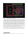
Figure 4-6: Board layout of the NFC shield (displayed by Eagle) ...................................... 26
Figure 4-7: The connection between the Arduino board and the NFC shield with the
oscilloscope connected to examine the signals ................................................. 27
Figure 4-8: Get Firmware Version command on the Arduino board with response ........... 27
Figure 4-9: The final connection with the oscilloscope connected to examine the
signals ............................................................................................................... 28
Figure 4-10: Read SPI Status sent from the MSP430 to the NFC shield with a response .... 28
Figure 4-11: Tag with UID e29847cd is read and access is granted followed by response
from the board................................................................................................... 31
vii
List of Tables
Table 1:
Table 2:
Table 3:
Table 4:
SPI signals ........................................................................................................ 14
The four different clock modes......................................................................... 17
PN532 SPI settings ........................................................................................... 23
The power consumption of the different parts of the system ........................... 31
ix
List of acronyms and abbreviations
BSL
DCO
DHCP
FET
GSM
GPS
ISO
JTAG
KB
MCU
MSP
NDEF
NFC
PCB
PD
PoE
PSE
RFID
SBW
SPE
SPI
TCP
TFTP
UDP
UID
UICC
UMTS
USART
USB
Wi-Fi
Bootstrap Loader
Digitally-Controlled Oscillator
Dynamic Host Configuration Protocol
Flash Emulation Tool
Global System for Mobile
Global Positioning Systems
International Organization for Standards
Joint Test Action Group
Kilo Byte
Micro Controller Unit
Mixed-Signal Processor
NFC Data Exchange Format
Near Field Communication
Printed Circuit Board
Power Device
Power over Ethernet
Power Sourcing Equipment
Radio Frequency Identification
Spy-Bi-Wire
Source Power Equipment
Serial Peripheral Interface
Transmission Control Protocol
Trivial File Transfer Protocol
User Datagram Protocol
Unique Identifier Number
Universal Integrated Circuit Card
Universal Mobile Telecommunications System
Universal Synchronous/Asynchronous Receiver/Transmitter
Universal Serial Bus
Wireless Fidelity
xi
1 Introduction
In this chapter we will give a short overview and explanation of this thesis project.
1.1 General introduction to the area
In the last several years, smartphones have become more powerful and have been designed to be
used as pocket-sized personal computers. As different designers and smartphone manufacturer try to
“win” market share they are constantly adding new features and improving the performance of their
different models of smartphones. This has enabled other companies to develop new tools and services
which utilizes smartphones. Today, Near Field Communication (NFC) is provided in many
smartphones. This has enabled applications to verify the user’s location * and in some cases their
identity by using a smartphone. This technique in combination with others can be used in various
applications and services.
Computer communication systems and the Internet are playing an important role in our everyday
environment. Today almost any device (workstation, television, lamp, etc.) can be connected to the
Internet. Increasingly smartphones are constantly connected to the Internet over third and fourth
generation networks. This network connectivity will play an important part in our project.
As technology develops, the demands for new products and services to make our life more
efficient also grow. Consider the simple use case of lending your apartment key to a friend while you
are out of town. This could be made easier by use of NFC and smartphones in combination with the
Internet communication, as you can simply issue you friend a digital certificate which he or she can
present to your door via their smartphone’s NFC interface. To realize this use case we will use a
combination of technologies to prototype a Smart Door lock.
1.2 Problem definition
To develop our smart door lock there are some sub-problems we need to solve. First we need to
study two basic technologies: NFC technology (as used in smartphones) and a network attached door
lock. We will combine these technologies to develop our smart door lock. Based upon our study of
NFC we must create an application that can run on a smartphone† to respond to the NFC reader when
it is queried. We need a corresponding application running in either the network attached door lock or
in the cloud to query the smartphone via NFC. Given the NFC communication between the reader and
the smartphone an application running in either the network attached door lock or in the cloud will
determine whether the door should be unlocked or not.
While we have some basic experience with microcontrollers and some knowledge of computer
communication systems, we did not yet have any knowledge of NFC technology. Combining these
different technologies in one project should take our knowledge to the next level. Our first step in
doing this is to connect a microcontroller to the Internet, and then connect a NFC reader to this
microcontroller. Note that one of the other areas that we want to explore is the use of Power over
Ethernet (PoE) technology, so that we do not need a separate connection from our microcontroller to
the building’s power mains.
1.3 Goal
The main goal of this project is to develop a smart door lock system where an administrator or
owner of an apartment or building can manage and send “digital keys” to other persons in order to
allow them to access an apartment, building, or specific room in a building by using their NFC
equipped smartphone or a NFC smartcard.
*
See for example the use case of a security guard in the recent thesis by Thi Van Anh Pham, Security of NFC
applications [1]
†
In order to achieve to this during our time of the project, the smartphones required to run in Card Emulation
mode, something that we didn’t have the possibility to use, but was later introduced in Android KitKat 4.4
1
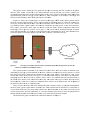
The project can be divided into two partts: the first part
p concerning the NFC module in the
t phone
and the NFC readeer connected
d to the miicrocontroller and the second
s
part which conccerns the
communnication betw
ween the micrrocontroller aand a cloud service. We have adoptedd a cloud dep
ployment
approachh based upoon the energy
y savings shhown by Go
oce Talagano
ov in his maaster’s thesiss [2] and
because of the flexibbility that a clloud based seervice will offer.
o
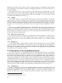
ws the overalll system. As shown in th
his figure a NCF
N reader w
will be placeed outside
Figuure 1-1 show
the doorr and the miicrocontroller will be plaaced inside the building
g where it caannot be mo
odified or
access bby someone outside
o
the door.
d
The m
microcontrolleer will be co
onnected to a server viaa a Power
over Ethhernet (PoE) capable swiitch. This neetwork conneection provid
des power too the microcontroller,
NFC reaader, and electric strike plate (or m
motor to turn
n the latch).. Further infformation ab
bout PoE
technoloogy will be given
g
in section 2.5 on page 7. Thee system willl be manageed through a website
where thhe administraator of a lock
k can create eelectronic keeys and manaage the lock.. Note that th
hese keys
can be designed to work
w
only durring a specifi
fic time or ev
ven be a one-time-only keey.
Figure 1-1:
An ove
erview on how the
t smart doorr locks system works
w
(Note th
hat the figure ddoes not show the
t
connection to the
e electric strike
e plate or latch .)
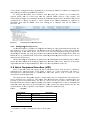
The system musst be connectted to the acctual lock on
n the door; th
his can be doone in differrent ways
dependinng on the typpe of lock in
nstalled on thhe door. Thee most comm
mon lock useed in houses is a dead
bolt; theese locks usee a metal bolt that slidess into the do
oor jamb which is controolled by a keey on the
outside aand a latch on
o the inside (see Figure 1-2). For theese kinds of locks,
l
were tthere is no ellectronics
managinng the lock, hence
h
we hav
ve to install a motor, serrvo, or a soleenoid that caan switch thee latch on
the insidde of the dooor to lock or unlock
u
the ddoor, this willl require som
me type of seensor that caan tell the
microconntroller if thhe door is loccked or unloocked, these sensors can be buttons tthat will be pushed
p
if
the latchh is in the loccked- or unlo
ocked-mode.
Therre are also ellectronic doo
or locks thatt already hav
ve a build in motor or sollenoid which
h unlocks
the door when it getss a signal fro
om a controlller unit. Thiss controller can
c be attachhed to a card reader or
a key paad for PIN-codes. For these kinds off locks the microcontroll
m
ler of the sm
mart door locck system
can be cconnected to the lock meechanism as a second controller unit. However hhow the physsical lock
should aactually functtion and whaat kind of loccks to use is not
n the focuss of this projeect.
a
aree listed at thee start of Chaapter 3.
The detailed sub goals to be achieved
2
Figure 1-2:
A latch to mechanicallly control the ddoor lock on a door
1.4 S
Structure
e of the thesis
Thiss thesis is divvided into fiv
ve chapters. Chapter 1 giives an overv
view of whaat the projectt is about.
Chapter 2 will givee the readerr basic backkground matterial so that the readerr can undersstand the
conceptss that will bee subsequenttly used in thhis project. This
T chapter will also sum
ummarize som
me of the
related w
work relevannt to this projject. Chapterr 3 covers th
he methods used
u
in the pproject to ach
hieve our
goals whhich containss a range of both softwaare and hardw
ware tools. Described
D
inn chapter 4 iss how we
tested ouur prototype to see if it fu
ulfilled our ppurposes with
h the projectt. Since we ddid not accom
mplish all
of our gooals, chapterr 5 reviews our
o conclusioon and descrribes what we
w have left uundone in ad
ddition to
suggestinng what could be done in
n future worrk to build up
pon this project. The finaal chapter also covers
what we would have done differeently in the pproject if we were to do itt again.
3
2 Background
In this chapter we will briefly describe the embedded platform that we will use and we will
introduce some of the concepts that are useful to understand the rest of this thesis. This chapter will
also describe some of the related work that is relevant to this thesis project.
2.1 What have others already done?
Some previous research has been done that is related to our project. We will summarize these
related projects in this section. This is particularly the case for our basic platform, as we will re-use the
microcontroller and PoE network circuit board developed by earlier master’s thesis students at this
department. Following this we will introduce some of the related work done regarding door locks,
access control, and cloud based services.
2.1.1 Exploiting Wireless Sensors
The master’s thesis[3] by Albert López and Francisco Javier Sánchez concerned sniffing wireless
sensor traffic in order to collect this sensor data and use it for multiple purposes. They worked with
sensors in the 868 MHz band. They designed and created a motherboard with a TI MSP430
microcontroller as the core of their gateway. Since the MSP430 is a very low power consumption chip
it was ideal for use with PoE. They utilized a Microchip ENC28J60 network interface. This network
interface was connected to the microcontroller via a serial peripheral interface (SPI). The ENC28J60
Microchip offers dual port random access memory for sending and receiving data packets, as this
network interface provides the buffering needed for packets being sent and received, there was no need
for external memory. In order to supply power to this board they used PoE technology. In their project
they also used an SPI interface to connect a daughterboard with a radio transceiver for the 760 to
928 MHz band.
2.1.2 White space sensor platform
Javier Lara Peinado in his thesis project [4] took the sensor platform developed by López and
Sánchez and added a new boot program to provide network based booting, configuration of the device
via the dynamic host configuration protocol (DHCP), and installation of application software via the
trivial file transfer protocol (TFTP)*. Using this new software base he implemented a white space
sensor platform that sent its measurement results to a central server via UDP. White spaces can be
shortly described as licensed frequencies that are not used all the time.
2.1.3 Fixing the PoE and building a white space sensor grid
Julia Alba Tormo Peiró in her thesis project [5], extended the work of Peinado and corrected the
problem with respect to limited power of the PoE circuit of the board developed by López and
Sánchez. We will make use of this modification to the board and the additional boards which she made
in our experiments.
2.1.4 Lockitron and other commercial lock company efforts
The company Lockitron has developed a similar smartlock that is placed over your current interior
latch for a deadbolt lock. The Lockitron product does not use the PoE technology, but rather it uses a
battery for its power. Also the Lockitron product uses Wi-Fi for its network communication and can
only work with specific deadbolt locks, which makes it less universal.
Assa Abloy has also created a smartlock solution for door locks. Assa Abloy’s Seos product uses
NFC for locking and unlocking doors [6]. Yale locks has also developed an NFC lock system, it uses
the mobile lock platform that Assa Abloy developed [7].
*
See section 2.3.
5
Vingcard Elsafe is another company that is marketing an NFC-compatible lock. At this time the
product is primarily for hotel rooms. Because of its product design, this product seems invisible to the
user [8].
Telcred has implemented a service that allows access to facilities with the help of digital tickets.
By using these digital keys in conjunction with NFC technology they have realized a highly flexible
solution for visitors to the EIT ICT Labs Centre in Stockholm [9]. (One floor below where we are
carrying out our project.) After we finished the laboratory work for out project, Telcred installed three
of their lock systems in doors near the laboratory where we did our project.
2.2 NFC
NFC is a contactless communication technology. Today NFC is used in higher end smartphones
and tablets[10, 11]. NFC uses radio-frequency identification (RFID) techniques to communicate with
another NFC device. The two devices should not be more than 10 cm from each other (a theoretical
limit) and their separation should be less than 4 cm for stable communication[12]. The most common
uses of NFC today are for identification and tickets. Mobile payments using NFC[13, 14] is another
popular topic because of its speed and security. Given that Visa (the world leader in electronic
payment) has now teamed up with Samsung (the company which sold the most phones 2013) to enable
smartphones with NFC to be used as a credit or debit card [15], it seems that the future of NFC is
bright.
2.2.1 Using an NFC reader
NFC operates at 13.56 MHz and it uses RFID technology for its communication. There are mainly
two sorts of NFC devices: a passive NFC device and an active device that is always connected to a
power source. The passive device has no internal power source; therefore it dependents on the
electromagnetic field produced by the NFC reader. The active device generates an electromagnetic
field that powers the passive device it wants to communicate with.
Two active NFC devices can exchange data with each other using peer-to-peer mode. Peer-to-peer
mode is standardized in International Organization for Standardization (ISO) 18092 [1]. An NFC
reader can also function in Card Emulation mode.
2.2.2 Security of NFC applications
Every NFC-enabled application requires appropriate security. The type of security is related to
what kind of function the application provides. For example, a service that performs a monetary
transaction must be highly secure (at least proportionately to the maximum value of transaction or
transactions that can be performed).
In contrast, simple services such as receiving (with the help of using your NFC smartphone)
discount “coupons” as you enter a shop entrance would require very little or almost no security at all.
The case of an NFC-enabled restaurant menu is explained in detail in the recent master’s thesis of Thi
Van Anh Pham [1].
2.2.3 Secure elements
A secure element (SE) is a platform were an application can be installed, managed, personalized,
and executed securely. An SE is a combination of hardware, software interfaces, and protocols that
allows secure storage and usage of credentials for payments, authentication, and other services[16].
SEs can be categorized into three types:
•
•
*
6
An embedded SE is a non-removable SEs that can manage business- and personal
information in a safe way. Embedded SEs is installed in the unit at manufacturing.
A smartcard for mobile phone terminals in GSM- and UMTS-band (UICC*) is a genetic,
standardized, physical, and logical platform for smart card applications. A UICC is used by
Universal Integrated Circuit Card
•
telephone companies to include a USIM (3G SIM card) application on the card to verify a user
for a 3G network.
A micro SD-card (µSD-card) is a memory card with an embedded chip that is used as a SE.
There are some SD-cards with embedded NFC antennas.
The form of SE used by cellular operators or payment services in conjunction with a NFC enabled
phone is decided by the companies that are involved [17]. Companies have selected each of the three
types of SEs described above in order to achieve their specific goals.
2.2.4 Security and Privacy of NFC applications
As mentioned earlier, the security of NFC applications is very dependent upon what kind of
service the application provides. As a result there are different approaches to privacy in NFC
applications. Privacy in NFC applications is almost entirely reliant on the design of the application.
For example consider the matter of default settings; for privacy reasons the NFC communication
capability should be inactive when a user’s smartphone is locked or inactive. However, this is not
always the default setting for every smartphone. Additionally every NFC application should inform a
user about what action it is going to take when it is being used. For example, when an application is
going to open a web browser or when the application will send a text message. An advantage of NFC
from the point of view of transaction privacy is that NFC is independent of Global Positioning System
(GPS) activation in the phone and can even be independent of the cellular network. These features
provide the user with greater anonymity and increase the user’s privacy.
2.3 TFTP
The Trivial File Transfer Protocol (TFTP) is a very simple protocol used to transfer files between
network devices. TFTP was developed in the late 1970s, but stabilized in the 1980s[18]. TFTP is
commonly used to transfer configuration and boot files to hardware that lack persistent memory or
disk space, thus a device need not have a disk or stable storage for more than a network boot loader.
As a result TFTP is widely used for upgrading or restoring firmware in routers.
TFTP uses the UDP protocol for its transfers. Typically it uses UDP port 69, but it is also possible
to configure a TFTP server so it uses another UDP port number.
Since the board that we will be using supports TFTP, we have adopted this as a means for booting
up the device, installing its software, and configuring the hardware. This means that we can easily
install new software, without needing to use an EEPROM programmer or other similar device.
However, it does mean that we need to implement a Dynamic Host Configuration Protocol (DHCP)
server and a TFTP server for our experiments.
2.4 Dynamic Host Configuration Protocol server
We will use a DHCP server to supply an IP address to each of the network attached
microcontroller circuit boards based upon a MAC address that we have configured into the network
boot loader. The DHCP server will also provide the board with the IP address of the TFTP server and
the name of the file that this board is to load via TFTP. The DHCP configuration file that we have
used is shown in Appendix A.
2.5 PoE
Power over Ethernet (PoE) enables Ethernet cables to transfer both data and electrical power to
devices. PoE can theoretically deliver up to a maximum of 15W of DC power. In practice the
maximum available power is about 12.95W because of the losses in the cables. PoE was standardized
in the IEEE 802.3af standard [19].
2.5.1 Advantages of PoE
USB does not always provide sufficient power required for some types of hardware to function.
Additionally, in a smart door lock scenario the likely distances will be greater than those supported by
USB. USB can provide 5W of power over a cable with a maximum length of 5m, while PoE devices
7
using CAT5 cable and provide 12.95W of power to devices 100m away[20], CAT5e cables can
provide 30W of power.
2.5.2 Disadvantages of PoE
The main disadvantage of implementing the PoE interface is that not all network switches supports
the PoE interface, those switches that supports the PoE is usually more expensive. If there is no switch
that implements the PoE interface available, there is PoE injectors to buy to add power to the PoE
interface.
Also because the network cable is providing power there might be a concern of the cables heating
up, however, this is not an issue because the power limitation at 30W for CAT5e cables is well under
the safety margin from the cable bundle heating up as the CAT5e cables have a lower resistance drop
[21].
2.5.3 Alternatives to PoE
Power might be provided to the device via an alternate means, such as a separate cable from an
AC to DC power converter. However, in this case there is a need to run a separate power cable to the
device (in addition to the cable used for communication) and there is the need to locate the AC to DC
power converter at an electrical outlet. Using an AC to DC converter connected to mains power likely
increases the cost, as an outlet may needs to be installed near the door or there is the cost of additional
cabling.
Another alternative power source for the device is a battery or supercapacitor. This alternative
avoids the need to externally power the device at the cost of adding a battery or supercapacitor.
Additionally, this complicates the system as there now needs to be some means to replace or recharge
this power source. There may also be a problem about whether the lock should open when it runs out
of power or whether it should remain locked. The later alternative may introduce the need for another
means of opening the lock if there is no power, while the former may eliminate the security that was
offered by the lock.
8
3 Method
In this chapter we will explain our goals and what we have to do to reach our goals. There are
many steps and new things we have to learn before building the Smart door lock system.
In order to realize the Smart Door Lock is a system we need to achieve these goals:
•
•
•
•
•
•
•
•
Connect the microprocessor circuit board to a network,
Make the microprocessor download its application at boot time,
Connect a NFC reader to this microprocessor,
Create an application for a smartphone that can send messages to the NFC reader,
Create custom UDP packets to be sent and received by this microprocessor,
Connect sensors to this microprocessor,
Connect and control a servo motor connected to this microprocessor, and
Set up a web server and a homepage to control this microprocessor.
All of these sub goals have to be achieved and the different elements of the system have to work
together properly. For example: the NFC reader should send data to the microprocessor which the
microprocessor will forward as data inside a UDP datagram to our webserver. We will also have to do
the same encapsulation of data from the sensors and in order to receive commands from the web server
we will decapsulate the commands received within a UDP datagram to lock or unlock the door.
3.1 Software
In this section we will explain the software we have used to develop the Smart door lock.
3.1.1
Wireshark
Wireshark* is very popular computer program that analyzes network traffic. Since our project is
partly based on sending and receiving data exchange from both the motherboard and the DHCP/TFTP
server, Wireshark was a very useful tool for troubleshooting and analyzing if the packets contained
what we expected and were send/received when we expected. We used Wireshark to verify if there
was DHCP and TFTP activity. This was very useful when we started to send our custom made UDP
packets.
3.1.2 Code Composer Studio
We have used Texas Instruments’ Code Composer Studio™ (CCStudio) [22] as our integrated
development environment when writing code for the microprocessor.
3.2 Hardware
In this section we will describe the hardware tools that we used to develop the Smart door lock.
3.2.1 Mixed signal Oscilloscope
To develop and verify the signals transmitted and received from/to the microcontroller we need to
actually see the signals, to do this we used an oscilloscope. The oscilloscope that we used is a HP
54645D, now known as Agilent 54645D [23], which is a mixed signal oscilloscope with two analog
inputs and 16 digital channels for mixed signal analysis.
This oscilloscope supports triggering which allowed us to easily find the signals that we want to
see by selecting one signal to trigger on when this signal entered the state that we wanted to
investigate.
3.2.2 Programmer
The programmer that we used to flash our code to the MSP430 microcontroller is the MSPFET430UIF from Texas Instruments (TI) [24]. The programmer is officially referred to as a Flash
*
www.wireshark.org
9
Emulation Tool (FET); this tool can be used for writing the program to the MSP430 microcontroller
and controlling the microcontroller manually for debugging a program, it can even provide power to
the microcontroller.
The standard FET device from TI connects via the USB interface, although there are older
versions that connect via the serial-port interface. This FET can program the processor using either the
Joint test action group (JTAG) or Spy-Bi-Wire (SBW) protocol through a 14 (2x7) pin connection that
is available on the motherboard (section 3.3.1).
3.2.3 Arduino
The Arduino board is a microcontroller board with open open-source hardware. The specific
Arduino board we used was an Arduino Uno R3 [25] based on the ATmega328 [26] microcontroller.
The board also has 14 digital input/output pins which can be used for different functions. The board
contains a USB connection where can also be used to power the board when connected to a computer.
Of course one can also power the board other ways, as so long as the power supplied is not over
5 volts.
There are many different daughter boards (so called shields) that can be easily attached to the
Arduino board through I2C and SPI communication. We used one such shield equipped with an NFC
interface (this shield is decribed in section 3.3.2). The main reason why we used the Arduino Uno R3
board is because we wanted to investigate the necessary connections beyond the SPI interface between
the NFC shield and the Arduino board.
3.2.4 HP ProCurve Switch 2626
For testing our system we connected our motherboard’s network interface to an HP ProCurve
Switch 2626 [27] switch. This is a PoE capable switch; hence it could power the system. We also
connected this switch to a Dell model Optiplex GX620 [28] computer via a secondary Ethernet
interface.
3.2.5 Desktop PC
A Dell model Optiplex GX620 desktop computer running openSUSE [29] acted as the DHCP
server (see section 3.4.1) and TFTP server (see section 3.4.2 ). This computer also ran Wireshark –
which was used to capture and observe the traffic to and from the system that we were developing.
This computer could also be used to provide the services that in a real deployment of the system would
be provided by a server running in a cloud.
3.3 Description of the embedded platform
In this part of the thesis we will briefly describe the embedded platform that was developed by
previous master students (as described in sections 2.1.1 to 0) to function as a wireless sensor sniffer.
For further details about the platform we refer the reader to the individual master’s thesis indicated in
these sections. The platform can be separated into a main motherboard with a SPI * interface for
connecting a daughterboard. The SPI interface on the motherboard provides the adaptability to connect
a daughterboard of the user’s choice without having to modify any other part of the circuit board. In
the case of the former master’s thesis projects the SPI was used to connect a daughterboard with a
radio module operating in the hundreds of MHz frequency range, but in our project we are going to
utilize a NFC daughterboard which works in the 13.56 MHz frequency band. We believed that it
would be relatively simple to change to the daughterboard which will be described in section 3.3.2.
3.3.1 Motherboard
Figure 3-1 and Figure 3-2 shows the motherboard that is responsible for providing power and
performing the computing required of our embedded platform. The board is designed around a Texas
Instruments MSP430F5437A [30] microcontroller (MCU). This processor (shown in Figure 3-2)
includes two SPIs: one is used to connect the Ethernet controller and the other connects to a
*
Serial Peripheral Interface, see section 3.5
10
daughterboard of the user’s choice. The Ethernet controller is an ENC28J60 [31] chip which
communicates with the MCU via the SPI.
The MCU supports two programming interfaces either Bootstrap Loader (BSL) or Joint Test
Action Group (JTAG). Our board only included with the JTAG interface and therefore this is the
interface we used to install the boot loader code.
With the help of the jumpers (shown in Figure 3-1) a user can choose between getting power from
PoE or an external DC power supply. The TL2575HV (shown in Figure 3-2) is a step-down converter
[32] which makes it possible to use any DC voltage supply between 3.3V and 60V. In our project we
will only utilize PoE (as described in section 2.5). The Ethernet cable from the motherboard needs to
be connected to the power sourcing equipment (PSE). This PSE function is generally provided by a
switch or router with PoE functionality. The TPS2375 [33] chip takes care of the PoE signaling to tell
the host (PSE) the amount of power that it requires. Our board is designed to be a class 1 Powered
Device (PD); hence its maximum power is 3.84W. Based upon our initial estimates of the amount of
power that we will require, 3.84W is more than enough power.
11
Figure 3-1:
The fro
ont side of the motherboard
m
Figure 3-2:
The back side of the motherboard
m
3.3.2 D
Daughterbo
oard (NFC Shield
S
v1.0))
For our daughterrboard we seelected an N
NFC shield version
v
1.0 frrom Seeedstuudio [34]. Th
his board
(shown iin Figure 3-33) is an NFC
C transceiverr that contain
ns all the neccessary harddware compo
onents for
communnication withh any motherb
board that suupports SPI.
12
The shield is built around th
he popular annd widely ussed NXP PN
N532 chip. Th
The PN532 provides a
completee module forr contactlesss communicaation in the 13.56 MHz band.
b
The N
NFC shield also
a has a
built in P
Printed Circuit Board (P
PCB) antenn a and suppo
orts both 3.3V
V and 5V poower supply
y with the
help of a Texas Instrruments TXB
B0104 [35] leevel translato
or. This NFC
C shield was created as a breakout
board (i..e., shield) too connect to Arduino mootherboards. However,
H
beecause of its low price, itt use of a
widely uused NFC chhip, on-board
d antenna, annd the possib
bility to link it to our mootherboard viia SPI we
selected this board foor our projecct.
(a)
(b)
Figure 3-3: The front side
e (a) and the ba
ackside (b) of t he NFC shield
3.4 C
Connectiing the platform
m to the
e networ
rk
In thhis section we
w explain ho
ow we configgured the DH
HCP and the TFTP serverr. As the system must
be conneected to a neetwork in ord
der to be ablee to identify and manage keys, hencee the motherb
board has
to be connnected to a network. To
o provide thee motherboaard’s network
k interface w
with an IP ad
ddress we
configurred a DHCP server to prrovide an IP -address to the
t motherbo
oard based uupon a MAC
C address
that we pprogrammedd into the nettwork boot looader. As deescribed in seection 2.1.1 tthe actual ap
pplication
to be exxecuted will be transferrred at boot ttime from a TFTP serveer. Thereforee, we also needed
n
to
configurre a TFTP server on thee network. T
To ensure th
hat the moth
herboard corrrectly asks for
f an IP
address and an appplication to run
r we usedd the TFTP
Pboot * prograam, that Javvier Lara Peeinado, a
previouss master studdent, wrote. We loaded hhis code into
o the motherrboard usingg a MSP-FET430UIF
JTAG (ssection 3.2.2)) programmeer connected to one of ou
ur laptop com
mputers.
3.4.1 C
Configuring
g the DHCP
P server
Therre are manyy different ways
w
to realiize a DHCP
P server. Forr example, m
many routerrs have a
built-in DHCP serveer. Alternatiively, DHCP
P server sofftware can be
b installed and configu
ured on a
computeer that is alreeady connectted to the nettwork to hav
ve it act as a DHCP serveer for the network. In
order to keep the cossts of the pro
oduct as low as possible we
w have assu
umed that thee site where the smart
door locck system wiill be installeed will alreaady have onee or more co
omputers atttached to a local
l
area
network,, hence we chhose to utilizze one of theese computerrs to act as a DHCP serveer.
For oour project we
w used a deesktop compuuter running openSUSE [29] to run th
the ISC DHC
CP Server
[36]. Thee configuratiion of the DH
HCP server ccan be madee by editing a configuratiion file for th
he DHCP
*
https://ggithub.com/cazzulu/mind-thee-gaps/tree/maaster/TFTPboot
13
server (ssee the confiiguration filee in Appendiix A) or by using
u
the YaaST [37] whiich is a conffiguration
and instaalling tool foor the openSU
USE [29] sysstem.
To vverify that thhe DHCP server workss we used Wireshark
W
(See section 33.1.1) to mo
onitor the
network traffic; thuus we could verify thhat the expeected DHCP
P discover, offer, requ
uest, and
acknowlledge messagges were excchanged and that the mottherboard recceived the IPP address thaat we had
configurred for it. Figure
F
3-4 shows
s
a scrreen capturee of the DH
HCP handshhake as cap
ptured by
Wiresharrk. Note thhat the DHC
CP server w
was running
g on a com
mputer withh the IP ad
ddress of
192.168..1.100.
Figure 3-44:
A scree
en capture of th
he DHCP proce ss
3.4.2 C
Configuring
g the TFTP server
As m
mentioned beefore a TFTP
P server simpplifies the loaading of a neew applicatioon into the board.
b
For
this purppose we set up a TFTP server.
s
We ddecided to seet up the TF
FTP server oon the same computer
that wass acting as the
t DHCP server.
s
The TFTP server was also configured
c
tthrough YaS
ST in the
openSUS
SE PC deksttop. By usin
ng Wiresharkk on the worrkstation thatt was hostingg both the TFTP
T
and
DHCP seerver, we veerified that th
he TFTP servver worked by
b transferrin
ng files betw
ween two PC``s (one of
which w
was the TFTP
P server).
Wheen connectingg the motherrboard to thee network, th
he motherboaard should innitially makee a DHCP
request aand then dow
wnload the configured
c
aapplication from
fr
the TFT
TP server. H
However in our
o initial
experimeents this did not happen faultlessly.
f
T
This is also laater explaineed in section 4.3.
3.5 S
Serial Pe
eriphera
al Interfface (SP
PI)
SPI is a data linnk which caan operate inn full or hallf duplex mo
ode. This innterface is co
ommonly
implemeented by microprocesso
m
ors. Using eeither a 4-w
wire (or 3-wire) conneection SPI allows a
microproocessor (miccrocontrollerr) to comm
municate witth other dev
vices such as sensors or other
microproocessors thatt support SPII.
The SPI protocool is designed
d to support a single masster device to communiccate with onee or more
slaves cconnected too a serial bus. The maaster (the microprocesso
m
or) initiates communicaation and
providess a clock forr synchronization. The sslave is a device (in our case either a NFC-read
der or the
ENC28JJ60 Ethernet controller) which
w
responnds to the maater’s commu
unication, recceives comm
mands and
sends daata, under thee control of the micropro
rocessor. Tab
ble 1 shows the signals uused by SPI.. We will
use thesee names for these
t
signalss in our descrription*. SPI utilizes 8 bitt bytes [38].
Table 1:
SPI sign
nals
Signal Nam
me
SCLK
MOSI/SIM
MO
MISO/SOM
MI
SS (CE)
*
Description
Serial
S
Clock
Master
M
Outpuut Slave Inpu
ut
Master
M
Input Slave Outpu
ut
Slave
S
Select ((Chip Enablee)
Note thaat there are othher commonly
y used names for these sign
nals.
14
As mentioned above, the master initializes the communication between the devices. Before
initiating this communication the master first configures the serial clock of the selected SPI to a
frequency which is less or equal to the maximum frequency supported by the slave device. For
example, in our case this frequency is either 5 MHz for the NFC-reader or 8 MHz for the ENC28J60
Ethernet controller. The code* to configure the SPI interface used to connect to the Ethernet controller
is shown below:
*
Extracted from the config.c file of the TFTPboot program. Note that the code has been reformatted for
inclusion in this thesis.
15
From hardware_board.c
// ENC28J60
#define ETH_CS
#define ETH_CS_IN
#define ETH_CS_OUT
#define ETH_CS_DIR
#define ETH_CS_REN
BIT0
P3IN
P3OUT
P3DIR
P3REN
#define
#define
#define
#define
#define
#define
#define
#define
ETH_INT
ETH_INT_IN
ETH_INT_DIR
ETH_INT_OUT
ETH_INT_REN
ETH_INT_IES
ETH_INT_IE
ETH_INT_IFG
BIT2
P1IN
P1DIR
P1OUT
P1REN
P1IES
P1IE
P1IFG
#define ETH_RST
#define ETH_RST_OUT
#define ETH_RST_DIR
BIT3
P1OUT
P1DIR
From config.c:
// ENC28J60 SPI port
#define ETH_SIMO
#define ETH_SOMI
#define ETH_SCLK
#define ETH_SPI_IN
#define ETH_SPI_OUT
#define ETH_SPI_DIR
#define ETH_SPI_REN
#define ETH_SPI_SEL
BIT1
BIT2
BIT3
P3IN
P3OUT
P3DIR
P3REN
P3SEL
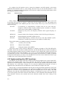
void InitializeEthSpi(void)
{
// Activate reset state
UCB0CTL1 |= UCSWRST;
// Configure ports
ETH_SPI_SEL |= ETH_SCLK + ETH_SIMO + ETH_SOMI;
// Special functions for SPI pins
ETH_SPI_DIR |= ETH_SIMO + ETH_SCLK;
ETH_CS_DIR |= ETH_CS;
ETH_CS_OUT |= ETH_CS;
// Outputs
// Configure SPI registers
UCB0CTL0 |= UCCKPH + UCMSB + UCMST + UCSYNC;
// Clock phase 0, Clock pol 0, 8-bit
// MSB first, Master mode, 3-pin SPI, Synch
UCB0CTL1 |= UCSSEL_2; // SMCLK clock source
UCB0BR0 = 0;
// No Prescaler (8MHz)
UCB0BR1 = 0;
UCA0MCTL = 0;
// Deactivate reset state
UCB0CTL1 &= ~UCSWRST;
}
The master then selects the desired slave by pulling the SS line to the “low” state. The slaves that
have not been activated by the master using its slave select will disregard the serial clock and MOSI
signals from the master. In this manner the master selects only one slave at the time [39].
When the slave wishes to communicate with the microprocessor (master) the slave can use an
interrupt line to indicate that an event has occurred. Otherwise the master needs to poll the slave(s) to
see if it (they) have any input.
16
The SPI interfacee can work in different cclock modes depending on the microccontroller you want to
connect, there are four
f
clock modes.
m
The clock modee depends on
n the configguration of the
t clock
polarity and phase; Figure
F
3-5 sh
hows a timingg diagram off the differen
nt clock modees.
Figure 3-5:
SPI tim
ming diagram, th
he vertical red line represent CPHA = 0 and the
t blue line CPPHA = 1
At C
CPOL = 0 (cclock polarity
y) the base vvalue of the clock
c
is zero
o and at CPO
OL = 1 the base value
of the cllock is one. When CPOL
L = 0 is choosen at CPHA
HA = 0 (clock
k phase) dataa are captureed on the
clock’s rrising edge and
a data are transmitted on the fallin
ng edge, with
h CPHA = 1 data are cap
ptured on
the clockk’s falling edge
e
and datta are transm
mitted on thee clock’s rissing edge. W
When CPOL = 1 and
CPHA = 0 data are captured on clock’s falliing edge and
d data is tran
nsmitted on tthe rising ed
dge, while
with CPH
HA = 1 dataa are captured
d on the clocck’s rising ed
dge and data is transmitteed on the fallling edge
of the cloock.
Thesse settings reesult in a tottal of four cclock modes that can be configured. Table 2 sum
mmarizes
these diffferent modes.
Table 2:
The fou
ur different clock modes
CPOL
CPHA
0
0
0
1
0
1
2
1
0
3
1
1
Mode
17
4 Im
mpleme
entation
n and A nalysis
s
In thhis chapter we
w will explaain the stepss we toke to achieve the goals we seet in chapter 3, which
includedd programminng, reading and
a a lot of debugging. All
A the files used in this project can be found
at the D
Dropbox linkk https://www
w.dropbox.coom/sh/43h51
19564hspkw2/RcXkXGtC
tCqQ . The appendix
gives a sshort descripttion of what the folders ccontain and what
w they weere used to doo.
Thiss chapter beggins with a description
d
iin section 4..1 of how we
w could pingg the motherrboard to
verify neetwork connnectivity and
d in section 4.2 we desccribe how we
w transferreed and receiv
ved UDP
packets. In section 4.3
4 we descriibe the idea oof network booting.
b
The SPI configuurations are described
d
in sectioon 4.4 and the
t debuggin
ng of the coonnection bettween the board and shhield are desscribed in
section 44.6. The NFC
C tags, the android
a
appliication and th
he python seerver are desscribed in secction 4.5.
The whoole system working
w
tog
gether with a Python UDP
U
server is
i described in 4.8. Thee chapter
concludees with a desscription of th
he complete smart door lock
l
system.
4.1 V
Verifying
g the ne
etwork c
connectiion
As w
we use UDP
P packets to send data too and from the
t motherbo
oard of our ssystem we wanted
w
to
ensure thhat our systeem was com
mmunicating correctly with our DHC
CP server. Inn order to do
o this we
used Wirreshark to viiew the traffiic between thhe DHCP serrver and our board. Afterr establishing that the
board haad requested and received
d an IP addreess we used the program
m ping on thee PC to send an ICMP
echo reqquest messagge to our bo
oard just to see if it wo
ould respond correctly. T
This verified
d that the
network interface off the board had no probblems receiv
ving and sen
nding ICMP packets and
d that the
network stack was ruunning on thee microproceessor.
P Echo requeest from the computer (that was alsoo acting as ou
ur DHCP
Figuure 4-1 displaays an ICMP
Server) with the IP address of 192.168.1.1 and a respo
onse from our
o board wiith the IP ad
ddress of
192.168..1.7.
Figure 4-1:
Wiresh
hark capture of the ICMP requuest and the respond back.
19
4.2 UDP Echo software
In order to ensure that we could send and receive UDP packets containing our own data, we
decided to start by implemented a simple program to echo a string that we sent to the board from the
PC. Since our board used the ENC28J60 for its network communication we had to learn the steps that
are necessary for sending UDP Packets, so by looking into frequency scanner project file in the master
project of Javier Lara Peinado [4] and also reading into the UDP.c file provided by Microchip we
finally managed to understand the steps required for our goal. These steps are described below.
In order to send a UDP packet we must:
1. Call the “ARPResolve” routine to obtain the MAC of the IP destination we wish to
send the UDP datagram to.
2. Call UDPOpen to open a socket to be used to send our UDP Packets.
3. Call UDPisPutReady (sets the current socket as the active socket, and determines how
many bytes can be written to this UDP socket). This step is important because the
ENC28J60 provides the buffering for the IP packet (or packets), hence the processor
does not have to buffer the complete datagram – thus reducing the amount of RAM
memory that the program needs.
4. Call UDPPut (or UDPPutArray) for building and storing the data into the packet
within the ENC28J60.
5. Call UDPFlush to send our packet to the desired destination.
6. Call UDPClose to close the socket (this is not mandatory)
When the Ethernet controller receives UDP packets, then we need to use the following two
functions:
1. Call UDPisGetReady (sets the current socket as the active one, and determines how
many bytes can be read from the UDP socket) and
2. Call UDPGet (reads a byte from the currently active socket).
For this testing we used a shell window on the PC that was hosting the DHCP server. We invoked
our test program with the destination IP address and the port of the board to send our text message and
received the expected response back from the board. The result of test is shown in Figure 4-2, where
we sent the string “TEST” and received this response echoed back from our board. We could have
chosen to use the Transmission control protocol (TCP) for our data packets, but since we also wanted
the TFTP in our project and it already used the UDP for its file transfers, we thought it would be better
to stay with the UDP protocol, also the UDP protocol has faster file transfer speed and if case of a
packet drop then one would have to just resend the packet.
20
Figure 4-2:
The dark blue line sho
ows the messagge TEST being echoed
e
back from our board.
4.3 N
Network
k Booting
g
As m
mentioned inn section 2.3 we knew thhe TCP/IP sttack implem
mented in ourr board supp
ported the
TFTP prrotocol. We wanted to take advanttage of to automatically
a
y transfer ouur code to the
t board
immediaately after the board has received an IP address from
f
a DHCP
P server. Thhe thought off this was
that the board wouldd directly loaad its code tthrough the network,
n
thu
us avoiding tthe need to connect
c
a
program
mmer to the board.
b
In the case of deplloyed system
m this would
d mean that eeach device could get
the latestt version of the
t software when it nextt rebooted orr when comm
manded to.
We set up a TFT
TP server wh
hich include d an examplle file that was
w meant too be sent to our
o board
immediaately after it received
r
an IP address. B
Before we tried to send this
t file to ouur board we first tried
to send tthe file to annother PC co
onnected to th
the same TFT
TP server. The
T other PC
C was running
g Ubuntu
12.04 LT
TS in a Virttual-box [40]]. Figure 4-33 displays th
he Wireshark
k output as Ubuntu requ
uests and
receives the file from
m our TFTP server.
s
21
Figure 4-3:
File Blin
nker.txt is requ
uested from 1992.168.1.100 an
nd successfully received.
Now
w that we knnew that the TFTP and D
DHCP config
guration have had no prooblems, our next step
was to hhave the sysstem (motherrboard) requuest the file from the TF
FTP server tthat it learned in the
DHCP rresponse from
m the DHC
CP server. H
However, herre we ran in
nto a problem
m as the bo
oard only
requestedd a small paart of the file and stored iit in the firstt block of thee memory. A
After this, thee transfer
kept loopping requestting the firstt block becauuse the moth
herboard nev
ver acknowleedges the firrst block,
which m
made the TFTP server reesend the firrst block. Because
B
of th
his our file was not succcessfully
transfer tto our board.
Duee to other priiorities in ourr project we never succeeeded in findiing a solutionn to this prob
blem. For
this reasoon debugginng the TFTP loading
l
of ann application
n remains as future work..
4.4 S
SPI Drive
ers conffiguratio
on
The declarationss that define the pins to bbe used for th
he interface the
t NFC dauughter card are
a shown
below. T
These ports use
u the UCA1
1 register on the MSP430
0.
// RF S
SPI port
#define
e RF SIMO
#define
e RF SOMI
#define
e RF SPI IN
#define
e RF SPI OUT
O
#define
e RF SPI DIR
D
#define
e RF SPI REN
R
#define
e RF SPI SEL
B
BIT6
B
BIT7
P
P5IN
P
P5OUT
P
P5DIR
P
P5REN
P
P5SEL
#define
e RF SCLK
#define
e RF SPI SCLK DIR
#define
e RF SPI SCLK SEL
B
BIT6
P
P3DIR
P
P3SEL
22
To configure the SPI interface used to connect the daughter card (NFC-shield) to the master
(MSP430-microcontroller) there is some settings that need to be set for the SPI interface to work
properly. As mentioned earlier the daughter card is based on a PN532 microchip which needs to have
the settings [41] shown in Table 3.
Table 3:
PN532 SPI settings
The mode used for the clock is Mode 0
Data is always sampled on the first clock edge of SCK
SCK is active High
The data order used is LSB first
These settings are set in the control register of the SPI interface we are using, in our case
UCA1CTL0. We also have to choose a clock source for the signals to be sent. The unified clock
system (UCS) module in the MSP430 provides various clocks. There is up to five clock sources to
choose from [30]:
XT1CLK
Low-frequency or high-frequency oscillator that can be used with low
frequency 32768 Hz watch crystals, standard crystals, resonators, or external
clock sources in the 4 MHz to 32 MHz range.
VLOCLK
Internal very low power, low frequency oscillator with a typical frequency of
10 kHz.
REFOCLK
Internal, trimmed, low-frequency oscillator with 32768 Hz typical frequency.
DCOCLK
Internal digitally-controlled oscillator (DCO)
XT2CLK
Optional high-frequency oscillator that can be used with standard crystals,
resonators or external clock sources in the 4 MHz to 32 MHz range.
Three clock signals are available from the UCS module:
ACLK
Auxiliary clock (32 kHz).
MCLK
Master clock (8 MHz).
SMCLK
Subsystem master clock (8MHz).
These three clocks (ACLK, MCLK, SMCLK) are software selectable as XT1CLK, REFOCLK,
VLOCKL, DCOCLK, and when available, XT2CLK. ACLK and SMCLK are software selectable by
individual peripheral modules and are available externally at a pin, and MCLK is used by the CPU and
system. All these clocks can be divided by 1, 2, 4, 8, 16, or 32 to provide the desired clock frequency.
As mentioned in section 3.4 the maximum SPI clock frequency for the PN532 is 5 MHz, to generate
the desired clock frequency we chose to use the SMCLK as our clock source and divided it by 2 to get
a 4 MHz clock source which the PN532 can utilize.
4.5 Implementing the SPI functions
SeeedStudio, the developer of the NFC-shield, provided some example source code for their NFCShield for the Arduino board. This source code does not include the actual transmit and receive
functions for the SPI interface as these examples were written for the Arduino board which provides
SPI functions via a SPI library. Because we are using the MSP430-microcontroller we had to
implement these SPI functions for the MSP430 in order to make the example code work.
Energia [42] is a prototyping platform with the goal to bring the Arduino framework to the Texas
Instruments MSP430. However, Energia only supports the MSP430 LaunchPad and FraunchPad,
which are not based on the MSP430f5437a (the microcontroller that we are using). The main
difference is the pin map of the boards and the registers, as mentioned in section 4.4 are we using the
UCA1CTL0 register for the SPI connection (NFC-shield), as the LaunchPad and FraunchPad may use
other interfaces. However, the transmit and receive functions should work with a change in the
register.
23
Lookking at the example
e
sou
urce code froom SeeedStu
udio we could determinee which SPI function
was critiical for the example cod
de to work on the MSP
P430. The most
m
critical SSPI function
n that we
needed tto implemennt was the traansmit functiion* (which is basically the
t same as the receive function)
and the sslave select (SS)
(
function
n to select thee SPI slave to
t communiccate with.
The transmit andd receive fu
unctions are tthe same function, as when
w
we wannt to receivee data we
simply trransmit a zerro and then read
r
the respponse. When we transmitt data we sennd data and ignore the
responsee.
We hhad to write the SS function ourselvees because th
he one provided from Ennergia did no
ot suit the
microconntroller we are
a using. Th
his function ssimply chang
ges the SS pin from HIG
GH to LOW when the
slave is tto be selectedd, and the rev
versed whenn unselected.
4.6 C
Connectiing the daughte
d
erboard and debugging
g
We uused SPI to connect the daughterboaard (NFC Sh
hield) to the motherboard
rd. In order to
t do this
we had tto connect thhe connection
ns mentionedd in Table 3-1, as well as provide poower and gro
ound. The
motherbooard broughht the SPI signals,
s
3.3 V power, and ground to
t an easy to access connector.
Similarlyy the NFC shield’s SPI pins,
p
3.3 V ppower input,, and ground
d were brougght to a conv
venient to
access coonnector. Thhis would seeem to have m
made it easy to
t connect th
he two boardds together. Figure
F
4-4
shows thhese connectiions between
n these two bboards.
Figure 4-44:
The SPI, power, and ground
g
connecttion between the boards
The NFC shieldd (daughterbo
oard) had a built in pro
ogram that gets commannd from a SP
PI master
device annd sends bacck a respond
d to that comm
mmand. For example; if th
he master devvice (MSP43
30) sends
the get-ffirmware-verrsion commaand to the N
NFC shield, the shield sh
hould responnd with the firmware
version iit is running. This metho
od was used to verify that the SPI co
onnection wa
was working. We used
the oscillloscope, desscribed in seection 3.2.1,, to see if th
here was any
y response fr
from the NFC shield,
Figure 44-5 shows thee command being sent fr
from the MSP430 (line 2)
2 and no ressponse from the NFC
shield (liine 3). Note that line 1 on
n the displayy shows the clock
c
signal from
f
the SPII master.
*
See appendix
24
Figure 4-5:
Get Firmware Version
n command on the motherboard without an
ny response
As tthe NFC shieeld was desiigned to be used with th
he Arduino board,
b
there was a suspiicion that
there waas another coonnection in addition
a
to thhe SPI signaals, 3.3 V pow
wer, and grouund that neeeded to be
connecteed. To find thhat connectio
on we decideed to attach the NFC shield to an Arrduino board and then
looked aat the SPI siggnals and oth
her signals onn the oscillosscope. Howeever, there w
were approxim
mately 58
connectiions (8 of whhich are grou
unds) betweeen the shield
d and the Ard
duino board. As this seem
med to be
too manyy for us to exxamine to fin
nd which connnection wass missing, wee looked at thhe board layo
out of the
NFC shiield to see exxactly what each of the cconnectors was
w connecteed to. Fortunnately, the deevelopers
of the N
NFC shield (SeeedStudio
(
o) provided a board layo
out of the board in Eaggle* format (sshown in
Figure 4-6) and they provided a schematic
s
forr the board (also
(
in Eaglee format).
*
Easily A
Applicable Graaphical Layou
ut Editor (EAG
GLE) is an eleectronic design automation application to
o make
schematiccs of PCBs.
25
Figure 4-6:
Board layout
l
of the NFC
N shield (dispplayed by Eagle)
In adddition, to thhe SPI conn
nections on tthe right end
d of the boarrd (to whichh we connected when
interfacinng to our motherboard) when the shhield is plugg
ged into to the
t Ardunio board the co
onnectors
across thhe top and thhe bottom off the board aare connected
d. Based upo
on the schem
matic we beliieved that
many off these conneectors were connected
c
to different paarts of the log
gic on this sh
shield. Howeever, after
examininng the boardd layout we could excludde most of the
t connectors on the booard because they did
not actuually connectt to anything
g on the shiield (despitee what the schematics suuggested). Moreover,
M
after exaamining whicch signals were interfaceed to at the SPI,
S power, and
a ground cconnector on
n the right
side of tthe board onne of the con
nnections thhat we did not
n have wass the connecction from th
he power
connectoor on the botttom of the bo
oard. Follow
wing this conn
nection lead us to the TX
XB0104PWR
R voltagelevel traanslator [43] (marketed U6
U on the sschematic) which
w
gets power
p
from ttwo sources, the SPI
interfacee, power, annd ground connector
c
annd from thee Arduino power
p
interfface. Lookin
ng at the
datasheeet for the volltage-level trranslator we learned thatt the voltage--level translaator needs tw
wo power
sources to function. However, with
w only a single poweer source fro
om the SPI iinterface, po
ower, and
ground cconnector thiis effectively
y isolated all of the SPI siignals from the
t PN532 chhip!
Afteer connectingg power to th
he level transslator (using the dark greeen wire show
own in Figuree 4-7) we
sent the get firmwaree version com
mmand* to thhe NFC shieeld from the Arduino boaard to see if there
t
was
any response. Figuree 4-8 shows the
t commandd being sent on line 2 and
d that there a response on
n line 3.
*
The defi
finition of the commands for the PN532 N
NFC shield caan be found in the file gw.h in the projectt folder
26
Figure 4-7:
The con
nnection betwe
een the Arduinno board and th
he NFC shield with
w the oscillos
oscope connected to
nals
exxamine the sign
Figure 4-8:
Get Firmware Version
n command on the Arduino board with response
Now
w that all the connection had been foound and testted with the Arduino boaard we conn
nected the
NFC shield to the MSP430 motherboard and connected th
he oscillosco
ope to examinne the signalls.
w
com
mmunication between the MSP430 annd the NFC shield, the
Figuure 4-9 shows the final, working,
green caable on the top
t of the NFC shield iss the additional power connection foor the level translator
t
(Note thhat this is 3.33V.). The sig
gnals that aree transmitted
d and receiveed are shownn on the screeen of the
oscillosccope in Figurre 4-10.
27
Figure 4-9:
The final connection with
w the oscillooscope connectted to examine
e the signals
Figure 4-10:
Read SPI Status sent from
f
the MSP4430 to the NFC shield with a re
esponse
Linee 1 on the osscilloscope in
i Figure 4-110 is the clo
ock of the MSP430,
M
linee 2 is the maaster-outslave-in (MOSI) connnection, linee 3 is the slaave-out-master-in (MISO
O) connectioon, line 4 is the slave
select (S
SS) line. Linee 2 shows thee read SPI sttatus commaand being sen
nt to the NFC
C shield, the read SPI
commannd consist of the hexadeccimal value oof 2, which can
c be seen on
o line 2 in FFigure 4-10, note that
28
the SPI operates in LSB mode*. The command is sent during the first clock sequence and during the
second clock sequence the NFC shield replies with its status, in this case the value 1 which means that
the SPI device is ready.
4.7 Setting up appropriate triggering of the mixed
oscilloscope
An important element of the debugging describe in the previous section was setting up an
appropriate trigger – so that one could see the SPI commands and responses.
The signals that are shown on the oscilloscope are in real time, this means that the signals are
shown as they are sent and this happens very fast, which makes it hard to inspect the signals. One can
pause the oscilloscope on a signal but this method is not very precise or effective as the screen is
paused at the moment the button is pressed, which means that there might not be any or the right
signals shown on the screen of the oscilloscope. This is why we had to use the trigger function of the
oscilloscope.
To set up the oscilloscope to use the trigger function we have to set up a pattern to trigger on, to do
this we simply pressed the Pattern button on the oscilloscope, this brings up a new menu to set up the
pattern to follow on each line connected to the oscilloscope. We can choose from triggering on a
falling edge of a signal or on a rising edge. The oscilloscope that we used only supports triggering on
one line, which means that we can only select one signal to follow and edge trigger on, however, the
pattern can be configured to include other lines but this only checks if the other lines is in High or Low
mode depending on the pattern we set. For example: if we would like to trigger on the first signal
when we send data we set up the pattern to trigger on the rising edge of the data line, we also know
that the SS line should be in Low state as the slave board is selected, this pattern should freeze the
screen on the oscilloscope at the moment when there is a rising edge of the data line and the SS line is
in Low state. There is a lot of options to set up a pattern, in our case we used the “and” operator to
choose a pattern, however, one can use the “or”, “exclusive or”, etc. to setup a pattern between the
different inputs.
4.8 Android application and NFC Tags
As mentioned in section 2.2 NFC is a contactless communication technology, it allows a data
transfer between two NFC enabled devices. An NFC tag could be realized as a sticker which contains
a small microchip that can store a small amount of data and transfer it to a NFC enabled device. How
much data you can store depends on which type of tag you are using, since different types of tags have
different memory capacities. The tags used in our project are MIFARE Classic tags [44] with a
memory size of 1 Kilobyte (KB). The MIFARE Classic tags are widely used today in public
transportation, electronic toll collection, and in loyalty cards. Our tags are also NFC Data Exchange
Format (NDEF) enable and formatable. This means that one can store messages or homepages and
even different application-defined actions on the tag to be viewed or used from any NFC enabled
device. Since the tags are formatable an application can delete the data stored on the tag and write new
content to be stored by the tag. The tags we used also contain a Unique Identifier Number (UID)
which we used in our project to identify a specific.
In order to read the UID of each NFC tag we used the Android application TagWriter [45] from
the Google play application market. This application was developed by the company NXP
Semiconductors [46], the same company as makes the PN532 NFC chip used on the shield.
We implemented an application in the motherboard. This application simply sends a UID read
requests to the NFC shield. If an NFC tag is located near the antenna of the NFC shield the NFC shield
will get a response from the tag. The application places the tag’s UID into a UDP packet and sends it
to our UDP server (a program running on the PC acts as a UDP server). The UDP server compares this
tag against entries in a list of acceptable NFC tag UIDs associated with this smart door lock system. If
*
See section 4.4
29
the UID of this tag is in the list, then the UDP server sends an UDP packet to the board informing it to
either lock or unlock the lock. For our testing we indicated whether access was granted or denied by
turning on a green (granted) or orange (denied) LED on the board.
4.9 UDP Server
The UDP server program was written in the programming language Python [47] because of the
simplicity of writing the code. The server program also generates console output indicating if the
scanned NFC tag is to granted or denied access followed by an OPEN or CLOSE message being sent
back to application running on the motherboard. For learning how to write a UDP server in Python we
looked into the wiki page of Python for UDP communications [48]. When we had learned and
understood how to create UDP sockets and transfer and receive UDP packets, we created our own very
simple server which received different blocks of the NFC Tag UID. There were a total of 4 blocks
received and each block represents 8bits. Once all the blocks are received from the NFC tag UID and
converted from hexadecimal to decimal values we then utilized this value to lookup if this card should
grant access or not. There are of course some flaws with this method since another Tag’s UID might
have the same value and then we would grant access even those we should not do so. However, this
simple server was sufficient to verify that our UDP server combined with the motherboard reading the
NFC Tag’s UID was working.
The python server program is included in the appendix.
4.10
The Smart Door Lock
Now that everything is working, it was time for to test the whole system. This means that the
board sends a UDP packet to the UDP (Python) server followed by receiving a UDP packet from the
server which tells whether access was granted or denied. Finally the motherboard replies to the UDP
server telling it if the lock has been opened or locked.
Figure 4-11 displays the output of Wireshark and the console output of the UDP server in the case
when access is granted. We can see that a UDP packet was sent from the board to the UDP server
which examines the tag’s UID and the server’s response UDP packet informing the board of its
answer, followed by another UDP packet from the board informing the server if the lock is at that
moment OPEN or CLOSED. In this example the tag will unlock the lock and grant access to the user.
A similar procedure was used with a tag that was not registered with the UDP server resulted in a
decision to deny access. We can see from these exchanges that the basic functionality of the smart
door lock system has been realized.
30
Figure 4-11:
Tag witth UID e29847ccd is read and aaccess is grante
ed followed by response from
m the board.
4.11
Pow
wer cons
sumptio
on
As w
we aimed to develop a cheap
c
system
m, we have to
t consider the
t power coonsumption; the table
below shhows the pow
wer consumeed by the diffferent parts of
o the system
m running in ddifferent modes.
Table 4:
The power consumption of the diffeerent parts of the system
Hardwaare
MSP4300f5437a
Activee
Standby
y
*
~ 0.00
024 W
†
~ 0.000004 W*
Motherbboard
~ 0.96
6W
-
NFC Shiield
~ 0.44
4 W†
~ 0.34 W†
W
Complette system
~ 1.4 W†
W
~ 1.3 W†
W
*This vallue is based onn the informattion provided in the data sheet for the com
mponent, the hhighest valuess are used
in the calculation.
†
This meeasurement is based on the value
v
shown oon the Multim
meter.
31
The system does not operate in the active state all the time. In active mode all the systems’
functions are running, this includes the motherboard and all the components of the NFC Shield, as well
as the electromagnetic field that the antenna produces to power the NFC tag. In standby mode the
system does not send any packets through the Ethernet interface, also there is no NFC tag to provide
with power.
The measurements are made the same way as Julia Alba Tormo Peiró describes in her master’s
thesis in section 3.2.1.1.6 [5].
32
5 Conclusions and Future work
This chapter summarizes our conclusions and suggests some future work that could be built upon
what has been done and could address the parts of the original problem that have not been realized.
The chapter ends with some reflections on the economic, social, and ethical issues considered during
this thesis project.
5.1 Conclusions
To make a system that would achieve the project goal as stated in section 1.3 required that we
achieve eight different sub goals (as stated that in the beginning of chapter 3). While we did not
succeed in realizing some of our goals, we did managed to develop a working NFC reader that can
read the UID of an NFC tag by using a NFC shield connected to a MSP430537a microcontroller via a
SPI interface. We also managed to send UDP packets containing the NFC tag’s UID to our UDP
server that based upon the UID either granted or denied access to the user. Although the result of the
access decision was indicated via a green or orange LED on the board, this could easily be turned into
a signal to control a relay to activate an electric strike plate for a period of time or to active an
alternative means of unlock/locking the door’s lock.
Because the project spans of a wide range of disciplines involving both hardware and software,
there were a lot of tools for us to learn and use. Programming a microcontroller and learning how to
connect two different SPI devices included some debugging which led us to learn how to use a mixed
signal oscilloscope. Also, we learned how to create, send, and receive UDP packets with the
microcontroller. In addition to using the microcontroller we learned how to send and receive UDP
packets using Python programming to realize our UDP server.
For monitoring the network traffic we used the software Wireshark. We learned how to make use
of this software both for examining the protocols and packets that were being exchanged. Additionally,
we learned that we could generate UDP messages within the application running on the
microcontroller to display debugging information via Wireshark.
If we were to do the project again one of the things we would do differently is to read more about
what is required of the components to function together before starting our coding. We would also not
take for granted that things will work correctly right away. Furthermore, we will be more aware that
there might be information missing in the documentation of the product, such as we experienced with
the need for the second power source for the TXB0104PWR chip on the NFC shield. We think that
reading the documentation and looking at the schematics of the components would prevent errors such
as this from taking as much time as it did.
Additionally, rather than getting stuck on one problem in the early stage of the project one should
focus on going further with the other goals rather than spending too much time attempting to fix one
specific problem. In the end we managed to get a working system, despite some parts of the project
being modified or eliminated because of the limited time for this project. For the future we learned that
when developing a system we should do a lot more research (specifically reading and studying the
documentation) in order to avoid minor problems causing a lot of frustration and unnecessary time
being spend on them.
The most significant outcome of this project was that we learned how to interface the NFC shield
to any SPI capable microcontroller, rather than requiring that the NFC shield be plugged into an
Arduino. When doing research on this project we found that no one had previously solved this
problem despite many people having encountered problems when trying to make use of NFC shields
with platforms other than the Arduino. We published our solution to this in a posting* to the TI E2E
Community on October 17 2013 at 06:56 AM so that others could build upon our solution.
*
http://e2e.ti.com/support/microcontrollers/msp430/f/166/p/292483/1020503.aspx
33
5.2 Future work
Currently we have a NFC reader that only reads a NFC tag’s UID then sends this information in a
UDP packet to a simple UDP server that makes a decision and responds with an access granted or
denied response. Our NFC reader is currently only reading a tag in MiFare target id mode; the next
step would be to make it work in peer to peer mode so it can communicate with a smartphone with an
NFC interface. Once the NFC reader works in peer to peer mode, then one could develop an Android
application that will use NDEF for transferring a message. On the 31st of October 2013 Google
introduced KitKat 4.4 [49], a version of Android which makes it possible for an Android smartphone
with NFC to emulate a NFC smart card. This was something that we did not have during our project.
This card emulation mode will be very helpful for future communication between the NFC reader and
a smartphone.
Creating a full-fledged server with a database of all the NFC tag UIDs which should be granted
access should be developed together with a webpage to manage the keys, update the database, and
generate one-time or limited use soft tags that could be used by a smart phone – rather than being
limited to making an access or deny decision based simply upon a tag’s UID.
Because of the limited time we did not research how the lock should be installed on the door. The
system needs to have a set of sensors and motors to be able to detect if a door is opened/closed and
locked/unlocked, what type of sensors and motors should be used and how they should be installed is
something that needs to be researched and developed.
An additional area that has not been explored in this thesis project is how to implement
appropriate security for this system. This includes how to realize the appropriate cryptographic
functions in the motherboard and how to realize them at the server. Using these cryptographic
functions is should be possible to secure the boot loader (so that only properly signed code could be
loaded), so that cryptographic tokens could be utilized for access control (rather than using UIDs
which could easily be generated using a NFC equipped smartphone), and developing timed challenge
response security so that one could ensure that the NFC device is actually in front of the NFC reader
and not elsewhere (in order to avoid relaying of NFC communication). Also in the case of NFC tags
there is unused memory in them which could be used to put in some security functions. Since our NFC
reader forwards data to a UDP server there is a need of securing this transportation over the network,
and using a usual Transport Layer Security might be a good idea to look into.
Last but not least it would be great to make the network bootloader work, since it would ease the
process of distributing updates to the software that should be run in the board, while avoiding the need
to physically attach the FET debugger to the board.
5.3 Reflections
The goal with our bachelor’s thesis project was to simplify a way to control access via a locked
door. Since NFC technology is becoming more widespread - as seen in public transportation, loyalty
cards, and smartphones - the choice of using the NFC technology together with the UDP packets
seems a very smart and useful tool for the future. In this sense we consider this bachelor’s thesis
project to have a positive social impact if this solution can be realized and deployed in the future.
The use of the MSP430F5437a ultra low power microcontroller together with NFC shield and
having everything powered via PoE makes the hardware of this project energy efficient, this means
environmental considerations were taken in the choice of the hardware. Moreover, because the board
we used supported PoE all of the power for the system was sent over the Ethernet cable, thus
eliminating the materials and labor costs associated with having to provide mains or another separate
wiring plant to power the system.
As our board utilized the NFC shield designed for an Arduino by interconnecting the shield via an
SPI interface with a MSP430F537a microcontroller with an ENC28J60 for its network
communication, we avoided the need for an Arduino with two shields – one for NFC and for Ethernet
and an external power supply and a nearby mains power outlet, thus there was a lower economic cost
by using this hardware.
34
We have not encountered any ethical issues when carrying out this bachelor’s thesis project other
than the issue of identifying users to be given access to a door based upon the UID of their NFC tag.
This requirement could be removed in a future implementation that used cryptographic tokens. As
noted in the previous section all security considerations have been ignored in this project and remain
for future work.
35
References
[1]
[2]
[3]
[4]
[5]
[6]
[7]
[8]
[9]
[10]
[11]
[12]
[13]
[14]
[15]
[16]
T. V. A. Pham, 'Security of NFC applications', Master’s thesis, Royal Institute of Technology,
School of Information and Communication Technology, Stockholm, Sweden, June 2013,
TRITA-ICT-EX;2013:125, Available at http://kth.divaportal.org/smash/record.jsf?searchId=2&pid=diva2:634369.
G. Talaganov, 'Green VoIP : A SIP Based Approach', Master’s thesis, Royal Institute of
Technology, School of Information and Communication Technology, Stockholm, Sweden,
2012, TRITA-ICT-EX;2012:162. Available at http://kth.divaportal.org/smash/record.jsf?pid=diva2:539142.
A. Lopez Garcia and F. J. Sanchez Galisteo, “Exploiting wireless sensors: A gateway for 868
MHz sensors”, Master’s thesis, Royal Institute of Technology, School of Information and
Communication Technology, Stockholm, Sweden, Jun. 2012, TRITA-ICT-EX; 2012:110.
[Online]. Available: http://urn.kb.se/resolve?urn=urn:nbn:se:kth:diva-98209 [accessed July 1,
2013].
J. Lara Peinado, "Minding the spectrum gaps : First steps toward developing a distributed white
space sensor grid for cognitive radios", Master’s thesis, Royal Institute of Technology, School
of Information and Communication Technology, Stockholm, Sweden, 2013, TRITA-ICTEX;2013:102. [Online]. Available at http://kth.divaportal.org/smash/record.jsf?pid=diva2:627307
T. P. J. Alba, ‘Spectrum sensing based on specialized microcontroller based white space
sensors : Measuring spectrum occupancy using a distributed sensor grid’, Master’s thesis, Royal
Institute of Technology, School of Information and Communication Technology, Stockholm,
Sweden, 2013, TRITA-ICT-EX; 2013:177. [Online]. Available: http://kth.divaportal.org/smash/record.jsf?searchId=1&pid=diva2:636617. [Accessed: 11-November-2013].
‘Lockitron’. [Online]. Available: https://lockitron.com/preorder. [Accessed: 01-July-2013].
‘Yale unveils NFC door locks - NFC World’, NFC World. [Online]. Available:
http://www.nfcworld.com/2011/09/09/39785/yale-unveils-nfc-door-locks/. [Accessed: 04-July2013].
‘Vingcard debuts invisible door lock - NFC World’, NFC World. [Online]. Available:
http://www.nfcworld.com/2012/07/06/316689/vingcard-debuts-invisible-door-lock/. [Accessed:
04-July-2013].
‘European Institute of Innovation and Technology – Innovative NFC access control solution
from Telcred opens the doors to EIT ICT Labs Stockholm Co-location Centre’. [Online].
Available: http://eit.europa.eu/newsroom-and-media/article/innovative-nfc-access-controlsolution-from-telcred-opens-the-doors-to-eit-ict-labs-stockholm-co-loc/. [Accessed: 04-July2013].
‘List of NFC phones’. [Online]. Available: http://www.nfcworld.com/nfc-phones-list/.
[Accessed: 01-July-2013].
‘Tablet • NFC phones and other devices • NFC World’. [Online]. Available:
http://www.nfcworld.com/nfc-data/tablet/. [Accessed: 01-July-2013].
‘npelly_jham_how-to-nfc_FINAL - how_to_nfc.pdf’. Available at
http://static.googleusercontent.com/external_content/untrusted_dlcp/www.google.com/sv//event
s/io/2011/static/presofiles/how_to_nfc.pdf, [accessed July 1, 2013].
‘What is PayPass NFC? | MasterCard®’. [Online]. Available:
http://www.mastercard.com/us/paypass/phonetrial/whatispaypass.html. [Accessed: 01-July2013].
‘Visa payWave for Mobile’. [Online]. Available: https://developer.visa.com/paywavemobile.
[Accessed: 01-July-2013].
‘Visa Teams Up With Samsung on Contactless Mobile Payments - Bloomberg’. [Online].
Available: http://www.bloomberg.com/news/2013-02-25/visa-teams-up-with-samsung-oncontactless-mobile-payments.html. [Accessed: 01-July-2013].
‘Alternatives for Banks to Offer Secure Mobile Payments.doc - MObey Forum 3 - 2010 Alternatives for Banks.pdf’. Available at
37
[17]
[18]
[19]
[20]
[21]
[22]
[23]
[24]
[25]
[26]
[27]
[28]
[29]
[30]
[31]
[32]
[33]
[34]
[35]
[36]
38
https://www.nacha.org/userfiles/File/The_Internet_Council/Resources/MObey%20Forum%203
%20-%202010%20-%20Alternatives%20for%20Banks.pdf, [accessed July 4, 2013].
S. Kabir, "Säkerhetsstandard för ett mjukvarubaserat säkerhetselement." Bachelor’s thesis,
Royal Institute of Technology, School of Information and Communication Technology,
Stockholm, Sweden, 2013, TRITA-ICT-EX; 2013:136. [Online] Available at http://kth.divaportal.org/smash/record.jsf?searchId=1&pid=diva2:631622
‘The TCP/IP Guide - TFTP Overview, History and Standards’. [Online]. Available:
http://www.tcpipguide.com/free/t_TFTPOverviewHistoryandStandards.htm. [Accessed: 01July-2013].
‘IEEE-SA -IEEE Get 802 Program - 802.3: Ethernet’. [Online]. Available:
http://standards.ieee.org/about/get/802/802.3.html. [Accessed: 15-November-2013].
‘What is Power over Ethernet 102909.ppt - introduction_to_poe_ieee802.3af_802.3at.pdf’.
Available at http://www.ieee.li/pdf/viewgraphs/introduction_to_poe_ieee802.3af_802.3at.pdf,
[accessed July 1, 2013].
‘What does the new Power over Ethernet standard mean for IT pros? - TechRepublic’. [Online].
Available: http://www.techrepublic.com/blog/data-center/what-does-the-new-power-overethernet-standard-mean-for-it-pros/. [Accessed: 29-November-2013].
‘Code Composer Studio (CCStudio) Integrated Development Environment (IDE) v5 CCSTUDIO - TI Tool Folder’. [Online]. Available: http://www.ti.com/tool/ccstudio. [Accessed:
15-November-2013].
‘54645D 100-MHz 200-MSa/s Mixed Signal Oscilloscope [Obsolete] | Agilent’. [Online].
Available: http://www.home.agilent.com/en/pd-1000001438%3Aepsg%3Apro-pn-54645D/100mhz-200-msa-s-mixed-signal-oscilloscope?&cc=SE&lc=eng. [Accessed: 15-November-2013].
‘MSP430 USB Debugging Interface - MSP-FET430UIF - TI Software Folder’. [Online].
Available: http://www.ti.com/tool/msp-fet430uif. [Accessed: 08-November-2013].
‘Arduino - ArduinoBoardUno’. [Online]. Available:
http://arduino.cc/en/Main/arduinoBoardUno. [Accessed: 08-November-2013].
‘ATmega48PA/88PA/168PA/328P - doc8161.pdf’. Available at
http://www.atmel.com/Images/doc8161.pdf, [accessed November 8, 2013].
‘ProCurve Switch 2626 (J4900B) specifications - HP Products and Services Products’. [Online].
Available: http://h10010.www1.hp.com/wwpc/ca/en/sm/WF06b/12136296-1213629812136298-12136298-12136316-12136318-31539227.html?dnr=2. [Accessed: 20-November2013].
‘Drivers & Downloads | Dell US’. [Online]. Available:
http://www.dell.com/support/drivers/us/en/19/Product/optiplex-gx620. [Accessed: 20November-2013].
‘openSUSE’. [Online]. Available: http://en.opensuse.org/Main_Page. [Accessed: 07-November2013].
‘MSP430F543xA, MSP430F541xA Mixed Signal Microcontroller (Rev. C) msp430f5437a.pdf’. Available at http://www.ti.com/lit/ds/symlink/msp430f5437a.pdf,
[accessed July 29, 2013].
‘ENC28J60 Data Sheet - 39662c.pdf’. Available at
http://ww1.microchip.com/downloads/en/DeviceDoc/39662c.pdf, [accessed July 29, 2013].
‘TL2575, TL2575HV 1-A Simple Step-Down Switching Voltage Regulators (Rev. B) tl2575hv-adj.pdf’. Available at http://www.ti.com/lit/ds/symlink/tl2575hv-adj.pdf, [accessed
July 29, 2013].
‘TPS237x: IEEE 802.3af PoE Powered Device Controllers (Rev. B) - tps2375.pdf’. Available at
http://www.ti.com/lit/ds/symlink/tps2375.pdf, [accessed July 29, 2013].
‘NFC Shield [SLD80453P] - $29.50 : Seeed Studio Bazaar, Boost ideas, extend the reach’.
[Online]. Available: http://www.seeedstudio.com/depot/nfc-shield-p-916.html. [Accessed: 29July-2013].
‘TXB0104 4-Bit Bidirectional Voltage-Level Translator (Rev. F) - txb0104.pdf’. Available at
http://www.ti.com/lit/ds/symlink/txb0104.pdf, [accessed July 29, 2013].
‘Internet Systems Consortium | DHCP’. [Online]. Available:
http://www.isc.org/downloads/dhcp/. [Accessed: 26-July-2013].
[37] ‘Portal:YaST - openSUSE’. [Online]. Available: http://en.opensuse.org/Portal:YaST. [Accessed:
07-November-2013].
[38] ‘Tutorials | Gustavo Litovsky’. [Online]. Available: http://glitovsky.com/blog/?page_id=21.
[Accessed: 29-July-2013].
[39] ‘SPI Interface in embedded systems’. [Online]. Available:
http://www.eeherald.com/section/design-guide/esmod12.html. [Accessed: 29-July-2013].
[40] ‘Oracle VM VirtualBox’. [Online]. Available: https://www.virtualbox.org/. [Accessed: 07November-2013].
[41] ‘User Manual - 141520.pdf’. Available at
http://www.nxp.com/documents/user_manual/141520.pdf, [accessed July 29, 2013].
[42] ‘Energia Reference - Introduction’. [Online]. Available: http://energia.nu/. [Accessed: 20November-2013].
[43] ‘Voltage Level Translation - Dual Supply Translator - TXB0104 - TI.com’. [Online]. Available:
http://www.ti.com/product/txb0104. [Accessed: 15-November-2013].
[44] ‘MIFARE Classic :: NXP Semiconductors’. [Online]. Available:
http://www.nxp.com/products/identification_and_security/smart_card_ics/mifare_smart_card_ic
s/mifare_classic/. [Accessed: 07-November-2013].
[45] ‘NFC TagWriter by NXP - Android-appar på Google Play’. [Online]. Available:
https://play.google.com/store/apps/details?id=com.nxp.nfc.tagwriter&hl=sv. [Accessed: 07November-2013].
[46] ‘Home :: NXP Semiconductors’. [Online]. Available: http://www.nxp.com/. [Accessed: 07November-2013].
[47] ‘Python Programming Language – Official Website’. [Online]. Available:
http://www.python.org/. [Accessed: 07-November-2013].
[48] ‘UdpCommunication - Python Wiki’. [Online]. Available:
https://wiki.python.org/moin/UdpCommunication. [Accessed: 20-November-2013].
[49] ‘Android KitKat | Android Developers’. [Online]. Available:
http://developer.android.com/about/versions/kitkat.html. [Accessed: 15-November-2013].
Image Reference
Figure 3-5: Wikipedia, URL: http://en.wikipedia.org/wiki/File:SPI_timing_diagram2.svg Retrieved:
2013-10-10
39
Appendix
Source Code
All the files and source codes involved in our bachelor project are available in this Dropbox folder
https://www.dropbox.com/sh/43h519564hspkw2/RcXkXGtCqQ. The subfolders in this main folder
link to different sections in our project.
•
The DHCP CONFIG folder contains the DHCP server configuration we used in the
openSUSE PC so that the board could connect to it and receive an IP.
•
The UDP Server folder contains the necessary UDP server code in the language Python
which received and responded with UDP packets to our board.
•
The UDPSmartLock contains all the necessary code for our board in order to read NFC
UID Tags and also send/receive UDP packets.
41
DHCP server CONFIG
option tftp-server-address code 150 = ip-address;
option tftp-server-address 192.168.1.1;
option bootfile-name "frequencyScanner.txt";
option boot-size 76;
ddns-update-style none;
default-lease-time 86400;
max-lease-time 86400;
authoritative ;
subnet 192.168.1.0 netmask 255.255.255.0 {
option subnet-mask 255.255.255.0;
option broadcast-address 192.168.1.255;
option routers 192.168.1.2;
range 192.168.1.5 192.168.1.20;
host NFC-Shield {
hardware ethernet 02:00:00:00:00:02;
fixed-address 192.168.1.7;
}
host Scannerboard {
hardware ethernet 02:00:00:00:00:03;
fixed-address 192.168.1.5;
}
}
43
UDP Python Server
from socket import *
import sys
import select
import ast
import os
#address of the UDP server and port
address = ('192.168.1.1', 8837)
#create socket for internet and UDP
server_socket = socket(AF_INET, SOCK_DGRAM)
#bind this socket to our address
server_socket.bind(address)
while(1):
print "Waiting for TAG ID "
#buffer size is 65535 bytes (random choice)
recv_data, addr = server_socket.recvfrom(65535)
#first block (8bits) of received message
int1=recv_data[0]
#second block (8bits) of received message
int2=recv_data[1]
#third block (8bits) of received message
int3=recv_data[2]
#fourth block (8bits) of received message
int4=recv_data[3]
#convert blocks from hexadecimal to decimal
intsum1=ord(int1)
intsum2=ord(int2)
intsum3=ord(int3)
intsum4=ord(int4)
#summarize the values
intsum = (intsum1+intsum2+intsum3+intsum4)
#in this case the value 654 represents the tag UID e29847cd in decimal
if 654 == intsum:
server_socket1 = socket(AF_INET, SOCK_DGRAM)
data1 = 'OPEN'
print "Grant Access"
#if granted then send 'OPEN' to our board
server_socket1.sendto(data1, addr)
elif recv_data != intsum:
server_socket2 = socket(AF_INET, SOCK_DGRAM)
print "Denied"
data2 = "CLOSE"
#if denied then send 'CLOSE' to our board
server_socket2.sendto(data2, addr)
45
UDPSmartLock critical functions
//Spi for UCA1
uint8_t spi_send(const uint8_t _data) {
while (!(UCA1IFG & UCTXIFG))
//UC0IFG & UCB0TXIFG
;// wait for previous tx to complete
UCA1TXBUF = _data; // setting TXBUF clears the TXIFG flag
while (!(UCA1IFG & UCRXIFG))
; // wait for an rx character?
return UCA1RXBUF; // reading clears RXIFG flag
}
//SS, shifts the output on SS pin (pin5)
void digitalWrite(uint8_t val) {
if (val == LOW) {
P5OUT &= ~BIT5;
P5DIR = BIT5; // set bit 5 to output
} else {
P5OUT |= BIT5;
P5DIR = BIT5; // set bit 5 to output
}
}
/*Function:Transmit a byte to PN532 through the SPI interface. */
inline void write(uint8_t _data) {
spi_send(_data);
}
/*Function:Receive a byte from PN532 through the SPI interface */
inline uint8_t read0(void) {
uint8_t data_ = spi_send(0);
return data_;
}
These functions are the necessary functions to make example code from SeeedStudio to work, the
example code can be found on http://www.seeedstudio.com/wiki/File:PN532_SPI_V2.zip
47
TRITA-ICT-EX-2013:257
www.kth.se