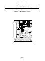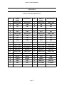
1
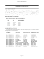
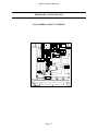
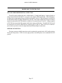
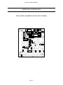
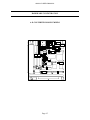
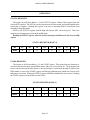
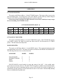
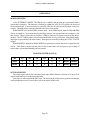
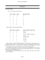
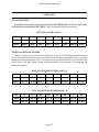
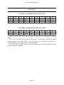
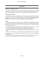
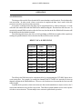
4A20 ANALOG INPUT CARD MANUAL
Version 1.0
Copyright 1997 by MESA ELECTRONICS Richmond, CA. Printed in the United States of
America. All rights reserved. This document and the data disclosed herein is not to be reproduced,
used, disclosed in whole or in part to anyone without the written permission of MESA
ELECTRONICS.
Mesa Electronics
4175 Lakeside Drive, Suite #100
Richmond, CA 94806-1950
Tel (510) 223-9272 - Fax (510) 223-9585
E-Mail: [email protected] - Website: www.mesanet.com
4A20 A-D USER'S MANUAL
TABLE OF CONTENTS
HANDLING PRECAUTIONS
Handling precautions . . . . . . . . . . . . . . . . . . . . . . . . . . . . . . . . . . . . . . . . . . . . . . . . . . . . . . . . . . . . . . . . . . ii
INTRODUCTION
General . . . . . . . . . . . . . . . . . . . . . . . . . . . . . . . . . . . . . . . . . . . . . . . . . . . . . . . . . . . . . . . . . . . . . . . . . . . . . . . 7
CONFIGURATION
General . . . . . . . . . . . . . . . . . . . . . . . . . . . . . . . . . . . . . . . . . . . . . . . . . . . . . . . . . . . . . . . . . . . . . . . . . . . . . . . . 8
Standard configuration . . . . . . . . . . . . . . . . . . . . . . . . . . . . . . . . . . . . . . . . . . . . . . . . . . . . . . . . . . . . . . . . 8
Base address select . . . . . . . . . . . . . . . . . . . . . . . . . . . . . . . . . . . . . . . . . . . . . . . . . . . . . . . . . . . . . . . . . . . . 10
Register locations . . . . . . . . . . . . . . . . . . . . . . . . . . . . . . . . . . . . . . . . . . . . . . . . . . . . . . . . . . . . . . . . . . . . . 10
Single and differential mode select . . . . . . . . . . . . . . . . . . . . . . . . . . . . . . . . . . . . . . . . . . . . . . . . . . . . 12
Shield connection . . . . . . . . . . . . . . . . . . . . . . . . . . . . . . . . . . . . . . . . . . . . . . . . . . . . . . . . . . . . . . . . . . . . . 12
Input mode and shield termination jumpers. . . . . . . . . . . . . . . . . . . . . . . . . . . . . . . . . . . . . . . . . . . . 12
A-D converter mode . . . . . . . . . . . . . . . . . . . . . . . . . . . . . . . . . . . . . . . . . . . . . . . . . . . . . . . . . . . . . . . . . . 14
INSTALLATION
Installation . . . . . . . . . . . . . . . . . . . . . . . . . . . . . . . . . . . . . . . . . . . . . . . . . . . . . . . . . . . . . . . . . . . . . . . . . . . . 16
OPERATION
Check-out . . . . . . . . . . . . . . . . . . . . . . . . . . . . . . . . . . . . . . . . . . . . . . . . . . . . . . . . . . . . . . . . . . . . . . . . . . . . 17
4A20 registers . . . . . . . . . . . . . . . . . . . . . . . . . . . . . . . . . . . . . . . . . . . . . . . . . . . . . . . . . . . . . . . . . . . . . . . . 17
Data registers . . . . . . . . . . . . . . . . . . . . . . . . . . . . . . . . . . . . . . . . . . . . . . . . . . . . . . . . . . . . . . . . . . . . . . . . . 17
Status register . . . . . . . . . . . . . . . . . . . . . . . . . . . . . . . . . . . . . . . . . . . . . . . . . . . . . . . . . . . . . . . . . . . . . . . . 18
Start register . . . . . . . . . . . . . . . . . . . . . . . . . . . . . . . . . . . . . . . . . . . . . . . . . . . . . . . . . . . . . . . . . . . . . . . . . . 18
GCTable register . . . . . . . . . . . . . . . . . . . . . . . . . . . . . . . . . . . . . . . . . . . . . . . . . . . . . . . . . . . . . . . . . . . . . . 19
GCTable inc register . . . . . . . . . . . . . . . . . . . . . . . . . . . . . . . . . . . . . . . . . . . . . . . . . . . . . . . . . . . . . . . . . . 19
Mode register . . . . . . . . . . . . . . . . . . . . . . . . . . . . . . . . . . . . . . . . . . . . . . . . . . . . . . . . . . . . . . . . . . . . . . . . . 19
Setup register . . . . . . . . . . . . . . . . . . . . . . . . . . . . . . . . . . . . . . . . . . . . . . . . . . . . . . . . . . . . . . . . . . . . . . . . . 20
Timer counter Registers . . . . . . . . . . . . . . . . . . . . . . . . . . . . . . . . . . . . . . . . . . . . . . . . . . . . . . . . . . . . . . 22
4A20 A-D USER'S MANUAL
TABLE OF CONTENTS
OPERATION
Minimum conversion time . . . . . . . . . . . . . . . . . . . . . . . . . . . . . . . . . . . . . . . . . . . . . . . . . . . . . . . . . . . . 24
Overload recovery . . . . . . . . . . . . . . . . . . . . . . . . . . . . . . . . . . . . . . . . . . . . . . . . . . . . . . . . . . . . . . . . . . . . 24
Noise . . . . . . . . . . . . . . . . . . . . . . . . . . . . . . . . . . . . . . . . . . . . . . . . . . . . . . . . . . . . . . . . . . . . . . . . . . . . . . . . . 24
A-D Pipelineing . . . . . . . . . . . . . . . . . . . . . . . . . . . . . . . . . . . . . . . . . . . . . . . . . . . . . . . . . . . . . . . . . . . . . . . 25
Polled mode operation . . . . . . . . . . . . . . . . . . . . . . . . . . . . . . . . . . . . . . . . . . . . . . . . . . . . . . . . . . . . . . . . 26
Convert clock . . . . . . . . . . . . . . . . . . . . . . . . . . . . . . . . . . . . . . . . . . . . . . . . . . . . . . . . . . . . . . . . . . . . . . . . . 26
Scan length counter . . . . . . . . . . . . . . . . . . . . . . . . . . . . . . . . . . . . . . . . . . . . . . . . . . . . . . . . . . . . . . . . . . . 27
The GCtable . . . . . . . . . . . . . . . . . . . . . . . . . . . . . . . . . . . . . . . . . . . . . . . . . . . . . . . . . . . . . . . . . . . . . . . . . . 27
Interrupt mode operation . . . . . . . . . . . . . . . . . . . . . . . . . . . . . . . . . . . . . . . . . . . . . . . . . . . . . . . . . . . . . 28
DMA mode operation . . . . . . . . . . . . . . . . . . . . . . . . . . . . . . . . . . . . . . . . . . . . . . . . . . . . . . . . . . . . . . . . . 29
Continuous DMA . . . . . . . . . . . . . . . . . . . . . . . . . . . . . . . . . . . . . . . . . . . . . . . . . . . . . . . . . . . . . . . . . . . . . 30
I/O connector pin-out . . . . . . . . . . . . . . . . . . . . . . . . . . . . . . . . . . . . . . . . . . . . . . . . . . . . . . . . . . . . . . . . . 31
Termination panels. . . . . . . . . . . . . . . . . . . . . . . . . . . . . . . . . . . . . . . . . . . . . . . . . . . . . . . . . . . . . . . . . . . . 32
Calibration . . . . . . . . . . . . . . . . . . . . . . . . . . . . . . . . . . . . . . . . . . . . . . . . . . . . . . . . . . . . . . . . . . . . . . . . . . . . 32
DEMONSTRATION PROGRAMS
4A20POL . . . . . . . . . . . . . . . . . . . . . . . . . . . . . . . . . . . . . . . . . . . . . . . . . . . . . . . . . . . . . . . . . . . . . . . . . . . . . 33
4A20INT . . . . . . . . . . . . . . . . . . . . . . . . . . . . . . . . . . . . . . . . . . . . . . . . . . . . . . . . . . . . . . . . . . . . . . . . . . . . . 33
4A20DMA . . . . . . . . . . . . . . . . . . . . . . . . . . . . . . . . . . . . . . . . . . . . . . . . . . . . . . . . . . . . . . . . . . . . . . . . . . . 33
REFERENCE INFORMATION
Specifications . . . . . . . . . . . . . . . . . . . . . . . . . . . . . . . . . . . . . . . . . . . . . . . . . . . . . . . . . . . . . . . . . . . . . . . . . 34
Warranty. . . . . . . . . . . . . . . . . . . . . . . . . . . . . . . . . . . . . . . . . . . . . . . . . . . . . . . . . . . . . . . . . . . . . . . . . . . . . . 35
Schematic diagrams . . . . . . . . . . . . . . . . . . . . . . . . . . . . . . . . . . . . . . . . . . . . . . . . . . . . . . . . . . . . . . . . . . . 37
4A20 A-D USER'S MANUAL
4A20 A-D USER'S MANUAL
HANDLING INFORMATION
STATIC ELECTRICITY
The CMOS integrated circuits on the 4C24 can be damaged by exposure to electrostatic
discharges. The following precautions should be taken when handling the 4C24 to prevent
possible damage.
A. Leave the 4C24 in its antistatic bag until needed.
B. All work should be performed at an antistatic workstation.
C. Ground equipment into which 4C24 will be installed.
D. Ground handling personnel with conductive bracelet through 1 megohm resistor to
ground.
E. Avoid wearing synthetic fabrics, particularly Nylon.
4A20 A-D USER'S MANUAL
GENERAL
INTRODUCTION
The 4A20 is an all CMOS successive approximation type data acquisition system on a PC/104
card. The 4A20 has an instrumentation amplifier input for rejection of common mode noise. The
input amplifier has programmable gains of 1, 10 or 100, giving full scale input ranges of +- 5 V, +-500
mV and +-50 mV respectively. The input multiplexer and instrumentation amplifier are fully
protected against fault voltages of up to 35 V. The Serial A-D chip and card design reduces digital
noise feedthrough to the analog side.
The 4A20's reference is available on the input connector for use in ratiometric applications.
Conversions may be started with the on card counter timer or an external source. Host transfers may
be DMA, polled, or interrupt driven. Both 8 and 16 bit transfers are supported in all modes. The
RAM table on the 4A20 allows a preprogrammed channel and gain sequence of up to 4096 readings to
be made under DMA control with no processor intervention. The 4A20 has provisions for extending
the number of analog inputs to 64 single ended or 32 differential channels with the 7I23 and 7I24
submultiplexing termination panels.
The 4A20 is mapped into 12 contiguous I/O port locations that can be located anywhere in the
1024 port addressing range of the PC-BUS.
The 4A20 can generate an interrupt
(IRQ2,5,6,7,10,11,12,15 are software selectable) when a conversion is complete or at the end of a
DMA scan. Any of the 7 available DMA channels can be selected by software.
Page 7
4A20 A-D USER'S MANUAL
HARDWARE CONFIGURATION
GENERAL
The 4A20 has a number of jumper configurable options that must be properly set to match the
application. Each group of jumpers will be discussed separately by function. In the following
discussions, when the words "up", "down", "right", and "left" are used it is assumed that the 4A20
analog input card is oriented with its contact fingers pointing towards the person doing the
configuration.
STANDARD CONFIGURATION
The 4A20 card is configured in the following manner when shipped from the factory. The
demonstration programs assume this configuration, and will probably 'hang' if run on a card
configured differently. This means that if you would like to verify card operation, you should do it
before you reconfigure the 4A20.
BASE ADDRESS
0220H
INPUT CONFIGURATION
DIFFERENTIAL
SHIELD CONNECTION
TERMINATED AT ANALOG GROUND
ADC MODE
BIPOLAR
ADC DATA FORMAT
TWO'S COMPLEMENT
Page 8
4A20 A-D USER'S MANUAL
HARDWARE CONFIGURATION
DEFAULT JUMPER CONFIGURATION
Page 9
4A20 A-D USER'S MANUAL
HARDWARE CONFIGURATION
BASE ADDRESS SELECT
The 4A20 occupies 12 contiguous addresses in I/O space. The 4A20 base address is set with PAL
U17 and jumpers W8 and W9. Four pre-programmed I/O locations can be set via jumpers W8 and
W9. The following table shows the available I/O locations with the standard PAL. If these I/O
locations conflict with other I/O in your system, Mesa can supply a custom PAL U17 that locates
4A20 I/O in 4 arbitrary locations. Note that even though the 4A20 uses 12 port locations, the base
address must start at a 16 byte boundary.
BASE ADDRESS SELECT WITH STANDARD PAL:
W9
W8
4A20 ADDRESS
RIGHT
RIGHT
LEFT
LEFT
RIGHT
LEFT
RIGHT
LEFT
0220H
0230H
0240H
0250H
4A20 REGISTER LOCATIONS
The 4A20 registers are located as follows. Note that a complete register description is contained
in the operation section of this manual.
ADDRESS
REGISTER
READ FUNCTION WRITE FUNCTION
BASE ADDRESS + 0
BASE ADDRESS + 1
BASE ADDRESS + 2
BASE ADDRESS + 3
BASE ADDRESS + 4
BASE ADDRESS + 5
BASE ADDRESS + 6
BASE ADDRESS + 7
BASE ADDRESS + 8
BASE ADDRESS + 9
BASE ADDRESS + A
BASE ADDRESS + B
ADC DATA
ADCDATA
ADC DATA
ADC DATA
CONV STATUS
EOC BIT
START
GO BIT
GCTABLE
GCTABLE
GCTABLEINC
XXXXXX
MODE
XXXXXX
SETUP /GCTABCLR GCTABCLR
RATE COUNTER
READS COUNT
SCAN COUNTER
READS COUNT
EXTRA COUNTER READS COUNT
CTR CONTROL
XXXXXX
Page 10
XXXXXXXX
XXXXXXXX
POLLED START
GO BIT
GCTABLE
INCREMENT TP
IRQ/DRQ MODE
SETUP REG
SETS COUNT
SETS COUNT
SETS COUNT
SETS CTR MODE
4A20 A-D USER'S MANUAL
HARDWARE CONFIGURATION
BASE ADDRESS SELECT JUMPERS
Page 11
4A20 A-D USER'S MANUAL
HARDWARE CONFIGURATION
SINGLE ENDED/DIFFERENTIAL SELECTION
The 4A20 can be configured to have 8 differential or 16 single ended inputs. Jumpers placed on
jumper blocks W4,W5,W6 and W7 are used to select single or differential mode. When all jumpers
are placed in the right hand position, the differential mode is selected. When all jumpers are placed in
the left hand position, the single ended mode is selected. In the single ended mode, the input common
signal is not ground but INCOM which is available at I/O connector pins 23 and 24. Voltages applied
to INCOM must meet the 4A20 common mode input range specifications. Normally INCOM would
be connected to ANALOG GROUND (at connector pins 27 and 28). Please refer to I/O connector
pin-out in the operation section for single ended and differential input connections.
SHIELD CONNECTION
The input connector shield connections can be terminated at ground on the 4A20 card by placing
W10 in the left position. If W10 is in the right position, the shield pins are not terminated at 4A20
ground.
Page 12
4A20 A-D USER'S MANUAL
HARDWARE CONFIGURATION
INPUT MODE AND SHIELD CONNECTION JUMPERS
Page 13
4A20 A-D USER'S MANUAL
HARDWARE CONFIGURATION
A-D CONVERTER MODE
The A-D chip on the 4A20 can be operated in unipolar or bipolar mode. If only positive signals
need to be converted, the unipolar mode will give double the useable resolution. W1,W2, and W3 set
the A-D converter mode. When W1,W2, and W3 are in the up position, bipolar mode is selected.
When W1,W2, and W3 are in the down position, unipolar mode is selected. When bipolar mode is
selected, the output coding is two's complement. When unipolar mode is selected, the output coding
is straight binary.
Page 14
4A20 A-D USER'S MANUAL
HARDWARE CONFIGURATION
A-D CONVERTER MODE JUMPERS
Page 15
4A20 A-D USER'S MANUAL
INSTALLATION
INSTALLATION
When the 4A20 has been properly configured for its application, it can be inserted into a PC/104
stack. The standoffs should then be tightened to secure the 4A20 in its place. When the 4A20 is
secured in the stack the 40 pin input connector can be plugged in from the side.
The 4A20 should be checked for proper operation after installation. The test programs in the
OPERATION section of the manual can be used to verify proper operation after first installation.
Page 16
4A20 A-D USER'S MANUAL
OPERATION
CHECK-OUT
After the 4A20 has been configured and installed in the system, it should be checked for correct
operation. The supplied program 4A20POL.EXE will sequentially read and print the voltages on the
8 differential input channels. The selected gain is 1. The program 4A20POL assumes that the 4A20 is
configured with the standard (from factory) configuration.
4A20 REGISTERS
The 4A20 uses 12 contiguous I/O port locations for communication with the processor. These
ports are discussed individually in the following section.
DATA REGISTERS
The registers at the 4A20 base address +0 and base address +1 are the data registers that return the
converted data. These registers can be read as two bytes starting at base address +0 or as a single 16
bit word at base address+0 on 16 bit processors. The 16Bit flag in the SETUP register must be set in
order to read tha data as a single word instead of two bytes.
Reading either register will clear an interrupt request when the 4A20 transfer mode is interrupt
driven.
DATA REGISTER 0 (BASE +0)
BIT
D7
D6
D5
D4
D3
D2
D1
D0
READ
AD7
AD6
AD5
AD4
AD3
AD2
AD1
AD0
WRITE
X
X
X
X
X
X
X
X
DATA REGISTER 1 (BASE+1)
BIT8/16
D7/D15
D6/D14
D5/D13
D4/D13
D3/D12
D2/D11
D1/D10
D0/G8
READ
AD15
AD14
AD13
AD12
AD11
AD10
AD9
AD8
WRITE
X
X
X
X
X
X
X
X
Page 17
4A20 A-D USER'S MANUAL
OPERATION
STATUS REGISTER
The register at 4A20 base address + 2 is the STATUS register. Reads of this register return the
current EOC status bit. The EOC bit is set low when a conversion is started, and returns high when the
conversion is complete. Reading this register is the way to determine End Of Conversion when
operating in the polled mode.
Writes to the STATUS register with D0 high will start an ADC conversion cycle. This is the
normal way of starting a conversion in the polled mode.
Reading the STATUS register when the 4A20 is running in the DMA mode will clear the IRQ
request.
STATUS REGISTER (BASE+2)
BIT
D7
D6
D5
D4
D3
D2
D1
D0
READ
X
X
X
X
X
X
X
EOC
START REGISTER
The register at 4A20 base address + 3 is the START register. This register has two functions, to
start conversions in the interrupt and DMA modes, and to set or clear the go bit. The go bit gates the
convert clock (either the internal counter or the external input). In the interrupt mode or either of the
DMA modes, a write to the START register with D0 high simultaneously enables the convert clock
and starts a conversion. Writing the START register with D0 low disables the convert clock. Reading
the START register returns the status of the GO bit.
START REGISTER (BASE+3)
BIT
D7
D6
D5
D4
D3
D2
D1
D0
READ
X
X
X
X
X
X
X
GO
WRITE
X
X
X
X
X
X
X
GO
Page 18
4A20 A-D USER'S MANUAL
OPERATION
GCTABLE REGISTER
The register at 4A20 base address + 4 is the GCTABLE register. This register allows access to the
gain and channel table. The main purpose of the GCTABLE is to allow arbitrary channel and gain
sequences in the DMA operating modes, but the table is usable in all modes.
You must not read or write the GCTABLE when the convert clock is enabled, as it may corrupt
the current reading, the GCTABLE or both.
GCTABLE REGISTER (BASE +4)
BIT
D7
D6
D5
D4
D3
D2
D1
D0
READ
G1
G0
CHSEL5
CHSEL4
CHSEL3
CHSEL2
CHSEL1
CHSEL0
WRITE
G1
G0
CHSEL5
CHSEL4
CHSEL3
CHSEL2
CHSEL1
CHSEL0
GCTABLE INC REGISTER
The register at 4A20base address + 5 is the GCTABLEINC register. TheGCTABLEINC register
is not really a register, but simply a location that when written to will increment the GCTABLE
pointer. The data written is not important.
MODE REGISTER
The register at 4A20 base address + 6 is the MODE register. This register determines the main
operational mode of the 4A20. The main 4A20 mode is encoded on the MODE0 and MODE1 bits.
The following table shows how to select the modes.
4A20 MODE
MODE1
MODE0
POLLED MODE
INTERRUPT MODE
DMAI
DMAB
0
0
1
1
0
1
0
1
POLLED MODE is useful mainly for setup and testing of the ADC. In the polled mode,
conversions are started by software. The ADC STATUS register is readable only in the polled mode.
The external start convert commands and the convert clock from the rate counter are ignored. In
polled mode, the table pointer is not incremented at the start of a conversion. Both the DRQ and IRQ
drivers are disabled in the polled mode.
Page 19
4A20 A-D USER'S MANUAL
OPERATION
MODE REGISTER
In the INTERRUPT MODE, The IRQ driver is enabled, and an interrupt is generated when a
conversion is complete. The interrupt is cleared by reading the ADC DATA register (the first read
clears the interrupt). Conversions may be started by software, the external convert input, or the rate
counter. The table pointer is not incremented at the start of conversion.
DMAI MODE is the normal DMA transfer mode. In the DMAI mode, both the IRQ and DRQ
drivers are enabled. Conversions may be started by software, the external start convert input, or the
rate counter. When a conversion is complete, a DRQ is generated to request transfer of the data to
memory. The GCTABLE pointer is incremented at the start of every conversion. In the DMAI mode,
interrupts are generated by the scan counter. Interrupts are cleared by reading the CONV STATUS
register.
DMAB MODE is identical to DMAI MODE except that the external start convert signal sets the
GO bit. This allows a single external pulse on the external start convert input to start a block of
conversions, at a rate determined by the rate counter.
MODE REGISTER (BASE+6)
BIT
D7
D6
D5
D4
D3
D2
D1
D0
READ
X
X
X
X
X
X
MODE1
MODE0
WRITE
X
X
X
X
X
X
MODE1
MODE0
SETUP REGISTER
The setup register allows the selection of interrupts, DMA channels, selection of 16 bit or 8 bit
transfer mode and access to the power down bit.
Interrupts are selected with the ISEL bits. The 4A20 can be configured to generate an interrupt
on the completion of an A-D conversion cycle or the end of a DMA scan.
Page 20
4A20 A-D USER'S MANUAL
OPERATION
SETUP REGISTER
There are 8 possible interrupt selections:
ISEL2
ISEL1
ISEL0
IRQ SELECTED
0
0
0
2/9
0
0
1
5
0
1
0
6
0
1
1
7
1
0
0
10
1
0
1
11
1
1
0
12
1
1
1
15
DMA channels are selected with the DSEL bits:
DSEL2 DSEL1 DSEL0
DMA CHANNEL SELECTED
0
0
0
0 (8 bit)
0
0
1
1 (8 bit)
0
1
0
2 (8 bit, normally used by floppy)
0
1
1
3 (8 bit)
1
0
0
XX not available
1
0
1
5 (16 bit)
1
1
0
6 (16 bit)
1
1
1
7 (16 bit)
When selecting the IRQ and DMA channel, you must make sure that no other card or
motherboard peripheral uses the selected IRQ or DMA channel. When changing the SETUP register,
the MODE register must be set to polled mode, as this disables the DRQ and IRQ drivers. This
prevents a possible transient conflict with other interrupt channels or DMA channels.
The WORD bit will enable 16 bit transfers when set high. The WORD bit affects the DATA
register width for polled and interrupt driven modes, and the DMA transfer size. If 16 bit DMA
transfers are used, the WORD bit must be set.
The PWRDN bit turns off the analog system power when set high. This can save about 1/2 of the
card power dissipation.
Page 21
4A20 A-D USER'S MANUAL
OPERATION
SETUP REGISTER
A side effect of writing the setup register is that the GCTABLE pointer is cleared. This is done
when software needs to load the GCTABLE. This is usually done only at system startup.
SETUP REGISTER (BASE+7)
BIT
D7
D6
D5
D4
D3
D2
D1
D0
READ
X
X
X
X
X
X
PWRDN
WORD
WRITE
DSEL2
DSEL1
DSEL0
ISEL2
ISEL1
ISEL0
PWRDN
WORD
TIMER-COUNTER REGISTERS
The next 4 registers access the 82C54 counter chip on the 4A20. While detailed information on
82C54 operation is beyond the scope of this manual, a brief register description follows. For more
information on programming the 82C54 you may refer to the 4A20LOW.PAS and 4A20INT.PAS
Pascal source code files, which contain example procedures and constants for configuring and
loading the counters.
RATE COUNTER REGISTER (BASE+ 8)
BIT
D7
D6
D5
D4
D3
D2
D1
D0
READ
CNT7/15
CNT6/14
CNT5/13
CNT4/12
CNT3/11
CNT2/10
CNT1/9
CNT0/8
WRITE
CNT7/15
CNT6/14
CNT5/13
CNT4/12
CNT3/11
CNT2/10
CNT1/9
CNT0/8
SCAN COUNTER REGISTER (BASE+ 9)
BIT
D7
D6
D5
D4
D3
D2
D1
D0
READ
CNT7/15
CNT6/14
CNT5/13
CNT4/12
CNT3/11
CNT2/10
CNT1/9
CNT0/8
WRITE
CNT7/15
CNT6/14
CNT5/13
CNT4/12
CNT3/11
CNT2/10
CNT1/9
CNT0/8
Page 22
4A20 A-D USER'S MANUAL
OPERATION
EXTRA COUNTER REGISTER (BASE+0AH)
BIT
D7
D6
D5
D4
D3
D2
D1
D0
READ
CNT7/15
CNT6/14
CNT5/13
CNT4/12
CNT3/11
CNT2/10
CNT1/9
CNT0/8
WRITE
CNT7/15
CNT6/14
CNT5/13
CNT4/12
CNT3/11
CNT2/10
CNT1/9
CNT0/8
COUNTER CONTROL REGISTER (BASE+ 0BH)
BIT
D7
D6
D5
D4
D3
D2
D1
D0
WRITE
SC1
SC0
RW1
RW1
M2
M1
M0
BCD
The RATE COUNTER can be used for setting the conversion rate in the interrupt and DMA
modes.
The SCAN COUNTER can be used for two purposes. One purpose is to allow non-binary
sequence lengths in the DMA modes. The other purpose is to generate an interrupt at a
programmable count (for example at the end of a DMA block),
The COUNTER CONTROL register is used for setting the counter modes, sending counter latch
and status read-back commands.
Page 23
4A20 A-D USER'S MANUAL
OPERATION
MINIMUM CONVERSION TIME
The minimum conversion time (= 1/ maximum conversion rate) on 4A20 models is 10 uSec. This
is equivalent to a 100KHz conversion rate. The 16 bit model of the 4A20 is limited to a 75 KHz
conversion rate for full accuracy. This is due to instrumentation amplifier settling time limitations.
OVERLOAD RECOVERY
The 4A20 may require up to 2 minimum conversion times to recover from inputs that exceed full
scale by a factor of 2 or more. This means that if you are running the 4A20 at close to the maximum
conversion rate, you must make sure that no inputs cause overloads. When multiple inputs are
multiplexed you need to make sure that all unused inputs are properly terminated.
NOISE
All analog systems suffer from the effects of noise. In high resolution, high speed analog to digital
converters, this noise manifests itself as dithering of the converter LSBs. On the 4A20, this noise has
four main sources: Inherent noise in the ADC, Noise from the input circuitry, digital feed-through,
and externally picked-up noise.
The inherent ADC noise cannot be eliminated, but can be reduced by a factor of 2 by using the
bipolar mode, and offsetting the input sources to use the full plus and minus input range.
Noise from the input circuitry can be minimized by using the lowest gain settings.
Digital feed-through noise is caused by coupling from the logic level signals to the ADC or analog
circuitry.
Noise from external sources can be minimized by using the differential input mode, keeping
source impedance as low as possible (and matched in differential mode), and by careful shielding and
grounding practice.
Noise can of course be averaged. If some input channels can trade off conversion rate for noise
performance, those channels should be averaged to improve total system performance.
Page 24
4A20 A-D USER'S MANUAL
OPERATION
A-D PIPELINING
The design of the serial A-D used on the 4A20 causes that data read from the A-D to be delayed by
one conversion. In other words, when a conversion is complete,the data that is read is from the
previous conversion, not the current conversion.
In repetitive scanning modes this delay can be compensated for by software that puts a 1 count
offset into the routine that reads the DMA buffer and discarding the first data from the first scan. In
repetitively scanned DMA operation, after the first scan, the data in the first DMA buffer location will
be the data from the last channel scanned.
The following table shows the effect of A-D pipelining on DMA driven mode while repetitively
reading 8 sequential channels. Notice that the first data of the first scan is invalid.
RESULT OF A-D PIPELINING
DMA WORD
ADDRESSES
A-D DATA
SCAN 1
A-D DATA
SCAN >1
START +0
XXXX
CH7 DATA
START +1
CH0 DATA
CH0 DATA
START +2
CH1 DATA
CH1 DATA
START +3
CH2 DATA
CH2 DATA
START +4
CH3 DATA
CH3 DATA
START +5
CH4 DATA
CH4 DATA
START +6
CH5 DATA
CH5 DATA
START +7
CH6 DATA
CH6 DATA
The offset in the DMA data can be compensated for by programming the GCTABLE data to have
a one count offset. For example, by starting the channel in the GCTABLE at 1 instead of 0, the scan
channels will match the DMA addresses. However, the first data word returned in the first scan will
still be invalid.
In polled mode operation, when conversions are done on a demand basis, it may be easier to do 2
conversions and throw away the first conversion. This allows random channel access at the expense
of a slower conversion rate. This normally is not a concern in polled mode operation.
Page 25
4A20 A-D USER'S MANUAL
OPERATION
POLLED MODE OPERATION
The 4A20 can be operated in polled mode if desired. Polled mode must also be used when
selecting ADC modes. When polled mode is used, the gain and channel setting for each reading is
selected via software. In the polled mode, the IRQ and DRQ drivers are disabled, and the rate counter
and external start convert inputs are ignored.
The following is a brief description of the necessary sequence to operate the 4A20 in the polled
mode. Before polled mode operation can begin, you must select polled mode operation (and the ADC
mode) by writing an appropriate mode byte to the MODE register. It is a good idea to clear the table
pointer (by writing to the SETUP register location) when the 4A20 is used in polled mode. The first
step in making a polled mode reading is to select the desired channel and gain. Selecting the channel
and gain is accomplished by writing to the GCTABLE register. After a settling time of 15 uSEC has
elapsed, the conversion may be started. To start a conversion, you write a 1 to the CONV STATUS
register. Two things happen when the conversion is started: the ADC chip changes from track to hold
mode, and the ADC chip begins its internal conversion cycle. Starting a conversion sets the EOC bit in
the STATUS register low. The EOC bit can then be polled until it returns high. This indicates that the
conversion is complete. The final step is to read the data from the converter. The data can be read as 2
bytes from DATA REGISTER0 and DATA REGISTER1 or as a single 16 bit word 16 bit word from
DATA REGISTER0. Note that as discussed above, the data returned is from the previous
conversion, not the one just finished.
Because the ADC chip samples the analog input when a conversion is started, the settling time of
the input amplifier can be overlapped with the ADC conversion cycle. To do this, you write the new
channel and gain information into the GCTABLE register immediately after starting a conversion.
This allows the maximum throughput in the polled mode.
CONVERT CLOCK
When the 4A20 is used in the interrupt or DMA driven modes, it is possible to have the on card
counter start conversions at a programmable rate. This is accomplished by setting channel 0 of the
82C54 into the rate generator mode, and then loading the RATE COUNTER register with an
appropriate count. The input clock signal to the rate counter is 4.194304 MHZ for all 4A20 models.
In the rate generator mode, the conversion rate is equal to the rate counter clock divided by the count
loaded into the RATE COUNTER register. The conversion rate will be (4.194304 MHz / count) Hz.
Once the mode and count have been programmed, conversions can be started by writing a 1 to the
START register. Writing a 1 to the START register immediately starts a conversion, and sets the
GO bit. When the GO bit is high, the rate counter output will periodically start conversions. When the
conversion is complete, either an IRQ or a DRQ will be generated, depending the 4A20 mode.
Page 26
4A20 A-D USER'S MANUAL
OPERATION
CONVERT CLOCK
When the GO bit is high, the external start input can also start conversions. The external start
input is an active low signal that must be active longer that 100 nS but for no longer than 2 uSEC. The
external start input has a pull-up resistor, and can be left unconnected if not used.
For more information on programming the 82C54 you may refer to the 4A20LOW.PAS and
4A20INT.PAS Pascal source code files, which contain example procedures and constants for
configuring and loading the counters.
THE SCAN COUNTER
The scan counter can be used for two purposes. One purpose is to allow non binary sequence
lengths in the DMA modes. This is accomplished by programming the scan counter to operate in the
rate generator mode, with the count set to the desired sequence length. The scan counter then
periodically resets the GCTABLE pointer. This allows, for example, you to do DMA transfers from
channels 0,1,2 repeatedly, and ignore other channels.
The other purpose is to generate an interrupt at the end of a DMA block, or when halfway through
a block (which is useful with continuous DMA of binary count lengths). In either case, an interrupt is
generated whenever the scan counter reaches 0.
It is somewhat tricky to synchronize the scan counter with the table pointer because of the way
that 82C54 counters are loaded. The Pascal routine LoadScanCounter in the file 4A20LOW.PAS can
be refered to as an example of what is necessary.
THE GCTABLE
The gain setting and channel selection on the 4A20 is determined by data in a 4096 byte RAM
table. The main purpose of the table is to allow arbitrary channel and gain sequences when the 4A20
is used with DMA. The table must be loaded by user software before DMA operation can begin. To
load the table, first program the 4A20 for polled mode operation. This disables the on card convert
clock and the external start convert input. Then you clear the table pointer by writing to the SETUP
REGISTER location. (This would happen as a side effect of selecting the DMA and IRQ channels).
Next, you write the desired channel select and gain information to the GCTABLE register. Then you
write to the GCTABLEINC location to increment the table pointer. The last two steps are then
repeated until the table is full, or enough entries for the programmed scan length are written.
If the sequencing capability of the GCTABLE is not needed, for example in polled mode, it may be
treated as a latch. In this case you should clear the GCTABLE pointer first before reading from or
writing to the GCTABLE.
Page 27
4A20 A-D USER'S MANUAL
OPERATION
THE GCTABLE
Data bits 6 and 7 of the GCTABLE entry determine the input amplifier gain. The following table
shows how to select the desired gain.
GAIN SETTING AND COORESPONDING INPUT RANGES
GN1
(BIT 7)
GN0
(BIT6)
GAIN
UNIPOLAR
RANGE
BIPOLAR
RANGE
0
0
1
0 to +5V
-5V to +5V
0
1
10
0 to +0.5V
-0.5V to +0.5V
1
0
100
0 to +0.05V
-0.05V to +0.05V
1
1
10
0 to +0.5V
-0.5V to +0.5V
Data bits 0 through 5 are the channel select bits. Only bits 0 through 3 are used locally. Channel
select bits 4 and 5 are available on the input connector to allows external submultiplexing. The unused
channel select bits may also be used to trigger external events synchronously with the ADCs
conversions.
Since the channel sequence can be arbitrary, it is possible to scan some channels in a multiplexed
system faster than others. For example: a channel sequence of 0,1,0,2,0,3,0,4,0,5,0,6,0,7 in the
GCTABLE would allow you to scan channel 0 at one half of the maximum throughput rate of the
4A20, while still scanning the other 7 channels at a slower rate.
INTERRUPT MODE OPERATION
The interrupt driven mode is most useful at moderate conversion rates. (Below 5 KHz or so
depending on the host processor). This is because the interrupt latency and interrupt overhead of the
PC will typically cause problems at higher conversion rates. When interrupt mode is enabled, the IRQ
driver is enabled, the DRQ driver is disabled, and IRQs are generated on every end of conversion. The
IRQ is cleared by reading the ADC DATA register. Probably the most useful interrupt driven scheme
is to use the RATE COUNTER to set a periodic conversion rate.
The following is a brief description of the necessary sequence to operate the 4A20 in the interrupt
driven mode with periodic conversions started by the RATE COUNTER.
Before interrupt driven mode operation can begin, you must select interrupt mode operation (and
the ADC mode) by writing an appropriate mode byte to the MODE register.
Page 28
4A20 A-D USER'S MANUAL
OPERATION
INTERRUPT MODE OPERATION
Then the RATE COUNTER should be programmed for rate generator mode, and loaded with the
appropriate count. You should make sure that the IRQ is initially clear by reading the ADC DATA
register.
Once the mode and the RATE COUNTER have been programmed, conversions can be started by
writing a 1 to the START register. Writing a 1 to the START register immediately starts a
conversion, and sets the GO bit. When the GO bit is high, the RATE COUNTER output will
periodically start conversions. When the conversion is complete, an IRQ will be generated.
Channel and gain can be either updated by the interrupt service routine, or by the GCTABLE. If
the GCTABLE is used, the interrupt service routine needs to increment the table pointer, as it is not
automatically incremented in the interrupt mode. If the GCTABLE is not used, the interrupt service
routine should write the gain and channel values for the next conversion before it returns. This will
give the maximum settling time for the next reading.
For more information on the interrupt driven operation mode, please refer to the Pascal source
code 4A20INT.PAS and 4A20LOW.PAS.
DMA MODE OPERATION
The DMA driven mode allows the highest throughput rates with the least CPU overhead. When
DMA mode is selected, both the IRQ and DRQ drivers are enabled, DRQs are generated at the end of
every conversion, IRQs are generated by the SCAN counter, and the IRQ is cleared by reading the
CONV STATUS register. Probably the most useful DMA driven scheme is to use the RATE
COUNTER to set a periodic conversion rate.
The following is a brief description of the necessary sequence to operate the 4A20 in the DMA
driven mode with periodic conversions started by the RATE COUNTER.
Before DMA driven mode operation can begin, you must first selct the desired DMA channel and
interrupt with the SETUP register. Then you select DMA mode operation (and the ADC mode) by
writing an appropriate mode byte to the MODE register.
Then the RATE COUNTER should be programmed for rate generator mode, and loaded with the
appropriate count. You should make sure that the IRQ is initially clear by reading the STATUS
register.
The next step is to program the DMA controller. In 8 bit mode, 2 DRQs are generated for each
transfer. Data is always read LSB first. In order to get the normal byte order (LSB first) it is
necessary to have the DMA controller increment addresses and start at an even address.
Once the DMA controller, 4A20 mode and the RATE COUNTER have been programmed,
conversions can be started by writing a 1 to the START register. Writing a 1 to the START register
immediately starts a conversion, and sets the GO bit. When the GO bit is high, the rate counter
output will periodically start conversions. When the conversion is complete, a DRQ will be
generated.
Page 29
4A20 A-D USER'S MANUAL
OPERATION
DMA MODE OPERATION
In the DMA driven modes, the table pointer is incremented by every convert clock. This means
that the sequential entries in the GCTABLE determine the gain and channel sequence.
Interrupts are generated whenever the scan counter counts to 0 when the 4A20 is used in the
DMA modes. This can be used to generate an interrupt at the end of a DMA block or at some arbitrary
point in the DMA transfer.
When the DMA transfer is complete, a pending DRQ will be left 'hanging'. In addition, the
convert clock will still be running. To restart DMA transfers you must stop the convert clock by
clearing the go bit, wait one convert time, clear the pending DRQ by setting the 4A20 to polled mode
and back to DMA mode, and then reload the rate counter. DMA transfers are then restarted by setting
the go bit.
CONTINUOUS DMA MODE
It is possible to program the DMA controller in its autoinitialize mode to allow continuous DMA
driven conversions to take place. If this is done, it is useful to program the SCAN COUNTER to
generate an interrupt twice during the DMA block transfer. In this way the host program can be
informed when it is safe to copy data out of the DMA buffer area (by copying from the half of the
DMA buffer that the DMA controller just filled).
Page 30
4A20 A-D USER'S MANUAL
OPERATION
INPUT CONNECTOR PINOUT
PIN
SINGLE
ENDED
DIFFERENTIAL
PIN
SINGLE
ENDED
DIFFERENTIAL
1
SHIELD GND
SHIELD GND
2
SHIELD GND
SHIELD GND
3
IN0
+IN0
4
IN8
-IN0
5
IN1
+IN1
6
IN9
-IN1
7
IN2
+IN2
8
IN10
-IN2
9
IN3
+IN3
10
IN11
-IN3
11
SHIELD GND
SHIELD GND
12
SHIELD GND
SHIELD GND
13
IN4
+IN4
14
IN12
-IN4
15
IN5
+IN5
16
IN13
-IN5
17
IN6
+IN6
18
IN14
-IN6
19
IN7
+IN7
20
IN15
-IN7
21
SHIELD GND
SHIELD GND
22
SHIELD GND
SHIELD GND
23
INPUT COM
NO CONNECT
24
INPUT COM
NO CONNECT
25
REF OUT
REF OUT
26
REF OUT
REF OUT
27
SIGNAL GND
SIGNAL GND
28
SIGNAL GND
SIGNAL GND
29
SHIELD GND
SHIELD GND
30
SHIELD GND
SHIELD GND
31
/EXTSC
/EXTSC
32
GND
GND
33
CHSEL4
CHSEL4
34
CHSEL5
CHSEL5
35
GND
GND
36
TEMP OUT
TEMP OUT
37
GND
GND
38
-10 UNREG
-10 UNREG
39
+10 UNREG
+10 UNREG
40
GND
GND
Page 31
4A20 A-D USER'S MANUAL
OPERATION
TERMINATION PANELS
Two screw termination panels are available for use with the 4A20. The 7I21-40 simply terminates
the 40 pin flat cable from the 4A20 into 40 individual box type terminals. The 7I22-40 also supplies a
10 mV/oC output for thermocouple cold junction compensation.
All termination panels can be mounted on standoffs or supplied with DIN rail mounting
hardware.
4A20 CALIBRATION
The 4A20 has potentiometers for full scale adjustment and two zero adjustments. These are set at
the factory and should not normally require adjustment on a new card. The suggested calibration
interval on the 4A20 is 1 year. To calibrate the 4A20 you will need a calibration voltage source of
4.0000V +- .005%.
The calibration procedure and the calibration software assume an input configuration as follows:
differential input mode, differential input pair 0 (+IN 0 and -IN 0) connected to analog ground,
differential input +IN 1 connected to the calibration voltage, and differential input -IN 1 grounded.
The input zero should be adjusted first. To adjust input zero, set the 4A20 gain to 100 and select
differential input pair 0. (The channel with both inputs grounded.) Then adjust R5 (marked IZ) for a
reading of that oscillates between 1 and 0. Remember the potentiometer position and then set R5 for a
reading that oscillates between 0 and -1 and remember this position. Then adjust R5 to the midpoint
between the preceding two positions. Then, set the gain to 1 and adjust the R4 (marked OZ) in the
same manner as R5. The zero controls interact, so you must repeat the adjustments of R4 and R5 for
optimum accuracy.
After the input zero controls have been set, the full scale adjustment can be made. First, if not
already done, connect the calibration source of 4.0000V to differential input pair 1 (with calibrator +
connected to differential input +IN 1 and calibrator - connected to differential input -IN 1). Set the
4A20 gain to 1 and the input channel to 1. Then adjust R6 (marked FS) in the same manner as zero
was adjusted except that you center the count on 26214 instead of 0.
The supplied program 4A20CAL.EXE will select the proper 4A20 gain and channel for adjusting
the three potentiometers, while continuously reading the converter. When 4A20CAL is running,
various keys are used to select the whether input zero, output zero, or full scale is to be adjusted.
NOTE: R4 and R5 have reversed markings on REV. A version cards (R4 is marked IZ but
should be OZ, R5 is marked OZ but should be IZ). The revision marking is above the input
connector.
Page 32
4A20 A-D USER'S MANUAL
DEMONSTRATION PROGRAMS
4A20POL
4A20POL.EXE is a TURBO-PASCAL demonstration program of polled mode 4A20 operation.
4A20POL assumes that the 4A20 is configured with the standard configuration. 4A20POL
continuously reads the 8 differential input channels and prints the input voltages it finds. To exit the
program, type any character.
4A20INT
4A20INT is a TURBO PASCAL demonstration program of interrupt driven operation. 4A20INT
uses PC-BUS interrupt 7 and I/O port location 0220H. These are the factory default settings for a
4A20. You must insure that no other cards in the system will drive INT 7, and that no other cards
overlap the 4A20 I/O addresses before running 4A20INT. 4A20INT uses the GCTABLE to generate
the next channel address and gain. The RATE COUNTER is used to set the interrupt rate, and the
SCAN counter is used to set the length of the table scan.
4A20INT reads 7 differential input channels with the gain set to 1 at a conversion rate of 500 Hz.
The 7 inputs are scanned 12 times and then 4A20INT prints the input voltages it found. Higher
interrupt rates (than 500Hz or so) would require a machine language interrupt service routine.
4A20DMA
4A20DMA is a TURBO PASCAL demonstration program of DMA driven operation.
4A20DMA uses PC-BUS DMA channel 1 and I/O port location 0220H. These are the factory default
settings for a 4A20. You must insure that no other cards in the system use DMA channel 1, and that
no other cards overlap the 4A20 I/O addresses before running 4A20INT. In addition, because the
IRQ driver is always enabled in the DMA driven modes, you should make sure that there is no other
IRQ 7 source in the system.
4A20INT uses the GCTABLE to generate the next channel address and gain. The RATE
COUNTER is used to set the convert rate, and the SCAN counter is used to set the length of the table
scan.
4A20DMA reads 6 differential input channels with the gain set to 1 at a conversion rate of 50000
Hz. The 6 inputs are scanned 14 times and then 4A20DMA prints the input voltages it found. The
program simply polls the DMA controller to determine when it is done.
4A20SCOP
4A20SCOP is a simple graphic display program that uses the 4A20 in DMA driven mode.
4A20SCOP needs to have the appropriate BGI driver in the directory it is run from
The source code for all four example programs is supplied on the disk that accompanied the 4A20.
The file names of the source code files are 4A20POL.PAS, 4A20INT.PAS, 4A20DMA.PAS and
4A20SCOP.PAS. In addition, a set of common low level routines used by all three programs is in the
file 4A20LOW.PAS.
Page 33
4A20 A-D USER'S MANUAL
SPECIFICATIONS
MIN.
MAX.
UNITS
Conversion rate (12,16 bit)
---
100,75
KHz
Reference stability (12,16 bit)
---
+-20,10
PPM/oC
Gain accuracy (X10 and X100 ranges)
---
+-.05
% at 25 oC
Gain temperature coefficient
---
+-10
PPM/oC
Input Offset temp. coefficient
---
+-2
uV/oC
Common mode input range
-7
+7
V
Common mode rejection ratio
100
---
dB (DC)
Input bias current
---
+-30
nA
Maximum output at 12 mA sink
---
0.4
V
Minimum output at 6 mA source
3.8
---
V
Input capacitance
---
15
pF
Input leakage current
---
5
uA
Output drive capability
150
---
pF
Output sink current
12
---
mA
Supply voltage
4.5
5.5
V
Supply current
---
150
mA
-I version
-40
+85
o
C
-C version
0
+70
o
C
Relative humidity
0
90
%
ANALOG:
DIGITAL OUTPUTS:
BUS LOADING:
POWER REQUIREMENTS:
ENVIRONMENTAL:
Operating temperature
Page 34
4A20 A-D USER'S MANUAL
WARRANTY
Mesa Electronics warrants the products it manufactures to be free from defects in material and
workmanship under normal use and service for the period of 2 years from date of purchase. This
warranty shall not apply to products which have been subject to misuse, neglect, accident, or
abnormal conditions of operation.
In the event of failure of a product covered by this warranty, Mesa Electronics, will repair any
product returned to Mesa Electronics within 2 years of original purchase, provided the warrantor's
examination discloses to its satisfaction that the product was defective. The warrantor may at its
option, replace the product in lieu of repair. With regard to any product returned within 2 years of
purchase, said repairs or replacement will be made without charge. If the failure has been caused by
misuse, neglect, accident, or abnormal conditions of operation, repairs will be billed at a nominal cost.
THE FOREGOING WARRANTY IS IN LIEU OF ALL OTHER WARRANTIES,
EXPLICIT OR IMPLIED. INCLUDING BUT NOT LIMITED TO ANY IMPLIED WARRANTY
OF MERCHANTABILITY, FITNESS, OR ADEQUACY FOR ANY PARTICULAR PURPOSE
OR USE. MESA ELECTRONICS SHALL NOT BE LIABLE FOR ANY SPECIAL,
INCIDENTAL, OR CONSEQUENTIAL DAMAGES, WHETHER IN CONTRACT, TORT, OR
OTHERWISE.
If any failure occurs, the following steps should be taken:
1. Notify Mesa Electronics, giving full details of the difficulty. On receipt of this information,
service data, or shipping instructions will be forwarded to you.
2. On receipt of the shipping instructions, forward the product, in its original protective
packaging, transportation prepaid to Mesa Electronics. Repairs will be made at Mesa Electronics and
the product returned transportation prepaid.
Page 35
4A20 A-D USER'S MANUAL
Page 36
4A20 A-D USER'S MANUAL
SCHEMATICS
Page 37
4A20 A-D USER'S MANUAL
Page 38