1
US005627962A
United States Patent [191
[11] Patent Number:
Goodrum et a].
[45]
[54] CIRCUIT FOR REASSIGNING THE POWER
ON PROCESSOR IN A MULTIPROCESSING
SYSTEM
5,627,962
May 6, 1997
Date of Patent:
FOREIGN PATENT DOCUMENTS
0270064
0486304
6/1988
5/1992
European Pat. Oif, .
European Pat. 01f. .
OTHER PUBLICATIONS
Start-up Master Processor Selection Method for Multi-Pro
[75] Inventors: Alan L. Goodrum, Tomball; Gary B.
Kotzur; Kurt C. Lantz, both of
Spring; David F. Heinrich, Tomball;
Jeffrey T. Wilson, Houston, all of Tex.
375-376 (Sep. 1990).
[73] Assignee: Compaq Computer Corporation,
Pentium Processor at iComp Index 735/90 MHZ, Pentium
Processor at (Comp Index 815/100 MHZ, Intel Corp, pp.
Houston, Tex.
1-6, 12-19 (May 1994).
Pentium Family User’s Manual, vol. 1: Data Book, 18-4,
18-11 to 18-18 19-5 to 19-13. 20-1 to 20-3, 21-13 (1994).
Primary Examiner-Robert W. Beausoliel, Jr.
[21] Appl. No.2 366,509
[22] Filed:
Dec. 30, 1994
6
[51]
[52]
[58]
Int. Cl- .......................... .. GolR 31/28; G06F 11/00
US. Cl. ............................... .. 395/182.11; 395/182.11;
395/ 183.12
Field of Search ............................. .. 395/575, 182.11,
395/132-21, 133-12; 371/ 16-1~ 16-3
.
[56]
cessor Systems, 33 IBM Technical Disclosure Bulletin
Assistant Examiner—Glenn Snyder
Attorney, Agent’ or Firm_PraveL Hcwitt, Kimball &
Kriegcr
AB TRA
[57]
S
CT
A hot spare boot circuit that automatically switches from a
non-operational CPU to an operational CPU for powering up
Refemnces Clted
the computer system. In the multiprocessor computer
U_S_ PATENT DOCUMENTS
system, a ?rst CPU is designated to perform power on
operations. If the ?rst CPU fails, which is determined when
4,502,116
2/1935 Fofvler et a1- - - ‘ - -
4,634,110
1/1937 J‘mch et a1‘
4,646,298
1987 Laws et at“
4/1989 Bishop et al. .
4,339 895
6/1989 Mama ____ __
4,360,196
3/1939 wengen
a dead man counter in the hot spare boot circuit times out,
- 371/11
the hot spare circuit ensures that the ?rst CPU is in a disabled
....... .. 371/9
tional second CPU, reinitializing certain ID information as
h th t th
d CPU
1 crf
state. Next, the hot spare boot circuit identi?es an opera
4’7O3’419 1 1987 Krause et ' '
4,775,976 10/1988 Yokoyama
4,823,256
- - - -- 364/200
364/200
necessary Suc
, a
e Sewn
can PT°Per Y P
"m
power on operations. The hot spare boot then awakens the
second CPU, using a startup interprooessor interrupt in one
5,155,729 10/1992 Rysko et a1.
embodiment, or simply negating the hard reset of the second
5,408,647
4/1995 Landry .... ..
CPU in a second embodiment The second CPU then pro
5,450,576
9/1995 Kennedy
5,491,788
2/1996 Cepulis
5,495,569
2/1996 Kotzur ......................... .. 395/183.12 X
ceeds to perform the power on functions.
.
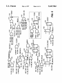
SLEEPIZI'
12 Claims, 6 Drawing Sheets
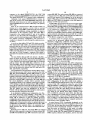
201
._______F
mm]
PEEL
262
cm 2
fP
PZPBElUl' CPUTYPE
L2
+5»!
260 \
F2P?|EN_
PM
PD
HUSH",
PGOUD
um
-___
PtPnlEN
SPRDLK
CACHE
['214
264
FLUSHHI'
PRESET
f 206
>
202
\
f212/213
k
r
ADDRESS
FRESH
9"“
"UNTRBL l
— PlCllHzD] mm"
PA J
266
’
L200
PRESET
cumRuL
222
_
PICDl?l/DPEN
SLEEPIZ]
.
PICDIIIMPICEN
9
SLAVE MD]
“"6
f210
CLOCK
I
J
MEMORY CONTROL
Mc/
"mom ADDRESS
mm"-
l
\MA
"3c
mmm- I I a
TWPRIM
"mg?
BUFFERS _i__-(
SLAVE_ <(('1us
I
I
PC\
268
MEMORY um
DATA
,
\
mus 3:0]
Pxcniunl
w
HSBE
250
246PMIE 242% \23s
m
CONTROL
I PC! ADDRESS/DATA
PROCESSOR CONNECTOR
L 224
5,627,962
1
2
CIRCUIT FOR REASSIGNING THE POWER
ON PROCESSOR IN A MULTIPROCESSING
SYSTEM
level and input polarity logic, and tables to allow individual
interrupts to be addressed to one or more CPUs at various
CROSS REFERENCE TO RELATED
APPLICATION
rupt messages from the I/O APIC and keeps track of which
interrupts are in service by each CPU. The local APICs are
interrupt priorities. The local APIC is implemented inside
each of the P54C or P54CM processors and receives inter
also responsible for sending special interprocessor interrupt
The present invention relates to powering up micropro
(IPI) messages over an APIC bus to the other CPU to
cessors in multiprocessor computer systems, as does
commonly-owned US. Pat. No. 5,495,569. entitled “CIR
CUIT FOR ENSURING THAT A LOCAL INTERRUP'I‘
CONTROLLER lNA MICROPROCESSOR IS POWERED
UPACI‘IVE.”
10
sor bus without the need for additional logic. This highly
integrated solution greatly simpli?es the design of dual
processor systems.
BACKGROUND OF THE INVENTION
In a multiprocessor system, a problem that sometimes
occurs is that one of the multiple processors may fail. Thus,
it is desirable that some sort of fault-tolerant scheme be
1. Field of the Invention
The invention relates to multiprocessor computer
developed, particularly during power up, to ensure that the
systems, and more particularly, to a circuit for reassigning
the power-on processor in a dual processor system when a
processor fails.
2. Description of the Related Art
computer system continues to function even though a non
operational processor is encountered. One method of boot
ing up a multiprocessor system is to assign a primary
processor responsible for powering up the computer system.
Microprocessors have seen rapid improvements in speed
and performance. For example. the latest generation of
microprocessors from Intel Corporation include the Pentium
processors, which contain signi?cant enhancements over the
Once the computer system has been successfully started up,
25
the primary processor then turns on and tests the remaining
processors and various other components in the computer
system. If the primary microprocessor does not function
prior generation 486 processors. Even with the rapid
properly, however, it would be unable to turn on the remain
improvements in microprocessor performance, however.
ing processors, leaving the entire computer system incapaci
resource requirements of software applications are always
increasing. which in turn drives the need for the design and
development of ever more powerful and e?icient computer
tated. Consequently, the computer owner or operator has a
computer system with one or more operational CPUs, but
the system is useless until the repairman arrives.
One approach to resolve this problem is utilized in the
Compaq Systempro XL and Proliant 2000 and 4000 com
puter systems and is described fully in US. Pat. No. 5,408,
systems.
One well known method of improving computer perfor
mance is to provide multiple processors in a single system.
Both asymmetrical and symmetrical multiprocessor systems
have been developed. In asymmetrical multiprocessor
accomplish special functions. Thus, on a dual processor
board utilizing a P54C processor and a P54CM processor,
the two processors can be directly connected to the proces
35
647, entitled “Automatic Logical CPU Assignment of Physi
cal CPUs” and hereby incorporated by reference. The
systems, one microprocessor is the master and another
microprocessor performs speci?c functions as a slave of the
master microprocessor. In this con?guration, the slave pro
technique utilizes a deadrnan timer associated with each
processor and specialized hardware to determine the ?rst
cessor performs only operations designated by the master
are set as the logical processor values. Only logical proces
sor zero is allowed to boot the computer system and initiates
the remaining processors, which have been in a sleep
logical processor. On reset, the physical processor numbers
processor.
The symmetrical multiprocessor system is more efficient
then the asymmetrical system, as tasks are more evenly
condition. If the logical processor zero does not access a
divided between the processors. Thus, in a symmetrical
system, any processor can perform any required function.
given address location within a given timer period, the
Thus, all microprocessors operate simultaneously, spending
45
little or no idle time, and the computer system operates near
its maximum e?iciency. However, although symmetrical
failed and the new logical processor zero commences the
boot sequence. This process continues until a successful
multiprocessor systems are e?icient, they are also very
difficult to design. thereby adding to their cost and com
plexity. As a result, only very high end users can afford
boot operation occurs.
This technique was further improved in versions of the
‘ Compaq Proliant 2000 and 4000 computer systems using
symmetrical multiprocessing systems.
To alleviate design complexities of multiprocessor
systems, Intel has developed the Pentium P54C and P54CM
processors. The P54C and P54CM processors integrate logic
associated deadman timer expires and sends a signal to the
specialized hardware to cause all logical processor values to
be decremented. The current logical processor zero becomes
55
procedures described in US. Pat. No. 5,491,788, entitled
“Automatic Reassignment of Booting CPU Based on Prior
Errors” ?led and hereby incorporated by reference. In this
necessary for a dual processor system, each including an
improvement, when logical processor zero starts the booting
on-chip advanced programmable interrupt controller
(APIC). The local APICs support multiprocessor interrupt
management, multiple I/O subsystem support, compatibility
process, it ?rst checks an error log to see if certain critical
errors have previously occurred on that processor. If so, the
with the EISA 8259 interrupt controllers, and interprocessor
interrupts between the two processors.
The APIC is a standardized approach developed by Intel
for symmetric multiprocessing. It allows any interrupt to be
serviced by any CPU. The APIC architecture is implemented
errors prior to actually loading the operating system and if
any have occurred, changes the next logical processor to
booting sequence stops and the deadrnan timer causes CPU
rotation. The logical processor zero also checks for critical
processor zero, passes the booting control and shuts itself
down.
in two pieces: an “I/O APIC” resides close to the I/O 65
However, these techniques could not be directly applied
subsystem and a “local APIC” is implemented inside the
to a dual processor P54C and P54CM system because the
P54C or P54CM processors. The 1/0 APIC contains edge/
specialized hardware was not available and different tech
5,627,962
4
3
BRIEF DESCRIPTION OF THE DRAWINGS
A better understanding of the present invention can be
niques were used to start the P54CM second processor.
Therefore, the non-operational processor problem reappears
in the P54C and P54CM systems, with the problem exac
obtained when the following detailed description of the
preferred embodiment is considered in conjunction with the
erbated by the knowledge that solutions exist in other
con?gurations.
SUMMARY OF THE PRESENT INVENTION
It is therefore an object of the present invention to identify
an operational microprocessor in a multiprocessor system so
that the system can be properly powered up when the
primary microprocessor is nonoperational. A hot spare boot
circuit according to the present invention automatically
following drawings, in which:
FIG. 1 is a block diagram of a system board for use with
the preferred embodiment of the present invention;
10
FIG. 2 is a block diagram of a processor board including
multiple processors and a hot spare boot circuit according to
the present invention;
FIG. 2A is a block diagram of an alternative processor
reassigns the power up responsibilities to an operational
second processor should the primary processor fail. The hot
spare boot circuit ?rst determines if the primary processor
responsible for powering up the computer system is opera
tional when the computer system is initially started. In the
board including multiple processors and a hot spare boot
circuit according to the present invention;
FIG. 3 is a logic diagram of portions of the hot spare boot
circuit for determining the con?guration of the multiproces
preferred embodiment, a counter that times out after a
sor system and for determining if a primary processor is
predetermined period is used to determine if the primary
non-operational;
processor is non-operational. Ifthe counter times out, the hot
spare boot circuit resets each of the plurality of processors
in the multiprocessor system. In a ?rst embodiment of the
present invention, one reset signal is used to reset the
FIG. 4 is a state diagram of a state machine in the hot
20
processors. Thus, deasserting the reset signal will allow both
processors to come out of reset. After the reset signal has
been deasserted, the hot spare boot circuit places the non
operational processor in the tristate test mode and reinitial
izes an identi?er in the operational processor such that it acts
as the primary processor. Then, the hot spare boot circuit
sends a startup interprocessor interrupt message to the
operational processor' to awaken it. In response, the opera
tional processor performs the necessary power on functions.
In a variation to the ?rst embodiment of the present
25
exemplary multiprocessor computer system incorporating
circuitry and slots for receiving interchangeable circuit
boards, including a processor board P as shown in FIG. 2.
35
cessor is a primary or dual processor. If the CPUTYPE pin
is pulled low, then the processor is a primary processor; if
pulled high, the processor is a dual processor. Thus, when
the primary processor is detected as being non-operational,
the state of the CPUTYPE pin on the other, operational
processor is switched so that the operational processor
becomes the primary processor. As a result, the need for an
interprocessor interrupt message is avoided, as the opera
DETAILED DESCRIPTION OF THE
PREFERRED EMBODIMENT
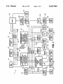
Referring now to FIG. 1. the system board S of an
the preferred embodiment of the present invention is shown.
In the preferred embodiment, the system board S contains
invention, rather than having to send the startup interpro
cessor interrupt, the operational processor is recon?gured
such that it becomes the primary processor. Each processor
includes a CPUTYPE pin for identifying Whether the pro
spare boot circuit; and
FIG. 5 is a logic diagram of portions of the hot spare boot
circuit providing control signals to the processors.
The system board S also includes two primary buses. The
?rst bus is the PCI or Peripheral Component Interconnect
bus 98 which includes address/data portion 100, also
referred to as PCIAD, control and byte enable portion 102
and control signal portion 104. The control signal portion
104 includes a clock PCICLK preferably running at 33
MHZ. The PCICLK clock is provided by the processor board
P and is the main PCI bus clock. The address/data bus
40
PCIAD is preferably 32 bits wide, although it can be
upgraded to 64 bits if desired. The second primary bus on the
system board S is the EISA bus 99. The EISA bus 99
includes LA address portion 106, SA address portion 108,
SD data portion 110 and EISA/ISA control signal portion
tional processor behaves as a primary processor in powering 45 112. The PCI and EISA buses 98 and 99 form the backbones
of the system board S.
up the computer system.
A CPU connector 114 is connected to the PCI bus 98 to
In an alternative embodiment of the present invention,
each of the processors in the computer system is connected
receive the processor board P having two microprocessors.
APCI graphics connector 116 is connected to the PCI bus 98
to a separate processor bus, with each processor con?gured
as a primary processor. To prevent the processors from all 50 to receive a video graphics card (not shown). The graphics
powering up at the same time, sleep signals are asserted to
card provides video signals to an external monitor (not
all but one of the processors to prevent those processors
shown). A PCI option connector 118 is also connected to the
from becoming active. In normal operation, once the power
PCI bus 98 to receive any additional cards designed accord
up processor has completed performing its power on
ing to the PCI standard. In addition, a SCSI and network
functions, it causes the sleep signals to the other processors 55 interface (NIC) controller 120 is connected to the PCI bus
98. Preferably, the controller 120 is a single integrated
to be deasserted. However, if the power up processor is
non-operational, the sleep signal to an operational processor
is automatically deasserted, allowing it to be awakened. In
this embodiment, separate reset signals are used to reset the
processors. Consequently, the hot spare circuit can maintain
the reset signal to the non-operational processor asserted,
while deasserting the reset signal provided to another pro
circuit and includes the capabilities necessary to act as a PCI
bus master and slave and the circuitry to act as a SCSI
controller and an Ethernet interface. A SCSI connector 122
is connected to the controller 120 to allow connection of
various SCSI devices, such as hard disk drives and
CD-ROM drives. An Ethernet connector 124 is provided on
cessor reassigned to perform the power on functions. As
the system board S and is connected to ?lter and transformer
each of the processors is connected to a separate processor
circuitry 126, which in turn is connected to the controller
bus, the non-operational processor need not be tristated as 65 120. This forms a network or Ethernet connection for
there would be no potential contention for the processor bus
connecting the system board S and computer to a local area
signals.
network (LAN).
5,627,962
5
6
A PCI-EISA bridge 130 is provided to convert signals
One of the microprocessors on the processor board is
between the PCI bus 98 and the EISA bus 99. The PCI-EISA
bridge 130 includes the necessary address and data bulfers
and latches, arbitration and bus master control logic for the
PCI bus, EISA arbitration circuitry, an EISA bus controller
designated as the primary processor for running the BIOS
code. An 8742 or keyboard controller 156 is connected to the
X1) bus and EISA address and control portions 108 and 112.
The keyboard controller 156 is of conventional design and
as conventionally used in EISA systems, and a DMA con
is connected in turn to a keyboard connector 158 and a
mouse or pointing device connector 160.
4 The computer system of the preferred embodiment also
troller. Preferably the PCI-EISA bridge 130 is a single
integrated circuit, but other combinations are possible. Dur
ing power up, the PCI-EISA bridge 130 asserts the signal
PRESETlN for approximately 200 milliseconds to reset the
processor board P.
10
includes audio capabilities. To this end a CODEC chip 162
is connected to the miscellaneous system logic chip 132 and
to an analog ampli?er and mixer chip 164. An FM synthe
sizer chip 166 is connected to the analog ampli?er and mixer
164 and receives digital information from the X1) bus. The
FM synthesizer 166 is also connected to the control and data
portions 110 and 112 of the EISA bus 99 and is controlled
Arniscellaneous system logic chip 132 is connected to the
EISA bus 99. In the preferred embodiment, the miscella
neous system logic chip 132 is implemented as an ASIC. The
miscellaneous system logic chip 132 contains a digital audio
interface, counters and timers as conventionally present in
personal computer systems, an interrupt controller for both
by the miscellaneous system logic chip 132. An audio
connector 168 is provided to allow external audio connec
tions to the computer and is connected to the outputs and
the PCI and EISA buses 98 and 99 and power management
logic, as well as other miscellaneous circuitry. The interrupt
controller portion of the miscellaneous system logic chip
inputs of the analog ampli?er and mixer 164.
132 transmits interrupt signals to the microprocessor on the
processor board P via signals IBUS[3:0]. As there are 24
interrupts in the PCI/EISA system, the interrupts are trans
a computer system. Many alternative embodiments could
exist. For example. there would be additional PCI and EISA
It is understood that this is an exemplary embodiment of
mitted 4 at a time across IBUS[3:0] in 6 OSC clocks. The
slots if the computer system was intended for ?le server use,
OSC clock is provided by logic on the processor board P, and
preferably has a frequency of approximately 14.3 MHZ.
In an alternative embodiment, the miscellaneous logic
with the video system then preferably connected off of the
EISA bus 99 and the audio system components removed.
Other variations will be apparent to one sln'lled in the art.
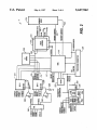
Referring now to FIG. 2, the processor board P for use
with the system board S is shown. In the processor board P,
chip 132 is implemented with the 82374EB EISA System
Component (ESC) chip from Intel, while the PCI-EISA
bridge 130 is the 82375EB PCI-EISA Bridge (PCEB) chip
25
30
the primary CPU or microprocessor 200 is preferably the
35
having data, address and control portions PD. PA and PC. A
second microprocessor 201, preferably the Pentium P54CM
from Intel. The ESC includes an I/O advanced program
mable interrupt controller (APIC) so that it can communi
cate interrupts directly to the processors located on the
processor board P over APIC data bits PICD[1:O]. In this
alternative embodiment, the signal PRESEI'IN is asserted
not by the PCEB chip but by a separate integrated chip.
A series of four EISA slots 134 are connected to the EISA
bus 99 to receive ISA and EISA adapter cards. A combina
tion I/O chip 136 is connected to the EISA bus 99. The
combination I/O chip 136 preferably includes a ?oppy disk
controller, real time clock (RI‘C)/CMOS memory, two
UARI‘s, a parallel port and various address decode logic. A
?oppy disk connector 138 for receiving a cable to a ?oppy
disk drive is connected to the combination I/O chip 136. A
pair of serial port connectors are also, connected to the
combination I/O chip 136, as is a parallel port connector
142. A bu?’er 144 is connected to both the EISA bus 99 and
management as well as perform interprocessor interrupts
(lPIs) for communication with each other. The local APICs
work in conjunction with an I/O APIC 244 located exter
nally on a PCI multiprocessor interface chip (PMIC) 238. If
the miscellaneous logic chip 132 is implemented with the
45
nected to the EISA bus 99 and receives its control signals
from the combination I/O chip 136. An address latch 150 is
connected to the EISA bus 99 and controlled by the com
capability for the NVRAM 148. Preferably the NVRAM
148 is used to contain certain system information.
A data buifer 152 is connected to the SD portion of the
ESC, then a portion of the I/O APIC is located on the ESC.
In addition to the I/O APIC 244, the PMIC 238 also includes
a hot spare boot circuit 246 and a CPU case register 240,
which will be described below.
The CPU 200 (or logical CPUl) is preferably con?gured
50
non-volatile random access memory (NVRAM) 148 is con
bination IIO chip 136 to provide additional addressing
from Intel, is also connected to the processor bus 202. Each
of the Pentium P54C and P54CM processors includes an
on-chip advanced programmable interrupt controller
(APIC). The local APICs support multiprocessor interrupt
the combination IIO chip 136 to act as a buffer between the
EISA bus 99 and a hard disk drive connector 146 to allow
connection of an IDE-type hard disk drive (not shown). A
64-bit Pentium P54C processor from Intel, which operates at
50 or 60 MHz externally and 75 or 90 MHz internally. The
microprocessor 200 is connected to a processor bus 202
as the primary processor responsible for booting up the
system. In normal operation, after the PCI-EISA bridge 130
has negated PRESEI‘IN low, CPUl vectors to an entry point
in the ?ash ROM 154 to execute the BIOS code. In addition
to properly initializing various system components, CPUl
55
also awakens the second processor 201 (logical CPU2) to
place it in operation. To start the P54CM processor, CPUl
transmits a startup IPI message to CPU2.
The I/O APIC 244 in the PMIC 238 receives PCI and
EISA bus 99 to provide an additional data bus XD for
EISA interrupts through signals IBUS[3 :0]. In response, the
various additional components of the computer system. The
I/O APIC forwards the interrupts to the local APICs in the
microprocessors 200 and 201 over the APIC bus PICD[1:0]
NVRAM 148 is connected to the X0 data bus to receive its
data bits. A ?ash ROM 154 receives its control and address
signals from the EISA bus 99 and is connected to the )0) bus
for data transfer. Preferably, the ?ash ROM 154 contains the
BIOS information for the computer system and can be
reprogrammed to allow for revisions of the BIOS. The BIOS
contains the instructions for performing power on functions.
as appropriate. The PMIC 238 also provides reset signals
PRESETOUT[2:1]. In the P54CICM dual processor
con?guration, the signal PRESEI‘OUTU] is provided to a
processor cache and memory controller (CMC) and PCI
bridge 210. The CMC 210 has a clock input connected to the
processor clock, which runs at either 50 or 60 Mhz. In
5,627,962
7
8
response to the signal PRESETOUT[I], the CMC 210
system 203, 205. The cache systems 203, 205 are connected
to the processor bus 202, with a CMC 210, data buffers 212
and 213 and memory 214 con?gured as in the processor
board of FIG. 2. It is noted that the CPUTYPE pins of CPU1
asserts a hard reset signal PRESET to both CPU1 and CPU2.
The signal PRESETOUT[Z] is unused in this con?guration.
Ordinarily. both signals PRESETOUT[2:1] follow the
state of the system reset signal PRESETIN delayed by one
200A and CPU2 201A are grounded so that both appear as
PCICLK clock. However, as will be explained below. the
primary or P54C-type processors.
signals PRESETOUT[2:1] behave di?erently if the primary
APMIC 238 is also located on the processor board of FIG.
CPU1 fails.
Each of the microprocessors 200 and 201 include an
internal or L1 cache memory. A level 2 (L2) or external
cache memory system 208 is connected to the processor bus
2A. The signals PICD[1:0] are connected to CPU1 200A,
CPU2 201A and the PMIC 238. The signal PRESETOUT[1]
is connected to CPU1 200A. while the signal PRESETOUT
[2] is connected to CPU2 201A. The PMIC 238 also is
connected to a signal P2PBE[0]* used to switch the local
APIC 1D in CPU2 201A when the primary CPU1 200A fails.
In the preferred embodiment. the local APIC ID of CPU1
200A is assigned the value ObOOOO and the local APIC ll) of
CPU2 201A is assigned the value ObOOOl.
A variation of the two primary processor con?guration
202 to provide additional caching capabilities to improve
performance of the computer system. The CMC 210 is
connected to the control portion PC and to the address
portion PA. For the P54C/CM con?guration. a single L2
cache is used for both microprocessors 200 and 201. In the
two primary processor con?guration. each processor is
coupled to a separate L2 cache through the separate proces
involves use of processors without local APICs. In this
sor buses.
alternative con?guration. additional external logic on the
processor board P must be implemented to allow CPU1 and
CPU2 to communicate with each other and to handle inter
A set of two data buffers 212 and 213, which are prefer
ably implemented with ASICs, are connected between the
rupts. In both the two primary processor con?gurations. the
PMIC 238 provides PRESETOUT[I] to CPU1 200A and
processor data bus PD and the 64-bit memory data bus MD
provided by a memory array 214. Control signals to the data
buffers 212 and 213 are provided by the CMC 210. The data
PRESETOUT[Z] to CPU2 201A as hard resets. After the
PCI-EISA bridge 130 negates the system reset signal
buffers 212 and 213 are also connected to the PCI address
and data bus PCIAD through a connector 224. which is
PRESETIN, CPU1 200A acts as the power on processor
while CPU2 201A is maintained disabled through the use of
provided to be mateably received by the processor connector
a signal SLEEP[2]*. The signal SLEEP[2]* is controlled by
114.
The data bu?ers 212 and 213 each include a SLAVE___
input. As shown, the SLAVE_input to the data buffer 212 is
a sleep bit in a CPU2 control register located in the PMIC
238. If the sleep bit is set high, then the signal SLEEP[2]*
is asserted low. However, if the sleep bit is set low, then the
tied to ground and the SLAVE_input of the data buffer 213
is not connected, the input being pulled high by an internal
pull-up resistor. The data buffer 212 is referred to as the
slave data buffer, and the data buffer 213 is referred to as the
master data buifer. Each data bu?'er receives half the data
bits from the processor. memory and PCI data buses PD,
signal SLEEP [21* is deasserted high.
35
For the two primary processor with APIC con?guration.
CPU1 200A awakens CPU2 201A by ?rst clearing the sleep
bit in the CPU2 control register and then transmitting a
startup IPI message. For the two primary processor without
APIC con?guration. a reset bit in the CPU2 control register
is ?rst set high before the sleep bit is cleared by CPU1.
MD, and PCIAD, respectively.
Clock distribution and generation circuitry 222 is associ
Writing a “1” to the reset bit causes the reset signal
ated with the processor card P and is connected to the CMC
210. The clock distribution circuitry 222 provides a clock
PCLK to the processor bus 202, as well as the clock OSC for
PRESETOUT[2] to be pulsed high for 15 PCICLK clocks.
When both the signals SLEEP[Z]. and PRESETOUT[Z] are
deasserted, CPU2 201A is awakened.
Bits 4, 5 and 6 of the CPU case register 240 (referred to
running a dead man counter 242 in the hot spare boot circuit
246 and for clocking transfers over the bus IBUS [3:0]. The
processor connector 224 is connected to the CMC 210 and 45 as CPU_CASE[6:4]) in the PMIC 238 indicate the type of
the clock distribution circuitry 222 to provide clocks
(including PCICLK) to the computer system and to provide
CPU con?guration. If bits CPU_CASE [6:4] contain a
value 0b000. then that indicates there is only one CPU in the
a PCI interface to allow the microprocessors 200 and 201 to
access the PCI and EISA buses 98 and 99 and to allow PCI
and EISA bus masters to access the main memory array 214.
The PCI address and data are multiplexed on the bus
system. If bits CPU CASE[6:4] contain the value ()b100,
then that indicates a multiprocessor system con?gured with
PCIAD, with the address provided during the address phase
and data provided during the data phase.
multiprocessor system con?gured with two primary proces
In an alternative multiprocessor con?guration, two Pen
tium P54C processors (each including a local APIC) are
CPU_CASE[6:4] contain the value ObOll, then that indi
cates a multiprocessor system with two primary processors
having local APICs, such as two P54C processors. The bit
CPU_CASE[7] if set high indicates that the primary boot
processor CPU1 is dead and that the computer system has
been booted on the secondary CPU2.
As noted above, CPU1 is preferably designated as the
processor that performs the power on functions. However, if
CPU1 fails, the hot spare boot circuit 246 according to the
present invention automatically switches to CPU2 to per
a P54C processor and a P54CM processor. If bits CPU_
CASE [6:4] contain the value 0b001, then that indicates a
sors which do not include local APICs. Finally, if bits
55
used instead of the P54C/CM con?guration. This con?gu
ration will be referred to as the two primary processor
con?guration and is shown in FIG. 2A. Unlike the P54C/CM
con?guration, where both processors share all the processor
signals, each of the processors in the two primary processor
con?guration is connected to a separate processor bus. With
the processors thus separated, there is no contention for a
single processor bus, as does exist in the P54C/CM con
?guration.
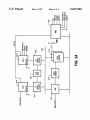
Referring now to FIG. 2A, the CPU1 200A and CPU2
201A are each connected to respective L2 cache systems 203
and 205, with arbitration logic. 207 connected to each cache
form the power on functions. As also noted, on system
65
power on reset, the signal PRESE'I'IN is asserted by the
PCI-EISA bridge 130. The signal PRESEI‘IN initializes all
PMIC registers. internal state machines, and the dead man
5,627,962
10
counter 242 located in the hot spare boot circuit 246. On the‘
TYPE pin is pulled low, the processor behaves as a P54C
next rising edge of the clock PCICLK, the PMIC 238 asserts
primary processor. If the CPUTYPE pin is pulled high, the
the signals PRESETOUT[Zzl] high. In the two primary
processor con?guration, the signal PRESETOUT[1] is pro
processor behaves as a P54CM dual processor. In the ?rst
embodiment, the CPUTYPE pin of CPU1 is always pulled
low and the CPUTYPE pin of CPU2 is always pulled high.
In the second embodiment. the CPUTYPE pin of CPU2 is
vided as a hard reset to CPU1 and the signal PRESETOUT
[2] is provided as a hard reset to CPU2. In the P54C/CM
con?guration, the signal PRESETOUT[1] is provided to the
CMC 210, which in response asserts the signal PRESET to
both CPU1 and CPU2.
While the reset signals PRESETOUT[2z1] are asserted
10
high, the microprocessor 201 responds by driving certain of
its output pins to predetermined states. Ifthe microprocessor
201 is a P54CM processor, it drives its DPEN* pin low. The
DPEN* pin is shared with the APIC data pin PICD[0]. In
addition, in the two primary processor con?guration. if the
15
microprocessor 201A is the P54C processor with a local
APIC, the pin APICEN is driven low by the CPU2 201A.
The signal APICEN is shared with the APIC data pin
to signals P2PRIEN_and P1PRIEN_, respectively. The
signals P2PRIEN_and P1PRIEN_are provided by a PAL
260, whose inputs receive signals FLUSH[1]*, PRESET,
and PGOOD. The PAL 260 is clocked by a signal SPRCLK,
which preferably has a frequency of the CPU clock. If CPU1
is detected to have failed, the PMIC 238 asserts the signal
PICD[1].
After the PCI-EISA bridge 130 negates the reset signal
PRESETIN, the signals PRESETOUT[Zzl] are negated on
the next rising edge of PCICLK. Additionally, on the falling
edge of the signal PRESETIN. the following signals are
sampled by the PMIC 238: the signal DPEN* which when
20
asserted low indicates that a P54CM is installed; a signal
HSBE which when asserted high indicates that the hot spare
25
FLUSH[1], while the signal PRESET is asserted to place
CPU1 in tristate test mode. The PAL 260 senses the signal
FLUSH[1], asserted along with the signal PRESET to switch
the states of signals P1PRIEN_and P2PRIEN__such that the
tristate buffer 262 is enabled to drive the CPUTYPE pin of
CPU2 low. Thus, as CPU2 has now been switched from a
P54CM to a P54C processor, it will perform the power on
functions once the signal PRESEI‘ is negated low by the
CMC 210.
In the two primary processor con?guration, if the dead
boot capability of the PMIC 238 is enabled; the signal
TWPRIM* which when asserted low indicates a multipro
cessor system con?gured with two primary processors, with
or without APICs; and the signal APICEN which when
asserted high indicates that the APIC on CPU2 in the two
man counter 242 times out, CPU1 200A is placed back in the
reset state by asserting the signal PRESETOUT[1], while the
signal PRESETOUT[Z] is negated low a little more than one
milliseconds after the dead man counter 242 times out to
primary processor con?guration is enabled. The signal
HSBE is pulled high by a pullup resistor 250, thereby
indicating in the ?rst embodiment that hot spare boot is
always enabled. If all the above signals are sampled in their
connected to the output of a tristate butler 262 and the
CPUTYPE pin of CPU1 is connected to the output of a
tristate buffer 266. If the tristate buffer 262 is disabled, the
CPUTYPE pin of CPU2 is pulled high by a resistor 264. If
the tristate buifer 266 is disabled, the CPUTYPE pin of
CPU1 is pulled low by a resistor 268.
The inputs of both tristate buffers 262 and 266 are
connected to ground. and their enable inputs are connected
enable CPU2 201A. On the deassertion of the signal
35
PRESETOUT[2], CPU2 201A performs the necessary
power up functions, without the need for a startup IPI
message.
Referring now to FIG. 3, a schematic diagram of the hot
spare boot circuit 246 in the PMIC 238 is shown. Alatch 300
receives the inverted state of the signal DPEN,, the signal
HSBE, the inverted state of the signal TWPRIM, and the
signal APICEN. The enable input of the latch 300 is con
nected to the signal PRESETIN. If the signal PRESEI'IN is
deasserted states (except for HSBE), then that indicates only
one CPU is in the system and the hot spare boot capability
is by default non-functional.
When the PMIC 238 detects a dual processor system and
the hot spare boot capability is enabled, the dead man
counter 242 is started two OSC clocks after the system reset
signal PRESEI‘IN is negated. If CPU1 boots properly, the
dead man counter 242 is reset when the CPU1 writes the
asserted high, the latch 300 is transparent. On the following
processor case values into the register 240, which occurs 45 edge of the signal PRESE'I'IN, the inverted state of the
relatively early in the power on self test or POST procedure.
signal DPEN*, the state of the signal HSBE, the inverted
However, if the dead man counter 242 times out, then that
state of the signal TWPRIM*, and the state of the signal
indicates that CPU1 is non-functional. As a result, in accor
APICEN are latched. The latch 300 provides output signals
dance with the present invention, CPU1 is set or maintained
in a disabled state, and the computer system is initialized by
CPU2.
In a ?rst embodiment of the P54C/CM dual processor
P54CM__INSTALLED for indicating if a P54CM processor
is installed in the system, a signal HS_BOUI‘__EN to
indicate whether the hot spare boot capability is enabled, a
signal TW_PEAKS to indicate if the multiprocessor system
is con?gured with two primary processors, and a signal
APIC_PRES to indicate whether the two primary proces—
con?guration, the PMIC 238 awakens CPU2 by sending a
startup IPI message to CPU2. The startup IPI message
includes an interrupt vector pointing to a ?xed entry point of
the BIOS ROM 154, to which CPU2 will vector for begin
ning startup operations. The startup IPI is located at a
prede?ned location in a redirection table located in the I/O
APIC 244. The hot spare boot circuit 246 triggers access to
the prede?ned location in the redirection table by asserting
a signal STARI‘UP IPI. The IPI message is serially trans
ferred from the PMIC 238 to CPU2 over the APIC data bits
PICD[1:O].
55
sors include local APICs.
The reset signal PRESEI'IN is also provided to the D
input of a D ?ip-?op 302, which is clocked by the signal
PCICLK. The output of the D ?ip-?op 302 provides the
signal S__PRESEI'IN, which represents the signal PRESE
TIN synchronized to the clock PCICLK. In addition, another
signal OSC_PRESEI‘]N is developed in the hot spare boot
circuit 246, which is synchronized to the clock OSC used by
the dead man counter 242. If the signal PRESE'I‘IN is
In a second embodiment of the P54C/CM con?guration,
asserted high, the signal OSC_PRESEI‘IN is asserted high
a startup IPI is not needed for awakening CPU2 in the 65 on the next rising edge of the clock OSC. The signal
P54C/CM con?guration. Both the Pentium P54C and
OSC_PRESEI'IN falls two OSC clocks after the falling
P54CM processors include a CPUTYPE pin. If the CPU
edge of the signal PRESETIN.
5,627,962
12
11
The signal OSC_PRESET1N is provided to one input of
the 0 inputs of multiplexors 318 and 320. The 1 inputs of the
an OR gate 304, whose other input is connected to a signal
multiplexors 318 and 320 are grounded low and their select
inputs are connected to the RESET input. The outputs of the
multiplexers 318 and 320 are provided to the D inputs of D
?ip-?ops 322 and 324. The D ?ip-?op 322 is clocked on the
S2_CPU_CASE__WR1'ITEN for indicating when the CPU
case register 240 has been written once. If CPUl powers up
properly, CPUl writes to the CPU case register 240 with
rising edge of the CLK input, and the D ?ip-?op 324 is
clocked on the falling edge of the CLK input. The outputs of
appropriate values (as explained above) to indicate the type
of CPU con?guration, which values it will have read from
the CPU case register 240. The output of the OR gate 304
drives a signal RST_DEAD__MAN_TMR for resetting the
dead man counter 242. Thus, proper power up by CPUl will
the D ?ip-?ops 322 and 324 are provided to the inputs of an
OR gate 326, whose output is connected to the 0 input of a
10
cause the CPU case register 240 to be written, which in turn
causes the dead man counter 242 to be reset. The dead man
counter 242 preferably is reset to the initial value of
0X1B4F4C8. The enable input of the dead man counter 242
is connected to the output of an AND gate 316. One input of
the AND gate 316 is connected to a signal DEAD_MAN_
multiplexer 328. The 1 input of the multiplexor 328 is
grounded low. and its select input is connected to the RESET
input. The output of the multiplexor 328 is connected to the
D input of a D ?ip-?op 330, which is clocked on the rising
edge of the CLK input. The output of the D ?ip-?op 330 is
connected to the output of the synchronizer circuit 315,
which in turn drives the signal S2_DEAD_MAN to indi
TMR_EN, which is provided by an AND gate 306. The ?rst
cate whether the dead man counter 242 has timed out. The
input of the AND gate 306 receives the signal HS_BOOT_
net effect of the synchronizer circuit 315 is to delay the
assertion and deassertion of the signal S2__DEAD_MAN
EN and the second input is connected to the output of an OR ,
gate 308. The inputs of the OR gate 308 receive signals
CM_PRES and TW_PRES, which are provided by D
?ip-?ops 310 and 312, respectively. The D ?ip-?ops 310 and
20
Once the dead man counter 242 counts down to 0, and the
25
signal TMR_EQ_0 is asserted high, a second counter 332
is enabled by the signal TMR_EQ_0. The reset input of the
counter 332 is connected to the output of an OR gate 334,
whose ?rst input receives the signal OSC_PRESET]N.
During system reset, the counter 332 is reset to the value
0><37EE. The other input of the OR gate 334 is connected to
the output of an AND gate 336, which receives input signals
TMR_EQ_0 and S2_STOP_ONE_MS__TMR. The
30
counter 332 also includes a load input, which when asserted
high loads the counter 332 with the value O><0004. The load
312 are clocked by the signal OSC, and are reset by the
signal OSC_PRESET]N. The D inputs of the D ?ip-?ops
310 and 312 are connected to the signals CM_PRES_REG
and TW_PRES__REG, respectively. The signals
CM__PRES_REG and TW_PRES__REG are decoded from
bits 4, 5 and 6 of the CPU case register 240, and indicate
whether the P54CM processor is present or two primary
processors are present, respectively. Before the CPU case
register 240 is written with the proper values by the power
by two PCICLK clocks from the signal TMR_EQ_0.
on processor. the states of bits CPU_CASE[6:4] are deter
input is connected to the output of an AND gate 338, whose
mined from the states of the signals P54CM_INSTALLED,
inputs receive signals TMR_EQ_0 and S2_LOAD_
TW_PEAKS, and APIC_PRES provided by the latch 300.
If the signal P54CM_INSTALLED is asserted high, then
the register bit CPU_CASE[6] is set high. If the signal
TW_PEAKS is asserted high, then the register bit CPU_
CASE[4] is set high. Further, if the signals TW_PEAKS
COUNT. The enable input of the counter 332 is connected
to the signal TMR_EQ_0, and the counter 332 is clocked
by the signal OSC. The counter 332 decrements on each
and APIC_PRES are both asserted high, the register bit
CPU_CASE[5] is set high. The signal CM_PRES_REG is
asserted high if register bits CPU_CASE[6:4] contain the
value OblOO. The signal TW_PRES_REG is asserted high
if the register bits CPU_CASE[6:4] contain either the value
rising edge of the clock OSC if the signal TMR_EQ_0 is
asserted. Further, when the counter 332 reaches the value
zero, it wraps around back to the initial value 0><37EE. The
40
counter 332 provides output signals ONE_MS_TMR
45
[15:0], which are received by comparators 340 and 342. The
comparator 340 asserts a signal ONE_MS_PASSED if the
counter 332 has counted down to the value zero, indicating
that 1 millisecond has elapsed. The comparator 342 asserts
a signal PULSE__TIMEOUT high when the counter 332
0b011 or ObOOl.
Thus, etfectively, the signal DEAD_MAN_TMR_EN is
driven high if the processor board P is con?gured as a dual
processor system, the hot spare boot capability is enabled as
decrements to the value 6.
indicated by the signal HS_BOOT_EN, and the synchro
nized reset signal OSC_PRESEI'IN has been negated.
input of a synchronizer circuit 344, which contains the same
components as the synchronizer circuit 315. The CLK input
of the synchronizer circuit 344 is connected to the signal
Assertion of the signal DEAD_MAN_TMR_EN etfec
tively enables the counter 242 to decrement from its initial
value of 0x1B4F4CS. The counter 242 is clocked by the
The signal ONE_MS_PASSED is provided to the signal
50
PCICLK, its RESET input is connected to the signal
S__PRESEI‘]N, and its output provides a signal S2_ONE_
signal OSC, and provides output signals DEAD_MAN_
MS_PASSED. The signal PULSE_TIMEOUT is provided
to the signal input of another synchronizer circuit 346, which
TMR[24:O]. The output of the counter 242 is provided to a
is also clocked by the signal PCICLK and reset by the signal
S_PRESET]N. The output of the synchronizer circuit 346
provides a signal S2_PULSE_TIMEOUT. The signals
comparator 314, which asserts a signal TMR_EQ_0 high
when the counter 242 has decremented down to 0. The
inverted state of the signal TMR_EQ_0 is provided to the
other input of theAND gate 316. Once the dead man counter
242 counts down to zero, it is disabled from further decre
menting; as a result, the counter 242 remains at the value
S2_ONE_MS__PASSED and S2_PULSE_TIMEOUT are
versions of the signals ONE_MS_PASSED and PULSE_
TIMEOUT, respectively, delayed by two rising edges of the
clock PCICLK.
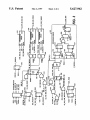
Referring now to FIG. 4, a state diagram of a state
zero.
The signal TMR_EQ_0 is also provided to the signal
INPUT of a synchronizer circuit 315. The synchronizer
circuit 315 also includes a CLK input, a RESE'I‘ input, and
an output, which are connected to the signals PCICLK,
machine HSBST is shown. On system reset, indicated by the
signal S_PRESEI‘IN, the state machine HSBST transitions
S_PRESE'I'1N, and S2_DEAD_MAN, respectively. The
to or remains in state IDLE. When the signal S_PRESET]N
is negated, the state machine remains in state lDLE until the
signal INPUT of the synchronizer circuit 315 is connected to
signal S2_DEAD_MAN is asserted high, indicating that
65
5,627,962
13
14
the deadman timer has timed out. In response. the state
machine HSBST transitions to state START_HSB. As will
is negated low or both the signals PICD1_PULSE and
S2_PULSE_TlMEOUT are asserted high. The second con
dition ensures that, if PICD[l] is not driven low, the state
machine HSBST is able to proceed after the timeout signal
be described in FIG. 5, the reset signals PRESEI‘OUT[2:1]
are asserted high when the state machine HSBST enters state
STARI‘_HSB. The signals PRESE'I‘OUT[2:1] are thereafter
maintained high until certain other conditions occur, as will
be described in FIG. 5. It is noted that all transitions of the
state machine HSBST occur on the rising edge of the clock
PCICLK. The state machine HSBST remains in state
STARI‘_HSB until the signal S2__ONE__MS_PASSED is
asserted high to indicate that approximately 1 millisecond
has passed since the dead man counter 242 has timed out.
From state STARI‘_HSB, the state machine transitions to
state WA1T_PICDI_PULSE, where it remains while the
signal PICD1_PULSE is asserted high and the signal
S2_PULSE__T1MEOUT is negated low.
Referring back to FIG. 3, the signal PICD1_PULSE is
15
vided to the AND gate 338 in FIG. 3 to load the counter 332
with the value 0><0O04. This value of 0><0004 ensures that
provided by a D ?ip-?op 352. The D input of the D ?ip-?op
there is a 4 OSC clock delay before the signal PRESEI‘OU‘T
[1] is allowed to be negated, as explained below.
Referring back to FIG. 4, from state CLK_1_‘AFI‘_
PULSE, the state machine HSBST transitions to state
CLK2_AFI‘__PULSE on the next rising edge of clock
PCICLK. The states CLK_1_AFI'_PULSE and the
352 is connected to the output of a D ?ip-?op 350, whose D
input is connected to the signal PICD[l]. The D ?ip-?ops
350 and 352 are clocked by the signal PCICLK, and both are
reset low by the signal S__PRESEI‘IN. As noted above, in
the P54C/CM dual processor system, the P54CM processor
drives the PICD[O]/DPEN, pin low when the signal PRESET
is asserted high. Assertion of the signal PICD[O] causes any
25
other I/O APICs present in the computer system. such as one
in an ESC chip if present. to thinkthat the system has started.
The U0 APIC 244 in the PMIC 238 does not respond to the
assertion of the signal PICD[O] as the state machine in the
I/O APIC 244 is maintained in the reset state. In response to
the assertion of the signal PICD[O], the ESC drives the APIC
data bit PICD[l] low every 20 PICCLK clocks. The PIC
CLK clock is used to control transfers over the APIC bus
PICD[lzO] and is driven from the OSC clock, which pref
erably runs at approximately 14.3 Mhz. The bit PICD[l] is
pulsed low for either 1 or 2 PICCLK clocks, depending on
S2_PULSE_TIMEOUT goes high. If the signal PICD1__
PULSE is negated low, then the state machine HSBST
asserts a signal LOAD_COUNT high.
Referring now to FIG. 5, the signal LOAD_COUNT is
provided to the select input of a multiplexer 540, whose 0
and 1 inputs are tied low and high. respectively. The output
of the multiplexor 540 is connected to the D input of the D
?ip-?op 542. The output of the D ?ip-?op 542 is in turn
connected to the D input of a D ?ip-?op 544. which provides
the signal S2_LOAD_COUNT. The D ?ip-?ops 542 and
544 are clocked by the signal OSC and reset by the signal
OSC_PRESEI'IN. The signal S2__LOAD_COUNT is pro
CLK2__AF1"_PULSE are dummy states inserted to ensure
that all signals have stabilized. From state CLK_2__AFI‘_
PULSE, the state machine HSBST transitions to state DLY__
AFI‘_PULSE on the next rising edge of clock PCICLK.
Referring again to FIG. 5, an OR gate 502 receives signals
STARI‘_HSB. WAI'I‘_PICDI_PULSE, CLK_1_AFI‘_
PULSE, CLK__2_AFI‘_PULSE, and DLY_AFI‘_PULSE
which indicate that the state machine HSBSI‘ is in one of the
corresponding states. In other words, the signal STARI‘__
HSB represents that the state machine HSBST is in state
35
START__HSB, etc. The output of the OR gate 502 provides
a signal RESEI‘_TIME. The signal RESEI‘_TIME is pro
the message transmitted during a status cycle as standard in
I/O APIC operation and known to those skilled in the art.
The P54CM processor samples the state of the signal
vided to one input of an OR gate 504 and one input of an OR
PICD[l] on the falling edge of the signal PRESET provided
by the CMC 210. If the signal PICD[l] is sampled low, then
The signal PRESETOUTI is provided to a bu?ier 508,
the local APIC of CPU2 is disabled. However, if the signal
PICD[l] is sampled high, the local APIC is enabled.
Therefore, to ensure that PICD[l] is not driven low by the
PRESETOUTZ is provided to one input of an OR gate 510,
whose other input receives a signal RSI‘__CPU2. The output
of the OR gate 510 is connected to the input of a buffer 512,
whose output drives the signal PRESEI'OUT[2]. In the two
miscellaneous logic chip 132 when the signal PRESET‘ is
gate 506. The outputs of the OR gates 504 and 506 provide
signals PRESEI‘OUTl and PRESEI‘OUT2. respectively.
whose output drives the signal PRESETOUTH]. The signal
45
being provided to the P54CM processor, the state machine
HSBST waits in state WAIT_PICD1_PULSE until the
signal PICD1_PULSE is driven low by the I/O APIC 244 or
primary processor without APIC con?guration, the signal
the ESC. By waiting for a su?iciently long period after the
signal PICD1_PULSE has been negated low, the signal
the reset bit of the CPU2 control register being set high by
CPUl, the PMIC 238 asserts the signal RST_CPU2 for 15
PICD1_PULSE is allowed to come back high before PRE
PCICLK clocks. While the hot spare boot state machine is
SEI‘ is negated low by the CMC 210. Without the state
not in the IDLE state, the signal SLEEP[2]* is negated to
allow CPU2 to be awakened after the signal PRESEI‘OUT
[2] is released
RST__CPU2 is used to control the state of PRESEI‘OUI‘[2]
when CPUl is attempting to awaken CPU2. In response to
WAII‘_PICD1_PULSE, if for some reason the signal PICD
[1] is sampled low as the reset signal PRESET is negated
low which may occur if there is a race condition between the 55
rising edge of the signal PICD[l] and the falling edge of the
signal PRESET or if the processors are reset separately from
the I/O APIC 244 and the problem is not addressed-the
local APIC of CPU2 would be disabled. As a result, the
P54CM processor would be unable to respond to a subse
quent startup lPI message for waking up CPU2 at the end of
the hot spare boot sequence. The consequences would be
fatal, as CPU2 would be unable to power up the computer
sents the state of CPU case register bit CPU__CASE[7]. If
the CPU case register 240 has not yet been written once, the
system.
Referring again to FIG. 4, the state machine HSBST
During normal power up operations by CPUl in either of
the two primary processor con?gurations, CPU2 is main
tained disabled by keeping the sleep bit of the CPU2 control
register in the PMIC 238 set at the high state. The sleep bit
of the CPU2 control register, represented as a signal
P2__SLEEP, is provided to one input of an AND gate 550,
whose other input receives the inverted state of a signal
HS_BOOT_REG. The signal HS_BOUI‘__REG repre
transitions from state WA1T_PICD1_PULSE to state
bit CPU__CASE[7] is equal to a signal HS_BOUI‘. The
signal HS__BOUI‘ is asserted high when the state machine
CLK__1_AFI‘_PULSE if either the signal PICD1_PULSE
HSBST is not in state IDLE, which means that it remains
65
5,627,962
15
16
asserted once the state machine HSBST leaves the IDLE
state until the computer system is reset.
The output of the AND gate 550 is connected to the select
If the multiprocessor system is con?gured in the P54C/
CM mode, the signal FLUSH[1]* is asserted when the dead
man counter 242 times out. The output .pins of the non
input of a multiplexor 552. The 0 and 1 inputs of the
multiplexer 552 are tied high and low, respectively. The
output of the multiplexor 552 is connected to the D input of
operational CPU1 200 are thus tristated so that they will not
the D ?ip ?op 554, whose output provides the signal
interfere with the operations of CPU2 201. In the P54C/CM
con?guration, this is required as CPU1 and CPU2 share the
same processor bus 202. In the two primary processor
SLEEP[2] . The D ?ip ?op 554 is clocked on the rising edge
of PCICLK and reset by S_PRESETIN. During normal
the hot spare boot sequence.
operation, the signal SLEEP[2]* is deasserted only when the
sleep bit P2_SLEEP is set low by CPU1. However, during
5
con?guration, the signal FLUSH[1]* is not asserted during
10
the hot spare boot sequence. once the state machine HSBST
leaves state IDLE and the signal HS_BOOT is asserted, the
signal SLEEP[2]* is deas serted high to allow CPU2 to wake
up.
Once the dead man counter 242 expires and the state
machine HSBST enters state START_HSB, both signals
PRESETOUT[I] and PRESETOUT[2] are asserted high to
reset CPU1 and CPU2. At the same time, the signal SLEEP
[2] * is deasserted low in the two primary processor con
?guration to allow CPU2 to begin the power on procedure
RESET_TIME is asserted high, the signal HOLD_APIC_
15
to the assertion of the signal PICD[0] by CPU2 in the
20
state machine HSBST transitions to state CLK_1_AFI‘_
25
from 4 to 6 OSC clocks after the state machine HSBST
transitions out of state WAIT_PICD1__PULSE. This is
because the state machine HSBST transitions to state CLK_
1_AFI‘_PULSE either in response to the signal PICD1_
When the signal PRESETIN is negated low, the signals
PULSE being negated (thereby asserting the signal LOAD__
30
COUNT and loading the counter 232 With the value 0><O0O4
one PCICLK later) or to the signal S2_PULSE_TMOUT
being asserted high (indicating that the counter 232 has
reached the value 0><0006).
On the transition to state CLK__1_AFI‘_STRT, the sig
TIME drives both signals PRESETOUT[2:1] back high
when the state machine HSBST enters state START_HSB.
The ?nal input of the OR gate 504 is connected to the
output of an AND gate 514, whose inputs receive signals
TW_PRES_REG and HS_BOOT. Thus, if the multipro
Referring back to FIG. 4, the state machine HSBST
remains in state DLY_AFI‘_PULSE until the signal
S2_ONE_MS__PASSED is asserted high. in which case the
STRT. The signal S2_ONE_MS__PASSED is asserted high
PRESETOUT[2:1] are negated low one PCICLK clocks
later under normal conditions, i.e., CPU1 is operational.
Otherwise, if CPU1 is non-operational, the signal RESET_
SM is asserted high to disable a state machine in the I/O
APIC 244 to ensure that the I/O APIC 244 does not respond
P54C/CM con?guration.
once the signal PRESETOUT[Z] is negated by the PMIC
238.
Both OR gates 504 and 506 also receive the signal
S_PRESETIN. When the system reset signal PRESETIN is
asserted by the PCI-EISA bridge 130, the CPU reset signals
PRESETOUT[2:1] are also driven high one PCICLK later.
The signal RESET_TIME is further provided to one
input of an OR gate 538, whose other input receives a signal
RELEASE_APIC_SM. The output of the OR gate 538
provides a signal HOLD_APIC_SM. While the signal
35
cessor system is con?gured with two primary processors,
and the dead man counter 242 has expired indicating a CPU1
nal RESET_TIME is negated low. As a consequence, in the
p54C/CM dual processor con?guration, the signal
PRESETOUT[I] is negated low, thereby causing the CMC
210 to deassert the signal PRESET to CPU1 and CPU2. For
the two primary processor con?guration, the signal
PRESETOUT[l] is maintained high While the signal
failure, the signal PRESETOUT[l] is maintained high to
disable CPU1 200A until the next system reset, in which
in the reset state. This is allowable as CPU1 200A and CPU2
201A are connected to separate buses.
45
PRESETOUT[2] is negated low. From state CLK_1_
AFI‘__STR1", the state machine HSBST transitions to state
CLK_2_AFT_STRI‘. On the next PCICLK clock, the state
machine HSBST transitions to state RELEASE_APIC_
SM.
The signal RESET_TIME is also provided to one input of
a NAND gate 516, whose other input receives the inverted
state of the signal TW_PRES_REG. The output of the
by a tristate buffer 520, whose input is connected to the
output of an OR gate 522. The enable input of the tristate
case the same procedure as described is repeated to deter
mine if CPU1 is operational. In the two primary processor
con?guration, CPU1 200A is disabled simply by keeping it
Referring again to FIG. 5, the signal P2PBE[0]* is driven
bu?‘er 520 is connected to the inverted state of a signal
NAND gate 516 is connected to one input of an AND gate
560, whose other input is connected to a signal
FLUSHALL_. The signal FLUSHALL_is asserted by the
PMIC 238 in response to commands issued by the CMC 210
for ?ushing the internal caches of CPU1 and CPU2 as well
50
PBEO_EN provided by an OR gate 524. The ?rst input of
the OR gate 522 receives a signal PBEO_DLY2, and its
second input is connected to the output of an exclusive OR
gate 526. The ?rst input of the exclusive OR gate 526
as the L2 cache 208. Plush and cache on bits in the CPU1
and CPU2 control registers of the PMIC 238 are set high or
toggled to indicate that the L1 and L2 caches are to be
?ushed. The output of the AND gate 560 is connected to one
receives the signal TW_PRES_REG, which indicates
whether the multiplexor system is in the two primary
processor con?guration. The other input of the exclusive OR
input of an OR gate 562, whose other input is connected to
the signal TW_PRES_REG. The output of the OR gate 562
is connected to an input of the AND gate 564, whose other
input is connected to the output of a NAND gate 566. The
inputs of the OR gate 528 receive signals RESET_TIME,
CLK_1_AFI‘_STRT, and CLK__2_AFI‘_STRT. The
inputs of the OR gate 524 receive signals RESET_TIME,
CLK_1_AFI‘_STRI‘, CLK_2_AFI‘_STRT, and PBEO_
inputs of the NAND gate 566 receive signals Pi_CACHON
and TW_PRES_REG. ‘The signal Pi_CACHON is the
DLY2.
Thus, before the state machine HSBST reaches state
cache on bit of the CPU1 control register of the PMIC 238.
The output of the AND gate 564 drives the signal FLUSH
[l]*, which is asserted during the hot spare boot sequence to
place CPU1 200 in the tristate test mode.
gate 526 is connected to the output of an OR gate 528. The
RELEASE_APIC_SM, the output of the OR gate 528 is
65 driven low. However, once the state machine HSBST has
transitioned to state RELEASE_APIC_SM, the output of
the OR gate 528 is driven high. If the two primary processor
5,627,962
17
18
con?guration is used and the signal TW__PRES_REG is
and CPU2 are switched to reassign CPU2 as being the
asserted. the exclusive OR gate 526 outputs a zero.
primary processor for powering up the computer system. As
shown in FIG. 2, the CPUTYPE pin of CPU2 is driven low
by the tristate buffer 262 when it is enabled by the signal
P2PRIEN_being asserted low. The CPUTYPE pin of CPUl
is driven low by the tristate buffer 266 when it is enabled by
the signal P1PRIEN_being asserted low. In the PAL 260,
the signal P2PRIEN_is provided by the output of an
However, if the P54C/CM dual processor mode is used, the
exclusive OR gate 526 outputs a high. At the same time that
the output of the OR gate 528 is negated low when the state
machine HSBST reaches state RELEASE__APIC_SM, the
output of the OR gate 524 is also negated low to enable the
tristate buifer 520. Thus, in the P54C/CM dual processor
con?guration, the signal P2PBE[O], is driven high, while in
the two primary processor con?guration, the signal P2PBE
[0]* is driven low. Driving the signal P2PBE[O], high to the
inverter 578, whose input is connected to the signal
PlPRIEN_. The signal P1PRlEN__is connected to the out
put of a D ?ip ?op 576, which is clocked by the signal
SPRCLK. The D input of the D ?ip ?op 576 is connected to
the output of an OR gate 574, whose inputs are connected to
the outputs of AND gates 570 and 572. The inputs of AND
P54CM processor forces the local APIC ID of the P54CM to
be ObOOOO. As explained earlier. this is normally the local
APIC ll) assigned to the P54C processor. However, as the
P54C processor is determined to be non-operational. the
local APIC_ID of the P54CM is reassigned so that it can
gates 570 receive signals PRESET, FLUSH[1]*, and
PGOOD. The signal PGOOD indicates that the computer
system power voltage has reached their active levels. The
inputs of the AND gate 572 receive signals P1PRIEN_and
PGOOD. Thus, if the signal FLUSH[1], is not driven low by
the AND gate 574 during the hot spare boot sequence,
properly start up the computer system. Driving the signal
P2PBE[0]* low to a P54C processor in the two primary
processor con?guration also causes the local APIC ID of
CPU2 201A to be reassigned to the value ObOOOO. It is noted
that for the two primary processor mode without local
APICs, there is no APIC ID to reassign. CPU2 is simply
awakened to handle the power up of the computer system.
The signal PBEO__DLY2 is provided to the OR gates 522
and 524 to ensure that the signal P2PBE[0], is asserted high
while the system reset signal PRESEI‘IN is asserted high,
and for two PCICLK clocks after negation of the signal
PRESETIN. The signal PBEO__DLY2 is provided by a D
?ip-?op 530, whose D input is connected to the output of a
D ?ip-?op 532. The D input of the D ?ip-?op 532 is
grounded low. Both D ?ip-?ops 530 and 532 are clocked by
the signal PCICLK, and both are reset to a high state by a
indicating that CPUl is functional, the signal P1PRIEN_is
asserted low to enable the tristate buffer 266 and the signal
P2PR1EN__is deasserted high to disable the tristate buffer
262. However, if the signal FLUSH[1]* is asserted low
while the signal PRESETOUI‘[1] is asserted high during the
25
30
signal TW_RESE'I‘. The signal TW_RESEI‘ is provided by
35
CONT_HSB when the signal S2_PULSE__TIMEOUT is
asserted high, indicating that the counter 332 has counted
CONT_HSB for approximately 6 OSC clocks until the
signal S2_ONE_MS_PASSED is asserted high. When that
certain 11) information as necessary such that the second
45
CPU can properly perform power on operations. The hot
spare boot then awakens the second CPU, using a startup
interprocessor interrupt in one embodiment, or simply
negating the hard reset of the second CPU in a second
embodiment. The second CPU then proceeds to perform the
power on functions.
provides the signal S2_STOP_ONE_MS__TMR, which is
50
The foregoing disclosure and description of the invention
are illustrative and explanatory thereof, and various changes
in the size, shape, materials, components, circuit elements,
wiring connections and contacts, as well as in the details of
the illustrated circuitry and construction and method of
state machine HSBST at state IDLE.
55
which indicates that the state machine HSBST is in state
BOOT_P54CM, is provided to one input of an AND gate
536. The other input of the AND gate 536 is connected to the
inverted state of the signal TW_PRES_REG. The output of
the AND gate 536 drives the signal STARI‘UP_IPI. In the
?rst embodiment of the P54C/CM dual processor
con?guration, the signal STARI‘UP__IPI is asserted high
when the state machine reaches the state BOUI‘ P54CM.
Assertion of the signal STARTUPJPI triggers the I/O
APIC 244 to send a startup IPI message to CPU2 201.
65
However, as noted above, in the second embodiment of
the P54C/CM con?guration, the CPUTYPE pins of CPUl
operational CPU for powering up the computer system. In
the multiprocessor computer system, a ?rst CPU is desig
nated to perform power on operations. If the ?rst CPU fails,
circuit identi?es an operational second CPU, reinitializing
BOOT_P54CM. In state BOOT_P54CM, the state
machine HSBST drives a signal SI‘OP_ONE_MS_TMR
Returning now to FIG. 5, the signal BOOT_P54CM,
What has been described is a hot spare boot circuit that
automatically switches from a non-operational CPU to an
the ?rst CPU is in a disabled state. Next, the hot spare boot
occurs, the state machine HSBST transitions to state
provided to the AND gate 336 for resetting the counter 332
to the initial value 0X37EE. The state machine HSBST stays
in state BOOT_P54CM until the computer system is reset,
as indicated by the signal S_PRESETIN, which restarts the
CPU2 200 vectors to the normal reset location in the BIOS
ROM 154 to begin power on operations, rather than the
which is determined when a dead man counter in the hot
spare boot circuit times out, the hot spare circuit ensures that
down to 0X0O06. The state machine HSBST remains in state
high. The signal STOP_ONE_MS__TMR is provided to the
input of a synchronizer circuit 333 (FIG. 3), which is
clocked by the signal OSC and reset by the signal OSC_
PRESETIN. The output of the synchronizer circuit 333
signal PRESEI‘OUT[1] being negated by the PMIC 238,
startup location indicated by the startup IPI message.
an AND gate 534, whose inputs receive the signals
S__PRESETIN and TW_PEAKS.
Returning now to FIG. 4, the state machine HSBST
transitions from state RELEASE__APIC_SM to state
hot spare boot sequence, the signal P1PRIEN__is deasserted
high andv the signal P2PRIEN__is asserted low. As a result,
the CPUTYPE pin of CPU2 200 is pulled low, causing it to
behave as a P54C processor. Consequently, when the signal
PRESEI‘ is negated low by the CMC 210 in response to the
operation may be made without departing from the spirit of
the invention.
We claim:
1. A multi-processor computer system incorporating the
capability to automatically switch between processors for
powering up the computer system, the computer system
comprising:
a ?rst processor normally assigned to power up the
computer system;
a second processor capable of powering up the computer
system if said ?rst processor fails;
a timer coupled to said ?rst processor and con?gured to
determine if said ?rst processor has failed;
5,627,962
19
20
a boot peripheral device coupled to said ?rst and second
processors; and
a hot spare boot circuit coupled to said timer and to said
?rst and second processors, said hot spare boot circuit
utilizing a single reset signal to place said ?rst and
second processors into reset states for a predetermined
a second processor capable of powering up the computer
system if said ?rst processor fails;
a timer coupled to said ?rst processor for determining if
said ?rst processor has failed;
a boot peripheral device coupled to said ?rst and second
processors;
a hot spare boot circuit coupled to said timer and to said
?rst and second processors, said hot spare boot circuit
period if said ?rst processor fails,
said hot spare boot circuit adapted to assert a ?ush signal
to place said ?rst processor into a tristate test mode if
said ?rst processor fails, and
said hot spare boot circuit further adapted to thereafter
awaken said second processor to power up the com
puter system and boot the computer system from said
boot peripheral device.
2. The multi-processor computer system of claim 1,
utilizing a single reset signal to place said ?rst and
10
second processors into reset states for a predetermined
period if said ?rst processor fails, said hot spare boot
circuit further con?gured to assert a ?ush signal to
place said ?rst processor into a tristate test mode if said
?rst processor fails; and
wherein said ?rst and second processors each include a CPU
an interproces sor interrupt generation circuit coupled to or
included within said hot spare boot circuit and further
coupled to said second processor,
type pin, wherein said CPU type pin of each of said
said interprocessor interrupt generation circuit con?gured
processors being driven to a ?rst state indicates that the
processor associated therewith is a primary processor
to awaken said second processor to power up the
responsible for powering up the computer system, and
wherein said CPU type pin of each of said processors being
said interprocessor interrupt generation circuit transmit
ting an interprocessor interrupt message to notify said
15
computer system if said ?rst processor fails,
driven to a second state indicates that the processor is a dual
second processor that it is to boot the computer system
processor that needs to be awakened by another processor
during power up, and wherein said hot spare boot circuit is
con?gured to drive the CPU type pin of said second pro
from said boot peripheral device.
8. The multi-processor computer system of claim 7,
wherein a computer system reset signal is initially asserted
to initialize components of the computer system, wherein
25
cessor to said ?rst state if said ?rst processor fails.
3. The multi-processor computer system of claim 2,
wherein said ?rst processor is a Pentium P54C processor and
said second processor is a Pentium P54CM processor.
4. The multi-processor computer system of claim 2,
wherein a computer system reset signal is initially asserted
to initialize components of the computer system, wherein
said timer includes a dead man counter, said dead man
counter adapted to count from a predetermined initial value
30
and wherein said dead man counter is further adapted to
count to a predetermined ?nal value indicating that said ?rst
processor has failed.
9. The multi-processor computer system of claim 8,
said timer includes a dead man counter, said dead man
counter adapted to count from a predetermined initial value
after said computer system reset signal has been deasserted,
after said computer system reset signal has been deasserted,
35
wherein said ?rst processor resets said dead man counter if
said ?rst processor powers up properly.
and wherein said dead man counter counts to a predeter
mined ?nal value to indicate that said ?rst processor has
wherein said ?rst and second processors each include a local
failed.
interrupt controller having an identi?er, said identi?er for
5. The multi-processor computer system of claim 4,
wherein said ?rst processor resets said dead man counter if
said ?rst processor powers up properly.
6. The multi-processor computer system of claim 1,
wherein said hot spare boot circuit is con?gured to transmit
a single processor reset signal to place said ?rst and second
processors into reset states for a predetermined period if said
?rst processor fails.
7. A multi-processor computer system incorporating the
capability to automatically switch between processors con
nected on a common processor bus in a computer system for 50
powering up the computer system, the computer system
comprising:
a ?rst processor normally assigned to power up the
computer system;
10. The multi-processor computer system of claim 7,
said ?rst processor having a ?rst value, said identi?er for
said second processor having a second value, wherein said
interprocessor interrupt generation circuit is con?gured to
initialize said identi?er of said second processor to said ?rst
value if said ?rst processor fails.
11. The multi-processor computer system of claim 10,
wherein said ?rst processor is a Pentium P54C processor and
said second processor is a Pentium P54CM processor.
12. The multi-processor computer system of claim 7,
wherein said hot spare boot circuit is con?gured to transmit
a single processor reset signal to place said ?rst and second
processors into reset states for a predetermined period if said
?rst processor fails.