1
v1AR, INC.
•
23600 Mercantile Road
•
8086/S100
Cleveland, Ohio 44122
CPU - INTERRUPT (Copyright (C) 1981 TecMar Inc.)
I-A
•
Phone: (216) 464-7410 INTRODUCTION 8086/S-100 CPU - INTERRUPT The Tecmar 16 bit S-lOO CPU-Interrupt board is based
on the INTEL 8086 microprocessor and consists of the
CPU with 8 levels of vectored interrupt and S-lOO
interface with extended addressing. The board complies
with the proposed IEEE 16 bit S-lOO protocol providing the
ability to fetch and store two- bytes at a time which
effectively doubles the previous capacity of the bus.
This board can access I/O devices (byte-at-a-time or word
at-a-time) through memory locations or I/O ports providing
compatibility with conventional S-lOO 8080/Z80 systems.
The board permits a one megabyte address space by
utilizing a 20 bit address which is formed using the
extended address protocol in the proposed standard for the
S-lOO bus allowing full use of the 8086.
The INTEL 8086 microprocessor is fully described in
INTEL's MCS-86™ User's Manual.
(Please refer to this
since the information on the 8086 integrated circuit will
not be repeated in this manual.)
The primary features
include eight 16 bit registers, hardware multiply and
divide, hardware trace mode, and inherently position
independent code via base registers.
The 8086 machine
language provides a 5 to 10 fold
base increase in
performance over the 8080. Assembly language programs for
the 8080 can be easily translated into 8086 programs with
approximately a factor of two increase in performance.
The CPU-Interrupt board can be used with 8-bit memory
boards, but memory capable of 16-bit transfers will allow
faster operation. The board has a power-on jump feature to
FFFFO H where a monitor is provided (on the PROM-I/O
board) •
Depending upon the crystal installed,
be set up to operate at 4, 5, or 8 MHz.
the system can
The 8086 uses a full 16-bit address for I/O devices
unlike the 8080 which duplicates the 8-bit I/O address on
A15-A8 and A7-AO.
The board is shipped with all jumpers in a standard
configuration but can easily be changed to take advantage
of the optional features, such as the wait state
generator.
(Copyright (C) 1981 TecMar Inc.)
2-A
FEATURES 8086/S-100 CPU - INTERRUPT 1)
S-IOO bus compatible
2)
16 bit microcomputer (8086)
3)
8 levels of vectored interrupt
4)
Designed for operation at 4, 5, or 8 MHz
5)
Compatible with conventional S-IOO 8080/Z80 boards
6)
One megabyte address space
7)
Full 16 bit address for I/O device
8)
On-board regulators
9)
Operates with 8259A vectored interrupt chip or from
PINT (line 73) of S-IOO bus.
10)
Operates with 8 bit wide memory or 16 bit wide memory
REQUIREMENTS
1)
S-IOO bus
(Copyright (C) 1981 TecMar Inc.)
3-A
FUNCTIONAL BLOCKS
8086/S-100 CPU - INTERRUPT
Processor Timing:
using a crystal oscillator, supply the
processor clock (4,5, or 8 MHz) to the processor and
the bus i2 line.
Supply a 2 MHz peripheral timing
clock to the bus.
Provide power-on clear to the
processor and bus and synchronize the reset to the
processor.
Synchronize the wait state generation
with the clock (XRDY, PRDY AND CPU READY).
This
circuit is centered around the Intel 8284 clock
generator chip.
Bus Control: From the processor clock and the SO, Sl, S2
signals provided by the processor, generate the S-IOO
bus status lines and the S-IOO bus command/control
lines, disabling them on the assertion of STAT DSB
and cjc DSB respectively. Handle DMA request/grant
timing.
Provide timing and control signals to the
rest of the board (ALE, PSYNC, DT/R, DEN, INTA,
IORDC, AIOWC).
Centered o'n an Intel 8288 bus
controller chip.
Vectored Interrupt: Based on the VIO-VI7 lines on the bus
generate and vector interrupts to the 8086 processor
(INT). Based on an 8259A priority interrupt chip.
.:.
Data Path Control and Buffers: Using signals generated by
the bus control section: Latch the address from ADO
A19 and drive the address lines AO-A19 on the bus,
drive the 8086 AD inputs from the appropriate SIOO
bus lines at the appropriate times, drive the bus
from the 8086 AD outputs at the appropriate times.
The address and data outQuts to the bus may be
disabled by ADD DSB and DO DSB respectively.
The
output depends on SIXTN rather than on the internally
generated SXTRQ to avoid any problems which might
arise from bus contention in the event of the failure
of a 16-bit operation.
This block is centered around
a set of bidirectional bus transceivers and address
latches •
(Copyright (C) 1981 TecMar Inc.)
4-A
I.C. 's associated
layout) •
with
block
(See
Component
#:
Block
Type
I. C.
8086 8086-4 32 Processor
Timing
74LS05 74LS04 74367 74LS161 8284 2
3,5 17 29 31 Bus Control
74LS08 8288 74368 74LS04 ' - ? 4L 00 74LSI0 74LS02 74LS175 74367 74LS74 74LS136 30 24 9, 10 4, 26 (DMA) 16, 36 (DMA) 33 35 (DMA) 34, 27 (DMA) 17 25 (DMA) 11 (DMA) Vectored
Interrupt
74LS05
2, 6 74LS04
3, 4, 5 8259A
13 make sure strap for interrupt
source is correct
Data Path
8282 74LSI0 74LS04 74LS245 74LS32 74LSll 74164 74125 74LSOO 74LS74 74LS08 74LS173 81LS95 (Copyright (C) 1981 TecMar Inc.)
-
diagram
5-A
7, 14, 15 33 4, 5, 18 8, 39 1, 23 12 19 20 21 22 28 37 38 I'
)
0'\
I
::t>'
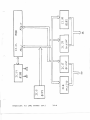
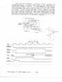
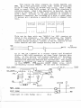
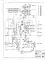
BLOCK DIAGRAM OF 8086 CPU CARD
r--------=
.
-,. --
- ~
~
. .----
_.-_ ._----- ------.---_.
8086
----------.,.-------;>t-------- -r-- T---r-------
S;1s;-1s;
RQ/GT.0
,-r-:('t\
~
A16-A19
INT
\I
V
.J.
It
ALE
bus
control
(incl. DMA)
data
path
.DlIR
urn
"ENII
data {8}
~
>
I
c:(
~I
Cl
W
w
~
Trill I T
I
,
"I'J
_ _ _PSY~C
III
,
U
~~
contra 1
and
I brffers
(.)\ :;r"
L
"
timing
1111111
J?:
ex:I
a:.
V'
I
l-c
~2
>->-V'
o
(processor
speed ~
l-c
a:
~~
c
ex:
I~
~ ~~~ J ~2
status 1 i nes SWO, SINTA, SINP, SOUT,
MWRITE, SMEMR, SHLTA, SMI,
SXTRQ command
control
1i nes
PWR, PDBIN, PSYNC, PWAIT
PHLOA
S-100 BUS
VI0-VI7
ADO OSB
kS[XTN,
. M~-AB
processor
ADo-AD} 5
-.J Y "
....c
c
C
r
C
c
C
~
1
y
HARDWARE OPERATION
8086/S-l00 CPU - INTERRUPT
..
The reader cf this section is cautioned that he is
expected to be reasonably familiar with use of the 7400
series TTL and have reviewed the data sheets for the Intel
8085, 8282, 8284, 8286, 8288, and 8259A ICs in chapter S
of the MCS-86 users' manual. He is also expected to have
reviewed a copy of the proposed IEEE standard for the S
100 bus.
The first step in interfacing a processor to the S
100 bus is defining the exact meaning of each bus signal
to be generated under all possible conditions. The second
step is establishing what signals are available from the
processor.
A mapping is then defined to create those
signals required at the processor and at the bus from
those available at the bus and at the processor.
The
rn a pp in g rn us t the n bee x ami ned toe n sur e t h a i t P 1 ace s no
unnecessary restrictions upon the operation of the
processor or the bus and that it will in fact work even
under worst-case conditions.
In order to conform with the proposed standard for
the S-lOO bus*, the CPU card must generate the following
Signals:
A19
A18
A17
. A16
A1S
A14
A13
A12
All
Ala
A9
A8
A7
A6
AS
A4
A3
A2
Al
AO
DI7/DATA1S
D16/DATA14
DIS/DATA13
DI4/DATA12
D13/DATAll
DI2/DATAIO
DI1/DATA9
DIO/DATA8
D07/DATA7
D06/DATA6
DOS/DATAS
D04/DATA4
D03/DATA3
D02/DATA2
DOl/DATAl
DOO/DATAO
PHLDA
SMl
SOUT
SINP
SMEMR
SHLTA
SXTRQ
PSYNC
PWR
PDBIN
SINTA
swO
*See IEEE ·Computer· magazine, March 1979, pp. 20-44.
(Copyright (C) 1981 TecMar Inc.)
7-A
In addition to those lines, the CPU card or front
panel must generate certain timing signals.
Since there
is no front panel, the CPU must generate
1!2
bus timing
CLOCK
peripheral timing
MWRITE
memoy write
POC
power-on clear
Besides the data lines (D07-D08 and DI?-DIO)' the
inputs to the CPU board from the S-IO bus are as follows:
XRDY
PRESET
VIO
STAT DSB
VII
DSB
VI2
C/C
ADD DSB
V13
DO DSB
ill .
SIXTN
VIS
PRDY
V16
PINT
VI?
PHOLD
in addition to the +8V and ground lines on the bus.
Based on the 8086 documentation, operating in "MAX n
mode, the following signals are available (see pages S-9
and S-ll of the MCS-86 User's Manual).
ADIS-ADO A19 , A18' AI?' A16 BHE RD S2' Sl' So
RQ/GTO' RQ/GTI
LOCK
(Copyright (C) 1981 TecMar Inc.)
8-A
-------
And the 8086 requires the following inputs:
READY INTR TEST (tie low) RESET CLK Adding an 8284 (I.C.
following outputs:
31)
RESET
OSC CLK
PCLK READY
clock generator provides the
(8086 input) (8086 input) (8086 input) and, the following inputs are required:
connect to 12, 15,
frequency crystal TANK
F/C
EFI
CSYNC
RDY2 AEN2
AENI
RDYI
RES or
24
MHz fundamental leave open for use with overtone mode crystals). tie low (input is from crystal, not EFI) tie low (unused input) tie low (unused multiprocessor sync facility) tie low tie high tie low
unused "alternate bus" ready line Adding an 8288 (I.C. 44) bus controller provides
outputs (see MCS-86 User's Manual, pages 5-33).
MRDC
MWTC
AMWC
IORDC
IOWC
AIOWC
INTA
DT/R
DEN
(Copyright (C) 1981 TecMar Inc.)
9-A
the
MCE
ALE
requiring the inputs
So
(from 8086)
S1
( from 8 0 86 )
S2
(from 8086)
CLK
(from 8284)
AEN
(tie low)
CEN
(tie high)
lOB
(tie low)
Summarizing the required inputs, we have
INTR
RDY2
RES
and the data input lines time multiplexed into AD15-ADOThe 8086's complex scheme of addressing and
intstruction look-ahead prohibits the use of a
conventional front panel for altering memory, examining
memory, or starting program execution at an arbitrary
location as is done with IMSAI or Altair 8080-based S-IOO
systems. The convention used in the systems which have no
front panel is a simple switch called "RESET" which when
pressed connects line 75 of the bus ("PRESET") to ground
and no other lights or switches.
This scheme seems to be
most reasonable for use in an 8086 system, and thus it is
adopted.
A software-based front panel could of course be
designed with lights and switches as I/O devices under
program control.
The most complicated part of the mapping between the
8086 and the S-IOO bus is in the data paths.
There are so
many functions that the only reasonable way to list them
is in a table.
(Copyright (C) 1981 TecMar Inc.)
10-A
data
source
function
data
destnation
--........ r
8-bit memory ~ or
I/O output to
an
Iiliffilre:r::e.d-p.oi t
or -location!.-
8-bit memory
8-bit I/O ou put to
an odd numbered port
or location
16-bit memory ea
16-bit I/O output
x
or
8-bit memory I~
e ___.
8-bit I/O inpu
evenbered
or ocation
-
8-bit memory read or
8-bit I/O input from
odd-numbered port or
location
L --
~ ----7 AD1S - AD 8
16-bit memory read or
16-bit I/O input
DI 7 - DI O D07-DOO AD1S-AD8
AD7-ADO
16-bit read
from 8-bit memory
DI 7 -DI O AD 7 -AD
AD1S-A 8
16-bit write to
8-bit memory
g
D0 7 - DOO
interrupt acknowledge
82S9A chip not
installed
interrupt acknowledge
82S9A chip installed
82S9A data
lines
These transfers are conceptually implemented as follows:
r
(Copyright (C) 1981 TecMar Inc.)
...
ll-A
~
to
tv")
U
H
~,
a k:...
C\1
~
00
C"'.\
CO
to
<t:
'-0
co
H
0
co
'"...
:...
......
c-J
,.....
(f)
I
0
V
o
H
/
...
V
N
H
~
':T
C"J
VI
...j
::t-
K'""
f'..
A
'-
...)
>'
Lj
0
V
r--+~
b
:t
(\j
~
~
""
~
0-
('(")
'o:t::
,
a
y
0
VJ
...J
I-
.-4
H co
o
<:0
c
<X)
U
r--+~
!-t c-J
Q
~
l.r;
;:j-
-,,/
«)
v
H
~
0
V
N
H
VJ
-.J
'::t
f'-.
l.n
«)
(Copyright (C) 1981 TecMar Inc.)
("'J
12-A
K
The transfers needed may be organized by destination.
destination
Source
DO
AD 7 .•• AD
ADlS···A 8
01
AD15 .•• AD8
g
01
DO
on board 82S9A
01
The bus buffers will all be disabled when DO DSB is pulled
low (for DMA), or when the 8259A is acknowledging an
interrupt.
The DIR inputs of the two transceivers are
driven by the DT/R line of the bus controller (8288).
The control lines for the drivers must now be considered.
The IC's at the data bus interface are enabled as follows:
IC 80
(DO~-DO'Z):
Enab ed .tQt.
~ 8-bit write to even byte
16-bit read (even byte)
l6-bit write (even byte)
Direction
8086 to bus
bus to 8086
8086 to bus
IC 39 (010-017):
Enabled 1M
8-bit read from odd byte
~ -bit read (odd byte)
16-bit write (odd byte)
Direction
bus to 8086
bus to 8086
8086 to bus
IC 15 (0° 0 - 0 °7):
~ -bit write to odd byte
IC 38 (01 0 -01 7 ):
l 8-bit read from even byte (data is latched when AO goes high on second half of 16 bit read from 8-bit memory. ) All of these IC's also require that DEN (from 8288)
and EN (from 8259A) both be high for a transfer to take
place.
(Copyright (C) 1981 TecMar Inc.)
13-A
-------~---
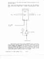
The 16-bit transfer to/from 8-bit memory is
accomplished by a circuit that detects the abscence of
SIXTN when SXTRQ is active. If this happens, wait states
are inserted while the circuit holds AO low for three
clock periods and then hOlds AO high for the rest of the
bus cycle (3 more clock periods). The transfer proceeds
as if two memory operations were done back-to-back at the
even and odd byte locations. The only difference is that
the data from the even byte (IC 38) is latched while the
odd byte is read and IC 38 is still enabled.
l
5TNRQ
I
1
(,)2.
IL________________
PDB ltV
L
-PWR
LGtc~ e~r
Ao~
~~v________________
~~_
WAIT
P.5YNC--.J
(Copyright (C) 1981 TecMar Inc.)
14-A
The details on the 8259 interrupt chip are given in its
section later.
Now
that the d ata paths are taken care of, the ad dress
path (naturally) comes next.
Rather conv enti onally, this
is:
Ie 14, Ie 15
1C 37
AD Iq
-
AD 0 - - - - - - - f
20 bi t
1a tch
atch
OE
ALE (8288)
Ie 24
Ie 5 (74LS04)
ADD DSB (bus)
Associated with this is the PHANTOM line circuitry.
The extended address lines A16-A19 are or-ed and a true
output causes the PHANTOM line (S-lOO pin 67) to be pulled
low (if PHANTOM jumper is in place) whenever memory is
addressed above the lower 64K. This allows the use of RAM
cards that only decode the AO-A15 address lines in the
lower 64K without conflict above this space.
(Copyiight (C) 1981 TecMar Inc.)
l5-A
Next, the required 8086/8284 inputs INTR, RDYl, and
RES will be considered.
(the 8259A's interrupt inputs are
considered separately as well as the DMA request/grant
sequence).
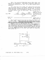
The interrupt line, PINT, can indirectly drive the
INTR interrupt input of the 8086. However, if the 8259A
interrupt chip is used, i l must drive the INTR. To avoid
noise problems (from disconnected inputs), a wired strap
is used rather than an "OR" gate.
The circuitry is
simple:
+5
( connect h
ere 'lf
(bus) PINT
(8259ft.) INT
(Ie 13)
4.7
strap
10 (choose 1)
8259A not installed
so interrupts can
come from the bus)
\
',INTR 8056
I
----------------------------------4.
I
(connect here if
8259A installed)
The "ready" inputs from the bus drive the 8284 's (IC
31) RDY2 input. Both lines must be "ready" for the RDYI
line to be ready. Note that the 8284 has an "OR" between
RDYI and RDY2 so both inputs cannot be used.
Added to this is the optional wait state generator.
This adds one wait state to every bus cycle.in SlQQition to
any requested by the device being accessed. The circuit
adds a one clock duration low on the RD2 line at the end
of a low caused by another device (slow memory) or right
after the PSYNC pulse if no other wait state is requested.
The circuit is:
+sv
(Copyright (C) 1981 TecMar Inc.)
16-A
-------
The RES input of the 8284 (I.C. 31) remains.
This
input should provide power-on reset, reset in the event of
momentary power failure, and reset when the bus PRESET
line is brought low. A Schmitt trigger is provided on the
8284,so an R-C network is adequate for power-on detection
with a delay of 0.2-0.5 sec. to allow the power supply to
settle.
A diode is added to discharge the capacitor in
. the event of momentary power failure.
An open-collector
gate serves to discharge (and hold low) the capacitor as
PRESET is brought low. The complete circuit is:
Ie 31
8284
PRESET
RES
The required output signals are divided into three
groups, the command/control lines (PHLDA, PSYNC, PDBIN,
PWR), the status lines (SMEMR, SINP, SMI, SOUT, SHLTA,
SWO, SINTA, and SXTRQ), and the other lines (~2' CLOCK,
MWRITE, POC).
The command/control lines will be discussed first.
The discussion of PHLDA is reserved for the DMA
request/grant paragraph later.
PSYNC is a posi tive-going
pulse of one clock period duration at the beginning of a
bus cycle. This is accomplished by latching ALE (from the
8282) on the rising edge of the system clock CLK (from one
8284).
ALE is high for one rising CLK edge at the
beginning of each cycle. PDBIN is asserted when either
MRDC (8288) or IORC (8288) is asserted.
PWR occurs with
either AIOWC or AMWTC (8288). The schematic is
shown on
the next page.
(Copyright (C) 1981 TecMar Inc.)
17-A
I C 17
PHLDA
PHLDA
from circuit
PSYNC
ALE
::'
CL -MRDC · lORC
IN
AMWTC AIOWC PWR
10K
C/C
IC 4 The status lines are next.
SMEMR (bus) is MRDC
(8288). SINP (bus) is IORC (8288). SM 1 (bus) is decoded
f rom SO, Sl' S2 (8086) (and thi s could not be decoded
E,.nless the 8086 were operating in nMAX n mode).
Since Sp'
Sl,and S2 are valid only at the falling edge ofALE, th1s
output must be latched.
SOUT (bus) is AIOWC (8288).
SHLTA (bus) is derived from SO, Sl' and 82 in much the
same mann~r as SMI.
SWO (bus) is assertea with either
AIOWC (8288) or AMWTC (8288).
SINTA (bus) is INTA (8288).
SXTRQ (bus) is asserted for a cycle whenever both ADO and
BHE are low when ALE falls.
The schematic is thus:
(Copyright (C) 1981 TecMar Inc.)
18-A
DSB
MRDC ______________________________________________
~
SMEMR
(8288)
rORC
(8 2 8 8 - , - - - - - - - - - - - - - - - - - - - , - - - - - - - - - - - - - - d
AIOLS~
(8~88 \
_____________________________________________d
rJ
I
>-~-t
Sat
(e086)s
SL
IC 33
_
(8086) YI/ /0
,>----t_ _ _~OUT
IC 34
~____~D
80 6
-v;l{
, > - - - - t - - _......... I NP
Q~__~
SMl
"
.---...,...,
elk
IC 33
~__-+~D
Q~__~
SHLTA
lk
ALE
(8288) through inverter
AIOWC
AMWTC
-0
SI NTA '
AD
rc
C 35
0
34
Q
TRQ
+5
el k
STAT
DSB .'
(Copyright (C) 1981 TecMar Inc.)
19-A
___ This.leaves the other signals; ¢2' CLOCK, ~WRITE, and
POCo ¢2 1S the processor clock, CL~ CLOCK 1S required
to be a 2 MHz signal of 40-60% duty cycle.
When a 4MHz
8086 is used, the PCLK output of the 8284 provides a
suitable signal. When 5 MHz operation is desired, the OSC
output of the 8284 (at 15 MHz) must somehow be divided to
give 2 MHz.
Clearly it is not possible to produce a
symmetric waveform, but dividing by 8 with a reset every
15 pulses will produce a waveform which is shaped like
this.
•
•
4/15 lJsec
,
4/15 lJsec
•
•
4/15 lJsec
3/15
~I
This can be done with one 74LS16l (or 163) counter as
shown in the schematic. For 8MHz operation, the 74LS16l
is used to divide the PCLK output by two.
MWRITE poses a
serious design problem. Either it can be treated in the
older fashion and left always driving the bus as:
PWR
~+-______________D~
SOUT
________
______________
v:l
~~~
not
~MWRITE imp1emented
Or it can be treated as a status signal and disabled
during a DMA hold sequence, as some later designs have
done.
If the memory (and memory-mapped I/O) designer
avoids using this line, no problem will result. If no DMA
devices are used the designs are equivalent. The latter
design is selected for ease of implementation, and MWRITE
is thus AMWTC.
POC is the RESET (8284) line, which
,conveniently mirrors PRESET. We now have the schematic:
PCLK (8284)
OSC (8284)
0 .....
s ~HI2. .!''''---i 0
C
B
1k
Q
reo
~ . .J
~8MH'l.
r-----iki
,,~tl
CLOCK
C 17
SM~1.Y.'~
Cf'
QA
BMH..
IC 29
8M~:b +Sv
STAT
rus
•
9---...;y..._ _-+___
RESET
(Copyright (C) 1981 TecMar Inc.)
~+-_ _- * - _
20-A
MWRITE
POC
Next comes the DMA request/grant circuitry. It is
necessary to generate a low-true pulse of 0
CLK cycle
duration into the RIO/GTO pin of the 8086 upon receiving a
PHOLD signal. When the processor responds with a low-true
pulse through the ~ID~ pin, PHLDA is asserted on the bus.
When P-H0 LDis r e 1 e a sed, an 0 the r low - t rue p u 1 s emu s t be
generated into the pin. This circuitry will accomplish
the task:
5
D
PHOLD
Q
8086
:
IC 27
lSl
k
>--_--j RQ/GT0
Q
IC 32
(inverted
from 8284)
PHLDA
(A) (B) (C) (D) (E) is PHOLD synchronized on the falling edge of the
processor clock.
is (A) inverted and delayed one clock period; when
high the master request pulse is over.
is the RQ/GTO pin of the 8086
is high when PHLDA is asserted or RQ/GTO is low.
is high when the master request pulse is done and
either the CPU grant is being pulsed on RQ/GTO or
PHLDA is already asserted.
(Copyright (C) 1981 TecMar Inc.)
2l-A
elK
PHOl "_ _-,
(D)
(E) "
PHLDA
------------------------~
See the reI evan t ti mi ng diag r am on p. 5-17 of In te 1 's
~~ User's Manual
.M~=
Finally there is the optional 8259A priority
interrupt controller chip and its associated circuitry.
First, what happens if the chip is not present? The EN
(8259A) line is pulled high by a pullup resistor to +5
volts and during the second INTA pulse the interrupt
address is expected to be on the DI lines on the bus. The
strap option for INTR (8086 output) was discussed earlier.
The interrupt lines are derived from VIO-VI7 on the bus;
the data lines are connected to AD~-ADO on the 8086.
A"I 0 WC (82 88 ) d r i v e s WR (82 5 9 A), I 0 RC (82 8 8 ) d r i v e s RD
(8259A).
CS is asserted when AO and A2-A8 are all low
(I/O ports a and 2).
Al (bus from 8282) drives AO
(8259A). Two consecutive even ports are chosen so that
the data lines used by the 8086 will be the same for both.
(These particular ports are those used by the INTEL DEMO
86 monitor ROM.)
INTA (8288) drives INTA (8259A)
directly.
INT (8259A) drives INTR (8086) directly, as
discussed before.
EN (8259A) is used to disable the
outputs of the multiplexers to AD7.-ADO as discussed under
data paths. The CAS lines are left open (consigning the
8259A to operate in buffered, non-cascaded mode) because
their use would require the definition of additional bus
1 ines.
(Copyright (C) 1981 TecMar Inc.)
22-A
The schematic is thus:
IC 3
-V
IC 3
IC 3
VI3
VI5
IR0
D,
,.I../D1 (8086)
I Rl
0 ~----------~~
IR2
Os
IR3
8259A
0"
IR4
IR5
03
f--_ _ _ _ _
6
D2
IC 13
ADs
II
II
II
II
03
A02
II
II
IR6
D1
ADl
II
VI7
IR7
Do
AD
II
AI
WR
INTA
INTA
(8288)
INT
INTR
(8086)
A
RO
AO
Ae
EN
C3
A,
A6
As
IC* 6
A"
IC 6
*
A3
C6
A2
IC 6
*
r-
Ao
(Copyright (C) 1981 TecMar Inc.)
23-A
to control
circuitry
Outside of mapping a series of logic equations into
SSI logic and selecting bus drivers for the control
signals, the design is now complete. Remaining is a check
on power consumption and design of the on-board power
supply, a timing check of the circuit to make sure that
there are no ridiculously long delays in sending data to
or taking data from the bus, and a system check to make
sure that all of the individually designed circuits will
work together.
Without going into the details of gate counts and
individual worst case supply currents, the board will
consume at most about 1,800 rna.
This means that ~~Q
conventional 7805 regulators will have to be used if they
are to regulate for the board.
Adequate bypassing and
decoupling are also necessary. Decoupling is accomplished
by an 0.1
f ceramic disk capacitor across the power
supply at the Vcc terminal of each package.
Bypassing is
inherent in the supply.
The timing check shows that at worst a 20 ns. delay
is possible in read and write operations due to bus
drivers on the card.
This must be accounted for in
specifying memory and I/O
speed.
(This assumes all
74LS parts).
The system check tUrns up an anomaly in the use of
the 8288 bus controller in systems having "wait states".
The 8288 bus controller cannot detect the occurence of a
not ready condition (wait state) and will proceed as if
said condition had not occurred.
Since the 8288 is a
static device, the clock into it can be gated to solve
this problem as follows:
READY ------;-r--...,
(8284)
\-----r-
I---_-::C:.:.LK( 8288 )
IC 30
The gate delays are necessary to prevent glitching on
the 8288'" s CLK input. Exper imentally this circui t off er s
the largest margin against varying gate delays in either
direction so that aging and temperature will have a
minimum effect on its operation.
Electrical compliance with the S-IOO standard is
accomplished by the use of 74367 and 74368 bus drivers for
the control signals and by making pullup resistors on the
open collector bus lines 5-10K~ to be well within the
current limits. The 8282 and 74LS245 far exceed the drive
capability requirement.
(Copyright (C) 1981 TecMar Inc.)
24-A
---~
.
--· ... .1O:MtI
?
' ::z..
.
. -
··
.
I
z:
w
z:
o
a...
::::
o
u
~cr~
.-
•
~-
gs
, .,. - -
CO
, .:
~
.
I~
' .
I
..,.,-.&
.~I.-.
\D
~~
~
Ie. ...
NOTe:
"
D INDlCATE"f> 61G"'''l~ THAY ~ ~ TO C4»4f\'>r.lftJTS
"''''CII ~ 5Il0"," 0101 "".sz:r Z Of' no;s DIAlil(AM (SHeeT "2)
Z) f"NC'ItC-LCJ) ..'5 ,...",CAYEr cohP It . I., c;",res, ,WellTEiIiS Ao->D
"IE Ci"ct.e '5 o-JOT V$EJ) , lD 'P6NnPo' Qtjp TYF'I: -SEE UST
f3VF~
rJll
.
3) ONl.y .....ltr or T>£ e.PV CHip os SHOW'" HERI! - THE I<E5T OF
Ir IS J)ESCRI&EO ON S>lEET Z OF ntiS SD.<\RI)S PIA<i~"""'.
'~
+SV
v'
+
~61\1
S,OJL
AEN
zL
Ll.K.
?41S ISO
" 3C
1b,
7"'~OO
17
2.'l
,... 3>1.7
eZSB
2~
7'4 l.S ~
Zi>
74 LS04
;1<1 L5175
2 7~
Fros
TYF'IO
~~oe
9,10
29
74
~
3,3D
74
L~06
lb,
B213-4
;'2
33
~BO
35
"fwo O~
74 LStO
,~~,~ ~ J3p'
~/"t:Delli
At.£.
ALE
.,.
14
"
.....
#141
2
¢2 ~
f'!.)R
<l>l
+sv
jJL
PRES€T 75
-
5X
,00
A.LE
~
z.f
21~T
.'10
t-!1c~~ ~. r+
4.
a-.J. ~
2
It'o.ll'lf2 1
J''1
-
"I
J'B
cU(ll9+
71~
~~~'IP~L--------------------t
c~I~>r--------------~~~~----------=
~
AI'!
AlB
AI7
AI6
B
~.~PHANTOM
8066/5-100 CPU
Re'l.O
TEUYIR INC. CI~...eI~nd . Ohio
")
A05B
ALE
DO, DOl DOl
DOl DOl DOS 1)06 007
01. 011 011 Oil D1I DIS DIG 011
DOiiSB
~
18'1
13~1
'--' ~IiilI4il~IWFI3lI1i
2
110!
~
I
17 1
1lI1 1,1
lsi
111
III
I>'
8 -~ ID e
7'1lS215
" . S IDE
31
AI'I~
-.
A18~
L, I
J
J
®
71 8
'''i
"'is ..& "A",u
••
- ~,.,.
.•
1~
~lq
~:~,;
AD 10
I
AD,
, ,
'" Oi
~,
4
""S
.,
~Z~
!II
~
~
t----c>
IZ . - ,
5TN
DOole::>;
7 "
813
D!LR
-S
1
@ ~~
lOLl"
11-
6
~
•
<-.J
t ;
~,!O
Z/I'lISII~'liSI'll
q
.p
l r<L 1,(
- -I
"
tl l}#lli., I:ll il mJ~l l'~
IJ 1IJ
--'!'.
LL
I
~
1
~
J,
&
~
rI
{
l'
" :
I
t lill.L
I I II I 1111
I I I I
,
..
.,
H+J
I
~
-J-J
>+',qJ
J
r'
J "
"
~
AD
~ll
" lsm
,
LL
'""'la
•
AO
JI 181
I
"""ol:'
AD "
Eli
.r"~-fS\l
..#
10
01
'2 1 41 s l 61
50niJ
.--.
b1
M3
AD 11&
AD
~
.
:
I
J
"""
_
WAIT
®
I I 81 71 181
8086
"II~
1
@
OE~
7 ~ 1 ~~7 3
I'll SIISII'
?w
11
I'
'''',
...-J~Jar_s+3...,T1r..._4_r._H_h~ ~~-~>---£,0Ci
.
Sq"{e5~
111 I
G)
......
CI ALE
-I "I '1'-1 I I II [
,, 1 ••
n
'/
S
II.
AOS8
D
~~z
Jtl
I!lTR
1L_ _ _ _
gl
3
1
ST& II
7' L< .l13
~ I_I
cZ2
.,
oe
f-i-/--1-.
10 STN
/I 1:11
PINT
loill<)"","r-"collo-II£II::
I~ I; r~ I~ I~
I;: I~ 15
MII~l§l~~~~~
,....
q:
....
N
ot ot
p')
«
~
11)
I.Q
q:
q:
<c
G
<:'
8086/5-too CPU
...11 ...1/
:;;11:;;11 ::?I 1121 1ctll~
COO""Q.
= :::!~~!1
«<<.:<<cr<
'"'"
I~f!!
IK: AL I. :
0 ....
3('1181
TEC.H~"
Rc.\I. D
I
No, t,.
UK.
,u.V,.IlD
CLEVEL~NO,OHIO
O. Kce'\e.
10 - 7 - 81
P IIlAWN.V
If.
2
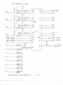
PARTS LIST
8086/S-100 BUS
I.C.#
1
2
3
4
5
6
7
8
9
10
11
12
13
14
15
16
17
18
19
20
21
22
23
24
25
26
27
28
29
30
31
32
33
34
35
36
37
38
39
~1.
COMPONENTS
PART TYPE MID NUMBER
OUANTITY
74LS32
1
IN915 DIODE
74LS05
100K~ RESISTOR
1
74LS04
lK~ RESISTORS
3
74LS04
6
4. 7K~ RESISTORS
74LS04
4.7K~ RESISTOR NETWORKS
2
74LS05
BOURNS#4310R-I01-472
8282
29
O.I~f CERAMIC DECOUPLING
74LS245
CAPACITORS
74368
5
18~f TANTALUM CAPACITORS
74368
15VWDC
74LS136
1
CRYSTAL
74LSll
12.0 MHz. for 4 MHz. CPU
8259A
15.0 MHZ. for 5 MHz. CPU
24.0 MHz. for 8 MHz. CPU
8282
8282
7895 VOLTAGE REGULATORS
2
74LSOO
HEAT SINKS
2
8T97 or 74367
THERMALLOY#6107-14
74LS04
74164
74125
7
JUMPER CONNECTORS
74LSOO
74LS74
74LS32
8288
74LS74
74LS04
74LS175
74LS08
74LS161 (for 5 MHz. or 8 MHz.)
74LS08
8284
8086
74LSI0
74LS175
74LS02
74LSOO
74LS173
81LS95
74LS245
(Copyright (C) 1981 TecMar Inc.)
28-A
SET-UP
8086/S-100 CPU - INTERRUPT
Boards built and tested by Tecmar Inc. will have all
jumpers in place for the processor speed purchased. The
options will be set as follows:
1. 16 bit operation only
2. No wait state (except for 8 MHz boards which will
have the wait state option selected
3. PHANTOM line driver not connected
4. 8259A vectored interrupt selected
No set-up is needed for these boards. If one desires
to change this set-up or if the board was
not built and
tested by Tecmar, see the Jumper Summary that follows.
If
changing the processor speed, remember to change the
crystal also; 12.000MHz crystal for 4MHz operation, 15.000
MHz for 5MHz or 24.000MHz for 8MHz.
Also note that an
8086 chip will run at slower speeds than it is rated but
not at faster speeds; i.e. don't expect to run an 8086-4
(4MHz version) at 8MHz.
(Copyright (C) 1981 TecMar Inc.)
29-A
JUMPER SUMMARY
8086/S-l00 CPU - INTERRUPT
There are nine jumper locations on the board that are
used for setting the operating speed and selecting the
optional features on the board.
All illustrations of
jumper placement are in the same orientation as on the
parts placement diagram.
See the diagram for position of
jumpers.
NOTE: 50 0
means place the small jumper connector so
that it connects (covers) the two jumper pins that are
connected by the., , the third pin will have nothing on
it.
Jl: PHANTOM jumper.
Put a jumper here to cause the
PHANTOM line (S-IOO pin 67) to be pulled low whenever
the CPU addresses memory above the lower 64K. This
allows an older memory card with a l6-bit address to
be used in the lower 64K (as long as the memoy cards
also have a PHANTOM line connection).
If there is no
jumper here, the CPU card has no affect on PHANTOM.
J2:
Selection of 8259A or PINT interrupt operation.
A) 000
For operation with 8259A vectored interrupt
chip
B) 066 For operation of interrupts with the PINT
line(S-lOO pin 73)
J3:
Selection of the l6-bit transfers from 8-bit memory
option.
A) 00 0 Jumper this way if all of system memory is
16 bits wide
B) 006 Jumper this way if any of system memory is
8 bit only memory
J6: Selection of optional wait state.
A)~
with jumper this way the CPU board will insert
o a wait state,
in addition to any wait state
requested by the device being accessed, in every
bus cycle. This is needed for 8 MHz operation
or for use with very slow memory.
B)o with jumper this way no extra wait states
~ will be added.
All other jumpers are for CPU speed selection and should
not be changed unless the crystal is changed also (see
system set-up).
J4: This jumper is in for 5 or 4 MHz operation, out for 8
MHz.
J5: This jumper is in for 8 MHz operation, out for 5 or 4
MHz.
(Copyright (C) 1981 TecMar Inc.)
30-A
J7:
J8:
This jumper is in for 5 MHz operation, out for 4 or 8
MHz.
60
For 8 MHz operation
For 4 MHz operation
No jumper for 5 MHz operation
<:>
J9:
0
60
For 5 MHz operation
For 8 MHz operation
No jumper for 4 MHz operation
50
<:>
o.r6
(Copyright (C) 1981 TecMar Inc.)
31-A
TIMING REQUIREMENTS
8086/S-l00 CPU - INTERRUPT
Parameter
AM.H.z
.5..MHz
lllliz
read pulse
address to read puIs
SOOns
80ns
400ns
6Sns
2S0ns
40ns
write pulse width
address to write pulse
SOOns
80ns
400ns
-6Sns
2S0ns
40ns
worst-case minimum access
time from read strobe
worst-case write cycle time
480ns
1000ns
380ns
800ns
230ns
SOOns
These timing requirements refer to memory boards not
memory chips. The bus driver delays on the board will
require chips to have access times that are around SOns.
faster than the board timing requirement.
These read and write times also apply to I/O devices -
note that standard 82SlA requires a read pulse of 2S0ns
and a write pulse of 2S0ns with data setup of lSOns, so a
write state is required on write operations. The standard
82SSA requires a read pulse width of 300ns and a write
pulse width of 400ns with a lOOns data setup time and 30ns
hold time, so it requires a wait state also.
r
(Copyright (C) 1981 TecMar Inc.)
32-A
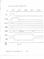
8086 CPU BUS
TIMI~G
WITH
O~[
WAIT STATE
,..--
~2
Tl
T'2.
~
..
,I.
IT3
1
IT~!~____
ALE ~
P.5 ~ NC.
--'X-----------------------------------------------
Add (" e.S5 _ _
SMl
SXTRQ
__x~__~~--------------------______
~)(~_______A__c_t_'_v_~______________J><__------------
PDBIN
-
PWR
XI\DV
- 0"
P~DY
(Copyright (C) 1981 TecMar Inc.)
33-A
CRITICAL TIMING SIGNALS
8086/S-100 CPU - INTERRUPT
Please observe that all signals are necessary to the
oeration of the board; there are very few failures that
will not "crash the system".
CLK processor clock - without thi s nothing will wor k (4,
5, or 8 MHz) also check this at pin 2 of the 8288 and look
for glitches.
data path gating signals:
DI bus:
OE
DIR
EN
STB
DO bus:
OE
DIR
ENI
EN2
Address bus:
OE
ALE
I.C.
39
39
38
38
Pin #
19
1
9
11
8
8
15
15
19
1
1
19
7
14
37
7
14
37
24
9
9
1,2
11
11
7
3
(ALE inverted)
from bus:
SIXTN
(absence of this signal on 16-bit
operations to 16-bit memory will cause the operation to
fail).
Proper 8086 operation can be diagnosed by examining the
outputs of the 8288 controller chip while single-stepping
the processor and comparing them to the operations implied
by the software.
FOR EXAMPLE SEE NEXT SECTION.
(Copyright (C) 1981 TecMar Inc.)
34-A
DIAGNOSTIC AIDS 8086/S-100 CPU - INTERRUPT The 8086 board set is fully static in that it can be
single-cycled from the bus. Note however that only memory
or I/O cycles may be extended to yield useful information
on the bus. If a known program is being executed (i.e. a
ROM monitor or bootstrap upon startup) the sequence of
instruction fetches of data accesses as well as I/O
operations may be observed with the use of:
1) A device to drive the XRDY (pin 3) line low from
the time that PSYNC is high and »~(8086 clock) is
low until a (debounced) pushbutton is depressed.
It should be possible to disable this circuit by
means of a double-throw toggle switch.
These are
the single cycle and run/stop switches
respectively.
2) Some means for displaying the states of
bus lines. If a lot of time is available,
probe will do.
Otherwise, you will
display panel which captures every line
the bus.
all the
a logic
need a
used on
3) A logic probe or clip-on display to show the
logic states of all 37 signal lines on the 8086
chip itself, and on any other package desired.
The technique consists of resetting the processor while
the run/stop switch is at "stop", and then examining the
bus data, address, status, and control information for
incorrect signals.
If an incorrect signal is found, it
should be traced back to the I.C. it originates at (for
address signals, the 8282: data signals through
the
74LS245's or the other two data buffers).
Bus cycles should be repeatedly examined until the program
appears to execute correctly, having performed:
.. 1)
2)
3)
4)
5)
6)
7)
8)
9)
10)
16-bit memory read
8-bit memory read from an odd location (AO=l)
8-bit memory read from an even location (AO=O)
16-bit memory write
8-bit memory write to an odd location (AO=l)
8-bit memory write to an even location (AO=O)
I/O input operation
I/O output operation
16-bit read from 8-bit memory (if 8-bit memory
is present)
16-bit write to 8-bit memory
(Copyright (C) 1981 TecMar Inc.)
35-A
If all those operations appear successful, the problem is
probably either
1) bus noise (are you using an active terminator
card? Is the bus adequately shielded?)
2) bus signal risetime problem (do all your boards
conform to the electrical portion of the proposed
S-IOO specification?)
3) bus contention (is another device dynamically
driving the bus due to faulty address decoding
logic or control logic?
In single-stepping a program, do not forget that the 8086
pre-fetches instructions.
It is, therefore, necessary to
keep track of where it should be going and nQt decide that
you have a defective processor chip when instructions are
fetched beyond a jump which should have been taken.
Here is an example taken from the first few instructions
of the INTEL Demo-86 monitor:
FFFFO
FF6BC
FF6BD
FF6C2
JMP
CLI
MOV
MOV
FF6B8
1000
FF60:00BC
EA
FA
2E
BC
SS,CS:00B8
SP,07CO
BCOO
60FF
8E 16
07CO
First cycle:
FFFFO
DI=BC DO=EA SMEMR=l,SXTRQ=O, SMl=l,
Second cycle:
n
n
FFFF2
DI=60 DO=OO
"
Third cycle:
n
n
"
FFFF4
DI=XX DO=FF
insert possible additional fetch cycle at FFFF6
Next cycle:
DI=2E DO=FA SMEMR=l,SXTRQ=O, SMl=l,
FF6BC
00B8
PDBIN=l
n
n
PDBIN=l
And so on.
Please note that in order to implement this debugging
technique, an intimate knowledge of the hardware and a
listing of the software, a well as special hardware is
required.
Conventional 8080 front panels will n~ work
and may damage the 8086 board set if their use .is
attempted.
In the example given above, assume that on a memory
read operation the correct information is found on the
bus, but the processor acts as if it had received
incorrect data (Le. jumps into nonexistent memory). In
this cae, reset the processor again and compare the data
signals at the processor pins ADIS to
ADO with the
apropriate DI7 to DIO and D07 to DOO signals respectively.
(Copyright (C) 1981 TecMar Inc.)
36-A
If they are not the same at, say,
bit 3 (i.e. 003 is
not the same as A03)' trace the 003 signal into pin 15 of
IC8 (74LS245), verl.fy that it is tl1e same at pin 5 and at
pin 13 of the 8086. The location of the failure must then
be in the node which first has an incorrect signal (such
as a shorted of broken trace) or in the device driving
that node (i.e. bad IC) or in a device receiving data from
that node (Le. bad IC shorting input to +5 or ground).
(Copyright (C) 1981 TecMar Inc.)
37-A
LIMITATIONS
8086/S-100 CPU - INTERRUPT
1. Due to the complex nature of the 8086 addressing
scheme it is essentially infeasible to implement a
front panel in the manner done on the IMSAI and ALTAIR
machines.
The reset, run/stop, and single-step features of those
front panels as well as a bus display (the address,
data, and status lights) can be implemented in a
manner similar to those front panels with the addition
of status display lights on SXTRQ and SIXTN.
Altering memory could be accomplished through the use
of a DMA scheme, but starting program execution at a
particular point would be completely infeasible from a
front-panel-like device.
Therefore, it is recommended that the machine be set
up with a terminal-oriented monitor.
It has a power
on jump feature (to fixed address FFFFOH) and a simple
monitor is available from INTEL in a pair of 2616
PROMs.
A front panel effect could also be achieved by storing
in ROM a program to treat a set of lights and switches
as I/O devices and emulate a front panel, but that
-implementation sacrifices the ability to single-step a
program.
2. The 8086 system for the S-IOO bus meets all of the
requirements for a bus master outlined in the proposed
standard published in the March 1979 IEEE Computer
magazine, except that it is faster.
It uses no lines that are specified as undefined or
reserved for future use.
It also does not use the
STVAL (sta t us val i d) 1 ine whi ch was not well def ined
in the proposed standard 'and is not even needed since
the status lines are valid immediately following the
PSYC pulse.
It drives the following lines which are not considered
type "M" (master) signals:
~2
CLOCK
MWRITE
POC
24
49
68 - disabled by STAT DSB low
99
(Copyright (C) 1981 TecMar Inc.)
38-A
The CPU card treats PRESET (75) as an open-collector
input (or momentary normally-open switch to ground)
and emits a low on the POC line when that input is
asserted exactly as if the power had just been turned
on.
The PINT line is ignored by the CPU if the vectored
interrupt option is instaled on the CPU ' card.
(See
jumper summary).
Note that the response to the INTA signal by the
interrupt controller or interupting device for the
8086 is ENTIRELY different from the response on an
8080 system.
(The 8086 requires that a one-byte
interrupt type be put on the bus, whereas the 8080
requires than an instruction be put onto the bus.)
For this reason the use of the vectored interrupt
option on the CPU card is recommended whenever
interrupts are to be used.
The system presently runs on a ~2 clock of 5 MHz as
the standard. The system can alsolbe used with 4 or 8
MHz 8086's, but at 8MHz this is faster than the S-lOO
standard indicates.
To run at 8 MHz the wait state
option will have to be used as there will probably not
be very many devices in the system that can run that
fast.
The wait state option will slow bus operations
down to a reasonable speed while allowing internal
8086 operations to proceed at 8 MHz. Devices which use
the ~2 clock as a timing base for external operations
assuml.ng that it is 2MHz should be modified to use the
CLOCK (49) signal which is 2MHz.
Note:
in 5 MHz
systems the CLOCK signal will not be symmetrical.
Note that unlike the 8080, the 8086 does llQt duplicate
the 8-bit I/O address on A15-A8and A7-AO, but rather
uses a full 16-bit address for I/O devices.
I/O
mapped
boards accessing lines A15 through A8 as
substitutes for A7 through AO will need to be
addressed differently in software as opposed to the
way they were on the 8080.
The extended address bits
are all zero for an I/O operation.
(Copyright (C) 1981 TecMar Inc.)
39-A