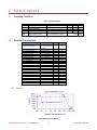
1
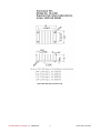
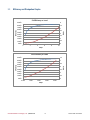
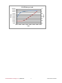
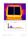
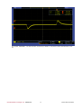
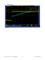
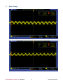
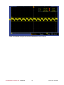
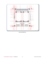
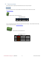
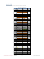
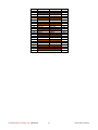
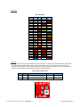
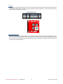
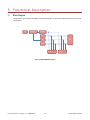
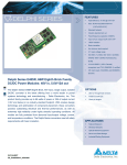
IATX25110HR PCI/104-Express DC/DC Power Supply User’s Manual BDM-610020126 Rev. A RTD Embedded Technologies, Inc. AS9100 and ISO 9001 Certified RTD Embedded Technologies, Inc. 103 Innovation Boulevard State College, PA 16803 USA Telephone: 814-234-8087 Fax: 814-234-5218 www.rtd.com [email protected] [email protected] Revision History Rev A 01/19/2015 Initial Release Advanced Analog I/O, Advanced Digital I/O, aAIO, aDIO, a2DIO, Autonomous SmartCal, “Catch the Express”, cpuModule, dspFramework, dspModule, expressMate, ExpressPlatform, HiDANplus, “MIL Value for COTS prices”, multiPort, PlatformBus, and PC/104EZ are trademarks, and “Accessing the Analog World”, dataModule, IDAN, HiDAN, RTD, and the RTD logo are registered trademarks of RTD Embedded Technologies, Inc (formerly Real Time Devices, Inc.). PS/2 is a trademark of International Business Machines Inc. PCI, PCI Express, and PCIe are trademarks of PCI-SIG. PC/104, PC/104-Plus, PCI-104, PCIe/104, PCI/104-Express and 104 are trademarks of the PC/104 Embedded Consortium. All other trademarks appearing in this document are the property of their respective owners. Failure to follow the instructions found in this manual may result in damage to the product described in this manual, or other components of the system. The procedure set forth in this manual shall only be performed by persons qualified to service electronic equipment. Contents and specifications within this manual are given without warranty, and are subject to change without notice. RTD Embedded Technologies, Inc. shall not be liable for errors or omissions in this manual, or for any loss, damage, or injury in connection with the use of this manual. Copyright © 2015 by RTD Embedded Technologies, Inc. All rights reserved. RTD Embedded Technologies, Inc. | www.rtd.com iii IATX25110HR User’s Manual Table of Contents 1 2 Introduction 6 1.1 Product Overview........................................................................................................................................................................ 6 1.2 Board Features ........................................................................................................................................................................... 6 1.3 Contact Information .................................................................................................................................................................... 7 Specifications 8 2.1 Operating Conditions .................................................................................................................................................................. 8 2.2 Electrical Characteristics ............................................................................................................................................................ 8 Note 1: Max Load is defined as 10 Amps on 5V, 3.03 amps on 3.3V, and 3.245 amps on the 12V ........................................................... 8 3 4 5 2.3 Efficiency and Dissipation Graphs ............................................................................................................................................ 10 2.4 Thermal Images ........................................................................................................................................................................ 12 2.5 Step Response ......................................................................................................................................................................... 14 2.6 Input Protection ......................................................................................................................................................................... 16 2.7 Ripple Voltage........................................................................................................................................................................... 17 Board Connection 19 3.1 Board Handling Precautions ..................................................................................................................................................... 19 3.2 Physical Characteristics ............................................................................................................................................................ 19 3.3 Connectors, Jumpers, and LEDs .............................................................................................................................................. 21 3.4 Steps for Installing .................................................................................................................................................................... 28 IDAN Connections 30 4.1 Module Handling Precautions ................................................................................................................................................... 30 4.2 Connectors................................................................................................................................................................................ 30 4.3 Steps for Installing .................................................................................................................................................................... 32 Functional Description 5.1 34 Block Diagram........................................................................................................................................................................... 34 6 Troubleshooting 35 7 Additional Information 36 8 7.1 PC/104 Specifications ............................................................................................................................................................... 36 7.2 PCI and PCI Express Specification .......................................................................................................................................... 36 Limited Warranty RTD Embedded Technologies, Inc. | www.rtd.com 37 iv IATX25110HR User’s Manual Table of Figures Figure 1 Derating Curve of Modules ......................................................................................................................................................................... 8 Figure 2 Heat Sink shown for reference only ........................................................................................................................................................... 9 Figure 3 Board Pictured without Heat Sink ............................................................................................................................................................. 19 Figure 4: Board Dimensions ................................................................................................................................................................................... 20 Figure 5: Board Connections, Jumpers .................................................................................................................................................................. 21 Figure 6 LED Locations .......................................................................................................................................................................................... 27 Figure 7: Example 104™Stack ............................................................................................................................................................................... 28 Figure 8 IATX25110HR IDAN connector drawing .................................................................................................................................................. 30 Figure 9 IDAN frame rear view ............................................................................................................................................................................... 31 Figure 10 IDAN frame front view ............................................................................................................................................................................ 31 Figure 11 Power Output Connector DB9 ................................................................................................................................................................ 31 Figure 12 IDAN Input Power Connector ................................................................................................................................................................. 32 Figure 13 IDAN Power Mating Connector .............................................................................................................................................................. 32 Figure 14 IDAN Power Mating Cable...................................................................................................................................................................... 32 Figure 15: Example IDAN System .......................................................................................................................................................................... 33 Figure 16: IATX25110HR Block Diagram ............................................................................................................................................................... 34 Table of Tables Table 1: Ordering Options ........................................................................................................................................................................................ 6 Table 2: Operating Conditions .................................................................................................................................................................................. 8 Table 3 TB1 Vin Connector .................................................................................................................................................................................... 22 Table 4 TB2 Vout Connector .................................................................................................................................................................................. 22 Table 5 CN1 and CN2 PCIe Bus ............................................................................................................................................................................ 23 Table 6 CN3 PCI Bus ............................................................................................................................................................................................. 25 Table 7 X1 Board PS_ON# Jumper........................................................................................................................................................................ 25 Table 8 X2 ON/OFF Jumper ................................................................................................................................................................................... 26 Table 9: IDAN Power Output Connector Pin-out .................................................................................................................................................... 31 Table 10: IDAN Power Input Connector Pin-out ..................................................................................................................................................... 32 RTD Embedded Technologies, Inc. | www.rtd.com v IATX25110HR User’s Manual 1 Introduction 1.1 Product Overview The IATX25110HR was designed to meet the power requirements of the PCI/104-Express Specification. 1.2 Board Features PCIe pass through bus PCI pass through bus 10V to 36V DC voltage input range 10 Amps of 5V 4.17 Amps of 12V 3.03 Amps of 3.3V 2.0 Amps of 5VSB Remote ON/OFF control Reverse voltage protection Input over voltage protection Input over current protection ATX functionality The IATX25110HR is available with the following options: Table 1: Ordering Options Part Number IATX25110HR Description Standard Configuration as pictured on cover Standard Configuration as pictured on cover, except without PCI bus IATX35110HR connector installed. IDAN-IATX25110HR Board Mounted in IDAN frame IDAN-IATX35110HR Board Mounted in IDAN frame ID-IATX25110HR Board with screw terminals for power connections ID-IATX35110HR Board with screw terminals for power connections Standard Configuration as pictured on cover, except without downward IATX25110HR-XNS express connector installed. Standard Configuration as pictured on cover, except without downward IATX35110HR-XNS express connector installed. Board with screw terminals for power connections, except without ID-IATX25110HR-XNS downward express connector installed. Board with screw terminals for power connections, except without ID-IATX35110HR-XNS downward express connector installed. Note: Contact RTD sales if you want a custom configuration. The Intelligent Data Acquisition Node (IDAN™) building block can be used in just about any combination with other IDAN building blocks to create a simple but rugged 104™ stack. This module can also be incorporated in a custom-built RTD HiDAN™ or HiDANplus High Reliability Intelligent Data Acquisition Node. Contact RTD sales for more information on our high reliability systems. RTD Embedded Technologies, Inc. | www.rtd.com 6 IATX25110HR User’s Manual 1.3 Contact Information 1.3.1 SALES SUPPORT For sales inquiries, you can contact RTD Embedded Technologies sales via the following methods: Phone: E-Mail: 1.3.2 1-814-234-8087 [email protected] Monday through Friday, 8:00am to 5:00pm (EST). TECHNICAL SUPPORT If you are having problems with you system, please try the steps in the Troubleshooting section of this manual. For help with this product, or any other product made by RTD, you can contact RTD Embedded Technologies technical support via the following methods: Phone: E-Mail: 1-814-234-8087 Monday through Friday, 8:00am to 5:00pm (EST). [email protected] RTD Embedded Technologies, Inc. | www.rtd.com 7 IATX25110HR User’s Manual 2 Specifications 2.1 Operating Conditions Table 2: Operating Conditions 2.2 Symbol Vin Ta Ts RH Parameter Supply Voltage Operating Temperature Storage Temperature Relative Humidity MTBF Mean Time Before Failure Test Condition Non-Condensing Telcordia Issue 2 30°C, Ground benign, controlled Min 10.00 -40 -55 0 Max 36.00 +85 +125 90% TBD Unit V C C % Hours Electrical Characteristics Parameter Test Condition Max Unit 25°C 10.00V Vin four Maximum Power Dissipation Hour Soak no Airflow no 11.66 W Heat Sink Combined Efficiency 10Vin 25°C Max load (note 1) 87.83 % Combined Efficiency 24Vin 25°C Max load (note 1) 90.88 % Combined Efficiency 36Vin 25°C Max load (note 1) 89.35 % 5V Efficiency with 24Vin 25°C 10.0 Amp load 87.11 % 5VSB Efficiency with 24Vin 25°C 2 Amp load 87.11 % 12V Efficiency with 24Vin 25°C 4.17 Amp load 87.44 % 3.3V Efficiency with 12Vin 25°C 3.03 Amp load 90.67 % 5V DC Load Regulation 25°C 70.0 mV 5VSB DC Load Regulation 25°C 70.0 mV 12V DC Load Regulation 25°C 24 mV 3.3V DC Load Regulation 25°C 10 mV 5VSB P-P voltage ripple 25°C 2.0 Amp load ? mV 5V P-P voltage ripple 25°C 10.0 Amp load 118.0 mV 12V P-P voltage ripple 25°C 4.17 Amp load 244.0 mV 5V Switching Frequency 25°C 306 KHz+-2% 5V standby Switching Frequency 25°C 306 KHz+-2% 12V Switching Frequency 25°C 308 KHz+-2% 3.3V Switching Frequency 25°C 634 KHz+-2% Reverse Voltage Protection 25°C -36 V Input Overcurrent Trip Level 25°C 14.3 Amps Galvanic Isolation voltage 25°C 1500 V Module Thermal Shutdown Case Temp. 110 C Note 1: Max Load is defined as 10 Amps on 5V, 3.03 amps on 3.3V, and 3.245 amps on the 12V 2.2.1 DERATING: Figure 1 Derating Curve of Modules RTD Embedded Technologies, Inc. | www.rtd.com 8 IATX25110HR User’s Manual Figure 2 Heat Sink shown for reference only RTD Embedded Technologies, Inc. | www.rtd.com 9 IATX25110HR User’s Manual 2.3 Efficiency and Dissipation Graphs 90.00% 8 80.00% 7.5 70.00% 7 60.00% 6.5 50.00% 6 40.00% 5.5 30.00% 20.00% 5 10.00% 4.5 0.00% Watts Efficiency 5V Efficiency vs. Load 4 0 2 4 6 8 10 Amps 12V Efficiency vs. Load 90.00% 7.5 80.00% 7 6.5 60.00% 50.00% 6 40.00% 5.5 30.00% 5 20.00% 4.5 10.00% 0.00% 0.000 Watts Efficiency 70.00% 4 1.000 2.000 3.000 4.000 Amps RTD Embedded Technologies, Inc. | www.rtd.com 10 IATX25110HR User’s Manual 100.00% 90.00% 80.00% 70.00% 60.00% 50.00% 40.00% 30.00% 20.00% 10.00% 0.00% 0.000 1.1 1 0.9 0.8 Watts Efficiency 3.3V Efficiency vs. Load 0.7 0.6 0.500 1.000 1.500 2.000 2.500 3.000 0.5 3.500 Amps RTD Embedded Technologies, Inc. | www.rtd.com 11 IATX25110HR User’s Manual 2.4 Thermal Images Top; No Heat Sink, 23°C, Max Load, 24Vin, At thermal equilibrium, Max temperature is 81.9C (measured with a thermocouple between the quarter bricks). RTD Embedded Technologies, Inc. | www.rtd.com 12 IATX25110HR User’s Manual Bottom; No Heat Sink, 23°C, Max Load, 24Vin, At thermal equilibrium, Max temperature is 71.3C RTD Embedded Technologies, Inc. | www.rtd.com 13 IATX25110HR User’s Manual 2.5 Step Response AC coupled, 20MHz BWL, 5V (and 5VSB) output, step load response from 5.0 amps to 9.0 Amps 24V Vin. Peak to Peak deviation is 488 mV AC coupled, 20MHz BWL, 12V step response current step. (0.42A to 3.75A) 24Vin, Peak to Peak deviation is 996 mV RTD Embedded Technologies, Inc. | www.rtd.com 14 IATX25110HR User’s Manual AC coupled, 20MHz BWL, 3.3V step response current step. (0.303A to 2.73A) 24Vin Peak to Peak deviation is 210 mV RTD Embedded Technologies, Inc. | www.rtd.com 15 IATX25110HR User’s Manual 2.6 Input Protection Input surge protection test. 36Vin CH1 is input of 36V. CH2 is after the protection. 46V inductive spike is reduced to 25.6V and rolls up to 36V in 5 mSec. RTD Embedded Technologies, Inc. | www.rtd.com 16 IATX25110HR User’s Manual 2.7 Ripple Voltage 5V and 5VSB AC coupled 20MHz BWL output ripple voltage at 10.0 Amp load. Measured Peak to Peak is 118.0 mV. 12V AC coupled 20MHz BWL output ripple voltage at 4.17 Amp load. Measured Peak to Peak is 118.0 mV. RTD Embedded Technologies, Inc. | www.rtd.com 17 IATX25110HR User’s Manual 3.3V AC coupled 20MHz BWL output ripple voltage at 3.03 Amp load. Measured Peak to Peak is 118.0 mV. RTD Embedded Technologies, Inc. | www.rtd.com 18 IATX25110HR User’s Manual 3 Board Connection 3.1 Board Handling Precautions To prevent damage due to Electrostatic Discharge (ESD), keep your board in its antistatic bag until you are ready to install it into your system. When removing it from the bag, hold the board at the edges, and do not touch the components or connectors. Handle the board in an antistatic environment, and use a grounded workbench for testing and handling of your hardware. 3.2 Physical Characteristics Weight: Approximately 226g (0.498 lbs.) no heat sink Board Dimensions: 93.52 mm L x 95.89 mm W (3.682 in L x 3.775 in W) Insert picture here Figure 3 Board Pictured without Heat Sink RTD Embedded Technologies, Inc. | www.rtd.com 19 IATX25110HR User’s Manual Figure 4: Board Dimensions RTD Embedded Technologies, Inc. | www.rtd.com 20 IATX25110HR User’s Manual 3.3 Connectors, Jumpers, and LEDs PCI Bus Vin Pos Vin Neg GND 12V GND 3.3V GND 5V ON/OFF PS_ON# PCIe Bus Figure 5: Board Connections, Jumpers RTD Embedded Technologies, Inc. | www.rtd.com 21 IATX25110HR User’s Manual 3.3.1 CONNECTORS AND JUMPERS All I/O connectors have Pin 1 designated by a thick white silkscreen line, and/or a square pad on the PCB. Power Connectors TB1 is a two pin input power connector. Each pin is labeled on the PCB. Mating connector is a Pheonix contact 1779987 (www.Pheonixcontact.com) Facing the connector, from left to right, the pin out is: Table 3 TB1 Vin Connector TB1 Pin 1 2 Pin Name Vin+ Vin- Function 9V to 36V input Input Negative IDAN ? ? TB2 is a six pin auxiliary power connector. Both +5V pins are sourced from the same 5V supply. Each pin is labeled on the PCB. Mating connector is a Pheonix contact 1781027 (www.Pheonixcontact.com) Facing the connector, from left to right, the pin out is: Table 4 TB2 Vout Connector TB2 Pin 1 2 3 4 5 6 Pin Name +5V GND +3.3V GND +12V GND RTD Embedded Technologies, Inc. | www.rtd.com Function 5V auxiliary output Ground connection 3.3V auxiliary output Ground connection 12V auxiliary output Ground connection 22 IDAN 9-pin “D” ? ? ? ? ? ? IATX25110HR User’s Manual CN1 and CN2 PCIe Bus CN1 and CN2 are the PCIe connectors. All pins stack through with no lane shifting. Table 5 CN1 and CN2 PCIe Bus CNX Pin 1 3 5 7 9 11 13 15 17 19 21 23 25 27 29 31 33 35 37 39 41 43 45 47 49 51 53 55 57 59 61 63 65 67 69 71 73 75 77 79 81 83 85 87 89 91 93 95 97 99 101 103 105 107 109 111 113 Signal USB_OC# 3.3V USB_1p USB_1n GND PEx1_1Tp PEx1_1Tn GND PEx1_2Tp PEx1_2Tn GND PEx1_1Rp PEx1_1Rn GND PEx1_2Rp PEx1_2Rn GND PEx1_1Clkp PEx1_1Clkn +5V_SB PEx1_2Clkp PEx1_2Clkn DIR SMB_DAT SMB_CLK SMB_ALERT STK0 / WAKE# GND PEx4_1T(0)p PEx4_1T(0)n GND PEx4_1T(1)p PEx4_1T(1)n GND PEx4_1T(2)p PEx4_1T(2)n GND PEx4_1T(3)p PEx4_1T(3)n GND SATA_T1p SATA_T1n GND SSTX1p SSTX1n GND Reserved Reserved GND SATA_DET#1 SATA_PWREN#1 GND STK2 / SDVO_DAT GND PEx4_1R(0)p PEx4_1R(0)n GND RTD Embedded Technologies, Inc. | www.rtd.com Signal PE_RST# 3.3V USB_0p USB_0n GND PEx1_0Tp PEx1_0Tn GND PEx1_3Tp PEx1_3Tn GND PEx1_0Rp PEx1_0Rn GND PEx1_3Rp PEx1_3Rn GND PEx1_0Clkp PEx1_0Clkn +5V_SB PEx1_3Clkp PEx1_3Clkn PWRGOOD PEx_x4_Clkp PEx_x4_Clkn PSON# STK1 / PEG_ENA# GND PEx4_0T(0)p PEx4_0T(0)n GND PEx4_0T(1)p PEx4_0T(1)n GND PEx4_0T(2)p PEx4_0T(2)n GND PEx4_0T(3)p PEx4_0T(3)n GND SATA_T0p SATA_T0n GND SSTX0p SSTX0n GND Reserved Reserved GND SATA_DET#0 SATA_PWREN#0 GND LPC_CLK GND PEx4_0R(0)p PEx4_0R(0)n GND 23 CNX Pin 2 4 6 8 10 12 14 16 18 20 22 24 26 28 30 32 34 36 38 40 42 44 46 48 50 52 54 56 58 60 62 64 66 68 70 72 74 76 78 80 82 84 86 88 90 92 94 96 98 100 102 104 106 108 110 112 114 IATX25110HR User’s Manual 115 117 119 121 123 125 127 129 131 133 135 137 139 141 143 145 147 149 151 153 155 C1 C2 C3 PEx4_1R(1)p PEx4_1R(1)n GND PEx4_1R(2)p PEx4_1R(2)n GND PEx4_1R(3)p PEx4_1R(3)n GND SATA_R1p SATA_R1n GND SSRX1p SSRX1n GND LPC_AD0 LPC_AD1 GND LPC_AD2 LPC_AD3 GND 5V 5V 12V RTD Embedded Technologies, Inc. | www.rtd.com PEx4_0R(1)p PEx4_0R(1)n GND PEx4_0R(2)p PEx4_0R(2)n GND PEx4_0R(3)p PEx4_0R(3)n GND SATA_R0p SATA_R0n GND SSRX0p SSRX0n GND LPC_DRQ# LPC_SERIRQ# GND LPC_FRAME# RTC_Battery GND 24 116 118 120 122 124 126 128 130 132 134 136 138 140 142 144 146 148 150 152 154 156 IATX25110HR User’s Manual CN3 PCI Bus Table 6 CN3 PCI Bus Pin Number 1 2 3 4 5 6 7 8 9 10 11 12 13 14 15 16 17 18 19 20 21 22 23 24 25 26 27 28 29 30 A row B row C row GND N/C N/C N/C GND N/C N/C +3.3V N/C GND N/C +3.3V N/C GND N/C N/C +3.3V N/C N/C GND N/C +5V N/C GND N/C +5V N/C GND +12V -12V 5VSB N/C GND N/C N/C N/C N/C N/C GND N/C +3.3V N/C GND N/C +3.3V N/C N/C GND N/C N/C +5V GND N/C N/C N/C N/C +5V +5V N/C N/C +5V N/C N/C GND N/C N/C GND N/C PS_ON# +3.3V N/C GND N/C +3.3V N/C GND N/C N/C N/C N/C N/C GND N/C +5V N/C GND N/C +5V N/C N/C D row N/C +5V N/C N/C GND N/C N/C +3.3V N/C N/C GND N/C +3.3V N/C GND N/C +3.3V N/C N/C GND N/C N/C N/C N/C GND N/C GND N/C N/C GND X1 Jumper The X1 jumper is part of a four pin jumper located near the input power connector. Default is open or attached to the power switch in IDAN. The board is labeled with settings. When the jumper is open, all main supplies on the board are controlled via PS_ON# (normal ATX functionality). When the jumper is shorted, the board be powered on when the input is present (assuming X2 is open). The only LEDs that should be on when PS_ON# is not asserted is the input power LED and the 5VSTBY LED. Table 7 X1 Board PS_ON# Jumper X1 Pin 1 Signal PS_ON# 2 Vin- Function Short to Pin 2 = Override PS_ON# Open = CPU controls PS_ON# (Default) Reference RTD Embedded Technologies, Inc. | www.rtd.com 25 IDAN Power Switch note Pin 1 is indicated By a square pad Power Switch IATX25110HR User’s Manual X2 Jumper The X2 jumper is the ON/OFF signal. Default is open. When set to ON, all board supplies can be enabled. When the ON/OFF jumper is set to OFF, all supplies, including 5VSTBY, are disabled. The X2 pin is pulled to Vin+ through a 100K resistor. The only indication of power on the board will be the input power LED should still be on. Table 8 X2 ON/OFF Jumper X2 Pin 3 Signal X2 4 Vin- Function Short to Pin 2=ON Open = OFF (Default) Reference IDAN N/C N/C Solder Jumpers B2 and B3 B2 and B3 are on the bottom of the board located in the corners to either side of the PCI connector. Both of the solder jumpers are open by default and are used for setting the potential of the frame. B2 is labeled “Frame Input GND” and B3 is labeled “Frame Output GND”. B2 shorts the Vin- rail to the frame when populated and B3 shorts the GND rail to the frame when populated. If both solder jumpers are populated, input and output ground will be shorted together. RTD Embedded Technologies, Inc. | www.rtd.com 26 IATX25110HR User’s Manual 3.3.2 LEDS Voltage indicator LEDs There are six LEDs on the board. Four are labeled by CN1 (PCIe bus) by their voltage. If one of these four LEDs is on, the respective voltage is good. The remaining two LEDs, of the six, are input power indicators. They are located on the bottom of the board by the input power connector. The green one is labeled “Vin is On” and the red one is labeled “Reversed”. When the green LED is on, there is a voltage present at the input connector. When the red LED is on, the input leads have been reversed. ON Bottom Figure 6 LED Locations RTD Embedded Technologies, Inc. | www.rtd.com 27 IATX25110HR User’s Manual 3.4 Steps for Installing 1. 2. 3. 4. 5. 6. 7. 8. 9. 10. 11. 12. 13. 14. 15. Always work at an ESD protected workstation, and wear a grounded wrist-strap. Turn off power to the PC/104 system or stack. Select and install stand-offs to properly position the module on the stack. Remove the module from its anti-static bag. Check that pins of the bus connector are properly positioned. Check the stacking order; make sure all of the busses used by the peripheral cards are connected to the cpuModule. Hold the module by its edges and orient it so the bus connector pins line up with the matching connector on the stack. Gently and evenly press the module onto the PC/104 stack. If any boards are to be stacked above this module, install them. Attach any necessary cables to the PC/104 stack. Re-connect the power cord and apply power to the stack. Boot the system and verify that all of the hardware is working properly. Any wires into or out of the board should be twisted to reduce inductance. Wires are to be kept as short as possible to reduce unnecessary voltage drops. Power wires should be able to carry at least 10 Amps of current. Figure 7: Example 104™Stack RTD Embedded Technologies, Inc. | www.rtd.com 28 IATX25110HR User’s Manual RTD Embedded Technologies, Inc. | www.rtd.com 29 IATX25110HR User’s Manual 4 IDAN Connections 4.1 Module Handling Precautions To prevent damage due to Electrostatic Discharge (ESD), keep your module in its antistatic bag until you are ready to install it into your system. When removing it from the bag, hold the module by the aluminum enclosure, and do not touch the components or connectors. Handle the module in an antistatic environment, and use a grounded workbench for testing and handling of your hardware. 4.2 Connectors 4.2.1 EXTERNAL I/O CONNECTORS The power ON/OFF switch with LED is located on the front of the frame. The 2-pin push-pull power input connector and the 9-pin “D” power output connector are brought out of the back of the frame. Power Switch Input Power Figure 8 IATX25110HR IDAN connector drawing LED on Power switch lights when outputs are on. RTD Embedded Technologies, Inc. | www.rtd.com 30 Output Power IATX25110HR User’s Manual To be added later Figure 9 IDAN frame rear view To be added later Figure 10 IDAN frame front view 1 6 Figure 11 Power Output Connector DB9 Table 9: IDAN Power Output Connector Pin-out Pin Number 1 2 3 4 5 6 7 8 9 Description 5V GND 12V GND N/C 5V GND 3.3V GND Three Amp current rating per pin. RTD Embedded Technologies, Inc. | www.rtd.com 31 IATX25110HR User’s Manual Pin 1 Figure 12 IDAN Input Power Connector Figure 13 IDAN Power Mating Connector The mating connector is a Souriau JBXFD1G02MSSDSMR Table 10: IDAN Power Input Connector Pin-out Pin Number Description 1 Vin+ 2 VinTen Amp current rating per pin. Figure 14 IDAN Power Mating Cable Mating cable IDAN-XKCM18 is shipped with IDAN configuration. 4.3 Steps for Installing 1. 2. 3. 4. 5. 6. 7. 8. 9. 10. 11. 12. Always work at an ESD protected workstation, and wear a grounded wrist-strap. Turn off power to the IDAN system. Remove the module from its anti-static bag. Check that pins of the bus connector are properly positioned. Check the stacking order; make sure all of the busses used by the peripheral cards are connected to the cpuModule. Hold the module by its edges and orient it so the bus connector pins line up with the matching connector on the stack. Gently and evenly press the module onto the IDAN system. If any boards are to be stacked above this module, install them. Finish assembling the IDAN stack by installing screws of an appropriate length. Attach any necessary cables to the IDAN system. Re-connect the power cord and apply power to the stack. Boot the system and verify that all of the hardware is working properly. RTD Embedded Technologies, Inc. | www.rtd.com 32 IATX25110HR User’s Manual Figure 15: Example IDAN System RTD Embedded Technologies, Inc. | www.rtd.com 33 IATX25110HR User’s Manual 5 Functional Description 5.1 Block Diagram The Figure below shows the functional block diagram of the ATX35110HR-190W. The various parts of the block diagram are discussed in the following sections. Vin Protection 5VSTBY 5V Vout 12V 3.3V PCIe PCI Figure 16: IATX25110HR Block Diagram RTD Embedded Technologies, Inc. | www.rtd.com 34 IATX25110HR User’s Manual 6 Troubleshooting If you are having problems with your system, please try the following initial steps: Simplify the System – Remove modules one at a time from your system to see if there is a specific module that is causing a problem. Perform you troubleshooting with the least number of modules in the system possible. Swap Components – Try replacing parts in the system one at a time with similar parts to determine if a part is faulty or if a type of part is configured incorrectly. If problems persist, or you have questions about configuring this product, contact RTD Embedded Technologies via the following methods: Phone: E-Mail: +1-814-234-8087 [email protected] Be sure to check the RTD web site (http://www.rtd.com) frequently for product updates, including newer versions of the board manual and application software. RTD Embedded Technologies, Inc. | www.rtd.com 35 IATX25110HR User’s Manual 7 Additional Information 7.1 PC/104 Specifications A copy of the latest PC/104 specifications can be found on the webpage for the PC/104 Embedded Consortium: www.pc104.org 7.2 PCI and PCI Express Specification A copy of the latest PCI and PCI Express specifications can be found on the webpage for the PCI Special Interest Group: www.pcisig.com RTD Embedded Technologies, Inc. | www.rtd.com 36 IATX25110HR User’s Manual 8 Limited Warranty RTD Embedded Technologies, Inc. warrants the hardware and software products it manufactures and produces to be free from defects in materials and workmanship for one year following the date of shipment from RTD Embedded Technologies, Inc. This warranty is limited to the original purchaser of product and is not transferable. During the one year warranty period, RTD Embedded Technologies will repair or replace, at its option, any defective products or parts at no additional charge, provided that the product is returned, shipping prepaid, to RTD Embedded Technologies. All replaced parts and products become the property of RTD Embedded Technologies. Before returning any product for repair, customers are required to contact the factory for a Return Material Authorization (RMA) number. This limited warranty does not extend to any products which have been damaged as a result of accident, misuse, abuse (such as: use of incorrect input voltages, improper or insufficient ventilation, failure to follow the operating instructions that are provided by RTD Embedded Technologies, “acts of God” or other contingencies beyond the control of RTD Embedded Technologies), or as a result of service or modification by anyone other than RTD Embedded Technologies. Except as expressly set forth above, no other warranties are expressed or implied, including, but not limited to, any implied warranties of merchantability and fitness for a particular purpose, and RTD Embedded Technologies expressly disclaims all warranties not stated herein. All implied warranties, including implied warranties for merchantability and fitness for a particular purpose, are limited to the duration of this warranty. In the event the product is not free from defects as warranted above, the purchaser's sole remedy shall be repair or replacement as provided above. Under no circumstances will RTD Embedded Technologies be liable to the purchaser or any user for any damages, including any incidental or consequential damages, expenses, lost profits, lost savings, or other damages arising out of the use or inability to use the product. Some states do not allow the exclusion or limitation of incidental or consequential damages for consumer products, and some states do not allow limitations on how long an implied warranty lasts, so the above limitations or exclusions may not apply to you. This warranty gives you specific legal rights, and you may also have other rights which vary from state to state. RTD Embedded Technologies, Inc. | www.rtd.com 37 IATX25110HR User’s Manual RTD Embedded Technologies, Inc. 103 Innovation Boulevard State College, PA 16803 USA Telephone: 814-234-8087 Fax: 814-234-5218 www.rtd.com [email protected] [email protected] Copyright 2015 by RTD Embedded Technologies, Inc. All rights reserved.