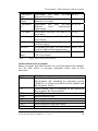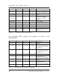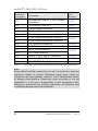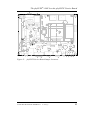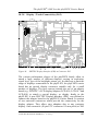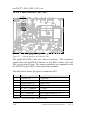
1
® phyFLEX -i.MX 6 Hardware Manual Document No.: L-773e_2 SOM Prod. No.: PFL-A-XL1-xxx SOM PCB. No.: 1362.1 CB Prod. No.: CB PCB. No.: Edition: PBA-B-01 1364.2, 1364.3 March 2013 A product of a PHYTEC Technology Holding company phyFLEX®-i.MX 6 [PFL-A-XL1-xxx Copyrighted products are not explicitly indicated in this manual. The absence of the trademark (™, or ®) and copyright (©) symbols does not imply that a product is not protected. Additionally, registered patents and trademarks are similarly not expressly indicated in this manual. The information in this document has been carefully checked and is considered to be entirely reliable. However, PHYTEC Messtechnik GmbH assumes no responsibility for any inaccuracies. PHYTEC Messtechnik GmbH neither gives any guarantee nor accepts any liability whatsoever for consequential damages resulting from the use of this manual or its associated product. PHYTEC Messtechnik GmbH reserves the right to alter the information contained herein without prior notification and accepts no responsibility for any damages that might result. Additionally, PHYTEC Messtechnik GmbH offers no guarantee nor accepts any liability for damages arising from the improper usage or improper installation of the hardware or software. PHYTEC Messtechnik GmbH further reserves the right to alter the layout and/or design of the hardware without prior notification and accepts no liability for doing so. © Copyright 2013 PHYTEC Messtechnik GmbH, D-55129 Mainz. Rights - including those of translation, reprint, broadcast, photomechanical or similar reproduction and storage or processing in computer systems, in whole or in part - are reserved. No reproduction may occur without the express written consent from PHYTEC Messtechnik GmbH. Address: EUROPE NORTH AMERICA PHYTEC Messtechnik GmbH Robert-Koch-Str. 39 D-55129 Mainz GERMANY PHYTEC America LLC 203 Parfitt Way SW, Suite G100 Bainbridge Island, WA 98110 USA Ordering +49 (6131) 9221-32 Information: [email protected] 1 (800) 278-9913 [email protected] Technical Support: +49 (6131) 9221-31 [email protected] 1 (800) 278-9913 [email protected] Fax: +49 (6131) 9221-33 1 (206) 780-9135 Web Site: http://www.phytec.de http://www.phytec.eu http://www.phytec.com 2nd Edition March 2013 © PHYTEC Messtechnik GmbH 2013 L-773e_2 Contents List of Figures..............................................................................................iii List of Tables ...............................................................................................iv Conventions, Abbreviations and Acronyms............................................vii Preface..........................................................................................................xi 1 Introduction......................................................................................... 1 1.1 Block Diagram ............................................................................. 4 1.2 phyFLEX-i.MX 6 Component Placement.................................... 5 1.3 Minimum Requirements to operate the phyFLEX-i.MX 6.......... 7 2 Pin Description .................................................................................... 8 3 Jumpers.............................................................................................. 23 4 Power.................................................................................................. 27 4.1 Primary System Power (VDD_5V_IN_R)................................. 27 4.2 Power Management IC (PMIC) (U14)....................................... 28 4.2.1 Power Domains ............................................................. 29 4.3 Supply Voltage for external Logic ............................................. 32 4.4 Control Management IC (CMIC) (U17)) ................................... 32 5 System Configuration and Booting ................................................. 33 6 System Memory................................................................................. 38 6.1 DDR3-SDRAM (U2-U9) ........................................................... 38 6.2 NAND Flash Memory (U13) ..................................................... 39 6.3 I²C EEPROM (U10)................................................................... 39 6.3.1 EEPROM Write Protection Control (J3) ...................... 40 6.4 SPI Flash Memory (U25) )......................................................... 40 7 SD / MMC Card Interfaces .............................................................. 41 8 Serial Interfaces................................................................................. 43 8.1 Universal Asynchronous Interface ............................................. 44 8.2 USB OTG Interface.................................................................... 45 8.3 USB Host Interface .................................................................... 46 8.4 Ethernet Interface ....................................................................... 47 8.4.1 Ethernet PHY (U11)...................................................... 47 8.4.2 Software Reset of the Ethernet Controller .................... 48 8.4.3 MAC Address................................................................ 49 8.5 I2C Interface ............................................................................... 49 8.6 SPI Interface ............................................................................... 50 8.7 I2S Audio Interface (SSI)) .......................................................... 51 8.8 CAN Interface ............................................................................ 52 8.9 SATA Interface .......................................................................... 52 8.10 PCI Express Interface................................................................. 53 8.11 Media Local Bus ........................................................................ 54 © PHYTEC Messtechnik GmbH 2013 L-773e_2 i phyFLEX®-i.MX 6 [PFL-A-XL1-xxx 9 10 11 12 13 14 General Purpose I/Os ....................................................................... 55 User LEDs.......................................................................................... 57 Debug Interface (X1, X4) ................................................................. 58 LVDS Display Interface ................................................................... 62 12.1 LVDS Display Interface pixel mapping .................................... 63 High-Definition Multimedia Interface (HDMI)................................ 65 LVDS Camera Interface .................................................................. 66 14.1 Signal Configuration (J9 and J31) ............................................. 67 Environment Management IC (EMIC) (U19)................................ 68 Technical Specifications ................................................................... 69 Hints for Integrating and Handling the phyFLEX-i.MX 6 .......... 72 17.1 Integrating the phyFLEX-i.MX 6 .............................................. 72 17.2 Handling the phyFLEX-i.MX 6................................................. 74 The phyFLEX-i.MX 6 on the phyFLEX Carrier Board............... 75 18.1 Concept of the phyFLEX Carrier Board.................................... 76 18.2 Overview of the phyFLEX Carrier Board Peripherals .............. 77 18.2.1 Connectors and Pin Header........................................... 79 18.2.2 Switches ........................................................................ 81 18.2.3 LEDs ............................................................................. 82 18.2.4 Jumpers ......................................................................... 84 18.3 Functional Components on the phyFLEX Carrier Board .......... 88 18.3.1 phyFLEX-i.MX 6 SOM Connectivity (X1, X2)........... 88 18.3.2 Power ............................................................................ 89 18.3.2.1 Wall Adapter Input (X12).............................. 91 18.3.2.2 Power over Ethernet Plus (PoE+).................. 92 18.3.2.3 Power Management Connector (X22)........... 93 18.3.3 RS-232 Connectivity (X51, X50) ................................. 95 18.3.4 CAN Connectivity (X52).............................................. 97 18.3.5 Ethernet Connectivity (X28)......................................... 98 18.3.6 USB Host Connectivity (X45, X65, X66) .................... 99 18.3.7 USB OTG Connectivity (X26) ................................... 101 18.3.8 Display / Touch Connectivity (X65) .......................... 103 18.3.8.1 Display Data Connector (X65) .................... 104 18.3.8.2 Display Power Connector (X65) ................. 107 18.3.8.3 Touch Screen Connectivity ......................... 107 18.3.9 High-Definition Multimedia Interface (HDMI) (X40)108 18.3.10 Camera Interface (X63, X64) ..................................... 110 18.3.11 Audio Interface (X7, X8, X9, X10, X11) )) ............... 112 18.3.12 I2C Connectivity.......................................................... 114 15 16 17 18 203H 63H 204H 64H 205H 65H 206H 6H 207H 67H 208H 68H 209H 69H 210H 70H 21H 71H 21H 72H 213H 73H 214H 74H 215H 75H ii 216H 76H 217H 7H 218H 78H 219H 79H 20H 80H 21H 81H 2H 82H 23H 83H 24H 84H 25H © PHYTEC Messtechnik GmbH 2013 L-773e_2 Contents 18.3.13 SPI Connectivity ......................................................... 115 18.3.14 User programmable GPIOs ......................................... 116 18.3.15 User programmable LEDs........................................... 117 18.3.16 Secure Digital Memory Card/ MultiMedia Card (X57, X56) .................................................................. 118 18.3.17 PCIe Connectivity (X59)............................................. 119 18.3.18 SATA (X62, X61)....................................................... 121 18.3.19 CPU Fan Connector (X41).......................................... 122 18.3.20 Wi-Fi/Bluetooth Connector (X58) .............................. 122 18.3.21 Boot Mode Selection (S3)........................................... 124 18.3.22 System Reset Button (S1) ........................................... 126 18.3.23 JTAG Interface (X4) ................................................... 127 18.3.24 RTC at U28 ................................................................. 128 19 Revision History .............................................................................. 131 Index.......................................................................................................... 133 238H 98H 239H List of Figures 91B Figure 1: Block Diagram of the phyFLEX-i.MX 6 ................................... 4 Figure 2: phyFLEX-i.MX 6 Component Placement (top view)................ 5 Figure 3: phyFLEX-i.MX 6 Component Placement (bottom view).......... 6 Figure 4: Pinout of the phyFLEX-Connector (top view) .......................... 9 Figure 5: Typical Jumper Pad Numbering Scheme................................. 23 Figure 6: Jumper Locations (top view).................................................... 24 Figure 7: Jumper Locations (bottom view) ............................................. 25 9H 10H 10H 102H 103H 104H 105H 240H 241H 24H 243H 24H 245H 246H Figure 8: Powering scheme of phyFLEX- i.MX 6 ...................................... 31 106H 247H Figure 9: 107H JTAG Interface at X4 (top view) ............................................. 59 248H Figure 10: JTAG Interface at X4 (bottom view) ....................................... 60 108H 249H Figure 11: Physical Dimensions (top view) .............................................. 69 109H 250H Figure 12: Footprint of the phyFLEX-i.MX 6........................................... 73 10H 251H Figure 13: phyFLEX Carrier Board Overview of Connectors, LEDs and Buttons............................................................................... 78 1H 25H Figure 14: Typical Jumper Numbering Scheme........................................ 84 12H 253H Figure 15: phyFLEX Carrier Board Jumper Locations ............................. 85 13H 254H © PHYTEC Messtechnik GmbH 2013 L-773e_2 iii phyFLEX®-i.MX 6 [PFL-A-XL1-xxx Figure 16: phyFLEX-i.MX 6 SOM Connectivity to the Carrier Board .... 88 Figure 17: Powering Scheme .................................................................... 89 Figure 18: Power Connector corresponding to Wall Adapter Input X12 . 92 Figure 19: RS-232 Interface Connectors X50 and X51 ............................ 95 Figure 20: RS-232 Connector X50 Signal Mapping (UART1) ................ 96 Figure 21: RS-232 Connector X51 Signal Mapping (UART0) ................ 96 Figure 22: CAN Connector X52 Signal Mapping..................................... 97 Figure 23: Ethernet Interface at Connector X28 ....................................... 98 Figure 24: Components supporting the USB Host Interface..................... 99 Figure 25: USB OTG Interface at Connector X26.................................. 101 Figure 26: PHYTEC Display Interface (PDI) at Connector X65............ 103 Figure 27: Camera Interface at Connector X63 ...................................... 110 Figure 28: Audio Interface at Connectors X7, X8, X9, X10, X11.......... 112 Figure 29: SD / MM Card interfaces at connector X57 and X56 ........... 118 Figure 30: Boot Mode Selection DIP Switch S3..................................... 124 Figure 31: System Reset Button S1......................................................... 126 Figure 32: RTC with Battery Buffer ....................................................... 128 List of Tables Table 1: Signal Types used in this Manual ............................................. ix Table 2: Abbreviations and Acronyms used in this Manual.................... x Table 3: Pinout of the phyFLEX-fix Connector X1, Row A................. 11 Table 4: Pinout of the phyFLEX-fix Connector X1, Row B ................. 13 Table 5: Pinout of the phyFLEX-optional Connector X2, Row A ........ 16 Table 6: Pinout of the phyFLEX-optional Connector X2, Row B ........ 17 Table 7: Pinout of the phyFLEX-flex Connector X3, Row A ............... 19 Table 8: Pinout of the phyFLEX-flex Connector X3, Row B ............... 20 Table 9: Jumper Settings........................................................................ 26 Table 10: Standard phyFLEX Boot Options............................................ 34 iv © PHYTEC Messtechnik GmbH 2013 L-773e_2 Contents Table 11: phyFLEX-i.MX 6 specific Boot Options................................. 34 Table 12: Boot Configuration Pins at phyFLEX-flex Connector X3 ..... 35 Table 13: Boot Configuration Signals generated by the CMIC............... 37 Table 14: EEPROM write protection states via J3................................... 40 Table 15: Location of SD/ MMC Card Interface Signals ........................ 41 Table 16: Location of the UART Signals................................................. 44 Table 17: Location of the USB OTG Signals .......................................... 45 Table 18: Location of the USB-Host Signals........................................... 46 Table 19: Location of the Ethernet Signals.............................................. 47 Table 20: I2C Interface Signal Location................................................... 49 Table 21: SPI Interface Signal Location .................................................. 50 Table 22: I2S Interface Signal Location ................................................... 51 Table 23: CAN Interface Signal Location................................................ 52 Table 24: SATA Interface Signal Location.............................................. 52 Table 25: PCIe Interface Signal Location ................................................ 53 Table 26: Media Local Bus Interface Signal Location ............................ 54 Table 27: Location of GPIO Pins............................................................. 55 Table 28: Debug Interface Signal Location at phyFLEX-Connector X1 58 Table 29: JTAG Connector X4 Signal Assignment ................................. 61 Table 30: Display Interface Signal Location............................................ 62 Table 31: Second Display Interface Signal Location at X3 ..................... 63 Table 32: Pixel Mapping of 18-bit LVDS Display Interface ................... 64 Table 33: Pixel Mapping of 24-bit LVDS Display Interface ................... 64 Table 34: HDMI Interface Signal Location at X2.................................... 65 Table 35: Camera Interface Signal Location at X2.................................. 66 Table 36: LVDS Signal Configuration J9 and J31................................... 67 Table 37: phyFLEX Carrier Board Connectors and Pin Headers ............ 79 Table 38: phyFLEX Carrier Board Push Buttons Descriptions ............... 81 Table 39: phyFLEX Carrier Board LEDs Descriptins ............................. 82 © PHYTEC Messtechnik GmbH 2013 L-773e_2 v phyFLEX®-i.MX 6 [PFL-A-XL1-xxx Table 40: phyFLEX Carrier Board Jumper Descriptions ........................ 86 Table 41: Voltage Domains on the Carrier Board ................................... 90 Table 42: Power LEDs ............................................................................. 90 Table 43: Power Jumpers ......................................................................... 91 Table 44: Power Management Connector X22........................................ 93 Table 45: USB Hub’s Status LEDs D93 – D96 ..................................... 100 Table 46: USB VBUS indicator LEDs...................................................... 100 Table 47: Distribution of the USB Hub’s (U5) Ports ............................ 100 Table 48: Display Data Connector Signal Description.......................... 104 Table 49: Auxiliary Interfaces at PDI Data Connector X65.................. 106 Table 50: PDI Power Connector X65 Signal Description ..................... 107 Table 51: HDMI/DVI Connector X40 Pinout........................................ 108 Table 52: PHYTEC Camera Connector X63......................................... 110 Table 53: PHYTEC Camera Connector X64......................................... 111 Table 54: I2C Connectivity..................................................................... 114 Table 55: I2C0 Addresses in Use ........................................................... 114 Table 56: SPI0 Connector Selection ...................................................... 115 Table 57: SPI0 Pin Header X53 Pinout ................................................. 115 Table 58: SPI1 Pin Header X30 Pinout ................................................. 116 Table 59: GPIO Pin Header X54 Pinout................................................ 116 Table 60: GPIO Function Description ................................................... 117 Table 61: PCIe0 Connector X59............................................................ 119 Table 62: SATA Data Connector X62................................................... 121 Table 63: Molex Disk Power Connector X61........................................ 121 Table 64: CPU Fan Connector X41 ....................................................... 122 Table 65: Wi-Fi/Bluetooth Connector X58 ........................................... 123 Table 66: phyFLEX Carrier Board DIP Switch S3 Descriptions .......... 125 Table 67: JTAG Connector X4 .............................................................. 127 Table 68: RTC Interrupt Configuration JP1: ......................................... 129 vi © PHYTEC Messtechnik GmbH 2013 L-773e_2 Conventions, Abbreviations and Acronyms Conventions, Abbreviations and Acronyms This hardware manual describes the PFL-A-XL1 System on Module in the following referred to as phyFLEX®-i.MX 6. The manual specifies the phyFLEX®-i.MX 6's design and function. Precise specifications for the Freescale Semiconductor i.MX 6 microcontrollers can be found in the enclosed microcontroller Data Sheet/User's Manual. Note: We refrain from providing detailed part specific information within this manual, which can be subject to continuous changes, due to part maintenance for our products. Please read the paragraph "Product Change Management and information in this manual on parts populated on the SOM" within the Preface. Note: The BSP delivered with the phyFLEX®-i.MX 6 usually includes drivers and/or software for controlling all components such as interfaces, memory, etc. Therefore programming close to hardware at register level is not necessary in most cases. For this reason, this manual contains no detailed description of the controller's registers, or information relevant for software development. Please refer to the i.MX 6 Reference Manual, if such information is needed to connect customer designed applications. Conventions The conventions used in this manual are as follows: Signals that are preceded by an "n", "/", or “#”character (e.g.: nRD, /RD, or #RD), or that have a dash on top of the signal name (e.g.: RD) are designated as active low signals. That is, their active state is when they are driven low, or are driving low. A "0" indicates a logic zero or low-level signal, while a "1" represents a logic one or high-level signal. The hex-numbers given for addresses of I2C devices always represent the 7 MSB of the address byte. The correct value of the LSB which depends on the desired command (read (1), or write (0)) must be added to get the complete address byte. E.g. given address in this manual 0x41 => complete address byte = 0x83 to read from the device and 0x82 to write to the device © PHYTEC Messtechnik GmbH 2013 L-773e_2 vii phyFLEX®-i.MX 6 [PFL-A-XL1-xxx Tables which describe jumper settings show the default position in bold, blue text. Text in blue italic indicates a hyperlink within, or external to the document. Click these links to quickly jump to the applicable URL, part, chapter, table, or figure. References made to the phyFLEX-Connector always refer to the high density samtec connector on the undersides of the phyFLEX-i.MX 6 System on Module. Types of Signals Different types of signals are brought out at the phyFLEX-Connector. The following table lists the abbreviations used to specify the type of a signal. Signal Type Power Ref-Voltage Input Output IO IPU OC-Bidir PU OC-Output 5V Input PD LVDS Input LVDS Output LVDS IO TMDS Output USB IO viii Description Supply voltage input Reference voltage output Digital input Digital output Bidirectional input/output Digital input with pull-up, must only be connected to GND. (jumper or open-collector output) Open collector input/output with pull up Open collector output without pull up, requires an external pull up 5 V tolerant input with pull down Differential line pairs 100 Ohm LVDS level input Differential line pairs 100 Ohm LVDS level output Differential line pairs 100 Ohm LVDS level bidirectional input/output Differential line pairs 100 Ohm TMDS level output Differential line pairs 90 Ohm USB level bidirectional input/output Abbr. PWR_I REF_O I O I/O IPU OC-BI OC 5V_PD LVDS_I LVDS_O LVDS_I/O TMDS_O USB_I/O © PHYTEC Messtechnik GmbH 2013 L-773e_2 Conventions, Abbreviations and Acronyms ETHERNET Input ETHERNET Output ETHERNET IO PCIe Input PCIe Output MLB Output MLB IO MIPI CSI-2 Input Table 1: Differential line pairs 100 Ohm Ethernet level input Differential line pairs 100 Ohm Ethernet level onput Differential line pairs 100 Ohm Ethernet level bidirectional input/output Differential line pairs 100 Ohm PCIe level input Differential line pairs 100 Ohm PCIe level output Differential line pairs 100 Ohm Media local bus output Differential line pairs 100 Ohm Media local bus bidirectional input/output Differential line pairs 100 Ohm MIPI CSI-2 level input ETH_I ETH_O ETH_I/O PCIe_I PCIe_O MLB_O MLB_I/O CSI-2_I Signal Types used in this Manual Abbreviations and Acronyms Many acronyms and abbreviations are used throughout this manual. Use the table below to navigate unfamiliar terms used in this document. Abbreviation Definition BSP Board Support Package (Software delivered with the Development Kit including an operating system (Windows, or Linux) preinstalled on the module and Development Tools). CB Carrier Board; used in reference to the phyFLEX Development Kit Carrier Board. DFF D flip-flop. EMB External memory bus. EMI Electromagnetic Interference. GPI General purpose input. GPIO General purpose input and output. GPO General purpose output. © PHYTEC Messtechnik GmbH 2013 L-773e_2 ix phyFLEX®-i.MX 6 [PFL-A-XL1-xxx IRAM J JP PCB PDI PEB PMIC PoE POR RTC SMT SOM Sx Sx_y Table 2: x Internal RAM; the internal static RAM on the Freescale Semiconductor i.MX 6 microcontroller. Solder jumper; these types of jumpers require solder equipment to remove and place. Solderless jumper; these types of jumpers can be removed and placed by hand with no special tools. Printed circuit board. PHYTEC Display Interface; defined to connect PHYTEC display adapter boards, or custom adapters PHYTEC Extension Board Power management IC Power over Ethernet Power-on reset Real-time clock. Surface mount technology. System on Module; used in reference to the PFL-A-XL1 /phyFLEX®-i.MX 6 module User button Sx (e.g. S1, S2, etc.) used in reference to the available user buttons, or DIP-Switches on the carrier board. Switch y of DIP-Switch Sx; used in reference to the DIP-Switch on the carrier board. Abbreviations and Acronyms used in this Manual © PHYTEC Messtechnik GmbH 2013 L-773e_2 Preface Preface As a member of PHYTEC's new phyFLEX® product family the phyFLEX-i.MX 6 is one of a series of PHYTEC System on Modules (SOMs) that can be populated with different controllers and, hence, offers various functions and configurations. PHYTEC supports a variety of 8-/16- and 32-bit controllers in two ways: (1) as the basis for Rapid Development Kits which serve as a reference and evaluation platform (2) as insert-ready, fully functional phyFLEX® OEM modules, which can be embedded directly into the user’s peripheral hardware design. Implementation of an OEM-able SOM subassembly as the "core" of your embedded design allows you to focus on hardware peripherals and firmware without expending resources to "re-invent" microcontroller circuitry. Furthermore, much of the value of the phyFLEX® module lies in its layout and test. PHYTEC's new phyFLEX® product family consists of a series of extremely compact embedded control engines featuring various processing performance classes while using the newly developed phyFLEX® embedded bus standard. The standardized connector footprint and pin assignment of the phyFLEX® bus makes this new SOM generation extremely scalable and flexible. This also allows to use the same carrier board to create different applications depending on the required processing power. With this new SOM concept it is possible to design entire embedded product families around vastly different processor performances while optimizing overall system cost. In addition, future advances in processor technology are already considered with this new embedded bus standard making product upgrades very easy. Another major advantage is the forgone risk of potential system hardware redesign steps caused by processor or other critical component discontinuation. Just use one of PHYTEC's other phyFLEX® SOMs thereby ensuring an extended product life cycle of your embedded application. © PHYTEC Messtechnik GmbH 2013 L-773e_2 xi phyFLEX®-i.MX 6 [PFL-A-XL1-xxx Production-ready Board Support Packages (BSPs) and Design Services for our hardware will further reduce your development time and risk and allow you to focus on your product expertise. Take advantage of PHYTEC products to shorten time-to-market, reduce development costs, and avoid substantial design issues and risks. With this new innovative full system solution you will be able to bring your new ideas to market in the most timely and cost-efficient manner. For more information go to: http://www.phytec.de/de/leistungen/entwicklungsunterstuetzung.html or www.phytec.eu/europe/oem-integration/evaluation-start-up.html Ordering Information The part numbering of the phyFLEX has the following structure: PFL-A-xx-xxxxxx.A2 Generation A = First Generation B = Second Generation Product number (consecutive) Assembly options (depending on model) Version number In order to receive product specific information on changes and updates in the best way also in the future, we recommend to register at http://www.phytec.de/de/support/registrierung.html or http://www.phytec.eu/europe/support/registration.html xii © PHYTEC Messtechnik GmbH 2013 L-773e_2 Preface For technical support and additional information concerning your product, please visit the support section of our web site which provides product specific information, such as errata sheets, application notes, FAQs, etc. http://www.phytec.de/de/support/faq/faq-phyFLEX-i.MX6.html or http://www.phytec.eu/europe/support/faq/faq-phyFLEX-i.MX6.html Declaration of Electro Magnetic Conformity of the PHYTEC phyFLEX®-i.MX 6 PHYTEC System on Module (henceforth products) are designed for installation in electrical appliances or as dedicated Evaluation Boards (i.e.: for use as a test and prototype platform for hardware/software development) in laboratory environments. Caution: PHYTEC products lacking protective enclosures are subject to damage by ESD and, hence, may only be unpacked, handled or operated in environments in which sufficient precautionary measures have been taken in respect to ESD-dangers. It is also necessary that only appropriately trained personnel (such as electricians, technicians and engineers) handle and/or operate these products. Moreover, PHYTEC products should not be operated without protection circuitry if connections to the product's pin header rows are longer than 3 m. PHYTEC products fulfill the norms of the European Union’s Directive for Electro Magnetic Conformity only in accordance to the descriptions and rules of usage indicated in this hardware manual (particularly in respect to the pin header row connectors, power connector and serial interface to a host-PC). Implementation of PHYTEC products into target devices, as well as user modifications and extensions of PHYTEC products, is subject to renewed establishment of conformity to, and certification of, Electro Magnetic Directives. Users should ensure conformance following any modifications to the products as well as implementation of the products into target systems. © PHYTEC Messtechnik GmbH 2013 L-773e_2 xiii phyFLEX®-i.MX 6 [PFL-A-XL1-xxx Product Change Management and information in this manual on parts populated on the SOM When buying a PHYTEC SOM, you will, in addition to our HW and SW offerings, receive a free obsolescence maintenance service for the HW we provide. Our PCM (Product Change Management) Team of developers, is continuously processing, all incoming PCN's (Product Change Notifications) from vendors and distributors concerning parts which are being used in our products. Possible impacts to the functionality of our products, due to changes of functionality or obsolesce of a certain part, are being evaluated in order to take the right masseurs in purchasing or within our HW/SW design. Our general philosophy here is: We never discontinue a product as long as there is demand for it. Therefore we have established a set of methods to fulfill our philosophy: Avoiding strategies • • • Avoid changes by evaluating longlivety of parts during design in phase. Ensure availability of equivalent second source parts. Stay in close contact with part vendors to be aware of roadmap strategies. Change management in rare event of an obsolete and non replaceable part • • xiv Ensure long term availability by stocking parts through last time buy management according to product forecasts. Offer long term frame contract to customers. © PHYTEC Messtechnik GmbH 2013 L-773e_2 Preface Change management in case of functional changes • • • Avoid impacts on Product functionality by choosing equivalent replacement parts. Avoid impacts on Product functionality by compensating changes through HW redesign or backward compatible SW maintenance. Provide early change notifications concerning functional relevant changes of our Products. Therefore we refrain from providing detailed part specific information within this manual, which can be subject to continuous changes, due to part maintenance for our products. In order to receive reliable, up to date and detailed information concerning parts used for our product, please contact our support team for through the given contact information within this manual. © PHYTEC Messtechnik GmbH 2013 L-773e_2 xv phyFLEX®-i.MX 6 [PFL-A-XL1-xxx xvi © PHYTEC Messtechnik GmbH 2013 L-773e_2 Introduction 1 Introduction The phyFLEX-i.MX 6 belongs to PHYTEC’s phyFLEX System on Module family. The phyFLEX SOMs represent the continuous development of PHYTEC System on Module technology. Like its mini-, micro- and nanoMODUL predecessors, the phyFLEX boards integrate all core elements of a microcontroller system on a subminiature board and are designed in a manner that ensures their easy expansion and embedding in peripheral hardware developments. PHYTEC's phyFLEX family introduces the newly developed phyFLEX embedded bus standard. Apart from processor performance, a large number of embedded solutions require a corresponding number of standard interfaces. Among these process interfaces are for example Ethernet, USB, UART, SPI, I2C, PCIe, audio, and display connectivity. The phyFLEX bus exactly meets this requirement with the phyFLEX-fix connector. As well the location of the commonly used interfaces as the mechanical specifications are clearly defined. Beside this, the phyFLEX concept also considers, that different controllers have many different interfaces. To take this into account, the phyFLEX concept allows two more connectors: the phyFLEXoptional connector, which has optional, but defined interfaces at fixed positions (e.g. SATA, CAN, camera) and the phyFLEX-flex connector, which has only fixed Ground signals. All other signals of the phyFLEX-flex connector are module specific. All interface signals of PHYTEC's new phyFLEX bus are available on up to three, highdensity pitch (0.5 mm) connectors, allowing the phyFLEXs to be plugged like a "big chip" into a target application. As independent research indicates that approximately 70 % of all EMI (Electro Magnetic Interference) problems stem from insufficient supply voltage grounding of electronic components in high frequency environments approximately 20 % of all pin header connectors on the phyFLEX bus are dedicated to Ground. This improves EMI and EMC characteristics and makes it easier to design complex applications meeting EMI and EMC guidelines using phyFLEX boards even in high noise environments. © PHYTEC Messtechnik GmbH 2013 L-773e_2 1 phyFLEX®-i.MX 6 [PFL-A-XL1-xxx phyFLEX boards achieve their small size through modern SMD technology and multi-layer design. In accordance with the complexity of the module, 0402-packaged SMD components and laser-drilled microvias are used on the boards, providing phyFLEX users with access to this cutting edge miniaturization technology for integration into their own design. The phyFLEX-i.MX 6 is a subminiature (60 mm x 70 mm) insertready System on Module populated with the Freescale Semiconductor i.MX 6 microcontroller. Its universal design enables its insertion in a wide range of embedded applications. Precise specifications for the controller populating the board can be found in the applicable controller reference manual or datasheet. The descriptions in this manual are based on the Freescale Semiconductor i.MX 6. No description of compatible microcontroller derivative functions is included, as such functions are not relevant for the basic functioning of the phyFLEX-i.MX 6. The phyFLEX-i.MX 6 offers the following features: • Subminiature System on Module (60 mm x 70 mm) achieved through modern SMD technology • Populated with the Freescale Semiconductor i.MX 6 microcontroller (BGA624 packaging) • Max. 1.2 GHz core clock frequency • Boot from different memory devices (NAND Flash (standard)) • phyFLEX bus. Commonly used interfaces such as Ethernet, USB, UART, SPI, I2C, audio, PCIe, SATA, CAN, display and camera connectivity (both LVDS) are available at up to three high-density (0.5 mm) samtec connector, enabling the phyFLEX-i.MX 6 to be plugged like a "big chip" into target application • Single supply voltage of 5 V • All controller required supplies generated on board • Improved interference safety achieved through multi-layer PCB technology and dedicated ground pins • 1 GB (up to 4 GB) DDR3 SDRAM • 1 GB (up to 16 GB) on-board NAND Flash 2 © PHYTEC Messtechnik GmbH 2013 L-773e_2 Introduction • • • • • • • • • • • • • • • • • • • • • • • • Up to 16 MB on-board serial Flash (bootable) Up to 4 kB I2C EEPROM Serial interface with 4 lines (TTL) allowing simple hardware handshake High-Speed USB OTG transceiver High-Speed USB HOST transceiver 10/100/1000 Mbit Ethernet interface Two I2C interfaces Two SPI interfaces PCIe Interface I2S Interface CAN interface Media Local Bus (MLB) interface 4 Channel LVDS (24 Bit) LCD-Interface HDMI interface Two LVDS Camera Interface Two SD/MMC card interfaces SATA interface Support of standard 20 pin debug interface through JTAG connector Eleven GPIO/IRQ ports (with phyFLEX-flex connector even more) Two user programmable LEDs Power Management IC (PMIC) Optional Environment Management IC (EMIC) to monitor voltage, current and temperature, and for fan control One Wake Up input Industrial temperature range (-40 °C to +85 °C) © PHYTEC Messtechnik GmbH 2013 L-773e_2 3 phyFLEX®-i.MX 6 [PFL-A-XL1-xxx 1.1 Block Diagram Control Signals (Reset, Wake-up, Bootpins) CMIC PMIC Control Signals FAN control, PM-Bus (I2C) EMIC USB_OTG, USB_H1 (both i.MX6 internal PHY) I2C EEPROM I2C1 Display LVDS0 (4 Lanes + clock) HDMI I2S (1 output lanes, 1 input lane) DDR3 (64Bit) Bank1 RGMII 10/100/1000 MBit Ethernet Ethernet PHY DDR3 (64Bit) Bank2 phyFLEX-fix (X1) and phyFLEX-optional (X2) Connector PCIe NAND-Flash SATA 2 x UART SPI-NOR-Flash CAN 2 x SD-Interface (8 bit, 4 bit) i.MX 6 2 x SPI (1 with 4 CS, 1 with 1 CS) 2 x I2C 9 GPIOs JTAG CSI0 Camera parallel LVDS Converter CSI1 Camera parallel Camera0 LVDS Camera1 LVDS LVDS Converter Display LVDS1 phyFLEX-flex (X3) Connctor MLB CSI 1 Parallel Camera, GPIOs DISP0 parallel Display Inteface and Address/Databus, multiplexed with other functions at connector X1 or X2 Figure 1: 4 Block Diagram of the phyFLEX-i.MX 6 © PHYTEC Messtechnik GmbH 2013 L-773e_2 Introduction 1.2 phyFLEX-i.MX 6 Component Placement R138 R111 C251 C252 C225 C255 C256 C365 R132 C401 XT4 C382 C383 C360 C327 Q3 C283 R102 R112 Q1 U24 R80 R81 R82 R83 R101 R107 R60 R71 C271 U11 C284 R158 L3 C280 C285 C288 R84 C281 R88 C286 R161 L4 C282 C287 D1 D2 R85 R92 R91 C379 C380 R182 C295 R72 C279 C278 C291 R123 C304 C377 C400 R78 R106 R77 R63 R64 C272 XT3 C250 C361 L9 L7 R235 C375 R234 C333 C310 U13 L8 XT1 R79 C353 R209 R208 C276 U14 R121 R96 R205 R8 R206 C155 R15 C277 R159 L6 C45 U18 C307 L5 R14 XT2 R58 C290 R89 R90 R128 U27 C369 L2 R59 R211 R119 R10 R9 C154 C157 C156 C311 R109 R110 R108 R168 R193 C308 R103 C309 R195 C349 Figure 2: C299 R87 C351 20 C118 C117 C116 C115 C66 R194 C392 C393 Q10 C301 U17 R114 R115 R116 X4 C357 R196 Q4 C224 C246 C245 R22 C247 C248 C249 C227 C244 C241 C174 C243 C242 C238 R142 R160 R212 C370 U1 C405 C163 U20 R134 R86 C403 2 J3 R129 R122 J9 J26 R207 R95 R165 C404 U6 R16 R130 C326 U23 R188 R69 R173 J14 J6 R170 R98 R189 J16 J5 R174 J28 J15 J8 R99 J20 R176 J24 J12 J17 R171 J11 J19 R175 J29 J10 J7 R169 R172 J13 J21 R164 J30 C168 C408 R231 U15 R222 R223 C266 U7 C332 R232 J25 R197 C212 C319 U8 R192 R191 R202 R224 C265 R225 C235 R23 C233 C226 C236 C234 C237 C239 C232 C324 C230 C187 C231 C229 C228 U21 C253 C145 C140 C214 C240 C221 C223 C220 R24 C222 C219 C215 C254 C218 R218 C216 C213 C217 C150 U9 C318 U10 R76 R226 C260 C267 R227 C321 C320 C368 C313 U25 Q7 R61 C264 C165 C167 R220 R221 R44 R37 R41 R35 R31 R33 R49 R42 R25 R45 R53 R40 R57 R29 R55 C159 R28 C160 C342 C343 C344 R200 Q6 R62 R166 U26 R201 phyFLEX-i.MX 6 Component Placement (top view) © PHYTEC Messtechnik GmbH 2013 L-773e_2 5 phyFLEX®-i.MX 6 [PFL-A-XL1-xxx TP22 X3 TP24 phyFLEX-flex TP32 TP7 C211 C161 C406 C71 R117 1 R118 R177 X4 C1 36 phyFLEX-optional R11 C20 C350 C354 C352 C348 Q8 R213 C338 TP26C340 TP14 R113 R12 C38 C269 C345 R214 6 C358 TP12 R190 C355 C356 J31 C125 C124 C127 C126 Figure 3: phyFLEX-fix Q11 X2 R233 TP17 R240 R237 TP10 C306 C263 C314 C317TP3 C82 C28 C6 C137 C34 J18 C63 C81C29 C5 C2 C1 C62 C25 C79 C14 C65 C105 C50 C52 R203 C363 C84 R204 C123C9 C24 C23 C31 C64 C85 C10 C76 C21 C4 C17 C83 C122 C11 C26 C22 C32 C18 C58 C47 C37 C36 C35 C74 C12 C19 C331 R68 C59 C119 C86C75 C99R3 C96 C92 C93 C101 C90 R210 C91 R178 C98 R163 J23 C359 R94 R2 TP15 C108 C102 R1 R4 C120 J4 Q12 R65 Q13 Q14 C7 C109 C87 C41 C133 C8 C341 C339 C289 C48 TP34 C315 L1 X1 C40 C270R67R66 C39 R198 R126 R125 C88 U12 C57 J22 J2 C206 C205 C51 C185 R155 C374 TP11 R238 R185 R184 R186 R183 U16 R152 R143 C89 C371 C300 TP1 C373 C204 C202 C203 R136 TP36 R73 TP29 TP38 C273 C389 C297 C274 C275 C372 TP16 C322 TP30 TP28 C367 TP31 C366 C258 C164 C169 R70 R120 C72 C384 C381 R217 TP37 J1 R74 TP4 C407 C305 C302 R131 TP27 C61 C259 R43 R39 R32 R30 R47 R51 R50 R46 C162 C210 R104 C316 R105 C257 C104 C294 U5 R179 C296 C328 C394 C395 C197 C200 C196 C195 C171 C201 R21 C152 C190 R219 C194 C193 C191 C192 C292 C293 C298 TP9 C398 C397 C386 C390 C387 C376 C391 C385 C303 C396 C388 TP13 C330 C323 U22 C325 TP20 TP21 C183 C186 C180 C188 R20 C153 C189 C182 R181 C170 C181 C179 R180 U19 Q2 R75 U4 C268 C33 C138 C113 C13 C15 C134 C30 C43 C55 C49 C312 C135 C262 C106 C3 C44 C97 C139 C107 C94 C261 C209 C16 C78 18 R C121 C27 R6 C103 C42 C95 C56 C111 C128 C100 C60 C131R199 C110 C69 C46 C129 R140 R5 C114 C54 C53 R13 C130 C132 C73 C70 C68 C112 C80 C67 TP6 R7 C77 C364 R124 R157 R153 R97 R156 R135 R154 R137 R141 TP2 R100 TP35 TP19 U3 C208 C335 C207 C334 TP5 C346 C347R93 C329 C336 R133C337 R127 R147 R146 R145 R144 R149 R148 R151 R150 TP23 TP8 TP18 C178 R19 C198 C172 C173 C149 C176 C177 C148 R139 C151 C175 C147 R167 C184 C142 R17 C144 C143 C199 C146 C141 U2 C166 R38 R36 R34 R48 R56 R52 R54 R27 TP33 C158 R26 Q9 19 phyFLEX-i.MX 6 Component Placement (bottom view) © PHYTEC Messtechnik GmbH 2013 L-773e_2 Introduction 1.3 Minimum Requirements to operate the phyFLEX-i.MX 6 Basic operation of the phyFLEX-i.MX 6 only requires supply of a +5 V input voltage with 2 A load and the corresponding GND connection. These supply pins are located at the phyFLEX-Connector X1: VDD_5V_IN_R: X1 A1, A2, A3, B1, B2, B3 Connect all +5 V VCC input pins to your power supply and at least the matching number of GND pins. Corresponding GND: X1 A4, A10, A16, B4, B7, B13 Please refer to section 2 for information on additional GND Pins located at the phyFLEX-Connector X1. Caution: We recommend connecting all available +5 V input pins to the power supply system on a custom carrier board housing the phyFLEX-i.MX 6 and at least the matching number of GND pins neighboring the +5 V pins. In addition, proper implementation of the phyFLEX-i.MX 6 module into a target application also requires connecting all GND pins neighboring signals that are being used in the application circuitry. Please refer to section 4 for more information. © PHYTEC Messtechnik GmbH 2013 L-773e_2 7 phyFLEX®-i.MX 6 [PFL-A-XL1-xxx 2 Pin Description Please note that all module connections are not to exceed their expressed maximum voltage or current. Maximum signal input values are indicated in the corresponding controller manuals/data sheets. As damage from improper connections varies according to use and application, it is the user's responsibility to take appropriate safety measures to ensure that the module connections are protected from overloading through connected peripherals. As Figure 4 indicates, all phyFLEX bus signals extend to up to three surface mount technology (SMT) connectors (0.5 mm) (referred to as phyFLEX-Connector). This allows the phyFLEX-i.MX 6 to be plugged into any target application like a "big chip". As well the location of the commonly used interfaces as the mechanical specifications of the connectors are clearly defined. The first connector X1 is called phyFLEX-fix connector. All phyFLEX SOMs support all interfaces specified for this connector at the same locations. The second connector X2, called phyFLEXoptional connector, has optional, but defined interfaces at fixed positions (e.g. SATA, CAN, camera). phyFLEX SOMs can, but do not have to support the interfaces at the phyFLEX-optional connector. The third connector, phyFLEX-flex connector X3, has only fixed Ground signals. All other signals of the phyFLEX-flex connector are module specific and depend on the features of the controller populating the SOM. The numbering scheme for the phyFLEX-Connector is based on a two dimensional matrix in which column positions are identified by a letter and row position by a number with prefixed Connector Reference (X1=phyFLEX-fix, X2=phyFLEX-optional, X3=phyFLEX-flex). Pin X1A1, for example, is always located in the upper left hand corner of the matrix of connector X1. The pin numbering values increase moving down on the board. Lettering of the pin connector rows progresses alphabetically from left to right (refer to Figure 4). 8 © PHYTEC Messtechnik GmbH 2013 L-773e_2 Pin Description The numbered matrix can be aligned with the phyFLEX-i.MX 6 (viewed from above; phyFLEX-Connector pointing down) or with the socket of the corresponding phyFLEX Carrier Board/user target circuitry. The upper left-hand corner of the numbered matrix (pin X1A1) is thus covered with the corner of the phyFLEX-i.MX 6. The numbering scheme is always in relation to the PCB as viewed from above, even if all connector contacts extend to the bottom of the module. The numbering scheme is thus consistent for both the module’s phyFLEX-Connector as well as the mating connector on the phyFLEX Carrier Board or target hardware, thereby considerably reducing the risk of pin identification errors. The following figure illustrates the numbered matrix system. It shows a phyFLEX-i.MX 6 with all three SMT phyFLEX-Connectors on its underside (defined as dotted lines) mounted on a carrier board. In order to facilitate understanding of the pin assignment scheme, the diagram presents a cross-view of the phyFLEX-i.MX 6 module showing the phyFLEX-Connector mounted on the underside of the module’s PCB. Figure 4: Pinout of the phyFLEX-Connector (top view) © PHYTEC Messtechnik GmbH 2013 L-773e_2 9 phyFLEX®-i.MX 6 [PFL-A-XL1-xxx Table 3 to Table 8 provide an overview of the pinout of the different phyFLEX-Connectors X1, X2, and X3 with signal names and descriptions specific to the phyFLEX-i.MX 6. It also provides the appropriate voltage domain, signal type (ST) and a functional grouping of the signals. The signal type includes also information about the signal 1. A description of the signal types can be found in Table 1. The Freescale Semiconductor i.MX 6 is a multi-voltage operated microcontroller and as such special attention should be paid to the interface voltage levels to avoid unintentional damage to the microcontroller and other on-board components. Please refer to the Freescale Semiconductor i.MX 6 Reference Manual for details on the functions and features of controller signals and port pins. 1 : 10 The specified direction indicated refers to the standard phyFLEX use of the pin. © PHYTEC Messtechnik GmbH 2013 L-773e_2 Pin Description Pin # Signal ST Voltage domain X1A1 VDD_5V_IN_R PWR_I 5V X1A2 VDD_5V_IN_R PWR_I 5V X1A3 VDD_5V_IN_R PWR_I 5V X1A4 GND - - X1A5 X_JTAG_TRSTB I VDD_3V3_LOGIC X1A6 X1A7 X1A8 X1A9 X1A10 X1A11 X_JTAG_TDI X_JTAG_TMS X_JTAG_TDO X_JTAG_TCK GND N.C. I I O I - VDD_3V3_LOGIC VDD_3V3_LOGIC VDD_3V3_LOGIC VDD_3V3_LOGIC - X1A12 X_UART1_TxD_TTL O VDD_3V3_LOGIC X1A13 X_UART1_RxD_TTL I VDD_3V3_LOGIC X1A14 X1A15 X1A16 X1A17 O I REF_O VDD_3V3_LOGIC VDD_3V3_LOGIC VDD_3V3_LOGIC X1A18 X_UART0_TxD_TTL O VDD_3V3_LOGIC X1A19 reference-voltage REF_O VDD_3V3_LOGIC X1A20 X_UART0_RxD_TTL I VDD_3V3_LOGIC X1A21 X_SPI0_MOSI O VDD_3V3_LOGIC X1A22 GND - - X1A23 X_SPI0_MISO I VDD_3V3_LOGIC X1A24 X1A25 X1A26 X1A27 X1A28 X1A29 O O O REF_O O VDD_3V3_LOGIC VDD_3V3_LOGIC VDD_3V3_LOGIC VDD_3V3_LOGIC VDD_3V3_LOGIC Table 3: X_UART1_RTS_TTL X_UART1_CTS_TTL GND reference-voltage X_SPI0_CSBOOT X_SPI0_CS0 X_SPI0_CS1 reference-voltage GND X_SPI0_CLK Description 5 V Primary Voltage Supply Input 5 V Primary Voltage Supply Input 5 V Primary Voltage Supply Input Ground 0 V JTAG reset input (low active) JTAG TDI JTAG TMS JTAG TDO JTAG clock input Ground 0 V Not connected UART1 serial transmit signal UART1 serial data receive signal UART1 request to send UART1 clear to send Ground 0 V UART1 reference voltage UART0 serial transmit signal UART0 reference voltage UART0 serial data receive signal SPI0 master output/slave input Ground 0 V SPI0 master input/slave output SPI0 Chip Select BOOT SPI0 Chip Select 0 SPI0 Chip Select 1 SPI0 reference voltage Ground 0 V SPI0 clock signal Pinout of the phyFLEX-fix Connector X1, Row A © PHYTEC Messtechnik GmbH 2013 L-773e_2 11 phyFLEX®-i.MX 6 [PFL-A-XL1-xxx X1A30 X_SPI1_CS0 1 O X1A31 X_SPI1_MOSI1 O X1A32 X_SPI1_MISO1 I X1A33 X1A34 X1A35 X1A36 REF_O O O reference-voltage GND X_SPI1_CLK1 X_SPI1_CS11 X1A37 X_USB0_nVBUSEN O X1A38 X1A39 X1A40 X1A41 X1A42 PWR_I IPU REF_O O X_USB0_VBUS X_USB0_nOC GND reference-voltage X_USB0_CHGDET X1A43 X_USB1_nVBUSEN O X1A44 X1A45 X1A46 X1A47 X1A48 X1A49 X1A50 X1A51 X1A52 X1A53 PWR_I IPU REF_O O O I REF_O O X_USB1_VBUS X_USB1_nOC GND reference-voltage X_I2S0_CLK X_I2S0_FRM X_I2S0_ADC reference-voltage GND X_I2S0_DAC X1A54 X_GPIO0 I/O X1A55 X_GPIO1 I/O X1A56 X_GPIO2 I/O X1A57 reference-voltage X1A58 GND REF_O - X1A59 X_GPIO3 I/O X1A60 X_GPIO4 I/O Table 3: 1 : 12 VDD_3V3_LOGIC SPI1 chip select 0 SPI1 master output/slave VDD_3V3_LOGIC input SPI1 master input/slave VDD_3V3_LOGIC output VDD_3V3_LOGIC SPI1 reference voltage Ground 0 V VDD_3V3_LOGIC SPI1 clock signal VDD_3V3_LOGIC SPI1 chip select 1 USB0 VBUS enable VDD_3V3_LOGIC (active low) 5V USB0 VBUS input VDD_3V3_LOGIC USB0 overcurrent input Ground 0 V VDD_3V3_LOGIC USB0 reference voltage VDD_3V3_LOGIC USB0 charger detection USB1 VBUS enable VDD_3V3_LOGIC (active low) 5V USB1 VBUS input VDD_3V3_LOGIC USB1 overcurrent input Ground 0 V VDD_3V3_LOGIC USB1 reference voltage VDD_3V3_LOGIC I2S receive clock VDD_3V3_LOGIC I2S receive frame VDD_3V3_LOGIC I2S receive data VDD_3V3_LOGIC I2S reference voltage Ground 0 V VDD_3V3_LOGIC I2S transmit data General purpose VDD_3V3_LOGIC input/output 0 General purpose VDD_3V3_LOGIC input/output 1 General purpose VDD_3V3_LOGIC input/output 2 VDD_3V3_LOGIC GPIO reference voltage Ground 0 V General purpose VDD_3V3_LOGIC input/output 3 General purpose VDD_3V3_LOGIC input/output 4 Pinout of the phyFLEX-fix Connector X1, Row A (continued) SPI1 is not available for i.MX 6 Solo and i.MX 6 Dual Lite © PHYTEC Messtechnik GmbH 2013 L-773e_2 Pin Description X1A61 X_GPIO5 I/O VDD_3V3_LOGIC X1A62 X_GPIO6 I/O VDD_3V3_LOGIC X1A63 X_GPIO7 I/O VDD_3V3_LOGIC X1A64 GND - - X1A65 X_GPIO8 I/O VDD_3V3_LOGIC X1A66 X_GPIO9 I/O VDD_3V3_LOGIC X1A67 X_GPIO10 I/O VDD_3V3_LOGIC X1A68 X1A69 X1A70 X1A71 X1A72 X1A73 OC-BI OC-BI REF_O IPU OC VDD_3V3_LOGIC VDD_3V3_LOGIC VDD_3V3_LOGIC VDD_PM - X1A74 X_PM_SDA OC-BI VDD_3V3_LOGIC X1A75 X_PM_SCL OC-BI VDD_3V3_LOGIC X1A76 GND X_PM_nON/WAKEUP/ X1A77 OFF X1A78 X_PM_PWR_GOOD X1A79 X_PM_PWM X1A80 X_PM_TACHO - - IPU VDD_PM OC OC 5V_PD - Table 3: X_I2C0_SDA X_I2C0_SCL GND reference-voltage X_PM_nRESET_IN X_PM_nRESET_OUT Pinout of the phyFLEX-fix Connector X1, Row A (continued) Pin # Signal ST Voltage Domain X1B1 VDD_5V_IN_R PWR_I 5V X1B2 VDD_5V_IN_R PWR_I X1B3 VDD_5V_IN_R PWR_I X1B4 X1B5 X1B6 X1B7 GND reference-voltage RSVD GND REF_O - Table 4: General purpose input/output 5 General purpose input/output 6 General purpose input/output 7 Ground 0 V General purpose input/output 8 General purpose input/output 9 General purpose input/output 10 I2C0 data I2C0 clock Ground 0 V I2C0 reference voltage Reset input Reset output Power management bus data (EMIC) Power management bus clock (EMIC) Ground 0 V Power on/wakeup/power off input Power good output Fan PWM output Fan tacho input Description 5 V Primary Voltage Supply Input 5 V Primary Voltage 5V Supply Input 5 V Primary Voltage 5V Supply Input Ground 0 V VDD_3V3_LOGIC JTAG reference voltage Reserved Ground 0 V Pinout of the phyFLEX-fix Connector X1, Row B © PHYTEC Messtechnik GmbH 2013 L-773e_2 13 phyFLEX®-i.MX 6 [PFL-A-XL1-xxx X1B8 reference-voltage REF_O VDD_SD0 X1B9 X_SD0_nWP I VDD_SD0 X1B10 X_SD0_nCD I VDD_SD0 X1B11 X1B12 X1B13 X1B14 X1B15 X1B16 X1B17 X1B18 X1B19 X1B20 X1B21 X1B22 X1B23 I/O O O I/O I/O I/O I/O I/O I/O I/O - VDD_SD0 VDD_SD0 VDD_SD0 VDD_SD0 VDD_SD0 VDD_SD0 VDD_SD0 VDD_SD0 VDD_SD0 VDD_SD0 - REF_O VDD_3V3_LOGIC ETH_O ETH_O OC ETH_I ETH_I ETH_I/O ETH_I/O OC ETH_I/O ETH_I/O USB_I/O USB_I/O I USB_/IO USB_I/O VDD_3V3_LOGIC VDD_3V3_LOGIC VDD_3V3_LOGIC VDD_3V3_LOGIC VDD_3V3_LOGIC VDD_3V3_LOGIC VDD_3V3_LOGIC VDD_3V3_LOGIC VDD_3V3_LOGIC VDD_3V3_LOGIC i.MX 6 internal i.MX 6 internal VDD_3V3_LOGIC i.MX 6 internal i.MX 6 internal X1B24 X1B25 X1B26 X1B27 X1B28 X1B29 X1B30 X1B31 X1B32 X1B33 X1B34 X1B35 X1B36 X1B37 X1B38 X1B39 X1B40 X1B41 X1B42 X1B43 X1B44 X1B45 Table 4: 14 X_SD0_D3 X_SD0_CMD GND X_SD0_CLK X_SD0_D0 X_SD0_D1 X_SD0_D2 X_SD0_D4 GND X_SD0_D5 X_SD0_D6 X_SD0_D7 RSVD X_ETH0_ANALOG_ VOLTAGE GND X_ETH0_A+/TX0+ X_ETH0_A-/TX0X_ETH0_LED0 X_ETH0_B+/RX0+ X_ETH0_B-/RX0GND X_ETH0_C+ X_ETH0_CX_ETH0_LED1 X_ETH0_D+ X_ETH0_DGND X_USB0_DX_USB0_D+ X_USB0_ID N.C. N.C. GND X_USB1_DX_USB1_D+ SD0 reference voltage SD0 write protection (active low) SD0 card detection (active low) SD0 data 3 SD0 command Ground 0 V SD0 clock SD0 data 0 SD0 data 1 SD0 data 2 SD0 data 4 Ground 0 V SD0 data 5 SD0 data 6 SD0 data 7 reserved ETH0 reference voltage for 10/100 Mbit Ground 0 V ETH0 data A+ /transmit+ ETH0 data A-/transmitETH0 link LED output ETH0 data B+/receive+ ETH0 data B-/receiveGround 0 V ETH0 data C+ (only GbE) ETH0 data C- (only GbE) ETH0 traffic LED output ETH0 data D+ (only GbE) ETH0 data D- (only GbE) Ground 0 V USB0 dataUSB0 data+ USB0 ID Pin Not connected Not connected Ground 0 V USB0 dataUSB0 data+ Pinout of the phyFLEX-fix Connector X1, Row B (continued) © PHYTEC Messtechnik GmbH 2013 L-773e_2 Pin Description X1B46 X1B47 X1B48 X1B49 X1B50 X1B51 RSVD N.C. N.C. GND X_LVDS0_L0+ X_LVDS0_L0- - LVDS_O i.MX 6 internal LVDS_O i.MX 6 internal X1B52 X_LVDS0_nDISP_EN I/O VDD_3V3_LOGIC X1B53 X1B54 X1B55 X1B56 X1B57 LVDS_O LVDS_O LVDS_O LVDS_O i.MX 6 internal i.MX 6 internal i.MX 6 internal i.MX 6 internal I/O VDD_3V3_LOGIC LVDS_O LVDS_O LVDS_O LVDS_O REF_O i.MX 6 internal i.MX 6 internal i.MX 6 internal i.MX 6 internal VDD_3V3_LOGIC X1B65 X_PCIe0_nPRSNT I/O VDD_3V3_LOGIC X1B66 X1B67 X1B68 X1B69 REF_O PCIe_O PCIe_O VDD_3V3_LOGIC i.MX 6 internal i.MX 6 internal X1B70 X_PCIe0_nWAKE I/O VDD_3V3_LOGIC X1B71 X1B72 X1B73 X1B74 X1B75 X1B76 X1B77 X1B78 X1B79 X1B80 PCIe_I PCIe_I PCIe_O PCIe_O IPU IPU IPU - i.MX 6 internal i.MX 6 internal i.MX 6 internal i.MX 6 internal VDD_PM VDD_PM VDD_PM - X1B58 X1B59 X1B60 X1B61 X1B62 X1B63 X1B64 Table 4: X_LVDS0_L1+ X_LVDS0_L1GND X_LVDS0_L2+ X_LVDS0_L2X_LVDS0_DISP_BL_P WM X_LVDS0_L3+ X_LVDS0_L3GND X_LVDS0_CLK+ X_LVDS0_CLKreference-voltage reference-voltage GND X_PCIe0_TX+ X_PCIe0_TX- X_PCIe0_RX+ X_PCIe0_RXGND X_PCIe0_CLK+ X_PCIe0_CLKX_BOOT0 X_BOOT1 X_BOOT2 GND RSVD reserved Not connected Not connected Ground 0 V LVDS0 data0+ LVDS0 data0LVDS0 display enable (low active) LVDS0 data1+ LVDS0 data1Ground 0 V LVDS0 data2+ LVDS0 data2LVDS0 backlight PWM output LVDS0 data3+ LVDS0 data3Ground 0 V LVDS0 clock+ LVDS0 clockLVDS0 reference voltage PCIe0 present signal (low active) PCIe0 reference voltage Ground 0 V PCIe0 transmit lane+ PCIe0 transmit lanePCIe0 wake signal (low active) PCIe0 receive lane+ PCIe0 receive laneGround 0 V PCIe0 clock lane+ PCIe0 clock laneBoot configuration 0 Boot configuration 1 Boot configuration 2 Ground 0 V reserved Pinout of the phyFLEX-fix Connector X1, Row B (continued) © PHYTEC Messtechnik GmbH 2013 L-773e_2 15 phyFLEX®-i.MX 6 [PFL-A-XL1-xxx Pin # Signal ST Voltage Domain X2A1 X2A2 X2A3 X2A4 X2A5 X2A6 X2A7 X2A8 X2A9 X2A10 X2A11 X2A12 X2A13 X2A14 X2A15 X2A16 X2A17 X2A18 X2A19 X_I2C1_SDA X_I2C1_SCL reference-voltage X_CAN0_TXD X_CAN0_RXD GND reference-voltage X_HDMI0_SDA X_HDMI0_SCL X_SATA0_TX+ X_SATA0_TXGND X_SATA0_RX+ X_SATA0_RXX_SD1_D3 X_SD1_CMD X_SD1_CLK GND reference-voltage OC-BI VDD_3V3_LOGIC OC-BI VDD_3V3_LOGIC REF_O VDD_3V3_LOGIC O VDD_3V3_LOGIC I VDD_3V3_LOGIC REF_O VDD_3V3_LOGIC I/O VDD_3V3_LOGIC I/O VDD_3V3_LOGIC LVDS_O i.MX 6 internal LVDS_O i.MX 6 internal LVDS_I i.MX 6 internal LVDS_I i.MX 6 internal I/O VDD_SD1 O VDD_SD1 O VDD_SD1 REF_O VDD_SD1 X2A20 X_SD1_nWP I VDD_SD1 X2A21 X_SD1_nCD I VDD_SD1 X2A22 X2A23 X2A24 X2A25 X2A26 X2A27 X2A28 X2A29 X2A30 X2A31 X2A32 X2A33 X2A34 X2A35 X2A36 X2A37 I/O I/O I/O - VDD_SD1 VDD_SD1 VDD_SD1 - Table 5: 16 X_SD1_D0 X_SD1_D1 GND X_SD1_D2 N.C. N.C. N.C. N.C. GND N.C. N.C. N.C. N.C. N.C. GND N.C. Description I2C1 data I2C1 clock I2C1 reference voltage CAN0 transmit CAN0 receive Ground 0 V CAN0 reference voltage HDMI0 I2C data HDMI0 I2C clock SATA0 transmit lane+ SATA0 transmit laneGround 0 V SATA0 receive lane+ SATA0 receive laneSD1 data 3 SD1 command SD1 clock Ground 0 V SD1 reference voltage SD1 write protection (active low) SD1 card detection (active low) SD1 data 0 SD1 data 1 Ground 0 V SD1 data 2 Not connected Not connected Not connected Not connected Ground 0 V Not connected Not connected Not connected Not connected Not connected Ground 0 V Not connected Pinout of the phyFLEX-optional Connector X2, Row A © PHYTEC Messtechnik GmbH 2013 L-773e_2 Pin Description X2A38 X2A39 X2A40 X2A41 X2A42 X2A43 X2A44 X2A45 X2A46 X2A47 X2A48 X2A49 X2A50 N.C. N.C. X_CAMERA0_L0+ X_CAMERA0_L0GND X_CAMERA0_CLK reference-voltage RSVD X_CAMERA1_L0+ X_CAMERA1_L0GND X_CAMERA1_CLK reference-voltage Table 5: Pin # LVDS_I LVDS_I O REF_O LVDS_I LVDS_I O REF_O VDD_3V3_LOGIC VDD_3V3_LOGIC VDD_3V3_LOGIC VDD_3V3_LOGIC VDD_3V3_LOGIC VDD_3V3_LOGIC VDD_3V3_LOGIC VDD_3V3_LOGIC Not connected Not connected Camera0 data+ Camera0 dataGround 0 V Camera0 master clock Camera0 reference voltage reserved Camera1 data+ Camera1 dataGround 0 V Camera1 master clock Camera1 reference voltage Pinout of the phyFLEX-optional Connector X2, Row A (continued) Signal X2B1 X_HDMI0_TMDS_DATA2+ X2B2 X_HDMI0_TMDS_DATA2- X2B3 GND X2B4 X_HDMI0_TMDS_DATA1+ X2B5 X_HDMI0_TMDS_DATA1- X2B6 reference-voltage X2B7 X_HDMI0_TMDS_DATA0+ X2B8 X_HDMI0_TMDS_DATA0- X2B9 GND ST TMDS_ O TMDS_ O TMDS_ O TMDS_ O REF_O Voltage Domain Description i.MX 6 internal HDMI0 data2+ i.MX 6 internal HDMI0 data2- - Ground 0 V i.MX 6 internal HDMI0 data1+ i.MX 6 internal HDMI0 data1- VDD_3V3_LOGIC HDMI0 reference voltage i.MX 6 internal HDMI0 data0+ i.MX 6 internal HDMI0 data0- - Ground 0 V i.MX 6 internal HDMI0 clock+ i.MX 6 internal HDMI0 clock- VDD_3V3_LOGIC HDMI0 CEC HDMI0 hot plug detect Not connected Ground 0 V Not connected X2B12 X_HDMI0_CEC TMDS_ O TMDS_ O TMDS_ O TMDS_ O I/O X2B13 X_HDMI0_nHPD I VDD_3V3_LOGIC X2B14 N.C. X2B15 GND X2B16 N.C. - - X2B10 X_HDMI0_TMDS_CLOCK+ X2B11 X_HDMI0_TMDS_CLOCK- Table 6: Pinout of the phyFLEX-optional Connector X2, Row B © PHYTEC Messtechnik GmbH 2013 L-773e_2 17 phyFLEX®-i.MX 6 [PFL-A-XL1-xxx X2B17 X2B18 X2B19 X2B20 X2B21 X2B22 X2B23 X2B24 X2B25 X2B26 X2B27 X2B28 X2B29 X2B30 X2B31 X2B32 X2B33 X2B34 X2B35 X2B36 X2B37 X2B38 X2B39 X2B40 X2B41 X2B42 X2B43 X2B44 X2B45 X2B46 X2B47 X2B48 X2B49 X2B50 Table 6: N.C. N.C. N.C. N.C. GND N.C. N.C. N.C. N.C. N.C. GND N.C. N.C. RSVD N.C. N.C. GND N.C. N.C. RSVD N.C. N.C. GND N.C. N.C. RSVD N.C. N.C. GND N.C. N.C. N.C. N.C. N.C. - - Not connected Not connected Not connected Not connected Ground 0 V Not connected Not connected Not connected Not connected Not connected Ground 0 V Not connected Not connected reserved Not connected Not connected Ground 0 V Not connected Not connected reserved Not connected Not connected Ground 0 V Not connected Not connected reserved Not connected Not connected Ground 0 V Not connected Not connected Not connected Not connected Not connected Pinout of the phyFLEX-optional Connector X2, Row B (continued) Note: Signals on the phyFLEX-fix (X1) and phyFLEX-optional (X2) connectors have fixed positions equal for all phyFLEX SOMs. Furthermore all phyFLEX SOMs support all interfaces specified for the phyFLEX-fix connector (X1). As opposed to this, the phyFLEXoptional connector (X2) has optional, but defined interfaces at fixed 18 © PHYTEC Messtechnik GmbH 2013 L-773e_2 Pin Description positions (e.g. SATA, CAN, camera). Other phyFLEX SOMs might have more, or less interfaces. Pin # Signal ST Voltage Domain Description X3A1 X3A2 X3A3 X3A4 X3A5 X3A6 X3A7 X3A8 X3A9 X3A10 X3A11 X3A12 X3A13 X3A14 X3A15 X3A16 X3A17 X3A18 X3A19 X3A20 X3A21 X3A22 X3A23 X3A24 X3A25 X3A26 X3A27 X3A28 X3A29 X3A30 X3A31 X3A32 X3A33 X3A34 X3A35 X_CSI_CLK0P X_CSI_CLK0M X_CSI0_DAT10 X_CSI_D0P X_CSI_D0M GND X_CSI_D1P X_CSI_D1M X_CSI0_DAT11 X_CSI_D2P X_CSI_D2M GND X_CSI_D3P X_CSI_D3M X_CSI0_DAT12 X_CSI0_DAT13 X_CSI0_DAT14 GND X_CSI0_DAT15 X_CSI0_DAT16 X_CSI0_DAT17 X_CSI0_DAT18 X_CSI0_DAT19 GND X_CSI0_MCLK X_CSI0_PIXCLK X_CSI0_VSYNC X_CSI0_DATA_EN X_TAMPER GND X_EIM_WAIT X_EIM_A24 X_EIM_A23 X_EIM_A22 X_EIM_A21 CSI-2_I CSI-2_I I CSI-2_I CSI-2_I CSI-2_I CSI-2_I I CSI-2_I CSI-2_I CSI-2_I CSI-2_I I I I I I I I I O O I O I I O O O O i.MX 6 internal i.MX 6 internal VDD_3V3_LOGIC i.MX 6 internal i.MX 6 internal i.MX 6 internal i.MX 6 internal VDD_3V3_LOGIC i.MX 6 internal i.MX 6 internal i.MX 6 internal i.MX 6 internal VDD_3V3_LOGIC VDD_3V3_LOGIC VDD_3V3_LOGIC VDD_3V3_LOGIC VDD_3V3_LOGIC VDD_3V3_LOGIC VDD_3V3_LOGIC VDD_3V3_LOGIC VDD_3V3_LOGIC VDD_3V3_LOGIC VDD_3V3_LOGIC VDD_3V3_LOGIC VDD_3V3_LOGIC VDD_3V3_LOGIC VDD_3V3_LOGIC VDD_3V3_LOGIC VDD_3V3_LOGIC VDD_3V3_LOGIC CSI clock+ CSI clockCSI0 data10 CSI data0+ CSI data0Ground 0 V CSI data1+ CSI data1CSI0 data11 CSI data2+ CSI data2Ground 0 V CSI data3+ CSI data3CSI0 data12 CSI0 data13 CSI0 data14 Ground 0 V CSI0 data15 CSI0 data16 CSI0 data17 CSI0 data18 CSI0 data19 Ground 0 V CSI0 master clock CSI0 pixel clock CSI0 vertical sync CSI0 data enable Tamper Ground 0 V EIM wait EIM address24 EIM address23 EIM address22 EIM address21 Table 7: Pinout of the phyFLEX-flex Connector X3, Row A © PHYTEC Messtechnik GmbH 2013 L-773e_2 19 phyFLEX®-i.MX 6 [PFL-A-XL1-xxx X3A36 X3A37 X3A38 X3A39 X3A40 X3A41 X3A42 X3A43 X3A44 X3A45 X3A46 X3A47 X3A48 X3A49 X3A50 X3A51 X3A52 X3A53 X3A54 X3A55 X3A56 X3A57 X3A58 X3A59 X3A60 Table 7: Pin # X3B1 X3B2 X3B3 X3B4 X3B5 GND X_EIM_A20 X_EIM_A19 X_EIM_A18 X_EIM_A17 X_EIM_EB0 GND X_EIM_EB1 X_EIM_DA0 X_EIM_DA1 X_EIM_DA2 X_EIM_DA3 GND X_EIM_DA4 X_EIM_DA5 X_EIM_DA6 X_EIM_DA7 X_EIM_DA8 GND X_EIM_DA9 X_EIM_DA10 X_EIM_DA11 X_EIM_DA12 X_EIM_A16 GND 20 VDD_3V3_LOGIC VDD_3V3_LOGIC VDD_3V3_LOGIC VDD_3V3_LOGIC VDD_3V3_LOGIC VDD_3V3_LOGIC VDD_3V3_LOGIC VDD_3V3_LOGIC VDD_3V3_LOGIC VDD_3V3_LOGIC VDD_3V3_LOGIC VDD_3V3_LOGIC VDD_3V3_LOGIC VDD_3V3_LOGIC VDD_3V3_LOGIC VDD_3V3_LOGIC VDD_3V3_LOGIC VDD_3V3_LOGIC VDD_3V3_LOGIC VDD_3V3_LOGIC - Ground 0 V EIM address20 EIM address19 EIM address18 EIM address17 EIM enable byte0 Ground 0 V EIM enable byte1 EIM address/data0 EIM address/data1 EIM address/data2 EIM address/data3 Ground 0 V EIM address/data4 EIM address/data5 EIM address/data6 EIM address/data7 EIM address/data8 Ground 0 V EIM address/data9 EIM address/data10 EIM address/data11 EIM address/data12 EIM address16 Ground 0 V Pinout of the phyFLEX-flex Connector X3, Row A (continued) Signal X_LVDS1_TX0_P X_LVDS1_TX0_N GND X_LVDS1_TX1_P X_LVDS1_TX1_N X_DISP0_DAT9/PWM X3B6 2_PWMO X3B7 X_LVDS1_TX2_P X3B8 X_LVDS1_TX2_N X3B9 GND X3B10 X_LVDS1_TX3_P X3B11 X_LVDS1_TX3_N Table 8: O O O O O O I/O I/O I/O I/O I/O I/O I/O I/O I/O I/O I/O I/O I/O O - ST Votlage domain Description LVDS_O LVDS_O LVDS_O LVDS_O i.MX 6 internal i.MX 6 internal i.MX 6 internal i.MX 6 internal O VDD_3V3_LOGIC LVDS_O LVDS_O LVDS_O LVDS_O i.MX 6 internal i.MX 6 internal i.MX 6 internal i.MX 6 internal LVDS1 data0+ LVDS1 data0Ground 0 V LVDS1 data1+ LVDS1 data1DISP0 data9/PWM2 output LVDS1 data2+ LVDS1 data2Ground 0 V LVDS1 data3+ LVDS1 data3- Pinout of the phyFLEX-flex Connector X3, Row B © PHYTEC Messtechnik GmbH 2013 L-773e_2 Pin Description X3B19 X_MLB_SP MLB_I/O i.MX 6 internal X3B20 X_MLB_SN MLB_I/O i.MX 6 internal X3B21 X3B22 X3B23 X3B24 X3B25 X3B26 X3B27 X3B28 X3B29 X3B30 X3B31 X3B32 X3B33 X3B34 MLB_O MLB_O I O O I O O I/O I/O I/O LVDS_I/ O LVDS_I/ O I/O I/O I I I/O I/O i.MX 6 internal i.MX 6 internal VDD_3V3_LOGIC VDD_3V3_LOGIC VDD_3V3_LOGIC VDD_3V3_LOGIC VDD_3V3_LOGIC VDD_3V3_LOGIC VDD_3V3_LOGIC VDD_3V3_LOGIC VDD_3V3_LOGIC CSI0 data4 LVDS1 clock+ LVDS1 clockGround 0 V Media local bus data line+ Media local bus data lineCSI0 data5 Media local bus signal line+ Media local bus signal lineGround 0 V Media local bus clock+ Media local bus clockCSI0 data9 EIM load burst address EIM Read/write Ground 0 V CSI0 data8 EIM output enable EIM burst clock EIM address/data13 EIM address/data14 Ground 0 V EIM address/data15 i.MX 6 internal Differential clock2+ i.MX 6 internal Differential clock2- VDD_3V3_LOGIC VDD_3V3_LOGIC VDD_3V3_LOGIC VDD_3V3_LOGIC VDD_3V3_LOGIC VDD_3V3_LOGIC X3B44 PMIC_VBBAT PWR_I 2V – 5V X3B45 GND - - X3B46 VDD_MX6_SNVS PWR_I 3V GPIO16 EIM data22 Ground 0 V CSI0 data7 CSI0 data6 Keypad column1 Keypad row1 PMIC Backup power supply Ground 0 V i.MX6 Backup power supply (normally generated by PMIC) X3B12 X3B13 X3B14 X3B15 X3B16 X3B17 X3B18 X_CSI0_DAT4 X_LVDS1_CLK_P X_LVDS1_CLK_N GND X_MLB_DP X_MLB_DN X_CSI0_DAT5 GND X_MLB_CP X_MLB_CN X_CSI0_DAT9 X_EIM_LBA X_EIM_RW GND X_CSI0_DAT8 X_EIM_OE X_EIM_BCLK X_EIM_DA13 X_EIM_DA14 GND X_EIM_DA15 X3B35 X_CLK2_P X3B36 X_CLK2_N X3B37 X3B38 X3B39 X3B40 X3B41 X3B42 X3B43 Table 8: X_GPIO_16 X_EIM_D22 GND X_CSI0_DAT7 X_CSI0_DAT6 X_KEY_COL1 X_KEY_ROW1 I LVDS_O LVDS_O MLB_I/O MLB_I/O I VDD_3V3_LOGIC i.MX 6 internal i.MX 6 internal i.MX 6 internal i.MX 6 internal VDD_3V3_LOGIC Pinout of the phyFLEX-flex Connector X3, Row B (continued) © PHYTEC Messtechnik GmbH 2013 L-773e_2 21 phyFLEX®-i.MX 6 [PFL-A-XL1-xxx X3B47 X3B48 X3B49 X3B50 X3B51 X3B52 X3B53 X3B54 X3B55 X3B56 X3B57 X3B58 X3B59 X3B60 Table 8: X_DI0_DISP_CLK X_DI0_PIN4 X_DISP0_DAT6 X_DISP0_DAT7 GND X_DISP0_DAT10 X_DISP0_DAT11 X_DISP0_DAT12 X_DISP0_DAT15 X_DISP0_DAT20 GND X_DISP0_DAT21 X_DISP0_DAT22 X_DISP0_DAT23 O O O O O O O O O O O O VDD_3V3_LOGIC VDD_3V3_LOGIC VDD_3V3_LOGIC VDD_3V3_LOGIC VDD_3V3_LOGIC VDD_3V3_LOGIC VDD_3V3_LOGIC VDD_3V3_LOGIC VDD_3V3_LOGIC VDD_3V3_LOGIC VDD_3V3_LOGIC VDD_3V3_LOGIC DI0 display clock DI0 pin4 DISP0 data6 DISP0 data7 Ground 0 V DISP0 data10 DISP0 data11 DISP0 data12 DISP0 data15 DISP0 data20 Ground 0 V DISP0 data21 DISP0 data22 DISP0 data23 Pinout of the phyFLEX-flex Connector X3, Row B (continued) Caution! Signals on the phyFLEX-optional connector (X3) are module specific. This connector has only fixed Ground signals. All other signals of the phyFLEX-flex connector depend on the features of the controller populating the SOM. 22 © PHYTEC Messtechnik GmbH 2013 L-773e_2 Jumpers 3 Jumpers For configuration purposes, the phyFLEX-i.MX 6 has several solder jumpers, some of which have been installed prior to delivery. Figure 5 illustrates the numbering of the solder jumper pads, while Figure 6 and Figure 7 indicate the location of the solder jumpers on the board. Table 9 below provides a functional summary of the solder jumpers which can be changed to adapt the phyFLEX-i.MX 6 to your needs. It shows their default positions, and possible alternative positions and functions. A detailed description of each solder jumper can be found in the applicable chapter listed in the table. Note: Jumpers not listed should not be changed as they are installed with regard to the configuration of the phyFLEX-i.MX 6. closed e.g.: J3 Figure 5: e.g.: J3 e.g.: J5 Typical Jumper Pad Numbering Scheme If manual jumper modification is required please ensure that the board as well as surrounding components and sockets remain undamaged while de-soldering. Overheating the board can cause the solder pads to loosen, rendering the module inoperable. Carefully heat neighboring connections in pairs. After a few alternations, components can be removed with the solder-iron tip. Alternatively, a hot air gun can be used to heat and loosen the bonds. © PHYTEC Messtechnik GmbH 2013 L-773e_2 23 phyFLEX®-i.MX 6 [PFL-A-XL1-xxx Please pay special attention to the “TYPE” column to ensure you are using the correct type of jumper (0 Ohms, 10k Ohms, etc…). The jumpers are either 0805 package or 0402 package with a 1/8 W or better power rating. J3 J9 J14 J16 J15 J12 J6 J5 J8 J17 J11 J10 J13 J24 J30 J29 24 J28 J20 J19 J7 J21 Figure 6: Jumper Locations (top view) © PHYTEC Messtechnik GmbH 2013 L-773e_2 Jumpers X3 phyFLEX-flex J18 phyFLEX-fix X2 phyFLEX-optional J31 X1 Figure 7: Jumper Locations (bottom view) © PHYTEC Messtechnik GmbH 2013 L-773e_2 25 phyFLEX®-i.MX 6 [PFL-A-XL1-xxx The jumpers (J = solder jumper) have the following functions: Jumper Description Type Chapter J3 connects the write protect input of the on board 0R EEPROM with GND. If this jumper is not (0402) populated, the EEPROM is write protected. J3 closed EEPROM is not write protected 6.3 open EEPROM is write protected. The protection can be changed by the EEPROM_WP signal J5-J8, J10-J21, J24,J28J30 These jumpers are connected to the boot configuration inputs of the i.MX 6. They can be used to change the boot settings according to the 10 kΩ i.MX 6 datasheet. (0402) Please refer to the i.MX 6 data sheet for more detailed information. J9 J9 selects rising, or falling edge strobe for the 0Ω LVDS Deserializer at U12 used for the camera (0402) connectivity of the phyFLEX-i.MX 6 (CSI1) 2+3 rising edge strobe used for the LVDS camera signals 5 14.1 1+2 falling edge strobe used for the LVDS camera signals J31 selects rising, or falling edge strobe for the 0Ω LVDS Deserializer at U27 used for the camera (0402) connectivity of the phyFLEX-i.MX 6 (CSI0) J31 2+3 rising edge strobe used for the LVDS camera signals 14.1 1+2 falling edge strobe used for the LVDS camera signals Table 9: 1 : 26 Jumper Settings 1 Default settings are in bold blue text © PHYTEC Messtechnik GmbH 2013 L-773e_2 Power 4 Power The phyFLEX-i.MX 6 operates off of a single power supply voltage. The following sections of this chapter discuss the primary power pins on the phyFLEX-Connector X1 in detail. 4.1 Primary System Power (VDD_5V_IN_R) The phyFLEX-i.MX 6 operates off of a primary voltage supply with a nominal value of +5 V. On-board switching regulators generate the 3.3 V, 2.5 V, 1.375 V, 1.5 V, 0.75 V, 1.2 V and 3 V voltage supplies required by the i.MX 6 MCU and on-board components from the primary 5 V supplied to the SOM. For proper operation the phyFLEX-i.MX 6 must be supplied with a voltage source of 5 V ±5 % with 2 A load at the VCC pins on the phyFLEX-Connector X1. VDD_5V_IN_R: X1 A1, A2, A3, B1, B2, B3 Connect all +5 V VCC input pins to your power supply and at least the matching number of GND pins. Corresponding GND: X1 A4, A10, A16, B4, B7, B13 Please refer to section 2 for information on additional GND Pins located at the phyFLEX-Connector X1. Caution: As a general design rule we recommend connecting all GND pins neighboring signals which are being used in the application circuitry. For maximum EMI performance all GND pins should be connected to a solid ground plane. © PHYTEC Messtechnik GmbH 2013 L-773e_2 27 phyFLEX®-i.MX 6 [PFL-A-XL1-xxx 4.2 Power Management IC (PMIC) (U14) The phyFLEX-i.MX 6 provides the on-board Power Management IC (PMIC) DA9063 at position U14 to generate different voltages required by the processor and the on-board components. Figure 8 presents a graphical depiction of the powering scheme. The DA9063 supports many functions like on-chip RTC and different power management functionalities like dynamic voltage control, different low power modes and regulator supervision. It is connected to the i.MX 6 via the on board I2C bus. The I2C address of the DA9063 is 0x58. 28 © PHYTEC Messtechnik GmbH 2013 L-773e_2 Power 4.2.1 Power Domains External voltages: • VDD_5V_IN_R • USB0_VBUS • USB1_VBUS • PMIC_VBBAT 5V main supply voltage USB0 Bus voltage, must be supplied with 5 V if USB0 is used USB1 Bus voltage, must be supplied with 5 V if USB1 is used PMIC Backup supply Internal voltages: VDD_5V_IN 1 : only used to generate other voltages Internally generated voltages: VDD_MX6_ARM (1.375 V), VDD_MX6_SOC (1.375V), VDD_3V3_LOGIC (3.3 V), VDD_3V3_PMIC_IO (3.3V), VDD_SD0 and VDD_SD1 (3.3V), VDD_ETH_IO (2.5V) VDD_MX6_SNVS (3.0 V), VDD_MX6_HIGH (3.0V), VDD_PM (3.3 V), VDD_ETH_1V2 (1.2V), VDD_DDR3_1V5 (1.5 V), DDR3_VTT (0.75 V), DDR3_VREF (0.75 V) • VDD_MX6_ARM: (1.375 V) i.MX 6 core (VDDARM_IN, VDDARM23_IN) • VDD_MX6_SOC: (1.375 V) i.MX 6 SOC (VDDSOC_IN) • VDD_MX6_HIGH: (3.0 V) i.MX 6 internal regulator (VDDHIGH_IN) • VDD_MX6_SNVS: (3.0 V) i.MX 6 backup supply (VDD_SNVS_IN) • VDD_ETH_IO: (2.5 V) i.MX6 RGMII supply (NVCC_RGMII, NVCC_ENET), Ethernet PHY RGMII IO supply • VDD_ETH_1V2: (1.2 V) Ethernet PHY core voltage 1 derived from 5V_IN_R via current sense amplifier at U16 : © PHYTEC Messtechnik GmbH 2013 L-773e_2 29 phyFLEX®-i.MX 6 [PFL-A-XL1-xxx • VDD_SD0: (3.3 V) i.MX6 SD3 supply (NVCC_SD3) • VDD_SD1: (3.3 V) i.MX6 SD2 supply (NVCC_SD2) • VDD_PM: (3.3 V) CMIC supply • VDD_3V3_PMIC_IO: (3.3 V) PMIC IO supply • VDD_DDR3_1V5: (1.5 V) i.MX 6 DDR (NVCC_DRAM), RAM devices • DDR3_VTT: (0.75 V) RAM devices termination voltage • DDR3_VREF: (0.75 V) i.MX 6 DDR3 reference voltage (DRAM_VREF), RAM devices reference voltage • VDD_3V3_LOGIC: (3.3 V) i.MX 6 pad supply (NVCC_NANDF, NVCC_JTAG, NVCC_LCD, NVCC_CSI, NVCC_EIM, NVCC_GPIO), I2C EEPROM, SPI Flash, NAND Flash, Camera Deserializer, Ethernet PHY, EMIC 30 © PHYTEC Messtechnik GmbH 2013 L-773e_2 Power VDD_5V_IN_R Current Sense IC VDD_5V_IN VDD_PM 3.3V LDO VDD_MX6_ARM Switching regulators VDD_MX6_SOC VDD_DDR3_1V5 DDR3_VTT DDR3 LDO VDD_3V3 DDR3_VREF VDD_3V3_LOGIC SWITCH PERI_SWG VDD_ETH_1V2 DA9063 VDD_ETH_IO VDD_MX6_SNVS LDOs VDD_3V3_PMIC_IO VDD_SD0 VDD_SD1 VDD_MX6_HIGH Figure 8: Powering scheme of phyFLEX- i.MX 6 © PHYTEC Messtechnik GmbH 2013 L-773e_2 31 phyFLEX®-i.MX 6 [PFL-A-XL1-xxx 4.3 Supply Voltage for external Logic The voltage level of the phyFLEX’s logic circuitry is VDD_3V3_LOGIC (3.3 V) which is generated on-board. In order to allow connecting external devices to the phyFLEX-i.MX 6 without the need of another voltage source in addition to the primary supply this voltage is brought out at the different reference voltage pins of the phyFLEX-Connector. Use of level shifters supplied with VDD_3V3_LOGIC allows converting the signals according to the needs on the custom target hardware. Alternatively signals can be connected to an open drain circuitry with a pull-up resistor attached to VDD_3V3_LOGIC. Please use this voltage only as reference and not for supplying purpose. 4.4 Control Management IC (CMIC) (U17)) The phyFLEX-i.MX 6 provides an on-board Control Management IC (CMIC) at position U17 to control different phyFLEX specific functions such as power management, reset or boot configuration. Please refer to the phyFLEX specification for further information. 32 © PHYTEC Messtechnik GmbH 2013 L-773e_2 System Configuration and Booting 5 System Configuration and Booting Although most features of the i.MX 6 microcontroller are configured and/or programmed during the initialization routine, other features, which impact program execution, must be configured prior to initialization via pin termination. The system start-up configuration includes: • Boot device order configuration During the reset cycle the operational system boot mode of the i.MX 6 processor is determined by the configuration of two BOOTMODE pins BOOT_MODE[1:0]. These pins select the boot type. If the boot type is set to “Internal boot” (BOOT_MODE[1:0]=10, BOOT_CFGx[7:0] are used to configure further boot options. You can find further information about these boot pins in the i.MX 6 Reference Manual. The internal ROM code is the first code executed during the initialization process of the i.MX 6 after POR. The ROM code detects which boot devices the controller has to check by using the BOOT_MODE[1:0] and particular BOOT_CFGx[7:0] pin configuration. For serial boot devices, the ROM code polls the communication interface selected, initiates the download of the code into the internal RAM and triggers its execution from there. For memory booting, the ROM code finds the bootstrap in permanent memories such as NAND-Flash or SD-Cards and executes it. Please refer to the i.MX 6 Reference Manual for more information. The phyFLEX-i.MX 6 provides three boot configuration pins BOOT[2:0]. The setting of these pins configures the boot device which is selected by the processor. The standard phyFLEX boot options are shown in Table 10. Boot options specific for the i.MX 6 controller ar e shown in Table 11. © PHYTEC Messtechnik GmbH 2013 L-773e_2 33 phyFLEX®-i.MX 6 [PFL-A-XL1-xxx Boot Mode X_BOOT2 X_BOOT1 X_BOOT0 0 1 1 1 On board memory (e.g. NAND, SSD, eMMC) 1 (optional) 1 1 0 SPI0 2 (optional) 1 0 1 alternative on board memory (e.g. SSD, eMMC) 3 (optional) 1 0 0 SD0 external 4 (optional) 0 1 1 Serial (UART or USB) 5 (optional) 0 1 0 SATA0 6 (optional) 0 0 1 USB0 7 (optional) 0 0 0 specific (e.g. PCIe, I2C, Ethernet……) Table 10: Bootsource Standard phyFLEX Boot Options The phyFLEX-i.MX 6 specific boot options are shown in the following table. Boot Mode X_BOOT2 X_BOOT1 0 1 1 1 NAND 1 1 1 0 SPI3, CS0 (on board SPI Flash if populated, same as mode 2) 2 1 0 1 SPI3, CS0 (on board SPI Flash if populated, same as mode 1) 3 1 0 0 SD0 external 4 0 1 1 Serial USB OTG (USB0, same as mode 6) 5 0 1 0 SATA 6 0 0 1 Serial USB OTG (USB0, same as mode 4) 7 0 0 0 Bootconfig from eFUSE Table 11: 34 X_BOOT0 Bootsource phyFLEX-i.MX 6 specific Boot Options © PHYTEC Messtechnik GmbH 2013 L-773e_2 System Configuration and Booting The BOOT[2:0] lines have 10 kΩ pull-up resistors populated on the module. Hence leaving the three pins unconnected sets the controller to boot mode 0, NAND boot. Note: As some of the signals which are brought out on the phyFLEX-flex connector are used to configure the boot mode for specific boot options, please make sure that these signals are not driven by any device on the baseboard during reset. The signals which may affect the boot configuration are shown in Table . Pin # Signal I/O SL Description X3A31 X3A32 X3A33 X3A34 X3A35 X3A37 X3A38 X3A39 X3A40 X3A41 X3A43 X3A44 X3A45 X3A46 X3A47 X3A49 X3A50 X3A51 X3A52 X3A53 X3A55 X3A56 X_EIM_WAIT X_EIM_A24 X_EIM_A23 X_EIM_A22 X_EIM_A21 X_EIM_A20 X_EIM_A19 X_EIM_A18 X_EIM_A17 X_EIM_EB0 X_EIM_EB1 X_EIM_DA0 X_EIM_DA1 X_EIM_DA2 X_EIM_DA3 X_EIM_DA4 X_EIM_DA5 X_EIM_DA6 X_EIM_DA7 X_EIM_DA8 X_EIM_DA9 X_EIM_DA10 I O O O O O O O O O O I/O I/O I/O I/O I/O I/O I/O I/O I/O I/O I/O 3.3 V 3.3 V 3.3 V 3.3 V 3.3 V 3.3 V 3.3 V 3.3 V 3.3 V 3.3 V 3.3 V 3.3 V 3.3 V 3.3 V 3.3 V 3.3 V 3.3 V 3.3 V 3.3 V 3.3 V 3.3 V 3.3 V EIM wait EIM address24 EIM address23 EIM address22 EIM address21 EIM address20 EIM address19 EIM address18 EIM address17 EIM enable byte0 EIM enable byte1 EIM address/data0 EIM address/data1 EIM address/data2 EIM address/data3 EIM address/data4 EIM address/data5 EIM address/data6 EIM address/data7 EIM address/data8 EIM address/data9 EIM address/data10 Table 12: Configuration Pin BCFG4[1] BCFG4[0] BCFG3[7] BCFG3[6] BCFG3[5] BCFG3[4] BCFG3[3] BCFG3[2] BCFG3[1] BCFG4[3] BCFG4[4] BCFG1[0] BCFG1[1] BCFG1[2] BCFG1[3] BCFG1[4] BCFG1[5] BCFG1[6] BCFG1[7] BCFG2[0] BCFG2[1] BCFG2[2] Boot Configuration Pins at phyFLEX-flex Connector X3 © PHYTEC Messtechnik GmbH 2013 L-773e_2 35 phyFLEX®-i.MX 6 [PFL-A-XL1-xxx Pin # Signal I/O SL Description X3A57 X3A58 X3A59 X3B25 X3B26 X3B31 X3B32 X3B34 X_EIM_DA11 X_EIM_DA12 X_EIM_A16 X_EIM_LBA X_EIM_RW X_EIM_DA13 X_EIM_DA14 X_EIM_DA15 I/O I/O O O O I/O I/O I/O 3.3 V 3.3 V 3.3 V 3.3 V 3.3 V 3.3 V 3.3 V 3.3 V EIM address/data11 EIM address/data12 EIM address16 EIM load burst address EIM Read/write EIM address/data13 EIM address/data14 EIM address/data15 Table 12: Configuration Pin BCFG2[3] BCFG2[4] BCFG3[0] BCFG4[2] BCFG4[5] BCFG2[5] BCFG2[6] BCFG2[7] Boot Configuration Pins at phyFLEX-flex Connector X3 (continued) By setting the desired boot mode with the phyFLEX boot configuration pins BOOT[2:0], the CMIC, which is populated on the module, sets some of the appropriate BCFG pins and the BOOT_MODE[1:0] pins of the i.MX 6 controller. Only BCFG1[7:4], BCFG2[1], BCFG4[2] and BOOT_MODE[1:0] can be set by the CMIC. All other BCFG pins are set to a fixed value by 10 kΩ configuration resistors which are located on the phyFLEX module. Furthermore BCFG1[4], BCFG2[1] and BCFG4[2] have 10 kΩ on board configuration resistors, too. The specific boot configuration settings, which are set by the on board configuration resistors, can be changed by modifying the resistors on the module or by connecting a configuration resistor (e.g. 1 kΩ) to the configuration signal. Please consider that any change of the default BCFG configuration can also influence other boot modes, which might result in faulty boot behavior. For further information about the different boot modes and the influence of the BCFG pins please see the i.MX 6 Reference Manual. Table 13 shows to which level the CMIC sets the different configuration signals for the boot modes. “Z” means that the CMIC sets the signal to high impedance, and thus the value of the configuration resistor is used. 36 © PHYTEC Messtechnik GmbH 2013 L-773e_2 System Configuration and Booting Boot mode Description BOOT_MODE [1:0] BCFG1[7:4] BCFG2[1] BCFG4[2] 0 NAND 0b10 0b1000 depends on NAND 0bZ size 1 SPI 0b10 0b0011 0bZ 0bZ 2 SPI 0b10 0b0011 0bZ 0bZ 3 SD0 0b10 0b010Z 0bZ 0bZ 4 USB OTG 0b01 0bZZZZ 0bZ 0bZ 5 SATA 0b10 0b0010 0bZ 0bZ 6 USB OTG 0b01 0bZZZZ 0bZ 0bZ 7 eFUSE 0b00 0bZZZZ 0bZ 0bZ Table 13: Boot Configuration Signals generated by the CMIC © PHYTEC Messtechnik GmbH 2013 L-773e_2 37 phyFLEX®-i.MX 6 [PFL-A-XL1-xxx 6 System Memory The phyFLEX-i.MX 6 provides three types of on-board memory: • • • • 2 Banks DDR3 RAM: NAND Flash (VFBGA): I²C-EEPROM: SPI Flash: 1 GB DDR3 SDRAM (up to 4 GB) 1 1 GB (up to 16 GB)1 4 kB1 16 MB1 The following sections of this chapter detail each memory type used on the phyFLEX-i.MX 6. 6.1 DDR3-SDRAM (U2-U9) The RAM memory of the phyFLEX-i.MX 6 is comprised of up to two 64 bit wide banks each of four 16-bit wide DDR3-SDRAM chips (Bank 1: U2-U5, Bank 2: U6-U9). The chips are connected to the special DRR interface called Multi Mode DDR Controller (MMDC) of the i.MX 6 processor. The DDR3 memory is accessed via the second AHB port starting at 0x1000 0000. Typically the DDR3-SDRAM initialization is performed by a boot loader or operating system following a power-on reset and must not be changed at a later point by any application code. When writing custom code independent of an operating system or boot loader, SDRAM must be initialized by accessing the appropriate SDRAM configuration registers on the i.MX 6 controller. Refer to the i.MX 6 Reference Manual for accessing and configuring these registers. 1 : 38 Please contact PHYTEC for more information about additional module configurations. © PHYTEC Messtechnik GmbH 2013 L-773e_2 System Memory 6.2 NAND Flash Memory (U13) Use of Flash as non-volatile memory on the phyFLEX-i.MX 6 provides an easily reprogrammable means of code storage. The following Flash devices can be used on the phyFLEX-i.MX 6: The Flash devices are programmable with 3.3 V. No dedicated programming voltage is required. As of the printing of this manual these NAND Flash devices generally have a life expectancy of at least 100,000 erase/program cycles and a data retention rate of 10 years. The NAND Flash memories are connected to the External Interface Module (EIM). /CS0 (NANDF_CS0) of the EIM interface selects the NAND Flash at U13. 6.3 I²C EEPROM (U10) The phyFLEX-i.MX 6 is populated with a non-volatile 4 kB I 1 EEPROM with an I²C interface at U10. This memory can be used to store configuration data or other general purpose data. This device is accessed through I²C port 1 on the i.MX 6. The control registers for I²C port 1 are mapped between addresses 0x021A 0000 and 0x021A 3FFF. Please see the i.MX 6 Reference Manual for detailed information on the registers. The three lower address bits are fixed to zero which means that the EEPROM can be accessed at I2C address 0x50. Write protection to the device is accomplished via jumper J3. Refer to section 6.3.1 for further details. 1 : See the manufacturer’s data sheet for interfacing and operation. © PHYTEC Messtechnik GmbH 2013 L-773e_2 39 phyFLEX®-i.MX 6 [PFL-A-XL1-xxx 6.3.1 EEPROM Write Protection Control (J3) Jumper J3 controls write access to the EEPROM (U10) device. Closing this jumper allows write access to the device, while removing this jumper will cause the EEPROM to enter write protect mode, thereby disabling write access to the device. The following configurations are possible: EEPROM Write Protection State Write access allowed Write protected Table 14: J3 closed open EEPROM write protection states via J3 1 Note: If the jumper is not set, the write protection signal can also be changed by GPIO3_19 of the i.MX 6 controller. 6.4 SPI Flash Memory (U25) ) The optional SPI Flash Memory of the phyFLEX-i.MX 6 at U25 can be used to store configuration data or any other general purpose data. Beside this it can also be used as boot device. The device is accessed through eCSPI3 CS0 on the i.MX 6. The control registers for eCSPI3 are mapped between addresses 0x0201 0000 and 0x0201 3FFF. Please see the i.MX 6 Reference Manual for detailed information on the registers. As of the printing of this manual these SPI Flash devices generally have a life expectancy of at least 100,000+ erase/program cycles and a data retention rate of 20 years. This makes the SPI Flash a reliable and secure solution to store the first and second level bootloaders. 1 : 40 Defaults are in bold blue text © PHYTEC Messtechnik GmbH 2013 L-773e_2 SD / MMC Card Interfaces 7 SD / MMC Card Interfaces The phyFLEX bus features one fixed and one optional SD / MMC Card interface. On the phyFLEX-i.MX 6 the interface signals extend from the controllers third and second Ultra Secured Digital (uSDHC3 / uSDHC2) Host Controller to the phyFLEX-Connector. Table shows the location of the different interface signals on the phyFLEXConnector. The MMC/SD/SDIO Host Controller is fully compatible with the SD Memory Card Specification 3.0 and SD I/O Specification, Part E1, v1.10. SD / MMC Card interface SD0 (uSDHC3 of the i.MX 6), supports 8 data channels and SD1 (uSDHC2 of the i.MX 6) 4 data channels. Both interfaces have a maximum data rate of up to 104 MB/s (refer to the i.MX 6 Reference Manual for more information). Signal X1B8 reference-voltage REF_O VDD_SD0 X1B9 X_SD0_nWP I VDD_SD0 X1B10 X_SD0_nCD I VDD_SD0 X1B11 X1B12 X1B13 X1B14 X1B15 X1B16 X1B17 X1B18 X1B20 X1B21 I/O O O I/O I/O I/O I/O I/O I/O VDD_SD0 VDD_SD0 VDD_SD0 VDD_SD0 VDD_SD0 VDD_SD0 VDD_SD0 VDD_SD0 VDD_SD0 Table 15: X_SD0_D3 X_SD0_CMD GND X_SD0_CLK X_SD0_D0 X_SD0_D1 X_SD0_D2 X_SD0_D4 X_SD0_D5 X_SD0_D6 ST Voltage Domain Pin # Description SD0 reference voltage SD0 write protecttion (active low) SD0 card detection (active low) SD0 data 3 SD0 command Ground 0 V SD0 clock SD0 data 0 SD0 data 1 SD0 data 2 SD0 data 4 SD0 data 5 SD0 data 6 Location of SD/ MMC Card Interface Signals © PHYTEC Messtechnik GmbH 2013 L-773e_2 41 phyFLEX®-i.MX 6 [PFL-A-XL1-xxx Pin # Signal ST Voltage Domain X1B22 X2A15 X2A16 X2A17 X_SD0_D7 X_SD1_D3 X_SD1_CMD X_SD1_CLK I/O I/O O O VDD_SD0 VDD_SD1 VDD_SD1 VDD_SD1 X2A19 reference-voltage REF_O VDD_SD1 X2A20 X_SD1_nWP I VDD_SD1 X2A21 X_SD1_nCD I VDD_SD1 X2A22 X_SD1_D0 X2A23 X_SD1_D1 X2A25 X_SD1_D2 I/O I/O I/O VDD_SD1 VDD_SD1 VDD_SD1 Table 15: 42 Description SD0 data 7 SD1 data 3 SD1 command SD1 clock SD1 reference voltage SD1 write protection (active low) SD1 card detection (active low) SD1 data 0 SD1 data 1 SD1 data 2 Location of SD/ MMC Card Interface Signals (continued) © PHYTEC Messtechnik GmbH 2013 L-773e_2 Serial Interfaces 8 Serial Interfaces The phyFLEX-i.MX 6 provides numerous serial interfaces some of which are equipped with a transceiver to allow direct connection to external devices: 1. Two High speed UARTs (TTL, derived from UART3 and UART4 of the i.MX 6) with up to 4 MHz and one with hardware flow control (RTS and CTS signals) 2. High speed USB OTG interface (extended directly from the i.MX 6’s USB-HS OTG PHY (USB-PHY)) 3. High speed USB HOST interface (extended directly from the i.MX 6 USB HOST PHY (USB-PHY)) 4. Auto-MDIX enabled 10/100/1000 Mbit Ethernet interface 5. Two I2C interface (derived from I2C port 2 and port 3 of the i.MX 6) 6. Two Serial Peripheral Interface (SPI) interface (extended from the third and fifth SPI module (eCSPI3 and eCSPI5) of the i.MX 6) 7. I2S audio interface (originating from the fifth module of the i.MX 6’s Synchronous Serial Interface (SSI5)) 8. CAN 2.0B interface (extended directly from the i.MX 6 FlexCAN1 module) 9. SATA II, 3.0 Gbps (extended directly from the i.MX 6 SATA PHY) 10. PCI Express Gen. 2.0 (extended directly from the i.MX 6 PCIe PHY) 11. Media Local Bus (MLB) interface (connecting to the i.MX 6’s MediaLB 150 block) The following sections of this chapter detail each of these serial interfaces and any applicable configuration jumpers. © PHYTEC Messtechnik GmbH 2013 L-773e_2 43 phyFLEX®-i.MX 6 [PFL-A-XL1-xxx 8.1 Universal Asynchronous Interface The phyFLEX-i.MX 6 provides two high speed universal asynchronous interfaces with up to 4 MHz and one with additional hardware flow control (RTS and CTS signals). The following table shows the location of the signals on the phyFLEX-Connector. Pin # Signal ST Voltage Domain X1A12 X_UART1_TxD_TTL O VDD_3V3_LOGIC X1A13 X_UART1_RxD_TTL I VDD_3V3_LOGIC X1A14 X_UART1_RTS_TTL O VDD_3V3_LOGIC X1A15 X_UART1_CTS_TTL I VDD_3V3_LOGIC X1A17 reference-voltage REF_O VDD_3V3_LOGIC X1A18 X_UART0_TxD_TTL O X1A19 reference-voltage REF_O VDD_3V3_LOGIC X1A20 X_UART0_RxD_TTL I Table 16: VDD_3V3_LOGIC VDD_3V3_LOGIC Description UART3 serial transmit signal UART3 serial data receive signal UART3 request to send UART3 clear to send UART3 reference voltage UART4 serial transmit signal UART4 reference voltage UART4 serial data receive signal Location of the UART Signals The signals extend from UART3 respectively UART4 of the i.MX 6 directly to the phyFLEX-Connector without conversion to RS-232 level. External RS-232 transceivers must be attached by the user if RS-232 levels are required. 44 © PHYTEC Messtechnik GmbH 2013 L-773e_2 Serial Interfaces 8.2 USB OTG Interface The phyFLEX-i.MX 6 provides a high speed USB OTG interface which uses the i.MX 6 embedded HS USB OTG PHY. An external USB Standard-A (for USB host), USB Standard-B (for USB device), or USB mini-AB (for USB OTG) connector is all that is needed to interface the phyFLEX-i.MX 6 USB OTG functionality. The applicable interface signals can be found on the phyFLEX-fix Connector X1 as shown in Table 17. Pin # Signal ST Voltage Domain X1A37 X_USB0_nVBUSEN O VDD_3V3_LOGIC X1A38 X_USB0_VBUS PWR_I 5V X1A39 X_USB0_nOC IPU VDD_3V3_LOGIC X1A41 reference-voltage REF_O VDD_3V3_LOGIC X1A42 X_USB0_CHGDET O VDD_3V3_LOGIC X1B38 X1B39 X1B40 X_USB0_D- USB_I/O i.MX 6 internal X_USB0_D+ USB_I/O i.MX 6 internal X_USB0_ID I Table 17: VDD_3V3_LOGIC Description USB0 VBUS enable (active low) USB0 VBUS input USB0 overcurrent pin USB0 reference voltage USB0 charger detection USB0 dataUSB0 data+ USB0 ID Pin Location of the USB OTG Signals © PHYTEC Messtechnik GmbH 2013 L-773e_2 45 phyFLEX®-i.MX 6 [PFL-A-XL1-xxx 8.3 USB Host Interface The phyFLEX-i.MX 6 provides a high speed USB Host interface which uses the i.MX 6 embedded HS USB Host PHY. An external USB Standard-A (for USB host) connector is all that is needed to interface the phyFLEX-i.MX 6 USB Host functionality. The applicable interface signals (D+/D-/ PWR/OC) can be found on the phyFLEX-fix Connector X1. Pin # Signal X1A43 X_USB1_nVBUSEN X1A44 X_USB1_VBUS X1A45 X_USB1_nOC X1A47 reference-voltage X1B44 X1B45 X_USB1_D- Table 18: 46 X_USB1_D+ ST Voltage Domain Description USB1 VBUS O VDD_3V3_LOGIC enable (active low) USB1 VBUS PWR_I 5V input USB1 IPU VDD_3V3_LOGIC overcurrent pin USB1 reference REF_O VDD_3V3_LOGIC voltage USB_I/O i.MX 6 internal USB0 dataUSB_I/O i.MX 6 internal USB0 data+ Location of the USB-Host Signals © PHYTEC Messtechnik GmbH 2013 L-773e_2 Serial Interfaces 8.4 Ethernet Interface Connection of the phyFLEX-i.MX 6 to the world wide web or a local area network (LAN) is possible using the on-board GbE PHY at U11. It is connected to the RGMII interface of the i.MX 6. The PHY operates with a data transmission speed of 10 Mbit/s, 100 Mbit/s or 1000 Mbit/s. 8.4.1 Ethernet PHY (U11) With an Ethernet PHY mounted at U11 the phyFLEX-i.MX 6 has been designed for use in 10Base-T, 100Base-T and 1000Base-T networks. The 10/100/1000Base-T interface with its LED signals extends to the phyFLEX-fix Connector X1. Pin # Signal ST Voltage Domain X1B24 X_ETH0_ANALOG_ REF_O VOLTAGE VDD_3V3_LOGIC X1B26 X1B27 X1B28 X1B29 X1B30 X1B32 X1B33 X1B34 X1B35 X1B36 X_ETH0_A+/TX0+ X_ETH0_A-/TX0X_ETH0_LED0 X_ETH0_B+/RX0+ X_ETH0_B-/RX0X_ETH0_C+ X_ETH0_CX_ETH0_LED1 X_ETH0_D+ X_ETH0_D- VDD_3V3_LOGIC VDD_3V3_LOGIC VDD_3V3_LOGIC VDD_3V3_LOGIC VDD_3V3_LOGIC VDD_3V3_LOGIC VDD_3V3_LOGIC VDD_3V3_LOGIC VDD_3V3_LOGIC VDD_3V3_LOGIC Table 19: ETH_O ETH_O OC ETH_I ETH_I ETH_I/O ETH_I/O OC ETH_I/O ETH_I/O Description ETH0 reference voltage for 10/100Mbit , for phyFLEX-i.MX 6 this pin is only connected to a 100 nF capacitor tied to ground ETH0 data A+ /transmit+ ETH0 data A-/transmitETH0 link LED output ETH0 data B+/receive+ ETH0 data B-/receiveETH0 data C+ (only GbE) ETH0 data C- (only GbE) ETH0 traffic LED output ETH0 data D+ (only GbE) ETH0 data D- (only GbE) Location of the Ethernet Signals The on board GbE PHY supports HP Auto-MDIX technology, eliminating the need for the consideration of a direct connect LAN cable, or a cross-over patch cable. It detects the TX and RX pins of the connected device and automatically configures the PHY TX and RX © PHYTEC Messtechnik GmbH 2013 L-773e_2 47 phyFLEX®-i.MX 6 [PFL-A-XL1-xxx pins accordingly. The Ethernet PHY also features an Auto-negotiation to automatically determine the best speed and duplex mode. The Ethernet controller is connected to the RGMII interface of the i.MX 6. Please refer to the i.MX 6 Reference Manual for more information about this interface. In order to connect the module to an existing 10/100/1000Base-T network some external circuitry is required. The required termination resistors on the analog signals (ETH0_A±, ETH0_B±, ETH0_C±, ETH0_D±) are integrated in the chip, so there is no need to connect external termination resistors to these signals. Connection to an external Ethernet magnetics should be done using very short signal traces. The A+/A-, B+/B-, C+,C- and D+/D- signals should be routed as 100 Ohm differential pairs. The same applies for the signal lines after the transformer circuit. The carrier board layout should avoid any other signal lines crossing the Ethernet signals. If you are using the applicable carrier board for the phyFLEX-i.MX 6 (part number PBA-B-01), the external circuitry mentioned above is already integrated on the board (refer to section 18.3.5). Caution! Please see the datasheet of the Ethernet PHY when designing the Ethernet transformer circuitry. 8.4.2 Software Reset of the Ethernet Controller The Ethernet PHY at U11 can be reset by software. The reset input of the Ethernet PHY is permanently connected to Pad EIM_D23 (GPIO3_23) of the i.MX 6. 48 © PHYTEC Messtechnik GmbH 2013 L-773e_2 Serial Interfaces 8.4.3 MAC Address In a computer network such as a local area network (LAN), the MAC (Media Access Control) address is a unique computer hardware number. For a connection to the Internet, a table is used to convert the assigned IP number to the hardware’s MAC address. In order to guarantee that the MAC address is unique, all addresses are managed in a central location. PHYTEC has acquired a pool of MAC addresses. The MAC address of the phyFLEX-i.MX 6 is located on the bar code sticker attached to the module. This number is a 12-digit HEX value. 8.5 I2C Interface The Inter-Integrated Circuit (I2C) interface is a two-wire, bidirectional serial bus that provides a simple and efficient method for data exchange among devices. The i.MX 6 contains three identical and independent multimaster fast-mode I2C modules. The interface of the second and third module (I2C2 and I2C3) are available on the phyFLEX-Connectors. The first module connects to the on-board EEPROM (refer to section 6.3) and to the EMIC at U19 (see section 15). Both I2C interfaces which are brought out on the connector have on board resistors which are laid-out for a capacitive load of max. 150 pF in fast mode. The following table lists the I2C port on the phyFLEX-Connector: Pin # X1A68 X1A69 X1A71 X2A1 X2A2 X2A3 Table 20: Signal X_I2C0_SDA X_I2C0_SCL referencevoltage X_I2C1_SDA X_I2C1_SCL referencevoltage ST I/O I/O Voltage Domain VDD_3V3_LOGIC VDD_3V3_LOGIC REF_O VDD_3V3_LOGIC I/O I/O VDD_3V3_LOGIC VDD_3V3_LOGIC REF_O VDD_3V3_LOGIC Description I2C0 data I2C0 clock I2C0 reference voltage I2C1 data I2C1 clock I2C1 reference voltage I2C Interface Signal Location © PHYTEC Messtechnik GmbH 2013 L-773e_2 49 phyFLEX®-i.MX 6 [PFL-A-XL1-xxx 8.6 SPI Interface The Serial Peripheral Interface (SPI) interface is a four-wire, bidirectional serial bus that provides a simple and efficient method for data exchange among devices. The phyFLEX provides two SPI interfaced on the phyFLEX-fix connector X1. The SPI interfaces provide three respectively two chip select signals. The Enhanced Configurable SPI (ECSPI) of the i.MX 6 has five separate modules (ECSPI1, ECSPI2, ECSPI3, ECSPI4 and ECSPI5) which support data rates of up to 20 Mbit/s. The interface signals of the third and fifth module (ECSPI3, ECSPI5) are made available on the phyFLEXConnector. This module is master/slave configurable. The following table lists the SPI signals on the phyFLEX-Connector: Pin # Signal ST Voltage Domain X1A21 X_SPI0_MOSI O VDD_3V3_LOGIC X1A23 X_SPI0_MISO I VDD_3V3_LOGIC X1A24 X_SPI0_CSBOOT O VDD_3V3_LOGIC X1A25 X1A26 X_SPI0_CS0 X_SPI0_CS1 O O VDD_3V3_LOGIC VDD_3V3_LOGIC X1A27 reference-voltage REF_O VDD_3V3_LOGIC X1A29 X1A30 X_SPI0_CLK X_SPI1_CS0 O O VDD_3V3_LOGIC VDD_3V3_LOGIC X1A31 X_SPI1_MOSI O VDD_3V3_LOGIC X1A32 X_SPI1_MISO I VDD_3V3_LOGIC X1A33 reference-voltage REF_O VDD_3V3_LOGIC X1A35 X1A36 X_SPI1_CLK X_SPI1_CS1 O O Table 21: 50 VDD_3V3_LOGIC VDD_3V3_LOGIC Description SPI0 master output/slave input SPI0 master input/slave output SPI0 chip select BOOT SPI0 chip select 0 SPI0 chip select 1 SPI0 reference voltage SPI0 clock signal SPI1 chip select 0 SPI1 master output/slave input SPI1 master input/slave output SPI1 reference voltage SPI1 clock signal SPI1 chip select 1 SPI Interface Signal Location © PHYTEC Messtechnik GmbH 2013 L-773e_2 Serial Interfaces 8.7 I2S Audio Interface (SSI)) The Synchronous Serial Interface (SSI) of the phyFLEX-i.MX 6 is a full-duplex, serial interface that allows to communicate with a variety of serial devices, such as standard codecs, digital signal processors (DSPs), microprocessors, peripherals, and popular industry audio codecs that implement the inter-IC sound bus standard (I2S) and Intel AC’97 standard. The i.MX 6 provides three instances of the SSI module. On the phyFLEX-i.MX 6 SSI5 is brought out to the phyFLEX-Connector. With reference to the phyFLEX specification, the main purpose of this interface is to connect to an external codec, such as I2S. Four signals extend from the i.MX 6 SSI module to the phyFLEX-Connector (I2S0_CLK, I2S0_FRM, I2S0_ADC, I2S0_DAC). Pin # X1A48 X1A49 X1A50 Signal X_I2S0_CLK X_I2S0_FRM X_I2S0_ADC ST I/O I/O I X1A51 reference-voltage REF_O X1A53 X_I2S0_DAC O Table 22: Voltage Domain VDD_3V3_LOGIC VDD_3V3_LOGIC VDD_3V3_LOGIC Description I2S clock I2S frame I2S receive data I2S reference VDD_3V3_LOGIC voltage VDD_3V3_LOGIC I2S transmit data I2S Interface Signal Location © PHYTEC Messtechnik GmbH 2013 L-773e_2 51 phyFLEX®-i.MX 6 [PFL-A-XL1-xxx 8.8 CAN Interface The CAN interface of the phyFLEX-i.MX 6 is connected to the first FlexCAN module (FlexCAN1) of the i.MX 6 which is a full implementation of the CAN protocol specification Version 2.0B. It supports standard and extended message frames and programmable bit rates of up to 1 Mb/s. The signals of the CAN interface are brought out on the phyFLEX-optional connector X2. The following table shows the position of the signals. Pin # Signal X2A4 X_CAN0_TXD X2A5 X_CAN0_RXD Voltage Domain Description VDD_3V3_LOGIC CAN0 transmit VDD_3V3_LOGIC CAN0 receive CAN0 reference X2A7 reference-voltage REF VDD_3V3_LOGIC voltage Table 23: 8.9 ST O I CAN Interface Signal Location SATA Interface The SATA II interface of the phyFLEX-i.MX 6 is a high-speed serialized ATA data link interface compliant with SATA Revision 3.0 (physical layer complies with SATA Revision 2.5) which supports data rates of up to 3.0 Gbit/s. The interface includes an internal DMA engine, command layer, transport layer, link layer and the physical layer. The interface itself supports only one SATA device. The phyFLEX-i.MX 6 provides an SATA II Interface at the phyFLEX-optional connector X2 at the following locations: Pin # Signal ST Voltage Domain Description X2A10 X_SATA0_TX+ LVDS_O i.MX 6 internal SATA0 transmit lane+ X2A11 X_SATA0_TX- SATA0 transmit lane- LVDS_O i.MX 6 internal X2A13 X_SATA0_RX+ LVDS_I i.MX 6 internal SATA0 receive lane+ X2A14 X_SATA0_RX- i.MX 6 internal SATA0 receive lane- Table 24: 52 LVDS_I SATA Interface Signal Location © PHYTEC Messtechnik GmbH 2013 L-773e_2 Serial Interfaces 8.10 PCI Express Interface The 1-lane PCI Express interface of the phyFLEX-i.MX 6 provides PCIe Gen. 2.0 functionality which supports 5 Gbit/s operation. Furthermore the interface is fully backwards compatible to the 2.5 Gbit/s Gen. 1.1 specification. The present and the wake signals are realized by GPIOs. Table 25 shows the position of the PCIe signals on the phyFLEX-fix connector X1. Pin # Description PCIe0 present X1B65 X_PCIe0_nPRSNT I/O VDD_3V3_LOGIC signal (low active) PCIe0 reference X1B66 reference-voltage REF_O VDD_3V3_LOGIC voltage PCIe0 transmit X1B68 X_PCIe0_TX+ PCIe_O i.MX 6 internal lane+ PCIe0 transmit X1B69 X_PCIe0_TXPCIe_O i.MX 6 internal lanePCIe0 wake X1B70 X_PCIe0_nWAKE I/O VDD_3V3_LOGIC signal (low active) PCIe0 receive X1B71 X_PCIe0_RX+ PCIe_I i.MX 6 internal lane+ PCIe0 receive X1B72 X_PCIe0_RXPCIe_I i.MX 6 internal laneX1B74 X_PCIe0_CLK+ PCIe_O i.MX 6 internal PCIe0 clock lane+ X1B75 X_PCIe0_CLKPCIe_O i.MX 6 internal PCIe0 clock laneTable 25: Signal ST Voltage Domain PCIe Interface Signal Location © PHYTEC Messtechnik GmbH 2013 L-773e_2 53 phyFLEX®-i.MX 6 [PFL-A-XL1-xxx 8.11 Media Local Bus The Media Local Bus (MLB) interface provides a link to a MOST® data network, using the standardized Media Local Bus protocol (up to 150 Mbit/s) for inter-chip communication. The Media Local Bus interface is implemented as MediaLB 6-pin interface (differential). The module is backward compatible to MLB-50. The MLB interface is only available on the not standardized phyFLEX-flex connector X3. The following table shows the position of the signals on the connector. Pin # Signal ST Voltage Domain X3B16 X_MLB_DP MLB_I/O i.MX 6 internal X3B17 X_MLB_DN MLB_I/O i.MX 6 internal X3B19 X_MLB_SP MLB_I/O i.MX 6 internal X3B20 X_MLB_SN MLB_I/O i.MX 6 internal X3B22 X_MLB_CP MLB_O i.MX 6 internal X3B23 X_MLB_CN MLB_O i.MX 6 internal Table 26: 54 Description Media local bus data line+ Media local bus data lineMedia local bus signal line+ Media local bus signal lineMedia local bus clock+ Media local bus clock- Media Local Bus Interface Signal Location © PHYTEC Messtechnik GmbH 2013 L-773e_2 General Purpose I/O 9 General Purpose I/Os The phyFLEX bus provides 11 GPIO signals. Table shows the location of the GPIO pins on the phyFLEX-Connector, as well as the corresponding ports of the i.MX 6. Pin # Signal ST X1A54 X_GPIO0 I/O X1A55 X_GPIO1 I/O X1A56 X_GPIO2 I/O X1A57 referencevoltage Description General purpose VDD_3V3_LOGIC input/output 0 (GPIO5_8 of i.MX 6) General purpose VDD_3V3_LOGIC input/output 1 (GPIO5_7 of i.MX 6) General purpose VDD_3V3_LOGIC input/output 2 (GPIO4_18 of i.MX 6) REF_O VDD_3V3_LOGIC GPIO reference voltage X1A59 X_GPIO3 I/O X1A60 X_GPIO4 I/O X1A61 X_GPIO5 I/O X1A62 X_GPIO6 I/O Table 27: Voltage Domain General purpose VDD_3V3_LOGIC input/output 3 (GPIO4_19 of i.MX 6) General purpose VDD_3V3_LOGIC input/output 4 (GPIO1_6 of i.MX 6) General purpose VDD_3V3_LOGIC input/output 5 (GPIO1_9 of i.MX 6) General purpose VDD_3V3_LOGIC input/output 6 (GPIO7_12 of i.MX 6) Location of GPIO Pins © PHYTEC Messtechnik GmbH 2013 L-773e_2 55 phyFLEX®-i.MX 6 [PFL-A-XL1-xxx Pin # ST Voltage Domain X1A63 X_GPIO7 I/O VDD_3V3_LOGIC X1A65 X_GPIO8 I/O VDD_3V3_LOGIC X1A66 X_GPIO9 I/O VDD_3V3_LOGIC X1A67 X_GPIO10 I/O VDD_3V3_LOGIC Table 27: Signal Description General purpose input/output 7 (GPIO7_13 of i.MX 6) General purpose input/output 8 (GPIO4_5 of i.MX 6) General purpose input/output 9 (GPIO2_23 of i.MX 6) General purpose input/output 10 (GPIO2_24 of i.MX 6) Location of GPIO Pins (continued) Beside these 11 dedicated GPIOs, most of the i.MX 6 signals which are connected directly to the module connector can be configured to act as GPIOs, due to the multiplexing functionality of most controller pins. 56 © PHYTEC Messtechnik GmbH 2013 L-773e_2 General Purpose I/O 10 User LEDs The phyFLEX-i.MX 6 provides two user LEDs on board, a red (D2) and a green (D1). D2 can be controlled by setting GPIO2_31 (pad EIM_EB3) and D1 can by controlled by setting GPIO1_30 (pad ENET_TXD0) to the desired output level. A high-level turns the LED on, a low-level turns it off. © PHYTEC Messtechnik GmbH 2013 L-773e_2 57 phyFLEX®-i.MX 6 [PFL-A-XL1-xxx 11 Debug Interface (X1, X4) The phyFLEX-i.MX 6 is equipped with a JTAG interface for downloading program code into the external flash, internal controller RAM or for debugging programs currently executing. The JTAG interface extends to the phyFLEX-fix connector X1 and also to a 2.0 mm pitch pin header at X4 on the edge of the module PCB. Table 28 shows the location of the JTAG pins on the phyFLEX-fix connector X1. Pin # Signal ST Voltage Domain X1A5 X_JTAG_nTRST I VDD_3V3_LOGIC X1A6 X1A7 X1A8 X_JTAG_TDI X_JTAG_TMS X_JTAG_TDO I I O VDD_3V3_LOGIC VDD_3V3_LOGIC VDD_3V3_LOGIC X1A9 X_JTAG_TCK I VDD_3V3_LOGIC - - X1A10 GND X1A11 X_JTAG_RTCLK O VDD_3V3_LOGIC X1B5 VDD_3V3_LOGIC Table 28: reference-voltage REF_O Description JTAG reset input JTAG TDI JTAG TMS JTAG TDO JTAG clock input Ground 0 V JTAG RTCLK JTAG reference voltage Debug Interface Signal Location at phyFLEX-Connector X1 Figure 9 and Figure 10 show the position of the debug interface (JTAG connector X4) on the phyFLEX-i.MX 6 module. 58 © PHYTEC Messtechnik GmbH 2013 L-773e_2 Debug Interfaces 2 JTAG X4 20 Figure 9: JTAG Interface at X4 (top view) © PHYTEC Messtechnik GmbH 2013 L-773e_2 59 phyFLEX®-i.MX 6 [PFL-A-XL1-xxx 1 JTAG X4 19 Figure 10: JTAG Interface at X4 (bottom view) Pin 1 of the JTAG connector X4 is on the connector side of the module. Pin 2 of the JTAG connector is on the controller side of the module. Table 29 shows details on the JTAG signal pin assignment. 60 © PHYTEC Messtechnik GmbH 2013 L-773e_2 Debug Interfaces Note: The JTAG connector X4 only populates phyFLEX-i.MX 6 modules with a specific order option. We recommend integration of a standard (2 mm pitch) pin header connector in the user target circuitry to allow easy program updates via the JTAG interface. Signal VSUPPLY (VDD_3V3_LOGIC) Pin Row* A B 2 1 GND GND GND GND GND 4 6 8 10 12 3 5 7 9 11 GND GND GND GND 14 16 18 20 13 15 17 19 Table 29: Signal TREF (VDD_3V3_LOGIC via 0 Ohms) X_JTAG_TRSTB X_JTAG_TDI X_JTAG_TMS X_JTAG_TCK X_JTAG_RTCK (connected via 0 Ohms to X_JTAG_TCK) X_JTAG_TDO X_PM_nRESET_IN not connected not connected JTAG Connector X4 Signal Assignment *Note: Row A is on the controller side of the module and row B is on the connector side of the module PHYTEC offers a JTAG-Emulator adapter (order code JA-002) for connecting the phyFLEX-i.MX 6 to a standard emulator. The JTAGEmulator adapter extends the signals of the module’s JTAG connector to a standard ARM connector with 2 mm pin pitch. The JA-002 therefore functions as an adapter for connecting the module’s nonARM-compatible JTAG connector X4 to standard Emulator connectors. © PHYTEC Messtechnik GmbH 2013 L-773e_2 61 phyFLEX®-i.MX 6 [PFL-A-XL1-xxx 12 LVDS Display Interface The LVDS-Signals from the on-chip LVDS Display Bridge (LDB) of the i.MX 6 are brought out at the phyFLEX-fix connector X1. Thus an LVDS-Display can connect directly to the phyFLEX-i.MX 6. The location of the applicable interface signals (X_LVDS0_L0-3+, X_LVDS0_L0-3-, X_LVDS0_CLK+ and X_LVDS0_CLK-) and of the two control signals display enable and backlight PWM (nLVDS0_DISP_EN and LVDS0_DISP_BL_PWM) can be found in the table below. Pin # Signal Description LVDS0 X1B50 X_LVDS0_L0+ LVDS_O i.MX 6 internal data0+ X1B51 X_LVDS0_L0LVDS_O i.MX 6 internal LVDS0 data0LVDS0 X1B52 X_LVDS0_nDISP_EN O VDD_3V3_LOGIC display enable (low active) LVDS0 X1B53 X_LVDS0_L1+ LVDS_O i.MX 6 internal data1+ X1B54 X_LVDS0_L1LVDS_O i.MX 6 internal LVDS0 data1LVDS0 X1B56 X_LVDS0_L2+ LVDS_O i.MX 6 internal data2+ X1B57 X_LVDS0_L2LVDS_O i.MX 6 internal LVDS0 data2LVDS0 X_LVDS0_DISP_BL_ X1B58 O VDD_3V3_LOGIC backlight PWM PWM output LVDS0 X1B59 X_LVDS0_L3+ LVDS_O i.MX 6 internal data3+ X1B60 X_LVDS0_L3LVDS_O i.MX 6 internal LVDS0 data3LVDS0 X1B62 X_LVDS0_CLK+ LVDS_O i.MX 6 internal clock+ X1B63 X_LVDS0_CLKLVDS_O i.MX 6 internal LVDS0 clockLVDS0 X1B64 reference-voltage REF_O VDD_3V3_LOGIC reference voltage Table 30: 62 ST Voltage Domain Display Interface Signal Location © PHYTEC Messtechnik GmbH 2013 L-773e_2 LVDS Display Interface Furthermore the phyFLEX-i.MX 6 supports a second LVDS Display at the non standardized phyFLEX-flex connector X3. The table below shows the location of the signals: Pin # Signal ST X3B1 X_LVDS1_TX0_P LVDS_O X3B2 X_LVDS1_TX0_N LVDS_O X3B4 X_LVDS1_TX1_P LVDS_O X3B5 X_LVDS1_TX1_N LVDS_O X3B7 X_LVDS1_TX2_P LVDS_O X3B8 X_LVDS1_TX2_N LVDS_O X3B10 X_LVDS1_TX3_P LVDS_O X3B11 X_LVDS1_TX3_N LVDS_O X3B13 X_LVDS1_CLK_P LVDS_O X3B14 X_LVDS1_CLK_N LVDS_O Table 31: Voltage Domain Description LVDS1 i.MX 6 internal data0+ LVDS1 i.MX 6 internal data0LVDS1 i.MX 6 internal data1+ LVDS1 i.MX 6 internal data1LVDS1 i.MX 6 internal data2+ LVDS1 i.MX 6 internal data2LVDS1 i.MX 6 internal data3+ LVDS1 i.MX 6 internal data3LVDS1 i.MX 6 internal clock+ LVDS1 i.MX 6 internal clock- Second Display Interface Signal Location at X3 12.1 LVDS Display Interface pixel mapping The phyFLEX specification defines the pixel mapping of the LVDS display interface. The pixel mapping equates to the OpenLDI respectively Intel 24.0 or JEIDA standard. Thus you can connect 18bit as well as 24-bit LVDS displays to the phyFLEX. Table 32 and Table 33 show the recommended pixel mapping of the LVDS display. However since the i.MX 6 LDB Module supports also the SPWG pixel mapping, this one can be used as well by setting the appropriated configuration bit. © PHYTEC Messtechnik GmbH 2013 L-773e_2 63 phyFLEX®-i.MX 6 [PFL-A-XL1-xxx Note: To be fully compatible to the phyFLEX specification, make sure that the LVDS display you want to use provides the same pin mapping as the phyFLEX (JEIDA respectively OpenLDI). Normally this is only important for 24-bit LVDS displays because due to the organization of the LVDS pixel mapping all common 18-bit LVDS displays should work. 18-bit LVDS Display 1 2 CLK 1 1 A0 G0 R5 A1 B1 B0 A2 DE VSYNC A3 0 0 Table 32: 64 4 0 R3 G4 B5 0 5 0 R2 G3 B4 0 6 1 R1 G2 B3 0 7 1 R0 G1 B2 0 6 1 R3 G4 B5 R1 7 1 R2 G3 B4 R0 Pixel Mapping of 18-bit LVDS Display Interface 24-bit LVDS Display 1 2 CLK 1 1 A0 G2 R7 A1 B3 B2 A2 DE VSYNC A3 0 B1 Table 33: 3 0 R4 G5 HSYNC 0 3 0 R6 G7 HSYNC B0 4 0 R5 G6 B7 G1 5 0 R4 G5 B6 G0 Pixel Mapping of 24-bit LVDS Display Interface © PHYTEC Messtechnik GmbH 2013 L-773e_2 LVDS Display Interface 13 High-Definition Multimedia Interface (HDMI) The High-Definition Multimedia Interface (HDMI) of the phyFLEX-i.MX 6 is compliant to HDMI 1.4 and DVI 1.0. It supports a maximum pixel clock of up to 340 MHz for up to 720p at 100 Hz and 720i at 200 Hz, or 1080p at 60 Hz and 1080i/720i at 120 Hz HDTV display resolutions, and a graphic display resolution of up to 2048x1536 (QXGA). Please refer to the i.MX 6 Reference Manual for more information. The following table shows the location of the HDMI signals on the phyFLEX-optional connector X2. Pin # Signal ST Voltage Domain X2A8 X_HDMI0_SDA I/O VDD_3V3_LOGIC X2A9 X_HDMI0_SCL I/O VDD_3V3_LOGIC X2B1 X_HDMI0_TMDS_DATA2+ TMDS_O i.MX 6 internal X2B2 X_HDMI0_TMDS_DATA2- TMDS_O i.MX 6 internal X2B4 X_HDMI0_TMDS_DATA1+ TMDS_O i.MX 6 internal X2B5 X_HDMI0_TMDS_DATA1- TMDS_O i.MX 6 internal X2B6 reference-voltage REF_O VDD_3V3_LOGIC X2B7 X_HDMI0_TMDS_DATA0+ TMDS_O i.MX 6 internal X2B8 X_HDMI0_TMDS_DATA0- TMDS_O i.MX 6 internal X2B10 X_HDMI0_TMDS_CLOCK+ TMDS_O i.MX 6 internal X2B11 X_HDMI0_TMDS_CLOCK- TMDS_O i.MX 6 internal X2B12 X_HDMI0_CEC I/O VDD_3V3_LOGIC X2B13 X_HDMI0_nHPD I VDD_3V3_LOGIC Table 34: Description HDMI0 I2C data HDMI0 I2C clock HDMI0 data2+ HDMI0 data2HDMI0 data1+ HDMI0 data1HDMI0 reference voltage HDMI0 data0+ HDMI0 data0HDMI0 clock+ HDMI0 clockHDMI0 CEC HDMI0 hot plug detect HDMI Interface Signal Location at X2 © PHYTEC Messtechnik GmbH 2013 L-773e_2 65 phyFLEX®-i.MX 6 [PFL-A-XL1-xxx 14 LVDS Camera Interface The phyFLEX-i.MX 6 uses two 1-channel 10-Bit LVDS Random Lock Deserializer (U12 and U27) to receive LVDS-Signals from a LVDS Camera Interface. The LVDS Deserializer converts the LVDS Signals to a 10-bit wide parallel data bus and separate clock which can be used as inputs for the i.MX 6 Camera Sensor Interfaces (U12 is connected to CSI1 and U27 is connected to CSI0). The 10-bit wide data bus consists of 8 color information bits and 2 sync bits (HSYNC/VSYNC). The following table shows the location of the applicable interface signals (X_CAMERAx_CLK, X_CAMERAx_L+, X_CAMERAx_L-) on the phyFLEX-Connector. Pin # Signal X2A40 X_CAMERA0_L0+ X2A41 X_CAMERA0_L0- ST Voltage Domain Description LVDS_I VDD_3V3_LOGIC Camera0 data+ LVDS_I VDD_3V3_LOGIC Camera0 dataCamera0 X2A43 X_CAMERA0_CLK O VDD_3V3_LOGIC master clock Camera0 refeX2A44 reference-voltage REF_O VDD_3V3_LOGIC rence voltage X2A46 X_CAMERA1_L0+ LVDS_I VDD_3V3_LOGIC Camera1 data+ X2A47 X_CAMERA1_L0LVDS_I VDD_3V3_LOGIC Camera1 dataCamera1 X2A49 X_CAMERA1_CLK O VDD_3V3_LOGIC master clock Camera1 refeX2A50 reference-voltage REF_O VDD_3V3_LOGIC rence voltage Table 35: Camera Interface Signal Location at X2 To assists the implementation of a power management the Deserializer’s REN inputs are connected to the CSI0_DATA_EN pad (U27) respectively to the EIM_DA10 pad (U12) of the i.MX 6. Furthermore the nPWRDN signals of the Deserializers are connected to the ENET_RX_ER pad (U27) respectively to the EIM_EB0 pad (U12) of the i.MX 6. Thereby the LVDS Deserializer can be turned off by software. 66 © PHYTEC Messtechnik GmbH 2013 L-773e_2 LVDS Camera Interface 14.1 Signal Configuration (J9 and J31) J9 selects rising, or falling edge strobe for the LVDS Deserializer at U12 used for the camera connectivity of the phyFLEX-i.MX 6 CSI1 port. J31 selects rising, or falling edge strobe for the LVDS Deserializer at U27 used for the camera connectivity of the phyFLEX-i.MX 6 CSI0 port. Position Description Type 2+3 rising edge strobe used for the LVDS camera 0R (0402) signals 1+2 falling edge strobe used for the LVDS camera signals Table 36: LVDS Signal Configuration J9 and J31 © PHYTEC Messtechnik GmbH 2013 L-773e_2 67 phyFLEX®-i.MX 6 [PFL-A-XL1-xxx 15 Environment Management IC (EMIC) (U19) The optional Environment Management IC (EMIC) at U19 gives the possibility to detect, monitor and record particular physical parameter such as current consumption, temperature und voltages. Furthermore the Environment Management IC comes with a PWM output and a tacho input for fan controlling and an I2C Management bus. 68 © PHYTEC Messtechnik GmbH 2013 L-773e_2 Technical Specifications 16 Technical Specifications 3mm The physical dimensions of the phyFLEX-i.MX 6 are represented in Figure 11. The module’s profile is max. 10 mm thick, with a maximum component height of 3.0 mm on the bottom (connector) side of the PCB and approximately 5.0 mm on the top (microcontroller) side. The board itself is approximately 1.4 mm thick. 60mm 8mm 44mm D2.2mm 64mm 70mm phyFLEX-i.MX 6 Figure 11: Physical Dimensions (top view) © PHYTEC Messtechnik GmbH 2013 L-773e_2 69 phyFLEX®-i.MX 6 [PFL-A-XL1-xxx Note: To facilitate the integration of the phyFLEX-i.MX 6 into your design, the footprint of the phyFLEX-i.MX 6 is available for download (see section 17.1). Additional specifications: Dimensions: Weight: Storage temperature: Operating temperature: Humidity: Operating voltage: Power consumption: 60 mm x 70 mm TBD -40°C to +125°C 0°C to +70°C (commercial) -40°C to +85°C (industrial) 95% r.F. not condensed VCC 5 V +/- 5% TBD These specifications describe the standard configuration of the phyFLEX-i.MX 6 as of the printing of this manual. 70 © PHYTEC Messtechnik GmbH 2013 L-773e_2 Technical Specifications Connectors on the phyFLEX-i.MX 6: Manufacturer Samtec Number of pins per contact rows Samtec part number (lead free) phyFLEX-fix (X1): 160 pins (2 rows of 80 pins each) BSH-080-01-L-D-A-K-TR Number of pins per contact rows Samtec part number (lead free) phyFLEX-optional (X2): 100 pins (2 rows of 50 pins each) BSH-050-01-L-D-A-K-TR Number of pins per contact rows Samtec part number (lead free) phyFLEX-flex (X3): 120 pins (2 rows of 60 pins each) BSH-060-01-L-D-A The following list shows the receptacle sockets that correspond to the connectors populating the underside of the phyFLEX—i.MX 6. The given connector height indicates the distance between the two connected PCBs when the module is mounted on the corresponding carrier board. In order to get the exact spacing, the maximum component height (3 mm) on the bottom side of the phyFLEX must be subtracted. Connector height 5 mm Manufacturer Number of pins per contact row Samtec part number (lead free) PHYTEC part number (lead free) Samtec 160 pins (2 rows of 80 pins each) ASP-167037-01 (BTH-080-01-L-D-A-K-TR) VM245 Number of pins per contact row Samtec part number (lead free) PHYTEC part number (lead free) 100 pins (2 rows of 50 pins each) BTH-050-01-L-D-A-K-TR VM247 Number of pins per contact row Samtec part number (lead free) PHYTEC part number (lead free) 120 pins (2 rows of 60 pins each) BTH-060-01-L-D-A VM240 Please refer to the corresponding data sheets and mechanical specifications provided by Samtec (www.samtec.com). © PHYTEC Messtechnik GmbH 2013 L-773e_2 71 phyFLEX®-i.MX 6 [PFL-A-XL1-xxx 17 Hints for Integrating and Handling the phyFLEX-i.MX 6 17.1 Integrating the phyFLEX-i.MX 6 Besides this hardware manual much information is available to facilitate the integration of the phyFLEX-i.MX 6 into customer applications. 1. 2. the design of the standard phyFLEX Carrier Board can be used as a reference for any customer application many answers to common questions can be found at http://www.phytec.de/de/support/faq/faq-phyFLEX-i.MX 6.html, or http://www.phytec.eu/europe/support/faq/faq-phyFLEX-i.MX 6.html 3. 4. 72 the link “Carrier Board” within the category Dimensional Drawing leads to the layout data as shown in Figure 12. It is available in different file formats. Use of this data allows to integrate the phyFLEX-i.MX 6 SOM as a single component into your design. different support packages are available to support you in all stages of your embedded development. Please visit http://www.phytec.de/de/support/support-pakete.html, or http://www.phytec.eu/europe/support/support-packages.html, or contact our sales team for more details. © PHYTEC Messtechnik GmbH 2013 L-773e_2 Hints for Integrating and Handling Figure 12: Footprint of the phyFLEX-i.MX 6 © PHYTEC Messtechnik GmbH 2013 L-773e_2 73 phyFLEX®-i.MX 6 [PFL-A-XL1-xxx 17.2 Handling the phyFLEX-i.MX 6 • Modifications on the phyFLEX Module Removal of various components, such as the microcontroller and the standard quartz, is not advisable given the compact nature of the module. Should this nonetheless be necessary, please ensure that the board as well as surrounding components and sockets remain undamaged while de-soldering. Overheating the board can cause the solder pads to loosen, rendering the module inoperable. Carefully heat neighboring connections in pairs. After a few alternations, components can be removed with the solder-iron tip. Alternatively, a hot air gun can be used to heat and loosen the bonds. Caution! If any modifications to the module are performed, regardless of their nature, the manufacturer guarantee is voided. • Integrating the phyFLEX into a Target Application Successful integration in user target circuitry greatly depends on the adherence to the layout design rules for the GND connections of the phyFLEX module. For maximum EMI performance we recommend as a general design rule to connect all GND pins to a solid ground plane. But at least all GND pins neighboring signals which are being used in the application circuitry should be connected to GND. 74 © PHYTEC Messtechnik GmbH 2013 L-773e_2 The phyFLEX®-i.MX 6 on the phyFLEX Carrier Board 18 The phyFLEX-i.MX 6 on the phyFLEX Carrier Board PHYTEC phyFLEX Carrier Boards are fully equipped with all mechanical and electrical components necessary for the speedy and secure start-up and subsequent communication to and programming of applicable PHYTEC System on Module (SOM) modules. phyFLEX Carrier Boards are designed for evaluation, testing and prototyping of PHYTEC System on Module in laboratory environments prior to their use in customer designed applications. The phyFLEX Carrier Board provides a flexible development platform enabling quick and easy start-up and subsequent programming of the phyFLEX-i.MX 6 System on Module. The carrier board design allows easy connection of additional extension boards featuring various functions that support fast and convenient prototyping and software evaluation. The phyFLEX Carrier Board supports the following features for the phyFLEX-i.MX 6 modules: • Power supply circuits to supply the phyFLEX-i.MX 6 and the peripheral devices of the carrier board • 12 V Power Supply • POE+ Power over Ethernet support (25 W) • Support of all interfaces available at the phyFLEX-fix and phyFLEX-optional Connector • Support of different power modes of the appropriate phyFLEXs • Switch to configure the boot order of the i.MX 6 • Full featured 4 line RS-232 transceiver supporting data rates of up to 1 Mbps, hardware handshake and RS-232 connector • Second 2 line RS-232 transceiver supporting data rates of up to 1 Mbps • High Integrated and isolated CAN interface • USB 3.0 Hub with 4 downstream ports available at different Connectors (the i.MX 6 supports only USB 2.0 ) • USB-OTG interface © PHYTEC Messtechnik GmbH 2013 L-773e_2 75 phyFLEX®-i.MX 6 [PFL-A-XL1-xxx • 10/100/1000 Mbps Ethernet interfaces • Support of two I2C buses from the SOM, available at different connectors on the carrier board • Connectivity to two SPI interfaces from the phyFLEX-Module • Complete audio interface available at four 3.5 mm audio jacks + speaker connector • DVI interface • PHYTEC Display Interface (PDI) (LVDS display with separate connectors for data lines and display / backlight supply voltage) • Circuitry to allow dimming of a backlight • Touchscreen interface for use of 4 wire resistive touch screens • Two LVDS camera interfaces compatible to PHYTEC phyCAM-S+ camera standard with I2C for camera control • Two Secure Digital Card / Multi Media Card Interfaces • PHYTEC Wi-Fi/Bluetooth Connector • DIP-Switch to configure the boot options for the phyFLEX-i.MX 6 module mounted • RTC with battery supply/backup • SATA Power and Data Connector • PCIe Port • Five user programmable LEDs • Pin header connector to connect to 10 GPIOs of the phyFLEXModule • Fan Connector • JTAG interface for programming and debugging 18.1 Concept of the phyFLEX Carrier Board The phyFLEX Carrier Board provides a flexible development platform enabling quick and easy start-up and subsequent programming of the phyFLEX System on Module. The carrier board design allows easy connection of additional extension boards featuring various functions that support fast and convenient prototyping and software evaluation. The carrier board is compatible with all phyFLEX SOMs. 76 © PHYTEC Messtechnik GmbH 2013 L-773e_2 The phyFLEX®-i.MX 6 on the phyFLEX Carrier Board This modular development platform concept includes the following components: • the phyFLEX-i.MX 6 Module populated with the i.MX 6 processor and all applicable SOM circuitry such as DDR SDRAM, Flash, PHYs, and transceivers to name a few. • the phyFLEX Carrier Board which offers all essential components and connectors for start-up including: a power socket which enables connection to an external power adapter, interface connectors such as DB-9, USB and Ethernet allowing for use of the SOM’s interfaces with standard cable. The following sections contain specific information relevant to the operation of the phyFLEX-i.MX 6 mounted on the phyFLEX Carrier Board. Note: Only features of the phyFLEX Carrier Board which are supported by the phyFLEX-i.MX 6 are described. Jumper settings and configurations which are not suitable for the phyFLEX-i.MX 6 are not described in the following chapters. 18.2 Overview of the phyFLEX Carrier Board Peripherals The phyFLEX Carrier Board is depicted in Figure 13. It is equipped with the components and peripherals listed in Table , Table 38, Table and Table . For a more detailed description of each peripheral refer to the appropriate chapter listed in the applicable table. Figure 13 highlights the location of each peripheral for easy identification. © PHYTEC Messtechnik GmbH 2013 L-773e_2 77 Figure 13: J104 BOOT_SEL S2 X65 WLAN/Bluetooth X58 X45 J57 X49 X40 CPU_Fan USB2,3 RTC STM32_BOOT HDMI/DVI X44 S4 X26 SD1 F X51 X67 X22 Pwr Management JP5 X62 UART0 1 J113 J106 phyFLEX-fix SD0 M SATA X54 © PHYTEC Messtechnik GmbH 2013 X52 JP7 phyFLEX-optional X61 X1 X56 CAN X57 X4 ARM_JTAG J23 J24 X7 SPEAKER X53 no TH Parts X41 JTAG_STM32 JP1 BAT1 POE J95 J90 J89 J87 J88 J91 J92 J94 J93 J96 J77 J35 J34 J32 J33 J36 X11 X66 SPI0 X30 X10 SPI1 X9 mini PCIe1 mini_PCIe1 J9 J8 X55 J115 X63 UART1 USB0(OTG) X8 J22 miniPCIe1_WPAN miniPCIe1_WLAN miniPCIe1_WWAN SD0_WLAN_ACTIVE SD0_CARD_ACTIVE USER_LED_3 USER_LED_2 USER_LED_1 USER_LED_0 USER_LED_GPIO USB_3.0_DN1 USB_3.0_DN0 USB_2_VB USB_3_VB USB_1_VB USB_OTG HUB_HS_SUSP. HUB_SS_SUSP. HUB_SS HUB_HS VCC5 VCC3V3 VCC12POE VCC12 VCC12IN PCIe0 mini PCIe0 X12 Display 12V_DC Camera_0 X64 Camera_1 X28 X59 JP11 LCD Adapter USB_HUB_RES S5 RESET S1 X50 F 78 PWR PCB Edge S3 phyFLEX®-i.MX 6 [PFL-A-XL1-xxx Line_OUT Hset_OUT MIC_IN Line_IN JP13 no TH Parts JP10 GPIO J79 J86 no TH Parts phyFLEX Carrier Board Overview of Connectors, LEDs and Buttons L-773e_2 The phyFLEX®-i.MX 6 on the phyFLEX Carrier Board 18.2.1 Connectors and Pin Header Table lists all available connectors on the phyFLEX Carrier Board. Figure 13 highlights the location of each connector for easy identification. Reference Designator X26 phyFLEX-fix connector for mounting the phyFLEX-i.MX 6 phyFLEX-optional connector for mounting the phyFLEX-i.MX 6 JTAG pin header connector Speaker connector Line out connector Headset out connector Microphone in connector Line in connector Wall adapter input power jack to supply main board power (12 V, max. 5 A) USB OTG connector X28 Ethernet0/POE RJ-45 connector X30 X40 X41 SPI1 pin header connector DVI connector CPU fan connector USBDN0, USBDN1 & Ethernet1 8 connector X1 X2 X4 X7 X8 X9 X10 X11 X12 X45 X50 Table 37: 8 See Section Description : Serial interface, DB-9F UART1 with handshakes 18.3.1 18.3.1 18.3.23 18.3.11 18.3.2.1 18.3.7 18.3.2.2 and 18.3.5 18.3.13 18.3.9 18.3.19 18.3.6 18.3.3 phyFLEX Carrier Board Connectors and Pin Headers Ethernet1 is not supported by the phyFLEX-i.MX 6 © PHYTEC Messtechnik GmbH 2013 L-773e_2 79 phyFLEX®-i.MX 6 [PFL-A-XL1-xxx Reference Designator X51 X52 X53 X54 X55 X56 X57 X58 X59 X61 X62 X63 X64 X65 Table 37: See Section Description Serial Interface, DB-9F UART0 without Handshakes CAN interface, DB-9M SPI0 pin header connector GPIO pin header connector Alternative power connector (12 V > 5 A) Secure Digital/MultiMedia Card slot1 Secure Digital/MultiMedia Card slot0 Wi-Fi/Bluetooth connector PCIe0 connector SATA power connector SATA data connector Camera_0, phyCAM-S+ Connector Camera_1, phyCAM-S+ Connector PDI (PHYTEC Display Interface) 18.3.3 18.3.4 18.3.13 18.3.14 18.3.2.1 18.3.16 18.3.20 18.3.17 18.3.18 18.3.10 18.3.10 18.3.8 phyFLEX Carrier Board Connectors and Pin Headers (continued) Note: Ensure that all module connections are not to exceed their expressed maximum voltage or current. Maximum signal input values are indicated in the corresponding controller User's Manual/Data Sheets. As damage from improper connections varies according to use and application, it is the user‘s responsibility to take appropriate safety measures to ensure that the module connections are protected from overloading through connected peripherals. 80 © PHYTEC Messtechnik GmbH 2013 L-773e_2 The phyFLEX®-i.MX 6 on the phyFLEX Carrier Board 18.2.2 Switches The phyFLEX Carrier Board is populated with some switches which are essential for the operation of the phyFLEX-i.MX 6 module on the carrier board. Figure 13 shows the location of the switches and push buttons. Button Description S1 System Reset Button – system reset signal generation S2 Power Button – powering on and off main supply voltages of the carrier board S3 DIP-switch – boot mode selection Table 38: See Section 18.3.22 Not implemented, yet 18.3.21 phyFLEX Carrier Board Push Buttons Descriptions S1 Issues a system reset signal. Pressing this button will toggle the nRESET_IN pin (X1A72) of the phyFLEX microcontroller LOW, causing the controller to reset. S2 Issues a power on/off/wake event. Pressing this button less than 5 seconds will wake up the phyFLEX-i.MX 6 module and the peripherals on the carrier board, or will turn on the system, if it is powered off. Pressing this button more than 5 seconds will turn off the system without proper shut down of the operating system. S3 This DIP-switch allows to change the booting device order of the phyFLEX-i.MX 6 © PHYTEC Messtechnik GmbH 2013 L-773e_2 81 phyFLEX®-i.MX 6 [PFL-A-XL1-xxx 18.2.3 LEDs The phyFLEX Carrier Board is populated with numerous LEDs to indicate the status of the various USB-Host interfaces, as well as the different supply voltages. Figure 13 shows the location of the LEDs. Their function is listed in the table below: See Section LED Color Description D91 green Indicates presence of 12 V input voltage VCC12_POE_X from Ethernet at connector X28 D100 green Indicates presence of 12 V input voltage VCC12_IN at power connector X12, or X55 D102 green 12 V supply voltage VCC12 available at the DC-toDC synchronous buck controller U58 (derived from VCC12_IN or VCC12_POE) 18.3.2 D101 green 5 V supply voltage VCC5_X for the phyFLEX-i.MX 6 D112 green 5 V supply voltage VCC5 for various peripherals on the phyFLEX Carrier Board D111 green 3.3 V supply voltage VCC3V3_X for various peripherals on the phyFLEX Carrier Board available D105 green User LED connected to GPIO10 (GPIO2_24 at i.MX 6) D97 red User LED0 conrolled by a 4-bit LED dimmer (U52) D98 yellow User LED1 conrolled by a 4-bit LED dimmer (U52) D99 yellow User LED2 conrolled by a 4-bit LED dimmer (U52) D86 green User LED3 conrolled by a 4-bit LED dimmer (U52) D93 green High-speed indicator LED for USB hub's upstream port connection speed D94 green Super-speed indicator LED for USB hub's upstream 18.3.6 port connection speed D95 green High-speed suspend status indicator LED for USB hub's upstream port Table 39: 82 18.3.15 phyFLEX Carrier Board LEDs Descriptins © PHYTEC Messtechnik GmbH 2013 L-773e_2 The phyFLEX®-i.MX 6 on the phyFLEX Carrier Board LED Color Description See Section D96 green Super-speed suspend status indicator LED for USB hub's upstream port 18.3.6 D106 red SD0 Card Connector X57 active D107 red SD0 Wi-Fi/Bluetooth Connector X58 active D85 green Indicates presence of VBUS at the USB OTG interface D84 green Indicates presence of VBUS at the USB Host interface (USB1, USB hub's upstream) D87 green VBUS indicator for USB Hub downstream port USB DN0 D88 green VBUS indicator for USB Hub downstream port USB DN1 Table 39: 18.3.16 18.3.20 18.3.7 18.3.6 phyFLEX Carrier Board LEDs Descriptions (continued) Note: Detailed descriptions of the assembled connectors, jumpers and switches can be found in the following chapters. © PHYTEC Messtechnik GmbH 2013 L-773e_2 83 phyFLEX®-i.MX 6 [PFL-A-XL1-xxx 18.2.4 Jumpers The phyFLEX Carrier Board comes pre-configured with removable jumpers (JP) and solder jumpers (J). The jumpers allow the user flexibility of configuring a limited number of features for development constraint purposes. Table 40 below lists the jumpers, their default positions, and their functions in each position. Figure 14 depicts the jumper pad numbering scheme for reference when altering jumper settings on the development board. Figure 15 provides a detailed view of the phyFLEX Carrier Board jumpers and their default settings. In these diagrams a beveled edge indicates the location of pin 1. Before making connections to peripheral connectors it is advisable to consult the applicable section in this manual for setting the associated jumpers. solder jumper removable jumper e.g.: JP1 Figure 14: e.g.: JP5 e.g.: J9 Typical Jumper Numbering Scheme Table provides a comprehensive list of all carrier board jumpers. The table only provides a concise summary of jumper descriptions. For a detailed description of each jumper see the applicable chapter listing in the right hand column of the table. If manual modification of the solder jumpers is required please ensure that the board as well as surrounding components and sockets remain undamaged while de-soldering. Overheating the board can cause the solder pads to loosen, rendering the board inoperable. Carefully heat neighboring connections in pairs. After a few alternations, components can be removed with the solder-iron tip. Alternatively, a hot air gun can be used to heat and loosen the bonds. 84 © PHYTEC Messtechnik GmbH 2013 L-773e_2 The phyFLEX®-i.MX 6 on the phyFLEX Carrier Board PCB Edge X26 X50 S2 S3 X28 PWR USB0(OTG) JP5 S1 BOOT_SEL RESET UART1 S5 X57 X56 Camera_1 USB_HUB_RES X64 LCD Adapter SD1 Display X65 no TH Parts SD0 J95 J90 J89 J87 J88 J91 J92 J94 J93 J96 POE mini_PCIe1 PCIe0 mini PCIe1 X66 X59 mini PCIe0 J77 J35 J34 J32 J33 J36 J106 GPIO X54 X58 WLAN/Bluetooth X63 Camera_0 VCC12IN no TH Parts J113 VCC12POE VCC12 VCC5 VCC3V3 HUB_HS HUB_SS HUB_HS_SUSP. HUB_SS_SUSP. USB_OTG USB_1_VB X1 BAT1 phyFLEX-fix USB_2_VB USB_3_VB USB_3.0_DN0 USB_3.0_DN1 JP11 USER_LED_GPIO USER_LED_0 phyFLEX-optional J104 USER_LED_1 USER_LED_2 JP1 J115 USER_LED_3 J86 SD0_CARD_ACTIVE RTC ARM_JTAG Pwr Management STM32_BOOT X49 JTAG_STM32 JP10 S4 miniPCIe1_WWAN X53 miniPCIe1_WPAN SPI0 no TH Parts SATA miniPCIe1_WLAN JP13 1 X62 CPU_Fan X30 SPI1 X67 X41 SD0_WLAN_ACTIVE X4 X61 X22 X44 USB2,3 J22 J57 J79 J9 J8 JP7 J23 J24 CAN Line_OUT Hset_OUT MIC_IN Line_IN UART0 HDMI/DVI 12V_DC SPEAKER X12 X45 X55 X51 X40 X52 X7 X11 X10 X9 X8 M Figure 15: phyFLEX Carrier Board Jumper Locations © PHYTEC Messtechnik GmbH 2013 L-773e_2 85 phyFLEX®-i.MX 6 [PFL-A-XL1-xxx The following conventions were used in the Jumper column of the jumper table (Table ) • J = solder jumper • JP = removable jumper Jumper/ Setting JP1 Description Jumper JP1 connects the RTC Interrupt to the Power_ON/Wake/Off Signal or to the GPIO5 Signal of the phyFLEX-i.MX 6. 1+2 RTC Interrupt connect to Power_ON/Wake/Off See Section 18.3.23 2+3 RTC Interrupt connect to GPIO5 JP5 Jumper JP5 forces the USB OTG interface of the phyFLEX-i.MX 6 to function either as host (master), or device (slave). open USB0_ID floating, phyFLEX-i.MX 6 in slave mode, 18.3.7 or according to the mode configured by software 1+2 USB0_ ID connected to GND, phyFLEX-i.MX 6 in host mode JP7 Jumper JP7 allows to connect an terminating resistor of 120 Ohm to the CAN interface 18.3.4 open Terminating resistor not connected 1+2 Terminating resistor connected JP10 Jumper JP10 selects whether the voltage VCC5 and VCC3V3 are turned on and off by the PWR_GOOD signal of the phyFLEX-i.MX 6 or are permanently switched on. Power_ON connected to high level. VCC5 and 18.3.2 1+2 VCC3V3 are permanently on 2+3 Power_ON connected to PWR_GOOD. If PWR_GOOD is low the voltages VCC5 and VCC3V3 are switched on. Table 40: 86 phyFLEX Carrier Board Jumper Descriptions © PHYTEC Messtechnik GmbH 2013 L-773e_2 The phyFLEX®-i.MX 6 on the phyFLEX Carrier Board Jumper/ Setting JP11 See Description Section Jumper JP11 allows to control the supply voltage of VCC5_X of the phyFLEX-i.MX 6 module 18.3.2 1+2 VCC5_X Voltage is off 2+3 VCC5_X Voltage is on JP13 Jumper JP13 allows to route the signals of SDIO0 either to the SD card slot X57, or to the Wi-Fi 18.3.16 /Bluetooth connector X58 and 18.3.20 1+2 SD0 routed to the SD card slot X57 2+3 SD0 routed to the Wi-Fi /Bluetooth connector X58 J9 1+2 2+3 J12 1+2 2+3 J27-J30 1+2 2+3 Table 40: Jumper J9 connects the shield contact of audio jack X9 (headphone out) to either GND, or the HPCOM output driver of the stereo audio codec at U25. Connecting the shield contact to HPCOM allows using the jack detection function of the stereo audio codec. Shield contact connected to GND, jack detection disabled Shield contact connected to the HPCOM output driver of the stereo audio codec, jack detection enabled Jumper J12 configures the I²C address of the touch screen controller at U6 Touch Controller (U6) Address: 0x41 Touch Controller (U6) Address: 0x44 Jumpers J27–J30 connect the TTL signals of UART1 either to the RS-232 transceiver at U11 (thus making UART1 available at DB-9 connector X50 at RS-232 level), or to the Wi-Fi/Bluetooth module connector X58 (at TTL level) UART1 connected to Transceiver U11 UART1 connected to wifi/Bluetooth module connector X58 18.3.11 18.3.8.3 18.3.3 and 18.3.20 phyFLEX Carrier Board Jumper Descriptions (continued) © PHYTEC Messtechnik GmbH 2013 L-773e_2 87 phyFLEX®-i.MX 6 [PFL-A-XL1-xxx 18.3 Functional Components on the phyFLEX Carrier Board This section describes the functional components of the phyFLEX Carrier Board supporting the phyFLEX-i.MX 6. Each subsection details a particular connector/interface and associated jumpers for configuring that interface. 18.3.1 phyFLEX-i.MX 6 SOM Connectivity (X1, X2) PCB Edge X26 X50 X28 X57 X56 X64 no TH Parts Display X65 mini PCIe1 X66 X59 mini PCIe0 X63 X54 X58 no TH Parts X1 BAT1 phyFLEX-fix phyFLEX-optional X4 X61 X22 X49 X30 1 X53 no TH Parts X67 X62 X41 X12 X45 X55 X40 X44 X51 X52 X7 X11 X10 X9 X8 M Figure 16: phyFLEX-i.MX 6 SOM Connectivity to the Carrier Board Connectors X1 and X2 on the carrier board provide the phyFLEX System on Module connectivity. The connector is keyed for proper insertion of the SOM. Figure 16 above shows the location of connectors X1 and X2, along with the pin numbering scheme as described in section 2. 88 © PHYTEC Messtechnik GmbH 2013 L-773e_2 The phyFLEX®-i.MX 6 on the phyFLEX Carrier Board Caution: Samtec connectors guarantee optimal connection and proper insertion of the phyFLEX-i.MX 6. Please make sure that the phyFLEX-i.MX 6 is fully plugged into the matting connectors of the carrier board. Otherwise individual signals may have a bad, or no contact. 18.3.2 Power PCB Edge X26 X50 S2 S3 X28 PWR USB0(OTG) JP5 S1 BOOT_SEL RESET UART1 S5 X57 X56 Camera_1 USB_HUB_RES X64 LCD Adapter SD1 Display X65 no TH Parts SD0 J95 J90 J89 J87 J88 J91 J92 J94 J93 J96 POE mini_PCIe1 PCIe0 mini PCIe1 X66 X59 mini PCIe0 J77 J35 J34 J32 J33 J36 J106 GPIO X54 X58 WLAN/Bluetooth X63 Camera_0 no TH Parts J113 D100 VCC12IN D91 D102 VCC12POE VCC12 D101 VCC5 D111 VCC3V3 HUB_HS HUB_SS HUB_HS_SUSP. HUB_SS_SUSP. USB_OTG USB_1_VB X1 BAT1 phyFLEX-fix USB_2_VB USB_3_VB USB_3.0_DN0 USB_3.0_DN1 JP11 USER_LED_GPIO USER_LED_0 phyFLEX-optional J104 USER_LED_1 USER_LED_2 JP1 J115 USER_LED_3 J86 SD0_CARD_ACTIVE RTC ARM_JTAG Pwr Management STM32_BOOT X49 JTAG_STM32 JP10 S4 miniPCIe1_WWAN X53 miniPCIe1_WPAN SPI0 no TH Parts SATA miniPCIe1_WLAN JP13 1 X62 CPU_Fan X30 SPI1 X67 X41 SD0_WLAN_ACTIVE X4 X61 X22 X44 USB2,3 J22 J57 J79 J9 J8 JP7 J23 J24 CAN Line_OUT Hset_OUT MIC_IN Line_IN UART0 HDMI/DVI 12V_DC SPEAKER X12 X45 X55 X51 X40 X52 X7 X11 X10 X9 X8 M Figure 17: Powering Scheme The primary input power of the phyFLEX-i.MX 6 Carrier Board comes from either the wall adapter jack X12 (+12 V), or connector X55 (input current > 5 A), or the Power-over-Ethernet circuit (via Ethernet jack X28). Switching regulators on the carrier board generate six different voltages to supply the phyFLEX-i.MX 6 and the different components of the carrier board supported by the SOM. The following table lists the five voltage domains and their main use. © PHYTEC Messtechnik GmbH 2013 L-773e_2 89 phyFLEX®-i.MX 6 [PFL-A-XL1-xxx Voltage domain VCC1V8 Description supply voltage (VCC5_X, VCC5, VCC3V3, buck converter, PDI interface, PCIe, SATA, CPU fan), resulting from either VCC12_In, or VCC_POE supply voltage (PDI interface, SATA, DVI, CAN, USB) Supply voltage phyFLEX SOM supply voltage (PDI, camera, CPU fan, power management, RTC, Wi-Fi/Bluetooth, SD/MMC card interface, UART interface, PCIe) supply voltage Wi-Fi/Bluetooth VCC1V8_Audio Supply voltage audio codec VCC1V5 Supply voltage mini PCIe1 9 connector X66 VCC1V1 Supply core voltage USB Hub VCC12 VCC5 VCC5_X VCC3V3 Table 41: Voltage Domains on the Carrier Board Five LEDs on the phyFLEX Carrier Board show the status of the different voltage domains. The assignment of the LEDs to the voltage domains is shown in the following table: LEDs Color Description D91 green VCC12_POE – 12 V POE voltage attached to connector X28 D100 green VCC12_IN – D102 green VCC12 – 12 V supply voltage for the phyFLEX Carrier Board attached to connector X12 or X55 12 V supply voltage for DC-to-DC synchronous buck controller and peripherals on the phyFLEX Carrier Board resulting from either VCC12_IN, or VCC12_POE. D101 green VCC5_X – 5 V supply voltage for the phyFLEX module D112 green VCC5 – 5 V supply voltage for various peripherals on the phyFLEX Carrier Board D111 green VCC_3V3_X – 3.3 V supply voltage for peripherals on the phyFLEX Carrier Board Table 42: 9 : 90 Power LEDs PCIe1 is not supported by the phyFLEX-i.MX 6 © PHYTEC Messtechnik GmbH 2013 L-773e_2 The phyFLEX®-i.MX 6 on the phyFLEX Carrier Board Two jumpers on the phyFLEX-i.MX 6 Carrier Board allow to enable, or disable single voltage domains. The following table lists the jumpers and the associated voltage domain. Voltage domain VCC5, VCC3V3 VCC5_X Table 43: Jumper Description JP10 Jumper JP10 selects whether the voltages VCC5 and VCC3V3 are turned on and off by the PWR_GOOD signal of the phyFLEX-i.MX 6 or are permanently switched on. 1+2 Power_ON connected to high level. VCC5 and VCC3V3 are permanently on 2+3 Power_ON connected to PWR_GOOD. If PWR_GOOD is low the voltages VCC5 and VCC3V3 are switched on. JP11 Jumper JP11 allows to control the supply voltage of VCC5_X of the phyFLEX-i.MX 6 module 1+2 VCC5_X Voltage is off 2+3 VCC5_X Voltage is on Power Jumpers 18.3.2.1 Wall Adapter Input (X12) Caution: Do not use a laboratory adapter to supply power to the carrier board! Power spikes during power-on could destroy the phyFLEX module mounted on the carrier board! Do not change modules or jumper settings while the carrier board is supplied with power! Permissible input voltage at X12: 12 V DC regulated. The required current load capacity of the power supply depends on the specific configuration of the phyFLEX mounted on the carrier board as well as whether optional PCIe boards, USB Devices or SATA drives are connected to the carrier board. An adapter with a minimum supply of 2.0 A is recommended. © PHYTEC Messtechnik GmbH 2013 L-773e_2 91 phyFLEX®-i.MX 6 [PFL-A-XL1-xxx Caution: The power supply circuitry on the carrier board is not designed to support all connectable devices at the same time! Polarity: +12 VDC ≥ 2000 mA -- + Center Hole 2.5 mm 5.0 mm GND Figure 18: Power Connector corresponding to Wall Adapter Input X12 Note: If many functions and peripherals of the phyCORE-i.MX 6 kit are used at the same time the power consumption might exceed 60 W ( 5 A). Wall Adapter Input X12 is not capable to support this. In this case connector X55 must be used. This Connector supports a current of up to 16 A.. 18.3.2.2 Power over Ethernet Plus (PoE+) The Power-over-Ethernet Plus (POE+) circuit provides a method of powering the board via the Ethernet interface. In this configuration the carrier board acts as the Powered Device (PD) while the connecting Ethernet interface acts as the Power Source Equipment (PSE). For applications that require Ethernet connectivity this is an extremely convenient method to also simultaneously provide power. To make use of the PoE circuit a PSE e.g. a PoE enabled router or switch is necessary. LED D91 indicates the availability of the PoE supply voltage. The PoE+ circuit generates a supply voltage of 12 V, which is feed into the VCC12 branch through an ideal diode. The IEEE PoE+ standard restricts the maximum amount of power a PSE must provide and therefore a PD can consume. The carrier board PoE+ circuit was designed to provide up to 25 W of power to the board. 92 © PHYTEC Messtechnik GmbH 2013 L-773e_2 The phyFLEX®-i.MX 6 on the phyFLEX Carrier Board The carrier board Ethernet connector X28 supports both PSE sourcing methods of power over the data wires, or power over the spare wires. Caution: The PoE+ circuit was designed to provide up to 25 W of power to the board. This is less than the board can potentially consume. Be aware that this limitation could cause board operation to fail if peak power is exceeded due to enabled peripherals. Do not supply the system over Ethernet, if the power consumption expected might exceed 25 W! Do not change modules or jumper settings while the carrier board is supplied with power over the Ethernet! 18.3.2.3 Power Management Connector (X22) The pin header (X22) provides the Power Management Signals. Pin # 1 2 3 4 5 6 7 8 9 10 Table 44: 10 : Signal Name VCC3V3 RESET_OUT RESET_IN Power_ON/Wake/OFF PM_SDA PM_SCL NC PWR_GOOD NC GND Description 3.3 V power supply Reset Output Reset Input Power ON/Wake/Off Signal Power Management I²C SDA 10 Power Management I²C SCL1 Not connected Power Good Signal Not connected Ground Power Management Connector X22 The function of this signal is not available yet © PHYTEC Messtechnik GmbH 2013 L-773e_2 93 phyFLEX®-i.MX 6 [PFL-A-XL1-xxx 18.3.2.3.1 • • Power States RUN can be entered by pressing using power button S2 less than 5 seconds. Button S2 is connected to Power_ON/Wake/OFF Signal. OFF can also be entered using power button S2. In this mode we have to make a distinction between two possible of OFF modes. The first is, when the system is shut down by software. In this case, the phyFLEX-i.MX 6 will stop the running processes and shutdown. If button S2 is held for a time longer than 5 seconds, OFF mode will be reached by turning off the phyFLEX-i.MX 6 internal voltages without stopping processes and shutdown. It is also possible to control state modes from outside the carrier board with the help of the Power_ON/Wake/OFF Signal accessible on the Power Management plug connector X22. To enter the different power states, signal Power_ON/Wake/OFF must be active low for different times as described in the text above. 94 © PHYTEC Messtechnik GmbH 2013 L-773e_2 The phyFLEX®-i.MX 6 on the phyFLEX Carrier Board 18.3.3 RS-232 Connectivity (X51, X50) PCB Edge X26 X50 S2 S3 X28 PWR USB0(OTG) JP5 S1 BOOT_SEL RESET UART1 S5 X57 X56 Camera_1 USB_HUB_RES X64 LCD Adapter SD1 Display X65 no TH Parts SD0 J95 J90 J89 J87 J88 J91 J92 J94 J93 J96 POE mini_PCIe1 PCIe0 mini PCIe1 X66 X59 J77 J35 J34 J32 J33 J36 WLAN/Bluetooth Camera_0 J106 GPIO X54 X58 mini PCIe0 phyFLEX-fix X63 VCC12IN no TH Parts J113 VCC12POE VCC12 VCC5 VCC3V3 HUB_HS HUB_SS HUB_HS_SUSP. HUB_SS_SUSP. USB_OTG USB_1_VB X1 BAT1 phyFLEX-fix USB_2_VB USB_3_VB USB_3.0_DN0 USB_3.0_DN1 JP11 USER_LED_GPIO USER_LED_0 phyFLEX-optional J104 USER_LED_1 USER_LED_2 JP1 J115 USER_LED_3 J86 SD0_CARD_ACTIVE RTC ARM_JTAG Pwr Management STM32_BOOT X49 JTAG_STM32 JP10 S4 X53 SPI0 no TH Parts SATA miniPCIe1_WLAN miniPCIe1_WPAN JP13 1 X62 X41 X30 SPI1 X67 CPU_Fan SD0_WLAN_ACTIVE miniPCIe1_WWAN X4 X61 X22 X44 USB2,3 J22 J57 J79 J9 J8 JP7 J23 J24 CAN Line_OUT Hset_OUT MIC_IN Line_IN UART0 HDMI/DVI 12V_DC SPEAKER X12 X45 X55 X51 X40 X52 X7 X11 X10 X9 X8 M Figure 19: RS-232 Interface Connectors X50 and X51 Connectors X50 and X51 are DB9 sub-connectors and provide connection interfaces to UART0 (X51) and UART1 (X50) of the phyFLEX-i.MX 6 (UART4 and UART3 of the i.MX 6). Two RS-232 transceivers (U10, U11) on the carrier board convert the TTL level signals from the phyFLEX-i.MX 6 to RS-232 level signals. The serial interface UART1 allows for a 5-wire connection including the signals RTS and CTS for hardware flow control. UART0 provides only signals TX and RX. Figure 20 and Figure 21 below show the signal mapping of the RS-232 level signals at connectors X50 and X51. The RS-232 interface at connector X51 (UART0) is hard-wired and no jumpers must be configured for proper operation. © PHYTEC Messtechnik GmbH 2013 L-773e_2 95 phyFLEX®-i.MX 6 [PFL-A-XL1-xxx To use the RS-232 interface UART1 at X50 jumpers J27 to J30 (on the backside of the carrier board) must be set to 1+2. 1 6 2 7 3 8 4 9 5 Figure 20: Pin 2: Pin 7: Pin 3: Pin 8: TxD-RS232 RTS-RS232 RxD-RS232 CTS-RS232 Pin 5: GND RS-232 Connector X50 Signal Mapping (UART1) 1 6 2 7 3 8 4 9 5 Figure 21: 96 Pin 2: TxD-RS232 Pin 3: RxD-RS232 Pin 5: GND RS-232 Connector X51 Signal Mapping (UART0) © PHYTEC Messtechnik GmbH 2013 L-773e_2 The phyFLEX®-i.MX 6 on the phyFLEX Carrier Board 18.3.4 CAN Connectivity (X52) Connector X52 is a SUB-D9M connector and provides connection interfaces to the CAN interface of the i.MX 6 . The TTL level signals from the phyFLEX-i.MX 6 are converted to differential CAN signals by the CAN transceiver at U24. This chip is completely integrated with DC/DC Switching Regulator to generate an isolated 5 V voltage. Jumper JP7 can be installed to add a 120 Ohm termination resistor across the CAN data lines if needed (refer to Table ). 1 6 2 7 3 8 4 9 5 Figure 22: Pin 6: Pin 2: Pin 7: Pin 3: GND_CAN_ISO CANL CANH GND_CAN_ISO CAN Connector X52 Signal Mapping © PHYTEC Messtechnik GmbH 2013 L-773e_2 97 phyFLEX®-i.MX 6 [PFL-A-XL1-xxx 18.3.5 Ethernet Connectivity (X28) PCB Edge X26 X50 S2 S3 X28 PWR USB0(OTG) JP5 S1 BOOT_SEL RESET UART1 S5 X57 X56 Camera_1 USB_HUB_RES X64 LCD Adapter SD1 Display X65 no TH Parts SD0 J95 J90 J89 J87 J88 J91 J92 J94 J93 J96 POE mini_PCIe1 PCIe0 mini PCIe1 X66 X59 J77 J35 J34 J32 J33 J36 WLAN/Bluetooth Camera_0 J106 GPIO X54 X58 mini PCIe0 phyFLEX-fix X63 VCC12IN no TH Parts J113 VCC12POE VCC12 VCC5 VCC3V3 HUB_HS HUB_SS HUB_HS_SUSP. HUB_SS_SUSP. USB_OTG USB_1_VB X1 BAT1 phyFLEX-fix USB_2_VB USB_3_VB USB_3.0_DN0 USB_3.0_DN1 JP11 USER_LED_GPIO USER_LED_0 phyFLEX-optional J104 USER_LED_1 USER_LED_2 JP1 J115 USER_LED_3 J86 SD0_CARD_ACTIVE RTC ARM_JTAG Pwr Management STM32_BOOT X49 JTAG_STM32 JP10 S4 miniPCIe1_WWAN X53 miniPCIe1_WPAN SPI0 no TH Parts SATA miniPCIe1_WLAN JP13 1 X62 CPU_Fan X30 SPI1 X67 X41 SD0_WLAN_ACTIVE X4 X61 X22 X44 USB2,3 J22 J57 J79 J9 J8 JP7 MIC_IN Line_IN J23 J24 CAN 12V_DC Line_OUT Hset_OUT UART0 HDMI/DVI SPEAKER X12 X45 X55 X40 X51 X52 X7 X11 X10 X9 X8 M Figure 23: Ethernet Interface at Connector X28 The Ethernet interface of the phyFLEX is accessible at the RJ-45 connector (X28) on the carrier board. Due to its characteristics this interface is hard-wired and can not be configured via jumpers. The LEDs for LINK (green) and SPEED (yellow) indication are integrated in the connector. The Ethernet interface also supports Power over Ethernet (PoE+). Please refer to section 18.3.2.2 for more information. 98 © PHYTEC Messtechnik GmbH 2013 L-773e_2 The phyFLEX®-i.MX 6 on the phyFLEX Carrier Board 18.3.6 USB Host Connectivity (X45, X65, X66) PCB Edge X26 X50 X28 JP5 X57 X56 X64 no TH Parts X65 Display J95 J90 J89 J87 J88 J91 J92 J94 J93 J96 X66 mini PCIe1 X59 X54 X58 mini PCIe0 J77 J35 J34 J32 J33 J36 X63 J106 U33 no TH Parts J113 X1 BAT1 phyFLEX-fix JP11 phyFLEX-optional J104 JP1 J115 J86 X4 X61 X22 X49 X30 JP13 1 JP10 X53 no TH Parts X67 X62 X41 X44 J22 J57 J79 J9 J8 JP7 J23 J24 X12 X45 X55 X51 X40 X52 X7 X11 X10 X9 X8 M Figure 24: Components supporting the USB Host Interface The USB host interface of the phyFLEX is accessible via the USB hub controller U33 on the carrier board. The controller supports control of input USB devices such as keyboard, mouse or USB key. The USB hub has 4 downstream facing ports. Two ports extend to standard USB connectors at X45 (dual USB A and Ethernet). These interfaces are compliant with USB revision 3.0 11. The remaining ports are accessible at the display data connector X65 and the mini PCIe Connector X66. These two interfaces provide only the data lines D+ and D-. They do not feature a supply line Vbus. 11 : Please note that the USB interfaces of the phyFLEX-i.MX 6 Module are only compliant to USB 2.0. Because of that USB 3.0 devices attached to X45 will not operate at their maximum transmission rate. © PHYTEC Messtechnik GmbH 2013 L-773e_2 99 phyFLEX®-i.MX 6 [PFL-A-XL1-xxx LEDs D93 to D96 signal the USB hub’s upstream port status. The following table shows the function of the. LED Color Description D93 green High-speed indicator LED for USB hub’s upstream port connection speed D94 green Super-speed indicator LED for USB hub’s upstream port connection speed D95 green High-speed suspend status indicator LED for USB hub’s upstream port D96 green Super-speed suspend status indicator LED for USB hub’s upstream port Table 45: USB Hub’s Status LEDs D93 – D96 LEDs D84, D87 and D88 indicate the presence of the VBUS supply voltage. LED Color Description D84 green USB1_VBUS indicator LED (USB hub’s upstream) D87 green USB30_VBUS_DN0 indicator LED (X45) D88 green USB30_VBUS_DN1 indicator LED (X45) Table 46: USB VBUS indicator LEDs Table 47 shows the distribution of the four downstream facing ports to the different connectors. USB hub port # USB_DN0 USB_DN1 Connector X45 (bottom) X45 (top) USB_DN2 X65 USB_DN3 X66 Table 47: 100 Connector Type USB A (3.0) USB A (3.0) 40 pin FCC (pins B16 (D+) and B17 (D-)) Mini PCIe (pins 36 (D-) and D38 (D+)) Distribution of the USB Hub’s (U5) Ports © PHYTEC Messtechnik GmbH 2013 L-773e_2 The phyFLEX®-i.MX 6 on the phyFLEX Carrier Board 18.3.7 USB OTG Connectivity (X26) F PCB Edge X26 X50 S2 S3 X28 PWR USB0(OTG) JP5 S1 BOOT_SEL RESET UART1 S5 X57 X56 Camera_1 USB_HUB_RES X64 LCD Adapter SD1 Display X65 no TH Parts SD0 J95 J90 J89 J87 J88 J91 J92 J94 J93 J96 POE mini_PCIe1 PCIe0 mini PCIe1 X66 X59 J77 J35 J34 J32 J33 J36 WLAN/Bluetooth Camera_0 J106 GPIO X54 X58 mini PCIe0 phyFLEX-fix X63 VCC12IN no TH Parts J113 VCC12POE VCC12 VCC5 VCC3V3 HUB_HS HUB_SS HUB_HS_SUSP. HUB_SS_SUSP. USB_OTG USB_1_VB X1 BAT1 phyFLEX-fix USB_2_VB USB_3_VB USB_3.0_DN0 USB_3.0_DN1 JP11 USER_LED_GPIO USER_LED_0 phyFLEX-optional J104 USER_LED_1 USER_LED_2 JP1 J115 USER_LED_3 J86 SD0_CARD_ACTIVE RTC ARM_JTAG Pwr Management STM32_BOOT X49 JTAG_STM32 S4 miniPCIe1_WWAN X53 X67 miniPCIe1_WLAN miniPCIe1_WPAN JP13 SPI0 no TH Parts SATA X62 CPU_Fan X30 SPI1 1 JP10 X41 SD0_WLAN_ACTIVE X4 X61 X22 X44 USB2,3 J22 J57 J79 J9 J8 JP7 J23 J24 CAN Line_OUT Hset_OUT MIC_IN Line_IN UART0 HDMI/DVI 12V_DC SPEAKER X12 X45 X55 X51 X40 F Figure 25: X52 X7 X11 X10 X9 X8 M USB OTG Interface at Connector X26 The USB OTG interface of the phyFLEX is accessible at connector X26 (USB micro AB) on the carrier board. The phyFLEX supports the On-The-Go feature. The Universal Serial Bus On-The-Go is a device capable to initiate the session, control the connection and exchange Host/Peripheral roles between each other. This interface is compliant with USB revision 2.0. Jumper JP5 configures the OTG operating mode. By default this jumper is open, which leaves the USB_OTG_ID pin floating, and thus configuring the OTG interface as slave. Alternatively this jumper can be closed, connecting USB_OTG_ID to GND, and configuring the OTG interface as host. Typically the configuration of a connecting device as host or slave is done automatically via a USB OTG cable. © PHYTEC Messtechnik GmbH 2013 L-773e_2 101 phyFLEX®-i.MX 6 [PFL-A-XL1-xxx However, given the limited number of OTG enabled devices in the embedded market this jumper is provided to either simulate an OTG cable, or force the OTG interface into host mode when OTG operation is not required. LED D85 signals VBUS power output. 102 © PHYTEC Messtechnik GmbH 2013 L-773e_2 The phyFLEX®-i.MX 6 on the phyFLEX Carrier Board 18.3.8 Display / Touch Connectivity (X65) F PCB Edge X26 X50 S2 S3 X28 PWR USB0(OTG) JP5 S1 BOOT_SEL RESET UART1 S5 X57 X56 Camera_1 USB_HUB_RES X64 LCD Adapter SD1 Display X65 no TH Parts SD0 J95 J90 J89 J87 J88 J91 J92 J94 J93 J96 POE mini_PCIe1 PCIe0 mini PCIe1 X66 X59 J77 J35 J34 J32 J33 J36 WLAN/Bluetooth Camera_0 J106 GPIO X54 X58 mini PCIe0 phyFLEX-fix X63 VCC12IN no TH Parts J113 VCC12POE VCC12 VCC5 VCC3V3 HUB_HS HUB_SS HUB_HS_SUSP. HUB_SS_SUSP. USB_OTG USB_1_VB X1 BAT1 phyFLEX-fix USB_2_VB USB_3_VB USB_3.0_DN0 USB_3.0_DN1 JP11 USER_LED_GPIO USER_LED_0 phyFLEX-optional J104 USER_LED_1 USER_LED_2 JP1 J115 USER_LED_3 J86 SD0_CARD_ACTIVE RTC ARM_JTAG Pwr Management STM32_BOOT X49 JTAG_STM32 S4 miniPCIe1_WWAN X61 X22 SPI1 X53 X67 miniPCIe1_WLAN miniPCIe1_WPAN JP13 SPI0 no TH Parts SATA X62 CPU_Fan X30 1 JP10 X41 SD0_WLAN_ACTIVE X4 X44 USB2,3 J22 J57 J79 J9 J8 JP7 J23 J24 CAN Line_OUT Hset_OUT MIC_IN Line_IN UART0 HDMI/DVI 12V_DC SPEAKER X12 X45 X55 X51 X40 F Figure 26: X52 X7 X11 X10 X9 X8 M PHYTEC Display Interface (PDI) at Connector X65 The various performance classes of the phyFLEX family allow to attach a large number of different displays varying in resolution, signal level, type of the backlight, pinout, etc. In order not to limit the range of displays connectable to the phyFLEX, the phyFLEX carrier board has no special display connector suitable only for a small number of displays. The new concept intends the use of an adapter board (e.g. PHYTEC’s LCD display adapters LCD-014, LCD-017 and LCD-018) to attach a special display, or display family to the phyFLEX. A new PHYTEC Display-Interface (PDI) was defined to connect the adapter board to the phyFLEX Carrier Board. It consists of two universal connectors which provide the connectivity for the display adapter. They allow easy adaption also to any customer display. One connector (40 pin FCC connector 0.5 mm pitch) at X65 © PHYTEC Messtechnik GmbH 2013 L-773e_2 103 phyFLEX®-i.MX 6 [PFL-A-XL1-xxx is intend for connecting all data signals to the display adapter. It combines various interface signals like LVDS, USB, I2C, etc. required to hook up a display. The second connector of the PDI (AMP microMatch 8-338069-2) at X65 provides all supply voltages needed to supply the display and a backlight, and the brightness control. The following sections contain specific information on each connector. 18.3.8.1 Display Data Connector (X65) PDI data connector X65 provides display data from the serial LVDS display interface of thephyFLEX- i.MX 6 (see section 12). In addition other useful interfaces such as USB, I2C, etc. are available at PDI data connector X65. Table 49 lists all miscellaneous signals and gives detailed explanations. The following table shows the pin-out of the PDI’s display data connectors at X65. The display data connector at X65 is 40 pin FCC connector with 0.5 mm pitch. Pin # B1 B2 B3 B4 B5 B6 B7 B8 B9 B10 B11 B12 Signal name SPI0_SCLK SPI0_MISO SPI0_MOSI SP10_CS1 GPIO6 VCC3V3 I2C0_SCL I2C0_SDA GND LS_BRIGHT VCC3V3 /PWR_KEY Table 48: 12 : 104 ST O I/O O/I O I O I/O I/O O O I SL 3.3 V 3.3 V 3.3 V 3.3 V 3.3 V 3.3 V 3.3 V 3.3 V 3.3 V 3.3 V 3.3 V Description SPI 0 clock SPI 0 master data in; slave data out SPI 0 master data out; slave data in SPI 0 chip select display Display interrupt input Power supply display 12 I2C clock signal I2C data signal Ground PWM brightness output Logic supply voltage1 Power on/off Button Display Data Connector Signal Description Provided to supply any logic on the display adapter. Max. draw 100 mA © PHYTEC Messtechnik GmbH 2013 L-773e_2 The phyFLEX®-i.MX 6 on the phyFLEX Carrier Board Pin # B13 Signal name /DISP_ENA ST O B14 PHYWIRE I/O B15 GND USB_DP_DN2 I/O SL Description 3.3 V Display enable signal Hardware Introspection Interface 3.3 V for internal use only Ground 3.3 V USB_DN2 data + B20 USB_DM_DN2 GND LVDS_L0LVDS_L0+ I/O O O 3.3 V 3.3 V 3.3 V USB_DN2 data Ground LVDS data channel 0 negative output LVDS data channel 0 positive output B21 B22 B23 B24 B25 B26 B27 B28 B29 B30 B31 B32 B33 B34 B35 B36 B37 B38 B39 B40 GND LVDS_L1LVDS_L1+ GND LVDS_L2LVDS_L2+ GND LVDS_L3LVDS_L3+ GND LVDS_CLKLVDS_CLK+ GND TS_X+ TS_XTS_Y+ TS_YNC GND LS_ANA O O O O O O O O I/O I/O I/O I/O I 3.3 V 3.3 V 3.3 V 3.3 V 3.3 V 3.3 V 3.3 V 3.3 V 3.3 V 3.3 V 3.3 V 3.3 V 3.3 V Ground LVDS data channel 1 negative output LVDS data channel 1 positive output Ground LVDS data channel 2 negative output LVDS data channel 2 positive output Ground LVDS data channel 3 negative output LVDS data channel 3 positive output Ground LVDS clock channel negative output LVDS clock channel positive output Ground Touch Touch Touch Touch Not connected Ground Light sensor analog input B16 B17 B18 B19 Table 48: Display Data Connector Signal Description (continued) © PHYTEC Messtechnik GmbH 2013 L-773e_2 105 phyFLEX®-i.MX 6 [PFL-A-XL1-xxx The table below shows the auxiliary interfaces at display data connector X65. Signal USBDN2 Description USB host interface derived form port 2 of the USB hub at U33. Suitable for optional features e.g. front USB. I2C0 IcC interface for optional EEPROM, or other I2C devices SPI0 SPI interface to connect optional SPI slave 1-WIRE Hardware Introspection Interface For internal use only /Power_ON/Wake/OFF Power on/off signal to allow for an ON/OFF switch on a front panel. It connects to the PWRON input of the CMIC on the phyFLEX-i.MX 6 and to the power management connector X22 /LVDS_DISP_EN Can be used to enable, or disable the display, or to shutdown the backlight. LVDS_DISP_BACKLIGHT_PWM PWM output to control the brightness of a display´s backlight (0%=dark, 100%=bright). LS_ANA Analog light sensor input. The analog light sensor input at pin 40 extends to an 8-bit A/D converter (U7) which is connected to the I2C0 Bus at address 0x64. To get the maximum adjustment range the output voltage of an applicable light sensor should range from 0 V to VRef (VCC3V3). Table 49: 106 Auxiliary Interfaces at PDI Data Connector X65 © PHYTEC Messtechnik GmbH 2013 L-773e_2 The phyFLEX®-i.MX 6 on the phyFLEX Carrier Board 18.3.8.2 Display Power Connector (X65) The display power connector X65 (AMP microMatch 8-188275-2) provides all supply voltages needed to supply the display and a backlight. Pin # A1 A2 Signal name GND VCC3V3 ST O A3 A4 A5 A6 A7 A8 A9 GND VCC5_1 GND VCC5_1 GND VCC5_1 GND LVDS_DISP_BACK LIGHT_PWM VCC12 VCC12 O O O O 3.3 V O O +12 V Backlight power supply +12 V Backlight power supply A10 A11 A12 Table 50: SL 3.3 V 5V 5V 5V Description Ground 3.3 V power supply display Ground 5V power supply display Ground 5 V power supply display Ground 5 V power supply display Ground PWM brightness output PDI Power Connector X65 Signal Description 18.3.8.3 Touch Screen Connectivity As many smaller applications need a touch screen as user interface, provisions are made to connect 4- wire resistive touch screens to the PDI data connector X65 (pins B34 - B37, refer to Table ). The signals from the touch screen panel are processed by a touch panel controller at U6. The touch panel controller is connected to I2C bus I2C0 at address 0x41. By changing jumper J12 the address can be set to 0x44 if needed (refer to Table ). An additional interrupt output is connected to GPIO0 (X1A54 on the phyFLEX-fix Connector) of the phyFELX-i.MX 6. © PHYTEC Messtechnik GmbH 2013 L-773e_2 107 phyFLEX®-i.MX 6 [PFL-A-XL1-xxx 18.3.9 High-Definition Multimedia Interface (HDMI) (X40) The High-Definition Multimedia Interface (HDMI) of the phyFLEX-i.MX 6 Module is compliant to HDMI 1.4, HDCP 1.4 and DVI 1.0. It supports a maximum pixel clock of 340 Mhz at a resolution of up to 1080p @ 60 Mhz and 720p/1080i @ 120 Mhz. Please refer to the i.MX 6 Reference Manual for more information. The HDMI interface brought out at an DVI female connector X40 on phyFLEX Carrier Board comprises the following signal groups: three pairs of data signals, one pair of clock signals, an I²C bus which is exclusively for the HDMI interface, and the hot plug detect (HPD) signal. Level shifters shift the I²C interface signals and the hot plug detect signal from IO voltage (VCC3V3) to 5 V, while the data and clock signals extend directly form the phyFLEX-Connector to the DVI receptacle. Pin # Signal name HDMI_TMDS_DATA2- ST O SL HDMI 2 HDMI_TMDS_DATA2+ O HDMI 3 4 5 6 7 8 GND NC NC X_HDMI_SCL X_HDMI_SDA NC HDMI_TMDS_DATA1- I/O I/O O 5V 5V HDMI HDMI_TMDS_DATA1+ O HDMI GND NC NC V5_HDMI GND O - 5V - 1 9 10 11 12 13 14 15 Table 51: 108 Description HDMI data channel negative output HDMI data channel positive output Ground Not connected Not connected HDMI I²C clock signal HDMI I²C data signal Not connected HDMI data channel negative output HDMI data channel positive output Ground Not connected Not connected 5 V power supply Ground 2 2 1 1 HDMI/DVI Connector X40 Pinout © PHYTEC Messtechnik GmbH 2013 L-773e_2 The phyFLEX®-i.MX 6 on the phyFLEX Carrier Board Pin # 16 17 18 19 20 21 22 23 24 C1 C2 C3 C4 C5 S1 S2 S3 S4 S5 Signal name nX_HDMI_HPD HDMI_TMDS_DATA0- ST I O SL 5V HDMI HDMI_TMDS_DATA0+ O HDMI GND NC NC GND HDMI_TMDS_CLOCK+ HDMI_TMDS_CLOCKNC NC NC NC NC Shield Shield NC NC Shield O O - HDMI HDMI - Table 51: Description HDMI hot plug detection HDMI data channel 0 negative output HDMI data channel 0 positive output Ground Not connected Not connected Ground HDMI clock positive output HDMI clock positive output Not connected Not connected Not connected Not connected Not connected Shield Shield Not connected Not connected Shield HDMI/DVI Connector X40 Pinout (continued) © PHYTEC Messtechnik GmbH 2013 L-773e_2 109 phyFLEX®-i.MX 6 [PFL-A-XL1-xxx 18.3.10 Camera Interface (X63, X64) F PCB Edge X26 X50 S2 S3 X28 PWR USB0(OTG) JP5 S1 BOOT_SEL RESET UART1 S5 X57 X56 Camera_1 USB_HUB_RES X64 LCD Adapter SD1 Display X65 no TH Parts SD0 J95 J90 J89 J87 J88 J91 J92 J94 J93 J96 POE mini_PCIe1 PCIe0 mini PCIe1 X66 X59 J77 J35 J34 J32 J33 J36 Camera_0 J106 GPIO X54 X58 WLAN/Bluetooth mini PCIe0 phyFLEX-fix X63 VCC12IN no TH Parts J113 VCC12POE VCC12 VCC5 VCC3V3 HUB_HS HUB_SS HUB_HS_SUSP. HUB_SS_SUSP. USB_OTG USB_1_VB X1 BAT1 phyFLEX-fix USB_2_VB USB_3_VB USB_3.0_DN0 USB_3.0_DN1 JP11 USER_LED_GPIO USER_LED_0 phyFLEX-optional J104 USER_LED_1 USER_LED_2 JP1 J115 USER_LED_3 J86 SD0_CARD_ACTIVE RTC ARM_JTAG Pwr Management STM32_BOOT X49 JTAG_STM32 S4 miniPCIe1_WWAN X53 X67 miniPCIe1_WLAN miniPCIe1_WPAN JP13 SPI0 no TH Parts SATA X62 X41 X30 SPI1 1 JP10 CPU_Fan SD0_WLAN_ACTIVE X4 X61 X22 X44 USB2,3 J22 J57 J79 J9 J8 JP7 J23 J24 CAN Line_OUT Hset_OUT MIC_IN Line_IN UART0 HDMI/DVI 12V_DC SPEAKER X12 X55 X45 X51 X40 F Figure 27: X52 X7 X11 X10 X9 X8 M Camera Interface at Connector X63 The phyFLEX-i.MX 6 has two camera interfaces. This interfaces extend from the phyFLEX-Connector to the RJ45 sockets X63 and X64 on the carrier board. The camera interfaces are compatible with the PHYTEC phyCAM-S+ camera interface standard. The table below shows the pinout of connector X63: Pin # 1 2 3 4 5 6 7 8 Table 52: 110 Signal Name Camera0_L0+ Camera0_L0Camera0_RXCLKI2C_SDA_CAMERA I2C_SCL_CAMERA Camera0_RXCLK + VCC_CAMERA0 GND Description LVDS Input+ LVDS InputLVDS ClockI2C Data I2C Clock LVDS Clock+ Power supply camera (3.3 V) Ground PHYTEC Camera Connector X63 © PHYTEC Messtechnik GmbH 2013 L-773e_2 The phyFLEX®-i.MX 6 on the phyFLEX Carrier Board The following table shows the pinout of connector X64: Pin # 1 2 3 4 5 6 7 8 Table 53: Signal Name Camera1_L0+ Camera1_L0Camera0_RXCLKI2C_SDA_CAMERA I2C_SCL_CAMERA Camera1_RXCLK + VCC_CAMERA1 GND Description LVDS Input+ LVDS InputLVDS ClockI2C Data I2C Clock LVDS Clock+ Power supply camera (3.3 V) Ground PHYTEC Camera Connector X64 © PHYTEC Messtechnik GmbH 2013 L-773e_2 111 phyFLEX®-i.MX 6 [PFL-A-XL1-xxx 18.3.11 Audio Interface (X7, X8, X9, X10, X11) )) F PCB Edge X26 X50 S2 S3 X28 PWR USB0(OTG) JP5 S1 BOOT_SEL RESET UART1 S5 X57 X56 Camera_1 USB_HUB_RES X64 LCD Adapter SD1 Display X65 no TH Parts SD0 J95 J90 J89 J87 J88 J91 J92 J94 J93 J96 POE mini_PCIe1 PCIe0 mini PCIe1 X66 X59 J77 J35 J34 J32 J33 J36 WLAN/Bluetooth Camera_0 J106 GPIO X54 X58 mini PCIe0 phyFLEX-fix X63 VCC12IN no TH Parts J113 VCC12POE VCC12 VCC5 VCC3V3 HUB_HS HUB_SS HUB_HS_SUSP. HUB_SS_SUSP. USB_OTG USB_1_VB X1 BAT1 phyFLEX-fix USB_2_VB USB_3_VB USB_3.0_DN0 USB_3.0_DN1 JP11 USER_LED_GPIO USER_LED_0 phyFLEX-optional J104 USER_LED_1 USER_LED_2 JP1 J115 USER_LED_3 J86 SD0_CARD_ACTIVE RTC ARM_JTAG Pwr Management STM32_BOOT X49 JTAG_STM32 S4 miniPCIe1_WWAN SPI1 X53 X67 miniPCIe1_WLAN miniPCIe1_WPAN JP13 SPI0 no TH Parts SATA X62 CPU_Fan X30 1 JP10 X41 SD0_WLAN_ACTIVE X4 X61 X22 X44 USB2,3 J22 J57 J79 J9 J8 JP7 J23 J24 CAN 12V_DC Line_OUT Hset_OUT MIC_IN Line_IN UART0 HDMI/DVI SPEAKER X12 X45 X55 X51 X40 F Figure 28: X52 X7 X11 X10 X9 X8 M Audio Interface at Connectors X7, X8, X9, X10, X11 The audio interface provides a method of exploring the phyFLEX-i.MX 6 I²S capabilities. The phyFLEX Carrier Board is populated with a low-power stereo audio codec with integrated mono class-d amplifier at U25. It provides a High Performance Audio DAC and ADC with sample rates from 8 kHz to 96 kHz. It supports a stereo line input, stereo microphone input, stereo line output, stereo headphone output and direct speaker output. The audio codec is interfaced to the phyFLEX-i.MX 6 via I²S interface for audio data and the I²C0 interface for codec configuration (I²C address 0x18). Audio devices can be connected to 3.5 mm audio jacks at X8, X9, X10 and X11. A detailed list of applicable connectors 112 © PHYTEC Messtechnik GmbH 2013 L-773e_2 The phyFLEX®-i.MX 6 on the phyFLEX Carrier Board is presented below. The pin header connector at X7 allows for direct connection of a Mono Class-D 1W BTL 8 Ohm Speaker. Audio Outputs: X8 – Line Output X9 – Headset Output X7 – Speaker Output Audio Inputs: X10 – Microphone In X11 – Line In Please refer to the audio codec´s reference manual for additional information regarding the special interface specification. The audio codec´s master clock of 19.2 MHz will be generated at OZ1 on the carrier board. The microphone input (X10) and the headset output (X9) allows jack detection. The jack detection of the microphone input is hardwired, while jack detection of the headset output can be disabled by jumper J9. In default position (2+3) jumper J9 connects the shield contact of audio jack X9 (headset out) to the HPCOM output driver of the stereo audio codec at U25. In this configuration jack detection is enabled. Connecting the shield contact to GND (J9 at 1+2) disables the jack detection function. © PHYTEC Messtechnik GmbH 2013 L-773e_2 113 phyFLEX®-i.MX 6 [PFL-A-XL1-xxx 18.3.12 I2C Connectivity The carrier board provides two I2C buses (I2C0 and I2C1). These are available at different connectors on the phyFLEX Carrier Board. The following table provides a list of the connectors and pins with I2C connectivity. Connector Camera interface X63 Location pin 4 (I2C_SDA_CAMERA); pin 5 (I2C_SCL_CAMERA) derived from I2C1 Camera interface X64 pin 4 (I2C_SDA_CAMERA); pin 5 (I2C_SCL_CAMERA) derived from I2C1 Display data connector X65 pin B8 (I2C0_SDA); pin B7 (I2C0_SCL) Table 54: I2C Connectivity To avoid any conflicts when connecting external I2C devices to the phyFLEX Carrier Board the addresses of the on-board I2C devices must be considered. On the carrier board only I2C0 is used for the different devices. I2C1 is reserved for camera interfaces. Some of the addresses can be configured by jumper. Table 55 lists the addresses already in use. The table shows only the default address. Please refer to section 18.2.4 for alternative address settings. Device RTC (U28) A/D converter (U7) Touch screen controller (U6) Audio Controller (U25) LED dimmer (U52) Table 55: 114 Address used I2C0 Jumper (7 MSB) 0x51 0x64 0x41 (Switchable to J12 0x44) 0x18 0x62 I2C0 Addresses in Use © PHYTEC Messtechnik GmbH 2013 L-773e_2 The phyFLEX®-i.MX 6 on the phyFLEX Carrier Board 18.3.13 SPI Connectivity The carrier board supports connectivity to both SPI Interfaces of the phyFLEX Module. The SPI0 interface is available at the display data connector X65, Wi-Fi/Bluetooth connector X58 and the SPI0 pin header connector X53. SPI0 supports 3 slave select signals. SPI0_CS0 is reserved to address the SPI Flash on the module and is not available on the carrier board. Connector PDI data connector X65 Wi-Fi/Bluetooth connector X58 Location pin B1 (SPI0_CLK); pin B2 (SPI0_MISO); pin B3 (SPI0_MOSI); pin B4 (SPI0_CS1) pin 5 (SPI0_CLK); pin 20 (SPI0_MISO); pin 3 (SPI0_MOSI); pin 1 (SPI0_CS3) SPI0 pin header see Table 57 connector X53 Table 56: Pin 1 2 3 4 5 6 7 8 9 10 Table 57: SPI0 Connector Selection ST NC NC NC O O I O O O SL 3.3 V 3.3 V 3.3 V 3.3 V 3.3 V GND 3.3 V Description Not Connected Not Connected Not Connected SPI0_CS2 SPI0_CS3 SPI0_MISO SPI0_MOSI SPI0_CLK Ground VREF_SPI0 SPI0 Pin Header X53 Pinout The second SPI1 interface is available with two chip selects at pin header connector X30. © PHYTEC Messtechnik GmbH 2013 L-773e_2 115 phyFLEX®-i.MX 6 [PFL-A-XL1-xxx Pin 1 2 3 4 5 6 7 8 9 10 Table 58: ST NC NC NC O O I O O O SL 3.3 V 3.3 V 3.3 V 3.3 V 3.3 V GND 3.3 V Description Not Connected Not Connected Not Connected SPI1_CS1 SPI0_CS0 SPI1_MISO SPI1_MOSI SPI1_CLK Ground VREF_SPI1 SPI1 Pin Header X30 Pinout 18.3.14 User programmable GPIOs Some GPIOs on phyFLEX Carrier Board are reserved for several functions. All GPIOs are also mapped at GPIO Connector X54. See Table 60 which function each GPIO has. Pin 1 2 3 4 5 6 7 8 9 10 11 12 13 14 Table 59: 116 ST I/O I/O I/O I/O I/O I/O I/O I/O I/O I/O I/O - SL 3.3 V 3.3 V 3.3 V 3.3 V 3.3 V 3.3 V 3.3 V 3.3 V 3.3 V 3.3 V 3.3 V 3.3 V GND GND Description VREF_GPIO GPIO0 GPIO1 GPIO2 GPIO3 GPIO4 GPIO5 GPIO6 GPIO7 GPIO8 GPIO9 GPIO10 Ground Ground GPIO Pin Header X54 Pinout © PHYTEC Messtechnik GmbH 2013 L-773e_2 The phyFLEX®-i.MX 6 on the phyFLEX Carrier Board GPIO GPIO0 GPIO5 Function Interrupt Touch Controller at U6 If JP1 is connected between pin 2 and 3, signal RTC_INT is connected to GPIO5 GPIO6 SPI_IRQ at LCD Connector X65 (pin B5) GPIO10 Connected to User LED D105 Table 60: GPIO Function Description 18.3.15 User programmable LEDs The phyFLEX Carrier Board provides 5 user programmable LEDs. LED D105, is directly connected to GPIO10 of the phyFLEX-i.MX 6 (pin X1A67). A logic 1 at GPIO10 turns the LED on. The other user programmable LEDs (D86, D97-D99) are controlled by a 4-bit LED dimmer at U52 which is connected to I²C0 at adress 0x62. © PHYTEC Messtechnik GmbH 2013 L-773e_2 117 phyFLEX®-i.MX 6 [PFL-A-XL1-xxx 18.3.16 Secure Digital Memory Card/ MultiMedia Card (X57, X56) F PCB Edge X26 X50 S2 S3 X28 PWR USB0(OTG) JP5 S1 BOOT_SEL RESET UART1 S5 X57 X56 Camera_1 USB_HUB_RES X64 LCD Adapter SD1 Display X65 no TH Parts SD0 J95 J90 J89 J87 J88 J91 J92 J94 J93 J96 POE mini_PCIe1 PCIe0 mini PCIe1 X66 X59 J77 J35 J34 J32 J33 J36 WLAN/Bluetooth Camera_0 J106 GPIO X54 X58 mini PCIe0 phyFLEX-fix X63 VCC12IN no TH Parts J113 VCC12POE VCC12 VCC5 VCC3V3 HUB_HS HUB_SS HUB_HS_SUSP. HUB_SS_SUSP. USB_OTG USB_1_VB X1 BAT1 phyFLEX-fix USB_2_VB USB_3_VB USB_3.0_DN0 USB_3.0_DN1 JP11 USER_LED_GPIO USER_LED_0 phyFLEX-optional J104 USER_LED_1 USER_LED_2 JP1 J115 USER_LED_3 J86 SD0_CARD_ACTIVE RTC ARM_JTAG Pwr Management STM32_BOOT X49 JTAG_STM32 S4 miniPCIe1_WWAN SPI1 X53 X67 miniPCIe1_WLAN miniPCIe1_WPAN JP13 SPI0 no TH Parts SATA X62 CPU_Fan X30 1 JP10 X41 SD0_WLAN_ACTIVE X4 X61 X22 X44 USB2,3 J22 J57 J79 J9 J8 JP7 J23 J24 CAN 12V_DC Line_OUT Hset_OUT MIC_IN Line_IN UART0 HDMI/DVI SPEAKER X12 X45 X55 X51 X40 F Figure 29: X52 X7 X11 X10 X9 X8 M SD / MM Card interfaces at connector X57 and X56 The phyFLEX Carrier Board provides two standard SDHC card slots at X57 and X56 for connection to SD/MM cards. It allows easy and convenient connection to peripheral devices like SD- and MM cards. Power to the SD interface is supplied by inserting the appropriate card into the SD/MMC slot. SD0 at X57 shares the SDIO signals with the Wi-Fi/Bluetooth connector X58. To use the SD0 card slot at X57, JP13 must be closed at 1 and 2. LED D106 shows that card slot SD0 (X57) is active. 118 © PHYTEC Messtechnik GmbH 2013 L-773e_2 The phyFLEX®-i.MX 6 on the phyFLEX Carrier Board 18.3.17 PCIe Connectivity (X59) The phyFLEX Carrier Board provides one PCIe x1 lane at X59. PCIe0 is available at this connector. Pin # A1 B1 A2 B2 A3 B3 A4 B4 A5 B5 A6 B6 A7 B7 A8 B8 A9 B9 A10 B10 A11 B11 A12 B12 A13 Table 61: Signal Name GND VCC12 VCC12 VCC12 VCC12 NC GND GND NC NC NC NC NC GND2 NC +3.3V1 +3.3V2 NC +3.3V3 3.3VAUX PWRGD WAKE GND7 NC REFCLK+ Description Ground 12 V power supply 12 V power supply 12 V power supply 12 V power supply Not connected Ground Ground Not connected Not connected Not connected Not connected Not connected Ground Not connected 3.3 V power supply (VCC3V3) 3.3 V power supply (VCC3V3) Not connected 3.3 V power supply (VCC3V3) 3.3 V power supply (VCC3V3) #RESET_OUT PCIex_WAKE Ground Not connected PCIe1_CLK+ PCIe0 Connector X59 © PHYTEC Messtechnik GmbH 2013 L-773e_2 119 phyFLEX®-i.MX 6 [PFL-A-XL1-xxx Pin # B13 A14 B14 A15 B15 A16 B16 A17 B17 A18 B18 Table 61: 120 Signal Name GND3 REFCLKHSOP_0 GND8 HSON_0 HSLP_0 GND4 HSLN_0 #PRSNT2 GND9 GND5 Description Ground PCIex_CLKPCIex_TX+ Ground PCIex_TXPCIex_RX+ Ground PCIex_RXPCIex_PRSNT Ground Ground PCIe0 Connector X59 (continued) © PHYTEC Messtechnik GmbH 2013 L-773e_2 The phyFLEX®-i.MX 6 on the phyFLEX Carrier Board 18.3.18 SATA (X62, X61) The phyFLEX Carrier Board provides the possibility to directly connect an SATA hard disk drive. There are two connectors provided. The first connector (X62) is a Foxconn LD1807F-S51P and dedicated for Data Signals. The Second Connector (X61) is Molex Disk Drive Connector and dedicated for power supply of the hard disk drive. Pin # S1 S2 1 2 3 4 5 6 7 Table 62: Pin # 1 2 3 4 Table 63: Signal Name Shield1 Shield2 GND TX+ TXGND RXRX+ GND Description Ground Ground Ground SATA_TX+ SATA_TXGround SATA_RXSATA_RX+ Ground SATA Data Connector X62 Signal Name VCC12 GND GND VCC5 Description 12 V power supply Ground Ground 5 V power supply Molex Disk Power Connector X61 © PHYTEC Messtechnik GmbH 2013 L-773e_2 121 phyFLEX®-i.MX 6 [PFL-A-XL1-xxx 18.3.19 CPU Fan Connector (X41) If a CPU Fan is used, the carrier board supports the direct connection of a standard CPU fan with speed control at X41. Pin # 1 2 3 4 Table 64: Signal Name GND VCC12 Tacho PWM Description Ground 12 V power supply Fan Speed Signal Speed Control Signal CPU Fan Connector X41 18.3.20 Wi-Fi/Bluetooth Connector (X58) A Wi-Fi/Bluetooth module, such as the PHYTEC PCM-958, can connect to the carrier board’s pin header at X58. Different interfaces connect to the Wi-Fi/Bluetooth module (UART1, SPI0, SD0). To provide the TTL signals of UART1 at the Wi-Fi/Bluetooth connector X58 jumpers J27 – J30 must be closed at 2+3. Use of SDI0 for Wi-Fi/Bluetooth requires JP13 to be switched from position 1+2 to 2+3. LED D107 indicates that SDIO is available at connector X58. No special configuration is required to use SPI0 (CS3) for Wi-Fi/Bluetooth connectivity. Table 65 shows the pinout of connector X58. 122 © PHYTEC Messtechnik GmbH 2013 L-773e_2 The phyFLEX®-i.MX 6 on the phyFLEX Carrier Board Pin 1 2 3 4 5 6 7 8 9 10 11 12 13 14 15 16 17 18 19 20 21 22 23 24 25 26 27 28 29 30 31 32 Table 65: ST O O O O O I/O I/O I/O I I/O I I I/O I/O I/O I/O I/O O SL 3.3 V 3.3 V 1.8 V 3.3 V 1.8 V 3.3 V 3.3 V 3.3 V 3.3 V 3.3 V 3.3 V 3.3 V 3.3 V 3.3 V 3.3 V 3.3 V 3.3 V 3.3 V 3.3 V 3.3 V 3.3 V 3.3 V 3.3 V 3.3 V Description SPI0_CS3 Ground SPI0_MOSI VCC1V8 SPI0_CLK VCC1V8 Ground Ground UART1_TXD_WLAN (TTL) VREF_SD1 UART1_RTS_WLAN (TTL) VREF_SD1 SD0_D5_WLAN VCC3V3 Ground VCC3V3 SD0_D4_WLAN Ground SD0_D6_WLAN SPI0_MISO SD0_D3_WLAN UART1_RXD_WLAN (TTL) Ground UART1_CTS_WLAN (TTL) SD0_D2_WLAN Ground SD0_D1_WLAN SD0_D7_WLAN SD0_D0_WLAN SD0_CMD_WLAN Ground SD0_CLK_WLAN Wi-Fi/Bluetooth Connector X58 © PHYTEC Messtechnik GmbH 2013 L-773e_2 123 phyFLEX®-i.MX 6 [PFL-A-XL1-xxx 18.3.21 Boot Mode Selection (S3) F PCB Edge X26 X50 S2 S3 X28 PWR USB0(OTG) JP5 S1 BOOT_SEL RESET UART1 S5 X57 X56 Camera_1 USB_HUB_RES X64 LCD Adapter SD1 Display X65 no TH Parts SD0 J95 J90 J89 J87 J88 J91 J92 J94 J93 J96 POE mini_PCIe1 PCIe0 mini PCIe1 X66 X59 J77 J35 J34 J32 J33 J36 WLAN/Bluetooth Camera_0 J106 GPIO X54 X58 mini PCIe0 phyFLEX-fix X63 VCC12IN no TH Parts J113 VCC12POE VCC12 VCC5 VCC3V3 HUB_HS HUB_SS HUB_HS_SUSP. HUB_SS_SUSP. USB_OTG USB_1_VB X1 BAT1 phyFLEX-fix USB_2_VB USB_3_VB USB_3.0_DN0 USB_3.0_DN1 JP11 USER_LED_GPIO USER_LED_0 phyFLEX-optional J104 USER_LED_1 USER_LED_2 JP1 J115 USER_LED_3 J86 SD0_CARD_ACTIVE RTC ARM_JTAG Pwr Management STM32_BOOT X49 JTAG_STM32 S4 miniPCIe1_WWAN X61 X22 SPI1 X53 X67 miniPCIe1_WLAN miniPCIe1_WPAN JP13 SPI0 no TH Parts SATA X62 CPU_Fan X30 1 JP10 X41 SD0_WLAN_ACTIVE X4 X44 USB2,3 J22 J57 J79 J9 J8 JP7 J23 J24 CAN Line_OUT Hset_OUT MIC_IN Line_IN UART0 HDMI/DVI 12V_DC SPEAKER X12 X45 X55 X51 X40 F Figure 30: X52 X7 X11 X10 X9 X8 M Boot Mode Selection DIP Switch S3 The boot mode DIP Switch S3 is provided to configure the boot mode of the phyFLEX-i.MX 6 after reset. This DIP Switch allows to choose different boot sources. The following table gives an overview of the different boot Sources. Note: The following table describes only settings suitable for the phyFLEX-i.MX 6. Other settings must not be used with the phyFLEX-i.MX 6. 124 © PHYTEC Messtechnik GmbH 2013 L-773e_2 The phyFLEX®-i.MX 6 on the phyFLEX Carrier Board Boot Mode X_BOOT0 (S3_1) 1 1 1 1 1 1 0 2 1 0 1 3 4 5 6 1 0 0 0 0 1 1 0 0 1 0 1 0 0 Table 66: : X_BOOT1 (S3_2) 0 7 13 X_BOOT2 (S3_3) BOOT Source On board mass storage (NAND, SSD, eMMC SPI0 Alternative on board mass storage (SSD, eMMC) SD0 external Serial (UART0) SATA0 USB0 Specific (PCIe, I2C, Ethernet phyFLEX Carrier Board DIP Switch S3 Descriptions 13 Default settings are in bold blue text © PHYTEC Messtechnik GmbH 2013 L-773e_2 125 phyFLEX®-i.MX 6 [PFL-A-XL1-xxx 18.3.22 System Reset Button (S1) F PCB Edge X26 X50 S2 S3 X28 PWR USB0(OTG) JP5 S1 BOOT_SEL RESET UART1 S5 X57 X56 Camera_1 USB_HUB_RES X64 LCD Adapter SD1 Display X65 no TH Parts SD0 J95 J90 J89 J87 J88 J91 J92 J94 J93 J96 POE mini_PCIe1 PCIe0 mini PCIe1 X66 X59 J77 J35 J34 J32 J33 J36 WLAN/Bluetooth Camera_0 J106 GPIO X54 X58 mini PCIe0 phyFLEX-fix X63 VCC12IN no TH Parts J113 VCC12POE VCC12 VCC5 VCC3V3 HUB_HS HUB_SS HUB_HS_SUSP. HUB_SS_SUSP. USB_OTG USB_1_VB X1 BAT1 phyFLEX-fix USB_2_VB USB_3_VB USB_3.0_DN0 USB_3.0_DN1 JP11 USER_LED_GPIO USER_LED_0 phyFLEX-optional J104 USER_LED_1 USER_LED_2 JP1 J115 USER_LED_3 J86 SD0_CARD_ACTIVE RTC ARM_JTAG Pwr Management STM32_BOOT X49 JTAG_STM32 S4 X61 X22 SPI1 X53 X67 miniPCIe1_WLAN miniPCIe1_WPAN JP13 SPI0 no TH Parts SATA X62 CPU_Fan X30 1 JP10 X41 SD0_WLAN_ACTIVE miniPCIe1_WWAN X4 X44 USB2,3 J22 J57 J79 J9 J8 JP7 J23 J24 CAN Line_OUT Hset_OUT MIC_IN Line_IN UART0 HDMI/DVI 12V_DC SPEAKER X12 X55 X45 X51 X40 F Figure 31: X52 X7 X11 X10 X9 X8 M System Reset Button S1 The phyFLEX Carrier Board is equipped with a system reset button at S1. Pressing the button will reset the phyFLEX mounted on the phyFLEX Carrier Board. In the sequel the phyFLEX module generates the signal nRESET_OUT, which resets the peripheral devices on the phyFLEX Carrier Board, such as the USB Hub, etc. 126 © PHYTEC Messtechnik GmbH 2013 L-773e_2 The phyFLEX®-i.MX 6 on the phyFLEX Carrier Board 18.3.23 JTAG Interface (X4) The JTAG interface of the phyFLEX-i.MX 6 is accessible at connector X4 on the carrier board. This interface is compliant with JTAG specification IEEE 1149.1 or IEEE 1149.7. No jumper settings are necessary for using the JTAG port. The following table describes the signal configuration at X4. When referencing contact numbers note that pin 1 located at the angled corner. . Pins towards the labeling “ARM_JTAG” are odd numbered Pin # 1 2 3 4,6,8,10, 12,14,18 ,20 5 7 9 11 13 15 17 19 Table 67: Signal Name VREF_JTAG VREF_JTAG nJTAG_TRST GND ST O O I - SL 3.3V 3.3V 3.3V JTAG_TDI JTAG_TMS I 3.3V I/O 3.3V JTAG_TCK I JTAG_RTCLK O 3.3V 3.3V JTAG_TDO nRESET_IN n.c. n.c. 3.3V 3.3V - O I - Description JTAG reference voltage JTAG reference voltage JTAG Test Reset Ground JTAG Test Data Input JTAG Test Mode Select Signal JTAG Test Clock Signal JTAG Return Test Clock Signal JTAG Test Data Output System Reset - JTAG Connector X4 © PHYTEC Messtechnik GmbH 2013 L-773e_2 127 phyFLEX®-i.MX 6 [PFL-A-XL1-xxx 18.3.24 RTC at U28 F PCB Edge X26 X50 S2 S3 X28 PWR USB0(OTG) JP5 S1 BOOT_SEL RESET UART1 S5 X57 X56 Camera_1 USB_HUB_RES X64 LCD Adapter SD1 Display X65 no TH Parts SD0 J95 J90 J89 J87 J88 J91 J92 J94 J93 J96 POE mini_PCIe1 PCIe0 mini PCIe1 X66 X59 J77 J35 J34 J32 J33 J36 WLAN/Bluetooth J106 GPIO X54 X58 mini PCIe0 phyFLEX-fix X63 Camera_0 VCC12IN no TH Parts J113 VCC12POE VCC12 VCC5 VCC3V3 HUB_HS HUB_SS HUB_HS_SUSP. HUB_SS_SUSP. USB_OTG USB_1_VB X1 BAT1 phyFLEX-fix USB_2_VB USB_3_VB USB_3.0_DN0 USB_3.0_DN1 JP11 USER_LED_GPIO USER_LED_0 phyFLEX-optional J104 JP1 J115 USER_LED_1 USER_LED_2 USER_LED_3 U28 J86 SD0_CARD_ACTIVE RTC ARM_JTAG Pwr Management STM32_BOOT X49 JTAG_STM32 S4 miniPCIe1_WWAN X53 X67 miniPCIe1_WLAN miniPCIe1_WPAN JP13 SPI0 no TH Parts SATA X62 CPU_Fan X30 SPI1 1 JP10 X41 SD0_WLAN_ACTIVE X4 X61 X22 X44 USB2,3 J22 J57 J79 J9 J8 JP7 J23 J24 CAN Line_OUT Hset_OUT MIC_IN Line_IN UART0 HDMI/DVI 12V_DC SPEAKER X12 X55 X45 X51 X40 F Figure 32: X52 X7 X11 X10 X9 X8 M RTC with Battery Buffer For real-time or time-driven applications, the phyFLEX Carrier Board is equipped with an RTC-8564 Real-Time Clock at U28. This RTC device provides the following features: • Serial input/output bus (I2C), address 0x51 (7 MSB) • Power consumption Bus active (400 kHz): < 1 mA Bus inactive, CLKOUT inactive: = 275 nA • Clock function with four year calendar • Century bit for year 2000-compliance • Universal timer with alarm and overflow indication • 24-hour format • Automatic word address incrementing • Programmable alarm, timer and interrupt functions 128 © PHYTEC Messtechnik GmbH 2013 L-773e_2 The phyFLEX®-i.MX 6 on the phyFLEX Carrier Board The Real-Time Clock is programmed via the I2C bus (address 0x51). Since the phyFLEX-i.MX 6 is equipped with an internal I2C controller, the I2C protocol is processed very effectively without extensive processor action (refer also to section 8.5) The Real-Time Clock also provides an interrupt output that extends to jumper JP1. Jumper JP1 allows to connect the RTC interrupt to the Power_ON/Wake/Off Signal or to the GPIO5 of the phyFLEX-i.MX 6 14. An interrupt occurs in the event of a clock alarm, timer alarm, timer overflow and event counter alarm. It has to be cleared by software. With the interrupt function, the Real-Time Clock can be utilized in various applications. Position Description 1+2 RTC Interrupt connected to Power_ON/Wake/Off 2+3 RTC Interrupt connected to GPIO5 Table 68: RTC Interrupt Configuration JP1: After connection of the supply voltage the Real-Time Clock generates no interrupt. The RTC must be first initialized (see RTC Data Sheet for more information). Use of a coin cell at BAT1 allows to buffer the RTC. 14 : connected to GPIO_9 (pin T2) of the i.MX 6 on the phyFLEX-i.MX 6 © PHYTEC Messtechnik GmbH 2013 L-773e_2 129 phyFLEX®-i.MX 6 [PFL-A-XL1-xxx 130 © PHYTEC Messtechnik GmbH 2013 L-773e_2 Revision History 19 Revision History Date 25.09.2012 07.12.2012 15.03.2013 Version numbers Manual L-773e_0 Manual L-773e_1 Manual L-773e_2 © PHYTEC Messtechnik GmbH 2013 Changes in this manual First draft, Preliminary documentation. Describes the phyFLEX-i.MX 6 with phyFLEX Carrier Board. First Edition appropriate for the .2 PCB of the carrier board Second Edition information updated for the .1 PCB of the phyFLEX-i.MX 6 and the .3 PCB of the carrier board L-773e_2 131 phyFLEX®-i.MX 6 [PFL-A-XL1-xxx 132 © PHYTEC Messtechnik GmbH 2013 L-773e_2 Index Index 1 F 1000Base-T............................... 47 100Base-T................................. 47 10Base-T................................... 47 Features ....................................... 2 CB ......................................... 75 9 9 67 General Purpose I/Os ................ 55 GND Connection ...................... 74 A H Audio Interface ......................... 51 Humidity ................................... 70 B I Block Diagram............................ 4 Booting...................................... 33 I²C EEPROM ............................ 39 I2C Interface .............................. 49 I2C Memory............................... 26 I2S.............................................. 51 C Camera Interface....................... 66 CAN .................................... 52, 97 CMIC ........................................ 32 Control Management IC ........... 32 D DDR3_1V5 ............................... 30 DDR3_VREF............................ 30 DDR3_VTT .............................. 30 DDR3-SDRAM ........................ 38 Debug Interface......................... 58 Dimensions ............................... 70 Display Interface....................... 62 E EEPROM ............................ 38, 39 EEPROM Write Protection....... 40 EMC ........................................xiii EMIC .................................. 32, 68 Emulator.................................... 61 Environment Management IC... 68 Ethernet..................................... 47 © PHYTEC Messtechnik GmbH 2013 L-773e_2 G J J10-J21 ...................................... 26 J12 ........................................... 107 J24 ............................................. 26 J28-J30 ...................................... 26 J3 26, 40 J31 .......................................26, 67 J5-J8 .......................................... 26 J9 26 JA-002....................................... 61 JP7............................................. 97 JTAG Interface.......................... 58 JTAG-Emulator Adapter........... 61 L LAN .......................................... 49 LED SOM D1................................ 57 SOM D2................................ 57 LINK LED ................................ 98 LVDS 133 phyFLEX®-i.MX 6 [PFL-A-XL1-xxx Camera Signals............... 26, 67 M MAC ......................................... 49 MAC Address ........................... 49 N NAND Flash ............................. 39 O Operating Temperature............. 70 Operating Voltage..................... 70 P PDI.......................................... 103 phyFLEX Carrier Board Connectors............................ 79 JP1 ...................................... 129 JTAG Interface................... 127 Peripherals............................ 77 Pin Header ............................ 79 RTC .................................... 128 S1 ........................................ 126 S3 ........................................ 124 Switches ............................... 81 X1 ......................................... 88 X10 ..................................... 112 X11 ..................................... 112 X12 ....................................... 89 X2 ......................................... 88 X26 ..................................... 101 X28 ....................................... 98 X4 ....................................... 127 X40 ..................................... 108 X41 ..................................... 122 X45 ....................................... 99 X51 ....................................... 95 X52 ....................................... 97 X58 ..................................... 122 X59 ..................................... 119 X61 ..................................... 121 X62 ..................................... 121 134 X63 ..................................... 110 X64 ..................................... 110 X65 ............................... 99, 103 X7 ....................................... 112 X8 ....................................... 112 X9 ....................................... 112 phyFLEX-Connector ............ 8, 10 Physical Dimensions................. 69 PHYTEC Display-Interface.... 103 Pin Description ........................... 8 Pinout X1 ................. 11, 12, 13, 14, 15 X2 ............................. 16, 17, 18 X3 ....................... 19, 20, 21, 22 PMIC......................................... 28 Power Consumption.................. 70 Power Domains......................... 29 Power Supply.............................. 7 R RS-232 ...................................... 96 RS-232 Level ............................ 44 RTC......................................... 128 S SATA Interface......................... 52 SD / MMC Card Interfaces....... 41 Serial Interfaces ........................ 43 SMT Connector .......................... 8 SPEED LED ............................. 98 SPI Flash............................. 38, 40 SPI Interface ............................. 50 Storage Temperature................. 70 Supply Voltage ......................... 27 System Configuration ............... 33 System Memory........................ 38 System Power ........................... 27 T Technical Specifications........... 69 Touch Screen Connectivity .... 107 © PHYTEC Messtechnik GmbH 2013 L-773e_2 Index U U10............................................ 39 U11............................................ 47 U12...................................... 26, 67 U13............................................ 39 U17............................................ 32 U19............................................ 68 U25............................................ 40 U27...................................... 26, 67 U2-U9 ....................................... 38 UART........................................ 44 USB OTG Interface....................... 45 USB 2.0................................... 101 USB 3.0..................................... 99 USB Device .............................. 45 © PHYTEC Messtechnik GmbH 2013 L-773e_2 USB Host ............................45, 46 USB OTG.................................. 45 User LEDs................................. 57 V VCC_PM................................... 30 VDD_5V_IN............................. 29 VDD_5V_IN_R ........................ 27 Voltage Output.......................... 32 W Weight....................................... 70 X X26.......................................... 101 X4.............................................. 58 135 phyFLEX®-i.MX 6 [PFL-A-XL1-xxx 136 © PHYTEC Messtechnik GmbH 2013 L-773e_2 Suggestions for Improvement Document: phyFLEX®-i.MX 6 Document number: L-773e_2, March 2013 How would you improve this manual? Did you find any mistakes in this manual? Submitted by: Customer number: Name: Company: Address: Return to: PHYTEC Messtechnik GmbH Postfach 100403 D-55135 Mainz, Germany Fax : +49 (6131) 9221-33 © PHYTEC MesstechnikGmbH 2013 L-773e_2 page Published by © PHYTEC Messtechnik GmbH 2013 Ordering No. L-773e_2 Printed in Germany