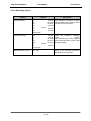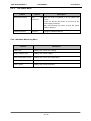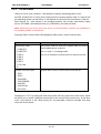
1
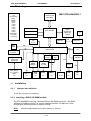
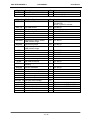
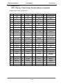
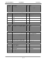
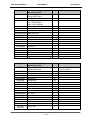
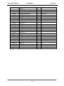
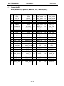
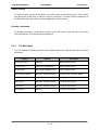
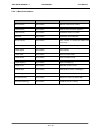
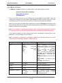
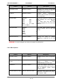
User Manual
ETE/ETX Module
MSC ETE-A945GSE-1
Intel® AtomTM N270
Rev. 0.2
2014-09-19
MSC ETE-A945GSE-1
- PRELIMINARY -
User Manual
Preface
Copyright Notice
Copyright © 2014 MSC Technologies GmbH. All rights reserved.
Copying of this document, and giving it to others and the use or communication of the contents
thereof, is forbidden without express authority. Offenders are liable to the payment of damages.
All rights are reserved in the event of the grant of a patent or the registration of a utility model or
design.
Important Information
This documentation is intended for qualified audience only. The product described herein is not
an end user product. It was developed and manufactured for further processing by trained
personnel.
Disclaimer
Although this document has been generated with the utmost care no warranty or liability for
correctness or suitability for any particular purpose is implied. The information in this document
is provided “as is” and is subject to change without notice.
EMC Rules
This unit has to be installed in a shielded housing. If not installed in a properly shielded
enclosure, and used in accordance with the instruction manual, this product may cause radio
interference in which case the user may be required to take adequate measures at his or her
owns expense.
Trademarks
All used product names, logos or trademarks are property of their respective owners.
Certification
MSC Technologies GmbH is certified according to DIN EN ISO 9001:2000 standards.
Life-Cycle-Management
MSC products are developed and manufactured according to high quality standards. Our lifecycle-management assures long term availability through permanent product maintenance.
Technically necessary changes and improvements are introduced if applicable. A productchange-notification and end-of-life management process assures early information of our
customers.
Product Support
MSC engineers and technicians are committed to provide support to our customers whenever
needed.
Before contacting Technical Support of MSC Technologies GmbH, please consult the
respective pages on our web site at www.msc-technologies.eu/support/boards for the latest
documentation, drivers and software downloads.
If the information provided there does not solve your problem, please contact our Technical
Support:
Email: [email protected]
Phone: +49 8165 906-200
2 / 55
MSC ETE-A945GSE-1
- PRELIMINARY -
User Manual
Content
1
2
3
4
5
6
General Information ......................................................................................................................... 4
1.1
Revision History ........................................................................................................................ 4
1.2
Introduction ............................................................................................................................... 4
Technical Description ....................................................................................................................... 5
2.1
Specifications............................................................................................................................ 5
2.2
Block diagram ........................................................................................................................... 7
2.3
Installation ................................................................................................................................ 7
2.3.1
Jumpers and switches ........................................................................................................ 7
2.3.2
Installing a DDR2 SO-DIMM module .................................................................................. 7
2.4
Watchdog ................................................................................................................................. 8
2.5
Interrupts, DMA channels, Upper memory ................................................................................. 8
2.5.1
PCI Devices ....................................................................................................................... 8
2.5.2
DMA channels.................................................................................................................... 9
2.5.3
Memory map ...................................................................................................................... 9
2.5.4
SMBus address map .......................................................................................................... 9
Mechanical Specification .................................................................................................................10
3.1
Top view ..................................................................................................................................10
3.2
Bottom view .............................................................................................................................10
ETX Connectors..............................................................................................................................11
4.1
Connector X1 (PCI, USB, Audio) ..............................................................................................11
4.2
Connector X2 (ISA) ..................................................................................................................13
4.3
Connector X3 (CRT, Display, TVout, Serial, Parallel, Mouse, Keyboard) .................................15
4.4
Connector X3 - alternate pinout ................................................................................................19
4.5
Connector X4 ...........................................................................................................................20
(EIDE, Ethernet, Speaker, Batterie, I2C, SMBus, etc.) ........................................................................20
4.6
Connector X5 (FAN).................................................................................................................22
4.7
SATA Connectors ....................................................................................................................22
4.8
Mini USB Connectors ...............................................................................................................23
4.9
LVDS Connector X9 (option) ....................................................................................................23
BIOS...............................................................................................................................................24
5.1
Introduction ..............................................................................................................................24
5.1.1
Startup Screen Overview...................................................................................................24
5.1.2
Activity Detection Background ...........................................................................................24
5.2
TrustedCore Setup Utility .........................................................................................................25
5.2.1
Configuring the System BIOS ............................................................................................25
5.2.2
The Main Menu .................................................................................................................27
5.2.3
The Advanced Menu .........................................................................................................31
5.2.4
The Security Menu ............................................................................................................41
5.2.5
The Power Menu ...............................................................................................................42
5.2.6
The Boot Menu .................................................................................................................43
5.2.7
The Exit Menu ...................................................................................................................44
5.3
Bios Update .............................................................................................................................45
5.4
Bios Crisis Recovery ................................................................................................................46
5.5
Diagnostics Postcodes .............................................................................................................48
5.5.1
Bootblock Bios Postcodes .................................................................................................48
5.5.2
System Bios Postcodes .....................................................................................................49
5.5.3
Memory Detection Postcodes ............................................................................................53
5.5.4
ACPI Postcodes ................................................................................................................54
Troubleshooting ..............................................................................................................................55
3 / 55
MSC ETE-A945GSE-1
User Manual
- PRELIMINARY -
1 General Information
1.1 Revision History
Rev.
0.1
0.2
Date
2012-11-28
2014-09-19
Description
Draft
New covering page
1.2 Introduction
The ETe-A945GSE is an all-in-one AtomTM N270 CPU module. It is fully compliant with the
ETX 3.0 standard.
The module is based on Intel
AtomTM N270 CPU and the Intel
945GSE chipset.
The Intel AtomTM N270 CPU is on the embedded roadmap of Intel , which means that
the processors are long term available.
The Intel
AtomTM N270 CPU supports 533MHz CPU bus.
The Intel 945GSE supports 400/533MHz memory bus.
The ETE- A945GSE supports DDR2 memory modules. It provides a 200-pin SO-DIMM
socket giving you the flexibility to configure your system up to 2GB of DDR2-DRAM.
The integrated 32-bit 3D Intel Graphics Media Accelerator 950 supports a dual-channel
LVDS graphic interface.
On board features include a 10/100Base-T RTL8103T Ethernet controller, two EIDE ports,
audio, parallel / floppy, serial, keyboard and mouse interfaces, six USB2.0 ports and two
SATA ports.
4 / 55
MSC ETE-A945GSE-1
- PRELIMINARY -
User Manual
2 Technical Description
2.1 Specifications
Core
CPU
Intel® Atom TM Processor N270, 1.60GHz, 533 MHz,
FCBGA8, soldered.
ChipSet
Mobile Intel ® 945GSE
Intel ® 82801GBM ICH7-M
L2 Cache
512KB 1.60GHz 533 MHz
Memory
200-Pin SO-DIMM socket for DDR2 (max. 2GByte)
ISA-Bus Interface
PCI to ISA Bridge ITE8888 (ETX connector X2)
PCI-Bus Interface
Intel ® 82801 ICH7 (ETX connector X1)
Video
Intel® Gen 3.5 Integrated Graphics Engine
CRT-Interface
(Optional Flat Panel Interface (LVDS 18bit single-/dualchannel))
Chrontel® CH7308 SDVO to LVDS converter (LVDS 24bit
single-/dual-channel)
Ethernet
LAN controller RTL8103T (10/100Base-T)
Audio
HDA decoder VT1708s
USB
integrated in Intel ® 82801GBM ICH7-M:
6 USB 1.1/2.0 ports
EIDE
integrated in Intel ® 82801GBM ICH7-M:
1 Port for up to 2 devices
Ultra ATA/66/100
JMICRON® JMB368 PCIe to PATA controller:
1 Port for up to 2 devices
Ultra ATA/66/100
Floppy Disk
integrated in W83627 SIO (pins shared with parallel port)
SATA
integrated in Intel ® 82801GBM ICH7-M:
2 Ports
Serial, COM1, COM2
integrated in W83627 SIO:
2 x TTL
IrDA on COM2
Parallel
integrated in W83627 SIO:
1 Parallel Port (PS/2-compatible/ECP/EPP via
SETUP configurable, pins shared with floppy port)
5 / 55
MSC ETE-A945GSE-1
User Manual
- PRELIMINARY -
Keyboard, Mouse
integrated in W83627 SIO:
MFII-Keyboard Interface, PS/2-Mouse Interface
Realtime Clock
integrated in 82801GBM ICH7-M (external battery
required)
Watchdog
Microcontroller PIC12F509A:
Start delay and timeout configurable via SETUP
creates hardware reset
TPM (optional)
Trusted Plattform Module TPM 1.2:
SLB 9635 TT 1.2
EDID-EEPROM
on Board EDID EEPROM:
enable / disable via SETUP
BIOS
Phoenix Trusted/SecureCore in SPI Flash device
EEPROM
EEPROM for CMOS Setup backup
System Monitoring
1 fan with speed input (valid only if optional fan connector
is used)
3 temperatures (CPU, GSE and board: EMC2104)
6 voltages (Vcore(CPU), +2.5V, +3.3V, +1.5V, +1.05V,
Vbat: W83627 SIO)
Power supply
+5V ±5%
Typical supply current
(DOS prompt)
1.6 A
Typical CMOS battery
power consumption
1.8 µA
Environment
Temperature
RTC / CMOS integrated in Intel
82801GBM ICH7-M
0 ... + 60°C (operating),
-25 ... + 85°C (non operating)
Humidity (rel.)
0 … 95 % (operating),
5 … 95 % (non operating)
Note:
A heat spreader plate is available from MSC providing a
standard thermal interface for the module.
The heat spreader is not a heat sink!
Dimensions
95 x 114 x 12 mm
6 / 55
MSC ETE-A945GSE-1
User Manual
- PRELIMINARY -
2.2 Block diagram
Power IN
+5V
+5V Standby
VBAT
Power
+3,30V
+2,50V
+1,80V
+1,50V
+1,35V
+1,25V
+1,05V
+0,90V
VCCCORE
+3,3VSUS
+1,5VSUS
CPU
Intel® Atom®
N270 BGA
CRT
Northbridge
X3
PC5300
DDR2
SDRAM SODIMM max.
2GByte
Intel® 945GSE
LVDS 2x24Bit X3
LVDS 2x18Bit X9
Clock
ICS9LPR3
65
2x mini
USB
X10/X11
SPI
Flash
MSC ETE-A945GSE-1
SM
B
FAN
X5
HW-Monitor
EMC2104
SPI
Southbridge
Intel® ICH7M
LP
C
TPM 1.2
Infineon®
EEPROM
Super I/O
Winbond®
W83627HF
I/O
PS2, Floppy,
LPT, COM1/2,
IRDA,
X3
PCI
X1
PCI
PCI / ISA
ITE8888
Watch
dog
PCIe
PCIe to
PATA
JMB368
USB
USB 1-4
X1
EIDE
2x IDE
X4
Audio
codec
VT1708s
SM
B
RTL
8103T
Audio
SMBus
SATA
LAN
X1
X4
X7 X8
X1
ISA
2.3 Installation
2.3.1
Jumpers and switches
There are no jumpers or switches.
2.3.2 Installing a DDR2 SO-DIMM module
The ETE-A945GSE board has a standard 200-pin SO-DIMM socket for 1.8V DDR2SDRAM SO-DIMM modules. The chipset supports 256-Mbit, 512-Mbit and 1-Gbit
technologies providing maximum capacity of 2GB.
Note:
Module height should not exceed 1260 mil (= 32 mm)
7 / 55
ISA
X2
MSC ETE-A945GSE-1
User Manual
- PRELIMINARY -
2.4 Watchdog
The ETE- A945GSE board has a watchdog function implemented in a PIC Microcontroller.
Via SETUP the watchdog can be enabled and configured.
If the watchdog is enabled a counter is started which creates a reset if it is not retriggered
within a programmable time window.
Possible watchdog delays: Disabled (default), 1s, 5s, 10s, 1min, 5min, 10min
The time delay starts before the OS is loaded.
To retrigger the watchdog use the uebi.exe tool.
2.5 Interrupts, DMA channels, Upper memory
IRQ
used for
available
comment
0
Timer 0
No
1
Keyboard
No
2
Slave 8259
No
3
COM2 / COM1
No
(1)
4
COM1 / COM2
No
(1)
5
LPT2 / LPT1
Yes
(1) / (2)
6
Floppy Disk Controller
No
(1)
7
LPT1 / LPT2
No
(1) / (2)
8
Real Time Clock
No
9
PCI
Yes
(1)
10
PCI / COM3
Yes
(1) / (2)
11
PCI / COM4
Yes
(1) / (2)
12
PS/2 Mouse
No
(1)
13
Floating Point Unit
No
14
Primary IDE
No
(1)
15
Secondary IDE
No
(1)
(1) If the device is disabled in SETUP, the interrupt is available.
(2) Can be used by external Super I/O controller FDC37C669
2.5.1 PCI Devices
PCI Device
PCI to ISA ITE8888
Sound (MODEM, not used)
USB 0..3 (Southbridge)
PCI Interrupt
REQ/GNT (0..3)
IDSEL
serial
4/45/5
AD29
INTA / INTB
---
INTC
---
8 / 55
MSC ETE-A945GSE-1
User Manual
- PRELIMINARY -
2.5.2 DMA channels
DMA
used for
available
0
comment
Yes
1
(ECP, if enabled)
(No)
2
Floppy Disk Controller
No
3
(ECP, if enabled)
(No)
4
Cascade
No
5..7
---
Yes
LPT ECP mode, if enabled
LPT ECP mode (default)
2.5.3 Memory map
Upper Memory
used for
available
comment
C0000h..CFFFFh
VGA BIOS
No
64 KB VGA BIOS
D0000h..D3FFFh
SATA
Yes/No
Shared with SATA OPROM*)
Yes
ISA bus or shadow RAM
D4000h..DFFFFh
E0000h..E3FFFh
USB Buffer
No
E4000h..FFFFFh
System BIOS
*) free when SATA OPROM disabled
No
2.5.4 SMBus address map
Device
A6 A5 A4 A3 A2 A1
A0
R/W
address *)
SMBus host
0
0
0
1
0
0
0
x
10h
clock synthesizer IC9LPRS365
1
1
0
1
0
0
1
x
D2h
watchdog
1
0
1
1
0
0
0
x
B0h
HW monitor EMC2104
0
1
0
1
1
1
1
x
5Eh
SIO W83627HF (default)
0
0
1
0
1
1
0
x
5Ah
SIO W83627HF Temp3 default
1
0
0
1
0
0
0
x
90h
SIO W83627HF Temp2 default
1
0
0
1
0
0
1
x
92h
CMOS backup EEPROM #1
1
0
1
0
1
0
0
x
A8h
CMOS backup EEPROM #2
1
0
1
0
1
0
1
x
AAh
SPD EEPROM (SO-DIMM)
1
0
1
0
0
0
0
x
A0h
*) 8 bit address (with R/W) / 7 bit address (without R/W)
9 / 55
MSC ETE-A945GSE-1
- PRELIMINARY -
User Manual
3 Mechanical Specification
3.1 Top view
X10
X11
X8
X2
X4
X7
X3
X1
X5
X9
3.2 Bottom view
X2
X4
X3
X3
10 / 55
MSC ETE-A945GSE-1
User Manual
- PRELIMINARY -
4 ETX Connectors
4.1 Connector X1 (PCI, USB, Audio)
Pin
Signal
Pin
Signal
Pin
Signal
Pin
Signal
1
GND
2
GND
51
VCC
52
VCC
3
PCICLK3
4
PCICLK4
53
PAR
54
SERR#
5
GND
6
GND
55
GPERR#
56
RESERVED
7
PCICLK1
8
PCICLK2
57
PME#
58
USB2#
9
REQ3#
10
GNT3#
59
LOCK#
60
DEVSEL#
11
GNT2#
12
3.3V
61
TRDY#
62
USB3#
13
REQ2#
14
GNT1#
63
IRDY#
64
STOP#
15
REQ1#
16
3.3V
65
FRAME#
66
USB2
17
GNT0#
18
RESERVED
67
GND
68
GND
19
VCC
20
VCC
69
AD16
70
CBE2#
21
SERIRQ
22
REQ0#
71
AD17
72
USB3
23
AD0
24
3.3V
73
AD19
74
AD18
25
AD1
26
AD2
75
AD20
76
USB0#
27
AD4
28
AD3
77
AD22
78
AD21
29
AD6
30
AD5
79
AD23
80
USB1#
31
CBE0#
32
AD7
81
AD24
82
CBE3#
33
AD8
34
AD9
83
VCC
84
VCC
35
GND
36
GND
85
AD25
86
AD26
37
AD10
38
AUXAL
87
AD28
88
USB0
39
AD11
40
MIC
89
AD27
90
AD29
41
AD12
42
AUXAR
91
AD30
92
USB1
43
AD13
44
ASVCC
93
PCIRST#
94
AD31
45
AD14
46
SNDL
95
INTC#
96
INTD#
47
AD15
48
ASGND
97
INTA#
98
INTB#
49
CBE1#
50
SNDR
99
GND
100
GND
11 / 55
MSC ETE-A945GSE-1
Signal
VCC
GND
3V
RESERVED
Signal
User Manual
- PRELIMINARY -
Description
Power Supply +5V, +/-5%
Power Ground
Power Supply +3.3V
Not connected
I/O
I
I
O
n.a.
Note
external supply
external supply
Do not use externally
Do not connect
Description of PCI Bus Signals
I/O
Note
PCI outputs 3,3V signal
level
PCI inputs 5V tolerant
PCICLK1..4.
REQ0..3#
GNT0..3#
AD0..31
CBE0..3#
PAR
SERR#
GPERR#
PME#
LOCK#
DEVSEL#
TRDY#
IRDY#
STOP#
FRAME#
PCIRST#
INTA#
INTB#
INTC#
INTD#
SERIRQ
Signal
USB0, USB0#
USB1, USB1#
USB2, USB2#
USB3, USB3#
USB4, USB4#
USB5, USB5#
Signal
SNDL
SNDR
AUXAL
AUXAR
MIC
ASGND
ASVCC
PCI clock output
PCI bus request
PCI bus grant
PCI Adress-/ Databus
PCI bus command/byte enables
PCI bus parity
PCI bus system error
PCI bus grant parity error
PCI bus power management event
PCI bus lock
PCI bus device select
PCI bus target ready
PCI bus initiator ready
PCI bus stop
PCI bus frame
PCI bus reset
PCI bus interrupt A
PCI bus interrupt B
PCI bus interrupt C
PCI bus interrupt D
Serial interrupt request
Description of USB Signals
USB Port 0
USB Port 1
USB Port 2
USB Port 3
USB Port 4
USB Port 5
Description of Audio Signals
Line-Level stereo output left
Line-Level stereo output right
Auxiliary input A left
Auxiliary input A right
Microphone input
Analog ground of sound controller
Analog supply of sound controller
12 / 55
O
I
O
I/O
I/O
I/O
I/O
I/O
I/O
I/O
I/O
I/O
I/O
I/O
I/O
O
I
I
I
I
I/O
I/O
I/O
I/O
I/O
I/O
I/O
I/O
PU 8k2 3,3V
PU 8k2 3,3V
PU 8k2 3,3V
internal PU 20k 3,3Vsus
PU 8k2 3,3V
PU 8k2 3,3V
PU 8k2 3,3V
PU 8k2 3,3V
PU 8k2 3,3V
PU 8k2 3,3V
3,3V signal level
PU 8k2 3,3V
PU 8k2 3,3V
PU 8k2 3,3V
PU 8k2 3,3V
PU 10k 3,3V
Note
5V tolerant; internal PD 15k
5V tolerant; internal PD 15k
5V tolerant; internal PD 15k
5V tolerant; internal PD 15k
5V tolerant; internal PD 15k
5V tolerant; internal PD 15k
I/O
O
O
I
I
I
I
O
Note
0.7VRMS
0.7VRMS
3.3V
MSC ETE-A945GSE-1
User Manual
- PRELIMINARY -
4.2 Connector X2 (ISA)
Pin
Signal
Pin
Signal
Pin
Signal
Pin
Signal
1
GND
2
GND
51
VCC
52
VCC
3
SD14
4
SD15
53
SA6
54
IRQ5
5
SD13
6
MASTER#
55
SA7
56
IRQ6
7
SD12
8
DREQ7
57
SA8
58
IRQ7
9
SD11
10
DACK7#
59
SA9
60
SYSCLK
11
SD10
12
DREQ6
61
SA10
62
REFSH#
13
SD9
14
DACK6#
63
SA11
64
DREQ1
15
SD8
16
DREQ5
65
SA12
66
DACK1#
17
MEMW#
18
DACK5#
67
GND
68
GND
19
MEMR#
20
DREQ0
69
SA13
70
DREQ3
21
LA17
22
DACK0#
71
SA14
72
DACK3#
23
LA18
24
IRQ14
73
SA15
74
IOR#
25
LA19
26
IRQ15
75
SA16
76
IOW#
27
LA20
28
IRQ12
77
SA18
78
SA17
29
LA21
30
IRQ11
79
SA19
80
SMEMR#
31
LA22
32
IRQ10
81
IOCHRDY
82
AEN
33
LA23
34
IO16#
83
VCC
84
VCC
35
GND
36
GND
85
SD0
86
SMEMW#
37
SBHE#
38
M16#
87
SD2
88
SD1
39
SA0
40
OSC
89
SD3
90
NOWS#
41
SA1
42
BALE
91
DREQ2
92
SD4
43
SA2
44
TC
93
SD5
94
IRQ9
45
SA3
46
DACK2#
95
SD6
96
SD7
47
SA4
48
IRQ3
97
IOCHK#
98
RSTDRV
49
SA5
50
IRQ4
99
GND
100
GND
13 / 55
MSC ETE-A945GSE-1
Signal
VCC
GND
Signal
SD0..15
User Manual
- PRELIMINARY -
Description
Power Supply +5V, +/-5%
Power Ground
I/O
I
I
Note
external supply
external supply
ISA Bus Signals
ISA Databus
I/O
I/O
I/O
I/O
I/O
I/O
I/O
I/O
I/O
Note
all ISA outputs 5V signal level
(PU 8k2 5V)
all ISA inputs 5V tolerant
PU 8k2 5V
PU 8k2 5V
internal PU 50k 5V
PD 4k7
PD 4k7
PU 8k2 5V
PU 1k0 5V
I/O
I/O
PU 8k2 5V
PU 1k0 5V
I/O
I/O
I
I/O
I/O
I
I/O
PU 8k2 5V
PU 8k2 5V
PU 4k7 5V
PU 1k0 5V
PU 1k0 5V
PU 1k0 5V
PU 1k0 5V
I
I
O
O
O
I
I/O
I/O
I
I
I/O
I
PU 1k0 5V
PU 1k0 5V
SA0..19
LA17..23
SBHE#
BALE
AEN
MEMR#
SMEMR#
ISA Addressbus
ISA Addressbus
ISA Byte High Enable
ISA Address Latch Enable
ISA Address Enable
ISA memory read
ISA memory read in lowest
1MB address range
MEMW#
ISA memory write
SMEMW# ISA memory write in lowest
1MB address range
IOR#
ISA IO read
IOW#
ISA IO write
IOCHK#
ISA IO check
IOCHRDY ISA IO channel ready
M16#
ISA 16Bit memory device
IO16#
ISA 16Bit IO device
REFSH# ISA memory refresh cycle
pending
NOWS#
ISA No waitstates
MASTER# ISA Master
SYSCLK ISA System clock (8 MHz)
OSC
ISA Oscillator (14,31818 MHz)
RSTDRV ISA Reset signal
DREQ0..7 ISA DMA request
DACK0#..7# ISA DMA acknowledge
TC
ISA DMA end
IRQ3..7
ISA Interrupt request
IRQ9..12 ISA Interrupt request
IRQ14
ISA Interrupt request
IRQ15
ISA Interrupt request
14 / 55
PD 8k2
PD 4k7
IRQ table see 2.5; PU 8k2 5V
IRQ table see 2.5; PU 8k2 5V
IRQ table see 2.5; PU 8k2 5V
IRQ table see 2.5; PU 8k2 5V
MSC ETE-A945GSE-1
User Manual
- PRELIMINARY -
4.3 Connector X3
(CRT, Display, TVout, Serial, Parallel, Mouse, Keyboard)
Standard pinout with LVDS and LPT
Pin
Signal
Pin
Signal
Pin
Signal
Pin
Signal
1
GND
2
GND
51
LPT/FLPY#
52
RESERVED
3
R
4
B
53
VCC
54
GND
5
HSY
6
G
55
STB#/RES
56
AFD#/DENSEL
7
VSY
8
DDCK
57
RESERVED
58
PD7/RES
9
DETECT#
10
DDDA
59
IRRX
60
ERR#/HDSEL#
11
LCDDO16
12
LCDDO18
61
IRTX
62
PD6/RES
13
LCDDO17
14
LCDDO19
63
RXD2
64
INIT#/DIR#
15
GND
16
GND
65
GND
66
GND
17
LCDDO13
18
LCDDO15
67
RTS2#
68
PD5/RES
19
LCDDO12
20
LCDDO14
69
DTR2#
70
SLIN#/STEP#
21
GND
22
GND
71
DCD2#
72
PD4/
DSKCHG#
23
LCDDO8
24
LCDDO11
73
DSR2#
74
PD3/RDATA#
25
LCDDO9
26
LCDDO10
75
CTS2#
76
PD2/WP#
27
GND
28
GND
77
TXD2
78
PD1/TRK0#
29
LCDDO4
30
LCDDO7
79
RI2#
80
PD0/INDEX#
31
LCDDO5
32
LCDDO6
81
VCC
82
VCC
33
GND
34
GND
83
RXD1
84
ACK/DRV1
35
LCDDO1
36
LCDDO3
85
RTS1#
86
BUSY#/MOT1#
37
LCDDO0
38
LCDDO2
87
DTR1#
88
PE/WDATA#
39
VCC
40
VCC
89
DCD1#
90
SLCT#/
WGATE#
41
JILI_DAT
42
LTGIO0
91
DSR1#
92
MSCLK
43
JILI_CLK
44
BLON#
93
CTS1#
94
MSDAT
45
BIASON
46
DIGON
95
TXD1
96
KBCLK
47
COMP
48
Y
97
RI1#
98
KBDAT
49
SYNC
50
C
99
GND
100
GND
15 / 55
MSC ETE-A945GSE-1
Signal
VCC
GND
N.C.
LTGIO0
DETECT#
User Manual
- PRELIMINARY -
Description
Power Supply +5VDC, 5%
Power Ground
Not connected
General Purpose IO
Not connected
I/O
I
I
n.a.
O
n.a.
Note
external supply
external supply
I/O
O
O
O
Note
3V3 signal level
3V3 signal level
DDCK
DDDA
Description of analog CRT signals
Horizontal Sync
Vertical Sync
Red channel RGB Analog Video
Output
Green channel RGB Analog Video
Output
Blue channel RGB Analog Video
Output
Display Data Channel Clock
Display Data Channel Data
I/O
I/O
PU 2k2 5V
PU 2k2 5V
Signal
SYNC
Y
C
COMP
Description of TV signals (option)
n.c.
n.c.
n.c.
n.c.
I/O
n.a.
n.a.
n.a.
n.a.
Note
Signal
Description of COMx signals
I/O
Note
All TTL signal level
Data terminal ready of COM1/COM2
Ring indicator of COM1/COM2
Data transmit of COM1/COM2
Data receive of COM1/COM2
Clear to send of COM1/COM2
Request to send of COM1/COM2
Data carrier detect of COM1/COM2
Data set ready of COM1/COM2
O
I
O
I
I
O
I
I
Description of keyboard and
infrared signals
Keyboard Data
Keyboard Clock
Mouse Data
Mouse Clock
Infrared Transmit
Infrared Receive
I/O
Note
I/O
O
I/O
O
O
I
PU 8k2 5V
PU 8k2 5V
PU 8k2 5V
PU 8k2 5V
Signal
HSYNC
VSYNC
R
G
B
DTR1..2#
RI1..2#
TXD1..2
RXD1..2
CTS1..2#
RTS1..2#
DCD1..2#
DSR1..2#
Signal
KBDAT
KBCLK
MSDAT
MSCLK
IRTX
IRRX
16 / 55
GPIO42; PU 4k7 5V
O
O
PU 470k 5V
PU 470k 5V
PU 470k 5V
PU 470k 5V
PU 470k 5V
MSC ETE-A945GSE-1
Signal
LPT/FLPY#
STB#/RES
AFD#/DENSEL
PD0/INDEX#
PD1/TRK0#
PD2/WP#
PD3/RDATA#
PD4/DSKCHG#
PD5/RES
PD6/RES
PD7/RES
ERR#/HDSEL#
INIT#/DIR#
SLIN#/STEP#
ACK/DRV1
BUSY#/MOT1#
PE/WDATA#
SLCT#/WGATE#
Signal
LPT/FLPY#
STB#/RES
AFD#/DENSEL
PD0/INDEX#
PD1/TRK0#
PD2/WP#
PD3/RDATA#
PD4/DSKCHG#
PD5/RES
PD6/RES
PD7/RES
ERR#/HDSEL#
INIT#/DIR#
SLIN#/STEP#
ACK/DRV1
BUSY#/MOT1#
PE/WDATA#
SLCT#/
WGATE#
User Manual
- PRELIMINARY -
Description of FDC signals
(shared with LPT)
LPT or Floppy Interface
configuration input
nc
density select:
low = 250/300Kb/s
high = 500/1000Kb/s
Index signal
Track signal
Write protect signal
Raw data read
Disc changed
nc
nc
nc
Head select
Direction
Motor step
Drive 1 select
Motor 1 select
Raw write data
Write enable
I/O
Description of LPT signals
(shared with FDC)
LPT or Floppy Interface
configuration input
Strobe signal
Automatic feed
Databus D0
Databus D1
Databus D2
Databus D3
Databus D4
Databus D5
Databus D6
Databus D7
LPT error
Initiate
Select
Acknowledge
Busy
Paper empty
Power ON
I/O
17 / 55
I
Note
Connect to GND; PU 10k 5V
O
I
I
I
I
I
O
O
O
O
O
O
O
I
O
O
I/O
I/O
I/O
I/O
I/O
I/O
I/O
I/O
I
O
O
I
I
I
I
Note
Connect to VCC (resistor
4K7); PU 10k 5V
MSC ETE-A945GSE-1
Signal
BIASON
DIGON
BLON#
LCDDO0
LCDDO1
LCDDO2
LCDDO3
LCDDO4
LCDDO5
LCDDO6
LCDDO7
LCDDO8
LCDDO9
LCDDO10
LCDDO11
LCDDO12
LCDDO13
LCDDO14
LCDDO15
LCDDO16
LCDDO17
LCDDO18
LCDDO19
JILI_DAT
JILI_CLK
User Manual
- PRELIMINARY -
Description of LVDS Flatpanel
signals
n.c. (Display contrast voltage ON)
Display Power ON
Display Backlight ON
LVDS_L0LVDS_L0+
LVDS_L1LVDS_L1+
LVDS_L2LVDS_L2+
LVDS_LCLKLVDS_LCLK+
LVDS_L3LVDS_L3+
LVDS_U0LVDS_U 0+
LVDS_U 1LVDS_U 1+
LVDS_U 2LVDS_U 2+
LVDS_U CLKLVDS_U CLK+
LVDS_U3LVDS_U3+
JILI DATA
JILI CLOCK
(*) n/a
18 / 55
I/O
O
O
O
O
O
O
O
O
O
O
O
O
O
O
O
O
O
O
O
O
O
O
O
I/O
I/O
Note
3,3V tolerant
PU 4k7 5V
(*)
(*)
(*)
(*)
PU 4k7 3,3V
PU 4k7 3,3V
MSC ETE-A945GSE-1
User Manual
- PRELIMINARY -
4.4 Connector X3 - alternate pinout
LPT
(LPT/FLPY# = high)
Floppy
(LPT/FLPY# = low)
Pin
Signal
Pin
Signal
Pin
Signal
Pin
Signal
51
LPT/FLPY#
52
RESERVED
51
LPT/FLPY#
52
RESERVED
53
VCC
54
GND
53
VCC
54
GND
55
STB#
56
AFD#
55
RESERVED
56
DENSEL
57
RESERVED
58
PD7
57
RESERVED
58
RESERVED
59
IRRX
60
ERR#
59
IRRX
60
HDSEL#
61
IRTX
62
PD6
61
IRTX
62
RESERVED
63
RXD2
64
INT#
63
RXD2
64
DIR#
65
GND
66
GND
65
GND
66
GND
67
RTS2#
68
PD5
67
RTS2#
68
RESERVED
69
DTR2#
70
SLIN#
69
DTR2#
70
STEP#
71
DCD2#
72
PD4
71
DCD2#
72
DSKCHG#
73
DSR2#
74
PD3
73
DSR2#
74
RDATA#
75
CTS2#
76
PD2
75
CTS2#
76
WP#
77
TXD2
78
PD1
77
TXD2
78
TRK0#
79
RI2#
80
PD0
79
RI2#
80
INDEX#
81
VCC
82
VCC
81
VCC
82
VCC
83
RXD1
84
ACK
83
RXD1
84
DRV
85
RTS1#
86
BUSY#
85
RTS1#
86
MOT
87
DTR1#
88
PE
87
DTR1#
88
WDATA#
89
DCD1#
90
SLCT#
89
DCD1#
90
WGATE#
91
DSR1#
92
MSCLK
91
DSR1#
92
MSCLK
93
CTS1#
94
MSDAT
93
CTS1#
94
MSDAT
95
TXD1
96
KBCLK
95
TXD1
96
KBCLK
97
RI1#
98
KBDAT
97
RI1#
98
KBDAT
99
GND
100
GND
99
GND
100
GND
19 / 55
MSC ETE-A945GSE-1
User Manual
- PRELIMINARY -
4.5 Connector X4
(EIDE, Ethernet, Speaker, Batterie, I2C, SMBus, etc.)
Pin
Signal
Pin
Signal
Pin
Signal
Pin
Signal
1
GND
2
GND
51
SIDE_IOW#
52
PIDE_IOR#
3
5V_SB
4
PWGIN
53
SIDE_DRQ
54
PIDE_IOW#
5
PS_ON
6
SPEAKER
55
SIDE_D15
56
PIDE_DRQ
7
PWRBTN#
8
BATT
57
SIDE_D0
58
PIDE_D15
9
KBINH
10
LILED
59
SIDE_D14
60
PIDE_D0
11
RSMRST#
12
ACTLED
61
SIDE_D1
62
PIDE_D14
13
ROMKBCS#
14
SPEEDLED
63
SIDE_D13
64
PIDE_D1
15
EXT_PRG
16
I2CLK
65
GND
66
GND
17
VCC
18
VCC
67
SIDE_D2
68
PIDE_D13
19
OVCR#
20
GPCS#
69
SIDE_D12
70
PIDE_D2
21
EXTSMI#
22
I2DAT
71
SIDE_D3
72
PIDE_D12
23
SMBCLK
24
SMBDATA
73
SIDE_D11
74
PIDE_D3
25
SIDE_CS3#
26
SMBALRT#
75
SIDE_D4
76
PIDE_D11
27
SIDE_CS1#
28
DASP_S
77
SIDE_D10
78
PIDE_D4
29
SIDE_A2
30
PIDE_CS3#
79
SIDE_D5
80
PIDE_D10
31
SIDE_A0
32
PIDE_CS1#
81
VCC
82
VCC
33
GND
34
GND
83
SIDE_D9
84
PIDE_D5
35
PDIAG_S
36
PIDE_A2
85
SIDE_D6
86
PIDE_D9
37
SIDE_A1
38
PIDE_A0
87
SIDE_D8
88
PIDE_D6
39
SIDE_INTRQ
40
PIDE_A1
89
GPE2#
90
CBLID_P#
41
BATLOW#
42
GPE1#
91
RXD#
92
PIDE_D8
43
SIDE_AK#
44
PIDE_INTRQ
93
RXD
94
SIDE_D7
45
SIDE_RDY
46
PIDE_AK#
95
TXD#
96
PIDE_D7
47
SIDE_IOR#
48
PIDE_RDY
97
TXD
98
HDRST#
49
VCC
50
VCC
99
GND
100
GND
20 / 55
MSC ETE-A945GSE-1
User Manual
- PRELIMINARY -
Signal
VCC
GND
N.C.
Description
Power Supply +5VDC, 5%
Power Ground
Not connected
I/O
I
I
n.a.
Note
external supply
external supply
Signal
PIDE_D0..15
PIDE_A0..2
PIDE_CS1#
PIDE_CS3#
PIDE_DRQ
PIDED_AK#
PIDE_RDY
PIDE_IOR#
PIDE_IOW#
PIDE_INTRQ
CBLID_P#
Description of IDE signals
Primary IDE Databus
Primary IDE Addressbus
Primary IDE chip select channel0
Primary IDE chip select channel1
Primary IDE dma request
Primary IDE dma acknowledge
Primary IDE ready
Primary IDE IO read
Primary IDE IO write
Primary IDE interrupt request
Cable ID primary
I/O
I/O
O
O
O
I
O
I
O
O
I
I
Note
D7: Internal PD11k5
SIDE_D0..15
SIDE_A0..2
SIDE_CS1#
Secondary IDE Databus
Secondary IDE Addressbus
Secondary IDE chip select
channel0
Secondary IDE chip select
channel1
Secondary IDE dma request
Secondary IDE dma acknowledge
Secondary IDE ready
Secondary IDE IO read
Secondary IDE IO write
Secondary IDE interrupt request
SATA LED#
I/O
O
O
D7: Internal PD31k6
SIDE_CS3#
SIDE_DRQ
SIDED_AK#
SIDE_RDY
SIDE_IOR#
SIDE_IOW#
SIDE_INTRQ
DASP_S
PDIAG_S
HDRST#
Signal
TXD+, TXDRXD+, RXDACTLED
LILED
SPEEDLED
Secondary IDE Master/Slave
negotiation
HardDrive reset
Description of Ethernet signals
Ethernet Twisted Pair transmit
signal pair
Ethernet Twisted Pair receive
signal pair
Ethernet activity LED
Ethernet link LED
Ethernet speed LED, ON at
100Mb/s
21 / 55
Internal PD 11k5
PU 4k7 3,3V
PU 8k2 3,3V
PD 10k
O
I
O
I
O
O
I
OC
PD 4k7
PU 4k7 3,3V
PD 8k2
Function requires ext. PU to
3V3. Do not pull down!
I
O
3,3V signal level
I/O
O
Note
I
O
O
O
3,3V (10mA sink)
3,3V (10mA sink)
3,3V (10mA sink)
MSC ETE-A945GSE-1
User Manual
- PRELIMINARY -
Signal
SPEAKER
Description of Misc. signals
Speaker output
I/O
O
BATT
PWGIN
I2CLK
I2DAT
SMBCLK
SMBDAT
SMBALRT#
KBINH
5V_SB
PS_ON
PWRBTN#
OVCR#
ROMKBCS#
EXT_PRG#
GPCS#
GPE1#
GPE2#
BATLOW#
EXTSMI#
RSMRST#
Battery supply
Power good input
I2C Bus Clock
I2C Bus Data
SM Bus Clock
SM Bus Data
SM Bus Alert
Keyboard inhibit
Supply of internal suspend circuit
Power Save ON
Power Button
Over current detect for USB
n.c.
n.c.
n.c.
n.c.
Ring Input
Batterie low
External SMI
Resume Reset
I
I
I/O
I/O
I/O
I/O
I
I
I
O
I
I
n.a.
n.a.
n.a.
n.a.
I
I
I
I
Note
Internal PD 20k ; 3,3V
signal level
3,3V (3,6V max.)
PU 10k 3,3V
PU 2k2 3,3V
PU 2k2 3,3V
PU 6k8 5V
PU 6k8 5V
PU 10k 3,3V_SUS
PU 10k 5V
PU 4k7 5V_SB
Internal PU 20k 3,3V_SUS
PU 8k2 3,3V_SUS
PU 10k 3,3V_SUS
PU 220k 3,3V_SUS
PU 10k 3,3V_SUS
3,3V signal level
4.6 Connector X5 (FAN)
Pin
Signal
1
GND
2
PWM controlled VCC 5V
3
Fan speed
Connector:
JST S3B-ZR-SM4A-TF
4.7 SATA Connectors
Pin
Signal X7
Pin
Signal X8
1
GND
1
GND
2
S1_TX+
2
S2_TX+
3
S1_TX-
3
S2_TX-
4
GND
4
GND
5
S1_RX-
5
S2_RX-
6
S1_RX+
6
S2_RX+
7
GND
7
GND
22 / 55
MSC ETE-A945GSE-1
User Manual
- PRELIMINARY -
4.8 Mini USB Connectors
Pin
Signal X10
Pin
Signal X11
1
5V
1
5V
2
USB4_Data-
2
USB5_Data -
3
USB4_Data +
3
USB5_Data +
4
USB_ID4
4
USB_ID5
5
GND
5
GND
4.9 LVDS Connector X9 (option)
Pin
Signal
1
LVDS_A0-
2
LVDS_A0+
3
LVDS_A1-
4
LVDS_A1+
5
LVDS_A2-
6
LVDS_A2+
7
LVDS_A_CLK-
8
LVDS_A_CLK+
9
LVDS_B0-
10
LVDS_B0+
11
LVDS_B1-
12
LVDS_B1+
13
LVDS_B2-
14
LVDS_B2+
15
LVDS_B_CLK-
16
LVDS_B_CLK+
17
GND
18
LVDS_VDD_EN (PD 100k, 3,3V tolerant)
19
LVDS_BKLEN# (PU 4k7 5V)
20
Connector:
LVDS_BKLT_CTRL (PD 100k, 3,3V tolerant)
Hirose
DF14-20P-1.25H
23 / 55
MSC ETE-A945GSE-1
5
- PRELIMINARY -
User Manual
BIOS
5.1 Introduction
This guide describes the Phoenix TrustedCore Startup screen and contains information on
how to access Phoenix TrustedCore setup to modify the settings which control Phoenix preOS (operating system) functions.
5.1.1
Startup Screen Overview
The Phoenix TrustedCore Startup screen is a graphical user interface (GUI) that is included
in Phoenix TrustedCore products. The default bios behavior is to show an informational text
screen during bios POST phase, but the graphical boot screen can be enabled in the bios
setup. The standard boot screen is a black screen, including a progress bar at the bottom of
the screen. This bar indicates the progress of the Startup Screen functions and provides
user prompting and POST status. The following figure shows the various parts of a generic
Startup Screen at 1024x768 resolution:
5.1.2
Activity Detection Background
While the TrustedCore Startup screen is displayed, press the Setup Entry key (F2 –
TrustedCore default). The TrustedCore Startup Status Bar acknowledges the input, and at
the end of POST, the screen clears and setup launches.
An example of the Startup Status Bar displaying changing state is shown in the following
figure. The “Please Wait…” text is displayed after the F2 key is pressed to acknowledge
user input.
Active status bar:
24 / 55
MSC ETE-A945GSE-1
- PRELIMINARY -
User Manual
5.2 TrustedCore Setup Utility
With the Phoenix TrustedCore Setup program, you can modify TrustedCore settings and
control the special features of your computer. The Setup program uses a number of menus
for making changes and turning the special features on or off. This chapter provides an
overview of the Setup utility and describes at a high-level how to use it.
5.2.1
Configuring the System BIOS
To start the Phoenix TrustedCore Setup utility, press [F2] to launch Setup. The Setup main
menu appears.
The BIOS Menu Structure
The BIOS Menu is structured in the following way:
Main
Board Information
IDE Channel 0 Master
IDE Channel 0 Slave
SATA Port 0
SATA Port 1
Boot Options
Advanced
Cache Memory
CPU Control Sub-Menu
MCH Control Sub-menu
Video (Intel IGD) Control Sub-menu
ICH Control Sub-menu
PCI Control Sub-menu
ICH USB Control Sub-menu
ACPI Control Sub-menu
Clock Control Sub-menu
I/O Device Configuration
Watchdog Options
Security
Power
Hardware Monitor
Boot
Exit
25 / 55
MSC ETE-A945GSE-1
User Manual
- PRELIMINARY -
The Menu Bar
The Menu Bar at the top of the window lists these selections:
Menu Items
Description
Main
Use this menu for basic system configuration.
Advanced
Use this menu to set the Advanced Features available on your
system’s chipset.
Security
Use this menu to set User and Supervisor Passwords and the
Backup and Virus-Check reminders.
Power
Use this menu to configure Power-Management features.
Boot
Use this menu to set the boot order in which the BIOS attempts to
boot to OS.
Exit
Exits the current menu.
Use the left and right arrow keys on your keyboard to make a menu selection.
The Legend Bar
Use the keys listed in the legend bar on the bottom of the screen to make your selections, or
to exit the current menu. The following table describes the legend keys and their alternates:
Key
Function
F1 or Alt-H
General Help window.
Esc
Exit this menu.
Arrow keys
Select a different menu.
Up and down arrow keys
Move cursor up and down.
Tab or Shift-Tab
Move cursor left and right (i.e. at System Time / System Date).
Home or End
Move cursor to top or bottom of window.
PgUp or PgDn
Move cursor to next or previous page.
F5 or -
Select the previous value for the field.
F6 or + or Space
Select the next value for the field.
F9
Load the Default Configuration values (for all menus).
F10
Save and exit.
Enter
Execute command or select submenu.
26 / 55
MSC ETE-A945GSE-1
User Manual
- PRELIMINARY -
Select an item
To select an item, use the arrow keys to move the cursor to the field you want. Then use the
plus-and-minus value keys to select a value for that field. The Save Values commands in
the Exit Menu save the values currently displayed in all the menus.
Display a submenu
To display a submenu, use the arrow keys to move the cursor to the sub menu you want.
Then press Enter. A pointer marks all submenus.
5.2.2
The Main Menu
You can make the following selections on the Main Menu itself. Use the sub menus for other
selections.
Feature
Options
Description
Board Information
Submenu
Displays BIOS Version
System Time
Enter Time (HH:MM:SS)
Set the System Time.
System Date
Enter Date (DD/MM/YYYY)
Set the System Date.
IDE Channel 0 Master
Submenu “Master & Slaves”
Configure IDE Channel 0 Master
IDE Channel 0 Slave
Submenu “Master & Slaves”
Configure IDE Channel 0 Slave
SATA Port 0
Submenu “Master & Slaves”
Configure SATA Port 0
SATA Port 1
Submenu “Master & Slaves”
Configure SATA Port 1
Boot Options
Submenu
Configure Boot Options
27 / 55
MSC ETE-A945GSE-1
User Manual
- PRELIMINARY -
5.2.2.1 Board Information
Feature
Options
Description
Bios Version
Informative
Shows current bios version.
HW Platform
Informative
Name of the hardware platform
HW Revision
Informative
Hardware revision number
Serial #
Informative
Hardware Serial Number
Boot Counter
Informative
The number of times this board has
booted up.
CPU String
Informative
CPU Identification string
CPU Speed
Informative
CPU Speed
CPU Class
Informative
CPU ID Class code
CPU Model
Informative
CPU ID Model code
CPU Stepping
Informative
CPU ID Stepping
CPU Cores
Informative
Number of CPU cores
Northbridge
Informative
Identification of the northbridge
Southbridge
Informative
Identification of the southbridge
System Memory
Informative
Amount of memory below 1MB
Extended Memory
Informative
Total amount of memory
28 / 55
MSC ETE-A945GSE-1
User Manual
- PRELIMINARY -
5.2.2.2 Master and Slaves
The Master and Slave settings on the Main Menu control these types of devices:
• Hard-disk drives (IDE and SATA)
• Removable-disk drives
• CD-ROM drives
There is one IDE connector on your motherboard, usually labeled "Primary IDE". There are
usually two connectors on each ribbon cable attached to IDE connector. When you have
connected two drives to this connector, the one on the end of the cable is the Master.
When you enter Setup, the Main Menu displays the results of Autotyping information each
drive provides about its own size and other characteristics–and how they are arranged as
Masters or Slaves on your machine.
Note: Do not attempt to change these settings unless you have an installed drive that does
not autotype properly (such as an older hard-disk drive that does not support autotyping).
If you need to change your drive settings, select one of the Master or Slave drives on the
Main Menu. This will display a menu like this:
Note: The capacity is displayed in ‘real’ Mbytes (1MB=1024*1024 Bytes) Drives with a total
capacity greater than 8Gbyte operate in LBA format only.
Feature
Options
Description
None = Autotyping is not able to
Removable, supply the drive type or end user has
selected None, disabling any drive that
Removable, may
be
installed.
ATAPI, Auto = Autotyping, the drive itself
supplies
the
information.
User = You supply the hard-disk drive
information in the following fields.
IDE Removable = Removable Disk
Drive
ATAPI Removable = Removable Disk
Drive
Other ATAPI = non-specific ATAPI
Device
CD-ROM = CD-ROM drive.
Type
None,
ATAPI
CD-ROM,
IDE
Other
User,
Auto
Cylinders
1 to 65536
Number of Cylinders
Heads
1 to 16
Number of read/write heads
Sectors
1 to 63
Number of sectors per track
Multi-Sector Transfers
Disabled,
4
sectors,
16 sectors
2
8
29 / 55
Disabled
sectors, Any selection except
sectors, determines the number of sectors
transferred per block.
MSC ETE-A945GSE-1
User Manual
- PRELIMINARY -
Feature
Options
Description
LBA Mode Control
Disabled, Enabled
Enabling LBA causes Logical Block
Addressing to be used in place of
Cylinders, Heads, & Sectors.
32 Bit I/O
Disabled, Enabled
Enables
32-bit
communication
between CPU and IDE card. Requires
PCI or local bus.
Transfer Mode
Standard
Fast
PIO
Fast
PIO
Fast
PIO
Fast
PIO
FPIO
3
/
DMA
FPIO 4 / DMA 2
Ultra DMA Mode
Disabled
Mode
Mode
Mode
Mode
Mode
Mode 5
SMART Monitoring
Disabled, Enabled
1
2
3
4
1
Selects the method for transferring the
data between the hard disk and
system
memory.
The Setup menu only lists those
options supported by the drive and
platform.
Ultra DMA Mode supports 33/66/100
0 MB/sec transfer rate for fixed disk
1 drives.
2
3
4
Displays the status of SMART
Monitoring if supported by the used
drive.
WARNING: Incorrect settings can cause your system to malfunction.
5.2.2.3 Boot Options
Feature
Post Errors
Description
Disabled, Enabled
Enabled displays system configuration
on boot.
Diagnostic Disabled, Enabled
Enabled displays the diagnostic
screen
during
boot.
Disabled displays the Boot Logo.
Disabled, Enabled
Pauses and displays Setup Entry or
resume boot prompt if error occurs on
boot. If disabled, system always
attempts to boot.
Summary screen
Boot-time
Screen
Options
Extended Memory Testing Normal, Just zero it, None
30 / 55
Determines which type of test will be
performed on extended memory during
POST (above 1 MB).
MSC ETE-A945GSE-1
5.2.3
User Manual
- PRELIMINARY -
The Advanced Menu
Feature
Installed O/S
Options
Description
Other,
Win95,
Win98,
WinMe,
Win2000,
WinXP
Select the operating system installed
on your system which you will use
most commonly.
Reset configuration Data
No, Yes
Select ‘Yes’ if you want to clear the
Extended System Configuration Data
(ESCD) area.
Large Disk Access Mode
Other, DOS
Select Other for UNIX, Novell
NetWare. Select DOS for all other
operating systems.
Small Disk Access Mode
No, Yes
Select if CHS translation should be
made for a LBA-capable harddisk with
less than 1024 cylinders, e.g.
CompactFlash(R).
If
you
have
problems with booting from a
CompactFlash(R), try to change this
setting.
NOTE: An incorrect setting can cause
some operating systems to display
unexpected behavior.
No = translate CHS only if HDD has
>1024 cyls.
Yes = translate CHS for all LBAcapable disks.
Port 80 Cycles
LPC Bus, PCI Bus
Control where the Port 80h cycles are
sent.
Local Bus IDE adapter
Disabled, Enabled
Enable the integrated local bus IDE
adapter.
Secondary PATA OPROM Disabled, Enabled
Enables or disables the OPROM of the
onboard secondary PATA Controller
Cache Memory
Submenu
Configure Cache Memory
CPU Control Sub-Menu
Submenu
Configure CPU Control
MCH Control Sub-Menu
Submenu
Configure MCH Control
Video (Intel IGD) Control Submenu
Sub-Menu
Configure Video (Intel IGD) Control
ICH Control Sub-Menu
Submenu
Configure ICH Control
ACPI Control Sub-Menu
Submenu
Configure ACPI Control
Clock Control Sub-Menu
Submenu
Configure Clock Control
I/O Device Configuration
Submenu
Configure I/O Device
31 / 55
MSC ETE-A945GSE-1
User Manual
- PRELIMINARY -
Feature
Options
Watchdog Options
Description
Submenu
Configure Watchdog Options
5.2.3.1 Cache Memory Control Menu
Feature
Options
Description
Cache System BIOS area
Uncached,
Write Protect
Enables caching of system BIOS area.
Cache Video BIOS area
Uncached,
Write Protect
Enables caching of video BIOS area.
Cache
Cache
Cache
D000
D400
D800
–
–
–
Disabled = This block is not cached.
Through, Write through = Writes are cached
Protect, and sent to main memory at once.
Write Protect = Writes are ignored.
Write Back = Writes are cached but
not sent to main memory until
necessary.
D3FF Disabled,
D7FF Write
DBFF Write
Write Back
5.2.3.2 Atom CPU Control Sub-Menu
Feature
Processor
Management
Options
Power Disabled,
GV3
C-States
Enabled
Description
Selects
the
Processor
Power
only, Management desired:
Only,
Disabled = C-States and GV3 are
disabled.
GV3 Only = C-States are disabled.
C-States Only = GV3 is disabled.
Enabled = C-States und GV3 are
enabled.
Enhanced
Enable
C-States Disabled, Enabled
Enables Enhanced C-State support.
Disabled
disabled.
=
Enhanced
C-States
Enabled = Enhanced C-State enable.
Timestamp
Updates
Counter Disabled, Enabled
32 / 55
Control TSC updates after C3/C4
through this Setup Option.
MSC ETE-A945GSE-1
Feature
Thermal Control Circuit
DTS Enable
User Manual
- PRELIMINARY -
Options
Description
Disabled,
TM1,
TM2,
TM1 and TM2
Setting this bit enables the thermal
control circuit (TCC) portion of the
Thermal Monitor feature of the CPU.
Disabled, Enabled
Enabled the Atom DTS to be used for
platform Thermal Management.
TM1
=
50%
TM2 = Geyserville III
duty
Cycle
Note: If DTS is disabled, thermal
throttling in ACPI will not work.
No Execute Mode Mem Enabled, Disabled
Protection
Set Max Ext CPUID = 3
Disabled, Enabled
Sets Max CPUID extended function
value to 3.
5.2.3.3 MCH Control Sub-Menu
Feature
Options
Description
MDA Support
Disabled, Enabled
Control MDA support for the PEG
Device.
Memory Throttling
Disabled, Enabled
Controls throttling and
limiting for the GMCH.
Delta Temperature in SPD Disabled, Enabled
33 / 55
bandwidth
Controls memory throttling based on
thermal information present in the
memory SPD.
MSC ETE-A945GSE-1
User Manual
- PRELIMINARY -
5.2.3.4 Video (Intel IGD) Control Sub-Menu
Feature
Options
IGD – Device 2
Description
Disabled, Auto
Enables or Disable the Internal
Graphics Device by setting item to the
desired value.
IGD – Device 2, Function1 Disabled, Auto
Enables or Disable Function 1 of the
Internal Graphics Device by setting
item to the desired value.
IGD – Boot Type
VBIOS
CRT,
LFP,
EFP,
EFP2,
CRT+LFP,
CRT+EFP,
IGD – LCD Panel Type
default, Select the Video Device that will be
activated during POST.
1024x768
1 PPC, 18b Select the LCD panel used by the
1600x1200
2 PPC, 24b Internal Graphics Device by selecting
1280x1024
2 PPC, 24b the
appropriate
setup
item.
1024x768 1 PPC, 24b
The first item is Panel 1, the last item
is
Panel
16.
Some Panels are not numbered due to
size constraints.
Note: Due to size constrains not all
Panels are exactly numbered. The first
item is Panel 1, the last one Panel 16.
IGD – Panel Scaling
IGD
–
Brightness
Selects the LCD panel scaling option
used by the Internal Graphics Device.
1.
Auto
2.
Force
Scaling
3. Off
Backlight 0%, 10%, 20%, 30%, 40%, Select the starting brightness for the
50%, 60%, 70%, 80%, 90%, LVDS backlight signal.
100%
DVMT 3.0 Mode
Pre-Allocated
Size
Auto, Force Scaling, Off
Fixed, DVMT, Combo
Memory 1 MB, 8 MB
Total graphics Memory
Select the configuration of DVMT 3.0
Graphics Memory that Driver will
allocate for use by the Internal
Graphics
Device.
1.
Fixed
2.
DVMT
3. Combo
Select the amount of Pre-Allocated
Graphics Memory for use by the
Internal Graphics Device.
64MB, 128 MB, MaxDVMT
Select the amount of Total Graphics
Memory
Pre-Allocated + Fixed + DVMT for use
by the Internal for use by the Internal
Graphics Device.
34 / 55
MSC ETE-A945GSE-1
User Manual
- PRELIMINARY -
Feature
Options
DVMT Graphics Memory
N/A
Description
Displays the Memory size of the Video
device.
Onboard EDID EEPROM Disabled, Enabled
(GSE)
Enables or disables the Onboard
EEPROM for EDID.
Onboard EDID EEPROM Disabled, Enabled
(Chrontel)
Enables or disables the Onboard
EEPROM for EDID (Chrontel)
5.2.3.5 ICH Control Sub Menu
Feature
PCI Control Submenu
Options
Submenu
Description
Configure PCI Control
ICH USB Contol Submenu Submenu
Configure ICH USB Control
AC97A –
Function 2
Control Detection of the AC97 Audio
Device.
Device
30, Disabled, Auto
Disabled = AC97 Audio will be
unconditionally disabled, regardless of
presence.
Auto = AC97 Audio will be enabled if
present, disabled otherwise.
AC97M –
Function 3
Device
30, Disabled, Auto
Control Detection of the AC97 Modem
Device.
Disabled = AC97 Modem will be
unconditionally disabled, regardless of
presence.
Auto = AC97 Modem will be enabled if
present, disabled otherwise.
AC97 Modem PNE Enable Disabled, Enabled
Control the ability to wake the System
from an AC97 Modem Device
SATA –
Function 2
Compatible:
SATA Drive = Primary on SATA
Controller,
in
Legacy
Mode.
PATA Drive = Secondary on SATA
Controller, in Legacy Mode
Device
31, Compatible, Enhanced
Enhanced:
SATA Drive = Primary on SATA
Controller,
in
Native
Mode.
PATA Drive = Primary on PATA
Controller, in Legacy Mode
AHCI Configuration
Disabled, Enabled
35 / 55
Enhanced
AHCI:
WinXP-SP1+IAA driver supports AHCI
mode.
MSC ETE-A945GSE-1
- PRELIMINARY -
Feature
Options
User Manual
Description
Disable Vacant Ports
Disabled, Enabled
Controls automatic disabling if vacant
SATA ports.
On–board LAN
Disabled, Enabled
Setting item to “Disabled” will remove
the LAN from PCI Config Space.
Setting item to “Enabled” will allow the
LAN to operate correctly.
PXE OPROM
Disabled, Enabled
Enable PXE Option ROM.
Pop Up Mode Enable
Disabled, Enabled
Select the proper mode:
If disabled, bus master traffic is a
break event and it will return from
C3/C4 to C0 based on break events.
If enabled, ICH will observe a bus
master request and it will take the
system from a C3/C4 state to a C2
state and auto enable bus masters.
Pop Down Mode Enable
Disabled, Enabled
Should be enabled only if Pop up is
enabled:
If disabled, ICH will NOT attempt to
automatically return.
If enabled, ICH will observe a NO bus
master request and it can return to a
previous C3 or C4 state.
DMI Link ASPM Support
5.2.3.5.1
Enabled, Disabled
Control ASPM support for DMI link
between GMCH and ICH.
PCI Control Sub-Menu
Feature
PCI IRQ line 1 - 8
Options
Disabled,
Auto
3, 4, 5, 6, 7, 10, 12
Description
Select the IRQ number that should
Select, be used for this PCI interrupt line.
Disabled – PCI INT not functional
Auto Select – Let Bios decide which
IRQ should be assigned
3, 4, 5, 6, 7, 10, 12 – Use this IRQ
number for the PCI interrupt
Note: To avoid a critical conflict with
SMBUS it is not possible to disable
IRQ line 4.
36 / 55
MSC ETE-A945GSE-1
5.2.3.5.2
User Manual
- PRELIMINARY -
ICH USB Control Sub-Menu
Feature
Options
Description
USB 1.1 Controllers
Enable 1, Enable 2, Enable 3, Select the number of enabled USB1.1
Enable 4
Controllers.
USB 2.0 Controller
Disabled, Enabled
Control USB 2.0 functionality through
this Setup Item.
5.2.3.6 ACPI Control Sub-Menu
Feature
Options
Description
Enable ACPI
No, Yes
En/Disable ACPI BIOS (Advanced
Configuration and Power Interface)
Disable ACPI _Sx
None, S1, S2, S3
Select one of the ACPI power states:
S1, S2, or S3. If selected, the
corresponding power state will be
disabled.
FACP – RTC S4 Flag Disabled, Enabled
Value
Valid only for ACPI
FACP – PM Timer Flag Disabled, Enabled
Value
Valid only for ACPI
Control the value for the RTC S4 flag
in the FACP Table
Controls the timer used by the OS
through the FACP Tables Flags.
This is now possible with WINXP
SP2 and beyond.
HPET Support
Disabled, Enabled
This field is valid only in the
WindowsXP OS.
Control the High Performance Event
Timer through this setup option
when enabled. The HPET Table will
then be pointed to by the RSDT and
the proper enable bits will be set.
HPET Base Address
0xFED00000,
0xFED01000,
0xFED02000,
0xFED03000
Select the Base Address for the High
Performance Event Timer.
Passive Cooling Trip Point Disabled,
This value controls the temperature
47 C, 55 C, 63 C, 71 C, 79 C, of the ACPI Passive Trip Point – the
87 C, 95 C, 103 C, 111 C, point in which the OS will begin
119 C
throttling the CPU.
Note: If the DTS is enabled, only
values below 97C are valid.
37 / 55
MSC ETE-A945GSE-1
- PRELIMINARY -
Feature
Passive TC1 Value,
Options
User Manual
Description
0 - 15
This value sets the TC1-2 value for
the ACPI Passive Cooling Formula.
Passive TSP Value
1 - 15
This item sets the TSP value for the
ACPI Passive Cooling Formula.
It represents in tenths of a second
how often the OS will read the
temperature when Passive Cooling
is Enabled.
Critical Trip Point
POR,
This value controls the temperature
47 C, 55 C, 63 C, 71 C, 79 C, of the ACPI Critical Trip Point – the
87 C, 95 C, 103 C, 111 C, point in which the OS will shut the
119 C, 127 C
system off.
Passive TC2 Value,
Notes: (1)100C is POR for all Intels
CPUs. (2) If value is > 100C and
DTS is enabled, the Out-of-Spec Bit
will be used.
(3) The EC value will be set to 127
after ACPI initialation.
5.2.3.7 Clock Control Sub-Menu
Feature
CK-505 Clock Chip
PLL1 Spread
Mode
Options
Program
Description
Control Programming of the CK-505
Clock
Chip.
Program = TBD.
Spectrum Off, Down Spread,
Spread
Center Programming of PLL1 Spread
Spectrum
Clock
Off : PLL1 Spektrum is disabled
Down
Spread
=
0.5%
Center Spread = 0.25%
PLL3 Spread Spectrum
Off, Software
Programming of PLL3 Spread
Spectrum
Clock
Off : PLL1 Spektrum is disabled
Software = Spread Spectrum is Bios
Controlled with following supported
ranges
:
Down
Spread:
0.5%
2%
Center Spread: 0.25% - 0.5%
Spread Percentage
Down 0.5%, Down 1%, Down If controlled by Software, select
1.5%, Center 0.25%, Center Percentage
of
PLL3
Spread
0.5%
Spectrum
38 / 55
MSC ETE-A945GSE-1
- PRELIMINARY -
User Manual
5.2.3.8 I/O Device Configuration Menu
Feature
Options
Description
Serial Port A
Disabled, Enabled, Auto
Disabled = Disabled the device
Enabled = User configuration
Auto = BIOS or OS chooses
configuration
Base I/O address
3F8, 2F8, 3E8, 2E8
Set the base I/O address for Serial
Port A.
Interrupt
3, 4
Set the interrupt for Serial Port A.
Serial Port B
Disabled, Enabled, Auto
Disabled = Disabled the device
Enabled = User configuration
Auto = BIOS or OS chooses
configuration
Mode
Normal, IR, ASK-IR
Set the mode for Serial Port B (wired
/ infrared).
Base I/O address
3F8, 2F8, 3E8, 2E8
Set the base I/O address for Serial
Port B.
Interrupt
3, 4
Set the interrupt for Serial Port B.
Parallel Port
Disabled, Enabled, Auto
Disabled = Disabled the device
Enabled = User configuration
Auto = BIOS or OS chooses
configuration
Mode
Output
Bi-directional,
ECP
Base I/O address
378, 278, 3BC
Set the base I/O address for Parallel
Port.
Interrupt
5, 7
Set the interrupt for Parallel Port.
DMA channel
1, 3
Set the DMA channel for Parallel
Port (only available if mode was set
to ECP).
only, Set the mode for Parallel Port.
Warning: If you choose the same I/O address or Interrupt for more than one port, the menu
displays an asterisk (*) at the conflicting settings.
39 / 55
MSC ETE-A945GSE-1
- PRELIMINARY -
User Manual
5.2.3.9 Watchdog Options
Feature
Options
Description
Watchdog delay
1
5
10
30
1
minute
5
10
30 minutes
second, After watchdog is activated, he waits
seconds, selected delay time before he starts
seconds, counting the timeout period.
seconds
,
minutes,
minutes,
Watchdog timeout
0.4
1
5
10
30
1
minute
5
10 minutes
second,
second,
seconds,
seconds,
seconds,
,
minutes,
Watchdog start on boot
No, Yes
Select the maximum watchdog
trigger
period.
If the watchdog will not be triggered
during selected period, system reset
will be generated.
Select if the watchdog should be
started at the end of POST.
40 / 55
MSC ETE-A945GSE-1
5.2.4
User Manual
- PRELIMINARY -
The Security Menu
Feature
Options
Supervisor Password Is Displays
Password Is
User Password Is
Set
Password
Description
Supervisor Displays the current status of the
Supervisor password (“Clear” or “Set”)
Displays User Password Is Displays the current status of the User
password (“Clear” or “Set”)
Supervisor Press return to enter Supervisor Password controls access to
supervisor password
the setup utility.
Set User Password
Press return to enter user User Password controls access to the
password
system at boot.
Password on boot
Disabled,
Enabled
Enables password entry on boot
TPM Support
Disabled,
Enabled
Enable Trusted Platform Module support.
Current TPM State
Displays
State
Change TPM State
No
Enable
&
Deactivate &
Clear
Current
TPM Displays the current TPM status.
Change, Changes TPM state.
Activate,
Disable,
41 / 55
MSC ETE-A945GSE-1
5.2.5
User Manual
- PRELIMINARY -
The Power Menu
Feature
After Power Failure
Options
Stay
Power On
Description
Off, Sets the mode of operation if an AC power loss
occurs.
Power On will turn the power on as soon as the
power supply is back on.
Stay Off will keep the power off until the power
button is pressed.
Hardware Monitor
Submenu
Configure Hardware Monitor
5.2.5.1 Hardware Monitoring Menu
Feature
Description
CPU Vcore
Displays the current CPU voltage.
Supply voltage (+5V)
Displays the current voltage.
CPU Temperature Sensor
Displays the current CPU temperature.
Board Temperature Sensor
Displays the current board temperature.
FAN 1 speed
Displays the current fan speed.
42 / 55
MSC ETE-A945GSE-1
5.2.6
User Manual
- PRELIMINARY -
The Boot Menu
After you turn on your computer, it will attempt to load the operating system (such
as DOS, Windows XP or Linux) from a device listed in the boot priority order. If it cannot find
the operating system on that device, it will attempt to load it from the next device in that list.
Boot devices (i.e., with access to an operating system) can include: hard drives, floppy
drives, CD ROMs, removable devices (e.g. USB sticks), and network cards.
Note: Specifying any device as a boot device on the Boot Menu requires the availability of
an operating system on that device.
Selecting "Boot" from the Menu Bar displays the Boot menu, which looks like this:
Feature
Boot priority order:
1: USB KEY:
2: USB FDC:
3: IDE 4:
4: IDE 5:
5: IDE 0:
6: IDE 2:
7: PCI LAN:
8:
Exclude from boot order:
Description
Boot priority order for next boot. System tries to boot the
first bootable device in this list.
Use <+> and <-> to change order.
Use <x> to exclude or include device to boot priority list.
System does not try to boot a device from this list.
: IDE 1:
: IDE 3:
: USB HDD:
: USB CDROM:
: USB ZIP:
: USB LS120:
: PCI SCSI:
Pressing the “F10” key during the bios boot phase will bring up the bios boot menu, which
will allow you to select a different boot device for the current boot process only. In this boot
menu, only devices in the “Boot priority list” will selectable. Devices excluded from boot
order will not be shown.
43 / 55
MSC ETE-A945GSE-1
5.2.7
- PRELIMINARY -
User Manual
The Exit Menu
The following sections describe each of the options on this menu. Note that <Esc> does not
exit this menu. You must select one of the items from the menu or menu bar to exit.
Exit Saving Changes
After making your selections on the Setup menus, always select "Exit Saving Changes".
This procedures stores the selections displayed in the menus in CMOS (short for "batterybacked CMOS RAM") a special section of memory that stays on after you turn your system
off. The next time you boot your computer, the BIOS configures your system according to
the Setup selections stored in CMOS.
If you attempt to exit without saving, the program asks if you want to save before exiting.
During boot-up, PhoenixBIOS attempts to load the values saved in CMOS. If those values
cause the system boot to fail, reboot and press <F2> to enter Setup. In Setup, you can get
the Default Values (as described below) or try to change the selections that caused the boot
to fail.
Exit Discarding Changes
Use this option to exit Setup without storing in CMOS any new selections you may have
made. The selections previously in effect remain in effect.
Load Setup Defaults
To display the default values for all the Setup menus, select "Load Setup Defaults" from the
Main Menu.
If, during boot-up, the BIOS program detects a problem in the integrity of values stored in
CMOS, it displays these messages:
System CMOS checksum bad - run SETUP Press <F1> to resume, <F2> to Setup
The CMOS values have been corrupted or modified incorrectly, perhaps by an application
program that changes data stored in CMOS.
Press <F1> to resume the boot or <F2> to run Setup with the ROM default values already
loaded into the menus. You can make other changes before saving the values to CMOS.
Discard Changes
If, during a Setup Session, you change your mind about changes you have made and have
not yet saved the values to CMOS, you can restore the values you previously saved to
CMOS.
Selecting “Discard Changes” on the Exit menu updates all the selections with their previous
values.
Save Changes
Selecting “Save Changes” saves all the selections without exiting Setup. You can return to
the other menus if you want to review and change your selections.
44 / 55
MSC ETE-A945GSE-1
- PRELIMINARY -
User Manual
5.3 Bios Update
If a System-BIOS update is required please follow these instructions:
1.) Create a bootable DOS disk/usb-stick/hdd.
2.) Copy PHLASH16.EXE, BIOS.WPH and UPDATE.BAT to this device.
3.) Boot the system from this device.
4.) Type "update.bat" to update the System BIOS.
5.) When the BIOS update has finished, reboot the system.
Note: After the system has been updated, the CMOS has been changed to defaults and
therefore it is necessary to enter Setup (press F2 at boot time) to configure the system
settings.
45 / 55
MSC ETE-A945GSE-1
- PRELIMINARY -
User Manual
5.4 Bios Crisis Recovery
Note: Contact your sales for information how to get the CRISDISK.ZIP
recovery dongle.
and an USB
Please follow these simple steps to create a bootable crisis recovery medium:
Unzip CRISDISK.ZIP and start the windows-based program WINCRIS.EXE on the host
system. A window will pop up as shown below:
In the drop-down box, either select “Floppy Drive A” to create a recovery disk, or select
“Removable Disk 0 (xxxMb)” to create a recovery usb stick. Disk options should be left at
“Create MINIDOS Crisis Disk”.
Press the start button to generate the selected crisis recovery medium.
There are two possibilities to force the target system into crisis recovery mode: either by USB
crisis recovery dongle or by crisis recovery jumper.
46 / 55
MSC ETE-A945GSE-1
- PRELIMINARY -
User Manual
With the dongle, you just have to plug it into a free USB port before switching the system on.
Please make sure that you use different USB controllers for USB dongle and USB crisis
recovery medium. After powerup, crisis recovery mode should automatically start.
The crisis recovery jumper is located next to Com Express Board Connector the (see picture
below). You have to shorten the two pins before applying power to the board. As soon as
crisis recovery is started, you can remove the jumper.
The programming process is signalled by short beeps and terminated after successfull
programming with one long beep. After that, the system is automatically rebooted.
Important
Notes:
USB recovery dongle and USB crisis recovery device must not be plugged to the
same USB controller.
Crisis recovery may take up to 5 minutes
A long beep indicated successful recovery
Crisis recovery does not include the bootblock.
47 / 55
MSC ETE-A945GSE-1
- PRELIMINARY -
User Manual
5.5 Diagnostics Postcodes
Postcodes can be seen on a special Postcode display, either on the MSC mainboard or on an
external Postcode PCI card. There is an item in the bios setup to select the bus that should get
the postcode data: either PCI (for external cards) or LPC (for onboard displays).
If a postcode display has only 2 digits, only the lower byte of word-value postcodes will be
shown.
5.5.1
Bootblock Bios Postcodes
Code
BBH
80h
81h
82h
83h
84h
85h
86h
87h
88h
89h
8Ah
8Bh
8Ch
8Dh
8Eh
8Fh
90h
91h
92h
93h
94h
95h
95h
96h
97h
99h
Bootblock Task Description
Bootblock Early Init after Reset
Chipset Init
Bridge Init
CPU Init
System Timer Init
System I/O Init
Check forced Recovery Boot, CMOS & CMOS Backup Clear
Check BIOS Checksum
Goto BIOS, start early BIOS initialzations
Init Multi Processor
Set Huge Segment
OEM Initializations
Init Interrupt and DMA Controller
Init Memory Type
Init Memory Size
Shadow Boot Block
Init SMM
System Memory Test
Init Interrupt Vectors
Init Realtime Clock
Init Standard Video
Init Beeper
Initialize USB Controller
Init Boot
Clear Huge Segment
Boot OS
Init Security
48 / 55
MSC ETE-A945GSE-1
5.5.2
- PRELIMINARY -
User Manual
System Bios Postcodes
Code
04h
03h
06h
07h
08h
09h
0Ah
0Bh
0Ch
0Eh
0Fh
10h
11h
12h
13h
14h
16h
17h
18h
1Ah
1Ch
20h
22h
24h
28h
29h
2Ah
2Ch
2Eh
2Fh
32h
33h
36h
38h
3Ah
3Ch
3Dh
41h
42h
45h
46h
47h
Beeps
1-2-2-3
1-3-1-1
1-3-1-3
1-3-4-1
1-3-4-3
2-1-2-3
POST Task Description
Get CPU type
Disable Non-Maskable Interrupt (NMI)
Initialize system hardware
Disable shadow and execute code from the ROM.
Initialize chipset with initial POST values
Set IN POST flag
Initialize CPU registers
Enable CPU cache
Initialize caches to initial POST values
Initialize I/O component
Initialize fixed disk drives
Initialize Power Management
Load alternate registers with initial POST values
Restore CPU control word during warm boot
Initialize PCI Bus Mastering devices
Initialize keyboard controller
BIOS ROM checksum
Initialize cache before memory Autosize
8254 timer initialization
8237 DMA controller initialization
Reset Programmable Interrupt Controller
Test DRAM refresh
Test 8742 Keyboard Controller
Set ES segment register to 4 GB
Autosize DRAM
Initialize POST Memory Manager
Clear 512 kB Base RAM
RAM Address test
Base RAM Test
Enable cache before system BIOS shadow
Compute CPU clock speed in MHz
Initialize Phoenix Dispatch Manager
Warm start shut down
Shadow system BIOS ROM
Autosize cache
Advanced configuration of chipset registers
Load alternate registers with CMOS values
Initialize RomPilot
Initialize interrupt vectors
POST device initialization
Check ROM copyright notice
Initialize I20 support
49 / 55
MSC ETE-A945GSE-1
Code
48h
49h
4Ah
4Bh
4Ch
4Eh
4Fh
50h
51h
52h
54h
55h
58h
59h
5Ah
5Bh
5Ch
60h
62h
64h
66h
67h
68h
69h
6Ah
6Bh
6Ch
70h
72h
76h
7Ch
7Dh
7Eh
80h
81h
82h
83h
84h
85h
86h
87h
88h
89h
8Ah
Beeps
2-2-3-1
- PRELIMINARY -
User Manual
POST Task Description
Check video configuration against CMOS
Initialize PCI bus and devices
Initialize all video adapters in system
QuietBoot start (optional)
Shadow video BIOS ROM
Display BIOS copyright notice
Initialize MultiBoot
Display CPU type and speed
Initialize EISA board
Test keyboard
Set key click if enabled
Configure USB devices
Test for unexpected interrupts
Initialize POST display service
Display prompt "Press F2 to enter SETUP"
Disable CPU cache
Conventional memory test
Extended memory test
Address Test on Extended Memory
Jump to UserPatch1
Configure advanced cache registers
CPU feature, MP, and APIC initialization
Enable external and CPU caches
Setup System Management Mode (SMM) area
Display external L2 cache size
Load custom defaults (optional)
Display BIOS shadow status
Display error messages
Check for configuration errors
Check for keyboard errors
Set up hardware interrupt vectors
Initialilze Intelligent System Monitoring
Initialize coprocessor if present
Disable onboard Super I/O ports and IRQs
Late POST device initialisation
Detect and install external RS232 ports
Configure non-MCD IDE controllers
Detect and install external parallel ports
Initialize PC-compatible PnP ISA devices
Re-initialize onboard I/O ports.
Configure Motheboard Configurable Devices (optional)
Initialize BIOS Data Area
Enable Non-Maskable Interrupts (NMIs)
Initialize Extended BIOS Data Area
50 / 55
MSC ETE-A945GSE-1
Code
8Bh
8Ch
8Fh
90h
91h
92h
93h
95h
96h
97h
98h
99h
9Ah
9Ch
9Dh
9Eh
9Fh
A0h
A2h
A4h
A8h
AAh
ACh
AEh
B0h
B1h
B2h
B3h
B4h
B5h
B6h
B7h
B9h
BAh
BCh
BDh
BEh
BFh
C0h
C1h
C2h
C3h
C4h
- PRELIMINARY -
Beeps
1-2
User Manual
POST Task Description
Test and initialize PS/2 mouse
Initialize floppy controller
Determine number of ATA drives (optional)
Initialize hard-disk controllers
Program timing registers according to PIO modes
Jump to UserPatch2
Build MPTABLE for multi-processor boards
Install CD ROM for boot
Clear huge ES segment register
Fixup Multi Processor table
Enable PCI devices and ROM Scan One long, two short
beeps on checksum failure
Check for SMART Drive
Shadow option ROMs
Set up Power Management
Initialize security engine (optional)
Enable hardware interrupts
Determine number of ATA and SCSI drives
Set time of day
Check key lock
Initialize typematic rate
Erase F2 prompt
Scan for F2 key stroke
Enter SETUP
Clear Boot flag
Check for errors
Inform RomPilot about the end of POST.
POST done - prepare to boot operating system
store enhanced CMOS values in non-volatile area
1 One short beep before boot
Terminate QuietBoot (optional)
Check password (optional)
Initialize ACPI BIOS
Prepare Boot
Initialize DMI parameters
Clear parity checkers
Display MultiBoot menu
Clear screen (optional)
Check virus and backup reminders
Try to boot with INT 19
Initialize POST PEM Error Manager
Initialize PEM error logging
Initialize error PEM display function
Initialize PEM system error handler
51 / 55
MSC ETE-A945GSE-1
Code
C5h
C6h
C7h
C8h
C9h
CAh
CBh
CCh
CDh
CEh
D2h
Beeps
- PRELIMINARY -
POST Task Description
PnPnd dual CMOS (optional)
Initialize note dock (optional)
Initialize note dock late
Force check (optional)
Extended checksum (optional)
Redirect Int 15h to enable remote keyboard
Redirect Int 13h to Memory Technologies
Redirect Int 10h to enable remote serial video
Remap I/O and memory for PCMCIA
Initialize digitizer and display message
Unknown interrupt or exception
52 / 55
User Manual
MSC ETE-A945GSE-1
5.5.3
- PRELIMINARY -
User Manual
Memory Detection Postcodes
Code
Calistoga Memory Detection
FFA0h
Start memory detection
FF01h
Enable MCHBAR
FF02h
Check for DRAM initialisation interrupt and reset fail
FF03h
Verify all DIMMs are DDR2 and unbuffered
FF04h
Detect an improper warm reset and handle
FF05h
Detect if ECC SO-DIMMs are present in the system
FF06h Verify all DIMMs are single or double sided and not asymmetric
FF07h
Verify all DIMMs are x8 or x16 width
FF08h Find a common CAS latency between the DIMMS and the MCH
FF09h Determine the memory frequency and CAS latency to program
FF10h
Determine the smallest common TRAS for all DIMMs
FF11h
Determine the smallest common TRP for all DIMMs
FF12h
Determine the smallest common TRCD for all DIMMs
FF13h
Determine the smallest refresh period for all DIMMs
FF14h
Verify burst length of 8 is supported by all DIMMs
FF15h
Determine the smallest tWR supported by all DIMMs
FF16h
Determine DIMM size parameters
FF17h
Program Graphics frequency and PLL settings
FF18h
Program system memory frequency
FF19h
Determine and set the mode of operation for the memory
channels
FF20h
Program clock crossing registers
FF21h
Disable Fast Dispatch
FF22h Program the DRAM Row Attributes and DRAM Row Boundary
registers
FF23h
Program the DRAM Bank Architecture register
FF24h
Program the DRAM Timing & and DRAM Control registers
FF25h
Program ODT
FF26h
Perform steps required before memory init
FF27h
Program the receive enable reference timing control register
Program the DLL Timing Control Registers , RCOMP settings
FF28h
Enable DRAM Channel I/O Buffers
FF29h
Enable all clocks on populated rows
FF30h
Perform JEDEC memory initialization for all memory rows
FF31h
Program PM Settings
FF32h
Perform additional steps required after memory init
FF33h
Program DRAM throttling and throttling event registers
FF34h
Setup DRAM control register for normal operation and enable
FF35h
Setup DRAM control register for normal operation and enable
FF36h
Enable RCOMP
FF37h
Clear DRAM initialization bit in the ICH
53 / 55
MSC ETE-A945GSE-1
5.5.4
- PRELIMINARY -
ACPI Postcodes
Code
03h
04h
05h
ABh
CDh
ACPI Codes
Enter Suspend State S3
Enter Hibernate State S4
Enter Softoff State S5
Enter Wakeup from Powerstate
End Wakeup from Powerstate
54 / 55
User Manual
MSC ETE-A945GSE-1
- PRELIMINARY -
6 Troubleshooting
For additional help contact MSC Technical Support:
Phone: +49 - 8165 906 - 200
Fax:
+49 - 8165 906 - 201
Email: [email protected]
55 / 55
User Manual