1
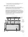
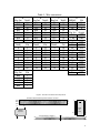
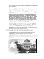
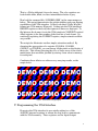
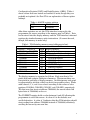
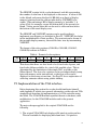
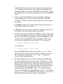
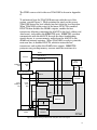
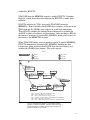
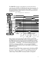
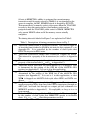
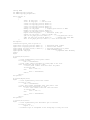
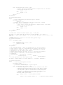
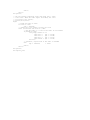
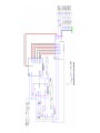
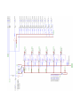
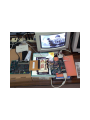
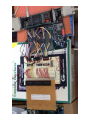
A Simple VGA Interface for the PowerPC
403GCX Evaluation Board
Jonathan Jones, Undergraduate
Department of Computer Science
Texas A & M University
Completed January 23, 2001
Table of Contents
I. Abstract . . . . . . . . . . . . . . . . . . . . . . . . . . . . . . . . . . . . . . . . . . . . 3
II. Hardware Requirements . . . . . . . . . . . . . . . . . . . . . . . . . . . . . 3
Figure 1. Abstract wiring diagram . . . . . . . . . . . . . . . . . . . . 5
Table 1. Wire connections . . . . . . . . . . . . . . . . . . . . . . . . . . 6
Figure 2. Pinouts for connectors and components . . . . . . . . 6
III. Demonstrating the VGA Interface’s Functions . . . . . . . . . 7
Figure 3. Academic building in four shades of gray . . . . . . . 7
Figure 4. Three frames to be page-flipped . . . . . . . . . . . . . . 8
IV. Programming the VGA Interface . . . . . . . . . . . . . . . . . . . . . . 8
Table 2. 403GCX register settings . . . . . . . . . . . . . . . . . . . .9
Table 3. VGA interface memory map . . . . . . . . . . . . . . . . . 9
Table 4. Format of color registers . . . . . . . . . . . . . . . . . . . . 10
V. Implementation of the VGA Interface . . . . . . . . . . . . . . . . . 12
Figure 5. Diagram showing functional units, signals . . . . . 12
Figure 6. State diagram for BUSCTL . . . . . . . . . . . . . . . . . . 13
Figure 7. Timing diagram for memory write cycle . . . . . . . . 14
Figure 8. State diagram for MEMCTRL . . . . . . . . . . . . . . . . 15
Table 5. Descriptions of timing parameters . . . . . . . . . . . . 16
VI. Possible Future Projects . . . . . . . . . . . . . . . . . . . . . . . . . . . . . 17
VII. References . . . . . . . . . . . . . . . . . . . . . . . . . . . . . . . . . . . . . . . . . . 18
Appendices
A. XS40 V1.1 documentation
B. PPC 403 EVB expansion interface pinout
C. 74ALS245 bus transceivers documentation
D. 24.0 MHz clock oscillator documentation
E. XStend V1.3 documentation
F. VGA signal generation with the XS board
G. VHDL source code for VGACORE module
H. Documentation for SRAM module
I. FPGA design schematics
J. IBM 403GCX embedded controller manual
K. Photographs
2
I. Abstract
This report describes the author’s implementation of a VGA monitor
interface for the PowerPC 403GCX evaluation board. Additional
hardware used for the project essentially consists of a Xilinx[1] FPGA,
a 32KB SRAM module, a few resistors (forming a simple DAC), and a
VGA monitor connector. These components are all included on
prototyping boards available from XESS Corp[2]. Because of the
limited pinout of the FPGA chosen for the project, three 74245 bus
transcievers are needed as well. A 24.0 MHz oscillator is used to clock
the circuit.
The VGA interface implemented allows the display of a 512 by 240
pixel image with four user-definable colors. It also includes a vertical
offset register to facilitate hardware scrolling. Programs running on
the 403GCX can update the registers and SRAM by using store
instructions.
II. Hardware Requirements
The required hardware components, in addition to the PowerPC
403GCX evaluation board, are the following:
1. One XESS Corp. XS40 prototyping board. The implementation
described herein uses a Version 1.1 board, which includes a Xilinx
XC4010XL FPGA. Other versions of the XS40 with other FPGAs
will work, but may require different jumper settings. Compare
your board’s documentation with the Version 1.1 jumper settings
listed below (in Part III ). If you don’t have an XS40 board, you can
wire up your own FPGA, SRAM, power supply, and FPGA
programming interface according to the XS40’s schematics. (The
XS40’s other components are not used.) Complete Documentation
for the XS40 V1.1 is included as Appendix A.
2. One XESS Corp. XStend board, which provides the VGA connector
and DAC, and provides header pins to make it easier to wire wrap
to the XS40’s pins. Versions 1.2 and above of the XS40 include the
VGA connector and DAC onboard and make the XStend
unnecessary for this application. This implementation was tested
using the XStend V1.3; other versions may require different jumper
settings.
3. One 24.0 MHz crystal oscillator clocks the circuit on the FPGA.
Some versions of the XS40 include a 12.0 MHz oscillator, which
3
isn’t fast enough for this application. Others include a
programmable oscillator which can’t be programmed to operate at
24.0 MHz.
4. Three 74245 octal bus transcievers. The specific part used for
testing this implementation was the SN74ALS245AN from Texas
Instruments. If you want to use a slower part, you may have to
adjust the number of wait states in the BUSCTL state machine
(Part IV). These transcievers isolate the 403GCX’s address and
data buses from those of the SRAM. If you use an FPGA with a
larger pinout, you can eliminate the need for these by connecting all
bus lines directly to the FPGA, using separate pins for the SRAM’s
buses and the 403GCX’s buses.
5. One 5V power supply for powering the bus transcievers. The
XS40’s power supply does not appear capable of powering them
while still enabling the oscillator to provide a clean and consistent
signal.
6. A breadboard and wiring to connect everything together and to the
PowerPC 403GCX evaluation board’s expansion interface.
For testing, the following will also be needed:
7. Any VGA monitor. The signals output by the VGA interface are
compatible with all VGA monitors.
8. The IBM RISCWatch debugger system. Installation and operation
of this system is described in a previous report[3], and further
documentation is available on IBM’s Web site[4]. It is basically a
hardware/software interface to allow a PC to communicate directly
with the PowerPC 403GCX through its JTAG testing interface.
This allows the 403GCX’s I/O Configuration Register (IOCR) and
Bank Registers (BRn) to be set, so the 403GCX will know how to
access the VGA interface’s memory. Then RISCWatch can be used
to actually load the data into display memory. Alternatively, you
can write a program that sets the registers and fills the video RAM,
and load this program using the evaluation board’s ROM monitor.
9. A PC connected via its parallel port to the XS40 board. The PC
must have XSTOOLs software (available from XESS[2]) for
programming the FPGA via the parallel port. For creating .BIT
files (FPGA program images) you’ll need Xilinx Foundation Series
software (from Xilinx[1]). The latter is not free, but it is not
4
necessary unless you want to modify the FPGA program. If not,
just use the .BIT file accompanying this document.
III. Assembly and Configuration
Assembly consists of wiring the hardware components together.
Configuration includes adding/removing shunts on the jumpers of the
XS40 and XStend boards, and programming the FPGA.
Pin assignments for the PowerPC 403GCX evaluation board’s
expansion interface, for the 74245 bus transcievers, and for the 24.0
MHz oscillator are included in Appendices B, C, and D, respectively.
Pin assignments for the XS40 (whose pins are exposed by the XStend)
can be found in Appendix A. Figure 1 is a wiring diagram showing
how the components are connected. Each line represents a set of
connections, as detailed in Table 1.
Figure 1. Abstract wiring diagram.
403GCX EVB
Expansion
Interface
A
B
742451
MX045
742452
C
5V power
supply
742453
H
D
J
E
F
+
-
G
XStend Board
J18
XS40 Board
XS40’s parallel
port interface
to PC’s parallel
port interface
9V power
supply
to VGA monitor
+
-
5
Exp Int
A39
B39
A31
B31
C31
A32
B32
C32
742451
2
3
4
5
6
7
8
9
19
Exp Int
B26
A26
A15
A40
B26
A
E
742451
18
17
16
15
14
13
12
11
J18
3
4
5
78
79
82
83
84
68
J
Table 1. Wire connections.
B
C
Exp Int 742452 Exp Int 742453
A33
18
A9
18
B33
17
B9
17
C33
16
C9
16
A34
15
A10
15
B34
14
B10
14
C34
13
C10
13
A35
12
A11
12
B35
11
B11
11
F
G
742452
J18
742453
J18
2
59
2
10
3
57
3
80
4
51
4
81
5
56
5
35
6
50
6
38
7
68
7
39
8
60
8
40
9
29
9
41
19
68
19
68
MX045
7
8
14
Exp Int
C40
C28
742451
1
10
20
742452
1
10
20
742453
1
10
20
J18
52
J18
7
37
9
8
7
D
H
J18
52
14
2
Supply
GND
GND
GND
GND
+5V
GND
GND
+5V
GND
GND
+5V
GND
Figure 2. Pinouts for connectors and components.
PowerPC 403GCX EVB expansion interface connector
C40
B40
A40
14
C1
B1
A1
20
8
74245
top
view
MX045
top view
10
J18 (oriented as in Figure 1)
1
1
7
21
22
11
1 84
64
63
42 43
6
For convenience, the pinouts for all the components and connectors are
shown in Figure 2.
Jumpers on the XS40 and XStend board are used to select certain
options and disable various unneeded components. For versions 1.1
and 1.3, respectively, of the boards, the jumpers should be configured
as follows. On the XStend board, move all DIP switches to the
OFF/OPEN position, and remove shunts from all jumpers except J11.
This will disable all the components on the XStend board except the
VGA connector and its associated DAC. On the XS40 board, shunt
jumpers J4, J5 (if present), J7 (across pins 1 and 2), and J11. Remove
the shunts from jumpers J6 and J10. These settings specify, among
other things, that the parallel port interface will be used to program
the FPGA. See section 1.6 of Appendix A for more information about
jumper settings of the XS40 V1.1 board. See Appendix E for
information on jumper settings for the XStend V1.3.
After doing all the above, all that remains is to program the FPGA
with the VGA.BIT file. Do this by using the XSLOAD or GXSLOAD
program from the XSTOOLs suite. An image should appear
immediately on the screen after programming. (You may have to push
the RESET button on the XStend board first.)
IV. Demonstrating the VGA Interface’s Functions
As a first demonstration, run the RISCWatch software and select
“Command File” from the File menu. Then choose the file
“SCREEN1.CMD” that accompanies this document. Execute the script
in Normal Mode. The image in Figure 3 should be displayed on the
VGA monitor.
Figure 3. The Academic Building in four shades of gray.
7
This is a 512-by-240-pixel, four-color image. The color registers are
loaded with white, black, and two intermediate shades of grey.
Now load the command file “SCREEN2.CMD” in the same manner as
before. This script demonstrates the palette shifting and page flipping
capabilities of the VGA interface. It first loads three 512-by-85 pixel
frames into VGA memory (Figure 4). It then sets the VGA interface’s
HEIGHT register so that only the topmost 85 lines are displayed. To
flip between the frames, it sets the VGA interface’s VOFFSET (vertical
offset) register to the line number of the first line of each frame. By
continually updating the VOFFSET register, simple animation effects
are possible.
The script also illustrates another simple animation method. By
changing the appropriate color register (COLORA, COLORB,
COLORC, or COLORD), you can change all the pixels on the display of
that color. This allows changing the color of large areas of the screen
much faster than would be possible by storing a new value in memory
for each pixel.
Combining these effects can achieve very annoying results, as the
script shows.
Figure 4. Three frames to be page-flipped.
V. Programming the VGA Interface
Preparing the VGA interface for use entails setting two of the
403GCX’s internal registers to inform the chip how to communicate
with the VGA’s memory. These registers are the Input/Output
8
Configuration Register (IOCR) and Bank Register 3 (BR3). Table 2
shows values that were tested and verified to work, though they are
probably not optimal. See Part VI for an explanation of these register
settings.
Table 2. 403GCX register settings.
IOCR
0004C402
BR3
5010402E
After these registers are set, the VGA interface is exposed to the
programmer for access according to the memory map in Table 3. Data
can be stored into the display memory and the VGA interface’s internal
registers by standard memory write instructions. (It cannot be read,
though; this memory is write-only.)
Table 3. VGA Interface memory map (addresses in hex).
Address(es)
Size
Field
75000000 – 75007FFF
32KB Display memory
75007800 – 75007FFF 2KB
Invisible display memory
75008000 – 75008007
6B
VGA interface’s internal registers
75008000
1B
COLORA register
75008001
1B
COLORB register
75008002
1B
COLORC register
75008003
1B
COLORD register
75008004
1B
VOFFSET register
75008005
1B
HEIGHT register
75008006
1B
(unused)
75008007
1B
(unused)
The display memory is organized as follows. Each scan line is 512
pixels wide and occupies 128 bytes of memory. This means there are
four pixels in each byte of display memory. And that means each pixel
is represented by two bits, which can have four possible values. Pixels
with values 0, 1, 2, and 3 are colored according to the values of color
registers COLORA, COLORB, COLORC, and COLORD, respectively.
The first scan line starts at address 75000000; the second starts 128
bytes later at 75000080; and so on.
The VOFFSET register holds a value between 0 and 255 allowing the
programmer to scroll the screen. A value of 0 is the default, nonscrolled situation. A value of 1 indicates that the VGA interface should
start reading from address 75000080 instead of 75000000, effectively
scrolling the screen by one scan line.
9
The HEIGHT register holds a value between 0 and 240 representing
the number of scan lines to be displayed on the screen. A value of 240
is the default and causes the first 30 KB (240 scan lines) of display
memory (starting from the address indicated by VOFFSET) to be
visible. (The remaining 2 KB of display memory is “invisible.”) A
value of 120, for example, causes the bottom half of the screen to be
blank. Values greater than 240 can be used to add scan lines below
the bottom of the usual display area.
The HEIGHT and VOFFSET registers can be used together to
implement page flipping, as described in Part IV. VOFFSET also helps
in the imelementation of text scrolling. The new text can be drawn in
the invisible display memory, then scrolled into view by incrementing
VOFFSET.
The format of the color registers (COLORA, COLORB, COLORC,
COLORD) is shown in Table 4.
bit 7 (MSB)
field
X
Table 4. Format of color registers.
6
5
4
3
2
X
Red1
Red0
Green1 Green0
1
Blue1
0 (LSB)
Blue0
This shows that there are four levels of red, four levels of green, and
four levels of blue available, for a total of 64 possible colors. This is
determined by the limitations of the simple DAC available on the
XStend board. The four color registers can be set independently (using
byte-wide memory write instructions), so that four colors can be
displayed on the screen at one time. See Part IV for an explanation of
achieving animaton effects using palette shifting.
VI. Implementation of the VGA interface
Before beginning this section the reader should familiarize himself
with Appendix F, which gives general information on the relevant VGA
standard and describes an implementation of a VGA controller using
the XS40. The VGACORE module specified therein is the basis, with
modifications, for the VGACORE module used in the present
application.
The major changes applied to the original VGACORE are the
following:
1. The original VGACORE only displays 256 pixels in each scan line.
This isn’t suitable for displaying 80-column text. 512 pixels is
10
sufficient (with each text character six pixels wide, and space left
over at the margins). However, this requires that the pixel clock
speed be doubled. The original VGACORE used the XS40’s onboard
12.0 MHz clock; the new version will require an external 24.0 MHz
clock.
2. In the original VGACORE the colors are hard-wired. The new
version makes use of four color registers (COLORA, COLORB,
COLORC, COLORD; see Part V) to allow the colors to be changed
in software.
3. A VOFFSET register was added to allow hardware scrolling to be
controlled by software (see Part V).
4. A HEIGHT register was added to allow the number of scan lines in
the display to be controlled by software (see Part V).
5. Since the clock speed is doubled, the SRAM is no longer fast enough
to yield correct output in the span of a single clock cycle. Therefore
the new VGACORE uses pipelining to allow the SRAM three clock
cycles to drive its outputs before they are sampled. This change
was effected by editing the process labeled I. The conditional
if hcnt(1 downto 0)="00" then
was changed to
if hcnt(1 downto 0)="11" then
Since the SRAM’s address bus is driven when hcnt=”00”, that
gives three clock cycles before its outputs are sampled. Of course,
this also required tweaking the hsyncb and blank signals to
account for the pipelining delay.
6. The VGACORE module is continually reading from SRAM while
the electron beams sweep across the screen. Then there is an idle
period in which the beams are moved back across the screen to the
beginning of the next scan line. Then after all the scan lines have
been displayed, there is a much longer idle period while the beams
are moved back to the top of the screen. These idle periods are
utilized by the new VGACORE, via its memreq signal, to yield
control of the SRAM to allow the 403GCX to access it. VGACORE
drops memreq to allow the BUSCTL state machine to give control of
the 403GCX access to the local address and data buses.
11
The VHDL source code for the new VGACORE is shown in Appendix
G.
To understand how the VGACORE interacts with the rest of the
system, consult Figure 5. While painting the pixels on the screen,
VGACORE drives the local address bus and reads the local data bus.
When VGACORE yields control of the buses, BUSCTL is enabled.
BUSCTL then disables the SRAM’s outputs, enables the bus
transcievers (thereby connecting the 403GCX to the local address and
data buses), and enables the MEMCTRL unit. MEMCTRL can then
communicate with the 403GCX, through the three handshaking
signals shown, to oversee memory writes from the 403GCX to the
SRAM and internal registers. When VGACORE is ready to paint the
next scan line, it disables BUSCTL, which tri-states the bus
transcievers and enables the SRAM’s data outputs. MEMCTRL
postpones any pending memory accesses until the next time it is
READY
CHIP SELECT
403GCX
WRITE BYTE
VGA
Monitor
ADDRESS
BUS
DATA
BUS
RGB
SYNC
Bus Transcievers
ENABLE
VGACORE
LOCAL
ADDRESS
BUS
LOCAL
DATA
BUS
ENABLE
BUSCTL
ENABLE
ENABLE
WRITE ENABLE
MEMCTRL
REGISTERS
SRAM
MEMORY
MODULE
REGISTER VALUES
FPGA
Figure 5. Diagram showing functional units, data paths, and control signals.
12
enabled by BUSCTL.
VGACORE uses its MEMREQ output to enable BUSCTL. Examine
Figure 6, which shows the state diagram for BUSCTL, a finite state
machine.
BUSCTL waits in its “VGA” state until VGACORE deasserts
MEMREQ. Then it disables the SRAM’s data outputs, and waits in its
ZWt1 state for the SRAM’s data outputs to reach high impedance.
Then BUSCTL enables the external bus transcievers to connect the
403GCX to the local address and data buses. After waiting in BWt for
the buses to be driven, it asserts MC_ENABLE, which gives control of
the buses to the MEMCTRL module.
When VGACORE needs access to memory again, it asserts MEMREQ.
BUSCTL immediately deasserts MC_ENABLE, disables the bus
transcievers (thus isolating the 403GCX from the local buses), and
enables the SRAM’s data outputs. The cycle repeats.
BU SCTL
//diagram AC TION S
Sreg0
R ESET
MC _EN ABLE
C LOC K
BU F_OEN
MEMREQ
SR AM_OEN
Wt
RESET=’1’
SR AM_OEN <= ’1’;
BU F _OEN <= ’1’;
MC_EN ABLE <= ’0’;
W t := W t + 1;
VGA
/0/
M EM REQ = ’0’
SR AM_OEN <= ’1’;
W t := 0;
Z W t1
/1/
W t := W t + 1;
Wt >= 5
BU F_OEN <= ’0’;
W t := 0;
BW t
/2/
Wt >= 5
MC _EN ABLE <= ’1’;
Wt >= 5
Wt >= 5
SW t
/5/
W t := W t + 1;
VGA:
Z W t1:
BW t:
PPC :
Z W t2:
SW t:
Z W t2
/4/
SR AM_OEN <= ’0’;
W t := 0;
W t := W t + 1;
M EM REQ = ’1’
MC _EN ABLE <= ’0’;
BUF _OEN <= ’1’;
W t := 0;
PPC
/3/
W ait while VGACOR E is controlling m em ory .
W ait f or the buses to be tri-stated.
W ait f or external buf f ers to driv e the buses.
Allow PPC to control m em ory until VGAC OR E raises MEMR EQ.
W ait f or the buses to be tri-stated.
W ait f or address/data buses to be driv en by VGAC OR E/SR AM.
Figure 6. State diagram for BUSCTL. This is a Mealy machine.
Transition conditions are italicized. Transition actions are boxed. A
box attached directly to a state is an action that occurs each time
the state is entered. Wt is a variable.
13
The MEMCTRL module is responsible for processing the memory
writes from the 403GCX to the SRAM and to the internal registers. To
see how the memory write cycle works, look at Figure 7. To the left of
the timing diagram is a brief schematic showing the interconnections
and direction of each signal.
Figure 7. Timing diagram for PPC → SRAM write cycle.
PPC
FPGA
CSPPC
WBE
READY
ADDR
DATA
ADDRLOCAL
DATALOCAL
G
OE
CSSRAM
WE
XCVER
SRAM
tSDXE tXELZ
tXP
tCSWB
tADCP
tWBWE
tWP
tWBR
tADCS
tCSWH
tWR
tRCWH tCWRL
tADH
tWHAD
Before memory can be accessed by the PPC 403GCX, the BUSCTL
module must connect the 403GCX’s address and data buses to those of
the SRAM. That means it must deactivate the SRAM’s data outputs
(using the OE¯ signal) and enable the bus transceivers (with G¯). This
causes ADDRLOCAL and DATALOCAL to be driven by the bus transceivers.
BUSCTL has entered its PPC state and raised its MC_ENABLE
signal, giving the PPC 403GCX access to the SRAM, controlled by the
MEMCTRL module.
When the PPC 403GCX initiates a memory write, it first drives ADDR
and DATA, and then CS¯PPC (“chip select”) is dropped to indicate that
the memory address being written to is within the VGA memory’s
address range. Finally WBE¯ (“write byte enable”) is dropped to
14
indicate that the address and data buses are ready to be sampled, and
the memory write can begin as soon as the VGA is ready.
As soon as the address on ADDR has propagated through the
transceivers to ADDRLOCAL, the CS SRAM signal is either raised or dropped
by the MEMORY module. If the address is associated with one of the
VGA’s internal registers, CS SRAM is driven high; if the address is in the
range associated with the SRAM, CS SRAM is driven low.
When MEMCTRL senses that the PPC 403GCX has initiated a write
cycle, it drops the SRAM’s WE signal to write the data on
DATALOCALinto the address on ADDRLOCAL. After the appropriate write
pulse duration (tWP) the memory access is complete, and the MEMORY
module can raise READY to allow the PPC 403GCX to complete the
cycle.
The handshaking is completed when the PPC 403GCX raises its CS PPC
and WBE PPC signals. After a certain hold time (tADH), a new memory
write cycle can begin.
MEMCTRL is implemented as the simple Mealy FSM shown in Fig. 8.
R ESET
MEMC TR L
MC _EN ABLE
//diagram AC TION S
PPC_W BN
SR AM_W EN
PPC_CSN
R EAD Y
C LOC K
Sreg0
Wt
RESET = ’1’
SR AM_W EN <= ’1’;
READ Y <= ’0’;
W t := W t + 1;
Idle
/0/
M C_ENABLE = ’1’ and PPC_CSN = ’0’ and PPC_WBN = ’0’
W t := 0;
Buf W t
/1/
M C_ENABLE = ’0’
(postpone)
Wt >= 2
SR AM_W EN <= ’0’;
W t := 0;
M C_ENABLE = ’0’
SR AM_W EN <= ’1’;
(postpone)
PPC_WBN = ’1’
R EADY <= ’0’;
Idle:
W ait f or control of m em ory and PPC write request.
Buf W t: W ait f or address and data buses to be set up by external buf f ers.
W rite: Process request; if interrupted (MC _ENABLE = ’0’),
then postpone the m em ory write until MC _EN ABLE = ’1’.
Ack:
Assert R EAD Y until PPC _W BN = ’1’.
W t := W t + 1;
W rite
/2/
Wt >= 3
SRAM_W EN <= ’1’;
R EAD Y <= ’1’;
(com pleted)
Ack
/3/
Figure 8. The MEMCTRL module.
15
Of note is MEMCTRL’s ability to postpone the current memory
transcation until it regains access to SRAM if, at any time before the
access is complete, the MC_ENABLE signal is dropped by BUSCTL.
This means that if a memory write is in progress when the VGACORE
is ready to draw the next scan line, that memory write can be
postponed until the VGACORE yields control of SRAM. MEMCTRL
only asserts READY when and if the memory access actually
completes.
The timing intervals labeled in Figure 7 are explained in Table 5.
tSDXE
tXELZ
tXP
tADCP
tCSWB
tADCS
tWBWE
Table 5. Descriptions of timing parameters shown in Fig. 7.
Time from SRAM disable to transceivers enable. This interval must be
at least the time it takes for SRAM to tri-state its data outputs (TOHZ in
Appendix H). It is controlled by the number of clock cycles that
BUSCTL stays in its ZWt1 state.
Time from transceivers enable until transceiver outputs are driven.
This interval is a property of the transceivers (tPZH and tPZL in Appendix
C).
Time for values to propagate through the bus transceivers. This is a
property of the transceivers (tPLH and tPHL in Appendix C).
Time after ADDR and DATA are driven before CS PPC is dropped. This
is determined by the setting of the CSN bit of the 403GCX’s BR3
register (see Appendix J). It is set to 0 in this application.
Time after CS PPC is dropped before WBE is dropped. This interval is
determined by the setting of the WBN bit of the 403GCX’s BR3
register (see Appendix J). It is set to 1 in this application, so that
WBE is dropped one 403GCX clock cycle after ADDR and DATA are
driven.
Time after ADDRLOCAL is set up before CS SRAM is set. This interval is a
small propagation delay from one of the FPGA’s input pins, through an
AND gate, and back out through an output pin (see schematic for
MEMORY module in Appendix I). It’s negligible, as long as tCSWH is
large enough.
Time after WBE is dropped before WE is dropped. This is controlled
by the number of clock cycles that MEMCTRL spends in its BufWt
state. If tXP < tADCP + tCSWB, then this parameter can be 0.
16
tWP Write pulse width. The SRAM requires that ADDRLOCAL, DATALOCAL,
and WE held for a certain period (TWP in Appendix H) in order for the
memory write to be completed succcessfully. The length of this
interval is controlled by setting the number of clock cycles that the
MEMCTRL module spends in its Write state.
tWR Time after WE is raised before READY is raised. This is zero, but it
could be increased by adding wait states to MEMCTRL between its
Wait and Ack states.
tCSWH Time after CS SRAM is set before WE goes high. The lower bound is a
parameter of the SRAM (TCW in Appendix H). Since tADCS is so small,
this requirement is easily met.
tWBR Time from WBE low until READY high. In the 403GCX’s devicedpaced transfer mode (controlled by the RE bit of the BR3 register; see
Appendix J) the 403GCX automatically inserts wait states during this
interval. The PTD bit of the 403GCX’s IOCR register (Appendix J)
must be set to 1 so that the number of wait states is unlimited.
tWHAD DATALOCAL hold time after WE goes high. There is no lower bound set
by the SRAM module (see TDH in Appendix H).
tADH ADDR and DATA hold time after CS PPC and WBE are raised. This is
controlled by the TH field of the 403GCX’s BR3 register (see Appendix
J). TH was set to 7 for testing this application.
tRCWH Time after READY is raised before CS PPC and WBE are raised. This
is controlled by the TWT field of the 403GCX’s BR3 register (see
Appendix J). According to TWT, the 403GCX will wait a certain
number of clock cycles before it samples the READY signal. TWT was
set to 10 for testing this application.
tCWRL Time after CS PPC and WBE are raised before READY is deasserted.
This is controlled by the number of clock cycles the MEMCTRL module
spends in ts Ack state. Currently READY is deasserted on the next
rising clock edge after CS PPC and WBE are sampled high.
The top-level project schematic and the schematic for the MEMORY
module are shown in Appendix I.
VII. Possible Future Projects
This work could be easily expanded upon in several obvious ways. The
XC4010XL has ample extra room for additional logic:
Number of CLBs:
101 out of
400
25%
CLB Flip Flops:
96
CLB Latches:
0
4 input LUTs:
136
3 input LUTs:
32 (20 used as route-throughs)
Number of bonded IOBs:
42 out of
65
64%
IOB Flops:
0
17
IOB Latches:
0
Number of BUFGLSs:
1 out of
8
Total equivalent gate count for design: 1803
12%
♦ The VGA interface’s resolution and color depth could be enhanced
by increasing the frequency of the dot clock, increasing the amount
of SRAM available, and modifying the VGACORE module.
♦ The page-flipping and scrolling facilities (see Parts IV and V) could
be improved by adding HOFFSET and WIDTH registers. This
would enable horizontal scrolling and page-flipping.
♦ Hardware support for text display could be added. Separate
memory areas for the font and the display map could be user
configurable. Text scrolling could be accomplished in hardware.
♦ Additional screen modes could be added. Screen refresh rates,
resolutions, and color depths could be software-selectable.
♦ Other peripherals could be connected to the 403GCX’s expansion
interface to work in concert with the VGA interface.
The information compiled in the Appendices and illuminated in the
text of this document should be very helpful in these pursuits.
References
[1] Xilinx Corporation: http://www.xilinx.com
[2] XESS Corporation: http://www.xess.com
[3] “Developing Applications for the IBM PPC403GCX Evaluation
Board” was a CPSC 483 project at Texas A&M in the Spring of
2000. The final report is available here:
http://chef.cs.tamu.edu/past-projects/00a/G6/final_report.doc
[4] The home page for RISCWatch:
http://www.chips.ibm.com/products/powerpc/tools/riscwatc.html
18
Appendix A
This Appendix contains documentation for Version 1.1 of XESS
Corporation’s XS40 prototyping board.
This document was originally downloaded from here:
http://www.xess.com/manuals/xs40-manual-v1_1.pdf
Appendix B
This Appendix contains the pinout for the PowerPC 403GCX
evaluation board’s expansion interface. It was excertped from Section
5.4 of the IBM PowerPC 403 Evaluation Board Kit User’s Manual.
The User’s Manual was originally found here:
http://www.chips.ibm.com/products/powerpc/evalkits/403ev_um.pdf
Appendix C
This Appendix contains documentation for the Texas Instruments
SN74ALS245AN octal bus transciever.
It was originally located here:
http://www-s.ti.com/sc/psheets/sdas226a/sdas226a.pdf
Appendix D
This Appendix cointains documentation for the CTS Reeves MX045
24.0 MHz clock oscillator.
It was originally located here:
http://www.ctscorp.com/reeves/clocks/047.pdf
Appendix E
This Appendix contains documentation for Version 1.3 of XESS
Corporation’s XStend board.
This document was originally located here:
http://www.xess.com/manuals/xst-manual-v1_3.pdf
Appendix F
This document is an explanation of how to implement a simple VGA
controller using the XS40/XStend.
It was originally found here:
http://www.xess.com/appnotes/vga.pdf
Appendix G
This Appendix includes the VHDL source code for the modified
VGACORE module used in this application. It was originally based on
the VGACORE module described in Appendix F.
library IEEE;
use IEEE.std_logic_1164.all;
use IEEE.std_logic_unsigned.all;
entity vgacore is
port
(
reset: in std_logic; -- reset
clock: in std_logic; -- VGA dot clock
colorA: in std_logic_vector(5 downto 0);
colorB: in std_logic_vector(5 downto 0);
colorC: in std_logic_vector(5 downto 0);
colorD: in std_logic_vector(5 downto 0);
memreq: out std_logic;
-- request/yield control of SRAM
height: in std_logic_vector(7 downto 0);
voffset: in std_logic_vector(7 downto 0);
hsyncb: buffer std_logic;
-- horizontal (line) sync
vsyncb: out std_logic; -- vertical (frame) sync
rgb: out std_logic_vector(5 downto 0);
-- red,green,blue colors
addr: out std_logic_vector(14 downto 0);
-- address into video RAM
data: in std_logic_vector(7 downto 0) -- data from video RAM
);
end vgacore;
architecture vgacore_arch of vgacore is
signal hcnt: std_logic_vector(9 downto 0);
signal vcnt: std_logic_vector(9 downto 0);
signal pixrg: std_logic_vector(7 downto 0);
signal blank: std_logic;
signal pblank: std_logic;
signal
begin
-----
horizontal pixel counter
vertical line counter
byte-wide register for 4 pixels
video blanking signal
-- pipelined video blanking
A: process(clock,reset)
begin
-- reset asynchronously clears pixel counter
if reset=’1’ then
hcnt <= "0000000000";
-- horiz. pixel counter increments on rising edge of dot clock
elsif (clock’event and clock=’1’) then
-- horiz. pixel counter rolls-over after 761 pixels
if hcnt<760 then
hcnt <= hcnt + 1;
else
hcnt <= "0000000000";
end if;
end if;
end process;
B: process(hsyncb,reset)
begin
-- reset asynchronously clears line counter
if reset=’1’ then
vcnt <= "0000000000";
-- vert. line counter increments after every horiz. line
elsif (hsyncb’event and hsyncb=’1’) then
-- vert. line counter rolls-over after 528 lines
if vcnt<527 then
vcnt <= vcnt + 1;
else
vcnt <= "0000000000";
end if;
end if;
end process;
C: process(clock,reset)
begin
-- reset asynchronously sets horizontal sync to inactive
if reset=’1’ then
hsyncb <= ’1’;
-- horizontal sync is recomputed on the rising edge of every dot clock
elsif (clock’event and clock=’1’) then
-- horiz. sync is low in this interval to signal start of a new line
if (hcnt>=584 and hcnt<676) then
hsyncb <= ’0’;
else
hsyncb <= ’1’;
end if;
end if;
end process;
D: process(hsyncb,reset)
begin
-- reset asynchronously sets vertical sync to inactive
if reset=’1’ then
vsyncb <= ’1’;
-- vertical sync is recomputed at the end of every line of pixels
elsif (hsyncb’event and hsyncb=’1’) then
-- vert. sync is low in this interval to signal start of a new frame
if (vcnt>=490 and vcnt<492) then
vsyncb <= ’0’;
else
vsyncb <= ’1’;
end if;
end if;
end process;
-- blank video outside of visible region: (0,0) -> (513,479)
E: blank <= ’1’ when (hcnt>=515 or hcnt<=2 or vcnt>=(height & ’0’)) else ’0’;
memreq <= ’1’ when ((vcnt<=(height & ’0’) or vcnt>=526) and (hcnt <= 515 or hcnt >= 755))
else ’0’;
--memreq <= ’1’;
-- store the blanking signal for use in the next pipeline stage
F: process(clock,reset)
begin
if reset=’1’ then
pblank <= ’0’;
elsif (clock’event and clock=’1’) then
pblank <= blank;
end if;
end process;
-----------H:
The video RAM address is built by appending bits 8-2 of the horizontal
pixel counter to bits 8-1 of the vertical line counter. (We don’t have
enough memory to display 512 x 480, so we’re displaying 512 x 240 and
ignoring bit 0 of the vertical line counter.)
Example: When displaying the pixel at (x,y) = (511,239) the horizontal
pixel counter is "111111111", and the vertical line counter is
"11101111x".
Concatenating:
vertical[8:1] = 11101111 +
horizontal[8:2] =
1111111 =
111011111111111
So this application uses 30720 bytes of RAM.
addr <= (vcnt(8 downto 1) & hcnt(8 downto 2)) + (voffset & "0000000");
I: process(clock,reset)
begin
-- clear the pixel register on reset
if reset=’1’ then
pixrg <= "00000000";
-- pixel clock controls changes in pixel register
elsif (clock’event and clock=’1’) then
-- the pixel register is loaded with the contents of the video
-- RAM location when the lower two bits of the horiz. counter
-- are both zero. The active pixel is in the lower two bits
-- of the pixel register. For the next 3 clocks, the pixel
-- register is right-shifted by two bits to bring the other
-- pixels in the register into the active position.
if hcnt(1 downto 0)="11" then
pixrg <= data; -- load 4 pixels from RAM
else
pixrg <= "00" & pixrg(7 downto 2);
-- right-shift pixel register
end if;
end if;
end process;
-- the color mapper translates each 2-bit pixel into a 6-bit
-- color value. When the video signal is blanked, the color
-- is forced to zero (black).
J: process(clock,reset)
begin
-- blank the video on reset
if reset=’1’ then
rgb <= "000000";
-- update the color outputs on every dot clock
elsif (clock’event and clock=’1’) then
-- map the pixel to a color if the video is not blanked
if pblank=’0’ then
case pixrg(1 downto 0) is
when "00" =>
rgb <= colorA;
when "01" =>
rgb <= colorB;
when "10" =>
rgb <= colorC;
when others => rgb <= colorD;
end case;
-- otherwise, output black if the video is blanked
else
rgb <= "000000";
-- black
end if;
end if;
end process;
end vgacore_arch;
Appendix H
This Appendix contains documentation for the SRAM module included
on the XS40 board V1.1: Winbond’s W24257AK-15 SRAM.
This document was originally located here:
http://www.winbond.com/sheet/257a-12.pdf
Appendix I
This Appendix includes schematics for the FPGA program used in this
application. On the next page the top-level schematic is shown. The
page after contains the schematic for the MEMORY module.
Appendix J
This Appendix contains an explanation of the PowerPC 403GCX’s
IOCR and BR3 registers. It was excerpted from Section 12.8 of the
IBM PPC403GCX Embedded Controller User’s Manual.
The User’s Manual was originally located here:
http://www.chips.ibm.com/products/powerpc/chips/gcx_um.pdf
Appendix K
Here are a couple of photographs of the finished project. The first
shows the VGA interface in action, displaying an image on a VGA
monitor. The second shows a close-up view of the wiring.