1
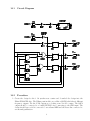
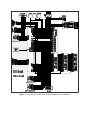
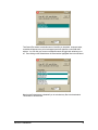
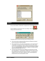
PHYSICS 623
Programmable Gate Array Experiment
Dec.11, 2001
1
The Goal of This Experiment
You will design a small digital circuit, download the design to a Field Programmable Gate Array
(FPGA) IC, and verify that the circuit operates as predicted.
When using an FPGA, you build the circuit by creating the circuit diagram with schematic
capture software and then running programs that creates a bitmap that is downloaded into the
FPGA chip. This technique is valuable, in research or any enterprise, since you can quickly make
moderately complex circuits and yet quickly make changes as the needs change.
2
Xilinx FPGA Introduction
A Field Programmable Gate Array, commonly known as an FPGA, is a general purpose programmable IC which is mainly used in the digital design environment that requires flexibility in
design and fast turn around time.
In contrast to design using commercial ICs, FPGA can be configured to the designer’s specific
circuits in a single chip. In addition, in the case of design errors, FPGA can be redesigned
and reconfigured easily in software, where as in the commercial IC design, it is not so easy to
modify the already connected circuitry. In comparison to EPLD (Electrically Programmable
Logic Device), FPGAS have more levels of registers and a more general routing topology. This
renders the EPLD less useful in more general systems, especially in pipelined systems. Because
of its size, ease of use, and reconfigurability, FPGA represents an attractive alternative in digital
design. It is particularly suitable for experimental and rapid prototyping environments.
Different types of FPGA from different vendors are available. The one we will be using is the
Xilinx FPGA. Therefore, throughout this document, the term FPGA is referring to the Xilinx
FPGA.
In general, there are two kinds of blocks in a Xilinx FPGA: Configurable Logic Blocks (CLB)
and Input/Output Blocks (IOB).
Each CLB is capable of supporting generic combinational logic functions of up to 8 inputs
and 2 outputs. In addition, two flip-flops are provided in each CLB for storing the outputs
of the combinational logic. Each FPGA contains a good number of CLBs arranged in a 2dimensional square array to implement and interconnect the desired logic functions of the system.
For example, in the XC4005, there are 196 CLBs arranged in a 14 by 14 array.
IOBs are used to support the interface, including TTL voltage level, higher driving current,
3-state buffers, etc..., to the external environments. In addition, one flip-flop is also available in
each IOB to provide latched input/output. Depending on the size of the chip, different size of
FPGA contains different number of IOBs placed on the perimeter of the CLB array. In the case
of XC4005, there are 112 IOBs available for external connections.
Configurable routing wires are presented between CLBs and between CLBs and IOBs for
interconnecting blocks. The routing wires are arranged in the form of a configurable matrix such
that connections from any direction to any other direction are possible.
The Xilinx FPGA design process consists of the following procedures:
1
2.1
FPGA Design Flow
• The Schematic Capture tool is used for the design entry of the circuit.
• The Design Implementation tools perform the translation, map, place, route and bitstream
generation phases of the design flow.
• The binary image of the circuit design is downloaded to the FPGA chip using a Download
tool.
3
Experimental Procedures
This experiment is to acquaint you with the design process of Xilinx FPGA. You will enter the
design of a simple circuit for the FPGA, download it to the FPGA, and verify that it works in
hardware.
The CAD tool for drawing the circuit schematic is integral to the Xilinx Foundation software
that runs on Windows platorms.
The FPGA chip you will be using is the XC4005XL. It contains 196 CLBs arranged in a 14 by
14 array. In addition, there are 112 IOBs available for external connection. For other properties
of the XC4005 series, please consult “The Programmable Logic Data Book” from Xilinx.
The first circuit with which we will work is a three bit synchronous binary counter (cnt3).
The first step with any circuit is to put a truth table or logic timing diagram into your notebook.
This allows you to check the logic of your design as you work on it, and later gives you something
to check the measured output against.
4
Equipment
The experiment needs the following equipment.
• A test board (XS40-005XL) which contains the XC4005XL Xilinx chip, readout devices,
and input/output cable connectors.
• A motherboard (XStend) for the test board that contains more readout devices, switches,
analog I/O, a keboard and VGA interface, and a prototyping area in which additional
circuit components can be added.
• An NT Workstation with the Xilinx development software.
• Stabilized voltage supply of +9.0 volts that plugs into the test board.
• An oscilloscope from the 623 lab.
5
Design Process
It is assumed that you already know how to draw and edit a schematic using CAD schematic
capture tools.
• Log on to the NT workstation. The instructor will supply the login password if needed.
2
• Make sure you have a directory with your name to later store your files. .
• Under the Xilinx program Group, start the Xilinx Project Manager. The Project Manager
controls all aspects of the design flow. You can access all of the design entry and design
implementation tools as well as the files and documents associated with your project. Under
file open a new project and enter a project name.
• Choose the appropriate family, part, and speed grade. This operation will load the appropriate part libraries. We use the 4005XL which you can run at the lowest speed grade
(3).
• Start the Schematic Editor by clicking on the right-most icon in the Design Entry phase
button.
• Enter the circuit using the appropriate parts. The parts are available in the parts toolbox
which can be opened by selecting Mode → Symbols from the menu bar, or clicking the
Symbols Toolbox button in the vertical toolbar on the left side of the scematic editor.
• Unlike Electronics Workbench, wires must be added by using either the wire or bus
tools. At the end of the design entry you will have to edit the IPAD and OPAD parts
to assign them to the real pin numbers that connect to external components such as LEDs
and switches. For external connections, each input must contain a ipad-ibuf block pair,
and each output must contain a opad-obuf block pair from the io parts list. At this stage
you can also add labels for wires and nets.
• Save the schematic by selecting File → Save or clicking the Save icon in the horizontal
toolbar.
6
Circuit Design Constraints
In reality, all input/output signals are bonded to IC pins. Normally, It is the designer’s job to
designate the IC pin for each signal. This is referred to as the pinout constraint. In the case of
Xilinx FPGA, there are two ways to assign the signals to the IC pins:
1. Leave the pin name unspecified and let the Xilinx software assign the signals to pins automatically. The advantage of this approach is that the designer do not have to worry about
the pin assignments, therefore, some labor can be saved. However, there is no guarantee
that the next time you run the Xilinx software, you will obtain exactly the same pinout
assignment. The software is free to assign any signal to any pin if there is no constraint.
This could be annoying if the FPGA is already wired to a system and some design errors
are discovered which would require rerunning the layout software.
2. What we must do. Specify pin locations by attaching a LOC parameter to a pad component. Specify the pinout by altering (editing) the “LOC” designation in the “opad” symbol
to be “Pnn”, where nn is the desired pin number. The easiest way to edit this (and the net
name outside the symbol) is to
• Double click the OPAD connected to the output for which you want to assign a pin
number. The Symbol Properties dialog box opens.
3
• In the Parameters section, add a new parameter with these values:
Name: LOC
Description: Pnn, where nn is the two digit pin number.
• Click Add. The parameter then appears in the list box.
• Click Apply. You see the parameter next to the OPAD.
• Click OK to close the window.
• The same procedure would be followed for IPAD assignments if needed.
This fixes the pinout such that no rewiring is necessary if the design has to undergo several
revisions and if you want to use any of the circuit board components such as the LEDs and
pushbuttons.
In this experiment, the XC4005XL FPGA is mounted on a circuit board/motherboard combination which has direct connections to the FPGA. To use any of the external components on
these boards requires knowing how the component pins connect to the FPGA pins.
For example, pin 67 (P67) is connected to the push button labelled SPARE and pin 37
(P37) is connected to the push button labeled RESET. These pins are then inputs, such as
a reset signal. Any attempt to use them as an output will cause drive fight. You will find the
component pin assignments on the circuit board pinout sheet.
7
Printing Schematics
The circuit schematic can be printed from the schematic window.
8
Processing Xilinx Circuits
After the circuit is designed and the pinout properly constrained, you may start mapping the
circuit into the Xilinx hardware using the implementation tools.
1. The tools are started by clicking the Implementation button in the Project Flowchart area.
2. The Implement Design dialog box displays. Accept the defaults after checking that the
family and device are correct. Click on Run.
3. The Flow Engine display will come up and run the design through the implementation
tools. The full sequence will be:
• TRANSLATE
• MAP
• PLACE and ROUTE
• TIMING
• CONFIGURE. The result of this operation is a .bit configuration file which will be
later downloaded into the FPGA using another application.
4. The above operations generate reports which provide details of the operations. To access
the reports, select the Reports tab from the Project Flow area of the Project Manager. To
open a particular report, double click its icon.
4
9
Downloading the Circuit
The binary configuration bit file is now ready to be downloaded to the actual FPGA chip. Please
follow the following steps for downloading.
1. Make sure the circuit boards are connected to a +9V plug-in power supply.
2. Make sure the circuit board is connected to the parallel (printer) port of the PC.
3. You will then use one of several available GXSTOOLS depending on which function you
are trying to implement.
• GXSTEST: This utility lets the user test an XS Board for proper functioning.
• GXSLOAD: This utility lets the user download FPGA configuration files to the
FPGA.
• GXSPORT: This utility lets the user send logic inouts to an XS Board by toggling
the data pins of the parallel port.
10
Sample Circuit
The experiment circuit cnt3 is provided in this section for reference. It is a binary 3 bit synchronous up counter. The circuit diagram is provided. Please refer to it as you construct your
experimental circuit.
5
10.1
Circuit Diagram
10.2
Procedure
1. Create the design for the 3 bit synchronous counter and download the design into the
Xilinx XC4005XL chip. The Xilinx parts include an oscillator (OSC4) which has 4 different
frequency outputs. Use the 15 Hz output as a clocking source for the counter. The OSC4
output should be connected to a buffer (BUFG) before connecting to the CLK input. The
design should have each bit connected to an external LED and the Reset line connected to
an external pushbutton.
6
2. Verify that the circuit is working. Check that it starts in the clear condition and that the
LEDs light up in the correct sequence.
3. Return to the circuit design and correct any observed problems. Modify the circuit so that
the only thing that happens is that one LED lights at the 7 count.
4. Test the counter with the other three oscillator frequencies. You will have to use the scope
to observe the waveforms. The highest frequency is 3 MHz.
5. Record all observations in your notebook and include an explanation of how the circuit
works.
7
Listing 1: Connections between the XStend LEDs and the XS40.
# LEFT LED DIGIT SEGMENT CONNECTIONS (ACTIVE-LOW)
NET LSB<0>
LOC=P3;
NET LSB<1>
LOC=P4;
NET LSB<2>
LOC=P5;
NET LSB<3>
LOC=P78;
NET LSB<4>
LOC=P79;
NET LSB<5>
LOC=P82;
NET LSB<6>
LOC=P83;
NET LDPB
LOC=P84;
#
# RIGHT LED DIGIT SEGMENT CONNECTIONS (ACTIVE-LOW)
NET RSB<0>
LOC=P59;
NET RSB<1>
LOC=P57;
NET RSB<2>
LOC=P51;
NET RSB<3>
LOC=P56;
NET RSB<4>
LOC=P50;
NET RSB<5>
LOC=P58;
NET RSB<6>
LOC=P60;
NET RDPB
LOC=P28;
#
# INDIVIDUAL LED CONNECTIONS (ACTIVE-LOW)
NET DB<1>
LOC=P41;
NET DB<2>
LOC=P40;
NET DB<3>
LOC=P39;
NET DB<4>
LOC=P38;
NET DB<5>
LOC=P35;
NET DB<6>
LOC=P81;
NET DB<7>
LOC=P80;
NET DB<8>
LOC=P10;
Listing 3: Connections between the XStend DIP and pushbutton switches and the XS40.
# DIP SWITCH CONNECTIONS
NET DIPSW<1>
LOC=P7;
NET DIPSW<2>
LOC=P8;
NET DIPSW<3>
LOC=P9;
NET DIPSW<4>
LOC=P6;
NET DIPSW<5>
LOC=P77;
NET DIPSW<6>
LOC=P70;
NET DIPSW<7>
LOC=P66;
NET DIPSW<8>
LOC=P69;
#
# PUSHBUTTON SWITCH CONNECTIONS (ACTIVE-LOW)
NET SPAREB
LOC=P67;
NET RESETB
LOC=P37;
Figure 7: Programmer's model of the XS40/XStend Board combination.
GXSTOOLS Components
The GXSTOOLs package contains these utilities:
GXSTEST: This utility lets the user test an XS Board for proper functioning.
GXSSETCLK: this utility lets the user set the clock frequency of the programmable
oscillator on an XS Board.
GXSLOAD.EXE: This utility lets the user download FPGA and CPLD configuration files
and HEX files to an XS Board.
GXSPORT.EXE: This utility lets the user send logic inputs to an XS Board by toggling the
data pins of the PC parallel port.
Instructions for using these utilities are presented in the following sections.
GXSTEST
You start GXSTEST by clicking on the
icon placed on the desktop during the
GXSTOOLs installation. This brings up the screen shown below.
Your next step is to select the parallel port that your XS Board is connected to from the
port pulldown list. GXSTEST starts with parallel port LPT1 as the default, but you can also
select LPT2 or LPT3 depending upon the configuration of your PC.
After selecting the parallel port, you select the type of XS Board you are testing from the
associated pulldown list. Then click on the TEST button to start the testing procedure.
GXSTEST will program the microcontroller and the FPGA or CPLD to perform a test
procedure. Status messages will be printed at the bottom of the GXSTEST window as the
testing proceeds. At the end of the test, you will receive a message informing you whether
your XS Board passed the test or not.
GXSTOOLS 3.0 USER MANUAL
1
GXSSETCLK
You start GXSSETCLK by clicking on the
icon placed on the desktop during
the GXSTOOLs installation. This brings up the screen shown below.
Your next step is to select the parallel port that your XS Board is connected to from the
port pulldown list. GXSSETCLK starts with parallel port LPT1 as the default, but you can
also select LPT2 or LPT3 depending upon the configuration of your PC. After selecting
the parallel port, you select from the pulldown list the type of XS Board you have
connected to the PC parallel port.
Next you must enter a divisor between 1 and 2052 into the text box. Once programmed,
the oscillator will output a clock signal generated by dividing its 100 MHz master frequency
by the divisor. The divisor is stored in non-volatile storage in the oscillator chip so you only
need to use GXSSETCLK when you want to change the frequency.
An external clock signal can be substituted for the internal master frequency of the
programmable oscillator. Checking the external clock checkbox will enable this feature in
the programmable oscillator chip. Of course, you are then responsible for providing the
external clock to the XS Board.
Clicking on the SET button will start the oscillator programming procedure. Status
messages will be printed at the bottom of the GXSSETCLK window as the programming
proceeds. You will also receive instructions on how to set the shunts on the XS Board
jumpers to place the oscillator into its programming mode. At the end of the programming,
you will receive a message informing you that your XS Board clock has been set.
GXSLOAD
You start GXSLOAD by clicking on the
icon placed on the desktop during the
GXSTOOLs installation. This brings up the screen shown below.
GXSTOOLS 3.0 USER MANUAL
2
Your next step is to select the parallel port that your XS Board is connected to as shown
below. GXSLOAD starts with parallel port LPT1 as the default, but you can also select
LPT2 or LPT3 depending upon the configuration of your PC. If you are programming an
XS40 Board with an Atmel serial EEPROM, you can also check the EEPROM box to
enable the programming of the EEPROM. In most cases, however, you will leave the box
unchecked so that the FPGA or CPLD on the XS Board will be programmed.
After setting the parallel port and EEPROM flag, you can download files to the XS Board
simply by dragging them to the GXSLOAD window as shown below. Once you release
the mouse left-button and drop the files, GXSLOAD will begin sending the files to the XS
Board through the parallel port connection. If you drag & drop a non-downloadable file
(one with a suffix other than .BIT, .SVF, or .HEX), GXSLOAD will ignore it.
GXSTOOLS 3.0 USER MANUAL
3
During the process, GXSLOAD will display the name of the file currently being
downloaded below the Recent Files window as shown below.
Once the downloading is finished, the file names are added to the Recent Files window
and the Reload button is enabled. Now you can download these files to the XS Board just
by clicking on the Reload button. This is a useful shortcut to have as you make changes
to your design in Foundation and need to test the modifications.
GXSTOOLS 3.0 USER MANUAL
4
The Recent Files window records the name of each file you download. As shown below,
a scrollbar will appear once you have dropped more than eight files on the GXSLOAD
window. You can click your mouse on multiple file names to toggle their selections on or
off. Then clicking on the Reload button will download the highlighted files to the XS Board.
Note that the Reload button is disabled if you do not select any files to be downloaded.
This situation is shown below.
GXSTOOLS 3.0 USER MANUAL
5
GXSPORT
Once you have loaded the XS Board with a configuration file using GXSLOAD, you can
then use GXSPORT to exercise the functions of your design. Click on the
to bring up the window shown below.
icon
The window contains several controls which perform the following functions:
n
The Port list box lets you select the parallel port that your XS Board is connected to
just like you did with the GXSLOAD program.
n
There are eight buttons, each of which is associated with one of the eight data bits of
the parallel port. On startup, each button is labeled with the binary value currently
output on the associated data pin. When you click one of these buttons, the displayed
binary value toggles but this new value does not appear on the data pin until
you press the Strobe button (see below).
n
The Strobe button transfers the bit values displayed on the data button to the data
pins of the parallel port. The Strobe button is enabled if at least one value on a data
button is different from the actual value output on its data pin. The Strobe button is
disabled if the value on each data pin matches the value on its associated button,
because then there is no need to transfer the values.
GXSTOOLS 3.0 USER MANUAL
6
n
If you check the Count box, the value output on the data pins will increment every time
you click on the Strobe button. In this case, the Strobe button will stay enabled.
n
Clicking the Exit button terminates GXSPORT without updating the data pins with any
new values that may have been entered.
GXSTOOLS 3.0 USER MANUAL
7