1
Interfacing the Xilinx SP601 Spartan 6 development
board to the GRLIB IP library
Master of Science Thesis in the Programme Integrated Electronic System
Design.
MATTIAS WINSTEN
Chalmers University of Technology
Department of Computer Science and Engineering
Göteborg, Sweden, June 2012
The Author grants to Chalmers University of Technology the non-exclusive right to
publish the Work electronically and in a non-commercial purpose make it accessible on
the Internet.
The Author warrants that he/she is the author to the Work, and warrants that the Work
does not contain text, pictures or other material that violates copyright law.
The Author shall, when transferring the rights of the Work to a third party (for example a
publisher or a company), acknowledge the third party about this agreement. If the Author
has signed a copyright agreement with a third party regarding the Work, the Author
warrants hereby that he/she has obtained any necessary permission from this third party to
let Chalmers University of Technology store the Work electronically and make it
accessible on the Internet.
Interfacing the Xilinx SP601 Spartan 6 development board to the GRLIB IP library
MATTIAS WINSTEN
© MATTIAS WINSTEN, June 2012.
Examiner: PER LARSSON-EDEFORS
Chalmers University of Technology
Department of Computer Science and Engineering
SE-412 96 Göteborg
Sweden
Telephone + 46 (0)31-772 1000
Department of Computer Science and Engineering
Göteborg, Sweden June 2012
Abstract
This report provides a detailed description of interfacing the developing board "Spartan 6 SP601"
with GRLIB's standard IP library. The thesis was carried out at Aeroflex Gaisler at Kungsgatan in
Gothenburg. The main part of the thesis consisted of designing a wrapper interfacing the Xilinx
Memory Controller Block (MCB) with the Advanced Microcontroller Bus Architecture (AMBA).
AMBA is a processor bus architecture developed by ARM for on-chip communication in embedded
microcontrollers. GRLIB is a standard IP library (available with GNU General Public License) using
AMBA for internal communication. The MCB is a hard circuit within the Xilinx Spartan 6 FPGA that
is available through Xilinx's Core Generator software. The MCB is connected to 128MB DDR2
memory provided by Elpida.
A board specific template design was created including a Leon 3 processor, AHB controller, IP
blocks for reset and clock generation and SPI memory controller, all IP components within GRLIB
IP library. During logical simulation a patched SecureIP block from Xilinx was used to simulate the
MCB's physical part. The developing language was VHDL (hardware description language), and
logical simulation was performed with Modelsim 6.5e. Xilinx ISE developing tools were used for
the synthesis and Impact was used downloading the design into the FPGA. Gaisler's GRMON
software was used to debug and verify the hardware. Benchmarks and verification was carried out
using a set of benchmark programs including Dhrystone and self-developed test software.
3
Sammanfattning
Den här rapporten beskriver anpassningen utav GRLIBs standardiserade IP-blocksbibliotek för
utvecklingskortet Spartan 6 SP601. Exjobbet är utfört hos Aeroflex Gaisler på Kungsgatan i
Göteborg. Den största delen av exjobbet är fokuserat kring utvecklingen utav en wrapper som
fungerar som brygga mellan Xilinx minneskontrollenhet (MCB) och processorbussarkitekturen
AMBA (Advanced Microcontroller Bus Architechture). AMBA är framtaget och utvecklat av ARM
för On-chip kommunikation för inbyggda microcontrollers. GRLIB (tillgängligt via GNU licens) är
ett IP-blocksbibliotek, framtaget för System on-chip (SOC), där IP blocken kommunicerar via
AMBAs bussarkitektur. Minneskontrollenheten är ett hårt makro och är del av Xilinx Spartan 6.
Minneskontrollern är kopplad till ett DDR2-800 minne. MCB Blocket är tillgängligt via Xilinx Core
generator som genererar nödvändiga mjuka VHDL block.
Först togs en exempeldesign fram till SP601 kortet innehållande IP block ifrån GRLIB så som,
Leon3 processor, IP block för reset och klockgenerering, AHB kontroller och SPI minneskontroller.
Simulering gjordes med hjälp av ett patchat SecureIP block ifrån Xilinx, detta för att simulera det
hårda makrot. Wrappen är skriven i VHDL, simuleringen är gjord i Modelsim 6.5e, designen är
syntetiserad med Xilinx ISE och den färdiga designen är nerladdad till FPGAN med Impact. För att
verifiera och debugga hårdvaran användes Gaisler utvecklade mjukvaran GRMON. Benchmarking
och verifikation gjordes med bland annat egenutvecklad mjukvara och mjukvara ifrån Dhrystone.
4
Acknowledgments
I would like to thank my supervisor Jiri Gaisler for his guidance and support throughout the thesis.
I would also like to thank the staff at Aeroflex Gaisler for their support and my examiner Professor
Per Larsson-Edefors at the department of Computer Science and Engineering. Finally I would like
to thank two of my best friends, Shahin Ghazinouri and Martina Johansson for proof-reading this
report.
5
Table of Contents
Table of Contents .....................................................................................................................................................................6
1
2
3
Introduction......................................................................................................................................................................8
1.1
Background .............................................................................................................................................................8
1.2
Thesis proposal .....................................................................................................................................................8
1.3
Demarcation ...........................................................................................................................................................9
1.4
Report structure ...................................................................................................................................................9
Interfacing SP601 to GRLIB .................................................................................................................................... 10
2.1
DDR2 - Memory module Elpida EDE1116ACBG-800 ........................................................................ 10
2.2
GRLIB ...................................................................................................................................................................... 12
2.3
SREC ........................................................................................................................................................................ 12
2.4
SP601 Developing board................................................................................................................................ 13
2.5
Board specific template design ................................................................................................................... 14
Wrapping Xilinx MCB to the AMBA AHB interface ....................................................................................... 16
3.1
MCB.......................................................................................................................................................................... 16
3.1.1 Block diagram .................................................................................................................................................... 16
3.1.2 Interface and signal description ................................................................................................................ 17
3.1.3 MCB Functionality and Operation............................................................................................................. 21
3.2
AMBA ...................................................................................................................................................................... 23
3.2.1 Signal description AHB .................................................................................................................................. 24
3.2.2 AHB Functionality and Operation ............................................................................................................. 28
3.3
The wrapper module design process ....................................................................................................... 32
3.3.1 Core generation with Xilinx CORE Generator 11.4............................................................................ 32
3.3.2 Reset and calibration ...................................................................................................................................... 35
3.3.3 Basic transfer and implementation of the wrapper into the board specific template
design................................................................................................................................................................................ 37
3.3.4 Implement AMBA AHB interface ............................................................................................................... 38
3.3.5 Simulation............................................................................................................................................................ 43
3.3.6 Testing in hardware ........................................................................................................................................ 43
3.3.7 Issues ..................................................................................................................................................................... 43
4
Results .............................................................................................................................................................................. 44
4.1
Resulting component ....................................................................................................................................... 44
4.1.1 Overview .............................................................................................................................................................. 44
4.1.2 Operation ............................................................................................................................................................. 45
4.1.3 Configuration options..................................................................................................................................... 45
4.1.4 Signal description............................................................................................................................................. 45
4.1.5 Library dependencies..................................................................................................................................... 46
4.2
Simulation results ............................................................................................................................................. 46
6
5
4.3
Synthesis results ................................................................................................................................................ 48
4.4
Hardware verification and performance ................................................................................................ 48
Conclusions .................................................................................................................................................................... 49
5.1
6
Future work ......................................................................................................................................................... 49
Appendix ......................................................................................................................................................................... 50
6.1
References ............................................................................................................................................................ 50
6.2
Applications and version numbers............................................................................................................ 51
6.3
Source code (Wrapper module).................................................................................................................. 52
7
1 Introduction
1.1 Background
Field Programmable Gate Arrays (FPGA’s) contains programmable logic and are configured with
software blocks written in a Hardware Description Language (HDL). A FPGA designed system is
per unit more expensive than an application specific integrated circuit (ASIC), but for low to
medium volumes the total development cost may be lower for a FPGA design. FPGAs are
reconfigurable and therefor products containing FPGAs may be updated for improvements or bug
fixes in a late development stage or in an existing product, thus time to market may significantly
be decreased. FPGAs are also used as development platforms for ASIC design, e.g for verify
functionality and performance. (Andrew, 2006)
Spartan 6 is a FPGA provided by Xilinx, containing blocks such as Look Up Tables (LUTs),
Digital Signal Processing blocks (DSP-block) and Memory Controller Block (MCB). The MCB is a
primitive accessible via the logic in the FPGA. A primitive memory controller block provide a
memory controller function with less logic used, runs with a higher frequency and require less
development time than the same functionality implemented with HDL. (Xilinx, 2010)
Aeroflex Gaisler develops and supports the GRLIB standard Intellectual Property (IP) library
including cores such as the Leon 3 SPARC V8-processor and memory controllers. The Advanced
Microcontroller Bus Architecture (AMBA) is used for internal communication between the IP
cores. (Gaisler, 2009)
There are several advantages when using AMBA, e.g it is technology independent which allows
the designer to create and reuse system and IP libraries when using different technologies. AMBA
minimize the silicon used for internal infrastructure and still provide high performance and low
power consumption. (Shrivastava, 2011)
The development board is a Xilinx SP01 Spartan 6. The memory module on the board contains
128 MB DDR2 memory provided by Elpida. (Xilinx, 2009)
The project goal is to access the DDR2 memory module on SP601 from the AMBA architecture,
via the MCB.
1.2 Thesis proposal
The work will consist of developing a GRLIB template system on chip (SOC) design for the new
Xilinx SP601 Spartan6 FPGA development board. The work will be done in several steps:
Starting with an existing LEON3 template design, a new design will be made with IP cores
fitting the interfaces of the SP601 board. These includes: LEON3 SPARC processor, GRETH
10/100/1000 Ethernet MAC, I2C controller, parallel NOR flash controller, DDR2 controller,
GPIO port, JTAG debug link and console UART. (Gaisler, 2009)
The new design will be simulated in VHDL to assure correctness of operation, and then
implemented on the SP601 board. This will require the creation of a suitable .ucf file with
pin mappings and timing constraints.
The DDR2 IP core in GRLIB will be used in the initial design, but then replaced with a new
DDR2 core using the Memory Controller Block (MCB) provided by the Spartan6 FPGA. The
MCB is a hard macro and allows interfacing DDR2 memories of up to 200 MHz (DDR2400). An VHDL wrapper for the MCB will be developed that will adapt the custom backend interface to the AMBA AHB bus used in GRLIB. The wrapper should focus on achieving
high frequency (100 MHz) and low latency. Special attention must be placed on clock
synchronization between the DDR and AHB clock domains. More information about the
MCB can be found in the Spartan6 data sheet and in Xilinx application note UG388.
8
The final design with the new DDR2 core will be verified on the SP601 board, and a set of
standard benchmarks will be run to analyze the performance. Typically, these include
Dhrystone, CoreMark and the Linux kernel.
Synthesis and place & route will be performed using the ISE-11.4 toolset from Xilinx. Simulation
will be done with Modelsim. Software development and debugging will be carried out using the
BCC compiler for LEON3 and the GRMON debug monitor.
1.3 Demarcation
Due to time constraints, the following demarcations were made.
Split and retry
The AMBA operations split and retry are excluded from the wrapper
Fix system bus width
The wrapper is limited to a fixed 32 bits AMBA AHB data bus.
Limited number of ports
The wrapper is limited to support one AMBA AHB port.
Limited benchmarking with commercial software
Benchmarking with commercial software is limited to include only Dhrystone.
1.4 Report structure
This report begins with a general description of the project including DDR2, GRLIB and the
Development card SP601, followed by a detailed description of the Xilinx Memory Controller
Block and AMBA. The report also describes the implementation flow of the wrapper, including
development, simulation models, verification and validation in hardware. The final part of the
report describes the result and conclusions of the work, as well as detailed information about the
wrapper's functionality, signal description and generics. The report is written with Word 2010.
9
Interfacing SP601 to GRLIB
2
2.1 DDR2 - Memory module Elpida EDE1116ACBG-800
The Xilinx SP601 Spartan 6 development board includes 1GB DDR2 memory provided by Elpida.
The module is EDE-1116ACBG-800, with a 16 bit memory interface (SSTL18). The memory is
routed to bank 3 on Spartan 6. Maximum frequency is 400MHz, which results in a maximum data
rate of 800Mb/s. The list below specifies the memory module parameters. (Elpida, 2008)
Density: 1Gbits.
Organization: 8M words x16 bits x8 banks.
Package: 84 ball.
2KB page size - Row address: a0-a12 - Col address a0-a9.
Burst length 4, 8.
Memory interface:
- SSTL_18
- VDD, VDDQ= 1.8V ± 0.1V
- normal/weak driver strength
Operating case temperature range: TC 0oC to +95oC
Refresh:
- Mode: Autorefresh, Self-refresh
- Cycles: 8192 cy / 64 ms
- Avg. T 7.8 µs at 0 oC ≤ TC ≤ +85 oC
- Avg. T 7.8 µs at +85 oC ≤ TC ≤ +95 oC
The memory operation is controlled by the Xilinx MCB, including refresh operation. The physical
interface and adjustments are also provided by the Xilinx MCB, see chapter 3.1. (Elpida, 2008)
Table 1, DDR2 signals describes the signals in the DDR2 interface. (Elpida, 2008)
Signal
A13 to A0
BA2 to BA0
DQ15 to DQ0
U/L-DQS
RDQS
CS
RAS,CAS,WE
CKE
CK,CKN
DM, U/L-DM
Description
Address pins
Bank address
Data bus
Upper and lower differential data strobe
Differential data strob for read
Chip select
Control signals determine which Row and Column to activate
Clock enable
Differential clock
Upper and lower write mask
Table 1, DDR2 signals
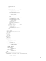
Figure 1 below displays a block diagram of the Elpida memory. The control signals chip-, row- and
column- select , write enable together with the address bus are decoded and used to generate the
required operation. The memory can simultaneously access different banks for increased
performance. (Elpida, 2008)
10
Figure 1, Elpida DDR2 memory block diagram. (Elpida, 2008)
On die termination (ODT) enables internal termination resistance. For a data width of 16 bits, ODT
11
is applied to each of /RDQS, RDQS, DQS,/DQS, DQ, UDM and LDM. If the extended mode register
(EMRS) is programmed to disable ODT, the ODT pin will be ignored. If the EMRS enables ODT,
there is a latency of eight clock cycles until the ODT is driven high. CKE is active high, thus setting
CKE low deactivates clock signals and in/out buffers as well as provides for self-refresh and power
down operation. (Elpida, 2008)
2.2 GRLIB
GRLIB is a IP library of reusable IP cores developed and supported by Aeroflex Gaisler. The IP
library is designed for SOC development. The cores in GRLIB uses the AMBA bus architecture for
communication. GRLIB also include complete template designs for developing boards for a variety
of boards and vendors. Figure 2 shows the template design included in GRLIB for the LEON3 GRXC3S-1500 board.
Figure 2, template design for LEON3 GR-XC3S-1500 board. (Jiri G. Sandi H. Edvin C. , 2009)
To configure a template design the graphical scripting tool xconfig is used, launched by type “make
xconfig” from the Linux command line. The settings are stored in a VHDL file, config.vhd. To
simulate the template design configured by xconfig , library compilation scripts are used. The first
script is launched by type “make scripts” generating a variety of scripts for different tools including
ISE, Symplify and Modelsim. To simulate the template design in Modelsim the command “make
vsim” is used. The script will compile all libraries needed to simulate the template. Testbenches
are also included in the template design.
Synthesis is also performed using a Make script. For synthesis with ISE the command “make
ise” is used.
Software compilation for the design is also performed by a script. The user implements C code
in the file systest.c and runs the command "make soft". The output is several files used for
simulation such as sdram.srec, used to load the memory simulation model in GRLIB, and
systest.exe that may be run in hardware. (Jiri G. Sandi H. Edvin C. , 2009)
2.3 SREC
The format of the file loaded into the Hynix memory module is SREC. This standard stores data in
hexadecimal format in a defined pattern, where each row has the same pattern. The first character
is "s" indicating the start of the row. The second symbol is a digit, defining the type of the data
field. The following 2 digits indicate the number bytes in the following row of data. The fifth digit
is the start of the address, 8 digits long for sdram.srec. The byte address is the offset address of
each row. This is followed by the data stored, 16 bytes. The last two digits consist of a checksum
based on the data in the row. Example of two lines in the file sdram.srec :
12
S3154000008091D02000010000000100000001000000A6
S31540000090A1480000A75000001080201BAC1020098A
This is 32 bytes of sequential data stored at address 40000080.
2.4 SP601 Developing board
SP601 is a development board provided by Xilinx. The key modules are listed below.
-FPGA: XC6SLX16 CS324-2C Spartan-6
-DDR2 Component Memory 128MB
-8 MB Quad SPI Flash
-16MB Parallel (BPI) Flash
-10/100/1000 Tri-Speed Ethernet PHY
-Serial (UART) to USB Bridge
-200MHz Oscillator (Differential)
-Socket (Single-Ended) Populated with 27MHz Oscillator.
(Xilinx, 2009)
Figure 3 shows the Xilinx SP601 Spartan 6 development board.
Figure 3, Xilinx SP601 Spartan 6 development board. (Xilinx, 2009)
13
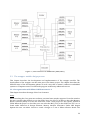
2.5 Board specific template design
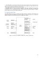
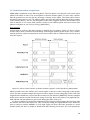
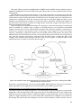
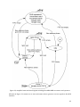
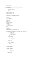
A board specific template design was created using IP blocks from GRLIB. The advantage of a
template design is that it is reusable and customized for a specific board design, in this project the
board SP601. The design is constructed around a Leon 3 processor and the AMBA processor bus
architecture. In the first synthesis a MMU was included in Leon 3. Spartan 6 xc6slx16 is one of the
smaller modules in the Spartan 6 series and the MMU didn't fit the design and was subsequently
excluded. Also included in the template design are IP blocks for clock and reset generation, AHB
controller, APB controller, AHB JTAG and AHB/APB- bridge. Figure 4 shows the board specific
template design. The wrapper is marked with dotted line since its design is not developed at this
first stage.
Figure 4, the board specific template design.
Short description of the blocks included in the board specific design.
Leon3 processor, the CPU and central component in the system. The Leon 3 is a Scalable
Processor Architecture (SPARC) CPU. SPARC is derived from the reduced instruction set
14
computing (RISC) architecture. Leon 3 is highly customizable and has features such a, 7 stage
pipeline, separate instruction and data cache, Hardware multiply, divide and MAC units,
configurable caches (1 - 4 ways, 1 - 256 kbytes/way) and high performance (1.4 DMIPS/MHz, 1.8
CoreMark/MHz).
JTAG Debug Link, provides a JTAG interface to AMBA AHB. This core provides a debug link to
the Leon 3 system. The core can generate reads and writes transfers to any address in the AMBA
AHB address space. The core decodes two JTAG instructions and implements 2 JTAG data
registers. The core does not implement any registers mapped into AMBA AHB/APB address space.
AHB/APB bridge, is an AMBA APB master with an AHB slave interface. The master supports up
to 16 APB slave modules and the number of slaves is defined by the VHDL constant NAPBSLV.
GRLIB APB slaves plug and play information is available through the bridge. The information is
mapped on a read-only address area at the bridge address space. The address space is 80000000 80100000. (Gaisler, 2010)
The Memory controller (the VHDL block MCTRL) supports a variety of memory types. The
memory supports PROM, memory mapped I/O devices, SRAM and SDRAM. In this particular
design the core is connected to a flash memory (PROM). The core is a slave on the AHB and
mapped on the AHB address space 00000000 - 40000000. The function of the controller is
programmed through configuration registers through APB. In this design, the core is mapped to
the APB address space 80000000 - 80000100. (Gaisler, 2010)
In the board specific design, the memory controller is connected to the parallel flash through a
2.5 V bank in the FPGA (Xilinx, 2009)
15
3 Wrapping Xilinx MCB to the AMBA AHB interface
3.1 MCB
Xilinx Spartan 6 includes one or more Memory Controller Blocks (MCB), implemented as hard
macros inside the Spartan 6 FPGA. The MCB is a multi-port memory controller and supports a
variety of memory module types. It provides higher performance and lower power consumption
compared to equivalent IP core implementation. The MCB supports several different memory
types, such as DDR, DDR2, DDR3 and LPDDR (mobile DDR). The data rate is up to 800 Mb/s (200
MHz). The MCB supports 1 to 6 ports, the number of ports is user-configurable through CORE
generator. It also supports common memory device options such as programmable drive strength,
On-Die Termination (ODT), CAS latency, self-refresh, refresh interval and has automatic delay
calibration of memory strobes and read data input. (Xilinx, 2010)
3.1.1 Block diagram
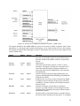
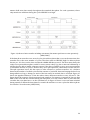
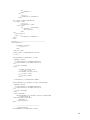
Figure 5 shows the block diagram of the MCB. A HDL design is unable to connect to the internal
blocks of the MCB and should interface the user interface, named User Logic in Figure 5.
Figure 5, MCB block diagram. (Xilinx, 2010)
Each of the six FIFO blocks, CMD FIFO 0-5, stores the commands related to for the FIFO’s
corresponding data path. Each data path may be configured for read, write or both read and write.
The blocks included in the data path are “32-Bit Bidirectional”, “32-Bit Unidirectional”, Datapath
and PHY. The PHY block handles the adaptation needed to communicate with different kinds of
memory modules. Initially during each start-up sequence the Calibration Logic block calibrates the
PHY block. The Arbiter block determines which port that has the priority to accessing the memory
device. The Controller block is the core block that controls the MCB and regulate the reads and
16
writes operations carried out by the MCB. The clock network distribution as well as the signal
distribution between blocks are also included in the block diagram as separate blocks in figure 5.
(Xilinx, 2010)
3.1.2 Interface and signal description
The primitive is wrapped with a soft wrapper including less than 100 LUTS. The hard macro has 6
fix ports of 32 bits width, 2 bidirectional and 4 unidirectional. The wrapper contains clock
distribution and covers the fixed not used ports. For example if the designer uses a bidirectional
32-bits port, the other five ports are covered by the wrapper and the interface will consist of only
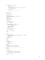
the 32 bits bidirectional port. The port interface is customizable and the supported write and read
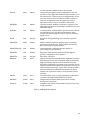
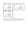
port configurations are showed in Figure 6.
Figure 6, port configurations. (Xilinx, 2010)
Configuration 1 in the figure shows a direct port mapping to the macro, creating a similar port
configuration as the hard MCB. The other configurations are four 32 bits ports, two 32 bits & one
64 bits port, two 64 bits ports or one 128 bits port. Each port has independent clock signals, so for
example in configuration 3 the two 32 bits ports may have one clock source and the 64 bits port
an other.
The following table 2, 3 and 4 describes in details the MCB´s user interface. The interface is
available and accessible from within the FPGA’s logic and should be connected in the HDL design.
17
Table 2 shows the clock and reset signals.
Signal
async_rst
calib_done
Type
Input
Output
mcb_drp_clk
Input
pll_ce_0
Input
pll_ce_90
Input
pll_lock
sys_rst
sysclk_2x
Input
Input
Input
sysclk_2x_180
Input
Function
Asynchronous reset.
Indicate that the inbuilt calibration for the MCB is carried out. No read,
write or command operation will be carried out before the calib_done
signal is asserted high.
This clock synchronizes the soft calibration module to the sysclk_2x
domain. It must be generated by the same PLL as sysclk_2x to ensure
phase-synchronization.
I/O clock enable strobe from BUFPLL. This signal pulses high on every
other clock cycle of sysclk_2x. It is used for double data rate transfers in
the I/O blocks.
I/O clock enable strobe from BUFPLL. This signal pulses high on every
other clock cycle of sysclk_2x_180. It is used for double data rate
transfers in the I/O blocks.
Lock signal from the PLL block.
Main reset for the MCB.
Main clock for the MCB. This signal is generated by the Spartan-6 FPGA
PLL block and is rebuffered by the BUFPLL driver to the I/O clock
network. It operates at two times the memory clock frequency (for
example, 800 MHz for a 400 MHz memory interface).
This input is the phase-shifted clock with the same frequency as
sysclk_2x. It is generated by the same PLL/BUFPLL resources.
Table 2, MCB signal description
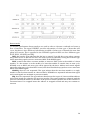
Table 3 shows the signals included in the command path.
Signal
Type
pX_cmd_addr[29:0] Input
pX_cmd_bl[5:0]
pX_cmd_clk
pX_cmd_empty
pX_cmd_en
pX_cmd_error
pX_cmd_full
pX_cmd_instr[2:0]
Function
Byte start address for current transfer. Note that addresses must
be aligned to port size.
Input
Burst length in number of words for the current transaction. Burst
length is encoded as 0 to 63, representing 1 to 64 words. The word
width is equals to the port width (for example, a burst length of 3
on a 64-bit port transfers 3 x 64-bit user words = 192 bits total).
Input
Clock for the Command FIFO. FIFO signals are captured on the
rising edge of this clock.
Output The active high empty flag for the Command FIFO indicates that no
commands are queued in the FIFO.
Input
This active-high signal is the write enable signal for the Comand
FIFO.
Output This output indicates a Command Port error occurred because the
FIFO pointers were unsynchronized.
Output The active high full flag for the Command FIFO indicates that the
Command FIFO is full.
Input
Indicate which type of command the MCB should carry out, read,
write or refresh. For details see table 4.
Table 3, MCB signal description
18
The MCB is controlled by the command messages send on the signals pX_cmd_instr. Table 4 shows
the supported instructions.
pX_cmd_instr[0:2]
Value Name
000
Write
001
Read
010
Write with Auto precharge
011
Read with Auto precharge
1xx
Refresh
Function
Write data from the Write Data FIFO to the memory
module. The number of words is set by the signal
pX_cmd_bl and the offset (byte) address is set by the
signal pX_cmd_addr. The write instruction is valid for
read only and bidirectional ports.
Read data from the memory module to the Read Data
FIFO. The number of words is set by the signal
pX_cmd_bl and the offset (byte) address is set by the
signal pX_cmd_addr. The write instruction is valid for
read only and bidirectional ports.
Memory write with auto precharge. The same function as
Write but with precharge.
Memory read with auto precharge. The same function as
Read but with precharge.
Refresh the memory.
Table 4, MCB signal description
The instruction write with auto precharge is the same function as write but with auto precharge
carried out after a burst completion. Auto precharge closes the DRAM bank there the write
operation ends. The instruction read with auto precharge works in the same way as write with
auto precharge, but the operation is read instead of write. The refresh command resets the tREFI
counter that allows data to stream uninterrupted for a full refresh cycle. The MCB automatically
initiate the refresh command, so the Refresh command may only be used if the designer wants to
initiate a refresh from within the design. (Xilinx, 2010)
Table 5 shows the signals included in the read and write path.
Signal
pX_wr_clk
pX_wr_count[6:0]
Type
Input
Output
pX_wr_data
[px_size -1 : 0]
Input
pX_wr_empty
Output
pX_wr_en
Input
Function
Clock input for the write path.
Counts the element stored in the Write Data FIFO. The
range covers the depth of the FIFO, 1 to 64. The latency of
this signal is longer than the signal pX_wr_empty, thus the
FIFO may be empty or experience an underrun even if
signal pX_wr_count is not 0.
Data to be loaded into the Write Data FIFO and sent to the
memory. PX_SIZE can be 32, 64, or 128 bits, depending on
the port configuration.
Indicate that the FIFO is empty and no data in the FIFO is
valid.
Write enable for the Write Data FIFO. It indicates that the
data on pX_wr_data is valid.
19
pX_wr_error
Output
pX_wr_full
Output
pX_wr_mask
[px_masksize-1:0]
Input
pX_wr_underrun
Output
pX_rd_clk
pX_rd_en
pX_rd_data
[px_size-1:0]
pX_rd_full
Input
Input
Output
pX_rd_empty
pX_rd_count[6:0]
Output
Output
pX_rd_overflow
Output
pX_rd_error
Output
Output
This signal indicates a Write Data FIFO error occurred
because the FIFO pointers were unsynchronized. An MCB
reset is required to recover from this condition.
Indicate that the Write Data FIFO is full. When this signal is
high, it prevents data from being loaded into the FIFO.
Data mask bits for Write Data. This mask is loaded into the
FIFO coincident with the associated Write Data
(pX_wr_data). One mask bit is associated with each byte of
data. When a pX_wr_mask bit is high, the corresponding
byte of data is masked.
The underrun flag indicates there was not enough data in
the Write Data FIFO to complete the transaction. The last
valid data word is written continuously to finish the burst.
The sys_rst signal must be asserted to recover from this
condition.
Clock input for the read path.
Read enable for the Read Data FIFO.
Output data from the Read Data FIFO. PX_SIZE can be 32,
64, or 128 bits, depending on the port configuration.
Indicate that the Read Data FIFO is full. When the FIFO is
full, loading data into the FIFO from the memory module is
prohibited.
Indicate that the FIFO is empty.
Counts the element stored in the Read Data FIFO. The
range covers the depth of the FIFO, 1 to 64. The latency of
this signal is longer than the signal pX_rd_full. Therefore,
the FIFO could be full or experience overflow even when
the signal pX_rd_count is less than 64.
Read Data FIFO overflow. When the signal is asserted high,
data transmitted from the memory module are lost. The
sys_rst signal must be asserted to reset this signal and
recover from this condition.
This signal indicates a Read Data FIFO error occurred
because the FIFO pointers were unsynchronized. An MCB
reset is required to recover from this condition.
Table 5, MCB signal description
The user interface is the internal interface available from within the FPGA described above and
realizing an interface to the MCB independent of the memory module type. The interface facing
the memory module is customized by the from Xilinx provided software, see chapter 3.3.1 Core
generation with Xilinx CORE Generator 11.4. Thus parameters such as data bus width, latency and
the memory module internal structure is generated by the software realizing the MCB. For a detail
description of the memory module interface see Xilinx’s ug388. (Xilinx, 2010)
20
3.1.3 MCB Functionality and Operation
Startup sequence
The initial startup sequence is divided into two different phases, adjustment of the input
termination and centering of the data strobe signal used in the memory interface.
During the first phase the input termination value for several pins in the memory interface is
adjusted. Calibration of the termination value improves signal integrity and reduces component
count by align the endpoint of the signal transmission with the termination point. The calibration
is done by measure the value of an external resistor connected to the memory interface and then
program the I/O blocks of the MCB pins to create a split termination between the I/O reference
voltage and ground. Automatically adjustment of the termination value may be turned off by the
designer when customizing a MCB, see chapter 3.3.1 Core generation with Xilinx CORE Generator
11.4.
Data is transferred via the memory data bus dq and the memory data strobe signal dsq. During
the second phase the dqs signal is centered in regard to dq. The calibration is done by carrying out
several memory transactions and phase shift the strobe signal.
The dqs is continuously adjusted to compensate for temperature or voltage variations after the
calibration is done. (Xilinx, 2010)
Addressing
The offset address is set via the signal pX_cmd_addr included in the command interface. The
memory is addressed in byte addresses and the memory address space is sequential. The address
set on pX_cmd_addr must be aligned with the width on the data buses pX_wr_data and pX_rd_data.
The value set on pX_cmd_addr for a data bus with the width 32 bits should be, 0x00, 0x04, 0x08
and so on. A 64 bits rd/wr port is 8 bytes wide, thus the addresses set on the pX_cmd_addr should
be 0x00, 0x08, 0x16 and so on.
To write one byte of data to the address 0x01 with a 32 bits data bus, a mask may be used to
prevent data on address 0x00 & 0x02-0x03 to be modified. One mask bit is associated with each
byte of data. When a pX_wr_mask bit is high, the corresponding byte of data is masked. So in the
example above the value set for pX_wr_mask should be “1101”. (Xilinx, 2010)
MCB operations
The user interface as described in previous sections is mainly divided into 3 separate types of
interface, read, write and command. Operations are initiated by loading instruction into the
command FIFO. Write operation transfer data from the Write Data FIFO into the memory module,
while read operation transfer data from the memory module to the Read Data FIFO. Write
operations therefor require valid data in the Write Data FIFO before a write operation command is
loaded into the command FIFO. Read operation require available storage in the Read Data FIFO
before a read operation is loaded into the command FIFO. Data is loaded into both the Command
FIFO and the Write FIFO as long as the FIFO’s enable signal is asserted high. If there is invalid data
on a data bus, the invalid data will still be stored in the FIFO since the FIFO lacks inbuilt validity
check for incoming data. (Xilinx, 2010)
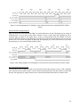
Command FIFO timing diagram
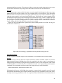
Figure 7 shows how a write command is loaded into the command FIFO 0. As seen in the figure the
signal p0_cmd_instr is asserted 0 for write. The signal p0_cmd_bl determine the number of words
to be transferred from the Write Data FIFO into the memory. As seen in the Figure 7 the burst
length is set to 3 words. The signal p0_cmd_addr sets the write operation’s offset address.
21
Figure 7, the timing diagram for loading a write instruction into the command FIFO 0. (Xilinx,
2010)
Write Data FIFO timing diagram
Figure 8 shows how the Write Data FIFO 0 is loaded with three words. The signal p0_wr_empty is
asserted from 1 to 0 as soon as the FIFO contains a word, 2 cycles after the signal p0_wr_en is
asserted high. In Figure 8 the signal p0_wr_count is synchronized with the number of words
stored in the FIFO, however since the pX_wr_count isn’t synchronized this pattern may not always
be the case. If no words are pulled off the FIFO, the signal p0_wr_count is increased 1 cycle after
the signal p0_wr_en is asserted high. (Xilinx, 2010)
Figure 8, the timing diagram for loading three words into the Write Data FIFO 0. (Xilinx, 2010)
Read Data FIFO timing diagram
The Read Data FIFO is filled up with words transferred from the memory when a read command
been executed by the MCB. Figure 9 shows data being transferred from the memory at the data
bus dq. The signal p0_rd_empty asserted to low indicate that Read Data FIFO 0 contains valid.
22
Figure 9, the timing diagram shows the data flow after a read instruction has been carried out by
the MCB and data is fetched from the memory module. (Xilinx, 2010)
Then the Read Data FIFO contains valid data, words may be pulled off by asserting the signal
pX_rd_en to high. In Figure 10 the value of signal p0_rd_count does increase, indicating that the
Read Data FIFO is filled up with words from the memory. By asserting p0_rd_en high, data is
pulled off the FIFO and becomes valid on the bus p0_rd_data. (Xilinx, 2010)
Figure 10, timing diagram shows data transfer from and to the Read Data FIFO. (Xilinx, 2010)
3.2 AMBA
The Advanced Microcontroller Bus Architecture (AMBA) is a processor architecture bus
developed by ARM for on-chip communication in embedded micro controllers. The architecture
provides an effective data transfer between different IP blocks. The architecture is dived into
three different buses, the Advanced High-performance Bus (AHB), the Advanced System bus (ASB)
and the Advanced Peripheral Bus (APB). The system bus is not used in the interconnection
between Gaisler's IP-block and will just be briefly described in this report. To archive high
performance, the buses are parallel and pipelined. The pipelining is done in two phases, an
address phase and a data phase.
The AMBA AHB is a bus for high performance transmission. This means it's suitable for
modules that require high interconnection performance (i.e. high frequency), such as processors
and on-chip memory controllers. The AHB uses a backbone structure, meaning all masters and
slaves are connected to the same bus.
23
The AMBA ASB is a system bus for high performing system modules. This is an alternative bus
which is suitable when the demands on performance is not as high as for AHB. This bus is not
implemented in GRLIB and will not be described further.
The AMBA APB is a bus for low power peripherals. This bus is optimized for low power
consumption and has a reduced interface compare to the other two buses. In GRLIB, one
configuration is to use a AHB/APB controller to attach the APB to the AHB. Examples of modules
that use APB are VGA, PS/2 and UART. (ARM, 1999)
3.2.1 Signal description AHB
The AMBA AHB bus protocol is divided into master and slave interfaces. The interfaces are
specified according to the AMBA 2.0 architecture. Figure 11 shows the interface for an AHB slave
module and Figure 12 shows the interface for an AHB master module.
Figure 11, interface for a AMBA 2.0 AHB master module. . (ARM, 1999)
24
Figure 12, interface for a AMBA 2.0 AHB slave module. . (ARM, 1999)
The signals defined by the AMBA AHB bus protocol are listed in Table 6 together with a short
description of each signal. More detailed description can be found further down in this chapter.
Each signal included in the AHB begins with H to differentiate the name from other signals in the
system. (ARM, 1999)
Signal
HSELx
Width
1 bit
Source
Master
HADDR
HWRITE
32 bits
1 bit
Master
Master
HTRANS
2 bits
Master
HSIZE
3 bits
Master
HBURST
3 bits
Master
HWDATA
32 bits
Master
Function
Slave select, high when a specific slave is selected. Each
slave has its own HSEL signal. Thus the HSEL bus has
the same width as the number of slaves connected to
the bus
Address bus
Determine if the master requires a read or a write
operation. The signal is set high for write and low for
read. This signal should be combined with data on
either the write data bus (HWDATA) or the read data
bus (WRDATA).
Indicates which of the following transmissions is in
progress, NONSEQUENTIAL (NONSEQ), SEQUENTIAL
(SEQ), IDLE or BUSY
& Indicate the size of the current transmission. AMBA
2.0 support sizes from 8 bits (1 Byte) up to 1024 bits
(128 Byte), e.g 8 bits (1 Byte), 16 bits (half word) and
32 bits (word).
Indicate which type of burst that is currently in
progress. e.g Single transfer, Incrementing burst and
wrapping burst. A detailed description follows further
down in this chapter.
Write bus that is used by the master to transfer data to
the selected slave during write operations. To complete
25
HPROT
4 bits
Master
BUSREQx
1 bit
Master
HLOCKx
1 bit
Master
HCLK
1 bit
Clk gen.
HMASTER
4 bits
Arbiter
HMASTERLOCK 1 bit
Arbiter
HGRANTx
1 bit
Arbiter
HRESETn
HREADY
1 bit
1 bit
Rst gen.
Slave
HRESP
2 bits
Slave
HRDATA
32 bits
Slave
HSPLITx
16 bits
Slave
a write operation HRWITE has to be set high.
The protection signal is used to implement a level of
protection. The signal also indicates if the transfer is an
opcode fetch or a data access, a privileged mode access
or a user mode access. If a master module contains a
memory management unit, the signal are used to
determine if the access is cachable or bufferable.
Used by a master module to indicate it require access
and control of the bus. Each master module has its own
HBUSREQ signal.
Locked transfer, indicate that a specific master calls for
a locked bus access. This also means that no other
masters should be granted access to the bus until this
signal is low.
Bus clock, all signal timings are related to a positive
flank.
Master number, indicates which master currently is
granted access to the bus. These signals are used by
slaves that support split transfers.
Locked sequence, indicates that the master is
performing a locked transfer.
Bus grant, indicates that master x has the highest
priority compared to other masters.
Bus reset, active low.
Signal from the slave informing the capability to deliver
data the next clock cycle. The signal must by default be
high, and should only be set low when the selected
slave been requested to perform a bus operation and is
unable to perform the operation by the next clock cycle.
If the slave becomes busy, e.g the slave needs to make a
internal calibration, HREADY can't be set low until a
master has requested a read or write operation from
the slave.
Provides status of the current transmission, the values
can either be OKAY, ERROR, RETRY or SPLIT.
Read bus that transfers data from slave to master
during read operations.
Indicate to the arbiter which master is allowed to retry
a split operation.
Table 6, AHB signal description.
26
In addition to the AMBA 2.0 interface, several signals have been added by Gaisler Research, as well
as minor modifications to the clock and reset signals. The clock and reset signals are distributed to
the modules through IP blocks from GRLIB and are not named HCLK and HRESETn as in the
standard. Table 7 describes the added signals. Plug and play functionality has also been added to
the original AMBA 2.0 architecture.
Signal
Hmbsel
hcache
hirq
Testen
testrst
scanen
testoen
hirq
hconfig
Type
Input
Input
Input
Input
Input
Input
Input
Output
Output
hindex
Output
Function
Memory bank select
Cache-able
Interrupt result bus
Scan test enable
Scan test reset
Scan enable
Test output enable
Interrupt bus
Memory access reg, describes address space, vendor and
device etc.
For diagnostic use only
Table 7, Signals added to the AMBA 2.0 bus architecture.
A burst is a sequence of data, often in address order, where all transfers are of the same type. Each
transfer is completed during one clock cycle. The signal HBURST indicates which type of burst that
is occurring. There are two main burst types, and variants of them. They are, incrementing bursts
and wrapping bursts. The incrementing burst is a sequential burst where the data in the transfer
follows in increasing address order. A wrapping burst has an address wrap at a specific address
boundary. The most basic transfer type in AMBA is Single transfer (SINGLE), where one data of a
specific length is transferred over the bus. There is also incrementing burst of unspecified length
(INCR), which is a series of single transfers ordered by address. In Table 8 all the burst types are
listed.
HBurst[2:0] Type
Function
000
001
010
011
100
101
110
111
Single transfer
Incrementing burst of unspecified length
4 - beat wrapping burst
4 - beat incrementing burst
8 - beat wrapping burst
8 - beat incrementing burst
16 - beat wrapping burst
16 - beat incrementing burst
Single
Incr
Wrap4
Incr4
Wrap8
Incr8
Wrap16
Incr16
Table 8, Hburst signal encoding.
Burst transfers must not cross over a 1kB address boundary and therefore a master unit must not
start a fixed length incrementing burst so it will cross such a boundary.
The signals used by the AMBA AHB are described above. The following chapter will put those
signals into context of usage and dependence. . (ARM, 2009)
27
3.2.2 AHB Functionality and Operation
AMBA AHB is pipelined in two different phases. The first phase is an address and control signal
phase from master to slave. The second phase is the data transfer phase. To start with, a master
must be granted access to the bus by asserting a request to the arbiter. The arbiter then notices
the master and grants access. The address phase provides information about the address, length
of the transfer (burst) , size etc. The data phase, as the name suggests, indicates data transfer from
slave to master or vice-versa. Each transfer consists of one address phase and one or more data
phases. Each phase is one clock cycle long. (ARM, 2009)
Basic transfer
As described in section 0 the data transfer is divided into two phases. Figure 13 shows a basic
transfer where data is transferred immediately following the address phase. In this case, a master
module performs a data read operation, so the slave must be able to send data the next clock cycle
after the request.
Figure 13, shows a basic transfer (a master module requests a read operation). (ARM, 2009)
Master modules drive the address and control signals on the bus on the rising edge of the system
clock. The slave modules sample the required control signals on next rising edge of the clock. The
targeted slave handles the request and drives data onto the data bus (HRDATA) which is sampled
by the active master module on the next rising clock edge. Due to the nature of a pipelined bus,
both address and data phases are processed during the same clock cycle.
If a slave is unable to transfer data immediately following the address phase, the slave may stall
the transfer and freeze the entire bus. This is done by setting the signal HREADY low. When the
slave is ready to transfer HREADY is set to high. Figure 14 shows the basic principle of a write
transfer where the slave is unable to handle data the following clock cycle. For write operations,
28
masters hold write data steady throughout the extended data phase. For read operations, slaves
only must drive valid data during the cycles HREADY is set high.
Figure 14, shows a basic transfer including wait states (the master performs a write operation). .
(ARM, 2009)
If the data phase stretches over several cycles, the address phase that occurs at the same time also
stretches out to the same number of cycles. The slave must set HREADY high if a address phase
has not yet - if it does not the slave violates the AMBA AHB bus protocol. The slave must always be
ready to accept an address phase, and if for some reason is busy (e.g. due to internal calibration) it
still needs to be able to handle a master request. If the slave is unable to carry out a request within
a reasonable amount of cycles, it should carry out a split operation, rather than to freeze the bus.
The split operation leaves the bus open to other masters to perform transfers. It's a balance
between the number of stalled cycles and the amount of overhead, between keeping the bus from
being stalled too long or letting too much of the bus traffic be wasted due to overhead. Figure 15
shows the pipelined behavior of the bus where three different transfers occurs, A,B and C. The
figure shows the scenario of both write and read transfers. For instance, in transfer A, there is data
both on the write and the read bus during the data phase. In a real scenario there is just valid data
on either the write data bus or on the read data bus. In Figure 15 there is one wait state included
during transfer B. When the data phase for transfer B stretches over two cycles the address phase
for transfer C does the same. (ARM, 2009)
29
Figure 15, three transfers of data A,B and C on the AMBA bus. (ARM, 2009)
Burst transfer
To increase performance burst transfers are used in order to decrease overhead and create a
flow of transfers. The signal HBURST provides information of what type of burst that will
occur, but there is also additional information available of what type of transfer the next data
phase will contain. This is specified in the HTRANS signal and there are four different types:
IDLE, BUSY, NONSEQ and SEQ.
IDLE, this transfer type indicates that the bus is unused. Typically this occurs when a master
has granted access to the bus but does not wish to perform a transfer. During this transfer type
slaves must always perform a zero wait state OKAY at the HRESP signal.
BUSY, transfer that allows a master module to insert an IDLE cycles in the middle of a burst
transfer. If a bus master is in the middle of a burst but unable to transfer data at next cycle,
HTRANS is set to BUSY and next cycle will be ignored by the slave. Address and control signals
must reflect the next cycle when BUSY is used, and slaves should always perform a zero wait state
OKAY at the HRESP signal.
NONSEQ, short for non sequential. This type indicate that the next data transfer is a single
transfer or the first data transfer in a burst transfer. HTRANS non sequential indicates that signal
and control signals are unrelated to previous transfer.
SEQ, short for sequential. This type indicate that the transfer is part of a burst and that address
and control signals are related to the previous transfer. The control signals are identical with the
previous ones and the address is the same as the previous address plus the size of the transfer for
increment burst. For wrapped bursts the address is wrapped around and may not continue to
increase.
30
Figure 16 shows an incrementing burst with the length of four data transfers. (ARM, 2009)
During the first data transfer, HTRANS is set to non sequential since it is the first transfer of the
burst. Next cycle, HTRANS is set to busy that indicate that the master is currently unavailable to
perform a transfer. Next, three sequential transfers follow, with same control signals as the
previous cycle and with incrementing address. The third transfer's data phase is stretched to two
cycles when HREADY is set low by the slave. While not included in the figure, the burst will end
with either HTRANS set to IDLE or NONSEQ. (ARM, 2009)
Figure 16, shows an increment burst with the length of four data transfers. (ARM, 2009)
Interconnection
Figure 17 shows how the address bus, data read bus and data write bus are routed and connected.
Central multiplexers drive out address and write data controlled by the Arbiter. The bus master
that has been granted access to the bus drives the bus. For the slaves, there is a similar multiplexer
which decodes the HSEL signals and one slave drives the read data bus to all bus masters. (ARM,
2009)
31
Figure 17, interconnection of AMBA AHB. (ARM, 2009)
3.3 The wrapper module design process
This chapter describes the development and implementation of the wrapper module. The
development of the wrapper was the main part of the thesis project. The chapter describes the
different steps of the development phases in such a way that a master's student in embedded
systems or computer science can follow the progress without any additional sources.
3.3.1 Core generation with Xilinx CORE Generator 11.4
This chapter describes the usage of the Core Generator.
Setup
When launching the Core generator software, an initial start window appears. From this window
the user can select the desired core in the folder list to the left. To be able to select the Memory
Block Controller (MCB) core, the user must first create a new project for the specific Spartan 6
FPGA. When the project is saved the user can select the MIG (v3.3) in the folder list. The core is
found under Memories & Storage Elements, Memory Interface Generators. Under MIG Output
Options the user can either choose to create a design or to use a Xilinx reference board. The
32
reference board option merely links to a Xilinx webpage, so the Create design option should be
chosen. Component Name defines the name of the component, which in this case is mig_2. Next
choice is the bank which the memory is connected to. On the SP602 board the memory is routed
through bank 3. The memory type is DDR2.
The next option is frequency, the range interval is 3000 ps (333 Mhz) to 8000 ps (125 Mhz).
The frequency is for the memory time domain and unrelated to the system bus frequency.
However there is a recommended ratio between them see 3.1. In the Memory Part option a variety
of memory modules can be selected, also a custom model is available where the user set the
memory parameters manually. The memory model chosen is the one on the SP601 board,
EDE1116ACBG-8E. The chosen memory model sets the parameters to 1Gb, x16, row:13, col:10,
data bits per strobe: 8, single rank and with data mask. Output Drive strength is set to
Fullstrength, RTT (Nominal) -ODT is set to 50 ohms, DQS# Enable is set to enable and High
Temperature Self Refresh Rate is disabled.
Next option configure the ports including the soft VHDL blocks that create the MCB interface.
The hard macro have a fixed number of ports, thus all port configuration is made in the soft blocks.
The width of 32 bits is chosen in the list which enables five ports. For the desired design only
port0 is enabled. Two different Memory Address Mapping Selections can be made, Row Bank Col
or Bank Row Col. Depending on the nature of the data transferred to the memory, one of the two
choices may result in a higher performance. For this core Row Bank Col is chosen. Next option is
Arbitration for the ports, where either the Round Robin or a custom arbitration pattern can be
used. The design only has one port and arbitration is not needed. For the SSTL Output Drive
Strength, Address and Control as well as Data, is set to Class II. For the Memory Interface Pin
Termination the option Calibrated Input Termination is set, the SP602 has support for this option.
The option for Static Calibration Memory Address reserve an address space required for static
calibration. This is only required for a system where the MCB's suspend mode operation is used.
The reserved space is used by the MCB to write a test pattern during static calibration. The specific
system don't use the suspend mode operation and no address needs to be allocated. Next option
sets if the calibration stage should be skipped during functional simulation. To save time during
simulation this option is set. The Debug Signals for Memory Controller is also disabled. The final
option is for the system clock, which is either differential or single-ended. The SP602 board
provides a differential clock source and option is set differential. To create a core the user just
needs to press the finish button and the core will be generated.
Output
The output generated by Core generator is divided into several folders, with both a example
design as well as a user design together with a variety of scripts, such as Modelsim's .do and tcl.
Simulation blocks for the memory module is generated in some cases, but not for memories
provided by Elpida. Required libraries such as Xilinx simulation library and simulation model for
Xilinx MCB are not generated, thus they manually have to be downloaded and added to the scripts.
The output files are listed below and are shortly described.
mig_2. vho: vho template file containing code that may be used as a model in HDL design.
mig_2.xco: CORE Generator input file containing core parameters for regeneration of a core
mig_2_flist.txt: Containing a list of all the output files generated by the software.
mig_2_xmdf.tcl: ISE Project Navigator Interface file, used by ISE to create and integrate a projec t
with ISE.
Also there is a directory folder mig_2 is created, containing the three directories docs,
example_design and user_design. The directory names are self-explaining, the folder docs contain
documentation, more specific the documents ug388 and ug416 which are both relevant for
33
integrating MCB into a system. The other two folders contain an example design and a user design.
The two have similar directory setup, where the folders rtl and sim are described below.
RTL, SIM
The CORE generator output include 2 designs, user and example. Both designs include test scripts,
testbench and rtl and sim folders. They are assigned their own directories. The differences
between them are small, for instance, the signal generation files, (used in the testbench to trigger
read and write transfers), are located under the directory “RTL/traffic_gen” in the example design,
and under the sim directory in the user design. The included .do script “sim.do” compiles and runs
the simulation. The SIM directory contains simulation scripts and the top testbench. The thin
(soft) wrapper created by CORE generator is located in the RTL folder. If the MCB is included in
another design, the files in the RTL folder must also be included.
Figure 18 shows the MCB block generated by Xilinx CORE generator, the VHDL file mig_2 is
located in the rtl directory.
Figure 18, the block mig_2, captured from Core generator set up process.
Library dependencies
In order to get the example design to run in simulation, correct libraries have to be included.
UNISIM
The Make script is used in GRLIB to compile all libraries needed in GRLIB. A build-in version of
Xilinx simulation library UNISIM is then used and compiled by the make script. For simulating the
example design provided by CORE generator the build-in version is not enough and a full version
of UNISIM must be used. The full version of UNISIM is included and compiled using following three
commands. The commands should be typed in the design directory in the GRLIB tree.
make install-unisim, make distclean, make vism
Excluding the full version of UNISIM is done using the command make uninstall-unisim. To install
the full Xilinx UNISIM library the variable XILINX must point to the installation path of ISE. This is
normally done during installation of ISE. To compile the Xilinx UNISIM libraries with Modelsim the
34
variable VCOMPT =-explicit must be set in the local Makefile. The local Makefile is found in the
design directory in the GRLIB tree.
MCB and SecureIp
In order to simulate the Xilinx Memory Block Controller (MCB) a model with the functional
behavior of the MCB must be used. A way to hide the underlying HDL code is to create a black box
containing a model with the functionality of the MCB. This may be done with either Smart models
or SecureIP blocks, where SecureIP is the more modern alternative. The SecureIP block is
provided through Xilinx home page Xilinx.com. A SecureIP block contains HDL files written in
Verilog. To simulate SecureIP blocks with Modelsim, a version of 6.4b or higher is required.
Memory module
A simulation library for the memory model from Elpida was downloaded,
ede1116ac_8e_0627_vp.zip and unziped in the sim/functional directory. This model is also a
SecureIP block. See www.elpida.com
Library relevant issues
To compile the SecureIP blocks and the example design a mixed Verilog/VHDL license was
needed. At the time only a VHDL license was available at Gaisler, thus a simulation of the example
design was impossible with current configuration. A mix license was achieved at Chalmers
University of Technology and all files included in the simulation were transferred to a Chalmers
user storage area. The files were remotely compiled and a successful simulation was made. The
transfer of the project files to Chalmers, including a successful simulation, proved that the example
design worked properly. However the project goal is to interface the MCB with GRLIB including
that the final system should be able to run at an environment provided at Aeroflex Gaisler.
The problem was solved by replace and patching the SecureIP blocks. In order to compile the
MCB SecureIP block a patch provided by Xilinx was used. The patch required Modelsim version
6.5e or higher. The path contains of 42 files named mcb_0XX.vp. To compile the MCB simulation
block the following commands are used:
vlog -work secureip -f
vcom -work ./work
<path> /mcb_mti/mcb_cell.list.f
<path> /MCB.vhd
The file mcb_cell.list.f contains all the 42 file names and the -f flag sets that a list is compiled. The
second command compiles the VHDL part of the MCB simulation model. Instead of Elpida's
SecureIP block, the memory model Hynix HY5PS121621F in GRLIB was implemented into the
example design. The result is a successful simulation within the environment at Aeroflex Gaisler.
The simulation was run by the sim.do script as described in the chapter above.
3.3.2 Reset and calibration
Because it's hard to test synchronization during simulation it's better to test this in hardware. The
goal of the first step is to clean the MCB from test blocks provided by CORE generator, synthesize
the design and verify the calibration and reset operations.
First the user design provided by CORE generator was altered in the same way as the example
design, compiling the libraries used in the design and change the memory model in the testbench
to the Hynix block. A Makefile was created in the sim directory, including different functions such
as compiling all necessary libraries and remove all compiled files. Xilinx UNISIM libraries were
compiled with the GRLIB Make script and then mapped with the new Make script into the sim
directory. The script sim.do contains the following row, loading the design:
vsim -t ps -novopt +notimingchecks -L unisim -L secureip work.sim_tb_top glbl
35
The file glbl.v is used for initializing some of the simulation environment, however this file may be
excluded and it's still possible to run the simulation with similar outcome. The resolution of the
simulation was chosen to 1 fs.
The test script sim.do were divided into 3 files, make the test more dynamical. The first file
loaded the design, the second added waves and the third file is the main part of the sim.do file,
running the simulation.
The Hynix memory simulation block is altered so initial data don't need to be written to the
memory, instead its loaded through a .srec file. To verify the calibration operation no data is
needed and an empty file is loaded into the memory block.
To synthesize the MCB the .ucf file was altered to correspond with the pin configuration and
the following TCL script was manufactured and executed.
project new MCBWrapper.ise
project set family "Spartan6"
project set device XC6SLX16
project set speed -2
project set package csg324
xfile add ../rtl/WrapperDesignMW.vhd
xfile add ../rtl/MCB_two.vhd
xfile add ../rtl/iodrp_controller.vhd
xfile add ../rtl/iodrp_mcb_controller.vhd
xfile add ../rtl/mcb_raw_wrapper.vhd
xfile add ../rtl/mcb_soft_calibration.vhd
xfile add ../rtl/mcb_soft_calibration_top.vhd
xfile add ../rtl/memc3_infrastructure.vhd
xfile add ../rtl/memc3_wrapper.vhd
xfile add ../MCBWrapper.ucf
xfile add WrapperDesignMW.xcf
process run "Generate Programming File"
Tcl script to synthesize the first MCB design.
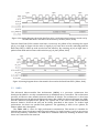
Figure 19 shows reset and calibration_done signals from the Modelsim simulation. Both reset and
calibration_done was put to pins on the SP602 connected diodes for visual status when tested in
hardware. Reset is active low and calibration_done is set high until the reset signal toggle from
low to high.
Figure 19, reset and calibration_done from simulation with Modelsim.
The result in Figure 19 corresponded with result received from the verification in hardware.
36
3.3.3 Basic transfer and implementation of the wrapper into the board specific template
design
To verify the functions of the MCB interface, a signal generator was implemented generating
written transfers to the memory.
Test logic was implemented in the testbench and ports for data and address were added to the
wrapper. Internal logic were added to the wrapper to generate appropriate signals to the MCB.
The test logic performed two written bursts of a fixed length.
In the next step the specific template design was altered, e.g signal name similarity throughout
the design, the 200 MHz clock source was added. The MCB and the wrapper were added to an own
package file called WrapperPackage.vhd. The template designs testbench were also altered to
include the memory model, simulate clock sources etc.
There is a difference between the Elpida memory on the SP602 and the Hynix memory model.
The Hynix block has 4 banks and the Elpida memory has 8. This difference is not an issue, because
the Hynix block memory space will wrap around. Also a simulation may be limited to include 4
banks. In the testbench only two out of three bank address signals are connected to the memory
model.
Include the wrapper libraries in GRLIBS's make script
The commando “make scripts” generate the scripts, which are used to compile the source code.
Include new libraries into GRLIB is uncomplicated which gives a dynamical structure to the
library. Adding the directory's name into the file dirs.txt includes the directory into the scripts. To
include specific files for synthesizing and simulation, these are listed in the file vhdlsyn.txt in
respective folder. To include a file just for simulation the file is listed into vhdlsim.txt. The VHDL
output files from CORE generator, together with the wrapper block were added into the directory
GRLIB/lib/work. The MCB's VHDL file was located to the folder mcb, the folder was located to the
same directory and specified to be included only in simulation.
The SecureIP could not be added that easy into the three, the compilation command is for
Verilog and it does also include the flag -f needed to compile a list. Thus the SecureIP block has to
be compiled separately. If the SecureIP library is compiled and mapped into the right path
modelsim/work/secureip, it will cause conflict with the scripted started by the command “make
vsim”. Therefore the flow has to be as following.
1) Write the command: make scripts
2) Write the command: make vsim
3) Waits until the script stop and manually write “secureip = modelsim/work/secureip” into the file
modelsim.ini.
4) Write the command: source compileSecureIP.sc
5) Write the command: make vsim
The compileSecureIP.sc script is simply creating the secureip library and compiling the cell list.
echo
echo '------- Set up modelsim lib. ---------'
vlib modelsim/work/secureip
vlog -work modelsim/work/secureip -f ~/<path>/mcb_mti/mcb_cell.list.f
The compileSecureIP.sc script
The wrapper is included into the template design, the outgoing signal from the wrapper
calib_done is connected to the reset generator and holds the design in reset until the MCB's
calibration is done. Simulation is done as previous, with the testbench for the board specific
template design.
37
Problems encountered
The simulation created a massive output of warnings. The warnings were about, that the clock
period to the memory was too small and that arithmetic operands in MCB were resulting in X'(es).
The Hynix memory simulation model was limited to a narrow frequency rap around 125 MHz,
this was determined by tune the frequency until the clock period were not too long or too short.
For VHDL designs warnings are generated initially in a simulation due to unknown values on some
signals, such as “** Warning: NUMERIC_STD.TO_INTEGER: metavalue detected,
returning 0”. There are also some arithmetical package warnings due to unknown values on
some signals that are used in arithmetic operations. In order to suppress these warnings two
commands are used:
set NumericStdNoWarnings 1
set StdArithNoWarnings 1
These warnings should later be turned on to detect errors during the simulation.
3.3.4 Implement AMBA AHB interface
The biggest and final step of the design process, implementation of the AMBA AHB interface. The
step includes implementation of a bridge between the AMBA AHB and the MCB. The wrapper
supports an AHB data bus width of 32 bits.
Planning for a functionality test were made, which included, writing, reading and error check
between the written and read data. The goal was to implement the test into hardware wire a diode
to a test complete signal. After consideration it seemed more time efficient to directly implement
the AMBA AHB interface. Afterwards this seemed to be a correct decision.
State machine to request data from the MCB
To start with, a state machine of Moore type replaced the test logic in the wrapper. The state
machine was designed to read out data of the memory loaded into the Hynix module. The state
machine worked fine, if the memory model were loaded with an empty SREC file a reading
resulted in output data just containing zeroes. Then the memory were loaded with a SREC file
generated by the make soft script, data were transferred from the memory.
Comparing the data received from the MCB with the requested data from the SREC file, showed
that the data received were not the data requested. Requesting a word at address x and then x+4
resulted in receiving half words from address x, x+8, x+16 and then x+24. After troubleshooting it
were determined that a generic to the Hynix memory model was set incorrect. Hynix memory
model supports a wider data width of 16 to 64 bits. By divide the memory data bus between 1 to 4
Hynix block and set the generic BBITS, the Hynix blocks will be used as one memory with wider
data bus length. When the generic BBITS was set to 16 the design worked as it should.
The MCB is using little-endian encoding, this has to be taken into consideration when
interfacing the MCB into a system with big-endian, such as GRLIBs designs. A generic is added to
the wrapper so the module may be used in a system with either big or little endian.
Implement support for the AHB operation increment read
Initially the plug and play output signal hconfig was set in the wrapper. In GRLIB the file
devices.vhd lists vendors and devices. A device number not listed was chosen to the hconfig signal.
Address space 40000000 - 48000000 is mapped for the wrapper. Simulating the Leon 3 system
the following data is listed on the screen relevant for the wrapper:
slv4:Gaisler Research
Unknown Device
memory at 0x40000000, size 128 Mbyte, cacheable, prefetch
The plug and play signal hconfig is correct set and correct information is transferred.
38
The input address signal from AMBA AHB is HADDR and the DDR2 memory address space is
mapped to 40000000, to feed the MCB with right address the four most significant bits are left
unconnected.
The MCB bursts out data from the memory to the FIFO or burst the reverse direction. Thus the
number of data transferred from the memory to the read FIFO has to be determined before the
read transfer is executed. The data in the read FIFO has to be unloaded one by one, and there is no
operation for cleaning the FIFO. An increment burst has an undecided length and there is not
possible to predetermine the number of words that will be requested. A fixed burst length of 8
words was set, and if a burst continues for longer than 8 words, the wrapper will request a new 8
burst long reading from the MCB.
Figure 20 shows the implemented design. The wrapper is in the Idle state then it's unselected
and it's available for requests from a master on the AHB interface. As described in the AMBA
chapter a master select a slave with the HSEL in signal. Thus when the wrapper is selected for a
read burst it jumps to the operation state. In this state control signals are send to the MCB
interface, requesting a read burst transfer from the DDR2 memory and transfer the data to the
AHB data bus. The read FIFO does not have an operation that removes all data out of the FIFO at
once, thus the wrapper will jump to state that clears the FIFO. State 2 empty the FIFO if the
wrapper isn't selected, the next state is back to idle. If the wrapper is selected either in the
operational state or in state 2, next state become state 1.
Figure 20, simplified state machine diagram, showing the designs principle, including the AMBA
AHB increment read operation
Next step is to implement the rest of the needed AMBA AHB operations. The choice of structure
makes it possible to just implement more functionality into the AHB operation state.
Implement support for the AHB operations single write/read and incr. write
The address input to the MCB is mapped to a word boundary, in the meaning that a word has the
length that is the natural width of the system data buses. The MCB base this on the width of the
data buses on ports, if their width is 32 bits the address is ali gn with b'00' and if it's 64 bits the
address is align with b'000' and so on. The width of the system buses in AMBA are set to 32 bits in
this design. This means that all readings are done at word boundary, smaller transfer sizes do
39
require modification of the write mask. The data in the DDR2 memory is set so that the smallest
transfer of data is 2 words (equals 64 bits). The MCB handles this, so if one word is requested the
MCB transfers two words from the memory but only stores one in the FIFO. The other word is
automatically read out before the signal rd_empty is set low, but the data is driving the FIFO's out
data bus for a short period of time.
Idle and State 1 are implemented with the function to determinate which AHB operation that is
requested from the wrapper. This is done by analyzing the in signals HSEL, HTRANS, HBURST,
HWRITE, HSIZE and HADDR. According to the AMBA AHB protocol a slave must always be
available for an address phase each clock cycle, and if not set the out signal HREADY low. A
transfer request may come in the end of a burst, when the wrapper handles the last data phase.
Thus registers are implemented to store the control signals values, as well as logic to handle the
HREADY signal.
State 2 is included to make sure the read FIFO is empty, as well as the write FIFO. If a transfer is
requested during State 2 the data is stored in the registers and next state become State 1.
In a normal read transfer the MCB fills up the read FIFO with the requested number of words in
a continuous sequential burst. In some cases however the burst is divided into two bursts of data,
due to reading delay for closure of the current row and activation of the next. To handle this
occurrence the state Split Read is added together with a word counter that counts the number of
word taken out of the FIFO. The counting occurs in all states that empty the read FIFO, e.g. State 1
and State 2. If the signal rd_empty goes high before 8 words have been read from the FIFO, a split
reading has occurred and next state is the Split Read state. The Split Read state wait until the data
has filled the FIFO and then transfer the rest of requested words to the AHB data bus.
Each AHB operation in the AHB operation state is separated in the designed code. Each
operation is divided between a sequence of states generating the wanted function.
The wrapper has an asynchronous reset directly connected to the MCB reset signal. The rest of
the logic, including the state machine, is connected to a synchronous reset. In the template design
the out signal calib_done is connected to the reset generator, holding the cores in reset as long as
the MCB is calibrating. When the calibration is done, the synchronous reset is released and the
wrappers internal logic is synchronized with the rest of the cores in the design.
The MCB uses little-endian encoding, and the Leon 3 system uses big-endian. The write mask is
implemented as shown in Figure 21. For the 32 bits and 64 bits write transfers the write mask is
fully transparent. For 16 bits and 8 bits a part of the data in the memory is masked.
40
Figure 21, the write mask.
During this part of the design process the entire wrapper was rewritten, from a design with
'dataflow' design method to a design written with a two process design method. Adding all
combinational logic into one process and all the sequential logic (registers) into the other.
Figure 22 shows a simplified state machine of the fully implemented wrapper module.
41
Figure 22, simplified state machine diagram including the AMBA AHB increment read operation
All states in Figure 22 contain one or more sub-states, this to generate correct signals to the MCB
interface.
42
3.3.5 Simulation
Several tests for the leon 3 processor are included in GRLIB. These tests are written in C and found
in the directory: ”software/leon3”. The test used in the simulation is base_test.c and invokes the
leon3_test.c which invokes several c- functions related to the leon 3 processor, e.g. multest and
divtest. These tests do not specific test the function of the memory, though they result in a huge
amount of transfers to the DDR2 memory.
The variable disas in the leon 3 processor determine if the assemble instructions are printed on
screen during simulation. To active this feature the flag -gdisas=1 is set when the simulation is
loaded in Modelsim.
To debug in an efficient way, the core ddr2spa from GRLIB were instantiated to create an
output from the base test. By using the output from ddr2spa as reference it's possible to
determine differences in the output from the wrapper module. The base test generates thousands
of assessable instructions and it's too time consuming to manually go through the output row by
row. Several awk scripts were manufactured and put together to automatic compare the outputs.
The scripts first make the outputs comparable, e.g. remove plug & play information and the first
column in the output, showing the time the assessable instruction was executed. Secondly they
compare the outputs row by row and print both lines in a file if they distinguish.
3.3.6 Testing in hardware
The system was synthesized with ISE and some small bugs were corrected. The tested design is
the same as described in chapter about the specific template design. Benchmark software
provided by Dhrystone run on the Leon 3 system. Also own manufactured software were used,
such as “Hello world” and more a more complex program. The more complex program was both
writing and reading data to the full memory area, also validating the data, starting from byte
transfers and end in double word transfers.
Initially tested the screen output become corrupt and some software crashed during the run.
This issue depended on a bug in the written mask. The simulation only contained transfers with
32 bits width, and smaller width transfers were not tested in the system.
3.3.7 Issues
Issues encountered during the implementation of the AMBA AHB interface.
Split read in the DDR2 memory. When closing current row, and activating the next the MCB did
not fill up the read FIFO. This issue occurred seldom compared to the normal read operation and
was not described in the ugg388 data sheet provided by Xilinx. The issue was solved with an
additional state.
The out signal HCAHCE from the wrapper were not set. This resulted in that the cache test
included in the leon3_ test failed. This bug was time consuming to find, but easy to solve. The out
signal HCACHE was set to fix high.
The simulation did initially just include transfers with 32 bits data width. Tested in hardware the
written mask was not set correct, thus the byte and half word written transfers become incorrect.
This problem was solved by implement logic that set the written mask correctly.
43
4 Results
This chapter summarizes the results of this thesis project. Block diagram, simulation and synthesis
result for the resulting component are included.
4.1 Resulting component
This chapter summarizes the wrapper component developed during the project, including block,
signal description and operation.
4.1.1 Overview
The wrapper interfaces the custom back-end interface of the AMBA AHB, providing access to the
Elpida EDE1116ACBG DDR2 memory module on the Xilinx SP601 Spartan 6 development board.
The wrapper module uses Xilinx Memory Controller Block provided in Spartan 6. Figure 23 shows
the wrapper block diagram. The wrapper is customizable and any memory supported by Xilinx
MCB may replace the EDE1116ACBG DDR2 memory. Note: Each MCB is specified for a certain
memory model, replacing the memory model also means replace the current MCB core. The
wrapper doesn't implement any registers in the AMBA AHB address space.
Figure 23, the final wrapper module.
44
4.1.2 Operation
The wrapper is an AMBA AHB slave, implementing support for both single and incrementing burst
transfers. The block Signal Generator translates the AHB interface operations into operations
suited for the Xilinx MCB interface. The wrapper operates in two clock domains, memory and
system bus. Synchronization between domains is provided by the MCB. The asynchronous reset is
connected to the Xilinx MCB. A reset pulse triggers a calibration sequence in the MCB. When the
calibration is finished the signal calib_done is driven from low to high. As long as calib_done is low
the signal generator block is held in reset.
4.1.3 Configuration options
Table 9 shows the configuration options of the core.
Generic
hindex
haddr
hmask
bigindian
Function
AHB slave index
ADDR field of the AHB BAR0 defining SDRAM area.
Default is 0xF0000000 - 0xFFFFFFFF
MASK field of the AHB BAR0 defining SDRAM area.
Enable big-endian encoding at the AHB data buses.
Allowed range
0 – (NAHBSLV-1)
& 0 - 16#FFF#
Default
0
16#000#
& 0 - 16#FFF#
true/ false
16#F00#
true
Table 9, Configuration options
4.1.4 Signal description
Table 10 describes the signals in the wrapper interface.
Signal name
Mcb3_dram_dq
Mcb3_dram_a
Mcb3_dram_ba
Mcb3_dram_ras_n
Mcb3_dram_cas_n
Mcb3_dram_we_n
Mcb3_dram_odt
Mcb3_dram_cke
Mcb3_dram_dm
Mcb3_dram_udqs
Mcb3_rzq
Mcb3_zio
Mcb3_dram_udm
Mcb3_dram_dqs
Mcb3_dram_ck
Mcb3_dram_ck_n
Aho
Ahi
Calib_done
Rst_n_syn
Type
Bidir
Output
Output
Output
Output
Output
Output
Output
Output
Bidir
Bidir
Bidir
Output
Bidir
Output
Output
Output
Input
Output
Input
Function
DDR2 memory data bus
DDR2 memory address bus
DDR2 bank address bus
DDR2 memory row address strobe
DDR2 memory column address strobe
DDR2 memory write enable
DDR2 memory odt
DDR2 memory clock enable
DDR2 memory data mask
DDR2 memory upper data strobe
Calibration reference signal
Calibration reference signal
DDR2 memory upper data mask
DDR2 memory data strobe
DDR2 memory clock
DDR2 memory clock (inverted)
AHB slave output signals
AHB slave input signals
Initial calibration done
Synchronous reset
45
Rst_n_async
Clk_amba
Clk_mem_n
Clk_mem_p
Input
Input
Input
Input
Asynchronous reset
System clock
Memory clock (inverted)
Memory clock
Table 10, Signal description.
4.1.5 Library dependencies
Table 11 shows libraries used when instantiating the core.
Library
GRLIB
Package
AMBA
Imported Units
Signals
Description
AHB signal definitions
Table 11, Library dependencies.
4.2 Simulation results
The wrapper is simulated with the same testbench that is used to simulate the template design.
The design is able to simulate the wrapper module including the MCB. It is also possible to
simulate the ddr2spa module included in GRLIB. The constant CFG_DDR2_WRAPPER in the
leon3mp block is set if the wrapper or the ddr2spa is included in the simulation. Figure 24 shows
the initial part of the simulation. The signal calib_done goes high and the Leon 3 starts to
communicate on the bus. Figure 25 shows a complete simulation.
46
Figure 24, the initial part of the simulation.
Figure 25, complete simulation.
47
4.3 Synthesis results
The wrapper is efficiently implemented, using only ~535 LUTS. The differential clock source at the
SP601 board is 200 MHz. The highest input clock frequency that could be reached during
synthesis was 333 MHz, though this was not verified in hardware. The system clock for the
specific template design is 54 MHz and is obtained by multiplying the clock resource from the
developing board (27 MHz) with 2.
4.4 Hardware verification and performance
Verification was made with a set of software programs, including Dhrystone and self-developed
software. According to Gaisler, (see 2.5) the maximal performance using the Dhrystone
benchmark software at 54 MHz is 76.6 MIPS. With a processor system and a wrapper that are not
yet optimized, a Dhrystone score of 56 MIPS was achieved, which is 74% of the score of an
optimized system. The functional verification was done by filling the entire memory area with
data and then verifying the content. The transfers started with bytes (8 bits) and ended with
doublewords (64 bits). Grmon was used to access the AHB bus and load the program into SDRAM.
After each program download the stack pointer was set so that it would not overwrite the
program data.
48
5 Conclusions
The thesis resulted in a fully working wrapper and template design. The wrapper was simulated
and verified at a system clock frequency of 54 MHz and a memory clock frequency of 200 MHz.
The system including the wrapper achieved a MIPS score of 56. The wrapper is implemented using
only 553 LUTS. The wrapper provides a AMBA AHB interface to the Xilinx MCB.
The development of the wrapper module was initially carried out using the 'dataflow' design
method. During implementation of the AMBA AHB operations, the code was rewritten using a two
process design method. One process contains all asynchronous logic, and one process contains all
sequential logic (registers). This design method shortened development time as well as time spent
on debugging.
The functionality of access the specific Elpida RAM 2 module from the AMBA AHB may easily be
extended to access any memory module supported by the MCB. Accessing a different memory
module simply require a new MCB module configured in Core generator to support the desired
memory type. The wrapper’s memory interface should also be adjusted if the desired memory
module has a different interface to the now used.
The wrapper module is only limited to the Spartan 6 FPGA and may also be included at
different board designs, not only the SP601 development board.
5.1 Future work
Due to time limitations, some features were left for future implementation. These features are
suggested improvements, and were not essential to meet the required specifications set by the
initial thesis proposal.
Full AMBA support
The wrapper does not fully support all functions specified in AMBA, such as split
transactions and fixed-length bursts. Adding support for these functions will not affect
the current usage, but would improve compliance to the AMBA specification.
Customized AMBA bus width
Bus width is fixed to 32 bits. The MCB supports 64 and 128 bit data width, which
means it's possible to implement support in the wrapper as well.
Increase performance
One port and one of the MCB’s internal FIFO are currently used. By adding ports and
internal FIFOs the overall performance would increase.
Access a different type of memory or memory module
The wrapper is currently accessing the 128 MB DDR2 memory provided by Elpida. To
further verify and extend the wrapper’s functionality, it should be modified to support
different types of memory modules.
49
6 Appendix
6.1 References
1. Leone. Andrew, (2006). FPGAs. EEPN, Volume 65, Issue 3.
http://proxy.lib.chalmers.se/login?url=http://search.proquest.com.proxy.lib.chalmers.se/
docview/218997097?accountid=10041
2. Xilinx, (2010). Spartan-6 FPGA Memory Controller user guide. Document no.: UG388 (v2.3)
http://www.xilinx.com/support/documentation/user_guides/ug388.pdf
3. Jiri Gaisler. Sandi H. Edvin C. ,( 2009). GRLIB IP Library User's Manual. Version 1.0.22
www.gaisler.com/products/grlib/grlib.pdf
4.
Anurag Shrivastava, G.S. Tomar, Ashutosh Kumar Singh, (2011). Performance Comparison
of AMBA Bus-Based System-On-Chip Communication Protocol. 2011 International
Conference on Communication Systems and Network Technologies
http://ieeexplore.ieee.org.proxy.lib.chalmers.se/stamp/stamp.jsp?tp=&arnumber=59664
87
5.
Xilinx, (2009). SP601 Hardware User Guide. Document no.: UG518 (v1.1)
http://www.xilinx.com/support/documentation/boards_and_kits/ug518.pdf
6. Jiri Gaisler. Sandi H. Edvin C. ,( 2009). GRLIB IP Library User's Manual. Version 1.0.22
7. Elpida, (2008). Data sheet 1G bits DDR2 SDRAM. Document no.: E1173E40 (Ver. 4.0)
www.elpida.com/eolpdfs/E1173E40_EOL.pdf
8. Jiri Gaisler. Sandi H. Edvin C. ,( 2009). GRLIB IP Library User's Manual. Version 1.0.22
9. Xilinx, (2009). SP601 Hardware User Guide. Document no.: UG518 (v1.1)
10. ARM, (2009). AMBA Specification (Rev 2.0). Document no.: ARM IHI 0011A.
http://polimage.polito.it/~lavagno/esd/IHI0011A_AMBA_SPEC.pdf
11. Gaisler, (2010). GRLIB IP Core User`s Manual, Version 1.1.0 -B4104.
http://www.gaisler.com/products/grlib/grip.pdf
12. Xilinx, (2009). SP601 Hardware User Guide. Document no.: UG518 (v1.1)
13. Xilinx, (2010). Spartan-6 FPGA Memory Controller user guide. Document no.: UG388 (v2.3)
14. ARM, (2009). AMBA Specification (Rev 2.0). Document no.: ARM IHI 0011A.
50
6.2 Applications and version numbers
GRLIB IP Library 1.0.22-b4075
GRMON Debug Monitor v1.1.44
Linux KDE (K Desktop Environment) realese 3.5.10
Mentor Graphics ModelSim 6.5e
Xilinx ISE Webpack 11
Impact v11.4
Xilinx CORE Generator 11.4
51
6.3 Source code (Wrapper module)
---------------------------------------------------------------------+
--Device
: Spartan-6
--Purpose
: T his is the design top level.
--Author
: Mattias Winsten
:
--------------------------------------------------------------------+
library ieee; use ieee.std_logic_1164.all;
library grlib;
use grlib.amba.all;
use grlib.stdlib.all;
use grlib.devices.all;
use work.compwrap.all;
entity WrapperDesignMW is
generic(
hindex
: integer := 0;
haddr
: integer := 0;
hmask
: integer := 16#f00#;
bigIndian
: boolean := true
);
port(
--interface to the phy memory
mcb3_dram_dq : inout std_logic_vector(15 downto 0);
mcb3_dram_a
: out std_logic_vector(12 downto 0);
mcb3_dram_ba : out std_logic_vector(2 downto 0);
mcb3_dram_ras_n : out std_logic;
mcb3_dram_cas_n : out std_logic;
mcb3_dram_we_n : out std_logic;
mcb3_dram_odt : out std_logic;
mcb3_dram_cke : out std_logic;
mcb3_dram_dm : out std_logic;
mcb3_dram_udqs : inout std_logic;
mcb3_rzq
: inout std_logic;
mcb3_zio
: inout std_logic;
mcb3_dram_udm : out std_logic;
mcb3_dram_dqs : inout std_logic;
mcb3_dram_ck : out std_logic;
mcb3_dram_ck_n : out std_logic;
aho
ahi
: out ahb_slv_out_type;
: in ahb_slv_in_type;
calib_done
test_error
: out std_logic;
: out std_logic;
-- rst and clk
rst_n_syn
: in std_logic;
rst_n_async
: in std_logic;
clk_amba
clk_mem_n
clk_mem_p
);
: in std_logic;
: in std_logic;
: in std_logic
end WrapperDesignMW;
architecture rtl of WrapperDesignMW is
-- constants-----------------------------------------------constant hconfig : ahb_config_type := (
0 => ahb_device_reg ( VENDOR_GAISLER, 16#0C0#, 0, 0, 0),
4 => ahb_membar(haddr, '1', '1', hmask),
others => zero32);
--constant CFG_migv33_NOT_mig2 : integer := 1; -- set to 1 to choose migv33.
type state_type is (RST , IDLE, ST ATE_1, ST ATE_2, MCB_SPLIT_READ_1, MCB_SPLIT_READ_2,
SRD_1, SRD_2, SRD_3,
INCR_RD_1, INCR_RD_2, INCR_RD_3,
52
SWR_1, SWR_2, SWR_3, SWR_4,
INCR_WR_1, INCR_WR_2, INCR_WR_3, INCR_WR_4,
s1, s2, s3, s4
);
-- registers -type reg_type is record
--cmd
cmd_en
: std_logic;
cmd_instr : std_logic_vector(2 downto 0);
cmd_bl
: std_logic_vector(5 downto 0);
cmd_byte_addr : std_logic_vector(29 downto 0);
--wr
wr_en
: std_logic;
wr_mask
: std_logic_vector(3 downto 0);
wr_data
: std_logic_vector(31 downto 0);
--rd
rd_en
: std_logic;
--Amba
hready
hresp
hrdata
: std_logic;
: std_logic_vector(1 downto 0);
: std_logic_vector(31 downto 0);
-----------------------------------------------------state
: state_type;
test_error : std_logic;
--incr rd var
wordCounter : integer range 0 to (8+2);
splitRead : std_logic;
extraCy
: std_logic;
firstCy
: std_logic;
tmpHsize
: std_logic_vector(2 downto 0);
tmpBurst
: std_logic_vector(2 downto 0);
tmpWrite
: std_logic;
tmpAddr
: std_logic_vector(31 downto 0);
--wr
newAddrPhase : std_logic;
wordCounterWr : std_logic_vector(5 downto 0);
dataSize
: std_logic_vector(2 downto 0);
end record;
type input_reg is record
--cmd
cmd_empty : std_logic;
cmd_full
: std_logic;
--wr
wr_full
: std_logic;
wr_empty : std_logic;
wr_count
: std_logic_vector(6 downto 0);
wr_underrun : std_logic;
wr_error
: std_logic;
-- rd
rd_data
: std_logic_vector(31 downto 0);
rd_full
: std_logic;
rd_empty
: std_logic;
rd_count
: std_logic_vector(6 downto 0);
rd_overflow : std_logic;
rd_error
: std_logic;
calib_done
end record;
: std_logic;
signal r, rin : reg_type;
signal i
: input_reg;
signal hsel
: std_logic;
begin
53
comb: process( rst_n_syn, r, ahi, i )
variable v : reg_type;
variable warningVar : std_logic;
begin
v:=r;
warningVar:= '0';
case r.state is
--- Reset -------------------------------------------------------------------when RST =>
if i.calib_done = '0' or rst_n_syn ='0' then
v.state := RST ;
else
v.hready := '1';
v.state :=IDLE;
end if;
v.cmd_en
:= '0';
v.cmd_instr :=(others => '0');
v.cmd_bl
:=(others => '0');
v.cmd_byte_addr :=(others => '0');
v.wr_en
:= '0';
v.wr_mask
:=(others =>'0');
v.wr_data
:=(others =>'0');
v.rd_en
:= '0';
v.hready
v.hresp
v.hrdata
:= '0';
:=(others =>'0');
:=(others =>'0');
v.tmpHsize
:= "010";
v.dataSize := "010";
v.extraCy
:= '0';
v.firstCy
:= '0';
v.tmpBurst := "000";
v.tmpWrite := '0';
v.tmpAddr
:= (others => '0');
v.newAddrPhase := '1';
v.wordCounterWr := (others => '0');
v.splitRead := '0';
v.test_error := '0';
--- Single Read -------------------------------------------------------------------when SRD_1 =>
if r.dataSize /= "010" then
v.test_error := '1';
end if;
v.cmd_bl := "000000";
v.cmd_instr := "001";
v.cmd_en := '1';
v.hready := '0';
v.cmd_byte_addr := r.tmpAddr(29 downto 2) & "00";
v.state:= SRD_2;
v.rd_en := '0';
when SRD_2 =>
v.cmd_en := '0';
if i.rd_empty = '0' then
v.rd_en := '1';
v.state := SRD_3;
end if;
when SRD_3 =>
v.hrdata(31 downto 16) := i.rd_data(15 downto 0);
v.hrdata(15 downto 0) := i.rd_data(31 downto 16);
v.hready := '1';
54
v.wordCounter := 8;
v.state := state_2;
--- Increment Burst Read ----------------------------------------------------------when INCR_RD_1 =>
if r.dataSize /= "010" then
v.test_error := '1';
end if;
v.wordCounter := 0;
v.cmd_bl := "000111"; -- bl 8
--v.cmd_bl := "001111"; -- bl 16
v.cmd_instr := "001";
v.cmd_en := '1';
v.hready := '0';
v.cmd_byte_addr := r.tmpAddr(29 downto 2) & "00";
v.extraCy := '0';
v.rd_en := '0';
v.state := INCR_RD_2;
when INCR_RD_2 =>
v.cmd_en := '0';
v.firstCy := '1';
if i.rd_empty = '0' then
v.extraCy := '1';
if r.extraCy = '1' then
v.rd_en := '1';
v.state := INCR_RD_3;
end if;
end if;
when INCR_RD_3 =>
--v.rd_en := '1';
v.hrdata(31 downto 16) := i.rd_data(15 downto 0);
v.hrdata(15 downto 0) := i.rd_data(31 downto 16);
--v.rd_en := '0';
if (ahi.hsel(hindex) ='1' and ahi.htrans = "11") or r.firstCy ='1' then -- htrans 11 = seq
if i.rd_empty = '1' then
v.hready := '0';
v.rd_en := '0';
v.extraCy := '0';
v.state := INCR_RD_2;
else
if v.wordCounter >= 8 then
v.state := INCR_RD_1;
v.tmpAddr := ahi.haddr;
v.hready := '0';
v.rd_en := '1';
else
v.wordCounter := r.wordCounter +1;
v.hready := '1';
v.firstCy := '0';
v.rd_en := '1';
--(v.state := incr_rd_3;)
end if;
end if;
elsif ahi.hsel(hindex) = '1' and ahi.htrans = "10" then -- htrans 10 = non-seq
v.state := ST ATE_1;
v.hready := '0';
v.tmpHsize := ahi.hsize;
v.tmpBurst := ahi.hburst;
v.tmpWrite := ahi.hwrite;
v.tmpAddr := ahi.haddr;
if i.rd_empty = '1' then
-- if rd-fifo empty
v.rd_en := '0';
if r.wordCounter >= 8 then
-- if all words are read
--do nothing
v.splitRead := '0';
55
else
v.splitRead := '1';
end if;
else
v.rd_en := '1';
v.wordCounter := r.wordCounter +1;
end if;
else -- ahi.sel = 0 eller htrans idle eller busy
if i.rd_empty = '1' then
v.rd_en := '0';
if r.wordCounter >= 8 then
v.state := IDLE;
else
-- a split reading
v.splitRead := '1';
v.state := ST ATE_2;
end if;
else
v.state := ST ATE_2;
v.rd_en := '1';
v.wordCounter := r.wordCounter +1;
end if;
end if;
--- Incr Write --------------------------------------------------------------------when INCR_WR_1 =>
if r.dataSize /= "010" then
v.test_error := '1';
end if;
v.cmd_instr := "000";
v.cmd_byte_addr := r.tmpAddr(29 downto 2) & "00";
v.wr_en := '1';
if (ahi.hsel(hindex) ='1' and ahi.htrans = "11") then
if bigIndian = true then
v.wr_data(31 downto 16):= ahi.hwdata(15 downto 0);
v.wr_data(15 downto 0) := ahi.hwdata(31 downto 16);
else
v.wr_data := ahi.hwdata;
end if;
if r.dataSize = "000" then -- 8 bits
v.wr_mask := "1110";
elsif r.dataSize = "001" then -- 16 bits
v.wr_mask := "1100";
else
v.wr_mask := "0000";
end if;
v.wordCounterWr := v.wordCounterWr +"000001";
elsif ahi.hsel(hindex) = '0' or ahi.htrans = "10" then -- end input of data.
if bigIndian = true then
v.wr_data(31 downto 16):= ahi.hwdata(15 downto 0);
v.wr_data(15 downto 0) := ahi.hwdata(31 downto 16);
else
v.wr_data := ahi.hwdata;
end if;
v.state := INCR_WR_2;
elsif ahi.hsel(hindex) = '0' or ahi.htrans = "00" then -- end input of data.
-- pragma translate_off
print(" INCR_WR_1: htrans is idle ");
warningVar := '1';
-- pragma translate_on
end if;
--------------------------------------------------------- pragma translate_off
if (ahi.hsel(hindex) ='1' and ahi.htrans = "01") then
56
print(" INCR_WR_1: htrans is busy ");
end if;
ASSERT warningVar = '0'
REPORT "INCR_WR_1: htrans is idle" -- a /= b evaluates to TRUE
SEVERIT Y WARNING;
-- pragma translate_on
----------------------------------------------------------
when INCR_WR_2 =>
v.wr_en := '0';
v.state := INCR_WR_3;
when INCR_WR_3 =>
v.cmd_bl := r.wordCounterWr; -- singel wr, cmd_bl= 0
v.wordCounterWr := (others => '0');
v.cmd_en := '1';
v.state := INCR_WR_4;
when INCR_WR_4 =>
v.cmd_en := '0';
if r.newAddrPhase = '1' then
v.state := ST ATE_1;
v.wordCounter := 8;
else
if ahi.hsel(hindex) = '1' and ahi.htrans = "10" then
v.tmpHsize := ahi.hsize;
v.tmpBurst := ahi.hburst;
v.tmpWrite := ahi.hwrite;
v.tmpAddr := ahi.haddr;
v.hready := '0';
v.state:= ST ATE_1;
v.wordCounter := 8;
else
v.state:= ST ATE_2;
v.wordCounter := 8;
end if;
end if;
---------------------
when s1 =>
if i.wr_empty = '1'then
v.cmd_byte_addr := "000000000011111111111101001000";
v.cmd_bl := "000001";
v.cmd_instr := "001";
v.cmd_en := '1';
v.state := s2;
else
end if;
-- addr fff48
when s2 =>
v.cmd_en := '0';
if i.rd_empty = '0' then
v.state := s3;
v.rd_en := '1';
v.hrdata := (others => '0');
end if;
when s3 =>
v.hrdata(31 downto 16) := i.rd_data(15 downto 0);
v.hrdata(15 downto 0) := i.rd_data(31 downto 16);
--- Single Write ------------------------------------------------------------------when SWR_1 =>
v.wr_en := '1';
if bigIndian = true then
v.wr_data(31 downto 16):= ahi.hwdata(15 downto 0);
v.wr_data(15 downto 0) := ahi.hwdata(31 downto 16);
else
v.wr_data := ahi.hwdata;
end if;
57
if r.dataSize = "000" then
v.test_error := '1';
end if;
if r.dataSize = "000" then
-- 8 bits
if r.tmpAddr(1 downto 0) = "00" then
v.wr_mask := "1101";
elsif r.tmpAddr(1 downto 0) = "01" then
v.wr_mask := "1110";
elsif r.tmpAddr(1 downto 0) = "10" then
v.wr_mask := "0111";
elsif r.tmpAddr(1 downto 0) = "11" then
v.wr_mask := "1011";
end if;
elsif r.dataSize = "001" then
-- 16 bits
if r.tmpAddr(1 downto 0) = "00" then
v.wr_mask := "1100";
elsif r.tmpAddr(1 downto 0) = "10" then
v.wr_mask := "0011";
else
--pragma translate_off
print(" SWR_1: Error, Address error ");
--pragma translate_on
end if;
elsif r.dataSize = "010" then
-- 32 bits
v.wr_mask := "0000";
else
--pragma translate_off
print(" SWR_1: Not supported datasize ");
--pragma translate_on
end if;
v.cmd_bl := "000000";
v.cmd_instr := "000";
v.cmd_byte_addr := r.tmpAddr(29 downto 2) & "00";
v.state := SWR_2;
when SWR_2 =>
v.wr_en := '0';
v.state := SWR_3;
when SWR_3 =>
v.cmd_en := '1';
v.state := SWR_4;
when SWR_4 =>
v.cmd_en := '0';
if r.newAddrPhase = '1' then
v.state := ST ATE_1;
v.wordCounter := 8;
else
if ahi.hsel(hindex) = '1' and ahi.htrans = "10" then
v.tmpHsize := ahi.hsize;
v.tmpBurst := ahi.hburst;
v.tmpWrite := ahi.hwrite;
v.tmpAddr := ahi.haddr;
v.hready := '0';
v.state:= ST ATE_1;
v.wordCounter := 8;
else
v.state:= ST ATE_2;
v.wordCounter := 8;
end if;
end if;
--- Idle -------------------------------------------------------------------when IDLE =>
if ahi.hsel(hindex) = '1' and ahi.htrans = "10" then -- if selected and htrans nonseq
v.tmpAddr := ahi.haddr;
58
v.tmpHsize := ahi.hsize;
v.hready := '0';
if ahi.hwrite = '1' then
v.dataSize:= v.tmpHsize;
v.hready := '1';
v.newAddrPhase := '0';
if ahi.hburst = "000" then
v.state := SWR_1;
elsif ahi.hburst = "001" then
v.state := INCR_WR_1;
v.wordCounterWr := (others => '0');
else
-- pragma translate_off
print(" ERROR IDLE: Burst(wr) not impl. or invalid hburst ");
-- pragma translate_on
v.state := RST ;
end if;
else
v.dataSize:= v.tmpHsize;
if ahi.hburst = "000" then
v.state := SRD_1;
elsif ahi.hburst = "001" then
v.state := INCR_RD_1;
else
v.state := RST ;
-- pragma translate_off
print("ERROR IDLE:Burst(rd) not impl. or invalid hburst ");
-- pragma translate_on
end if;
end if;
elsif ahi.hsel(hindex) = '1' and ahi.htrans = "11" then
-- pragma translate_off
print("ERROR IDLE: htrans = 11 (seq), should not be 11 at this point");
-- pragma translate_on
else
v.hready := '1';
end if;
--- State_1 -------------------------------------------------------------------when ST AT E_1 =>
if r.splitRead = '1' then
v.newAddrPhase := '1';
v.hready := '0';
v.state := MCB_SPLIT_READ_1;
end if;
if i.rd_empty = '1' and r.wordCounter < 8 then
v.newAddrPhase := '1';
v.hready := '0';
v.state := MCB_SPLIT_READ_1;
elsif i.rd_empty = '1' and i.wr_empty = '1' and r.splitRead = '0' then -- rd-fifo and wr-fifo empty
v.rd_en := '0';
v.wordCounter := 0;
if r.tmpWrite = '1' then
v.dataSize := r.tmpHsize;
v.hready := '1';
v.newAddrPhase := '0';
if r.tmpBurst = "000" then
v.state := SWR_1;
elsif r.tmpBurst = "001" then
v.state := INCR_WR_1;
v.wordCounterWr := (others => '0');
else
-- pragma translate_off
print(" ERROR ST ATE_1: Burst (wr) is not impl. or invalid hburst ");
-- pragma translate_on
v.state:= RST ;
end if;
59
else
v.dataSize := r.tmpHsize;
if r.tmpBurst = "000" then
v.state:= SRD_1;
elsif r.tmpBurst = "001" then
v.state := INCR_RD_1;
else
-- pragma translate_off
print(" ERROR ST ATE_1: Burst (rd) is not impl. or invalid hburst ");
-- pragma translate_on
v.state:= RST ;
end if;
end if;
else
--(state:= State_1;)
v.hready := '0';
if i.rd_empty = '0' then
v.rd_en := '1'; -- empty the rd-fifo.
v.wordCounter := r.wordCounter +1;
else
--wait for wr fifo to empty.
end if;
end if;
--- ST AT E 2 -------------------------------------------------------------------when ST AT E_2 =>
if ahi.hsel(hindex) = '1' and ahi.htrans = "10" then
v.state := ST ATE_1;
v.hready := '0';
v.tmpHsize := ahi.hsize;
v.tmpBurst := ahi.hburst;
v.tmpWrite := ahi.hwrite;
v.tmpAddr := ahi.haddr;
v.newAddrPhase:= '1';
-- counting the number of read words
if r.splitRead = '1' then
elsif i.rd_empty = '1' then
-- if rd-fifo empty
v.rd_en := '0';
if r.wordCounter >= 8 then
-- if all words are read
--do nothing
v.splitRead := '0';
else
v.splitRead := '1';
end if;
else
-- not splitRead and not rd-fifo not empty
v.rd_en := '1';
v.wordCounter := r.wordCounter +1;
end if;
elsif ahi.hsel(hindex) = '1' and ahi.htrans = "11" then
-- pragma translate_off
print("ERROR ST ATE_2: htrans = 11 (seq), should not be 11 at this point");
-- pragma translate_on
elsif r.splitRead = '1' then
v.state := MCB_SPLIT_READ_1;
v.newAddrPhase := '0';
v.hready := '1';
elsif i.rd_empty = '1' and i.wr_empty = '1' then
v.rd_en := '0';
if r.wordCounter >= 8 then
-- if all words are read
v.hready := '1';
v.state:= IDLE;
else
v.state := MCB_SPLIT_READ_1;
v.newAddrPhase := '0';
v.hready := '1';
end if;
else
if i.rd_empty = '0' then
v.wordCounter := r.wordCounter +1; --empty rd_fifo
else
--wait for wr-fifo to become empty
60
end if;
end if;
--- MCB_Split_Read ------------------------------------------------------------when MCB_SPLIT_READ_1 =>
if i.rd_empty = '0' then
v.state := MCB_SPLIT _READ_2;
v.rd_en := '1';
end if;
when MCB_SPLIT_READ_2 =>
if ahi.hsel(hindex) = '1' and ahi.htrans = "10" and r.newAddrPhase = '0' then
v.tmpHsize := ahi.hsize;
v.tmpBurst := ahi.hburst;
v.tmpWrite := ahi.hwrite;
v.tmpAddr := ahi.haddr;
v.hready := '0';
v.newAddrPhase := '1';
elsif r.newAddrPhase = '1' then
v.hready := '0';
else
v.hready := '1';
end if;
if i.rd_empty = '1' then
v.rd_en := '0';
v.splitRead := '0';
v.wordCounter := 8;
if v.newAddrPhase = '1' then
v.state := ST ATE_1;
else
v.state := IDLE;
end if;
end if;
when others =>
v.state := RST ;
end case;
-- additional to incr_wr, to singel write, split read -------------------------------if r.state = INCR_WR_1 or r.state = INCR_WR_2 or r.state = INCR_WR_3 or r.state = SWR_1 or
r.state = SWR_2 or r.state =SWR_3 or r.state = MCB_SPLIT_READ_1 then
if ahi.hsel(hindex) = '1' and ahi.htrans = "10" and r.newAddrPhase = '0' then
v.tmpHsize := ahi.hsize;
v.tmpBurst := ahi.hburst;
v.tmpWrite := ahi.hwrite;
v.tmpAddr := ahi.haddr;
v.hready := '0';
v.newAddrPhase := '1';
elsif r.newAddrPhase = '1' then
v.hready := '0';
else
v.hready := '1';
end if;
end if;
------------------------------------------------------------------------------------if rst_n_async = '0' then
calib_done <= '0';
else
calib_done <= i.calib_done;
end if;
if rst_n_syn = '0' then
v.state := RST ;
end if;
rin <= v;
test_error <= v.test_error;
61
end process;
-- Ansättning av signaler ---------------------------------------------------hsel
<= ahi.hsel(hindex);
aho.hready <= r.hready;
aho.hresp <= r.hresp;
aho.hrdata <= r.hrdata;
aho.hconfig <= hconfig;
aho.hirq <= (others => '0');
aho.hindex <= hindex;
aho.hsplit <= (others => '0');
aho.hcache <= '1';
-- registers
regs : process(clk_amba)
begin
if rising_edge(clk_amba) then r <= rin; end if;
end process;
MCB_inst : mig_2 generic map(
C3_P0_MASK_SIZE
=> 4,
C3_P0_DATA_PORT_SIZE => 32,
C3_P1_MASK_SIZE
=> 4,
C3_P1_DATA_PORT_SIZE => 32,
C3_MEMCLK_PERIOD
=> 5000,
C3_RST _ACT_LOW
=> 1,
C3_INPUT_CLK_TYPE
=> "DIFFERENTIAL",
C3_CALIB_SOFT_IP
=> "T RUE",
C3_MEM_ADDR_ORDER
=> "BANK_ROW_COLUMN",
C3_NUM_DQ_PINS
=> 16,
C3_MEM_ADDR_WIDTH
=> 13,
C3_MEM_BANKADDR_WIDTH => 3 ,
C3_MC_CALIB_BYPASS => "YES"
)
port map (
mcb3_dram_dq
=> mcb3_dram_dq,
mcb3_dram_a
=> mcb3_dram_a,
mcb3_dram_ba => mcb3_dram_ba,
mcb3_dram_ras_n => mcb3_dram_ras_n,
mcb3_dram_cas_n => mcb3_dram_cas_n,
mcb3_dram_we_n => mcb3_dram_we_n,
mcb3_dram_odt => mcb3_dram_odt,
mcb3_dram_cke => mcb3_dram_cke,
mcb3_dram_dm => mcb3_dram_dm,
mcb3_dram_udqs => mcb3_dram_udqs,
mcb3_rzq
=> mcb3_rzq,
mcb3_zio
=> mcb3_zio,
mcb3_dram_udm => mcb3_dram_udm,
c3_sys_clk_p => clk_mem_p,
c3_sys_clk_n => clk_mem_n,
c3_sys_rst_n => rst_n_async,
c3_calib_done => i.calib_done,
c3_clk0
=> open,
c3_rst0
=> open,
mcb3_dram_dqs => mcb3_dram_dqs,
mcb3_dram_ck => mcb3_dram_ck,
mcb3_dram_ck_n => mcb3_dram_ck_n,
c3_p0_cmd_clk => clk_amba,
c3_p0_cmd_en => r.cmd_en,
c3_p0_cmd_instr => r.cmd_instr,
c3_p0_cmd_bl => r.cmd_bl,
c3_p0_cmd_byte_addr => r.cmd_byte_addr,
c3_p0_cmd_empty => i.cmd_empty,
c3_p0_cmd_full => i.cmd_full,
c3_p0_wr_clk => clk_amba,
c3_p0_wr_en => r.wr_en,
c3_p0_wr_mask => r.wr_mask,
c3_p0_wr_data => r.wr_data,
c3_p0_wr_full => i.wr_full,
c3_p0_wr_empty => i.wr_empty,
c3_p0_wr_count => i.wr_count,
c3_p0_wr_underrun => i.wr_underrun,
62
c3_p0_wr_error => i.wr_error,
c3_p0_rd_clk => clk_amba,
c3_p0_rd_en
=> r.rd_en,
c3_p0_rd_data => i.rd_data,
c3_p0_rd_full => i.rd_full,
c3_p0_rd_empty => i.rd_empty,
c3_p0_rd_count => i.rd_count,
c3_p0_rd_overflow => i.rd_overflow,
c3_p0_rd_error => i.rd_error
);
end rtl;
63