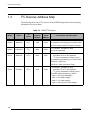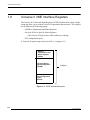
1
USPIIIi Software Manual Version 1.3 — November 2005 Themis Computer—Americas and Pacific Rim 47200 Bayside Parkway Fremont, CA 94538 Phone (510) 252-0870 Fax (510) 490-5529 World Wide Web http://www.themis.com Themis Computer—Rest of World 5 Rue Irene Joliot-Curie 38320 Eybens, France Phone +33 476 14 77 80 Fax +33 476 14 77 89 Copyright © 2005 Themis Computer, Inc. ALL RIGHTS RESERVED. No part of this publication may be reproduced in any form, by photocopy, microfilm, retrieval system, or by any other means now known or hereafter invented without the prior written permission of Themis Computer. The information in this publication has been carefully checked and is believed to be accurate. However, Themis Computer assumes no responsibility for inaccuracies. Themis Computer retains the right to make changes to this publication at any time without prior notice. Themis Computer does not assume any liability arising from the application or use of this publication or the product(s) described herein. RESTRICTED RIGHTS LEGEND: Use, duplication, or disclosure by the United States Government is subject to the restrictions set forth in DFARS 252.227-7013 (c)(1)(ii) and FAR 52.227-19. TRADEMARKS THEMIS® is a registered trademark of Themis Computer, Inc. SOLARIS™ is a trademark of Sun Microsystems SPARC® and UltraSPARC® are registered trademarks of SPARC International All other trademarks or registered trademarks used in this publication are the property of their respective owners. Themis Customer Support North America, South America, and Pacific Rim Telephone: Fax: E-mail: Web Site: USPIIIi Software Manual, Version 1.3 November 2005 Part Number: 110615-023 510-252-0870 510-490-5529 [email protected] http://www.themis.com USPIIIi Software Manual Version Revision History Version 1.3................................................................................... November 2005 • • • • • • • • • • Themis Computer Replaced photo on page ix to reflect new logo (Preface/How to Use This Manual). Changed “will add” to “has added” in the second sentence in Section 2.1, "Themis OBP Commands," on page 2-1 (Chapter 2). Reworded paragraph 2 of Section 2.2, "OBP VME Environment Variables," on page 2-1 (Chapter 2). Added a note to Section 2.2, "OBP VME Environment Variables," on page 2-1, regarding rebooting the system to see modifications to the environment variables (Chapter 2). Corrected the following values in Table 2-1 on page 2-2 and Table 3-2 on page 3-5: vmearbitration mode (from “round-robin” to “round-robin/priority”) and vme32-slave-base from “0–1048576” to “0–4294901760.” Better defined the software used on the USPIIIi in Section 3.1, "Introduction," on page 3-1 (Chapter 3). Revisions to the first paragraph in Section 3.2, "SUN OpenBoot PROM (OBP)," on page 3-1 to include the applicable versions of Sun Solaris and delete references to Wind River VxWorks. Also changed UltraSPARC-IIe to UltraSPARCIIIi (Chapter 3). Updated reference material revision and part numbers in Section 3.2, "SUN OpenBoot PROM (OBP)," on page 3-1 (Chapter 3). Updated Table 3-2 on page 3-5 to match Table 2-1 on page 2-2 (Chapter 3). Changed usp3i.rev1.6 to usp3i.rev3.7 in step 1 of Section 3.2.4, "Updating the System Flash PROM," on page 3-6. iii USPIIIi Software Manual Version Revision History • • • • • • • • • • • • • • • • • • • • • • • iv Deleted Table 3-3 from Section 3.2.5, “Additional OBP Commands” on page 3-8, and referred the reader to Table 2-2 (Chapter 3). Changed “Unix system administrator” to “Themis Technical Support” in the last paragraph of Section 3.2.4, “Updating the System Flash PROM,” on page 3-7 (Chapter 3). Added Section 3.2.4.2, "Updating the System Flash Prom From a SCSI Disk," on page 3-8 (Chapter 3). In the last paragraph of Section 3.2.5.1, "Accessing VME Address Space from OBP," on page 3-9, changed reset command to reset-all, and added the VME select-dev command (Chapter 3). Changed “Sun’s Solstice” to “smosservice and/or smdiskless” in the 2nd to last paragraph on page 3-14 in Section 3.3, “Overview of VME Interface Under Solaris (Chapter 3). Added sections 3.3 through 3.5.5 on pages 3-14 through 3-39 to include the VME program documentation from the USP-2 Programmer’s Guide manual (Chapter 3). Global changed driver names “themvme” to “pcivme” and “sbvmemem” to “vmemem” on pages 3-14 through 3-17 (Chapter 3). Global changed THEMISvme to THEMIS3ivme on pages 3-16 through 3-20 (Chapter 3). Added two paragraphs to the bottom of page 5-3 in Section 5.2, “Thermal Monitoring,” regarding detection of temperature error conditions (Chapter 5). Added 1 sentence to the bottom of page 5-7 in Section 5.2.1, “Setting Temperature Thresholds,” regarding the usp3i_temp -m utility (Chapter 5). Removed references to company-internal infrastructure (tintin) throughout the document. Changed “single-board computer” to “multi-slot VME computer” in the introduction of page ix (Preface). Added a note regarding the look of the “ok” prompt in Section 2.2, "OBP VME Environment Variables," on page 2-1 (Chapter 2). Added footnote b, regarding VME address windows, to Table 2-1 on page 2-2 (Chapter 2). Added a note to Section 2.3, "Additional VME OBP Commands," on page 2-3, regarding OBP commands not available in all versions of OBP. Changed Openboot “3.x” to Openboot “4.x” in Table 2-2 on page 2-3 (Chapter 2). Deleted obsolete commands from Table 2-2 on page 2-3 (Chapter 2). Reworded the note on in Section 3.2.1 “OBP VME Environment Variables” on page 3-2 (Chapter 3). Revised and added text to the last paragraph on page 3-2, regarding different OBP environment variables in different OBP versions (Chapter 3). Deleted the values for the nvramrc environment variable in Table 3-1 on page 3-4 (Chapter 3). Added a reference to the Universe Table 3-2 on page 3-5 (Chapter 3). II VME-to-PCI Bus Bridge User’s Manual after Changed the default value for vme32-slave-size in Table 3-2 on page 3-5 (Chapter 3). Edited and added text to Section 3.2.3.1, "probe-scsi-all," on page 3-6 (Chapter 3). Themis Computer USPIIIi Software Manual • • • • • • • • • • • • • • • • • • • • • • • • Themis Computer Added a new subhead to Section 3.2.4 (3.2.4.1, Updating the System Flash from the Network), and renumbered the subsequent subhead—pages 3-7 and 3-8 (Chapter 3). Added the first sentence in Section 3.2.4.1, stating that the user must have access to a tftp server . . . on page 3-7 (Chapter 3). Made multiple edits to Sections 3.2.4.1 and 3.2.4.2 on pages 3-7 through 3-9 (Chapter 3). Added a note to Section 3.2.5 on page 3-9, regarding OBP commands and versions (Chapter 3). Changed the four Universe II registers (bulleted list) at the top of page 3-10 in Section 3.2.5.1 (Chapter 3). Changed the sample commands (just above the note) on page 3-10 in Section 3.2.5.1 (Chapter 3). Added a note to Section 3.2.5.1 on page 3-10 regarding OBP commands and version (Chapter 3). Deleted the last sentence of the 1st paragraph in Section 3.2.5.2 on page 3-11 (Chapter 3). Added footnote “a” to Table 3-3 on page 3-14 (Chapter 3). Changed multiple occurrences of “Solaris 2.x” to “Solaris” in Chapter 3. Changed SBus to PCI Bus throughout Chapter 3. Added a description of an alternate form of the pkgadd command to Section 3.3.1.2 on page 3-17 (Chapter 3). Revised the fourth paragraph of Section 3.3.1.2 (just before the note) on page 3-17 (Chapter 3). Updated the sample installation log of the VME nexus driver on page 3-18 (Chapter 3). Updated the sample installation log of the sample drivers on page 3-21 (Chapter 3). Updated the sample uninstallation log of sample drivers on page 3-23 (Chapter 3). Deleted explanations of “simpledma” and “testmbi” and added explanations for “sw_reset_n_sysfail” and “sysfail_test” sample drivers, in Section 3.3.4 on page 3-25 (Chapter 3). Added the last sentence to Section 3.4.2 on page 3-27, that reads “The corresponding variables . . .” (Chapter 3). Deleted the 3rd and 4th paragraphs (including the bulleted list) of Section 3.4.3 on page 3-27 (Chapter 3). Deleted the last two paragraphs of Section 3.4.5 on page 3-29 (Chapter 3). Rewrote the last sentence of the last paragraph of Section 3.4.5.1 on page 3-29 (Chapter 3). Changed the reference to “Chapter 8” to “Section 3.3.4” in the 4th paragraph of Section 3.5 on page 3-32 (Chapter 3). Changed the vector values in the 2nd to last paragraph of Section 3.5 (Chapter 3). Edited any mention of the SIGBUS signal in regards to accessing nonexistent address space, in multiple occurrences throughout Chapter 3. v USPIIIi Software Manual Version Revision History • • • • Added two PLD registers to the list on page 4-1: “user-and-boot-device-jumpers” and “RMW-semaphore-and-test” (Chapter 4). Changed 3 occurrences of “System LED” to “Enable LED” in the description of bit 1 under PLD register: offset0x06 on Page 4-6. Enhanced and updated the index. Made assorted minor revisions and grammatical corrections. Version 1.2 ..............................................................................................July 2004 Version 1.1 ................................................................................... December 2003 Version 1.0 .................................................................................. September 2003 vi Themis Computer Table of Contents How to Use This Manual ................................................................................................ xi 1. USPIIIi Programming Guide ....................................................................................... 1-1 1.1 Introduction ............................................................................................................ 1-1 1.2 Jbus Address Map .................................................................................................. 1-2 1.3 I2C Bus Topology .................................................................................................. 1-5 1.4 I2C Devices Address Map ..................................................................................... 1-6 1.5 Ebus Device Address Map ................................................................................... 1-10 1.6 PLD Registers ...................................................................................................... 1-10 1.7 PCI-Ebus Bridge Configuration EEPROM ......................................................... 1-11 1.8 Universe II VME Interface Registers .................................................................. 1-14 2. OBP Commands ............................................................................................................ 2-1 2.1 Themis OBP Commands ....................................................................................... 2-1 2.2 OBP VME Environment Variables ........................................................................ 2-1 2.3 Additional VME OBP Commands ........................................................................ 2-3 3. Themis USPIIIi Software ............................................................................................. 3-1 3.1 Introduction ............................................................................................................ 3-1 3.2 SUN OpenBoot PROM (OBP) .............................................................................. 3-1 3.2.1 OBP VME Environment Variables ............................................................ 3-2 3.2.2 Setting and Reading VME OBP Environment in Hex ............................... 3-6 3.2.3 Support Commands .................................................................................... 3-6 3.2.3.1 probe-scsi-all ............................................................................... 3-6 3.2.4 Updating the System Flash PROM ............................................................ 3-6 3.2.4.1 Updating the System Flash PROM from the Network ............... 3-7 3.2.4.2 Updating the System Flash Prom From a SCSI Disk ................. 3-8 Themis Computer vii USPIIIi Software Manual 3.2.5 viii Additional OBP commands ....................................................................... 3-9 3.2.5.1 Accessing VME Address Space from OBP ................................ 3-9 3.2.5.2 VME Mapping Support under OBP .......................................... 3-11 3.2.5.3 USPIIIi OBP Device aliases ..................................................... 3-13 3.3 Overview of VME Interface Under Solaris ......................................................... 3-15 3.3.1 VMEbus Nexus Driver ............................................................................ 3-16 3.3.1.1 Installing the USPIIIi VME Nexus Driver ............................... 3-17 3.3.1.2 Installing THEMIS3ivme ......................................................... 3-17 3.3.1.3 Removing THEMIS3ivme ........................................................ 3-20 3.3.2 Utility Drivers .......................................................................................... 3-21 3.3.3 Installing the Sample Drivers .................................................................. 3-21 3.3.3.1 Uninstalling the Sample Drivers ............................................... 3-23 3.3.4 Sample VME Programs and VME Leaf Drivers ..................................... 3-24 3.4 Writing Programs for the VMEbus ...................................................................... 3-25 3.4.1 Solaris Device Hierarchy ......................................................................... 3-25 3.4.2 Configuring the Software Interface of USPIIIi ........................................ 3-27 3.4.3 Accessing the VMEbus from OBP .......................................................... 3-27 3.4.4 Accessing the VMEbus from Solaris ....................................................... 3-27 3.4.5 Using Read/Write .................................................................................... 3-27 3.4.5.1 Using mmap .............................................................................. 3-29 3.4.5.2 Slave Mode Access to Another VME Board ............................ 3-29 3.5 Writing VME Device Drivers .............................................................................. 3-32 3.5.1 Probing Devices ....................................................................................... 3-34 3.5.2 Registering Interrupts .............................................................................. 3-35 3.5.3 Allocating DVMA Space ......................................................................... 3-37 3.5.4 Mapping VMEbus Space ......................................................................... 3-39 3.5.5 Driving Devices Without Writing Device Drivers .................................. 3-39 3.5.6 Environmental Monitoring Programs ...................................................... 3-41 usp3i_temp ................................................................................ 3-41 usp3i_voltage ............................................................................ 3-41 usp3i_uled ................................................................................. 3-42 usp3i_pld and plxdrv ................................................................ 3-42 Themis Computer Table of Contents 4. Programmable Logic Device ........................................................................................ 4-1 4.1 PLD Function Upgrade .......................................................................................... 4-1 4.1.1 Examples .................................................................................................... 4-2 4.2 PLD Register Set ................................................................................................... 4-3 4.3 Output from themis-show-pld ................................................................... 4-11 5. Device Monitoring ......................................................................................................... 5-1 5.1 Introduction ............................................................................................................ 5-1 5.2 Thermal Monitoring ............................................................................................... 5-1 5.2.1 Setting Temperature Thresholds ................................................................ 5-4 5.3 Voltage Monitoring ................................................................................................ 5-8 Index....................................................................................................................................... I-1 Themis Computer ix USPIIIi Software Manual List of Figures Figure 1-1 Figure 1-2 Figure 1-3 Figure 3-1 Figure 3-2 Figure 5-1 Figure 5-2 Jbus Address Space Mapping to PCI Configuration Space ............................. 1-4 I2C Bus Topology............................................................................................ 1-5 UCSR Access Mechanism ............................................................................. 1-14 Nexus Driver Directory Structure.................................................................. 3-16 USPIIIi Device Tree ...................................................................................... 3-26 Placement of USPIIIi Device Monitors ........................................................... 5-2 Outputs of the Temperature Sensor Controller................................................ 5-3 List of Tables Table 1-1 Table 1-2 Table 1-3 Table 1-4 Table 1-5 Table 1-6 Table 2-1 Table 2-2 Table 3-1 Table 3-2 Table 3-3 Table 3-4 Table 3-5 Table 3-6 Table 3-7 Table 3-8 Table 3-9 Table 3-10 Table 3-11 Table 5-1 x Jbus ID Assignment ......................................................................................... 1-3 Jbus Address Map ............................................................................................ 1-3 USPIIIi I2C Devices ........................................................................................ 1-6 USPIIIi Ebus Devices .................................................................................... 1-10 EEPROM Addresses and Data ...................................................................... 1-11 Universe II Register Map............................................................................... 1-15 OBP VME Environment Variables.................................................................. 2-2 VME OBP Commands..................................................................................... 2-3 OBP Environment Variables ........................................................................... 3-3 OBP VME Environment Variables.................................................................. 3-5 List of OBP aliases ........................................................................................ 3-14 VMEbus Interrupt Mapping........................................................................... 3-17 vmemem Device Driver................................................................................. 3-21 VME Special Files ......................................................................................... 3-28 Address Space................................................................................................ 3-33 Temperature Monitoring Commands............................................................. 3-41 Voltage Monitoring Command ...................................................................... 3-42 User Status LED Commands ......................................................................... 3-42 PLD Commands............................................................................................. 3-42 Voltages Monitored on the CPU-0 and CPU-1 Boards ................................... 5-8 Themis Computer How to Use This Manual Introduction The Themis Computer USPIIIi is an UltraSPARC-IIIi-based multi-slot VME computer (see photo below) that is SPARC version 9.0 compliant with a VMEbus interface. The software interface for the VMEbus and other on-board peripheral devices is transparently implemented under Solaris. Themis Computer has also developed custom software that enables software programmers to effectively use the powerful features of the VMEbus Interface. Themis Computer xi USPIIIi Software Manual The USPIIIi has a total of 14 models (see Table 1). All models are based on a combination of six different VME boards: the USPIIIi System board, two CPU boards (CPU-0 and CPU-1), the TGA3D/3D+ Graphics board, and two PMC Carrier boards (one with 2 PMC slots and one with 3 PMC slots). In addition, several VME-backplane-connected paddle boards are available for the USPIIIi that provide I/O connections through the P2 backplane connector (for details, see the USPIIIi Hardware Manual [Themis P/N 110615-022]). The USPIIIi Hardware Manual also provides information on the hardware design of the USPIIIi system, including a product overview, OBP commands, device monitoring, connector pinouts, jumper-pin and solder-bead configurations, circuit-board and front-panel diagrams, LED interpretation, and VME-slot configurations. To avoid confusion about the numbering of VME slots in the USPIIIi system (represented in Table 1), Themis Computer offers the following explanation: Note: Although the USPIIIi system may require multiple VME slots, the System Board is considered to be in logical VME slot 1, even though one or two VME slots to the left of the System Board may be physically occupied by CPU-0 and/or CPU-1. xii Themis Computer How to Use This Manual Introduction Table 1. USPIIIi Model Configurations Model /Configuration CPU-1 USPIIIi/1-1 USPIIIi/1-2 Yes USPIIIi/2G-1 USPIIIi/2G-2 Yes USPIIIi/3G2-1 USPIIIi/3G2-2 Yes USPIIIi/3GP2-1 USPIIIi/3GP2-2 Yes USPIIIi/3GP3-1 USPIIIi/3GP3-2 Yes USPIIIi/2P2-1 USPIIIi/2P2-2 Yes USPIIIi/2P3-1 USPIIIi/2P3-2 Themis Computer Yes CPU-0 System Board VME Slot 1 TGA3D/3D+ Graphics Board VME Slot 2 VME Slot 3 PMC Carrier Board (1 only) 2-PMC Slots VME Slot 2 or 3 3-PMC Slots VME Slot 2 or 3 Yes Yes Yes Yes Yes Yes Yes Yes Yes Yes Yes Yes Yes Yes Yes Yes Yes Yes Yes Yes Yes Yes (VME Slot 3) Yes Yes Yes Yes (VME Slot 3) Yes Yes Yes Yes (VME Slot 3) Yes Yes Yes Yes (VME Slot 3) Yes Yes Yes (VME Slot 2) Yes Yes Yes (VME Slot 2) Yes Yes Yes (VME Slot 2) Yes Yes Yes (VME Slot 2) xiii USPIIIi Software Manual Intended Audience The custom software containing programs, documentation, and packaging, is targeted for various software users: • System Administrators who install the software and perform the necessary software configuration. • Users who perform day-to-day operations on USPIIIi systems. • Application programmers who write user-level programs to access the VMEbus interface devices through the built-in VMEbus devices. • System programmers/device-driver writers who develop kernel-level device drivers for VMEbus devices. Some functions overlap one another. The basic concepts required for many of these functions are common. This manual is structured around the basic concepts of using a VMEbus system. In Case Of Difficulties If the USPIIIi does not behave as described or if you encounter difficulties installing or configuring the board, please call Themis Computer technical support at +1 (510) 252-0870, fax your questions to +1 (510) 490-5529, or e-mail to [email protected]. You can also contact us via our web site: http://www.themis.com. UNIX Commands This document may not contain information on basic UNIX® commands and procedures such as shutting down the system, booting the system, and configuring devices. xiv Themis Computer How to Use This Manual See one or more of the following for this information: • Solaris Handbook for Sun Peripherals, which contains SolarisTM software commands • A Practical Guide to Solaris, Copyright 1999, Mark G. Sobell • AnswerBookTM on-line documentation for the Solaris software environment • Other software documentation that you received with your system Shell Prompts In UNIX, the primary method for telling the computer what to do is to type commands at a shell prompt. The following table shows the default prompts for four different Solaris software shells. Shell Prompt C shell machine_name% C shell superuser machine_name# Bourne shell and Korn shell $ Bourne shell and Korn shell superuser # Website Information Themis Computer’s corporate and product information may be accessed on the World Wide Web by browsing the website at http://www.themis.com. Themis Computer xv USPIIIi Software Manual Notes, Cautions, Warnings, and Sidebars The following icons and formatted text are included in this document for the reasons described: A note provides additional information that may be helpful in carrying out a procedure or action. Note: A caution describes a procedure or action that may result in injury to the operator or equipment. This may involve—but is not restricted to—heavy equipment or sharp objects. To reduce the risk, follow the instructions accompanying this symbol. Caution: A warning describes a procedure or action that may cause injury to the operator or equipment as a result of hazardous voltages. To reduce the risk of electrical shock and danger, follow the instructions accompanying this symbol. Warning: A “sidebar” adds detail to the section within which it is placed, but is not absolutely vital to the description or procedure of the section. Sidebar: Your Comments are Welcome We are interested in improving our documentation and welcome your comments and suggestions. You can email your comments to us at [email protected]. Please include the document part number in the subject line of your email. xvi Themis Computer 177 Software Section Chapter USPIIIi Programming Guide 1.1 Introduction This document provides critical information for software programmers who must write the firmware code to control the extra hardware features implemented on the USPIIIi. The native firmware from Sun was modified by Themis to accommodate the topology differences between the Sun reference platform (the Sun Blade 2500 workstation) and the Themis USPIIIi. The following is a list of features implemented on the USPIIIi: • User 8MB flash memory (AMD device AM29LV065D) • TTY C and D ports using the usual SAB 82532 from Infineon (formerly Siemens) • User LED I2C driver • Analog voltage I2C converter • An additional I2C thermal sensor ADM1031 dedicated to the second CPU board temperature monitoring • Dual fiber-channel controller ISP2312 • VME interface based on the Universe-II controller • USPIIIi specific control/status registers implemented into a CY37512 programmable logic device from Cypress • H/W read/modify write (or test and set) semaphores for shared resources Themis Computer 1-1 USPIIIi Software Manual Themis modifications include: • PCI segments topology and its IDsel assignments • Interrupt assignment/mapping, which impacts the Tomatillo initialization • I2C bus topology and its address map • Jbus topology (although it will be transparent to the firmware/software) 1.2 Jbus Address Map The Jbus has several agents. Each has its own Agent ID (JID) number, which is used in the decoding process. The Jbus address space has 43 address bits, or 8 Terabytes of address reach. This space is broken up into two 42-bit physical spaces, one for the memory space (cacheable), the other for the IO space (non-cacheable) . 0x000.0000.0000 Main Memory 4TB includes 16GB for CPU0 cacheable memory space 16GB for CPU1 cacheable memory space 0x400.0000.0000 I/O space 4TB includes Jbus device configuration space PCI address spaces (Cfg/IO/Mem) 0x800.0000.0000 Each agent on Jbus has its own 5-bit Jbus ID. It has 8 MB of non-cacheable address space assigned for its Jbus configuration registers. These 8-MB windows are defined by: • PA[42:41] = 10b • PA[40:28] = 0.0000.0000.0000b • PA[27:23] = JID[4:0] • PA[22:00] = 8MB for Jbus device configuration registers 1-2 Themis Computer 1—USPIIIi Programming Guide Jbus Address Map Table 1-1. Jbus ID Assignment Jbus Agent JID[4..0] Jbus Cfg space Start address End address Size Jalapeno CPU0 0x00 0x400.0000.0000 0X400.007f.ffff 8 MB Jalapeno CPU1 0x01 0x400.0080.0000 0X400.00ff.ffff 8 MB Jalapeno CPU2 0x02 0x400.0100.0000 0X400.017f.ffff 8 MB Jalapeno CPU3 0x03 0x400.0180.0000 0X400.01ff.ffff 8 MB Habaniero 0x08 0x400.0400.0000 0X400.047f.ffff 8 MB Tomatillo 0 (Slave) 0x1c 0x400.0e00.0000 0X400.0e7f.ffff 8 MB Tomatillo 1 (Master) 0x1e 0x400.0f00.0000 0X400.0f7f.ffff 8 MB Each Jbus agent has its own specific Jbus configuration space layout. The table below provides the layout for the Tomatillo. Table 1-2. Jbus Address Map Register Themis Computer add to Jbus cfg base Jbus Tomatillo ID register 0x0000.0000 UPA0 offset base register 0x0040.0000 UPA0 offset mask register 0x0040.0008 UPA1 offset base register 0x0040.0010 UPA1 offset mask register 0x0040.0018 PCI-A memory offset base register 0x0040.0040 PCI-A memory offset mask register 0x0040.0048 PCI-A Cfg offset base register 0x0040.0050 PCI-A Cfg offset mask register 0x0040.0058 PCI-B memory offset base register 0x0040.0060 PCI-B memory offset mask register 0x0040.0068 PCI-B Cfg offset base register 0x0040.0070 PCI-B Cfg offset mask register 0x0040.0078 Tomatillo CSR 0x0041.0000 PCI-A CSR base register 0x0050.0000 PCI-B CSR base register 0x0060.0000 Ichip CSR base register 0x0078.0000 1-3 USPIIIi Software Manual Jbus ADDRESS SPACE 8-byte PCI-A configuration space (16MB) High address High address PCI-A Mem base address PCI-A IO base address 0x100.0000 PCI-A cfg base address Jbus base address of PCI cfg registers on PCI-A segment: bus # Idsel: dev # Function: fct# PCI space base address for Jbus agent JID Fct# x 211 JID x 236 Dev# x 211 0x600.0000.0000 PCI space base address (Hard-coded) Bus# x 216 PCI-A cfg/io offset mask PCI-A cfg/io offset base PCI-A mem offset mask PCI-A mem offset base Low address 0x40.0040 Jbus cfg base address for Jbus agent JID JID x 223 0x400.0000.0000 = Jbus cfg base address (Hard-coded) Low address Figure 1-1. Jbus Address Space Mapping to PCI Configuration Space 1-4 Themis Computer 1—USPIIIi Programming Guide I2C Bus Topology 1.3 I2C Bus Topology The USPIIIi has several I2C busses numbered 1 to 6. Their topology is provided in Figure 1-2. SOUTHBRIDGE M1535D+ XBUS ADM1031 ICS951601 PA: 0x58 VA: 0x58 PA: 0xD2 VA: 0xD2 XBUS to I2C Bridge SYSTEM BOARD Level translator 5V/3.3V 2 I C_1 MEMORY #0 IMAX 87LPC764 I2C_5 I2C_2 PA: 0x12 VA: 0x12 EEPROM AT24LCS52 PA: 0xA0 VA: 0xB6 EEPROM EEPROM EEPROM AT24C64 AT24C64 AT24C64 PA: 0xA2 VA: 0xB8 PA: 0xA4 VA: 0xBA PA: 0xA6 VA: 0xBC MEMORY #1 ADM1031 PA: 0x5C VA: 0x5C CPU #1 I2C_3 EEPROM U12601 AT24C64 EEPROM U12601 AT24C64 EEPROM U12601 AT24C64 ADM1031 PCF8591 PA: 0xA0 VA: 0xC6 PA: 0xA2 VA: 0xC8 PA: 0xA4 VA: 0xCA PA: 0xA6 VA: 0xCC PA: 0x5A VA: 0x5E PA: 0x92 VA: 0x92 CPU #0 EEPROM U12601 AT24C64 I2C_4 TOMATILLO GPIO MASTER I2C_6 EEPROM U12601 AT24C64 PCF8591 PCF8574 PA: 0x90 VA: 0x90 PA: 0x40 VA: 0x40 PA: 0xAE VA: 0xAE Figure 1-2. I2C Bus Topology Themis Computer 1-5 USPIIIi Software Manual 1.4 I2C Devices Address Map The following table lists all I2C devices on the USPIIIi and provides relevant setting information for each of them. Table 1-3. USPIIIi I2C Devices Board Device I2C Bus # HW Physical Address SW Virtual Address I2C Controller with Description I2C controller: PCF8584 on Xbus System ADM1031 I2C_1 0x58 0x58 System ICS951601 I2C_1 0xD2 0xD2 ADM1031 I2C_2 CPU-0 0x5C 0x5C • Temperature monitoring on the system board • Therm output used for the thermal interrupt I2C controller: PCF8584 on Xbus • PCI clock generator I2C controller: PCF8584 on Xbus and IMAX I2C to I2C bus expander; I2C_2 bus is attached to Port #0 of Imax • Temperature monitoring on the CPU-0 board Diode D1 = CPU-0 die Diode D2 = CPU-0 reference Temp1 CPU-0 PCF8591 I2C_4 0x90 0x90 I2C controller: PCF8584 on Xbus and IMAX I2C to I2C bus expander; I2C_4 bus is attached to Port #2 of Imax • DC/DC voltage monitoring on CPU-0 - AIN0 -> VCC (Vme backplane) - AIN1 -> 2.5V (DDR voltage) - AIN2 -> 1.5V (Jbus voltage) - AIN3 -> VCCP0 (CPU-0 core voltage) 1-6 Themis Computer 1—USPIIIi Programming Guide I2C Devices Address Map Table 1-3. USPIIIi I2C Devices (Continued) Board Device CPU-0 PCF8574 I2C Bus # I2C_4 HW Physical Address 0x40 SW Virtual Address 0x40 I2C Controller with Description I2C controller: PCF8584 on Xbus and IMAX I2C to I2C bus expander; I2C_4 bus is attached to Port #2 of Imax • Control of User LEDs - P0 -> User LED 0 - P1 -> User LED 1 - P2 -> User LED 2 - P3 -> User LED 3 - P4 to P7 unassigned CPU-0 AT24C64 CPU-0 MC12430 Memory 0 24LCS52 JIO Master U12601 JIO slave U10601 I2C_2 0xAE 0xAE Pseudo Pseudo 0xA0 0xB6 USPIIIi system parameters stored in EEPROM Jbus clock generator I2C controller: PCF8584 on Xbus and IMAX I2C to I2C bus expander; I2C_2 bus is attached to Port #0 of Imax • DDR DIMM EEPROM SDF (1st DIMM) Memory 0 24LCS52 I2C_2 0xA2 0xB8 I2C controller: PCF8584 on Xbus and IMAX I2C to I2C bus expander; I2C_2 bus is attached to Port #0 of Imax • DDR DIMM EEPROM SDF (2nd DIMM) Memory 0 24LCS52 2 I C_2 0xA4 0xBA I2C controller: PCF8584 on Xbus and IMAX I2C to I2C bus expander; I2C_2 bus is attached to Port #0 of Imax • DDR DIMM EEPROM SDF (3rd DIMM) Memory 0 24LCS52 2 I C_2 0xA6 0xBC I2C controller: PCF8584 on Xbus and IMAX I2C to I2C bus expander; I2C_2 bus is attached to Port #0 of Imax • DDR DIMM EEPROM SDF (4th DIMM) Themis Computer 1-7 USPIIIi Software Manual Table 1-3. USPIIIi I2C Devices (Continued) Board CPU-1 Device ADM1031 I2C Bus # I2C_3 HW Physical Address 0x5A SW Virtual Address 0x5E I2C Controller with Description I2C controller: PCF8584 on Xbus and IMAX I2C to I2C bus expander; I2C_3 bus is attached to Port #1 of Imax • Temperature monitoring on the CPU-1 board Diode D1 = CPU-1 die Diode D2 = CPU-1 reference Temp2 I2C controller: PCF8584 on Xbus and IMAX I2C to I2C bus expander; I2C_3 bus is attached to Port #1 of Imax CPU-1 PCF8591 I2C_3 0x92 0x92 • DC/DC voltage monitoring on CPU-1 - AIN0 -> VCC (VME backplane) - AIN1 -> 2.5V (DDR voltage) - AIN2 -> 1.5V (Jbus voltage) - AIN3 -> VCCP1 (CPU-1 core voltage) Memory 1 24LCS52 I2C_3 0xA0 0xC6 I2C controller: PCF8584 on Xbus and IMAX I2C to I2C bus expander; I2C_3 bus is attached to Port #1 of Imax • DDR DIMM EEPROM SDF (1st DIMM) Memory 1 24LCS52 I2C_3 0xA2 0xC8 I2C controller: PCF8584 on Xbus and IMAX I2C to I2C bus expander; I2C_3 bus is attached to Port #1 of Imax • DDR DIMM EEPROM SDF (2nd DIMM) Memory 1 24LCS52 I2C_3 0xA4 0xCA I2C controller: PCF8584 on Xbus and IMAX I2C to I2C bus expander; I2C_3 bus is attached to Port #1 of Imax • DDR DIMM EEPROM SDF (3rd DIMM) Memory 1 24LCS52 I2C_3 0xA6 0xCC I2C controller: PCF8584 on Xbus and IMAX I2C to I2C bus expander; I2C_3 bus is attached to Port #1 of Imax • DDR DIMM EEPROM SDF (4th DIMM) 1-8 Themis Computer 1—USPIIIi Programming Guide I2C Devices Address Map The I2C to I2C bridge expander (IMAX) is a microcontroller located on the CPU0 board. This bridge expander fans out the main primary I2C bus (called I2C_1 in this document) in four secondary I2C busses called I2C_2 to I2C_5. Those I2C busses are attached to Port 0 to 3 respectively of the IMAX bridge. The IMAX is itself an I2C device, programmed by OBP through the Xbus-to-I2C bridge controlled by the Southbridge ASIC on the system board. (see I2C bus topology in Figure 1-2 on page 1-5). The I2C address of the IMAX is 0x12. All the programming details are provided by Sun into two documents. Those documents are: • imax_code.pdf • imax_info.pdf (the most relevant for the firmware programmer) Because of the change on the I2C topology and the additional devices, the address filter bitmap, the routing table and the address translation page table in the Imax must be modified at the OBP level. Themis Computer 1-9 USPIIIi Software Manual 1.5 Ebus Device Address Map Table 1-4 lists all the USPIIIi devices located on the Ebus, and provides relevant information for each of them. The Ebus controller is the PLX9030, which bridges the PCI-2A-33Mhz bus (Boot PCI bus) to the Ebus peripheral bus. Table 1-4. USPIIIi Ebus Devices Device Board • Part Number • Reference Des. Address Size Flash 8Mx8 System • AMD29LV065 • U4701 User Flash - AMD29LV065 0x80.0000 • SAB82532 • U1101 8-bit bus implementation 0x80 • CY37512 • U3901 Implements TTY ports C&D Attached to CS2 of the PLX9030 Cypress PLD PLD Cypress System 8MBytes Attached to CS0 of the PLX9030 Serial controller System Description 0x100 Implements miscellaneous registers Attached to CS3 of the PLX9030 The base address of each device will be assigned by OBP during the PCI probing process. Size information is located in the EEPROM configuration device attached to the PLX9030. The AMD 29LV065 programming algorithm is fully described in the datasheet of this component. 1.6 PLD Registers The various registers of the Cypress Programmable Logic Device (PLD or CPLD) are used to control many different functions of the USPIIIi. [See Chapter 4, "Programmable Logic Device", for a full description of the PLD registers.] 1-10 Themis Computer 1—USPIIIi Programming Guide PCI-Ebus Bridge Configuration EEPROM 1.7 PCI-Ebus Bridge Configuration EEPROM The Ebus is controlled by the PLX PCI9030 bridge from PLX technology. The PCI configuration registers can be downloaded after reset from a non-volatile memory EEPROM companion device. The EEPROM contains the information that is specific to our implementation. When the EEPROM is not present or is blank, the PCI9030 ASIC will automatically set the PCI configuration registers to their default values. It is then possible to program from the PCI bus. Utility functions are available under OBP to program and/or reprogram the content of the EEPROM for the initialization phase of the product. Utility functions are also available to fix on-site issues without having to return the board to manufacturing for upgrade. Table 1-5. EEPROM Addresses and Data EEPROM Address Themis Computer EEPROM Data Comments 0x00 0x9030 PCI device ID 0x02 0x10B5 PCI Vendor ID 0x04 0xCA90 0x06 0x0000 0x08 0x0680 0x0A 0x0000 0x0C 0x0000 0x0E 0x0000 0x10 0x0000 0x12 0x0040 0x14 0x0000 0x16 0x0100 0x18 0x4801 0x1A 0x4801 0x1C 0x0000 0x1E 0x0000 The Rev ID should match the original rev ID. 1-11 USPIIIi Software Manual Table 1-5. EEPROM Addresses and Data (Continued) EEPROM Address 1-12 EEPROM Data Comments 0x20 0x0000 0x22 0x4c06 0x24 0x0000 0x26 0x0003 0x28 0x0F80 LAS0RR for User flash 0x2A 0x0000 8 Mbytes, memory space, No prefetch 0x2C 0x0000 LAS1RR not assigned 0x2E 0x0000 0x30 0x0FFF LAS2RR for TTY C/D 0x32 0xFF81 128 Bytes, IO space. 0x34 0x0FFF LAS3RR for PLD registers 0x36 0xFF01 256 Bytes, IO space. 0x38 0x0000 0x3A 0x0000 0x3C 0x0000 0x3E 0x0001 0x40 0x0000 0x42 0x0000 0x44 0x0000 0x46 0x0001 0x48 0x0000 0x4A 0x0001 0x4C 0x0000 0x4E 0x0000 0x50 0x5431 Enable Cs0 space address decoding on PCI Disable Cs1 space address decoding on PCI Enable Cs2 space address decoding on PCI Enable Cs3 space address decoding on PCI Themis Computer 1—USPIIIi Programming Guide PCI-Ebus Bridge Configuration EEPROM Table 1-5. EEPROM Addresses and Data (Continued) EEPROM Address Themis Computer EEPROM Data 0x52 0xB8C0 0x54 0x0000 0x56 0x0000 0x58 0x5431 0x5A 0xB8C0 0x5C 0x5431 0x5E 0xB8C0 0x60 0x0000 0x62 0x0000 0x64 0x0080 0x66 0x0001 0x68 0x0000 0x6A 0x0000 0x6C 0x0000 0x6E 0x0081 0x70 0x0000 0x72 0x0101 0x74 0x0030 0x76 0x0040 0x78 0x0078 0x7A 0x0000 0x7C 0x0024 0x7E 0x9240 Comments 1-13 USPIIIi Software Manual 1.8 Universe II VME Interface Registers The Universe II Control and Status Registers (UCSR) facilitate host system configuration and allow you to control Universe II operational characteristics. The registers are divided into the following groups: • VMEbus Configuration and Status Registers • Universe II Device Specific Status Registers —The Universe II registers have little-endian byte-ordering • PCI Configuration Space A Universe-II register map is shown in Table 1-6 on page 1-15. VMEbus Configuration and Status registers (VCSR) Universe Device Specific Registers (UDSR) 4 KBytes PCI Configuration space (PCICS) Figure 1-3. UCSR Access Mechanism 1-14 Themis Computer 1—USPIIIi Programming Guide Universe II VME Interface Registers Table 1-6. Universe II Register Map Offset 000 004 Register PCI Configuration Space ID Register PCI Configuration Space Control and Status Register Name PCI_ID PCI_CSR 008 PCI Configuration Class Register PCI_CLASS 00C PCI Configuration Miscellaneous 0 Register PCI_MISC0 010 PCI Configuration Base Address 0 Register PCI_BS0 014 PCI Configuration Base Address 1 Register PCI_BS1 018-024 PCI Unimplemented 028 PCI Reserved 02C PCI Reserved 030 PCI Unimplemented 034 PCI Reserved 038 PCI Reserved 03C PCI Configuration Miscellaneous 1 Register PCI_MISC1 040-0FF PCI Unimplemented 100 PCI Target Image 0 Control Register LSI0_CTL 104 PCI Target Image 0 Base Address Register LSI0_BS 108 PCI Target Image 0 Bound Address Register LSI0_BD 10C PCI Target Image 0 Translation Offset Register LSI0_TO 110 Reserved 114 PCI Target Image 1 Control Register LSI1_CTL 118 PCI Target Image 1 Base Address Register LSI1_BS 11C PCI Target Image 1 Bound Address Register LSI1_BD 120 PCI Target Image 1 Translation Offset Register LSI1_TO 124 Reserved 128 PCI Target Image 2 Control Register LSI2_CTL 12C PCI Target Image 2 Base Address Register LSI2_BS Themis Computer PCI_MISC1 1-15 USPIIIi Software Manual Table 1-6. Universe II Register Map (Continued) Offset 1-16 Register Name 130 PCI Target Image 2 Bound Address Register LSI2_BD 134 PCI Target Image 2 Translation Offset Register LSI2_TO 138 Reserved 13C PCI Target Image 3 Control Register LSI3_CTL 140 PCI Target Image 3 Base Address Register LSI3_BS 144 PCI Target Image 3 Bound Address Register LSI3_BD 148 PCI Target Image 3 Translation Offset Register LSI3_TO 14C-16C Reserved 170 Special Cycle Control Register 174 Special Cycle PCI Bus Address Register 178 Special Cycle Swap/Compare Enable Register 17C Special Cycle Compare Data Register SCYC_CMP 180 Special Cycle Swap Data Register SCYC_SWP 184 PCI Miscellaneous Register 188 Special PCI Target Image Register SLSI 18C PCI Command Error Log Register L_CMDERR 190 PCI Address Error Log Register 194-19C Reserved 1A0 PCI Target Image 4 Control Register LSI4_CTL 1A4 PCI Target Image 4 Base Address Register LSI4_BS 1A8 PCI Target Image 4 Bound Address Register LSI4_BD 1AC PCI Target Image 4 Translation Offset Register LSI4_TO 1B0 Reserved 1B4 PCI Target Image 5 Control Register LSI5_CTL 1B8 PCI Target Image 5 Base Address Register LSI5_BS 1BC PCI Target Image 5 Bound Address Register LSI5_BD 1C0 PCI Target Image 5 Translation Offset Register LSI5_TO SCYC_CTL SCYC_ADDR SCYC_EN LMISC LAERR Themis Computer 1—USPIIIi Programming Guide Universe II VME Interface Registers Table 1-6. Universe II Register Map (Continued) Offset Register Name 1C4 Reserved 1C8 PCI Target Image 6 Control Register LSI6_CTL 1CC PCI Target Image 6 Base Address Register LSI6_BS 1D0 PCI Target Image 6 Bound Address Register LSI6_BD 1D4 PCI Target Image 6 Translation Offset Register LSI6_TO 1D8 Reserved 1DC PCI Target Image 7 Control Register LSI7_CTL 1E0 PCI Target Image 7 Base Address Register LSI7_BS 1E4 PCI Target Image 7 Bound Address Register LSI7_BD 1E8 PCI Target Image 7 Translation Offset Register LSI7_TO 1EC-1FC Reserved 200 DMA Transfer Control Register DCTL 204 DMA Transfer Byte Count Register DTBC 208 DMA PCI Bus Address Register 20C Reserved 210 DMA VMEbus Address Register 214 Reserved 218 DMA Command Packet Pointer Register 21C Reserved 220 DMA General Control and Status Register DGCS 224 DMA Linked List Update Enable Register D_LLUE 228-2FC Reserved 300 PCI Interrupt ENABLE Register 304 PCI Interrupt Status Register LINT_STAT 308 PCI Interrupt Map 0 Register LINT_MAP0 30C PCI Interrupt Map 1 Register LINT_MAP1 Themis Computer DLA DVA DCPP LINT_EN 1-17 USPIIIi Software Manual Table 1-6. Universe II Register Map (Continued) Offset 1-18 Register Name 320 Interrupt Status/ID Out Register STATID 324 VIRQ1 STATUS/ID Register V1_STATID 328 VIRQ2 STATUS/ID Register V2_STATID 32C VIRQ3 STATUS/ID Register V3_STATID 330 VIRQ4 STATUS/ID Register V4_STATID 334 VIRQ5 STATUS/ID Register V5_STATID 338 VIRQ6 STATUS/ID Register V6_STATID 33C VIRQ7 STATUS/ID Register V7_STATID 340 PCI Interrupt Map 2 Register LINT_MAP2 344 VME Interrupt Map 1 Register VINT_MAP2 348 Mailbox 0 Register MBOX0 34C Mailbox 1 Register MBOX1 350 Mailbox 2 Register MBOX2 354 Mailbox 3 Register MBOX3 358 Semaphore 0 Register SEMA0 35C Semaphore 1 Register SEMA1 360-3FC Reserved 400 Master Control Register MAST_CTL 404 Miscellaneous Control Register MISC_CTL 408 Miscellaneous Status Register MISC_STAT 40C User AM Codes Register 410-EFC Reserved F00 VMEbus Slave Image 0 Control Register VSI0_CTL F04 VMEbus Slave Image 0 Base Address Register VSI0_BS F08 VMEbus Slave Image 0 bound Address Register VSI0_BD F0C VMEbus Slave Image 0 Translation Offset Register VSI0_TO USER_AM Themis Computer 1—USPIIIi Programming Guide Universe II VME Interface Registers Table 1-6. Universe II Register Map (Continued) Offset Register Name F10 Reserved F14 VMEbus Slave Image 1 Control Register VSI1_CTL F18 VMEbus Slave Image 1 Bound Address Register VSI1_BS F1C VMEbus Slave Image 1 Bound Address Register VSI1_BD F20 VMEbus Slave Image 1 Translation Offset Register VSI1_TO F24 Reserved F28 VMEbus Slave Image 2 Control Register VSI2_CTL F2C VMEbus Slave Image 2 Bound Address Register VSI2_BS F30 VMEbus Slave Image 2 Bound Address Register VSI2_BD F34 VMEbus Slave Image 2 Translation Offset Register VSI2_TO F38 Reserved F3C VMEbus Slave Image 3 Control Register VSI3_CTL F40 VMEbus Slave Image 3 Bound Address Register VSI3_BS F44 VMEbus Slave Image 3 Bound Address Register VSI3_BD F48 VMEbus Slave Image 3 Translation Offset Register VSI3_TO F4C-F60 Reserved F64 Location Monitor Control Register LM_CTL F68 Location Monitor Base Address Register LM_BS F6C Reserved F70 VMEbus Register Access Image Control Register F74 VMEbus Register Access Image Base Address Register F78 Reserved F7C Reserved F80 VMEbus CSR Control Register VCSR_CTL F84 VMEbus CSR Translation Offset Register VSCR_TO F88 VMEbus AM Code Error Log Register V_AMERR Themis Computer VRAI_CTL VRAI-BS 1-19 USPIIIi Software Manual Table 1-6. Universe II Register Map (Continued) Offset 1-20 Register Name F8C VMEbus Address Error Log Register VAERR F90 VMEbus Slave Image 4 Control Register VSI4_CTL F94 VMEbus Slave Image 4 Bound Address Register VSI4_BS F98 VMEbus Slave Image 4 Bound Address Register VSI4_BD F9C VMEbus Slave Image 4 Translation Offset Register VSI4_TO FA0 Reserved FA4 VMEbus Slave Image 5 Control Register VSI5_CTL FA8 VMEbus Slave Image 5 Bound Address Register VSI5_BS FAC VMEbus Slave Image 5 Bound Address Register VSI5_BD FB0 VMEbus Slave Image 5 Translation Offset Register VSI5_TO FB4 Reserved FB8 VMEbus Slave Image 6 Control Register VSI6_CTL FBC VMEbus Slave Image 6 Bound Address Register VSI6_BS FC0 VMEbus Slave Image 6 Bound Address Register VSI6_BD FC4 VMEbus Slave Image 6 Translation Offset Register VSI6_TO FC8 Reserved FCC VMEbus Slave Image 7 Control Register VSI7_CTL FD0 VMEbus Slave Image 7 Bound Address Register VSI7_BS FD4 VMEbus Slave Image 7 Bound Address Register VSI7_BD FD8 VMEbus Slave Image 7 Translation Offset Register VSI7_TO FDC-FEC Reserved FF0 VME CR/CSR Reserved FF4 VMEbus CSR Bit Clear Register VCSR_CLR FF8 VMEbus CSR Bit Set Register VCSR_SET FFC VMEbus CSR Address Register VCSR_BS Themis Computer 2 Software Section Chapter OBP Commands 2.1 Themis OBP Commands The USPIIIi incorporates Sun's standard OBP version 4.x as the default firmware. Themis has added specific OBP functions to support the additional Fibre Channel and VME functions. The VME commands are summarized in the remaining sections of this chapter. 2.2 OBP VME Environment Variables The environment variables (see Table 2-1 on page 2-2) may be set at the “ok” prompt in OBP by using the setenv command: Note: The “ok” prompt appears differently for different systems. For example, on a single-processor system, the prompt appears as “ok.” However, on a system with two CPUs (such as the UltraSPARC), the prompt may be designated as “{0} ok” or “{1} ok.” For the purposes of this manual, future references to the “ok” prompt, will be designated, simply, as “ok.” ok setenv variable_name value When running Solaris, the eeprom command can view or modify environment variables (the syntax may vary depending on the type of command-line shell being used): # Themis Computer eeprom variable_name=value 2-1 USPIIIi Hardware Manual Note: Modified environment variables will not take effect until you reboot the system. There are a number of ways to reboot the system. For example, you can execute the OBP command reset-all or you can recycle power. From within Solaris, execute the reboot command to shut down the operating system and then reboot. Table 2-1. OBP VME Environment Variablesa Variable Name Value Default Value Description force-system-controller true/false false If set to “true”, Universe II is forced to be the system controller. If set to false, the system-controller status is determined by auto-sensing circuitry. vme-bus-request-level 0–7 0 vme-request-mode fair/demand fair When the Universe II requests the VME bus, it can use either “fair” or “demand” mode. vme-release-mode ror/rwd ror When the Universe II releases the VME bus, it can use either “ror” (release on request) or “rwd” (release when done). round-robin/priority round-robin Arbitration mode used if the USPIIIi is the system controller. 1, 2, 3, 4, 5, 6 1, 2, 3, 4, 5, 6 VME bus interrupt level to be serviced by the VME leaf driver. vme-arbitration-mode vme-irq-to-service Level used to request the VME bus. vme32-master-base 0–4294967295 0 Defines a master window on VME. All subsequent VME mappings that fall within this window will use this window instead of allocating one of the remaining Universe II register sets to define a new window. The best use of this master window is to define it to encompass all other VME device addresses (if possible) that will be accessed by the USPIIIi. vme32-master-size 0–4294967295 0 Size of the master VME-bus address window. Must be less than 1.2 GB. 24, 32 32 If 32 (decimal) is used, space is A32D32. If 24 (decimal) is used, space is A24D32. vme32-slave-base 0–4294901760 1048576 vme32-slave-size 0–4294967295 4294967295 vme24-slave-base 0–16777216 0 vme24-slave-size 0–16777216 16777216 vme32-master-mode Slave window base address in A32 modeb. Slave window size in A32 modeb. Slave window base address in A24 mode. Slave window size in A24 mode. a. Numerical values are decimal. b. To avoid self-reference, the VME address window defined by vme32-slave-base and vme32-slave-size should not overlap the VME addresss window defined by vme32-master-base and vme32-master-size. 2-2 Themis Computer 2—OBP Commands Additional VME OBP Commands 2.3 Additional VME OBP Commands The following table describes a list of OBP commands that are accessible when the current node is VME. To set the current node to VME, execute the OBP command “vme select-dev”. Note: Some versions of OBP do not employ the “vme selelct-dev” command. If this command does not work on your system, use the command: “cd /pci@1e,600000/THEMIS,pcivme”. Table 2-2. VME OBP Commands Command Themis Computer Description show-universe-regs Reads and displays all the Universe II registers. <offset> universe-reg@ Reads and places on the OBP stack, the Universe II register content located at offset <offset> from the Universe II base address (Consult the Sun OpenBoot 4.x Command Reference for instructions on displaying stack contents; for example, the command showstack.) <offset> universe-reg@ . Reads and displays the Universe II register contents located at offset <offset> from the Universe II base address. <data> <offset> universe-reg! Writes the value <data> into the Universe II register located at offset <offset> from the Universe II base address. 2-3 USPIIIi Hardware Manual 2-4 Themis Computer Software Section Chapter 311 Themis USPIIIi Software 3.1 Introduction This chapter describes the software used on the Themis USPIIIi. This includes the OBP firmware, Sun Solaris 8 2/04, Sun Solaris 9 4/04 or later, or Sun Solaris 10 Operating Systems. The default firmware is Sun’s Open Boot Prom (OBP) that has been modified to support VME. OBP will boot the Solaris operating system. 3.2 SUN OpenBoot PROM (OBP) The Themis USPIIIi OBP is based on OBP 4.x from Sun. Themis has added several OBP command extensions that are specific to the USPIIIi. All other OBP commands are the same as the Sun UltraSPARC-IIIi Platform (as implemented in the Sun Blade 2500 workstation). Specific details of the OBP architecture are defined in the IEEE 1275 specification document. Reference materials that describe the OBP include: • OpenBoot 4.x Command Reference—Sun Part Number: 816-1177-10 • OpenBoot Quick Reference 3.x—Sun Part Number: 806-2908-10 • Writing FCode 3.x Programs—Sun Part Number: 806-1379-10 Themis Computer 3-1 USPIIIi Software Manual 3.2.1 OBP VME Environment Variables The environment variables (see Table 3-1 below and Table 3-2 on page 3-5) may be set at the ok prompt in OBP by using the setenv command. ok setenv variable_name value when running Solaris with the command line (the syntax may vary depending on the shell used): # eeprom variable_name=value A board RESET is required for the new values to take effect. In OBP all values are in decimal form, so you would enter the command as follows: eeprom vme32-slave-size=0x800000. However, this can be inconvenient when dealing with values that are better represented in hexadecimal, such as VME addresses. Refer to Section 3.2.2, "Setting and Reading VME OBP Environment in Hex," on page 3-6 for instructions on how to easily use hexadecimal numbers in the command line. Note: The Solaris command line will accept hexadecimal values if they are preceded by 0x. From within Solaris type the command as follows: eeprom vme32-slave-size=8388608. Table 3-1 shows an example of the results of the printenv command. Your results might show more or less environment variables, depending on what version of OBP you have. 3-2 Themis Computer 3—Themis USPIIIi Software SUN OpenBoot PROM (OBP) Table 3-1. OBP Environment Variables {1} ok printenv Variable Name Value Default Value themis-switch-value 255 255 force-system-controller false false vme-bus-request-level 0 0 vme-request-mode fair fair vme-release-mode ror ror vme-arbitration-mode round-robin round-robin vme-irq-to-service 1,2,3,4,5,6 1,2,3,4,5,6 vme32-master-base 0 0 vme32-master-size 0 0 vme32-master-mode 32 32 vme32-slave-base 1048576 1048576 vme32-slave-size 4294967295 4294967295 vme24-slave-base 0 0 Variable Name Value Default Value vme24-slave-size 16777216 16777216 extra-64m-segments 1 1 vme-init 3735928559 3735928559 themis-cpu-count 2 2 test-args diag-passes 1 1 therm-reset-hold disabled disabled audio-device? disabled disabled system-low-limit 0 0 system-therm-limit 110 80 system-high-limit 100 70 cpu1-low-limit 5 5 cpu1-therm-limit 115 115 cpu1-high-limit 105 105 cpu0-low-limit 5 5 cpu0-therm-limit 115 115 cpu0-high-limit 105 105 local-mac-address? true true fcode-debug? false false silent-mode? false false scsi-initiator-id 7 7 Themis Computer 3-3 USPIIIi Software Manual Table 3-1. OBP Environment Variables (Continued) oem-logo oem-logo? No default false oem-banner false No default oem-banner? false false ansi-terminal? true true screen-#columns 80 80 screen-#rows 34 34 ttyb-rts-dtr-off false false ttyb-ignore-cd true true ttya-rts-dtr-off false false ttya-ignore-cd true true Variable Name Value Default Value ttyb-mode 9600,8,n,1,- 9600,8,n,1,- ttya-mode 9600,8,n,1,- 9600,8,n,1,- output-device screen screen input-device keyboard keyboard auto-boot-on-error? false false load-base 16384 16384 auto-boot? false true boot-command boot boot diag-file kadb -rv diag-device /pci@1d,700000/scsi@4/di ... net boot-file boot-device disk:a disk5 disk net use-nvramrc? false false none No default nvramrc security-mode security-password No default security-#badlogins 0 No default diag-script none none diag-level min max diag-switch? true false error-reset-recovery boot boot {1} ok 3-4 Themis Computer 3—Themis USPIIIi Software SUN OpenBoot PROM (OBP) Table 3-2. OBP VME Environment Variablesa Name Value Default Value Description If set to “true”, Universe II is forced to be the system controller. If set to false, the system-controller status is determined by auto-sensing circuitry. force-system-controller true/false false vme-bus-request-level 0–7 0 vme-request-mode fair/demand fair When the Universe II requests the VME bus, it can use either “fair” or “demand” mode. vme-release-mode ror/rwd ror When the Universe II releases the VME bus, it can use either “ror” (release on request) or “rwd” (release when done). round-robin/priority round-robin Arbitration mode used if the USPIIIi is the system controller. 1, 2, 3, 4, 5, 6 1, 2, 3, 4, 5, 6 VME bus interrupt level to be serviced by the VME leaf driver. vme-arbitration-mode vme-irq-to-service Level used to request the VME bus. vme32-master-base 0–4294967295 0 Defines a master window on VME. All subsequent VME mappings that fall within this window will use this window instead of allocating one of the remaining Universe II register sets to define a new window. The best use of this master window is to define it to encompass all other VME device addresses (if possible) that will be accessed by the USPIIIi. vme32-master-size 0–4294967295 0 Size of the master VME-bus address window. Must be less than 1.2 GB. 24, 32 32 If 32 (decimal) is used, space is A32D32. If 24 (decimal) is used, space is A24D32. vme32-slave-base 0–4294901760 1048576 Slave window base address in A32 mode. vme32-slave-size 0–16777216 16777216 Slave window size in A32 mode. vme24-slave-base 0–16777216 0 vme24-slave-size 0–16777216 16777216 vme32-master-mode Slave window base address in A24 mode. Slave window size in A24 mode. a—Numerical values are decimal. For a more detailed description of the VME values, refer to the Universe II VME-toPCI Bus Bridge User’s Manual (P/N 80A3010_MA001_03), available from Tundra Semiconductor Corporation. Themis Computer 3-5 USPIIIi Software Manual 3.2.2 Setting and Reading VME OBP Environment in Hex Because an OBP environment variable is an integer, commands like setenv or printenv use the integer format. This makes setting the base address and base size awkward. To use hex number format, enter general variables to set and read address and base. For example, ok 200000 to vme24-slave-size and ok vme24-slave size .h 3.2.3 Support Commands 3.2.3.1 probe-scsi-all The command probe-scsi-all probes the first SCSI bus (SCSI A), the second SCSI bus (SCSI B), and the two FC-AL ports. This command behaves in a similar fashion to the standard OBP command probe-scsi. Probing FC-AL ports that are not connected to an FC-AL drive and do not have loopback connectors installed, will result in an “Link not ready – Loss of Sync” error message. Note: 3.2.4 Updating the System Flash PROM Great care must be taken when performing a Flash upgrade. If an invalid or corrupted PROM file was downloaded, or if you experience a power outage during the process, the USPIIIi may not be bootable. DO NOT interrupt the command while it is in progress. Warning: 3-6 Themis Computer 3—Themis USPIIIi Software SUN OpenBoot PROM (OBP) 3.2.4.1 Updating the System Flash PROM from the Network To update the system flash PROM from the network, you will need to have access to a tftpboot server. To update the system flash PROM device: 1. First download the OBP image from the tftpboot server. To do this, type 4000 dload obpimage-file For example, {1} ok 4000 dload usp3i.rev3.7 Boot device: /pci@1f,700000/network@2:,usp3i.rev3.7 File and args: 1000 Mbps full-duplex Timeout waiting for ARP/RARP packet 104000 Server IP address: 198.211.242.2 Client IP address: 198.211.242.62 2. Next, type the flash-update command to write the OBP image to the flash {1} ok flash-update which results in: Update flash with the downloaded OBP image Erasing ... done Copying .. Verifying .. This command writes the previously downloaded obp image file to flash. It is best to update your flash PROM directly after resetting the system. Call your Themis Technical Support in case of problems. Themis Computer 3-7 USPIIIi Software Manual 3.2.4.2 Updating the System Flash Prom From a SCSI Disk When your system powers up, make sure it boots to the "ok" OBP prompt and then STOPS! It may be necessary for you to temporarily set the OBP variable "auto-boot?" to false, to prevent Solaris from automatically booting. The flashupdate command described below will only work after a fresh power-up to the "ok" prompt. Flash-update will not work if you perform a STOP-A or Ctrl-Break key combination to interrupt the power-on self-test Solaris boot process. Nor will it work if Solaris is already running and you issue a "halt" or "init 0" command to arrive at the "ok" prompt. Note: To update the system flash PROM device using a SCSI disk: 1. Download the most recent OBP binary image file from the Themis ftp server. Call Themis Customer Support at 510-252-0870 to obtain a user name and password that will allow you to access the Themis ftp server. To find the OBP image file on the Themis ftp server, navigate through the subdirectories (or folders) as follows: outgoing→Release→obp→USPIIIi→(select the folder with the appropriate rev. e.g., rev3.7)→(select the binary file with the appropriate name, e.g., 111068-080-usp3i_obp_revx.x_chk_5891.bin). 2. Copy the OBP image file to the root directory of the primary SCSI disk. This procedure assumes that Solaris is already installed on the disk and was used to copy the OBP file to the root directory. 3. Make sure that "auto-boot?" is set to false, then shut down Solaris and power the USPIIIi off and on again. At the “ok” prompt, issue the following commands: 4. ok load no-such-file Boot device: /pci@1d,700000/scsi@4/disk@0,0 File and args:no-such-file 5. ok go Boot: cannot open no-such-file Enter filename[no-such-file] 6. Send a break key-combination (see note, below). Type ‘go’ to resume. 3-8 Themis Computer 3—Themis USPIIIi Software SUN OpenBoot PROM (OBP) The easiest way to send a break key-combination is to press STOP-A from a Sun keyboard, CTRL-Break from a PS/2 keyboard, or CTRL-Break from a HyperTerminal on a Windows XP desktop PC. If you are connected to the USPIIIi via TTYA, the method for sending a break character is dependent on the terminal or terminal-emulator software you are using. And, in fact, some versions of OBP will not accept a break event from the TTYA connection. Note: 7. ok load disk:,|usp3i.rev3.7 8. Next type the flash-update command to write the OBP image to the flash: ok flash-update 3.2.5 Additional OBP commands To view a list of OBP commands that are accessible when the current node is VME, refer to Table 2-2 on page 2-3. To set the current node to VME, execute the OBP command: “vme select-dev” Some versions of OBP do not employ the “vme selelct-dev” command. If this command does not work on your system, use the command: “cd /pci@1e,600000/THEMIS,pcivme”. Note: 3.2.5.1 Accessing VME Address Space from OBP Prior to actually accessing VME from OBP, you need to make sure that the Universe II PCI target images are set correctly. A PCI target image is actually a window from PCI Bus to VMEbus. Each image or window defines a contiguous range of PCI addresses (base address and size). When a PCI cycle is issued by the USPIIIi CPU with an address falling inside a particular window address range, the Universe II will propagate that cycle to the VME. The VME cycle will be formed according to the attributes defined in the window registers: • VME address • VME Address modifier (Please refer to the Universe II User's Manual for details.) The Themis OBP command show-universe-regs can be used to view the settings of the 8 address windows. Each window is controlled by four Universe II registers: Themis Computer 3-9 USPIIIi Software Manual • • • • LSx_CTL: control register LSx_BS: PCI base address of the window LSx_BD: PCI bound address of the window LSx_TO: Translation register Suppose we want to access VME A32:0xaa00.0000: ok aa00.0000 to vme32-master-base ok 1000.0000 to vme32-master-size ok reset-all ..... ok vme select-dev ok show-universe-regs Some versions of OBP do not employ the “vme selelct-dev” command. If this command does not work on your system, use the command: “cd /pci@1e,600000/THEMIS,pcivme”. Note: By carefully reviewing the output of the show-universe-regs command, we see that the mapping we defined using the vme32-master-base and vme32-master-size Themis OBP variables is controlled by the 7th window (LS7_CTL, LS7_BS, LS7_BD, LS7_TO). The LS7_BS register contains the base PCI address of that window (should be 0x800.0000). Now we can access VME using the OBP space command, which permits us to use physical addresses by bypassing the CPU MMU: ok 1234 1ff.0800.0000 15 spacel! (writes 1234 to VME address A32:0xaa00.0000) ok 1ff.0800.0000 15 spacel? (reads back from that address) 0x1ff.0000.0000 is the base address of the PCI bus through which VME is accessed. 0x15 is the SPARC ASI (address space identifier) that is defined for PCI accesses. 3-10 Themis Computer 3—Themis USPIIIi Software SUN OpenBoot PROM (OBP) The above VME accesses were made using the 0x09 Address modifier code. This could be a problem when trying to access other VME boards (like the Themis USPIIIi-1v, since it is programmed to accept supervisor address modifiers). To set the address modifier to be 0x0d (supervisor), simply enter: Note: ok 1dc universe-reg@ 1000 or 1dc universe-reg! This will set the SUPER bit in LSI7_CTL. That was for A32 VME accesses. These accesses are done using the 8 PCI target image windows. For A24 and A16 accesses a special Universe II window is used: the special PCI target image. The mechanism is the same as for A32 accesses. Please refer to the Universe II User's Manual for details. 3.2.5.2 VME Mapping Support under OBP Due to the design of Tomatillo, whenever a non-existing VME location is accessed, a parity-error is recorded within Tomatillo that causes OBP to fail in the family of peek and poke (cpeek, wpeek, lpeek, cpoke, wpoke, and lpoke). To circumvent this problem, OBP has been enhanced to use the DMA engine inside the Universe chip to do the peek and poke so that both can still work in the OBP. Because peek and poke use virtual addresses, map-in and map-out commands have been enhanced to track the mapping to the VME Bus; hence the operations of peek, poke, memory access, etc., are transparent to the user. Thus, the syntax in the OBP reference manual has been preserved in the Themis USPIIIi VME node. To help you read the mapping, the following symbols are defined: 7d 6d 3d 2d 4d 0d Themis Computer value value value value value value A24D32 A16D32 A24D16 A16D16 A32D32 A32D16 3-11 USPIIIi Software Manual Examples: \ To test a register in VME A32D32 space. showstack a000.0000 A32D32 1000.0000 map-in value a32va a32va 100 + value register-a register-a map? 1234.5678 register-a lpoke register-a lpeek register-a l? a32va 0040.0000 map-out \ !!! Required after OBP testing is done. \ To test a register in VME A24D16 space. showstack a0.0000 A24D16 10.0000 map-in value a24va a24va 100 + value register-b register-b map? 1234 register-b wpoke register-b wpeek register-b w? a24va 10.0000 map-out \ Not required after OBP testing is done. \ To test a register in VME A16D16 space. showstack a000 A16D16 1000 map-in value a16va a16va 100 + value register-c register-c map? 12 register-c cpoke register-c cpeek register-c c? a16va 1000 map-out \ Not required after OBP testing is done. 3-12 Themis Computer 3—Themis USPIIIi Software SUN OpenBoot PROM (OBP) Constraints: Mapping a CPU virtual address to VME address space requires many resources. First, the MMU maps the CPU virtual address to a PCI physical address. Universe-II register sets are then used to map the PCI physical address to a VME address. For A24 and A16 devices, due to its small physical size, PCI address space is preallocated and the Universe-II mapping register (the Special PCI Target Image Register at offset 0x188) is dedicated. Thus, at the end of OBP testing, map-out for A16 and A24 devices is not required. For A32 devices, PCI address space and Universe-II mapping registers (PCI Target Image [0-7] at offset 0x100 to 0x1e8) are managed by the VME Nexus device driver when Solaris is running. Thus, at the end of OBP testing for A32 devices, the resource must be released by executing the map-out command. Otherwise, when Solaris is running, certain PCI addresses will be answered by more than one PCI target image. Also, due to the complexity of managing resources using fcode, only one map-in is supported for all A32 space. Subsequent map-in for A32 devices will wipe out the mapping established in the previous map-in. The workaround for this is to map a huge region with a single map-in command. The VME node can map in more than 1 GByte of VME space in a single command. For A24 and A16 devices, as many map-in commands can be used as the applications require and the mapping resources don’t need to be freed at the end of testing using the map-out command. 3.2.5.3 USPIIIi OBP Device aliases The devalias command displays the list of OBP aliases for the USPIIIi, as shown in Table 3-3. Themis Computer 3-13 USPIIIi Software Manual Table 3-3. List of OBP aliases ok devaliasa net /pci@1f,700000/network@2 ide /pci@1e,600000/ide@d cdrom /pci@1d,700000/scsi@4/disk@6,0:f disk1 /pci@1d,700000/scsi@4/disk@1,0 disk0 /pci@1d,700000/scsi@4/disk@0,0 disk /pci@1d,700000/scsi@4/disk@0,0 scsi /pci@1d,700000/scsi@4 ttyb /pci@1e,600000/isa@7/serial@0,2e8 ttya /pci@1e,600000/isa@7/serial@0,3f8 a—If your system has a graphics card installed, you will also see a screen alias defined, for your particular graphics card. For example, a Themis TGA-100 card screen alias would look like this: screen 3-14 /pci@1c,600000/pci@2/SUNW,XVR-100@2 Themis Computer 3—Themis USPIIIi Software Overview of VME Interface Under Solaris 3.3 Overview of VME Interface Under Solaris Great effort has been expended to achieve complete compatibility between Sun VME implementations and the device driver interface implemented for the USPIIIi board under Solaris. This section is primarily concerned with the implementation and programming of USPIIIi specific features that are not common to the Sun UltraSPARC family of workstations and servers. It assumes that the reader is familiar with the Sun4u architecture and concepts of the VMEbus and the device drivers. The VMEbus interface of the USPIIIi is transparently implemented under Solaris 2. The software interface is fully compatible with generic Sun4u VME architecture systems. Any VME device driver that conforms to the appropriate Solaris Device Driver Interface will run unmodified on Themis platforms. Themis Computer has developed a number of device drivers to provide the necessary software interface needed by system programmers. The drivers can be classified into three categories: • VMEbus Nexus driver • Utility drivers • Sample drivers The drivers are described in the following subsections. Themis also provides online manual pages for all the drivers included in the software interface. These manual pages include more detailed information on the drivers. The USPIIIi can run the Solaris OS from either a local disk or from the Ethernet network as a diskless client. In the case of a local disk, the Solaris OS will be loaded from the Sun Solaris CD-ROM. To install the USPIIIi as a diskless client, users need to run smosservice and/or smdiskless on a boot server system. Please refer to Sun’s documentation on how to install the Solaris Operating System. In order to be able to access VME from Solaris, users need to install the Themis VME Nexus driver for the USPIIIi. The VME Nexus driver is a Solaris package, that is installed/removed using the pkgadd(1M)/pkgrm(1M) Solaris command. The installation is menu driven, and users should always reboot the system in the reconfiguration mode (boot -r) right after installing the VME Nexus driver. Themis Computer 3-15 USPIIIi Software Manual 3.3.1 VMEbus Nexus Driver The pcivme Nexus driver forms the core of the software interface provided by Themis Computer. It is a bus Nexus driver that encapsulates all the architectural features of supporting the Themis USPIIIi board on Solaris systems. This driver is configured to be permanently loaded as the bus Nexus driver for the VMEbus. root PCI Bus pcivme vmedma esp vmemem Figure 3-1. Nexus Driver Directory Structure Any driver that specifies its class or parent as “vme” will be attached to the pcivme driver. The pcivme driver provides support for all VMEbus operations, including VME interrupt processing, Direct Virtual Memory Access (DVMA) on the VMEbus, mapping of registers on the VMEbus to kernel space, mapping of VMEbus memory to user address space through mmap(), etc. The pcivme driver recognizes the standard configuration file for VME device drivers. The configuration of any VME device driver specifies the VMEbus interrupt level and the interrupt vector. The mapping of the VMEbus interrupt level to the SPARC interrupt priority level is as follows: 3-16 Themis Computer 3—Themis USPIIIi Software Overview of VME Interface Under Solaris : Table 3-4. VMEbus Interrupt Mapping System Interrupt Level VMEbus SPARC ip 1 1 2 3 4 5 6 7 2 3 5 7 9 11 13 3.3.1.1 Installing the USPIIIi VME Nexus Driver The software interface for USPIIIi is distributed as a software package for Solaris systems. The software package is named THEMIS3ivme and can be installed and removed like other standard Solaris software packages, by using the pkgadd and pkgrm commands. 3.3.1.2 Installing THEMIS3ivme The THEMIS3ivme package is distributed on standard media and can be installed directly from the media. To install the package, place the installation media in the appropriate slot and execute this command: # pkgadd -d <media name> where <media name> is the name of the media on your system. The pkgadd command will copy the contents of the package to the appropriate directories and perform the necessary installation. After the command completes, the system has to be rebooted for the new software to be operational. The pcivme and the vmemem drivers will be added to the system. Another form of the pkgadd command is: pkgadd -d <filename>, where <filename> is the name of the binary file containing the package. It may be necessary to use this form of the pkgadd command after downloading a new version of the THEMIS3ivme package from the Themis FTP site. You may choose to install sample leaf drivers by executing a script provided for that purpose. The sample drivers are not required for the normal operation of the USPIIIi system, however they are required to enable the VME programs to work properly. Refer to Section 3.3.4, "Sample VME Programs and VME Leaf Drivers," on page 3-24. The sample drivers will not be installed by this procedure. See Section 3.3.3, "Installing the Sample Drivers," on page 3-21. Note: Themis Computer 3-17 USPIIIi Software Manual During the course of installation, pkgadd will prompt you for input on optional configuration. The first prompt will ask you to choose the packages to be installed: # pkgadd -d THEMIS3ivme.file The following packages are available: 1 THEMIS3ivme Themis VME Drivers for SPARC USPIIIi (32/64-bit Solaris 9) (sparc) USPIIIi Release 1.1 Select package(s) you wish to process (or 'all' to process all packages). (default: all) [?,??,q]: Processing package instance <THEMIS3ivme> from </THEMIS3ivme.file> Themis VME Drivers for SPARC USPIIIi (32/64-bit Solaris 9) (sparc) USPIIIi Release 1.1 Themis Computer You are about to install the vme nexus driver for Solaris 9 (32/64-bit version) to use the VMEbus interface on the Themis USPIIIi The package replaces the functionality of the vmemem driver from the original Sun distribution. However current versions of the files will be retained. Please ensure that the vmemem drivers are not currently used. After the installation, execute 'reboot -- "-r"' to reboot the system using 64-bit kernel, or, execute 'reboot -- "-rD kernel/unix"' to use 32-bit kernel. If the system cannot be rebooted at this time, you may abort the installation of the package now. Continue installation? [n] [y,n,?,q] y Where should the driver objects be installed [/platform/sun4u/kernel/drv] [?,q] Using </> as the package base directory. ## Processing package information. ## Processing system information. 9 package pathnames are already properly installed. ## Verifying disk space requirements. ## Checking for conflicts with packages already installed. ## Checking for setuid/setgid programs. This package contains scripts which will be executed with super-user permission during the process of installing this package. Do you want to continue with the installation of <THEMIS3ivme> [y,n,?] y 3-18 Themis Computer 3—Themis USPIIIi Software Overview of VME Interface Under Solaris Installing Themis VME Drivers for SPARC USPIIIi (32/64-bit Solaris 9) as <THEMIS3ivme> ## Executing preinstall script. ## Installing part 1 of 1. [ verifying class <none> ] [ verifying class <devlink> ] [ verifying class <system> ] /platform/sun4u/kernel/drv/pcivme /platform/sun4u/kernel/drv/sparcv9/pcivme /platform/sun4u/kernel/drv/sparcv9/sysfail /platform/sun4u/kernel/drv/sparcv9/vmedma /platform/sun4u/kernel/drv/sparcv9/vmemem /platform/sun4u/kernel/drv/sysfail /platform/sun4u/kernel/drv/sysfail.conf /platform/sun4u/kernel/drv/vmedma /platform/sun4u/kernel/drv/vmedma.conf /platform/sun4u/kernel/drv/vmemem /platform/sun4u/kernel/drv/vmemem.conf [ verifying class <drv> ] /usr/include/themis/sysfailio.h /usr/include/themis/vmebustypes.h /usr/include/themis/vmectlio.h /usr/include/themis/vmedmaio.h /usr/include/themis/vmedvma.h /usr/include/themis/vmeintr.h [ verifying class <include> ] /usr/share/man/man7/vmedma.7 /usr/share/man/man7/vmedvma.7 /usr/share/man/man7/vmeintr.7 [ verifying class <manpage> ] /opt/THEMIS3ivme/DOC/ddi_peekpoke.DOC /opt/THEMIS3ivme/DOC/mailbox.DOC /opt/THEMIS3ivme/DOC/sw_reset_n_sysfail.DOC /opt/THEMIS3ivme/DOC/vmeintr.DOC /opt/THEMIS3ivme/RELEASE.notes /opt/THEMIS3ivme/drv/README.first /opt/THEMIS3ivme/drv/bin/ddi_peekpoke32 /opt/THEMIS3ivme/drv/bin/sparcv9/ddi_peekpoke64 /opt/THEMIS3ivme/drv/bin/sparcv9/vmedvma /opt/THEMIS3ivme/drv/bin/sparcv9/vmeintr /opt/THEMIS3ivme/drv/bin/vmedvma /opt/THEMIS3ivme/drv/bin/vmedvma.conf /opt/THEMIS3ivme/drv/bin/vmeintr /opt/THEMIS3ivme/drv/bin/vmeintr.conf /opt/THEMIS3ivme/drv/install.sample /opt/THEMIS3ivme/drv/remove.sample /opt/THEMIS3ivme/drv/src/Makefile /opt/THEMIS3ivme/drv/src/vmedvma.c /opt/THEMIS3ivme/drv/src/vmeintr.c Themis Computer 3-19 USPIIIi Software Manual /opt/THEMIS3ivme/drv/themis/universe.h /opt/THEMIS3ivme/drv/themis/vmebustypes.h /opt/THEMIS3ivme/drv/themis/vmedvma.h /opt/THEMIS3ivme/drv/themis/vmeintr.h /opt/THEMIS3ivme/example/Makefile /opt/THEMIS3ivme/example/dmatest /opt/THEMIS3ivme/example/dmatest.c /opt/THEMIS3ivme/example/sparcv9/dmatest /opt/THEMIS3ivme/example/sparcv9/sw_reset_n_sysfail /opt/THEMIS3ivme/example/sparcv9/sysfail_test /opt/THEMIS3ivme/example/sparcv9/vme_dvma /opt/THEMIS3ivme/example/sparcv9/vme_intr /opt/THEMIS3ivme/example/sparcv9/vme_mmap /opt/THEMIS3ivme/example/sparcv9/vme_rw /opt/THEMIS3ivme/example/sw_reset_n_sysfail /opt/THEMIS3ivme/example/sw_reset_n_sysfail.c /opt/THEMIS3ivme/example/sysfail_test /opt/THEMIS3ivme/example/sysfail_test.c /opt/THEMIS3ivme/example/vme_dvma /opt/THEMIS3ivme/example/vme_dvma.c /opt/THEMIS3ivme/example/vme_intr /opt/THEMIS3ivme/example/vme_intr.c /opt/THEMIS3ivme/example/vme_mmap /opt/THEMIS3ivme/example/vme_mmap.c /opt/THEMIS3ivme/example/vme_rw /opt/THEMIS3ivme/example/vme_rw.c [ verifying class <sample> ] ## Executing postinstall script. Reboot client to install driver. Reboot client to install driver. Reboot client to install driver. Reboot client to install driver. It will be necessary to do a reconfiguration reboot after driver installation. Execute 'reboot -- "-r"' to reboot the 64-bit kernel, or execute 'reboot -- "-rD kernel/unix"' to use the 32-bit kernel. The new vme drivers will not be functional till a reboot is done. Installation of <THEMIS3ivme> was successful. # 3.3.1.3 Removing THEMIS3ivme If you want to remove the software interface of USPIIIi for any reason, you can execute the pkgrm command to remove the THEMIS3ivme package: # pkgrm THEMIS3ivme pkgrm will remove all the files contained in the package. The original contents of VME drivers before the package was installed will be restored. 3-20 Themis Computer 3—Themis USPIIIi Software Overview of VME Interface Under Solaris 3.3.2 Utility Drivers These drivers are a standard part of the software interface provided by Themis Computer. These drivers provide a useful interface to system programmers who wish to utilize the different features of the VMEbus architecture. The vmemem device driver provides the standard /dev devices for accessing the VMEbus from user processes: Table 3-5. vmemem Device Driver Device File Address Size Data Transfer Size /dev/vme32d32 32 32 /dev/vme32d16 32 16 /dev/vme24d32 24 32 /dev/vme24d16 24 16 /dev/vme16d16 16 16 read(), write() and mmap() calls are supported and no special ioctl() calls are required to configure the interface. 3.3.3 Installing the Sample Drivers The sample drivers (vmeintr, dvma, testmbi, simpledma) are not required for the normal operation of the USPIIIi system and therefore are not installed by the installation procedure described Section 3.3.1.2, "Installing THEMIS3ivme," on page 3-17. You may choose to install these drivers by executing a script provided for that purpose: # cd / # cd /opt # ls -la total 10 drwxr-xr-x 5 root drwxr-xr-x 23 root drwxr-xr-x 3 root drwxr-xr-x 5 root drwxr-xr-x 6 bin # cd THEMIS3ivme # ls -la total 14 drwxr-xr-x 6 bin drwxr-xr-x 5 root Themis Computer sys root bin sys bin 512 512 512 512 512 Aug Aug Aug Aug Aug 23 23 17 17 23 15:02 15:04 12:15 12:20 15:02 . .. SUNWits SUNWrtvc THEMIS3ivme bin sys 512 Aug 23 15:02 . 512 Aug 23 15:02 .. 3-21 USPIIIi Software Manual drwxr-xr-x 2 bin -rwxr-xr-x 1 bin drwxr-xr-x 6 bin drwxr-xr-x 3 bin drwxr-xr-x 3 bin # # # ls -la total 14 drwxr-xr-x 6 bin drwxr-xr-x 5 root drwxr-xr-x 2 bin -rwxr-xr-x 1 bin drwxr-xr-x 6 bin drwxr-xr-x 3 bin drwxr-xr-x 3 bin # cd drv # ls -la total 28 drwxr-xr-x 6 bin drwxr-xr-x 6 bin -rw-r--r-1 bin drwxr-xr-x 3 bin -rwxr-xr-x 1 bin -rwxr-xr-x 1 bin drwxr-xr-x 2 bin drwxr-xr-x 2 bin drwxr-xr-x 2 bin # # ./install.sample bin bin bin bin bin 512 382 512 512 512 Aug Mar Aug Aug Aug 23 4 23 23 23 15:02 2004 15:02 15:02 15:02 DOC RELEASE.notes drv example man bin sys bin bin bin bin bin 512 512 512 382 512 512 512 Aug Aug Aug Mar Aug Aug Aug 23 23 23 4 23 23 23 15:02 15:02 15:02 2004 15:02 15:02 15:02 . .. DOC RELEASE.notes drv example man bin bin bin bin bin bin bin bin bin 512 512 2964 512 2474 1797 512 512 512 Aug Aug Mar Aug Mar Mar Aug Aug Aug 23 23 4 23 4 4 23 23 23 15:02 15:02 2004 15:02 2004 2004 15:02 15:02 15:02 . .. README.first bin install.sample remove.sample src sys themis ****************************************************** * Installation Script for * * Themis USPIIIi Solaris 9 * * sample device drivers * ****************************************************** This script installs the sample device drivers for Solaris 9 to use the VMEbus interface on the Themis USPIIIi. The script creates symbolic links under /dev for the device special files. ======================================================= If you want to proceed, type y or Y. Otherwise, press any other key to abort. y 3-22 Themis Computer 3—Themis USPIIIi Software Overview of VME Interface Under Solaris ... Replacing vmeintr interrupt driver ... Replacing vmedvma DVMA driver ... Updating /etc/devlink.tab Installing new drivers Copying header files Installation completed. # 3.3.3.1 Uninstalling the Sample Drivers To uninstall the sample drivers: # cd /opt/THEMIS3ivme/drv # # ls -la total 28 drwxr-xr-x 6 bin bin drwxr-xr-x 6 bin bin -rw-r--r-1 bin bin drwxr-xr-x 3 bin bin -rwxr-xr-x 1 bin bin -rwxr-xr-x 1 bin bin drwxr-xr-x 2 bin bin drwxr-xr-x 2 bin bin drwxr-xr-x 2 bin bin # # ./remove.sample 512 512 2964 512 2474 1797 512 512 512 Aug Aug Mar Aug Mar Mar Aug Aug Aug 23 23 4 23 4 4 23 23 23 15:02 15:02 2004 15:02 2004 2004 15:02 15:02 15:02 . .. README.first bin install.sample remove.sample src sys themis ****************************************************** * Remove Script for * * Themis USPIIIi Solaris 9 * * sample device drivers * ****************************************************** This script removes the sample device drivers for Solaris 9 to use the VMEbus interface on the Themis USPIIIi. ======================================================= If you want to proceed, type y or Y. Otherwise, press any other key to abort. y Themis Computer 3-23 USPIIIi Software Manual ... Removing vmeintr interrupt driver ... Removing vmedvma DVMA driver ... Updating /etc/devlink.tab Removing installed drivers Removing header files Removal completed. # 3.3.4 Sample VME Programs and VME Leaf Drivers The software interface provided for the USPIIIi platform fully supports standard VMEbus device drivers written for Solaris environments. It is the intention of Themis Computer to fully support users who wish to write their own VME device drivers that would function on USPIIIi platforms. To aid these users and to illustrate the specific features of the VMEbus architecture, Themis provides a number of sample device drivers. Themis provides the complete source code and the necessary configuration files for these drivers. The drivers are located under the /opt/THEMIS3ivme directory. • vmeintr: This sample illustrates the vectored interrupt mechanism of the VMEbus. The vmeintr driver relies on the driver configuration files to specify the interrupts it should handle. Each instance of the driver registers the interrupts with the system. Through the ioctls implemented by the driver, you can generate interrupts and send them to the appropriate driver instances. The interrupt generator and the interrupt receiver need to run on different computers. • vmedvma: This sample driver illustrates the use of Direct Virtual Memory Access within a device driver. You can ask the driver to allocate a DMA region on the VMEbus. The driver allocates all the necessary resources to support a DVMA transfer to this region. The driver also implements mechanisms by which you program can write to or read from the DVMA region. Furthermore, the VME NEXUS package includes example programs to help users build their own application or test VME. The programs are: • dmatest: This program uses the Universe II DMA engine. Several options can be selected by command line parameters. • vme_dvma: This program sets the USPIIIi to be accessible from VME by enabling a slave window. 3-24 Themis Computer 3—Themis USPIIIi Software Writing Programs for the VMEbus • vme_intr: This program uses the example driver vmeintr to send/receive VME interrupts. • vme_mmap: This program accesses VME using the Solaris mmap(2) system calls. The system calls works by programming the MMU to map VME memory within the address space of the calling program. Further VME accesses are done using simple references, like C language pointers. • vme_rw: This program accesses VME using the more traditional UNIX approach of doing I/Os. VME memory is accessed using the UNIX read(2) and write(2) system calls. This will result in slower VME transfer speed. • sw_reset_n_sysfail: This program demonstrates the support of programmable VME RESET (software reset) and sysfail. It is an interactive program tthat allows you to explore the supported features. • sysfail_test: This program tests the THEMIS sysfail driver. The ioctl() functions include: SIOCENSYSF: Enable sysfail interrupts SIOCREGSYSF: Sends a SIGSEGV if a SYSFAIL interrupt happens SIOCUNREGSYSF: Unregister 3.4 Writing Programs for the VMEbus The software interface of the USPIIIi is transparently implemented under Solaris. The software interface is fully compatible with the generic Sun4u VME architecture systems. Any VME device driver that conforms to the appropriate Solaris Device Driver Interface will run unmodified on Themis platforms. This section is intended for system programmers who are not familiar with the Solaris architecture and the concepts of the VMEbus. The guide discusses the concepts of Solaris drivers and VMEbus devices as they pertain to the Themis USPIIIi product. The section is intended as a general introduction of the basic concepts of using the USPIIIi product under Solaris. 3.4.1 Solaris Device Hierarchy Solaris systems support architecture independence of devices by using a layered approach. Devices and buses are represented in a data structure resembling an inverted tree. Each node in the tree structure has a specific device function. Standard devices are associated with leaf nodes. The drivers for these devices are called leaf drivers. The intermediate nodes in the tree are associated with buses, like PCI bus, VMEbus etc. These nodes are called bus nexus nodes and the drivers associated with Themis Computer 3-25 USPIIIi Software Manual them are called bus nexus drivers. The bus nexus driver encapsulates all the architectural dependencies of a particular bus. The leaf driver only needs to know the kind of bus it is connected to. The device tree for USPIIIi systems is shown below. root PCI Bus esp pcivme vmedma vmemem Figure 3-2. USPIIIi Device Tree In this diagram, root, pcivme, and PCI bus are bus nexus drivers. The pcivme driver encapsulates all the details of the implementation of the VMEbus interface. The vmemem driver, which is a leaf driver, only needs to know that it is connected to the VMEbus. Solaris, like other UNIX systems, represents devices as special files in the file systems. These files are advertised by the device driver and are maintained by the drvconfig(1M) program. Usually the special files are created under the /devices directory and represent the hardware layout of a particular machine. sysdef(1) and prtconf(1) can be used to view the internal device tree. Symbolic links are created from the /dev directory to the special files in the /devices directory. User programs normally use the files from the /dev directory. VMEbus devices are not self-identifying, i.e., they do not provide information about themselves to the system. Drivers for VMEbus devices need to have a probe() entry so that the kernel can determine if the device is really present. Additional information about the device must be provided in a hardware configuration file. See driver.conf(4) for more information. VMEbus interrupts are vectored. When a device interrupts, it provides the priority as well as an interrupt vector. The kernel uses the information to uniquely identify the interrupt service routine to be called. The hardware configuration file must specify each priority-vector pair that the device may issue. 3-26 Themis Computer 3—Themis USPIIIi Software Writing Programs for the VMEbus 3.4.2 Configuring the Software Interface of USPIIIi The USPIIIi board can be accessed in a slave mode from another board on the VMEbus chassis. This type of access requires specifying the slave base address and the size of the slave access region of the USPIIIi board. Distinct values can be specified for 24bit addresses and 32-bit addresses. On a VMEbus chassis with multiple boards, each processor board is required to have a non-overlapping region for slave mode access. The OBP variables vme32-slave-base and vme24-slave-base can be used to set the slave base addresses of a USPIIIi board. The corresponding variables vme32-slavesize and vme24-slave-size control the size of these slave windows. 3.4.3 Accessing the VMEbus from OBP It is often convenient to access the VMEbus from the Open Boot PROM. For example, after adding a new memory board on the chassis, the OBP can be used to quickly test the proper installation and configuration of the memory board. Further testing of the board can then be done under the Solaris environment. For a description of OBP commands themselves, please refer to the document named OpenBoot Command Reference. 3.4.4 Accessing the VMEbus from Solaris This section describes the many features of the software interface provided by Themis Computer. The features provide the system programmer with powerful ways of accessing the VMEbus from the Solaris Operating System environment. Themis Computer has developed several sample programs that illustrate ways to use the software interface provided. These programs are available with the source code and can be used to test the configuration of a VME system. They can also be used as example programs for the use of the different features provided by the software interface. The following subsections introduce the concepts of accessing the VMEbus from user programs. The reader may note that though the examples in this section use VMEbus memory boards, the usage can be extended to any type of VMEbus board. 3.4.5 Using Read/Write The vmemem driver from Themis Computer enables you to access any VMEbus address from a user program. Depending on the address space used by the particular VMEbus card, different device files need to be used. Themis Computer 3-27 USPIIIi Software Manual Table 3-6. VME Special Files File Address Size Data Transfer Size Physical Address Range /dev/vme16d16 16 bits 16 bits 0x0-0xFFFF /dev/vme24d16 24 bits 16 bits 0x0-0xFFFFFF /dev/vme32d16 32 bits 16 bits 0x0-0xFFFFFFFF /dev/vme24d32 24 bits 32 bits 0x0-0xFFFFFF /dev/vme32d32 32 bits 32 bits 0x0-0xFFFFFFFF For example, to access a VME card that supports 24-bit addresses and 32-bit data transfers, you need to use the file /dev/vme24d32. Using /dev/vmeXXdYY files is very similar to using normal files; the user program opens the file, uses the memory address as an offset for the lseek system call, and does a read or write operation at the offset. The 'offset' must fall within the physical address range of the file that was opened; also there should be a VMEbus device that would respond to the address. To access 16 bytes at the VMEbus address 0xa0000, the following code snippet can be used: .. int fd; int vme_base; char buffer[16]; if ( ( fd = open( "/dev/vme24d32", O_RDWR)) < 0) { perror("In opening file /dev/vme24d32"); return(-1); } vme_base = 0xa0000; if ( lseek ( fd, vme_base, SEEK_SET) < 0) { perror("In lseeking to 0xa0000"); close(fd); return(-1); } if ( read ( fd, buffer, sizeof(buffer) ) != sizeof(buffer) ) { perror("In reading 16 bytes"); close(fd); return(-1); } . . 3-28 Themis Computer 3—Themis USPIIIi Software Writing Programs for the VMEbus In the above example, if there is no device on the VMEbus at address 0xa0000, the VMEbus operation will time-out and the program will return -1 with errno set to EFAULT. 3.4.5.1 Using mmap A faster way to access VMEbus space is to use the mmap(2) system call. mmap() establishes a mapping between the user process's address space and a memory object represented by an open file. The /dev/vmeXXdYY files can be used for mmap() as well. For example, to access a region of length 1000 bytes in the VMEbus space, starting from location 0x500, the following code segment can be used: . int vme; caddr_t pageptr; . if ((vme = open("/dev/vme32d32",O_RDWR)) < 0) { perror("open error on VME file"); return; } if ((pageptr = mmap((caddr_t)0L, roundup( 1000, PAGESIZE), PROT_READ|PROT_WRITE, MAP_SHARED, vme, (off_t)(0x500 & PAGEMASK ))) == (caddr_t)-1) { perror("mmap error"); return; } . Note that the 'off' parameter to mmap() is constrained to be aligned at a page boundary. The 'len' parameter does not have a size or alignment constraint. The success of mmap() does not imply that the specified range of VMEbus is valid and accessible. If the region specified by [ off, off+len ] is not a valid VMEbus address region, access to the region will panic (crash) the Solaris kernel. 3.4.5.2 Slave Mode Access to Another VME Board Memory on the USPIIIi board can be accessed from another board on the VMEbus chassis. This type of access is called slave mode access. Slave mode access under Solaris is tied to the concept of Direct Virtual Memory Access (DVMA). DVMA is a facility present on SPARC hardware that allows a device driver to specify virtual addresses rather than physical addresses for a DMA operation. The kernel maintains a map that specifies the correspondence between the DVMA address and the physical memory. Themis Computer 3-29 USPIIIi Software Manual In a typical operation, the master issues an address on the VMEbus; this address falls within the slave address range of another board on the chassis. The VME controller on the slave board then converts the VME address into an PCI bus virtual address. The VME controller then performs a DVMA operation on the PCI bus to access the physical memory location. The PCI bus virtual address generated by the VME slave access must be configured in the IOMMU translation table. Themis Computer provides a driver that performs this configuration; the driver allocates a DVMA region and sets it up for VMEbus slave access at a particular VMEbus address. The master board simply uses this VMEbus address and generates a slave access operation on the VMEbus. The system that allocated the DVMA memory can also access the region by using special ioctl calls provided by the driver. Please refer to Section 3.3.4, "Sample VME Programs and VME Leaf Drivers," on page 3-24 for more information on the vmedvma driver. The following code segment sets up a memory region of size 8192 bytes for DVMA access: . #include <themis/vmedvma.h> . . . int fd; struct vme_dvmacopy dma_req; /* open the device */ if ((fd = open("/dev/vmedvma", O_RDWR))<0) { perror("can't open /dev/vmedvma"); exit(1); } /* allocate a DVMA region */ dma_req.size = 8192; if (ioctl(fd, VDMA_ALLOCATE, &dma_req) != 0) { perror("In allocating DVMA"); close(fd); return(-1); } printf("Allocated a DVMA region id : %d, at virtual address : %x\n", dma_req.id, dma_req.addr); . . . The 'virtual address' output by this program can be used by other boards on the VMEbus chassis to gain access to this DVMA region. For example, if a second board on the same chassis needs to access this region, one can execute this command: 3-30 Themis Computer 3—Themis USPIIIi Software Writing Programs for the VMEbus od -x /dev/vme24d32 {slave_address} where {slave_address} is the virtual address output by the program. The DVMA region can be accessed from the same system by invoking the ioctl() calls implemented by the vmedvma driver. The following code segment fills a DVMA region with zeros, starting from offset 0x500. . struct vme_dvmacopy dma_write; char * buffer; . . buffer = malloc( 4096); dma_write.id = 1; dma_write.addr= (caddr_t) buffer; dma_write.size= 4096; dma_write.offset= 2048; if (ioctl(fd, VDMA_WRITE, &dma_write) != 0) { perror("In initializing DVMA region"); close(fd); return(-1); } . Themis Computer 3-31 USPIIIi Software Manual 3.5 Writing VME Device Drivers A device driver is a kernel module responsible for managing low-level I/O operations for a particular hardware device. Some device drivers manage ‘fake’ devices that exist only in software. A device driver contains all the device-specific code to communicate with a device. Like the system call interface protects application programs from the specifics of the platform, the device drivers protect the kernel from the specifics of the devices. A device driver also provides a standard I/O interface to the rest of the system; i.e., a user program should be able to open a ‘device file’ and issue (in most cases a subset of) standard system calls to the file. The VMEbus interface of Themis Computer’s USPIIIi is transparently implemented under Solaris. Note that no software support is provided for Solaris 1.x. The software interface is fully compatible with the generic Sun4u VME architecture systems. Any VME device driver that confirms to the appropriate Solaris Device Driver Interface will run unmodified on Themis platforms. This guide is intended to highlight the VMEbus specific features that influence the design of drivers for VMEbus devices. It tries to provide basic information, and when needed, refers to sources for more detailed information on specific concepts. A full introduction to the principles of writing device drivers is beyond the scope of this guide. The book “SunOS 5.x Writing Device Drivers” has extensive information on writing device drivers for Solaris systems. Themis Computer has developed a number of sample device drivers that illustrate the concepts covered in this chapter. Please see Section 3.3.4, "Sample VME Programs and VME Leaf Drivers," on page 3-24, for more information on the sample device drivers. These drivers, along with user level programs that interface to them, are provided in source code format. The last section in the guide discusses the situations where developing a custom device driver may not be necessary. It discusses mechanisms by which most device operations can be performed from the user level. Driver configuration files pass information about device drivers and their configuration to the system. Since VMEbus devices are not self-identifying, drivers for these devices need to use driver configuration files to inform the system that the device hardware may be present. The configuration file also must specify the device addresses on the VMEbus and any interrupt capabilities that the device may have. 3-32 Themis Computer 3—Themis USPIIIi Software Writing VME Device Drivers The syntax of an entry in the configuration file is: name="driver name" class="vme" reg="...." interrupts="..."; Specifying class as "vme" indicates to the kernel that the device driver is for a VMEbus device and should be attached to the VMEbus nexus driver. On USPIIIi systems, the bus nexus driver is named pcivme. Two common properties of interest to VME device drivers are the reg and interrupts properties. The reg property is an array of 3-tuples: address space, offset and length. Each 3-tuple describes a contiguous resource (registers) that can be mapped. The value of the address space is derived from the following table: Table 3-7. Address Space Address Space Value A16:D16 0x2D A24:D16 0x3D A32:D16 0xD A16:D32 not supported A24:D32 0x7D A32:D32 0x4D As an example, for a device that supports A24D32 and has a set of registers that are 32-byte long and start at address 0xee00, the following 3-tuple can be used: 0x7d, 0xee00,32. Multiple register sets are separated by commas. VMEbus supports vectored interrupts. The interrupts property in the driver configuration file specifies all the interrupts that the device may generate. The interrupts property is an array of 2-tuples: VMEbus interrupt level, VMEbus vector number. For example, for a device that generates interrupts at VME level 3 with a vector of 0x84, this two-tuple can be used: 2, 0x84. The VMEbus interrupt level has a value between 1 and 7, and the vector a value between 2 and 254. All VMEbus device drivers must provide reg properties. The first two integer elements of this property are used to construct the address part of the device name under /devices. Only devices that generate interrupts need to provide interrupt properties. Themis Computer 3-33 USPIIIi Software Manual Note that the DDI/DKI functions are capable of handling the VMEbus specific features, provided that the hardware configuration file is correct. e.g., if the hardware configuration file correctly defines a register set, the ddi_map_regs() function can be used to map the register set into kernel address space, without any extra effort from the driver code. 3.5.1 Probing Devices Since VME devices are not self-identifying, drivers for these devices are required to have a probe entry point. Usually the probe entry point tries to map the registers and then attempt to access the hardware using any of the peek and poke routines. The probe entry point should not initialize the device in any way; it also should not initialize any of the software state. Mapping registers from VMEbus space do not need any special considerations. The ddi_map_regs() function call can be used to map the registers; this function will take care of the VMEbus address space that the register set is in. The following code segment is an example of mapping a register set and 'carefully' accessing a byte in the set. /* * xxprobe - probe for this device */ static int xxprobe(dev_info_t *dip) { struct my_reg_str *regs; /* Device registers */ caddr_t kaddr; /* mapped register address */ int retval; /* return value */ /* * If we're self-identifying, then we're here. */ if (ddi_dev_is_sid(dip) == DDI_SUCCESS) return DDI_PROBE_SUCCESS; /* * Probe the device by mapping the registers, and reading the * command register and the parm7 register...This assures that * *something* is there. The attach routine will try to run * more rigorous checks. So this simple check is all we * really need here. */ 3-34 Themis Computer 3—Themis USPIIIi Software Writing VME Device Drivers if ((retval = ddi_map_regs(dip, 0, &kaddr, 0, 0)) != DDI_SUCCESS) { cmn_err(CE_WARN,"xx%d(probe): can't map my registers, error%d\n", ddi_get_instance(dip), retval); return DDI_PROBE_FAILURE; } regs = (struct my_reg_str *)kaddr; retval = ddi_peekl(dip, (long *)®s->command, (long *)0) == DDI_SUCCESS ? DDI_PROBE_SUCCESS : DDI_PROBE_FAILURE; if (retval == DDI_PROBE_SUCCESS) retval = ddi_peekl(dip, (long *)®s->parm7, (long *)0) == DDI_SUCCESS ? DDI_PROBE_SUCCESS : DDI_PROBE_FAILURE; ddi_unmap_regs(dip, 0, &kaddr, 0, 0); return retval; } 3.5.2 Registering Interrupts VMEbus interrupts are vectored. When a device interrupts, it provides the priority as well as an interrupt vector. The kernel uses the information to uniquely identify the interrupt service routine to be called. The hardware configuration file must specify each priority-vector pair that the device may issue. Once this has been done, the driver code can call the ddi_add_intr() function to register the interrupts. On return from this function, the fourth argument contains a pointer that points to useful information like the VMEbus interrupt priority and the VMEbus vector number. The following code segment provides an example of registering an interrupt with the kernel; the code first gets the number of interrupt specifications in the configuration file; then it registers an interrupt handler for each interrupt specification. static int xxattach(dev_info_t * dip, ddi_attach_cmd_t cmd) { struct xxstat * xsp; int nbint,i; . if ( cmd != DDI_ATTACH) return (DDI_FAILURE); . . /* get the number of interrupt definitions */ if (ddi_dev_nintrs(devi, &nbint) == DDI_FAILURE) { cmn_err(CE_WARN,"xx: No interrupts property."); return (DDI_FAILURE); } Themis Computer 3-35 USPIIIi Software Manual for ( i=0; i < nbint; i++) { /* Register first with a null handler so that the interrupt * routine doesn't grab the mutex */ if ( ddi_add_intr(dip, i, &xsp->iblock_cookie[i],NULL, ( (u_int (*) (caddr_t) nulldev, NULL) != DDI_SUCCESS) { cmn_err(CE_WARN,"xx: cannot register interrupt."); return (DDI_FAILURE); } /* Initialize the mutex now. */ mutex_init ( &xsp->mu, "xx mutex", MUTEX_DRIVER, (void *) xsp->iblock_cookie[i]); /* Remove the interrupt and register again with the correct * interrupt handler. */ ddi_remove_intr ( dip, i, xsp->iblock_cookie[i]); if ( ddi_add_intr(dip, i, &xsp->iblock_cookie[i], &xsp->idevice_cookie[i], xxintr, NULL) != DDI_SUCCESS) { cmn_err(CE_WARN,"xx: cannot register interrupt."); return (DDI_FAILURE); } cmn_err (CE_NOTE,"Registered interrupt %d with priority %d and vector 0x%x", i, xsp->idevice_cookie[i].idev_priority, xsp->idevice_cookie[i].idev_vector); } . . Themis Computer provides a sample device driver, vmeintr, to illustrate the use of interrupts in device drivers. This driver is provided along with the source code and a sample configuration file. The reader may wish to study the source code for this driver to gain a better understanding of handling interrupts in device drivers. 3-36 Themis Computer 3—Themis USPIIIi Software Writing VME Device Drivers 3.5.3 Allocating DVMA Space Direct Virtual Memory Access is a facility present on SPARC hardware that allows a device to specify virtual addresses rather than physical addresses for a DMA operation. The kernel maintains a map that specifies the correspondence between the DVMA address and the physical memory. It is the responsibility of the device driver to set up the memory region for DVMA access. Setting up a DVMA region is a two-step process: allocating memory and allocating DMA resources for this memory region. The following code segment is an example of setting up a DVMA region of size 'len' bytes. While allocating memory and setting it up for DVMA, the driver can describe the capabilities of the DMA engine to the kernel by using a ddi_dma_lim_t structure. On USPIIIi systems, the capabilities are as follows: . static ddi_dma_lim_t limits = { 0x0, 0xffffffff, 0xffffffff, 07f, 0x1, 0 }; . . caddr_t kmem_base; int req_id, real_len, req_len; ddi_dma_handle_t handle; ddi_dma_cookie_t cookie; dma_req_t *reqp; . . req_len = len; real_len = 0; /* allocate memory */ if (ddi_mem_alloc (xsp->dip, &limits, (size_t)req_len, 0, &kmem_base, (uint *) &real_len) != DDI_SUCCESS) { cmn_err (CE_NOTE, "ddi_mem_alloc failed."); return (ENOMEM); } Themis Computer 3-37 USPIIIi Software Manual /* set it up for DMA access */ if (ddi_dma_addr_setup (xsp->dip, (struct as *) NULL, kmem_base, real_len, DDI_DMA_RDWR, DDI_DMA_DONTWAIT, 0, &limits, &handle) != DDI_DMA_MAPPED) { ddi_mem_free (kmem_base); cmn_err (CE_NOTE, "ddi_dma_addr_setup failed."); return (EFAULT); } /* extract the virtual address of the memory region. * this can be obtained from the DMA cookie structure. */ if (ddi_dma_htoc (handle, 0, &cookie) != DDI_SUCCESS || ddi_dma_sync (handle, 0, real_len, DDI_DMA_SYNC_FORDEV) != DDI_SUCCESS) { ddi_dma_free (handle); ddi_mem_free (kmem_base); cmn_err (CE_NOTE, " ddi_dma_sync() failed\n"); return (EFAULT); } cmn_err ( CE_NOTE,"Virtual address of memory is 0x%x",kmem_base); cmn_err ( CE_NOTE,"Virtual address of the DVMA region is 0x%x", (caddr_t) cookie.dmac_address ); . . . The address contained in the 'DMA cookie' is the 'virtual address' of the DVMA memory region and can be used to access the memory region over the VMEbus. e.g., if the 'virtual address' printed by the second cmn_err statement is 0x588, you can access this memory region from another system on the VMEbus chassis by using this command: # od -x /dev/vme24d32 0x588 3-38 Themis Computer 3—Themis USPIIIi Software Writing VME Device Drivers 3.5.4 Mapping VMEbus Space On some occasions, it would be convenient to map a chunk of VMEbus address space into the system's memory. From the user level, this can be done by doing an mmap() operation on the appropriate /dev/vmeXXdYY file. From the driver level, mapping VMEbus address space can be done by using the ddi_map_regs() function. As an example, to map two pages of VMEbus space starting at location 0x66000000, the following code segment can be used: if (ddi_map_regs(dip, 0, &map_space, 0x66000000, (off_t) 8192) != DDI_SUCCESS) { return (EFAULT); } On return from the function, map_space contains the base address of the kernel virtual region. There are many caveats to using ddi_map_regs() to map a portion of VMEbus address space. • An A32:D32 device can only map a chunk from A32:D32 address space. • The address space indicated by [offset, offset+len] must be a valid region on the VMEbus. • Access to the mapped region should be localized. Subsequent access to locations that are far apart will result in many page faults, particularly on regions of larger sizes. It is prudent to use the ddi_peek() and ddi_poke() routines to access a region mapped using ddi_map_regs(). 3.5.5 Driving Devices Without Writing Device Drivers As mentioned before, device drivers protect the rest of the kernel from the specifics of hardware devices. Most hardware devices would necessitate the development of a device driver before they can be used on a computer system. However the features of the VMEbus and the design and implementation of the Themis Computer software interface for VME alleviate the need for specialized device drivers for most simple VME devices. This provides a tremendous advantage to programmers writing applications for these simple devices. Themis Computer 3-39 USPIIIi Software Manual In Solaris device drivers are dynamically loadable. This avoids the need to relink the kernel and reboot the system whenever a driver is modified. However, a fault in the driver could still cause the kernel to panic, resulting in long downtimes for the machine. Further, an abnormal shutdown of the machine, as in the case of kernel panic, could cause the disk to be corrupted and some important files to be lost. These problems can be avoided if the program driving the device executes in user mode instead of kernel mode. This section discusses some ways by which a user program can do device operations that are traditionally performed by a device driver. The section is intended to clue the programmer on to the possibilities of accessing devices from user level. The reader is encouraged to go through the source code of the sample drivers to gain an insight into how they can be used for user-level access. In simplistic terms, a device can be viewed as a collection of registers that are addressable. Almost all of these registers can be either read from or written to. Some of them allow both read and write access. Access to many of the registers results in effects like resetting the value of the register, clearing the interrupt etc. Some registers require a particular sequence of accessing them. Some registers have specific data widths that can be used to access them. Though there are some devices that have some very peculiar behavior, most devices can be modeled as a collection of registers. Such devices, if they are VMEbus devices, can be programmed and used without the need for a specialized device driver. As mentioned before, VMEbus addresses are not distinguishable from memory addresses. The vmemem driver from Themis Computer, which is the device driver for the /dev/vmeXXdYY files, enables a user program to access any address in the VMEbus space. This feature can be used to access the registers of a device from a user program. The user program needs to open the appropriate /dev/vmeXXdYY file, lseek to the address of the device registers and do a read or write operation. The vmemem driver performs the read/write operation 'carefully' by using the ddi_peek() and ddi_poke() calls. If the user program opens the appropriate file and the read/write access meets the alignment criteria of the device, the device registers can be easily programmed from the user program. For example, to access a device that supports 32 address bits and has 32-bit data, with the registers starting at offset 0x7e000000, the user program needs to open /dev/vme32d32 and lseek to offset 0x7e000000. Please note that the registers of this device could be 8-bit wide, 16-bit wide or 32-bit wide. If the read/write call is issued with the appropriate length, the vmemem driver will issue the appropriate ddi_peek or ddi_poke call. 3-40 Themis Computer 3—Themis USPIIIi Software Writing VME Device Drivers Note that the mmap() interface of the vmemem driver does not use the ddi_peek/ddi_poke calls. In such cases, access to all nonexistent address space will panic (crash) the Solaris kernel. Devices that issue interrupts pose more of a problem when accessed from the user level. In some cases the devices can be programmed to not raise interrupts. Input/output in such cases may be done by making the user program 'busy-wait'. In other cases, the vmeintr driver can be used to receive the interrupt and signal a user program when the interrupt is raised. The user program can then look at the device registers and take appropriate actions. 3.5.6 Environmental Monitoring Programs The following Solaris application programs have been written specifically for the USPIIIi system: usp3i_temp The usp3i_temp application (see Table 3-8) interfaces with the ADM1031 temperature monitors that are installed on the System, CPU0, and CPU1 boards. Table 3-8. Temperature Monitoring Commands Command usp3i_temp usp3i_temp -c usp3i_temp -m Description Dumps the temperature and threshold settings This is an interactive method for changing temperature thresholds. This change will remain in effect until the next power cycle. To make permanent threshold changes, use the OBP environment variable (see Section 5.2.1, "Setting Temperature Thresholds," on page 5-4). Causes the system to run in an infinite loop, monitoring abnormal conditions and reporting to the console. usp3i_voltage The usp3i_voltage application (see Table 3-9) interfaces with the PCF8591 device that is used for DC/DC voltage monitoring on both CPU0 and CPU1. Themis Computer 3-41 USPIIIi Software Manual Table 3-9. Voltage Monitoring Command Command Description usp3i_voltage Dumps all voltages (backplane, memory, Jbus, and CPU core). usp3i_uled The usp3i_uled application (see Table 3-10) interfaces with the PCF8574 device on the CPU0 board that controls the four User Status LEDs. Table 3-10. User Status LED Commands Command Description usp3i_uled -e led# Turns ON the specified User LED (# = 1 through 4). usp3i_uled -d led# Turns OFF the specified User LED (# = 1 through 4). usp3i_pld and plxdrv The usp3i_pld program is an application to get and set bytes in the PLD registers. plxdrv is a device driver for the PLX PCI9030 bridge chip that maps the memory space for the Cypress PLD (CPLD) residing on the ebus (see Table 3-11). To add the plxdrv driver to the system, use the following command: cp plxdrv /usr/kernel/drv/sparcv9/plxdrv add_drv -i ‘pci10b5,9030’ plxdrv Table 3-11. PLD Commands Command 3-42 Description usp3i_pld Dumps all the PLD registers. usp3i_pld -g <offset> Gets the byte at the specified register offset. usp3i_pld -p <offset> <value> Puts the new value at the specified register offset. Themis Computer Software Section Chapter 4 Programmable Logic Device The USPIIIi Programmable Logic Device (PLD) is accessible through the EBus and has many registers that are used to control a variety of different functions. These registers are described in the final section of this chapter. Access and control of PLD registers require a knowledge of PLD functions, described in the following section. 4.1 PLD Function Upgrade Certain PLD functions have been added to OBP 3.2 to facilitate the operation and analysis of the USPIIIi system. These include: themis-show-pld ..........................................Displays a list of all functions pld-revision-status ........................................... See PLD register 0x00 user-and-boot-device-jumpers ........................ See PLD register 0x02 jumper-status vme-slot .................................... See PLD register 0x03 vme-reset-mode ....................................................... See PLD register 0x04 temperature-sensor-status ............................. See PLD register 0x05 miscellaneous-status ......................................... See PLD register 0x06 scsi-termination-status .................................. See PLD register 0x07 tty-kbm-ac97-status ........................................... See PLD register 0x08 scsi-termination-control ............................... See PLD register 0x09 scsi-termpwr-status ........................................... See PLD register 0x0a RMW-semaphore-and-test ..................................... See PLD register 0xf0 dump-pld .........................................................Performs a PLD register dump Themis Computer 4-1 USPIIIi Software Manual In addition, the following functions are available to read and write PLD registers directly as a character (c) or byte, word (w), or long word (l): pldc@ pldw@ pldl@ pldc! pldw! pldl! \ \ \ \ \ \ 4.1.1 ( ( ( ( ( ( offset -- data ) ...............Read the byte content of offset -- data ) ................Read the 16-bit word of offset -- data ) ................Read the 32-bit word of data offset -- ) ..................Write the byte data into data offset -- ) ............... Write the 16-bit data into data offset -- ) ............... Write the 32-bit data into the the the the the the PLD PLD PLD PLD PLD PLD register register register register register register at at at at at at offset offset offset offset offset offset Examples The following examples illustrate how a typical function works: 1. Read PLD register 0x04: ok 4 pldc@ . <Enter> ok f \ ............................... Bit values returned are [ 0 0 0 0 1 1 1 1 ] 2. Set bit 4 and bit 5 of PLD register 0x04 to 1: ok 3f 4 pldc! <Enter> 3. Verify that bit 4 and bit 5 of PLD register 0x04 have been set to 1: 4-2 ok 4 pldc@ . <Enter> ok 3f \ ............................. Bit values returned are [ 0 0 1 1 1 1 1 1 ] Themis Computer USPIIIi Software Manual 4.2 PLD Register Set The following is extracted from the register descriptions written in the VHDL source code of the PLD itself. -- ----------------------------------- PLD register : offset 0x00 -- Description : PLD revision and ID -- Width : 8-bit -- Vector name : pld_reg(0,i) -- ----------------------------------- Description -- bits [3..0] : Revision of this PLD -0x0 and 0xf are reserved for engineering -- bits [7..4] : CPU family ID -- 0001 ---> Hummingbird -- 0010 ---> Phantom -- 0011 ---> Corsair -- 0100 ---> CPU 3i ------------------- ----------------------------------- PLD register : offset 0x02 -- Description : User jumper and Boot device jumper -- Width : 8-bit -- Vector name : pld_reg(1,i) -- ----------------------------------- Description -- bit 0 : (RO) - Status of Jumper JP3901 -0 : JP3901 jumper is OFF -1 : JP3901 jumper is installed. -- bit 1 : (RO) - Status of Jumper JP3902 -0 : JP3902 jumper is OFF - Boot device is the external Rombo. -1 : JP3902 jumper is installed. - Boot device is the on-board OBP flash. -- bit 2 : (RO) - Status of Jumper JP3903 -0 : JP3903 jumper is OFF -1 : JP3903 jumper is installed - Boot flash WRITE is enabled. -- bit 3 : (RO) - Status of Jumper JP3908 -0 : JP3908 jumper is OFF - The shutdown condition will force the board under reset -1 : JP3908 jumper is installed. - The shutdown condition will not put the board under reset. (Battle mode) -- bit 4 : (RO) - Status of Solder Bead SB3502 (the M66en signal for PCI1A). -0 : The PCI bus PCI1A is running at 33Mhz -1 : The PCI bus PCI1A is running at 66Mhz -- bit 5 : (RO) - Status of Solder Bead SB3503 (the M66en signal for PCI1B). -0 : The PCI bus PCI1B is running at 33Mhz -1 : The PCI bus PCI1B is running at 66Mhz -- bit 6 : (RO) - Status of the M66en signal for PCI2A. -0 : The PCI bus PCI2A is running at 33Mhz -1 : The PCI bus PCI2A is running at 66Mhz -- bit 7 : (RO) - Status of Solder Bead SB3501 (the M66en signal for PCI2B). -0 : The PCI bus PCI2B is running at 33Mhz -1 : The PCI bus PCI2B is running at 66Mhz ------------------ 4-3 Themis Computer USPIIIi Software Manual -- ----------------------------------- PLD register : offset 0x03 -- Description : VME slot geographical ID -- Width : 8-bit -- Vector name : pld_reg(2,i) -- ----------------------------------- Description -- bit 0 : (RO) - Status of VME P1 signal GA0 (pin P1.D10) -0 : GA0 pull-up -1 : GA0 tied to GND (by the VME64X backplane). -- bit 1 : (RO) - Status of VME P1 signal GA1 (pin P1.D11) -0 : GA1 pull-up -1 : GA1 tied to GND (by the VME64X backplane). -- bit 2 : (RO) - Status of VME P1 signal GA2 (pin P1.D13) -0 : GA2 pull-up -1 : GA2 tied to GND (by the VME64X backplane). -- bit 3 : (RO) - Status of VME P1 signal GA3 (pin P1.D15) -0 : GA3 pull-up -1 : GA3 tied to GND (by the VME64X backplane). -- bit 4 : (RO) - Status of VME P1 signal GA4 (pin P1.D17) -0 : GA4 pull-up -1 : GA4 tied to GND (by the VME64X backplane). -- bit 5 : (RO) - Status of VME P1 signal GAP (pin P1.D9) -0 : GAP pull-up -1 : GAP tied to GND (by the VME64X backplane). -- bit 6 : (RO) - Read as ‘0’. -- bit 7 : (RO) - Read as ‘0’. --- Encoding table for the GAx register bits. -- GAP GA4 GA3 GA2 GA1 GA0 slot ID -0 0 0 0 0 1 0x01 -> 1 -0 0 0 0 1 0 0x02 -> 2 -1 0 0 0 1 1 0x23 -> 3 -0 0 0 1 0 0 0x04 -> 4 -1 0 0 1 0 1 0x25 -> 5 -1 0 0 1 1 0 0x26 -> 6 -0 0 0 1 1 1 0x07 -> 7 -0 0 1 0 0 0 0x08 -> 8 -1 0 1 0 0 1 0x29 -> 9 -1 0 1 0 1 0 0x2a -> 10 -0 0 1 0 1 1 0x0b -> 11 -1 0 1 1 0 0 0x2c -> 12 -0 0 1 1 0 1 0x0d -> 13 -0 0 1 1 1 0 0x0e -> 14 -1 0 1 1 1 1 0x2f -> 15 -0 1 0 0 0 0 0x10 -> 16 -1 1 0 0 0 1 0x31 -> 17 -1 1 0 0 1 0 0x32 -> 18 -0 1 0 0 1 1 0x13 -> 19 -1 1 0 1 0 0 0x34 -> 20 -0 1 0 1 0 1 0x15 -> 21 -0 0 0 0 0 0 0x00 -> No VME64X compliant -other values are illegal (symptom of a problem) ------------------ 4-4 Themis Computer 4—Programmable Logic Device PLD Register Set -- ----------------------------------- PLD register : offset 0x04 -- Description : VME reset control/status -- Width : 8-bit -- Vector name : pld_reg(3,i) -- ----------------------------------- Description -- bit 0 : (RO) - Status of the Jumper JP2101 -0 : The jumper is OFF and the board set in auto-sensing mode. -1 : The jumper is ON and the board set as system controller. -- bit 1 : (RO) - Status of the Jumper JP2201 -0 : The jumper is OFF and the board CANNOT transmit a reset on the VME. -1 : The jumper is ON and the board CAN assert a reset on the VME. -- bit 2 : (RO) - Status of the Jumper JP2301 -0 : The jumper is OFF and the board CANNOT receive a reset from the VME. -1 : The jumper is ON and the board COULD be reset by the VME. -(see also programmable bit pld_reg(3,4) below.) -- bit 3 : (RO) - Status of the Universe controller -0 : The Universe is NOT the VME system controller. -1 : The Universe is currently the VME system controller. -- bit 4 : (RW) - Programmable incoming VME reset enable bit. -0 : A reset on the VME bus cannot reset the board. -1 : A reset on the VME bus COULD reset the board, assuming -bit pld(3,2) is also set to 1. -Upon power-up of the VME backplane, this bit is cleared. -and remains unchanged upon Front panel reset assertion. -- bit 5 : (RW) - Programmable enable bit for the Universe local LRST signal. -0 : Will prevent the Universe from propagating a reset to the IIIi board thru the Lrst (pin R1) signal. -1 : Will allow the Universe to propagate a reset into the IIIi board thru the Lrst (pin R1) signal. -Upon power-up of the VME backplane, this bit is cleared. -and remains unchanged upon Front panel reset assertion. -- bit 6 : (RW) - reserved for future use -Upon power-up of the VME backplane, this bit is cleared. -- bit 7 : (RW) -1 : When over-temp occurs in non-battle mode, hold board in reset until power is recycled. -0 : When over-temp occurs in non-battle mode, hold board in reset until temperature drops 5 degrees below shutdown level. -- ------------------ -- ----------------------------------- PLD register : offset 0x05 -- Description : Temperature sensor status register -- Width : 8-bit -- Vector name : pld_reg(4,i) -- ----------------------------------- Description -- bit 0 : (RO) - Status of the CPU0 board over-temperature sensor. -0 : No over-temperature condition detected. -1 : Over-temperature condition detected. -- bit 1 : (RO) - Status of the CPU1 board over-temperature sensor. Themis Computer 4-5 USPIIIi Software Manual -0 : No over-temperature condition detected. -1 : Over-temperature condition detected. -- bit 2 : (RO) - Status of the system board over-temperature sensor. -0 : No over-temperature condition detected. -1 : Over-temperature condition detected. -- bit 3 : (RO) - Over-temperature (CPU-0, CPU-1, or System board) is detected and latched. -0 : No. -1 : Yes. -- bit 4 : (RO) - Status of the CPU0 board warning temperature indicator. -0 : Temperature below the warning threshold. -1 : Temperature ABOVE the warning threshold. -- bit 5 : (RO) - Status of the CPU1 board warning temperature sensor. -0 : Temperature below the warning threshold. -1 : Temperature ABOVE the warning threshold. -- bit 6 : (RO) - Status of the system board warning temperature sensor. -0 : Temperature below the warning threshold. -1 : Temperature ABOVE the warning threshold. -- bit 7 : (RO) - Read as ‘0’; ------------------- ----------------------------------- PLD register : offset 0x06 -- Description : miscellaneous & patch control/status register -- Width : 8-bit -- Vector name : pld_reg(5,i) -- ----------------------------------- Description -- bit 0 : (RO) - 0 means the PLD clock divider is set to normal mode (CLK10HZ clock = 10 Hz) -and solder bead SB3901 is not installed. -1 means the PLD clock divider is set to test mode (CLK10HZ clock = 1 MHz) -and solder bead SB3901 is installed. -- bit 1 : (RW) - This bit controls the Enable LED -0 : turn-off the Enable LED. -1 : turn-on the Enable LED. -Upon board reset, the LED is turned-off. -- bit 2 : (RO) - User flash status bit -0 : The User flash is busy executing a programming command in progress. -1 : The User flash is ready to accept a new command. -- bit 3 : (RO) - Status of the MXAbus multiplexer control signal. -0 : The MXA bus is used to drive the JTAG bus and is isolate from the XAbus. -(Solder bead SB4000 connected to 2-3). -1 : The MXA bus is connected to the XA bus. (Solder bead SB4000 set to 1-2) -- bit [6..4] : (RO) - Status of the Jumpers JP3906, JP3905, JP3904 -0 : The jumper is installed. -1 : The jumper is removed. -Those jumpers are used to set a “patch” number. -The generic IIIi will have those three jumpers installed. -- bit 7 : (RO) - Status of the jumper JP3907. (signal xjp3907_l) -0 : The jumper is installed (ON). -1 : The jumper is removed (OFF). ------------------ 4-6 Themis Computer 4—Programmable Logic Device PLD Register Set -- ----------------------------------- PLD register : offset 0x07 -- Description : SCSI termination status register -- Width : 8-bit -- Vector name : pld_reg(6,i) -- ----------------------------------- Description -- bit 0 : (RO) - 0 : NO SCSI peripheral has been plugged on the Front panel SCSI A connector. -1 : A SCSI device has been plugged into the front panel SCSI A connector. -- bit 1 : (RO) - 0 : NO SCSI peripheral has been plugged on SCSI A thru the VME P2 interface. -1 : A SCSI device has been plugged on the SCSI-A bus thru the VME P2 interface. -- bit 2 : (RO) - 0 : The lower section of the SCSI-A front panel termination is disabled. -1 : The lower section of the SCSI-A front panel termination is enabled. -Lower section : SCSI control lines and SCSI data lines [0..7]. -- bit 3 : (RO) - 0 : The upper section of the SCSI-A front panel termination is disabled. -1 : The upper section of the SCSI-A front panel termination is enabled. -Upper section : SCSI data lines [8..15]. -- bit 4 : (RO) - 0 : The lower section of the SCSI-A P2 termination is disabled. -1 : The lower section of the SCSI-A P2 termination is enabled. -- bit 5 : (RO) - 0 : The upper section of the SCSI-A P2 termination is disabled. -1 : The upper section of the SCSI-A P2 termination is enabled. -- bit 6 : (RO) - Status of the solder bead SB1604 used to indicate what kind of termination -devices are used on the system board. -0 means UNITRODE UCC5673. -1 means Dallas DS2119. -- bit 7 : (RO) - Status of the solder bead SBX1701 used to indicate what kind of termination -devices are used on the SCSI adaptor board. -0 means UNITRODE UCC5673. -1 means Dallas DS2119. ------------------- ----------------------------------- PLD register : offset 0x08 -- Description : KBM, USB, TTY-A, TTY-B physical port setting -- Width : 8-bit -- Vector name : pld_reg(7,i) -- ----------------------------------- Description -- bit [1..0] : (RO) - These bits provide info on the setting of the PS/2 and USB -Case of DIN8 connector -0 1 : PS/2 on Front - No USB -1 1 : PS/2 on P2 - No USB -1 0 : PS/2 on P2 - USB on the front -0 0 : No PS/2 - USB on the front -Case of USB connector -0 1 : No PS/2 - USB on the front -1 1 : PS/2 on P2 - USB on the front -1 0 : PS/2 on P2 - USB on the front -0 0 : No PS/2 - USB on the front -bit 0 : (RO) - is the status of the solder bead SB12201. -When the solder-bead is set to 2-3, this bit is set to ‘0’ -When the solder-bead is set to 1-2, this bit is set to ‘1’ -bit 1 : (RO) - is the status of the solder bead SB2505. Themis Computer 4-7 USPIIIi Software Manual -When the solder-bead is set to 2-3, this bit is set to ‘1’ -When the solder-bead is set to 1-2, this bit is set to ‘0’ -- bit 2 : (RO) - Read as ‘0’ -- bit 3 : (RO) - 0 : The USB power IC (U12202 - TPS2402) does not report a power failure. -1 : The USP power IC (U12202 - TPS2402) reports a power failure. -- bit 4 : (RO) - Status of JP4401 which controls the TTY B front panel transceiver mode. -0 : The TTY B interface transceiver on the front is set to RS422. -The jumper JP4401 is ON. -1 : The TTY B interface transceiver on the front is set to RS232. -The jumper JP4401 is OFF. -- bit 5 : (RO) - Status of the jumper JP4403 which controls the TTY B port front panel versus P2 -0 : The TTY B port is accessible on the front panel -The jumper JP4403 is OFF. -1 : The TTY B port is accessible on VME P2 connector. -The jumper JP4403 is ON. -- bit 6 : (RO) - Status of the jumper JP4402 which controls the TTY A port front panel versus P2 -0 : The TTY A port is accessible on the front panel -The jumper JP4402 is OFF. -1 : The TTY A port is accessible on VME P2 connector. -The jumper JP4402 is ON. -- bit 7 : (RO) - Status of the jumper JP2502 which controls the AC97 port on PMC carrier or on P2 -0 : The AC97 Audio port is accessible on the PMC carrier -The jumper JP2502 is OFF. -1 : The AC97 Audio port is accessible on VME P2 connector. -The jumper JP2502 is ON. ------------------- ----------------------------------- PLD register : offset 0x09 -- Description : SCSI_A termination control register -- Width : 8-bit -- Vector name : pld_reg(8,i) -- ----------------------------------- Description -- bit [1..0] : (RW) - These bits control the SCSI-A lower section of the Front panel termination -(SCSI-A control signals and SCSI-A data lines [0..7]) -0 0 => The termination are forced in the “disabled” state. -0 1 => The termination are forced in the “enabled” state. -1 X => The termination setting depends on the state of the corresponding -sense pins. -Upon reset, those bits are set to ‘1’. -- bit [3..2] : (RW) - These bits control the SCSI-A upper section of the Front panel termination -(SCSI-A data lines [8..15]) -0 0 => The termination are forced in the “disabled” state. -0 1 => The termination are forced in the “enabled” state. -1 X => The termination setting depends on the state of the corresponding -sense pins. -Upon reset, those bits are set to ‘1’. -- bit [5..4] : (RW) - These bits control the SCSI-A lower section of the P2 termination -(SCSI-A control signals and SCSI-A data lines [0..7]) -0 0 => The termination are forced in the “disabled” state. -0 1 => The termination are forced in the “enabled” state. -1 X => The termination setting depends on the state of the corresponding -sense pins. 4-8 Themis Computer 4—Programmable Logic Device PLD Register Set -Upon reset, those bits are set to ‘1’. -- bit [7..6] : (RW) - These bits control the SCSI-A upper section of the P2 termination -(SCSI-A data lines [8..15]) -0 0 => The termination are forced in the “disabled” state. -0 1 => The termination are forced in the “enabled” state. -1 X => The termination setting depends on the state of the corresponding -sense pins. -Upon reset, those bits are set to ‘1’. ------------------- -- ----------------------------------- PLD register : offset 0x0a -- Description : SCSI-A/B termination power control -- Width : 8-bit -- Vector name : pld_reg(9,i) -- ----------------------------------- Description -- bit 0 : (RW) - Upon reset, this bit is cleared. -- bit 1 : (RW) - Upon reset, this bit is cleared. -- bit 2 : (RW) - Upon reset, this bit is cleared. -- bit 3 : (RW) - Control the termination power on SCSIA. -0 : The termination power on SCSI-A is enabled. -1 : The termination power on SCSI-A is shutdown. -- bit 4 : (RW) - Control the termination power on SCSIB. -0 : The termination power on SCSI-B is enabled. -1 : The termination power on SCSI-B is shutdown. -- bit 5 : (RO) - Status of the sense pin on the SCSI-B interface. -0 : NO scsi device plugged onto SCSI-B interface -1 : a SCSI device is plugged onto SCSI-B interface -- bit 6 : (RO) - Read as ‘0’ -- bit 7 : (RO) - Read as ‘0’ ------------------ -- ----------------------------------- PLD register : offset 0xF0 to 0xFF -- Description : Atomic RWM semaphore and Test -- Width : 8-bit -- Vector name : semaphore_reg(i) -- ----------------------------------- Description -- This register is dedicated for the implementation of a Test And Set -- function. It has a very peculiar behavior which is described in full details -- hereafter : -- The semaphore register can be accessed in two ways. -- One way is for testing purpose. The other is the normal operating mode. -- For test, the address 0b11110xx1 is used. -- For operating mode, the address 0b11110xx0 is used. -- The semaphore is dedicated for the management of shared resources among -- multiple CPU owners. Only one CPU can own the shared resources at any -- given time. Bit 0 of the semaphore is used as the busy (or owned) bit. -- When this bit is set to 1, it means the semaphore is used by somebody -- and any other pretender to access to the shared resources must wait for Themis Computer 4-9 USPIIIi Software Manual -- this owned/busy bit to be cleared by the owner. In order to identify -- who is the owner (to troubleshoot an ownership conflict problem), it is -- suggested to use the two “don’t care” address bits [2:1] as the Owner ID. -- This means that the S/W responsible to manage the semaphore resource -- will assign a different address (one out of four) for each of the owners -- (maximum of 4). --- Behavior in operating mode: --- Upon reset, the semaphore content is cleared. This means no one owns the -- semaphore. -- When a CPU wants to get ownership of a shared resource, it will first get -- ownership of the semaphore. It will do so by polling the semaphore and -- checking the ownership bit. If the ownership bit is read as 0, that means -- that the semaphore was free and, thanks to the H/W mechanism implemented -- in this logic, the CPU is now becoming the owner of the semaphore. When -- the read occurs, the logic checks if the owned/busy bit is set. If it is -- set, the address bits [2:1] which, by convention identifies the owner, -- is stored into the semaphore bits[2..1]. If it is not set, the owner ID bits -- of the semaphore are left unchanged. -- Upon read, the semaphore owned/busy bit is always set to 1 (meaning owned/busy -- is asserted.) only after the previous content has been provided to the polling CPU. -- The setting of the owned/busy bit occurs “atomically” on the trailing edge of the -- read access. -- When the CPU wants to release the ownership of the semaphore, it simply writes to -- the semaphore with bit D0 set to 0. The write access automatically clears the owner ID -- to 0. --- Behavior in test mode: --- The register behaves like any standard REad/Write register. Only bits[2..0] are writable. --In test mode --- bit [2..0] : (RW) - Upon reset, these bits are cleared. -- bit [7..3] : (RO) - Read as ‘0’. --In operating mode --- bit 0 : (Read to Write 1) - Upon reset, this bit (called Busy bit) is cleared. -A read access automatically sets this bit to 1 AFTER the read -has been completed and BEFORE anyone accesses to it. -A write access will set the bit according to the value on D0. --- bit [2..1] : (exotic RW) - Upon reset, these bits (called Owner ID) are cleared. -On read access, address bits [2..1] will be stored in this -register bits if the Busy bit is clear at the beginning of the -read access. If the Busy bit is set at the beginning of the -read access, these bits return the ID of the current owner of -the semaphore. -On write access, those bits are automatically cleared. -- bit [7..3] : (RO) - Read as ‘0’. ------------------- 4-10 Themis Computer 4—Programmable Logic Device Output from themis-show-pld 4.3 Output from themis-show-pld The following is a typical output response to the themis-show-pld command: {1} ok themis-show-pld UspIIIi - revision / ID register 0x7ee.0100.0c00 Revision level : 0xf Board ID : UspIIIi User jumper and boot device jumper status 0x7ee.0100.0c02 JP3901 INSTALLED JP3902 INSTALLED, USPIIIi will boot from the on-board system flash JP3903 INSTALLED, Enable system flash write JP3908 NOT INSTALLED, USPIIIi will go into reset mode under overtemperature condition PCI1A running at 33Mhz PCI1B running at 66Mhz PCI2A running at 33Mhz PCI2B running at 33Mhz UspIIIi - VME64X slot ID register 0x7ee.0100.0c03 No VME64X backplane VME reset mode control register 0x7ee.0100.0c04 JP2101 NOT INSTALLED, VME SYSCON set using autosensing JP2201 INSTALLED, Board CAN assert an outgoing VMEbus sysreset JP2301 INSTALLED, Board CAN receive an incoming VMEBus sysreset Board is THE VME SYSTEM CONTROLLER The IIIi is isolated from any incoming VME SYSRST UNIVERSE local reset effect has no effect Temperature sensor status register 0x7ee.0100.0c05 CPU0 board temperature no OVER-temperature condition CPU1 board temperature no OVER-temperature condition Themis Computer 4-11 USPIIIi Software Manual system board temperature no OVER-temperature condition CPU0 board temperature is below the warning threshold CPU1 board temperature is below the warning threshold system board temperature is below the warning threshold Miscellaneous status register 0x7ee.0100.0c06 SB3901 NOT INSTALLED, PLD clock output (CLK10HZ) set to normal : 10HZ System LED turned-off User Flash busy executing a programming command JP4001 INSTALLED, (1-2set) Rombo interface is used to access to the external boot PROM JP3904 NOT INSTALLED JP3905 NOT INSTALLED JP3906 NOT INSTALLED JP3907 NOT INSTALLED SCSI-A termination status register 0x7ee.0100.0c07 No SCSI device plugged on front panel SCSI-A interface No SCSI device plugged on P2 SCSI-A interface SCSI-A front panel termination / lower section enabled SCSI-A front panel termination / upper section enabled SCSI-A P2 termination / lower section enabled SCSI-A P2 termination / upper section enabled SB1604 NOT INSTALLED, System board SCSI termination set to Dallas DS2119 SBX1701 NOT INSTALLED, SCSI adaptor termination set to Dallas DS2119 KBM/USB/TTY-A&B setting register 0x7ee.0100.0c07 Solderbead SB12201 set to 1-2 Solderbead SB2505 set to 1-2 USB power rail OK JP4401 NOT INSTALLED, TTY-B Front panel interface set to RS232 JP4403 NOT INSTALLED, TTY-B interface accessible on the front panel JP4402 NOT INSTALLED, TTY-A interface accessible on the front panel JP2502 INSTALLED, AC97-Audio interface accessible on P2 4-12 Themis Computer 4—Programmable Logic Device Output from themis-show-pld SCSI-A termination control register 0x7ee.0100.0c09 SCSI-A front panel termination ( lower section ) is controlled by the sense pins SCSI-A front panel termination ( upper section ) is controlled by the sense pins SCSI-A P2 termination ( lower section ) is controlled by the sense pins SCSI-A P2 termination ( upper section ) is controlled by the sense pins SCSI-A/B termination power control register 0x7ee.0100.0c0a SCSI-A termination power is enabled SCSI-B termination power is enabled No device plugged on the SCSI-B interface Themis Computer 4-13 USPIIIi Software Manual 4-14 Themis Computer 5 Maintenance Section Chapter Device Monitoring 5.1 Introduction The USPIIIi design contains two categories of monitoring devices: • Thermal measurement • DC/DC converter voltage measurement 5.2 Thermal Monitoring USPIIIi thermal sensors are all based on the I2C ADM1031 device from Analog Devices. There are a total of three thermal sensors, one on each major board of the USPIIIi; namely, the System board, the CPU-0 board, and the CPU-1 board. Each ADM1031 sensor is able to report three temperatures: the first temperature is that of the ADM1031 device itself, the second and third temperatures are those of the two remote diodes used as sensors. On both the CPU-0 and CPU-1 boards, one of the diodes is on the CPU die; therefore its temperature can be considered the CPU junction temperature. The second diode is a discrete component placed on the board in a location that is given in Figure 5-1 on page 5-2. On the System board, the two remote diodes are discrete components, one placed at the inlet, the other at the exhaust. Their locations are provided in detail in Figure 5-1. Themis Computer 5-1 USPIIIi Software Manual Thermal Monitoring VME P1 VME P2 CPU-1 3.42” DDR 1 1.69” Diode (bottom side) I2C thermal controller 4.87” 0 0.50” Diode (top side) VME P1 VME P2 TM0 CPU-0 2.49” DDR 0 1.84” 5.63” 0 4.60” TM1 VME P1 VME P2 2.96” 2.29” 1.50” 9.10” 4.46” 0 0.47” PMC Card Figure 5-1. Placement of USPIIIi Device Monitors 5-2 Themis Computer 5—Device Monitoring Thermal Monitoring The temperature sensor controller ADM1031 provides two outputs. One (THERM) is asserted to report that the temperature has risen above the warning threshold (called Therm-limit in the ADM1031 datasheet), and is deasserted when the temperature reaches a full 5°C below the Therm-limit threshold. The other (INT or SMBALERT) is asserted when the temperature is out of the programmable temperature low and high thresholds. The behavior of these two signals is illustrated (in a simplistic way) in Figure 5-2. 5oC THERM Thigh Therm limit Tlow INT Temperature Figure 5-2. Outputs of the Temperature Sensor Controller The default behavior of the OBP is to initialize the temperature sensors in noninterrupt mode. However, interrupt mode is enabled if a temperature-related error condition occurs during the OBP boot process. If this occurs, the appropriate CPU1/CPU0 OVER TEMP or SYS OVER TEMP front panel LED lights up, indicating an error condition. To detect over/under temperature conditions under Solaris, run the utility usp3i_temp in monitor mode (-m). Upon detection of a temperature-error condition, the sensor interrupt bit is turned on and the appropriate front-panel LED lights up (as defined in the previous paragraph). Themis Computer 5-3 USPIIIi Software Manual 5.2.1 Setting Temperature Thresholds The following environment variables are used to set the temperature thresholds for the three sensors: system-low-limit system-therm-limit system-high-limit cpu1-low-limit cpu1-therm-limit cpu1-high-limit cpu0-low-limit cpu0-therm-limit cpu0-high-limit 0 80 70 5 115 105 5 115 105 0 80 70 5 115 105 5 115 105 To change the temperature threshold, type: {1} ok setenv system-therm-limit 85 To see the current temperature reading on the different sensors, type: {1} ok .env System Board Inlet Outlet Local : : : +33 C +39 C +33 C CPU 0 Die Board Sensor Local Voltage on Ain0 Voltage on Ain1 Voltage on Ain2 Voltage on Ain3 CPU 1 Die Board Sensor Local Voltage on Ain0 Voltage on Ain1 Voltage on Ain2 Voltage on Ain3 5-4 (Backplane (Memory (Jbus (CPU core (Backplane (Memory (Jbus (CPU core +5V ) +2.6V ) +1.5V ) +Vcore) +5V ) +2.5V ) +1.5V ) +Vcore) input input input input : : : : : : : +64 +50 +39 4980 2578 1503 1347 C C C mV mV mV mV input input input input : : : : : : : +64 +47 +33 4980 2578 1484 1386 C C C mV mV mV mV Themis Computer 5—Device Monitoring Thermal Monitoring To see a more detailed listing of the sensor temperatures and their threshold settings: {1} ok themis-show-temp System Board Temperature -----------------------I2C address : 58 Device : ADM1031 (Analog devices) ADM1031 device ID (0x31) : 31 Company ID (0x41) : 41 Revision : 3 Remote 1 temperature parameters : Temperature High limit : +100 Temperature Low limit : +0 Temperature THERM limit : +110 Temperature -----> Remote 1 : Remote 2 temperature parameters : Temperature High limit : +100 Temperature Low limit : +0 Temperature THERM limit : +110 Temperature -----> Remote 2 : Local temperature parameters : Temperature High limit : +70 Temperature Low limit : +0 Temperature THERM limit : +80 Temperature -----> local : CPU0 Temperature ---------------I2C address : 5c Device : ADM1031 (Analog devices) ADM1031 device ID (0x31) : 31 Company ID (0x41) : 41 Revision : 3 Remote 1 temperature parameters : Temperature High limit : Temperature Low limit : Temperature THERM limit : Temperature -----> Remote 2 temperature parameters : Temperature High limit : Temperature Low limit : Temperature THERM limit : Themis Computer +105 +5 +115 Remote 1 : +32 +36 +31 +60 +105 +5 +115 5-5 USPIIIi Software Manual Temperature -----> Remote 2 : Local temperature parameters : Temperature High limit : +70 Temperature Low limit : +0 Temperature THERM limit : +80 Temperature -----> local : CPU1 Temperature ---------------I2C address : 5e Device : ADM1031 (Analog devices) ADM1031 device ID (0x31) : 31 Company ID (0x41) : 41 Revision : 3 Remote 1 temperature parameters : Temperature High limit : Temperature Low limit : Temperature THERM limit : Temperature -----> Remote 2 temperature parameters : Temperature High limit : Temperature Low limit : Temperature THERM limit : Temperature -----> Local temperature parameters : Temperature High limit : Temperature Low limit : Temperature THERM limit : Temperature -----> +45 +35 +105 +5 +115 Remote 1 : +59 +105 +5 +115 Remote 2 : +41 +70 +0 +80 local : +30 Under Solaris, you can dump the temperature of the different sensors using the following command: # ./usp3i_temp Sys local temperature is Therm limit: 80 High limit : 70 Low limit : 0 Sys inlet temperature is Therm limit: 80 High limit : 70 Low limit : 0 5-6 38 30 Themis Computer 5—Device Monitoring Thermal Monitoring Sys outlet temperature is Therm limit: 80 High limit : 70 Low limit : 0 CPU-0 local temperature is Therm limit: 80 High limit : 70 Low limit : 0 CPU-0 die temperature is Therm limit: 115 High limit : 105 Low limit : 5 CPU-0 board temperature is Therm limit: 115 High limit : 105 Low limit : 5 CPU-1 local temperature is Therm limit: 80 High limit : 70 Low limit : 0 CPU-1 die temperature is Therm limit: 115 High limit : 105 Low limit : 5 CPU-1 board temperature is Therm limit: 115 High limit : 105 Low limit : 5 # 41 48 85 60 34 77 49 You can also change the thresholds by typing "./usp3i_temp -c”: # ./usp3i_temp -c Sys local temperature is Therm limit: 80 38 new value: Type the new value or simply hit enter to continue without changing. To run the utility in monitor mode, type: # ./usp3i_temp -m Themis Computer 5-7 USPIIIi Software Manual 5.3 Voltage Monitoring The USPIIIi CPU-0/CPU-1 boards have many built-in DC/DC converters. The voltage output must be set to very specific values in order to get maximum performance. As a result, it is vital to implement a capability to monitor these critical voltages. Design of the USPIIIi contains an I2C A/D converter on each CPU board that allows us to read the current voltage of the many critical DC/DC converters outputs. The voltages monitored are listed in Table 5-1. Table 5-1. Voltages Monitored on the CPU-0 and CPU-1 Boards CPU-0 CPU-1 VCC (+5V) backplane VCC (+5V) backplane 2.5V DDR memory0 voltage 2.5V DDR memory1 voltage 1.5V Jbus termination voltage 1.5V Jbus termination voltage VCCP0 CPU core voltage VCCP1 CPU core voltage To see the current Voltage levels, type the OBP command: {1} ok themis-show-voltage CPU0 Voltage -----------Voltage on Ain0 (Backplane Voltage on Ain1 (Memory Voltage on Ain2 (Jbus Voltage on Ain3 (CPU core Voltage -----------Voltage on Ain0 (Backplane Voltage on Ain1 (Memory Voltage on Ain2 (Jbus Voltage on Ain3 (CPU core {1} ok 5-8 +5V ) +2.5V ) +1.5V ) +Vcore) input input input input : : : : 4980 2578 1503 1367 mV mV mV mVCPU1 +5V ) +2.5V ) +1.5V ) +Vcore) input input input input : : : : 4980 2578 1484 1386 mV mV mV mV Themis Computer Index A A/D converter 5-8 address map Ebus device 1-10 I2C devices 1-6 Jbus 1-2, 1-3 address space 3-33 mapping to PCI, Jbus 1-4 ADM1031 datasheet 5-3 device 5-1 sensor 5-3 allocating DVMA space 3-37 AMD device AM29LV065D 1-1 analog voltage I2C converter 1-1 B bridge expander (IMAX) 1-9 bridge, Xbus-to-I2C 1-9 C commands additional OBP 3-9 additional OBP VME 2-3 OBP 2-1 OBP support 3-6 PLD 3-42 temperature monitoring 3-41 themis-show-pld 4-11 UNIX xiv user status LED 3-42 voltage monitoring 3-42 Comments are Welcome xvi configuring the USPIIIi software 3-27 CPU junction temperature 5-1 CPU-0 xii CPU-0 board 5-1 Themis Computer CPU-1 xii CPU-1 board 5-1 CY37512 programmable logic device 1-1 Cypress PLD (CPLD) 1-10, 3-42 See also PLD D DC/DC converter 5-1, 5-8 device aliases, OBP 3-13 device drivers 3-39 device monitors 5-2 devices, probing 3-34 dmatest 3-24 documentation feedback, [email protected] xvi documentation, SUN 1-9 drivers sample 3-21 sample VME leaf 3-24 utility 3-21 VME device 3-32 DVMA space, allocating 3-37 E Ebus bridge 1-11 device address map 1-10 peripheral bus 1-10 EEPROM 1-11 addresses and data 1-11 environment variables OBP VME 2-1, 3-2, 3-6 environmental monitoring programs 3-41 usp3i_pld 3-42 usp3i_temp 3-41 usp3i_uled 3-42 usp3i_voltage 3-41 Index-1 USPIIIi Software Manual F fiber-channel controller ISP2312 1-1 firmware 1-1 Flash PROM, updating 3-6, 3-8 from a SCSI disk 3-8 H hex 3-6 hierarchy, Solaris 2.x device 3-25 I I2C ADM1031 device 5-1 bus topology 1-2, 1-5 devices address map 1-6 I2C to I2C bridge expander (IMAX) 1-9 thermal sensor ADM1031 1-1 ID assignment, Jbus 1-3 IDsel assignments 1-2 In Case Of Difficulties xiv installing THEMIS3ivme 3-17 INT 5-3 Intended Audience xiv interrupt mapping 1-2, 3-17 interrupts 3-35 J Jbus address map 1-2, 1-3 address space 1-2 address space mapping to PCI 1-4 configuration space layout 1-3 ID assignment 1-3 topology 1-2 JID 1-2 M mapping OBP VME 3-11 VMEbus interrupt 3-17 VMEbus space 3-39 Index-2 medvma 3-24 mmap 3-29 model configurations, UPSIIIi xiii monitoring devices thermal measurement 5-1 voltage measurement 5-1 N native firmware 1-1 Nexus driver 3-16 O OBP 3-1 accessing the VMEbus 3-27 accessing VME address space from OBP 3-9 additional commands 3-9 commands 2-1, 2-3 device aliases 3-13 support commands 3-6 VME environment variables 3-2, 3-6 VME mapping 3-11 P PCI configuration space 1-4 segments topology 1-2 PCI-Ebus bridge 1-11 PLD 1-10, 4-1 commands 3-42 register set 4-3 registers 1-10 PLD functions 4-1 dump-pld 4-1 examples 4-2 jumper-status vme-slot 4-1 miscellaneous-status 4-1 pldc! 4-2 pldc@ 4-2 pldl! 4-2 pldl@ 4-2 pld-revision-status 4-1 pldw! 4-2 Themis Computer Index pldw@ 4-2 scsi-termination-control 4-1 scsi-termination-status 4-1 scsi-termpwr-status 4-1 temperature-sensor-status 4-1 themis-show-pld 4-1 tty-kbm-ac97-status 4-1 vme-reset-mode 4-1 PLX PCI9030 bridge chip 3-42 PLX9030 Ebus controller 1-10 plxdrv application 3-42 PMC Carrier boards xii probing devices 3-34 Programmable Logic Device (PLD). See PLD or CPLD programming guide 1-1 programs environmental monitoring 3-41 sample VME 3-24 writing for the VMEbus 3-25 prompts, shell xv R read/write 3-27 register map, Universe II 1-15 removing THEMIS3ivme 3-20 S SAB 82532, Infineon 1-1 sample drivers 3-21 sbvmemem 3-21 semaphores 1-1 shared resources 1-1 shell prompts xv slave mode 3-29 slot configurations, VME xiii SMBALERT 5-3 software configuring the USPIIIi 3-27 environmental monitoring programs 3-41 installing THEMIS3ivme 3-17 plxdrv device driver 3-42 Themis Computer programming guide 1-1 SUN Open Boot PROM. See OBP SUN Solaris Operating System 3-15 usp3i_pld program 3-42 usp3i_temp program 3-41 usp3i_uled program 3-42 usp3i_voltage program 3-41 USPIIIi 3-1 VME Nexus driver 3-17 Solaris 3-1, 3-15 device hierarchy 3-25 SPARC version 9.0 xi Sun documentation 1-9 Sun native firmware 1-1 SUN OBP (Open Boot Prom). See OBP SUN Solaris 3-15 System board xii, 5-1 T temperature 3-41 monitoring commands 3-41 thresholds 5-4 temperature sensor controller ADM1031 5-3 THERM output 5-3 TGA3D/3D+ Graphics board xii Themis website, www.themis.com xv THEMIS3ivme 3-17, 3-20 themis-show-pld command 4-11 themvme 3-16 THERM output 5-3 thermal measurement 5-1 thermal sensors 5-1 thresholds, temperature 5-4 Tomatillo 1-2, 1-3 TTY C and D ports 1-1 TTY-C/D 8-bit bus 1-10 Index-3 USPIIIi Software Manual U UCSR access mechanism 1-14 uninstall, sample drivers 3-23 Universe II controller 1-1 register map 1-15 UNIX commands xiv updating Flash PROM 3-6, 3-8 from a SCSI disk 3-8 User Flash - AMD29LV065 1-10 User LED I2C driver 1-1 user status LED commands 3-42 USPIIIi device monitors 5-2 device monitors, placement of 5-2 environmental monitoring applications usp3i_pld 3-42 usp3i_temp 3-41 usp3i_uled 3-42 usp3i_voltage 3-41 I2C devices 1-6 installing the VME Nexus driver 3-17 models xiii photo of xi programming guide 1-1 slot configurations xiii software 3-1 utility drivers 3-21 accessing from OBP 3-27 accessing from Solaris 3-27 interface xi mapping 3-39 Nexus driver 3-16 vmeintr 3-24 voltage measurement 5-1 voltage monitoring commands 3-42 voltages monitored CPU-0 and CPU-1 Boards 5-8 W warning threshold, temperature 5-3 website, www.themis.com xv writing programs 3-25 writing VME device drivers 3-32 X Xbus-to-I2C bridge 1-9 V VME environment variables table 2-2 interface registers 1-14 leaf drivers, sample 3-24 P2 Paddle board xii programs, sample 3-24 slot configurations xiii special files 3-28 vme_dvma 3-24 vme_intr 3-25 vme_rw 3-25 VMEbus Index-4 Themis Computer