1
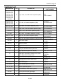
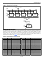
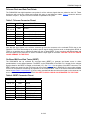
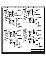
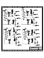
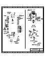
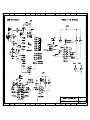
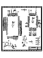
DS26303DK
3.3V, E1/T1/J1, Short-Haul,
Octal LIU Design Kit
www.maxim-ic.com
GENERAL DESCRIPTION
FEATURES
The DS26303DK is a fully integrated design kit for
the DS26303 3.3V, 8-port, E1/T1/J1 line interface
unit (LIU). This design kit contains all the necessary
circuitry to evaluate the DS26303 in all modes of
operation. The design kit also includes an on-board
microprocessor to run real-time code for further part
evaluation.
Expedites New Designs by Eliminating FirstPass Prototyping
Demonstrates Key Functions of the DS26303
Includes DS26303 x 8-Port LIU, Transformers,
75Ω BNC Connectors, RJ-48 Connectors, and
Termination Passives
Communicates Directly with any PC with a
USB or RS-232 Serial Interface
DESIGN KIT CONTENTS
DS26303DK Board
5V AC/DC Adapter
3ft USB Cable
Download:
ChipView Software
DS26303DK.def Definition Files
DS26303DK Data Sheet
High-Level Windows®-Based Software
Provides Visual Access to All Registers
ORDERING INFORMATION
On-Board T1 and E1 Crystal Oscillators for
Stable Clock Generation
PART
DS26303DK
Software-Controlled (Register) Mapped
Configuration Switches Facilitate Real-Time
Clock and Signal Routing
Precision Test Points for All Clocks and
Signals
DESCRIPTION
On-Board BERT for Testing and Pattern
Generation
DS26303 Design Kit Board
Windows is a registered trademark of Microsoft Corp.
1 of 43
REV: 101105
DS26303 Design Kit
TABLE OF CONTENTS
COMPONENT LIST .....................................................................................................................3
BOARD FLOORPLAN.................................................................................................................6
BASIC OPERATION....................................................................................................................7
HARDWARE CONFIGURATION ................................................................................................7
QUICK START (HARDWARE SETTINGS—SINGLE POWER SUPPLY)............................................................... 7
JTAG CONFIGURATION ............................................................................................................................. 7
Table 1. JTAG Connector (J6) Pinout............................................................................................................... 7
Figure 1. DS26303DK JTAG Chain .................................................................................................................. 8
ADDRESS/DATA BUS CONNECTOR ............................................................................................................. 8
Table 2. Address/Data Connector Pinout ......................................................................................................... 8
TELECOM CLOCK AND DATA TEST POINTS ................................................................................................. 9
Table 3. Telecom Connector Pinout ................................................................................................................. 9
ON-BOARD BIT ERROR-RATE TESTER (BERT) .......................................................................................... 9
Table 4. BERT Connector Pinout ..................................................................................................................... 9
PROM SPI CONFIGURATION................................................................................................................... 10
Figure 2. SPI Timing Diagram ........................................................................................................................ 10
Figure 3. SPI Configuration with PROM ......................................................................................................... 11
Table 5. Configuration Memory ...................................................................................................................... 11
SOFTWARE CONFIGURATION ...............................................................................................12
QUICK START (SOFTWARE—CHIPVIEW) .................................................................................................. 12
MEMORY MAP..........................................................................................................................12
Table 6. DS26303DK Relative Address Map.................................................................................................. 12
Table 7. General-Purpose FPGA Memory Map.............................................................................................. 12
ID REGISTERS..........................................................................................................................13
CONTROL REGISTERS............................................................................................................13
DS26303 INFORMATION..........................................................................................................21
DS26303DK INFORMATION.....................................................................................................21
TECHNICAL SUPPORT ............................................................................................................21
SCHEMATICS ...........................................................................................................................21
2 of 43
DS26303 Design Kit
COMPONENT LIST
DESIGNATION
C1, C4, C6, C7,
C18, C24, C26,
C34, C36, C37,
C38, C41, C43–
C47, C49, C50,
C51, C53–C59,
C61–C83, C85,
C86, C90
C2, C3, C22, C30,
C35, C40, C42,
C48, C52, C60,
C84, C88, C89
C5, C9, C19, C21,
C27, C28, C87
QTY
DESCRIPTION
SUPPLIER/
PART NUMBER
53
0.1µF ±20%, 16V X7R ceramic capacitors (0603)
AVX
0603YC104MAT
13
1µF ±10%, 16V ceramic capacitors (1206)
Panasonic
ECJ-3YB1C105K
7
10µF ±20%, 10V ceramic capacitors (1206)
C8
1
6.8µF ±10%, 6.3V X5R ceramic capacitor (1206)
C10–C17
8
470pF ±10%, 100V ceramic capacitors (0603)
C20, C23, C25,
C91, C92
5
68µF ±20%, 16V tantalum capacitors (D case)
C29, C31, C39
3
22pF ±5%, 25V ceramic capacitors (0603)
C32, C33
2
10pF ±5%, 50V ceramic capacitors (1206) (tall case)
D1, D12
2
Green LEDs (SMD)
D2–D11
10
Red LEDs (SMD)
D13, D14, D15
3
1A, 40V Schottky diodes
H1–H4
4
KIT, 4-40 hardware
0.75 nylon standoff and 0.25 nylon screw
J1
1
40-pin terminal strip (dual row, vertical)
J2
1
2.1mm/5.5mm connector
Power jack, right-angle PC board mount; closed
frame, high current, 24V DC at 5A
J3
1
Black, single right angle (Type B)
J4
1
DB9 right-angle connector (short case)
J5, J7, J8, J21–J36
19
5-pin SMB connectors
50Ω, vertical, gold
J6, J9–J17
10
14-pin headers (dual row, vertical)
J18, J19, J20
3
100-mil 3-position jumpers
J37–J44
8
2-pin headers, 0.100in centers (vertical)
J45, J46
2
8-pin 4-port RJ45 jacks (right angle)
L1
1
1.0µH ±20%, 2-pin SMT inductor
3 of 43
Panasonic
ECJ-3YB1A106M
Panasonic
ECJ-3YB0J685K
Panasonic
ECJ-1VB2A471K
Panasonic
ECS-T1CD686R
AVX
06033A220JAT
Phycomp
1206CG100J9B200
Panasonic
LN1351C
Panasonic
LN1251C
International Rectifier
10BQ040
Not applicable
4-40KIT2
Samtec
TSW-120-07-T-D
CUI, Inc.
PJ-002AH
Molex
Not applicable
AMP
788750-2
AMP
413990-1
Samtec
TSW-107-14-T-D
Samtec
Not applicable
Samtec
TSW-102-07-T-S
Molex
43223-8140
Coiltronics
UP1B-1R0
DS26303 Design Kit
SUPPLIER/
PART NUMBER
DESIGNATION
QTY
DESCRIPTION
R1, R58, R87
3
Resistors (0603)
DO NOT POPULATE
—
R2, R14–R26, R28,
R32–R43, R46–
R50, R52, R54–
R57, R63–R66,
R68, R69, R71,
R72, R73, R76,
R77, R82, R85,
R86, R88, R91,
R93, R96, R97,
R130
57
10kΩ ±5%, 1/16W resistors (0603)
Panasonic
ERJ-3GEYJ103V
R3–R9, R11, R12,
R13, R29, R31,
R44, R45, R60,
R61, R62, R78,
R79, R94, R95,
R98–R102, R104,
R117, R120, R121,
R124–R129
36
33Ω ±5%, 1/16W resistors (0603)
Panasonic
ERJ-3GEYJ330V
R10
1
22kΩ ±5%, 1/16W resistor (0603)
Panasonic
ERJ-3GEYJ223V
R27, R67, R70,
R74, R75, R80,
R81, R83, R84,
R89, R90, R123
12
330Ω ±5%, 1/16W resistors (0603)
Panasonic
ERJ-3GEYJ331V
R30, R59
2
15kΩ ±5%, 1/16W resistors (0603)
Panasonic
ERJ-3GEYJ153V
R51
1
Resistor (1206)
DO NOT POPULATE
—
R53
1
470Ω ±5%, 1/16W resistor (0603)
R92
1
51Ω ±5%, 1/16W resistor (0603)
R103, R105–R116,
R118, R119, R122
16
60.4Ω ±1%, 1/16W resistors (0603)
SW2, SW6
2
4-pin single-pole switch
SW3, SW4, SW5,
SW7
4
6-pin slide switches (DPDT, through hole)
T1, T2
2
U1
1
U2
1
U3, U11
2
U4
1
U5
1
U6
1
Transformers (1:2 count transmitter/1:1 count
receiver)
(40-pin wide SO, -40°C to +85°C)
8-bit FIFO USB UART
(32-pin LQFP)
MCORE Microcontroller (144-pin LQFP)
128k x 8 SRAM
(32-pin SO)
DS2174 EBERT
(44-pin PLCC, 0°C to +70°C)
Spartan-II 2.5V FPGA, 200k gate
(256-pin BGA)
3.3V, E1/T1/J1 long-haul octal LIU
(144-pin eLQFP, 0°C to +70°C)
4 of 43
Panasonic
ERJ-3GEYJ471V
Panasonic
ERJ-3GEYJ510V
Panasonic
ERJ-3EKF60R4V
Panasonic
EVQPAE04M
Tyco Electronics
SSA22
Pulse Engineering
T1114
FTDI
FT245BM
Motorola
MMC2107PV
Cypress
CY62128VL-70SC
Dallas Semiconductor
DS2174Q
Xilinx
XC2S200-5FG256C
Dallas Semiconductor
DS26303L
DS26303 Design Kit
DESIGNATION
QTY
DESCRIPTION
U7
1
U8
1
U9, U12
2
High-speed buffers
U10, U18
2
1.5W, 3.3V or adj, 1A linear regulators
(16-pin TSSOP-EP)
U13, U15
2
Hex inverters (14-pin SO)
U14
1
U16
1
U17
1
U19
1
X1
1
6.00MHz low-profile crystal
X2
1
8.000MHz low-profile crystal
Y1
1
Y2
1
PROM for FPGA
(44-pin TQFP)
Dual RS-232 transmitter/receiver
(150-mil, 16-pin SO)
Quad 2-input NAND gate
(14-pin SO)
Switch debouncer
(4-pin SOT143)
2.5V or adj linear regulator
(8-pin µMAX/SO)
Platform flash in-system programmable configuration
PROM
(2Mb, 20-pin TSSOP)
Oscillator, crystal clock
5V, 2.048MHz
Oscillator, crystal clock
5V, 1.544MHz
5 of 43
SUPPLIER/
PART NUMBER
Xilinx
XC18V02VQ44C
Dallas Semiconductor
DS232AR
Fairchild Semiconductor
NC7SZ86
Maxim
MAX1793EUE-33
Toshiba
TC74HC04AFN
Toshiba
TC74HC00AFN
Maxim
MAX6816EUS-T
Maxim
MAX1792EUA25
Xilinx
XCF02SVO20C
Pletronics
LP49-26-6.00M
Ecliptek Corp.
EC1-8.000M
SaRonix
NTH039A-2.0480
SaRonix
NTH039A-1.5440
DS26303 Design Kit
BOARD FLOORPLAN
5V
PWR
TECLK CLK A
LOS LED
TCLK, RCLK, RLOS
TPOS, RPOS,
TNEG, RNEG
CON
USER
SWITCHES
BERT
DS2174
BERT
ADDRESS/DATA
XFMR
PORTS 5–8
JTAG
SERIAL
CON
LIU PWR
JUMPER
CON
RJ48
FLASH
PROM
PORTS
5–8
ON-BOARD
µC
DS26303
RST BOARD
SRAM
USB
Tx/Rx
USB
CON
USER
BNC
OSC
E1
OSC
T1
RJ48
PORTS
1–4
SRAM
PORTS 1–4
TCLK, RCLK, RLOS
TPOS, RPOS,
TNEG, RNEG
FPGA
Tx/Rx CLOCK,
DATA
SWITCH/MUX
LOS LED
6 of 43
XFMR
DS26303 Design Kit
BASIC OPERATION
This design kit relies upon several supporting files, which are available for downloading on our website at
www.maxim-ic.com/DS26303DK.
The support files are used with an evaluation program called ChipView, which is available for download at
www.maxim-ic.com/telecom.
HARDWARE CONFIGURATION
Quick Start (Hardware Settings—Single Power Supply)
•
•
•
•
•
•
•
For single power-supply operation, short jumpers J18, J19, and J20 between the 3.3V pin and the VLIU pin.
This connects VDD of the DS26303 to the 3.3V supply on the design kit.
Ensure that the FLASH switch (SW3) is in the RUN position.
Ensure that the FPGA switch (SW5) is in the ON position.
Ensure that the SPI/PROM switch (SW7) is in the OFF position.
If using the serial port, connect a RS-232 serial cable from DS26303DK (J4) to the PC.
If using the USB port, connect a USB cable from DS26303DK (J3) to the PC.
Connect AC/DC adapter with an AC power source and the DS26303DK (J2). PWR LED should be on.
JTAG Configuration
The JTAG chain is controlled by the connector JTAG CON (J6) and two on-board switches: FLASH (SW3) and
ONCE/JTAG (SW4). Depending on the function, such as programming the internal microcontroller flash or
performing boundary scan operations, the JTAG CON connector can be used and the switches can be configured
to accomplish the desired task. For information on programming the internal flash of the on-board microcontroller,
refer to the MMC2107 microcontroller user manual and board schematic.
For most purposes, having the complete JTAG chain is sufficient. Figure 1 shows the complete chain as well as
what order the devices appear during boundary scan. Table 1 shows the pinout of the JTAG connector. Connect
any JTAG cable to the connector to perform all operations. Note the JTAG chain changes depending on the switch
SW4. The ONCE location of SW4 is used for programming the on-board microcontroller only.
Table 1. JTAG Connector (J6) Pinout
PIN
NAME
1
2, 4, 6, 7
3
5
8
9
10
11
12
13
14
JTDI
GND
JTDO
JTCLK
ALIGN KEY
BRD RST
JTMS
BRD V3.3
JDE
N.C.
JTRST
7 of 43
DS26303 Design Kit
Figure 1. DS26303DK JTAG Chain
SW4
JTAG
JTMS
JTCLK
JTDI
JTDO
(U2)
(U19)
ON-BOARD
µC
FLASH MEM
FOR FPGA
(U5)
GEN
(U6)
DS26303
FPGA
ONCE
(U7)
FLASH MEM
FOR SPI
SW4
JTMS
JTCLK
(U2)
JTDI
JTDO
ON-BOARD
µC
Address/Data Bus Connector
The DS26303DK has a connector (J1) to monitor all local bus activity for the design kit. All the signals can be
captured with a high-impedance probe and displayed on an oscilloscope or logic analyzer. Note: If the FPGA
switch (SW5) is in the “OFF” position, the on-board microcontroller will no longer drive any data onto the local bus.
Therefore, the user can now connect the local bus of the DS26303 into another system without making any
modifications to the hardware. See Table 2 for specific pin information for connector J1.
Table 2. Address/Data Connector Pinout
PIN
1
3
5
7
9
11
13
15
17
19
21
23
25
27
29
31
33
35
NAME
A8
A7
A6
A5
A4
A3
A2
A1
A0
MUX
CSFPGA
CSBERT
CSLIU
ALELIU
RD
WR
MODESEL
—
FUNCTION
Local Address Bit 8
Local Address Bit 7
Local Address Bit 6
Local Address Bit 5
Local Address Bit 4
Local Address Bit 3
Local Address Bit 2
Local Address Bit 1
Local Address Bit 0
Mux
Chip Select FPGA
Chip Select DS2174
Chip Select DS26303
Address Latch Enable
Read Signal
Write Signal
Mode Select
Not Used
PIN
2
4
6
8
10
12
14
16
18
20
22
24
26
28
30
32
34, 36
37–40
8 of 43
NAME
D0
D1
D2
D3
D4
D5
D6
D7
CLKE
RDY
OE
MOTEL
INT
FPGAEN
UIN1
UIN2
3.3V
GND
FUNCTION
Local Data Bit 0
Local Data Bit 1
Local Data Bit 2
Local Data Bit 3
Local Data Bit 4
Local Data Bit 5
Local Data Bit 6
Local Data Bit 7
SPI Clock Edge Select
Ready Handshake from LIU
Output Enable LIU
Motorola/Intel Select
Interrupt for DS26303
FPGA Enable Pin
User Input 1
User Input 2
Board 3.3V
Ground
DS26303 Design Kit
Telecom Clock and Data Test Points
The DS26303DK has high-impedance test points for all the telecom signals that are related to the LIU. These
signals are split up by port number and marked with easy to read silkscreen labels. Table 3 shows the telecom
connector for port 1. The pinout for this connector is repeated for all 8 ports.
Table 3. Telecom Connector Pinout
PIN
1
2, 4, 6, 8,
10, 12, 14
3
5
7
9
11
13
NAME
TCLK
GND
RCLK
TPOS
RPOS
TNEG
RNEG
RLOS
FUNCTION
Transmit Clock Input
Ground
Receive Clock Output
Transmit Positive Data Input
Receive Positive Data Output
Transmit Negative Data Input
Receive Positive Data Output
Receive Loss-of-Signal Output
Note that the input signals in the telecom connector go from the connector to the on-board FPGA, then to the
DS26303. The FPGA was designed to perform specific signal routing functions such as looping back RPOS to
TPOS on a particular port or transferring data from the on-board BERT. If you are using user-defined data and
drive the signal on the connector, be sure to tri-state the input signal in the FPGA. FAILURE TO DO SO COULD
CAUSE DAMAGE TO THE FPGA!
On-Board Bit Error-Rate Tester (BERT)
The DS26303DK has an on-board bit error-rate tester (BERT) to generate and detect errors in either
pseudorandom or user-defined patterns. The BERT on the DS26303DK is the DS2174. A header for the relevant
signals related to the BERT is located on the board (J17). See Table 4 for the pinout of the BERT connector. The
BERT signals are routed into the FPGA and can be muxed into any of the 8 DS26303 LIU ports under software
control. For all questions concerning the operation of the on-board BERT, refer to the device data sheet available
online at www.maxim-ic.com/telecom. If you are using user-defined data and driver the signal on the connector, be
sure to tri-state the input signal in the FPGA. FAILURE TO DO SO COULD CAUSE DAMAGE TO THE FPGA!
Table 4. BERT Connector Pinout
PIN
1
2, 4, 6, 8,
10, 12, 14
3
5
7
9
11
13
NAME
TCLK_EN
GND
TCLKIN
TCLKO
RCLKIN
RCLKEN
TDAT
RDAT
FUNCTION
BERT TCLK Enable
Ground
BERT TCLK Input
BERT TCLK Output
BERT RCLK Input
BERT RCLK Enable
BERT TDAT Output
BERT RDAT Input
9 of 43
DS26303 Design Kit
PROM SPI Configuration
In software mode, it is possible to configure the DS26303 using a parallel interface or a serial peripheral interface
(SPI). Most advanced microcontrollers have both a parallel interface and SPI interface such as the microcontroller
on the DS26303DK. The command you send to the microcontroller through either the USB or serial port
determines if that data is placed on the parallel or SPI bus. Refer to the data sheet for Chipview on the particular
commands required to switch data ports.
A unique feature with the SPI port is that a PROM can be used to provide the LIU with the specific data needed for
configuration. If the data in the PROM is formatted a certain way, it can seem as the PROM is acting like a
controller with a SPI interface in master mode.
The most common PROMs to use for this type of application are those with an internal address accumulator. This
feature for the PROM is important because the device must automatically jump to the next available address in the
configuration memory. The Xilinx XC18V00 device family is a byte-wide nonvolatile memory with an autoincrement
address function. The family of devices is available in 1Mb, 2Mb, and 4Mb densities. The PROM is also useful
because the device can perform in-circuit programming with the JTAG port. Refer the data sheet for the XC18V00
for the JTAG codes for programming the configuration memory.
Figure 2 shows a general relationship of the timing for a SPI bus. For this case, all data is clocked into the slave
device on the rising edge of SCLK. This feature can be configurable on the DS26303.
Figure 2. SPI Timing Diagram
SCLK 1
2
3
4
5
6
7
A1
A2
A3
A4
A5
A
6
8
9
10
11
12
13
14
15
16
D4
D5
D6
D7
CSB
SDI
0
(lsb)
x
DO
(adrs
msb)
(lsb)
D1
D2
D3
(msb)
WRITE ACCESS ENABLED
SDO
Figure 3 shows a simplified diagram of the XC18V00 device and the DS26303 in SPI (serial) mode. Notice a few
key points about this diagram. First, the CLK for the XC18V00 is the MCLK for the LIU, but this is not the SCLK for
the SPI interface. The SCLK can be programmed as needed. See Table 5 for an example of the memory map.
Second, the programming for this device begins when OE on the XC18V00 goes high. Therefore, consideration
must be taken if some delay is necessary. Generally, it is sufficient for the OE pin to be connected to some powerup delay device. The OE delay is not necessary on this DK.
10 of 43
DS26303 Design Kit
Figure 3. SPI Configuration with PROM
(U12)
JTCLK
JTMS
JTDI
JTDO
(U6)
XC18V00
CFG
PROM
3.3V
D7
CS
D6
SCLK
D5
SDI
DS26303
CE
OE CLK
DELAY
MCLK
(LIU)
Table 5. Configuration Memory
ADDRESS
0x00
0x01
0x02
0x03
0x04
0x05
0x06
0x07
0x08
0x09
0x0A
0x0B
0x0C
0x0D
0x0E
0x0F
0x10
0x11
0x12
0x13
0x14
0x15
0x16
0x17
0x18
0x19
0x1A
0x1B
0x1C
0x1D
0x1E
0x1F
0x20
0x21
0x22
D7
CSB
1
0
0
0
0
0
0
0
0
0
0
0
0
0
0
0
0
0
0
0
0
0
0
0
0
0
0
0
0
0
0
0
0
1
1
D6
SCLK
0
0
1
0
1
0
1
0
1
0
1
0
1
0
1
0
1
0
1
0
1
0
1
0
1
0
1
0
1
0
1
0
1
0
X
D5
SDI
0
0
0
1
1
0
0
0
0
0
0
0
0
0
0
0
0
0
0
1
1
1
1
0
0
0
0
1
1
1
1
0
0
X
X
D4
X
D3
D2
D1
X
X
X
Start of Write Cycle
Bit A0
(Always a “0” for a write)
Bit A1
Bit A2
Bit A3
Bit A4
Bit A5
Bit A6
Bit A7
Bit D0 (LSB)
Bit D1
Bit D2
Bit D3
Bit D4
Bit D5
Bit D6
Bit D7
End of Write Cycle
11 of 43
D0
X
DS26303 Design Kit
SOFTWARE CONFIGURATION
Quick Start (Software—ChipView)
•
•
•
•
•
•
•
•
Perform steps in the Quick Start (Hardware Configuration).
Load ChipView software.
Select COM port.
Select Register View.
From the Programs menu, launch the host application named ChipView.exe. If the default installation options
were used, click the Start button on the Windows toolbar and select Programs -> ChipView -> ChipView.
Load the DS26303DK.def file.
Make sure that all the register settings are correct for the proper function desired for the DS26303DK.
Refer to the DS26303 data sheet for all questions pertaining to device functionality.
MEMORY MAP
The on-board microcontroller is configured to start the user address space at 0x81000000. All offsets given below
are relative to the beginning of the user address space.
Table 6. DS26303DK Relative Address Map
REF
DES
U5
U4
U6
DEVICE
General-Purpose FPGA
Tx/Rx Clock, Data
Switch/Mux
DS2174 BERT
DS26303 8-Port T1/E1/J1
LIU
OFFSET
0x0000
0x1000
0x2000
All device registers can be easily modified using the ChipView.exe host-based user-interface software.
Table 7. General-Purpose FPGA Memory Map
OFFSET
REGISTER NAME
TYPE
0x00
0x02
0x03
0x04
0x05
0x06
0x07
0x08
0x0A
0x0B
0x0C
0x0D
0x10
0x11
0x12
BRDID
DSIDH
DSIDM
DSIDL
BRDREV
ASMREV
FPGAREV
CTRL1
ABSP
BTCLK
BRCLK
BRDAT
TCLK
TPOS
TNEG
Read-Only
Read-Only
Read-Only
Read-Only
Read-Only
Read-Only
Read-Only
Control
Control
Control
Control
Control
Control
Control
Control
DESCRIPTION
Board ID
Dallas Extended ID Upper Nibble
Dallas Extended ID Middle Nibble
Dallas Extended ID Lower Nibble
Board Rev
Assembly Rev
FPGA Firmware Rev
Control Register 1
Address Bank Select Pointer
BERT TCLK Input
BERT RCLK Input
BERT RDAT Input
Indirect Register for TCLK Source Control
Indirect Register for TPOS Source Control
Indirect Register for TPOS Source Control
12 of 43
DS26303 Design Kit
ID REGISTERS
BID: BOARD ID (Offset = 0X0000)
BID is read-only with a value of 0xD.
XBIDH: HIGH NIBBLE EXTENDED BOARD ID (Offset = 0X0002)
XBIDH is read-only with a value of 0x0.
XBIDM: MIDDLE NIBBLE EXTENDED BOARD ID (Offset = 0X0003)
XBIDM is read-only with a value of 0x1.
XBIDL: LOW NIBBLE EXTENDED BOARD ID (Offset = 0X0004)
XBIDL is read-only with a value of 0x6.
BREV: BOARD FAB REVISION (Offset = 0X0005)
BREV is read-only and displays the current fab revision.
AREV: BOARD ASSEMBLY REVISION (Offset = 0X0006)
AREV is read-only and displays the current assembly revision.
PREV: FPGA REVISION (Offset = 0X0007)
PREV is read-only and displays the current PLD firmware revision.
CONTROL REGISTERS
Register Name: CTRL_1
Register Description: DS26303DK FPGA CONTROL REGISTER 1
Register Offset: 0x08
Bit #
Name
7
INT303
6
ENRLOS1
5
CLKE
4
SPI_SWAP
3
SPI
2
OE
1
MCLK1
0
MCLK0
Bit 7: INT303. This bit indicates the status of the INT303 line.
If INT303 = LOW, there is no hardware interrupt on the DS26303.
If INT303 = HIGH, there is a hardware interrupt on the DS26303.
Bit 6: ENRLOS1. This bit enables the RLOS1 LED. This should not be enabled when driving TECLK from the
DS26303.
If ENRLOS1 = LOW, the RLOS1 LED is not enabled.
If ENRLOS1 = HIGH, the RLOS1 LED is enabled and lights when RLOS1 is high.
Bit 5: CLKE. This bit sets the CLKE pin on the DS26303. This is only active when SPI (Bit 0) is HIGH. If SPI (Bit 0)
is low, CLKE is always low.
If CLKE = LOW, SDO is clocked out on the rising edge of SCLK.
If CLKE = HIGH, SDO is clocked out on the falling edge of SCLK.
Bit 4: SPI_SWAP. This bit sets the BSWP/A5 pin on the DS26303. This is only active when SPI (Bit 0) is HIGH.
If SPI_SWAP = LOW, the SPI bus is LSB first.
If SPI_SWAP = HIGH, the SPI bus is MSB first.
Bit 3: SPI. This bit sets up the FPGA to use serial mode. This bit also changes the mode pin on the DS26303.
If SPI = LOW, the parallel bus is used for all read/write access. This also sets the MODE pin on the
DS26303 to logic 1.
If SPI = HIGH, the SPI bus is used for all read/write access. This also sets the MODE pin on the DS26303
to logic 0.
Bit 2: OE. This bit controls the OE pin to the DS26303.
Bits 1 and 0: MCLK1 and MCLK0. These bits control the MCLK pin to the DS26303.
MCLK1
MCLK0
DESCRIPTION OF MCLK
0
0
MCLK = high-impedance mode
0
1
MCLK = on-board T1 oscillator
1
0
MCLK = on-board E1 oscillator
1
1
MCLK = user clock input
13 of 43
DS26303 Design Kit
Register Name: ABSP
Register Description: ADDRESS BANK SWAP POINTER
Register Offset: 0x0A
Bit #
Name
7
D7
6
D6
5
D5
4
D4
3
D3
2
D2
1
D1
0
D0
Bits 7 to 0: D7 to D0. These bits control the address bank for address 0x10 (TCLK N), 0x11 (TPOS), and 0x12
(TNEG).
ABSP
0x00
0x01
0x02
0x03
0x04
0x05
0x06
0x07
DESCRIPTION
Bank Address Value for Port 1
Bank Address Value for Port 2
Bank Address Value for Port 3
Bank Address Value for Port 4
Bank Address Value for Port 5
Bank Address Value for Port 6
Bank Address Value for Port 7
Bank Address Value for Port 8
14 of 43
DS26303 Design Kit
Register Name: BTCLK
Register Description: BERT TCLK SOURCE
Register Offset: 0x0B
Bit #
Name
7
D7
6
D6
5
D5
4
D4
3
D3
Bits 7 to 0: D7 to D0. These bits control the source of the TCLK for the BERT.
BTCLK
0x00
0x01
0x02
0x03
0x04
0x05
0x06
0x07
0x08
0x09
0x0A
0x0B
0x0C
0x0D
0x0E
0x0F
0x10
0x11
0x12
0x13
0x14
0x15
0x16–0xFF
DESCRIPTION
RCLK Port 1
RCLK Port 2
RCLK Port 3
RCLK Port 4
RCLK Port 5
RCLK Port 6
RCLK Port 7
RCLK Port 8
HI-Z
HI-Z
HI-Z
HI-Z
HI-Z
HI-Z
HI-Z
HI-Z
1.544MHz On-board oscillator
2.048MHz On-board oscillator
User clock
CLKA DS26303
TECLK DS26303
TCLKBERT OUT
HI-Z
15 of 43
2
D2
1
D1
0
D0
DS26303 Design Kit
Register Name: BRCLK
Register Description: BERT RCLK SOURCE
Register Offset: 0x0C
Bit #
Name
7
D7
6
D6
5
D5
4
D4
3
D3
Bits 7 to 0: D7 to D0. These bits control the source of the RCLK for the BERT.
BTCLK
0x00
0x01
0x02
0x03
0x04
0x05
0x06
0x07
0x08
0x09
0x0A
0x0B
0x0C
0x0D
0x0E
0x0F
0x10
0x11
0x12
0x13
0x14
0x15
0x16–0xFF
DESCRIPTION
RCLK Port 1
RCLK Port 2
RCLK Port 3
RCLK Port 4
RCLK Port 5
RCLK Port 6
RCLK Port 7
RCLK Port 8
HI-Z
HI-Z
HI-Z
HI-Z
HI-Z
HI-Z
HI-Z
HI-Z
1.544MHz On-board oscillator
2.048MHz On-board oscillator
User clock
CLKA DS26303
TECLK DS26303
TCLKBERT OUT
HI-Z
16 of 43
2
D2
1
D1
0
D0
DS26303 Design Kit
Register Name: BRDAT
Register Description: BERT RDAT SOURCE
Register Offset: 0x0D
Bit #
Name
7
D7
6
D6
5
D5
4
D4
3
D3
2
D2
1
D1
0
D0
Bits 7 to 0: D7 to D0. These bits control the source of the RDAT for the BERT. Note that the DS26303 must be in
single-rail mode for BERT to function properly.
BRDAT
0x00
0x01
0x02
0x03
0x04
0x05
0x06
0x07
0x08
0x09
0x0A
0x0B
0x0C
0x0D
0x0E
0x0F
0x10
0x11
0x12
0x13
0x14
0x15
0x16–0xFF
DESCRIPTION
RPOS Port 1
RPOS Port 2
RPOS Port 3
RPOS Port 4
RPOS Port 5
RPOS Port 6
RPOS Port 7
RPOS Port 8
HI-Z
HI-Z
HI-Z
HI-Z
HI-Z
HI-Z
HI-Z
HI-Z
1.544MHz On-board oscillator
2.048MHz On-board oscillator
User clock
CLKA DS26303
TECLK DS26303
TCLKBERT OUT
HI-Z
17 of 43
DS26303 Design Kit
Register Name: TCLK
Register Description: PORT TCLK SOURCE
Register Offset: 0x10
Bit #
Name
7
D7
6
D6
5
D5
4
D4
3
D3
2
D2
Note: This is an indirect register that is related to ABSP (0x0A). See register description.
Bits 7 to 0: D7 to D0. These bits control the source of the port TCLK for the DS26303.
TCLK
0x00
0x01
0x02
0x03
0x04
0x05
0x06
0x07
0x08
0x09
0x0A
0x0B
0x0C
0x0D
0x0E
0x0F
0x10
0x11
0x12
0x13
0x14
0x15
0x16–0xFF
DESCRIPTION
RCLK Port 1
RCLK Port 2
RCLK Port 3
RCLK Port 4
RCLK Port 5
RCLK Port 6
RCLK Port 7
RCLK Port 8
HI-Z
HI-Z
HI-Z
HI-Z
HI-Z
HI-Z
HI-Z
HI-Z
1.544MHz On-board oscillator
2.048MHz On-board oscillator
User clock
CLKA DS26303
TECLK DS26303
TCLKBERT OUT
HI-Z
18 of 43
1
D1
0
D0
DS26303 Design Kit
Register Name: TPOS
Register Description: PORT TPOS SOURCE
Register Offset: 0x11
Bit #
Name
7
D7
6
D6
5
D5
4
D4
3
D3
2
D2
Note: This is an indirect register that is related to ABSP (0x0A). See register description.
Bits 7 to 0: D7 to D0. These bits control the source of the port TPOS for the DS26303.
TPOS
0x00
0x01
0x02
0x03
0x04
0x05
0x06
0x07
0x08
0x09
0x0A
0x0B
0x0C
0x0D
0x0E
0x0F
0x10
0x11
0x12
0x13
0x14
0x15
0x16–0xFF
DESCRIPTION
RPOS Port 1
RPOS Port 2
RPOS Port 3
RPOS Port 4
RPOS Port 5
RPOS Port 6
RPOS Port 7
RPOS Port 8
HI-Z
HI-Z
HI-Z
HI-Z
HI-Z
HI-Z
HI-Z
HI-Z
1.544MHz On-board oscillator
2.048MHz On-board oscillator
User clock
CLKA DS26303
TECLK DS26303
TDATBERT OUT
HI-Z
19 of 43
1
D1
0
D0
DS26303 Design Kit
Register Name: TNEG
Register Description: PORT TNEG SOURCE
Register Offset: 0x12
Bit #
Name
7
D7
6
D6
5
D5
4
D4
3
D3
2
D2
Note: This is an indirect register that is related to ABSP (0x0A). See register description.
Bits 7 to 0: D7 to D0. These bits control the source of the port TNEG for the DS26303.
TNEG
0x00
0x01
0x02
0x03
0x04
0x05
0x06
0x07
0x08
0x09
0x0A
0x0B
0x0C
0x0D
0x0E
0x0F
0x10
0x11
0x12
0x13
0x14
0x15
0x16–0xFF
DESCRIPTION
RNEG Port 1
RNEG Port 2
RNEG Port 3
RNEG Port 4
RNEG Port 5
RNEG Port 6
RNEG Port 7
RNEG Port 8
HI-Z
HI-Z
HI-Z
HI-Z
HI-Z
HI-Z
HI-Z
HI-Z
1.544MHz On-board oscillator
2.048MHz On-board oscillator
User clock
CLKA DS26303
TECLK DS26303
Drive Logic “0”
HI-Z
20 of 43
1
D1
0
D0
DS26303 Design Kit
DS26303 INFORMATION
For more information about the DS26303, refer to the DS26303 data sheet available on our website at
www.maxim-ic.com/DS26303.
DS26303DK INFORMATION
For more information about the DS26303DK including software downloads, go to www.maxim-ic.com/DS26303DK.
TECHNICAL SUPPORT
For additional technical support, e-mail your questions to [email protected].
SCHEMATICS
The DS26303DK schematics are featured in the following 22 pages.
21 of 43
Maxim/Dallas Semiconductor cannot assume responsibility for use of any circuitry other than circuitry entirely embodied in a Maxim/Dallas Semiconductor product.
No circuit patent licenses are implied. Maxim/Dallas Semiconductor reserves the right to change the circuitry and specifications without notice at any time.
Maxim Integrated Products, 120 San Gabriel Drive, Sunnyvale, CA 94086 408-737-7600
© 2005 Maxim Integrated Products • Printed USA
The Maxim logo is a registered trademark of Maxim Integrated Products, Inc. The Dallas logo is a registered trademark of Dallas Semiconductor Corporation.