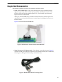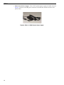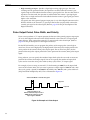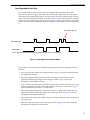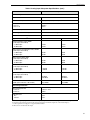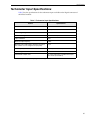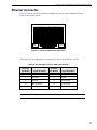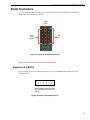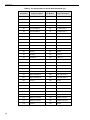
1
Title Page
UM-26000-A
DT7837
User’s Manual
Copyright Page
First Edition
March, 2015
Copyright © 2015 by Data Translation, Inc.
All rights reserved.
Information furnished by Data Translation, Inc. is believed to be
accurate and reliable; however, no responsibility is assumed by
Data Translation, Inc. for its use; nor for any infringements of
patents or other rights of third parties which may result from its
use. No license is granted by implication or otherwise under any
patent rights of Data Translation, Inc.
Use, duplication, or disclosure by the United States Government
is subject to restrictions as set forth in subparagraph (c)(1)(ii) of
the Rights in Technical Data and Computer software clause at 48
C.F.R, 252.227-7013, or in subparagraph (c)(2) of the Commercial
Computer Software - Registered Rights clause at 48 C.F.R.,
52-227-19 as applicable. Data Translation, Inc., 100 Locke Drive,
Marlboro, MA 01752.
Data Translation, Inc.
100 Locke Drive
Marlboro, MA 01752-1192
(508) 481-3700
www.datatranslation.com
Fax: (508) 481-8620
E-mail: [email protected]
The DT7837 software is based of the Linux open-source
development environment which uses the GNU (General Public
License). Data Translation example programs may use code from
other vendors. This code is for demonstration purposes only. If
you want to use this code for commercial purposes, you must
ensure that you resolve any licensing issues with the appropriate
parties.
Data Translation® is a registered trademark of Data Translation,
Inc.
All other brand and product names are trademarks or registered
trademarks of their respective companies.
FCC
Page
Radio and Television Interference
This equipment has been tested and found to comply with CISPR EN55022 Class A and
EN61000-6-1 requirements and also with the limits for a Class A digital device, pursuant to
Part 15 of the FCC Rules. These limits are designed to provide reasonable protection against
harmful interference when the equipment is operated in a commercial environment. This
equipment generates, uses, and can radiate radio frequency energy and, if not installed and
used in accordance with the instruction manual, may cause harmful interference to radio
communications. Operation of this equipment in a residential area is likely to cause harmful
interference, in which case the user will be required to correct the interference at his own
expense.
Changes or modifications to this equipment not expressly approved by Data Translation could
void your authority to operate the equipment under Part 15 of the FCC Rules.
Note: This product was verified to meet FCC requirements under test conditions that
included use of shielded cables and connectors between system components. It is important
that you use shielded cables and connectors to reduce the possibility of causing interference
to radio, television, and other electronic devices.
Canadian Department of Communications Statement
This digital apparatus does not exceed the Class A limits for radio noise emissions from
digital apparatus set out in the Radio Interference Regulations of the Canadian Department of
Communications.
Le présent appareil numérique n’émet pas de bruits radioélectriques dépassant les limites
applicables aux appareils numériques de la class A prescrites dans le Règlement sur le
brouillage radioélectrique édicté par le Ministère des Communications du Canada.
Table of Contents
Table of Contents
About this Manual . . . . . . . . . . . . . . . . . . . . . . . . . . . . . . . . . . . . . . . . . . . . . . . . . . . . . . 9
Intended Audience. . . . . . . . . . . . . . . . . . . . . . . . . . . . . . . . . . . . . . . . . . . . . . . . . . . . . . . . . . . . . 9
How this Manual is Organized . . . . . . . . . . . . . . . . . . . . . . . . . . . . . . . . . . . . . . . . . . . . . . . . . . 9
Conventions Used in this Manual . . . . . . . . . . . . . . . . . . . . . . . . . . . . . . . . . . . . . . . . . . . . . . . . 9
Related Information . . . . . . . . . . . . . . . . . . . . . . . . . . . . . . . . . . . . . . . . . . . . . . . . . . . . . . . . . . . 10
Where To Get Help. . . . . . . . . . . . . . . . . . . . . . . . . . . . . . . . . . . . . . . . . . . . . . . . . . . . . . . . . . . . 10
Chapter 1: Overview . . . . . . . . . . . . . . . . . . . . . . . . . . . . . . . . . . . . . . . . . . . . . . . . . . . 11
Hardware Features. . . . . . . . . . . . . . . . . . . . . . . . . . . . . . . . . . . . . . . . . . . . . . . . . . . . . . . . . . . . 12
Board Layout Overview . . . . . . . . . . . . . . . . . . . . . . . . . . . . . . . . . . . . . . . . . . . . . . . . . . . . . . . 15
Supported Software . . . . . . . . . . . . . . . . . . . . . . . . . . . . . . . . . . . . . . . . . . . . . . . . . . . . . . . . . . . 18
Supported Accessories. . . . . . . . . . . . . . . . . . . . . . . . . . . . . . . . . . . . . . . . . . . . . . . . . . . . . . . . . 19
Getting Started Procedure. . . . . . . . . . . . . . . . . . . . . . . . . . . . . . . . . . . . . . . . . . . . . . . . . . . . . . 21
Chapter 2: Principles of Operation . . . . . . . . . . . . . . . . . . . . . . . . . . . . . . . . . . . . . . . 23
Block Diagram . . . . . . . . . . . . . . . . . . . . . . . . . . . . . . . . . . . . . . . . . . . . . . . . . . . . . . . . . . . . . . . 24
ARM Block. . . . . . . . . . . . . . . . . . . . . . . . . . . . . . . . . . . . . . . . . . . . . . . . . . . . . . . . . . . . . . . . . . . 25
ARM Processor . . . . . . . . . . . . . . . . . . . . . . . . . . . . . . . . . . . . . . . . . . . . . . . . . . . . . . . . . . . 25
Memory . . . . . . . . . . . . . . . . . . . . . . . . . . . . . . . . . . . . . . . . . . . . . . . . . . . . . . . . . . . . . . . . . 25
Embedded NAND Flash . . . . . . . . . . . . . . . . . . . . . . . . . . . . . . . . . . . . . . . . . . . . . . . . . . . 25
EEPROM. . . . . . . . . . . . . . . . . . . . . . . . . . . . . . . . . . . . . . . . . . . . . . . . . . . . . . . . . . . . . . . . . 25
Micro SD Card . . . . . . . . . . . . . . . . . . . . . . . . . . . . . . . . . . . . . . . . . . . . . . . . . . . . . . . . . . . . 26
USB Device (Client) Port . . . . . . . . . . . . . . . . . . . . . . . . . . . . . . . . . . . . . . . . . . . . . . . . . . . 26
USB Host Port . . . . . . . . . . . . . . . . . . . . . . . . . . . . . . . . . . . . . . . . . . . . . . . . . . . . . . . . . . . . 26
Serial Port 0 . . . . . . . . . . . . . . . . . . . . . . . . . . . . . . . . . . . . . . . . . . . . . . . . . . . . . . . . . . . . . . 26
Serial Port 1 / I2C2 Port . . . . . . . . . . . . . . . . . . . . . . . . . . . . . . . . . . . . . . . . . . . . . . . . . . . . 26
SPI Port . . . . . . . . . . . . . . . . . . . . . . . . . . . . . . . . . . . . . . . . . . . . . . . . . . . . . . . . . . . . . . . . . . 27
GPMC Bus Interface . . . . . . . . . . . . . . . . . . . . . . . . . . . . . . . . . . . . . . . . . . . . . . . . . . . . . . . 27
Additional Signals Used on Processor . . . . . . . . . . . . . . . . . . . . . . . . . . . . . . . . . . . . . . . . 27
Digital Connector . . . . . . . . . . . . . . . . . . . . . . . . . . . . . . . . . . . . . . . . . . . . . . . . . . . . . . . . . 27
Analog Input Features . . . . . . . . . . . . . . . . . . . . . . . . . . . . . . . . . . . . . . . . . . . . . . . . . . . . . . . . . 29
Analog Input Channels . . . . . . . . . . . . . . . . . . . . . . . . . . . . . . . . . . . . . . . . . . . . . . . . . . . . 29
Input Ranges and Gains . . . . . . . . . . . . . . . . . . . . . . . . . . . . . . . . . . . . . . . . . . . . . . . . . . . . 29
IEPE Functions. . . . . . . . . . . . . . . . . . . . . . . . . . . . . . . . . . . . . . . . . . . . . . . . . . . . . . . . . . . . 30
Input Resolution . . . . . . . . . . . . . . . . . . . . . . . . . . . . . . . . . . . . . . . . . . . . . . . . . . . . . . . . . . 30
Continuous Sampling Mode . . . . . . . . . . . . . . . . . . . . . . . . . . . . . . . . . . . . . . . . . . . . . . . . 30
Input Triggers . . . . . . . . . . . . . . . . . . . . . . . . . . . . . . . . . . . . . . . . . . . . . . . . . . . . . . . . . . . . 31
Input Clock Source and Sampling Frequency. . . . . . . . . . . . . . . . . . . . . . . . . . . . . . . . . . 32
Data Format and Transfer . . . . . . . . . . . . . . . . . . . . . . . . . . . . . . . . . . . . . . . . . . . . . . . . . . 33
5
Contents
Error Conditions . . . . . . . . . . . . . . . . . . . . . . . . . . . . . . . . . . . . . . . . . . . . . . . . . . . . . . . . . . 33
Tachometer Input Features . . . . . . . . . . . . . . . . . . . . . . . . . . . . . . . . . . . . . . . . . . . . . . . . . . . . . 34
General-Purpose Counter/Timer Features. . . . . . . . . . . . . . . . . . . . . . . . . . . . . . . . . . . . . . . . 36
C/T Channels . . . . . . . . . . . . . . . . . . . . . . . . . . . . . . . . . . . . . . . . . . . . . . . . . . . . . . . . . . . . 36
C/T Clock Input Sources . . . . . . . . . . . . . . . . . . . . . . . . . . . . . . . . . . . . . . . . . . . . . . . . . . . 37
Gate Types . . . . . . . . . . . . . . . . . . . . . . . . . . . . . . . . . . . . . . . . . . . . . . . . . . . . . . . . . . . . . . . 37
Pulse Output Period, Pulse Width, and Polarity . . . . . . . . . . . . . . . . . . . . . . . . . . . . . . . 38
Counter/Timer Operation Modes . . . . . . . . . . . . . . . . . . . . . . . . . . . . . . . . . . . . . . . . . . . 39
Event Counting . . . . . . . . . . . . . . . . . . . . . . . . . . . . . . . . . . . . . . . . . . . . . . . . . . . . . . . 39
Rate Generation . . . . . . . . . . . . . . . . . . . . . . . . . . . . . . . . . . . . . . . . . . . . . . . . . . . . . . . 40
Non-Repeatable One-Shot . . . . . . . . . . . . . . . . . . . . . . . . . . . . . . . . . . . . . . . . . . . . . . 41
Idle Mode . . . . . . . . . . . . . . . . . . . . . . . . . . . . . . . . . . . . . . . . . . . . . . . . . . . . . . . . . . . . 42
Measure Counter Features . . . . . . . . . . . . . . . . . . . . . . . . . . . . . . . . . . . . . . . . . . . . . . . . . . . . . 43
Digital I/O Features. . . . . . . . . . . . . . . . . . . . . . . . . . . . . . . . . . . . . . . . . . . . . . . . . . . . . . . . . . . 47
Digital I/O Lines . . . . . . . . . . . . . . . . . . . . . . . . . . . . . . . . . . . . . . . . . . . . . . . . . . . . . . . . . . 47
Operation Modes. . . . . . . . . . . . . . . . . . . . . . . . . . . . . . . . . . . . . . . . . . . . . . . . . . . . . . . . . . 47
Triggering Acquisition on Multiple Modules . . . . . . . . . . . . . . . . . . . . . . . . . . . . . . . . . . . . . 48
Chapter 3: Troubleshooting . . . . . . . . . . . . . . . . . . . . . . . . . . . . . . . . . . . . . . . . . . . . . 49
Technical Support . . . . . . . . . . . . . . . . . . . . . . . . . . . . . . . . . . . . . . . . . . . . . . . . . . . . . . . . . . . . 50
If Your Module Needs Factory Service . . . . . . . . . . . . . . . . . . . . . . . . . . . . . . . . . . . . . . . . . . . 51
Chapter 4: Calibration . . . . . . . . . . . . . . . . . . . . . . . . . . . . . . . . . . . . . . . . . . . . . . . . . . 53
Overview . . . . . . . . . . . . . . . . . . . . . . . . . . . . . . . . . . . . . . . . . . . . . . . . . . . . . . . . . . . . . . . . . . . . 54
Using the Calibration Utility . . . . . . . . . . . . . . . . . . . . . . . . . . . . . . . . . . . . . . . . . . . . . . . . . . . 55
Calibrating the Analog Input Subsystem . . . . . . . . . . . . . . . . . . . . . . . . . . . . . . . . . . . . . . . . 56
Warming up the Module . . . . . . . . . . . . . . . . . . . . . . . . . . . . . . . . . . . . . . . . . . . . . . . . . . . 56
Connecting a Precision Voltage Source . . . . . . . . . . . . . . . . . . . . . . . . . . . . . . . . . . . . . . . 56
Using the Auto-Calibration Procedure . . . . . . . . . . . . . . . . . . . . . . . . . . . . . . . . . . . . . . . 56
Using the Manual Calibration Procedure . . . . . . . . . . . . . . . . . . . . . . . . . . . . . . . . . . . . . 57
Restoring Factory-Calibration Settings . . . . . . . . . . . . . . . . . . . . . . . . . . . . . . . . . . . . . . . 58
Appendix A: Specifications . . . . . . . . . . . . . . . . . . . . . . . . . . . . . . . . . . . . . . . . . . . . . 59
Analog Input Specifications . . . . . . . . . . . . . . . . . . . . . . . . . . . . . . . . . . . . . . . . . . . . . . . . . . . . 60
Digital Input Specifications. . . . . . . . . . . . . . . . . . . . . . . . . . . . . . . . . . . . . . . . . . . . . . . . . . . . . 63
Digital Output Specifications . . . . . . . . . . . . . . . . . . . . . . . . . . . . . . . . . . . . . . . . . . . . . . . . . . . 64
Tachometer Input Specifications . . . . . . . . . . . . . . . . . . . . . . . . . . . . . . . . . . . . . . . . . . . . . . . . 65
Measure Counter Specifications. . . . . . . . . . . . . . . . . . . . . . . . . . . . . . . . . . . . . . . . . . . . . . . . . 66
General-Purpose Counter/Timer Specifications . . . . . . . . . . . . . . . . . . . . . . . . . . . . . . . . . . . 67
Trigger Specifications. . . . . . . . . . . . . . . . . . . . . . . . . . . . . . . . . . . . . . . . . . . . . . . . . . . . . . . . . . 68
Master Oscillator Specifications . . . . . . . . . . . . . . . . . . . . . . . . . . . . . . . . . . . . . . . . . . . . . . . . . 69
Power, Physical, and Environmental Specifications . . . . . . . . . . . . . . . . . . . . . . . . . . . . . . . . 70
6
Contents
Regulatory Specifications . . . . . . . . . . . . . . . . . . . . . . . . . . . . . . . . . . . . . . . . . . . . . . . . . . . . . . 71
Connector Specifications . . . . . . . . . . . . . . . . . . . . . . . . . . . . . . . . . . . . . . . . . . . . . . . . . . . . . . . 72
External Power Supply Specifications. . . . . . . . . . . . . . . . . . . . . . . . . . . . . . . . . . . . . . . . . . . . 73
Appendix B: Connector Pin Assignments and LED Status Indicators . . . . . . . . . . 75
Analog Input Connectors . . . . . . . . . . . . . . . . . . . . . . . . . . . . . . . . . . . . . . . . . . . . . . . . . . . . . . 76
Digital Connector . . . . . . . . . . . . . . . . . . . . . . . . . . . . . . . . . . . . . . . . . . . . . . . . . . . . . . . . . . . . . 77
USB Device (Client) Connector . . . . . . . . . . . . . . . . . . . . . . . . . . . . . . . . . . . . . . . . . . . . . . . . . 79
USB Host Connector . . . . . . . . . . . . . . . . . . . . . . . . . . . . . . . . . . . . . . . . . . . . . . . . . . . . . . . . . . 80
Ethernet Connector . . . . . . . . . . . . . . . . . . . . . . . . . . . . . . . . . . . . . . . . . . . . . . . . . . . . . . . . . . . 81
Micro SD Card Connector . . . . . . . . . . . . . . . . . . . . . . . . . . . . . . . . . . . . . . . . . . . . . . . . . . . . . . 82
External +5 V Power Connector. . . . . . . . . . . . . . . . . . . . . . . . . . . . . . . . . . . . . . . . . . . . . . . . . 83
Serial Connectors . . . . . . . . . . . . . . . . . . . . . . . . . . . . . . . . . . . . . . . . . . . . . . . . . . . . . . . . . . . . . 85
Serial Port 0 (UART 0) . . . . . . . . . . . . . . . . . . . . . . . . . . . . . . . . . . . . . . . . . . . . . . . . . . . . . 85
SPI Connector . . . . . . . . . . . . . . . . . . . . . . . . . . . . . . . . . . . . . . . . . . . . . . . . . . . . . . . . . . . . 86
Serial Port 1 / I2C2 Connector. . . . . . . . . . . . . . . . . . . . . . . . . . . . . . . . . . . . . . . . . . . . . . . 87
I/O Block Connector . . . . . . . . . . . . . . . . . . . . . . . . . . . . . . . . . . . . . . . . . . . . . . . . . . . . . . . . . . 88
STP26 Screw Terminal Panel. . . . . . . . . . . . . . . . . . . . . . . . . . . . . . . . . . . . . . . . . . . . . . . . . . . . 91
LED Status Indicators . . . . . . . . . . . . . . . . . . . . . . . . . . . . . . . . . . . . . . . . . . . . . . . . . . . . . . . . . 93
Index . . . . . . . . . . . . . . . . . . . . . . . . . . . . . . . . . . . . . . . . . . . . . . . . . . . . . . . . . . . . . . . . 95
7
Contents
8
About this Manual
The first part of this manual describes how to install and set up your DT7837 module and
verify that your module is working properly.
The second part of this manual describes the features of the DT7837 module and how to
program the DT7837 module using Linux system calls. Troubleshooting information is also
provided.
Intended Audience
This document is intended for engineers, scientists, technicians, or others responsible for
using and/or programming a DT7837 module for data acquisition operations in the Linux
operating system. It is assumed that you have some familiarity with data acquisition
principles and that you understand your application.
How this Manual is Organized
This manual is organized as follows:
• Chapter 1, “Overview,” describes the major features of the DT7837 module, as well as the
supported software and accessories for the module.
• Chapter 2, “Principles of Operation,” describes all of the features of the DT7837 module.
• Chapter 3, “Troubleshooting,” provides information that you can use to resolve problems
with the DT7837 module should they occur.
• Chapter 4, “Calibration,” describes how to calibrate the analog circuitry of the DT7837
module.
• Appendix A, “Specifications,” lists the specifications of the DT7837 module.
• Appendix B, “Connector Pin Assignments and LED Status Indicators,” lists the pin
assignments of the connectors on the DT7837 module, and describes the LED status
indicators on the DT7837 module.
• An index completes this manual.
Conventions Used in this Manual
The following conventions are used in this manual:
• Notes provide useful information or information that requires special emphasis, cautions
provide information to help you avoid losing data or damaging your equipment, and
warnings provide information to help you avoid catastrophic damage to yourself or your
equipment.
• Items that you select or type are shown in bold.
9
About this Manual
Related Information
Refer to the following documents, which can be found on the DT7837 web page on our
website (http://www.datatranslation.com/products/dataacquisition/embedded/DT7837/)
for more information on using the DT7837 module:
• DT7837 Getting Started help file
• DT7837 File I/O Programming Manual
Refer to your Linux documentation for more information about Linux and Texas Instruments
documentation for more information on the TI Sitara AM3352, 1 GHz, ARM® Cortex-A8
processor.
Where To Get Help
Should you run into problems installing or using a DT7837 module, the Data Translation
Technical Support Department is available to provide technical assistance. Refer to Chapter 4
for more information. If you are outside the United States or Canada, call your local
distributor, whose number is listed on our web site (www.datatranslation.com).
10
1
Overview
Hardware Features. . . . . . . . . . . . . . . . . . . . . . . . . . . . . . . . . . . . . . . . . . . . . . . . . . . . . . . . . . . . 12
Supported Software . . . . . . . . . . . . . . . . . . . . . . . . . . . . . . . . . . . . . . . . . . . . . . . . . . . . . . . . . . . 18
Supported Accessories. . . . . . . . . . . . . . . . . . . . . . . . . . . . . . . . . . . . . . . . . . . . . . . . . . . . . . . . . 19
Getting Started Procedure. . . . . . . . . . . . . . . . . . . . . . . . . . . . . . . . . . . . . . . . . . . . . . . . . . . . . . 21
11
Chapter 1
Hardware Features
The DT7837 module is an open-source Linux computing platform with a high-accuracy,
dynamic signal analyzer front-end, making it ideal for embedded applications that require
noise, vibration, and acoustic measurements.
The module is composed of two boards (the bottom board contains the ARM block and the
top board contains the I/O block) that connect together, as show in Figure 1. Users can embed
the module into their own enclosure and/or system, as needed.
Figure 1: DT7837 Module
The key features of the DT7837 module are as follows:
• Open-source computing platform featuring a TI Sitara AM3352, 1 GHz, ARM® Cortex-A8
processor.
• Linux distribution consisting of a Linux kernel, bootloader, and file system with a DT7837
device driver, USB device (client) driver, and USB host driver.
• Ethernet 10/100 Mbps connectivity to a host computer.
• USB 2.0 full-speed connectivity to a host computer.
12
Overview
• USB 2.0 host connection to external devices, such as a mouse, keyboard, or external
storage devices.
• Analog input subsystem:
− Four, single-ended analog input channels available through SMA connectors.
− Four simultaneous sampling, Delta-Sigma, 24-bit analog-to-digital converters (ADCs).
− Support for IEPE (Integrated Electronic Piezoelectric) inputs, including use of a 4 mA
current source with 20 V compliance voltage for AC or DC coupling.
− Programmable throughput rate from 195.3125 Samples/s to 105.469 kSamples/s.
− Input range of ±10 V with software-selectable gains of 1 and 10 for an effective input
range of ±10 V and ±1 V.
− Continuous acquisition from multiple analog input channels simultaneously.
− Supports the ability to return the value of the tachometer, general-purpose
counter/timer, measure counter, and/or digital input port in the analog input data
stream, allowing you to measure a variety of signals synchronously with analog input
measurements.
− Software-programmable trigger source (software trigger, external trigger, or threshold
trigger using any analog input channel) to start acquisition.
− Accounts for analog input group delay in hardware and allows user-specified trigger
delay to account for analog output group delay.
• Up to eight, TTL digital input lines using the eight general-purpose inputs. You can read
the digital input port directly or you can return the value of the digital input port in the
input data stream.
• Up to eight, TTL digital output lines using the eight general-purpose outputs. You can
write a value to the digital output port directly.
• One, 32-bit, general-purpose counter/timer for performing event counting, rate
generation, and non-repeatable one-shot operations. You can use two general-purpose
input signals for the C/T clock and gate inputs and one general-purpose output signal for
the C/T clock output. You can read the value of the counter/timer directly or through the
input data stream.
• One tachometer input signal. The value of the tachometer input signal can be returned in
the input stream.
• One phase/measure counter. You can program the edge that starts the measurement and
the edge that stops the measurement. Many edge types are supported. The data from the
measure counter can be returned in the input stream.
• 2 GB embedded NAND flash memory that contains the Linux kernel, bootloader, and file
system; this memory can also be used to store user files and data
• 512 MB SDRAM (DDR3) memory
• 8 kBytes EEPROM
• Micro SD connector supports micro SD cards, which can be used as a boot source for
general-purpose file and data storage
• 3.3 V UART, I2C, and an SPI (Serial Peripheral Interface) interfaces for embedded
connectivity.
13
Chapter 1
• Serial debug port.
• External power connectors (4-pin DIN or 3-pin Phoenix header) for connecting a +5 VDC
power supply.
14
Overview
Board Layout Overview
The DT7837 module consists of an ARM block and a I/O block. Figure 2 shows the layout of
the ARM block (the bottom board). Figure 3 shows the layout of the I/O block (the top board).
15
Chapter 1
Digital Connector
(Tachometer, Digital I/O, External Trigger, Counter/Timer)
Power LED
Connector to the
I/O Block
Serial
Port 1
(J14)
SPI
Port
(J12)
Reset/Boot
Switch
AM3552
Processor
Serial
Port 0
(J13)
Ethernet
Connector
USB Host Grounding USB Device SD Card +5 V Power
Port
Stud
(Client) Port
Figure 2: Layout of the ARM Block of the DT7837 Module
16
Overview
Output Trigger
LED (bottom)
Input Trigger LED
(top)
Analog Input Connectors
Analog Output Connector
(analog output currently not
supported in software)
Figure 3: Layout of the I/O Block of the DT7837 Module
17
Chapter 1
Supported Software
The following software is available for use with the DT7837 module:
• DT7837 File I/O Commands – A set of commands in Linux user space for opening a
subsystem or stream, configuring a subsystem or stream, acquiring data in the input
stream, reading or updating the digital I/O port, and/or writing values to the calibration
potentiometers. Numerous example programs are provided to illustrate how to use these
commands. Refer to the DT7837 File I/O Programming Manual for more information.
• DT7837 Kernel Device Driver – The device driver resides in the Linux kernel and is
responsible for performing the functions defined by the DT7837 file I/O commands on the
DT7837 module.
• DT7837 Calibration Utility – This utility, described in Chapter 4, allows you to calibrate
the analog circuitry of the DT7837 module.
18
Overview
Supported Accessories
The following optional accessories are available for a DT7837 module:
• STP26 screw terminal panel – This screw terminal panel accepts tachometer, digital
input, C/T gate input, and C/T clock input signals from the Digital connector on the
DT7837 module and provides digital output and C/T clock output signals from the
Digital connector on the module.
The 26-pin, 36-inch, EP406 cable is included with the STP26 screw terminal panel. The
cable allows you to attach the STP26 screw terminal panel to the Digital connector on a
DT7837 module.
Figure 4 shows the STP26 and EP406 cable.
Figure 4: STP26 Screw Terminal Panel and EP406 Cable
• EP405 USB to Serial TTL Debug Cable – This 3Mbaud, 1.8 m cable, shown in Figure 5,
connects the USB port of the host computer to serial UART connector J13 on the DT7837,
allowing you to debug the DT7837 using a terminal interface.
Figure 5: EP405 USB to Serial TTL Debug Cable
19
Chapter 1
• EP361 External Power Supply – This +5 VDC optional power supply and cable, shown in
Figure 6, connects to the DIN power connector on the DT7837 module and to the wall
power outlet.
Figure 6: EP361 +5 VDC External Power Supply
20
Overview
Getting Started Procedure
Refer to the DT7837 Getting Started help file on our web site
(http://www.datatranslation.com/products/dataacquisition/embedded/DT7837/) for
getting started information
21
Chapter 1
22
2
Principles of Operation
Block Diagram . . . . . . . . . . . . . . . . . . . . . . . . . . . . . . . . . . . . . . . . . . . . . . . . . . . . . . . . . . . . . . . 24
Analog Input Features . . . . . . . . . . . . . . . . . . . . . . . . . . . . . . . . . . . . . . . . . . . . . . . . . . . . . . . . . 29
Tachometer Input Features . . . . . . . . . . . . . . . . . . . . . . . . . . . . . . . . . . . . . . . . . . . . . . . . . . . . . 34
General-Purpose Counter/Timer Features. . . . . . . . . . . . . . . . . . . . . . . . . . . . . . . . . . . . . . . . 36
Measure Counter Features . . . . . . . . . . . . . . . . . . . . . . . . . . . . . . . . . . . . . . . . . . . . . . . . . . . . . 43
Digital I/O Features. . . . . . . . . . . . . . . . . . . . . . . . . . . . . . . . . . . . . . . . . . . . . . . . . . . . . . . . . . . 47
Triggering Acquisition on Multiple Modules . . . . . . . . . . . . . . . . . . . . . . . . . . . . . . . . . . . . . 48
23
Chapter 2
Block Diagram
The DT7837 is an open-source Linux computing platform with a high-accuracy, dynamic
signal analyzer front-end.
The DT7837 consists of two boards. The bottom board is the ARM block, which includes the
ARM processor, PC and embedded connectivity options, and memory, as well as the digital
I/O, counter/timer, measure counter, and tachometer circuitry.
The top board is the I/O block, which includes four 24-bit IEPE analog inputs and one 24-bit
stimulus analog output.
Note: The analog output circuitry is currently not supported in software.
Figure 7 shows a block diagram of the DT7837 module.
DT7837 Block Diagram
ARM Block
GPMC
Bus
I/O Block
Expansion
Bus
Four 24-Bit
A/D Inputs
DRAM
512 MB DDR3
Serial
UART
Ethernet
10/100
USB 2.0
Host
NAND Flash 2GB
TI
AM335x
ARM Cortex-A8
24-Bit
D/A Output
FPGA
IEPE Inputs
Stimulus
Waveform
Output*
FIFOs
Tachometer
USB 2.0
Client
SD Card
26-Pin Digital
Connector
Clock Generators
Voltage Regulators
Power Supply
+5 VDC
GPIO Signals
(8 DI, 8 DO,
Measure Counter,
Counter/Timer,
Ext. Trigger Input)
*Currently, not supported in software.
Figure 7: Block Diagram of the DT7837 Module
24
Principles of Operation
ARM Block
The ARM block of the DT7837 module uses the TI Sitara AM3352 processor and its associated
peripherals to provide an open-source, single-board computer. The AM3352 supports many
different interfaces, many of which are shared on the configurable I/O pins. In addition to the
AM3352, the DT7837 module uses an embedded NAND flash and an FPGA.
This section describes the features of the ARM block in more detail.
ARM Processor
The AM3352 is based on the ARM Cortex-8 32-bit processor and is configured to run at
600 MHz.
Refer to the following web site for more information on this processor:
http://www.ti.com/product/am3352
Memory
A 512 MB, DDR3, SDRAM memory device is connected to the AM3352 processor through a
dedicated DDR (Double Data Rate) memory interface.
Embedded NAND Flash
A 2 GB embedded NAND flash device is connected to the AM3352 processor through the
16-bit GPMC (General Purpose Memory Controller) bus, and can be accessed at the CS0
address space. The flash memory contains the Linux kernel, bootloader, and the file system.
You can also use the flash memory for general-purpose data and file storage as well as for
input data and waveform storage.
EEPROM
An 8 kByte EEPROM device is connected to the I2C0, 2-wire, serial interface of the AM3352
processor. The EEPROM stores information about the device, including the calibration
information.
25
Chapter 2
Micro SD Card
A micro SD card slot is provided to support optional high-speed (up to 24 MB/s) micro SD
cards. Micro SD cards (not provided with the module) communicate with the AM3352
processor using the MMC0 port in the 4-bit interface mode.
You can use a micro SD card as a boot source or for general-purpose file and data storage.
USB Device (Client) Port
The DT7837 module provides a USB 2.0 device (client) port on a type B receptacle. The device
port connects to the USB port 0 controller of the AM3352 processor.
When connected to a host computer through this USB port, the host computer can identify the
DT7837 module and load the appropriate drivers through the enumeration process.
USB Host Port
The DT7837 provides a high-speed USB 2.0 host port on a type A receptacle. The host port
connects to the USB port 1 controller of the AM3352 processor. The USB host port supports
any USB device, provided that the required software is installed on the Linux operating
system.
If desired, you can connect USB devices, such as a keyboard, mouse, memory stick, or hub to
this port.
Serial Port 0
Serial port 0 is a 3.3 V TTL serial interface provided on a 6-pin header. This port supports
transmit and receive signals (no handshaking), and connects to the UART 0 interface of the
AM3552 processor.
This port is particularly useful when you are debugging your applications. To use this port,
use the EP405 USB to serial TTL adapter cable.
Serial Port 1 / I2C2 Port
Serial port 1 and the I2C2 port are provided on the same 6-pin header.
Serial port 1 is a 3.3 V TTL serial interface that supports transmit and receive signals, and
connects to the UART1 interface of the AM3552 processor.
The bidirectional I2C2 port connects to the I2C port 2 interface of the AM3552 processor and is
provided for embedded connectivity. It is possible to reconfigure the pins of the I2C port 2
interface as the remaining UART 1 pins to provide the full functionality of serial port 1.
26
Principles of Operation
SPI Port
The SPI (Serial Peripheral Interface) is provided on an additional 6-pin header for embedded
connectivity. This port connects to the SPI port 1 interface of the AM3552 processor.
GPMC Bus Interface
A 16-bit address/data multiplexed bus interface is supplied by the processor. In addition to
the NAND flash, this bus also supports the FPGA. All control registers for the DT7837 are
accessible in the CS1 address space. The CS3 address space provides access to the input FIFO.
Additional Signals Used on Processor
The following are additional pins on the processor that are connected for use on the DT7837
module:
• XDMAEvent0 – Configured, but not used
• XDMAEvent1 – Used for an analog output DMA event (currently not supported)
• XDMAEvent2 – Used for an analog input DMA event
• GPIO1_20 – Configured for a DMA event, but not used
• GPIO1_25 – Configured as an interrupt, but not used
• GPIO1_26 – Configured as an interrupt, but not used
• GPIO1_27 – Configured as an interrupt, but not used
• GPIO3_20 – Configured as an interrupt, but not used
Digital Connector
The Digital connector provides access to the tachometer input and GPIO (General Purpose
Input and Output) signals of the DT7837 module. Refer to page 77 for the pin assignments of
this connector.
Using software, you can specify a general-purpose input signal as the signal source for the
following destinations:
• Digital input (the default signal for each general-purpose input pin)
• External A/D trigger input
• External D/A trigger input
• Gate input for the general-purpose counter/timer (C/T 0)
• Clock input for the general-purpose counter/timer (C/T 0)
27
Chapter 2
Using software, you can specify a general-purpose (general-purpose) output signal as the
signal source for one of these destinations:
• Digital output (the default signal for each general-purpose output pin)
• Clock output for the general-purpose counter/timer (C/T 0)
Note that a single general-purpose input may drive several destinations at the same time.
However, a single general-purpose output can have only one driving source.
28
Principles of Operation
Analog Input Features
This section describes the following features of analog input (A/D) subsystem on the DT7837
module:
• Analog input channels, described on this page
• Input ranges and gains, described on this page
• IEPE functions, described on page 30
• Input resolution, described on page 30
• Continuous sampling mode, described on page 30
• Input triggers, described on page 31
• Input sample clock source and sampling frequency, described on page 32
• Data format and transfer, described on page 33
• Error conditions, described on page 33
Analog Input Channels
The DT7837 module provides four analog input channels (channels 0 to 3). These are
single-ended channels; you can connect IEPE sensors to these inputs, if desired; refer to page
30 for more information on IEPE functions.
Note: To maintain simultaneous operation, all analog input connections on the DT7837
module must have the same lead lengths.
The DT7837 module uses four, Delta-Sigma, 24-bit ADCs that provide anti-aliasing filters
based on the clock rate. These filters remove aliasing, which is a condition where high
frequency input components erroneously appear as lower frequencies after sampling.
Using software, you can specify which analog input channels to sample by specifying bits 0 to
3 in the channel mask for the input stream.
Input Ranges and Gains
The DT7837 module provides an input range of ±10 V and software-selectable gains of 1 and
10. This provides effective input ranges of ±10 V (when the gain is 1) and ±1 V (when the gain
is 10).
29
Chapter 2
IEPE Functions
Applications that require accelerometer, vibration, noise, or sonar measurements often use
IEPE sensors. IEPE conditioning is built-in to the analog input circuitry of the DT7837 module.
The modules support the following software-programmable IEPE functions for each analog
input channel:
• Excitation current source – The DT7837 module provides an internal excitation current
source of 4 mA. You can turn the internal excitation current source on or off using
software.
• Coupling type – You can select whether AC coupling or DC coupling is used.
DT7837 modules provide +20 V compliance voltage.
Note: If you enable the use of the internal excitation current source, it is recommended that
you choose AC coupling.
Input Resolution
The resolution of the analog input channels is fixed at 24 bits; you cannot specify the
resolution in software.
Continuous Sampling Mode
The DT7837 module supports continuous sampling mode on the input stream. This is an
asynchronous I/O operation that is non-blocking so that your application can perform other
operations while acquisition is being performed.
In continuous sampling mode, you can acquire data from the following channels in the input
data stream: analog input channels 0 to 3, the tachometer input, the general-purpose
counter/timer, the measure counter, and the digital input port. In software, you specify the
channel mask for the input stream to determine which channels to sample. The bits of the
channel mask are as follows:
• Channels (bits) 0 to 3 – Analog input channels 0 to 3
• Channel (bit) 4 – Tachometer; refer to page 34 for more information
• Channel (bit) 5 – Counter/timer 0; refer to page 36 for more information
• Channel (bit) 6 – Measure counter; refer to page 43 for more information
• Channel (bit) 7 – Digital input port; refer to page 47 for more information
The trigger that starts acquisition for the channels in the input stream can be any of the
supported start trigger sources. Refer to page 31 for more information about the start trigger
sources. However, the input stream of the module must be armed (using software) before the
module can detect the trigger condition.
30
Principles of Operation
If a software trigger is specified as the start trigger, acquisition starts immediately when the
software start command is executed. Otherwise, acquisition begins when the specified trigger
signal is detected. When it detects the specified start trigger, the module simultaneously
acquires data from all of the channels in specified in the input stream. Acquisition repeats
continuously until you stop the operation. The conversion rate is determined by the sampling
frequency; refer to page 32 for more information.
When you stop the operation using software, the DMA engine stops and no further data is
collected. It is the programmer’s responsibility to clean up all inprocess control block
resources. To restart the operation, the input stream of the module must be armed and started
again.
Figure 8 illustrates continuous acquisition mode using three channels: analog input channels 0
and 1 and the digital input port. When the start trigger is detected, samples from the specified
channels are acquired continuously.
Input
Sample
Clock
Chan 7
Chan 7
Chan 7
Chan 7
Chan 7
Chan 7
Chan 1
Chan 1
Chan 1
Chan 1
Chan 1
Chan 1
Chan 0
Chan 0
Chan 0
Chan 0
Chan 0
Chan 0
Pre-trigger data acquired
Start Trigger occurs
Figure 8: Continuous Sampling Mode on the DT7837 Module
Input Triggers
A trigger is an event that occurs based on a specified set of conditions. For continuous
sampling mode of the channels in the input data stream, described on page 30, you must
specify a start trigger to start acquisition.
The DT7837 module supports the following sources for the start trigger; you configure the
trigger source and its parameters using software:
• Software trigger – A software trigger event occurs when you start the analog input
operation (the computer issues a write to the module to begin conversions). Using
software, specify the start trigger source as a software trigger.
• External digital (TTL) trigger – An external digital (TTL) trigger event occurs when the
module detects a rising- or falling-edge transition on the signal connected to a
general-purpose input pin on the Digital connector. (Refer to page 27 for more the pin
descriptions of the Digital connector.) You can specify which edge is active using software.
31
Chapter 2
• Threshold trigger – The start trigger event occurs when the signal attached to a specified
analog input channel rises above or falls below a user-specified threshold value. Using
software, you specify the following parameters:
− Edge – Specify a rising-edge threshold trigger if you want to trigger when the signal
rises above a threshold level, or a falling-edge threshold trigger if you want to trigger
when the signal falls below a threshold level.
− Threshold channel – Specify any one of the analog input channels as the threshold
input channel.
− Threshold level – Specify a value between ±10 V for a gain of 1 or ±1 V for a gain of 10
as the threshold level. Note that in software, this value must be entered as counts.
To convert raw counts to volts, use the following formulas:
Gain of 1:
volts = ((2.0f * 10.0f * counts)/(1<<24) – 10.0f)
Gain of 10:
volts = ((2.0f * counts)/(1<<24) – 1.0f)
Note: The DT7837 driver sets the threshold level as close as possible to the value that you
specify. However, the value that you specify may not be the actual value that is set. You
can return the actual threshold level that was set using software.
Input Clock Source and Sampling Frequency
The DT7837 module supports an internal A/D clock, which is derived from the 48 MHz
reference clock. The reference clock is generated from the onboard oscillator.
Using software, you specify the frequency at which to pace input operations. The sampling
frequency can range from 195.3125 Hz to 105.469 kHz.
Note: According to sampling theory (Nyquist Theorem), specify a frequency that is at least
twice as fast as the input’s highest frequency component. For example, to accurately sample a
20 kHz signal, specify a sampling frequency of at least 40 kHz to avoid aliasing.
The DT7837 driver sets the sampling frequency as close as possible to the value that you
specify. However, the value that you specify may not be the actual value that is set. You can
return the actual sampling frequency that was set using software.
Once the sample clock is started, the module requires 39 conversions before the first A/D
sample is valid. The valid sample is aligned with the start trigger.
32
Principles of Operation
Note: After changing the A/D master clock, wait a few milliseconds for the master clock to
settle before calibrating the module or performing an acquisition.
The DT7837 module has two power modes: low power mode and high power mode. Low
power mode is used when you specify a sampling frequency less than 52.734 kHz. High
power mode is used when you specify a sampling frequency greater than or equal to
52.734 kHz. If you change the power mode from low to high power or from high power to
low power, and then configure the device, the module is self-calibrated. You may notice that
it takes time after the device is configured to complete the calibration process.
Data Format and Transfer
The DT7837 has an input FIFO of 2 kSamples (8 kBytes). Each sample of the DT7837 is a 32-bit
value.
The DT7837 module uses offset binary data encoding, where 000000 represents negative
full-scale, and FFFFFFh represents positive full-scale. Use software to specify the data
encoding as binary. The ADC outputs FFFFFFh for above-range signals, and 000000 for
below-range signals.
Error Conditions
The DT7837 module will detect an overrun error if the user buffers are not being sent to the
module fast enough, and the A/D converters run out of user buffers to fill. To avoid this error,
try one or more of the following:
• Reduce the clock rate of the A/D
• Increase the size of the buffers
• Increase the number of buffers
• Close any other applications that are running
33
Chapter 2
Tachometer Input Features
You can connect a tachometer signal with a range of ±30 V to pin 23 of the Digital connector.
(Refer to page 27 for the pin descriptions of the Digital connector.) The tachometer input
accepts signals with a maximum frequency of 1 MHz and a minimum pulse width of 0.4 μs.
The threshold voltage is fixed at +2 V with 0.5 V of hysteresis.
To read the value of tachometer in the input stream, specify bit 4 in the channel mask for the
input stream.
You can measure the frequency or period of the tachometer input signal to calculate the
rotation speed for high-level (±30 V) tachometer input signals. An internal 12 MHz counter is
used for the measurement, yielding a resolution of 83 ns (1/12 MHz).
You can read the number of counts between two consecutive starting edges of the tachometer
input signal by including channel 4 for the DT7837 in the analog input channel list. The
starting edge is programmable (either rising or falling).
Using software, you can also specify a flag (called Stale) that indicates whether or not the data
is new. If the Stale flag is set as Used (the default value), the most significant bit (MSB) of the
value is set to 0 to indicate new data; reading the value before the measurement is complete
returns an MSB of 1. If the Stale flag is set to Not Used, the MSB is always set to 0.
When the input operation is started, the internal 12 MHz counter starts incrementing when it
detects the first starting edge of the tachometer input and stops incrementing when it detects
the next starting edge; at that point, the counter stores the count. The stored count is
maintained until it is read as part of the input data stream or until a new count is stored. The
next tachometer measurement operation is started automatically.
If the sample rate of the input subsystem is faster than the tachometer input frequency, then
the stored count retains the current value when the count is read by the input subsystem. The
operation of the Stale flag in this case is described as follows:
• If another input subsystem sample occurs before another measure completes and the Stale
flag is enabled, then the Stale flag is set and the stale measure count is written into the
input data stream.
• If another input subsystem sample occurs before another measure completes and the Stale
flag is disabled, then the Stale flag is not set and the stale measure count is written into the
input data stream.
If the input sample rate is slower than the tachometer input frequency, then as each period
measurement completes, a new count value is stored. When the input subsystem sample
occurs, the most recently stored measure count is written into the input data stream.
A data pipeline is used in the hardware to compensate for the A/D group delay and
synchronizes the value of the tachometer input with the analog input measurements so that
all measurements are correlated in time. The tachometer input is treated like any other
channel in the analog input channel list; therefore, all the triggering and conversion modes
supported for analog input channels are supported for the tachometer input.
34
Principles of Operation
When you read the value of the tachometer input as part of the analog input data stream, you
might see results similar to the following:
Table 1: An Example of Reading the Tachometer Input as Part of the Analog Input Data Stream
Time
A/D Value
Tachometer
Input Value
Status of Operation
10
5002
0
Operation started, but is not complete
20
5004
0
Operation not complete
30
5003
0
Operation not complete
40
5002
12373
Operation complete
50
5000
12373
Next operation started, but is not complete
60
5002
12373
Operation not complete
70
5004
12373
Operation not complete
80
5003
14503
Operation complete
90
5002
14503
Next operation started, but is not complete
Using the count that is returned from the tachometer input, you can determine the following:
• Frequency of a signal pulse (the number of periods per second). You can calculate the
frequency as follows:
− Frequency = 12 MHz/(Number of counts – 1)
where 12 MHz is the internal counter/timer clock frequency
For example, if the count is 21, the measured frequency is 600 kHz (12 MHz/20).
• Period of a signal pulse. You can calculate the period as follows:
− Period = 1/Frequency
− Period = (Number of counts – 1)/12 MHz
where 12 MHz is the internal counter/timer clock frequency
35
Chapter 2
General-Purpose Counter/Timer Features
This section describes the following features of counter/timer (C/T) operations:
• C/T channels, described below
• C/T clock sources, described on page 37
• Gate types, described on page 37
• Pulse output period and duty cycle, described on page 38
• C/T operation modes, described on page 39
C/T Channels
DT7837 modules provide one 32-bit, general-purpose counter/timer (C/T 0). As shown in
Figure 9, the counter/timer accepts a clock input and gate input signal and outputs a pulse
(clock output signal).
Clock Input SIgnal
(internal or external)
Counter
Pulse Output Signal
Gate Input Signal
(software or external
input)
Figure 9: Counter/Timer Channel
Using software, you define general-purpose I/O pins on the Digital connector for the external
C/T clock input, external C/T gate input, and C/T clock output signals.
To read the value of C/T 0 in the input stream, specify bit 5 in the channel mask of the input
stream.
36
Principles of Operation
C/T Clock Input Sources
The following clock input sources are available for the general-purpose counter/timer; you
select the clock source through software:
• Internal C/T clock – The internal C/T clock uses a 48 MHz time base. This clock source is
typically used for one-shot, repetitive one-shot, and rate generation operations.
• External C/T clock – An external C/T clock is useful when you want to pace
counter/timer operations at rates not available with the internal C/T clock or if you want
to pace at uneven intervals. The frequency of the external C/T clock can range from
0.0112 Hz to 10 MHz.
This clock source is typically used for event counting and rate generation operations.
Using software, specify one of the general-purpose input pins (1 to 8) of the Digital
connector on the DT7837 module as the external C/T clock input. Then, physically
connect the external clock signal to the selected pin. (Refer to page 27 for the pin
descriptions of the Digital connector.) Counter/timer operations start on the rising edge of
the clock input signal.
Note: If you specify a counter/timer in the input stream, the A/D clock determines how
often you want to read the counter value. Refer to page 32 for more information about the
A/D sample clock.
Gate Types
The edge or level of the counter gate signal determines when a counter/timer operation is
enabled.
Unless you are using a software gate (no gate), define one of the general-purpose input pins of
the Digital connector on the DT7837 module as the external C/T gate input using software.
Then, physically connect the external gate signal to the selected pin. (Refer to page 27 for the
pin descriptions of the Digital connector.)
DT7837 modules provide the following gate types; you select the gate type using software:
• None – A software start command enables any counter/timer operation immediately
after execution. (No general-purpose input signal is required if a gate type of None is
selected.)
• Low external gate input – Specifies a logic low or falling edge gate type. For event
counting and rate generation mode, the operation is enabled when the counter’s gate
signal is low and is disabled when the counter’s gate signal is high. For one-shot mode or
repetitive one-shot mode, the operation is enabled when the counter’s gate signal goes
from a high to a low transition and is disabled when the counter’s gate signal goes from a
low to a high transition.
You specify one of the general-purpose input pins (1 to 8) of the Digital connector on the
DT7837 module as the external C/T gate input. Ensure that you physically connect the
external gate signal to the selected pin. (Refer to page 27 for the pin descriptions of the
Digital connector.)
37
Chapter 2
• High external gate input – Specifies a logic high or rising edge gate type. For event
counting and rate generation mode, the operation is enabled when the counter’s gate
signal is high and is disabled when the counter’s gate signal is low. For one-shot mode or
repetitive one-shot mode, the operation is enabled when the counter’s gate signal goes
from a low to a high transition and is disabled when the counter’s gate signal goes from a
high to a low transition.
You specify one of the general-purpose input pins (1 to 8) of the Digital connector on the
DT7837 module as the external C/T gate input. Ensure that you physically connect the
external gate signal to the selected pin. (Refer to page 27 for the pin descriptions of the
Digital connector.)
Pulse Output Period, Pulse Width, and Polarity
If you want to perform a C/T output operation, define one of the general-purpose output pins
(11 to 18) of the Digital connector on the DT7837 module as the external C/T output signal
using software. Then, connect the external C/T output signal to the selected pin. (Refer to
page 27 for the pin descriptions of the Digital connector.)
For the DT7837 module, you can program the polarity of the output pulse (active high or
active low). For an active high pulse, the high portion of the total pulse output period is the
active portion of the counter/timer pulse output signal. For an active low pulse, the low
portion of the total pulse output period is the active portion of the counter/timer pulse output
signal.
Using software, you can specify the number of input clock cycles that are used to create one
period of the counter clock output signal. You can also specify the number of input clock
cycles used to create the active pulse width (or duty cycle) of the C/T output signal.
For example, if you are using an external C/T clock running at 10000 Hz as the input clock
source of the counter/timer, and you want to generate a output signal of 1000 Hz with a 20%
duty cycle, specify a period of 10 (10000 Hz divided by 10 is 1000 Hz) and a pulse width of 2
(the period of 10 multiplied by 20%). This is illustrated in Figure 10.
Active Pulse Width = 2 for 20% duty cycle
high pulse
low pulse
Total Pulse Period = 10
With an external C/T input clock of
10000 Hz and a period of 10, the
output signal is 1000 Hz.
Figure 10: Example of a Pulse Output
38
Principles of Operation
Note: If you are using an internal C/T clock input source, you can output pulses using a
maximum frequency of 24 MHz. Note, however, that the integrity of the signal degrades at
frequencies greater than 10 MHz.
If you are using an external C/T clock input source, you can output pulses using a maximum
frequency of 5 MHz.
Counter/Timer Operation Modes
The general-purpose counter/timer on the DT7837 module supports the following
counter/timer operation modes:
• Event counting
• Rate generation
• Non-repeatable one-shot
• Idle
The following subsections describe these modes in more detail.
Event Counting
Use event counting mode if you want to count the number of rising edges that occur on the
counter’s clock input when the counter’s gate signal is active (low-level or high-level).
You can count a maximum of 4,294,967,296 events before the counter rolls over to 0 and starts
counting again.
Using software, you must specify the following parameters for the event counting operation:
• Active gate type (external low level or external high level). Refer to page 37 for more
information about the supported gate types.
• The general-purpose input pin to use for the external gate signal. Ensure that you
physically connect the gate signal to this input pin. Refer to page 27 for the pin
descriptions of the Digital connector.
• The C/T clock source (internal or external). Note that in event counting mode, the
external C/T clock is more useful than an internal C/T clock; refer to page 37 for more
information about the C/T clock sources.
• The general-purpose input pin to use for the external C/T clock input. Ensure that you
physically connect the clock input signal to this input pin. Refer to page 27 for the pin
descriptions of the Digital connector.
Refer to page 39 for an example of connecting an event counting application.
39
Chapter 2
Rate Generation
Use rate generation mode to generate a continuous pulse output signal from the counter’s
output signal. You can use this pulse output signal as an external clock to pace other
operations, such as an analog input or other counter/timer operations.
The pulse output operation is enabled whenever the counter’s gate signal is at the specified
level. While the pulse output operation is enabled, the counter outputs a pulse of the specified
type and frequency continuously. As soon as the operation is disabled, rate generation stops.
You can output pulses using a maximum frequency of 24 MHz (if using the internal C/T
clock) or 5 MHz (if using the external C/T clock).
Note: The integrity of the signal degrades at frequencies greater than 10 MHz.
Using software, you must specify the following parameters for the rate generation operation:
• Active gate type (external low level or external high level). Refer to page 37 for more
information about the supported gate types.
• The general-purpose input pin to use for the external gate signal. Ensure that you
physically connect the gate signal to this input pin. Refer to page 27 for the pin
descriptions of the Digital connector.
• The C/T clock source (internal or external). Refer to page 37 for more information about
the C/T clock sources.
• If you are using an external C/T clock source, the general-purpose input pin to use for the
external C/T clock input. Ensure that you physically connect the clock input signal to this
input pin. Refer to page 27 for the pin descriptions of the Digital connector.
• The period of the output pulse. Refer to page 38 for more information about the period of
the output pulse.
• The pulse width (duty cycle) of the active pulse. Refer to page 38 for more information
about the pulse width of the output pulse.
• The general-purpose output signal to use for the C/T clock output signal. Ensure that you
physically connect the C/T output signal to this output pin. Refer to page 27 for the pin
descriptions of the Digital connector.
• The polarity of the output signal (active high or active low). Refer to page 38 for more
information on the polarity of the output pulse.
Refer to page 40 for an example of connecting a rate generation application.
40
Principles of Operation
Non-Repeatable One-Shot
Use non-repeatable one-shot mode to generate a single output pulse from the counter
whenever the specified edge is detected on the counter’s gate signal (after the pulse period
from the previous output pulse expires). Any gate signals that occur while the pulse is being
output are not detected by the module, as shown in Figure 11. The module continues to output
a pulse when the specified gate edge is detected until you stop the operation. You can use this
mode to clean up a poor clock input signal by changing its pulse width, and then outputting
it.
Gate Signal is Ignored
Gate Input (High)
Output Pulses*
*You can determine period, pulse width, and polarity of the output pulse using software.
Figure 11: Non-Repeatable One-Shot Mode
Using software, you must specify the following parameters for the non-repeatable one-shot
operation:
• Active gate type that enables the operation. Refer to page 37 for more information about
the supported gate types.
• The general-purpose input pin to use for the external gate signal. Ensure that you
physically connect the gate signal to this input pin. Refer to page 27 for the pin
descriptions of the Digital connector.
• The C/T clock source (internal or external) that generates the pulse. Note that in one-shot
mode, the internal C/T clock is more useful than an external C/T clock; refer to page 37
for more information about the C/T clock sources.
• The general-purpose input pin to use for the external C/T clock input. Ensure that you
physically connect the clock input signal to this input pin. Refer to page 27 for the pin
descriptions of the Digital connector.
• The period of the output pulse. Refer to page 38 for more information about the period of
the output pulse.
• The pulse width (duty cycle) of the active pulse. Refer to page 38 for more information
about the pulse width of the output pulse.
41
Chapter 2
• The general-purpose output signal to use for the C/T clock output signal. Ensure that you
physically connect the C/T output signal to this output pin. Refer to page 27 for the pin
descriptions of the Digital connector.
• The polarity of the output signal (active high or active low). Refer to page 38 for more
information on the polarity of the output pulse.
• Retriggerable setting of 0 for non-repeatable one-shot.
Refer to page 41 for an example of connecting a non-repeatable one-shot application.
Idle Mode
If you use idle mode, the counter no longer drives the clock output signal that is assigned to
one of the general-purpose output signals (pins 11 to 18) of the Digital connector.
Note: The value of the counter output signal can also be overwritten by writing to the
digital output subsystem.
If you assigned a general-purpose input signal as a counter clock or gate input (or external
trigger), you can read the value of the signal as you would any other digital input signal.|
Refer to page 47 for more information on digital I/O operations.
42
Principles of Operation
Measure Counter Features
DT7837 modules provides one measure counter. Using this counter, you can measure the
frequency, period, or pulse width of a single signal or the time period between two signals and
return the value in the analog input stream. This is useful for correlating the analog input data
with digital positional data, measuring the frequency of a signal, or as a tachometer. An
internal 48 MHz counter is used for the measurement, yielding a resolution of 20 ns
(1/48 MHz).
Using software commands, you can configure the following parameters for the measure
counter:
• The signals that start and stop the measurement. Refer to Table 2 for the supported start
and stop signals.
Table 2: Possible Start and Stop Signals
Signal
Connection Required
A/D conversion complete
No connection required.
Tachometer input
(falling edge or rising edge)
Connect to Tachometer input.
Digital input 0
(falling edge or rising edge)
Connect a digital input, external A/D trigger, C/T clock input, or
C/T gate input to general-purpose input 0 (pin 1) of the Digital
connector. By default, this is digital input 0.
Digital input 1
(falling edge or rising edge)
Connect a digital input, external A/D trigger, C/T clock input, or
C/T gate input to general-purpose input 1 (pin 2) of the Digital
connector. By default, this is digital input 1.
Digital input 2
(falling edge or rising edge)
Connect a digital input, external A/D trigger, C/T clock input, or
C/T gate input to general-purpose input 2 (pin 3) of the Digital
connector. By default, this is digital input 2.
Digital input 3
(falling edge or rising edge)
Connect a digital input, external A/D trigger, C/T clock input, or
C/T gate input to general-purpose input 3 (pin 4) of the Digital
connector. By default, this is digital input 3.
Digital input 4
(falling edge or rising edge)
Connect a digital input, external A/D trigger, C/T clock input, or
C/T gate input to general-purpose input 4 (pin 5) of the Digital
connector. By default, this is digital input 4.
Digital input 5
(falling edge or rising edge)
Connect a digital input, external A/D trigger, C/T clock input, or
C/T gate input to general-purpose input 5 (pin 6) of the Digital
connector. By default, this is digital input 5.
Digital input 6
(falling edge or rising edge)
Connect a digital input, external A/D trigger, C/T clock input, or
C/T gate input to general-purpose input 6 (pin 7) of the Digital
connector. By default, this is digital input 6.
Digital input 7
(falling edge or rising edge)
Connect a digital input, external A/D trigger, C/T clock input, or
C/T gate input to general-purpose input 7 (pin 8) of the Digital
connector. By default, this is digital input 7.
43
Chapter 2
• A flag (called Stale) indicating whether or not the data is new. This flag is used only when
the start edge and the stop edge is set to use the same pin and edge.
If the Stale flag is set as Used (the default value), the most significant bit (MSB) of the
value is set to 0 to indicate new data; reading the value before the measurement is
complete returns an MSB of 1. If the Stale flag is set to Not Used, the MSB is always set to
0.
When the selected start edge is the same as the selected stop edge, the internal 48 MHz
counter starts incrementing when it detects the first start edge of the selected input signal and
stops incrementing when it detects the selected stop edge (which is the same as the start edge,
in this case); at that point, the counter stores and resets the count. The stored count is
maintained until it is read as part of the input data stream or until a new count is stored. Since
the stop edge is the same as the start edge in this case, the stop edge for the current
measurement is the start edge for the next measurement; therefore, no waveform periods are
missed. The value of the measure count depends on the input subsystem sample frequency,
described as follows:
• If the input subsystem sample frequency is faster than the selected input frequency, then
the stored measure count retains the current value when it is read by the input subsystem.
The operation of the Stale flag in this case is described as follows:
− If another input subsystem sample occurs before another measure completes and the
Stale flag is used, then the Stale flag is set and the stale measure count is written into
the input data stream.
− If another input subsystem sample occurs before another measure completes and the
Stale flag is not used, then the Stale flag is not set and the stale measure count is
written into the input data stream.
• If the input subsystem sample frequency is slower than the selected input frequency, then
the new measure count value is stored as each period measurement completes. When an
input subsystem sample occurs, then the most recently stored measure count is written
into the input data stream.
When the selected start edge is not the same as the selected stop edge, the internal 48 MHz
counter starts incrementing when it detects the selected start edge and stops incrementing
when it detects the next selected stop edge; at that point, the counter stores and resets the
count. The stored count is maintained until it is read as part of the input data stream or until a
new count is stored. The value of the measure count depends on the input subsystem sample
frequency, described as follows:
• If the input subsystem sample rate is faster than the selected measurement period, then
the stored count retains the current value when the count is read by the input subsystem.
The operation of the Stale flag in this case is described as follows:
− If another input subsystem sample occurs before another measure completes and the
Stale flag is used, then the Stale flag is set and the stale measure count is written into
the input data stream.
− If another input subsystem sample occurs before another measure completes and the
Stale flag is not used, then the Stale flag is not set and the stale measure count is
written into the input data stream.
44
Principles of Operation
• If the input subsystem sample rate is slower than the selected measurement period, then a
new count value is stored as each period measurement completes. When an input
subsystem sample occurs, the most recently stored measure count is written into the input
data stream.
A data pipeline is used in the hardware to compensate for the A/D group delay and
synchronizes the value of the measure counter with the analog input measurements, so that all
measurements are correlated in time. The measure counter is treated like any other channel in
the analog input channel list; therefore, all the triggering and conversion modes supported for
analog input channels are supported for the measure counter.
When you read the value of the measure counter as part of the analog input data stream, you
might see results similar to the following:
Table 3: An Example of Reading a Measure Counter as Part of the Analog Input Data Stream
Time
A/D Value
Measure Counter
Values
Status of Operation
10
5002
0
Operation started, but is not complete
20
5004
0
Operation not complete
30
5003
0
Operation not complete
40
5002
12373
Operation complete
50
5000
12373
Next operation started, but is not complete
60
5002
12373
Operation not complete
70
5004
12373
Operation not complete
80
5003
14503
Operation complete
90
5002
14503
Next operation started, but is not complete
Using the count that is returned from the measure counter, you can determine the following:
• Frequency between the start and stop signals/edges. You can calculate the frequency as
follows:
− Frequency = 48 MHz/(Number of counts – 1)
where 48 MHz is the internal measure counter frequency
For example, if the count is 201, the measured frequency is 240 kHz (48 MHz/200).
• Period between the start and stop signals/edges. You can calculate the period as follows:
− Period = 1/Frequency
− Period = (Number of counts – 1)/48 MHz
where 48 MHz is the internal measure counter frequency
45
Chapter 2
• Pulse width of the start and stop signal/edges (rising to falling edge or falling edge to
rising edge). You can calculate the period as follows:
− Pulse width = 1/Frequency
− Pulse width = (Number of counts – 1)/48 MHz
where 48 MHz is the internal measure counter frequency
46
Principles of Operation
Digital I/O Features
This section describes the following features of digital I/O operations:
• Digital I/O lines
• Operation modes
Digital I/O Lines
DT7837 modules support one digital input port, consisting of up to 8 digital input lines (lines
0 to 7) and one digital output port, consisting of up to 8 digital output lines (lines 0 to 7). The
resolution is fixed at 8 bits.
By default, general-purpose input pins 1 to 8 of the Digital connector on the DT7837 module
correspond to digital input signals 0 to 7. Similarly, general-purpose output pins 11 to 18 of the
Digital connector on the DT7837 module correspond to digital output signals 0 to 7.
Note: If you assigned a general-purpose input signal as a counter clock or gate input or as
an external trigger, you can read the value of the signal as you would any other digital input
signal, if desired.
If you want to write a value to a specific digital output line, ensure that the corresponding pin
of the Digital connector is not configured for another use (such as the output of the
counter/timer) or you could corrupt the signal on the pin.
A digital line is high if its value is 1; a digital line is low if its value is 0. On power up or reset,
a low value (0) is output from each of the digital output lines and a high value (1) is read from
each of the digital input lines if the lines are not connected.
Operation Modes
DT7837 modules support the following digital I/O operation modes:
• Synchronous read and write operations – Using software, you can read the value of the
digital input port using a synchronous read operation or write a value to the digital
output port using a synchronous write operation. The operation is blocking, in that it does
not return until the value is read or written.
You do not specify a trigger or clock for a synchronous read or write operation. The
operation stops automatically once the value is read or written.
• Continuous digital input – Using software, enter the digital input port (all 8 digital input
lines) as specify bit 7 of the channel mask in the input stream. You can specify the
sampling frequency and trigger source for the input stream. The trigger starts the
acquisition. The input sample clock paces the acquisition of data from the digital input
port as well as the analog input channels, tachometer input, general-purpose
counter/timer, and/or the measure counter.
47
Chapter 2
Triggering Acquisition on Multiple Modules
The internal clock on the DT7837 module is derived from the 48 MHz crystal oscillator and
provides the timing for the analog input subsystem on the module.
You can start acquisition on multiple modules by connecting all modules to a shared external
trigger input, as shown in Figure 12. Using software, you must define one of the
general-purpose input pins on the Digital connector on each DT7837 module as the external
trigger signal. When triggered, the modules start acquiring data at the same time.
Using this connection scheme, the measurements of one module are not synchronous with the
measurements of another module as they do not share the same reference clock.
Device Under
Test
External
Trigger
Inputs
DT7837
#1
Inputs
DT7837
#2
.
.
.
Inputs
DT7837
#n
Figure 12: Triggering Multiple Modules Using an External Trigger Source
48
3
Troubleshooting
Technical Support . . . . . . . . . . . . . . . . . . . . . . . . . . . . . . . . . . . . . . . . . . . . . . . . . . . . . . . . . . . . . 50
If Your Module Needs Factory Service . . . . . . . . . . . . . . . . . . . . . . . . . . . . . . . . . . . . . . . . . . . 51
49
Chapter 3
Technical Support
Should you experience problems using the DT7837 module, follow these steps:
1. Read all the appropriate sections of this manual and the DT7837 File I/O Programming
Manual.
2. Refer to the supplied example programs for clarification.
3. Check that you have installed your hardware devices properly.
4. Check that you have installed the software properly.
If you are still having difficulty using the DT7837 module, Data Translation’s Technical
Support Department is available to provide technical assistance.
To request technical support, go to our web site at http://www.datatranslation.com and click
on the Support link.
When requesting technical support, be prepared to provide the following information:
• Your product serial number
• The hardware/software product you need help on
If you are located outside the USA, contact your local distributor; see our web site
(www.datatranslation.com) for the name and telephone number of your nearest distributor.
50
Troubleshooting
If Your Module Needs Factory Service
If your module must be returned to Data Translation, do the following:
1. Record the module’s serial number, and then contact the Customer Service Department at
(508) 481-3700, ext. 1323 (if you are in the USA) and obtain a Return Material
Authorization (RMA).
If you are located outside the USA, call your local distributor for authorization and
shipping instructions; see our web site (www.datatranslation.com) for the name and
telephone number of your nearest distributor. All return shipments to Data Translation
must be marked with the correct RMA number to ensure proper processing.
2. Using the original packing materials, if available, package the module as follows:
− Wrap the module in an electrically conductive plastic material. Handle with ground
protection. A static discharge can destroy components on the module.
− Place in a secure shipping container.
3. Return the module to the following address, making sure the RMA number is visible on
the outside of the box.
Customer Service Dept.
Data Translation, Inc.
100 Locke Drive
Marlboro, MA 01752-1192
51
Chapter 3
52
4
Calibration
Overview . . . . . . . . . . . . . . . . . . . . . . . . . . . . . . . . . . . . . . . . . . . . . . . . . . . . . . . . . . . . . . . . . . . . 54
Using the Calibration Utility . . . . . . . . . . . . . . . . . . . . . . . . . . . . . . . . . . . . . . . . . . . . . . . . . . . 55
Calibrating the Analog Input Subsystem . . . . . . . . . . . . . . . . . . . . . . . . . . . . . . . . . . . . . . . . . 56
53
Chapter 4
Overview
DT7837 modules are calibrated at the factory and should not require calibration for initial use.
We recommend that you check and, if necessary, readjust the calibration of the analog circuitry
every six months using the DT7837 Calibration Utility.
The DT7837 Calibration Utility is provided as both a web application (cal-server) and a
command-line program (dt7837cal).
This chapter describes how to calibrate the analog input subsystem of a DT7837 module using
the command-line program, dt7837cal.
54
Calibration
Using the Calibration Utility
To use the command-line DT7837 Calibration Utility, perform the following steps:
1. From the usr/local/dt7837/dt7837-calibration directory on the module, type dt7837cal,
and press Enter.
The main screen of the DT7837 Calibration Utility appears.
2. Once the calibration utility is running, calibrate the analog input circuitry either
automatically or manually, as described on page 56.
55
Chapter 4
Calibrating the Analog Input Subsystem
This section describes how to use the DT7837 Calibration Utility to calibrate each analog input
channel of the DT7837 module.
Warming up the Module
Before calibrating the analog input circuitry, ensure that the module has been powered on for
at least one hour.
Connecting a Precision Voltage Source
To calibrate the analog input circuitry, you need to connect an external precision voltage
source to the DT7837 module that is capable of generating 0.0000 V to +9.3750 V. Connect the
precision voltage source to the first analog input channel that you want to calibrate (typically
analog input channel 0).
Using the Auto-Calibration Procedure
Auto-calibration is the easiest to use and is the recommended calibration method. To
auto-calibrate the analog input subsystem, do the following:
1. From the main menu of the program, select 2: Automatically calibrate an analog input
channel.
2. Enter the number (0 to 3) of the analog input channel that you want to calibrate, then
enter Y to continue.
3. Verify that 0.0000 V is applied to the channel that you want to calibrate.
4. Adjust the value to 0.0000 V by typing a value between 0 and 255 or by pressing the + or –
key.
5. Verify that +9.3750 V is applied to the channel that you want to calibrate.
6. Adjust the value to +9.3750 V by typing a value between 0 and 255 or by pressing the + or
– key.
7. Verify that +0.9375 V is applied to the channel that you want to calibrate.
8. Adjust the value to +0.9375 V by typing a value between 0 and 255 or by pressing the + or
– key.
9. Repeat steps 2 through 8 for the remaining analog input channels on the module.
10. When you have finished calibrating the module, press X from the main menu to exit from
the program.
56
Calibration
Using the Manual Calibration Procedure
The DT7837 has two gains (1 and 10) and two power modes: low power mode and high power
mode. Low power mode is calibrated when you specify a sampling frequency less than
52.734 kHz. High power mode is calibrated when you specify a sampling frequency greater
than 52.734 kHz. Ensure that you calibrate each analog input channel for gains of 1 and 10 if
you are using both gains and for both high and low power mode if you are using sampling
frequencies below and above 52.734 kHz. By default, this utility uses DC coupling with the
current source disabled.
To manually calibrate the analog input circuitry, do the following for each channel:
1. From the main menu of the program, select 1: Manually calibrate an analog input
channel.
2. Enter the number (0 to 3) of the analog input channel that you want to calibrate.
3. Enter the gain value (1 or 10) to calibrate for the analog input channel.
4. Enter 0 to calibrate the offset potentiometer or 1 to calibrate the gain potentiometer.
5. Enter 0 to calibrate the selected potentiometer for sampling frequencies less than or equal
to 52734 Hz or 1 to calibrate the selected potentiometer for sampling frequencies greater
than 52734 Hz.
The current calibrations selections are displayed.
6. If the current selections are correct, enter Y. To fix an entry, enter N to repeat these steps.
7. If you chose to calibrate the offset potentiometer in step 4, adjust the potentiometer as
follows:
a. Verify that 0.0000 V is applied to the channel that you want to calibrate.
b. Adjust the value to 0.0000 V by typing a value between 0 and 255 or by pressing the +
or – key.
c.
Press Enter to display the current information for the channel, including the value of
the potentiometer and the current reading.
d. Repeat steps 7b and 7c until the reading is calibrated to 0.0000 V.
e. Once calibrated, press x to exit to the main menu.
8. If you chose to calibrate the gain potentiometer in step 4 and selected a gain of 1 in step 3,
adjust the potentiometer as follows:
a. Verify that +9.375 V is applied to the channel that you want to calibrate.
b. Adjust the value to +9.375 V by typing a value between 0 and 255 or by pressing the +
or – key.
c.
Press Enter to display the current information for the channel, including the value of
the potentiometer and the current reading.
d. Repeat steps 8b and 8c until the reading is calibrated to +9.375 V.
e. Press x to exit to the main menu.
57
Chapter 4
9. If you chose to calibrate the gain potentiometer in step 4 and selected a gain of 10 in step 3,
adjust the potentiometer as follows:
a. Verify that +0.9375 V is applied to the channel that you want to calibrate.
b. Adjust the value to +0.9375 V by typing a value between 0 and 255 or by pressing the
+ or – key.
c.
Press Enter to display the current information for the channel, including the value of
the potentiometer and the current reading.
d. Repeat steps 9b and 9c until the reading is calibrated to +0.9375 V.
e. Press x to exit to the main menu.
10. Repeat these steps for each gain and sampling frequency for the selected channel.
11. Repeat these steps for each analog input channel.
12. When you have finished calibrating the module, press X from the main menu to exit from
the program.
Restoring Factory-Calibration Settings
If you wish, you can restore the analog input calibration values for each channel to their
original factory settings by selecting 3: Restore all analog input factory calibration settings
from the main menu of the DT7837 Calibration Utility.
A prompt is displayed to inform that the values were reset.
58
A
Specifications
Analog Input Specifications . . . . . . . . . . . . . . . . . . . . . . . . . . . . . . . . . . . . . . . . . . . . . . . . . . . . 60
Digital Input Specifications. . . . . . . . . . . . . . . . . . . . . . . . . . . . . . . . . . . . . . . . . . . . . . . . . . . . . 63
Digital Output Specifications . . . . . . . . . . . . . . . . . . . . . . . . . . . . . . . . . . . . . . . . . . . . . . . . . . . 64
Tachometer Input Specifications . . . . . . . . . . . . . . . . . . . . . . . . . . . . . . . . . . . . . . . . . . . . . . . . 65
Measure Counter Specifications. . . . . . . . . . . . . . . . . . . . . . . . . . . . . . . . . . . . . . . . . . . . . . . . . 66
General-Purpose Counter/Timer Specifications . . . . . . . . . . . . . . . . . . . . . . . . . . . . . . . . . . . 67
Trigger Specifications. . . . . . . . . . . . . . . . . . . . . . . . . . . . . . . . . . . . . . . . . . . . . . . . . . . . . . . . . . 68
Master Oscillator Specifications . . . . . . . . . . . . . . . . . . . . . . . . . . . . . . . . . . . . . . . . . . . . . . . . . 69
Power, Physical, and Environmental Specifications . . . . . . . . . . . . . . . . . . . . . . . . . . . . . . . . 70
Regulatory Specifications . . . . . . . . . . . . . . . . . . . . . . . . . . . . . . . . . . . . . . . . . . . . . . . . . . . . . . 71
Connector Specifications . . . . . . . . . . . . . . . . . . . . . . . . . . . . . . . . . . . . . . . . . . . . . . . . . . . . . . . 72
External Power Supply Specifications. . . . . . . . . . . . . . . . . . . . . . . . . . . . . . . . . . . . . . . . . . . . 73
59
Appendix A
Analog Input Specifications
Table 4 lists the specifications for the analog input subsystem on the DT7837 module.
Table 4: Analog Input Subsystem Specifications
Feature
60
DT7837 Specifications
Number of analog input channels
4, single-ended
Resolution
24 bits
Ranges and gains
Gain of 1:
Gain of 10:
±10 V
±1 V
A/D type
Delta Sigma
Data encoding
Offset binary
Input FIFO
2 kSamples/s
Maximum sample rate
105.469 kS/s
Minimum sample rate
195.3125 S/s
ADC master clock range
100 kHz to 27 MHz
Sampling frequency
< 52.734 kHz:
52.734 kHz to 105.469 kHz:
512 x sample frequency
256 x sample frequency
Group delay
39/sample rate, in seconds
ADC Delta Sigma filtera
Passband, –3 dB:
Passband ripple, ±0.005 dB:
Stopband, –100 dB:
0.49 x sample frequency, Hz
0.453 x sample frequency, Hz
0.547 x sample frequency, Hz
Analog filtera
Low pass cutoff, –3 dB:
High pass cutoff, –3 dB (AC coupling):
400 kHz
0.1 Hz
Channel-to-channel crosstalkb
Input Signal = 1 kHz:
≤ –121 dB with 50 Ω termination
Input impedance
1 MΩ || 20 pFc
Coupling
AC/DC (software-selectable per channel)
IEPE current source
4 mA ±0.5%
IEPE compliance voltage
24 V
IEPE current source noise
DC to 1 kHz
5 nARMS
Specifications
Table 4: Analog Input Subsystem Specifications (cont.)
Feature
DT7837 Specifications
DC Accuracy
Offset errord
±1 mV
Offset error temperature coefficient
±(7.2 μV/° C )/ Gain) ± 100 μV/° C
Gain error
Gain of 1:
Gain of 10:
±0.02%
±0.5%
Gain error temperature coefficient
50 ppm/° C
ADC Integral Non-Linearity error, INL
±0.0006% of full-scale range
ADC Differential Non-Linearity error, DNL
Monotonic to 24 bits
Dynamic Performancee
Gain of 1
Gain of 10
Effective Number of Bits, ENOBf
(1 kHz input, 105.5 kSPS)
–1 dBFS input:
–6 dBFS input:
15 bits
16 bits
15 bits
16 bits
Signal to Noise and Distortion Ratio, SINADg
(1 kHz input, 105.5 kSPS)
–1 dBFS input:
–6 dBFS input:
93 dB
92 dB
93 dB
92 dB
Signal to Noise Ratio, SNRh
(1 kHz input, 105.5 kSPS)
–1 dBFS input:
–6 dBFS input:
97 dB
96 dB
97 dB
96 dB
Total Harmonic Distortion, THDi
(1 kHz input, 105.5 kSPS)
–1 dBFS input:
–6 dBFS input:
–102 dB
–100 dB
–102 dB
–101 dB
Spurious Free Dynamic Range, SFDRj
(1 kHz input, 105.5 kSPS)
–1 dBFS input:
–6 dBFS input:
97 dBFS
103 dBFS
98 dBFS
102 dBFS
Noise Floor
(50 Ω input termination, 105.5 kSPS)
56 μVRMS
65 μVRMS
Overvoltage Protection
Overvoltage protection
Power on:
Power off:
+40 V to –20 V
±40 V
ESD protection
Arc:
Contact:
8 kV
4 kV
a.
b.
c.
d.
The total frequency response is the combined frequency response of the ADC Delta Sigma filter and the analog filter.
Channel 0 is the reference channel with a 20 Vpp signal and a maximum sample rate of 105.469 kSamples/s.
Cable capacitance of 30 pF per foot (typical) must be added.
Offset errors are referred to the input.
61
Appendix A
e. ENOB, SINAD, SNR, THD, and SFDR measurements were made with a 16384 point FFT with a minimum 4-term
Blackman Harris window.
f. Effective Number of Bits (ENOB) is calculated from the SINAD value with adjustment for level below full-scale of the
input signal.
( SINAD – 1.76 + IBFS )
ENOB = ----------------------------------------------------------6.02
where, IBFS is a positive value in dB, representing the ratio of a full-scale signal to the input signal.
g. Signal to Noise and Distortion (SINAD) is the ratio of the RMS value of the input signal to the RMS sum of all other
spectral components, excluding DC.
h. Signal to Noise Ratio (SNR) is the ratio of the RMS value of the input signal to the RMS sum of all other spectral
components, excluding harmonics and DC.
i. Total Harmonic Distortion (THD) is the ratio of the RMS value of the input signal to the RMS sum of all harmonics.
j. Spurious Free Dynamic Range (SFDR) is the ratio of the RMS full-scale range to the RMS value of the largest peak
spurious component, including harmonics.
62
Specifications
Digital Input Specifications
Table 5 lists the specifications for the digital input signals available on the Digital connector of
the DT7837 module.
Table 5: Digital Input Specifications
Feature
Specifications
Number of general-purpose inputs
8
Input type
3.3 V high-speed CMOS, Schmitt trigger, 5 V tolerant
Input termination
22.1 kΩ pull-up resistor to 3.3 V
+ Voltage threshold
2.0 V typical
– Voltage threshold
0.8 V typical
Clocked with sample clock:
Yes, if the digital input port is included in the input data stream
(channel/bit 7)
63
Appendix A
Digital Output Specifications
Table 5 lists the specifications for the digital output signals available on the Digital connector
of the DT7837 module.
Table 6: Digital Output Specifications
Feature
64
Specifications
Number of general-purpose outputs
8
Output type
LVTTL
Logic high output voltage
2.4 V minimum
Logic low output voltage
0.4 V maximum
Logic high output current
–10 mA maximum
Logic low output current
4 mA maximum
Short circuit current
50 mA maximum
Clocked with sample clock
Currently not supported
Specifications
Tachometer Input Specifications
Table 7 lists the specifications for the tachometer input available on the Digital connector of
the DT7837 module.
Table 7: Tachometer Input Specifications
Feature
Specifications
Number of channels
1
Resolution
31 bits per channel
Input voltage range
±30 V
Threshold voltage
+2 V with 0.5 V hysteresis
Input termination
None
Maximum input frequency
1 MHza
Minimum pulse width high/low (minimum amount of
time it takes a C/T to recognize an input pulse)
0.4 μs
Clock frequency for tachometer measurements
12 MHz (83 ns resolution)
Overvoltage protection
±30 V
Clocked with sample clock:
Yes, if the tachometer is included in the input
data stream (channel/bit 4)
a. Limited by signal integrity and input signal conditioning.
65
Appendix A
Measure Counter Specifications
Table 8 lists the specifications for the measure counter on the DT7837 module.
Table 8: Measure Counter Specifications
Feature
Specifications
Number of measure counters
1
Resolution
31 bits per channel
Clock frequency for measurement counters
48 MHz (20.8 ns resolution)
Maximum input frequency
10 MHza
Minimum pulse width high/low
50 ns (0.4 μs if the tachometer input is used for the
starting edge and stopping edge)
Start and stop signals/edges
A/D conversion complete
Tachometer input (falling or rising edge)
Digital inputs 0 to 7 (falling or rising edge)
C/T 0 Clock input (falling or rising edge)
C/T 0 Gate input (falling or rising edge)
Clocked with sample clock:
Yes, if the measure counter is included in the input data
stream (channel/bit 6)
a. Limited by signal integrity and input signal conditioning.
66
Specifications
General-Purpose Counter/Timer Specifications
Table 7 lists the specifications for the general-purpose counter/timer (C/T 0) on the DT7837
module.
Table 9: General-Purpose Counter/Timer Specifications
Feature
Specifications
Number of general-purpose counter/timers
1
Clock sources
Internal:
External:
48 MHz reference clock
General-purpose inputs 0 to 7 on the Digital connector
Gate sources
Internal:
External:
Software
General-purpose inputs 0 to 7 on the Digital connector
Counter/timer outputs
General-purpose outputs 11 to 18 on the Digital connector
Resolution
32 bits per channel
Clock divider
Minimum:
Maximum:
2
4,294,967,296
Clock output
Minimum:
Maximum:
0.0112 Hz
24 MHz
Maximum clock or gate input frequency
24 MHza
Minimum pulse width (minimum amount of time it
takes a C/T to recognize an input pulse)
50 ns
Input voltage range
0 to 3.3 V (+5 V tolerance)
Inputs
Input logic load:
High input voltage:
Low input voltage:
Low input current:
Input termination:
1 LVTTL
2.0 V minimum
0.8 V maximum
–0.8 mA maximum
22 kΩ
Clocked with sample clock:
Yes, if the C/T is included in the input data stream
(channel/bit 5)
a. The integrity of the signal degrades at frequencies greater than 10 MHz.
67
Appendix A
Trigger Specifications
Table 10 lists the specifications for the triggers on the DT7837 module.
Table 10: Trigger Specifications
Feature
Trigger sources
Internal software trigger:
External digital trigger:
Threshold trigger:
Software-initiated
Software-selectable, general-purpose inputs 0 to 7 on the Digital connector
Software-selectable, analog inputs 0 to 3
External trigger (digital)
Trigger type:
Input type:
Input termination:
+ Voltage threshold:
– Voltage threshold:
Minimum pulse width high/low:
Overvoltage protection:
Edge-sensitive, rising- or falling-edge trigger (software-selectable)
3.3 V high-speed CMOS, Schmitt trigger, 5 V tolerant
22.1 kΩ pull-up resistor to 3.3 V
2.0 V
0.8 V
250 ns
±30 V
Threshold trigger
Trigger type:
Threshold level:
Hysteresis:
Trigger delay
68
DT7837 Specifications
Rising- or falling-edge threshold trigger on any analog input channel
(software-selectable)
−10 V to +10 V @ gain of 1; ±1 V @ gain of 10
100 mV
1 conversion period maximum
Specifications
Master Oscillator Specifications
Table 11 lists the specifications for the master oscillator on the DT7837 module.
Table 11: Master Oscillator Specifications
Feature
Specifications
Frequency
48 MHz
Frequency stability
±30 ppma
a. Stability budget consists of initial tolerance, operating temperature range,
rated power supply voltage change, load change, 10-year aging, shock, and
vibration.
69
Appendix A
Power, Physical, and Environmental Specifications
Table 12 lists the power, physical, and environmental specifications for the DT7837 module.
.
Table 12: Power, Physical, and Environmental Specifications
Feature
70
DT7837 Specifications
Power
+5 VDC @ 2 A maximum
Warm-up time
1 hour
Physical Dimensions
Depth:
Width:
Height:
Weight:
6.28 in (159.5 mm)
3.937 in (100 mm)
1.30 in (33 mm)
7.2 oz (204 g)
Environmental
Operating temperature range:
Storage temperature range:
Relative humidity:
Altitude:
0° C to 55° C
–25° C to 85° C
To 95%, noncondensing
To 10,000 feet
Specifications
Regulatory Specifications
The DT7837 module is CE-compliant. Table 13 lists the regulatory specifications for the
DT7837 module.
Table 13: Regulatory Specifications
Feature
DT7837 Specifications
Emissions (EMI)
FCC Part 15, Class A
EN55011:2007 (Based on CISPR-11, 2003/A2, 2006)
Immunity
EN61326-1:2006
Electrical Equipment for Measurement, Control, and Laboratory
Use
EMC Requirements
EN61000-4-2:2009
Electrostatic Discharge (ESD) 4 kV contact discharge,
8 kV air discharge, 4 kV horizontal and vertical coupling planes
EN61000-4-3:2006
Radiated electromagnetic fields, 3 V/m, 80 to 1000 MHz;
3 V/m, 1.4 GHz to 2 GHz; 1 V/m, 2 GHz to 2.7 GHz
EN61000-4-4:2004
Electrical Fast Transient/Burst (EFT) 1 kV on data cables
EN61000-4-6:2009
Conducted immunity requirements, 3 Vrms on data cables
150 kHz to 80 MHz
RoHS (EU Directive 2002/95/EG)
Compliant (as of July 1st, 2006)
Safety
UL, CSA
71
Appendix A
Connector Specifications
Table 14 lists the connector specifications for the DT7837 module.
Table 14: Connector Specifications
Connector
Board
Reference
Designator a
Part Number of Connector
on Module
Part Number of
Mating Connector
Analog input SMA connectors
J1-J5 on I/O block
Amphenol Connex 132203
–
Ethernet (RJ45) connector
J1 on ARM block
Bothhand LU1S041C-43 LF
–
USB host connector
J2 on ARM block
TE Connectivity 292336-1
–
USB device (client) connector
J4 on ARM block
TE Connectivity 292304-2
–
MicroSD connector
J5 on ARM block
Molex 503182-1853
–
External power supply
DIN connector:
J6 on ARM block
Kycon KPJX-4S-S
Kycon KPPX-4P
TB1 on ARM block
Phoenix Contact 1707434
Phoenix Contact 1839610
Digital connector
J8 on ARM block
TE Connectivity 5499786-6
–
Serial connectorsb
J12, J13, and J14 on
ARM block
FCI 68000-406HLF
–
3-Pin header:
a. The reference designator indicates the location of the connector on the board. The ARM block is the bottom board and the I/O
block is the top board.
b. The optional EP405 USB to Serial TTL cable attaches to connector J13 and the USB port of your computer.
72
Specifications
External Power Supply Specifications
Table 15 lists the specifications for the option EP361 +5 V external power supply that is used
with the DIN power connector on the DT7837 module.
Table 15: Specifications for the Optional EP361 External Power Supply
Used with the DIN Connector on the DT7837 Module
Feature
Specifications
Type
Total Power medical power supply (TPEMG24-S050400-7)
Input voltage
Typical 90 - 264 V AC
Input current
Typical 0.347 A at 115 V AC, 0.215 A at 230 V AC
Frequency
47 to 63 Hz
Inrush current
6.274 A RMS at 230 V AC
Output voltage
5 V DC
Output current
4.0 A
Output wattage
Typical 20 - 24 W
Noise and ripple
1% peak to peak
Regulatory specifications
UL, ITE, CE, FCC Class B, Energy Star compliant
73
Appendix A
Table 16 lists the specifications for the external power supply that is used with the 3-position
header on the DT7837 module.
Table 16: Specifications for the External Power Supply
Used with the 3-Position Header on the DT7837 Module
Feature
74
Specifications
Output voltage
5 VDC to
Output current
2 A with 4 A surge capability
Noise and ripple
50 mVpp
B
Connector Pin Assignments and LED
Status Indicators
Analog Input Connectors . . . . . . . . . . . . . . . . . . . . . . . . . . . . . . . . . . . . . . . . . . . . . . . . . . . . . . 76
Digital Connector . . . . . . . . . . . . . . . . . . . . . . . . . . . . . . . . . . . . . . . . . . . . . . . . . . . . . . . . . . . . . 77
USB Device (Client) Connector . . . . . . . . . . . . . . . . . . . . . . . . . . . . . . . . . . . . . . . . . . . . . . . . . 79
USB Host Connector . . . . . . . . . . . . . . . . . . . . . . . . . . . . . . . . . . . . . . . . . . . . . . . . . . . . . . . . . . 80
Ethernet Connector . . . . . . . . . . . . . . . . . . . . . . . . . . . . . . . . . . . . . . . . . . . . . . . . . . . . . . . . . . . 81
Micro SD Card Connector . . . . . . . . . . . . . . . . . . . . . . . . . . . . . . . . . . . . . . . . . . . . . . . . . . . . . . 82
External +5 V Power Connector. . . . . . . . . . . . . . . . . . . . . . . . . . . . . . . . . . . . . . . . . . . . . . . . . 83
Serial Connectors . . . . . . . . . . . . . . . . . . . . . . . . . . . . . . . . . . . . . . . . . . . . . . . . . . . . . . . . . . . . . 85
I/O Block Connector . . . . . . . . . . . . . . . . . . . . . . . . . . . . . . . . . . . . . . . . . . . . . . . . . . . . . . . . . . 88
STP26 Screw Terminal Panel. . . . . . . . . . . . . . . . . . . . . . . . . . . . . . . . . . . . . . . . . . . . . . . . . . . . 91
LED Status Indicators . . . . . . . . . . . . . . . . . . . . . . . . . . . . . . . . . . . . . . . . . . . . . . . . . . . . . . . . . 93
75
Appendix B
Analog Input Connectors
Figure 13 shows the layout of the analog input SMA connectors (connectors J1-J5) on the I/O
block (top board) of the DT7837 module.
Channel n Analog In
Channel n Analog In Return
Figure 13: Analog Input Connectors
76
Connector Pin Assignments and LED Status Indicators
Digital Connector
Figure 14 shows the layout of the 26-pin Digital connector (J8) on the ARM block (bottom
board) of the DT7837 module. This connector brings out the tachometer, GPIO, and event
output signals for the module.
25
1
26
2
Figure 14: Layout of the Digital Connector
Table 17 lists the pin assignments for the Digital connector on the DT7837 module.
Table 17: Pin Assignments for the Digital Connector
Connector
Pin Number
Signal Description
Connector
Pin Number
Signal Description
1
General Purpose Input 0a
14
General Purpose Output 3b
2
General Purpose Input 1a
15
General Purpose Output 4b
3
General Purpose Input 2a
16
General Purpose Output 5b
4
General Purpose Input 3a
17
General Purpose Output 6b
5
General Purpose Input 4a
18
General Purpose Output 7b
6
General Purpose Input 5a
19
Digital Ground
7
a
General Purpose Input 6
20
Digital Ground
8
General Purpose Input 7a
21
Event Out (currently not
supported)
9
Digital Ground
22
Digital Ground
10
Digital Ground
23
Tachometer input
11
General Purpose Output 0b
24
Digital Ground
12
General Purpose Output 1b
25
+5 V
13
General Purpose Output 2b
26
Digital Ground
a. The input signals are +5 V tolerant and 22 kΩ pull-ups are provided. By default, they are configured as digital
input signals. By default, these signals are configured as digital input signals.
b. The output signals are driven by LVTTL buffers and are capable of providing up to ±24 mA of drive current at
standard LVTTL levels. By default, they are configured as digital output signals. By default, these signals are
configured as digital output signals.
77
Appendix B
Using software, you can specify a general-purpose input signal as the signal source for the
following destinations:
• Digital input (the default signal for each general-purpose input pin)
• External A/D trigger input
• Gate input for the general-purpose counter/timer (C/T 0)
• Clock input for the general-purpose counter/timer (C/T 0)
Using software, you can specify a general-purpose output signal as the signal source for one
of these destinations:
• Digital output (the default signal for each general-purpose output pin)
• Clock output for the general-purpose counter/timer (C/T 0)
Note that a single general-purpose input may drive several destinations at the same time.
However, a single general-purpose output can have only one driving source.
78
Connector Pin Assignments and LED Status Indicators
USB Device (Client) Connector
Figure 15 shows the layout of the USB device (client) connector (J4) on the ARM block (bottom
board) of the DT7837 module. This is a type B connector.
1
4
2
3
Figure 15: Layout of the USB Type B Connector for the USB Device (Client) Port
Table 18 lists the pin assignments for the USB type B connector on the DT7837 module for the
USB device (client) port.
Table 18: Pin Assignments for the USB Type B Connector for the USB Device (Client) Port
Connector
Pin Number
Signal Description
Connector
Pin Number
Signal Description
1
USB +5 V
3
USB Data +
2
USB Data –
4
USB Ground
Note: The outer shell provides cable shield to chassis ground.
79
Appendix B
USB Host Connector
Figure 15 shows the layout of the USB host connector (J2) on the ARM block (bottom board) of
the DT7837 module. This is a type A connector.
4
3
2
1
Figure 16: Layout of the USB Type A Connector for the USB Host Port
Table 19 lists the pin assignments for the USB type A connector on the DT7837 module for the
USB host port.
Table 19: Pin Assignments for the USB Type B Connector for the USB Device (Client) Port
Connector
Pin Number
Signal Description
Connector
Pin Number
Signal Description
1
USB +5 V
3
USB Data +
2
USB Data –
4
USB Ground
Note: The outer shell provides cable shield to chassis ground.
80
Connector Pin Assignments and LED Status Indicators
Ethernet Connector
Figure 15 shows the layout of the Ethernet (RJ45) connector (J1) on the ARM block (bottom
board) of the DT7837 module.
1 2 3 4 5 6 7 8
LED1
LED2
Figure 17: Layout of the Ethernet Connector
Table 20 lists the pin assignments for the Ethernet connector on the DT7837 module.
Table 20: Pin Assignments for the Ethernet Connector
Connector
Pin Number
Signal Description
Connector
Pin Number
Signal Description
1
Transmit+
5
Not connected
2
Transmit–
6
Receive–
3
Receive+
7
Not connected
4
Not connected
8
Not connected
LED1
Activity (green)
LED2
Link (yellow)
Note: The outer shell provides cable shield to chassis ground.
81
Appendix B
Micro SD Card Connector
Figure 18 shows the layout of the Micro SD Card connector (J5) on the ARM block (bottom
board) of the DT7837 module.
11
15
8
7
6
5
4
3
2
1
9
Card Detect Switch
14
10
Bottom View
12
13
Figure 18: Micro SD Card Connector
Table 21 lists the pin assignments for the Micro SD card connector on the DT7837 module.
Table 21: Pin Assignments for the Micro SD Card Connector
Connector
Pin Number
82
Signal Description
Connector
Pin Number
Signal Description
1
DAT2
9
CD
2
DAT3/CD
10
DGND
3
CMD
11
CGND
4
+3.3 V
12
CGND
5
CLK
13
CGND
6
DGND
14
CGND
7
DAT0
15
CGND
8
DAT1
Connector Pin Assignments and LED Status Indicators
External +5 V Power Connector
The DT7837 module provides two connectors for attaching a +5 VDC external power supply:
a DIN connector and a 3-position Phoenix header.
Figure 19 shows the layout of the DIN power connector (J6) on the ARM block (bottom board)
of the DT7837.
1
3
2
4
Figure 19: Layout of the DIN Power Connector
Table 22 lists the pin assignments for the external DIN power connector on the DT7837
module.
Table 22: Pin Assignments for the External Power Connector
Connector
Pin Number
Signal Description
Connector
Pin Number
Signal Description
1
+5 VDC
2
+5 VDC
3
Ground
4
Ground
You can connect the optional EP361 power supply to the DIN connector, if desired. Refer to
page 72 and page 73 for detailed specifications of this power supply.
83
Appendix B
Figure 20 shows the layout of the 3-pin Phoenix header (TB1) on the ARM block (bottom
board) of the DT7837 module.
Terminal 2
Terminal 1
Terminal 3
Figure 20: Layout of the 3-Position Phoenix Header
Table 23 lists the terminal assignments for the 3-position header on the DT7837 module.
Table 23: Terminal Assignments for the 3-Position Header (TB1) on the DT7837 Module
Terminal Number
Signal Description
1
+5 VDC
2
Digital Ground
3
Chassis Ground
Note that you must connect an external power supply to this header that meets the
specifications described on page 74.
84
Connector Pin Assignments and LED Status Indicators
Serial Connectors
Figure 15 shows the layout of the 6-pin serial connectors (J12, J13, and J14) on the ARM block
(bottom board) of the DT7837 module.
Serial
Port 0
Serial
Port 1/
I2C2 Port
SPI
Port
Figure 21: Layout of the Serial Connectors
These connectors are described in the sections that follow.
Serial Port 0 (UART 0)
Figure 15 shows the layout of the Serial port 0 (J13) on the ARM block (bottom board) of the
DT7837 module.
6
1
*Note that the pin order of connector
J13 is reversed from connectors J12
and J14.
Figure 22: Layout of Serial Port 0 (J13)
85
Appendix B
Table 24 lists the pin assignments for serial port 0 on the DT7837 module.
Table 24: Pin Assignments for Serial Port 0 (J13) on the DT7837 Module
Connector
Pin Number
Signal Description
1
DGND
2
Not Connected
3
Not Connected
4
UART0_RX
5
UART0_TX
6
Not Connected
SPI Connector
Figure 15 shows the layout of the SPI connector (J12) on the ARM block (bottom board) of the
DT7837 module.
1
6
Figure 23: Layout of SPI Connector (J12)
Table 25 lists the pin assignments for the SPI connector on the DT7837 module.
Table 25: Pin Assignments for SPI Connector (J12) on the DT7837 Module
Pin Number
86
Signal Description
1
SPI1_D0
2
SPI1_SCLK
3
SPI1_CS0
4
SPI1_D1
5
DGND
6
+3.3 V
Connector Pin Assignments and LED Status Indicators
Serial Port 1 / I2C2 Connector
Figure 15 shows the layout of the Serial port 1/ I2C2 connector (J14) on the ARM block
(bottom board) of the DT7837 module.
1
6
Figure 24: Layout of Serial Port 1 / I2C Port (J14)
Table 26 lists the pin assignments for the Serial port 1/ I2C connector on the DT7837 module.
Table 26: Pin Assignments for Serial Port 1 / I2C Connector (J14) on the DT7837 Module
Pin Number
Signal Description
1
UART1_RX
2
UART1_TX
3
I2C2_SDA
4
I2C2_SCL
5
DGND
6
+3.3 V
87
Appendix B
I/O Block Connector
Figure 15 shows the layout of the I/O block connector (J9) on the DT7837 module.
1
3
5
7
9
11
13
15
17
19
21
23
25
27
29
31
33
35
37
39
41
43
45
47
49
51
53
55
57
59
61
63
65
67
69
71
73
75
77
79
81
83
85
87
89
91
93
95
97
99
101
103
105
107
109
111
113
115
117
119
2
4
6
8
10
12
14
16
18
20
22
24
26
28
30
32
34
36
38
40
42
44
46
48
50
52
54
56
58
60
62
64
66
68
70
72
74
76
78
80
82
84
86
88
90
92
94
96
98
100
102
104
106
108
110
112
114
116
118
120
Figure 25: I/O Block Connector (J9)
88
Connector Pin Assignments and LED Status Indicators
Table 27 lists the pin assignments of the I/O block connector on the DT7837 module (on both
the ARM block and the I/O block).
Table 27: Pin Assignments for the I/O Block Connector (J9)
Connector
Pin Number
Signal Description
Connector
Pin Number
Signal Description
1
+5 V
2
+5 V
3
+5 V
4
+5 V
5
Ground
6
Ground
7
Ground
8
Ground
9
Test 0
10
Test 1
11
Test 2
12
Test 3
13
LED 0
14
LED 1
15
LED 2
16
LED 3
17
LED 4
18
LED 5
19
LED 6
20
LED 7
21
DC/DC Sync 0
22
DC/DC Sync 1
23
Ground
24
Ground
25
I2C SLC 0
26
I2C SLC 1
27
I2C SDA 0
28
I2C SDA 1
29
Ground
30
Ground
31
Write Enable 0
32
Write Enable 1
33
Read Enable 0
34
Read Enable 1
35
In Sync Control 0
36
In Sync Control 1
37
In Sync Control 2
38
In Sync Control 3
39
Ground
40
Ground
41
DAQ Clock 0
42
DAQ Clock 1
43
DAQ Clock 2
44
DAQ Clock 3
45
Ground
46
Ground
47
Sync 0
48
Sync 1
49
Data Clock 0
50
Data Clock 1
51
Data Clock 2
52
Data Clock 3
53
Ground
54
Ground
55
In Serial Data 0
56
In Serial Data 1
57
In Serial Data 2
58
In Serial Data 3
89
Appendix B
Table 27: Pin Assignments for the I/O Block Connector (J9)
Connector
Pin Number
90
Signal Description
Connector
Pin Number
Signal Description
59
In Serial Data 4
50
In Serial Data 5
61
In Serial Data 6
62
In Serial Data 7
63
Ground
64
Ground
65
In Parallel Data 0
66
In Parallel Data 1
67
In Parallel Data 2
68
In Parallel Data 3
69
In Parallel Data 4
70
In Parallel Data 5
71
In Parallel Data 6
72
In Parallel Data 7
73
Ground
74
Ground
75
Control 0
76
Control 1
77
Control 2
78
Control 3
79
Control 4
80
Control 5
81
Control 6
82
Control 7
83
Ground
84
Ground
85
Control 8
86
Control 9
87
Control 10
88
Control 11
89
Control 12
90
Control 13
91
Control 14
92
Control 15
93
Ground
94
Ground
95
Out Parallel Data 0
96
Out Parallel Data 1
97
Out Parallel Data 2
98
Out Parallel Data 3
99
Out Parallel Data 4
100
Out Parallel Data 5
101
Out Parallel Data 6
102
Out Parallel Data 7
103
Ground
104
Ground
105
Out Serial Data 0
106
Out Serial Data 1
107
Out Serial Data 2
108
Out Serial Data 3
109
Out Serial Data 4
110
Out Serial Data 5
111
Out Serial Data 6
112
Out Serial Data 7
113
Ground
114
Ground
115
Out Sync Control 0
116
Out Sync Control 1
117
Out Sync Control 2
118
Out Sync Control 3
119
Ground
120
Ground
Connector Pin Assignments and LED Status Indicators
STP26 Screw Terminal Panel
The STP26 contains one 26-pin connector and a screw terminal block (TB1). The 26-pin
connector provides access to the signals from the Digital connector on the DT7837 module.
Figure 26 shows the layout of the STP26 screw terminal panel.
Figure 26: Layout of the STP26 Screw Terminal Panel
Table 28 lists the screw terminal assignments for the STP26 screw terminal panel.
91
Appendix B
Table 28: Screw Terminal Assignments for the STP26 Screw Terminal Panel
Screw Terminal
92
Signal Description
X
Shield
26
Digital Ground
25
+5 V
24
Digital Ground
23
Tachometer Input
22
Digital Ground
21
Reserved for future use
20
Digital Ground
19
Digital Ground
18
General-Purpose Output 7
17
General-Purpose Output 6
16
General-Purpose Output 5
15
General-Purpose Output 4
14
General-Purpose Output 3
13
General-Purpose Output 2
12
General-Purpose Output 1
11
General-Purpose Output 0
10
Digital Ground
9
Digital Ground
8
General-Purpose Input 7
7
General-Purpose Input 6
6
General-Purpose Input 5
5
General-Purpose Input 4
4
General-Purpose Input 3
3
General-Purpose Input 2
2
General-Purpose Input 1
1
General-Purpose Input 0
Connector Pin Assignments and LED Status Indicators
LED Status Indicators
The DT7837 module has a Power LED indicator on the ARM block (bottom board) and trigger
LEDs on the I/O block (top board), as shown in Figure 27.
Input Trigger LED
Output Trigger LED
Power LED
Figure 27: Power LED on the DT7837 Module
These LEDs are described in Table 29.
Table 29: LED Status Indicators on the DT7837 Module
LED
Input Trigger
LED
Output
Trigger LED
Power LED
Color of the LED
Status Description
Off
Idle.
Solid amber
Input subsystem armed; it is waiting for an external digital
trigger or threshold trigger (the module must have been
configured for one of these trigger types).
Solid green
Input subsystem has been triggered.
Off
Idle.
Solid amber
Output subsystem armed; it is waiting for an external digital
trigger or threshold trigger (the module must have been
configured for one of these trigger types).
Solid green
Output subsystem has been triggered.
Off
Power off.
Solid green
Power on.
93
Appendix B
94
Index
Index
Symbols
+5 V power connector 83, 84
Numerics
3-position Phoenix header 84
A
accessories
EP405 USB to serial TTL debug cable 19
EP406 cable 19
STP26 screw terminal panel 19
aliasing 32
AM3352 processor 25
analog input
calibrating 56
channels 29
connectors 76
data format and transfer 33
error conditions 33
gain 29
IEPE functions 30
input range 29
resolution 30
sample clock 32
specifications 60
triggers 31
ARM block 25
ARM processor 25
C
C/T, see counter/timer 66, 67
calibrating the module
analog input subsystem 56
running the calibration utility 55
channels
analog input 29
counter/timer 36
digital I/O 47
digital input 47
measure counter 43
tachometer 34
client port, USB 26
clock sources
analog input 32
counter/timer 37
connectors
+5 V power 83
analog input 76
digital 77
Ethernet 81
I/O block 88
I2C2 87
micro SD card 82
serial 85
serial port 0 85
serial port 1 87
SPI 86
USB client 79
USB host 80
conversion rate 31
counter/timer
channels 36
clock sources 37
gate types 37
specifications 67
subsystem specifications 66
counting events 39
coupling type 30
current source 30
customer service 51
D
data encoding 33
data format and transfer, input data 33
DDR3 memory 25
digital connector 27, 77
digital I/O operations
continuous digital input 47
lines 47
synchronous read 47
synchronous write 47
digital trigger 31
DIN power connector 83
DT7837 Calibration Utility 18
duty cycle 38
95
Index
E
K
EEPROM 25
embedded NAND flash 25
encoding data 33
environmental specifications 70
EP405 USB to serial TTL debug cable 19
EP406 cable 19
errors, analog input 33
Ethernet connector 81
event counting 39
excitation current source 30
external clock 37
external digital trigger 31
kernel device driver 18
F
factory service 51
file I/O commands 18
flash 25
formatting input data 33
FPGA 27
frequency
analog input operations 32
external C/T clock 37
G
LED status indicators 93
Input Trigger 93
Output Trigger 93
Power 93
lines, digital I/O 47
M
master oscillator 32
specifications 69
measure counter
features 43
specifications 66
memory 25
micro SD card 26
connector 82
N
NAND flash 25
non-repeatable one-shot 41
Nyquist Theorem 32
gain 29
gate type 37
generating one-shot pulses 41
generating pulses 40
GMPC bus interface 27
group delay 32
oscillator, specifications 69
output pulses 40, 41
Output Trigger LED 93
H
P
host port, USB 26
physical specifications 70
polarity of counter output signal 38
ports, digital I/O 47
power connector
3-pin Phoenix header 84
DIN 83
Power LED 93
power specifications 70, 74
processor 25
pulse output
non-repeatable one-shot 41
period 38
pulse width 38
rate generation 40
pulse width 38
I
I2C2 connector 26, 87
idle mode 42
IEPE features 30
input
channels 29
ranges 29
resolution 30
Input Trigger LED 93
internal C/T clock 37
internal sample clock 32
96
L
O
Index
R
ranges, analog input 29
rate generation 40
regulatory specifications 71
resolution
analog input 30
digital I/O 47
returning boards to the factory 51
RMA 51
S
sample clock 32
SD card 26
SDRAM 25
serial connectors 85
serial peripheral interface 27, 86
serial port 0 26, 85, 86, 87
serial port 1 26
serial port 1 connector 87
signals used on processor 27
size, module 70
software trigger 31
specifications 59
analog input 60
connector 72
counter/timer 67
counter/timer specifications 66
environmental 70
EP361 external power supply 73
external power for the 3-position header 74
master oscillator 69
physical 70
power 70
regulatory 71
tachometer input 65
triggers 68
SPI connector 86
SPI port 27
start trigger
external digital (TTL) trigger 31
software 31
threshold trigger 32
STP25 screw terminal panel 91
STP26 screw terminal panel 19, 91
technical support 50
threshold trigger 32
transferring input data 33
triggers
external 31
software 31
specifications 68
threshold 32
troubleshooting 50
TTL trigger 31
type A connector 80
type B USB connector 79
U
UART 0 85, 86, 87
UART 1 87
UART0 26
UART1 26
units, counter/timer 36
USB client port 26
USB device connector 79
USB device port 26
USB host connector 80
USB host port 26
V
voltage ranges 29
W
warm-up time 56
T
tachometer input
features 34
specifications 65
97
Index
98