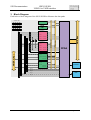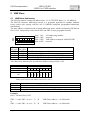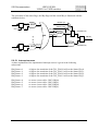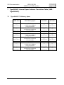
1
SIS Documentation
SIS3150USB
USB2.0 to VME interface
SIS3150USB
USB2.0 to VME Interface
with optional TigerSHARC(s)
User Manual
SIS GmbH
Harksheider Str. 102A
22399 Hamburg
Germany
Phone: ++49 (0) 40 60 87 305 0
Fax:
++49 (0) 40 60 87 305 20
email: [email protected]
http://www.struck.de
Version: sis3150usb-M-0-1v130 as of 02.10.08
Page 1 of 73
SIS Documentation
SIS3150USB
USB2.0 to VME interface
Revision Table:
Revision
0.01
1.00
1.01
1.10
1.10a
1.20
1.21
1.22
1.23
1.24
Date
25.12.04
14.01.01
09.02.05
10.03.05
10.05.05
02.06.05
26.10.05
19.12.05
26.12.05
26.09.06
1.25
1.26
1.27
1.28
1.29
1.30
28.03.07
24.05.07
06.12.07
22.01.08
28.03.08
02.10.08
Page 2 of 73
Modification
Generation
First official release
S80, 610 and 620 added
Block diagram, USB resource access, VME addressing
Minor corrections
Firmware rev. 0x2004, VME side LEMO out select register
lsusb screen shot with 3150 db entry
1st TS as option also
closedriver VI, touch up
Bug fix in BERR timeout table (default 1,25 s)
Retry Error added
LED table added
Power consumption added
Bug Fix in Arbiter Behaviour, LWORD note
S80-6 and 7 explanation
Note on D16 VME access from TigerSHARC
Additional VIs (require DLL version 20.01.08 or later)
SIS Documentation
SIS3150USB
USB2.0 to VME interface
1 Table of contents
1
1
2
Table of contents..............................................................................................................3
Introduction .....................................................................................................................5
Functionality....................................................................................................................6
2.1
3
4
Applications ...................................................................................................................................... 6
Block Diagram.................................................................................................................7
USB device ......................................................................................................................8
4.1
SIS3150 USB Register space ............................................................................................................. 8
4.1.1
USB Register Space Address Map.............................................................................................. 9
4.2
USB Register description................................................................................................................. 10
4.2.1
USB Control/Status Register(write/read) .................................................................................. 10
4.2.2
Module Id. and Firmware Revision Register ( read) .................................................................. 11
4.2.3
USB TS-Link Connect Register(write**/read) .......................................................................... 12
4.2.4
USB LEMO Out Select Register (write**/read)........................................................................ 13
4.2.5
USB VME Master Status/Control register (read/write).............................................................. 14
4.2.6
USB VME Master Cycle Status (read)..................................................................................... 16
4.2.7
USB VME Interrupt Status Register (read) ............................................................................... 16
4.2.8
XILINX JTAG_TEST register.................................................................................................. 17
4.2.9
XILINX JTAG_DATA_IN register .......................................................................................... 17
4.2.10 XILINX JTAG_CONTROL register......................................................................................... 17
4.3
TS-BUS (internal TigerSHARC Bus)............................................................................................... 18
4.4
VME Bus ........................................................................................................................................ 18
5
VME Slave ....................................................................................................................20
5.1
VME Slave Addressing.................................................................................................................... 20
5.1.1
VME Slave Address map of SIS3150 ....................................................................................... 21
5.2
Register description ......................................................................................................................... 23
5.2.1
Control/Status Register(0x, write/read)..................................................................................... 23
5.2.2
Module Id. and Firmware Revision Register (0x4, read)............................................................ 24
5.2.3
Interrupt configuration register (0x8)........................................................................................ 25
5.2.4
IRQ mode ................................................................................................................................ 25
5.2.5
Interrupt Control/Status register (0xC)...................................................................................... 26
5.2.6
LEMO Out Select Register (write/read) .................................................................................... 28
5.2.7
XILINX JTAG_TEST register.................................................................................................. 29
5.2.8
XILINX JTAG_DATA_IN register .......................................................................................... 29
5.2.9
XILINX JTAG_CONTROL register......................................................................................... 29
5.3
Common Bus description................................................................................................................. 30
5.3.1
CMC Site................................................................................................................................. 30
5.3.2
TigerSHARC ........................................................................................................................... 30
5.3.3
SDRAM................................................................................................................................... 30
6
TigerSHARC .................................................................................................................31
6.1
6.2
6.3
7
TigerSHARC global Memory Map .................................................................................................. 31
TS Hardware Interrupts.................................................................................................................... 32
TS Links.......................................................................................................................................... 33
TigerSHARC Internal Space Address Translation Table (VME / TigerSHARC) ............34
7.1
7.2
7.3
8
TigerSHARC TS1 Memory Space ................................................................................................... 34
TigerSHARC TS2 Memory Space ................................................................................................... 35
SDRAM Memory Space ................................................................................................................. 35
Tiger SHARC Host Space..............................................................................................36
8.1
9
TigerSHARC VME Master Space.................................................................................................... 36
Windows Driver.............................................................................................................39
9.1
Installation....................................................................................................................................... 39
9.1.1
Setup Installation Scripts.......................................................................................................... 39
9.1.2
Installation under XP................................................................................................................ 39
9.2
SIS3150USB base program.............................................................................................................. 42
10
10.1
Labview (Windows) Interface .....................................................................................43
closedriver....................................................................................................................................... 44
Page 3 of 73
SIS Documentation
10.2
10.3
10.4
10.5
10.6
10.7
10.8
10.9
10.10
10.11
10.12
10.13
10.14
10.15
10.16
10.17
10.18
11
lsusb................................................................................................................................................ 53
VME Readout Speed...................................................................................................54
12.1
13
Performance/speed test .................................................................................................................... 54
Front Panel Elements ..................................................................................................55
13.1
13.2
14
Front Panel LEDs ............................................................................................................................ 55
USB1/USB2.0 Distinction ............................................................................................................... 56
Jumpers/connectors.....................................................................................................57
14.1
14.2
14.3
14.4
14.5
14.6
14.7
14.8
14.9
14.10
15
16
17
FindAll_SIS3150USB_Devices ....................................................................................................... 44
handle.gbl........................................................................................................................................ 44
sis3150usb_load_dsp sis3150 usb_load_dsp_fileprompt ................................................................... 45
sis3150usb_version.......................................................................................................................... 45
sis3150usb_register_dma_write ....................................................................................................... 46
sis3150usb_register_dma_read......................................................................................................... 46
sis3150usb_register_sgl_write ......................................................................................................... 47
sis3150usb_register_sgl_read........................................................................................................... 47
sis3150_tsbus_dma_write ............................................................................................................ 48
sis3150_tsbus_dma_read.............................................................................................................. 48
sis3150_tsbus_sgl_write............................................................................................................... 49
sis3150_tsbus_sgl_read................................................................................................................ 49
vme_read..................................................................................................................................... 50
vme_write.................................................................................................................................... 50
vme_a32d32_read........................................................................................................................ 51
vme_a32d32_write....................................................................................................................... 51
vme_dma_read ............................................................................................................................ 52
LINUX .......................................................................................................................53
11.1
12
SIS3150USB
USB2.0 to VME interface
J10 16 MHz VME Sysclock............................................................................................................. 58
J770 and J771 Termination of LEMO Input 1 and 2 ......................................................................... 58
JP570 SIS3150 FPGA JTAG source................................................................................................. 59
JP580 CMC FPGA JTAG source ..................................................................................................... 59
Jumper JP_CMC1 and JP_CMC2..................................................................................................... 60
CON570 SIS3150 JTAG connector................................................................................................. 61
CON580 CMC JTAG connector ..................................................................................................... 61
TS_JTAG: TigerSHARCs JTAG Test Access Port connector ......................................................... 62
Switch S80 ...................................................................................................................................... 63
Switch S610 and S620 ................................................................................................................. 64
SIS3150 Top Assembly Drawing ................................................................................65
Connector types ..........................................................................................................66
Appendix ....................................................................................................................67
17.1 Power Consumption......................................................................................................................... 67
17.2 Protocol........................................................................................................................................... 67
17.2.1 Transfer Write Access .............................................................................................................. 67
17.2.2 Transfer Read Access............................................................................................................... 68
17.2.3 Block transfer Read Direct VME Bus Access ........................................................................... 70
17.3 Glossary .......................................................................................................................................... 71
18
Index ..........................................................................................................................72
Page 4 of 73
SIS Documentation
SIS3150USB
USB2.0 to VME interface
1 Introduction
The SIS3150/9921 USB2.0 to VME interface is a combination of two cards. The actual VME
master/slave card is the SIS3150 dual CMC carrier board, which can be equipped with up to 2
TigerSHARC Digital Signal Processors (DSPs). The SIS9921 is the interfacing CMC card,
which has the Cypress Semiconductor CY7C68013 USB2.0 controller chip.
While a USB to VME interface is slow for single cycle VME transactions (typically 100 s)
compared to a PCI to VME interface (SIS1100/3100 typically 5 s) you can reach block
transfer speeds in the 30 MByte/s ballpark (what is similar to many Tundra Universe II based
SBC’s). On the SIS3150/9921 single cycle performance can be enhanced in two ways.
pipelining of several cycles
execution of VME transactions under
control of the TigerSHARC DSP
Especially with the 2nd approach the USB2.0
to VME interface allows for the
implementation of very demanding hard
realtime applications in combination with the
ease of use with your laptop computer
The use of the 2nd CMC site of the SIS3150 for a frontend card like the SIS9300 4 channel
100 MHz 14-bit digitizer board allows you to build efficient systems with and without making
use of the VME bus. A 4 channel ADC/digitizer system of that type in a rackmount box is
shown below.
Page 5 of 73
SIS Documentation
SIS3150USB
USB2.0 to VME interface
2 Functionality
The SIS3150USB interfaces the popular Universal Serial Bus (USB) to the VMEbus. The
modules functionality comprises:
USB2.0 and USB1.1 compliance
VME master A16/A24/A32 D8/D16/D32/BLT32/MBLT64
VME slave A32/D32/BLT32/MBLT64
1 or 2 TS101 TigerSHARC DSP(s) as option
2 digital front panel inputs/2 outputs
64 MB SDRAM memory
1 available CMC site
P2 access to lower CMC site
12 front panel LEDs
2.1 Applications
The SIS3150 USB2.0 to VME interface is a good choice whenever:
a.) single cycle read/write performance is not of top importance
b.) good single cycle performance is required, but single cycle transactions can be handled
under control of the TigerSHARC DSP(s).
Applications comprise but are not limited to:
test benches
module acceptance testing
hard realtime readout systems
histogramming systems
data destination for other VME masters/existing readout systems
Page 6 of 73
SIS Documentation
SIS3150USB
USB2.0 to VME interface
3 Block Diagram
Find below a block diagram of the SIS3150USB to illustrate the data paths.
Used for USB
FLASHPROM
TS VME
SDRAM
64MB
CMC1/SIS9300 e.g.
TS1_LINK3
TSx Control
FST
FST
FST
FST
TS2_LINK1
FST
TS2_LINK2
TS2 Control
FST
Tiger Sharc 2
TS2_LINK0
TS2_LINK3
TSx Control
VME Bus
TS1 Control
64-bit data bus
FST
TS1_LINK2
32-bit address bus
FST
FST
TS1_LINK1
FST
Tiger Sharc 1
TS1_LINK0
FPGA
FST Control
CMC Site 1
VME P2 (A,C)
CMC1_LINK1
CMC1_LINK2
CMC1 Control
CMC1_LINK3
CMC Site 2 SIS9921USB
CMC2_LINK1
CMC2_LINK2
CMC2 Control
Control I/O
CMC2_LINK3
TSx_L3
TSx_L2
TSx_L1
LEDs
TSx_L0
Page 7 of 73
SIS Documentation
SIS3150USB
USB2.0 to VME interface
4 USB device
The SIS3150USB device (USB peripheral) is hotplugging.
The SIS3150USB device in combination with the drivers (Win2K/XP, future option LINUX)
supports access to following spaces.
- SIS3150 USB register space
- SIS3150 TS-BUS (internal TigerSHARC Bus)
- VME Bus
4.1 SIS3150 USB Register space
The driver offers the following calls:
int sis3150Usb_Register_Single_Read(HANDLE usbDevice,
ULONG addr, ULONG* data) ;
int sis3150Usb_Register_Dma_Read(HANDLE usbDevice,
ULONG addr, ULONG* dmabufs,
ULONG req_nof_data, ULONG* got_nof_data) ;
int sis3150Usb_Register_Single_Write(HANDLE usbDevice,
ULONG addr, ULONG data) ;
int sis3150Usb_Register_Dma_Write(HANDLE usbDevice,
ULONG addr, ULONG* dmabufs,
ULONG req_nof_data, ULONG* put_nof_data);
Page 8 of 73
SIS Documentation
SIS3150USB
USB2.0 to VME interface
4.1.1 USB Register Space Address Map
Offset
0x0
0x1
0x2
0x3
R/W
R/W
R
R/W
R/W
0x10
0x11
0x12
R/W USB VME Master Status/Control register
R
USB VME Master Cycle Status Register
R
USB VME Interrupt Status Register
0x20
0x21
R/W USB XILINX JTAG_TEST/JTAG_DATA_IN
W USB XILINX JTAG_CONTROL
0x40
R/W Test Register (32-bit read/write register)
0x100
0x101
0x102
0x103
KA
KA
KA
KA
Key reset all
Key CMC1 Hardware Reset pulse (20ms)
Key CMC1 Logic-Reset
Key TigerSHARCs Reset pulse (2us)
0x110
0x111
KA
KA
Key TigerSHARCs TS1 IRQ2 Request
Key TigerSHARCs TS2 IRQ2 Request
0x10000000
..
0x1FFFFFF
0x20000000
0xFFFFFFF
Function/Register
USB Control/Status register
Module Id. and firmware revision register
USB TS-Link Connect Register
USB LEMO Out Select Register
R
USB Address/Data Test space:
Read Data = Read Address
R
USB Speed Test space:
Read Data = Speed Counter
The Speed Counter increments every 16ns (62.5 MHz)
The shorthand KA stands for key address. Write access with arbitrary data to a key address
initiates the specified function
Page 9 of 73
SIS Documentation
SIS3150USB
USB2.0 to VME interface
4.2 USB Register description
The function of the individual registers is described in detail in this section.
The first line after the subsection header (in Courier font) like:
#define SIS3150_CONTROL_STATUS
0x0
refers to the sis3150usb.h header file.
4.2.1 USB Control/Status Register(write/read)
#define SIS3150USB_CONTROL_STATUS
0x0
The control register is in charge of the control of some basic properties of the SIS3150 board,
like enabling test pulse generators. It is implemented via a selective J/K register, a specific
function is enabled by writing a 1 into the set/enable bit, the function is disabled by writing a
1 into the clear/disable bit (which location is 16-bit higher in the register). An undefined
toggle status will result from setting both the enable and disable bits for a specific function at
the same time.
On read access the same register represents the status register.
Bit
31
..
..
24
23
22
21
20
19
18
17
16
15
..
6
5
4
3
2
1
0
write Function
Clear reserved control bit 15
..
..
Clear USB LEMO Out 2 (*)
Clear USB LEMO Out 1 (*)
Clear USB LEMO Out control bit
Clear USB XILINX JTAG Control bit (*)
switch off user LED U2 (*)
switch off user LED U1 (*)
Set reserved control bit 15
..
..
Set USB LEMO Out 2 (***)
Set USB LEMO Out 1 (***)
Set USB LEMO Out control bit
Set USB XILINX JTAG Control bit
switch on user LED U2 (**)
switch on user LED U1 (**)
read Function
0
..
..
0
Status LEMO In 2 Latch
Status LEMO In 1 Latch
Status LEMO In 2
Status LEMO In 1
0
CMC reset pulse active (21ms)
0
CMC1 detect
Status reserved control bit 15
..
..
Status USB LEMO Out 2 Bit
Status USB LEMO Out 1 Bit
Status USB LEMO Out control bit
Status USB XILINX JTAG Control bit
Status User LED U2 (**)
Status User LED U1 (**)
(1=LED on, 0=LED off)
(*) denotes power up default setting, i.e. the power up reading of the register is 0x0
(**) the LEDs could be also set from VME Slave side
(***) see USB LEMO Out Select Register
LEMO In 1/2 Latch is set on the leading edge of LEMO In 1/2 (> 16ns) and is cleared on
read access (if it was set).
USB LEMO Out Control bit = 0 :
USB LEMO Out Control bit = 1 :
VME Slave LEMO Out control
USB LEMO Out control
USB XILINX JTAG Control bit = 0 :
USB XILINX JTAG Control bit = 1 :
VME Slave XILINX JTAG control
USB XILINX JTAG control
Page 10 of 73
SIS Documentation
SIS3150USB
USB2.0 to VME interface
4.2.2 Module Id. and Firmware Revision Register ( read)
#define SIS3150USB_MODID_VERSION
0x1
This register reflects the module identification of the SIS3150/SIS3150USB and its minor and
major firmware revision levels. The major revision level will be used to distinguish between
substantial design differences and experiment specific designs, while the minor revision level
will be used to mark user specific adaptations.
Bit
31
30
29
28
27
26
25
24
23
22
21
20
19
18
17
16
15
14
13
12
11
10
9
8
7
6
5
4
3
2
1
0
Function
Module Id. Bit 15
Module Id. Bit 14
Module Id. Bit 13
Module Id. Bit 12
Module Id. Bit 11
Module Id. Bit 10
Module Id. Bit 9
Module Id. Bit 8
Module Id. Bit 7
Module Id. Bit 6
Module Id. Bit 5
Module Id. Bit 4
Module Id. Bit 3
Module Id. Bit 2
Module Id. Bit 1
Module Id. Bit 0
Major Revision Bit 7
Major Revision Bit 6
Major Revision Bit 5
Major Revision Bit 4
Major Revision Bit 3
Major Revision Bit 2
Major Revision Bit 1
Major Revision Bit 0
Minor Revision Bit 7
Minor Revision Bit 6
Minor Revision Bit 5
Minor Revision Bit 4
Minor Revision Bit 3
Minor Revision Bit 2
Minor Revision Bit 1
Minor Revision Bit 0
Major revision number
0x20
Reading
3
1
5
0
Application/user
Generic SIS3150USB design
Page 11 of 73
SIS Documentation
SIS3150USB
USB2.0 to VME interface
4.2.3 USB TS-Link Connect Register(write**/read)
#define SIS3150USB_TS_LINK_CONNECT_REG
0x2
TS-Link Breaker Enable Register
See chapter TS LINKs
** not all bits
Bit
31
..
..
12
11
10
9
8
7
6
5
4
3
2
1
meaning
no
..
..
no
no
no
TS1-Link3
TS1-Link2
TS2-Link3
TS2-Link2
TS2-Link1
TS2-Link0
TS1-Link3
TS1-Link2
TS1-Link1
TS2-Link2
TS2-Link3
internal TSx-Link3
internal TSx-Link2
internal TSx-Link1
internal TSx-Link0
internal TSx-Link3
internal TSx-Link2
internal TSx-Link1
0
TS1-Link0
internal TSx-Link0
Page 12 of 73
Function
0
..
..
0
0
0
Set/clear; 0: not connected; 1: connected
Set/clear; 0: not connected; 1: connected
0: always disabled; reserved
0: always disabled; reserved
0: always disabled; reserved
0: always disabled; reserved
0: always disabled; reserved
0: always disabled; reserved
1: always enabled;
( connected with SIS3150 FPGA; TS-VME Master DMA)
1: always enabled; ( connected with CMC1 Link 1)
SIS Documentation
SIS3150USB
USB2.0 to VME interface
4.2.4 USB LEMO Out Select Register (write**/read)
#define SIS3150USB_LEMO_OUT_SELECT_REG
0x3
Bit
31
30
29
28
27
26
25
24
23
22
21
20
19
18
17
16
meaning
reserved
reserved
VME Slave – Lemo Out 2
USB – Lemo Out 2
reserved
reserved
reserved
CMC 1 - Trigger
reserved
TS2 – Flag 2
TS2 – Flag 1
reserved
reserved
TS1 – Flag 2
TS1 – Flag 1
reserved
Function
no
no
1: VME Slave Control Bit “LEMO Out 2” is ored to LEMO OUT 2
1: USB Control Bit “LEMO Out 2” is ored to LEMO OUT 2
no
no
no
1: CMC 1 Trigger is ored to LEMO OUT 2
no
1: TS2 Flag 2 is ored to LEMO OUT 2
1: TS2 Flag 1 is ored to LEMO OUT 2
no
no
1: TS1 Flag 2 is ored to LEMO OUT 2
1: TS1 Flag 1 is ored to LEMO OUT 2
no
Bit
15
14
13
12
11
10
9
8
7
6
5
4
3
2
1
0
meaning
reserved
reserved
VME Slave – Lemo Out 1
USB – Lemo Out 1
reserved
reserved
reserved
CMC 1 - Trigger
reserved
TS2 – Flag 2
TS2 – Flag 1
reserved
reserved
TS1 – Flag 2
TS1 – Flag 1
reserved
Function
no
no
1: VME Slave Control Bit “LEMO Out 1” is ored to LEMO OUT 1
1: USB Control Bit “LEMO Out 1” is ored to LEMO OUT 1
no
no
no
1: CMC 1 Trigger is ored to LEMO OUT 1
no
1: TS2 Flag 2 is ored to LEMO OUT 1
1: TS2 Flag 1 is ored to LEMO OUT 1
no
no
1: TS1 Flag 2 is ored to LEMO OUT 1
1: TS1 Flag 1 is ored to LEMO OUT 1
no
(*) denotes power up default setting, i.e. the power up reading of the register is 0x10001000 (USB Lemo Out
Bits are selected)
Note: TS Flags are low active
Page 13 of 73
SIS Documentation
SIS3150USB
USB2.0 to VME interface
4.2.5 USB VME Master Status/Control register (read/write)
#define SIS3150USB_VME_MASTER_CONTROL_STATUS 0x10
The control register is in charge of the control of most of the basic properties of the SIS3150
board in write access. It is implemented via a selective J/K register, a specific function is
enabled by writing a 1 into the set/enable bit, the function is disabled by writing a 1 into the
clear/disable bit (which location is 16-bit higher in the register). An undefined toggle status
will result from setting both the enable and disable bits for a specific function at the same
time.
Bit
31
30
29
28
27
26
25
24
23
22
21
20
19
18
17
16
15
14
13
12
11
10
9
8
7
6
5
4
3
2
1
0
Write Function
Clear SYSTEM VME BERR TIMER BIT1
Clear SYSTEM VME BERR TIMER BIT0
Clear LONG TIMER BIT1
Clear LONG TIMER BIT0
no function
no function
no function
no function
no function
Clear VME REQUESTER TYPE BIT
Clear VME_REQ_LEVEL BIT1
Clear VME_REQ_LEVEL BIT0
no function
no function
Clear VME_SYSRESET bit
no function
Set SYSTEM VME BERR TIMER BIT1
Set SYSTEM VME BERR TIMER BIT0
Set LONG TIMER BIT1
Set LONG TIMER BIT0
no function
no function
no function
no function
no function
Set VME REQUESTER TYPE BIT
Set VME_REQ_LEVEL BIT1
Set VME_REQ_LEVEL BIT0
no function
no function
Set VME_SYSRESET bit (*4)
no function
Read Function
0
0
0
0
0
0
0
0
0
0
0
0
0
0
0
Status VME System Controller (*3)
Status SYSTEM VME BERR TIMER BIT1
Status SYSTEM VME BERR TIMER BIT0
Status LONG TIMER BIT1
Status LONG TIMER BIT0
0
0
0
0
0
Status VME REQUESTER TYPE BIT
Status VME_REQ_LEVEL BIT1
Status VME_REQ_LEVEL BIT0
0
0
Status VME_SYSRESET bit
0
The power up value is 0x00000000 (or 0x00010000 with system controller set)
Notes:
(*3) is set if Jumper J10/1-2 is inserted or if VME System Controller Enable bit is set
(*4) if Switch S80-7 is ON and VME_SYSRESET bit is set then VME_SYSRESET is issued
Page 14 of 73
SIS Documentation
SIS3150USB
USB2.0 to VME interface
Explanation/function of bit combinations:
SYSTEM VME BERR TIMER BIT1
0
0
1
1
SYSTEM VME BERR TIMER BIT0
0
1
0
1
VME Bus Error after
1,25 s (default)
6,25 s
12,5 s
100 s
Note: The default value of 1,25 s will be fine with most of VME slaves on the market, there are peculiar cards
which will respond to a VME cycle much slower however also. The bus error code is 0x211.
LONG TIMER BIT1
0
0
1
1
LONG TIMER BIT0
0
1
0
1
LONG Timeout after
1 ms (default)
10 ms
50 ms
200 ms
LONG Timeout: arbitration timeout, no reply from current VME master or VME bus mastership not granted
The arbitration timeout error code is ox214.
VME_REQ_LEVEL BIT1
0
0
1
1
VME_REQ_LEVEL BIT0
0
1
0
1
VME REQUESTER TYPE BIT
0
1
VME Bus Request Level
BR3 (highest Level, default)
BR2
BR1
BR0
VME Bus Requester Type
Release when Done (default)
Release on Request
Page 15 of 73
SIS Documentation
SIS3150USB
USB2.0 to VME interface
4.2.6 USB VME Master Cycle Status (read)
#define SIS3150USB_VME_MASTER_CYCLE_STATUS
0x11
This register contains status information for the last VME Cycle.
D31
VME Cycle Error Register
D16
D15
VME Transfer Byte Count Register
D0
VME Cycle Error Codes:
- 0x110
USB Protocol Error: invalid parameter
- 0x111
USB Protocol Error: USB write error
- 0x112
USB Protocol Error: USB read error
- 0x113
USB Protocol Error: USB read length error
-
0x211
0x212
0x214
VME Buserror
VME_RETRY_ERROR
VME Arbitration Timeout
4.2.7 USB VME Interrupt Status Register (read)
#define SIS3150USB_VME_INTERRUPT_STATUS
0x12
This register contains Status Information of the last VME Cycle. In special cases the driver
reads this Status Information register.
This register reflects the status of the VME IRQ lines.
Bit
31
..
..
8
7
6
5
4
3
2
1
0
Function
0
..
..
0
Status VME IRQ 7 on VME BUS
Status VME IRQ 6 on VME BUS
Status VME IRQ 5 on VME BUS
Status VME IRQ 4 on VME BUS
Status VME IRQ 3 on VME BUS
Status VME IRQ 2 on VME BUS
Status VME IRQ 1 on VME BUS
0
Page 16 of 73
Reading
SIS Documentation
SIS3150USB
USB2.0 to VME interface
4.2.8 XILINX JTAG_TEST register
#define SIS3150_JTAG_TEST
0x20
/* write; D32;
*/
This register is used in the firmware upgrade process over VME only. A TCK is generated
upon a write cycle to the register.
Bit
31
...
4
3
2
1
0
write Function
none
...
none
none
none
TMS
TDI
4.2.9 XILINX JTAG_DATA_IN register
#define SIS3150_JTAG_DATA_IN
0x20
/* read; D32;
*/
This register is used in the firmware upgrade process over VME only. It is at the same address
as the JTAG_TEST register and is used in read access. It operates as a shift register for TDO.
The contents of the register is shifted to the right by one bit with every positive edge of TCK
and the status of TDO is transferred to Bit 30. Bit 31 reflects the current value of TDO during
a read access.
4.2.10 XILINX JTAG_CONTROL register
#define SIS3150_JTAG_CONTROL
0x24
/* write only; D32;
*/
This register is used in the firmware upgrade process over VME only.
Bit
31
...
4
3
2
1
Function
31
...
4
3
2
MUX_CMC_JTAG
0
JTAG_OUT_EN
write
none
...
none
none
none
0: SIS3150 JTAG control
1: CMC Sites JTAG control
0: Disable JTAG output
1: Enable JTAG output
Page 17 of 73
SIS Documentation
SIS3150USB
USB2.0 to VME interface
4.3 TS-BUS (internal TigerSHARC Bus)
The Windows driver offers the following calls:
int EXPORT sis3150Usb_TsBus_Single_Read(HANDLE usbDevice,
ULONG addr, ULONG* data) ;
int EXPORT sis3150Usb_TsBus_Dma_Read(HANDLE usbDevice,
ULONG addr, ULONG* dmabufs,
ULONG req_nof_data,
ULONG* got_nof_data) ;
int EXPORT sis3150Usb_TsBus_Single_Write(HANDLE usbDevice,
ULONG addr, ULONG data) ;
int EXPORT sis3150Usb_TsBus_Dma_Write(HANDLE usbDevice,
ULONG addr, ULONG* dmabufs,
ULONG req_nof_data,
ULONG* put_nof_data) ;
4.4 VME Bus
The Windows driver offers the following calls:
int EXPORT sis3150Usb_Vme_Single_Read(HANDLE usbDevice,
ULONG addr,
ULONG am,
ULONG size,
ULONG* data) ;
int EXPORT sis3150Usb_Vme_Dma_Read(HANDLE usbDevice,
ULONG addr,
ULONG am,
ULONG size,
ULONG fifo_mode,
ULONG* dmabufs,
ULONG req_nof_data,
ULONG* got_nof_data) ;
Note: req_nof_data and got_nof_data are counted in longwords
int EXPORT sis3150Usb_Vme_Single_Write(HANDLE usbDevice,
ULONG addr,
ULONG am,
ULONG size,
ULONG data);
int EXPORT sis3150Usb_Vme_Dma_Write(HANDLE usbDevice,
ULONG addr,
ULONG am,
ULONG size,
ULONG fifo_mode,
ULONG* dmabufs,
ULONG req_nof_data,
ULONG* put_nof_data);
Page 18 of 73
SIS Documentation
SIS3150USB
USB2.0 to VME interface
Not all combinations of the parameters are possible and allowed.
All supported VME cycles are defined in the include file
..\sis3150usb_vme_win_utils\sis3150usb_calls\ sis3150usb_vme_calls.h.
Examples:
int vme_A32D32_read(HANDLE hXDev,
u_int32_t vme_adr,
u_int32_t* vme_data ) ;
int vme_A32MBLT64_read(HANDLE hXDev,
u_int32_t vme_adr,
u_int32_t* vme_data,
u_int32_t req_num_of_lwords,
u_int32_t* got_no_of_lwords) ;
Note: req_num_of_lwords and got_no_of_lwords are counted in longwords
Page 19 of 73
SIS Documentation
SIS3150USB
USB2.0 to VME interface
5 VME Slave
5.1 VME Slave Addressing
The SIS3150 module occupies an address space of 0x 7FF FFFF Bytes (i.e. 128 MBytes).
The SIS3150 firmware addressing concept is a pragmatic approach to combine standard
rotary switch style settings with the use of VME64x backplane geographical addressing
functionality.
The base address is defined by the selected addressing mode, which is defined by DIP-Switch
S80-1/2/3/4 and possibly rotary switch SW2 and SW1 (in non geographical mode).
2
3
4
5
6
7
8
S80
1
OFF
S80-1
S80-2
S80-3
S80-4
ON:
OFF:
OFF:
OFF:
A32 addressing enabled
reserved
VME address compared with SW2/SW1
reserved
S80-1
S80-3 Description
EN_A32 EN_GEO
OFF
OFF
non A32 addressing, reserved for future use
OFF
ON
non A32 addressing, reserved for future use
ON
OFF
A32 addressing, address compared with SW1/SW2
ON
ON
A32 addressing, address compared with geographical address
The table below illustrates the possible base address settings if S80-1 ON.
*
y
y
y
GA0
GA1
GA2
ON
GA3
OFF
Bits
31 30 29 28 27
SW2
SW1*
GA4
S80-3
if SW1 between 0 and 7 then address selectection if A27=0
if SW1 between 8 and F then address selectection if A27=1
Shorthand
SW2/SW1
y
GA0-GA4
Explanation
Setting of rotary switch SW2 or SW1 respective
don’t care
Geographical address bit as defined by the VME64x(P) backplane
Example:
S80-1 ON and S80-3 OFF
SW2 = 2 and SW1 = 0 (or 1....7)
or
SW2 = 9 and SW1 = 8 (or 9....F)
Page 20 of 73
VME Base Address = 0x 2000 0000
VME Base Address = 0x 9800 0000
SIS Documentation
SIS3150USB
USB2.0 to VME interface
5.1.1 VME Slave Address map of SIS3150
VME Slave Space
REGISTER
KEY ADDRESSES
0x0000 0000
0x0000 0FFF
RESERVED
0x0080 0000
FLASHPROM
0x009F FFFF
RESERVED
0x0100 0000
Common Bus Space
CMC Site 1
0x0180 0000
CMC Site 2
0x0200 0000
TS1
0x0300 0000
TS2
0x0400 0000
SDRAM
0x07FF FFFF
Page 21 of 73
SIS Documentation
SIS3150USB
USB2.0 to VME interface
5.1.1.1 VME Register Space
The implemented VME registers are listed in the table below.
Offset
0x0
0x4
0x8
0xC
0x10
R/W
R/W
R
R/W
R/W
R/W
Mode
D32
D32
D32
D32
D32
0x20
0x24
R/W
W
XILINX JTAG_TEST/JTAG_DATA_IN
XILINX JTAG_CONTROL
future use
R/W
One wire Id. register
0x400
0x404
0x408
0x40C
0x410
KA
KA
KA
KA
KA
D32
D32
D32
D32
D32
Function/Register
Control/Status register
Module Id. and firmware revision register
Interrupt configuration register
Interrupt control/status register
LEMO out selec register
Key reset all
Key CMC1 and CMC2 Hardware Reset pulse (20ms)
Key CMC1 Logic-Reset
Key CMC2 Logic-Reset
Key TigerSHARCs Reset pulse (2us)
The shorthand KA stands for key address. Write access with arbitrary data to a key address
initiates the specified function
5.1.1.2 Common Bus Address Space
The common bus resources are addressed through VME as listed below.
Offset
0x080 0000 to
0x09F FFFC
R/W
R/W
0x100 0000 to
0x17F FFFC
0x180 0000 to
0x1FF FFFC
0x200 0000 to
0x2FF FFFC
0x300 0000 to
0x3FF FFFC
0x400 0000 to
0x7FF FFFC
R/W
Mode
D32
Function/Register
Flashprom (not yet implemented)
4Mbit 512Kbyte
access only with D7-D0 2Mbyte space
R/W
D32
CMC Site 1
(BLT32/MBLT64)
D32
CMC Site 2
(BLT32/MBLT64)
D32/BLT32/MBLT64 TigerSHARC TS1
R/W
D32/BLT32/MBLT64 TigerSHARC TS2
R/W
D32/BLT32/MBLT64 SDRAM
R/W
Note: Access to the SDRAM is only allowed after the SDRAM Controller of the TigerSHARC (TS1) is
configured and enabled.
Page 22 of 73
SIS Documentation
SIS3150USB
USB2.0 to VME interface
5.2 Register description
The function of the individual registers is described in detail in this section.
The first line after the subsection header (in Courier font) like:
#define SIS3150_CONTROL_STATUS
0x0
/* read/write; D32 */
refers to the sis3150.h header file.
5.2.1 Control/Status Register(0x, write/read)
#define SIS3150_CONTROL_STATUS
0x0
/* read/write; D32 */
The control register is in charge of the control of some basic properties of the SIS3150 board,
like enabling test pulse generators. It is implemented via a selective J/K register, a specific
function is enabled by writing a 1 into the set/enable bit, the function is disabled by writing a
1 into the clear/disable bit (which location is 16-bit higher in the register). An undefined
toggle status will result from setting both the enable and disable bits for a specific function at
the same time.
On read access the same register represents the status register.
Bit
31
..
22
21
20
19
18
17
16
15
..
6
5
4
3
2
1
0
write Function
Clear reserved control bit 15
..
..
Clear VME Slave LEMO Out 2 (*)
Clear VME Slave LEMO Out 1 (*)
Clear reserved control bit 3
Clear reserved control bit 2
switch off user LED U2 (*)
switch off user LED U1 (*)
Set reserved control bit 15
..
..
Set VME Slave LEMO Out 2 (***)
Set VME Slave LEMO Out 1 (***)
Set reserved control bit 3
Set reserved control bit 2
switch on user LED U2 (**)
switch on user LED U1 (**)
read Function
0
..
..
..
0
0
CMC reset pulse active (21ms)
CMC2 detect
CMC1 detect
Status reserved control bit 15
..
..
Status VME Slave LEMO Out 2 Bit
Status VME Slave LEMO Out 1 Bit
Status reserved control bit 3
Status reserved control bit 2
Status User LED U2 (**)
Status User LED U1 (**)
(1=LED on, 0=LED off)
(*) denotes power up default setting, i.e. the power up reading of the register is 0x0
(**) the LEDs can be set from the USB side also
(***) see USB LEMO Out Select Register
Page 23 of 73
SIS Documentation
SIS3150USB
USB2.0 to VME interface
5.2.2 Module Id. and Firmware Revision Register (0x4, read)
#define SIS3150_MODID
0x4
/* read only; D32 */
This register reflects the module identification of the SIS3150 and its minor and major
firmware revision levels. The major revision level will be used to distinguish between
substantial design differences and experiment specific designs, while the minor revision level
will be used to mark user specific adaptations.
Bit
31
30
29
28
27
26
25
24
23
22
21
20
19
18
17
16
15
14
13
12
11
10
9
8
7
6
5
4
3
2
1
0
Function
Module Id. Bit 15
Module Id. Bit 14
Module Id. Bit 13
Module Id. Bit 12
Module Id. Bit 11
Module Id. Bit 10
Module Id. Bit 9
Module Id. Bit 8
Module Id. Bit 7
Module Id. Bit 6
Module Id. Bit 5
Module Id. Bit 4
Module Id. Bit 3
Module Id. Bit 2
Module Id. Bit 1
Module Id. Bit 0
Major Revision Bit 7
Major Revision Bit 6
Major Revision Bit 5
Major Revision Bit 4
Major Revision Bit 3
Major Revision Bit 2
Major Revision Bit 1
Major Revision Bit 0
Minor Revision Bit 7
Minor Revision Bit 6
Minor Revision Bit 5
Minor Revision Bit 4
Minor Revision Bit 3
Minor Revision Bit 2
Minor Revision Bit 1
Minor Revision Bit 0
Reading
3
1
5
0
5.2.2.1 Major revision numbers
Find below a table with major revision numbers used/reserved to date
Major revision number
0x01
Page 24 of 73
Application/user
Generic SIS3150 CMC SIS9920_ETH design
SIS Documentation
SIS3150USB
USB2.0 to VME interface
5.2.3 Interrupt configuration register (0x8)
#define SIS3150_IRQ_CONFIG
0x8
/* read/write; D32 */
In conjunction with the interrupt control register this read/write register controls the VME
interrupt behaviour of the SIS3150. Eight interrupt sources are foreseen, for the time being
four of them are associated with an interrupt condition, the others are reserved for future use.
The interrupter type is DO8 .
5.2.4 IRQ mode
In RORA (release on register access) mode the interrupt will be pending until the IRQ
source is cleared by specific access to the corresponding disable VME IRQ source bit. After
the interrupt is serviced the source has to be activated with the enable VME IRQ source bit
again.
In ROAK (release on acknowledge) mode , the interrupt condition will be cleared (and the
IRQ source disabled) as soon as the interrupt is acknowledged by the CPU. After the interrupt
is serviced the source has to be activated with the enable VME IRQ source bit again.
Bit
31
...
16
15
14
13
12
11
10
9
8
7
6
5
4
3
2
1
0
Function
RORA/ROAK Mode (0: RORA; 1: ROAK)
VME IRQ Enable (0=IRQ disabled, 1=IRQ enabled)
VME IRQ Level Bit 2
VME IRQ Level Bit 1
VME IRQ Level Bit 0
IRQ Vector Bit 7; placed on D7 during VME IRQ ACK cycle
IRQ Vector Bit 6; placed on D6 during VME IRQ ACK cycle
IRQ Vector Bit 5; placed on D5 during VME IRQ ACK cycle
IRQ Vector Bit 4; placed on D4 during VME IRQ ACK cycle
IRQ Vector Bit 3; placed on D3 during VME IRQ ACK cycle
IRQ Vector Bit 2; placed on D2 during VME IRQ ACK cycle
IRQ Vector Bit 1; placed on D1 during VME IRQ ACK cycle
IRQ Vector Bit 0; placed on D0 during VME IRQ ACK cycle
Default
0
0
0
0
0
0
0
0
0
0
0
0
0
0
0
0
0
0
0
The power up default value reads 0x00000000
Page 25 of 73
SIS Documentation
SIS3150USB
USB2.0 to VME interface
5.2.5 Interrupt Control/Status register (0xC)
#define SIS3150_IRQ_CONTROL
0xC
/* read/write; D32 */
The interrupt sources are enabled with the interrupt control register. The interrupt source is
cleared in the interrupt service routine. The status internal IRQ flag can be used for tests
without activating VME interrupt generation. It is set whenever an interrupt would be
generated if interrupting would be enabled in the interrupt configuration register.
fourth condition is reserved for future use.
Bit
31
30
29
28
27
26
25
24
23
22
21
20
19
18
17
16
15
14
13
12
11
10
9
8
7
6
5
4
3
2
1
0
Function (w)
1 Shot : IRQ_UPDATE
unused
unused
unused
unused
unused
unused
unused
Clear IRQ source 7
Clear IRQ source 6
Clear IRQ source 5
Clear IRQ source 4
Clear IRQ source 3
Clear IRQ source 2
Clear IRQ source 1
Clear IRQ source 0
Disable IRQ source 7
Disable IRQ source 6
Disable IRQ source 5
Disable IRQ source 4
Disable IRQ source 3
Disable IRQ source 2
Disable IRQ source 1
Disable IRQ source 0
Enable IRQ source 7
Enable IRQ source 6
Enable IRQ source 5
Enable IRQ source 4
Enable IRQ source 3
Enable IRQ source 2
Enable IRQ source 1
Enable IRQ source 0
(r)
Status IRQ source 7 (CMC2_VME_IRQ1: reserved)
Status IRQ source 6 (CMC2_VME_IRQ0: reserved)
Status IRQ source 5 (CMC1_VME_IRQ1: reserved)
Status IRQ source 4 (CMC1_VME_IRQ0: reserved)
Status IRQ source 3 (TS2_VME_IRQ1; ? sensitive)
Status IRQ source 2 (TS2_VME_IRQ0; ? sensitive)
Status IRQ source 1 (TS1_VME_IRQ1; ? sensitive)
Status IRQ source 0 (TS1_VME_IRQ0; ? sensitive)
Status flag source 7
Status flag source 6
Status flag source 5
Status flag source 4
Status flag source 3
Status flag source 2
Status flag source 1
Status flag source 0
Status VME IRQ
Status internal IRQ
0
0
0
0
0
0
Status enable source 7 (read as 1 if enabled, 0 if disabled)
Status enable source 6 (read as 1 if enabled, 0 if disabled)
Status enable source 5 (read as 1 if enabled, 0 if disabled)
Status enable source 4 (read as 1 if enabled, 0 if disabled)
Status enable source 3 (read as 1 if enabled, 0 if disabled)
Status enable source 2 (read as 1 if enabled, 0 if disabled)
Status enable source 1 (read as 1 if enabled, 0 if disabled)
Status enable source 0 (read as 1 if enabled, 0 if disabled)
The power up default value reads 0x00000000
Note: The clear IRQ source bits are relevant for edge sensitive IRQs only
Page 26 of 73
Default
0
0
0
0
0
0
0
0
0
0
0
0
0
0
0
0
0
0
0
0
0
0
0
0
0
0
0
0
0
0
0
SIS Documentation
SIS3150USB
USB2.0 to VME interface
The generation of the status flags, the IRQ flags and the actual IRQ is illustrated with the
schematic below:
IRQ ACK cycle
Status FLAG
Source 0
Source 0
Clear
AND
Status IRQ
Source 0
VME IRQ enable
Enable 0
O
R
IRQ_Update
Clear
OR
internal
VME_IRQ
IRQ (ROAK case)
AND
MUX
Status FLAG
Source 7
Source 7
Clear
AND
Status IRQ
Source 7
VME IRQ
AND
IRQ (RORA case)
Enable 7
5.2.5.1 Interrupt sources
A short explanation of the implemented interrupt sources is given in the following
subsections.
IRQ Source 0:
IRQ Source 1:
IRQ Source 2:
IRQ Source 3:
A high to low transition of the TS1_FLAG0 will set the Status Flag 0.
A high to low transition of the TS1_FLAG1 will set the Status Flag 1.
A high to low transition of the TS2_FLAG0 will set the Status Flag 2.
A high to low transition of the TS2_FLAG1 will set the Status Flag 3.
IRQ Source 4:
IRQ Source 5:
IRQ Source 6:
IRQ Source 7:
no source (reserved for CMC1 IRQ0)
no source (reserved for CMC1 IRQ1)
no source (reserved for CMC2 IRQ0)
no source (reserved for CMC2 IRQ1)
Page 27 of 73
SIS Documentation
SIS3150USB
USB2.0 to VME interface
5.2.6 LEMO Out Select Register (write/read)
#define SIS3150_LEMO_OUT_SELECT_REG
0x10
This register allows you to select the source(s) that are driving the LEMO outputs on the
SIS3150 board.
Bit
31
30
29
28
27
26
25
24
23
22
21
20
19
18
17
16
meaning
reserved
reserved
VME Slave – Lemo Out 2
USB – Lemo Out 2
reserved
reserved
reserved
CMC 1 - Trigger
reserved
TS2 – Flag 2
TS2 – Flag 1
reserved
reserved
TS1 – Flag 2
TS1 – Flag 1
reserved
Function
No
No
1: VME Slave Control Bit “LEMO Out 2” is ored to LEMO OUT 2
1: USB Control Bit “LEMO Out 2” is ored to LEMO OUT 2
No
No
No
1: CMC 1 Trigger is ored to LEMO OUT 2
No
1: TS2 Flag 2 is ored to LEMO OUT 2
1: TS2 Flag 1 is ored to LEMO OUT 2
No
No
1: TS1 Flag 2 is ored to LEMO OUT 2
1: TS1 Flag 1 is ored to LEMO OUT 2
No
Bit
15
14
13
12
11
10
9
8
7
6
5
4
3
2
1
0
meaning
reserved
reserved
VME Slave – Lemo Out 1
USB – Lemo Out 1
reserved
reserved
reserved
CMC 1 - Trigger
reserved
TS2 – Flag 2
TS2 – Flag 1
reserved
reserved
TS1 – Flag 2
TS1 – Flag 1
reserved
Function
No
No
1: VME Slave Control Bit “LEMO Out 1” is ored to LEMO OUT 1
1: USB Control Bit “LEMO Out 1” is ored to LEMO OUT 1
No
No
No
1: CMC 1 Trigger is ored to LEMO OUT 1
No
1: TS2 Flag 2 is ored to LEMO OUT 1
1: TS2 Flag 1 is ored to LEMO OUT 1
No
No
1: TS1 Flag 2 is ored to LEMO OUT 1
1: TS1 Flag 1 is ored to LEMO OUT 1
No
(*) denotes power up default setting, i.e. the power up reading of the register is 0x10001000 (USB Lemo Out
Bits are selected)
Note: TS Flags are low active
Page 28 of 73
SIS Documentation
SIS3150USB
USB2.0 to VME interface
5.2.7 XILINX JTAG_TEST register
#define SIS3150_JTAG_TEST
0x20
/* write; D32;
*/
This register is used in the firmware upgrade process over VME only. A TCK is generated
upon a write cycle to the register.
Bit
31
...
4
3
2
1
0
write Function
none
...
none
none
none
TMS
TDI
5.2.8 XILINX JTAG_DATA_IN register
#define SIS3150_JTAG_DATA_IN
0x20
/* read; D32;
*/
This register is used in the firmware upgrade process over VME only. It is at the same address
as the JTAG_TEST register and is used in read access. It operates as a shift register for TDO.
The contents of the register is shifted to the right by one bit with every positive edge of TCK
and the status of TDO is transferred to Bit 30. Bit 31 reflects the current value of TDO during
a read access.
5.2.9 XILINX JTAG_CONTROL register
#define SIS3150_JTAG_CONTROL
0x24
/* write only; D32;
*/
This register is used in the firmware upgrade process over VME only.
Bit
31
...
4
3
2
1
Function
31
...
4
3
2
MUX_CMC_JTAG
0
JTAG_OUT_EN
write
none
...
none
none
none
0: SIS3150 JTAG control
1: CMC Sites JTAG control
0: Disable JTAG output
1: Enable JTAG output
Page 29 of 73
SIS Documentation
SIS3150USB
USB2.0 to VME interface
5.3 Common Bus description
The function of the individual registers is described in detail in this section.
The first line after the subsection header (in Courier font) like:
#define
#define
#define
#define
#define
SIS3150_CMC1_BASE
SIS3150_CMC2_BASE
SIS3150_TS1_BASE
SIS3150_TS2_BASE
SIS3150_SDRAM_BASE
0x01000000
0x01800000
0x02000000
0x03000000
0x04000000
refers to the sis3150.h header file.
5.3.1 CMC Site
Only the data bits 35-0 of the common 64-bit data bus are connected to the CMC Sites.
5.3.2 TigerSHARC
After Reset (also Power Up Reset) the TigerSHARC’s External Data Port is configured in 32bit Bus Width Mode.
Therefore, at first the TS_REG_SYSCON has to be programmed.
5.3.3 SDRAM
Supported 32-bit and 64-bit access to SDRAM.
Note:
Page 30 of 73
Access to the SDRAM is only allowed after the SDRAM Controller of the
TigerSHARC (TS1) is configured and enabled.
SIS Documentation
SIS3150USB
USB2.0 to VME interface
6 TigerSHARC
The two TigerSHARCs, the two CMC Sites and the SIS3150 FPGA (VME interface) use a
common bus (32-bit address and 64-bit data) on the SIS3150. Additional a 64 Mbyte SDRAM
and a 512 Kbyte 8-bit Flashprom (not yet supported) are connected also to the common bus.
Each TigerSHARC has access to the CMC Sites, to the other TigerSHARC, to the SDRAM
and to the Flashprom (not yet supported).
The TigerSHARC TS1 has the processor ID 0 and the TigerSHARC TS2 has the pocessor ID
1.
6.1 TigerSHARC global Memory Map
The TigerSHARC DSP has an internal, a multiprocessor space and an external space. The
internal space (inside the DSP) consisting of a set of registers and three Memory Blocks
(6Mbit, each 2Mbit).
INTERNAL SPACE
INTERNAL MEMORY
BLOCK 0
GLOBAL SPACE
0x0000 0000
0x0000 0000
INTERNAL SPACE
0x0000 FFFF
0x003F FFFF
RESERVED
INTERNAL MEMORY
BLOCK 1
RESERVED
0x0008 0000
0x01C0 0000
BROADCAST
0x0008 FFFF
0x0200 0000
RESERVED
INTERNAL MEMORY
BLOCK2
PROCESSOR ID 0
0x0010 0000
0x0240 0000
PROCESSOR ID 1
0x0010 FFFF
0x0280 0000
INTERNAL REGISTERS
(UREGS)
PROCESSOR ID 2
0x0018 0000
0x0018 FFFF
Multiprocessor Space
RESERVED
0x02C0 0000
PROCESSOR ID 3
0x0300 0000
PROCESSOR ID 4
0x0340 0000
PROCESSOR ID 5
0x0380 0000
PROCESSOR ID 6
RESERVED
0x03C0 0000
PROCESSOR ID 7
0x0400 0000
SDRAM
0x0800 0000
External Space
0x003F FFFF
CMC Site 1
(MEMORY BANK 0)
0x0C00 0000
CMC Site 2
(MEMORY BANK1)
0x1000 0000
HOST
0xFFFF FFFF
Page 31 of 73
SIS Documentation
SIS3150USB
USB2.0 to VME interface
6.2 TS Hardware Interrupts
Each DSP supports four external hardware Interrupts (IRQ3-0).
The sources of the eight IRQs (TS1_IRQ3-0 and TS2_IRQ3-0) are defined by the SIS3150
FPGA design.
The SIS3150 Firmware versions “31500101” and
assignments.
“31500102”
TS1_IRQ0
TS1_IRQ1
TS1_IRQ2
TS1_IRQ3
CMC Site 1
(CMC_TS1_IRQ_REQ)
CMC Site 2
(CMC_TS1_IRQ_REQ)
USB Key Address
leading edge NIM Input 1
TS2_IRQ0
TS2_IRQ1
TS2_IRQ2
TS2_IRQ3
CMC Site 1
(CMC_TS1_IRQ_REQ)
CMC Site 2
(CMC_TS1_IRQ_REQ)
USB Key Address
leading edge NIM Input 1
Page 32 of 73
supports the following
SIS Documentation
SIS3150USB
USB2.0 to VME interface
6.3 TS Links
The TigerSHARC link ports provide an optional high speed communications channel that is
useful for implementing point to point communication without using the common data bus.
The DSP’s core can write directly to a link port’s transmit register and read from a receive
register or the DMA controller can perform DMA transfers through the link port DMA
channels.
Each TigerSHARC has four Link Ports (TS1_L0, .. TS1_L3, TS2_L0, .. TS2_L3). Each
CMC side has two Link Ports. The SIS3150 FPGA has four Link Ports also.
The SIS3150 onboard “breakers” open or close the connection(s) between these different
Link Ports.
Following ten point to point connections are possible:
TS1L0
TS1L1
TS1L2
TS1L3
internal TSxL0
internal TSxL1
internal TSxL2
internal TSxL3
(connected with CMC Site 1 and SIS3150 FPGA)
(connected with CMC Site 2 and SIS3150 FPGA)
(connected with CMC Site 1 and SIS3150 FPGA)
(connected with CMC Site 2 and SIS3150 FPGA)
TS2L0
TS2L1
TS2L2
TS2L3
internal TSxL0
internal TSxL1
internal TSxL2
internal TSxL3
(connected with CMC Site 1 and SIS3150 FPGA)
(connected with CMC Site 2 and SIS3150 FPGA)
(connected with CMC Site 1 and SIS3150 FPGA)
(connected with CMC Site 2 and SIS3150 FPGA)
TigerSHARC to TigerSHARC point to point connections
TS1L2
TS2L3
TS1L3
TS2L2
In SIS3150 Firmware versions “31500101” and “31500102”, the point to point connections
are set by design. In future Firmware versions, it will be programmable by VME Slave
register access.
The following point to point connections are closed together:
TS1L0
TS1L1
TS1L2
TS1L3
internal TSxL0
internal TSxL1
internal TSxL2
internal TSxL3
connected with CMC Site 1
connected with CMC Site 2
connected with CMC Site 1
connected with CMC Site 2
Page 33 of 73
SIS Documentation
SIS3150USB
USB2.0 to VME interface
7 TigerSHARC Internal Space Address Translation Table (VME /
TigerSHARC)
7.1 TigerSHARC TS1 Memory Space
VME offset
TS1 Memory Space
TS1 offset
TS2 offset
0x02000000
to
0x0200fffc
Block 0
0x00000000
to
0x00003fff
0x02400000
to
0x02403fff
0x00004000
to
0x0000ffff
0x02404000
to
0x0240ffff
0x00080000
to
0x00083fff
0x02480000
to
0x02483fff
0x00084000
to
0x0008ffff
0x02484000
to
0x0248ffff
0x00100000
to
0x00103fff
0x02500000
to
0x02503fff
0x00104000
to
0x0010ffff
0x02504000
to
0x0250ffff
0x02010000
to
0x0203fffc
0x02200000
to
0x0220fffc
0x02210000
to
0x0223fffc
0x02400000
to
0x0240fffc
0x02410000
to
0x0243fffc
Page 34 of 73
16 KLWord (64 KByte)
program code/data
Block 0
48 KLWord (192 KByte)
free user buffer
Block 1
16 KLWord (64 KByte)
program code/data
Block 1
48 KLWord (192 KByte)
free user buffer
Block 2
16 KLWord (64 KByte)
program code/data
Block 2
48 KLWord (192 KByte)
free user buffer
SIS Documentation
SIS3150USB
USB2.0 to VME interface
7.2 TigerSHARC TS2 Memory Space
VME offset
TS2 Memory Space
TS1 offset
TS2 offset
0x03000000
to
0x0300fffc
Block 0
0x02000000
to
0x02003fff
0x00000000
to
0x00003fff
0x02004000
to
0x0200ffff
0x00004000
to
0x0000ffff
0x02080000
to
0x02083fff
0x00080000
to
0x00083fff
0x02084000
to
0x0208ffff
0x00084000
to
0x0008ffff
0x02100000
to
0x02103fff
0x00000000
to
0x00003fff
0x02104000
to
0x0210ffff
0x00004000
to
0x0000ffff
Buffer
TS1 offset
TS2 offset
64Mbyte SDRAM
0x04000000
to
0x04FFFFFF
0x04000000
to
0x04FFFFFF
0x03010000
to
0x0303fffc
0x03200000
to
0x0320fffc
0x03210000
to
0x0323fffc
0x03400000
to
0x0340fffc
0x03410000
to
0x0343fffc
7.3
16 KLWord (64 KByte)
program code/data
Block 0
48 KLWord (192 KByte)
free user buffer
Block 1
16 KLWord (64 KByte)
program code/data
Block 1
48 KLWord (192 KByte)
free user buffer
Block 2
16 KLWord (64 KByte)
program code/data
Block 2
48 KLWord (192 KByte)
free user buffer
SDRAM Memory Space
VME offset
0x04000000
to
007fffffc
Page 35 of 73
SIS Documentation
SIS3150USB
USB2.0 to VME interface
8 Tiger SHARC Host Space
The TS Host Space is defined from address 0x1000 0000 to 0xffff ffff
8.1 TigerSHARC VME Master Space
The TS VME Space is defined from 0x1000 0000 to 0x1fff ffff.
Access is D64 always.
A command is initiated by D64 write cycle.
The lower 32 data bits [D31:0] hold the write datum (don’t care on read), the upper 32 data
bits [D63:32] hold the VME address.
The TS address [A27:A1] holds the address modifier for the cycle and so on.
Example VME write:
volatile unsigned long long var_long64_data ;
volatile unsigned long long * vme_space_long64_pointer ;
vme_space_long64_pointer = (unsigned long long *) host_start_addr + vme_space_mode ;
/* write */
var_long64_data = __builtin_compose_64u(vme_space_address, vme_space_data); // D63:32, D31:0
*(vme_space_long64_pointer) = var_long64_data ;
/* read */
var_long64_data = *(vme_space_long64_pointer) ;
D63:32 holds the status register
D31:0 holds the read datum (for a single cycle read)
Data are passed over a link to the TS during a DMA
Note: Set address bit A0 for D16 VME access (corresponding to bit D32 of the D64 DSP
write cycle)
Page 36 of 73
SIS Documentation
SIS3150USB
USB2.0 to VME interface
The function of the individual bits is given in the table below.
TS Addr
Bit
Write Function
27
26
25
24
Force VME AS Single cycle during DMA with
constant Vme Addresses
reserved
reserved
reserved
23
READ_FIFO_DISABLE
0: VME read data will be pushed into FIFO
1: VME read data will be stored in register only
22
READ_FIFO_CLR_DISABLE
0: VME read FIFO will be cleared at the beginning
1: VME read FIFO will not be cleared at the beginning
21
WORD_COUNT_CLR_DISABLE
0: clear word count on each sequencer read
1: leave word count uncleared
20
19
18
17
16
VME ADDR_INC_DISABLE (DMA)
HOLD_VME_MASTER
DMA_CYCLE
SINGLE_CYCLE
VME_CYCLE (not INTERNAL_CYCLE)
for VME_CYCLE
15
14
13
12
11
10
9
8
15
14
13
12
11
10
9
8
for Internal_CYCLE
reserved
DMA_MODE Bit 1
DMA_MODE Bit 0
DMA (read)
reserved
VME AS HOLD
VME DS1 Veto
VME DS0 Veto
VME_IACK
VME_WRITE
VME_AM5
VME_AM4
VME_AM3
VME_AM2
VME_AM1
VME_AM0
Note: Set address bit A0 for D16 VME access (corresponding to bit D32 of the D64 DSP
write cycle)
Page 37 of 73
SIS Documentation
SIS3150USB
USB2.0 to VME interface
More detailed description of bits [19:16]
ADDR_19
ADDR_18
ADDR_17
ADDR_16
HOLD_VME_
MASTER
DMA_CYCLE
SINGLE_CYCLE
INTERN
x
x
x
1
internal Cycle
0
0
0
0
release VME MASTER_SHIP
1
0
0
0
VME Arbitration only and hold VME
MASTER_SHIP
0
0
1
0
VME Single Cycle with Arbitration
and release VME MASTER_SHIP
1
0
1
0
VME Single Cycle with Arbitration
and hold VME MASTER_SHIP
0
1
x
0
VME DMA Cycle with Arbitration
and release VME MASTER_SHIP
1
1
x
0
VME DMA Cycle with Arbitration
and hold VME MASTER_SHIP
Page 38 of 73
CYCLE
SIS Documentation
SIS3150USB
USB2.0 to VME interface
9 Windows Driver
9.1
Installation
9.1.1 Setup Installation Scripts
The setup installation scripts can be found on the SISCDROM as shown below:
Run the setup_win2k or setup_winxp script in the corresponding directory. The batch files
will copy the required files to your c: disk drive.
9.1.2 Installation under XP
As soon as a SIS3150USB is detected on a USB port for the first time you will be prompted
by the hardware assistant under Windows XP (while the driver will just be installed under
Windows 2000). You will not want to connect to Windows Update.
Page 39 of 73
SIS Documentation
SIS3150USB
USB2.0 to VME interface
In the next step you select automatic installation.
The SIS3150 USB driver did not undergo the Windows-Logo-Test, but you will want to
continue installation anyway.
In the last step you finish installation.
Page 40 of 73
SIS Documentation
SIS3150USB
USB2.0 to VME interface
Page 41 of 73
SIS Documentation
SIS3150USB
USB2.0 to VME interface
9.2 SIS3150USB base program
The SIS3150USB base program is a convenient tool to execute VME cycles with the USB to
VME interface. It has a graphical user interface and is based on National Instruments
Labwindows CVI development environment. The program with the CVI runtime engine
(RTE) can be installed by running the setup executable in the cvidistkit directory.
The user interface of the program is shown below.
Note: The SIS3150 USB base program checks for USB devices in a cyclic manner as long as
the USB Device check slide bar is set to On. The scan resets the user LED on the SIS3150 in
case it was set/switched on with a control write.
Page 42 of 73
SIS Documentation
SIS3150USB
USB2.0 to VME interface
10 Labview (Windows) Interface
The SIS3150USB Labview interface uses the same DLL as the standard Windows driver. At
this point in time the VIs are limited to one SIS3150USB interface. The handle for this
interface is passed to the VME access VIs as a global variable.
Copy the winlabview directory to your c: drive.
The DLL is assumed to be in c:\sis3150winlabview\sis3150usb_vme_win.dll
Page 43 of 73
SIS Documentation
SIS3150USB
USB2.0 to VME interface
10.1 closedriver
The closedriver VI is used to close the instance of the driver (after powering off the VME
crate eg.). Without closing the driver you will get a new device with every power cycle
Ezusb-0, Ezusb-1, Ezusb-2, Ezusb-3. After Ezusb-3 you would have to restart Labview to
start at Ezusb-0 again. Please not, that the closedriver VI needs the last valid handle as input
parameter (i.e. you can not use the global handle from a failed call to the
FindAll_SIS3150USB_Devices VI to close the driver.
10.2 FindAll_SIS3150USB_Devices
This VI scans for SIS3150USB devices, reports the number of found devices, lists the first
device, opens a handle to the first device and downloads the code the Cypress FX USB
controller chip. Serial number and firmware revision of the first device are reported also. The
error and FX Download Error LEDs stay off upon successful completion.
10.3 handle.gbl
This handle holds the global variable handle, that is used for VME access through the first
found interface in the VME calls.
Page 44 of 73
SIS Documentation
SIS3150USB
USB2.0 to VME interface
10.4 sis3150usb_load_dsp sis3150 usb_load_dsp_fileprompt
These 2 VIs reset the DSP(s), open a loader file, load the code to the DSP(s) and start the DSP(s). The filename
is hardcoded to tigersharc.ldr for sis3150_load_dsp while you will be prompted for a filename with
sis3150usb_load_dsp_fileprompt.
The error code is 0 upon successful completion. An error code of -4 indicates access to a non existing file (as
illustrated below).
10.5 sis3150usb_version
Returns the version of the used sis3150usb_vme_win DLL (implemented January 20 th of 2008
as shown in the screenshot below). The format of the returned hex value is ddmmyy00.
Note: call implemented for the first time in DLL generated on January 20th of 2008
sis3 register_dma_write
Page 45 of 73
SIS Documentation
SIS3150USB
USB2.0 to VME interface
10.6 sis3150usb_register_dma_write
Block transfer write to register address space.
10.7 sis3150usb_register_dma_read
Block transfer read from register address space.
Page 46 of 73
SIS Documentation
SIS3150USB
USB2.0 to VME interface
10.8 sis3150usb_register_sgl_write
Single word write to register space. Used to control SIS3150 properties (a write with datum 1
to address 0 –as shown below- will switch on user LED1 e.g.).
10.9 sis3150usb_register_sgl_read
Single word read from register space. A read from address 1 will return the module Id and
firmware revision as illustrated below e.g.
Page 47 of 73
SIS Documentation
SIS3150USB
USB2.0 to VME interface
10.10 sis3150_tsbus_dma_write
Block transfer write to the TigerSHARC address space. Used to initialize SDRAM memory
(in the example below with 0x12341234) e.g.
10.11 sis3150_tsbus_dma_read
Block transfer read from TigerSHARC address space. Used to read chunks of data from
SDRAM memory e.g.
Page 48 of 73
SIS Documentation
SIS3150USB
USB2.0 to VME interface
10.12 sis3150_tsbus_sgl_write
Single word write to TigerSHARC space.
10.13 sis3150_tsbus_sgl_read
Single word read from TigerSHARC space.
Page 49 of 73
SIS Documentation
SIS3150USB
USB2.0 to VME interface
10.14 vme_read
This VI allows the execution of VME single read cycles. Input parameter are address, AM
(address modifier) and size (4 bytes, 2 bytes or 1 byte).
Successful execution is flagged by a 0 error code with the error LED off.
10.15 vme_write
This VI is the single write counterpart to vme_read with the same parameter set.
Page 50 of 73
SIS Documentation
SIS3150USB
USB2.0 to VME interface
10.16 vme_a32d32_read
This VI is the A32 D32 version of the more general vme_read VI. AM and size are fixed.
10.17 vme_a32d32_write
This VI is the A32 D32 version of the more general vme_writeVI. AM and size are fixed.
Page 51 of 73
SIS Documentation
SIS3150USB
USB2.0 to VME interface
10.18 vme_dma_read
This VI is the block transfer VME read cycle VI. An array with size elements is initialized to
the inivalue and req_num_data words are read from the specified address. Address increment
is switched of with fifo_mode=1. got_num_words displays the number of retrieved words and
4 array elements are displayed in destU32array. You can request a large number of words and
check got_num_words for the actual word count after a bus error (after reading data from a
SIS3820 multiscaler in FIFO mode e.g.)
Page 52 of 73
SIS Documentation
SIS3150USB
USB2.0 to VME interface
11 LINUX
LINUX support for the SIS3150USB is provided on the SIS CDROM.
We do not have feedback on LINUX driver based installations at this point in time however
and are not working with the LINUX driver in house.
11.1 lsusb
The SIS3150USB will be seen as shown below:
Entry of the SIS GmbH USB vendor Id. and the SIS3150 into later versions of the usb.ids file
was taken care of..
On a SUSE 10.0 distribution (kernel 2.6.13-15-smp e.g.) you will get output in the form
shown below:
Page 53 of 73
SIS Documentation
SIS3150USB
USB2.0 to VME interface
12 VME Readout Speed
While the nature of USB results in VME single cycle execution times in the order of 100 s
(compared to 5 s on a SIS1100/3100 PCI to VME interface), you will reach decent block
transfer performance as illustrated in the screendump below (data as measured on a USB2.0
port of a 3.2 GHz P IV Siemens Fujitsu Scenic PC).
Single cycle execution times well below 1 s can be accomplished with execution under
control of the TigherSHARC.
12.1 Performance/speed test
The readout speed on a particular PC can be measured with a VME memory (Chrislin e.g.) or
a VME slave with memory (SIS330x ADC e.g.) with the Visual C program speed_test_vme
Page 54 of 73
SIS Documentation
SIS3150USB
USB2.0 to VME interface
13 Front Panel Elements
The SIS3150USB has 12 front panel LEDs, 2 LEMO 00 input, 2 LEMO 00 ouput connectors
and a type A USB connector.
13.1 Front Panel LEDs
The SIS3150 USB has 8 LEDs on the SIS3150 carrier card and 4 LEDs on the SIS9921 USB
CMC card.
Designation
A
P
R
U1
LED
Access
Power
Ready
VME user LED
Color
yellow
red
green
green
Function
Signals VME Slave access to the unit
Flags presence of VME power
Signals configured logic
To be switched on/off under user program control
M
T1
T2
U2
VME Master
TS1_FLAG2
TS2_FLAG2
VME user LED
yellow
red
green
green
VME Master access
Signals TS_FLAG2 of TigerSHARC 1
Signals TS_FLAG2 of TigerSHARC 2
To be switched on/off under user program control
The LED locations are shown in the portion of the front panel drawing below.
The Power and Ready LEDs reflect the current status, the other LEDs are monostable (i.e. the
duration of the on phase is stretched for better visibility).
An LED test cycle is performed upon power up.
SIS9921 LED
L1
L2
L3
L4
Function
Unused, under FX2 control
USB1/USB2 distinction
Unused, under FX2 control
FX2 setup/USB activity
Page 55 of 73
SIS Documentation
SIS3150USB
USB2.0 to VME interface
13.2 USB1/USB2.0 Distinction
After power up LEDs L2 and L4 are on (unless a user program/driver has initialized the USB
controller on board of the SIS3150 right away). The SIS3150 runs in USB1 mode if L2 is on
and in USB2.0 mode if L2 is off after download of the FX2 setup file (flagged by L4 off).
Note: LED L4 is used to indicate USB activity also.
Page 56 of 73
SIS Documentation
SIS3150USB
USB2.0 to VME interface
14 Jumpers/connectors
The SIS3150 has two rotary switches, three 8-bit switches, seven jumper fields and three
JTAG connector.
Rotary Switch
SW2
SW1
Function
Selection of VME Slave Address (A31-A28)
Selection of VME Slave Address (A27)
(refer to section 5.1)
8-bit Switch
S80
S610
S620
Function
Selection of VME Slave Address Mode and selection of Reset features
Selection of TigerSHARC Controls
Selection of TigerSHARC Controls
Jumper field
J10
JP570
JP580
JP_CMC1
JP_CMC2
J770
J771
Function
VME System Controller/16 MHz Sysclock
SIS3150 FPGA JTAG source
CMC FPGA JTAG source
CMC1 FPGA JTAG TDI/TDO chain control
CMC2 FPGA JTAG TDI/TDO chain control
LEMO NIM Input 1 terminated with 50 Ohm to GND if closed
LEMO NIM Input 2 terminated with 50 Ohm to GND if closed
JTAG connector
CON570
CON580
TS_JTAG
Function
SIS3150 FPGA JTAG connector
CMC FPGA JTAG connector
TigerSHARC JTAG connector
Refer to the top layer assembly drawing (see section 15) for jumper/connector locations.
Page 57 of 73
SIS Documentation
SIS3150USB
USB2.0 to VME interface
14.1 J10 16 MHz VME Sysclock
The 16 MHz VME Sysclock can be enabled/disabled with jumper J10.
J10
closed
open
16 MHz VME Sysclock
on
off
Note: a VME display (like the VDIS e.g.) can be used to check, whether another master in a
multi master VME setup generates Sysclock.
14.2 J770 and J771 Termination of LEMO Input 1 and 2
The 50 input termination of the 2 NIM front panel inputs can be switched on/off with the
two jumpers J770 and J771.
J770
closed
open
J771
closed
open
Termination LEMO Input 1
terminated
unterminated
Termination LEMO Input 2
terminated
unterminated
Schematic of the relevant section of the PCB:
Page 58 of 73
SIS Documentation
SIS3150USB
USB2.0 to VME interface
14.3 JP570 SIS3150 FPGA JTAG source
SIS3150 Firmware can be loaded to the XC18V04 serial PROM via a JTAG download cable
(XILINX JTAG-PC4 e.g.) or via the VME interface of the SIS3150. Please note, that errors
during this process can render a module temporarily in non working condition.. JP570 has 3
pins. The first pin of the jumper fields is marked by a square pin on the solder side and an
extra frame on the silk screen of the component side.
Depending on whether pins 1 and 2 or 2 and 3 are closed the JTAG source is defined as listed
below.
JP570
1-2 closed: JTAG connector CON 570
JP570
2-3 closed: VME
14.4 JP580 CMC FPGA JTAG source
Firmware can be loaded to the XC18V04 serial PROM on the CMC(s) via a JTAG download
cable (XILINX JTAG-PC4 e.g.) or via the VME interface of the SIS3150. Please note, that
errors during this process can render a module temporarily in non working condition.. JP580
has 3 pins. The first pin of the jumper fields is marked by a square pin on the solder side and
an extra frame on the silk screen of the component side.
Depending on whether pins 1 and 2 or 2 and 3 are closed the JTAG source is defined as listed
below.
JP580
1-2 closed: JTAG connector CON 580
JP580
2-3 closed: VME
Page 59 of 73
SIS Documentation
SIS3150USB
USB2.0 to VME interface
14.5 Jumper JP_CMC1 and JP_CMC2
This jumper(s) JP_CMC1/ JP_CMC2 closes the CMC JTAG lines TDI and TDO of the
installed CMC1/CMC2 card.
JP_CMC2
open: if CMC2 card is installed
JP_CMC2
JP_CMC1 JP_CMC1
close: if no CMC2 card is installed
Page 60 of 73
open: if CMC1 card is installed
close: if no CMC1 card is installed
SIS Documentation
SIS3150USB
USB2.0 to VME interface
14.6 CON570 SIS3150 JTAG connector
The SIS3150 on board logic can load its firmware from a serial PROMs . The firmware can
be upgraded through VME (future option) or the JTAG connector. A list of firmware designs
can be found under http://www.struck.de/sis3150firm.htm.
Hardware like the XILINX HW-JTAG-PC in connection with the appropriate software (the
XILINX WebPACK is furnished on the accompanying CDROM) will be required for in field
JTAG firmware upgrades through the JTAG connector.
The JTAG connector is a 9 pin single row 1/10 inch header, the pin assignment on the
connector can be found in the table below.
Pin
1
2
3
4
5
6
7
8
9
Short hand
VCC
GND
nc
TCK
nc
TDO
TDI
nc
TMS
Description
Supply voltage
Ground
not connected, cut to avoid polarity mismatch
test clock
not connected
test data out
test data in
not connected
test modus
Note: put S80-5 in OFF position to disable watchdog for firmware upgrade
14.7 CON580 CMC JTAG connector
The CMC on board logic can load its firmware from a serial PROMs. The firmware can be
upgraded through VME (future option) or the JTAG connector.
Hardware like the XILINX HW-JTAG-PC in connection with the appropriate software (the
XILINX WebPACK is furnished on the accompanying CDROM) will be required for in field
JTAG firmware upgrades through the JTAG connector.
The JTAG connector is a 9 pin single row 1/10 inch header, the pin assignment on the
connector can be found in the table below.
Pin
1
2
3
4
5
6
7
8
9
Short hand
VCC
GND
nc
TCK
nc
TDO
TDI
nc
TMS
Description
Supply voltage
Ground
not connected, cut to avoid polarity mismatch
test clock
not connected
test data out
test data in
not connected
test modus
Note: - disable watchdog on CMC card(s) for firmware upgrade
- close Jumper JP_CMC1 or JP_CMC2 of no CMC card is installed
Page 61 of 73
SIS Documentation
SIS3150USB
USB2.0 to VME interface
14.8 TS_JTAG: TigerSHARCs JTAG Test Access Port connector
Short hand
GND
GND
GND
GND
GND
GND
GND
Pin
1
3
5
7
9
11
13
Pin
2
4
6
8
10
12
14
Short hand
EMU
GND
TMS
TCK
TRST
TDI
TDO
Description
Emulation (output, low activ)
Ground
Test Mode Select (input)
Test Clock (input)
Test Reset (input; low activ)
Test Data Input (input)
Test Data Output (output)
TS_JATG
Page 62 of 73
TDO
TDI
TRST
TCK
TMS
GND
EMU
Note: when the emulator is not connected to this connector, place jumper 5-6 (TMS), 7-8
(TCK), 9-10 (TRST) and 11-12 (TDI) as shown below. These jumpers hold the JTAG
signals in the correct state to allow the DSP(s) to run free.
SIS Documentation
SIS3150USB
USB2.0 to VME interface
S80
14.9 Switch S80
Selection of VME Slave Address Mode and selection of reset features.
S80-1:
S80-2:
S80-3:
S80-4:
Enable VME Slave A32 Addressing
reserved
Enable VME Slave Geographical Addressing
reserved
S80-5:
S80-6:
S80-7:
Enable (ON) or Disable (OFF) FPGA-Watchdog
Enable (ON) VME SYSRESET output from power on cicuitry
Enable (ON) VME SYSRESET output from Bit 1 of VME master control
register
connect (ON) VME SYSRESET to SIS3150 Reset
S80-8:
Note 1: The diagram above illustrates the default setting at time of shipment. The VME slave
is disabled by default.
Note 2: A power up deadlock situation results from simultaneous ON position of switches
S80-6 and S80-8
Page 63 of 73
SIS Documentation
SIS3150USB
USB2.0 to VME interface
14.10 Switch S610 and S620
Selection of TigerSHARC Controls.
SIS3150 Default setting:
3
4
5
6
7
8
1
OFF
S610 – 1
S610 – 2
S610 – 3
S610 – 4
S610 – 5
S610 – 6
S610 – 7
S610 – 8
ON
OFF
OFF
OFF
OFF
OFF
ON
ON
ON
ON
OFF
OFF
ON
ON
ON
ON
TSx_CONTRLIMP0
TSx_CONTRLIMP1
TSx_CONTRLIMP2
TSx_DS0
TSx_DS1
TSx_DS2
TS1_BM_L
TS2_BM_L
4
5
6
7
8
TS1 boot strap (on = IRQs disabled )
TS2 boot strap (on = IRQs disabled)
Control Impedance Selection
Digital Drive Strength Selection
Interrupt Enable Selection after Reset
Interrupt Enable Selection after Reset
TSx_LCLKRAT0
TSx_LCLKRAT1
TSx_LCLKRAT2
TSx_BMS_L
TS1_TMROE
TS2_TMROE
TS1_L2DIR
TS2_L2DIR
CLK x 4 (62.5 x 4 = 250 MHz)
TSx boot strap (on = boot from EPROM)
(off = reserved)
(off = reserved)
(off = reserved)
(off = reserved)
TSx_LCLKRAT02..0: LCLK Ratio
TSx_BMS_L:
EPROM boot Selection
LCLKRAT2-0 Ratio
LCLKRAT2-0
000
001
010
011
100
101
110
111
Page 64 of 73
3
OFF
TSx_CONTRLIMP2..0:
TSx_DS2..0:
TS1_BM_L:
TS2_BM_L:
S620 – 1
S620 – 2
S620 – 3
S620 – 4
S620 – 5
S620 – 6
S620 – 7
S620 – 8
2
S610
2
S620
1
Ratio
2
2,5
3
3,5
4
5
6
Reserved
SIS Documentation
SIS3150USB
USB2.0 to VME interface
15 SIS3150 Top Assembly Drawing
Page 65 of 73
SIS Documentation
SIS3150USB
USB2.0 to VME interface
16 Connector types
The VME connectors and the front panel connectors used on the SIS3350are:
Connector
160 pin zabcd
90o PCB LEMO
USB connector
Page 66 of 73
Purpose
VME P1/P2
Digitial I/O connectors
USB connector type A
Part Number
Harting 02 01 160 2101
LEMO EPL.00.250.NTN
Tyco 292303-1
SIS Documentation
SIS3150USB
USB2.0 to VME interface
17 Appendix
17.1 Power Consumption
Find below a table listing the currents:
Configuration
Without TigerSHARC
With one TigerSHARC
Without two TigerSHARCs
+5V
< 1,5 A
< 2,0 A
< 2,5 A
+12V
< 100 mA
< 100 mA
< 100 mA
17.2 Protocol
17.2.1 Transfer Write Access
Request (from USB)
Confirmation from SIS3150 to USB
Bit 31
Bit 0
REQUEST
SPACE
CTRL
Header (0xAAAA)
[3:0]
[11:0]
Address modifier
BC
(VME only)
(byte count, max.32768)
Bit 31
Bit 0
(Start) address A31-0
- VME: Byte Address;
- Register and TS-BUS: LWORD Address
Datum 1
Datum 2
.......
datum n
In case of no Error
No Confirmation: Read Request Length = 0
(PKTEND generated)
In case of Error
CONFIRM
STATUS
BC
Header
(0xEE)
[7:0]
(byte count, max.32768)
[15:0]
Page 67 of 73
SIS Documentation
SIS3150USB
USB2.0 to VME interface
17.2.2 Transfer Read Access
Request (from USB)
Confirmation from SIS3150 to USB
Bit 31
Bit 0
REQUEST
SPACE
CTRL
Header (0xAAAA)
[3:0]
[11:0]
Address modifier
BC
(VME only)
(byte count, max.32768)
Bit 31
Bit 0
(Start) address A31-0
(VME: Byte Address; else LWORD Address)
address 2 (list)
address 3
.......
address n
datum 1
datum 2
..
datum n
The protocol status register has to be read if the received number “Got Nof Bytes” does not
match the number of requested Bytes “Requested Nof Bytes”.
Page 68 of 73
SIS Documentation
SIS3150USB
USB2.0 to VME interface
Definition of SP[3:0]
SP[3:0]
0
1
2
3
4
5-15
Space
reserved
Register Space
TS-BUS Space
reserved
VME Space
reserved
Definition of CTRL[11:0]
Bit Bit
Comment
11 WR
write request
0:
1:
read
write
10 AUTO ADDRESS
0:
1:
auto address increment
no address increment
00:
01:
10:
11:
address increment by 1 (VME Byte)
address increment by 2 (VME 16-bit Word)
address increment by 4 (VME 32-bit Word)
address increment by 8
00:
01:
10:
11:
reserved
reserved
reserved
reserved
0:
1:
no List Mode
List Mode
0:
1:
D32 cycles on TS Bus
D64 cycles on TS Bus (address and length must be
8-byte aligned)
INCREMENT DISABLE
(FIFO Access)
9-8 Address Increment offset
(VME Data Size)
7-6 BYTE/WORD SWAP
5 LIST Mode
4
3
2
1 TS-BUS SGL FLAG
0 TS-BUS D64 access
Page 69 of 73
SIS Documentation
SIS3150USB
USB2.0 to VME interface
17.2.3 Block transfer Read Direct VME Bus Access
CTL:
CTL:
CTL:
0x20
0x22
0x81
(REQ and BT)
(CONF and BT; arbitrary: WR and BT)
(END and EOT; arbitrary: WR and BT)
Request (from PCI)
Confirmation from SIS3100
Bit 31
Bit 0
SC_PROT CTL : 0x20
SP: 01
Bit 31
Bit 0
BE: 0F
address modifier (with CTL:AM =1 only)
address A63-32 (with CTL:A64 =1 only)
(Start) address A31-0 (4 Byte aligned)
BC (byte count; 4-er steps: 4,8, ...)
SC_PROT
CTL: 0x22
SP: 01
---
CTL: 0x81 ?
SP: 01
---
CTL: 0x23 ?
SP: 01
EC
datum 1
datum 2
..
datum n
SC_PROT
or in error case
SC_PROT
Page 70 of 73
SIS Documentation
SIS3150USB
USB2.0 to VME interface
17.3 Glossary
Term
CMC
DSP
SBC
Explanation
Common Mezzanine Card, IEEE 1386
Digital Signal Processor
Single Board Computer
Page 71 of 73
SIS Documentation
SIS3150USB
USB2.0 to VME interface
18 Index
+12V 67
+5V 67
16 MHz 58
A32 51, 63
address map 21, 22
VME 22
address space 18, 20
AM 50
applications 6
arbitration
timeout 15
backplane 20
BERR
timeout 15
block diagram 7
bus error 15
bus request level 15
closedriver 44
CMC 5, 71
CON500 59
CON570 61
CON580 61
connector types 66
CVI 42
CY7C68013 5
D16 with TigerSHARC 36, 37
D32 51
DLL 43
DO8 25
Driver
Windows 39
DSP 71
error codes 16
FindAll_SIS3150USB_Devices 44
firmware 61
front panel elements 55
Front Panel Layout 18, 20
functionality 6
FX2 56
GA 20
GND 61, 62
got_num_words 52
handle 44
handle.gbl 44
Harting 66
input
LEMO 58
installation 39
interrupt sources 27
interrupter mode 25
interrupter type 25
introduction 5
IRQ
almost full 27
clock shadow 26, 27
FIFO almost full 26
FIFO threshold 26
Page 72 of 73
LNE 26, 27
overflow 26
source 27
source 0 27
source 4 27
IRQ mode 25
ROAK 25
RORA 25
J1 20
J10 58
J770 58
J771 58
J90 61
JP570 59
JP580 59
JTAG 59, 61
jumpers 57
L2 56
L4 56
Labview 43
LCLKRAT 64
LED
Color 55
error 50
front panel 55
user 12, 13, 14, 23, 28, 42
user 1 10
user 2 10
LEMO 66
In 1 10
In 2 10
Out 1 10
Out 2 10
LEMO input 58
LINUX 53
lsusb 53
master 5
mastership 15
mode
FIFO 52
monostable 55
PCI to VME interface 54
Power Consumption 67
PROM 59, 61
Protocol 67
realtime 5
register
control 11, 24
firmware revision 11, 24
interrupt configuration 25
interrupt control 16, 25
interrupt control/status 26
JTAG_CONTROL 17, 29, 30
JTAG_DATA_IN 17, 29
JTAG_TEST. 17, 29
LEMO out select 28
master control 63
SIS Documentation
module Id. 11, 24
protocol status 68
USB control 10
USB LEMO Out 13
USB status 10
USB TS-Link Connect 12
USB VME Master Status 14
VME Master Control 14
register space
USB 8
register_dma_read 46
register_dma_write 45, 46
register_sgl_read 47
register_sgl_write 47
release
on request 15
when done 15
req_num_data 52
request level 15
requester 15
return codes 16
ROAK 25
RORA 25
rotary switch 20
RTE 42
S610 64
S620 64
S80 63
SBC 71
SIS3150base 42
sis3150usb_load_dsp 45
sis3150usb_load_dsp_fileprompt 45
sis3150usb_version 45
SIS330x 54
slave 20
speed 54
SUSE 53
SW3 20
SW4 20
Sysclock 58
SYSRESET 63
TCK 61, 62
TDI 17, 29, 61, 62
TDO 61, 62
termination 58
TigerSHARC 67
TigherSHARC 54
SIS3150USB
USB2.0 to VME interface
timeout
arbitration 15
BERR 15
TMS 17, 29, 61, 62
TS
host space 36
links 33
VME addressing 31
VME master space 36
TS hardware interrupts 32
TS_JTAG 62
TS-BUS 8
tsbus_dma_read 48
tsbus_dma_write 48
tsbus_sgl_read 49
tsbus_sgl_write 49
Tundra 5
Tyco 66
USB 6
address map 9
device 8
register space 8
vendor Id. 53
usb.ids 53
USB1 56
USB2.0 56
user
LED 23
VCC 61, 62
VME 5, 8
address 36
address map 22
base address 20
connector 66
readout speed 54
slave 20, 63
slave address map 21
VME addressing 31
vme_a32d32_read 51
vme_a32d32_write 51
vme_dma_read 52
vme_read 50
vme_write 50
VME64x 20
Windows Driver 39
XC18V04 59
Page 73 of 73