1
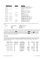
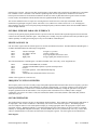
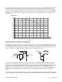
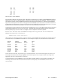
KURZWEIL 150 FOURIER SYNTHESIZER
HARDWARE PROGRAMMER’S MODEL AND ADDRESS MAP
This document describes the Kurzweil 150 Fourier Synthesizer from the hardware programmer’s point of view. It contains
addresses for all of the hardware registers and brief descriptions of each. At this level the programmer is responsible for all
of the details involved in sound generation, MIDI data decoding (if used), time keeping, front panel display refreshing, and
button scanning.
The reader should be familiar with the documents titled "Model K150 User’s Manual", "150FS Version 1.6 Software", and
"Appendix 1 - K150FS System Exclusive Formats" as an example of one successful K150FS operating system
implementation. However this document was prepared for those interested in creating their own operating system perhaps
emphasizing different aspects of additive synthesis than the Kurzweil implementation, which was aimed primarily at realistic
recreations of acoustic instruments and a comprehensive MIDI implementation. For example, frequency envelopes for
partials might be implemented with the time saved by omitting the dynamic partial allocation feature of the Kurzweil
implementation.
SUMMARY OF HARDWARE RESOURCES
The K150FS consists of three boards: the CPU board, the "engine board", and the "sound board". The latter two make up the
sound generator while the CPU board contains all of the memory and other peripheral devices. The overall system resources
are as follows:
1.
2.
3.
4.
5.
6.
7.
8.
9.
10.
11.
12.
13.
14.
15.
16.
68000 CPU running at 10MHz.
Program EPROM up to 128K bytes (4 x 27256 200nS), no wait states.
Scratch RAM (non volatile) 16K, no wait states
Sound EPROM up to 128K bytes (4 x 27256 200nS) or 256K bytes (4 x 27512), 2,5 wait states
Sound RAM (non volatile) 64K, 2,5 wait states
Parameter RAM (non volatile) 2K (old style) or 8K (new style), 2,5 waits
MC6850 serial I/O chip for MIDI In and Out
MC6840 programmable timer chip
16 character 14 segment LED display with decimal points
24 button panel
Contact sense for sustain pedal
Modulator and demodulator for audio cassette storage
General purpose parallel interface (not normally assembled on CPU board)
Miscellaneous output port for diagnostics and power-fail shutdown
Frequency units converter, functions as a large lookup table
Sound generator with 240 sine/noise waves and automatic linear interpolation of amplitude envelopes.
68000 CPU
The 68000 is clocked at 10MHz which is substantially faster than personal computers using the 68000 such as the Atari ST
and Apple Macintosh. Furthermore, for accesses to the primary program EPROM and scratch RAM, there are no wait states.
Programs normally run in Supervisor Mode and there is no special hardware for memory write protection or illegal address
detection. In fact, attempting to read or write a nonexistent address may cause the 68000 to hang due to lack of a DTACK.
The 68000 RESET instruction will reset the sound generator and peripherals.
The 68000 address map is as follows:
ADDRESS RANGE
$000000 - 00FFFF
$010000 - 01FFFF
$020000 - 020003
$024000 - 02000F
$028000 - 02BFFF
$02C000 - 02C7FF
K150FS Programmer’s Model
ALIASES
-023FFF
-027FFF
-02FFFF
FUNCTION
Program EPROM #1, 64K (sockets U55, U57)
Program EPROM #2, 64K (sockets U54, U56)
MC6850 MIDI UART (see below for actual addresses)
MC6840 Timer (see below for actual addresses)
Scratch RAM, 16K
(old style) Parameter RAM, 2K
1
Rev. A 26-APR-88
ADDRESS RANGE
$02C000 - 02DFFF
$030000 - 0307FF
$030800
$034000 - 03400A
$03400B
$03400C
$03400D
$03400E
$038000 - 380003
$038004 - 03800F
$03C000
$03C800 - 03C8FF
$040000 - 05FFFF
$060000 - 07FFFF
$080000 - 09FFFF
$0A0000 - 0BFFFF
$0C0000 - 0C7FFF
$0E0000 - 0E7FFF
$100000
ALIASES
-02FFFF
-033FFF
-037FFF
-03BFFF
-03C7FF
-03FFFF
-0DFFFF
-0FFFFF
-FFFFFF
FUNCTION
(new style) Parameter RAM, 8K
Sound Generator Partial Control Words
Sound generator control & status
-reservedMiscellaneous Status Register
-reservedCassette output D-to-A Register
Miscellaneous Control Register
Front panel
Reserved for test fixtures
Frequency units converter
General purpose parallel I/O
Sound ROM, 32K-128K, socket U14
Sound ROM, 32K-128K, socket U15
Sound ROM, 32K-128K, socket U16
Sound ROM, 32K-128K, socket U25
Sound RAM, 32K, socket U26
Sound RAM, 32K, socket U27
16 alias copies of all of above
Interrupts use the autovector method of linking to the service subroutine. Only 3 of the possible 7 interrupts are used as
follows:
LEVEL
7
5
2
AUTOVECTOR
00007C
000074
000068
ADDRESS FUNCTION
Power fail
6850 MIDI Interface
6840 Timer
The Power Fail interrupt only happens when the power-supply detects that voltage is dropping such as when the unit is turned
off or the power company fails. There MUST be a power-fail service routine and it MUST pulse the SRAM SAFE signal as
described below in the Miscellaneous I/O section. If this is not done, the non-volatile RAM contents will be lost and the
backup battery drain will become high enough to deplete the battery in a couple of months. The SRAM SAFE signal is
required to flip a flip-flop into the standby power mode. It is recommended that during program development the backup
battery be removed to prevent unnecessary drain.
MEMORY
The K150FS has several classes of memory present. Program EPROM and scratch RAM run at full 0 wait-state speed and
are present as pairs of memory chips. Sound EPROM, sound RAM, and parameter RAM require wait states but are present
as individual chips for greater flexibility. The table below identifies each kind of memory chip, its function, and its U
number on the CPU board.
ADDRESS RANGE
$000000-00FFFF
$010000-01FFFF
$028000-02BFFF
old $02C000-02C7FF
new $02C000-02DFFF
$040000-04FFFF
$060000-06FFFF
$080000-08FFFF
$0A0000-0AFFFF
$0C0000-0C7FFF
$0E0000-0E7FFF
K150FS Programmer’s Model
U-LOCATION
U55-H U57-L
U54-H U56-L
U40-H U41-L
U42
U42
U14
U15
U16
U25
U26
U27
FUNCTION
Program EPROM
Program EPROM
Scratch RAM
Parameter RAM
Parameter RAM
Sound EPROM
Sound EPROM
Sound EPROM
Sound EPROM
Sound RAM
Sound RAM
2
SIZE
64K
64K
16K
2K
8K
32K,64K
32K,64K
32K,64K
32K,64K
32K
32K
CHIP TYPE
27256
27256
6264
6116
6264
27256,27512
27256,27512
27256,27512
27256,27512
62256
62256
SPEED
200nS
200nS
150nS
150nS
150nS
200nS
200nS
200nS
200nS
150nS
150nS
Rev. A 26-APR-88
The primary program EPROM is 16 bits wide and consists of one or two pairs of 27256 EPROMS. U55 and U57 chips must
be present since they are addressed beginning at $000000 and contain the startup and interrupt vectors. U54 and U56 are
optional and may be used if the program becomes larger than 64K bytes. Of course sound data may also be present in either
pair of EPROMs if desired with the advantage of zero wait state data access.
When using an EPROM programmer to prepare software for the K150FS, it is useful to know that the address and data bit
assignments are the same as the industry standard given in databooks. AO is the least significant address bit and A14 is the
most significant. Likewise, DO is the least significant data bit and D7 is the most significant. Data is stored in the EPROM
in positive true polarity.
The primary scratch RAM is also 16 bits wide and consists of a pair of 6264 static RAMs for a total of 16K. This RAM is
non volatile. It is intended for rapid access uses such as the 68000 stack, expanded parameter lists, and the like but could
also be used for RAM-resident sounds with the advantage of zero wait state access.
The parameter RAM, sound RAM, and sound ROM are each 8 bits wide but still appear to the programmer as if they are 16
bits wide. The 8-to-16 bit conversion hardware adds 5 wait states for a 16-bit access in order to do two 8-bit accesses.
However, if the 68000 instruction is a byte mode instruction, only 2 wait states are added. It is possible to put program code
in these memories but operation would be substantially slowed due to the extra wait states. The Sound EPROM sockets will
accept either 27256 EPROMs for 32K bytes each or 27512 EPROMs for 64K bytes each. They can also accept 1 megabit
mask ROMs (128K bytes each) but not 1 megabit EPROMs (the latter have 32 pins instead of 28).
MC6840 TIMER
The MC6840 contains 3 independent counter timers. Timer #1 is completely general purpose and has nothing connected to
its clock input or timer output. Timer #2 can be used by software to count sample periods (51.2uS each) of the sound
generator. Its clock input is connected to a square wave with a 51.2uS period. Timer #3 must be programmed to output a
500KHz square wave which is used as the baud rate input of the MC6850 MIDI UART described below. Nothing is
connected to timer #3’s clock input but the system clock (Enable frequency) is 1.0MHz. The gate inputs to all three timers
are wired to permanent ones.
The 6840 register addresses are as follows:
$024001
$024003
$024003
$024005
$024005
$024007
$024007
$024009
$024009
$02400B
$02400B
$02400D
$02400D
$02400F
$02400F
(write)
(read)
(write)
(read)
(write)
(read)
(write)
(read)
(write)
(read)
(write)
(read)
(write)
(read)
(write)
Control Register #1 and #3
Status Register
Control Register #2
Timer #1 counter
Write MSB Buffer Register
Read LSB Buffer Register
Timer #1 latches
Timer #2 counter
Write MSB Buffer Register
Read LSB Buffer Register
Timer #2 latches
Timer #3 counter
Write MSB Buffer Register
Read LSB Buffer Register
Timer #3 latches
Programming details for the 6840 can be found attached to the end of this document.
MC6850 MIDI UART
A Motorola 6850 Serial Interface Adapter is used for MIDI I/O. Only the serial input and serial output are used; the modem
control outputs are not used and the modem control inputs are hardwired such that full operation of the transmitter and
receiver are permitted. The baud rate is taken from timer 3 of the 6840 described above. For the standard 31.25 KBaud
MIDI rate, 16X clock is selected in the 6850 and timer 3 is set for 2uS = 500KHz.
K150FS Programmer’s Model
3
Rev. A 26-APR-88
The 6850 register addresses are as follows:
$020001
$020001
$020003
$020003
(read)
(write)
(read)
(write)
Control Register
Status Register
Received Data Register
Transmit Data Register
See also the section below on Miscellaneous I/O for a description of bits which control normal operation and diagnostic loopback of the MIDI signals. Programming details for the 6850 can be found attached to the end of this document.
FRONT PANEL
The front panel consists of 16 alphanumeric LED characters and 24 pushbuttons. Software is responsible for refreshing the
display and scanning the buttons.
The display consists of 16 characters each of which has 14 segments and a decimal point. The characters are numbered 0-15
from left to right. A counter selects which character is actually activated at any instant. This counter may be reset to zero
(leftmost) by reading address $038000 and incremented (move one position right) by reading address $038001. Words
written to $038000 contain a 15 bit pattern that defines the segment pattern for the currently activated character. One bits
make segments light up.
Thus to produce a display, a software routine would rapidly sequence through one character at a time using the segment
pattern write and counter increment read functions. To avoid "ghosting", the segment pattern should be blanked while
incrementing the character counter. This may be accomplished either by writing zeroes to the segment register at $038000 or
reading address $038002. Also, to avoid visible flicker, a rate of 60 complete refreshes per second is desirable which figures
to about 1 millisecond hold time per character. During program development it is best to avoid leaving the display in a
stopped state with one character showing very brightly for long periods of time.
8
13
5
9
14
15
4
12
3
10
1
2
11
6
The keypad consists of 6 columns of 4 buttons each. The keypad is tied into the display refresh circuit. The 6 keypad
columns are activated one-at-a-time when the leftmost 6 display columns are activated. The leftmost character activates the
leftmost button column, etc. The state of the 4 buttons in the selected column may be read at address $038003. Bit 0 is the
topmost button in the column and bit 3 is the bottommost. A zero indicates a pressed button. Bits 4-7 are undefined and the
other 10 display columns do not select any buttons. Assuming a display refresh rate of approximately 60Hz, debouncing of
the button presses is not necessary.
CASSETTE INTERFACE
The cassette interface consists of a simple signal generator for writing and a signal polarity detector (zero-crossing detector)
for reading. Modulation and demodulation of the signal and coding and decoding of the data is up to the driver software.
The cassette signal generator is separate from the much more sophisticated sound generator and consists of a "poor man’s Dto-A converter" and a low-pass filter. The D-to-A converter can produce 9 different voltage levels (for an effective
resolution of 3+ bits) according to the 8-bit pattern written to address $03400E. The voltage level is proportional to the
number of ONE bits in the pattern. The location of the ones in the pattern is not important but it is desirable that they be
evenly distributed among the zeros when possible. A waveform is produced by simply writing an appropriate sequence of
K150FS Programmer’s Model
4
Rev. A 26-APR-88
patterns to the converter. The low-pass filter cutoff frequency is about 7KHz with a cutoff slope of 12dB/octave so an update
rate of 20KHz or more is advisable. This method of producing audio cassette signals allows rounded-off waveforms of
known spectral content to be used which can minimize the adverse effects of phase distortion in typical cassette recorders.
For best results, the modulation scheme should restrict the signal bandwidth to about 500-2000Hz.
The cassette readback circuit is a simple zero-crossing detector connected to bit 3 of the byte at $03400B. When the
instantaneous signal input is negative, the bit will read as a zero; otherwise it will be read as a one. Low- and high-pass
filters minimize the effects of low frequency thumps and high frequency transients and hiss but let the 500-2000Hz band of
interest through unaltered.
GENERAL PURPOSE PARALLEL INTERFACE
Circuitry for the general purpose parallel interface is present on the CPU board but the required integrated circuits and cable
connector are not normally soldered in place. The parallel port is actually a tiny bus expansion with a 256 byte address space
and the capability of reading and writing bytes to any selected address within that space.
MISCELLANEOUS 1/0
One 4-bit status register and 6-bit control register are used for miscellaneous functions. The Miscellaneous Status Register is
at address $03400B and has the following bit assignments:
BIT 3
BIT 2
BIT 1
BIT 0
Cassette read input
Low battery detector
Left pedal
Right pedal
0=negative, 1=positive
1=battery voltage is low
0=tip of pedal jack connected to sleeve
0=ring of pedal jack connected to sleeve
The 6-bit Miscellaneous Control Register is at address $03400F and is write-only. Its bit assignments are:
BIT 5
BIT 4
BIT 3
BIT 2
BIT 1
BIT 0
1=Enable normal MIDI I/O, O=disable
1=Enable internal MIDI loopback, O=permit normal operation
Unused
O=Normal operation, 1=Set SRAM SAFE flip-flop
Unused
1=Illuminate the LED mounted on the CPU board
All bits of this register are zeroed on reset.
FREQUENCY UNITS CONVERTER
The Frequency Units Converter is actually a large lookup table implemented in hardware that converts a frequency specified
in octaves to frequency control words suitable for use with the sound generator. It is used by writing a 15-bit positive pitch
value expressed in units of 1/2048 octave to address $03C000 and then immediately reading the equivalent 15 bit positive
frequency parameter from the same address. Thus it replaces what would otherwise be a 64K byte table or lengthy
computation. The octaves are relative to D9 (9397.243Hz) thus $0000 is 9397.24Hz, $0800 is 4698.62Hz (D8), $1000 is
2349.31Hz (D7), etc.
SOUND GENERATOR
The sound generator consists of an array of 240 identical digital oscillators. Their outputs are summed together and appear at
the output jack. Each of these oscillators is controlled by a set of four 16-bit read/write registers. The 68000 program
exercises complete control over the sound produced simply by writing appropriate data in the appropriate sequence to the
appropriate registers. Readback capability is provided for diagnostics and so that software can find out where an oscillator
currently "is" in amplitude and phase if necessary. Note that 68000 CPU access is permitted only once every 3.2uS so there
will be a variable number of wait states associated with accessing these registers. The four registers are described below.
Phase Register
K150FS Programmer’s Model
5
Rev. A 26-APR-88
Most fundamental is the Phase register. In generating sound, the current content of the phase register is used as an address to
lookup in a sine table. If one considers the content of the Phase Register to be an unsigned integer between 0 and 65535, the
sine table yields the value: SIN(2*PI*P/65536) where P is the Phase Register content and PI=3.14159... Thus a Phase
Register content of zero gives a zero result, 8192 gives .7071, 16384 gives +1, and 49152 gives -1. Note that it is the Sine
that is being looked up, not the more conventional Cosine. The phase register for each partial may be freely read or written at
any time although writing when the amplitude is non-zero will probably produce a click. Typically it is desirable to begin a
sound with all partials initialized to zero phase in order to avoid attack clicks.
Frequency Register
The Frequency Register contains a 15-bit unsigned integer for controlling frequency in bits 0-14 and the sine/noise selection
flag in bit 15. Assuming sine waves (bit 15=0), the sound generator works by adding the 15 bit frequency parameter to the
phase register every sample period ignoring overflow. The sample period is 51.2uS which corresponds to 19531.25 KS/s. A
frequency parameter of $0001 would therefore produce a frequency of 0.29802Hz while $7FFF would be just short of the
Nyquist frequency at 9765.33Hz (and be lost in the anti-alias filter). The general formula for frequency is: F=0.29802322*P
Hz where P is the 15-bit frequency parameter expressed as an integer. The Frequency Register may be read and written at
will.
When bit 15 of the Frequency Register is a one, the sound generator looks up in a noise table rather than a sine table. The 15
bit frequency parameter is still added to the Phase Register every sample period as before. The noise table lookup uses bits
2-13 of the phase register content as a lookup address to 4096 noise samples. However these 4096 samples are really two
sets of 2048 samples each, one being "low" noise and the other being "high" noise. These two sets of samples are interleaved
in the noise ROM such that bit 2 of the Phase Register selects low noise when it is zero and high noise when it is one. Thus
if the Frequency Register content is a multiple of 8, the Phase Register will always address samples in the same noise table.
Which noise table is determined by the initial setting of bit 2 in the Phase Register.
The specific intended application of the noise tables was to enhance the
realism of piano notes. A Frequency Register setting of 8 with an initial Phase Register setting of 0 (low) or 4 (high) will
step through these samples as intended. Many additional noise effects are possible by using other Frequency Register
settings that may step through the noise tables slower or faster and also intermix noise samples. This will require
experimentation.
Amplitude Register
Whereas the Phase and Frequency registers controlled the generation of the basic waveform, the Amplitude and Slope
registers control the generation of amplitude envelope segments. The Amplitude Register contains a 16-bit unsigned integer
which gives amplitude in units of 6/4096 dB. Thus the minimum amplitude is 0dB, which is silence, and the maximum is
95.9985dB. Please note that the register content really is decibels, not a simple multiplying factor. For example, if the
maximum amplitude of a single partial corresponding to an Amplitude Register setting of $FFFF is 1.0 volts, 0.5 volt (6dB
less) would be produced by a setting of $F800, not $8000. The amplitude register setting can be read or changed at any time
but a large change is likely to produce a click.
Slope Register
Unlike frequency, infrequent updating of amplitude values is generally an unsatisfactory method of producing amplitude
envelopes. This is because a sudden change in amplitude produces a step discontinuity in the resulting waveform which is
heard as a click, whereas a sudden change in frequency still leaves a continuous waveform. Thus amplitude must be updated
very quickly so that the size of the update steps is small enough to reduce or eliminate update clicks. Thus the K150FS
sound generator has automatic amplitude envelope segment generating hardware. The principle is the same as with the Phase
and Frequency registers: the content of the Slope Register is added to the Amplitude Register periodically, thus producing a
continuous, linear (in decibels) increase or decrease in amplitude. By simply changing the setting of the Slope Register at
every breakpoint in the overall desired envelope shape, a piecewise linear approximation to any arbitrary envelope shape may
be produced. Unlike the Phase Register however, the Amplitude Register will "stick" at minimum or maximum if the
addition produces an overflow or underflow.
The Slope Register content is a signed 16-bit integer value between -16384 and +16383. This restricted range leaves bit 14
free as a flag to select between a fast (every sample period) or slow (every 16 sample periods) rate of adding the slope value
K150FS Programmer’s Model
6
Rev. A 26-APR-88
to the amplitude value. Thus in fast mode (bit 14=0), the LSB of the slope value is 28.6dB per second whereas in slow mode
(bit 14=1), it is 1.78dB/sec. Although the slow mode has much more slope resolution than the fast mode, it should only be
used for relatively slow slopes since it can cause a low buzzing sound from large amplitude steps at its slow 1.2KHz update
rate.
Note that the polarity of bit 14 is the same whether the slope is positive or negative. Thus one should OR-in bit 14 after any
twos complement operations.
Addressing Partials
There are 240 sets of the four registers described above in the address range of $030000 - 0307FF. Word moves should
always be used to ensure that both bytes of an addressed register are read/changed simultaneously. Partials are numbered
from 0 to 255 and the partial number used in the formulas below will be called P. If P is divisible by 16, it is a silent partial
and does not contribute to the sound regardless of the register values. The base address for the registers associated with a
given partial, P, is: $030000+(8*P). The Phase Register then is at the base address plus 4, Frequency at base plus 2,
Amplitude at base+6, and Slope at base+0.
Amplitude Ranges
The sound generator theoretically produces 24-bit sample values (240 partials times 16 bits per partial). The lower 20 bits of
these participate in producing the output (yes, all 20) but the upper 4 bits are clipped. The waveform is actually clipped
(which is relatively unnoticable in small amounts), rather than allowed to wraparound which would sound truly awful. Thus
it is theoretically possible to clip a waveform of 17 or more partials if they are at maximum amplitude and perfectly in phase.
In practice, clipping seldom, if ever, occurs because not all partials of a listenable sound are going to be at maximum at once
and the slight frequency errors due to the 0.3Hz quantization ensures that phases are going to be scrambled in the long term.
The programmer may therefore feel free to use any amplitude range desired.
Sound Generator Control/Status
The overall sound generator is controlled by a write-only register at $030800. The bit assignments are as follows:
BIT 0
BIT 1
BIT 2
BIT 3
Bit 4-7
0=Halt, 1=Run
1=Single-cycle execution for each write, 0=no effect
don’t care
0=Mute, 1=Normal operation
don’t care
Thus normal operation is achieved by writing $09 to $038000. Normally the sound generator is started at power-up after
clearing all of the Amplitude and Slope registers and then is left running continuously. For effective muting of startup and
power-down transients, Mute should be held active for several hundred milliseconds after initializing and starting the sound
generator and also immediately forced on in the power-fail interrupt service routine (see description above). Single-cycle
execution is for diagnostic and hardware debugging use.
Also at address $038000 is a read-only status register for the sound generator. Its bit assignments are:
BIT 0
BIT 1
BIT 2
BIT 3
Bit 4-7
1=Access timeslot to sound generator registers
1=Run mode
Serial data for sample readback
1=16th sample (slow slopes will be applied)
undefined
These bits are provided for diagnostic purposes. Bit 2 allows a diagnostic program to read the low 20 bits of the last
calculated sample one bit at a time.
Anti-Alias Filter Considerations
K150FS Programmer’s Model
7
Rev. A 26-APR-88
In order to simplify its design and also reduce audible noise, the anti-alias low-pass filter used in the K150FS does not have a
maximally flat passband; instead it gently slopes downward and then cuts off suddenly near the Nyquist frequency. The
effect of this slope is to make the actual output amplitudes of high frequency partials somewhat less than their programmed
amplitudes. The existing K150FS operating software takes this curve into account when it starts notes. User software should
do the same to ensure a "flat" frequency response. The filter response curve is reproduced below to aid in applying the
correction:
Response, dB
0
-2
-4
-6
-8
-10
-12
-14
-16
-18
-20
0
1.0
2.0
3.0
4.0
kHz
5.0
6.0
7.0
8.0
9.0
PROGRAM DEVELOPMENT TECHNIQUES
While program development for the K150FS can be successfully done by erasing and reprogramming EPROMs and testing
operation each time a change is made, such a procedure is much like using a batch-processing mainframe computer 15 years
ago. Although Kurzweil programmers use an expensive Hewlett-Packard development system for programming, one can be
almost as productive with a personal computer, a MIDI interface, and the suggestions below.
+5V
+5V
100
From RS-232
Transmit Data
200
2
2.2K
To RS-232
Receive Data
6N138
MIDI
from
K150
2N2222
6
3
5
220 x 2
2N2907
8
4
4
2.2K
270
1N4148
MIDI
to
K150
5
2.2K
5
-12V
The first step in putting together a suitable development system is to get a MIDI interface for the development computer
(called the "host") so that communication with the K150FS is possible. These are available for all of the popular personal
computers. For a campus mainframe offering only RS-232 ports, it is possible to program the MIDI baud rate in the K150FS
to 4800 baud by setting the MC6840 Timer #3 to divide the 1MHz system clock by 13. Then a MIDI to RS-232 level
shifting circuit, such as shown below, can be used for the connection. Either way, you will be using ASCII and perhaps pure
binary code rather than MIDI protocol in communicating between the host and the K150FS for program development
purposes.
Once a communication link is established, the next task is to write a simple program loader and program it into two EPROMs
which are plugged into sockets U55 and U57 of the K150FS. If the loader and the data format is kept simple, it should only
K150FS Programmer’s Model
8
Rev. A 26-APR-88
take 2 or 3 iterations to get it functional. Then you will be able to download any software you want into K150FS RAM and
execute it. At this point you may wish to write or adapt a "monitor" program which will make debugging of the real software
easier or just jump into writing and debugging synthesizer control software.
If a monitor is written, it is useful to have an "interrupt button" which will stop the program under test and return to the
monitor for examination of memory contents. This can be accomplished by pulling down the U6 pin 1 node on the CPU
board for about 10 microseconds with an open-collector TTL device. This will create a level 7 interrupt which would be
interpreted by the monitor as "console interrupt" rather than "power fail". Take care not to make the pulse too long or it will
trigger the reset circuit and reset the processor instead.
The stock K150FS has a limited amount of zero wait state RAM for loading software into; just 16K. A simple modification
can convert the U54/U56 sockets (second 64K of program EPROM) into 64K of zero wait state RAM instead. A 62256
(32Kx8 static) type of RAM chip should be used in each socket and any standard speed (100/120/150nS) is acceptable. This
new RAM will be volatile. Only word writes should be performed to this RAM; trying to write just one byte will either write
garbage into the other byte or nothing at all. To make the conversion, perform the following steps (none involve functional
changes to the CPU board so you can quickly restore normal EPROM operation for running the stock K150FS software):
1.
2.
Obtain two 28-pin DIP platforms (if necessary, cut down a 40-pin platform)
Either mount the RAM chip directly or a 28-pin socket on the platform and connect all pins except 1, 20, 22, and 27 of
the RAM to the corresponding pins on the platform.
3. Connect pin 1 of the RAM to pin 27 of the platform.
4. Connect pin 20 of the RAM to pin 22 of the platform.
5. Connect pin 22 of the RAM to pin 20 of the platform.
6. Connect one end of a flying wire 6 inches long to pin 27 the RAM.
7. Plug the two prepared platform/RAM assemblies into the U54 and U56 sockets
8. Solder each flying lead to U50 pin 11 on the CPU board.
9. Solder a jumper wire from U37 pin 12 to U50 pin 12.
10. Solder a jumper wire from U50 pin 2 to U50 pin 13
To restore normal operation with EPROM in the U54 and U56 sockets, simply unsolder the two flying wires from U50 pin
11, remove the RAM platforms, and plug in EPROMS. The two jumper wires added to the CPU board will not affect
anything.
ALTERATION OF THE LOOKUP TABLE EPROMS
Other alterations one might wish to make are in the various lookup tables used in the K150FS. Since these are all standard
EPROMS, changing their contents for specialized applications is easy.
Frequency Converter EPROM
The Frequency Converter was designed to use a 2716 2Kx8 bit EPROM as U64 but boards are shipped with 2732 4Kx8 bit
devices installed. The most significant address bit, A11, of the 2732 is tied high so all of the data is in the upper half of the
device. 350nS or faster devices are acceptable.
Bits 1-10 of the word written to the frequency converter address the EPROM as if it were a 1K by 16 device (EPROM
A0=0=high byte). The 16-bit word read from the EPROM is then placed into a 16-bit shift register and shifted right
according to bits 11-14 of the word written to the frequency converter. If these bits are all zeros, then there is no shifting;
0001 shifts once, etc. Zeroes are shifted into the most significant bit of the result. Bits 0 and 15 of the word written to the
frequency converter are not used.
One complication is that several of the address and data signals to the EPROM have been scrambled. The table below
documents those that have been scrambled:
REAL
SIGNAL
A1
A2
EPROM
SIGNAL
A2
A4
K150FS Programmer’s Model
REAL
SIGNAL
D1
9
EPROM
SIGNAL
D2
Rev. A 26-APR-88
A3
A4
A5
A6
A8
A9
A10
A6
A8
A10
A9
A5
A3
A1
D2
D3
D4
D6
D7
D4
D6
D7
D3
D1
Sine/Noise Wave Table EPROMs
The other table of interest is the sine/noise table. This table was designed to use two 8K by 8 masked ROMs but boards are
shipped with 27128 16K by 8 EPROMs installed. 150nS access time is required for these EPROMS. They are in positions
U39 (high byte) and U40 on the Sound Board which is the bottom board in the K150FS box. The most significant address
input, A13, is tied high so all of the data is in the upper half of the EPROMS. (One could connect a switch or unused bit of
the Miscellaneous Output Register to this pin and select between the standard sine/noise tables and custom ones.) A12 of the
EPROMs selects between the sine half and the noise half. Zero selects sine and one selects noise.
Considering the sine half of the table, the 4096 locations are addressed by bits 2-13 of the Phase Register and are expected to
contain the first quadrant of a sine wave in reverse order. Thus $FFF represents 0*PI and $000 represents 0.4998779*PI.
External symmetry logic uses bits 14 and 15 of the phase value to complete the other three quadrants.
But there’s more. The "SIN" values in the EPROM are actually the base 2 Log of the SIN. The exact formula for the
EPROM content expressed as a 16-bit integer is:
EPROM VALUE = 32768 - 2048 * log2( S )
where S is the sine value between 0 and 1.0. However, when S=1.0, the EPROM value should be 32767 ($7FFF) instead of
32768 and when S=0, the EPROM value should be 0. Some examples of angles, sines, and coded sines are shown below:
ANGLE
radians
ANGLE
EPROM address
SINE
decimal
SINE
log
0.000000
0.062533
0.125318
0.252584
0.523600
0.785400
1.57080
$FFF
$F5C
$EB8
$D6C
$AAB
$7FF
$000
.0000
.0625
.1250
.2500
.5000
.7071
.9999
$0000
$6000
$6800
$7000
$7800
$7C00
$7FFF
For the noise half of the table, the symmetry logic is switched off and bits 14 & 15 of the Phase Register are ignored. The
noise sample stored in the table is in sign-magnitude form with the sign in bit 15 (1=negative) and the base 2 log of the
magnitude in bits 0-14 as described above for the sine.
As with the frequency converter EPROM, several of the address and data signals have been scrambled. Fortunately, the
scrambling is the same for both U39 and U40 and is the same as the frequency converter EPROM. See above for the
conversion table.
K150FS Programmer’s Model
10
Rev. A 26-APR-88