1
Intel® XScale™ Microarchitecture
for the PXA255 Processor
User’s Manual
March, 2003
Order Number: 278796
Information in this document is provided in connection with Intel® products. No license, express or implied, by estoppel or otherwise, to any
intellectual property rights is granted by this document. Except as provided in Intel's Terms and Conditions of Sale for such products, Intel assumes no
liability whatsoever, and Intel disclaims any express or implied warranty, relating to sale and/or use of Intel® products including liability or warranties
relating to fitness for a particular purpose, merchantability, or infringement of any patent, copyright or other intellectual property right. Intel products are
not intended for use in medical, life saving, or life sustaining applications. Intel may make changes to specifications and product descriptions at any
time, without notice.Intel may make changes to specifications and product descriptions at any time, without notice.
Designers must not rely on the absence or characteristics of any features or instructions marked “reserved” or “undefined.” Intel reserves these for
future definition and shall have no responsibility whatsoever for conflicts or incompatibilities arising from future changes to them.
The Intel® XScale™ Microarchitecture Users Manual for the PXA255 processor may contain design defects or errors known as errata
which may cause the product to deviate from published specifications. Current characterized errata are available on request.
Contact your local Intel sales office or your distributor to obtain the latest specifications and before placing your product order.
Copies of documents which have an ordering number and are referenced in this document, or other Intel literature may be obtained by calling 1-800548-4725 or by visiting Intel's website at http://www.intel.com.
Copyright © Intel Corporation, 2003
* Other names and brands may be claimed as the property of others.
ARM and StrongARM are registered trademarks of ARM, Ltd.
ii
Intel® XScale™ Microarchitecture User’s Manual
Contents
Contents
1
Introduction...................................................................................................................................1-1
1.1
1.2
1.3
2
Programming Model .....................................................................................................................2-1
2.1
2.2
2.3
3
About This Document ........................................................................................................1-1
1.1.1 How to Read This Document ................................................................................1-1
1.1.2 Other Relevant Documents ..................................................................................1-1
High-Level Overview of the Intel® XScale™ core as Implemented in the
Application Processors ......................................................................................................1-2
1.2.1 ARM* Compatibility ...............................................................................................1-3
1.2.2 Features................................................................................................................1-3
1.2.2.1 Multiply/Accumulate (MAC)...................................................................1-3
1.2.2.2 Memory Management ...........................................................................1-4
1.2.2.3 Instruction Cache ..................................................................................1-4
1.2.2.4 Branch Target Buffer.............................................................................1-4
1.2.2.5 Data Cache ...........................................................................................1-4
1.2.2.6 Fill Buffer & Write Buffer .......................................................................1-5
1.2.2.7 Performance Monitoring........................................................................1-5
1.2.2.8 Power Management ..............................................................................1-5
1.2.2.9 Debug ...................................................................................................1-5
Terminology and Conventions ...........................................................................................1-6
1.3.1 Number Representation........................................................................................1-6
1.3.2 Terminology and Acronyms ..................................................................................1-6
ARM* Architecture Compatibility........................................................................................2-1
ARM* Architecture Implementation Options ......................................................................2-1
2.2.1 Big Endian versus Little Endian ............................................................................2-1
2.2.2 Thumb...................................................................................................................2-1
2.2.3 ARM* DSP-Enhanced Instruction Set...................................................................2-2
2.2.4 Base Register Update...........................................................................................2-2
Extensions to ARM* Architecture.......................................................................................2-2
2.3.1 DSP Coprocessor 0 (CP0)....................................................................................2-3
2.3.1.1 Multiply With Internal Accumulate Format ............................................2-3
2.3.1.2 Internal Accumulator Access Format ....................................................2-6
2.3.2 New Page Attributes .............................................................................................2-9
2.3.3 Additions to CP15 Functionality ..........................................................................2-10
2.3.4 Event Architecture ..............................................................................................2-11
2.3.4.1 Exception Summary ............................................................................2-11
2.3.4.2 Event Priority.......................................................................................2-11
2.3.4.3 Prefetch Aborts ...................................................................................2-12
2.3.4.4 Data Aborts .........................................................................................2-12
2.3.4.5 Events from Preload Instructions ........................................................2-14
2.3.4.6 Debug Events .....................................................................................2-15
Memory Management...................................................................................................................3-1
3.1
3.2
Overview ............................................................................................................................3-1
Architecture Model.............................................................................................................3-1
3.2.1 Version 4 vs. Version 5 .........................................................................................3-2
3.2.2 Instruction Cache ..................................................................................................3-2
3.2.3 Data Cache and Write Buffer ................................................................................3-2
Intel® XScale™ Microarchitecture User’s Manual
iii
Contents
3.3
3.4
4
Instruction Cache..........................................................................................................................4-1
4.1
4.2
4.3
5
5.2
Branch Target Buffer (BTB) Operation ..............................................................................5-1
5.1.1 Reset ....................................................................................................................5-2
5.1.2 Update Policy........................................................................................................5-2
BTB Control .......................................................................................................................5-2
5.2.1 Disabling/Enabling ................................................................................................5-2
5.2.2 Invalidation............................................................................................................5-3
Data Cache...................................................................................................................................6-1
6.1
6.2
iv
Overview............................................................................................................................4-1
Operation ...........................................................................................................................4-2
4.2.1 Instruction Cache is Enabled ................................................................................4-2
4.2.2 The Instruction Cache Is Disabled........................................................................4-2
4.2.3 Fetch Policy ..........................................................................................................4-2
4.2.4 Round-Robin Replacement Algorithm ..................................................................4-3
4.2.5 Parity Protection ...................................................................................................4-3
4.2.6 Instruction Fetch Latency......................................................................................4-4
4.2.7 Instruction Cache Coherency ...............................................................................4-4
Instruction Cache Control ..................................................................................................4-5
4.3.1 Instruction Cache State at RESET .......................................................................4-5
4.3.2 Enabling/Disabling ................................................................................................4-5
4.3.3 Invalidating the Instruction Cache.........................................................................4-5
4.3.4 Locking Instructions in the Instruction Cache .......................................................4-6
4.3.5 Unlocking Instructions in the Instruction Cache....................................................4-7
Branch Target Buffer ....................................................................................................................5-1
5.1
6
3.2.4 Details on Data Cache and Write Buffer Behavior................................................3-3
3.2.5 Memory Operation Ordering .................................................................................3-3
3.2.6 Exceptions ............................................................................................................3-4
Interaction of the MMU, Instruction Cache, and Data Cache ............................................3-4
Control ...............................................................................................................................3-4
3.4.1 Invalidate (Flush) Operation .................................................................................3-4
3.4.2 Enabling/Disabling ................................................................................................3-5
3.4.3 Locking Entries .....................................................................................................3-5
3.4.4 Round-Robin Replacement Algorithm ..................................................................3-7
Overviews ..........................................................................................................................6-1
6.1.1 Data Cache Overview...........................................................................................6-1
6.1.2 Mini-Data Cache Overview ...................................................................................6-2
6.1.3 Write Buffer and Fill Buffer Overview....................................................................6-3
Data Cache and Mini-Data Cache Operation ....................................................................6-4
6.2.1 Operation When Caching is Enabled....................................................................6-4
6.2.2 Operation When Data Caching is Disabled ..........................................................6-4
6.2.3 Cache Policies ......................................................................................................6-4
6.2.3.1 Cacheability ..........................................................................................6-4
6.2.3.2 Read Miss Policy ..................................................................................6-4
6.2.3.3 Write Miss Policy...................................................................................6-5
6.2.3.4 Write-Back Versus Write-Through ........................................................6-6
6.2.4 Round-Robin Replacement Algorithm ..................................................................6-6
6.2.5 Parity Protection ...................................................................................................6-6
6.2.6 Atomic Accesses ..................................................................................................6-7
Intel® XScale™ Microarchitecture User’s Manual
Contents
6.3
6.4
6.5
7
Configuration ................................................................................................................................7-1
7.1
7.2
7.3
8
Overview ............................................................................................................................7-1
CP15 Registers..................................................................................................................7-3
7.2.1 Register 0: ID & Cache Type Registers ................................................................7-4
7.2.2 Register 1: Control & Auxiliary Control Registers .................................................7-5
7.2.3 Register 2: Translation Table Base Register ........................................................7-7
7.2.4 Register 3: Domain Access Control Register........................................................7-8
7.2.5 Register 5: Fault Status Register ..........................................................................7-8
7.2.6 Register 6: Fault Address Register .......................................................................7-9
7.2.7 Register 7: Cache Functions ................................................................................7-9
7.2.8 Register 8: TLB Operations ................................................................................7-10
7.2.9 Register 9: Cache Lock Down ............................................................................7-11
7.2.10 Register 10: TLB Lock Down ..............................................................................7-12
7.2.11 Register 13: Process ID ......................................................................................7-12
7.2.11.1 The PID Register Affect On Addresses ..............................................7-13
7.2.12 Register 14: Breakpoint Registers ......................................................................7-13
7.2.13 Register 15: Coprocessor Access Register ........................................................7-14
CP14 Registers................................................................................................................7-15
7.3.1 Registers 0-3: Performance Monitoring ..............................................................7-16
7.3.2 Registers 6-7: Clock and Power Management ...................................................7-16
7.3.3 Registers 8-15: Software Debug.........................................................................7-17
Performance Monitoring ...............................................................................................................8-1
8.1
8.2
8.3
8.4
8.5
8.6
8.7
9
Data Cache and Mini-Data Cache Control ........................................................................6-7
6.3.1 Data Memory State After Reset ............................................................................6-7
6.3.2 Enabling/Disabling ................................................................................................6-7
6.3.3 Invalidate & Clean Operations ..............................................................................6-8
6.3.3.1 Global Clean and Invalidate Operation .................................................6-8
Re-configuring the Data Cache as Data RAM .................................................................6-10
Write Buffer/Fill Buffer Operation and Control .................................................................6-13
Overview ............................................................................................................................8-1
Clock Counter (CCNT; CP14 - Register 1) ........................................................................8-1
Performance Count Registers (PMN0 - PMN1; CP14 - Register 2 and 3, Respectively) ..8-2
8.3.1 Extending Count Duration Beyond 32 Bits ...........................................................8-2
Performance Monitor Control Register (PMNC) ................................................................8-2
8.4.1 Managing the PMNC ............................................................................................8-4
Performance Monitoring Events ........................................................................................8-4
8.5.1 Instruction Cache Efficiency Mode .......................................................................8-5
8.5.2 Data Cache Efficiency Mode ................................................................................8-6
8.5.3 Instruction Fetch Latency Mode............................................................................8-6
8.5.4 Data/Bus Request Buffer Full Mode .....................................................................8-6
8.5.5 Stall/Writeback Statistics Mode.............................................................................8-7
8.5.6 Instruction TLB Efficiency Mode ...........................................................................8-8
8.5.7 Data TLB Efficiency Mode ....................................................................................8-8
Multiple Performance Monitoring Run Statistics ................................................................8-8
Examples ...........................................................................................................................8-8
Test...............................................................................................................................................9-1
9.1
9.2
Boundary-Scan Architecture and Overview .......................................................................9-1
Reset .................................................................................................................................9-3
Intel® XScale™ Microarchitecture User’s Manual
v
Contents
9.3
9.4
9.5
10
Software Debug..........................................................................................................................10-1
10.1
10.2
10.3
10.4
10.5
10.6
10.7
vi
Instruction Register............................................................................................................9-3
9.3.1 Boundary-Scan Instruction Set .............................................................................9-3
Test Data Registers ...........................................................................................................9-5
9.4.1 Bypass Register....................................................................................................9-5
9.4.2 Boundary-Scan Register.......................................................................................9-6
9.4.3 Device Identification (ID) Code Register...............................................................9-8
9.4.4 Data Specific Registers ........................................................................................9-8
TAP Controller ...................................................................................................................9-8
9.5.1 Test Logic Reset State .........................................................................................9-9
9.5.2 Run-Test/Idle State.............................................................................................9-10
9.5.3 Select-DR-Scan State.........................................................................................9-10
9.5.4 Capture-DR State ...............................................................................................9-10
9.5.5 Shift-DR State.....................................................................................................9-10
9.5.6 Exit1-DR State ....................................................................................................9-11
9.5.7 Pause-DR State..................................................................................................9-11
9.5.8 Exit2-DR State ....................................................................................................9-11
9.5.9 Update-DR State ................................................................................................9-11
9.5.10 Select-IR Scan State ..........................................................................................9-12
9.5.11 Capture-IR State.................................................................................................9-12
9.5.12 Shift-IR State ......................................................................................................9-12
9.5.13 Exit1-IR State......................................................................................................9-12
9.5.14 Pause-IR State ...................................................................................................9-12
9.5.15 Exit2-IR State......................................................................................................9-13
9.5.16 Update-IR State ..................................................................................................9-13
Introduction ......................................................................................................................10-1
10.1.1 Halt Mode ...........................................................................................................10-1
10.1.2 Monitor Mode......................................................................................................10-2
Debug Registers ..............................................................................................................10-2
Debug Control and Status Register (DCSR) ...................................................................10-3
10.3.1 Global Enable Bit (GE) .......................................................................................10-4
10.3.2 Halt Mode Bit (H) ................................................................................................10-4
10.3.3 Vector Trap Bits (TF,TI,TD,TA,TS,TU,TR) .........................................................10-4
10.3.4 Sticky Abort Bit (SA) ...........................................................................................10-5
10.3.5 Method of Entry Bits (MOE)................................................................................10-5
10.3.6 Trace Buffer Mode Bit (M) ..................................................................................10-5
10.3.7 Trace Buffer Enable Bit (E).................................................................................10-5
Debug Exceptions............................................................................................................10-5
10.4.1 Halt Mode ...........................................................................................................10-6
10.4.2 Monitor Mode......................................................................................................10-7
HW Breakpoint Resources ..............................................................................................10-8
10.5.1 Instruction Breakpoints .......................................................................................10-9
10.5.2 Data Breakpoints ................................................................................................10-9
Software Breakpoints.....................................................................................................10-11
Transmit/Receive Control Register (TXRXCTRL) .........................................................10-11
10.7.1 RX Register Ready Bit (RR) .............................................................................10-12
10.7.2 Overflow Flag (OV) ...........................................................................................10-13
10.7.3 Download Flag (D)............................................................................................10-13
10.7.4 TX Register Ready Bit (TR) ..............................................................................10-14
Intel® XScale™ Microarchitecture User’s Manual
Contents
10.7.5 Conditional Execution Using TXRXCTRL .........................................................10-14
10.8 Transmit Register (TX) ..................................................................................................10-15
10.9 Receive Register (RX) ...................................................................................................10-15
10.10 Debug JTAG Access .....................................................................................................10-16
10.10.1 SELDCSR JTAG Command .............................................................................10-16
10.10.2 SELDCSR JTAG Register ................................................................................10-17
10.10.2.1 DBG.HLD_RST .................................................................................10-18
10.10.2.2 DBG.BRK..........................................................................................10-18
10.10.2.3 DBG.DCSR .......................................................................................10-18
10.10.3 DBGTX JTAG Command..................................................................................10-19
10.10.4 DBGTX JTAG Register .....................................................................................10-19
10.10.5 DBGRX JTAG Command .................................................................................10-20
10.10.6 DBGRX JTAG Register ....................................................................................10-20
10.10.6.1 RX Write Logic ..................................................................................10-21
10.10.6.2 DBGRX Data Register ......................................................................10-21
10.10.6.3 DBG.RR ............................................................................................10-22
10.10.6.4 DBG.V...............................................................................................10-22
10.10.6.5 DBG.RX ............................................................................................10-22
10.10.6.6 DBG.D...............................................................................................10-23
10.10.6.7 DBG.FLUSH .....................................................................................10-23
10.10.7 Debug JTAG Data Register Reset Values........................................................10-23
10.11 Trace Buffer ...................................................................................................................10-23
10.11.1 Trace Buffer CP Registers ................................................................................10-23
10.11.1.1 Checkpoint Registers........................................................................10-24
10.11.1.2 Trace Buffer Register (TBREG) ........................................................10-25
10.11.2 Trace Buffer Usage...........................................................................................10-25
10.12 Trace Buffer Entries.......................................................................................................10-27
10.12.1 Message Byte ...................................................................................................10-27
10.12.1.1 Exception Message Byte ..................................................................10-28
10.12.1.2 Non-exception Message Byte ...........................................................10-28
10.12.1.3 Address Bytes...................................................................................10-29
10.13 Downloading Code into the Instruction Cache...............................................................10-30
10.13.1 LDIC JTAG Command ......................................................................................10-30
10.13.2 LDIC JTAG Data Register ................................................................................10-31
10.13.3 LDIC Cache Functions......................................................................................10-32
10.13.4 Loading IC During Reset ..................................................................................10-33
10.13.4.1 Loading IC During Cold Reset for Debug .........................................10-34
10.13.4.2 Loading IC During a Warm Reset for Debug ....................................10-36
10.13.5 Dynamically Loading IC After Reset .................................................................10-38
10.13.5.1 Dynamic Code Download Synchronization.......................................10-39
10.13.6 Mini Instruction Cache Overview ......................................................................10-40
10.14 Halt Mode Software Protocol .........................................................................................10-40
10.14.1 Starting a Debug Session .................................................................................10-40
10.14.1.1 Setting up Override Vector Tables....................................................10-41
10.14.1.2 Placing the Handler in Memory .........................................................10-41
10.14.2 Implementing a Debug Handler ........................................................................10-42
10.14.2.1 Debug Handler Entry ........................................................................10-42
10.14.2.2 Debug Handler Restrictions ..............................................................10-42
10.14.2.3 Dynamic Debug Handler ...................................................................10-43
10.14.2.4 High-Speed Download ......................................................................10-44
10.14.3 Ending a Debug Session ..................................................................................10-45
Intel® XScale™ Microarchitecture User’s Manual
vii
Contents
10.15 Software Debug Notes...................................................................................................10-46
11
Performance Considerations ......................................................................................................11-1
11.1
11.2
11.3
A
Optimization Guide ...................................................................................................................... A-1
A.1
A.2
A.3
viii
Branch Prediction ............................................................................................................11-1
Instruction Latencies........................................................................................................11-2
11.2.1 Performance Terms ............................................................................................11-2
11.2.2 Branch Instruction Timings .................................................................................11-3
11.2.3 Data Processing Instruction Timings ..................................................................11-4
11.2.4 Multiply Instruction Timings ................................................................................11-5
11.2.5 Saturated Arithmetic Instructions........................................................................11-6
11.2.6 Status Register Access Instructions ...................................................................11-7
11.2.7 Load/Store Instructions.......................................................................................11-7
11.2.8 Semaphore Instructions......................................................................................11-8
11.2.9 Coprocessor Instructions ....................................................................................11-8
11.2.10 Miscellaneous Instruction Timing........................................................................11-8
11.2.11 Thumb Instructions .............................................................................................11-9
Interrupt Latency..............................................................................................................11-9
Introduction ....................................................................................................................... A-1
A.1.1 About This Guide ................................................................................................. A-1
Intel® XScale™ Core Pipeline.......................................................................................... A-1
A.2.1 General Pipeline Characteristics ......................................................................... A-2
A.2.1.1. Number of Pipeline Stages .................................................................. A-2
A.2.1.2. Intel® XScale™ Core Pipeline Organization ....................................... A-2
A.2.1.3. Out Of Order Completion ..................................................................... A-3
A.2.1.4. Register Dependencies........................................................................ A-3
A.2.1.5. Use of Bypassing ................................................................................. A-3
A.2.2 Instruction Flow Through the Pipeline ................................................................. A-4
A.2.2.1. ARM* v5 Instruction Execution ............................................................ A-4
A.2.2.2. Pipeline Stalls ...................................................................................... A-4
A.2.3 Main Execution Pipeline ...................................................................................... A-4
A.2.3.1. F1 / F2 (Instruction Fetch) Pipestages................................................. A-4
A.2.3.2. ID (Instruction Decode) Pipestage ....................................................... A-5
A.2.3.3. RF (Register File / Shifter) Pipestage .................................................. A-5
A.2.3.4. X1 (Execute) Pipestages ..................................................................... A-5
A.2.3.5. X2 (Execute 2) Pipestage .................................................................... A-6
A.2.3.6. XWB (write-back) ................................................................................. A-6
A.2.4 Memory Pipeline .................................................................................................. A-6
A.2.4.1. D1 and D2 Pipestage........................................................................... A-6
A.2.5 Multiply/Multiply Accumulate (MAC) Pipeline ...................................................... A-6
A.2.5.1. Behavioral Description ......................................................................... A-7
Basic Optimizations .......................................................................................................... A-7
A.3.1 Conditional Instructions ....................................................................................... A-7
A.3.1.1. Optimizing Condition Checks............................................................... A-7
A.3.1.2. Optimizing Branches............................................................................ A-8
A.3.1.3. Optimizing Complex Expressions ...................................................... A-10
A.3.2 Bit Field Manipulation ........................................................................................ A-11
A.3.3 Optimizing the Use of Immediate Values........................................................... A-11
A.3.4 Optimizing Integer Multiply and Divide .............................................................. A-11
A.3.5 Effective Use of Addressing Modes................................................................... A-12
Intel® XScale™ Microarchitecture User’s Manual
Contents
A.4
A.5
A.6
Cache and Prefetch Optimizations ................................................................................. A-12
A.4.1 Instruction Cache ............................................................................................... A-13
A.4.1.1. Cache Miss Cost................................................................................ A-13
A.4.1.2. Round Robin Replacement Cache Policy .......................................... A-13
A.4.1.3. Code Placement to Reduce Cache Misses ....................................... A-13
A.4.1.4. Locking Code into the Instruction Cache ........................................... A-13
A.4.2 Data and Mini Cache ......................................................................................... A-14
A.4.2.1. Non Cacheable Regions .................................................................... A-14
A.4.2.2. Write-through and Write-back Cached Memory Regions .................. A-14
A.4.2.3. Read Allocate and Read-write Allocate Memory Regions ................. A-15
A.4.2.4. Creating On-chip RAM ....................................................................... A-15
A.4.2.5. Mini-data Cache ................................................................................. A-15
A.4.2.6. Data Alignment .................................................................................. A-16
A.4.2.7. Literal Pools ....................................................................................... A-17
A.4.3 Cache Considerations ....................................................................................... A-17
A.4.3.1. Cache Conflicts, Pollution and Pressure............................................ A-17
A.4.3.2. Memory Page Thrashing.................................................................... A-18
A.4.4 Prefetch Considerations .................................................................................... A-18
A.4.4.1. Prefetch Distances ............................................................................. A-18
A.4.4.2. Prefetch Loop Scheduling .................................................................. A-18
A.4.4.3. Compute vs. Data Bus Bound............................................................ A-19
A.4.4.4. Low Number of Iterations ................................................................... A-19
A.4.4.5. Bandwidth Limitations ........................................................................ A-19
A.4.4.6. Cache Memory Considerations.......................................................... A-20
A.4.4.7. Cache Blocking .................................................................................. A-21
A.4.4.8. Prefetch Unrolling .............................................................................. A-21
A.4.4.9. Pointer Prefetch ................................................................................. A-22
A.4.4.10. Loop Interchange ............................................................................... A-23
A.4.4.11. Loop Fusion ....................................................................................... A-23
A.4.4.12. Prefetch to Reduce Register Pressure .............................................. A-23
Instruction Scheduling .................................................................................................... A-24
A.5.1 Scheduling Loads .............................................................................................. A-24
A.5.1.1. Scheduling Load and Store Double (LDRD/STRD) ........................... A-26
A.5.1.2. Scheduling Load and Store Multiple (LDM/STM)............................... A-27
A.5.2 Scheduling Data Processing Instructions .......................................................... A-28
A.5.3 Scheduling Multiply Instructions ........................................................................ A-28
A.5.4 Scheduling SWP and SWPB Instructions .......................................................... A-29
A.5.5 Scheduling the MRA and MAR Instructions (MRRC/MCRR)............................. A-29
A.5.6 Scheduling the MIA and MIAPH Instructions ..................................................... A-30
A.5.7 Scheduling MRS and MSR Instructions............................................................. A-30
A.5.8 Scheduling Coprocessor Instructions ................................................................ A-31
Optimizations for Size..................................................................................................... A-31
A.6.1 Multiple Word Load and Store ........................................................................... A-31
A.6.2 Use of Conditional Instructions .......................................................................... A-31
A.6.3 Use of PLD Instructions ..................................................................................... A-32
A.6.4 Thumb Instructions ............................................................................................ A-32
Figures
1-1
3-1
4-1
4-2
Intel® XScale™ Microarchitecture Architecture Features .........................................................1-3
Example of Locked Entries in TLB.............................................................................................3-8
Instruction Cache Organization .................................................................................................4-1
Locked Line Effect on Round Robin Replacement ....................................................................4-6
Intel® XScale™ Microarchitecture User’s Manual
ix
Contents
5-1 BTB Entry ..................................................................................................................................5-1
5-2 Branch History ...........................................................................................................................5-2
6-1 Data Cache Organization ..........................................................................................................6-2
6-2 Mini-Data Cache Organization ..................................................................................................6-3
6-3 Locked Line Effect on Round Robin Replacement ..................................................................6-13
9-1 Test Access Port (TAP) Block Diagram.....................................................................................9-2
9-2 BSDL code for 256-MBGA package ..........................................................................................9-7
9-3 TAP Controller State Diagram ...................................................................................................9-9
10-1SELDCSR Hardware .............................................................................................................10-17
10-2DBGTX Hardware..................................................................................................................10-19
10-3DBGRX Hardware .................................................................................................................10-20
10-4RX Write Logic.......................................................................................................................10-21
10-5DBGRX Data Register ...........................................................................................................10-22
10-6High Level View of Trace Buffer ............................................................................................10-26
10-7Message Byte Formats..........................................................................................................10-27
10-8Indirect Branch Entry Address Byte Organization .................................................................10-30
10-9LDIC JTAG Data Register Hardware.....................................................................................10-31
10-10Format of LDIC Cache Functions ........................................................................................10-33
10-11Code Download During a Cold Reset For Debug ................................................................10-35
10-12Code Download During a Warm Reset For Debug..............................................................10-37
10-13Downloading Code in IC During Program Execution ...........................................................10-38
A-1
Intel® XScale™ Core RISC Superpipeline...................................................A-2
Tables
2-1 Multiply with Internal Accumulate Format..................................................................................2-4
2-2 MIA{<cond>} acc0, Rm, Rs .......................................................................................................2-4
2-3 MIAPH{<cond>} acc0, Rm, Rs ..................................................................................................2-5
2-4 MIAxy{<cond>} acc0, Rm, Rs....................................................................................................2-6
2-5 Internal Accumulator Access Format.........................................................................................2-7
2-6 MAR{<cond>} acc0, RdLo, RdHi ...............................................................................................2-8
2-7 MRA{<cond>} RdLo, RdHi, acc0 ...............................................................................................2-8
2-8 First-level Descriptors ................................................................................................................2-9
2-9 Second-level Descriptors for Coarse Page Table .....................................................................2-9
2-10Second-level Descriptors for Fine Page Table ........................................................................2-10
2-11Exception Summary ................................................................................................................2-11
2-12Event Priority ...........................................................................................................................2-11
2-13Intel® XScale™ Core Encoding of Fault Status for Prefetch Aborts .......................................2-12
2-14Intel® XScale™ Core Encoding of Fault Status for Data Aborts .............................................2-13
3-1 Data Cache and Buffer Behavior when X = 0............................................................................3-2
3-2 Data Cache and Buffer Behavior when X = 1............................................................................3-3
3-3 Memory Operations that Impose a Fence .................................................................................3-4
3-4 Valid MMU & Data/mini-data Cache Combinations ...................................................................3-4
7-1 MRC/MCR Format.....................................................................................................................7-2
7-2 LDC/STC Format when Accessing CP14 ..................................................................................7-2
7-3 CP15 Registers .........................................................................................................................7-3
7-4 ID Register.................................................................................................................................7-4
7-5 Cache Type Register .................................................................................................................7-5
7-6 ARM* Control Register ..............................................................................................................7-6
7-7 Auxiliary Control Register ..........................................................................................................7-7
x
Intel® XScale™ Microarchitecture User’s Manual
Contents
7-8 Translation Table Base Register ...............................................................................................7-7
7-9 Domain Access Control Register...............................................................................................7-8
7-10 Fault Status Register .................................................................................................................7-8
7-11 Fault Address Register ..............................................................................................................7-9
7-12 Cache Functions........................................................................................................................7-9
7-13 TLB Functions..........................................................................................................................7-11
7-14 Cache Lockdown Functions.....................................................................................................7-11
7-15 Data Cache Lock Register.......................................................................................................7-11
7-16 TLB Lockdown Functions ........................................................................................................7-12
7-17 Accessing Process ID..............................................................................................................7-12
7-18 Process ID Register.................................................................................................................7-13
7-19 Accessing the Debug Registers...............................................................................................7-13
7-20 Coprocessor Access Register .................................................................................................7-14
7-21 CP14 Registers........................................................................................................................7-16
7-22 Accessing the Performance Monitoring Registers...................................................................7-16
7-23 PWRMODE Register 7 ............................................................................................................7-17
7-24 CCLKCFG Register 6 ..............................................................................................................7-17
7-25 Clock and Power Management valid operations .....................................................................7-17
7-26 Accessing the Debug Registers...............................................................................................7-18
8-1 Clock Count Register (CCNT) ...................................................................................................8-2
8-2 Performance Monitor Count Register (PMN0 and PMN1).........................................................8-2
8-3 Performance Monitor Control Register (CP14, register 0).........................................................8-3
8-4 Performance Monitoring Events ................................................................................................8-4
8-5 Some Common Uses of the PMU..............................................................................................8-5
9-1 TAP Controller Pin Definitions ...................................................................................................9-2
9-2 JTAG Instruction Codes.............................................................................................................9-4
9-3 JTAG Instruction Descriptions ...................................................................................................9-4
10-1 Coprocessor 15 Debug Registers............................................................................................10-2
10-2 Coprocessor 14 Debug Registers............................................................................................10-2
10-3 Debug Control and Status Register (DCSR) ...........................................................................10-3
10-4 Event Priority ...........................................................................................................................10-6
10-5 Instruction Breakpoint Address and Control Register (IBCRx) ................................................10-9
10-6 Data Breakpoint Register (DBRx)............................................................................................10-9
10-7 Data Breakpoint Controls Register (DBCON)........................................................................10-10
10-8 TX RX Control Register (TXRXCTRL)...................................................................................10-12
10-9 Normal RX Handshaking .......................................................................................................10-12
10-10High-Speed Download Handshaking States ........................................................................10-13
10-11TX Handshaking...................................................................................................................10-14
10-12TXRXCTRL Mnemonic Extensions ......................................................................................10-14
10-13TX Register ..........................................................................................................................10-15
10-14RX Register..........................................................................................................................10-15
10-15DEBUG Data Register Reset Values ...................................................................................10-23
10-16CP 14 Trace Buffer Register Summary................................................................................10-24
10-17Checkpoint Register (CHKPTx) ...........................................................................................10-24
10-18TBREG Format ....................................................................................................................10-25
10-19Message Byte Formats ........................................................................................................10-28
10-20LDIC Cache Functions .........................................................................................................10-32
11-1 Branch Latency Penalty...........................................................................................................11-1
11-2 Latency Example .....................................................................................................................11-3
11-3 Branch Instruction Timings (Those predicted by the BTB) ......................................................11-3
Intel® XScale™ Microarchitecture User’s Manual
xi
Contents
11-4Branch Instruction Timings (Those not predicted by the BTB) ................................................11-4
11-5Data Processing Instruction Timings .......................................................................................11-4
11-6Multiply Instruction Timings .....................................................................................................11-5
11-7Multiply Implicit Accumulate Instruction Timings .....................................................................11-6
11-8Implicit Accumulator Access Instruction Timings.....................................................................11-6
11-9Saturated Data Processing Instruction Timings ......................................................................11-7
11-10Status Register Access Instruction Timings...........................................................................11-7
11-11Load and Store Instruction Timings .......................................................................................11-7
11-12Load and Store Multiple Instruction Timings..........................................................................11-8
11-13Semaphore Instruction Timings .............................................................................................11-8
11-14CP15 Register Access Instruction Timings............................................................................11-8
11-15CP14 Register Access Instruction Timings............................................................................11-8
11-16SWI Instruction Timings .........................................................................................................11-8
11-17Count Leading Zeros Instruction Timings ..............................................................................11-9
A-1
Pipelines and Pipe stages ............................................................................A-3
xii
Intel® XScale™ Microarchitecture User’s Manual
Introduction
1.1
1
About This Document
This document describes the Intel® XScale™ core as implemented in the PXA255 processor.
Intel Corporation assumes no responsibility for any errors which may appear in this document nor
does it make a commitment to update the information contained herein.
Intel retains the right to make changes to these specifications at any time, without notice. In
particular, descriptions of features, timings, and pin-outs does not imply a commitment to
implement them.
1.1.1
How to Read This Document
It is necessary to be familiar with the ARM* Version 5TE Architecture in order to understand some
aspects of this document.
Each chapter in this document focuses on a specific architectural feature of the Intel® XScale™
core.
•
•
•
•
•
•
•
•
•
•
Note:
1.1.2
Chapter 2, “Programming Model”
Chapter 3, “Memory Management”
Chapter 4, “Instruction Cache”
Chapter 5, “Branch Target Buffer”
Chapter 6, “Data Cache”
Chapter 7, “Configuration”
Chapter 8, “Performance Monitoring”
Chapter 10, “Software Debug”
Chapter 11, “Performance Considerations”
Appendix A, “Optimization Guide” covers instruction scheduling techniques.
Most of the “buzz words” and acronyms found throughout this document are captured in
Section 1.3.2, “Terminology and Acronyms” on page 1-6, located at the end of this chapter.
Other Relevant Documents
• ARM* Architecture Reference Manual Document Number: ARM DDI 0100E
This document describes the ARM* Architecture and is publicly available.
See http://www.arm.com/ARMARM for details. Sold as:
ARM* Architecture Reference Manual
Second Edition, edited by David Seal: Addison-Wesley: ISBN 0-201-73719-1
• Intel® PXA255 Processor Developer’s Manual, Intel Order # 278693
Intel® XScale™ Microarchitecture User’s Manual
1-1
Introduction
• Intel® PXA255 Processor Design Guide, Intel Order # 278694
• Intel® 80200 Processor Development Manual, Intel Order #273411
This document describes the first implementation of the Intel® XScale™ Microarchitecture
in a microprocessor targeted at IO applications
Available from http://developer.intel.com
1.2
High-Level Overview of the Intel® XScale™ core as
Implemented in the Application Processors
The Intel® XScale™ core is an ARM* V5TE compliant microprocessor. It is a high performance
and low-power device that leads the industry in MIPS/mW. The core is not intended to be delivered
as a stand alone product but as a building block for an ASSP (Application Specific Standard
Product) with embedded markets such as handheld devices, networking, storage, remote access
servers, etc. The PXA255 processor is an example of an ASSP designed primarily for handheld
devices. This document limits itself to describing the implementation of the Intel® XScale™ core
as it is implemented in the PXA255 processor. In almost every attribute the Intel® XScale™ core
used in the application processor is identical to the Intel® XScale™ core implemented in the
Intel® 80200
The Intel® XScale™ core incorporates an extensive list of microarchitecture features that allow it
to achieve high performance. This rich feature set lets you select the appropriate features that
obtain the best performance for your application. Many of the micro-architectural features added to
the Intel® XScale™ core help hide memory latency which often is a serious impediment to high
performance processors. This includes:
• The ability to continue instruction execution even while the data cache is retrieving data from
external memory
•
•
•
•
A write buffer
Write-back caching
Various data cache allocation policies which can be configured differently for each application
Cache locking
All these features improve the efficiency of the memory bus external to the core.
The Intel® XScale™ core efficiently handles audio processing through the support of 16-bit data
types and enhanced 16-bit operations. These audio coding enhancements center around multiply
and accumulate operations which accelerate many of the audio filtering and multimedia CODEC
algorithms.
1.2.1
ARM* Compatibility
ARM* Version 5 (V5) Architecture added new features to ARM* Version 4, including among other
inclusions, floating point instructions. The Intel® XScale™ core implements the integer
instruction set of ARM* V5, but does not provide hardware support for any of the floating point
instructions.
1-2
Intel® XScale™ Microarchitecture User’s Manual
Introduction
The Intel® XScale™ core provides the ARM* V5T Thumb instruction set and the ARM* V5E
DSP extensions. To further enhance multimedia applications, the Intel® XScale™ core includes
additional Multiply-Accumulate functionality as the first instantiation of Intel® Media Processing
Technology. These new operations from Intel are mapped into ARM* coprocessor space.
Backward compatibility with StrongARM* products is maintained for user-mode applications.
Operating systems may require modifications to match the specific hardware features of the Intel®
XScale™ core and to take advantage of the performance enhancements added.
1.2.2
Features
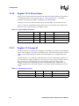
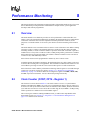
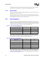
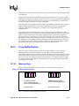
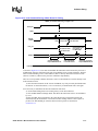
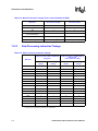
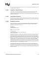
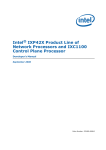
Figure 1-1 shows the major functional blocks of the Intel® XScale™ core. The following sections
give a brief, high-level overview of these blocks.
Figure 1-1. Intel® XScale™ Microarchitecture Architecture Features
Instruction
Cache
32 Kbytes
32 Ways
Lockable by line
MicroProcessor
7 Stage
pipeline
Branch Target
Buffer
128 Entries
Performance
Monitoring
Debug
Max 32 Kbytes
32 Ways
WR - Back or
WR - Through
Hit under miss
IMMU
Power
Mgnt
Ctrl
Mini-Data
Cache
Data Ram
Max 28 Kbytes
Re-Map of data
cache
DMMU
32 entry TLB
Fully associative
Lockable by entry
Hardware Breakpoints
Branch History Table
1.2.2.1
Data Cache
32 entry TLB
Fully associative
Lockable by entry
MAC
Single cycle throughput (16*32)
16-bit SIMD
40-bit accumulator
2 Kbytes
2 Ways
Fill Buffer
4 - 8 entries
Write Buffer
8 entries
Full coalescing
JTAG
Multiply/Accumulate (MAC)
The MAC unit supports early termination of multiplies/accumulates in two cycles and can sustain a
throughput of a MAC operation every cycle. Several architectural enhancements were made to the
MAC to support audio coding algorithms, which include a 40-bit accumulator and support for 16bit packed data.
Refer to Section 2.3, “Extensions to ARM* Architecture” on page 2-2 for more information.
1.2.2.2
Memory Management
The Intel® XScale™ core implements the Memory Management Unit (MMU) Architecture
specified in the ARM* Architecture Reference Manual. The MMU provides access protection and
virtual to physical address translation.
The MMU Architecture also specifies the caching policies for the instruction cache and data cache.
These policies are specified as page attributes and include:
Intel® XScale™ Microarchitecture User’s Manual
1-3
Introduction
•
•
•
•
•
identifying code as cacheable or non-cacheable
selecting between the mini-data cache or data cache
write-back or write-through data caching
enabling data write allocation policy
enabling the write buffer to coalesce stores to external memory
Refer to Chapter 3, “Memory Management” for more information.
1.2.2.3
Instruction Cache
The Intel® XScale™ core implements a 32-Kbyte, 32-way set associative instruction cache with a
line size of 32 bytes. All requests that “miss” the instruction cache generate a 32-byte read request
to external memory. A mechanism to lock critical code within the cache is also provided.
Refer to Chapter 4, “Instruction Cache” for more information.
In addition to the main instruction cache there is a 2-Kbyte mini-instruction cache dedicated to
advanced debugging features. Refer to Chapter 10, “Software Debug” for more information.
1.2.2.4
Branch Target Buffer
The Intel® XScale™ core provides a Branch Target Buffer (BTB) to predict the outcome of branch
type instructions. It provides storage for the target address of branch type instructions and predicts
the next address to present to the instruction cache when the current instruction address is that of a
branch.
The BTB holds 128 entries. Refer to Chapter 5, “Branch Target Buffer” for more information.
1.2.2.5
Data Cache
The Intel® XScale™ core implements a 32-Kbyte, 32-way set associative data cache and a 2Kbyte, 2-way set associative mini-data cache. Each cache has a line size of 32 bytes, supporting
write-through or write-back caching.
The data/mini-data cache is controlled by page attributes defined in the MMU Architecture and by
coprocessor 15.
Refer to Chapter 6, “Data Cache” for more information.
The Intel® XScale™ core allows applications to re-configure a portion of the data cache as data
RAM. Software may place special tables or frequently used variables in this RAM. Refer to
Section 6.4, “Re-configuring the Data Cache as Data RAM” on page 6-10 for more information.
1.2.2.6
Fill Buffer & Write Buffer
The Fill Buffer and Write Buffer enable the loading and storing of data to memory beyond the
Intel® XScale™ core. The Write Buffer carries all write traffic beyond the core allowing data
coalescing when both globally enabled, and when associated with the appropriate memory page
types. The Fill buffer assists the loading of data from memory, which along with an associated
Pend Buffer allows multiple memory reads to be outstanding. Another key function of the Fill
1-4
Intel® XScale™ Microarchitecture User’s Manual
Introduction
Buffer [along with the Instruction Fetch Buffers] is to allow the application processor external
SDRAM to be read as 4-word bursts, rather than single word accesses, improving overall memory
bandwidth.
Both the Fill, Pend and Write buffers help to decouple core speed from any limitations to accessing
external memory. Further details on these buffers can be found in Section 6.5, “Write Buffer/Fill
Buffer Operation and Control” on page 6-13
1.2.2.7
Performance Monitoring
Two performance monitoring counters have been added to the Intel® XScale™ core that can be
configured to monitor various events in the Intel® XScale™ core. These events allow a software
developer to measure cache efficiency, detect system bottlenecks and reduce the overall latency of
programs.
Refer to Chapter 8, “Performance Monitoring” for more information.
1.2.2.8
Power Management
The Intel® XScale™ core incorporates a power and clock management unit that can assist ASSPs
in controlling their clocking and managing their power. These features are described in Section 7.3,
“CP14 Registers” on page 7-15.
1.2.2.9
Debug
Intel® XScale™ core supports software debugging through two instruction address breakpoint
registers, one data-address breakpoint register, one data-address/mask breakpoint register, a miniinstruction cache and a trace buffer.
Testability & hardwar-8.3(r)-8.le™a028.3(-10(e)r)-10(e)7( )0 11.9-27.5(2ma)0.000007 Tc 1 Tf9.2.3(.2me)6.4(2.-2r)-
Intel® XScale™ Microarchitecture User’s Manual
1-5
Configuration
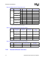
7.2.4
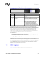
Register 3: Domain Access Control Register
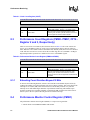
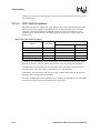
Table 7-9. Domain Access Control Register
31 30 29 28 27 26 25 24 23 22 21 20 19 18 17 16 15 14 13 12 11 10 9
D15
D14
D13
D12
D11
D10
D9
D8
D7
D6
D5
8
D4
7
6
D3
5
4
D2
3
2
D1
1
0
D0
reset value: unpredictable
Bits
31:0
7.2.5
Access
Description
Access permissions for all 16 domains - The meaning
of each field can be found in the ARM Architecture
Reference Manual.
Read / Write
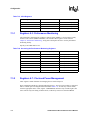
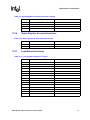
Register 5: Fault Status Register
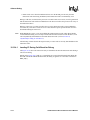
The Fault Status Register (FSR) indicates which fault has occurred, which could be either a
prefetch abort or a data abort. Bit 10 extends the encoding of the status field for prefetch aborts and
data aborts. The definition of the extended status field is found in Section 2.3.4, “Event
Architecture” on page 2-11. Bit 9 indicates that a debug event occurred and the exact source of the
event is found in the debug control and status register (CP14, register 10). When bit 9 is set, the
domain and extended status field are undefined.
Upon entry into the prefetch abort or data abort handler, hardware will update this register with the
source of the exception. Software is not required to clear these fields.
Table 7-10. Fault Status Register
31 30 29 28 27 26 25 24 23 22 21 20 19 18 17 16 15 14 13 12 11 10 9
8
X D 0
7
6
5
Domain
4
3
2
1
0
Status
reset value: unpredictable
Bits
Access
31:11
Read-unpredictable / Write-as-Zero
Description
Reserved
Status Field Extension (X)
10
Read / Write
This bit is used to extend the encoding of the Status field,
when there is a prefetch abort [See Table 2-13 on
page 2-12] and when there is a data abort [See
Table 2-14 on page 2-13].
Debug Event (D)
7-8
9
Read / Write
This flag indicates a debug event has occurred and that
the cause of the debug event is found in the MOE field of
the debug control register (CP14, register 10)
8
Read-as-zero / Write-as-Zero
=0
7:4
Read / Write
Domain - Specifies which of the 16 domains was being
accessed when a data abort occurred
3:0
Read / Write
Status - Used along with the X-bit above to determine the
type of cycle type that generated the exception. See
“Event Architecture” on page 2-11
Intel® XScale™ Microarchitecture User’s Manual
Configuration
7.2.6
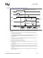
Register 6: Fault Address Register
Table 7-11. Fault Address Register
31 30 29 28 27 26 25 24 23 22 21 20 19 18 17 16 15 14 13 12 11 10 9
8
7
6
5
4
3
2
1
0
Fault Virtual Address
reset value: unpredictable
Bits
31:0
7.2.7
Access
Description
Fault Virtual Address - Contains the MVA of the data
access that caused the memory abort
Read / Write
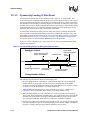
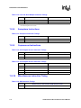
Register 7: Cache Functions
All the cache functions defined in existing StrongARM* products appear here. The Intel®
XScale™ core adds other functions as well. This register is write-only. Reads from this register, as
with an MRC, have an undefined effect.
Disabling/enabling a cache has no effect on contents of the cache: valid data stays valid, locked
items remain locked and accesses that hit in the cache will hit. To prevent cache hits after disabling
the cache it is necessary to invalidate it. The way to prevent hits on the fill buffer is to drain it. All
operations defined in Table 7-12 work regardless of whether the cache is enabled or disabled.
The Drain Write Buffer function not only drains the write buffer but also drains the fill buffer. The
Intel® XScale™ core does not check permissions on addresses supplied for cache or TLB
functions. Because only privileged software may execute these functions, full accessibility is
assumed. Cache functions will not generate any of the following:
• translation faults
• domain faults
• permission faults
Since the Clean D Cache Line function reads from the data cache, it is capable of generating a
parity fault. The other operations will not generate parity faults.
The invalidate instruction cache line command does not invalidate the BTB. If software invalidates
a line from the instruction cache and modifies the same location in external memory, it needs to
invalidate the BTB also. Not invalidating the BTB in this case will cause unpredictable results.
Table 7-12. Cache Functions (Sheet 1 of 2)
Function
opcode_2
CRm
Data
Instruction
Invalidate I&D cache & BTB
0b000
0b0111
Ignored
MCR p15, 0, Rd, c7, c7, 0
Invalidate I cache & BTB
0b000
0b0101
Ignored
MCR p15, 0, Rd, c7, c5, 0
Invalidate I cache line
0b001
0b0101
MVA
MCR p15, 0, Rd, c7, c5, 1
Invalidate D cache
0b000
0b0110
Ignored
MCR p15, 0, Rd, c7, c6, 0
Invalidate D cache line
0b001
0b0110
MVA
MCR p15, 0, Rd, c7, c6, 1
Clean D cache line
0b001
0b1010
MVA
MCR p15, 0, Rd, c7, c10, 1
Intel® XScale™ Microarchitecture User’s Manual
7-9
Configuration
Table 7-12. Cache Functions (Sheet 2 of 2)
Function
opcode_2
CRm
Data
Instruction
Drain Write (& Fill) Buffer
0b100
0b1010
Ignored
MCR p15, 0, Rd, c7, c10, 4
Invalidate Branch Target Buffer
0b110
0b0101
Ignored
MCR p15, 0, Rd, c7, c5, 6
Allocate Line in the Data Cache
0b101
0b0010
MVA
MCR p15, 0, Rd, c7, c2, 5
The line-allocate command allocates a tag into the data cache specified by bits [31:5] of Rd. If a
valid dirty line (with a different MVA) already exists at this location it will be evicted. The 32 bytes
of data associated with the newly allocated line are not initialized and therefore will generate
unpredictable results if read.
This command may be used for cleaning the entire data cache on a context switch and also when
re-configuring portions of the data cache as data RAM. In both cases, Rd is a virtual address that
maps to some non-existent physical memory. When creating data RAM, software must initialize
the data RAM before read accesses can occur. Specific uses of these commands can be found in
Chapter 6, “Data Cache”.
Other items to note about the line-allocate command are:
•
•
•
•
It forces all pending memory operations to complete.
If the targeted cache line is already resident, this command has no effect.
This command cannot be used to allocate a line in the mini Data Cache.
The newly allocated line is not marked as “dirty”. However, if a valid store is made to that line
it will be marked as “dirty” and will get written back to external memory if another line is
allocated to the same cache location. This eviction will produce unpredictable results if the
line-allocate command used a virtual address that mapped to non-existent memory.
To avoid this situation, the line-allocate operation should only be used if one of the following
can be guaranteed:
— The virtual address associated with this command is not one that will be generated during
normal program execution. This is the case when line-allocate is used to clean/invalidate
the entire cache.
— The line-allocate operation is used only on a cache region destined to be locked. When the
region is unlocked, it must be invalidated before making another data access.
7.2.8
Register 8: TLB Operations
Disabling/enabling the MMU has no effect on the contents of either TLB: valid entries stay valid,
locked items remain locked. To invalidate the TLBs the commands below are required. All
operations defined in Table 7-13 work regardless of whether the cache is enabled or disabled.
This register is write-only. Reads from this register, as with an MRC, have an undefined effect.
7-10
Intel® XScale™ Microarchitecture User’s Manual
Configuration
Table 7-13. TLB Functions
Function
7.2.9
opcode_2
CRm
Data
Instruction
Invalidate I&D TLB
0b000
0b0111
Ignored
MCR p15, 0, Rd, c8, c7, 0
Invalidate I TLB
0b000
0b0101
Ignored
MCR p15, 0, Rd, c8, c5, 0
Invalidate I TLB entry
0b001
0b0101
MVA
MCR p15, 0, Rd, c8, c5, 1
Invalidate D TLB
0b000
0b0110
Ignored
MCR p15, 0, Rd, c8, c6, 0
Invalidate D TLB entry
0b001
0b0110
MVA
MCR p15, 0, Rd, c8, c6, 1
Register 9: Cache Lock Down
Register 9 is used for locking down entries into the instruction cache and data cache. (The protocol
for locking down entries can be found in Chapter 6, “Data Cache”.) Data can not be locked into the
mini-data cache.
Table 7-14 shows the command for locking down entries in the instruction cache, instruction TLB,
and data TLB. The cache entry to lock is specified by the virtual address in Rd. The data cache
locking mechanism follows a different procedure than the instruction cache. The data cache is
placed in lock down mode such that all subsequent fills to the data cache result in that line being
locked in, as controlled by Table 7-15.
Lock/unlock operations on a disabled cache have an undefined effect. This register is write-only.
Reads from this register, as with an MRC, have an undefined effect.
Table 7-14. Cache Lockdown Functions
Function
opcode_2
CRm
Data
Instruction
Fetch and Lock I cache line
0b000
0b0001
MVA
MCR p15, 0, Rd, c9, c1, 0
Unlock Instruction cache
0b001
0b0001
Ignored
MCR p15, 0, Rd, c9, c1, 1
Read data cache lock register
0b000
0b0010
Read lock mode
value
MRC p15, 0, Rd, c9, c2, 0
Write data cache lock register
0b000
0b0010
Set/Clear lock
mode
MCR p15, 0, Rd, c9, c2, 0
Unlock Data Cache
0b001
0b0010
Ignored
MCR p15, 0, Rd, c9, c2, 1
Table 7-15. Data Cache Lock Register
31 30 29 28 27 26 25 24 23 22 21 20 19 18 17 16 15 14 13 12 11 10 9
8
7
6
5
4
3
2
1
0
L
reset value: writable bits set to 0
Bits
Access
31:1
Read-unpredictable / Write-as-Zero
Description
Reserved
Data Cache Lock Mode (L)
0
Read-unpredictable / Write
Intel® XScale™ Microarchitecture User’s Manual
0 = No locking occurs
1 = Any fill into the data cache while this bit is set gets
locked in
7-11
Configuration
7.2.10
Register 10: TLB Lock Down
Register 10 is used for locking down entries into the instruction TLB, and data TLB. The protocol
for locking down entries can be found in Chapter 3, “Memory Management”. Lock/unlock
operations on a TLB when the MMU is disabled have an undefined effect.
This register is write-only. Reads from this register, as with an MRC, have an undefined effect.
Table 7-16 shows the commands for locking down entries in the instruction TLB, and data TLB.
The entry to lock is specified by the virtual address in Rd.
Table 7-16. TLB Lockdown Functions
Function
7.2.11
opcode_2
CRm
Data
Instruction
Translate and Lock I TLB entry
0b000
0b0100
MVA
MCR p15, 0, Rd, c10, c4, 0
Translate and Lock D TLB entry
0b000
0b1000
MVA
MCR p15, 0, Rd, c10, c8, 0
Unlock I TLB
0b001
0b0100
Ignored
MCR p15, 0, Rd, c10, c4, 1
Unlock D TLB
0b001
0b1000
Ignored
MCR p15, 0, Rd, c10, c8, 1
Register 13: Process ID
The Intel® XScale™ core supports the remapping of virtual addresses through a Process ID (PID)
register. This remapping occurs before the instruction cache, instruction TLB, data cache and data
TLB are accessed. The PID register controls when virtual addresses are remapped and to what
value.
The PID register is a 7-bit value that is ORed with bits 31:25 of the virtual address when they are
zero. This effectively remaps the address to one of 128 “slots” in the 4 Gbytes of address space. If
bits 31:25 are not zero, no remapping occurs. This feature is useful for operating system
management of processes that may map to the same virtual address space. In those cases, the
virtually mapped caches on the Intel® XScale™ core would not require invalidating on a process
switch.
Table 7-17. Accessing Process ID
Function
7-12
opcode_2
CRm
Instruction
Read Process ID Register
0b000
0b0000
MRC p15, 0, Rd, c13, c0, 0
Write Process ID Register
0b000
0b0000
MCR p15, 0, Rd, c13, c0, 0
Intel® XScale™ Microarchitecture User’s Manual
Configuration
Table 7-18. Process ID Register
31 30 29 28 27 26 25 24 23 22 21 20 19 18 17 16 15 14 13 12 11 10 9
8
7
6
5
4
3
2
1
0
Process ID
reset value: 0x0000_0000
Bits
7.2.11.1
Access
Description
31:25
Read / Write
Process ID - This field is used for remapping the virtual
address when bits 31-25 of the virtual address are zero.
24:0
Read-as-Zero / Write-as-Zero
Reserved - Must be programmed to zero for future
compatibility
The PID Register Affect On Addresses
All addresses generated and used by User Mode code are eligible for being translated using the PID
register. Privileged code however, must be aware of certain special cases in which address
generation does not follow the usual flow.
• The PID register is not used to remap the virtual address when accessing the Branch Target
Buffer (BTB). Debug software reading the BTB needs to recognize addresses as MVAs. Any
write to the PID register invalidates the BTB. This prevents any virtual addresses after the PID
has changed from matching the incorrect Branch Target of any previously running process.
• A breakpoint address (see Section 7.2.12, “Register 14: Breakpoint Registers” on page 7-13)
must be expressed as an MVA when written to the breakpoint register. This means the value of the
PID must be combined appropriately with the address before it is written to the breakpoint
register. All virtual addresses in translation descriptors (see Chapter 3, “Memory Management”)
are MVAs.
7.2.12
Register 14: Breakpoint Registers
The Intel® XScale™ core contains two instruction breakpoint address registers (IBCR0 and
IBCR1), one data breakpoint address register (DBR0), one configurable data mask/address register
(DBR1), and one data breakpoint control register (DBCON). The Intel® XScale™ core also
supports a 2K byte mini instruction cache for debugging and a 256 entry trace buffer that records
program execution information. The registers to control the trace buffer are located in CP14.
Refer to Chapter 10, “Software Debug” for more information on these features of the Intel®
XScale™ core.
Table 7-19. Accessing the Debug Registers (Sheet 1 of 2)
Function
opcode_2
CRm
Read Instruction Breakpoint
Register 0 (IBCR0)
0b000
0b1000
MRC p15, 0, Rd, c14, c8, 0
Write IBCR0
0b000
0b1000
MCR p15, 0, Rd, c14, c8, 0
Read Instruction Breakpoint
Register 1 (IBCR1)
0b000
0b1001
MRC p15, 0, Rd, c14, c9, 0
Write IBCR1
0b000
0b1001
MCR p15, 0, Rd, c14, c9, 0
Read Data Breakpoint 0 (DBR0)
0b000
0b0000
MRC p15, 0, Rd, c14, c0, 0
Intel® XScale™ Microarchitecture User’s Manual
Instruction
7-13
Configuration
Table 7-19. Accessing the Debug Registers (Sheet 2 of 2)
Function
7.2.13
opcode_2
CRm
Instruction
Write DBR0
0b000
0b0000
MCR p15, 0, Rd, c14, c0, 0
Read Data Mask/Address Register
(DBR1)
0b000
0b0011
MRC p15, 0, Rd, c14, c3, 0
Write DBR1
0b000
0b0011
MCR p15, 0, Rd, c14, c3, 0
Read Data Breakpoint Control
Register (DBCON)
0b000
0b0100
MRC p15, 0, Rd, c14, c4, 0
Write DBCON
0b000
0b0100
MCR p15, 0, Rd, c14, c4, 0
Register 15: Coprocessor Access Register
Register 15: Coprocessor Access Register is selected when opcode_2 = 0 and CRm = 1.
This register controls access rights to all the coprocessors in the system except for CP15 and CP14.
Both CP15 and CP14 can only be accessed in privilege mode. This register is accessed with an
MCR or MRC with the CRm field set to 1.
This register controls access to CP0 on the application processors.
Example 7-1. Disallowing access to CP0
;; The following code clears bit 0 of the CPAR.
;; This will cause the processor to fault if software
;; attempts to access CP0.
LDR R0, =0x3FFE
MCR P15, 0, R0, C15, C1, 0
CPWAIT
; bit 0 is clear
; move to CPAR
; wait for effect See Section 2.3.3
Table 7-20. Coprocessor Access Register (Sheet 1 of 2)
31 30 29 28 27 26 25 24 23 22 21 20 19 18 17 16 15 14 13 12 11 10 9
0 0
C
P
1
3
C
P
1
2
C
P
1
1
8
7
6
5
4
3
2
1
0
C
C C C C C C C C C C
P
P P P P P P P P P P
1
9 8 7 6 5 4 3 2 1 0
0
reset value: 0x0000_0000
7-14
Bits
Access
31:16
Read-unpredictable / Write-as-Zero
Description
Reserved - Should be programmed to zero for future
compatibility
Intel® XScale™ Microarchitecture User’s Manual
Configuration
Table 7-20. Coprocessor Access Register (Sheet 2 of 2)
31 30 29 28 27 26 25 24 23 22 21 20 19 18 17 16 15 14 13 12 11 10 9
0 0
C
P
1
3
C
P
1
2
C
P
1
1
8
7
6
5
4
3
2
1
0
C
C C C C C C C C C C
P
P P P P P P P P P P
1
9 8 7 6 5 4 3 2 1 0
0
reset value: 0x0000_0000
Bits
15:14
13:1
Access
Description
Read-as-Zero/Write-as-Zero
Reserved - Should be programmed to zero for future
compatibility
Read / Write
Coprocessor Access RightsEach bit in this field corresponds to the access rights for
each coprocessor. Only CP0 has any effect on the
application processors CP1-CP13 must always be written
as zero
Coprocessor Access RightsThis bit corresponds to the access rights for CP0.
0
Read / Write
0 = Access denied. Any attempt to access the
corresponding coprocessor will generate an
Undefined exception, even in privileged modes.
1 = Access allowed. Includes read and write accesses.
A typical use for this register is for an operating system to control resource sharing among
applications. All applications can be denied access to CP0 by clearing the appropriate coprocessor
bit in the Coprocessor Access Register. An application may request the use of the accumulator in
CP0 by issuing an access to the resource, which will result in an undefined exception. The
operating system may grant access to this coprocessor by setting the appropriate bit in the
Coprocessor Access Register and return to the application where the access is retried. Sharing
resources among different applications requires a state saving mechanism.
Two possibilities are:
• The operating system, during a context switch, could save the state of the coprocessor if the
last executing process had access rights to the coprocessor.
• The operating system, during a request for access, saves off the old coprocessor state with the
last process to have access to it.
Under both scenarios, the OS needs to restore state when a request for access is made. This means
the OS has to maintain a list of what processes are modifying CP0 and their associated state.
A system programmer making this OS change should include code for coprocessors CP0 through
CP13. Although the PXA255 processor only supports CP0, future products may implement
additional coprocessor functionality from CP1-CP13.
7.3
CP14 Registers
Table 7-21 lists the CP14 registers implemented in the Intel® XScale™ core.
Intel® XScale™ Microarchitecture User’s Manual
7-15
Configuration
Table 7-21. CP14 Registers
Register (CRn)
7.3.1
Access
Description
0-3
Read / Write
Performance Monitoring Registers
4-5
Unpredictable
Reserved
6-7
Read / Write
Clock and Power Management
8-15
Read / Write
Software Debug
Registers 0-3: Performance Monitoring
The performance monitoring unit contains a control register (PMNC), a clock counter (CCNT),
and two event counters (PMN0 and PMN1). The format of these registers can be found in
Chapter 8, “Performance Monitoring”, along with a description on how to use the performance
monitoring facility.
Opcode_2 and CRm must be zero.
Table 7-22. Accessing the Performance Monitoring Registers
Function
CRn (Register #)
Instruction
Read PMNC
0b0000
MRC p14, 0, Rd, c0, c0, 0
Write PMNC
0b0000
MCR p14, 0, Rd, c0, c0, 0
Read CCNT
0b0001
MRC p14, 0, Rd, c1, c0, 0
Write CCNT
0b0001
MCR p14, 0, Rd, c1, c0, 0
Read PMN0
0b0010
MRC p14, 0, Rd, c2, c0, 0
Write PMN0
0b0010
MCR p14, 0, Rd, c2, c0, 0
Read PMN1
0b0011
MRC p14, 0, Rd, c3, c0, 0
Write PMN1
0b0011
MCR p14, 0, Rd, c3, c0, 0
.
7.3.2
Registers 6-7: Clock and Power Management
These registers contain functions for managing the core clock and power.
Power management modes are supported through register 7. Two low power modes are supported
that are entered upon executing the functions listed in Table 7-25. To enter any of these modes,
write the appropriate data to CP14, register 7 (PWRMODE). Software may read this register, but
since software only runs during ACTIVE mode, it will always read zeroes from the M field.
7-16
Intel® XScale™ Microarchitecture User’s Manual
Configuration
Table 7-23. PWRMODE Register 7
31 30 29 28 27 26 25 24 23 22 21 20 19 18 17 16 15 14 13 12 11 10 9
8
7
6
5
4
3
2
1
0
M
reset value: writable bits set to 0
Bits
Access
31:2
Read-unpredictable / Write-as-Zero
Reserved
Read / Write
Mode (M)
0 = ACTIVE
1 = Idle Mode
2 = Reserved
3 = Sleep Mode
1:0
Description
Software can change core clock frequency by writing to CP 14 register 6, CCLKCFG.
Table 7-24. CCLKCFG Register 6
31 30 29 28 27 26 25 24 23 22 21 20 19 18 17 16 15 14 13 12 11 10 9
8
7
6
5
4
3
2
1
0
CCLKCFG
reset value: unpredictable
Bits
Access
Description
31:4
Read-unpredictable / Write-as-Zero
Reserved
Core Clock Configuration (CCLKCFG)
3:0
Read / Write
0b0001 - Enter Turbo Mode
0b001x - Enter Frequency Change Sequence (Turbo
Mode bit may be set or cleared in the same write)
Other values are reserved
Table 7-25. Clock and Power Management valid operations
7.3.3
Function
Data
Instruction
Enter Idle Mode
1
MCR p14, 0, Rd, c7, c0, 0
Reserved
2
MCR p14, 0, Rd, c7, c0, 0
Enter Sleep Mode
3
MCR p14, 0, Rd, c7, c0, 0
Read CCLKCFG
ignored
MRC p14, 0, Rd, c6, c0, 0
Write CCLKCFG
CCLKCFG value
MCR p14, 0, Rd, c6, c0, 0
Registers 8-15: Software Debug
Software debug is supported by address breakpoint registers (Coprocessor 15, register 14), serial
communication over the JTAG interface and a trace buffer. Registers 8 and 9 are used for the serial
interface and registers 10 through 13 support a 256 entry trace buffer. Register 14 and 15 are the
debug link register and debug SPSR (saved program status register). These registers are explained
in more detail in Chapter 10, “Software Debug”.
Opcode_2 and CRm must be zero.
Intel® XScale™ Microarchitecture User’s Manual
7-17
Configuration
Table 7-26. Accessing the Debug Registers
Function
7-18
CRn (Register #)
Instruction
Read Transmit Debug Register (TX)
0b1000
MRC p14, 0, Rd, c8, c0, 0
Write TX
0b1000
MCR p14, 0, Rd, c8, c0, 0
Read Receive Debug Register (RX)
0b1001
MRC p14, 0, Rd, c9, c0, 0
Write RX
0b1001
MCR p14, 0, Rd, c9, c0, 0
Read Debug Control and Status Register (DCSR)
0b1010
MRC p14, 0, Rd, c10, c0, 0
Write DCSR
0b1010
MCR p14, 0, Rd, c10, c0, 0
Read Trace Buffer Register (TBREG)
0b1011
MRC p14, 0, Rd, c11, c0, 0
Write TBREG
0b1011
MCR p14, 0, Rd, c11, c0, 0
Read Checkpoint 0 Register (CHKPT0)
0b1100
MRC p14, 0, Rd, c12, c0, 0
Write CHKPT0
0b1100
MCR p14, 0, Rd, c12, c0, 0
Read Checkpoint 1 Register (CHKPT1)
0b1101
MRC p14, 0, Rd, c13, c0, 0
Write CHKPT1
0b1101
MCR p14, 0, Rd, c13, c0, 0
Read Transmit and Receive Debug Control
Register (TXRXCTRL)
0b1110
MRC p14, 0, Rd, c14, c0, 0
Write TXRXCTRL
0b1110
MCR p14, 0, Rd, c14, c0, 0
Intel® XScale™ Microarchitecture User’s Manual
Performance Monitoring
8
This chapter describes the performance monitoring facility of the Intel® XScale™ core. The events
that are monitored provide performance information for compiler writers, system application
developers and software programmers.
8.1
Overview
The Intel® XScale™ core hardware provides two 32-bit performance counters that allow two
unique events to be monitored simultaneously. In addition, the Intel® XScale™ core implements a
32-bit clock counter that can be used in conjunction with the performance counters; its sole
purpose is to count the number of core clock cycles which is useful in measuring total execution
time.
The Intel® XScale™ core can monitor either occurrence events or duration events. When counting
occurrence events, a counter is incremented each time a specified event takes place and when
measuring duration, a counter counts the number of processor clocks that occur while a specified
condition is true. If any of the 3 counters overflow, an IRQ or FIQ will be generated if it’s enabled.
Each counter has its own interrupt enable. The counters continue to monitor events even after an
overflow occurs, until disabled by software.
Each of these counters can be programmed to monitor any one of various events.
To further augment performance monitoring, the Intel® XScale™ core clock counter can be used
to measure the executing time of an application. This information combined with a duration event
can feedback a percentage of time the event occurred with respect to overall execution time.
Each of the three counters and the performance monitoring control register are accessible through
Coprocessor 14 (CP14), registers 0-3. Refer to Section 7.3.1, “Registers 0-3: Performance
Monitoring” on page 7-16 for more details on accessing these registers with MRC, MCR, LDC,
and STC coprocessor instructions. Access is allowed in privileged mode only.
8.2
Clock Counter (CCNT; CP14 - Register 1)
The format of CCNT is shown in Table 8-1. The clock counter is reset to ‘0’ by Performance
Monitor Control Register (PMNC) or can be set to a predetermined value by directly writing to it.
It counts core clock cycles. When CCNT reaches its maximum value 0xFFFF_FFFF, the next clock
cycle will cause it to roll over to zero and set the overflow flag (bit 10) in PMNC. An IRQ or FIQ
will be reported if it is enabled via bit 6 in the PMNC register.
The CCNT register continues running in DEBUG mode, yet will become unpredictable if the
Power Mode register, see Section 7.3.2, “Registers 6-7: Clock and Power Management” on
page 7-16 is written as non-ACTIVE.
Intel® XScale™ Microarchitecture User’s Manual
8-1
Performance Monitoring
Table 8-1. Clock Count Register (CCNT)
31 30 29 28 27 26 25 24 23 22 21 20 19 18 17 16 15 14 13 12 11 10 9
8
7
6
5
4
3
2
1
0
Clock Counter
reset value: unpredictable
Bits
31:0
8.3
Access
Description
32-bit clock counter - Reset to ‘0’ by PMNC register.
When the clock counter reaches its maximum value
0xFFFF_FFFF, the next cycle will cause it to roll over to
zero and generate an IRQ or FIQ if enabled.
Read / Write
Performance Count Registers (PMN0 - PMN1; CP14 Register 2 and 3, Respectively)
There are two 32-bit event counters; their format is shown in Table 8-2. The event counters are
reset to ‘0’ by the PMNC register or can be set to a predetermined value by directly writing to
them. When an event counter reaches its maximum value 0xFFFF_FFFF, the next event it needs to
count will cause it to roll over to zero and set the overflow flag (bit 8 or 9) in PMNC. An IRQ or
FIQ interrupt will be reported if it is enabled via bit 4 or 5 in the PMNC register.
Table 8-2. Performance Monitor Count Register (PMN0 and PMN1)
31 30 29 28 27 26 25 24 23 22 21 20 19 18 17 16 15 14 13 12 11 10 9
8
7
6
5
4
3
2
1
0
Event Counter
reset value: unpredictable
Bits
31:0
8.3.1
Access
Read / Write
Description
32-bit event counter - Reset to ‘0’ by PMNC register.
When an event counter reaches its maximum value
0xFFFF_FFFF, the next event it needs to count will
cause it to roll over to zero and generate an IRQ interrupt
if enabled.
Extending Count Duration Beyond 32 Bits
To increase the monitoring duration, software can extend the count duration beyond 32 bits by
counting the number of overflow interrupts each 32-bit counter generates. This can be done in the
interrupt service routine (ISR) where an increment to some memory location every time the
interrupt occurs will enable longer durations of performance monitoring. This intrudes upon
program execution but is typically negligible, comparing the ISR execution time in the order of
tens of cycles to the 232 cycles it takes to generate an overflow interrupt.
8.4
Performance Monitor Control Register (PMNC)
The performance monitor control register (PMNC) is a coprocessor register that:
• controls which events PMN0 and PMN1 will monitor
8-2
Intel® XScale™ Microarchitecture User’s Manual
Performance Monitoring
•
•
•
•
detects which counter overflowed
enables/disables interrupt reporting
resets all counters to zero
and enables the entire mechanism
Table 8-3 shows the format of the PMNC register.
Table 8-3. Performance Monitor Control Register (CP14, register 0) (Sheet 1 of 2)
31 30 29 28 27 26 25 24 23 22 21 20 19 18 17 16 15 14 13 12 11 10 9
evtCount1
evtCount0
8
7
flag
6
5
4
inten
3
2
1
0
D C P E
reset value: E and inten are 0, others unpredictable
Bits
Access
Description
31:28
Read-unpredictable / Write-as-0
Reserved
27:20
Read / Write
Event Count1 - identifies the source of events that
PMN1 counts. See Table 8-4 for a description of the
values this field may contain.
19:12
Read / Write
Event Count0 - identifies the source of events that
PMN0 counts. See Table 8-4 for a description of the
values this field may contain.
11
Read-unpredictable / Write-as-0
Reserved
Overflow/Interrupt Flag - identifies which counter
overflowed
Bit 10 = clock counter overflow flag
Bit 9 = performance counter 1 overflow flag
Bit 8 = performance counter 0 overflow flag
10:8
Read / Write
Read Values:
0 = no overflow
1 = overflow has occurred
Write Values:
0 = no change
1 = clear this bit
7
Read-unpredictable / Write-as-0
Reserved
Interrupt Enable - used to enable/disable interrupt
reporting for each counter
Bit 6 = clock counter interrupt enable
0 = disable interrupt
1 = enable interrupt
6:4
Read / Write
Bit 5 = performance counter 1 interrupt enable
0 = disable interrupt
1 = enable interrupt
Bit 4 = performance counter 0 interrupt enable
0 = disable interrupt
1 = enable interrupt
Clock Counter Divider (D) -
3
Read / Write
Intel® XScale™ Microarchitecture User’s Manual
0 = CCNT counts every processor clock cycle
1 = CCNT counts every 64th processor clock cycle
8-3
Performance Monitoring
Table 8-3. Performance Monitor Control Register (CP14, register 0) (Sheet 2 of 2)
31 30 29 28 27 26 25 24 23 22 21 20 19 18 17 16 15 14 13 12 11 10 9
evtCount1
evtCount0
8
7
6
flag
5
inten
4
3
2
1
0
D C P E
reset value: E and inten are 0, others unpredictable
Bits
Access
Description
Clock Counter Reset (C) -
2
Read-unpredictable / Write
1
Read-unpredictable / Write
0
Read / Write
0 = no action
1 = reset the clock counter to ‘0x0’
Performance Counter Reset (P) 0 = no action
1 = reset both performance counters to ‘0x0’
Enable (E) -
8.4.1
0 = all 3 counters are disabled
1 = all 3 counters are enabled
Managing the PMNC
An interrupt will be reported when a counter’s overflow flag is set and its associated interrupt
enable bit is set in the PMNC register. The interrupt will remain asserted until software clears the
overflow flag by writing a one to the flag that is set. Note that the PXA255 processor Interrupt
Controller and the CPSR interrupt bit must be enabled in order for software to receive the interrupt.
The PMCR registers continue running in DEBUG mode, yet will become unpredictable if the
Power Mode register, see Section 7.3.2, “Registers 6-7: Clock and Power Management” on
page 7-16 is written as non-ACTIVE.
Note:
8.5
The counters continue to record events even after they overflow.
Performance Monitoring Events
Table 8-4 lists events that may be monitored by the PMU. Each of the Performance Monitor Count
Registers (PMN0 and PMN1) can count any listed event. Software selects which event is counted
by each PMNx register by programming the evtCountx fields of the PMNC register.
Table 8-4. Performance Monitoring Events (Sheet 1 of 2)
Event Number
(evtCount0 or
evtCount1)
8-4
Event Definition
0x0
Instruction cache miss requires fetch from external memory.
0x1
Instruction cache cannot deliver an instruction. This could indicate an I-Cache miss or an
ITLB miss. This event will occur every cycle in which the condition is present.
0x2
Stall due to a data dependency. This event will occur every cycle in which the condition is
present.
0x3
Instruction TLB miss.
0x4
Data TLB miss.
Intel® XScale™ Microarchitecture User’s Manual
Performance Monitoring
Table 8-4. Performance Monitoring Events (Sheet 2 of 2)
Event Number
(evtCount0 or
evtCount1)
Event Definition
0x5
Branch instruction executed, branch may or may not have changed program flow.
0x6
Branch mispredicted. (B and BL instructions only.)
0x7
Instruction executed.
0x8
Stall because the data cache buffers are full. This event will occur every cycle in which the
condition is present.
0x9
Stall because the data cache buffers are full. This event will occur once for each contiguous
sequence of this type of stall, regardless the length of the stall.
0xA
Data cache accesses, including misses and uncached accesses, but not including Cache
Operations (defined in Section 7.2.7)
0xB
Data cache misses, including uncached accesses but not including Cache Operations
(defined in Section 7.2.7)
0xC
Data cache write-back. This event occurs once for each 1/2 line (four words) that are written
back from the cache.
0xD
Software changed the PC. This event occurs any time the PC is changed by software and
there is not a mode change. For example, a mov instruction with PC as the destination will
trigger this event. Executing a swi from User mode will not trigger this event, because it will
incur a mode change.
all others
Reserved, unpredictable results
Some typical combination of counted events are listed in this section and summarized in Table 8-5.
In this section, we call such an event combination a mode.
Table 8-5. Some Common Uses of the PMU
Mode
8.5.1
PMNC.evtCount0
PMNC.evtCount1
Instruction Cache Efficiency
0x7 (instruction count)
0x0 (I-Cache miss)
Data Cache Efficiency
0xA (D-Cache access)
0xB (D-Cache miss)
Instruction Fetch Latency
0x1 (I-Cache cannot deliver)
0x0 (I-Cache miss)
Data/Bus Request Buffer Full
0x8 (D-Buffer stall duration)
0x9 (D-Buffer stall)
Stall/Writeback Statistics
0x2 (data stall)
0xC (D-Cache writeback)
Instruction TLB Efficiency
0x7 (instruction count)
0x3 (ITLB miss)
Data TLB Efficiency
0xA (D-cache access)
0x4 (DTLB miss)
Instruction Cache Efficiency Mode
PMN0 totals the number of instructions that were executed, which does not include instructions
fetched from the instruction cache that were never executed. This can happen if a branch
instruction changes the program flow; the instruction cache may retrieve the next sequential
instructions after the branch, before it receives the target address of the branch.
PMN1 counts the number of instruction fetch requests to external memory. Each of these requests
loads 32 bytes at a time due to the instruction fetch buffers, even when the memory page is marked
as uncached.
Intel® XScale™ Microarchitecture User’s Manual
8-5
Performance Monitoring
Statistics derived from these two events:
• Instruction cache miss-rate. This is derived by dividing PMN1 by PMN0.
• The average number of cycles it took to execute an instruction or commonly referred to as
cycles-per-instruction (CPI). CPI can be derived by dividing CCNT by PMN0, where CCNT
was used to measure total execution time.
8.5.2
Data Cache Efficiency Mode
PMN0 totals the number of data cache accesses, which includes cacheable and non-cacheable
accesses, mini-data cache access and accesses made to locations configured as data RAM.
Note that STM and LDM will each count as several accesses to the data cache depending on the
number of registers specified in the register list. LDRD will register two accesses.
PMN1 counts the number of data cache and mini-data cache misses. Cache operations do not
contribute to this count. See Section 7.2.7 for a description of these operations.
The common statistic derived from these two events is:
• Data cache miss-rate. This is derived by dividing PMN1 by PMN0.
8.5.3
Instruction Fetch Latency Mode
PMN0 accumulates the number of cycles when the instruction-cache is not able to deliver an
instruction to the Intel® XScale™ core due to an instruction-cache miss or instruction-TLB miss.
This event means that the processor core is stalled.
PMN1 counts the number of instruction fetch requests to external memory. Each of these requests
loads 32 bytes at a time. This is the same event as measured in instruction cache efficiency mode
and is included in this mode for convenience so that only one performance monitoring run is need.
Statistics derived from these two events:
• The average number of cycles the processor stalled waiting for an instruction fetch from
external memory to return. This is calculated by dividing PMN0 by PMN1. If the average is
high then the Intel® XScale™ core may be starved of memory access due to other bus traffic.
• The percentage of total execution cycles the processor stalled waiting on an instruction fetch
from external memory to return. This is calculated by dividing PMN0 by CCNT, which was
used to measure total execution time.
8.5.4
Data/Bus Request Buffer Full Mode
The Data Cache has buffers available to service cache misses or uncacheable accesses. For every
memory request that the Data Cache receives from the processor core a buffer is speculatively
allocated in case an external memory request is required or temporary storage is needed for an
unaligned access. If no buffers are available, the Data Cache will stall the processor core. How
often the Data Cache stalls depends on the performance of the bus external to the Intel® XScale™
core (the internal bus inside the application processor) and what the memory access latency is for
Data Cache miss requests to external memory. If the Intel® XScale™ core memory access latency
8-6
Intel® XScale™ Microarchitecture User’s Manual
Performance Monitoring
is high, possibly due to starvation, these Data Cache buffers will become full. This performance
monitoring mode is provided to see if the Intel® XScale™ core is being starved of the bus external
to the Intel® XScale™ core.
PMN0 accumulates the number of clock cycles the processor is being stalled due to this condition
and PMN1 monitors the number of times this condition occurs.
Statistics derived from these two events:
• The average number of cycles the processor stalled on a data-cache access that may overflow
the data-cache buffers. This is calculated by dividing PMN0 by PMN1. This statistic lets you
know if the duration event cycles are due to many requests or are attributed to just a few
requests. If the average is high then the Intel® XScale™ core may be starved from accessing
the application processor internal bus due to other bus activity, e.g. companion chip bus cycles.
• The percentage of total execution cycles the processor stalled because a Data Cache request
buffer was not available. This is calculated by dividing PMN0 by CCNT, which was used to
measure total execution time.
8.5.5
Stall/Writeback Statistics Mode
When an instruction requires the result of a previous instruction and that result is not yet available,
the Intel® XScale™ core stalls in order to preserve the correct data dependencies. PMN0 counts
the number of stall cycles due to data-dependencies. Not all data-dependencies cause a stall; only
the following dependencies cause such a stall penalty:
• Load-use penalty: attempting to use the result of a load before the load completes. To avoid the
penalty, software should delay using the result of a load until it’s available. This penalty shows
the latency effect of data-cache access.
• Multiply/Accumulate-use penalty: attempting to use the result of a multiply or multiply-
accumulate operation before the operation completes. Again, to avoid the penalty, software
should delay using the result until it’s available.
• ALU use penalty: there are a few isolated cases where back to back ALU operations may
result in one cycle delay in the execution. These cases are defined in Chapter 11, “Performance
Considerations”.
PMN1 counts the number of writeback operations emitted by the data cache. These writebacks
occur when the data cache evicts a dirty line of data to make room for a newly requested line or as
the result of clean operation (CP15, register 7).
Statistics derived from these two events:
• The percentage of total execution cycles the processor stalled because of a data dependency.
This is calculated by dividing PMN0 by CCNT, which was used to measure total execution
time. Often a compiler can reschedule code to avoid these penalties when given the right
optimization switches.
• Total number of data writeback requests to external memory can be derived solely with PMN1.
Intel® XScale™ Microarchitecture User’s Manual
8-7
Performance Monitoring
8.5.6
Instruction TLB Efficiency Mode
PMN0 totals the number of instructions that were executed, which does not include instructions
that were translated by the instruction TLB and never executed. This can happen if a branch
instruction changes the program flow; the instruction TLB may translate the next sequential
instructions after the branch, before it receives the target address of the branch.
PMN1 counts the number of instruction TLB table-walks, which occur when there is a TLB miss.
If the instruction TLB is disabled PMN1 will not increment.
Statistics derived from these two events:
• Instruction TLB miss-rate. This is derived by dividing PMN1 by PMN0.
• CPI (See Section 8.5.1) can be derived by dividing CCNT by PMN0, where CCNT was used
to measure total execution time.
8.5.7
Data TLB Efficiency Mode
PMN0 totals the number of data cache accesses, which includes cacheable and non-cacheable
accesses, mini-data cache access and accesses made to locations configured as data RAM.
Note that STM and LDM will each count as several accesses to the data TLB depending on the
number of registers specified in the register list. LDRD will register two accesses.
PMN1 counts the number of data TLB table-walks, which occur when there is a TLB miss. If the
data TLB is disabled PMN1 will not increment.
The statistic derived from these two events is:
• Data TLB miss-rate. This is derived by dividing PMN1 by PMN0.
8.6
Multiple Performance Monitoring Run Statistics
Even though only two events can be monitored at any given time, multiple performance monitoring
runs can be done, capturing different events from different modes. For example, the first run could
monitor the number of writeback operations (PMN1 of mode, Stall/Writeback) and the second run
could monitor the total number of data cache accesses (PMN0 of mode, Data Cache Efficiency).
From the results, a percentage of writeback operations to the total number of data accesses can be
derived.
8.7
Examples
In this example, the events selected with the Instruction Cache Efficiency mode are monitored and
CCNT is used to measure total execution time. Sampling time ends when PMN0 overflows which
will generate an IRQ interrupt.
8-8
Intel® XScale™ Microarchitecture User’s Manual
Performance Monitoring
Example 8-1. Configuring the Performance Monitor
; Configure PMNC for instruction cache efficiency
;
evtCount0 = 7, evtCount1 = 0, flag = 0x7 to clear outstanding overflows
;
inten = 0x7set all counters to trigger an interrupt on overflow
;
C = 1
reset CCNT register
;
P = 1
reset PMN0 and PMN1 registers
;
E = 1
enable counting
MOV R0,#0x7777
MCR P14,0,R0,C0,c0,0 ; write R0 to PMNC
; Counting begins
Counter overflow can be dealt with in the IRQ interrupt service routine as shown below:
Example 8-2. Interrupt Handling
IRQ_INTERRUPT_SERVICE_ROUTINE:
; Assume that performance counting interrupts are the only IRQ in the system
MRC P14,0,R1,C0,c0,0 ; read the PMNC register
BIC R2,R1,#1
; clear the enable bit
MCR P14,0,R2,C0,c0,0 ; clear interrupt flag and disable counting
MRC P14,0,R3,C1,c0,0 ; read CCNT register
MRC P14,0,R4,C2,c0,0 ; read PMN0 register
MRC P14,0,R5,C3,c0,0 ; read PMN1 register
<process the results>
SUBS PC,R14,#4
; return from interrupt
As an example, assume the following values in CCNT, PMN0, PMN1 and PMNC:
Example 8-3. Computing the Results
; Assume CCNT overflowed
CCNT = 0x0000,0020 ;Overflowed and continued counting
Number of instructions executed = PMN0 = 0x6AAA,AAAA
Number of instruction cache miss requests = PMN1 = 0x0555,5555
Instruction Cache miss-rate = 100 * PMN1/PMN0 = 5%
CPI = (CCNT + 2^32)/Number of instructions executed = 2.4 cycles/instruction
In the contrived example above, the instruction cache had a miss-rate of 5% and CPI was 2.4.
Intel® XScale™ Microarchitecture User’s Manual
8-9
Performance Monitoring
8-10
Intel® XScale™ Microarchitecture User’s Manual
9
Test
The application processor Test Access Port (TAP) conforms to the IEEE Std. 1149.1 – 1990, IEEE
Std. 1149.1a-1993, Standard Test Access Port and Boundary-Scan Architecture. Refer to this
standard for any explanations not covered in this section. This standard is more commonly referred
to as JTAG, an acronym for the Joint Test Action Group.
The JTAG interface on the application processor can be used as a hardware interface for software
debugging of PXA255 systems. This interface is described in Chapter 10, “Software Debug.”
The JTAG hardware and test features of the application processor are discussed in the following
sections.
9.1
Boundary-Scan Architecture and Overview
The JTAG interface on the application processor provides a means of driving and sampling the
external pins of the device irrespective of the core state. This feature is known as boundary scan.
Boundary scan permits testing of both the device's electrical connections to the circuit board and
integrity of the circuit board connections between devices via linked JTAG interfaces. The
interface intercepts external connections within the device via a boundary-scan cell, and each such
“cell” is then connected together to form a serial shift register, called the boundary-scan register.
The boundary-scan test logic elements include the TAP pins, TAP Controller, instruction register,
and a set of test data registers including: boundary-scan register, bypass register, device
identification register, and data specific registers. This is shown in Figure 9-1.
Figure 9-1. Test Access Port (TAP) Block Diagram
TDI
Instruction
Register/5
Boundary Scan Register
TMS
TCK
nTRST
TAP
Controller
Bypass Register/1
TDO
Device ID Register/32
Data Specific Register(s)
Control And Clock Signals
Intel® XScale™ Microarchitecture User’s Manual
9-1
Test
The Test Access Port interface is controlled via five dedicated pins. These pins are described in
Table 9-1.
Table 9-1. TAP Controller Pin Definitions
Signal Name
Mnemonic
Type
Definition
Test Clock
TCK
Input
Clock input for the TAP controller, instruction register, and test
data registers.
Test Mode Select
TMS
Input
Controls operation of the TAP controller. The TMS input is
pulled high when not being driven. TMS is sampled on the
rising edge of TCK.
Test Data In
TDI
Input
Serial data input to the instruction and test data registers. Data
at TDI is sampled on the rising edge of TCK. TDI is pulled high
when not being driven.
Test Data Out
TDO
Output
Serial data output. Data at TDO is clocked out on the falling
edge of TCK. It provides an inactive (high-Z) state during nonshift operations to support parallel connection of TDO outputs
at the board or module level.
Asynchronous Reset
9.2
nTRST
Input
Provides asynchronous initialization of the JTAG test logic.
Assertion of this pin puts the TAP controller in the
Test_Logic_Reset state. An external source must drive this
signal from low to high for TAP controller operation.
Reset
The boundary-scan interface includes a synchronous finite state machine, the TAP controller in
Figure 9-1. In order to force the TAP controller into the correct state, a reset pulse must be applied
to the nTRST pin.
Note:
A clock on TCK is not necessary to reset the application processor.
To use the boundary-scan interface these points apply:
• During power-up only, drive nTRST from low to high either before or at the same time as
nRESET.
• During power-up only, wait 10 µs after deassertion of nTRST before proceeding with any
JTAG operation.
• Always drive the nBATT_FAULT and nVDD_FAULT pins high. An active low signal on
either pin puts the device into sleep which powers down all JTAG circuitry.
The action of reset (either a pulse or a dc level) is:
• System mode is selected (the boundary-scan chain does NOT intercept any of the signals
passing between the pads and the core.)
• Idcode instruction is selected. If TCK is pulsed, the contents of the ID register are clocked out
of TDO.
If the boundary-scan interface is not to be used, then the nTRST pin may be tied permanently low
or to the nRESET pin.
9-2
Intel® XScale™ Microarchitecture User’s Manual
Test
9.3
Instruction Register
The instruction register (IR) holds instruction codes shifted through the Test Data Input (TDI) pin.
Instruction codes in this register select the specific test operation performed and the test data
register accessed. These instructions can be either mandatory or optional as set forth in the IEEE
Std. 1149.1a-1993, user-defined, or private.
The instruction register is a 5-bit wide serial shift register. Data is loaded into the IR serially
through the TDI pin clocked by the rising edge of TCK when the TAP controller is in the Shift_IR
state.
The most significant bit of the IR is connected to TDI, and the least significant bit is connected to
TDO. TDI is shifted into IR on the rising edge of TCK, as long as TMS remains asserted.
Upon activation of the nTRST pin, the latched instruction asynchronously changes to the idcode
instruction.
9.3.1
Boundary-Scan Instruction Set
The application processor supports three mandatory public boundary scan instructions: extest,
sample/preload, bypass. It also supports three optional public instructions: idcode, clamp, highz,
four user-defined instructions: dbgrx, ldic, dcsr, dbgtx, and fourteen private instructions. The
application processor does not support the optional public instructions runbist, intest, or
usercode. Table 9-2 summarizes these boundary-scan instruction codes. Table 9-3 describes each
of these instructions in detail.
Table 9-2. JTAG Instruction Codes
Instruction Code
Instruction Name
Instruction Code
Instruction Name
000002
extest
010102
private
000012
sample/preload
010112
private
000102
dbgrx
011002
private
000112
private
011012
private
001002
clamp
011102 - 011112
not used
001012
private
100002
dbgtx
001102
not used
100012 - 110012
private
001112
ldic
110102 - 111012
not used
010002
highz
111102
idcode
010012
dcsr
111112
bypass
Intel® XScale™ Microarchitecture User’s Manual
9-3
Test
Table 9-3. JTAG Instruction Descriptions
Instruction /
Requisite
Opcode
Description
000002
The extest instruction initiates testing of external circuitry, typically board-level
interconnects and off-chip circuitry. extest connects the Boundary-Scan register
between TDI and TDO in the Shift_DR state only. When extest is selected, all
output signal pin values are driven by values shifted into the Boundary-Scan
register and may change only on the falling-edge of TCK in the Update_DR state.
When extest is selected, all system input pin states must be loaded into the
Boundary-Scan register on the rising-edge of TCK in the Capture_DR state.
Values shifted into input latches in the Boundary-Scan register are never used by
the processor’s internal logic.
extest
IEEE 1149.1
Required
The sample/preload instruction performs two functions:
sample
IEEE 1149.1
000012
• When the TAP controller is in the Update-DR state, the preload instruction
occurs on the falling edge of TCK. This instruction causes the transfer of data
held in the Boundary-Scan cells to the slave register cells. Typically the slave
latched data is then applied to the system outputs by means of the extest
instruction.
Required
000102
For Software Debug, see Section 10.10.5, “DBGRX JTAG Command” on
page 10-20
clamp
001002
The clamp instruction allows the state of the signals driven from the application
processor pins to be determined from the boundary-scan register while the
Bypass register is selected as the serial path between TDI and TDO. Signals
driven from the application processor pins will not change while the clamp
instruction is selected.
ldic
001112
For Software Debug, see Section 10.13.1, “LDIC JTAG Command” on
page 10-30
highz
010002
The highz instruction floats all three-stateable output and in/out pins. Also, when
this instruction is active, the Bypass register is connected between TDI and TDO.
This register can be accessed via the JTAG Test-Access Port throughout the
device operation. Access to the Bypass register can also be obtained with the
bypass instruction.
dcsr
010012
For Software Debug, see Section 10.3, “Debug Control and Status Register
(DCSR)” on page 10-3
dbgtx
100002
For Software Debug, see Section 10.10.3, “DBGTX JTAG Command” on
page 10-19
dbgrx
idcode
IEEE 1149.1
111102
Optional
IEEE 1149.1
Required
The idcode instruction is used in conjunction with the device identification
register. It connects the identification register between TDI and TDO in the
Shift_DR state. When selected, idcode parallel-loads the hard-wired identification
code (32 bits) on TDO into the identification register on the rising edge of TCK in
the Capture_DR state.
Note: The device identification register is not altered by data being shifted in on
TDI.
bypass
9-4
• When the TAP controller is in the Capture-DR state, the sample instruction
occurs on the rising edge of TCK and provides a snapshot of the
component’s normal operation without interfering with that normal operation.
The instruction causes Boundary-Scan register cells associated with outputs
to sample the value being driven by the application processor.
111112
The bypass instruction selects the Bypass register between TDI and TDO pins
while in SHIFT_DR state, effectively bypassing the processor’s test logic. 02 is
captured in the CAPTURE_DR state. While this instruction is in effect, all other
test data registers have no effect on the operation of the system. Test data
registers with both test and system functionality perform their system functions
when this instruction is selected.
Intel® XScale™ Microarchitecture User’s Manual
Test
9.4
Test Data Registers
The Test Data Registers are:
•
•
•
•
9.4.1
Bypass Register
Boundary-Scan Register
Device Identification (ID) Code Register
Data Specific Registers
Bypass Register
The Bypass register is a single-bit register that is selected as the path between TDI and TDO to
allow the device to be bypassed during boundary-scan testing. This allows for more rapid
movement of test data to and from other components on a board that are required to perform JTAG
test operations.
When the bypass, highz, or clamp instruction is the current instruction in the instruction register,
serial data is transferred from TDI to TDO in the Shift-DR state with a delay of one TCK cycle.
There is no parallel output from the bypass register.
A logic 0 is loaded from the parallel input of the bypass register in the Capture-DR state.
9.4.2
Boundary-Scan Register
The boundary-scan register consists of a serially connected set of cells around the periphery of the
device at the interface between the core logic and the system input/output pads. This register can be
used to isolate the pins from the core logic and then drive or monitor the system pins. The
connected boundary-scan cells make up a shift-register.
The boundary-scan register is selected as the register to be connected between TDI and TDO only
during the sample/preload and extest instructions. Values in the boundary-scan register are used,
but are not changed, during the clamp instruction.
In the normal (system) mode of operation straight-through connections between the core logic and
pins are maintained, and normal system operation is unaffected. Such is the case when the sample/
preload instruction is selected.
In test mode when extest is the currently selected instruction, values can be applied to the output
pins independently of the actual values on the input pins and core logic outputs. On the application
processor, all of the boundary-scan cells include update registers with the exception of the
nRESET_OUT and PWR_EN pins. In the case of the nRESET_OUT and PWR_EN pins, the
contents of the scan latches are not placed on the pins. This is to prevent a scan operation from
disabling power to the device and/or resetting external components.
The following pins are not part of the boundary-scan shift-register:
• PEXTAL
• PXTAL
• TEXTAL
Intel® XScale™ Microarchitecture User’s Manual
9-5
Test
•
•
•
•
•
•
•
TXTAL
XM
XP
YM
YP
REF
The five TAP Controller pins
Also, JTAG operations cannot be performed in sleep, i.e. the nBATT_FAULT and nVDD_FAULT
pins must always be driven high during JTAG operation.
The extest guard values should be clocked into the boundary-scan register (using the sample/
preload instruction) before the extest instruction is selected to ensure that known data is applied to
the core logic during the test. These guard values should also be used when new EXTEST vectors
are clocked into the boundary-scan register.
The values stored in the boundary-scan register after power-up are not defined. Similarly, the
values previously clocked into the boundary-scan register are not guaranteed to be maintained
across a JTAG reset (from forcing nTRST low or entering the Test Logic Reset state).
The PXA255 256-pin PBGA package boundary scan pin order is shown in Figure 9-2 on page 9-6.
Figure 9-2. BSDL code for 256-MBGA package
-- A full BSDL file for this part is available from Intel
entity processor_jtag is
generic(PHYSICAL_PIN_MAP : string := "MBGA-256");
port ( gpio
: inout bit_vector(80 DOWNTO 0);
scl
: inout bit;
sda
: inout bit;
usb_n
: inout bit;
usb_p
: inout bit;
mmdat
: inout bit;
mmcmd
: inout bit;
md
: inout bit_vector(31 DOWNTO 0);
pwr_en
: out bit;
nreset_out : out bit;
ac_reset_n : out bit;
rdnwr
: out bit;
sdclk_0
: out bit;
sdclk_1
: out bit;
sdclk_2
: out bit;
sdcke
: out bit_vector(1 DOWNTO 0);
nsdcs_0
: out bit;
nsdcs_1
: out bit;
nsdcs_2
: out bit;
nsdcs_3
: out bit;
dqm_0
: out bit;
dqm_1
: out bit;
dqm_2
: out bit;
dqm_3
: out bit;
nsdcas
: out bit;
9-6
Intel® XScale™ Microarchitecture User’s Manual
Test
nsdras
nwe
noe
ncs_0
ma
test
testclk
nvdd_fault
nbatt_fault
boot_sel
nreset
pextal
textal
yp
ym
xp
xm
ref
pxtal
txtal
tms
tck
tdi
tdo
ntrst
9.4.3
:
:
:
:
:
:
:
:
:
:
:
:
:
:
:
:
:
:
:
:
:
:
:
:
:
out bit;
out bit;
out bit;
out bit;
out bit_vector(25 DOWNTO 0);
in bit;
in bit;
in bit;
in bit;
in bit_vector(2 DOWNTO 0);
in bit;
out bit;
out bit;
in bit;
in bit;
in bit;
in bit;
in bit;
in bit;
in bit;
in bit;
in bit;
in bit;
out bit;
in bit);
Device Identification (ID) Code Register
The Device Identification register is used to read the 32-bit device identification code. No
programmable supplementary identification code is provided.
When the idcode instruction is current, the ID register is selected as the serial path between TDI
and TDO.
The format of the ID register is as follows:
31
28 27
Version
12 11
Part Number
0
JEDEC Code
The high-order 4 bits of the ID register contains the version number of the silicon and changes with
each new revision.
There is no parallel output from the ID register.
The 32-bit device identification code is loaded into the ID register from its parallel inputs during
the CAPTURE-DR state.
Intel® XScale™ Microarchitecture User’s Manual
9-7
Test
9.4.4
Data Specific Registers
Data Specific Registers are used for the application processor instruction cache initialization and
software debugging. For further information see Section 10.3, “Debug Control and Status Register
(DCSR)” on page 10-3, Section 10.10.2, “SELDCSR JTAG Register” on page 10-17,
Section 10.13.2, “LDIC JTAG Data Register” on page 10-31, Section 10.10.4, “DBGTX JTAG
Register” on page 10-19 and Section 10.10.6, “DBGRX JTAG Register” on page 10-20.
9.5
TAP Controller
The TAP controller is a 16-state synchronous finite state machine that controls the sequence of test
logic operations. The TAP can be controlled via a bus master. The bus master can be either
automatic test equipment or a programmable logic device that interfaces to the Test Access Port
(TAP). The TAP controller changes state only in response to a rising edge of TCK or power-up.
The value of the test mode state (TMS) input signal at a rising edge of TCK controls the sequence
of state changes. The TAP controller is automatically initialized on power–up. In addition, the TAP
controller can be initialized by applying a high signal level on the TMS input for five TCK periods.
Behavior of the TAP controller and other test logic in each controller state is described in the
following sub-sections. Figure 9-3 shows the state transitions that occur in the TAP controller. Note
that all application processor digital signals participate in the boundary scan except the PWR_EN
pin. This prevents a scan operation from turning off power to the application processor. For greater
detail on the state machine and the public instructions, refer to IEEE 1149.1 Standard Test Access
Port and Boundary-Scan Architecture Document.
9-8
Intel® XScale™ Microarchitecture User’s Manual
Test
Figure 9-3. TAP Controller State Diagram
1
nTRST
0
1
TEST - LOGIC RESET
0
0
RUN - TEST /
IDLE
1
SELECTDR - SCAN
1
0
0
1
1
CAPTURE - DR
CAPTURE - IR
0
0
0
SHIFT - DR
1
1
EXIT1 - DR
1
EXIT1 - IR
0
0
PAUSE - DR
0
PAUSE - IR
0
1
1
0
EXIT2 - DR
EXIT2 - IR
1
1
UPDATE - IR
UPDATE - DR
1
0
SHIFT - IR
1
0
1
SELECTIR - SCAN
0
1
0
NOTE: ALL STATE TRANSITIONS ARE BASED ON THE VALUE OF TMS.
9.5.1
Test Logic Reset State
In this state, test logic is disabled to allow normal operation of the application processor. Test logic
is disabled by loading the idcode register. No matter what the state of the controller, it enters TestLogic-Reset state when the TMS input is held high (1) for at least five rising edges of TCK. The
controller remains in this state while TMS is high. The TAP controller is also forced to enter this
state by enabling nTRST.
If the controller exits the Test-Logic-Reset controller states as a result of an erroneous low signal
on the TMS line at the time of a rising edge on TCK (for example, a glitch due to external
interference), it returns to the test logic reset state following three rising edges of TCK with the
TMS line at the intended high logic level. Test logic operation is such that no disturbance is caused
to on-chip system logic operation as the result of such an error.
9.5.2
Run-Test/Idle State
The TAP controller enters the Run-Test/Idle state between scan operations. The controller remains
in this state as long as TMS is held low. In the Run-Test/Idle state the runbist instruction is
performed; the result is reported in the RUNBIST register. Instructions that do not call functions
Intel® XScale™ Microarchitecture User’s Manual
9-9
Test
generate no activity in the test logic while the controller is in this state. The instruction register and
all test data registers retain their current state. When TMS is high on the rising edge of TCK, the
controller moves to the Select-DR-Scan state.
9.5.3
Select-DR-Scan State
The Select-DR-Scan state is a temporary controller state. The test data registers selected by the
current instruction retain their previous state. If TMS is held low on the rising edge of TCK when
the controller is in this state, the controller moves into the Capture-DR state and a scan sequence
for the selected test data register is initiated. If TMS is held high on the rising edge of TCK, the
controller moves into the Select-IR-Scan state.
The instruction does not change while the TAP controller is in this state.
9.5.4
Capture-DR State
When the controller is in this state and the current instruction is sample/preload, the BoundaryScan register captures input pin data on the rising edge of TCK. Test data registers that do not have
parallel input are not changed. Also if the sample/preload instruction is not selected while in this
state, the Boundary-Scan registers retain their previous state.
The instruction does not change while the TAP controller is in this state.
If TMS is high on the rising edge of TCK, the controller enters the Exit1-DR. If TMS is low on the
rising edge of TCK, the controller enters the Shift-DR state.
9.5.5
Shift-DR State
In this controller state, the test data register, which is connected between TDI and TDO as a result
of the current instruction, shifts data one bit position nearer to its serial output on each rising edge
of TCK. Test data registers that the current instruction selects but does not place in the serial path,
retain their previous value during this state.
The instruction does not change while the TAP controller is in this state.
If TMS is high on the rising edge of TCK, the controller enters the Exit1-DR state. If TMS is low
on the rising edge of TCK, the controller remains in the Shift-DR state.
9.5.6
Exit1-DR State
This is a temporary controller state. When the TAP controller is in the Exit1-DR state and TMS is
held high on the rising edge of TCK, the controller enters the Update-DR state, which terminates
the scanning process. If TMS is held low on the rising edge of TCK, the controller enters the
Pause-DR state.
The instruction does not change while the TAP controller is in this state. All test data registers
selected by the current instruction retain their previous value during this state.
9-10
Intel® XScale™ Microarchitecture User’s Manual
Test
9.5.7
Pause-DR State
The Pause-DR state allows the test controller to temporarily halt the shifting of data through the
test data register in the serial path between TDI and TDO. The test data register selected by the
current instruction retains its previous value during this state. The instruction does not change in
this state.
The controller remains in this state as long as TMS is low. When TMS goes high on the rising edge
of TCK, the controller moves to the Exit2-DR state.
9.5.8
Exit2-DR State
This is a temporary state. If TMS is held high on the rising edge of TCK, the controller enters the
Update-DR state, which terminates the scanning process. If TMS is held low on the rising edge of
TCK, the controller enters the Shift-DR state.
The instruction does not change while the TAP controller is in this state. All test data registers
selected by the current instruction retain their previous value during this state.
9.5.9
Update-DR State
The Boundary-Scan register is provided with a latched parallel output. This output prevents
changes at the parallel output while data is shifted in response to the extest, sample/preload
instructions. When the Boundary-Scan register is selected while the TAP controller is in the
Update-DR state, data is latched onto the Boundary-Scan register’s parallel output from the shiftregister path on the falling edge of TCK. The data held at the latched parallel output does not
change unless the controller is in this state.
While the TAP controller is in this state, all of the test data register’s shift-register bit positions
selected by the current instruction retain their previous values.
The instruction does not change while the TAP controller is in this state.
When the TAP controller is in this state and TMS is held high on the rising edge of TCK, the
controller enters the Select-DR-Scan state. If TMS is held low on the rising edge of TCK, the
controller enters the Run-Test/Idle state.
9.5.10
Select-IR Scan State
This is a temporary controller state. The test data registers selected by the current instruction retain
their previous state. In this state, if TMS is held low on the rising edge of TCK, the controller
moves into the Capture-IR state and a scan sequence for the instruction register is initiated. If TMS
is held high on the rising edge of TCK, the controller moves to the Test-Logic-Reset state.
The instruction does not change in this state.
9.5.11
Capture-IR State
When the controller is in the Capture-IR state, the shift register contained in the instruction register
loads the fixed value 00012 on the rising edge of TCK.
Intel® XScale™ Microarchitecture User’s Manual
9-11
Test
The test data register selected by the current instruction retains its previous value during this state.
The instruction does not change in this state. While in this state, holding TMS high on the rising
edge of TCK causes the controller to enter the Exit1-IR state. If TMS is held low on the rising edge
of TCK, the controller enters the Shift-IR state.
9.5.12
Shift-IR State
When the controller is in this state, the shift register contained in the instruction register is
connected between TDI and TDO and shifts data one bit position nearer to its serial output on each
rising edge of TCK. The test data register selected by the current instruction retains its previous
value during this state. The instruction does not change.
If TMS is held high on the rising edge of TCK, the controller enters the Exit1-IR state. If TMS is
held low on the rising edge of TCK, the controller remains in the Shift-IR state.
9.5.13
Exit1-IR State
This is a temporary state. If TMS is held high on the rising edge of TCK, the controller enters the
Update-IR state, which terminates the scanning process. If TMS is held low on the rising edge of
TCK, the controller enters the Pause-IR state.
The test data register selected by the current instruction retains its previous value during this state.
The instruction does not change and the instruction register retains its state.
9.5.14
Pause-IR State
The Pause-IR state allows the test controller to temporarily halt the shifting of data through the
instruction register. The test data registers selected by the current instruction retain their previous
values during this state.
The instruction does not change and the instruction register retains its state.
The controller remains in this state as long as TMS is held low. When TMS goes high on the rising
edges of TCK, the controller moves to the Exit2-IR state.
9.5.15
Exit2-IR State
This is a temporary state. If TMS is held high on the rising edge of TCK, the controller enters the
Update-IR state, which terminates the scanning process. If TMS is held low on the rising edge of
TCK, the controller enters the Shift-IR state.
This test data register selected by the current instruction retains its previous value during this state.
The instruction does not change and the instruction register retains its state.
9.5.16
Update-IR State
The instruction shifted into the instruction register is latched onto the parallel output from the shiftregister path on the falling edge of TCK. Once latched, the new instruction becomes the current
instruction. Test data registers selected by the current instruction retain their previous values.
9-12
Intel® XScale™ Microarchitecture User’s Manual
Test
If TMS is held high on the rising edge of TCK, the controller enters the Select-DR-Scan state. If
TMS is held low on the rising edge of TCK, the controller enters the Run-Test/Idle state.
Intel® XScale™ Microarchitecture User’s Manual
9-13
Test
9-14
Intel® XScale™ Microarchitecture User’s Manual
Software Debug
10
This chapter describes the software debug and related features implemented in the Intel® XScale™
core, namely:
•
•
•
•
•
•
10.1
debug modes, registers and exceptions
a serial debug communication link via the JTAG interface
a trace buffer
a mini Instruction Cache
a mechanism to load the instruction cache through JTAG
Debug Handler software issues
Introduction
Two key terms that require clear definition in debugging are the differences between the host and
target ends of a debugging scenario. The following text in this chapter refers to a debugger and a
debug handler.
The debugger is software that runs on a host system outside of the Intel® XScale™ core. The
debug handler is an event handler that runs on the Intel® XScale™ core, when a debug event
occurs.
The Intel® XScale™ core debug unit, when used with a debugger application, allows software
running on an Intel® XScale™ core target to be debugged. The debug unit allows the debugger to
stop program execution and re-direct execution to a debug handling routine. Once program
execution has stopped, the debugger can examine or modify processor state, co-processor state, or
memory. The debugger can then restart execution of the application.
The external debug interface to the PXA255 processor is via the JTAG port. Further details on the
JTAG interface can be found in Section 9, “Test”.
On the Intel® XScale™ core, one of two debug modes can be entered:
• Halt mode
• Monitor mode
10.1.1
Halt Mode
When the debug unit is configured for halt mode, the reset vector is overloaded to serve as the
debug vector. A new processor mode, DEBUG mode (CPSR[4:0] = 0x15), is added to allow debug
exceptions to be handled similarly to other types of ARM* exceptions.
When a debug exception occurs, the processor switches to debug mode and redirects execution to a
debug handler, via the reset vector. After the debug handler begins execution, the debugger can
communicate with the debug handler to examine or alter processor state or memory through the
JTAG interface.
Intel® XScale™ Microarchitecture User’s Manual
10-1
Software Debug
The debug handler can be downloaded and locked directly into the instruction cache through the
JTAG interface so external memory is not required to contain debug handler code.
10.1.2
Monitor Mode
In monitor mode, debug exceptions are handled like ARM* prefetch aborts or ARM* data aborts,
depending on the cause of the exception.
When a debug exception occurs, the processor switches to abort mode and branches to a debug
handler using the pre-fetch abort vector or data abort vector. The debugger then communicates with
the debug handler to access processor state or memory contents.
10.2
Debug Registers
CP15 registers are accessible using MRC and MCR. CRn and CRm specify the register to access.
The opcode_1 and opcode_2 fields are not used and must be set to 0. Software access to all debug
registers must be done in privileged mode. User mode access will generate an undefined instruction
exception. Specifying registers which do not exist has unpredictable results.
Table 10-1. Coprocessor 15 Debug Registers
Register name
CRn
CRm
Instruction breakpoint register 0 (IBCR0)
14
8
Instruction breakpoint register 1 (IBCR1)
14
9
Data breakpoint register 0 (DBR0)
14
0
Data breakpoint register 1 (DBR1)
14
3
Data breakpoint control register (DBCON)
14
4
CP14 registers are accessible using MRC, MCR, LDC and STC (CDP to any CP14 registers will
cause an undefined instruction trap). The CRn field specifies the number of the register to access.
The CRm, opcode_1, and opcode_2 fields are not used and must be set to 0.
Table 10-2. Coprocessor 14 Debug Registers
Register name
CRn
CRm
TX Register (TX)
8
0
RX Register (RX)
9
0
Debug Control and Status Register (DCSR)
10
0
Trace Buffer Register (TBREG)
11
0
Checkpoint Register 0 (CHKPT0)
12
0
Checkpoint Register 1 (CHKPT1)
13
0
TXRX Control Register (TXRXCTRL)
14
0
The TX and RX registers, certain bits in the TXRXCTRL register, and certain bits in the DCSR can
be accessed by a debugger through the JTAG interface. This is to allow an external debugger to
have access to the internal state of the processor. For the details of which bits can be accessed see
Table 10-8, Table 10-12 and Table 10-3.
10-2
Intel® XScale™ Microarchitecture User’s Manual
Software Debug
10.3
Debug Control and Status Register (DCSR)
The DCSR register is the main control register for the debug unit. Table 10-3 shows the format of
the register. The DCSR register can be accessed in privileged modes by software running on the
core or by a debugger through the JTAG interface. Refer to Section 10, “SELDCSR JTAG
Register” for details about accessing DCSR through JTAG.
For the Trap bits in Table 10-3 writing a one enables the trap behavior, while writing a zero will
disable the trap.
Table 10-3. Debug Control and Status Register (DCSR) (Sheet 1 of 2)
31 30 29 28 27 26 25 24 23 22 21 20 19 18 17 16 15 14 13 12 11 10
GE H
Bits
TF TI
Access
31
Software Read / Write
JTAG Read-Only
30
Software Read Only
JTAG Read / Write
29:24
TD TA TS TU TR
9
8
7
6
5
4
SA
Description
Global Enable (GE)
3
2
1
MOE
0
M E
Reset
Value
TRST
Value
0
unchanged
unchanged
0
undefined
undefined
unchanged
0
unchanged
0
undefined
undefined
unchanged
0
unchanged
0
unchanged
0
unchanged
0
unchanged
0
0: disables all debug functionality
1: enables all debug functionality
Halt Mode (H)
0: Monitor Mode
1: Halt Mode
Read-undefined / Write-As-Zero
Reserved
23
Software Read Only
JTAG Read / Write
Trap FIQ (TF)
22
Software Read Only
JTAG Read / Write
Trap IRQ (TI)
21
Read-undefined / Write-As-Zero
Reserved
20
Software Read Only
JTAG Read / Write
Trap Data Abort (TD)
19
Software Read Only
JTAG Read / Write
Trap Prefetch Abort (TA)
18
Software Read Only
JTAG Read / Write
Trap Software Interrupt (TS)
17
Software Read Only
JTAG Read / Write
Trap Undefined Instruction (TU)
16
Software Read Only
JTAG Read / Write
Trap Reset (TR)
Intel® XScale™ Microarchitecture User’s Manual
10-3
Software Debug
Table 10-3. Debug Control and Status Register (DCSR) (Sheet 2 of 2)
31 30 29 28 27 26 25 24 23 22 21 20 19 18 17 16 15 14 13 12 11 10
GE H
Bits
15:6
5
TF TI
9
TD TA TS TU TR
Access
Description
Reserved
Software Read / Write
JTAG Read-Only
Sticky Abort (SA)
Method Of Entry (MOE)
10.3.1
Software Read / Write
JTAG Read-Only
1
Software Read / Write
JTAG Read-Only
0
Software Read / Write
JTAG Read-Only
7
6
5
4
SA
Read-undefined / Write-As-Zero
4:2
8
3
2
MOE
1
0
M E
Reset
Value
TRST
Value
undefined
undefined
0
unchanged
0b000
unchanged
0
unchanged
0
unchanged
000: Processor Reset
001: Instruction Breakpoint Hit
010: Data Breakpoint Hit
011: BKPT Instruction Executed
100: External Debug Event Asserted
101: Vector Trap Occurred
110: Trace Buffer Full Break
111: Reserved
Trace Buffer Mode (M)
0: Wrap around mode
1: fill-once mode
Trace Buffer Enable (E)
0: Disabled
1: Enabled
Global Enable Bit (GE)
The Global Enable bit disables and enables all debug functionality (except the reset vector trap).
Following a processor reset, this bit is clear so all debug functionality is disabled. When debug
functionality is disabled, the BKPT instruction becomes a NOP and external debug breaks,
hardware breakpoints, and non-reset vector traps are ignored.
10.3.2
Halt Mode Bit (H)
The Halt Mode bit configures the debug unit for either halt mode or monitor mode.
10.3.3
Vector Trap Bits (TF,TI,TD,TA,TS,TU,TR)
The Vector Trap bits allow instruction breakpoints to be set on exception vectors without using up
any of the breakpoint registers. When a bit is set, it acts as if an instruction breakpoint was set up
on the corresponding exception vector. A debug exception is generated before the instruction in the
exception vector executes.
Software running on the Intel® XScale™ core must set the Global Enable bit and the debugger
must set the Halt Mode bit and the appropriate vector trap bit through JTAG to set up a non-reset
vector trap.
10-4
Intel® XScale™ Microarchitecture User’s Manual
Software Debug
To set up a reset vector trap, the debugger sets the Halt Mode bit and reset vector trap bit through
JTAG. The Global Enable bit does not effect the reset vector trap. A reset vector trap can be set up
before or during a processor reset. When processor reset is de-asserted, a debug exception occurs
before the instruction in the reset vector executes.
10.3.4
Sticky Abort Bit (SA)
The Sticky Abort bit is only valid in Halt mode. It indicates a data abort occurred within the Special
Debug State (see Section 10, “Halt Mode”). Since Special Debug State disables all exceptions, a
data abort exception does not occur. However, the processor sets the Sticky Abort bit to indicate a
data abort was detected. The debugger can use this bit to determine if a data abort was detected
during the Special Debug State. The sticky abort bit must be cleared by the debug handler before
exiting the debug handler.
10.3.5
Method of Entry Bits (MOE)
The Method of Entry bits specify the cause of the most recent debug exception. When multiple
exceptions occur in parallel, the processor places the highest priority exception (based on the
priorities in Table 10-4) in the MOE field.
10.3.6
Trace Buffer Mode Bit (M)
The Trace Buffer Mode bit selects one of two trace buffer modes:
• Wrap-around mode - Trace buffer fills up and wraps around until a debug exception occurs.
• Fill-once mode - The trace buffer automatically generates a debug exception (trace buffer full
break) when it becomes full.
10.3.7
Trace Buffer Enable Bit (E)
The Trace Buffer Enable bit enables and disables the trace buffer. Both DCSR.e and DCSR.ge must
be set to enable the trace buffer. The processor automatically clears this bit to disable the trace
buffer when a debug exception occurs. For more details on the trace buffer refer to Section 10,
“Trace Buffer”.
10.4
Debug Exceptions
A debug exception causes the processor to re-direct execution to a debug event handling routine.
The Intel® XScale™ core debug architecture defines the following debug exceptions:
1. instruction breakpoint
2. data breakpoint
3. software breakpoint
4. external debug break
5. exception vector trap
6. trace-buffer full break
Intel® XScale™ Microarchitecture User’s Manual
10-5
Software Debug
When a debug exception occurs, the processor’s actions depend on whether the debug unit is
configured for Halt mode or Monitor mode.
Table 10-4 shows the priority of debug exceptions relative to other processor exceptions.
Table 10-4. Event Priority
Event
Priority
Reset
2
Data Abort (precise)
3
Vector
Data Breakpoint
4
Data Abort (imprecise)
5
External debug break, Trace-buffer full
6
FIQ
7
IRQ
8
Instruction Breakpoint
9
Prefetch Abort
10
Undefined, SWI, BKPT
11
a.
10.4.1
1
Trapa
See “Vector Trap Bits (TF,TI,TD,TA,TS,TU,TR)” on page 10-4 for vector trap options
Halt Mode
The debugger turns on Halt mode through the JTAG interface by scanning in a value that sets the
bit in DCSR. The debugger turns off Halt mode through JTAG, either by scanning in a new DCSR
value or by a TRST. Processor reset does not effect the value of the Halt mode bit.
When halt mode is active, the processor uses the reset vector as the debug vector. The debug
handler and exception vectors can be downloaded directly into the instruction cache, to intercept
the default vectors and reset handler, or they can be resident in external memory. Downloading into
the instruction cache allows a system with memory problems, or no external memory, to be
debugged. Refer top Section 10.13, “Downloading Code into the Instruction Cache” on page 10-30
for details about downloading code into the instruction cache.
During Halt mode, software running on the Intel® XScale™ core cannot access DCSR, or any of
hardware breakpoint registers, unless the processor is in Special Debug State (SDS), described
below.
When a debug exception occurs during Halt mode, the processor takes the following actions:
•
•
•
•
disables the trace buffer
sets DCSR.moe encoding
processor enters a Special Debug State (SDS)
for data breakpoints, trace buffer full break, and external debug break:
R14_dbg = PC of the next instruction to execute + 4
for instruction breakpoints and software breakpoints and vector traps:
R14_dbg = PC of the aborted instruction + 4
• SPSR_dbg = CPSR
10-6
Intel® XScale™ Microarchitecture User’s Manual
Software Debug
•
•
•
•
•
CPSR[4:0] = 0b10101 (DEBUG mode)
CPSR[5] = 0
CPSR[6] = 1
CPSR[7] = 1
PC = 0x01
Following a debug exception, the processor switches to debug mode and enters SDS, which allows
the following special functionality:
• All events are disabled. SWI or undefined instructions have unpredictable results. The
processor ignores pre-fetch aborts, FIQ and IRQ (SDS disables FIQ and IRQ regardless of the
enable values in the CPSR). The processor reports data aborts detected during SDS by setting
the Sticky Abort bit in the DCSR, but does not generate an exception (processor also sets up
FSR and FAR as it normally would for a data abort).
• Normally, during halt mode, software cannot write the hardware breakpoint registers or the
DCSR. However, during the SDS, software has write access to the breakpoint registers (see
Section 10, “HW Breakpoint Resources”) and the DCSR (see Table 10-3, “Debug Control and
Status Register (DCSR)” on page 10-3).
• The IMMU is disabled. In halt mode, since the debug handler would typically be downloaded
directly into the instruction cache, it would not be appropriate to do TLB accesses or
translation walks, since there may not be any external memory or if there is, the translation
table or TLB may not contain a valid mapping for the debug handler code. To avoid these
problems, the processor internally disables the IMMU during SDS.
• The PID is disabled for instruction fetches. This prevents fetches of the debug handler code
from being remapped to a different address than where the code was downloaded.
The SDS remains in effect regardless of the processor mode. This allows the debug handler to
switch to other modes, maintaining SDS functionality. Entering user mode will cause unpredictable
behavior. The processor exits SDS following a CPSR restore operation.
When exiting, the debug handler should use:
subs pc, lr, #4
This restores CPSR, turns off all of SDS functionality, and branches to the target instruction.
10.4.2
Monitor Mode
In monitor mode, the processor handles debug exceptions like normal ARM* exceptions. If debug
functionality is enabled (DCSR[31] = 1) and the processor is in Monitor mode, debug exceptions
cause either a data abort or a pre-fetch abort.
The following debug exceptions cause data aborts:
• data breakpoint
• external debug break
• trace-buffer full break
1.
When the vector table is relocated (CP15 Control Register[13] = 1), the debug vector is relocated to 0xFFFF_0000
Intel® XScale™ Microarchitecture User’s Manual
10-7
Software Debug
The following debug exceptions cause pre-fetch aborts:
• instruction breakpoint
• BKPT instruction
The processor ignores vector traps during monitor mode.
When an exception occurs in monitor mode, the processor takes the following actions:
1. disables the trace buffer
2. sets DCSR.moe encoding
3. sets FSR[9]
4. R14_abt = PC of the next instruction to execute + 4 (for Data Aborts)
R14_abt = PC of the faulting instruction + 4 (for Prefetch Aborts)
5. SPSR_abt = CPSR
6. CPSR[4:0] = 0b10111 (ABORT mode)
7. CPSR[5] = 0
8. CPSR[6] = unchanged
9. CPSR[7] = 1
10. PC = 0xc (for Prefetch Aborts),
PC = 0x10 (for Data Aborts)
During Abort mode, external Debug breaks and trace buffer full breaks are internally postponed.
When the processor exits Abort mode, either through a CPSR restore or a write directly to the
CPSR, the postponed Debug breaks will immediately generate a Debug exception. Any of these
postponed Debug breaks are cleared once any one Debug exception occurs.
When exiting, the debug handler should do a CPSR restore operation that branches to the next
instruction to be executed in the program under debug.
10.5
HW Breakpoint Resources
The Intel® XScale™ core debug architecture defines two instruction and two data breakpoint
registers, denoted IBCR0, IBCR1, DBR0, and DBR1.
The instruction and data address breakpoint registers are 32-bit registers. The instruction
breakpoint causes a break before execution of the target instruction. The data breakpoint causes a
break after the memory access has been issued.
In this section Modified Virtual Address (MVA) refers to the virtual address ORed with the PID.
Refer to Section 7.2.11, “Register 13: Process ID” on page 7-12 for more details on the PID. The
processor does not OR the PID with the specified breakpoint address prior to doing address
comparison. This must be done by the programmer and written to the breakpoint register as the
MVA. This applies to data and instruction breakpoints.
10-8
Intel® XScale™ Microarchitecture User’s Manual
Software Debug
10.5.1
Instruction Breakpoints
The Debug architecture defines two instruction breakpoint registers (IBCR0 and IBCR1). The
format of these registers is shown in Table 10-5., Instruction Breakpoint Address and Control
Register (IBCRx). In ARM* mode, the upper 30 bits contain a word aligned MVA to break on. In
Thumb mode, the upper 31 bits contain a half-word aligned MVA to break on. In both modes, bit 0
enables and disables that instruction breakpoint register. Enabling instruction breakpoints while
debug is globally disabled (DCSR.GE=0) will result in unpredictable behavior.
Table 10-5. Instruction Breakpoint Address and Control Register (IBCRx)
31 30 29 28 27 26 25 24 23 22 21 20 19 18 17 16 15 14 13 12 11 10 9
8
7
6
5
4
3
2
1
IBCRx
0
E
reset value: unpredictable address, disabled
Bits
Access
31:1
Read / Write
0
Read / Write
Description
Instruction Breakpoint MVA
in ARM* mode, IBCRx[1] is ignored
IBCRx Enable (E) 0 = Breakpoint disabled
1 = Breakpoint enabled
An instruction breakpoint will generate a debug exception before the instruction at the address
specified in the IBCR executes. When an instruction breakpoint occurs, the processor sets the
DBCR[MOE] bits to 0b001.
Software must disable the breakpoint before exiting the handler. This allows the breakpointed
instruction to execute after the exception is handled.
Single step execution is accomplished using the instruction breakpoint registers and must be
completely handled in software (either on the host or by the debug handler).
10.5.2
Data Breakpoints
The Intel® XScale™ core debug architecture defines two data breakpoint registers (DBR0,
DBR1). The format of the registers is shown in Table 10-6.
Table 10-6. Data Breakpoint Register (DBRx)
31 30 29 28 27 26 25 24 23 22 21 20 19 18 17 16 15 14 13 12 11 10 9
8
7
6
5
4
3
2
1
0
DBRx
reset value: unpredictable
Bits
Access
Description
DBR0: Data Breakpoint MVA
31:0
Read / Write
DBR1:
Data Address Mask OR
Data Breakpoint MVA
DBR0 is a dedicated data address breakpoint register. DBR1 can be programmed for 1 of 2
operations:
Intel® XScale™ Microarchitecture User’s Manual
10-9
Software Debug
• data address mask
• second data address breakpoint
The DBCON register controls the functionality of DBR1, as well as the enables for both DBRs.
DBCON also controls what type of memory access to break on.
Table 10-7. Data Breakpoint Controls Register (DBCON)
31 30 29 28 27 26 25 24 23 22 21 20 19 18 17 16 15 14 13 12 11 10 9
8
7
6
M
5
4
3
2
E1
1
0
E0
reset value: 0x0000_0000
Bits
31:9
8
7:4
Access
Description
Read-as-Zero / Write-ignored
Reserved
Read / Write
DBR1 Mode (M) 0: DBR1 = Data Address Breakpoint
1: DBR1 = Data Address Mask
Read-as-Zero / Write-ignored
Reserved
DBR1 Enable (E1) -
3:2
Read / Write
When DBR1 = Data Address Breakpoint
0b00: DBR1 disabled
0b01: DBR1 enabled, Store only
0b10: DBR1 enabled, Any data access, load or store
0b11: DBR1 enabled, Load only
When DBR1 = Data Address Mask this field has no effect
1:0
Read / Write
DBR0 Enable (E0) 0b00: DBR0 disabled
0b01: DBR0 enabled, Store only
0b10: DBR0 enabled, Any data access, load or store
0b11: DBR0 enabled, Load only
When DBR1 is programmed as a data address mask, it is used in conjunction with the address in
DBR0. The bits set in DBR1 are ignored by the processor when comparing the address of a
memory access with the address in DBR0. Using DBR1 as a data address mask allows a range of
addresses to generate a data breakpoint. When DBR1 is selected as a data address mask, it is
unaffected by the E1 field of DBCON. The mask is used only when DBR0 is enabled.
When DBR1 is programmed as a second data address breakpoint, it functions independently of
DBR0. In this case, the DBCON[E1] controls DBR1.
A data breakpoint is triggered if the memory access matches the access type and the address of any
byte within the memory access matches the address in DBRx. For example, LDR triggers a
breakpoint if DBCON[E0] is 0b10 or 0b11, and the address of any of the 4 bytes accessed by the
load matches the address in DBR0.
The processor does not trigger data breakpoints for the PLD instruction or any CP15, register
7,8,9,or 10 functions. Any other type of memory access can trigger a data breakpoint. For data
breakpoint purposes the SWP and SWPB instructions are treated as stores - they will not cause a
data breakpoint if the breakpoint is set up to break on loads only and an address match occurs.
On unaligned memory accesses, breakpoint address comparison is done on a word-aligned address
(aligned down to word boundary).
10-10
Intel® XScale™ Microarchitecture User’s Manual
Software Debug
When a memory access triggers a data breakpoint, the breakpoint is reported after the access is
issued. The memory access will not be aborted by the processor. The actual timing of when the
access completes with respect to the start of the debug handler depends on the memory
configuration.
On a data breakpoint, the processor generates a debug exception and re-directs execution to the
debug handler before the next instruction executes. The processor reports the data breakpoint by
setting the DCSR.moe to 0b010. The link register of a data breakpoint is always PC (of the next
instruction to execute) + 4, regardless of whether the processor is configured for monitor mode or
halt mode.
10.6
Software Breakpoints
Mnemonics:
BKPT (See ARM* Architecture Reference Manual, ARMv5T)
Operation:
If DCSR[31] = 0, BKPT is a NOP;
If DCSR[31] =1, BKPT causes a debug exception
The processor handles the software breakpoint as described in Section 10.4, “Debug Exceptions”
on page 10-5.
10.7
Transmit/Receive Control Register (TXRXCTRL)
Communications between the debug handler and debugger are controlled through handshaking bits
that ensure the debugger and debug handler make synchronized accesses to TX and RX. The
debugger side of the handshaking is accessed through the DBGTX (Section 10, “DBGTX JTAG
Register”) and DBGRX (Section 10, “DBGRX JTAG Register”) JTAG Data Registers, depending
on the direction of the data transfer. The debug handler uses separate handshaking bits in
TXRXCTRL register for accessing TX and RX.
The TXRXCTRL register also contains two other bits that support high-speed download. One bit
indicates an overflow condition that occurs when the debugger attempts to write the RX register
before the debug handler has read the previous data written to RX. The other bit is used by the
debug handler as a branch flag during high-speed download.
All of the bits in the TXRXCTRL register are placed such that they can be read directly into the CC
flags in the CPSR with an MRC (with Rd = PC). The subsequent instruction can then conditionally
execute based on the updated CC value
Intel® XScale™ Microarchitecture User’s Manual
10-11
Software Debug
Table 10-8. TX RX Control Register (TXRXCTRL)
31 30 29 28 27 26 25 24 23 22 21 20 19 18 17 16 15 14 13 12 11 10 9
8
7
6
5
4
3
2
1
0
R O
T
D
R V
R
reset value: 0x0000_0000
Bits
31
30
29
28
27:0
10.7.1
Access
Description
Software Read-only / Write-ignored
RR
JTAG Write-only
1=RX Register Ready
OV
Software Read / Write
1=RX overflow sticky flag
Software Read-only/ Write-ignored
D
JTAG Write-only
High-speed download flag
Software Read-only/ Write-ignored
TR
JTAG Write-only
1=TX Register Ready
Read-as-Zero / Write-ignored
Reserved
RX Register Ready Bit (RR)
The debugger and debug handler use the RR bit to synchronize accesses to RX. Normally, the
debugger and debug handler use a handshaking scheme that requires both sides to poll the RR bit.
To support higher download performance for large amounts of data, a high-speed download
handshaking scheme can be used in which only the debug handler polls the RR bit before accessing
the RX register, while the debugger continuously downloads data.
Table 10-9 shows the normal handshaking used to access the RX register.
Table 10-9. Normal RX Handshaking
Debugger Actions
Debugger wants to send data to debug handler.
Before writing new data to the RX register, the debugger polls RR through JTAG until the bit is cleared.
After the debugger reads a ‘0’ from the RR bit, it scans data into JTAG to write to the RX register and sets the
valid bit. The write to the RX register automatically sets the RR bit.
Debug Handler Actions
Debug handler is expecting data from the debugger.
The debug handler polls the RR bit until it is set, indicating data in the RX register is valid.
Once the RR bit is set, the debug handler reads the new data from the RX register. The read operation
automatically clears the RR bit.
When data is being downloaded by the debugger, part of the normal handshaking can be bypassed
to allow the download rate to be increased. Table 10-10 shows the handshaking used when the
debugger is doing a high-speed download. Before the high-speed download can start, both the
debugger and debug handler must be synchronized, such that the debug handler is executing a
routine that supports the high-speed download.
10-12
Intel® XScale™ Microarchitecture User’s Manual
Software Debug
Although it is similar to the normal handshaking, the debugger polling of RR is bypassed with the
assumption that the debug handler can read the previous data from RX before the debugger can
scan in the new data.
Table 10-10. High-Speed Download Handshaking States
Debugger Actions
Debugger wants to transfer code into the Intel® XScale™ core system memory.
Prior to starting download, the debugger must poll the RR bit until it is clear. Once the RR bit is clear, indicating
the debug handler is ready, the debugger starts the download.
The debugger scans data into JTAG to write to the RX register with the download bit and the valid bit set.
Following the write to RX, the RR bit and D bit are automatically set in TXRXCTRL.
Without polling of RR to see whether the debug handler has read the data just scanned in, the debugger
continues scanning in new data into JTAG for RX, with the download bit and the valid bit set.
An overflow condition occurs if the debug handler does not read the previous data before the debugger
completes scanning in the new data, (see Section 10, “Overflow Flag (OV)” for more details on the overflow
condition).
After completing the download, the debugger clears the D bit allowing the debug handler to exit the download
loop.
Debug Handler Actions
Debug handler is in a routine waiting to write data out to memory. The routine loops based on the D bit in
TXRXCTRL.
The debug handler polls the RR bit until it is set. It then reads the Rx register, and writes it out to memory. The
handler loops, repeating these operations until the debugger clears the D bit.
10.7.2
Overflow Flag (OV)
The Overflow flag is a sticky flag that is set when the debugger writes to the RX register while the
RR bit is set.
The flag is used during high-speed download to indicate that some data was lost. The assumption
during high-speed download is that the time it takes for the debugger to shift in the next data word
is greater than the time necessary for the debug handler to process the previous data word. So,
before the debugger shifts in the next data word, the handler will be polling for that data.
However, if the handler incurs stalls that are long enough such that the handler is still processing
the previous data when the debugger completes shifting in the next data word, an overflow
condition occurs and the OV bit is set.
Once set, the overflow flag will remain set, until cleared by a write to TXRXCTRL with an MCR.
After the debugger completes the download, it can examine the OV bit to determine if an overflow
occurred. The debug handler software is responsible for saving the address of the last valid store
before the overflow occurred.
10.7.3
Download Flag (D)
The value of the download flag is set by the debugger through JTAG. This flag is asserted during
high-speed download to replace a loop counter.
Using the download flag, the debug handler loops until the debugger clears the flag. Therefore,
when doing a high-speed download, for each data word downloaded, the debugger should set the D
bit. On completing the download the debugger clears the D bit releasing the debug handler to take
the data.
Intel® XScale™ Microarchitecture User’s Manual
10-13
Software Debug
The download flag becomes especially useful when an overflow occurs. If a loop counter is used,
and an overflow occurs, the debug handler cannot determine how many data words overflowed.
Therefore the debug handler counter may get out of sync with the debugger - the debugger may
finish downloading the data, but the debug handler counter may indicate there is more data to be
downloaded - this results in unpredictable behavior of the debug handler.
10.7.4
TX Register Ready Bit (TR)
The debugger and debug handler use the TR bit to synchronize accesses to the TX register. The
debugger and debug handler must poll the TR bit before accessing the TX register. Table 10-11
shows the handshaking used to access the TX register.
Table 10-11. TX Handshaking
Debugger Actions
Debugger is expecting data from the debug handler.
Before reading data from the TX register, the debugger polls the TR bit through JTAG until the bit is set. NOTE:
while polling TR, the debugger must scan out the TR bit and the TX register data.
Reading a ‘1’ from the TR bit, indicates that the TX data scanned out is valid
The action of scanning out data when the TR bit is set, automatically clears TR.
Debug Handler Actions
Debug handler wants to send data to the debugger (in response to a previous request).
The debug handler polls the TR bit to determine when the TX register is empty (any previous data has been
read out by the debugger). The handler polls the TR bit until it is clear.
Once the TR bit is clear, the debug handler writes new data to the TX register. The write operation
automatically sets the TR bit.
10.7.5
Conditional Execution Using TXRXCTRL
All of the bits in TXRXCTRL are placed such that they can be read directly into the CC flags using
an MCR instruction. To simplify the debug handler, the TXRXCTRL register should be read using
the following instruction:
mrc p14, 0, r15, C14, C0, 0
This instruction will directly update the condition codes in the CPSR. The debug handler can then
conditionally execute based on each CC bit. Table 10-12 shows the mnemonic extension to
conditionally execute based on whether the TXRXCTRL bit is set or clear.
Table 10-12. TXRXCTRL Mnemonic Extensions
TXRXCTRL bit
mnemonic extension to execute if bit set
mnemonic extension to execute if bit
clear
31 (to N flag)
MI
PL
30 (to Z flag)
EQ
NE
29 (to C flag)
CS
CC
28 (to V flag)
VS
VC
The following example is a code sequence in which the debug handler polls the TXRXCTRL
handshaking bit to determine when the debugger has completed its write to RX and the data is
ready for the debug handler to read.
loop:
10-14
mcr
p14, 0, r15, c14, c0, 0# read the handshaking bit in TXRXCTRL
Intel® XScale™ Microarchitecture User’s Manual
Software Debug
mcrmi
bpl
10.8
p14, 0, r0, c9, c0, 0 # if RX is valid, read it
loop
# if RX is not valid, loop
Transmit Register (TX)
The TX register is the debug handler transmit buffer. The debug handler sends data to the debugger
through this register.
Table 10-13. TX Register
31 30 29 28 27 26 25 24 23 22 21 20 19 18 17 16 15 14 13 12 11 10 9
8
7
6
5
4
3
2
1
0
TX
reset value: unpredictable
Bits
31:0
Access
Software Read / Write
JTAG Read-only
Description
Debug handler writes data to send to debugger
Since the TX register is accessed by the debug handler (using MCR/MRC) and the debugger
(through JTAG), handshaking is required to prevent the debug handler from writing new data
before the debugger reads the previous data.
The TX register handshaking is described in Table 10-11, “TX Handshaking” on page 10-14.
10.9
Receive Register (RX)
The RX register is the receive buffer used by the debug handler to get data sent by the debugger
through the JTAG interface.
Table 10-14. RX Register
31 30 29 28 27 26 25 24 23 22 21 20 19 18 17 16 15 14 13 12 11 10 9
8
7
6
5
4
3
2
1
0
RX
reset value: unpredictable
Bits
31:0
Access
Software Read-only
JTAG Write-only
Description
Software reads to receives data/commands from
debugger
Since the RX register is accessed by the debug handler (using MRC) and the debugger (through
JTAG), handshaking is required to prevent the debugger from writing new data to the register
before the debug handler reads the previous data out. The handshaking is described in Section 10,
“RX Register Ready Bit (RR)”.
Intel® XScale™ Microarchitecture User’s Manual
10-15
Software Debug
10.10
Debug JTAG Access
There are four JTAG instructions used by the debugger during software debug: LDIC, SELDCSR,
DBGTX and DBGRX. LDIC is described in Section 10, “Downloading Code into the Instruction
Cache”. The other three JTAG instructions are described in this section.
SELDCSR, DBGTX and DBGRX use a common 36-bit shift register (DBG_SR). New data is
shifted in and captured data out through the DBG_SR. In the UPDATE_DR state, the new data is
shifted into the appropriate data register. Details of the JTAG state machine can be found in
Section 9, “Test”.
10.10.1
SELDCSR JTAG Command
The ‘SELDCSR’ JTAG instruction selects the DCSR JTAG data register. The JTAG opcode is
‘01001’. When the SELDCSR JTAG instruction is in the JTAG instruction register, the debugger
can directly access the Debug Control and Status Register (DCSR). The debugger can only modify
certain bits through JTAG, but can read the entire register.
The SELDCSR instruction also allows the debugger to generate an external debug break.
10-16
Intel® XScale™ Microarchitecture User’s Manual
Software Debug
10.10.2
SELDCSR JTAG Register
Placing the “SELDCSR” JTAG instruction in the JTAG IR, selects the DCSR JTAG Data register
(Figure 10-1), allowing the debugger to access the DCSR, generate an external debug break, set the
hold_rst signal, which is used when loading code into the instruction cache during reset.
Figure 10-1. SELDCSR Hardware
Capture_DR
0
0 10
TDI
TDO
3 2
35 34
1
34 33
Core CLK
DBG_SR
Update_DR
ignored
TCK
0
2 1 0
DBG_REG
hold_rst
external debug break
31
0
DCSR
software read/write
A Capture_DR loads the current DCSR value into DBG_SR[34:3]. The other bits in DBG_SR are
loaded as shown in Figure 10-1.
A new DCSR value can be scanned into DBG_SR, and the previous value out, during the Shift_DR
state. When scanning in a new DCSR value into the DBG_SR, care must be taken to also set up
DBG_SR[2:1] to prevent undesirable behavior.
Update_DR parallel loads the new DCSR value into DBG_REG[33:2]. This value is then loaded
into the actual DCSR register. All bits defined as JTAG writable in Table 10-3, “Debug Control and
Status Register (DCSR)” on page 10-3 are updated.
An external host and the debug handler running on the Intel® XScale™ core must synchronize
access to the DCSR. If one side writes the DCSR at the same time the other side reads the DCSR,
the results are unpredictable.
Intel® XScale™ Microarchitecture User’s Manual
10-17
Software Debug
10.10.2.1
DBG.HLD_RST
The debugger uses DBG.HLD_RST when loading code into the instruction cache during a
processor reset. Details about loading code into the instruction cache are in Section 10,
“Downloading Code into the Instruction Cache”.
The debugger must set DBG.HLD_RST before or during assertion of the reset pin. Once
DBG.HLD_RST is set, the reset pin can be de-asserted, and the processor will internally remain in
reset. The debugger can then load debug handler code into the instruction cache before the
processor begins executing any code.
Once the code download is complete, the debugger must clear DBG.HLD_RST. This takes the
processor out of reset, and execution begins at the reset vector.
A debugger sets DBG.HLD_RST in one of 2 ways:
• Either by taking the JTAG state machine into the Capture_DR state, which automatically loads
DBG_SR[1] with ‘1’, then the Exit2 state, followed by the Update_Dr state. This sets the
DBG.HLD_RST, clear DBG.BRK, and leave the DCSR unchanged (the DCSR bits captured in
DBG_SR[34:3] are written back to the DCSR on the Update_DR). Refer to Figure 9-3, “TAP
Controller State Diagram” on page 9-9.
• Alternatively, a ‘1’ can be scanned into DBG_SR[1], with the appropriate value scanned in for
the DCSR and DBG.BRK.
DBG.HLD_RST can only be cleared by scanning in a ‘0’ to DBG_SR[1] and scanning in the
appropriate values for the DCSR and DBG.BRK.
10.10.2.2
DBG.BRK
DBG.BRK allows the debugger to generate an external debug break and asynchronously re-direct
execution to a debug handling routine.
A debugger sets an external debug break by scanning data into the DBG_SR with DBG_SR[2] set
and the desired value to set the DCSR JTAG writable bits in DBG_SR[34:3].
Once an external debug break is set, it remains set internally until a debug exception occurs. In
Monitor mode, external debug breaks detected during abort mode are postponed until the processor
exits abort mode. In Halt mode, breaks detected during SDS are postponed until the processor exits
SDS. When an external debug break is detected outside of these two cases, the processor ceases
executing instructions as quickly as the current pipeline contents can be completed. This improves
breakpoint accuracy by reducing the number of instructions that can execute after the external
debug break is requested. However, the processor will continue to process any instructions which
have already begun execution. Debug mode will not be entered until all processor activity has
ceased in an orderly fashion.
10.10.2.3
DBG.DCSR
The DCSR is updated with the value loaded into DBG.DCSR following an Update_DR. Only bits
specified as writable by JTAG in Table 10-3 are updated.
10-18
Intel® XScale™ Microarchitecture User’s Manual
Software Debug
10.10.3
DBGTX JTAG Command
The ‘DBGTX’ JTAG instruction selects the DBGTX JTAG data register. The JTAG opcode for this
instruction is ‘0b10000’. Once the DBGTX data register is selected, the debugger can receive data
from the debug handler.
10.10.4
DBGTX JTAG Register
The DBGTX JTAG instruction selects the Debug JTAG Data register (Figure 10-2). The debugger
uses the DBGTX data register to poll for breaks (internal and external) both to cause an entry into
Debug mode and once in Debug mode, to read data from the debug handler.
Figure 10-2. DBGTX Hardware
software write
set by write to TX
software read-only
TX
31
0
28
Core CLK
0x0000_0000
Capture_DR
0
TCLK
01
TXRXCTRL
01
delay
clear by Debugger read
TDI
TDO
3 2
35 34
1
0
DBG_SR
Update_DR
Ignored
A Capture_DR loads the TX register value into DBG_SR[34:3] and TXRXCTRL[28] into
DBG_SR[0]. The other bits in DBG_SR are loaded as shown in Figure 10-3.
The captured TX value is scanned out during the Shift_DR state.
Data scanned in is ignored on an Update_DR.
A ‘1’ captured in DBG_SR[0] indicates the captured TX data is valid. After doing a Capture_DR,
the debugger must place the JTAG state machine in the Shift_DR state to guarantee that a debugger
read clears TXRXCTRL[28].
Intel® XScale™ Microarchitecture User’s Manual
10-19
Software Debug
10.10.5
DBGRX JTAG Command
The ‘DBGRX’ JTAG instruction selects the DBGRX JTAG data register. The JTAG opcode for
this instruction is ‘0b00010’. Once the DBGRX data register is selected, the debugger can send
data to the debug handler through the RX register.
10.10.6
DBGRX JTAG Register
The DBGRX JTAG instruction selects the DBGRX JTAG Data register. The debugger uses the
DBGRX data register to send data or commands to the debug handler.
Figure 10-3. DBGRX Hardware
software read/write
undefined
delay
31 30 29
0
TXRXCTRL
Capture_DR
01
TDI
TDO
3 2
35 34
1
DBG_REG[1]
0
DBG_SR
Update_DR
clear by a read from RX
set by Debugger Write
TCK
34 33
2 1 0
clear DBG_REG[34]
Flush RR
to TXRXCTRL[29]
set overflow
set TXRXCTRL[31]
RX
Write
Logic
DBG_REG
enable
31
0
RX
TXRXCTRL[31]
Core CLK
software read
A Capture_DR loads TXRXCTRL[31] into DBG_SR[0]. The other bits in DBG_SR are loaded as
shown in Figure 10-3.
The captured data is scanned out during the Shift_DR state.
While polling TXRXCTRL[31], incorrectly setting DBG_SR[35] or DBG_SR[1] will cause
unpredictable behavior following an Update_DR.
10-20
Intel® XScale™ Microarchitecture User’s Manual
Software Debug
Update_DR parallel loads DBG_SR[35:1] into DBG_REG[34:0]. Whether the new data gets
written to the RX register or an overflow condition is detected depends on the inputs to the RX
write logic.
10.10.6.1
RX Write Logic
The RX write logic (Figure 10-4) serves 4 functions:
1) Enable the debugger write to RX - the logic ensures only new, valid data from the debugger
is written to RX. In particular, when the debugger polls TXRXCTRL[31] to see whether the
debug handler has read the previous data from RX. The JTAG state machine must go through
Update_DR, which should not modify RX.
2) Clear DBG_REG[34] - mainly to support high-speed download. During high-speed
download, the debugger continuously scans in data to send to the debug handler and sets
DBG_REG[34] to signal the data is valid. Since DBG_REG[34] is never cleared by the
debugger in this case, the ‘0’ to ‘1’ transition used to enable the debugger write to RX would
not occur.
3) Set TXRXCTRL[31] - When the debugger writes new data to RX, the logic automatically
sets TXRXCTRL[31], signalling to the debug handler that the data is valid.
4) Set the overflow flag (TXRXCTRL[30] - During high-speed download, the debugger does
not poll to see if the handler has read the previous data. If the debug handler stalls long
enough, the debugger may overwrite the previous data before the handler can read it. The logic
sets the overflow flag when the previous data has not been read yet, and the debugger has just
written new data to RX.
Figure 10-4. RX Write Logic
DBG_REG[34]
Clear DBG_REG[34]
Latch
RX write enable
Latch
Set TXRXCTRL[31]
TXRXCTRL[31]
Set overflow flag
(TXRXCTRL[30])
Core CLK
10.10.6.2
DBGRX Data Register
The bits in the DBGRX data register (Figure 10-5) are used by the debugger to send data to the
processor. The data register also contains a bit to flush previously written data and a high-speed
download flag.
Intel® XScale™ Microarchitecture User’s Manual
10-21
Software Debug
Figure 10-5. DBGRX Data Register
RX
TXRXCTRL[31]
0
0
1
2
1
Capture_DR
DBG_SR
TDI
35 34
3
0
TDO
DBG.RR
cleared by
RX Write Logic
Update_DR
DBG_REG
34 33
2
TCK
1
0
DBG.FLUSH
DBG.D
DBG.RX
DBG.V
10.10.6.3
DBG.RR
The debugger uses DBG.RR as part of the synchronization that occurs between the debugger and
debug handler for accessing RX. This bit contains the value of TXRXCTRL[31] after a
Capture_DR. The debug handler automatically sets TXRXCTRL[31] by doing a write to RX.
The debugger polls DBG.RR to determine when the handler has read the previous data from RX.
The debugger sets TXRXCTRL[31] by setting the DBG.V bit.
10.10.6.4
DBG.V
The debugger sets this bit to indicate the data scanned into DBG_SR[34:3] is valid data to write to
RX. DBG.V is an input to the RX Write Logic and is also cleared by the RX Write Logic.
When this bit is set, the data scanned into the DBG_SR will be written to RX following an
Update_DR. If DBG.V is not set and the debugger does an Update_DR, RX will be unchanged.
This bit does not affect the actions of DBG.FLUSH or DBG.D.
10.10.6.5
DBG.RX
DBG.RX is written into the RX register based on the output of the RX Write Logic. Any data that
needs to be sent from the debugger to the processor must be loaded into DBG.RX with DBG.V set
to 1. DBG.RX is loaded from DBG_SR[34:3] when the JTAG enters the Update_DR state.
10-22
Intel® XScale™ Microarchitecture User’s Manual
Software Debug
DBG.RX is written to RX following an Update_DR when the RX Write Logic enables the RX
register.
10.10.6.6
DBG.D
DBG.D is provided for use during high speed download. This bit is written directly to
TXRXCTRL[29]. The debugger sets DBG.D when downloading a block of code or data to the
Intel® XScale™ core system memory. The debug handler then uses TXRXCTRL[29] as a branch
flag to determine the end of the loop.
Using DBG.D as a branch flags eliminates the need for a loop counter in the debug handler code.
This avoids the problem were the debugger’s loop counter is out of synchronization with the debug
handler’s counter because of overflow conditions that may have occurred.
10.10.6.7
DBG.FLUSH
DBG.FLUSH allows the debugger to flush any previous data written to RX. Setting DBG.FLUSH
clears TXRXCTRL[31].
10.10.7
Debug JTAG Data Register Reset Values
Upon asserting TRST, the DEBUG data register is reset. Assertion of the reset pin does not affect
the DEBUG data register. Table 10-15 shows the reset and TRST values for the data register. Note:
these values apply for DBG_REG for SELDCSR, DBGTX and DBGRX.
Table 10-15. DEBUG Data Register Reset Values
10.11
Bit
TRST
RESET
DBG_REG[0]
0
unchanged
DBG_REG[1]
0
unchanged
DBG_REG[33:2]
unpredictable
unpredictable
DBG_REG[34]
0
unchanged
Trace Buffer
The 256 entry trace buffer provides the ability to capture control flow information to be used for
debugging an application. Two modes are supported:
1. The buffer fills up completely and generates a debug exception. Then software empties the
buffer.
2. The buffer fills up and wraps around until it is disabled. Then software empties the buffer.
10.11.1
Trace Buffer CP Registers
CP14 defines three registers (see Table 10-16) for use with the trace buffer. These CP14 registers
are accessible using MRC, MCR, LDC and STC (CDP to any CP14 registers will cause an
undefined instruction trap). The CRn field specifies the number of the register to access. The CRm,
opcode_1, and opcode_2 fields are not used and must be set to 0.
Intel® XScale™ Microarchitecture User’s Manual
10-23
Software Debug
Table 10-16. CP 14 Trace Buffer Register Summary
CP14 Register Number
Register Name
11
Trace Buffer Register (TBREG)
12
Checkpoint 0 Register (CHKPT0)
13
Checkpoint 1 Register (CHKPT1)
Any access to the trace buffer registers in User mode will cause an undefined instruction exception.
Specifying registers which do not exist has unpredictable results.
10.11.1.1
Checkpoint Registers
When the debugger reconstructs a trace history, it is required to start at the oldest trace buffer entry
and construct a trace going forward. In fill-once mode and wrap-around mode when the buffer does
not wrap around, the trace can be reconstructed by starting from the point in the code where the
trace buffer was first enabled.
The difficulty occurs in wrap-around mode when the trace buffer wraps around at least once. In this
case the debugger gets a snapshot of the last N control flow changes in the program, where N is less
than of equal to the size of the buffer. The debugger does not know the starting address of the oldest
entry read from the trace buffer. The checkpoint registers provide reference addresses to help
reduce this problem.
Table 10-17. Checkpoint Register (CHKPTx)
31 30 29 28 27 26 25 24 23 22 21 20 19 18 17 16 15 14 13 12 11 10 9
8
7
6
5
4
3
2
1
0
CHKPTx
reset value: Unpredictable
Bits
31:0
Access
Read/Write
Description
CHKPTx:
target address for corresponding entry in trace buffer
The two checkpoint registers (CHKPT0, CHKPT1) on the Intel® XScale™ core provide the
debugger with two reference addresses to use for re-constructing the trace history.
When the trace buffer is enabled, reading and writing to either checkpoint register has
unpredictable results. When the trace buffer is disabled, writing to a checkpoint register sets the
register to the value written. Reading the checkpoint registers returns the value of the register.
In normal usage, the checkpoint registers are used to hold the target addresses of specific entries in
the trace buffer. Direct and indirect entries written into the trace buffer are marked as checkpoints
with the corresponding target address being automatically written into the checkpoint registers.
Exception and roll-over messages never use the checkpoint registers. When a checkpoint register
value is updated, the processor sets bit 6 of the message byte in the trace buffer to indicate that the
update occurred. (refer to Table 10-19., Message Byte Formats)
When the trace buffer contains only one entry relating to a checkpoint, the corresponding
checkpoint register is CHKPT0. When the trace buffer wraps around, two entries will typically be
marked as relating to checkpoint register values, usually about half the trace buffer length apart.
10-24
Intel® XScale™ Microarchitecture User’s Manual
Software Debug
This is always the case as the messages in the trace buffer vary in length. With two entries, the first
(oldest) entry that set a checkpoint in the trace buffer corresponds to CHKPT1, the second entry
that set a checkpoint corresponds to CHKPT0.
Although the checkpoint registers are provided for wrap-around mode, they are still valid in fillonce mode.
10.11.1.2
Trace Buffer Register (TBREG)
The trace buffer is read through TBREG, using MRC and MCR. Software can only read the trace
buffer when it is disabled. Reading the trace buffer while it is enabled, will cause unpredictable
behavior of the trace buffer. Writes to the trace buffer have unpredictable results. Reading the trace
buffer returns the oldest byte in the trace buffer in the least significant byte of TBREG. The byte is
either a message byte or one byte of the 32 bit address associated with an indirect branch
message.Table 10-18 shows the format of the trace buffer register.
Table 10-18. TBREG Format
31 30 29 28 27 26 25 24 23 22 21 20 19 18 17 16 15 14 13 12 11 10
9
8
7
6
5
4
3
2
1
0
Data
reset value: unpredictable
Bits
10.11.2
Access
Description
31:8
Read-as-Zero/Write-ignored
Reserved
7:0
Read / Write-unpredictable
Message Byte or Address Byte
Trace Buffer Usage
The Intel® XScale™ core trace buffer is 256 bytes in length. The first byte read from the buffer
represents the oldest trace history information in the buffer. The last (256th) byte read represents
the most recent entry in the buffer. The last byte read from the buffer will always be a message
byte. This provides the debugger with a starting point for parsing the entries out of the buffer.
Because the debugger needs the last byte as a starting point when parsing the buffer, the entire trace
buffer must be read (256 bytes on the Intel® XScale™ core) before the buffer can be parsed.
Figure 10-6 is a high level view of the trace buffer.
Intel® XScale™ Microarchitecture User’s Manual
10-25
Software Debug
Figure 10-6. High Level View of Trace Buffer
first byte read
(oldest entry)
target[7:0]
1001 CCCC (indirect)
1000 CCCC (direct)
CHKPT1
CHKPT0
1100 CCCC (direct)
...
1111 1111 (roll-over)
target[31:24]
target[23:16]
target[15:8]
target[7:0]
1101 CCCC (indirect)
1000 CCCC (direct)
last byte read
(most recent entry)
1111 1111 (roll-over)
1000 CCCC (direct)
The trace buffer must be initialized prior to its initial usage, then again prior to each subsequent
usage. Initialization is done be reading the entire trace buffer. The process of reading the trace
buffer also clears it out (all entries are set to 0b00000000), so when the trace buffer has been used
to capture a trace, the process of reading the captured trace data also re-initializes the trace buffer
for its next usage.
The trace buffer can be used to capture a trace up to a processor reset. A processor reset disables
the trace buffer, but does not affect the contents. The trace buffer does not capture reset events or
debug exceptions.
Since the trace buffer is cleared out before it is used, all entries are initially 0b00000000. In fillonce mode, these 0’s can be used to identify the first valid entry in the trace buffer. In wrap around
mode, in addition to identifying the first valid entry, these 0 entries can be used to determine
whether a wrap around occurred.
As the trace buffer is read, the oldest entries are read first. Reading a series of 5 (or more)
consecutive “0b00000000” entries in the oldest entries indicates that the trace buffer has not
wrapped around and the first valid entry will be the first non-zero entry read out.
Reading 4 or less consecutive “0b00000000” entries requires a bit more intelligence in the host
software. The host software must determine whether these 0’s are part of the address of an indirect
branch message, or whether they are part of the “0b00000000” that the trace buffer was initialized
with. If the first non-zero message byte is an indirect branch message, then these 0’s are part of the
address since the address is always read before the indirect branch message (see Section 10,
“Address Bytes”). If the first non-zero entry is any other type of message byte, then these 0’s
indicate that the trace buffer has not wrapped around and that first non-zero entry is the start of the
trace.
10-26
Intel® XScale™ Microarchitecture User’s Manual
Software Debug
If the oldest entry from the trace buffer is non-zero, then the trace buffer has either wrapped around
or just filled up.
Once the trace buffer has been read and parsed, the host software must re-create the trace history
from oldest trace buffer entry to latest. Trying to re-create the trace going backwards from the latest
trace buffer entry will not work in most cases, because once a branch message is encountered, it
may not be possible to determine the source of the branch.
In fill-once mode, the return from the debug handler to the application should generate an indirect
branch message. The address placed in the trace buffer will be that of the target application
instruction. Using this as a starting point, re-creating a trace going forward in time is
straightforward.
In wrap around mode, the host software uses the checkpoint registers and address bytes from
indirect branch entries to re-create the trace going forward. The drawback is that some of the oldest
entries in the trace buffer may be untraceable, depending on where the earliest checkpoint (or
indirect branch entry) is located. The best case is when the oldest entry in the trace buffer set a
checkpoint, so the entire trace buffer can be used to re-create the trace. The worst case is when the
first checkpoint is in the middle of the trace buffer and no indirect branch messages exist before
this checkpoint. In this case, the host software would have to start at its known address (the first
checkpoint) which is half way through the buffer and work forward from there.
10.12
Trace Buffer Entries
Trace buffer entries consist of either one or five bytes. Most entries are one byte messages
indicating the type of control flow change. The target address of the control flow change
represented by the message byte is either encoded in the message byte (as for exceptions) or can be
determined by looking at the instruction word (like for direct branches). Indirect branches require
five bytes per entry. One byte is the message byte identifying it as an indirect branch. The other
four bytes make up the target address of the indirect branch. The following sections describe the
trace buffer entries in detail.
10.12.1
Message Byte
There are two message formats, (exception and non-exception) as shown in Figure 10-7.
Figure 10-7. Message Byte Formats
M V V V C C C C
M M M M C C C C
7
7
0
0
M = Message Type Bit
VVV = exception vector[4:2]
CCCC = Incremental Word Count
MMMM = Message Type Bits
CCCC = Incremental Word Count
Exception Format
Non-exception Format
Table 10-19 shows all of the possible trace messages.
Intel® XScale™ Microarchitecture User’s Manual
10-27
Software Debug
Table 10-19. Message Byte Formats
Message Name
Message Byte Type
Message Byte format
# address bytes
Exception
exception
0b0VVV CCCC
0
Direct Brancha
non-exception
0b1000 CCCC
0
non-exception
0b1100 CCCC
0
non-exception
0b1001 CCCC
4
non-exception
0b1101 CCCC
4
non-exception
0b1111 1111
0
ab
Direct Branch with checkpoint
Indirect Branch
Indirect Branch with
c
checkpointb
Roll-over
a.
b.
c.
10.12.1.1
Direct branches include ARM* and THUMB bl, b
These message types correspond to trace buffer updates to the checkpoint registers
Indirect branches include ARM* ldm, ldr, and dproc to PC; ARM* and THUMB bx, blx and THUMB pop.
Exception Message Byte
When any kind of exception occurs, an exception message is placed in the trace buffer. In an
exception message byte, the message type bit (M) is always 0.
The vector exception (VVV) field is used to specify bits[4:2] of the vector address (offset from the
base of default or relocated vector table). The vector allows the host software to identify which
exception occurred.
The incremental word count (CCCC) is the instruction count since the last control flow change (not
including the current instruction for undef, SWI, and pre-fetch abort). The instruction count
includes instructions that were executed and conditional instructions that were not executed due to
the condition of the instruction not matching the CC flags.
A count value of 0 indicates that 0 instructions executed since the last control flow change and the
current exception. For example, if a branch is immediate followed by a SWI, a direct branch
exception message (for the branch) is followed by an exception message (for the SWI) in the trace
buffer. The count value in the exception message will be 0, meaning that 0 instructions executed
after the last control flow change (the branch) and before the current control flow change (the
SWI). Instead of the SWI, if an IRQ was handled immediately after the branch (before any other
instructions executed), the count would still be 0, since no instructions executed after the branch
and before the interrupt was handled.
A count of 0b1111 indicates that 15 instructions executed between the last branch and the
exception. In this case, an exception was either caused by the 16th instruction (if it is an undefined
instruction exception, pre-fetch abort, or SWI) or handled before the 16th instruction executed (for
FIQ, IRQ, or data abort).
10.12.1.2
Non-exception Message Byte
Non-exception message bytes are used for direct branches, indirect branches, and rollovers.
In a non-exception message byte, the 4-bit message type field (MMMM) specifies the type of
message (refer to Table 10-19).
10-28
Intel® XScale™ Microarchitecture User’s Manual
Software Debug
The incremental word count (CCCC) is the instruction count since the last control flow change
(excluding the current branch). The instruction count includes instructions that were executed and
conditional instructions that were not executed due to the condition of the instruction not matching
the CC flags. In the case of back-to-back branches the word count would be 0 indicating that no
instructions executed after the last branch and before the current one.
A rollover message is used to keep track of long traces of code that do not have control flow
changes. The rollover message means that 16 instructions have executed since the last message
byte was written to the trace buffer.
If the incremental counter reaches its maximum value of 15, a rollover message is written to the
trace buffer following the next instruction (which will be the 16th instruction to execute). This is
shown in Example 10-1. The count in the rollover message is 0b1111, indicating that
15 instructions have executed after the last branch and before the current non-branch instruction
that caused the rollover message.
Example 10-1. Rollover Messages Examples
count = 5
BL label1
count = 0
MOV
count = 1
MOV
count = 2
MOV
...
count = 14
MOV
count = 15
MOV
count = 0
branch message placed in trace buffer after branch executes
count = 0b0101
rollover message placed in trace buffer after 16th instruction executes
count = 0b1111
If the 16th instruction is a branch (direct or indirect), the appropriate branch message is placed in
the trace buffer instead of the roll-over message. The incremental counter is still set to 0b1111,
meaning 15 instructions executed between the last branch and the current branch.
10.12.1.3
Address Bytes
Only indirect branch entries contain address bytes in addition to the message byte. Indirect branch
entries always have four address bytes indicating the target of that indirect branch. When reading
the trace buffer the MSB of the target address is read out first; the LSB is the fourth byte read out;
and the indirect branch message byte is the fifth byte read out. The byte organization of the indirect
branch message is shown in Figure 10-8.
Intel® XScale™ Microarchitecture User’s Manual
10-29
Software Debug
Figure 10-8. Indirect Branch Entry Address Byte Organization
target[31:24]
Trace buffer is read by
software in this
direction. The message
byte is always the last of
the 5 bytes in the entry
to be read.
target[23:16]
target[15:8]
target[7:0]
indirect branch message
10.13
Downloading Code into the Instruction Cache
On the Intel® XScale™ core, a 2K mini instruction cache, physically separate1 from the 32K main
instruction cache can be used as an on-chip instruction RAM. An external host can download code
directly into either the mini or main instruction cache through JTAG. In addition to downloading
code, several cache functions are supported.
The Intel® XScale™ core supports loading either instruction cache during reset and during
program execution. Loading the instruction cache during normal program execution requires a
strict handshaking protocol between software running on the Intel® XScale™ core and the external
host.
In the remainder of this section the term ‘instruction cache’ applies to either main or mini
instruction cache.
10.13.1
LDIC JTAG Command
The LDIC JTAG instruction selects the JTAG data register for loading code into the instruction
cache. The JTAG opcode for this instruction is ‘00111’. The LDIC instruction must be in the JTAG
instruction register in order to load code directly into the instruction cache through JTAG.
1.
A cache line fill from external memory will never be written into the mini-instruction cache. The only way to load a line into the miniinstruction cache is through JTAG.
10-30
Intel® XScale™ Microarchitecture User’s Manual
Software Debug
10.13.2
LDIC JTAG Data Register
The LDIC JTAG Data Register is selected when the LDIC JTAG instruction is in the JTAG IR. An
external host can load and invalidate lines in the instruction cache through this data register.
Figure 10-9. LDIC JTAG Data Register Hardware
unpredictable
Capture_DR
TDI
LDIC_SR1
TDO
32
3 2
1
0
Update_DR
LDIC_REG
32
2 1 0
TCK
Core CLK
LDIC_SR2
32
2 1 0
To Instruction Cache
LDIC
State Machine
The data loaded into LDIC_SR1 during a Capture_DR is unpredictable.
All LDIC functions and data consists of 33 bit packets which are scanned into LDIC_SR1 during
the Shift_DR state.
Update_DR parallel loads LDIC_SR1 into LDIC_REG which is then synchronized with the Intel®
XScale™ core clock and loaded into the LDIC_SR2. Once data is loaded into LDIC_SR2, the
LDIC State Machine turns on and serially shifts the contents if LDIC_SR2 to the instruction cache.
Note:
There is a delay from the time of the Update_DR to the time the entire contents of LDIC_SR2 have
been shifted to the instruction cache. Removing the LDIC JTAG instruction from the JTAG IR
before the entire contents of LDIC_SR2 are sent to the instruction cache will cause unpredictable
behavior. Therefore, following the Update_DR for the last LDIC packet, the LDIC instruction must
Intel® XScale™ Microarchitecture User’s Manual
10-31
Software Debug
remain in the JTAG IR for a minimum of 15 TCKs. This ensures the last packet is correctly sent to
the instruction cache.
10.13.3
LDIC Cache Functions
The Intel® XScale™ core supports four cache functions that can be executed through JTAG. Two
functions allow an external host to download code into the main instruction cache or the mini
instruction cache through JTAG. Two additional functions are supported to allow lines to be
invalidated in the instruction cache. The following table shows the cache functions supported
through JTAG.
Table 10-20. LDIC Cache Functions
Arguments
Function
Encoding
Address
# Data Words
Invalidate IC Line
0b000
VA of line to invalidate
0
Invalidate Mini IC
0b001
-
0
Load Main IC
0b010
VA of line to load
8
Load Mini IC
0b011
VA of line to load
8
RESERVED
0b100-0b111
-
-
Invalidate IC line invalidates the line in the instruction cache containing specified virtual address.
If the line is not in the cache, the operation has no effect. It does not take any data arguments.
Invalidate Mini IC will invalidate the entire mini instruction cache. It does not effect the main
instruction cache. It does not require a virtual address or any data arguments.
Load Main IC and Load Mini IC write one line of data (8 ARM* instructions) into the specified
instruction cache at the specified virtual address.
The LDIC Invalidate Mini I-Cache function does not invalidate the BTB (like the CP15 Invalidate
IC function) so software must do this manually where appropriate.
10-32
Intel® XScale™ Microarchitecture User’s Manual
Software Debug
Each cache function is downloaded through JTAG in 33 bit packets. Figure 10-10 shows the packet
formats for each of the JTAG cache functions. Invalidate IC Line and Invalidate Mini IC each
require 1 packet. Load Main IC and Load Mini IC each require 9 packets.
Figure 10-10. Format of LDIC Cache Functions
VA[31:5]
Invalidate IC Line
0 0 0 0 0 0
32 31
Invalidate Mini IC
x x
5
Load Main IC
(CMD = 0b010)
0
... x 0 0 0 0 0 1
32 31
P
2
5
2
0
- indicates first
bit shifted in
Data Word 7
.
.
.
- indicates last
bit shifted in
Data Word 0
P
and
Load Mini IC
(CMD = 0b011)
VA[31:5]
32 31
0 0 0
5
CMD
2
0
All packets are 33 bits in length. Bits [2:0] of the first packet specify the function to execute. For
functions that require an address, bits[32:6] of the first packet specify an 8-word aligned address
(Packet1[32:6] = VA[31:5]). For Load Main IC and Load Mini IC, 8 additional data packets are
used to specify 8 ARM* instructions to be loaded into the target instruction cache. Bits[31:0] of the
data packets contain the data to download. Bit[32] of each data packet is the value of the parity for
the data in that packet.
As shown in Figure 10-10, the first bit shifted in TDI is bit 0 of the first packet. After each 33-bit
packet, the host must take the JTAG state machine into the Update_DR state. After the host does an
Update_DR and returns the JTAG state machine back to the Shift_DR state, the host can
immediately begin shifting in the next 33-bit packet.
10.13.4
Loading IC During Reset
Code can be downloaded into the instruction cache through JTAG during a processor reset. This
feature is used during software debug to download the debug handler prior to starting an
application program. The downloaded handler can then intercept the reset vector and do any
necessary setup before the application code executes.
Any code downloaded into the instruction cache through JTAG, must be downloaded to addresses
that are not already valid in the instruction cache. Failure to meet this requirement will result in
unpredictable behavior by the processor. During a processor reset, the instruction cache is typically
invalidated, with the exception of the following modes:
• LDIC mode: active when LDIC JTAG instruction is loaded in the JTAG IR; prevents the mini
instruction cache and the main instruction cache from being invalidated during reset.
Intel® XScale™ Microarchitecture User’s Manual
10-33
Software Debug
• HALT mode: active when the Halt Mode bit is set in the DCSR; prevents only the mini
instruction cache from being invalidated; main instruction cache is invalidated by reset.
During a cold reset (in which both a processor reset and a JTAG reset occurs) it can be guaranteed
that the instruction cache will be invalidated since the JTAG reset takes the processor out of any of
the modes listed above.
During a warm reset, if a JTAG reset does not occur, the instruction cache is not invalidated by
reset when any of the above modes are active. This situation requires special attention if code is
downloaded during the warm reset.
Note:
While Halt Mode is active, reset can invalidate the main instruction cache. Thus debug handler
code downloaded during reset can only be loaded into the mini instruction cache. However, code
can be dynamically downloaded into the main instruction cache. (refer to Section 10,
“Dynamically Loading IC After Reset”).
The following sections describe the steps necessary to ensure code is correctly downloaded into the
instruction cache.
10.13.4.1
Loading IC During Cold Reset for Debug
The Figure 10-11 shows the actions necessary to download code into the instruction cache during a
cold reset for debug.
NOTE: In the Figure 10-11 hold_rst is a signal that gets set and cleared through JTAG When the
JTAG IR contains the SELDCSR instruction, the hold_rst signal is set to the value scanned into
DBG_SR[1].
10-34
Intel® XScale™ Microarchitecture User’s Manual
Software Debug
Figure 10-11. Code Download During a Cold Reset For Debug
RESET pin asserted until hold_rst signal is set
Reset Pin
TRST resets JTAG IR to IDCODE
TRST
RESET does not affect IC
RESET invalidates IC
Internal
RESET
hold_rst keeps internal reset asserted
Processor branches
to address 0
hold_rst
wait 2030 tcks after
Reset deasserted
JTAG IR
IDCODE
SELDCSR
set hold_rst signal
set Halt Mode bit
clock 15 tcks after
last update_dr
in LDIC mode
LDIC
Enter LDIC mode
Download code
SELDCSR
clear hold_rst signal
keep Halt Mode bit set
An external host should take the following steps to load code into the instruction cache following a
cold reset:
1. Assert the Reset and TRST pins: This resets the JTAG IR to IDCODE and invalidates the
instruction cache (main and mini).
2. Load the SELDCSR JTAG instruction into JTAG IR and scan in a value to set the Halt Mode
bit in DCSR and to set the hold_rst signal. For details of the SELDCSR, refer to
Section 10.10.2.
3. After hold_rst is set, de-assert the Reset pin. Internally the processor remains held in reset.
4. After Reset is de-asserted, wait 2030 TCKs.
5. Load the LDIC JTAG instruction into JTAG IR.
6. Download code into instruction cache in 33-bit packets as described in Section 10, “LDIC
Cache Functions”.
7. After code download is complete, clock a minimum of 15 TCKs following the last update_dr
in LDIC mode.
8. Place the SELDCSR JTAG instruction into the JTAG IR and scan in a value to clear the
hold_rst signal. The Halt Mode bit must remain set to prevent the instruction cache from being
invalidated.
9. When hold_rst is cleared, internal reset is de-asserted, and the processor executes the reset
vector at address 0.
Intel® XScale™ Microarchitecture User’s Manual
10-35
Software Debug
An additional issue for debug is setting up the reset vector trap. This must be done before the
internal reset signal is de-asserted. As described in Section 10.3.3, the Halt Mode and the Trap
Reset bits in the DCSR must be set prior to de-asserting reset in order to trap the reset vector. There
are two possibilities for setting up the reset vector trap:
• The reset vector trap can be set up before the instruction cache is loaded by scanning in a
DCSR value that sets the Trap Reset bit in addition to the Halt Mode bit and the hold_rst
signal.
• The reset vector trap can be set up after the instruction cache is loaded. In this case, the DCSR
should be set up to do a reset vector trap, with the Halt Mode bit and the hold_rst signal
remaining set.
In either case, when the debugger clears the hold_rst bit to de-assert internal reset, the debugger
must have already set the Halt Mode and Trap Reset bits in the DCSR.
10.13.4.2
Loading IC During a Warm Reset for Debug
Loading the instruction cache during a warm reset is a slightly different situation than during a cold
reset. For a warm reset, the main issue is whether the instruction cache gets invalidated by the
processor reset or not.
There are several possible scenarios:
• While reset is asserted, TRST is also asserted.
In this case the instruction cache is invalidated, so the actions taken to download code are
identical to those described in Section 10.13.4.1
• When reset is asserted, TRST is not asserted, but the processor is not in Halt Mode.
In this case, the instruction cache is also invalidated, so the actions are the same as described in
Section 10.13.4.1, after the LDIC instruction is loaded into the JTAG IR.
• When reset is asserted, TRST is not asserted, and the processor is in Halt Mode.
In this last scenario, the mini instruction cache does not get invalidated by reset, since the
processor is in Halt Mode. This scenario is described in more detail in this section.
The last scenario described above is shown in Figure 10-12.
10-36
Intel® XScale™ Microarchitecture User’s Manual
Software Debug
Figure 10-12. Code Download During a Warm Reset For Debug
RESET pin asserted until hold_rst signal is set
Reset pin
TRST
RESET does not affect Mini IC (Halt Mode Bit set)
Internal
RESET
hold_rst keeps internal reset asserted
hold_rst
wait 2030 tcks after
Reset deasserted
JTAG IR
JTAG INSTR
SELDCSR
set hold_rst signal
keep Halt Mode bit set
clock 15 tcks after
last update_dr
in LDIC mode
LDIC
enter LDIC mode
Load code into IC
SELDCSR
clear hold_rst signal
keep Halt Mode bit set
Halt Mode
As shown in Figure 10-12, reset does not invalidate the instruction cache because the processor is
in Halt Mode. Since the instruction cache was not invalidated, it may contain valid lines. The host
must avoid downloading code to virtual addresses that are already valid in the instruction cache
(mini IC or main IC), otherwise the processor will behave unpredictably.
There are several possible solutions that ensure code is not downloaded to a VA that already exists
in the instruction cache.
1) Since the mini instruction cache was not invalidated, any code previously downloaded into
the mini IC is valid in the mini IC, so it is not necessary to download the same code again.
If it is necessary to download code into the instruction cache then:
2) Assert TRST, halting the device awaiting activity on the JTAG interface.
3) Clear the Halt Mode bit through JTAG. This allows the instruction cache to be invalidated
by reset.
4) Place the LDIC JTAG instruction in the JTAG IR, then proceed with the normal code
download, using the Invalidate IC Line function before loading each line. This requires 10
packets to be downloaded per cache line instead of the 9 packets as described in
Section 10.13.3
Intel® XScale™ Microarchitecture User’s Manual
10-37
Software Debug
10.13.5
Dynamically Loading IC After Reset
An external host can load code into the instruction cache “on the fly” or “dynamically”. This
occurs when the host downloads code while the processor is not being reset. However, this requires
strict synchronization between the code running on the Intel® XScale™ core and the external host.
The guidelines for downloading code during program execution must be followed to ensure proper
operation of the processor. The description in this section focuses on using a debug handler running
on the Intel® XScale™ core to synchronize with the external host, but the details apply for any
application that is running while code is dynamically downloaded.
To dynamically download code during software debug, there must be a minimal debug handler
stub, responsible for doing the handshaking with the host, resident in the instruction cache. This
debug handler stub can be downloaded into the instruction cache during processor reset using the
method described in Section 10.13.4. Section 10, “Dynamic Code Download Synchronization”
describes the details for implementing the handshaking in the debug handler.
Figure 10-13 shows a high level view of the actions taken by the host and debug handler during
dynamic code download.
Figure 10-13. Downloading Code in IC During Program Execution
Debugger Actions
wait for handler to signal
ready to start download
JTAG IR
download code
signal handler
download is complete
clock
15 TCKs
LDIC
DBGTX
DBGRX
continue execution.
Handler begins execution
signal host ready
for download
wait for host to signal
download complete
Debug Handler Actions
The following steps describe the details for downloading code:
1. Since the debug handler is responsible for synchronization during the code download, the
handler must be executing before the host can begin the download. The debug handler
execution starts when the application running on the Intel® XScale™ core generates a debug
exception or when the host generates an external debug break.
2. While the DBGTX JTAG instruction is in the JTAG IR (see Section 10, “DBGTX JTAG
Command”), the host polls DBG_SR[0], waiting for the debug handler to set it.
3. When the debug handler gets to the point where it is ready to begin the code download, it
writes to TX, which automatically sets DBG_SR[0]. This signals the host that it can begin the
download. The debug handler then begins polling TXRXCTRL[31] waiting for the host to
clear it through the DBGRX JTAG register (to indicate the download is complete).
4. The host writes LDIC to the JTAG IR, and downloads the code. For each line downloaded, the
host must invalidate the target line before downloading code to that line. Failure to invalidate a
line prior to writing it will cause unpredictable operation by the processor.
10-38
Intel® XScale™ Microarchitecture User’s Manual
Software Debug
5. When the host completes its download, the host must wait a minimum of 15 TCKs, then
switch the JTAG IR to DBGRX, and complete the handshaking (by scanning in a value that
sets DBG_SR[35]). This clears TXRXCTL[31] and allows the debug handler code to exit the
polling loop.
6. After the handler exits the polling loop, it branches to the downloaded code.
Note:
10.13.5.1
The debug handler stub must reside in the instruction cache and execute out of the cache while
doing the synchronization. The processor must not be doing any code fetches to external memory
while code is being downloaded.
Dynamic Code Download Synchronization
The following pieces of code are necessary in the debug handler to implement the synchronization
used during dynamic code download. The pieces must be ordered in the handler as shown below.
#
#
#
#
#
#
#
#
#
Before the download can start, all outstanding instruction fetches must complete.
The MCR invalidate IC by line function serves as a barrier instruction in
the core. All outstanding instruction fetches are guaranteed to complete before
the next instruction executes.
NOTE1: the actual address specified to invalidate is implementation defined, but
must not have any harmful effects.
NOTE2: The placement of the invalidate code is implementation defined, the only
requirement is that it must be placed such that by the time the debugger starts
loading the instruction cache, all outstanding instruction fetches have completed
mov r5, address
mcr p15, 0, r5, c7, c5, 1
#
#
#
#
#
#
The host waits for the debug handler to signal that it is ready for the
code download. This can be done using the TX register access handshaking
protocol. The host polls the TR bit through JTAG until it is set, then begins
the code download. The following MCR does a write to TX, automatically
setting the TR bit.
NOTE: The value written to TX is implementation defined.
mcr p14, 0, r6, c8, c0, 0
# The debug handler waits until the download is complete before continuing. The
# debugger uses the RX handshaking to signal the debug handler when the download
# is complete. The debug handler polls the RR bit until it is set. A debugger write
# to RX automatically sets the RR bit, allowing the handler to proceed.
# NOTE: The value written to RX by the debugger is implementation defined - it can
be a bogus value signalling the handler to continue or it can be a target address
for the handler to branch to.
loop:
mrc
p14, 0, r15, c14, c0, 0
@ handler waits for signal from debugger
bpl
loop
mrc
p14, 0, r0, c8, c0, 0
@ debugger writes target address to RX
bx
r0
In a very simple debug handler stub, the above parts may form the complete handler downloaded
during reset (with some handler entry and exit code). When a debug exception occurs, routines can
be downloaded as necessary. This allows the entire handler to be dynamic.
Intel® XScale™ Microarchitecture User’s Manual
10-39
Software Debug
Another possibility is for a more complete debug handler to be downloaded during reset. The
debug handler may support some operations, such as read memory, write memory, etc. However,
other operations, such as reading or writing a group of CP registers, can be downloaded
dynamically. This method could be used to dynamically download infrequently used debug handler
functions, while the more common operations remain static in the mini-instruction cache.
10.13.6
Mini Instruction Cache Overview
The mini instruction cache is a smaller version of the main instruction cache (Refer to Chapter 4
for more details on the main instruction cache). It is a 2KB, 2-way set associative cache. There are
32 sets, each containing two ways; each way contains 8 words. The cache uses the round-robin
replacement policy for lines overloaded from the debugger.
Normal application code is never cached in the mini instruction cache on an instruction fetch. The
only way to get code into the mini instruction cache is through the JTAG LDIC function. Code
downloaded into the mini instruction cache is essentially locked - it cannot be overwritten by
application code running on the Intel® XScale™ core. It is not locked against code downloaded
through the JTAG LDIC functions.
Application code can invalidate a line in the mini instruction cache using a CP15 Invalidate IC line
function to an address that hits in the mini instruction cache. However, a CP15 global invalidate IC
function does not affect the mini instruction cache.
The mini instruction cache can be globally invalidated through JTAG by the LDIC Invalidate IC
function or by a processor reset when the processor is not in HALT or LDIC mode. A single line in
the mini instruction cache can be invalidated through JTAG by the LDIC Invalidate IC-line
function.
The mini instruction cache is virtually addressed and addresses may be remapped by the PID.
However, since the debug handler executes in Special Debug State, address translation and PID
remapping are turned off. For application code, accesses to the mini instruction cache use the
normal address translation and PID mechanisms.
10.14
Halt Mode Software Protocol
This section describes the overall debug process in Halt Mode. It describes how to start and end a
debug session and provides details for implementing a debug handler. Intel may provide a standard
Debug Handler that implements some of the techniques in this chapter. This code and other
documentation describing additional handler implementation techniques and requirements is
intended for manufacturers of debugging tools.
10.14.1
Starting a Debug Session
Prior to starting a debug session in Halt Mode, the debugger must download code into the
instruction cache during reset, via JTAG. (Section 10, “Downloading Code into the Instruction
Cache”). This downloaded code should consist of:
• a debug handler;
• an override default vector table;
• an override relocated vector table (if necessary).
10-40
Intel® XScale™ Microarchitecture User’s Manual
Software Debug
While the processor is still in reset, the debugger sets up the DCSR to trap the reset vector. This
causes a debug exception to occur immediately when the processor comes out of reset. Execution is
redirected to the debug handler allowing the debugger to perform any necessary initialization. The
reset vector trap is the only debug exception that can occur with debug globally disabled
(DCSR[31]=0). Therefore, the debugger must also enable debug prior to exiting the handler to
ensure all subsequent debug exceptions correctly break to the debug handler.
10.14.1.1
Setting up Override Vector Tables
The override default vector table intercepts the reset vector and branches to the debug handler
when a debug exception occurs. If the vector table is relocated, the debug vector is relocated to
address 0xFFFF_0000. Thus, an override relocated vector table is required to intercept vector
0xFFFF_0000 and branch to the debug handler.
Both override vector tables also intercept the other debug exceptions, so they must be set up to
either branch to a debugger specific handler or go to the application’s handlers.
It is possible that the application modifies its vector table in memory, so the debugger may not be
able to set up the override vector table to branch to the application’s handlers. The Debug Handler
may be used to work around this problem by reading memory and branching to the appropriate
address. Vector traps can be used to get to the debug handler, or the override vector tables can
redirect execution to a debug handler routine that examines memory and branches to the
application’s handler.
10.14.1.2
Placing the Handler in Memory
The debug handler is not required to be placed at a specific pre-defined address. However, there are
some limitations on where the handler can be placed due to the override vector tables and the 2way set associative mini instruction cache.
In the override vector table, the reset vector must branch to the debug handler using:
• a direct branch, which limits the start of the handler code to within 32 MB of the reset vector,
or
• an indirect branch with a data processing instruction. The data processing instruction creates
an address using immediate operands and then branches to the target. An LDR to the PC does
not work because the debugger cannot set up data in memory before starting the debug
handler.
The 2-way set associative limitation is due to the fact that when the override default and relocated
vector tables are downloaded, they take up both ways of Set 0 (w/ addresses 0x0 and
0xFFFF_0000). Therefore, debug handler code cannot be downloaded to an address that maps into
Set 0, otherwise it will overwrite one of the vector tables (avoid addresses w/ lower 12 bits=0).
The instruction cache 2-way set limitation is not a problem when the reset vector uses a direct
branch, since the branch offset can be adjusted accordingly. However, it makes using indirect
branches more complicated. Now, the reset vector actually needs multiple data processing
instructions to create the target address and branch to it.
One possibility is to set up vector traps on the non-reset exception vectors. These vector locations
can then be used to extend the reset vector.
Intel® XScale™ Microarchitecture User’s Manual
10-41
Software Debug
Another solution is to have the reset vector do a direct branch to some intermediate code. This
intermediate code can then use several instructions to create the debug handler start address and
branch to it. This would require another line in the mini instruction cache, since the intermediate
code must also be downloaded. This method also requires that the layout of the debug handler be
well thought out to avoid the intermediate code overwriting a line of debug handler code, or vice
versa.
For the indirect branch cases, a temporary scratch register may be necessary to hold intermediate
values while computing the final target address. DBG_r13 can be used for this purpose (see
Section 10, “Debug Handler Restrictions” for restrictions on DBG_r13 usage).
10.14.2
Implementing a Debug Handler
The debugger uses the debug handler to examine or modify processor state by sending commands
and reading data through JTAG. The software interface between the debugger and debug handler is
specific to a debugger implementation.
10.14.2.1
Debug Handler Entry
When the debugger requests an external debug break or is waiting for an internal break, it then
polls the TR bit through JTAG to determine when the processor has entered Debug Mode. The
debug handler entry code must do a write to TX to signal the debugger that the processor has
entered Debug Mode. The write to TX sets the TR bit, signalling the host that a debug exception
has occurred and the processor has entered Debug Mode. The value of the data written to TX is
implementation defined (debug break message, contents of register to save on host, etc.).
10.14.2.2
Debug Handler Restrictions
The Debug Handler executes in Debug Mode which is similar to other privileged processor modes,
however, there are some differences. Following are restrictions on Debug Handler code and
differences between Debug Mode and other privileged modes.
• The processor is in Special Debug State following a debug exception, and thus has special
functionality as described in Section 10, “Halt Mode”.
• Although address translation and PID remapping are disabled for instruction accesses (as
defined in Special Debug State), data accesses use the normal address translation and PID
remapping mechanisms.
• Debug Mode does not have a dedicated stack pointer, DBG_r13. Although DBG_r13 exists, it
is not a general purpose register. Its contents are unpredictable and cannot be relied upon
across any instructions or exceptions. However, DBG_r13 can be used, by data processing
(non RRX) and MCR/MRC instructions, as a temporary scratch register.
• The following instructions must not be executed in Debug Mode as they will result in
unpredictable behavior:
LDM
LDR w/ Rd=PC
LDR w/ RRX addressing mode
SWP
LDC
STC
10-42
Intel® XScale™ Microarchitecture User’s Manual
Software Debug
• The handler executes in Debug Mode and can be switched to other modes to access banked
registers. The handler must not enter User Mode; any User Mode registers that need to be
accessed can be accessed in System Mode. Entering User Mode will cause unpredictable
behavior.
10.14.2.3
Dynamic Debug Handler
On the Intel® XScale™ core, the debug handler and override vector tables may reside in the 2 KB
mini instruction cache, separate from the main instruction cache. A “static” Debug Handler is
downloaded during reset. This is the base handler code, necessary to do common operations such
as handler entry/exit, parse commands from the debugger, read/write ARM* registers, read/write
memory, etc.
Some functions may require large amounts of code or may not be used very often. As long as there
is space in the mini-instruction cache, these functions can be downloaded as part of the static
Debug Handler. However, if space is limited, the debug handler also has a dynamic capability that
allows a function to be downloaded when it is needed. There are three methods for implementing a
dynamic debug handler (using the mini instruction cache, main instruction cache, or external
memory). Each method has limitations and advantages. Section 10, “Dynamically Loading IC
After Reset” describes how to dynamically load the mini or main instruction cache.
1. using the Mini IC
The static debug handler can support a command which can have functionality dynamically
mapped to it. This dynamic command does not have any specific functionality associated with
it until the debugger downloads a function into the mini instruction cache. When the debugger
sends the dynamic command to the handler, new functionality can be downloaded, or the
previously downloaded functionality can be used.
There are also variations in which the debug handler supports multiple dynamic commands,
each mapped to a different dynamic function; or a single dynamic command that can branch to
one of several downloaded dynamic functions based on a parameter passed by the debugger.
Debug Handlers that allow code to be dynamically downloaded into the mini instruction cache
must be carefully written to avoid inadvertently overwriting a critical piece of debug handler
code. Dynamic code is downloaded to the way pointed to by the round-robin pointer. Thus, it
is possible for critical debug handler code to be overwritten, if the pointer does not select the
expected way.
To avoid this problem, the debug handler should be written to avoid placing critical code in
either way of a set that is intended for dynamic code download. This allows code to be
downloaded into either way, and the only code that is overwritten is the previously
downloaded dynamic function. This method requires that space within the mini instruction
cache be allocated for dynamic download, limiting the space available for the static Debug
Handler. Also, the space available may not be suitable for a larger dynamic function.
Once downloaded, a dynamic function essentially becomes part of the Debug Handler. If
written in the mini instruction cache, it does not get overwritten by application code. It remains
in the cache until it is replaced by another dynamic function or the lines where it is
downloaded are invalidated.
2. Using the Main IC.
The steps for downloading dynamic functions into the main instruction cache is similar to
downloading into the mini instruction cache. However, using the main instruction cache has its
advantages.
Using the main instruction cache eliminates the problem of inadvertently overwriting static
Debug Handler code by writing to the wrong way of a set, since the main and mini instruction
caches are separate. The debug handler code does not need to be specially mapped out to avoid
Intel® XScale™ Microarchitecture User’s Manual
10-43
Software Debug
this problem. Also, space for dynamic functions does not need to be allocated in the mini
instruction cache and dynamic functions are not limited to the size allocated.
The dynamic function can actually be downloaded anywhere in the address space. The
debugger specifies the location of the dynamic function by writing the address to RX when it
signals to the handler to continue. The debug handler then does a branch-and-link to that
address.
If the dynamic function is already downloaded in the main instruction cache, the debugger
immediately downloads the address, signalling the handler to continue.
The static Debug Handler only needs to support one dynamic function command. Multiple
dynamic functions can be downloaded to different addresses and the debugger uses the
function’s address to specify which dynamic function to execute.
Since the dynamic function is being downloaded into the main instruction cache, the
downloaded code may overwrite valid application code, and conversely, application code may
overwrite the dynamic function. The dynamic function is only guaranteed to be in the cache
from the time it is downloaded to the time the debug handler returns to the application (or the
debugger overwrites it).
3. External memory
Dynamic functions can also we downloaded to external memory (or they may already exist
there). The debugger can download to external memory using the write-memory commands.
Then the debugger executes the dynamic command using the address of the function to
identify which function to execute. This method has many of the same advantages as
downloading into the main instruction cache.
Depending on the memory system, this method could be much slower than downloading
directly into the instruction cache. Another problem is the application may write to the
memory where the function is downloaded. If it can be guaranteed by software design that the
application does not modify the downloaded dynamic function, the debug handler can save the
time it takes to re-download the code. Otherwise, to ensure the application does not corrupt the
dynamic functions, the debugger should re-download any dynamic functions it uses.
For all three methods, the downloaded code executes in the context of the debug handler. The
processor will be in Special Debug State, so all of the special functionality applies.
The downloaded functions may also require some common routines from the static debug handler,
such as the polling routines for reading RX or writing TX. To simplify the dynamic functions, the
debug handler should define a set of registers to contain the addresses of the most commonly used
routines. The dynamic functions can then access these routines using indirect branches (BLX).
This helps reduce the amount of code in the dynamic function since common routines do not need
to be replicated within each dynamic function.
10.14.2.4
High-Speed Download
Special debug hardware has been added to support a high-speed download mode to increase the
performance of downloads to system memory (vs. writing a block of memory using the standard
handshaking).
The basic assumption is that the debug handler can read any data sent by the debugger and write it
to memory, before the debugger can send the next data. Thus, in the time it takes for the debugger
to scan in the next data word and do an Update_DR, the handler is already in its polling loop,
waiting for it. Using this assumption, the debugger does not have to poll RR to see whether the
handler has read the previous data - it assumes the previous data has been consumed and
immediately starts scanning in the next data word.
10-44
Intel® XScale™ Microarchitecture User’s Manual
Software Debug
The pitfall is when the write to memory stalls long enough that the assumption fails. In this case the
download with normal handshaking can be used (or high-speed download can still be used, but a
few extra TCKs in the Pause_DR state may be necessary to allow a little more time for the store to
complete).
The hardware support for high-speed download includes the Download bit (DCSR[29]) and the
Overflow Flag (DCSR[30]).
The download bit acts as a branch flag, signalling to the handler to continue with the download.
This removes the need for a counter in the debug handler.
The overflow flag indicates that the debugger attempted to download the next word before the
debug handler read the previous word.
More details on the Download bit, Overflow flag and high-speed download, in general, can be
found in Section 10, “Transmit/Receive Control Register (TXRXCTRL)”.
Following is example code showing how the Download bit and Overflow flag are used in the
debug handler:
hs_write_word_loop:
hs_write_overflow:
bl
read_RX
@ read data word from host
@@ read
mrc
bcc
beq
TXRXCTRL into the
p14, 0, r15, c14,
hs_write_done
hs_write_overflow
CCs
c0, 0
@ if D bit clear, download complete, exit loop.
@ if overflow detected, loop until host clears D bit
str
r0, [r6], #4
@ store only if there is no overflow.
b
hs_write_word_loop
@ get next data word
hs_write_done:
@@ after the loop, if the overflow flag was set, return error message to host
moveq
r0, #OVERFLOW_RESPONSE
beq
send_response
b
write_common_exit
10.14.3
Ending a Debug Session
Prior to ending a debug session, the debugger must take the following actions:
1. Clear the DCSR (disable debug, exit Halt Mode, clear all vector traps, disable the trace buffer)
2. turn off all breakpoints;
3. invalidate the mini instruction cache;
4. invalidate the main instruction cache;
5. invalidate the BTB;
These actions ensure that the application program executes correctly after the debugger has been
disconnected.
Intel® XScale™ Microarchitecture User’s Manual
10-45
Software Debug
10.15
Software Debug Notes
1) Trace buffer message count value on data aborts:
LDR to non-PC that aborts gets counted in the exception message. But an LDR to the PC that
aborts does not get counted as an exception message.
2) Software note on data abort generation in Special Debug State.
1) Avoid code that could generate precise data aborts.
2) If this cannot be done, then handler needs to be written such that a memory access is
followed by 1 NOP. In this case, certain memory operations must be avoided - LDM, STM,
STRD, LDC, SWP.
3) Data abort on Special Debug State:
When write-back is on for a memory access that causes a data abort, the base register is
updated with the write-back value. This is inconsistent with normal (non-SDS) behavior where
the base remains unchanged if write-back is on and a data abort occurs.
4) Trace Buffer wraps around and loses data in Halt Mode when configured for fill-once mode:
It is possible to overflow (and lose) data from the trace buffer in fill-once mode, in Halt Mode.
When the trace buffer fills up, it has space for 1 indirect branch message (5 bytes) and 1
exception message (1 byte).
If the trace buffer fills up with an indirect branch message and generates a trace buffer full
break at the same time as a data abort occurs, the data abort has higher priority, so the
processor first goes to the data abort handler. This data abort is placed into the trace buffer
without losing any data.
However, if another imprecise data abort is detected at the start of the data abort handler, it will
have higher priority than the trace buffer full break, so the processor will go back to the data
abort handler. This 2nd data abort also gets written into the trace buffer. This causes the trace
buffer to wrap-around and one trace buffer entry is lost (oldest entry is lost). Additional trace
buffer entries can be lost if imprecise data aborts continue to be detected before the processor
can handle the trace buffer full break (which will turn off the trace buffer).
This trace buffer overflow problem can be avoided by enabling vector traps on data aborts.
5) The TXRXCTRL.OV bit (overflow flag) does not get set during high-speed download when the
handler reads the RX register at the same time the debugger writes to it.
If the debugger writes to RX at the same time the handler reads from RX, the handler read
returns the newly written data and the previous data is lost. However, in this specific case, the
overflow flag does not get set, so the debugger is unaware that the download was not
successful.
10-46
Intel® XScale™ Microarchitecture User’s Manual
Performance Considerations
11
This chapter describes performance considerations that compiler writers, application programmers
and system designers need to be aware of to efficiently use the Intel® XScale™ core. Performance
numbers discussed here include branch prediction, and instruction latencies.
The timings in this section are specific to the PXA255 processor, and how it implements the ARM*
v5TE architecture. This is not a summary of all possible optimizations nor is it an explanation of
the ARM* v5TE instruction set. For information on instruction definitions and behavior consult the
ARM* Architecture Reference Manual.
11.1
Branch Prediction
The Intel® XScale™ core implements dynamic branch prediction for the ARM* instructions B and
BL and for the Thumb instruction B. Any instruction that specifies the PC as the destination is
predicted as not taken, and is not entered into the BTB. For example, an LDR or a MOV that loads
or moves directly to the PC will be predicted not taken and incur a branch latency penalty.
The instructions B and BL (including Thumb) enter into the branch target buffer when they are
taken for the first time. A taken branch refers to when they are evaluated to be true. Once in the
branch target buffer, the Intel® XScale™ core dynamically predicts the outcome of these
instructions based on previous outcomes. Table 11-1 shows the branch latency penalty when these
instructions are correctly predicted and when they are not. A penalty of zero for correct prediction
means that the Intel® XScale™ core can execute the next instruction in the program flow in the
cycle following the branch.
Table 11-1. Branch Latency Penalty
Core Clock Cycles
Description
ARM*
Thumb
+0
+0
Predicted Correctly. The instruction matches in the branch target buffer and is
correctly predicted.
+5
Mispredicted. There are three occurrences of branch misprediction, all of
which incur a 4-cycle branch delay penalty.
1. The instruction is in the branch target buffer and is predicted not-taken, but
is actually taken.
2. The instruction is not in the branch target buffer and is a taken branch.
3. The instruction is in the branch target buffer and is predicted taken, but is
actually not-taken
+4
Intel® XScale™ Microarchitecture User’s Manual
11-1
Performance Considerations
11.2
Instruction Latencies
The latencies for all the instructions are shown in the following sections with respect to their
functional groups: branch, data processing, multiply, status register access, load/store, semaphore,
and coprocessor.
The load and store addressing modes implemented in the Intel® XScale™ core do not add to the
instruction latencies numbers.
The following section explains how to read these tables.
11.2.1
Performance Terms
• Issue Clock (cycle 0)
The first cycle when an instruction is decoded and allowed to proceed to further stages in the
execution pipeline (i.e., when the instruction is actually issued).
• Cycle Distance from A to B
The cycle distance from cycle A to cycle B is (B-A) -- that is, the number of cycles from the
start of cycle A to the start of cycle B. Example: the cycle distance from cycle 3 to cycle 4 is
one cycle.
• Issue Latency
The cycle distance from the first issue clock of the current instruction to the issue clock of the
next instruction. The actual number of cycles can be influenced by cache-misses, resourcedependency stalls, and resource availability conflicts.
• Result Latency
The cycle distance from the first issue clock of the current instruction to the issue clock of the
first instruction that can use the result without incurring a resource dependency stall. The
actual number of cycles can be influenced by cache-misses, resource-dependency stalls, and
resource availability conflicts
• Minimum Issue Latency (without Branch Misprediction)
The minimum cycle distance from the issue clock of the current instruction to the first possible
issue clock of the next instruction assuming best case conditions (i.e., that the issuing of the
next instruction is not stalled due to a resource dependency stall; the next instruction is
immediately available from the cache or memory interface; the current instruction does not
incur resource dependency stalls during execution that can not be detected at issue time; and if
the instruction uses dynamic branch prediction, correct prediction is assumed).
• Minimum Result Latency
The required minimum cycle distance from the issue clock of the current instruction to the
issue clock of the first instruction that can use the result without incurring a resource
dependency stall assuming best case conditions (i.e., that the issuing of the next instruction is
not stalled due to a resource dependency stall; the next instruction is immediately available
from the cache or memory interface; and the current instruction does not incur resource
dependency stalls during execution that can not be detected at issue time).
• Minimum Issue Latency (with Branch Misprediction)
The minimum cycle distance from the issue clock of the current branching instruction to the
first possible issue clock of the next instruction. This definition is identical to Minimum Issue
Latency except that the branching instruction has been mispredicted. It is calculated by adding
11-2
Intel® XScale™ Microarchitecture User’s Manual
Performance Considerations
Minimum Issue Latency (without Branch Misprediction) to the minimum branch latency
penalty number from Table 11-1.
• Minimum Resource Latency
The minimum cycle distance from the issue clock of the current multiply instruction to the
issue clock of the next multiply instruction assuming the second multiply does not incur a data
dependency and is immediately available from the instruction cache or memory interface.
For the following code fragment, here is an example of computing latencies:
Example 11-1. Computing Latencies
UMLAL
ADD
SUB
MOV
r6,r8,r0,r1
r9,r10,r11
r2,r8,r9
r0,r1
Table 11-2 shows how to calculate Issue Latency and Result Latency for each instruction. Looking
at the issue column, the UMLAL instruction starts to issue on cycle 0 and the next instruction,
ADD, issues on cycle 2, so the Issue Latency for UMLAL is two. From the code fragment, there is
a result dependency between the UMLAL instruction and the SUB instruction. In Table 11-2,
UMLAL starts to issue at cycle 0 and the SUB issues at cycle 5. thus the Result Latency is five.
Table 11-2. Latency Example
Cycle
11.2.2
Issue
Executing
0
umlal (1st cycle)
--
1
umlal (2nd cycle)
umlal
2
add
umlal
3
sub (stalled)
umlal & add
4
sub (stalled)
umlal
5
sub
umlal
6
mov
sub
7
--
mov
Branch Instruction Timings
Table 11-3. Branch Instruction Timings (Those predicted by the BTB)
Mnemonic
Minimum Issue Latency when Correctly
Predicted by the BTB
Minimum Issue Latency with Branch
Misprediction
B
1
5
BL
1
5
Intel® XScale™ Microarchitecture User’s Manual
11-3
Performance Considerations
(
Table 11-4. Branch Instruction Timings (Those not predicted by the BTB)
Mnemonic
Minimum Issue Latency when
the branch is not taken
Minimum Issue Latency when
the branch is taken
BLX(1)
N/A
5
BLX(2)
1
5
BX
1
5
Data Processing Instruction with
PC as the destination
Same as Table 11-5
4 + numbers in Table 11-5
LDR PC,<>
2
8
a
LDM with PC in register list
a.
11.2.3
10 + max (0, numreg-3)
3 + numreg
numreg is the number of registers in the register list including the PC.
Data Processing Instruction Timings
Table 11-5. Data Processing Instruction Timings
<shifter operand> is NOT a Shift/Rotate
by Register
Mnemonic
a.
11-4
<shifter operand> is a Shift/Rotate by
Register OR
<shifter operand> is RRX
Minimum Issue
Latency
Minimum Result
Latencya
Minimum Issue
Latency
Minimum Result
Latencya
ADC
1
1
2
2
ADD
1
1
2
2
AND
1
1
2
2
BIC
1
1
2
2
CMN
1
1
2
2
CMP
1
1
2
2
EOR
1
1
2
2
MOV
1
1
2
2
MVN
1
1
2
2
ORR
1
1
2
2
RSB
1
1
2
2
RSC
1
1
2
2
SBC
1
1
2
2
SUB
1
1
2
2
TEQ
1
1
2
2
TST
1
1
2
2
If the next instruction needs to use the result of the data processing for a shift by immediate or as Rn in a QDADD or QDSUB,
one extra cycle of result latency is added to the number listed.
Intel® XScale™ Microarchitecture User’s Manual
Performance Considerations
11.2.4
Multiply Instruction Timings
Table 11-6. Multiply Instruction Timings (Sheet 1 of 2)
Mnemonic
MLA
Rs Value
(Early Termination)
S-Bit
Value
Minimum
Issue Latency
Minimum Result
Latencya
Minimum Resource
Latency (Throughput)
Rs[31:15] = 0x00000
or
Rs[31:15] = 0x1FFFF
0
1
2
1
1
2
2
2
Rs[31:27] = 0x00
or
Rs[31:27] = 0x1F
0
1
3
2
1
3
3
3
0
1
4
3
all others
MUL
1
4
4
4
Rs[31:15] = 0x00000
or
Rs[31:15] = 0x1FFFF
0
1
2
1
1
2
2
2
Rs[31:27] = 0x00
or
Rs[31:27] = 0x1F
0
1
3
2
1
3
3
3
0
1
4
3
all others
SMLAL
1
4
4
4
Rs[31:15] = 0x00000
or
Rs[31:15] = 0x1FFFF
0
2
RdLo = 2; RdHi = 3
2
1
3
3
3
Rs[31:27] = 0x00
or
Rs[31:27] = 0x1F
0
2
RdLo = 3; RdHi = 4
3
1
4
4
4
0
2
RdLo = 4; RdHi = 5
4
all others
1
5
5
5
SMLALxy
N/A
N/A
2
RdLo = 2; RdHi = 3
2
SMLAWy
N/A
N/A
1
3
2
SMLAxy
N/A
N/A
1
2
1
Rs[31:15] = 0x00000
or
Rs[31:15] = 0x1FFFF
0
1
RdLo = 2; RdHi = 3
2
1
3
3
3
Rs[31:27] = 0x00
or
Rs[31:27] = 0x1F
0
1
RdLo = 3; RdHi = 4
3
1
4
4
4
0
1
RdLo = 4; RdHi = 5
4
1
5
5
5
SMULL
all others
SMULWy
N/A
N/A
1
3
2
SMULxy
N/A
N/A
1
2
1
Intel® XScale™ Microarchitecture User’s Manual
11-5
Performance Considerations
Table 11-6. Multiply Instruction Timings (Sheet 2 of 2)
Mnemonic
Rs Value
(Early Termination)
Rs[31:15] = 0x00000
UMLAL
Rs[31:27] = 0x00
all others
Rs[31:15] = 0x00000
UMULL
Rs[31:27] = 0x00
all others
a.
S-Bit
Value
Minimum
Issue Latency
Minimum Result
Latencya
Minimum Resource
Latency (Throughput)
0
2
RdLo = 2; RdHi = 3
2
1
3
3
3
0
2
RdLo = 3; RdHi = 4
3
1
4
4
4
0
2
RdLo = 4; RdHi = 5
4
1
5
5
5
0
1
RdLo = 2; RdHi = 3
2
1
3
3
3
0
1
RdLo = 3; RdHi = 4
3
1
4
4
4
0
1
RdLo = 4; RdHi = 5
4
1
5
5
5
If the next instruction needs to use the result of the multiply for a shift by immediate or as Rn in a QDADD or QDSUB, one
extra cycle of result latency is added to the number listed.
Table 11-7. Multiply Implicit Accumulate Instruction Timings
Rs Value (Early
Termination)
Minimum Issue
Latency
Minimum Result
Latency
Minimum Resource
Latency
(Throughput)
Rs[31:16] = 0x0000
or
Rs[31:16] = 0xFFFF
1
1
1
Rs[31:28] = 0x0
or
Rs[31:28] = 0xF
1
2
2
all others
1
3
3
MIAxy
N/A
1
1
1
MIAPH
N/A
1
2
2
Mnemonic
MIA
Table 11-8. Implicit Accumulator Access Instruction Timings
Mnemonic
Minimum Issue Latency
Minimum Result Latency
Minimum Resource Latency
(Throughput)
MAR
2
2
2
MRA
a.
11.2.5
1
(RdLo = 2; RdHi =
3)a
2
If the next instruction needs to use the result of the MRA for a shift by immediate or as Rn in a QDADD or QDSUB, one extra
cycle of result latency is added to the number listed.
Saturated Arithmetic Instructions
h
11-6
Intel® XScale™ Microarchitecture User’s Manual
Performance Considerations
Table 11-9. Saturated Data Processing Instruction Timings
11.2.6
Mnemonic
Minimum Issue Latency
Minimum Result Latency
QADD
1
2
QSUB
1
2
QDADD
1
2
QDSUB
1
2
Status Register Access Instructions
Table 11-10. Status Register Access Instruction Timings
11.2.7
Mnemonic
Minimum Issue Latency
Minimum Result Latency
MRS
1
2
MSR
2 (6 if updating mode bits)
1
Load/Store Instructions
Table 11-11. Load and Store Instruction Timings
Mnemonic
Minimum Issue Latency
Minimum Result Latency
LDR
1
3 for load data; 1 for writeback of base
LDRB
1
3 for load data; 1 for writeback of base
LDRBT
1
3 for load data; 1 for writeback of base
LDRD
1 (+1 if Rd is R12)
3 for Rd; 4 for Rd+1; 2 for writeback of base
LDRH
1
3 for load data; 1 for writeback of base
LDRSB
1
3 for load data; 1 for writeback of base
LDRSH
1
3 for load data; 1 for writeback of base
LDRT
1
3 for load data; 1 for writeback of base
PLD
1
N/A
STR
1
1 for writeback of base
STRB
1
1 for writeback of base
STRBT
1
1 for writeback of base
STRD
2
1 for writeback of base
STRH
1
1 for writeback of base
STRT
1
1 for writeback of base
Intel® XScale™ Microarchitecture User’s Manual
11-7
Performance Considerations
Table 11-12. Load and Store Multiple Instruction Timings
Mnemonic
Minimum Issue Latencya
Minimum Result Latency
LDM
3 - 23
1-3 for load data; 1 for writeback of base
STM
3 - 18
1 for writeback of base
a.
11.2.8
LDM issue latency is 7 + N if R15 is in the register list and 2 + N if it is not. STM issue latency is calculated as 2 + N. N is
the number of registers to load or store.
Semaphore Instructions
Table 11-13. Semaphore Instruction Timings
11.2.9
Mnemonic
Minimum Issue Latency
Minimum Result Latency
SWP
5
5
SWPB
5
5
Coprocessor Instructions
Table 11-14. CP15 Register Access Instruction Timings
Mnemonic
Minimum Issue Latency
Minimum Result Latency
MRC
4
4
MCR
2
N/A
Table 11-15. CP14 Register Access Instruction Timings
11.2.10
Mnemonic
Minimum Issue Latency
Minimum Result Latency
MRC
7
7
MCR
7
N/A
LDC
10
N/A
STC
7
N/A
Miscellaneous Instruction Timing
Table 11-16. SWI Instruction Timings
11-8
Mnemonic
Minimum latency to first instruction of SWI exception handler
SWI
6
Intel® XScale™ Microarchitecture User’s Manual
Performance Considerations
Table 11-17. Count Leading Zeros Instruction Timings
11.2.11
Mnemonic
Minimum Issue Latency
Minimum Result Latency
CLZ
1
1
Thumb Instructions
The timing of Thumb instructions are the same as their equivalent ARM* instructions. This
mapping can be found in the ARM* Architecture Reference Manual. The only exception is the
Thumb BL instruction when H = 0; the timing in this case would be the same as an ARM* data
processing instruction.
11.3
Interrupt Latency
Minimum Interrupt Latency is defined as the minimum number of cycles from the assertion of any
interrupt signal (IRQ or FIQ) to the execution of the instruction at the vector for that interrupt. An
active system responding to an interrupt will typically depend predominantly on the PXA255
processor’s internal & external bus activity.
Assuming best case conditions exist when the interrupt is asserted, e.g., the system isn’t waiting on
the completion of some other operation, the core will recognize an interrupt approximately 6 core
clock cycles after the application processors interrupt controller detects an interrupt.
A sometimes more useful concept to work with is the Maximum Interrupt Latency. This is typically
a complex calculation that depends on what else is going on in the system at the time the interrupt
is asserted. Some examples that can adversely affect interrupt latency are:
•
•
•
•
the instruction currently executing could be a 16-register LDM,
the processor could fault just when the interrupt arrives,
the processor could be waiting for data from a load, doing a page table walk, etc., and
high core to system (bus) clock ratios.
Maximum Interrupt Latency can be reduced by:
• ensuring that the interrupt vector and interrupt service routine are resident in the instruction
cache. This can be accomplished by locking them down into the cache.
• removing or reducing the occurrences of hardware page table walks. This also can be
accomplished by locking down the application’s page table entries into the TLBs, along with
the page table entry for the interrupt service routine.
Intel® XScale™ Microarchitecture User’s Manual
11-9
Performance Considerations
11-10
Intel® XScale™ Microarchitecture User’s Manual
Optimization Guide
A.1
A
Introduction
This document contains optimization techniques for achieving the highest performance from the
Intel® XScale™ core architecture. It is written for developers who are optimizing compilers or
performance analysis tools for the Intel® XScale™ core based processors. It can also be used by
application developers to obtain the best performance from their assembly language code. The
optimizations presented in this chapter are based on the Intel® XScale™ core, and hence can be
applied to all products that are based on it including the PXA255 processor.
The Intel® XScale™ core architecture includes a superpipelined RISC architecture with an
enhanced memory pipeline. The Intel® XScale™ core instruction set is based on ARM* v5
architecture; however, the Intel® XScale™ core includes new instructions. Code generated for the
SA-110, SA-1100 and SA-1110 executes on Intel® XScale™ core based processors, however to
obtain the maximum performance of your application code, it should be optimized for the Intel®
XScale™ core using the techniques presented here.
A.1.1
About This Guide
This guide assumes that you are familiar with the ARM* instruction set and the C language. It
consists of the following sections:
Section A.1, “Introduction”. Outlines the contents of this guide.
Section A.2, “Intel® XScale™ Core Pipeline”. This chapter provides an overview of the Intel®
XScale™ core pipeline behavior.
Section A.3, “Basic Optimizations”. This chapter outlines basic optimizations that can be applied
to the Intel® XScale™ core.
Section A.4, “Cache and Prefetch Optimizations”. This chapter contains optimizations for efficient
use of caches. Also included are optimizations that take advantage of the prefetch instruction of the
Intel® XScale™ core.
Section A.5, “Instruction Scheduling”. This chapter shows how to optimally schedule code for the
Intel® XScale™ core pipeline.
Section A.6, “Optimizations for Size”. This chapter contains optimizations that reduce the size of
the generated code.
A.2
Intel® XScale™ Core Pipeline
One of the biggest differences between the Intel® XScale™ core and StrongARM processors is the
pipeline. Many of the differences are summarized in Figure A-1. This section provides a brief
description of the structure and behavior of the Intel® XScale™ core pipeline.
Intel® XScale™ Microarchitecture User’s Manual
A-1
Optimization Guide
A.2.1
General Pipeline Characteristics
While the Intel® XScale™ core pipeline is scalar and single issue, instructions may occupy all
three pipelines at once. Out of order completion is possible. The following sections discuss general
pipeline characteristics.
A.2.1.1.
Number of Pipeline Stages
The Intel® XScale™ core has a longer pipeline (7 stages versus 5 stages for StrongARM*) which
operates at a much higher frequency than its predecessors do. This allows for greater overall
performance. The longer Intel® XScale™ core pipeline has several negative consequences,
however:
• Larger branch misprediction penalty (4 cycles in the Intel® XScale™ core instead of 1 in
StrongARM Architecture). This is mitigated by dynamic branch prediction.
• Larger load use delay (LUD) - LUDs arise from load-use dependencies. A load-use
dependency gives rise to a LUD if the result of the load instruction cannot be made available
by the pipeline in due time for the subsequent instruction. An optimizing compiler should find
independent instructions to fill the slot following the load.
• Certain instructions incur a few extra cycles of delay on the Intel® XScale™ core as compared
to StrongARM processors (LDM, STM).
• Decode and register file lookups are spread out over 2 cycles in the Intel® XScale™ core,
instead of 1 cycle in predecessors.
A.2.1.2.
Intel® XScale™ Core Pipeline Organization
The Intel® XScale™ core single-issue superpipeline consists of a main execution pipeline, MAC
pipeline, and a memory access pipeline. These are shown in Figure A-1, with the main execution
pipeline shaded.
Figure A-1. Intel® XScale™ Core RISC Superpipeline
Memory pipeline
D1
D2
X2
XWB
DWB
Main execution pipeline
F1
F2
ID
RF
X1
MAC pipeline
M1
M2
Mx
Table A-1 gives a brief description of each pipe-stage.
A-2
Intel® XScale™ Microarchitecture User’s Manual
Optimization Guide
Table A-1. Pipelines and Pipe stages
Pipe / Pipestage
Main Execution Pipeline
A.2.1.3.
Description
Covered In
Handles data processing instructions
Section A.2.3
F1/F2
Instruction Fetch
Section A.2.3
ID
Instruction Decode
Section A.2.3
RF
Register File / Operand Shifter
Section A.2.3
X1
ALU Execute
Section A.2.3
X2
State Execute
Section A.2.3
XWB
Write-back
Section A.2.3
Memory Pipeline
Handles load/store instructions
Section A.2.4
D1/D2
Data Cache Access
Section A.2.4
DWB
Data cache writeback
Section A.2.4
MAC Pipeline
Handles all multiply instructions
Section A.2.5
M1-M5
Multiplier stages
Section A.2.5
MWB (not shown)
MAC write-back - may occur during M2-M5
Section A.2.5
Out Of Order Completion
Sequential consistency of instruction execution relates to two aspects: first, to the order in which
the instructions are completed; and second, to the order in which memory is accessed due to load
and store instructions. The Intel® XScale™ core preserves a weak processor consistency because
instructions may complete out of order, provided that no data dependencies exist.
While instructions are issued in-order, the main execution pipeline, memory, and MAC pipelines
are not lock-stepped, and, therefore, have different execution times. This means that instructions
may finish out of program order. Short ‘younger’ instructions may be finished earlier than long
‘older’ ones. The term ‘to finish’ is used here to indicate that the operation has been completed and
the result has been written back to the register file.
A.2.1.4.
Register Dependencies
In certain situations, the pipeline may need to be stalled because of register dependencies between
instructions. A register dependency occurs when a previous MAC or load instruction is about to
modify a register value that has not been returned to the register file and the current instruction
needs access to the same register.
If no register dependencies exist, the pipeline will not be stalled. For example, if a load operation
has missed the data cache, subsequent instructions that do not depend on the load may complete
independently.
A.2.1.5.
Use of Bypassing
The Intel® XScale™ core pipeline makes extensive use of bypassing to minimize data hazards.
Bypassing allows results forwarding from multiple sources, eliminating the need to stall the
pipeline.
Intel® XScale™ Microarchitecture User’s Manual
A-3
Optimization Guide
A.2.2
Instruction Flow Through the Pipeline
The Intel® XScale™ core pipeline issues a single instruction per clock cycle. Instruction execution
begins at the F1 pipestage and completes at the XWB pipestage.
Although a single instruction may be issued per clock cycle, all three pipelines (MAC, memory,
and main execution) may be processing instructions simultaneously. If there are no data hazards,
then each instruction may complete independently of the others.
Each pipestage takes a single clock cycle or machine cycle to perform its subtask with the
exception of the MAC unit.
A.2.2.1.
ARM* v5 Instruction Execution
Figure A-1 uses arrows to show the possible flow of instructions in the pipeline. Instruction
execution flows from the F1 pipestage to the RF pipestage. The RF pipestage may issue a single
instruction to either the X1 pipestage or the MAC unit (multiply instructions go to the MAC, while
all others continue to X1). This means that at any instant either M1 or X1 will be idle.
All load/store instructions are routed to the memory pipeline after the effective addresses have been
calculated in X1.
The ARM* v5 BLX (branch and exchange) instruction, which is used to branch between ARM*
and THUMB code, causes the entire pipeline to be flushed (The BLX instruction is not
dynamically predicted by the BTB). If the processor is in Thumb mode, then the ID pipestage
dynamically expands each Thumb instruction into a normal ARM* v5 RISC instruction and
execution resumes as usual.
A.2.2.2.
Pipeline Stalls
The progress of an instruction can stall anywhere in the pipeline. Several pipestages may stall for
various reasons. It is important to understand when and how hazards occur in the Intel® XScale™
core pipeline. Performance degradation could be significant if care is not taken to minimize
pipeline stalls.
A.2.3
Main Execution Pipeline
A.2.3.1.
F1 / F2 (Instruction Fetch) Pipestages
The job of the instruction fetch stages F1 and F2 is to present the next instruction to be executed to
the ID stage. Several important functional units reside within the F1 and F2 stages, including:
• Branch Target Buffer (BTB)
• Instruction Fetch Unit (IFU)
An understanding of the BTB (See Chapter 5, “Branch Target Buffer”) and IFU are important for
performance considerations. A summary of operation is provided here so that the reader may
understand its role in the F1 pipestage.
• Branch Target Buffer (BTB)
The BTB predicts the outcome of branch type instructions. Once a branch type instruction
reaches the X1 pipestage, its target address is known. If this address is different from the
A-4
Intel® XScale™ Microarchitecture User’s Manual
Optimization Guide
address that the BTB predicted, the pipeline is flushed, execution starts at the new target
address, and the branch’s history is updated in the BTB.
• Instruction Fetch Unit (IFU)
The IFU is responsible for delivering instructions to the instruction decode (ID) pipestage.
One instruction word is delivered each cycle (if possible) to the ID. The instruction could
come from one of two sources: instruction cache or fill buffers.
A.2.3.2.
ID (Instruction Decode) Pipestage
The ID pipestage accepts an instruction word from the IFU and sends register decode information
to the RF pipestage. The ID is able to accept a new instruction word from the IFU on every clock
cycle in which there is no stall. The ID pipestage is responsible for:
• General instruction decoding (extracting the opcode, operand addresses, destination addresses
and the offset).
• Detecting undefined instructions and generating an exception.
• Dynamic expansion of complex instructions into a sequence of simple instructions. Complex
instructions are defined as ones that take more than one clock cycle to issue, such as LDM,
STM, and SWP.
A.2.3.3.
RF (Register File / Shifter) Pipestage
The main function of the RF pipestage is to read and write to the register file unit, or RFU. It
provides source data to:
•
•
•
•
EX for ALU operations
MAC for multiply operations
Data Cache for memory writes
Coprocessor interface
The ID unit decodes the instruction and specifies which registers are accessed in the RFU. Based
upon this information, the RFU determines if it needs to stall the pipeline due to a register
dependency. A register dependency occurs when a previous instruction is about to modify a
register value that has not been returned to the RFU and the current instruction needs to access that
same register. If no dependencies exist, the RFU will select the appropriate data from the register
file and pass it to the next pipestage. When a register dependency does exist, the RFU will keep
track of which register is unavailable and when the result is returned, the RFU will stop stalling the
pipe.
The ARM* architecture specifies that one of the operands for data processing instructions is the
shifter operand, where a 32-bit shift can be performed before it is used as an input to the ALU. This
shifter is located in the second half of the RF pipestage.
A.2.3.4.
X1 (Execute) Pipestages
The X1 pipestage performs the following functions:
• ALU calculation - the ALU performs arithmetic and logic operations, as required for data
processing instructions and load/store index calculations.
• Determine conditional instruction execution - The instruction’s condition is compared to the
CPSR prior to execution of each instruction. Any instruction with a false condition is
Intel® XScale™ Microarchitecture User’s Manual
A-5
Optimization Guide
cancelled, and will not cause any architectural state changes, including modifications of
registers, memory, and PSR.
• Branch target determination - If a branch was mispredicted by the BTB, the X1 pipestage
flushes all of the instructions in the previous pipestages and sends the branch target address to
the BTB, which will restart the pipeline
A.2.3.5.
X2 (Execute 2) Pipestage
The X2 pipestage contains the program status registers (PSRs). This pipestage selects what is
going to be written to the RFU in the XWB cycle: PSRs (MRS instruction), ALU output, or other
items.
A.2.3.6.
XWB (write-back)
When an instruction has reached the write-back stage, it is considered complete. Changes are
written to the RFU.
A.2.4
Memory Pipeline
The memory pipeline consists of two stages, D1 and D2. The data cache unit, or DCU, consists of
the data-cache array, mini-data cache, fill buffers, and writebuffers. The memory pipeline solely
handles load and store instructions.
A.2.4.1.
D1 and D2 Pipestage
Operation begins in D1 after the X1 pipestage has calculated the effective address for load/stores.
The data cache and mini-data cache returns the destination data in the D2 pipestage. Before data is
returned in the D2 pipestage, sign extension and byte alignment occurs for byte and half-word
loads.
A.2.5
Multiply/Multiply Accumulate (MAC) Pipeline
The Multiply-Accumulate (MAC) unit executes all multiply and multiply-accumulate instructions
supported by the Intel® XScale™ core. The MAC implements the 40-bit Intel® XScale™ core
accumulator register acc0 and handles the instructions, which transfer its value to and from
general-purpose ARM* registers.
The following are important characteristics about the MAC:
• The MAC is not truly pipelined, as the processing of a single instruction may require use of the
same datapath resources for several cycles before a new instruction can be accepted. The type
of instruction and source arguments determines the number of cycles required.
• No more than two instructions can occupy the MAC pipeline concurrently.
• When the MAC is processing an instruction, another instruction may not enter M1 unless the
original instruction completes in the next cycle.
• The MAC unit can operate on 16-bit packed signed data. This reduces register pressure and
memory traffic size. Two 16-bit data items can be loaded into a register with one LDR.
• The MAC can achieve throughput of one multiply per cycle when performing a 16 by 32 bit
multiply.
A-6
Intel® XScale™ Microarchitecture User’s Manual
Optimization Guide
A.2.5.1.
Behavioral Description
The execution of the MAC unit starts at the beginning of the M1 pipestage, where it receives two
32-bit source operands. Results are completed N cycles later (where N is dependent on the operand
size) and returned to the register file. For more information on MAC instruction latencies, refer to
Section 11.2, “Instruction Latencies”.
An instruction that occupies the M1 or M2 pipestages will also occupy the X1 and X2 pipestage,
respectively. Each cycle, a MAC operation progresses for M1 to M5. A MAC operation may
complete anywhere from M2-M5. If a MAC operation enters M3-M5, it is considered committed
because it will modify architectural state regardless of subsequent events.
A.3
Basic Optimizations
This chapter outlines optimizations specific to the ARM* architecture. These optimizations have
been modified to suit the Intel® XScale™ core where needed.
A.3.1
Conditional Instructions
The Intel® XScale™ core architecture provides the ability to execute instructions conditionally.
This feature combined with the ability of the Intel® XScale™ core instructions to modify the
condition codes makes possible a wide array of optimizations.
A.3.1.1.
Optimizing Condition Checks
The Intel® XScale™ core instructions can selectively modify the state of the condition codes.
When generating code for if-else and loop conditions it is often beneficial to make use of this
feature to set condition codes, thereby eliminating the need for a subsequent compare instruction.
Consider the C code segment:
if (a + b)
Code generated for the if condition without using an add instruction to set condition codes is:
;Assume r0 contains the value a, and r1 contains the value b
add
r0,r0,r1
cmp
r0, #0
However, code can be optimized as follows making use of an ADD instruction to set condition
codes:
;Assume r0 contains the value a, and r1 contains the value b
adds r0,r0,r1
The instructions that increment or decrement the loop counter can also be used to modify the
condition codes. This eliminates the need for a subsequent compare instruction. A conditional
branch instruction can then be used to exit or continue with the next loop iteration.
Consider the following C code segment:
for (i = 10; i != 0; i--)
{
do something;
}
Intel® XScale™ Microarchitecture User’s Manual
A-7
Optimization Guide
The optimized code generated for the above code segment would look like:
L6:
.
.
subs r3, r3, #1
bne .L6
It is also beneficial to rewrite loops whenever possible so as to make the loop exit conditions check
against the value 0. For example, the code generated for the code segment below will need a
compare instruction to check for the loop exit condition.
for (i = 0; i < 10; i++)
{
do something;
}
If the loop were rewritten as follows, the code generated avoids using the compare instruction to
check for the loop exit condition.
for (i = 9; i >= 0; i--)
{
do something;
}
A.3.1.2.
Optimizing Branches
Branches decrease application performance by indirectly causing pipeline stalls. Branch prediction
improves the performance by lessening the delay inherent in fetching a new instruction stream. The
number of branches that can accurately be predicted is limited by the size of the branch target
buffer. Since the total number of branches executed in a program is relatively large compared to the
size of the branch target buffer; it is often beneficial to minimize the number of branches in a
program. Consider the following C code segment.
int foo(int a)
{
if (a > 10)
return 0;
else
return 1;
}
The code generated for the if-else portion of this code segment using branches is:
cmp
ble
mov
b
r0, #10
L1
r0, #0
L2
mov
r0, #1
L1:
L2:
The code generated above takes three cycles to execute the else part and four cycles for the if-part
assuming best case conditions and no branch misprediction penalties. In the case of the Intel®
XScale™ core, a branch misprediction incurs a penalty of four cycles. If the branch is mispredicted
50% of the time, and if we assume that both the if-part and the else-part are equally likely to be
taken, on an average the code above takes 5.5 cycles to execute.
3 + 4
50
-------- = 5.5
100- × 4 + ----------2
A-8
cycles .
Intel® XScale™ Microarchitecture User’s Manual
Optimization Guide
If we were to use the Intel® XScale™ core to execute instructions conditionally, the code
generated for the above if-else statement is:
cmp
r0, #10
movgt r0, #0
movle r0, #1
The above code segment would not incur any branch misprediction penalties and would take three
cycles to execute assuming best case conditions. As can be seen, using conditional instructions
speeds up execution significantly. However, the use of conditional instructions should be carefully
considered to ensure that it does improve performance. To decide when to use conditional
instructions over branches consider the following hypothetical code segment:
if (cond)
if_stmt
else
else_stmt
Assume that we have the following data:
N1B
Number of cycles to execute the if_stmt assuming the use of branch instructions
N2B
Number of cycles to execute the else_stmt assuming the use of branch instructions
P1
Percentage of times the if_stmt is likely to be executed
P2
Percentage of times we are likely to incur a branch misprediction penalty
Number of cycles to execute the if-else portion using conditional instructions assuming
N1C
the if-condition to be true
Number of cycles to execute the if-else portion using conditional instructions assuming
N2C
the if-condition to be false
Once we have the above data, use conditional instructions when:
P2
P1
100 – P1
P1
100 – P1
N1 × -------- + N2 × ---------------------- ≤ N1 B × --------- + N2 B × ---------------------- + --------- × 4
C 100 C
100
100
100 100
The following example illustrates a situation in which we are better off using branches over
conditional instructions. Consider the code sample shown below:
cmp
bne
add
add
add
add
add
b
r0,
L1
r0,
r1,
r2,
r3,
r4,
L2
#0
r0,
r1,
r2,
r3,
r4,
#1
#1
#1
#1
#1
sub
sub
sub
sub
sub
r0,
r1,
r2,
r3,
r4,
r0,
r1,
r2,
r3,
r4,
#1
#1
#1
#1
#1
L1:
L2:
In the above code sample, the cmp instruction takes 1 cycle to execute, the if-part takes 7 cycles to
execute and the else-part takes 6 cycles to execute. If we were to change the code above so as to
eliminate the branch instructions by making use of conditional instructions, the if-else part would
always take 10 cycles to complete.
Intel® XScale™ Microarchitecture User’s Manual
A-9
Optimization Guide
If we make the assumptions that both paths are equally likely to be taken and that branches are mispredicted 50% of the time, the costs of using conditional execution Vs using branches can be
computed as follows:
Cost of using conditional instructions:
50
50
1 + --------- × 10 + --------- × 10 = 11
100
100
cycles
Cost of using branches:
50
50
50
1 + --------- × 7 + --------- × 6 + --------- × 4 = 9.5
100
100
100
cycles
As can be seen, we get better performance by using branch instructions in the above scenario.
A.3.1.3.
Optimizing Complex Expressions
Conditional instructions should also be used to improve the code generated for complex
expressions such as the C shortcut evaluation feature. Consider the following C code segment:
int foo(int a,
{
if (a != 0
return
else
return
}
int b)
&& b != 0)
0;
1;
The optimized code for the if condition is:
cmp
r0, #0
cmpne r1, #0
Similarly, the code generated for the following C segment
int foo(int a,
{
if (a != 0
return
else
return
}
int b)
|| b != 0)
0;
1;
is:
cmp
r0, #0
cmpeq r1, #0
The use of conditional instructions in the above fashion improves performance by minimizing the
number of branches, thereby minimizing the penalties caused by branch mispredictions. This
approach also reduces the utilization of branch prediction resources.
A-10
Intel® XScale™ Microarchitecture User’s Manual
Optimization Guide
A.3.2
Bit Field Manipulation
The Intel® XScale™ core shift and logical operations provide a useful way of manipulating bit
fields. Bit field operations can be optimized as follows:
;Set the bit number specified by r1 in register r0
mov
r2, #1
orr
r0, r0, r2, asl r1
;Clear the bit number specified by r1 in register r0
mov
r2, #1
bic
r0, r0, r2, asl r1
;Extract the bit-value of the bit number specified by r1 of the
;value in r0 storing the value in r0
mov
r1, r0, asr r1
and
r0, r1, #1
;Extract the higher order 8 bits of the value in r0 storing
;the result in r1
mov
r1, r0, lsr #24
A.3.3
Optimizing the Use of Immediate Values
The Intel® XScale™ core MOV or MVN instruction should be used when loading an immediate
(constant) value into a register. Please refer to the ARM* Architecture Reference Manual for the set
of immediate values that can be used in a MOV or MVN instruction. It is also possible to generate
a whole set of constant values using a combination of MOV, MVN, ORR, BIC, and ADD
instructions. The LDR instruction has the potential of incurring a cache miss in addition to
polluting the data and instruction caches. The code samples below illustrate cases when a
combination of the above instructions can be used to set a register to a constant value:
;Set the value of r0 to 127
mov
r0, #127
;Set the value of r0 to 0xfffffefb.
mvn
r0, #260
;Set the value of r0 to 257
mov
r0, #1
orr
r0, r0, #256
;Set the value of r0 to 0x51f
mov
r0, #0x1f
orr
r0, r0, #0x500
;Set the value of r0 to 0xf100ffff
mvn
r0, #0xff, 16
bic
r0, r0, #0xe, 8
; Set the value of r0 to 0x12341234
mov
r0, #0x8d, 30
orr
r0, r0, #0x1, 20
add
r0, r0, r0, LSL #16 ; shifter delay of 1 cycle
Note that it is possible to load any 32-bit value into a register using a sequence of four instructions.
A.3.4
Optimizing Integer Multiply and Divide
Multiplication by an integer constant should be optimized to make use of the shift operation
whenever possible.
;Multiplication of R0
mov
r0, r0, LSL
;Multiplication of R0
add
r0, r0, r0,
by 2n
#n
by 2n+1
LSL #n
Intel® XScale™ Microarchitecture User’s Manual
A-11
Optimization Guide
n
·
m
Multiplication by an integer constant that can be expressed as ( 2 + 1 ) ⋅ ( 2 ) can similarly be
optimized as:
;Multiplication of r0 by an integer constant that can be
;expressed as (2n+1)*(2m)
add
r0, r0, r0, LSL #n
mov
r0, r0, LSL #m
Please note that the above optimization should only be used in cases where the multiply operation
cannot be advanced far enough to prevent pipeline stalls.
Dividing an unsigned integer by an integer constant should be optimized to make use of the shift
operation whenever possible.
;Dividing r0 containing an unsigned value by an integer constant
;that can be represented as 2n
mov
r0, r0, LSR #n
Dividing a signed integer by an integer constant should be optimized to make use of the shift
operation whenever possible.
;Dividing
;that can
mov
add
mov
r0 containing a signed value by an integer constant
be represented as 2n
r1, r0, ASR #31
r0, r0, r1, LSR #(32 - n)
r0, r0, ASR #n
The add instruction would stall for 1 cycle. The stall can be prevented by filling in another
instruction before add.
A.3.5
Effective Use of Addressing Modes
The Intel® XScale™ core provides a variety of addressing modes that make indexing an array of
objects highly efficient. For a detailed description of these addressing modes please refer to the
ARM* Architecture Reference Manual. The following code samples illustrate how various kinds of
array operations can be optimized to make use of these addressing modes:
;Set the contents of the word pointed to by r0 to the value
;contained in r1 and make r0 point to the next word
str
r1,[r0], #4
;Increment the contents of r0 to make it point to the next word
;and set the contents of the word pointed to the value contained
;in r1
str
r1, [r0, #4]!
;Set the contents of the word pointed to by r0 to the value
;contained in r1 and make r0 point to the previous word
str
r1,[r0], #-4
;Decrement the contents of r0 to make it point to the previous
;word and set the contents of the word pointed to the value
;contained in r1
str
r1,[r0, #-4]!
A.4
Cache and Prefetch Optimizations
This chapter considers how to use the various cache memories in all their modes and then examines
when and how to use prefetch to improve execution efficiencies.
A-12
Intel® XScale™ Microarchitecture User’s Manual
Optimization Guide
A.4.1
Instruction Cache
The Intel® XScale™ core has separate instruction and data caches. Only fetched instructions are
held in the instruction cache even though both data and instructions may reside within the same
memory space with each other. Functionally, the instruction cache is either enabled or disabled.
There is no performance benefit in not using the instruction cache. The exception is that code,
which locks code into the instruction cache, must itself execute from non-cached memory.
A.4.1.1.
Cache Miss Cost
The Intel® XScale™ core performance is highly dependent on reducing the cache miss rate. Note
that this cache miss penalty becomes significant when the core is running much faster than external
memory. Executing non-cached instructions severely curtails the processor's performance in this
case and it is very important to do everything possible to minimize cache misses.
A.4.1.2.
Round Robin Replacement Cache Policy
Both the data and the instruction caches use a round robin replacement policy to evict a cache line.
The simple consequence of this is that at sometime every line will be evicted, assuming a nontrivial program. The less obvious consequence is that predicting when and over which cache lines
evictions take place is very difficult to predict. This information must be gained by
experimentation using performance profiling.
A.4.1.3.
Code Placement to Reduce Cache Misses
Code placement can greatly affect cache misses. One way to view the cache is to think of it as 32
sets of 32 bytes, which span an address range of 1024 bytes. When running, the code maps into 32
modular blocks of 1024 bytes of cache space (See Figure 6-1 on page 6-2). Any sets, which are
overused, will thrash the cache. The ideal situation is for the software tools to distribute the code on
a temporal evenness over this space.
This is very difficult if not impossible for a compiler to do. Most of the input needed to best
estimate how to distribute the code will come from profiling followed by compiler based two pass
optimizations.
A.4.1.4.
Locking Code into the Instruction Cache
One very important instruction cache feature is the ability to lock code into the instruction cache.
Once locked into the instruction cache, the code is always available for fast execution. Another
reason for locking critical code into cache is that with the round robin replacement policy,
eventually the code will be evicted, even if it is a very frequently executed function. Key code
components to consider for locking are:
•
•
•
•
Interrupt handlers
Real time clock handlers
OS critical code
Time critical application code
The disadvantage to locking code into the cache is that it reduces the cache size for the rest of the
program. How much code to lock is very application dependent and requires experimentation to
optimize.
Intel® XScale™ Microarchitecture User’s Manual
A-13
Optimization Guide
Code placed into the instruction cache should be aligned on a 1024 byte boundary and placed
sequentially together as tightly as possible so as not to waste precious memory space. Making the
code sequential also insures even distribution across all cache ways. Though it is possible to choose
randomly located functions for cache locking, this approach runs the risk of landing multiple cache
ways in one set and few or none in another set. This distribution unevenness can lead to excessive
thrashing of the Data and Mini Caches
A.4.2
Data and Mini Cache
The Intel® XScale™ core allows the user to define memory regions whose cache policies can be
set by the user (see Section 6.2.3, “Cache Policies”). Supported policies and configurations are:
•
•
•
•
•
•
•
•
Non Cacheable with no coalescing of memory writes.
Non Cacheable with coalescing of memory writes.
Mini-Data cache with write coalescing, read allocate, and write-back caching.
Mini-Data cache with write coalescing, read allocate, and write-through caching.
Mini-Data cache with write coalescing, read-write allocate, and write-back caching.
Data cache with write coalescing, read allocate, and write-back caching.
Data cache with write coalescing, read allocate, and write-through caching.
Data cache with write coalescing, read-write allocate, and write-back caching.
To support allocating variables to these various memory regions, the tool chain (compiler,
assembler, linker and debugger), must implement these named sections.
The performance of your application code depends on what cache policy you are using for data
objects. A description of when to use a particular policy is described below.
The Intel® XScale™ core allows dynamic modification of the cache policies at run time, however,
the operation does require considerable processing time and therefore should not be recommended
for use by applications.
If the application is running under an OS, then the OS may restrict you from using certain cache
policies.
A.4.2.1.
Non Cacheable Regions
It is recommended that non-cache memory (X=0, C=0, and B=0) be used only if necessary as is
often necessary for I/O devices. Accessing non-cacheable memory is likely to cause the processor
to stall frequently due to the long latency of memory reads.
A.4.2.2.
Write-through and Write-back Cached Memory Regions
Write-through memory regions generate more data traffic on the bus. Therefore use the write-back
policy in preference to the write-through policy whenever possible.
In an external DMA environment it may be necessary to use a write through policy where data is
shared with external companion devices. In such a situation all shared memory regions should use
write through policy to save regular cache cleaning. Memory regions that are private to a particular
processor should use the write back policy.
A-14
Intel® XScale™ Microarchitecture User’s Manual
Optimization Guide
A.4.2.3.
Read Allocate and Read-write Allocate Memory Regions
Most of the regular data and the stack for your application should be allocated to a read-write
allocate region. It is expected that you will be writing and reading from them often.
Data that is write only (or data that is written to and subsequently not used for a long time) should
be placed in a read allocate region. Under the read-allocate policy if a cache write miss occurs a
new cache line will not be allocated, and hence will not evict critical data from the Data cache.
A.4.2.4.
Creating On-chip RAM
Part of the Data cache can be converted into fast on-chip RAM. Access to objects in the on-chip
RAM will not incur cache miss penalties, thereby reducing the number of processor stalls.
Application performance can be improved by converting a part of the cache into on-chip RAM and
allocating frequently used variables to it. Due to the Intel® XScale™ core round-robin replacement
policy, all data will eventually be evicted. Therefore to prevent critical or frequently used data from
being evicted it should be allocated to on-chip RAM.
The following variables are good candidates for allocating to the on-chip RAM:
• Frequently used global data used for storing context for context switching.
• Global variables that are accessed in time critical functions such as interrupt service routines.
The on-chip RAM is created by locking a memory region into the Data cache (see Section 6.4,
“Re-configuring the Data Cache as Data RAM” for more details). If the data in the on-chip RAM is
to be initialized to zero, then the locking process can be made quicker by using the CP15 prefetch
zero function. This function does not generate external memory references.
When creating the on-chip RAM, care must be taken to ensure that all sets in the on-chip RAM
area of the Data cache have approximately the same number of ways locked. An uneven allocation
may increase the level of thrashing in some sets while leaving other sets under utilized.
For example, consider three arrays arr1, arr2 and arr3 of size 64 bytes each that are being allocated
to the on-chip RAM and assume that the address of arr1 is 0, address of arr2 is 1024, and the
address of arr3 is 2048. All three arrays will be within the same sets, i.e. set0 and set1, as a result
three ways in both sets set0 and set1, will be locked, leaving 29 ways for use by other variables.
This can be improved by allocating on-chip RAM data in sequential order. In the above example
allocating arr2 to address 64 and arr3 to address 128, allows the three arrays to use only 1 way in
sets 0 through 5.
A.4.2.5.
Mini-data Cache
The mini-data cache is best used for data structures, which have short temporal lives, and/or cover
vast amounts of data space. Addressing these types of data spaces from the Data cache would
corrupt much if not all of the Data cache by evicting valuable data. Eviction of valuable data will
reduce performance. Placing this data instead in a Mini-data cache memory region would prevent
Data cache corruption while providing the benefits of cached accesses.
A prime example of using the mini-data cache would be for caching the procedure call stack. The
stack can be allocated to the mini-data cache so that it’s use does not trash the main data cache.
This would separate local variables from global data.
Intel® XScale™ Microarchitecture User’s Manual
A-15
Optimization Guide
Following are examples of data that could be assigned to the mini-data cache:
• The stack space of a frequently occurring interrupt, the stack is used only during the duration
of the interrupt, which is usually very small.
• Video buffers, these are usual large and would otherwise more than occupy the main cache
allowing for little or no reuse of cached data.
• Streaming data such as Music or Video files that will be read sequentially with little data reuse.
Over use of the Mini-Data cache will thrash the cache. This is easy to do because the Mini-Data
cache only has two ways per set. For example, a loop which uses a simple statement such as:
for (i=0; i < IMAX; i++)
{
A[i] = B[i] + C[i];
}
Where A, B, and C reside in a mini-data cache memory region and each is array is aligned on a 1K
boundary will quickly thrash the cache.
A.4.2.6.
Data Alignment
Cache lines begin on 32-byte address boundaries. To maximize cache line use and minimize cache
pollution, data structures should be aligned on 32 byte boundaries and sized to multiple cache line
sizes. Aligning data structures on cache address boundaries simplifies later addition of prefetch
instructions to optimize performance.
Not aligning data on cache lines has the disadvantage of moving the prefetch address
correspondingly to the misalignment. Consider the following example:
struct {
long ia;
long ib;
long ic;
long id;
} tdata[IMAX];
for (i=0, i<IMAX; i++)
{
PREFETCH(tdata[i+1]);
tdata[i].ia = tdata[i].ib + tdata[i].ic - tdata[i].id];
....
tdata[i].id = 0;
}
In this case if tdata[] is not aligned to a cache line, then the prefetch using the address of
tdata[i+1].ia may not include element id. If the array was aligned on a cache line + 12 bytes, then
the prefetch would have to be placed on &tdata[i+1].id.
A-16
Intel® XScale™ Microarchitecture User’s Manual
Optimization Guide
If the structure is not sized to a multiple of the cache line size, then the prefetch address must be
advanced appropriately and will require extra prefetch instructions. Consider the following
example:
struct {
long ia;
long ib;
long ic;
long id;
long ie;
} tdata[IMAX];
ADDRESS preadd = tdata
for (i=0, i<IMAX; i++)
{
PREFETCH(predata+=16);
tdata[i].ia = tdata[i].ib + tdata[i].ic - tdata[i].id + tdata[i].ie;
....
tdata[i].ie = 0;
}
In this case, the prefetch address was advanced by size of half a cache line and every other prefetch
instruction is ignored. Further, an additional register is required to track the next prefetch address.
Generally, not aligning and sizing data will add extra computational overhead.
A.4.2.7.
Literal Pools
The Intel® XScale™ core does not have a single instruction that can move all literals (a constant or
address) to a register. One technique to load registers with literals in the Intel® XScale™ core is by
loading the literal from a memory location that has been initialized with the constant or address.
These blocks of constants are referred to as literal pools. See Section A.3, “Basic Optimizations”
for more information on how to do this. It is advantageous to place all the literals together in a pool
of memory known as a literal pool. These data blocks are located in the text or code address space
so that they can be loaded using PC relative addressing. However, references to the literal pool area
load the data into the data cache instead of the instruction cache. Therefore it is possible that the
literal may be present in both the data and instruction caches, resulting in waste of space.
For maximum efficiency, the compiler should align all literal pools on cache boundaries and size
each pool to a multiple of 32 bytes, the size of a cache line. One additional optimization would be
to group highly used literal pool references into the same cache line. The advantage is that once one
of the literals has been loaded, the other seven will be available immediately from the data cache.
A.4.3
Cache Considerations
A.4.3.1.
Cache Conflicts, Pollution and Pressure
Cache pollution occurs when unused data is loaded in the cache and cache pressure occurs when
data that is not temporal to the current process is loaded into the cache. For an example, see
Section A.4.4.2., “Prefetch Loop Scheduling” below.
Intel® XScale™ Microarchitecture User’s Manual
A-17
Optimization Guide
A.4.3.2.
Memory Page Thrashing
Memory page thrashing occurs because of the nature of SDRAM. SDRAMs are typically divided
into multiple banks. Each bank can have one selected page where a page address size for current
memory components is often defined as 4k. Memory lookup time or latency time for a selected
page address is currently 2 to 3 bus clocks. Thrashing occurs when subsequent memory accesses
within the same memory bank access different pages. The memory page change adds 3 to 4 bus
clock cycles to memory latency. This added delay extends the prefetch distance correspondingly
making it more difficult to hide memory access latencies. This type of thrashing can be resolved by
placing the conflicting data structures into different memory banks or by paralleling the data
structures such that the data resides within the same memory page. It is also extremely important to
insure that instruction and data sections are in different memory banks, or they will continually
trash the memory page selection.
A.4.4
Prefetch Considerations
The Intel® XScale™ core has a true prefetch load instruction (PLD). The purpose of this
instruction is to preload data into the data and mini-data caches. Data prefetching allows hiding of
memory transfer latency while the processor continues to execute instructions. The prefetch is
important to compiler and assembly code because judicious use of the prefetch instruction can
enormously improve throughput performance of the Intel® XScale™ core. Data prefetch can be
applied not only to loops but also to any data references within a block of code. Prefetch also
applies to data writing when the memory type is enabled as write allocate
The Intel® XScale™ core prefetch load instruction is a true prefetch instruction because the load
destination is the data or mini-data cache and not a register. Compilers for processors which have
data caches, but do not support prefetch, sometimes use a load instruction to preload the data cache.
This technique has the disadvantages of using a register to load data and requiring additional
registers for subsequent preloads and thus increasing register pressure. By contrast, the prefetch
can be used to reduce register pressure instead of increasing it.
The prefetch load is a hint instruction and does not guarantee that the data will be loaded.
Whenever the load would cause a fault or a table walk, then the processor will ignore the prefetch
instruction, the fault or table walk, and continue processing the next instruction. This is particularly
advantageous in the case where a linked list or recursive data structure is terminated by a NULL
pointer. Prefetching the NULL pointer will not fault program flow.
A.4.4.1.
Prefetch Distances
Scheduling the prefetch instruction requires some understanding of the system latency times and
system resources which affect when to use the prefetch instruction. For the PXA255 processor a
cache line fill of 8 words from external memory will take more than 10 memory clocks, depending
on external RAM speed and system timing configuration. With the core running faster than
memory, data from external memory may take many tens of core clocks to load, especially when
the data is the last in the cacheline. Thus there can be considerable savings from prefetch loads
being used many instructions before the data is referenced.
A.4.4.2.
Prefetch Loop Scheduling
When adding prefetch to a loop which operates on arrays, it may be advantageous to prefetch ahead
one, two, or more iterations. The data for future iterations is located in memory by a fixed offset
from the data for the current iteration. This makes it easy to predict where to fetch the data. The
number of iterations to prefetch ahead is referred to as the prefetch scheduling distance.
A-18
Intel® XScale™ Microarchitecture User’s Manual
Optimization Guide
It is not always advantageous to add prefetch to a loop. Loop characteristics that limit the use value
of prefetch are discussed below.
A.4.4.3.
Compute vs. Data Bus Bound
At the extreme, a loop, which is data bus bound, will not benefit from prefetch because all the
system resources to transfer data are quickly allocated and there are no instructions that can
profitably be executed. On the other end of the scale, compute bound loops allow complete hiding
of all data transfer latencies.
A.4.4.4.
Low Number of Iterations
Loops with very low iteration counts may have the advantages of prefetch completely mitigated. A
loop with a small fixed number of iterations may be faster if the loop is completely unrolled rather
than trying to schedule prefetch instructions.
A.4.4.5.
Bandwidth Limitations
Overuse of prefetches can usurp resources and degrade performance. This happens because once
the bus traffic requests exceed the system resource capacity, the processor stalls. The Intel®
XScale™ core data transfer resources are:
4 fill buffers
4 pending buffers
8 half cache line write buffer
SDRAM resources are typically:
1-4 memory banks
1 page buffer per bank referencing a 4K address range
4 transfer request buffers
Consider how these resources work together. A fill buffer is allocated for each cache read miss. A
fill buffer is also allocated for each cache write miss if the memory space is write allocate along
with a pending buffer. A subsequent read to the same cache line does not require a new fill buffer,
but does require a pending buffer and a subsequent write will also require a new pending buffer. A
fill buffer is also allocated for each read to a non-cached memory page and a write buffer is needed
for each memory write to non-cached memory that is non-coalescing. Consequently, a STM
instruction listing eight registers and referencing non-cached memory will use eight write buffers
assuming they don’t coalesce and two write buffers if they do coalesce. A cache eviction requires a
write buffer for each dirty bit set in the cache line. The prefetch instruction requires a fill buffer for
each cache line and 0, 1, or 2 write buffers for an eviction.
When adding prefetch instructions, caution must be asserted to insure that the combination of
prefetch and instruction bus requests do not exceed the system resource capacity described above
or performance will be degraded instead of improved. The important points are to spread prefetch
operations over calculations so as to allow bus traffic to free flow and to minimize the number of
necessary prefetches.
Intel® XScale™ Microarchitecture User’s Manual
A-19
Optimization Guide
A.4.4.6.
Cache Memory Considerations
Stride, the way data structures are walked through, can affect the temporal quality of the data and
reduce or increase cache conflicts. The Intel® XScale™ core data cache and mini-data caches each
have 32 sets of 32 bytes. This means that each cache line in a set is on a modular 1K-address
boundary. The caution is to choose data structure sizes and stride requirements that do not
overwhelm a given set causing conflicts and increased register pressure. Register pressure can be
increased because additional registers are required to track prefetch addresses. The effects can be
affected by rearranging data structure components to use more parallel accesses to search and
compare elements. Similarly rearranging sections of data structures so that sections often written fit
in the same half cache line [16 bytes for the Intel® XScale™ core] can reduce cache eviction writebacks. On a global scale, techniques such as array merging can enhance the spatial locality of the
data.
As an example of array merging, consider the following code:
int a [NMAX];
int b [NMAX];
int ix;
for (i=0; i<NMAX]; i++)
{
ix = b[i];
if (a[i] != 0)
ix = a[i];
do_other calculations;
}
In the above code, data is read from both arrays a and b, but a and b are not spatially close. Array
merging can place a and b spatially close.
struct {
int a;
int b;
} c_arrays;
int ix;
for (i=0; i<NMAX]; i++)
{
ix = c[i].b;
if (c[i].a != 0)
ix = c[i].a;
do_other_calculations;
}
As an example of rearranging often written arrays to sections in a structure, consider the code
sample:
struct employee {
struct employee *prev;
struct employee *next;
float Year2DatePay;
float Year2DateTax;
int ssno;
int empid;
float Year2Date401KDed;
float Year2DateOtherDed;
};
In the data structure shown above, the fields Year2DatePay, Year2DateTax, Year2Date401KDed,
and Year2DateOtherDed are likely to change with each pay check. The remaining fields however
change very rarely. If the fields are laid out as shown above, assuming that the structure is aligned
A-20
Intel® XScale™ Microarchitecture User’s Manual
Optimization Guide
on a 32-byte boundary, modifications to the Year2Date fields is likely to use two write buffers
when the data is written out to memory. However, we can restrict the number of write buffers that
are commonly used to 1 by rearranging the fields in the above data structure as shown below:
struct employee {
struct employee *prev;
struct employee *next;
int ssno;
int empid;
float Year2DatePay;
float Year2DateTax;
float Year2Date401KDed;
float Year2DateOtherDed;
};
A.4.4.7.
Cache Blocking
Cache blocking techniques, such as strip-mining, are used to improve temporal locality of the data.
Given a large data set that can be reused across multiple passes of a loop, data blocking divides the
data into smaller chunks which can be loaded into the cache during the first loop and then be
available for processing on subsequent loops thus minimizing cache misses and reducing bus
traffic.
As an example of cache blocking consider the following code:
for(i=0; i<10000; i++)
for(j=0; j<10000; j++)
for(k=0; k<10000; k++)
C[j][k] += A[i][k] * B[j][i];
The variable A[i][k] is completely reused. However, accessing C[j][k] in the j and k loops can
displace A[i][k] from the cache. Using blocking the code becomes:
for(i=0; i<10000; i++)
for(j1=0; j<100; j++)
for(k1=0; k<100; k++)
for(j2=0; j<100; j++)
for(k2=0; k<100; k++)
{
j = j1 * 100 + j2;
k = k1 * 100 + k2;
C[j][k] += A[i][k] * B[j][i];
}
A.4.4.8.
Prefetch Unrolling
When iterating through a loop, data transfer latency can be hidden by prefetching ahead one or
more iterations. The solution incurs an unwanted side affect that the final interactions of a loop
loads useless data into the cache, polluting the cache, increasing bus traffic and possibly evicting
valuable temporal data. This problem can be resolved by prefetch unrolling. For example consider:
for(i=0; i<NMAX; i++)
{
prefetch(data[i+2]);
sum += data[i];
}
Intel® XScale™ Microarchitecture User’s Manual
A-21
Optimization Guide
The last two iterations will prefetch superfluous data. The problem can be avoid by unrolling the
end of the loop.
for(i=0; i<NMAX-2; i++)
{
prefetch(data[i+2]);
sum += data[i];
}
sum += data[NMAX-2];
sum += data[NMAX-1];
Unfortunately, prefetch loop unrolling does not work on loops with indeterminate iterations.
A.4.4.9.
Pointer Prefetch
Not all looping constructs contain induction variables. However, prefetching techniques can still be
applied. Consider the following linked list traversal example:
while(p) {
do_something(p->data);
p = p->next;
}
The pointer variable p becomes a pseudo induction variable and the data pointed to by p->next can
be prefetched to reduce data transfer latency for the next iteration of the loop. Linked lists should
be converted to arrays as much as possible.
while(p) {
prefetch(p->next);
do_something(p->data);
p = p->next;
}
Recursive data structure traversal is another construct where prefetching can be applied. This is
similar to linked list traversal. Consider the following pre-order traversal of a binary tree:
preorder(treeNode *t) {
if(t) {
process(t->data);
preorder(t->left);
preorder(t->right);
}
}
The pointer variable t becomes the pseudo induction variable in a recursive loop. The data
structures pointed to by the values t->left and t->right can be prefetched for the next iteration of
the loop.
preorder(treeNode *t) {
if(t) {
prefetch(t->right);
prefetch(t->left);
process(t->data);
preorder(t->left);
preorder(t->right);
}
}
Note the order reversal of the prefetches in relationship to the usage. If there is a cache conflict and
data is evicted from the cache then only the data from the first prefetch is lost.
A-22
Intel® XScale™ Microarchitecture User’s Manual
Optimization Guide
A.4.4.10.
Loop Interchange
As mentioned earlier, the sequence in which data is accessed affects cache thrashing. Usually, it is
best to access data in a contiguous spatially address range. However, arrays of data may have been
laid out such that indexed elements are not physically next to each other. Consider the following C
code which places array elements in row major order.
for(j=0; j<NMAX; j++)
for(i=0; i<NMAX; i++)
{
prefetch(A[i+1][j]);
sum += A[i][j];
}
In the above example, A[i][j] and A[i+1][j] are not sequentially next to each other. This situation
causes an increase in bus traffic when prefetching loop data. In some cases where the loop
mathematics are unaffected, the problem can be resolved by induction variable interchange. The
above example becomes:
for(i=0; i<NMAX; i++)
for(j=0; j<NMAX; j++)
{
prefetch(A[i][j+1]);
sum += A[i][j];
}
A.4.4.11.
Loop Fusion
Loop fusion is a process of combining multiple loops, which reuse the same data, into one loop.
The advantage of this is that the reused data is immediately accessible from the data cache.
Consider the following example:
for(i=0; i<NMAX; i++)
{
prefetch(A[i+1], b[i+1], c[i+1]);
A[i] = b[i] + c[i];
}
for(i=0; i<NMAX; i++)
{
prefetch(D[i+1], c[i+1], A[i+1]);
D[i] = A[i] + c[i];
}
The second loop reuses the data elements A[i] and c[i]. Fusing the loops together produces:
for(i=0; i<NMAX; i++)
{
prefetch(D[i+1], A[i+1], c[i+1], b[i+1]);
ai = b[i] + c[i];
A[i] = ai;
D[i] = ai + c[i];
}
A.4.4.12.
Prefetch to Reduce Register Pressure
Prefetch can be used to reduce register pressure. When data is needed for an operation, then the
load is scheduled far enough in advance to hide the load latency. However, the load ties up the
receiving register until the data can be used. For example:
ldr
r2, [r0]
; Process code { not yet cached latency > 30 core clocks }
add
r1, r1, r2
Intel® XScale™ Microarchitecture User’s Manual
A-23
Optimization Guide
In the above case, r2 is unavailable for processing until the add statement. Prefetching the data load
frees the register for use. The example code becomes:
pld
; Process
ldr
; Process
add
[r0] ;prefetch the data keeping r2 available for use
code
r2, [r0]
code { ldr result latency is 3 core clocks }
r1, r1, r2
With the added prefetch, register r2 can be used for other operations until just before it is needed.
A.5
Instruction Scheduling
This chapter discusses instruction scheduling optimizations. Instruction scheduling refers to the
rearrangement of a sequence of instructions for the purpose of minimizing pipeline stalls. Reducing
the number of pipeline stalls improves application performance. While making this rearrangement,
care should be taken to ensure that the rearranged sequence of instructions has the same effect as
the original sequence of instructions.
A.5.1
Scheduling Loads
On the Intel® XScale™ core, an LDR instruction has a result latency of 3 cycles assuming the data
being loaded is in the data cache. If the instruction after the LDR needs to use the result of the load,
then it would stall for 2 cycles. If possible, the instructions surrounding the LDR instruction should
be rearranged
to avoid this stall. Consider the following example:
add
ldr
add
sub
mul
r1,
r0,
r6,
r8,
r9,
r2, r3
[r5]
r0, r1
r2, r3
r2, r3
In the code shown above, the ADD instruction following the LDR would stall for 2 cycles because
it uses the result of the load. The code can be rearranged as follows to prevent the stalls:
ldr
add
sub
add
mul
r0,
r1,
r8,
r6,
r9,
[r5]
r2, r3
r2, r3
r0, r1
r2, r3
Note that this rearrangement may not be always possible. Consider the following example:
cmp
addne
subeq
ldr
cmp
A-24
r1,
r4,
r4,
r0,
r0,
#0
r5, #4
r5, #4
[r4]
#10
Intel® XScale™ Microarchitecture User’s Manual
Optimization Guide
In the example above, the LDR instruction cannot be moved before the ADDNE or the SUBEQ
instructions because the LDR instruction depends on the result of these instructions. Noting the
conditional behavior, one could rewrite the above code to make it run faster at the expense of
increasing code size:
cmp
ldrne
ldreq
addne
subeq
cmp
r1,
r0,
r0,
r4,
r4,
r0,
#0
[r5, #4]
[r5, #-4]
r5, #4
r5, #4
#10
The optimized code takes six cycles to execute compared to the seven cycles taken by the
unoptimized version.
The result latency for an LDR instruction is significantly higher if the data being loaded is not in
the data cache. To minimize the number of pipeline stalls in such a situation the LDR instruction
should be moved as far away as possible from the instruction that uses result of the load. Note that
this may at times cause certain register values to be spilled to memory due to the increase in
register pressure. In such cases, use a prefetch load instruction as a preload hint, to ensure that the
data access in the LDR instruction hits the cache when it executes. A PLD instruction should be
used in cases where we can be sure that the load instruction would be executed. Consider the
following code sample:
; all other registers are in use
sub
r1, r6, r7
mul
r3, r6, r2
mov
r2, r2, LSL #2
orr
r9, r9, #0xf
add
r0, r4, r5
ldr
r6, [r0]
add
r8, r6, r8
add
r8, r8, #4
orr
r8, r8, #0xf
; The value in register r6 is not used after this
In the code sample above, the ADD and the LDR instruction can be moved before the MOV
instruction. Note that this would prevent pipeline stalls if the load hits the data cache. However, if
the load is likely to miss the data cache, move the LDR instruction so that it executes as early as
possible - before the SUB instruction. However, moving the LDR instruction before the SUB
instruction would change the program semantics. It is possible to move the ADD and the LDR
instructions before the SUB instruction if we allow the contents of the register r6 to be spilled and
restored from the stack as shown below:
; all other registers are in use
str
r6, [sp, #-4]!
add
r0, r4, r5
ldr
r6, [r0]
mov
r2, r2, LSL #2
orr
r9, r9, #0xf
add
r8, r6, r8
ldr
r6, [sp], #4
add
r8, r8, #4
orr
r8, r8, #0xf
sub
r1, r6, r7
mul
r3, r6, r2
; The value in register r6 is not used after this
Intel® XScale™ Microarchitecture User’s Manual
A-25
Optimization Guide
As can be seen above, the contents of the register r6 have been spilled to the stack and subsequently
loaded back to the register r6 to retain the program semantics. Another way to optimize the code
above is with the use of the preload instruction as shown below:
; all other registers are in use
add
r0, r4, r5
pld
[r0]
sub
r1, r6, r7
mul
r3, r6, r2
mov
r2, r2, LSL #2
orr
r9, r9, #0xf
ldr
r6, [r0]
add
r8, r6, r8
add
r8, r8, #4
orr
r8, r8, #0xf
; The value in register r6 is not used after this
The Intel® XScale™ core has 4 fill-buffers that are used to fetch data from external memory when
a data-cache miss occurs. The Intel® XScale™ core stalls when all fill buffers are in use. This
happens when more than 4 loads are outstanding and are being fetched from memory. As a result,
the code written should ensure that no more than 4 loads are outstanding at the same time. For
example, the number of loads issued sequentially should not exceed 4. Also note that a preload
instruction may cause a fill buffer to be used. As a result, the number of preload instructions
outstanding should also be considered to derive how many loads are simultaneously outstanding.
Similarly, the number of write buffers also limits the number of successive writes that can be issued
before the processor stalls. No more than eight stores can be issued. Also note that if the data
caches are using the write-allocate with writeback policy, then a load operation may cause stores to
the external memory if the read operation evicts a cache line that is dirty (modified). The number of
sequential stores may be further limited by these other writes.
A.5.1.1.
Scheduling Load and Store Double (LDRD/STRD)
The Intel® XScale™ core introduces two new double word instructions: LDRD and STRD.
LDRD loads 64-bits of data from an effective address into two consecutive registers, conversely,
STRD stores 64-bits from two consecutive registers to an effective address. There are two
important restrictions on how these instructions may be used:
• the effective address must be aligned on an 8-byte boundary
• the specified register must be even (r0, r2, etc.).
If this situation occurs, using LDRD/STRD instead of LDM/STM to do the same thing is more
efficient because LDRD/STRD issues in only one/two clock cycle(s), as opposed to LDM/STM
which issues in four clock cycles. Avoid LDRDs targeting R12; this incurs an extra cycle of issue
latency.
The LDRD instruction has a result latency of 3 or 4 cycles depending on the destination register
being accessed (assuming the data being loaded is in the data cache).
add
r6, r7, r8
sub
r5, r6, r9
; The following ldrd instruction would load values
; into registers r0 and r1
ldrd r0, [r3]
orr r8, r1, #0xf
mul
r7, r0, r7
A-26
Intel® XScale™ Microarchitecture User’s Manual
Optimization Guide
In the code example above, the ORR instruction would stall for 3 cycles because of the 4 cycle
result latency for the second destination register of an LDRD instruction. The code shown above
can be rearranged to remove the pipeline stalls:
; The following ldrd instruction would load values
; into registers r0 and r1
ldrd r0, [r3]
add
r6, r7, r8
sub
r5, r6, r9
mul
r7, r0, r7
orr
r8, r1, #0xf
Any memory operation following a LDRD instruction (LDR, LDRD, STR and so on) would stall
for 1 cycle. This stall time could be used to execute a data processing instruction.
; The str instruction below would stall for 1 cycle
ldrd r0, [r3]
str
r4, [r5]
A.5.1.2.
Scheduling Load and Store Multiple (LDM/STM)
LDM and STM instructions have an issue latency of 2-20 cycles depending on the number of
registers being loaded or stored. The issue latency is typically 2 cycles plus an additional cycle for
each of the registers being loaded or stored assuming a data cache hit. The instruction following an
LDM would stall whether or not this instruction depends on the results of the load. A LDRD or
STRD instruction does not suffer from this drawback (except when followed by a memory
operation) and should be used where possible. Consider the task of adding two 64-bit integer
values. Assume that the addresses of these values are aligned on an 8 byte boundary. This can be
achieved using the LDM instructions as shown below:
; r0 contains
; r1 contains
ldm
r0,
ldm
r1,
adds r0,
adc
r1,
the address of the value being copied
the address of the destination location
{r2, r3}
{r4, r5}
r2, r4
r3, r5
If the code were written as shown above, assuming all the accesses hit the cache, the code would
take 11 cycles to complete. Rewriting the code as shown below using LDRD instruction would
take only 7 cycles to complete. The performance would increase further if we can fill in other
instructions after LDRD to reduce the stalls due to the result latencies of the LDRD instructions.
; r0 contains
; r1 contains
ldrd r2,
ldrd r4,
adds r0,
adc
r1,
the address of the value being copied
the address of the destination location
[r0]
[r1]
r2, r4
r3, r5
Similarly, the code sequence shown below takes 5 cycles to complete.
stm
add
r0, {r2, r3}
r1, r1, #1
The alternative version which is shown below would only take 3 cycles to complete.
strd
add
r2, [r0]
r1, r1, #1
Intel® XScale™ Microarchitecture User’s Manual
A-27
Optimization Guide
A.5.2
Scheduling Data Processing Instructions
Most Intel® XScale™ core data processing instructions have a result latency of 1 cycle. This
means that the current instruction is able to use the result from the previous data processing
instruction. However, the result latency is 2 cycles if the current instruction needs to use the result
of the previous data processing instruction for a shift by immediate. As a result, the following code
segment would incur a 1 cycle stall for the MOV instruction:
sub
add
mov
r6, r7, r8
r1, r2, r3
r4, r1, LSL #2
The code above can be rearranged as follows to remove the 1 cycle stall:
add
sub
mov
r1, r2, r3
r6, r7, r8
r4, r1, LSL #2
All data processing instructions incur a 2 cycle issue penalty and a 2 cycle result penalty when the
shifter operand is a shift/rotate by a register or shifter operand is RRX. Since the next instruction
would always incur a 2 cycle issue penalty, there is no way to avoid such a stall except by rewriting the assembler instruction. Consider the following segment of code:
mov
mul
add
sub
r3,
r4,
r5,
r7,
#10
r2, r3
r6, r2, LSL r3
r8, r2
The subtract instruction would incur a 1 cycle stall due to the issue latency of the add instruction as
the shifter operand is shift by a register. The issue latency can be avoided by changing the code as
follows:
mov
mul
add
sub
A.5.3
r3,
r4,
r5,
r7,
#10
r2, r3
r6, r2, LSL #10
r8, r2
Scheduling Multiply Instructions
Multiply instructions can cause pipeline stalls due to either resource conflicts or result latencies.
The following code segment would incur a stall of 0-3 cycles depending on the values in registers
r1, r2, r4 and r5 due to resource conflicts.
mul
mul
r0, r1, r2
r3, r4, r5
The following code segment would incur a stall of 1-3 cycles depending on the values in registers
r1 and r2 due to result latency.
mul
mov
r0, r1, r2
r4, r0
Note that a multiply instruction that sets the condition codes blocks the whole pipeline. A 4 cycle
multiply operation that sets the condition codes behaves the same as a 4 cycle issue operation.
Consider the following code segment:
muls
add
sub
sub
A-28
r0,
r3,
r4,
r5,
r1,
r3,
r4,
r5,
r2
#1
#1
#1
Intel® XScale™ Microarchitecture User’s Manual
Optimization Guide
The add operation above would stall for 3 cycles if the multiply takes 4 cycles to complete. It is
better to replace the code segment above with the following sequence:
mul
add
sub
sub
cmp
r0,
r3,
r4,
r5,
r0,
r1,
r3,
r4,
r5,
#0
r2
#1
#1
#1
Please refer to Section 11.2, “Instruction Latencies” to get the instruction latencies for the multiply
instructions. The multiply instructions should be scheduled taking into consideration these
instruction latencies.
A.5.4
Scheduling SWP and SWPB Instructions
The SWP and SWPB instructions have a 5 cycle issue latency. As a result of this latency, the
instruction following the SWP/SWPB instruction would stall for 4 cycles. SWP and SWPB
instructions should, therefore, be used only where absolutely needed.
For example, the following code may be used to swap the contents of 2 memory locations:
; Swap the contents of memory locations pointed to by r0 and r1
ldr
r2, [r0]
swp
r2, [r1]
str
r2, [r1]
The code above takes 9 cycles to complete. The rewritten code below, takes 6 cycles to execute;
assuming the availability of r3.
; Swap the contents of memory locations pointed to by r0 and r1
ldr
r2, [r0]
ldr
r3, [r1]
str
r2, [r1]
str
r3, [r0]
A.5.5
Scheduling the MRA and MAR Instructions (MRRC/MCRR)
The MRA (MRRC) instruction has an issue latency of 1 cycle, a result latency of 2 or 3 cycles
depending on the destination register value being accessed and a resource latency of 2 cycles.
Consider the code sample:
mra
mra
add
r6, r7, acc0
r8, r9, acc0
r1, r1, #1
The code shown above would incur a 1-cycle stall due to the 2-cycle resource latency of an MRA
instruction. The code can be rearranged as shown below to prevent this stall.
mra
add
mra
r6, r7, acc0
r1, r1, #1
r8, r9, acc0
Similarly, the code shown below would incur a 2 cycle penalty due to the 3-cycle result latency for
the second destination register.
mra
mov
mov
add
r6,
r1,
r0,
r2,
r7, acc0
r7
r6
r2, #1
Intel® XScale™ Microarchitecture User’s Manual
A-29
Optimization Guide
The stalls incurred by the code shown above can be prevented by rearranging the code:
mra
add
mov
mov
r6,
r2,
r0,
r1,
r7, acc0
r2, #1
r6
r7
The MAR (MCRR) instruction has an issue latency, a result latency, and a resource latency of 2
cycles. Due to the 2-cycle issue latency, the pipeline would always stall for 1 cycle following a
MAR instruction. The use of the MAR instruction should, therefore, be used only where
absolutely necessary.
A.5.6
Scheduling the MIA and MIAPH Instructions
The MIA instruction has an issue latency of 1 cycle. The result and resource latency can vary from
1 to 3 cycles depending on the values in the source register.
Consider the following code sample:
mia
mia
acc0, r2, r3
acc0, r4, r5
The second MIA instruction above can stall from 0 to 2 cycles depending on the values in the
registers r2 and r3 due to the 1 to 3 cycle resource latency.
Similarly, consider the following code sample:
mia
mra
acc0, r2, r3
r4, r5, acc0
The MRA instruction above can stall from 0 to 2 cycles depending on the values in the registers r2
and r3 due to the 1 to 3 cycle result latency.
The MIAPH instruction has an issue latency of 1 cycle, result latency of 2 cycles and a resource
latency of 2 cycles.
Consider the code sample shown below:
add
miaph
miaph
mra
sub
r1, r2, r3
acc0, r3, r4
acc0, r5, r6
r6, r7, acc0
r8, r3, r4
The second MIAPH instruction would stall for 1-cycle due to a 2-cycle resource latency. The
MRA instruction would stall for 1-cycle due to a 2-cycle result latency. These stalls can be avoided
by rearranging the code as follows:
miaph
add
miaph
sub
mra
A.5.7
acc0, r3, r4
r1, r2, r3
acc0, r5, r6
r8, r3, r4
r6, r7, acc0
Scheduling MRS and MSR Instructions
The MRS instruction has an issue latency of 1 cycle and a result latency of 2 cycles. The MSR
instruction has an issue latency of 2 cycles (6 if updating the mode bits) and a result latency of 1
cycle.
A-30
Intel® XScale™ Microarchitecture User’s Manual
Optimization Guide
Consider the code sample:
mrs
orr
add
r0, cpsr
r0, r0, #1
r1, r2, r3
The ORR instruction above would incur a 1 cycle stall due to the 2-cycle result latency of the
MRS instruction. In the code example above, the ADD instruction can be moved before the ORR
instruction to prevent this stall.
A.5.8
Scheduling Coprocessor Instructions
The MRC instruction has an issue latency of 1 cycle and a result latency of 3 cycles. The MCR
instruction has an issue latency of 1 cycle.
Consider the code sample:
add
mrc
mov
add
r1, r2, r3
p15, 0, r7, C1, C0, 0
r0, r7
r1, r1, #1
The MOV instruction above would incur a 2-cycle latency due to the 3-cycle result latency of the
MRC instruction. The code shown above can be rearranged as follows to avoid these stalls:
mrc
add
add
mov
A.6
p15, 0, r7, C1, C0, 0
r1, r2, r3
r1, r1, #1
r0, r7
Optimizations for Size
For applications such as cell phone software it is necessary to optimize the code for improved
performance while minimizing code size. Optimizing for smaller code size will, in general, lower
the performance of your application. These are some techniques for optimizing for code size using
the Intel® XScale™ core instruction set.
Many optimizations mentioned in the previous chapters improve the performance of ARM* code.
However, using these instructions will result in increased code size. Use the following
optimizations to reduce the space requirements of the application code.
A.6.1
Multiple Word Load and Store
The LDM/STM instructions are one word long and let you load or store multiple registers at once.
Use the LDM/STM instructions instead of a sequence of loads/stores to consecutive addresses in
memory whenever possible.
A.6.2
Use of Conditional Instructions
Using conditional instructions to expand if-then-else statements as described in Section A.3.1,
“Conditional Instructions” may result in increasing or decreasing the size of the generated code.
Compare the savings made by any removal of branch instructions to determine whether conditional
execution reduces code size. If the conditional components of both the ‘if’ and ‘else’ are more than
two instructions it would be more compact code to use branch instructions instead.
Intel® XScale™ Microarchitecture User’s Manual
A-31
Optimization Guide
A.6.3
Use of PLD Instructions
The preload instruction PLD is only a hint, it does not change the architectural state of the
processor. Using or not using them will not change the behavior of your code, therefore, you should
avoid using these instructions when optimizing for space.
A.6.4
Thumb Instructions
The best opportunity for code compaction is to utilize the ARM* Thumb instructions. These
instructions are additions to the ARM* architecture primarily for the purpose of code size
reduction.
16-bit Thumb instructions have less functionality than their 32-bit equivalents, hence Thumb code
is typically slower than 32-bit ARM* code. However, in some unusual cases where Instruction
Cache size is a significant influence, being able to hold more Thumb instructions in cache may aid
performance. Whatever the performance outcome, Thumb coding significantly reduces code size.
A-32
Intel® XScale™ Microarchitecture User’s Manual