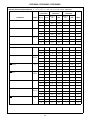
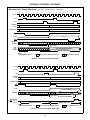
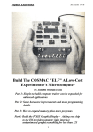
1
CDP1802A, CDP1802AC,
CDP1802BC
TM
CMOS 8-Bit Microprocessors
March 1997
Features
Description
• Maximum Input Clock Maximum Frequency Options
At VDD = 5V
- CDP1802A, AC . . . . . . . . . . . . . . . . . . . . . . . . . 3.2MHz
- CDP1802BC . . . . . . . . . . . . . . . . . . . . . . . . . . . 5.0MHz
• Maximum Input Clock Maximum Frequency Options
At VDD = 10V
- CDP1802A, AC . . . . . . . . . . . . . . . . . . . . . . . . . 6.4MHz
• Minimum Instruction Fetch-Execute Times
At VDD = 5V
- CDP1802A, AC . . . . . . . . . . . . . . . . . . . . . . . . . . 5.0µs
- CDP1802BC . . . . . . . . . . . . . . . . . . . . . . . . . . . . 3.2µs
The CDP1802 family of CMOS microprocessors are 8-bit
register oriented central processing units (CPUs) designed
for use as general purpose computing or control elements in
a wide range of stored program systems or products.
• Any Combination of Standard RAM and ROM Up to
65,536 Bytes
• 8-Bit Parallel Organization With Bidirectional Data Bus
and Multiplexed Address Bus
• 16 x 16 Matrix of Registers for Use as Multiple
Program Counters, Data Pointers, or Data Registers
The CDP1802 types include all of the circuits required for
fetching, interpreting, and executing instructions which have
been stored in standard types of memories. Extensive
input/output (I/O) control features are also provided to facilitate system design.
The 1800 series architecture is designed with emphasis on
the total microcomputer system as an integral entity so that
systems having maximum flexibility and minimum cost can
be realized. The 1800 series CPU also provides a synchronous interface to memories and external controllers for I/O
devices, and minimizes the cost of interface controllers. Further, the I/O interface is capable of supporting devices operating in polled, interrupt driven, or direct memory access
modes.
The CDP1802A and CDP1802AC have a maximum input
clock frequency of 3.2MHz at VDD = 5V. The CDP1802A and
CDP1802AC are functionally identical. They differ in that the
CDP1802A has a recommended operating voltage range of
4V to 10.5V, and the CDP1802AC a recommended operating voltage range of 4V to 6.5V.
• On-Chip DMA, Interrupt, and Flag Inputs
• Programmable Single-Bit Output Port
• 91 Easy-to-Use Instructions
The CDP1802BC is a higher speed version of the
CDP1802AC, having a maximum input clock frequency of
5.0MHz at VDD = 5V, and a recommended operating voltage
range of 4V to 6.5V.
Ordering Information
PART NUMBER
5V - 3.2MHz
CDP1802ACE
5V - 5MHz
CDP1802BCE
CDP1802ACEX
CDP1802BCEX
CDP1802ACQ
CDP1802BCQ
CDP1802ACD
CDP1802ACDX
-
TEMPERATURE RANGE
o
o
PACKAGE
PKG. NO.
-40 C to +85 C
PDIP
-40oC to +85oC
PLCC
N44.65
-40oC to +85oC
SBDIP
D40.6
Burn-In
CDP1802BCDX
CAUTION: These devices are sensitive to electrostatic discharge; follow proper IC Handling Procedures.
1-888-INTERSIL or 321-724-7143 | Intersil (and design) is a trademark of Intersil Americas Inc.
Copyright © Intersil Americas Inc. 2002. All Rights Reserved
3-3
Burn-In
E40.6
E40.6
D40.6
File Number
1305.2
CDP1802A, CDP1802AC, CDP1802BC
Pinouts
36 INTERRUPT
SC0
6
35 MWR
MRD
7
34 TPA
BUS 7
8
33 TPB
INTERRUPT
5
DMA-OUT
37 DMA OUT
SC1
6
5
4
3
2
1 44 43 42 41 40
XTAL
38 DMA IN
4
VDD
3
Q
NC
CLEAR
CLOCK
39 XTAL
WAIT
40 VDD
2
CLEAR
1
WAIT
Q
CLOCK
DMA-IN
44 LEAD PLCC
(PACKAGE TYPE Q)
TOP VIEW
SC1
40 LEAD PDIP (PACKAGE SUFFIX E)
40 LEAD SBDIP (PACKAGE SUFFIX D)
TOP VIEW
SC0
7
39
MWR
MRD
8
38
TPA
BUS 7
9
37
TPB
BUS 6
10
36
MA7
9
32 MA7
BUS 5 10
31 MA6
BUS 4 11
30 MA5
BUS 5
11
35
MA6
BUS 3 12
29 MA4
NC
12
34
NC
BUS 2 13
28 MA3
BUS 4
13
33
MA5
BUS 1 14
27 MA2
BUS 3
14
32
MA4
BUS 0 15
26 MA1
BUS 2
15
31
MA3
BUS 1
16
30
MA2
BUS 0
17
29
MA1
25 MA0
MA0
EF1
EF2
21 EF4
EF3
22 EF3
EF4
N0 19
VSS 20
18 19 20 21 22 23 24 25 26 27 28
NC
23 EF2
VSS
N1 18
N0
24 EF1
N1
N2 17
N2
VCC 16
VCC
BUS 6
ADDRESS BUS
CDP1852
INPUT PORT
CS2
CS1
N0 MA0-7
MRD
CDP1802
8-BIT CPU
MA0-7
MRD
CDP1833
1K-ROM
MWR
DATA
N1
CS1
CDP1852
CS2
OUTPUT
PORT CLOCK
TPA
TPB DATA
MRD
CDP1824
32 BYTE RAM
MWR
TPA
CEO
DATA
FIGURE 1. TYPICAL CDP1802 SMALL MICROPROCESSOR SYSTEM
3-4
MA0-4
CS
CDP1802A, CDP1802AC, CDP1802BC
Block Diagram
I/O REQUESTS
MEMORY ADDRESS LINES
I/O FLAGS
DMA
OUT
MA6 MA4 MA2 MA0 EF1 EF3
EF2 EF4
MA7 MA5 MA3 MA1
MUX
DMA
IN
INT
CONTROL
CLEAR
WAIT
CLOCK
LOGIC
CLOCK
XTAL
SCO
SCI
Q LOGIC
TPA
TPB
MWR
MRD
CONTROL AND
TIMING LOGIC
TO INSTRUCTION
DECODE
STATE
CODES
SYSTEM
TIMING
A
B
ALU
DF
D
INCR/
DECR
REGISTER
R(0).1 R(0).0 ARRAY
R(1).1 R(1).0 R
R(2).1 R(2).0
R(9).1 R(9).0
R(A).1 R(A).0
LATCH
AND
DECODE
R(E).1 R(E).0
R(F).1 R(F).0
N0
X
T
P
I
N
N1
N2
BUS 0
BUS 1
8-BIT BIDIRECTIONAL DATA BUS
BUS 2
BUS 3
BUS 4
BUS 5
BUS 6
BUS 7
FIGURE 2.
3-5
I/O
COMMANDS
CDP1802A, CDP1802AC, CDP1802BC
Absolute Maximum Ratings
Thermal Information
DC Supply Voltage Range, (VDD)
(All Voltages Referenced to VSS Terminal)
CDP1802A. . . . . . . . . . . . . . . . . . . . . . . . . . . . . . . . . -0.5V to +11V
CDP1802AC, CDP1802BC. . . . . . . . . . . . . . . . . . . . -0.5V to +7V
Input Voltage Range, All Inputs . . . . . . . . . . . . . .-0.5V to VDD +0.5V
DC Input Current, any One Input . . . . . . . . . . . . . . . . . . . . . . . . . ±10mA
Thermal Resistance (Typical, Note 4)
θJA (oC/W)
θJC (oC/W)
PDIP . . . . . . . . . . . . . . . . . . . . . . . . . .
50
N/A
PLCC . . . . . . . . . . . . . . . . . . . . . . . . . .
46
N/A
SBDIP . . . . . . . . . . . . . . . . . . . . . . . . .
55
15
Device Dissipation Per Output Transistor
TA = Full Package Temperature Range . . . . . . . . . . . . . . . 100mW
Operating Temperature Range (TA)
Package Type D . . . . . . . . . . . . . . . . . . . . . . . . . . -55oC to +125oC
Package Type E and Q. . . . . . . . . . . . . . . . . . . . . . -40oC to +85oC
Storage Temperature Range (TSTG) . . . . . . . . . . . . -65oC to +150oC
Lead Temperature (During Soldering)
At distance 1/16 ± 1/32 In. (1.59 ± 0.79mm)
from case for 10s max . . . . . . . . . . . . . . . . . . . . . . . . . . . . +265oC
Lead Tips Only. . . . . . . . . . . . . . . . . . . . . . . . . . . . . . . . . . +300oC
CAUTION: Stresses above those listed in “Absolute Maximum Ratings” may cause permanent damage to the device. This is a stress only rating and operation
of the device at these or any other conditions above those indicated in the operational sections of this specification is not implied.
Recommended Operating Conditions
TA = -40oC to +85oC. For maximum reliability, operating conditions should be selected so
that operation is always within the following ranges:
TEST CONDITIONS
CDP1802A
CDP1802AC
CDP1802BC
(NOTE 2)
VCC
(V)
VDD
(V)
MIN
MAX
MIN
MAX
MIN
MAX
UNITS
DC Operating Voltage Range
-
-
4
10.5
4
6.5
4
6.5
V
Input Voltage Range
-
-
VSS
VDD
VSS
VDD
VSS
VDD
V
4 to 6.5
4 to 6.5
-
-
-
1
-
1
µs
4 to 10.5
4 to 10.5
-
1
-
-
-
-
µs
5
5
5
-
5
-
3.2
-
µs
5
10
4
-
-
-
-
-
µs
10
10
2.5
-
-
-
-
-
µs
5
5
-
400
-
400
-
667
KBytes/s
5
10
-
500
-
-
-
-
10
10
-
800
-
-
-
-
5
5
DC
3.2
DC
3.2
DC
5
MHz
5
10
DC
4
-
-
-
-
MHz
10
10
DC
6.4
-
-
-
-
MHz
PARAMETER
Maximum Clock Input Rise or
Fall Time
Minimum Instruction Time
(Note 3)
Maximum DMA Transfer Rate
Maximum Clock Input Frequency,
fCL, Load Capacitance
(CL) = 50pF
NOTES:
1. Printed circuit board mount: 57mm x 57mm minimum area x 1.6mm thick G10 epoxy glass, or equivalent.
2. VCC must never exceed VDD.
3. Equals 2 machine cycles - one Fetch and one Execute operation for all instructions except Long Branch and Long Skip, which require 3
machine cycles - one Fetch and two Execute operations.
4. θJA is measured with component mounted on an evaluation board in free air.
3-6
CDP1802A, CDP1802AC, CDP1802BC
Static Electrical Specifications
at TA = -40oC to +85oC, Except as Noted
TEST CONDITIONS
CDP1802AC,
CDP1802BC
CDP1802A
SYMBOL
VOUT
(V)
VIN
(V)
VCC,
VDD
(V)
MIN
(NOTE 1)
TYP
MAX
MIN
(NOTE 1)
TYP
MAX
UNITS
IDD
-
-
5
-
0.1
50
-
1
200
µA
-
-
10
-
1
200
-
-
-
µA
0.4
0, 5
5
1.1
2.2
-
1.1
2.2
-
mA
(Except XTAL)
0.5
0, 10
10
2.2
4.4
-
-
-
-
mA
XTAL
0.4
5
5
170
350
-
170
350
-
µA
4.6
0, 5
5
-0.27
-0.55
-
-0.27
-0.55
-
mA
(Except XTAL)
9.5
0, 10
10
-0.55
-1.1
-
-
-
-
mA
XTAL
4.6
0
5
-125
-250
-
-125
-250
-
µA
-
0, 5
5
-
0
0.1
-
0
0.1
V
-
0, 10
10
-
0
0.1
-
-
-
V
-
0, 5
5
4.9
5
-
4.9
5
-
V
PARAMETER
Quiescent Device Current
Output Low Drive (Sink)
Current
IOL
Output High Drive (Source)
Current
IOH
Output Voltage
Low Level
VOL
Output Voltage
High Level
VOH
-
0, 10
10
9.9
10
-
-
-
-
V
Input Low Voltage
VIL
0.5, 4.5
-
5
-
-
1.5
-
-
1.5
V
0.5, 4.5
-
5, 10
-
-
1
-
-
-
V
1, 9
-
10
-
-
3
-
-
-
V
0.5, 4.5
-
5
3.5
-
-
3.5
-
-
V
0.5, 4.5
-
5, 10
4
-
-
-
-
-
V
1, 9
-
10
7
-
-
-
-
-
V
-
-
5
0.4
0.5
-
0.4
0.5
-
V
-
-
5, 10
0.3
0.4
-
-
-
-
V
-
-
10
1.5
2
-
-
-
-
V
Any
Input
0, 5
5
-
±10-4
±1
-
±10-4
±1
µA
0, 10
10
-
±10-4
±1
-
-
-
µA
0, 5
0, 5
5
-
±10-4
±1
-
±10-4
±1
µA
0, 10
0, 10
10
-
±10-4
±1
-
-
-
µA
-
-
5
-
2
4
-
2
4
mA
-
-
5
-
-
-
-
3
6
mA
Input High Voltage
CLEAR Input Voltage
VIH
VH
Schmitt Hysteresis
Input Leakage Current
Three-State Output Leakage
IIN
IOUT
Current
Operating Current
CDP1802A, AC
at f = 3.2MHz
IDDI
(Note 2)
CDP1802BC
at f = 5.0MHz
Minimum Data Retention
Voltage
VDR
VDD = VDR
-
2
2.4
-
2
2.4
V
Data Retention Current
IDR
VDD = 2.4V
-
0.05
-
-
0.5
-
µA
3-7
CDP1802A, CDP1802AC, CDP1802BC
Static Electrical Specifications
at TA = -40oC to +85oC, Except as Noted (Continued)
TEST CONDITIONS
PARAMETER
Output Capacitance
VCC,
VDD
(V)
MIN
(NOTE 1)
TYP
MAX
MIN
(NOTE 1)
TYP
MAX
UNITS
CIN
-
5
7.5
-
5
7.5
pF
COUT
-
10
15
-
10
15
pF
SYMBOL
Input Capacitance
VOUT
(V)
VIN
(V)
CDP1802AC,
CDP1802BC
CDP1802A
NOTES:
1. Typical values are for TA = +25oC and nominal VDD.
2. Idle “00” at M(0000), CL = 50pF.
Dynamic Electrical Specifications
TA = -40oC to +85oC, CL = 50pF, VDD ±5%, Except as Noted
TEST
CONDITIONS
PARAMETER
CDP1802A,
CDP1802AC
CDP1802BC
SYMBOL
VCC (V)
VDD (V)
(NOTE 1)
TYP
MAX
(NOTE 1)
TYP
MAX
UNITS
tPLH, tPHL
5
5
200
300
200
300
ns
5
10
150
250
-
-
ns
10
10
100
150
-
-
ns
5
5
600
850
475
525
ns
5
10
400
600
-
-
ns
10
10
300
400
-
-
ns
5
5
250
350
175
250
ns
5
10
150
250
-
-
ns
10
10
100
150
-
-
ns
5
5
200
300
175
275
ns
5
10
150
250
-
-
ns
10
10
100
150
-
-
ns
5
5
200
350
175
275
ns
5
10
150
290
-
-
ns
10
10
100
175
-
-
ns
5
5
200
300
175
225
ns
5
10
150
250
-
-
ns
10
10
100
150
-
-
ns
5
5
300
450
250
375
ns
5
10
250
350
-
-
ns
10
10
100
200
-
-
ns
PROPAGATION DELAY TIMES
Clock to TPA, TPB
Clock-to-Memory High-Address Byte
Clock-to-Memory Low-Address Byte Valid
Clock to MRD
Clock to MRD
Clock to MWR
Clock to (CPU DATA to BUS) Valid
tPLH, tPHL
tPLH, tPHL
tPHL
tPLH
tPLH, tPHL
tPLH, tPHL
3-8
CDP1802A, CDP1802AC, CDP1802BC
Dynamic Electrical Specifications
TA = -40oC to +85oC, CL = 50pF, VDD ±5%, Except as Noted (Continued)
TEST
CONDITIONS
PARAMETER
Clock to State Code
Clock to Q
Clock to N (0 - 2)
CDP1802A,
CDP1802AC
CDP1802BC
SYMBOL
VCC (V)
VDD (V)
(NOTE 1)
TYP
MAX
(NOTE 1)
TYP
MAX
UNITS
tPLH, tPHL
5
5
300
450
250
400
ns
5
10
250
350
-
-
ns
10
10
150
250
-
-
ns
5
5
250
400
200
300
ns
5
10
150
250
-
-
ns
10
10
100
150
-
-
ns
5
5
300
550
275
350
ns
5
10
200
350
-
-
ns
10
10
150
250
-
-
ns
5
5
-20
25
-20
0
ns
5
10
0
50
-
-
ns
10
10
-10
40
-
-
ns
5
5
150
200
125
150
ns
5
10
100
125
-
-
ns
10
10
75
100
-
-
ns
5
5
0
30
0
30
ns
5
10
0
20
-
-
ns
10
10
0
10
-
-
ns
5
5
150
250
100
150
ns
5
10
100
200
-
-
ns
10
10
75
125
-
-
ns
5
5
-75
0
-75
0
ns
5
10
-50
0
-
-
ns
10
10
-25
0
-
-
ns
5
5
100
150
75
125
ns
5
10
75
100
-
-
ns
10
10
50
75
-
-
ns
5
5
10
50
20
40
ns
5
10
-10
15
-
-
ns
10
10
0
25
-
-
ns
tPLH, tPHL
tPLH, tPHL
MINIMUM SET UP AND HOLD TIMES
Data Bus Input Set Up
Data Bus Input Hold
DMA Set Up
DMA Hold
Interrupt Set Up
Interrupt Hold
WAIT Set Up
tSU
tH
(Note 2)
tSU
tH
(Note 2)
tSU
tH
(Note 2)
tSU
3-9
CDP1802A, CDP1802AC, CDP1802BC
Dynamic Electrical Specifications
TA = -40oC to +85oC, CL = 50pF, VDD ±5%, Except as Noted (Continued)
TEST
CONDITIONS
PARAMETER
CDP1802BC
SYMBOL
VCC (V)
VDD (V)
(NOTE 1)
TYP
MAX
(NOTE 1)
TYP
MAX
UNITS
tSU
5
5
-30
20
-30
0
ns
5
10
-20
30
-
-
ns
10
10
-10
40
-
-
ns
5
5
150
200
100
150
ns
5
10
100
150
-
-
ns
10
10
75
100
-
-
ns
5
5
150
300
100
150
ns
5
10
100
200
-
-
ns
10
10
75
150
-
-
ns
5
5
125
150
90
100
ns
5
10
100
125
-
-
ns
10
10
60
75
-
-
ns
EF1-4 Set Up
EF1-4 Hold
CDP1802A,
CDP1802AC
tH
(Note 2)
Minimum Pulse Width Times
CLEAR Pulse Width
tWL
(Note 2)
CLOCK Pulse Width
tWL
NOTES:
1. Typical values are for TA = +25oC and nominal VDD.
2. Maximum limits of minimum characteristics are the values above which all devices function.
Timing Specifications
as a function of T(T = 1/fCLOCK) at TA = -40 to +85oC, Except as Noted
TEST CONDITIONS
CDP1802A,
CDP1802AC
CDP1802BC
PARAMETERS
SYMBOL
VCC (V)
VDD (V)
MIN
(NOTE 1)
TYP
MIN
(NOTE 1)
TYP
UNITS
High-Order Memory-Address Byte
Set Up to TPA
Time
tSU
5
5
2T-550
2T-400
2T-325
2T-275
ns
5
10
2T-350
2T250
-
-
ns
10
10
2T-250
2T-200
-
-
ns
5
5
t/2-25
T/2-15
T/2-25
T/2-15
ns
5
10
T/2-35
T/2-25
-
-
ns
10
10
T/2-10
T/2-+0
-
-
ns
5
5
T-30
T+0
T-30
T+0
ns
5
10
T-20
T+0
-
-
ns
10
10
T-10
T+0
-
-
ns
5
5
T-200
T-150
T-175
T-125
ns
5
10
T-150
T-100
-
-
ns
10
10
T-100
T-50
-
-
ns
High-Order Memory-Address Byte
Hold After TPA Time
Low-Order Memory-Address Byte
Hold After WR Time
CPU Data to Bus Hold After WR
Time
tH
tH
tH
3-10
CDP1802A, CDP1802AC, CDP1802BC
Timing Specifications
as a function of T(T = 1/fCLOCK) at TA = -40 to +85oC, Except as Noted
TEST CONDITIONS
CDP1802A,
CDP1802AC
CDP1802BC
PARAMETERS
SYMBOL
VCC (V)
VDD (V)
MIN
(NOTE 1)
TYP
MIN
(NOTE 1)
TYP
UNITS
Required Memory Access Time Address to Data
tACC
5
5
5T-375
5T-250
5T-225
5T-175
ns
5
10
5T-250
5T-150
-
-
ns
10
10
5T-190
5T-100
-
-
ns
5
5
T/2-25
T/2-18
T/2-20
T/2-15
ns
5
10
T/2-20
T/2-15
-
-
ns
10
10
T/2-15
T/2-10
-
-
ns
MRD to TPA
tSU
NOTE:
1. Typical values are for TA = +25oC and nominal VDD.
Timing Waveforms
FETCH (READ)
CLOCK
ADDRESS
EXECUTE (WRITE)
00 01 10 11 20 21 30 31 40 41 50 51 60 61 70 71 00 01 10 11 20 21 30 31 40 41 50 51 60 61 70 71 00
HI BYTE
LOW BYTE
HI BYTE
LOW BYTE
TPA
TPB
MRD
MWR
DATA
VALID INPUT DATA
VALID OUTPUT DATA
FIGURE 3. BASIC DC TIMING WAVEFORM, ONE INSTRUCTION CYCLE
3-11
CDP1802A, CDP1802AC, CDP1802BC
Timing Waveforms
tW
CLOCK
(Continued)
0
00
1
01
10
2
11
tPLH
TPA
3
20
21
30
4
31
40
5
41
50
6
51
60
70
tPLH
tSU
MRD
(MEMORY
READ CYCLE)
61
tPLH, tPHL
tPHL
MWR
(MEMORY
WRITE CYCLE)
tPLH, tPHL
tH
tSU
tPLH
tPLH
tPHL
tPLH
tPHL
tH
tPLH, tPHL
tPLH
tPLH, tPHL
tPHL
tPLH, tPHL
tPLH
tPLH
DATA
LATCHED IN CPU
tSU
DATA FROM
BUS TO CPU
tH
DMA SAMPLED (S1, S2, S3)
tSU
tH
tSU
tH
DMA
REQUEST
INTERRUPT
SAMPLED (S1, S2)
INTERRUPT
REQUEST
EF 1-4
01
tPLH, tPHL
LOW ORDER
ADDRESS BYTE
Q
N0, N1, N2
(I/O EXECUTION
CYCLE)
00
tPHL
DATA FROM
CPU TO BUS
STATE
CODES
71
tH
HIGH ORDER
ADDRESS BYTE
tPLH
0
tPHL
TPB
MEMORY
ADDRESS
7
FLAG LINES
SAMPLED (IN S1)
tSU
tH
tSU
WAIT
ANY NEGATIVE
TRANSITION
tW
CLEAR
NOTES:
1. This timing diagram is used to show signal relationships only and does not represent any specific machine cycle.
2. All measurements are referenced to 50% point of the waveforms.
3. Shaded areas indicate “Don’t Care” or undefined state. Multiple transitions may occur during this period.
FIGURE 4. TIMING WAVEFORM
3-12
CDP1802A, CDP1802AC, CDP1802BC
Machine Cycle Timing Waveforms
0
1
2
3
4
5
6
7
(Propagation Delays Not Shown)
0
1
2
3
4
5
6
7
0
1
2
3
4
5
6
7
0
CLOCK
TPA
TPB
MACHINE
CYCLE
CYCLE n
MA
HIGH ADD
CYCLE (n + 1)
LOW ADDRESS
HIGH ADD
CYCLE (n + 2)
LOW ADDRESS
HIGH ADD
LOW ADDRESS
FIGURE 5. GENERAL TIMING WAVEFORMS
INSTRUCTION
FETCH (S0)
MEMORY READ CYCLE
EXECUTE (S1)
NON MEMORY CYCLE
FETCH (S0)
EXECUTE
MEMORY READ CYCLE
MRD
MWR (HIGH)
MEMORY
OUTPUT
ALLOWABLE MEMORY ACCESS
VALID OUTPUT
“DON’T CARE” OR INTERNAL DELAYS
VALID
OUTPUT
HIGH IMPEDANCE STATE
FIGURE 6. NON-MEMORY CYCLE TIMING WAVEFORMS
INSTRUCTION
FETCH (S0)
MEMORY READ CYCLE
EXECUTE (S1)
FETCH (S0)
MEMORY WRITE CYCLE
MEMORY READ CYCLE
EXECUTE
MRD
MWR
MEMORY
OUTPUT
ALLOWABLE MEMORY ACCESS
CPU OUTPUT
TO MEMORY
OFF
VALID OUTPUT
VALID
OUTPUT
VALID DATA
“DON’T CARE” OR INTERNAL DELAYS
OFF
HIGH IMPEDANCE STATE
FIGURE 7. MEMORY WRITE CYCLE TIMING WAVEFORMS
3-13
VALID
CDP1802A, CDP1802AC, CDP1802BC
Machine Cycle Timing Waveforms
INSTRUCTION
FETCH (S0)
MEMORY READ CYCLE
(Propagation Delays Not Shown)
(Continued)
EXECUTE (S1)
MEMORY READ CYCLE
FETCH (S0)
EXECUTE
MEMORY READ CYCLE
MRD
MWR (HIGH)
MEMORY
OUTPUT
ALLOWABLE MEMORY ACCESS
VALID OUTPUT
“DON’T CARE” OR INTERNAL DELAYS
VALID
OUTPUT
VALID
OUTPUT
HIGH IMPEDANCE STATE
FIGURE 8. MEMORY READ CYCLE TIMING WAVEFORMS
INSTRUCTION
FETCH (S0)
MEMORY READ CYCLE
EXECUTE (S1)
MEMORY READ CYCLE
EXECUTE (S1)
FETCH (S0)
MEMORY READ CYCLE
MRD
MWR (HIGH)
MEMORY
OUTPUT
ALLOWABLE MEMORY ACCESS
VALID OUTPUT
“DON’T CARE” OR INTERNAL DELAYS
VALID OUTPUT
HIGH IMPEDANCE STATE
FIGURE 9. LONG BRANCH OR LONG SKIP CYCLE TIMING WAVEFORMS
3-14
VALID
OUTPUT
CDP1802A, CDP1802AC, CDP1802BC
Machine Cycle Timing Waveforms
0
1
2
3
4
(Propagation Delays Not Shown)
5
6
7
0
1
(Continued)
2
3
4
5
6
7
0
CLOCK
TPA
TPB
MACHINE
CYCLE
INSTRUCTION
CYCLE n
CYCLE (n + 1)
FETCH (S0)
EXECUTE (S1)
MRD
N0 - N2
N=9-F
MWR
MEMORY
OUTPUT
VALID OUTPUT
ALLOWABLE MEMORY ACCESS
DATA
BUS
(NOTE 1)
VALID DATA FROM INPUT DEVICE
MEMORY READ CYCLE
NOTE 1
USER GENERATED SIGNAL
MEMORY WRITE CYCLE
HIGH IMPEDANCE STATE
“DON’T CARE” OR INTERNAL DELAYS
FIGURE 10. INPUT CYCLE TIMING WAVEFORMS
0
1
2
4
3
5
6
7
0
1
2
3
4
5
6
7
CLOCK
TPA
TPB
MACHINE
CYCLE
CYCLE n
CYCLE (n + 1)
FETCH (S0)
EXECUTE (S1)
INSTRUCTION
MRD
N=1-9
ALLOWABLE MEMORY ACCESS
N0 - N2
DATA BUS
ALLOWABLE MEMORY ACCESS
VALID OUTPUT
VALID DATA FROM MEMORY
DATA STROBE
(MRD • TPB • N)
(NOTE 1)
MEMORY READ CYCLE
NOTE 1
USER GENERATED SIGNAL
MEMORY READ CYCLE
“DON’T CARE” OR INTERNAL DELAYS
FIGURE 11. OUTPUT CYCLE TIMING WAVEFORMS
3-15
HIGH IMPEDANCE STATE
0
CDP1802A, CDP1802AC, CDP1802BC
Machine Cycle Timing Waveforms
0
1
2
4
3
5
6
7
(Propagation Delays Not Shown)
0
1
2
3
4
5
6
(Continued)
7
0
1
2
3
4
5
6
7
CLOCK
TPA
TPB
MACHINE
CYCLE
CYCLE n
INSTRUCTION
CYCLE (n+1)
FETCH (S0)
CYCLE (n+2)
EXECUTE (S1)
DMA (S2)
DMA-IN
MRD
MWR
MEMORY
OUTPUT
VALID OUTPUT
VALID DATA FROM INPUT DEVICE
DATA BUS
(NOTE 1)
MEMORY READ CYCLE
MEMORY READ, WRITE
OR NON-MEMORY CYCLE
NOTE 1
USER GENERATED SIGNAL
MEMORY WRITE CYCLE
HIGH IMPEDANCE STATE
“DON’T CARE” OR INTERNAL DELAYS
FIGURE 12. DMA IN CYCLE TIMING WAVEFORMS
0
1
2
3
4
5
6
7
0
1
2
3
4
5
6
7
0
1
2
3
4
5
6
CLOCK
TPA
TPB
MACHINE
CYCLE
INSTRUCTION
CYCLE n
CYCLE (n + 1)
CYCLE (n + 2)
FETCH (S0)
EXECUTE (S1)
DMA (S2)
DMA OUT
(NOTE 1)
MRD
MWR
MEMORY
OUTPUT
DATA
STROBE
(S2 • TPB)
(NOTE 1)
VALID OUTPUT
MEMORY READ CYCLE
NOTE 1
USER GENERATED SIGNAL
MEMORY READ, WRITE
OR NON-MEMORY CYCLE
“DON’T CARE” OR INTERNAL DELAYS
FIGURE 13. DMA OUT CYCLE TIMING WAVEFORMS
3-16
VALID DATA FROM MEMORY
MEMORY READ CYCLE
HIGH IMPEDANCE STATE
CDP1802A, CDP1802AC, CDP1802BC
Machine Cycle Timing Waveforms
0
1
2
3
4
5
6
7
(Propagation Delays Not Shown)
0
1
2
3
4
5
(Continued)
6
7
0
1
2
3
4
5
6
CLOCK
TPA
TPB
MACHINE
CYCLE
INSTRUCTION
CYCLE n
CYCLE (n + 1)
CYCLE (n + 2)
FETCH (S0)
EXECUTE (S1)
INTERRUPT (S3)
MRD
MWR
INTERRUPT
(NOTE 1)
(INTERNAL) IE
MEMORY
OUTPUT
MEMORY READ CYCLE
VALID OUTPUT
MEMORY READ, WRITE
OR NON-MEMORY CYCLE
NOTE 1
USER GENERATED SIGNAL
“DON’T CARE” OR INTERNAL DELAYS
NON-MEMORY CYCLE
HIGH IMPEDANCE STATE
FIGURE 14. INTERRUPT CYCLE TIMING WAVEFORMS
Performance Curves
8
8
CL, LOAD CAPACITANCE = 50pF
CL, LOAD CAPACITANCE = 50pF
7
VCC = VDD = 10V
fCL, SYSTEM MAXIMUM CLOCK
FREQUENCY (MHz)
fCL, SYSTEM MAXIMUM CLOCK
FREQUENCY (MHz)
7
6
5
VCC = 5V, VDD = 10V
4
VCC = VDD = 5V
3
2
1
0
25
35
45
55
65
75
85
95 105
TA, AMBIENT TEMPERATURE (oC)
115
6
5
VCC = VDD = 5V
4
3
2
1
0
125
25
FIGURE 15. CDP1802A, AC TYPICAL MAXIMUM CLOCK
FREQUENCY AS A FUNCTION OF TEMPERATURE
35
45
55
65
75
85
95 105
TA, AMBIENT TEMPERATURE (oC)
115
125
FIGURE 16. CDP1802BC TYPICAL MAXIMUM CLOCK
FREQUENCY AS A FUNCTION OF TEMPERATURE
3-17
CDP1802A, CDP1802AC, CDP1802BC
TA = 25oC
-10
VCC = VDD = 5V
350
-9
VDS, DRAIN-TO-SOURCE VOLTAGE (V)
-8
-7
-6
-5
-4
-3
-2
-1
0
VGS, GATE-TO-VOLTAGE = -5V
1
300
2
250
3
VCC = VDD = 10V
200
-10V
4
tTLH
150
5
VCC = VDD = 5V
100
tTHL
6
50
VCC = VDD = 10V
7
0
0
25
50
TA, AMBIENT TEMPERATURE = -40oC TO +85oC
75 100 125 150 175 200
CL, LOAD CAPACITANCE (pF)
IOL, OUTPUT LOW (SINK) CURRENT (mA)
FIGURE 17. TYPICAL TRANSITION TIME vs LOAD CAPACITANCE FOR ALL TYPES
FIGURE 18. CDP1802A, AC MINIMUM OUTPUT HIGH (SOURCE)
CURRENT CHARACTERISTICS
TA = -40oC TO +85oC
-5
VDS, DRAIN-TO-SOURCE VOLTAGE (V)
-4
-3
-2
-1
0
35
30
1
25
VGS, GATE-TO-SOURCE = 10V
20
VGS, GATE-TO-VOLTAGE = -5V
2
15
10
5V
5
0
1
2
3
4
5
3
6
7
8
9
10
4
VDS, DRAIN-TO-SOURCE VOLTAGE (V)
FIGURE 19. CDP1802A, AC MINIMUM OUTPUT LOW (SINK)
CURRENT CHARACTERISTICS
IOH, OUTPUT HIGH (SOURCE) CURRENT (mA)
tTHL, tTLH, TRANSITION TIME (ns)
400
(Continued)
IOH, OUTPUT HIGH (SOURCE) CURRENT (mA)
Performance Curves
FIGURE 20. CDP1802BC MINIMUM OUTPUT HIGH (SOURCE)
CURRENT CHARACTERISTICS
3-18
CDP1802A, CDP1802AC, CDP1802BC
(Continued)
150
TA = -40oC TO +85oC
∆tPLH, ∆tPHL, ∆ PROPAGATION DELAY
TIME (ns)
IOL, OUTPUT LOW (SINK) CURRENT (mA)
Performance Curves
TA = 25oC
VCC = VDD = 5V
125
20
100
10
VGS, GATE-TO-SOURCE = 5V
5
75
50
∆tPLH
VCC = VDD = 10V
∆tPHL
VCC = VDD = 5V
25
VCC = VDD = 10V
0
0
1
2
3
4
25
5
VDS, DRAIN-TO-SOURCE VOLTAGE (V)
50
100
150
∆CL, ∆ LOAD CAPACITANCE (pF)
200
NOTE: ANY OUTPUT EXCEPT XTAL
FIGURE 21. CDP1802BC MINIMUM OUTPUT LOW (SINK)
CURRENT CHARACTERISTICS
PD, TYPICAL POWER DISSIPATION
FOR CDP1802D (mW)
1000
FIGURE 22. TYPICAL CHANGE IN PROPAGATION DELAY AS A
FUNCTION OF A CHANGE IN LOAD CAPACITANCE
FOR ALL TYPES
TA = 25oC
VCC = VDD = 10V
100
10 BRANCH
IDLE
1
VCC = VDD = 5V
0.1
0.01
0.1
1
fCL, CLOCK INPUT FREQUENCY (MHz)
10
NOTE: IDLE = “00” AT M(0000), BRANCH = “3707” AT M(8107), CL = 50pF
FIGURE 23. TYPICAL POWER DISSIPATION AS A FUNCTION OF CLOCK FREQUENCY FOR BRANCH INSTRUCTION AND IDLE
INSTRUCTION FOR ALL TYPES
Signal Descriptions
Bus 0 to Bus 7 (Data Bus)
8-bit bidirectional DATA BUS lines. These lines are used for
transferring data between the memory, the microprocessor,
and I/O devices.
N0 to N2 (I/O Control Lines)
The direction of data flow is defined in the I/O instruction by bit
N3 (internally) and is indicated by the level of the MRD signal.
MRD = VCC: Data from I/O to CPU and Memory
MRD = VSS: Data from Memory to I/O
EF1 to EF4 (4 Flags)
Activated by an I/O instruction to signal the I/O control logic of
a data transfer between memory and I/O interface. These
lines can be used to issue command codes or device selection codes to the I/O devices (independently or combined with
the memory byte on the data bus when an I/O instruction is
being executed). The N bits are low at all times except when
an I/O instruction is being executed. During this time their
state is the same as the corresponding bits in the N register.
These inputs enable the I/O controllers to transfer status
information to the processor. The levels can be tested by the
conditional branch instructions. They can be used in conjunction with the INTERRUPT request line to establish interrupt priorities. These flags can also be used by I/O devices
to “call the attention” of the processor, in which case the program must routinely test the status of these flag(s). The
flag(s) are sampled at the beginning of every S1 cycle.
3-19
CDP1802A, CDP1802AC, CDP1802BC
INTERRUPT, DMA-lN, DMA-OUT (3 I/O Requests)
These inputs are sampled by the CPU during the interval
between the leading edge of TPB and the leading edge of
TPA.
Interrupt Action - X and P are stored in T after executing
current instruction; designator X is set to 2; designator P is
set to 1; interrupt enable is reset to 0 (inhibit); and instruction
execution is resumed. The interrupt action requires one
machine cycle (S3).
DMA Action - Finish executing current instruction; R(0)
points to memory area for data transfer; data is loaded into
or read out of memory; and increment R(0).
NOTE: In the event of concurrent DMA and Interrupt requests,
DMA-lN has priority followed by DMA-OUT and then Interrupt.
Q
Single bit output from the CPU which can be set or reset
under program control. During SEQ or REQ instruction execution, Q is set or reset between the trailing edge of TPA and
the leading edge of TPB.
CLOCK
Input for externally generated single-phase clock. The clock is
counted down internally to 8 clock pulses per machine cycle.
XTAL
SC0, SC1, (2 State Code Lines)
These outputs indicate that the CPU is: 1) fetching an
instruction, or 2) executing an instruction, or 3) processing a
DMA request, or 4) acknowledging an interrupt request. The
levels of state code are tabulated below. All states are valid
at TPA. H = VCC, L = VSS.
Connection to be used with clock input terminal, for an external crystal, if the on-chip oscillator is utilized. The crystal is
connected between terminals 1 and 39 (CLOCK and XTAL)
in parallel with a resistance (10MΩ typ). Frequency trimming
capacitors may be required at terminals 1 and 39. For additional information, see Application Note AN6565.
WAIT, CLEAR (2 Control Lines)
STATE CODE LINES
STATE TYPE
memory does not have a three-state high-impedance output,
MRD is useful for driving memory/bus separator gates. It is
also used to indicate the direction of data transfer during an
I/O instruction. For additional information see Table 1.
Provide four control modes as listed in the following truth table:
SC1
SC0
S0 (Fetch)
L
L
CLEAR
WAIT
MODE
S1 (Execute)
L
H
L
L
LOAD
S2 (DMA)
H
L
L
H
RESET
S3 (Interrupt)
H
H
H
L
PAUSE
H
H
RUN
TPA, TPB (2 Timing Pulses)
Positive pulses that occur once in each machine cycle (TPB
follows TPA). They are used by I/O controllers to interpret
codes and to time interaction with the data bus. The trailing
edge of TPA is used by the memory system to latch the
higher-order byte of the 16-bit memory address. TPA is suppressed in IDLE when the CPU is in the load mode.
MA0 to MA7 (8 Memory Address Lines)
In each cycle, the higher-order byte of a 16-bit CPU memory
address appears on the memory address lines MA0-7 first.
Those bits required by the memory system can be strobed
into external address latches by timing pulse TPA. The low
order byte of the 16-bit address appears on the address lines
after the termination of TPA. Latching of all 8 higher-order
address bits would permit a memory system of 64K bytes.
VDD, VSS, VCC (Power Levels)
The internal voltage supply VDD is isolated from the
Input/Output voltage supply VCC so that the processor may
operate at maximum speed while interfacing with peripheral
devices operating at lower voltage. VCC must be less than or
equal to VDD. All outputs swing from VSS to VCC. The recommended input voltage swing is VSS to VCC.
Architecture
MWR (Write Pulse)
The CPU block diagram is shown in Figure 2. The principal
feature of this system is a register array (R) consisting of sixteen 16-bit scratchpad registers. Individual registers in the
array (R) are designated (selected) by a 4-bit binary code
from one of the 4-bit registers labeled N, P and X. The contents of any register can be directed to any one of the following three paths:
A negative pulse appearing in a memory-write cycle, after
the address lines have stabilized.
1. The external memory (multiplexed, higher-order byte first,
on to 8 memory address lines).
2. The D register (either of the two bytes can be gated to D).
MRD (Read Level)
A low level on MRD indicates a memory read cycle. It can be
used to control three-state outputs from the addressed memory which may have a common data input and output bus. If a
3. The increment/decrement circuit where it is increased or
decreased by one and stored back in the selected 16-bit
register.
3-20
CDP1802A, CDP1802AC, CDP1802BC
The three paths, depending on the nature of the instruction,
may operate independently or in various combinations in the
same machine cycle.
With two exceptions, CPU instruction consists of two 8clock-pulse machine cycles. The first cycle is the fetch cycle,
and the second - and third if necessary - are execute cycles.
During the fetch cycle the four bits in the P designator select
one of the 16 registers R(P) as the current program counter.
The selected register R(P) contains the address of the memory location from which the instruction is to be fetched. When
the instruction is read out from the memory, the higher order
4 bits of the instruction byte are loaded into the register and
the lower order 4 bits into the N register. The content of the
program counter is automatically incremented by one so that
R(P) is now “pointing” to the next byte in the memory.
The X designator selects one of the 16 registers R(X) to
“point” to the memory for an operand (or data) in certain ALU
or I/O operations.
The N designator can perform the following five functions
depending on the type of instruction fetched:
1. Designate one of the 16 registers in R to be acted upon
during register operations.
2. Indicate to the I/O devices a command code or device
selection code for peripherals.
3. Indicate the specific operation to be executed during the
ALU instructions, types of test to be performed during the
Branch instruction, or the specific operation required in a
class of miscellaneous instructions (70 - 73 and 78 - 7B).
4. Indicate the value to be loaded into P to designate a new
register to be used as the program counter R(P).
5. Indicate the value to be loaded into X to designate a new
register to be used as data pointer R(X).
The registers in R can be assigned by a programmer in three
different ways: as program counters, as data pointers, or as
scratchpad locations (data registers) to hold two bytes of data.
Program Counters
Any register can be the main program counter; the address
of the selected register is held in the P designator. Other registers in R can be used as subroutine program counters. By
single instruction the contents of the P register can be
changed to effect a “call” to a subroutine. When interrupts
are being serviced, register R(1) is used as the program
counter for the user's interrupt servicing routine. After reset,
and during a DMA operation, R(0) is used as the program
counter. At all other times the register designated as program counter is at the discretion of the user.
Data Pointers
The registers in R may be used as data pointers to indicate a
location in memory. The register designated by X (i.e., R(X))
points to memory for the following instructions (see Table 1).
1. ALU operations F1 - F5, F7, 74, 75, 77
2. Output instructions 61 through 67
3. Input instructions 69 through 6F
4. Certain miscellaneous instructions - 70 - 73, 78, 60, F0
The register designated by N (i.e., R(N)) points to memory
for the “load D from memory” instructions 0N and 4N and the
“Store D” instruction 5N. The register designated by P (i.e.,
the program counter) is used as the data pointer for ALU
instructions F8 - FD, FF, 7C, 7D, 7F. During these instruction
executions, the operation is referred to as “data immediate”.
Another important use of R as a data pointer supports the
built-in Direct-Memory-Access (DMA) function. When a
DMA-ln or DMA-Out request is received, one machine cycle
is “stolen”. This operation occurs at the end of the execute
machine cycle in the current instruction. Register R(0) is
always used as the data pointer during the DMA operation.
The data is read from (DMA-Out) or written into (DMA-ln) the
memory location pointed to by the R(0) register. At the end
of the transfer, R(0) is incremented by one so that the processor is ready to act upon the next DMA byte transfer
request. This feature in the 1800-series architecture saves a
substantial amount of logic when fast exchanges of blocks of
data are required, such as with magnetic discs or during
CRT-display-refresh cycles.
Data Registers
When registers in R are used to store bytes of data, four
instructions are provided which allow D to receive from or
write into either the higher-order or lower-order byte portions
of the register designated by N. By this mechanism (together
with loading by data immediate) program pointer and data
pointer designations are initialized. Also, this technique
allows scratchpad registers in R to be used to hold general
data. By employing increment or decrement instructions,
such registers may be used as loop counters.
The Q Flip-Flop
An internal flip-flop, Q, can be set or reset by instruction and
can be sensed by conditional branch instructions. The output
of Q is also available as a microprocessor output.
3-21
CDP1802A, CDP1802AC, CDP1802BC
Interrupt Servicing
Register R(1) is always used as the program counter whenever interrupt servicing is initiated. When an interrupt
request occurs and the interrupt is allowed by the program
(again, nothing takes place until the completion of the current instruction), the contents of the X and P registers are
stored in the temporary register T, and X and P are set to
new values; hex digit 2 in X and hex digit 1 in P. Interrupt
Enable is automatically deactivated to inhibit further interrupts. The user's interrupt routine is now in control; the contents of T may be saved by means of a single instruction (78)
in the memory location pointed to by R(X). At the conclusion
of the interrupt, the user's routine may restore the pre-interrupted value of X and P with a single instruction (70 or 71).
The Interrupt Enable flip-flop can be activated to permit further interrupts or can be disabled to prevent them.
CPU Register Summary
pressed during the initialization cycle. The next cycle is an S0,
S1, or an S2 but never an S3. With the use of a 71 instruction
followed by 00 at memory locations 0000 and 0001, this feature
may be used to reset IE, so as to preclude interrupts until ready
for them. Power-up reset can be realized by connecting an RC
network directly to the CLEAR pin, since it has a Schmitt triggered input, see Figure 24.
VCC
CDP1802
RS
CLEAR
3
C
THE RC TIME CONSTANT
SHOULD BE GREATER THAN
THE OSCILLATOR START-UP
TIME (TYPICALLY 20ms)
FIGURE 24. RESET DIAGRAM
Pause
D
8 Bits
Data Register (Accumulator)
DF
1-Bit
Data Flag (ALU Carry)
B
8 Bits
Auxiliary Holding Register
Stops the internal CPU timing generator on the first negative
high-to-low transition of the input clock. The oscillator continues to operate, but subsequent clock transitions are ignored.
R
16 Bits
1 of 16 Scratchpad Registers
Run
P
4 Bits
Designates which register is Program Counter
X
4 Bits
Designates which register is Data Pointer
N
4 Bits
Holds Low-Order Instruction Digit
I
4 Bits
Holds High-Order Instruction Digit
T
8 Bits
Holds old X, P after Interrupt (X is high nibble)
lE
1-Bit
Interrupt Enable
Q
1-Bit
Output Flip-Flop
May be initiated from the Pause or Reset mode functions. If
initiated from Pause, the CPU resumes operation on the first
negative high-to-low transition of the input clock. When initiated from the Reset operation, the first machine cycle following Reset is always the initialization cycle. The initialization
cycle is then followed by a DMA (S2) cycle or fetch (S0) from
location 0000 in memory.
Run-Mode State Transitions
CDP1802 Control Modes
The WAIT and CLEAR lines provide four control modes as
listed in the following truth table:
CLEAR
WAIT
MODE
L
L
LOAD
L
H
RESET
H
L
PAUSE
H
H
RUN
The CPU state transitions when in the RUN and RESET
modes are shown in Figure 25. Each machine cycle requires
the same period of time, 8 clock pulses, except the initialization cycle, which requires 9 clock pulses. The execution of
an instruction requires either two or three machine cycles,
S0 followed by a single S1 cycle or two S1 cycles. S2 is the
response to a DMA request and S3 is the interrupt response.
Table 2 shows the conditions on Data Bus and Memory
Address lines during all machine states.
Instruction Set
The function of the modes are defined as follows:
The CPU instruction summary is given in Table 1. Hexadecimal notation is used to refer to the 4-bit binary codes.
Load
Holds the CPU in the IDLE execution state and allows an I/O
device to load the memory without the need for a “bootstrap”
loader. It modifies the IDLE condition so that DMA-lN operation does not force execution of the next instruction.
In all registers bits are numbered from the least significant bit
(LSB) to the most significant bit (MSB) starting with 0.
R(W): Register designated by W, where
W = N or X, or P
Reset
R(W).0: Lower order byte of R(W)
Registers l, N, Q are reset, lE is set and 0’s (VSS) are placed on
the data bus. TPA and TPB are suppressed while reset is held
and the CPU is placed in S1. The first machine cycle after termination of reset is an initialization cycle which requires 9 clock
pulses. During this cycle the CPU remains in S1 and register X,
P, and R(0) are reset. Interrupt and DMA servicing are sup-
R(W).1: Higher order byte of R(W)
Operation Notation
M(R(N)) → D; R(N) + 1 → R(N)
This notation means: The memory byte pointed to by R(N) is
3-22
CDP1802A, CDP1802AC, CDP1802BC
loaded into D, and R(N) is incremented by 1.
IDLE • DMA • INT
FORCE S1
S1 RESET
(LONG BRANCH,
LONG SKIP, NOP, ETC.)
DMA
S1 EXECUTE
S1 INIT
DMA
INT • DMA
DMA • IDLE • INT
DMA
DMA
S2 DMA
DMA
DMA • INT
S3 INT
S0 FETCH
DMA
INT • DMA
PRIORITY: FORCE S0, S1
DMA IN
DMA OUT
INT
FIGURE 25. STATE TRANSITION DIAGRAM
TABLE 1. INSTRUCTION SUMMARY (SEE NOTES)
MNEMONIC
OP
CODE
LOAD VIA N
LDN
0N
M(R(N)) → D; FOR N not 0
LOAD ADVANCE
LDA
4N
M(R(N)) → D; R(N) + 1 → R(N)
LOAD VIA X
LDX
F0
M(R(X)) → D
LDXA
72
M(R(X)) → D; R(X) + 1 → R(X)
LOAD IMMEDIATE
LDl
F8
M(R(P)) → D; R(P) + 1 → R(P)
STORE VIA N
STR
5N
D → M(R(N))
STXD
73
D → M(R(X)); R(X) - 1 → R(X)
INCREMENT REG N
INC
1N
R(N) + 1 → R(N)
DECREMENT REG N
DEC
2N
R(N) - 1 → R(N)
INCREMENT REG X
IRX
60
R(X) + 1 → R(X)
INSTRUCTION
OPERATION
MEMORY REFERENCE
LOAD VIA X AND ADVANCE
STORE VIA X AND DECREMENT
REGISTER OPERATIONS
GET LOW REG N
GLO
8N
R(N).0 → D
PUT LOW REG N
PLO
AN
D → R(N).0
GET HIGH REG N
GHl
9N
R(N).1 → D
PUT HIGH REG N
PHI
BN
D → R(N).1
OR
OR
F1
M(R(X)) OR D → D
OR IMMEDIATE
ORl
F9
M(R(P)) OR D → D; R(P) + 1 → R(P)
LOGIC OPERATIONS (Note 1)
3-23
CDP1802A, CDP1802AC, CDP1802BC
TABLE 1. INSTRUCTION SUMMARY (SEE NOTES) (Continued)
MNEMONIC
OP
CODE
EXCLUSIVE OR
XOR
F3
M(R(X)) XOR D → D
EXCLUSIVE OR IMMEDIATE
XRI
FB
M(R(P)) XOR D → D; R(P) + 1 → R(P)
AND
AND
F2
M(R(X)) AND D → D
AND IMMEDIATE
ANl
FA
M(R(P)) AND D → D; R(P) + 1 → R(P)
SHIFT D RIGHT, LSB(D) → DF, 0 → MSB(D)
INSTRUCTION
SHIFT RIGHT
OPERATION
SHR
F6
SHIFT RIGHT WITH CARRY
SHRC
76
(Note 2)
SHIFT D RIGHT, LSB(D) → DF, DF → MSB(D)
RING SHIFT RIGHT
RSHR
76
(Note 2)
SHIFT D RIGHT, LSB(D) → DF, DF → MSB(D)
SHL
FE
SHIFT LEFT WITH CARRY
SHLC
7E
(Note 2)
SHIFT D LEFT, MSB(D) → DF, DF → LSB(D)
RING SHIFT LEFT
RSHL
7E
(Note 2)
SHIFT D LEFT, MSB(D) → DF, DF → LSB(D)
ADD
ADD
F4
M(R(X)) + D → DF, D
ADD IMMEDIATE
ADl
FC
M(R(P)) + D → DF, D; R(P) + 1 → R(P)
ADD WITH CARRY
ADC
74
M(R(X)) + D + DF → DF, D
ADD WITH CARRY, IMMEDIATE
ADCl
7C
M(R(P)) + D + DF → DF, D; R(P) + 1 → R(P)
SUBTRACT D
SD
F5
M(R(X)) - D → DF, D
SUBTRACT D IMMEDIATE
SDl
FD
M(R(P)) - D → DF, D; R(P) + 1 → R(P)
SUBTRACT D WITH BORROW
SDB
75
M(R(X)) - D - (NOT DF) → DF, D
SUBTRACT D WITH BORROW, IMMEDIATE
SDBl
7D
M(R(P)) - D - (Not DF) → DF, D; R(P) + 1 → R(P)
SM
F7
D-M(R(X)) → DF, D
SUBTRACT MEMORY IMMEDIATE
SMl
FF
D-M(R(P)) → DF, D; R(P) + 1 → R(P)
SUBTRACT MEMORY WITH BORROW
SMB
77
D-M(R(X))-(NOT DF) → DF, D
SUBTRACT MEMORY WITH BORROW, IMMEDIATE
SMBl
7F
D-M(R(P))-(NOT DF) → DF, D; R(P) + 1 → R(P)
BR
30
M(R(P)) → R(P).0
NBR
38
(Note 2)
BZ
32
IF D = 0, M(R(P)) → R(P).0, ELSE R(P) + 1 → R(P)
SHORT BRANCH IF D NOT 0
BNZ
3A
IF D NOT 0, M(R(P)) → R(P).0, ELSE R(P) + 1 → R(P)
SHORT BRANCH IF DF = 1
BDF
IF DF = 1, M(R(P)) → R(P).0, ELSE R(P) + 1 → R(P)
SHORT BRANCH IF POS OR ZERO
BPZ
33
(Note 2)
SHORT BRANCH IF EQUAL OR GREATER
BGE
SHORT BRANCH IF DF = 0
BNF
IF DF = 0, M(R(P)) → R(P).0, ELSE R(P) + 1 → R(P)
SHORT BRANCH IF MINUS
BM
3B
(Note 2)
SHORT BRANCH IF LESS
BL
SHORT BRANCH IF Q = 1
BQ
31
IF Q = 1, M(R(P)) → R(P).0, ELSE R(P) + 1 → R(P)
SHORT BRANCH IF Q = 0
BNQ
39
IF Q = 0, M(R(P)) → R(P).0, ELSE R(P) + 1 → R(P)
SHIFT LEFT
SHIFT D LEFT, MSB(D) → DF, 0 → LSB(D)
ARITHMETIC OPERATIONS (Note 1)
SUBTRACT MEMORY
BRANCH INSTRUCTIONS - SHORT BRANCH
SHORT BRANCH
NO SHORT BRANCH (See SKP)
SHORT BRANCH IF D = 0
3-24
R(P) + 1 → R(P)
CDP1802A, CDP1802AC, CDP1802BC
TABLE 1. INSTRUCTION SUMMARY (SEE NOTES) (Continued)
MNEMONIC
OP
CODE
SHORT BRANCH IF EF1 = 1 (EF1 = VSS)
B1
34
IF EF1 =1, M(R(P)) → R(P).0, ELSE R(P) + 1 → R(P)
SHORT BRANCH IF EF1 = 0 (EF1 = VCC)
BN1
3C
IF EF1 = 0, M(R(P)) → R(P).0, ELSE R(P) + 1 → R(P)
SHORT BRANCH IF EF2 = 1 (EF2 = VSS)
B2
35
IF EF2 = 1, M(R(P)) → R(P).0, ELSE R(P) + 1 → R(P)
SHORT BRANCH IF EF2 = 0 (EF2 = VCC)
BN2
3D
IF EF2 = 0, M(R(P)) → R(P).0, ELSE R(P) + 1 → R(P)
INSTRUCTION
OPERATION
SHORT BRANCH IF EF3 = 1 (EF3 = VSS)
B3
36
IF EF3 = 1, M(R(P)) → R(P).0, ELSE R(P) + 1 → R(P)
SHORT BRANCH IF EF3 = 0 (EF3 = VCC)
BN3
3E
IF EF3 = 0, M(R(P)) → R(P).0, ELSE R(P) + 1 → R(P)
SHORT BRANCH IF EF4 = 1 (EF4 = VSS)
B4
37
IF EF4 = 1, M(R(P)) → R(P).0, ELSE R(P) + 1 → R(P)
SHORT BRANCH IF EF4 = 0 (EF4 = VCC)
BN4
3F
IF EF4 = 0, M(R(P)) → R(P).0, ELSE R(P) + 1 → R(P)
LBR
C0
M(R(P)) → R(P). 1, M(R(P) + 1) → R(P).0
NLBR
C8
(Note 2)
LBZ
C2
lF D = 0, M(R(P)) → R(P).1, M(R(P) +1) → R(P).0,
ELSE R(P) + 2 → R(P)
LONG BRANCH IF D NOT 0
LBNZ
CA
IF D Not 0, M(R(P)) → R(P).1, M(R(P) + 1) → R(P).0, ELSE
R(P) + 2 → R(P)
LONG BRANCH IF DF = 1
LBDF
C3
lF DF = 1, M(R(P)) → R(P).1, M(R(P) + 1) → R(P).0, ELSE
R(P) + 2 → R(P)
LONG BRANCH IF DF = 0
LBNF
CB
IF DF = 0, M(R(P)) → R(P).1, M(R(P) + 1) → R(P).0, ELSE
R(P) + 2 → R(P)
LONG BRANCH IF Q = 1
LBQ
C1
IF Q = 1, M(R(P)) → R(P).1, M(R(P) + 1) → R(P).0,
ELSE R(P) + 2 → R(P)
LONG BRANCH lF Q = 0
LBNQ
C9
lF Q = 0, M(R(P)) → R(P).1, M(R(P) + 1) → R(P).0
EISE R(P) + 2 → R(P)
SHORT SKIP (See NBR)
SKP
38
(Note 2)
R(P) + 1 → R(P)
LONG SKIP (See NLBR)
LSKP
C8
(Note 2)
R(P) + 2 → R(P)
LSZ
CE
IF D = 0, R(P) + 2 → R(P), ELSE CONTINUE
LONG SKIP IF D NOT 0
LSNZ
C6
IF D Not 0, R(P) + 2 → R(P), ELSE CONTINUE
LONG SKIP IF DF = 1
LSDF
CF
IF DF = 1, R(P) + 2 → R(P), ELSE CONTINUE
LONG SKIP IF DF = 0
LSNF
C7
IF DF = 0, R(P) + 2 → R(P), ELSE CONTINUE
LONG SKIP lF Q = 1
LSQ
CD
IF Q = 1, R(P) + 2 → R(P), ELSE CONTINUE
LONG SKIP IF Q = 0
LSNQ
C5
IF Q = 0, R(P) + 2 → R(P), ELSE CONTINUE
LONG SKIP IF lE = 1
LSlE
CC
IF IE = 1, R(P) + 2 → R(P), ELSE CONTINUE
lDL
00
(Note 3)
NO OPERATION
NOP
C4
CONTINUE
SET P
SEP
DN
N→P
SET X
SEX
EN
N→X
SET Q
SEQ
7B
1→Q
BRANCH INSTRUCTIONS - LONG BRANCH
LONG BRANCH
NO LONG BRANCH (See LSKP)
LONG BRANCH IF D = 0
R(P) + 2 → R(P)
SKIP INSTRUCTIONS
LONG SKIP IF D = 0
CONTROL INSTRUCTIONS
IDLE
3-25
WAIT FOR DMA OR INTERRUPT; M(R(0)) → BUS
CDP1802A, CDP1802AC, CDP1802BC
TABLE 1. INSTRUCTION SUMMARY (SEE NOTES) (Continued)
MNEMONIC
OP
CODE
RESET Q
REQ
7A
0→Q
SAVE
SAV
78
T → M(R(X))
MARK
79
(X, P) → T; (X, P) → M(R(2)), THEN P → X; R(2) - 1 → R(2)
RETURN
RET
70
M(R(X)) → (X, P); R(X) + 1 → R(X), 1 → lE
DISABLE
DlS
71
M(R(X)) → (X, P); R(X) + 1 → R(X), 0 → lE
OUTPUT 1
OUT 1
61
M(R(X)) → BUS; R(X) + 1 → R(X); N LINES = 1
OUTPUT 2
OUT 2
62
M(R(X)) → BUS; R(X) + 1 → R(X); N LINES = 2
OUTPUT 3
OUT 3
63
M(R(X)) → BUS; R(X) + 1 → R(X); N LINES = 3
OUTPUT 4
OUT 4
64
M(R(X)) → BUS; R(X) + 1 → R(X); N LINES = 4
OUTPUT 5
OUT 5
65
M(R(X)) → BUS; R(X) + 1 → R(X); N LINES = 5
OUTPUT 6
OUT 6
66
M(R(X)) → BUS; R(X) + 1 → R(X); N LINES = 6
OUTPUT 7
OUT 7
67
M(R(X)) → BUS; R(X) + 1 → R(X); N LINES = 7
INPUT 1
INP 1
69
BUS → M(R(X)); BUS → D; N LINES = 1
INPUT 2
INP 2
6A
BUS → M(R(X)); BUS → D; N LINES = 2
INPUT 3
INP 3
6B
BUS → M(R(X)); BUS → D; N LINES = 3
INPUT 4
INP 4
6C
BUS → M(R(X)); BUS → D; N LINES = 4
INPUT 5
INP 5
6D
BUS → M(R(X)); BUS → D; N LINES = 5
INPUT 6
INP 6
6E
BUS → M(R(X)); BUS → D; N LINES = 6
INPUT 7
INP 7
6F
BUS → M(R(X)); BUS → D; N LINES = 7
INSTRUCTION
PUSH X, P TO STACK
OPERATION
INPUT - OUTPUT BYTE TRANSFER
3-26
CDP1802A, CDP1802AC, CDP1802BC
TABLE 1. INSTRUCTION SUMMARY (SEE NOTES) (Continued)
INSTRUCTION
MNEMONIC
OP
CODE
OPERATION
NOTES: (For Table 1)
1. The arithmetic operations and the shift instructions are the only instructions that can alter the DF.
After an add instruction:
DF = 1 denotes a carry has occurred
DF = 0 Denotes a carry has not occurred
After a subtract instruction:
DF = 1 denotes no borrow. D is a true positive number
DF = 0 denotes a borrow. D is two’s complement
The syntax “-(not DF)” denotes the subtraction of the borrow.
2. This instruction is associated with more than one mnemonic. Each mnemonic is individually listed.
3. An idle instruction initiates a repeating S1 cycle. The processor will continue to idle until an I/O request (INTERRUPT, DMA-lN, or DMA- OUT) is
activated. When the request is acknowledged, the idle cycle is terminated and the I/O request is serviced, and then normal operation is resumed.
4. Long-Branch, Long-Skip and No Op instructions require three cycles to complete (1 fetch + 2 execute).
Long-Branch instructions are three bytes long. The first byte specifies the condition to be tested; and the second and third byte, the
branching address.
The long-branch instructions can:
a. Branch unconditionally
b. Test for D = 0 or D ≠ 0
c. Test for DF = 0 or DF = 1
d. Test for Q = 0 or Q = 1
e. Effect an unconditional no branch
If the tested condition is met, then branching takes place; the branching address bytes are loaded in the high-and-low order bytes of the
current program counter, respectively. This operation effects a branch to any memory location.
If the tested condition is not met, the branching address bytes are skipped over, and the next instruction in sequence is fetched and executed. This operation is taken for the case of unconditional no branch (NLBR).
5. The short-branch instructions are two bytes long. The first byte specifies the condition to be tested, and the second specifies the branching address.
The short branch instruction can:
a. Branch unconditionally
b. Test for D = 0 or D ≠ 0
c. Test for DF = 0 or DF = 1
d. Test for Q = 0 or Q = 1
e. Test the status (1 or 0) of the four EF flags
f. Effect an unconditional no branch
If the tested condition is met, then branching takes place; the branching address byte is loaded into the low-order byte position of the
current program counter. This effects a branch within the current 256-byte page of the memory, i.e., the page which holds the branching
address. If the tested condition is not met, the branching address byte is skipped over, and the next instruction in sequence is fetched
and executed. This same action is taken in the case of unconditional no branch (NBR).
6. The skip instructions are one byte long. There is one Unconditional Short-Skip (SKP) and eight Long-Skip instructions.
The Unconditional Short-Skip instruction takes 2 cycles to complete (1 fetch + 1 execute). Its action is to skip over the byte following it.
Then the next instruction in sequence is fetched and executed. This SKP instruction is identical to the unconditional no-branch instruction (NBR) except that the skipped-over byte is not considered part of the program.
The Long-Skip instructions take three cycles to complete (1 fetch + 2 execute).
They can:
a. Skip unconditionally
b. Test for D = 0 or D ≠ 0
c. Test for DF = 0 or DF = 1
d. Test for Q = 0 or Q = 1
e. Test for IE = 1
If the tested condition is met, then Long Skip takes place; the current program counter is incremented twice. Thus two bytes are skipped
over, and the next instruction in sequence is fetched and executed. If the tested condition is not met, then no action is taken. Execution
is continued by fetching the next instruction in sequence.
3-27
CDP1802A, CDP1802AC, CDP1802BC
TABLE 2. CONDITIONS ON DATA BUS AND MEMORY ADDRESS LINES DURING ALL MACHINE STATES
STATE
I
N
S1
DATA
BUS
MEMORY
ADDRESS
MRD
MWR
N
LINES
NOTES
00
XXXX
1
1
0
1
00
XXXX
1
1
0
2
MRP → l, N; RP + 1 → RP
MRP
RP
0
1
0
3
SYMBOL
OPERATION
0 → I, N, Q, X, P; 1 → lE
RESET
Initialize, Not Programmer 0000 → R
Accessible
S0
S1
FETCH
0
0
lDL
IDLE
MR0
RO
0
1
0
4, Fig. 8
0
1-F
LDN
MRN → D
MRN
RN
0
1
0
Fig. 8
1
0-F
INC
RN + 1 → RN
Float
RN
1
1
0
Fig. 6
2
0-F
DEC
RN - 1 → RN
Float
RN
1
1
0
Fig. 6
3
0-F
Short Branch
Taken: MRP → RP.0
Not Taken; RP + 1 → RP
MRP
RP
0
1
0
Fig. 8
4
0-F
LDA
MRN → D; RN + 1 → RN
MRN
RN
0
1
0
Fig. 8
5
0-F
STR
D → MRN
D
RN
1
0
0
Fig. 7
6
0
IRX
RX + 1 → RX
MRX
RX
0
1
0
Fig. 7
6
1
OUT 1
MRX → BUS; RX + 1 → RX
MRX
RX
0
1
1
Fig. 11
2
OUT 2
2
Fig. 11
3
OUT 3
3
Fig. 11
4
OUT 4
4
Fig. 11
5
OUT 5
5
Fig. 11
6
OUT 6
6
Fig. 11
7
OUT 7
7
Fig. 11
9
INP 1
1
Fig. 10
A
INP 2
2
Fig. 10
B
INP 3
3
Fig. 10
C
INP 4
4
Fig. 10
D
INP5
5
Fig. 10
E
INP6
6
Fig. 10
F
INP7
7
Fig. 10
0
RET
MRX → (X, P); RX + 1 → RX;
1 → lE
MRX
RX
0
1
0
Fig. 8
1
DlS
MRX → (X, P); RX + 1 → RX;
0 → lE
MRX
RX
0
1
0
Fig. 8
2
LDXA
MRX → D; RX + 1 → RX
MRX
RX
0
1
0
Fig. 8
3
STXD
D → MRX; RX - 1 → RX
D
RX
1
0
0
Fig. 7
4
ADC
MRX + D + DF → DF, D
MRX
RX
0
1
0
Fig. 8
7
BUS → MRX, D
Data from
I/O Device
RX
1
0
MRX - D - DFN → DF, D
MRX
RX
0
1
0
Fig. 8
LSB(D) → DF; DF → MSB(D)
Float
RX
1
1
0
Fig. 6
SMB
D - MRX - DFN → DF, D
MRX
RX
0
1
0
Fig. 8
SAV
T → MRX
T
RX
1
0
0
Fig. 7
5
SDB
6
SHRC
7
8
3-28
CDP1802A, CDP1802AC, CDP1802BC
TABLE 2. CONDITIONS ON DATA BUS AND MEMORY ADDRESS LINES DURING ALL MACHINE STATES (Continued)
DATA
BUS
MEMORY
ADDRESS
MRD
MWR
N
LINES
NOTES
T
R2
1
0
0
Fig. 7
0→Q
Float
RP
1
1
0
Fig. 6
SEQ
1→Q
Float
RP
1
1
0
Fig. 6
C
ADCl
MRP + D + DF → DF, D;
RP + 1
MRP
RP
0
1
0
Fig. 8
D
SDBl
MRP - D - DFN → DF, D;
RP + 1
MRP
RP
0
1
0
Fig. 8
E
SHLC
MSB(D) → DF; DF → LSB(D)
Float
RP
1
1
0
Fig. 6
F
SMBl
D - MRP - DFN → DF, D;
RP + 1
MRP
RP
0
1
0
Fig. 8
8
0-F
GLO
RN.0 → D
RN.0
RN
1
1
0
Fig. 6
9
0-F
GHl
RN.1 → D
RN.1
RN
1
1
0
Fig. 6
A
0-F
PLO
D → RN.0
D
RN
1
1
0
Fig. 6
B
0-F
PHI
D → RN.1
D
RN
1
1
0
Fig. 6
C
0 - 3,
8-B
Long Branch
MRP
RP
0
1
0
Fig. 9
M(RP + 1)
RP + 1
0
1
0
Fig. 9
STATE
I
N
SYMBOL
S1
7
9
MARK
A
REQ
B
S1#1
OPERATION
(X, P) → T, MR2; P → X;
R2 - 1 → R2
Taken: MRP → B; RP + 1 →
RP
Taken: B → RP.1;
MRP → RP.0
#2
S1#1
Not Taken: RP + 1 → RP
MRP
RP
0
1
0
Fig. 9
#2
Not Taken: RP + 1 → RP
M(RP + 1)
RP + 1
0
1
0
Fig. 9
Taken: RP + 1 → RP
MRP
RP
0
1
0
Fig. 9
Taken: RP + 1 → RP
M(RP + 1)
RP + 1
0
1
0
Fig. 9
Not Taken: No Operation
MRP
RP
0
1
0
Fig. 9
Not Taken: No Operation
MRP
RP
0
1
0
Fig. 9
No Operation
MRP
RP
0
1
0
Fig. 9
No Operation
MRP
RP
0
1
0
Fig. 9
S1#1
#2
S1#1
#2
S1#1
5
6
7
C
D
E
F
Long Skip
4
NOP
#2
S1
S1
D
0-F
SEP
N→P
NN
RN
1
1
0
Fig. 6
E
0-F
SEX
N→X
NN
RN
1
1
0
Fig. 6
F
0
LDX
MRX → D
MRX
RX
0
1
0
Fig. 8
1
2
3
4
5
7
OR
AND
XOR
ADD
SD
SM
MRX OR D → D
MRX AND D → D
MRX XOR D → D
MRX + D → DF, D
MRX - D → DF, D
D - MRX → DF, D
MRX
RX
0
1
0
Fig. 8
6
SHR
LSB(D) → DF; 0 → MSB(D)
Float
RX
1
1
0
Fig. 6
3-29
TABLE 2. CONDITIONS ON DATA BUS AND MEMORY ADDRESS LINES DURING ALL MACHINE STATES (Continued)
DATA
BUS
MEMORY
ADDRESS
MRD
MWR
N
LINES
NOTES
MRP
RP
0
1
0
Fig. 8
MSB(D) → DF; 0 → LSB(D)
Float
RP
1
1
0
Fig. 6
DMA IN
BUS → MR0; R0 + 1 → R0
Data from
I/O Device
R0
1
0
0
6, Fig. 12
DMAOUT
MR0 → BUS; R0 + 1 → R0
MR0
R0
0
1
0
6, Fig. 13
STATE
I
N
SYMBOL
S1
F
8
LDl
MRP → D; RP + 1 → RP
9
ORl
MRP OR D → D; RP + 1 → RP
A
ANl
MRP AND D → D; RP + 1 → RP
B
XRl
MRP XOR D → D; RP + 1 →
RP
C
ADl
MRP + D → DF, D; RP + 1 →
RP
D
SDl
MRP - D → DF, D; RP + 1 →
RP
F
SMl
D - MRP → DF, D; RP +1 →
RP
E
SHL
S2
OPERATION
S3
INTERRUPT
X, P → T; 0 → lE, 1 → P;
2→X
Float
RN
1
1
0
Fig. 14
S1
LOAD
IDLE (CLEAR, WAlT = 0)
M(R0 - 1)
R0 - 1
0
1
0
5, Fig. 8
NOTES:
1. lE = 1, TPA, TPB suppressed, state = S1.
2. BUS = 0 for entire cycle.
3. Next state always S1.
4. Wait for DMA or INTERRUPT.
5. Suppress TPA, wait for DMA.
6. IN REQUEST has priority over OUT REQUEST.
7. See Timing Waveforms, Figure 5 through Figure 14 for machine cycles.
Operating and Handling Considerations
Handling
All inputs and outputs of Intersil CMOS devices have a network for electrostatic protection during handling.
Operating
Operating Voltage - During operation near the maximum
supply voltage limit care should be taken to avoid or suppress
power supply turn-on and turn-off transients, power supply ripple, or ground noise; any of these conditions must not cause
VDD - VSS to exceed the absolute maximum rating.
Input Signals - To prevent damage to the input protection
circuit, input signals should never be greater than VDD nor
less than VSS. Input currents must not exceed 10mA even
when the power supply is off.
Unused Inputs - A connection must be provided at every
input terminal. All unused input terminals must be connected
to either VDD or VSS, whichever is appropriate.
Output Short Circuits - Shorting of outputs to VDD or VSS
may damage CMOS devices by exceeding the maximum
device dissipation.
All Intersil U.S. products are manufactured, assembled and tested utilizing ISO9000 quality systems.
Intersil Corporation’s quality certifications can be viewed at www.intersil.com/design/quality
Intersil products are sold by description only. Intersil Corporation reserves the right to make changes in circuit design, software and/or specifications at any time without
notice. Accordingly, the reader is cautioned to verify that data sheets are current before placing orders. Information furnished by Intersil is believed to be accurate and
reliable. However, no responsibility is assumed by Intersil or its subsidiaries for its use; nor for any infringements of patents or other rights of third parties which may result
from its use. No license is granted by implication or otherwise under any patent or patent rights of Intersil or its subsidiaries.
For information regarding Intersil Corporation and its products, see www.intersil.com
3-30
CDP1802AC/3
TM
High-Reliability CMOS 8-Bit Microprocessor
March 1997
Features
Description
• For Use In Aerospace, Military, and Critical Industrial
Equipment
The CDP1802A/3 High-Reliability LSI CMOS 8-bit register
oriented Central-Processing Unit (CPU) is designed for use
as a general purpose computing or control element in a wide
range of stored-program systems or products.
• Minimum Instruction Fetch-Execute Time of 4.5µs
(Maximum Clock
Frequency of 3.6MHz) at VDD =
5V, TA = +25oC
• Operation Over the Full Military
Temperature Range . . . . . . . . . . . . . . . -55oC to +125oC
• Any Combination of Standard RAM and ROM Up to
65,536 Bytes
• 8–Bit Parallel Organization With Bidirectional Data
Bus and Multiplexed Address Bus
• 16 x 16 Matrix of Registers for Use as Multiple Program Counters, Data Pointers, or Data Registers
• On-Chip DMA, Interrupt, and Flag Inputs
• High Noise Immunity . . . . . . . . . . . . . . . . . . 30% of VDD
Ordering Information
PACKAGE
SBDIP
TEMP. RANGE
(oC)
5V - 3.2MHz
PKG
NO.
-55 to 125
CDP1802ACD3
D40.6
The CDP1802A/3 includes all of the circuits required for
fetching, interpreting, and executing instructions which have
been stored in standard types of memories. Extensive
input/output (I/O) control features are also provided to facilitate system design.
The 1800 Series Architecture is designed with emphasis on
the total microcomputer system as an integral entity so that
systems having maximum flexibility and minimum cost can be
realized. The 1800 Series CPU also provides a synchronous
interface to memories and external controllers for I/O devices,
and minimizes the cost of interface controllers. Further, the I/O
interface is capable of supporting devices operating in polled,
interrupt-driven, or direct memory-access modes.
The CDP1802AC/3 is functionally identical to its predecessor, the CDP1802. The “A” version includes some performance enhancements and can be used as a direct
replacement in systems using the CDP1802.
This type is supplied in 40 lead dual-in-line sidebrazed
ceramic packages (D suffix).
Pinout
CDP1802AC/3 (SBDIP)
TOP VIEW
CLOCK
1
WAIT
2
40 VDD
39 XTAL
CLEAR
3
38 DMA IN
Q
4
37 DMA OUT
SC1
5
36 INTERRUPT
SC0
6
35 MWR
MRD
7
34 TPA
BUS 7
8
33 TPB
BUS 6
9
32 MA7
BUS 5 10
31 MA6
BUS 4 11
30 MA5
BUS 3 12
29 MA4
BUS 2 13
28 MA3
BUS 1 14
27 MA2
BUS 0 15
26 MA1
VCC 16
25 MA0
N2 17
24 EF1
N1 18
23 EF2
N0 19
22 EF3
VSS 20
21 EF4
CAUTION: These devices are sensitive to electrostatic discharge; follow proper IC Handling Procedures.
1-888-INTERSIL or 321-724-7143 | Intersil (and design) is a trademark of Intersil Americas Inc.
Copyright © Intersil Americas Inc. 2002. All Rights Reserved
1
File Number
1441.2
CDP1802AC/3
ADDRESS BUS
CDP1852
INPUT PORT
CS2
MA0–7
N0
MA0–7
MA0–4
CS1
MRD
MRD
MRD
CDP1802
8–BIT CPU
CDP1833
1K–ROM
MWR
DATA
CS1
CS2
CDP1852
OUTPUT CLOCK
PORT
MWR
N1
CEO
TPB DATA TPA
TPA DATA
8–BIT DATA BUS
FIGURE 1. TYPICAL CDP1802A/3 SMALL MICROPROCESSOR SYSTEM
2
CDP1824
32 BYTE RAM
CS
DATA
CDP1802AC/3
Absolute Maximum Ratings
Thermal Information
θJA (oC/W)
Thermal Resistance (Typical)
DC Supply Voltage Range, (VDD)
(All Voltages Referenced to VSS Terminal)
CDP1802AC/3 . . . . . . . . . . . . . . . . . . . . . . . . . . . . . . -0.5V to +7V
Input Voltage Range, All Inputs . . . . . . . . . . . . . -0.5V to VDD +0.5V
DC Input Current, any One Input . . . . . . . . . . . . . . . . . . . . . . . . . ±10mA
θJC (oC/W)
SBDIP Package . . . . . . . . . . . . . . . . . . .
55
15
Device Dissipation Per Output Transistor
TA = Full Package Temperature Range . . . . . . . . . . . . . . . . 100mW
Operating Temperature Range (TA)
Package Type D . . . . . . . . . . . . . . . . . . . . . . . . .-55oC to +125oC
Storage Temperature Range (TSTG). . . . . . . . . . . .-65oC to +150oC
Lead Temperature (During Soldering)
At distance 1/16 ± 1/32 In. (1.59 ±0.79mm)
from case for 10s max . . . . . . . . . . . . . . . . . . . . . . . . . . . +265oC
CAUTION: Stresses above those listed in “Absolute Maximum Ratings” may cause permanent damage to the device. This is a stress only rating and operation
of the device at these or any other conditions above those indicated in the operational sections of this specification is not implied.
Recommended Operating Conditions
TA = Full Package Temperature Range. For maximum reliability, operating conditions
should be selected so that operation is always within the following ranges
PARAMETER
MIN
MAX
UNITS
4
6.5
V
VSS
VDD
V
-
1
µs
DC Operating Voltage Range
Input Voltage Range
Maximum Clock Input Rise or Fall Time
Performance Specifications
VDD (V)
-55oC TO +25oC
+125oC
UNITS
Minimum Instruction Time (Note 1)
5
4.5
5.9
µs
Maximum DMA Transfer Rate
5
450
340
Kbytes/s
Maximum Clock Input Frequency,
Load Capacitance (CL) = 50pF, fCL
5
DC-3.6
DC-2.7
MHz
PARAMETER
NOTE:
1. Equals 2 machine cycles - one Fetch and one Execute operation for all instructions except Long Branch and Long Skip, which require 3
machine cycles - one Fetch and two Execute operations.
Static Electrical Specifications
All Limits are 100% Tested
-55oC, +25oC
CONDITIONS
+125oC
VOUT
(V)
VIN, (V)
VCC, VDD (V)
MIN
MAX
MIN
MAX
UNITS
-
-
5
-
100
-
250
µA
0.4
0, 5
5
1.20
-
0.90
-
mA
0.4
5
5
185
-
140
-
µA
4.6
0, 5
5
-
-0.30
-
-0.20
mA
4.6
0
5
-
-135
-
-100
µA
Output Voltage Low-Level, VOL
-
0, 5
5
-
0.1
-
0.2
V
Output Voltage High-Level, VOH
-
0, 5
5
4.9
-
4.8
-
V
PARAMETER
Quiescent Device Current, IDD
Output Low Drive (Sink) Current
(Except XTAL), IOL
XTAL
Output High Drive (Source)
Current (Except XTAL), IOH
XTAL
3
CDP1802AC/3
Static Electrical Specifications
All Limits are 100% Tested (Continued)
-55oC, +25oC
CONDITIONS
+125oC
VOUT
(V)
VIN, (V)
VCC, VDD (V)
MIN
MAX
MIN
MAX
UNITS
Input Low Voltage, VIL
0.5, 4.5
-
5
-
1.5
-
1.5
V
Input High Voltage, VIH
0.5, 4.5
-
5
3.5
-
3.5
-
V
Input Leakage Current, IIN
Any
Input
0, 5
5
-
±1
-
±5
µA
Three-State Output Leakage
Current, IOUT
0, 5
0, 5
5
-
±1
-
±5
µA
PARAMETER
NOTE:
2. 5V level characteristics apply to Part No. CDP1802AC/3, and 5V and 10V level characteristics apply to part No. CDP1802A/3.
Timing Specifications
As a Function of T (T = 1/fCLOCK), CL = 50 pF
LIMITS (NOTE 3)
VDD (V)
-55oC, +25oC
+125oC
UNITS
5
2T-450
2T-580
ns
High-Order Memory-Address Byte Hold After TPA Time, tH
5
T/2 +0
T/2 +0
ns
Low-Order Memory-Address Byte Hold After WR Time, tH
5
T-30
T-40
ns
CPU Data to Bus Hold After WR Time, tH
5
T-170
T-250
ns
Required Memory Access Time Address to Data, tACC
5
5T-300
5T-400
ns
PARAMETER
High-Order Memory-Address Byte Setup to TPA
Time, tSU
NOTE:
3. These limits are not directly tested.
Implicit Specifications
(Note 4) TA = -55oC to +25oC
SYMBOL
VDD (V)
TYPICAL
VALUES
UNITS
f = 2MHz
-
5
4
mW
Effective Input Capacitance any Input
-
CIN
-
5
pF
Effective Three-State Terminal Capacitance Data Bus
-
-
7.5
pF
Minimum Data Retention Voltage
-
VDR
-
2.4
V
Data Retention Current
-
IDR
2.4
10
µA
PARAMETER
Typical Total Power Dissipation
Idle “00” at M(0000), CL = 50pF
NOTE:
4. These specifications are not tested. Typical values are provided for guidance only.
4
CDP1802AC/3
Dynamic Electrical Specifications
CL = 50pF, Timing Measurement at 0.5 VDD Point
-55oC TO +25oC
+125oC
VDD (V)
MIN
MAX
MIN
MAX
UNITS
Clock to TPA, TPB
5
-
275
-
370
ns
Clock-to-Memory High Address Byte, tPLH, tPHL
5
-
725
-
950
ns
Clock-to-Memory Low Address Byte Valid, tPLH, tPHL
5
-
340
-
425
ns
Clock to MRD, tPLH, tPHL
5
-
340
-
425
ns
Clock to MWR, tPLH, tPHL
5
-
275
-
370
ns
Clock to (CPU DATA to BUS) Valid, tPLH, tPHL
5
-
430
-
550
ns
Clock to State Code, tPLH, tPHL
5
-
440
-
550
ns
Clock to Q, tPLH, tPHL
5
-
375
-
475
ns
Clock to N (0 - 2), tPLH, tPHL
5
-
400
-
525
ns
Data Bus Input Setup, tSU
5
10
-
10
-
ns
Data Bus Input Hold, t H
5
175
-
230
-
ns
DMA Setup, tSU
5
10
-
10
-
ns
DMA Hold, t H
5
200
-
270
-
ns
Interrupt Setup, t SU
5
10
-
10
-
ns
Interrupt Hold, tH
5
175
-
230
-
ns
WAIT Setup, tSU
5
30
-
30
-
ns
EF1-4 Setup, tSU
5
20
-
20
-
ns
EF1-4 Hold, tH
5
100
-
135
-
ns
CLEAR Pulse Width, tWL
5
150
-
200
-
ns
CLOCK Pulse Width, tWL
5
140
-
185
-
ns
PARAMETERS
Progagation Delay Times, tPLH, tPHL
Interface Timing Requirements (Note 5)
Required Pulse Width Times
NOTE:
5. Minimum input setup and hold times required by Part CDP1802AC/3.
5
CDP1802AC/3
6
5
4
VDD = 5V
3
2
1
25
35
45
55
65
75
85
95
105
115
LOAD CAPACITANCE (CL) = 50pF
7
6
TA = 25oC
5
4
D
7
0
8
TR
A
PO
LA
TE
LOAD CAPACITANCE (CL) = 50pF
3
2
TA = 125oC
EX
8
SYSTEM MAXIMUM CLOCK FREQUENCY
(fCL) (MHz)
SYSTEM MAXIMUM CLOCK FREQUENCY
(fCL) (MHz)
Performance Curves
1
0
125
2
3
4
5
AMBIENT TEMPERATURE (TA) (oC)
FIGURE 2. TYPICAL MAXIMUM CLOCK FREQUENCY AS A
FUNCTION OF TEMPERATURE
350
OUTPUT HIGH (SOURCE) CURRENT
(IOH -mA)
TRANSITION TIME (tTHL, t TLH) (ns)
8
9
10
11
12
0
AMBIENT TEMPERATURE (TA) = 25oC
300
250
200
150
tTLH
100
tTHL
50
0
25
50
75
100
125
150
LOAD CAPACITANCE (CL) (pF)
175
GATE TO SOURCE VOLTAGE (VGS) = -5V
1
2
3
4
AMBIENT TEMPERATURE = -40 TO +85oC
5
6
-10
200
-9
-8
-7
-6
-5
-4
-2
-3
-1
0
DRAIN TO SOURCE VOLTAGE (VDS) (V)
FIGURE 4. TYPICAL TRANSITION TIME vs LOAD
CAPACITANCE
FIGURE 5. MINIMUM OUTPUT HIGH (SOURCE) CURRENT
CHARACTERISTICS
35
1000
AMBIENT TEMPERATURE = -40oC TO +85oC
TYPICAL POWER DISSIPATION
(PD) (mW)
OUTPUT LOW (SINK) CURRENT (IOL) (mA)
7
FIGURE 3. TYPICAL MAXIMUM CLOCK FREQUENCY AS A
FUNCTION OF SUPPLY VOLTAGE
400
0
6
SUPPLY VOLTAGE (VDD) (V)
30
25
20
15
10
GATE TO SOURCE VOLTAGE (VGS) = 5V
5
1
2
3
4
5
6
7
8
9
100
10
1
“
”
CH
AN
BR
0.1
0.01
0
0
AMBIENT TEMPERATURE (TA) = 25oC
10
V CC
= VD
V CC
D
V
=5
D
= VD
=+
5V
”
LE
“ ID
0.1
1
10
CLOCK INPUT FREQUENCY (f CL) (MHz)
DRAIN-TO-SOURCE VOLTAGE (VDS) (V)
NOTES:
6. Idle = “00” at M (0000)
7. Branch = “3707” at M (8107)
FIGURE 6. MINIMUM OUTPUT LOW (SINK) CURRENT
CHARACTERISTICS
FIGURE 7. TYPICAL POWER DISSIPATION AS A FUNCTION
OF CLOCK FREQUENCY FOR BRANCH
INSTRUCTION AND IDLE INSTRUCTION
6
CDP1802AC/3
Performance Curves
(Continued)
∆
=
V
DD
=
5V
AMBIENT TEMPERATURE
(TA) = 25oC
125
C
C
100
V
PROPAGATION DELAY TIME
(∆tPLH, ∆tPHL) (ns)
150
75
50
H
∆
t PL
25
D
V CC
∆ t PH
= VD
= 5V
L
0
0
50
100
150
∆ LOAD CAPACITANCE (∆ CL) (pF)
200
NOTE: Any output except XTAL.
FIGURE 8. TYPICAL CHANGE IN PROPAGATION DELAY AS A FUNCTION OF A CHANGE IN LOAD CAPACITANCE
Burn-In Circuit
VDD
VDD
NC
40
2
39
3
38
4
37
5
36
6
35
7
34
8
33
9
32
10
31
11
30
12
29
13
28
14
27
15
26
16
25
17
24
18
23
19
22
20
21
NC
VDD
1
NC
VDD
ALL RESISTORS ARE 47kΩ ±20%
TYPE
CDP1802AC
VDD
TEMPERATURE
TIME
7V
+125oC
160 Hours
FIGURE 9. BIAS/STATIC BURN-IN CIRCUIT
All Intersil U.S. products are manufactured, assembled and tested utilizing ISO9000 quality systems.
Intersil Corporation’s quality certifications can be viewed at www.intersil.com/design/quality
Intersil products are sold by description only. Intersil Corporation reserves the right to make changes in circuit design, software and/or specifications at any time without
notice. Accordingly, the reader is cautioned to verify that data sheets are current before placing orders. Information furnished by Intersil is believed to be accurate and
reliable. However, no responsibility is assumed by Intersil or its subsidiaries for its use; nor for any infringements of patents or other rights of third parties which may result
from its use. No license is granted by implication or otherwise under any patent or patent rights of Intersil or its subsidiaries.
For information regarding Intersil Corporation and its products, see www.intersil.com
7
RCA 1802 Microprocessor
Prepared By:
Ben Knox
Henna Karim
Micah Sumner
Morgan Grinstead
John Redmon
Prepared For:
Dr. Joe Dumas
College of Engineering and Computer Science
University of Tennessee at Chattanooga
November 13, 2002
Computer Science 460 Section 001
Table of Contents
Introduction
Architectural Classification
Intended Applications
Control Unit
Registers
Bus Structure
Performing I/O
Instruction Set
Instruction Fetch and Decode
Interrupt Processing
Memory System
Conclusion
Bibliography
Appendix A
Introduction
The RCA 1802 was designed and introduced in 1974. The chip was capable of running at a clock frequency
of 6.4 MHz using a +10V power supply. The processor was designed and fabricated in CMOS. The chip
utilized 16 16-bit registers that could be accessed as 32 8-bit registers [10]. It was an 8 bit processor with 16
bit addressing. It was extremely simple and had the flexibility of a large register set. The 1802 had a single
accumulator register and a 16x16 register file [10]. This versatile chip was the first microprocessor used in
space, and RCA produced videogames based on it. The 1802 reached its peak of popularity in 1977, and at
that time sold for a little less than $30.00 as stated by Popular Mechanics [11]. The last commercial
microcomputer produced with the 1802 was a 1983 machine named the Comx 35. By 1983 the 1802 was no
longer cutting edge technology and the slow speed of the machine made it less efficient. We will now look the
1802 microprocessor in more detail, including its inner workings such as registers and instructions.
Architectural Classification
The RCA 1802 has an extremely simple design. It is a textbook example of the Von-Neumann architecture. It
has a single bus for instructions and data, and addresses a single memory. The processor does not have
temporal or spatial parallelism. It performs an instruction to completion before it fetches and executes the
next instruction. [1]
The 1802 has many characteristics that would later be implemented in RISC processors. It is not, however, a
RISC chip. The CPU has a relatively large set of 16 general-purpose 16-bit registers. The instruction set,
with only 91 instructions, is very simple.
Despite these traits the 1802 cannot be classified as a RISC
processor for several reasons. The load-store trait of RISC is not present. Many of the instructions, such as
ADI, access memory directly. [1] The instruction size is not the same for all instructions. Most instructions are
one byte, but any instruction that includes data is two bytes, and any instruction that contains an address is
three bytes. The 1802 is unable to perform any instructions in a single clock cycle. In fact, most instructions
took two machine cycles of eight clock pulses to perform their intended task, and in some cases the
instruction took three machine cycles. [6]
Intended Applications
The 1802 was designed for use as general-purpose computing or control elements in a wide range of stored
program systems or products. It was designed with emphasis on maximum flexibility and minimum cost, thus
this chip was used in a wide range of devices.
The 1802 was the first microprocessor in space via the Defense Meteorological Satellite Program
5D-1 spacecraft launched in 1976.
It was also included on the following spacecrafts:
OSCAR satellite,
Uo SAT-1, U o SAT-2, Voyager, Viking, and Galileo. [1] One reason for its space use was that the 1802 was
fabricated on sapphire, which leads to radiation and static resistance, ideal for space travel. [12]
This versatile chip was also used in Chrysler electronic ignitions, RCA and Radio Shack video games,
RCA video terminals, and ETI-660 computers. [14] Swiss payphone manufacturer Sodeco-Sia used it for
phones in France, Austria, and third world countries where its low power allowed the unit to work entirely from
the power of the phone line. [13]
In August & September of 1976 and also March & July of 1977, Popular Mechanics ran a series of articles
written by Joseph Weisbeckes on how to build a hobbyist computer. Mr. Weisbeckes called this computer the
COSMAC ELF. [17]
Figure 1: 1802 Pin Layout
Pinouts
6
35 MWR
MRD
7
34 TPA
BUS 7
8
33 TPB
INTERRUPT
36 INTERRUPT
SC0
DMA-OUT
5
DMA-IN
37 DMA OUT
SC1
6
5
4
3
2
1 44 43 42 41 40
XTAL
4
VDD
38 DMA IN
Q
NC
3
CLOCK
39 XTAL
CLEAR
WAIT
40 VDD
2
CLEAR
1
WAIT
Q
CLOCK
44 LEAD PLCC
(PACKAGE TYPE Q)
TOP VIEW
SC1
40 LEAD PDIP (PACKAGE SUFFIX E)
40 LEAD SBDIP (PACKAGE SUFFIX D)
TOP VIEW
SC0
7
39
MWR
MRD
8
38
TPA
BUS 7
9
37
TPB
BUS 6
10
36
MA7
9
32 MA7
BUS 5 10
31 MA6
BUS 4 11
30 MA5
BUS 5
11
35
MA6
BUS 3 12
29 MA4
NC
12
34
NC
BUS 2 13
28 MA3
BUS 4
13
33
MA5
27 MA2
BUS 3
14
32
MA4
26 MA1
BUS 2
15
31
MA3
BUS 1
16
30
MA2
BUS 0
17
29
MA1
BUS 6
BUS 1 14
BUS 0 15
25 MA0
MA0
EF1
EF2
EF3
21 EF4
EF4
VSS 20
NC
18 19 20 21 22 23 24 25 26 27 28
22 EF3
VSS
23 EF2
N0 19
N0
N1 18
N1
24 EF1
N2
N2 17
VCC
VCC 16
Due to its age, any specific information concerning the inner workings of the RCA 1802’s control unit
is very hard to find. All the information accumulated points to a simple, non-pipelined, hardwired control unit.
A single machine cycle consists of eight pulses of the clock.
The following is a discussion of the
communication lines entering and leaving the control unit. [1]
The control unit has two state code lines, SC0 and SC1, which provide information on its current activity.
Figure 2 provides a state table of their outputs and what they represent. The control unit generally alternates
between the S0, an instruction fetch, and S1, instruction execution, states. It takes one complete machine
cycle to fetch or execute an instruction.
The only exceptions are the long-branch and the long-skip
instructions. These instructions require a single machine cycle to be fetched and two machine cycles to be
executed.
Figure 3 provides a state transition diagram for the states of the control unit.
The minimum
instruction time for 2 machine cycle instruction executed on the CDP1802 running at 6.4 MHz and +10v is 2.5
microseconds. [1]
Figure 2: State Table
STATE CODE LINES
STATE TYPE
SC1
SC0
S0 (Fetch)
L
L
S1 (Execute)
L
H
S2 (DMA)
H
L
S3 (Interrupt)
H
H
Figure 3: State Transition Diagram
IDLE • DMA • INT
FORCE S1
S1 RESET
(LONG BRANCH,
LONG SKIP, NOP, ETC.)
DMA
S1 EXECUTE
S1 INIT
DMA
INT • DMA
DMA • IDLE • INT
DMA
DMA
S2 DMA
DMA
DMA • INT
S0 FETCH
DMA
PRIORITY: FORCE S0, S1
DMA IN
DMA OUT
INT
INT • DMA
S3 INT
The control unit has a write pulse, ~MWR, and read level, ~MRD, output. (The tilde represents NOT.) A
negative pulse on the ~MWR represents a write cycle. A negative pulse on the ~MRD represents a read
cycle. [1]
The TPA and TPB, timing pulses, are sent out from the control unit. These are the positive pulses that are
sent out once in a machine cycle. They are used by the I/O controllers to synchronize interaction with the
data bus. The trailing edge of the TPA signals the memory system to latch the high bits on the address bus.
The low order bits are placed on the bus at the termination of the TPA. [1]
The Q flip-flop is a single bit output from the control unit that can be set or reset by a program. It can then be
checked to see if a conditional branch is to be taken by the system. [1]
The ~XTAL output is to be used in conjunction with an external clock crystal if the on board oscillator is used.
It is used with the clock input terminal. [1]
There are two control lines, ~CLEAR and ~WAIT, that lead into the control unit. Figure 4 provides a state
table for these inputs and the functions they execute. [1]
CLEAR
WAIT
MODE
L
L
LOAD
L
H
RESET
H
L
PAUSE
H
H
RUN
Figure 4: Control Line State Table
There are three input lines that lead into the control unit that concern I/O requests: ~DMA IN, ~DMA OUT,
~INT. The ~INT line signals an interrupt. The ~DMA IN and ~DMA OUT lines signal that a DMA action is
requested. [1]
There are four I/O flags attached to the control unit, ~EF1 - ~EF4.
These flags are used by the I/O
controllers to transfer status information to the control unit. They can also be used along with the interrupt
line to establish a priority system among the interrupts. They can also be used by the I/O devices to alert the
control unit that they need attention.
The flags are sampled at the beginning of the S1 cycle. [1]
The N and I registers are connected to the instruction decode logic of the control unit. [1]
CPU Registers
Registers
The key feature of the RCA 1802 was its large register set. The 1802 had 16 sixteen-bit general
purpose registers. Figure 5 shows the general organization of the registers in the CPU. The following is a
description of the registers and their purpose.
R(0x0) – R(0xF)
The general purpose registers are all 16-bit registers. R(3) designates the register
selected by the binary code 0011. They can also be accessed as 32 eight-bit registers. R(3).0 refers
to the low order byte of R(3). R(3).1 refers to the high order byte of R(3). These registers have a
wide variety of uses. One of them will be pointed to by the P register to become the program counter.
Another may be pointed to by the X register to be a data pointer. In each case the register will hold
the address of a location in memory. The N register may also point to one of these registers to be
used in an instruction. The registers can also hold data that can be sent along to data bus to the D
register to be used by the ALU. One of the registers can also be used as a counter by being sent
through the incrementer attached to the A register.
The 1802 does not have a stack pointer, but
clever use of one the general purpose registers can allow the user to implement a stack. [16]
A
The A register is a 16-bit register. It is a temporary storage register that is connected to
the general registers and the incrementer/decrementer.
It holds data from one of the general
registers. It can then send it through the incrementer/decrementer to be operated upon. Then it can
either put the data back into a register or send it to the data bus. The A register is instrumental in the
implementation of a stack. The address held in the general register that is being used as the stack
pointer can be sent to the A register to be decremented for a stack push or incremented for a stack
pop.
The new address would then be stored back in the original general register. [1]
D
The D register is the accumulator. It is one byte or eight bits in length. The D register
holds all data to be manipulated by the ALU [16].
P
The P register is a four-bit register that contains the address of one of the general
purpose registers.
Four bits are all that is needed to address 16 individual registers or memory
addresses. The register pointed to by the P register becomes the program counter. The program
counter holds the address of the next instruction to be executed in RAM. [6]
X
The X register is a four-bit register that contains the address of one of the general
purpose registers. The register pointed to by the X register becomes a data pointer. The register
holds the address of data that can be used in some ALU operations, input operations, output
operations, and miscellaneous operations. [1]
T
The T register is an eight-bit register. It is used to temporarily hold the values of the X
and P register when an interrupt occurs. If the processor is currently executing an instruction when an
interrupt occurs, the instruction completes execution before X and P are loaded into T.
After the
interrupt is handled, X and P are restored. [1]
I, N
The I and N registers are both four-bits in length.
They are used together as a
makeshift Instruction Register. The N register holds the low-order bits of the instruction. These bits
either point to a general purpose register or act as a special code. The I register holds the high-order
bits of the instruction. These bits designate the type of instruction. [16]
DF
The DF register is a single-bit register. Technically it is named the Data Flag, but it
operates similarly to a carry flag.
It contains the carry out of an ALU operation. [6]
IE
The IE register is a single-bit register. It is the Interrupt Enable flag. If it is one then the
processor accepts interrupts.
If the flag is zero the processor denies interrupts. [6]
Internal Bus Structure
See Bus Structure.
Functional Unit
The functional unit of the RCA 1802 consists of a single eight-bit ALU. The ALU performs arithmetic
and logical operations on data. It receives one operand from the D register and the other operand from the
data bus. The result of the operation is placed in the D register. If there is a carry a one is placed in the DF
register. Otherwise, the DF register remains zero. [16]
MEMORY ADDRESS LINES
I/O REQUESTS
I/O FLAGS
DMA
OUT
MA6 MA4 MA2 MA0 EF1 EF3
EF2 EF4
MA7 MA5 MA3 MA1
MUX
DMA
IN
INT
CONTROL
CLEAR
WAIT
CLOCK
LOGIC
CLOCK
Bus Structure
XTAL
SCO
SCI
Q LOGIC
TPA
TPB
MWR
MRD
CONTROL AND
TIMING LOGIC
TO INSTRUCTION
DECODE
STATE
CODES
SYSTEM
TIMING
A
B
ALU
DF
D
INCR/
DECR
REGISTER
R(0).1 R(0).0 ARRAY
R(1).1 R(1).0 R
R(2).1 R(2).0
R(9).1 R(9).0
R(A).1 R(A).0
LATCH
AND
DECODE
N0
X
T
P
R(E).1 R(E).0
R(F).1 R(F).0
I
N
N1
I/O
COMMANDS
N2
BUS 0
BUS 1
8-BIT BIDIRECTIONAL DATA BUS
BUS 2
BUS 3
BUS 4
Figure 5: Internal Structure of the CDP1802 microprocessor
BUS 5
BUS 6
BUS 7
The RCA 1802 Chip used 8-bit parallel organization with bi-directional data bus and multiplexed
address bus. The 1800 series CPU utilizes a synchronous interface to memories and external controllers for
I/O devices.
The I/O interface allowed support of devices operating in polled, interrupt driven, or direct
memory access (DMA) modes.
The 1802 used N0 to N2 (pins #’s 17-19) as I/O control lines. [1] These lines can address up to 8
Input/Output
The
devices
INTERRUPT
to
,
I/O
or
DMA-IN
vice
, and
versa
DMA-OUT
(flow
usually
indicated
by
N3
internally).
[16]
are 3 I/O Requests that can be sent on the bus.
The 8-bit data bus serves a dual function. The data bus provides for not only external communication
but also internal communication within the processor. As Figure 5 shows, the data bus is directly connected
to the ALU and all of the registers except DF, IE, and A. This provides the main source of communication
within the processor. Intermittent individual connections connect the control logic to the functional units of the
processor.
**Note: The following figures are given for operation at +10 V.**
The maximum data transfer rate for
the data bus occurs during DMA transfers. This rate is 800 KB/sec. The bus does include some minimum set
up and hold times which are as follows: data bus set up = 40 ns, data bus Input Hold = 100 ns. [1]
Expandability is a feature.
For a cost of $20, the 1802 could interface with RCA’s 1861 “PIXIE”
graphics chip using its interrupt line, and one of the four “external flag” input lines. This graphics capability
utilized the DMA feature of the 1802. [13] Attaching cascading CD4515’s to the data bus permitted a large
number of I/O lines to be handled (well over 128). [17] The potential large number of I/O lines allowed for a
wide range of I/O devices including cassette interface, audio circuitry, monitors, keyboards, and even a
joystick. [13]
Performing I/O
The RCA 1802 performs I/O through an 8-bit data bus connecting the registers, ALU and external bus. To
output a memory address the 4-bit X register is given a value which points to one of the sixteen R registers
which contains the memory address.
The output instructions are 61-67.
The lower three bits of the
instruction are used to choose one of seven possible devices. This value is output on the lines N0, N1 and
N2. The lines may be connected directly to an external device and output only for the instructions 61, 62 and
64, or they may be decoded to connect to up to seven devices. When the output instruction is executed the
data is moved onto the bus from the memory position pointed to by R(X), and R(X) is incremented.
The
automatic incrementing of R(X) allows sequential data to be output quickly. [1]
The input works in much the same way as the output. The instructions to perform output are 69-6F. The
lower three bits of these instructions are output on the N0, N1 and N2 lines in the same way as the output,
and like the output they can be decoded or connected directly to external devices. The X register points to
the R register which contains the address of where to output, but unlike the output instructions the value in
R(X) is not incremented after execution. [1]
There is a simple implementation of DMA on the chip. The 1802 has a DMA IN pin and a DMA OUT pin. The
DMA pins act the same as interrupts. When a signal is received on the pin a machine cycle is used by the
CPU to perform the input or output. [6] This cannot be defined as a true implementation of DMA because the
CPU is involved in the data transfer, but it is referred to as DMA. If more than one signal is received DMA-IN
has priority over DMA-OUT which has priority above the Interrupt line. When the DMA-IN signal is receive the
data from the bus is moved into the address pointed to by R(0), and R(0) is incremented. When the DMA-Out
signal is received by the CPU the byte in memory pointed to my R(0) is moved onto the data bus and R(0) is
incremented. [1]
There are several chips in the 1800 series designed to support I/O. The 1852 is an 8-bit input/output port.
When the mode pin is set to 0 the port acts as an input. When the mode pin is set to 1 the port acts as an
output. [7] The 1861 is a video output chip that uses the DMA OUT and INT lines to output a 64x128 bitmap
image to an output screen. [8] The 1871 is a support chip that senses input from a mechanical keyboard and
outputs the appropriate code to the bus. [9]
Instruction Set
The 1802 RCA processor has an instruction set consisting of 91 opcodes, which are software compatible with
1801 instructions (59 opcodes). The 91 single-byte commands are grouped into five basic types: register,
memory and logic, arithmetic, branch skip and control, and I/O byte transfer instructions. Most instructions
require two machine cycles. [5] The only exception to this are the long branch and long skip instructions,
which take 3 machine cycles. [1] Each instruction is broken into two 4-bit hex digits, designated so that I is the
higher order digit and N is the lower order digit. The I word specifies the instruction type and N word either
specifies which register is to be used or acts as a special code. Register operation include instructions that
count data between internal registers. Memory refers to the commands that provide directions on how to load
or store memory bytes. Branching operations provide conditional and unconditional branch instructions.
Arithmetic logic instructions provide the common operations: add, subtract, AND, OR, EX-OR and shift while
control and I/O commands that take care of the timing and data operations. [5] The control functions facilitate
the program interrupts, operations selection, branch and link operations and control the Q flip flop. [2] The I/O
functions handle memory loading and data transfer operations into and out of the 1802. See Appendix A for
a complete set of 1802 instructions.
Instruction Fetch and Decode
Each CPU instruction is fetched on the first machine cycle and executed during the second machine
cycle, except for long branch and long skip instructions that require the first machine cycle to fetch the
instruction and on the 2 nd and 3 rd cycle fetch the address (execute). During the fetch cycle the 4-bits in P
are designated to select one of the 16 bit registers as the current program counter. The selected register
contains the address of the memory location to be fetched. When the instructions are read out of memory,
the high 4-bits of the instruction are loaded into the register and the low 4-bits of the instruction are put into
the N-register. The content of the program counter is automatically incremented by one so that it is now
pointing to the next byte in memory. [1]
Interrupt Processing
Interrupt services can originate from either I/O devices or user defined programs. The initial steps take by
the processor for each type are the same. First, the interrupt request is sent by the device or program across
a shared interrupt request line to the predefined interrupt pin number 36 on the CPU. Second, the X and P
registers are saved in the temporary register T.
instruction is finished executing.
However, the registers are only saved after the current
Next, Interrupt Enable is set to 0 to inhibit further interrupts from being
processed. It is at this point that the handling of the interrupt differs. If a user program caused the interrupt
then the scratch pad register R(1) is set as the program counter, and the address of the user defined
instruction is loaded into it. Next, the user routine must save the value of T by using the sav instruction. The
sav instruction saves the value of T to the memory position pointed to by R(X). From this point forward the
user program has full control on how the interrupt is to be handled. Once the user routine is done executing
then it is responsible for reloading the values of X and P. The user routine restores the values of X and P by
using either the ret or dis.
The ret and dis instruction work in almost the exact same way. First, they
access memory at the address pointed to by the R(X) register. Next, using the data that is found at this
address, the instructions restore the X and P registers. The instructions then increment the R(X) register so
that it points to the next available instruction. Finally, if the ret instruction was used then a 1 is placed in the
IE register to enable interrupts. If the dis instruction was used then a 0 is placed in the IE register to disable
interrupts. If a device caused the interrupt then the ~EF1 to ~EF4 flags are used in conjunction with the
interrupt pin to determine the priority level of the interrupt. Once the priority level has been determined, the
CPU loads the address of the handler into R(1) and executes these instructions. Before the completion of the
routine the values of X and P are restored. [1]
Memory System
The memory system of the CDP1802 is divided into three different components, RAM, ROM and an optional
PROM.
The general layout of
a CDP1802 system is given in the following diagram.
ADDRESS BUS
CDP1852
INPUT PORT
CS2
CS1
N0 MA0-7
MRD
CDP1802
8-BIT CPU
MA0-7
MRD
CDP1833
1K-ROM
MWR
DATA
N1
CS1
CDP1852
CS2
OUTPUT
PORT CLOCK
TPA
TPB DATA
MA0-4
MRD
CDP1824
32 BYTE RAM
MWR
TPA
CEO
DATA
FIGURE 6. TYPICAL CDP1802 SMALL MICROPROCESSOR SYSTEM
CS
[1]
As can bee seen from this diagram there exits a single multiplexed address bus that feeds into each memory
component. This address bus consists of sub-buses labeled MA0-MA7. There is also a bi-directional data
bus that runs from each memory chip to each I/O device and the 8-bit 1802 CPU. [1] In addition, unlike the
1804 and 1806 microprocessors the 1802 does not come bundled with the RAM and ROM on the
microprocessor chip. Rather each component must be purchased and installed separately. [1] Since the
1802 decodes the high-order address bits to select between memory chips, it uses a high-order memory
interleaving scheme. [1]
RAM
The 1802’s RAM takes the form of a CDP1824 chip(s). The 1824 is a 32 word by 8-bit fully static
CMOS random access memory. The time it takes to access RAM is about 320ns. There are three
signals that are associated with the 1824, ~MRD, ~MWR, and ~CS[1]. The ~CS signal acts as a chip
select and is present for memory expansions.
The ~MRD and ~MWR signals indicate whether a
memory read or write has been requested. [2]
A 1802 memory address consists of 16-bits. During the memory R/W cycle the high order
bytes are placed on the address bus first. If there are more than one random access memory chip
installed the upper two bits are used for the chip selection, otherwise they are not used.
The
remaining high-order bits are latched via the TPA clock timing pulse. However, if all the 8 high-order
bits are latched then 64K of memory can be obtained. Following the completion of the TPA timing
pulse, the lower order bytes appear on the address bus. [1] The lower five low-order address bits are
then used as the address within the selected chip. [2]
ROM
ROM can be implemented in a variety of ways. One of the most common ways is indicated in
the below figure. [3]
Figure 7: Typical CDP1802 ROM Layout
A CDP1883 latch decoder is used to select between an array of ROM chips. In this case the ROM
chips are CDM5364 chips. The CDM5364 chips are 8K by 8 bits in size, and have roughly the same
access time as the RAM.
The CDP1883 latch is a 7-bit latch used to select between multitudes of
different memory chips. The latch uses to the upper 7 bits of the address. The upper 2 high-order
address bits are decoded by the latch and used to select between the ROM chips.
The lower 5
high-order address bits coupled with all the low order bits are used to access a particular memory
address within the selected ROM chip. [3]
PROM
An optional CMOS PROM can be added to the memory system of the 1802 architecture. The
HM6641 chip is usually used for this type of memory. The HM6641 is a 512 byte by 8 bit CMOS PROM
with a maximum access time of 250ns. This PROM has an integrated address latch, which allows easy
interfacing to the multiplexed address bus of the 1802. [4]
Conclusion
While the RCA 1802 is considered by today’s standards a simplistic example of a CMOS processor, it was
considered cutting edge technology in 1974.
With its single address space for both data and instructions
and its single bi-directional data bus, the RCA 1802 can be classified as a Von-Neumann or Princeton
architecture machine. The simplicity of the design and its low cost allowed for great flexibility and a
cornucopia of applications. It has a large register set, 16 16-bit general purpose registers, and a small
instruction set, 91 different instructions. These features along with its short instruction time were a milestone
on the road to RISC chip design.
Bibliography
1. CDP1802A,CDP1802AC,CDP1802BC, no. 1, vol. 1, Intersil,
http://www.intersil.com/data/fn/fn1305.pdf , Mar. 1997.
2. CDP1824, CDP1824C, no. 1, vol. 1, Intersil,
http://www.intersil.com/data/FN/fn1103.pdf, Mar. 1997.
3. CDP1883, CDP1883C. no. 1, vol. 1, Intersil,
http://www.intersil.com/data/FN/FN1/fn1507/FN1507.pdf, Mar. 1997.
4. Ramja, PR. “CMOS PROM Interfaces with COSMAC,” Electronic Engineering,
vol. 57, no. 1, July 1985, pp. 36-38.
5. Unknown, “CDP1802 programming methods and mnemonic definitions.”
Electronic Design, vol. 51, no. 1,May 24,1978, pp. 122-130.
6. Pittman, Tom. A Short Course in Programming,
http://www.sbuniv.edu/~tpittman/IttyBitty/ShortCor.htm (Current 1980).
7. CDP1851, CDP1851C, no. 1, vol. 1, Intersil,
http://www.intersil.com/Data/fn/fn1/fn1056/FN1056.pdf, Mar. 1997.
8. RCA CMOS LSI Products CDP1861C, no. 1, vol. 1, RCA,
http://www.cosmacelf.com/cdp1861.pdf .
9. CDP1871A, CDP1871AC, no. 1, vol. 1, Harris Semiconductor,
http://www.cosmacelf.com/cdp1871.pdf , Aug. 1996.
10. IP-1802 Microprocessor Core, no. 1, vol. 1, Sierra Circuit Design, Inc.
home.teleport.com/~scd/IP/IP1802.pdf .
11. Joseph Weisbecker, “Build the COSMAC ‘ELF’: A Low-Cost Experimenter’s
Microcomputer, Parts 1-4,” Popular Electronics , Aug. 1976 pgs 33-38, Sept. 1976 pgs 37-40, Mar.
1977 pgs 63-67, July 1977 pgs 41-46.
12. Online Computing Dictionary, http://www.instantweb.com/foldoc/foldoc.cgi?RCA+1802 (current Nov. 2002)
13. “COSMAC ELF: The 1802’s Place in Microcomputer History,”
http://homepage.mac.com/ruske/cosmacelf/history1.htm (current Nov. 2002)
14. “The Antique Chip Collector’s Page,” http://www.antiquetech.com/chips/RCA1802.htm (current Nov.
2002)
15. http://groups.yahoo.com/group/cosmacelf/message/138 (current
16.
Nov.
2002)
User Manual for the RCA CDP1802 COSMAC Microprocessor , No.1, Vol. 1, RCA, 1977.