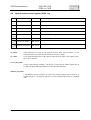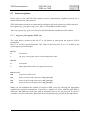
1
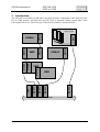
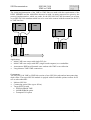
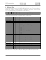
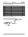
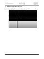
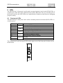
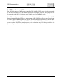
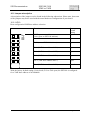
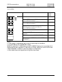
SIS Documentation
SIS3100/3100
VME to VME
SIS3100/3100
VME to VME interface
241002_V2
SIS3100 Initiator
attendum to SIS1100/3100
User Manual
SIS GmbH
Harksheider Str. 102A
22399 Hamburg
Germany
Phone: ++49 (0) 40 60 87 305 0
Fax:
++49 (0) 40 60 87 305 20
email: [email protected]
http://www.struck.de
Version: Revision 1.01 as of 03.12.02
Page 1 of 31
SIS Documentation
SIS3100/3100
VME to VME
Revision Table:
Revision
0.x
1.00
1.01
Page 2 of 31
Date
24.09.02
30.09.02
03.12.02
Modification
Generation
First official release
VME base address change (because of limited addressing
capabilities on some SBCs)
SIS Documentation
SIS3100/3100
VME to VME
1 Table of contents
1
2
3
4
5
Table of contents .............................................................................................................................................3
Introduction .....................................................................................................................................................3
Function/principle of operation .......................................................................................................................3
Address Map....................................................................................................................................................3
Register Description ........................................................................................................................................3
5.1
Type-Identifier/Version register(0x0, read).............................................................................................3
5.2
Firmware version register(0x4, read).......................................................................................................3
5.3
Interrupt configuration register (0x8) ......................................................................................................3
5.3.1
IRQ mode.........................................................................................................................................3
5.4
Interrupt control register (0xC)................................................................................................................3
5.5
Doorbell register (0x10, read only).........................................................................................................3
5.6
Optical status/control register (0x20, r/w) ...............................................................................................3
5.7
Protocol registers .....................................................................................................................................3
5.7.1
opt_prot_hdr register (0x80, r/w).....................................................................................................3
5.7.2
opt_prot_am register (0x84, r/w) .....................................................................................................3
5.7.3
opt_prot_adl register (0x88, r/w) .....................................................................................................3
5.7.4
opt_prot_dal register (0x90, r/w) .....................................................................................................3
5.7.5
opt_prot_error register (0xAC, read only) .......................................................................................3
5.8
Single Transfer Space Descriptor (0x400..0x4FC,read/write) ................................................................3
6
Protocol driven access .....................................................................................................................................3
6.1
Single Read..............................................................................................................................................3
6.2
Single Write .............................................................................................................................................3
6.3
DMA Read...............................................................................................................................................3
6.4
DMA Write..............................................................................................................................................3
7
Direct SGL access (mapping) ..........................................................................................................................3
8
LEDs................................................................................................................................................................3
8.1
Front panel LEDs.....................................................................................................................................3
8.1.1
Explanation of front panel LEDs .....................................................................................................3
8.1.2
Special case: LED Link up off.........................................................................................................3
8.2
PCB LEDs ...............................................................................................................................................3
9
VME system controller....................................................................................................................................3
10
Appendix .....................................................................................................................................................3
10.1 Power consumption..................................................................................................................................3
10.2 Jumper description...................................................................................................................................3
10.2.1 JP10 .................................................................................................................................................3
10.2.2 JP90 .................................................................................................................................................3
10.2.3 JP_DSP ............................................................................................................................................3
10.2.4 JP710 ...............................................................................................................................................3
10.2.5 JP770 ...............................................................................................................................................3
10.2.6 JP_DSP ............................................................................................................................................3
10.3 Boot mechanisms.....................................................................................................................................3
10.3.1 ISP PROM .......................................................................................................................................3
10.3.2 JTAG ...............................................................................................................................................3
10.4 Connector types .......................................................................................................................................3
11
Index ............................................................................................................................................................3
Page 3 of 31
SIS Documentation
SIS3100/3100
VME to VME
2 Introduction
The SIS3100/3100 VME to VME link is the third interface combination (after SIS1100/3100
PCI to VME interface and SIS1100/1100-OPT PCI to frontend readout system link) of the
SIS Gigabit link series. The full scope of the interface family is sketched below.
SIS3100
SIS1100OPT
VME
PCI Bus
Page 4 of 31
SIS1100
SIS1100
VME
SIS1100
SIS1100
SIS3100
CPU
SIS3100
CAMAC
SIS5100
SIS5100
VME
SIS3100
CAMAC
SIS3100
Detector mounted
readout system
SIS Documentation
SIS3100/3100
VME to VME
VME
VME
SIS3100
VME
SIS1100
CPU
SIS3100
VME
SBC
SIS3100
SIS3100
SIS3100
SIS3100
VME
SIS3100
SIS3100
SIS3100
The initial implementation of the VME to VME link was made with the requirements of the
DESY HERMES and the AMANDA detectors in mind. As many properties are given by the
protocol implementation, which was made for the SIS1100/3100, this document was written
as an SIS3100/3100 attendum which has to be seen in the context with the manual for the PCI
to VME interface.
PCI Bus
Applications
• Multi VME crate setups with single PCI slot
• Multi VME crate setups with SBC (single board computer) as eventbuilder
• Autonomous DSP based frontend crate readout with VME event collection
• Long distance VME-VME connections
Components
The SIS3100/3100 VME to VME link consists of two SIS3100 cards and an interconnecting
duplex fiber. The target SIS3100 module is equiped with all available options to allow for its
use as subeventbuilder.
• Initiator SIS3100
• Connecting optical fibre (up to 450 m)
• Target SIS3100 with
• SIS9200 SHARC DSP
• 64 MB SDRAM option
• Frontpanel I/O option
Page 5 of 31
SIS Documentation
SIS3100/3100
VME to VME
3 Function/principle of operation
The SIS3100/3100 VME-VME link consists of two SIS3100 VME cards and an
interconnecting optical fiber. The first SIS3100 is the so called initiator, the second SIS3100
is referred to as target. The target SIS3100 is installed in the remote crate, while the initiator
is installed in the local crate. The SIS3100 initiator is a VME slave design. It has the task to
simulate the function of the SIS1100 PCI card from the SIS1100/3100 PCI to VME interface.
The target SIS3100 has the same firmware design as a card that is part of a PCI to VME
interface.
There are two ways for remote crate VME access
• Protocol driven access
• Mapped (single transfer) access
While 3 (read) to 4 (write) VME cycles are required to initiate a transfer on the SIS3100
initiator with protocol driven access, mapped access allows access to the remote side in a
single VME cycle.
Especially on large word count block transfers the protocol overhead of the SIS3100/3100
VME to VME interface becomes negligible and the implemented block transfer modes up to
2e VME result in a high performance intercrate coupling.
With the SIS9200 DSP, SDRAM and I/O option efficient autonomous event readout in the
can be implemented in the target crate with no need for local VME master interaction.
Page 6 of 31
SIS Documentation
SIS3100/3100
VME to VME
4 Address Map
The SIS3100 initiator is a A32 D32/BLT32/MBLT64/2eVME slave. The base address is
defined with 5 jumpers of jumper array J10 as listed in the table below. Refer to section
10.2.1 for a detailed jumper description with a sketch of the array.
A28
J10/8
A27 A26 A25 A24
J10/7 J10/6 J10/5 J10/4
A23-A0
occupied address pace
The SIS3100 resources and their locations are listed in the table below.
Offset
0x0000
0x0000
0x0000
0x0000
0x0000
Key
Access
Function
0000
0004
0008
000C
0010
R
R
R/W
R/W
R
Type-Identifier/Version register
Firmware Version register
Interrupt configuration register
Interrupt control register
Doorbell register
0x0000 0020
0x0000 0024
R/W
W
Optical Status/Control register
KEY: Requester-Confirmation Logic Reset
0080
0084
0088
0090
R/W
R/W
R/W
R/W
opt_prot_hdr
opt_prot_am
opt_prot_adl
opt_prot_dal (dma_byte_length)
0x0000 00A8
0x0000 00AC
R/W
R
opt_prot_balance counter
opt_prot_error
0x0000 00B0
R
0x0000 0400
R/W
SGL Transfer Space descriptor[0]
0x0000 04FC
R/W
SGL Transfer Space descriptor[63]
0x004x xxxx
0x007x xxxx
R/W
opt_prot_dma_fifo
0x0080 xxxx
0x0082 xxxx
R/W
R/W
Direct SGL Transfer (descriptor[0])
Direct SGL Transfer (descriptor[1])
0x00FE xxxx
R/W
Direct SGL Transfer (descriptor[63])
0x0000
0x0000
0x0000
0x0000
KA
opt_prot_dma_rd_byte_counter
Note: Write access to a key address (KA)with arbitrary data invokes the respective action
Page 7 of 31
SIS Documentation
SIS3100/3100
VME to VME
5 Register Description
5.1
Type-Identifier/Version register(0x0, read)
This read only register holds the board type to allow for a distinction between different
interface types. The board type of the SIS3100 VME side is 1. Other stored parameters are
hardware version, firmware type and firmware version.
BIT access Name
7-0 RO
Identifier
Bedeutung
1 = PCI/PLX Interface
000000FF
2 = VME Controller
3 = CAMAC/FERA Controller
4 = Readoutsystem mit LVD SCSI
0x82 = VME initiator
15-8 RO
Hardware Version
1..255
Firmware Type
1 = universal
Firmware Version
1..255
0000FF00
23-16 RO
00FF0000
31-24 RO
FF000000
The type identifier/version register for the SIS3100 initiator reads:
0x 01 01 01 82
5.2
Firmware version register(0x4, read)
BIT access Name
7-0 RO
Bedeutung
Firmware Version
000000FF
15-8 RO
Firmware type
0x82 (VME initiator)
Board type
0x3100
0000FF00
31-16 RO
FFFF0000
The firmware version register for the SIS3100 initiator (firmware version 2) reads:
0x 31 00 82 02
Page 8 of 31
SIS Documentation
SIS3100/3100
VME to VME
5.3 Interrupt configuration register (0x8)
This read/write register controls the VME interrupt behaviour of the SIS3100 initiator.
The interrupter type is DO8 .
5.3.1 IRQ mode
In RORA (release on register access) mode the interrupt will be pending until the IRQ
source is cleared by specific access to the corresponding clear Doorbell IRQ bit.
In ROAK (release on acknowledge) mode , the interrupt condition will be cleared as soon as
the interrupt is acknowledged by the VME Master.
Bit
31
..
16
15
14
13
12
11
10
9
8
7
6
5
4
3
2
1
0
Function
reserved
..
reserved
reserved
reserved
reserved
RORA/ROAK Mode (0: RORA; 1: ROAK)
VME IRQ Enable (0=IRQ disabled, 1=IRQ enabled)
VME IRQ Level Bit 2
VME IRQ Level Bit 1
VME IRQ Level Bit 0
IRQ Vector Bit 7; placed on D7 during VME IRQ ACK cycle
IRQ Vector Bit 6; placed on D6 during VME IRQ ACK cycle
IRQ Vector Bit 5; placed on D5 during VME IRQ ACK cycle
IRQ Vector Bit 4; placed on D4 during VME IRQ ACK cycle
IRQ Vector Bit 3; placed on D3 during VME IRQ ACK cycle
IRQ Vector Bit 2; placed on D2 during VME IRQ ACK cycle
IRQ Vector Bit 1; placed on D1 during VME IRQ ACK cycle
IRQ Vector Bit 0; placed on D0 during VME IRQ ACK cycle
Default
0
0
0
0
0
0
0
0
0
0
0
0
0
0
0
0
0
0
0
The power up default value reads 0x 00000000
Page 9 of 31
SIS Documentation
SIS3100/3100
VME to VME
5.4 Interrupt control register (0xC)
This register controls the VME interrupt behaviour of the SIS3100 initiator.
Bit
31
30
29
28
27
26
25
24
23
22
21
20
19
18
17
16
15
..
0
Function (w)
unused
unused
unused
unused
unused
unused
unused
unused
unused
unused
unused
Clear Doorbell IRQ flag
unused
unused
unused
Disable Doorbell IRQ
unused
unused
Enable Doorbell IRQ
(r)
0
0
0
0
Status VME IRQ
Status internal IRQ
0
0
0
0
0
Status Doorbell IRQ flag
0
0
0
0
0
0
Status Enable Doorbell IRQ (read as 1 if enabled, 0 if disabled)
The power up default value reads 0x 00000000
Illustration of Status flag/IRQ flag and IRQ generation:
VME_IRQ_ENABLE
AND
Status Doorbell
IRQ flag
doorbell
IRQ pulse
AND
Clear
Enable Doorbell IRQ
Page 10 of 31
INTERNAL_VME_IRQ
VME IRQ
Default
0
0
0
0
0
0
0
0
0
0
0
0
0
0
0
0
0
0
0
SIS Documentation
SIS3100/3100
VME to VME
5.5 Doorbell register (0x10, read only)
Contains the Doorbell IRQ value of the Doorbell Request of the target.
by the other pending IRQ with consecutive doorbell register update.
Doorbell register bit
31:16
15
14
13
12
11
10
9
8
7
6
5
4
3
2
1
0
Function
0 (reserved)
Status DSP_IRQ
Status LEMO_ IN3_IRQ latch bit
Status LEMO_ IN2_IRQ latch bit
Status LEMO_ IN1_IRQ latch bit
Status FLAT_ IN4_IRQ latch bit
Status FLAT_ IN3_IRQ latch bit
Status FLAT_ IN2_IRQ latch bit
Status FLAT_ IN1_IRQ latch bit
Status VME IRQ 7 bit
Status VME IRQ 6 bit
Status VME IRQ 5 bit
Status VME IRQ 4 bit
Status VME IRQ 3 bit
Status VME IRQ 2 bit
Status VME IRQ 1 bit
0 (reserved)
Page 11 of 31
SIS Documentation
5.6
SIS3100/3100
VME to VME
Optical status/control register (0x20, r/w)
BIT Name
0
local acc
Beschreibung
RX_SYNCH
RO
Optical receiver synchronized
TX_SYNCH
RO
Remote optical receiver synchronized
SYNCH_CHG
WR: sel clr RX/TX_SYNCH changed
LOCAL_OPT_RESET
WR: sel clr
REMOTE_OPT_RESET
WR: sel clr
00000001
1
00000002
4
00000010
8
00000100
12
00001000
RX_SYNCH
valid characters are seen by the optical receiver from remote station, i.e. the
connection between remote sender and local receiver is stable.
TX_SYNCH
is set when both directions of the optical connection are stable. This implies, that ,
RX_SYNCH is set also.
LOCAL_OPT_RESET
a reset is generated by writting a 1 to this bit. A reset sets all control register bits to
0, clears the input and output FIFO as well as the data link layer.
REMOTE_OPT_RESET
a SP_RESET special character is send to the remote (target) side if this bit is
written to with a 1. The remote side has to react by initializing ist logic to a defined
state.
Page 12 of 31
SIS Documentation
5.7
SIS3100/3100
VME to VME
Protocol registers
Please refer to the SIS1100/3100 manual and the implemented Gigalink protocol for a
detailed discussion of the protocol.
SIS3100 initiator protocols are generated by writing to the local register set, which consist of
the registers opt_ prot_hdr to opt_ prot _dal (i.e offset address 0x80 to 0x90).
The error register opt_prot_error has to be checked after the completion of the transfer
5.7.1 opt_prot_hdr register (0x80, r/w)
The value that is written to the bits 27 to 24 defines at what point the protocol will be
transmitted.
Bits 31 to 28 have special functions. The value of the lower bits 23 to 0 is written to the
optical port as protocol header.
Bits 29
0
no function
1
opt_prot_error register will be cleared with protocol start
Bits 28
0
no function
1
DMA input FIFO will be reset upon protocol start
Bits 27 to 24
0x0
no protocol will be send
0x1
protocol will be send upon write of opt_ prot_hdr.
0x2
protocol will be send upon write of opt_ prot_adl.
0x4
protocol will be send upon write of opt_ prot_dal.
Note: you can minimize the number of required VME cycles by selecting the appropriate
condition for protocol transmission. If you have a number of writes with the same data to
different VME addresses (with same AM) it will make sense to use opt_prot_adl. If you have
a number of writes to the same address but with varying data opt_prot_dal is the right choice.
Page 13 of 31
SIS Documentation
SIS3100/3100
VME to VME
5.7.2 opt_prot_am register (0x84, r/w)
Protocol VME Address Modifier register
5.7.3 opt_prot_adl register (0x88, r/w)
Protocol Address register
5.7.4 opt_prot_dal register (0x90, r/w)
Protocol Data or DMA length register in Bytes.
5.7.5 opt_prot_error register (0xAC, read only)
Name
Code
BUSY
0x005
LINK_ERROR
0x101
REQUEST_BUSY_TIMEOUT
0x103
CONFIRMATION_TIMEOUT
0x107
NOT_DEFINED_REQUEST
0x203
VME_BUSERR
0x211
VME bus error
VME_RETRY
0x212
VME retry line set
VME_ARBITRATION_TIMEOUT 0x214
Page 14 of 31
Description
Optical link down, check fiber connection
Timeout during VME arbitration (in multi master VME system)
SIS Documentation
SIS3100/3100
VME to VME
5.8 Single Transfer Space Descriptor (0x400..0x4FC,read/write)
The 64 single transfer descriptors define the behaviour of the link during mapped access.
Bit
31
..
20
19
18
17
16
15
14
13
12
11...8
7
6
5
4
3
2
1
0
Function
Optical Address bit A31
..
Optical Address bit A20
Optical Address bit A19
Optical Address bit A18
Optical Address bit A17
0
0
VME IACK
0
Optical SPACE
0 : remote SIS3100 internal space
1 : remote SIS3100 VME space
6 : remote SIS3100 SDRAM/SHARC space
0
0
VME AM5
VME AM4
VME AM3
VME AM2
VME AM1
VME AM0
The SIS3100 initiator is always accessed in A32. The remote crate address modifier (AM) is
defined by the descriptors VME AM bits. Single cycle AM codes are valid only. The remote
data width is defined by the width of the local access (Byte/Word/Lword).
The VME IACK bit has to be set for an interrupt acknowledge cacle.
Page 15 of 31
SIS Documentation
SIS3100/3100
VME to VME
6 Protocol driven access
6.1 Single Read
Execution of a single read is implemented as a sequence of:
1. write to one or more registers of the hdr, am, adl register set
2. wait for opt_prot_error not equal 0x5 (busy)
data are valid if opt_prot_error == 0x0 and can be read from the tdal register
a non zero opt_prot_error content signals an error condition (see 5.7.5)
int vme_remote_A32D32_read(int p, u_int32_t local_base_adr, u_int32_t remote_vme_adr,
u_int32_t* vme_data )
{
int return_code ;
int error ;
vme_A32D32_write(p, local_base_adr + SIS3100_T_HDR, 0x3208010f );
vme_A32D32_write(p, local_base_adr + SIS3100_T_AM, 0x9) ;
vme_A32D32_write(p, local_base_adr + SIS3100_T_ADL, remote_vme_adr) ;
do {
vme_A32D32_read(p, local_base_adr + SIS3100_T_PROT_ERROR, &error) ;
} while (error == 0x005) ;
if (error == 0x0) {
vme_A32D32_read(p, local_base_adr + SIS3100_T_DAL, vme_data) ;
return 0x0 ; /* OK exit */
}
else {
return error ; /* exit */
}
}
int sis3100_remote_control_read(int p, u_int32_t local_base_adr, u_int32_t remote_adr,
u_int32_t* data )
{
int return_code ;
int error ;
vme_A32D32_write(p, local_base_adr + SIS3100_T_HDR, 0x3200000f );
vme_A32D32_write(p, local_base_adr + SIS3100_T_ADL, remote_adr) ;
do {
vme_A32D32_read(p, local_base_adr + SIS3100_T_PROT_ERROR, &error) ;
} while (error == 0x005) ;
if (error == 0x0) {
vme_A32D32_read(p, local_base_adr + SIS3100_T_DAL, data) ;
return 0x0 ; /* OK exit */
}
else {
return error ; /* exit */
}
}
Page 16 of 31
SIS Documentation
SIS3100/3100
VME to VME
6.2 Single Write
Execution of a single write is implemented as a sequence of:
1. write to one or more registers of the hdr, am, adl, dal registers
2. wait for opt_prot_error ungleich 0x5 (busy)
the write operation has completed successful if opt_prot_error == 0x0
a non zero opt_prot_error content signals an error condition (see 5.7.5)
int vme_remote_A32D32_write(int p, u_int32_t local_base_adr, u_int32_t remote_vme_adr,
u_int32_t vme_data )
{
int return_code ;
int error ;
vme_A32D32_write(p,
vme_A32D32_write(p,
vme_A32D32_write(p,
vme_A32D32_write(p,
local_base_adr
local_base_adr
local_base_adr
local_base_adr
+
+
+
+
SIS3100_T_HDR, 0x340C010f );
SIS3100_T_AM, 0x9) ;
SIS3100_T_ADL, remote_vme_adr) ;
SIS3100_T_DAL, vme_data ) ;
do {
vme_A32D32_read(p, local_base_adr + SIS3100_T_PROT_ERROR, &error) ;
} while (error == 0x005) ;
if (error == 0x0) {
return 0x0 ; /* OK exit */
}
else {
return error ; /* exit */
}
}
Page 17 of 31
SIS Documentation
SIS3100/3100
VME to VME
6.3 DMA Read
A DMA read cycle is a read request of N words, the sequence is:
1. write to one or more registers of the hdr, am, adl, dal register set
2. read N words from the DMA FIFO
3. after N words have been read (a local crate bus error occurred respective) the
opt_prot_error register has to be checked for return code (0x0 flags proper termination)
int vme_remote_A32BLT32_read(int p, u_int32_t local_base_adr, u_int32_t remote_vme_adr,
u_int32_t* vme_data,
u_int32_t req_num_of_lwords, u_int32_t* got_num_of_lwords)
{
int return_code ;
int error ;
/* header = 0x3428010f
vme_A32D32_write(p,
vme_A32D32_write(p,
vme_A32D32_write(p,
vme_A32D32_write(p,
clr ERR, reset fifo, start with T_DAL ;
local_base_adr
local_base_adr
local_base_adr
local_base_adr
+
+
+
+
BT, AM, VME, */
SIS3100_T_HDR, 0x3428010f );
SIS3100_T_AM, 0xb) ; /* remote AM */
SIS3100_T_ADL, remote_vme_adr) ;
SIS3100_T_DAL, (req_num_of_lwords<<2)) ;
vme_A32BLT32_read(p, local_base_adr + SIS3100_DMA_FIFO, vme_data, req_num_of_lwords,
got_num_of_lwords) ;
vme_A32D32_read(p, local_base_adr + SIS3100_T_PROT_ERROR, &error) ;
return error ; /* exit */
}
Note: The user has to make sure, that data are read from the DMA FIFO after completion of
the protocol start sequence without long gaps, as a protocol timeout of 10 ms is implemented.
Page 18 of 31
SIS Documentation
SIS3100/3100
VME to VME
6.4 DMA Write
A DME write cycle is a write request of N words, with following sequence:
1. write to one or more registers of the hdr, am, adl, dal register set
2. write N words to the DMA FIFO
3. after N words have been written
wait for opt_prot_error not equal 0x5 (busy)
opt_prot_error == 0x0 flags proper termination
non zero opt_prot_error contents signals an error case
int vme_remote_A32BLT32_write(int p, u_int32_t local_base_adr, u_int32_t remote_vme_adr,
u_int32_t* vme_data,
u_int32_t req_num_of_lwords, u_int32_t* put_num_of_lwords)
{
int return_code ;
int error ;
/* header = 0x242C010f clr ERR, start with T_DAL ; BT, AM, WR; VME, */
/* the DMA Write Fifo will be cleared automatically after sending protocol and then it is
possible to write
*/
/* to it until the end of length is reached
*/
vme_A32D32_write(p,
vme_A32D32_write(p,
vme_A32D32_write(p,
vme_A32D32_write(p,
local_base_adr
local_base_adr
local_base_adr
local_base_adr
+
+
+
+
SIS3100_T_HDR, 0x242C010f );
SIS3100_T_AM, 0xb) ; /* remote AM */
SIS3100_T_ADL, remote_vme_adr) ;
SIS3100_T_DAL, (req_num_of_lwords<<2)) ;
vme_A32BLT32_write(p, local_base_adr + SIS3100_DMA_FIFO, vme_data, req_num_of_lwords,
put_num_of_lwords) ;
do {
vme_A32D32_read(p, local_base_adr + SIS3100_T_PROT_ERROR, &error) ;
} while (error == 0x005) ;
if ((error == 0x0) && (return_code == 0x0 )) {
return 0x0 ; /* OK exit */
}
else {
vme_A32D32_write(p, local_base_adr + SIS3100_REQ_CONF_RESET, 0x0) ;
return ((return_code & 0xffff) + ((error & 0xffff) << 0x10) ) ; /* exit */
}
}
Note: The user has to make sure, that data are written to the DMA FIFO after completion of
the protocol start sequence without long gaps, as a protocol timeout of 10 ms is implemented.
Page 19 of 31
SIS Documentation
SIS3100/3100
VME to VME
7 Direct SGL access (mapping)
64 mal 1 MByte windows are implemented to map single cycles in the local crate into the
VME address space of the remote crate.
1. Example:
read/write access to control register of remote crate (target) SIS3100
prepare mapping with
write 0x0 to the address 0x400 (SGL Transfer Space descriptor(0))
direct access with
read/write from/to address 0x04000000 ;
2. Example: VME read/write from/to remote crate (at offset address 0x87600000)
prepare mapping with
write 0x87610009 to the address 0x404 (SGL Transfer Space descriptor(1), VME,
AM=9)
direct VME access with
read/write from/to address 0x04100000 ;
Note: Remote crate error codes are passed to the local crate in a transparent fashion, i.e. a bus
error (error code 0x211) during the remote crate VME access results in a bus error during the
access to the mapped address.
Page 20 of 31
SIS Documentation
SIS3100/3100
VME to VME
8 LEDs
The SIS3100 has 10 front panel and 8 surface mounted printed circuit board (PCB) LEDs to
visualise part of the units status. While the front panel LEDs allow the user to monitor part of
the boards activities, the PCB LEDs were implemented for hardware and firmware debugging
purposes mainly.
8.1 Front panel LEDs
The SIS3100 has 10 front panel and 8 surface mounted printed circuit board (PCB) LEDs to
visualise part of
LED
A
M
P
S
R
L
LU
LD
U
DU
Color
yellow
red
green
green
green
Function
Access (to VME slave port)
not used
Power
Requester-Confirmation logic busy
Ready (logic configured)
Link up
Link data up (initiator to target)
Link data down (target to initiator)
not used
not used
The arrangement of the front panel LEDs on the upper part of the front panel is shown in the
sketch below.
Page 21 of 31
SIS Documentation
SIS3100/3100
VME to VME
8.1.1 Explanation of front panel LEDs
LED
A
M
P
S
R
L
LU
LD
U
DU
Description
VME access to VME slave port of SIS3100
VME master, lit whenever the SIS3100 accesses the VME bus
(not used with SIS3100 initiator design)
Power, signals presence of +5 V supply voltage
Signals activity of the SIS3100 sequencer
Ready, lit when on board logic is configured (off during power up LED self test)
Link up, lit when connection to PCI side (or loopback connection) is established
Link data up, lit when data are send (and LED link up lit),
special case as described below when LED link up is off
Link data down, lit when link data are received (and LED link up lit),
special case as described below when LED link up is off
User LED, to be set and cleared under user program control
(not used with SIS3100 initiator design)
DSP user LED, to be set and cleared under optional DSPs user program
(not used with SIS3100 initiator design)
8.1.2 Special case: LED Link up off
In standard operation (i.e. both VME sides powered an connected with optical fiber) the LED
Link up off condition signals a problem on the Gigabit link connection. The LEDs Link data
up and Link data down are used to signal the problem cause under this condition. Link data up
is lit in case of a problem on the transmitter side, link data down is lit in case of a problem on
the receiver side. A short loopback cable (with proven reliability) is useful to track down the
problem source (fiber, VME side or PCI side)
8.2 PCB LEDs
The 8 red PCB LEDs D651-D658 are mounted close to the front panel on the upper edge of
the SIS3100. The reflect the status of the Vitesse serialiser/deserialiser (SERDES) chip.
LED
D651
D652
D653
D654
D655
D656
D657
D658
Page 22 of 31
Function
valid data
valid KChar
idle detect
resync
lossync
norun error
band error
dispar error
SIS Documentation
SIS3100/3100
VME to VME
9 VME system controller
The SIS3100 can act as VME system controller. The 16 MHz VME system clock is generated
by the SMD oscillator U10. and enabled by jumper 1 of jumper array J10. This jumper has to
be removed on the SIS3100 initiator as the module acts as a VME slave only.
Note: The user has to ensure, that the system clock is generated once per crate only. A VME
diagnosis module like the VDIS or a measurement with a VME bus extender can be used can
be used to check, whether a particular CPU or interface generates system clock (with all other
interfaces/CPUs unplugged from the VME backplane. Some VME slave modules may use the
system clock to initialize on board resources, this mechanism may fail if the system clock is
generated by more than one board in the crate.
Page 23 of 31
SIS Documentation
SIS3100/3100
VME to VME
10 Appendix
10.1 Power consumption
The SIS3100 is a +5 V single supply design. On board voltages other than +5V are generated
by linear regulators or DC/DC converters. A list with the used components can be found
below.
Component designator
U2
U3
U5
U6
Voltage
2.5 V
3.3 V
-5 V
-5 V
Component
LT1584CT
LT1584CT
TMH0505S
TMH0505S
Powered components
FPGAs
link medium/SERDES/drivers
flat cable in/outputs (ECL)
LEMO in/outputs (NIM)
Note: U5 and U6 will be stuffed when required by the given I/O configuration only
The power consumption depends on installed options and board activity. The figures below
are worst case estimates/measurements.
U in V
+5 V
+5 V
+5 V
+5 V
Page 24 of 31
Current in A
2,0
2,1
2,2
2,4
Configuration
Base configuration (SIS3100 initiator)
Base configuration with front panel I/Os
Base configuration with front panel I/Os and 64 MB
Base configuration with front panel I/Os, 64 MB and DSP
SIS Documentation
SIS3100/3100
VME to VME
10.2 Jumper description
A description of the jumpers can be found in the following subsections. Please note, that some
of the jumpers may not be used with the actual hardware configuration of your board.
10.2.1 JP10
Boot configuration/VME base address selection
Function
J10
Factory
default
setting
open
VME system controller
(leave open on SIS3100 initiator)
unused
open
GAP (not on SIS3100 initiator)
open
GA0 (VME slave address bit 24)
open
GA1 (VME slave address bit 25)
open
GA2 (VME slave address bit 26)
open
GA3 (VME slave address bit 27)
open
GA4 (VME slave address bit 28)
closed
With the factory default setting (GA4 closed, GA3 to GA0 open) the SIS3100 is configured
for a VME base address of 0x10000000
Page 25 of 31
SIS Documentation
SIS3100/3100
VME to VME
10.2.2 JP90
Function
J90
unused
Factory
default
setting
open
connect FPGA reset to LEMO reset output
(na on SIS3100 initiator)
connect power on reset to LEMO reset output
(na on SIS3100 initiator)
connect NIM reset input to execution of
SIS3100 power on reset (see Note 3)
(na on SIS3100 initiator)
power on reset
open
VME SYSRESET initiates power on reset of
SIS3100
FPGA reset results in VME SYSRESET
open
power on reset of SIS3100 results in VME
SYSRESET
open
closed
open
closed
closed
Notes:
1.) some jumper combinations may result in a power up reset deadlock
2.) Typical Master/slave SYSRESET setting
While it is typical for a VME master to issue SYSRESET upon power up (jumper 8 of
J90 closed) it is more suited for a VME slave to execute a power on reset as soon as the
VME SYSRESET condition is detected (jumper 6 of J90 closed).
3.) The width of the reset signal has to be greater than 20 ms
Page 26 of 31
SIS Documentation
SIS3100/3100
VME to VME
10.2.3 JP_DSP
If the jumper JP_DSP is opened, the JTAG lines TDI and TDO of the installed SIS9200 DSP
piggy will be connected to the main board and the programmable components on the card will
become part of the SIS3100 JTAG chain. The default setting is jumper closed (i.e. closed
TDI, TDO chain on the SIS3100 board).
10.2.4 JP710
Termination of flat cable inputs (not applicable for SIS3100 initiator).
10.2.5 JP770
Termination of LEMO inputs (not applicable for SIS3100 initiator).
10.2.6 JP_DSP
If the jumper JP_DSP is opened, the JTAG lines TDI and TDO of the installed SIS9200 DSP
piggy will be connected to the main board and the programmable components on the card will
become part of the SIS3100 JTAG chain. The default setting is jumper closed (i.e. closed
TDI, TDO chain on the SIS3100 board).
Page 27 of 31
SIS Documentation
SIS3100/3100
VME to VME
10.3 Boot mechanisms
The firmware of the SIS3100 can be loaded to the boards FPGAs by two different
mechanisms. Normally the user will use the factory installed firmware, which will be loaded
at power up by default, in some cases it may be of interest however to load special designs or
to upgrade the firmware to use extended functionality with the card. The boot options are
listed in the table below.
Mechanism
ISP PROM
JTAG
Connector/Chip designator
U501
CON500
Hardware
XC18V04VQ44
9-pin header
10.3.1 ISP PROM
A XILINX XC18V04 ISP (in system programmable) PROM is installed as default firmware
load source of the SIS3100. The contents of the serial PROM can be altered via the JTAG
port. The firmware upgrade procedure is online in the firmware section of our web site, so are
the actual firmware files.
10.3.2 JTAG
The XILINX_JTAG connector (CON500 ) is designed for the use with standard JTAG (Joint
Test Action Group)programming tools like the XILINX.HW-JTAG PC can be either used to
program the on board EEPROM, or to load firmware to the FPGAs directly for test purposes.
Find the pin assignment of the JTAG connector below.
Pin designator
JCC
GND
nc
TCK
nc
TDO
TDI
nc
TMS
Page 28 of 31
Description
Supply voltage
Ground
not connected
Test clock
not connected
Test data out
Test data in
not connected
Test mode select
SIS Documentation
SIS3100/3100
VME to VME
10.4 Connector types
Find below a list of the used connector types of the SIS3100.
Designation
U200
CON700
LEMO1-8
STD-168DIMM
CON_D1
CON_D2
P1/P2
Function
Optical Link
Flat cable user I/O
LEMO user I/O
DIMM socket
SHARC socket long
SHARC socket short
VME connector
Manufacturer
IBM
TYCO
LEMO
Berg
Samtec
Samtec
Harting
Part Number
IBM42F10SNNAA20 or 30
2-828581-0
EPL.00.250.NTN
88638-60002
TFM-150-02-S-D-A
TFM-145-02-S-D-A
02011602101.00
Page 29 of 31
SIS Documentation
SIS3100/3100
VME to VME
11 Index
+2.5 V 24
+3.3 V 24
+5 V 24
16 MHz 23
-5 V 24
A 21
Address Map 7
AM 15
AMP 29
base address 7
Berg 29
boot mechanisms 28
CON_D1 29
CON_D2 29
CON500 28
CON700 29
connector types 29
CPU 23
DC/DC 24
DIMM 29
DMA FIFO 18, 19
DMA read 18
DMA write 19
DO8 9
DSP 27
DU 21
ECL 24
FIFO 18, 19
input 12
output 12
firmware 28
FPGA 28
Harting 29
IACK 15
IBM 29
interrupter mode 9
interrupter type 9
IRQ
end of event 10
IRQ generation 10
IRQ mode 9
ROAK 9
RORA 9
ISP 28
ISP PROM 28
J10 7
JCC 28
JTAG 27, 28
jumper
description 25
JP_DSP 27
JP10 25
JP710 27
JP770 27
JP90 26
system controller 23
key address 7
Page 30 of 31
L 21
LD 21
LED 20, 21
access 21
DSP user 21
front panel 21, 22
link data down 21
link data up 21
link up 21, 22
master 21
PCB 22
power 21
ready 21
surface mounted 21
user 21
LEMO 29
linear regulator 24
Link
data down 22
data up 22
LU 21
M 21
nc 28
NIM 24
opt_prot_adl 14
opt_prot_am 14
opt_prot_dal 14
opt_prot_error 14
oscillator 23
P 21
P1 29
P2 29
PCB 21
power consumption 24
PROM 28
protocol
temporary 13
protocol driven access 16
R 21
register
board type 8
description 8
doorbell 7
firmware version 8
hardware configuration 12
interrupt configuration 9, 10, 11, 13
VME adress map 15
ROAK 9
RORA 9
RX_SYNCH 12
S 21
Samtec 29
SERDES 22
SHARC 29
single read 16
single write 17
SIS9200 27
SIS Documentation
SP_RESET 12
STD-168DIMM 29
SYSRESET 26
TCK 28
TDI 28
TDO 28
TMS 28
TX_SYNCH 12
TYCO 29
U 21
SIS3100/3100
VME to VME
U10 23
U200 29
VDIS 23
Vitesse 22
VME 29
bus extender 23
system controller 23
XC18V04 28
XILINX 28
XILINX_JTAG 28
Page 31 of 31