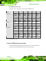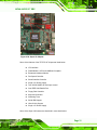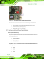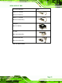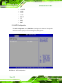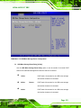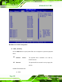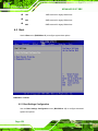
1
NOVA-9452 5.25” SBC
NOVA-9452 5.25” SBC
Page i
NOVA-9452 5.25” SBC
Revision
Date
Version
Changes
2008-05
2.00
- Changed Northbridge to Intel® 945GME
- Added auto power-on function setup jumper (J_AUTOPWR1)
information
- Added 24-bit LVDS screen support
2007-11
Page ii
1.00
Initial release
NOVA-9452 5.25” SBC
Copyright
COPYRIGHT NOTICE
The information in this document is subject to change without prior notice in order to
improve reliability, design and function and does not represent a commitment on the part
of the manufacturer.
In no event will the manufacturer be liable for direct, indirect, special, incidental, or
consequential damages arising out of the use or inability to use the product or
documentation, even if advised of the possibility of such damages.
This document contains proprietary information protected by copyright. All rights are
reserved. No part of this manual may be reproduced by any mechanical, electronic, or
other means in any form without prior written permission of the manufacturer.
TRADEMARKS
Product names mentioned herein are used for identification purposes only and may be
trademarks and/or registered trademarks of their respective owners.
Page iii
NOVA-9452 5.25” SBC
Packing List
NOTE:
If any of the components listed in the checklist below are missing,
please do not proceed with the installation. Contact the IEI reseller or
vendor you purchased the NOVA-9452 from or contact an IEI sales
representative directly. To contact an IEI sales representative, please
send an email to [email protected].
The items listed below should all be included in the NOVA-9452 package.
1 x NOVA-9452 single board computer
1 x IDE cable (44-pin)
2 x SATA cables
1 x SATA power cable
1 x VGA cable (2 x VGA cables for NOVA-9452VGA)
1 x KB/MS Y cable
1 x RS-232/422/485 cable
1 x Quad RS-232 adapter cable
1 x USB cable
1 x Mini jumper pack
1 x Utility CD
1 x QIG (quick installation guide)
Images of the above items are shown in Chapter 3.
Page iv
NOVA-9452 5.25” SBC
Table of Contents
1
INTRODUCTION..................................................................................................... 1
1.1 INTRODUCTION .......................................................................................................... 2
1.1.1 NOVA-9452 Benefits......................................................................................... 2
1.1.2 NOVA-9452 Features......................................................................................... 3
1.2 NOVA-9452 OVERVIEW ............................................................................................ 3
1.2.1 NOVA-9452 Overview Photo ............................................................................ 3
1.2.2 NOVA-9452 Peripheral Connectors and Jumpers ............................................. 5
1.2.3 Technical Specifications .................................................................................... 7
2
DETAILED SPECIFICATIONS ............................................................................. 9
2.1 OVERVIEW ............................................................................................................... 10
2.2 DIMENSIONS ............................................................................................................ 10
2.2.1 Board Dimensions............................................................................................ 10
2.2.2 External Interface Panel Dimensions................................................................11
2.3 DATA FLOW .............................................................................................................. 12
2.4 COMPATIBLE PROCESSORS ....................................................................................... 13
2.4.1 Compatible Processor Overview...................................................................... 13
2.4.2 Supported Processors ....................................................................................... 14
2.5 INTEL® 945GME NORTHBRIDGE CHIPSET ............................................................... 14
2.5.1 Intel® 945GME Memory Support.................................................................... 15
2.5.2 Intel® 945GME Integrated Graphics................................................................ 16
2.5.2.1 Intel® 945GME Analog CRT Support....................................................... 17
2.5.2.2 Intel® 945GME LVDS Support................................................................. 18
2.5.2.3 Intel® 945GME SDVO Support................................................................ 18
2.5.2.4 Chrontel CH7317A SDVO / RGB DAC................................................... 18
2.5.3 Intel® 945GME Direct Media Interface (DMI) ............................................... 19
2.6 INTEL® ICH7M SOUTHBRIDGE CHIPSET .................................................................. 20
2.6.1 Intel® ICH7M Overview .................................................................................. 20
2.6.2 Intel® ICH7M High Definition Audio Controller ............................................ 21
2.6.3 Intel® ICH7M IDE Interface............................................................................ 21
2.6.4 Intel® ICH7M Low Pin Count (LPC) Interface ............................................... 22
Page v
NOVA-9452 5.25” SBC
2.6.5 Intel® ICH7M PCI Interface ............................................................................ 23
2.6.6 Intel® ICH7M Real Time Clock....................................................................... 24
2.6.7 Intel® ICH7M SATA Controller....................................................................... 24
2.6.8 Intel® ICH7M USB Controller......................................................................... 24
2.7 PCI BUS COMPONENTS ............................................................................................ 25
2.7.1 PCI Bus Overview ........................................................................................... 25
2.7.2 PCI Expansion Slot .......................................................................................... 25
2.7.3 PCI-104 Connector .......................................................................................... 26
2.7.4 PC/104 Connector............................................................................................ 26
2.8 PCIE BUS COMPONENTS .......................................................................................... 28
2.8.1 PCIe Bus Overview.......................................................................................... 28
2.8.2 PCIe Mini Card Socket .................................................................................... 28
2.8.3 PCIe GbE Controller........................................................................................ 28
2.9 LPC BUS COMPONENTS ........................................................................................... 29
2.9.1 LPC Bus Overview .......................................................................................... 29
2.9.2 BIOS Chipset ................................................................................................... 30
2.9.3 Super I/O chipset.............................................................................................. 30
2.9.3.1 Super I/O LPC Interface ........................................................................... 32
2.9.3.2 Super I/O 16C550 UARTs ........................................................................ 32
2.9.3.3 Super I/O Enhanced Hardware Monitor ................................................... 32
2.9.3.4 Super I/O Infrared ..................................................................................... 32
2.9.3.5 Super I/O Fan Speed Controller................................................................ 33
2.9.3.6 Super I/O Parallel Port .............................................................................. 33
2.9.3.7 Super I/O Keyboard Controller................................................................. 34
2.9.4 Fintek F81216DG LPC Serial Port Chipset..................................................... 34
2.9.5 Lattice Semiconductor LC4064V LPC Digital I/O Chipset ............................ 35
2.10 ENVIRONMENTAL AND POWER SPECIFICATIONS ..................................................... 36
2.10.1 System Monitoring......................................................................................... 36
2.10.2 Operating Temperature and Temperature Control ......................................... 37
2.10.3 Power Consumption....................................................................................... 37
3
UNPACKING .......................................................................................................... 39
3.1 ANTI-STATIC PRECAUTIONS ...................................................................................... 40
3.2 UNPACKING.............................................................................................................. 40
3.2.1 Unpacking Precautions .................................................................................... 40
Page vi
NOVA-9452 5.25” SBC
3.3 UNPACKING CHECKLIST ........................................................................................... 41
3.3.1 Package Contents ............................................................................................. 41
3.3.2 Optional Items.................................................................................................. 42
4
CONNECTOR PINOUTS...................................................................................... 45
4.1 PERIPHERAL INTERFACE CONNECTORS .................................................................... 46
4.1.1 NOVA-9452 Layout......................................................................................... 46
4.1.2 Peripheral Interface Connectors....................................................................... 47
4.1.3 External Interface Panel Connectors................................................................ 49
4.2 INTERNAL PERIPHERAL CONNECTORS ...................................................................... 49
4.2.1 AT Power Connector ........................................................................................ 49
4.2.2 ATX Power Control Connector........................................................................ 50
4.2.3 Audio Connector (9-pin) .................................................................................. 51
4.2.4 CompactFlash® Socket.................................................................................... 52
4.2.5 Digital Input/Output (DIO) Connector ............................................................ 55
4.2.6 Fan Connector (+12V) ..................................................................................... 56
4.2.7 Front Panel Connector (8-pin) ......................................................................... 57
4.2.8 IDE Connector(44-pin) .................................................................................... 58
4.2.9 Infrared Interface Connector (5-pin)................................................................ 61
4.2.10 Inverter Connector ......................................................................................... 62
4.2.11 Keyboard/Mouse Connector .......................................................................... 63
4.2.12 LVDS LCD Connector................................................................................... 64
4.2.13 Parallel Port Connector .................................................................................. 65
4.2.14 PC/104-Plus Slot............................................................................................ 67
4.2.15 PCI Slot.......................................................................................................... 71
4.2.16 SATA Drive Connectors................................................................................. 74
4.2.17 Serial Port Connector (COM1 and COM 2)(RS-232/422/485) ..................... 75
4.2.18 Serial Port Connector (4 x RS-232) ............................................................... 76
4.2.19 USB Connectors (Internal) ............................................................................ 79
4.2.20 VGA Connectors (Internal)............................................................................ 80
4.3 EXTERNAL PERIPHERAL INTERFACE CONNECTOR PANEL ......................................... 81
4.3.1 LAN Connectors .............................................................................................. 81
5
INSTALLATION .................................................................................................... 83
5.1 ANTI-STATIC PRECAUTIONS ...................................................................................... 84
Page vii
NOVA-9452 5.25” SBC
5.2 INSTALLATION CONSIDERATIONS ............................................................................. 85
5.2.1 Installation Notices .......................................................................................... 85
5.2.2 Installation Checklist ....................................................................................... 86
5.3 CPU, CPU COOLING KIT AND SO-DIMM INSTALLATION ....................................... 87
5.3.1 Socket M CPU Installation .............................................................................. 87
5.3.2 Cooling Kit Installation.................................................................................... 89
5.3.3 SO-DIMM Installation..................................................................................... 92
5.3.4 CF Card Installation......................................................................................... 93
5.4 JUMPER SETTINGS .................................................................................................... 94
5.4.1 Auto Power-on Function Setup ........................................................................ 95
5.4.2 CF Card Setup.................................................................................................. 96
5.4.3 Clear CMOS Jumper........................................................................................ 97
5.4.4 LVDS Voltage Selection................................................................................... 98
5.4.5 PCI-104 Serial IRQ Selector.......................................................................... 100
5.4.6 PC/104 Serial IRQ Selector ........................................................................... 101
5.4.7 Serial Port Mode Selectors (COM1 and COM2) ........................................... 102
5.4.8 PCI-104 Voltage Setup................................................................................... 103
5.5 CHASSIS INSTALLATION ......................................................................................... 104
5.6 INTERNAL PERIPHERAL DEVICE CONNECTIONS...................................................... 104
5.6.1 Peripheral Device Cables............................................................................... 104
5.6.2 IDE Cable Connection ................................................................................... 105
5.6.3 5.1 Channel Audio Kit Installation ................................................................ 106
5.6.4 7.1 Channel Audio Kit Installation ................................................................ 107
5.6.5 Parallel Port Cable ......................................................................................... 109
5.6.6 SATA Drive Connection..................................................................................111
5.6.7 Keyboard/Mouse Y-cable Connector ..............................................................112
5.6.8 PCIe Mini card Installation.............................................................................113
5.6.9 Serial Port Connector Cable (Four Ports) Cable Connection .........................114
5.6.10 RS-232/422/485 Cable..................................................................................115
5.6.11 USB Cable (Dual Port) .................................................................................116
5.6.12 VGA Monitor Connection.............................................................................117
5.7 EXTERNAL PERIPHERAL INTERFACE CONNECTION ..................................................119
5.7.1 LAN Connection (Single Connector) .............................................................119
6
AMI BIOS.............................................................................................................. 121
Page viii
NOVA-9452 5.25” SBC
6.1 INTRODUCTION ...................................................................................................... 122
6.1.1 Starting Setup................................................................................................. 122
6.1.2 Using Setup.................................................................................................... 122
6.1.3 Getting Help................................................................................................... 123
6.1.4 Unable to Reboot After Configuration Changes............................................ 123
6.1.5 BIOS Menu Bar ............................................................................................. 123
6.2 MAIN ..................................................................................................................... 124
6.3 ADVANCED ............................................................................................................. 125
6.3.1 CPU Configuration ........................................................................................ 126
6.3.2 IDE Configuration ......................................................................................... 127
6.3.2.1 IDE Master, IDE Slave ........................................................................... 129
6.3.3 Floppy Configuration..................................................................................... 135
6.3.4 Super IO Configuration.................................................................................. 136
6.3.5 Hardware Health Configuration..................................................................... 140
6.3.6 ACPI Configuration ....................................................................................... 142
6.3.7 APM Configuration........................................................................................ 143
6.3.8 Remote Access Configuration........................................................................ 146
6.3.9 USB Configuration ........................................................................................ 151
6.3.9.1 USB Mass Storage Device Configuration............................................... 152
6.4 PCI/PNP ................................................................................................................ 155
6.5 BOOT ..................................................................................................................... 158
6.5.1 Boot Settings Configuration .......................................................................... 158
6.5.2 Boot Device Priority ...................................................................................... 161
6.5.3 Hard Disk Drives ........................................................................................... 162
6.5.4 Removable Drives.......................................................................................... 163
6.6 SECURITY............................................................................................................... 165
6.7 CHIPSET ................................................................................................................. 166
6.7.1 Northbridge Configuration............................................................................. 167
6.7.2 Southbridge Chipset Configuration ............................................................... 171
6.8 EXIT ....................................................................................................................... 172
7
DRIVER INSTALLATION.................................................................................. 175
7.1 AVAILABLE SOFTWARE DRIVERS ............................................................................ 176
7.2 DRIVER CD AUTO-RUN .......................................................................................... 176
7.3 CHIPSET DRIVER INSTALLATION............................................................................. 178
Page ix
NOVA-9452 5.25” SBC
7.4 INTEL GRAPHICS MEDIA ACCELERATOR DRIVER ................................................... 181
7.5 BROADCOM LAN DRIVER (FOR GBE LAN) INSTALLATION .................................. 185
7.6 REALTEK HD AUDIO DRIVER (ALC883) INSTALLATION ....................................... 190
7.6.1 BIOS Setup .................................................................................................... 190
7.6.2 Driver Installation .......................................................................................... 190
7.7 REALTEK AC`97 AUDIO DRIVER (ALC665) INSTALLATION .................................. 193
7.7.1 BIOS Setup .................................................................................................... 193
7.7.2 Driver Installation .......................................................................................... 193
A
BIOS OPTIONS .................................................................................................... 199
B
DIO INTERFACE................................................................................................. 203
B.1 DIO INTERFACE INTRODUCTION ........................................................................... 204
B.2 DIO CONNECTOR PINOUTS ................................................................................... 204
B.3 ASSEMBLY LANGUAGE SAMPLES ........................................................................... 205
B.3.1 Enable the DIO Input Function ..................................................................... 205
B.3.2 Enable the DIO Output Function .................................................................. 205
C
WATCHDOG TIMER .......................................................................................... 207
D
ADDRESS MAPPING...........................................................................................211
D.1 ADDRESS MAP ...................................................................................................... 212
D.2 1ST MB MEMORY ADDRESS MAP ......................................................................... 212
D.3 IRQ MAPPING TABLE ............................................................................................ 213
D.4 DMA CHANNEL ASSIGNMENTS ............................................................................. 213
Page x
NOVA-9452 5.25” SBC
List of Figures
Figure 1-1: NOVA-9452 SBC ..........................................................................................................2
Figure 1-2: NOVA-9452 Overview [Front View] ............................................................................4
Figure 1-2: NOVA-9452 Overview [Rear View] .............................................................................5
Figure 2-1: NOVA-9452 Dimensions (mm)..................................................................................10
Figure 2-2: External Interface Panel Dimensions (mm) ............................................................11
Figure 2-3: Data Flow Block Diagram .........................................................................................12
Figure 2-4: Socket M CPU Socket ...............................................................................................13
Figure 2-5: Intel® 945GME Northbridge Chipset .......................................................................15
Figure 2-6: 200-pin DDR2 SO-DIMM Socket...............................................................................16
Figure 2-7: Video Outputs............................................................................................................17
Figure 2-8: VGA Output................................................................................................................17
Figure 2-9: LVDS Output ..............................................................................................................18
Figure 2-10: Chrontel SDVO-to-RGB DAC Chipset ...................................................................19
Figure 2-11: DMI Interface............................................................................................................19
Figure 2-12: Intel® ICH7M Southbridge......................................................................................20
Figure 2-13: High Definition Audio..............................................................................................21
Figure 2-14: IDE Interface ............................................................................................................22
Figure 2-15: PCI Interface ............................................................................................................23
Figure 2-16: SATA .........................................................................................................................24
Figure 2-17: Onboard USB Implementation ...............................................................................25
Figure 2-18: PCI Expansion Slot .................................................................................................26
Figure 2-19: PCI-104 .....................................................................................................................26
Figure 2-20: PC/104 Expansion Slot ...........................................................................................27
Figure 2-21: PCIe Mini Card Socket ............................................................................................28
Figure 2-22: Broadcom PCI GbE Controllers.............................................................................29
Figure 2-23: BIOS Chipset ...........................................................................................................30
Figure 2-24: Super I/O Chipset ....................................................................................................31
Figure 2-25: Serial Ports ..............................................................................................................32
Figure 2-26: Infrared .....................................................................................................................32
Figure 2-27: Parallel Port .............................................................................................................33
Figure 2-28: Keyboard Controller ...............................................................................................34
Page xi
NOVA-9452 5.25” SBC
Figure 2-29: Fintek F81216DG LPC Serial Port Chipset ...........................................................35
Figure 2-30: Lattice Semiconductor LC4064V Digital I/O Chipset ...........................................36
Figure 4-1: Connector and Jumper Locations...........................................................................46
Figure 4-2: Connector and Jumper Locations...........................................................................47
Figure 4-3: AT Power Connector Location .................................................................................50
Figure 4-4: ATX Power Supply Enable Connector Location ....................................................51
Figure 4-5: Audio Connector Pinouts (10-pin) ...........................................................................52
Figure 4-6: CF Card Socket Location .........................................................................................53
Figure 4-7: DIO Connector Locations.........................................................................................55
Figure 4-8: +12V Fan Connector Location .................................................................................57
Figure 4-9: Front Panel Connector Pinout Locations ...............................................................58
Figure 4-10: Secondary IDE Device Connector Locations .......................................................59
Figure 4-11: Infrared Connector Pinout Locations....................................................................61
Figure 4-12: Panel Backlight Connector Pinout Locations ......................................................62
Figure 4-13: Keyboard/Mouse Connector Location ..................................................................63
Figure 4-14: LVDS LCD Connector Pinout Locations ...............................................................64
Figure 4-15: Parallel Port Connector Location ..........................................................................66
Figure 4-16: PC/104-Plus Slot Location .....................................................................................68
Figure 4-17: PCI Slot Location ....................................................................................................71
Figure 4-18: SATA Drive Connector Locations ..........................................................................74
Figure 4-19: RS-232/422/485 Serial Port Connector Location..................................................75
Figure 4-20: COM3 to COM6 Connector Pinout Locations.......................................................77
Figure 4-21: USB Connector Pinout Locations .........................................................................79
Figure 4-22: VGA Connector Pinout Locations .........................................................................80
Figure 4-23: NOVA-9452 External Peripheral Interface Connector..........................................81
Figure 4-24: RJ-45 Ethernet Connector......................................................................................82
Figure 5-1: Make sure the CPU socket retention screw is unlocked ......................................88
Figure 5-2: Lock the CPU Socket Retention Screw...................................................................89
Figure 5-3: Cooling Kit .................................................................................................................89
Figure 5-4: Cooling Kit Support Bracket ....................................................................................91
Figure 5-5: Connect the cooling fan cable.................................................................................91
Figure 5-6: SO-DIMM Installation ................................................................................................92
Figure 5-7: CF Card Installation ..................................................................................................94
Figure 5-8: Jumper Locations .....................................................................................................94
Figure 5-9: Auto Power-on Function Setup Jumper Location .................................................96
Page xii
NOVA-9452 5.25” SBC
Figure 5-10: CF Card Setup Jumper Location ...........................................................................97
Figure 5-11: Clear CMOS Jumper................................................................................................98
Figure 5-12: LVDS Voltage Selection Jumper Pinout Locations..............................................99
Figure 5-13: PCI-104 Voltage Setup Jumper Pinout Locations............................................. 100
Figure 5-14: PC/104 Voltage Setup Jumper Pinout Locations .............................................. 101
Figure 5-15: Serial Port Mode Selector Pinout Location ....................................................... 102
Figure 5-16: PCI-104 Voltage Setup Jumper Pinout Locations............................................. 103
Figure 5-17: IDE Cable Connection.......................................................................................... 105
Figure 5-18: 5.1 Channel Audio Kit .......................................................................................... 107
Figure 5-19: 7.1 Channel Audio Kit .......................................................................................... 108
Figure 5-20: LPT Cable Connection..........................................................................................110
Figure 5-21: Connect the LPT Device .......................................................................................110
Figure 5-22: SATA Drive Cable Connection .............................................................................111
Figure 5-23: SATA Power Drive Connection ............................................................................112
Figure 5-24: Keyboard/mouse Y-cable Connection ................................................................113
Figure 5-25: PCIe Mini Card Installation...................................................................................114
Figure 5-26: Four Serial Port Connector Cable Connection ..................................................115
Figure 5-27: RS-232/422/485 Cable Installation .......................................................................116
Figure 5-28: Dual USB Cable Connection ................................................................................117
Figure 5-29: VGA Pin Header.....................................................................................................118
Figure 5-30: VGA Connector......................................................................................................119
Figure 5-31: LAN Connection ................................................................................................... 120
Figure 7-1: Introduction Screen ............................................................................................... 177
Figure 7-2: Available Drivers .................................................................................................... 177
Figure 7-3: Chipset Driver Installation Program..................................................................... 178
Figure 7-4: Chipset Driver Installation Welcome Screen....................................................... 179
Figure 7-5: Chipset Driver Installation License Agreement .................................................. 179
Figure 7-6: Chipset Driver Readme File Information ............................................................. 180
Figure 7-7: Chipset Driver Installation Complete ................................................................... 180
Figure 7-8: Select the Operating System ................................................................................ 181
Figure 7-9: VGA Driver .............................................................................................................. 182
Figure 7-10: GMA Driver Readme File ..................................................................................... 182
Figure 7-11: GMA Driver File Extraction.................................................................................. 183
Figure 7-12: GMA Driver Installation Welcome Screen.......................................................... 183
Figure 7-13: GMA Driver License Agreement ......................................................................... 184
Page xiii
NOVA-9452 5.25” SBC
Figure 7-14: GMA Driver Installing Notice............................................................................... 184
Figure 7-15: GMA Driver Installation Complete ...................................................................... 185
Figure 7-16: Access Windows Control Panel ......................................................................... 186
Figure 7-17: Double Click the System Icon............................................................................. 187
Figure 7-18: Double Click the Device Manager Tab ............................................................... 187
Figure 7-19: Device Manager List ............................................................................................ 188
Figure 7-20: Search for Suitable Driver ................................................................................... 188
Figure 7-21: Locate Driver Files ............................................................................................... 189
Figure 7-22: Location Browsing Window ................................................................................ 189
Figure 7-23: 4-AUDIO\AC-KIT883HD\Windows Folder ........................................................... 191
Figure 7-24: HD Audio Driver Setup Extracting Files............................................................. 191
Figure 7-25: HD Audio Driver Setup Welcome Screen........................................................... 192
Figure 7-26: HD Audio Driver Installation Complete .............................................................. 192
Figure 7-27: CD 4-AUDIO\AC-KIT08R\Windows Folder ......................................................... 194
Figure 7-28: AC`97 Audio Driver Install Shield Wizard Starting............................................ 194
Figure 7-29: AC`97 Audio Driver Setup Preparation .............................................................. 195
Figure 7-30: AC`97 Audio Driver Welcome Screen................................................................. 195
Figure 7-31: AC`97 Audio Driver Software Configuration ..................................................... 196
Figure 7-32: AC`97 Audio Driver Digital Signal....................................................................... 196
Figure 7-33: AC`97 Audio Driver Installation Begins ............................................................. 197
Figure 7-34: AC`97 Audio Driver Installation Complete ......................................................... 197
Page xiv
NOVA-9452 5.25” SBC
List of Tables
Table 1-1: Technical Specifications ..............................................................................................8
Table 2-1: Processor Features ....................................................................................................13
Table 2-2: Supported Processors ...............................................................................................14
Table 2-3: Supported HDD Specifications..................................................................................22
Table 2-4: Power Consumption ...................................................................................................38
Table 3-1: Package List Contents................................................................................................42
Table 3-2: Optional Items .............................................................................................................43
Table 4-1: Peripheral Interface Connectors ...............................................................................48
Table 4-2: Rear Panel Connectors ..............................................................................................49
Table 4-3: AT Power Connector Pinouts.....................................................................................50
Table 4-4: ATX Power Supply Enable Connector Pinouts ........................................................51
Table 4-5: Audio Connector Pinouts (9-pin)...............................................................................52
Table 4-6: CF Card Socket Pinouts .............................................................................................54
Table 4-7: DIO Connector Pinouts...............................................................................................56
Table 4-8: +12V Fan Connector Pinouts .....................................................................................57
Table 4-9: Front Panel Connector Pinouts .................................................................................58
Table 4-10: Secondary IDE Connector Pinouts .........................................................................60
Table 4-11: Infrared Connector Pinouts......................................................................................61
Table 4-12: Panel Backlight Connector Pinouts ........................................................................62
Table 4-13: Keyboard/Mouse Connector Pinouts......................................................................63
Table 4-14: LVDS LCD Port Connector Pinouts.........................................................................65
Table 4-15: Parallel Port Connector Pinouts..............................................................................66
Table 4-16: PCI-104 Connector Pinouts......................................................................................69
Table 4-17: PC/104-Plus J2 Connector Pinouts .........................................................................70
Table 4-18: PC/104-Plus J1 Connector Pinouts .........................................................................70
Table 4-19: PCI Slot ......................................................................................................................73
Table 4-20: SATA Drive Connector Pinouts................................................................................74
Table 4-21: RS-232/422/485 Serial Port Connector Pinouts .....................................................76
Table 4-22: COM3 to COM6 Connector Pinouts.........................................................................78
Table 4-23: USB Port Connector Pinouts ...................................................................................79
Table 4-24: VGA Connector Pinouts ...........................................................................................80
Page xv
NOVA-9452 5.25” SBC
Table 4-25: LAN Pinouts...............................................................................................................81
Table 4-26: RJ-45 Ethernet Connector LEDs .............................................................................82
Table 5-1: Jumpers .......................................................................................................................95
Table 5-2: Auto Power-on Function Setup Jumper Settings ....................................................95
Table 5-3: CF Card Setup Jumper Settings................................................................................96
Table 5-4: Clear CMOS Jumper Settings ....................................................................................98
Table 5-5: LVDS Voltage Selection Jumper Settings.................................................................99
Table 5-6: PCI-104 Voltage Setup Jumper Settings................................................................ 100
Table 5-7: PC/104 Voltage Setup Jumper Settings ................................................................. 101
Table 5-8: Serial Port Mode Selector Jumper Settings .......................................................... 102
Table 5-9: PCI-104 Voltage Setup Jumper Settings................................................................ 103
Table 5-10: IEI Provided Cables ............................................................................................... 104
Table 6-1: BIOS Navigation Keys ............................................................................................. 123
Page xvi
NOVA-9452 5.25” SBC
BIOS Menus
Menu 1: Main .............................................................................................................................. 124
Menu 2: Advanced ..................................................................................................................... 126
Menu 3: CPU Configuration...................................................................................................... 127
Menu 4: IDE Configuration ....................................................................................................... 128
Menu 5: IDE Master and IDE Slave Configuration.................................................................. 130
Menu 6: Floppy Configuration.................................................................................................. 135
Menu 7: Super IO Configuration .............................................................................................. 136
Menu 8: Hardware Health Configuration ................................................................................. 141
Menu 9: ACPI Configuration ..................................................................................................... 142
Menu 10:Advanced Power Management Configuration ........................................................ 144
Menu 11: Remote Access Configuration [Advanced] ............................................................ 147
Menu 12: USB Configuration.................................................................................................... 151
Menu 13: USB Mass Storage Device Configuration ............................................................... 153
Menu 14: PCI/PnP Configuration ............................................................................................. 156
Menu 15: Boot ............................................................................................................................ 158
Menu 16: Boot Settings Configuration .................................................................................... 159
Menu 17: Boot Device Priority Settings .................................................................................. 161
Menu 18: Hard Disk Drives ....................................................................................................... 163
Menu 19: Removable Drives..................................................................................................... 164
Menu 20: Security ...................................................................................................................... 165
Menu 21: Chipset ....................................................................................................................... 167
Menu 22: Northbridge Chipset Configuration......................................................................... 168
Menu 23: Southbridge Chipset Configuration ........................................................................ 171
Menu 24:Exit............................................................................................................................... 173
Page xvii
NOVA-9452 5.25” SBC
THIS PAGE IS INTENTIONALLY LEFT BLANK
Page xviii
NOVA-9452 5.25” SBC
Chapter
1
1 Introduction
Page 1
NOVA-9452 5.25” SBC
1.1 Introduction
Figure 1-1: NOVA-9452 SBC
The NOVA-9452 motherboard is a Socket M Intel® Core™2 Duo, Intel® Core™ Duo,
Intel® Core™ Solo or Intel® Celeron® M (Yonah core) CPU platform. The NOVA-9452
has a maximum front side bus (FSB) frequency of 667 MHz and supports one 667 MHz
DDR2 SO-DIMM up to 2 GB. The NOVA-9452 supports multiple displays including two
VGA outputs and an LVDS output. Expansion options on the NOVA-9452 include a PCI
port, a PC/104-Plus slot and a PCIe mini card slot. Storage options include two SATA ports
and an IDE port to support an IDE device and a CompactFlash® card. Other features
include six serial ports, a parallel port, a digital I/O port, 6 USB 2.0 ports and two Gigabit
Ethernet ports.
1.1.1 NOVA-9452 Benefits
Some of the NOVA-9452 benefits are listed below:
Multiple display output options
Storage flexibility with support for SATA drives, IDE drives and
CompactFlash® Type I/II disks
DDR2 support enables faster data transfers
Multiple I/O interfaces provide connectivity to a broad range of external
peripheral devices
Page 2
NOVA-9452 5.25” SBC
1.1.2 NOVA-9452 Features
Some of the NOVA-9452 features are listed below.
Support for the following Socket M processors:
o
o
o
o
Intel® Core™2 Duo
Intel® Core™ Duo
Intel® Core™ Solo
Intel® Celeron® M (Yonah core)
Maximum FSB of 667 MHz
Maximum of one 2 GB (max.) 400 MHz, 533 MHz or 667 MHz DDR2
SO-DIMM
Two SATA drives with transfer rates of 1.5 Gb/s supported
Intel® Matrix Storage Manager
Two high performance PCIe GbE Ethernet controllers
Six USB 2.0 devices supported
Dual VGA and 18-bit/24-bit dual-channel LVDS
RoHS compliant
1.2 NOVA-9452 Overview
1.2.1 NOVA-9452 Overview Photo
The NOVA-9452 has a wide variety of internal and external peripheral connectors. A
labeled photo of the peripheral connectors on the front of the NOVA-9452 is shown in
Figure 1-2.
Page 3
NOVA-9452 5.25” SBC
Figure 1-2: NOVA-9452 Overview [Front View]
Page 4
NOVA-9452 5.25” SBC
Figure 1-3: NOVA-9452 Overview [Rear View]
1.2.2 NOVA-9452 Peripheral Connectors and Jumpers
The NOVA-9452 has the following connectors on-board:
1 x ATX power connector
1 x ATX control connector
1 x Audio connector
1 x CompactFlash® connector
1 x Digital input/output connector
2 x Fan connector
1 x Front panel connector
1 x IDE disk drive connector
1 x Infrared interface connector
1 x Inverter connector
1 x Keyboard and mouse connector
1 x LVDS connector
1 x PCIe mini card socket
1 x Parallel port connector
1 x PCI slot
Page 5
NOVA-9452 5.25” SBC
1 x PC104+ connector
2 x Serial ATA (SATA) drive connectors
2 x RS-232/422/485 serial port connectors
1 x RS-232 serial port connector (for four RS-232 devices)
1 x VGA output connector [2 x VGA (on Dual VGA model)]
3 x Dual USB connectors
The NOVA-9452 has the following external peripheral interface connectors on the board
rear panel
2 x Ethernet connectors
The NOVA-9452 has the following on-board jumpers:
Auto power-on function setup
COM1 serial port mode selector
COM2 serial port mode selector
Clear CMOS
PCI-104 SERIQ# (as part of PC/104-Plus)
PC/104 SERIQ# (as part of PC/104-Plus)
LCD voltage selector
CF card setting
VIO voltage selector
Page 6
NOVA-9452 5.25” SBC
1.2.3 Technical Specifications
NOVA-9452 technical specifications are listed in Table 1-1. See Chapter 2 for details.
Specification
NOVA-9452
Form Factor
5.25” Motherboard
Socket M Intel® Core™2 Duo
Socket M Intel® Core™ Duo
System CPU
Socket M Intel® Core™ Solo
Socket M Intel® Celeron® M (Yonah core)
Front Side Bus
533 MHz, or 667 MHz
Northbridge: Intel® 945GME
System Chipset
Southbridge: Intel® ICH7M
Memory
One 200-pin 2 GB (max.) 400/533/667 MHz DDR2 SO-DIMM
CRT: Integrated in the Intel® 945GME to support CRT
CRT: Through SDVO by Chrontel CH7317A
Display
(NOVA-9452VGA-R10)
LVDS: Dual channel 18-bit or 24-bit LVDS LCD panel
BIOS
AMI Flash BIOS
Audio
7.1 channel or 5.1 channel audio with an optional audio kit
LAN
Dual PCIe GbE Broadcom BCM5787M chipsets
Two RS-232/422/485 serial ports
COM
Four RS-232 serial ports
USB2.0
Six USB 2.0 ports
IDE
One 44-pin IDE connects to two Ultra ATA33 devices
Page 7
NOVA-9452 5.25” SBC
Specification
NOVA-9452
SATA
Two 1.5 Gb/s SATA drives supported
Keyboard/mouse
One 6-pin connector connects to a keyboard and mouse
Super I/O
ITE IT8712F-S
Digital I/O
One 24-bit digital I/O connector (12-bit input / 12-bit output)
Infrared
One Infrared connector
SSD
CF Type II
Watchdog Timer
Software programmable 1-255 sec. by super I/O
Power Supply
ATX supported
Temperature
0ºC – 60ºC (32ºF - 140ºF)
Humidity (operating)
5%~95% non-condensing
Dimensions (LxW)
203 mm x 146 mm
Weight (GW/NW)
850 g / 290 g
Table 1-1: Technical Specifications
Page 8
NOVA-9452 5.25” SBC
Chapter
2
2 Detailed Specifications
Page 9
NOVA-9452 5.25” SBC
2.1 Overview
This chapter describes the specifications and on-board features of the NOVA-9452 in
detail.
2.2 Dimensions
2.2.1 Board Dimensions
The dimensions of the board are listed below:
Length:
203 mm
Width:
146 mm
Figure 2-1: NOVA-9452 Dimensions (mm)
Page 10
NOVA-9452 5.25” SBC
2.2.2 External Interface Panel Dimensions
External peripheral interface connector panel dimensions are shown in Figure 2-2.
Figure 2-2: External Interface Panel Dimensions (mm)
Page 11
NOVA-9452 5.25” SBC
2.3 Data Flow
Figure 2-3 shows the data flow between the two on-board chipsets and other components
installed on the motherboard and described in the following sections of this chapter.
Figure 2-3: Data Flow Block Diagram
Page 12
NOVA-9452 5.25” SBC
2.4 Compatible Processors
2.4.1 Compatible Processor Overview
The NOVA-9452 supports the following Socket M processors:
Intel® Core™2 Duo processors
Intel® Core™ Duo processors
Intel® Core™ Solo processors
Intel® Celeron® M processors
Figure 2-4: Socket M CPU Socket
All three of the above processors communicate with the Intel® 945GME Northbridge
chipset through a 667 MHz front side bus (FSB). Features of the supported processors are
listed in Table 2-1.
CPU Features
Core™2 Duo
Core™ Duo
Core™ Solo
Celeron® M
Dual core
Yes
Yes
No
No
Enhanced Halt State (C1E)
No
Yes
No
No
Enhanced Intel® Speedstep® Technolgy
Yes
Yes
Yes
No
Execute Disable Bit
Yes
Yes
Yes
Yes
Intel® EM64T
Yes
No
No
No
Intel® Virtualization Technology
Yes
Yes
No
No
Table 2-1: Processor Features
Page 13
NOVA-9452 5.25” SBC
2.4.2 Supported Processors
Specifications for the compatible processors are listed in Table 2-2 below:
Family
CPU Speed Processor # Bus Speed
Mfg Tech
Stepping
Cache Size
Core™2 Duo
2.33 GHz
T7600
667 MHz
65 nm
B2
4 MB
2.16 GHz
T7400
667 MHz
65 nm
B2
4 MB
2 GHz
T7200
667 MHz
65 nm
B2
4 MB
1.83 GHz
T5600
667 MHz
65 nm
B2
2 MB
1.66 GHz
T5500
667 MHz
65 nm
B2
2 MB
2 GHz
T2500
667 MHz
65 nm
C0
2 MB
1.66 GHz
T2300E
667 MHz
65 nm
C0
2 MB
Core™ Solo
1.83 GHz
T1400
667 MHz
65 nm
C0
2 MB
Celeron® M
2 GHz
450
533 MHz
65 nm
D0
1 MB
1.86 GHz
440
533 MHz
65 nm
D0
1 MB
1.73 GHz
430
533 MHz
65 nm
C0
1 MB
1.73 GHz
430
533 MHz
65 nm
D0
1 MB
1.73 GHz
530
533 MHz
65 nm
-
1 MB
1.60 GHz
520
533 MHz
65 nm
B2
1 MB
1.46 GHz
410
533 MHz
65 nm
C0
1 MB
Core™ Duo
Table 2-2: Supported Processors
2.5 Intel® 945GME Northbridge Chipset
The Intel® 945GME Northbridge chipset has the Generation 3.1 Intel Integrated Graphics
Engine and the Intel® Graphics Media Accelerator 950 (Intel® GMA 950).
Page 14
NOVA-9452 5.25” SBC
Figure 2-5: Intel® 945GME Northbridge Chipset
The integrated graphics and memory controller hub (GMCH) facilitates the flow of
information primarily between the following four interfaces:
Front Side Bus (FSB)
System Memory Interface
Graphics Interface
Direct Media Interface (DMI)
2.5.1 Intel® 945GME Memory Support
WARNING:
Only DDR2 memory module can be installed on the NOVA-9452. Do
not install DDR memory modules. If a DDR memory module is installed
on the NOVA-9452, the NOVA-9452 may be irreparably damaged.
The Intel® 945GME Northbridge chipset on the NOVA-9452 supports one DDR2 200-pin
SO-DIMM with the following features:
One 200-pin SO-DIMM
DDR2 only (DO NOT install a DDR SO-DIMM)
Capacities of 256 MB, 512 MB, 1 GB or 2 GB
Page 15
NOVA-9452 5.25” SBC
Transfer speeds of 400 MHz, 533 MHz or 667 MHz
64-bit wide channel
The memory socket is shown in Figure 2-6.
Figure 2-6: 200-pin DDR2 SO-DIMM Socket
2.5.2 Intel® 945GME Integrated Graphics
The Intel® 945GME Northbridge chipset has an Intel® Gen. 3.5 integrated graphics
engine that supports the following display devices:
Analog CRT
LVDS
SDVO port (to Chrontel VGA chip)
Page 16
NOVA-9452 5.25” SBC
Figure 2-7: Video Outputs
2.5.2.1 Intel® 945GME Analog CRT Support
A DB-15 VGA connector on the external peripheral interface connector panel is interfaced
to the Intel® 945GME graphics engine. The Intel® 945GME internal graphics engine, with
an integrated 400 MHz RAMDAC and hot plug CRT support, supports analog CRT
monitors up to QXGA.
Figure 2-8: VGA Output
Page 17
NOVA-9452 5.25” SBC
2.5.2.2 Intel® 945GME LVDS Support
A 30-pin LVDS crimp connector is interfaced to the Intel® 945GME graphics engine. The
Intel® 945GME internal graphics engine supports LVDS displays with the following
features:
Up to UXGA monitors with a maximum resolution of 1600 x 1200
18-bit or 24-bit LVDS screens
25 MHz to 112 MHz single-channel or dual-channel LVDS screens
CPIS 1.5 compliant LVDS screens
Figure 2-9: LVDS Output
2.5.2.3 Intel® 945GME SDVO Support
The Intel® 945GME internal graphics engine has the following SDVO output features:
Concurrent operation of PCIe x 1 with SDVO
Two SDVO ports supported
o
o
o
o
o
SDVO is muxed onto the PCIe pins
DVI 1.0 support for external digital monitor
Only Downstream HDCP support
Supports TV and DVD formats
Display hot plug support
2.5.2.4 Chrontel CH7317A SDVO / RGB DAC
The Chrontel CH7317A SDVO digital-analog converter connects to the SDVO output on
the Northbridge and encodes and transmits data through an analog RGB port:
Page 18
NOVA-9452 5.25” SBC
Support for VGA RGB bypass
Analog RGB output
Fully programmable through serial port
Three 10-bit video DAC outputs
Figure 2-10: Chrontel SDVO-to-RGB DAC Chipset
2.5.3 Intel® 945GME Direct Media Interface (DMI)
Intel® 945GME Northbridge GMCH is connected to the Intel® ICH7M Southbridge
Chipset through the chip-to-chip Direct Media Interface (DMI).
Figure 2-11: DMI Interface
Features of the Intel® 945GME DMI are listed below:
2GB/s (1GB/s in each direction) bus speed
32-bit downstream address
Page 19
NOVA-9452 5.25” SBC
2.6 Intel® ICH7M Southbridge Chipset
2.6.1 Intel® ICH7M Overview
The Intel® ICH7M Southbridge chipset is connected to the Intel® 945GME Northbridge
GMCH through the chip-to-chip Direct Media Interface (DMI).
Figure 2-12: Intel® ICH7M Southbridge
Some of the features of the Intel® ICH7M are listed below.
Complies with PCI Express Base Specification, Revision 1.0a
Complies with PCI Local Bus Specification, Revision 2.3 and supports 33MHz
PCI operations
Supports ACPI Power Management Logic
Contains:
o
o
o
Enhanced DMA controller
Interrupt controller
Timer functions
Integrated SATA host controller with DMA operations interfaced to four SATA
connectors on the NOVA-9452
Integrated IDE controller supports Ultra ATA 100/66/33
Supports the four USB 2.0 devices on the NOVA-9452 with four UHCI
controllers and one EHCI controller
Complies with System Management Bus (SMBus) Specification, Version 2.0
Supports Audio Codec ’97 (AC’97) Revision 2.3
Supports Intel® High Definition Audio
Contains Low Pin Count (LPC) interface
Supports Firmware Hub (FWH) interface
Serial peripheral interface support
Page 20
NOVA-9452 5.25” SBC
2.6.2 Intel® ICH7M High Definition Audio Controller
The High Definition (HD) Audio controller integrated into the ICH7M complies with the HD
audio Component Specification, Version 2.3. The HD audio controller is connected to the
onboard audio connector. The audio connector is connected to an optional 5.1 channel or
7.1 channel audio kit with an embedded AC’97 or HD audio codec.
Figure 2-13: High Definition Audio
The AC’97 controller supports up to six PCM audio outputs. The HD audio controller
supports up to eight PCM audio outputs and another independent stereo audio channel.
Complete surround sound consists of the following audio channels:
Front left
Front right
Front center
Subwoofer
Center left (HD audio only)
Center right (HD audio only)
Back left
Back right
2.6.3 Intel® ICH7M IDE Interface
The integrated IDE interface on the ICH7M Southbridge supports two IDE hard disks and
ATAPI devices. PIO IDE transfers up to 16 MB/s and Ultra ATA transfers of 33 MB/s.
Page 21
NOVA-9452 5.25” SBC
Figure 2-14: IDE Interface
The integrated IDE interface is able to support Ultra ATA/33 IDE HDDs with data transfer
rates up to 33 MB/s. The specifications of the Ultra ATA/33 are listed below.
Specification
Ultra ATA/33
IDE devices
2
PIO Mode
0–4
PIO Max Transfer Rate
16.6 MB/s
DMA/UDMA designation
UDMA 2
DMA/UDMA Max Transfer
33 MB/s
Controller Interface
5V
Table 2-3: Supported HDD Specifications
2.6.4 Intel® ICH7M Low Pin Count (LPC) Interface
The ICH7M LPC interface complies with the LPC 1.1 specifications. The LPC bus from the
ICH7 is connected to the following components:
BIOS chipset
Super I/O chipset
Page 22
NOVA-9452 5.25” SBC
Serial port chipset
Digital I/O chipset
2.6.5 Intel® ICH7M PCI Interface
The PCI interface on the ICH7M is compliant with the PCI Revision 2.3 implementation.
Figure 2-15: PCI Interface
Some of the features of the PCI interface are listed below.
PCI Revision 2.3 compliant
33 MHz
5V tolerant PCI signals (except PME#)
Integrated PCI arbiter supports up to seven PCI bus masters
The PCI bus is connected to an interface gold finger on the bottom of the CPU cards and
supports four expansion PCI cards on the backplane.
Page 23
NOVA-9452 5.25” SBC
2.6.6 Intel® ICH7M Real Time Clock
256 bytes of battery backed RAM is provided by the Motorola MC146818A real time clock
(RTC) integrated into the ICH6. The RTC operates on a 3V battery and 32.768KHz crystal.
The RTC keeps track of the time and stores system data even when the system is turned
off.
2.6.7 Intel® ICH7M SATA Controller
The integrated SATA controller on the ICH7M Southbridge supports two SATA drives on
the NOVA-9452 with independent DMA operations.
Figure 2-16: SATA
SATA controller specifications are listed below.
Supports two SATA drives
Supports 3 Gb/s data transfer speeds
Supports Serial ATA Specification, Revision 1.0a
2.6.8 Intel® ICH7M USB Controller
Up to six high-speed, full-speed or low-speed USB devices are supported by the ICH7M
on the NOVA-9452. High-speed USB 2.0, with data transfers of up to 480MB/s, is enabled
with the ICH7M integrated Enhanced Host Controller Interface (EHCI) compliant host
controller. USB full-speed and low-speed signaling is supported by the ICH7M integrated
Universal Host Controller Interface (UHCI) controllers. All of the USB ports are
implemented with USB pin headers on the NOVA-9452.
Page 24
NOVA-9452 5.25” SBC
Figure 2-17: Onboard USB Implementation
2.7 PCI Bus Components
2.7.1 PCI Bus Overview
The PCI bus is connected to the components listed below:
PCI expansion slot
PCI-104 expansion slot (as part of the PC/104-Plus)
PC/104 expansion slot (as part of the PC/104-Plus)
The PCI bus complies with PCI Local Bus Specification, Revision 2.2 and supports 33MHz
PCI operations.
2.7.2 PCI Expansion Slot
The PCI expansion slot enables a PCI expansion card to be connected to the NOVA-9452.
Page 25
NOVA-9452 5.25” SBC
Figure 2-18: PCI Expansion Slot
2.7.3 PCI-104 Connector
The PC/104-Plus expansion slot combines a PCI-104 connector and a PC/104 connector.
The PCI-104 connector provides PCI bus connectivity and the PC/104 connector provides
ISA connectivity. PCI-104, PC/104-Plus and PC/104 compliant add-on cards connect to
the PC/104-Plus expansion slot.
Figure 2-19: PCI-104
2.7.4 PC/104 Connector
The PC/104 expansion slot is enabled through an ITE IT8888G PCI-to-ISA bridge single
function. The PC/104 expansion slot provides ISA connectivity to PC/104 and
PC/104-Plus compliant add-on cards. The PCI-to-ISA bridge and PC/104 expansion slot
are shown in Figure 2-20.
Page 26
NOVA-9452 5.25” SBC
Figure 2-20: PC/104 Expansion Slot
The IT8888G has a PCI specification v2.1 compliant 32-bit PCI bus interface and supports
both PCI Bus master and slave. The PCI interface supports both programmable positive
and full subtractive decoding schemes. Some of the features of the IT8888G PCI to ISA
bridge are listed below.
PCI Interface
Programmable PCI Address Decoders
PC/PCI DMA Controller
Distributed DMA Controller
ISA Interface
SM Bus
1 analog line-level mono output: MONO_OUT
Power-on Serial Bus Configuration
Serial IRQ
Versatile power-on strapping options
Supports NOGO function
Single 33 MHz Clock Input
+3.3V PCI I/F with +5V tolerant I/O buffers
+5V ISA I/F and core Power Supply
Page 27
NOVA-9452 5.25” SBC
2.8 PCIe Bus Components
2.8.1 PCIe Bus Overview
The Intel® ICH7M Southbridge chipset has six PCIe lanes. Three of the PCIe lanes are
attached to the following devices:
PCIe Mini card expansion slot
Two Broadcom PCIe GbE controllers
2.8.2 PCIe Mini Card Socket
One of the PCIe x1 lanes from the Intel® ICH7M is connected to a 52-pin PCIe mini card
socket. The socket can support standard PCIe mini cards that are 30mm wide, 50.95mm
long and 5mm high.
Figure 2-21: PCIe Mini Card Socket
2.8.3 PCIe GbE Controller
Two PCIe x1 lanes are connected to two Broadcom BCM5787M PCIe GbE controllers
shown in Figure 2-22 below.
Page 28
NOVA-9452 5.25” SBC
Figure 2-22: Broadcom PCI GbE Controllers
The Broadcom BCM5787M is a 10/100/1000BASE-T Ethernet LAN controller. The
BCM5787M combines a triple-speed IEEE 802.3 compliant Media Access Controller
(MAC) with a triple-speed Ethernet transceiver, a PCIe bus interface, and an on-chip
buffer memory. Some of the BCM5787 controller features are listed below:
Integrated 10/100/1000BASE-T transceiver
Automatic MDI crossover function
PCIe v1.0a
10/100/1000BASE-T full/half-duplex MAC
Wake on LAN support meeting the ACPI requirements
Statistics for SNMP MIB II, Ethernet-like MIB, and Ethernet MIB (802.3z,
clause 30)
Serial EEPROM or serial flash support
JTAG support
2.9 LPC Bus Components
2.9.1 LPC Bus Overview
The LPC bus is connected to components listed below:
BIOS chipset
Super I/O chipset
Lattice Semiconductor digital I/O chipset
Fintek serial port chipset
Page 29
NOVA-9452 5.25” SBC
2.9.2 BIOS Chipset
The BIOS chipset has a licensed copy of AMI BIOS installed on the chipset. Some of the
BIOS features are listed below:
AMI Flash BIOS
SMIBIOS (DMI) compliant
Console redirection function support
PXE (Pre-boot Execution Environment) support
USB booting support
The BIOS chipset is shown in Figure 2-23 below.
Figure 2-23: BIOS Chipset
2.9.3 Super I/O chipset
The iTE IT8712F Super I/O chipset is connected to the ICH7 Southbridge through the LPC
bus. The iTE IT8712F is an LPC interface-based Super I/O device that comes with
Environment Controller integration.
Page 30
NOVA-9452 5.25” SBC
Figure 2-24: Super I/O Chipset
Some of the features of the iTE IT8712F chipset are listed below:
LPC Interface
PC98/99/2001, ACPI and LANDesk Compliant
Enhanced Hardware Monitor
Fan Speed Controller
SmartGuardian Controller
Single +5V Power Supply
Two 16C550 UARTs for serial port control
One IEEE 1284 Parallel Port
Floppy Disk Controller
Keyboard Controller
Watchdog Timer
Serial IRQ Support
Vbat & Vcch Support
Single +5V Power Supply
Some of the Super I/O features are described in more detail below:
Page 31
NOVA-9452 5.25” SBC
2.9.3.1 Super I/O LPC Interface
The LPC interface on the Super I/O complies with the Intel® Low Pin Count Specification
Rev. 1.0. The LPC interface supports both LDRQ# and SERIRQ protocols as well as PCI
PME# interfaces.
2.9.3.2 Super I/O 16C550 UARTs
Figure 2-25: Serial Ports
The onboard Super I/O has two integrated 16C550 UARTs that can support the following:
Two standard serial ports
IrDa 1.0 and ASKIR protocols
The Fintek chipset connected to the LPC bus provides connectivity to another four serial
ports.
2.9.3.3 Super I/O Enhanced Hardware Monitor
The Super I/O Enhanced Hardware Monitor monitors three thermal inputs, VBAT internally,
and eight voltage monitor inputs. These hardware parameters are reported in the BIOS
and can be read from the BIOS Hardware Health Configuration menu.
2.9.3.4 Super I/O Infrared
Figure 2-26: Infrared
Page 32
NOVA-9452 5.25” SBC
The Super I/O has dedicated infrared pins that use the programmable amplitude shift
keyed (ASKIR serial) communication protocol to communicate with consumer remote
control equipment. Some features of the infrared interface are listed below:
ASKIR serial communication protocol
30 kHz – 57 kHz or 400 kHz – 500 kHz
Baud rates up to 115.2 KBps
2.9.3.5 Super I/O Fan Speed Controller
The Super I/O fan speed controller enables the system to monitor the speed of the fan.
One of the pins on the fan connector is reserved for fan speed detection and interfaced to
the fan speed controller on the Super I/O. The fan speed is then reported in the BIOS.
2.9.3.6 Super I/O Parallel Port
The Super I/O parallel port (LPT) supports standard mode, enhanced mode and
high-speed mode parallel port devices.
Figure 2-27: Parallel Port
The LPT is compliant with the following LPT modes.
Standard mode
o
Bi-directional SPP compliant
Enhanced mode
o
o
EPP v1.7 compliant
EPP v1.9 compliant
High-speed mode
o
ECP, IEEE 1284 compliant
Page 33
NOVA-9452 5.25” SBC
2.9.3.7 Super I/O Keyboard Controller
The Super I/O keyboard controller can execute the 8042 instruction set.
Figure 2-28: Keyboard Controller
Some of the keyboard controller features are listed below:
The 8042 instruction is compatible with a PS/2 keyboard and PS/2 mouse
Gate A20 and Keyboard reset output
Supports multiple keyboard power on events
Supports mouse double-click and/or mouse move power on events
2.9.4 Fintek F81216DG LPC Serial Port Chipset
The Fintek F81216DG chipset enables the addition of four additional UART serial ports
(COM3, COM4, COM5 and COM6). UART includes 16-byte send/receive FIFO. The
Fintek serial port chipset is interfaced to the Southbridge chipset through the LPC bus.
Page 34
NOVA-9452 5.25” SBC
Figure 2-29: Fintek F81216DG LPC Serial Port Chipset
Some of the features of the Fintek chipset are listed below:
Supports LPC interface
Totally provides 4 UART (16550 asynchronous) ports
o
o
3 x Pure UART
1 x UART+IR
One Watch dog timer with WDTOUT# signal
One Frequency input 24/48 MHz
Powered by 3Vcc
2.9.5 Lattice Semiconductor LC4064V LPC Digital I/O Chipset
The NOVA-9452 has a Lattice Semiconductor digital I/O chipset onboard that enables a
24-bit Digital I/O. The LC4064V chipset consists of multiple 36-input, 16 macrocell Generic
Logic Blocks interconnected by a Global Routing Pool. Output Routing Pools (ORPs)
connect the GLBs to the I/O Blocks that contain multiple I/O cells.
Page 35
NOVA-9452 5.25” SBC
Figure 2-30: Lattice Semiconductor LC4064V Digital I/O Chipset
Some of the features of the Lattice Semiconductor LC4064V chipset are listed below:
Up to four global clock pins with programmable clock polarity control
400 MHz maximum operating frequency
Operates with 3.3V, 2.5V or 1.8V power
2.10 Environmental and Power Specifications
2.10.1 System Monitoring
Three thermal inputs on the NOVA-9452 Super I/O Enhanced Hardware Monitor monitor
the following temperatures:
System temperature
Power temperature
CPU temperature
Eight voltage inputs on the NOVA-9452 Super I/O Enhanced Hardware Monitor monitor
the following voltages:
Vcore
+2.5V
+3.3V
+5.0V
Page 36
NOVA-9452 5.25” SBC
+12.0V
DDR Vtt
+1.5V
5VSB
The NOVA-9452 Super I/O Enhanced Hardware Monitor also monitors the following
voltages internally:
VBAT
The NOVA-9452 Super I/O Enhanced Hardware Monitor also monitors the following fan
speeds:
CPU Fan speed
The values for the above environmental parameters are all recorded in the BIOS
Hardware Health Configuration menu.
2.10.2 Operating Temperature and Temperature Control
The maximum and minimum operating temperatures for the NOVA-9452 are listed below.
Minimum Operating Temperature: 0ºC (32°F)
Maximum Operating Temperature: 60°C (140°F)
A cooling fan and heat sink must be installed on the CPU. Thermal paste must be
smeared on the lower side of the heat sink before it is mounted on the CPU. Heat sinks
are also mounted on the Northbridge and Southbridge chipsets to ensure the operating
temperature of these chips remain low.
2.10.3 Power Consumption
Table 2-4 shows the power consumption parameters for the NOVA-9452 running with a
2.16 GHz Intel® Core™2 Duo T7400 processor with a 667 MHz FSB and 512MB of 667
MHz DDR2 memory.
Page 37
NOVA-9452 5.25” SBC
Voltage
Current
+5V
3.81A
+12V
2.42A
Table 2-4: Power Consumption
Page 38
NOVA-9452 5.25” SBC
Chapter
3
3 Unpacking
Page 39
NOVA-9452 5.25” SBC
3.1 Anti-static Precautions
WARNING:
Failure to take ESD precautions during the installation of the
NOVA-9452 may result in permanent damage to the NOVA-9452 and
severe injury to the user.
Electrostatic discharge (ESD) can cause serious damage to electronic components,
including the NOVA-9452. Dry climates are especially susceptible to ESD. It is therefore
critical that whenever the NOVA-9452, or any other electrical component is handled, the
following anti-static precautions are strictly adhered to.
Wear an anti-static wristband: - Wearing a simple anti-static wristband can
help to prevent ESD from damaging the board.
Self-grounding:- Before handling the board touch any grounded conducting
material. During the time the board is handled, frequently touch any
conducting materials that are connected to the ground.
Use an anti-static pad: When configuring the NOVA-9452, place it on an
antic-static pad. This reduces the possibility of ESD damaging the
NOVA-9452.
Only handle the edges of the PCB:- When handling the PCB, hold the PCB
by the edges.
3.2 Unpacking
3.2.1 Unpacking Precautions
When the NOVA-9452 is unpacked, please do the following:
Follow the anti-static precautions outlined in Section 3.1.
Make sure the packing box is facing upwards so the NOVA-9452 does not fall
out of the box.
Make sure all the components shown in Section 3.3 are present.
Page 40
NOVA-9452 5.25” SBC
3.3 Unpacking Checklist
Note:
If some of the components listed in the checklist below are missing,
please do not proceed with the installation. Contact the IEI reseller or
vendor you purchased the NOVA-9452 from or contact an IEI sales
representative directly. To contact an IEI sales representative, please
send an email to [email protected].
3.3.1 Package Contents
The NOVA-9452 is shipped with the following components:
Quantity
Item and Part Number
1
NOVA-9452
1
HDD cable
Image
(P/N: 32200-000009-RS)
4
SATA cable
(P/N: 32000-062800-RS)
2
SATA power cable
(P/N: 32100-088600-RS)
1 for NOVA-9452
2 for NOVA-9452VGA
1
VGA cable
(P/N: 32000-033800-RS)
KB/MS PS/2 Y-cable
(P/N: 32000-023800-RS)
Page 41
NOVA-9452 5.25” SBC
Quantity
Item and Part Number
1
Image
Quad RS-232
(P/N: 32100-147900-RS)
1
Dual USB cable (wo bracket)
(P/N: 32000-044300-RS)
1
Mini jumper pack (2.0mm)
(P/N:33100-000033-RS)
1
Quick installation guide
1
Utility CD
Table 3-1: Package List Contents
3.3.2 Optional Items
NOTE:
The items listed in this section are optional items that must be ordered
separately. Please contact your NOVA-9452 vendor, distributor or
reseller for more information or, contact iEi directly by sending an email
to [email protected].
The following optional items are available for the NOVA-9452.
Page 42
NOVA-9452 5.25” SBC
Item and Part Number
Image
Audio kit_ 5.1 Channel
(P/N: AC-KIT08R-R10)
Audio kit_ 7.1 Channel
(P/N: AC-KIT883HD-R10)
Cooling Kit
(P/N: CF-479B-RS)
LPT cable
(P/N: 19800-000049-RS)
RS-232/422/485 cable
(P/N: 32200-026500-RS)
Table 3-2: Optional Items
Page 43
NOVA-9452 5.25” SBC
THIS PAGE IS INTENTIONALLY LEFT BLANK
Page 44
NOVA-9452 5.25” SBC
Chapter
4
4 Connector Pinouts
Page 45
NOVA-9452 5.25” SBC
4.1 Peripheral Interface Connectors
Section 4.1.1 shows peripheral interface connector locations. Section 4.1.2 lists all the
peripheral interface connectors seen in Section 4.1.1.
4.1.1 NOVA-9452 Layout
Figure 4-1 shows the on-board peripheral connectors, rear panel peripheral connectors
and on-board jumpers.
Figure 4-1: Connector and Jumper Locations
Page 46
NOVA-9452 5.25” SBC
Figure 4-2: Connector and Jumper Locations
4.1.2 Peripheral Interface Connectors
Table 4-1 shows a list of the peripheral interface connectors on the NOVA-9452. Detailed
descriptions of these connectors can be found below.
Connector
Type
Label
AT power connector
4-pin header
ATXPWR1
ATX control connector
3-pin wafer
ATXCTL1
Audio connector
14-pin header
J_AUDIO1
CompactFlash® (CF) connector
50-pin header
CF1
CPU fan connector
3-pin wafer
CPU_FAN1
Digital I/O connector
10-pin header
DIO1
Front panel connector
8-pin header
F_PANEL1
IDE Interface connector
44-pin header
IDE1
Page 47
NOVA-9452 5.25” SBC
Connector
Type
Label
Infrared connector
5-pin header
IR1
Inverter power connector
5-pin header
INVERTER1
Keyboard and mouse connector
6-pin wafer
KB_MS1
LVDS connector
30-pin crimp
LVDS1
Parallel port connector
26-pin header
LPT1
PC/104-Plus connector
120-pin PCI-104 connector and
PC104_PLUS1
104-pin PC/104 connector
PCI slot
124-pin PCI slot
PCI1
PCIe mini card connector
52-pin PCIe mini card slot
MINIPCIE1
Serial ATA (SATA) connector
7-pin SATA connector
SATA1
Serial ATA (SATA) connector
7-pin SATA connector
SATA2
Serial port connector (COM 1)
14-pin header
COM1
Serial port connector (COM 2)
14-pin header
COM2
Serial port connector (COM3-COM6)
40-pin header
COM3_6
System fan connector
3-pin wafer
SYS_FAN1
VGA connector
10-pin header
VGA1
VGA connector (dual VGA model only)
10-pin header
VGA2
USB connector
8-pin header
USB1
USB connector
8-pin header
USB2
USB connector
8-pin header
USB3
Table 4-1: Peripheral Interface Connectors
Page 48
NOVA-9452 5.25” SBC
4.1.3 External Interface Panel Connectors
Table 4-2 lists the rear panel connectors on the NOVA-9452. Detailed descriptions of
these connectors can be found in Section 4.2.20 on page 80
Connector
Type
Label
Ethernet connector
RJ-45
LAN1
Ethernet connector
RJ-45
LAN2
Table 4-2: Rear Panel Connectors
4.2 Internal Peripheral Connectors
Internal peripheral connectors are found on the motherboard and are only accessible
when the motherboard is outside of the chassis. This section has complete descriptions of
all the internal, peripheral connectors on the NOVA-9452.
4.2.1 AT Power Connector
CN Label:
ATXPWR1
CN Type:
4-pin AT power connector (1x4)
CN Location:
See Figure 4-3
CN Pinouts:
See Table 4-3
The 4-pin AT power connector is connected to an AT power supply.
Page 49
NOVA-9452 5.25” SBC
Figure 4-3: AT Power Connector Location
PIN NO.
DESCRIPTION
1
+12V
2
GND
3
GND
4
+5V
Table 4-3: AT Power Connector Pinouts
4.2.2 ATX Power Control Connector
CN Label:
ATXCTL1
CN Type:
3-pin wafer (1x3)
CN Location:
See Figure 4-4
CN Pinouts:
See Table 4-4
The ATX power supply enable connector enables the NOVA-9452 to be connected to an
ATX power supply. In default mode, the NOVA-9452 can only use an AT power supply. To
enable an ATX power supply the AT Power Select jumper must also be configured. Please
refer to Chapter 3 for more details.
Page 50
NOVA-9452 5.25” SBC
Figure 4-4: ATX Power Supply Enable Connector Location
PIN NO.
DESCRIPTION
1
GND
2
PS-ON
3
+5V Standby
Table 4-4: ATX Power Supply Enable Connector Pinouts
4.2.3 Audio Connector (9-pin)
CN Label:
J_AUDIO1
CN Type:
9-pin header
CN Location:
See Figure 4-5
CN Pinouts:
See Table 4-5
An optional module can be connected to the 9-pin audio connector to provide the system
with a high quality AC’97 or High Definition audio codec that provides a complete
integrated audio solution.
Page 51
NOVA-9452 5.25” SBC
Figure 4-5: Audio Connector Pinouts (10-pin)
PIN NO.
DESCRIPTION
PIN NO.
DESCRIPTION
1
AC97_SYNC
2
AC97_BITCLK
3
AC97_SDOUT
4
AC97_PCBEEP
5
AC97_SDIN
6
AC97_RST#
7
AC97_VCC
8
AC97_GND
9
AC97_12V
Table 4-5: Audio Connector Pinouts (9-pin)
4.2.4 CompactFlash® Socket
CN Label:
CF1 (solder side)
CN Type:
50-pin header (2x25)
CN Location:
See Figure 4-6
CN Pinouts:
See Table 4-6
A CF Type I or Type II memory card is inserted to the CF socket on the solder side of the
NOVA-9452.
Page 52
NOVA-9452 5.25” SBC
Figure 4-6: CF Card Socket Location
Page 53
NOVA-9452 5.25” SBC
PIN NO.
DESCRIPTION
PIN NO.
DESCRIPTION
1
GROUND
26
VCC-IN CHECK1
2
DATA 3
27
DATA 11
3
DATA 4
28
DATA 12
4
DATA 5
29
DATA 13
5
DATA 6
30
DATA 14
6
DATA 7
31
DATA 15
7
HDC_CS0#
32
HDC_CS1
8
N/C
33
N/C
9
GROUND
34
IOR#
10
N/C
35
IOW#
11
N/C
36
VCC_COM
12
N/C
37
IRQ15
13
VCC_COM
38
VCC_COM
14
N/C
39
CSEL
15
N/C
40
N/C
16
N/C
41
HDD_RESET
17
N/C
42
IORDY
18
SA2
43
SDREQ
19
SA1
44
SDACK#
20
SA0
45
HDD_ACTIVE#
21
DATA 0
46
66DET
22
DATA 1
47
DATA 8
23
DATA 2
48
DATA 9
24
N/C
49
DATA 10
25
VCC-IN CHECK2
50
GROUND
Table 4-6: CF Card Socket Pinouts
Page 54
NOVA-9452 5.25” SBC
4.2.5 Digital Input/Output (DIO) Connector
CN Label:
DIO1
CN Type:
26-pin header (2x13)
CN Location:
See Figure 4-7
CN Pinouts:
See Table 4-7
The digital input/output connector is managed through a dedicated Digital I/O chip. The
DIO connector pins are user programmable. The DIO provides 24-bit input/output
capabilities, up to 12-bits input and 12-bits output.
Figure 4-7: DIO Connector Locations
Page 55
NOVA-9452 5.25” SBC
PIN NO.
DESCRIPTION
PIN NO.
DESCRIPTION
1
GND
2
VCC5
3
Input 0
4
Output 0
5
Input 1
6
Output 1
7
Input 2
8
Output 2
9
Input 3
10
Output 3
11
Input 4
12
Output 4
13
Input 5
14
Output 5
15
Input 6
16
Output 6
17
Input 7
18
Output 7
19
Input 8
20
Output 8
21
Input 9
22
Output 9
23
Input 10
24
Output 10
25
Input 11
26
Output 11
Table 4-7: DIO Connector Pinouts
4.2.6 Fan Connector (+12V)
CN Label:
CPU_FAN1, SYS_FAN1
CN Type:
3-pin header
CN Location:
See Figure 4-8
CN Pinouts:
See Table 4-8
The cooling fan connectors provide a 12V, 500mA current to a CPU fan and system
cooling fan. The connector has a "rotation" pin to get rotation signals from fans and notify
the system so the system BIOS can recognize the fan speed. Please note that only
specified fans can issue the rotation signals.
Page 56
NOVA-9452 5.25” SBC
Figure 4-8: +12V Fan Connector Location
PIN NO.
DESCRIPTION
1
Fan Speed Detect
2
+12V
3
GND
Table 4-8: +12V Fan Connector Pinouts
4.2.7 Front Panel Connector (8-pin)
CN Label:
F_PANEL1
CN Type:
8-pin header (2x4)
CN Location:
See Figure 4-9
CN Pinouts:
See Table 4-9
The front panel connector connects to external switches and indicators to monitor and
control the motherboard. These indicators and switches include:
Power button
Reset button
Power LED
HDD LED
Page 57
NOVA-9452 5.25” SBC
Figure 4-9: Front Panel Connector Pinout Locations
FUNCTION
PIN
DESCRIPTION
FUNCTION
PIN
DESCRIPTION
Power Button
1
PWRBTSW-
Power LED
2
VCC
3
GND
4
GND
5
VCC
6
SYSRST#
7
-HDLED
8
GND
HDD LED
Reset
Table 4-9: Front Panel Connector Pinouts
4.2.8 IDE Connector(44-pin)
CN Label:
IDE1
CN Type:
44-pin header (2x22)
CN Location:
See Figure 4-10
CN Pinouts:
See Table 4-10
One 44-pin IDE device connector on the NOVA-9452 supports connectivity to two hard
disk drives.
Page 58
NOVA-9452 5.25” SBC
Figure 4-10: Secondary IDE Device Connector Locations
Page 59
NOVA-9452 5.25” SBC
PIN NO.
DESCRIPTION
PIN NO.
DESCRIPTION
1
RESET#
2
GND
3
DATA 7
4
DATA 8
5
DATA 6
6
DATA 9
7
DATA 5
8
DATA 10
9
DATA 4
10
DATA 11
11
DATA 3
12
DATA 12
13
DATA 2
14
DATA 13
15
DATA 1
16
DATA 14
17
DATA 0
18
DATA 15
19
GND
20
N/C
21
IDE DRQ
22
GND
23
IOW#
24
GND
25
IOR#
26
GND
27
IDE CHRDY
28
BALE – DEFAULT
29
IDE DACK
30
GND
31
INTERRUPT
32
N/C
33
SA1
34
PDIAG#
35
SA0
36
SA2
37
HDC CS0#
38
HDC CS1#
39
HDD ACTIVE#
40
GND
41
VCC
42
VCC
43
GND
44
N/C
Table 4-10: Secondary IDE Connector Pinouts
Page 60
NOVA-9452 5.25” SBC
4.2.9 Infrared Interface Connector (5-pin)
CN Label:
IR1
CN Type:
5-pin header (1x5)
CN Location:
See Figure 4-11
CN Pinouts:
See Table 4-11
The infrared interface connector supports both the Amplitude Shift Key Infrared (ASKIR)
interface.
Figure 4-11: Infrared Connector Pinout Locations
PIN NO.
DESCRIPTION
1
VCC
2
NC
3
IR-RX
4
GND
5
IR-TX
Table 4-11: Infrared Connector Pinouts
Page 61
NOVA-9452 5.25” SBC
4.2.10 Inverter Connector
CN Label:
INVERTER1
CN Type:
5-pin wafer (1x5)
CN Location:
See Figure 4-12
CN Pinouts:
See Table 4-12
The backlight inverter connector provides the backlight on the LCD display connected to
the NOVA-9452 with +12V of power.
Figure 4-12: Panel Backlight Connector Pinout Locations
PIN NO. DESCRIPTION
1
BRIGHTNESS
2
GROUND
3
+12V
4
GROUND
5
BACKLIGHT ENABLE
Table 4-12: Panel Backlight Connector Pinouts
Page 62
NOVA-9452 5.25” SBC
4.2.11 Keyboard/Mouse Connector
CN Label:
KB_MS1
CN Type:
6-pin header (1x6)
CN Location:
See Figure 4-13
CN Pinouts:
See Table 4-13
The keyboard and mouse connector can be connected to a standard PS/2 cable or PS/2
Y-cable to add keyboard and mouse functionality to the system.
Figure 4-13: Keyboard/Mouse Connector Location
PIN NO.
DESCRIPTION
1
+5V KB DATA
2
MS DATA
3
MS CLK
4
KB DATA
5
KB CLK
6
GROUND
Table 4-13: Keyboard/Mouse Connector Pinouts
Page 63
NOVA-9452 5.25” SBC
4.2.12 LVDS LCD Connector
CN Label:
LVDS1
CN Type:
30-pin crimp (2x10)
CN Location:
See Figure 4-14
CN Pinouts:
See Table 4-14
The 30-pin LVDS LCD connector can be connected to single channel or dual channel,
18-bit or 24-bit LVDS panel.
Figure 4-14: LVDS LCD Connector Pinout Locations
Page 64
NOVA-9452 5.25” SBC
PIN NO. DESCRIPTION
PIN NO. DESCRIPTION
1
GND1
2
GND2
3
A_Y0
4
A_Y0#
5
A_Y1
6
A_Y1#
7
A_Y2
8
A_Y2#
9
A_CK
10
A_CK#
11
A_Y3
12
A_Y3#
13
GND3
14
GND4
15
B_Y0
16
B_Y0#
17
B_Y1
18
B_Y1#
19
B_Y2
20
B_Y2#
21
B_CK
22
B_CK#
23
B_Y3
24
B_Y3#
25
GND5
26
GND6
27
VCC_LCD
28
VCC_LCD
29
VCC_LCD
30
VCC_LCD
Table 4-14: LVDS LCD Port Connector Pinouts
4.2.13 Parallel Port Connector
CN Label:
LPT1
CN Type:
26-pin box header
CN Location:
See Figure 4-15
CN Pinouts:
See Table 4-15
The 26-pin parallel port connector connects to a parallel port connector interface or some
other parallel port device such as a printer.
Page 65
NOVA-9452 5.25” SBC
Figure 4-15: Parallel Port Connector Location
PIN NO.
DESCRIPTION
PIN NO.
DESCRIPTION
1
STROBE#
2
DATA 0
3
DATA 1
4
DATA 2
5
DATA 3
6
DATA 4
7
DATA 5
8
DATA 6
9
DATA 7
10
ACKNOWLEDGE
11
BUSY
12
PAPER EMPTY
13
PRINTER SELECT
14
AUTO FORM FEED #
15
ERROR#
16
INITIALIZE
17
PRINTER SELECT LN#
18
GROUND
19
GROUND
20
GROUND
21
GROUND
22
GROUND
23
GROUND
24
GROUND
25
GROUND
26
NC
Table 4-15: Parallel Port Connector Pinouts
Page 66
NOVA-9452 5.25” SBC
4.2.14 PC/104-Plus Slot
CN Label:
PC104_PLUS1
CN Type:
PC/104-Plus Slot
CN Location:
See Figure 4-17
CN Pinouts:
See Table 4-19
The PC/104-Plus slot enables PC/104-Plus expansion cards to be connected to the board.
PC/104-Plus allows compatibility with 8-bit PC/104 cards, 16-bit PC/104 cards and
PCI-104 cards.
Page 67
NOVA-9452 5.25” SBC
Figure 4-16: PC/104-Plus Slot Location
Page 68
NOVA-9452 5.25” SBC
PIN NO. DESCRIPTION PIN NO. DESCRIPTION PIN NO. DESCRIPTION PIN NO. DESCRIPTION
A1
GND/5V KEY
B1
RESERVED1
C1
VCC
D1
AD0
A2
PIO_VCC
B2
AD2
C2
AD1
D2
VCC
A3
AD5
B3
GND7
C3
AD4
D3
AD3
A4
C/BE0
B4
AD7
C4
GND12
D4
AD6
A5
GND1
B5
AD9
C5
AD8
D5
GND18
A6
AD11
B6
PIO_VCC
C6
AD10
D6
M66EN
A7
AD14
B7
AD13
C7
GND13
D7
AD12
A8
VCC3
B8
C/BE1
C8
AD15
D8
VCC3
A9
SERR
B9
GND8
C9
SB0
D9
PAR
A10
GND2
B10
PERR
C10
VCC3
D10
SDONE
A11
STOP
B11
VCC3
C11
LOCK
D11
GND19
A12
VCC3
B12
TRDY
C12
GND14
D12
DEVSEL
A13
FRAME
B13
GND9
C13
IRDY
D13
VCC3
A14
GND3
B14
AD16
C14
VCC3
D14
C/BE2
A15
AD18
B15
VCC3
C15
AD17
D15
GND20
A16
AD21
B16
AD20
C16
GND15
D16
AD19
A17
VCC3
B17
AD23
C17
AD22
D17
VCC3
A18
IDSEL0
B18
GND10
C18
IDSEL1
D18
IDSEL2
A19
AD24
B19
C/BE3
C19
PIO_VCC
D19
IDSEL3
A20
GND4
B20
AD26
C20
AD25
D20
GND21
A21
AD29
B21
VCC
C21
AD28
D21
AD27
A22
VCC
B22
AD30
C22
GND16
D22
AD31
A23
REQ0
B23
GND11
C23
REQ1
D23
PIO_VCC
A24
GND5
B24
REQ2
C24
VCC
D24
GNT0
A25
GNT1
B25
PIO_VCC
C25
GNT2
D25
GND22
A26
VCC
B26
CLK0
C26
GND17
D26
CLK1
A27
CLK2
B27
VCC
C27
CLK3
D27
GND23
A28
GND6
B28
INTD
C28
VCC
D28
RST
A29
+12V
B29
INTA
C29
INTB
D29
INTC
A30
-12V
B30
RESERVED2
C30
RESERVED3
D30
GND/3V_KEY
Table 4-16: PCI-104 Connector Pinouts
Page 69
NOVA-9452 5.25” SBC
PIN NO. DESCRIPTION PIN NO. DESCRIPTION PIN NO. DESCRIPTION PIN NO. DESCRIPTION
1
-IOCHK
2
GND
3
SD7
4
RSTDRV
5
SD6
6
VCC
7
SD5
8
IRQ9
9
SD4
10
NC
11
SD3
12
DRQ2
13
SD2
14
NC
15
SD1
16
-NOWS
17
SD0
18
+12V
19
IOCHRDY
20
GND
21
AEN
22
-SMEMW
23
SA19
24
-SMEMR
25
SA18
26
-IOW
27
SA17
28
-IOR
29
SA16
30
-DACK3
31
SA15
32
DRQ3
33
SA14
34
-DACK1
35
SA13
36
DRQ1
37
SA12
38
-REFRESH
39
SA11
40
BCLK
41
SA10
42
IRQ7
43
SA9
44
IRQ6
45
SA8
46
IRQ5
47
SA7
48
IRQ4
49
SA6
50
IRQ3
51
SA5
52
-DACK2
53
SA4
54
TC
55
SA3
56
BALE
57
SA2
58
VCC
59
SA1
60
ISAOSC
61
SA0
62
GND
63
GND
64
GND
Table 4-17: PC/104-Plus J2 Connector Pinouts
PIN NO. DESCRIPTION PIN NO. DESCRIPTION PIN NO. DESCRIPTION PIN NO. DESCRIPTION
1
GND
2
GND
3
-SBHE
4
-MEMCS16
5
SA23
6
-IOCS16
7
SA22
8
IRQ10
9
SA21
10
IRQ11
11
SA20
12
IRQ12
13
SA19
14
IRQ15
15
SA18
16
IRQ14
17
SA17
18
-DACK0
19
-MEMR
20
DRQ0
21
-MEMW
22
-DACK5
23
SD8
24
DRQ5
25
SD9
26
-DACK6
27
SD10
28
DRQ6
29
SD11
30
-DACK7
31
SD12
32
DRQ7
33
SD13
34
VCC
35
SD14
36
-MASTER
37
SD15
38
GND
39
NC
40
GND
Table 4-18: PC/104-Plus J1 Connector Pinouts
Page 70
NOVA-9452 5.25” SBC
4.2.15 PCI Slot
CN Label:
PCI1
CN Type:
PCI Slot
CN Location:
See Figure 4-17
CN Pinouts:
See Table 4-19
The PCI slot enables a PCI expansion module to be connected to the board.
Figure 4-17: PCI Slot Location
Page 71
NOVA-9452 5.25” SBC
PIN NO.
DESCRIPTION
PIN NO.
DESCRIPTION
A1
TRST
B1
-12V
A2
+12V
B2
TCK
A3
TMS
B3
GND
A4
TDI
B4
TDO
A5
+5V
B5
+5V
A6
INTA
B6
+5V
A7
INTC
B7
INTB
A8
+5V
B8
INTD
A9
RESERVED3
B9
PRSNT1
A10
+5V
B10
RESERVED1
A11
RESERVED4
B11
PRSNT2
A12
GND
B12
GND
A13
GND
B13
GND
A14
3.3V_AUX
B14
RESERVED2
A15
RST
B15
GND
A16
+5V
B16
CLK
A17
GNT
B17
GND
A18
GND
B18
REQ
A19
PME
B19
+5V
A20
AD30
B20
AD31
A21
+3.3V
B21
AD29
A22
AD28
B22
GND
A23
AD26
B23
AD27
A24
GND
B24
AD25
A25
AD24
B25
+3.3V
A26
IDSEL
B26
C/BE3
A27
+3.3V
B27
AD23
A28
AD22
B28
GND
A29
AD20
B29
AD21
A30
GND
B30
AD19
A31
AD18
B31
+3.3V
Page 72
NOVA-9452 5.25” SBC
A32
AD16
B32
AD17
A33
+3.3V
B33
C/BE2
A34
FRAME
B34
GND
A35
GND
B35
IRDY
A36
TRDY
B36
+3.3V
A37
GND
B37
DEVSEL
A38
STOP
B38
GND
A39
+3.3V
B39
LOCK
A40
SDONE
B40
PERR
A41
SBO
B41
+3.3V
A42
GND
B42
SERR
A43
PAR
B43
+3.3V
A44
AD15
B44
C/BE1
A45
+3.3V
B45
AD14
A46
AD13
B46
GND
A47
AD11
B47
AD12
A48
GND
B48
AD10
A49
AD9
B49
GND
A52
C/BE0
B52
AD8
A53
+3.3V
B53
AD7
A54
AD6
B54
+3.3V
A55
AD4
B55
AD5
A56
GND
B56
AD3
A57
AD2
B57
GND
A68
AD0
B68
AD1
A59
+5V
B59
+5V
A60
REQ64
B60
ACK64
A61
+5V
B61
+5V
A62
+5V
B62
+5V
Table 4-19: PCI Slot
Page 73
NOVA-9452 5.25” SBC
4.2.16 SATA Drive Connectors
CN Label:
SATA1 and SATA2
CN Type:
7-pin SATA drive connectors
CN Location:
See Figure 4-18
CN Pinouts:
See Table 4-20
The four SATA drive connectors are each connected to a second generation SATA drive.
Second generation SATA drives transfer data at speeds as high as 150MB/s.
Figure 4-18: SATA Drive Connector Locations
PIN NO. DESCRIPTION
1
GND
2
TX+
3
TX-
4
GND
5
RX-
6
RX+
7
GND
Table 4-20: SATA Drive Connector Pinouts
Page 74
NOVA-9452 5.25” SBC
4.2.17 Serial Port Connector (COM1 and COM 2)(RS-232/422/485)
CN Label:
COM1 and COM2
CN Type:
14-pin header (2x7)
CN Location:
See Figure 4-19
CN Pinouts:
See Table 4-21
The 14-pin serial port connector connects to the COM1 and COM 2 serial communications
channels. COM1 and COM2 are multi function channels. In default mode COM1 and
COM2 are RS-232 serial communication channels but, with the function select jumper,
can be configured as either an RS-422 or RS-485 serial communications channels.
Figure 4-19: RS-232/422/485 Serial Port Connector Location
Page 75
NOVA-9452 5.25” SBC
PIN NO.
DESCRIPTION
PIN NO.
DESCRIPTION
1
NDCD2
8
NDSR2
2
NRX2
9
NRTS2
3
NTX2
10
NCTS2
4
NDTR2
11
NRI2
5
GND
12
GND
6
TX2+
13
TX2-
7
RX2+
14
RX2-
Table 4-21: RS-232/422/485 Serial Port Connector Pinouts
4.2.18 Serial Port Connector (4 x RS-232)
CN Label:
COM3_6
CN Type:
40-pin header (2x20)
CN Location:
See Figure 4-20
CN Pinouts:
See Table 4-22
The 40-pin serial port connector contains four serial ports. All four serial ports are RS-232
serial communications channels. The serial port locations are specified below.
COM 3 is located on pin 1 to pin 10
COM 4 is located on pin 11 to pin 20
COM 5 is located on pin 21 to pin 30
COM 6 is located on pin 31 to pin 40
Page 76
NOVA-9452 5.25” SBC
Figure 4-20: COM3 to COM6 Connector Pinout Locations
Page 77
NOVA-9452 5.25” SBC
PIN NO.
DESCRIPTION
PIN NO.
DESCRIPTION
1
TXD485+
2
TXD485-
3
RXD485+
4
RXD485-
5
N/C
6
N/C
7
N/C
8
N/C
9
GND
10
GND
11
DCD2
12
DSR2
13
RXD2
14
RTS2
15
TXD2
16
CTS2
17
DTR2
18
RI2
19
GND
20
GND
21
DCD3
22
DSR3
23
RXD3
24
RTS3
25
TXD3
26
CTS3
27
DTR3
28
RI3
29
GND
30
GND
31
DCD4
32
DSR4
33
RXD4
34
RTS4
35
TXD4
36
CTS4
37
DTR4
38
RI4
39
GND
40
GND
Table 4-22: COM3 to COM6 Connector Pinouts
Page 78
NOVA-9452 5.25” SBC
4.2.19 USB Connectors (Internal)
CN Label:
USB1, USB2 and USB3
CN Type:
8-pin header (2x4)
CN Location:
See Figure 4-21
CN Pinouts:
See Table 4-23
The 2x4 USB pin connectors each provide connectivity to two USB 1.1 or two USB 2.0
ports. Each USB connector can support two USB devices. The USB ports are used for I/O
bus expansion.
Figure 4-21: USB Connector Pinout Locations
PIN NO. DESCRIPTION PIN NO. DESCRIPTION
1
VCC
2
GND
3
DATAN-
4
DATA1M-
5
DATAN+
6
DATAM+
7
GND
8
VCC
Table 4-23: USB Port Connector Pinouts
Page 79
NOVA-9452 5.25” SBC
4.2.20 VGA Connectors (Internal)
CN Label:
VGA1 and VGA2
CN Type:
10-pin box header (2x5)
CN Location:
See Figure 4-22
CN Pinouts:
See Table 4-24
The 2x5 VGA pin connectors provide connectivity to external VGA ports enabling the
system to be connected to a standard CRT screen.
Figure 4-22: VGA Connector Pinout Locations
PIN NO. DESCRIPTION PIN NO. DESCRIPTION
1
L_RED
2
CRT_DDC_DATA
3
L_GREEN
4
CRT_DDC_CLK
5
L_BLUE
6
GND
7
5VHSYNC
8
GND
9
5VVSYNC
10
GND
Table 4-24: VGA Connector Pinouts
Page 80
NOVA-9452 5.25” SBC
4.3 External Peripheral Interface Connector Panel
Figure 4-23 shows the NOVA-9452 rear panel. The NOVA-9452 rear panel consists of two
RJ-45 Ethernet connectors. These connectors are accessible when the NOVA-9452 is
installed in a chassis.
Figure 4-23: NOVA-9452 External Peripheral Interface Connector
4.3.1 LAN Connectors
CN Label:
LAN1 and LAN2
CN Type:
RJ-45
CN Location:
See Figure 4-23
CN Pinouts:
See Table 4-25
The NOVA-9452 is equipped with two built-in GbE Ethernet controllers. The controllers
can connect to the LAN through two RJ-45 LAN connectors. There are two LEDs on the
connector indicating the status of LAN. The pin assignments are listed in the following
table:
PIN
DESCRIPTION
PIN
DESCRIPTION
1
TXA+
5
TXC+
2
TXA-
6
TXC-
3
TXB+
7
TXD+
4
TXB-
8
TXD-
Table 4-25: LAN Pinouts
Page 81
NOVA-9452 5.25” SBC
Figure 4-24: RJ-45 Ethernet Connector
The RJ-45 Ethernet connector has two status LEDs, one green and one yellow. The green
LED indicates activity on the port and the yellow LED indicates the port is linked. See
Table 4-26.
STATUS
DESCRIPTION
STATUS
DESCRIPTION
GREEN
Activity
YELLOW
Linked
Table 4-26: RJ-45 Ethernet Connector LEDs
Page 82
NOVA-9452 5.25” SBC
Chapter
5
5 Installation
Page 83
NOVA-9452 5.25” SBC
5.1 Anti-static Precautions
WARNING:
Failure to take ESD precautions during the installation of the
NOVA-9452 may result in permanent damage to the NOVA-9452 and
severe injury to the user.
Electrostatic discharge (ESD) can cause serious damage to electronic components,
including the NOVA-9452. Dry climates are especially susceptible to ESD. It is therefore
critical that whenever the NOVA-9452, or any other electrical component is handled, the
following anti-static precautions are strictly adhered to.
Wear an anti-static wristband: - Wearing a simple anti-static wristband can
help to prevent ESD from damaging the board.
Self-grounding:- Before handling the board touch any grounded conducting
material. During the time the board is handled, frequently touch any
conducting materials that are connected to the ground.
Use an anti-static pad: When configuring the NOVA-9452, place it on an
antic-static pad. This reduces the possibility of ESD damaging the
NOVA-9452.
Only handle the edges of the PCB:-: When handling the PCB, hold the PCB
by the edges.
Page 84
NOVA-9452 5.25” SBC
5.2 Installation Considerations
NOTE:
The following installation notices and installation considerations should
be read and understood before the NOVA-9452 is installed. All
installation notices pertaining to the installation of the NOVA-9452
should be strictly adhered to. Failing to adhere to these precautions
may lead to severe damage of the NOVA-9452 and injury to the person
installing the motherboard.
5.2.1 Installation Notices
WARNING:
The installation instructions described in this manual should be
carefully followed in order to prevent damage to the NOVA-9452,
NOVA-9452 components and injury to the user.
Before and during the installation please DO the following:
Read the user manual:
o
The user manual provides a complete description of the NOVA-9452
installation instructions and configuration options.
Wear an electrostatic discharge cuff (ESD):
o
Electronic components are easily damaged by ESD. Wearing an ESD cuff
removes ESD from the body and helps prevent ESD damage.
Place the NOVA-9452 on an antistatic pad:
o
When installing or configuring the motherboard, place it on an antistatic
pad. This helps to prevent potential ESD damage.
Turn all power to the NOVA-9452 off:
Page 85
NOVA-9452 5.25” SBC
o
When working with the NOVA-9452, make sure that it is disconnected
from all power supplies and that no electricity is being fed into the system.
Before and during the installation of the NOVA-9452 DO NOT:
Remove any of the stickers on the PCB board. These stickers are required for
warranty validation.
Use the product before verifying all the cables and power connectors are
properly connected.
Allow screws to come in contact with the PCB circuit, connector pins, or its
components.
5.2.2 Installation Checklist
The following checklist is provided to ensure the NOVA-9452 is properly installed.
All the items in the packing list are present
The CPU is installed
The CPU cooling kit is properly installed
A compatible memory module is properly inserted into the slot
The CF Type I or CF Type II card is properly installed into the CF socket
The jumpers have been properly configured
The NOVA-9452 is inserted into a chassis with adequate ventilation
The correct power supply is being used
The following devices are properly connected
o
o
o
o
o
o
o
o
IDE device
SATA drives
Keyboard and mouse cable
Audio kit
Power supply
USB cable
Serial port cable
Parallel port cable
The following external peripheral devices are properly connected to the
chassis:
o
Page 86
VGA screen
NOVA-9452 5.25” SBC
o
o
USB device
LAN connection
5.3 CPU, CPU Cooling Kit and SO-DIMM Installation
WARNING:
A CPU should never be turned on without the specified cooling kit
being installed. If the cooling kit (heat sink and fan) is not properly
installed and the system turned on, permanent damage to the CPU,
NOVA-9452 and other electronic components attached to the system
may be incurred. Running a CPU without a cooling kit may also result
in injury to the user.
The CPU, CPU cooling kit and SO-DIMM are the most critical components of the
NOVA-9452. If one of these component is not installed the NOVA-9452 cannot run.
5.3.1 Socket M CPU Installation
WARNING:
CPUs are expensive and sensitive components. When installing the
CPU please be careful not to damage it in anyway. Make sure the CPU
is installed properly and ensure the correct cooling kit is properly
installed.
To install a Socket M CPU onto the NOVA-9452, follow the steps below:
Page 87
NOVA-9452 5.25” SBC
WARNING:
When handling the CPU, only hold it on the sides. DO NOT touch the
pins at the bottom of the CPU.
Step 1: Unlock the CPU retention screw. When shipped, the retention screw of the
CPU socket should be in the unlocked position. If it is not in the unlocked
position, use a screwdriver to unlock the screw. See Figure 5-1.
Figure 5-1: Make sure the CPU socket retention screw is unlocked
Step 2: Inspect the CPU socket. Make sure there are no bent pins and make sure the
socket contacts are free of foreign material. If any debris is found, remove it with
compressed air.
Step 3: Correctly Orientate the CPU. Make sure the IHS (integrated heat sink) side is
facing upwards.
Step 4: Correctly position the CPU. Match the Pin 1 mark with the cut edge on the
CPU socket. See Figure 5-1.
Page 88
NOVA-9452 5.25” SBC
Step 5: Align the CPU pins. Carefully align the CPU pins with the holes in the CPU
socket.
Step 6: Insert the CPU. Gently insert the CPU into the socket. If the CPU pins are
properly aligned, the CPU should slide into the CPU socket smoothly.
Step 7: Lock the retention screw. Rotate the retention screw into the locked position.
See Figure 5-2.Step 0:
Figure 5-2: Lock the CPU Socket Retention Screw
5.3.2 Cooling Kit Installation
Figure 5-3: Cooling Kit
Page 89
NOVA-9452 5.25” SBC
An IEI Socket M CPU cooling kit can be purchased separately. The cooling kit comprises a
CPU heat sink and a cooling fan.
WARNING:
Do not wipe off (accidentally or otherwise) the pre-sprayed layer of
thermal paste on the bottom of the [Fan model#] heat sink. The thermal
paste between the CPU and the heat sink is important for optimum
heat dissipation.
To install the CF-479B-RS cooling kit, please follow the steps below.
Step 1: Place the cooling kit onto the CPU. Make sure the CPU cooling fan cable
can be properly routed when the cooling kit is installed.
Step 2: Properly align the cooling kit. Make sure its four spring screw fasteners can
pass through the pre-drilled holes on the PCB.
Step 3: Secure the cooling kit. From the solder side of the PCB, align the support
bracket to the screw threads on heat sink that were inserted through the PCB
holes. (See Figure 5-4)
Page 90
NOVA-9452 5.25” SBC
Figure 5-4: Cooling Kit Support Bracket
Step 4: Tighten the screws. Use a screwdriver to tighten the four screws. Tighten each
nut a few turns at a time and do not over-tighten the screws.
Step 5: Connect the fan cable. Connect the cooling kit fan cable to the fan connector
on the motherboard. Carefully route the cable and avoid heat generating chips
and fan blades. See Figure 5-5. Step 0:
Figure 5-5: Connect the cooling fan cable
Page 91
NOVA-9452 5.25” SBC
5.3.3 SO-DIMM Installation
WARNING:
Using incorrectly specified SO-DIMM may cause permanently damage
the NOVA-9452. Please make sure the purchased SO-DIMM complies
with the memory specifications of the NOVA-9452. SO-DIMM
specifications compliant with the NOVA-9452 are listed in Chapter 2.
To install a SO-DIMM into a SO-DIMM socket, please follow the steps below and refer to
Figure 5-6.
Figure 5-6: SO-DIMM Installation
Step 1: Locate the SO-DIMM socket. Place the NOVA-9452 on an anti-static pad with
the solder side facing up.
Step 2: Align the SO-DIMM with the socket. The SO-DIMM must be oriented in such a
way that the notch in the middle of the SO-DIMM must be aligned with the
plastic bridge in the socket.
Step 3: Insert the SO-DIMM. Push the SO-DIMM chip into the socket at an angle. (See
Figure 5-6)
Step 4: Open the SO-DIMM socket arms. Gently pull the arms of the SO-DIMM socket
out and push the rear of the SO-DIMM down. (See Figure 5-6)
Page 92
NOVA-9452 5.25” SBC
Step 5: Secure the SO-DIMM. Release the arms on the SO-DIMM socket. They clip into
place and secure the SO-DIMM in the socket.Step 0:
5.3.4 CF Card Installation
NOTE:
The NOVA-9452 can support both CF Type I cards and CF Type II
cards. For the complete specifications of the supported CF cards
please refer to Chapter 2.
To install the a CF card (Type 1 or Type 2) onto the NOVA-9452, please follow the steps
below:
Step 1: Locate the CF card socket. Place the NOVA-9452 on an anti-static pad with
the solder side facing up. Locate the CF card.
Step 2: Align the CF card. Make sure the CF card is properly aligned with the CF
socket.
Step 3: Insert the CF card. Gently insert the CF card into the socket making sure the
socket pins are properly inserted into the socket. See Figure 5-7. Step 0:
Page 93
NOVA-9452 5.25” SBC
Figure 5-7: CF Card Installation
5.4 Jumper Settings
NOTE:
A jumper is a metal bridge used to close an
electrical circuit. It consists of two or three metal
pins and a small metal clip (often protected by a
plastic cover) that slides over the pins to connect
them. To CLOSE/SHORT a jumper means
connecting the pins of the jumper with the plastic
clip and to OPEN a jumper means removing the
plastic clip from a jumper.
Figure 5-8: Jumper Locations
Before the NOVA-9452 is installed in the system, the jumpers must be set in accordance
with the desired configuration. The jumpers on the NOVA-9452 are listed in Table 5-1.
Page 94
NOVA-9452 5.25” SBC
Description
Label
Type
Auto power-on function setup
J_AUTOPWR1
2-pin header
CF card setup
J_CF1
2-pin header
Clear CMOS
J_CMOS1
3-pin header
LVDS voltage selection
J_VLVDS1
3-pin header
PCI-104 SERIQ#
JP3
2-pin header
PC/104 SERIQ#
JP5
2-pin header
Serial port mode selector
JP1
6-pin header
Serial port mode selector
JP2
6-pin header
VIO voltage selector
JP4
3-pin header
Table 5-1: Jumpers
5.4.1 Auto Power-on Function Setup
Jumper Label:
J_AUTOPWR1
Jumper Type:
2-pin header
Jumper Settings:
See Table 5-2
Jumper Location:
See Figure 5-9
The Auto Power-on Function Setup jumper enables or disables the auto power-on function.
Auto Power-on Function Setup jumper settings are shown in Table 5-3.
Auto Power-on
Description
Open
Enable
Closed
Disable
Default
Table 5-2: Auto Power-on Function Setup Jumper Settings
Page 95
NOVA-9452 5.25” SBC
The Auto Power-on Function Setup jumper location is shown in Figure 5-10.
Figure 5-9: Auto Power-on Function Setup Jumper Location
5.4.2 CF Card Setup
Jumper Label:
J_CF1
Jumper Type:
2-pin header
Jumper Settings:
See Table 5-3
Jumper Location:
See Figure 5-10
The CF Card Setup jumper sets the CF Type I card or CF Type II cards as either the slave
device or the master device. CF Card Setup jumper settings are shown in Table 5-3.
AT Power Select
Description
Open
Slave
Closed
Master
Default
Table 5-3: CF Card Setup Jumper Settings
The CF Card Setup jumper location is shown in Figure 5-10.
Page 96
NOVA-9452 5.25” SBC
Figure 5-10: CF Card Setup Jumper Location
5.4.3 Clear CMOS Jumper
Jumper Label:
J_CMOS1
Jumper Type:
3-pin header
Jumper Settings:
See Table 5-4
Jumper Location:
See Figure 5-11
If the NOVA-9452 fails to boot due to improper BIOS settings, the clear CMOS jumper
clears the CMOS data and resets the system BIOS information. To do this, use the jumper
cap to close pins 2 and 3 for a few seconds then reinstall the jumper clip back to pins 1
and 2.
If the “CMOS Settings Wrong” message is displayed during the boot up process, the fault
may be corrected by pressing the F1 to enter the CMOS Setup menu. Do one of the
following:
Enter the correct CMOS setting
Load Optimal Defaults
Load Failsafe Defaults.
After having done one of the above, save the changes and exit the CMOS Setup menu.
The clear CMOS jumper settings are shown in Table 5-4.
Page 97
NOVA-9452 5.25” SBC
AT Power Select
Description
Short 1 - 2
Keep CMOS Setup
Short 2 - 3
Clear CMOS Setup
Default
Table 5-4: Clear CMOS Jumper Settings
The location of the clear CMOS jumper is shown in Figure 5-11 below.
Figure 5-11: Clear CMOS Jumper
5.4.4 LVDS Voltage Selection
WARNING:
Permanent damage to the screen and NOVA-9452 may occur if the
wrong voltage is selected with this jumper. Please refer to the user
guide that cam with the monitor to select the correct voltage.
Page 98
NOVA-9452 5.25” SBC
Jumper Label:
J_VLVDS1
Jumper Type:
3-pin header
Jumper Settings:
See Table 5-5
Jumper Location:
See Figure 5-12
The LVDS Voltage Selection jumper allows the LVDS screen voltage to be set. The LVDS
Voltage Selection jumper settings are shown in Table 5-5.
AT Power Select
Description
Short 1-2
+3.3V LVDS
Short 2-3
+5V LVDS
Default
Table 5-5: LVDS Voltage Selection Jumper Settings
The LVDS Voltage Selection jumper location is shown in Figure 5-12.
Figure 5-12: LVDS Voltage Selection Jumper Pinout Locations
Page 99
NOVA-9452 5.25” SBC
5.4.5 PCI-104 Serial IRQ Selector
Jumper Label:
JP3
Jumper Type:
2-pin header
Jumper Settings:
See Table 5-5
Jumper Location:
See Figure 5-12
The PCI-104 Serial IRQ Selector enables the serial IRQ protocol for this device. The
PCI-104 Serial IRQ Selector jumper settings are shown in Table 5-5.
PCI-104 B1 selector
Description
Open
Disconnect
Closed
Connect
Default
Table 5-6: PCI-104 Voltage Setup Jumper Settings
The PCI-104 Voltage Setup jumper location is shown in Figure 5-12.
Figure 5-13: PCI-104 Voltage Setup Jumper Pinout Locations
Page 100
NOVA-9452 5.25” SBC
5.4.6 PC/104 Serial IRQ Selector
Jumper Label:
JP5
Jumper Type:
2-pin header
Jumper Settings:
See Table 5-5
Jumper Location:
See Figure 5-12
The PC/104 Serial IRQ Selector enables the serial IRQ protocol for this device. The
PC/104 Serial IRQ Selector jumper settings are shown in Table 5-5.
PC/104 B1 selector
Description
Open
Disconnect
Closed
Connect
Default
Table 5-7: PC/104 Voltage Setup Jumper Settings
The PC/104 Voltage Setup jumper location is shown in Figure 5-12.
Figure 5-14: PC/104 Voltage Setup Jumper Pinout Locations
Page 101
NOVA-9452 5.25” SBC
5.4.7 Serial Port Mode Selectors (COM1 and COM2)
Jumper Label:
JP1, JP2
Jumper Type:
6-pin header
Jumper Settings:
See Table 5-8
Jumper Location:
See Figure 5-15
The COM 1 and COM2 serial port mode selectors configure the serial ports to use RS-232,
RS-422 or RS-485 signaling. The jumper selection options are shown in Table 5-8.
COM
Description
Short 1 – 2
RS-232
Short 3 – 4
RS-422
Short 5 – 6
RS-485
Default
Table 5-8: Serial Port Mode Selector Jumper Settings
The serial port mode selectors are shown in Figure 5-15 below.
Figure 5-15: Serial Port Mode Selector Pinout Location
Page 102
NOVA-9452 5.25” SBC
5.4.8 PCI-104 Voltage Setup
Jumper Label:
JP4
Jumper Type:
3-pin header
Jumper Settings:
See Table 5-5
Jumper Location:
See Figure 5-12
The PCI-104 Voltage Setup jumper allows the PC/104-Plus VIO voltage to be set. The
PCI-104 Voltage Setup jumper settings are shown in Table 5-5.
PCI-104 Voltage Setup
Description
Short 1-2
+5V
Short 2-3
+3.3V
Table 5-9: PCI-104 Voltage Setup Jumper Settings
The PCI-104 Voltage Setup jumper location is shown in Figure 5-12.
Figure 5-16: PCI-104 Voltage Setup Jumper Pinout Locations
Page 103
NOVA-9452 5.25” SBC
5.5 Chassis Installation
WARNING:
Airflow is critical to the cooling of the CPU and other onboard
components. The chassis in which the NOVA-9452 must have air vents
to allow cool air to move into the system and hot air to move out.
The NOVA-9452 must be installed in a chassis with ventilation holes on the sides allowing
airflow to travel through the heat sink surface. In a system with an individual power supply
unit, the cooling fan of a power supply can also help generate airflow through the board
surface.
5.6 Internal Peripheral Device Connections
5.6.1 Peripheral Device Cables
The cables listed in Table 5-10 are shipped with the NOVA-9452.
Quantity
Type
1
IDE cable
1
KB/MS cable
2
SATA drive cable
1
SATA drive power cable
1
Serial port cable
1
Quad Serial port cable
1
USB cable
1
VGA cable (2 x VGA cable for NOVA-9452VGA)
Table 5-10: IEI Provided Cables
Page 104
NOVA-9452 5.25” SBC
Optional cables are listed below:
LPT cable
FDD cable
7.1 channel audio kit
5.1 channel audio kit
5.6.2 IDE Cable Connection
The IDE flat cable connects to the NOVA-9452 to one or two IDE devices. To connect an
IDE HDD to the NOVA-9452 please follow the instructions below.
Step 1: Locate the IDE connector. The location/s of the IDE device connector/s is/are
shown in Chapter 3.
Step 2: Insert the connector. Connect the IDE cable connector to the onboard
connector. See Figure 5-17. A key on the front of the cable connector ensures it
can only be inserted in one direction.
Figure 5-17: IDE Cable Connection
Page 105
NOVA-9452 5.25” SBC
Step 3: Connect the cable to an IDE device. Connect the two connectors on the other
side of the cable to one or two IDE devices. Make sure that pin 1 on the cable
corresponds to pin 1 on the connectorStep 0:
5.6.3 5.1 Channel Audio Kit Installation
NOTE:
This is an optional item that must be ordered separately. For further
information please contact the nearest NOVA-9452 distributor, reseller
or vendor or contact an iEi sales representative directly. Send any
queries to [email protected].
The optional 5.1 channel audio kit connects to the 10-pin audio connector on the
NOVA-9452. The audio kit consists of three audio jacks. One audio jack, Mic In, connects
to a microphone. The remaining two audio jacks, Line-In and Line-Out, connect to two
speakers. To install the audio kit, please refer to the steps below:
Step 1: Connect the audio kit cable. The audio kit is shipped with a cable that
connects the audio kit to the NOVA-9452. Connect the cable to the connector on
the back of the audio kit. Make sure the pins are properly aligned (i.e. pin 1
connects to pin 1).
Step 2: Locate the audio connector. The location of the 10-pin audio connector is
shown in Chapter 3.
Step 3: Align pin 1. Align pin 1 on the onboard connector with pin 1 on the audio kit
cable connector. Pin 1 on the audio kit cable connector is indicated with a white
dot. See Figure 5-18.
Page 106
NOVA-9452 5.25” SBC
Figure 5-18: 5.1 Channel Audio Kit
Step 4: Mount the audio kit onto the chassis. Once the audio kit is connected to the
NOVA-9452, secure the audio kit bracket to the system chassis.
Step 5: Connect the audio devices. Connect one speaker to the line-in audio jack, one
speaker to the line-out audio jack and a microphone to the mic-in audio jack.
Step 6: Install the driver. If the 5.1 channel audio kit is used, the ALC655 Realtek
codec driver must be installed. Refer to Chapter 7 for driver installation
instructions.Step 0:
5.6.4 7.1 Channel Audio Kit Installation
NOTE:
This is an optional item that must be ordered separately. For further
information please contact the nearest NOVA-9452 distributor, reseller
or vendor or contact an iEi sales representative directly. Send any
queries to [email protected].
Page 107
NOVA-9452 5.25” SBC
The optional 7.1 channel audio kit connects to the 10-pin audio connector on the
NOVA-9452. The audio kit consists of five audio jacks. One audio jack, Mic In, connects to
a microphone. The remaining four audio jacks, Line-In, Front-Out, Rear-Out, and Center
Subwoofer, connect to speakers. To install the audio kit, please refer to the steps below:
Step 1: Connect the audio kit cable. The audio kit is shipped with a cable that
connects the audio kit to the NOVA-9452. Connect the cable to the connector on
the back of the audio kit. Make sure the pins are properly aligned (i.e. pin 1
connects to pin 1).
Step 2: Locate the audio connector. The location of the 10-pin audio connector is
shown in Chapter 3.
Step 3: Align pin 1. Align pin 1 on the onboard connector with pin 1 on the audio kit
cable connector. Pin 1 on the audio kit cable connector is indicated with a white
dot. See Figure 5-18.
Figure 5-19: 7.1 Channel Audio Kit
Step 4: Mount the audio kit onto the chassis. Once the audio kit is connected to the
NOVA-9452, secure the audio kit bracket to the system chassis.
Page 108
NOVA-9452 5.25” SBC
Step 5: Connect the audio devices. Connect one speaker to the line-in audio jack, one
speaker to the line-out audio jack and a microphone to the mic-in audio jack.
Step 6: Install the driver. If the 5.1 channel audio kit is used, the ALC883 Realtek
codec driver must be installed. Refer to Chapter 7 for driver installation
instructions.Step 0:
5.6.5 Parallel Port Cable
The optional parallel port (LPT) cable respectively connects the onboard LPT 26-pin box
header to an external LPT device (like a printer). The cable comprises a 26-pin female
header, to be connected to the onboard LPT box-header, on one side and on the other
side a standard external LPT connector. To connect the LPT cable, please follow the steps
below.
Step 1: Locate the connector. The LPT connector location is shown in Chapter 4.
Step 2: Align the connectors. Correctly align pin 1 on the cable connector with pin 1 on
the NOVA-9452 LPT box-header connector. See Figure 5-20.
Step 3: Insert the cable connectors. Once the cable connector is properly aligned with
the 26-pin box-header connector on the NOVA-9452, connect the cable
connector to the onboard connector. See Figure 5-20.
Page 109
NOVA-9452 5.25” SBC
Figure 5-20: LPT Cable Connection
Step 4: Attach the LPT connector bracket to the chassis. The LPT cable connector is
connected to a standard external LPT interface connector. To secure the LPT
interface connector to the chassis please refer to the installation instructions that
came with the chassis.
Step 5: Connect LPT device. Once the LPT interface connector is connected to the
chassis, the LPT device can be connected to the LPT interface connector. See
Figure 5-21Step 0:\
Figure 5-21: Connect the LPT Device
Page 110
NOVA-9452 5.25” SBC
5.6.6 SATA Drive Connection
The NOVA-9452 is shipped with two SATA drive cables and one SATA drive power cable.
To connect the SATA drives to the connectors, please follow the steps below.
Step 1: Locate the connectors. The locations of the SATA drive connectors are shown
in Chapter 3.
Step 2: Insert the cable connector. Press the clip on the connector at the end of the
SATA cable and insert the cable connector into the onboard SATA drive
connector. See Figure 5-22.
Figure 5-22: SATA Drive Cable Connection
Step 3: Connect the cable to the SATA disk. Connect the connector on the other end
of the cable to the connector at the back of the SATA drive. See Figure 5-23.
Step 4: Connect the SATA power cable. Connect the SATA power connector to the
back of the SATA drive. See Figure 5-23. Step 0:
Page 111
NOVA-9452 5.25” SBC
Figure 5-23: SATA Power Drive Connection
5.6.7 Keyboard/Mouse Y-cable Connector
The NOVA-9452
is shipped with a
keyboard/mouse
Y-cable
connector. The
keyboard/mouse Y-cable connector connects to a keyboard/mouse connector on the
NOVA-9452 and branches into two cables that are each connected to a PS/2 connector,
one for a mouse and one for a keyboard. To connect the keyboard/mouse Y-cable
connector please follow the steps below.
Step 1: Locate the connector. The location of the keyboard/mouse Y-cable connector
is shown in Chapter 3.
Step 2: Align the connectors. Correctly align pin 1 on the cable connector with pin 1 on
the NOVA-9452 keyboard/mouse connector. See Figure 5-24.
Step 3: Insert the cable connectors. Once the cable connector is properly aligned with
the keyboard/mouse connector on the NOVA-9452, connect the cable connector
to the onboard connectors. See Figure 5-24.
Page 112
NOVA-9452 5.25” SBC
Figure 5-24: Keyboard/mouse Y-cable Connection
Step 4: Attach PS/2 connectors to the chassis. The keyboard/mouse Y-cable
connector is connected to two PS/2 connectors. To secure the PS/2 connectors
to the chassis please refer to the installation instructions that came with the
chassis.
Step 5: Connect the keyboard and mouse. Once the PS/2 connectors are connected
to the chassis, a keyboard and mouse can each be connected to one of the
PS/2 connectors. The keyboard PS/2 connector and mouse PS/2 connector are
both marked. Please make sure the keyboard and mouse are connected to the
correct PS/2 connector. Step 0:
5.6.8 PCIe Mini card Installation
A PCIe Mini expansion card can be installed on the NOVA-9452 using the PCIe Mini card
expansion slot. To install a PCIe Mini card into the PCIe Mini card socket, please follow the
steps below and refer to Figure 5-6.
Page 113
NOVA-9452 5.25” SBC
Figure 5-25: PCIe Mini Card Installation
Step 1: Locate the PCIe Mini socket. Place the NOVA-9452 on an anti-static pad with
the solder side facing down.
Step 2: Align the PCIe Mini card with the socket. The PCIe Mini card must be
oriented in such a way that the notch on the PCIe Mini card aligns with the
plastic bridge in the socket.
Step 3: Insert the PCIe Mini card. Push the PCIe Mini card into the socket at an angle.
(See Figure 5-6)
Step 4: Secure the PCIe Mini card. Push the PCIe Mini card down until the two clips
snap into place, securing the card in place. Step 0:
5.6.9 Serial Port Connector Cable (Four Ports) Cable Connection
The NOVA-9452 is shipped with one four serial port connector cable. The four serial port
connector cable connects four serial port connectors on the cable to the 40-pin serial port
connectors on the NOVA-9452. To connect the four serial port connector cable please
follow the steps below.
Step 1: Locate the serial port connector. The location of the 40-pin serial port
connector is shown in Chapter 3.
Page 114
NOVA-9452 5.25” SBC
Step 2: Align the connectors. Correctly align pin 1 on the cable connector with pin 1 on
the NOVA-9452 40-pin serial port connector. See Figure 5-24.
Step 3: Insert the cable connectors. Once the cable connector is properly aligned with
the 40-pin serial port connector on the NOVA-9452, connect the cable connector
to the onboard connectors. See Figure 5-24.
Figure 5-26: Four Serial Port Connector Cable Connection
Step 4: Attach DB-9 serial port connectors to the chassis. The four DB-9 serial port
connectors can be inserted into four preformed holes in the chassis. Once,
inserted the DB-9 connectors should be secured to the chassis with the
retention screws.Step 0:
5.6.10 RS-232/422/485 Cable
The RS-232/422/485 cable consists of one serial port connector attached to a serial
communications cable that is then attached to two D-sub 9 male connectors. The
connector with four wires is for RS-422/485 communication. The connector with nine wires
is for RS-232 communication. To install the cable, please follow the steps below.
Page 115
NOVA-9452 5.25” SBC
Step 1: Locate the connector. The location of the RS-232/422/485 connector is shown
in Chapter 3.
Step 2: Insert the cable connector. Insert the connector into the serial port box header.
A key on the front of the cable connectors ensures the connector can only be
installed in one direction.
Figure 5-27: RS-232/422/485 Cable Installation
Step 3: Secure the bracket. The D-sub 9 male connectors both have two retention
screws that must be secured to a chassis or bracket.
Step 4: Connect the serial device. Once the connectors are attached, a serial
communications device can be connected to the system. Step 0:
5.6.11 USB Cable (Dual Port)
The NOVA-9452 is shipped with a dual port USB 2.0 cable. To connect the USB cable
connector, please follow the steps below.
Step 1: Locate the connectors. The locations of the USB connectors are shown in
Chapter 3.
Page 116
NOVA-9452 5.25” SBC
WARNING:
If the USB pins are not properly aligned, the USB device can burn out.
Step 2: Align the connector. Correctly align pin 1 on the cable connector with pin 1 on
the NOVA-9452 USB connector.
Step 3: Insert the cable connectors.. Once the cable connectors are properly aligned
with the USB pins on the NOVA-9452, connect the cable connectors to the
onboard connectors. See Figure 5-28.
Figure 5-28: Dual USB Cable Connection
Step 4: Attach the USB ports to the chassis. The USB 2.0 connectors are attached to
the chassis. To secure the ports to the chassis please refer to the installation
instructions that came with the chassis.Step 0:
5.6.12 VGA Monitor Connection
The NOVA-9452 has a single 10-pin VGA box header or two on the VGA model. female
DB-15 connector on the external peripheral interface panel. The DB-15 connector is
Page 117
NOVA-9452 5.25” SBC
connected to a CRT or VGA monitor. To connect a monitor to the NOVA-9452, please
follow the instructions below.
Step 1: Align the connector and box header. Make sure pin 1 on the connector is
aligned with pin 1 on the box header.
Step 2: Insert the connector in the box header. Once aligned, push the connector into
the box header until it is fully seated.
Figure 5-29: VGA Pin Header
Step 3: Connect the female DB-15 connector to the chassis or a bracket. Attach the
VGA connector directly to the chassis, or connect it to a bracket and install the
bracket in the chassis.
Step 4: Align the VGA connector. Align the male DB-15 connector from the VGA
monitor with the female DB-15 connector on the external peripheral interface.
Step 5: Insert the VGA connector.. Once the connectors are properly aligned with the
insert the male connector from the VGA screen into the female connector on the
NOVA-9452. See Figure 5-30.
Page 118
NOVA-9452 5.25” SBC
Figure 5-30: VGA Connector
Step 6: Secure the connector. Secure the DB-15 VGA connector from the VGA
monitor to the external interface by tightening the two retention screws on either
side of the connector. Step 0:
5.7 External Peripheral Interface Connection
The following external peripheral devices can be connected to the external peripheral
interface connectors.
RJ-45 Ethernet cable connectors
To install these devices, connect the corresponding cable connector from the actual
device to the corresponding NOVA-9452 external peripheral interface connector making
sure the pins are properly aligned.
5.7.1 LAN Connection (Single Connector)
There are two external RJ-45 LAN connectors. The RJ-45 connectors enable connection
to an external network. To connect a LAN cable with an RJ-45 connector, please follow the
instructions below.
Page 119
NOVA-9452 5.25” SBC
Step 1: Locate the RJ-45 connectors. The locations of the USB connectors are shown
in Chapter 4.
Step 2: Align the connectors. Align the RJ-45 connector on the LAN cable with one of
the RJ-45 connectors on the NOVA-9452. See Figure 5-31.
Figure 5-31: LAN Connection
Step 3: Insert the LAN cable RJ-45 connector. Once aligned, gently insert the LAN
cable RJ-45 connector into the onboard RJ-45 connector. Step 0:
Page 120
NOVA-9452 5.25” SBC
Chapter
6
6 AMI BIOS
Page 121
NOVA-9452 5.25” SBC
6.1 Introduction
A licensed copy of AMI BIOS is preprogrammed into the ROM BIOS. The BIOS setup
program allows users to modify the basic system configuration. This chapter describes
how to access the BIOS setup program and the configuration options that may be
changed.
6.1.1 Starting Setup
The AMI BIOS is activated when the computer is turned on. The setup program can be
activated in one of two ways.
1. Press the DELETE key as soon as the system is turned on or
2. Press the DELETE key when the “Press Del to enter SETUP”
message appears on the screen. 0.
If the message disappears before the DELETE key is pressed, restart the computer and try
again.
6.1.2 Using Setup
Use the arrow keys to highlight items, press ENTER to select, use the PageUp and
PageDown keys to change entries, press F1 for help and press ESC to quit. Navigation
keys are shown in.
Key
Function
Up arrow
Move to previous item
Down arrow
Move to next item
Left arrow
Move to the item on the left hand side
Right arrow
Move to the item on the right hand side
Esc key
Main Menu – Quit and not save changes into CMOS
Status Page Setup Menu and Option Page Setup Menu -Exit current page and return to Main Menu
Page Up key
Increase the numeric value or make changes
Page Dn key
Decrease the numeric value or make changes
Page 122
NOVA-9452 5.25” SBC
Key
Function
F1 key
General help, only for Status Page Setup Menu and Option
Page Setup Menu
F2 /F3 key
Change color from total 16 colors. F2 to select color
forward.
F10 key
Save all the CMOS changes, only for Main Menu
Table 6-1: BIOS Navigation Keys
6.1.3 Getting Help
When F1 is pressed a small help window describing the appropriate keys to use and the
possible selections for the highlighted item appears. To exit the Help Window press ESC or
the F1 key again.
6.1.4 Unable to Reboot After Configuration Changes
If the computer cannot boot after changes to the system configuration is made, CMOS
defaults. Use the jumper described in Chapter 5.
6.1.5 BIOS Menu Bar
The menu bar on top of the BIOS screen has the following main items:
Main Changes the basic system configuration.
Advanced Changes the advanced system settings.
PCIPnP Changes the advanced PCI/PnP Settings
Boot Changes the system boot configuration.
Security Sets User and Supervisor Passwords.
Chipset Changes the chipset settings.
Power Changes power management settings.
Exit Selects exit options and loads default settings
The following sections completely describe the configuration options found in the menu
items at the top of the BIOS screen and listed above.
Page 123
NOVA-9452 5.25” SBC
6.2 Main
The Main BIOS menu (BIOS Menu 1) appears when the BIOS Setup program is entered.
The Main menu gives an overview of the basic system information.
BIOS Menu 1: Main
System Overview
The System Overview lists a brief summary of different system components. The fields in
System Overview cannot be changed. The items shown in the system overview include:
AMI BIOS: Displays auto-detected BIOS information
o
o
o
Page 124
Version:
Current BIOS version
Build Date: Date the current BIOS version was made
ID:
Installed BIOS ID
NOVA-9452 5.25” SBC
Processor: Displays auto-detected CPU specifications
o
o
o
Type: Names the currently installed processor
Speed: Lists the processor speed
Count: The number of CPUs on the motherboard
System Memory: Displays the auto-detected system memory.
o
Size:
Lists memory size
The System Overview field also has two user configurable fields:
System Time [xx:xx:xx]
Use the System Time option to set the system time. Manually enter the hours, minutes
and seconds.
System Date [xx/xx/xx]
Use the System Date option to set the system date. Manually enter the day, month and
year.
6.3 Advanced
Use the Advanced menu (BIOS Menu 2) to configure the CPU and peripheral devices
through the following sub-menus:
WARNING:
Setting the wrong values in the sections below may cause the system
to malfunction. Make sure that the settings made are compatible with
the hardware.
CPU Configuration (see Section 6.3.1)
IDE Configuration (see Section 6.3.2)
Floppy Configuration (see Section 6.3.3)
SuperIO Configuration (see Section 6.3.4)
Hardware Health Configuration (see Section 6.3.5)
Page 125
NOVA-9452 5.25” SBC
ACPI Configuration (see Section 6.3.6)
APM Configuration (See Section 6.3.7)
Remote Access Configuration (see Section 6.3.8)
USB Configuration (see Section 6.3.9)
BIOS Menu 2: Advanced
6.3.1 CPU Configuration
Use the CPU Configuration menu (BIOS Menu 3) to view detailed CPU specifications
and configure the CPU.
Page 126
NOVA-9452 5.25” SBC
BIOS Menu 3: CPU Configuration
The CPU Configuration menu (BIOS Menu 3) lists the following CPU details:
Manufacturer: Lists the name of the CPU manufacturer
Brand String: Lists the brand name of the CPU being used
Frequency: Lists the CPU processing speed
FSB Speed: Lists the FSB speed
Cache L1: Lists the CPU L1 cache size
Cache L2: Lists the CPU L2 cache size
6.3.2 IDE Configuration
Use the IDE Configuration menu (BIOS Menu 4) to change and/or set the configuration
of the IDE devices installed in the system.
Page 127
NOVA-9452 5.25” SBC
BIOS Menu 4: IDE Configuration
ATA/IDE Configurations [Compatible]
Use the ATA/IDE Configurations option to configure the ATA/IDE controller.
Disabled
Disables the on-board ATA/IDE controller.
Compatible
Configures the on-board ATA/IDE controller to be in
compatible mode. In this mode, a SATA channel will
replace one of the IDE channels. This mode supports up
to 4 storage devices.
Enhanced
DEFAULT
Configures the on-board ATA/IDE controller to be in
Enhanced mode. In this mode, IDE channels and SATA
Page 128
NOVA-9452 5.25” SBC
channels are separated. This mode supports up to 6
storage devices. Some legacy OS do not support this
mode.
Legacy IDE Channels [PATA Pri, SATA Sec]
SATA Only
SATA is configured on the IDE channels
PATA Pri, SATA Sec
PATA is the primary IDE channel and SATA is
the secondary IDE channel
SATA Pri., PATA Sec
(Default)
PATA is the secondary channel and SATA is
the primary IDE channel
PATA Only
PATA is configured on the IDE channels
IDE Master and IDE Slave
When entering setup, BIOS auto detects the presence of IDE devices. BIOS displays the
status of the auto detected IDE devices. The following IDE devices are detected and are
shown in the IDE Configuration menu:
Primary IDE Master
Primary IDE Slave
Secondary IDE Master
Secondary IDE Slave
The IDE Configuration menu (BIOS Menu 4) allows changes to the configurations for the
IDE devices installed in the system. If an IDE device is detected, and one of the above
listed four BIOS configuration options are selected, the IDE configuration options shown in
Section 6.3.2.1 appear.
6.3.2.1 IDE Master, IDE Slave
Use the IDE Master and IDE Slave configuration menu to view both primary and
secondary IDE device details and configure the IDE devices connected to the system.
Page 129
NOVA-9452 5.25” SBC
BIOS Menu 5: IDE Master and IDE Slave Configuration
Auto-Detected Drive Parameters
The “grayed-out” items in the left frame are IDE disk drive parameters automatically
detected from the firmware of the selected IDE disk drive. The drive parameters are listed
as follows:
Device: Lists the device type (e.g. hard disk, CD-ROM etc.)
Type: Indicates the type of devices a user can manually select
Vendor: Lists the device manufacturer
Size: List the storage capacity of the device.
LBA Mode: Indicates whether the LBA (Logical Block Addressing) is a
method of addressing data on a disk drive is supported or not.
Block Mode: Block mode boosts IDE drive performance by increasing the
amount of data transferred. Only 512 bytes of data can be transferred per
Page 130
NOVA-9452 5.25” SBC
interrupt if block mode is not used. Block mode allows transfers of up to 64 KB
per interrupt.
PIO Mode: Indicates the PIO mode of the installed device.
Async DMA: Indicates the highest Asynchronous DMA Mode that is
supported.
Ultra DMA: Indicates the highest Synchronous DMA Mode that is supported.
S.M.A.R.T.: Indicates whether or not the Self-Monitoring Analysis and
Reporting Technology protocol is supported.
32Bit Data Transfer: Enables 32-bit data transfer.
Type [Auto]
Use the Type BIOS option select the type of device the AMIBIOS attempts to boot from
after the Power-On Self-Test (POST) is complete.
The BIOS is prevented from searching for an IDE disk
Not Installed
drive on the specified channel.
Auto
DEFAULT
The BIOS auto detects the IDE disk drive type
attached to the specified channel. This setting should
be used if an IDE hard disk drive is attached to the
specified channel.
CD/DVD
The CD/DVD option specifies that an IDE CD-ROM
drive is attached to the specified IDE channel. The
BIOS does not attempt to search for other types of
IDE disk drives on the specified channel.
ARMD
This option specifies an ATAPI Removable Media
Device. These include, but are not limited to:
ZIP
LS-120
Page 131
NOVA-9452 5.25” SBC
LBA/Large Mode [Auto]
Use the LBA/Large Mode option to disable or enable BIOS to auto detects LBA (Logical
Block Addressing). LBA is a method of addressing data on a disk drive. In LBA mode, the
maximum drive capacity is 137 GB.
The BIOS is prevented from using the LBA mode control
Disabled
on the specified channel.
Auto
DEFAULT
The BIOS auto detects the LBA mode control on the
specified channel.
Block (Multi Sector Transfer) [Auto]
Use the Block (Multi Sector Transfer) to disable or enable BIOS to auto detect if the
device supports multi-sector transfers.
The BIOS is prevented from using Multi-Sector Transfer
Disabled
on the specified channel. The data to and from the device
occurs one sector at a time.
Auto
DEFAULT
The BIOS auto detects Multi-Sector Transfer support on
the drive on the specified channel. If supported the data
transfer to and from the device occurs multiple sectors at
a time.
PIO Mode [Auto]
Use the PIO Mode option to select the IDE PIO (Programmable I/O) mode program timing
cycles between the IDE drive and the programmable IDE controller. As the PIO mode
increases, the cycle time decreases.
Auto
DEFAULT
BIOS auto detects the PIO mode. Use this value if the IDE disk
drive support cannot be determined.
Page 132
NOVA-9452 5.25” SBC
0
PIO mode 0 selected with a maximum transfer rate of 3.3MBps
1
PIO mode 1 selected with a maximum transfer rate of 5.2MBps
2
PIO mode 2 selected with a maximum transfer rate of 8.3MBps
3
PIO mode 3 selected with a maximum transfer rate of 11.1MBps
4
PIO mode 4 selected with a maximum transfer rate of 16.6MBps
(This setting generally works with all hard disk drives
manufactured after 1999. For other disk drives, such as IDE
CD-ROM drives, check the specifications of the drive.)
DMA Mode [Auto]
Use the DMA Mode BIOS selection to adjust the DMA mode options.
Auto
DEFAULT
BIOS auto detects the DMA mode. Use this value if the IDE
disk drive support cannot be determined.
SWDMA0
Single Word DMA mode 0 selected with a maximum data
transfer rate of 2.1MBps
SWDMA1
Single Word DMA mode 1 selected with a maximum data
transfer rate of 4.2MBps
SWDMA2
Single Word DMA mode 2 selected with a maximum data
transfer rate of 8.3MBps
MWDMA0
Multi Word DMA mode 0 selected with a maximum data
transfer rate of 4.2MBps
MWDMA1
Multi Word DMA mode 1 selected with a maximum data
transfer rate of 13.3MBps
MWDMA2
Multi Word DMA mode 2 selected with a maximum data
transfer rate of 16.6MBps
Page 133
NOVA-9452 5.25” SBC
Ultra DMA mode 0 selected with a maximum data transfer
UDMA1
rate of 16.6MBps
Ultra DMA mode 1 selected with a maximum data transfer
UDMA1
rate of 25MBps
Ultra DMA mode 2 selected with a maximum data transfer
UDMA2
rate of 33.3MBps
Ultra DMA mode 3 selected with a maximum data transfer
UDMA3
rate of 44MBps (To use this mode, it is required that an
80-conductor ATA cable is used.)
Ultra DMA mode 4 selected with a maximum data transfer
UDMA4
rate of 66.6MBps (To use this mode, it is required that an
80-conductor ATA cable is used.)
Ultra DMA mode 5 selected with a maximum data transfer
UDMA5
rate of 99.9MBps (To use this mode, it is required that an
80-conductor ATA cable is used.)
S.M.A.R.T [Auto]
Use the S.M.A.R.T option to auto-detect, disable or enable Self-Monitoring Analysis and
Reporting Technology (SMART) on the drive on the specified channel. S.M.A.R.T predicts
impending drive failures. The S.M.A.R.T BIOS option enables or disables this function.
Auto
DEFAULT
BIOS auto detects HDD SMART support.
Disabled
Prevents BIOS from using the HDD SMART feature.
Enabled
Allows BIOS to use the HDD SMART feature
32Bit Data Transfer [Enabled]
Use the 32Bit Data Transfer BIOS option to enables or disable 32-bit data transfers.
Page 134
NOVA-9452 5.25” SBC
Prevents the BIOS from using 32-bit data transfers.
Disabled
Enabled
DEFAULT
Allows BIOS to use 32-bit data transfers on supported
hard disk drives.
6.3.3 Floppy Configuration
Use the Floppy Configuration menu to configure the floppy disk drive connected to the
system.
BIOS Menu 6: Floppy Configuration
Floppy A/B
Use the Floppy A/B option to configure the floppy disk drive. Options are listed below:
Page 135
NOVA-9452 5.25” SBC
Disabled
360 KB 51/4”
1.2 MB 51/4”
720 KB 31/2”
1.44 MB 31/2’
DEFAULT
2.88 MB 31/2”
6.3.4 Super IO Configuration
Use the Super IO Configuration menu (BIOS Menu 7) to set or change the
configurations for the FDD controllers, parallel ports and serial ports.
BIOS Menu 7: Super IO Configuration
Page 136
NOVA-9452 5.25” SBC
Serial Port1 Address [3F8/IRQ4]
Use the Serial Port1 Address option to select the Serial Port 1 base address.
No base address is assigned to Serial Port 1
Disabled
3F8/IRQ4
DEFAULT
Serial Port 1 I/O port address is 3F8 and the interrupt
address is IRQ4
Serial Port 1 I/O port address is 3E8 and the interrupt
3E8/IRQ4
address is IRQ4
Serial Port 1 I/O port address is 2E8 and the interrupt
2E8/IRQ3
address is IRQ3
Serial Port1 Mode [Normal]
Use the Serial Port1 Mode option to select the transmitting and receiving mode for the
first serial port.
Normal
(Default)
Serial Port 1 mode is normal
Serial Port 1 mode is ASK IR
ASK IR
Serial Port2 Address [2F8/IRQ3]
Use the Serial Port2 Address option to select the Serial Port 2 base address.
No base address is assigned to Serial Port 2
Disabled
2F8/IRQ3
DEFAULT
Serial Port 2 I/O port address is 3F8 and the interrupt
address is IRQ3
3E8/IRQ4
Serial Port 2 I/O port address is 3E8 and the interrupt
address is IRQ4
2E8/IRQ3
Serial Port 2 I/O port address is 2E8 and the interrupt
address is IRQ3
Page 137
NOVA-9452 5.25” SBC
Serial Port2 Mode [Normal]
Use the Serial Port2 Mode option to select the Serial Port2 operational mode.
Normal
DEFAULT
Serial Port 2 mode is normal
IrDA
Serial Port 2 mode is IrDA
ASK IR
Serial Port 2 mode is ASK IR
Serial Port3 Address [3E8]
Use the Serial Port3 Address option to select the Serial Port 3 base address.
No base address is assigned to Serial Port 3
Disabled
3E8
DEFAULT
Serial Port 3 I/O port address is 3E8
2E8
Serial Port 3 I/O port address is 2E8
2E0
Serial Port 3 I/O port address is 2E0
Serial Port4 Address [2E8]
Use the Serial Port4 Address option to select the Serial Port 4 base address.
Disabled
No base address is assigned to Serial Port 4
3E8
Serial Port 4 I/O port address is 3E8
2E8
DEFAULT
2E0
Serial Port 4 I/O port address is 2E8
Serial Port 4 I/O port address is 2E0
Serial Port5 Address [2E0]
Use the Serial Port5 Address option to select the Serial Port 5 base address.
Disabled
Page 138
No base address is assigned to Serial Port 5
NOVA-9452 5.25” SBC
3E8
Serial Port 5 I/O port address is 3E8
2E8
Serial Port 5 I/O port address is 2E8
2E0
Serial Port 5 I/O port address is 2E0
DEFAULT
Serial Port 5 I/O port address is 2D8
2D8
Serial Port6 Address [2D8]
Use the Serial Port6 Address option to select the Serial Port 6 base address.
Disabled
No base address is assigned to Serial Port 6
3E8
Serial Port 6 I/O port address is 3E8
2E8
Serial Port 6 I/O port address is 2E8
2E0
Serial Port 6 I/O port address is 2E0
2D8
Serial Port 6 I/O port address is 2D8
DEFAULT
Parallel Port Address [378]
Use the Parallel Port Address option to select the parallel port base address.
No base address is assigned to the Parallel Port
Disabled
378
DEFAULT
Parallel Port I/O port address is 378
278
Parallel Port I/O port address is 278
3BC
Parallel Port I/O port address is 3BC
Parallel Port Mode [Normal]
Use the Parallel Port Mode option to select the mode the parallel port operates in.
Normal
DEFAULT
The normal parallel port mode is the standard mode
for parallel port operation.
Page 139
NOVA-9452 5.25” SBC
The parallel port operates in the enhanced parallel
EPP
port mode (EPP). The EPP mode supports
bi-directional communication between the system
and the parallel port device and the transmission
rates between the two are much faster than the
Normal mode.
The
ECP
parallel
port
operates
in
the
extended
capabilities port (ECP) mode. The ECP mode
supports bi-directional communication between the
system and the parallel port device and the
transmission rates between the two are much faster
than the Normal mode
ECP+EPP
The parallel port is also be compatible with EPP and
ECP `devices described above
Parallel Port IRQ [IRQ7]
Use the Parallel Port IRQ option to set the parallel port interrupt address.
IRQ5 is assigned as the parallel port interrupt address
IRQ5
IRQ7
DEFAULT
IRQ7 is assigned as the parallel port interrupt address
6.3.5 Hardware Health Configuration
The Hardware Health Configuration menu (BIOS Menu 8) shows the operating
temperature, fan speeds and system voltages.
Page 140
NOVA-9452 5.25” SBC
BIOS Menu 8: Hardware Health Configuration
Hardware Health Monitoring
Use the Hardware Health Configuration menu (BIOS Menu 8) monitor system
environmental parameters. The following health parameters are monitored.
Temperature monitoring: The following system temperatures are monitored:
o
o
o
CPU Temperature
System Temperature
PWM Temperature
Fan Speed Monitoring: The following system fan speeds are monitored:
o
o
CPU Fan Speed
System Fan Speed
Voltage Monitoring: The following system voltages are monitored:
o
CPU Core
Page 141
NOVA-9452 5.25” SBC
o
o
o
o
o
o
o
o
+1.8VDDR
+3.30V
+5.00V
+12.0V
DDRVTT
1.5V
5VSB
VBAT
6.3.6 ACPI Configuration
The ACPI Configuration menu (BIOS Menu 9) configures the Advanced Configuration
and Power Interface (ACPI) and Power Management (APM) options.
BIOS Menu 9: ACPI Configuration
Page 142
NOVA-9452 5.25” SBC
Suspend Mode [S1(POS)]
Use the Suspend Mode option to specify the sleep state the system enters when it is not
being used.
S1 (POS)
DEFAULT
The system enters S1(POS) sleep state. The system
appears off. The CPU is stopped; RAM is refreshed; the
system is running in a low power mode.
S3 (STR)
The system enters a S3(STR) sleep state. The CPU has
no power; RAM is in slow refresh; the power supply is in a
reduced power mode.
Auto
The BIOS automatically selects a sleep state for the
system.
6.3.7 APM Configuration
The APM Configuration menu (BIOS Menu 10) allows the advanced power
management options to be configured.
Page 143
NOVA-9452 5.25” SBC
BIOS Menu 10:Advanced Power Management Configuration
Select AT/ATX Power [ATX Power]
Use the Select AT/ATX Power BIOS option to select the power supply that is connected
to the system.
An AT power supply is connected to the system and
AT Power
the other APM configuration options are disabled
ATX Power
DEFAULT
An ATX power supply is connected to the system
Power Button Mode [On/Off]
Use the Power Button Mode BIOS to specify how the power button functions.
Page 144
NOVA-9452 5.25” SBC
On/Off
(Default)
When the power button is pressed the system is either
turned on or off
When the power button is pressed the system goes into
Suspend
suspend mode
Restore on AC Power Loss [Power Off]
Use the Restore on AC Power Loss BIOS option to specify what state the system returns
to if there is a sudden loss of power to the system.
Power Off
The system remains turned off
Power On
The system turns on
Last State
(Default)
The system returns to its previous state. If it was on, it
turns itself on. If it was off, it remains off.
Resume on Ring [Disabled]
Use the Resume on Ring BIOS option to enable activity on the RI (ring in) modem line to
rouse the system from a suspend or standby state. That is, the system will be roused by
an incoming call on a modem.
Disabled
(Default)
Wake event not generated by an incoming call
Wake event generated by an incoming call
Enabled
Resume on LAN [Disabled]
Use the Resume on LAN BIOS option to enable activity on the network controller to rouse
the system from a suspend or standby state.
Disabled
(Default)
Wake event not generated by network controller
activity
Page 145
NOVA-9452 5.25” SBC
Wake event generated by network controller activity
Enabled
Resume On RTC Alarm [Disabled]
Use the Resume On RTC Alarm option to specify the time the system should be roused
from a suspended state.
Disabled
(Default)
The real time clock (RTC) cannot generate a wake
event
Enabled
If selected, the following appears with values that
can be selected:
RTC Alarm Date (Days)
System Time
After setting the alarm, the computer turns itself on
from a suspend state when the alarm goes off.
6.3.8 Remote Access Configuration
Use the Remote Access Configuration menu (BIOS Menu 11) to configure remote
access parameters. The Remote Access Configuration is an AMIBIOS feature and
allows a remote host running a terminal program to display and configure the BIOS
settings.
Page 146
NOVA-9452 5.25” SBC
BIOS Menu 11: Remote Access Configuration [Advanced]
Remote Access [Disabled]
Use the Remote Access option to enable or disable access to the remote functionalities
of the system.
Disabled
Enabled
DEFAULT
Remote access is disabled.
Remote access configuration options shown below
appear:
Serial Port Number
Serial Port Mode
Page 147
NOVA-9452 5.25” SBC
Flow Control
Redirection after BIOS POST
Terminal Type
VT-UTF8 Combo Key Support
These configuration options are discussed below.
Serial Port Number [COM1]
Use the Serial Port Number option allows to select the serial port used for remote
access.
COM1
DEFAULT
COM2
System is remotely accessed through COM1
System is remotely accessed through COM2
NOTE: Make sure the selected COM port is enabled through the Super I/O configuration
menu.
Base Address, IRQ [2F8h,3]
The Base Address, IRQ option cannot be configured and only shows the interrupt
address of the serial port listed above.
Serial Port Mode [115200 8,n,1]
Use the Serial Port Mode option to select baud rate through which the console redirection
is made. The following configuration options are available
115200 8,n,1 DEFAULT
57600 8,n,1
38400 8,n,1
19200 8,n,1
09600 8,n,1
Page 148
NOVA-9452 5.25” SBC
NOTE:
Identical baud rate setting musts be set on the host (a management
computer running a terminal software) and the slave
Flow Control [None]
Use the Flow Control option to report the flow control method for the console redirection
application.
None
DEFAULT
No control flow,
Hardware
Hardware is set as the console redirection
Software
Software is set as the console redirection
Redirection After BIOS POST [Always]
Use the Redirection After BIOS POST option to specify when console redirection should
occur.
Disabled
The console is not redirected after POST
Boot Loader
Redirection is active during POST and during Boot
Loader
Always
DEFAULT
Redirection is always active (Some OSes may not
work if set to Always)
Terminal Type [ANSI]
Use the Terminal Type BIOS option to specify the remote terminal type.
ANSI
DEFAULT
The target terminal type is ANSI
Page 149
NOVA-9452 5.25” SBC
VT100
The target terminal type is VT100
VT-UTF8
The target terminal type is VT-UTF8
VT-UTF8 Combo Key Support [Disabled]
Use the VT-UFT8 Combo Key Support option to enable additional keys that are not
provided by VT100 for the PC 101 keyboard.
The VT100 Terminal Definition is the standard convention used to configure and conduct
emergency management tasks with UNIX-based servers. VT100 does not support all keys
on the standard PC 101-key layout, however. The VT-UTF8 convention makes available
additional keys that are not provided by VT100 for the PC 101 keyboard.
Disabled
DEFAULT
Enabled
Disables the VT-UTF8 terminal keys
Enables the VT-UTF8 combination key. Support for
ANSI/VT100 terminals
Sredir Memory Display Delay [Disabled]
Use the Sredir Memory Display Delay option to select the delay before memory
information is displayed. Configuration options are listed below
No Delay
Delay 1 sec
Delay 2 sec
Delay 4 sec
Page 150
DEFAULT
NOVA-9452 5.25” SBC
6.3.9 USB Configuration
Use the USB Configuration menu (BIOS Menu 12) to read USB configuration
information and configure the USB settings.
BIOS Menu 12: USB Configuration
USB Function [Enabled]
Use the USB Function BIOS option to enable or disable a specified number of USB ports.
If only two USB ports are being used, disabling the remaining six USB frees up system
resources that can be redirected elsewhere.
Page 151
NOVA-9452 5.25” SBC
Disabled
USB function support disabled
Enabled
USB ports are enabled
USB 2.0 Controller [Enabled]
Use the USB 2.0 Controller BIOS option to enable or disable the USB 2.0 controller
USB 2.0 controller disabled
Disabled
Enabled
DEFAULT
USB 2.0 controller enabled
Legacy USB Support [Enabled]
Use the Legacy USB Support BIOS option to enable USB mouse and USB keyboard
support.
Normally if this option is not enabled, any attached USB mouse or USB keyboard does not
become available until a USB compatible operating system is fully booted with all USB
drivers loaded. When this option is enabled, any attached USB mouse or USB keyboard
can control the system even when there is no USB driver loaded onto the system.
Legacy USB support disabled
Disabled
Enabled
DEFAULT
Legacy USB support enabled
USB2.0 Controller Mode [HiSpeed]
Use the USB2.0 Controller Mode option to set the speed of the USB2.0 controller.
The controller is capable of operating at 12Mb/s
FullSpeed
HiSpeed
DEFAULT
The controller is capable of operating at 480Mb/s
6.3.9.1 USB Mass Storage Device Configuration
Use the USB Mass Storage Device Configuration menu (BIOS Menu 13) to configure
USB mass storage class devices.
Page 152
NOVA-9452 5.25” SBC
BIOS Menu 13: USB Mass Storage Device Configuration
USB Mass Storage Reset Delay [20 Sec]
Use the USB Mass Storage Reset Delay option to set the number of seconds POST
waits for the USB mass storage device after the start unit command.
POST waits 10 seconds for the USB mass storage
10 Sec
device after the start unit command.
20 Sec
DEFAULT
POST waits 20 seconds for the USB mass storage
device after the start unit command.
30 Sec
POST waits 30 seconds for the USB mass storage
device after the start unit command.
Page 153
NOVA-9452 5.25” SBC
POST waits 40 seconds for the USB mass storage
40 Sec
device after the start unit command.
Device ##
The Device## field lists the USB devices that are connected to the system.
Emulation Type [Auto]
Use the Emulation Type BIOS option to specify the type of emulation BIOS has to provide
for the USB device.
NOTE:
Please note that the device’s formatted type and the emulation type
provided by the BIOS must match for a device to boot properly. If both
types do not match then device’s behavior is undefined. To make sure both
types match, format the device using BIOS INT13h calls after selecting the
proper emulation option in BIOS setup. The FORMAT utility provided by
Microsoft® MS-DOS®, Microsoft® Windows® 95, and Microsoft®
Windows® 98 can be used for this purpose.
Auto
Floppy
DEFAULT
BIOS auto-detects the current USB.
The USB device will be emulated as a floppy drive.
The device can be either A: or B: responding to
INT13h calls that return DL = 0 or DL = 1
respectively.
Forced FDD
Allows a hard disk image to be connected as a
floppy image. This option works only for drives
formatted with FAT12, FAT16 or FAT32.
Page 154
NOVA-9452 5.25” SBC
Hard Disk
Allows the USB device to be emulated as hard disk
responding to INT13h calls that return DL values of
80h or above.
CDROM
Assumes the CD-ROM is formatted as bootable
media. All the devices that support block sizes
greater than 512 bytes can only be booted using this
option.
6.4 PCI/PnP
Use the PCI/PnP menu (BIOS Menu 12) to configure advanced PCI and PnP settings.
WARNING:
Setting wrong values for the BIOS selections in the PCIPnP BIOS
menu may cause the system to malfunction.
Page 155
NOVA-9452 5.25” SBC
BIOS Menu 14: PCI/PnP Configuration
IRQ# [Available]
Use the IRQ# address to specify what IRQs can be assigned to a particular peripheral
device.
Available
DEFAULT
The specified IRQ is available to be used by
PCI/PnP devices
Reserved
The specified IRQ is reserved for use by Legacy ISA
devices
Available IRQ addresses are:
IRQ3
Page 156
NOVA-9452 5.25” SBC
IRQ4
IRQ5
IRQ7
IRQ9
IRQ10
IRQ 11
IRQ 14
IRQ 15
DMA Channel# [Available]
Use the DMA Channel# option to assign a specific DMA channel to a particular PCI/PnP
device.
Available
DEFAULT
The specified DMA is available to be used by
PCI/PnP devices
The specified DMA is reserved for use by Legacy
Reserved
ISA devices
Available DMA Channels are:
DM Channel 0
DM Channel 1
DM Channel 3
DM Channel 5
DM Channel 6
DM Channel 7
Reserved Memory Size [Disabled]
Use the Reserved Memory Size BIOS option to specify the amount of memory that
should be reserved for legacy ISA devices.
Disabled
DEFAULT
No memory block reserved for legacy ISA devices
Page 157
NOVA-9452 5.25” SBC
16K
16KB reserved for legacy ISA devices
32K
32KB reserved for legacy ISA devices
64K
54KB reserved for legacy ISA devices
6.5 Boot
Use the Boot menu (BIOS Menu 15) to configure system boot options.
BIOS Menu 15: Boot
6.5.1 Boot Settings Configuration
Use the Boot Settings Configuration menu (BIOS Menu 15) to configure advanced
system boot options.
Page 158
NOVA-9452 5.25” SBC
BIOS Menu 16: Boot Settings Configuration
Quick Boot [Enabled]
Use the Quick Boot BIOS option to make the computer speed up the boot process.
No POST procedures are skipped
Disabled
Enabled
DEFAULT
Some POST procedures are skipped
Quiet Boot [Disabled]
Use the Quiet Boot BIOS option to select the screen display when the system boots.
Disabled
Enabled
DEFAULT
Normal POST messages displayed
OEM Logo displayed instead of POST messages
Page 159
NOVA-9452 5.25” SBC
AddOn ROM Display Mode [Force BIOS]
Use the AddOn ROM Display Mode option to allow add-on ROM (read-only memory)
messages to be displayed.
Force BIOS
DEFAULT
The system forces third party BIOS to display
during system boot.
The system displays normal information during
Keep Current
system boot.
Bootup Num-Lock [On]
Use the Bootup Num-Lock BIOS option to specify if the number lock setting must be
modified during boot up.
Does not enable the keyboard Number Lock automatically. To
Off
use the 10-keys on the keyboard, press the Number Lock key
located on the upper left-hand corner of the 10-key pad. The
Number Lock LED on the keyboard lights up when the Number
Lock is engaged.
On
DEFAULT
Allows the Number Lock on the keyboard to be enabled
automatically when the computer system boots up. This allows
the immediate use of the 10-key numeric keypad located on
the right side of the keyboard. To confirm this, the Number
Lock LED light on the keyboard is lit.
Giga LAN Boot ROM Support [Disabled]
Use the Giga LAN Boot ROM Support option to enable the system to be booted from a
remote system.
Disabled
Page 160
(Default)
Cannot be booted from a remote system through the
NOVA-9452 5.25” SBC
LAN
Enabled
(Default)
Can be booted from a remote system through the
LAN
6.5.2 Boot Device Priority
Use the Boot Device Priority menu (BIOS Menu 17) to specify the boot sequence from
the available devices. Possible boot devices may include:
1st FLOPPY DRIVE
HDD
CD/DVD
BIOS Menu 17: Boot Device Priority Settings
Page 161
NOVA-9452 5.25” SBC
6.5.3 Hard Disk Drives
Use the Hard Disk Drives menu to specify the boot sequence of the available HDDs.
When the menu is opened, the HDDs connected to the system are listed as shown below:
1st Drive
[HDD: PM-(part number)]
2nd Drive
[HDD: PS-(part number)]
3rd Drive
[HDD: SM-(part number)]
4th Drive
[HDD: SS-(part number)]
NOTE:
Only the drives connected to the system are shown. For example, if only
two HDDs are connected only “1st Drive” and “2nd Drive” are listed.
The boot sequence from the available devices is selected. If the “1st Drive” option is
selected a list of available HDDs is shown. Select the first HDD the system boots from. If
the “1st Drive” is not used for booting this option may be disabled.
Page 162
NOVA-9452 5.25” SBC
BIOS Menu 18: Hard Disk Drives
6.5.4 Removable Drives
Use the Removable Drives menu (BIOS Menu 19) to specify the boot sequence of the
available FDDs. When the menu is opened, the FDDs connected to the system are listed
as shown below:
1st Drive
[1st FLOPPY DRIVE]
2nd Drive
[2nd FLOPPY DRIVE]
NOTE:
Only the drives connected to the system are shown. For example, if only
one FDD is connected only “1st Drive” is listed.
Page 163
NOVA-9452 5.25” SBC
The boot sequence from the available devices is selected. If the “1st Drive” option is
selected a list of available FDDs is shown. Select the first FDD the system boots from. If
the “1st Drive” is not used for booting this option may be disabled.
BIOS Menu 19: Removable Drives
Page 164
NOVA-9452 5.25” SBC
6.6 Security
Use the Security menu (BIOS Menu 20) to set system and user passwords.
BIOS Menu 20: Security
Change Supervisor Password
Use the Change Supervisor Password to set or change a supervisor password. The
default for this option is Not Installed. If a supervisor password must be installed, select
this field and enter the password. After the password has been added, Install appears
next to Change Supervisor Password.
Page 165
NOVA-9452 5.25” SBC
Change User Password
Use the Change User Password to set or change a user password. The default for this
option is Not Installed. If a user password must be installed, select this field and enter the
password. After the password has been added, Install appears next to Change User
Password.
6.7 Chipset
Use the Chipset menu (BIOS Menu 21) to access the Northbridge and Southbridge
configuration menus.
WARNING:
Setting the wrong values for the Chipset BIOS selections in the Chipset
BIOS menu may cause the system to malfunction.
Page 166
NOVA-9452 5.25” SBC
BIOS Menu 21: Chipset
6.7.1 Northbridge Configuration
Use the Northbridge Configuration menu (BIOS Menu 21) to configure the Northbridge
chipset.
Page 167
NOVA-9452 5.25” SBC
BIOS Menu 22: Northbridge Chipset Configuration
Memory Hole [Disabled]
Use the Memory Hole option to reserve memory space between 15MB and 16MB for ISA
expansion cards that require a specified area of memory to work properly. If an older ISA
expansion card is used, please refer to the documentation that came with the card to see if
it is necessary to reserve the space.
Disabled
15MB – 16MB
DEFAULT
Memory is not reserved for ISA expansion cards
Between 15MB and 16MB of memory is reserved for
ISA expansion cards
Page 168
NOVA-9452 5.25” SBC
Boots Graphics Adapter [PEG/PCI]
Use the Boots Graphics Adapter option to select the graphics controller used as the
primary boot device. Select either an integrated graphics controller (IGD) or a combination
of PCI graphics controller or an IGD. Configuration options are listed below:
IGD
PCI/IGD
DEFAULT
Internal Graphics Mode Select [Enable, 8MB]
Use the Internal Graphic Mode Select option to specify the amount of system memory
that can be used by the Internal graphics device.
Disable
Internal graphics device disabled
Enable, 1MB
1MB of memory used by internal graphics device
Enable, 8MB
DEFAULT
8MB of memory used by internal graphics device
DVMT Mode Select [DVMT Mode]
Use the DVMT Mode Select option to select the Intel Dynamic Video Memory Technology
(DVMT) operating mode.
A fixed portion of graphics memory is reserved as
Fixed Mode
graphics memory.
DVMT Mode
DEFAULT
Graphics
memory
is
dynamically
allocated
according to the system and graphics needs.
Combo Mode
A fixed portion of graphics memory is reserved as
graphics memory. If more memory is needed,
graphics
memory
is
dynamically
allocated
according to the system and graphics needs.
Page 169
NOVA-9452 5.25” SBC
DVMT/FIXED Memory
Use the DVMT/FIXED Memory option to specify the maximum amount of memory that
can be allocated as graphics memory. This option can only be configured for if DVMT
Mode or Fixed Mode is selected in the DVMT Mode Select option. If Combo Mode is
selected, the maximum amount of graphics memory is 128MB. Configuration options are
listed below.
64MB
128MB
Default
Maximum DVMT
Boot Display Device
Use the Boot Display Device option to select the display device used by the system
when it boots. Configuration options are listed below.
Auto
DEFAULT
CRT1
LFP
CRT2
CRT1+LFP
CRT1+CRT2
Flat Panel Type [1024*768(18bits)]
Use the Flat Panel Type option to select the type of flat panel connected to the system.
Configuration options are listed below.
640*480(18bits)
800*600(18bits)
1024*768(18bits)
1280*1024(36bits)
1400*1050(36bits)
1600*1200(36bits)
1024*768(48bits)
1440*900(36bits)
Page 170
NOVA-9452 5.25” SBC
1440*900(48bits)
6.7.2 Southbridge Chipset Configuration
The Southbridge Chipset Configuration menu (BIOS Menu 23) allows the Southbridge
chipset to be configured.
BIOS Menu 23: Southbridge Chipset Configuration
Audio Controller [AC`97 Audio]
The Audio Controller option allows selection of the audio controller to use.
HD-Audio
The Intel® High Definition Audio controller is
enabled
Page 171
NOVA-9452 5.25” SBC
The on-board AC’97 controller is enabled
DEFAULT
AC`97 Audio
All audio controllers are disabled
All Disabled
On-board LAN1 [Auto]
The On-board LAN1 option enables or disables the on-board LAN1.
Enabled
DEFAULT
The on-board LAN1 controller is manually enabled
The on-board LAN1 controller is manually disabled
Disabled
On-board LAN2 [Auto]
The On-board LAN2 option enables or disables the on-board LAN2.
Enabled
DEFAULT
The on-board LAN2 controller is manually enabled
The on-board LAN2 controller is manually disabled
Disabled
Mini Card [Enabled]
The Mini Card option enabled or disables the PCIe Mini card port.
Enabled
Disabled
DEFAULT
The PCIe Mini card is manually enabled
The PCIe Mini card is manually disabled
6.8 Exit
Use the Exit menu (BIOS Menu 24) to load default BIOS values, optimal failsafe values
and to save configuration changes.
Page 172
NOVA-9452 5.25” SBC
BIOS Menu 24:Exit
Save Changes and Exit
Use the Save Changes and Exit option to save the changes made to the BIOS options
and to exit the BIOS configuration setup program.
Discard Changes and Exit
Use the Discard Changes and Exit option to exit the BIOS configuration setup program
without saving the changes made to the system.
Discard Changes
Use the Discard Changes option to discard the changes and remain in the BIOS
configuration setup program.
Page 173
NOVA-9452 5.25” SBC
Load Optimal Defaults
Use the Load Optimal Defaults option to load the optimal default values for each of the
parameters on the Setup menus. F9 key can be used for this operation.
Load Failsafe Defaults
Use the Load Failsafe Defaults option to load failsafe default values for each of the
parameters on the Setup menus. F8 key can be used for this operation.
Page 174
NOVA-9452 5.25” SBC
Chapter
7
7 Driver Installation
Page 175
NOVA-9452 5.25” SBC
7.1 Available Software Drivers
NOTE:
The content of the CD may vary throughout the life cycle of the product
and is subject to change without prior notice. You may visit the IEI
website or contact technical support for the latest updates.
The following drivers can be installed on the system.
Chipset driver
VGA driver
LAN driver
Audio driver
SATA driver
Installation instructions are given below.
7.2 Driver CD Auto-run
All the drivers for the NOVA-9452 are on the CD that came with the system. To install the
drivers, please follow the steps below.
Step 1: Insert the CD into a CD drive connected to the system.
Step 2: The starts up automatically
Step 3: Select NOVA-9452 from the initial menu shown in Figure 7-1.
Page 176
NOVA-9452 5.25” SBC
Figure 7-1: Introduction Screen
Step 4: A new screen with a list of available drivers appears (Figure 7-2).
Figure 7-2: Available Drivers
Step 5: Select the driver to install from the list in Figure 7-2. Step 0:
Page 177
NOVA-9452 5.25” SBC
7.3 Chipset Driver Installation
To install the chipset driver, please follow the steps below:
Step 1: Select the INF driver from the list in Figure 7-2.
Step 2: A new window opens (Figure 7-3).
Figure 7-3: Chipset Driver Installation Program
Step 3: Double click the infinst_Autol icon in Figure 7-3.
Step 4: The welcome screen in Figure 7-4 appears.
Page 178
NOVA-9452 5.25” SBC
Figure 7-4: Chipset Driver Installation Welcome Screen
Step 5: Click NEXT in Figure 7-4 to continue the installation process.
Step 6: The license agreement in Figure 7-5 appears.
Figure 7-5: Chipset Driver Installation License Agreement
Page 179
NOVA-9452 5.25” SBC
Step 7: Click YES to continue the setup.
Step 8: The Readme file in Figure 7-6 appears.
Figure 7-6: Chipset Driver Readme File Information
Step 9: Click NEXT in Figure 7-6 to start the driver installation.
Step 10: After the driver installation process is complete, a confirmation screen (Figure
7-7) appears. Step 0:
Figure 7-7: Chipset Driver Installation Complete
Page 180
NOVA-9452 5.25” SBC
7.4 Intel Graphics Media Accelerator Driver
To install the chipset driver, please follow the steps below:
Step 1: Select the VGA driver from the list in Figure 7-2.
Step 2: A new window opens (Figure 7-8).
Figure 7-8: Select the Operating System
Step 3: Select the operating system from those shown in Figure 7-8.
Step 4: A new window appears (Figure 7-9).
Page 181
NOVA-9452 5.25” SBC
Figure 7-9: VGA Driver
Step 5: Click the installation program icon in Figure 7-9.
Step 6: The Readme information file shown in Figure 7-10 appears.
Figure 7-10: GMA Driver Readme File
Step 7: Click NEXT to extract the GMA driver files. See Figure 7-11.
Page 182
NOVA-9452 5.25” SBC
Figure 7-11: GMA Driver File Extraction
Step 8: The welcome screen shown in Figure 7-12 appears.
Figure 7-12: GMA Driver Installation Welcome Screen
Step 9: To continue the installation process, click NEXT.
Step 10: The license agreement in Figure 7-13 appears.
Page 183
NOVA-9452 5.25” SBC
Figure 7-13: GMA Driver License Agreement
Step 11: Click the YES in Figure 7-13 to continue.
Step 12: The installation notice shown in Figure 7-14 appears.
Figure 7-14: GMA Driver Installing Notice
Step 13: A confirmation screen shown in Figure 7-15 appears.
Page 184
NOVA-9452 5.25” SBC
Figure 7-15: GMA Driver Installation Complete
Step 14: After selecting when to restart the computer in Figure 7-15, click FINISH. Step 0:
7.5 Broadcom LAN Driver (for GbE LAN) Installation
To install the Broadcom LAN driver, please follow the steps below.
Step 1: Open Windows Control Panel (Figure 7-16).
Page 185
NOVA-9452 5.25” SBC
Figure 7-16: Access Windows Control Panel
Step 2: Double click the System icon (Figure 7-17).
Page 186
NOVA-9452 5.25” SBC
Figure 7-17: Double Click the System Icon
Step 3: Double click the Device Manager tab (Figure 7-18).
Figure 7-18: Double Click the Device Manager Tab
Step 4: A list of system hardware devices appears (Figure 7-19).
Page 187
NOVA-9452 5.25” SBC
Figure 7-19: Device Manager List
Step 5: Double click the listed device that has question marks next to it. (This means
Windows does not recognize the device).
Step 6: The Device Driver Wizard appears (Figure 7-20). Click NEXT to continue.
Figure 7-20: Search for Suitable Driver
Page 188
NOVA-9452 5.25” SBC
Step 7: Select “Specify a Location” in the Locate Driver Files window (Figure 7-21).
Click NEXT to continue.
Figure 7-21: Locate Driver Files
Step 8: Select the proper OS folder under the “X:\3-LAN\BROADCOM BCM57xx
Drivers” directory (Figure 7-22) in the location browsing window, where “X:\” is
the system CD drive.
Figure 7-22: Location Browsing Window
Page 189
NOVA-9452 5.25” SBC
Step 9: Click OK to continue. A driver files location menu window appears. Click NEXT to
continue. The driver is installed.Step 0:
7.6 Realtek HD Audio Driver (ALC883) Installation
To install the Realtek High Definition (HD) Audio driver, please follow the steps below.
7.6.1 BIOS Setup
Step 1: Enter the BIOS setup. To do this, reboot the system and press DEL during POST.
Step 2: Go to the Southbridge Configuration menu. Set the Audio Controller option to
[Azalia]. See Chapter 6 for details.
Step 3: Press F10 to save the changes and exit the BIOS setup. The system reboots.
Step 0:
7.6.2 Driver Installation
Step 1: Insert the CD that came with the package.
Step 2: From the main driver menu, navigate to X:\4-AUDIO\AC-KIT883HD\Windows
(or other appropriate OS). X:\ represents the system CD drive. A new window
appears showing the folder contents (Figure 6-26).
Page 190
NOVA-9452 5.25” SBC
Figure 7-23: 4-AUDIO\AC-KIT883HD\Windows Folder
Step 3: Double-click the WDM_R140 icon to begin the driver installation process.
Step 4: Once the WDM_R140 icon is double clicked, the contents of the installation
package are extracted. See Figure 7-24.
Figure 7-24: HD Audio Driver Setup Extracting Files
Page 191
NOVA-9452 5.25” SBC
Step 5: The Welcome screen appears. Click NEXT. See Figure 7-25.
Figure 7-25: HD Audio Driver Setup Welcome Screen
Step 6: The driver is automatically installed.
Step 7: After the driver installation process is complete, a confirmation screen shown in
Figure 7-26 appears.
Figure 7-26: HD Audio Driver Installation Complete
Page 192
NOVA-9452 5.25” SBC
Step 8: The confirmation screen shown in Figure 7-26 allows you to restart the
computer immediately after the installation is complete or to restart the computer
later. For the settings to take effect the computer must be restarted. Once you
have decided when to restart the computer, click the “FINISH” button. Step 0:
7.7 Realtek AC`97 Audio Driver (ALC665) Installation
To install the Realtek AC `97 audio driver, please follow the steps below.
7.7.1 BIOS Setup
Step 1: Enter the BIOS setup. To do this, reboot the system and press DEL during POST.
Step 2: Go to the Southbridge Configuration menu. Set the Audio Controller option to
[AC`97]. See Section 6.7.2 for details.
Step 3: Press F10 to save the changes and exit the BIOS setup. The system reboots.
Step 0:
7.7.2 Driver Installation
Step 1: Insert the CD that came with the package.
Step 2: From the main driver menu, navigate to X:\4-AUDIO\AC-KIT08R\Windows (or
other appropriate OS). X:\ represents the system CD drive. A new window
appears showing the folder contents (Figure 7-27).
Page 193
NOVA-9452 5.25” SBC
Figure 7-27: CD 4-AUDIO\AC-KIT08R\Windows Folder
Step 3: Double-click the Setup.exe file to begin the driver installation process.
Step 4: Once you double click the Setup icon, the install shield wizard for the audio
driver starts. See Figure 7-28.
Figure 7-28: AC`97 Audio Driver Install Shield Wizard Starting
Step 5: The Realtek Audio Setup prepares the install shield to guide you through the
rest of the setup process. See Figure 7-25.
Page 194
NOVA-9452 5.25” SBC
Figure 7-29: AC`97 Audio Driver Setup Preparation
Step 6: After the install shield is prepared, the welcome screen shown in Figure 7-30
appears. To continue the installation process, click the “NEXT” button. The install
shield starts to configure the new software as shown in Figure 7-31.
Figure 7-30: AC`97 Audio Driver Welcome Screen
Page 195
NOVA-9452 5.25” SBC
Figure 7-31: AC`97 Audio Driver Software Configuration
Step 7: At this stage the “Digital Signal Not Found” screen appears (Figure 7-32). To
continue the installation process, click the “YES” button.
Figure 7-32: AC`97 Audio Driver Digital Signal
Page 196
NOVA-9452 5.25” SBC
Step 8: After clicking the “YES” button in Figure 7-32, the installation of the driver begins
(Figure 7-33).
Figure 7-33: AC`97 Audio Driver Installation Begins
Step 9: After the driver installation process is complete, a confirmation screen shown in
Figure 7-34 appears.
Figure 7-34: AC`97 Audio Driver Installation Complete
Page 197
NOVA-9452 5.25” SBC
Step 10: The confirmation screen shown in Figure 7-34 allows you to restart the
computer immediately after the installation is complete or to restart the computer
later. For the settings to take effect the computer must be restarted. Once you
have decided when to restart the computer, click the “FINISH” button. Step 0:
Page 198
NOVA-9452 5.25” SBC
Appendix
A
A BIOS Options
Page 199
NOVA-9452 5.25” SBC
System Overview .............................................................................................................. 124
System Time [xx:xx:xx] .................................................................................................... 125
System Date [xx/xx/xx] ..................................................................................................... 125
ATA/IDE Configurations [Compatible] ............................................................................ 128
Legacy IDE Channels [PATA Pri, SATA Sec]................................................................... 129
IDE Master and IDE Slave................................................................................................. 129
Auto-Detected Drive Parameters..................................................................................... 130
Type [Auto] ........................................................................................................................ 131
ZIP....................................................................................................................................... 131
LS-120 ................................................................................................................................ 131
LBA/Large Mode [Auto].................................................................................................... 132
Block (Multi Sector Transfer) [Auto] ............................................................................... 132
PIO Mode [Auto]................................................................................................................ 132
DMA Mode [Auto] .............................................................................................................. 133
S.M.A.R.T [Auto]................................................................................................................ 134
32Bit Data Transfer [Enabled].......................................................................................... 134
Floppy A/B ......................................................................................................................... 135
Serial Port1 Address [3F8/IRQ4]...................................................................................... 137
Serial Port1 Mode [Normal].............................................................................................. 137
Serial Port2 Address [2F8/IRQ3]...................................................................................... 137
Serial Port2 Mode [Normal].............................................................................................. 138
Serial Port3 Address [3E8] ............................................................................................... 138
Serial Port4 Address [2E8] ............................................................................................... 138
Serial Port5 Address [2E0] ............................................................................................... 138
Serial Port6 Address [2D8]............................................................................................... 139
Parallel Port Address [378] .............................................................................................. 139
Parallel Port Mode [Normal]............................................................................................. 139
Parallel Port IRQ [IRQ7].................................................................................................... 140
Hardware Health Monitoring ............................................................................................ 141
Suspend Mode [S1(POS)]................................................................................................. 143
Select AT/ATX Power [ATX Power] .................................................................................. 144
Power Button Mode [On/Off]............................................................................................ 144
Restore on AC Power Loss [Power Off] ......................................................................... 145
Resume on Ring [Disabled] ............................................................................................. 145
Page 200
NOVA-9452 5.25” SBC
Resume on LAN [Disabled].............................................................................................. 145
Resume On RTC Alarm [Disabled] .................................................................................. 146
RTC Alarm Date (Days)..................................................................................................... 146
System Time ...................................................................................................................... 146
Remote Access [Disabled]............................................................................................... 147
Serial Port Number ........................................................................................................... 147
Serial Port Mode................................................................................................................ 147
Flow Control ...................................................................................................................... 148
Redirection after BIOS POST........................................................................................... 148
Terminal Type .................................................................................................................... 148
VT-UTF8 Combo Key Support.......................................................................................... 148
Serial Port Number [COM1].............................................................................................. 148
Base Address, IRQ [2F8h,3]............................................................................................. 148
Serial Port Mode [115200 8,n,1] ....................................................................................... 148
Flow Control [None].......................................................................................................... 149
Redirection After BIOS POST [Always] .......................................................................... 149
Terminal Type [ANSI] ........................................................................................................ 149
VT-UTF8 Combo Key Support [Disabled] ....................................................................... 150
Sredir Memory Display Delay [Disabled]........................................................................ 150
USB Function [Enabled]................................................................................................... 151
USB 2.0 Controller [Enabled]........................................................................................... 152
Legacy USB Support [Enabled]....................................................................................... 152
USB2.0 Controller Mode [HiSpeed] ................................................................................. 152
USB Mass Storage Reset Delay [20 Sec] ........................................................................ 153
Device ##............................................................................................................................ 154
Emulation Type [Auto]...................................................................................................... 154
IRQ# [Available] .............................................................................................................. 156
DMA Channel# [Available]................................................................................................ 157
Reserved Memory Size [Disabled] .................................................................................. 157
Quick Boot [Enabled] ....................................................................................................... 159
Quiet Boot [Disabled] ....................................................................................................... 159
AddOn ROM Display Mode [Force BIOS] ....................................................................... 160
Bootup Num-Lock [On] .................................................................................................... 160
Giga LAN Boot ROM Support [Disabled]........................................................................ 160
Change Supervisor Password ......................................................................................... 165
Page 201
NOVA-9452 5.25” SBC
Change User Password.................................................................................................... 166
Memory Hole [Disabled] ................................................................................................... 168
Boots Graphics Adapter [PEG/PCI]................................................................................. 169
Internal Graphics Mode Select [Enable, 8MB] ............................................................... 169
DVMT Mode Select [DVMT Mode].................................................................................... 169
DVMT/FIXED Memory ....................................................................................................... 170
Boot Display Device ......................................................................................................... 170
Flat Panel Type [1024*768(18bits)] .................................................................................. 170
Audio Controller [AC`97 Audio]....................................................................................... 171
On-board LAN1 [Auto]...................................................................................................... 172
On-board LAN2 [Auto]...................................................................................................... 172
Mini Card [Enabled] .......................................................................................................... 172
Save Changes and Exit .................................................................................................... 173
Discard Changes and Exit................................................................................................ 173
Discard Changes............................................................................................................... 173
Load Optimal Defaults ...................................................................................................... 174
Load Failsafe Defaults ...................................................................................................... 174
Page 202
NOVA-9452 5.25” SBC
Appendix
B
B DIO Interface
Page 203
NOVA-9452 5.25” SBC
B.1 DIO Interface Introduction
The DIO connector on the NOVA-9452 is interfaced to DIO ports on the LC4064V Digital
I/O chipset. The DIO has both 12-bit digital inputs and 12-bit digital outputs. The digital
inputs and digital outputs are generally control signals that control the on/off circuit of
external devices or TTL devices. Data can be read or written to the selected address to
enable the DIO functions.
NOTE:
For further information, please refer to the datasheet for the LC4064V
Digital I/O chipset.
B.2 DIO Connector Pinouts
The following table describes how the DIO connector pins are connected to the DIO
chipset.
Pin
Description
Digital I/O Pin
Digital I/O Pin Description
1
Ground
N/A
N/A
2
VCC5
N/A
N/A
3
Input 0
34
IO_D6
4
Output 0
26
IO_C10
5
Input 1
38
IO_D8
6
Output 1
27
IO_C12
7
Input 2
39
IO_D10
8
Output 2
28
IO_C14
9
Input 4
40
IO_D12
10
Output 4
31
IO_D0
11
Input 5
41
IO_D14
12
Output 5
47
IO_A6
13
Input 6
42
CLK3/I
14
Output 6
48
IO_A8
Page 204
NOVA-9452 5.25” SBC
Pin
Description
Digital I/O Pin
Digital I/O Pin Description
15
Input 7
43
CLK0/I
16
Output 7
16
IO_B12
17
Input 8
44
IO_A0
18
Output 8
17
IO_B14
19
Input 9
45
IO_A2
20
Output 9
20
IO_C0
21
Input 10
46
IO_A4
22
Output 10
21
IO_C2
23
Input 11
14
IO_B8
24
Output 11
22
IO_C4
25
Input 12
15
IO_B10
26
Output 12
23
IO_C6
B.3 Assembly Language Samples
B.3.1 Enable the DIO Input Function
The BIOS interrupt call INT 15H controls the digital I/O. An assembly program to enable
digital I/O input functions is listed below.
MOV
AX, 6F08H
Sets the digital port as input
INT
15H
Initiates the INT 15H BIOS call
B.3.2 Enable the DIO Output Function
The BIOS interrupt call INT 15H controls the digital I/O. An assembly program to enable
digital I/O output functions is listed below.
MOV
AX, 6F09H
MOV
BL, 09H
INT
15H
Sets the digital port as output
Initiates the INT 15H BIOS call
Page 205
NOVA-9452 5.25” SBC
THIS PAGE IS INTENTIONALLY LEFT BLANK
Page 206
NOVA-9452 5.25” SBC
Appendix
C
C Watchdog Timer
Page 207
NOVA-9452 5.25” SBC
NOTE:
The following discussion applies to DOS environment. IEI support is
contacted or the IEI website visited for specific drivers for more
sophisticated operating systems, e.g., Windows and Linux.
The Watchdog Timer is provided to ensure that standalone systems can always recover
from catastrophic conditions that cause the CPU to crash. This condition may have
occurred by external EMI or a software bug. When the CPU stops working correctly,
Watchdog Timer either performs a hardware reset (cold boot) or a Non-Maskable Interrupt
(NMI) to bring the system back to a known state.
A BIOS function call (INT 15H) is used to control the Watchdog Timer:
INT 15H:
AH – 6FH Sub-function:
AL – 2:
Sets the Watchdog Timer’s period.
BL:
Time-out value (Its unit-second is dependent on the item “Watchdog
Timer unit select” in CMOS setup).
Table C-1: AH-6FH Sub-function
Call sub-function 2 to set the time-out period of Watchdog Timer first. If the time-out value
is not zero, the Watchdog Timer starts counting down. While the timer value reaches zero,
the system resets. To ensure that this reset condition does not occur, calling sub-function
2 must periodically refresh the Watchdog Timer. However, the Watchdog timer is disabled
if the time-out value is set to zero.
A tolerance of at least 10% must be maintained to avoid unknown routines within the
operating system (DOS), such as disk I/O that can be very time-consuming.
Page 208
NOVA-9452 5.25” SBC
NOTE:
When exiting a program it is necessary to disable the Watchdog Timer,
otherwise the system resets.
Example program:
; INITIAL TIMER PERIOD COUNTER
;
W_LOOP:
MOV
AX, 6F02H
;setting the time-out value
MOV
BL, 30
;time-out value is 48 seconds
INT
15H
;
; ADD THE APPLICATION PROGRAM HERE
;
CMP
EXIT_AP, 1
JNE
W_LOOP
;is the application over?
;No, restart the application
MOV
AX, 6F02H
;disable Watchdog Timer
MOV
BL, 0
;
INT
15H
;
; EXIT ;
Page 209
NOVA-9452 5.25” SBC
THIS PAGE IS INTENTIONALLY LEFT BLANK
Page 210
NOVA-9452 5.25” SBC
Appendix
D
D Address Mapping
Page 211
NOVA-9452 5.25” SBC
D.1 Address Map
I/O address Range
Description
000-01F
DMA Controller
020-021
Interrupt Controller
040-043
System time
060-06F
Keyboard Controller
070-07F
System CMOS/Real time Clock
080-09F
DMA Controller
0A0-0A1
Interrupt Controller
0C0-0DF
DMA Controller
0F0-0FF
Numeric data processor
1F0-1F7
Primary IDE Channel
2F8-2FF
Serial Port 2 (COM2)
378-37F
Parallel Printer Port 1 (LPT1)
3B0-3BB
Intel Graphics Controller
3C0-3DF
Intel Graphics Controller
3F6-3F6
Primary IDE Channel
3F7-3F7
Standard floppy disk controller
3F8-3FF
Serial Port 1 (COM1)
Table D-1: IO Address Map
D.2 1st MB Memory Address Map
Memory address
Description
00000-9FFFF
System memory
A0000-BFFFF
VGA buffer
F0000-FFFFF
System BIOS
1000000-
Extend BIOS
Table D-2: 1st MB Memory Address Map
Page 212
NOVA-9452 5.25” SBC
D.3 IRQ Mapping Table
IRQ0
System Timer IRQ8
RTC clock
IRQ1
Keyboard
IRQ9
ACPI
IRQ2
Available
IRQ10
LAN
IRQ3
COM2
IRQ11
LAN/USB2.0/SATA
IRQ4
COM1
IRQ12
PS/2 mouse
IRQ5
SMBus Controller IRQ13
FPU
IRQ6
FDC
IRQ14
Primary IDE
IRQ7
Available
IRQ15
Secondary IDE
Table D-3: IRQ Mapping Table
D.4 DMA Channel Assignments
Channel
Function
0
Available
1
Available
2
Floppy disk (8-bit transfer)
3
Available
4
Cascade for DMA controller 1
5
Available
6
Available
7
Available
Table D-4: IRQ Mapping Table
Page 213
NOVA-9452 5.25” SBC
THIS PAGE IS INTENTIONALLY LEFT BLANK
Page 214
NOVA-9452 5.25” SBC
Index
Page 215
NOVA-9452 5.25” SBC
four serial port......................................114
A
ACPI ........................................................142
anti-static precautions..........................40, 84
anti-static pad ..................................40, 84
anti-static wristband.........................40, 84
handling ...........................................40, 84
self-grounding..................................40, 84
ASKIR interface .........................................60
AT power connector...................................49
location and pinouts ..............................49
AT power select jumper .............................50
ATA flat cable ...................................106, 107
ATX power supply enable connector .........50
location and pinouts ..............................50
Audio Codec ’97 ........................................21
audio connector .....................................5, 51
location and pinouts ..............................51
B
keyboard/mouse Y-cable .....................112
LPT ..................................................... 109
parallel port......................................... 109
CF card ............................................... 52, 93
installation..............................................93
location and pinouts...............................52
setup jumper................................... 95, 96
socket ....................................................52
CF card setup jumper ......................... 95, 96
location ..................................................96
settings ........................................... 95, 96
chassis .................................................... 104
installation........................................... 104
chipset........................................................14
northbridge ............................................14
chipset driver................................... 178, 181
clear CMOS jumper ...................................97
location ..................................................98
settings ..................................................97
CMOS ........................................................97
backlight inverter connector.......................61
clear CMOS jumper ...............................97
location and pinouts ..............................61
codec .........................................................21
BIOS 30, 122, 123, 124, 125, 126, 127, 128,
AC’97.....................................................21
129, 130, 135, 136, 140, 141, 142, 143,
COM 1/2 pin 9 setting jumper ................. 102
144, 146, 147, 149, 151, 152, 153, 155,
location ............................................... 102
156, 158, 159, 160, 161, 163, 164, 165,
COM 2........................................................75
166, 167, 168, 171, 172, 173
BIOS chipset..............................................29
connector location and pinouts..............75
RS-232, RS-422 or RS-485...................75
COM 2 function select jumper ...................75
C
cables ......................................................104
dual port USB ...................................... 116
Page 216
COM 8........................................................76
connector location and pinouts..............76
RS-232 ..................................................76
COM1
NOVA-9452 5.25” SBC
pin 9 setup jumper...............................102
D
COM2
pin 9 setup jumper...............................102
digital input/output connector.....................55
compact flash connector..............................5
location and pinouts...............................55
CompactFlash............................................52
dimensions.................................................10
socket location and pinouts ...................52
board .....................................................10
connectors, pinouts and location
external peripheral interface connector
AT power ...............................................49
panel..................................................11
ATX power supply enable......................50
dual port USB cable.................................116
audio......................................................51
backlight inverter ...................................61
COM 2 serial port ..................................75
COM 8 serial port ..................................76
CompactFlash .......................................52
digital input/output .................................55
fan..........................................................56
IDE.........................................................58
infrared interface ...................................60
keyboard/mouse....................................62
LVDS LCD (30-pin)................................63
parallel port............................................65
PCI slot ............................................66, 71
serial port (COM 2)................................75
E
electrostatic discharge ........................ 40, 84
Enhanced Hardware Monitor .....................32
Ethernet ...................................................119
RJ-45 cable connector ........................119
RJ-45 connector ......................................6
Ethernet connectors...................................81
Ethernet controllers....................................81
external indicators......................................57
external peripheral interface ....................119
connection ...........................................119
connectors ...........................................119
external switches .......................................57
serial port (COM 5 to COM 8) ...............76
USB (internal)........................................79
F
VGA (internal)........................................80
cooling fan .....................................56, 90, 91
fan connector ........................................ 5, 56
cooling kit installation.................................89
location and pinouts...............................56
CPU
fan speed controller ...................................33
cooling fan .............................................90
FDD......................................................... 136
heat sink ................................................90
four serial port cable ................................114
installation..............................................87
front panel connector ............................ 5, 57
CPU ...........................................................14
location and pinouts...............................57
compatible .............................................14
front side bus ...............................................2
FSB ......................................................... 127
Page 217
NOVA-9452 5.25” SBC
K
H
hard disk drives
keyboard ....................................................62
SATA......................................................74
keyboard connector .....................................5
HDD LED ...................................................57
keyboard controller ....................................34
heat sink ....................................................90
keyboard/mouse ......................................112
cable connection..................................112
I
IDE connector, 40-pin ............................5, 58
location and pinouts ..............................58
IDE device ...................... 105, 106, 107, 108
onboard connector...............................112
Y-cable.................................................112
keyboard/mouse connector .......................62
location and pinouts...............................62
ATA flat cable...............................106, 107
L
connector.............................105, 106, 108
IDE flat cable .......................................105
LAN connection........................................119
IDE flat cable ...........................................105
LCD display................................................61
IDE interface ..............................................21
backlight inverter connector ..................61
infrared interface........................................60
LED
Amplitude Shift Key Infrared..................60
HDD .......................................................57
ASKIR....................................................60
power.....................................................57
infrared interface connector...................5, 60
LPC bus .............................................. 25, 29
location and pinouts ..............................60
LPC interface ...................................... 22, 32
installation checklist ...................................86
LPT
inverter connector ........................................5
cable connection................................. 109
IrDA..........................................................138
LPT cable................................................ 109
LPT connection ....................................... 109
J
jumper........................................................94
AT power select .....................................50
CF card setup..................................95, 96
clear CMOS...........................................97
COM 1/2 pin 9 setting..........................102
jumper configuration..............................94
LVDS voltage selection .........................98
PCI-104 Voltage Setup........100, 101, 103
Page 218
LVDS connector ...........................................5
LVDS display..............................................98
voltage select.........................................98
LVDS LCD connector.................................63
location and pinouts...............................63
LVDS panel ................................................63
18-bit......................................................63
24-bit......................................................63
dual channel ..........................................63
NOVA-9452 5.25” SBC
single channel .......................................63
power supply....................................... 49, 50
LVDS voltage selection jumper..................98
AT power supply ............................. 49, 50
location ..................................................99
ATX power supply..................................50
settings ..................................................99
processors .................................................14
PS/2 cable..................................................62
M
R
memory module installation ...............92, 113
memory support.........................................15
real time clock ............................................24
mouse ........................................................62
reset button ................................................57
mouse connector .........................................6
RJ-45 connection .....................................119
single connector ..................................119
N
northbridge chipset ....................................14
P
RJ-45 Ethernet connector..................... 6, 82
RJ-45 LAN connectors...............................81
RS-232.........................................75, 76, 115
COM 2 location and pinouts ..................75
COM 3 location and pinouts ..................75
parallel port
COM 4 location and pinouts ..................75
cable connection .................................109
COM 5 location and pinouts ..................76
parallel port ................................33, 139, 140
COM 6 location and pinouts ..................76
parallel port cable ....................................109
COM 7 location and pinouts ..................76
parallel port connection............................109
COM 8 location and pinouts ..................76
parallel port connector ...............................65
connector location and pinouts..............75
location and pinouts ..............................65
single cable..........................................115
parallel port connector .................................6
RS-422................................................ 75, 76
PCI Express GbE controller.......................28
COM 2 location and pinouts ..................75
PCI interface ..............................................23
RS-485................................................ 75, 76
PCI slot ................................................66, 71
COM 2 location and pinouts ..................75
location and pinouts ........................66, 71
S
PCI-104 Voltage Setup jumper 100, 101, 103
peripheral connectors ................................49
peripheral device cables..........................104
power button ..............................................57
Power Button Mode .................................144
power LED .................................................57
SATA
controller................................................24
SATA drive................................................ 111
cables .................................................. 111
connection ........................................... 111
Page 219
NOVA-9452 5.25” SBC
power cable ......................................... 111
cable
SATA drive connector ............................6, 74
dual port ..........................................116
location and pinouts ..............................74
cable ....................................................116
SATA drives................................................74
cable connection..................................117
serial port
connectors ...........................................116
controller................................................24
four port cable
four ports ......................................... 114
devices ..................................................79
serial port connector ........................6, 75, 76
USB 1.1 .................................................79
location and pinouts ........................75, 76
USB 2.0 .................................................79
serial port connector cable ...................... 114
USB 1.1......................................................79
serial ports .................................................32
USB 2.0............................................. 79, 152
SiS964 .....................................................171
USB cable
dual port...............................................116
socket 479 CPU
cooling kit ..............................................89
USB connector, internal .................. 6, 79, 80
cooling kit installation ............................89
location and pinouts...............................79
installation..............................................87
SODIMM ............................................92, 113
installation......................................92, 113
specifcations..........................................92
Super I/O chipset .................................29, 30
system voltages .......................................140
T
V
VGA ...................................................80, 117
VGA connector...................................... 6, 81
VGA connector, internal
location and pinouts...............................80
VGA monitor.............................................117
connection ...........................................117
technical specifications................................7
temperature .............................................140
TV output connector ....................................6
U
unpacking ..................................................40
unpacking checklist ...............................41
unpacking precautions ..........................40
USB ...................................79, 116, 151, 152
Page 220
W
warranty validation .....................................86
Y
Y-cable .......................................................62