1
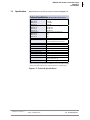
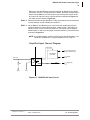
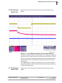
DNA/DNR-PC-911/912/913
Power Conversion Layer
User Manual
Board-mounted Power Source for External Devices and for
Inputs/Outputs of other Layers in same Chassis
November 2010 Edition
Version 1.5
PN Man-DNx-PC-91x-1110
© Copyright 1998-2010 United Electronic Industries, Inc. All rights reserved.
DNA-PC-91x Power Conversion Layer
No part of this publication may be reproduced, stored in a retrieval system, or transmitted, in any form
by any means, electronic, mechanical, by photocopying, recording, or otherwise without prior written
permission.
Information furnished in this manual is believed to be accurate and reliable. However, no responsibility
is assumed for its use, or for any infringements of patents or other rights of third parties that may result
from its use.
All product names listed are trademarks or trade names of their respective companies.
See UEI’s website for complete terms and conditions of sale:
http://www.ueidaq.com/company/terms.aspx
Contacting United Electronic Industries
Mailing Address:
27 Renmar Avenue
Walpole, MA 02081
U.S.A.
For a list of our distributors and partners in the US and around the world, please see
http://www.ueidaq.com/partners/
Support:
Telephone:(508) 921-4600
Fax:(508) 668-2350
Also see the FAQs and online “Live Help” feature on our web site.
Internet Support:
Support: [email protected]
Web-Site: www.ueidaq.com
FTP Site: ftp://ftp.ueidaq.com
Product Disclaimer:
WARNING!
DO NOT USE PRODUCTS SOLD BY UNITED ELECTRONIC INDUSTRIES, INC. AS CRITICAL
COMPONENTS IN LIFE SUPPORT DEVICES OR SYSTEMS.
Products sold by United Electronic Industries, Inc. are not authorized for use as critical components in
life support devices or systems. A critical component is any component of a life support device or
system whose failure to perform can be reasonably expected to cause the failure of the life support
device or system, or to affect its safety or effectiveness. Any attempt to purchase any United Electronic
Industries, Inc. product for that purpose is null and void and United Electronic Industries Inc. accepts
no liability whatsoever in contract, tort, or otherwise whether or not resulting from our or our
employees' negligence or failure to detect an improper purchase.
Note: Specificatons listed in this document are subject to change without notice. Check with UEI for
current status.
© Copyright 2010 all rights reserved
United Electronic Industries, Inc.
Tel: 508-921-4600
Date: November 2010
www.ueidaq.com
Vers: 1.5
File: PC-91x FrontMatter.fm
ii
iii
Table of Contents
Chapter 1 Introduction
.................................................... 1
1.1
Organization of this Manual . . . . . . . . . . . . . . . . . . . . . . . . . . . . . . . . . . . . . . . . . . . . 1
1.2
The DNx-PC-91x Layer(s) . . . . . . . . . . . . . . . . . . . . . . . . . . . . . . . . . . . . . . . . . . . . . 2
1.3
Specifications . . . . . . . . . . . . . . . . . . . . . . . . . . . . . . . . . . . . . . . . . . . . . . . . . . . . . . . 3
1.4
Device Architecture. . . . . . . . . . . . . . . . . . . . . . . . . . . . . . . . . . . . . . . . . . . . . . . . . . . 4
1.5
Layer Connectors and Wiring . . . . . . . . . . . . . . . . . . . . . . . . . . . . . . . . . . . . . . . . . . . 5
1.6
Jumper Settings for DNA Version . . . . . . . . . . . . . . . . . . . . . . . . . . . . . . . . . . . . . . . . 5
Chapter 2 Programming with the High Level API . . . . . . . . . . . . . . . . . . . . . . . . . . . . . . . 7
2.1
Creating a Session . . . . . . . . . . . . . . . . . . . . . . . . . . . . . . . . . . . . . . . . . . . . . . . . . . . 7
2.2
Configuring Channels . . . . . . . . . . . . . . . . . . . . . . . . . . . . . . . . . . . . . . . . . . . . . . . . 7
2.3
Programming the Power Output Level . . . . . . . . . . . . . . . . . . . . . . . . . . . . . . . . . . . . 7
2.4
Configuring the Timing . . . . . . . . . . . . . . . . . . . . . . . . . . . . . . . . . . . . . . . . . . . . . . . . 8
2.5
Reading Back Voltages, Currents, and Temperature . . . . . . . . . . . . . . . . . . . . . . . . . 8
2.6
Cleaning-up the Session. . . . . . . . . . . . . . . . . . . . . . . . . . . . . . . . . . . . . . . . . . . . . . . 8
Chapter 3 Programming with the Low-Level API . . . . . . . . . . . . . . . . . . . . . . . . . . . . . . . 9
3.1
3.1.1
3.1.2
DNA-PC-911/912/913 Layers . . . . . . . . . . . . . . . . . . . . . . . . . . . . . . . . . . . . . . . . . . . 9
DqAdv91xRead . . . . . . . . . . . . . . . . . . . . . . . . . . . . . . . . . . . . . . . . . . . . . . . . 9
DqAdv91xSetConfig. . . . . . . . . . . . . . . . . . . . . . . . . . . . . . . . . . . . . . . . . . . . 10
Appendix A Using a Power Conversion Layer with Other Layers . . . . . . . . . . . . . . . . . . 12
A.1
Overview . . . . . . . . . . . . . . . . . . . . . . . . . . . . . . . . . . . . . . . . . . . . . . . . . . . . . . . . . . 12
A.2
Driving the Digital Inputs and Outputs of a DNA-DIO-401 . . . . . . . . . . . . . . . . . . . . 12
A.3
Connecting to other DNA Boards or Layers . . . . . . . . . . . . . . . . . . . . . . . . . . . . . . . 15
Appendix B Accessories . . . . . . . . . . . . . . . . . . . . . . . . . . . . . . . . . . . . . . . . . . . . . . . . . . . 18
Accessories . . . . . . . . . . . . . . . . . . . . . . . . . . . . . . . . . . . . . . . . . . . . . . . . . . . . . . . . . . . . . . 18
Appendix C Initital Tests for PC-911 and PC-912 . . . . . . . . . . . . . . . . . . . . . . . . . . . . . . . 18
C.1
Test Configuration. . . . . . . . . . . . . . . . . . . . . . . . . . . . . . . . . . . . . . . . . . . . . . . . . . .
C.2
PC-911 . . . . . . . . . . . . . . . . . . . . . . . . . . . . . . . . . . . . . . . . . . . . . . . . . . . . . . . . . . . . 19
C.3
PC-912 . . . . . . . . . . . . . . . . . . . . . . . . . . . . . . . . . . . . . . . . . . . . . . . . . . . . . . . . . . . . 19
C.4
Switching Test . . . . . . . . . . . . . . . . . . . . . . . . . . . . . . . . . . . . . . . . . . . . . . . . . . . . . . 19
C.5
PC-911 Auto-Switch Test . . . . . . . . . . . . . . . . . . . . . . . . . . . . . . . . . . . . . . . . . . . . . . 20
C.6
PC-912 Auto-Switch Test . . . . . . . . . . . . . . . . . . . . . . . . . . . . . . . . . . . . . . . . . . . . . . 22
C.7
PC-912 Auto-Switch Test . . . . . . . . . . . . . . . . . . . . . . . . . . . . . . . . . . . . . . . . . . . . . . 22
C.8
Explorer Controls Test . . . . . . . . . . . . . . . . . . . . . . . . . . . . . . . . . . . . . . . . . . . . . . . . 24
C.9
PC-911 . . . . . . . . . . . . . . . . . . . . . . . . . . . . . . . . . . . . . . . . . . . . . . . . . . . . . . . . . . . 25
C.10
PC-912 . . . . . . . . . . . . . . . . . . . . . . . . . . . . . . . . . . . . . . . . . . . . . . . . . . . . . . . . . . . . 25
© Copyright 2010
United Electronic Industries, Inc.
Tel::508-921-4600
Date: November 2010
www.ueidaq.com
19
Vers: 1.5
DNx-PC-91x-ManualTOC.fm
iv
Index
....................................................................
© Copyright 2010
United Electronic Industries, Inc.
Tel::508-921-4600
Date: November 2010
www.ueidaq.com
Vers: 1.5
DNx-PC-91x-ManualTOC.fm
DNA-PC-91x Power Conversion Layer
List of Figures
Chapter 1 – Introduction . . . . . . . . . . . . . . . . . . . . . . . . . . . . . . . . . . . . . . . . . . . . . . . . . . . . 1
1-1
Photos of DNR- and DNA-PC-911 Power Conversion Layer Boards............................2
1-2
Technical Specifications .................................................................................................3
1-3
Block Diagram of DNx-PC-91x Layer Board...................................................................4
1-4
Pinouts of the DNA-PC-91x Power Conversion Layers..................................................5
1-5
Diagram of DNA-CT-651 Layer Position Jumper Settings..............................................5
1-6
Physical Layout of DNA-CT-651 Layer Board ................................................................6
Chapter 2 Programming with the High Level API . . . . . . . . . . . . . . . . . . . . . . . . . . . . . . . 7
(None)
Chapter 3 Programming with the Low-Level API
(None)
...............................9
Appendix A - Using a PC-91x with Other Layers in a Cube. . . . . . . . . . . . . . . . . . . . . . . . 12
A-1
DNA-DIO-401 Input Circuit ...........................................................................................13
A-2
Physical Layout of 912 and 401 Boards .......................................................................14
A-3
DNx-DIO-401 Output Circuit .........................................................................................14
A-4
Schematic Diagram of 911/912/913 Jumper Connections ...........................................15
A-5
Schematic Diagram of DIO-401-402-405 Jumper Connections ...................................16
A-6
Schematic Diagram of DIO-404 Jumper Connections..................................................16
A-7
Schematic Diagram of AO-350-353 Jumper Connections............................................17
A-8
Physical Location of DNA-PC-913 and AO-308-353 Jumpers .....................................17
Appendix B - Accesssories . . . . . . . . . . . . . . . . . . . . . . . . . . . . . . . . . . . . . . . . . . . . . . . . . . 19
Appendix C- Initial Tests for PC-911 and PC-912 . . . . . . . . . . . . . . . . . . . . . . . . . . . . . . . . 20
C-1
Scope Display with External Power Supply Disconnected ...........................................20
C-2
Scope Display with External Power Reconnected........................................................21
C-3
Scope Display with External Power Disconnected .......................................................22
C-4
Scope Display with External Power Supply Disconnected ...........................................23
C-5
Scope Display with External Power Reconnected........................................................24
© Copyright 2010 all rights reserved
United Electronic Industries, Inc.
Tel: 508-921-4600
Date: November 2010
www.ueidaq.com
Vers: 1.5
File: DNx-PC-91x-ManualLOF.fm
v
DNA-PC-91x Power Conversion Layer
Chapter 1
Introduction
Chapter 1
Introduction
This document outlines the feature set and use of the DNA-PC-911/912/913
Power Conversion Layers. These layers may be used as a source of power for
external devices and for digital and analog inputs and outputs of other layers
installed in the same PowerDNA Cube.
1.1
Organization
of this
Manual
This PowerDNA PC-91x User Manual is organized as follows:
•
Introduction
Provides an overview of Power Conversion Layer board features,
various models available, and what is needed to get started.
•
The PC-91x Layer
Provides an overview of the device architecture, connectivity, and
logic of layer.
•
Programming with the High Level API
Describes how to program the layer with UEIDAQ Framework API.
•
Programming with the Low Level API
Describes how to program the layer with DqAdv low level commands.
•
Appendix A: Using a Power Conversion Layer with other layers in
a PowerDNA Cube
This appendix shows how to use the PC-91x with various other types
of layers mounted in the same Cube.
•
Appendix B: Accessories
This appendix provides a list of accessories available for PC-91x
layer(s).
•
Index
This is an alphabetical listing of the topics covered in this manual.
Conventions
To help you get the most out of this manual and our products, please note that
we use the following conventions:
Tips are designed to highlight quick ways to get the job done, or
reveal good ideas you might not discover on your own.
NOTE: Notes alert you to important information.
CAUTION! Caution advises you of precautions to take to avoid injury,
data loss, and damage to your boards or a system crash.
Text formatted in bold typeface generally represents text that should be
entered verbatim. For instance, it can represent a command, as in the
following example: “You can instruct users how to run setup using a command
such as setup.exe.”
© Copyright 2010 all rights reserved
United Electronic Industries, Inc.
Tel: 508-921-4600
Date: November 2010
www.ueidaq.com
Vers: 1.5
File: PC-91x Chap1.fm
1
DNA-PC-91x Power Conversion Layer
Chapter 1
Introduction
1.2
The DNx-PC91x Layer(s)
The PC-91x layers have the following features:
•
Isolated DC/DC Converter
•
Overload Protection
•
Overtemperature Shutdown
•
Software-controlled on/off switch
•
Ability to read status of lines: voltage/current within limits, overload
DNR-PC-911
DNA-PC-911
Figure 1-1Photos of DNR- and DNA-PC-911 Power Conversion
Layer Boards
© Copyright 2010 all rights reserved
United Electronic Industries, Inc.
Tel: 508-921-4600
Date: November 2010
www.ueidaq.com
Vers: 1.5
File: PC-91x Chap1.fm
2
DNA-PC-91x Power Conversion Layer
Chapter 1
Introduction
1.3
Specifications
Specifications for the PC-91x layers are listed in Figure 1-2.
Technical Specifications: (all versionT unless otherwise noted)
Input voltage:
DNA-PC-911
DNA-PC-912
DNA-PC-913
Output voltage:
DNA-PC-911
DNA-PC-912
DNA-PC-913
Output current:*
DNA-PC-911
DNA-PC-912
DNA-PC-913
Output enable/disable
Input Selection*
Input protection
Output protection
Short circuit output current
Output Isolation
Input voltage readback acc.
Temp measurment acc.
Power supply efficiency
Power consumption
Operating temp. range
Operating humidity
9 - 36V DC
18 - 36V DC
9 - 36V DC
(call for info on other voltages)
±15 V DC ±3%
+24 V DC ±3%
±45 V DC ±3%
(derated 1.2% per °C above 40 °C)
1.2 A
1.6 A
0.4 A
software controlled. Default condition is ON
Power provided by internal bus or external
connection. Default source is internal.
5 A slow-blow fuse
Short cirtuit protected, unlimited duration
150 % of Imax
350 Vrms, min
±1%
±2 °C
>75% at all currents
0.8W (without load)
-40°C to +85°C (output current derated
1.2% per °C above 40 °C)
95%, non-condensing
* When the total power drawn from all DNx-PC-91x series boards in a single
chassis exceeds 40 watts, the use of external power is recommended.
Figure 1-2. Technical Specifications
© Copyright 2010 all rights reserved
United Electronic Industries, Inc.
Tel: 508-921-4600
Date: November 2010
www.ueidaq.com
Vers: 1.5
File: PC-91x Chap1.fm
3
DNA-PC-91x Power Conversion Layer
Chapter 1
Introduction
1.4
Device
Architecture
As shown in Figure 1-3, each DNA-PC-91x Layer has an isolated DC/DC
converter that outputs a DC voltage to external devices through a DB-37
connector on its front panel. The converter is also connected to an internal
power bus that runs between all installed layers in a cube. The DC voltage
from the converter is therefore available for use by other layers connected to
that bus. This feature is described more fully in Appendix A.
Block Diagram:
JPOW1
(DNA only)
+
-
Interlayer
Bus (for
DNA only)
Isolation
Isolation
Monitor
DC/DC
Status
On/Off +
Control
Logic
32-bit 66-MHz bus
DB37 Connector
Power
Switch
On/Off -
Figure 1-3. Block Diagram of DNx-PC-91x Layer Board
Each DNx-PC-91x layer has an Isolated DC/DC converter that outputs a
specific DC voltage. The PC-911 accepts 18-36VDC and outputs up to 1.3A at
±15VDC (40W); the PC-912 accepts 18-36VDC and outputs up to 1.6A at
+24VDC (40W); The PC-913 accepts 9-36VDC and outputs up to 0.3A at
±45VDC (15W).
CAUTION: The PC-91x provides thermal-, short-, and overload- protected
DC/DC. If the power consumption of the configured cube exceeds about
15 watts, ensure that you specify a fan to dissipate heat from the cube.
Otherwise, the automated protection system may be triggered to prevent
damage to the layer.
© Copyright 2010 all rights reserved
United Electronic Industries, Inc.
Tel: 508-921-4600
Date: November 2010
www.ueidaq.com
Vers: 1.5
File: PC-91x Chap1.fm
4
DNA-PC-91x Power Conversion Layer
Chapter 1
Introduction
1.5
Layer
Connectors
and Wiring
The PC-911/912/913 layers each use a 37-pin female D-Sub connector with the
pinouts shown in Figure 1-4:
Pinout Diagrams:
DB-37 (female)
37-pin connector:
DNx-PC-912
DNx-PC-911
Ext PWR Ret
DGND
DGND
DGND
DGND
DGND
DGND
DGND
DGND
DGND
DGND
DGND
DGND
DGND
DGND
DGND
DGND
Ext PWR+
37
36
35
34
33
32
31
30
29
28
27
26
25
24
23
22
21
20
19
18
17
16
15
14
13
12
11
10
9
8
7
6
5
4
3
2
1
Ext PWR Ret
–15V
–15V
–15V
–15V
–15V
–15V
–15V
N/C
N/C
N/C
+15V
+15V
+15V
+15V
+15V
+15V
+15V
Ext PWR+
Ext PWR Ret
DGND
DGND
DGND
DGND
DGND
DGND
DGND
DGND
DGND
DGND
DGND
DGND
DGND
DGND
DGND
DGND
Ext PWR+
37
36
35
34
33
32
31
30
29
28
27
26
25
24
23
22
21
20
19
18
17
16
15
14
13
12
11
10
9
8
7
6
5
4
3
2
1
Ext PWR Ret
DGND
DGND
DGND
DGND
DGND
DGND
DGND
N/C
N/C
N/C
+24V
+24V
+24V
+24V
+24V
+24V
+24V
Ext PWR+
DNx-PC-913
Ext PWR Ret
DGND
DGND
DGND
DGND
DGND
DGND
DGND
DGND
DGND
DGND
DGND
DGND
DGND
DGND
DGND
DGND
Ext PWR+
37
36
35
34
33
32
31
30
29
28
27
26
25
24
23
22
21
20
19
18
17
16
15
14
13
12
11
10
9
8
7
6
5
4
3
2
1
Ext PWR Ret
–45V
–45V
–45V
–45V
–45V
–45V
–45V
N/C
N/C
N/C
+45V
+45V
+45V
+45V
+45V
+45V
+45V
Ext PWR+
Figure 1-4. Pinouts of the DNA-PC-91x Power Conversion Layers
The layers use a B-size 37-pin D-sub connector with voltages available as
shown in Figure 1-4.
1.6
Jumper
Settings for
DNA Version
The DNA-PC-91x module (layer) has a jumper block that assigns the position
of the module within a PowerDNA Cube. The jumpers must be set to match the
physical position of an I/O board or layer in the Cube.
NOTE: Since all layers are assembled in Cubes before shipment to a
customer, you should never have to change a jumper setting.
In case a jumper may have been inadvertently misplaced, a diagram of the
jumper block is shown in Figure 1-5. To set the layer address, place jumpers
as shown for I/O position 1in Figure 1-5.
Jx Pins
I/O 1
Layer’s Position as marked on the Faceplate*
I/O 2
I/O 3
I/O 4
I/O 5
I/O 6
9-10
11-12
13-14
15-16
* All I/O Layers are sequentially enumerated from top to the bottom of the Cube
- Open
- Closed
Figure 1-5. Diagram of DNA-CT-651 Layer Position Jumper
Settings
© Copyright 2010 all rights reserved
United Electronic Industries, Inc.
Tel: 508-921-4600
Date: November 2010
www.ueidaq.com
Vers: 1.5
File: PC-91x Chap1.fm
5
DNA-PC-91x Power Conversion Layer
Chapter 1
Introduction
DNA 120-pin Bus Connector
4
2
5
7
9
11
15
13
16
14
J1
3
1
6
8
10
12
See Figure 1-5 for
jumper locations for
setting layer position.
DB-62 I/O Connector
External Circuits
Figure 1-6. Physical Layout of DNA-CT-651 Layer Board
© Copyright 2010 all rights reserved
United Electronic Industries, Inc.
Tel: 508-921-4600
Date: November 2010
www.ueidaq.com
Vers: 1.5
File: PC-91x Chap1.fm
6
DNA-PC-91x Power Conversion Layer
Chapter 2
Programming with the High Level API
Chapter 2
Programming with the High Level API
This section describes how to program the DNA-PC-91x using the UEIDAQ’s
Framework API.
The UEIDAQ framework is object oriented and its objects can be manipulated
in the same manner from various development environments such as Visual
C++, Visual Basic, or LabVIEW.
The following section focuses on the C++ API, but the concept is the same no
matter what programming language you are using.
Please refer to the “UEIDAQ Framework User Manual” for more information
about using other programming languages.
2.1
Creating a
Session
The Session object controls all operations on your PowerDNA device.
Therefore, the first task is to create a session object:
CUeiSession session;
2.2
Configuring
Channels
The PC-91x allows for reading back power voltage levels (Channels 0, 1, 2),
current (Channel 3) and temperature (Channel 4).
To access those measurements, configure the channel list using the session’s
object method “CreateAIChannel”.
// Configure PC-91x to read channels 0 to 4
session.CreateAIChannel(“pdna://192.168.100.2/Dev0/Ai0,1,2,3,4”,-10,
10,UeiAIChannelInputModeSingleEnded);
The input range and input mode settings are not used on the PC-91x.
2.3
Programming
the Power
Output Level
The following example shows how to switch the output on or off with the
custom property “source”:
// Set source 0: internal power, 1:external power, 2: external power
// with automatic switch to internal
session.SetCustomProperty("source", 0);
//
//
//
//
//
//
//
//
//
Set voltage selection
0: Power off
1: -4.33V +4.33V 12 W (911 only)
2: -9.66V +9.66V 24 W (911 only)
3: -15V +15V 36 W (911 only)
4: -4.33V +15V 24 W (911 only)
5: -15V +4.33V 24 W (911 only)
6: +11.66V 20 W (912 only)
7: +24V 40 W (912 only)
© Copyright 2010 all rights reserved
United Electronic Industries, Inc.
Tel: 508-921-4600
Date: November 2010
www.ueidaq.com
Vers: 1.5
File: PC-91x Chap2.fm
7
DNA-PC-91x Power Conversion Layer
Chapter 2
Programming with the High Level API
//
//
//
//
//
8: -14.33V +14.33V 12 W (913 only)
9: -29.66V +29.66V 24 W (913 only)
10: -45V +45V 36 W (913 only)
11: -14.33V +45V 24 W (913 only)
12: -45V +14.33V 24 W (913 only)
session.SetCustomProperty("voltageselect", 8);
2.4
Configuring
the Timing
You can only configure the PC-9x to run in simple mode (point by point). Other
timing modes are not supported.
In simple mode, the delay between samples is determined by software on the
host computer.
The following sample shows how to configure the simple mode.
session.ConfigureTimingForSimpleIO();
2.5
Reading
Back
Voltages,
Currents,
and
Temperature
Reading data from the PC-91x is done by using a reader object. Use the
scaled reader object to read the voltage, current, and temperature readback
values.
The following sample code shows how to create a scaled reader object and
read samples.
// Create a reader and link it to the session’s stream
CueiAnalogScaledReader reader(session.GetDataStream());
// read one scan, the buffer returned contains { volt1, volt2, volt3,
current, temperature }
double data[5];
reader.ReadSingleScan(data);
2.6
Cleaningup the
Session
The session object will clean itself up when it goes out of scope or when it is
destroyed. However, you can manually clean up the session (to reuse the
object with a different set of channels or parameters, for example).
session.CleanUp();
© Copyright 2010 all rights reserved
United Electronic Industries, Inc.
Tel: 508-921-4600
Date: November 2010
www.ueidaq.com
Vers: 1.5
File: PC-91x Chap2.fm
8
DNA-PC-91x Power Conversion Layer
Chapter 3
Programming with the Low-Level API
Chapter 3
Programming with the Low-Level API
The DqAdv functions of the low-level API, which are included in this chapter,
offer direct access to PowerDNA DaqBIOS protocol and allow you to access
device registers directly. For additional information, please refer to the API
Reference Manual document under:
Start » Programs » UEI » PowerDNA » Documentation
for all pre-defined types, error codes, and functions you can use with this layer.
3.1
DNA-PC-911/912/913 Layers
3.1.1
DqAdv91xRead
Syntax:
int DqAdv91xRead(int hd, int devn, uint32* status, uint32* bdata,
double* fdata)
Command: DQE
:
Input:
int hd
Handle to the IOM received from DqOpenIOM()
int devn
Device number
Output:
uint32 *status
Returns status value, 1 uint32
uint32 *bdata
Raw binary data, an array of 5 values, (NULL if not required)
double *fdata
Converted data, an array of 5 values, (NULL if not required)
Return:
DQ_ILLEGAL_HANDLE
Illegal IOM Descriptor or communication wasn’t established
DQ_BAD_DEVN
Device indicated by devn does not exist or is not an 1553-553
DQ_SEND_ERROR
Unable to send the Command to IOM
DQ_TIMEOUT_ERROR
Nothing is heard from the IOM for Timeout duration
DQ_IOM_ERROR
Error occurred at the IOM when performing this command
DQ_SUCCESS
Successful coompetion
Other negative values:
Low level IOM error
Output:
uint32 *status
Returns status value , 1 uint32
uint32 *bdata
Raw binary data, an array of 5 values, (NULL if not required)
double *fdata
Converted data, an array of 5 values, (NULL if not required)
© Copyright 2010 all rights reserved
United Electronic Industries, Inc.
Tel: 508-921-4600
Date: November 2010
www.ueidaq.com
Vers: 1.5
File: PC-91x Chap3.fm
9
DNA-PC-91x Power Conversion Layer
Chapter 3
10
Description:
This function returns the status and ADC readings from a 91x series layer.
PC-91X ADC channel assignments, indices for bdata [] and fdata []:
DQ_PC91X_CH_EXT_V
DQ_PC91X_CH_INPUT_I
(0)
(1)
DQ_PC91X_CH_INT_V
(2)
DQ_PC91X_CH_DCDC_INPUT_V (3)
DQ_PC91X_CH_THERM
(4)
// volts,
external JIO connector
// amps,
current used by DC/DC
// converters
// volts,
internal DNx system power
// volts,
voltage at input to DC/DC
// degrees C,temperature of the ADC IC
Bit defines for status information returned to *status
DQ_91X_STS_JMAIN_ON
DQ_91X_STS_JIO_ON
DQ_91X_STS_JIO
(1L<<2) // = 1 if JMAIN (DNA) is used as a
// power source
(1L<<1) // = 1 if JIO (Front connector) is used
// as a power source
(1L<<0) // JIO Input Power status, 0=fault, no
// power
Note: None.
3.1.2
DqAdv91xSetConfig
Syntax:
int DqAdv91xSetConfig(int hd, int devn, uint32 src, uint32 vsel)
Command: DQE
:
Input:
int hd
Handle to IOM received from DqOpenIOM()
int devn
Layer inside the IOM
int src
Voltage source selector, internal, JIO or JIO w/autoswitch
int vsel
Select the voltage options or turn power off
Output:
None.
Return:
DQ_ILLEGAL_HANDLE
Illegal IOM Descriptor or communication wasn’t established
DQ_BAD_DEVN
Device indicated by devn does not exist or is not a PC-91x
DQ_BAD_PARAMETER
Src or vsel is not one of the specified constants
DQ_SEND_ERROR
Unable to send the Command to IOM
DQ_TIMEOUT_ERROR
Nothing is heard from the IOM for Time out duration
DQ_IOM_ERROR
Error occurred at the IOM when performing this command
DQ_SUCCESS
Successful completion
Other negative values
© Copyright 2010 all rights reserved
United Electronic Industries, Inc.
Low level IOM error
Tel: 508-921-4600
Date: November 2010
www.ueidaq.com
Vers: 1.5
File: PC-91x Chap3.fm
DNA-PC-91x Power Conversion Layer
Chapter 3
11
Description:
This function sets the operating state of the PC-91x.
Use one of the following #defined constants for src:
DQ_91X_INTERNAL_POWER
DQ_91X_EXT_JIO_POWER
DQ_91X_EXT_JIO_AUTOSWITCH
//
//
//
//
//
use internal power from DNx system
use power from DB-37 (JIO) connector
use power from DB-37 (JIO) connector
but switch to internal power when JIO
voltage is too low ( approx 9V).
Use one of the following #defined constants for vsel. Use the constants that
apply to your particular PC-91x model.
For PC-911:
DQ_91X_POWER_OFF
DQ_911_P5_N5_12W
DQ_911_P10_N10_24W
DQ_911_P15_N15_36W
DQ_911_P15_N5_24W
DQ_911_P5_N15_24W
// set power off
// +-4.33V 12Watts
//+-9.66V 24Watts
// +-15V 36Watts
// +15V,-4.33V 24Watts
// +4.33V,-15V 24Watts
For PC-912:
DQ_91X_POWER_OFF
DQ_912_P12_20W
DQ_912_P24_40W
//
//
//
set power off
+11.66V 20Watts
+24V 40Watts
For PC-913:
DQ_91X_POWER_OFF
DQ_913_P15_N15_12W
DQ_913_P30_N30_24W
DQ_913_P45_N45_36W
DQ_913_P45_N15_24W
DQ_913_P15_N45_24W
//
//
//
//
//
//
set power off
+-14.33V 12Watts
+-29.66V 24Watts
+-45V 36Watts
+45V,-14.33V 24Watts
+14.33V,-45V 24Watts
Note:
None.
© Copyright 2010 all rights reserved
United Electronic Industries, Inc.
Tel: 508-921-4600
Date: November 2010
www.ueidaq.com
Vers: 1.5
File: PC-91x Chap3.fm
DNA-PC-91x Power Conversion Layer
12
Appendix A
Using a Power Conversion Layer
(DNx-PC-911/912/913) with Other Layers
in a PowerDNA Chassis
A.1
Overview
In addition to its ability to supply power to external devices through the DB-37
connector on the front panel, a DNA-PC-91x Power Conversion Layer may
also be used to supply power internally to other layers mounted within the
same Cube. (This function is not available with DNR version boards. With
DNR version boards, all interlayer connections must be made via external
connections to the DB-37 front panel connector.)
The power can be used to drive digital input, digital output, or analog output
circuits on these layers. The power conversion boards are available in three
types, each with a different output voltage. The DNx-PC-911 outputs ±15VDC,
the DNx-PC-912 +24VDC, and the DNx-PC-913 ±45VDC. For detailed specs,
refer to the Data Sheet for DNA-PC-91x Power Conversion Layers, which can
be viewed and downloaded from the website (www.ueidaq.com).
Power from a DNA-PC-91x board may be connected to either of two interlayer
power buses (Bus 1 or Bus 2) by installing jumpers on the board, as described
later in this guide. Bus 1 uses Pins 11 and 13 of the 14-pin interlayer
connectors mounted on each layer. Bus 2 uses Pins 12 and 14. This internal
connection feature is not available with DNR version because no interlayer
bus is provided. All such connections must be made externally.
Other layers in the same Cube, such as digital input/output or analog output
boards, can connect to either bus by installing jumpers on appropriate
connectors on that layer, as described below. In most cases, the connections
to Bus 1 and Bus 2 can be made by a user installing selected jumpers. On
some layers, however, such as the AO-308-353 board with ±40 VDC analog
outputs, additional connections or disconnections must be made at the factory
before shipment. Therefore, any jumpers are usually installed at the factory
before shipment. The only modifications to jumper connections suitable for
users to make in the field would be to change from Bus 1 to Bus 2 or vice
versa.
Examples are given in following sections that show how a user can install
jumpers for various types of layers.
A.2
Driving the
Digital Inputs
and Outputs
of a
DNA-DIO-401
To configure a Power Conversion Layer to drive the Digital Inputs or Outputs
of a DNA-DIO-401, use the following procedure:
STEP 1: Determine the voltage required for the task.
© Copyright 2010 all rights reserved
United Electronic Industries, Inc.
Tel: 508-921-4600
Date: November 2010
www.ueidaq.com
Vers: 1.5
File: PC-91x App A.fm
DNA-PC-91x Power Conversion Layer
13
Referring to the specifications for the 401 listed in its datasheet, the voltage
required is +24 VDC. The requirement for 24VDC, therefore, means that you
should use the DNA-PC-912 Conversion Layer as the power source for the
401 inputs.The Input Circuit for a typical channel is illustrated in Figure A-1;
the output circuit is shown in Figure A-3.
STEP 2: Determine which Interlayer Bus (Bus 1 or Bus 2) you want to use for this board.
For this example, we will arbitrarily choose Bus 1.
STEP 3: On the DNA-PC-912 Board that you use for this task, install jumpers in the
positions needed to connect the 912 output voltage to Bus 1. Since Bus 1 is
carried on Pins 11 and 13 of the interlayer bus, you should connect jumpers
between Pins 1-2 and 4-5 on the jumper connector marked J1 on the 912 board,
as shown in Figure A-2.
NOTE: If you had decided to use Bus 2 (Pins 12 and 14) instead of Bus 1, you
would have installed the J1 jumpers between Pins 2-3 and 5-6.
Simplified Input Channel Diagram
$*,-%*(-'!
+"*-))%$"!
(*
2
3
.(#$
4
1
/
.
$#$,%')-,
&-+"
Figure A-1. DNA-DIO-401 Input Circuit
© Copyright 2010 all rights reserved
United Electronic Industries, Inc.
Tel: 508-921-4600
Date: November 2010
www.ueidaq.com
Vers: 1.5
File: PC-91x App A.fm
DNA-PC-91x Power Conversion Layer
14
The physical layout of the 912 and 401 boards showing locations of jumpers
and bus connectors is illustrated below in Figure A-2.
DNA-DIO-401 Board
DNx-PC-912 Board
13
14
J1
11
12
3
9
2
8
1
7
9
7
10
8
5
6
Jumper
Block
Inter-layer
Bus Pins
3
4
1
JPOW1
JPOW1
jumpers
Inter-layer
Bus Pins
2
13
14
11
12
9
10
7
8
5
6
3
J1
3
1
4
Jumper
Block
9
2
8
1
7
2
Bus 1 pins
Bus 1 pins
Bus 2 pins
Bus 2 pins
jumpers
LEDs
LEDs
Figure A-2. Physical Layout of 912 and 401 Boards
STEP 4: To connect the 401 input circuits to the Interlayer Bus 1, install jumpers on the
DIO-401 board between Pins 1-2 and 4-5, as shown in Figure A-2.
NOTE: If you had used Bus 2 instead, you would have installed the jumpers
between Pins 2-3 and 5-6.
.
Simplified Output Channel Diagram
*%!"
1
4
2
3
( ')&&#" %'
*
$)(
&
+
#%
Figure A-3. DNx-DIO-401 Output Circuit
© Copyright 2010 all rights reserved
United Electronic Industries, Inc.
Tel: 508-921-4600
Date: November 2010
www.ueidaq.com
Vers: 1.5
File: PC-91x App A.fm
DNA-PC-91x Power Conversion Layer
15
A.3
Connecting
to other DNA
Boards or
Layers
The following figures are schematic diagrams that show jumper connections
for various Power Conversion boards and associated analog and digital I/O
boards.
Note:
In the DNA-PC-911, the following voltages and power levels are softwareselectable: +5V 12W, ±10V 24W, ±15V 36W, +15V/-5V 24W, +5V/-15V 24W.
In the DNA-PC-912, the following voltages and power levels are softwareselectable: +12V 20W, +24V 40W.
In the DNA-PC-913, the following voltages and power levels are softwareselectable: ±15V 12W, ±30V 24W, ±45V 36W, +45V/-15V 24W,
+15V/-45V 24W.
Interlayer
Power Bus
Connector
DNA-PC-911/912/913
POWER Connector
+VIN
GNDP
Bus 1
JPOW1
1
3
5
7
-15V-2/-45V-2
9
GND-1
11
+15V / +24V -113
+
+
+
+
+
+
+
+45V-1
+
+
+
+
+
+
+
+VIN
2
4
6
8
10
12
14
D1
GNDP
-15V-2/-45V-2
GND-2
+15V / +24V -2
+45V-2
Bus 2
GNDP
CON14AP
J2
4
J1
1
2
1
2
3
3
DGND
4
5
4
5
6
6
-15V
7
8
7
8
9
9
+15V
/+24V
VCC_DIG
DC/DC
Converter
C25
C13
3x3HEAD
Jumpers Installed here
connect DC/DC Converter output
to interlayer power bus 1.
Figure A-4. Schematic Diagram of 911/912/913 Jumper
Connections
© Copyright 2010 all rights reserved
United Electronic Industries, Inc.
Tel: 508-921-4600
Date: November 2010
www.ueidaq.com
Vers: 1.5
File: PC-91x App A.fm
DNA-PC-91x Power Conversion Layer
16
Power options:
- no jumpers installed : power via FDIO1 VCC_DIG/DGND pins
- 1-2 and 4-5 : power from 902 layer mapped to GND-1 and +24V-1
- 2-3 and 5-6 : power from 902 layer mapped to GND-2 and +24V-2
- 5-8 and 2-VCC-IN : power from the non-isolated input power 9-36V
POWER Connector
V-IN
1
TP5
JPOW1
+VIN-IN
1
3
GND-IN
5
7
9
GND-1
11
+15V / +24V -113
CON14AP
+
+
+
+
+
+
+
+
+
+
+
+
+
+
+VIN-IN
2
4
6
8
10
12
14
GND-IN
GND-2
+15V / +24V -2
J2
VCC_DIG
1
2
1
2
3
3
DGND
4
5
4
5
6
6
7
8
7
8
9
9
V-IN test point footprint should
use the
same hole/via as J2 connector;
also it should be located on the
same line as 2-5-8 pins of the J2
with 0.1" spacing from the pin 2
3x3HEAD
Figure A-5. Schematic Diagram of DIO-401-402-405 Jumper
Connections
POWER Connector
JPOW1
1
3
5
7
9
GND-1
11
+15V / +24V -113
+
+
+
+
+
+
+
+
+
+
+
+
+
+
2
4
6
8
10
12
14
GND-2
+15V / +24V -2
CON14AP
J2
VCC_DIG
1
2
1
2
3
3
DGND
4
5
4
5
6
6
7
8
7
8
9
9
4
3x3HEAD
Figure A-6. Schematic Diagram of DIO-404 Jumper Connections
© Copyright 2010 all rights reserved
United Electronic Industries, Inc.
Tel: 508-921-4600
Date: November 2010
www.ueidaq.com
Vers: 1.5
File: PC-91x App A.fm
DNA-PC-91x Power Conversion Layer
17
POWER Connector
JPOW1
+VIN
1
+ +
+ +
+ +
+ +
+ +
+ +
+ +
3
GND-P
5
7
-15V-1, -45V-1
9
GND-1
11
+15V / +24V / +45v -113
Factory-installed
resistors and/or
jumpers
3
+VA15
2
Rx1
+VIN
2
4
6
8
10
12
14
GND-P
-15V-2, -45V-2
GND-2
+15V / +24V /+45V -2
J2 CONN3
CON14AP
J3 CONN3 J4 CONN4
Jumpers
3 2 1
3 2 1
3 2 1
+VEXT
1
+Vo
AGND
Rx2
-VA15
-VEXT
Figure A-7. Schematic Diagram of AO-350-353 Jumper
Connections
DNA-AO-308-353 Board
DNA-PC-913 Board
jumpers
J1
3
9
2
8
1
7
13
11
9
7
5
14
12
10
8
6
Jumper
Block
J2
Interlayer
Bus Pins
3
4
1
Inter-layer
Bus Pins
2
JPOW1
JPOW1
jumpers
Conn
Blocks
3 2 1
J3
J4
13
11
9
7
5
14
12
10
8
6
4
1
2
Bus 1 pins
Bus 1 pins
Bus 2 pins
3
RX1,RX2
(factory)
Bus 2 pins
LEDs
LEDs
Figure A-8. Physical Location of DNA-PC-913 and AO-308-353
Jumpers
© Copyright 2010 all rights reserved
United Electronic Industries, Inc.
Tel: 508-921-4600
Date: November 2010
www.ueidaq.com
Vers: 1.5
File: PC-91x App A.fm
DNA-PC-91x Power Conversion Layer
Appendix B
B.1 Accessories
The following cables and STP boards are available for the PC-91x layers.
DNA-CBL-37
3ft, 37-way flat ribbon cable; connects DNx-PC-91x to DNA-STP-37
DNA-CBL-37S
3 ft, 37-way round, shielded cable
DNA-STP-37
37-way screw terminal panel; requires DNA-CBL-37
© Copyright 2010
all rights reserved
Electronic
Industries,
Inc.
United Electronic Industries, Inc.
1-821-2890
Tel: 508-921-4600
Date: November 2010
www.ueidaq.com
www.ueidaq.com
Vers:0.5
Vers: 1.5
File: PC-91x AppB.fm
18
DNA-PC-91x Power Conversion Layer
Appendix C
Initial Tests for PC-911 and PC-912
C.1 Test
Configuration
The goal of the test is verify that both PC-911 and PC-912 can produce proper
output voltages, report input voltage, layer temperature, and input current -- and
switch the input source based on the software commands or in auto-switch
mode. Note that the PC-913 design is identical to the PC-911 with exception of
the p/n for the DC/DCs that are used. As a result, the PC-911 tests also cover
PC-913 as well.
C.2 PC-911
A DNR-PC-911 was inserted into the first slot of a 3012 DNR rack in standard
configuration with power, Ethernet connection, and RS-232 port.
A load board with 3ea 100 ohm 10W resistors was connected across the PC911’s 30V output (from +15V to -15V) using an STP-3716 and a DB-37 cable.
This gives an approximate 27 Watt load to the power output.
An additional variable power supply set to a nominal 22V was connected to the
external power input connection using pins 1 and 19 of the aforementioned STP3716.
Scope probes were connected as follows:
C.3 PC-912
•
Channel 1 to load resistors.
•
Channel 2 to external power supply input at pins 1 and 19 of the STP.
•
Channel 3 to power supply powering the DNR rack.
•
V/div was set to 20V, 100ms/div timebase
A DNR-PC-912 was inserted into the first slot of a 3012 DNR rack in standard
configuration with power, Ethernet connection, and RS-232 port.
A load board with 6ea 100 ohm 10W resistors was then connected across the
PC-912’s 24 V output using an STP-3716 and DB-37 cable. This gives an
approximate 35.6 Watt load to the power output.
An additional variable power supply set to a nominal 22V was connected to the
external power input connection using pins 1 and 19 of the aforementioned STP3716.
Scope probes were then connected as follows:
•
Channel 1 to load resistors.
•
Channel 2 to external power supply input at pins 1 and 19 of the STP.
•
Channel 3 to power supply powering the DNR rack.
•
V/div was set to 20V, 100ms/div timebase
C.4 Switching Test PowerDNA Explorer was used to control and monitor the operation of the PC911/912.
1. PC-911: Using Explorer, the output voltage was set to ±15V and the power
source to “Auto-switch”.
© Copyright 2010
all rights reserved
Electronic
Industries,
Inc.
United Electronic Industries, Inc.
1-821-2890
Tel: 508-921-4600
Date: November 2010
www.ueidaq.com
www.ueidaq.com
Vers:0.5
Vers: 1.5
File: PC-91X App C.fm
19
DNA-PC-91x Power Conversion Layer
2. PC-912: The output voltage was set to 24V and the power source to “Internal/External/Auto-switch”. The external source was then applied and
removed in all modes; and verified that the output responded correctly.
Result: PASSED
3. Using Explorer, verified that internal and external readings were within 5%
of actual values.
Result: PASSED
4. Using Explorer, verified that the input voltage shown on Explorer is within
150mV of the external voltage shown on Explorer.
PASSED
C.5 PC-911 AutoSwitch Test
Disconnection of the external power supply produced the following scope
display.
Figure C-1. Scope Display with External Power Supply
Disconnected
The top trace shows the power to the load resistors. The middle trace shows the
disconnection and voltage decay of the external power as seen by the PC-911.
The top trace shows the load being powered by external power followed by
approx 300ms of off time, followed by re-powering of the load using internal
power.
© Copyright 2010
all rights reserved
Electronic
Industries,
Inc.
United Electronic Industries, Inc.
1-821-2890
Tel: 508-921-4600
Date: November 2010
www.ueidaq.com
www.ueidaq.com
Vers:0.5
Vers: 1.5
File: PC-91X App C.fm
20
DNA-PC-91x Power Conversion Layer
The voltage displays on Explorer verify that this is the case with the External
voltage falling to approximately zero and the Input voltage now showing a
reading very close to the Internal voltage.
Reconnecting the external power supply produces a display as shown below:
Figure C-2. Scope Display with External Power Reconnected
© Copyright 2010
all rights reserved
Electronic
Industries,
Inc.
United Electronic Industries, Inc.
1-821-2890
Tel: 508-921-4600
Date: November 2010
www.ueidaq.com
www.ueidaq.com
Vers:0.5
Vers: 1.5
File: PC-91X App C.fm
21
DNA-PC-91x Power Conversion Layer
C.6 PC-912 AutoSwitch Test
Disconnection of the external power supply produced the following scope
display:
Figure C-3. Scope Display with External Power Disconnected
The top trace shows the power to the load resistors. The middle trace shows the
disconnection and voltage decay of the external power as seen by the PC-912.
The top trace shows the load being powered by the external power followed by
approx 300ms of off time, followed by the re-powering of the load using the
internal power.
The voltage displays on Explorer verify that this is the case with the External
voltage falling to approx. zero and the Input voltage now showing a reading very
close to the Internal voltage.
C.7 PC-912 AutoSwitch Test
© Copyright 2010
all rights reserved
Electronic
Industries,
Inc.
United Electronic Industries, Inc.
1-821-2890
Disconnection of the external power supply produced the following scope
display:
Tel: 508-921-4600
Date: November 2010
www.ueidaq.com
www.ueidaq.com
Vers:0.5
Vers: 1.5
File: PC-91X App C.fm
22
DNA-PC-91x Power Conversion Layer
Figure C-4. Scope Display with External Power Supply
Disconnected
The top trace shows the power to the load resistors. The middle trace shows the
disconnection and voltage decay of the external power as seen by the PC-912.
The top trace shows the load being powered by the external power followed by
approx 300ms of off time, followed by the re-powering of the load using the
internal power.
The voltage displays on Explorer verify that this is the case with the External
voltage falling to approx. zero and the Input voltage now showing a reading very
close to the Internal voltage.
© Copyright 2010
all rights reserved
Electronic
Industries,
Inc.
United Electronic Industries, Inc.
1-821-2890
Tel: 508-921-4600
Date: November 2010
www.ueidaq.com
www.ueidaq.com
Vers:0.5
Vers: 1.5
File: PC-91X App C.fm
23
DNA-PC-91x Power Conversion Layer
Reconnecting the external power supply produces a display as shown here:
Figure C-5. Scope Display with External Power Reconnected
The top trace shows the load being powered by the internal power followed by
approx 300ms of off time, followed by the re-powering of the load using the
external power.
The voltage displays on Explorer verify that this is the case with the External
voltage returning to a nominal 24V and the Input voltage now showing a reading
very close to the External voltage.
C.8 Explorer
Controls Test
The two drop down control boxes on Explorer were exercised to verify that their
functions were controlled correctly.
The Power source was set to internal and the external power supply was
connected and disconnected to verify that the Input voltage remained at the
internal voltage.
PASSED
The Power source was set to external and the external power supply was
connected and disconnected to verify that the Input voltage would be at the
external voltage when connected and near zero volts when disconnected.
PASSED
© Copyright 2010
all rights reserved
Electronic
Industries,
Inc.
United Electronic Industries, Inc.
1-821-2890
Tel: 508-921-4600
Date: November 2010
www.ueidaq.com
www.ueidaq.com
Vers:0.5
Vers: 1.5
File: PC-91X App C.fm
24
DNA-PC-91x Power Conversion Layer
PC-911
The Output voltage was set to ±10V and the voltage on the load resistors was
measured to be 19.0V. The Input current reading on Explorer was also observed
to drop from 1.34A to 0.58A. On the ±5V setting, the load resistor voltage was
8.7V with an input current value of 0.15A returned by Explorer.
PASSED
PC-912
The Output voltage was set to +12V and the voltage on the load resistors was
approx 11.5V. The Input current reading on Explorer was also observed to
(expectedly) drop to approx ¼ of the value seen on the 24V setting (0.42A vs.
1.75A).
PASSED
© Copyright 2010
all rights reserved
Electronic
Industries,
Inc.
United Electronic Industries, Inc.
1-821-2890
Tel: 508-921-4600
Date: November 2010
www.ueidaq.com
www.ueidaq.com
Vers:0.5
Vers: 1.5
File: PC-91X App C.fm
25
26
Index
H
Numerics
401 Input Circuit 13
911/912/9013 Jumper Connections 15
High Level API
I
A
Accessories 18
AO-308-353 12
AO-350-353 Jumper Connections
Architecture 4
B
Block Diagram
Bus 1 12
Bus 2 12
Input Circuit 13
Interlayer Bus 13
J
17
Jumper Settings
Jumpers 13
Layer position jumper settings
Low-Level API 9
5
M
Modifications to Jumper Connections
Cable(s) 18
CAUTION 1
Cleaning-up 8
Configuring Excitation 7
Configuring the Timing 8
Connectors 5
Conventions 1
Creating a Session 7
O
Organization
Digital Inputs or Outputs of a Dna-DIO-401
DIO-401-402-405 Jumper Connections 16
DIO-404 Jumper Connections 16
DNA-CBL-37 18
DNA-PC-911 -- ±15VDC 12
DNA-PC-912 +24VDC 12
DNA-PC-913 ±45VDC 12
© Copyright 2010
United Electronic Industries, Inc.
1
12
Photo 2
Physical Layout 14
Physical layout 6
Physical Location 17
Pinout 5
Programming 7, 9
R
Reading Data
8
S
Screw-terminal panels
T
2
12
P
D
Features
5
L
4
C
F
7
Tips
18
1
Tel: 508-921-4600
www.ueidaq.com
Date: November 2010
Vers: 1.5
File: DNx-PC-91x-ManualIX.fm