1
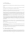
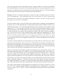
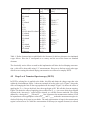
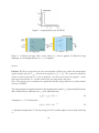
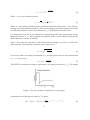
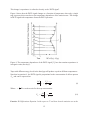
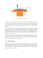
Deep-Level Transient Spectroscopy
Part 3 Laboratories
March 31, 2008
1
Contents
1 Introduction
3
2 Some words about third year labs
3
3 Safety notes
3
4 The theory
4
4.1
Semiconductors . . . . . . . . . . . . . . . . . . . . . . . . . . . . . . . . . . .
4
4.2
Schottky barrier diodes . . . . . . . . . . . . . . . . . . . . . . . . . . . . . . .
5
4.3
Capacitance and the depletion width . . . . . . . . . . . . . . . . . . . . . . . .
6
4.4
Defects and Deep-Level Traps . . . . . . . . . . . . . . . . . . . . . . . . . . .
7
4.5
Deep Level Transient Spectroscopy (DLTS) . . . . . . . . . . . . . . . . . . . .
9
5 Experimental Work
13
5.1
The Racks of Electronics . . . . . . . . . . . . . . . . . . . . . . . . . . . . . . 14
5.2
The Cryostat and Sample Holder . . . . . . . . . . . . . . . . . . . . . . . . . . 14
5.3
SRIM Simulation . . . . . . . . . . . . . . . . . . . . . . . . . . . . . . . . . . 15
5.4
Making the C-V measurement . . . . . . . . . . . . . . . . . . . . . . . . . . . 16
5.5
Analysing the C-V data . . . . . . . . . . . . . . . . . . . . . . . . . . . . . . . 17
5.6
DLTS measurement . . . . . . . . . . . . . . . . . . . . . . . . . . . . . . . . . 18
5.7
Perfoming a C-T measurement . . . . . . . . . . . . . . . . . . . . . . . . . . . 19
5.8
Analysing the DLTS data . . . . . . . . . . . . . . . . . . . . . . . . . . . . . . 19
6 Appendix: Important Numbers
20
2
1 Introduction
Semiconductor devices have revolutionised the world in which we live and have become such
a part of our everyday lives that we often take it for granted that they can and will perform
the task that they were designed for. However, due to their high quality the semiconductors
wafers used are extremely sensitive to defects arising from contamination, from impurities and
ion bombardment.
In this experiment you will examine how the static capacitance -using Capacitance-Voltage (C–
V)- and transient capacitance -using Deep-Level Transient Spectroscopy (DLTS)- of a metalsemiconductor diode (Schottky diode) varies with applied bias, temperature and time. These
measurement will allow you to gain a good understanding of the nature and effect of the defects
present in the silicon semiconductor.
DLTS is a highly sensitive analysis technique that is used on a daily bases by the semiconductor
industry. If you have a spare moment you might like to ask Prof. Google or Dr. Google Scholar
where it has been used. If you get around to doing this you will see papers dating back to 1974
when D.V. Lang first pioneered the technique [1].
2 Some words about third year labs
These notes don’t contain all the information you need - they’re here to define the terms for you,
and to give you an idea of the direction you should be taking. You’ll find that you need to go
foraging for more detailed information in other places - often in the references, and even more
often in the rubble of your demonstrators’ minds. You’re going to learn a lot while you’re doing
that, so don’t waste the effort - share all the work you’re doing with us in your report! Remember
that your report has to be self-contained. It doesn’t have to be beautiful, but it should be clear
and detailed. Perhaps the most important thing to remember is that when you write your report
you’re trying to teach your reader what you did, why you did it, and what you learned. That way,
we get to learn something too! Enjoy!
By the way, these notes have recenlty undergone a major revision, and may be littered with typos
(and possibly more serious errors). We in part3 would love it if you could bring any mistakes to
the attention of your demonstrators, or email suggestions to [email protected]
3 Safety notes
Liquid nitrogen has two main hazards associated with it: frostbite and asphyxiation. These are
related to its low boiling point (-196◦ C, 77 K) and its large gas to liquid volume ratio (682, at 1
atm and 15◦ C).
3
Frostbite: The eyes are particularly at risk from frostbite (cold burns) due to their moisture content. Liquid nitrogen rapidly boils when it comes in contact with an object at room temperature
and will splatter or spit. There is a risk of frostbite not only from direct contact but also from
indirect contact with a surface that has been cooled by liquid nitrogen. Objects less than about
-20◦ C will cause cold burns and if there is sufficient moisture on your skin you may become
frozen to the object.
Asphyxiation: When liquid nitrogen evaporates it displaces air and reduces the oxygen concentration in the air. Symptoms of asphyxia can be sudden in the case of a deep inhalation of air
with a low oxygen content or gradual asphyxia where the symptoms are more subtle. For further
information please consult the MSDS (Material Safety Data Sheets) for liquid nitrogen in the
safety folder.
The dewar must be placed on level surface at all times except during transport, preferably the
ground.
The room in which the dewar is stored and experiments are carried out must be kept well ventilated with all doors open while people are inside. This is to ensure that the oxygen content of
the room does not drop below 18% due to ANY spill including the worst case scenario where the
entire contents of the dewar evaporates.
Personal protective equipment
The following safety equipment is required when there is exposed liquid nitrogen present (e.g.
when the cap or cryostat is not inserted into the dewar, during refilling):
Gloves: Appropriate gloves should be worn when handling the dewar.
Face and eye protection: A full face shield conforming to AS 1337 must be worn.
Clothing: Loose dry clothing that completely covers the arms and legs must be worn. Trouser
legs preferably should not have cuffs that may trap liquid nitrogen.
Footwear: Shoes that completely cover the feet must be worn.
4 The theory
4.1 Semiconductors
You will find a good introduction to this topic in Streetman [2], it’s probably a good idea to have
a bit of a read of this text at some point (hmmm, even wikipedia has some interesting stuff on it).
So what is a semiconductor? Well you would probably be aware that it turns up in pretty much
everything these days (shoes, cats... even the humble laptop has some inside), so what makes it
so special? Why is it essential to the modern electrical device?
4
...Well, it’s now ‘your time to shine’!
Exercise .1 Ok, so what is a semiconductor? Your first task is to answer this question, you
will probably need to include a diagram of the band structure. Make your description relatively
comprehensive and cover topics like: band-gap, energy levels, fermi level, dopants, defects etc.
These topics are complicated but arguably the most interesting stuff in physics (well, I think so
anyway) so spend some time making sure you really understand this stuff.
Exercise .2 In this experiment the semiconductor we will use is silicon, why is this? Don’t get
bogged down with this, just give it some thought.
Right, so now we understand what a semiconductor is, time for the next question: how can we
use it? And how can we measure all these great properties? Well one step at a time, lets not rush
things. Next we will need to consider the ‘Schottky barrier diode’and how this device is affected
by a continuous and changing external bias.
4.2 Schottky barrier diodes
The electronic definition of a diode is a device that allows current to flow in one direction (forward bias) and not in the other (reverse bias), The same is true for a Schottky barrier diode.
To understand why this occurs one has to look at the band structure of a metal-semiconductor
junction and what occurs when a bias is applied across the junction.
Exercise .3 In this experiment we will be using n-type (phosphorous doped) silicon as the semiconductor and the metal is gold. By keeping this in mind, describe the Schottky diode effect. A
couple of well labeled diagram will be essential to this description, importantly:
• the band structure of both a metal and an n-type semiconductor separated in space.
• the band structure when the metal is now brought into contact with the n-type semiconductor.
In your diagram you should include these important terms: Fermi Level, Conduction Band,
Valance Band, Metal Work Function (φm ), Semiconductor Work Function (φs ), Barrier Height
(φb ), Depletion Width (ω), and Built in Voltage (Vbi ).
It should be noted that the work function of a metal describes the binding energy of the electrons
and is hence related to their Fermi level. Also when the metal and semiconductor come into
contact it becomes energetically favorable for electrons in the material to drift in such away
5
that the Fermi levels line up across the interface. This drift creates a charge difference over the
interface which creates a Built-in Voltage (Vbi ). In n-type silicon, if the work function of the
metal is larger than that of the silicon, the electrons in silicon drift away from the metal-silicon
interface region leaving behind a net positive charge in the silicon near this region. This region
is known as the Depletion Region (depleted of majority charge carriers) and characterized by a
width (ω).
In this experiment we will be looking at the electrical properties of a single Schottky barrier
diode. This will be done by applying a voltage, or External Bias, or voltage pulses to the gold
contact.
Exercise .4 Using a similar diagram to that used in the previous exercise, describe what occurs
when a ‘reverse’ External Bias (V) is applied across the metal-semiconductor junction.
Exercise .5 By considering what happens when ‘forward’ and ‘reverse’ bias is applied to our
Schottky diode, what is the significance of the Built in Voltage Vbi and the Barrier Height φb in
relation to current flowing through our devices? How does this lead to the ’diode’ effect?
Exercise .6 What happens if we bring a metal with a smaller work function in contact with a
n-type silicon?
The Schottky diodes made for this experiment were fabricated by first cleaning the silicon wafer
with solvents to remove any organic contaminates on the surface (‘degreasing’). Next the thin
‘native’ oxide (10-20Å) that exists on the surface of bare silicon is etched off with HF acid
(very dangerous stuff!) and the sample is promptly transferred to a thermal evaporator for gold
deposition through an aluminum mask.
4.3 Capacitance and the depletion width
Now, it should be understood from the previous section that, depending on the individual properties of the material and if an external bias is applied, a depleted region will form at a metalsemiconductor interface. The width of this region is related to these material properties and is
given by [3]:
ω=
s
2ǫ
kb T
(Vbi − (
)−V)
qn
q
Where:
ǫ is the dielectric constant of the semiconductor
n the active dopant concentration in the semiconductor
6
(1)
Vbi is the built–in voltage
and V the externally applied bias
An important effect of the Schottky diode is that a capacitance will form across this depletion
region.
Exercise .7 Now let’s think back a bit, what is capacitance? What is the formula for a parallel
plate capacitor? How is our diode similar to a parallel plate capacitor?
Exercise .8 By considering equation 1 find an expression for the capacitance over our device,
note that the area (A) of the diode is known and can be simply measured.
Right, so now we should have a direct relationship between the capacitance of our device, C, and
externally applied bias, V. Armed with this expression we can measure many properties of the
semiconductor by slapping a metal layer on top of the sample (thus forming a Schottky diode)
and measuring how the capacitance varies with the applied bias. This is the key of the C–V and
DLTS measurements.
Let’s take a closer look at this relationship. What are the thing we do not know in Equation 1?
Well, here in this experiment we can precisely hold the diode at a known temperature, we can
record the applied bias, and the importance of this equipment is that we can also accurately
measure the diodes capacitance. So all this leaves is n, the doping concentration, and Vbi , the
built–in voltage.
Exercise .9 Let’s first consider the simple case where n is constant throughout the silicon bulk.
From our expression, how can we calculate n and Vbi from measured capacitances (C) and
applied biases (V)?
Hint: try rearranging the expression in terms of 1/C 2 and V.
Exercise .10 Right-o, what happens now if n changes throughout the bulk of the silicon? How
can n be measured now?
Hint: We will be measuring the capacitance of lots of points at different applied voltage, how
will a changing n effect the ‘slope’ in our relationship? What does the ‘slope’ mean between two
points? (hmmm, I really feel like I have given this away)
4.4 Defects and Deep-Level Traps
At the heart of semiconductor physics is the idea that one can alter the electrical properties of
a semiconductor by the addition of impurities and defects in the semiconductor lattice. This
idea is the basis behind the doping of a semiconductor as these impurities or defects can create
7
donor or acceptor sites in the semiconductor lattice. Having said this, it is not always desirable to
have additional donor or acceptor in the semiconductor lattice as they may change the electrical
properties of a fabricated device in an undesired or unpredictable manner. It is for this important
reason that the task of electrical defect analysis has been undertaken.
Exercise .11 Here you should comprehensive explain the effects of different impurities and defects in semiconductors. You should make sure you cover the topics of: lattice vacancies and
interstitial atoms, electrically active dopants and defects, ‘shallow’ and ‘deep’ charge traps, and
the capture cross-section (σ) of a dopant.
The silicon wafers used to create the diode in this experiment have undergone ion implantation,
the species of ion is either phosphorous or hydrogen depending on which sample is used for your
individual experiment. It is well understood that this process introduces many defects into the
substrate [4, 5, 6]. This damage is initially of the form of interstitial atoms which have been
knocked off lattice sites leaving behind a vacancy [6] this damage is known a Frenkel defects.
At room temperature the vacancy and interstitial can migrate and separate without recombination. This occurs for 4-10% of the Frenkel defects created during ion implantation [6]. These
defects can go on to cluster together or form stable defect complexes with impurities. About
10-25% of the Frenkel defects that survive recombination form a di-vacancy cluster [7] which
is a characteristic defect for ion implanted silicon [4, 8], or bond with impurities to form other
stable clusters.
The defects of prime importance for electrical devices are those that are electrically active, meaning that they can trap charge carriers in the device. Electrically active traps are basically unoccupied states in the band-gap of a semiconductor that trap charge carriers. This occurs mostly due
to defects having dangling bonds, or unpaired electrons, and the traps exist with in the band-gap
of the silicon at some energy level depending on the structure of the defect.
Defects can be characterised by their position in the band-gap of a semiconductor relative to the
conduction band (trap energy, Et ), and their cross-section for trapping (capture cross-section, σ).
The values reported for electron traps in ion-implanted silicon are found in table 1. This table
shows the average value for the trap energies found in the literature. Absolute errors in the last
digit are shown in parentheses, no error is quoted for occasions where there is only one reference
for the defect, nor is the error quoted for capture cross-sections that have an error that is over an
order of magnitude difference. V indicates vacancy, other letters indicate elements, subscripts 2
& 3 indicate the number of vacancies in a cluster and superscripts indicate the charge state of the
trap. Other subscripts indicate either substitutional or interstitial atomic positions in the lattice.
The silicon wafer implanted with phosphorus was implanted at an energy of 450 keV at a dose
of 1x10⁹ P/cm2 while the samples implanted with hydrogen where implanted at an energy of
70 keV at a dose of 1x10¹⁰ H/cm2 . Ask your demonstrator which one you will be using for this
experiment.
8
Defect type
H–related
H–related
HC
VO
V–related
V2−
2
V2 O
V3 O
VO-H, other H–related
V–related
H–related
H–related
VP
V−
2
H–related
V2 –related
H–related
Unknown
Trap Energy
[ev]
0.10
0.13
0.15(1)
0.17(1)
0.19(1)
0.22(1)
0.27
0.30
0.30(2)
0.35(1)
0.39(1)
0.41(1)
0.42(2)
0.42(1)
0.45(1)
0.47
0.50(1)
0.59
Capture cross–section
[cm2 ]
–
–
–
7(4)x10−15
3.5x10⁻¹⁷
5(4)x10−16
–
–
3x10⁻¹⁵
5x10⁻¹⁶
1x10⁻¹⁷
–
5(3)x10−15
5(3)x10−15
1x10⁻¹⁷
–
–
–
Table 1: Defect characteristics as published in the literature for defects relevant to ion-implanted
n-type silicon. Here the V corresponds to a vacancy and the rest of the letters are standard
elements
The electrically active defects created in this implantation will alter the local doping concentration n, this will be observable using C–V measurements. However to find out exactly what type
of defects are causing this altered doping concentration we will need to employ DLTS.
4.5 Deep Level Transient Spectroscopy (DLTS)
In DLTS a pulsing bias is applied to the diode, this fills and drains the charge traps that exist
within the semiconductor, figure 1 shows an example of such a pulse cycle. Figure 2 shows the
effect of changing the bias on the trap population in the sample. Figure 2 a) shows the effect of
applying the Vpulse bias to the diode, here the traps begin to fill. We call this electron trapping.
Figure 2 b) shows the effect of applying a lower offset bias Vof f set (or reverse bias), here trapped
electron in the ‘increased ω’ region will be released, we call this electron emission. The region
defined by ω during the Vpulse bias and Vof f set bias is known as the measurement window, it will
be important to select appropriate values of Vpulse and Vof f set so that the measurement region includes all the deep level traps in your diode. The total concentration of traps in the measurement
region is referred to as NT while the concentration of full traps (or trapped electrons) is referred
9
Figure 1: A typical pulse cycle for DLTS.
Figure 2: a) Deep level traps ‘full’, occurs when Vpulse bias is applied. b) Deep level taps
emptying, occurs straight after the Vof f set is reapplied.
to as nT .
Exercise .12 Write an expression for the concentration of filled traps within the measurement
region straight after the Vpulse bias has been applied (nT (t = 0)). This expression should be
written in terms of the time Vpulse bias is applied tp , the rate the electrons are trapped rc , and a
total trap concentration NT . Assume all the traps are empty before the pulse.
Hint: The trapping rate is assumed to be exponential and don’t forget that there is a finite number
of traps to be filled .
The concentration of trapped electrons in the measurement region (nT ) exponentially decreases
and is effected by the emission rate (en ) of an individual trap:
nT (t) = nT (t = 0)e−en t
(2)
nT (t) = NT (t = 0)e−en t
(3)
Assuming nT ≈ NT this becomes:
en depends on temperature T , the trap energy level ET and the capture cross section of the trap
σc :
10
−(
en = γn σc T 2 e
Ec −ET
kB T
)
(4)
Where γn is a set of constants given by:
√
3
γn = 2 3Mc (2π) 2 kb2 m∗ h−3
(5)
Where Mc is the number of minima in the conduction band (6 for silicon) and m∗ is the effective
electron mass in the conduction band [9]. Since the trap energy level and the capture cross section
are different for different defects, the emission rate en will be different for each defect.
It is important to note that as the electrons are emitted from traps in the measurement region,
during the time the Vof f set bias is applied, the depletion width ω will be affected and hence the
diode capacitance will also be affected.
Figure 3 shows how the capacitance of the Schottky diode changes over time as a result of the
traps emptying. This capacitance transient can be expressed as:
C = C0
r
1−
nT (t)
n
(6)
For the case where the doping concentration is n is much greater than the trap concentration
(nT << n) we can say:
nT (t)
C ≈ C0 (1 −
)
(7)
2n
With DLTS we monitor the change in capacitance over some time interval (t1 , t2 ). The change
Figure 3: The time variation of capacitance as traps empty.
in capacitance over this interval (from Eq. 7) is hence:
∆C = C(t1 ) − C(t2 ) = C0 [
11
NT −en (T )t2
−en (T )t1
] [e
−e
]
2n
(8)
This change is capacitance is referred to loosely as the ‘DLTS signal’.
Figure 4 shows how the DLTS signal changes as a function of temperature when only a single
trap is present, this occurs due to the temperature dependence of the emission rate. This change
in DLTS signal with temperature forms the DLTS spectrum.
Figure 4: The temperature dependence of the DLTS signal [3], here the transient capacitance is
in negative units (are they?).
Traps with different energy levels in the band gap will produce a peak at different temperatures.
Note that in equation 8., the DLTS signal is proportional to the concentration of defects present
NT , and can be expressed as:
∆C
NT 1 − r
=
r
max
C0
2n r r−1
Where r =
t2
.
t1
(9)
We can then write for the trap concentration:
r
∆C
r r−1
NT = 2
n
C0 max 1 − r
(10)
Exercise .13 Differentiate Equation 8 with respect to T and show that the emission rate at the
12
temperature that the DLTS signal is greatest is given by the following equation:
en (Tpeak ) =
ln( tt21 )
t2 − t1
(11)
Hint: you will NOT NEED to explicitly differentiate en , just carry it through.
Exercise .14 Derive equation 9 by subbing equation 11 into equation 8.
Equation 11. shows that the measurement times t1 and t2 sets what is known as a rate window
for the emission rate. It can be shown that different rate windows cause the peak in the DLTS
signal to shift in temperature. By taking DLTS spectra with various rate windows we may obtain
a range of values for the peak temperature associated with each emission rate and hence each
defect. Using these values, and noting that at the peak temperature the emission rate is given by
your answer to Equation 11, it is possible to calculate both the trap energy level and the capture
cross-section.
Since the temperature at which the DLTS signal peaks changes with the rate window, we can
generate a plot of the temperature dependant rate against T1 using Equation 4, this is known as an
Arhhenius plot.
Exercise .15 Re-arrange Equation 4 to obtain ln( Ten2 ) in terms of T1 .
How can this be used to calculate the trap energy and capture cross section? Check with your
demonstrator as this will be important later in the DLTS analysis.
5 Experimental Work
The SULA DLTS system is a joint MARC group and Part 3 laboratory apparatus and is thus also
used for research. The research of the MARC group (and perhaps even one of your demonstrators) depends on the correct functionality of the equipment so it is especially important to treat
it with respect.
A rough experimental outline is as follows:
Week 1
• SRIM ion implantation simulation.
• C-V measurement at room temp and 79K.
13
• Analyze data to determine active dopant concentration etc.
Week 2
• DLTS and C-T measurements.
• Analyze data to determine tap energy and capture cross section of defects.
• Identify defects created in the implantation process.
5.1 The Racks of Electronics
The box at the top of the rack is the ‘Lakeshore’ temperature controller. This is primarily under
the ‘remote’ control of the PC and software. Do not play with it, if there is an error message or
other problem consult your demonstrator.
Next comes the digital CRO for monitoring the applied bias on the sample.
Then there is the SULA DLTS electronics. Further information on these units can be found in
the SULA DLTS user manual.
Underneath this is a rack of BNC connectors. Computers don’t come with BNC sockets, so this
rack is purely to interface the PC with all the electronics.
The last tray at the bottom is the variac for the diaphragm pump (for adjusting the pump speed)
and the thermocouple vacuum gauge for the roughing line pressure.
5.2 The Cryostat and Sample Holder
Ask your demonstrator to load your diode. The sample mounting setup is shown in figure 5. The
InGa is a ‘eutectic’ which is liquid at room temperature. We use it because it forms an Ohmic
contact with the sample (unlike the gold contact on top, which forms a Schottky contact). The
sapphire plate is an electrical insulator to reduce the stray capacitance created around the diode
but still allowing good thermal contact to the copper stage.
Exercise .16 What property of In or Ga makes InGa a suitable Ohmic contact? What about the
Au to create a Schottky contact?
Hint: It has nothing to do with resistivity/conductivity.
14
Figure 5: Sample holder schematic
Here we need accurate control of the temperature, for this reason the stage is fitted with a heater
and two thermocouples (electric thermometers). Thermocouple A is used for temperature control
and is situated at the base of the copper stage in the chamber near the heater, Thermocouple B
is situated at the top of the copper stage near the sample and is taken as the measured sample
temperature.
The cooling is provided by drawing liquid nitrogen up the tube at the bottom and through a
tube around the base of (and in intimate thermal contact with) the cold head and out the side,
through the transparent plastic tube. This is achieved by pumping on the transparent plastic tube
with a diaphragm pump (the same as used at home in a fish tanks). This diaphragm/N2 pump is
controlled by a variable voltage source. 70 V is good for cooling down to 77 K (takes about 15
mins); 20 V will keep it there.
The sample chamber is also evacuated using a rotary roughing pump. It is kept under vacuum for
a couple of reasons. It keeps out any moisture, oils and dust in the air which may contaminate
the sample and sample chamber. Most importantly it is needed for thermal isolation of the cold
head so that lower temperatures can be maintained.
5.3 SRIM Simulation
SRIM [10] is a software package written to tell us the Stopping power and Ranges of Ions in
Matter. Most of the information about SRIM can be found at www.srim.org, as can the software
packages themselves. You will find a hard copy of the SRIM manual in the lab, which contains
an excellent introduction to the software. You should read enough of it to feel comfortable with
what you are trying to use SRIM for.
15
We will use SRIM to determine the penetration depth of the implanted ions and the vacancy, or
damage, profile created in this process. This is important because you will need to know how to
probe for defects later in this practical.
Using SRIM, run a simulation that represents the same implantation parameters as that of the
diodes used in the practical. Importantly you will need to set the following parameters:
• Ion element type and energy
• Target element and width (it is important that the width is not too large as there is a limit
to the resolution)
• The total number of ions (not too large/small... I use about 100,000 ions)
From this calculation you will be able to find the depth profile over which the vacancies were
created when the ions were implanted in the wafer. This vacancy profile can then be used as an
approximate for the depth that the deep level traps exist.
5.4 Making the C-V measurement
The C-V measurement will allow us to determine the barrier height, depletion width and active
dopant density of the sample.
The bias is applied to the top diode contact of the sample via the output BNC connection on the
[Pulse generator] unit and the capacitance is read from the back contact which is connected to
the [In] of the [Capacitance meter] unit.
Electronics setup
Typically the output of the pulse generator is T ′ d off to the CRO so that the applied bias can be
observed. The applied DC bias can be controlled in two ways, with the [Offset] knob and via
an input into the [Ext. Bias] connection. The software will use the digital to analogue converter
(DAC) in the PC to apply a DC analogue bias to the sample via this input from [DACOUT0] of
the BNC adaptor.
Running the experiment
A voltage interval of around 0.1 V will be needed for a nice resolution data set for analysis.
Set the [Initial temp] to something around room temp, turn on the diaphragm pump and set the
voltage to around 10 V.
Step-by-step:
16
1. Flip the [Experiment] type to C-V
2. Click [Idle at initial temp] to set the temperature controller.
3. Set [Initial bias] and [Final bias] to 0V and -8V (or something like that)
4. The [Capacitance range] should be set to be set to 100 pF
5. Set the [Diode area]
6. Click [Run experiment] to start the measurement.Note: the measurement will not start until
the temperature of thermocouple A is at the [Initial temp].
5.5 Analysing the C-V data
Here you will need to re-examine your answers to exercise .9 and .10.
Exercise .17 To determine the built-in voltage Vbi you should only fit the data over biases close
to zero. This is because the free carrier concentration (as you will see) is not uniform over depth
and there is more leakage current at larger biases, making the capacitance measurements less
accurate. Do not calculate Vbi for each data point; this is not an accurate method. The SULA
Labview program can be used to calculate the built in voltage but you should also be able to
calculate this yourself using Excel. Compare your answer to what the SULA program gives you.
Exercise .18 Calculate the barrier height which can be expressed as:
φb = Vbi + (Ec − Ef )
(12)
Where Ef is the position of the Fermi level relative to the conduction band and is given by:
(Ec − Ef ) =
kb T
nc
Loge [ ]
q
n
(13)
nc is the Density of states in the conduction band of silicon:
nc = 12 × 106 (2πm∗
kb T 3
)2
h2
(14)
Note: your answer should be expressed in eV and greater than the built–in voltage but less than
the band gap of silicon.
17
Exercise .19 Now that you have the built-in voltage and the barrier height, sketch a labeled
band diagram for the diode showing the values for Vbi and φb .
Exercise .20 Calculate the active dopant concentration n as a function of depth. You will need to
re-examine your answers to exercise .9 and .10 and convert the capacitance to a corresponding
depletion width (depth). You can use Excel or Genplot for data analysis, this may take a bit of
time. You will need these results for DLTS section.
Exercise .21 Right, so now we have simulated the ion implantation process in SRIM which suggests there is a region in the silicon which has been damaged. You will have also created a profile
of the active doping concentration, what important conclusion can you draw from these profiles?
Exercise .22 What voltages will you use for your DLTS measurement window (Vof f set and
Vpulse ) and why?
5.6 DLTS measurement
Electronics setup
The electronics can now be setup for a DLTS measurement. The first thing to do is set the
[Offset](Vof f set ) on the [Pulse generator] to place the diode under reverse bias. This should be
set so that the depletion region is at the end of range you decided in the previous section. Monitor
the voltage with the [V] setting on the [Capacitance meter]. Since the bias output of the pulse
generator should also be connected to the CRO you should also be able to observe this on the
CRO. To ensure proper operation check the leakage current by pressing the [i] setting on the
[Capacitance meter]. The reading is in µA, it should not be more than 5 µA.
Next turn on the pulse generator with the [On/Off] toggle switch. Press the [ - ] button on the
[Capacitance meter]. The display now indicates the voltage at which the bias is pulsed to. Set the
pulse [Amplitude](Vpulse) on the pulse generator so that the depletion width will be at the start
of the region of uniform free carriers. You should be able to now see the pulse on the CRO. If
not, ensure that the CRO is set to the DC mode and external trigger. If the trigger is set to normal
you may need to adjust the trigger level.
The pulse [Width] should be set to fill as many traps as possible. The pulse width affects how
many of the defects will be filled during the pulse since they have a characteristic capture crosssection (and hence capture rate). For the defects in ion implanted silicon this needs to be about
10-20 ms. The electronics does not monitor this and the CRO needs to be used.
The [Initial delay] of the correlators need to be set to examine the capacitance transient over the
correct rate windows. There are four correlators so we can simultaneously look at four different
rate windows. The correlators work such that t1 = 2.7x[Initial delay] and t2 = 6.9x[Initial delay],
hence r = 2.56.
18
I have found these [Initial Delay] setting to work well:
Correlator 1:
Correlator 2:
Correlator 3:
Correlator 4:
10 ms
2 ms
0.5 ms
0.1 ms
The [TC] value of the correlators should be set to 10 seconds.
The [Period] of pulse repetition needs to be carefully set to ensure the electronics have enough
time to recover, I recommend 200 ms.
The [Pre-Amp] should be set to 100.
The pulse generator is now setup for DLTS and the rest of the measurement electronics can be
set up.
Software setup
Change the front panel [Experiment] to [DLTS] and enter all the hardware settings into the window. The [Initial Temp.] should be set to 78 K and the [Final Temp.] to room temperature. The
mode should be on [Step]. The stray capacitance is irrelevant and the [Offset] should be set to
[use current valses] and the should be zero.
Once you have completed this you can click [Run experiment] and the scan will take approximately 1-2 hours to complete.
5.7 Perfoming a C-T measurement
You will need to know Co at various temperatures to determine the defect concentrations (Eq. 10).
You can do this on a case by case basis or perform a scan over the whole temperature range used
in DLTS.
5.8 Analysing the DLTS data
Note: this section, although it looks relatively short, will take a fare bit of time. This bit is
the most important section of this lab so please allow plenty of time!
Exercise .23 Calculate the defect concentration for each of the defect peaks observed.
Exercise .24 Use Excel to find the location of each defect peak in terms of temperature. Use this
information to find the trap energy ET and capture cross section σ of each defect. See exercise
.15 for help here, don’t forget to also determine the errors in your energy levels.
19
Exercise .25 Which defect do you think your peaks correspond to?
In fact, DLTS offers rather poor energy resolution and hence identifying defects from a single
DLTS studies is not that accurate. A more detailed study would involve examining how the
observed defect peaks change as the sample is subjected to thermal annealing. In your case
however please refer to the literature. There should be several papers provided to you in the lab
somewhere. How do your results compare with the literature?
6 Appendix: Important Numbers
Diameter = 780 µm
= 850 µm
q
= 1.60218×10⁻¹⁹
ǫ
= ǫ0 × ǫs
ǫ0
= 8.85418×10⁻¹⁴
ǫs
= 11.9
kb
= 1.38066×10⁻²³
h
= 6.62617×10⁻³⁴
m∗
= me0 × me
me0
= 9.1095×10⁻³¹
me
= (0.98×0.192)1/3
for a P-implanted diode
for a H-implanted diode
Electron charge [C]
Permittivity of sample
Permittivity of free space [F/cm]
Dielectric factor for Si
Boltzmann’s constant [J/K]
Planck’s constant [J.s]
Effective electron mass [kg]
Electron rest mass [kg]
Effective electron mass in Si at 300K
References
[1] D. V. Lang. Deep-level transient spectroscopy: A new method to characterize traps in
semiconductors. J. Appl. Phys, 45(7):3023–32, 1974.
[2] B. G. Streetman. Solid State Electronic Devices. 1990.
[3] Dieter K. Schroder. Semiconductor Material and Device Characterization. Wiley Inter–
Science.
[4] B. G. Svensson et al. Divacancy acceptor levels in ion-irradiated silicon. Phys. Rev. B,
43(3):2292, 1991.
[5] P. Hazdra et al. The influence of implantation temperature and subsequent annealing on
residual implantation defects in silicon. Nclr. Instrmts. and Mthds. in Physcs. Rsrch B,
55(1-4):637, 1990.
[6] S. Coffa and F. Priolo. Electrical properties of ion implanted and electron irradiated c-si. In
Robert Hull et al., editors, Properties of Crystalline Si, page 746. Inspec, EMIS, 1999.
20
[7] B. G. Svensson et al. Generation of vacancy-type point defects in single collision cascades
during swift-ion bombardment of silicon. Phys. Rev. B, 55(16):10 498, 1997.
[8] A. Hallen et al. Deep level transient spectroscopy analysis of fast ion tracks in silicon. J.
Appl. Phys., 67(3):1266, 1990.
[9] P. Blood and J. W. Orton. The Electrical Characterization of Semiconductors: Majority
Carriers and Electron States, page 344. Academic Press, 1992.
[10] J. F. Ziegler SRIM-2003 Nucl. Instrum. Methods Phys. Res., Sect. B, 219:1027, 2004.
Acknowledgements
These notes were initially written by Matthew Lay in 2004, tweaked by David Hoxley in the
same year, and further modified in 2006 and 2008 by Byron Villis. Diodes were prepared by
Matthew Lay and Byron Villis with much help from Jeff McCallum.
21
Safety in the third year laboratory
This is to certify that the undersigned person has completed the following:
• read and understood the “General Safety notes” for the overall third year experimental
laboratories;
• read and understood the safety notes specific to the experiment listed below;
• been trained in the use of specialised equipment used in this experiment by the demonstrator listed below.
Experiment:
................................
Specalised equipment:
................................
................................
................................
Student:
Print name
................................
Signature
................................
Demonstrator:
Print name
................................
Signature
................................
Date:
................................
22