1
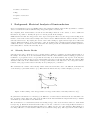
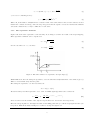
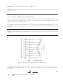
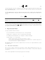
Deep-Level Transient Spectroscopy
Part 3 Labs
July 26, 2004
Contents
1 Introduction
1
2 Elementary Semiconductor Physics
2
3 Background: Electrical Analysis of Semiconductors
3
3.1 Schottky Barrier Diodes . . . . . . . . . . . . . . . . . . . . . . . . . . . . . . . . . . . . . . . . .
3
3.2 Capacitance–Voltage (C–V) Measurements . . . . . . . . . . . . . . . . . . . . . . . . . . . . . .
4
3.3 Deep Level Transient Spectroscopy (DLTS) . . . . . . . . . . . . . . . . . . . . . . . . . . . . . .
4
3.3.1
The capacitance transient . . . . . . . . . . . . . . . . . . . . . . . . . . . . . . . . . . . .
6
3.3.2
Variation in DLTS signal with temperature . . . . . . . . . . . . . . . . . . . . . . . . . .
7
4 Experimental Work
8
4.1 The racks of electronics . . . . . . . . . . . . . . . . . . . . . . . . . . . . . . . . . . . . . . . . .
8
4.2 The computer stuff . . . . . . . . . . . . . . . . . . . . . . . . . . . . . . . . . . . . . . . . . . . .
9
4.3 The cryostat and sample holder . . . . . . . . . . . . . . . . . . . . . . . . . . . . . . . . . . . . .
9
4.4 C-V measurement . . . . . . . . . . . . . . . . . . . . . . . . . . . . . . . . . . . . . . . . . . . . 10
4.5 Making a low temperature C-V measurement . . . . . . . . . . . . . . . . . . . . . . . . . . . . . 11
4.6 Analysing the C-V data . . . . . . . . . . . . . . . . . . . . . . . . . . . . . . . . . . . . . . . . . 11
4.7 DLTS measurement . . . . . . . . . . . . . . . . . . . . . . . . . . . . . . . . . . . . . . . . . . . 11
4.8 Analysing the DLTS data . . . . . . . . . . . . . . . . . . . . . . . . . . . . . . . . . . . . . . . . 13
4.9 If time permits.. . . . . . . . . . . . . . . . . . . . . . . . . . . . . . . . . . . . . . . . . . . . . . 14
1
Introduction
Semiconductor devices have revolutionised the world in which we live and have become such a part of our
everyday lives that we often take it for granted that they can and will perform the task that they were designed
for. However, due to their high quality the single crystal semiconductors wafers used are in fact extremely
sensitive to defects created arising from contamination from impurities and bombardment from high energy
ions.
In this experiment you will examine how the static and transient capacitance of a metal-semiconductor diode
(Schottky diode) varies with applied bias, temperature and time using Capacitance-Voltage (C-V) measurements
1
and Deep-Level Transient Spectroscopy (DLTS). These techniques are routinely used for wafer characterisation
by the semiconductor industry. DLTS is one of the most sensitive techniques available with the ability to
measure defect concentrations down to 1 defect per 1010 silicon atoms. (Wow!)
Analysing semiconductors (eg. Silicon wafers) using Deep Level Transient Spectroscopy (DLTS) reveals vital
information about the nature and effect of defects present in the semiconductor. DLTS is one of the few
techniques that probes the traps in the band-gap introduced by ion implantation of dopants.
The experiment involves analysing a Silicon wafer which has been irradiated or implanted with a low dose
of ions, and characterising the resulting defects. The sample is cooled with liquid nitrogen, a metal contact
is deposited to form a Schottky diode, and the capacitance measured under a variety of voltage pulses and
temperatures. Students will have the opportunity to gain a deeper understanding of semiconductor diodes
and the band-structure description of semiconductors. From the analysis of the results you will be able to
determine the nature and extent of radiation damage that the silicon chip has been exposed to. In understanding
the techniques applied you will gain a deeper understanding of semiconductor diodes and the band-structure
description of semiconductors.
2
Elementary Semiconductor Physics
The sections that follow assume a working knowledge of elementary semiconductor physics, in particular band
diagrams and doping. Some of you will be comfortable with these concepts because you have met them in
other courses, but others may me meeting them for the first time. A good introduction is given in Streetman, a
photocopy of which can be found in the lab. Also feel free to ask your demonstrators any questions, no matter
how dumb they sound (either the questions or the demonstrators :-).
Here is a list of jargon words, the meaning of which you need to know in order to understand the rest of the
prac notes:
• Semiconductor
• n-type
• p-type
• Work Function
• Fermi Level
• Capacitance
• Effective mass
• Diode
• Rectify
• Energy Band (Conduction band, valence band)
• Band gap
• Band Bending
• Dopant
• Depletion region
• Energy Level
• Deep level
• Majority carrier
• Minority carrier
2
• Carrier concentration
• Trap
• Capture cross-section
• Defect
3
Background: Electrical Analysis of Semiconductors
Deep level transient spectroscopy (DLTS) will be the principal technique used in this experiment to evaluate
defect concentration levels as well their trap energy and capture cross-sections.
By comparing these characteristics, as well as the annealing behaviour of the defects, to those outlined in
literature it is possible to identify the species of defects present in the samples.
DLTS uses the fact that the energy levels of the deep level traps are affected by the energy band bending at the
interface between the semiconductor sample and a metal contact. This metal-semiconductor interface forms a
Schottky barrier diode. By varying the extent of the band bending by applied biases traps can be filled and
emptied. This has an affect on the capacitance of the diode which can be measured and the signal analysed to
evaluate the defect concentration and to characterise the defects present. To understand how this is possible it
is necessary first to describe the Schottky diode.
3.1
Schottky Barrier Diodes
Schottky diodes can be fabricated on doped semiconductor surfaces to facilitate electrical characterisation of
the sample. A Schottky diode is a metal-semiconductor interface that exhibits current rectifying properties. It
is similar to a p-n junction diode, except that the Schottky diode characteristics only depend on the majority
carrier electrons [4], whereas the p-n diode characteristics depend on both majority and minority carriers. This
discussion will focus on the characteristics of a n-type semiconductor Schottky diode. You can get the characteristics of the p-type semiconductor Schottky diode by simple (err..) extension.
The rectification is a result of the Schottky barrier formed at the interface due to the different work functions
of the metal (φm ) and semiconductor (φs ). This barrier is characterised by a barrier height (φb ), see fig. 1.
Figure 1: The bending of the energy bands for a n-type semiconductor Schottky barrier diode [6].
In general the work function of a metal (φm ) is different to a semiconductor and when the two materials come
into electrical contact with each other electrons will from the material with the larger Fermi level (or smaller
work function) to that with a lower Fermi level.
The work function of a material describes the binding energy of the electrons and is related to their Fermi
level (see fig. 1). When the metal and semiconductor come into contact it becomes energetically favourable for
electrons in the material with the higher Fermi level to diffuse across to the other material. This builds up a
net charge difference over the interface which creates a built-in voltage (Vbi ). The region in the semiconductor
3
which will now have a net charge is the depletion region and characterised by a width (ω). The width of the
depletion region can be varied by an applied field (V) and is temperature (T) dependent.
Due to the band bending there is a region in the semiconductor that has been emptied of charge carriers and
has a net charge. This is the depletion region characterised by a width ω as seen in figure 1. The depletion
region width is given by:
ω=
s
kb T
2
(Vbi − (
)−V)
qn
q
(1)
Where:
is the dielectric constant of the semiconductor
n the free electron concentration in the semiconductor
Vbi is the built–in voltage
and V the externally applied bias, as shown in figure 1.
The capacitance of the Schottky diode can be determined by considering the depletion region as a dielectric
of width (ω) separating the metal contact of area (A) parallel to the edge of the depletion region in the
semiconductor:
C=
A
ω
(2)
Substituting equation 1 into 2 we have:
C =A
s
qn
2(Vbi − ( kbqT ) − V )
(3)
Armed with this expression, we can measure many properties of the semiconductor by slapping a metal layer on
top of the sample (thus forming a Schottky diode) and measuring how the capacitance varies with the applied
bias. This is the nub of the DLTS measurement.
3.2
Capacitance–Voltage (C–V) Measurements
By varying the applied voltage while measuring the capacitance we can determine the built–in voltage of the
diode and the concentration of free electrons in the semiconductor (which will be important for discussion of
the DLTS results later on).
Exercise 3.1 Rearrange equation 3 to express
1
C2
as a function of V .
Question 3.1 How can we now calculate n and Vb i from the measured capacitance and the applied bias? Write
an expression for them. N.B. n may not be constant and may vary with depth (hence V ) through the sample.
3.3
Deep Level Transient Spectroscopy (DLTS)
DLTS uses a changing bias to fill and empty charge traps to examine the traps over a given depth in the
semiconductor. Figure 2 shows an applied bias pulse cycle required for DLTS. Figure 3 shows the effect of
changing the bias on the trap population in the sample. Note also how the depletion region changes.
When the bias voltage is pulsed to the higher V0 value for some filling pulse time tp the traps in regions II and
III are exponentially filled with electrons from the dopants or conduction band.
4
Figure 2: Required pulse cycle for DLTS [6].
Figure 3: Deep level traps fill and empty depending on the applied bias [6].
Exercise 3.2 Write an expression for the concentration of filled traps in region II after the pulse (n T (t = 0))
in terms of tp and a capture rate tc . Assume all the traps are empty before the pulse.
The sample however spends most of it’s time under a lower bias Vb (stead-state reverse bias) (Fig. 3b) where
the traps in region II begin to empty as the band bending makes it energetically favourable for the electrons to
spill over into the conduction band of the semiconductor. We call this electron emission from the traps.
The concentration of filled traps in region II after the end of the pulse undergoes an exponential decay that
depends on the concentration of filled traps (nT (t = 0)) and the emission rate (en ).
nT (t) = nT (t = 0)e−en t
(4)
Now the capacitance is affected by the trapped charge, and the decrease in trapped charge causes an increase
in capacitance. This is shown in figure 4 and will be explained in the next section.
The emission rate en depends on temperature T , the trap energy level ET and the capture cross section of the
trap σc , viz:
5
en = en (T, ET , σc ) = γn σc T 2 e
−(
Ec −ET
kB T
)
(5)
γn is a set of constants given by:
√
3
γn = 2 3Mc (2π) 2 kb2 m∗ h−3
(6)
Where Mc is the number of minima in the conduction band of the semiconductor and m∗ is the effective electron
mass in the conduction band [1]. Since the trap energy level and the capture cross section characterise different
defects the emission rate en may be different for each defect.
3.3.1
The capacitance transient
Figure 4 shows how the capacitance of the Schottky diode changes over time as a result of the traps emptying.
This capacitance transient can be expressed as:
C = C0
r
nT (t)
n
(7)
nT (t)
)
2n
(8)
1−
For the case where nT << n we have:
C ≈ C0 (1 −
Figure 4: The time variation of capacitance as traps empty [6].
With DLTS we monitor the change in capacitance over some time interval (measurement or rate window) (t 1 , t2 ).
Where t1 is the initial delay after the pulse.
The change in capacitance over the rate window is:
δC = C(t1 ) − C(t2 )
(9)
We divide this by the final capacitance C0 to form our DLTS signal (S) which can be written as:
S=
−en (T )t2
ω 2 nT −en (T )t1
δC
= [1 − 02 ]
[e
−e
]
C0
ωb 2n
(10)
where ω0 and ωb are the widths of the depletion region under zero and reverse bias respectively.
The bias voltage is pulsed to the higher V0 value for the filling pulse time tp to fill the traps again and the cycle
is repeated. This allows many readings to be taken to average the signal over.
6
Exercise 3.3 Prove the above equation (Eq. 10). [Hard (?)]
Exercise 3.4 Write an expression for the concentration of filled traps at the end of the measurement window
in terms of t1 and t2 .
3.3.2
Variation in DLTS signal with temperature
Figure 5 shows how the signal changes as a function of temperature when a single trap is present. This occurs
due to the temperature dependence of the emission rate and it is the plot of the DLTS signal as a function of
temperature that forms a DLTS spectrum.
From equation 10 it is in fact the emission rate that governs what temperature the signal is largest at. Since
this depends on the trap energy (Eq. 5) it is hence possible to seperate the signals from different traps in the
band gap.
Exercise 3.5 Differentiate equation 10 with respect to T to obtain an expression for the peak signal temperature.
[Hard (?)]
Figure 5: The temperature dependence of the DLTS signal [6].
Note that in equation 10, if the trap concentration nT is zero then the signal is also zero. This is to say that
the magnitude of the DLTS signal is also proportional to the concentration of defects present, n T , and can be
expressed as:
δC
nT 1 − r
=
r
max
C0
2nD r r−1
Where r =
t2
t1 .
We can then write for the trap concentration:
7
(11)
r
δC
r r−1
nT = 2
nD
C0 max
1−r
(12)
It is also important to know the concentration of electrically active dopants in the same region that is being
probed to determine the defect concentration in that region. This is determined with the C-V measurements
and is outlined in that section.
By taking DLTS signals at various rate windows we may obtain a range of values for the peak temperature
associated with each defect. Using these values and noting that at the peak temperature the emission rate is
given by:
en (Tpeak ) =
ln( tt12 )
(13)
t2 − t 1
Exercise 3.6 Substitute the above expression (Eq. 13) into equation 5 to obtain ln( Ten2 ) in terms of
1
T.
If we now take the temperature at each of the DLTS peaks and the associated emission rate as given by equation
13 we have a method of determining the trap energy level and capture cross section of the defect. This is achieved
by producing an Arrhenius plot of ln( Ten2 ) vs. T1 . The trap energy level can then be found from the slope and
the capture cross section from the intercept.
4
Experimental Work
A rough experimental outline is as follows:
• Do C-V measurements on a n-Si Schottky diode at room temp and 79K
• Analyse data to determine free electron concentration and barrier height
• Do DLTS and C-T measurements on a ion implanted or irradiated Si sample.
• If time permits, do one of the following:
– Examine samples implanted/irradiated under different conditions
– Perform quasi-isothermal DLTS with different biases and analyse data to determine depth profile of
the defect. Involves more complicated calculations.
The equipment consists of three bunches of stuff; the racks of electronics, the computer stuff and the cryostat
and sample holder,.
4.1
The racks of electronics
The box at the top sitting on the PC is the temperature controller. This is primarily under the ‘remote’ control of the PC and software. Do not play with it, if there is an error message or other problem consult your
demonstrator.
Next comes the digital CRO for monitoring the appled bias on the sample.
8
Then there is the SULA DLTS electronics. Further information on these units can be found in the SULA DLTS
user manual.
Underneat this is a rack of BNC connectors. Computers don’t come with BNC sockets, so this rack is purely
to interface the PC with all the electronics.
The last tray at the bottom is the variac for the diaphragm pump (for adjusting the pump speed) and the
thermocouple vacuum gauge for the roughing line pressure (see section ??).
4.2
The computer stuff
The experiment is primarily controlled by a labview program, which has a nice GUI into which you can enter
the values that you would like certain parameters to assume. For example, to change the sample temperature,
just type (say) 275 into the relevant box, hit [Idle at initial temp], and the electronics will do the rest.
Your demonstrator will take you through most of what you need to do, but a few extra hints will be provided
here. For example, you need to tell the software what scale the capacitance meter is set to so that the correct
capacitance value is recorded.
You will be analysing the data using a command-line plotting/analysis software called genplot, which has some
similarities to IDL and C (for those who are into such stuff). You will be using pre-written programs (macros)
to analyse the data you have taken using Labview (using ASCII files). Your demonstrator will show you how
to do this.
4.3
The cryostat and sample holder
Figure 6: Sample schematic
The sample mounting setup is shown in figure 6. The InGa is a eutectic mixture of metals which is liquid at
room temperature. We use it because it forms an Ohmic contact with the sample (unlike the gold contact on
top, which forms a Schottky contact). The silver paint is there to hold the sample in place. The quartz is an
insulator to stop current from flowing between the probe contact and the backing plate, bypassing the sample.
Question 4.1 What property of In or Ga makes InGa a suitable Ohmic contact? What about the Ag?
The sample is electrically isolated from the chamber in order to minimise stray capacitance. For the same
reason, the coaxial cables connecting the sample to the electronics are kept as short as possible.
9
The sample needs to be cooled in order to minimise the thermally generated currents which act as noise in
the measurement. We need precise and accurate control of the temperature in order to do some of the funky
temp-dependent stuff later. For this reason the stage is fitted with a heater and two thermocouples (electric
thermometers). The cooling is provided by flowing liquid nitrogen up the spike at the bottom, through tubes
around the base of the sample holder, and out the side, through the transparent plastic tube. By this time,
the nitrogen is no longer a liquid but a gas, and so can be pumped away by a fish tank pump. This pump is
controlled by a variable voltage source (variac-this one is red and lives under the electronics). 70 V is good for
cooling down to 77K (takes about 15 mins); 20 V will keep it there.
Beware of liquid nitrogen-it is cold. It also contains to oxygen, so if you keep the doors closed and fill the room
with nitrogen, you will faint or suffocate. Don’t mess with the liquid nitrogen, and keep the doors open!
The sample is under vacuum for a couple of reasons. It keeps out water, oils and dust which may contaminate
the sample. Any water will quickly turn to ice on the sample as it is cooled, which will become liquid water
when it comes up to room temperature again.
4.4
C-V measurement
The C-V measurement will allow us to determine the barrier height, depletion width and free electron density
of the sample.
Equipment:
• Air Liquide LN2 cryostat/dewar (rotary roughing pump, N2 diaphram pump, temp controller)
• National instruments BNC-adaptor/DAC, SULA/Labview software
• SULA Pulse generator and capacitance meter units
The bias is applied to the top diode contact of sample via the output BNC connection on the [Pulse generator]
unit (Labelled as −
− ) and the capacitance is read from the back contact which is connected to the [In] of the
[Capacitance meter] unit.
1. Connect the Pulse generator output [−
− ] to the [Probe A] coax of the cryostat.
2. Connect the [Back contact] to the [In] of the [Capacitance meter]
3. The black buttons on the Capacitance meter control what is displayed on the LED. C shows the capacitance
divided by whatever [Crange] is set to (e.g. Crange is 300 pF and the reading is 0.50 then the capacitance is
150 pF). The reading should always be positive and less than about 1.3, if it isn’t contact your demonstrator
or change the Crange.
4. Ask your demonstrator to load a sample into the cryostat chamber and show you how the sample is
connected inside the chamber and how the temperature is controlled and measured inside the chamber.
5. To maintain a stable temperature for measurement the cryostat is simultaneously heated with a thermistor
inside the copper ‘cold head’ that the sample is mounted on and cooled by drawing liquid nitrogen through
a tube which is in thermal contact with the cold head. To do this you need to evacuate the chamber to
300-400 mTorr with the roughing pump to remove as much air and in particular water vapour as possible.
This will reduce thermal conduction with the lab environment and prevent water condensation on the
cold head.
6. Turn on the [Vac. Gauge] via the bottom power board
7. Open the chamber valve, close the venting valve
8. Turn on the [Roughing pump] via the power board
9. Typically the output of the pulse generator is tee’d off to the CRO so that the applied bias can be observed.
The applied DC bias can be controlled in two ways, with the [Offset] knob and via an input into the [Ext.
Bias] connection. The software will use the digital to analogue converter (DAC) in the PC to apply a DC
analogue bias to the sample via this input from [DACOUT0] of the BNC adaptor
10
10. Connect the [Ext. bias] to the [DACOUT0] BNC of the NI BNC adaptor.
11. Set [Offset] bias on the [Pulse generator] to 0
12. This completes the hardware setup and the rest of the setup is via the SULA software.
13. For starters you will perform a C-V measurement at room temperature biasing the diode from 0 V to -10
V. An interval of around 0.2 V will be needed for a nice resolution data set for analysis. To correct for
stray background capacitance from the wires and sample chamber the software needs to subtract this off
the raw capacitance reading, this has been measured for various capacitance range settings and appears
in table 1.
14. Flip the [Measurement type] to C-V
15. Set the [Initial temp] to something around room temp,
16. Set [Initial bias] to 0, [Final bias] to -10
17. The [Background capacitance] is given in table 1
18. The [Crange] should be set to be the same as the capacitance meter setting
19. The [Preamp gain] is irrelevant (I think)
Crange (pF)
100
300
1000
Background Capacitance (pF)
5.40
5.26
5.09
Table 1: Table of Stray/Background Capacitances for Cu mounting plate and AirLiquide cyrostat
4.5
Making a low temperature C-V measurement
The chamber should still be under vacuum and inserted into the dewar at this stage. If not, make it so. It is
important to ensure the chamber is at the correct low vacuum otherwise water vapour will condense onto the
sample and the cold head and contaminates them.
The chamber valve should be closed and roughing pump turned off to reduce any electrical noise and vibrations.
Set the [Initial Temp.] to 78 K now and click [Idle at Initial temp.]. The Spoint on the temp. controller
should now be at this value. Turn on the power for the N2 diaphram pump and increase the voltage to 70 V.
The sample should now be cooling and will take approximately 15 minutes to reach 78 K. If it doesn’t contact
your demonstrator. Since the pump is quite loud, you may wish to leave the room at this stage. Once you
have reached the initial temperature reduce the diaphram pump voltage to 10-20 V and make sure that the
temperature controller can maintain a stable temperature (within +/- 0.5 K). Now repeat the C-V measurement.
4.6
Analysing the C-V data
Your demonstrator will show you how to use genplot to extract the variables.
4.7
DLTS measurement
Equipment:
• Air Liquide LN2 cryostat/dewar (rotary roughing pump, N2 diaphram pump, temp controller)
• National instruments BNC-adaptor/DAC, SULA/Labview software
• SULA Pulse generator, capacitance meter, 4 correlator units
11
1. Setting up the filling pulse and correlators. The electronics can now be setup for a DLTS measurement.
The first thing to do is set the [Offset] on the [Pulse generator] to place the diode under reverse bias.
This should be set so that the depletion region is about 1.0-1.2 microns wide (between -6 and -10 V).
Monitor the voltage with the [V] setting on the [Capacitance meter]. Since the bias output of the pulse
generator should also be connected to the CRO you should also be able to observe this on the CRO. To
ensure proper operation check the leakage current by pressing the [i] setting on the [Capacitance meter].
The reading is in uA, if it is more than 10 uA reduce the reverse bias.
2. Set [Offset] on the [Pulse generator] to between -6 and -10 V as read on the [V] setting on the [Capacitance
meter]
3. Check the leakage current by pressing the [i] setting on the [Capacitance meter], reading is is uA. Reduce
bias if reading is more than 10 uA reduce the reverse bias
4. Next turn on the pulse generator with the [On/Off] toggle switch. Press the [ - ] button on the [Capacitance
meter]. The display now indicates the voltage at which the bias is pulsed to. To examine as much of the
sample as possible set the pulse [Amplitude] on the pulse generator so that it pulses to 0 V. You should
be able to now see the pulse on the CRO. If not, ensure that the CRO is set to the DC mode and external
trigger. If the trigger is set to normal you may need to adjust the trigger level.
5. Set [Amplitude] on the [Pulse generator] to 0 V as read on the [ - ] setting on the [Capacitance meter]
6. The pulse [Width] needs to be set to fill as many traps as possible. The pulse width affects how many
of the defects will be filled during the pulse since they have a characteristic capture cross-section (and
hence capture rate). For the defects in ion implanted silicon this needs to be between 10 and 100 ms. The
electronics does not monitor this and the CRO needs to be used. Although a larger pulse fills more defects
it also means that it will take longer for the electronics to recover after a pulse. The filling of defects
also does not scale linearly with pulse width but has an inverse exponential behaviour so it is often not
necessary to use a long pulse.
7. Set pulse [Width] and the range knob below it to between 10 and 100 ms as read seen in the applied bias
on the CRO.
8. The [Initial delay] (t1) of the correlators need to be set to examine the capacitance transient over the
correct rate windows. There are four correlators so we can simultaneously look at four different rate
windows. For ion implanted silicon we need values of t1 < 5 ms. Correlator 1 should have the largest
initial delay with the next correlator having consecutively smaller initial delays. The [Y] outputs of the
correlators should now also be connected to the corresponding channels of the NI BNC-adaptor (Channels
1, 2, 3, 4).
9. Set [Initial delay] for each correlator to be less than 2 ms, where Correlator 1 having the largest value and
each consecutive correlator having consecutively smaller values.
10. Ensure the [Y] outputs of the correlators are connected to the corresponding channels of the NI BNCadaptor (Ch1, 2, 3, 4).
11. The pulse generator is now setup for DLTS and the rest of the measurement electronics can be set up.
12. The [Pre-amp] output on correlator 1 unit should be connected to the CRO to monitor the capacitance
signal of the diode that is fed into the correlators for measurement. Increase the [Pre-amp gain] on the
correlator to as large as possible without producing a noisy signal. The pre-amp output should now be
connected to the [Input] of the auxiliary correlators (3 and 4).
13. Connect the [Pre-amp] output on correlator 1 to the CRO
14. Increase the [Pre-amp gain] on the correlator to as large as possible without producing a noisy signal.
15. Connect the [Pre-amp] output to the [Input] of the auxiliary correlators (3 and 4).
16. The [TC] value of the correlators affects how fast the internal capacitors discharge and hence how fast
consecutive measurements can be made. TC contributes to the total time constant TC tot which should
be as close as possible for each correlator. TCtot depends on many factors and is given by:
• For correlators 1 and 2 TCtot = TC if
[P eriod]
[InitialDelay]
12
< 50
• For correlators 3 and 4 TCtot = (TC + 0.5 ∗ TCapp )ifTC > TCapp
= (0.5 ∗ TC + TCapp )ifTC < TCapp
[Period]
and TCint is specified in the SULA User manual (for Initial Delay 0.5
Where TCapp = TCint ∗ [InitialDelay]
and 1 ms TCint = 10e-3 s)
17. Set [TC] so that T Ctot is as close as possible for each correlator according to the conditions shown in table
2.
Correlator 1 or 2
Period (ms)
200
200
200
100
100
100
100
50
50
50
Correlator 3 or 4
Period (ms)
200
200
200
100
100
100
100
50
50
50
50
Initial Delay (ms)
5
2
1
5
2
1
0.5
2
1
0.5
T Cint
0.06
0.06
0.06
0.06
0.06
0.06
0.06
0.06
0.06
0.06
T Capp
2.4
6.0
12.0
1.2
3.0
6.0
12.0
1.5
3.0
6.0
Initial Delay (ms)
5
2
1
5
2
1
0.5
5
2
1
0.5
T Cint
0.01
0.01
0.01
0.01
0.01
0.01
0.01
0.01
0.01
0.01
0.01
T Capp
0.4
1.0
2.0
0.2
0.5
1.0
2.0
0.1
0.3
0.5
1.0
T Ctot
TC=1
3
7
13
2
4
7
13
2
4
7
T Ctot
TC=1
1
2
3
1
1
2
3
1
1
1
2
TC=3
4
8
14
4
5
8
14
4
5
8
TC=10
11.2
13
16
10.6
11.5
13
17
10.8
11.5
13
TC=3
3
4
4
3
3
4
4
3
3
3
4
TC=10
10
10.5
11.0
10
10
10.5
11.0
10
10
10
10.5
Table 2: TC settings for Correlators on the SULA DLTS
18. The hardware is now setup and the rest of the experiment is controlled by the software. Change the front
panel [Experiment] to [DLTS] and enter all the hardware settings into the window. The [Initial Temp.]
should be set to 78 K and the [Final Temp.] to room temperature. The stray capacitance is irrelevant and
the [Offset] should be set to [measure at start]. The offset measurement is important because it removes
any offsets from the correlator readings so that if there are no defects (hence no change in capacitance)
the signal will be zero.
19. Change [Experiment] to [DLTS] on SULA software front panel
20. Enter all the hardware settings into the window.
21. Set The [Initial Temp.] should be set to 78 K and the [Final Temp.] to room temperature.
Offset should be set to [measure at start].
22. Once you have completed this you can click [Run experiment] and the scan will take approximately 1-2
hours to complete.
4.8
Analysing the DLTS data
Again, see your demonstrator
13
4.9
If time permits..
...it won’t. :-)
References
[1] P. Blood and J. W. Orton, The Electrical Characterization of Semiconductors: Majority Carriers and
Electron States, Academic Press, 1992, Page 344.
[2] Streetman, solid state electronic devices, ,1991
[3] E. H. Rhoderick, Metal-Semiconductor Contacts, Oxford University Press, 1978 (1st Ed.), Page 21.
[4] E. H. Rhoderick, Metal-Semiconductor Contacts, Oxford University Press, 1978 (1st Ed.), Page 10.
[5] E. H. Rhoderick and R. H. Williams, Metal-Semiconductor Contacts, Oxford University Press, 1998 (2nd
Ed.), Page 168.
[6] Dieter K. Schroder, Semiconductor Material and Device Characterization, Wiley Inter–Science.
Acknowledgements
These notes were written by Matthew Lay in 2004, and tweaked by David Hoxley in the same year.
14