1
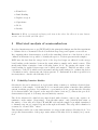
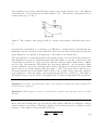
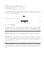
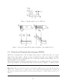
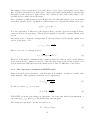
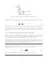
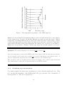
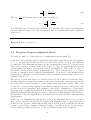
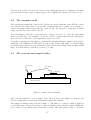
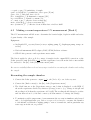
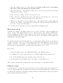
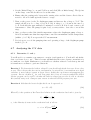
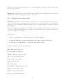
Deep-Level Transient Spectroscopy
Part 3 Laboratories
May 3, 2005
1
Contents
1 Introduction
4
2 Some words about third year labs
4
3 Safe handling of liquid nitrogen
5
3.1
General safety information . . . . . . . . . . . . . . . . . . . . . . . . . . . . . .
5
3.2
Location . . . . . . . . . . . . . . . . . . . . . . . . . . . . . . . . . . . . . . . .
5
3.3
Ventilation . . . . . . . . . . . . . . . . . . . . . . . . . . . . . . . . . . . . . . .
5
3.4
Personal protective equipment . . . . . . . . . . . . . . . . . . . . . . . . . . . .
5
4 Elementary Semiconductor Physics
6
5 Electrical analysis of semiconductors
7
5.1
Schottky barrier diodes . . . . . . . . . . . . . . . . . . . . . . . . . . . . . . . .
7
5.2
C–V Analysis . . . . . . . . . . . . . . . . . . . . . . . . . . . . . . . . . . . . .
9
5.3
Deep Level Transient Spectroscopy (DLTS) . . . . . . . . . . . . . . . . . . . . . 10
5.4
5.3.1
The capacitance transient and DLTS signal . . . . . . . . . . . . . . . . . 11
5.3.2
Calculating trap energy levels and capture cross-sections . . . . . . . . . 12
5.3.3
Calculating trap concentrations . . . . . . . . . . . . . . . . . . . . . . . 13
Deep-level traps in implanted silicon . . . . . . . . . . . . . . . . . . . . . . . . 14
6 Experimental Work
16
6.1
The racks of electronics . . . . . . . . . . . . . . . . . . . . . . . . . . . . . . . . 16
6.2
The computer stuff . . . . . . . . . . . . . . . . . . . . . . . . . . . . . . . . . . 17
6.3
The cryostat and sample holder . . . . . . . . . . . . . . . . . . . . . . . . . . . 17
6.4
Important constants . . . . . . . . . . . . . . . . . . . . . . . . . . . . . . . . . 18
6.5
Making a room temperature C-V measurement [Week 1] . . . . . . . . . . . . . 19
6.6
Making a low temperature C-V measurement . . . . . . . . . . . . . . . . . . . . 21
6.7
Analysing the C-V data . . . . . . . . . . . . . . . . . . . . . . . . . . . . . . . 22
6.8
6.7.1
Determine Vbi and φb . . . . . . . . . . . . . . . . . . . . . . . . . . . . . 22
6.7.2
Determine the doping profile . . . . . . . . . . . . . . . . . . . . . . . . . 23
DLTS measurement [Week 2] . . . . . . . . . . . . . . . . . . . . . . . . . . . . . 24
2
6.9
Perfoming a C-T measurement . . . . . . . . . . . . . . . . . . . . . . . . . . . . 26
6.10 Analysing the DLTS data . . . . . . . . . . . . . . . . . . . . . . . . . . . . . . 27
6.10.1 Calculate the defect concentrations . . . . . . . . . . . . . . . . . . . . . 27
6.10.2 Characterise the defects observed . . . . . . . . . . . . . . . . . . . . . . 27
6.11 If time permits.. . . . . . . . . . . . . . . . . . . . . . . . . . . . . . . . . . . . . 27
3
1
Introduction
Semiconductor devices have revolutionised the world in which we live and have become such a
part of our everyday lives that we often take it for granted that they can and will perform the
task that they were designed for. However, due to their high quality the single crystal semiconductors wafers used are in fact extremely sensitive to defects created arising from contamination
from impurities and bombardment from high energy ions.
In this experiment you will examine how the static and transient capacitance of a metalsemiconductor diode (Schottky diode) varies with applied bias, temperature and time using
Capacitance-Voltage (C-V) measurements and Deep-Level Transient Spectroscopy (DLTS).
These techniques are routinely used for wafer characterisation by the semiconductor industry. DLTS is one of the most sensitive techniques available with the ability to measure defect
concentrations down to 1 defect per 1010 silicon atoms. (Wow!)
Analysing semiconductors (eg. Silicon wafers) using Deep Level Transient Spectroscopy (DLTS)
reveals vital information about the nature and effect of defects present in the semiconductor.
DLTS is one of the few techniques that probes the traps in the band-gap introduced by ion
implantation of dopants.
The experiment involves analysing a Silicon wafer which has been irradiated or implanted with
a low dose of ions, and characterising the resulting defects. The sample is cooled with liquid
nitrogen, a metal contact is deposited to form a Schottky diode, and the capacitance measured
under a variety of voltage pulses and temperatures. Students will have the opportunity to
gain a deeper understanding of semiconductor diodes and the band-structure description of
semiconductors. From the analysis of the results you will be able to determine the nature
and extent of radiation damage that the silicon chip has been exposed to. In understanding
the techniques applied you will gain a deeper understanding of semiconductor diodes and the
band-structure description of semiconductors.
2
Some words about third year labs
These notes don’t contain all the information you need - they’re here to define the terms for
you, and to give you an idea of the direction you should be taking. You’ll find that you need
to go foraging for more detailed information in other places - often in the references, and even
more often in the rubble of your demonstrators’ minds. You’re going to learn a lot while you’re
doing that, so don’t waste the effort - share all the work you’re doing with us in your report!
Remember that your report has to be self-contained. It doesn’t have to be beautiful, but it
should be clear and detailed. Perhaps the most important thing to remember is that when you
write your report you’re trying to teach your reader what you did, why you did it, and what
you learned. That way, we get to learn something too! Enjoy!
By the way, these notes have recenlty undergone a major revision, and may be littered with typos (and possibly more serious errors). We in part3 would love it if you could bring any mistakes
to the attention of your demonstrators, or email suggestions to [email protected]
4
3
3.1
Safe handling of liquid nitrogen
General safety information
Liquid nitrogen has two main hazards associated with it: frostbite and asphyxiation. These are
related to its low boiling point (-196 ◦ C, 77 K) and its large gas to liquid volume ratio (682, at
1 atm and 15◦ C).
Frostbite The eyes are particularly at risk from frostbite (cold burns) due to their moisture
content [?]. Liquid nitrogen rapidly boils when it comes in contact with an object at
room temperature and will splatter or spit. There is a risk of frostbite not only from
direct contact but also from indirect contact with a surface that has been cooled by liquid
nitrogen. Objects less than about -20◦ C will cause cold burns and if there is sufficient
moisture on your skin you may become frozen to the object.
Asphyxiation When liquid nitrogen evaporates it displaces air and reduces the oxygen concentration in the air. Symptoms of asphyxia can be sudden in the case of a deep inhalation
of air with a low oxygen content or gradual asphyxia where the symptoms are more subtle.
For further information please consult the MSDS (Material Safety Data Sheets) for liquid
nitrogen in the safety folder.
3.2
Location
The dewar must be placed on level surface at all times except during transport [?], preferably
the ground.
3.3
Ventilation
The room in which the dewar is stored and experiments are carried out must be kept well
ventilated with all doors open while people are inside. This is to ensure that the oxygen
content of the room does not drop below 18% due to ANY spill [?] including the worst case
scenario where the entire contents of the dewar evaporates.
3.4
Personal protective equipment
The following safety equipment is required when there is exposed liquid nitrogen present (e.g.
when the cap or cryostat is not inserted into the dewar, during refilling):
Gloves Appropriate gloves should be worn when handling the dewar.
Face and eye protection A full face shield conforming to AS 1337 must be worn.
Clothing Loose dry clothing that completely covers the arms and legs must be worn. Trouser
legs preferably should not have cuffs that may trap liquid nitrogen.
5
Footwear Shoes that completely cover the feet must be worn.
Other References: EHS Manual, Risk Management Office, University of Melbourne; Safe Work
Procedure- Liquid nitrogen, School of Botany
Matthew D. H. Lay, July 2004.
4
Elementary Semiconductor Physics
The sections that follow assume a working knowledge of elementary semiconductor physics, in
particular band diagrams and doping. Some of you will be comfortable with these concepts
because you have met them in other courses, but others may me meeting them for the first
time. A good introduction is given in Streetman, a photocopy of which can be found in the
lab. Also feel free to ask your demonstrators any questions, no matter how dumb they sound
(either the questions or the demonstrators :-).
Here is a list of jargon words, the meaning of which you need to know in order to understand
the rest of the notes.
• Semiconductor
• Energy Band (conduction band, valence band)
• Band gap
• Energy Level
• Dopant
• n-type
• p-type
• Majority carrier
• Effective mass
• Deep level trap
• Defect
• Capture cross-section
• Carrier concentration
• Active dopant concentration
• Work Function
6
• Fermi Level
• Band Bending
• Depletion region
• Capacitance
• Diode
• Rectify
Exercise 1 Write a paragraph explaining each item in the above list. Show it to your demonstrator, and check that you both agree!
5
Electrical analysis of semiconductors
Deep level transient spectroscopy (DLTS) will be the principal technique used in this experiment
to evaluate defect concentration levels as well their trap energy and capture cross-sections.
By comparing these characteristics, as well as the annealing behaviour of the defects, to those
outlined in literature it is possible to identify the species of defects present in the samples.
DLTS uses the fact that the energy levels of the deep level traps are affected by the energy
band bending at the interface between the semiconductor sample and a metal contact. This
metal-semiconductor interface forms a Schottky barrier diode. By varying the extent of the
band bending by applied biases traps can be filled and emptied. This has an affect on the
capacitance of the diode which can be measured and the signal analysed to evaluate the defect
concentration and to characterise the defects present. To understand how this is possible it is
necessary first to describe the Schottky diode.
5.1
Schottky barrier diodes
Schottky diodes can be fabricated on doped semiconductor surfaces to facilitate electrical characterisation of the sample. A Schottky diode is a metal-semiconductor interface that exhibits
current rectifying properties. It is similar to a p-n junction diode, except that the Schottky
diode characteristics only depend on the majority carrier electrons [?], whereas the p-n diode
characteristics depend on both majority and minority carriers.
The diodes fabricated for this lab were first cleaned with solvents to remove any organic contaminates on the surface (‘degreasing’). Next the thin ‘native’ oxide (10-20Å) that exists on
the surface of bare silicon is etched off with HF acid and the sample is promptly transferred
to thermal evaporator for metal deposition through an Al mask. The evaporation chamber is
evacuated to around 5X10⁻⁶ mbar.
This discussion will focus on the characteristics of a n-type semiconductor Schottky diode. You
can get the characteristics of the p-type semiconductor Schottky diode by simple (err..) extension.
7
The rectification is a result of the Schottky barrier formed at the interface due to the different
work functions of the metal (φm ) and semiconductor (φs ). This barrier is characterised by a
barrier height (φb ), see fig. 1.
Figure 1: The bending of the energy bands for a n-type semiconductor Schottky barrier diode
[?].
In general the work function of a metal (φm ) is different to a semiconductor and when the two
materials come into electrical contact with each other electrons will from the material with the
larger Fermi level (or smaller work function) to that with a lower Fermi level.
The work function of a material describes the binding energy of the electrons and is related to
their Fermi level (see fig. 1). When the metal and semiconductor come into contact it becomes
energetically favourable for electrons in the material with the higher Fermi level to diffuse
across to the other material. This builds up a net charge difference over the interface which
creates a built-in voltage (Vbi ). In n-type silicon if the work function of the metal is larger than
that for silicon we get the situation shown in figure 1. The electrons in silicon drift across to
the metal and the region left behind will now have a net positive charge and is the depletion
region (depleted of majority charge carriers) and characterised by a width (ω). The width of
the depletion region can be varied by an applied field (V) and is temperature (T) dependent.
Question 1 In terms of current flow, what is the difference between the built-in voltage V bi
and the barrier height φb ?
Question 2 What happens if we put a metal with a smaller work function on top of n-type
silicon?
Due to the band bending there is a region in the semiconductor that has been emptied of charge
carriers and has a net charge. This is the depletion region characterised by a width ω as seen
in figure 1. The depletion region width is given by:
ω=
s
2
kb T
(Vbi − (
)−V)
qn
q
8
(1)
Where:
is the dielectric constant of the semiconductor
n the active dopant concentration in the semiconductor
Vbi is the built–in voltage
and V the externally applied bias, as shown in figure 1.
The capacitance of the Schottky diode can be determined by considering the depletion region
as a dielectric of width (ω) separating the metal contact of area (A) parallel to the edge of the
depletion region in the semiconductor:
C=
A
ω
(2)
Substituting equation 1 into 2 we have:
C=
5.2
v
u
u
At
qn
2(Vbi − ( kbqT ) − V )
(3)
C–V Analysis
Armed with equation 3, we can measure many properties of the semiconductor by slapping
a metal layer on top of the sample (thus forming a Schottky diode) and measuring how the
capacitance varies with the applied bias. This is the nub of the C–V and DLTS measurements.
Question 3 From Equation 3 how can we calculate n and Vbi from measured capacitances and
applied biases? Check your answer with your demonstrator as you will need to use this later.
Question 4 The calculated value for n at a given bias V can be shown to be equal to the
uncompensated donor concentration at the edge of the depletion region corresponding the applied
bias V [?]. From your answer to question 3 how is it possible to calculate the uncompensated
donor concentration n as a function of depth? Check your answer with your demonstrator as
you will need to use this later.
Note that although the ‘native’ oxide on the surface silicon is etched off some of it may grow
back when the samples are being transferred (in air) into the metal deposition chamber. Electrons readily tunnel through this thin oxide layer but there is a small contribution to the barrier
height.
9
Figure 2: Required pulse cycle for DLTS [?].
Figure 3: Deep level traps fill and empty depending on the applied bias [?].
5.3
Deep Level Transient Spectroscopy (DLTS)
DLTS uses a changing bias to fill and empty charge traps to examine the traps over a given
depth in the semiconductor. Figure 2 shows an applied bias pulse cycle required for DLTS.
Figure 3 shows the effect of changing the bias on the trap population in the sample. Note also
how the depletion region changes.
When the bias voltage is pulsed to the higher V0 value for some filling pulse time tp the traps in
regions II and III are exponentially filled with electrons from the dopants or conduction band.
Exercise 2 Write an expression for the concentration of filled traps in region II after the pulse
(nT (t = 0)) in terms of tp , a capture rate rc and a total trap concentration NT . Assume all
the traps are empty before the pulse and don’t forget that there is a finite number of traps to be
filled (!).
10
The sample however spends most of it’s time under a lower bias Vb (stead-state reverse bias)
(Fig. 3b) where the traps in region II begin to empty as the band bending makes it energetically
favourable for the electrons to spill over into the conduction band of the semiconductor. We
call this electron emission from the traps.
The concentration of filled traps in region II after the end of the pulse undergoes an exponential
decay that depends on the concentration of filled traps (nT (t = 0)) and the emission rate (en ).
nT (t) = nT (t = 0)e−en t
(4)
Now the capacitance is affected by the trapped charge, and the decrease in trapped charge
causes an increase in capacitance. This is shown in figure 4 and will be explained in the next
section.
The emission rate en depends on temperature T , the trap energy level ET and the capture cross
section of the trap σc , viz:
e n = γ n σc T 2 e
−(
Ec −ET
kB T
)
(5)
Where γn is a set of constants given by:
√
3
γn = 2 3Mc (2π) 2 kb2 m∗ h−3
(6)
Where Mc is the number of minima in the conduction band (6 for silicon) and m∗ is the effective
electron mass in the conduction band [?]. Since the trap energy level and the capture cross
section characterise different defects the emission rate en may be different for each defect.
5.3.1
The capacitance transient and DLTS signal
Figure 4 shows how the capacitance of the Schottky diode changes over time as a result of the
traps emptying. This capacitance transient can be expressed as:
s
nT (t)
n
(7)
nT (t)
)
2n
(8)
C = C0 1 −
For the case where nT << n we have:
C ≈ C0 (1 −
With DLTS we monitor the change in capacitance over some time interval (measurement or
rate window) (t1 , t2 ). Where t1 is the initial delay after the pulse.
The change in capacitance over the rate window is:
δC = C(t1 ) − C(t2 )
11
(9)
Figure 4: The time variation of capacitance as traps empty [?].
We divide this by the final capacitance C0 to form our DLTS signal (S) which can be written
as:
S=
nT
δC
−en (T )t2
−en (T )t1
= [ ] [e
−e
]
C0
2n
(10)
where ω0 and ωb are the widths of the depletion region under zero and reverse bias respectively.
The bias voltage is pulsed to the higher V0 value for the filling pulse time tp to fill the traps
again and the cycle is repeated. This allows many readings to be taken to average the signal
over.
5.3.2
Calculating trap energy levels and capture cross-sections
Figure 5 shows how the signal changes as a function of temperature when a single trap is
present. This occurs due to the temperature dependence of the emission rate and it is the plot
of the DLTS signal as a function of temperature that forms a DLTS spectrum.
From equation 10 it is in fact the emission rate that governs what temperature the signal reaches
its peak value. Since this depends on the trap energy (Eq. 5) traps with different energy levels
in the band gap will produce a peak at different temperatures.
Exercise 3 Differentiate Equation 10 with respect to T and show that the emission rate at the
temperature that the dlts signal is greatest is given by the following equation:
en (Tpeak ) =
ln( tt21 )
t2 − t 1
N.B. You will NOT NEED to explicitly differentiate en , just carry it through.
12
(11)
Figure 5: The temperature dependence of the DLTS signal [?].
Equation 11 shows that the measurement times t1 and t2 set what is known as a rate window
for the emission rate. It can be shown that different rate windows cause the peak to shift in
temperature. By taking DLTS spectra at various rate windows we may obtain a range of values
for the peak temperature associated with each emission rate and hence each defect. Using these
values and noting that at the peak temperature the emission rate is given by your answer to
Equation 11 it is possible to calculate both the trap energy level and the capture cross-section.
Question 5 Re-arrange Equation 5 to obtain ln( Ten2 ) in terms of
1
.
T
Since the temperature at which the DLTS signal peaks changes with the emission rate window
we can generate a plot of the above equation for various temperatures and emission rates. A
plot of a temperature dependant rate against T1 is known as an Arhhenius plot.
How can this be used to calculate the trap energy and capture cross section? Again check with
your demonstrator as this will be important later in the DLTS analysis.
5.3.3
Calculating trap concentrations
Note that in equation 10, if the trap concentration nT is zero then the signal is also zero. This
is to say that the magnitude of the DLTS signal is also proportional to the concentration of
defects present, nT , and can be expressed as:
13
nT 1 − r
δC
=
r
max
C0
2n r r−1
Where r =
t2
.
t1
(12)
We can then write for the trap concentration:
r
r r−1
δC
n
nT = 2
C0 max 1 − r
(13)
Note that the trap concentration is dependant on electrically active dopant concentration in
the region that is being probed. This is determined with C-V measurements and is outlined in
that section.
Exercise 4 Derive equation 12.
5.4
Deep-level traps in implanted silicon
(You will also find a good introduction to ion implantation in Streetman [?].)
It has been well established that ion implantation introduces many defects into the substrate
[?, ?, ?]. In particular Frenkel defects are created which consist of a host atom that has
been knocked off its substitutional lattice site into an interstitial position (i.e. between crystal
lattice sites) leaving a vacancy behind in the lattice [?]. At room temperature the vacancy
and interstitial can migrate and separate without recombination. This occurs for 4-10% of
the Frenkel defects created during ion implantation [?]. These defects can go on to cluster
together or form stable defect complexes with impurities. About 10-25% of the Frenkel defects
that survive recombination form a di-vacancy cluster [?] which is a characteristic defect for ion
implanted silicon [?, ?].
The defects of prime importance for electrical devices are those that are electrically active,
meaning that they can trap charge carriers in the device. Electrically active traps are basically
unoccupied states in the band-gap of a semiconductor that trap charge carriers. This occurs
mostly due to defects having dangling bonds which are unpaired electrons, and the traps exist
at some energy level depending on the structure of the defect. Identification of defect structures and atomic constituents is achieved most reliably with Electron Para-magnetic Resonance
(EPR) measurements although not every defect complex has an EPR signature. The identity of
defects which do not show up in EPR are often inferred from detailed analysis of their annealing
characteristics.
In the case of ion-implanted phosphorus doped silicon the interstitial silicon does not form a
trap, but the vacancies can migrate and combine with impurities such as oxygen and carbon
(found in even top grade commercially available silicon wafers) as well as with the phosphorus
dopant to form vacancy complexes. Chemical cleaning of the silicon can also lead to incorporation of hydrogen which is believed to be the constituent of many defect complexes.
14
Defects can be characterised by their position in the band-gap of a semiconductor relative to the
conduction band (trap energy, Et ), and their cross-section for trapping (capture cross-section,
σ). The values reported for electron traps in ion-implanted silicon are found in table 1. This
table shows the average value for the trap energies found in the literature. Absolute errors in
the last digit are shown in parentheses, no error is quoted for occasions where there is only one
reference for the defect, nor is the error quoted for capture cross-sections that have an error that
is over an order of magnitude difference. V indicates vacancy, other letters indicate elements,
subscripts 2 & 3 indicate the number of vacancies in a cluster and superscripts indicate the
charge state of the trap. Other subscripts indicate either substitutional or interstitial atomic
positions in the lattice.
Defect type
H–related
H–related
HC
VO
Cs Ci
V–related
V2−
2
V2 O
V3 O
VO-H, other H–related
V–related
H–related
H–related
VPs
V−
2
H–related
V2 –related
H–related
Unknown
Trap Energy
[ev]
0.10
0.13
0.15(1)
0.17(1)
0.17(0)
0.19(1)
0.22(1)
0.27
0.30
0.30(2)
0.35(1)
0.39(1)
0.41(1)
0.42(2)
0.42(1)
0.45(1)
0.47
0.50(1)
0.59
Capture cross–section
[cm2 ]
–
–
–
7(4)x10−15
8x10⁻¹⁸
3.5x10⁻¹⁷
5(4)x10−16
–
–
3x10⁻¹⁵
5x10⁻¹⁶
1x10⁻¹⁷
–
5(3)x−15
5(3)x−15
1x10⁻¹⁷
–
–
–
Table 1: Defect characteristics as published in the literature for defects relevant to ion-implanted
n-type silicon.
15
6
Experimental Work
The SULA DLTS system and its associated electronics is a joint MARC group
Part 3 laboratory apparatus and is thus also used for research. The research
of the MARC group (and perhaps even one of your demonstrators) depends on
the correct functionality of the equipment so it is especially important to treat
it with respect.
A rough experimental outline is as follows:
Week 1
• Do C-V measurements on a n-Si Schottky diode at room temp and 79K
• Analyse data to determine active dopant concentration and barrier height
Week 2
• Do DLTS and C-T measurements on a ion implanted or irradiated Si sample.
• If time permits, do one of the following:
– Examine samples implanted/irradiated under different conditions
– Perform quasi-isothermal DLTS with different biases and analyse data to determine
depth profile of the defect. Involves more complicated calculations.
The equipment consists of three bunches of stuff; the racks of electronics, the computer stuff
and the cryostat. Most of the components aren’t cheap off the shelf items so treat them with
respect.
6.1
The racks of electronics
The box at the top sitting on the PC is the temperature controller. This is primarily under
the ‘remote’ control of the PC and software. Do not play with it, if there is an error message
or other problem consult your demonstrator.
Next comes the digital CRO for monitoring the applied bias on the sample.
Then there is the SULA DLTS electronics. Further information on these units can be found in
the SULA DLTS user manual.
Underneath this is a rack of BNC connectors. Computers don’t come with BNC sockets, so
this rack is purely to interface the PC with all the electronics.
16
The last tray at the bottom is the variac for the diaphragm pump (for adjusting the pump
speed) and the thermocouple vacuum gauge for the roughing line pressure (see section 6.3).
6.2
The computer stuff
The experiment is primarily controlled by a labview program, which has a nice GUI into which
you can enter the values that you would like certain parameters to assume. For example, to
change the sample temperature, just type (say) 275 into the relevant box, hit [Idle at initial
temp], and the electronics will do the rest.
Your demonstrator will take you through most of what you need to do, but a few extra hints
will be provided here. For example, you need to tell the software what scale the capacitance
meter is set to so that the correct capacitance value is recorded.
You will be analysing the data using a command-line plotting/analysis software called genplot,
which has some similarities to IDL and C (for those who are into such stuff). You will be using
pre-written programs (macros) to analyse the data you have taken using Labview (using ASCII
files). Your demonstrator will show you how to do this.
6.3
The cryostat and sample holder
probe contact
Wire Bond
Au contact
ssteel
Quartz
n−Si
Ag paint
InGa eutectic
Ag paint
Stainless steel base
Figure 6: Sample holder schematic
Ask your demonstrator to load a sample and to show you how the sample is connected and
how the temperature is controlled and measured inside the chamber.
The sample mounting setup is shown in figure 6. The InGa is a ‘eutectic’ which is liquid at
room temperature. We use it because it forms an Ohmic contact with the sample (unlike the
gold contact on top, which forms a Schottky contact). The silver paint is there to hold the
17
sample in place. The quartz is an insulator to stop current from flowing between the probe
contact and the backing plate, bypassing the sample.
Question 6 What property of In or Ga makes InGa a suitable Ohmic contact? What about
the Ag? [Hint: It has nothing to do with resistivity/conductivity]
The sample is electrically isolated from the chamber in order to minimise stray capacitance.
For the same reason, the coaxial cables connecting the sample to the electronics are kept as
short as possible.
The sample needs to be cooled in order to minimise the thermally generated currents which
act as noise in the measurement. We need precise and accurate control of the temperature in
order to do some of the funky temp-dependent stuff later. For this reason the stage is fitted
with a heater and two thermocouples (electric thermometers). Thermocouple A is used for
temperature control and is situated at the base of the ‘Cu cold head’ in the chamber near the
heater, Thermocouple B is situated at the top of the cold head near the sample and is taken
as the measured sample temperature.
The cooling is provided by drawing liquid nitrogen up the tube at the bottom and through a
tube around the base of (and in intimate thermal contact with) the cold head and out the side,
through the transparent plastic tube. This is achieved by pumping on the transparent plastic
tube with a diaphragm pump (the same as used for fish tanks). Note that liquid nitrogen is in
fact very difficult to pump and in fact the pump doesn’t actually pump on liquid nitrogen as
it evaporates before reaching it.
This diaphragm/N2 pump is controlled by a variable voltage source (variac-this one is red and
lives under the electronics). 70 V is good for cooling down to 77 K (takes about 15 mins); 20
V will keep it there.
Beware of liquid nitrogen-it is cold. It also displaces air upon evaporation, so if you keep the
doors closed and fill the room with nitrogen, you may faint or suffocate. Ensure that you have
read the safety manual before proceeding, don’t mess with the liquid nitrogen, and keep the
doors open!
The sample chamber is also evacuated using a rotary roughing pump. It is kept under vacuum
for a couple of reasons. It keeps out any moisture, oils and dust in the air which may contaminate
the sample and sample chamber. Most importantly it is needed for thermal isolation of the cold
head so that lower temperatures can be maintained. The pump is connected to the chamber
via a power off venting valve which closes off the port to the tee-piece (hence chamber) and
vents the roughing line (the line connected to the pump) when the pump is switched off. This
is to prevent ‘suck back’ of oil from the pump when it is off.
6.4
Important constants
Diameter of diode = 780 µm with an uncertainty of 20 µm
q= 1.60218E-19 /* electron charge [C]
18
=eps0 × epss /* Permittivity of sample
eps0= 8.85418E-14 /* permittivity of free space [F/cm]
epss= 11.9 /* Dielectric factor for Si
kb= 1.38066E-23 /* Boltzmann’s constant [J/K]
h= 6.62617E-34 /* Planck’s constant [J.s]
m∗ =me0 × me /* effective electron mass [kg]
me0= 9.1095E-31 /* electron rest mass [kg]
me= (0.98x0.192 )1/3 /* effective electron mass factor in Si at 300K
6.5
Making a room temperature C-V measurement [Week 1]
The C-V measurement will allow us to determine the barrier height, depletion width and active
dopant density of the sample.
Equipment:
• Air Liquide LN2 cryostat/dewar (rotary roughing pump, N2 diaphragm pump, temp controller)
• National instruments BNC-adaptor/DAC, SULA/Labview software
• SULA Pulse generator and capacitance meter units
The bias is applied to the top diode contact of sample via the output BNC connection on the
[Pulse generator] unit (Labelled as - ) and the capacitance is read from the back contact which
is connected to the [In] of the [Capacitance meter] unit.
Be sure to carefully follow each and every steps involved in evacuating the chamber and cooling
the sample.
Evacuating the sample chamber
1. Connect the Pulse generator output [ - ] to the [Probe A] coax of the cryostat.
2. Connect the [Back contact] to the [In] of the [Capacitance meter]
3. The black buttons on the Capacitance meter control what is displayed on the LED. C
shows the capacitance divided by whatever [Crange] is set to (e.g. Crange is 300 pF and
the reading is 0.50 then the capacitance is 150 pF). The reading should always be positive
and less than about 1.3, if it isn’t contact your demonstrator or change the Crange.
4. To maintain a stable temperature for measurement the cryostat is simultaneously heated
and cooled with liquid nitrogen. Before you proceed you need to evacuate the chamber
to 300-400 mTorr with the roughing pump to remove as much air, and in particular any
water vapour in the air, as possible.
19
5. Open the chamber valve, close the venting valve being careful not to over-tighten
the valve as this will damage the bellows inside
6. Disconnect the tube connecting the venting valve to the dewar, this allows the pressure
build up in the dewar to escape
7. Turn on the [Vac. Gauge] via the bottom power board
8. Turn on the [Vac. pump] via the power board and note down in the log book how long
it takes to reach the operating pressure (below 400 mTorr).
9. When below 400 mTorr close the chamber valve. Then switch off the vacuum pump but
leave the Vac. Gauge on and make sure it reaches the blue line (true atm. pressure). If
it doesn’t contact your demonstrator.
10. You may proceed with the electronics setup while it is pumping down
Electronics setup
Typically the output of the pulse generator is tee’d off to the CRO so that the applied bias
can be observed. The applied DC bias can be controlled in two ways, with the [Offset] knob
and via an input into the [Ext. Bias] connection. The software will use the digital to analogue
converter (DAC) in the PC to apply a DC analogue bias to the sample via this input from
[DACOUT0] of the BNC adaptor
For starters perform a C-V measurement at room temperature biasing the diode over as large
a range as possible. Click on [i] on the [Capacitance meter] and adjust the [offset] DC bias
applied to the diode to determine a voltage range where [i] < 5 µA. Read the bias by pressing
[V]. Perform C-V measurements over this voltage range instead of 0 to -10 V.
Step-by-step:
1. Connect the [Ext. bias] to the [DACOUT0] BNC of the NI BNC adaptor.
2. Set [Offset] bias on the [Pulse generator] to 0. Flip the [Experiment] switch to C-V.
3. Record the pumping time and operating voltage in the user log.
4. Set the [initial bias] and [Final bias] to the values you determined above.
This completes the hardware setup and the rest of the setup is via the SULA software.
Software setup
A voltage interval of around 0.2 V will be needed for a nice resolution data set for analysis. To
correct for stray background capacitance from the wires and sample chamber the software needs
to subtract this off the raw capacitance reading, this has been measured for various capacitance
range settings and appears in table 2.
20
Set the [Initial temp] to something around room temp, turn on the diaphragm pump and set
the voltage to around 10 V, record the length of time and voltage you have this on in the
logbook when you finish.
Step-by-step:
1. Flip the [Experiment] type to C-V
2. Click [Idle at initial temp] to set the temperature controller.
3. Set [Initial bias] and [Final bias] to the minimum and maximum biases you previously
determined.
4. The [Crange] should be set to be the same as the capacitance meter setting
5. The [Preamp gain] is irrelevant (I think)
6. The [Stray capacitance] is given in table 2
7. Set the [Diode area]
8. Set the [Background capacitance] to [Use current value]
9. Click [Run experiment] to start the measurement. N.B. The measurement will not start
until the temperature of thermocouple A is at the set-point.
Crange (pF) Background Capacitance (pF)
100
5.40
300
5.26
1000
5.09
Table 2: Table of Stray/Background Capacitances for Cu mounting plate and Air Liquide
cyrostat
6.6
Making a low temperature C-V measurement
The chamber should still be under vacuum and inserted into the dewar at this stage. If not,
make it so. It is important to ensure the chamber is at the correct low vacuum otherwise it
will water vapour will condense in the chamber and it will take a long time to pump down to
a low temperature.
Cooling the sample/cold head
1. Ensure that the chamber is within the operating pressure (less than 400 mTorr). Record
the chamber pressure and how long it took to pump down in the user log book
2. The chamber valve should be closed and vacuum pump turned off to reduce any electrical
noise and vibrations.
21
3. Set the [Initial Temp.] to around 79 K now and click [Idle at Initial temp]. The Spoint
on the temp. controller should now be at this value.
4. Ensure that the venting tube between the venting valve and the dewar collar is disconnected to allow N2 build up in the dewar to escape.
5. Turn on the power for the N2 diaphragm pump and increase the voltage to 70 V. The
sample should now be cooling, record how long it takes to cool down in the user log
book. It should take approximately 15 minutes to reach 79 K. If it doesn’t contact your
demonstrator. Since the pump is quite loud, you may wish to leave the room at this
stage.
6. Once you have reached the initial temperature reduce the diaphragm pump voltage to
10-20 V and make sure that the temperature controller can maintain a stable temperature
(within +/- 0.5 K). Now repeat the C-V measurement.
7. Don’t forget to record the pumping time and operating voltage of the diaphragm pump
in the log book.
6.7
6.7.1
Analysing the C-V data
Determine Vbi and φb
You will need to re-examine your answers to exercise 3 and question 3. You should only fit the
data over biases close to zero. This is because will find that the active dopant concentration is
not uniform over depth. Furthermore you should not calculate values for each data point and
it is much more accurate to perform a linear fit.
Exercise 5 To determine the built-in voltage Vbi you should only fit the data over biases close
to zero. This is because the free carrier concentration (as you will see) is not uniform over depth
and there is more leakage current at larger biases, making the capacitance measurements less
accurate. Do not calculate Vbi for each data point; this is not an accurate method.The SULA
labview program can be used to calculate the built in voltage but you also be able to calculate
this yourself using excel. Compare your answer to what the SULA program gives you.
Exercise 6 Calculate the barrier height which can be expressed as:
φb = Vbi + Ef
(14)
Where Ef is the position of the Fermi level relative to the conduction band and is given by:
Ef =
nc
kb T
Loge [ ]
q
n
(15)
nc is the Density of states in the conduction band of silicon:
nc = 2 × 10⁶ (2πm∗
22
kb T 3
)2
h2
(16)
N.B. Your answer should be expressed in eV and greater than the built–in voltage but less than
the band gap of silicon.
Exercise 7 Now that you have the built-in voltage and the barrier height, sketch a labeled band
diagram for the diode showing the values for Vbi and φb
6.7.2
Determine the doping profile
Exercise 8 Calculate the active dopant concentration as a function of depth for both of your
scans. You will need to re-examine your answers to exercise 3 and question 3 and convert the
capacitance to a corresponding depletion width (depth). You will need these results for analysing
the DLTS data.
You can use Excel or genplot for data analysis, but use genplot to differentiate x-y data sets. It
will take an ASCII text file that you save with excel and will output it as another data file with
a file name that you can specify.
Step-by-step:
1. First copy diffdat.mac to the same directory your data file is in.
2. Open the [XGenplot] program and change to the directory where your data is
3. Then type [xeq diffdat.mac] to execute the differentiation macro
Genplot commands you may find useful are:
pwd -lists current directory
ls -lists contents of directory
cd xxx -changes to directory xxx
cd .. -goes up a directory level
read -reads your data file
show -show the data
pl -plot the data
trans dy/dx -differentiates the data
write -saves data file to disk
fit lin -to perform a linear fit
lt n -to plot with a line type n
23
lt 0 sy n -to plot with symbol type n
pen n -to plot with colour n
ov -fit -to overlay the fit
You can now import the file into Excel to calculate the free carrier concentration. You should
obtain values on the order of 1015 cm−3 . Comment on any differences between your scans.
From your profile determine a depth range over which you want to perform DLTS over and
establish what biases are needed for depletion depths over this range. Discuss this with your
demonstrator before continuing.
6.8
DLTS measurement [Week 2]
Equipment:
• Air Liquide LN2 cryostat/dewar (rotary roughing pump, N2 diaphragm pump, temp controller)
• National instruments BNC-adaptor/DAC, SULA/Labview software
• SULA Pulse generator, capacitance meter, 4 correlator units
Evactuating chamber and cooling the sample
Again the chamber should still be under vacuum and inserted into the dewar. Furthermore
the sample should be at 78 K. If not, make it so. Be sure to carefully follow the steps in the
previous section.
Electronics setup
The electronics can now be setup for a DLTS measurement. The first thing to do is set the
[Offset] on the [Pulse generator] to place the diode under reverse bias. This should be set so
that the depletion region is at the end of range you decided in the previous section. Monitor
the voltage with the [V] setting on the [Capacitance meter]. Since the bias output of the pulse
generator should also be connected to the CRO you should also be able to observe this on the
CRO. To ensure proper operation check the leakage current by pressing the [i] setting on the
[Capacitance meter]. The reading is in µA, it should not be more than 5 µA.
1. Set [Offset] on the [Pulse generator] to the value you have determined above as read on
the [V] setting on the [Capacitance meter]
2. Check the leakage current by pressing the [i] setting on the [Capacitance meter], reading
is is uA. Reduce bias if reading is more than 5 µA reduce the reverse bias
24
Next turn on the pulse generator with the [On/Off] toggle switch. Press the [ - ] button on the
[Capacitance meter]. The display now indicates the voltage at which the bias is pulsed to. Set
the pulse [Amplitude] on the pulse generator so that the depletion width will be at the start
of the region of uniform free carriers. You should be able to now see the pulse on the CRO. If
not, ensure that the CRO is set to the DC mode and external trigger. If the trigger is set to
normal you may need to adjust the trigger level.
• Set [Amplitude] on the [Pulse generator] to the bias reading as determined above as read
on the [ - ] setting on the [Capacitance meter]
The pulse [Width] should be set to fill as many traps as possible. The pulse width affects
how many of the defects will be filled during the pulse since they have a characteristic capture
cross-section (and hence capture rate). For the defects in ion implanted silicon this needs to
be between 10 and 100 ms. The electronics does not monitor this and the CRO needs to be
used. Although a larger pulse fills more defects it also means that it will take longer for the
electronics to recover after a pulse. The filling of defects also does not scale linearly with pulse
width but has an inverse exponential behaviour so it is often not necessary to use a long pulse.
• Set pulse [Width] and the range knob below it to between 10 and 100 ms as read seen in
the applied bias on the CRO.
The [Initial delay] (t1 ) of the correlators need to be set to examine the capacitance transient
over the correct rate windows. There are four correlators so we can simultaneously look at four
different rate windows. The correlators work so that the rate window is equal to 4.3xt 1 (i.e.
t2 =5.3xt1 ). For ion implanted silicon we need values of t1 < 5 ms. Correlator 1 should have the
largest initial delay with the next correlator having consecutively smaller initial delays. The
[Y] outputs of the correlators should now also be connected to the corresponding channels of
the NI BNC-adaptor (Channels 1, 2, 3, 4).
1. Set [Initial delay] for each correlator to be less than 5 ms, where Correlator 1 having the
largest value and each consecutive correlator having consecutively smaller values.
2. Ensure the [Y] outputs of the correlators are connected to the corresponding channels of
the NI BNC-adaptor (Ch1, 2, 3, 4).
3. The [Period] of pulse repetition needs to be carefully set to ensure the electronics have
enough time to recover. Follow the rules:
• Period > [Width] + 10*[Initial Delay on all correlators]
• Period < 200*[Initial Delay on correlators 1 and 2]
The pulse generator is now setup for DLTS and the rest of the measurement electronics can be
set up.
The [Pre-amp] output on correlator 1 unit should be connected to the CRO to monitor the
capacitance signal of the diode that is fed into the correlators for measurement. Increase the
[Pre-amp gain] on the correlator to as large as possible without producing a noisy signal. The
pre-amp output should now be connected to the [Input] of the auxiliary correlators (3 and 4).
25
1. Connect the [Pre-amp] output on correlator 1 to the CRO
2. Increase the [Pre-amp gain] on the correlator to as large as possible without producing a
noisy signal on the 1 V/div scale.
3. When checking the noise in the pre-amp gain signal (capacitance transient), use the 1
V/division scale on the CRO.
4. Connect the [Pre-amp] output to the [Input] of the auxiliary correlators (3 and 4).
The [TC] value of the correlators affects how fast the internal capacitors discharge and hence
how fast consecutive measurements can be made. TC contributes to the total time constant
TCtot which should be less than 12 ms and as close as possible for each correlator. TCtot
depends on many factors and has been calculated for you. Refer to the table on the wall of the
lab. The TCtot value should be kept less than 12 seconds.
• Set [TC] so that T Ctot is as close as possible for each correlator according to the table on
the wall in the lab.
Software setup
The hardware is now setup and the rest of the experiment is controlled by the software. Change
the front panel [Experiment] to [DLTS] and enter all the hardware settings into the window.
The [Initial Temp.] should be set to 78 K and the [Final Temp.] to room temperature. The
mode should be on [Step]. The stray capacitance is irrelevant and the [Offset] should be set to
[measure at start]. The offset measurement is important because it removes any offsets from
the correlator readings so that if there are no defects (hence no change in capacitance) the
signal will be zero.
1. Change [Experiment] to [DLTS] on SULA software front panel.
2. Enter all the hardware settings into the window.
3. Set the [Initial Temp.] to 78 K, the [Final Temp.] to room temperature, and the mode
to [Step].
4. The [Offset] should be set to [measure at start].
Once you have completed this you can click [Run experiment] and the scan will take approximately 1-2 hours to complete.
6.9
Perfoming a C-T measurement
You will need to know Co at various temperatures to determine the defect concentrations
(Eq. 13). You can do this on a case by case basis or perform a scan over the whole temperature
range used in DLTS.
26
6.10
Analysing the DLTS data
6.10.1
Calculate the defect concentrations
Calculate the defect concentration for each of the defect peaks observed.
6.10.2
Characterise the defects observed
Use the SULA analysis program to determine the peak DLTS signal temperatures for each of
the defects. You should not rely on the program to calculate Et and σc since it will not give
you any useful information on how good the linear fit is. Therefore use Excel or genplot. N.B.
A good fit gives R2 close to 1, or χ2 close to 0. Don’t forget to also determine the errors in
your energy levels.
Question 7 Which defect do you think your peaks correspond to?
In fact, DLTS offers rather poor energy resolution and identifying defects from DLTS studies
of one sample is not the way to do it. A more detailed study would involve examining how
the observed defect peaks change as the sample is subjected to thermal annealing. In your case
however please refer to the literature. There should be several papers provided to you in the lab
somewhere. How do your results compare with the literature?
6.11
If time permits..
If you’re super fast and keen; repeat C-V and DLTS measurements on the other sample which
has been implanted/irradiated under different conditions. Comment on any differences.
Otherwise it is possible to further analyse the defects you have found to determine their depth
distribution. This is achieved by performing many quick DLTS over a small temperature range
around the signal peak and changing the pulse height to change the probe depth each time.
This method is far more accurate than a full DLTS scan as it doesn’t use an average doping
concentration over a large depth range. Speak to your demonstrator for further information.
Acknowledgements
These notes were written by Matthew Lay in 2004, and tweaked by David Hoxley in the same
year. Samples were prepared and mounted by Matthew Lay with wire bonding done by Sean
Hearne.
27
This page left blank intentionally. No, seriously.
28
Safety in the third year laboratory
This is to certify that the undersigned person has completed the following:
• they have read and understood the ”General Safety notes” for the overall third year
experimental laboratories;
• they have read and understood the safety notes specific to the experiment listed below;
• they have been trained in the use of specialised equipment used in this experiment by the
demonstrator listed below.
Experiment:
...................................................
Specalised equipment:
...................................................
...................................................
...................................................
...................................................
...................................................
..................................................
..................................................
.....................................................
Demonstrator:
Print name
.......................................................
Signature
...................................................
Student:
Print name
.......................................................
Signature
...................................................
Date:
...................................................
29