1
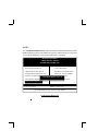
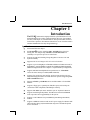
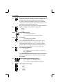
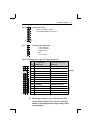
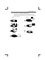
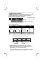
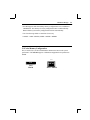
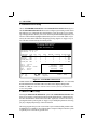
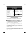
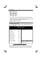
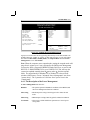
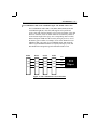
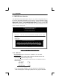
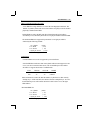
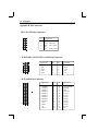
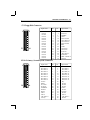
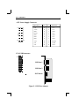
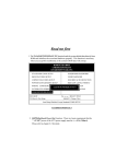
82430TX PCIset
P55-BT
ISA PCI M a in B o a rd
with Onboard PCI IDE and Super Multi-I/O.
TRADEMARK
All products and company names are
trademarks or registered trademarks of
their respective holders.
The specification is subject to change without notice.
V043
Package Checklist
Please make sure your package containg all items listed below before
your installation. If you find any damaged items or missing items,
please contact your retailer.
One Mainboard
One manual
One IDE ribbon cable
One floppy ribbon cable
Contents
page
Chapter 1 - Introduction ................................................... 1-1
System Block Diagram ............................................. 1-3
P55-BT Layout ........................................................ 1-4
Chapter 2 - Hardware Design ......................................... 2-1
2-1
2-2
2-3
2-4
2-5
2-6
Overview ..................................................................2-1
Connectors and Jumpers ............................................2-3
Real Time Clock Battey Replacement ..........................2-7
System Memory Configuration ...................................2-8
Cache Memory Configuration ....................................2-9
Integrated PCI Bridge .................................................2-10
Chapter 3 - ATX Power Connector
3-1 External Madem Ring-in Power-On and Keyboard Power
on Functions ................................................. 3-2
Chapter 4 - Award BIOS Setup ........................................ 4-1
4-1 Standard CMOS Setup ...............................................4-2
4-2 BIOS Features Setup ..................................................4-2
4-3 Chipset Features Setup ...............................................4-6
4-4 Power Management Setup ..........................................4-8
4-5 Plug & Play/PCI Configuration ....................................4-11
4-6 Integrated Peripherals .................................................4-14
4-7 Load Setup Defaults ...................................................4-16
4-8 Change Supervisor or User Password .........................4-17
4-9 IDE HDD Auto Detection ...........................................4-18
4-10 HDD Low Level Format ..............................................4-20
4-11 Save & Exit Setup .......................................................4-20
4-12 Exit Without Saving ....................................................4-20
Chapter 5 - Technical Information .................................... 5-1
5-1
5-2
5-3
5-4
I/O & Memory Map ....................................................5-1
Time & DMA Channels Map ......................................5-2
Interrupt Map .............................................................5-2
RTC & CMOS RAM Map ...........................................5-3
Appendix A: POST Codes ...................................................................5-4
Appendix B: I/O Connectors ...............................................................5-8
NOTE :
The "LOAD SETUP DEFAULTS" function loads the system default data directly from
ROM and initializes the associated hardware properly. This function is necessary when
you accept this Mainboard, or the system CMOS data is corrupted.
ROM PCI/ISA BIOS
CMOS SETUP UTILITY
AWARD SOFTWARE, INC.
STANDARD CMOS SETUP
SUPERVISOR PASSWORD
BIOS FEATURES SETUP
USER PASSWORD
CHIPSET FEATURES SETUP
IDE HDD AUTO DETECTION
POWER MANAGEMENT SETUP
HDD LOW LEVEL FORMAT
PNP/PCI CONFIGURA
Load SETUP Default (Y/N)? Y
INTEGRATED PERIPH
ETUP
SAVING
LOAD SETUP DEFAULTS
ESC: QUIT
F10:Save & Exit Setup
:SELECT ITEM
(Shift)F2 :Change Color
Load Setup Defaults Except Standard COMS SETUP
LOAD SETUP DEFAULT
Introduction 1-1
Chapter 1
Introduction
The P55-BT mainboard is a high performance system hardware based on
Intel Pentium Rprocessor and is equipped with four PCI slots, four standard
ISA slots, a PnP Super I/O controller and two dual-port PCI-IDE connectors
for the future expansion. The hardware dimension is an AT form-factor that is
220mm x 260mm with a four-layer design technology.
Specification
Intel 82430TX PCIset chipset.
R
Intel Pentium Processor operating at100 ~ 333 MHz (Easy CPU CLK
Setting JP4 : One Jumper Only) and P55C with 321 ZIF socket 7 for
scalability to accept faster processors in the future.
Supports an onboard Switching Voltage Regulator to increase CPU and
System's reliability.
Supports CPU Vcore Voltage 2.0V/2.8V/2.9V/3.2V selection.
Supports up to 256 MegaBytes of DRAM(a minimum of 8 MB) on board(72Pin SIMM x 2, 168-Pin DIMM x 2), BIOS auto FP DRAM, EDO DRAM and
SDRAM configuration.(Refer to Chapter 2-4 System Memory Configuration)
Supports Onboard Burst/Pipelined burst synchronous L2 Write Back
Cache. The cache memory is 512KB (64KB*32 SRAM).
Supports four 16-bit ISA slots and four 32-bit PCI slots and provides two
independent high performance PCI IDE interfaces capable of supporting PIO
Mode 3 and Mode 4 devices.
Supports ATAPI (e.g. CD-ROM) devices and Ultra DMA 33 for both IDE
interface.
Supports 1 floppy port, 1 parallel port (EPP,ECP port), and 2 serial ports
(16550 Fast UART compatible) with PnP Super I/O chip.
Supports both PS/2 style mouse and PS/2 style AT keyboard connectors
Supports Award Plug & Play BIOS . The BIOS is stored in Flash EPROM
form. It provides better upgradeability for the system.
Supports a CPU Hardware sleep and SMM (System Management Mode)
function.
Supports a PWR/ON connector with an ATX power supply for a Remote ON/
OFF controller, a Ring-in (External Modem only) Power-On and a Keyboard
Power-on function.
1-2 P55-BT
Supports a USB connector
Utilizes a Lithium battery which provides environmental protection and
longer life-time
Supports a CPU temperature alarm so that when CPU's cooling fan is malfunction
or CPU overheats, CPU automatically slow down.
Supports a dual-button configuration which consists of POWER button for Off/
On transitions and SLEEP button for Sleep/Wake transitions. The configuration
is for ACPI-defined 4-second override feature of the SLEEP button. When the
user presses the power button for less than 4 seconds, the system enters into
sleep mode. When the user presses the power button for more than 4 seconds,
the system is powered off.
Supports onboard ATX and AT power connectors.
Introduction 1-3
R
Pentium
processor
>
>
HOST BUS
>
>
PB
SRAM
TAG
MA[11:0]
Control
<
<
TAG Control
MTXC
HOST Bridge
324 BGA
>
>
MD[63:0]
>
<
CONTROL
PCI Slots
IDE CD-ROM
PIIX4
PCI BUS
I/O Bridge
Port_A
Port_B
Graphics
IDE HDD
324 BGA
Universal Serial Bus
BIOS
Flash EPROM
ISA Slots
Keyboard
BIOS
Figure 1-2 System Block Diagram
Super
I/O
Serial 1
Serial 2
FDD
Printer
1-4 P55-BT
P55-BT Layout
USB Conn.
3
1
CN1
W83877
<
JP8
1
Keyboard BIOS
JP13
K/B
CONN.
Power Conn.
ATX Power Conn.
COM1
1
Socket 7
6
See Page
2-4
64K*64
5
See Page
2-4
J4
ATX-PW-ON
IR CONN. JP9
HD-LED TB-LED G-LED SLEEP RESET SPEAKER
KEYLOCK
JP14
Means Pin 1
Figure 1-1
See Page
2-4
BANK0
10
BANK1
2 1
See Page
2-6
Note :
8 7
JP7
3
J18
DIMM 1
DIMM 2
SIMM 1
SIMM 2
1
26
COM2
J10
J9
JP1
25
Primary IDE
JP2
See Page
2-4
MTXC
JP4
See Page
2-5
PRINTER
Secondary IDE
PIIX4
2
FDD CONN.
PCI#1
PCI#2
PCI#3
PCI#4
1
BANK2
Hardware Design
2-1
Chapter 2
Hardware design
2-1 Overview
The P55-BT is designed with Intel 82430TX PCIset chipset which is developed by
INTEL Corporation to fully support PentiumR Processor PCI/ISA system. The Intel
82430TX PCIset chipset can increase integration and improve performance designs.
The chipset provides an integrated IDE controller with two high performance IDE
interfaces for up to four IDE devices (hard devices, CD-ROM device, etc). The PnP
Super I/O controller provides the standard PC I/O functions: a floppy interface, two
16 Byte FIFO serial ports and an EPP/ECP capable parallel port. The P55-BT layout is
shown in the previous page for user's reference. Care must be taken when inserting
memory modules, inserting CPU or even plugging PCI card into the associated slots
to avoid damaging any circuits or sockets on board. A cooling fan is strongly
recommended when installing P54C/P54CTB/P55C (MMX)/K5/K6/6x86 (6x86L)
processor due to possible overheat. The P55-BT supports CPU temperature monitor
and alarm to prevent CPU's cooling fan from malfunction or CPUoverheat. When CPU
overheats there is a heat sensor to monitor CPU temperature, than speaker will alarm
and CPU slow down to save you data and shutdown system.
The P55-BT supports a minimum of 8MB of System Memory and a maximum of
256MB with 512KB synchronous SRAM Onboard to increase system performance.
The P55-BT supports standard Fast Page, EDO (Extended Data Out or Hyper Page
Mode) or synchronous DRAM. The P55-BT provides two 72-pin SIMM and two
168-pin DIMM sites for memory expansion. Each socket supports 1M x 32(4MB), 2M
x 32(8MB), 4M x 32(16MB), and 8M x 32(32MB) single-sided or double-sided memory
modules. The memory timing requires 70 ns for Fast page devices or 60 ns for EDO
DRAM. This mainboard has two 168-pin DIMM sites to support 3.3V (power level)
Unbuffered Synchronous DRAMs(SDRAM) or 5.0V (power level) Fast Page, EDO
DRAM. Memory parity generation and checking are not supported. (DRAM Modules may be parity[x 36] or non-parity[x 32].
The P55-BT supports two Onboard PCI IDE connectors that can support PIO Mode/
Ultra DMA 33 device and detect IDE harddisk type by BIOS utility automatically.
2-2
P55-BT
The P55-BT supports Award Plug & Play BIOS for the ISA and PCI cards. The BIOS
can be located in Flash EPROM. The advantage of having Flash EPROM is much
easier to replace BIOS code if necessary.
The P55-BT has been designed with AT form-factor with ATX/AT power connector.
The mainboard layout and system block diagram are shown in Figure 1-1 and Figure
1-2.
Hardware Design
2-3
2-2 Connectors and Jumpers
This section describes all of the connectors and jumpers equipped in the mainboard.
Please refer to Figure 1-1 for the location of each connector and jumper.The figure
in the following means connecting pin 1&2 and means connecting pin 2&3.
Jumpers with two pins are shown as
for open and
for close.
1
5
7
10
JP14
KeyLock - Keyboard lock switch & Power LED connector.
1.Power LED(+)
2.N/C
3.GND
4.Keylock
5.GND
Speaker - connect to the system's speaker for beeping.
7. Speaker
8. N/C
9. GND
10. VCC
Reset - Close to restart system.
Sleep/Resume switch : Close to enter sleep mode.
A keystrobe or mouse movement (mouse driver exists) will
instantly "wake up"the system.(for AT Power Supply Only)
+
+
+
Power Saving LED indicator - LED ON when the system is in any
saving mode.
Turbo LED indicator - LED ON when a higher speed is selected.
Harddisk LED indicator - LED ON when Onboard PCI IDE
Harddisks activites.
2-4
P55-BT
JP9
System Power ON/OFF Switch (For ATX Power Suppply Connector)
Pressing the button once will switch the system on and enter the
SLEEP MODE(Suspend mode). While in the SLEEP MODE, a
keystrobe or mouse movement(mouse driver exists) will instantly
"wake up"the system. Pressing the button while the system is on for
more than 4 seconds will turn the system off.
Note : The button should be a momentary switch that is normally on.
JP1
1
3
J10/J9
JP8
1 EPROM BIOS Selection :
1-2 : 12V Flash EPROM (Intel).
2-3 : 5V Flash EPROM.(SST, Winbond).(Default)
3
Clear CMOS:
1-2 : Normal operation (Default)
2-3 : Clear CMOS Values
This setting allows users to clear current CMOS data to back to
default by setting the jumper to 2-3 when system is off. This
jumper should be brought back to pin 1-2 to restore the normal
operation. Here, we strongly recommend you pull out the power
cable for safety and from damage befor clearing CMOS data.
1
3
1
JP2
Keyboard Power ON function:
1-2 : Enabled
(For the details, please refer to Chapter 3-1: Keyboard
Power On Function)
2-3 : Disabled
Note: When Enabled or Disabled the Keyboard Power ON function.
Make sure to pull out the power cable or disconnect the 20-PIN
power supply.
3
7
1
JP7
8
J4
The Power Supply (+12V) of the CPU Cooling FAN:
1.GND
2.+12V
3.GND
2
1
5
DIMM1, DIMM2 (168PIN) DRAM TYPE Select:
1-2, 3-4 : Support 3.3V SDRAM (Default)
5-6, 7-8 : Support 5V EDO/FP DIMM TYPE DRAM
IrDA/ASK IR CONNECTOR:
1.VCC
2.NC
3.IRRX
4.GND
5.IRTX
Hardware Design
CN1 1
2 USB CONNECTOR:
Reserved for USB port Adapter
(refer to APPENDIX B:I/O Connectors)
15
JP13
2-5
16
1
5
PS/2 MOUSE CONNECTOR:
1. Data (Red Wire)
2. Clock (Blue Wire)
3. GND (Green)
4. NC
5. VCC (Yellow)
JP4:CPU Clock Rate Select. (Easy One Jumper Setting Only)
R
CPU Pentium Processor
P54C / P55C
Cyrix 6x86 / 6x86L / M2
AMD K5 / K6
IBM 6x86
JP4
1-2
66/100MHz
1
2
3-4
60/120MHz
6x86-PR150+(120MHz)
5-6
66/133MHz
6x86-PR166+(133MHz)
7-8
75/150MHz
6x86-PR200+(150MHz)
9-10 60/150MHz
6x86MX-PR166( M2 )
11-12 66/166MHz
6x86MX-PR200( M2 )
13-14 75/188MHz
6x86MX-PR233(M2)
15-16 66/200MHz
6x86MX-PR233( M2 )
17-18 75/225MHz
6x86MX-PR266(M2)
19-20 66/233MHz
6x86MX-PR266( M2 )
21-22 66/266MHz
23-24 60/300MHz
25
26 25-26 66/333MHz
*
(Default)
¡*
*
*
*
*
*
*
These jumper settings are reserved for the future CPU
versions. When the future CPU versions are ready and
suitable for this mainboard, these jumper settings will be
correctly updated.
2-6
P55-BT
J18
10 5
6
1
CPU Vcore voltage selection for Pentium MMX / AMD K6 / Cyrix
6x86L or 6x86MX
1-6 : 2.0V for AMD K6 fast processor (Reserved)
3.5V
3.2V
2-7 : 2.8V for Pentium P55C(MMX)/Cyrix 6X86L(Dual Voltage)
2.9V
3-8 : 2.9V for AMD K6 PR166/PR200 or 6x86MX-PR166/PR200/
2.8V(Default)
RP233/PR266(Dual Voltage)
2.0V
4-9 : 3.2V for AMD K6 PR233/PR266(Dual Voltage)
5-10 : 3.5V for Pentium P54C/P54CS/P54CTB/AMD K5/Cyrix
6X86(Single Voltage for Dual or Single plane)
Hardware Design
2-3
2-7
Real Time Clock Battery Replacement
The battery can be replaced by a Sanyo / Panasonic CR2032, or
other equivalent coin lithium battery. Please follow the steps below to
replace the battery.
2.Insert
1.Remove
+
1
+
1
2
+
2
3
4
+
+
3
+
+
2-8
P55-BT
2-4 System Memory Configuration
The P55-BT supports different types of settings for the system memory. There is a
jumper JP7 for SDRAM hardware setting needed for memory configuration. The
following figures show all possible memory combinations.
>
>
>
DIMM1
DIMM2
SIMM1
SIMM2
BANK 0
3.3V Synchronous DRAM
or 3.3V FP / EDO DRAM
BANK 1
3.3V Synchronous DRAM
or 3.3V FP / EDO DRAM
BANK 2
5V FP / EDO DRAM
MemoryConfigurationTable
DIMM (M1)
(BANK 0)
DIMM2 (M2)
(BANK 1)
SDRAM
8MB, 16MB
SIMM1,SIMM2
(BANK 2)
SDRM
8MB, 16MB
32MB
32MB
EDO/FD DRAM
4M x 2 (8MB)
8M x 2 (16MB)
16M x 2 (64MB)
64MB, 128MB
64MB, 128MB
Empty
x1
NOTE :
x1
TOTAL
Memory
MAX. =256MB
x2
=
=
1.P55-BT supports both Fast Page DRAM and EDO DRAM SIMMs, however
they cannot be mixed in the same memory bank.
2. DIMM module specification is 3.3V / unbuffered.
LEFT KEY ZONE
(UNBUFFERED)
CENTER KEY ZONE
(3.3 V DRAM)
The P55-BT supports two 168-pin DIMM module sockets to extend system
memory size.You can install (5V, JP7 1-2, 5-6, 7-8 Close) Fast Page, EDO or (3.3V /
UNBUFFERED JP7 1-2, 3-4 Close) Synchronous DRAM.
When you have a DIMM module to plug into a 168-pin dual readout connnector,
you must make sure that the DIMM module is 3.3V/Unbuffered to supports Intel
Pentium RProcessor System or 5V Fast Page, EDO DRAM.
Hardware Design
* P55-BT Supports and extends many memory configurations on its 2 SIMM and
2 DIMM sites. The memory size of any configuration can be combined flexibly.
BIOS will detect your memory configurations and sizes automaticallly.
* The 70ns Fast Page Mode or 60ns EDO is necessary.
* "BANK" = 64Bit = SIMM1, SIMM2 = DIMM1 = DIMM2
2-5 Cache Memory Configuration
The second level (L2) cache is installed in the mainboard to increase the system
performance. The P55-BT supports 512KB burst and piplined burst synchronous
SRAM.
U18
U21
TAG
SRAM
64K*64
DATA SRAM
2-9
2-10
P55-BT
2-6 Integrated PCI Bridge
R
The P55-BT utilizes Intel 430TX PCIset chipset to support Intel Pentium Processor
PCI/ISA system. The Intel 82430TX PCIset chipset consists of one 82439TX system
controller (MTXC) and one 82371AB PCI ISA/IDE Accelerator (PIIX4) bridge chip. It
provides an interface which translates CPU cycle into PCI bus cycle and PCI burst
read/write capability. In addition, it provides a high performance PCI arbiter and
supports four PCI Masters, Rotating Priority Mechanism, and Hidden Arbitration
Scheme Minimizes Arbitration Overhead. The 82371AB(PIIX4) supports PCI Specification Revision 2.1 Compliant and contains a Universal Serial Bus interface with both
host and hub control functions. P55-BT reserves a USB connector to provide two
USB ports for serial transfer at 12 or 1.5 Mbit/sec. This supports legacy keyboard
and mouse software with USB-Base Keyboard and mouse.
There are four interrupts in each PCI slot : INTA#, INTB#, INTC#, and INTD#, since
the P55-BT adapts the PCI auto-configuration with the system BIOS Setup utility.
When the system is turned on after adding a PCI add-in card, the BIOS automatically
configure interrupts, DMA channels, I/O space, and other paramaters. You do not
have to configure jumpers or worry about potential resource conflicts. Because PCI
cards use the same interrupt resource as ISA cards, you must specify the interrupts
used by ISA add-in cards in the BIOS Setup utility.
If a "Legacy card" (such as plug paddle card and cable for the ISA slot.) is plugged
in the system, modification in the ROM SETUP UTILITYbecomes necessary. First,
enter PCI CONFIGURATION SETUPutility from ROM SETUP UTILITYmain menu
to set the "PCI IDE IRQ MAP TO: ISA".
Second, you must enter CHIPSET FEATURES SETUP UTILITYfrom ROM SETUP
UTILITY main menu and set the " Onboard Primary PCI IDE: Disabledand Onboard
Secondary PCI IDE: Disable." When you plug the PCI/ISA IDE card into the system,
You should Disabled Onboard Primary and Secondary PCI IDEfrom CHIPSET
FEATURES SETUP UTILITYtoo.
When no paddle card and cable, you can set the system interrupt request (IRQ) on
the "Legacy card" (refer to user's manual of the card) to a proper system IRQ level (In
general, card's Primary is assigned to INTA and Secondary is assigned to INTB). If
the card is plugged into slot 1(marked PCI#1), you cannot use the second slot
(marked PCI#2) because the Secondary INT signal takes INTB from the slot (refer to
Page 3-12 for circuit diagram). The user then enters PCI CONFIGURATION SETUP
utility from ROM SETUP UTILITYmain menu and sets the " PCI IDE IRQ MAP TO:
PCI-Slot 1" (It depends on the slot # where the Legacy card is plugged).
Introduction 3-1
Chapter 3
ATX Power Connector
Except for the AT power connector, the P55-BT also equips with ATX power
connector which is a single 20-PIN input device for ATX power supply (see Figure
3-3). To implement the built-in Remote ON/OFF function on ATX power supply, a
momentary switch which is normally open should be connected to the position JP9
as the system ON/OF button. However, an AT power supply does not come with
this function.
Based on the ATX power connector, the P55-BT has been designed to support both
ACPI and Soft-OFF functions. According to the definition of ACPI, a Suspense
mode will be enabled while you push the JP9(system ON/OFF) button less than 4
seconds. Nevertheless, the system will be turned off by pressing for more than 4
seconds. Regarding the Soft-OFF(coming from the P55-BT onboard circuit controller), it is another way to turn off your system. Your system can be shut down
automatically by an operation system such as Windows 95.
>
ATX
POWER
SUPPLY
P55-BT
BOARD
JP9
Figure 3-3: Simple ATX Power ON/OFF Controller
System Power ON/OFF
Switch
3-2 P55-BT
3-1 External Modem Ring-in Power ON and Keyboard Power ON
Functions
On the basis of bounded functions in I/O chipset, the two serial ports are able to
support the External Modem Ring-in Power ON function. Once users connect the
external modem to COM1 or COM2, the P55-BT mainboard allows them to turn on
their system through the remote and host's dial-up control.
Exclusive Keyboard Power ON Function
To innovate a unique feature to benefit users, we devoted ourselves to create the
easiest and most convenient way to turn on your system based on the 5.0VSB
provided by the ATX power supply. This function is available only under system
being connected to ATX power.
How to work with it
Step 1: Please push the momentary switch (JP9 button) to turn on your system and
then push again to hold for more than 4 seconds to shut down as soon as
you turn it on.
Step 2: You can enjoy the Keyboard Power-ON function by pressing any 1 or 2 keys
at the same time for 1-2 seconds. After releasing the keys, your system will
be turned on automatically. And through the existing Soft-OFF, your
system can be powered off by Windows 95.
Notes:
1. Once you pull out the power cable or disconnect the 20-PIN power
supply, you have to repeat the Step 1 to re-enable this function.
2. The number of keys needed to turn on a system depends on the type of
keyboard you are appplying since the different loading on each keyboard.
Here, we would like to suggest you push 2 keys together.
3. Intel ATX version 2.0 specification has recommended you use the power
supply with 0.72A(720mA). With our P55-BT mainboard, the 5.0VSB standby
power only has to be > = 0.1A (100mA) then you can enjoy this unique benefit.
However, the ATX power supply which is < 0.1 (100mA) is still applicable to
your system by setting the JP2 to 2-3 to disable this feature.
4. When Enabled or Disabled the Keyboard Power ON function by JP2. Make
sure to pull out the power cabled or disconnect the 20-PIN power supply.
AWARD BIOS 4-1
Chapter 4
Award BIOS Setup
Award's ROM BIOS provides a built-in Setup program which allows user to modify the
basic system configuration and hardware parameters. The modified data will be stored
in a battery-backed CMOS RAM so data will be retained even when the power is turned
off. In general, the information saved in the CMOS RAM stay unchanged unless there
is configuration change in the system, such as hard drive replacement or new equipment
change.
It is possible that the CMOS battery is dead. This will cause data lose in CMOS RAM.
If so, it is necessaiy to re-enter system configuration parameters.
To enter Setup Propgram
Power on the computer and press <Del> key immediately. This will bring you into BIOS
CMOSSETUPUTILITY.
ROM PCI/ISA BIOS(2A59IPA9)
CMOSSETUPUTILITY
AWARD SOFTWARE, INC.
STANDARD CMOS SETUP
SUPERVISOR PASSWORD
BIOS FEATURES SETUP
USER PASSWORD
CHIPSET FEATURES SETUP
IDE HDD AUTO DETECTION
POWER MANAGEMENT SETUP
HDD LOW LEVEL FORMAT
PNP/PCI CONFIGURATION
SAVE & EXIT SETUP
INTEGRATED PERIPHERALS
EXIT WITHOUT SAVING
LOAD SETUP DEFAULTS
ESC : QUIT
F10
: SELECT ITEM
: Save & Exit Setup
(Shift)F2 : Change Color
Time, Date, Hard Disk Type...
Figure 4-1 CMOS SETUP UTILITY
The menu displays all the major selection items and allows user to select any shown
items. The selection is made by moving cursor (press any direction key ) to the item
and press 'Enter' key. An on-line help message is displayed at the bottom of the
screen as cursor is moving to various items which provides user better understanding of each function. When a selection is made, the menu of selected item will appear
so the user can modify the associated configuration parameters.
4-2 CHAPTER 4
4-1 Standard CMOS Setup
Choose "STANDARD CMOS SETUP" in the CMOS SETUP UTILITY Menu (Fig.4-1).
The STANDARD CMOS SETUP allows user to configure system setting such as current
date and time, type of hard disk drive installed in the system, floppy drive type, and the
type of display monitor. Memory size is auto-detected by the BIOS and displayed for your
reference. When a field is highlighted (direction keys to move cursor and <Enter> key to
select), the entries in the field will be changed by pressing <PgDn> or <PgUp> keys or
user can enter new data directly from the keyboard.
ROM PCI/ISA BIOS(2A59IPA9)
STANDARD CMOS SETUP
AWARD SOFTWARE, INC.
Date (mm:dd:yy) : Wed, Apr 17 1996
Time (hh:mm:ss) : 14 : 30 : 50
HARD DISKS
TYPE
Primary Master
: Auto
Primary Slave
: Auto
Secondary Master : Auto
Secondary Slave : Auto
SIZE
0
0
0
0
CYLS
0
0
0
0
HEAD
0
0
0
0
PRECOMP
0
0
0
0
Drive A : 1.44M, 3.5 in.
Drive B : None
Floppy 3 Mode Support : Disabled
Video
: EGA/VGA
Halt On : All Errors
LANDZONE
0
0
0
0
Base Memory :
Extended Memory :
Other Memory :
SECTORS MODE
0
Auto
0
Auto
0
Auto
0
Auto
640K
5360K
384K
Total Memory : 16384K
ESC : Quit
F1 : Help
(Shift) F2
: Select Item
: Change Color
PU/PD/+/- : Modify
Figure 4-2 STANDARD CMOS SETUP
NOTE: If hard disk Primary Master/Slave and Secondary Master/Slave were used Auto,
then the hard disk size and model will be auto-detected on display during POST.
NOTE: The "Halt On :" field is to determine when to halt the system by the BIOS if error
occurrs during POST.
4-2 BIOS Features Setup
Selecting the "BIOS FEATURES SETUP" option in the CMOS SETUP UTILITY menu
allows user to change system related parameters in the displayed menu. This menu shows
all of the manufacturer's default values of P55-BT. Again, user can move the cursor by
pressing direction keys and <PgDn> or <PgUp> keys to modify the parameters. Pressing
[F1] key to display help message of the selected item.
This setup program also provides 2 convenient ways to load the default parameter data
from BIOS[F6] or CMOS[F7] area if shown data is corrupted. This provides the system
a capability to recover from any possible error.
AWARD BIOS 4-3
ROM PCI/ISA BIOS(2A59IPA9)
BIOS FEATURES SETUP
AWARD SOFTWARE, INC.
Virus Warning
CPU Internal Cache
External Cache
Quick Power On Self Test
Boot Sequence
Swap Floppy Drive
Boot Up Floppy Seek
Boot Up NumLock Status
Boot UP System Speed
Gate A20 option
Typematic Rate Setting
Typematic Rate (Chars/Sec)
Type matic Delay (Msec)
Security Option
PCI/VGA Palette Snoop
OS Select For DRAM > 64MB
:
:
:
:
:
:
:
:
:
:
:
:
:
:
:
:
Disabled
Enabled
Enabled
Enabled
A, C, SCSI
Disabled
Enabled
On
High
Fast
Disabled
6
250
Setup
Disabled
Non-OS2
Video BIOS
C8000-CBFFF
CC000-CFFFF
D0000-D3FFF
D4000-D7FFF
D8000-DBFFF
DC000-DFFFF
Shadow
Shadow
Shadow
Shadow
Shadow
Shadow
Shadow
:
:
:
:
:
:
:
Enabled
Disabled
Disabled
Disabled
Disabled
Disabled
Disabled
Esc : Quit
: Select Item
F1 : Help
PU/PD/+/- : Modify
F5 : Old Values
(Shift)F2 : Color
F7 : Load Setup Defaults
Figure 4-3 BIOS FEATURES SETUP
Note: The Security Option contians "setup" and "system". The "setup" indicates
that the password setting is for CMOS only while the " system" indicates the
password setting is for both CMOS and system boot up procedure.
Virus Warning: This category flashes on the screen. During and after the system
boots up, any attempts to write to the boot sector or partition table of the hard disk
drive will halt the system and an error message will appear. You should then run an
anti-virus program to locate the virus. Keep in mind that this feature protects only the
boot sector, not the entire hard drive. Default value is Disabled
Enabled
: Activates automatically when the system boots up causing a warning
message to appear when anything attempts to access the boot sector.
Disabled
: No warning message to appear when anything attempts to access the
boot sector.
Note : Many disk diagnostic programs that access the boot sector table can trigger the
virus warning message. If you plan to run such a program, we recommend that you
first disable the virus warning.
CPU Internal Cache / External Cache:These two categories speed up memory access.
however, it depends on CPU / chipset design. The default value is Enable. If your CPU is
without Internal Cache then this item "CPU Internal Cache" will not be shown.
Enabled
: Enable cache.
Disable
: Disable cache.
4-4 CHAPTER 4
Quick Power On Self Test:This category speeds up Power On Self Test (POST)
after you power on the computer. If it is set to Enable, BIOS will shorten or skip
some check items during POST. The default is Enabled.
Enabled : Enable quick POST.
Disabled: Normal POST.
Boot Sequence:This category determines which drive is searched first for the O/S
(Operating System). Default value is A, C, SCSI. The following is your list of options.
[A, C, SCSI]-[C, A, SCSI]-[C, CDROM, A]-[CDROM, C, A]-[D, A, CDROM]
[E, A, CDROM]-[F, A, CDROM]-[SCSI, A, C]-[SCSI C, A]-[C Only], [LS/ZIP, C]
A,C :System will first search for floppy disk drive then hard disk drive.
C,A :System will first search for hard disk drive then floppy disk drive.
CDROM,C,A:System will first search for the CDROM drive (If the CDROM has a
bootable CD title.) and second search hard disk drive then flopp
disk drive.
C,CDROM,A:System will first search for the hard disk drive and second search
the CDROM drive (If the CDROM has a bootable CD title.) then
floppy disk drive.
Swap Floppy Drive: This will swap your physical drive letters A & B if you are using
two floppy disks. Default value is Disabled.
Enabled : Floppy A & B are able to swap under DOS.
Disabled: Floppy A & B are not able to swap.
Boot Up Floppy Seek: During Power-On-Self-Test (POST), BIOS will determine if the
floppy disk drive installed is 40 or 80 tracks. Only is 360K type 40 tracks while 760K,
1.2M and 1.44M are all 80 tracks. The default value is Enabled.
Enabled : BIOS searches for floppy disk drive to determine if it is 40 or 80 tracks,
Note that BIOS cannot tell from 720K, 1.2M or 1.44M drive type as
they are all 80 tracks.
Disabled: BIOS will not search for the type of floppy disk drive by track number.
Note that there will not be any warning message if the drive installed
is 360K.
Boot Up NumLock Status: Control the state of the Numlock key when the system
boots. The default value is On.
On : Keypad is number keys.
Off : Keypad is arrow keys.
Boot UP System Speed: Select Hight to boot at the default CPU speed; select Low to
boot at the speed of the AT bus.
High: Set the speed to high.
Low : Set the speed to low.
AWARD BIOS 4-5
Gate A20 Option: This refers to the way the system addresses memory above 1MB
(extended memory). The default value is Fast.
Normal : The A20 signal is controlled by keyboard controller or chipset hardware.
Fast : The A20 signal is controlled by Port 92 or chipset specific method.
Typematic Rate Setting: This determines the keystroke repeat rate.
Enabled : Enable typematic rate and typematic delay programming.
Disabled: Disable typematic rate and typematic delay programming. The rate will be
controlled by keyboard controller in your system.
Typematic Rate(Chars/Sec):
6 :6
10: 10
15: 15
24: 24
characters per second.
characters per second.
characters per second.
characters per second.
8: 8
12: 12
20: 20
30: 30
characters per second.
characters per second.
characters per second.
characters per second.
Typematic Delay(Msec): When holding a key, the time between the first and
second character displayed.
250 : 250msec.
500 : 500 msec.
750 : 750 msec.
1000: 1000 msec.
Security Option: This category allows you to limit access to the system and Setup, or
just to Setup. The default value is Setup.
System: The system will not boot and the access to Setup will be denied if the correct
password is not entered at the prompt.
Setup : The system will boot, but the access to Setup will be denied if the incorrect
password is not entered at the prompt.
PCI/VGA Palette Snoop: This filed controls the ability of a primary PCI VGA
controller to share a common palette(when a snoop write cycles) with an ISA
video card. The default value is Disabled.
Enabled:If an ISA card connects to a PCI VGA card via the VESA connector
and that ISA card connects to VGA monitor and that ISA card uses
the RAMDAC of PCI card.
Disabled:Disable the VGA card Palette snoop function.
Video BIOS Shadow: It determines whether video BIOS will be copied to RAM,
however; it is optional from chipset design. Video Shadow will increase the video
speed.
Enabled :
Video shadow is enabled.
Disabled:
Video shadow is disabled.
4-6 CHAPTER 4
C8000 - CBFFF Shadow :
CC000 - CFFFF Shadow:
D0000 - D3FFF Shadow:
D4000 - D7FFF Shadow:
D8000 - DBFFF Shadow:
DC000 - DFFFF Shadow:
These categories determine whether other expansion card optional ROM will be
copied to RAM by 16K byte or 32K byte per unit and the size depends on chipset. If
you install other expansion cards with ROMs on them, you will need to know which
addresses the ROMs use to shadow themselves specifically.
Enabled : Optional shadow is enabled.
Disabled: Optional shadow is disabled.
4-3 Chipset Features Setup
Choose the "CHIPSET FEATURES SETUP" in the CMOS SETUP UTILITY menu to
display the following menu.
ROM PCI/ISA BIOS(2A59IPA9)
CHIPSET FEATURES SETUP
AWARD SOFTWARE, INC.
Auto Configuration
DRAM Timing
DRAM Leadoff Timing
DRAM Write Burst Timing
Fast EDO Lead Off
Refresh RAS# Assertion
Fast RAS To CAS Delay
DRAM Page Idel Timer
DRAM Enhanced Paging
Fast MA to RAS# Delay
SDRAM (CAS Lat/RAS-to-CAS)
SDRAM Speculative Read
System BIOS Cacheable
Video BIOS Cacheabled
8 Bit I/O Recovery Time
16 Bit I/O Recovery Time
Memory Hole At 15M-16M
PCI 2.1 Compliance
:
:
:
:
:
:
:
:
:
:
:
:
:
:
:
:
:
:
Enabled
60ns
10 / 6 / 3
x333
Enabled
4 Clks
2
2 Clks
Enabled
2 Clks
2/2
Disabled
Disabled
Enabled
1
2
Disabled
Disabled
Current MB Temperature
CPU Warning Temperature
: 38C/100F
: 60C/140F
ESC : Quit
: Select Item
F1 : Help
PU/PD/+/- : Modify
F5 : Old Values
(Shift) F2 : Color
F7 : Load Setup Defaults
Figure 4-4 CHIPSET FEATURES SETUP
Auto Configuration: Selects predetermined optinal values of chipset parameters.
When Disabled, chipset parameters revert to setup information stored in COMS.
Many fields in this screen are not available when Auto Configuration is Enabled.
AWARD BIOS 4-7
Note: When you insert slow memory modules in the system and set a faster timing,
the system may hang up.
DRAM Timing: The default value is 60ns.
60ns : 2 (faster) Burst Wait State, for 60~70ns Fast Page Mode/EDO DRAM.
70ns : 3 (slower) Burst Wait State, for 70ns Fast Page Mode/EDO DRAM.
DRAM Leadoff Timing: The default value is 10/6/3 (Read Leadoff / Write Leadoff /
RAS# Precharge)
10/6/3 : For EDO / FPM reads and Writes timing.
11/7/3 : For slow EDO /FPM reads and Writes timing.
DRAM Writes Burst Timing: The default value is x222.
x222 : For EDO / FPM of the fast burst mode timings.
x333 : For EDO /FPM of the slow burst mode timings.
Fast EDO Lead off : The default value is Enabled.
Enabled : This field Enables fast timing EDO read cycles.
Disabled : Disables the fast timing EDO read cycles.
Refresh RAS# Assertion : The default value is 4 clks.
4 : This field controls the number of 4 clocks. RAS# is asserted for Refresh.
5 : This field controls the number of 5 clocks. RAS# is asserted for Refresh.
Fast RAS To CAS Delay : The default value is 2.
2 : This field controls a RAS# to CAS# delay is 2.
3 : This field controls a RAS# to CAS# delay is 3.
Fast MA to RAS# Delay : The default value is 2 Clks.
1 Clks : This field controls Memory Address to RAS's timing is 1 HCLKS.
2 Clks : This field controls Memory Address to RAS's timing is 1 HCLKS.
SDRAM (CAS Lat / RAS-to-CAS) : The default value is 2 / 2.
2/2 : This field controls a RAS# to CAS# delay of 2 HCLKS is provided for SDRAM.
3/3 : This field controls a RAS# to CAS# delay of 3 HCLKS is provided for SDRAM.
SDRAM Speculative Read : The default value is Disabled.
Enabled : Enables the SDRAM speculative read logic.
Disabled : Disables the SDRAM speculative read logic.
System BIOS Cacheable:
Enabled :
Allows caching of the system BIOS ROM at F0000h-FFFFFh, resulting
in better system performance. However, if any program writes to this
memory area, a system error may result.
Disabled : System BIOS non-cacheable
4-8 CHAPTER 4
Video BIOS Cacheable: The default value is enabled.
Enabled : This field Enables the Video BIOS Cacheable to speed up the VGA
Performance.
Disabled: Disables the Video BIOS Cacheable function.
8/16 Bit I/O Recovery Time: The default value is 1.
8 Bit I/O Recovery Time: This field defines the recovery time from 1 to 8 for 8bit I/O.
16 Bit I/O Recovery Time: To define the recovery time from 1 to 4 for 16-bit I/O.
Memory Hole at 15M-16M: The default value is disabled.
Disabled: Normal Setting.
Enabled : This field enables the main memory (15~16MB) remap to ISA BUS.
This feature reserves 15MB to 16MB memory address space to ISA
expansion card that specifically require this setting.
PCI 2.1 Compliance:The default value is Disabled.
Enabled: This field Enables the PCI 2.1 Compliance timing.
Disabled: Disables the PCI 2.1 timing.
Current MB Temperature:This field will Auto-detect the MB temperature when enter
the CHIPSET FEATURES SETUP.
CPU Warning Temperature:The default value is 60C/140F.
The purpose of this setting is to enable the CPU temperature warning & protection
function so that we can detect and monitor the fluctuant temperature during system
operation.
If the cooling fan applied to the CPU does not have enough power to control and cool
down the heat or is broken while running, the indicator of the current M/B temperature will be higher and higher.
To protect the CPU while the temperature is up to CPU warning temperature for
example 60C(the default value), the alarm will be activated and CPU speed will be
slowed down at the same time. At this moment, you have to save your data into disks
and then shut down system to cut off the alarm.
The thermal conductibility of a CPU and the cooling fan are playing two key roles to
determine whether the overheat problem could be happened or not. For example, if
you are using a high performance CPU but applying a low power cooling fan, the
situation mentioned above will happen again.
The setting value is available from 50C/122F to 70C/158F.
4-4 Power Management Setup
Choose the "POWER MANAGEMENT SETUP" in the CMOS SETUP UTILITY
to display the following screen. This menu allows user to modify the power
management parameters and IRQ signals. In general, these parameters should not
be changed unless it's absolutely necessary.
AWARD BIOS 4-9
ROM PCI/ISA BIOS (2A59IPA9)
POWER MANAGEMENT SETUP
AWARD SOFTWARE, INC.
Power Management
PM Control by APM
Video off Method
Video off After
: User Define
: Yes
: V/H SYNC+Blank
: Standby
Doze Mode
Standby Mode
Suspend Mode
HDD Power Down
VGA Active Monitor
Soft-OFF by PWB-BTTN
: Disable
: Disabled
: Disabled
: 15 Min
: Enabled
: Delay 4 Sec.
** Break Event From Suspend **
IRQ 8 Clock Event
: Disabled
** Reload Global Timer Events **
IRQ [3-7, 9-15], NMI
Primary IDE 0
Primary IDE 1
Secondary IDE 0
Secondary IDE 1
Floppy Disk
Serial Port
Parallel Port
:
:
:
:
:
:
:
:
Enabled
Disabled
Disabled
Disabled
Disabled
Disabled
Disabled
Disabled
ESC : Quit
: Select Item
F1 : Help
PU/PD/+/- : Modify
F5 : Old Values
(Shift) F2 : Color
F7 : Load Setup Defaults
Figure 4-5 POWER MANAGEMENT SETUP
Again, user can move the cursor by pressing direction keys to the field needed to be
modified and press <PgDn> or <PgUp> to alter item selection. You can only change
the content of Doze Mode, Standby Mode, and Suspend Mode when the Power
Management is set to 'User Define'.
Note: When the computer enters suspend mode (setting the suspend mode valid
range from 1 minute up to 1 hour) activated by the BIOS power Management.
You need to RUN a program POWER.EXE under DOS root, or need to add
DEVICE=C:\DOS\POWER.EXE in your CONFIG.SYS. This will keep the
system time updated normally when the system wake up from the suspend
R
R
mode. The supend mode for Windows 95 or Windows 3.1x has to install
windows APM feature. Choose "Advanced Power Management" item from
"system device". The "system device" field was from "system" icon in the
"control panel".
4-4-1 The Description of the Power Management
A. Power Management mode selection :
Disabled
: The system operates in NORMAL conditions (Non-GREEN) and
the Power Management function is disabled.
Max. saving
: Maximum power savings. Inactivity period is 1 minute in each
mode.
Min. saving
: Minimum power savings. Inactivity period is 1 minute in each mode.
User Define
: Allows user to define PM Timers parameters to control power
saving mode.
4-10 CHAPTER 4
B. Time-out parameters :
HDD Standby
The HDD Standby timer can be set from 1 to 15 minute(s).
System Doze
The "System Doze" mode timer starts to count when no "PM event"
occurres. The valid time-out setting is from 1 minute up to 1 hour.
System Standby
The "Standby" mode timer starts to count when the "System Doze" mode timer times
out and no "PM events" occurred. The valid range is from 1 minute up to 1 hour.
System Suspend
R
This function works only when the Pentium Procssor is installed. The timer starts
to count when the "System Standby" mode timer times out and no "PM Event"
occurres. The valid range is from 1 minute up to 1 hour.
4-4-2
Description of the Green Functions
PM Control by APM:
If Advanced Power Management (APM) is installed on your system, selecting Yes
gives better power savings.
Video Off Method: Determines the manner in which the monitor is blanked.
V/H SYNC+Blank:
System turns off vertical and horizontal synchronization ports and writes blanks to the
video buffer.
DPMS Support:
Select this option if your monitor supports the Display Power Management Signaling
(DPMS) standard of the Video Electronics Standards Association (VESA). Use the
software supplied for your video subsystem to select video power management values.
Blank Screen:
System only writes blanks to the video buffer.
Video off After: Determines when to activate the video off feature for monitor power
management. The settings are Video off after Suspend/standby/Doze/(N/A).
Soft-off by PWR-BTTN: This field is for the soft-off function setting. When the board
utilizes an ATX power supply, two types of settings are offered: Delay 4 Sec. and
instant-Off. When the setting is Delay 4 Sec.,users can power off the system by
pressing JP9 for 4 seconds. However, if users press JP9 for less than 4 seconds, the
system will enter the Suspend Mode. When the setting is instant-Off, users' first press
on JP9 will power off the system, but the second press will power on the system.
AWARD BIOS 4-11
The P55-BT supports HDD Power Down, Doze and standby power saving functions
when Intel Pentium RProcessor is installed. In addition, the suspend function
is supported when the JP14's sleep (sleep ref. Figure1-1) is closed to enter the green
function. The detailed descriptions of these functions are provided in the next page.
HDD Power Down
When the system stops reading or wiriting HDD, the timer starts to count. The system
will cut off the HDD power when timer runs out of time. The system will not resume
operation until either a read from or a wirte to HDD command is executed again.
Doze Mode
The system hardware will drop down CPU clock from normal working speed
when Doze mode timeout occurrs.
Standby Mode
When the system standby mode timer runs out, it will enter the standby mode and
retain CPU at slow working speed. The screen will be blanked out.
Suspend Mode
When the system suspend timer times out, the system will enter the suspend mode
and the chipset will stop CPU clock immediately. The power consumption in
Suspend Mode is lower than in standby mode. The screen is also blanked out.
PM Events:
AWARD BIOS defines Reload Global Timer Events in the power management mode
(Doze,standby & suspend). The user can initialize any PM Events to be "Enabled" or
"Disabled". When the system detects all of the enabled events which do not have any
activity, it will start the system Doze timer first if the "Power Management" isn't
"Disabled". Once the system Doze timer is timed out, it will process doze power saving
procedure by starting the system standby timer. When the standby timer ran out and
all of the "Enabled" events remains silent, the system will enter the standby mode. By
now, the system will not only process the standby power saving procedures but also
start the system suspend timer. When the suspend timer times out, all of the CPU clock
will stop by dropping system clock down to zero and remains this way until any one
of the "Enabled" event occurrs.
4-5
PnP/PCI Configuration
The PnP/PCI configuration program is for the user to modify the PCI/ISA IRQ signals when
various PCI/ISA cards are inserted in the PCI or ISA slots.
WARNING : Any misplacing IRQ could cause system cannot pick up the rescouces.
4-12 CHAPTER 4
ROM PCI/ISA BIOS(2A59CPA9)
PNP/PCI CONFIGURATION
AWARD SOFTWARE, INC.
PNP OS Installed
Resources Controlled By
Reset Configuration Data
IRQ-3
IRQ-4
IRQ-5
IRQ-7
IRQ-9
IRQ-10
IRQ-11
IRQ-12
IRQ-14
IRQ-15
DMA-0
DMA-1
DMA-3
DMA-5
DMA-6
DMA-7
assigned
assigned
assigned
assigned
assigned
assigned
assigned
assigned
assigned
assigned
assigned
assigned
assigned
assigned
assigned
assigned
to
to
to
to
to
to
to
to
to
to
to
to
to
to
to
to
: NO
: Manual
: Disabled
:
:
:
:
:
:
:
:
:
:
:
:
:
:
:
:
Legacy ISA
Legacy ISA
PCI/ISA PnP
PCI/ISA PnP
PCI/ISA PnP
PCI/ISA PnP
PCI/ISA PnP
PCI/ISA PnP
PCI/ISA PnP
PCI/ISA PnP
PCI/ISA PnP
PCI/ISA PnP
PCI/ISA PnP
PCI/ISA PnP
PCI/ISA PnP
PCI/ISA PnP
PCI IDE IRQ Map To
Primary IDE INT#
Secondary IDE INT#
: PCI-AUTO
:A
:B
ESC : Quit
: Select Item
F1 : Help
PU/PD/+/- : Modify
F5 : Old Values
(Shift) F2 : Color
F7 : Load Setup Defaults
Figure 4-6 PCI CONFIGURATION SETUP
Resource Controlled By:The default value is Manual.
Manual :PNP Card's resources will be controlled manually. You can set which
IRQ-X and DMA-X are assigned to PCI/ISA PNP or Legacy ISA Cards.
Auto
:If your ISA card and PCI card are all PNP cards, BIOS will assign the
interrupt resource automatically.
Reset Configuration Data:The default value is disabled.
Disabled:Normal Setting
Enabled :If you had plugged some Legacuy cards in the system and recorded into
ESCD(Extended System Configuration Data), you can set this field to
enabled to clear ESCD.
PCI IDE IRQ Map To:The default value is PCI-AUTO
When you have true PCI card(s) plugged into the system, you will not need
to change any thing here in the SETUP program. However, if you do not
know whether you have true PCI card or not, please refer to your PCI card
user's manual for the details.
When you have a legacy card (describbed in section 2-6) to be plugged
into the system,a proper setting is extremely important or it may cause the
system hang. The diagram shown below tells you how the Rotating
Priority Mechanism is designed.
AWARD BIOS 4-13
Used MEM base addr and Used MEM Length : The default value is N/A.
The Used MEM base addr (CB00, CC00, D000, D400, D800, DC00) and
Used MEM Length (8K, 16K, 32K, 64K) support some specific ISA
Legacy cards with requested memory space below 1M address. Now with
these two functions, users can define where the used memory address is
located and its length of the legacy area corresponding. Based on these,
BIOS will skip the UMB area that is used by the legacy device to avoid
the memory space conflict. For example, if users select "D000"for"Used
MEM base addr" and "16K" for "Used MEM Length", that means the
address region D0000H-D3FFFH is occupied by ISA legacy cards, and
thus BIOS will not assign this region for PnP/ISA and PCI cards.
PCI#4
PCI#3
PCI#2
INTB
INTC
INTD
PCI#1
INTA
INTC
INTD
INTA
INTB
INTD
INTA
INTB
INTC
INTA
INTB
INTC
INTD
INTA
INTB
INTC
INTD
Figure 4-7 The Combination of PCI INT# lines
PCI
Chipset
4-14 CHAPTER 4
4-6
Integated Peripherals
ROM PCI/ISA BIOS(2A59IPA9)
INTEGRATED PERIPHERALS
WARD SOFTWARE, INC.
IDE HDD Block Mode
IDE Primary Master PIO
IDE Primary Slave PIO
IDE Secondary Master PIO
IDE Secondary Slave PIO
IDE Primary Master UDMA
IDE Primary Slave UDMA
IDE Secondary Master UDMA
IDE Secondary Slave UDMA
Onboard Primary PCI IDE
Onboard Secondary PCI IDE
USB Keyboard Support
:
:
:
:
:
:
:
:
:
:
:
:
Enabled
Auto
Auto
Auto
Auto
Auto
Auto
Auto
Auto
Enabled
Enabled
Disabled
Onboard FDD Controller
Onboard Serial Port 1
Onboard Serial Port 2
UART 2 Mode
:
:
:
:
Enabled
Auto
Auto
Standard
Onboard Parallel Port
: 378/IRQ7
Onboard Parallel Mode
ECP Mode Ise DMA
Parallel Port EPP Type
ESC
F1
F5
F7
: ECP / EPP
:3
: EPP1.9
: Quit
: Select Item
: Help
PU/PD/+/- : Modify
: Old Values
(Shift) F2 : Color
: Load Setup Defaults
Note: If you don't use the Onboard IDE connector, than use On-card
(PCI or ISA card) IDE connector. You will set Onboard Primary
PCI IDE: Disabled and Onboard Secondary PCI IDE: Disabled
from CHIPSET FEATURES SETUP UTILITY.
The Onboard PCI IDE cable should be equal to or less than
18 inches (45 cm.).
IDE HDD Block Mode: Select enabled only if your hard drives support block mode.
Enabled : Enabled IDE HDD Block Mode. Provides higher HDD transfer rates.
Disabled: Disable IDE HDD Block Mode.
IDE Primary (Secondary) Master/Slave PIO : The default value is Auto.
This field is Selectable Primary (Secondary) IDE PIO Mode (0~4) for HDD.
IDE Primary (Secondary) Master/Slave UDMA : The default value is Auto.
Auto : Select Primary (Secondary) IDE used Ultra DMA HDD.
Disabled : Disabled Primary (Secondary) IDE used Ultra DMA HDD.
Onboard Primary PCI IDE: The default value is enabled.
Enabled : Enable Onboard 1st channel IDE port.
Disabled : Disable Onboard 1st channel IDE port, when using On-card (PCI or ISA
card) IDE connector.
Onboard Secondary PCI IDE: The default value is enabled.
Enabled : Enable Onboard 2nd channel IDE port.
Disabled : Disable Onboard 2nd channel IDE port when using On-card (PCI or ISA
card) IDE connector.
AWARD BIOS 4-15
IDE Primary Master PIO: The default value is Auto.
Auto
: BIOS will automatically detect the Onboard Primary Master PCI
IDE HDD Accessing mode.
Mode0~4
: Manually set the IDE Accessing mode.
IDE Primary Slave PIO: The default value is Auto.
Auto
: BIOS will automatically detect the Onboard Primary Slave PCI IDE
HDD Accessing mode.
Mode0~4
: Manually set the IDE Accessing mode.
IDE Secondary Master PIO: The default value is Auto.
Auto
: BIOS will automatically detect the Onboard Secondary Master PCI
IDE HDD Accessing mode.
Mode0~4
: Manually set the IDE Accessing mode.
IDE Secondary Slave PIO: The default value is Auto.
Auto
: BIOS will automatically detect the Onboard Secondary Slave PCI
IDE HDD Accessing mode.
Mode0~4
: Manually set the IDE Accessing mode.
Onboard FDC Controller: The default value is Enabled.
Enabled: Enable the Onboard SMC CHIP's floppy drive interface controller.
Disabled: Disable the Onboard SMC CHIP's floppy drive interface controller,
when using On-card ISA FDC's controller.
Onboard UART 1: This field allows the user to sellect the serial port. The default
value is 3F8H/IRQ4.
COM1: Enable Onboard Serial port 1 and address is 3F8H/IRQ4.
COM2: Enable Onboard Serial port 1 and address is 2F8H/IRQ3.
COM3: Enable Onboard Serial port 1 and address is 3E8H/IRQ4.
COM4: Enable Onboard Serial port 1 and address is 2E8H/IRQ3.
Disabled: Disable Onboard SMC CHIP's Serial port 1.
Onboard UART 2: This field allows the user to sellect the serial port. The default
value is 2F8H/IRQ3.
COM1: Enable Onboard Serial port 2 and address is 3F8H/IRQ4.
COM2: Enable Onboard Serial port 2 and address is 2F8H/IRQ3.
COM3: Enable Onboard Serial port 2 and address is 3E8H/IRQ4.
COM4: Enable Onboard Serial port 2 and address is 2E8H/IRQ3.
Disabled: Disable Onboard SMC CHIP's Serial port 2.
4-16 CHAPTER 4
Onboard UART 2 Mode:The default value is standard. This field allows the user to
select the COM2 port that can support a serial Infrared Interface.
standard:Support a Serial Infrared Interface IrDA.
HPSIR:Support a HP Serial Infrared Interface formats.
ASKIR:Support a Sharp Serial Infrared Interface formats.
Onboard Parallel port: This field allows the user to sellect the LPT port. The
default value is 378H/IRQ7.
378H
: Enable Onboard LPT port and address is 378H and IRQ7
278H
: Enable Onboard LPT port and address is 278H and IRQ5.
3BCH
: Enable Onboard LPT port and address is 3BCH and IRQ7.
Disabled
: Disable Onboard SMC CHIP's LPT port.
NOTE: Parallel Port address is 378H/3BCH that selects the rounting of IRQ7 for LPT1.
Parallel Port address is 278H that selects the rounting of IRQ5 for LPT1.
Parallel port Mode: This field allows the user to sellect the parallel port mode.
The default value is ECP+EPP.
Normal
: Standard mode. IBM PC/AT Compatible bidirectional parallel port.
EPP
: Enhanced Parallel Port mode.
ECP
: Extended Capabilities Port mode.
EPP+ECP : ECP Mode & EPP Mode.
ECP Mode USE DMA: This field allows the user to sellect DMA1 or DMA3 for
the ECP mode. The default value is DMA3.
DMA1
: The filed selects the rounting of DMA1 for the ECP mode.
DMA3
: The filed selects the rounting of DMA3 for the ECP mode.
4-7 Load Setup Defaults
The "LOAD SETUP DEFAULTS" function loads the system default data directly from
ROM and initializes the associated hardware properly. This function will be necessary
only when the system CMOS data is corrupted.
AWARD BIOS 4-17
ROM PCI/ISA BIOS(2A59IPA9)
CMOSSETUPUTILITY
AWARD SOFTWARE, INC.
STANDARD CMOS SETUP
SUPERVISOR PASSWORD
BIOS FEATURES SETUP
USER PASSWORD
CHIPSET FEATURES SETUP
IDE HDD AUTO DETECTION
POWER MANAGEMENT SETUP
HDD LOW LEVEL FORMAT
PNP/PCI CONFIGURA
Load SETUP Default (Y/N)? Y
INTEGRATED PERIPH
ETUP
SAVING
LOAD SETUP DEFAULTS
ESC: QUIT
F10:Save & Exit Setup
:SELECT ITEM
(Shift)F2 :Change Color
Load Setup Defaults Except Standard COMS SETUP
Figure 4-8 LOAD SETUP DEFAULT
4-8 Change Supervisor or User Password
To change the password, choose the "SUPERVISOR PASSWORD or USER PASSWORD " option from the CMOS SETUP UTILITY menu and press [Enter].
NOTE : Either "Setup" or "System" must be selected in the " Security Option" of the
BIOS FEATURES SETUP menu (Refer to Figure 4-3 for the details).
1. If CMOS is corrupted or the option was not used, a default password stored in the
ROM will be used. The screen will display the following message:
Enter Password:
Press the [Enter] key to continue after proper password is given.
2. If CMOS is corrupted or the option was used earlier and the user wish to change
default password, the SETUP UTILITY will display a message and ask for a
confirmation.
Confirm Password:
3. After pressing the [Enter] key (ROM password if the option was not used) or current
password (user-defined password), the user can change the password and store the
new one in CMOS RAM. A maximum of 8 characters is acceptable.
4-18 CHAPTER 4
4-9 IDE HDD Auto Detection
The "IDE HDD AUTO DETECTION" utility is a very useful tool especially when you
do not know which kind of hard disk type you are using. You can use this utility to detect
the correct disk type installed in the system automatically. But now you can set HARD
DISK TYPE to Auto in the STANDARD CMOS SETUP. You don't need the "IDE
HDD AUTO DETECTION" utility. The BIOS will Auto-detect the hard disk size and
model on display during POST.
ROM PCI/ISA BIOS(2A59IPA9)
CMOS SETUP UTILITY
AWARD SOFTWARE, INC.
HARD DISKS
TYPE SIZE CYLS HEADS PRECOMP LANDZONE SECTORS MODE
Primary Master :
Primary Slave
:
Secondary Master :
Secondary Slave :
343
665
16
65535
664
63
NORMAL
Select Secondary Slave Option (N=Skip) : N
OPTIONS
1 (Y)
SIZE CYLS HEAD PRECOMP LANDZ SECTOR MODE
0
0
0
0
0
0 NORMAL
ESC : Skip
Figure 4-9 IDE HDD AUTO DETECTION
NOTE: HDD Modes
The Award BIOS supports 3 HDD modes : NORMAL, LBA & LARGE
NORMAL mode
Generic access mode in which neither the BIOS nor the IDE controller will
make any transformations during accessing.
The maximum number of cylinders, heads and sectors for NORMAL mode are
1024, 16 and 63.
no. Cylinder
(1024)
x no. Head
( 16)
x no. Sector
( 63)
x no. per sector
( 512)
528 Megabytes
If users set his HDD to NORMAL mode, the maximum accessible HDD size
will be 528 Megabytes even though its physical size may be greater than that.
AWARD BIOS 4-19
LBA (Logical Block Addressing) mode
A new HDD accessing method to overcome the 528 Megabyte bottleneck. The
number of cylinders, heads and sectors shown in the setup may not be the number
physically contained in the HDD.
During HDD accessing, the IDE controller will transform the logical address
described by sector, head and cylinder into its own physical address inside the HDD.
The maximum HDD size supported by LBA mode is 8.4 Gigabytes which is
obtained by the following formula:
no. Cylinder
(1024)
x no. Head
( 255)
x no. Sector
( 63)
x bytes per secttor
( 512)
8.4 Gigabytes
LARGE mode
Extended HDD access mode is supported by Award Software.
Some IDE HDDs contain more than 1024 cylinder without LBA support (in some
cases, users do not want the LBA mode). The Award BIOS provides another
alternative to support these kinds of LARGE mode:
CYLS.
1120
560
HEADS
16
32
SECTOR
MODE
59
NORMAL
59
LARGE
BIOS tricks DOS (or other OS) that the number of cylinders is less than 1024 by
dividing it by 2. At the same time, the number of heads is multiplied by 2. Areverse
transformation process will be made inside INT 12h in order to access the right
HDD address.
Maximum HDD size:
no. Cylinder
(1024)
x no. Head
( 32)
x no. Sector
( 63)
x bytes per sector
( 512)
1 Gigabytes
4-20 CHAPTER 4
Note:
To support LBA or LARGE mode of HDDs, there must be some softwares involved. All
these softwares are located in the Award HDD Service Routine (1NT 13h). It may be failed
to access a HDD with LBA (LARGE) mode selected if you are running undera Operating
System which replaces the whole 1NT 13h. UNIX operating systems do not support either
LBA or LARGE and must utilize the Standard mode. However UNIX can support drives
larger than 528MB.
4-10 HDD Low Level Format
Interleave
Select the interleave number of the hard disk drive you wish to perform low
level format. You may select from 1 to 8. Check the documentation that
came with the drive for the correct interleave number, or select 0 for utility
automatic detection.
Auto scan bad track
This allows the utility to scan first then format by each track.
Start
Press<Y>to start low level format.
4-11 Save & Exit Setup
The "SAVE & EXIT SETUP" option will bring you back to boot up procedure
with all the changes you just made which are recorded in the CMOS RAM.
4-12 Exit Without Saving
The "EXIT WITHOUT SAVING" option will bring you back to normal boot up
procedure without saving any data into CMOS RAM. All of the old data in the
CMOS will not be upduted.
TECHNICAL INFORMATION 5-1
Chapter 5
Technical Information
5-1 I/O & MEMORY MAP
MEMORY MAP
Address Range
[00000-7FFFF]
[80000-9FBFF]
[9FC00-9FFFF]
[A0000-C7FFF]
[C8000-DFFFF]
[E0000-EEFFF]
[EF000-EFFFF]
[F0000-F7FFF]
[F8000-FCFFF]
[FD000-FDFFF]
[FE000-FFFFF]
Size
512K
127K
1K
160K
96K
60K
4K
32K
20K
4K
8K
Description
Conventional memory
Extended Conventional memory
Extended BIOS data area if PS/2 mouse is installed
Available for Hi DOS memory
Available for Hi DOS memory and adapter ROMs
Available for UMB
Video service routine for Monochrome & CGA adapter
BIOS CMOS setup utility
BIOS runtime service routine (2)
Plug and Play ESCD data area
BIOS runtime service routine (1)
I/O MAP
[000-01F]
[020-021]
[022-023]
[040-05F]
[060-06F]
[070-07F]
[080-09F]
[0A0-0BF]
[0C0-0DF]
[0F0-0FF]
[1F0-1F8 ]
[278-27F]
[2B0-2DF]
[2F8-2FF]
[360-36F]
[378-37F]
[3B0-3BF]
[3C0-3CF]
[3D0-3DF]
[3F0-3F7]
[3F8-3FF]
DMA controller.(Master)
INTERRUPT CONTROLLER.(Master)
CHIPSET control registers. I/O ports.
TIMER control registers.
KEYBOARD interface controller.(8042)
RTC ports & CMOS I/O ports.
DMA register.
INTERRUPT controller.(Slave)
DMA controller.(Slave)
MATH COPROCESSOR.
HARD DISK controller.
PARALLEL port 2.
GRAPHICS adapter controller.
SERIAL port 2.
NETWORK ports.
PARALLEL port 1.
MONOCHROME & PARALLEL port adapter.
EGA adapter.
CGA adapter.
FLOPPY DISK controller.
SERIAL port 1.
5-2 CHAPTER 5
5-2 Time & DMA Channels Map
TIME MAP:
TIMER Channel 0
TIMER Channel 1
TIMER Channel 2
System timer interrupt.
DRAM REFRESH request.
SPEAKER tone generator.
DMA CHANNELS :
DMA Channel 0
DMA Channel 1
DMA Channel 2
DMA Channel 3
DMA Channel 4
DMA Channel 5
DMA Channel 6
DMA Channel 7
Available.
Onboard ECP (Option).
FLOPPY DISK (SMC CHIP).
Onboard ECP (default).
Cascade for DMA controller 1.
Available.
Available.
Available.
5-3 Interrupt Map
NMI :
IRQ (H/W) :
Parity check error.
0
1
2
3
4
5
6
7
8
9
10
11
12
13
14
15
System TIMER interrupt from TIMER 0.
KEYBOARD output buffer full.
Cascade for IRQ 8-15.
SERIAL port 2.
SERIAL port 1.
PARALLEL port 2.
FLOPPY DISK (SMC CHIP).
PARALLEL port 1.
RTC clock.
Available.
Available.
Available.
PS/2 Mouse.
MATH coprocessor.
Onboard HARD DISK(IDE1) channel.
Onboard HARD DISK(IDE2) channel.
TECHNICAL INFORMATION 5-3
5-4 RTC & CMOS RAM Map
RTC & CMOS :
00
01
02
03
04
05
06
07
08
09
0A
0B
0C
0D
0E
0F
10
11
12
13
14
15
16
17
18
19-2d
2E-2F
30
31
32
33
35-3F
40-7F
Seconds.
Second alarm.
Minutes.
Minutes alarm.
Hours.
Hours alarm.
Day of week.
Day of month.
Month.
Year.
Status register A.
Status register B.
Status register C.
Status register D.
Diagnostic status byte.
Shutdown byte.
FLOPPY DISK drive type byte.
Reserve.
HARD DISK type byte.
Reserve.
Equipment type.
Base memory low byte.
Base memory high byte.
Extension memory low byte.
Extension memory high byte.
Reserved for ectension memory low byte.
Reserved for extension memory high byte.
DATE CENTURY byte.
INFORMATION FLAG.
Reserved.
Reserved for CHIPSET SETTING DATA.
5-4 CHAPTER 5
Appendix A: POST Codes
ISA POST codes are typically output to port address 80h.
POST(hex) DESCRIPTION
01-02
Reserved.
C0
Turn off OEM specific cache, shadow.
03
1.Initialize EISA registers (EISA BIOS only).
2.Initialize all the standard devices with default values Standard devices includes.
-DMA controller (8237).
-Programmable Interrupt Controller (8259).
-Programmable Internal Timer (8254).
-RTC chip.
04
Reserved
05
1.Keyboard Controller Self-Test.
2.Enable Keyboard Interface.
06
Reserved.
07
Verifies CMOS's basic R/W functionality.
C1
Auto-detection of onboard DRAM & Cache.
C5
Copy the BIOS from ROM into E0000-FFFFF shadow RAM so that POST will
go faster.
08
Test the first 256K DRAM.
09
OEM specific cache initialization(if needed).
0A
1.Initialize the first 32 interrupt vectors with corresponding Interrupt handlers
Initialize INT no from 33-120 with Dummy (Suprious)
Interrupt Handler.
2.Issue CPUID instruction to identify CPU type.
3.Early Power Management initialization (OEM specific).
0B
1.Verify the RTC time is valid or not.
2.Detect bad battery.
3.Read CMOS data into BIOS stack area.
4.PnP initializations including (PnP BIOS only):
-Assign CSN to PnP ISA card.
-Create resource map from ESCD.
5.Assign IO & Memory for PCI devices (PCI BIOS only).
TECHNICAL INFORMATION 5-5
POST(hex) DESCRIPTION
0C
Initialization of the BIOS Data Area. (40:ON - 40:FF)
0D
1.Program some of the Chipset's value according to Setup (Early Setup Value
Program).
2.Measure CPU speed for display and decide the system clock speed.
3.Video initialization including Monochromc, CGA and EGA/VGA. If no display
device found, the speaker will beep up.
0E
1.Test video RAM (If Monochromc display device found).
2.Show messages including:
-Award Logo, Copyright string, BIOS Data code & Part No.
-OEM specific sign on messages.
-Energy Star Logo. (Green BIOS ONLY)
-CPU brand, type & speed.
-Test system BIOS checksum. (Non-Compress Version only)
0F
DMA channel 0 test.
10
DMA channel 1 test.
11
DMA page registers test.
12-13
Reserved.
14
Test 8254 Timer 0 Counter 2.
15
Test 8259 interrupt mask bits for channel 1.
16
Test 8259 interrupt mask bits for channel 2.
17
Reserved.
19
Test 8259 functionality.
1A-1D
Reserved.
1E
If EISA NVM checksum is good, exccute EISA initialization. (EISA BIOS only)
1F-29
Reserved.
30
Detect Base Memory & Extended Memory Size.
31
1.Test Base Memory from 256K to 640K.
2.Test Extended Memory from 1M to the top of memory.
5-6 CHAPTER 5
POST(hex) DESCRIPTION
32
1.Display the Award Plug & Play BIOS Extension message (PnP BIOS only).
2.Program all onboard super I/O chips (if any) including COM ports, LPT
ports, FDD port ... according to setup value.
33-3B
Reserved.
3C
Set flag to allow users to enter CMOS Setup Utility.
3D
1.Initialize Keyboard.
2.Install PS/2 mouse.
3E
Try to turn on Level 2 cache.
Note : Some chipset may need to turn on the L2 cache in this stage. But
usually, the cache is turn on later in POST 61h.
3F-40
Reserved.
BF
1.Program the rest of the Chipset's value according to Setup (Later Setup Value
Program).
2.If auto-configuration is enabled, programmed the chipset with pre-defined
Values.
41
Initialize floppy disk drive controller.
42
Initialize Hard drive controller.
43
If it is a PnP BIOS, initialize serial and parallel ports.
44
Reserved.
45
Initialize math coprocessor.
46-4D
Reserved.
4E
If there is any error detected (such as video, kb...), show all the error messages
on the screen and wait for user to press <F1> key.
4F
1.If password is needed, ask for password.
2.Clear the Energy Star Logo (Green BIOS only).
50
Write all CMOS values currently in the BIOS stack area back into the CMOS.
51
Reserved.
TECHNICAL INFORMATION 5-7
POST(hex) DESCRIPTION
52
1.Initialize all ISA ROMs.
2.Later PCI initializations (PCI BIOS only).
-Assign IRQ to PCI devices.
-Initialize all PCI ROMs.
3.PnP Initialzations. (PnP BIOS only)
-Assign IO, Memory, IRQ & DMA to PnP ISA devices.
-Initialize all PnP ISA ROMs.
4.Program shadows RAM according to Setup settings.
5.Program parity according to Setup setting.
6.Power Management Initialization.
-Enable/Disable global PM.
-APM interface initialization.
53
1.If it is NOT a PnP BIOS, initialize serial and paralled ports.
2.Initialize time value in BIOS data area by translate the RTC time value into
a timer tick value.
60
Setup Virus Protection (Boot Sector Protection) functionality according to Setup
setting.
61
1.Try to turn on Level 2 cache.
Note : if L2 cache is already turned on in POST 3D, this part will be skipped.
2.Set the boot up speed according to Setup setting.
3.Last chance for Chipset initialization.
4.Last chance for Power Management initialization (Green BIOS only).
5.Show the system configuration table.
62
1.Setup daylight saving according to Setup value.
2.Program the NUM Lock, typematic rate & typematic speed according to Setup
setting.
63
1.If there is any changes in the hardware configuration, update the ESCD
information (PnP BIOS only).
2.Clear memory that have been used.
3.Boot system via INT 19H.
FF
System Booting. This means that the BIOS already past the control right to the
operating system.
Unexpected Errors:
POST(hex) DESCRIPTION
B0
If interrupt occurs in protected mode.
B1
Unclaimed NMI occurs.
5-8 CHAPTER 5
Appendix B: I/O Connectors
JP13 : PS/2 Mouse Connector:
Pin
1
1
2
3
4
5
5
Signal Name
Data
Clock
GND
NC
VCC
(Red Wire)
(Blue Wire)
(Green Wire)
(Yellow Wire)
JP10/COM1, JP11/COM2 : Serial Ports Connector
1
5
6
10
Signal Name
DCD
SIN
SOUT
DTR
GND
Pin
Pin
Signal Name
1
2
3
4
5
6
7
8
9
10
DSR
RTS
CTS
RI
NC
Signal Name
Pin
Pin
Signal Name
STROBEData Bit 0
Data Bit 1
Data Bit 2
Data Bit 3
Data Bit 4
Data Bit 5
Data Bit 6
Data Bit 7
ACJBUSY
PE
SLCT
1
2
3
4
5
6
7
8
9
10
11
12
13
14
15
16
17
18
19
20
21
22
23
24
25
26
AUTO FEEDERRORINITSLCT INGround
Ground
Ground
Ground
Ground
Ground
Ground
Ground
NC
J8 : Parallel Port Connector
1
13
6
26
TECHNICAL INFORMATION 5-9
J7 : Floppy Disk Connector
Signal Name
1
2
33
34
Ground
Ground
Ground
Ground
Ground
Ground
Ground
Ground
Ground
Ground
Ground
Ground
Ground
Ground
Ground
Ground
Ground
Pin
1
3
5
7
9
11
13
15
17
19
21
23
25
27
29
31
33
Pin
2
4
6
8
10
12
14
16
18
20
22
24
26
28
30
32
34
Signal Name
FDHDIN
Reserved
FDEDIN
IndexMotor Enable
Drive Select BDrive Select AMotor Enable
DIRSTEPWrite Data
Write Gate
Track 00Write ProtectRead DataSIDE 1 SELECTDiskette
J5/J6 : Primary, Secondray IDE Connector
1
39
2
40
Signal Name
Pin
Pin
Reset IDE
Host Data 7
Host Data 6
Host Data 5
Host Data 4
Host Data 3
Host Data 2
Host Data 1
Host Data 0
Ground
DRQ3
I/O WriteI/O ReadIOCHRDY
DACK3IRQ14
Addr 1
Addr 0
Chip Select 0Activity
1
3
5
7
9
11
13
15
17
19
21
23
25
27
29
31
33
35
37
39
2
4
6
8
10
12
14
16
18
20
22
24
26
28
30
32
34
32
38
40
Signal Name
Ground
Host Data 8
Host Data 9
Host Data 10
Host Data 11
Host Data 12
Host Data 13
Host Data 14
Host Data 15
Key
Ground
Ground
Ground
BALE
Ground
IOCS16Ground
Addr 2
Chip Select 1Ground
5-10 CHAPTER 5
ATX Power Supply Connector:
Signal Name
11
20
1
10
Pin
Pin
3.3V
11
1
3.3V
-12.0V
12
2
3.3V
GND
13
3
GND
PS-ON
14
4
5.0V
GND
15
5
GND
GND
16
6
5.0V
GND
17
7
GND
-5.0V
18
8
PW-OK
5.0V
19
9
5VSB
5.0V
20
10
12.0V
CN1: USB Connector:
1
USB Port 1
USB Port 2
PS/2 Mouse
1
Figure 5-1 USB Port Adapter
Signal Name