1
UM0174
User manual
STR910-EVAL
evaluation board
Introduction
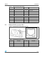
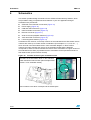
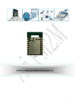
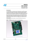
The STR910 evaluation board (STR910-EVAL) is a complete development platform for the
STMicroelectronic’s ARM® core-based STR91xF. Based on the ARM966ES core, the
STR91xF includes Pre-fetch Queue and Branch cache, full speed USB 2.0 compatible port,
Ethernet 100/10 interface, Embedded MAC, CAN2.0B compliant interface, a 2 Mbyte dual
bank Flash memory, a 96 Kbyte SRAM and many peripherals.
The STR910-EVAL board includes an STR910F microcontroller, pre-loaded demonstration
software and a full range of hardware features to help you evaluate device peripherals (such
as motor control, IrDA, USB, Ethernet, CAN) and develop your own applications. Extension
headers make it possible to easily connect a daughter board or wrapping board for your
specific application.
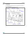
Figure 1.
STR910-EVAL evaluation board
Features
■
Three 5V power supply options: jack, USB connection or a daughter board
■
RTC with tamper detection
■
Audio play and record
■
Three RS232 connectors with support of full modem control on one connector
■
Infrared Data Access (IrDA)
■
USB 2.0 compliant with full-speed (12 Mb/s) data transmission
■
CAN 2.0B connection
■
Inductor motor control connector with 6 PWM output, emergency stop and tachometer
input
November 2007
Rev 3
1/46
www.st.com
UM0174
■
IEEE-802.3-2002 compliant Ethernet connection
■
Debug support via 20-pin JTAG connector
■
38-pin ETM connector for optional trace module
■
Dot-matrix LCD module
■
Joystick with 4-direction control and selector
■
Extension connectors for daughter board or wrapping board
About the user manuals...
This user manual provides information about using your STR910-EVAL and its hardware
features. This product includes the STR912FAW47X6 microcontroller with a 2 Mbyte
internal Flash memory. Earlier versions of the product include the STR912FAW44X6
microcontroller with a 512 Kbyte internal Flash memory.
For additional information about supporting software and tools, please refer to the STR9
microcontroller families web page on www.st.com.
Ordering information
To order the STR910 evaluation board, use the order code STR910-EVAL.
2/46
UM0174
Contents
Contents
About the user manuals... . . . . . . . . . . . . . . . . . . . . . . . . . . . . . . . . . . . . . . . . . . . . 2
Ordering information . . . . . . . . . . . . . . . . . . . . . . . . . . . . . . . . . . . . . . . . . . . . . . . . 2
1
Getting started . . . . . . . . . . . . . . . . . . . . . . . . . . . . . . . . . . . . . . . . . . . . . . 7
2
Hardware layout and configuration . . . . . . . . . . . . . . . . . . . . . . . . . . . . . 8
3
2.1
Power supply . . . . . . . . . . . . . . . . . . . . . . . . . . . . . . . . . . . . . . . . . . . . . . 10
2.2
Clock source . . . . . . . . . . . . . . . . . . . . . . . . . . . . . . . . . . . . . . . . . . . . . . . 11
2.3
Reset source . . . . . . . . . . . . . . . . . . . . . . . . . . . . . . . . . . . . . . . . . . . . . . 12
2.4
Ethernet . . . . . . . . . . . . . . . . . . . . . . . . . . . . . . . . . . . . . . . . . . . . . . . . . . 12
2.5
Audio features . . . . . . . . . . . . . . . . . . . . . . . . . . . . . . . . . . . . . . . . . . . . . 13
2.6
Serial Flash . . . . . . . . . . . . . . . . . . . . . . . . . . . . . . . . . . . . . . . . . . . . . . . 13
2.7
CAN . . . . . . . . . . . . . . . . . . . . . . . . . . . . . . . . . . . . . . . . . . . . . . . . . . . . . 13
2.8
RS232 and IrDA . . . . . . . . . . . . . . . . . . . . . . . . . . . . . . . . . . . . . . . . . . . . 14
2.9
Motor control . . . . . . . . . . . . . . . . . . . . . . . . . . . . . . . . . . . . . . . . . . . . . . 15
2.10
RTC and tamper . . . . . . . . . . . . . . . . . . . . . . . . . . . . . . . . . . . . . . . . . . . . 16
2.11
USB . . . . . . . . . . . . . . . . . . . . . . . . . . . . . . . . . . . . . . . . . . . . . . . . . . . . . 16
2.12
Development and debugging tool support . . . . . . . . . . . . . . . . . . . . . . . . 17
2.13
Display and input devices . . . . . . . . . . . . . . . . . . . . . . . . . . . . . . . . . . . . . 18
Connectors . . . . . . . . . . . . . . . . . . . . . . . . . . . . . . . . . . . . . . . . . . . . . . . 19
3.1
Motor control connector CN1 . . . . . . . . . . . . . . . . . . . . . . . . . . . . . . . . . . 20
3.2
Power supply connector CN2 . . . . . . . . . . . . . . . . . . . . . . . . . . . . . . . . . . 21
3.3
USB type B connector CN3 . . . . . . . . . . . . . . . . . . . . . . . . . . . . . . . . . . . 21
3.4
CAN type D, 9-pin male connector CN4 . . . . . . . . . . . . . . . . . . . . . . . . . . 22
3.5
ETM trace connector CN7 . . . . . . . . . . . . . . . . . . . . . . . . . . . . . . . . . . . . 22
3.6
RS232 with full modem control CN8 . . . . . . . . . . . . . . . . . . . . . . . . . . . . 23
3.7
JTAG debug connector CN9 . . . . . . . . . . . . . . . . . . . . . . . . . . . . . . . . . . . 24
3.8
RS232 connectors CN10 and CN12 . . . . . . . . . . . . . . . . . . . . . . . . . . . . 24
3.9
Ethernet RJ45 connector CN11 . . . . . . . . . . . . . . . . . . . . . . . . . . . . . . . . 25
3.10
Daughter board extension connector CN5 and CN6 . . . . . . . . . . . . . . . . 26
3/46
Contents
4
UM0174
Schematics . . . . . . . . . . . . . . . . . . . . . . . . . . . . . . . . . . . . . . . . . . . . . . . 30
Appendix A Implemented STR912F pin functions. . . . . . . . . . . . . . . . . . . . . . . . 39
Appendix B Product support . . . . . . . . . . . . . . . . . . . . . . . . . . . . . . . . . . . . . . . . . 43
Software updates . . . . . . . . . . . . . . . . . . . . . . . . . . . . . . . . . . . . . . . . . . . . . . . . . 43
Hardware spare parts . . . . . . . . . . . . . . . . . . . . . . . . . . . . . . . . . . . . . . . . . . . . . . 43
Sockets . . . . . . . . . . . . . . . . . . . . . . . . . . . . . . . . . . . . . . . . . . . . . . . . . . . . . . . . . 43
Connectors. . . . . . . . . . . . . . . . . . . . . . . . . . . . . . . . . . . . . . . . . . . . . . . . . . . . . . . 43
Getting prepared before you call. . . . . . . . . . . . . . . . . . . . . . . . . . . . . . . . . . . . . . 44
Revision history . . . . . . . . . . . . . . . . . . . . . . . . . . . . . . . . . . . . . . . . . . . . . . . . . . . . 45
4/46
UM0174
List of tables
List of tables
Table 1.
Table 2.
Table 3.
Table 4.
Table 5.
Table 6.
Table 7.
Table 8.
Table 9.
Table 10.
Table 11.
Table 12.
Table 13.
Table 14.
Table 15.
Table 16.
Table 17.
Table 18.
Table 19.
Table 20.
Table 21.
Table 22.
Power jumpers . . . . . . . . . . . . . . . . . . . . . . . . . . . . . . . . . . . . . . . . . . . . . . . . . . . . . . . . . . 11
Clock jumpers . . . . . . . . . . . . . . . . . . . . . . . . . . . . . . . . . . . . . . . . . . . . . . . . . . . . . . . . . . . 12
Ethernet jumpers . . . . . . . . . . . . . . . . . . . . . . . . . . . . . . . . . . . . . . . . . . . . . . . . . . . . . . . . 12
Audio jumpers . . . . . . . . . . . . . . . . . . . . . . . . . . . . . . . . . . . . . . . . . . . . . . . . . . . . . . . . . . . 13
CAN jumpers . . . . . . . . . . . . . . . . . . . . . . . . . . . . . . . . . . . . . . . . . . . . . . . . . . . . . . . . . . . 13
RS232 and IrDA jumpers . . . . . . . . . . . . . . . . . . . . . . . . . . . . . . . . . . . . . . . . . . . . . . . . . . 14
Motor control jumpers . . . . . . . . . . . . . . . . . . . . . . . . . . . . . . . . . . . . . . . . . . . . . . . . . . . . . 15
USB jumpers. . . . . . . . . . . . . . . . . . . . . . . . . . . . . . . . . . . . . . . . . . . . . . . . . . . . . . . . . . . . 16
ETM trace configuration . . . . . . . . . . . . . . . . . . . . . . . . . . . . . . . . . . . . . . . . . . . . . . . . . . . 17
LCD modules . . . . . . . . . . . . . . . . . . . . . . . . . . . . . . . . . . . . . . . . . . . . . . . . . . . . . . . . . . . 18
Motor control connector (CN1) . . . . . . . . . . . . . . . . . . . . . . . . . . . . . . . . . . . . . . . . . . . . . . 20
USB type B connector (CN3) . . . . . . . . . . . . . . . . . . . . . . . . . . . . . . . . . . . . . . . . . . . . . . . 21
CAN type D, male 9-pin male connector (CN4) . . . . . . . . . . . . . . . . . . . . . . . . . . . . . . . . . 22
ETM trace connector (CN7) . . . . . . . . . . . . . . . . . . . . . . . . . . . . . . . . . . . . . . . . . . . . . . . . 22
RS232 connector (CN8) with full modem support. . . . . . . . . . . . . . . . . . . . . . . . . . . . . . . . 23
JTAG debug connector (CN9) . . . . . . . . . . . . . . . . . . . . . . . . . . . . . . . . . . . . . . . . . . . . . . 24
RS232 connectors (CN10, CN12) . . . . . . . . . . . . . . . . . . . . . . . . . . . . . . . . . . . . . . . . . . . 25
Ethernet RJ45 connector (CN11) . . . . . . . . . . . . . . . . . . . . . . . . . . . . . . . . . . . . . . . . . . . . 25
Daughter board extension connector (CN5) . . . . . . . . . . . . . . . . . . . . . . . . . . . . . . . . . . . . 26
Daughter board extension connector (CN6) . . . . . . . . . . . . . . . . . . . . . . . . . . . . . . . . . . . . 28
Implemented pin functions of the STR912FAW47X6 . . . . . . . . . . . . . . . . . . . . . . . . . . . . . 39
Document revision history . . . . . . . . . . . . . . . . . . . . . . . . . . . . . . . . . . . . . . . . . . . . . . . . . 45
5/46
List of figures
UM0174
List of figures
Figure 1.
Figure 2.
Figure 3.
Figure 4.
Figure 5.
Figure 6.
Figure 7.
Figure 8.
Figure 9.
Figure 10.
Figure 11.
Figure 12.
Figure 13.
Figure 14.
Figure 15.
Figure 16.
Figure 17.
Figure 18.
Figure 19.
Figure 20.
Figure 21.
Figure 22.
Figure 23.
Figure 24.
6/46
STR910-EVAL evaluation board. . . . . . . . . . . . . . . . . . . . . . . . . . . . . . . . . . . . . . . . . . . . . . 1
Connecting development tools . . . . . . . . . . . . . . . . . . . . . . . . . . . . . . . . . . . . . . . . . . . . . . . 7
Hardware block diagram . . . . . . . . . . . . . . . . . . . . . . . . . . . . . . . . . . . . . . . . . . . . . . . . . . . . 8
STR910-EVAL evaluation board layout . . . . . . . . . . . . . . . . . . . . . . . . . . . . . . . . . . . . . . . . 9
Settings for two-pin jumpers . . . . . . . . . . . . . . . . . . . . . . . . . . . . . . . . . . . . . . . . . . . . . . . . 10
STR910-EVAL evaluation board connectors . . . . . . . . . . . . . . . . . . . . . . . . . . . . . . . . . . . 19
Motor control connector (CN1, top view) . . . . . . . . . . . . . . . . . . . . . . . . . . . . . . . . . . . . . . 20
Power supply connector (CN2, front view) . . . . . . . . . . . . . . . . . . . . . . . . . . . . . . . . . . . . . 21
USB type B connector (CN3, front view) . . . . . . . . . . . . . . . . . . . . . . . . . . . . . . . . . . . . . . 21
CAN type D, 9-pin male connector (CN4, front view) . . . . . . . . . . . . . . . . . . . . . . . . . . . . . 22
ETM trace connector (CN7, top view). . . . . . . . . . . . . . . . . . . . . . . . . . . . . . . . . . . . . . . . . 22
RS232 connector (CN8, front view) . . . . . . . . . . . . . . . . . . . . . . . . . . . . . . . . . . . . . . . . . . 23
JTAG debug connector (CN9, top view) . . . . . . . . . . . . . . . . . . . . . . . . . . . . . . . . . . . . . . . 24
RS232 connectors (CN10 and CN12, front view) . . . . . . . . . . . . . . . . . . . . . . . . . . . . . . . . 24
Ethernet RJ45 connector (CN11, front view) . . . . . . . . . . . . . . . . . . . . . . . . . . . . . . . . . . . 25
Find the version of your evaluation board. . . . . . . . . . . . . . . . . . . . . . . . . . . . . . . . . . . . . . 30
STR910-EVAL microcontroller connections . . . . . . . . . . . . . . . . . . . . . . . . . . . . . . . . . . . . 31
Power supply . . . . . . . . . . . . . . . . . . . . . . . . . . . . . . . . . . . . . . . . . . . . . . . . . . . . . . . . . . . 32
CAN and USB connections. . . . . . . . . . . . . . . . . . . . . . . . . . . . . . . . . . . . . . . . . . . . . . . . . 33
UART and IrDA connections. . . . . . . . . . . . . . . . . . . . . . . . . . . . . . . . . . . . . . . . . . . . . . . . 34
Ethernet connection . . . . . . . . . . . . . . . . . . . . . . . . . . . . . . . . . . . . . . . . . . . . . . . . . . . . . . 35
Audio peripherals . . . . . . . . . . . . . . . . . . . . . . . . . . . . . . . . . . . . . . . . . . . . . . . . . . . . . . . . 36
JTAG, ETM and daughter board connections . . . . . . . . . . . . . . . . . . . . . . . . . . . . . . . . . . 37
LCD and joystick . . . . . . . . . . . . . . . . . . . . . . . . . . . . . . . . . . . . . . . . . . . . . . . . . . . . . . . . . 38
UM0174
1
Getting started
Getting started
Your STR910-EVAL is designed with a full range of hardware features that will help you
rapidly evaluate microcontroller peripherals and develop your own applications. Descriptions
of hardware features and configurations are provided in Section 2 on page 8.
Demonstration software is preloaded in the board’s flash memory for easy demonstration of
device peripherals in stand-alone mode. For more information refer to the demonstration
software getting started.
Your STR910-EVAL is also designed for use as an application development platform and
reference design, and supports connection to a full range of in-circuit debugging tools and
integrated development environments.
To start using your STR910-EVAL evaluation board for application development, you will
have to set up your development tools and connect to the STR91xF.
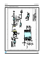
1.
Connect to your STR910-EVAL via the 20-pin JTAG connector.
A 38-pin ETM connector is also provided, allowing you to connect to and use your
microcontroller’s Embedded Trace Macrocell during debugging. For additional
configuration information, see Section 2.12 on page 17
2.
Power up the evaluation board.
The board can be powered by 5V from either the jack for external power supply, USB
connector, or a daughter board. For additional configuration information, see
Section 2.1 on page 10.
3.
Connect to the device from the debugging software on your host PC.
The BCD files, FME file and installation instructions that you will need to update your
debugging software are available for free download at the STMicroelectronics
microcontrollers support site on www.st.com.
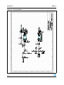
Figure 2.
Connecting development tools
Host PC running your
debugging software /
integrated development
environment
In-circuit emulator
In-circuit emulator
connects via 20-pin
JTAG standard
connector
Trace tool / connection
(optional)
Optional trace tool connects
to the STR91xF via a 38-pin
ETM connector.
7/46
Hardware layout and configuration
2
UM0174
Hardware layout and configuration
The STR910-EVAL is designed around the STR912FAW47X6 ARM966E-S in 128-pin LQFP
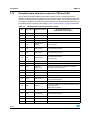
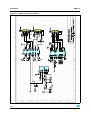
package. The hardware block diagram of the STR910-EVAL (Figure 2) illustrates the layout
of the board relative to the STR91xF peripherals and Figure 4 will help you locate these
features on the actual evaluation board.
Figure 3.
Hardware block diagram
Peripheral implementation on the STR910-EVAL board requires the use of alternate pin
functions supported by the STR912FAW47X6. A table of alternate pin functions used in this
design is provided in Appendix A.
8/46
UM0174
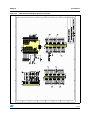
Figure 4.
Hardware layout and configuration
STR910-EVAL evaluation board layout
Daughter board
extension connectors,
CN5, CN6
Motor control
connector, CN1
Speaker, U5
Power supply
jack, CN2
USB type B
connector, CN3
STR912, U10
IrDA, U9
CAN D-type 9pin connector,
CN4
ETM
connector, CN7
RS232 with
full modem
support, CN8
JTAG debug
connector, CN9
Battery, BT1
RS232
connectors,
CN10, CN12
Ethernet
connector, CN11
Graphic LCD
Module, U19
Potentiometer,
RV2
General purpose
key, PB3
Microphone,
U21
Tamper_IN, PB1
RESET, PB2
Joystick, U20
9/46
Hardware layout and configuration
UM0174
The following sections provide jumper settings for configuring your STR910-EVAL
evaluation board and peripherals, including:
●
Power supply
●
RS232 and IrDA
●
Clock source
●
Motor control
●
Reset source
●
RTC and tamper
●
Ethernet
●
USB
●
Audio features
●
Development and debugging tool support
●
Serial Flash
●
Display and input devices
●
CAN
Two types of jumpers are used on the STR910-EVAL evaluation board:
●
3-pin jumpers with two possible positions, for which settings are presented in
schematics in the following sections
●
2-pin jumpers with two possible settings: Fitted– the circuit is closed, and Not fitted–
the circuit is open (see Figure 5)
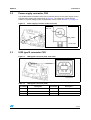
Figure 5.
Settings for two-pin jumpers
Not fitted
2.1
Fitted
Power supply
STR910-EVAL evaluation board is designed to be powered by a 5V DC power supply. It is
possible to configure the evaluation board to use any of the following three sources for the
power supply:
●
5V DC power adapter connected to the power supply jack (CN2, or PSU for Power
Supply Unit on the silk screen).
●
5V DC power with 500mA limitation via the USB type-B connector (CN3, or USB on
the silk screen).
●
5V DC power from the daughter board extension connectors (CN5 and CN6, DTB
for Daughter Board on the silk-screen).
There is also a 3V button battery, which can be used as a backup power supply for both the
RTC and the internal RAM of the STR91xF microcontroller.
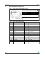
The power supply is configured by setting the related jumpers, JP2, JP3, JP4, JP6 and
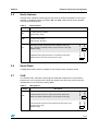
JP15 as described in Table 1.
10/46
UM0174
Hardware layout and configuration
Table 1.
Power jumpers
Jumper
JP6
Description
Selects one of the three possible 5V DC power supply sources:
DTB
Enables consumption measurement of 1.8V STR91xF CPU core power supply.
Default setting: Fitted
JP3
Enables consumption measurement of STR91xF analog power supply (AVDD).
Default setting: Fitted
JP15
Enables consumption measurement of STR91xF backup power supply (VBAT).
Default setting: Fitted
USB
PSU
JP4
USB
DTB
Enables consumption measurement of 3.3V STR91xF I/O power supply (VDDQ).
Default setting: Fitted
USB
PSU
JP2
USB
DTB
For power supply from USB (CN3), JP6 is set as shown to the
right:
If a daughter board is connected on CN5 and CN6, it must not
have its own power supply connected. The USB connection
supplies power to both the STR910-EVAL evaluation board and
the daughter board.
PSU
For power supply from the daughter board connectors (CN5
and CN6), JP6 is set as shown to the right:
DTB
For Power supply jack (CN2) to both STR910-EVAL evaluation
board and a daughter board connected to CN5 and CN6, JP6 is
set as shown to the right:
PSU
For Power supply jack (CN2) to the STR910-EVAL only, JP6 is
set as shown to the right:
(Default setting)
The LD1 LED is lit when the STR910-EVAL evaluation board is powered correctly.
2.2
Clock source
Four clock sources are available on the STR910-EVAL evaluation board for the
microcontroller, USB, RTC and Ethernet PHY transceiver.
●
X1– 25MHz crystal for STR91xF microcontroller
●
X2– 32KHz crystal for embedded RTC
●
X3– 25MHz crystal for Ethernet PHY transceiver U15
●
U12– 48MHz oscillator for USB
USB and Ethernet PHY are also able to run using the clock from the STR91xF. The clock
system can be configured by setting the jumpers JP25 and JP17 as described in Table 2.
11/46
Hardware layout and configuration
Table 2.
UM0174
Clock jumpers
Jumper
Description
JP25
Sets the clock source for Ethernet PHY to X3 or STR91xF.
2
MAC
1
2
Enables the external USB 48MHz clock source.
To use an external oscillator via P27 of the STR91xF for the USB clock input, JP17 is
fitted.
To use the internal clock of the STR91xF, JP17 is not fitted. In this case P27 can be
used for an alternate function.
Default setting: Not fitted
JP17
2.3
MAC
1
EXT
To use the 25MHz clock from X3, set JP25 as shown on the
right:
EXT
To use the 25MHz clock from the STR91xF P52, set JP25 as
shown on the right:
(Default setting)
Reset source
The reset signal of STR910-EVAL evaluation board is low active.
The reset sources include:
2.4
●
Power On Reset from STM1001 (U7)
●
Reset button (PB2)
●
Debugging tools via the CN9 or CN7 connector
●
Daughter board via the CN6 connector
Ethernet
The STR910-EVAL supports IEEE-802.3-2002 compliant Ethernet communication via the
MII interface PHY transceiver– STE100P with PHY address 10101b and integrated RJ45
connector with embedded transformer. JP24 enables/disables Ethernet support.
Table 3.
Jumper
JP24
Ethernet jumpers
Description
PHY transceiver STE100P is in Power Down mode when JP24 is not fitted.
Default setting: Fitted
Two embedded LEDs (yellow and green) for the RJ45 connector show current status of
Ethernet connection:
12/46
●
Yellow LED – blinking indicates transmission or reception via Ethernet
●
Green LED – is lit when a good link test has been detected
UM0174
2.5
Hardware layout and configuration
Audio features
STR910-EVAL evaluation board supports both audio recording and playback. This can be
disabled or enabled by setting of jumpers JP5 and JP26. Audio volume can be adjusted
using the potentiometer RV1.
Table 4.
Audio jumpers
Jumper
Description
Audio power amplifier TS4871 is forced into standby mode when JP5 (SPEAKER on
the silk-screen) is not fitted.
Default setting: Fitted
JP26
Microphone pre-amplifier MAX4061 is forced into shutdown mode when JP26 (MIC on
the silk-screen) is fitted.
Default setting: Not fitted
JP1
Audio play circuit is connected to P46 of STR91xF when JP1
(FIX_V & Audio on the silk-screen) is set as shown on the right:
(Default setting)
FIX V
1
Audio
1
2.6
2
FIX V
Adjustable analog signal from RV2 is connected to P46 of the
STR91xF when JP1 is set as shown on the right:
Audio
JP5
2
Serial Flash
A 64Mbit SPI interface Flash is available on the STR910-EVAL evaluation board.
2.7
CAN
The STR910-EVAL evaluation board supports CAN2.0B compliant bus communication
based on the 3.3V CAN transceiver. Both high-speed mode and slope-control mode are
available and can be selected by setting JP10.
Table 5.
Jumper
Description
1
2
SLOPE
HIGH
CAN transceiver functions in high-speed mode when JP10 is set
as shown on the right:
(Default setting)
SLOPE
CAN transceiver functions in slope-control mode when JP10
(HIGH or SLOPE on silk-screen) is set as shown to the right:
HIGH
JP10
CAN jumpers
1
2
13/46
Hardware layout and configuration
Table 5.
CAN jumpers (continued)
Jumper
JP12
2.8
UM0174
Description
CAN terminal resistor is enabled when JP12 (CAN terminal) is fitted.
Default setting: Not fitted
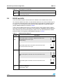
RS232 and IrDA
Three channels for RS232 communication are available on the STR910-EVAL board.
Two channels UART2 and UART3, use the RS232 transceiver U14 and two male D-type 9pin connectors CN10 and CN12. IrDA communication is supported as a multiplex function
on UART2. You can activate the IrDA transceiver and enable IrDA on UART2 by setting
jumpers JP13 and JP11 as indicated in Table 6.
UART1 uses the RS232 transceiver U13 with full modem control support and the male Dtype 9-pin connector CN8. For this feature, the DTR signal is multiplexed using the same pin
that is otherwise used for the RXD signal on UART2. You can select between the UART2
RXD and UART1 DTR signal by setting JP14 as indicated in Table 6.
Table 6.
Jumper
Description
1
1
2
U1DTR
U2RXD
UART2 RXD signal is used when JP14 is set as shown on the
right:
U1DTR
U2RXD
1
14/46
2
Allows selection of either UART2 or UART1 with full modem control support.
UART1 DTR signal is used when JP14 is set as shown on the
right:
JP11
UART2
1
JP14
2
IrDA
UART2 RXD signal will be connected to IrDA transceiver when
JP13 is set as shown on the right:
UART2
UART2 RXD signal is connected to RS232 transceiver when
JP13 is set as shown on the right:
(default setting)
IrDA
JP13
RS232 and IrDA jumpers
2
Shuts down IrDA transceiver. IrDA is enabled when JP11 is fitted while IrDA is disabled
when JP11 is Not fitted.
Default setting: Fitted
UM0174
Hardware layout and configuration
Table 6.
RS232 and IrDA jumpers (continued)
Jumper
Description
Jumpers JP18, JP19, JP21, JP22 and JP23 enable signals for UART1 with full modem control
2.9
JP18
UART1 DCD signal is enabled when JP18 is fitted.
Default setting: Fitted
JP19
UART1 DSR signal is enabled when JP19 is fitted.
Default setting: Fitted
JP21
UART1 CTS signal is enabled when JP21 is fitted.
Default setting: Fitted
JP22
UART1 RI signal is enabled when JP22 is fitted.
Default setting: Fitted
JP23
UART1 RTS signal is enabled when JP23 is fitted.
Default setting: Fitted
Motor control
STR910-EVAL board supports induction motor control via a 34-pin connector CN1, which
provides all required control and feedback signals to and from a motor power-drive board.
Available signals on this connector include emergency stop, motor speed, 3-phase motor
current, bus voltage, Heatsink temperature from the motor drive board and 6 channels of
PWM control signals going to the motor drive circuit.
Emergency stop, motor current sampling and motor speed detection are enabled by setting
jumpers JP16, JP7 and JP8.
The potentiometer (RV2) can be used to control motor speed when JP1 is configured to
connect RV2 to P46 of the STR91xF. See Table 4 on page 13.
Table 7.
Jumper
JP16
Motor control jumpers
Description
JP16 enables the emergency stop function on P67 of the motor control connector CN1.
P67 of the STR91xF is shared by both motor control and ETM trace support.
2
ETM
1
JP7
ETM
1
MC
P67 is used for external trigger of ETM tracing when JP16 is set
as shown on the right:
MC
P67 is used for motor control emergency stop detection when
JP16 (MC or ETM on silk-screen) is set as shown on the right:
(default setting)
2
Motor current sampling operation is enabled when JP7 is fitted (P40 connected to
P43). The I/O pins P40 and P43 are disconnected and can be used by a daughter
board when JP7 is not fitted.
Default setting: Fitted
15/46
Hardware layout and configuration
Table 7.
UM0174
Motor control jumpers (continued)
Jumper
Description
STR91xF I/O pin P25 is used as external clock of timer for motor control when JP8 is
fitted. P25 can be used by a daughter board when JP8 is not fitted.
Default setting: Fitted
JP8
Note:
When using the motor control connector, ensure that JP9 is set to allow the use of P0.1 on
the STR910F for motor control. JP9 can be configured to use P0.1 for the USB peripheral.
See Table 8 on page 16.
2.10
RTC and tamper
A 32KHz crystal X2 is available for the embedded RTC inside the STR91xF. The push
button PB1 can be used to simulate a tamper event on the RTC.
2.11
USB
The STR910-EVAL evaluation board offers USB 2.0 compliant communication via a USB
type-B connector (CN3) with full-speed (12Mb/s) data transfer. The evaluation board and
daughter board can be powered from this USB connection at 5V DC with a 500mA current
limitation.
Two clock sources are available for USB:
●
PLL generated clock from the STR91xF
●
External oscillator U12
Clock source is selected by setting JP17. Refer to Table 2: Clock jumpers on page 12 for
configuration details.
The unplugging of hardware from the USB connector (CN3) can be simulated by your
application software. USB hardware disconnect simulation is enabled by configuring the
jumper JP9, as described in Table 8.
Table 8.
Jumper
JP9
USB jumpers
Description
JP9 can be used to enable USB hardware disconnect simulation using P0.1 on the
STR910F. P0.1 of the STR91xF can be used either for Motor Control or USB.
USB hardware disconnect simulation is enabled and P0.1 of the
STR910F is used by the USB peripheral when JP9 is set as
shown to the right:
In this case, the USB pull up resistor (R10) is connected to pin 3
of the USB connector.
USB hardware disconnect simulation is disabled, and P0.1 of
the STR910F is used by the Motor Control connector (C1) when
JP9 is set as shown to the right:
(Default setting)
16/46
1
2
1
2
UM0174
2.12
Hardware layout and configuration
Development and debugging tool support
The STR910-EVAL evaluation board supports connection to both In-Circuit Emulators (ICE)
via a 20-pin standard JTAG interface and Trace tools via a 38-pin Embedded Trace
Macrocell (ETM) interface.
To enable the ETM trace feature, some alternate circuit functions have to be disconnected
by setting the jumpers listed in Table 9. Motor control, UART1 full modem control support
and USB external 48MHz clock use STR91xF I/O pins that are required for the ETM trace
connection on CN7. These features will be restricted when ETM trace is used. The
evaluation board can not be connected to a motor control drive board on connector CN1.
To ensure the integrity of high-speed signals on the ETM trace connections, each ETM
signal should have a single point-to-point connection from STR91xF microcontroller to the
38-pin ETM connector. Stub tracks ("dead-end" extensions to the signal track) should be
eliminated. If you encounter problems when using ETM connector, you can remove the
resistors indicated in Table 9 to avoid stub and improve signal quality on the ETM
connection.
Table 9.
Pin on CN7
6
ETM trace configuration
Description
TRACECLK
To disable alternate function
Disconnect motor power drive board
connected to CN1
To avoid stub
Remove R34
Keep JP16 set as shown below:
10
EXTTRIG
No change
1
2
24
TRACEPKT[3]
JP22 is not fitted (UART1 RI signal is
disabled)
Remove R35
26
TRACEPKT[2]
JP18 is not fitted (UART1 DCD signal is
disabled)
Remove R36
28
TRACEPKT[1]
JP19 is not fitted (UART1 DSR signal is
disabled)
Remove R37
30
TRACEPKT[0]
JP21 is not fitted (UART1 CTS signal is
disabled)
Remove R38
32
TRACESYNC
JP17 is not fitted (external USB48MHz clock
P27 source is disable)
Remove R39
34
PIPESTAT[2]
No
Remove R40
36
PIPESTAT[1]
JP8 is not fitted (Motor control Encoder A pin
on CN1 connector is disabled)
Remove R41
38
PIPESTAT[0]
No
Remove R42
17/46
Hardware layout and configuration
2.13
UM0174
Display and input devices
32x122 pixel graphic LCD and 4 general purpose LED's (LD2, 3, 4, 5) are available as
display devices. A 4-direction joystick with selection key and one general purpose button
(PB3) are available as input devices.
STR910-EVAL also supports a second optional 2x16 character LCD that can be mounted
on the U17 connector.
Table 10.
LCD modules
Graphic LCD U19 (default)
Pin on U19
18/46
Description
Pin on
STR91xF
Character LCD U17 (optional)
Pin on U17
Description
Pin on
STR91xF
1
GND
GND
1
GND
GND
2
VDD
3.3V
2
VDD
3.3V
3
VO
3
VO
4
RS
4
RS
P97
5
NC
5
RW
P96
6
E2
6
E
P94
7
NC
7
DB0
P80
8
E1
P94
8
DB1
P81
9
RW
P96
9
DB2
P82
10
DB0
P80
10
DB3
P83
11
DB1
P81
11
DB4
P84
12
DB2
P82
12
DB5
P85
13
DB3
P83
13
DB6
P86
14
DB4
P84
14
DB7
P87
15
DB5
P85
15
A
+5V
16
DB6
P86
16
K
GND
17
DB7
P87
18
RST
RESET#
19
A
+5V
20
K
GND
P97
P95
UM0174
3
Connectors
Connectors
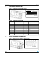
The following sections provide pin descriptions for the STR910-EVAL evaluation board
connectors shown in Figure 6.
Figure 6.
STR910-EVAL evaluation board connectors
USB type B
connector CN3
CAN type D, 9-pin
male connector CN4
JTAG debug
connector CN9
ETM trace
connector CN7
Ethernet RJ45
connector CN11
Motor control
connector CN1
Power supply
connector CN2
Daughter board extension
connector CN5 and CN6
RS232 with full
modem control CN8
RS232 connectors
CN10 and CN12
19/46
Connectors
3.1
UM0174
Motor control connector CN1
Figure 7.
Motor control connector (CN1, top view)
33 31 29 27 25 23 21 19 17 15 13 11 9 7 5
3
1
34 32 30 28 26 24 22 20 18 16 14 12 10 8 6
4
2
Top view
Table 11.
Motor control connector (CN1)
Pin number
20/46
Description
Pin number
Description
1
EMERGENCY STOP
2
GND
3
PWM-UH
4
GND
5
PWM-UL
6
GND
7
PWM-VH
8
GND
9
PWM-VL
10
GND
11
PWM-WH
12
GND
13
PWM-WL
14
BUS VOLTAGE
15
PHASE A CURRENT
16
GND
17
PHASE B CURRENT
18
GND
19
PHASE C CURRENT
20
GND
21
NTC BYPASS RELAY
22
GND
23
DISSIPATIVE BRAKE PWM
24
GND
25
+5V power
26
Heatsink temperature
27
PFC SYNC
28
3.3V power
29
PFC PWM
30
GND
31
Encoder A
32
GND
33
Encoder B
34
Encoder index
UM0174
3.2
Connectors
Power supply connector CN2
Your STR910-EVAL evaluation board can be powered from a DC 5V power supply via the
external power supply jack (CN2) shown in Figure 8. The central pin of CN2 must be
positive. For power supply jumper configurations, refer to section Section 2.1 on page 10.
Figure 8.
Power supply connector (CN2, front view)
DC +5V
GND
Front view
3.3
USB type B connector CN3
Figure 9.
USB type B connector (CN3, front view)
Front view
Table 12.
USB type B connector (CN3)
Pin number
Description
1
VBUS (Power)
2
DM
3
DP
Pin number
Description
4
GND
5, 6
Shield
21/46
Connectors
3.4
UM0174
CAN type D, 9-pin male connector CN4
Figure 10. CAN type D, 9-pin male connector (CN4, front view)
Front view
Table 13.
CAN type D, male 9-pin male connector (CN4)
Pin number
1, 4, 5
3.5
Description
Pin number
Description
NC
7
CANH
2
CANL
9
CANV+ (3.3V)
3, 6, 8
GND
ETM trace connector CN7
Figure 11. ETM trace connector (CN7, top view)
Top view
Table 14.
ETM trace connector (CN7)
Pin number
22/46
Description
Pin number
Description
1, 2, 3, 4, 16, 18, 20, 22, 23,
Not Connected
25, 27, 29, 13, 33, 35, 37
17
TMS
5
19
TDI
GND
UM0174
Connectors
Table 14.
ETM trace connector (CN7) (continued)
Pin number
3.6
Description
Pin number
Description
6
TRACECLK
21
TRST
7
DBGRQ
24
TRACEPKT[3]
8
DBGACK
26
TRACEPKT[2]
9
nSRST
28
TRACEPKT[1]
10
EXTTRIG
30
TRACEPKT[0]
11
TDO
32
12
Vtref
34
PIPESTAT[2]
13
RTCK
36
PIPESTAT[1]
14
Vsupply
38
PIPESTAT[0]
15
TCK
RS232 with full modem control CN8
Figure 12. RS232 connector (CN8, front view)
Front view
Table 15.
RS232 connector (CN8) with full modem support
Pin number
Description
Pin number
Description
1
UART1_DCD
6
UART1_DSR
2
UART1_RXD
7
UART1_RTS
3
UART1_TXD
8
UART1_CTS
4
UART1_DTR
9
UART1_RI
5
GND
23/46
Connectors
3.7
UM0174
JTAG debug connector CN9
Figure 13. JTAG debug connector (CN9, top view)
19 17 15 13 11 9 7 5
3
1
20 18 16 14 12 10 8 6
4
2
Top view
Table 16.
JTAG debug connector (CN9)
Pin number
3.8
Description
Pin number
Description
1
3.3V power
2
3.3V power
3
TRST
4
GND
5
TDI
6
GND
7
TMS
8
GND
9
TCK
10
GND
11
RTCK
12
GND
13
TDO
14
GND
15
nSRST
16
GND
17
DBGRQ
18
GND
19
DBGACK
20
GND
RS232 connectors CN10 and CN12
Figure 14. RS232 connectors (CN10 and CN12, front view)
Front view
24/46
UM0174
Connectors
Table 17.
RS232 connectors (CN10, CN12)
Pin number
Description
Pin number
Description
CN10
1
NC
2
3
UART2_TXD
4
5
GND
6
7
9
UART2_RXD
8
NC
CN12
1
NC
2
3
UART3_TXD
4
5
GND
6
7
9
3.9
UART3_RXD
8
NC
Ethernet RJ45 connector CN11
Figure 15. Ethernet RJ45 connector (CN11, front view)
Front view
Table 18.
Ethernet RJ45 connector (CN11)
Pin number
Description
Pin number
Description
1
TxData+
5
Shield
2
TxData-
6
RxData-
3
RxData+
7
Shield
4
Shield
8
Shield
25/46
Connectors
3.10
UM0174
Daughter board extension connector CN5 and CN6
Two 50-pin male headers CN5 and CN6 can be used to connect a daughter board or
standard wrapping board to the STR910-EVAL evaluation board. All 80 GPI/Os and the EMI
interface control signals are available on these connectors. Each pin on CN5 and CN6 can
be used by a daughter board after disconnecting it from the corresponding function block on
the STR910-EVAL evaluation board. Refer to Table 19 and Table 20 on page 28 for details.
Table 19.
Pin
26/46
Daughter board extension connector (CN5)
To disconnect from the
STR910-EVAL function block
Description Alternate function
1
GND
-
-
3
P16
Ethernet
Remove R69
5
P76
Joystick
Remove R68
7
P47
Microphone
Remove R60
9
P46
Motor control
speaker
JP1 is not fitted
11
P44
Motor control
Disconnect STR910-EVAL evaluation board from
motor power drive board
13
P42
Motor control
Disconnect STR910-EVAL evaluation board from
motor power drive board
15
P40
Motor control
Disconnect STR910-EVAL evaluation board with
motor power drive board.
JP7 is not fitted.
17
P71
Ethernet
Remove R51
19
GND
None
-
21
P20
ETM trace
UART1 CTS
Disconnect STR910-EVAL evaluation board from
ETM tracer. JP21 is not fitted.
23
P50
CAN RX
Remove R16
25
P74
Joystick
Remove R91
27
P51
UART1 RXD
Remove R59
29
P63
Motor control
Disconnect STR910-EVAL evaluation board from
motor power drive board
31
EMI_WRL
None
-
33
P52
Ethernet
Make sure the Ethernet clock is from external crystal
by setting of JP25.
Please refer to table2.3.
35
P53
Ethernet
Remove R71
37
P60
Motor control
Disconnect STR910-EVAL evaluation board from
motor power drive board
39
GND
None
-
41
P83
LCD
Remove R88
43
P84
LCD
Remove R65
UM0174
Connectors
Table 19.
Daughter board extension connector (CN5) (continued)
To disconnect from the
STR910-EVAL function block
Pin
Description Alternate function
45
P85
LCD
Remove R89
47
P86
LCD
Remove R66
49
D5V(note1)
None
-
2
P14
Ethernet
Remove R52
4
P15
Ethernet
Remove R76
6
P17
Ethernet
Remove R74
8
P77
Joystick
Remove R92
10
GND
None
-
12
P45
Motor control
Disconnect STR910-EVAL evaluation board from
motor power drive board
14
P43
Motor control
JP7 is not fitted.
16
P41
Motor control
Disconnect STR910-EVAL evaluation board from
motor power drive board
18
P70
Motor control
Disconnect STR910-EVAL evaluation board from
motor power drive board
20
P72
Motor control
Disconnect STR910-EVAL evaluation board from
motor power drive board.
JP8 is not fitted.
22
P21
ETM trace
UART1 DSR
Disconnect STR910-EVAL evaluation board from
ETM tracer. JP19 is not fitted.
24
P73
Motor control
Disconnect STR910-EVAL evaluation board from
motor power drive board
26
P75
Joystick
Remove R67
28
P62
Motor control
Disconnect STR910-EVAL evaluation board from
motor power drive board
30
GND
None
-
32
EMI_WRH
None
-
34
P80
LCD
Remove R63
36
P81
LCD
Remove R87
38
P82
LCD
Remove R64
40
P61
Motor control
Disconnect STR910-EVAL evaluation board from
motor power drive board
42
P22
ETM
UART1 DCD
Disconnect STR910-EVAL evaluation board from
ETM tracer. JP18 is not fitted.
44
P23
ETM
UART1 RI
Disconnect STR910-EVAL evaluation board from
ETM tracer. JP22 is not fitted.
46
P24
ETM
Disconnect STR910-EVAL evaluation board from
ETM trace
27/46
Connectors
UM0174
Table 19.
Pin
Description Alternate function
48
P87
50
GND
Table 20.
Pin
28/46
Daughter board extension connector (CN5) (continued)
LCD
To disconnect from the
STR910-EVAL function block
Remove R90
Daughter board extension connector (CN6)
To disconnect from the
STR910-EVAL function block
Description Alternate function
1
GND
None
-
3
P12
Ethernet
Remove R77
5
P11
Ethernet
Remove R53
7
P67
ETM
Motor control
Place JP16 in position 1•2 and remove R105.
9
TAMPER_IN None
-
11
RESET#
None
-
13
P05
Ethernet
Remove R56
15
P64
Motor control
Disconnect STR910-EVAL evaluation board from
motor power drive board
17
P56
SPI Flash
Remove R15
19
D5V(note1)
No
-
21
P03
Ethernet
Remove R73
23
EMI_ALE
None
-
25
P54
SPI Flash
-
27
P37
Motor control
Disconnect STR910-EVAL evaluation board from
motor power drive board
29
P00
Ethernet
Remove R78
31
P35
UART3 TX
-
33
P34
UART1 TX
-
35
P33
UART1 RTS
UART2 TX
-
37
P31
UART3 RX
Remove R75
39
GND
None
-
41
P27
ETM trace
USB clock
Disconnect STR910-EVAL evaluation board from
ETM racer. JP17 is not fitted.
43
P94
LCD
Remove R62
45
P92
LED2
Remove R83
47
P90
LED0
Remove R81
UM0174
Connectors
Table 20.
Note:
Daughter board extension connector (CN6) (continued)
To disconnect from the
STR910-EVAL function block
Pin
Description Alternate function
49
P25
ETM Trace
Motor control
Disconnect STR910-EVAL evaluation board from
ETM trace. JP8 is not fitted.
2
P13
Ethernet
Remove R70
4
RST_OUT
None
-
6
P10
Ethernet
Remove R54
8
P66
ETM trace
Motor control
Disconnect STR910-EVAL evaluation board from
ETM trace
10
GND
None
-
12
P07
Ethernet
Remove R79
14
P06
Ethernet
Remove R72
16
P65
Motor control
Disconnect STR910-EVAL evaluation board from
motor power drive board
18
P57
SPI Flash
Remove R14
20
P04
Ethernet
Remove R80
22
P55
SPI Flash
-
24
EMI_RD
None
-
26
P02
Ethernet
Remove R55
28
P01
Motor control or
USB hardware
disconnect
simulation
Disconnect STR910-EVAL evaluation board from
motor power drive board and place JP9 in position
1•2.
30
GND
None
-
32
P36
CAN TX
-
34
P97
LCD
Remove R61
36
P96
LCD
Remove R86
38
P32
UART1 DTR
UART2 RX
JP14 is not fitted.
40
P95
LCD
Remove R85
42
P30
Motor control
Disconnect STR910-EVAL evaluation board from
motor power drive board
44
P26
ETM Trace
Disconnect STR910-EVAL evaluation board from
ETM trace
46
P93
LED3
Remove R84
48
P91
LED1
Remove R82
50
GND
None
-
The D5V pin can be used to power the STR910-EVAL board from the power supply provided
by the daughter board.
29/46
Schematics
4
UM0174
Schematics
This section provides design schematics for the STR910-EVALboard key features, which
are provided to help you implement these features in your own application designs.
Schematics are provided for:
●
STR910F microcontroller connections (Figure 17)
●
Power supply (Figure 18)
●
CAN and USB connectors (Figure 19)
●
UART and IrDA connectors (Figure 20)
●
Ethernet connector (Figure 21)
●
Audio record and playback features (Figure 22)
●
JTAG and ETM connectors (Figure 23)
●
LCD and joystick features (Figure 24)
Schematics have versions, as do major versions of the evaluation board. Schematic version
numbers are made up of a letter number combination (for example A.0, A.1, B.0, B.1, ...),
which is found in the information block in each schematic diagram. In these version
numbers, the letter indicates the version of the evaluation board that the drawings
correspond to, and the number indicates the revision of the schematics for a given version of
the evaluation board. Zero (0) indicates that the schematics for the specified board are in
their initial version (have not been revised).
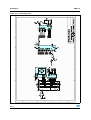
Figure 16. Find the version of your evaluation board
The letters in the information block on the evaluation
board indicate the board version (this example shows
version C of an evaluation board).
Note: numbers in this block correspond to the board layers.
30/46
UM0174
Schematics
Figure 17. STR910-EVAL microcontroller connections
31/46
Schematics
Figure 18. Power supply
32/46
UM0174
UM0174
Schematics
Figure 19. CAN and USB connections
33/46
Schematics
Figure 20. UART and IrDA connections
34/46
UM0174
UM0174
Schematics
Figure 21. Ethernet connection
35/46
Schematics
Figure 22. Audio peripherals
36/46
UM0174
UM0174
Schematics
Figure 23. JTAG, ETM and daughter board connections
37/46
Schematics
Figure 24. LCD and joystick
38/46
UM0174
UM0174
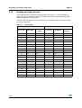
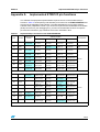
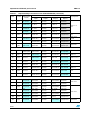
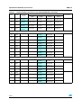
Implemented STR912F pin functions
Appendix A
Implemented STR912F pin functions
The STR910-Eval peripheral implementation requires the use of several alternate pin
functions. Table 21 shows primary and alternate pin functions for the STR912FAW47X6 that
are used in the application board design. The table indicates the pin functions used for
STR910-EVAL peripherals in blue. If you choose to implement the Embedded Trace Module
(ETM) connector for your debugging tool, you will use the alternate functions for specific
pins that are indicated in gray instead of the function indicated in blue.
Table 21.
Pin #
Implemented pin functions of the STR912FAW47X6
Default input
function
Pin name
Alternate functions
For peripheral...
Input 1
Output 1
Output 2
Output 3
67
P0.0
MII_TX_CLK
PHY Xmit clock
I2C0_CLKIN
I2C clock in
GPIO_0.0
GP Output
I2C0_CLKOUT
I2C clock out
ETM_PCK0
ETM Packet
Ethernet
69
P0.1
-
I2C0_DIN
I2C data in
GPIO_0.1
GP Output
I2C0_DOUT
I2C data out
ETM_PCK1
ETM Packet
Motor control or
USB
71
P0.2
MII_RXD0
PHY Rx data0
I2C1_CLKIN
I2C clock in
GPIO_0.2
GP Output
I2C1_CLKOUT
I2C clock out
ETM_PCK2
ETM Packet
76
P0.3
MII_RXD1
PHY Rx data
I2C1_DIN
I2C data in
GPIO_0.3
GP Output
I2C1_DOUT
I2C data out
ETM_PCK3
ETM Packet
78
P0.4
MII_RXD2,
PHY Rx data
TIM0_CAPA
Input Capture
GPIO_0.4
GP Output
EMI_CS0n
EMI Chip Select
ETM_PSTAT0
ETM pipe status
85
P0.5
MII_RXD3
PHY Rx data
TIM0_CAPB
Input Capture
GPIO_0.5
GP Output
EMI_CS1n
EMI Chip Select
ETM_PSTAT1
ETM pipe status
88
P0.6
MII_RX_CLK
PHY Rx clock
TIM2_CAPA
Input Capture
GPIO_0.6
GP Output
EMI_CS2n
EMI Chip Select
ETM_PSTAT2
ETM pipe status
90
P0.7
MII_RX_DV
PHY data valid
TIM2_CAPB
Input Capture
GPIO_0.7
GP Output
EMI_CS3n
EMI Chip Select
ETM_TRSYNC
ETM trace sync
98
P1.0
MII_RX_ER
PHY rcv error
ETM_EXTRIG
ETM ext. trigger
GPIO_1.0
GP Output
UART1_TX
UART xmit data
SSP1_SCLK
SSP mstr clk out
99
P1.1
-
UART1_RX
UART rcv data
GPIO_1.1
GP Output
MII_TXD0,
MAC Tx data
SSP1_MOSI
SSP mstr dat out
101
P1.2
-
SSP1_MISO
SSP mstr data in
GPIO_1.2
GP Output
MII_TXD1
MAC Tx data
UART0_TX
UART xmit data
106
P1.3
-
UART2_RX
UART rcv data
GPIO_1.3
GP Output
MII_TXD2
MAC Tx data
SSP1_NSS
SSP mstr sel out
109
P1.4
-
I2C0_CLKIN
I2C clock in
GPIO_1.4
GP Output
MII_TXD3
MAC Tx data
I2C0_CLKOUT
I2C clock out
110
P1.5
MII_COL
PHY collision
CAN_RX
CAN rcv data
GPIO_1.5
GP Output
UART2_TX
UART xmit data
ETM_TRCLK
ETM trace clock
114
P1.6
MII_CRS
PHY carrier sns
I2C0_DIN
I2C data in
GPIO_1.6
GP Output
CAN_TX
CAN Tx data
I2C0_DOUT
I2C data out
116
P1.7
-
ETM_EXTRIG
ETM ext. trigger
GPIO_1.7
GP Output
MII_MDC
MAC mgt dat ck
ETM_TRCLK
ETM trace clock
Ethernet
Ethernet
39/46
Implemented STR912F pin functions
Table 21.
Pin #
UM0174
Implemented pin functions of the STR912FAW47X6 (continued)
Default input
function
Pin name
Alternate functions
For peripheral...
Input 1
Output 1
Output 2
Output 3
10
P2.0
UART0_CTS
Clear To Send
I2C0_CLKIN
I2C clock in
GPIO_2.0
GP Output
I2C0_CLKOUT
I2C clock out
ETM_PCK0
ETM Packet
11
P2.1
UART0_DSR
Data Set Ready
I2C0_DIN
I2C data in
GPIO_2.1
GP Output
I2C0_DOUT
I2C data out
ETM_PCK1
ETM Packet
33
P2.2
UART0_DCD
Dat Carrier Det
I2C1_CLKIN
I2C clock in
GPIO_2.2
GP Output
I2C1_CLKOUT
I2C clock out
ETM_PCK2
ETM Packet
35
P2.3
UART0_RI
Ring Indicator
I2C1_DIN
I2C data in
GPIO_2.3
GP Output
I2C1_DOUT
I2C data out
ETM_PCK3
ETM Packet
37
P2.4
EXTCLK_T0T1
Ext clk timer0/1
SSP0_SCLK
SSP slv clk in
GPIO_2.4
GP Output
SSP0_SCLK
SSP mstr clk out
ETM_PSTAT0
ETM pipe status
ETM
45
P2.5
EXTCLK_T2T3
Ext clk timer2/3
SSP0_MOSI
SSP slv dat in
GPIO_2.5
GP Output
SSP0_MOSI
SSP mstr dat out
ETM_PSTAT1
ETM pipe status
Motor Control
or ETM
53
P2.6
-
SSP0_MISO
SSP mstr data in
GPIO_2.6
GP Output
SSP0_MISO
SSP slv data out
ETM_PSTAT2
ETM pipe status
ETM
54
USBCLK
_P2.7
USB_CLK48M
48MHz to USB
SSP0_NSS
SSP slv sel in
GPIO_2.7
GP Output
SSP0_NSS
SSP mstr sel out
ETM_TRSYNC
ETM trace sync
USB or ETM
55
P3.0
DMA_RQST0
Ext DMA request
UART0_RxD
UART rcv data
GPIO_3.0
GP Output
UART2_TX
UART xmit data
TIM0_PWMA
Out comp/PWM
Motor control
59
P3.1
DMA_RQST1
Ext DMA request
UART2_RxD
UART rcv data
GPIO_3.1
GP Output
UART0_TX
UART xmit data
TIM1_PWMA
Out comp/PWM
RS232 n° 3
60
P3.2
EXINT2
External Intr
UART1_RxD
UART rcv data
GPIO_3.2
GP Output
CAN_TX
CAN Tx data
UART0_DTR
Data Trmnl Rdy
RS232 n°2 or n°1
61
P3.3
EXINT3
External Intr
CAN_RX
CAN rcv data
GPIO_3.3
GP Output
UART1_TX
UART xmit data
UART0_RTS
Ready To Send
RS232 n°2 or n°1
63
P3.4
EXINT4
External Intr
SSP1_SCLK
SSP slv clk in
GPIO_3.4
GP Output
SSP1_SCLK
SSP mstr clk out
UART0_TX
UART xmit data
RS232 n°1
65
P3.5
EXINT5
External Intr
SSP1_MISO
SSP mstr data in
GPIO_3.5
GP Output
SSP1_MISO
SSP slv data out
UART2_TX
UART xmit data
RS232 n°3
66
P3.6
EXINT6
External Intr
SSP1_MOSI
SSP slv dat in
GPIO_3.6
GP Output
SSP1_MOSI
SSP mstr dat out
CAN_TX
CAN Tx data
CAN
68
P3.7
EXINT7
External Intr
SSP1_NSS
SSP slv select in
GPIO_3.7
GP Output
SSP1_NSS
SSP mstr sel out
TIM1_PWMA
Out comp/PWM
RS232 n°2
3
P4.0
ADC0
ADC input chnl
TIM0_CAPA
Input Capture
GPIO_4.0
GP Output
TIM0_PWMA
Out comp/PWM
ETM_PCK0
ETM Packet
2
P4.1
ADC1
ADC input chnl
TIM0_CAPB
Input Capture
GPIO_4.1
GP Output
TIM0_COMB
Out comp
ETM_PCK1
ETM Packet
1
P4.2
ADC2
ADC input chnl
TIM1_CAPA
Input Capture
GPIO_4.2
GP Output
TIM1_PWMA
Out comp/PWM
ETM_PCK2
ETM Packet
128
P4.3
ADC3
ADC input chnl
TIM1_CAPB
Input Capture
GPIO_4.3
GP Output
TIM1_COMB
Out comp
ETM_PCK3
ETM Packet
127
P4.4
ADC4
ADC input chnl
TIM2_CAPA
Input Capture
GPIO_4.4
GP Output
TIM2_PWMA
Out comp/PWM
ETM_PSTAT0
ETM pipe status
126
P4.5
ADC5
ADC input chnl
TIM2_CAPB
Input Capture
GPIO_4.5
GP Output
TIM2_COMB
Out comp
ETM_PSTAT1
ETM pipe status
125
P4.6
ADC6
ADC input chnl
TIM3_CAPA
Input Capture
GPIO_4.6
GP Output
TIM3_PWMA
Out comp/PWM
ETM_PSTAT2
ETM pipe status
RS232 n°1 or
ETM
Motor control
Motor control
40/46
Audio PWM or
potentiometer
UM0174
Implemented STR912F pin functions
Table 21.
Pin #
Implemented pin functions of the STR912FAW47X6 (continued)
Pin name
Default input
function
Alternate functions
For peripheral...
Input 1
Output 1
Output 2
Output 3
124
P4.7
ADC7
ADC input chnl
TIM3_CAPB
Input Capture
GPIO_4.7
GP Output
TIM3_COMB
Out comp
ETM_TRSYNC
ETM trace sync
Microphone in
12
P5.0
EXINT8
External Intr
CAN_RX
CAN rcv data
GPIO_5.0
GP Output
ETM_TRCLK
ETM trace clock
UART0_TX
UART xmit data
CAN
18
P5.1
EXINT9
External Intr
UART0_RxD
UART rcv data
GPIO_5.1
GP Output
CAN_TX
CAN Tx data
UART2_TX
UART xmit data
RS232 n°1
25
PHYCLK
_P5.2
EXINT10
External Intr
UART2_RxD
UART rcv data
GPIO_5.2
GP Output
MII_PHYCLK
25Mhz to PHY
TIM3_PWMA
Out comp/PWM
27
P5.3
EXINT11
External Intr
ETM_EXTRIG
ETM ext. trigger
GPIO_5.3
GP Output
MII_TX_EN
MAC xmit enbl
TIM2_PWMA
Out comp/PWM
70
P5.4
EXINT12
External Intr
SSP0_SCLK
SSP slv clk in
GPIO_5.4
GP Output
SSP0_SCLK
SSP mstr clk out
EMI_CS0n
EMI Chip Select
77
P5.5
EXINT13
External Intr
SSP0_MOSI
SSP slv dat in
GPIO_5.5
GP Output
SSP0_MOSI
SSP mstr dat out
EMI_CS1n
EMI Chip Select
79
P5.6
EXINT14
External Intr
SSP0_MISO
SSP mstr dat in
GPIO_5.6
GP Output
SSP0_MISO
SSP slv data out
EMI_CS2n
EMI Chip Select
80
P5.7
EXINT15
External Intr
SSP0_NSS
SSP slv select in
GPIO_5.7
GP Output
SSP0_NSS
SSP mstr sel out
EMI_CS3n
EMI Chip Select
29
P6.0
EXINT16
External Intr
TIM0_CAPA
Input Capture
GPIO_6.0
GP Output
TIM0_PWMA
Out comp/PWM
MC_UH
IMC phase U hi
31
P6.1
EXINT17
External Intr
TIM0_CAPB
Input Capture
GPIO_6.1
GP Output
TIM0_COMB
Out comp
MC_UL
IMC phase U lo
19
P6.2
EXINT18
External Intr
TIM1_CAPA
Input Capture
GPIO_6.2
GP Output
TIM1_PWMA
Out comp/PWM
MC_VH
IMC phase V hi
20
P6.3
EXINT19
External Intr
TIM1_CAPB
Input Capture
GPIO_6.3
GP Output
TIM1_COMB
Out comp
MC_VL
IMC phase V lo
83
P6.4
EXINT20
External Intr
TIM2_CAPA
Input Capture
GPIO_6.4
GP Output
TIM2_PWMA
Out comp/PWM
MC_WH
IMC phase W hi
84
P6.5
EXINT21
External Intr
TIM2_CAPB
Input Capture
GPIO_6.5
GP Output
TIM2_COMB
Out comp
MC_WL
IMC phase W lo
92
P6.6
EXINT22_TRIG
Ext Intr & Tach
UART0_RxD
UART rcv data
GPIO_6.6
GP Output
TIM3_PWMA
Out comp/PWM
ETM_TRCLK
ETM trace clock
93
P6.7
EXINT23_STOP
Ext Intr & Estop
ETM_EXTRIG
ETM ext. trigger
GPIO_6.7
GP Output
TIM3_COMB
Out comp
UART0_TX
UART xmit data
5
P7.0
EXINT24
External Intr
TIM0_CAPA
Input Capture
GPIO_7.0
GP Output
8b) EMI_A0
16b) EMI_A16
ETM_PCK0
ETM Packet
Motor control
6
P7.1
EXINT25
External Intr
TIM0_CAPB
Input Capture
GPIO_7.1
GP Output
8b) EMI_A1
16b) EMI_A17
ETM_PCK1
ETM Packet
Ethernet
7
P7.2
EXINT26
External Intr
TIM2_CAPA
Input Capture
GPIO_7.2
GP Output
8b) EMI_A2
16b) EMI_A18
ETM_PCK2
ETM Packet
Motor control
13
P7.3
EXINT27
External Intr
TIM2_CAPB
Input Capture
GPIO_7.3
GP Output
8b) EMI_A3
16b) EMI_A19
ETM_PCK3
ETM Packet
Ethernet
Flash
Motor control
Motor control or
ETM
41/46
Implemented STR912F pin functions
Table 21.
Pin #
UM0174
Implemented pin functions of the STR912FAW47X6 (continued)
Alternate functions
Default input
function
Pin name
For peripheral...
Input 1
Output 1
Output 2
Output 3
14
P7.4
EXINT28
External Intr
UART0_RxD
UART rcv data
GPIO_7.4
GP Output
8b) EMI_A4
16b) EMI_A20
EMI_CS3n
EMI Chip Select
Joystick
15
P7.5
EXINT29
External Intr
ETM_EXTRIG
ETM ext. trigger
GPIO_7.5
GP Output
8b) EMI_A5
16b) EMI_A21
EMI_CS2n
EMI Chip Select
118
P7.6
EXINT30
External Intr
TIM3_CAPA
Input Capture
GPIO_7.6
GP Output
8b) EMI_A6
16b) EMI_A22
EMI_CS1n
EMI Chip Select
EXINT31
119
P7.7
TIM3_CAPB
Input Capture
GPIO_7.7
GP Output
8b) EMI_A7
16b) EMI_CS0n
16b) EMI_A23
EMI addr out
-
-
GPIO_8.0
GP Output
8b) EMI_D0
16b) EMI_AD0
-
-
-
GPIO_8.1
GP Output
8b) EMI_D1
16b) EMI_AD1
-
-
-
GPIO_8.2
GP Output
8b) EMI_D2
16b) EMI_AD2
-
-
-
GPIO_8.3
GP Output
8b) EMI_D3
16b) EMI_AD3
-
-
-
GPIO_8.4
GP Output
8b) EMI_D4
16b) EMI_AD4
-
-
-
GPIO_8.5
GP Output
8b) EMI_D5
16b) EMI_AD5
-
-
-
GPIO_8.6
GP Output
8b) EMI_D6
16b) EMI_AD6
-
-
-
GPIO_8.7
GP Output
8b) EMI_D7
16b) EMI_AD7
-
-
-
GPIO_9.0
GP Output
8b) EMI_A8 16b)
EMI_AD8
-
LED
-
-
GPIO_9.1
GP Output
8b) EMI_A9
16b) EMI_AD9
-
LED
-
-
GPIO_9.2
GP Output
8b) EMI_A10
16b) EMI_AD10
-
-
-
GPIO_9.3
GP Output
8b) EMI_A11
16b) EMI_AD11
-
-
-
GPIO_9.4
GP Output
8b) EMI_A12
16b) EMI_AD12
-
-
-
GPIO_9.5
GP Output
8b) EMI_A13
16b) EMI_AD13
-
-
-
GPIO_9.6
GP Output
8b) EMI_A14
16b) EMI_AD14
-
-
-
GPIO_9.7
GP Output
8b) EMI_A15
16b) EMI_AD15
-
External Intr
26
P8.0
28
P8.1
30
P8.2
32
P8.3
34
P8.4
36
P8.5
38
P8.6
44
P8.7
46
P9.0
47
P9.1
50
P9.2
51
P9.3
52
P9.4
58
P9.5
62
P9.6
64
P9.7
42/46
LCD
LCD
UM0174
Product support
Appendix B
Product support
If you experience any problems with this product, or if you need spare parts or repairs,
contact the distributor or the STMicroelectronics sales office where you purchased the
product.
On the STMicroelectronics microcontrollers support site at www.st.com, you will find a
complete listing of ST sales offices and distributors, as well as documentation, software
downloads and user discussion groups to help you answer questions and stay up to date
with our latest product developments.
Software updates
All our latest software and related documentation are available for download from the
STMicroelectronics microcontrollers support site at www.st.com. For information about
firmware and hardware revisions, call your distributor or STMicroelectronics.
Hardware spare parts
Your development tool comes with the hardware you need to set it up, connect it to your PC
and connect to your application. However, some components can be bought separately if
you need additional ones. You can order extra components, such as sockets and adapters,
from STMicroelectronics, from the component manufacturer or from a distributor.
To help you find what you need, a listing of accessories for ST development tools is available
on the STMicroelectronics microcontrollers support site at www.st.com.
Sockets
Complete documentation and ordering information for P/TQFP sockets from Yamaichi,
Ironwood, CAB and Enplas are provided on their respective Internet sites.
Connectors
Complete documentation and ordering information for SAMTEC connectors is provided on
the SAMTEC web site.
43/46
Product support
UM0174
Getting prepared before you call
Collect the following information about the product before contacting ST or your distributor:
1.
44/46
Name of the company where you purchased the product.
2.
Date of purchase.
3.
Order Code: Refer to the side your emulators box. The order code will depend on the
region in which is was ordered (for example, the UK, Continental Europe or the USA).
4.
Serial Number: The serial number is found located on the rear panel of the
ST Micro Connect box and is also listed on the Global Reference card provided with
the emulator.
5.
TEB (Target Emulation Board) hardware and firmware versions: the hardware and
firmware versions can be found by opening an STVD7 session, entering the debug
context and selecting Help>About from the main menu. The TEB version numbers are
given in the Target box – scroll downwards until you find the TEB version (hardware)
and TEB PLD version (firmware).
6.
Target Device: The sales type of the ST microcontroller you are using in your
application.
UM0174
Revision history
Revision history
Table 22.
Document revision history
Date
Revision
Changes
12-Apr-2006
1
First draft release for review.
17-May-2006
2
Added explanation of schematic version numbers (Section 4).
Replaced board schematics C.0 with modified schematics C.1.
Changes to revision C.1 schematics include: R50 on JTAG
connector changed to “Do not fit” (Figure 22), STM1001 removed
from reset circuit (Figure 16).
2-Nov-2007
3
Replaced STR912FW44X6 by STR912FAW47X6 throughout the
manual.
Document reformatted.
45/46
UM0174
Please Read Carefully:
Information in this document is provided solely in connection with ST products. STMicroelectronics NV and its subsidiaries (“ST”) reserve the
right to make changes, corrections, modifications or improvements, to this document, and the products and services described herein at any
time, without notice.
All ST products are sold pursuant to ST’s terms and conditions of sale.
Purchasers are solely responsible for the choice, selection and use of the ST products and services described herein, and ST assumes no
liability whatsoever relating to the choice, selection or use of the ST products and services described herein.
No license, express or implied, by estoppel or otherwise, to any intellectual property rights is granted under this document. If any part of this
document refers to any third party products or services it shall not be deemed a license grant by ST for the use of such third party products
or services, or any intellectual property contained therein or considered as a warranty covering the use in any manner whatsoever of such
third party products or services or any intellectual property contained therein.
UNLESS OTHERWISE SET FORTH IN ST’S TERMS AND CONDITIONS OF SALE ST DISCLAIMS ANY EXPRESS OR IMPLIED
WARRANTY WITH RESPECT TO THE USE AND/OR SALE OF ST PRODUCTS INCLUDING WITHOUT LIMITATION IMPLIED
WARRANTIES OF MERCHANTABILITY, FITNESS FOR A PARTICULAR PURPOSE (AND THEIR EQUIVALENTS UNDER THE LAWS
OF ANY JURISDICTION), OR INFRINGEMENT OF ANY PATENT, COPYRIGHT OR OTHER INTELLECTUAL PROPERTY RIGHT.
UNLESS EXPRESSLY APPROVED IN WRITING BY AN AUTHORIZED ST REPRESENTATIVE, ST PRODUCTS ARE NOT
RECOMMENDED, AUTHORIZED OR WARRANTED FOR USE IN MILITARY, AIR CRAFT, SPACE, LIFE SAVING, OR LIFE SUSTAINING
APPLICATIONS, NOR IN PRODUCTS OR SYSTEMS WHERE FAILURE OR MALFUNCTION MAY RESULT IN PERSONAL INJURY,
DEATH, OR SEVERE PROPERTY OR ENVIRONMENTAL DAMAGE. ST PRODUCTS WHICH ARE NOT SPECIFIED AS "AUTOMOTIVE
GRADE" MAY ONLY BE USED IN AUTOMOTIVE APPLICATIONS AT USER’S OWN RISK.
Resale of ST products with provisions different from the statements and/or technical features set forth in this document shall immediately void
any warranty granted by ST for the ST product or service described herein and shall not create or extend in any manner whatsoever, any
liability of ST.
ST and the ST logo are trademarks or registered trademarks of ST in various countries.
Information in this document supersedes and replaces all information previously supplied.
The ST logo is a registered trademark of STMicroelectronics. All other names are the property of their respective owners.
© 2007 STMicroelectronics - All rights reserved
STMicroelectronics group of companies
Australia - Belgium - Brazil - Canada - China - Czech Republic - Finland - France - Germany - Hong Kong - India - Israel - Italy - Japan Malaysia - Malta - Morocco - Singapore - Spain - Sweden - Switzerland - United Kingdom - United States of America
www.st.com
46/46