1
Architectural Specification
May 1980
©
INTEL CORPORATION, 1980.
AFN-01488A-01
Intel Corporation makes no warranty for the use of its products and assumes no responsibility for any enors which
may appear in this document nor does it make a commitment to update the information contained herein.
Intel software products are copyrighted by and shall remain the property of Intel Corporation. Use, duplication or
disclosure is subject to restrictions stated in Intel's software license, or as defined in ASPR 7-104.9 (a) (9). Intel
Corporation assumes no responsibility for the use of any circuitry other than circuitry embodied in an Intel
product. No other circuit patent licenses are implied.
No part of this document may be copies or reproduced in any form or by any means without the prior wr:itten
consent of Intel Corporation.
The following are trademarks of Intel Corporation and may only be used to identify Intel products:
i
ICE
ICS
im
Insite
Intel
Intelevision
Intellec
iSBC
Library Manager
MCS
Megachassis
Micromap
Multimodule
PROMPT
Promware
RMX
UPI
J,lScope .
and the combinations of ICE, iCS, iSBC, MCS or RMX and a numerical suffix.
Additional copies of this or other Intel literature may be obtained from:
Literature Department
Intel Corporation
3065 Bowers Avenue
Santa Clara, CA 95051
f·INTEL CORPORATION. 1980
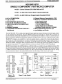
8051 Architectural Specification and Functional Description
8031/8051/8751
SINGLE-COMPONENT 8-BIT MICROCOMPUTER
• 803t - Control Oriented CPU With RAM and I/O
• 8051 - An 8031 With Factory Mask- Programmable ROM
• 8751 - An 8031 With User Programmable/Erasable EPROM
• External Memory Expandable to 128K
• MCS-48™ Architecture Enhanced with:
• Non-Paged Jumps
• Direct Addressing
• Four 8-Register Banks
• Stack Depth Up to 128-Bytes
• Multiply, Divide, Subtract, Compare
• Most Instructions Execute in 111S
• 411s Multiply and Divide
•
•
•
•
•
4K x 8 ROM/EPROM
128 x 8 RAM
Four 8-Bit Ports, 32 I/O Lines
Two 16-Bit Timer/Event Counters
High-Performance Full-Duplex Serial
Channel
• Boolean Processor
• Compatible with MCS-80™/MCS-85TM
Peripherals
The Intel® 8031/8051/8751 is a stand-alone, high-performance single-chip computer fabricated with Intel's highly-reliable
+5 Volt, depletion-load, N-Channel, silicon-gate HMOS technology and packaged in a 40-pin DIP. It provides the
hardware features, architectural enhancements and new instructions that are necessary to make it a powerful and cost
effective controller for applications requiring up to 64K bytes of program memory and / or up to 64K bytes of data storage.
The 8051/8751 contains a non-volatile 4K x 8 read only program memory; a volatile 128 x 8 read/write data memory;
32 I/O lines; two 16-bit timer/counters; a five-source, two-priority-Ievel, nested interrupt structure; a serial I/O port for
either multi-processor communications, I/O expansion, or full duplex UART; and on-chip oscillator and clock circuits.
The 8031 is identical, except that it lacks the program memory. For systems that require extra capability, the 8051 can
be expanded using standard TTL compatible memories and the byte oriented MCS-80 and MCS-85 peripherals.
The 8051 microcomputer, like its 8048 predecessor, is efficient both as a controller and as an arithmetic processor. The
8051 has extensive facilities for binary and BCD arithmetic and excels in bit-handling capabilities. Efficient use of program
memory results from an instruction set consisting of 44% one-byte, 41% two-byte, and 15% three-byte instructions. With
a 12 MHz crystal, 58% of the instructions execute in Ills, 40% in 2f1s and mUltiply and divide require only 411S. Among
the many instructions added to the standard 8048 instruction set are multiply, divide, subtract and compare.
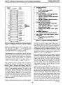
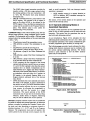
AST/VPD
FREQUENCY
REFERENCE
P1.0
vee
P1,1
PO.o
P1.2
PO.1
P1.3
PO.2
P1.4
PO.3
P1.5
PO.4
P1.6
PO.S
P1.7
PO.S
RST/VPO
PO.7
RXD P3.0
EAtVDO
TXO P3.1
ALEIPROG
r
}-.
ADDRESS
AND
OATA BUS
PSEN
ALE/PROG
INTO P3.2
PSEN
uin
P3.3
P2.7
TO P3.4
P2.S
T1 P3.5
P2.5
\VA P3.6
P2."
INTO ......
RD P3.7
P2.3
INT'......
XTAL2
P2.2
.m_ {{
TXO .....
TO-'
n........
XTAL1
P2.1
WA~
VSS
P2.D
AD"-
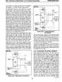
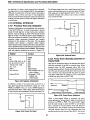
Figure 1. Pin
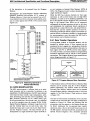
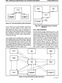
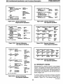
COUNTERS
:
g
Q.
}-,
}~"'.
ADDRESS
BUS
Figure 2. Logic Symbol
-1
,...----'---'---,
I
128 BYTES
DATA MEMORY
I
TWO 16-BIT
TIMER/EVENT
COUNTERS
I
I
I
I
I
I
I
I
I
I
PROGRAMMABLE
SERIAL PORT
• FULL DUPLEX
UART
• SYNCHRONOUS
SHIFTER
64K-SYTE 8US
• EXPANSION
CONTROL
INTERRUPTS
LINTERRUPTS
CONTROL
PARALLEL PORTS.
ADDRESS/DATA BUS,
AND 110 PINS
SERIAL
IN
SERIAL
OUT
Figure 3. Block Diagram
Configuration
Intel Corporation Assumes No Responsibility for the Use of Any Circuitry Other Than Circuitry Embodied in an Intel Product. No Other Circuit Patent licenses Are Implied.
© INTEL CORPORATION. 1980.
AFN-01488A-02
I
I
I
I
I
I
8051 Single-Chip
Microcomputer
Architectural Specification
and
Functional Description
Contents
CHAPTER 1 INTRODUCTION ..... .- .. .. .. .. .. .. .. ....
1.0
Abstract. . . . . . . . . . . . . . . . . . . . . . . . . . . . . . ..
1.1
Intel's Complete Line of Single-Chip
Microcomputers ........................
1.2
Enhancing the 8048 Architecture for
the 80's ................................
CHAPTER 2
2.0
2.1
2.2
2.3
2.4
2.5
2.6
2.7
2.8
©Intel Corporation 1980. All rights reserved.
2.9
1
1
1
1
ARCHITECTURAL OVERVIEW AND
FUNCTIONAL DESCRIPTION ........... 2
The 8051 Family ........................ 2
Macro-view of the 8051 Architecture ...... 2
2.1: 1 8051 CPU Architecture . . . . . . . . . . . .. 2
2.1.2 On-Chip Peripheral Functions. . . . . .. 3
2.1.2.1 Interrupt System .. . . . . . . . . .. 3
2.1.2.2 I/O Facilities. . . . . . . . . . . . . . .. 4
2.1.2.2.1 Open Drain I/O Pins. . .. 4
2.1.2.2.2 Quasi-Bidirectional
I/O Pins ............... 4
2.1.2.2.3 Microprocessor Bus .. .. 5
2.1.2.3 Timer/Event Counters ....... 6
2.1.2.4 Serial Communications. . . . .. 7
CPU Hardware. .. . .. . .. .. .. . .. .. .. . .. ... 9
2.2.1 Instruction Decoder. . . . . . . . . . . . . . .. 9
2.2.2' Program Counter ......... . . . . . . . . .. 9
2.2.3 Internal Data Memory .............. 9
2.2.3.1 Internal Data RAM ........... 9
2.2.3.2 Register Banks .•........... 9
2.2.3.3 Special Function Registers ... 9
2.2.3.4 A Register. . . . . . . . . . . . . . . . .. 9
2.2.3.5 B Register. . . . . . . . . . . . . . . . .. 9
2.2.3.6 PSW Register. .. .. .. .. .. .... 9
2.2.3.7 Stack Pointer . . . . . . . . . . . . . .. 9
2.2.3.8 Data Pointer ................ 11
2.2.4 Arithmetic Section ................. 11
2.2.5 Program Control Section ........... 11
2.2.6 Oscillator and Timing Circuitry ...... 11
2.2.7 Boolean Processor ................. 11
Memory Organization ................... 11
Operand Addressing .................... 12
Data Manipulation ............... " ...... 14
2.5.1 Data Transfer Operations ........... 14
2.5.2 logic Operations .................. 15
2.5.3 Arithmetic Operations .............. 16
Control Transfer ........................ 17
Instruction Set ........................... 18
2.7.1 What the Instruction Set Is ........... 18
2.7.2 Organization of the Instruction Set ". 18
2.7.3 Operand Addressing Modes and
Associated Operations ............. 21
Interrupt System ........................ 22
2.8.1 External Interrupts .................. 24
2.8.1.1 Transition-Activated
Interrupts .................. 24
2.8.1.2 level-Activated Interrupts .... 24
Ports and I/O Pins ....................... 24
AFN-Q1488A·03
CHAPTER 2
2.10
2.11
2.12
2.13
2.14
2.15
2.16
2.17
Table 2.1
ARCHITECTURAL OVERVIEW AND
FUNCTIONAL DESCRIPTION (Continued)
Accessing External Memory .............. 25
2.10.1 Operation of Ports ................ 26
2.10.2 Bus Cycle Timing ................. 26
TimerlCounter .......................... 28
2.11.1 TIC Mode Selection ............... 28
2.11.2 Configuring the TIC Input ......... 28
2.11.3 TIC Operation .................... 29
2.11.4 Reading and Reloading the TIC .... 29
Serial Channel .......................... 29
2.12.1 Serial Port Control Register and
Serial Data Registers .......... '.... 31
2.12.2 Operating Modes ................. 31
2.12.2.1 Operating Mode O •....•••. 31
2.12.2.2 Operating Modes 1
through 3 ................ 32
2.12.3 The Serial Frame ................. 32
2.12.4 Transmission Rate Generation ..... 32
2.12.5 UART Message Error Conditions ... 33
External Interface ....................... 33
2.13.1 Processor Reset and
Initialization ...................... 33
2.13.2 Power Down Operation of
Internal RAM ..................... 33
EPROM Programming .................... 34
The 8051 as an Evolution of the 8048 ...... 34
Development System and Software
Support ................................ 34
8051 Pin Description .................... 35
Instruction Set Summary ................. 37
AFN-01488A-04
8051 Architectural Specification and Functional Description
1.0 ABSTRACT
Now, thanks to the density of HMOS, technology has
once again permitted the birth of a microcomputer with
performance to leap into new product areas. The 8051
achieves a lOX function/speed improvement over the
8048 by packing 60,000 transistors onto a die 230 mils
square.
The 8031, 8051, and 8751 are the latest additions to Inters
line of single-chip microcomputers. The CPU architecture and on-chip peripheral functions of the 8051 are
described in this document. A user familiar with the
MCS-48 family should be able to evaluate and design-in
the 8051 using the information included herein.
The 8051 family addresses the high-end of the single-chip
computer market. It is the highest performance micfocomputer family in the world and out-performs all microprocessors and microcomputers in control oriented
applications. It offers an upward compatible growth path
for 8048 users with ten times the power of the 8048 as
shown in Table 1.1.
A detailed description of the hardware required to
expand the 8051 with more program memory, data
memory, I/O, specialized peripherals and into multiprocessor configurations is described in the 8051 Family
User's Manual.
1.1 INTEL'S COMPLETE LINE OF
SINGLE-CHIP MICROCOMPUTERS
•
•
•
•
•
•
•
•
•
In 1976 Intel introduced the 8748 microcomputer. This
marked the first time in history that technology permitted
a complete 8-bit computer to be fabricated on a single
silicon die. This single chip can control a limitless variety
of products ranging from appliances to automobiles to
computer terminals.
Since 1976 Intel has offered products for the full range of
single-chip microcomputer applications by pushing the
8048's architecture in several directions. The 8049 ran
nearly twice as fast as the 8748/8048 while doubling the
amount of on-chip program memory and data memory.
Applications requiring solely external program memory
were satisfied with the 8035 and 8039. Cost sensitive and
less I/O intensive applications incorporated the 8021
which executed a subset of the 8048's instruction set at a
slower speed. Finally, the 8022 integrated an 8-bit A/D
converter onto the 8021 die to allow the chip to interface
directly to a world in which most signals are analog.
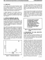
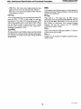
Figure I. I positions these products on a performance
versus die-size curve.
Table 1.1: 8051 Functions/Speed/Cost Relative
to 8048
1.2 ENHANCING THE 8048 ARCHITECTURE FOR THE 80's
The goal of the 8051 is to extend the architecture of the
industry standard 8048 single-chip microcomputer into
the 80's. This meant increasing the power of the 8048's
CPU as well as increasing the power, variety and quantity
of on-chip CPU peripherals.
The 8048's CPU architecture is ideal for control-oriented
applications demanding a low-cost microcomputer because
of its hardware simplicity and resulting silicon efficiency.
A simpleALU is used in virtually all operations: arithmetic, logic, data moves, bit testing and I/O. Since all
data is moved through the ALU this also simplifies the
internal data path. The 8048's simple addressing methods
of Register-, Register-Indirect- and Immediate-Addressing minimize hardware. The conditional branch logic
simply concatenates an immediate value to the upper
bits of the program counter to economize on silicon, but
results in page boundaries. The simplicity of the tablelook-up circuitry also results in page boundaries. The
user flags and test pins provided for monitoring program
and external status in an efficient manner are limited to
two of each. This architecture, and the choice of instruction encodings that it permits, results In 1,024 byte
programs of unsurpassed byte efficiency.
•
10
8051
9
8
7
iu
ilc
~
o...
...ffi
6
5
4
3
2
4X Program Memory (4k Bytes)
2X Data Memory (128 Bytes)
2X Register Banks (4 vs. 2)
2X Timers (Two 16-bit Timers)
New Full-Duplex Serial I/O Port
More I/O Pins (32 vs. 27)
Enhanced MCS-48 Architecture
21/2 X To 10X Execution Speed
1.4X Die Size
8022.
8048 •
8021.
0~------*X----~~1~.5~X------~2~X------.~2.5X
DIE SIZE
-Based on execution speed, memory size and peripheral functions.
Figure 1.1. Performance Versus Cost
AFN-01488A-05
1
8051 Architectural Specification and Functional Description
The silicon economic architecture of the 8048 causes
some inconvenience to the programmer but the relatively
short programs (one or two kilobytes) keep frustration
levels in check. The 8051 challenge was to maintain software and feature compatibility with the 8048 while
providing a more powerful microcomputer that is easier
to program and use. This allows a designer currently
using the 8048 to easily upgrade to the 8051 while protecting his investment in algorithm development and the
knowledge he gained by designing with the 8048.
ment, prototyping, low-volume production and applications requiring field updates; the 8051 for low-cost,
high-volume production and the 8031 for applications
desiring the flexibility of external Program Memory
which can be easily modified and updated in the field.
2.1 MACRO-VIEW OF THE 8051 ARCHITECTURE
On a single die the 8051 microcomputer combines CPU;
non-volatile 4K x 8 read-only program memory; volatile
128 x 8 read/write data memory; 32 I/O lines; two 16-bit
timer / event counters; a five-source, two-priority-Ievel,
nested interrupt structure; serial I/O port for either multiprocessor communications, I/O expansion, or full duplex
UART; and on-chip oscillator and clock circuits. This
section will provide an overview of the 8051 by providing
a high-level description of its major elements: the CPU
architecture and the on-chip functions peripheral to the
CPU. The generic term "8051" is also used to refer collectively to the 8031, 8051, and 8751.
Some of the achievements of the 8051 were to extend the
maximum program memory address space to 64K-bytes,
extending on-chip peripheral functions (counters, serial
ports and parallel ports) to satisfy emerging single-chip
applications, and enhancing a paged architecture to
make it suitable for the relocatable and re-entrant code
generated by modern programming techniques. Op codes
were reassigned to add new high-power operations and to
permit new addressing modes which make the old
operations more orthogonal. During this process special
care was taken to provide optimum byte efficiency and
maximum execution speed. The 8051 is typically 20%
more code efficient than the 8049 for programs longer
than 2048 bytes. Efficient use of program memory results
from an instruction set consisting of 44% one-byte, 41 %
two-byte and 15% three-byte instructions. With a 12
M Hz crystal, 58% of the instructions execute in ltis, 40%
in 2;,Is and multiply and divide require 'only 4tis.
2.1.1 8051 CPU Architecture
The 8051 CPU manipulates operands in four memory
spaces. These are the 64K-byte Program Memory, 64Kbyte External Data Memory, 384-byte Internal Data
Memory and 16-bit Program Counter spaces. The Internal Data Memory address space is further divided into the
256-byte Internal Data RAM and 128-byte Special
Function Register (SFR) address spaces shown in Figure
2.1. Four Register Banks (each with eight registers), 128
addressable bits, and the stack reside in the Internal Data
RAM. The stack depth is limited only by the available
Internal Data RAM and its location is determined by the
8-bit Stack Pointer. All registers except the Program
Counter and the four 8-Register Banks reside in the
Special Function Register address space. These memory
mapped registers include arithmetic registers, pointers,
I/O ports, and registers for the interrupt system, timers
and serial channel. 128 bit locations in the SFR address
space are addressable as bits. The 8051 contains 128 bytes
of Internal Data RAM and 20 SFRs.
2.0 THE 8051 FAMILY
The 8051 is a stand-alone high-performance single-chip
computer intended for use in sophisticated real-time
applications such as instrumentation, industrial control
and intelligent computer peripherals. It provides the
hardware features, architectural enhancements and new
instructions that make it a powerful and cost effective
controller for applications requiring up to 64K-bytes of
program memory and/ or up to 64K-bytes of data storage.
A Block Diagram is shown in Figure 3.
The 8031 is a control-oriented CPU without on-chip
program memory. It can address 64K-bytes of external
Program Memory in addition to 64K-bytes of External
Data Memory. For systems requiring extra capability,
each member of the 8051 family can be expanded using
standard memories and the byte oriented MCS-80 and
MCS-85 peripherals. The 8051 is an 8031 with the lower
4K-bytes of Program Memory filled with on-chip mask
programmable ROM while the 8751 has 4K-bytes ofUVlight-erasable/ electrically-programmable ROM.
The 8051 provides a non-paged Program Memory
address space to accommodate relocatable code. Conditional branches are performed relative to the Program
Counter. The register-indirect jump permits branching
relative to a 16-bit base register with an offset provided by
an 8-bit index register. Sixteen-bit jumps and calls permit
branching to any location in the contiguous 64K Program
Memory address space.
The three pin-compatible versions of this component
reduce development problems to a minimum and provide
maximum flexibility. The 8751 is well suited for develop-
The 8051 has five methods for addressing source operands: Register, Direct, Register-Indirect, Immediate, and
Base-Register- plus Index-Register- Indirect Addressing.
AFN-01488A-06
2
8051 Architectural Speciffcation ancrFunctionaJ Descrlpfion
64K
64K
t
EXTERNAl-
I,
OYERl-APPED SPACE
------
4095
-"Lr-----A
I
I
255 I
INTERNAl-
I
,
-
PROGRAM
COUNTER
I
,
0
25S
128
1~1..
,
J
,
PROGRAM
MEMORY
,
INTERNAlDATA RAM
-
,
'l
,
SPECIAL
FUNCTION
REGISTERS
,
,
EXTERNAL
DATA
MEMORY
INTERNAL DATA MEMORY
Figure 2.1. 8051 Family Memory Organization
The first three methods can be used for addressing
destination operands. Most instructions have a "destination,source" field that specifies the data type, addressing methods and operands involved. For operations
other than moves, the destination operand is also a source
operand.
single-byte, 4S two-byte and 17 three-byte instructions.
When using a 12 MHz oscillator, 64 instructions execute
in IlJs and 4S instructions execute in 4ls. The remaining
instructions (multiply and divide) require only ~s. The
number of bytes in each instruction and the number of
oscillator periods required for execution are listed in the
appended 80S I Instruction Set Summary.
Registers in the four 8-Register Banks can be accessed
through Register, Direct, or Register-Indirect Addressing; the 128 bytes of Internal Data RAM through
Direct or Register-Indirect Addressing; and the Special
Function Registers through Direct Addressing. External
Data Memory is accessed through Register-Indirect
Addressing. Look-Up-Tables resident in Program
Memory can be accessed through Base-Register- plus
Index-Register- Indirect Addressing.
2.1.2 On-Chip Peripheral Functions
Thus far only the CPU and memory spaces of the 80S 1
have been described. In addition to the CPU and
memories, an interrupt system, extensive I/O facilities,
and several peripheral functions are integrated on-chipto
relieve the CPU of repetitious, complicated or timecritical tasks and to permit stringent real-time control of
external system interfaces. The extensive 110 facilities
include the 110 pins, parallel 110 ports, bidirectional
address/data bus and the serial port for I/O expansion.
The CPU peripheral functions integrated on-chip are the
two 16-bit counters and the serial port. All of these work
together to greatly boost system performance.
The 80S 1 is classified as an 8-bit machine since the
internal ROM, RAM, Special Function Registers,
Arithmeticl Logic Unit and external data bus are each 8bits wide. The 80S 1 performs operations on bit, nibble,
byte and double-byte data types.
The 80S1 has extensive facilities for byte transfer, logic,
and integer arithmetic operations. It excels at bit handling
since data transfer, logic and conditional branch
operations· can be performed directly on Boolean
variables.
2.1.2.1 INTERRUPT SYSTEM
External events and the real~time-driven on-chip
peripherals require service by the CPU asynchronous to
the execution of any particular section of code. To tie the
asynchronous activities of these functions to normal
program execution, a sophisticated multiple-source, two~
priority-level, nested interrupt system is provided. Interrupt response latency ranges from 3IJs to 7IJs when
using a 12 MHz crystal.
The 80S I's instruction set is an enhancement of the
instruction set familiar to MCS-48 users. It is enhanced to
allow expansion of on-chip· CPU peripherals and to
optimize byte efficiency and execution speed. Op codes
were reassigned to add new high-power operations and to
permit new addressing modes which make the old
operations more orthogonal. Efficient use of program
memory results from an instruction set consisting of 49
The 80S I acknowledges interrupt requests from five
sources: Two from external sour.res via the INTO and
INTI pins, one from each of the two internal counters and
AFN-Ol488A-D7
3
8051 Architectural Specification and Functional Description
one from the serial I/O port. Each interrupt vectors to a
separate location in Program Memory for its service
program. Each of the five sources can be assigned to either
of two priority levels and can be independently enabled
and disabled. Additionally all enabled sources can be
globally disabled or enabled. Each external interrupt is
programmable as either level- or transition-activated and
is active-low to allow the "wire or-ing" of several interrupt
sources .to the input pin. The interrupt system is shown
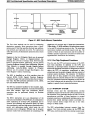
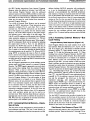
diagrammatically in Figure 2.2.
the 8051 as long as the pin is configured as an input. The
configuration of the ports is shown on the 8051 Family
Logic Symbol of Figure 2.
2.1.2.2.1 Open Drain 1/0 Pins
Each pin of Port 0 can be configured as an open drain
output or as a high impedance input. Resetting the
microcomputer programs each pin as an input by writing
a one (I) to the pin. Ifa zero (0) is later written to the pin it
becomes configured as an output and will continuously
sink current. Re-writing the pin to a one (I) will place its
output driver in a high-impedance state and configure the
pin as an input. Each I/O pin of Port 0 can sink two TTL
loads.
2.1.2.2 1/0 FACILITIES
The 8051 has instructions that treat its 32 I/O lines as 32
individually addressable bits and as four parallel 8-bit
ports addressable as Ports 0, 1,2 and 3. Ports 0,2 and 3
can also assume other functions. Port 0 provides the
multiplexed low-order address and data bus used, for
expanding the 8051 with standard memories and
peripherals. Port 2 provides the high-order address bus
when expanding the 8051 with external Program Memory
or more than 256 bytes of External Data Memory. The
pins of Port 3 can be configured individually to provide
external interrupt request inputs, counter inputs, the
serial port's receiver input and transmitter output, and to
generate the control signals used for reading and writing
External Data Memory. The generation or use of an
alternate function on a Port 3 pin is done automatically by
2.1.2.2.2 Quasi-Bidirectional 1/0 Pins
Ports 1,2 and 3 are quasi-bidirectional buffers. Resetting
the microcomputer programs each pin as an input by
writing a one (l) to the pin. If a zero (0) is later written to
the pin it becomes configured as an output and will
continuously sink current. Any pin that is configured as
an output will be reconfigured as an input when a one (I)
is written to the pin. Simultaneous to this reconfiguration
the output driver of the quasi-bidirectional port will
source current for two oscillator periods. Since current is
sourced only when a bit previously written to a zero (0) is
POLLING
HARDWARE
INPUT LEVEL AND
INTERRUPT REQUEST
FLAG REGISTERS:
INTO
......
tNT1
......
EXTERNAL
INT RQST 1
PORT
•
•
•
•
•
•
•
1----SOURCE
I.D.
-
HIGH PRIORITY
INTERRUPT
REQUEST
V
...AI"'"
.....
I"'"
=>
VECTOR
I'"
INTERNAL
TIMER 1
INTERNAL~
SERIAL
------
..AI'"
eXTERNAL
INTRQST0
INTERNAL
TIMER 0
INTERRUPT
PRIORITY
REGISTER:
INTERRUPT ENABLE
REGISTER:
SOURCE
GLOBAL
ENABLE
ENABLE
,..
r:.
-
R
FIVE INTERRUPT SOURCES
EACH INTERRUPT CAN BE INDIVIDUALLY ENABLED/DISABLED
ENABLED INTERRUPTS CAN BE GLOBALLY ENABLED/DISABLED
EACH INTERRUPT CAN BE ASSIGNED TO EITHER OF TWO PRIORITY LEVELS
EACH INTERRUPT VECTORS TO A SEPARATE LOCATION IN PROGRAM MEMORY
INTERRUPT NESTING TO TWO LEVELS
EXTERNAL INTERRUPT REQUESTS CAN BE PROGRAMMED TO BE LEVEL- OR
TRANSITION-ACTIVATED
V
----SOURCE
I.D.
r--
LOW PRIORITY
INTERRUPT
REQUEST
~
VECTOR
Figure 2.2. 8051 Interrupt System
AFN-01488A-08
4
8051 Architectural Specification and Functional Description
updated to a one (1), a pin programmed as an input will
not source current into the TTL gate that is driving it if the
pin is later written with another one (1). Since the quasibidirectional output driver sources current for only two
oscillator periods, an internal pullup resistor of approximately 20K- to 4OK-ohms is provided to hold the
external driver's loading at a TTL high level. Ports 1, 2
and 3 can sink/ source one TTL load.
The ALE signal is provided for strobing the address into
an external latch. The program store enable (PSEN)
signal is provided for enabling an external memory device
to Port 0 during a read from the Program Memory
address space. When the MOVX instruction is executed
Port 3 automatically generates the read (RD) signal for
enabling an External Data Memory device to Port 0 or
generates the write (WR) signal for strobing the external
memory device with the data emitted by Port O. Port 0
emits the address and data to the external memory
through a push/ pull driver that can sink/ source two TTL
loads. At the end of the read/write bus cycle Port 0 is
automatically reprogrammed to its high impedance state
and Port 2 is returned to the state it had prior to the bus
cycle. The 80S 1 generates the address, data and control
signals needed by memory and I/O devices in a manner
that minimize the requirements placed on external
program and data memories. At 12 MHz, the Program
Memory cycle time is SOOns and the access times required
from stable address and PSEN are approximately 320ns
and lSOns respectively. The External Data Memory cycle
2.1.2.2.3 Microprocessor Bus
A microprocessor bus is provided to permit the 80S 1 to
solve a wide range of problems and to allow the upward
growth of user products. This multiplexed address and
data bus provides an interface compatible with standard
memories, MCS-80 peripherals and the MCS-8S
memories that include on-chip programmable I/O ports
and timing functions. These are summarized in the 80S 1
Microcomputer Expansion Components chart of Figure
2.3.
When accessing external memory the high-order address
is emitted on Port 2 and the low-order address on Port O.
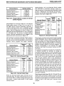
Category
1.0.
I/O Expander
'"
C
'"c0
Comments
8 Line I/O Expander (Shift Register)
Low Cost I/O Expander
User programmable and erasable.
Standard EPROMs
2758
2716-1
2732
2732A
IK
2K
4K
4K
Standard RAMs
2114A
2148
2142-2
IK x 4 100 ns RAM
lK x 4 70 ns RAM
I K x 4 200 ns RAM
Multiplexed Address/
Da.ta RAMs
8185A
I K x 8 300 ns RAM
Standard I/O
8212
8282
8283
8255A
8251 A
8-Bit Ii 0 Port .
8-Bit I/O Port
8-Bit I/O Port
Programmable Peripheral Interface
Programmable Communications
Interface
8205
8286
8287
8253A
8279
MCS-80 and MCS-85 peripheral devices
are compatible with the 8051· allowing
easy addition of specialized interfaces.
Future MCS-80/85 devices will also be
compatible.
8291
8292
I of 8 Binary Decoder
Bi-directional Bus Driver
Bi-directional Bus Driver (Inverting)
Programmable Interval Timer
Programmable Keyboard/ Display
Interface (128 Keys)
GPIB Talker/Listener
GPIB Controller
Universal Peripheral
Interfaces
8041 A
8741A
ROM Program Memory
EPROM Program Memory
User programmable to perform custom
I/O and control functions.
Memories with
on-chip I/O and
Peripheral
Functions.
8155-2
8355-2
8755-2
256 x 8 330 ns RAM
2K x 8 300 ns ROM
2K x 8 300 ns EPROM
Q,
e0
U
on
QO
Q
QO
•
ell
U
~
Description
Standard Peripherals
'"
;§
;
Q,
e
0
U
x
x
x
x
8
8
8
8
450
350
450
250
ns
ns
ns
ns
Light
Light
Light
Light
Erasable
Erasable
Erasable
Erasable
Data memory can be easily expanded
using standard NMOS RAMs.
Serves as Address Latch or I/O port.
Three 8-bit porgrammable I/O ports.
Serial Communcations Receiver/
Transmitter.
Figure 2.3. 8051 Microcomputer Expansion Components
AFN-Q1488A-09
5
8051 Architectural Specification and Functional Description
time is IllS and the access times required from stable
address and from read (RD) or write (WR) command are
approximately 600ns and 250ns respectively.
CRYSTAL
OSCILLATOR
$
2.1.2.3 TIMER/EVENT COUNTERS
The 8051 contains two 16-bit counters for measuring time
intervals, measuring pulse widths, counting events and
generating precise, periodic interrupt requests. Each can
be programmed independently to operate similar to an
8048 8-bit timer with divide by 32 prescaler or 8-bit
counter with divide by 32 prescaler (Mode 0), as a 16-bit
time-interval or event counter (Mode I), or as an 8-bit
time-interval or event counter with automatic reload
upon overflow (Mode 2).
CRYSTAL
°ii~O,.R ~~~~~ ~
__
OVERFLOW
1---4t----I~ (INTERRUPT
REQUEST)
FLAG 1
• 8048 TIMER/COUNTER
• 16-BIT TIMER/COUNTER
• 8-BIT AUTO-RELOAD TIMER/COUNTER
PULSE TO
SERIAL PORT
Figure 2.4.A. Timer/Event Counter
Modes 0, 1, and 2
CRYSTAL
OSCilLATOR
CRYSTAL
OSCILLATOR
$
OVERFLOW
(INTERRUPT
REQUEST)
FLAG 1
EXTERNAL ___
SOURCE
L--_ _ _ _--I~
• 8-BIT TIMER
• 8-BIT TIMER/COUNTER
OVERFLOW
(INTERRUPT
REQUEST)
FLAG 0
CRYSTAL
OSCilLATOR
$
The counters are started and stopped under software
control. Each counter sets its interrupt request flag when
it overflows from all ones to aU zeros (or auto-reload
value). The operating modes and input sources are
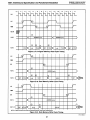
summarized in Figures 2.4A and 2.4B. The effects of the
configuration flags and the status flags are shown in
Figures 2.5A and 2.5B.
INTO
__
EXTSOEURRNCALE - .
When counter 0 is in Mode 3, counter I can be
programmed to any of the three aforementioned modes,
although it cannot set an interrupt request flag or generate
an interrupt. This mode is useful because counter I's overflow can be used to pulse the serial port's transmission-rate
generator. Along with their multiple operating modes and
16-bit precision, the counters can also handle very high
input frequencies. These range from 0.1 MHzto 1.0 MHz
(for 1.2 MHz to 12 MHz crystal) when programmed for
an input that is a division by 12 of the oscillator frequency
and from 0 Hz to an upper limit of 50 KHz to 0.5 MHz
(for 1.2 MHz to 12 MHz crystal) when programmed for
external inputs. Both· internal and external inputs can be
gated to the counter by a second external source for
directly measuring pulse widths.
COUNTER/TIMER
REQUEST)
FLAG 0
• 8048 TIMER/COUNTER
• 16-BIT TIMER/COUNTER
• 8-BIT AUTO-RELOAD TIMER/COUNTER
Additionally, counter 0 can be programmed to a mode
that divides it into one 8-bit time-interval or event
counter and one 8-bit time-interval counter (Mode 3).
GATE
OVERFLOW
~_--I~ (INTERRUPT
EXTERNAL-.
SOURCE
EX;5~:~~'"
• 8048 TIMER/COUNTER
• 16-BIT TIMER/COUNTER
• 8-BIT AUTO-RELOAD TIMER/COUNTER
PULSE TO
SERIAL PORT
Figure 2.4.8. Timer/Event Counter Mode 3
INTERRUPT
REQUEST
RUN
--~=-~l:'~>-"t"--r-\--J====j~:J
COUNTER 0
MODE 0: 8-BIT TIMER WITH PRESCALER/8-BIT COUNTER
WITH PRESCAlER
>----f MODE 1: 16-BIT TIMER/COUNTER
TO------~
MODE 2: 8-BIT AUTO-RELOAD TIMER/COUNTER
MODE 3: 8-BIT TIMER/COUNTER (TlO)
XTAl1
Figure 2.S.A. Timer/Counter 0 Control and Status Flag Circuitry
AFN-01488A-l0
6
8051 Architectural Specification and Functional Description
INTERRUPT
REQUEST
COUNTERI
TIMER
RUN
GATE
TIMERI
COUNTER
OIN
MODE 3
-
~
G
Hn
•
J )PULSE TO
SERIAL
PORT
COUNTER 1
MODE 0: 8-BIT TIMER WITH PRESCALERI
8-BIT COUNTER WITH PRESCALERMODE 1: 16-BIT TIMER/COUNTER
MODE 2: 8-BIT AUTO-RELOAD TIC
MODE 3: PREVENTS INCREMENTING
OF TIC 1
INT1
J
--
1"'"
~
~r~
>- r-r-r- :=fJ-
-
T1
XTAL1
+12
-
1 "'
-
COUNTER 0
~
~
8-8ITTIMER
(THO)
~
Figure 2.5.8. Timer/Counter 1 Control and Status Flag Circuitry
r - - - -- - - -- - -- -
• 100r11 Bit Frame
• Baud Rate Generetlon
from Oscillator or
Timer 1
• Address Frame
Recognition
I
I
I
I
g:~~~~t.,.OR
I
-
INTERRUPT
I -_ _ _-:-__ ~~~~SMIT
I
I
---:;:R:;:;S;.-TT-;;-----l
~-~-----~
SCON
(SERIAL CONTROL)
CONTROL"
TIMING CIRCUITRY
....
1.....
-:-16
TIMER 1
OVERFLOW
L ______________RECEIVER ___ _
~~
Figure 2.6. Serial
Port~UART
RECEIVE
DATA
Modes 1, 2, and 3
2.1.2.4 SERIAL COMMUNICATIONS
service the serial link. A block diagram of the serial port is
shown in Figure 2.6. Methods for linking UART (universal asynchronous receiver / transmitter) devices are shown
in Figure 2.7 and a method for I/O expansion is shown in
Figure 2.8.
The 8051 has a serial I/O port that is useful for serially
linking peripheral devices as well as multiple805ls
through standard asynchronous protocols with fullduplex operatiori. The serial port also has a synchronous
mode for expansion of I/O lines using CMOS and TTL
shift registers. This hardware serial communications
interface saves ROM code and permits a much higher
transmission rate than could be achieved through
software. In response to a serial port interrupt request the
CPU has only to read/write the serial port's buffer to
o
The full-duplex serial I/O port provides asynchronous
modes to facilitate communications with standard U ART
devices, such as printers and CRT terminals, or communications with other 8051s in multi-processor systems.
AFN-01488A-11
7
8051 Architectural Specification and Functional Description
~
.~
I
I
TXD
RXD
TXD
RXD
TXD
RXD
RXD
TXD
TXD
RXD
TXD
RXD
TXD
RXD
PORT PIN
8051
8051
8051
A. MULTI-80S1 INTERCONNECT -HALF DUPLEX
8051
8051
8051
r-----
RXD
~.
TXD
CTS
8251
8051
B. MULTI-80S1 INTERCONNECT-FULL DUPLEX
C. 8051-8251 INTERFACE
Figure 2.7. UART Interfacing Schemes
The receiver is double buffered to eliminate the overrun
that would occur if the CPU failed to respond to the
receiver's interrupt before the beginning of the next
frame. Double buffering of the transmitter is not needed
since the 8051 can generally maintain the serial link at its
maximum rate without it. A minor degradation in
transmission rate can occur in rare events such as when
the servicing of the transmitter has to wait for a lengthy
interrupt service program to complete. In asynchronous
modes, false start-bit rejection is provided on received
frames. For noise rejection a best two-out-of-three vote is
taken on three samples near the center of each received
bit.
8051
DATA
CLOCK
PORT PIN
A.1I0INPUT
EXPANSION
8051
When interfacing with standard UART devices the serial
channel can be programmed to a mode (Mode 1) that
transmits/ receives a ten-bit frame or programmed to a
mode (Mode 2 or 3) that transmits/receives an eleven-bit
frame as shown in Figure 2..9. The frame consists of a start
bit, eight or nine data bits and a stop bit. In Modes 1 and
3, the transmission-rate timing circuitry receives a pulse
from counter I each time the counter overflows. The
input to counter 1 can be an external source or a division
by 12 of the oscillator frequency. The auto-reload mode
of the counter provides communication rates of 122 to
31,250 bits per second (including start and stop bits) for a
12 MHz crystal. In Mode 2 the communication rate is a
division by 64 of the oscillator frequency yielding a
transmission rate of 187,500 bits per second (including
start and stop bits) for a 12 MHz crystal.
DATA
OS
CLOCK
PORT PIN
EN
B. 110 OUTPUT
EXPANSION
Figure 2.8. I/O Expansion Technique
MODE
~~~--------~--~--~---'I~
TTY
START
7-BIT DATA
,
PARITY'
2 STOP
START
TYPICAL
CRT
7·BIT DATA
START
8-BIT DATA
START
a-BIT DATA
MARK
STOP
PARITY STOP
2&3
Distributed processing offers a faster, more powerful
system than can be provided by a single CPU processor.
This results from a hierarchy of interconnected
processors, each with its own memories and 1/ O. In
multiprocessing, a host 8051 microcomputer controls a
multiplicity of 8051 s configured to operate simultaneouslyon separate portions of the program, each controlling a
portion of the overall process. The interconnected 8051 s
reduce the load on the host processor and result in a lowcost system of data transmission. This form of distributed
MULTIPROCESSOR
COMMUNICATIONS
~~~:I STOP
2&3
START
1/0
EXPANSION
9-BIT DATA
a·BITS
STOP
o
j..DATA
....- - - - - - - - - - - - '_ _ ClK
Figure 2.9. Typical Frame Formats
AFN-01488A-12
8
8051 Architectural Specification and Functional Description
2.2.3 Internal Data Memory
processing is especially effective in systems where controls
in a complex process are required at physically separated
locations.
The 8051 contains a I 28-byte Internal Data RAM (which
includes registers R7-RO in e'ach of four Banks), and
twenty memory-mapped Special Functional Registers.
In Modes 2 and 3 the automatic wake-up of slave
processors through interrupt driven address-frame
recognition is provided to facilitate interprocessor communications. The protocol for interprocessor communications is shown in Figure 2.10.
2.2.3.1 INTERNAL DATA RAM
The Internal Data RAM provides a convenient 128-byte
scratch pad memory.
1. Slaves -Configure serial port to interrupt CPU if the
2.2.3.2 REGISTER BANKS
received ninth data bit is a one (I).
2. Master-Transmit frame containing address in first 8
data bits and set ninth data bit (i.e., ninth
data bit designates address frame).
3. Slaves - Serial port interrupts CPU when address
frame is received. Interrupt service program
compares received address to its address.
The slave which has been addressed reconfigures its serial port to interrupt the CPU on
all subsequent transmissions.
4. Master-Transmit control frames and data frames
(these will be accepted only by the previously
addressed slave.)
There are four 8-Register Banks within the Internal Data
RAM, each containing registers R7-RO.
2.2.3.3 SPECIAL FUNCTION REGISTERS
The Special Function Registers include arithmetic registers
(A , B, PSW), pointers (SP, DPH, DPL) and registers
that provide an interface between the CPU and the
on-chip peripheral functions.
2.2.3.4 A REGISTER
The A register is the accumulator register. ACC is the
location of the accumulator in the Internal Data Memory.
Figure 2.10. Protocol for Multi-Processor
Communications
2.2.3.5 B REGISTER
The B register is dedicated during multiply and divide and
serves as both a source and a destination. During all other
operations the B register is simply another location of
the Internal Data Memory.
In synchronous mode (Mode 0) the high-speed serial port
provides an efficient, low-cost method of expanding I/O
lines using standard TTL and CMOS shift registers. The
serial channel provides a clock output for synchronizing
. the shifting of bits to/from an external register. The data
rate is a.division by 12 of the oscillator frequency and is
I M bits p(:r second at 12 MHz.
2.2.3.6 PSW REGISTER
The carry (CY), auxialiary carry (AC), user flag 0 (FO),
register bank select I (RS I), register bank select 0 (RSO),
overflow (OV) and parity (P) flags reside in the Program
Status Word (PSW) Register. These flags are bitmemory-mapped within the byte-memory-mapped PSW.
The PSW flags record processor status information and
control the operation of the processor.
The CY, AC, and OV flags generally reflect the status of
the latest arithmetic operation. The P flag always reflects
the parity of the A register. The carry flag is also a
Boolean accumulator for bit operations. Specific details
are provided in the "Flag Register Settings" section of
2.7.2.
FO is a general purpose flag which is pushed onto the
stack as part of a PSW save.
The two Register Bank select bits (RS I 'and RSO) determine which of the four 8-Register Banks is selected.
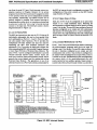
2.2 CPU HARDWARE
This section describes the hardware architecture of the
8051's CPU in detaiL The interrupt system and on-chip
functions peripheral to the CPU are described in
subsequent sections. A detailed 8051 Functional Block
Diagram is displayed in Figure 2. II.
2.2.1 Instruction Decoder
Each program instruction is decoded by the instruction
decoder. This unit generates the internal signals that
control the functions of each unit within the CPU section. These signals control the sources and destination
of data, as well as the function of the Arithmetic/Logic
Unit (ALU).
2.2.2 Program Counter
2.2.3.7 STACK POINTER
The I6-bit Program Counter (PC) controls the sequence in
which the instructions stored in program memory are
executed. It is manipulated with the Control Transfer
instructions listed in section 2.7.2.
The 8-bit Stack Pointer (SP) contains the address at
which the last byte was pushed onto the stack. This is
also the address of the next byte that will be popped. SP
is updatable under software control.
AFN·01488A-13
9
-
~-~,-~--
-----=----c---:
8051 Architectural Specification and Functional Description
· t1:
~~~
r--
i'.r
U
I ~ ri
I
a:
w
CY I AC I FO I RS11RSOI OV I
Q
0
PARITY,
I/t--
I~
lr -
Ip
A
U
I
w
Q
B
'"'"
w
a:
Q
Q
~
ROTATE CONTROLP
a:
w
IPC
INTERRUP
CONTROL
<:(
IEC
a:
w
SBUF
Q
r- -
0
u
w
Q
...
-V a'"w
SERIAL
PORT
SCON
'"'"a:w
I---
Q
Q
a:
z
TH1
i=
U
TL1
......
THO
0
z
:l
<:(
>a:
TIMER
CONTROL
U
TLO
'"
TMOD
0
:I
w
:I
:I
f4
<:(
a:
Cl
w
Q.
0
a:
Q.
TCON
DPH
I'\,
DPL
V
~
SP
128·8
RAM
PCH
f-------------
PCL
Q
0
U
:)
Q
~
:I
<:(
a:
f-----------REGISTER BANK 1
f------------REGISTER BANK 0
i
DRIVERS
~~
~"r
osc
&
TIMING
CIRCUITRY
T
A
L
1
---
~
V
REGISTER BANK 3
'"'"a: f------------w
REGISTER BANK 2
Q
tx
'\.7
PROGRAM CONTROL
a:
w
w
4K ·8
NONE (8031)
ROM (8051V
EPROM (87511
<:(
+
X
T
A
L
2
q
E
A
A
L
P
S
/
V
E
/
E
N
D
R
D
P
'"
~
~
,/,
/~
~L
I I
I
I
D D
PORT 1
PORT 3
CONTROL
PLA
CONTROL
ENGINE
DRIVERS
'" '';.
J~
I
~~
VL
INSTRUCTION
DECODER
Iv
rr l},
•
1
D
PORT2
r
0
PORTO
I
~
7-
1
~
R
S
T
V
C
C
V
S
S
/
V
P
o
D
G
Figure 2.11. 8051 Family Functional Block Diagram
AFN-01488A-14
10
8051 Architectural Specification and Functional Description
On any addressable bit, the Boolean processor can perform the bit operations of set, clear, complement,
jump-if-set, jump-if-not-set, j~mp-if-set-then-clear and
move to/from carry. Between any addressable bit (or its
complement) and the carry flag it can perform the bit
operation of logical and or logical or with the result
returned to the carry flag.
The bit-manipulation instructions provide optimum code
and speed efficiency in "bit-banging" applications such as
the control of the 8051's on-chip peripherals. The Boolean
processor also provides a straightforward means of converting logic equations (like those used in random
logic design) directly into software. Complex combinatorial-logic functions can be resolved without extensive
data movement, byte masking and test-and-branch trees.
2.2.3.8 DATA POINTER
The 16-bit Data Pointer (DPTR) register is the concatination of registers DPH (data pointer's high-order byte) and
DPL (data pointer's low-order byte). The DPTR is used in
Register-Indire91 Addressing to move Program Memory
constants, to move External Data Memory variables, and
to branch over the 64K Program Memory address space.
2.2.4 Arithmetic Section
The arithmetic section of the processor performs many
data manipulation functions and is comprised of the
Arithmetic/Logic Unit (ALU), A register, B register and
PSW register.
The AL U accepts 8-bit data words from one or two
sources and generates an 8-bit result under the control
of the instruction decoder. The ALU performs the arithmetic operations of add, subtract, multiply, divide, increment, decrement, BCD-decimal-add-adjust and compare
and .the logic operations of and, or, exclusive-or,
complement and rotate [right, left, or nibble swap (left
four)].
2.3 MEMORY ORGANIZATION
In the 8051 family the memory is organized ever three
address spaces and the program counter. The memory
spaces shown in Figure 2.1 are the:
• 16-bit Program Counter
• 64K-byte Program Memory address space
2.2.5 'Program Control Section
• 64K-byte External Data Memory address space
The program control section controls the sequence in
which the instructions stored in program memory are
executed. The conditional branch logic enables conditions
internal and external to the processor to cause a change
in the sequence of program execution.
• 384-byte Internal Data Memory address space
The 16-bit Program Counter register provides the 8051
with its 64K addressing capabilities. The Program Counter
allows the user to execute calls and branches to any location within the Program Memory space. There are no
instructions that permit program execution to move from
the Program Memory space to any of the data memory
spaces.
In the 8051 and 8751 the lower 4K of the 64K Program
Memory address space is filled by internal ROM and
EPROM, respectively. By trying the EA pin high, the
processor can be forced to fetch from the internal
ROM/EPROM for Program Memory addresses 0
through 4K. Bus expansion for accessing Program
Memory beyond 4K is automatic since external instruction fetches occur automatically when the Program
Counter increases above 4095. If the EA pin is tied low all
Program Memory fetches are from external memory.
The execution speed of the 8051 is an same regardless of
whether fetches are from internal or external Program
Memory. If all program storage is on-chip, byte location
4095 should be left vacant to prevent an undesired
prefetch from external Program Memory address 4096.
Certain locations in Program Memory are reserved for
specific programs. Locations 0000 through 0002 are
reserved for the initialization program. Following reset,
the CPU always begins execution at location 0000.
Locations 0003 through 0042 are reserved for the five
interrupt-request service programs. Each resource that
can request an interrupt requires that its service program
be stored at its reserved location.
2.2.6 Oscillator and Timing Circuitry
Timing generation for the 8051 is completely selfcontained, except for the frequency reference which can
be a crystal or external clock source. The on-board
oscillator is a parallel anti-resonant circuit with a
frequency range of 1.2 to 12 MHz. The XTAL2 pin is the
output of a high-gain amplifier, while XT AL I is its input.
A crystal connected between XT AL I and XT AL2
provides the feedback and phase shift required for
oscillation. The t.2 to 12 MHz range is also accomodated
when an external TTL compatible clock is applied to
XT AL 1 as the frequency source.
2.2.7 Boolean Processor
Although the Boolean processor is an integral part of the
8051's architecture, it may be considered an independent
bit processor since it has its own instruction set, its own
accumulator (the carry flag), and its own bit-addressable
RAM and I/O.
The bit-manipulation instructions allow the Direct
Addressing of 128 bits within the Internal Data RA M
and 128 bits within the Special Function Registers. The
Special Function Registers with an address evenly
divisable by eighqpO, TCON, PI, SCON, P2, IEC, P3,
IPC, PSW, A. and B) contain Direct Addressable bits.
AFN-01488A-15
11
8051 Architectural Specification and Functional Description
Register accessible through Direct Addressing can be
pushed I popped.
The 64K-byte External Data Memory address space.is
automatically accessed when the MOVX instruction is
executed.
Functionally the Internal Data Memory is the most flexible of the address spaces. The Internal Data Memory
space is subdivided into a 256-byte Internal Data RAM
address space and a 128-byte Special Function Register"'
address space as shown in Figure 2. 12.
SPECIAL
FUNCTION
REGISTERS
INTERNAL DATA RAM
(
The Special Function Register address space is 128 to 255.
All registers except the Program Counter and the four
8-Register Banks reside here. Memory mapping the
Special Function Registers allows them to be accessed as
easily as internal RAM. As such, they can be operated on
by most instructions. In addition, 128 bit locations within
the Special Function Register address space can be
accessed using Direct Addressing. These bits reside in the
Special Function Register byte locations divisible by
eight. The twenty Special Function Registers are listed
in Figure 2. 13. Their mapping in the Special Function
Register address space is shown in Figure 2.14.
,,------A--,
A
255
255
255
248 F8H
FOH
E8H
EOH
D8H
DOH
C8H
COH
B8H
BOH
ARITHMETIC REGISTERS:
ACCumulator*, B register*,
Program Status Word*
POINTERS:
Stack Pointer, Data Pointer (high & low)
PARALLEL I/O PORTS:
Port 3*, Port 2*, Port 1*, Port 0*
INTERRUPT SYSTEM:
Interrupt Priority Control*,
Interrupt Enable Control*
TIMERS:
Timer MODe, Timer CONtrol*, Timer 1
(high & low), Timer 0 (high & low)
SERIAL 1/0 PORT:
Serial CONtrol*, Serial data BUFfer
ADDRESSABLE
BITS IN
SFRs
(128 BITS)
A8H
AOH
98H
90H
128
135
88H
128 80H
-~
127
128
-48
ADORE 55ABLE
BITS IN
RAM
(128 BIT S)
REGISTERS
-<
127
32
7
R7
-24
RO
R7
16
RD
R7
8
0
120
0
BANK 3
RO
R7
RO
BANK 2
*Bits in these registers are bit addressable
BANK 1
Figure 2.13. Special Function Registers
BANKO
~
INTERNAL
DATA RAM
Performing a read from a location of the Internal Data
Memory where neither a byte of Internal Data RAM (i.e.
RAM addresses 128-255) nor a Special Function Register
exists will access data of indeterminable value.
SPECIAL FUNCTION
REGISTERS
Figure 2.12. Internal Data Memory
Address Space
Architecturally, each-memory space is a linear sequence
of 8-bit wide bytes. By Intel convention the storage of
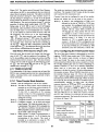
multi-byte address and data operands in program and
data memories is least significant byte at the low-order
address and the most significant byte at the high-order
address. Within byte X, the most significant bit is represented by X.7 while the least significant bit is X.O. Any
deviation from these conventions will be explicitly stated
in the text.
The Internal Data RAM address space is 0 to 255. Four
8-Register Banks occupy locations 0 through 31. The
stack can be located anywhere in the Internal Data RAM
address space. In addition, 128 bit locations of the on-chip
RAM are accessible through Direct Addressing. These
bits reside in Internal Data RAM at byte locations 32
through 47. Currently locations 0 through 127 of the
Internal Data RAM address space are filled with on-chip
RAM. Locations 128 through 255 may be filled on later
products without affecting existing software.
2.4 OPERAND ADDRESSING
The stack depth is limited only by the available Internal
Data RAM, thanks to an 8-bit reloadable Stack Pointer.
The stack is used for storing the Program Counter during
subroutine calls and may be used for passing parameters.
Any byte of Internal Data RAM or Special Function
There are five methods of addressing source operands.
They are Register Addressing, Direct Addressing,
Register-Indirect Addressing, Immediate Addressing,and
Base-Register- plus Index-Register- Indirect Addressing.
The first three of these methods can also be used to
AFN-01488A-16
12
8051 Architectural Specification and Functional Description
SYMBOLIC
ADDRESS
A.
~(
'FI
ACC
231
psw
1I
215
IPC
P3
IEC
P2
191
1
I
183
175
I
167
SBUF
SCON
P1
I
•
Register Addressing
R7-RO
-- A, B, C (bit), AB (two bytes),
DPTR (double byte)
• Direct Addressing
Lower 128 bytes of Internal Data RAM
Special Function Registers
128 bits in subset of Internal Data RAM
address space
128 bits in subset of Special Function
Register address space
• Register-Indirect Addressing
Internal Data RAM [@R1, @RO, @SP
(PUSH and POP only))
Least Significant Nibbles in Internal
Data RAM (@R1, @RO)
External Data Memory (@R1, @RO,
@DPTR)
• Immediate Addressing
-- Program Memory (tn-code constant)
• Base - Register- plus Index-Register- Indirect
Addressing
Program Memory (@ DPTR+A,
@PC+A)
BYTE
ADDRESS
BIT ADDRESS
\~
2481
B
A
~I:
224
208
184
176
168
160
152
151
144
(EOH)
I
I
1
I
184
(B8H)
176
(BOH)
I
(AOH)
208
168
(DOH)
(ASH)
160
1I
153
152
159
(FOH)
144
(99H)
(98H)
(9OH)
TH1
141
THO
140 (8CH)
Tl1
139 (8BH)
138 (BAH)
TlO
137
136
TMOD
TCON
:~ ~143 ~:
136
SP
SFR's
CONTAINING
DIRECT
ADDRESSABLE
BITS
(8DH)
(89H)
(88H)
::::
129 (81H)
128 (SOH)
PO
135
Figure 2.15. Operand Addressing Methods
128
(R 7-RO) of the selected Register Bank (RB). One of the
four 8-Register Banks is selected by a two-bit field in the
PSW. The registers may also be accessed through Direct
Addressing and Register-Indirect Addressing since the
four Register Banks are mapped into the lowest 32 bytes
of Internal Data RAM as shown in Figure 2.16. Other
Iflternal Data Memory locations that are addressed as
registers are A, B, C, AB and DPTR.
Figure 2.14. Mapping Of Special Function Registers
address a destination operand. Since operations in the
8051 require 0 (NOP only), I, 2, 3 or 4 operands, these
five addressing methods are used in combinations to
provide the .8051 with its 21 addressing modes.
Most instructions have a "destination, source'" field that
specifies the data type, addressing methods and operands
involved. For operations other than moves, the destination operand is also a source operand. For example, in
"subtract-with-borrow A,#5" the A register receives the
result of the value in register A minus 5, minus C.
Direct Addressing provides the only means of accessing
the memory-mapped byte-wide Special Function Registers
and memory mapped bits within the Special Function
Registers and Internal Data RAM. Direct Addressing of
bytes may also be used to access the lower 128 bytes
of Internal Data RAM. Direct Addressing of bits gains
access to a 128 bit subset of the Internal Data RAM and
128 bit subset of the Special Function Registers as shown
in Figures 2. 12, 2. 14 and 2. 16.
Most operations involve operands that are located in
Internal Data Memory. The selection of the Program
Memory space or External Data Memory space for a
second operand is determined by the operation mnemonic
unless it is an immediate operand. The subset of the
Internal Data Memory being addressed is determined by
the addressing method and address value. For example,
the Special Function Registers can be accessed only
thorugh Direct Addressing with an address of 128-255. A
summary of the operand addressing methods is shown in
Figure 2.15. The following paragraphs describe the five
addressing methods.
Register-Indirect Addressing using the content of R I or
RO in the selected Register Bank, or using the content of
the Stack Pointer (PUSH and POP only), addresses the
Internal Data RAM. Register-Indirect Addressing is also
used for accessing the External Data Memory. In this
case, either R 1or RO in the selected Register Bank may.be
used for accessing locations within a 256-byte block. The
block number can be preselected by the contents of a
port. The 16-bit Data Pointer may be used for accessing
any location within the full 64K external address space.
Immediate Addressing allows constants which are part
Register Addressing permits access to the eight registers
AFN'01488A-17
13
8051 Architectural Specification and Functional Description
as two locations in Internal Data Memory (DPH &
DPL). The Program Counter is always manipulated as a
single double-byte register.
While the 8051 has extensive facilities for byte logic
operations as well as byte binary and two-digit BCD
arithmetic, it excels in its bit handling capabilities. 128
bits in the Special Function Registers and 128 software
flags in the Internal Data RAM are all supported
orthogonally by the logic operations of and, or, set, clear,
and complement; the conditional branch operations of
jump-if-bit-set, jump-if-bit-not-set, and jump-if-bit-setthen-clear-bit; and the transfer operation of move bit.
Performing conditional branch, logical, and transfer operations directly on Boolean variables is a breakthrough
for microcomputers, since this makes the 8051 both a
byte processor and a Boolean processor.
of the instruction to be accessed from the Program
Memory.
Base-Register- plus Index-Register- Indirect Addressing
simplifies accessing look-up-tables (LUT) resident in
Program Memory. A byte may be accessed from a LUT
via an indirect move from a location whose address is the
sum of a base register (the DPTR or PC) and the index·
register (A).
SPECIAL
FUNCTION
REGISTERS
INTERNAL
DATA RAMI
STACK
~~
255 255
248
240
232
224
216
208
200
192
164
176
168
160
152
144
248 F8H
FOH
E8H
136
88H
128 80H
128 135
..,.....:::.~
DIRECT
ADDRESSING
(BITS)
7
R7
24
RO
,
8
'-
0
C8H
COH
B8H
BOH
2.5.1 Data Transfer Operations
DIRECT
ADDRESSING
(BITS)
Look-up-tables resident in Program Memory can be
accessed by indirect moves. A byte constant can be
transferred to the A register (Le. accumulator) from the
Program Memory location whose address is the sum of a
base register (the PC or DPTR) and the index register
(A). This provides a convenient means for programming
translation algorithms such as ASCII to seven segment
conversions. The Program Memory move operations are
shown diagrammatically in Figure 2. 17.
ASH
AOH
98H
90H
120
REGISTER
A
0
.E.
.!!
REGISTER
ADDRESSING
127
EOH
D8H
DOH
BANK 3
R7 BANK2
RO
R7
BANK 1
RO
R7
BANKO
RO
"~--~y
BASE-REGISTER- PLUS
INDEX-REGISTER-INDIRECT
@PC+A
(PROG MEM 0-64K)
~
)
BASE-REGISTER- PLUS
INDEX-REGISTER-INDIRECT
@OPTR+A
(PROG MEM 0-64K)
DIRECT ADDRESSING
STACK-POINTER REGISTER-INDIRECT AND
REGISTER-INDIRECT ADDRESSING
Figure 2.17 Program Memory Move Operations
Figure 2.16. Addressing Operands In
Internal Data Memory
A byte location within a 256-byte block of External Data
Memory can be accessed using R I or RO in RegisterIndirect Addressing. Any location within the full 64K
External Data Memory address space can be accessed
through Register-Indirect Addressing using a 16-bit bas..
register (i.e. the Data Pointer). These moves are shown
in Figure 2.18.
2.5 DATA MANIPULATION
The 8051 microcomputer is efficient both as an arithmetic processor and as a controller. In addition to the
capabilities of its 8048 predecessor, the 8051 was enhanced
with improved data transfer, logic manipulation, arithmetic processing, and real-time control capabilities. The
8051 performs operations on bit, nibble (4-bit), byte
(8-bit) and double-byte (l6-bit) data types. It is classified
as an 8-bit machine since the internal ROM, RAM,
Special Function Registers, Arithmetic/ Logic Unit (ALU)
and the external data bus are each 8-bits wide. The
double-byte data type is used only by the Data Pointer
and the Program Counter. The Data Pointer can be
manipulated as a single double-byte register (DPTR) or
The byte in-code-constant (immediate) moves and byte
variable moves within the 8051 are highly orthogonal as
detailed in Figure 2. 19. When one considers that the
accumulator and the registers in the Register Banks can
be Direct Addressed, the two-operand data transfer
operations allow a byte to be moved between any two of
the RB registers, Internal Data, RAM, accumulator and
Special Function Registers. Also, immediate operands
AFN-01488A-18
14
8051 Architectural Specification and Functional Description
DIRECT
REGISTER
R7-RO
REGISTER
Data
A
REGISTER
A
REGISTER·INDIRECT
@R1,@RO
(EXT DATA 0-255)
REGISTER-INDIRECT
@DP
(EXT DATA 0-64K)
REGISTER-INDIRECT
@R1,@RO
Figure 2.18. External Data Memory Move Operations
Figure 2.20. Internal Data Memory Exchange
Operations
can be moved to any of these locations. Of particular
interest is the Direct Address to Direct Address move
which permits the value in a port to be moved to the
Internal Data RAM without using any RB registers or
the accumulator. The Data Pointer register can be loaded
with a double-byte immediate value. Also, the 8051's
Boolean Processor can move any Direct Addressed bit to
or from the carry flag.
2.5.2 Logic Operations
The 8051 permits the logic operations of and, or, and
exlusive-or to be performed on the A register by a second
operand which can be immediate value, a register in the
selected Register Bank, a Register-Indirect Addressed
byte of Internal Data RAM ora Direct Addressed byte of
Internal Data RAM or Special Function Register. In
addition, these logic operations can be performed on a
Direct Addressed byte of the Internal Data RAM or
Special Function Register using the A register as the
second operand. Also, use of Immediate Addressing with
Direct Addressing permits these logic operations to set,
clear or complement any bit anywhere in the Internal
Data RAM or Special Function Registers without
The A register can be exchanged with a register in the
selected Register Bank, with a Register-Indirect Addressed
byte in the Internal Data RAM or with a Direct Addressed
byte in the Internal Data RAM or Special Function Register. The least significant nibble of the A registt;r can also
be exchanged with the least significant nibble of a RegisterIndirect Addressed byte in the Internal Data RAM. The
exchange operation is shown in Figure 2.20
REGISTER
DIRECT
C
Data
REGISTER
DPTR
16
REGISTER
R7-RO
DIRECT
REGISTER
A
Data
IMMEDIATE
# data
REGISTER-INDIRECT
@R1,@RO
REGISTER-INDIRECT
@SP
Figure 2.19. Internal Data Memory Move Operations
AFN-01488A-19
15
affecting the PSW,RB registers or accumulator. When
one takes into account that registers R 7-RO and the
accumulator can be Direct Addressed, the two-operand
logic operations allow the destination (first operand) to
be a byte in the Internal Data RAM, a Special Function
Register, RB registers (R 7-RO) or the accumulator while
the choice of the second operand can be any of the
aforementioned or an immediate value. The 8051 can
also perform a logical or, or a logical and, between the
Boolean accumulator (i.e. the carry flag) and any bit, or
its complement, that can be accessed through Direct
Addressing. The and, or, and exclusive-or logic operations are summarized in Figure 2.21.
•
•
•
•
add, increment, decrement, compare-to-zero, decrementand-compare-to-zero, and decimal-add-adjust, the 8051
implemented subtract-with-borrow, compare, mUltiply
and divide.
Only unsigned binary integar arithmetic is performed in
the ArithmetiC/Logic Unit. In the two-operand operations of add, add-with-carry and subtract-with-borrow,
the A register is the first operand and receives the result of
the operatjon. The second operand can be an immediate
byte, a register in the selected Register Bank, a RegisterIndirect Addressed byte or a Direct Addressed byte.
These instructions affect the overflow, carry, auxiliarycarry and parity flags in the Program Status Word
(PSW). The carry flag facilitates nonsigned integer and
multi-precision addition and subtraction and multiprecision rotation. Handling two's-complement-integer
(signed) addition and subtraction can easily be accomodated with software's monitoring ofthe PSWs overflow
flag. The auxiliary-carry flag simplifies BCD arithmetic.
An operation that has an arithmetic aspect similar to a
subtract is the compare-and-j~mp-if-not-equal operation. This operation perforros a conditional branch if a
register in the selected Register Bank, or an Indirect
Addressed byte of Internal Data RAM, does not equal an
immediate value; or if the A register does not equal a byte
in the Direct Addressable Internal Data RAM, or a
Special Function Register. While the destination operand
is not updated and neither source operand is affected by
the compare operation, the carry flag is. A summary of
the two-operand add/subtract operations is shown in
Figure 2.24.
IMMEDtATE
# data
Figure 2.21. Internal Data Memory Logic Operations
In addition to the logic operations that are performed on
Internal Data Memory as shown in Figure 2.21, there are
also logic operations that are performed specifically on
the A register. These are summarized in Figure 2.22.
Clear
Complement
Rotate-Laft
Rotate-Laft-Through-Carry
Rotate-Right
Rotate-Rlght-Through-Carry
Swep-NlbbI.. (Rotate Left Four)
REGISTER
C
(SETB,
ClR,CPL)
Figure 2.23. Internal Data Memory Logic Operations
(Bit-Specific)
• And (ANL)
.Or(ORL)
• Exclusive-or (XRL)
•
•
•
•
•
•
•
Set(SETB)
Clear (ClR)
Complement (CPL)
Jump-It-BII-Set-Then-Clear-BII (JBC)
REGISTER
A
•
•
•
•
Figure 2.22. Internal Data Memory Logic Operations
(Register A Specific)
Add
Add-With-Carry
Subtract-With·Borrow
Compare-And-Jump-II·Not·Equal (•••• )
DIRECT
Data
"", ,
In addition to the and andor bit logicals shown in Figure
2.21, there are logicals that can operate exclusively on a
Direct Addressed bit. These operations are listed in
Figure 2.23. The carry flag is also addressed as a register
and can be set, cleared or complemented with one-byte
instructions.
,/
,/
'"
,/
,/
,/
'"
REGISTER
R7·RO
2.5.3 Arithmetic Operations
REGISTER·INDIRECT
@Rl,@RO
Figure 2:24. Internal Data Memory Arithmetic
Operations
Along with the existing 8048 arithmetic operations of
AFN·01488A·20
16
8051 Architectural Specification and Functional Description
There are three arithmetic operations that operate
exclusively on the A· register. These are the decimaladjust for BCD addition and the two test conditions
shown in Figure 2.25. The decimal-adjust operation
converts the result from a binary addition of two two-digit
BCD values to yield the correct two-digit BCD result.
During this operation the auxiliary-carry flag helps effect
the proper adjustment. Conditional branches may be
taken based on the value in the A register being zero or
not zero.
• Declmal-Add-Adjust
• Jump-lf-A-ls.Zero
• Jump-I'·A-Is-Nol·Zero
::': r REGISTERT
A
I
REGISTER
B
1
Figure 2.27. Internal Data Memory Arithmetic
Operations (Register A with
B Specific)
modate relocatable code. The advantage of a non-paged
memory is that a minor change to a program tha( causes
a shift of the code's position in memory will not cause
page boundary readjustments to be necessary. This also
makes relocation possible. Relocation is desirable since it
permits several programmers to write relocatable modules
in various assembly and high-level languages which can
later be linked together to form the machine object code.
[:EJ
REG~TER
Figure 2.25. Internal Data Memory Arithmetic
Operations (Register A Specific)
Sixteen-bit jumps and calls are provided to allow branching to any location in the contiguous 64K Program
Memory address space and preempt the need for Program
Memory bank switching. Eleven-bit jumps and calls are
also provided to maintain compatibility with the 8048
and to provide an efficient jump within a 2K program
module. Unlike the 8048, the 8051's call operations do
not push the Program Status Word (PSW) to the stack
along with the Program Counter, since many subroutines
written for the 8051 do not affect the PSW. Hence the
8051 return operations pop only the Program Counter. The
8051 's branch, call and return operations are shown diagrammatically in Figures 2.28 , 2.29 and 2.3f> respectively.
The 805 I simplifies the implementation of software
counters since the increment and decrement operations
can be performed on the A register, a register in the
selected Register Bank, an Indirect Addressed byte in the
Internal Data RAM or a byte in the Direct Addressed
Internal Data RAM or Special Function Register. The
16-bit Data Pointer can be incremented. For efficient
loop control the decrement-and-jump-if-not-zero operation is provided. This operation can test a register in the
selected Register Bank, any Special Function Register or
any byte of Internal Data RAM accessible through Direct
Addressing and force a branch if it is not zero. The increment I decrement operations are summarized in Figure
2.26.
REGplSCTER
1"'"4e-_-I-(~_--I~I_MM_E_D_'A_:r_E
_
/16
_
Addr16
,.j
• Increment (INC)
• Decremeilt (DEC)
• Decremenl-And.Jump-tf-Nol-Zero
(DJNZ)
DIRECT
Dala
(INC, DEC, DJNZ)
.
11
REGISTER
DPTR
(INC)
Figure 2.28. Unconditional Branch Operations
REGISTER
A
(INC, DEC)
REGISTER
R7-RO
(INC, DEC, DJNZ)
REGISTER-INDIRECT
@R1,@RO
(INC, DEC)
16
Figure 2.26. Internal Data Memory Arithmetic
Operations
·SP is pre-incremented.
The mUltiply operation multiplies the one-byte A register
by the one-byte B register and returns a double-byte result
(MSB in B, LSB in A). The divide operation divides the
one-byte A register by the one-byte B register and returns
a byte quotient to the A register and a byte remainder to
the B register. These are shown in Figure 2.27.
. 11
*SP is pre .. incremented.
2.6 CONTROL TRANSFER
The 805 I has a non-paged Program Memory to accom-
Figure 2.29. Call Operations
AFN-Ol488A-21
17
8051 Architectural Specification and Functional Description
REG~~TER
machine codes that the computer recognizes, so much as
it depends upon the structure of the symbolic language
that is used to describe the machine codes.
141---I/'-16---t1 REGIST:~~~DIRECT I
...
'SP Is post-dec:remented.
The 8051 assembly language needs only forty-two mnemonics to specify the 8051 's thirty-three functions. A
function may have several mnemonics (e.g., MOV,
MOVX, MOVq since the function mnemonic specifies
when the Program Memory or External Data Memory
is used in conjunction with the Internal Data Memory.
When the function mnemonics are combined with unique
address combinations specified in the "destination, source"
field, III instructions are possible. The "destination,
source" field specifies the data type and the combination
of addressing methods to be used to address the destination and source operands. A summary of the 8051
instruction set is provided in Table 2-1.
Figure 2.30. Return Operation
The 805 I also provides a method for performing conditional and unconditional branching relative to the starting
address of the next instruction (PC - 128 to PC + 127). The
bit test operations allow a conditional branch to be taken
on the condition of a Direct Addressed bit being set or
not set.· The accumulator test operations allow a
conditional branch based on the accumulator being zero
or non-zero. Also provided are compare-and-jump-ifnot-equal and decrement-and-compare-to-zero. These are
shown in Figure 2.31.
•
•
•
•
Short Jump
Jump-If-Blt-Sel
Jump-If-Blt-Not-Set
Jump-If-Bil-Set-Then-Clear-Sit
•
•
•
•
The syntax of most 805 I assembly language instructions
consists of a function mnemonic followed by a "destination, source" operand field. Thus "MOV @RO, Data" may
be interpreted as "The content of the Internal Data
Memory location addressed by the content of Register 0
receives the content of the Internal Data Memory location addressed by Data." In two operand instructions, the
destination address also serves as the address of the first
source. As an example of this, "ANL Data, #5" may be
interpreted as "The content of the Internal Data
Memory location addressed by Data receives the result
of the operation when the content of the memory location
specified by Data is and-ed with the immediate 5."
Jump-If-A-Zero
Jump-If-A-Not-Zero
Dec:remenl-And-Jump-If-Nol-Zero
Compare-And-Jump-ll-Not-Equal
Figure 2.31. Unconditional Short Branch and
Conditional Branch Operations
The 8051 's instruction set is an enhancement of the
instruction set familiar to MCS-48 users. It is enhanced
to allow expansion of on-chip CPU peripherals and to
optimize byte efficiency and execution speed. Efficient
use of program memory results from an instruction set
consisting of 49 single-byte, 45 two-byte and 17 threebyte instructions. Most arithmetic, logical and branching
operations can be performed using an instruction that
appends either a short address or a long address. For
example, Register Addressing allows a two byte equivalent of the three byte Direct Addressing instructions.
Also, short branches are more code efficient than long
branches. 64 instructions execute in twelve oscillator
periods, 45 instructions execute in twenty-four oscillator
periods, and mUltiply and divide take only forty-eight
oscillator periods. The number of bytes in each instruction and the number of oscillator periods required for
execution are listed in Table 2-1.
The register-indirect jump in the 8051 permits branching
relative to a base register (DPTR) with an offset provided
by the non-signed integer value in the index register (A).
This accommodates N-way branching. The indirect jump
is shown in Figure 2.32.
. Figure 2.32. Unconditional Branch
(Indirect) Operation
2.7.2 Organization of the Instruction Set
2.7 INSTRUCTION SeT
Instructions are described here in four functional groups:
2.7.1 What the Instruction Set Is
•
•
•
•
An instruction set is a set of codes that directs a computer
to perform its operations. The ease of understanding the
instruction set does not depend upon the structure of the
Data Transfer
Arithmetic
Logic
Control Transfer
AFN-01488A-22
18
8051 Architectural Specification and Functional Description
The Data Transfer, Arithmetic and Logic groups mentioned in the preceding list are further subdivided into an .
array of codes that specify whether the operation is to
act upon immediate, RB register, accumulator, SFR or
memory locations; whether bits, nibbles, bytes or doublebytes are to be processed; and what addressing methods
are to be employed.
DATA TRANSFER
. Data transfer operations are divided into three classes:
• General Purpose
• Accumulator-Specific
• Address-Object
None affect the flag settings except a POP or MOV into
the PSW.
~~~:·~~·.;·1'··: ...
General Purpose Transfers. Three general purpose data
transfer operations are provided. These may be applied
to most operands, though there are specific exceptions.
MOV performs a bit or a byte transfer from the
source operand to the destination operand.
PUSH increments the SP register and then transfers a byte from the source operand to the stack
element currently addressed by SP.
POP transfers a byte operand from the stack
element addressed by the SP register to the
destination operand and then decrements SP.
Single-Operand Operations. Seven single-operand logical
operations are provided:
CLR is used to set eitber the A register, the C
register, or any Direct Addressed bit to zero (0).
SETB sets either the C register or any Direct
Addressed bit to one (1).
CPL either forms the one's complement of the
operand in the A register and returns the result
to the A register without affecting flags or forms
the one's complement of the C register or any
Direct Addressed bit.
RL, RLC, RR, RRC, SWAP. Five rotate operations can be performed on the A register; RL
(rotate left), RR (rotate right), RLC (rotate left
through C), RRC (rotate right through C) and
SW AP (rotate left four). For RLC and RRC the C
flag becomes equal to the last bit rotated out.
SWAP rotates the A register left four places to
exchange bits 3 through 0 with bits 7 through 4.
Two-Operand Operations. Three two-operand logical
operations are provided:
ANL performs the bitwise logical conjunction of
two source operands (for both bit and byte operands) and returns the result to the location of the
first operand.
ORL performs the bitwise logical inclusive disjunction of two source operands (for both bit and
byte operands) and returns the result to the location of the first operand.
XRL performs the bitwise logical exclusive disjunction of the two source oPerands (byte operands)
and returns the result to the location of the first
operand.
Accumulator-Specific Transfers. Four accumulator-specific
transfer operations are provided:
XCH exchanges the byte source operand with
register A (accumulator).
XCHD exchanges the low-order nibble of the
byte source operand with the low-order nibble of
register A.
MOVX performs a byte move between the
External Data Memory and the A register. The
external address can be specified by the DPTR
register (16-bit) or the Rl or RO register (8-bit).
MOVC performs the move of a byte from the
Program Memory to register A as follows. The
operand in the A register is used as an index into
a 256-byte table pointed to by the base register
(DPTR or PC). The byte operand accessed is
transferred to A. MOVC is used for table-look-up
byte translation and for accessing operands from
code-in-line tables.
Address-Object Transfer
MOV DPTR,#data loads 16-bits of immediate
data into a pair of destination registers, DPH and
DPL (DPH from low-order address, DPL from
high-order address).
ARITHMETIC
The 8051 provides the four basic mathematical operations.
Only 8-bit operations using unsigned arithmetic are supported directly. The overflow flag permits the addition
and subtraction operations to serve for both unsigned and
signed binary integers. A correction operation is also
provided to allow arithmetic to be peiformed directly on
packed decimal (BCD) representations.
Flag Register Settings. Three one-bit flag registers are set
or cleared by arithmetic operations to refl\!ct certain
properties of the result of the operation. These flags are
not affected by the increment and decrement instructions. A fourth flag (P) denotes the parity of the eight
accumulator bits. These flag registers are located in the
Program Status Word (PSW) register. Their bit assignment are shown below. A list of the instructions that
affect these flags is provided in the "8051 Instruction Set
.
Summary" in Table 2-\'
LOGIC
The 8051 performs the basic logic operations on both bit
and byte operands.
AFN-01488A-23
19
8051 Architectural Specification and Functional Description
CARRY
DECIMAL
CARRY
operand (the accumulator), subtracts one (I) if
the C flag is found previously set and returns the
result to the A register.
DEC (decrement) performs a subtraction of one
(1) from the source operand and returns the
results to the operand.
PARITY
SYMBOLIC
ADDRESS:
,...:::.:-....,...I.,...;;:....,....;.,;....,.....;.;.;;.;..-r-..;.;.;..;..,.....;......,....--r--P..,
REGISTER:
USER
FLAG
REGISTER BANK
SELECT
RESERVED
Multiplication.
PSW.7: CY: Carry Flag (also the C register)
PSW.6: AC: Auxiliary-Carry Flag
PSW.2: OV: Overflow Flag
P: Parity Flag
PSW.O:
PSW.5: FO: User Flag 0
reserved
PSW.I:
PSW.4: RSI: Register Select MSb
PSW.3: RSO: Register Select LSb
Unless otherwise stated, the instructions obey these rules:
CY is set if the operation results in a carry out of
(during addition) or a borrow into (during subtraction) the high-order bit of the result; otherwise
CY is cleared.
AC is set if the operation results in a carry out of
the low-order four bits of the result (during addition) or a borrow from the high-order bits into
the low-order 4 bits (during subtraction); otherwise
AC is cleared.
o V is set if the operation results in a carry into the
high-order bit of the result but not a carry out of
the high-order bit, or vice versa; otherwise OV is
cleared. OV is of use in two's-complement arithmetic, since it becomes set when the signed result
cannot be represented in 8 bits.
P is set if the module 2 sum of the eight bits in the
accumulator is I (odd parity); otherwise P is
cleared (even parity). When a value is written to
the PSW register, the P bit remains unchanged, as
it always reflects the parity of A.
Addition. Four addition operations are provided:
INC (increment) performs an addition of the
source operand and one (I) and returns the result
to the operand.
ADD performs an addition between the A register
and the second source operand and returns the
result to the A register.
ADDC (add with carry) performs an addition
between the A register and the second source
operand; adds one (1) if the C flag is found previously set and returns the result to register A.
DA (decimal-add-adjust for BCD addition) performs a correction to the sum which resulted from
the binary addition of two two-digit decimal
operands. The packed decimal sum formed by
DA is returned to A. The carry flag is set if the
BCD result is greater than 99; else it is cleared.
MUL performs an unsigned multiplication of the
A register by the B register, returning a doublebyte result. Register A receives the low-order
byte, B receives the high-order byte. OV is cleared
if the top half of the result is zero and is set if it
is non-zero. C is cleared. AC remains unaltered.
Division.
DIV performs an unsigned division of the A
register by the B register and returns the integer
quotient to register A and returns the fractional
remainder to the B register. Division by zero leaves
indeterminate data in registers A and B and sets
OV, otherwise OV is cleared. C is cleared. AC
remains unaltered.
CONTROL TRANSFER
There are' three classes of control transfer operations:
unconditional calls, returns and jumps; conditional jumps;
and interrupts. All control transfer operations cause, some
upon a specific condition, the program execution to
continue at a noIf-sequential location in program
memory.
Unconditional Calls, Returns and Jumps. Unconditional
calls, returns and jumps transfer control from the current
value of the Program Counter to the target address. Both
direct and indirect transfers are supported. The three
transfer operations are described below.
ACALL and LCALL push the address of the next
instruction onto the stack (PCL to low-order
address, PCH to high-order address) and then
transfer control to the target address. Absolute Call
is a 2-byte instruction used when the target address
is in the current 2K page. Long Call is a 3-byte
instruction that addresses the full 64K program
space. In ACALL, immediate data (i.e. an II bit
address field) is concatenated to the five most
significant bits of the PC (which is pointing to the
next instruction). If ACALL is in the last 2 bytes of
a 2K page then the call will be made to the next
page since the PC will have been incremented to
the next instruction prior to execution.
RET transfers control to the return address saved
on the stack by a previous call operation and
decrements the SP register by two (2) to adjust the
SP for the popped address.
AJMP, LJMP and SJMP transfer control tothe
target operand. The operation of AJ M P and
LJMP are analogous to ACALL and LCALL.
Subtraction. Two subtraction operations are provided:
SUBB (subtract with borrow) performs a subtraction of the second source operand from the first
AFN-01488A-24
20
8051 Architectural Specification and Functional Description
The SJMP (short jump) instruction provides for
transfers within a 256 byte range centered about
the starting address of the next instruction (-128
to +127). The PC-relative short jump facilitates
relocatable code.
JMP@ A+DPTR performs ajump relative to the
DPTR register. The operand in the A register is
used as the offset (0-255) to the address in the
DPTR register. Thus, the effective destination for
a jump can be anywhere in the Program Memory
space. This indirect' jump is also useful for
implementing N-way branches.
stack to avoid corruption. Only one interrupt transfer
operation is necessary:
RETI transfers control in a manner identical to '
RET. In addition, RET! reenables interrupts for
the current priority level.
See section 2.8 for further details on the operation and
control of the interrupt system.
2. 7.3 Operand Addressing Modes &
Associated Operations
In section 2.4 the instruction set was explained from the
point of view of which operands could be used with each
operation. This section lists the operations that can be
used with each addressing method.
Conditional Jumps. In the control transfer group, the conditional jumps perform a jump contingent upon a specific
condition. The destination will be within a 256-byte range
centered about the starting address of the next instruction
(-128 to +127).
JZ performs a jump if the accumulator is zero.
JNZ performs a jump if the accumulator is not
zero.
JC performs a jump if the carry flag is set.
JNC performs a jump if the carry flag is not set.
JB performs a jump if the Direct Addressed bit
is set.
JNB performs a jump if the Direct Addressed bit
is not set.
JBC performs a jump if the Direct Addressed bit
is set and then clears the Direct Addressed bit.
CJNE compares the first operand to the second
operand and performs a jump if they are not equal.
C is set if the first operand is less than the second
operand; else it is cleared. Comparis"ons can be
made between the A register and Direct Addressable bytes in the Internal Data Memory or between
an immediate value and either the A register, an
RB register in the selected Register Bank, or a
Register-Indirect addressed byte of the Internal
Data RAM.
DJNZ decrements the source operand and returns
the result to the operand. A jump is performed if
the result is not zero. The DJNZ instruction makes
a RAM location efficient for use as a program
loop counter by allowing the programmer to
decrement and test the counter in a single
instruction. The source operand of the DJNZ
instruction may be any byte in the Internal Data
Memory. Either Direct or Register Addressing
may be used to address the source operand.
As an introduction, Figure 2.33.A tabulates the total
addressing mode combinations for one-, two-, three-, and
four-operand operations. The various combinations give
the 8051 programmer great flexibility in writing code.
The following pages provide a handy reference for determining which function mnemonic can be combined with
the various operand addressing methods. The format
permits a quick reference to how the 8051's memory
spaces may be manipulated.
•
SIngte.O_d O_allon. (O_d 1) DIRECTA_g
REGISTER AddntooIng
REGISTER-INDIRECT Ad_1ng
•
Tw....O_...d Operallon.
-
OPERATION (Operud 1)
(Operand 1) _
(Operand 11 OPERATION (Ope<and 2)
DIRECT, DIRECT A_lng
DIRECT, REGISTER Addreoolng
DIRECT. REGISTER-INDIRECT Addreoolng
DIRECT, IMMEDIATE A _ V
REGISTER, DIRECT A _ g
REGISTER, REGISTER Add_g
REGISTER, REGISTER-INDIRECT A-.ng
REGISTER, IMMEDIATE Add_g
REGISTER-INDIRECT, DIRECT Addreulng
REGISTER-INDIRECT, REGISTER Add.-ng
REGISTER-INDIRECT, IMMEDIATE Add.....1ng
•
Th......Ope<and Opendlona
- REGISTER, BASE REGISTER PLUS INDEX REGISTER INDIRECT Addr..slng
- REGISTER, IMMEDIATE, DIRECT Addreoolng
REGISTER, IMMEDIATE, REGISTER Ad_lng
REGISTER. IMMEDIATE, REGISTER-INDIRECT A _ g
•
Four-Operand OperatIons
- REGISTER, IMMEDIATE, REGISTER, DIRECT Addreoolng
- REGISTER, IMMEDIATE, REGISTER. IMMEDIATE Ad_ng
- REGISTER, IMMEDIATE, REGISTER-INDIRECT, IMMEDIATE
Addreoolng
Figure 2.33.A. 8051 Operand
Addressing Modes
Interrupts. Program execution control may be transferred
by means of internal and external interrupts. All interrupts
perform a transfer by pushing the Program Counter onto
the stack and then branching to programs located at
absolute locations 3, II, 19, 27, and 35 in the Program
Memory. The programmer must push all registers that
will be altered by his interrupt service program onto the
'-OperaHon
NOP
Figure 2.33.B. Operand AddressingNo-Operand Operations
AFN-01488A-25
21
8051 Architectural Specification and Functional Description
•
•
DIRECT Adchuing
Opet'llnd
RAM (I11III 0-127) or SFA (I11III 128-255)
RAM (0-127) or SFR (128-255)
REGISTER Addressing
Operand
Operation
SETB.CLR.CPL
INC. DEC. DA, CLR.
CPL. RL, RLC. RR. RRC.
SWAP
INC. DEC
INC
C
A
R7oRO
DPTR
•
OperaUon
SETB.CLR.CPL
INC. DEC
REGISTER-INDIRECT Acldrealng
Opet'llnd
@R1. @RO [I•••• RAM (0-255)]
Operation
INC. DEC
• REGISTER-INDIRECT. DIRECT Addressing
Operand 1
Operand 2
@R1, @RO[RAM (0-255)]
RAM or SFA
@SP [RAM (0-255)]
RAM or SFR
Operation
MOV
PUSH. POP
• REGISTER-INDIRECT, REGISTER Addressing
Opera~2
Operand 1
@R1, @RO [RAM (0-255)]
A
@R1. @RO [EXT DATA (0-255)]
A
@DPTR[EXT DATA(o-64K)]
A
Operation
MOV
MOYX
MOYX
• REGISTER-INDIRECT. IMMEDIATE Addressing
Opera~ 2
Operand 1
@R1, @RO [RAM (0-255)]
PM (immediate)
Operation
MOV
Note, SFR = Special Funcllon Regia'"
Figure 2.33.C. Operand Addressing
Single-Operand Operations
•
•
•
•
DIRECT, DIRECT Ad~g
Opet'llnd 1
RAM or SFA
Operand 2
RAM or SFA
DIRECT. REGISTER Adchuing
Opet'llnd 1
OperMCI 2
RAM (I11III) or SFR (bI")
C
C~RAM(IIIIII)
C
or SFR (I11III1
RAMorSFA
A
RAM or SFR
RT-RD
Figure 2.33.F. Operand Addressing
Two-Operand Operations
• REGISTER, BASE-REGISTERopIus-INDEX-REGISTER-INDIRECT AddressIng
Operand 1
Operand 2 •
Operand 3
. Opsrmlon
A
@ DPTR+A
MOVC
A
@PC+A
MOVC
PC
@ DPTR+A
JMP (IndINcI)
Operation
MOV
Operation
MOV. ANL, ORL
ANL,ORL
• REGISTER. IMMEDIATE, REGISTER-INDIRECT AddressIng
Operand 1 Operand 2
- Operand 3
PC
PM (Immediate)
@SP
. MOV. ANL, ORL, XRL
MOV
DIRECT. REGISTER-INDIRECT AcIdreUIng
Operand 1
Operand 2
RAM or SFR
@R1. @RD
Operation
MOV
DIRECT. IMMEDIATE Addressing
Opmmd1
OperMCl2
RAM or SFA
PM (ImmedI"')
Operation
MOV, ANL, ORL, XRL
Note: PM = Progr.... M....ory
Figure 2.33.D. Operand Addressing
Two-Operand Operations
• REGISTER, DIRECT Addressing
Operand 1
Operand 2
C
RAM (bils) or SFR (bl")
A
RAMorSFR
RT-RO
RAM or SFR
• REGISTER, REGISTER Addressing
Operand 1
Operand 2
R7-RD
A
R7-RO
A
A
B
• REGISTER, REGISTER-INDIRECT Addressing
Operand 1
Operand 2
A
@R1, @RO [RAM (0-255)]
A
@Rl,@RO [EXT DATA
(0-255)]
@OPTR [EXT DATA (o-64K)]
@SP[RAM (0-255)]
A
PC
• REGISTER, IMMEDIATE Addressing
Operand 1
Operand 2
A
PM (Immedlale)
R7-RO
DPTR
PC
Note: PM
PM (Immediate)
PM (Immedlale)
PM (Immediate)
=Program Memory
OperatIon
LCALL,
ACALL
• REGISTER, IMMEDIATE, DIRECT AcIdeuIng
Oper~ 1
Operand 2
Operand 3
PC
PM
RAM (I11III) or
SFR(IIIIII)
PC
PM
RAM • SFA
Opsrmlon
JB,JNB,
JBC
DJNZ
• REGISTER, IMMEDIATE, REGISTER Addrasling
Operand'
Operand 2
Operand 3
PC
PM
C
PC
PM
A
PC
PM
RT-RO
JC,JNC
JZ.JNZ
DJNZ
0 ...........
Figure 2.33.G. Operand Addressin'g
Three-Operand Operations
• REGISTER, IMMEDIATe, REGISTER. DIRECT AcIdnuIng
- Operand 1 - Operand 2 - Operand 3 - Operand 4 - Operation
PC
PM
A
RAM or SFA
CJNE
Operalion
MOV
MOV, XCH. ADD,
ADDC, SUBB,JI.NL,
ORL, XRL
MOV
• REGISTER. IMMEDIATE. REGISTER. IMMEDIATE Addressing
- Operand 1 - Operand 2 - Oper~ 3 - Operand 4
PC
PM
A
PM
PM
RT-RO
PM
PC
- Operation
CJNE
CJNE
• REGISTER, IMMEDIATE, REGISTER-INDIRECT, IMMEDIATE Addressing
- Operand 1 - Operand 2 - Operand 3 - Operand 4 - Operation
PC
PM
@R1. @RO
PM
CJNE
Operation
MOV, XCH, ADD,
ADDC, SUBB,ANL,
ORL. XRL
MOV
MUL,DIV
Figure 2.33.H. Operand AddreSSing
FourmOperand Operations
Operation
MOV, XCH, ADD,
ADDC, SUBB, ANL.
ORL, XRL, XCHD
MOVX
2.8 INTERRUPT SYSTEM
MOVX
RET, RETI
Interrupts result in a transfer of control to a new program
location. The program servicing the request begins at this
address. In the 8051 there are five hardware resources that
can generate an interrupt request. The starting address of
the interrupt service program for each interrupt source is
shown in Figure 2.34.
Operation
MOV, ADD, ADDC,
SUBB, ANL, ORL,
XRL
MOV
MOV
WMP,AJMP,
SJMP
A resource requests an interrupt by setting its associated
interrupt request flag in the TCON or SCON register, as
detailed in Figure 2.35. The interrupt request will be
Figure 2.33.E. Operand Addressing
Two-Operand Operations
AFN-Ol488A-26
22
8051 Architectural Specification and Functional Description
Interrupt Source
External Request 0
Internal Timer/Counter 0
External Request I
Internal Timer/ Counter I
Internal Serial Port
Setting/ clearing a bit in the Interrupt Priority register
(IP) establishes its associated interrupt request as a
high/low priority. If a low-priority level interrupt is being
serviced, a high-priority level interrupt will interrupt it.
However, an interrupt source cannot interrupt a service
program of the same or higher level.
Starting Address
3 (0003 H)
II (OOOB H)
19 (0013 H)
27 (OOIB H)
35 (0023 H)
Figure 2.34. Program Memory Location of Interrupt
Service Programs
External Request 0
Internal Timer /
Counter 0
External Request 1
Internal Timer /
Counter I
Internal Serial Port
Reserved
Reserved
Reserved
acknowledged if its interrupt enable bit in the Interrupt
Enable register (shown in Figure 2.36) is set and if it is
the highest priority resource requesting an interrupt. A
resource's interrupt priority level is established as high
or low by the polarity of a bit in the Interrupt Priority
register. These bit assignments are shown in Figure 2.37.
Setting the resource's associated bit to a one (1) programs
it to the higher level. The priority of mUltiple interrupt
requests occurring simultaneously and assigned to the
same priority level is also shown in Figure 2.37.
Request
Flag
Bit
Location
External Request 0
Internal Timer/ Counter 0
External Request I
Internal Timer/ Counter I
Internal Serial Port (xmit)
Internal Serial Port (rcvr)
lEO
TFO
lEI
TFI
TI
RI
TCON .1
TCON.5
TCON.3
TCON.7
SCON.I
SCON.O
External Request 0
Internal Timer / Counter 0
External Request I
Internal Timer/ Counter 1
Internal Serial Port
Reserved
Reserved
All Enabled
Enable
Flag
Bit
Location
EXO
ETO
EXI
ETI
ES
None
None
EA
lE.O
IE.!
1E.2
IE.3
1E.4
1E.5
1E.6
1E.7
PXO
.0 (highest)
IP.O
PTO
PXl
.1
.2
IP.l
IP.2
.3
IP.J
IP.4
IP.5
IP.6
IP.7
PTI
PS
None
None
None
.4 (lowest)
The processor records the active priority level(s) by setting
internal flip-flop(s). One of these non-addressable flipflops is set while a low-level interrupt is being serviced.
The other flip-flop is set while the high-level interrupt is
being serviced. The appropriate flip-flop is set when the
processor transfers control to the service program. The
flip-flop corresponding to the interrupt level being
serviced is reset when the processor executes an RETI
Instruction.
To summarize, the sequence of events for an interrupt is:
A resource provokes an interrupt by setting its
associated interrupt request bit to let the processor know
an interrupt condition has occurred. The CPU's internal
hardware latches the interrupt request near the fallingedge of ALE in the tenth, twenty-second, thirty-fourth
and forty-sixth oscillator period of the instruction-inprogress. The Interrupt request is conditioned by bits in
the interrupt enable and interrupt priority registers. The
processor acknowledges the interrupt by setting one of
the two internal "priority-level active" flip-flops and performing a hardware subroutine call. This call pushes the
PC (but not the PSW) onto the stack and, for most
sources, clears the interrupt request flag. The service
program is then executed. Control is returned to the main
program when the RETI instruction is executed. The
RETI instruction also clears one of the internal "prioritylevel active" flip-flops.
Most interrupt request flags (lEO, lEt, TFO and TFl) are
cleared when the processor transfers control to the firstl
instruction of the interrupt service program. The TI and
RI interrupt request flags are the exceptions and must be
cleared as part of the serial port's interrupt service
program.
Figure 2.35. Interrupt Request Flags
Interrupt Source
Bit
Location
Figure 2.37. Interrupt Priority Flags
The servicing of a resource's interrupt request occurs at
the end of the instruction-in-progress. The processor
transfers control to the starting address of this resource's
interrupt service program and begins execution.
Interrupt Source
Priority
Within
Level
Priority
Interrupt Source
Flag
Figure 2.36. Interrupt Enable Flags
Within the Interrupt Enable register (IE) there are six
addressable flags. Five flags enable / disable the five interrupt sources when set/cleared. Setting/clearing the sixth
flag permits a global enable I disable of each enabled
interrupt request.
AFN-01488A-27
23
8051 Architectural Specification and Functional Description
can be programmed for either transition-activated or
level-activated operation. Control of the external interrupts is provided by the four low-order bits of TCON.
The process whereby a high-level interrupt request interrupts a low-level interrupt service program is called
nesting. In this case the address of the next instruction
in the low-priority service program is pushed onto the
stack, the stack pointer is incremented by two (2) and
processor control is transferred to the Program Memory
location of the first instruction of the high-level service
program. The last instruction of the high-priority interrupt service program must be an RETI instruction. This
instruction clears the higher "priority-level-active" flipflop. RETI also returns processor control to the next
instruction of the low-level interrupt service program.
Since the lower "priority-level-active" flip-flop has
remained set, high priority interrupts are re-enabled
while further low priority interrupts remain disabled.
Function
External Interrupt Request Flag I
Input INTI Transition-Activated
External Interrupt Request Flag 0
Input INTO Transition Activated
Thus, the greatest delay in response to an interrupt
request is 86 oscillator periods (approximately 7 f.JSec @
12 MHz). Examples of the best and worst case conditions
are illustrated in Figure 2.38.
Time
(Oscillator Periods)
Worst
Case
1) External interrupt request
2+ E
2-E
12
12
don't
care
24
48
38
86
generated immediately
before (best) / after (worst)
the pin is sampled. (Time
until end of bus cycle.)
2) Current or next instruction
finishes in 12 oscillator
periods
3) Next instruction is MUL
or DIV
4) Internal latency for hardware subroutine call
lEI
ITI
lEO
ITO
TCON.3
TCON.2
TCON.I
TCON.O
2.8.1.1 TRANSITION-ACTIVATED INTERRUPTS
The external. interrupt request inputs (INTO and INTI)
can be programmed for high-to-Iow transition-activated .
operation. For transition-activated operation, the input
must remain low for greater than twelve oscillator periods,
but need not be synchronous with the oscillator. It is
internally latched by the 8051 near the falling-edge of ALE
during an instruction's tenth, twenty-second, thirty-fourth
and forty-sixth oscillator periods and, if the input is low,
lEO or lEI is set. The upward transition of a transitionactivated input may occur at any time after the twelve
oscillator period latching time, but the input must remain
high for twelve oscillator periods before reactivation.
.
Best
Case
Bit
Location
Figure 2.39. Function of Bits in TCON
(Lower Nibble)
When ITO and IT I are set to one (I), interrupt requests on
INTO and INTI are transition-activated (high-to-Iow);
else they are low-level activated. lEO and lEI are the
interrupt request flags. These flags are set when their
~sponding interrupt request inputs at INTO and
INTI, respectively, are low when sampled by the 8051
and the transition-activated scheme is selected by ITO
and ITI. When ITO and ITI are programmed for levelactivated interrupts, the lEO and IE I flags are not affected
by the inputs at INTO and INTI respectively.
The highest-priority interrupt request gets serviced at the
end of the instruction-in-progress unless the request is
made in the last fourteen oscillator periods of the
instruction-in-progress. Under this circumstance, the next
instruction will also execute before the interrupt's subroutine call is made. The first instruction of the service
program will begin execution twenty-four oscillator
periods (the time required for the hardware subroutine
call) after the completion of the instruction-in-progress
or, under the circumstances mentioned earlier, twentyfour oscillator periods after the next instruction .
Instruction
Flag
2.8.1.2 LEVEL-ACTIVATED INTERRUPTS
The external interrupt request inputs (INTO and INTI)
can be programmed for level-activated operation. The
input is sampled by the 8051 near the falling-edge of ALE
during the instruction's tenth, twenty-second, thirty-fourth
and forty-sixth oscillator periods. If the input is low
during the sampling that occurs fourteen oscillator periods
before the end of the" instruction in progress, an interrupt subroutine call is made. The level-activated input
need be low only during the sampling that occurs fourteen
oscillator periods before the end of the instruction-inprogress and may remain low during the entire execution
of the service program. However, the input must be raised
before the service program completes to avoid possibly
envoking a second interrupt.
24
Figure 2.38. Best and Worst Case Response to Interrupt Request
2.9 PORTS AND I/O PINS
2.8.1 External Interrupts
There are 32 I/O pins configured as four 8-bit ports. Each
pin can be individually and independently programmed
The external interrupt request inputs (INTO and INTI)
AFN-01488A-28
24
8051 Architectural Specification and Functional Description
as an input or an output and each can be reconfigured
dynamically (i.e., on-the-fly) under software control.
READ (READMODIFY-WRITE) - - - - ,
An instruction that uses a port's bit/byte as a source
operand reads a value that is the logical and of the last
value written to the bit / byte and the polarity being
applied to the pin/pins by an external device (this
assumes that none of the 8051's electrical specs are being
violated). An instruction that reads a bit/byte, operates
on the content, and writes the result back to the bit/byte,
reads the last value written to the bit/byte instead ofthe
logic level at the pin/pins. Pins comprising a single port
can be made a mixed collection of inputs and outputs by,
writing a "one" to each pin that is to be an input. Each
time an instruction uses a port as the destination, the
operation must write "ones" to those bits that correspond
to the input pins. An input to a port pin need not be
synchronized to the oscillator. Each port pin is sampled
near the falling-edge of ALE during the read instruction's
tenth or twenty-second oscillator period. If an input is in
transition when it is sampled near the falling-edge of ALE
it will be read as an indeterminate value.
The instructions that perform a read of,operation on, and
write to a port's bit/byte are INC, DEC, CPL, JBC,
CJNE, DJNZ, ANL, 0 RL, and XRL. The source read by
these operations is the last value that was written to the
port, without regard to the levels being applied at the
pins. This insures that bits written to a one (I) for use as
inputs are not inadvertently cleared. See Figure 2.40.
+5V
- 2OK-40K
Q
INTERNAL
BUS
o
FLIP
FLOP
Q 1--+-+----1
WRITE P U L S E - + - - . . - - - - '
ZERO TO ,
TRANSITION
READ
(NON READMODIFYWRITE)
Figure 2.40.B. "Quasi-Bidirectional"
Port Structure
driver provides s01,lrce current for two oscillator periods
if, and only if, software updates the bit in the output latch
from a zero (0) to a one (I). Sourcing current only on a
"zero to one" transition prevents.a pin, programmed as
an input, from sourcing current into the external device
that is driving the input pin. The output drivers in Ports
1,2 and 3 can sink/source one TTL load.
Secondary functions (RD, WR, etc.) can be selected individually and independently for the pins of Port 3. Port 3
generates these secondary control signals automatically
as long as the pin corresponding to the appropriate signal
is programmed as an input.
.
READ (READMODIFY-WRITE) - - - - - ,
2.10 ACCESSING EXTERNAL MEMORY
When accessing external memory the 8051 emits the
upper address byte from Port 2 and the lower address
byte, as well as the data, from Port O. It uses ALE, PSEN
and two pins from Port 3 (RD and WR) for memory
control. ALE is used for latching the address into the
external memory. The PSEN signal enables the external
Program Memory to Port 0, the RD signal enables
External Data Memory to Port 0 and the WR signal
latches the data byte emitted by Port 0 into the External
Data Memory. Externally the PSEN and RD signals can
be combined logically if a contiguous external program
and data memory space (similar to a "von Ne1,lman"
machine) is desired. The P3.7 (RD) and P3.6 (WR) output
latches must be programmed to a one (1) if External Data
Memory is to be accessed. When P3.7 and P3.6 are programmed as RD and WR respectively, the remaining pinsi
of Port 3 may be individually programmed as desired.
The 8051 can address 64K bytes of external Program
Memory when the EA pin is tied low. When EA is high,
+5V
Q
0
0
FLIP
FLOP
Q
CLK
WRITE PULSE
1/0
PIN
PORT",
20R3
CLK
When used as a port, Port 0 has an open-drain output.
When used as a bus, it has a standard three-state driver.
The Port 0 output driver can sink/source two TTL loads.
Ports I, 2 and 3 have quasi-bidirectional output drivers
which incorporate a pullup resistor of 20K- to 40K-Ohms
as shown in Figure 2.40.B. In Ports 1, 2 and 3 the output
INTERNAL
BUS
D
":"
BUS CYCLE
TIMING
READ
(NON READMODIFY-WRITE)
Figure 2.40.A. "Bidirectional" Port Structure
AFN-01488A-29
25
tsU~l
ArcnneCtural :specification and Functional Description
address latching (MCS-85 memories with peripherals),
or it can be demultiplexed with an address latch to
generate a non-multiple?Ced bus (MCS-80 peripherals
and memory). During an external access the low-order
byte of the address and the data (for a write) is emitted
by the Port 0 output drivers. Ones (l's) are automatically
written to Port 0 at the very end of the bus cycle. Since
the Port Ooutput latches will contain ones (I 's) at the end of
the bus cycle, Port 0 will be in its high impedance state
when a bus cycle is not in progress. Port 2 emits the upper
8-bits of the address when a MOVX instruction using
DPTR is executed. Port 2's output drivers provide source
current for two oscillator periods when emitting the
address. Port 2's internal pullup resistors sustain the high
level.
the 8051 fetches instructions from internal Program
Memory when the address is between 0 and 4095 and
from external Program Memory when the addressed
memory location is between 4096 and 64K. In either case,
Ports 2 and 0 are automatically configured as an external
bus based on the value of the Pc. Instruction executio[}o
times are the same for code fetched from internal or
external Program Memory.
Up to 64K of External Data Memory can be accessed
using the MOVX instructions. These instructions automatically configure Port 0, and often Port 2, as an
external bus. The MOVX instructions use the DPTR,
RI or RO register as a pointer into the External Data
Memory. The 16-bit DPTR register is used when successive accesses cover a wide range of the 64K space. The
8-bit Rl and RO registers provide greatest byte efficiency
when successive accesses are constrained to a 256-byte
block of the External Data Memory space. When using Rl
and RO a subsequent block can be accessed by updating
the output latch of Port. 2. Port 2 is not affected by
execution of a MOVX that uses Rl or RO such that, if
32K or less of external memory is present, only part of
Port 2 needs to be used for selecting the desired block;
the remaining pins can be used for I/O. When a MOVX
using DPTR is executed, the value in Port 2's output
latch is altered only during the external access and then
is returned to its prior value. This permits efficient external block moves by interleaving MOVX instructions that
use DPTR and Rl or RO.
The ALE signal is generated every sixth oscillator period
during reads from either internal or external Program
Memory. The PSEN signal is generated every sixth oscillator period when reading from the external Program
Memory. When a read or write from External Data
Memory is being performed, a single ALE and a RD or a
WR signal is generated during a twelve oscillator period
interval. The 8051 always fetches an even number of bytes
from its Program Memory. If an odd number of bytes
are executed prior to a branch or to an External Data
Memory access, the non-executed byte is ignored by the
8051. If an instruction requires more oscillator periods
for its execution than for its fetch, the first byte of the
next instruction is fetched repeatedly while the first
instruction completes execution. If the CPU does not
address External Data Memory then ALE is generated
every sixth oscillator period and can be used as an
external clock. When External Data Memory is present,
external logic may be used to combine the occurence of
RD, WR, and ALE to generate an external clock with a
period equal to six oscillator periods.
2.10.2 Accessing External Memory-Bus
Cycle Timing
Program Memory Read Sequence (Figure 2.11)
Each Program Memory bus cycle consists of six oscillator periods. These are referred to as n, T2, T3, T4, T5
and T6 on Figure 2.41. The address is emitted from the
processor during T3. Data transfer occurs on the bus
during T5, T6 and the following bus cycle's Tl. When
fetching from external Program Memory, the 8051 will
always fetch an even number of bytes. If an odd number
of bytes are executed prior to a branch or an External
Data Memory access the non-executed byte will be
ignored by the 8051. An even number of idle bus cycles
(each 6 oscillator periods in duration) can occur between
external bus cycles when the processor is fetching from
internal Program Memory. The read cycle begins during
T2, with the assertion of address latch enable signal ALE
The falling edge of ALE (3) is used to latch the
address information, which is present on the bus at this
time
,into the 8282 latch if a non-multiplexed bus is
required. At T5, the address is removed from the Port 0
bus and the processor's bus drivers go to the highimpedance sta~ . The program memory read
control signal (PSEN)
is also asserted during T5.
PSEN causes the addressed device to enable its bus
drivers to the now-released bus. At some later time, valid
instruction data will become available on the bus G)
When the 8051 subsequently returns PSEN to the high
level (}) • the addressed device will then float its bus
drivers, relinquishing the bus again®.
CD .
CD
CD
For the MOVC instruction the op-code is fetched in the
first six-oscillator period, the first byte of the next instruction is fetched during the second six-oscillator period, the table entry is fetched in a third six-oscillator
period and the first byte of the next instruction is again
fetched in the fourth six-oscillator period.
2.10.1 Accessing External Memory-Operation of Ports
Data Memory Read Sequence (Figure 2.42)
The Port 0 bus is time mUltiplexed to permit transfer of
both addresses and data. This bus is used directly by
memory and peripheral devices that incorporate on-chip
Each External Data Memory bus cycle consists of twelve
oscillator periods. These are shown as T I through T 12 on
AFN-Ol488A-30
26
8051 Architectural Specification and Functional Description
T12
OSC
ALE
PORT 2
PORTO
FLOAT
Figure 2.41. Program Memory Read Cycle Timing
CDV
ALE
I
\0
V
CD 1/
~0
RD
0
X
PORT 2
PORTO
INST
Irl
ADDRESS A15-Aa
0
FLOAT
I
I
0
I
A7-Ao
I
®
(6)
>(
FLOAT
I
I
DATA IN
I
ADD RESS
ORFLOAT
FLOAT
I
Figure 2.42. Data Memory Read Cycle Timing
G::V
ALE
II
\
II
@ II
\0
®
X
PORT 2
PORTO
INST
0
I
IN FLOAT
I
ADDRESS A15-Aa
I
0
~
A7-Ao
I
D<
DATA OUT
I
ADD RESS
OR FLOAT
I
NOTE: In Figures 2.42 and 2.43 the Prior and Subsequent Machine Cycles access Program Memory.
Figure 2.43. Data Memory Write Cycle Timing
AFN-01488A-31
27
8051 Architectural Specification and Functional Description
Figure 2.42. The twelve period External Data Memory
cycle allows the 80S 1 to use peripherals that are relatively
slower than its program memories. The address is emitted
from the processor during T3. Data transfer occurs on
the bus during T7 through T12. TS and T6 is the period
during which the direction of the bus is changed for the.
read operation. The read cycle begins during T2, with the
The
assertion of address latch enable signal ALE
falling edge of ALE Q) is used to latch the address
information, which is present on the bus at this time
into the 8282 latch if a non-multiplexed bus is desired.
At TS, the address is removed from the Port 0 bus and
the processor's bus drivers go to the high-impedance
The data memor~ad control signal RD
state
is asserted during T7. RD causes the addressed
device to enable its bus drivers to the now-released bus.
At some later time, valid data will become available on
the bus
When the 80S1 subsequently returns RD
to the high level
the addressed device will then float
its bus drivers, relinquishing the bus again
The serial port receives a pulse each time that counter I
overflows. The standard UAR T modes divide this pulse
rate to generate the transmission rate.
Counter 0 can also be configured in one of four modes:
Modes 0-2) Modes 0-2 are the same as for counter I.
Mode 3) In Mode 3, the configuration of THO is not
affected by the bits in TMOD or TCON (see
next section). It is configured solely as an 8-bit
timer that is enabled for incrementing by
TCON's TRI bit. Upon THO's overflow the
TFI flag gets set. Thus, neither TRI nor TFI
is available to counter I when counter 0 is in
Mode 3. The function of TR I can be done by
placing counter I in Mode 3, so only the
function of TF I is actually given up by
counter I. In Mode 3, TLO is configured as an
8-bit timer/counter and is controlled, as usual,
by the Gate (TMOD.3), CIT (TMOD.2), TRO
(TCON.4) and TFO (TCON.S) control bits.
Data Memory Write Sequence (Figure 2.43)
2.11.2 Configuring the Timer/Counter Input
The write cycle, like the read cycle, begins with the asserand the emission of an address Q) .
tion of ALE
In T6, the processor emits the data to be written into the
addressed data memory location
This data remains
valid on the bus until the end of the following bus cycle's
The write signal WR goes low at T6
and
T2
remains active through Tl2
The use of the timer/counters is determined by two 8-bit
registers, TMOD (timer mode) and TCON (timer con-"
trol). The counter input circuitry is shown in Figures
2.46A and 2.468. The input to the counter circuitry is
from an external reference (for use as a counter), or from
the on-chip oscillator (for use as a timer), depending on
whether TMOD's CIT bit is set or cleared, respectively.
When used as a time base, the on-chip oscillator
frequency is divided by twelve (12) before being input to
the counter circuitry. When TMOD's Gate bit is set (I),
the external reference input (TI, TO) or the oscillator
input is gated to the counter conditional upon a second
external input (INTO, INTI) being high. When the Gate
bit is zero (0), the external reference or oscillator input is
unconditionally enabled. In either case, the normal
interrupt function of INTO and INT I is not affected by
the counter's operation. If enabled, an interrupt will
occur when the input at INTO or INT I is low. The
counters are enabled for incrementing when TCON's
TR I and TRO bits are set. When the counters overflow
the TFI and TFO bits in TCON get set and interrupt
requests are generated. The functions of the bits in TCON
are shown in Figure 2.44.
CD .
CD '
CD '
0.
®.
CD '
CD .
CD
CD .
0.
®.
CD
'
2.11 TIMER/COUNTER
Two independent 16-bit timer/counters are on-board the
80S 1 for use in measuring time intervals, measuring pulse
widths, counting events, and causing periodic (repetitious) interrupts.
2.11.1 Timer/Counter Mode Selection
Counter I can be configured in one of four modes:
Mode 0) Provides an 8-bit counter with a divide-by-32
prescaler or an 8-bit timer with a divide-by-32
prescaler. A read/write ofTHI accesses counter
l's bits 12-S. A read/write of TLt accesses
counter l's bits 7-0. The programmer should
clear the prescaler (counter I's bits 4-0) before
setting the run flag.
Mode I) Configures counter 1 as a 16-bit timer/counter.
Mode 2) Configures counter I as an 8-bit auto-reload
timer / counter. TH I holds the reload value. TL I
is incremented. The value in TH I is reloaded into
TL I when TLt overflows from all ones (I's). An
8048 compatible counter is achieved by configuring to mode 2 after zero-ing TH 1.
Mode 3) When counter I's mode is reprogrammed to
mode 3 (from mode 0, I or 2), it disables the
incrementing of the counter. This mode is
providt;d as an alternative to using the TR I
bit (TCON.6) to start and stop counter I.
Function
Counter interrupt request and
overflow Flag
Counter enable/disable bit
Counter interrupt request and
overflow Flag
Counter enable/disable bit
Flag
Bit
Location
TFI
TCON.7
TRI
TFO
TCON.6
TCON.S
TRO
TCON.4
Figure 2.44. Function of Bits in TeON
(Upper Nibble)
AFN-01488A-32
28
8051 Architectural Specification and Functional Description
2.11.4 Reading and Reloading the Timer/
Counters
The functions of the bits in TMOD are shown in Figure
2.45. Recall from section 2.3 that the bits in TMOD are
not bit addressable.
Function
Enable input at TI using INTI
Counter 1/ Timer 1 select
C I/T 1 Mode select MSb
C I/T I Mode select LSb
Enable input to TO using INTO
Counter 0/ Timer 0 select
C OfT 0 Mode select MSb
C 0/ T 0 Mode select LSb
Flag
Gate
CIT
Ml
MO
Gate
-
CIT
Ml
MO
The timer/counters can be read and reloaded on the fly.
However, the 16-bit timer/counters must be read and
loaded as two 8-bit bytes. During a read the potential
"phasing error" can be programmed around, as follows:
RTC MOV A, THO
MOVB, TLO
CJNE A, THO, RTC
Bit
Location
TMOD.7
TMOD.6
TMOD.5
TMOD.4
TMOD.3
2.12 SERIAL CHANNEL
The 8051 has a serialchannel useful for serially linking
UART (universal asynchronous receiver/transmitter)
devices and for expanding I/O. This full-duplex serial
I/O port can be programmed to function in one of four
operating modes.
Mode 0) Synchronous I/O expansion using TIL or
CMOS shift registers
Mode 1) UART interface with to-bit frame
and variable transmission rate
Mode 2) U ART interface with II-bit frame
and fixed transmission rate
U ART interface with II-bit frame
Mode 3)
and variable transmission rate
Modes 2 and 3 also provide automatic wake-up of slave
processors through interrupt driven address-frame
recognition for multiprocessor communications. Several
schemes of UART interfacing are shown in Figure 2.47
and an I/O expansion technique is shown in Figure 2.48.
TMOD.2
TMOD.l
TMOD.O
Figure 2.45. Functions of Bits in TMOD
2.11.3 Operation
The counter circuitry counts up to all l's and then
overflows to either O's or the reload value. Upon
overflow, TFI or TFO gets set. When an instruction
changes the timer's mode or alters its control bits, the
actual change occurs at the end of the instruction's
execution.
The T I and TO inputs are sampled near the falling-edge
of ALE in the tenth, twenty-second, thirty-fourth and
forty-sixth oscillator periods of the instruction-inprogress. They are also sampled in the twenty-second
oscillator period of MOVX despite the absence of ALE.
Thus, an external reference's high and low times must each
be a minimum of twelve oscillator periods in duration.
There is a twelve oscillator period delay from when a
toggled input (transition from high to low) is sampled to
when the counter is incremented.
2.12.1 Serial Port Control and Data Buffer
Registers
Data for transmission and from reception reside in the
serial port buffer register (SBUF). A write to SBUF
COUNTER 0
MODE 0: 8-8IT TIMER WITH PRESCALER/
8-BIT COUNTER WITH PRESCALER
MODE 1: l8-BIT TIMER/COUNTER
MODE 2: 8-BIT AUTO-RELOAD TIMER/COUNTER
MODE 3: 8-BIT TIMER/COUNTER (TLO)
TO-----'
XTAL1
Figure 2.46.A. Timer/Event Counter 0 Control and Status Flag Circuitry
AFN-01488A-33
29
8051 Architectural Specification and Functional Description
PULSE TO
SERIAL PORT
COUNTER 1
MODE 0: 8-BIT TIMER WITH PRESCALER/
8-BIT COUNTER WITH PRESCALER
MODE 1: 16-BIT TIMER/COUNTER
MODE 2: 8·BIT AUTO·RELOAD TIC
MODE 3: PREVENTS INCREMENTING
OF TIC
T1 _ _ _- - I
COUNTER 0
XTAL1
Figure 2.46.8. Timer/Event Counter 1 Control and Status Flag Circuitry
~
~
TXD
RXD
TXD
RXD
TXD
RXD
RXD
TXD
TXD
RXD
TXD
RXD
TXD
RXD
PORT PIN
8051
8051
8051
8051
A. MULTI·8051 INTERCONNECT-HALF DUPLEX
8051
8051
B. MULTI·8051 INTERCONNECT-FULL DUPLEX
8051
r----
~
RXD
TXD
ffi
8251
C. 8051·8251 INTERFACE
Figure 2.47. UART Interfacing Technique
updates the transmitter register, while a read from SBUF
reads a buffer that is updated by the receiver register
if / when flag RI is reset. The receiver is double buffered to
eliminate the overrun that would occur ifthe CPU failed
to respond to the receiver's interrupt before the beginning
of the next frame. In general double buffering of the
transmitter is not needed for the high performance 8051
to maintain the serial link at its maximum rate. A minor
degradation in data rate can occur in rare events. such as
when the servicing of the transmittter has to wait for a
lengthy interrupt service program to complete. In
asynchronous mode, false start-bit rejection is provided
on received frames. A two-out-of-three vote is taken on
each received bit for noise rejection. The serial port's
control and the monitoring of its status is provided by the
serial port control register (SCON). The contents of the
8-bit SCON register are shown in Figure 2.49.
8051
DATA
14----1
SIN
CLOCK
PORT PIN
A. IiOINPUT
EXPANSION
8051
.OATAt---....
CLOCK
PORT PIN
as
EN
B. IiOOUTPUT
EXPANSION
Figure 2.48. I/O Expansion Technique
AFN·01488A·34
30
8051 Architectural Specification and Functional Description
Function
Serial Port Operation
Mode (MSb)
Serial Port Operation
Mode (LSb)
Conditional Receiver
Enable
Receiver Enable
Transmitter Data Bit 8
Received Data Bit 8
Transmission Complete
Interrupt Flag
Reception Complete
Interrupt Flag
Flag
Bit
Location
SMO
SCON.7
SMI
SCON.6
SM2
SCON.5
REN
TB8
RB8
TI
SCON.4
SCON.3
SCON.2
SCON. I
RI
SCON.O
following the instruction that updated SBUF. The first
bit shifted in from P3.0 is latohed by the clock's risingedge in the twenty-fourth oscillator period following the
instruction that cleared the RI flag. One bit is shifted
every twelvth oscillator period until all eight bits have
been shifted.
2.12.2.2 OPERATING MODES 1-3
In the UART Modes (i.e., I through 3), the transmission
rate is sub-divided into 16 "ticks." The value of a received
bit is determined by taking a majority vote after it has
been sampled during the seventh, eighth and ninth
"ticks". If two or three ones (I's) are detected, the bit will
be given a one (I) value; if two or three zeros (O's) are
detected, the bit will be given a zero (0) value.
Until a start bit arrives, the receiver samples the RXD
input pin (P3.0) every "tick". One-half bit time
(eight "ticks") after the start bit is detected (i.e., a low
input level was sampled on "tick" one), the serial port
checks its validity (majority vote from "ticks" seven, eight
and nine) and accepts or rejects it. This provides rejection
of false start bits.
Figure 2.49. Functions of Bits in SCaN
Mode control hits S MO and S M I program the serial port
in one of four operating modes. A detailed description of
the modes is. provided in section 2.12.2. The receiverenable bit (REN) resets the receiver's start/stop logic.
When software sets REN to one (1), the receiver's
transmission-rate generator is initialized and reception is
enabled. REN must be set as part of the serial channel's
initialization program. When REN is cleared, reception
is disabled.
The CPU is informed that the transmitter portion .of
SB UF is empty or the receiver portion is full by TI and RI
respectively. TI and RI must be cleared as part of the
interrupt service program so as not to continuously
interrupt the CPU. Since TI and RI are or-ed together to
generate the serial port's interrupt request, they must be
polled to determine· the source of the interrupt.
The contents of the receiver's input shift register is moved
to SBUF and RB8 (Modes 2 and 3), and RI is set, when
a frame's ninth (Mode 1) or tenth (Modes 2 and 3) bit is
received. Upon reception of a second frame's ninth or
tenth bit, the data bits in the shift register are again transferred to SBUF and RB8, but only if software has reset
the RI flag. If RI has not been reset, then overrun will
occur since the shift register will continue to accept bits.
Double buffering the receiver provides the CPU with one
frame-time in which to empty the SBUF and RB8 registers. The RI flag is set and bit RB8 is loaded during the
ninth "tick" of the received frame's ninth or tenth bit.
The serial port begins looking for the next start bit
one-half bit time after the center of a stop bit is received.
2.12.2 Operating Modes
2.12.2.1 OPERATING MODE 0
The 1/0 expansion mode, Mode 0, is used to expand the
number of input and output pins. In this mode, a clock
output is provided for synchronizing the shifting of bits
into or from an external register. Eight bits will be shifted
out each time a data byte is written to the serial channel's
data buffer (SBUF), even if TI is set. Each time software
clears the RI flag, eight bits are shifted into SBUF before
the RI flag is again set. The receiver must be enabled [i.e.,
REN set to one (I)] for reception to occur.
Data is transmitted from the TXD output pin (P3.1) each
time a byte is written to SBUF, even if TI is set. TI is set
at the beginning of the transmitted tenth (Mode 1) or
eleventh (Modes 2 or 3) bit. After TI becomes set, if
SBUF is written-to prior to the end of the stop (tenth or
eleventh) bit, the transmission of the next frame's start.
bit will not begin until the end of the stop bit.
In Modes 2 and 3, ifSM2isset, frames are received but an
interrupt request is generated only when the received data
bit 8 (RB8) is a one (1). This feature permits interrupt
generated wake-up during interprocessor communications when mUltiple 8051 's are connected to a
serial bus. Thus, data bit 8 (RB8) awakens all processors
on the serial bus only when the master is changing the
address to a different processor. Each processor not
addressed then ignores the subsequent transmission of
control information and data. A protocol for multi-80S I
serial communications is shown in Figure 2.50. The SM2
bit has no effect in Modes 0 and l.
The synchronizing clock is output on pin P3.1 and toggles
from high to low near the falling-edge of ALE in the
fifteenth oscillator period following execution of the
instruction that updated SBUF or cleared the RI flag. It
then toggles near the falling-edge of ALE in each
subsequent sixth oscillator period until 8-bits are
transferred. The eighth rising-edge of clock (P3.1) sets the
RI or TI flag. At this point shifting is complete and the
clock is once again high. The first bit is shifted out of P3. 0
at the beginning of the eighteenth oscillator period
AFN-01488A-35
31
8051 Architectural Specification and Functional Description
110BAUDTTV
I
I
I
1. The hardware In each slave's serial port
begins by listening for an addre88. Receipt
of an addre88 frame will force an Interrupt If
the slave's SM2 bit Is set to one (1) to enable
"Interrupt on addre88 frame only".
2. The master then transmits a frame containing the 8-blt address of the slave that Is
to receive the subsequent commands and
data. A transmitted addre88 frame has Its
ninth data bit (TB8) set equal to one (1).
3. When the addre88 frame Is received, each
s'ave's serial port Interrupts its CPU. The
CPU then compares the addre88 sent to Its
own.
4. The 8051 stave which has been addressed
then resets Its SM2 bit to zero (0) to receive
all subsequent transmissions. All other
8051's leave their SM2 bits at a one (1) to
Ignore transmissions until a new address
arrives.
5. The master device then sends controllnformatlon and data, which In tum Is accepted
by the previously addressed 8051 [i.e., the
one that had set Its SM2 bit to zero (0)].
I
I
START DATA .01 .1 1·21 .31 .41 .51 .61 PARITY
I
STOP
TYPICAL ASCII TERMINAL
I
START
DATA .01 .1 1·21 .31 .41 .51 .61 PARITY 1 STOP
START 1 DATA.O 1 .1
I
OR
.21 .31 .41 .51 .6
I
I
I
STOP
.7 1 PARITY j STOP
OR
STAAT IDATA.oj .1 1.21.31.41.51.&1.71.81 STOP
I
I
I
Figur.e 2.52. Typical Frame Formats
2.12.4 Transmission Rate Generation
The proper timing for the serial I/O data is provided by a
transmission-rate generator. On-board the 8051, three
different methods of transmission rate generation are
provided. The transmission-rate achievable is dependent
upon the operating mode of the serial port.
In the I/O expansion mode (Mode 0) the oscillator
frequency is simply divdied by 12 to generate the
transmission rate. This produces a transmission rate of
1M bits per second at 12 MHz. If Modes lor 3 are being
used, the transmission rate can be generated from the
oscillator frequency or from an external reference frequency. In these modes, either one-twelfth the oscillator
frequency or the TI input frequency is divided by 256minus-the-value-in-TH I (counter I must be configured
in auto-reload mode by software) and then divided by
32 to generate the transmission rate. When the oscillator
frequency input (rather than TI) is selected, this method
produces a transmission rate of 122 to 31,250 bits per
second (including start and stop bits) at 12 MHz. The TI
external input is selected by setting the C;Tbit to one (1).
When Mode 2 is used, the oscillator frequency is simply
divided by 64 to generate the transmission rate. This
produces a transmission rate of 187,500 bits per second
(including start and stop bits) at 12 MHz.
Figure 2.50. Protocol for Multl- Processor
Communications
2.12.3 The Serial Frame
A frame is a string of bits. The frame transmitted and
received in Mode 0 is 8 bits in length. The data bits of the
frame are transmitted SBUF.O first and SBUF.7 last.
The frame transmitted and received in Mode 1 is ten bits
in length. The frame transmitted and received in Modes 2
and 3 is eleven bits in length. These frames consist of one
start bit, eight or nine data bits and a stop bit. Data bits 07 are loaded into SBUF.O-SBUF.7 respectively, and data
bit 8 into RB8 (receive) or TB8 (transmit). With nominal
software overhead, the last data bit can be made a parity·
bit, as shown in Figure 2.51.
2.12.5 UART Error Conditions
MOV C, P
; Parity moved to carry (byte
already in A).
MOV TB8, C ; Put carry into Transmitter Bit 8
MOV SBUF, A; Load Transmit Register
There are two UART error conditions that should be
accounted for when designing systems that use the serial
channel.
First, the 805I's serial channel provides no indication that
a valid stop bit has been received. However, since a start
bit is detected as a high-level to low-level transition, the
UART will not receive additional frames if a stop bit is
not received.
Figure 2.51. Generating Parity and
Transmitting Frame
Figure 2.52 shows some typical frame formats for
different applications. The data bits of the frame are
transmitted least significant bit first (SBUF.O) and TB8
last.
Second, the RI flag is set and SBUF and RB8 are loaded
from the receiver's input shift register when the received
AFN-01488A-36
32
8051 Architectural Specification and Functional Description
The Schmitt-trigger input has a small internal pull down
resistor which permits power-on reset (as shown in Figure
2.54) using only a small capacitor tied to VCe. A conventional external reset circuit, such as that in Figure
2.55, can also be used.
last data bit (i.e. ninth or tenth received bit) is sampled.
As long as RI is set, the loading of SBUF, the updating of
RB8 and the generation of further receiver interrupts is
inhibited. Thus, overrun will occur if the programmer
does not reset RI before reception of the next frame's last
data bit since the receiver's input shift register will shift in
a third frame.
+5V
2.13 EXTERNAL INTERFACE
2.13.1 Processor Reset and Initialization
Register
8051
....
Processor initialization is accomplished with activation
of the RST /VPO pin. To reset the processor, this pin
should be held high for at least twenty-four oscillator
periods. Upon powering up, RST /VPO should be held
high for at least I ms after the power supply stabilizes to
allow the oscillator to stabilize. Upon receipt of RST, the
processor ceases instruction execution and remains
dormant for the duration of the pUlse. The low-going
transition then initiates a sequence which requires
approximately twelve oscillator periods to execute before
ALE is generated and normal operation commences with
the instruction at absolute location OOOOH. This sequence
ends with registers initialized as shown in Figure 2.53.
v
RSTNPD
+5V
L
8051
~o-~~-._R_S_TN_P_O;-____~
Content
t
Figure 2.55. External Reset
PC
SP
PSW, OPH, OPL, A, B,
IP, IE, SCaN, TCON,
TMOO, THl, THO,
TLl, TLO
SBUF
Port 3-PQrt 0
Internal RAM
OOOOH
07H
OOH
OOH
OOH
OOH
Indeterminate
FFH (configures all I/O
pins as inputs)
Unchanged if VPO
applied; else
indeterminate
2.13.2 Power Down (Standby) Operation of
Internal RAM
Data can be maintained valid in the Internal Data RAM
while the remainder of the 8051 is powered down. When
powered down, the 8051 consumes about 10% of its
normal operating power. During normal operation, both
the CPU and the internal RAM derive their power from
VCC. However, the internal RAM will derive its power
from RST/VPD when the voltage on VCC is more than
a diode drop below that on RST/VPD.
VCC
Figure 2.53 Register Initialization
I
I
I
I
RSTNPO - - - - - - - - _ .
•
__
I
I __------+II ____---wro~~--------~~~~~I
(POWER·FAIL)
INTERRUPT I
I
In addition, certain of the control pins are driven to a
TTL high level during initialization. These are ALE/
PROG and PSEN. Thus, no ALE or PSEN signals are
generated while RST / VPD is high. When the processor
is reset all ports are immediately written with ones (l's).
I~i-----tl
I
NORMAL OPERATION SERVICE PROGRAM
+5V
t
---------i'......___rffl----
______
NORMAL OPERATION
Figure 2.56. Power-Down Sequence
8051
When a power-supply failure is imminent, the user's
system generates a "power-failure" signal to interrupt the
processor via INTO or INTI. This power-failure signal
must be early enough to allow the 8051 to save all data
that is relevant for recovery before VCC falls below its
operating limit. The program servicing the power-failure
interrupt request must save any important data and
machine status into the Internal Data RAM. The service
RSTNPD
Figure 2.54. Power-On Reset
AFN-01488A-37
33
8051 Architectural Specification and Functional Description
program must also enable the backup power supply to
the RST/VPD pin. Applying power to the RST/VPD pin
resets the 805 I and retains the internal RAM data valid
as the VCC power supply falls below limit. Normal operation resumes when RST/VPD is returned low. Figure
2.56 shows the waveforms for the power-down sequence.
necessary) as the s.ystem clock. The 64K contiguous
memory preempts the need for the SEL MBi instructions.
The SEL RBi instructions are preempted by instructions
that manipulate the PSW.
2.14 EPROM PROGRAMMING
The 8051 is supported by a total range of Intel development tools. This broad range of support shortens the
product development cycle and thus brings the product
to market sooner.
• ASM51
Absolute macro assembler for the 8051.
• CONV51 8048 assembly language source code to 8051
assembly source code conversion program.
• EM-51
8051/8751 emulator board that uses a
modified 8051 and an EPROM.
• ICE-5J™ Real-time in-circuit emulator.
• UPP-851 PROM programmer personality card.
8051 Workshop.
2.16 DEVELOPMENT SYSTEM AND
SOFTWARE SUPPORT
The 8751 is programmed and the 8051 and 8751 are
verified using the UPP-851 programming card. For programming and verification, address is input on Port I
and Port pins 2.0-2.3. Pins P2.4 and P2.5 are held to a
TTL low. Data is input and output through Port O.
RST/VPD is held at a TTL high level and PSEN is held
at a TTL low level during program and verify. To pro-·
gram, ALE/PROG is held at a TTL low level. ALE/
PROG is held at a TTL high level to verify the program.
Port pin 2.7 forces the Port 0 output drivers to the high
impedence state when held at a TTL high level and is held
at a TTL low level for verification. Erasure of an 8751
will leave the EPROM programmed to an all one's (I's)
state.
2.15 THE 8051 AS AN EVOLUTION OF
THE 8048
For every 8048 instruction there is a corresponding 8051
instruction, or in rare cases, a short sequence of instructions. An example of the latter is the adjustment required
for the use the 8051 makes of PC- and DPTR-relative
addressing. Thus, while the 8051 has new bit patterns
in its instruction coding, the functions of the 8048 may
be performed by the 8051. For this purpose Intel provides
a conversion program (CONV-51) which translates 8048
assembly source code to 8051 assembly source code. In
the 8051 the stack pointer has been changed from a 3-bit
field in the PSW to an 8-bit register. Therefore, the stack
pointer does not "roll-over" from address 23 to address 8,
but will increment to address 24. In general, 8048 code
that manipulates the stack pointer cannot be translated
by CONV-51. In translating 8048 code, upon an interrupt,
an unused RAM location can be used for storing the
PSW using the PUSH instruction with Direct Addressing
to keep the 8051 's stack size equivalent to that of the 8048.
•
8051 Software Development Package
(ASM51 and CONV51)
The 8051 software development package provides de. velopment system support for the powerful 8051 family
of single chip microcomputers. The package contains
a symbolic macro assembler and 8.048 to 8051 source
code converter. This diskette-based software package
runs under ISIS-II on any Intellec® Microcomputer
Development System with 64K bytes of memory.
8051 Macro Assembler (ASM51)
The 8051 macro assembler translates symbolic 8051 assembly language instructions into machine exectuable
object code. These assembly language mnemonics are
easier to program and are more readable than binary or
hexidecimal machine instructions. Also, by allowing the
programmer to give symbolic names to memory locations rather than absolute addresses, software design
and debug are performed more quickly and reliably.
ASM51 provides symbolic access for the many useful
addressing methods in the 8051 architecture. These
features include referencing bit and byte locations, and
provide 4-bit operations for BCD arithmetic. The assembler also provides symbolic access to the bits and
bytes in the RAM and Special Function Register address
spaces.
8048 and 8049 programs using only the low-order six or
seven bits of RI and RO in Indirect Addressing must now
use all eight bits. Thus, bit seven (and bit six for 8048
programs) must be zero.
The assembler supports macro definitions and calls. This
provides a convenient means of programming a frequently used code sequence only once. The assembler also
provides conditional assembly capabilities. Cross referencing is provided in the symbol table listing, which
shows the user the lines in which each symbol was defined and referenced.
8048 operations no longer necessary (and invalid) for the
8051 are MOVD, ANLD and ORLD. These instructions
control the 8243 I/O expander chip. Since the 8051 uses a
shift register for low-cost I/O expansion, these are no
longer necessary. However, the 8051 can interface to an
8243 using standard instructions on its ports. Also no
longer needed are the ENTO CLK and SEL MBi instructions. The 8051 uses ALE (along with RD and WR when
If an 8051 program contains errors, the assembler provides a comprehensive set of error diagnostics, which are
AFN-Ol488A-38
34
8051 Architectural Specification and Functional OescripUon
included in the assembly listing, or on another file.
8051 Workshop
The object code generated may be used t.o program the
8751 EPROM version of the chip or sent to Intel for
fabricating the 8051 RO M version. The assembler output
can also be debugged using the ICE-51 in-circuit emulator.
The workshop provides the design engineer or system
designer hands-on experience with the 8051 microcomputers. The course includes explanation of the Intel 8051
architecture, system timing and input / output design. Lab
sessions will allow the attendee to gain detailed familiarity with the 8051 family and support tools.
8048 to 8051 Assembly Langu~ge Converter
Utility Program (CONV51)
INSITE™ Library
The 8048 to 8051 assembly language converter is a utility
to help users of the MCS-48 family of microcomputers
upgrade their designs to the high performance 8051
architecture. By converting 8048 source code to 8051
source code, the investment in software developed for
the 8048 is maintained when the system is upgraded.
The INSITE Library contains 8051 utilities and
applications programs.
2.17 8051 FAMILY PIN DESCRIPTION
VSS
8051 Emulation BO.ard (EM-51)
Circuit ground potential.
The EM-51 8051 emulation board is a small (2.85" x
5.25; board which emulates an 8031/8051/8751 microcomputer using standard PROMs or EPROMs in place
of the 8051's on-chip program memory. The board includes a modified 8051 microcomputer, supporting
circuits, and two sockets for program memory. The user
may select two 2716 EPROMs, a 2732 EPROM, or two
3636 J:>ipolar PROMs depending on crystal frequency
and power requirements.
Vee
8051 In-Circuit Emulator (ICE-51™)
Port 1
+SV power supply during operation, programming and
verification.
Port 0
Port 0 is an 8-bit open drain bidirectional 110 port. It is
also the multiplexed low-order address and data bus
when using ~xternal memory. It is used for data input and
output during programming and verification. Port 0 can
sinkl source two TTL loads.
The 8051 In-Circuit Emulator resides in the Intellec
development system. The development system interfaces
with the user's 8051 system through an in-cable module
with the cable terminating in an 8051 pin-compatible
plug. Together these replace. the 8051 device in the system. With the emulator plug in place, the designer can
exercise the. system in real-time while collecting up to 255
instruction cycles of real-time data. In addition, he can
single step the system program. Static RAM memory is
available in the ICE-51 module to emulate the 8051's
internal and external program memories and external
data memory. The designer can display and alter the
contents of intermil 8051 registers, internal data RAM,
Special Function Registers, and replacement external
memory. Symbolic reference capability allows the designer to use meaningful symbols provided by ASM51
rather than absolute values when examing and modifying
the memory, registers, flags, and I/O ports in his system.
Port 1 is an 8-bit quasi-bidirectional I/O port. It is used
for the low-order address byte during programming and
verification. Port I can sinkl source one TTL load.
Port 2
Port 2 is an 8-bit quasi-bidirectional 110 port. It also
emits the high-order 8 bits of address when aa:essing
external memory. It is used for the high-order address and
the control signals during programming and verification.
Port 2 can sink/ source one TTL load.
Port 3
Port 3 is an 8-bit quasi-bidirectional 110 port. It also
contains the interrupt, timer, serial port and RD and WR
pins that are used by various options. The output latch
corresponding to a special function must be programmed
to a one (I) for that function to operate. Port 3 can
sink/ source one TTL load. The special functions are
assigned to the pins of Port 3, as follows:
- RXD / data (P3.0). Serial port's receiver data input
(asynchronous) or data input I output (synchronous).
- TXD/clock (P3.I). Serial port's transmitter data
output (asynchronous) or clock output (synchronous).
- INTO (P3.2). Interrupt 0 input or gate control input for
counter O.
- INTI (P3.3). Interrupt 1 input or gate control input for
counter 1.
- TO (P3.4). Input to counter O.
- TI (P3.5). Input to counter 1.
Universal PROM Programmer Personality
Card (UPP-851)
The UPP-851 is a personality card for the UPP-\03
Universal PROM Programmer. The Universal PROM
Programmer is an Intellec system peripheral capable of
programming and verifying the 8751. Programming and
verification operations are initiated from the Intellec
. development system console and are controlled by the
Universal PROM Mapper (UPM) program.
AFN-Ol488A-39
35
8051 Architectural Specification and Functional Description
PSEN
- WR (P3.6). The write control signal latches the data
byte from Port 0 into the External Data Memory.
-RD (P3.7). The read control signal enables External
Data Memory to Port O.
RSTNpD
The Program Store Enable output is a control signal that
enables the external Program Memory to the bus during
normal fetch operations.
A low to high transition on this pin (at approximately 3V)
resets the 80S 1. If VPD is held within its spec (approximately +SV), while VCC drops below spec, VPD
will provide standby power to the RAM. When VPD is
low, the RAM's current is drawn from VCC. A small
internal resistor permits power-on reset using only a
capacitator connected to VCC.
When held at a TTL high level, the 80S I executes
instructions from the internal ROM/EPROM when the
PC is less than 4096. When held at a TTL low level, the
80S I fetches all instructions from external Program
M~mory. The pin also receives the 21 V EPROM
programming supply voltage.
.
EAlVDD
XTAL 1
ALE/PROG .
Input to the oscillator's high gain amplifier. A crystal or
external source can be used.
Provides Address Latch Enable output used for latching
the address into external memory during normal operation. Receives the program pulse input during EPROM
programming.
XTAL 2
Output from the oscillator's amplifier. Required when a
crystal is used.
AFN·01488A·40
36
8051 Architectural Specification and Functional Description
TABLE 2-1
8051 INSTRUCTION SET SUMMARY
Notes on instruction set and addressing modes:
·~Register R7-RO of the currently selected Register Bani<.
Rn
data
-S-bit internal data location's address. This could be an Internal Data RAM location (0-127) or a SFR [i.e. (:0 port. con-.
tTOI register. status register. etc. (128-255)].
@Ri
-g-bit Internal Data RAM location (0-255) addressed indirectly through register R I or RD.
IIdata
-8-bit constant included in instruction.
IIdata 16 -16-bit constant included in instruction.
addrl6 -16-bit destination address. Used by LCALL & LJMP. A
branch can be anywhere within the 64K-byte Program Memory address space.
addrll -II-bit destination address. Used by ACALL & AJMP. The
branch will be within the same 2K-byte page of program
memory as the first byte of the following instruction.
rei
·--Signed (two's complement) 8-bit offset byte. Used by SJMP
and all conditionaljumps. Range is-128 to + 127 bytes relative
to first byte of the following instruction.
bit
-Direct Addressed bit in Internal Data RAM or Special Function Register.
- New operation not pTOvided by 8048 i 8049.
*
Data Tra nafer
Mnemonic
MOV A.Rn
"MOV A.data
MOV A.@Ri
MOV A.lldata
MOV Rn.A
"MOV Rn.data
MOV Rn.lldata
"MOV data.A
"MOV dala.Rn
"MOV data.data
"MOV data.@Ri
"MOV data.lldata
[email protected]
"MOV @Ri.data
MOV @Ri,lIdata
"MOV DPTR.
IIdata 16
"MOV C,bit
"MOV bit.C
"MOVC A.@A+
DPTR
"MOVC A.@A+PC
MOVX A.@Ri
"MOVX A.@DPTR
MOVX @Ri.A
·MOVX @DPTR.A
·PUSH data
'POP data
XCH A.Rn
"XCH A.data
XCH A.@Ri
XCHD A.@Ri
Description
Bytes
Move· register to A
I
Move direct byte to A
2
Move indirect RAM to A
I
Move immediate data io A
2
Move A to register
I
Move direct byte to register
2
Move immediate data to
2
register
Move A to direct byte
2
Move register 10 direct byte
2
Move direct byte to direct
3
byte
Move indirect RAM to
2
direct byte
Move immediate data to
3
direct byte
Move A to indirect RAM
I
Move direct byte to
2
indirect RAM
Move immediate data to
2
indirect RAM
Move l6-bit constant to
Data Pointer
Move direct bit to carry
2
Move carry to direct bit
2
Move Program Memory
byte addressed by
A+DPTR to A
Move Program Memory
byte addre"ed by
A+PC to A
Move External Data
(8-bit address) to A
Move External Data
(l6-bit address) to A
Move A to External Data
(8-bit address)
Move A to External Data
(l6-bit address)
Move direct byte to staci<
2
and,inc. SP
Move direct byte from
2
staci< and dec. S P
Exchange register with A
Exchange direct byte
with A
Exchange indirect RAM
with A
Exchange indirect RA M',
least sig nibble with A's LSN
Interrupt Response Time: To finish execution of current instruction.
respond to the interrupt request. push the PC and to vector to the first
instruction of the interrupt service progr.am requires 38 to 81 oscillator
periods (3 to 71's @ 12 MHz).
INSTRUCTIONS THAT AFFECT FLAG SETTINGS'
INSTRUCTION
ADD
ADDC
SUBB
'MUL
DIV
DA
RRC
RLC
SETB C
C
X
X
X
0
0
FLAG
OV
X
X
X
X
X
X
X
X
INSTRVCTION
AC
X
X
X
C
CLR C
CPL C
ANL C,bit
ANL C: bit
ORL C, bit
ORL C, bit
MOV C, 'bit
CJNE
FLAG
OV AC
0
X
X
X
X
X
X
X
'Note that operations on SFR byte address 20X or bit addresses 209-215
(i.e. the PSW or bits in the PSW) will also affect nag settings.
Logic
Oscillator
Periods
12
12
12
12
12
24
12
Mnemonic
ANL A.Rn
"ANL A.data
ANL A.@Ri
ANL A.lldata
"ANL data.A
"ANL data.lldata
"ANL C,bit
'ANL C,bit
12
24
24
ORL
"ORL
ORL
ORL
"ORL
'ORL
24
24
12
24
A.Rn
A.data
A.@Ri
A.lldata
data.A
data.lldata
"ORL C,bit
"ORL C, bit
12
XRL A.Rn
"XRL A.data
24
XRL A.@Ri
12
24
24
XRL A.lldata
'XRL data.A
24
"XRL data.lldata
24
·SETB C
"SETB bit
CLR A
CLR c.:
·CLR bit
CPL A
CPL C
"CPL bit
RL A
RLC A
24
24
24
24
24
RR A
RRC A
12
12
Description
Bytes
AND register to A
I
AND direct byte to A
2
AND indirect RAM to A
I
AND immediate data to A
2
AND A to direct byte
2
AND immediate data to
3
direct byte
AND direct bit to carry
2
... ND complement of
2
direct bit to carry
OR register to A
I
OR direct byte to A
2
OR indirect RAM to A
I
OR immediate data to A
2
OR A to direct byte
2
OR immediate data to
3
direct byte
OR direct bit to carry
OR complement of direct
bit to carry
Exclusive-OR register to A
Exclusive-OR direct byte
to A
Exclusive-OR indirect
RAM to A
Exclusive-OR immediate
data to A
Exclusive-OR A to direct
2
byte
Exclusive-OR immediate
data to direct byte
Set carry
1
Set direct bit
2
Clear A
Clear carry
Clear direct bit
2
Complement A
Complement carry
Complement direct bit
Rotate A Left
Rotate A Left through
carry
Rotate A Right
Rotate A Right through
Oscillator
Periods
12
12
12
12
12
24
24
24
12
12
12
12
12
24
24
24
12
12
12
12
12
24
12
12
12
12
12
12
12
12
12
12
12
12
carry
SWAP A
12
Rotate A left four
(exchange nibbles within
A)
12
12
All mnemonics copyrighted© Intel Corporation 1980.
AFN-01488A-41
37
8051 Architectural Specification and Functional Description
Arithmetic
Mnemonic
Description
Add register to A
Add direct byte to A
Add indirect RAM to A
Add immediate data to A
Add register and carry flag to A
Add direct byte aild carry flag
toA
ADDC A.@Ri Add indirect RAM and carry
flag to A
ADDC A./Idata Add immediate data and carry
flag to A
Subtract register and carry flag
"SUBD A.Rn
from A
Subtract direct byte and carry
"SUBD A.data
flag from A
Subtract indirect RA M and
"SUBD A.@Ri
carry flag from A
"SUBD A./Idata Subtract immediate data aild
carry flag from A
INCA
Increment A
INC Rn
Increment register
"INC data
Increment direct byte
INC@Ri
Increment indirect RAM
DECA
Decrement A
Decrement register
DEC Rn
"DEC data
Decrement direct byte
Decrement indirect RAM
"DEC@Ri
"INC DPTR
Increment Data Pointer
Multiply A times D
'MUL AB
Divide A by D
'DIV AD
Decimal add Adjust of A
DAA
ADD A.Rn
"ADD A.data
ADDA.@Ri
ADDA./Idata
ADDC A.Rn
*ADDC A.data
Bytes
Oscillator
Periods
I
2
I
2
I
2
12
12
12
12
12
12
ContrOl Trans'er (Branch)
AJMP addrll
"LJMP addrl6
"SJMP rei
"JMP @A+DPTR
12
JZ rei
JNZ rei
JC rei
JNC rei
"JD bit. rei
Absolute Jump
Long Jump
Short Jump
Jump indirect relative to
the DPTR
Jump if A is zero
Jump if A is not zero
Jump if carry is set
Jump if carry is not set
Jump relative if direct bit
12
"JNB bit. rei
Jump relative if direct bit
12
2
Description
Mnemonic
Byt..
2
3
2
24
24
24
24
2
2
2
2
3
24
24
24
24
24
3
24
3
24
3
24
3
24
3
24
3
24
3
24
3
24
is set
is not set
2
Jump relative if direct bit
is ser. then clear bit
"CJNE A.data.rel Compare direct byte to A
& Jump if not Eq.
See Note a.
'CJNE A.lldata.rel Compare immed. to A & Jump
if not Eq. See Note a.
'CJNE Rn.lldata. Compare immed. to reg &
Jump if not Eq. See Note a.
rei
Compare immed. to indirect
'CNJE @Ri.
RAM & Jump if not Eq.
IIdata.rel
See Note a.
Decrement register & Jump
DJNZ Rn.rel
if not zero
Decrement direct byte &
'DJNZ data. rei
Jump if not zero
" J DC bit.rel
12
12
2
2
I
I
2
12
12
12
12
12
12
12
12
12
24
48
48
Note a) Set C if the first operand is less than the second operand;
else clear
12
Control Trans'er (Subroutine)
Mnemonic
Other
Mnemonic
NOP
D ..crlptlon
No Operation
Oscillator
Periods
ACALL addrll
LCALL addrl6
RET
RETI
Oscillator
Byt.. Periods
I
12
Description
Absolute Subroutine Call
Long Subroutine Call
Return from Subroutine Call
Return from Interrupt Call
Bytes
2
3
Oscillator
Periods
24
24
24
24
All mnemonics copyrighted@ Intel Corporation 1980.
AFN-01488A-42
38
INTEL CORPORATION, 3065 Bowers Avenue, Santa Clara, CA 95057 (408) 987-8080
Printed in U.S.A./TP-46/0580/2K SC WL