1
AUDIO SPEAKER PROTECTION FROM
UNSAFE LEVELS OF AMPLIFIER GAIN
USING SMOOTH LIMITING ALGORITHMS
AND FEEDBACK CONTROL
Bethany M. Moatts and Paul D. Muri
Bachelor of Science in Electrical Engineering
Spring 2009
ABSTRACT
The device we have designed and built is an audio limiting device to
automatically calculate how much limiting of the small signal is needed to protect a
specific speaker cabinet. The user of the device inputs their speaker impedance and
speaker power rating. The audio amplifier's output then can be fed back to the limiter
where the limiter can detect when the power amplifier’s output wattage surpasses the
power the speaker can take. The limiter can then lower the sound level of the audio signal
using an algorithm to perform smooth attenuation in order to maintain the aesthetic
quality
of
the
i
audio
signal.
TABLE OF CONTENTS
ABSTRACT
i
INTRODUCTION
ii
A Note About Speaker Damage
ii
A Note About Power Ratings and Distortion
ii
LIST OF TABLES
viii
LIST OF FIGURES
viii
KEY TO ABBREVIATIONS
iv
CHAPTER 1: PROJECT FEATURES AND OBJECTIVES
1
CHAPTER 2: ANALYSIS OF COMPETITIVE PRODUCTS
3
2.1 General Approaches
3
2.2 Specific Examples
4
CHAPTER 3: CONCEPT/TECHNOLOGY SELECTION
7
3.1 The Attenuator and Analog vs. Digital Considerations
7
3.2 The “Brain”
9
3.3 Digital Potentiometer Model Selection
9
3.4 Feedback Signal Incorporation
11
3.5 A Temporary Sidetrack
12
CHAPTER 4: PROJECT ARCHITECTURE
15
4.1 From Input to Amplifier
15
4.2 Inside the Microcontroller: Analog to Digital Conversion
16
4.3 Inside the Microcontroller: Attenuation Determination and
Implementation
18
4.4 Practical Readjustments
20
4.5 The Analog Attenuation
24
CHAPTER 5: HARDWARE
25
5.1 The Digital PCB
25
5.2 The Analog PCB
27
CHAPTER 6: SOFTWARE
29
6.1 SPI Communication
29
6.2 Trial and Error, Lessons Learned
31
6.3 Attenuation Bracket Considerations
35
CHAPTER 7: PROJECT LOGISTICS
45
7.1 User Manual
45
7.2 Separation of Work
46
7.3 Bill of Materials
47
7.4 Gantt Chart
48
BIBLIOGRAPHY
49
APPENDIX: ADDITIONAL PROJECT MATERIAL
50
INTRODUCTION
The ever-expanding realm of technology and electronics is conquering every field
imaginable in this day and the field of music and sound reproduction in general is no
exception. Unfortunately, with the wide range of functions required of electronics in
order to manipulate the sound in the desired fashion, there has developed a need to
incorporate many different individual devices into a single signal chain from input to
output.
In most circumstances, the last component accounting for the audible
reproduction of the manipulated sound is the speaker. As with all electronic devices,
however, there are limits on the operating levels of the speaker that determine its safe
operating levels.
These limits cause a problem when we consider that the other
components that have manipulated the audio signal up until this point are independent of
the speaker and thus unaware of these safety requirements. The goal of our device is not
only to incorporate a limiting device into a signal chain that would account for these
safety limitations of the speaker in the presence of an amplifier, but to do so in a manner
that would maintain the continuity of the volume’s dynamics in an aesthetically pleasing,
non-distracting manner.
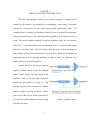
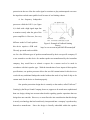
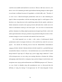
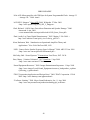
A Note About Speaker Damage:
With the purpose of our device being to protect speakers, we must first understand
what damages speakers in the first place. When we think of damage to a physical device,
we first consider the mechanically active parts of the device and how the behavior of
these parts could be put in danger.
For the speaker’s case, these mechanical
ii
parts are located at the point of the transduction of electrical energy in the incoming
voltage signal to mechanical energy. Here,
the cone of the speaker and its suspension
(which is usually attached to the coil
containing the incoming electrical signal;
some designs allow for the permanent magnet
component to be attached to the cone instead,
as shown in figure 1) oscillate back and forth
in its production of the desired air
Figure 1: Speaker components
Source: http://p-hardware.blogspot.com/
2008/04/speaker.html
pressure variations in order to create the
necessary sound waves. The mechanical
motion of this cone is directly related to the oscillating voltage level entering the speaker.
This means that the higher the peak voltage of the incoming signal, the greater the spatial
displacement the speaker cone will have to undergo in order to achieve a corresponding
sound wave (a higher peak in voltage signal and mechanical oscillatory motion of the
cone results in a louder sound at the output of the speaker). However, as with any
mechanical component, the range of motion of this cone is only designed to oscillate with
amplitudes corresponding the power rating and impedance of the speaker. Any signal
that surpasses these limits puts uncharacteristic strain on the cone and the suspension
attaching the cone to the speaker mainframe due to the extreme accelerations, stretching,
and prolonged over-vibration etc. that it experiences under such conditions. To prevent
this type of damage we need to ensure a safe range of motion for the speaker cone. This
however does not necessarily entail always limiting any sharp intermittent spike
iii
encountered in the audio signal’s amplitude. If the duration of the spike is appropriately
short and the audio signal in the surrounding time window is well below dangerous
operating amplitudes, it is very likely the speaker cone would be able to withstand such a
spike. Most of the time one such over-excursion of the speaker cone will not cause the
damage, but prolonged over-excursions leading to the mechanical fatigue will eventually
result in failure of the mechanical parts, including ripping or tearing of the cone or its
suspension. Another thing to note is the different types of speakers that can be used and
which types are most prone to different types of speaker damage. In the case of a
mechanical failure, woofer and tweeters are the usual culprits. Woofers handle the low
frequency spectrum of the input and are oftentimes overdriven at loud parties, where a
loud bass sound is desired. Tweeters are oftentimes overdriven mechanically when they
are associated with an inadequate crossover system, since these speakers are very small,
fagile, and easily damaged. In our project we will have to find a delicate balance
between protecting the speaker from high-amplitude spikes that are mechanically
hazardous to the system while still leaving the sound levels unaffected if it is determined
that such a spike in sound will not likely be detrimental to the speaker.
The other type of damage a speaker could encounter is heat damage. If the
speaker is producing a high volume of sound for an extended amount of time, the amount
of power being dissipated rises to very high levels, which causes the speaker to heat up to
extremely high temperatures and puts the speaker at risk for damage by overheating. At
these extremely high temperatures, either the voice coil adhesive can soften and cause the
voice coil to come apart, hence a mechanical failure on the part of the voice coil, or the
voice coil itself or the wires leading to the voice coil can literally melt, causing
iv
oftentimes an open circuit in the wiring and thus an inability of the speakers to produce
sound of any kind. The system is not put at risk of heat damage at the occurrence of
sharp spikes of high amplitudes, but only at a continuously high level of sound being
producedand for a reasonably long amount of time. In our device design, our goal is to
protect the speaker from both mechanical and heat damage. Our protection algorithm
does not involve an integration of the power dissipated by the speaker over time,
however, which would be necessary for an absolute guarantee that an over-heating issue
would not occur. Since we are limiting the amplitude of the signal entering the speaker,
however, attenuating the signal appropriately based on both the speaker’s power rating
and impedance, we would expect that under normal operating conditions (where the
speaker is driven with normal music for a couple hours at a time), our device would offer
adequate protection from both mechanical and heat damage.
A Note About Power Ratings and Distortion:
In our attenuation calculations, we must often incorporate the power ratings of
both the speaker, as input by the user, and the power rating of the amplifier we are using.
We must be aware, however, that even though these power ratings appear to be on the
same scale one another, they in fact are not. The power ratings of an amplifier is based
on the amount of power the amplifier is capable of dissipating with a sinusoidal,
monotone input into the system producing that power. This method of determining he
power rating is as straightforward as the power rating on a light bulb, where the power a
light bulb can dissipate is based on a steady ac power input from a wall socket. The
speaker’s power rating, however, is rated much differently. Since we would almost never
v
expect to be using a speaker to output a sound that stays at a single frequency, these
speakers are in stead based on typical trends found in music waveforms, where there are
constantly varying amplitudes and frequencies of sound and where, more importantly,
even if the signal may have an instantaneous power dissipation at a high value, this is
usually followed by a period of much lower values, which essentially allows the speaker
time to cool off. Because of this, an amplifier rated at a high level can oftentimes be used
to drive a speaker with a much lower power rating safely. For example, if we have a
speaker rated at 100 Watts, this speaker could not handle 100 Watts worth of a
continuous signal (such as a monotone sinusoid) into the system. However, an amplifier
rated at 400 Watts would be required to carry out the amplification of a music signal that
had instantaneous power peaks of up to 400 Watts. A given music signal with an average
power of 100 Watts would likely be constantly varying between say 50 and 400 Watts of
power, and thus would require an amplifier of at least 400 Watts of power rating to
amplify this signal without clipping. Since we know that the speaker is rated based on
the varying power changes in music, then, we could conclude that a 100-Watt speaker
would be able to safely run the signal, even though it is driven with an amplifier rated at
400 Watts and with a music signal containing 400-Watt peaks.
We should be aware that the previous example is dependent on the amplifier
operating without distortion, that is, without the clipping of the signal peaks. When the
input is clipped by the amplifier, the transistors saturate and automatically temporarily
output their maximum supply DC voltage of the system to produce the square-like
waveforms characteristic of clipping. When this happens, the speakers are more prone to
over-heating damage than they would be if that signal would have been unclipped and
vi
reached its full amplitude peak. For this reason, it is often said that some speaker damage
can actually be avoided by using a higher rated amplifier, since it would avoid this
distorting clipping from occurring.
In our project, since we are not detecting if a peak value observed was from a
clipped signal or an unclipped signal, in order to avoid an increased risk of heat damage
due to clipping, we would need to assume that the amplifier is operating in a nondistorting range. However, since we are taking the power rating of the amplifier into
account in our calculations, this should allow our device to prevent the amplifier from
reaching the range where it would begin such distortion. Therefore, our signal not only
functions to protect our speakers from being damaged, but also to prevent distortion in its
signal output.
vii
LIST OF TABLES
Table 1: overloadVoltage Calculations given all possible user input combinations..........19
Table 2: Potentiometer settings and attenuation statistics..................................................39
Table 3: Division of labor...................................................................................................46
Table 4: Bill of materials....................................................................................................47
Table 5: Gantt Chart............................................................................................................48
LIST OF FIGURES
Figure 1: Speaker components...........................................................................................iii
Figure 2: Feedback control..................................................................................................1
Figure 3: Predictive limiter............................................................... ..................................3
Figure 4: Example of feedback limiting............................................................... ..............5
Figure 5: THAT 4301 Analog Engine ............................................................... ..............12
Figure 6: High level system diagram............................................................... .................15
Figure 7: Software architecture.............................................................. ..........................17
Figure 8: Revised software flowchart.......................... .......................... ..........................23
Figure 9: Digital PCB.......................... .......................... ..................................................25
Figure 10: Attenuation of a cosine signal......................... .......................... .....................25
Figure 11: Analog schematic.......................... .......................... .......................................27
Figure 12: ADC step-down vs. high-voltage cosine and high-voltage music...................28
Figure 13: Full-wave rectification, diode in series, low pass filter....................................28
Figure 14: SPI communication wiring.......................... .......................... .........................29
Figure 15: General input vs. output trend of attenuation circuit throughout the range of
operation.....................................................................................................40
Figure 16: Input vs. output trend of attenuation circuit, low range only...........................41
Figure 17: Circuit Attenuation in dB for a Low Range of Input Signals...........................43
viii
KEY TO ABBREVIATIONS
ADC – analog to digital conversion: a general signal conversion method; also a register
defined on the Atmega 32 microprocessor for carrying out such a conversion
CS – chip select; an input pin to the MAX 5411 digital potentiometer, active low
PCB - printed circuit board; copper platforms whereupon electronic circuits have been
etched. PCBs are rugged, inexpensive, and can be highly reliable. They require
much more layout effort and higher initial cost than either wire-wrapped or pointto-point constructed circuits, but are much cheaper and faster for high-volume
production.
QSOP - Quarter-Size Small-Outline package; a chip package with pin spacing of 0.635
mm
SPI – serial peripheral interface; a synchronous serial data link standard of
communication involving a “master” talking to its “slave” over four wires called
master-in-slave-out (MISO), master-out-slave-in (MOSI), clock (CLK), and slave
select (SS)
SS – slave select; acts as a chip select for SPI communication slave enabling; a dedicated
pin on port B of the microprocessor, active low
iv
CHAPTER 1
PROJECT FEATURES AND OBJECTIVES
The main distinguishing feature of our device compared to similar devices
currently on the market is our capability to accommodate a wide variety of speakers,
allowing the consumer to use any typical speaker sold commercially today.
We
accomplish this by inserting user interfaces whereby the user can specify the impedance
and power specifications of the particular speaker, regardless of the speaker’s make or
model. The current industry standards for speaker impedance values are set at discrete
values of 2, 4, or 8 Ohms and the power consumption levels of a typical speaker ranges
between 50 and 1000 Watts. The user simply selects the levels of these parameters of
their speakers and our device automatically processes these inputs and recalibrates the
attenuation scheme of the limiting algorithms in order to allow for protection for a
speaker with these specified parameters.
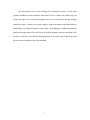
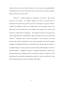
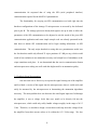
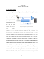
Another benefit of our device is that it
employs feedback control, where the feedback
signal is taken directly from the output of the
amplifier, which is also the input signal fed
directly into the speakers (see figure 2). This
provides a greater safety guarantee over another
common design involving predictive control,
since we have direct access to the signal that is to
be seen by the speaker and are not merely trying
to predict this signal.
1
Figure 2: Feedback control
The final benefit of our device design is its attenuation scheme. Unlike other
products intended to protect speakers from unsafe levels of input, our product does not
simply disconnect our circuit once dangerous levels are experienced, thereby abruptly
muting the signal. Instead, our system employs gradual attenuation algorithms that are
continuously yet subtly limiting the system input. By beginning to slightly attenuate the
signal in the upper range of the safe levels of speaker operation, once the threshold of the
speaker’s capability is reached the limiting function of our device has already begun and
therefore moves seamlessly over this threshold.
2
CHAPTER 2
ANALYSIS OF COMPETITIVE PRODUCTS
2.1 General Approaches
Essentially, our device is simply a limiter programmed to accomplishing a
specific goal. There are many different kinds of limiters that would be physically capable
of performing the same signal attenuation as our device, but very few would be “smart”
enough to automatically and continuously adjust this attenuation towards the goal of
protecting a speaker of a specific speaker.
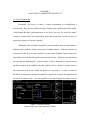
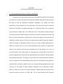
Within the realm of limiters designed to protect speakers, there are in general two
different types: predictive limiters and negative feedback limiters. Predictive limiters are
convenient in that they are more portable in general than feedback limiters and aren’t
necessarily used as dedicated speaker protectors all the time. However, their drawbacks
far outweigh this slight benefit. As seen in figure 3 below, the predictive limiters merely
predict the output of the amplifiers that the speakers will be exposed to and do not have
any connection to the actual voltage the speakers are exposed to. As such, in order for
the limiter to adequately calculate the amplifier’s output from its input, the amplifier must
be held at a constant value. Once the amplifier’s gain has changed, the limiter must be
Figure 3: Predictive limiter
Source: http://www.rane.com/note127.html
3
recalibrated or else the speaker is in danger of being over driven.
Negative feedback limiting is the concept our design is based off of, though we
were not aware of the existence of this technology upon the conception of the idea for our
project. This type of limiting in regards to speaker protection has become more popular
than its predictive counterpart for its many benefits. In general, this limiting technique
can guarantee safer, more reliable limiting since it is receiving its feedback directly from
the signal line that is being directly fed into the speaker itself (see figure 4 in section 2.2).
Because of this, that signal information can be used directly without having to back
calculate the gain of the amplifier, hence the limiter does not require recalibration upon
each readjustment of amplifier gain. Also, in this set-up knowledge of the parameters
regarding the amplifier, such as impedance and power rating, does not have to be as exact
as it does for the predictive set-up. Since we are presented with the output of the
amplifier, the main parameters we are concerned with in this situation becomes the
parameters of the speakers, so that slight variations or discrepancies from ideal amplifier
parameters are not as crucial to the functionality of the limiting device in this case.
2.2 Specific Examples
United States Patent #41737401 is a device that uses feedback control in an
attempt to protect speakers from being overdriven, but instead of actually attenuating the
signal as it approaches dangerous levels this device simply “cuts off the supply voltage to
a power amplifier circuit in disconnecting a loudspeaker from the output terminal of the
power amplifier circuit when an overvoltage is developed at the output of the power
amplifier circuit.” Our device has a significant advantage over this approach to speaker
4
protection in that we allow the audio signal to continue to play uninterrupted even once
the input has reached unacceptable levels because of our limiting scheme.
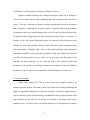
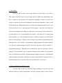
A low frequency loudspeaker
processor called the LSP-1 (see figure
4) is built with a high signal input line
to monitor exactly what the gain of the
power amplifier is. However, for every
different model of loud speakers
this device requires a PCB card.
Figure 4: Example of feedback limiting
Source:
http://www.arx.com.au/pdf/old/LSP1manual.pdf
The only pre-made cards available
are for a few different types of speakers manufactured by their own specific company. If
a user wanted to use this device for another speaker not manufactured by the Australian
company, they would have to submit a request for a custom card to be made in
accordance with their speaker type. With the introduction of user inputs of their speaker
specifications, our speaker processor allows the user full customization for this device to
work with any traditional loudspeaker model without the need of any kind of chip to be
custom made for the device to function properly.
One speaker protection design that is currently on the market, called TruPower!
Limiting by the Meyer Sound Company, however, appears to be much more sophisticated
than our design, taking into account other details regarding speaker operations that our
design does not consider. However, we must first take into consideration that this design
is merely a technology that has been directly incorporated into a company’s speakers they
themselves manufacture.
Since the design is literally embedded within the speaker
5
cabinet itself, there leaves no room for this device to be used on any speaker/amplifier
combination the user wishes and therefore does not offer the same freedom of speaker
choice to the user as our device does.
TruPower! is literally designed to calculate the “true power” that is being
delivered to the speaker.
For example, though in our device we assume that the
impedance of the speaker (as specified by the user as an input to our system) remains a
constant, this impedance actually varies slightly both over the frequency range of the
signal and over the operation time of the speaker as the speaker coils warm up and
experience a slight increase in impedance. The impedance increase in the speaker coils
causes a slight drop in the overall dynamic range of the speaker system over time and this
TruPower! technology seeks to correct this problem.
On the opposite end of the
spectrum, the frequency dependency of the speaker impedance can cause the speaker
impedance to unknowingly decrease at certain frequencies and thus open the speaker up
to potential damage occurring at signal levels that under normal impedance would have
passed as harmless. Though this frequency vs. impedance relationship is likely hard to
determine directly, this technology seeks to prevent any speaker overload due to this
phenomenon by automatically attenuating the signal by a couple extra dB after a long
period of operation time to prevent overheating of the speaker.
6
CHAPTER 3
CONCEPT/TECHNOLOGY SELECTION
3.1 The Attenuator and Analog vs. Digital Considerations
We knew from the start that the three major functions that needed to be performed
by our device were the collection of user input and feedback loop data, the processing of
that data to form the appropriate attenuation algorithms, and, finally, the actual
performance of the attenuation on our input signal. We knew that in order to interpret
and process information regarding analog data, we would likely find it best to perform
our processing in digital form. Our initial idea was to first perform analog to digital
conversion from our feedback signal to determine the amount of attenuation needed, and
then to go back and attenuate a digitized form of the input signal by that amount before
sending the analog version of the newly attenuated input signal through the amplifier.
Under this design, we thought it would be best to use either a digital signal processor
(DSP) or a microprocessor to carry out the attenuation of the signal in its digital form.
However, the problem with using the microprocessor for this purpose was a fear of
severe distortion of the audio signal, as a microprocessor would likely not be able to
produce a high quality of sound once the signal had been converted from analog to digital
form and then back again. The option of using a DSP chip would be beneficial in that not
only is it commonly used in manipulating audio signals and reproducing a high quality of
sound, but also it would be capable of some very complex limiting algorithms and would
even give us the option of using frequency distinction in our attenuation scheme.
However, neither of us had very strong knowledge of digital signal processing nor any
practical experience in the use of a DSP chip. We were both enrolled in the Electrical
7
Engineering Department’s Introduction to Digital Signal Processing class at the time, but
feared we would not learn enough about the practical functionality of such a device in
order to successfully incorporate this into our project with only a month or two of
lessons.
Our next idea was to employ the use of a potentiometer to control the attenuation
of our input signal in its original analog form, avoiding the possible distortions and
complications of digitization. However, a traditional analog potentiometer would need to
be controlled by our system’s “brain” and the only way to control such a potentiometer is
by physically turning a knob. The only way to accomplish this with electrical signals
would be through control of a motor, which would involve adding another component to
our device that would make matters unnecessarily complicated.
To circumvent the
problems presented us by the traditional analog potentiometer, we decided on using a
digital potentiometer that could be controlled directly by the “brain” of our system. The
digital potentiometer would contain physical wipers and resistors so that the attenuation
of our input signal should preserve the quality of our audio signal. The drawback to this
is that the digital potentiometer, unlike the analog potentiometer, has discrete positions
for the wiper to be located at, whereas the analog potentiometer’s wiper position can
continuously span between the high and low terminals of the potentiometer. The benefit
of being able to directly control the wiper’s position by the same device that will perform
the attenuation algorithm calculations and in a very accurate and precise manner,
however, was seen as a benefit well worth the loss of a continuous spectrum of
attenuation from our potentiometer, and thus the digital potentiometer was chosen over
its analog counterpart.
8
3.2 The “Brain”
We then needed to select a device that would act as the “brain” of our device.
This would need to first take in our user inputs and our feedback loop information; from
this it would not only determine the attenuation algorithms necessary to protect the
speaker in question but then send commands to perform that attenuation. Once we had
decided that using a digital potentiometer to perform the attenuation would be best, it was
an obvious choice to use a microprocessor for this purpose. Once this was decided, the
two main considerations for settling on a final device were the type of microcontroller to
use and what size of a microcontroller was needed. Our choice of an Atmel brand
microcontroller over a PIC (Peripheral Interface Controller) controller was made on the
basis of code familiarity. Bethany was in charge of the software programming of the
microprocessor, so she chose the c programming coding language of the Atmel controller
over the basic coding language of the PIC due to her experience with the related C++
programming language. Regarding size considerations, with our experience with the
Atmega 32 microcontroller and our general estimation of the number of pins and the
types on functions that would be needed (analog to digital conversion, communication
with the digital potentiometer, dedicated user inputs, and potential LCD output pins) we
decided that this device would be sufficient to meet the needs of our project.
3.3 Digital Potentiometer Model Selection
To begin with, we had very little knowledge regarding not only the types and
different features of digital potentiometers but also regarding which of these features
9
would be most suitable and beneficial to our device. What we did know, however, was
that we were to be attenuating an audio signal and that detecting changes in audio signals
in our brains is calibrated in terms of a logarithmic, or decibel (dB), scale. Therefore, if
we were to use a linear-based digital potentiometer and were to start attenuating our
signal in linear correspondence with the increasing input signal, it would appear at first
that there was a huge decrease in the sound being produced by the speaker, and then as
further attenuation occurred as the signal got louder and louder there would seem to be
almost no attenuation occurring at all in the signal. We were able to circumvent this
problem fortunately by finding digital potentiometers designed specifically to deal with
audio signal attenuation with wiper positions at taps positioned along the resistor to allow
resistance changes to occur on a decibel scale instead of on a linear scale.
Our initial approach was to order a wide variety of audio-tapered digital
potentiometers and to investigate which one we felt would be best suited for use in our
project.
We ordered the following devices from the Maxim/Dallas Semiconductor
company: DS1801, DS1802, DS1808, DS1881, DS1882, MAX5411, and MAX5486 and
researched the features of each device. Our initial decision was to use the DS1881 model
that provided 63 wiper steps of 1 dB per step, a power supply range within the 5 V limit
of the microprocessor we were using, zero-crossing detection to eliminate the clicking
and popping sounds that tend to accompany wiper position changes in audio chains, and
an option to store wiper position information in an EEPROM upon power off. However,
we were forced to abandon using this potentiometer once we discovered that the
difficulty of using the Atmega 32 microprocessor for I2C (Inter-integrated Circuit)
10
communication far surpassed that of using the SPI (serial peripheral interface)
communication required for the MAX5411 potentiometer.
The functionality for carrying out SPI communication was built right into the
hardware configurations of the Atmega 32 microprocessor as accessed by the dedicated
pins at port B. The Atmega processor already had registers set up in order to allow the
parameters of the SPI communication to be adjusted to suit the needs of the given SPI
communication application and some simple sample code was already presented in the
data sheet to initiate SPI communication and to begin sending information via SPI
communication. The only major drawback to using this new potentiometer model was
the fact that this model only allowed 32 wiper positions of 2 dB per step, which would
result in less resolution in our attenuation accuracy and a slight loss of smoothness as the
wiper transitions took place. It was determined that the ease in communication format
and microprocessor coding was well worth this slight sacrifice in attenuation quality.
3.4 Feedback Signal Incorporation
Our next task was to find a way to tap into the signal coming out of the amplifier
and feed back a version of this signal into the microprocessor where it could easily and
safely be measured by the microprocessor in determining the attenuation algorithms
necessary. The main problem here was that once the small signal input was fed through
the amplifier, it was at voltage levels that were unsafe to be directly fed into the
microprocessor, which could only safely handle voltages roughly in the range of 0-5.5
Volts. Therefore, we needed to design a circuit that would step down the voltages from
the amplifier from their current values to lie within the 0-5.5 Volts range. We also
11
needed to only submit positive voltage values to the microprocessor, so we decided to
add step down circuitry that probes the voltage output fed to the speaker. Since this
output is a 100-volt peak to peak swing an op-amp steps the voltage down by 1/10. Then
op-amp circuitry rectifies the negative voltages and then an active low pass filter
smoothes it out. This is explained further in the hardware section.
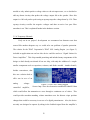
3.5 A Temporary Sidetrack
Early on in our project’s development we encountered an alternate route that
seemed like another adequate way we could solve our problem of speaker protection.
The website for the THAT Corporation’s THAT 4301 Analog Engine (see figure 5)
included an application note on how this device could be used as a “Signal Limiter for
Power Amplifiers.” This chip sounded promising and included many components of the
design we had already envisioned all on one chip, with only the addition of a couple
smaller components such as capacitors, resistors, and diodes needed. Another benefit,
besides convenience, that
this new solution had to
offer was its use of an
analog
controlled
voltageamplifier,
Figure 5: THAT 4301 Analog Engine
Source: http://www.ka-electronics.com/that4301/that4301.htm
which would allow the attenuation to occur through a continuous set of values. This
would provide smoother-sounding volume transitions over the discrete wiper position
changes that would be necessary in our use of a digital potentiometer. Also, the device
not only was designed to operate by taking in the feedback signal from the amplifier’s
12
output, similar to our original design, but it additionally contained an RMS detector to
enable that feedback signal’s strength to be more readily detectable by the device. This
would eliminate the need of our originally intended “step-down circuitry.”
However, there was one crucial drawback to this design that made it implausible
to use: it had no real user-defined flexibility. One of the main distinguishing features of
our device is its capability to be used with any speaker the user wishes, where the user
only has to select two simple parameters of their speakers and our device will
automatically recalibrate itself to fit their speaker’s needs. This new design was meant to
operate around a threshold value and automatically attenuate the audio signal past that
value, but this threshold value was determined by a relationship of resistance values used
in the circuit. In order for such values to be extracted from the user’s input and then a
determination to be made about how the attenuating algorithms operate according to
these values, we would require the use of a “smart” devise to take in such inputs and
carry out the necessary calculations.
The only real logical solution for this is to
incorporate the use of a microprocessor, for there is no functionality in the Analog
Engine device that would allow for such calculations to be made. An option would then
be to use a microprocessor along with the circuitry recommended for the “Signal Limiter
for Power Amplifiers,” but then the problem would become both an unnecessary increase
in complexity between the microprocessor to Signal Limiter circuitry and the inflexibility
to completely control all features of the Signal Limiter circuit due to their dependence on
set resistance values that would be hard-wired into the circuitry. The Signal Limiter
circuitry does allow some flexibility in setting the limiting threshold and compression
ratio by incorporating 3 different variable resistors, but even so many of its parameters
13
are set using a combination of these variable potentiometers and set resistors. Even if we
could set up our system to use digital potentiometers in place of these variable resistors
so that we could control the threshold and limiting parameters with our microprocessor,
this would seem to be at least three times as complicated as our original design involving
communication with only one digital potentiometer and without the worry of having to
hard-wire some parameters of the limiting into our circuit through the use of set resistor
values. Therefore, we decided that our original design would be the simplest and most
efficient way to accomplish our goal of speaker protection.
14
CHAPTER 4
PROJECT ARCHITECTURE
4.1 From Input to Amplifier
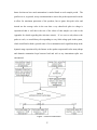
A very high-level system diagram can be seen in figure 6. The very first function
our device serves upon
system power up is the
input
of
the
user’s
speaker parameters. This
is accomplished through
the
use
of
toggle
switches. The user can
select
Figure 6: High level system diagram
speaker
impedances (2, 4 or 8 ohms) and speaker power ratings (100, 200… 1000 watts). With
this information the microprocessor calculates what the threshold voltage is to start
attenuation (the details of such calculation will be explained in section 4.3). The audio
signal itself originates from some electronic instrument, microphone, etc. as a very lowvoltage signal representing the pressure variations in the air produced by the music
desired to be amplified out to the general public. This signal travels through the power
amplifier where it experiences an amount of voltage gain depending on the position of the
“Volume” knob on the amplifier. We will assume for our project that this gain can be
varied at any point in time and do not require it to be set at a constant level for any
amount of time. Here is where the signal branches off: we have this amplified signal
both connected to the speaker, where it will act as a transducer converting electrical
15
waves into pressure waves in the air to produce sound, and we also run this signal
through a step-down circuit that will attenuate and manipulate the signal in preparation
for its entrance into our Atmega 32 microprocessor. The current step-down circuit
attenuates the voltage signal by .08x and then rectifies it and smoothes it out with a low
pass filter. The hardware architecture for this circuit is further explained in chapter 5, the
hardware section.
4.2 Inside the Microcontroller: Analog to Digital Conversion
This small signal version of the amplifier’s output is fed into a pin on our
microcontroller from port A (see figure 7 for the software architecture of the
microcontroller). (Please note that all the code for our Atmega 32 processor is included
in the Appendix.) This port’s pins are linked to dedicated hardware responsible for
controlling the microprocessor’s analog to digital conversion functionality. We utilize
the microcontroller’s ADC (analog to digital conversion) registers to configure and carry
out such an operation, converting our small 0-5.5 V signal from the feedback loop into a
set of discrete integer numbers valued between 0 and 1023 (corresponding to a 10-bit
digital result). Here we have the difficulty of an analog signal at our port A pin that is not
only is not sitting at a constant voltage level due to the changes in the amplifier’s gain,
but also fluctuates in a half-rectified fashion between 0 Volts and its peak voltage even
while the amplifier gain remains constant due to the sinusoidal characteristic of musical
frequencies. To be able to accurately interpret the signal level we first acquire sets of 100
samples of ADC readings and then perform statistical analyses (namely, calculating the
average value and the maximum value) on each set of data in order to be able to make a
16
better decision on how much attenuation is needed based on each sample period. The
goal here is to, in general, set up our attenuation to cater to the peaks experienced in order
to allow for maximum protection of the speakers, but to ignore this peak value and
instead use the average value in the case that a very short-lived spike in voltage is
experienced that is well above the rest of the values of that sample (see code in the
Appendix for details regarding this selection criteria). If we were to only observe the
peaks as a rule, we would always be responding to every little voltage peak in the system,
which would lead to both a general sense of over-attenuation and a significant drop in the
dynamic range experienced by the listener at the speaker output and lead to many abrupt
and dramatic attenuation leaps between load and soft as any intermittent spike was
encountered.
Figure 7: Software architecture
17
4.3 Inside the Microcontroller: Attenuation Determination and Implementation
Once we have the peak or average information from the ADC results, the user’s
inputs that were read into the system upon the device’s power up come into play. These
user inputs of speaker resistance and power rating are used to calculate the software
variable called the overloadVoltage, which is the threshold determining safe operation of
the user’s speaker.
As a short side note: we are using the term “threshold” more loosely for our
actual attenuation implementation where we allow the signal to float close to
and even slightly above this threshold level and consider this safe operation
for the speaker. This is due to the lax definition on how the actual speaker
rating is calculated, as mentioned in the Introduction, where the threshold is
assigned to an average level over time and allows for slight up and down
fluctuations in the music around this level.
The
overloadVoltage
equation
is:
overloadVoltage = ( wattage _ rating " impedance " .08 "1023) /5 . This comes from the
fact that: Power =
!
voltage 2
, so then Power " resistance = voltage 2 . The step down
resistance
circuitry attenuates a signal to .08 of its peaks, so voltage = Power " resistance " .08 .
!
!
Voltage is the overloadVoltage, power is the power a speaker can take, and resistance is
!
the speaker’s impedance, which is commonly
2, 4 or 8 ohms. Below is a chart of
common speaker impedances and power ratings that the user can set with their
corresponding overloadVoltage values:
18
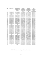
overloadVoltage
overloadVoltage
Impedance
[decimal] 0~1023
231.4784759
327.36
462.9569518
327.36
462.9569518
654.72
400.9324811
567.0041524
801.8649622
462.9569518
654.72
925.9139036
517.6016074
731.9992131
1023
567.0041524
801.8649622
1023
612.4344811
866.1131492
1023
654.72
925.9139036
1023
694.4354277
982.08
1023
731.9992131
1023
1023
[volts]
1.13137085
1.6
2.2627417
1.6
2.2627417
3.2
1.959591794
2.771281292
3.919183588
2.2627417
3.2
4.5254834
2.529822128
3.577708764
5
2.771281292
3.919183588
5
2.993325909
4.233202098
5
3.2
4.5254834
5
3.39411255
4.8
5
3.577708764
5
5
[Ohms]
Speaker
Power
Rating
[Watts]
2
4
8
2
4
8
2
4
8
2
4
8
2
4
8
2
4
8
2
4
8
2
4
8
2
4
8
2
4
8
100
100
100
200
200
200
300
300
300
400
400
400
500
500
500
600
600
600
700
700
700
800
800
800
900
900
900
1000
1000
1000
Table 1: overloadVoltage Calculations given all possible user
input combinations
Once this voltage limit value has been scaled down by the same proportional
amount used on the voltage during the step down process (0.08) in order to put it in the 05 Volt range, that value is then multiplied by a factor of (1023/5) in order to put the
parameter into a value on the same scale as that of the data from the ADC process, as a
value between 0 and 1023, so that the two values can be compared accurately. This
newly calculated threshold value is saved by the software as the variable
19
“overloadVoltage” and is carried, along with either the peak or average parameter from
each ADC set, as an argument into a function establishing attenuation levels based on a
comparison between the ADC set statistic and the threshold voltage for safe operation.
For example, if the peak voltage from a set of ADC conversions is equal or less than less
the “overloadVoltage” value, the first attenuation bracket bracketNumber = 0) would
send a command to the digital potentiometer to position the wiper to allow for 0 dB
attenuation.
With increasing ADC peak or average values in relation to the
“overloadVoltage” value, the wiper position is commanded to position itself to allow for
increasing amounts of attenuation.
Also incorporated into this same function is a
calculation of how drastic of a change in position a wiper must undergo in order to move
from its current location to the newly calculated location and based on this calculation
send the wiper through an appropriate amount of intermediate steps in order to more
smoothly transition from one attenuation level to another. For example, if we had a
wiper in a position corresponding to bracket 0 (for no attenuation) and we wanted to
move this wiper to the position corresponding to bracket 12 (to reduce the signal to about
1/5 of its current value), we would command the wiper to move through two other
intermediate positions on its way from the bracket 0 position to the bracket 12 position.
4.4 Practical Adjustments
One of the lessons learned from this project is that no matter how much thought,
analysis, and calculation you put into a design, once you test that design there is a great
likelihood that you will encounter some issues that never occurred to you from a
theoretical standpoint. This was the case with the attenuation algorithms that had been
20
coded in the software portion of our system. During the final testing stages of our device
our code worked perfectly, but that fact ended up being our only problem. During
testing, when the amplifier was causing the feedback signal to fall in the upper ranges of
attenuation, we would see the code step through the steps needed to reach the destination
attenuation bracket that had been specified for it in our code and then once it got there, as
a verification that the attenuation levels had been indeed calculated correctly, we saw the
ADC readings to go from the high values of the amplified signal to low values that were
well within the overloadVoltage safety threshold value. The problem, then, was that the
next command in our code was to run the function again to calculate an appropriate
attenuation bracket for the feedback signal. Since this function had already run once and
had done its job of bringing the signal into the range where it would not need further
attenuation, this second time around the code put the attenuated signal into bracket 0,
where no attenuation was required and the potentiometer’s wiper would be moved
accordingly. We must realize here, though, that by lowering the level of our small signal
audio input when we first commanded the attenuation, we did not change the high gain
setting present on the amplifier, so that once we bring this attenuation back to 0 dB, the
high amplifier gain is still present. Therefore, essentially the current code was causing
the attenuation for a high feedback signal to toggle between a given attenuation level and
0 dB of attenuation: once through the attenuation function and the attenuation would be
set, a second time through and the level would be in the safe range again so the
attenuation would be unset. This behavior both made the sound output from our system
to be distracting, unnatural, and aesthetically unpleasing and caused the output signal
21
going to our speaker to oftentimes reach very high levels that would very likely allow for
damage to the speaker to occur.
In order to change this, we only had to modify a few lines of our code, but this
drastically changed the behavior of the system in practice. We decided that instead of
calculating a destination attenuation bracket the potentiometer should reach based on its
current level (which would lead often to the toggling 0 dB bracket once the attenuation
did its job of bringing the signal back to safe levels), we should have the system only
change its attenuation bracket one at a time. To do this, we used the framework of the
existing attenuation bracket definitions to assign the current level to a bracket number
(the bracket numbers 0 – 23 correspond to wiper settings 0 – 46 dB, with a multiplication
of 2 factor to convert between the two) and then compared this bracket number with the
last bracket the wiper was assigned to. If the new bracket was lower than the previous
one, that meant that less attenuation was needed than was previously set, so our system
commands that the wiper position be moved +2dB from its previous setting. If, on the
other hand, the new bracket was higher than the previous one, that meant that less
attenuation was needed than was previously set, so our system commands that the wiper
position be moved -2dB from its previous setting. After making only this slight 2dB
change in the wiper position within our attenuation function, the code loops back to again
take a new ADC reading and calculate a new bracket number, where it can be determined
if the wiper should be moved for more or less attenuation. Also it should be noted that if
the signal has not changed levels enough to associate it with a different bracket number,
then the wiper is simply commanded to stay at its current position. By employing this
new algorithm, the safety threshold is reached a bit more slowly, but once it is reached it
22
stays within a reasonable limit of the threshold (per our “lax interpretation of the
threshold” explained in section 4.3), which is the main point of the speaker protection
function of our device. See figure 8 for the new software flowchart.
Under this new algorithm, the initial purposes for the bracket definitions are
nearly lost. Originally, these brackets were meant to calculate out where a wiper should
be, based on the signal level presented to the ADC sampler, for that signal to lie within
the threshold value. However, since we are not sending the wiper automatically to this
pre-calculated level but instead changing the attenuation only step-by-step and checking
each time to see if the level has yet reached safe values, these levels are only used as a
means of comparison. The function they now
serve is to tell how far away the new ADC
voltage level has to be from the old ADC
level in order to command the 2 dB change.
In this function, then, the bracket definitions
are still serving a useful purpose, so that the
wiper’s position will not be changed every
single cycle of the function. Also, built into
the attenuation bracket calculations is the
natural
dB
potentiometer’s
characteristic
wiper,
so
of
that
the
signals
requiring only a low level of attenuation
Figure 8: Revised software flowchart
will be more sensitive to voltage changes
23
whereas it will take more drastic changes in ADC voltage level for changes to occur at
higher levels of attenuation.
4.5 The Analog Attenuation
The digital potentiometer changes resistance and is input into the non-inverting
terminal of a TLC2272 op-amp.
As the potentiometer’s resistance goes down, the
resistance lowers and the signal attenuates. The output of the op-amp is fed back into the
input terminal, making it a simple voltage follower. The low terminal of the digital
potentiometer receives a 2.5 Volt DC signal. The high terminal of the potentiometer
receives the music with a Vcc/2 = 2.5 Volt bias. To make sure no DC component is
present in the original signal, coupling capacitors were used on the input to the resistors
and on the output of the TLC2272 op-amp.
24
CHAPTER 5
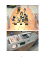
HARDWARE
The premise of the hardware for the limiter and speaker protector was using a
potentiometer to attenuate the small signal of an iPod or guitar before the signal reaches
the
input
of
the
guitar
amplifier.
The
potentiometer would be digitally controlled by an
atmega32 microprocessor using SPI protocol
serial communication. The processor made the
decisions of controlling the digital potentiometer
to change the music volume based on a signal
fed back from the amplifier.
Figure 9: Digital PCB
5.1 The Digital PCB
It was decided that one printed circuit board (PCB) would be built to handle the
digital components and another board would handle the analog elements. The first digital
board was built to house the atmega32 processor, digital potentiometer (maxim,
Max5411), 12-volt to 5-volt regulator (LM7805), and headers that plug into an LCD
display. Figure 10 shows how a cosine signal was
attenuated using the digital potentiometer.
The MAX5411 was chosen because it had a
logarithmic taper digital, with 32-tap points each. It can
replace mechanical potentiometers in audio applications
Figure 10: Attenuation of a cosine signal
25
requiring digitally controlled resistors. The chip also has a SPI-compatible serial
interface that controls the wiper positions. The MAX5411 has a factory-set resistance of
10k!. A zero-crossing detection feature minimizes the audible noise generated by wiper
transitions. Switching amplitudes through a digital potentiometer when there is any sort
of voltage cause small audible cracks. The zero-crossing feature has the potentiometer
wait until the low input and high input are equal to change its resistance. For the purpose
of mounting the MAX5411 on our PCB the 16-pin quarter-size small-outline package
(QSOP) package was chosen. 10 mil traces were routed to the 16-pin QSOP.
The digital board would receive the audio signal needing attenuation through its
high input on the digital potentiometer header. Since the digital potentiometer’s power
supply is ground the 5-volts the music needs a vcc/2 bias voltage. The music into the high
input terminal of the pot is then biased by 2.5 volts. The input to the low terminal is
simply 2.5 volts. The wiper is then connected to a voltage follower op-amp is then plugs
into the large personal amplification system.
26
5.2 The Analog PCB
The digital PCB also
received a feedback input into
its analog to digital conversion
port (ADC). This feedback input
was stepped down using the
analog board. The schematic
for the analog board is shown
on
the
consists
right.
of
The
two
board
power
regulators to regulate +12
volts and -12 volts to +5 volts
Figure 11: Analog Schematic
and -5 volts. A number of
resistors were using to bias
Figure 11: Analog schematic
to high and low terminals,
which are sent to the MAX5411. Two large 33uF capacitors were used to couple and DC
signal connected to the music inputted. Two capacitors were used because 33uF capacitor
are polarized electrolytic, thus the terminal charges must be symmetric. So, the two
positive sides of each capacitor were connected leaving the negative terminals on the
outside. The power was regulated to +5 volts and -5 volts because the op-amps used the
analog PCB circuitry required +/-5 volts. Fast rail-to-rail op-amp built by TI (TLC2272)
was used as a voltage follower for the small signal output.
27
The TLC2272 was also used as a step-down
op-amp. Since the large personal amplifier outputs a
high voltage signal of up to 100 volts peak-to-peak.
The first stage (U5A) of the step-down circuit op-amp
reduces the gain of the signal to 10 volts peak-to-peak.
The next two op-amps (U5B and U6A) full wave
rectify the signal. To smooth out the signal a low-pass
filter was built with a capacitor and resistor. The fullwave rectification circuitry was based on figure X
from the book “Introduction to Operational
Amplifier
Theory
and
Applications”
(Huelsman,1975). The top of figure 12 shows
Figure 12: ADC step-down vs. highvoltage cosine (top) and high-voltage
music (bottom)
how a simple cosine signal swinging from +50 voltage to -50 volts is rectified and then
smoothed out to be about 4 volts. The bottom of figure 12 shows how the rectified signal
changes with music and jump up and down depending on the music’s amplitude. The
figure below takes one through the step of how the cosine signal voltages look at each
stage of the analog board.
Figure 13: Full-wave rectification (left), diode in series
(middle), low
28 pass filter (right)
CHAPTER 6
SOFTWARE
6.1 SPI Communication
The use of Serial Peripheral Interface (SPI) communication was required for our
microprocessor to be able to control the digital potentiometer model we had chosen: the
MAX5411. As mentioned in chapter 3,
the prime reason for using this SPI
format of communication was that the
Atmega 32 chip contains pins that
are connected to internal hardware
Figure 14: SPI communication wiring
Source: http://dev.emcelettronica.com/category/tags/spiprotocol
designed to carry out such communication. Also, to correspond to such hardware, there
are registers featured on the microprocessor that enable the SPI hardware to be
configured and utilized easily.
As shown in figure 14, SPI communication is carried out between two devices
(the devices can be daisy-chained so that one master can communicate with multiple
slaves, be we only require two-device communication in our project), one being specified
as the “master” device and the other as a “slave” device. In our case we configure the
internal SPI Control Register (SPCR)’s bit corresponding to master mode (MSTR) to
have our microprocessor act as the master who is then responsible for sending data to the
digital potentiometer slave (which acts as a slave by default, since it lacks the capabilities
to perform the duties of a master device, such as generating its own clock signal). SPI
communication requires 4 different wires running between the two devices as shown in
29
figure 14, labeled SCLK (serial clock), MOSI (master out, slave in), MISO (master in,
slave out), and SS (slave select). The SCLK line is the clock that synchronizes the timing
between the two devices. This clock signal is generated by our microprocessor master
and its frequency is determined by setting registers corresponding to certain division
factors from the internally generated clock signal always present in the microprocessor.
The MOSI line is the most important connection in our SPI communication system. This
is where the transmitted message is sent as a series of ones and zeros from the
microcontroller to the digital potentiometer. The timing of the transmission of this
message is determined by the SCLK signal and the relationship between the phase and
polarity relationship between the clock signal and the message signal are set up using
registers in the microcontroller; this phase and polarity must match the phase and polarity
required by the SPI slave you are communicating to or else the signal will not be
interpreted correctly. The MISO line is meant to enable the slave to “talk” back to the
master device, but is not used in our project. The potentiometer would be reading back to
the microprocessor the current position of its wiper via the MISO line, but in our case we
are merely concerned about telling the digital potentiometer where to position its wiper
and based on that command from the master, as long as the slave device interprets the
commands correctly, we should already have knowledge of the current wiper position at
any point in time. The SS line is an active low line where the master prepares the slave
device to receive a transmission. This line is most important when more than one slave is
present in a system, where the master can define many SS output pins to be able to select
each slave device to talk to one at a time. The master’s SS line is usually connected to
the slave device’s CS (chip select) active low so that only the chip that is selected by the
30
master will be able to actively interpret the master’s commands. This same connection is
made between our microprocessor and our digital potentiometer’s chip select pin. The
details about the functionality of this line in regards to our single-device project will be
explained below in section 6.2.
6.2 Trial and Error, Lessons Learned
Our first step in creating our device was to ensure the functionality of the digital
potentiometer, which was not only the pivotal function of our device, responsible for
ensuring speaker safety, but also likely one of the most complex, due to the SPI
communication protocol intricacies. At first, we made the mistake of ignoring the sample
code provided in the Atmega 32 processor, thinking it would not provide fully SPI
communication functionality, so we attempted to get some bits of sample code from
online databases. Once we constructed an initial bread board-based design in order to
facilitate a piece of sample code (commanding the digital potentiometer to move through
each of its wiper positions) and hooked up a multimeter to the wiper to try and verify if it
was in fact following the commands sent by the microprocessor, we were seeing voltage
changes on the wiper and interpreted this to mean at least a partial success of the
potentiometer’s functionality. We learned on multiple occasions, however, that seeing an
apparent movement of the wiper, unless it exactly matches the value your code is setting
it to and is consistent upon running the program may times, does not at all mean that the
SPI communication code is working correctly. The two major mistakes we initially
found were that first we did not have the digital potentiometer wired up to power and
ground correctly and secondly that our sample code was much too complex and outdated.
31
From this realization, we discovered that the sample SPI code for master mode operation
on the microprocessor’s data sheet was all the code you needed in order to carry out SPI
communication. With our new set of code, we were seeing some very perplexing results.
For example, on a couple occasions, we would observe the voltage on the wiper to be
showing appropriate values most of the time, but would skip many values or oftentimes
jump between the power or ground voltage levels in the middle of a voltage progression
that was supposed to be in between those two values. We attempted to find our problem
by inserting some debugging code that blinked an LED (light-emitting diode) at crucial
points in our code to ensure it was running properly, but sometimes even this method was
no use when the LED seemed to show that the system was running through each line of
our code properly, but the wiper position was not changing at all.
Finally, we made our first step towards realization of our problem when we went
through a simulation of our code line-by-line on the AVR Studio 4 program (the same
program we were using to write, compile, and program our code into our device with),
checking that the register values that we were setting in our SPI initialization command
were setting properly and that our code was in general operating correctly. Through this
process, we immediately discovered that the bit in the SPI Control Register (SPCR) that
was responsible to setting the microprocessor to operate as the SPI master (the MSTR bit)
was being set properly, but was being unset in the very next, completely unrelated
command. Upon receiving some guidance from a TA (teaching assistant), we discovered
that the active low chip select (CS) pin on the digital potentiometer worked more like a
reset pin than it did like a traditional chip select pin whereby the device is enabled to
work for the duration of time that the active low select signal is held low. Therefore,
32
instead of outputting a continuously low signal from the SS pin of the microprocessor to
the CS pin of the potentiometer, we would need to start with the SS pin in the high
voltage position, transition this to a low right before communication with our
potentiometer began, and pull it back high again once one byte of information was
successfully transmitted. Prior to this, under the impression that we would simply need
the CS pin on the digital potentiometer to always be low, signifying that we always
wanted to talk to that chip, we had simplified the connections between the two devices by
simply tying the CS pin on the microcontroller to ground and ignoring the SS pin on the
microcontroller. Right away we saw this new “CS pin with reset functionality” concept,
we knew that we needed to run a wire between the microprocessor and the potentiometer
in order to enable communication to the device each time before any byte of information
could be transmitted.
After some further research on our MSTR bit-setting issue, we found this
sentence in a Wikipedia article entitled “AVR SPI C Snippets”: “When running master
mode, a low level at the slave select pin SS will force the device into slave mode.” At
first this seemed completely contradictory to our basic understanding of SPI
communication, for clearly figure 14 shows the SS pin on the SPI master connected to the
SS pin (in our case, called CS: chip select) on the slave, both being active low, with the
master being in charge of selecting which device it will be talking to. However, we were
not cautious in noticing a slight technicality in the operation of the SS pin on the
microprocessor.
In our case, we did not need the pin specified as SS on the
microcontroller, for its primary function was in fact to operate as its own version of our
potentiometer’s chip select pin in the case that someone were to need the capability of
33
having the microprocessor serve the function of a SPI slave device, where this pin would
be configured as an input and then driven low by an outside SPI master device when
communication to this microprocessor was desired. However, the simple fact that this
functionality was not needed by our system did not mean that we were safe in ignoring
this pin. If this pin is configured as an output pin while the device is in master mode (for
it cannot be configured as an output in slave mode or it would lose its ability to be
selected as such a slave), it becomes a general-purpose output pin and the SPI
communication system is not affected by this pin’s value.
However, we were not
observant of the fact that in the code from the Atmega 32 datasheet we were using they
left this SS pin set as an input, expecting the user to desire the microcontroller’s option to
act as a SPI slave (note that inputs are configured to a port value of 0, so that through the
lack of mentioning the input/output functionality explicitly in the code, the SS pin’s
function as an input was implied). The simple fact of the SS pin being configured as an
input would not have caused any problems, however, had this pin not been an active low
pin. Unfortunately, an input pin with no signal to drive it high is sitting at a low value.
Therefore, under the configuration we were using, our microcontroller was being
informed that it was required to act as a slave and was not actively trying to send
information but to receive it. Our problem was fixed once we combined these two bits of
insight into the functionality of the chip and slave select pins of our two devices: we first
set the SS pin on the microcontroller to be an output pin and then connected a separate
general purpose output pin, having no ties to the SPI system itself, to act as an output
signal to the potentiometer’s CS pin that would carryout the reset-like function required
for communication with our slave device.
34
6.3 Attenuation Bracket Considerations
The goal of our attenuation is to gradually limit our input signal as it approaches
and exceeds levels that would be considered unsafe for the speaker in consideration.
Since all of our considerations regarding what signal levels to attenuate are made based
on this threshold of safe limits for our speaker and the safe limit for our speaker’s
operation is based on the impedance and power rating parameters as defined by the user
inputs into the system, we first must establish this safety threshold which is referred to as
the variable “overloadVoltage” in our code. As briefly mentioned in section 4.2, we use
the relationship (power = voltage2 / resistance) along with our user inputs of power and
impedance to obtain a maximum voltage we want to have entering our speakers from the
output of the amplifier. After this formula is used to find the correct voltage value, we
must remember that the voltage information we are comparing this threshold value to is
from the result of analog to digital conversions of the stepped-down feedback signal and
being as such will be an integer value between 0 and 1023 due to the 10 bits of resolution
available to the ADC hardware. Therefore, to get this within an equivalent range we
must multiply this high-level voltage value by a factor of (1023*.08/5=16.4). This factor
comes from the step-down circuitry. Since we know that this threshold value will be
different for every given set of speaker parameters, we need a way of defining bracket
levels, where each “bracket” corresponds to a range of incoming data from the ADC that
translates into a certain command for the potentiometer’s wiper position and hence a
certain amount of attenuation of the input audio signal. Since this attenuation depends on
the overloadVoltage value, we define each bracket based upon the division of the statistic
35
(whether it is the peak or the average value) describing the set of incoming ADC values
by the overloadVoltage value. For example, 1.0 would mean that either the peak or
average value from the set of values that were sampled using the
microprocessor’s ADC function is exactly equal to the corresponding voltage threshold
value that would likely blow the speakers and 25.0 would mean that the peak or average
ADC value is twenty-five times the value of the safety threshold for the speaker (the
point at which our device essentially begins to mute the incoming audio signal).
Next, actual levels must be defined to both keep our signal at safe levels and to
avoid any abrupt changes in attenuation, so that the sound coming out of the speaker
retains as much of its original volume continuity as possible. The resistance positions of
the potentiometer’s wiper change by two decibels per discrete position of the wiper,
varying from 0 dB with the wiper connected to the high terminal of the potentiometer all
the way down to -62 dB where the wiper has very little resistance between it and the low
terminal of the potentiometer. The resistor also features a mute function that guarantees a
resulting gain of less than -90 dB. For our purposes, however, we must take into account
that the stated attenuation of each wiper position is for use of the digital potentiometer
alone in developing that amount of attenuation. In our case, the digital potentiometer is
merely one component, albeit the most important one, in our analog attenuation circuitry
(see chapter 5 for details). This translates into the fact that not only are the actual
changes in attenuation we get for each wiper step less than -2 dB, but also that even at the
potentiometer’s 0 dB level, we will still have a series of resistors present that will
function as attenuators to the incoming signal and thus the actual attenuation we
36
experience will be -1.22 dB (see table 2 for discrepancies between wiper positions and
actual circuit gain).
Once we had defined what gain levels were achievable by our circuit, we decided
that a Microsoft Excel spreadsheet would be most useful in developing a list of the range
of input values and then determining the best level of attenuation amongst those values.
Since we are basing all of our calculations around the overloadVoltage safety threshold
value, our list of inputs is given in terms of multiples of this value, from 0 meaning an
input voltage that is zero times the overloadVoltage value and 25 meaning an input
voltage that is twenty-five times the overloadVoltage value.
We must make a side note here that since the speaker thresholds in general should
be located a reasonable amount higher than the levels of normal operation, a signal level
that is twenty-five times higher than that threshold will likely not ever be encountered in
actual operation. However, since the range of the potentiometer and associated gain
function is capable of attenuating even a signal of this abnormally large magnitude back
down to within safe levels, we decided we would program the device to be able to handle
such levels. This way, we can be sure to account for the case of a speaker with a very
low power rating and resistance that could easily be overblown and could potentially,
though not likely, experience levels that are in fact twenty-five times that of its safety
threshold. It should also be noted that in fact the attenuation our device offers could
potentially limit input levels even above this (25 * overloadVoltage) point. For example,
-62 dB is the lowest position offered by the wiper within its normal range of operation
and even below that the device features a mute function that guarantees attenuation of -90
dB or below. Converted to a gain in units of Volts/Volts, -62 dB translates into 0.006345
37
and -90 dB translates into 0.0002542, which would mean that using one of these
attenuation levels would theoretically allow for an input that is either 141.8 or 3540.5
times the level of our overloadVoltage safety threshold level while still attenuating this
input to attain an output value that is still only 0.90 times that threshold value or less.
However, first of all, the -90 dB wiper position is intended for use as a mute function and
if we were to specify that our signal could function up until such extremely high input
levels under the -90 dB setting we would no longer have a way of muting the input signal
if the level was ever exceeded or for other emergency purposes. More importantly, as
previously stated, a level of (25*overloadVoltage) should be high enough that, regardless
of the speaker’s parameters, the input would never reach levels high enough to even
come close to this limit; thus, we would expect the mute function of our device never to
have to be employed.
Our final attenuation brackets allow for inputs to be smoothly attenuated until the
input reaches a level twenty times the threshold value. Between twenty and twenty-five
times this threshold value we start attenuating the signal toward a zero output in order to
alert the user that they are operating at extremely high levels and the amplifier’s gain
either needs to be turned down significantly or if the gain continues to increase our
device will soon merely mute the input signal (see figure 15 for this trend). Finally, we
set the attenuation ranges or input signals in the normal operating range of 0 to (20 *
overloadVoltage). Our first decision we make is to keep the output at least 10% below
the overloadVoltage safety threshold level. This will leave a small margin of error in our
attenuation to first account for the slight time delay between the time the audio signal is
input into the device until our device has calculated the necessary attenuation and has
38
-
dB
dB in V/V
Potentiometer
resistance (in
Ohms)
-90
-62
-60
-58
-56
-54
-52
-50
-48
-46
-44
-42
-40
-38
-36
-34
-32
-30
-28
-26
-24
-22
-20
-18
-16
-14
-12
-10
-8
-6
-4
-2
0
3.16228E-05
7.94328E-04
0.001
0.001258925
0.001584893
0.001995262
0.002511886
0.003162278
0.003981072
0.005011872
0.006309573
0.007943282
0.01
0.012589254
0.015848932
0.019952623
0.025118864
0.031622777
0.039810717
0.050118723
0.063095734
0.079432823
0.1
0.125892541
0.158489319
0.199526231
0.251188643
0.316227766
0.398107171
0.501187234
0.630957344
0.794328235
1
0.313065488
7.863849524
9.9
12.46336158
15.69044261
19.75309692
24.86767567
31.30654884
39.41260988
49.61753613
62.4647771
78.63849524
99
124.6336158
156.9044261
197.5309692
248.6767567
313.0654884
394.1260988
496.1753613
624.647771
786.3849524
990
1246.336158
1569.044261
1975.309692
2486.767567
3130.654884
3941.260988
4961.753613
6246.47771
7863.849524
9900
Overall
Attenuation
Circuit gain
(V/V)
2.54174E-04
0.006344658
0.007974009
0.010017459
0.012577757
0.015781718
0.019785044
0.024777644
0.030989194
0.038694486
0.048217748
0.059934712
0.074270619
0.091691784
0.112687809
0.137741483
0.167284115
0.201636184
0.240937014
0.285072579
0.333616218
0.385800493
0.440536686
0.496489492
0.552199867
0.606233744
0.657325434
0.70448641
0.747061825
0.784732911
0.817476546
0.845499799
0.869166975
Overall
SPI
Attenuation
Command
Circuit gain
sent to
(dB)
Potentiometer
-71.89736676 10011111
-43.95183576 00011111
-41.96646563 00011110
-39.98484857 00011101
-38.00793614 00011100
-36.03691468 00011011
-34.07325957 00011010
-32.11879988 00011001
-30.1757943
00011000
-28.24701832 00010111
-26.3358615
00010110
-24.4464316
00010101
-22.58365911 00010100
-20.75339154 00010011
-18.96246128 00010010
-17.21870491 00010001
-15.53090594 00010000
-13.9086306
00001111
-12.36192953 00001110
-10.9008911
00001101
-9.535056912 00001100
-8.272744426 00001011
-7.12035839
00001010
-6.081798781 00001001
-5.158074045 00001000
-4.347197873 00000111
-3.64439126
00000110
-3.042547604 00000101
-2.532869108 00000100
-2.105562662 00000011
-1.750493971 00000010
-1.45772983
00000001
-1.217935669 00000000
Table 2: Potentiometer settings and attenuation statistics
39
implemented that attenuation. For
instance, if we detect a significant
jump in the signal level, if that
signal was in fact a crescendoing
signal
(increasing
steadily
in
volume), by the time our device
Figure 15: General input vs. output trend of
attenuation circuit throughout the range of operation
begins to attenuate that signal the
signal will be even higher than we
anticipated. Under this 10% safety net system, that signal would have room to still be
higher than we expected and be attenuated to a safe level. The other possible discrepancy
this allows us to compensate for is the existence of peaks in the system that are either
undetected by our ADC sampling or are overlooked by our calculation of the ADC
statistic we decide to base our attenuation on. The possibility of our system not detecting
a peak in the system is very unlikely, since based on a 8 MHz internal clock rate of the
Atmega 32 microprocessor, our use of a division of 64 in the initialization of our ADC
conversion (see avr32_adc.h file in our code in the Appendix), and the 8 clock cycles that
is typically required to carry out each analog to digital conversion, that gives us a sample
rate of about 15.625 kHz. If we consider that the human range of hearing can only detect
tones up to 20 kHz and that 4.186 kHz is the highest frequency of a standard piano, we
can state with a reasonable amount of confidence that our system should be able to detect
nearly all the spikes within the human range of hearing. We should also near in mind that
when we talk about “spikes” we are implying that these high amplitude signals are very
short-lived and will likely not cause any damage to the speakers, for if they are of a
40
longer and more threatening duration, our system should be fully capable of detecting
them and setting the attenuation accordingly. As for a discrepancy between the statistic
values we choose from our ADC sampling sets, as briefly mentioned in section 4.2 (and
as shown in our code in the ADCAveragingandLCDFunctionsBethany.h header file)
under most circumstances we base all of our attenuation off of the incoming voltage’s
peak value from the set of ADC samples we have taken. However, we must take into
account that sometimes we may measure a very short-lived and therefore essentially
harmless spike to our system. In that case we have decided that it would be more
appropriate to use the average value of the incoming ADC sample data in order to get a
better characterization of what the incoming signal is like without consideration of the
spike. Therefore, our selection criteria becomes: 1) calculate both the peak and the
average of the incoming voltage signal 2) use the peak as the determining ADC statistic
to characterize that data unless that peak is greater than 3.5 times the average value 3) if
the peak is in fact greater than 3.5 times the average value, use the average value as the
statistic instead.
Now that we have
justified our use of imposing
a
(0.9*overloadVoltage)
limit on our output signals,
we then are left with simply
Figure 16: Input vs. output trend of attenuation
circuit, low range only
calculating
the
definitions
between where one attenuation
level (potentiometer wiper position) stops and another starts based on when the output
41
signal approaches that limit while using the first attenuation bracket. Such transitions can
be seen clearly in Figure 16.
As the signal approaches the (0.9*overloadVoltage) output line, the signal shows a
sharp drop, signifying a change in the potentiometer’s wiper position. Note, however,
that even though these drops appear to be abrupt and of a significant size, from figure 17
it can be seen that these drops between attenuation levels are well less than 1 dB in
magnitude for reasonable levels of signal input magnitude. This graph does alert us to
the fact that as the input levels, and thus attenuation levels, increase this drop becomes
larger and thus more in danger of being heard. As mentioned earlier, the just noticeable
difference (JND) of a change in volume that a human ear can detect is 1 dB (this was how
the system of decibels was created: to define a unit that corresponded to the capacities of
human hearing), so any change in signal attenuation levels would not be perceived until
the input voltage reached the value corresponding to (1.8*overloadVoltage). Under
normal operation, though there may be a few peaks in this region and slightly beyond, a
majority of the time the signal will likely stay below this level and thus the wiper level
changes should not lead to an abrupt drop in signal level. The other consideration was
determining at what level we should begin our attenuation in order to produce a smooth
transition up towards the safety limit. The trade-off here was that if we started the
attenuation too early, then we would unnecessarily shrink the dynamic range of the audio
signal with excessive attenuation even before it approached dangerous levels, but if we
waited too long before attenuating, we would have an abrupt drop in signal level once it
reached its overloadVoltage limit that would likely be distracting to the listener. We
sought a compromise between these two extremes and decided that attenuation beginning
42
at (0.8*overloadVoltage) would be adequate for our purposes and the smoothness of our
attenuation and the signal’s dynamic
integrity can be seen best from figure
16.
Once we had our signal
attenuation levels defined, there was
one more issue to consider in order to
Figure 17: Circuit Attenuation in dB for a Low
Range of Input Signals
smooth out the general purpose
operation of our device. Once we had assigned a specific potentiometer wiper position
command to each appropriate range of inputs, all we had was code that essentially said:
“Given this level of input, move potentiometer wiper to this position.” What we failed to
take into account, however, was the possibility that the wiper would sometimes need to
jump over a significant number of attenuation positions to adjust for a changing input
value.
For example, if a signal had been at a level corresponding to
(0.7*overloadVoltage), which would put it in attenuation bracket number 0 (see
digpotControlFinalBethany.h header file in code in the Appendix for attenuation bracket
numerical definitions) and lead to a positioning of the wiper at its 0 dB position, but then
abruptly jumped up to a level of (1.35*overloadVoltage), corresponding to a wiper in the
-12 dB position, under the current “direct command” method we would command the
wiper to make the leap between these two positions instantaneously. This abrupt and
dramatic change in wiper levels would cause an abrupt and unnatural drop in sound
presented to the listener that would likely be very distracting and would take away from
the aesthetic sound of the music. In order to make up for this, we altered our code to step
43
through each wiper position of the potentiometer between the previous wiper position and
the position the wiper is currently being commanded to go to, pausing for a very short
amount of time at each position to allow the gradual smoothing of the attenuation have
audible results. Originally, this stepping code only allowed the wiper to step through 1-3
additional positions, depending on how far away the previous wiper position was in
relation to the position being currently commanded. However, this was determined to be
both inefficient in both the bulkiness of the code and in its ability to produce a genuinely
smooth transition between positions, since stepping through one extra position is no
where near as smooth as a transition as is stepping through all possible wiper positions
between the origin and destination positions. Our final code to implement this feature
was an implementation of two if loops, each containing a for loop to cycle through all the
potentiometer positions (see the calculateAttenuationBracket function within the
digpotControlFinalBethany.h header file in code in the Appendix for full implementation
details). The introduction of this feature into our code was crucial to maintaining the
aesthetic integrity of the sound we are processing.
NOTE: In our final code, some unexpected practical considerations had to be
accounted for based on the results of some of the final phases of the testing our
device, causing some major changes to the overall nature of our system’s
functionality. See section 4.4 for updates to the attenuation algorithms and the
function of the aforementioned attenuation bracket calculations.
44
CHAPTER 7: PROJECT LOGISTICS
7.1 User Manual
Operation of our device is simple and nearly self-explanatory. The left most jack
receives the power amplifier's high voltage signal. This signal is captured using the red
cable that came with our device. The cable splits the output of the power amplifier. One
end goes to the speaker, and the other goes to this left most high signal jack. The middle
jack receives the small signal output of the your instrument. The right most jack is the
output into your power amplifier. Once the device has been properly connected, the user
first powers on their amplifier and speaker with the amplifier gain knob at a modestly low
setting (since the user has not entered the correct parameters for their speaker at this point
and proper attenuation to ensure speaker safety is therefore not yet operational) and
power on our device’s power supply by flipping the black power switch at the rear of the
device. Next, the user dials in the speaker impedance and power rating as given by the
speaker manufacturer’s specifications. The impedance is to be dialed in on the knob on
the left and has settings of 2, 4, or 8 Ohms; the values increase with a clockwise turn of
the knob and the current value set can be seen on the LCD screen display as it is changed.
The power rating is to be dialed in using the knob on the right and has settings of 50
Watts to 800 Watts with the current power rating also being displayed on the LCD
screen. Once these two values have been dialed into the system, the amplifier’s gain can
be changed by the user at will and our system will protect the speaker from being
damaged. Also displayed on the LCD screen is the “overloadVoltage” value of the safety
threshold corresponding to the user specified speaker ratings and the amount of
attenuation currently affect on the device. Once the use of the amplifier and speaker is no
45
longer needed, cut off the power to the speaker and amplifier first before cutting off
power to our device (by flipping the black power switch again at the rear of the device) to
ensure that speaker safety is maintained for the entire duration of speaker operation.
7.2 Separation of Work
Bethany
Paul
Processor breakout
Processor breakout
Atmel coding design
Design of PCB
uP code testing
Hardware testing
UI coding and testing
Power sensing testing
Final board population
Final board population
Test/debug
Test/debug
Table 3: Division of Labor
In general, Bethany was in charge of the software of our device and Paul was in
charge of the hardware of our device. In addition to designing the attenuation scheme we
46
intended to use in our limiting algorithms, writing the software code, debugging the code,
and testing the code’s functionality with various hardware components at different stages
during the design process, Bethany was also the main contributor towards composing and
doing research for the final report and she designed and constructed the poster for the
final demonstration in the NEB rotunda. In addition to deciding what exact functionality
was needed in hardware in order to implement our design, designing both the attenuation
and step-down circuits for our system, designing and populating the PCBs, and
debugging the hardware during both the breadboard and PCB stages, Paul also was
responsible for the “finishing touch” work on our hardware in order to make it look
professional for our last presentation in the NEB rotunda (including buying and soldering
custom plugs for our device’s external wirings, adding LED lights to show audio output,
changing out the LCD screen, cleaning up any wire-wrappings, etc.).
7.3 Bill of Materials
Product
Aluminum Face
1/4' Mono Input Jacks
Red LEDs
LCD screen 4x20 Winstar
Power Supply +12/-12/+5
19' Rackmount Casing
Electrolytic Capacitors
Operational Amplifiers
TLC2272
THAT electronics
PCB standoffs
Atmel Atmega32
Toggles
Digital Potentiometer
MAX5411
1
3
21
1
1
1
20
Price Per
Unit
$12.45
$4.34
$0.95
$18.97
$0.00
$0.00
$0.20
5
12
3
1
2
$0.13
$1.56
$4.56
$0.00
$0.00
$0.65
$18.72
$13.68
$0.00
$0.00
$0.00
$0.00
$101.44
Quantity
3
Total:
Table 4: Bill of Materials
47
Total
$12.45
$13.02
$19.95
$18.97
$0.00
$0.00
$4.00
7.4 Gantt Chart
Table 5: Gantt Chart
48
BIBLIOGRAPHY
“8-bit AVR Microcontroller with 32K Bytes In-System Programmable Flash: Atmega 32
– Atmega 32L.” 2008. Atmel.
“AVR SPI C Snippets.” Open AVR. 2009. Wikipedia. 27 Mar. 2009
<http://www.openavr.org/AVR_SPI_C_Snippets>.
Clark, Richard. “A2420 Some Facts About Distortion and Speaker Damage.” 2000.
Autosound. 9 Apr. 2009
<www.monstercable.com/mpc/stable/tech/A2420_Some_Facts.pdf>.
“Dual, Audio, Log Taper Digital Potentiometers.” 2005. Maxim. 3 Feb. 2009. <
http://www.maxim-ic.com/quick_view2.cfm/qv_pk/2567>.
Korn, Huelsman, Wait. “Introduction to Operational Amplifier Theory and
Applications.” New York: McGraw-Hill, 1992.
“LSP-1 Concert Series Speaker Protector Owner’s Manual.” 2000. ARX. 23 Jan. 2009
<http://www.arx.com.au/pdf/old/LSP1manual.pdf >.
McCarthy, Bob. “Sound Systems.” Transmission. Focal Press, 2007. 28-30.
Ross, Monty. “Limiters Unlimited.” 1997. RaneNote. 5 Apr. 2009
<http://www.rane.com/note127.html>.
“Sound Equipment Resources.” 2009. Images Entertainment Superstore. 11 Apr. 2009
<http://www.images2.co.uk/Sound_Equipment/resources_loudspeakers_explaine
d_blowing_a_speaker.html>.
“THAT Corporation Application and Design Notes.” 2009. THAT Corporation. 15 Feb.
2009 <http://www.thatcorp.com/appnotes.html>.
“TruPower Limiting.” 2009. Meyer Sound Labratories, Inc. 11 Apr. 2009
<http://www.meyersound.com/products/technology/tpl_tech.htm>.
49
APPENDIX
ADDITIONAL PROJECT MATERIAL
50
51
//**********************************************************************
// File Name
: 'Bethany4-10.c'
//**********************************************************************
#include <avr/io.h>
//#include <avr/interrupt.h>
#include "util/delay.h"
//#include "spi.h"
#include <math.h>
#include "adcAveragingAndLCDfunctionsBethany.h"
#include "digpotControlFinalBethany.h"
#include <stdio.h>
#define
#define
#define
#define
#define
#define
#define
#define
SPI_PORT PORTB
SPI_DDR DDRB
DD_MISO 6
DD_MOSI 5
DD_SCK 7
DD_SS 4
POT_CS 1
LED 0
int main(void)
{
DDRC = 0x00;
SPI_PORT |= 0x01;
delay_ms(10);
int speakerImpedence;
int speakerPowerRating;
int overloadVoltage;
int previousBracketNumber = 0;
unsigned int adcStatistic;
//initially no attenuation
LCD_INIT();
SPI_MasterInit();
SPI_MasterTransmit(0xFF);
SPI_MasterTransmit(0b10111111);
//initialize the LCD screen
//initialize SPI communication
//analog power up
//enable zero-crossing detection
while(1)
{
//take in user impedence
if( (PORTC | (0b11110000)) == (0b11110001)) speakerImpedence = 2;
if( (PORTC | (0b11110000)) == (0b11110010)) speakerImpedence = 4;
if( (PORTC | (0b11110000)) == (0b11110100)) speakerImpedence = 8;
//take in user’s speaker power rating
if( (PORTC | (0b00001111)) == (0b00001111))
if( (PORTC | (0b00001111)) == (0b00011111))
if( (PORTC | (0b00001111)) == (0b00101111))
if( (PORTC | (0b00001111)) == (0b00111111))
if( (PORTC | (0b00001111)) == (0b01001111))
if( (PORTC | (0b00001111)) == (0b01011111))
if( (PORTC | (0b00001111)) == (0b01101111))
if( (PORTC | (0b00001111)) == (0b01111111))
if( (PORTC | (0b00001111)) == (0b10001111))
if( (PORTC | (0b00001111)) == (0b10011111))
speakerPowerRating
speakerPowerRating
speakerPowerRating
speakerPowerRating
speakerPowerRating
speakerPowerRating
speakerPowerRating
speakerPowerRating
speakerPowerRating
speakerPowerRating
=
=
=
=
=
=
=
=
=
=
100;
200;
300;
400;
500;
600;
700;
800;
900;
1000;
overloadVoltage = (sqrt(speakerImpedence*speakerPowerRating)*0.08*1023)/5;
//calculate the overloadVoltage
//safety threshold
adcStatistic = adcPeakOrAve();
previousBracketNumber = calculateAttenuationBracket(adcStatistic, overloadVoltage,
previousBracketNumber);
//The above code goes through one cycle of adc converting a set of
//100 values, returning either its peak or its average, then using that
52
//info along with the overloadVoltage and the old wiper position the command
//1) determines the destination attenuation bracket the wiper needs
//to reach while defining each level as a ratio comparison of the adc reading
//to the overloadVoltage 2) determines how far away from that destination it
//is currently 3) goes through gradual steps to set the wiper to its new position
//4) returns the new bracket number of the wiper's position so that it can be set
//as the new previousBracketNumber in the main function
displayADCPeakandAttenuation(adcStatistic, overloadVoltage, previousBracketNumber);
//update the display of the LCD screen to show the peak from the current set of
//ADC data (a value between 0 and 1023), the overloadVoltage value calculated
//from the user’s input data (on the 0 to 1023 range), and the attenuation level
//of the digital potentiometer (from 0 dB and –90 dB)
}
return 0;
}
//**********************************************************************
// File Name
: ‘adcAveragingAndLCDfunctionsBethany.h’
//**********************************************************************
#include <avr/io.h>
#include <stdio.h>
#include <stdlib.h>
#include <string.h>
#include "LCD.h"
#include "avr32_adc.h"
unsigned int adcPeakOrAve()
{
ADC_INIT();
// Initialize ADC
unsigned int adc_val[100];
unsigned int adcSum=0;
unsigned int adcPeak =0;
for(int i = 0 ; i < 100 ; i++)
{
adc_val[i] = ADC_START(0);
//set current adc value at channel 4
//to value in int
//keep tally of adcSum for this set
//of 100 adc conversions
adcSum = adcSum + adc_val[i];
if(adc_val[i] > adcPeak)
{
adcPeak = adc_val[i];
}
_delay_ms(10);
//if new high value, set that as peak
//this is the wait time between
//samples (plus the 8
//clock cycles or so it takes between
//each ad conversion as occurs
//in the ADC_START function
}
return adcPeak;
}
void displayADCPeakandAttenuation(int adcPeak, int overloadVoltage, int
previousBracketNumber)
{
char adcPeak_string[20];
char previousBracketNumber_string[20];
char overloadVoltage_string[20];
sprintf(adcPeak_string,"%d",adcPeak); // Convert ADC int value to ASCII string
53
sprintf(previousBracketNumber_string,"%d", (previousBracketNumber*2));
// Convert ADC binary value to ASCII string
sprintf(overloadVoltage_string,"%d", (overloadVoltage));
// Convert overloadVoltage binary value to ASCII string
LCD_COMMAND(LCD_CLEAR_HOME);
// Clear the LCD and send cursor to the beginning
LCD_STRING("ADC: ");
// Print text to LCD
LCD_STRING(adcPeak_string);
// Print ASCII adc value
LCD_STRING(" OV: ");
// Print text to LCD
LCD_STRING(overloadVoltage_string);
// Print ASCII overloadVoltage value
LCD_ADDR(0x40);
// Move cursor to second line
LCD_STRING("Attenuation: -");
LCD_STRING(previousBracketNumber_string);
LCD_STRING("dB");
_delay_ms(30);
// Pause for 100ms before looping again
}
//**********************************************************************
// File Name
: ‘avr32_adc.h’
//**********************************************************************
void ADC_INIT(void)
{
ADMUX = 0b00000000;
ADCSRA = 0b10000110;
}
// ADC clock prescalar of 64
int ADC_START(unsigned char channel)
{
ADMUX = channel;
ADCSRA |= (1 << ADSC);
// Start conversion
while(ADCSRA & (1 << ADSC)); // wait for conversion to complete
return ADC;
}
//**********************************************************************
// File Name
: ‘digpotcontrolfinalbethany.h’
//**********************************************************************
#include <avr/io.h>
#include "util/delay.h"
#include "math.h"
#define SPI_PORT PORTB
#define SPI_DDR DDRB
#define DD_MISO 6
#define DD_MOSI 5
#define DD_SCK 7
#define DD_SS 4
#define POT_CS 1
#define LED 0
#define Bitset(port,pin) port|=(1<<pin)
#define Bitclr(port,pin) port&=~(1<<pin)
void SPI_MasterInit(void)
54
{
/* Set MOSI and SCK output, all others input */
SPI_DDR = (1<<DD_MOSI)|(1<<DD_SCK)|(1<<DD_SS)|(1<<POT_CS)|(1<<LED);
/* Enable SPI, Master, set clock rate fck/16 */
SPCR=(1<<SPE)|(1<<MSTR)|(1<<SPR0);
Bitset(SPI_PORT, 4);
}
//______________________________________________________________________________________
void SPI_MasterTransmit(unsigned char cData)
{
/* Set SS low */
Bitclr(SPI_PORT,1);
/* Start transmission */
SPDR = cData;
/* Wait for transmission complete */
_delay_ms(100);
/* Set SS high */
Bitset(SPI_PORT,1);
_delay_ms(10);
}
//_______________________________________________________________________________________
int calculateAttenuationBracket(int currentVoltage, int overloadVoltage, int
previousBracketNumber)
{
int currentBracketNumber;
//setting up the attenuation bracket definitions
if(currentVoltage < (0.9*overloadVoltage))
{
currentBracketNumber = 0;
}
else if(currentVoltage < (1.0*overloadVoltage))
{
currentBracketNumber = 1;
}
else if(currentVoltage < (1.1*overloadVoltage))
{
currentBracketNumber = 2;
}
else if(currentVoltage < (1.2*overloadVoltage))
{
currentBracketNumber = 3;
}
else if(currentVoltage < (1.3*overloadVoltage))
{
currentBracketNumber = 4;
}
else if(currentVoltage < (1.4*overloadVoltage))
{
currentBracketNumber = 5;
}
else if(currentVoltage < (1.5*overloadVoltage))
{
currentBracketNumber = 6;
}
else if(currentVoltage < (1.6*overloadVoltage))
{
currentBracketNumber = 7;
}
else if(currentVoltage < (1.7*overloadVoltage))
{
currentBracketNumber = 8;
55
}
else if(currentVoltage < (1.8*overloadVoltage))
{
currentBracketNumber = 9;
}
else if(currentVoltage < (2*overloadVoltage))
{
currentBracketNumber = 10;
}
else if(currentVoltage < (2.3*overloadVoltage))
{
currentBracketNumber = 11;
}
else if(currentVoltage < (2.7*overloadVoltage))
{
currentBracketNumber = 12;
}
else if(currentVoltage < (3.2*overloadVoltage))
{
currentBracketNumber = 13;
}
else if(currentVoltage < (3.7*overloadVoltage))
{
currentBracketNumber = 14;
}
else if(currentVoltage < (4.5*overloadVoltage))
{
currentBracketNumber = 15;
}
else if(currentVoltage < (5.4*overloadVoltage))
{
currentBracketNumber = 16;
}
else if(currentVoltage < (6.6*overloadVoltage))
{
currentBracketNumber = 17;
}
else if(currentVoltage < (8*overloadVoltage))
{
currentBracketNumber = 18;
}
else if(currentVoltage < (9.9*overloadVoltage))
{
currentBracketNumber = 19;
}
else if(currentVoltage < (12.2*overloadVoltage))
{
currentBracketNumber = 20;
}
else if(currentVoltage < (15.1*overloadVoltage))
{
currentBracketNumber = 21;
}
else if(currentVoltage < (18.8*overloadVoltage))
{
currentBracketNumber = 22;
}
else if(currentVoltage < (20*overloadVoltage))
{
currentBracketNumber = 23;
}
else if(currentVoltage < (22.5*overloadVoltage))
{
currentBracketNumber = 24;
}
else if(currentVoltage < (25*overloadVoltage))
{
currentBracketNumber = 25;
}
else if(currentVoltage >= (25*overloadVoltage))
{
56
currentBracketNumber = 26;
}
if(previousBracketNumber == currentBracketNumber)
{
SPI_MasterTransmit(potCommandValue(currentBracketNumber));
}
else if(previousBracketNumber > currentBracketNumber)//too soft
{
SPI_MasterTransmit(potCommandValue(previousBracketNumber-1));
currentBracketNumber = previousBracketNumber-1;
}
else if(previousBracketNumber < currentBracketNumber)//too loud
{
SPI_MasterTransmit(potCommandValue(previousBracketNumber+1));
currentBracketNumber = previousBracketNumber+1;
}
displayADCPeakandAttenuation(currentVoltage, overloadVoltage, currentBracketNumber);
return currentBracketNumber;
}
//_______________________________________________________________________________________
int bracketNumber(int PotCommand)
{
if(PotCommand == 0b00000000) return 0;
else if(PotCommand == 0b00000001) return
else if(PotCommand == 0b00000010) return
else if(PotCommand == 0b00000011) return
else if(PotCommand == 0b00000100) return
else if(PotCommand == 0b00000101) return
else if(PotCommand == 0b00000110) return
else if(PotCommand == 0b00000111) return
else if(PotCommand == 0b00001000) return
else if(PotCommand == 0b00001001) return
else if(PotCommand == 0b00001010) return
else if(PotCommand == 0b00001011) return
else if(PotCommand == 0b00001100) return
else if(PotCommand == 0b00001101) return
else if(PotCommand == 0b00001110) return
else if(PotCommand == 0b00001111) return
else if(PotCommand == 0b00010000) return
57
1;
2;
3;
4;
5;
6;
7;
8;
9;
10;
11;
12;
13;
14;
15;
16;
else
else
else
else
else
else
else
else
else
else
if(PotCommand
if(PotCommand
if(PotCommand
if(PotCommand
if(PotCommand
if(PotCommand
if(PotCommand
if(PotCommand
if(PotCommand
if(PotCommand
==
==
==
==
==
==
==
==
==
==
0b00010001)
0b00010010)
0b00010011)
0b00010100)
0b00010101)
0b00010110)
0b00010111)
0b00011001)
0b00011111)
0b10011111)
return
return
return
return
return
return
return
return
return
return
17;
18;
19;
20;
21;
22;
23;
24;
25;
26;
}
//______________________________________________________________________________________
int potCommandValue(int bracketNumber)
{
if(bracketNumber == 0) return 0b00000000;
else if(bracketNumber == 1) return 0b00000001;
else if(bracketNumber == 2) return 0b00000010;
else if(bracketNumber == 3) return 0b00000011;
else if(bracketNumber == 4) return 0b00000100;
else if(bracketNumber == 5) return 0b00000101;
else if(bracketNumber == 6) return 0b00000110;
else if(bracketNumber == 7) return 0b00000111;
else if(bracketNumber == 8) return 0b00001000;
else if(bracketNumber == 9) return 0b00001001;
else if(bracketNumber == 10) return 0b00001010;
else if(bracketNumber == 11) return 0b00001011;
else if(bracketNumber == 12) return 0b00001100;
else if(bracketNumber == 13) return 0b00001101;
else if(bracketNumber == 14) return 0b00001110;
else if(bracketNumber == 15) return 0b00001111;
else if(bracketNumber == 16) return 0b00010000;
else if(bracketNumber == 17) return 0b00010001;
else if(bracketNumber == 18) return 0b00010010;
else if(bracketNumber == 19) return 0b00010011;
else if(bracketNumber == 20) return 0b00010100;
else if(bracketNumber == 21) return 0b00010101;
else if(bracketNumber == 22) return 0b00010110;
else if(bracketNumber == 23) return 0b00010111;
else if(bracketNumber == 24) return 0b00011001;
else if(bracketNumber == 25) return 0b00011111;
else if(bracketNumber == 26) return 0b10011111;
}
58