1
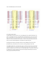
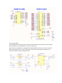
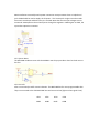
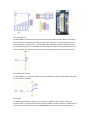
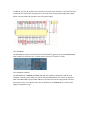
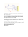
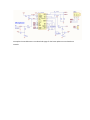
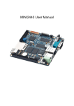
Incomplete section 1 of user manual. See andahammer.com downloads page for the latest manuals. 1.1 1.1.1 1.1.2 1.1.3 MINI2440.................................................... ‐ 10 ‐‐ MINI2440 appearance ............................................. ‐ 10 ‐‐ MINI2440 features hardware resources .................. ‐ 11 ‐‐ CD‐ROM resources that users ..................................‐ 12 – 1.2 Interface layout and jumper ............................................. ‐ 12 ‐‐ 1.2.1 Jumper Description ................................................................ ‐ 13 ‐‐ 1.2.2 Interface Layout ................................................................. ‐ 13 – 1.3 Interface description resources ......................................... ‐ 13 ‐‐ 1.3.1 address space allocation and the definition of chip select signal ............. ‐ 14 ‐‐ 1.3.2 SDRAM storage systems .............................................................................‐ 15 ‐‐ 1.3.3 FLASH storage systems ...............................................................................‐ 15 ‐‐ 1.3.4 Power Supply System and Interface ...........................................................‐ 16 ‐‐ 1.3.5 System Reset ...............................................................................................‐ 18 ‐‐ 1.3.6 User LED .......................................................................................................‐ 18 ‐‐ 1.3.7 User button ..................................................................................................‐ 19 ‐‐ 1.3.8 A / D input test .............................................................................................‐ 19 ‐‐ 1.3.9 PWM control buzzer .....................................................................................‐ 20 ‐‐ 1.3.10 Serial Port ...................................................................................................‐ 20 ‐‐ 1.3.11 USB interface ..............................................................................................‐ 21 ‐‐ 1.3.12 LCD interface ..............................................................................................‐ 22 ‐‐ 1.3.13 EEPROM .....................................................................................................‐ 23 ‐‐ 1.3.14 Network Interface ....................................................................................... 23 ‐‐ 1.3.15 Audio Interface ........................................................................................... 24 ‐‐ 1.3.16 JTAG Interface ............................................................................................. 25 ‐‐ 1.3.17 GPIO ............................................................................................................‐ 26 ‐‐ 1.3.18 CMOS CAMERA 1.3.19 system bus interface ..................................................................................‐ 28 ‐‐ Characteristics ............................................... 1.3 1.4 linux...............................................................‐ 29 – WindowsCE characteristics .............................‐ 30 – Chapter II Mini2440 .....................‐ 31 ‐‐ 2.1 Mini2440 set up and connect................................‐ 31 ‐‐ 2.1.1 Startup mode selection ...........................................‐ 31 ‐‐ 2.1.2 External interface connector ...................................‐ 31 ‐‐ 2.1.3 Setting HyperTerminal ............................................‐ 31 – 2.2 Mini2440 BIOS function and use ......................................‐ 35 ‐‐ 2.3.1 boot into BIOS mode ................................................................‐ 35 ‐‐ 2.2.2 install USB drive ..........................................................................‐ 36 ‐‐ 2.3.3 Function description Main Menu ...................................‐ 39 ‐‐ 2.2.4 Zoning submenu function ..................................................‐ 42 – 2.2.5 set Linux boot parameters sub‐menu function.........‐ 45 – 2.3 System test of Mini2440 resources .................‐ 49 ‐‐ Download 2.3.1 to run testing procedures ..............‐ 49 – 2.3.2 external resources to test .........................................‐ 55 – 2.4 2.4.1 2.4.2 2.4.3 2.4.4 2.4.5 2.4.6 2.4.7 2.4.8 2.4.9 2.4.10 2.4.11 2.4.12 2.4.13 2.4.14 2.4.15 2.4.16 2.4.17 2.4.18 Qtopia graphical interface for Linux ……………‐ 62 ‐‐ Touch Panel Calibration ............................................. 64 ‐‐ The main interface ..................................‐ 65 ‐‐ MP3 Player ...........................................................‐ 66 ‐‐ Playing video........................ ...................................‐ 67 ‐‐ Photo browser...................................‐ 68 ‐‐ Calculator.........................................................‐ 68 ‐‐ Terminal command.........................................‐ 69 ‐‐ Network Settings...................................‐ 70 ‐‐ Ping Test.....................................‐ 71 ‐‐ browser.....................................‐ 73 ‐‐ LED test...................................‐ 73 ‐‐ EEPROM read and write test.........................‐ 75 ‐‐ PWM control buzzer test..................‐ 76 ‐‐ touch pen testing...............................‐ 77 ‐‐ bar code scanner..................................‐ 78 ‐‐ language settings.................................‐ 79 ‐‐ rotating screen.................................‐ 80 ‐‐ Backlight control and brightness adjustment.............‐ 81 – 2.5 Linux non‐graphical interface system testing..........‐ 81 ‐‐ 2.5.1 player MP3.............................................‐ 83 ‐‐ 2.5.2 How to run the stay of proceedings...................‐ 83 ‐‐ 2.5.3 USB / mobile hard disk.......................‐ 84 ‐‐ 2.5.4 SD cards....................‐ 85 ‐‐ 2.5.5 USB camera capture......................‐ 85 ‐‐ 2.5.6 Communicating and sharing documents with a PC ...‐ 86 ‐‐ 2.5.7 How to display remote control via Web camera USB......‐ 88 ‐‐ 2.5.8 LED Control ............................‐ 90 ‐‐ 2.5.9 Test panel buttons ............................‐ 91 ‐‐ 2.5.10 2.5.11 2.5.12 2.5.13 2.5.14 2.5.15 2.5.16 2.5.17 2.5.18 2.5.19 2.5.20 2.5.21 2.5.22 2.5.23 2.5.24 Serial Port 2 and 3 test.......................‐ 92 ‐‐ test buzzer................................‐ 94 ‐‐ Control of LCD backlight........................‐ 94 ‐‐ test I2C‐EEPROM..................‐ 95 ‐‐ use telnet on the bbs...........................‐ 96 ‐‐ How do I set up network to access the Internet web sit............ ‐ 98 ‐‐ Setting the MAC Address.................‐ 100 ‐‐ How to use Telnet remote log Mini2440 ......................... ‐ 103 ‐‐ File transfers with FTP ........................‐ 103 ‐‐ through the website control panel LED .....................................‐ 104 ‐‐ How to use the network file system mounted NFS ...................‐ 105 ‐‐ Save settings and real‐time clock system.........‐ 106 ‐‐ How to Power‐down save data to Flash.........‐ 106 ‐‐ How to set boot auto‐run programs....‐ 107 ‐‐ How to use the screenshot command......‐ 108 – 2.6 2.6.1 2.6.2 2.6.3 2.6.4 2.6.5 2.6.6 2.6.7 2.6.8 2.6.9 2.6.10 2.6.11 2.6.12 2.6.13 2.6.14 2.6.15 2.6.16 pre‐installed on WindowsCE functions and external resources to test ............‐ 109 ‐‐ Test button ............................................. ..............................................‐ 110 ‐‐ LED Test ............................................. ........................................ ‐ 111 ‐‐ Rotating the screen test .......................................................‐ 112 ‐‐ Serial Communication Test .....................................................‐ 112 ‐‐ How to use the USB ........................................... ..................‐ 114 ‐‐ How to use the SD / MMC card ......................... ..................‐ 115 ‐‐ the use of Windows Media Player to play mp3 .....................‐ 116 ‐‐ How to use the super‐smooth player, SD card playback Mpeg4 movie .........‐ 117 ‐‐ Ethernet test ........................................... ..........................................‐ 117 ‐‐ log in through telnet target board .................................. ...............‐ 118 ‐‐ use ftp to send files to the target version .......................... .........‐ 119 ‐‐ Web server testing ............................................ ..................‐ 120 ‐‐ Save Touch Panel Calibration .................. .....................‐ 121 ‐‐ use ActiveSync for USB synchronous communication...... ......................‐ 122 ‐‐ wireless card to test ...........................................................‐ 123 ‐‐ How do I set up real‐time clock and save ........................ ........‐ 124 – 2.7 2.7.1 2.7.2 2.7.3 2.7.4 H‐JTAG programmer Express BIOS to the Mini2440 (all the process of mouse‐ 125 ‐‐ H‐JTAG Introduction ................................................................‐ 125 ‐‐ install and set up H‐JTAG ..........................................‐ 126 ‐‐ Model settings and Flash programmer BIOS ......................‐ 130 ‐‐ Frequently Asked Questions ...............................................‐ 136 – Chapter III of backup and recovery system and install the update...........‐ 137 ‐‐ 3.1 backup and recovery system ...........................................‐ 137 ‐‐ 3.1.1 Backup System............. .................................‐ 137 ‐‐ 3.1.2 use the backup file to restore the system .................‐ 142 – 3.2 3.2.1 3.2.2 3.2.3 3.2.4 3.3 3.3.1 3.3.2 3.3.3 3.3.4 installed on Linux systems ................................................‐ 145 ‐‐ Zoning ..................................................................‐ 145 ‐‐ install bootloader ...........................................................‐ 147 ‐‐ Install linux kernel.........................................................‐ 149 ‐‐ to install the root file system .....................................‐ 150 – installed WinCE system ............................................‐ 153 ‐‐ Zoning ...................................................................‐ 153 ‐‐ install bootloader ...................................................‐ 154 ‐‐ install eboot ..............................................................‐ 156 ‐‐ install wince kernel image .....................................‐ 157 – Downloaded to the memory to run 3.4 ..............................‐ 161 ‐‐ 3.4.1 running 2440test ......................................................‐ 161 ‐‐ 3.4.2 running uCos2 .................................................... 166 ‐‐ 3.4.3 running Linux ......................................................‐ 171 ‐‐ 3.4.4 running WinCE .................................................‐ 174 – Chapter IV ADS1.2 use integrated development environment...........‐ 177 ‐‐ 4.1 the use of ADS to create LED Engineering.....................................‐ 177 ‐‐ 4.1.1 set up a project ....................................................................‐ 177 ‐‐ 4.1.2 compile and link the project ................................................‐ 182 – 4.2 the use of H‐JTAG debug code ...............................................‐ 189 ‐‐ 4.2.1 for the H‐JTAG configuration AXD DEBUGGER .............................‐ 189 ‐‐ 4.2.4 the use of H‐JTAG in ADS1.2 simulation debugging environment......‐ 192 – 4.3 compiler programmer running 2440test ............................‐ 192 ‐‐ 4.3.1 Compile and use of H‐JTAG debug 2440test ......................‐ 193 ‐‐ 4.3.2 through the USB to download to run 2440test ................‐ 197 – 4.4.3 put 2440test programmer to Nand Flash running .............‐ 201 – 4.5 4.5.1 4.5.2 4.5.3 uCos2 compiler and programmer ...............................................‐ 204 ‐‐ compiler uCos2 .................................................................. 204 ‐‐ put uCos2 downloaded to the memory to run .........................‐ 206 ‐‐ put uCos2 programmer to Nand Flash running .................. ...‐ 210 – 4.6 NBOOT compiler and programmer ..................................‐ 213 ‐‐ 4.6.1 compiler NBOOT ........................................................‐ 213 ‐‐ 4.6.2 put NBOOT programmer to Nand Flash ..................‐ 216 – Chapter V set up Linux development environment .......................‐ 219 ‐‐ 5.1 Based on Redhat Linux9.0 development environment set up ..........‐ 219 ‐‐ 5.1.1 fully graphical installation Redhat9.0 .........................................‐ 219 ‐‐ 5.1.2 set up cross‐compiling environment ....................................‐ 232 ‐‐ 5.1.3 Configure Network File System NFS Services .................‐ 233 ‐‐ 5.1.4 your system through NFS ........................................... ..‐ 234 ‐‐ 5.1.5 configured PC‐Linux‐ftp Services ...........................‐ 236 ‐‐ 5.1.6 configured PC‐telnet services ................................‐ 237 ‐‐ 5.1.7 in Redhat add new users ...........................................‐ 238 – Chapter VI of Embedded Linux Application Development Getting Started Guide ...........‐ 240 ‐‐ 6.1 Hello, World! .................................................‐ 240 ‐‐ 6.1.1 Hello, World source code .....................................‐ 240 ‐‐ 6.1.2 compiler Hello, World .......................................‐ 240 ‐‐ 6.1.3 put Hello, World downloaded to the Mini2440 to run ................‐ 240 – 6.2 6.2.1 6.2.2 6.2.3 6.2.4 6.2.5 6.2.6 6.2.7 Introduction to Embedded Linux Development .....................‐ 244 ‐‐ LED test procedure .....................................‐ 244 ‐‐ Test button .................................................‐ 245 ‐‐ UDP network programming ...........................‐ 247 ‐‐ Examples of math library calls ...........................‐ 252 ‐‐ Thread programming examples...............................‐ 253 ‐‐ Examples of application programming pipeline ....................‐ 255 ‐‐ Based on C + + The Hello, World .......................‐ 260 – 6.3 The most simple embedded Linux driver module ............‐ 261 ‐‐ 6.3.1 Hello, Module source code ................................‐ 261 ‐‐ 6.3.2 put Hello, Module add kernel code tree, and compile............‐ 262 ‐‐ 6.3.3 put Hello, Module Download and install the Mini2440 to use ........‐ 265 – 6.4 6.4.1 6.4.2 6.5 Simple Example ............................................ Linux driver ..............................‐ 266 ‐‐ LED Driver .........................................................................................‐ 266 ‐‐ Key drivers .......................................................................‐ 270 ‐‐ Embedded Linux Examples transplantation procedures .......................‐ 276 – 6.5.1 mp3 player madplay Detailed transplantation process ............... 276 ‐‐ (1) set up working directory, copy the source code package ...................‐ 277 ‐‐ (2) extract the source code package .............................................. 277 ‐‐ (3) rely on the compiler madplay library file .........................‐ 278 ‐‐ (4) compiler installed madplay ........................................‐ 279 ‐‐ (5) to test PC version of madplay .........................................‐ 282 ‐‐ (6) script to build the compiler build‐x86 .................................‐ 282 ‐‐ (7) to build and amend the ARM version of the compiler script build‐arm ........‐ 283 ‐‐ (8) Download madplay to the Mini2440 to run the test .............‐ 287 – Chapter VII of the common bootloader configuration and compiler ............‐ 289 ‐‐ 7.1 configuration and compile vivi ...............................................‐ 290 ‐‐ 7.1.1 compiler using the default configuration ...............................................................‐ 290 ‐‐ 7.1.2 Configuration vivi start from the Nor Flash ............................‐ 293 – 7.2 7.2.1 7.2.2 7.2.3 use the ADS compiler YL‐BIOS ..............................................‐ 294 ‐‐ the use of ADS compiler YL‐BIOS ...........................‐ 294 ‐‐ put YL‐BIOS download into memory to run ................‐ 296 ‐‐ programmer YL‐BIOS to the Mini2440 ..................‐ 299 – 7.3 configuration and compile U‐Boot .................................‐ 301 ‐‐ 7.3.1 configure and compile U‐Boot ..................................‐ 302 ‐‐ 7.3.2 programmer put U‐Boot to the Mini2440 ......................‐ 303 – Chapter VIII of the linux kernel configuration and compile ........................‐ 307 ‐‐ 8.1 using the default kernel configuration file ...............................‐ 307 ‐‐ 8.1.1 extract the kernel source code ........................................‐ 307 ‐‐ 8.1.2 Loading the default configuration files .....................‐ 308 ‐‐ 8.1.3 kernel .....................................................................‐ 309 ‐‐ 8.1.4 all Linux driver source code location ...................... ..‐ 311 ‐‐ Custom linux kernel 8.2 ......................................‐ 312 ‐‐ 8.2.1 How to Configure CPU Options ............................‐ 313 ‐‐ 8.2.2 How to configure the various sizes of LCD driver support .......................‐ 315 ‐‐ 8.2.3 How to configure the Touch Panel ..............................‐ 318 ‐‐ 8.2.4 How to configure USB mouse and keyboard ............................... ‐321 ‐‐ 8.2.5 how to configure USB support ....................................... ‐324 ‐‐ 8.2.6 how to configure the mesh and SMIC Micro USB camera, etc. ............. ‐327 ‐‐ 8.2.7 how to configure the network card driver CS8900 .................... ‐330 ‐‐ 8.2.8 How to configure the sound card driver..................... 51H‐336 ‐‐ 8.2.9 how to configure SD / MMC card driver........... 512H‐340 ‐‐ 8.2.10 How to configure the LED driver.................................................................. 513H‐341 ‐‐ 8.2.11 How to configure key driver............................................................. 514H‐342 ‐‐ 8.2.12 how to configure serial port driver................... 515H‐343 ‐‐ 8.2.13 how to configure the RTC Real Time Clock driver................. 516H‐344 ‐‐ 8.2.14 how to configure file system support yaffs......................... 517H‐345 ‐‐ 8.2.15 how to configure EXT2/VFAT / NFS file system, etc................ 518H‐347 ‐‐ 8.3 yaffs root file system image production.................... ‐352 ‐‐ Chapter IX 21H ......................... WinCE Development Guide.................... ‐354 ‐‐ 9.1 based development environment WinCE5.0...................... ‐354 ‐‐ 9.1.1 install Platform Builder 5.0 (with latest patch 2007).........‐354 ‐‐ Import 9.1.2 installed BSP.....................‐365 ‐‐ 9.1.3 to install wireless card driver ............................‐368 ‐‐ Examples of kernel engineering 9.1.4 .............................‐371 ‐‐ 9.1.5 Export SDK...........................‐375 ‐‐ 9.1.6 installed Embedded Visual C + + (EVC) .........................‐381 ‐‐ EVC install patches and 9.1.7 derived SDK...................‐387 ‐‐ CE custom kernel 9.1.8.........‐396 ‐‐ 9.2 using ActiveSync synchronization with PC communications (public) ......‐410 ‐‐ 9.2.1 install ActiveSync..............‐410 ‐‐ 9.2.2 for synchronous communication to install USB drivers .............‐415 ‐‐ 9.2.3 transfer using ActiveSync synchronization tool to copy files ............‐419 ‐‐ 9.2.4 ActiveSync to connect with Platform Builder and implement of communications screenshot ‐422 ‐‐ 9.2.5 use ActiveSync with the Platform Builder online editing the registry ........‐429 ‐‐ EVC's 9.3 create a Hello, World, and downloaded to the compiler Mini2440 running ..‐430 ‐‐ 9.4 create applications VS2005/2008 and downloaded to the compiler Mini2440 running .‐ 437 ‐‐ Create Project 9.4.1 .......................................................................‐438 ‐‐ Mini2440 to connect 9.4.2 settings ...................................................................‐440 ‐‐ Download 9.4.3 9.5 9.5.1 9.5.2 9.5.3 9.5.4 compiler Mini2440 to run .............................‐443 ‐‐ LED driver sample preparation and testing .....................................‐444 ‐‐ understanding of hardware connection .....................................‐445 ‐‐ LED prepared 24H streaming driver ........................................‐446 ‐‐ put LED driver added to the BSP in order to compile .................‐452 ‐‐ prepare and compile the test application LED ...................‐454 ‐‐ LED testing procedures put 247H 9.5.5 added to the core, and set up a desktop shortcut ...‐457 ‐‐ Appendix 1 Qt embedded graphics development entry ......................‐459 ‐‐ H1. Set up development environment ............................................‐459 ‐‐ H2. Compiled X86 and Qtopia platform, Hello, World and embedded browser ......‐459 ‐‐ H2.1 compile Qt / Embedded ........................................‐460 ‐‐ H2.2 simulated in the PC running Qtopia ...............................‐460 ‐‐ 2.3 compiler Hello, World sample .....................................‐460 ‐‐ 2.4 run a separate Hello, World ......................................‐461 ‐‐ 2.5 Running Hello, World in Qtopia................................‐461 ‐‐ ARM compiler 256H3 the Qtopia platform, and Hello, World and embedded browser .....‐462 ‐‐ 3.1 compile Qt / Embedded ........................................‐462 ‐‐ 3.2 compiler Hello, World sample ...............................‐463 ‐‐ 3.3 Download Hello World to a target board and run .............‐463 ‐‐ To use their own 260H3.4 compiled Qtopia update the production file system ....‐467 ‐‐ Frequently Asked Questions 4 ..............................‐467 ‐‐ 262H4.1 the implementation of build errors ........................‐468 ‐‐ Hello 4.2 compile errors .......................................‐469 ‐‐ Hello 264H4.3 compile error occurs when the second information ..........‐469 ‐‐ in Appendix 2 of the command line using the BIOS update and programmer system ‐470 ‐‐ 1.1. How to enter the BIOS of the command‐line mode .................‐470 ‐‐ 1.1.1 from menu to enter the command‐line mode ...............‐470 ‐‐ Nand Flash in 1.1.2 starts to enter the command‐line mode .........‐471 ‐‐ 2.2 install linux .......................................................‐471 ‐‐ Nand Flash on 2.2.1 zoning ...............................‐472 ‐‐ 2.2.2 to restore BIOS .......................................‐473 ‐‐ Linux kernel programmer 3.2.3 ............................‐475 ‐‐ 3.2.4 programmer yaffs based on the root file system ........‐477 ‐‐ Restart the system 3.2.5 ................................‐479 ‐‐ 3.3 installed wince ...............................‐479 ‐‐ Nand Flash on 3.3.1 zoning .........................................‐480 ‐‐ 3.3.2 to restore BIOS .......................................................‐481 ‐‐ 3.3.3 programmer Eboot .............................................‐482 ‐‐ Wince kernel programmer 3.3.4 .......................................‐483 ‐‐ Appendix 3 using SJF2440 programmer BIOS .........................‐487 ‐‐ 1 installed driver GIVEIO ............................................‐487 ‐‐ 2 use SJF2440 programmer BIOS ..............................‐493 ‐‐ MINI2440 Introduction About 1.1 MINI2440 The mini2440 is a practical low‐cost ARM9 Single Board Computer (SBC) with a very high performance/cost ratio. With the Samsung S3C2440 microprocessor and the use of professional layout and quality peripheral chips, it is very robust. The Mini2440 uses a four‐layer board with gold immersion processing, and has high quality equal‐length bus routing in timing critical areas. The production environment and quality control are the same as those of modern high‐speed motherboards. 1.1.1 MINI2440 Component Side 1.1.2 MINI2440 features and hardware resources Processor ‐ Samsung S3C2440A, 400MHz (Max 533Mhz) RAM On‐board 64M SDRAM 32bit data bus clock frequency up to 100MHz FLASH storage 64MBytes Nand Flash 2MBytes Nor Flash with installed BIOS LCD Interface 4‐wire Resistive Touch Panel interface ‐‐ 10 bit A/D Supports 4 and 16 level gray‐scale, 256 color, 4096 color STN LCD screen size from 3.5 inch to 12.1 inch screen resolution up to 1024x768 Support 4 and 16 level gray‐scale, 256 color, 64K color, True Color TFT LCD screen size from 3.5‐inch to 12.1‐inch screen resolution to 1024x768 pixels Configuration for the NEC 240x320/3.5‐inch TFT true color LCD with Touch Panel Interface and resources 1 10/100M Ethernet RJ‐45 interface (DM9000 network chip) 3 serial ports ‐ one configured for RS‐232, COM0 1 USB Host 1 USB Slave B‐type interface 1 SD card storage interface, no size limit 1 Channel Stereo audio output interface, 1 Built in microphone 1 Microphone input. 1 2.0mm pitch 10‐pin JTAG interface 4 USER LEDs 6 USER buttons (with connection to GPIO connector and 8 pin user connector) 1 buzzer PWM control 1 adjustable resistor for A/D test 1 IIC bus AT24C08 chip for IIC Bus Test or configuration data, holds 256 bytes. 2.0 mm pitch 20PIN camera interface Power Interface (5V), with power switch and indicator light System Clock Source Passive crystal Internal real‐time clock (with back‐up lithium battery) Expansion Interface 1 34 pin 2.0mm GPIO interface 1 40 pin 2.0mm system bus interface Size 100 x 100 (mm) Supported Operating Systems Linux 2.6.29 WindowsCE.NET 5.0/6.0 uC/OS‐II 1.1.3 CD‐ROM resources (1) ADS1.2 Setup (2) H‐JTAG debugging software programmer (3) Windows Flash programmer software SJF2440 (4) Linux Nand Flash programmer software Jflash‐2440 (with source code) (5) Serial tools CRT, dnw (6) C language tool chain (7) USB drive (WindowXP/2000 under installation) (8) vivi source code for Linux. (The bootloader.) (9) Test code for LED lights on the board. (10) A collection of sample apps that test system I/O. (11) WindowsCE BSP and sample project files (12) linux development tools and kernel source code package: ‐ Arm‐linux‐gcc‐4.3.2 tool chain used for kernel, Qtopia 2.2.0, user apps. ‐ Yaffs file system mapping tool mkyaffsimage ‐ Linux‐2.6.29 for MINI2440 kernel source code (including the DM9000 driver, all kinds of TFT LCD drivers, sound card driver, Touch Panel Driver, YAFFS source code, SD card driver, RTC driver, serial port expansion drive, the USB camera driver, USB mouse and keyboard, USB drives, etc.) (13) Embedded graphical interface. Qtopia source code package. Embedded browser source code package. (14) Mini2440 schematic diagram (PDF format). (15) User's manual (pdf format) 1.2 Interface layout and jumpers. 1.2.1 Jumper Description. There is only one on‐board jumper, J2. It is used to select the LCD driver board input voltage. For NEC3.5‐inch LCD, set voltage selector for 5V. 1.2.2 Interface Layout Mini2440 interface layout is shown in the diagram above. An optional cable and connector kit has a cable for every connector and a connector for every cable. 1.3 Interface resources. This section details each interface or module with pin definitions and occupied CPU resources. 1.3.1 address space allocation and the definition of chip select signals. The S3C2440 supports two modes: Boot from NAND Flash or boot from NOR Flash. The boot mode determines the configuration of the memory map as shown in this table. When the NOR/NAND switch is in the NOR position, the system conforms to the memory map on the left. In the NAND position, the The S3C2440 uses the memory map on the right. SFR Area for special control register addresses: The following are the device address space allocations and the definition of the chip select signals. The nGCS0 chip select space is different depending onstart‐up mode. In NAND Flash boot mode the internal 4K Bytes ‐ BootSram ‐ is mapped to nGCS0 Space. In Nor Flash start mode (non‐Nand Flash Boot Mode), nGSC0 is connected to external memory. Nor Flash has been mapped to the chip select space nGCS0 The 64 MByte SDRAM address space is: 0x30000000 to 0x34000000 1.3.2 SDRAM storage systems The Mini2440 uses two external 32MByte SDRAMs for a total of 64M bytes of SDRAM memory which together form a 100 MHz 32‐bit data bus RAM. With its 16K each of data and instruction cache running at over 400 MHz, the whole system performs much as if it had 400 MHz external buses. Here is the SDRAM portion of the schematic. 1.3.3 FLASH storage systems The Mini2440 has two kinds of Flash, one is the 2MByte Nor Flash, model SST39VF1601. The other is the 64 MByte Nand Flash model K9F1208. The S3C2440 supports starting from either Flash. The slide switch, S2, chooses Nand or Nor. The Nor Flash uses A1‐A22 for a total of 22 address lines. Why not A0? Because the memory is 1 word or two bytes (16 bits) wide and all access is on even numbered addresses. The smallest unit read is two bytes. According to the schematic, the design could use a total of 8 Mbyte of Nor Flash. On the SST39V1601 chips, A20 and A21 have no connection, allowing 2 Mbytes of Nor flash. The 64 MByte Nand Flash is only 8 bits wide. Again, the 16k data and instruction caches allow reasonable speed even if running code from Nand memory. (Most code is made of loops and sections that repeat. Once in cache, they run at full 400 MHz speed. The Harvard architecture of the ARM9 allows fetching and pipelining instructions and data simultaneously from the two caches, giving exceptional performance.) 1.3.4 Power Supplies The Mini2440's power supply system is rather simple and requires an external 5V power supply. Three regulators are used to generate 3.3V, 1.8V, and 1.25V. Please note: The Mini2440 is not designed for handheld mobile devices, so it does not have full power management circuitry. The S1 DIP switch controls the system power and there is no provision for power control through software. Most installations eventually need a power connection more permanent than a simple barrel jack. CON8 should be used to supply the 5V power. This 2.0mm pitch single row socket needs 5V on each outside pin and both inner pins are GND. Note that the two input voltages are not connected. VDDIN powers the on‐board parts through the regulators. VDD5V goes to CON5, the system bus expansion connector. 1.3.5 System Reset The Mini2440 conditions reset with the MAX811 reset chip to provide a clean low level reset to the CPU. 1.3.6 User LED LEDs are commonly used for status indication. The Mini2440 has four user‐programmable LEDs. They are connected to the S3C2440 GPIO lines and are active‐low (light on when signal is low). LED1 LED2 LED3 LED4 GPB5 GPB6 GPB7 GPB8 1.3.7 User buttons or keys. The user buttons are controlled by Port G, which can be used to assign several functions to the pins. The Mini2440 has a total of 6 user test buttons connected directly to the CPU interrupt pins. The active‐low signals are held high by 10K resistors R17 ‐ R22. Connector 12 has the same 6 user button signals with ground and VDD (3.3V). No external pull‐up is needed. Pins 1 ‐ 6 on Connector 12 are defined as K1 through K6 to match the on‐board buttons. You can use more than one switch on each line. The 6 user buttons correspond to external interrupts EINT8 EINT11 EINT13 EINT14 EINT15 EINT19 and depending on resister settings, can also be set to GPIO GPG0 GPG3 GPG5 GPG6 GPG7 GPG11 or nSS1 SPIMISO1 SPIMOSI1 SPICLK1 TCLK1 The Connector‐12 functions are determined by Port G. See the S3C2440 Data Sheet for Port G details. Port G Control Register Con12.1 10xx 101010xx 10xxxx10 11xx 111111xx 11xxxx11 EINT8 00xx 000000xx 00xxxx00 in 01xx 010101xx 01xxxx01 out GPG0 Con12.2 EINT11 nSS1 GPG3 Con12.3 EINT13 SPI MISO1 GPG5 Con12.4 EINT14 SPI MOSI1 GPG6 Con12.5 EINT15 SPI CLK1 GPG7 Con12.6 EINT19 TCLK1 GPG11 Con12.7 Vdd 3.3V Con12.8 GND 1.3.8 A/D input test. The Mini2440 has an 8‐channel 10 bit A/D converter with sample and hold. When a touchpad is used, 4 channels are dedicated to touch pad conversion. The other 4 are general purpose and are on connector 4, GPIO. Pins 5, 6, 7, 8 are AIN0, AIN1, AIN2, AIN3. AIN0 is connected to a pot on the PCB for testing. If you need AIN0, remove the pot or cut the trace from the pot center pin to pin5 of CON4. The trace is on the bottom of the PCB with quite a bit of free space around it. 1.3.9 PWM Control buzzer The Mini2440 has a small buzzer, which can be controlled (somewhat) through PWM. The signal is from GPIO pin 31 (GPB0). 1.3.10 Serial The Samsung S3C2440 chip supports three serial ports UART0, UART1, UART2. Each has a connector with TTL level signals and also connects to CON4, the GPIO connector. UART0 also has TTL to RS‐232 conversion and uses the COM0 DB9 connector to work with any RS232 device. COM0 boots at 115,000 BAUD, N 0 1 and is fully supported by Linux and WinCE. 1.3.11 USB interface The Mini2440 has two USB interfaces. A USB Host, like an ordinary PC's USB interface, can be used with a USB camera, keyboard, mouse, wifi dongle, etc. The USB Slave is the smaller squarish connector (like you find on printers) and is generally used to download to the target board. When the Mini2440 is running WinCE, it can ActiveSync software with Windows. When the Mini2440 is running a Linux system, there is no corresponding driver and application. Ethernet is usually preferred for data transfer in Linux. The USB Slave can be controlled with a GPC5 register bit to set USB_EN or disable. It can be disabled to conserve CPU resources. 1.3.12 LCD interface The Mini2440 LCD interface has a 41 Pin 0.5mm pitch white connector, which contains common LCD control signals (line‐field scanning, the clock, enable, etc.) and complete RGB output of 8:8:8, supporting a maximum of 16 million colors. The LED backlight can be turned on or off with GPB1. The backlight signal is called LCD_PWR PWM output and reset signals (nRESET), one of the backlight control signals is LCD_PWR. In addition, pins 37, 38, 39, 40 are for the four‐wire touch screen interface. They can be directly connected to a Touch Panel. See figure J2 for the LCD driver board power supply select signal. All the currently used LCD controllers use a 5V power supply. 1.3.13 EEPROM The Mini2440 has a direct connection from the S3C2440 I2C signal pin to an AT24C08 EEPROM with a capacity of 256 byte. This is mainly used to test the I2C bus and I2C code. 1.3.14 Network Interface The Mini2440 uses a DM9000 10/100M LAN chip with network transformers and an RJ‐45 connector. Ordinary Cat5e cable can connect from the Mini2440 to your routers or switches. Note: Each Mini2440's network MAC address is the same and can be configured by software. See section 2.4 for Linux. WinCE users refer to the BSP for the DM9000 driver code and the registry file (platform.reg). 1.3.15 Audio Interface The S3C2440’s built in I2S bus interface is directly connected to an external 8/16 bit stereo CODEC. The Mini2440 to adopt Based on the I2S bus UDA1341 audio decoder chip implementation system, the chip initializes internal registers and settings are taken L3‐bus with bus connection control of the implementation, where we have used a Samsung design of public board, respectively, using the CPU's GPB2, GPB3, GPB4 port analog implementation of the L3‐Bus specification L3MODE, L3DATA, L3CLOCK, their initialization End after UDA1341 are no longer useful, so these three line of control can also use an ordinary single‐chip analog implementation. The output of audio systems for the development of on‐board common aperture 3.5mm socket, input is divided into two roads, all the way for the onboard MAK Grams of the wind, and the other road through the 2.0mm socket CON10 white leads. Two‐way audio input of the driver are different, at present only CON10 interface corresponding recording channel can be used, please refer to our website update information, the two channels of our most Will drive up the end. Incomplete: See andahammer.com downloads page for the latest updates on translated user manuals.