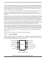
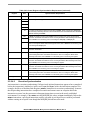
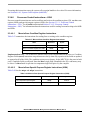
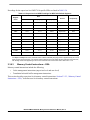
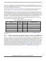
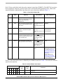
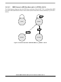
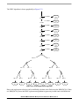
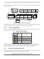
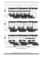
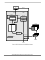
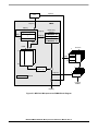
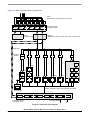
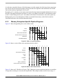
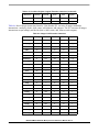
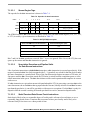
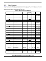
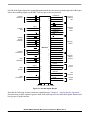
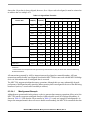
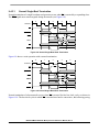
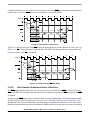
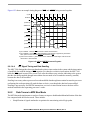
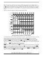
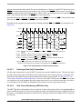
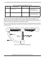
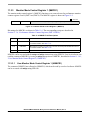
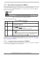
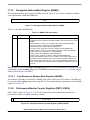
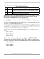
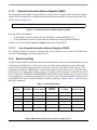
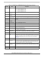
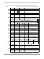
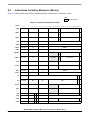
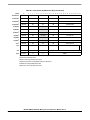
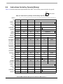
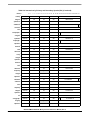
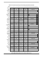
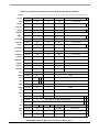
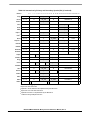
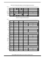
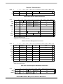
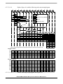
1
MPC7410/MPC7400
RISC Microprocessor
Reference Manual
Supports
MPC7410
MPC7400
MPC7410UM/D
10/2008
Rev. 2
How to Reach Us:
Home Page:
www.freescale.com
Web Support:
http://www.freescale.com/support
USA/Europe or Locations Not Listed:
Freescale Semiconductor, Inc.
Technical Information Center, EL516
2100 East Elliot Road
Tempe, Arizona 85284
+1-800-521-6274 or
+1-480-768-2130
www.freescale.com/support
Europe, Middle East, and Africa:
Freescale Halbleiter Deutschland GmbH
Technical Information Center
Schatzbogen 7
81829 Muenchen, Germany
+44 1296 380 456 (English)
+46 8 52200080 (English)
+49 89 92103 559 (German)
+33 1 69 35 48 48 (French)
www.freescale.com/support
Information in this document is provided solely to enable system and software
implementers to use Freescale Semiconductor products. There are no express or
implied copyright licenses granted hereunder to design or fabricate any integrated
circuits or integrated circuits based on the information in this document.
Freescale Semiconductor reserves the right to make changes without further notice to
any products herein. Freescale Semiconductor makes no warranty, representation or
guarantee regarding the suitability of its products for any particular purpose, nor does
Freescale Semiconductor assume any liability arising out of the application or use of
any product or circuit, and specifically disclaims any and all liability, including without
limitation consequential or incidental damages. “Typical” parameters which may be
provided in Freescale Semiconductor data sheets and/or specifications can and do
vary in different applications and actual performance may vary over time. All operating
parameters, including “Typicals” must be validated for each customer application by
customer’s technical experts. Freescale Semiconductor does not convey any license
under its patent rights nor the rights of others. Freescale Semiconductor products are
not designed, intended, or authorized for use as components in systems intended for
Japan:
Freescale Semiconductor Japan Ltd.
Headquarters
ARCO Tower 15F
1-8-1, Shimo-Meguro, Meguro-ku
Tokyo 153-0064
Japan
0120 191014 or
+81 3 5437 9125
[email protected]
surgical implant into the body, or other applications intended to support or sustain life,
Asia/Pacific:
Freescale Semiconductor China Ltd.
Exchange Building 23F
No. 118 Jianguo Road
Chaoyang District
Beijing 100022
China
+86 010 5879 8000
[email protected]
unintended or unauthorized use, even if such claim alleges that Freescale
For Literature Requests Only:
Freescale Semiconductor
Literature Distribution Center
P.O. Box 5405
Denver, Colorado 80217
+1-800 441-2447 or
+1-303-675-2140
Fax: +1-303-675-2150
LDCForFreescaleSemiconductor
@hibbertgroup.com
Document Number: MPC7410UM/D
Rev. 2, 10/2008
or for any other application in which the failure of the Freescale Semiconductor product
could create a situation where personal injury or death may occur. Should Buyer
purchase or use Freescale Semiconductor products for any such unintended or
unauthorized application, Buyer shall indemnify and hold Freescale Semiconductor
and its officers, employees, subsidiaries, affiliates, and distributors harmless against all
claims, costs, damages, and expenses, and reasonable attorney fees arising out of,
directly or indirectly, any claim of personal injury or death associated with such
Semiconductor was negligent regarding the design or manufacture of the part.
Freescale and the Freescale logo are trademarks or registered trademarks
of Freescale Semiconductor, Inc. in the U.S. and other countries. All other
product or service names are the property of their respective owners. The
described product is a PowerPC microprocessor. The PowerPC name is a
trademark of IBM Corp. and is used under license. IEEE 1149.1a and 754
are trademarks of the Institute of Electrical and Electronics Engineers, Inc.
(IEEE). This product is not endorsed or approved by the IEEE.
© Freescale Semiconductor, Inc., 2000, 2002, 2008. All rights reserved.
Contents
Paragraph
Number
Title
Page
Number
Contents
About This Book
Audience ........................................................................................................................... 36
Organization...................................................................................................................... 37
Suggested Reading............................................................................................................ 38
General Information...........................................................................................................38
Related Documentation......................................................................................................38
Conventions ...................................................................................................................... 39
Acronyms and Abbreviations ........................................................................................... 40
Terminology Conventions................................................................................................. 43
Chapter 1
Overview
1.1
1.2
1.2.1
1.2.2
1.2.2.1
1.2.2.2
1.2.2.3
1.2.2.4
1.2.2.4.1
1.2.2.4.2
1.2.2.4.3
1.2.2.4.4
1.2.2.4.5
1.2.2.4.6
1.2.3
1.2.4
1.2.5
1.2.6
1.2.6.1
1.2.6.2
1.2.6.2.1
1.2.6.2.2
1.3
1.3.1
General Operation............................................................................................................ 1-1
General Features .............................................................................................................. 1-4
Overview of Features................................................................................................... 1-4
Instruction Flow........................................................................................................... 1-8
Instruction Queue and Dispatch Unit ...................................................................... 1-8
Branch Processing Unit (BPU)................................................................................ 1-8
Completion Unit ...................................................................................................... 1-9
Independent Execution Units................................................................................. 1-10
AltiVec Vector Permute Unit (VPU) ................................................................. 1-10
AltiVec Vector Arithmetic Logic Unit (VALU)................................................. 1-11
Integer Units (IUs)............................................................................................. 1-11
Floating-Point Unit (FPU) ................................................................................. 1-11
Load/Store Unit (LSU) ...................................................................................... 1-12
System Register Unit (SRU).............................................................................. 1-12
Memory Management Units (MMUs)....................................................................... 1-12
On-Chip Instruction and Data Caches ....................................................................... 1-13
L2 Cache Implementation.......................................................................................... 1-14
System Interface/Bus Interface Unit (BIU) ............................................................... 1-15
System Interface Operation ................................................................................... 1-16
Signal Groupings ................................................................................................... 1-17
Signal Configuration.......................................................................................... 1-20
Clocking............................................................................................................. 1-21
Implementation .............................................................................................................. 1-21
PowerPC Registers and Programming Model ........................................................... 1-22
MPC7410/MPC7400 RISC Microprocessor Reference Manual, Rev. 2
Freescale Semiconductor
3
Contents
Paragraph
Number
1.3.2
1.3.2.1
1.3.2.2
1.3.2.3
1.3.3
1.3.3.1
1.3.3.2
1.3.4
1.3.4.1
1.3.4.2
1.3.5
1.3.5.1
1.3.5.2
1.3.6
1.3.7
1.3.8
1.3.9
1.3.10
1.4
1.5
Title
Page
Number
Instruction Set ............................................................................................................ 1-28
PowerPC Instruction Set........................................................................................ 1-28
AltiVec Instruction Set........................................................................................... 1-30
Instruction Set........................................................................................................ 1-30
On-Chip Cache Implementation ................................................................................ 1-31
Cache Model.......................................................................................................... 1-31
Cache Implementation ........................................................................................... 1-31
Exception Model........................................................................................................ 1-31
PowerPC Exception Model.................................................................................... 1-32
MPC7410 Exception Implementation ................................................................... 1-33
Memory Management................................................................................................ 1-35
PowerPC Memory Management Model ................................................................ 1-35
Memory Management Implementation ................................................................. 1-36
Instruction Timing ..................................................................................................... 1-36
AltiVec Implementation............................................................................................. 1-38
Power Management ................................................................................................... 1-38
Thermal Management—MPC7400 only ................................................................... 1-39
Performance Monitor................................................................................................. 1-40
Differences between the MPC7410 and the MPC7400 ................................................. 1-41
Differences between the MPC7410 and the MPC750 ................................................... 1-41
Chapter 2
Programming Model
2.1
2.1.1
2.1.2
2.1.3
2.1.3.1
2.1.3.2
2.1.4
2.1.4.1
2.1.5
2.1.5.1
2.1.5.2
2.1.5.3
2.1.5.4
2.1.5.4.1
2.1.5.4.2
2.1.5.5
2.1.5.6
Register Set ...................................................................................................................... 2-1
Register Set Overview ................................................................................................. 2-1
Register Set Summary ................................................................................................. 2-3
Supervisor-Level Registers (OEA) .............................................................................. 2-9
Processor Version Register (PVR)........................................................................... 2-9
Machine State Register (MSR) ................................................................................ 2-9
User-Level Registers (VEA)...................................................................................... 2-12
Time Base Registers (TBL, TBU) ......................................................................... 2-12
MPC7410-Specific Register Descriptions ................................................................. 2-12
Hardware Implementation-Dependent Register 0 (HID0) .................................... 2-13
Hardware Implementation-Dependent Register 1 (HID1) .................................... 2-17
Memory Subsystem Control Register (MSSCR0)................................................. 2-18
Instruction and Data Cache Registers.................................................................... 2-20
L2 Private Memory Control Register (L2PMCR)—MPC7410 Only ............... 2-21
L2 Cache Control Register (L2CR)................................................................... 2-22
Instruction Address Breakpoint Register (IABR).................................................. 2-25
Thermal Management Registers—MPC7400 Only............................................... 2-26
MPC7410/MPC7400 RISC Microprocessor Reference Manual, Rev. 2
4
Freescale Semiconductor
Contents
Paragraph
Number
2.1.5.6.1
2.1.5.6.2
2.1.5.7
2.1.5.7.1
2.1.5.7.2
2.1.5.7.3
2.1.5.7.4
2.1.5.7.5
2.1.5.7.6
2.1.5.7.7
2.1.5.7.8
2.1.5.7.9
2.1.5.7.10
2.1.5.7.11
2.1.5.7.12
2.1.5.7.13
2.1.6
2.2
2.2.1
2.2.2
2.2.3
2.2.4
2.3
2.3.1
2.3.1.1
2.3.1.2
2.3.1.3
2.3.1.4
2.3.2
2.3.2.1
2.3.2.2
2.3.2.3
2.3.2.4
2.3.2.4.1
2.3.2.4.2
2.3.2.4.3
2.3.3
2.3.4
2.3.4.1
2.3.4.1.1
Title
Page
Number
Thermal Management Registers (THRM1–THRM3)—MPC7400 Only.......... 2-26
Instruction Cache Throttling Control Register (ICTC) ..................................... 2-29
Performance Monitor Registers ............................................................................. 2-29
Monitor Mode Control Register 0 (MMCR0) ................................................... 2-29
User Monitor Mode Control Register 0 (UMMCR0)........................................ 2-32
Monitor Mode Control Register 1 (MMCR1) ................................................... 2-33
User Monitor Mode Control Register 1 (UMMCR1)........................................ 2-33
Monitor Mode Control Register 2 (MMCR2) ................................................... 2-33
User Monitor Mode Control Register 2 (UMMCR2)........................................ 2-34
Breakpoint Address Mask Register (BAMR).................................................... 2-34
User Breakpoint Address Mask Register (UBAMR) ........................................ 2-35
Performance Monitor Counter Registers (PMC1–PMC4) ................................ 2-35
User Performance Monitor Counter Registers (UPMC1–UPMC4) .................. 2-36
Sampled Instruction Address Register (SIAR).................................................. 2-37
User-Sampled Instruction Address Register (USIAR) ...................................... 2-37
Sampled Data Address Register (SDAR) and
User-Sampled Data Address Register (USDAR) .......................................... 2-37
Reset Settings............................................................................................................. 2-37
Operand Conventions .................................................................................................... 2-39
Floating-Point Execution Models—UISA................................................................. 2-39
Data Organization in Memory and Data Transfers.................................................... 2-40
Alignment and Misaligned Accesses......................................................................... 2-40
Floating-Point Operands ............................................................................................ 2-40
Instruction Set Summary ............................................................................................... 2-41
Classes of Instructions ............................................................................................... 2-42
Definition of Boundedly Undefined ...................................................................... 2-42
Defined Instruction Class ...................................................................................... 2-42
Illegal Instruction Class ......................................................................................... 2-43
Reserved Instruction Class .................................................................................... 2-43
Addressing Modes ..................................................................................................... 2-44
Memory Addressing .............................................................................................. 2-44
Memory Operands ................................................................................................. 2-44
Effective Address Calculation ............................................................................... 2-44
Synchronization ..................................................................................................... 2-45
Context Synchronization ................................................................................... 2-45
Execution Synchronization................................................................................ 2-48
Instruction-Related Exceptions.......................................................................... 2-49
Instruction Set Overview ........................................................................................... 2-49
UISA Instructions ...................................................................................................... 2-50
Integer Instructions ................................................................................................ 2-50
Integer Arithmetic Instructions.......................................................................... 2-50
MPC7410/MPC7400 RISC Microprocessor Reference Manual, Rev. 2
Freescale Semiconductor
5
Contents
Paragraph
Number
2.3.4.1.2
2.3.4.1.3
2.3.4.1.4
2.3.4.2
2.3.4.2.1
2.3.4.2.2
2.3.4.2.3
2.3.4.2.4
2.3.4.2.5
2.3.4.2.6
2.3.4.3
2.3.4.3.1
2.3.4.3.2
2.3.4.3.3
2.3.4.3.4
2.3.4.3.5
2.3.4.3.6
2.3.4.3.7
2.3.4.3.8
2.3.4.3.9
2.3.4.3.10
2.3.4.4
2.3.4.4.1
2.3.4.4.2
2.3.4.4.3
2.3.4.4.4
2.3.4.5
2.3.4.6
2.3.4.6.1
2.3.4.6.2
2.3.4.7
2.3.5
2.3.5.1
2.3.5.2
2.3.5.3
2.3.5.3.1
2.3.5.4
2.3.6
2.3.6.1
2.3.6.2
2.3.6.3
Title
Page
Number
Integer Compare Instructions ............................................................................ 2-51
Integer Logical Instructions............................................................................... 2-52
Integer Rotate and Shift Instructions ................................................................. 2-52
Floating-Point Instructions .................................................................................... 2-53
Floating-Point Arithmetic Instructions.............................................................. 2-54
Floating-Point Multiply-Add Instructions ......................................................... 2-54
Floating-Point Rounding and Conversion Instructions ..................................... 2-55
Floating-Point Compare Instructions................................................................. 2-55
Floating-Point Status and Control Register Instructions ................................... 2-55
Floating-Point Move Instructions...................................................................... 2-56
Load and Store Instructions ................................................................................... 2-56
Self-Modifying Code......................................................................................... 2-57
Integer Load and Store Address Generation...................................................... 2-57
Register Indirect Integer Load Instructions ....................................................... 2-57
Integer Store Instructions................................................................................... 2-58
Integer Store Gathering...................................................................................... 2-59
Integer Load and Store with Byte-Reverse Instructions.................................... 2-60
Integer Load and Store Multiple Instructions.................................................... 2-60
Integer Load and Store String Instructions ........................................................ 2-60
Floating-Point Load and Store Address Generation.......................................... 2-61
Floating-Point Store Instructions....................................................................... 2-62
Branch and Flow Control Instructions................................................................... 2-64
Branch Instruction Address Calculation............................................................ 2-64
Branch Instructions............................................................................................ 2-64
Condition Register Logical Instructions............................................................ 2-65
Trap Instructions ................................................................................................ 2-65
System Linkage Instruction—UISA...................................................................... 2-65
Processor Control Instructions—UISA ................................................................. 2-66
Move to/from Condition Register Instructions.................................................. 2-66
Move to/from Special-Purpose Register Instructions (UISA)........................... 2-66
Memory Synchronization Instructions—UISA ..................................................... 2-68
VEA Instructions ....................................................................................................... 2-69
Processor Control Instructions—VEA .................................................................. 2-69
Memory Synchronization Instructions—VEA ...................................................... 2-69
Memory Control Instructions—VEA .................................................................... 2-70
User-Level Cache Instructions—VEA .............................................................. 2-70
Optional External Control Instructions.................................................................. 2-73
OEA Instructions ....................................................................................................... 2-74
System Linkage Instructions—OEA ..................................................................... 2-74
Processor Control Instructions—OEA .................................................................. 2-74
Memory Control Instructions—OEA .................................................................... 2-77
MPC7410/MPC7400 RISC Microprocessor Reference Manual, Rev. 2
6
Freescale Semiconductor
Contents
Paragraph
Number
2.3.6.3.1
2.3.6.3.2
2.3.7
2.4
2.5
2.5.1
2.5.1.1
2.5.1.2
2.5.1.3
2.5.1.4
2.5.2
2.5.2.1
2.5.2.2
2.5.2.3
2.5.2.4
2.5.2.5
2.5.3
2.5.3.1
2.5.3.2
2.5.3.3
2.5.4
2.5.5
2.5.5.1
2.5.5.2
2.5.5.3
2.5.5.4
2.5.5.5
2.5.5.6
2.5.5.7
2.5.5.8
2.6
2.6.1
2.6.2
Title
Page
Number
Supervisor-Level Cache Management Instruction—(OEA) ............................. 2-78
Translation Lookaside Buffer Management Instructions—OEA ...................... 2-78
Recommended Simplified Mnemonics...................................................................... 2-79
AltiVec Instructions ....................................................................................................... 2-79
AltiVec UISA Instructions ............................................................................................. 2-80
Vector Integer Instructions......................................................................................... 2-80
Vector Integer Arithmetic Instructions .................................................................. 2-80
Vector Integer Compare Instructions ..................................................................... 2-82
Vector Integer Logical Instructions ....................................................................... 2-83
Vector Integer Rotate and Shift Instructions.......................................................... 2-83
Vector Floating-Point Instructions ............................................................................. 2-84
Vector Floating-Point Arithmetic Instructions....................................................... 2-84
Vector Floating-Point Multiply-Add Instructions.................................................. 2-84
Vector Floating-Point Rounding and Conversion Instructions.............................. 2-85
Vector Floating-Point Compare Instructions ......................................................... 2-86
Vector Floating-Point Estimate Instructions.......................................................... 2-86
Vector Load and Store Instructions............................................................................ 2-86
Vector Load Instructions........................................................................................ 2-86
Vector Load Instructions Supporting Alignment ................................................... 2-87
Vector Store Instructions........................................................................................ 2-87
Control Flow .............................................................................................................. 2-88
Vector Permutation and Formatting Instructions ....................................................... 2-88
Vector Pack Instructions ........................................................................................ 2-88
Vector Unpack Instructions.................................................................................... 2-88
Vector Merge Instructions...................................................................................... 2-89
Vector Splat Instructions........................................................................................ 2-89
Vector Permute Instructions................................................................................... 2-90
Vector Select Instruction........................................................................................ 2-90
Vector Shift Instructions ........................................................................................ 2-90
Vector Status and Control Register Instructions .................................................... 2-91
AltiVec VEA Instructions .............................................................................................. 2-91
AltiVec Vector Memory Control Instructions—VEA................................................ 2-91
AltiVec Instructions with Specific Implementations for the MPC7410 .................... 2-92
Chapter 3
L1 and L2 Cache Operation
3.1
3.2
3.3
3.4
L1 Instruction and Data Caches....................................................................................... 3-1
Data Cache Organization ................................................................................................. 3-5
Instruction Cache Organization ....................................................................................... 3-6
Memory and Cache Coherency........................................................................................ 3-7
MPC7410/MPC7400 RISC Microprocessor Reference Manual, Rev. 2
Freescale Semiconductor
7
Contents
Paragraph
Number
3.4.1
3.4.1.1
3.4.2
3.4.2.1
3.4.3
3.4.3.1
3.4.3.2
3.4.3.3
3.4.3.4
3.4.3.4.1
3.4.3.4.2
3.4.3.4.3
3.4.3.5
3.4.3.6
3.4.3.7
3.4.4
3.4.4.1
3.4.4.2
3.4.4.3
3.4.4.4
3.5
3.5.1
3.5.1.1
3.5.1.2
3.5.1.3
3.5.1.4
3.5.1.5
3.5.1.6
3.5.2
3.5.3
3.5.3.1
3.5.3.2
3.5.3.3
3.5.3.4
3.5.3.5
3.5.3.6
3.5.3.7
3.5.3.8
3.6
3.6.1
Title
Page
Number
Memory/Cache Access Attributes (WIMG Bits)......................................................... 3-7
Out-of-Order Accesses to Guarded Memory........................................................... 3-8
Coherency Support ...................................................................................................... 3-8
AltiVec Transient Hint Support ............................................................................. 3-10
Coherency Protocols .................................................................................................. 3-10
Snoop Response..................................................................................................... 3-12
Intervention............................................................................................................ 3-13
Simplified Transaction Types ................................................................................ 3-14
MESI State Transitions .......................................................................................... 3-14
MESI Protocol in 60x Bus Mode and MPX Bus Mode
(with L1_INTVEN = 0b000)......................................................................... 3-15
MESI Protocol in MPX Bus Mode with Modified Intervention Enabled ......... 3-18
MESI Protocol in MPX Bus Mode (with L1_INTVEN = 0b110)..................... 3-21
MERSI State Transitions ....................................................................................... 3-25
Reservation Snooping............................................................................................ 3-28
State Changes for Self-Generated Bus Transactions ............................................. 3-29
MPC7410-Initiated Load/Store Operations ............................................................... 3-33
Performed Loads and Stores .................................................................................. 3-33
Sequential Consistency of Memory Accesses ....................................................... 3-33
Enforcing Store Ordering....................................................................................... 3-34
Atomic Memory References.................................................................................. 3-34
Cache Control ................................................................................................................ 3-35
Cache Control Parameters in HID0 ........................................................................... 3-35
Enabling and Disabling the Data Cache ................................................................ 3-35
Data Cache Locking .............................................................................................. 3-36
Data Cache Flash Invalidation............................................................................... 3-36
Enabling and Disabling the Instruction Cache ...................................................... 3-37
Instruction Cache Locking..................................................................................... 3-37
Instruction Cache Flash Invalidation ..................................................................... 3-37
Data Cache Hardware Flush Parameter in MSSCR0................................................. 3-38
Cache Control Instructions ........................................................................................ 3-38
Data Cache Block Touch (dcbt) ............................................................................ 3-39
Data Cache Block Touch for Store (dcbtst) .......................................................... 3-39
Data Cache Block Zero (dcbz) .............................................................................. 3-40
Data Cache Block Store (dcbst) ............................................................................ 3-41
Data Cache Block Flush (dcbf) ............................................................................. 3-41
Data Cache Block Allocate (dcba)........................................................................ 3-41
Data Cache Block Invalidate (dcbi) ...................................................................... 3-42
Instruction Cache Block Invalidate (icbi).............................................................. 3-42
Cache Operations ........................................................................................................... 3-43
Data Cache Block Fill Operations ............................................................................. 3-43
MPC7410/MPC7400 RISC Microprocessor Reference Manual, Rev. 2
8
Freescale Semiconductor
Contents
Paragraph
Number
3.6.2
3.6.3
3.6.4
3.6.5
3.6.6
3.6.7
3.6.8
3.6.8.1
3.6.9
3.7
3.7.1
3.7.2
3.7.2.1
3.7.3
3.7.3.1
3.7.3.2
3.7.3.3
3.7.3.4
3.7.3.5
3.7.3.6
3.7.3.6.1
3.7.3.7
3.7.3.8
3.7.3.8.1
3.7.3.8.2
3.7.3.9
3.7.3.10
3.7.4
3.7.5
3.7.6
3.7.6.1
3.7.6.2
3.7.6.3
3.7.7
3.7.8
3.7.9
3.7.9.1
3.7.9.2
3.7.9.3
3.7.10
3.7.10.1
Title
Page
Number
Instruction Cache Block Fill Operations ................................................................... 3-43
Allocation on Cache Misses ...................................................................................... 3-43
Load Miss Folding ..................................................................................................... 3-44
Store Miss Merging.................................................................................................... 3-44
Store Hit to a Data Cache Block Marked Recent or Shared ...................................... 3-45
Data Cache Block Push Operation............................................................................. 3-45
Cache Block Replacement Selection ......................................................................... 3-46
AltiVec LRU Instruction Support .......................................................................... 3-48
L1 Cache Invalidation and Flushing.......................................................................... 3-49
L2 Cache Interface......................................................................................................... 3-50
L2 Cache Interface Overview .................................................................................... 3-50
L2 Cache Organization .............................................................................................. 3-51
L2 Cache Tag Status Bits....................................................................................... 3-52
L2 Cache Control Register (L2CR) ........................................................................... 3-52
Enabling and Disabling the L2 Cache ................................................................... 3-53
L2 Cache Parity Checking and Generation ........................................................... 3-53
L2 Cache Size ........................................................................................................ 3-53
L2 Cache SRAM Types ......................................................................................... 3-54
L2 Cache Write-Back/Write-Through Modes ....................................................... 3-54
L2 Cache Data-Only and Instruction-Only Operation........................................... 3-54
L2 Cache Locking Using L2DO and L2IO ....................................................... 3-54
L2 Cache Global Invalidation................................................................................ 3-55
L2 Cache Flushing................................................................................................. 3-55
L2 Cache Hardware Flush ................................................................................. 3-56
L2 Cache Software Flush .................................................................................. 3-56
L2 Cache Clock and Timing Controls ................................................................... 3-57
L2 Cache Power Management and Test Controls.................................................. 3-58
L2 Private Memory Control Register—MPC7410 Only ........................................... 3-58
L2 Cache Initialization............................................................................................... 3-60
L2 Cache Operation ................................................................................................... 3-60
L2 Cache Allocation on Cache Misses.................................................................. 3-62
L2 Cache Replacement Selection .......................................................................... 3-62
Store Hit to a Shared or Recent L2 Cache Block .................................................. 3-62
Private Memory Operation—MPC7410-Only........................................................... 3-63
L2 Cache Clock Configuration .................................................................................. 3-64
L2 Cache Testing ....................................................................................................... 3-65
Testing Overall L2 Cache Operation ..................................................................... 3-65
Testing L2 Cache External SRAMs....................................................................... 3-65
Testing L2 Cache Tags........................................................................................... 3-66
L2 Cache SRAM Timing Examples .......................................................................... 3-66
Pipelined Burst SRAM .......................................................................................... 3-67
MPC7410/MPC7400 RISC Microprocessor Reference Manual, Rev. 2
Freescale Semiconductor
9
Contents
Paragraph
Number
3.7.10.2
3.7.10.3
3.8
3.9
3.9.1
3.9.2
3.9.3
Title
Page
Number
Late-Write SRAM.................................................................................................. 3-68
PB3 SRAM ............................................................................................................ 3-69
System Bus Interface Unit ............................................................................................. 3-71
Caches and System Bus Transactions............................................................................ 3-71
Bus Operations Caused by Cache Control Instructions............................................. 3-72
Transfer Attributes ..................................................................................................... 3-73
Snooping .................................................................................................................... 3-75
Chapter 4
Exceptions
4.1
4.2
4.3
4.3.1
4.3.2
4.3.3
4.3.4
4.4
4.5
4.6
4.6.1
4.6.2
4.6.2.1
4.6.2.2
4.6.3
4.6.3.1
4.6.3.2
4.6.4
4.6.5
4.6.6
4.6.7
4.6.8
4.6.9
4.6.10
4.6.11
4.6.12
4.6.13
4.6.14
4.6.15
4.6.16
Exceptions........................................................................................................................ 4-2
Exception Recognition and Priorities .............................................................................. 4-4
Exception Processing ....................................................................................................... 4-8
Enabling and Disabling Exceptions........................................................................... 4-11
Steps for Exception Processing.................................................................................. 4-12
Setting MSR[RI] ........................................................................................................ 4-12
Returning from an Exception Handler....................................................................... 4-13
Process Switching .......................................................................................................... 4-13
Data Stream Prefetching and Exceptions....................................................................... 4-13
Exception Definitions .................................................................................................... 4-14
System Reset Exception (0x00100)........................................................................... 4-15
Machine Check Exception (0x00200) ....................................................................... 4-16
Machine Check Exception Enabled (MSR[ME] = 1)............................................ 4-18
Checkstop State (MSR[ME] = 0) .......................................................................... 4-19
DSI Exception (0x00300) .......................................................................................... 4-19
DSI Exception—Page Fault................................................................................... 4-19
DSI Exception—Data Address Breakpoint Facility .............................................. 4-20
ISI Exception (0x00400)............................................................................................ 4-20
External Interrupt Exception (0x00500) .................................................................... 4-20
Alignment Exception (0x00600) ............................................................................... 4-21
Program Exception (0x00700)................................................................................... 4-22
Floating-Point Unavailable Exception (0x00800) ..................................................... 4-23
Decrementer Exception (0x00900)............................................................................ 4-23
System Call Exception (0x00C00) ............................................................................ 4-23
Trace Exception (0x00D00)....................................................................................... 4-23
Floating-Point Assist Exception (0x00E00) .............................................................. 4-23
Performance Monitor Exception (0x00F00).............................................................. 4-24
AltiVec Unavailable Exception (0x00F20)................................................................ 4-25
Instruction Address Breakpoint Exception (0x01300) .............................................. 4-25
System Management Interrupt Exception (0x01400)................................................ 4-26
MPC7410/MPC7400 RISC Microprocessor Reference Manual, Rev. 2
10
Freescale Semiconductor
Contents
Paragraph
Number
4.6.17
4.6.18
Title
Page
Number
AltiVec Assist Exception (0x01600).......................................................................... 4-27
Thermal Management Exception (0x01700) ............................................................. 4-28
Chapter 5
Memory Management
5.1
5.1.1
5.1.2
5.1.3
5.1.4
5.1.5
5.1.6
5.1.6.1
5.1.6.2
5.1.7
5.1.8
5.2
5.3
5.4
5.4.1
5.4.1.1
5.4.1.2
5.4.1.3
5.4.2
5.4.3
5.4.3.1
5.4.3.2
5.4.3.2.1
5.4.3.2.2
5.4.3.2.3
5.4.4
5.4.5
5.4.5.1
5.4.5.2
5.4.5.3
5.4.6
5.4.7
MMU Overview............................................................................................................... 5-2
Memory Addressing .................................................................................................... 5-4
MMU Organization...................................................................................................... 5-4
Address Translation Mechanisms ................................................................................ 5-8
Memory Protection Facilities..................................................................................... 5-10
Page History Information........................................................................................... 5-11
General Flow of MMU Address Translation ............................................................. 5-11
Real Addressing Mode and Block Address Translation Selection ........................ 5-11
Page Address Translation Selection ...................................................................... 5-13
MMU Exceptions Summary ...................................................................................... 5-15
MMU Instructions and Register Summary................................................................ 5-17
Real Addressing Mode................................................................................................... 5-19
Block Address Translation............................................................................................. 5-19
Memory Segment Model ............................................................................................... 5-20
Page History Recording ............................................................................................. 5-20
Referenced Bit ....................................................................................................... 5-21
Changed Bit ........................................................................................................... 5-21
Scenarios for Referenced and Changed Bit Recording ......................................... 5-22
Page Memory Protection ........................................................................................... 5-23
TLB Description ........................................................................................................ 5-23
TLB Organization and Operation .......................................................................... 5-23
TLB Invalidation ................................................................................................... 5-25
tlbie Instruction ................................................................................................. 5-25
tlbsync Instruction............................................................................................. 5-27
Synchronization Requirements for tlbie and tlbsync......................................... 5-28
Page Address Translation Summary.......................................................................... 5-29
Page Table Search Operation..................................................................................... 5-31
Conditions for a Page Table Search Operation...................................................... 5-31
AltiVec Line Fetch Skipping ................................................................................. 5-32
Page Table Search Operation Flow........................................................................ 5-32
Page Table Updates.................................................................................................... 5-36
Segment Register Updates ......................................................................................... 5-37
Chapter 6
Instruction Timing
MPC7410/MPC7400 RISC Microprocessor Reference Manual, Rev. 2
Freescale Semiconductor
11
Contents
Paragraph
Number
6.1
6.2
6.3
6.3.1
6.3.2
6.3.2.1
6.3.2.2
6.3.2.3
6.3.3
6.3.3.1
6.3.4
6.3.4.1
6.3.4.2
6.4
6.4.1
6.4.1.1
6.4.1.2
6.4.1.3
6.4.1.3.1
6.4.1.3.2
6.4.2
6.4.3
6.4.4
6.4.5
6.4.5.1
6.4.5.2
6.4.6
6.4.7
6.4.7.1
6.4.7.2
6.4.8
6.4.8.1
6.4.8.2
6.4.8.2.1
6.4.8.2.2
6.4.8.2.3
6.5
6.5.1
6.5.2
6.6
Title
Page
Number
Terminology and Conventions......................................................................................... 6-2
Instruction Timing Overview........................................................................................... 6-3
Timing Considerations..................................................................................................... 6-9
General Instruction Flow ............................................................................................. 6-9
Instruction Fetch Timing............................................................................................ 6-12
Cache Arbitration................................................................................................... 6-12
Cache Hit ............................................................................................................... 6-12
Cache Miss............................................................................................................. 6-15
Memory Subsystem-Specific Pipeline Diagrams ...................................................... 6-17
L2 Cache Access Timing Considerations (MPX Bus Only) ................................. 6-19
Instruction Dispatch and Completion Considerations ............................................... 6-20
Rename Register Operation ................................................................................... 6-20
Instruction Serialization......................................................................................... 6-21
Execution Unit Timings ................................................................................................. 6-22
Branch Processing Unit Execution Timing................................................................ 6-22
Branch Folding and Removal of Fall-Through Branch
Instructions ........................................................................................................ 6-23
Branch Instructions and Completion ..................................................................... 6-24
Branch Prediction and Resolution ......................................................................... 6-25
Static Branch Prediction .................................................................................... 6-26
Predicted Branch Timing Examples .................................................................. 6-27
Integer Unit Execution Timing .................................................................................. 6-29
Floating-Point Unit Execution Timing ...................................................................... 6-29
Effect of Floating-Point Exceptions on Performance ................................................ 6-29
Load/Store Unit Execution Timing............................................................................ 6-30
Effect of Operand Placement on Performance ...................................................... 6-30
Integer Store Gathering.......................................................................................... 6-31
System Register Unit Execution Timing ................................................................... 6-31
AltiVec Instructions Executed by the LSU ................................................................ 6-32
LRU Instructions ................................................................................................... 6-32
Transient Instructions ............................................................................................ 6-32
AltiVec Instructions ................................................................................................... 6-33
AltiVec Permute Unit (VPU) Execution Timing ................................................... 6-33
AltiVec Arithmetic Logical Unit (VALU) Execution Timing ............................... 6-33
Vector Simple Integer Unit (VSIU) Execution Timing ..................................... 6-33
Vector Complex Integer Unit (VCIU) Execution Timing ................................. 6-33
Vector Floating-Point Unit (VFPU) Execution Timing..................................... 6-33
Memory Performance Considerations ........................................................................... 6-35
Caching and Memory Coherency .............................................................................. 6-35
Effect of TLB Miss on Performance.......................................................................... 6-36
Instruction Scheduling Guidelines................................................................................. 6-37
MPC7410/MPC7400 RISC Microprocessor Reference Manual, Rev. 2
12
Freescale Semiconductor
Contents
Paragraph
Number
6.6.1
6.6.1.1
6.6.1.2
6.6.1.3
6.7
Title
Page
Number
Branch, Dispatch, and Completion Unit Resource Requirements............................. 6-37
Branch Resolution Resource Requirements .......................................................... 6-37
Dispatch Unit Resource Requirements.................................................................. 6-38
Completion Unit Resource Requirements ............................................................. 6-38
Instruction Latency Summary........................................................................................ 6-39
Chapter 7
AltiVec Technology Implementation
7.1
7.1.1
7.1.1.1
7.1.1.2
7.1.1.3
7.1.1.4
7.1.1.5
7.1.2
7.1.2.1
7.1.2.2
7.1.2.3
7.1.2.3.1
7.1.2.3.2
7.1.2.3.3
7.1.2.3.4
7.1.2.3.5
7.1.2.3.6
7.1.2.3.7
7.1.2.3.8
7.1.2.3.9
7.1.3
7.2
7.3
7.4
7.5
AltiVec Technology and the Programming Model .......................................................... 7-1
Register Set .................................................................................................................. 7-1
Changes to the Condition Register .......................................................................... 7-1
Addition to the Machine State Register................................................................... 7-2
Vector Registers (VRs) ............................................................................................ 7-2
Vector Status and Control Register (VSCR)............................................................ 7-2
Vector Save/Restore Register (VRSAVE) ............................................................... 7-3
AltiVec Instruction Set................................................................................................. 7-4
LRU Instructions ..................................................................................................... 7-4
Transient Instructions and Caches ........................................................................... 7-4
Data Stream Touch Instructions............................................................................... 7-5
Stream Engine Tags ............................................................................................. 7-7
Speculative Execution and Pipeline Stalls
for Data Stream Instructions........................................................................... 7-7
Static/Transient Data Stream Touch Instructions ................................................ 7-7
Relationship with the sync/tblsync Instructions .................................................. 7-8
Data Stream Termination ..................................................................................... 7-8
Line Fetch Skipping............................................................................................. 7-9
Context Awareness and Stream Pausing.............................................................. 7-9
Differences Between dst/dstt and dstst/dststt Instructions................................... 7-9
Data Stream Stop (dss) and Data Stream Stop All (dssall) Instructions ........... 7-10
Vector Floating Point Data Considerations................................................................ 7-10
AltiVec Technology and the Cache Model .................................................................... 7-14
AltiVec and the Exception Model .................................................................................. 7-14
AltiVec and the Memory Management Model .............................................................. 7-15
AltiVec Technology and Instruction Timing.................................................................. 7-15
Chapter 8
Signal Descriptions
8.1
8.1.1
Signal Groupings ............................................................................................................. 8-1
Signal Summary........................................................................................................... 8-3
MPC7410/MPC7400 RISC Microprocessor Reference Manual, Rev. 2
Freescale Semiconductor
13
Contents
Paragraph
Number
8.1.2
8.2
8.2.1
8.2.2
8.2.2.1
8.2.2.2
8.2.2.3
8.2.3
8.2.3.1
8.2.3.1.1
8.2.3.1.2
8.2.3.2
8.2.3.2.1
8.2.3.2.2
8.2.4
8.2.4.1
8.2.4.1.1
8.2.4.1.2
8.2.4.2
8.2.4.2.1
8.2.4.2.2
8.2.4.3
8.2.4.4
8.2.4.5
8.2.4.5.1
8.2.4.5.2
8.2.4.6
8.2.4.7
8.2.5
8.2.5.1
8.2.5.2
8.2.5.2.1
8.2.5.2.2
8.2.5.3
8.2.5.3.1
8.2.5.3.2
8.2.6
8.2.6.1
8.2.6.2
8.2.6.3
8.2.7
Title
Page
Number
60x Bus and MPX Bus Output Signal States During Reset ........................................ 8-5
60x Bus Signal Configuration.......................................................................................... 8-6
60x Bus Functional Groupings .................................................................................... 8-6
Address Bus Arbitration Signals.................................................................................. 8-8
Bus Request (BR)—Output ..................................................................................... 8-8
Bus Grant (BG)—Input ........................................................................................... 8-8
Address Bus Busy (ABB)—Output......................................................................... 8-8
Address Transfer Signals ............................................................................................. 8-9
Address Bus (A[0:31])............................................................................................. 8-9
Address Bus (A[0:31])—Output ......................................................................... 8-9
Address Bus (A[0:31])—Input ............................................................................ 8-9
Address Bus Parity (AP[0:3])................................................................................ 8-10
Address Bus Parity (AP[0:3])—Output............................................................. 8-10
Address Bus Parity (AP[0:3])—Input ............................................................... 8-10
Address Transfer Attribute Signals............................................................................ 8-10
Transfer Start (TS) ................................................................................................. 8-11
Transfer Start (TS)—Output.............................................................................. 8-11
Transfer Start (TS)—Input ................................................................................ 8-11
Transfer Type (TT[0:4])......................................................................................... 8-11
Transfer Type (TT[0:4])—Output ..................................................................... 8-11
Transfer Type (TT[0:4])—Input ........................................................................ 8-11
Transfer Burst (TBST)—Output ........................................................................... 8-12
Transfer Size (TSIZ[0:2])—Output ....................................................................... 8-12
Global (GBL)......................................................................................................... 8-12
Global (GBL)—Output ..................................................................................... 8-12
Global (GBL)—Input ........................................................................................ 8-13
Write-Through (WT)—Output .............................................................................. 8-13
Cache Inhibit (CI)—Output................................................................................... 8-13
Address Transfer Termination Signals....................................................................... 8-14
Address Acknowledge (AACK)—Input ............................................................... 8-14
Address Retry (ARTRY) ....................................................................................... 8-14
Address Retry (ARTRY)—Output .................................................................... 8-14
Address Retry (ARTRY)—Input....................................................................... 8-15
Shared (SHD) ........................................................................................................ 8-15
Shared (SHD)—Output ..................................................................................... 8-15
Shared (SHD)—Input........................................................................................ 8-16
Data Bus Arbitration Signals ..................................................................................... 8-16
Data Bus Grant (DBG)—Input.............................................................................. 8-16
Data Bus Write Only (DBWO)—Input ................................................................. 8-17
Data Bus Busy (DBB)—Output ............................................................................ 8-17
Data Transfer Signals................................................................................................. 8-18
MPC7410/MPC7400 RISC Microprocessor Reference Manual, Rev. 2
14
Freescale Semiconductor
Contents
Paragraph
Number
8.2.7.1
8.2.7.1.1
8.2.7.1.2
8.2.7.2
8.2.7.2.1
8.2.7.2.2
8.2.8
8.2.8.1
8.2.8.2
8.3
8.3.1
8.3.1.1
8.3.1.2
8.3.1.3
8.3.1.4
8.3.1.5
8.3.1.6
8.3.2
8.3.3
8.4
8.4.1
8.4.2
8.4.2.1
8.4.2.2
8.4.2.3
8.4.3
8.4.3.1
8.4.3.2
8.4.3.3
8.4.3.4
8.4.4
8.4.4.1
8.4.4.2
8.4.4.3
8.4.4.3.1
8.4.4.3.2
8.4.4.4
8.4.4.5
8.4.4.6
8.4.4.6.1
8.4.4.6.2
Title
Page
Number
Data Bus (DH[0:31], DL[0:31]) ............................................................................ 8-18
Data Bus (DH[0:31], DL[0:31])—Output ......................................................... 8-18
Data Bus (DH[0:31], DL[0:31])—Input............................................................ 8-18
Data Bus Parity (DP[0:7]) ..................................................................................... 8-19
Data Bus Parity (DP[0:7])—Output .................................................................. 8-19
Data Bus Parity (DP[0:7])—Input ..................................................................... 8-19
Data Transfer Termination Signals ............................................................................ 8-19
Transfer Acknowledge (TA)—Input ..................................................................... 8-20
Transfer Error Acknowledge (TEA)—Input ......................................................... 8-20
60x/MPX Bus Protocol Signal Compatibility ............................................................... 8-21
60x Bus Signals Not in the MPC7410 ....................................................................... 8-21
Address Bus Busy and Data Bus Busy (ABB and DBB) ...................................... 8-21
Data Retry (DRTRY) ............................................................................................. 8-21
Extended Transfer Protocol (XATS)...................................................................... 8-21
Transfer Code (TC[0:1]) ........................................................................................ 8-21
Cache Set Element (CSE[0:1]) .............................................................................. 8-22
Address Parity Error and Data Parity Error (APE, DPE) ...................................... 8-22
60x Signals Multiplexed with New MPX Bus Mode Signals ................................... 8-22
New MPX Bus Mode Signals.................................................................................... 8-22
MPX Bus Signal Configuration ..................................................................................... 8-23
MPX Bus Mode Functional Groupings ..................................................................... 8-24
MPX Address Bus Arbitration Signals...................................................................... 8-25
Bus Request (BR)—Output ................................................................................... 8-25
Bus Grant (BG)—Input ......................................................................................... 8-25
Address Bus Monitor (AMON)—Output.............................................................. 8-25
Address Bus and Parity in MPX Bus Mode .............................................................. 8-26
Address Bus (A[0:31])—Output............................................................................ 8-26
Address Bus (A[0:31])—Input .............................................................................. 8-26
Address Parity (AP[0:3])—Output ........................................................................ 8-26
Address Parity (AP[0:3])—Input........................................................................... 8-26
Address Transfer Attribute Signals in MPX Bus Mode ............................................ 8-27
Transfer Start (TS)—Output .................................................................................. 8-27
Transfer Start (TS)—Input..................................................................................... 8-27
Transfer Type (TT[0:4])......................................................................................... 8-27
Transfer Type (TT[0:4])—Output ..................................................................... 8-27
Transfer Type (TT[0:4])—Input ........................................................................ 8-28
Transfer Burst (TBST)—Output ........................................................................... 8-28
Transfer Size (TSIZ[0:2])—Output ....................................................................... 8-28
Global (GBL)......................................................................................................... 8-28
Global (GBL)—Output...................................................................................... 8-28
Global (GBL)—Input ........................................................................................ 8-28
MPC7410/MPC7400 RISC Microprocessor Reference Manual, Rev. 2
Freescale Semiconductor
15
Contents
Paragraph
Number
8.4.4.7
8.4.4.7.1
8.4.4.7.2
8.4.4.8
8.4.4.8.1
8.4.4.8.2
8.4.5
8.4.5.1
8.4.5.2
8.4.5.2.1
8.4.5.2.2
8.4.5.3
8.4.5.3.1
8.4.5.3.2
8.4.5.4
8.4.6
8.4.6.1
8.4.6.2
8.4.6.3
8.4.6.4
8.4.7
8.4.7.1
8.4.7.1.1
8.4.7.1.2
8.4.7.2
8.4.7.3
8.4.8
8.4.8.1
8.4.8.2
8.5
8.5.1
8.5.1.1
8.5.1.2
8.5.1.2.1
8.5.1.2.2
8.5.1.3
8.5.1.3.1
8.5.1.3.2
8.5.2
8.5.2.1
8.5.2.2
Title
Page
Number
Write-Through (WT) ............................................................................................. 8-29
Write-Through (WT)—Output .......................................................................... 8-29
Write-Through (WT)—Input ............................................................................. 8-29
Cache Inhibit (CI) .................................................................................................. 8-29
Cache Inhibit (CI)—Output............................................................................... 8-29
Cache Inhibit (CI)—Input ................................................................................. 8-29
MPX Address Transfer Termination Signals ............................................................. 8-30
Address Acknowledge (AACK)—Input................................................................ 8-30
Address Retry (ARTRY) ....................................................................................... 8-30
Address Retry (ARTRY)—Output .................................................................... 8-30
Address Retry (ARTRY)—Input ....................................................................... 8-31
MPX Bus Shared (SHD0, SHD1) Signals ............................................................. 8-31
Shared (SHD0, SHD1)—Output ....................................................................... 8-31
Shared (SHD0, SHD1)—Input .......................................................................... 8-32
Snoop Hit (HIT)—Output...................................................................................... 8-32
Data Bus Arbitration Signals ..................................................................................... 8-33
Data Bus Grant (DBG)—Input.............................................................................. 8-33
Data Transaction Index (DTI[0:2])—Input ........................................................... 8-33
Data Ready (DRDY)—Output .............................................................................. 8-34
Data Bus Monitor (DMON)—Output ................................................................... 8-34
Data Transfer Signals in MPX Bus Mode ................................................................. 8-34
Data Bus (DH[0:31], DL[0:31]) ............................................................................ 8-35
Data Bus (DH[0:31], DL[0:31])—Output ......................................................... 8-35
Data Bus (DH[0:31], DL[0:31])—Input............................................................ 8-35
Data Bus Parity (DP[0:7])—Output ...................................................................... 8-35
Data Bus Parity (DP[0:7])—Input ......................................................................... 8-35
Data Transfer Termination Signals in MPX Bus Mode............................................. 8-36
Transfer Acknowledge (TA)—Input ..................................................................... 8-36
Transfer Error Acknowledge (TEA)—Input ......................................................... 8-36
Non-Protocol Signal Descriptions ................................................................................. 8-36
L2 Cache Address/Data ............................................................................................. 8-36
L2 Address (L2ADDR[18:0])—Output ................................................................ 8-37
L2 Data (L2DATA[0:63]) ...................................................................................... 8-38
L2 Data (L2DATA[0:63])—Output ................................................................... 8-38
L2 Data (L2DATA[0:63])—Input...................................................................... 8-38
L2 Data Parity (L2DP[0:7])................................................................................... 8-38
L2 Data Parity (L2DP[0:7])—Output................................................................ 8-39
L2 Data Parity (L2DP[0:7])—Input .................................................................. 8-39
L2 Cache Clock/Control ............................................................................................ 8-39
L2 Chip Enable (L2CE)—Output.......................................................................... 8-39
L2 Write Enable (L2WE)—Output ....................................................................... 8-39
MPC7410/MPC7400 RISC Microprocessor Reference Manual, Rev. 2
16
Freescale Semiconductor
Contents
Paragraph
Number
8.5.2.3
8.5.2.4
8.5.2.5
8.5.2.6
8.5.2.7
8.5.3
8.5.3.1
8.5.3.2
8.5.3.3
8.5.3.4
8.5.3.4.1
8.5.3.4.2
8.5.3.5
8.5.3.6
8.5.3.7
8.5.4
8.5.4.1
8.5.4.2
8.5.4.3
8.5.4.4
8.5.4.5
8.5.5
8.5.5.1
8.5.5.2
8.5.5.3
8.5.6
8.5.6.1
8.5.6.2
8.5.6.3
8.5.6.4
8.5.6.5
8.5.7
8.5.7.1
8.5.7.2
8.5.8
Title
Page
Number
L2 Clock Out A (L2CLK_OUTA)—Output ......................................................... 8-40
L2 Clock Out B (L2CLK_OUTB)—Output.......................................................... 8-40
L2 Synchronize Out (L2SYNC_OUT)—Output................................................... 8-40
L2 Synchronize In (L2SYNC_IN)—Input ............................................................ 8-40
L2 Low-Power Mode Enable (L2ZZ)—Output .................................................... 8-41
Interrupts/Reset Signals ............................................................................................. 8-41
Interrupt (INT)—Input........................................................................................... 8-41
System Management Interrupt (SMI)—Input ....................................................... 8-41
Machine Check (MCP)—Input.............................................................................. 8-42
Reset Signals.......................................................................................................... 8-42
Soft Reset (SRESET)—Input............................................................................ 8-42
Hard Reset (HRESET)—Input.......................................................................... 8-42
Checkstop Input (CKSTP_IN)—Input.................................................................. 8-43
Checkstop Output (CKSTP_OUT)—Output ........................................................ 8-43
Check (CHK)—Input............................................................................................. 8-43
Processor Status/Control Signals ............................................................................... 8-43
Reservation (RSRV)—Output ............................................................................... 8-44
Timebase Enable (TBEN)—Input ......................................................................... 8-44
Quiescent Request (QREQ)—Output.................................................................... 8-44
Quiescent Acknowledge (QACK)—Input............................................................. 8-44
Enhanced Mode (EMODE)—Input ....................................................................... 8-45
Clock Control Signals................................................................................................ 8-46
System Clock (SYSCLK)—Input.......................................................................... 8-46
PLL Configuration (PLL_CFG[0:3])—Input ........................................................ 8-46
Clock Out (CLK_OUT)—Output.......................................................................... 8-47
IEEE Std. 1149.1a-1993 (JTAG) Interface Description............................................. 8-47
JTAG Test Clock (TCK)—Input............................................................................ 8-48
JTAG Test Data Input (TDI)—Input ..................................................................... 8-48
JTAG Test Data Output (TDO)—Output............................................................... 8-48
JTAG Test Mode Select (TMS)—Input................................................................. 8-48
JTAG Test Reset (TRST)—Input .......................................................................... 8-48
Bus Voltage Select (BVSEL)/L2 Voltage Select (L2VSEL) ..................................... 8-49
Bus Voltage Select (BVSEL)—Input .................................................................... 8-49
L2 Voltage Select (L2VSEL)—Input .................................................................... 8-49
Power and Ground Signals ........................................................................................ 8-49
Chapter 9
System Interface Operation
9.1
9.1.1
MPC7410 System Interface Overview ............................................................................ 9-1
MPC7410 Bus Operation Features .............................................................................. 9-2
MPC7410/MPC7400 RISC Microprocessor Reference Manual, Rev. 2
Freescale Semiconductor
17
Contents
Paragraph
Number
9.1.1.1
9.1.1.2
9.1.2
9.1.3
9.1.4
9.1.5
9.1.6
9.1.7
9.2
9.2.1
9.2.2
9.3
9.3.1
9.3.1.1
9.3.1.2
9.3.1.3
9.3.2
9.3.2.1
9.3.2.2
9.3.2.2.1
9.3.2.2.2
9.3.2.2.3
9.3.2.3
9.3.2.4
9.3.2.4.1
9.3.2.4.2
9.3.3
9.3.3.1
9.3.3.2
9.3.3.3
9.4
9.4.1
9.4.1.1
9.4.1.2
9.4.1.3
9.4.2
9.4.3
9.4.3.1
9.4.3.2
9.4.3.3
9.4.4
Title
Page
Number
60x Bus Features...................................................................................................... 9-2
MPX Bus Features................................................................................................... 9-2
Overview of System Interface Accesses...................................................................... 9-3
Summary of L1 Instruction and Data Cache Operation .............................................. 9-3
L2 Cache and System Interface ................................................................................... 9-6
Operation of the System Interface ............................................................................... 9-6
Memory Subsystem Control Register (MSSCR0) Effects .......................................... 9-7
Direct-Store Accesses Not Supported.......................................................................... 9-7
60x Bus Protocol.............................................................................................................. 9-8
Arbitration Signals—Overview ................................................................................. 9-10
Address Pipelining and Split-Bus Transactions......................................................... 9-10
60x Address Bus Tenure ................................................................................................ 9-11
Address Bus Arbitration ............................................................................................ 9-11
Qualified Bus Grant ............................................................................................... 9-12
Bus Parking............................................................................................................ 9-12
Ignoring ABB ........................................................................................................ 9-13
Address Transfer........................................................................................................ 9-13
Address Bus Parity ................................................................................................ 9-15
Address Transfer Attribute Signals........................................................................ 9-15
Transfer Type (TT[0:4]) Signals in 60x Bus Mode ........................................... 9-15
Transfer Size (TSIZ[0:2]) Signals ..................................................................... 9-17
Write-Through (WT), Cache Inhibit (CI), and Global (GBL) Signals.............. 9-18
Burst Ordering During Data Transfers .................................................................. 9-18
Effect of Alignment in Data Transfers................................................................... 9-18
Misalignment Example...................................................................................... 9-19
Alignment of External Control Instructions ...................................................... 9-20
Address Transfer Termination ................................................................................... 9-20
Address Retry Window and Qualified ARTRY .................................................... 9-21
Snoop Copyback and Window of Opportunity...................................................... 9-21
Snoop Response and SHD Signal.......................................................................... 9-22
60x Data Bus Tenure...................................................................................................... 9-23
Data Bus Arbitration.................................................................................................. 9-23
Qualified Data Bus Grant in 60x Bus Mode.......................................................... 9-23
Using the DBB Signal ........................................................................................... 9-23
Data Bus Write Only (DBWO) and Data Bus Arbitration .................................... 9-24
Data Transfer Signals and Protocol ........................................................................... 9-24
Data Transfer Termination ......................................................................................... 9-25
Normal Single-Beat Termination........................................................................... 9-26
Data Transfer Termination Due to a Bus Error...................................................... 9-27
No-DRTRY Mode ................................................................................................. 9-28
Using Data Bus Write Only (DBWO) ....................................................................... 9-28
MPC7410/MPC7400 RISC Microprocessor Reference Manual, Rev. 2
18
Freescale Semiconductor
Contents
Paragraph
Number
9.5
9.6
9.6.1
9.6.1.1
9.6.1.1.1
9.6.1.1.2
9.6.1.2
9.6.1.2.1
9.6.1.2.2
9.6.1.2.3
9.6.1.2.4
9.6.1.3
9.6.1.3.1
9.6.1.3.2
9.6.1.3.3
9.6.1.4
9.6.1.4.1
9.6.1.4.2
9.6.1.4.3
9.6.1.4.4
9.6.2
9.6.2.1
9.6.2.1.1
9.6.2.1.2
9.6.2.2
9.6.2.2.1
9.6.2.2.2
9.6.2.2.3
9.6.2.2.4
9.6.2.2.5
9.6.2.2.6
9.6.2.2.7
9.6.2.2.8
9.6.2.3
9.7
9.7.1
9.7.2
9.7.3
9.8
9.8.1
Title
Page
Number
60x Bus Timing Examples............................................................................................. 9-29
MPX Bus Protocol ......................................................................................................... 9-35
Address Tenure in MPX Bus Mode ........................................................................... 9-36
Address Arbitration Phase ..................................................................................... 9-36
Qualified Bus Grant in MPX Bus Mode ........................................................... 9-36
MPX Bus Mode Address Bus Parking .............................................................. 9-37
Address Transfer in MPX Bus Mode .................................................................... 9-39
Address Bus Driven Mode ................................................................................ 9-40
Address Bus Streaming...................................................................................... 9-40
Address Bus Parity ............................................................................................ 9-40
Address Pipelining............................................................................................. 9-40
Transfer Attributes in MPX Bus Mode.................................................................. 9-40
Transfer Type 0–4 (TT[0:4]) in MPX Bus Mode .............................................. 9-41
Transfer Size...................................................................................................... 9-41
Aligned and Misaligned Transfers..................................................................... 9-42
Address Termination Phase in MPX Bus Mode .................................................... 9-42
Address Retry (ARTRY) in MPX Bus Mode.................................................... 9-43
Shared (SHD0, SHD1) Signals for MPX Bus Mode ........................................ 9-45
Hit (HIT) Signal and Data Intervention ............................................................ 9-46
HIT Signal Timing and Data Snarfing .............................................................. 9-47
Data Tenure in MPX Bus Mode ................................................................................ 9-47
Data Bus Arbitration Phase in MPX Bus Mode .................................................... 9-48
Qualified Data Bus Grant in MPX Bus Mode ................................................... 9-48
Data Streaming Constraints for Data Bus Arbitration
in MPX Bus Mode....................................................................................... 9-48
Data Bus Transfers................................................................................................. 9-49
Earliest Transfer of Data.................................................................................... 9-49
Data Intervention—MPX Bus Mode ................................................................. 9-49
Data-Only Transaction Protocol ........................................................................ 9-50
DRDY Timing (Data-Only Transactions) ......................................................... 9-51
Pipelining of Data-Only Transactions ............................................................... 9-52
Retrying Data-Only Transactions ...................................................................... 9-52
Ordering of Data-Only Transactions ................................................................. 9-53
Data Tenure Reordering in MPX Bus Only....................................................... 9-53
Data Termination Phase in MPX Bus Mode.......................................................... 9-54
Interrupt, Checkstop, and Reset Signal Interactions...................................................... 9-55
External Interrupts ..................................................................................................... 9-55
Checkstops ................................................................................................................. 9-55
Reset Inputs................................................................................................................ 9-55
Processor State Signal Interactions................................................................................ 9-55
System Quiesce Control Signals................................................................................ 9-56
MPC7410/MPC7400 RISC Microprocessor Reference Manual, Rev. 2
Freescale Semiconductor
19
Contents
Paragraph
Number
9.8.2
9.9
9.9.1
Title
Page
Number
Support for the lwarx/stwcx. Instruction Pair ........................................................... 9-56
IEEE Std. 1149.1a-1993 Compliant Interface ............................................................... 9-57
JTAG/COP Interface.................................................................................................. 9-57
Chapter 10
Power Management
10.1
10.2
10.2.1
10.2.2
10.2.3
10.2.3.1
10.2.3.2
10.2.4
10.2.4.1
10.2.4.2
10.2.4.3
10.2.4.4
10.2.4.5
10.2.4.6
10.2.5
10.3
10.3.1
10.3.2
10.3.2.1
10.3.2.2
10.3.2.3
10.3.2.4
10.4
Dynamic Power Management........................................................................................ 10-1
Programmable Power Modes......................................................................................... 10-1
Full-Power Mode with Dynamic Power Management Disabled ............................... 10-3
Full-Power Mode with Dynamic Power Management Enabled ................................ 10-3
Doze Mode................................................................................................................. 10-3
Entering Doze Mode.............................................................................................. 10-3
Returning to Full-Power Mode from Doze Mode ................................................. 10-3
Nap Mode .................................................................................................................. 10-4
Entering Nap Mode................................................................................................ 10-4
Nap Mode Bus Snooping Sequence ...................................................................... 10-4
Returning to Full-Power Mode.............................................................................. 10-5
Sleep Mode ............................................................................................................ 10-5
Entering Sleep Mode ............................................................................................. 10-6
Returning to Full-Power Mode.............................................................................. 10-6
Power Management Software Considerations........................................................... 10-6
Thermal Assist Unit (TAU)—MPC7400 Only .............................................................. 10-6
Thermal Assist Unit Overview .................................................................................. 10-7
Thermal Assist Unit Operation .................................................................................. 10-8
Thermal Assist Unit Single-Threshold Mode........................................................ 10-8
Thermal Assist Unit Dual-Threshold Mode ........................................................ 10-10
MPC7400 Junction Temperature Determination ................................................. 10-10
Power Saving Modes and Thermal Assist Unit Operation.................................. 10-10
Instruction Cache Throttling........................................................................................ 10-10
Chapter 11
Performance Monitor
11.1
11.2
11.2.1
11.2.2
11.3
11.3.1
11.3.2
Overview........................................................................................................................ 11-2
Performance Monitor Exception.................................................................................... 11-3
Performance Monitor Signals .................................................................................... 11-3
Using Timebase Event to Trigger or Freeze a Counter or Generate an Exception.... 11-4
Performance Monitor Registers ..................................................................................... 11-4
Performance Monitor Special-Purpose Registers ...................................................... 11-4
Monitor Mode Control Register 0 (MMCR0) ........................................................... 11-5
MPC7410/MPC7400 RISC Microprocessor Reference Manual, Rev. 2
20
Freescale Semiconductor
Contents
Paragraph
Number
11.3.2.1
11.3.3
11.3.3.1
11.3.4
11.3.4.1
11.3.5
11.3.5.1
11.3.6
11.3.6.1
11.3.7
11.3.7.1
11.4
11.5
11.5.1
11.5.2
11.5.3
11.5.4
Title
Page
Number
User Monitor Mode Control Register 0 (UMMCR0)............................................ 11-8
Monitor Mode Control Register 1 (MMCR1) ........................................................... 11-9
User Monitor Mode Control Register 1 (UMMCR1)............................................ 11-9
Monitor Mode Control Register 2 (MMCR2) ......................................................... 11-10
User Monitor Mode Control Register 2 (UMMCR2).......................................... 11-10
Breakpoint Address Mask Register (BAMR)...........................................................11-11
User Breakpoint Address Mask Register (UBAMR) ...........................................11-11
Performance Monitor Counter Registers (PMC1–PMC4)........................................11-11
User Performance Monitor Counter Registers (UPMC1–UPMC4) .................. 11-12
Sampled Instruction Address Register (SIAR)........................................................ 11-13
User Sampled Instruction Address Register (USIAR) ........................................ 11-13
Event Counting ............................................................................................................ 11-13
Event Selection ............................................................................................................ 11-14
PMC1 Events ........................................................................................................... 11-15
PMC2 Events ........................................................................................................... 11-18
PMC3 Events ........................................................................................................... 11-21
PMC4 Events ........................................................................................................... 11-22
Appendix A
MPC7410 Instruction Set Listings
A.1
A.2
A.3
A.4
A.5
A.6
A.7
Instructions Sorted by Mnemonic
(Decimal and Hexidecimal) ........................................................................................ A-1
Instructions Sorted by Primary and Secondary Opcodes (Decimal and Hexidecimal) A-12
Instructions Sorted by Mnemonic (Binary) .................................................................. A-25
Instructions Sorted by Opcode (Binary) ....................................................................... A-38
Instructions Grouped by Functional Categories ........................................................... A-49
Instructions Sorted by Form ......................................................................................... A-65
Instruction Set Legend .................................................................................................. A-83
Appendix B
Instructions Not Implemented
Appendix C
Revision History
C.1
C.2
C.3
History of User’s Manual Revisions................................................................................C-1
Changes From Revision 1 to Revision 2 .........................................................................C-1
Changes From Revision 0 to Revision 1 .........................................................................C-2
MPC7410/MPC7400 RISC Microprocessor Reference Manual, Rev. 2
Freescale Semiconductor
21
Contents
Paragraph
Number
Title
Page
Number
MPC7410/MPC7400 RISC Microprocessor Reference Manual, Rev. 2
22
Freescale Semiconductor
Figures
Figure
Number
Title
Page
Number
Figures
1-1
1-2
1-3
1-4
1-5
1-6
2-1
2-2
2-3
2-4
2-5
2-6
2-7
2-8
2-9
2-10
2-11
2-12
2-13
2-14
2-15
2-16
2-17
3-1
3-2
3-3
3-4
3-5
3-6
3-7
3-8
3-9
3-10
3-11
3-12
3-13
3-14
MPC7410 Microprocessor Block Diagram............................................................................. 1-3
L1 Cache Organization ......................................................................................................... 1-14
System Interface.................................................................................................................... 1-17
MPC7410 Microprocessor Signal Groups ............................................................................ 1-20
MPC7410 Microprocessor Programming Model—Registers............................................... 1-24
Pipeline Diagram................................................................................................................... 1-37
Programming Model—MPC7410 Microprocessor Registers................................................. 2-2
Machine State Register (MSR) ............................................................................................... 2-9
Hardware Implementation-Dependent Register 0 (HID0).................................................... 2-13
Hardware Implementation-Dependent Register 1 (HID1).................................................... 2-17
Memory Subsystem Control Register (MSSCR0) ................................................................ 2-18
L2 Private Memory Control Register (L2PMCR)—MPC7410 Only ................................... 2-21
L2 Cache Control Register (L2CR) ...................................................................................... 2-22
Instruction Address Breakpoint Register .............................................................................. 2-26
Thermal Management Registers 1–2 (THRM1–THRM2)—MPC7400 Only ...................... 2-26
Thermal Management Register 3 (THRM3)—MPC7400 Only ........................................... 2-28
Instruction Cache Throttling Control Register (ICTC)......................................................... 2-29
Monitor Mode Control Register 0 (MMCR0)....................................................................... 2-30
Monitor Mode Control Register 1 (MMCR1)....................................................................... 2-33
Monitor Mode Control Register 2 (MMCR2)....................................................................... 2-33
Breakpoint Address Mask Register (BAMR) ....................................................................... 2-34
Performance Monitor Counter Registers (PMC1–PMC4).................................................... 2-35
Sampled Instruction Address Registers (SIAR).................................................................... 2-37
Cache/Memory Subsystem/BIU Integration ........................................................................... 3-3
Data Cache Organization ........................................................................................................ 3-5
Instruction Cache Organization............................................................................................... 3-6
Read Transaction—60x and MPX Bus Modes, L1_INTVEN = 0b000............................... 3-15
RWITM, Write, and Flush Transactions—60x and MPX Bus Modes,
L1_INTVEN = 0b000 ..................................................................................................... 3-16
Clean Transaction—60x and MPX Bus Modes, L1_INTVEN = 0b000 ............................. 3-16
Kill Transaction—60x and MPX Bus Modes, L1_INTVEN = 0b000................................. 3-17
Read Transaction—MPX Bus Mode, L1_INTVEN = 0b100 .............................................. 3-18
RWITM and Flush Transactions—MPX Bus Mode, L1_INTVEN = 0b100 ...................... 3-19
Write Transaction—MPX Bus Mode, L1_INTVEN = 0b100 ............................................. 3-19
Clean Transaction—MPX Bus Mode, L1_INTVEN = 0b100............................................. 3-20
Kill Transaction—MPX Bus Mode, L1_INTVEN = 0b100................................................ 3-20
Read Transaction—MPX Bus Mode, L1_INTVEN = 0b110 .............................................. 3-21
RWITM Transaction—MPX Bus Mode, L1_INTVEN = 0b110......................................... 3-22
MPC7410/MPC7400 RISC Microprocessor Reference Manual, Rev. 2
Freescale Semiconductor
23
Figures
Figure
Number
3-15
3-16
3-17
3-18
3-19
3-20
3-21
3-22
3-23
3-24
3-25
3-26
3-27
3-28
3-29
3-30
3-31
3-32
3-33
3-34
3-35
3-36
3-37
3-38
3-39
4-1
4-2
4-3
5-1
5-2
5-3
5-4
5-5
5-6
5-7
5-8
5-9
5-10
5-11
5-12
Title
Page
Number
Write Transaction—MPX Bus Mode, L1_INTVEN = 0b110 ............................................. 3-22
Flush Transaction State Diagram—MPX Bus Mode,
L1_INTVEN = 0b110 ..................................................................................................... 3-23
Clean Transaction—MPX Bus Mode, L1_INTVEN = 0b110 ............................................. 3-23
Kill Transaction—MPX Bus Mode, L1_INTVEN = 0b110 ................................................ 3-24
Read Transaction—MPX Bus Mode, L1_INTVEN = 0b111 .............................................. 3-25
RWITM Transaction—MPX Bus Mode, L1_INTVEN = 0b111 ......................................... 3-26
Write Transaction—MPX Bus Mode, L1_INTVEN = 0b111 ............................................. 3-26
Flush Transaction—MPX Bus Mode, L1_INTVEN = 0b111.............................................. 3-27
Clean Transaction—MPX Bus Mode, L1_INTVEN = 0b111 ............................................. 3-27
Kill Transaction—MPX Bus Mode, L1_INTVEN = 0b111 ................................................ 3-28
Read Transaction Snoop Hit on the Reservation Address Register ...................................... 3-28
Reskill Transaction Snoop Hit on the Reservation Address Register................................... 3-29
Transaction (other than Read or Reskill) Snoop Hit on the Reservation Address Register.. 3-29
Self-Generated Data Read/Read-Atomic Transaction .......................................................... 3-30
Self-Generated Data RWITM/RWITM-Atomic/Kill (Caused by dcbz Miss) Transaction... 3-31
Self-Generated Kill (Caused by Write Hit on S or R) Transaction....................................... 3-31
Self-Generated Read (Caused by Instruction Fetch) Transaction......................................... 3-32
Self-Generated RCLAIM Transaction .................................................................................. 3-32
PLRU Replacement Algorithm ............................................................................................. 3-47
Typical 1-Mbyte L2 Cache Configuration ............................................................................ 3-51
L2 Cache Controller Tag Organization ................................................................................. 3-52
Pipeline Burst SRAM Timing ............................................................................................... 3-67
Late-Write SRAM Timing .................................................................................................... 3-68
PB3 SRAM Timing............................................................................................................... 3-70
Double-Word Address Ordering—Critical Double Word First ............................................ 3-72
Machine Status Save/Restore Register 0 (SRR0) ................................................................... 4-8
Machine Status Save/Restore Register 1 (SRR1) ................................................................... 4-8
Machine State Register (MSR) ............................................................................................... 4-9
MMU Conceptual Block Diagram—32-Bit Implementations................................................ 5-5
MPC7410 Microprocessor IMMU Block Diagram ................................................................ 5-6
MPC7410 Microprocessor DMMU Block Diagram............................................................... 5-7
Address Translation Types ...................................................................................................... 5-9
General Flow of Address Translation (Real Addressing Mode and Block) ......................... 5-12
General Flow of Page and Direct-Store Interface Address Translation................................ 5-14
Segment Register and DTLB Organization .......................................................................... 5-24
tlbie Instruction Execution and Bus Snooping Flow ............................................................ 5-26
tlbsync Instruction Execution and Bus Snooping Flow ....................................................... 5-28
Page Address Translation Flow—TLB Hit........................................................................... 5-30
Primary Page Table Search ................................................................................................... 5-35
Secondary Page Table Search Flow ...................................................................................... 5-36
MPC7410/MPC7400 RISC Microprocessor Reference Manual, Rev. 2
24
Freescale Semiconductor
Figures
Figure
Number
6-1
6-2
6-3
6-4
6-5
6-6
6-7
6-8
6-9
6-10
6-11
6-12
6-13
6-14
6-15
6-16
7-1
7-2
7-3
8-1
8-2
9-1
9-2
9-3
9-4
9-5
9-6
9-7
9-8
9-9
9-10
9-11
9-12
9-13
9-14
9-15
9-16
9-17
9-18
9-19
9-20
Title
Page
Number
Pipelined Execution Unit ........................................................................................................ 6-4
Superscalar/Pipeline Diagram................................................................................................. 6-5
MPC7410 Microprocessor Pipeline Stages............................................................................. 6-8
Instruction Flow Diagram ..................................................................................................... 6-11
Instruction Timing—Cache Hit............................................................................................. 6-13
Instruction Timing—Cache Miss .......................................................................................... 6-16
Data L1 Load Hit (No Stalls) ................................................................................................ 6-17
Data L1 Store Hit (No Stalls)................................................................................................ 6-17
Data L1 Load Miss, L2 Hit (No Stalls)................................................................................. 6-18
Data L1 Load Miss, L2 Miss, BIU Fetch.............................................................................. 6-19
Branch Folding...................................................................................................................... 6-23
Removal of Fall-Through Branch Instruction....................................................................... 6-24
Branch Completion ............................................................................................................... 6-25
Branch Instruction Timing .................................................................................................... 6-28
Data Dependencies in Non-Java Mode ................................................................................. 6-34
Data Forwarding in Java Mode ............................................................................................. 6-35
Vector Registers (VRs)............................................................................................................ 7-2
Vector Status and Control Register (VSCR) ........................................................................... 7-2
Vector Save/Restore Register (VRSAVE)............................................................................... 7-3
60x Bus Signal Groups ........................................................................................................... 8-7
MPX Bus Signal Groups....................................................................................................... 8-24
MPC7410 Microprocessor Block Diagram............................................................................. 9-5
Timing Diagram Legend ......................................................................................................... 9-8
Overlapping Tenures on the MPC7410 Bus for a Single-Beat Transfer................................. 9-9
Address Bus Arbitration........................................................................................................ 9-12
Address Bus Arbitration Showing Bus Parking.................................................................... 9-13
Address Bus Transfer ............................................................................................................ 9-14
Snooped Address Cycle with ARTRY.................................................................................. 9-22
Normal Single-Beat Read Termination................................................................................. 9-26
Normal Single-Beat Write Termination ................................................................................ 9-26
Normal Burst Transaction ..................................................................................................... 9-27
Read Burst with TA Wait States............................................................................................ 9-27
Fastest Single-Beat Reads ..................................................................................................... 9-30
Fastest Single-Beat Writes .................................................................................................... 9-31
Single-Beat Reads Showing Data-Delay Controls................................................................ 9-32
Single-Beat Writes Showing Data Delay Controls ............................................................... 9-33
Burst Transfers with Data Delay Controls ............................................................................ 9-34
Use of Transfer Error Acknowledge (TEA) ......................................................................... 9-35
MPX Bus Address Bus Arbitration—Non-Parked Case....................................................... 9-37
Bus Arbitration—Parked Case.............................................................................................. 9-38
Address Parking in MPX Bus Multiprocessor Systems........................................................ 9-39
MPC7410/MPC7400 RISC Microprocessor Reference Manual, Rev. 2
Freescale Semiconductor
25
Figures
Figure
Number
9-21
9-22
9-23
9-24
9-25
9-26
9-27
9-28
10-1
10-2
11-1
11-2
11-3
11-4
11-5
11-6
0-1
Title
Page
Number
Overlapped ARTRY and TS (with a Delayed AACK) in MPX Bus Mode .......................... 9-44
SHD0 and SHD1 Negation Timing....................................................................................... 9-45
HIT and ARTRY Asserted Together ..................................................................................... 9-47
Data Intervention for Read (Atomic) and RWITM (Atomic) Using the Data-Only Transfer
Protocol ............................................................................................................................ 9-50
Data-Only Transaction for a Flush Operation....................................................................... 9-51
Pipelined Data-Only Transactions ........................................................................................ 9-52
Retry Examples of Data-Only Transactions.......................................................................... 9-53
IEEE Std. 1149.1a-1993 Compliant Boundary-Scan Interface............................................. 9-57
Power Management State Diagram....................................................................................... 10-2
Thermal Assist Unit Block Diagram..................................................................................... 10-7
Monitor Mode Control Register 0 (MMCR0)....................................................................... 11-5
Monitor Mode Control Register 1 (MMCR1)....................................................................... 11-9
Monitor Mode Control Register 2 (MMCR2)..................................................................... 11-10
Breakpoint Address Mask Register (BAMR) ......................................................................11-11
Performance Monitor Counter Registers (PMC1–PMC4)...................................................11-11
Sampled Instruction Address Register (SIAR) ................................................................... 11-13
Figure 3-35. L2 Cache Controller Tag Organization ..............................................................C-5
MPC7410/MPC7400 RISC Microprocessor Reference Manual, Rev. 2
26
Freescale Semiconductor
Tables
Table
Number
Title
Page
Number
Tables
i
ii
iii
1-1
1-2
1-3
1-4
1-5
1-6
1-7
1-8
2-1
2-2
2-3
2-4
2-5
2-6
2-7
2-8
2-9
2-10
2-11
2-12
2-13
2-14
2-15
2-16
2-17
2-18
2-19
2-20
2-21
2-22
2-23
2-24
2-25
2-26
Acronyms and Abbreviated Terms............................................................................................40
Terminology Conventions.........................................................................................................43
Instruction Field Conventions ...................................................................................................44
Architecture-Defined Registers on the MPC7410
(Excluding SPRs) ............................................................................................................. 1-25
Architecture-Defined SPRs Implemented by the MPC7410 ................................................ 1-26
AltiVec-Specific Registers .................................................................................................... 1-27
MPC7410-Specific Registers................................................................................................ 1-27
Exception Classifications...................................................................................................... 1-33
Exceptions and Conditions.................................................................................................... 1-33
Differences between the MPC7410 and the MPC7400 ........................................................ 1-41
Differences between the MPC7410 and the MPC750 .......................................................... 1-41
Register Summary for the MPC7410...................................................................................... 2-3
Additional PVR Bits ............................................................................................................... 2-9
MSR Bit Settings .................................................................................................................. 2-10
IEEE Floating-Point Exception Mode Bits ........................................................................... 2-12
HID0 Field Descriptions ....................................................................................................... 2-13
HID0[BCLK] and HID0[ECLK] CLK_OUT Configuration................................................ 2-17
HID1 Field Descriptions ....................................................................................................... 2-18
MSSCR0 Field Descriptions ................................................................................................. 2-19
L2PMCR Field Descriptions—MPC7410 Only ................................................................... 2-21
L2CR Field Descriptions ...................................................................................................... 2-22
Instruction Address Breakpoint Register Field Descriptions................................................ 2-26
THRM1–THRM2 Bit Settings—MPC7400 Only ................................................................ 2-27
Valid THRM1/THRM2 States—MPC7400 Only ................................................................. 2-27
THRM3 Bit Settings—MPC7400 Only ................................................................................ 2-28
ICTC Field Descriptions ....................................................................................................... 2-29
MMCR0 Field Descriptions.................................................................................................. 2-30
MMCR1 Field Descriptions.................................................................................................. 2-33
MMCR2 Field Descriptions.................................................................................................. 2-34
BAMR Field Descriptions .................................................................................................... 2-35
PMCj Field Descriptions....................................................................................................... 2-36
Settings Caused by Hard Reset (Used at Power-On) ............................................................ 2-37
Control Registers Synchronization Requirements ................................................................ 2-46
Integer Arithmetic Instructions ............................................................................................. 2-50
Integer Compare Instructions................................................................................................ 2-51
Integer Logical Instructions .................................................................................................. 2-52
Integer Rotate Instructions .................................................................................................... 2-53
MPC7410/MPC7400 RISC Microprocessor Reference Manual, Rev. 2
Freescale Semiconductor
27
Tables
Table
Number
2-27
2-28
2-29
2-30
2-31
2-32
2-33
2-34
2-35
2-36
2-37
2-38
2-39
2-40
2-41
2-42
2-43
2-44
2-45
2-46
2-47
2-48
2-49
2-50
2-51
2-52
2-53
2-54
2-55
2-56
2-57
2-58
2-59
2-60
2-61
2-62
2-63
2-64
2-65
2-66
2-67
Title
Page
Number
Integer Shift Instructions....................................................................................................... 2-53
Floating-Point Arithmetic Instructions ................................................................................. 2-54
Floating-Point Multiply-Add Instructions ............................................................................ 2-54
Floating-Point Rounding and Conversion Instructions......................................................... 2-55
Floating-Point Compare Instructions .................................................................................... 2-55
Floating-Point Status and Control Register Instructions....................................................... 2-55
Floating-Point Move Instructions ......................................................................................... 2-56
Integer Load Instructions ...................................................................................................... 2-58
Integer Store Instructions ...................................................................................................... 2-59
Integer Load and Store with Byte-Reverse Instructions ....................................................... 2-60
Integer Load and Store Multiple Instructions ....................................................................... 2-60
Integer Load and Store String Instructions ........................................................................... 2-60
Floating-Point Load Instructions .......................................................................................... 2-61
Floating-Point Store Instructions .......................................................................................... 2-62
Store Floating-Point Single Behavior ................................................................................... 2-62
Store Floating-Point Double Behavior.................................................................................. 2-63
Branch Instructions ............................................................................................................... 2-64
Condition Register Logical Instructions ............................................................................... 2-65
Trap Instructions ................................................................................................................... 2-65
System Linkage Instruction—UISA ..................................................................................... 2-65
Move to/from Condition Register Instructions ..................................................................... 2-66
Move to/from Special-Purpose Register Instructions (UISA) .............................................. 2-66
User-level SPR Encodings .................................................................................................... 2-67
User-level SPR Encodings for MPC7410-Defined Registers ............................................... 2-67
Memory Synchronization Instructions—UISA .................................................................... 2-68
Move from Time Base Instruction ........................................................................................ 2-69
Memory Synchronization Instructions—VEA...................................................................... 2-70
User-Level Cache Instructions.............................................................................................. 2-71
External Control Instructions ................................................................................................ 2-73
System Linkage Instructions—OEA..................................................................................... 2-74
Segment Register Manipulation Instructions (OEA) ............................................................ 2-74
Move to/from Machine State Register Instructions .............................................................. 2-74
Move to/from Special-Purpose Register Instructions (OEA) ............................................... 2-75
Supervisor-level SPR Encodings .......................................................................................... 2-75
Supervisor-level SPR Encodings for MPC7410-Defined Registers ..................................... 2-77
Supervisor-Level Cache Management Instruction................................................................ 2-78
Translation Lookaside Buffer Management Instruction ....................................................... 2-78
Vector Integer Arithmetic Instructions.................................................................................. 2-80
CR6 Field Bit Settings for Vector Integer Compare Instructions ......................................... 2-82
Vector Integer Compare Instructions .................................................................................... 2-82
Vector Integer Logical Instructions....................................................................................... 2-83
MPC7410/MPC7400 RISC Microprocessor Reference Manual, Rev. 2
28
Freescale Semiconductor
Tables
Table
Number
2-68
2-69
2-70
2-71
2-72
2-73
2-74
2-75
2-76
2-77
2-78
2-79
2-80
2-81
2-82
2-83
2-84
2-85
2-86
3-1
3-2
3-3
3-4
3-5
3-6
3-7
3-8
3-9
3-10
3-11
3-12
3-13
3-14
3-15
3-16
3-17
4-1
4-2
4-3
4-4
4-5
Title
Page
Number
Vector Integer Rotate Instructions......................................................................................... 2-83
Vector Integer Shift Instructions ........................................................................................... 2-83
Vector Floating-Point Arithmetic Instructions...................................................................... 2-84
Vector Floating-Point Multiply-Add Instructions ................................................................. 2-85
Vector Floating-Point Rounding and Conversion Instructions ............................................. 2-85
Vector Floating-Point Compare Instructions......................................................................... 2-86
Vector Floating-Point Estimate Instructions ......................................................................... 2-86
Vector Integer Load Instructions........................................................................................... 2-87
Vector Load Instructions Supporting Alignment .................................................................. 2-87
Vector Integer Store Instructions........................................................................................... 2-87
Vector Pack Instructions........................................................................................................ 2-88
Vector Unpack Instructions ................................................................................................... 2-89
Vector Merge Instructions ..................................................................................................... 2-89
Vector Splat Instructions ....................................................................................................... 2-90
Vector Permute Instruction.................................................................................................... 2-90
Vector Select Instruction ....................................................................................................... 2-90
Vector Shift Instructions........................................................................................................ 2-91
Move to/from VSCR Register Instructions........................................................................... 2-91
AltiVec User-Level Cache Instructions................................................................................. 2-92
Data Cache Status Bits ............................................................................................................ 3-9
Allowed Data Cache States..................................................................................................... 3-9
Coherency Protocols in 60x Bus Mode................................................................................. 3-11
Coherency Protocols in MPX Bus Mode.............................................................................. 3-11
Snoop Response Summary.................................................................................................... 3-12
Snoop Intervention Summary ............................................................................................... 3-13
Simplified Transaction Types................................................................................................ 3-14
MPC7410 Load/Store Ordering ............................................................................................ 3-33
PLRU Replacement Way Selection ...................................................................................... 3-46
PLRU Bit Update Rules........................................................................................................ 3-48
PLRU Bit Update Rules for AltiVec LRU Instructions ........................................................ 3-49
Legal L2 Cache States........................................................................................................... 3-52
L2 Cache Sizes and Data RAM Organizations ..................................................................... 3-53
L2 Cache/Private Memory Configurations ........................................................................... 3-59
Bus Operations Caused by Cache Control Instructions (WIM = 001) ................................. 3-72
Address/Transfer Attributes Generated by the MPC7410 ................................................... 3-74
Snooped Bus Transaction Summary .................................................................................... 3-76
Exception Classifications........................................................................................................ 4-3
Exceptions and Conditions...................................................................................................... 4-3
MPC7410 Exception Priorities ............................................................................................... 4-6
MSR Bit Settings .................................................................................................................... 4-9
IEEE Floating-Point Exception Mode Bits ........................................................................... 4-11
MPC7410/MPC7400 RISC Microprocessor Reference Manual, Rev. 2
Freescale Semiconductor
29
Tables
Table
Number
4-6
4-7
4-8
4-9
4-10
4-11
4-12
4-13
4-14
4-15
4-16
4-17
5-1
5-2
5-3
5-4
5-5
5-6
5-7
5-8
6-1
6-2
6-3
6-4
6-5
6-6
6-7
6-8
6-9
7-1
7-2
7-3
7-4
7-5
7-6
7-7
7-8
7-9
7-10
7-11
8-1
Title
Page
Number
MSR Setting Due to Exception............................................................................................. 4-14
System Reset Exception—Register Settings......................................................................... 4-16
HID0 Machine Check Enable Bits........................................................................................ 4-17
Machine Check Exception—Register Settings ..................................................................... 4-18
DSI Exception—Register Settings........................................................................................ 4-19
External Interrupt Exception—Register Settings.................................................................. 4-21
Alignment Interrupt—Register Settings ............................................................................... 4-22
Performance Monitor Exception—Register Settings............................................................ 4-25
Instruction Address Breakpoint Exception—Register Settings ............................................ 4-26
System Management Interrupt Exception—Register Settings.............................................. 4-26
AltiVec Assist Exception—Register Settings ....................................................................... 4-27
Thermal Management Exception—Register Settings........................................................... 4-28
MMU Feature Summary ......................................................................................................... 5-3
Access Protection Options for Pages .................................................................................... 5-10
Translation Exception Conditions........................................................................................ 5-15
Other MMU Exception Conditions for the MPC7410 Processor ......................................... 5-16
MPC7410 Microprocessor Instruction Summary—Control MMUs .................................... 5-17
MPC7410 Microprocessor MMU Registers ......................................................................... 5-18
Table Search Operations to Update History Bits—TLB Hit Case........................................ 5-20
Model for Guaranteed R and C Bit Settings ......................................................................... 5-22
Performance Effects of Memory Operand Placement .......................................................... 6-30
Effect of TLB Miss on Performance..................................................................................... 6-36
Branch Operation Execution Latencies................................................................................. 6-39
SRU Execution Latencies ..................................................................................................... 6-40
Condition Register Logical Execution Latencies.................................................................. 6-40
Integer Unit Execution Latencies.......................................................................................... 6-41
Floating-Point Unit Execution Latencies.............................................................................. 6-43
Load/Store Instruction Latencies .......................................................................................... 6-44
AltiVec Instruction Latencies................................................................................................ 6-46
VSCR Field Descriptions........................................................................................................ 7-3
VRSAVE Bit Settings ............................................................................................................. 7-4
AltiVec User-Level Cache Instructions................................................................................... 7-5
Opcodes for dstx Instructions ................................................................................................. 7-7
DST[STRM] Description........................................................................................................ 7-7
The dstx Stream Termination Conditions ............................................................................... 7-8
Denormalization for AltiVec Instructions ............................................................................. 7-11
Vector Floating-Point Compare, Min, and Max in Non-Java Mode ..................................... 7-11
Vector Floating-Point Compare, Min, and Max in Java Mode ............................................. 7-12
Round-to-Integer Instructions in Non-Java Mode ................................................................ 7-13
Round-to-Integer Instructions in Java Mode ........................................................................ 7-13
MPC7410 Signal Cross Reference.......................................................................................... 8-3
MPC7410/MPC7400 RISC Microprocessor Reference Manual, Rev. 2
30
Freescale Semiconductor
Tables
Table
Number
8-2
8-3
8-4
8-5
8-6
8-7
8-8
9-1
9-2
9-3
9-4
9-5
9-6
9-7
10-1
10-2
10-3
10-4
10-5
11-1
11-2
11-3
11-4
11-5
11-6
11-7
11-8
11-9
11-10
11-11
11-12
A-1
A-2
A-3
A-4
A-5
A-6
A-7
A-8
A-9
A-10
Title
Page
Number
Output Signal States During System Reset ............................................................................. 8-5
Address Parity Bit Assignments ........................................................................................... 8-10
Data Bus Lane Assignments ................................................................................................. 8-18
DP[0:7] Signal Assignments ................................................................................................. 8-19
Signal Compatibility Summary............................................................................................. 8-21
L2 Cache Address Signal Mappings ..................................................................................... 8-37
IEEE Interface Pin Descriptions ........................................................................................... 8-47
Transfer Type Encodings for 60x Bus Mode ........................................................................ 9-15
TBST and TSIZ[0:2] Encodings in 60x Bus Mode .............................................................. 9-17
Burst Ordering....................................................................................................................... 9-18
Aligned Data Transfers ......................................................................................................... 9-19
Misaligned Data Transfers (Four-Byte Examples) ............................................................... 9-20
Transfer Type Encodings for MPX Bus Mode...................................................................... 9-41
TBST and TSIZ[0:2] Encodings in MPX Bus Mode............................................................ 9-41
Programmable Power Modes ................................................................................................ 10-1
THRM1 and THRM2 Field Descriptions ............................................................................. 10-7
THRM3 Bit Field Settings .................................................................................................... 10-8
Valid THRM1 and THRM2 Bit Settings............................................................................... 10-9
ICTC Field Descriptions ..................................................................................................... 10-11
Performance Monitor SPRs—Supervisor Level ................................................................... 11-4
Performance Monitor SPRs—User Level (Read-Only)........................................................ 11-5
MMCR0 Field Descriptions.................................................................................................. 11-6
MMCR1 Field Descriptions.................................................................................................. 11-9
MMCR2 Field Descriptions................................................................................................ 11-10
BAMR Field Descriptions ...................................................................................................11-11
PMCj Field Descriptions..................................................................................................... 11-12
Monitorable States .............................................................................................................. 11-13
PMC1 Events—MMCR0[PMC1SEL] Select Encodings .................................................. 11-15
PMC2 Events—MMCR0[PMC2SEL] Select Encodings ................................................... 11-18
PMC3 Events—MMCR1[PMC3SEL] Select Encodings ................................................... 11-21
PMC4 Events—MMCR1[PMC4SEL] Select Encodings ................................................... 11-22
Instructions by Mnemonic (Dec, Hex)................................................................................... A-1
Instructions by Primary and Secondary Opcodes (Dec, Hex) ............................................. A-12
Instructions by Mnemonic (Bin) .......................................................................................... A-25
Instructions by Primary and Secondary Opcode (Bin) ........................................................ A-38
Integer Arithmetic Instructions ............................................................................................ A-49
Integer Compare Instructions............................................................................................... A-49
Integer Logical Instructions ................................................................................................. A-50
Integer Rotate Instructions ................................................................................................... A-50
Integer Shift Instruction ....................................................................................................... A-51
Floating-Point Arithmetic Instructions ................................................................................ A-51
MPC7410/MPC7400 RISC Microprocessor Reference Manual, Rev. 2
Freescale Semiconductor
31
Tables
Table
Number
A-11
A-12
A-13
A-14
A-15
A-16
A-17
A-18
A-19
A-20
A-21
A-22
A-23
A-24
A-25
A-26
A-27
A-28
A-29
A-30
A-31
A-32
A-33
A-34
A-35
A-36
A-37
A-38
A-39
A-40
A-41
A-42
A-43
A-44
A-45
A-46
A-47
A-48
A-49
A-50
A-51
Title
Page
Number
Floating-Point Multiply-Add Instructions ........................................................................... A-51
Floating-Point Rounding and Conversion Instructions........................................................ A-52
Floating-Point Compare Instructions ................................................................................... A-52
Floating-Point Status and Control Register Instructions...................................................... A-53
Integer Load Instructions ..................................................................................................... A-53
Integer Store Instructions ..................................................................................................... A-54
Integer Load and Store with Byte Reverse Instructions....................................................... A-54
Integer Load and Store Multiple Instructions ...................................................................... A-54
Integer Load and Store String Instructions .......................................................................... A-54
Memory Synchronization Instructions................................................................................. A-55
Floating-Point Load Instructions ......................................................................................... A-55
Floating-Point Store Instructions ......................................................................................... A-55
Floating-Point Move Instructions ........................................................................................ A-56
Branch Instructions .............................................................................................................. A-56
Condition Register Logical Instructions .............................................................................. A-56
System Linkage Instructions ................................................................................................ A-56
Trap Instructions .................................................................................................................. A-57
Processor Control Instructions ............................................................................................. A-57
Cache Management Instructions .......................................................................................... A-57
Segment Register Manipulation Instructions....................................................................... A-57
Lookaside Buffer Management Instructions ........................................................................ A-58
External Control Instructions ............................................................................................... A-58
Vector Integer Arithmetic Instructions................................................................................. A-58
Floating-Point Compare Instructions ................................................................................... A-61
Floating-Point Estimate Instructions.................................................................................... A-61
Vector Load Instructions Supporting Alignment ................................................................. A-61
Integer Store Instructions ..................................................................................................... A-61
Vector Pack Instructions....................................................................................................... A-62
Vector Unpack Instructions .................................................................................................. A-62
Vector Splat Instructions ...................................................................................................... A-62
Vector Permute Instruction................................................................................................... A-63
Vector Select Instruction ...................................................................................................... A-63
Vector Shift Instructions....................................................................................................... A-63
Move to/from Condition Register Instructions .................................................................... A-63
User-Level Cache Instructions............................................................................................. A-63
I-Form .................................................................................................................................. A-65
B-Form ................................................................................................................................. A-65
SC-Form............................................................................................................................... A-65
D-Form................................................................................................................................. A-66
X-Form................................................................................................................................. A-68
XL-Form .............................................................................................................................. A-72
MPC7410/MPC7400 RISC Microprocessor Reference Manual, Rev. 2
32
Freescale Semiconductor
Tables
Table
Number
A-52
A-53
A-54
A-55
A-56
A-57
A-58
A-59
A-60
A-61
A-62
A-63
B-1
B-2
0-1
0-2
Title
Page
Number
XFX-Form............................................................................................................................ A-73
XFL-Form ............................................................................................................................ A-73
XO-Form .............................................................................................................................. A-73
.............................................................................................................................................. A-74
M-Form ................................................................................................................................ A-75
VA-Form .............................................................................................................................. A-76
.............................................................................................................................................. A-76
VX-Form .............................................................................................................................. A-76
.............................................................................................................................................. A-80
VXR-Form ........................................................................................................................... A-81
MPC7410 General Instruction Set Legend .......................................................................... A-83
MPC7410-Specific Instruction Set Legend ......................................................................... A-90
32-Bit Instructions Not Implemented by the MPC7410 Processor.........................................B-1
64-Bit Instructions Not Implemented by the MPC7410 Processor.........................................B-1
Table 2-5. HID0[BCLK] and HID0[ECLK] CLK_OUT Configuration ................................C-3
Table 8-7. L2 Cache Address Signal Mappings......................................................................C-9
MPC7410/MPC7400 RISC Microprocessor Reference Manual, Rev. 2
Freescale Semiconductor
33
Tables
Table
Number
Title
Page
Number
MPC7410/MPC7400 RISC Microprocessor Reference Manual, Rev. 2
34
Freescale Semiconductor
About This Book
The primary objective of this reference manual is to describe the functionality of the MPC7410 for
software and hardware developers. In addition, this manual supports the MPC7400. The MPC7410 is a
processor built on Power Architecture™ technology, using the original PowerPC™ instruction set
architecture. This book is written from the perspective of the MPC7410, and unless otherwise noted, the
information also applies to the MPC7400, which has the same functionality as the MPC7410. Any
differences in data regarding bus timing, signal behavior, and AC, DC, and thermal characteristics are in
the hardware specifications.
This book is intended as a companion to the Programming Environments Manual for 32-Bit
Implementations of the PowerPC™ Architecture (referred to as the Programming Environments Manual).
NOTE
This manual describes MPC7410 features not defined by the architecture
and is to be used with the Programming Environments Manual.
Because the architecture definition is flexible to support a broad range of
processors, The Programming Environments Manual describes generally
those features common to these processors and indicates which features are
optional or may be implemented differently in the design of each processor.
Note that the Programming Environments Manual describes features of the
PowerPC architecture only for 32-bit implementations.
Contact your sales representative for a copy of the Programming
Environments Manual.
This document and the Programming Environments Manual distinguish between the architecture’s three
levels, or programming environments, which are as follows:
• User instruction set architecture (UISA)—The UISA defines the level of the architecture to which
user-level software should conform. The UISA defines the base user-level instruction set,
user-level registers, data types, memory conventions, and the memory and programming models
seen by application programmers.
• Virtual environment architecture (VEA)—The VEA, which is the smallest component of the
architecture, defines additional user-level functionality that falls outside typical user-level software
requirements. The VEA describes the memory model for an environment in which multiple
processors or other devices can access external memory and defines aspects of the cache model and
cache control instructions from a user-level perspective. VEA resources are particularly useful for
optimizing memory accesses and for managing resources in an environment in which other
processors and other devices can access external memory.
Implementations that conform to the VEA also conform to the UISA but may not necessarily
adhere to the OEA.
MPC7410/MPC7400 RISC Microprocessor Reference Manual, Rev. 2
Freescale Semiconductor
35
•
Operating environment architecture (OEA)—The OEA defines supervisor-level resources
typically required by an operating system. It defines the memory management model,
supervisor-level registers, and the exception model.
Implementations that conform to the OEA also conform to the UISA and VEA.
Note that some resources are defined more generally at one level in the architecture and more specifically
at another. For example, conditions that cause a floating-point exception are defined by the UISA, but the
exception mechanism itself is defined by the OEA.
Because it is important to distinguish between the levels of the architecture to ensure compatibility across
multiple platforms, those distinctions are shown clearly throughout this book.
For ease in reference, topics in this book are presented in the same order as the Programming Environments
Manual. Topics build upon one another, beginning with a description and complete summary of the
MPC7410 programming model (registers and instructions) and progressing to more specific,
architecture-based topics regarding the cache, exception, and memory management models. As such,
chapters may include information from multiple levels of the architecture. For example, the discussion of
the cache model uses information from both the VEA and the OEA.
Additionally, the MPC7410 implements the AltiVec™ technology resources. There are two books that
describe the AltiVec technology:
• AltiVec™ Technology Programming Environments Manual (AltiVec PEM) is a reference guide for
programmers. The AltiVec PEM uses a standardized format instruction to describe each
instruction, showing syntax, instruction format, register translation language (RTL) code that
describes how the instruction works, and a listing of which, if any, registers are affected. At the
bottom of each instruction entry is a figure that shows the operations on elements within source
operands and where the results of those operations are placed in the destination operand.
• AltiVec™ Technology Programming Interface Manual (AltiVec PIM) describes how programmers
can access AltiVec functionality from programming languages such as C and C++. The AltiVec
PIM describes the high-level language interface and application binary interface for System V and
embedded applications for use with the AltiVec instruction set extension to the architecture.
The PowerPC Architecture: A Specification for a New Family of RISC Processors defines the architecture
from the perspective of the three programming environments and remains the defining document for the
PowerPC architecture. For information on ordering Freescale documentation, see “Related
Documentation,” on page 38.
Information in this book is subject to change without notice, as described in the disclaimers on the title
page of this book. As with any technical documentation, it is the readers’ responsibility to be sure they are
using the most recent version of the documentation.
To locate any published errata or updates for this document, refer to the world-wide web at
http://www.freescale.com.
Audience
This manual is intended for system software and hardware developers and applications programmers who
want to develop products for the MPC7410 and the MPC7400. It is assumed that the reader understands
MPC7410/MPC7400 RISC Microprocessor Reference Manual, Rev. 2
36
Freescale Semiconductor
operating systems, microprocessor system design, basic principles of RISC processing, and details of the
architecture.
Organization
Following is a summary and a brief description of the major sections of this manual:
• Chapter 1, “Overview,” is useful for readers who want a general understanding of the features and
functions of the architecture and the MPC7410. This chapter describes the flexible nature of the
architecture definition and provides an overview of how the architecture defines the register set,
operand conventions, addressing modes, instruction set, cache model, exception model, and
memory management model.
• Chapter 2, “Programming Model,” is useful for software engineers who need to understand the
MPC7410-specific registers, operand conventions, and details regarding how PowerPC
instructions are implemented on the MPC7410. Instructions are organized by function.
• Chapter 3, “L1 and L2 Cache Operation,” discusses the cache and memory model as implemented
on the MPC7410.
• Chapter 4, “Exceptions,” describes the exception model defined in the OEA and the specific
exception model implemented on the MPC7410.
• Chapter 5, “Memory Management,” describes the MPC7410’s implementation of the memory
management unit specified by the OEA.
• Chapter 6, “Instruction Timing,” provides information about latencies, interlocks, special
situations, and various conditions to help make programming more efficient. This chapter is of
special interest to software engineers and system designers.
• Chapter 7, “AltiVec Technology Implementation,” summarizes the features and functionality
provided by the implementation of the AltiVec technology.
• Chapter 8, “Signal Descriptions,” provides descriptions of individual signals of the MPC7410.
• Chapter 9, “System Interface Operation,” describes signal timings for various operations. It also
provides information for interfacing to the MPC7410.
• Chapter 10, “Power Management,” provides information about power saving and thermal
management modes for the MPC7410.
• Chapter 11, “Performance Monitor,” describes the operation of the performance monitor
diagnostic tool incorporated in the MPC7410.
• Appendix A, “MPC7410 Instruction Set Listings,” lists all PowerPC instructions while indicating
those instructions that are not implemented by the MPC7410; it also includes the instructions that
are specific to the MPC7410. Instructions are grouped according to mnemonic, opcode, function,
and form. Also included is a quick reference table that contains general information, such as the
architecture level, privilege level, and form, and indicates if the instruction is 64-bit and optional.
• Appendix B, “Instructions Not Implemented,” provides a list of the 32- and 64-bit PowerPC
instructions not implemented in the MPC7410.
• Appendix C, “Revision History,” lists corrections to the previous versions of this manual and the
MPC7400 User’s Manual Rev. 0.
• This manual also includes a glossary and an index.
MPC7410/MPC7400 RISC Microprocessor Reference Manual, Rev. 2
Freescale Semiconductor
37
Suggested Reading
This section lists additional reading that provides background for the information in this manual as well as
general information about the architecture.
General Information
The following documentation, available through Morgan-Kaufmann Publishers, 340 Pine Street, Sixth
Floor, San Francisco, CA, provides useful information about the Power Architecture technology and
computer architecture in general:
• The PowerPC Architecture: A Specification for a New Family of RISC Processors, Second Edition,
by International Business Machines, Inc.
For updates to the specification, see http://www.austin.ibm.com/tech/ppc-chg.html.
• PowerPC Microprocessor Common Hardware Reference Platform: A System Architecture, by
Apple Computer, Inc., International Business Machines, Inc., and Motorola, Inc.
• Computer Architecture: A Quantitative Approach, Second Edition, by John L. Hennessy and
David A. Patterson
• Computer Organization and Design: The Hardware/Software Interface, Second Edition, David A.
Patterson and John L. Hennessy
• Power Architecture™ Technology Primer (PWRARCPRMRM), available from the Freescale
website.
Related Documentation
Freescale documentation is available from the sources listed on the back cover of this manual; the
document order numbers are included in parentheses for ease in ordering:
• Programming Environments Manual for 32-Bit Implementations of the PowerPC Architecture
(MPEFPC32B/AD)—Describes resources defined by the PowerPC architecture.
• User’s manuals—These books provide details about individual implementations and are intended
for use with the Programming Environments Manual.
• Addenda/errata to user’s manuals—Because some processors have follow-on parts an addendum
is provided that describes the additional features and functionality changes. These addenda are
intended for use with the corresponding user’s manuals.
• Hardware specifications—Hardware specifications provide specific data regarding bus timing,
signal behavior, and AC, DC, and thermal characteristics, as well as other design considerations.
Separate hardware specifications are provided for each part described in this book.
• Technical summaries—Each device has a technical summary that provides an overview of its
features. This document is roughly the equivalent to the overview (Chapter 1) of an
implementation’s user’s manual.
• Application notes—These short documents address specific design issues useful to programmers
and engineers working with Freescale processors.
MPC7410/MPC7400 RISC Microprocessor Reference Manual, Rev. 2
38
Freescale Semiconductor
Additional literature is published as new processors become available. For a current list of documentation,
refer to http://www.freescale.com.
Conventions
This document uses the following notational conventions:
cleared/set
When a bit takes the value zero, it is said to be cleared; when it takes a value of
one, it is said to be set.
mnemonics
Instruction mnemonics are shown in lowercase bold.
italics
Italics indicate variable command parameters, for example, bcctrx.
Book titles in text are set in italics
Internal signals are set in italics, for example, qual BG
0x0
Prefix to denote hexadecimal number
0b0
Prefix to denote binary number
rA, rB
Instruction syntax used to identify a source GPR
rD
Instruction syntax used to identify a destination GPR
frA, frB, frC
Instruction syntax used to identify a source FPR
frD
Instruction syntax used to identify a destination FPR
REG[FIELD]
Abbreviations for registers are shown in uppercase text. Specific bits, fields, or
ranges appear in brackets. For example, MSR[LE] refers to the little-endian mode
enable bit in the machine state register.
x
In some contexts, such as signal encodings, an unitalicized x indicates a don’t
care.
x
An italicized x indicates an alphanumeric variable.
n
An italicized n indicates an numeric variable.
¬
NOT logical operator
&
AND logical operator
|
OR logical operator
Indicates reserved bits or bit fields in a register. Although these bits can be written
0000
to as ones or zeros, they are always read as zeros.
MPC7410/MPC7400 RISC Microprocessor Reference Manual, Rev. 2
Freescale Semiconductor
39
Acronyms and Abbreviations
Table i contains acronyms and abbreviations that are used in this document.
Table i. Acronyms and Abbreviated Terms
Term
Meaning
ALU
Arithmetic logic unit
BAT
Block address translation
BHT
Branch history table
BIST
Built-in self test
BIU
Bus interface unit
BPU
Branch processing unit
BSDL
Boundary-scan description language
BTIC
Branch target instruction cache
CMOS
COP
Complementary metal-oxide semiconductor
Common on-chip processor
CQ
Completion queue
CR
Condition register
CTR
DABR
Count register
Data address breakpoint register
DAR
Data address register
DBAT
Data BAT
DCMP
Data TLB compare
DEC
Decrementer register
DLL
Delay-locked loop
DMISS
Data TLB miss address
DMMU
Data MMU
DPM
Dynamic power management
dRLDB
Data reload buffer
dRLT
Data reload table
DSISR
Register used for determining the source of a DSI exception
DTLB
Data translation lookaside buffer
EA
Effective address
EAR
External access register
ECC
Error checking and correction
FIFO
First-in-first-out
MPC7410/MPC7400 RISC Microprocessor Reference Manual, Rev. 2
40
Freescale Semiconductor
Table i. Acronyms and Abbreviated Terms (continued)
Term
FPR
FPSCR
Meaning
Floating-point register
Floating-point status and control register
FPU
Floating-point unit
GPR
General-purpose register
HIDn
Hardware implementation-dependent register
IABR
Instruction address breakpoint register
IBAT
Instruction BAT
ICTC
Instruction cache throttling control register
IEEE
Institute for Electrical and Electronics Engineers
IMMU
Instruction MMU
IQ
Instruction queue
iRLDB
Instruction reload buffer
iRLT
Instruction reload table
ITLB
Instruction translation lookaside buffer
IU
Integer unit
JTAG
Joint Test Action Group
L1OQ
Level 1 operation queue
L2
L2CR
L2PMCR
Secondary cache (level 2 cache)
Level 2 cache control register
Level 2 private memory control register
LFQ
Load fold queue
LIFO
Last-in, first-out
LR
Link register
LRU
Least recently used
LSB
Least-significant byte
lsb
Least-significant bit
LSQ
Least-significant quad word
lsq
Least-significant quad word
LSU
Load/store unit
MESI
Modified/exclusive/shared/invalid—cache coherency protocol
MMCRn
Monitor mode control registers
MMU
Memory management unit
MSB
Most-significant byte
MPC7410/MPC7400 RISC Microprocessor Reference Manual, Rev. 2
Freescale Semiconductor
41
Table i. Acronyms and Abbreviated Terms (continued)
Term
Meaning
msb
Most-significant bit
MSQ
Most-significant quad word
msq
Most-significant quad word
MSR
Machine state register
NaN
Not a number
No-op
No operation
OEA
Operating environment architecture
PEM
The Programming Environments Manual
PID
Processor identification tag
PIM
The Programming Interface Manual
PLL
Phase-locked loop
PLRU
Pseudo least recently used
PMCn
Performance monitor counter registers
POR
Power-on reset
POWER
PTE
PTEG
Performance Optimized with Enhanced RISC architecture
Page table entry
Page table entry group
PVR
Processor version register
RAW
Read-after-write
RISC
Reduced instruction set computing
RTL
Register transfer language
RWITM
Read with intent to modify
RWNITM
SDA
SDR1
Read with no intent to modify
Sampled data address register
Register that specifies the page table base address for virtual-to-physical address translation
SIA
Sampled instruction address register
SPR
Special-purpose register
SRn
Segment register
SRR0
Machine status save/restore register 0
SRR1
Machine status save/restore register 1
SRU
System register unit
TAU
Thermal assist unit
TB
Time base facility
MPC7410/MPC7400 RISC Microprocessor Reference Manual, Rev. 2
42
Freescale Semiconductor
Table i. Acronyms and Abbreviated Terms (continued)
Term
Meaning
TBL
Time base lower register
TBU
Time base upper register
THRM n
Thermal management registers
TLB
Translation lookaside buffer
TTL
Transistor-to-transistor logic
UIMM
Unsigned immediate value
UISA
User instruction set architecture
UMMCRn
UPMC n
User monitor mode control registers
User performance monitor counter registers
USIA
User sampled instruction address register
VEA
Virtual environment architecture
VFPU
Vector floating-point unit
VIQ
Vector issue queue
VIU1
Vector instruction unit 1
VIU2
Vector instruction unit 2
VPN
Virtual page number
VPU
Vector permute unit
VSID
Virtual segment identification
VTQ
Vector touch queue
WAR
Write-after-read
WAW
Write-after-write
WIMG
Write-through/caching-inhibited/memory-coherency enforced/guarded bits
XATC
Extended address transfer code
XER
Register used for indicating conditions such as carries and overflows for integer operations
Terminology Conventions
Table ii describes terminology conventions used in this manual.
Table ii. Terminology Conventions
Architecture Specification
This Manual
Data storage interrupt (DSI)
DSI exception
Extended mnemonics
Simplified mnemonics
Fixed-point unit (FXU)
Integer unit (IU)
MPC7410/MPC7400 RISC Microprocessor Reference Manual, Rev. 2
Freescale Semiconductor
43
Table ii. Terminology Conventions (continued)
Architecture Specification
This Manual
Instruction storage interrupt (ISI)
ISI exception
Interrupt
Exception
Privileged mode (or privileged state)
Supervisor-level privilege
Problem mode (or problem state)
User-level privilege
Real address
Physical address
Relocation
Translation
Storage (locations)
Memory
Storage (the act of)
Access
Store in
Write back
Store through
Write through
Table iii describes instruction field notation used in this manual.
Table iii. Instruction Field Conventions
Architecture Specifications
Equivalencies
BA, BB, BT
crbA, crbB, crbD (respectively)
BF, BFA
crfD, crfS (respectively)
D
d
DS
ds
FLM
FM
FRA, FRB, FRC, FRT, FRS
frA, frB, frC, frD, frS (respectively)
FXM
CRM
RA, RB, RT, RS
rA, rB, rD, rS (respectively)
SI
SIMM
U
IMM
UI
UIMM
/, //, ///
0...0 (shaded)
MPC7410/MPC7400 RISC Microprocessor Reference Manual, Rev. 2
44
Freescale Semiconductor
Chapter 1
Overview
This chapter provides an overview of the MPC7410 microprocessor features, including a block diagram
showing the major functional components. It also provides information about how the MPC7410
implementation complies with the Power Architecture™ and AltiVec™ definitions. This manual also
supports the MPC7400 microprocessor which for the most part has the same functionality as the
MPC7410. Any differences between the two microprocessors are specifically noted in this user’s manual.
Note that the bus timing, AC, DC, mechanical, and thermal characteristics for each microprocessor are
detailed in their respective hardware specifications.
1.1
General Operation
This section describes the features and general operation of the MPC7410 and provides a block diagram
showing major functional units. The MPC7410 is a reduced instruction set computer (RISC)
microprocessor that implements the PowerPC™ instruction set architecture (PowerPC ISA), built on
Power Architecture technology. The MPC7410 implements the 32-bit portion of architecture, which
provides 32-bit effective addresses, integer data types of 8, 16, and 32 bits, and floating-point data types
of 32 and 64 bits. The MPC7410 also implements the AltiVec instruction set architectural extension.
The MPC7410 is a superscalar processor that can dispatch and complete two instructions simultaneously.
It incorporates the following execution units:
• Floating-point unit (FPU)
• Branch processing unit (BPU)
• System register unit (SRU)
• Load/store unit (LSU)
• Two integer units (IUs):
— IU1 executes all integer instructions.
— IU2 executes all integer instructions except multiply and divide instructions.
• Two vector units that support AltiVec instructions:
— Vector permute unit (VPU)
— Vector arithmetic logic unit (VALU), which consists of the following independent subunits:
– Vector simple integer unit (VSIU)
– Vector complex integer unit (VCIU)
– Vector floating-point unit (VFPU)
The ability to execute several instructions in parallel and the use of simple instructions with rapid
execution times yield high efficiency and throughput for MPC7410-based systems. Most integer
instructions (including VSIU instructions) have a one-clock cycle execution latency.
MPC7410/MPC7400 RISC Microprocessor Reference Manual, Rev. 2
Freescale Semiconductor
1-1
The FPU and VFPU are pipelined; that is, the tasks they perform are broken into subtasks executed in
successive stages. Typically, a floating-point instruction occupies only one of the three FPU stages at a
time, freeing the previous stage to operate on the next floating-point instruction. Thus, three floating-point
instructions can be in the FPU execute stage at a time and one floating-point instruction can finish
executing per processor clock cycle.
The VFPU has four pipeline stages when executing in non-Java mode and five when executing in Java
mode.
Note that for the MPC7410, double- and single-precision versions of floating-point instructions have the
same latency. For example, a floating-point multiply-add instruction takes three cycles to execute,
regardless of whether it is single- (fmadds) or double-precision (fmadd).
Figure 1-1 shows the parallel organization of the execution units (shaded in the diagram). The instruction
unit fetches, dispatches, and predicts branch instructions. Note that this is a conceptual model that shows
basic features rather than attempting to show how features are implemented physically.
The MPC7410 has independent on-chip, 32-Kbyte, eight-way set-associative, physically-addressed L1
(level-one) caches for instructions and data and independent instruction and data memory management
units (MMUs). Each MMU has a 128-entry, two-way set-associative translation lookaside buffer (DTLB
and ITLB) that saves recently used page address translations. Block address translation is implemented
with the four-entry instruction and data block address translation (IBAT and DBAT) arrays defined by the
architecture. During block translation, effective addresses are compared simultaneously with all four BAT
entries, as described in Chapter 5, “Memory Management.” For information about the L1 caches, see
Chapter 3, “L1 and L2 Cache Operation.”
The L2 cache is implemented with an on-chip, two-way, set-associative tag memory, and with external,
synchronous SRAMs for data storage. The external SRAMs are accessed through a dedicated L2 cache
port that supports a single bank of 256 Kbytes, 512 Kbytes, 1 Mbyte, or 2 Mbytes of synchronous SRAMs.
On the MPC7410, the L2 interface can be configured to use half (256 Kbytes minimum) or all of the
SRAM area as a direct-mapped, private memory space. Note that the MPC7400 does not support this
private memory functionality on its L2 interface. For information about the L2 cache implementation, see
Chapter 3, “L1 and L2 Cache Operation.”
The MPC7410 has four software-controllable power-saving modes. Three static modes, doze, nap, and
sleep, progressively reduce power dissipation. When functional units are idle, a dynamic power
management mode causes those units to enter a low-power mode automatically without affecting
operational performance, software execution, or external hardware. The MPC7400 provides an additional
thermal assist unit (TAU) and a way to reduce the instruction fetch rate for limiting power dissipation. Note
that the MPC7410 does not provide a thermal assist unit. Power management is described in Chapter 10,
“Power Management.”
The MPC7410 uses an advanced CMOS process technology and is fully compatible with TTL devices.
MPC7410/MPC7400 RISC Microprocessor Reference Manual, Rev. 2
1-2
Freescale Semiconductor
Figure 1-1. MPC7410 Microprocessor Block Diagram
MPC7410/MPC7400 RISC Microprocessor Reference Manual, Rev. 2
Freescale Semiconductor
1-3
Completion Queue
(8 Entry)
Completion Unit
VSCR
Vector ALU
Vector
Permute
Unit
18-Bit L2 Address Bus
64- or 32-Bit L2 Data Bus
Ability to complete up
to two instructions per clock
Integer
Unit 2
Reservation
Station
+
CTR
LR
32-Bit Address Bus
64-Bit Data Bus
L2 Castout
IBAT
Array
DBAT
Array
Reservation
Station (2 Entry)
128-Entry
DTLB
SRs
(Original)
Data MMU
128-Entry
ITLB
SRs
(Shadow)
Instruction MMU
32-Kbyte
I Cache
Instruction
Instruction
Reload Buffer Reload Table
Memory Subsystem
Data Reload Data Reload
Buffer
Table
64-Bit
6 Rename
Buffers
FPSCR
FPSCR
+ x ÷
FloatingPoint Unit
Reservation
Station
32-Kbyte
Tags D Cache
Tags
128-Bit
(4 Instructions)
FPR File
Completed
L1
Stores Operations 64-Bit
Load/Store Unit
+ (EA Calculation)
Load Fold
32-Bit Finished Queue
Stores
Vector
Touch
Queue
6 Rename
Buffers
GPR File
PA
EA
Bus Interface Unit
Data
L2 Miss
Transaction
Queue
32-Bit
System
Register Unit
Reservation
Station
64-Bit (2 Instructions)
Dispatch Unit
BHT
(512 Entry)
BTIC
(64 Entry)
Branch Processing
Unit
L2 Controller
L2 Data
L2 Tags
Transaction
L2CR
Queue
L2PMCR
32-Bit
+ x ÷
Integer
Unit 1
Reservation
Station
Instruction Queue
(6 Word)
128-Bit
6 Rename
Buffers
VR File
128-Bit
VSIU VCIU VFPU
Reservation
Station
2 Instructions
Reservation
Station
•
•
•
•
•
Additional Features
Time Base
Counter/Decrementer
Clock Multiplier
JTAG/COP Interface
Power Management
Fetcher
Instruction Unit
1.2
General Features
This section describes the features of the MPC7410. The interrelationships of these features are shown in
Figure 1-1.
1.2.1
Overview of Features
Major features of the MPC7410 are as follows:
• High-performance, superscalar microprocessor
— As many as four instructions can be fetched from the instruction cache per clock cycle
— As many as two instructions can be dispatched per clock
— As many as eight instructions can execute per clock (including two integer instructions and four
AltiVec instructions)
— Single-clock-cycle execution for most instructions
— One instruction per clock throughput for most instructions
• Eight independent execution units and three register files
— Branch processing unit (BPU) features static and dynamic branch prediction
– 64-entry (16-set, four-way set-associative) branch target instruction cache (BTIC), a cache
of branch instructions that have been encountered in branch/loop code sequences. If a target
instruction is in the BTIC, it is fetched into the instruction queue a cycle sooner than it can
be made available from the instruction cache. Typically, if a fetch access hits the BTIC, it
provides the first two instructions in the target stream.
– 512-entry branch history table (BHT) with two bits per entry for four levels of
prediction—not-taken, strongly not-taken, taken, strongly taken
– Branch instructions that do not update the count register (CTR) or link register (LR) are
removed from the instruction stream.
— Two integer units (IUs) that share 32 GPRs for integer operands
– IU1 can execute any integer instruction.
– IU2 can execute all integer instructions except multiply and divide instructions (shift, rotate,
arithmetic, and logical instructions). Most instructions that execute in IU2 take one cycle to
execute. The IU2 has a single-entry reservation station.
— Three-stage FPU and a 32-entry FPR file
– Fully compliant with IEEE Std. 754™-1985 FPU for both single- and double-precision
operations
– Supports non-IEEE mode for time-critical operations
– Hardware support for denormalized numbers
– Single-entry reservation station
– Thirty-two 64-bit FPRs for single- or double-precision operands
— Two vector units and 32-entry vector register file (VRs)
– Vector permute unit (VPU)
MPC7410/MPC7400 RISC Microprocessor Reference Manual, Rev. 2
1-4
Freescale Semiconductor
•
•
•
– Vector arithmetic logic unit (VALU), which consists of the three independent subunits:
vector simple integer unit (VSIU), vector complex integer unit (VCIU), and vector
floating-point unit (VFPU)
— Two-stage LSU
– Supports integer, floating-point and vector instruction load/store traffic
– Four-entry vector touch queue (VTQ) supports all four architected AltiVec data stream
operations
– Two-entry reservation station
– Single-cycle, pipelined load or store cache accesses (byte, half word, double word, quad
word) including misaligned accesses within a double-word boundary
– Dedicated adder calculates effective addresses (EAs)
– Supports store gathering
– Performs alignment, normalization, and precision conversion for floating-point data
– Executes cache control and TLB instructions
– Performs alignment, zero padding, and sign extension for integer data
– Hits under misses (multiple outstanding misses) supported
– Six-entry store queue
– Sequencing for load/store multiples and string operations
– Supports both big- and little-endian modes, including misaligned little-endian accesses
— SRU handles miscellaneous instructions
– Executes CR logical and move to/move from SPR instructions (mtspr and mfspr)
– Single-entry reservation station
Rename buffers
— Six GPR rename buffers
— Six FPR rename buffers
— Six VR rename buffers
— Condition register buffering supports two CR writes per clock
Completion unit
— The completion unit retires an instruction from the eight-entry reorder buffer (completion
queue) when all instructions ahead of it have been completed, the instruction has finished
execution, and no exceptions are pending.
— Guarantees sequential programming model (precise exception model)
— Monitors all dispatched instructions and retires them in order
— Tracks unresolved branches and flushes instructions from the mispredicted branch
— Retires as many as two instructions per clock
Separate on-chip L1 instruction and data caches (Harvard architecture)
— 32-Kbyte, eight-way set-associative instruction and data caches
— Pseudo least-recently-used (PLRU) replacement algorithm
MPC7410/MPC7400 RISC Microprocessor Reference Manual, Rev. 2
Freescale Semiconductor
1-5
—
—
—
—
•
•
•
32-byte (eight-word) L1 cache block
Physically indexed/physical tags
Cache write-back or write-through operation programmable on a per-page or per-block basis
Instruction cache can provide four instructions per clock; data cache can provide four words
per clock
— Caches can be disabled in software
— Caches can be locked in software
— Data cache coherency (MEI, MESI, and MERSI) maintained in hardware
— Separate copy of data cache tags for efficient snooping
— No snooping of instruction cache except for icbi instruction
— Data cache supports AltiVec LRU and transient instructions, as described in Section 1.3.2.2,
“AltiVec Instruction Set.”
— The critical double word is made available to the requesting unit when it is burst into the reload
data queue. The caches are nonblocking, so they can be accessed during this operation.
Level 2 (L2) cache interface
— On-chip two-way set-associative L2 cache controller and tags
— External data SRAMs
— Support for 256-Kbyte, 512-Kbyte, 1-Mbyte, and 2-Mbyte L2 caches
— Copyback or write-through data cache (on a per page basis, or for all L2)
— 32-byte (256 K and 512 K), 64-byte (1 M), or 128-byte (2 M) sectored line size
— Direct-mapped, private memory capability for half (256 Kbytes minimum) or all of the L2
SRAM space (MPC7410-only; not supported by the MPC7400)
— Supports pipelined (register-register) synchronous burst SRAMs, PB3 pipelined
(register-register) synchronous burst SRAMs, and pipelined (register-register) late-write
synchronous burst SRAMs
— Configurable core-to-L2 frequency divisors
— Configurable for 64- or 32-bit L2 data bus (MPC7410-only; 32-bit L2 data bus not supported
by the MPC7400)
Separate memory management units (MMUs) for instructions and data
— 52-bit virtual address; 32-bit physical address
— Address translation for 4-Kbyte pages, variable-sized blocks, and 256-Mbyte segments
— Memory programmable as write-back/write-through, cacheable/noncacheable, and coherency
enforced/coherency not enforced on a page or block basis
— Separate IBATs and DBATs (four each) also defined as SPRs
— Separate instruction and data translation lookaside buffers (TLBs)
– Both TLBs are 128-entry, two-way set associative, and use LRU replacement algorithm
– TLBs are hardware-reloadable (that is, the page table search is performed in hardware)
Efficient data flow
MPC7410/MPC7400 RISC Microprocessor Reference Manual, Rev. 2
1-6
Freescale Semiconductor
•
•
•
•
— All data buses between VRs, LSU, L1 caches, L2 cache controller, and the bus interface unit
are 128 bits wide
— The L1 data cache is fully pipelined to provide 128 bits/cycle to/from the VRs
— L2 is fully pipelined to provide 64 (MPC7410 and MPC7400) or 32 (MPC7410-only) bits per
L2 clock cycle to the L1 caches
— Up to 8 outstanding, out-of-order, cache misses allowed between the L1 data cache and L2/bus
— Up to seven out-of-order transactions on the bus, one in progress and six pending
— Load folding to fold new L1 data cache misses into older, outstanding load and store misses to
the same line
— Store miss merging for multiple store misses to the same line. Only coherency action taken
(address-only) for store misses merged to all 32 bytes of a cache block (no data tenure needed).
— Two-entry finished store queue and 4-entry completed store queue between the LSU and the
L1 data cache
— Separate additional queues for efficient buffering of outbound data (such as cast outs and write
throughs) from the L1 data cache and L2
Multiprocessing support features include the following:
— Hardware-enforced, cache coherency protocols for data cache
– 3-state (MEI) similar to the MPC750
– 4-state (MESI) similar to the MPC604
– 5-state (MERSI), where the new Recent (R) state allows shared intervention
— Load/store with reservation instruction pair for atomic memory references, semaphores, and
other multiprocessor operations
Power and thermal management
— Three static modes, doze, nap, and sleep, progressively reduce power dissipation:
– Doze—All the functional units are disabled except for the time base/decrementer registers
and the bus snooping logic.
– Nap—The nap mode further reduces power consumption by disabling bus snooping, leaving
only the time base register and the PLL in a powered state.
– Sleep—All internal functional units are disabled, after which external system logic may
disable the PLL and SYSCLK.
— On the MPC7400, a thermal management facility provides software-controllable thermal
management. Thermal management is performed through the use of three supervisor-level
registers and an MPC7400-specific thermal management exception. The MPC7410 does not
support the thermal management facility.
— Instruction cache throttling provides control of instruction fetching to limit power
consumption.
Performance monitor can be used to help debug system designs and improve software efficiency.
In-system testability and debugging features through JTAG boundary-scan capability
MPC7410/MPC7400 RISC Microprocessor Reference Manual, Rev. 2
Freescale Semiconductor
1-7
1.2.2
Instruction Flow
As shown in Figure 1-1, the MPC7410 instruction unit provides centralized control of instruction flow to
the execution units. The instruction unit contains a sequential fetcher, six-entry instruction queue (IQ),
dispatch unit, and BPU. It determines the address of the next instruction to be fetched based on information
from the sequential fetcher and from the BPU.
The sequential fetcher loads instructions from the instruction cache into the instruction queue. The BPU
extracts branch instructions from the sequential fetcher. Branch instructions that cannot be resolved
immediately are predicted using either the MPC7410-specific dynamic branch prediction or the
architecture-defined static branch prediction.
Branch instructions that do not affect the LR or CTR are removed from the instruction stream. The BPU
folds branch instructions when a branch is taken (or predicted as taken); branch instructions that are not
taken, or predicted as not taken, are removed from the instruction stream through the dispatch mechanism.
Instructions issued beyond a predicted branch do not complete execution until the branch is resolved,
preserving the programming model of sequential execution. If branch prediction is incorrect, the
instruction unit flushes all predicted path instructions, and instructions are fetched from the correct path.
See Chapter 6, “Instruction Timing,” for a detailed discussion of instruction timing.
1.2.2.1
Instruction Queue and Dispatch Unit
The instruction queue (IQ), shown in Figure 1-1, holds as many as six instructions and loads up to four
instructions from the instruction cache during a single processor clock cycle. The instruction fetcher
continuously attempts to load as many instructions as there were vacancies in the IQ in the previous clock
cycle. All instructions except branch, Return from Exception (rfi), System Call (sc), and Instruction
Synchronize (isync) instructions are dispatched to their respective execution units from the bottom two
positions in the instruction queue (IQ0 and IQ1) at a maximum rate of two instructions per cycle.
Reservation stations are provided for the IU1, IU2, FPU, LSU, SRU, VPU, and VALU. The dispatch unit
checks for source and destination register dependencies, determines whether a position is available in the
completion queue, and inhibits subsequent instruction dispatching as required.
Branch instructions can be detected, decoded, and predicted from anywhere in the instruction queue. For
a more detailed discussion of instruction dispatch, see Section 6.3.4, “Instruction Dispatch and
Completion Considerations.”
1.2.2.2
Branch Processing Unit (BPU)
The BPU receives branch instructions from the sequential fetcher and performs CR lookahead operations
on conditional branches to resolve them early, achieving the effect of a zero-cycle branch in many cases.
Unconditional branch instructions and conditional branch instructions in which the condition is known can
be resolved immediately. For unresolved conditional branch instructions, the branch path is predicted
using either the architecture-defined static branch prediction or the MPC7410-specific dynamic branch
prediction. Dynamic branch prediction is enabled if HID0[BHT] = 1.
MPC7410/MPC7400 RISC Microprocessor Reference Manual, Rev. 2
1-8
Freescale Semiconductor
When a prediction is made, instruction fetching, dispatching, and execution continue from the predicted
path, but instructions cannot complete and write back results to architected registers until the prediction is
determined to be correct (resolved). When a prediction is incorrect, the instructions from the incorrect path
are flushed from the processor and processing begins from the correct path. The MPC7410 allows a second
branch instruction to be predicted; instructions from the second predicted instruction stream can be fetched
but cannot be dispatched.
Dynamic prediction is implemented using a 512-entry branch history table (BHT), a cache that provides
two bits per entry that together indicate four levels of prediction for a branch instruction—not-taken,
strongly not-taken, taken, strongly taken. When dynamic branch prediction is disabled, the BPU uses a bit
in the instruction encoding to predict the direction of the conditional branch. Therefore, when an
unresolved conditional branch instruction is encountered, the MPC7410 executes instructions from the
predicted target stream although the results are not committed to architected registers until the conditional
branch is resolved. This execution can continue until a second unresolved branch instruction is
encountered.
When a branch is taken (or predicted as taken), the instructions from the untaken path must be flushed and
the target instruction stream must be fetched into the IQ. The BTIC is a 64-entry, four-way set associative
cache that contains the most recently used branch target instructions, typically in pairs. When an
instruction fetch hits in the BTIC, the instructions arrive in the instruction queue in the next clock cycle, a
clock cycle sooner than they would arrive from the instruction cache. Additional instructions arrive from
the instruction cache in the next clock cycle. The BTIC reduces the number of missed opportunities to
dispatch instructions and gives the processor a one-cycle head start on processing the target stream.
The BPU contains an adder to compute branch target addresses and three user-accessible registers—the
link register (LR), the count register (CTR), and the condition register (CR). The BPU calculates the return
pointer for subroutine calls and saves it into the LR for certain types of branch instructions. The LR also
contains the branch target address for the Branch Conditional to Link Register (bclrx) instruction. The
CTR contains the branch target address for the Branch Conditional to Count Register (bcctrx) instruction.
Because the LR and CTR are SPRs, their contents can be copied to or from any GPR. Also, because the
BPU uses dedicated registers rather than GPRs or FPRs, execution of branch instructions is largely
independent from execution of integer and floating-point instructions.
1.2.2.3
Completion Unit
The completion unit operates closely with the instruction unit. Instructions are fetched and dispatched in
program order. At the point of dispatch, the program order is maintained by assigning each dispatched
instruction a successive entry in the eight-entry completion queue. The completion unit tracks instructions
from dispatch through execution and retires them in program order from the two bottom entries in the
completion queue (CQ0 and CQ1).
Instructions cannot be dispatched to an execution unit unless there is a vacancy in the completion queue.
Branch instructions that do not update the CTR or LR are removed from the instruction stream and do not
take an entry in the completion queue. Instructions that update the CTR and LR follow the same dispatch
and completion procedures as non-branch instructions, except that they are not issued to an execution unit.
Completing an instruction commits execution results to architected registers (GPRs, FPRs, VRs, LR, and
CTR). In-order completion ensures the correct architectural state when the MPC7410 must recover from
MPC7410/MPC7400 RISC Microprocessor Reference Manual, Rev. 2
Freescale Semiconductor
1-9
a mispredicted branch or any exception. An instruction is retired as it is removed from the completion
queue.
For a more detailed discussion of instruction completion, see Section 6.3.4, “Instruction Dispatch and
Completion Considerations.”
1.2.2.4
Independent Execution Units
In addition to the BPU, the MPC7410 provides the seven execution units described in the following
sections.
1.2.2.4.1
AltiVec Vector Permute Unit (VPU)
The VPU performs the following permutations on vector operands:
• Pack—Vector pack instructions truncate the contents of two concatenated source operands
(grouped as eight words or sixteen half words) into a single result of eight half words or sixteen
bytes, respectively.
• Unpack—Vector unpack instructions unpack the eight low or high bytes (or four low or high half
words) of one source operand into eight half words (or four words) using sign extension to fill the
most significant bytes (MSBs).
• Merge—Byte vector merge instructions interleave the eight low bytes (or eight high bytes) from
two source operands producing a result of 16 bytes. Similarly, half-word vector merge instructions
interleave the four low half words (or four high half words) of two source operands producing a
result of eight half words, and word vector merge instructions interleave the two low words (or two
high words) from two source operands producing a result of four words. The vector merge
instruction has many uses, and it can be used to efficiently transpose SIMD vectors.
• Splat—Vector splat instructions prepare vector data for operations in which one source vector is to
consist of elements that all have the same value (for example, multiplying all elements of a vector
register by a constant). Vector splat instructions also can move data. For example, to multiply all
elements of a vector register by a constant, the vector splat instructions can be used to splat the
scalar into a vector register. Likewise, when storing a scalar into an arbitrary memory location, it
must be splatted into a vector register, and that register must be specified as the source of the store.
This guarantees that the data appears in all possible positions of that scalar size for the store.
• Permute—Permute instructions allow any byte in any two source vector registers to be directed to
any byte in the destination vector. The fields in a third source operand specify from which field in
the source operands the corresponding destination field is to be taken. The Vector Permute (vperm)
instruction provides many useful functions. For example, it can be used efficiently to perform table
lookups and data alignment. For an example of how to align data, see Section 3.1.6, “Quad-Word
Data Alignment,” in the AltiVec Technology Programming Environments Manual.
• Select—Data flow in the vector unit can be controlled without branching by using a vector
compare instruction and the vector select (vsel) instruction. In this case, the compare result vector
is used directly as a mask operand of a vector select instruction. The vsel instruction selects one
field from one or the other of two source operands under control of its mask operand. Use of the
TRUE/FALSE compare result vector with select in this manner produces a two-instruction
equivalent of conditional execution on a per-field basis.
MPC7410/MPC7400 RISC Microprocessor Reference Manual, Rev. 2
1-10
Freescale Semiconductor
These instructions are described in detail in Chapter 2, “Addressing Modes and Instruction Set Summary,”
in the AltiVec Technology Programming Environments Manual.
1.2.2.4.2
AltiVec Vector Arithmetic Logic Unit (VALU)
As shown in Figure 1-1, the VALU consists of the following three independent subunits:
• Vector simple integer unit (VSIU)—executes simple vector integer computational instructions,
such as addition, subtraction, maximum and minimum comparisons, averaging, rotation, shifting,
comparisons, and Boolean operations
• Vector complex integer unit (VCIU)—executes longer-latency vector integer instructions, such as
multiplication, multiplication/addition, and sum-across with saturation
• Vector floating-point unit (VFPU)—executes all vector floating-point instructions
Although only one instruction can be dispatched to the VALU per processor clock cycle, all three subunits
can execute simultaneously. For example, if instructions are dispatched one at a time to the VFPU, VCIU,
and VSIU, all three subunits can be executing separate instructions, and, if enough VR rename resources
are available, two of them can write back their results in the same clock cycle.
1.2.2.4.3
Integer Units (IUs)
The integer units IU1 and IU2 are shown in Figure 1-1. The IU1 can execute any integer instruction; IU2
can execute any integer instruction except multiplication and division instructions. Each IU has a
single-entry reservation station that can receive instructions from the dispatch unit and operands from the
GPRs or the rename buffers.
Each IU consists of three single-cycle subunits—a fast adder/comparator, a subunit for logical operations,
and a subunit for performing rotates, shifts, and count-leading-zero operations. These subunits handle all
one-cycle arithmetic instructions; only one subunit can execute an instruction at a time.
The IU1 has a 32-bit integer multiplier/divider as well as the adder, shift, and logical units of the IU2. The
multiplier supports early exit for operations that do not require full 32- x 32-bit multiplication.
Each IU has a dedicated result bus (not shown in Figure 1-1) that connects to rename buffers.
1.2.2.4.4
Floating-Point Unit (FPU)
The FPU, shown in Figure 1-1, is designed such that single-precision operations require only a single pass,
with a latency of three cycles. As instructions are dispatched to the FPU’s reservation station, source
operand data can be accessed from the FPRs or from the FPR rename buffers. Results in turn are written
to the rename buffers and are made available to subsequent instructions. Instructions pass through the
reservation station in dispatch order.
The FPU contains a single-precision multiply-add array and the floating-point status and control register
(FPSCR). The multiply-add array allows the MPC7410 to efficiently implement multiply and
multiply-add operations. The FPU is pipelined so that one single- or double-precision instruction can be
issued per clock cycle. Note that an execution bubble may occur after three consecutive, independent
floating-point arithmetic instructions to allow for a normalization special case. Thirty-two 64-bit
floating-point registers are provided to support floating-point operations. Stalls due to contention for FPRs
MPC7410/MPC7400 RISC Microprocessor Reference Manual, Rev. 2
Freescale Semiconductor
1-11
are minimized by automatic allocation of the six floating-point rename registers. The MPC7410 writes the
contents of the rename registers to the appropriate FPR when floating-point instructions are retired by the
completion unit.
The MPC7410 supports all IEEE Std. 754 floating-point data types (normalized, denormalized, NaN, zero,
and infinity) in hardware, eliminating the latency incurred by software exception routines.
1.2.2.4.5
Load/Store Unit (LSU)
The LSU executes all load and store instructions as well as the AltiVec LRU and transient instructions and
provides the data transfer interface between the GPRs, FPRs, VRs, and the cache/memory subsystem. The
LSU calculates effective addresses, performs data alignment, and provides sequencing for load/store string
and multiple instructions.
Load and store instructions are issued and translated in program order; however, some memory accesses
can occur out of order. Synchronizing instructions can be used to enforce strict ordering. When there are
no data dependencies and the guarded bit for the page or block is cleared, a maximum of one out-of-order
cacheable load operation can execute per cycle from the perspective of the LSU, with a two-cycle total
latency on a cache hit. Data returned from the cache is held in a rename register until the completion logic
commits the value to a GPR, FPR, or VR. Stores cannot be executed out of order and are held in the store
queue until the completion logic signals that the store operation is to be completed to memory. The
MPC7410 executes store instructions with a maximum throughput of one per cycle and a three-cycle total
latency to the data cache. The time required to perform the actual load or store operation depends on the
processor/bus clock ratio and whether the operation involves the on-chip cache, the L2 cache, system
memory, or an I/O device.
1.2.2.4.6
System Register Unit (SRU)
The SRU executes various system-level instructions, as well as condition register logical operations and
move to/from special-purpose register instructions. To maintain system state, most instructions executed
by the SRU are execution-serialized; that is, the instruction is held for execution in the SRU until all
previously issued instructions have executed. Results from execution-serialized instructions executed by
the SRU are not available or forwarded for subsequent instructions until the instruction completes.
1.2.3
Memory Management Units (MMUs)
The MPC7410’s MMUs support up to 4 Petabytes (252) of virtual memory and 4 Gigabytes (232) of
physical memory for instructions and data. The MMUs control access privileges for these spaces on block
and page granularities. Referenced and changed status is maintained by the processor for each page to
support demand-paged virtual memory systems.
The LSU calculates effective addresses for data loads and stores; the instruction unit calculates effective
addresses for instruction fetching. The MMU translates the effective address to determine the correct
physical address for the memory access.
The MPC7410 supports the following types of memory translation:
MPC7410/MPC7400 RISC Microprocessor Reference Manual, Rev. 2
1-12
Freescale Semiconductor
•
•
•
Real addressing mode—In this mode, translation is disabled by clearing bits in the machine state
register (MSR): MSR[IR] for instruction fetching or MSR[DR] for data accesses. When address
translation is disabled, the physical address is identical to the effective address.
Page address translation—translates the page frame address for a 4-Kbyte page size
Block address translation—translates the base address for blocks (128 Kbytes to 256 Mbytes)
If translation is enabled, the appropriate MMU translates the higher-order bits of the effective address into
physical address bits. The lower-order address bits (that are untranslated and therefore, considered both
logical and physical) are directed to the on-chip caches where they form the index into the eight-way
set-associative tag array. After translating the address, the MMU passes the higher-order physical address
bits to the cache and the cache lookup completes. For caching-inhibited accesses or accesses that miss in
the cache, the untranslated lower-order address bits are concatenated with the translated higher-order
address bits; the resulting 32-bit physical address is used by the memory subsystem and the bus interface
unit, which accesses external memory.
The TLBs store page address translations for recent memory accesses. For each access, an effective
address is presented for page and block translation simultaneously. If a translation is found in both the TLB
and the BAT array, the block address translation in the BAT array is used. Usually the translation is in a
TLB and the physical address is readily available to the on-chip cache. When a page address translation is
not in a TLB, hardware searches for one in the page table following the model defined by the architecture.
Instruction and data TLBs provide address translation in parallel with the on-chip cache access, incurring
no additional time penalty in the event of a TLB hit. The MPC7410’s instruction and data TLBs are
128-entry, two-way set-associative caches that contain address translations. The MPC7410 automatically
generates a search of the page tables in memory on a TLB miss.
1.2.4
On-Chip Instruction and Data Caches
The MPC7410 implements separate L1 instruction and data caches. Each cache is 32-Kbyte and eight-way
set associative. As defined by the architecture, they are physically indexed. Each cache block contains
eight contiguous words from memory that are loaded from an 8-word boundary (that is, bits EA[27–31]
are zeros); thus, a cache block never crosses a page boundary. An entire cache block can be updated by a
four-beat burst load across a 64-bit system bus. Misaligned accesses across a page boundary can incur a
performance penalty. The data cache is a nonblocking, write-back cache with hardware support for
reloading on cache misses. The critical double word is transferred on the first beat and is simultaneously
written to the cache and forwarded to the requesting unit, minimizing stalls due to load delays. The cache
being loaded is not blocked to internal accesses while the load completes.
MPC7410/MPC7400 RISC Microprocessor Reference Manual, Rev. 2
Freescale Semiconductor
1-13
The MPC7410 cache organization is shown in Figure 1-2.
128 Sets
Block 0
Address Tag 0
State
Words [0–7]
Block 1
Address Tag 1
State
Words [0–7]
Block 2
Address Tag 2
State
Words [0–7]
Block 3
Address Tag 3
State
Words [0–7]
Block 4
Address Tag 4
State
Words [0–7]
Block 5
Address Tag 5
State
Words [0–7]
Block 6
Address Tag 6
State
Words [0–7]
Block 7
Address Tag 7
State
Words [0–7]
8 Words/Block
Figure 1-2. L1 Cache Organization
The instruction cache provides up to four instructions per cycle to the instruction queue. The instruction
cache can be invalidated entirely or on a cache-block basis. It is invalidated and disabled by setting
HID0[ICFI] and then clearing HID0[ICE]. The instruction cache can be locked by setting HID0[ILOCK].
The instruction cache supports only the valid/invalid states.
The data cache provides four words per cycle to the LSU. Like the instruction cache, the data cache can
be invalidated all at once or on a per-cache-block basis. The data cache can be invalidated and disabled by
setting HID0[DCFI] and then clearing HID0[DCE]. The data cache can be locked by setting
HID0[DLOCK]. The data cache tags are dual-ported, so a load or store can occur simultaneously with a
snoop.
The MPC7410 also implements a 64-entry (16-set, four-way set-associative) branch target instruction
cache (BTIC). The BTIC is a cache of branch instructions that have been encountered in branch/loop code
sequences. If the target instruction is in the BTIC, it is fetched into the instruction queue a cycle sooner
than it can be made available from the instruction cache. Typically the BTIC contains the first two
instructions in the target stream. The BTIC can be disabled and invalidated through software.
For more information and timing examples showing cache hit and cache miss latencies, see Section 6.3.2,
“Instruction Fetch Timing.”
1.2.5
L2 Cache Implementation
The L2 cache is a unified cache that receives memory requests from both the L1 instruction and data
caches independently. The L2 cache is implemented with an on-chip, two-way, set-associative tag
MPC7410/MPC7400 RISC Microprocessor Reference Manual, Rev. 2
1-14
Freescale Semiconductor
memory, and with external, synchronous SRAMs for data storage. The external SRAMs are accessed
through a dedicated L2 cache port that supports a single bank of 256-Kbyte, 512-Kbyte, 1-Mbyte, or
2-Mbyte synchronous SRAMs. The L2 cache normally operates in write-back mode and supports system
cache coherency through snooping.
Depending on its size, the L2 cache is organized into 32-, 64-, or 128-byte lines. Lines are subdivided into
32-byte sectors (blocks), the unit at which cache coherency is maintained.
The L2 cache controller contains the L2 cache control register (L2CR), which includes bits for enabling
parity checking, setting the L2-to-processor clock ratio, and identifying the type of RAM used for the L2
cache implementation. The L2 cache controller also manages the L2 cache tag array, which is two-way
set-associative with 8K tags per way. Each sector (32-byte cache block) has its own valid, shared, and
modified status bits. The L2 implements the MERSI protocol using three status bits per sector.
Requests from the L1 cache generally result from instruction misses, data load or store misses,
write-through operations, or cache management instructions. Requests from the L1 cache are compared
against the L2 tags and serviced by the L2 cache if they hit; they are forwarded to the bus interface if they
miss.
The L2 cache can accept multiple, simultaneous accesses. The L1 instruction cache can request an
instruction at the same time that the L1 data cache is requesting data. The L1 data cache requests are
handled through the data reload table (shown in Figure 1-1), which can have up to eight outstanding data
cache misses. The L2 cache also services snoop requests from the bus. If there are multiple pending
requests to the L2 cache, snoop requests have highest priority. The next priority are load and store requests
from the L1 data cache. The next priority are instruction fetch requests from the L1 instruction cache.
On the MPC7410, the L2 interface can be configured to use half (256 Kbytes minimum) or all of the
SRAM area as a direct-mapped, private memory space. Note that the MPC7400 does not support this
private memory functionality on its L2 interface. The private memory space provides a low-latency,
high-bandwidth area for critical data or instructions. Accesses to the private memory space do not
propagate to the L2 cache nor are they visible to the external system bus. The private memory space is also
not snooped, so the coherency of its contents must be maintained by software or not at all. For more
information, see Chapter 3, “L1 and L2 Cache Operation.”
1.2.6
System Interface/Bus Interface Unit (BIU)
The MPC7410 processor bus interface is based on the 60x bus, but it includes several features that allow
it to provide significantly higher memory bandwidth. The MPC7410 can be configured to support either
an MPC750-compatible 60x mode or an expanded bus mode called MPX bus mode.
The MPC7410 has a separate address and data bus, each with its own set of arbitration and control signals.
This allows for the decoupling of the data tenure from the address tenure of a transaction, and provides for
a wide range of system bus implementations including:
• Non-pipelined bus operation
• Pipelined bus operation
• Split transaction operation
• Enveloped transaction operation
MPC7410/MPC7400 RISC Microprocessor Reference Manual, Rev. 2
Freescale Semiconductor
1-15
The MPC7410 supports only the normal memory-mapped address segments defined in the architecture.
The 60x bus interface has the following features:
• 32-bit address bus (plus 4 bits of odd parity)
• 64-bit data bus (plus 8 bits of odd parity); a 32-bit data bus mode is not provided
• Supports two cache coherency protocols:
— Three-state (MEI) similar to the MPC750
— Four-state (MESI) similar to the MPC604
• On-chip snooping to maintain L1 data cache and L2 cache coherency for multiprocessing
applications
• Supports address-only transfers (useful for a variety of broadcast operations in multiprocessor
applications)
• Support for limited out-of-order transactions
• Support for up to seven transactions (six pending plus one data tenure in progress)
• TTL-compatible interface
In addition to the 60x bus features, to gain increased performance, the MPX bus mode has the following
features:
• Increased address bus bandwidth by eliminating dead cycles under some circumstances
• Full data streaming for burst reads and burst writes
• Increased levels of address pipelining
• Support for full out-of-order transactions
• Support for data intervention in multiprocessing systems
• Support for third cache coherency protocol: Five-state (MERSI), where the new R state allows
shared intervention
• Improved electrical timings (for example, programmable option for keeping address bus driven)
1.2.6.1
System Interface Operation
The primary activity of the MPC7410 system interface is transferring data and instructions between the
processor and system memory. There are three types of bus transfers:
• Single-beat transfers—These memory accesses allow transfer sizes of 8, 16, 24, 32, or 64 bits in
one bus clock cycle. Single-beat transactions are caused by uncacheable read and write operations
that access memory directly (that is, when caching is disabled), cache-inhibited accesses, and
stores in write-through mode.
• Two-beat burst (16 bytes) data transfers—Generated to support caching-inhibited or write-through
AltiVec loads and stores (only generated in MPX bus mode).
• Four-beat burst (32 byte) data transfers—Initiated when an entire cache block is transferred.
Because the first-level caches on the MPC7410 are write-back caches, burst-read memory operations are
the most common memory accesses, followed by burst-write memory operations, and single-beat
(noncacheable or write-through) memory read and write operations.
MPC7410/MPC7400 RISC Microprocessor Reference Manual, Rev. 2
1-16
Freescale Semiconductor
The MPC7410 also supports address-only operations, variants of the burst and single-beat operations (for
example, atomic memory operations and global memory operations that are snooped), and address retry
activity (for example, when a snooped read access hits a modified block in the cache). Because all I/O is
memory-mapped, I/O accesses use the same protocol as memory accesses. The MPX bus also supports
data-only operations to provide for data intervention.
Access to the system interface is granted through an external arbitration mechanism that allows devices to
compete for bus mastership. This arbitration mechanism is flexible, allowing the MPC7410 to be
integrated into systems that implement various fairness and bus parking procedures to avoid arbitration
overhead.
Typically, memory accesses are weakly ordered—sequences of operations, including load/store string and
multiple instructions, do not necessarily execute in the order they begin—maximizing the efficiency of the
bus without sacrificing data coherency. The MPC7410 allows read operations to be performed ahead of
store operations (except when a dependency exists, or in cases where a noncacheable access is performed).
The MPC7410 provides support for a write operation to be performed ahead of a previously queued read
data tenure (for example, letting a snoop push be enveloped between address and data tenures of a read
operation) in 60x bus mode and full data-tenure reordering in MPX bus mode. Because the MPC7410 can
dynamically optimize run-time ordering of load/store traffic, overall performance is improved.
The system interface supports address pipelining, which allows the address tenure of one transaction to
overlap the data tenure of another. The extent of the pipelining depends on external arbitration and control
circuitry. Similarly, the MPC7410 supports split-bus transactions for systems with multiple potential bus
masters—one device can have mastership of the address bus while another has mastership of the data bus.
Allowing multiple bus transactions to occur simultaneously increases the available bus bandwidth for
other activity.
The system interface is specific for each microprocessor implementation.
1.2.6.2
Signal Groupings
The MPC7410 signals are grouped as shown in Figure 1-3. Signals are provided for implementing the bus
protocol, clocking and control of the L2 caches, as well as separate L2 address and data buses. Test and
control signals provide diagnostics for selected internal circuits.
Address Arbitration
Data Arbitration
Address Start
Data Transfer
Address Transfer
Transfer Attribute
Data Termination
MPC7410
Address Termination
L2 Cache Clock/Control
L2 Cache Address/Data
Clocks
Processor Status/Control
Test and Control
System Status
VDD
VDD (I/O)
Figure 1-3. System Interface
MPC7410/MPC7400 RISC Microprocessor Reference Manual, Rev. 2
Freescale Semiconductor
1-17
The signals used for the 60x and the MPX bus protocols are largely identical except that the MPX bus
differs in the following ways:
• Does not use the ABB and DBB output signals
• Uses three DTI[0:2] signals instead of a single DBWO signal
• Uses two SHD[0:1] signals instead of a single SHD signal
The MPC7410 bus protocol signals are grouped as follows:
• Address arbitration signals—The MPC7410 uses these signals to arbitrate for address bus
mastership.
• Address start signals—These signals indicate that a bus master has begun a transaction on the
address bus.
• Address transfer signals—These signals include the address bus and address parity signals. They
are used to transfer the address and to ensure the integrity of the transfer.
• Transfer attribute signals—These signals provide information about the type of transfer, such as
the transfer size and whether the transaction is bursted, write-through, or caching-inhibited.
• Address termination signals—These signals are used to acknowledge the end of the address phase
of the transaction. They also indicate whether a condition exists that requires the address phase to
be repeated.
• Data arbitration signals—The MPC7410 uses these signals to arbitrate for data bus mastership.
• Data transfer signals—These signals, which consist of the data bus and data parity signals, are used
to transfer the data and to ensure the integrity of the transfer.
• Data termination signals—Data termination signals are required after each data beat in a data
transfer. In a single-beat transaction, a data termination signal also indicates the end of the tenure;
in burst accesses, data termination signals apply to individual beats and indicate the end of the
tenure only after the final data beat. They also indicate whether a condition exists that requires the
data phase to be repeated.
The remaining signals are used for functions other than the bus protocol and they are grouped as follows:
• L2 cache clock/control signals—These signals provide clocking and control for the L2 cache.
• L2 cache address/data—The MPC7410 has separate address and data buses for accessing the L2
cache.
• Interrupt and reset signals—These signals include the interrupt signal, checkstop signals, and both
soft reset and hard reset signals. These signals are used to generate interrupt exceptions and, under
various conditions, to reset the processor.
• Processor status/control signals—These signals are used to set the reservation coherency bit,
enable the time base, and other functions.
• Miscellaneous signals—These signals are used in conjunction with resources such as the time base
facility.
• JTAG/COP interface signals—The common on-chip processor (COP) unit provides a serial
interface to the system for performing board-level boundary scan interconnect tests.
• Clock signals—These signals determine the system clock frequency. These signals can also be
used to synchronize multiprocessor systems.
MPC7410/MPC7400 RISC Microprocessor Reference Manual, Rev. 2
1-18
Freescale Semiconductor
NOTE
Active-low signals are shown with overbars—for example, ARTRY
(address retry) and TS (transfer start). Active-low signals are referred to as
asserted (active) when they are low and negated when they are high. Signals
that are not active low, such as AP[0:3] (address bus parity signals) and
TT[0:4] (transfer type signals) are referred to as asserted when they are high
and negated when they are low.
MPC7410/MPC7400 RISC Microprocessor Reference Manual, Rev. 2
Freescale Semiconductor
1-19
1.2.6.2.1
Signal Configuration
Figure 1-4 shows the MPC7410’s logical pin configuration. The signals are grouped by function.
MPX Bus Signals
BUS REQUEST
Address Bus:
ARBITRATION
Address Bus:
TXFR. START /
ADDRESS /
ATTRIBUTES
BUS GRANT
8
L2 DATA
L2 DATA PARITY
ADDR. PARITY
4
1
TRANSFER TYPE
5
1
TRANSFER BURST
1
5
TRANSFER SIZE
3
1
L2 SYNC IN
1
L2 ENABLE
L2 WRITE
L2 CLOCK OUT
1
1
L2 CONTROL
WRITE THROUGH
1
1
L2 AVDD
CACHE-INHIBIT
1
1
SHARED
DATA TRANS. INDEX
DATA READY
DATA
DATA PARITY
TRANSFER ERR. ACK.
BUS MODE
BUS VOLT. SEL.
ADDR. MONITOR
DATA MONITOR
CHECK
1
L2 Cache:
ADDRESS /
DATA
L2 DATA SIZE
GLOBAL
TRANSFER ACK.
BUS SELECT
AND
MONITORING
64
32
DATA BUS GRANT
Data Bus:
TERMINATION
1
L2 ADDRESS
ADDRESS
HIT
Data Bus:
DATA
19
1
ADDRESS RETRY
Data Bus:
ARBITRATION
1
TRANSFER START
ADDRESS ACK.
Address Bus:
TERMINATION
L2 Interface and Other Signals
L2 Cache:
CONTROL /
CLOCKS
L2 VOLTAGE SELECT
L2ZZ
1
1
1
2
1
1
1
1
1
1
EXT INTERRUPT
SMI INTERRUPT
MACHINE CHECK
SOFT RESET
Processor:
INTERRUPTS /
RESETS
HARD RESET
3
1
1
RESERVATION
1
TIME BASE ENABLE
1
PERF. MON. IN
64
1
QUIESCENT REQ
8
1
QUIESCENT ACK.
1
1
1
1
1
1
2
1
1
Processor:
STATE /
CONTROL
CHECKSTOP IN
CHECKSTOP OUT
1
SYSTEM CLOCK
4
PLL CONFIG.
1
CLOCK OUT
1
AVDD
5
JTAG / COP
3
FACTORY TEST
CLOCK
CONTROL
TEST
INTERFACE
Note: 266 total signal pins are shown (including analog V DDs)
The data transaction index includes DBWO for 60x compatibility.
The bus monitor signals include ABB and DBB for 60x compatibility.
Figure 1-4. MPC7410 Microprocessor Signal Groups
Signal functionality is described in detail in Chapter 8, “Signal Descriptions,” and Chapter 9, “System
Interface Operation.”
MPC7410/MPC7400 RISC Microprocessor Reference Manual, Rev. 2
1-20
Freescale Semiconductor
1.2.6.2.2
Clocking
For functional operation, the MPC7410 uses a single clock input signal, SYSCLK, from which clocking
is derived for the processor core, the L2 interface, and the MPX bus interface. Additionally, internal clock
information is made available at the pins to support debug and development.
The MPC7410’s clocking structure supports a wide range of processor-to-bus clock ratios. The internal
processor core clock is synchronized to SYSCLK with the aid of a VCO-based PLL. The PLL_CFG[0–3]
signals are used to program the internal clock rate to a multiple of SYSCLK as defined in the MPC7410
hardware specification. The bus clock is maintained at the same frequency as SYSCLK. SYSCLK does
not need to be a 50% duty-cycle signal.
The MPC7410 generates the clock for the external L2 synchronous data RAMs. The clock frequency for
the RAMs is divided down from (and phase-locked to) the core clock frequency of the MPC7410. The
core-to-L2 frequency divisor for the L2 PLL is selected through L2CR[L2CLK].
1.3
Implementation
The PowerPC ISA consists of three layers. Adherence to the architecture can be described in terms of
which of the following levels of the architecture is implemented:
• User instruction set architecture (UISA)—Defines the base user-level instruction set, user-level
registers, data types, floating-point exception model, memory models for a uniprocessor
environment, and programming model for a uniprocessor environment.
• Virtual environment architecture (VEA)—Describes the memory model for a multiprocessor
environment, defines cache control instructions, and describes other aspects of virtual
environments. Implementations that conform to the VEA also adhere to the UISA, but may not
necessarily adhere to the OEA.
• Operating environment architecture (OEA)—Defines the memory management model,
supervisor-level registers, synchronization requirements, and the exception model.
Implementations that conform to the OEA also adhere to the UISA and the VEA.
The MPC7410 supports all three levels of the architecture described above. For more information about
the PowerPC architecture, see The Programming Environments. Specific MPC7410 features are listed in
Section 1.2, “General Features.”
This section describes the PowerPC ISA in general, and specific details about the MPC7410
implementation of this architecture. The structure of this section follows the organization of the user’s
manual; each subsection provides an overview of each chapter.
• Registers and programming model—Section 1.3.1, “PowerPC Registers and Programming
Model,” describes the registers for the operating environment architecture common among
processors of this family and describes the programming model. It also describes the registers that
are unique to the MPC7410. The information in this section is described more fully in Chapter 2,
“Programming Model.”
Instruction set and addressing modes—Section 1.3.2, “Instruction Set,” describes the instruction
set and addressing modes for the PowerPC operating environment architecture, and defines and
MPC7410/MPC7400 RISC Microprocessor Reference Manual, Rev. 2
Freescale Semiconductor
1-21
•
•
•
•
•
•
1.3.1
describes the PowerPC instructions implemented in the MPC7410. The information in this section
is described more fully in Chapter 2, “Programming Model.”
Cache implementation—Section 1.3.3, “On-Chip Cache Implementation,” describes the cache
model that is defined generally by the virtual environment architecture. It also provides specific
details about the MPC7410 cache implementation. The information in this section is described
more fully in Chapter 3, “L1 and L2 Cache Operation.”
Exception model—Section 1.3.4, “Exception Model,” describes the exception model of the
operating environment architecture and the differences in the MPC7410 exception model. The
information in this section is described more fully in Chapter 4, “Exceptions.”
Memory management—Section 1.3.5, “Memory Management,” describes generally the
conventions for memory management. This section also describes the MPC7410’s implementation
of the 32-bit memory management specification. The information in this section is described more
fully in Chapter 5, “Memory Management.”
Instruction timing—Section 1.3.6, “Instruction Timing,” provides a general description of the
instruction timing provided by the superscalar, parallel execution supported by the MPC7410. The
information in this section is described more fully in Chapter 6, “Instruction Timing.”
Power management—Section 1.3.8, “Power Management,” describes how the power management
can be used to reduce power consumption when the processor, or portions of it, are idle. The
information in this section is described more fully in Chapter 10, “Power Management.”
Thermal management (MPC7400 only) —Section 1.3.9, “Thermal Management—MPC7400
only,” describes the thermal management unit (TAU) of the MPC7400. Note that the MPC7410
does not support the thermal management facility. The TAU and its associated registers
(THRM1–THRM3) and exception can be used to manage system activity in a way that prevents
exceeding system and junction temperature thresholds. This is particularly useful in
high-performance portable systems, which cannot use the same cooling mechanisms (such as fans)
that control overheating in desktop systems. The information in this section is described more fully
in Chapter 10, “Power Management.”
PowerPC Registers and Programming Model
The PowerPC ISA defines register-to-register operations for most computational instructions. Source
operands for these instructions are accessed from the registers or are provided as immediate values
embedded in the instruction opcode. The three-register instruction format allows specification of a target
register distinct from the two source operands. Load and store instructions transfer data between registers
and memory.
The architecture also defines two levels of privilege—supervisor mode of operation (typically used by the
operating system) and user mode of operation (used by the application software). The programming
models incorporate 32 GPRs, 32 FPRs, special-purpose registers (SPRs), and several miscellaneous
registers. The AltiVec extensions augment the programming model with 32 VRs, one status and control
register, and one save and restore register. Each processor also has its own unique set of
implementation-specific registers to support functionality that may not be defined by the architecture.
Having access to privileged instructions, registers, and other resources allows the operating system to
control the application environment (providing virtual memory and protecting operating-system and
MPC7410/MPC7400 RISC Microprocessor Reference Manual, Rev. 2
1-22
Freescale Semiconductor
critical machine resources). Instructions that control the state of the processor, the address translation
mechanism, and supervisor registers can be executed only when the processor is operating in supervisor
mode.
Figure 1-5 shows all the MPC7410 registers available at the user and supervisor level. The numbers to the
right of the SPRs indicate the number that is used in the syntax of the instruction operands to access the
register. For more information, see Chapter 2, “Programming Model.”
MPC7410/MPC7400 RISC Microprocessor Reference Manual, Rev. 2
Freescale Semiconductor
1-23
SUPERVISOR MODEL—OEA
Configuration Registers
USER MODEL—VEA
Time Base Facility (For Reading)
TBR 268
TBL
TBR 269
TBU
USER MODEL—UISA
Count Register
GPR0
GPR1
XER
SPR 1
XER
Link Register
GPR31
SPR 8
LR
Performance
Monitor Registers
Performance Counters
UPMC1
UPMC2
UPMC3
UPMC4
1
UMMCR
0
UMMCR
Condition
Register
CR
1
Floating-Point
Status and
Control
SPR
936
SPR
FPSCR
Breakpoint Address
Mask Register 1
UBAMR
Processor Version
Register
PVR
SPR
Vector Save/Restore
Register 3
SPR
PIR
Data BAT
Registers
IBAT0U
IBAT0L
IBAT1U
IBAT1L
IBAT2U
IBAT2L
IBAT3U
IBAT3L
SPR
528
SPR
529
SPR
530
SPR
531
SPR
DBAT0U
DBAT0L
DBAT1U
DBAT1L
DBAT2U
DBAT2L
DBAT3U
DBAT3L
SPRGs
SPR
272
SPR
273
SPRG0
SPRG1
SPRG2
SPRG3
Segment
Registers
SPR
SPR
SPR
SPR
SPR
SPR
SPR
SPR
536 SR0
537 SR1
538
539
540 SR15
541
542
543 SDR1
SPR
Data Address
Register
DAR
VR0
VR1
VR31
SPR
DSISR
DSISR
Performance
PMC1
PMC2
PMC3
PMC4
SRR0
SPR
SRR1
SPR
SPR
Monitor Control 1
Sampled
Instruction
SPR
953
SPR
954
SIAR
SPR
Breakpoint
Address Mask
MMCR0
MMCR1
MMCR2
SPR
952
SPR
SPR
Miscellaneous Registers
External Address
Register 2
Data Address
Breakpoint Register
SPR
L2 Private Memory
Control Register
EAR
SPR
DABR
DEC
SPR
L2 Control
Registers 1, 2, 4
Decremente
Memory Subsystem Control Register
SPR1014
MSSCR
Save and Restore
Registers
Performance Monitor Registers
Vector Registers 3
Memory Subsystem Registers
L2CR
SPR
Instruction Address
Breakpoint Register 1
IABR
SPR
Time Base
(For Writing)
SPR
TBL
TBR
L2PMCR SPR
TBU
TBR
Power/Thermal Management Registers
Thermal Assist Registers 1, 5 Instruction Cache Throttling
Processor-specific registers that may not be supported by
Control Register 1
other processors that implement the PowerPC architecture. THRM1
THRM2
Optional register defined by the PowerPC architecture.
THRM3
3 These registers are defined by the AltiVec technology.
4 L2PMCR is not implemented on the MPC7400.
2
SPR
SDR1
BAMR
VSCR
1
Processor ID Register2
Memory Management Registers
Instruction
BAT
EAR
Vector Status and
Control Register 3
MSR
SPR 287
SPR
1008
AltiVec Registers
VRSAVE
Machine State Register
Exception Handling Registers
FPR31
SPR 939
Monitor Control
Floating-Point
Registers
FPR0
FPR1
SPR
937
SPR
938
Sampled Instruction
Address 1
USIAR
HID0
HID1
General-Purpose
Registers
SPR 9
CTR
Hardware
Implementation
Registers 1
SPR
1020
SPR
ICTC
SPR
Figure 1-5. MPC7410 Microprocessor Programming Model—Registers
MPC7410/MPC7400 RISC Microprocessor Reference Manual, Rev. 2
1-24
Freescale Semiconductor
The following tables summarize the PowerPC registers implemented in the MPC7410; Table 1-1 describes
registers (excluding SPRs) defined by the architecture.
Table 1-1. Architecture-Defined Registers on the MPC7410
(Excluding SPRs)
Register
Level
Function
CR
User
The condition register (CR) consists of eight four-bit fields that reflect the results of certain
operations, such as move, integer and floating-point compare, arithmetic, and logical
instructions, and provide a mechanism for testing and branching.
FPRs
User
The 32 floating-point registers (FPRs) serve as the data source or destination for
floating-point instructions. These 64-bit registers can hold either single- or double-precision
floating-point values.
FPSCR
User
The floating-point status and control register (FPSCR) contains the floating-point exception
signal bits, exception summary bits, exception enable bits, and rounding control bits needed
for compliance with the IEEE Std. 754.
GPRs
User
The 32 GPRs serve as the data source or destination for integer instructions.
MSR
Supervisor The machine state register (MSR) defines the processor state. Its contents are saved when
an exception is taken and restored when exception handling completes. The MPC7410
implements MSR[POW], (defined by the architecture as optional), which is used to enable
the power management feature. The MPC7410-specific MSR[PM] bit is used to mark a
process for the performance monitor.
SR0–SR15
Supervisor The sixteen 32-bit segment registers (SRs) define the 4-Gbyte space as sixteen 256-Mbyte
segments. The MPC7410 implements segment registers as two arrays—a main array for
data accesses and a shadow array for instruction accesses; see Figure 1-1. Loading a
segment entry with the Move to Segment Register (mtsr) instruction loads both arrays. The
mfsr instruction reads the master register, shown as part of the data MMU in Figure 1-1.
The OEA defines numerous special-purpose registers that serve a variety of functions, such as providing
controls, indicating status, configuring the processor, and performing special operations. During normal
execution, a program can access the registers, shown in Figure 1-5, depending on the program’s access
privilege (supervisor or user, determined by the privilege-level (PR) bit in the MSR). GPRs and FPRs are
accessed through operands that are part of the instructions. Access to registers can be explicit (that is,
through the use of specific instructions for that purpose such as Move to Special-Purpose Register (mtspr)
and Move from Special-Purpose Register (mfspr) instructions) or implicit, as the part of the execution of
an instruction. Some registers can be accessed both explicitly and implicitly.
In the MPC7410, all SPRs are 32 bits wide. Table 1-2 describes the architecture-defined SPRs
implemented by the MPC7410. The Programming Environments Manual describes these registers in
detail, including bit descriptions. Section 2.1.1, “Register Set Overview,” describes how these registers are
MPC7410/MPC7400 RISC Microprocessor Reference Manual, Rev. 2
Freescale Semiconductor
1-25
implemented in the MPC7410. In particular, this section describes which features the architecture defines
as optional are implemented on the MPC7410.
Table 1-2. Architecture-Defined SPRs Implemented by the MPC7410
Register
Level
LR
User
BATs
CTR
DABR
DAR
DEC
DSISR
Function
The link register (LR) can be used to provide the branch target address and to hold the
return address after branch and link instructions.
Supervisor The architecture defines 16 block address translation (BAT) registers, which operate in
pairs. There are four pairs of data BATs (DBATs) and four pairs of instruction BATs (IBATs).
BATs are used to define and configure blocks of memory.
User
The count register (CTR) is decremented and tested by branch-and-count instructions.
Supervisor The optional data address breakpoint register (DABR) supports the data address
breakpoint facility.
User
The data address register (DAR) holds the address of an access after an alignment or DSI
exception.
Supervisor The decrementer register (DEC) is a 32-bit decrementing counter that provides a way to
schedule decrementer exceptions.
User
The DSISR defines the cause of data access and alignment exceptions.
EAR
Supervisor The external access register (EAR) controls access to the external access facility through
the External Control In Word Indexed (eciwx) and External Control Out Word Indexed
(ecowx) instructions.
PIR
Supervisor The processor ID register (PIR) is used to differentiate between processors in a
multiprocessor system.
PVR
Supervisor The processor version register (PVR) is a read-only register that identifies the processor.
SDR1
Supervisor SDR1 specifies the page table format used in virtual-to-physical page address translation.
SRR0
Supervisor The machine status save/restore register 0 (SRR0) saves the address used for restarting
an interrupted program when a Return from Interrupt (rfi) instruction executes.
SRR1
Supervisor The machine status save/restore register 1 (SRR1) is used to save machine status on
exceptions and to restore machine status when an rfi instruction is executed.
SPRG0–
SPRG3
TB
XER
Supervisor SPRG0–SPRG3 are provided for operating system use.
User: read The time base register (TB) is a 64-bit register that maintains the time of day and operates
Supervisor: interval timers. The TB consists of two 32-bit fields—time base upper (TBU) and time base
read/write lower (TBL).
User
The XER contains the summary overflow bit, integer carry bit, overflow bit, and a field
specifying the number of bytes to be transferred by a Load String Word Indexed (lswx) or
Store String Word Indexed (stswx) instruction.
MPC7410/MPC7400 RISC Microprocessor Reference Manual, Rev. 2
1-26
Freescale Semiconductor
Table 1-3 describes the registers defined by the AltiVec technology.
Table 1-3. AltiVec-Specific Registers
Register
Level
Function
VRs
User
The 32 vector registers (VRs) serve as the data source or destination for AltiVec instructions.
VSCR
User
The 32-bit vector status and control register (VSCR). A 32-bit vector register that is read and
written in a manner similar to the FPSCR.
VRSAVE
User
The 32-bit vector save (VRSAVE) register is defined by the AltiVec technology to assist
application and operating system software in saving and restoring the architectural state
across process context-switched events.
Table 1-4 describes the supervisor-level SPRs in the MPC7410 that are not defined by the architecture.
Section 2.1.2, “Register Set Summary,” gives detailed descriptions of these registers, including bit
descriptions.
Table 1-4. MPC7410-Specific Registers
Register
Level
Function
BAMR
Supervisor
Breakpoint address mask register is used in conjunction with the events that monitor IABR
and DABR hits.
HID0
Supervisor
The hardware implementation-dependent register 0 (HID0) provides checkstop enables
and other functions.
HID1
Supervisor
The hardware implementation-dependent register 1 (HID1) allows software to read the
configuration of the PLL configuration signals.
IABR
Supervisor
The instruction address breakpoint register (IABR) supports instruction address breakpoint
exceptions. It can hold an address to compare with instruction addresses in the IQ. An
address match causes an instruction address breakpoint exception.
ICTC
Supervisor
The instruction cache-throttling control register (ICTC) has bits for controlling the interval at
which instructions are fetched into the instruction queue in the instruction unit. This helps
control the MPC7410’s overall junction temperature.
L2CR
Supervisor
The L2 cache control register (L2CR) is used to configure and operate the L2 cache. It has
bits for enabling parity checking, setting the L2-to-processor clock ratio, and identifying the
type of RAM used for the L2 cache implementation.
L2PMCR
Supervisor
MPC7410 only. The L2 private memory control register (L2PMCR) is used to configure the
private memory function of the L2 interface. This register is not implemented on the
MPC7400.
MMCR0–
MMCR2
Supervisor
The monitor mode control registers (MMCR0–MMCR1) are used to enable various
performance monitoring interrupt functions. UMMCR0–UMMCR1 provide user-level read
access to MMCR0–MMCR1.
MSSCR0
Supervisor
The memory subsystem control register is used to configure and operate the memory
subsystem.
PMC1–
PMC4
Supervisor
The performance monitor counter registers (PMC1–PMC4) are used to count specified
events. UPMC1–UPMC4 provide user-level read access to these registers.
SIAR
Supervisor
The sampled instruction address register (SIAR) holds the EA of an instruction executing
at or around the time the processor signals the performance monitor interrupt condition.
The USIAR register provides user-level read access to the SIAR.
MPC7410/MPC7400 RISC Microprocessor Reference Manual, Rev. 2
Freescale Semiconductor
1-27
Table 1-4. MPC7410-Specific Registers (continued)
Register
Level
THRM1,
THRM2
Supervisor
MPC7400 only. THRM1 and THRM2 provide a way to compare the junction temperature
against two user-provided thresholds. The thermal assist unit (TAU) can be operated so
that the thermal sensor output is compared to only one threshold, selected in THRM1 or
THRM2.
THRM3
Supervisor
MPC7400 only. THRM3 is used to enable the TAU and to control the output sample time.
UBAMR
User
The user breakpoint address mask register (UBAMR) provides user-level read access to
BAMR.
UMMCR0–
UMMCR2
User
The user monitor mode control registers (UMMCR0–UMMCR1) provide user-level read
access to MMCR0–MMCR2.
UPMC1–
UPMC4
User
The user performance monitor counter registers (UPMC1–UPMC4) provide user-level read
access to PMC1–PMC4.
USIAR
User
The user sampled instruction address register (USIAR) provides user-level read access to
the SIAR register.
1.3.2
Function
Instruction Set
All instructions tdefined by the architecture are encoded as single-word (32-bit) opcodes. Instruction
formats are consistent among all instruction types, permitting efficient decoding to occur in parallel with
operand accesses. This fixed instruction length and consistent format greatly simplifies instruction
pipelining.
For more information, see Chapter 2, “Programming Model.”
1.3.2.1
PowerPC Instruction Set
The PowerPC instructions are divided into the following categories:
• Integer instructions—These include computational and logical instructions.
— Integer arithmetic instructions
— Integer compare instructions
— Integer logical instructions
— Integer rotate and shift instructions
• Floating-point instructions—These include floating-point computational instructions, as well as
instructions that affect the FPSCR.
— Floating-point arithmetic instructions
— Floating-point multiply/add instructions
— Floating-point rounding and conversion instructions
— Floating-point compare instructions
— Floating-point status and control instructions
• Load/store instructions—These include integer and floating-point load and store instructions.
— Integer load and store instructions
MPC7410/MPC7400 RISC Microprocessor Reference Manual, Rev. 2
1-28
Freescale Semiconductor
•
•
•
— Integer load and store multiple instructions
— Floating-point load and store
— Primitives used to construct atomic memory operations (lwarx and stwcx. instructions)
Flow control instructions—These include branching instructions, condition register logical
instructions, trap instructions, and other instructions that affect the instruction flow.
— Branch and trap instructions
— Condition register logical instructions
Processor control instructions—These instructions are used for synchronizing memory accesses
and management of caches, TLBs, and the segment registers.
— Move to/from SPR instructions
— Move to/from MSR
— Synchronize
— Instruction synchronize
— Order loads and stores
Memory control instructions—These instructions provide control of caches, TLBs, and SRs.
— Supervisor-level cache management instructions
— User-level cache instructions
— Segment register manipulation instructions
— Translation lookaside buffer management instructions
This grouping does not indicate the execution unit that executes a particular instruction or group of
instructions.
Integer instructions operate on byte, half-word, and word operands. Floating-point instructions operate on
single-precision (one word) and double-precision (one double word) floating-point operands. The
architecture uses instructions that are four bytes long and word-aligned. It provides for byte, half-word,
and word operand loads and stores between memory and a set of 32 GPRs. It also provides for word and
double-word operand loads and stores between memory and a set of 32 floating-point registers (FPRs).
Computational instructions do not modify memory. To use a memory operand in a computation and then
modify the same or another memory location, the memory contents must be loaded into a register,
modified, and then written back to the target location with distinct instructions.
Processors follow the program flow when they are in the normal execution state. However, the flow of
instructions can be interrupted directly by the execution of an instruction or by an asynchronous event.
Either kind of exception may cause one of several components of the system software to be invoked.
Effective address computations for both data and instruction accesses use 32-bit unsigned binary
arithmetic. A carry from bit 0 is ignored in 32-bit implementations.
MPC7410/MPC7400 RISC Microprocessor Reference Manual, Rev. 2
Freescale Semiconductor
1-29
1.3.2.2
AltiVec Instruction Set
The AltiVec instructions are divided into the following categories:
• Vector integer arithmetic instructions—These include arithmetic, logical, compare, rotate and shift
instructions.
• Vector floating-point arithmetic instructions—These include floating-point arithmetic instructions,
as well as a discussion on floating-point modes.
• Vector load and store instructions—These include load and store instructions for vector registers.
The AltiVec technology defines LRU and transient type instructions that can be used to optimize
memory accesses.
— LRU instructions. The AltiVec architecture specifies that the lvxl and stvxl instructions differ
from other AltiVec load and store instructions in that they leave cache entries in a
least-recently-used (LRU) state instead of a most-recently-used state.
— Transient instructions. The AltiVec architecture describes a difference between static and
transient memory accesses. A static memory access should have some reasonable degree of
locality and be referenced several times or reused over some reasonably long period of time. A
transient memory reference has poor locality and is likely to be referenced a very few times or
over a very short period of time.
The following instructions are interpreted to be transient:
– dstt and dststt (transient forms of the two data stream touch instructions)
– lvxl and stvxl
• Vector permutation and formatting instructions—These include pack, unpack, merge, splat,
permute, select and shift instructions.
• Processor control instructions—These instructions are used to read and write from the vector status
and control register (VSCR).
• Memory control instructions—These instructions are used for managing the caches (user level and
supervisor level).
• Vector permutation and formatting instructions—These include pack, unpack, merge, splat,
permute, select and shift instructions, described in Section 2.5.5, “Vector Permutation and
Formatting Instructions.”
• Processor control instructions—These instructions are used to read and write from the AltiVec
Status and Control Register., described in Section 2.3.4.6, “Processor Control
Instructions—UISA.”
• Memory control instructions—These instructions are used for managing of caches (user level and
supervisor level), described in Section 2.3.5.3, “Memory Control Instructions—VEA.”
1.3.2.3
Instruction Set
The MPC7410 instruction set is defined as follows:
• The MPC7410 provides hardware support for all 32-bit PowerPC instructions.
• The MPC7410 implements the following instructions optional to the architecture:
— External Control In Word Indexed (eciwx)
MPC7410/MPC7400 RISC Microprocessor Reference Manual, Rev. 2
1-30
Freescale Semiconductor
—
—
—
—
—
—
1.3.3
External Control Out Word Indexed (ecowx)
Data Cache Block Allocate (dcba)
Floating Select (fsel)
Floating Reciprocal Estimate Single-Precision (fres)
Floating Reciprocal Square Root Estimate (frsqrte)
Store Floating-Point as Integer Word (stfiwx)
On-Chip Cache Implementation
The following subsections describe the architecture’s treatment of cache in general and the
MPC7410-specific implementation, respectively. A detailed description of the MPC7410 cache
implementation is provided in Chapter 3, “L1 and L2 Cache Operation.”
1.3.3.1
Cache Model
The architecture does not define hardware aspects of cache implementations. For example, processors can
have unified caches, separate L1 instruction and data caches (Harvard architecture), or no cache at all.
Microprocessors that are built on the PowerPC ISA control the following memory access modes on a page
or block basis:
• Write-back/write-through mode
• Caching-inhibited mode
• Memory coherency
The caches are physically addressed, and the data cache can operate in either write-back or write-through
mode as specified by the architecture.
The architecture defines the term ‘cache block’ as the cacheable unit. The VEA and OEA define cache
management instructions a programmer can use to affect cache contents.
1.3.3.2
Cache Implementation
The MPC7410 cache implementation is described in Section 1.2.4, “On-Chip Instruction and Data
Caches,” and Section 1.2.5, “L2 Cache Implementation.” The BPU also contains a 64-entry BTIC that
provides immediate access to cached target instructions. For more information, see Section 1.2.2.2,
“Branch Processing Unit (BPU).”
1.3.4
Exception Model
The following sections describe the exception model defined by the architecture as well as the
implementation specific to the MPC7410. A detailed description of the MPC7410 exception model is
provided in Chapter 4, “Exceptions.”
MPC7410/MPC7400 RISC Microprocessor Reference Manual, Rev. 2
Freescale Semiconductor
1-31
1.3.4.1
PowerPC Exception Model
The PowerPC exception mechanism allows the processor to interrupt the instruction flow to handle certain
situations caused by external signals, errors, or unusual conditions arising from the instruction execution.
When exceptions occur, information about the state of the processor is saved to certain registers and the
processor begins execution at an address (exception vector) predetermined for each exception. Exception
processing occurs in supervisor mode.
Although multiple exception conditions can map to a single exception vector, a more specific condition
may be determined by examining a register associated with the exception—for example, the DSISR and
the FPSCR. Additionally, some exception conditions can be enabled or disabled explicitly by software.
The architecture requires that exceptions be handled in program order; therefore, although a particular
implementation may recognize exception conditions out of order, they are handled in order. When an
instruction-caused exception is recognized, any unexecuted instructions that appear earlier in the
instruction stream, including any that are undispatched, are required to complete before the exception is
taken, and any exceptions those instructions cause must also be handled first. Likewise, asynchronous,
precise exceptions are recognized when they occur, but are not handled until the instructions currently in
the completion queue successfully retire or generate an exception, and the completion queue is emptied.
Unless a catastrophic condition causes a system reset or machine check exception, only one exception is
handled at a time. For example, if one instruction encounters multiple exception conditions, those
conditions are handled sequentially. After the exception handler handles an exception, the instruction
processing continues until the next exception condition is encountered. Recognizing and handling
exception conditions sequentially guarantees that exceptions are recoverable.
When an exception is taken, information about the processor state before the exception was taken is saved
in SRR0 and SRR1. Exception handlers should save the information stored in SRR0 and SRR1 early to
prevent the program state from being lost due to a system reset or machine check exception, or due to an
instruction-caused exception in the exception handler. The contents of SRR0 and SRR1 should also be
saved before enabling external interrupts.
The architecture supports four types of exceptions:
• Synchronous, precise—These are caused by instructions. All instruction-caused exceptions are
handled precisely; that is, the machine state at the time the exception occurs is known and can be
completely restored. This means that (excluding the trap and system call exceptions) the address
of the faulting instruction is provided to the exception handler and that neither the faulting
instruction nor subsequent instructions in the code stream will complete execution before the
exception is taken. Once the exception is processed, execution resumes at the address of the
faulting instruction (or at an alternate address provided by the exception handler). When an
exception is taken due to a trap or system call instruction, execution resumes at an address provided
by the handler.
• Synchronous, imprecise—The architecture defines two imprecise floating-point exception modes:
recoverable and nonrecoverable. Even though the MPC7410 provides a means to enable the
imprecise modes, it implements these modes identically to the precise mode (that is, enabled
floating-point exceptions are always precise).
MPC7410/MPC7400 RISC Microprocessor Reference Manual, Rev. 2
1-32
Freescale Semiconductor
•
•
Asynchronous, maskable—The architecture defines external and decrementer interrupts as
maskable, asynchronous exceptions. When these exceptions occur, their handling is postponed
until the next instruction, and any exceptions associated with that instruction, completes execution.
If no instructions are in the execution units, the exception is taken immediately upon determination
of the correct restart address (for loading SRR0). As shown in Table 1-5, the MPC7410 implements
additional asynchronous, maskable exceptions.
Asynchronous, nonmaskable—There are two nonmaskable asynchronous exceptions: system reset
and the machine check exception. These exceptions may not be recoverable, or may provide a
limited degree of recoverability. Exceptions report recoverability through the MSR[RI] bit.
1.3.4.2
MPC7410 Exception Implementation
Although exceptions have other characteristics, such as priority and recoverability, Table 1-5 describes
categories of exceptions the MPC7410 handles uniquely. Table 1-5 includes no synchronous imprecise
exceptions; although the PowerPC architecture supports imprecise handling of floating-point exceptions,
the MPC7410 implements these exception modes precisely.
Table 1-5. Exception Classifications
Synchronous/Asynchronous
Precise/Imprecise
Exception Type
Asynchronous, nonmaskable
Imprecise
Asynchronous, maskable
Precise
External, decrementer, system management, thermal
management, and performance monitor interrupts
Synchronous
Precise
Instruction-caused exceptions
Machine check, system reset
Table 1-6 lists MPC7410 exceptions and conditions that cause them. Exceptions specific to the MPC7410
are indicated. Note that only three exceptions may result from execution of an AltiVec instruction:
• AltiVec unavailable exception. Taken if there is an attempt to execute any non-stream vector
instruction with MSR[VA] = 0. After this exception is handled, execution resumes at offset
0x00F20. This exception does not occur for stream instructions (dst[t], dstst[t], or dss). Note that
the contents of the VRSAVE register are not protected by this exception, which is consistent with
the AltiVec specification.
• A DSI exception. Taken if a vector load or store operation encounters a page fault (does not find a
valid PTE) or a protection violation. Also a DSI occurs if a vector load or store attempts to access
T = 1 direct store space.
• AltiVec assist exception. Taken in some cases if a vector floating-point instruction detects
denormalized data as an input or output in Java mode.
Table 1-6. Exceptions and Conditions
Exception Type
Vector Offset
(hex)
Reserved
00000
—
System reset
00100
Assertion of either HRESET or SRESET or at power-on reset
Causing Conditions
MPC7410/MPC7400 RISC Microprocessor Reference Manual, Rev. 2
Freescale Semiconductor
1-33
Table 1-6. Exceptions and Conditions (continued)
Exception Type
Vector Offset
(hex)
Machine check
00200
Assertion of TEA during a data bus transaction, assertion of MCP, or an
address, data, or L2 bus parity error. MSR[ME] must be set.
DSI
00300
As specified in the architecture. For TLB misses on load, store, or cache
operations, a DSI exception occurs if a page fault occurs. The MPC7410 takes
a DSI if a lwarx or stwcx. instruction is executed to an address marked
write-through or if the data cache is enabled and locked.
ISI
00400
As defined by the PowerPC architecture.
External interrupt
00500
MSR[EE] = 1 and INT is asserted.
Alignment
00600
A floating-point load/store, stmw, stwcx., lmw, lwarx, eciwx or ecowx
instruction operand is not word-aligned.
A multiple/string load/store operation is attempted in little-endian mode.
The operand of dcbz is in memory that is write-through-required or
caching-inhibited or the cache is disabled
Program
00700
As defined by the architecture.
Floating-point
unavailable
00800
As defined by the architecture.
Decrementer
00900
As defined by the architecture, when the most significant bit of the DEC
register changes from 0 to 1 and MSR[EE] = 1.
Reserved
Causing Conditions
00A00–00BFF —
System call
00C00
Execution of the System Call (sc) instruction.
Trace
00D00
MSR[SE] = 1 or a branch instruction completes and MSR[BE] = 1. Unlike the
architecture definition, isync does not cause a trace exception on MPC7410.
Reserved
00E00
The MPC7410 does not generate an exception to this vector. Other
processors may use this vector for floating-point assist exceptions.
Reserved
Performance
monitor1
00E10–00EFF —
00F00
The limit specified in a PMC register is reached and MMCR0[ENINT] = 1
AltiVec unavailable1
00F20
Occurs due to an attempt to execute any non-stream AltiVec instruction while
MSR[VA] = 0. This exception is not taken for stream instructions (dst[t],
dstst[t] or dss).
Instruction address
breakpoint1
01300
IABR[0–29] matches EA[0–29] of the next instruction to complete, and
IABR[BE] = 1.
System management
interrupt1
01400
MSR[EE] = 1 and SMI is asserted.
Reserved
AltiVec assist1
01500–015FF —
01600
Supports denormalization detection in Java mode as defined by the AltiVec
specification.
MPC7410/MPC7400 RISC Microprocessor Reference Manual, Rev. 2
1-34
Freescale Semiconductor
Table 1-6. Exceptions and Conditions (continued)
Exception Type
Thermal management
exception2
Reserved
1
2
Vector Offset
(hex)
01700
Causing Conditions
MPC7400 only. Thermal management is enabled, the junction temperature
exceeds the threshold specified in THRM1 or THRM2, and MSR[EE] = 1.
01800–02FFF —
MPC7410-/MPC7400-specific
MPC7400-specific
1.3.5
Memory Management
The following subsections describe the memory management features of the architecture and the
MPC7410 implementation, respectively.
1.3.5.1
PowerPC Memory Management Model
The primary functions of the MMU are to translate logical (effective) addresses to physical addresses for
memory accesses and to provide access protection on blocks and pages of memory. There are two types of
accesses generated by the MPC7410 that require address translation—instruction accesses, and data
accesses to memory generated by load, store, and cache control instructions.
The architecture defines different resources for 32- and 64-bit processors; the MPC7410 implements the
32-bit memory management model. The memory management model provides 4 Gbytes of logical address
space accessible to supervisor and user programs with a 4-Kbyte page size and 256-Mbyte segment size.
In addition, it defines an interim 52-bit virtual address and hashed page tables for generating 32-bit
physical addresses.
The architecture also provides independent four-entry BAT arrays for instructions and data that maintain
address translations for blocks of memory. These entries define blocks that can vary from 128 Kbytes to
256 Mbytes. The BAT arrays are maintained by system software.
The PowerPC MMU and exception model support demand-paged virtual memory. Virtual memory
management permits execution of programs larger than the size of physical memory; demand-paged
implies that individual pages are loaded into physical memory from system memory only when they are
first accessed by an executing program.
The hashed page table is a variable-sized data structure that defines the mapping between virtual page
numbers and physical page numbers. The page table size is a power of 2, and its starting address is a
multiple of its size. The page table contains a number of page table entry groups (PTEGs). A PTEG
contains eight page table entries (PTEs) of eight bytes each; therefore, each PTEG is 64 bytes long. PTEG
addresses are entry points for table search operations.
Setting MSR[IR] enables instruction address translations and MSR[DR] enables data address translations.
If the bit is cleared, the respective effective address is the same as the physical address.
MPC7410/MPC7400 RISC Microprocessor Reference Manual, Rev. 2
Freescale Semiconductor
1-35
1.3.5.2
Memory Management Implementation
The MPC7410 implements separate MMUs for instructions and data. It maintains a copy of the segment
registers in the instruction MMU; however, read and write accesses to the segment registers (mfsr and
mtsr) are handled through the segment registers in the data MMU. The MPC7410 MMU is described in
Section 1.2.3, “Memory Management Units (MMUs).”
The R (referenced) bit is updated in the PTE in memory (if necessary) during a table search due to a TLB
miss. Updates to the C (changed) bit are treated like TLB misses. A complete table search is performed
and the entire TLB entry is rewritten to update the C bit.
1.3.6
Instruction Timing
The MPC7410 is a pipelined, superscalar processor. A pipelined processor is one in which instruction
processing is divided into discrete stages, allowing work to be done on different instructions in each stage.
For example, after an instruction completes one stage, it can pass on to the next stage leaving the previous
stage available to the subsequent instruction. This improves overall instruction throughput.
A superscalar processor is one that issues multiple independent instructions into separate execution units,
allowing instructions to execute in parallel. The MPC7410 has eight independent execution units, two for
integer instructions, and one each for floating-point, branch, load/store, system register, vector permute,
and vector arithmetic logic unit instructions. Having separate GPRs, FPRs, and VRs allows integer,
floating-point, and vector calculations, and load and store operations to occur simultaneously without
interference. Additionally, rename buffers are provided to allow operations to post execution results for
use by subsequent instructions without committing them to the architected FPRs, GPRs, and VRs.
As shown in Figure 1-6, the common pipeline of the MPC7410 has four stages through which all
instructions must pass—fetch, decode/dispatch, execute, and complete/write back. Some instructions
occupy multiple stages simultaneously and some individual execution units have additional stages. For
MPC7410/MPC7400 RISC Microprocessor Reference Manual, Rev. 2
1-36
Freescale Semiconductor
example, the floating-point pipeline consists of three stages through which all floating-point instructions
must pass.
Maximum four-instruction fetch
per clock cycle
Fetch
BPU
Maximum three-instruction dispatch
per clock cycle (includes one branch
instruction)
Dispatch
Execute Stage
VALU
VFPU1
VPU
VSIU
VCIU1
VFPU2
VCIU2
VFPU3
VCIU3
VFPU4
FPU1
FPU2
SRU
FPU3
Complete (Write-Back)
LSU1
IU1
IU2
LSU2
Maximum two-instruction
completion per clock cycle
Figure 1-6. Pipeline Diagram
Note that Figure 1-6 does not show features, such as reservation stations and rename buffers that reduce
stalls and improve instruction throughput.
The instruction pipeline in the MPC7410 has four major pipeline stages as described below. Because the
architecture can be applied to such a wide variety of implementations, instruction timing varies among
processors, and the following pipeline description is specific to the MPC7410 and MPC7400.
• The fetch pipeline stage primarily involves retrieving instructions from the memory system and
determining the location of the next instruction fetch. The BPU decodes branches during the fetch
stage and removes those that do not update CTR or LR from the instruction stream.
• The dispatch stage is responsible for decoding the instructions supplied by the instruction fetch
stage and determining which instructions can be dispatched in the current cycle. A rename ID is
given to instructions with a target destination. If source operands for the instruction are available,
they are read from the appropriate register file or rename register to the execute pipeline stage. If
a source operand is not available, dispatch provides a tag that indicates which rename register will
supply the operand when it becomes available. At the end of the dispatch stage, the dispatched
instructions and their operands are latched by the appropriate execution unit.
• Instructions executed by the IUs, FPU, SRU, LSU, VPU, and VALU are dispatched from the
bottom two positions in the instruction queue. In a single clock cycle, a maximum of two
instructions can be dispatched to these execution units in any combination. When an instruction is
MPC7410/MPC7400 RISC Microprocessor Reference Manual, Rev. 2
Freescale Semiconductor
1-37
•
•
1.3.7
dispatched, it is assigned a position in the eight-entry completion queue. A branch instruction can
be issued on the same clock cycle for a maximum three-instruction dispatch.
During the execute pipeline stage, each execution unit that has an executable instruction executes
the selected instruction (perhaps over multiple cycles), writes the instruction's result into the
appropriate rename register, and notifies the completion stage that the instruction has finished
execution. In the case of an internal exception, the execution unit reports the exception to the
completion pipeline stage and (except for the FPU) discontinues instruction execution until the
exception is handled. The exception is not signaled until that instruction is the next to be
completed.
Execution of most floating-point instructions is pipelined within the FPU allowing up to three
instructions to be executing in the FPU concurrently. The FPU stages are multiply, add, and
round-convert. Execution of most load/store instructions is also pipelined. The load/store unit has
two pipeline stages. The first stage is for effective address calculation and MMU translation and
the second stage is for accessing the data in the cache.
The complete pipeline stage maintains the correct architectural machine state and transfers
execution results from the rename registers to the GPRs and FPRs (and CTR and LR, for some
instructions) as instructions are retired. As with dispatching instructions from the instruction
queue, instructions are retired from the two bottom positions in the completion queue. If
completion logic detects an instruction causing an exception, all following instructions are
cancelled, their execution results in rename registers are discarded, and instructions are fetched
from the appropriate exception vector.
AltiVec Implementation
The MPC7410 implements the AltiVec registers and instruction set as they are described by the AltiVec
Technology Programming Environments Manual. AltiVec technology features are briefly described in the
following sections:
• AltiVec registers are described in Table 1-3.
• AltiVec instructions are described in Section 1.3.2.2, “AltiVec Instruction Set.”
• Execution units for AltiVec instructions are described in Section 1.2.2.4.1, “AltiVec Vector
Permute Unit (VPU),” and Section 1.2.2.4.2, “AltiVec Vector Arithmetic Logic Unit (VALU).”
The AltiVec implementation is described fully in Chapter 7, “AltiVec Technology Implementation.”
1.3.8
Power Management
The MPC7410 provides four power modes, selectable by setting the appropriate control bits in the MSR
and HID0 registers. The four power modes are as follows:
• Full-power—This is the default power state of the MPC7410. The MPC7410 is fully powered and
the internal functional units are operating at the full processor clock speed. If the dynamic power
management mode is enabled, functional units that are idle will automatically enter a low-power
state without affecting performance, software execution, or external hardware.
• Doze—All the functional units of the MPC7410 are disabled except for the time base/decrementer
registers and the bus snooping logic. The MPC7400-specific thermal assist unit also remains active
MPC7410/MPC7400 RISC Microprocessor Reference Manual, Rev. 2
1-38
Freescale Semiconductor
•
•
in doze mode. When the processor is in doze mode, an external asynchronous interrupt, a system
management interrupt, a decrementer exception, a hard or soft reset, or machine check brings the
MPC7410 into the full-power state. The MPC7410 in doze mode maintains the PLL in a fully
powered state and locked to the system external clock input (SYSCLK) so a transition to the
full-power state takes only a few processor clock cycles.
Nap—The nap mode further reduces power consumption by disabling bus snooping, leaving only
the decrementer/time base registers, the PLL, and the DLL (for L2 RAM clocks) in a powered state.
The MPC7400-specific thermal assist unit also remains active in nap mode. The MPC7410 returns
to the full-power state upon receipt of an external asynchronous interrupt, a system management
interrupt, a decrementer exception, a hard or soft reset, or a machine check input (MCP). A return
to full-power state from a nap state takes only a few processor clock cycles. When the processor is
in nap mode, if QACK is negated, the processor is put in doze mode to support snooping.
Sleep—Sleep mode minimizes power consumption by disabling all internal functional units, after
which external system logic may disable the PLL and SYSCLK. Returning the MPC7410 to the
full-power state requires the enabling of the PLL and SYSCLK, followed by the assertion of an
external asynchronous interrupt, a system management interrupt, a hard or soft reset, or a machine
check input (MCP) signal after the time required to relock the PLL.
Chapter 10, “Power Management,” provides information about power saving modes for the MPC7410.
1.3.9
Thermal Management—MPC7400 only
The MPC7400-specific thermal assist unit (TAU) provides a way to control heat dissipation. This ability
is particularly useful in portable computers, which, due to power consumption and size limitations, cannot
use desktop cooling solutions such as fans. Therefore, better heat sink designs coupled with intelligent
thermal management is of great importance for high performance portable systems. The thermal assist unit
(TAU), three supervisor-level registers, and a thermal management exception to allow for software control
of thermal management. Note that the MPC7410 does not support the thermal management facility.
Primarily, the thermal management system monitors and regulates the system’s operating temperature. For
example, if the temperature is about to exceed a set limit, the system can be made to slow down or even
suspend operations temporarily in order to lower the temperature.
The thermal management facility also ensures that the processor’s junction temperature does not exceed
the operating specification. To avoid the inaccuracies that arise from measuring junction temperature with
an external thermal sensor, the MPC7400’s on-chip thermal sensor and logic tightly couples the thermal
management implementation.
The TAU consists of a thermal sensor, digital-to-analog convertor, comparator, control logic, and the
dedicated SPRs described in Section 1.3.1, “PowerPC Registers and Programming Model.” The TAU does
the following:
• Compares the junction temperature against user-programmable thresholds
• Generates a thermal management exception if the temperature crosses the threshold
• Enables the user to estimate the junction temperature by way of a software successive
approximation routine
MPC7410/MPC7400 RISC Microprocessor Reference Manual, Rev. 2
Freescale Semiconductor
1-39
The TAU is controlled through the privileged mtspr/mfspr instructions to the three SPRs provided for
configuring and controlling the sensor control logic, which function as follows:
• THRM1 and THRM2 provide the ability to compare the junction temperature against two
user-provided thresholds. Having dual thresholds gives the thermal management software finer
control of the junction temperature. In single threshold mode, the thermal sensor output is
compared to only one threshold in either THRM1 or THRM2.
• THRM3 is used to enable the TAU and to control the comparator output sample time. The thermal
management logic manages the thermal management exception generation and time multiplexed
comparisons in the dual threshold mode as well as other control functions.
Instruction cache throttling provides control of the MPC7400’s overall junction temperature by
determining the interval at which instructions are fetched. This feature is accessed through the ICTC
register.
Section 10.3, “Thermal Assist Unit (TAU)—MPC7400 Only,” provides information about thermal
management modes for the MPC7400.
1.3.10
Performance Monitor
The MPC7410 incorporates a performance monitor facility that system designers can use to help bring up,
debug, and optimize software performance. The performance monitor counts events during execution of
instructions related to dispatch, execution, completion, and memory accesses.
The performance monitor incorporates several registers that can be read and written to by supervisor-level
software. User-level versions of these registers provide read-only access for user-level applications. These
registers are described in Section 1.3.1, “PowerPC Registers and Programming Model.” Performance
monitor control registers, MMCR0 or MMCR1, can be used to specify which events are to be counted and
the conditions for which a performance monitoring exception is taken. Additionally, the sampled
instruction address register, SIAR (USIAR), holds the address of the first instruction to complete after the
counter overflowed.
Attempting to write to a user-read-only performance monitor register causes a program exception,
regardless of the MSR[PR] setting.
When a performance monitor exception occurs, program execution continues from vector offset 0x00F00.
Chapter 11, “Performance Monitor,” describes the operation of the performance monitor diagnostic tool
incorporated in the MPC7410.
MPC7410/MPC7400 RISC Microprocessor Reference Manual, Rev. 2
1-40
Freescale Semiconductor
1.4
Differences between the MPC7410 and the MPC7400
The MPC7410 is a derivative of the MPC7400 microprocessor design. Table 1-7 summarizes the
differences between the two microprocessors.
Table 1-7. Differences between the MPC7410 and the MPC7400
Feature
Difference
Private memory
The MPC7410 supports using the L2 SRAMs as direct-mapped private memory. The private
memory feature on the MPC7410 is configured by a new supervisor-level, special-purpose
register, the L2 private memory control register (L2PMCR).
The MPC7400 does not support private memory. As such, the MPC7400 does not implement
the L2PMCR.
L2 data bus width
The MPC7410 supports a 32- or 64-bit L2 data bus.
The MPC7400 supports only a 64-bit L2 data bus.
L2 address bus width The MPC7410 adds an L2 address signal, L2ADDR[18], to support up to 2 Mbyte of L2 cache
with a 32-bit data bus.
Thermal Assist Unit
Processor version
register (PVR)
Core and I/O
voltages
The MPC7400 features a thermal assist unit; the MPC7410 does not support the thermal assist
unit. See Section 1.3.9, “Thermal Management—MPC7400 only,” for more information.
The PVR for the MPC7410 is 0x800C_1nnn.
The PVR for the MPC7400 is 0x000C_0nnn.
The electrical characteristics of the MPC7410 are different from those of the MPC7400. See the
corresponding hardware specifications for each device.
Operation frequency The clock AC specifications and PLL configuration of the MPC7410 are different from those of
and core/clock ratios the MPC7400. See the corresponding hardware specifications for each device.
1.5
Differences between the MPC7410 and the MPC750
The design philosophy on the MPC7410 (and the MPC7400) is to change from the MPC750 base only
where required to gain compelling multimedia and multiprocessor performance. The MPC7410’s core is
essentially the same as the MPC750’s, except that whereas the MPC750 has a 6-entry completion queue
and has slower performance on some floating-point double-precision operations, the MPC7410 has an
8-entry completion queue and a full double-precision FPU. The MPC7410 also adds the AltiVec
instruction set, has a new memory subsystem, and can interface to the improved MPX bus. Differences are
summarized in Table 1-8.
Table 1-8. Differences between the MPC7410 and the MPC750
Feature
Difference
Core
Sequencing The MPC750 has a 6-entry IQ and a 6-entry CQ. For each clock, it can fetch four instructions, dispatch
two instructions, fold one branch, and complete two instructions. The MPC7410 is identical, except for
an eight-entry CQ, as shown in Figure 1-1. The extra CQ entries reduce the opportunity for dispatch
bottlenecks to the MPC7410’s additional execution units.
MPC7410/MPC7400 RISC Microprocessor Reference Manual, Rev. 2
Freescale Semiconductor
1-41
Table 1-8. Differences between the MPC7410 and the MPC750 (continued)
Feature
Difference
Load/Store
Ordering
On the MPC750, load and store operations are assumed to be weakly ordered. That is, the load/store
unit (LSU) can perform load operations that occur later in the program ahead of store operation.
However, strongly ordered load and store operations can be enforced through setting the
caching-inhibited (I) memory/cache access attribute.
On the MPC7410, load and store operations are also assumed to be weakly ordered, and load
operations can bypass store operations. However, unlike the MPC750 and other PowerPC
microprocessors, the MPC7410 does not enforce load/store ordering when the access is
caching-inhibited or write-through guarded. See Section 3.4.4.2, “Sequential Consistency of Memory
Accesses,” for more information.
FPU
On the MPC750, single-precision operations involving multiplication have a 3-cycle latency, while their
double-precision equivalents take an additional cycle. Because the MPC7410 has a full
double-precision FPU, double- and single-precision multiplies have the same latency: 3 cycles.
Floating-point divides have the same latency for both designs (17 cycles for single-precision, 31 for
double-precision).
MPC750
MPC7410
AltiVec
technology
Double-precision floating-point multiply
4 cycles
All other floating-point add and multiply
3 cycles
All floating-point add and multiply
3 cycles
The MPC7410 implements all instructions defined by the AltiVec specification. Two dispatchable AltiVec
functional units were added, a vector permute unit (VPU) and a vector ALU unit (VALU). The VALU
comprises a simple integer unit, a complex integer unit, and a floating-point unit. As shown in Figure 1-1,
the MPC7410 also adds 32 128-bit vector registers (VRs) and 6 VR rename registers.
The VPU handles permute and shift operations and the VALU handles calculations. The LSU handles
AltiVec load and store operations. To support AltiVec operations, all memory subsystem data buses are
128 bits wide (as opposed to 64 bits in the MPC750). Queues have been added and queue sizes have
been increased to sustain heavy AltiVec technology usage.
The AltiVec technology is designed to improve the performance of vector-intensive code in applications
such as multimedia and digital signal processing. AltiVec-targeted code can accelerate 2D and 3D
graphics functions 3–5 times, especially core functions in 3D engines and game-related 2D functions.
Memory Subsystem
The MPC7410 has a new memory subsystem designed to support AltiVec technology loads, the new MPX bus
protocol, and 5-state multiprocessing capabilities. Queues and queue sizes are designed to support more efficient data
flow. For example, the MPC750 has a three-entry LSU store queue, while the MPC7410 has a six-entry LSU store
queue.
The MPC7410 adds an eight-entry reload buffer, where L1 data cache misses can wait for their data to be loaded. This
enables load miss folding and store miss merging.
Load miss
folding
In the MPC750, if a second load misses to the same cache block, the second load must wait for the
critical word of the first load before it can access its data, and subsequent accesses are also stalled. In
the MPC7410, the first load or store causes an entry to be allocated in the reload buffer. A subsequent
load to the same cache block is placed aside in the load fold queue (LFQ), and it can return its data
immediately when available. Also, subsequent accesses to the cache are not blocked and can be
processed.
For example, on the MPC750 if a load or store (access A) misses in the data cache, a subsequent load
(access B) to the same cache block must wait until the critical word for A is retired. Because of this, any
subsequent loads or stores after access B also cannot access the data cache until the reload for access
A completes.
On the other hand, with the MPC7410 if a load or store access A misses in the data cache, up to four
subsequent misses to the same cache block can be folded into the LFQ, and subsequent instructions
can access the data cache. Loads are blocked only when the reload table or the LFQ are full.
MPC7410/MPC7400 RISC Microprocessor Reference Manual, Rev. 2
1-42
Freescale Semiconductor
Table 1-8. Differences between the MPC7410 and the MPC750 (continued)
Feature
Difference
Store miss
merging
In the MPC750, if a second store misses to the same cache block, it must wait for the critical word of
the first store before it can write its data. The MPC7410 can merge several stores to the same cache
block into the same entry in its reload buffer. If enough stores merge to write all 32 bytes of the cache
block (usually via two back-to-back AltiVec store misses), then no data needs to be loaded from the bus
and an address-only transaction (KILL) is broadcast instead.
Cache
Allocate on
reload
Both designs have the same L1 cache size, but differ in their block allocation policy. The MPC750 has
an allocate-on-miss policy, while the MPC7410 has an allocate-on-reload policy, which allows better
cache allocation and replacement and more efficient use of data bus bandwidth.
If access A misses in the cache, the MPC750 immediately identifies the victim block (call it X) if there is
one and allocates its space for the new data (call it Y) to be loaded. If a subsequent access (access B)
needs this victim block, even if access B occurs before Y has been loaded, then it will miss because as
soon as X is victimized it is no longer valid. After Y has loaded (and, if X is modified, after X has been
cast out), X must be reloaded, and B must wait until its data is valid again.
The MPC7410, on the other hand, delays allocation/victimization until the block reload occurs. In the
example above, while Y is being loaded, B can hit block X, and a different block is victimized. This allows
more efficient use of the cache and can reduce thrashing.
On the MPC7410, allocation occurs in parallel with reload which uses the cache more efficiently.
MPC750
MPC7410
1-cycle load arbitration
1-cycle load arbitration
1-cycle allocate
4-beat reload
4-cycle victimization (if castout needed)
4-beat reload (64 bits/beat)
Total = 6 or 10 cycles
Total = 5 cycles
Outstanding The MPC750 allows one outstanding data cache miss and one outstanding instruction cache miss
misses
(accessing the L2 or the bus) at any time. The MPC7410 allows one instruction cache miss and up to
eight data side misses. Note that the L2 can queue up to four hits but with a fast L2 (1:1 mode) it is
impossible to fill this queue with data cache misses. The L2 miss queue can queue four transactions
waiting to access the processor address bus.
Miss under
miss
While processing a miss, the MPC750’s data cache allows subsequent loads and stores to hit in the data
cache (hit under miss), but it blocks on the next miss until the first miss finishes reloading. The MPC7410
allows subsequent accesses that miss in the data cache to propagate to the L2 and beyond (miss under
miss).
MPC7410/MPC7400 RISC Microprocessor Reference Manual, Rev. 2
Freescale Semiconductor
1-43
Table 1-8. Differences between the MPC7410 and the MPC750 (continued)
Feature
L2 cache
Difference
The MPC7410 has twice as many on-chip L2 tags per way (8192) than the MPC750 and can support
twice the L2 cache size (up to 2 Mbyte). The sectoring configuration differs as follows:
MPC750
MPC7410
2 Mbyte
1 Mbyte
4
sectors/tag
2
sectors/tag
1 sector/tag
4
1 Mbyte
sectors/tag
512 Kbyte 2
512 Kbyte
Assigning fewer sectors per tag uses the cache more efficiently.
The MPC7410 and MPC750 also have different cache reload policies. On the MPC750, an L1 cache
miss that also misses in the L2 causes a reload from the bus to both L1 and L2. On the MPC7410,
misses to the L1 instruction cache behave the same way, but misses to the L1 data cache cause data
to be reloaded into the L1 only. Thus, with respect to the L1 data cache, the L2 holds only blocks that
are cast out; it acts as a giant victim cache for the L1 data cache. This improves performance because
the data is duplicated in the L1 data cache and L2 less often.
L2 data bus The MPC7410 supports a 32- or 64-bit L2 data bus.
width
The MPC7400 supports only a 64-bit L2 data bus.
L2 address
bus width
The MPC7410 L2 address bus has two additional bits:
MPC7410 L2ADDR[18:0]
MPC750 L2ADDR[16:0]
Private
memory
Although not supported on the MPC7400, the MPC7410’s L2 interface supports using the SRAM area
as a direct-mapped, private memory space. This feature is supported on the MPC755, but is not
supported on the MPC750. The private memory space provides a low-latency, high-bandwidth area for
critical data or instructions. Accesses to the private memory space do not propagate to the L2 cache nor
are they visible to the external system bus.
60x bus/
MPX bus
The MPC7410 supports the 60x bus used by the MPC750, but it also supports a new bus (MPX bus). It
implements a 5-state cache-coherency protocol (MERSI) and the MESI and MEI subsets. This provides
better hardware support of multiprocessing.
For example, the MPX bus supports data intervention. On the 60x bus, if one processor performs a read
of data that is marked modified in another processor’s cache, the transaction is retried and the data is
pushed to memory, after which the transaction is restarted. The MPX bus allows data to be forwarded
directly to the requesting processor from the processor that has it cached. (The MPC7410 also supports
intervention for data marked exclusive and shared.)
The MPC7410 supports up to seven simultaneous transactions on the 60x or MPX bus interface (one
in progress and six pending); the MPC750 supports only two.
MPC7410/MPC7400 RISC Microprocessor Reference Manual, Rev. 2
1-44
Freescale Semiconductor
Chapter 2
Programming Model
This chapter describes the MPC7410 programming model, emphasizing those features specific to the
MPC7410 processor and summarizing those that are common to processors built on the PowerPC ISA. It
consists of three major sections, which describe the following:
• Registers implemented in the MPC7410
• Operand conventions
• The MPC7410 instruction set
For detailed information about architecture-defined features, see The Programming Environments Manual
and the AltiVec Technology Programming Environments Manual.
AltiVec Technology and the Programming Model
AltiVec programming model features are described as follows:
• Thirty-four additional registers—32 VRs, VRSAVE, and VSCR. See Section 7.1, “AltiVec
Technology and the Programming Model.”
2.1
Register Set
This section describes the registers implemented in the MPC7410. It includes an overview of registers
defined by the architecture and the AltiVec technology, highlighting differences in how these registers are
implemented in the MPC7410, and a detailed description of MPC7410-specific registers. Full descriptions
of the architecture-defined register set are provided in Chapter 2, “PowerPC Register Set,” in The
Programming Environments Manual and Chapter 2, “AltiVec Register Set,” in the AltiVec Technology
Programming Environments Manual (PEM).
Registers are defined at all three levels of the architecture—user instruction set architecture (UISA),
virtual environment architecture (VEA), and operating environment architecture (OEA). The architecture
defines register-to-register operations for all computational instructions. Source data for these instructions
is accessed from the on-chip registers or is provided as immediate values embedded in the opcode. The
three-register instruction format allows specification of a target register distinct from the two source
registers, thus preserving the original data for use by other instructions and reducing the number of
instructions required for certain operations. Data is transferred between memory and registers with explicit
load and store instructions only.
2.1.1
Register Set Overview
Figure 2-1 shows the MPC7410 register set.
MPC7410/MPC7400 RISC Microprocessor Reference Manual, Rev. 2
Freescale Semiconductor
2-1
SUPERVISOR MODEL—OEA
Configuration Registers
USER MODEL—VEA
Time Base Facility (For Reading)
TBL
TBU
TBR 268
TBR 269
USER MODEL—UISA
Count Register
CTR
SPR 9
GPR0
GPR1
SPR 1
Link Register
LR
SPR 8
GPR31
Performance
Monitor Registers
Performance Counters 1
UPMC1
SPR 937
UPMC2
SPR 938
UPMC3
SPR 941
Floating-Point
Registers
FPR0
FPR1
Sampled Instruction
Address 1
Condition
Register
SPR 939
Monitor Control
CR
1
UMMCR0
SPR 936
UMMCR1
SPR 940
UMMCR2
SPR 928
SPR 1008
HID1
SPR 1009
Processor ID Register2
PIR
Data BAT
Registers
IBAT0U
SPR 528
DBAT0U
SPR 536
SR0
SR1
IBAT0L
SPR 529
DBAT0L
SPR 537
SPR 530
DBAT1U
SPR 538
IBAT1L
SPR 531
DBAT1L
SPR 539
IBAT2U
SPR 532
DBAT2U
SPR 540
IBAT2L
SPR 533
DBAT2L
SPR 541
IBAT3U
SPR 534
DBAT3U
SPR 542
IBAT3L
SR15
SDR1
SDR1
DBAT3L
SPRGs
SPRG0
SPR 272
SPRG1
SPR 273
SPRG2
SPR 274
SPRG3
SPR 275
Performance
FPSCR
PMC1
SPR 953
PMC2
SPR 954
SPR 935
Vector Save/Restore
Register 3
SPR 256
SPR 1023
Segment
Registers
IBAT1U
Data Address
Register
DAR
SPR 25
VR1
SPR 19
DSISR
SRR0
SPR 26
SRR1
SPR 27
SPR 18
Performance Monitor Registers
PMC3
SPR 957
PMC4
SPR 958
Monitor Control 1
Sampled
Instruction
SIAR
SPR 955
Breakpoint
Address Mask
BAMR
MMCR0
SPR 952
MMCR1
SPR 956
MMCR2
SPR 944
SPR 951
Miscellaneous Registers
Vector Registers 3
VR0
Save and Restore
Registers
DSISR
AltiVec Registers
VRSAVE
MSR
SPR 287
Memory Management
Instruction
BAT
Floating-Point
Status and
Control
Breakpoint Address
Mask Register 1
UBAMR
HID0
PVR
Machine State Register
Exception Handling Registers
FPR31
USIAR
Processor Version
Register
General-Purpose
Registers
XE
XER
Hardware
Implementation
Registers 1
External Address
Register 2
EAR
Data Address
Breakpoint Register
DABR
SPR 282
Instruction Address
Breakpoint Register 1
SPR 1013
IABR
SPR 1010
Vector Status and
Control Register 3
VSCR
VR31
Decremente
DEC
SPR 22
L2 Control
Registers 1, 2, 4
Memory Subsystem Registers
Memory Subsystem Control Register
SPR1014
MSSCR0
1
Processor-specific registers that may not be implemented by
other processors built on Power Architecture technology.
2
Optional register defined by the architecture.
3 These registers are defined by the AltiVec technology.
4
L2PMCR is not implemented on the MPC7400.
5
MPC7400 only; MPC7410 does not support Thermal Assist.
Time Base
(For Writing)
L2CR
SPR 1017
TBL
TBR 284
L2PMCR
SPR 1016
TBU
TBR 285
Power/Thermal Management Registers
Thermal Assist Registers 1, 5 Instruction Cache Throttling
Control Register 1
THRM1
SPR 1020
ICTC
SPR 1019
THRM2
SPR 1021
THRM3
SPR 1022
Figure 2-1. Programming Model—MPC7410 Microprocessor Registers
MPC7410/MPC7400 RISC Microprocessor Reference Manual, Rev. 2
2-2
Freescale Semiconductor
The number to the right of the special-purpose registers (SPRs) is the number used in the syntax of the
instruction operands to access the register (for example, the number used to access the XER register is
SPR 1). These registers can be accessed using mtspr and mfspr. Note that not all registers in Figure 2-2
are SPRs; for example, VSCR and VRs are AltiVec registers and do not have an SPR number.
2.1.2
Register Set Summary
Table 2-1 summarizes the registers implemented in the MPC7410.
Table 2-1. Register Summary for the MPC7410
Name
SPR
Description
Reference
UISA Registers
CR
—
Condition register. The 32-bit CR consists of eight 4-bit fields,
CR0–CR7, that reflect results of certain arithmetic operations and
provide a mechanism for testing and branching.
PEM
CTR
9
Count register. Holds a loop count that can be decremented
during execution of appropriately coded branch instructions. The
CTR can also provide the branch target address for the Branch
Conditional to Count Register (bcctrx) instruction.
PEM
FPR0–
FPR31
—
Floating-point registers (FPRn). The 32 FPRs serve as the data
source or destination for all floating-point instructions.
PEM
FPSCR
—
Floating-point status and control register. Contains floating-point
exception signal bits, exception summary bits, exception enable
bits, and rounding control bits for compliance with the IEEE Std.
754.
PEM
GPR0–
GPR31
—
General-purpose registers (GPRn). The thirty-two GPRs serve as
data source or destination registers for integer instructions and
provide data for generating addresses.
PEM
LR
8
Link register. Provides the branch target address for the Branch
Conditional to Link Register (bclrx) instruction, and can be used
to hold the logical address of the instruction that follows a branch
and link instruction, typically used for linking to subroutines.
PEM
UBAMR 1
935
User breakpoint address mask register. Used with the events that
monitor IABR and DABR hits. UBAMR provides user-level read
access to the BAMR register.
11.3.2.1
UMMCR01,
UMMCR11,
UMMCR21
936,
940,
928
User monitor mode control registers (UMMCRn). Used to enable
various performance monitor exception functions. UMMCRs
provide user-level read access to MMCR registers.
2.1.5.7 &
11.3.2.1,
2.1.5.7.4 &
11.3.3.1,
2.1.5.7.6 &
11.3.4.1
UPMC1–
UPMC41
937, 938
941, 942
User performance monitor counter registers (UPMC n). Used to
record the number of times a certain event has occurred. UPMCs
provide user-level read access to PMC registers.
2.1.5.7.10,
11.3.6.1
USIAR1
939
User sampled instruction address register. Contains the effective
address of an instruction executing at or around the time that the
processor signals the performance monitor exception condition.
USIAR provides user-level read access to the SIAR.
2.1.5.7.12,
11.3.7.1
VR0–VR312
—
Vector registers (VRn). Data source and destination registers for
all AltiVec instructions.
7.1.1.4
MPC7410/MPC7400 RISC Microprocessor Reference Manual, Rev. 2
Freescale Semiconductor
2-3
Table 2-1. Register Summary for the MPC7410 (continued)
Name
SPR
Description
Reference
VRSAVE2
256
Vector save/restore register. Defined by the AltiVec technology to
assist application and operating system software in saving and
restoring the architectural state across process context-switched
events. The register is maintained only by software to track live or
dead information on each AltiVec register.
7.1.1.5
VSCR2
—
Vector status and control register. A 32-bit vector register that is
read and written in a manner similar to the FPSCR.
7.1.1.4
XER
1
Indicates overflows and carries for integer operations.
Implementation Note—To emulate the POWER architecture
lscbx instruction, XER[16–23] are be read with mfspr[XER] and
written with mtspr[XER].
PEM
VEA
TBL,
TBU
(For Reading)
TBR 268,
TBR 269
Time base facility. Consists of two 32-bit registers, time base
lower and upper registers (TBL/TBU). TBL (TBR 268) and TBU
(TBR 269) can only be read from and not written to.TBU and TBL
can be read with the move from time base register (mftb)
instruction.
PEM
2.1.4.1
2.3.5.1
OEA
BAMR1, 3
951
Breakpoint address mask register. Used in conjunction with the
events that monitor IABR and IABR hits.
2.1.5.7.7,
11.3.5
DABR4, 5
1013
Data address breakpoint register. Optional register implemented
in the MPC7410 and is used to cause a breakpoint exception if a
specified data address is encountered.
PEM
DAR
19
Data address register. After a DSI or alignment exception, DAR is
set to the effective address (EA) generated by the faulting
instruction.
PEM
DEC
22
Decrementer register. A 32-bit decrementer counter used with the
decrementer exception.
Implementation Note—In the MPC7410, DEC is decremented
and the time base increments at 1/4 of the system bus clock
frequency.
PEM
DSISR
18
DSI source register. Defines the cause of DSI and alignment
exceptions.
PEM
EAR6, 7
282
External access register. Used with eciwx and ecowx. Note that
the EAR and the eciwx and ecowx instructions are optional in the
architecture.
PEM
HID01, 7
HID11, 8
IABR1, 9
1008, 1009 Hardware implementation-dependent registers. Control various
functions, such as enabling checkstop conditions, and locking,
enabling, and invalidating the instruction and data caches. The
HID1 reflects the state of PLL_CFG[0:3] clock signals.
1010
Instruction address breakpoint register. Used to cause a
breakpoint exception if a specified instruction address is
encountered.
2.1.5.1,
2.1.5.2
2.1.5.5
MPC7410/MPC7400 RISC Microprocessor Reference Manual, Rev. 2
2-4
Freescale Semiconductor
Table 2-1. Register Summary for the MPC7410 (continued)
Name
SPR
Description
Reference
IBAT0U/L,10
IBAT1U/L,10
IBAT2U/L,10
IBAT3U/L,10
528, 529
530, 531
532, 533
534, 535
PEM,
5.3
DBAT0U/L,11
DBAT1U/L,11
DBAT2U/L,11
DBAT3U/L,11
536, 537
538, 539
540, 541
542, 543
Block-address translation (BAT) registers. The OEA includes an
array of block address translation registers that can be used to
specify four blocks of instruction space and four blocks of data
space. The BAT registers are implemented in pairs: four pairs of
instruction BATs (IBAT0U–IBAT3U and IBAT0L–IBAT3L) and four
pairs of data BATs (DBAT0U–DBAT3U and DBAT0L–DBAT3L).
Because BAT upper and lower words are loaded separately,
software must ensure that BAT translations are correct during the
time that both BAT entries are being loaded.
The MPC7410 implements IBAT[G]; however, attempting to
execute code from an IBAT area with G = 1 causes an ISI
exception.
ICTC 1
1019
Instruction cache throttling control register. Has bits for enabling
instruction cache throttling and for controlling the interval at which
instructions are fetched. This controls overall junction
temperature.
2.1.5.6,
10.4
L2CR1
1017
L2 cache control register. Includes bits for enabling parity
checking, setting the L2-to-processor clock ratio, and identifying
the type of RAM used for the L2 cache implementation.
2.1.5.4.2
L2PMCR1
1016
L2 private memory control register
Used to configure and operate the private memory feature.
2.1.5.4.1
MMCR04,
MMCR14,
MMCR21
952,
956,
944
Monitor mode control registers (MMCRn). Enable various
performance monitor exception functions. UMMCR0–UMMCR2
provide user-level read access to these registers.
2.1.5.7.1, 11.3.2
2.1.5.7.3, 11.3.3
2.1.5.7.5, 11.3.4
MPC7410/MPC7400 RISC Microprocessor Reference Manual, Rev. 2
Freescale Semiconductor
2-5
Table 2-1. Register Summary for the MPC7410 (continued)
Name
SPR
Description
Reference
MSR 7
—
Machine state register. Defines the processor state. The MSR
can be modified by the mtmsr, sc, and rfi instructions. It can be
read by the mfmsr instruction. When an exception is taken, MSR
contents are saved to SRR1. See Section 4.3, “Exception
Processing.” The following bits are optional in the architecture.
Note that setting MSR[EE] masks decrementer and external
interrupt exceptions and MPC7410-specific system
management, and performance monitor exceptions, and the
MPC7400-specific thermal management exception.
PEM,
2.1.3.2,
4.3
Bit
Name
Description
6
VEC
AltiVec available. MPC7410 and AltiVec
technology specific; optional to the PowerPC
ISA.
0 AltiVec technology is disabled.
1 AltiVec technology is enabled.
Note: When a non-stream AltiVec instruction
accesses VRs or the VSCR when VEC = 0 an
AltiVec unavailable exception is generated. This
does not occur for data streaming instructions
(dst(t), dstst(t), and dss); the VRs and the
VSCR are available to data streaming
instructions even if VEC = 0. VRSAVE can be
accessed even if VECþ = 0.
13
POW
Power management enable. MPC7410-specific
and optional to the PowerPC ISA.
0 Power management is disabled.
1 Power management is enabled. The
processor can enter a power-saving mode
determined by HID0[NAP,SLEEP] when
additional conditions are met. See Table 2-5.
29
PMM
Performance monitor marked mode.
MPC7410-specific and optional to the PowerPC
ISA. See Chapter 11, “Performance Monitor.”
0 Process is not a marked process.
1 Process is a marked process.
MSSCR01, 12
1014
Memory subsystem control register. Used to configure and
operate many aspects of the memory subsystem.
PIR
1023
Processor identification register. Provided for system use. The
MPC7410 does not change PIR contents.
PEM
PMC1–
PMC44
953, 954
957, 958
Performance monitor counter registers (PMCn). Used to record
the number of times a certain event has occurred. UPMCs
provide user-level read access to these registers.
2.1.5.7.9,
11.3.6
PVR
287
Processor version register. Read-only register that identifies the
version (model) and revision level of the processor.
PEM,
2.1.3.1
2.1.5.3
MPC7410/MPC7400 RISC Microprocessor Reference Manual, Rev. 2
2-6
Freescale Semiconductor
Table 2-1. Register Summary for the MPC7410 (continued)
Name
SPR
Description
Reference
SDAR,
USDAR
—
Sampled data address register. The MPC7410 does not
implement the optional registers (SDAR or the user-level,
read-only USDAR register) defined by the architecture. However,
for compatibility with processors that do, those registers can be
written to by boot code without causing an exception. SDAR is
SPR 959; USDAR is SPR 943.
2.1.5.7.13
SDR113
25
Sample data register. Specifies the base address of the page
table entry group (PTEG) address used in virtual-to-physical
address translation.
SIAR 4
955
Sampled instruction address register. Contains the effective
address of an instruction executing at or around the time that the
processor signals the performance monitor exception condition.
USIAR provides user-level read access to the SIAR.
SPRG0–
SPRG3
272–275
SR0–
PEM
2.1.5.7.12
11.3.7
SPRG n. Provided for operating system use.
PEM,
—
Segment registers (SRn). Note that the MPC7410 implements
separate instruction and data MMUs. It associates
architecture-defined SRs with the data MMU. It reflects SRs
values in separate, shadow SRs in the instruction MMU.
PEM
SRR0,
SRR1
26,
27
Machine status save/restore registers (SRRn). Used to save the
address of the instruction at which execution continues when rfi
executes at the end of an exception handler routine. SRR1 is
used to save machine status on exceptions and to restore
machine status when rfi executes.
Implementation Note—When a machine check exception
occurs, the MPC7410 sets one or more error bits in SRR1. Refer
to the individual exceptions for individual SRR1 bit settings.
PEM,
4.3
TBL,
TBU
(For Writing)
284,
285
Time base. A 64-bit structure (two 32-bit registers) that maintains
the time of day and operating interval timers. The TB consists of
two registers—time base upper (TBU) and time base lower (TBL).
The time base registers can be written to only by supervisor-level
software.
TBL (SPR 284) and TBU (SPR 285) can only be written to and not
read from. TBL and TBU can be written to, with the move to
special purpose register (mtspr) instruction.
PEM
2.1.4.1
2.3.5.1
SR1514
MPC7410/MPC7400 RISC Microprocessor Reference Manual, Rev. 2
Freescale Semiconductor
2-7
Table 2-1. Register Summary for the MPC7410 (continued)
Name
SPR
Description
Reference
THRM115,
THRM215,
THRM315
1020,
1021,
1022
Thermal management registers (THRM n). Used to enable and
set thresholds for the thermal management facility.
THRM1, THRM2—Provide the ability to compare the junction
temperature against two user-provided thresholds. Dual
thresholds give thermal management software differing degrees
of action in lowering the junction temperature. The TAU can be
also operated in a single threshold mode in which the thermal
sensor output is compared to only one threshold in either THRM1
or THRM2.
THRM3—Used to enable the thermal management assist unit
(TAU) and to control the comparator output sample time.
2.1.5.6.1
1
MPC7410-specific register may not be supported on other processors that implement the PowerPC ISA.
Register is defined by the AltiVec technology.
3 A context synchronizing instruction must follow the mtspr.
4
Defined as optional register in the PowerPC ISA.
5 A dssall and sync must precede the mtspr and then a sync and a context synchronizing instruction must follow. Note
that if a user is not using the AltiVec data streaming instructions, then a dssall is not necessary prior to accessing
the register.
6 A dssall and sync must precede the mtspr and then a sync and a context synchronizing instruction must follow. Note
that if a user is not using the AltiVec data streaming instructions, then a dssall is not necessary prior to accessing
register.
7 For specific synchronization requirements on the register see Table 2-22.
8 A sync and context synchronizing instruction must follow a mtspr.
9 A context synchronizing instruction must follow a mtspr.
10 A context synchronizing instruction must follow a mtspr.
11 A dssall and sync must precede the mtspr and then a sync and a context synchronizing instruction must follow. Note
that if a user is not using the AltiVec data streaming instructions, then a dssall is not necessary prior to accessing
the register.
12 A dssall and sync must precede a mtspr instruction and then a sync and context synchronizing instruction must
follow. Note that if a user is not using the AltiVec data streaming instructions, then a dssall is not necessary prior to
accessing the register.
13 A dssall and sync must precede a mtspr and then a sync and context synchronizing instruction must follow. Note that
if a user is not using the AltiVec data streaming instructions, then a dssall is not necessary prior to accessing the
register.
14 A dssall and sync must precede a mtsr or mtsrin instruction and then a sync and context synchronizing instruction
must follow. Note that if a user is not using the AltiVec data streaming instructions, then a dssall is not necessary
prior to accessing the register.
15 MPC7400-specific register. The MPC7410 does not support thermal management facility.
2
The UISA registers are user-level. General-purpose registers (GPRs), floating-point registers (FPRs) and
vector registers (VRs) are accessed through instruction operands. Access to registers can be explicit (by
using instructions for that purpose such as Move to Special-Purpose Register (mtspr) and Move from
Special-Purpose Register (mfspr) instructions) or implicit as part of the execution of an instruction. Some
registers are accessed both explicitly and implicitly.
NOTE
The MPC7410 fully decodes the SPR field of the instruction. If the SPR
specified is undefined, an illegal instruction program exception occurs.
MPC7410/MPC7400 RISC Microprocessor Reference Manual, Rev. 2
2-8
Freescale Semiconductor
2.1.3
Supervisor-Level Registers (OEA)
The OEA defines the registers an operating system uses for memory management, configuration,
exception handling, and other operating system functions and they are summarized in Table 2-1. The
following supervisor-level registers defined by the architecture contain additional implementation-specific
information for the MPC7410.
2.1.3.1
Processor Version Register (PVR)
For more information, see “Processor Version Register (PVR),” in Chapter 2, “PowerPC Register Set,” of
The Programming Environments Manual.
NOTE
The processor version number for the MPC7400 is 0x000C; the processor
version number for the MPC7410 is 0x800C. The processor revision level
starts at 0x0100 for the MPC7400 and 0x1100 for the MPC7410. The
revision level is updated for each silicon revision. Table 2-2 describes the
MPC7410 PVR bits that are not required by the architecture.
Table 2-2. Additional PVR Bits
2.1.3.2
B its
Name
Description
0–15
Type
Processor type
16–19
Tech
Processor technology
20–23
Major
Major revision number
24–31
Minor
Minor revision number
Machine State Register (MSR)
The MSR defines the state of the processor. When an exception occurs, MSR bits, as described in Table 2-3
are altered as determined by the exceptions. The MSR can also be modified by the mtmsr, sc, and rfi
instructions. It can be read by the mfmsr instruction.
The MPC7410 MSR is shown in Figure 2-2.
Reserved
0000_0
0
VEC
5 6
00_0000
7
12
POW
13
0
ILE
14 15
EE
PR
FP
ME
FE0
SE
BE
FE1
16 17 18 19
20
21 22
23
0
IP
IR
DR
0
24 25 26 27 28
PMM
29
RI
LE
30 31
Figure 2-2. Machine State Register (MSR)
MPC7410/MPC7400 RISC Microprocessor Reference Manual, Rev. 2
Freescale Semiconductor
2-9
The MSR bits are defined in Table 2-3.
Table 2-3. MSR Bit Settings
Bit(s)
Name
Description
0–5
—
6
VEC1, 2
7–12
—
13
POW1, 3
14
—
Reserved. Implementation-specific
15
ILE
Exception little-endian mode. When an exception occurs, this bit is copied into MSR[LE] to select
the endian mode for the context established by the exception.
16
EE
External interrupt enable
0 The processor delays recognition of external interrupts and decrementer exception conditions.
1 The processor is enabled to take an external interrupt or the decrementer exception.
17
PR4
Privilege level
0 The processor can execute both user- and supervisor-level instructions.
1 The processor can only execute user-level instructions.
18
FP2
Floating-point available
0 The processor prevents dispatch of floating-point instructions, including floating-point loads,
stores, and moves.
1 The processor can execute floating-point instructions and can take floating-point enabled
program exceptions.
19
ME
Machine check enable
0 Machine check exceptions are disabled.
1 Machine check exceptions are enabled.
20
FE02
21
SE
Reserved
AltiVec vector unit available
0 The processor prevents dispatch of AltiVec instructions (excluding the data streaming
instructions—dst, dstt, dstst, dststt, dss, and dssall). The processor also prevents access
to the vector register file (VRF) and the vector status and control register (VSCR). Any attempt
to execute an AltiVec instruction that accesses the VRF or VSCR, excluding the data
streaming instructions generates the AltiVec unavailable exception. The data streaming
instructions are not affected by this bit; the VRF and VSCR registers are available to the data
streaming instructions even when the MSR[VEC] is cleared.
1 The processor can execute AltiVec instructions and the VRF and VSCR registers are
accessible to all AltiVec instructions.
Note that the VRSAVE register is not protected by MSR[VEC].
Reserved
Power management enable
0 Power management disabled (normal operation mode).
1 Power management enabled (reduced power mode).
Power management functions are implementation-dependent. See Chapter 10, “Power
Management.”
IEEE floating-point exception mode 0 (see Table 2-4)
Single-step trace enable
0 The processor executes instructions normally.
1 The processor generates a single-step trace exception upon the successful execution of every
instruction except rfi, isync, and sc. Successful execution means that the instruction caused
no other exception.
MPC7410/MPC7400 RISC Microprocessor Reference Manual, Rev. 2
2-10
Freescale Semiconductor
Table 2-3. MSR Bit Settings (continued)
1
2
3
4
5
6
Bit(s)
Name
Description
22
BE
23
FE12
24
—
Reserved. This bit corresponds to the AL bit of the POWER architecture.
25
IP
Exception prefix. The setting of this bit specifies whether an exception vector offset is prepended
with Fs or 0s. In the following description, nnnnn is the offset of the exception.
0 Exceptions are vectored to the physical address 0x000n_nnnn.
1 Exceptions are vectored to the physical address 0xFFFn_nnnn.
26
IR5
Instruction address translation
0 Instruction address translation is disabled.
1 Instruction address translation is enabled.
For more information see Chapter 5, “Memory Management.”
27
DR4
Data address translation
0 Data address translation is disabled.
1 Data address translation is enabled.
For more information see Chapter 5, “Memory Management.”
28
—
29
PMM1
30
RI
31
LE6
Branch trace enable
0 The processor executes branch instructions normally.
1 The processor generates a branch type trace exception when a branch instruction executes
successfully.
IEEE floating-point exception mode 1 (see Table 2-4)
Reserved
Performance monitor marked mode
0 Process is not a marked process.
1 Process is a marked process.
This bit can be set when statistics need to be gathered on a specific (marked) process. The
statistics will only be gathered when the marked process is executing.
MPC7410–specific; defined as optional by the architecture. For more information about the
performance monitor marked mode bit, see Section 11.4, “Event Counting.”
Indicates whether system reset or machine check exception is recoverable.
0 Exception is not recoverable.
1 Exception is recoverable.
The RI bit indicates whether from the perspective of the processor, it is safe to continue (that is,
processor state data such as that saved to SRR0 is valid), but it does not guarantee that the
interrupted process is recoverable.
Little-endian mode enable
0 The processor runs in big-endian mode.
1 The processor runs in little-endian mode.
Optional to the PowerPC architecture
A context synchronizing instruction must follow a mtmsr instruction.
A dssall and sync must precede a mtmsr instruction and then a context synchronizing instruction must follow.
A dssall and sync must precede a mtmsr and then a sync and context synchronizing instruction must follow. Note that
if a user is not using the AltiVec data streaming instructions, then a dssall is not necessary prior to accessing the
MSR[DR] or MSR[PR] bit.
A context synchronizing instruction must follow a mtmsr. When changing the MSR[IR] bit the context synchronizing
instruction must reside at both the untranslated and the translated address following the mtmsr.
A dssall and sync must precede an rfi to guarantee a solid context boundary. Note that if a user is not using the AltiVec
data streaming instructions, then a dssall is not necessary prior to accessing the MSR[LE] bit.
MPC7410/MPC7400 RISC Microprocessor Reference Manual, Rev. 2
Freescale Semiconductor
2-11
Note that setting MSR[EE] masks not only the architecture-defined external interrupt and decrementer
exceptions but also the MPC7410-specific system management, performance monitor exceptions, and the
MPC7400-specific thermal management exceptions.
The IEEE floating-point exception mode bits (FE0 and FE1) together define whether floating-point
exceptions are handled precisely, imprecisely, or whether they are taken at all. As shown in Table 2-4, if
either FE0 or FE1 are set, the MPC7410 treats exceptions as precise. MSR bits are guaranteed to be written
to SRR1 when the first instruction of the exception handler is encountered. For further details, see Chapter
2, “PowerPC Register Set” and Chapter 6, “Exceptions,” of The Programming Environments Manual.
Table 2-4. IEEE Floating-Point Exception Mode Bits
FE0
FE1
0
0
Floating-point exceptions disabled
0
1
Imprecise nonrecoverable. For this setting, the MPC7410 operates in floating-point precise mode.
1
0
Imprecise recoverable. For this setting, the MPC7410 operates in floating-point precise mode.
1
1
Floating-point precise mode
2.1.4
Mode
User-Level Registers (VEA)
The VEA defines the time base facility (TB), which consists of two 32-bit registers—time base upper
(TBU) and time base lower (TBL).
2.1.4.1
Time Base Registers (TBL, TBU)
The time base registers can be written only by supervisor-level instructions but can be read by both userand supervisor-level software. The time base registers have two different addresses. TBU and TBL can be
read from the TBR 268 and 269 respectively with the move from special purpose register (mfspr) and the
move from time base register (mftb) instructions. TBU and TBL can be written to TBR 284 and 285
respectively with the move to special purpose register (mtspr) instruction. Reading from SPR 284 or 285
causes an illegal instruction exception. For more information, see “PowerPC VEA Register Set—Time
Base,” in Chapter 2, “PowerPC Register Set,” of The Programming Environments Manual.
2.1.5
MPC7410-Specific Register Descriptions
The architecture allows for implementation-specific SPRs. This section describes registers that are defined
for the MPC7410 but are not included in the PowerPC ISA. Note that in the MPC7410, these registers are
all supervisor-level registers. All the registers described in the AltiVec Technology Programming
Environments Manual are implemented in MPC7410. See Chapter 2, “AltiVec Register Set,” in the AltiVec
Technology Programming Environments Manual for details about these registers.
Note that while it is not guaranteed that the implementation of MPC7410-specific registers is consistent
among processors built on the PowerPC ISA, other processors can implement similar or identical registers.
The registers in the following subsections are presented in the order of the chapters in this book. First, the
processor control registers are described followed by the cache control registers. Then the
implementation-specific registers for exception processing and memory management are presented,
MPC7410/MPC7400 RISC Microprocessor Reference Manual, Rev. 2
2-12
Freescale Semiconductor
followed by the thermal and power management registers. Finally the performance monitor registers are
presented.
2.1.5.1
Hardware Implementation-Dependent Register 0 (HID0)
The hardware implementation-dependent register 0 (HID0) controls the state of several functions within
the MPC7410. The HID0 register is shown in Figure 2-3.
RISEG
EBD
EMCP
EBA
PAR
1
DPM
BCLK ECLK DOZE SLEEP
0
0
NAP
0
2
DCE
ICFI
ICE
DLOCK
3
4
5
NHR
ILOCK
SPD
DCFI
SGE
IFTT
BTIC
DCFA
00
6
7
8
Reserved
NOPTI
NOPDST
BHT
0
0
9 10 11 12 13 14 15 16 17 18 19 20 21 22 23 24 25 26 27 28 29 30 31
Figure 2-3. Hardware Implementation-Dependent Register 0 (HID0)
The HID0 bits are described in Table 2-5.
Table 2-5. HID0 Field Descriptions
Bits
Name
Description
0
EMCP
Enable MCP. The primary purpose of this bit is to mask out further machine check
exceptions caused by assertion of MCP, similar to how MSR[EE] can mask external
interrupts.
0 Masks MCP. Asserting MCP stops generation of a machine check exception or a
checkstop.
1 Asserting MCP causes a checkstop if MSR[ME] = 0, or a machine check exception if
MSR[ME] = 1.
1
—
2
EBA
Enable/disable system bus address parity checking
0 Prevents address parity checking.
1 Allows bus address parity error to cause a checkstop if MSR[ME] = 0 or a machine
check exception if MSR[ME] = 1.
EBA and EBD allow the processor to operate with memory subsystems that do not
generate parity.
3
EBD
Enable system bus data parity checking
0 Data parity checking is disabled.
1 Allows a data parity error to cause a checkstop if MSR[ME] = 0 or a machine check
exception if MSR[ME] = 1.
EBA and EBD allow the processor to operate with memory subsystems that do not
generate parity.
4
BCLK
CLK_OUT output enable and clock type selection
Used in conjunction with HID0[ECLK] and the HRESET signal to configure CLK_OUT.
See Table 2-6.
Reserved
Defined as the DBP bit on some earlier processors.
Parity generation is always enabled, but parity checking on the address or data
buses is enabled only when the corresponding bit HID[EBA] or HID[EBD] is set.
MPC7410/MPC7400 RISC Microprocessor Reference Manual, Rev. 2
Freescale Semiconductor
2-13
Table 2-5. HID0 Field Descriptions (continued)
Bits
Name
Description
5
—
6
ECLK
CLK_OUT output enable and clock type selection
Used in conjunction with HID0[BCLK] and the HRESET signal to configure CLK_OUT.
See Table 2-6.
7
PAR
Disable precharge of ARTRY and SHD[0] or SHD[1]
0 Precharge of ARTRY enabled
1 Alters bus protocol slightly by preventing the processor from driving ARTRY to high
(negated) state. If this is done, the system must restore the signals to the high state.
8
DOZE
Doze mode enable
Operates in conjunction with MSR[POW].
0 Doze mode disabled.
1 Doze mode enabled. Doze mode is invoked by setting MSR[POW] while this bit is set.
In doze mode, the PLL, time base, and snooping remain active.
9
NAP
Nap mode enable. Operates in conjunction with MSR[POW].
0 Nap mode disabled.
1 Nap mode enabled. Nap mode is invoked by setting MSR[POW] while this bit is set.
In nap mode, the PLL and the time base remain active.
Note that if both NAP and SLEEP are set, the MPC7451 ignores the SLEEP bit.
10
SLEEP
Sleep mode enable. Operates in conjunction with MSR[POW].
0 Sleep mode disabled.
1 Sleep mode enabled. Sleep mode is invoked by setting MSR[POW] while this bit is
set. QREQ is asserted to indicate that the processor is ready to enter sleep mode. If
the system logic determines that the processor can enter sleep mode, the quiesce
acknowledge signal, QACK, is asserted back to the processor. When the QACK
signal assertion is detected, the processor enters sleep mode after several processor
clocks. At this point, the system logic can turn off the PLL by first configuring
PLL_CFG[0:3] to PLL bypass mode, and then disabling SYSCLK.
11
DPM
Dynamic power management enable
0 Dynamic power management is disabled.
1 Functional units enter a low-power mode automatically if the unit is idle. This does not
affect operational performance and is transparent to software or any external
hardware.
12
RISEG
Read I SEG (test only)
0 Data segment registers read by mfsr.
1 Instruction segment registers read by mfsr.
See Section 2.3.6.3.2, “Translation Lookaside Buffer Management Instructions—OEA.”
13–14
—
15
NHR
Reserved
Defined as HID0[5]: EICE on some earlier processors.
Reserved
Not hard reset (software-use only). Helps software distinguish a hard reset from a soft
reset.
0 A hard reset occurred if software had previously set this bit.
1 A hard reset has not occurred. If software sets this bit after a hard reset, when a reset
occurs and this bit remains set, software knows it was a soft reset.
The MPC7410 never writes this bit unless executing an mtspr(HID0).
MPC7410/MPC7400 RISC Microprocessor Reference Manual, Rev. 2
2-14
Freescale Semiconductor
Table 2-5. HID0 Field Descriptions (continued)
Bits
Name
Description
16
ICE
Instruction cache enable
0 The instruction cache is neither accessed nor updated. All pages are accessed as if
they were marked cache-inhibited (WIM = x1x). Potential cache accesses from the
bus (snoop and cache operations) are ignored. In the disabled state for the L1
caches, the cache tag state bits are ignored and all accesses are propagated to the
L2 cache or bus as burst transactions. For those transactions, CI is asserted
regardless of address translation. ICE is zero at power-up.
1 The instruction cache is enabled.
17
DCE
Data cache enable
0 The data cache is neither accessed nor updated. All pages are accessed as if they
were marked cache-inhibited (WIM = x1x). Potential cache accesses from the bus
(snoop and cache operations) are ignored. In the disabled state for the L1 caches,
the cache tag state bits are ignored and all accesses are propagated to the L2 cache
or bus as cache-inhibited. For those transactions, CI is asserted regardless of
address translation. DCE is zero at power-up.
1 The data cache is enabled.
18
ILOCK
Instruction cache lock
0 Normal operation
1 All of the ways of the instruction cache are locked. A locked cache supplies data
normally on a read hit. On a miss, the access is treated the same as if the instruction
cache was disabled.Thus, the bus request is a 32-byte burst read, but the cache is
not loaded with data. The data is reloaded into the L2 unless the L2CR[L2DO] bit is
set. Note that setting this bit has the same effect as setting ICTRL[ICWL] to all ones.
However, when this bit is set, ICTRL[ICWL] is ignored. Chapter 3, “L1 and L2 Cache
Operation,” gives further details.
19
DLOCK
Data cache lock
0 Normal operation
1 All the ways of the data cache are locked. A locked cache supplies data normally on
a read hit but is treated as a cache-inhibited transaction on a miss. On a miss, a load
transaction still reads a full cache line from the L2 or bus but does not reload that line
into the L1. Any store miss is treated like a write-through store and the transaction
occurs on the bus with the WT signal asserted. A snoop hit to a locked L1 data cache
operates as if the cache were not locked. A cache block invalidated by a snoop
remains invalid until the cache is unlocked.
To prevent locking during a cache access, a sync instruction must precede the setting
of DLOCK and a sync must follow.
20
ICFI
Instruction cache flash invalidate
0 The instruction cache is not invalidated. The bit is cleared when the invalidation
operation begins (the next cycle after the write operation to the register). The
instruction cache must be enabled for the invalidation to occur.
1 An invalidate operation is issued that marks the state of each instruction cache block
as invalid. Cache access is blocked during this time. Setting ICFI clears all the valid
bits of the blocks and sets the PLRU bits to point to way L0 of each set. When the L1
flash invalidate bits are set through an mtspr operation, the hardware automatically
clears these bits in the next cycle (provided that the corresponding cache enable bits
are set in HID0).
Note, in the MPC603 and MPC603e processors, the proper use of the ICFI and DCFI
bits was to set them and clear them in two consecutive mtspr operations. Software that
already has this sequence of operations does not need to be changed to run on the
MPC7410.
MPC7410/MPC7400 RISC Microprocessor Reference Manual, Rev. 2
Freescale Semiconductor
2-15
Table 2-5. HID0 Field Descriptions (continued)
Bits
Name
Description
21
DCFI
Data cache flash invalidate
0 The data cache is not invalidated. The bit is cleared when the invalidation operation
begins (the next cycle after the write operation to the register).
1 An invalidate operation is issued that marks the state of each data cache block as
invalid without writing back modified cache blocks to memory. Cache access is
blocked during this time. Bus accesses to the cache are signaled as a miss during
invalidate-all operations. Setting DCFI clears all the valid bits of the blocks and the
PLRU bits to point to way L0 of each set. When the L1 flash invalidate bits are set
through an mtspr operation, the hardware automatically clears these bits in the next
cycle. Note that setting DCFI invalidates the data cache regardless of whether it is
enabled.
Note, in the MPC603e processors, the proper use of the ICFI and DCFI bits was to set
them and clear them in two consecutive mtspr operations. Software that already has
this sequence of operations does not need to be changed to run on the MPC7410.
22
SPD
Speculative data cache and instruction cache access disable
0 Speculative bus accesses to nonguarded space (G = 0) from both the instruction and
data caches is enabled.
1 Speculative bus accesses to nonguarded space in both caches is disabled.
23
IFTT
I-Fetch TTx encoding differentiation
0 I-cache and D-cache reads are not differentiated.
1 TTx code for all D-cache reads are changed from READ (TTx = 01010) to READ
ATOMIC (TTx = 11010). I-cache reads continue to be identified as READ (TTx =
01010).
Defined as IFEM on some earlier microprocessors built on the PowerPC ISA.
24
SGE
Store gathering enable
0 Store gathering is disabled.
1 Integer store gathering is performed for write-through accesses to nonguarded space
or for cache-inhibited stores to nonguarded space as described in Section 2.3.4.3.5,
“Integer Store Gathering.”
25
DCFA
Data cache flush assist
(Force data cache to ignore invalid sets on miss replacement selection.)
0 The data cache flush assist facility is disabled.
1 The miss replacement algorithm ignores invalid entries and follows the replacement
sequence defined by the PLRU bits. This reduces the series of uniquely addressed
load or dcbz instructions to eight per set. The bit should be set just before beginning
a cache flush routine and should be cleared when the series of instructions is
complete.
26
BTIC
Branch target instruction cache enable. Used to enable use of the 64-entry branch
instruction cache.
0 The BTIC contents are invalidated and the BTIC behaves as if it were empty. New
entries cannot be added until the BTIC is enabled.
1 The BTIC is enabled and new entries can be added.
The BTIC is flushed by context synchronization, which is required after a move to HID0.
Thus if the synchronization rules are followed, modifying this BTIC bit implicitly flushes
the BTIC. See Chapter 6, “Instruction Timing,” for further details.
27
—
Reserved
Defined as FBIOB on some earlier processors.
28
—
Reserved
Defined as ABE on some earlier processors.
MPC7410/MPC7400 RISC Microprocessor Reference Manual, Rev. 2
2-16
Freescale Semiconductor
Table 2-5. HID0 Field Descriptions (continued)
Bits
Name
Description
29
BHT
Branch history table enable
0 BHT disabled. The MPC7410 uses static branch prediction as defined by the
architecture (UISA) for those branch instructions the BHT would have otherwise used
to predict (that is, those that use the CR or CTR mechanism to determine direction).
For more information on static branch prediction, see “Conditional Branch Control,” in
Chapter 4 of The Programming Environments Manual.
1 Allows the use of the dynamic prediction 512 entry branch history table (BHT).
The BHT is disabled at power-on reset. All entries are set to weakly, not-taken.
30
NOPDST
No-op dst, dstt, dstst, and dststt instructions
0 The dst, dstt, dstst, and dststt instructions are enabled.
1 The dst, dstt, dstst, and dststt instructions are no-oped globally, and all previously
executed dst streams are cancelled.
31
NOPTI
No-op the data cache touch instructions
0 The dcbt and dcbtst instructions are enabled.
1 The dcbt and dcbtst instructions are no-oped globally.
Table 2-6 shows how HID0[BCLK], HID0[ECLK], and HRESET are used to configure CLK_OUT. See
Section 8.5.5.3, “Clock Out (CLK_OUT)—Output,” for more information.
Table 2-6. HID0[BCLK] and HID0[ECLK] CLK_OUT Configuration
HRESET
HID0[ECLK]
HID0[BCLK]
CLK_OUT
Asserted
x
x
External bus clock (SYSCLK)
Negated
0
0
Reserved for factory
Negated
0
1
Reserved for factory
Negated
1
0
Core
Negated
1
1
External bus clock (SYSCLK)
HID0 can be accessed with mtspr and mfspr using SPR 1008. All mtspr instructions should be followed
by a context synchronization instruction such as isync, for specific details see Section 2.3.2.4,
“Synchronization.”
2.1.5.2
Hardware Implementation-Dependent Register 1 (HID1)
The hardware implementation-dependent register 1 (HID1) reflects the state of the PLL_CFG[0:3] signals.
The HID1 bits are shown in Figure 2-4.
Reserved
PC0 PC1 PC2 PC3
0
1
2
3
þ þ0000_0000_0000_0000_0000_0000_0000
4
31
Figure 2-4. Hardware Implementation-Dependent Register 1 (HID1)
MPC7410/MPC7400 RISC Microprocessor Reference Manual, Rev. 2
Freescale Semiconductor
2-17
The HID1 bits are described in Table 2-7.
Table 2-7. HID1 Field Descriptions
1
Bits1
Name
0
PC0
PLL configuration bit 0 (read-only)
1
PC1
PLL configuration bit 1 (read-only)
2
PC2
PLL configuration bit 2 (read-only)
3
PC3
PLL configuration bit 3 (read-only)
4–31
—
Description
Reserved
A sync and context synchronizing instruction must follow a mtspr.
HID1 can be accessed with mfspr using SPR 1009. All mtspr instructions should be followed by a sync
and context synchronization instruction for specific details see Section 2.3.2.4, “Synchronization.”
2.1.5.3
Memory Subsystem Control Register (MSSCR0)
The memory subsystem control register (MSSCR0), shown in Figure 2-5, is used to configure and operate
the memory subsystem for the MPC7410. It is accessed as SPR 1014. The MSSCR0 is initialized to all 0s
except for the read-only bits.
SHDEN
EMODE
DL1HWF
SHDPEN3
0
1 2
4
5
7
ABD
1
L1_INTVEN L2_INTVEN
8
Reserved
þ 0000_0000_0000_0000_0000þþ
9 10 11 12
31
Figure 2-5. Memory Subsystem Control Register (MSSCR0)
MPC7410/MPC7400 RISC Microprocessor Reference Manual, Rev. 2
2-18
Freescale Semiconductor
Table 2-8 describes MSSCR0 fields.
Table 2-8. MSSCR0 Field Descriptions
Bits
Name
Function
0
SHDEN
Shared-state enable
0 3-state MEI protocol
1 4-state MESI protocol
The MPC7410 implements both a 3-state MEI coherency protocol similar to the MPC750 and
a 4-state MESI protocol similar to the MPC604e family of processors.
1
SHDPEN3
SHD0/SHD1 signal enable in 3-state MEI mode
0 SHD0/SHD1 signals are not sampled and are not driven when SHDEN = 0. SHD0 and
SHD1 are always seen as negated by the processor.
1 SHD0/SHD1 signals sampled when SHDEN = 0.
For some system implementations, MPC7410 can be inserted into an MPC750 socket that
has no SHD0 and SHD1 connection. In this case, this control bit (and SHDEN) should remain
cleared to prevent the processor from sampling indeterminate or floating signal input values
on these signals.
SHDPEN3 has an effect only when SHDEN = 0. If SHDEN = 1, SHD0 is sampled if EMODE =
0, and SHD0 and SHD1 are sampled if EMODE = 1.
For multiprocessor systems, when SHDEN = 0, SHDPEN3 must be set and the SHDx
signal(s) must be connected between the processors. If either of these conditions are not met,
the processor cannot guarantee the atomicity of an lwarx/stwcx. instruction pair.
Note that SHD1 is driven or sampled only in MPX bus mode (EMODE = 1), regardless of the
state of this control bit. In 60x bus mode (EMODE = 0), the above statements apply to the SHD
signal (multiplexed with SHD0).
2–4
L1_INTVEN
L1 data cache HIT intervention enable
000 HIT intervention disabled. All Modified intervention is performed using the 60x-style
ARTRY/window-of-opportunity write-with-kill push.
HIT intervention occurs for snoop hits to lines in the following states:
100 Modified
110 Modified or exclusive
111 Modified, exclusive, or recent. Shared (recent) intervention uses a 5-state MERSI
coherency protocol.
Bits 001, 010, 011, and 101 are illegal.
These bits have an effect only when the processor is configured in MPX bus mode (EMODE
signal asserted during HRESET, which sets MSSCR0[EMODE]).
The following is the only legal combination of values for L1 and L2 intervention enables:
L1_INTVEN[0–2]||L2INTVEN[0–2] =
000 || 000 No HIT intervention
100 || 000
110 || 000
111 || 000
100 || 100
110 || 100
111 || 100
110 || 110
111 || 110
111 || 111 Full HIT intervention.
MPC7410 does not support different L1_INTVEN or L2_INTVEN settings in different
MPC7410 processors in a multiple processor system.
5–7
L2_INTVEN
L2 HIT intervention enable
Same definition as for L1_INTVEN.
MPC7410/MPC7400 RISC Microprocessor Reference Manual, Rev. 2
Freescale Semiconductor
2-19
Table 2-8. MSSCR0 Field Descriptions (continued)
Bits
Name
Function
8
DL1HWF
L1 data cache hardware flush
Refer to Section 3.5.2, “Data Cache Hardware Flush Parameter in MSSCR0,” for more details.
9
—
10
EMODE
11
ABD
12–31
—
Reserved
MPX bus mode (read-only)
0 Processor is in 60x bus mode (EMODE was sampled negated at HRESET negation).
1 Processor is in MPX bus mode. (EMODE was sampled asserted at HRESET negation).
Address bus driven (read-only)
Valid only when EMODE = 1.
0 Processor drives the address bus only in the interval from TS through AACK (if after
HRESET is negated, EMODE is detected as negated).
1 Processor drives the address bus to a stable value every cycle following a qualified bus
grant i(f after HRESET was negated EMODE is detected as asserted).
This mode is provided to enhance the electrical characteristics of the address bus in MPX bus
mode by not allowing the address bus to float to indeterminate values when this processor is
parked on the bus.
Reserved
Because the MSSCR0 parameters SHDEN, SHDPEN3, L1_INTVEN, and L2_INTVEN alter how the
MPC7410 responds to snoop requests, it is important that changes to these parameters are handled
correctly.
The correct sequence necessary to change the values for HDEN, SHDPEN3, L1_INTVEN, and
L2_INTVEN is as follows:
1. disable interrupts
2. dssall
3. sync
4. Flush L1 data cache
5. Flush L2 cache
6. sync
7. mtspr(MSSCR0)
8. sync
Note that it is unnecessary to follow the above sequence when changing the MSSCR0[DL1HWF].
2.1.5.4
Instruction and Data Cache Registers
There are several registers used for configuring and controlling the various L1, and L2 caches. Along with
the cache registers (L2PMCR and L2CR), HID0 is used in configuring the caches. Details of how the
various cache registers are used is discussed below. See the Chapter 3, “L1 and L2 Cache Operation,” for
further details on configuring the cache.
MPC7410/MPC7400 RISC Microprocessor Reference Manual, Rev. 2
2-20
Freescale Semiconductor
2.1.5.4.1
L2 Private Memory Control Register (L2PMCR)—MPC7410 Only
The L2 private memory control register, shown in Figure 2-6, is a supervisor-level,
implementation-specific SPR used to configure and operate the L2 cache. Note that the MPC7400 does
not support private memory and does not implement the L2PMCR. It is cleared by a hard reset or power-on
reset. The L2PMCR can be accessed with the mtspr and mfspr instructions using SPR 1016.
PMEN
00 _0000 _0000 _000
PMBA
0
DBSIZ
PMSIZ
26 27 28 29 30
13 14
31
Figure 2-6. L2 Private Memory Control Register (L2PMCR)—MPC7410 Only
The L2 private memory control register is described in Chapter 3, “L1 and L2 Cache Operation.” The
L2PMCR bits are described in Table 2-9.
Table 2-9. L2PMCR Field Descriptions—MPC7410 Only
Bits
Name
Description
0–13
PMBA
14–26
—
27–28
DBSIZ
L2 data bus size
00 64 bit
10 32 bit
01 Reserved
11 Reserved
29
PMEN
Private memory enable
0 Private memory disabled
1 Private memory enabled
30–31
PMSIZ
Private memory size
00 2 Mbytes
01 256 Kbytes
10 512 Kbytes
11 1 Mbyte
Private memory base address
PA[0:10] for 2 Mbytes
PA[0:11] for 1 Mbyte
PA[0:12] for 512 Kbytes
PA[0:13] for 256 Kbytes
Reserved
Must be 0x000 for proper operation.
MPC7410/MPC7400 RISC Microprocessor Reference Manual, Rev. 2
Freescale Semiconductor
2-21
2.1.5.4.2
L2 Cache Control Register (L2CR)
The L2 cache control register (L2CR), shown in Figure 2-7, is a supervisor-level, implementation-specific
SPR used to configure and operate the L2 cache. It is cleared by a hard reset or power-on reset. The L2CR
register can be accessed with the mtspr and mfspr instructions using SPR 1017.
L2WT
L2DO L2CTL L2TS
L2PE
L2E
0
L2SIZ
1
2
3
L2CLK
4
L2RAM
6
7
8
L2I
L2DF
L2SL L2BYP
L2OH
L2CLKSTP
L2FA L2HWF L2IO
9 10 11 12 13 14 15 16 17 18 19
20
21
L2IP
00000000
22 23
30 31
Figure 2-7. L2 Cache Control Register (L2CR)
The L2 cache interface is described in Chapter 3, “L1 and L2 Cache Operation.” The L2CR bits are
described in Table 2-10.
Table 2-10. L2CR Field Descriptions
Bits
Name
Description
0
L2E
L2 cache enable
0 L2 cache operation (including snooping) disabled
1 L2 cache operation (including snooping) enabled
The L2 cache operation is enabled starting with the next transaction the L2 cache unit receives.
Before enabling the L2 cache, the L2 clock must be configured through L2CR[2CLK], and the
L2 DLL must stabilize (see the MPC7410 Hardware Specifications for further details). All other
L2CR bits must be set appropriately. The L2 cache may need to be invalidated globally. If the
L2 cache is enabled, the L1 data cache must also be enabled.
1
L2PE
L2 data parity checking enable
0 L2 odd data parity disabled
1 L2 odd data parity enabled
Odd parity checking for the L2 data RAM interface. When L2PE is set, it allows a data parity
error on the L2 bus to cause a checkstop if MSR[ME] = 0, or a machine check exception if
MSR[ME] = 1. The MPC7410 always generates L2 data parity.
2–3
L2SIZ
L2 size
Should be set according to the size of the L2 data RAMs as follows:
00 2 Mbyte, 128 bytes (4 sectors) per tag
01 256 Kbyte, 32 bytes (1 sector) per tag
10 512 Kbyte, 32 bytes (1 sector) per tag
11 1 Mbyte, 64 bytes (2 sectors) per tag
A 256-Kbyte L2 cache requires a data RAM configuration of 32 Kbytes x 64 bits; a 512-Kbyte
L2 cache requires a configuration of 64 Kbyte x 64 bits; a 1-Mbyte L2 cache requires a
configuration of 128K x 64 bits.
MPC7410/MPC7400 RISC Microprocessor Reference Manual, Rev. 2
2-22
Freescale Semiconductor
Table 2-10. L2CR Field Descriptions (continued)
Bits
Name
Description
4–6
L2CLK
L2 clock ratio (core-to-L2 frequency divider)
Specifies the clock divider ratio based on the core clock frequency at which the L2 data SRAM
interface operates. When these bits are cleared, the L2 clock is stopped and the on-chip DLL
for the L2 interface is disabled. For nonzero values, the processor generates the L2 clock and
the on-chip DLL is enabled. After the L2 clock ratio is chosen, the DLL must stabilize before the
L2 interface can be enabled. (See the MPC7410 Hardware Specifications for further details).
The resulting L2 clock frequency cannot be slower than the clock frequency of the 60x bus
interface.
000 L2 clock and DLL disabled
001 ÷1
010 ÷1.5
011 ÷3.5
100 ÷2
101 ÷2.5
110 ÷3
111 ÷4
7–8
L2RAM
L2 RAM type
Configures the L2 SRAM interface for the type of synchronous SRAMs used:
• Pipelined (register-register) synchronous burst SRAMs that clock addresses in and clock
data out
• Late-write synchronous SRAMs, for which the MPC7410 requires a pipelined
(register-register) configuration. Late-write RAMs require write data to be valid on the cycle
after WE is asserted, rather than on the same cycle as the write enable as with traditional
burst RAMs.
• Newer generation pipeline burst SRAMs, referred to as PB3-type SRAMs
For burst RAM selections, the MPC7410 does not use the burst feature of the SRAM; it
generates an address for each access.
00 Reserved
01 PB3 SRAM
10 Pipelined (register-register) synchronous burst SRAM (PB2)
11 Pipelined (register-register) synchronous late-write SRAM
9
L2DO
L2 data-only mode
0 Data-only operation in the L2 cache disabled
1 Data-only operation in the L2 cache enabled
Enables data-only operation in the L2 cache. When this bit is set, only transactions from the L1
data cache can be cached in the L2 cache. L1 instruction cache operations are serviced for
instruction addresses already in the L2 cache; however, the L2 cache is not reloaded for L1
instruction cache misses. Note that setting both L2DO and L2IO effectively locks the L2 cache.
10
L2I
L2 global invalidate
0 L2 cache not invalidated globally
1 L2 cache invalidated globally
Invalidates the L2 cache globally by clearing the L2 status bits. This bit must not be set while
the L2 cache is enabled.
11
L2CTL
L2 RAM control (ZZ enable)
Enables the automatic operation of the L2ZZ (low-power mode) signal for cache RAMs that
support the ZZ function. While L2CTL is set, L2ZZ asserts automatically when the MPC7410
enters nap or sleep mode and negates automatically when the MPC7410 exits nap or sleep
mode. This bit should not be set when the MPC7410 is in nap mode and snooping is to be
performed through the negation of QACK.
MPC7410/MPC7400 RISC Microprocessor Reference Manual, Rev. 2
Freescale Semiconductor
2-23
Table 2-10. L2CR Field Descriptions (continued)
Bits
Name
Description
12
L2WT
L2 write-through
Selects write-through mode (rather than the default write-back mode) so all writes to the L2
cache also write through to the system bus. For these writes, the L2 cache entry is always
marked as clean (valid unmodified) rather than dirty (valid modified). This bit must never be
asserted after the L2 cache has been enabled as previously-modified lines can get remarked
as clean during normal operation.
13
L2TS
L2 test support
Causes cache block pushes from the L1 data cache that result from dcbf and dcbst instructions
to be written only into the L2 cache and marked valid, rather than being written only to the
system bus and marked invalid in the L2 cache in case of a hit. This bit allows a dcbz/dcbf
instruction sequence to be used with the L1 cache enabled to easily initialize the L2 cache with
any address and data information. This bit also keeps dcbz instructions from being broadcast
on the system and single-beat cacheable store misses in the L2 from being written to the
system bus.
14–15
L2OH
L2 output hold
Configure output hold time for address, data, and control signals driven by the MPC7410 to the
L2 data RAMs. They should generally be set according to the SRAM’s input hold time
requirements, for which late-write SRAMs usually differ from burst SRAMs.
00 Shortest output hold
01 Short output hold
10 Long output hold
11 Longest output hold
See the MPC7410 Hardware Specifications for specific output hold times.
16
L2SL
L2 DLL slow
Increases the delay of each tap of the DLL delay line. It is intended to increase the delay through
the DLL to accommodate slower L2 RAM bus frequencies. Generally, L2SL should be set if the
L2 RAM interface is operated below 150 MHz.
17
L2DF
L2 differential clock
Configures the two clock-out signals (L2CLK_OUTA and L2CLK_OUTB) of the L2 interface to
operate as one differential clock. In this mode, the B clock is driven as the logical complement
of the A clock. This mode supports the differential clock requirements of late-write SRAMs.
Generally, this bit should be set when late-write SRAMs are used.
18
L2BYP
L2 DLL bypass
The DLL unit receives three input clocks:
• A square-wave clock from the PLL unit to phase adjust and export
• A non-square-wave clock for the internal phase reference
• A feedback clock (L2SYNC_IN) for the external phase reference.
Causes clock #2 to be used as clocks #1 and #2. (Clock #2 is the actual clock used by the
registers of the L2 interface circuitry.) L2BYP is intended for use when the PLL is being
bypassed. If the PLL is being bypassed, the DLL must be operated in divide-by-1 mode, and
SYSCLK must be fast enough for the DLL to support.
19
L2FA
L2 flush assist (for software flush)
When this bit is negated, all lines castout from the L1 data cache that have a state of
CDMRSV=01xxx1 (i.e. C-bit negated), do not allocate in the L2 if they miss. Setting this bit
forces every castout from the data cache to allocate an entry in the L2 if that castout misses in
the L2 regardless of the state of the C-bit. The L2FA bit must be set and the L2IO bit must be
cleared in order to use the software flush algorithm provided in Section 3.7.3.8.2, “L2 Cache
Software Flush.”
MPC7410/MPC7400 RISC Microprocessor Reference Manual, Rev. 2
2-24
Freescale Semiconductor
Table 2-10. L2CR Field Descriptions (continued)
Bits
Name
Description
20
L2HWF
L2 hardware flush.
0 L2 hardware flush disabled
1 L2 hardware flush enabled
When L2CR[L2HWF] is set, the L2 begins a flush by starting with way 0. Each modified block
(sector) is cast out as it is flushed. After the first line in the first way is flushed, the next way
(same index) is flushed. When all ways for a given index have been flushed, the index is
incremented and same process occurs for line 1, etc.
During a hardware flush, the L2 services both read hits and bus snooping.
The hardware flush completes when all blocks in the L2 have a status of invalid. At this time,
the processor automatically clears L2CR[L2HWF]. However, even though the hardware flush is
considered complete, there may still be outstanding castouts queued in the L2SQ that need to
be performed to the L3 and outstanding castouts in the BSQ waiting to be performed to the
system interface.
See Section 3.7.3.8.1, “L2 Cache Hardware Flush,” for more information.
21
L2IO
L2 instruction-only mode
Setting this bit enables instruction-only operation in the L2 cache. For this operation, only
transactions from the L1 instruction cache are allowed to be reloaded in the L2 cache. Data
addresses already in the cache will still hit for the L1 data cache. When both L2DO and L2IO
are asserted, the L2 cache is effectively locked.
22
L2CLKSTP L2 clock stop
Enables the automatic stopping of the L2CLK_OUT signals for cache rams that support this
function. While L2CLKSTP is set, the L2CLK_OUT signals will automatically be stopped when
MPC7410 enters nap or sleep mode, and automatically restarted when MPC7410 exits nap or
sleep.
23
L2DRO
24–30
—
31
L2IP
2.1.5.5
L2DLL rollover checkstop enable
Enables a potential rollover (or actual rollover) condition of the DLL to cause a checkstop for
the processor. A potential rollover condition occurs when the DLL is selecting the last tap of the
delay line, and thus can risk rolling over to the first tap with one adjustment while in the process
of keeping in sync. Such a condition is improper operation for the DLL, and while this condition
is not expected, this bit allows detection for added security. This bit can be set when the DLL is
first enabled (set with the L2CLK bits) to detect rollover during initial synchronization. It can also
be set when the L2 cache is enabled (with L2E bit) after the DLL has achieved initial lock.
Reserved
L2 global invalidate in progress (read only)
This read-only bit indicates whether an L2 global invalidate operation is in progress. It should
be monitored after an L2 global invalidate operation has been initiated by the L2I bit to
determine when it has completed.
Instruction Address Breakpoint Register (IABR)
The instruction address breakpoint register (IABR), shown in Table 2-8, supports the instruction address
breakpoint exception. When this exception is enabled, instruction fetch addresses are compared with an
effective address stored in the IABR. If the word specified in the IABR is fetched, the instruction
breakpoint handler is invoked. The instruction that triggers the breakpoint does not execute before the
handler is invoked. For more information, see Section 4.6.15, “Instruction Address Breakpoint Exception
(0x01300).” The IABR can be accessed with mtspr and mfspr using the SPR 1010. The MPC7410
requires that an mtspr[IABR] be followed by a context synchronizing instruction. The MPC7410 may not
generate a breakpoint response for that context synchronizing instruction if the breakpoint was enabled by
MPC7410/MPC7400 RISC Microprocessor Reference Manual, Rev. 2
Freescale Semiconductor
2-25
mtspr[IABR] immediately preceding it. The MPC7410 can not block a breakpoint response on the context
synchronizing instruction if the breakpoint was disabled by mtspr[IABR] immediately preceding it. For
more information on synchronization see Section 2.3.2.4.1, “Context Synchronization.”
Reserved
Address
BE 0
0
29 30 31
Figure 2-8. Instruction Address Breakpoint Register
The IABR bits are described in Table 2-11.
Table 2-11. Instruction Address Breakpoint Register Field Descriptions
Bits1
0–29
1
Name
Description
Address Word instruction breakpoint address to be compared with EA[0–29] of the next
instruction.
30
BE
Breakpoint enabled. Setting this bit enables breakpoint address checking.
31
—
Reserved
A context synchronizing instruction must follow a mtspr.
2.1.5.6
Thermal Management Registers—MPC7400 Only
The MPC7400 features an on-chip thermal assist unit (TAU) provides the following functions:
• Compares the junction temperature against user programmed thresholds
• Generates a thermal management interrupt if the temperature crosses the threshold
• Provides a way for a successive approximation routine to estimate junction temperature
Control and access to the TAU is through the privileged mtspr/mfspr instructions to the three THRM
registers. Also, junction temperature can be controlled with the ICTC register. Note that the MPC7410
does not support the thermal assist unit.
2.1.5.6.1
Thermal Management Registers (THRM1–THRM3)—MPC7400
Only
THRM1 and THRM2, shown in Figure 2-9, provide the ability to compare the junction temperature
against two user-provided thresholds. Having dual thresholds allows thermal management software
differing degrees of action in reducing junction temperature. The thermal management unit can also use a
single-threshold mode in which the thermal sensor output is compared to only one threshold in either
THRM1 or THRM2.
Reserved
TIN TIV
0
1
THRESHOLD
2
þ þ 000_0000_0000_0000_0000_0 þþ
8
9
TIDTIE V
28 29 30 31
Figure 2-9. Thermal Management Registers 1–2 (THRM1–THRM2)—MPC7400 Only
MPC7410/MPC7400 RISC Microprocessor Reference Manual, Rev. 2
2-26
Freescale Semiconductor
The fields in THRM1 and THRM2 are described in Table 2-12.
Table 2-12. THRM1–THRM2 Bit Settings—MPC7400 Only
Bits
Field
Description
0
TIN
Thermal management interrupt bit. Read only. The state of this bit is valid only if TIV is set. The
interpretation of TIN is controlled by TID.
0 The thermal sensor output has not crossed the threshold specified in the SPR.
1 The thermal sensor output crossed the threshold specified in the SPR.
1
TIV
Thermal management interrupt valid. Read only.
0 The thermal management interrupt (TIN) state is invalid. TIV is cleared by writing to the
register.
1 The thermal management interrupt (TIN) state is valid. TIV is cleared by writing to the
register.
2–8
Threshold Threshold value that the output of the thermal sensor is compared to. The threshold range is
0•–127•C,
–127•C, and each bit represents 1•C. Note that this is not the thermal sensor resolution.
9–28
—
Reserved, should be cleared.
29
TID
Thermal management interrupt direction bit. Selects the result of the temperature comparison to
set TIN bit and to assert a thermal management interrupt if TIE = 1.
0 TIN is set and an interrupt occurs if the junction temperature exceeds the threshold.
1 TIN is set and an interrupt is indicated if the junction temperature is below the threshold.
30
TIE
Thermal management interrupt enable. Allows system software to make a successive
approximation to estimate the junction temperature.
0 If V = 1, TIN records the status of the junction temperature vs. threshold comparison without
asserting an interrupt signal.
1 The thermal management interrupt signal is enabled. The thermal management interrupt is
masked by setting MSR[EE].
31
V
Valid bit.
0 The threshold, TID, and TIE bits are invalid.
1 The threshold, TID, and TIE bits are valid.
Setting THRM1[V], THRM2[V], and THRM3[E] enables operation of the thermal sensor.
The execution of an mtspr instruction to THRMn anytime during a TAU operation clears THRMn[TIV]
and restarts the temperature comparison. Executing an mtspr instruction to THRM3 clears THRM1[TIV]
and THRM2[TIV] and restarts temperature comparison in THRMn if THRM3[E] = 1.
Examples of valid THRM1 and THRM2 bit settings are shown in Table 2-13.
Table 2-13. Valid THRM1/THRM2 States—MPC7400 Only
TIN1
TIV1
TID
TIE
V
x
x
x
x
0
Threshold in the SPR is not used for comparison.
x
x
x
0
1
Threshold is used for comparison; thermal management interrupt assertion is
disabled.
x
x
0
0
1
Set TIN and do not assert thermal management interrupt if the junction
temperature exceeds the threshold.
x
x
0
1
1
Set TIN and assert thermal management interrupt if the junction temperature
exceeds the threshold.
Description
MPC7410/MPC7400 RISC Microprocessor Reference Manual, Rev. 2
Freescale Semiconductor
2-27
Table 2-13. Valid THRM1/THRM2 States—MPC7400 Only (continued)
1
TIN1
TIV1
TID
TIE
V
x
x
1
0
1
Set TIN and do not assert thermal management interrupt if the junction
temperature is less than the threshold.
x
x
1
1
1
Set TIN and assert thermal management interrupt if the junction temperature is
less than the threshold.
x
0
x
x
1
The state of the TIN bit is not valid.
0
1
0
x
1
The junction temperature is less than the threshold and as a result the thermal
management interrupt is not generated for TIE = 1.
1
1
0
x
1
The junction temperature is greater than the threshold and as a result the thermal
management interrupt is generated if TIE = 1.
Description
TIN and TIV are read-only status bits.
The THRM3 register, shown in Figure 2-10, is used to enable the thermal assist unit and to control the
comparator output sample time. The thermal assist logic manages the thermal management interrupt
generation and time-multiplexed comparisons in dual-threshold mode as well as other control functions.
Reserved
þ0000_0000_0000_0000_00 þþ
0
Sampled Interval Timer Value
17 18
E
30 31
Figure 2-10. Thermal Management Register 3 (THRM3)—MPC7400 Only
The bits in THRM3 are described in Table 2-14.
Table 2-14. THRM3 Bit Settings—MPC7400 Only
Bits
Name
Description
0–17
—
Reserved for future use.
System software should clear these bits when writing to THRM3.
0–14
—
Reserved, should be cleared.
When writing to THRM3[0–14], the system software should read from THRM3[0–14] first to
preserve the values.
18–30
SITV
31
E
Sample interval timer value. Number of elapsed system bus clock cycles before a junction
temperature vs. threshold comparison result is sampled in order for TIN to be set and an interrupt
to be generated. The value should be greater than 20 µs. This is necessary due to the thermal
sensor, DAC, and the analog comparator settling time being greater than the bus cycle time.
Enables the thermal sensor compare operation if either THRM1[V] or THRM2[V] = 1.
The THRM registers can be accessed with the mtspr and mfspr instructions using the following SPR
numbers:
• THRM1 is SPR 1020
• THRM2 is SPR 1021
• THRM3 is SPR 1022
MPC7410/MPC7400 RISC Microprocessor Reference Manual, Rev. 2
2-28
Freescale Semiconductor
2.1.5.6.2
Instruction Cache Throttling Control Register (ICTC)
Reducing the rate of instruction fetching can control junction temperature without the complexity and
overhead of dynamic clock control. System software can control instruction forwarding by writing a
nonzero value to the ICTC register, a supervisor-level register shown in Figure 2-11. The overall junction
temperature reduction comes from the dynamic power management of each functional unit when the
MPC7410 is idle in between instruction fetches. Phase-locked loop (PLL) and delay-locked loop (DLL)
configurations are unchanged.
Reserved
FI
þ 0000 _0000_0000_0000_0000_000 þþ
0
22 23
E
30 31
Figure 2-11. Instruction Cache Throttling Control Register (ICTC)
Table 2-15 describes the bit fields for the ICTC register.
Table 2-15. ICTC Field Descriptions
Bits
Name
0–22
—
Reserved
The bits should be cleared.
23–30
FI
Instruction forwarding interval expressed in processor clocks
0x00 0 clock cycle.
0x01 1 clock cycle
.
.
.
0xFF 255 clock cycles
E
Enable instruction throttling
0 Instructions dispatch normally.
1 Only one instruction dispatches every INTERVAL cycles.
31
Description
Instruction cache throttling is enabled by setting ICTC[E] and writing the instruction forwarding interval
into ICTC[INTERVAL]. A context synchronizing instruction should be executed after a move to the ICTC
register to ensure that it has taken effect. Enabling, disabling, and changing the instruction forwarding
interval affect instruction forwarding immediately.
The ICTC register can be accessed with the mtspr and mfspr instructions using SPR 1019.
2.1.5.7
Performance Monitor Registers
This section describes the registers used by the performance monitor, which is described in Chapter 11,
“Performance Monitor.”
2.1.5.7.1
Monitor Mode Control Register 0 (MMCR0)
The monitor mode control register 0 (MMCR0), shown in Figure 2-12, is a 32-bit SPR provided to specify
events to be counted and recorded. If the state of MSR[PR] and MSR[PMM] matches a state specified in
MPC7410/MPC7400 RISC Microprocessor Reference Manual, Rev. 2
Freescale Semiconductor
2-29
MMCR0, then counting is enabled see Section 11.4, “Event Counting,” for further details. The MMCR0
can be accessed only in supervisor mode. User-level software can read the contents of MMCR0 by issuing
an mfspr instruction to UMMCR0, described in Section 2.1.5.7.2, “User Monitor Mode Control Register
0 (UMMCR0).”
FCS FCM0 PMXE
FC
PMCjCE
TBSEL
FCP FCM1 FCECE
TBEE
PMC1CE
TRIGGER
0 1
2
3
4 5
6 7
8
9 10
PMC2SEL
PMC1SEL
THRESHOLD
15 16 17 18 19
25 26
31
Figure 2-12. Monitor Mode Control Register 0 (MMCR0)
This register is automatically cleared at power-up. Reading this register does not change its contents.
Table 2-16 describes MMCR0 fields.
Table 2-16. MMCR0 Field Descriptions
Bits
Name
Description
0
FC
Freeze counters
0 The PMCs are incremented (if permitted by other MMCR bits).
1 The PMCs are not incremented (performance monitor counting is disabled). The
processor sets this bit when an enabled condition or event occurs and
MMCR0[FCECE] = 1. Note that SIAR is not updated if performance monitor counting
is disabled.
1
FCS
Freeze counters in supervisor mode
0 The PMCs are incremented (if permitted by other MMCR bits).
1 The PMCs are not incremented if MSR[PR] = 0.
2
FCP
Freeze counters in user mode
0 The PMCs are incremented (if permitted by other MMCR bits).
1 The PMCs are not incremented if MSR[PR] = 1.
3
FCM1
Freeze counters while mark = 1
0 The PMCs are incremented (if permitted by other MMCR bits).
1 The PMCs are not incremented if MSR[PMM] = 1.
4
FCM0
Freeze counters while mark = 0
0 The PMCs are incremented (if permitted by other MMCR bits).
1 The PMCs are not incremented if MSR[PMM] = 0.
5
PMXE
Performance monitor exception enable
0 Performance monitor exceptions are disabled.
1 Performance monitor exceptions are enabled until a performance monitor exception
occurs, at which time MMCR0[PMXE] is cleared.
Software can clear PMXE to prevent performance monitor exceptions. Software can
also set PMXE and then poll it to determine whether an enabled condition or event
occurred.
MPC7410/MPC7400 RISC Microprocessor Reference Manual, Rev. 2
2-30
Freescale Semiconductor
Table 2-16. MMCR0 Field Descriptions (continued)
Bits
Name
Description
6
FCECE
Freeze counters on enabled condition or event
0 The PMCs are incremented (if permitted by other MMCR bits).
1 The PMCs are incremented (if permitted by other MMCR bits) until an enabled
condition or event occurs when MMCR0[TRIGGER] = 0, at which time MMCR0[FC]
is set. If the enabled condition or event occurs when MMCR0[TRIGGER] = 1, FCECE
is treated as if it were 0.
The use of the trigger and freeze counter conditions depends on the enabled conditions
and events described in Section 11.2, “Performance Monitor Exception.”
7–8
TBSEL
Time base selector. Selects the time base bit that can cause a time base transition event
(the event occurs when the selected bit changes from 0 to 1).
00 TBL[31]
01 TBL[23]
10 TBL[19]
11 TBL[15]
Time base transition events can be used to periodically collect information about
processor activity. In multiprocessor systems in which the TB registers are
synchronized among processors, time base transition events can be used to correlate
the performance monitor data obtained by the several processors. For this use,
software must specify the same TBSEL value for all the processors in the system.
Because the time-base frequency is implementation-dependent, software should
invoke a system service program to obtain the frequency before choosing a value for
TBSEL.
9
TBEE
Time base event enable
0 Time-base transition events are disabled.
1 Time-base transition events are enabled. A time-base transition is signaled to the
performance monitor if the TB bit specified in MMCR0[TBSEL] changes from 0 to 1.
Time-base transition events can be used to freeze the counters (MMCR0[FCECE]),
trigger the counters (MMCR0[TRIGGER]), or signal an exception (MMCR0[PMXE]).
Changing the bits specified in MMCR0[TBSEL] while MMCR0[TBEE] is enabled may
cause a false 0 to 1 transition that signals the specified action (freeze, trigger, or
exception) to occur immediately.
10–15
16
THRESHOLD
Threshold
Contains a threshold value, which is a value such that only events that exceed the value
are counted (PMC1 events 11, 19, and 20).
By varying the threshold value, software can obtain a profile of the characteristics of the
events subject to the threshold. For example, if PMC1 counts cache misses for which
the duration exceeds the threshold value, software can obtain the distribution of cache
miss durations for a given program by monitoring the program repeatedly using a
different threshold value each time.
Note that MMCR2[THRESHMULT] chooses whether this value is multiplied by 2 or 32.
PMC1CE
PMC1 condition enable. Controls whether counter negative conditions due to a negative
value in PMC1 are enabled.
0 Counter negative conditions for PMC1 are disabled.
1 Counter negative conditions for PMC1 are enabled. These events can be used to
freeze the counters (MMCR0[FCECE]), trigger the counters (MMCR0[TRIGGER]), or
signal an exception (MMCR0[PMXE]).
MPC7410/MPC7400 RISC Microprocessor Reference Manual, Rev. 2
Freescale Semiconductor
2-31
Table 2-16. MMCR0 Field Descriptions (continued)
Bits
Name
Description
17
PMCjCE
PMCj condition enable. Controls whether counter negative conditions due to a negative
value in any PMCj (that is, in any PMC except PMC1) are enabled.
0 Counter negative conditions for all PMCjs are disabled.
1 Counter negative conditions for all PMCjs are enabled. These events can be used to
freeze the counters (MMCR0[FCECE]), trigger the counters (MMCR0[TRIGGER]), or
signal an exception (MMCR0[PMXE]).
18
TRIGGER
Trigger
0 The PMCs are incremented (if permitted by other MMCR bits).
1 PMC1 is incremented (if permitted by other MMCR bits). The PMCjs are not
incremented until PMC1 is negative or an enabled timebase or event occurs, at which
time the PMCjs resume incrementing (if permitted by other MMCR bits) and
MMCR0[TRIGGER] is cleared. The description of FCECE explains the interaction
between TRIGGER and FCECE.
Uses of TRIGGER include the following:
• Resume counting in the PMCjs when PMC1 becomes negative without causing a
performance monitor exception. Then freeze all PMCs (and optionally cause a
performance monitor exception) when a PMCj becomes negative. The PMCjs then
reflect the events that occurred after PMC1 became negative and before PMCj
becomes negative. This use requires the following MMCR0 bit settings.
–TRIGGER = 1
–PMC1CE = 0
–PMCjCE = 1
–TBEE = 0
–FCECE = 1
–PMXE = 1 (if a performance monitor exception is desired)
• Resume counting in the PMCjs when PMC1 becomes negative, and cause a
performance monitor exception without freezing any PMCs. The PMCjs then reflect
the events that occurred between the time PMC1 became negative and the time the
interrupt handler reads them. This use requires the following MMCR0 bit settings.
–TRIGGER = 1
–PMC1CE = 1
–TBEE = 0
–FCECE = 0
–PMXE = 1
The use of the trigger and freeze counter conditions depends on the enabled conditions
and events described in Section 11.2, “Performance Monitor Exception.”
19–25
PMC1SEL
PMC1 selector. Contains a code (one of at most 128 values) that identifies the event to
be counted in PMC1. See Table 11-9.
26–31
PMC2SEL
PMC2 selector. Contains a code (one of at most 64 values) that identifies the event to
be counted in PMC2. See Table 11-10.
MMCR0 can be accessed with mtspr and mfspr using SPR 952.
2.1.5.7.2
User Monitor Mode Control Register 0 (UMMCR0)
The contents of MMCR0 are reflected to UMMCR0, which can be read by user-level software. MMCR0
can be accessed with mfspr using SPR 936.
MPC7410/MPC7400 RISC Microprocessor Reference Manual, Rev. 2
2-32
Freescale Semiconductor
2.1.5.7.3
Monitor Mode Control Register 1 (MMCR1)
The monitor mode control register 1 (MMCR1) functions as an event selector for performance monitor
counter registers 3,and 4 (PMC3and, PMC4). The MMCR1 register is shown in Figure 2-13.
Reserved
PMC3SELECT
0
00_0000_0000_0000_þ0000_0000 þ
PMC4SELECT
4 5
9 10
31
Figure 2-13. Monitor Mode Control Register 1 (MMCR1)
Bit settings for MMCR1 are shown in Table 2-17. The corresponding events are described in
Section 2.1.5.7.9, “Performance Monitor Counter Registers (PMC1–PMC4).”
Table 2-17. MMCR1 Field Descriptions
Bits
Name
Description
0–4
PMC3SELECT
PMC3 selector. Contains a code (one of at most 32 values) that identifies the event to
be counted in PMC3. See Table 11-11.
5–9
PMC4SELECT
PMC4 selector. Contains a code (one of at most 32 values) that identifies the event to
be counted in PMC4. See Table 11-12.
10–31
—
Reserved
MMCR1 can be accessed with mtspr and mfspr using SPR 956. User-level software can read the contents
of MMCR1 by issuing an mfspr instruction to UMMCR1, described in Section 2.1.5.7.4, “User Monitor
Mode Control Register 1 (UMMCR1).”
2.1.5.7.4
User Monitor Mode Control Register 1 (UMMCR1)
The contents of MMCR1 are reflected to UMMCR1, which can be read by user-level software. MMCR1
can be accessed with mfspr using SPR 940.
2.1.5.7.5
Monitor Mode Control Register 2 (MMCR2)
The monitor mode control register 2 (MMCR2) functions as an event selector for performance monitor
counter registers 3 and 4 (PMC3 and PMC4). The MMCR2 register is shown in Figure 2-14.
THRESHMULT
SMCNTEN
SMINTEN
þ 0_0000_0000_0000_ 0000_0000_0000_0000 þþ
0
1
2
31
Figure 2-14. Monitor Mode Control Register 2 (MMCR2)
MPC7410/MPC7400 RISC Microprocessor Reference Manual, Rev. 2
Freescale Semiconductor
2-33
Table 2-18 describes MMCR2 fields.
Table 2-18. MMCR2 Field Descriptions
Bits
Name
Description
0
THRESHMULT
1
SMCNTEN
SMCNTEN is used to mask the request from a peripheral performance monitor.
0 Ignore PMON_IN.
1 Start counting when PMON_IN is asserted.
Note that counting is subject to other enabling control bits in MMCR0.
2
SMINTEN
SMINTEN is used to mask the performance monitor exception request from a peripheral
performance monitor.
0 Ignore SMI.
1 When SMI is asserted, take a performance monitoring interrupt if enabled in MMCR0 and
MSR[EE]. This event can be used to freeze the counters (MMCR0[FCECE]), trigger the
counters (MMCR0[TRIGGER]), or signal an exception (MMCR0[PMXE]).
When SMINTEN = 1, the MPC7410 never takes an SMI.
Threshold multiplier
Used to extend the range of the THRESHOLD field, MMCR0[10–15].
0 Threshold field is multiplied by 2.
1 Threshold field is multiplied by 32.
MMCR2 can be accessed with mtspr and mfspr using SPR 944. User-level software can read the contents
of MMCR2 by issuing an mfspr instruction to UMMCR2, described in Section 2.1.5.7.6, “User Monitor
Mode Control Register 2 (UMMCR2).”
2.1.5.7.6
User Monitor Mode Control Register 2 (UMMCR2)
The contents of MMCR2 are reflected to UMMCR2, which can be read by user-level software. UMMCR2
can be accessed with the mfspr instruction using SPR 928.
2.1.5.7.7
Breakpoint Address Mask Register (BAMR)
The breakpoint address mask register (BAMR), shown in Figure 2-15, is used in conjunction with the
events that monitor IABR and DABR hits.
MASK
0
31
Figure 2-15. Breakpoint Address Mask Register (BAMR)
MPC7410/MPC7400 RISC Microprocessor Reference Manual, Rev. 2
2-34
Freescale Semiconductor
Table 2-19 describes BAMR fields.
Table 2-19. BAMR Field Descriptions
Bit
Name
Description
0–31
MASK
Used with events (PMC1 events 9 and 10) that monitor IABR and DABR hits
The addresses to be compared for an IABR or DABR match are affected by the value
in BAMR:
• IABR hit (PMC1, event 8) occurs if IABR_CMP (that is, IABR AND BAMR) =
instruction_address_compare (that is, EA AND BAMR)
IABR_CMP[0–29] = IABR[0–29] AND BAMR[0–29]
instruction_addr_cmp[0–29] = instruction_addr[0–29] AND BAMR[0–29]
• DABR hit (PMC1, event 9) occurs if DABR_CMP (that is, DABR AND BAMR) =
effective_address_compare (that is, EA AND BAMR).
DABR_CMP[0–28] = DABR[0–28] AND BAMR[0–28]
effective_addr_cmp[0–28] = effective_addr[0–28] AND BAMR[0–28]
Be aware that breakpoint events 9 and 10 of PMC1 can be used to trigger ISI and
DSI exceptions when the performance monitor detects an enabled overflow. This
feature supports debug purposes and occurs only when IABR[30] or DABR[30–31]
are set. To avoid taking one of the above interrupts, make sure that IABR[30] and/or
DABR[30–31] are cleared.
BAMR can be accessed with mtspr and mfspr using SPR 951. For synchronization requirements on the
register see Section 2.3.2.4, “Synchronization.”
User-level software can read the contents of BAMR by issuing an mfspr instruction to UBAMR, described
in Section 2.1.5.7.8, “User Breakpoint Address Mask Register (UBAMR).”
2.1.5.7.8
User Breakpoint Address Mask Register (UBAMR)
The contents of BAMR are reflected to UBAMR, which can be read by user-level software. UBAMR can
be accessed with the mfspr instructions using SPR 935.
2.1.5.7.9
Performance Monitor Counter Registers (PMC1–PMC4)
PMC1–PMC4, shown in Figure 2-16, are 32-bit counters that can be programmed to generate a
performance monitor exception when they overflow.
OV
0
Counter Value
1
31
Figure 2-16. Performance Monitor Counter Registers (PMC1–PMC4)
MPC7410/MPC7400 RISC Microprocessor Reference Manual, Rev. 2
Freescale Semiconductor
2-35
The bits contained in the PMC registers are described in Table 2-20.
Table 2-20. PMCj Field Descriptions
Bits
Name
Description
0
OV
1–31
Counter Value
Overflow
When this bit is set, it indicates that this counter has overflowed and reached its maximum
value so that PMCn[OV] = 1.
Counter value
Indicates the number of occurrences of the specified event.
Counters overflow when the high-order (sign) bit becomes set; that is, they reach the value 2,147,483,648
(0x8000_0000). However, an exception is not generated unless both MMCR0[PMXE] and either
MMCR0[PMC1CE] or MMCR0[PMCjCE] are also set as appropriate.
Note that the exception can be masked by clearing MSR[EE]; the performance monitor condition may
occur with MSR[EE] cleared, but the exception is not taken until MSR[EE] is set. Setting
MMCR0[FCECE] forces counters to stop counting when a counter exception or any enabled condition or
event occurs. Setting MMCR0[TRIGGER] forces counters PMCj (j > 1), to begin counting when PMC1
goes negative or an enabled condition or event occurs.
Software is expected to use the mtspr instruction to explicitly set PMC to non-overflowed values. Setting
an overflowed value may cause an erroneous exception. For example, if both MMCR0[PMXE] and either
MMCR0[PMC1CE] or MMCR0[PMCjCE] are set and the mtspr instruction loads an overflow value, an
exception may be taken without an event counting having taken place.
The PMC registers can be accessed with the mtspr and mfspr instructions using the following SPR
numbers:
• PMC1 is SPR 953
• PMC2 is SPR 954
• PMC3 is SPR 957
• PMC4 is SPR 958
2.1.5.7.10
User Performance Monitor Counter Registers (UPMC1–UPMC4)
The contents of the PMC1–PMC4 are reflected to UPMC1–UPMC4, which can be read by user-level
software. The UPMC registers can be read with mfspr using the following SPR numbers:
• UPMC1 is SPR 937
• UPMC2 is SPR 938
• UPMC3 is SPR 941
• UPMC4 is SPR 942
MPC7410/MPC7400 RISC Microprocessor Reference Manual, Rev. 2
2-36
Freescale Semiconductor
2.1.5.7.11
Sampled Instruction Address Register (SIAR)
The sampled instruction address register (SIAR) is a supervisor-level register that contains the effective
address of the last instruction to complete before the performance monitor exception is signaled. The SIAR
is shown in Figure 2-17.
Instruction Address
0
31
Figure 2-17. Sampled Instruction Address Registers (SIAR)
Note that SIAR is not updated:
• if performance monitor counting has been disabled by setting MMCR0[FC] or
• if the performance monitor exception has been disabled by clearing MMCR0[PMXE].
SIAR can be accessed with the mtspr and mfspr instructions using SPR 955.
2.1.5.7.12
User-Sampled Instruction Address Register (USIAR)
The contents of SIAR are reflected to USIAR, which can be read by user-level software. USIAR can be
accessed with the mfspr instructions using SPR 939.
2.1.5.7.13
Sampled Data Address Register (SDAR) and User-Sampled Data Address
Register (USDAR)
The MPC7410 does not implement the sampled data address register (SDA) or the user-level, read-only
USDA registers. However, for compatibility with processors that do, those registers can be written to by
boot code without causing an exception. SDA is SPR 959; USDA is SPR 943.
2.1.6
Reset Settings
Table 2-21 shows the state of the registers and other resources after a hard reset and before the first
instruction is fetched from address 0xFFF0_0100 (the system reset exception vector). When a register is
not initialized at hard reset. the setting is undefined.
Table 2-21. Settings Caused by Hard Reset (Used at Power-On)
Resource
Setting
BAMR
0x0000_0000
BATs
Undefined
Caches
(L1/L2)1
Invalidated and Disabled.
CR
Undefined
CTR
Undefined
DABR
Breakpoint is disabled. Address is undefined.
DAR
0x0000_0000
DEC
0xFFFF_FFFF
MPC7410/MPC7400 RISC Microprocessor Reference Manual, Rev. 2
Freescale Semiconductor
2-37
Table 2-21. Settings Caused by Hard Reset (Used at Power-On) (continued)
Resource
Setting
DSISR
0x0000_0000
EAR
0x0000_0000
FPRs
Undefined
FPSCR
0x0000_0000
GPRs
Undefined
HID0
0x0000_0000
HID1
0x0000_0000
IABR
0x0000_0000 (Breakpoint is disabled.)
ICTC
0x0000_0000
L2CR
0x0000_0000
L2PMCR
0x0000_0000
LR
0x0000_0000
MMCRn
0x0000_0000
MSSCR0
0x0040_0000 (EMODE and ABD depend on hardware signals.)
MSSSR0
0x0040_00000x0000_0000
MSR
0x0000_0040 (only IP set)
PIR
0x0000_0000
PMCn
PVR
Undefined
0x800C_xxxx, where xxxx depends on the revision level, starting at 1100
Reservation address Undefined
Reservation flag
Cleared
SDR1
0x0000_0000
SIAR
0x0000_0000
SPRG0–SPGR3
0x0000_0000
SRs
Undefined
SRR0
0x0000_0000
SRR1
0x0000_0000
TBU and TBL
0x0000_0000
THRM1–THRM3
0x0000_0000
TLBs
Undefined
UBAMR
0x0000_0000
UMMCR n
0x0000_0000
UPMCn
0x0000_0000
MPC7410/MPC7400 RISC Microprocessor Reference Manual, Rev. 2
2-38
Freescale Semiconductor
Table 2-21. Settings Caused by Hard Reset (Used at Power-On) (continued)
Resource
USIAR
VRs
1
2.2
Setting
0x0000_0000
Undefined
VRSAVE
0x0000_0000
VSCR
0x0001_0000
XER
0x0000_0000
The processor automatically begins operations by issuing an instruction fetch. Because caching is inhibited at start-up, this
generates a single-beat load operation on the bus.
Operand Conventions
This section describes the operand conventions as they are represented in two levels of the
architecture—UISA and VEA. Detailed descriptions are provided of conventions used for storing values
in registers and memory, accessing PowerPC registers, and representation of data in these registers.
2.2.1
Floating-Point Execution Models—UISA
The IEEE Std. 754 defines conventions for 64- and 32-bit arithmetic. The standard requires that
single-precision arithmetic be provided for single-precision operands. The standard permits
double-precision arithmetic instructions to have either (or both) single-precision or double-precision
operands, but states that single-precision arithmetic instructions should not accept double-precision
operands.
The UISA follows these guidelines:
• Double-precision arithmetic instructions can have single-precision operands but always produce
double-precision results.
• Single-precision arithmetic instructions require all operands to be single-precision and always
produce single-precision results.
For arithmetic instructions, conversion from double- to single-precision must be done explicitly by
software, while conversion from single- to double-precision is done implicitly by the processor.
All implementations of the architecture provide the equivalent of the following execution models to ensure
that identical results are obtained. The definition of the arithmetic instructions for infinities, denormalized
numbers, and NaNs follow conventions described in the following sections.
Although the double-precision format specifies an 11-bit exponent, exponent arithmetic uses two
additional bit positions to avoid potential transient overflow conditions. An extra bit is required when
denormalized double-precision numbers are prenormalized. A second bit is required to permit
computation of the adjusted exponent value in the following examples when the corresponding exception
enable bit is one:
• Underflow during multiplication using a denormalized operand
• Overflow during division using a denormalized divisor
MPC7410/MPC7400 RISC Microprocessor Reference Manual, Rev. 2
Freescale Semiconductor
2-39
2.2.2
Data Organization in Memory and Data Transfers
Bytes in memory are numbered consecutively starting with 0. Each number is the address of the
corresponding byte.
Memory operands can be bytes, half words, words, double words, quad words, or, for the load/store
multiple and load/store string instructions, a sequence of bytes or words. The address of a memory operand
is the address of its first byte (that is, of its lowest-numbered byte). Operand length is implicit for each
instruction.
2.2.3
Alignment and Misaligned Accesses
The operand of a single-register memory access instruction has an alignment boundary equal to its length.
An operand’s address is misaligned if it is not a multiple of its width.
The concept of alignment is also applied more generally to data in memory. For example, a 12-byte data
item is said to be word-aligned if its address is a multiple of four.
Some instructions require their memory operands to have certain alignment. In addition, alignment can
affect performance. For single-register memory access instructions, the best performance is obtained when
memory operands are aligned.
Instructions are 32 bits (one word) long and must be word-aligned.
The MPC7410 does not provide hardware support for floating-point memory that is not word-aligned. If
a floating-point operand is not word-aligned, the MPC7410 invokes an alignment exception, and it is left
up to software to break up the offending memory access operation appropriately. In addition, some
non-double-word–aligned memory accesses suffer performance degradation as compared to an aligned
access of the same type.
In general, floating-point word accesses should always be word-aligned and floating-point double-word
accesses should always be double-word–aligned. Frequent use of misaligned accesses is discouraged
because they can degrade overall performance.
2.2.4
Floating-Point Operands
The MPC7410 provides hardware support for all single- and double-precision floating-point operations for
most value representations and all rounding modes. This architecture provides for hardware to implement
a floating-point system as defined in ANSI/IEEE Std. 754-1985, IEEE Standard for Binary Floating Point
Arithmetic. Detailed information about the floating-point execution model can be found in Chapter 3,
“Operand Conventions,” in The Programming Environments Manual.
The MPC7410 supports non-IEEE mode when FPSCR[29] is set. In this mode, denormalized numbers are
treated in a non-IEEE conforming manner. This is accomplished by delivering results that are forced to the
value zero.
MPC7410/MPC7400 RISC Microprocessor Reference Manual, Rev. 2
2-40
Freescale Semiconductor
2.3
Instruction Set Summary
This chapter describes instructions and addressing modes defined for the MPC7410. These instructions are
divided into the following functional categories:
• Integer instructions—These include arithmetic and logical instructions. For more information, see
Section 2.3.4.1, “Integer Instructions.”
• Floating-point instructions—These include floating-point arithmetic instructions, as well as
instructions that affect the floating-point status and control register (FPSCR). For more
information, see Section 2.3.4.2, “Floating-Point Instructions.”
• Load and store instructions—These include integer and floating-point load and store instructions.
For more information, see Section 2.3.4.3, “Load and Store Instructions.”
• Flow control instructions—These include branching instructions, condition register logical
instructions, trap instructions, and other instructions that affect the instruction flow. For more
information, see Section 2.3.4.4, “Branch and Flow Control Instructions.”
• Processor control instructions—These instructions are used for synchronizing memory accesses
and managing segment registers. For more information, see Section 2.3.4.6, “Processor Control
Instructions—UISA,” Section 2.3.5.1, “Processor Control Instructions—VEA,” and
Section 2.3.6.2, “Processor Control Instructions—OEA.”
• Memory synchronization instructions—These instructions are used for memory synchronizing.
See Section 2.3.4.7, “Memory Synchronization Instructions—UISA,” and Section 2.3.5.2,
“Memory Synchronization Instructions—VEA,” for more information.
• Memory control instructions—These instructions provide control of caches and TLBs. For more
information, see Section 2.3.5.3, “Memory Control Instructions—VEA,” and Section 2.3.6.3,
“Memory Control Instructions—OEA.”
• External control instructions—These include instructions for use with special input/output devices.
For more information, see Section 2.3.5.4, “Optional External Control Instructions.”
• AltiVec instructions–AltiVec technology does not have optional instructions defined, so all
instructions listed in the AltiVec Technology Programming Environments Manual are implemented
for MPC7410. Instructions that are implementation specific are described in Section 2.6.2,
“AltiVec Instructions with Specific Implementations for the MPC7410.”
Note that this grouping of instructions does not necessarily indicate the execution unit that processes a
particular instruction or group of instructions. This information, which is useful for scheduling instructions
most effectively, is provided in Chapter 6, “Instruction Timing.”
Integer instructions operate on word operands. Floating-point instructions operate on single-precision and
double-precision floating-point operands. AltiVec instructions operate on byte, half-word, word, and
quad-word operands. The PowerPC ISA uses instructions that are four bytes long and word-aligned. It
provides for byte, half-word, and word operand loads and stores between memory and a set of 32
general-purpose registers (GPRs). It provides for word and double-word operand loads and stores between
memory and a set of 32 floating-point registers (FPRs). It also provides for byte, half-word, word, and
quad-word operand loads and stores between memory and a set of 32 vector registers (VRs).
Arithmetic and logical instructions do not read or modify memory. To use the contents of a memory
location in a computation and then modify the same or another memory location, the memory contents
MPC7410/MPC7400 RISC Microprocessor Reference Manual, Rev. 2
Freescale Semiconductor
2-41
must be loaded into a register, modified, and then written to the target location using load and store
instructions.
The description of each instruction includes the mnemonic and a formatted list of operands. To simplify
assembly language programming, a set of simplified mnemonics and symbols is provided for some of the
frequently-used instructions; see Appendix F, “Simplified Mnemonics,” in The Programming
Environments Manual for a complete list of simplified mnemonics. Programs written to be portable across
the various assemblers for the PowerPC ISA should not assume the existence of mnemonics not described
in that document.
2.3.1
Classes of Instructions
The MPC7410 instructions belong to one of the following three classes:
• Defined
• Illegal
• Reserved
Note that while the definitions of these terms are consistent among the processors built on the PowerPC
ISA, the assignment of these classifications is not. For example, PowerPC instructions defined for 64-bit
implementations are treated as illegal by 32-bit implementations such as the MPC7410.
The class is determined by examining the primary opcode and the extended opcode, if any. If the opcode,
or combination of opcode and extended opcode, is not that of a defined instruction or of a reserved
instruction, the instruction is illegal.
Instruction encodings that are now illegal can become assigned to instructions in the architecture or can be
reserved by being assigned to processor-specific instructions.
2.3.1.1
Definition of Boundedly Undefined
If instructions are encoded with incorrectly set bits in reserved fields, the results on execution can be said
to be boundedly undefined. If a user-level program executes the incorrectly coded instruction, the resulting
undefined results are bounded in that a spurious change from user to supervisor state is not allowed, and
the level of privilege exercised by the program in relation to memory access and other system resources
cannot be exceeded. Boundedly undefined results for a given instruction can vary between
implementations and between execution attempts in the same implementation.
2.3.1.2
Defined Instruction Class
Defined instructions are guaranteed to be supported in all implementations of the PowerPC ISA, except as
stated in the instruction descriptions in Chapter 8, “Instruction Set,” of The Programming Environments
Manual. The MPC7410 provides hardware support for all instructions defined for 32-bit implementations.
It does not support the optional fsqrt, fsqrts, and tlbia instructions.
A processor invokes the illegal instruction error handler (part of the program exception) when it
encounters a PowerPC instruction that has not been implemented. The instruction can be emulated in
software, as required.
MPC7410/MPC7400 RISC Microprocessor Reference Manual, Rev. 2
2-42
Freescale Semiconductor
A defined instruction can have invalid forms. The MPC7410 provides limited support for instructions
represented in an invalid form.
2.3.1.3
Illegal Instruction Class
Illegal instructions can be grouped into the following categories:
• Instructions not defined in the architecture.The following primary opcodes are defined as illegal,
but can be used in future extensions to the architecture:
1, 5, 6, 9, 22, 56, 57, 60, 61
Future versions of the architecture can define any of these instructions to perform new functions.
• Instructions defined in the architecture but not implemented in a specific implementation. For
example, instructions that can be executed on 64-bit processors built on Power Architecture
technology are considered illegal by 32-bit processors such as the MPC7410.
The following primary opcodes are defined for 64-bit implementations only and are illegal on the
MPC7410:
2, 30, 58, 62
• All unused extended opcodes are illegal. The unused extended opcodes can be determined from
information in Section A.4, “Instructions Sorted by Opcode (Binary),” and Section 2.3.1.4,
“Reserved Instruction Class.” Notice that extended opcodes for instructions defined only for 64-bit
implementations are illegal in 32-bit implementations, and vice versa. The following primary
opcodes have unused extended opcodes:
17, 19, 31, 59, 63 (Primary opcodes 30 and 62 are illegal for all 32-bit implementations, but as
64-bit opcodes, they have some unused extended opcodes.)
• An instruction consisting of only zeros is guaranteed to be an illegal instruction. This increases the
probability that an attempt to execute data or memory that was not initialized invokes the system
illegal instruction error handler (a program exception). Note that if only the primary opcode
consists of all zeros, the instruction is considered a reserved instruction, as described in
Section 2.3.1.4, “Reserved Instruction Class.”
The MPC7410 invokes the system illegal instruction error handler (a program exception) when it detects
any instruction from this class or any instructions defined only for 64-bit implementations.
See Section 4.6.7, “Program Exception (0x00700),” for additional information about illegal and invalid
instruction exceptions. Except for an instruction consisting of binary zeros, illegal instructions are
available for additions to the architecture.
2.3.1.4
Reserved Instruction Class
Reserved instructions are allocated to specific implementation-dependent purposes not defined by the
architecture. Attempting to execute a reserved instruction that has not been implemented invokes the
illegal instruction error handler (a program exception). See “Program Exception (0x0_0700),” in Chapter
6, “Exceptions,” in The Programming Environments Manual for information about illegal and invalid
instruction exceptions.
MPC7410/MPC7400 RISC Microprocessor Reference Manual, Rev. 2
Freescale Semiconductor
2-43
The architecture defines four types of reserved instructions:
• Instructions in the POWER™ architecture not part of the UISA. For details on POWER
architecture incompatibilities and how they are handled by processors built on the PowerPC ISA,
see Appendix B, “POWER Architecture Cross Reference,” in The Programming Environments
Manual.
• Implementation-specific instructions required for the processor to conform to the PowerPC ISA
(none of these are implemented in the MPC7410)
• All other implementation-specific instructions
• Architecturally allowed extended opcodes
2.3.2
Addressing Modes
This section provides an overview of conventions for addressing memory and for calculating effective
addresses as defined by the architecture for 32-bit implementations. For more detailed information, see
“Conventions,” in Chapter 4, “Addressing Modes and Instruction Set Summary,” of The Programming
Environments Manual.
2.3.2.1
Memory Addressing
A program references memory using the effective (logical) address computed by the processor when it
executes a memory access or branch instruction or when it fetches the next sequential instruction.
Bytes in memory are numbered consecutively starting with zero. Each number is the address of the
corresponding byte.
2.3.2.2
Memory Operands
Memory operands can be bytes, half words, words, double words, quad words or, for the load/store
multiple and load/store string instructions, a sequence of bytes or words. The address of a memory operand
is the address of its first byte (that is, of its lowest-numbered byte). Operand length is implicit for each
instruction. The architecture supports both big-endian and little-endian byte ordering. The default byte and
bit ordering is big-endian. See “Byte Ordering,” in Chapter 3, “Operand Conventions,” of The
Programming Environments Manual for more information about big- and little-endian byte ordering.
The operand of a single-register memory access instruction has a natural alignment boundary equal to the
operand length; that is, the natural address of an operand is an integral multiple of its length. A memory
operand is said to be aligned if it is aligned at its natural boundary; otherwise it is misaligned. For a detailed
discussion about memory operands, see Chapter 3, “Operand Conventions,” of The Programming
Environments Manual.
2.3.2.3
Effective Address Calculation
An effective address is the 32-bit sum computed by the processor when executing a memory access or
branch instruction or when fetching the next sequential instruction. For a memory access instruction, if the
sum of the effective address and the operand length exceeds the maximum effective address, the memory
MPC7410/MPC7400 RISC Microprocessor Reference Manual, Rev. 2
2-44
Freescale Semiconductor
operand is considered to wrap around from the maximum effective address through effective address 0, as
described in the following paragraphs.
Effective address computations for both data and instruction accesses use 32-bit unsigned binary
arithmetic. A carry from bit 0 is ignored.
Load and store operations have the following modes of effective address generation:
• EA = (rA|0) + offset (including offset = 0) (register indirect with immediate index)
• EA = (rA|0) + rB (register indirect with index)
Refer to Section 2.3.4.3.2, “Integer Load and Store Address Generation,” for a detailed description of
effective address generation for load and store operations.
Branch instructions have three categories of effective address generation:
• Immediate
• Link register indirect
• Count register indirect
2.3.2.4
Synchronization
The synchronization described in this section refers to the state of the processor that is performing the
synchronization.
2.3.2.4.1
Context Synchronization
The System Call (sc) and Return from Interrupt (rfi) instructions perform context synchronization by
allowing previously issued instructions to complete before performing a change in context. Execution of
one of these instructions ensures the following:
• No higher priority exception exists (sc).
• All previous instructions have completed to a point where they can no longer cause an exception.
If a prior memory access instruction causes direct-store error exceptions, the results are guaranteed
to be determined before this instruction is executed.
• Previous instructions complete execution in the context (privilege, protection, and address
translation) under which they were issued.
• The instructions following the sc or rfi instruction execute in the context established by these
instructions.
Modifying certain registers requires software synchronization to follow certain register dependencies.
Table 2-22 defines specific synchronization procedures that are required when using various SPRs and
specific bits within SPRs. Context synchronizing instructions that can be used are: isync, sc, rfi, and any
exception other than system reset and machine check. If multiple bits are being modified that have
different synchronization requirements, the most restrictive requirements can be used. However, a mtspr
MPC7410/MPC7400 RISC Microprocessor Reference Manual, Rev. 2
Freescale Semiconductor
2-45
instruction to modify either HID0[ICE] or HID0[ICFI] should not also modify other HID0 bits that
requires synchronization.
Table 2-22. Control Registers Synchronization Requirements
Register
Bits
Synchronization Requirements
BAMR
Any
A context synchronizing instruction must follow the mtspr.
DABR
Any
A dssall and sync must precede the mtspr and then a sync and a context synchronizing
instruction must follow. Note that if a user is not using the AltiVec data streaming instructions,
then a dssall is not necessary prior to accessing the register.
DBATs
Any
A dssall and sync must precede the mtspr and then a sync and a context synchronizing
instruction must follow. Note that if a user is not using the AltiVec data streaming instructions,
then a dssall is not necessary prior to accessing the register.
EAR
Any
A dssall and sync must precede the mtspr and then a sync and a context synchronizing
instruction must follow. Note that if a user is not using the AltiVec data streaming instructions,
then a dssall is not necessary prior to accessing register.
HID0
BHT
A context synchronizing instruction must follow the mtspr.
BTIC
DPM
NAP
NHR
SLEEP
SPD
BCLK
A sync and context synchronizing instruction must follow a mtspr.
ECLK
EMCP
EBA
EBD
PAR
DCE
DCFI
A dssall and sync must precede a mtspr and then a sync and context synchronizing
instruction must follow. Note that if a user is not using the AltiVec data streaming instructions,
then a dssall is not necessary prior to accessing the HID0{DCE] or HID0[DCFI] bit.
DLOCK
NOPDST
ICE
ICFI
A context synchronizing instruction must immediately follow a mtspr. A mtspr instruction for
HID0 should not modify either of these bits at the same time it modifies another bit that
requires additional synchronization.
ILOCK
A context synchronizing instruction must precede and follow a mtspr.
NOPTI
A mtspr must follow a sync and a context synchronizing instruction.
SGE
IABR
Any
A context synchronizing instruction must follow a mtspr.
MPC7410/MPC7400 RISC Microprocessor Reference Manual, Rev. 2
2-46
Freescale Semiconductor
Table 2-22. Control Registers Synchronization Requirements (continued)
Register
Bits
Synchronization Requirements
IBATs
Any
A context synchronizing instruction must follow a mtspr.
MSR
VEC
A context synchronizing instruction must follow a mtmsr instruction.
FE0
FE1
FP
IR
A context synchronizing instruction must follow a mtmsr. When changing the MSR[IR] bit
the context synchronizing instruction must reside at both the untranslated and the translated
address following the mtmsr.
DR
A dssall and sync must precede a mtmsr and then a sync and context synchronizing
instruction must follow. Note that if a user is not using the AltiVec data streaming instructions,
then a dssall is not necessary prior to accessing the MSR[DR] or MSR[PR] bit.
PR
LE
POW
A dssall and sync must precede an rfi to guarantee a solid context boundary. Note that if a
user is not using the AltiVec data streaming instructions, then a dssall is not necessary prior
to accessing the MSR[LE] bit.
A dssall and sync must precede a mtmsr instruction and then a context synchronizing
instruction must follow.
MSSCR0
Any
A dssall and sync must precede a mtspr instruction and then a sync and context
synchronizing instruction must follow. Note that if a user is not using the AltiVec data
streaming instructions, then a dssall is not necessary prior to accessing the register.
SDR1
Any
A dssall and sync must precede a mtspr and then a sync and context synchronizing
instruction must follow. Note that if a user is not using the AltiVec data streaming instructions,
then a dssall is not necessary prior to accessing the register.
L2CR, L2PMCR
Any
A sync must precede a mtspr instruction and then a sync and context synchronizing
instruction must follow. Note that if a user is not using the AltiVec data streaming instructions,
then a dssall is not necessary prior to accessing the register.
SR0–SR15
Any
A dssall and sync must precede a mtsr or mtsrin instruction and then a sync and context
synchronizing instruction must follow. Note that if a user is not using the AltiVec data
streaming instructions, then a dssall is not necessary prior to accessing the register.
Other registers or bits
—
2.3.2.4.2
No special synchronization requirements.
Execution Synchronization
An instruction is execution synchronizing if all previously initiated instructions appear to have completed
before the instruction is initiated or, in the case of sync and isync, before the instruction completes. For
example, the Move to Machine State Register (mtmsr) instruction is execution synchronizing. It ensures
that all preceding instructions have completed execution and cannot cause an exception before the
instruction executes, but does not ensure subsequent instructions execute in the newly established
environment. For example, if the mtmsr sets the MSR[PR] bit, unless an isync immediately follows the
mtmsr instruction, a privileged instruction could be executed or privileged access could be performed
without causing an exception even though the MSR[PR] bit indicates user mode.
MPC7410/MPC7400 RISC Microprocessor Reference Manual, Rev. 2
Freescale Semiconductor
2-47
2.3.2.4.3
Instruction-Related Exceptions
There are two kinds of exceptions in the MPC7410—those caused directly by the execution of an
instruction and those caused by an asynchronous event (or interrupts). Either can cause components of the
system software to be invoked.
Exceptions can be caused directly by the execution of an instruction as follows:
• An attempt to execute an illegal instruction causes the illegal instruction (program exception)
handler to be invoked. An attempt by a user-level program to execute the supervisor-level
instructions listed below causes the privileged instruction (program exception) handler to be
invoked. The MPC7410 provides the following supervisor-level instructions—dcbi, mfmsr,
mfspr, mfsr, mfsrin, mtmsr, mtspr, mtsr, mtsrin, rfi, tlbie, and tlbsync. Note that the privilege
level of the mfspr and mtspr instructions depends on the SPR encoding.
• Any mtspr, mfspr, or mftb instruction with an invalid SPR (or TBR) field causes an illegal type
program exception. Likewise, a program exception is taken if user-level software tries to access a
supervisor-level SPR. An mtspr instruction executing in supervisor mode (MSR[PR] = 0) with the
SPR field specifyingHID1 or PVR (read-only registers) executes as a no-op.
• An attempt to access memory that is not available (page fault) causes the ISI or DSI exception
handler to be invoked.
• The execution of an sc instruction invokes the system call exception handler that permits a program
to request the system to perform a service.
• The execution of a trap instruction invokes the program exception trap handler.
• The execution of an instruction that causes a floating-point exception while exceptions are enabled
in the MSR invokes the program exception handler.
A detailed description of exception conditions is provided in Chapter 4, “Exceptions.”
2.3.3
Instruction Set Overview
This section provides a brief overview of the PowerPC instructions implemented in the MPC7410 and
highlights any special information with respect to how the MPC7410 implements a particular instruction.
Note that the categories used in this section correspond to those used in Chapter 4, “Addressing Modes
and Instruction Set Summary,” in The Programming Environments Manual. These categorizations are
somewhat arbitrary, are provided for the convenience of the programmer, and do not necessarily reflect the
architecture specification.
MPC7410/MPC7400 RISC Microprocessor Reference Manual, Rev. 2
2-48
Freescale Semiconductor
Note that some instructions have the following optional features:
• CR Update—The dot (.) suffix on the mnemonic enables the update of the CR.
• Overflow option—The o suffix indicates that the overflow bit in the XER is enabled.
2.3.4
UISA Instructions
The UISA includes the base user-level instruction set (excluding a few user-level cache control,
synchronization, and time base instructions), user-level registers, programming model, data types, and
addressing modes. This section discusses the instructions defined in the UISA.
2.3.4.1
Integer Instructions
This section describes the integer instructions. These consist of the following:
• Integer arithmetic instructions
• Integer compare instructions
• Integer logical instructions
• Integer rotate and shift instructions
Integer instructions use the content of the GPRs as source operands and place results into GPRs, the XER
register, and condition register (CR) fields.
2.3.4.1.1
Integer Arithmetic Instructions
Table 2-23 lists the integer arithmetic instructions defined by the architecture.
Table 2-23. Integer Arithmetic Instructions
Name
Mnemonic
Syntax
Add Immediate
addi
rD,rA,SIMM
Add Immediate Shifted
addis
rD,rA,SIMM
add (add. addo addo.)
rD,rA,rB
subf (subf. subfo subfo.)
rD,rA,rB
Add Immediate Carrying
addic
rD,rA,SIMM
Add Immediate Carrying and Record
addic.
rD,rA,SIMM
Subtract from Immediate Carrying
subfic
rD,rA,SIMM
addc (addc. addco addco.)
rD,rA,rB
subfc (subfc. subfco subfco.)
rD,rA,rB
adde (adde. addeo addeo.)
rD,rA,rB
subfe (subfe. subfeo subfeo.)
rD,rA,rB
addme (addme. addmeo addmeo.)
rD,rA
subfme (subfme. subfmeo subfmeo.)
rD,rA
addze (addze. addzeo addzeo.)
rD,rA
Add
Subtract From
Add Carrying
Subtract from Carrying
Add Extended
Subtract from Extended
Add to Minus One Extended
Subtract from Minus One Extended
Add to Zero Extended
MPC7410/MPC7400 RISC Microprocessor Reference Manual, Rev. 2
Freescale Semiconductor
2-49
Table 2-23. Integer Arithmetic Instructions (continued)
Name
Mnemonic
Syntax
subfze (subfze. subfzeo subfzeo.)
rD,rA
neg (neg. nego nego.)
rD,rA
mulli
rD,rA,SIMM
Multiply Low Word
mullw (mullw. mullwo mullwo.)
rD,rA,rB
Multiply High Word
mulhw (mulhw.)
rD,rA,rB
mulhwu (mulhwu.)
rD,rA,rB
divw (divw. divwo divwo.)
rD,rA,rB
divwu divwu. divwuo divwuo.
rD,rA,rB
Subtract from Zero Extended
Negate
Multiply Low Immediate
Multiply High Word Unsigned
Divide Word
Divide Word Unsigned
Although there is no Subtract Immediate instruction, its effect can be achieved by using an addi instruction
with the immediate operand negated. Simplified mnemonics are provided that include this negation. The
subf instructions subtract the second operand (rA) from the third operand (rB). Simplified mnemonics are
provided in which the third operand is subtracted from the second operand. See Appendix F, “Simplified
Mnemonics,” in The Programming Environments Manual for examples.
The UISA states that an implementation that executes instructions that set the overflow enable bit (OE) or
the carry bit (CA) can either execute these instructions slowly or prevent execution of the subsequent
instruction until the operation completes. Chapter 6, “Instruction Timing,” describes how the MPC7410
handles CR dependencies. The summary overflow bit (SO) and overflow bit (OV) in the XER register are
set to reflect an overflow condition of a 32-bit result. This can happen only when OE = 1.
2.3.4.1.2
Integer Compare Instructions
The integer compare instructions algebraically or logically compare the contents of register rA with either
the zero-extended value of the UIMM operand, the sign-extended value of the SIMM operand, or the
contents of rB. The comparison is signed for the cmpi and cmp instructions, and unsigned for the cmpli
and cmpl instructions. Table 2-24 summarizes the integer compare instructions.
Table 2-24. Integer Compare Instructions
Name
Mnemonic
Syntax
Compare Immediate
cmpi
crfD,L,rA,SIMM
Compare
cmp
crfD,L,rA,rB
Compare Logical Immediate
cmpli
crfD,L,rA,UIMM
Compare Logical
cmpl
crfD,L,rA,rB
The crfD operand can be omitted if the result of the comparison is to be placed in CR0. Otherwise the
target CR field must be specified in crfD, using an explicit field number.
For information on simplified mnemonics for the integer compare instructions see Appendix F,
“Simplified Mnemonics,” in The Programming Environments Manual.
MPC7410/MPC7400 RISC Microprocessor Reference Manual, Rev. 2
2-50
Freescale Semiconductor
2.3.4.1.3
Integer Logical Instructions
The logical instructions shown in Table 2-25 perform bit-parallel operations on the specified operands.
Logical instructions with the CR updating enabled (uses dot suffix) and instructions andi. and andis. set
CR field CR0 to characterize the result of the logical operation. Logical instructions do not affect
XER[SO], XER[OV], or XER[CA].
See Appendix F, “Simplified Mnemonics,” in The Programming Environments Manual for simplified
mnemonic examples for integer logical operations.
Table 2-25. Integer Logical Instructions
Name
Mnemonic
Syntax
Implementation Notes
AND Immediate
andi.
rA,rS,UIMM
—
AND Immediate Shifted
andis.
rA,rS,UIMM
—
OR Immediate
ori
rA,rS,UIMM
The architecture defines ori r0,r0,0 as the preferred
form for the no-op instruction. The dispatcher
discards this instruction and only dispatches it to the
completion queue, but not to any execution unit.
OR Immediate Shifted
oris
rA,rS,UIMM
—
XOR Immediate
xori
rA,rS,UIMM
—
XOR Immediate Shifted
xoris
rA,rS,UIMM
—
and (and.)
rA,rS,rB
—
or (or.)
rA,rS,rB
—
xor (xor.)
rA,rS,rB
—
nand (nand.)
rA,rS,rB
—
NOR
nor (nor.)
rA,rS,rB
—
Equivalent
eqv (eqv.)
rA,rS,rB
—
andc (andc.)
rA,rS,rB
—
orc (orc.)
rA,rS,rB
—
Extend Sign Byte
extsb (extsb.)
rA,rS
—
Extend Sign Half Word
extsh (extsh.)
rA,rS
—
cntlzw (cntlzw.)
rA,rS
—
AND
OR
XOR
NAND
AND with Complement
OR with Complement
Count Leading Zeros Word
2.3.4.1.4
Integer Rotate and Shift Instructions
Rotation operations are performed on data from a GPR, and the result, or a portion of the result, is returned
to a GPR. See Appendix F, “Simplified Mnemonics,” in The Programming Environments Manual for a
complete list of simplified mnemonics that allows simpler coding of often-used functions such as clearing
the leftmost or rightmost bits of a register, left justifying or right justifying an arbitrary field, and simple
rotates and shifts.
Integer rotate instructions rotate the contents of a register. The result of the rotation is either inserted into
the target register under control of a mask (if a mask bit is 1 the associated bit of the rotated data is placed
MPC7410/MPC7400 RISC Microprocessor Reference Manual, Rev. 2
Freescale Semiconductor
2-51
into the target register, and if the mask bit is 0 the associated bit in the target register is unchanged), or
ANDed with a mask before being placed into the target register.
The integer rotate instructions are summarized in Table 2-26.
Table 2-26. Integer Rotate Instructions
Name
Mnemonic
Syntax
Rotate Left Word Immediate then AND with Mask
rlwinm (rlwinm.)
rA,rS,SH,MB,ME
Rotate Left Word then AND with Mask
rlwnm (rlwnm.)
rA,rS,rB,MB,ME
Rotate Left Word Immediate then Mask Insert
rlwimi (rlwimi.)
rA,rS,SH,MB,ME
The integer shift instructions perform left and right shifts. Immediate-form logical (unsigned) shift
operations are obtained by specifying masks and shift values for certain rotate instructions. Simplified
mnemonics (shown in Appendix F, “Simplified Mnemonics,” in The Programming Environments
Manual) are provided to make coding of such shifts simpler and easier to understand.
Multiple-precision shifts can be programmed as shown in Appendix C, “Multiple-Precision Shifts,” in The
Programming Environments Manual. The integer shift instructions are summarized in Table 2-27.
Table 2-27. Integer Shift Instructions
Name
2.3.4.2
Mnemonic
Syntax
Shift Left Word
slw (slw.)
rA,rS,rB
Shift Right Word
srw (srw.)
rA,rS,rB
Shift Right Algebraic Word Immediate
srawi (srawi.)
rA,rS,SH
Shift Right Algebraic Word
sraw (sraw.)
rA,rS,rB
Floating-Point Instructions
This section describes the floating-point instructions, which include the following:
• Floating-point arithmetic instructions
• Floating-point multiply-add instructions
• Floating-point rounding and conversion instructions
• Floating-point compare instructions
• Floating-point status and control register instructions
• Floating-point move instructions
See Section 2.3.4.3, “Load and Store Instructions,” for information about floating-point loads and stores.
The architecture supports a floating-point system as defined in the IEEE Std. 754, but requires software
support to conform with that standard. All floating-point operations conform to the IEEE Std. 754, except
if software sets the non-IEEE mode bit (FPSCR[NI]).
MPC7410/MPC7400 RISC Microprocessor Reference Manual, Rev. 2
2-52
Freescale Semiconductor
2.3.4.2.1
Floating-Point Arithmetic Instructions
The floating-point arithmetic instructions are summarized in Table 2-28.
Table 2-28. Floating-Point Arithmetic Instructions
Name
Floating Add (Double-Precision)
Floating Add Single
Floating Subtract (Double-Precision)
Floating Subtract Single
Floating Multiply (Double-Precision)
Floating Multiply Single
Mnemonic
Syntax
fadd fadd.)
frD,frA,frB
fadds fadds.)
frD,frA,frB
fsub (fsub.)
frD,frA,frB
fsubs (fsubs.)
frD,frA,frB
fmul (fmul.)
frD,frA,frC
fmuls (fmuls.)
frD,frA,frC
fdiv fdiv.)
frD,frA,frB
fdivs (fdivs.)
frD,frA,frB
fres (fres.)
frD,frB
frsqrte (frsqrte.)
frD,frB
fsel
frD,frA,frC,frB
Floating Divide (Double-Precision)
Floating Divide Single
Floating Reciprocal Estimate Single
Floating Reciprocal Square Root
1
Estimate1
1
Floating Select
1
These instructions are optional in the architecture.
All single-precision arithmetic instructions are performed using a double-precision format. The
floating-point architecture is a single-pass implementation for double-precision products. In most cases, a
single-precision instruction using only single-precision operands, in double-precision format, has the same
latency as its double-precision equivalent.
2.3.4.2.2
Floating-Point Multiply-Add Instructions
These instructions combine multiply and add operations without an intermediate rounding operation. The
floating-point multiply-add instructions are summarized in Table 2-29.
Table 2-29. Floating-Point Multiply-Add Instructions
Name
Mnemonic
Syntax
fmadd (fmadd.)
frD,frA,frC,frB
fmadds (fmadds.)
frD,frA,frC,frB
fmsub (fmsub.)
frD,frA,frC,frB
Floating Multiply-Subtract Single
fmsubs (fmsubs.)
frD,frA,frC,frB
Floating Negative Multiply-Add (Double-Precision)
fnmadd (fnmadd.)
frD,frA,frC,frB
fnmadds (fnmadds.)
frD,frA,frC,frB
fnmsub (fnmsub.)
frD,frA,frC,frB
fnmsubs (fnmsubs.)
frD,frA,frC,frB
Floating Multiply-Add (Double-Precision)
Floating Multiply-Add Single
Floating Multiply-Subtract (Double-Precision)
Floating Negative Multiply-Add Single
Floating Negative Multiply-Subtract (Double-Precision)
Floating Negative Multiply-Subtract Single
MPC7410/MPC7400 RISC Microprocessor Reference Manual, Rev. 2
Freescale Semiconductor
2-53
2.3.4.2.3
Floating-Point Rounding and Conversion Instructions
The Floating Round to Single-Precision (frsp) instruction is used to truncate a 64-bit double-precision
number to a 32-bit single-precision floating-point number. The floating-point convert instructions convert
a 64-bit double-precision floating-point number to a 32-bit signed integer number.
Examples of uses of these instructions to perform various conversions can be found in Appendix D,
“Floating-Point Models,” in The Programming Environments Manual.
Table 2-30. Floating-Point Rounding and Conversion Instructions
Name
Floating Round to Single
Floating Convert to Integer Word
Floating Convert to Integer Word with Round toward Zero
2.3.4.2.4
Mnemonic
Syntax
frsp (frsp.)
frD,frB
fctiw (fctiw.)
frD,frB
fctiwz (fctiwz.)
frD,frB
Floating-Point Compare Instructions
Floating-point compare instructions compare the contents of two floating-point registers. The comparison
ignores the sign of zero (that is +0 = –0). The floating-point compare instructions are summarized in
Table 2-31.
Table 2-31. Floating-Point Compare Instructions
Name
2.3.4.2.5
Mnemonic
Syntax
Floating Compare Unordered
fcmpu
crfD,frA,frB
Floating Compare Ordered
fcmpo
crfD,frA,frB
Floating-Point Status and Control Register Instructions
Every FPSCR instruction appears to synchronize the effects of all floating-point instructions executed by
a given processor. Executing an FPSCR instruction ensures that all floating-point instructions previously
initiated by the given processor appear to have completed before the FPSCR instruction is initiated and
that no subsequent floating-point instructions appear to be initiated by the given processor until the FPSCR
instruction has completed. The FPSCR instructions are summarized in Table 2-32.
Table 2-32. Floating-Point Status and Control Register Instructions
Name
Mnemonic
Syntax
mffs (mffs.)
frD
mcrfs
crfD,crfS
Move to FPSCR Field Immediate
mtfsfi (mtfsfi.)
crfD,IMM
Move to FPSCR Fields
mtfsf (mtfsf.)
FM,frB
Move to FPSCR Bit 0
mtfsb0 (mtfsb0.)
crbD
Move to FPSCR Bit 1
mtfsb1 (mtfsb1.)
crbD
Move from FPSCR
Move to Condition Register from FPSCR
MPC7410/MPC7400 RISC Microprocessor Reference Manual, Rev. 2
2-54
Freescale Semiconductor
Implementation Note—The architecture states that in some implementations, the Move to FPSCR Fields
(mtfsf) instruction can perform more slowly when only some of the fields are updated as opposed to all of
the fields. In the MPC7410, there is no degradation of performance.
2.3.4.2.6
Floating-Point Move Instructions
Floating-point move instructions copy data from one FPR to another. The floating-point move instructions
do not modify the FPSCR. The CR update option in these instructions controls the placing of result status
into CR1. Table 2-33 summarizes the floating-point move instructions.
Table 2-33. Floating-Point Move Instructions
Name
Mnemonic
Syntax
Floating Move Register
fmr (fmr.)
frD,frB
Floating Negate
fneg (fneg.)
frD,frB
Floating Absolute Value
fabs (fabs.)
frD,frB
fnabs (fnabs.)
frD,frB
Floating Negative Absolute Value
2.3.4.3
Load and Store Instructions
Load and store instructions are issued and translated in program order; however, the accesses can occur
out of order. Synchronizing instructions are provided to enforce strict ordering. This section describes the
load and store instructions, which consist of the following:
• Integer load instructions
• Integer store instructions
• Integer load and store with byte-reverse instructions
• Integer load and store multiple instructions
• Floating-point load instructions
• Floating-point store instructions
• Memory synchronization instructions
Implementation Notes—The following describes how the MPC7410 handles misalignment:
The MPC7410 provides hardware support for misaligned memory accesses. It performs those accesses
within a single cycle if the operand lies within a double-word boundary. Misaligned memory accesses that
cross a double-word boundary degrade performance.
Although many misaligned memory accesses are supported in hardware, the frequent use of them is
discouraged because they can compromise the overall performance of the processor. Only one outstanding
misalignment at a time is supported which means it is non-pipelined.
Accesses that cross a translation boundary can be restarted. That is, a misaligned access that crosses a page
boundary is completely restarted if the second portion of the access causes a page fault. This can cause the
first access to be repeated.
On some processors, such as the MPC603e, a TLB reload operation causes an instruction restart. On the
MPC7410, TLB reloads are performed transparently and only a page fault causes a restart.
MPC7410/MPC7400 RISC Microprocessor Reference Manual, Rev. 2
Freescale Semiconductor
2-55
2.3.4.3.1
Self-Modifying Code
When a processor modifies a memory location that can be contained in the instruction cache, software
must ensure that memory updates are visible to the instruction fetching mechanism. This can be achieved
by executing the following instruction sequence (using either dcbst or dcbf):
dcbst (or dcbf)|update memory
sync
|wait for update
icbi
|remove (invalidate) copy in instruction cache
sync
|ensure that ICBI invalidate at the icache has completed
isync
|remove copy in own instruction buffer
These operations are required because the data cache is a write-back cache. Because instruction fetching
bypasses the data cache, changes to items in the data cache can not be reflected in memory until the fetch
operations complete. The sync after the icbi is required to ensure that the icbi invalidation has completed
in the instruction cache.
Special care must be taken to avoid coherency paradoxes in systems that implement unified secondary
caches (like the MPC7410), and designers should carefully follow the guidelines for maintaining cache
coherency that are provided in the VEA, and discussed in Chapter 5, “Cache Model and Memory
Coherency,” in The Programming Environments Manual.
2.3.4.3.2
Integer Load and Store Address Generation
Integer load and store operations generate effective addresses using register indirect with immediate index
mode, register indirect with index mode, or register indirect mode. See Section 2.3.2.3, “Effective Address
Calculation,” for information about calculating effective addresses. Note that in some implementations,
operations that are not naturally aligned can suffer performance degradation. Refer to Section 4.6.6,
“Alignment Exception (0x00600),” for additional information about load and store address alignment
exceptions.
2.3.4.3.3
Register Indirect Integer Load Instructions
For integer load instructions, the byte, half word, word, or double word addressed by the EA (effective
address) is loaded into rD. Many integer load instructions have an update form, in which rA is updated
with the generated effective address. For these forms, if rA ≠ 0 and rA ≠ rD (otherwise invalid), the EA
is placed into rA and the memory element (byte, half word, word, or double word) addressed by the EA
is loaded into rD. Note that the architecture defines load with update instructions with operand rA = 0 or
rA = rD as invalid forms.
Implementation Notes—The following notes describe the MPC7410 implementation of integer load
instructions:
• The architecture cautions programmers that some implementations of the architecture can execute
the load half algebraic (lha, lhax) instructions with greater latency than other types of load
instructions. This is not the case for the MPC7410; these instructions operate with the same latency
as other load instructions.
• The architecture cautions programmers that some implementations of the architecture can run the
load/store byte-reverse (lhbrx, lbrx, sthbrx, stwbrx) instructions with greater latency than other
MPC7410/MPC7400 RISC Microprocessor Reference Manual, Rev. 2
2-56
Freescale Semiconductor
•
•
types of load/store instructions. This is not the case for the MPC7410. These instructions operate
with the same latency as the other load/store instructions.
The architecture describes some preferred instruction forms for load and store multiple instructions
and integer move assist instructions that can perform better than other forms in some
implementations. None of these preferred forms affect instruction performance on the MPC7410.
The architecture defines the lwarx and stwcx. as a way to update memory atomically. In the
MPC7410, reservations are made on behalf of aligned 32-byte sections of the memory address
space. Executing lwarx and stwcx. to a page marked write-through does cause a DSI exception if
the page is marked cacheable write-through (WIM = 10x), but as with other memory accesses, DSI
exceptions can result for other reasons such as a protection violations or page faults.
Table 2-34 summarizes the integer load instructions.
Table 2-34. Integer Load Instructions
Name
2.3.4.3.4
Mnemonic
Syntax
Load Byte and Zero
lbz
rD,d(rA)
Load Byte and Zero Indexed
lbzx
rD,rA,rB
Load Byte and Zero with Update
lbzu
rD,d(rA)
Load Byte and Zero with Update Indexed
lbzux
rD,rA,rB
Load Half Word and Zero
lhz
rD,d(rA)
Load Half Word and Zero Indexed
lhzx
rD,rA,rB
Load Half Word and Zero with Update
lhzu
rD,d(rA)
Load Half Word and Zero with Update Indexed
lhzux
rD,rA,rB
Load Half Word Algebraic
lha
rD,d(rA)
Load Half Word Algebraic Indexed
lhax
rD,rA,rB
Load Half Word Algebraic with Update
lhau
rD,d(rA)
Load Half Word Algebraic with Update Indexed
lhaux
rD,rA,rB
Load Word and Zero
lwz
rD,d(rA)
Load Word and Zero Indexed
lwzx
rD,rA,rB
Load Word and Zero with Update
lwzu
rD,d(rA)
Load Word and Zero with Update Indexed
lwzux
rD,rA,rB
Integer Store Instructions
For integer store instructions, the contents of rS are stored into the byte, half word, word or double word
in memory addressed by the EA (effective address). Many store instructions have an update form, in which
rA is updated with the EA. For these forms, the following rules apply:
• If rA ≠ 0, the effective address is placed into rA.
• If rS = rA, the contents of register rS are copied to the target memory element, then the generated
EA is placed into rA (rS).
MPC7410/MPC7400 RISC Microprocessor Reference Manual, Rev. 2
Freescale Semiconductor
2-57
The architecture defines store with update instructions with rA = 0 as an invalid form. In addition, it
defines integer store instructions with the CR update option enabled (Rc field, bit 31, in the instruction
encoding = 1) to be an invalid form. Table 2-35 summarizes the integer store instructions.
Table 2-35. Integer Store Instructions
Name
2.3.4.3.5
Mnemonic
Syntax
Store Byte
stb
rS,d(rA)
Store Byte Indexed
stbx
rS,rA,rB
Store Byte with Update
stbu
rS,d(rA)
Store Byte with Update Indexed
stbux
rS,rA,rB
Store Half Word
sth
rS,d(rA)
Store Half Word Indexed
sthx
rS,rA,rB
Store Half Word with Update
sthu
rS,d(rA)
Store Half Word with Update Indexed
sthux
rS,rA,rB
Store Word
stw
rS,d(rA)
Store Word Indexed
stwx
rS,rA,rB
Store Word with Update
stwu
rS,d(rA)
Store Word with Update Indexed
stwux
rS,rA,rB
Integer Store Gathering
The MPC7410 performs store gathering for write-through accesses to nonguarded space or to
cache-inhibited stores to nonguarded space if the stores are 4 bytes and they are word-aligned. These stores
are combined in the load/store unit (LSU) to form a double word and are sent out on the system bus as a
single-beat operation. However, stores can be gathered only if the successive stores that meet the criteria
are queued and pending.
Store gathering takes place regardless of the address order of the stores. The store gathering feature is
enabled by setting HID0[SGE].
Store gathering is not performed for the following:
• Stores to guarded cache-inhibited or write-through space
• Byte-reverse store
• stwcx. and ecowx accesses
• Floating-point stores
• Store operations attempted during a hardware table search
• Store operations in LE = 1 mode
If store gathering is enabled and the stores do not fall under the above categories, an eieio or sync
instruction must be used to prevent two stores from being gathered.
MPC7410/MPC7400 RISC Microprocessor Reference Manual, Rev. 2
2-58
Freescale Semiconductor
2.3.4.3.6
Integer Load and Store with Byte-Reverse Instructions
Table 2-36 describes integer load and store with byte-reverse instructions. When used in a system
operating with the default big-endian byte order, these instructions have the effect of loading and storing
data in little-endian order. Likewise, when used in a system operating with little-endian byte order, these
instructions have the effect of loading and storing data in big-endian order. For more information about
big-endian and little-endian byte ordering, see “Byte Ordering,” in Chapter 3, “Operand Conventions,” in
The Programming Environments Manual.
Table 2-36. Integer Load and Store with Byte-Reverse Instructions
Name
2.3.4.3.7
Mnemonic
Syntax
Load Half Word Byte-Reverse Indexed
lhbrx
rD,rA,rB
Load Word Byte-Reverse Indexed
lwbrx
rD,rA,rB
Store Half Word Byte-Reverse Indexed
sthbrx
rS,rA,rB
Store Word Byte-Reverse Indexed
stwbrx
rS,rA,rB
Integer Load and Store Multiple Instructions
The load/store multiple instructions are used to move blocks of data to and from the GPRs. The load
multiple and store multiple instructions can have operands that require memory accesses crossing a
4-Kbyte page boundary. As a result, these instructions can be interrupted by a DSI exception associated
with the address translation of the second page.
The architecture defines the Load Multiple Word (lmw) instruction with rA in the range of registers to be
loaded as an invalid form.
Table 2-37. Integer Load and Store Multiple Instructions
Name
2.3.4.3.8
Mnemonic
Syntax
Load Multiple Word
lmw
rD,d(rA)
Store Multiple Word
stmw
rS,d(rA)
Integer Load and Store String Instructions
The integer load and store string instructions allow movement of data from memory to registers or from
registers to memory without concern for alignment. These instructions can be used for a short move
between arbitrary memory locations or to initiate a long move between misaligned memory fields.
However, in some implementations, these instructions are likely to have greater latency and take longer to
execute, perhaps much longer, than a sequence of individual load or store instructions that produce the
same results. Table 2-38 summarizes the integer load and store string instructions.
Table 2-38. Integer Load and Store String Instructions
Name
Mnemonic
Syntax
Load String Word Immediate
lswi
rD,rA,NB
Load String Word Indexed
lswx
rD,rA,rB
MPC7410/MPC7400 RISC Microprocessor Reference Manual, Rev. 2
Freescale Semiconductor
2-59
Table 2-38. Integer Load and Store String Instructions (continued)
Name
Mnemonic
Syntax
Store String Word Immediate
stswi
rS,rA,NB
Store String Word Indexed
stswx
rS,rA,rB
In the MPC7410 implementation operating with little-endian byte order, execution of a load or string
instruction will take an alignment exception.
Load string and store string instructions can involve operands that are not word-aligned.
For load/store string operations, the MPC7410 does not combine register values to reduce the number of
discrete accesses. However, if store gathering is enabled and the accesses fall under the criteria for store
gathering the stores can be combined to enhance performance. At a minimum, additional cache access
cycles are required. Usage of load/store string instructions is discouraged.
2.3.4.3.9
Floating-Point Load and Store Address Generation
Floating-point load and store operations generate effective addresses using the register indirect with
immediate index addressing mode and register indirect with index addressing mode. Floating-point loads
and stores are not supported for direct-store accesses. The use of floating-point loads and stores for
direct-store access results in an alignment exception.
There are two forms of the floating-point load instruction—single-precision and double-precision operand
formats. Because the FPRs support only the floating-point double-precision format, single-precision
floating-point load instructions convert single-precision data to double-precision format before loading an
operand into an FPR.
Implementation Notes—The MPC7410 treats exceptions as follows:
• The FPU can be run in two different modes—Ignore exceptions mode (MSR[FE0] = MSR[FE1] =
0) and precise mode (any other settings for MSR[FE0,FE1]). For the MPC7410, ignore exceptions
mode allows floating-point instructions to complete earlier and thus can provide better
performance than precise mode.
• The floating-point load and store indexed instructions (lfsx, lfsux, lfdx, lfdux, stfsx, stfsux, stfdx,
stfdux) are invalid when the Rc bit is one.
The architecture defines a load with update instruction with rA = 0 as an invalid form. Table 2-39
summarizes the floating-point load instructions.
Table 2-39. Floating-Point Load Instructions
Name
Mnemonic
Syntax
Load Floating-Point Single
lfs
frD,d(rA)
Load Floating-Point Single Indexed
lfsx
frD,rA,rB
Load Floating-Point Single with Update
lfsu
frD,d(rA)
Load Floating-Point Single with Update Indexed
lfsux
frD,rA,rB
lfd
frD,d(rA)
Load Floating-Point Double
MPC7410/MPC7400 RISC Microprocessor Reference Manual, Rev. 2
2-60
Freescale Semiconductor
Table 2-39. Floating-Point Load Instructions (continued)
Name
2.3.4.3.10
Mnemonic
Syntax
Load Floating-Point Double Indexed
lfdx
frD,rA,rB
Load Floating-Point Double with Update
lfdu
frD,d(rA)
Load Floating-Point Double with Update Indexed
lfdux
frD,rA,rB
Floating-Point Store Instructions
This section describes floating-point store instructions. There are three basic forms of the store
instruction—single-precision, double-precision, and integer. The integer form is supported by the optional
stfiwx instruction. Because the FPRs support only floating-point, double-precision format for
floating-point data, single-precision floating-point store instructions convert double-precision data to
single-precision format before storing the operands. Table 2-40 summarizes the floating-point store
instructions.
Table 2-40. Floating-Point Store Instructions
Name
Mnemonic
Syntax
Store Floating-Point Single
stfs
frS,d(rA)
Store Floating-Point Single Indexed
stfsx
frS,r B
Store Floating-Point Single with Update
stfsu
frS,d(rA)
Store Floating-Point Single with Update Indexed
stfsux
frS,r B
Store Floating-Point Double
stfd
frS,d(rA)
Store Floating-Point Double Indexed
stfdx
frS,rB
Store Floating-Point Double with Update
stfdu
frS,d(rA)
Store Floating-Point Double with Update Indexed
stfdux
frS,r B
Store Floating-Point as Integer Word Indexed1
stfiwx
frS,rB
1
The stfiwx instruction is optional to the architecture
Some floating-point store instructions require conversions in the LSU. Table 2-41 shows conversions the
LSU makes when executing a Store Floating-Point Single instruction.
Table 2-41. Store Floating-Point Single Behavior
FPR Precision
Data Type
Action
Single
Normalized
Store
Single
Denormalized
Store
Single
Zero, infinity, QNaN
Store
Single
SNaN
Store
MPC7410/MPC7400 RISC Microprocessor Reference Manual, Rev. 2
Freescale Semiconductor
2-61
Table 2-41. Store Floating-Point Single Behavior (continued)
FPR Precision
Data Type
Action
Double
Normalized
If (exp ≤ 896)
then
Denormalize and Store
else
Store
Double
Denormalized
Store zero
Double
Zero, infinity, QNaN
Store
Double
SNaN
Store
Table 2-42 shows the conversions made when performing a Store Floating-Point Double instruction. Most
entries in the table indicate that the floating-point value is simply stored. Only in a few cases are any other
actions taken.
Table 2-42. Store Floating-Point Double Behavior
FPR Precision
Data Type
Action
Single
Normalized
Store
Single
Denormalized
Normalize and Store
Single
Zero, infinity, QNaN
Store
Single
SNaN
Store
Double
Normalized
Store
Double
Denormalized
Store
Double
Zero, infinity, QNaN
Store
Double
SNaN
Store
Architecturally, all floating-point numbers are represented in double-precision format within the
MPC7410. Execution of a store floating-point single (stfs, stfsu, stfsx, stfsux) instruction requires
conversion from double- to single-precision format. If the exponent is not greater than 896, this conversion
requires denormalization. The MPC7410 supports this denormalization by shifting the mantissa one bit at
a time. Anywhere from 1 to 23 clock cycles are required to complete the denormalization, depending upon
the value to be stored.
Because of how floating-point numbers are implemented in the MPC7410, there is also a case when
execution of a store floating-point double (stfd, stfdu, stfdx, stfdux) instruction can require internal
shifting of the mantissa. This case occurs when the operand of a store floating-point double instruction is
a denormalized single-precision value. The value could be the result of a load floating-point single
instruction, a single-precision arithmetic instruction, or a floating round to single-precision instruction. In
these cases, shifting the mantissa takes from 1 to 23 clock cycles, depending upon the value to be stored.
These cycles are incurred during the store.
MPC7410/MPC7400 RISC Microprocessor Reference Manual, Rev. 2
2-62
Freescale Semiconductor
2.3.4.4
Branch and Flow Control Instructions
Some branch instructions can redirect instruction execution conditionally based on the value of bits in the
CR. When the processor encounters one of these instructions, it scans the execution pipelines to determine
whether an instruction in progress can affect the particular CR bit. If no interlock is found, the branch can
be resolved immediately by checking the bit in the CR and taking the action defined for the branch
instruction.
2.3.4.4.1
Branch Instruction Address Calculation
Branch instructions can alter the sequence of instruction execution. Instruction addresses are always
assumed to be word aligned; the processors that ignore the two low-order bits of the generated branch
target address.
Branch instructions compute the EA of the next instruction address using the following addressing modes:
• Branch relative
• Branch conditional to relative address
• Branch to absolute address
• Branch conditional to absolute address
• Branch conditional to link register
• Branch conditional to count register
Note that in the MPC7410, all branch instructions (b, ba, bl, bla, bc, bca, bcl, bcla, bclr, bclrl, bcctr,
bcctrl) are executed by the BPU. Some of these instructions can redirect instruction execution
conditionally on the value of CR bits. When the CR bits resolve, the branch instruction is either marked as
correct or mispredicted. Correcting a mispredicted branch requires that the MPC7410 flush speculatively
executed instructions and restore the machine state to immediately after the branch.This correction can be
done immediately upon resolution of the condition register bits.
2.3.4.4.2
Branch Instructions
Table 2-43 lists the branch instructions defined by the architecture. To simplify assembly language
programming, a set of simplified mnemonics and symbols is provided for the most frequently used forms
of branch conditional, compare, trap, rotate and shift, and certain other instructions. See Appendix F,
“Simplified Mnemonics,” in The Programming Environments Manual for a list of simplified mnemonic
examples.
Table 2-43. Branch Instructions
Name
Branch
Branch Conditional
Branch Conditional to Link Register
Branch Conditional to Count Register
Mnemonic
Syntax
b (ba bl bla)
target_addr
bc (bca bcl bcla)
BO,BI,target_addr
bclr (bclrl)
BO,BI
bcctr (bcctrl)
BO,BI
MPC7410/MPC7400 RISC Microprocessor Reference Manual, Rev. 2
Freescale Semiconductor
2-63
2.3.4.4.3
Condition Register Logical Instructions
Condition register logical instructions, shown in Table 2-44, and the Move Condition Register Field
(mcrf) instruction are also defined as flow control instructions.
Table 2-44. Condition Register Logical Instructions
Name
Mnemonic
Syntax
crand
crbD,crbA,crbB
Condition Register OR
cror
crbD,crbA,crbB
Condition Register XOR
crxor
crbD,crbA,crbB
crnand
crbD,crbA,crbB
Condition Register NOR
crnor
crbD,crbA,crbB
Condition Register Equivalent
creqv
crbD,crbA, crbB
crandc
crbD,crbA, crbB
Condition Register OR with Complement
crorc
crbD,crbA, crbB
Move Condition Register Field
mcrf
crfD,crfS
Condition Register AND
Condition Register NAND
Condition Register AND with Complement
Note that if the LR update option is enabled for any of these instructions, the architecture defines these
forms of the instructions as invalid.
2.3.4.4.4
Trap Instructions
The trap instructions shown in Table 2-45 are provided to test for a specified set of conditions. If any of
the conditions tested by a trap instruction are met, the system trap type program exception is taken. For
more information, see Section 4.6.7, “Program Exception (0x00700).” If the tested conditions are not met,
instruction execution continues normally.
Table 2-45. Trap Instructions
Name
Mnemonic
Syntax
Trap Word Immediate
twi
TO,rA,SIMM
Trap Word
tw
TO,rA,rB
See Appendix F, “Simplified Mnemonics,” in The Programming Environments Manual for a complete set
of simplified mnemonics.
2.3.4.5
System Linkage Instruction—UISA
The System Call (sc) instruction permits a program to call on the system to perform a service; see
Table 2-46 and also Section 2.3.6.1, “System Linkage Instructions—OEA,” for additional information.
Table 2-46. System Linkage Instruction—UISA
Name
Mnemonic
Syntax
System Call
sc
—
MPC7410/MPC7400 RISC Microprocessor Reference Manual, Rev. 2
2-64
Freescale Semiconductor
Executing this instruction causes the system call exception handler to be evoked. For more information,
see Section 4.6.10, “System Call Exception (0x00C00).”
2.3.4.6
Processor Control Instructions—UISA
Processor control instructions are used to read from and write to the condition register (CR), machine state
register (MSR), and special-purpose registers (SPRs). See Section 2.3.5.1, “Processor Control
Instructions—VEA,” for the mftb instruction and Section 2.3.6.2, “Processor Control
Instructions—OEA,” for information about the instructions used for reading from and writing to the MSR
and SPRs.
2.3.4.6.1
Move to/from Condition Register Instructions
Table 2-47 summarizes the instructions for reading from or writing to the condition register.
Table 2-47. Move to/from Condition Register Instructions
Name
Mnemonic
Syntax
Move to Condition Register Fields
mtcrf
CRM,rS
Move to Condition Register from XER
mcrxr
crfD
Move from Condition Register
mfcr
rD
Implementation Note—The architecture indicates that in some implementations the Move to Condition
Register Fields (mtcrf) instruction can perform more slowly when only a portion of the fields are updated
as opposed to all of the fields. The condition register access latency for the MPC7410 is the same in both
cases, if multiple fields are affected. Note that mtcrf single field is handled in the IU1s and latency may
be lower if a mtcrf multi is split into its component single field pieces by the compiler.
2.3.4.6.2
Move to/from Special-Purpose Register Instructions (UISA)
Table 2-48 lists the mtspr and mfspr instructions.
Table 2-48. Move to/from Special-Purpose Register Instructions (UISA)
Name
Mnemonic
Syntax
Move to Special-Purpose Register
mtspr
SPR,rS
Move from Special-Purpose Register
mfspr
rD,SPR
MPC7410/MPC7400 RISC Microprocessor Reference Manual, Rev. 2
Freescale Semiconductor
2-65
Table 2-49 lists the SPR numbers for user-level SPR accesses.
Encodings for the MPC7410-specific user-level SPRs are listed in Table 2-50.
Table 2-49. User-level SPR Encodings
SPR
1
Register Name
Access
mfspr/mtspr
01001
User (UISA)
Both
Decimal
spr[5–9]
spr[0–4]
CTR
9
00000
LR
8
00000
01000
User (UISA)
Both
TBL2
268
01000
01100
User (VEA)
mfspr, mftb
TBU2
269
01000
01101
User (VEA)
mfspr, mftb
VRSAVE
256
01000
00000
User (AltiVec/UISA)
Both
1
00000
00001
User (UISA)
Both
XER
1
The order of the two 5-bit halves of the SPR number is reversed compared with actual instruction coding. For mtspr and mfspr
instructions, the SPR number coded in assembly language does not appear directly as a 10-bit binary number in the instruction.
The number coded is split into two 5-bit halves that are reversed in the instruction, with the high-order five bits appearing in bits
16–20 of the instruction and the low-order five bits in bits 11–15.
2 The TB registers are referred to as TBRs rather than SPRs and can be written to using the mtspr instruction in supervisor mode
and the TBR numbers here. The TB registers can be read in user mode using either the mftb instruction and specifying TBR 268
for TBL and TBR 269 for TBU.
Table 2-50. User-level SPR Encodings for MPC7410-Defined Registers
Register
Name
SPR 1
Access
mfspr/mtspr
00110
User
mfspr
11101
01000
User
mfspr
940
11101
01100
User
mfspr
UMMCR2
928
11101
00000
User
mfspr
UPMC1
937
11101
01001
User
mfspr
UPMC2
938
11101
01010
User
mfspr
UPMC3
941
11101
01101
User
mfspr
Decimal
spr[5–9]
spr[0–4]
UBAMR
935
11101
UMMCR0
936
UMMCR1
MPC7410/MPC7400 RISC Microprocessor Reference Manual, Rev. 2
2-66
Freescale Semiconductor
Table 2-50. User-level SPR Encodings for MPC7410-Defined Registers (continued)
SPR 1
Register
Name
Access
mfspr/mtspr
01110
User
mfspr
01011
User
mfspr
Decimal
spr[5–9]
spr[0–4]
UPMC4
942
11101
USIAR
939
11101
1
Note that the order of the two 5-bit halves of the SPR number is reversed compared with actual instruction coding. For mtspr and
mfspr instructions, the SPR number coded in assembly language does not appear directly as a 10-bit binary number in the
instruction. The number coded is split into two 5-bit halves that are reversed in the instruction, with the high-order 5 bits appearing
in bits 16–20 of the instruction and the low-order 5 bits in bits 11–15.
2.3.4.7
Memory Synchronization Instructions—UISA
Memory synchronization instructions control the order in which memory operations are completed with
respect to asynchronous events, and the order in which memory operations are seen by other processors or
memory access mechanisms. SeeSection 3.4.4.4, “Atomic Memory References,” for additional
information about these instructions and about related aspects of memory synchronization. See Table 2-51
for a summary.
Table 2-51. Memory Synchronization Instructions—UISA
Name
Mnemonic
Load Word
and Reserve
Indexed
lwarx 1
Store Word
Conditional
Indexed
stwcx.1
Synchronize
sync
Syntax
Implementation Notes
rD,rA,rB Programmers can use lwarx with stwcx. to emulate common semaphore
operations such as test and set, compare and swap, exchange memory, and
fetch and add. Both instructions must use the same EA. Reservation granularity
is implementation-dependent. The MPC7410 makes reservations on behalf of
rS,rA,rB aligned 32-byte sections of the memory address space. Executing lwarx and
stwcx. to a page marked write-through (WIMG = 10xx) or when the data cache
is locked causes a DSI exception. If the location is not word-aligned, an
alignment exception occurs.
The stwcx. instruction is the only load/store instruction with a valid form if Rc is
set. If Rc is zero, executing stwcx. sets CR0 to an undefined value.
—
Because it delays execution of subsequent instructions until all previous
instructions complete to where they cannot cause an exception, sync is a
barrier against store gathering. Additionally, all load/store cache/bus activities
initiated by prior instructions are completed. Touch load operations (dcbt,
dcbtst) must complete address translation, but need not complete on the bus.
The sync completes after a successful broadcast on the system bus.
The latency of sync depends on the processor state when it is dispatched and
on various system-level situations. Note that, frequent use of sync will degrade
performance.
1 Note that the MPC7451 implements the lwarx and stwcx. as defined in architecture. In as execution of lwarx or
stwcx. instructions to memory marked write-through or cache-inhibited causes a DSI exception.
System designs with an external cache should take special care to recognize the hardware signaling caused
by a SYNC bus operation and perform the appropriate actions to guarantee that memory references that
can be queued internally to the external cache have been performed globally.
See Section 2.3.5.2, “Memory Synchronization Instructions—VEA,” for details about additional memory
synchronization (eieio) instructions.
MPC7410/MPC7400 RISC Microprocessor Reference Manual, Rev. 2
Freescale Semiconductor
2-67
In the architecture, the Rc bit must be zero for most load and store instructions. If Rc is set, the instruction
form is invalid for sync and lwarx instructions. If the MPC7410 encounters one of these invalid instruction
forms, it sets CR0 to an undefined value.
2.3.5
VEA Instructions
The virtual environment architecture (VEA) describes the semantics of the memory model that can be
assumed by software processes, and includes descriptions of the cache model, cache control instructions,
address aliasing, and other related issues. Implementations that conform to the VEA also adhere to the
UISA, but do not necessarily adhere to the OEA.
This section describes additional instructions that are provided by the VEA.
2.3.5.1
Processor Control Instructions—VEA
In addition to the move to condition register instructions (specified by the UISA), the VEA defines the
mftb instruction (user-level instruction) for reading the contents of the time base register; see Chapter 3,
“L1 and L2 Cache Operation,” for more information. Table 2-52 shows the mftb instruction.
Table 2-52. Move from Time Base Instruction
Name
Move from Time Base
Mnemonic
Syntax
mftb
rD, TBR
Simplified mnemonics are provided for the mftb instruction so it can be coded with the TBR name as part
of the mnemonic rather than requiring it to be coded as an operand. See Appendix F, “Simplified
Mnemonics,” in The Programming Environments Manual for simplified mnemonic examples and for
simplified mnemonics for Move from Time Base (mftb) and Move from Time Base Upper (mftbu), which
are variants of the mftb instruction rather than of mfspr. The mftb instruction serves as both a basic and
simplified mnemonic. Assemblers recognize an mftb mnemonic with two operands as the basic form, and
an mftb mnemonic with one operand as the simplified form.Note that the MPC7410 ignores the extended
opcode differences between mftb and mfspr by ignoring bit 25 and treating both instructions identically.
Implementation Note—In the MPC7410, note the following:
• The MPC7410 allows user-mode read access to the time base counter through the use of the Move
from Time Base (mftb) and the Move from Time Base Upper (mftbu) instructions. As a 32-bit
implementation of the architecture, the MPC7410 can access TBU and TBL separately only.
• The time base counter is clocked at a frequency that is one-fourth that of the bus clock. Counting
is enabled by assertion of the time base enable (TBEN) input signal.
2.3.5.2
Memory Synchronization Instructions—VEA
Memory synchronization instructions control the order in which memory operations are completed with
respect to asynchronous events, and the order in which memory operations are seen by other processors or
memory access mechanisms. See Chapter 3, “L1 and L2 Cache Operation,” for more information about
these instructions and about related aspects of memory synchronization.
MPC7410/MPC7400 RISC Microprocessor Reference Manual, Rev. 2
2-68
Freescale Semiconductor
In addition to the sync instruction (specified by UISA), the VEA defines the Enforce In-Order Execution
of I/O (eieio) and Instruction Synchronize (isync) instructions. The number of cycles required to complete
an eieio instruction depends on system parameters and on the processor's state when the instruction is
issued. As a result, frequent use of this instruction can degrade performance.
Table 2-53 describes the memory synchronization instructions defined by the VEA.
Table 2-53. Memory Synchronization Instructions—VEA
Name
Mnemonic Syntax
Implementation Notes
Enforce
In-Order
Execution of
I/O
eieio
—
The eieio instruction is dispatched to the LSU and executes after all previous
cache-inhibited or write-through accesses are performed; all subsequent
instructions that generate such accesses execute after eieio. As the eieio
operation doesn’t affect the caches, it bypasses the L2 cache and is forwarded
to the bus. An EIEIO operation is broadcast on the external bus to enforce
ordering in the external memory system. Because the MPC7410 does reorder
noncacheable accesses, eieio may be needed to force ordering. However, if
store gathering is enabled and an eieio is detected in a store queue, stores are
not gathered. Broadcasting eieio prevents external devices, such as a bus
bridge chip, from gathering stores.
Instruction
Synchronize
isync
—
The isync instruction is refetch serializing; that is, it causes the MPC7410 to wait
for all prior instructions to complete first then executes which purges all
instructions from the processor and then refetches the next instruction. The
isync instruction is not executed until all previous instructions complete to the
point where they cannot cause an exception. The isync instruction does not wait
for all pending stores in the store queue to complete. Any instruction after an
isync sees all effects of prior instructions occurring before the isync.
2.3.5.3
Memory Control Instructions—VEA
Memory control instructions can be classified as follows:
• Cache management instructions (user-level and supervisor-level)
• Translation lookaside buffer management instructions (OEA)
This section describes the user-level cache management instructions defined by the VEA. See
Section 2.3.6.3, “Memory Control Instructions—OEA,” for information about supervisor-level cache,
segment register manipulation, and translation lookaside buffer management instructions.
2.3.5.3.1
User-Level Cache Instructions—VEA
The instructions summarized in this section help user-level programs manage on-chip caches if they are
implemented. See Chapter 3, “L1 and L2 Cache Operation,” for more information about cache topics. The
following sections describe how these operations are treated with respect to the MPC7410’s caches.
As with other memory-related instructions, the effects of cache management instructions on memory are
weakly-ordered. If the programmer must ensure that cache or other instructions have been performed with
respect to all other processors and system mechanisms, a sync instruction must be placed after those
instructions.
MPC7410/MPC7400 RISC Microprocessor Reference Manual, Rev. 2
Freescale Semiconductor
2-69
Note that the MPC7410 interprets cache control instructions (icbi, dcbi, dcbf, dcbz, and dcbst) as if they
pertain only to the local L1 and L2 caches. A dcbz (with M set) is always broadcast on the bus interface
if it does not hit as modified in either on-chip cache.
The MPC7410 always broadcasts an icbi. All cache control instructions to direct-store space are no-ops.
For information how cache control instructions affect the L2 cache, see 3.7.6, “L2 Cache Operation.”
Table 2-54 summarizes the cache instructions defined by the VEA. Note that these instructions are
accessible to user-level programs.
Table 2-54. User-Level Cache Instructions
Name
Mnemonic
Syntax
Implementation Notes
Data Cache Block
Touch 1
dcbt
rA,rB
The VEA defines this instruction to allow for potential system performance
enhancements through the use of software-initiated prefetch hints.
Implementations are not required to take any action based on execution
of this instruction, but they can prefetch the cache block corresponding to
the EA into their cache. When dcbt executes, the MPC7410 checks for
protection violations (as for a load instruction). This instruction is treated
as a no-op for the following cases:
• The access causes a protection violation.
• The page is mapped cache-inhibited or direct-store (T = 1).
• The cache is locked or disabled
• HID0[NOPTI] = 1
Otherwise, if no data is in the cache location, the MPC7410 requests a
cache line fill. Data brought into the cache is validated as if it were a load
instruction. The memory reference of a dcbt sets the reference bit.
Data Cache Block
Touch for Store 1
dcbtst
rA,rB
This instruction dcbtst can be noped by setting HID0[NOPTI].
The dcbtst instruction behaves similarly to a dcbt instruction, except that
the line fill request on the bus is signaled as intent-to-modify or read-claim,
and the data is marked as exclusive in the L1 data cache. More
specifically, the following cases occur depending on where the line
currently exists or does not exist in the MPC7410.
• dcbtst hits in the L1 data cache. In this case, the dcbtst does nothing
and the state of the line in the cache is not changed. Thus, if the line
was in the shared or recent states, a subsequent store hits on this
shared line and incur the associated latency penalties.
• dcbtst misses in the L1 data cache and hits in the L2 cache. In this case,
the dcbtst will reload the L1 data cache with the state found in the L2
cache. Again, if the line was in the shared or recent states in the L2, a
subsequent store will hit on this shared line and incur the associated
latency penalties.
• dcbtst misses in L1 data cache and L2 caches. In this case, MPC7410
will request the line from memory with intent-to-modify or read-claim
and reload the L1 data cache in the exclusive state. As subsequent
store will hit on exclusive and can perform the store to the L1 data
cache immediately.
In addition, a dcbtst instruction will be no-oped if the target address of the
dcbtst is mapped as write-through.
MPC7410/MPC7400 RISC Microprocessor Reference Manual, Rev. 2
2-70
Freescale Semiconductor
Table 2-54. User-Level Cache Instructions (continued)
Name
Mnemonic
Syntax
Implementation Notes
Data Cache Block
Set to Zero
dcbz
rA,rB
The EA is computed, translated, and checked for protection violations. For
cache hits, two beats of zeros are written to the cache block and the tag is
marked modified. For cache misses with the replacement block marked
not modified, the zero reload is performed and the cache block is marked
modified. However, if the replacement block is marked modified, the
contents are written back to memory first. The instruction takes an
alignment exception if the cache is locked or disabled or if the cache is
marked WT or CI. If WIMG = xx1x (coherency enforced), the address is
broadcast to the bus before the zero reload fill.
The exception priorities (from highest to lowest) are as follows:
1 Cache disabled—Alignment exception
2 Cache is locked—Alignment exception
3 Page marked write-through or cache-inhibited—alignment exception
4 BAT protection violation—DSI exception
5 TLB protection violation—DSI exception
dcbz is broadcast if WIMG = xx1x (coherency enforced).
Data Cache Block
Allocate
dcba
rA,rB
The EA is computed, translated, and checked for protection violations. For
cache hits, two beats of zeros are written to the cache block and the tag is
marked modified. For cache misses with the replacement block marked
non-dirty, the zero reload is performed and the cache block is marked
modified. However, if the replacement block is marked modified, the
contents are written back to memory first. The instruction performs a no-op
if the cache is locked or disabled or if the cache is marked WT or CI. If
WIMG =xx1x (coherency enforced), the address is broadcast to the bus
before the zero reload fill.
A no-op occurs for the following:
• Cache is disabled
• Cache is locked
• Page marked write-through or cache-inhibited
• BAT protection violation
• TLB protection violation
dcba is broadcast if WIMG = xx1x (coherency enforced).
Data Cache Block
Store
dcbst
rA,rB
The EA is computed, translated, and checked for protection violations.
• For cache hits with the tag marked not modified, no further action is
taken.
• For cache hits with the tag marked modified, the cache block is written
back to memory and marked exclusive.
If WIMG = xx1x (coherency enforced) dcbst is broadcast. The instruction
acts like a load with respect to address translation and memory protection.
It executes regardless of whether the cache is disabled or locked.
The exception priorities (from highest to lowest) for dcbst are as follows:
1 BAT protection violation—DSI exception
2 TLB protection violation—DSI exception
MPC7410/MPC7400 RISC Microprocessor Reference Manual, Rev. 2
Freescale Semiconductor
2-71
Table 2-54. User-Level Cache Instructions (continued)
Name
Mnemonic
Syntax
Implementation Notes
Data Cache Block
Flush
dcbf
rA,rB
The EA is computed, translated, and checked for protection violations:
• For cache hits with the tag marked modified, the cache block is written
back to memory and the cache entry is invalidated.
• For cache hits with the tag marked not modified, the entry is invalidated.
• For cache misses, no further action is taken.
A dcbf is broadcast if WIMG = xx1x (coherency enforced).The instruction
acts like a load with respect to address translation and memory protection.
It executes regardless of whether the cache is disabled or locked.
The exception priorities (from highest to lowest) for dcbf are as follows:
1 BAT protection violation—DSI exception
2 TLB protection violation—DSI exception
Instruction Cache
Block Invalidate
icbi
rA,rB
This instruction is always broadcast on the bus (independent of the WIMG
setting). icbi should always be followed by a sync and an isync to make
sure that the effects of the icbi are seen by the instruction fetches
following the icbi itself.
1 A program that uses dcbt and dcbtst instructions improperly performs less efficiently. To improve performance, HID0[NOPTI] can be
set, which causes dcbt and dcbtst to be no-oped at the cache. They do not cause bus activity and cause only a 1-clock execution
latency. The default state of this bit is zero which enables the use of these instructions.
2.3.5.4
Optional External Control Instructions
The architecture defines an optional external control feature that, if implemented, is supported by the two
external control instructions, eciwx and ecowx. These instructions allow a user-level program to
communicate with a special-purpose device. These instructions are provided in the MPC7410 and are
summarized in Table 2-55.
Table 2-55. External Control Instructions
Name
Mnemonic
External
Control In
Word Indexed
eciwx
External
Control Out
Word Indexed
ecowx
Syntax
Implementation Notes
rD,rA,rB A transfer size of 4 bytes is implied; the TBST and TSIZ[0:2] signals are
redefined to specify the resource ID (RID), copied from bits EAR[28–31]. For
these operations, TBST carries the EAR[28] data. Misaligned operands for
these instructions cause an alignment exception. Addressing a location
rS,rA,rB where SR[T] = 1 causes a DSI exception. If MSR[DR] = 0 a programming
error occurs and the physical address on the bus is undefined.
Note: These instructions are optional to the architecture.
The eciwx/ecowx instructions let a system designer map special devices in an alternative way. The MMU
translation of the EA is not used to select the special device, since it is used in most instructions such as
loads and stores. Rather, the EA is used as an address operand that is passed to the device over the address
bus. Four other signals (the burst and size signals on the system bus) are used to select the device; these
four signals output the 4-bit resource ID (RID) field located in the EAR. The eciwx instruction also loads
a word from the data bus that is output by the special device. For more information about the relationship
between these instructions and the system interface, refer to Chapter 8, “Signal Descriptions.”
MPC7410/MPC7400 RISC Microprocessor Reference Manual, Rev. 2
2-72
Freescale Semiconductor
2.3.6
OEA Instructions
The operating environment architecture (OEA) includes the structure of the memory management model,
supervisor-level registers, and the exception model. Implementations that conform to the OEA also adhere
to the UISA and the VEA. This section describes the instructions provided by the OEA.
2.3.6.1
System Linkage Instructions—OEA
This section describes the system linkage instructions (see Table 2-56). The user-level sc instruction lets a
user program call on the system to perform a service and causes the processor to take a system call
exception. The supervisor-level rfi instruction is used for returning from an exception handler.
Table 2-56. System Linkage Instructions—OEA
Name
Mnemonic
Syntax
System Call
sc
—
The sc instruction is context-synchronizing.
Return from
Interrupt
rfi
—
The rfi instruction is context-synchronizing. For the MPC7410, this means the
rfi instruction works its way to the final stage of the execution pipeline,
updates architected registers, and redirects the instruction flow.
2.3.6.2
Implementation Notes
Processor Control Instructions—OEA
The instructions listed in Table 2-57 provide access to the segment registers for 32-bit implementations.
These instructions operate completely independently of the MSR[IR] and MSR[DR] bit settings. Refer to
“Synchronization Requirements for Special Registers and for Lookaside Buffers,” in Chapter 2,
“PowerPC Register Set,” of The Programming Environments Manual for serialization requirements and
other recommended precautions to observe when manipulating the segment registers.
Table 2-57. Segment Register Manipulation Instructions (OEA)
Name
Mnemonic
Syntax
mtsr
SR,rS
—
mtsrin
rS,rB
—
mfsr
rD,SR
The shadow SRs in the instruction MMU can be read
by setting HID0[RISEG] before executing mfsr.
mfsrin
rD,rB
—
Move to Segment Register
Move to Segment Register Indirect
Move from Segment Register
Move from Segment Register Indirect
Implementation Notes
The processor control instructions used to access the MSR and the SPRs is discussed in this section.
Table 2-58 lists instructions for accessing the MSR.
Table 2-58. Move to/from Machine State Register Instructions
Name
Mnemonic
Syntax
Move to Machine State Register
mtmsr
rS
Move from Machine State Register
mfmsr
rD
MPC7410/MPC7400 RISC Microprocessor Reference Manual, Rev. 2
Freescale Semiconductor
2-73
The OEA defines encodings of mtspr and mfspr to provide access to supervisor-level registers. The
instructions are listed in Table 2-59.
Table 2-59. Move to/from Special-Purpose Register Instructions (OEA)
Name
Mnemonic
Syntax
Move to Special-Purpose Register
mtspr
SPR,rS
Move from Special-Purpose Register
mfspr
rD,SPR
Encodings for the architecture-defined SPRs are listed in Table 2-49. Encodings for MPC7410-specific,
supervisor-level SPRs are listed in Table 2-50. Simplified mnemonics are provided for mtspr and mfspr
in Appendix F, “Simplified Mnemonics,” in The Programming Environments Manual. For a discussion of
context synchronization requirements when altering certain SPRs, refer to Appendix E, “Synchronization
Programming Examples,” in The Programming Environments Manual.
Table 2-60 lists the SPR numbers for supervisor-level SPR accesses.
Table 2-60. Supervisor-level SPR Encodings
SPR
1
Register Name
Access
mfspr/mtspr
10101
Supervisor (OEA)
Both
00000
10011
Supervisor (OEA)
Both
537
10000
11001
Supervisor (OEA)
Both
DBAT0U
536
10000
11000
Supervisor (OEA)
Both
DBAT1L
539
10000
11011
Supervisor (OEA)
Both
DBAT1U
538
10000
11010
Supervisor (OEA)
Both
DBAT2L
541
10000
11101
Supervisor (OEA)
Both
DBAT2U
540
10000
11100
Supervisor (OEA)
Both
DBAT3L
543
10000
11111
Supervisor (OEA)
Both
DBAT3U
542
10000
11110
Supervisor (OEA)
Both
DEC
22
00000
10110
Supervisor (OEA)
Both
DSISR
18
00000
10010
Supervisor (OEA)
Both
EAR2
282
01000
11010
Supervisor (OEA)
Both
IBAT0L
529
10000
10001
Supervisor (OEA)
Both
IBAT0U
528
10000
10000
Supervisor (OEA)
Both
IBAT1L
531
10000
10011
Supervisor (OEA)
Both
IBAT1U
530
10000
10010
Supervisor (OEA)
Both
IBAT2L
533
10000
10101
Supervisor (OEA)
Both
IBAT2U
532
10000
10100
Supervisor (OEA)
Both
Decimal
spr[5–9]
spr[0–4]
DABR2
1013
11111
DAR
19
DBAT0L
MPC7410/MPC7400 RISC Microprocessor Reference Manual, Rev. 2
2-74
Freescale Semiconductor
Table 2-60. Supervisor-level SPR Encodings (continued)
SPR
1
Register Name
Access
mfspr/mtspr
10111
Supervisor (OEA)
Both
10000
10110
Supervisor (OEA)
Both
1012
11111
10100
Supervisor (OEA)
Both
952
11101
11000
Supervisor
Both
MMCR12
956
11101
11100
Supervisor
Both
PIR
1023
11111
11111
Supervisor (OEA)
Both
PMC12
953
11101
11001
Supervisor
Both
PMC22
954
11101
11010
Supervisor
Both
PMC32
957
11101
11101
Supervisor
Both
PMC42
958
11101
11110
Supervisor
Both
SDR1
25
00000
11001
Supervisor (OEA)
Both
SIAR4
955
11101
11011
Supervisor
Both
SPRG0
272
01000
10000
Supervisor (OEA)
Both
SPRG1
273
01000
10001
Supervisor (OEA)
Both
SPRG2
274
01000
10010
Supervisor (OEA)
Both
SPRG3
275
01000
10011
Supervisor (OEA)
Both
SRR0
26
00000
11010
Supervisor (OEA)
Both
SRR1
27
00000
11011
Supervisor (OEA)
Both
TBL 4
284
01000
11100
Supervisor (OEA)
mtspr
2
285
01000
11101
Supervisor (OEA)
mtspr
Decimal
spr[5–9]
spr[0–4]
IBAT3L
535
10000
IBAT3U
534
LDSTDB 3
MMCR02
TBU
1
2
3
4
Note that the order of the two 5-bit halves of the SPR number is reversed compared with actual instruction coding. For mtspr and
mfspr instructions, the SPR number coded in assembly language does not appear directly as a 10-bit binary number in the
instruction. The number coded is split into two 5-bit halves that are reversed in the instruction, with the high-order 5 bits appearing
in bits 16–20 of the instruction and the low-order 5 bits in bits 11–15.
Optional register defined by the architecture
The LDSTDB is reserved for factory use only. Writing any bits in this register may have boundedly undefined results.
The TB registers are referred to as TBRs rather than SPRs and can be written to using the mtspr instruction in supervisor mode
and the TBR numbers here. The TB registers can be read in user mode using either the mftb instruction and specifying TBR 268
for TBL and TBR 269 for TBU.
MPC7410/MPC7400 RISC Microprocessor Reference Manual, Rev. 2
Freescale Semiconductor
2-75
Encodings for the supervisor-level MPC7410-specific SPRs are listed in Table 2-50.
Table 2-61. Supervisor-level SPR Encodings for MPC7410-Defined Registers
Register
Name
Access
mfspr/mtspr
10111
Supervisor
Both
11111
10000
Supervisor
Both
1009
11111
10001
Supervisor
mfspr
IABR
1010
11111
10010
Supervisor
Both
ICTC
1019
11111
11011
Supervisor
Both
L2CR
1017
11111
11001
Supervisor
Both
1016
11111
11000
Supervisor
Both
MMCR2
944
11101
10000
Supervisor
Both
MSSCR0
1014
11111
10110
Supervisor
Both
THRM1
1020
11111
11100
Supervisor
Both
THRM2
1021
11111
11101
Supervisor
Both
THRM3
1022
11111
11110
Supervisor
Both
Decimal
spr[5–9]
spr[0–4]
BAMR
951
11101
HID0
1008
HID1
L2PMCR
1
SPR 1
Note that the order of the two 5-bit halves of the SPR number is reversed compared with actual instruction coding.
For mtspr and mfspr instructions, the SPR number coded in assembly language does not appear directly as a 10-bit
binary number in the instruction. The number coded is split into two 5-bit halves that are reversed in the instruction,
with the high-order 5 bits appearing in bits 16–20 of the instruction and the low-order 5 bits in bits 11–15.
2.3.6.3
Memory Control Instructions—OEA
Memory control instructions include the following:
• Cache management instructions (supervisor-level and user-level)
• Translation lookaside buffer management instructions
This section describes supervisor-level memory control instructions. Section 2.3.5.3, “Memory Control
Instructions—VEA,” describes user-level memory control instructions.
MPC7410/MPC7400 RISC Microprocessor Reference Manual, Rev. 2
2-76
Freescale Semiconductor
2.3.6.3.1
Supervisor-Level Cache Management Instruction—(OEA)
Table 2-62 lists the only supervisor-level cache management instruction.
Table 2-62. Supervisor-Level Cache Management Instruction
Name
Mnemonic
Syntax
Implementation Notes
Data Cache
Block
Invalidate
dcbi
rA,rB
The EA is computed, translated, and checked for protection violations. For cache
hits, the cache block is marked I regardless of prior state. A dcbi is broadcast if
M = 1 (coherency enforced). The instruction acts like a store with respect to
address translation and memory protection. It executes regardless of whether the
cache is disabled or locked.
The exception priorities (from highest to lowest) for dcbi are as follows:
1 BAT protection violation—DSI exception
2 TLB protection violation—DSI exception
See Section 2.3.5.3.1, “User-Level Cache Instructions—VEA,” for cache instructions that provide
user-level programs the ability to manage the on-chip caches. If the effective address references a
direct-store segment, the instruction is treated as a no-op.
2.3.6.3.2
Translation Lookaside Buffer Management Instructions—OEA
The address translation mechanism is defined in terms of the segment descriptors and page table entries
(PTEs) that processors use to locate the logical-to-physical address mapping for a particular access. These
segment descriptors and PTEs reside in on-chip segment registers and page tables in memory, respectively.
See Chapter 7, “Memory Management,” for more information about TLB operations. Table 2-63
summarizes the operation of the TLB instructions in the MPC7410.
Table 2-63. Translation Lookaside Buffer Management Instruction
Name
TLB Invalidate
Entry
TLB Synchronize
Mnemonic
Syntax
Implementation Notes
tlbie
rB
Invalidates both ways in both instruction and data TLB entries at the
index provided by EA[14–19]. It executes regardless of the MSR[DR]
and MSR[IR] settings. To invalidate all entries in both TLBs, the
programmer should issue 64 tlbie instructions that each successively
increment this field.
tlbsync
—
TLBSYNC is broadcast.
Implementation Note—The tlbia instruction is optional for an implementation if its effects can be
achieved through some other mechanism. Therefore, it is not implemented on the MPC7410. As described
above, tlbie can be used to invalidate a particular index of the TLB based on EA[14–19]—a sequence of
64 tlbie instructions followed by a tlbsync instruction invalidates all the TLB structures (for EA[14–19]
= 0, 1, 2, . . . , 63). Attempting to execute tlbia causes an illegal instruction program exception.
The presence and exact semantics of the TLB management instructions are implementation-dependent. To
minimize compatibility problems, system software should incorporate uses of these instructions into
subroutines.
MPC7410/MPC7400 RISC Microprocessor Reference Manual, Rev. 2
Freescale Semiconductor
2-77
2.3.7
Recommended Simplified Mnemonics
The description of each instruction includes the mnemonic and a formatted list of operands.
Architecture-compliant assemblers support the mnemonics and operand lists. To simplify assembly
language programming, a set of simplified mnemonics and symbols is provided for some of the most
frequently-used instructions; refer to Appendix F, “Simplified Mnemonics,” in the The Programming
Environments Manual for a complete list. Programs written to be portable across the various assemblers
for the PowerPC ISA should not assume the existence of mnemonics not described in this document.
2.4
AltiVec Instructions
The following sections provide a general summary of the instructions and addressing modes defined by
the AltiVec Instruction Set Architecture (ISA). For specific details on the AltiVec instructions see the
AltiVec Technology Programming Environments Manual and Chapter 7, “AltiVec Technology
Implementation.” AltiVec instructions belong primarily to the UISA, unless otherwise noted. AltiVec
instructions are divided into the following categories:
•
•
•
•
•
•
Vector integer arithmetic instructions—These include arithmetic, logical, compare, rotate and shift
instructions, described in Section 2.3.4.1, “Integer Instructions.”
Vector floating-point arithmetic instructions—These floating-point arithmetic instructions and
floating-point modes are described in Section 2.3.4.2, “Floating-Point Instructions.”
Vector load and store instructions—These load and store instructions for vector registers are
described in Section 2.5.3, “Vector Load and Store Instructions.”
Vector permutation and formatting instructions—These include pack, unpack, merge, splat,
permute, select and shift instructions, and are described in Section 2.5.5, “Vector Permutation and
Formatting Instructions.”
Processor control instructions—These instructions are used to read and write from the AltiVec
Status and Control Register, and are described in Section 2.3.4.6, “Processor Control
Instructions—UISA.”
Memory control instructions—These instructions are used for managing caches (user level and
supervisor level), and are described in Section 2.6.1, “AltiVec Vector Memory Control
Instructions—VEA.”
This grouping of instructions does not necessarily indicate the execution unit that processes a particular
instruction or group of instructions within a processor implementation.
Integer instructions operate on byte, half-word, and word operands. Floating-point instructions operate on
single-precision operands. The AltiVec ISA uses instructions that are four bytes long and word-aligned. It
provides for byte, half-word, word, and quad-word operand fetches and stores between memory and the
vector registers (VRs).
Arithmetic and logical instructions do not read or modify memory. To use the contents of a memory
location in a computation and then modify the same or another memory location, the memory contents
must be loaded into a register, modified, and then written to the target location using load and store
instructions.
MPC7410/MPC7400 RISC Microprocessor Reference Manual, Rev. 2
2-78
Freescale Semiconductor
The AltiVec ISA supports both big-endian and little-endian byte ordering. The default byte and bit
ordering is big-endian; see “Byte Ordering,” in Chapter 3, “Operand Conventions,” of the AltiVec
Technology Programming Environments Manual for more information.
2.5
AltiVec UISA Instructions
This section describes the instructions defined in the AltiVec user instruction set architecture (UISA).
2.5.1
Vector Integer Instructions
The following are categories for vector integer instructions:
• Vector integer arithmetic instructions
• Vector integer compare instructions
• Vector integer logical instructions
• Vector integer rotate and shift instructions
Integer instructions use the content of VRs as source operands and also place results into VRs. Setting the
Rc bit of a vector compare instruction causes the CR6 field of the condition register (CR) to be updated;
refer to Section 2.5.1.2, “Vector Integer Compare Instructions” for more details.
The AltiVec integer instructions treat source operands as signed integers unless the instruction is explicitly
identified as performing an unsigned operation. For example, both the Vector Add Unsigned Word Modulo
(vadduwm) and Vector Multiply Odd Unsigned Byte (vmuloub) instructions interpret the operands as
unsigned integers.
2.5.1.1
Vector Integer Arithmetic Instructions
Table 2-64 lists the integer arithmetic instructions defined by the architecture.
Table 2-64. Vector Integer Arithmetic Instructions
Name
Mnemonic
Syntax
Vector Add Unsigned Integer [b,h,w] Modulo1
vaddubm
vadduhm
vadduwm
vD,vA,vB
Vector Add Unsigned Integer [b,h,w] Saturate
vaddubs
vadduhs
vadduws
vD,vA,vB
Vector Add Signed Integer [b.h.w] Saturate
vaddsbs
vaddshs
vaddsws
vD,vA,vB
Vector Add and Write Carry-out Unsigned Word
vaddcuw
vD,vA,vB
Vector Subtract Unsigned Integer Modulo
vsububm
vsubuhm
vsubuwm
vD,vA,vB
MPC7410/MPC7400 RISC Microprocessor Reference Manual, Rev. 2
Freescale Semiconductor
2-79
Table 2-64. Vector Integer Arithmetic Instructions (continued)
Name
Mnemonic
Syntax
Vector Subtract Unsigned Integer Saturate
vsububs
vsubuhs
vsubuws
vD,vA,vB
Vector Subtract Signed Integer Saturate
vsubsbs
vsubshs
vsubsws
vD,vA,vB
Vector Subtract and Write Carry-out Unsigned Word
vsubcuw
vD,vA,vB
Vector Multiply Odd Unsigned Integer [b,h] Modulo
vmuloub
vmulouh
vD,vA,vB
Vector Multiply Odd Signed Integer [b,h] Modulo
vmulosb
vmulosh
vD,vA,vB
Vector Multiply Even Unsigned Integer [b,h] Modulo
vmuleub
vmuleuh
vD,vA,vB
Vector Multiply Even Signed Integer [b,h] Modulo
vmulesb
vmulesh
vD,vA,vB
Vector Multiply-High and Add Signed Half-Word Saturate
vmhaddshs
vD,vA,vB, vC
Vector Multiply-High Round and Add Signed Half-Word Saturate
vmhraddshs
vD,vA,vB,vC
Vector Multiply-Low and Add Unsigned Half-Word Modulo
vmladduhm
vD,vA,vB,vC
Vector Multiply-Sum Unsigned Integer [b,h] Modulo
vmsumubm
vmsumuhm
vD,vA,vB,vC
Vector Multiply-Sum Signed Half-Word Saturate
vmsumshs
vD,vA,vB,vC
Vector Multiply-Sum Unsigned Half-Word Saturate
vmsumuhs
vD,vA,vB,vC
Vector Multiply-Sum Mixed Byte Modulo
vmsummbm
vD,vA,vB,vC
Vector Multiply-Sum Signed Half-Word Modulo
vmsumshm
vD,vA,vB,vC
Vector Sum Across Signed Word Saturate
vsumsws
vD,vA,vB
Vector Sum Across Partial (1/2) Signed Word Saturate
vsum2sws
vD,vA,vB
Vector Sum Across Partial (1/4) Unsigned Byte Saturate
vsum4ubs
vD,vA,vB
Vector Sum Across Partial (1/4) Signed Integer Saturate
vsum4sbs
vsum4shs
vD,vA,vB
Vector Average Unsigned Integer
vavgub
vavguh
vavguw
vD,vA,vB
Vector Average Signed Integer
vavgsb
vavgsh
vavgsw
vD,vA,vB
Vector Maximum Unsigned Integer
vmaxub
vmaxuh
vmaxuw
vD,vA,vB
MPC7410/MPC7400 RISC Microprocessor Reference Manual, Rev. 2
2-80
Freescale Semiconductor
Table 2-64. Vector Integer Arithmetic Instructions (continued)
Name
2.5.1.2
Mnemonic
Syntax
Vector Maximum Signed Integer
vmaxsb
vmaxsh
vmaxsw
vD,vA,vB
Vector Minimum Unsigned Integer
vminub
vminuh
vminuw
vD,vA,vB
Vector Minimum Signed Integer
vminsb
vminsh
vminsw
vD,vA,vB
Vector Integer Compare Instructions
The vector integer compare instructions algebraically or logically compare the contents of the elements in
vector register vA with the contents of the elements in vB. Each compare result vector is comprised of
TRUE (0xFF, 0xFFFF, 0xFFFF_FFFF) or FALSE (0x00, 0x0000, 0x0000_0000) elements of the size
specified by the compare source operand element (byte, half word, or word). The result vector can be
directed to any VR and can be manipulated with any of the instructions as normal data (for example,
combining condition results).
Vector compares provide equal-to and greater-than predicates. Others are synthesized from these by
logically combining or inverting result vectors.
The integer compare instructions (shown in Table 2-66) can optionally set the CR6 field of the condition
register. If Rc = 1 in the vector integer compare instruction, then CR6 is set to reflect the result of the
comparison, as follows in Table 2-65.
Table 2-65. CR6 Field Bit Settings for Vector Integer Compare Instructions
CR Bit
CR6 Bit
Vector Compare
24
0
1 Relation is true for all element pairs (that is, vD is set to all ones)
25
1
0
26
2
1 Relation is false for all element pairs (that is, register vD is cleared)
27
3
0
Table 2-66 summarizes the vector integer compare instructions.
Table 2-66. Vector Integer Compare Instructions
Name
Mnemonic
Vector Compare Greater than Unsigned Integer
vcmpgtub[.]
vcmpgtuh[.]
vcmpgtuw[.]
Syntax
vD,vA,vB
MPC7410/MPC7400 RISC Microprocessor Reference Manual, Rev. 2
Freescale Semiconductor
2-81
Table 2-66. Vector Integer Compare Instructions (continued)
Name
2.5.1.3
Mnemonic
Syntax
Vector Compare Greater than Signed Integer
vcmpgtsb[.]
vcmpgtsh[.]
vcmpgtsw[.]
vD,vA,vB
Vector Compare Equal to Unsigned Integer
vcmpequb[.]
vcmpequh[.]
vcmpequw[.]
vD,vA,vB
Vector Integer Logical Instructions
The vector integer logical instructions shown in Table 2-67 perform bit-parallel operations on the
operands.
Table 2-67. Vector Integer Logical Instructions
Name
Mnemonic
Syntax
vand
vD,vA,vB
Vector Logical OR
vor
vD,vA,vB
Vector Logical XOR
vxor
vD,vA,vB
vandc
vD,vA,vB
vnor
vD,vA,vB
Vector Logical AND
Vector Logical AND with Complement
Vector Logical NOR
2.5.1.4
Vector Integer Rotate and Shift Instructions
The vector integer rotate instructions are summarized in Table 2-68.
Table 2-68. Vector Integer Rotate Instructions
Name
Vector Rotate Left Integer
Mnemonic
Syntax
vrlb
vrlh
vrlw
vD,vA,vB
The vector integer shift instructions are summarized in Table 2-69.
Table 2-69. Vector Integer Shift Instructions
Name
Vector Shift Left Integer
Mnemonic
Syntax
vslb
vslh
vslw
vD,vA,vB
MPC7410/MPC7400 RISC Microprocessor Reference Manual, Rev. 2
2-82
Freescale Semiconductor
Table 2-69. Vector Integer Shift Instructions
Name
2.5.2
Mnemonic
Syntax
Vector Shift Right Integer
vsrb
vsrh
vsrw
vD,vA,vB
Vector Shift Right Algebraic
Integer
vsrab
vsrah
vsraw
vD,vA,vB
Vector Floating-Point Instructions
This section describes the vector floating-point instructions that include the following:
• Vector floating-point arithmetic instructions
• Vector floating-point rounding and conversion instructions
• Vector floating-point compare instructions
• Vector floating-point estimate instructions
The AltiVec floating-point data format complies with the ANSI/IEEE Std.754 as defined for single
precision. A quantity in this format represents a signed normalized number, a signed denormalized
number, a signed zero, a signed infinity, a quiet not a number (QNaN), or a signaling NaN (SNaN).
Operations conform to the description in the section “AltiVec Floating-Point Instructions-UISA,” in
Chapter 3, “Operand Conventions,” of the AltiVec Technology Programming Environments Manual.
The AltiVec ISA does not report IEEE exceptions but rather produces default results as specified by the
Java/IEEE/C9X Standard; for further details on exceptions see “Floating-Point Exceptions,” in Chapter 3,
“Operand Conventions,” of the AltiVec Technology Programming Environments Manual.
2.5.2.1
Vector Floating-Point Arithmetic Instructions
The floating-point arithmetic instructions are summarized in Table 2-70.
Table 2-70. Vector Floating-Point Arithmetic Instructions
Name
2.5.2.2
Mnemonic
Syntax
Vector Add Floating-Point
vaddfp
vD,vA,vB
Vector Subtract Floating-Point
vsubfp
vD,vA,vB
Vector Maximum Floating-Point
vmaxfp
vD,vA,vB
Vector Minimum Floating-Point
vminfp
vD,vA,vB
Vector Floating-Point Multiply-Add Instructions
Vector multiply-add instructions are critically important to performance because a multiply followed by a
data dependent addition is the most common idiom in DSP algorithms. In most implementations,
floating-point multiply-add instructions perform with the same latency as either a multiply or add alone,
thus doubling performance in comparing to the otherwise serial multiply and adds.
MPC7410/MPC7400 RISC Microprocessor Reference Manual, Rev. 2
Freescale Semiconductor
2-83
AltiVec floating-point multiply-add instructions fuse (a multiply-add fuse implies that the full product
participates in the add operation without rounding, only the final result rounds). This not only simplifies
the implementation and reduces latency (by eliminating the intermediate rounding) but also increases the
accuracy compared to separate multiply and adds.
The floating-point multiply-add instructions are summarized in Table 2-71.
Table 2-71. Vector Floating-Point Multiply-Add Instructions
Name
2.5.2.3
Mnemonic
Syntax
Vector Multiply-Add Floating-Point
vmaddfp
vD,vA,vC,vB
Vector Negative Multiply-Subtract Floating-Point
vnmsubfp
vD,vA,vC,vB
Vector Floating-Point Rounding and Conversion Instructions
All AltiVec floating-point arithmetic instructions use the IEEE default rounding mode round-to-nearest.
The AltiVec ISA does not provide the IEEE directed rounding modes.
The AltiVec ISA provides separate instructions for converting floating-point numbers to integral
floating-point values for all IEEE rounding modes as follows:
•
•
•
•
Round-to-nearest (vrfin) (round)
Round-toward-zero (vrfiz) (truncate)
Round-toward-minus-infinity (vrfim) (floor)
Round-toward-positive-infinity (vrfip) (ceiling)
Floating-point conversions to integers (vctuxs, vctsxs) use round-toward-zero (truncate) rounding. The
floating-point rounding instructions are shown in Table 2-72.
Table 2-72. Vector Floating-Point Rounding and Conversion Instructions
Name
Mnemonic
Syntax
Vector Round to Floating-Point Integer Nearest
vrfin
vD,vB
Vector Round to Floating-Point Integer toward Zero
vrfiz
vD,vB
Vector Round to Floating-Point Integer toward Positive Infinity
vrfip
vD,vB
Vector Round to Floating-Point Integer toward Minus Infinity
vrfim
vD,vB
Vector Convert from Unsigned Fixed-Point Word
vcfux
vD,vB,UIMM
Vector Convert from Signed Fixed-Point Word
vcfsx
vD,vB,UIMM
Vector Convert to Unsigned Fixed-Point Word Saturate
vctuxs
vD,vB,UIMM
Vector Convert to Signed Fixed-Point Word Saturate
vctsxs
vD,vB,UIMM
MPC7410/MPC7400 RISC Microprocessor Reference Manual, Rev. 2
2-84
Freescale Semiconductor
2.5.2.4
Vector Floating-Point Compare Instructions
The floating-point compare instructions are summarized in Table 2-73.
Table 2-73. Vector Floating-Point Compare Instructions
Name
Mnemonic
Syntax
Vector Compare Greater Than Floating-Point [Record]
vcmpgtfp[.]
vD,vA,vB
Vector Compare Equal to Floating-Point [Record]
vcmpeqfp[.]
vD,vA,vB
vcmpgeqfp[.]
vD,vA,vB
vcmpbfp[.]
vD,vA,vB
Vector Compare Greater Than or Equal to Floating-Point [Record]
Vector Compare Bounds Floating-Point [Record]
2.5.2.5
Vector Floating-Point Estimate Instructions
The floating-point estimate instructions are summarized in Table 2-74.
Table 2-74. Vector Floating-Point Estimate Instructions
Name
Mnemonic
Syntax
vrefp
vD,vB
vrsqrtefp
vD,vB
Vector Log2 Estimate Floating-Point
vlogefp
vD,vB
Vector 2 Raised to the Exponent Estimate Floating-Point
vexptefp
vD,vB
Vector Reciprocal Estimate Floating-Point
Vector Reciprocal Square Root Estimate Floating-Point
2.5.3
Vector Load and Store Instructions
Only very basic load and store operations are provided in the AltiVec ISA. This keeps the circuitry in the
memory path fast so the latency of memory operations is minimized. Instead, a powerful set of field
manipulation instructions are provided to manipulate data into the desired alignment and arrangement after
the data has been brought into the VRs.
Load vector indexed (lvx, lvxl) and store vector indexed (stvx, stvxl) instructions transfer an aligned
quad-word vector between memory and VRs. Load vector element indexed (lvebx, lvehx, lvewx) and
store vector element indexed instructions (stvebx, stvehx, stvewx) transfer byte, half-word, and word
scalar elements between memory and VRs.
2.5.3.1
Vector Load Instructions
For vector load instructions, the byte, half word, word, or quad word addressed by the EA (effective
address) is loaded into vD.
The default byte and bit ordering is big-endian as in the architecture; see “Byte Ordering,” in Chapter 3,
“Operand Conventions,” of the AltiVec Technology Programming Environments Manual for information
about little-endian byte ordering.
MPC7410/MPC7400 RISC Microprocessor Reference Manual, Rev. 2
Freescale Semiconductor
2-85
Table 2-75 summarizes the vector load instructions.
Table 2-75. Vector Integer Load Instructions
Name
Mnemonic
Syntax
lvebx
lvehx
lvewx
vD,rA,rB
Load Vector Element Indexed
lvx
vD,rA,rB
Load Vector Element Indexed LRU 1
lvxl
vD,rA,rB
Load Vector Element Integer Indexed
1
2.5.3.2
On the MPC7410, lvxl and stvxl are interpreted to be transient. See Section 7.1.2.3, “Data Stream
Touch Instructions.”
Vector Load Instructions Supporting Alignment
The lvsl and lvsr instructions can be used to create the permute control vector to be used by a subsequent
vperm instruction. Let X and Y be the contents of vA and vB specified by vperm. The control vector
created by lvsl causes the vperm to select the high-order 16 bytes of the result of shifting the 32-byte value
X || Y left by sh bytes (sh = the value in EA[60–63]). The control vector created by lvsr causes the vperm
to select the low-order 16 bytes of the result of shifting X || Y right by sh bytes.
Table 2-76 summarizes the vector alignment instructions.
Table 2-76. Vector Load Instructions Supporting Alignment
Name
2.5.3.3
Mnemonic
Syntax
Load Vector for Shift Left
lvsl
vD,rA,rB
Load Vector for Shift Right
lvsr
vD,rA,rB
Vector Store Instructions
For vector store instructions, the contents of the VR used as a source (vS) are stored into the byte, half
word, word or quad word in memory addressed by the effective address (EA). Table 2-77 provides a
summary of the vector store instructions.
Table 2-77. Vector Integer Store Instructions
Name
Store Vector Element Integer Indexed
Store Vector Element Indexed
Store Vector Element Indexed
1
LRU1
Mnemonic
Syntax
svetbx
svethx
svetwx
vS,rA,rB
stvx
vS,rA,rB
stvxl
vS,rA,rB
On the MPC7410, lvxl, stvxl are interpreted to be transient. See Section 7.1.2.3, “Data Stream Touch
Instructions.”
MPC7410/MPC7400 RISC Microprocessor Reference Manual, Rev. 2
2-86
Freescale Semiconductor
2.5.4
Control Flow
AltiVec instructions can be freely intermixed with existing PowerPC instructions to form a complete
program. AltiVec instructions provide a vector compare and select mechanism to implement conditional
execution as the preferred mechanism to control data flow in AltiVec programs. In addition, AltiVec vector
compare instructions can update the condition register thus providing the communication from AltiVec
execution units to branch instructions necessary to modify program flow based on vector data.
2.5.5
Vector Permutation and Formatting Instructions
Vector pack, unpack, merge, splat, permute, and select can be used to accelerate various vector math
operations and vector formatting. Details of these instructions follow.
2.5.5.1
Vector Pack Instructions
Half-word vector pack instructions (vpkuhum, vpkuhus, vpkshus, vpkshss) truncate the sixteen half
words from two concatenated source operands producing a single result of sixteen bytes (quad word) using
either modulo (28), 8-bit signed-saturation, or 8-bit unsigned-saturation to perform the truncation.
Similarly, word vector pack instructions (vpkuwum, vpkuwus, vpkswus, vpksws) truncate the eight
words from two concatenated source operands producing a single result of eight half words using modulo
(216), 16-bit signed-saturation, or 16-bit unsigned-saturation to perform the truncation.
Table 2-78 describes the vector pack instructions.
Table 2-78. Vector Pack Instructions
Name
Mnemonic
Syntax
Vector Pack Unsigned Integer [h,w]
Unsigned Modulo
vpkuhum
vpkuwum
vD, vA, vB
Vector Pack Unsigned Integer [h,w]
Unsigned Saturate
vpkuhus
vpkuwus
vD, vA, vB
Vector Pack Signed Integer [h,w]
Unsigned Saturate
vpkshus
vpkswus
vD, vA, vB
Vector Pack Signed Integer [h,w] signed
Saturate
vpkshss
vpkswss
vD, vA, vB
vpkpx
vD, vA, vB
Vector Pack Pixel
2.5.5.2
Vector Unpack Instructions
Byte vector unpack instructions unpack the 8 low bytes (or 8 high bytes) of one source operand into 8 half
words using sign extension to fill the most-significant bytes (MSBs). Half word vector unpack instructions
unpack the 4 low half words (or 4 high half words) of one source operand into 4 words using sign extension
to fill the MSBs.
Two special purpose forms of vector unpack are provided—the Vector Unpack Low Pixel (vupklpx) and
the Vector Unpack High Pixel (vupkhpx) instructions for 1/5/5/5 αRGB pixels. The 1/5/5/5 pixel vector
unpack, unpacks the four low 1/5/5/5 pixels (or four 1/5/5/5 high pixels) into four 32-bit (8/8/8/8) pixels.
MPC7410/MPC7400 RISC Microprocessor Reference Manual, Rev. 2
Freescale Semiconductor
2-87
The 1-bit α element in each pixel is sign extended to 8 bits, and the 5-bit R, G, and B elements are each
zero extended to 8 bits.
Table 2-79 describes the unpack instructions.
Table 2-79. Vector Unpack Instructions
Name
2.5.5.3
Mnemonic
Syntax
Vector Unpack High Signed Integer
vupkhsb
vupkhsh
vD, vB
Vector Unpack High Pixel
vupkhpx
vD, vB
Vector Unpack Low Signed Integer
vupklsb
vupklsh
vD, vB
Vector Unpack Low Pixel
vupklpx
vD, vB
Vector Merge Instructions
Byte vector merge instructions interleave the 8 low bytes or 8 high bytes from two source operands
producing a result of 16 bytes. Similarly, half-word vector merge instructions interleave the 4 low half
words (or 4 high half words) of two source operands producing a result of 8 half words, and word vector
merge instructions interleave the 2 low words or 2 high words from two source operands producing a result
of 4 words. The vector merge instruction has many uses. For example, it can be used to efficiently
transpose SIMD vectors. Table 2-80 describes the merge instructions.
Table 2-80. Vector Merge Instructions
Name
2.5.5.4
Mnemonic
Syntax
Vector Merge High Integer
vmrghb
vmrghh
vmrghw
vD, vA, vB
Vector Merge Low Integer
vmrglb
vmrglh
vmrglw
vD, vA, vB
Vector Splat Instructions
When a program needs to perform arithmetic vector operations, the vector splat instructions can be used
in preparation for performing arithmetic for which one source vector is to consist of elements that all have
the same value. Vector splat instructions can be used to move data where it is required. For example to
multiply all elements of a vector register (VR) by a constant, the vector splat instructions can be used to
splat the scalar into the VR. Likewise, when storing a scalar into an arbitrary memory location, it must be
MPC7410/MPC7400 RISC Microprocessor Reference Manual, Rev. 2
2-88
Freescale Semiconductor
splatted into a VR, and that VR must be specified as the source of the store. This guarantees that the data
appears in all possible positions of that scalar size for the store.
Table 2-81. Vector Splat Instructions
Name
Mnemonic
Syntax
vspltb
vsplth
vspltw
vD, vB, UIMM
vspltisb
vspltish
vspltisw
vD, SIMM
Vector Splat Integer
Vector Splat Immediate Signed Integer
2.5.5.5
Vector Permute Instructions
Permute instructions allow any byte in any two source VRs to be directed to any byte in the destination
vector. The fields in a third source operand specify from which field in the source operands the
corresponding destination field is taken. The Vector Permute (vperm) instruction is a very powerful one
that provides many useful functions. For example, it provides a way to perform table-lookups and data
alignment operations. An example of how to use the vperm instruction in aligning data is described in
“Quad-Word Data Alignment” in Chapter 3, “Operand Conventions,” of the AltiVec Technology
Programming Environments Manual. Table 2-78 describes the vector permute instruction.
Table 2-82. Vector Permute Instruction
Name
Vector Permute
2.5.5.6
Mnemonic
Syntax
vperm
vD, vA,vB,vC
Vector Select Instruction
Data flow in the vector unit can be controlled without branching by using a vector compare and the Vector
Select (vsel) instructions. In this use, the compare result vector is used directly as a mask operand to vector
select instructions.The vsel instruction selects one field from one or the other of two source operands under
control of its mask operand. Use of the TRUE/FALSE compare result vector with select in this manner
produces a two instruction equivalent of conditional execution on a per-field basis. Table 2-83 describes
the vsel instruction.
Table 2-83. Vector Select Instruction
Name
Vector Select
2.5.5.7
Mnemonic
Syntax
vsel
vD,vA,vB,vC
Vector Shift Instructions
The vector shift instructions shift the contents of one or of two VRs left or right by a specified number of
bytes (vslo, vsro, vsldoi) or bits (vsl, vsr). Depending on the instruction, this shift count is specified either
by low-order bits of a VR or by an immediate field in the instruction. In the former case the low-order 7
bits of the shift count register give the shift count in bits (0 ≤ count ≤ 127). Of these 7 bits, the high-order
MPC7410/MPC7400 RISC Microprocessor Reference Manual, Rev. 2
Freescale Semiconductor
2-89
4 bits give the number of complete bytes by which to shift and are used by vslo and vsro; the low-order 3
bits give the number of remaining bits by which to shift and are used by vsl and vsr.
Table 2-84 describes the vector shift instructions.
Table 2-84. Vector Shift Instructions
Name
Mnemonic
Syntax
Vector Shift Left
vsl
vD,vA,vB
Vector Shift Right
vsr
vD,vA,vB
vsldoi
vD,vA,vB,SH
Vector Shift Left by Octet
vslo
vD,vA,vB
Vector Shift Right by Octet
vsro
vD,vA,vB
Vector Shift Left Double by Octet Immediate
2.5.5.8
Vector Status and Control Register Instructions
Table 2-85 summarizes the instructions for reading from or writing to the AltiVec status and control
register (VSCR), described in Section 7.1.1.5, “Vector Save/Restore Register (VRSAVE).”
Table 2-85. Move to/from VSCR Register Instructions
Name
2.6
Mnemonic
Syntax
Move to AltiVec Status and Control Register
mtvscr
vB
Move from AltiVec Status and Control Register
mfvscr
vB
AltiVec VEA Instructions
The virtual environment architecture (VEA) describes the semantics of the memory model that can be
assumed by software processes, and includes descriptions of the cache model, cache-control instructions,
address aliasing, and other related issues. Implementations that conform to the VEA also adhere to the
UISA, but may not necessarily adhere to the OEA. For further details, see Chapter 4, “Addressing Mode
and Instruction Set Summary,” in The Programming Environments Manual.
This section describes the additional instructions that are provided by the AltiVec ISA for the VEA.
2.6.1
AltiVec Vector Memory Control Instructions—VEA
Memory control instructions include the following types:
• Cache management instructions (user-level and supervisor-level)
• Translation lookaside buffer (TLB) management instructions
This section briefly summarizes the user-level cache management instructions defined by the AltiVec
VEA. See Chapter 3, “L1 and L2 Cache Operation” for more information about supervisor-level cache,
segment register manipulation, and TLB management instructions.
MPC7410/MPC7400 RISC Microprocessor Reference Manual, Rev. 2
2-90
Freescale Semiconductor
The AltiVec architecture specifies the data stream touch instructions dst(t), dstst(t), and it specifies two
data stream stop (dss(all)) instructions. The MPC7410 implements all of them. The term dstx used below
refers to all of the stream touch instructions.
The instructions summarized in this section provide user-level programs the ability to manage on-chip
caches, see Chapter 3, “L1 and L2 Cache Operation” for more information about cache topics.
Bandwidth between the processor and memory is managed explicitly by the programmer through the use
of cache management instructions. These instructions provide a way for software to communicate to the
cache hardware how it should prefetch and prioritize the writeback of data. The principal instruction for
this purpose is a software directed cache prefetch instruction called data stream touch (dst). Other related
instructions are provided for complete control of the software directed cache prefetch mechanism.
Table 2-86 summarizes the directed prefetch cache instructions defined by the AltiVec VEA. Note that
these instructions are accessible to user-level programs.
Table 2-86. AltiVec User-Level Cache Instructions
Name
Mnemonic
Syntax
Data Stream Touch (non-transient)
dst
rA,rB,STRM
—
Data Stream Touch Transient
dstt
rA,rB,STRM
Used for last access
Data Stream Touch for Store
dstst
rA,rB,STRM
Not recommended for use in MPC7410
Data Stream Touch for Store Transient
dststt
rA,rB,STRM
Not recommended for use in MPC7410
dss
STRM
—
dssall
STRM
—
Data Stream Stop (one stream)
Data Stream Stop All
Implementation Notes
For detailed information for how to use these instruction, see Section 7.1.2.3, “Data Stream Touch
Instructions.”
2.6.2
AltiVec Instructions with Specific Implementations for the MPC7410
The AltiVec architecture specifies Load Vector Indexed LRU (lvxl) and Store Vector Indexed LRU (stvxl)
instructions. The architecture suggests that these instructions differ from regular AltiVec load and store
instructions in that they leave cache entries in a least recently used (LRU) state instead of a most recently
used (MRU) state. This supports efficient processing of data which is known to have little reuse and poor
caching characteristics. The MPC7410 implements these instructions as suggested. They follow all the
cache allocation and replacement policies described in Section 3.6, “Cache Operations,” but they leave
their addressed cache entries in the LRU state. In addition, all LRU instructions are also interpreted to be
transient and are also treated as described in Section 7.1.2.2, “Transient Instructions and Caches.”
MPC7410/MPC7400 RISC Microprocessor Reference Manual, Rev. 2
Freescale Semiconductor
2-91
MPC7410/MPC7400 RISC Microprocessor Reference Manual, Rev. 2
2-92
Freescale Semiconductor
Chapter 3
L1 and L2 Cache Operation
The MPC7410 microprocessor contains separate 32-Kbyte, eight-way set associative level 1 (L1)
instruction and data caches to allow the execution units and registers rapid access to instructions and data.
In addition, the MPC7410 microprocessor features an integrated level 2 (L2 cache) cache controller.
This chapter describes the organization of the on-chip L1 instruction and data caches, cache coherency
protocols, cache control instructions, various cache operations, the L2 cache controller, and the interaction
between the caches, the load/store unit (LSU), the instruction unit, the memory subsystem, and the bus
interface unit (BIU).
Note that in this chapter, the term ‘multiprocessor’ is used in the context of maintaining cache coherency.
These multiprocessor devices could be actual processors or other devices that can access system memory,
maintain their own caches, and function as bus masters requiring cache coherency.
AltiVec Technology and the Cache Implementation
The implementation of AltiVec technology in the MPC7410 has implications that affect the cache model,
specifically:
• AltiVec transient instructions (dstt, dststt, lvxl, stvxl), described in Section 3.4.2.1, “AltiVec
Transient Hint Support”
• Store miss merging, described in Section 3.6.5, “Store Miss Merging”
• AltiVec LRU instructions (lvxl, stvxl), described in Section 3.6.8.1, “AltiVec LRU Instruction
Support”
• External system bus transactions caused by caching-inhibited AltiVec loads and stores, or
write-through AltiVec stores, described in Section 3.9, “Caches and System Bus Transactions”
3.1
L1 Instruction and Data Caches
The MPC7410 L1 cache implementation has the following characteristics:
• Two separate 32-Kbyte instruction and data caches (Harvard architecture).
• Both instruction and data caches are eight-way set associative.
• The cache directories are physically addressed. The physical (real) address tag is stored in the
cache directory.
• Both the instruction and data caches have 32-byte cache blocks. A cache block is the block of
memory that a coherency state describes, also referred to as a cache line.
• Six status bits for each data cache block allow encoding for coherency and victimization, as
follows:
— Castout (C)
MPC7410/MPC7400 RISC Microprocessor Reference Manual, Rev. 2
Freescale Semiconductor
3-1
•
•
•
•
•
•
— Dirty (D)
— Modified (M)
— Recent (R)
— Shared (S)
— Valid (V)
A single coherency status bit for each instruction cache block allows encoding for the following
two possible states:
— Invalid (INV)
— Valid (VAL)
The MPC7410 supports a five- (MERSI) modified/exclusive/recent/shared/invalid, four- (MESI),
or three-state (MEI) coherency protocol.
The L1 data cache supports load-miss folding.
The L1 data cache supports store-miss merging.
Each cache can be invalidated or locked by setting the appropriate bits in the hardware
implementation-dependent register 0 (HID0), a special-purpose register (SPR) specific to the
MPC7410.
The caches implement a pseudo least-recently-used (PLRU) replacement algorithm within each
set. The caches also support AltiVec LRU instructions.
The MPC7410 supports a fully-coherent 4-Gbyte physical memory address space. Bus snooping is used
to ensure the coherency of global memory with respect to the data cache.
On a cache miss, cache blocks are filled in four beats of 64 bits each. The burst fill is performed as a
critical-double-word-first operation.
For the instruction cache, the critical double word is simultaneously written to the cache and forwarded to
the instruction queue, thus minimizing stalls due to cache fill latency. The instruction cache is not blocked
to internal accesses while a load completes, providing for hits under misses.
For the data cache, an entire cache block is collected in a reload buffer before being loaded into the cache.
This allows the data cache to service multiple outstanding misses while at the same time staying available
to subsequent load and store hits.
MPC7410/MPC7400 RISC Microprocessor Reference Manual, Rev. 2
3-2
Freescale Semiconductor
The instruction and data caches are integrated into the MPC7410 as shown in Figure 3-1.
Load/Store Unit
Load
Fold
Queue
L1 Write
Data
Buffer
L1 Operation
Queue
Instruction
MMU
20 Bits
PA[0:19]
7 Bits
EA[20:26]
I-Cache
Tags
Data
MMU
Instruction
Unit
128 Bits
4 Instructions
20 Bits
PA[0:19]
7 Bits
EA[20:26]
D-Cache
Tags
I-Cache
I-Cache—32-Kbyte
Status 8-Way, Set Associative
128 Bits
D-Cache D-Cache—32-Kbyte
Status 8-Way, Set Associative
Internal Bus
L2 Controller
L2 Data
Transaction
Queue
18 Bits
L2
Tags
L2
Status
64/32 Bits
Bus Interface Unit
Memory Subsystem
L2
Miss
Queue
Data
Reload
Table
(dRLT)
Data
Reload
Buffer
(dRLDB)
Instruction
Reload
Table
Instruction
Reload
Buffer
Data
Transaction
Queue
L2
Castout
Data
Buffer
L2 Address Bus
L2
Castout
Queue
L2 Data Bus
32 Bits
64 Bits
System Address Bus
PA: Physical Address
EA: Effective Address
System Data Bus
Figure 3-1. Cache/Memory Subsystem/BIU Integration
Both caches are tightly coupled to the MPC7410’s L2 cache controller and bus interface unit to allow
efficient access to the L2 cache or the system memory controller and other bus masters. The bus interface
MPC7410/MPC7400 RISC Microprocessor Reference Manual, Rev. 2
Freescale Semiconductor
3-3
unit receives requests for bus operations from the instruction and data caches, and executes the operations
per the 60x or MPX bus protocol. The BIU provides address queues, prioritizing logic, and bus control
logic. The BIU captures snoop addresses for data cache, address queue, and memory reservation (lwarx
and stwcx.) operations.
The memory subsystem provides an eight-entry data reload table (dRLT) and an associated eight-entry
data reload buffer (dRLDB) for performing loads and store reloads and store miss merging. A four-entry
load fold queue (LFQ) holds consecutive load misses to outstanding load miss operations. A four-entry L1
operation queue (L1OPQ) holds outstanding cache operations, cast-outs, and caching-inhibited or
caching- allowed/write-through stores. An eight-entry L1 write data buffer holds data for cast-outs and
caching-inhibited or caching-allowed/write-through stores. A two-entry instruction reload table (iRLT)
and an associated two-entry instruction reload buffer (iRLDB) performs instruction cache miss reloads and
holds the instruction until it is reloaded into the L2 cache.
The data cache supplies data to the general-purpose registers (GPRs), floating-point registers (FPRs), and
vector registers (VRs) by means of the load/store unit (LSU). The MPC7410’s LSU is directly coupled to
the data cache to allow efficient movement of data to and from the GPRs, FPRs, and VRs. The LSU
provides all logic required to calculate effective addresses, handles data alignment to and from the data
cache, and provides sequencing for load and store string and multiple operations. Write operations to the
data cache can be performed on a byte, half-word, word, double-word, or quad-word basis.
The instruction cache provides a 128-bit interface to the instruction unit, so four instructions can be made
available to the instruction unit in a single clock cycle. The instruction unit accesses the instruction cache
frequently in order to sustain the high throughput provided by the six-entry instruction queue.
MPC7410/MPC7400 RISC Microprocessor Reference Manual, Rev. 2
3-4
Freescale Semiconductor
3.2
Data Cache Organization
The data cache is organized as 128 sets of eight blocks as shown in Figure 3-2.
128 Sets
Block 0
Address Tag 0
Status
Words [0–7]
Block 1
Address Tag 1
Status
Words [0–7]
Block 2
Address Tag 2
Status
Words [0–7]
Block 3
Address Tag 3
Status
Words [0–7]
Block 4
Address Tag 4
Status
Words [0–7]
Block 5
Address Tag 5
Status
Words [0–7]
Block 6
Address Tag 6
Status
Words [0–7]
Block 7
Address Tag 7
Status
Words [0–7]
8 Words/Block
Figure 3-2. Data Cache Organization
Each block consists of 32 bytes of data, six status bits, and an address tag. Note that in the architecture, the
term ‘cache block,’ or simply ‘block,’ when used in the context of cache implementations, refers to the
unit of memory at which coherency is maintained. For the MPC7410, this is the 32-byte cache line. This
value may be different for other implementations.
Each cache block contains eight contiguous words from memory that are loaded from an eight-word
boundary (that is, bits A[27:31] of the logical (effective) addresses are zero); as a result, cache blocks are
aligned with page boundaries. Address bits A[20:26] provide the index to select a cache set. The tags
consist of physical address bits PA[0:19]. Address translation occurs in parallel with set selection (from
A[20:26]). The data cache tags are dual-ported and non-blocking, for efficient load/store and snooping
operations. Logical address bits A[27:31] locate a byte within the selected block.
There are six status bits associated with each cache block. These bits are used to implement the
modified/exclusive/recent/shared/invalid (MERSI), MESI, and MEI cache coherency protocols and to
support the AltiVec transient instructions. The coherency protocols are described in Section 3.4, “Memory
and Cache Coherency.”
MPC7410/MPC7400 RISC Microprocessor Reference Manual, Rev. 2
Freescale Semiconductor
3-5
3.3
Instruction Cache Organization
The instruction cache also consists of 128 sets of eight blocks, as shown in Figure 3-3.
128 Sets
Block 0
Address Tag 0
Status
Instructions [0–7]
Block 1
Address Tag 1
Status
Instructions [0–7]
Block 2
Address Tag 2
Status
Instructions [0–7]
Block 3
Address Tag 3
Status
Instructions [0–7]
Block 4
Address Tag 4
Status
Instructions [0–7]
Block 5
Address Tag 5
Status
Instructions [0–7]
Block 6
Address Tag 6
Status
Instructions [0–7]
Block 7
Address Tag 7
Status
Instructions [0–7]
8 Instructions/Block
Figure 3-3. Instruction Cache Organization
Each block consists of 8 instructions, a single status bit, and an address tag. As with the data cache, each
instruction cache block is loaded from an eight-word boundary (that is, bits A[27:31] of the logical
(effective) addresses are zero); as a result, cache blocks are aligned with page boundaries. Also, address
bits A[20:26] provide the index to select a set, and bits A[27:29] select an instruction within a block. The
tags consist of bits PA[0:19]. Address translation occurs in parallel with set selection (from A[20:26]).
The instruction cache differs from the data cache in that it does not implement a multiple state cache
coherency protocol. A single status bit indicates only whether a cache block is valid or invalid. The
instruction cache is not snooped, so if a processor modifies a memory location that may be contained in
the instruction cache, software must ensure that such memory updates are visible to the instruction fetching
mechanism. This can be achieved with the following instruction sequence:
dcbst
sync
icbi
sync
isync
#
#
#
#
#
update memory
wait for update
remove (invalidate) copy in instruction cache
wait for ICBI operation to be globally performed
remove copy in own instruction buffer
MPC7410/MPC7400 RISC Microprocessor Reference Manual, Rev. 2
3-6
Freescale Semiconductor
These operations are necessary because the processor does not maintain instruction memory coherent with
data memory. Software is responsible for enforcing coherency of instruction caches and data memory.
Since instruction fetching may bypass the data cache, changes made to items in the data cache may not be
reflected in memory until after the instruction fetch completes.
3.4
Memory and Cache Coherency
The primary objective of a coherent memory system is to provide the same image of memory to all devices
using the system. Coherency allows synchronization and cooperative use of shared resources. Otherwise,
multiple copies of a memory location, some containing stale values, could exist in a system resulting in
errors when the stale values are used. Each potential bus master must follow rules for managing the state
of its cache. This section describes the coherency mechanisms of the architecture and the cache coherency
protocols that the MPC7410 data cache supports.
Note that unless specifically noted, the discussion of coherency in this section applies to the MPC7410’s
data cache only. The instruction cache is not snooped. Instruction cache coherency must be maintained by
software. However, the MPC7410 does support a fast instruction cache invalidate capability as described
in Section 3.5.1.6, “Instruction Cache Flash Invalidation.”
3.4.1
Memory/Cache Access Attributes (WIMG Bits)
Some memory characteristics can be set on either a memory management block or page basis by using the
WIMG bits in the BAT registers or page table entries (PTE), respectively. These bits allow both
uniprocessor and multiprocessor system designs to exploit numerous system-level performance
optimizations. The WIMG attributes control the following functionality:
• Write-through (W bit)
• Caching-inhibited (I bit)
• Memory-coherency-required (M bit)
• Guarded (G bit)
The WIMG attributes are programmed by the operating system for each page and block. The W and I
attributes control how the processor performing an access uses its own cache. The M attribute ensures that
coherency is maintained for all copies of the addressed memory location. The G attribute prevents
out-of-order loading and prefetching from the addressed memory location.
The WIMG attributes occupy four bits in the BAT registers for block address translation and in the PTEs
for page address translation. The WIMG bits are programmed as follows:
• The operating system uses the mtspr instruction to program the WIMG bits in the BAT registers
for block address translation. The IBAT register pairs do not have a G bit and all accesses that use
the IBAT register pairs are considered not guarded.
• The operating system writes the WIMG bits for each page into the PTEs in system memory as it
sets up the page tables.
When an access requires coherency, the processor performing the access must inform the coherency
mechanisms throughout the system that the access requires memory coherency. The M attribute
determines the kind of access performed on the bus (global or non-global).
MPC7410/MPC7400 RISC Microprocessor Reference Manual, Rev. 2
Freescale Semiconductor
3-7
Software must exercise care with respect to the use of these bits if coherent memory support is desired.
Careless specification of these bits may create situations that present coherency paradoxes to the processor.
These coherency paradoxes can occur within a single processor or across several processors. It is important
to note that in the presence of a paradox, the operating system software is responsible for correctness.
In particular, a coherency paradox can occur when the state of these bits is changed without appropriate
precautions (such as flushing the pages that correspond to the changed bits from the caches of all
processors in the system) or when the address translations of aliased real addresses specify different values
for certain WIMG bit values. The MPC7410 supports aliasing for WIMG = 100x and WIMG = 000x;
however, the MPC7410 does not support aliasing WIMG = 101x and WIMG = 001x. Specifically, this
means that for a given physical address, the MPC7410 only supports simultaneous memory/cache access
attributes for that physical address of caching-allowed, write-through, memory-coherency-not-required
(WIMG = 100x) and caching-allowed, write-back, memory-coherency-not-required (WIMG = 000x).
For real addressing mode (that is, for accesses performed with address translation disabled—MSR[IR] =
0 or MSR[DR] = 0 for instruction or data access, respectively), the WIMG bits are automatically generated
as 0b0011 (all memory is write-back, caching-allowed, memory-coherency-required, and guarded).
3.4.1.1
Out-of-Order Accesses to Guarded Memory
Guarded memory may be accessed out of order if the load is guaranteed to be executed. In this case, the
entire cache block containing the referenced data may be loaded into the cache.
In addition, out-of-order accesses to non-guarded space (G = 0), from both the instruction and data caches,
can be disabled by setting speculative access disable bit, HID0[SPD].
For the MPC7410, a guarded load is not allowed to access the system interface until that load is at the
bottom of the completion buffer. This means that all prior load accesses to the system interface must have
already returned data to the processor before the subsequent guarded load is allowed to access the system
address bus. This prevents the MPC7410 from pipelining a guarded load with any other type of load on
the system interface. Note that this has a large negative effect on load miss bandwidth performance. For
this reason, it is not recommended to have guarded loads in code streams that require high system
bandwidth utilization.
3.4.2
Coherency Support
The MPC7410 provides full hardware support for cache coherency and ordering instructions (dcbz, dcbi,
dcbf, sync, icbi, and eieio) and full hardware implementation of the TLB management instructions (tlbie,
and tlbsync). Snooping, described in Section 3.9.3, “Snooping,” is integral to the memory subsystem
design and operation. The MPC7410 is self-snooping and can ARTRY its own tlbie, tlbsync, icbi, and
sync broadcasts.
MPC7410/MPC7400 RISC Microprocessor Reference Manual, Rev. 2
3-8
Freescale Semiconductor
Each 32-byte cache block in the data cache contains 6 status bits (CDMRSV). The MPC7410 uses these
bits to support the coherency protocols and to direct castout and reload operations. The L1 data cache
status bits and the conditions that cause them to be set or cleared are defined in Table 3-1.
Table 3-1. Data Cache Status Bits
Status
Bit
Name
C
Castout
D
Dirty
M
Modified
R
Meaning
Set Conditions
Clear Conditions
The cache block should be castout Non-transient reload from Transient hit
BIU
from the L1 data cache to the L2
cache when selected for
replacement
dcbst hit
The cache block has been stored Store miss reload from
to since it was reloaded into the L1 BIU or L2
Write-back store hit on ¬S
data cache
& ¬R
The cache block is modified with
respect to the external system
interface
dcbst hit
Store miss reload from
Snoop clean hit
BIU or L2
Write-back store hit on ¬S Snoop read hit
& ¬R
Recent
This is the most recent processor
to perform a read transaction to the
cache block while other processors
have a shared copy
Load miss reload from
Snoop read hit
BIU with SHD response
Load miss reload from L2
cache with L2 cache
status = R
S
Shared
The cache block is shared with
other processors and is read-only
None
Load miss reload from
BIU with SHD response
Load miss reload from L2
cache with L2 cache
status = R or S
V
Valid
The cache block is valid
Reload from BIU or L2
cache
dcbi, dcbf hit
Write-back store hit to R
or S (see Section 3.6.6,
“Store Hit to a Data Cache
Block Marked Recent or
Shared,”)
dcbz, dcba hit (see
Section 3.5.3.3, “Data
Cache Block Zero (dcbz))
snoop invalidate hit
Every L1 data cache block’s state is defined by its CDMRSV status bits. Table 3-2 describes the allowed
states for the status bits.
Table 3-2. Allowed Data Cache States
CDMRSV value
Extended
State
MERSI
state
Comments
C
D
M
R
S
V
x
x
x
x
x
0
I
I
Invalid line
1
0
0
0
0
1
EC
E
Reload from BIU, or dcbst hit on MCD
MPC7410/MPC7400 RISC Microprocessor Reference Manual, Rev. 2
Freescale Semiconductor
3-9
Table 3-2. Allowed Data Cache States (continued)
CDMRSV value
Extended
State
MERSI
state
Comments
C
D
M
R
S
V
0
0
0
0
0
1
E
E
Load miss reload from L2 cache, or transient load miss reload
from BIU, or transient load hit
1
1
0
0
0
1
ECD
E
Snooped clean hit on MCD, caused push
0
1
0
0
0
1
ED
E
Snooped clean hit on MD, caused push
1
0
0
0
1
1
SC
S
Load miss reload from BIU
0
0
0
0
1
1
S
S
Load miss reload from L2 cache, or transient load hit
1
1
0
0
1
1
SCD
S
Snooped read hit on MCD, caused push
0
1
0
0
1
1
SD
S
Snooped read hit on MD, caused push
1
0
0
1
1
1
RC
R
Reload from BIU
0
0
0
1
1
1
R
R
Reload from L2 cache, or transient load miss reload from BIU,
or transient hit
0
0
1
0
0
1
M
M
Load miss reload from L2 cache
1
1
1
0
0
1
MCD
M
Store hit on E or M, or caching-allowed store miss reloaded
from BIU
0
1
1
0
0
1
MD
M
Store hit on E or M after reloading from L2 cache, or after a
transient hit
Note that any state not shown in Table 3-2 is not allowed. Also note that any valid line with either the C
or D bit set is cast out from the data cache when it is selected for replacement.
3.4.2.1
AltiVec Transient Hint Support
The C status bit in the data cache tags may be cleared if a transient type access hits in the data cache. In
addition, the C bit is not set upon reload from the BIU if the miss is a transient type access. The dstt, dststt,
lvxl, and stvxl instructions are considered to be transient.
3.4.3
Coherency Protocols
When configured for either MPX bus or 60x bus modes, the MPC7410 can be configured to support a
four-state MESI protocol (similar to the MPC604-family microprocessors) or a three-state MEI protocol
(similar to the MPC603- and 750-family microprocessors).
When configured for MPX bus mode, the MPC7410 supports an additional five-state cache coherency
protocol, referred to as the MERSI protocol. The additional state in this protocol is the recent state. This
state is used for shared data intervention. It indicates that a cache block is shared and is the most recently
read version of the data. A cache block is placed in the R state when it is loaded after a shared snoop
response was detected. The cache block is downgraded to the S state when another snoop read access for
this line is performed. The cache block in the recent state is the one used to supply intervention data. This
MPC7410/MPC7400 RISC Microprocessor Reference Manual, Rev. 2
3-10
Freescale Semiconductor
ensures that only one processor supplies data for intervention. The MERSI coherency protocol together
with the MPX bus protocol allows for data-only intervention between caches.
The MESI or MEI coherency protocol is selected by the MSSCR0[SHDEN] parameter. SHDEN = 0b1
indicates that the MPC7410 uses the shared state and follows the MESI protocol. SHDEN = 0b0 indicates
that MPC7410 does not use the shared state and follows the MEI protocol. The MERSI protocol is a
superset of the MESI protocol requiring SHDEN = 1. The MERSI coherency protocol is selected by
enabling full L1 intervention in MSSCR0 (L1_INTVEN = 0b111) when SHDEN = 0b1.
Table 3-3 summarizes the coherency protocols and intervention supported in 60x bus mode
(MSSCR0[EMODE] = 0b0). The intervention types are described in Table 3-6.
Table 3-3. Coherency Protocols in 60x Bus Mode
1
Coherency
Protocol
SHDEN
MEI
0
Window-of-opportunity for hits on modified
N/A
MESI
1
Window-of-opportunity for hits on modified
N/A
Intervention Type1
L1_INTVEN
See Section 3.4.3.2, “Intervention,” for information about Intervention types.
Note that L1_INTVEN is only recognized when the MPC7410 is configured for MPX bus mode.
Table 3-4 summarizes the coherency protocols and interventions supported in MPX bus mode
(MSSCR0[EMODE] = 0b1). The intervention types are described in Table 3-6.
Table 3-4. Coherency Protocols in MPX Bus Mode
L1_INTVEN
Coherency
Protocol
SHDEN
MEI
0
MESI
MERSI
1
1
Intervention Type1
MI2
EI3
SI4
Window-of-opportunity for hits on modified
0
0
0
Cache-to-cache/window-of-opportunity for hits on
modified
1
0
0
Cache-to-cache/window-of-opportunity for hits on
modified
Cache-to-cache for hits on exclusive
1
1
x
Window-of-opportunity for hits on modified
0
0
0
Cache-to-cache/window-of-opportunity for hits on
modified
1
0
0
Cache-to-cache/window-of-opportunity for hits on
modified
Cache-to-cache for hits on exclusive
1
1
0
Cache-to-cache/window-of-opportunity for hits on
modified
Cache-to-cache for hits on exclusive and recent
1
1
1
1
See Section 3.4.3.2, “Intervention,” for information about Intervention types
MI is the modified intervention enable bit in L1_INTVEN
3 EI is the exclusive intervention enable bit in L1_INTVEN
2
MPC7410/MPC7400 RISC Microprocessor Reference Manual, Rev. 2
Freescale Semiconductor
3-11
4
SI is the shared intervention enable bit in L1_INTVEN
Note that the snoop intervention when L1_INTVEN = 0b000 is the same as that for 60x bus mode. Also
note that when SHDEN = 0b0, the SI bit of the L1_INTVEN parameter has no effect (that is, when cleared,
the SHDEN parameter overrides the SI bit).
3.4.3.1
Snoop Response
Table 3-5 describes the snoop responses used by the MPC7410. See Chapter 8, “Signal Descriptions,” and
Chapter 9, “System Interface Operation,” for detailed signal timing and bus protocol information.
Table 3-5. Snoop Response Summary
State
Transition
Diagram
Symbol
Snoop Response
Description
No response
— (no symbol)
The processor does not contain any memory at the snooped address
or the coherency protocol does not require a response. The snoop
has been fully serviced and no internal pipeline collisions occurred
that would require a busy response.
SHD asserted
S
The processor contains data from the snooped address or a
reservation on the snooped address.
ARTRY asserted
A
The processor cannot service the snoop due to an internal pipeline
collision (busy). The same address tenure must be re-run at a later
time.
ARTRY and SHD asserted
AS
The processor contains a modified copy of data from the snooped
address and is prepared to perform a window-of-opportunity (W)
snoop push.
HIT asserted for one cycle
The processor contains a modified copy of data from the snooped
H1
(MPX bus mode address and is prepared to perform cache-to-cache/window-ofopportunity (CW) intervention.
only)
HIT asserted for two cycles H2
The processor contains an exclusive or recent copy of data from the
(MPX bus mode snooped address and is prepared to perform cache-to-cache (C)
only)
intervention. This is an optional extended meaning of HIT response
that indicates that data snarfing by the system is not necessary.
MPC7410/MPC7400 RISC Microprocessor Reference Manual, Rev. 2
3-12
Freescale Semiconductor
3.4.3.2
Intervention
Table 3-6 briefly describes the intervention types used by the MPC7410. See Chapter 9, “System Interface
Operation,” for signaling protocol information for each intervention type.
Table 3-6. Snoop Intervention Summary
State
Transition
Diagram
Symbol
Intervention Type
No intervention
Description
— (No symbol) The processor does not contain any memory at the snooped address or the
coherency protocol does not require intervention.
Window-of-opportunity W
Window-of-opportunity snoop push for hits on modified data. The processor
performs a write-with-kill, snoop-push transaction in the next address
tenure. The MPC7410 asserts BR in the window of opportunity to initiate the
snoop push operation. The window of opportunity is defined as the second
cycle after an AACK that has been ARTRYed. Only the intervening master
can assert BR in the window of opportunity.
When a master asserts BR in the window of opportunity, it uses it to perform
a snoop push (write-with-kill) to the most previous snoop address (unless
the master still has a write-with-kill pending due to a previous
window-of-opportunity request that is not yet satisfied). The MPC7410
always presents a cache-block aligned address (that is,
A[27–31] = 0b0_0000) for every window-of-opportunity snoop push.
Cache-to-cache/
window-of-opportunity
CW
(MPX bus
mode only)
Cache-to-cache intervention or window-of-opportunity snoop push for hits
on modified data. The processor has queued up a data-only write
transaction to provide data to the snooping master (cache-to-cache
intervention). If another master asserts ARTRY coincident with the
assertion of HIT, the MPC7410 cancels the queued-up data-only write
transaction and asserts BR in the window of opportunity to perform a
write-with-kill, snoop push in the next address tenure
(window-of-opportunity snoop push).
Cache-to-cache
C
(MPX bus
mode only)
Cache-to-cache intervention for hits on exclusive or shared data. The
processor has queued up a data-only write transaction to provide data to
the snooping master (cache-to-cache intervention). If another master
asserts ARTRY coincident with the assertion of HIT, the MPC7410 cancels
the queued-up data-only transaction but does not attempt to perform a
snoop push. The cache block state is already changed to the new state due
to the snoop. Thus, the intervening processor (the one that asserted HIT)
does not contain the cache block in a state suitable for intervention when
the retried snoop transaction is rerun on the bus.
MPC7410/MPC7400 RISC Microprocessor Reference Manual, Rev. 2
Freescale Semiconductor
3-13
3.4.3.3
Simplified Transaction Types
For the purposes of snooping bus transactions, the MPC7410 treats related (but distinct) transaction types
as a single simplified transaction type. Table 3-7 defines the mapping of simplified transaction types to
actual transaction types.
Table 3-7. Simplified Transaction Types
Simplified Transaction
Type
Actual Transaction Type
MEI Protocol
(SHDEN = 0)
Actual Transaction Type
MESI or MERSI Protocol
(SHDEN = 1)
Read
Read
Read-atomic
—
RWITM
RWITM
RWITM-atomic
RCLAIM
Read
Read-atomic
RWITM
RWITM-atomic
RCLAIM
RWNITC
RWNITC—Acts like a read transaction for
snoop response purposes; acts like a clean
transaction for MESI state change
purposes.
RWNITC—Acts like a RWITM transaction
for snoop response purposes; acts like a
clean transaction for MEI state change
purposes.
Write
Write-with-flush
Write-with-flush-atomic
Flush
Flush
Clean
Clean
Kill
Kill
Write-with-kill
RWITM
RWITM-atomic
RCLAIM
Write-with-flush
Write-with-flush-atomic
Kill
Write-with-kill
Reskill
(Used for reservation
snooping only)
Note that when SHDEN = 0b0, the MPC7410 snoops read transactions as if they were RWITM
transactions. Also when SHDEN = 0b0, any MPC7410-initiated read transaction that generates a
SHD-assertion response is treated as an invalidate operation.
In the following state transition diagrams, RWNITC is not explicitly shown. For state transitions (for
example, modified to exclusive) RWNITC is treated like a clean operation. For intervention purposes (for
example a W or H intervention) RWNITC is treated like a read operation.
3.4.3.4
MESI State Transitions
In the following state transition diagrams, all snooped transactions are assumed to be global (GBL
asserted), caching-allowed (CI negated), and write-back (WT negated). If either CI or WT is asserted, then
MPC7410/MPC7400 RISC Microprocessor Reference Manual, Rev. 2
3-14
Freescale Semiconductor
the state transitions remain the same, but no data intervention occurs. Instead, a window-of-opportunity
snoop push is performed only for snoop hits to modified cache blocks.
The state diagrams use symbols on the transition lines for snoop response and intervention type. For
example, H1S-CW would denote a one-cycle HIT and SHD asserted snoop response and a
cache-to-cache/window-of-opportunity intervention type. See Table 3-5 and Table 3-6 for the symbols
used in the state diagrams.
3.4.3.4.1
MESI Protocol in 60x Bus Mode and MPX Bus Mode (with
L1_INTVEN = 0b000)
The following state diagrams show the MESI state transitions when the MPC7410 is configured for 60x
bus mode and for MPX bus mode when hit intervention is disabled (L1_INTVEN = 0b000).
S
Invalid
Shared
S
AS-W
Modified
Exclusive
Figure 3-4. Read Transaction—60x and MPX Bus Modes, L1_INTVEN = 0b000
MPC7410/MPC7400 RISC Microprocessor Reference Manual, Rev. 2
Freescale Semiconductor
3-15
Invalid
Shared
AS-W
Modified
Exclusive
Figure 3-5. RWITM, Write, and Flush Transactions—60x and MPX Bus Modes, L1_INTVEN = 0b000
Invalid
Modified
Shared
AS-W
Exclusive
Figure 3-6. Clean Transaction—60x and MPX Bus Modes, L1_INTVEN = 0b000
MPC7410/MPC7400 RISC Microprocessor Reference Manual, Rev. 2
3-16
Freescale Semiconductor
Invalid
Shared
See note
Modified
Exclusive
Note: If another master asserts ARTRY, the MPC7410 performs a
window-of-opportunity style push. Otherwise, there is no intervention.
Figure 3-7. Kill Transaction—60x and MPX Bus Modes, L1_INTVEN = 0b000
MPC7410/MPC7400 RISC Microprocessor Reference Manual, Rev. 2
Freescale Semiconductor
3-17
3.4.3.4.2
MESI Protocol in MPX Bus Mode with Modified Intervention Enabled
The following state diagrams show the MESI state transitions when the MPC7410 is configured for MPX
bus mode with only modified intervention enabled (L1_INTVEN = 0b100).
S
Invalid
Shared
S
H1S-CW
Modified
Exclusive
Figure 3-8. Read Transaction—MPX Bus Mode, L1_INTVEN = 0b100
MPC7410/MPC7400 RISC Microprocessor Reference Manual, Rev. 2
3-18
Freescale Semiconductor
Invalid
Shared
H1-CW
Modified
Exclusive
Figure 3-9. RWITM and Flush Transactions—MPX Bus Mode, L1_INTVEN = 0b100
Invalid
Shared
AS-W
Modified
Exclusive
Figure 3-10. Write Transaction—MPX Bus Mode, L1_INTVEN = 0b100
MPC7410/MPC7400 RISC Microprocessor Reference Manual, Rev. 2
Freescale Semiconductor
3-19
Invalid
Modified
Shared
H1-CW
Exclusive
Figure 3-11. Clean Transaction—MPX Bus Mode, L1_INTVEN = 0b100
Invalid
Shared
See note
Modified
Exclusive
Note: If another master asserts ARTRY, the MPC7410 performs a
window-of-opportunity style push. Otherwise, there is no intervention.
Figure 3-12. Kill Transaction—MPX Bus Mode, L1_INTVEN = 0b100
MPC7410/MPC7400 RISC Microprocessor Reference Manual, Rev. 2
3-20
Freescale Semiconductor
3.4.3.4.3
MESI Protocol in MPX Bus Mode (with L1_INTVEN = 0b110)
The following state diagrams show the MESI state transitions when the MPC7410 is configured for MPX
bus mode with modified and exclusive intervention (but not shared intervention) enabled (L1_INTVEN =
0b110).
S
Invalid
Shared
H2S-C
H1S-CW
Modified
Exclusive
Figure 3-13. Read Transaction—MPX Bus Mode, L1_INTVEN = 0b110
MPC7410/MPC7400 RISC Microprocessor Reference Manual, Rev. 2
Freescale Semiconductor
3-21
Invalid
H1-CW
Modified
Shared
H2-C
Exclusive
Figure 3-14. RWITM Transaction—MPX Bus Mode, L1_INTVEN = 0b110
Invalid
Shared
AS-W
Modified
Exclusive
Figure 3-15. Write Transaction—MPX Bus Mode, L1_INTVEN = 0b110
MPC7410/MPC7400 RISC Microprocessor Reference Manual, Rev. 2
3-22
Freescale Semiconductor
Invalid
Shared
H1-CW
Modified
Exclusive
Figure 3-16. Flush Transaction State Diagram—MPX Bus Mode,
L1_INTVEN = 0b110
Invalid
Modified
Shared
H1-CW
Exclusive
Figure 3-17. Clean Transaction—MPX Bus Mode, L1_INTVEN = 0b110
MPC7410/MPC7400 RISC Microprocessor Reference Manual, Rev. 2
Freescale Semiconductor
3-23
Invalid
Shared
See note
Modified
Exclusive
Note: If another master asserts ARTRY, the MPC7410 performs a
window-of-opportunity style push. Otherwise, there is no intervention.
Figure 3-18. Kill Transaction—MPX Bus Mode, L1_INTVEN = 0b110
MPC7410/MPC7400 RISC Microprocessor Reference Manual, Rev. 2
3-24
Freescale Semiconductor
3.4.3.5
MERSI State Transitions
The following state diagrams show the MERSI state transitions when the MPC7410 is configured for MPX
bus mode with full (modified, exclusive, and shared) hit intervention enabled ([L1_INTVEN = 0b111).
Invalid
Recent
S
H2S-C
Shared
H1S-CW
Modified
H2S-C
Exclusive
Figure 3-19. Read Transaction—MPX Bus Mode, L1_INTVEN = 0b111
Note that when the MPC7410 detects a snoop hit for a read transaction for a cache block marked recent
(R), it asserts SHD and HIT, and transitions the cache block to the shared (S) state. When the MPC7410
detects a snoop hit for data in the S state, it asserts SHD, but it does not try to intervene by asserting HIT.
In this manner, only one version of shared data is ever available for intervention. This is strictly an optional
extension and is not needed for masters that do not support shared intervention.
MPC7410/MPC7400 RISC Microprocessor Reference Manual, Rev. 2
Freescale Semiconductor
3-25
Invalid
H2-C
H1-CW
Shared
Modified
H2-C
Recent
Exclusive
Figure 3-20. RWITM Transaction—MPX Bus Mode, L1_INTVEN = 0b111
Invalid
AS-W
Modified
Recent
Shared
Exclusive
Figure 3-21. Write Transaction—MPX Bus Mode, L1_INTVEN = 0b111
MPC7410/MPC7400 RISC Microprocessor Reference Manual, Rev. 2
3-26
Freescale Semiconductor
Invalid
H1-CW
Recent
Shared
Modified
Exclusive
Figure 3-22. Flush Transaction—MPX Bus Mode, L1_INTVEN = 0b111
Invalid
Recent
Shared
Modified
H1-CW
Exclusive
Figure 3-23. Clean Transaction—MPX Bus Mode, L1_INTVEN = 0b111
MPC7410/MPC7400 RISC Microprocessor Reference Manual, Rev. 2
Freescale Semiconductor
3-27
Invalid
See note
Modified
Recent
Shared
Exclusive
Note: If another master asserts ARTRY, the MPC7410 performs a
window-of-opportunity style push. Otherwise, there is no intervention.
Figure 3-24. Kill Transaction—MPX Bus Mode, L1_INTVEN = 0b111
3.4.3.6
Reservation Snooping
The MPC7410 snoops all transactions against the contents of the reservation address register independent
of the cache snooping. The following state diagrams show the response to those snoops.
S
No Reservation
Reservation
Figure 3-25. Read Transaction Snoop Hit on the Reservation Address Register
MPC7410/MPC7400 RISC Microprocessor Reference Manual, Rev. 2
3-28
Freescale Semiconductor
Reservation released
No Reservation
Reservation
Figure 3-26. Reskill Transaction Snoop Hit on the Reservation Address Register
No Reservation
Reservation
Figure 3-27. Transaction (other than Read or Reskill) Snoop Hit on the Reservation Address Register
3.4.3.7
State Changes for Self-Generated Bus Transactions
The MPC7410 snoops its own transactions and monitors the response from other masters. The following
figures show the state changes for self-generated bus transactions. State transitions and snoop responses
MPC7410/MPC7400 RISC Microprocessor Reference Manual, Rev. 2
Freescale Semiconductor
3-29
are shown. Each diagram denotes a specific bus transaction that the MPC7410 generates. The snoop
responses from other masters in the system are shown beside each state transition line.
ARTRY or
(SHD using MEI)
SHD but no ARTRY
using MERSI
Invalid
Recent
SHD but no ARTRY
using MESI
Shared
Modified
Exclusive
No SHD and
no ARTRY
Figure 3-28. Self-Generated Data Read/Read-Atomic Transaction
MPC7410/MPC7400 RISC Microprocessor Reference Manual, Rev. 2
3-30
Freescale Semiconductor
ARTRY
Invalid
No ARTRY
Recent
Shared
Modified
Exclusive
Figure 3-29. Self-Generated Data RWITM/RWITM-Atomic/Kill (Caused by dcbz Miss) Transaction
ARTRY
Invalid
ARTRY
Recent
Shared
No ARTRY
No ARTRY
Modified
Exclusive
Figure 3-30. Self-Generated Kill (Caused by Write Hit on S or R) Transaction
MPC7410/MPC7400 RISC Microprocessor Reference Manual, Rev. 2
Freescale Semiconductor
3-31
ARTRY or
(SHD using MEI)
SHD but no ARTRY
using MERSI
Invalid
Recent
SHD but no ARTRY
using MESI
Shared
Modified
Exclusive
No SHD and
no ARTRY
Figure 3-31. Self-Generated Read (Caused by Instruction Fetch) Transaction
ARTRY
Invalid
Recent
Shared
No ARTRY
Modified
Exclusive
Figure 3-32. Self-Generated RCLAIM Transaction
MPC7410/MPC7400 RISC Microprocessor Reference Manual, Rev. 2
3-32
Freescale Semiconductor
3.4.4
MPC7410-Initiated Load/Store Operations
Load and store operations are assumed to be weakly ordered on the MPC7410. In general, the load/store
unit (LSU) can perform load operations that occur later in the program ahead of store operations, even
when the access is caching-inhibited or when data cache is disabled. Any load followed by any store is
performed in order. See Section 3.4.4.2, “Sequential Consistency of Memory Accesses” for more
information.
The MPC7410 does not provide support for direct-store segments. Operations attempting to access a
direct-store segment will invoke a DSI exception. For additional information about DSI exceptions, refer
to Section 4.6.3, “DSI Exception (0x00300).”
3.4.4.1
Performed Loads and Stores
The architecture defines a performed load operation as one that has the addressed memory location bound
to the target register of the load instruction. The architecture defines a performed store operation as one
where the stored value is the value that any other processor will receive when executing a load operation
(that is, of course, until it is changed again). With respect to the MPC7410, caching-allowed (WIMG =
x0xx) loads and caching-allowed, write-back (WIMG = 00xx) stores are performed when they have
arbitrated to address the cache block in the L1 data cache, the L2 cache, or the system bus. Note that loads
are considered performed at the L1 data cache and L2 cache only if the respective cache contains a valid
copy of that address. Write-back stores are considered performed at the L1 data cache and L2 cache only
if the respective cache contains a valid, non-shared copy of that address. Caching-inhibited (WIMG =
x1xx) loads, caching-inhibited (WIMG = x1xx) stores, and write-through (WIMG = 10xx) stores are
performed when they have been successfully presented to the external system bus.
3.4.4.2
Sequential Consistency of Memory Accesses
The architecture requires that all memory operations executed by a single processor be sequentially
consistent with respect to that processor. This means that all memory accesses appear to be executed in
program order with respect to exceptions and data dependencies.
The MPC7410 achieves sequential consistency by operating a single pipeline to the cache/MMU. All
memory accesses are presented to the MMU in exact program order and therefore exceptions are
determined in order.
Table 3-8 defines the load/store ordering on the MPC7410 for each memory/cache access attribute setting.
Table 3-8. MPC7410 Load/Store Ordering
Cache/Memory
Access Attributes
WIMG1
Store—Store
Ordered
Load—Load
Ordered
Store—Load
Ordered
Load—Store
Ordered
Caching-Inhibited, Guarded
01x1
Yes
Yes
Requires eieio
Yes
Caching-Inhibited,
Non-Guarded
01x0
Yes
Yes
Requires sync
Yes
Write-Through, Guarded
10x1
Yes
Yes
Requires sync
Yes
Write-Through, Non-Guarded
10x0
Yes
Requires eieio
Requires sync
Yes
MPC7410/MPC7400 RISC Microprocessor Reference Manual, Rev. 2
Freescale Semiconductor
3-33
Table 3-8. MPC7410 Load/Store Ordering
Cache/Memory
Access Attributes
WIMG1
Store—Store
Ordered
Load—Load
Ordered
Store—Load
Ordered
Load—Store
Ordered
Write-Back,
Coherency-Required
001x
Requires eieio
Requires eieio
Requires sync
Yes
Write-Back,
Coherency-Not-Required
000x
Requires eieio
Requires eieio
Requires sync
Yes
1
The architecture states that combinations where WIMG = 11xx are not supported.
Loads are allowed to bypass stores once exception checking has been performed for the store, but data
dependency checking is handled in the load/store unit so that a load will not bypass a store with an address
match. Newer caching-allowed loads can bypass older caching-allowed loads only if the two loads are to
different 32-byte address granules. Newer caching-allowed write-back stores can bypass older
caching-allowed write-back stores if they do not store to overlapping bytes of data.
Note that although memory accesses that miss in the cache are forwarded to the reload buffer for future
arbitration for the L2 cache and external bus, all potential synchronous exceptions have been resolved
before the cache. In addition, although subsequent memory accesses can address the cache, full coherency
checking between the cache and the memory queue is provided to avoid dependency conflicts.
3.4.4.3
Enforcing Store Ordering
Unlike previous PowerPC ISA microprocessor implementations, the MPC7410 does reorder
cache-inhibited memory accesses and write-through, guarded memory accesses. As shown in Table 3-8,
certain memory accesses require an eieio or a sync instruction to ensure ordering. These instructions are
used to enforce storage ordering.
If store gathering is enabled, the eieio instruction may be used to keep stores from being gathered. If an
eieio instruction is detected in the store queues, then store gathering is not performed. The eieio instruction
causes a system bus broadcast, which may be used to prevent external devices, such as a bus bridge chip,
from gathering stores.
3.4.4.4
Atomic Memory References
The architecture defines the Load Word and Reserve Indexed (lwarx) and the Store Word Conditional
Indexed (stwcx.) instructions to provide an atomic update function for a single, aligned word of memory.
These instructions can be used to develop a rich set of multiprocessor synchronization primitives. Note
that atomic memory references constructed using lwarx/stwcx. instructions depend on the presence of a
coherent memory system for correct operation. These instructions should not be expected to provide
atomic access to noncoherent memory. For detailed information on these instructions, refer to Chapter 2,
“Programming Model,” in this book and Chapter 8, “Instruction Set,” in The Programming Environments
Manual.
The lwarx instruction performs a load word from memory operation and creates a reservation for the
32-byte section of memory that contains the accessed word. The reservation granularity is 32 bytes. The
lwarx instruction makes a non-specific reservation with respect to the executing processor and a specific
MPC7410/MPC7400 RISC Microprocessor Reference Manual, Rev. 2
3-34
Freescale Semiconductor
reservation with respect to other masters. This means that any subsequent stwcx. executed by the same
processor, regardless of address, will cancel the reservation. Also, any bus write or invalidate operation
from another processor to an address that matches the reservation address will cancel the reservation.
The stwcx. instruction does not check the reservation for a matching address. The stwcx. instruction is
only required to determine whether a reservation exists. The stwcx. instruction performs a store word
operation only if the reservation exists. If the reservation has been cancelled for any reason, then the stwcx.
instruction fails and clears the CR0[EQ] bit in the condition register. The architectural intent is to follow
the lwarx/stwcx. instruction pair with a conditional branch which checks to see whether the stwcx.
instruction failed.
Executing an lwarx or stwcx. instruction to areas marked write-through or when the L1 data cache is
enabled and locked causes a DSI exception.
If the page table entry is marked caching-allowed (WIMG = x0xx), and an lwarx access misses in the
cache, then the MPC7410 performs a cache block fill. If the page is marked caching-inhibited (WIMG =
x1xx) and the access misses, then the lwarx instruction appears on the bus as a single-beat load. All bus
operations that are a direct result of either an lwarx instruction or an stwcx. instruction are placed on the
bus with a special encoding. Note that this does not force all lwarx instructions to generate bus
transactions, but rather provides a means for identifying when an lwarx instruction does generate a bus
transaction. If an implementation requires that all lwarx instructions generate bus transactions, then the
associated pages should be marked as caching-inhibited. Note also that the MPC7410 uses the lwarx
encoding to differentiate instruction fetches from data loads when HID0[IFTT] is set.
The MPC7410 implements a reservation signal (RSRV) as on the MPC604- and the MPC750-family
processors. The state of the reservation is always presented onto the RSRV output signal. This can be used
to determine when an internal condition has caused a change in the reservation state.
3.5
Cache Control
The MPC7410’s L1 caches are controlled by programming specific bits in the HID0 and MSSCR0
special-purpose registers and by issuing dedicated cache control instructions. Section 3.5.1, “Cache
Control Parameters in HID0,” describes the HID0 cache control bits, Section 3.5.2, “Data Cache Hardware
Flush Parameter in MSSCR0,” describes the data cache hardware flush control in MSSCR0, and
Section 3.5.3, “Cache Control Instructions,” describes the cache control instructions.
3.5.1
Cache Control Parameters in HID0
The HID0 special-purpose register contains several bits that invalidate, disable, and lock the instruction
and data caches. The following sections describe these facilities.
3.5.1.1
Enabling and Disabling the Data Cache
The data cache may be enabled or disabled by using the data cache enable bit, HID0[DCE]. HID0[DCE]
is cleared on power-up, disabling the data cache. Snooping is not performed when the data cache is
disabled. Note that if the data cache is disabled, the L2 cache must also be disabled. The L2 cache is
enabled/disabled by L2CR[L2E].
MPC7410/MPC7400 RISC Microprocessor Reference Manual, Rev. 2
Freescale Semiconductor
3-35
When the data cache is in the disabled state (HID0[DCE] = 0), the cache tag status bits are ignored, and
all accesses are propagated to the system bus as single-beat transactions. Note that the CI (cache inhibit)
signal always reflects the state of the caching-inhibited memory/cache access attribute (the I bit)
independent of the state of HID0[DCE]. Also note that disabling the data cache does not affect the
translation logic; translation for data accesses is controlled by MSR[DR].
The setting of the DCE bit must be preceded by a sync instruction to prevent the cache from being enabled
or disabled in the middle of a data access. In addition, the cache must be globally flushed before it is
disabled to prevent coherency problems when it is re-enabled.
The dcbz instruction causes an alignment exception when the data cache is disabled. The touch load (dcbt
and dcbtst) instructions are no-ops when the data cache is disabled; however, address translation is still
performed for these instructions. Other cache instructions (dcbf, dcbst, and dcbi) do not affect the data
cache when it is disabled.
3.5.1.2
Data Cache Locking
The contents of the data cache can be locked by setting the data cache lock bit, HID0[DLOCK]. For a
locked data cache, there are no new tag allocations. Store hits and snoop hits are the only operations that
can cause a tag state change in a locked data cache. The setting of the DLOCK bit must be preceded by a
sync instruction to prevent the data cache from being locked during a data access.
The MPC7410 treats a load hit to a locked data cache the same as a load hit to an unlocked data cache.
That is, the data cache services the load with the requested data. However, a load that misses in a locked
data cache is passed to the reload buffer and propagated to the L2 cache or system bus as a
caching-allowed, 32-byte burst read. But even though the reload buffer is filled with an entire cache block,
the data cache is not updated with the new data. This allows for load miss folding for subsequent accesses
to the cache block in the reload buffer without updating the locked cache.
As with load hits, write-back store hits to a locked data cache are treated the same as write-back store hits
to an unlocked cache. Write-back store misses to a locked data cache are treated as if they were marked
write-through. Note that because write-back store misses to a locked data cache are treated as
write-through, store reordering may occur on the system bus when the processor is in the MPX bus mode
(MSSCR0[EMODE] = 0b1). This can only occur if snoops are performed to the target address of the store
when the address is not contained in the data cache but is contained in the L2 cache. To prevent this
reordering, software must disable the exclusive and recent types of L2 cache HIT intervention when the
data cache is locked by setting MSSCR0[L2_INTVEN] = 0bn00.
The MPC7410 treats snoop hits to a locked data cache the same as snoop hits to an unlocked data cache.
However, any cache block invalidated by a snoop hit remains invalid until the cache is unlocked.
3.5.1.3
Data Cache Flash Invalidation
The data cache flash invalidate bit, HID0[DCFI], is used to invalidate the entire data cache in a single
operation. Note that there is no broadcast of a Flash invalidate operation and any modified data in the cache
will be lost. Individual data cache blocks are invalidated using the dcbi instruction. See Section 3.5.3.7,
“Data Cache Block Invalidate (dcbi),” for more information about the dcbi instruction.
MPC7410/MPC7400 RISC Microprocessor Reference Manual, Rev. 2
3-36
Freescale Semiconductor
DCFI is set through an mtspr operation. The MPC7410 automatically clears DCFI in the clock cycle after
it is set (provided that the data cache is enabled in the HID0 register). Note that some microprocessors
accomplish data cache flash invalidation by setting and clearing HID0[DCFI] with two consecutive mtspr
instructions (that is, the bit is not automatically cleared by the microprocessor). Software that has this
sequence of operations does not need to be changed to run on the MPC7410.
The data cache is automatically invalidated when the MPC7410 is powered up and during a hard reset.
However, a soft reset does not automatically invalidate the data cache. Software must set HID0[DCFI] to
invalidate the entire data cache after a soft reset.
3.5.1.4
Enabling and Disabling the Instruction Cache
The instruction cache may be enabled or disabled through the use of the instruction cache enable bit,
HID0[ICE]. HID0[ICE] is cleared on power-up, disabling the instruction cache. The setting of the ICE bit
must be preceded by an isync instruction to prevent the cache from being enabled or disabled in the middle
of an instruction fetch. The icbi instruction is not affected by disabling the instruction cache.
When the instruction cache is in the disabled state (HID[ICE] = 0), the cache tag status bits are ignored,
and all instruction fetches are propagated to the system bus as single-beat transactions. Note that the CI
signal always reflects the state of the caching-inhibited memory/cache access attribute (the I bit)
independent of the state of HID0[ICE]. Also note that disabling the instruction cache does not affect the
translation logic; translation for instruction accesses is controlled by MSR[IR].
3.5.1.5
Instruction Cache Locking
The contents of the instruction cache can be locked by setting the instruction cache lock bit,
HID0[ILOCK]. For a locked instruction cache, there are no new tag allocations. Snoop hits are the only
operations that can cause a tag state change in a locked instruction cache. The setting of the ILOCK bit
must be preceded by an isync instruction to prevent the instruction cache from being locked during an
instruction fetch.
An instruction fetch that hits in a locked instruction cache is serviced by the cache. An instruction fetch
that misses in a locked instruction cache is propagated to the system bus as a 32-byte burst read. However,
the data is not loaded into the instruction cache. The data is loaded into the L2 cache (unless L2CR[L2DO]
= 1).
Note that the CI signal always reflects the state of the caching-inhibited memory/cache access attribute
(the I bit) independent of the state of HID0[ILOCK].
3.5.1.6
Instruction Cache Flash Invalidation
The instruction cache flash invalidate bit, HID0[ICFI], is used to invalidate the entire instruction cache in
a single operation. Note that there is no broadcast of a flash invalidate operation. Individual instruction
cache blocks are invalidated using the icbi instruction. See Section 3.5.3.8, “Instruction Cache Block
Invalidate (icbi),” for more information about the icbi instruction.
ICFI is set through an mtspr operation. Once set, the MPC7410 automatically clears ICFI in the next clock
cycle (provided that the instruction cache is enabled in the HID0 register). Note that some microprocessors
MPC7410/MPC7400 RISC Microprocessor Reference Manual, Rev. 2
Freescale Semiconductor
3-37
accomplish instruction cache flash invalidation by setting and clearing HID0[ICFI] with two consecutive
mtspr instructions (that is, the bit is not automatically cleared by the microprocessor). Software that has
this sequence of operations does not need to be changed to run on the MPC7410.
The instruction cache is automatically invalidated when the MPC7410 is powered up and during a hard
reset. However, a soft reset does not automatically invalidate the instruction cache. Software must set
HID0[ICFI] to invalidate the entire instruction cache after a soft reset.
3.5.2
Data Cache Hardware Flush Parameter in MSSCR0
The MPC7410 provides a hardware flush mechanism to ease flushing of the data cache. It is controlled by
MSSCR0[dL1HWF]. When the processor detects a state transition from 0 to 1 in dL1HWF, the MPC7410
initiates a hardware flush of the data cache.
The flush is performed by starting with low cache indices and increments through way 0 of the cache one
index at a time until the maximum index value is obtained. Then, the index is reset to zero and the same
process is repeated for ways 1, 2, 3, 4, 5, 6, and 7 of the data cache. For each index and way of the cache,
the processor generates a non-global Write-with-Kill operation to the system bus for all modified cache
blocks. At the end of the hardware flush, all lines in the data cache are invalidated.
During the flush, all memory subsystem requests to the data cache are stalled until the flush is complete.
Snoops, however, are fully serviced by the data cache during the flush.
When the data cache tags have been fully flushed of all valid entries, the dL1HWF bit is cleared by
hardware. Note that when dL1HWF is cleared, data cache flushes can still exist in the L1OPQ or below.
A final sync instruction is required to guarantee that all data from the data cache has been written to the
system address interface.
The recommended sequence to flush the data cache follows:
1. disable interrupts
2. dssall
3. sync
4. set MSSCR0[dL1HWF] = 1
5. sync
The data cache hardware flush mechanism is not present in earlier microprocessor implementations. Using
MSSCR0[dL1HWF] is the preferred mechanism for flushing the data cache on the MPC7410.
3.5.3
Cache Control Instructions
The architecture defines instructions for controlling both the instruction and data caches (when they exist).
The cache control instructions: dcbt, dcbtst, dcbz, dcbst, dcbf, dcba, dcbi, and icbi—are intended for the
management of the local L1 and L2 caches. The MPC7410 interprets the cache control instructions as if
they pertain only to its own L1 or L2 caches. These instructions are not intended for managing other caches
in the system (except to the extent necessary to maintain coherency).
The MPC7410 snoops all global (GBL asserted) cache control instruction broadcasts. The dcbst, dcbf, and
dcbi instructions cause a broadcast on the system bus (when M = 1) to maintain coherency. The icbi
MPC7410/MPC7400 RISC Microprocessor Reference Manual, Rev. 2
3-38
Freescale Semiconductor
instruction is always broadcast, regardless of the state of the memory-coherency-required attribute. The
MPC7410 treats any cache control instruction directed to a direct-store segment [T = 1] as a no-op.
3.5.3.1
Data Cache Block Touch (dcbt)
The Data Cache Block Touch (dcbt) instruction provides potential system performance improvement
through the use of a software-initiated prefetch hint. Note that PowerPC ISA implementations are not
required to take any action based on the execution of these instructions, but they may choose to prefetch
the cache block corresponding to the effective address into their cache.
If the effective address of a dcbt instruction is directed to a direct-store segment [T = 1], or if
HID0[NOPTI] = 1, the MPC7410 treats the instruction as a no-op without translation. This means that a
table search operation is not initiated and the reference (R) bit is not set.
If the effective address of a dcbt instruction is not directed to a direct-store segment [T = 0] and
HID0[NOPTI] = 0, the effective address is computed, translated, and checked for protection violations as
defined in the architecture. The dcbt instruction is treated as a load to the addressed byte with respect to
address translation and protection.
The MPC7410 treats the dcbt instruction as a no-op if any of the following occur:
• A valid address translation is not found in the BAT, TLB, or through a table search operation
• Load accesses are not permitted to the addressed page (protection violation)
• The BAT or PTE is marked caching-inhibited (I = 1)
• The cache is locked or disabled
Under these conditions, table search operations are performed and the reference bit is set, even though the
instruction is treated as a no-op.
If none of the conditions for a no-op are met, the MPC7410 checks if the addressed cache block is in the
L1 data cache. If the cache block is not in the L1 data cache, the MPC7410 checks if the addressed cache
block is in the L2 cache. If the cache block is not in the L2 cache, the MPC7410 initiates a burst read (with
no intent to modify) on the system bus.
The data brought into the cache as a result of this instruction is validated in the same manner that a load
instruction would be (that is, it is marked as exclusive or shared). The memory reference of a dcbt
instruction causes the reference bit to be set. Note also that the successful execution of the dcbt instruction
affects the state of the TLB and cache LRU bits as defined by the PLRU algorithm (see Section 3.6.8,
“Cache Block Replacement Selection”).
3.5.3.2
Data Cache Block Touch for Store (dcbtst)
The Data Cache Block Touch for Store (dcbtst) instruction behaves similarly to the dcbt instruction except
for the following:
• If the target address of a dcbtst instruction is marked write-through (W = 1), the instruction is
treated as a no-op
• If the dcbtst hits in the L1 data cache, the state of the block is not changed
MPC7410/MPC7400 RISC Microprocessor Reference Manual, Rev. 2
Freescale Semiconductor
3-39
•
•
If the dcbtst misses in the L1 data cache, but hits in the L2 cache, the data is brought into the L1
data cache and is marked with the same state as in the L2 cache
If the dcbtst misses in both the L1 data cache and the L2 cache, the cache block fill request is
signaled on the bus as a read-with-intent-to-modify (60x-bus mode) or as a read-claim (MPX bus
mode) and the data is marked exclusive when it is brought into the L1 data cache from the system
bus
Note that since the dcbtst instruction is treated like a load in the cache hierarchy, cache blocks fetched by
the dcbtst can not participate in the store-miss-merging mechanism. From a programming point of view,
it is not wise to use a dcbtst unless the dcbtst can be placed sufficiently far ahead of any subsequent store
to that same cache block such that the dcbtst can fully reload the L1 data cache before the store is
attempted. If the store is attempted while the dcbtst cache block fill is still outstanding, the store will stall
until the dcbtst has reloaded the L1. This can back up the load/store unit’s committed store queue (CSQ).
If the dcbtst instruction cannot be placed sufficiently ahead of the subsequent store instruction, it may be
better to omit the dcbtst entirely.
If dcbtst (or dstst) is being used to prefetch a 32-byte coherency granule that will eventually be fully
consumed by 32-byte’s worth of stores (that is, two back-to-back AltiVec stvx instructions), the inclusion
of touch-for-store may reduce performance if the system is bandwidth-limited. This is due to the fact that
a touch-for-store must perform both a 32-byte coherency operation on the address bus (two or more bus
cycles) and a 32-byte data transfer (four or more bus cycles). On the other hand, caching-allowed,
write-back stores that merge to 32-bytes only require a 32-byte coherency operation (two or more bus
cycles) because of the store-miss-merging mechanism. Since these store misses are already fully pipelined
on MPC7410, placing a touch-for-store before a series of adjacent stores that will naturally merge may in
fact degrade performance due to data bus bandwidth limitations.
3.5.3.3
Data Cache Block Zero (dcbz)
The effective address EA is computed, translated, and checked for protection violations as defined in the
architecture. The dcbz instruction is treated as a store to the addressed byte with respect to address
translation and protection.
For the dcbz instruction, after translating the EA, the MPC7410 establishes a block of all zeros in the
reload buffer. The MPC7410 then performs one of the following coherency actions:
• If the corresponding memory page or block is marked memory-coherency-not-required, the block
of zeros from the reload buffer is immediately written to the data cache.
• If the corresponding memory page or block is marked memory-coherency-required, and the dcbz
hits to a cache block marked modified or exclusive, the block of zeros from the reload buffer is
immediately written to the data cache.
• If the corresponding memory page or block is marked memory-coherency-required, and the dcbz
hits to a cache block marked shared or recent, an address-only bus transaction (kill) is run prior to
the block of zeros from the reload buffer being written to the data cache.
• If the corresponding memory page or block is marked memory-coherency-required, and the dcbz
misses in the cache, an address-only bus transaction (kill) is run prior to the block of zeros from
the reload buffer being written to the data cache.
MPC7410/MPC7400 RISC Microprocessor Reference Manual, Rev. 2
3-40
Freescale Semiconductor
Note that after any required coherency operations have been performed, the block of zeros from the reload
buffer is written to the data cache, and the cache block is marked modified. The dcbz instruction does not
alter the state of the L2 cache; however, it does check the L2 cache for normal cache coherent ownership
by the MPC7410.
Executing a dcbz instruction to a disabled or locked data cache generates an alignment exception.
Executing a dcbz instruction to an EA with caching-inhibited or write-through attributes also generates an
alignment exception. BAT and TLB protection violations generate DSI exceptions.
3.5.3.4
Data Cache Block Store (dcbst)
The effective address is computed, translated, and checked for protection violations as defined in the
architecture. This instruction is treated as a load with respect to address translation and memory protection.
If the address hits in the cache and the cache block is in the modified state, the modified block is written
back to memory and the cache block is placed in the exclusive state. If the address hits in the cache and
the cache block is in any state other than modified, an address-only broadcast (clean) is performed.
The function of this instruction is independent of the WIMG bit settings of the block or PTE containing
the effective address. However, if the address is marked memory-coherency- required, the execution of
dcbst causes an address broadcast on the system bus. Execution of a dcbst instruction does not affect the
data cache or L2 cache if they are disabled.
A BAT or TLB protection violation generates a DSI exception.
3.5.3.5
Data Cache Block Flush (dcbf)
The effective address is computed, translated, and checked for protection violations as defined in the
architecture. This instruction is treated as a load with respect to address translation and memory protection.
If the address hits in the cache, and the block is in the modified state, the modified block is written back
to memory and the cache block is invalidated. If the address hits in the cache, and the cache block is in the
exclusive or shared state, the cache block is invalidated. If the address misses in the cache, no action is
taken.
The function of this instruction is independent of the WIMG bit settings of the block or PTE containing
the effective address. However, if the address is marked memory-coherency- required, the execution of
dcbf broadcasts an address-only FLUSH transaction on the system bus. Execution of a dcbf instruction
does not affect data cache or L2 cache if they are disabled.
A BAT or TLB protection violation generates a DSI exception.
3.5.3.6
Data Cache Block Allocate (dcba)
The MPC7410 implements the data cache block allocate (dcba) instruction. This is currently an optional
instruction in the virtual environment architecture (VEA); however, it may become required in future
versions of the architecture. The dcba instruction provides potential system performance improvement
through the use of a software-initiated pre-store hit. This allows software to establish a block in the data
cache in anticipation of a store into that block, without loading the block from memory.
MPC7410/MPC7400 RISC Microprocessor Reference Manual, Rev. 2
Freescale Semiconductor
3-41
The MPC7410 executes the dcba instruction the same as a dcbz instruction, with one major exception. In
cases when dcbz causes an exception, a dcba will no-op. Note that this means that a dcba/DABR address
match does not cause an exception.
3.5.3.7
Data Cache Block Invalidate (dcbi)
The effective address is computed, translated, and checked for protection violations as defined in the
architecture. This instruction is treated as a store with respect to address translation and memory
protection.
If the address hits in the cache, the cache block is invalidated, regardless of the state of the cache block.
Because this instruction may effectively destroy modified data, it is privileged (that is, dcbi is available to
programs at the supervisor privilege level, MSR[PR] = 0).
The function of this instruction is independent of the WIMG bit settings of the block or PTE containing
the effective address. However, if the address is marked memory-coherency- required, the execution of
dcbi broadcasts an address-only kill transaction on the system bus. Execution of a dcbi instruction does
not affect data cache or L2 cache if they are disabled.
A BAT or TLB protection violation for a dcbi translation generates a DSI exception.
3.5.3.8
Instruction Cache Block Invalidate (icbi)
The icbi instruction invalidates a matching entry in the instruction cache. During execution, the effective
address for the instruction is translated through the data MMU, and broadcasts on the system bus using the
memory-coherency attribute from translation. The MPC7410 always snoops global icbi transactions from
the bus (even if it is the bus master that is broadcasting) and sends it to the instruction cache for cache block
address comparison and invalidation. The MPC7410 snoops its own icbi broadcast regardless of the state
of the GBL signal. The icbi instruction invalidates a matching cache entry regardless of whether the
instruction cache is disabled or locked. The L2 cache is not affected by the icbi instruction.
An icbi instruction should always be followed by a sync and an isync instruction. This ensures that the
effects of the icbi are seen by the instruction fetches following the icbi itself. For self-modifying code, the
following sequence should be used to synchronize the instruction stream:
1. dcbst (push new code from data cache and L2 cache out to memory)
2. sync (wait for the dcbst to complete)
3. icbi (invalidate the old instruction cache entry in this processor and, by broadcasting the icbi to the
bus, invalidate the entry in all snooping processors)
4. sync (wait for the icbi to complete its bus operation)
5. isync (re-sync this processor’s instruction fetch)
The second sync instruction ensures completion of all prior icbi instructions. Note that the second sync
instruction is not shown in Section 5.1.5.2, “Instruction Cache Instructions,” in The Programming
Environments Manual. This sync is required on the MPC7410.
MPC7410/MPC7400 RISC Microprocessor Reference Manual, Rev. 2
3-42
Freescale Semiconductor
Since the sync instruction strongly serializes the MPC7410’s memory subsystem, performance of code
containing several icbi instructions can be improved by batching the icbi instructions together such that
only one sync instruction is used to synchronize all the icbi instructions in the batch.
3.6
Cache Operations
This section describes the MPC7410 cache operations.
3.6.1
Data Cache Block Fill Operations
The MPC7410’s data cache blocks are filled (sometimes referred to as a cache reload) from an eight-entry
reload buffer. Thirty two bytes of data are first collected in one of the reload data buffer entries before
being reloaded into the data cache. This allows the data cache to service multiple outstanding misses while
at the same time staying available to subsequent load and store hits. This behavior is described in
Section 3.6.4, “Load Miss Folding,” and Section 3.6.5, “Store Miss Merging.”
A data cache block fill is caused by a load miss or write-back store miss in the cache. The cache block that
corresponds to the missed address is updated by a burst transfer of the data from the L2 cache or system
memory after any necessary coherency actions have completed.
3.6.2
Instruction Cache Block Fill Operations
The MPC7410’s instruction cache blocks are loaded in four beats of 64 bits each, with the critical double
word loaded first. The instruction cache is not blocked to internal accesses while the fetch (caused by a
cache miss) completes. This functionality is sometimes referred to as ‘hits under misses,’ because the
cache can service a hit while a cache miss fill is waiting to complete. On a cache miss, the critical and
following double words read from memory are simultaneously written to the instruction cache and
forwarded to the instruction queue, thus minimizing stalls due to cache fill latency.
3.6.3
Allocation on Cache Misses
Instruction cache misses cause allocation into both the instruction cache and the L2 cache (assuming an
L2 cache miss). Data cache misses cause allocation into the data cache only. They do not cause allocation
into the L2 cache; the L2 cache is solely a victim cache for the data cache. The L2 cache allocates new
entries for data accesses only when blocks are cast out of the data cache.
The castout (C), dirty (D), and modified (M) bits in the data cache tags are used to determine how a data
cache replacement target is treated. If the replacement target is valid, then it is queued up as a castout if
either the C or D bits are set. See Table 3-1 for the specific conditions for which the C and D bits are set
and cleared.
When a block is queued up as a data cache castout and the L2 cache is enabled, the L2 cache allocates a
new tag for the castout in the L2 cache if it misses and the C bit is set. If the C bit is cleared and the block
misses in the L2 cache, the L2 cache does not allocate a tag. Instead, it passes the castout on to the system
interface if the block is marked modified. If the data cache castout hits in the L2 cache, the castout data is
written to the L2 cache regardless of the state of the C bit.
MPC7410/MPC7400 RISC Microprocessor Reference Manual, Rev. 2
Freescale Semiconductor
3-43
If the L2 cache is disabled, then the block replaced from the data cache is cast out to the system interface
if the block is marked modified.
3.6.4
Load Miss Folding
The MPC7410’s memory subsystem contains an eight entry reload buffer for L1 data cache reloads. The
reload buffer consists of two main parts: an eight entry reload table (dRLT) which contains addresses and
attributes, and an eight entry reload data buffer (dRLDB) which can store 32 bytes (a data cache block) per
entry.
When a caching-allowed load or store misses in the data cache, an entry is allocated in the dRLT. If a
subsequent load hits on a dRLT entry, it is placed in a four entry load fold queue (LFQ) with a tag pointing
to the dRLT entry upon which it hit. When the proper bytes of data in the dRLDB become valid, then the
load in the LFQ reads the data from the dRLDB and forwards it to the appropriate result bus. This is known
as load miss folding.
Load miss folding effectively puts aside subsequent load misses to the same 32-byte data cache block to
allow subsequent load and store access to the data cache.
Caching-inhibited loads are also allocated in the dRLT; however, subsequent loads are not allowed to fold
into a dRLT entry allocated for a caching-inhibited load.
3.6.5
Store Miss Merging
When a caching-allowed store misses in the data cache, an entry is allocated in the dRLT and the store data
is written into dRLDB. The remainder of the bytes not written by the store data are filled in when the cache
block is eventually fetched from the L2 cache or the BIU. When all 32 bytes are valid, the cache block in
the dRLDB is reloaded into the data cache.
If a subsequent store miss hits on a dRLT entry for a previous store miss, the subsequent store miss also
writes its data into the dRLDB for that entry. The store can then drain from the completed store queue as
it writes data to the dRLDB. The MPC7410 uses the coherency action performed by the first store miss for
any subsequent stores to the same cache block in the reload buffer. When the coherency action for the
original store miss that allocated the dRLT entry is complete and all 32 bytes of data are valid in the
dRLDB, the cache block in the dRLDB is reloaded into the data cache. This behavior is known as store
miss merging.
If a sufficient number of stores merge to the same dRLT entry such that all 32 bytes are written by store
data, the reload buffer no longer needs to fill from the L2 cache or BIU. In this case, the cache block fill
is treated as follows:
• If the original store that allocated the entry was marked memory-coherency-not-required, the cache
block is immediately reloaded into the data cache without waiting for coherency action or data
from the L2 cache or BIU.
• If the cache block fill request in the BIU for the reload buffer entry has not yet propagated to the
bottom of the BIU’s address queue, the transaction is completely dropped and does not appear on
the address bus. In this case, store miss merging to non-global space enables the processor to
silently allocate a new data cache block.
MPC7410/MPC7400 RISC Microprocessor Reference Manual, Rev. 2
3-44
Freescale Semiconductor
•
If the cache block fill request in the BIU is at the bottom of the BIU's address queue but has not
received a qualified bus grant for the read-with-intent-to-modify (RWITM) transaction, it performs
an address-only kill broadcast instead. If the cache block fill request has already received a
qualified bus grant, the transaction completes as a RWITM, but the data is discarded.
Note that two back-to-back AltiVec store misses can write a full 32-byte dRLT entry. For these
back-to-back AltiVec stores, the MPC7410 nearly always performs kill coherency actions instead of
RWITM transactions. Note that the chances of this happening decrease if other instructions are placed
between the two stores or if a data dependency stalls the second store.
For large block copies to either global (memory-coherency-required) or non-global
(memory-coherency-not-required) address space, the MPC7410 is more efficient if adjacent stores are
used instead of dcbz or dcba instructions. This is due to the following three reasons:
• store hits to the data cache are fully pipelined whereas dcbz/dcba hits to the data cache can happen
only once every four cycles best case
• the store miss merge mechanism allows the MPC7410 to issue kill transactions similar to
dcbz/dcba
•
3.6.6
dcbz/dcba instructions are usually used for prefetching; the real purpose of a copy is to
perform real stores which the MPC7410 can perform just as efficiently without dcbz/dcba
prefetches.
Store Hit to a Data Cache Block Marked Recent or Shared
Write-back stores that hit to a data cache block in the R or S state cannot be performed without first
obtaining exclusive ownership of that block by a kill broadcast on the system bus.
When a write-back store hits on a shared or recent cache block, the target block is invalidated in the data
cache. The current data from the target block is merged with the new store data and is copied into a reload
buffer entry. A kill operation is propagated to the system bus. When the kill broadcast is successful, the
target block is reloaded into the data cache in the MCD state.
Using the reload buffer for hit-on-shared/hit-on-recent simplifies snooping. If a snoop operation
invalidates ownership of the target block before the kill operation is successful, then the reload buffer entry
is changed to treat the entry like a normal store miss. In this case, the MPC7410 performs a RWITM
operation on the address bus instead, and reloads the data cache in the MCD state.
3.6.7
Data Cache Block Push Operation
When a cache block in the MPC7410 is snooped and hit by another bus master and the data is modified,
the cache block must be written to memory and made available to the snooping device. The cache block
that is hit is said to be pushed out onto the system bus. The MPC7410 supports two kinds of snoop push
operations—normal push operations and enveloped high-priority push operations, which are described in
Section 9.4.4, “Using Data Bus Write Only (DBWO).”
MPC7410/MPC7400 RISC Microprocessor Reference Manual, Rev. 2
Freescale Semiconductor
3-45
3.6.8
Cache Block Replacement Selection
Both the instruction and data cache use a pseudo least-recently-used (PLRU) replacement algorithm when
a new block needs to be placed in the cache. Note that data cache replacement selection is performed at
reload time, not when a miss occurs. Instruction cache replacement selection occurs when an instruction
cache miss is first recognized. This is fundamentally different from the data cache in that the replacement
target is selected upon miss and not upon reload.
Each cache is organized as eight blocks (ways) per set by 128 sets. There is a valid bit for each way in the
cache, L[0–7]. The replacement logic first checks to see if there are any invalid ways in the set and chooses
the lowest-order, invalid block (L[0–7]) as the replacement target. When all eight ways in the set are valid,
the PLRU algorithm is used to select the replacement target. There are seven PLRU bits, B[0–6] for each
set in the cache.
A way is selected for replacement according to the PLRU bit encodings shown in Table 3-9.
Table 3-9. PLRU Replacement Way Selection
Then the way selected for
replacement is:
If the PLRU bits are:
0
0
0
0
B0
0
B1
1
0
1
1
0
1
1
1
0
B2
B3
B4
B5
1
1
B6
0
L0
1
L1
0
L2
1
L3
0
L4
1
L5
0
L6
1
L7
MPC7410/MPC7400 RISC Microprocessor Reference Manual, Rev. 2
3-46
Freescale Semiconductor
The PLRU algorithm is shown graphically in Figure 3-33.
L0 invalid
Replace
L0
L1 invalid
Replace
L1
L2 invalid
Replace
L2
L3 invalid
Replace
L3
L4 invalid
Replace
L4
L5 invalid
Replace
L5
L6 invalid
Replace
L6
L7 invalid
Replace
L7
L0 valid
L1 valid
L2 valid
L3 valid
L4 valid
L5 valid
L6 valid
L7 valid
B0 = 1
B0 = 0
B1 = 0
B3 = 0
Replace
L0
B3 = 1
Replace
L1
B1 = 1
B4 = 0
Replace
L2
B2 = 0
B4 = 1
Replace
L3
B5 = 0
Replace
L4
B5 = 1
Replace
L5
B2 = 1
B6 = 0
Replace
L6
B6 = 1
Replace
L7
Figure 3-33. PLRU Replacement Algorithm
Data cache replacement selection can be modified by the data cache flush assist bit, HID0[DCFA]. When
set, HID0[DCFA] forces the PLRU replacement algorithm to ignore any invalid entries and follow the
MPC7410/MPC7400 RISC Microprocessor Reference Manual, Rev. 2
Freescale Semiconductor
3-47
replacement sequence defined by the PLRU bits. This can be used to simplify software flushing of the data
cache. See Section 3.6.9, “L1 Cache Invalidation and Flushing,” for more information. HID0[DCFA] does
not affect instruction cache replacement selection. If any of the valid bits (L[0–7]) for a given set in the
instruction cache are invalid, the first invalid entry (from L0 to L7) is always chosen as the replacement
way.
During power-up or hard reset, all the valid bits of the ways are cleared and the PLRU bits are cleared to
point to way L0 of each set. Note that this is also the state of the data or instruction cache after setting their
respective flash invalidate bits (HID0[DCFI] or HID0[ICFI]).
Each time a cache block is accessed, it is tagged as the most recently used way of the set (unless accessed
by the AltiVec LRU instructions; refer to Section 7.1.2.1, “LRU Instructions”). For every hit in the cache
or when a new block is reloaded, the PLRU bits for the set are updated using the rules specified in
Table 3-10.
Table 3-10. PLRU Bit Update Rules
If the
current
access is
to:
Then the PLRU bits in the set are changed to:
B0
B1
B2
B3
B4
B5
B6
L0
1
1
x
1
x
x
x
L1
1
1
x
0
x
x
x
L2
1
0
x
x
1
x
x
L3
1
0
x
x
0
x
x
L4
0
x
1
x
x
1
x
L5
0
x
1
x
x
0
x
L6
0
x
0
x
x
x
1
L7
0
x
0
x
x
x
0
x = Does not change
Note that only three PLRU bits are updated for any given access.
3.6.8.1
AltiVec LRU Instruction Support
The data cache fully supports the AltiVec LRU instructions (lvxl, stvxl). If one of these instructions causes
a hit in the data cache, then the PLRU bits are updated such that the way which hit is marked as
least-recently-used by using the PLRU update rules shown in Table 3-11. If no other hit to the cache index
occurs, this way is victimized upon the next data cache reload. Similarly, if an lvxl or stvxl instruction
MPC7410/MPC7400 RISC Microprocessor Reference Manual, Rev. 2
3-48
Freescale Semiconductor
misses in the cache, the PLRU bits are updated as shown in Table 3-11 when that cache block reloads the
data cache. Note that the instruction cache is not subject to any AltiVec LRU accesses.
Table 3-11. PLRU Bit Update Rules for AltiVec LRU Instructions
If the
current
AltiVec LRU
access is
to:
Then the PLRU bits in the set are changed to:
B0
B1
B2
B3
B4
B5
B6
L0
0
0
x
0
x
x
x
L1
0
0
x
1
x
x
x
L2
0
1
x
x
0
x
x
L3
0
1
x
x
1
x
x
L4
1
x
0
x
x
0
x
L5
1
x
0
x
x
1
x
L6
1
x
1
x
x
x
0
L7
1
x
1
x
x
x
1
x = Does not change
Note that an AltiVec LRU access simply inverts the update value of the three PLRU bits when compared
to the normal (MRU) update rules.
3.6.9
L1 Cache Invalidation and Flushing
The data cache can be invalidated by executing a series of dcbi instructions or by setting HID0[DCFI].
The instruction cache can be invalidated by executing a series of icbi instructions or by setting
HID0[ICFI].
Any modified entries in the data cache can be copied back to memory (flushed) by using the hardware
flush mechanism described in Section 3.5.2, “Data Cache Hardware Flush Parameter in MSSCR0.”
Because the instruction cache never contains modified entries, no flushing mechanism is necessary.
While the hardware flush mechanism for the data cache is the preferred flush mechanism, software flush
routines used for the MPC750 can also be used to flush the MPC7410 data cache. Note that future
MPC7410 derivatives may not support the MPC750 software flush mechanism.
The software flush routines flush the data cache by using the dcbf instruction or by executing a series of
12 uniquely addressed load or dcbz instructions to each of the 128 sets. The address space should not be
shared with any other process to prevent snoop hit invalidations during the flushing routine. Exceptions
should be disabled during this time so that the PLRU algorithm does not get disturbed.
The data cache flush assist bit, HID0[DCFA], simplifies the software flushing process. When set,
HID0[DCFA] forces the PLRU replacement algorithm to ignore the invalid entries and follow the
replacement sequence defined by the PLRU bits. This reduces the series of uniquely addressed load or
MPC7410/MPC7400 RISC Microprocessor Reference Manual, Rev. 2
Freescale Semiconductor
3-49
dcbz instructions to eight per set. HID0[DCFA] should be set just prior to the beginning of the cache flush
routine and cleared after the series of instructions is complete.
3.7
L2 Cache Interface
This section describes the MPC7410 microprocessor L2 cache interface, and its configuration and
operation. It describes how the MPC7410 signals, defined in Chapter 8, “Signal Descriptions,” interact to
perform address and data transfers to and from the L2 cache.
3.7.1
L2 Cache Interface Overview
The MPC7410’s L2 cache interface is implemented with an on-chip, two-way set associative tag memory
with 8192 (8K) tags per way, and a dedicated interface with support for up to 2 Mbyte of external
synchronous SRAMs.
The tags are sectored to support either four, two, or one cache blocks per tag entry depending on the L2
cache size. Each sector (32-byte cache block) in the L2 cache has three status bits that are used to
implement the MERSI cache coherency protocol (or the MESI and MEI subsets). The MPC7410’s L2
cache may be configured to operate in write-back or write-through mode and maintains cache coherency
through snooping.
The L2 interface can be configured to use half (256 Kbytes minimum) or all of the SRAM area as a
direct-mapped, private memory space. Accesses to the private memory space do not propagate to the L2
cache nor are they visible to the external system bus.
The L2 cache control register (L2CR) allows control of L2 cache configuration and interface timing. The
L2 private memory control register (L2PMCR) is provided for configuration of the private memory
feature.
The L2 cache interface provides two clock outputs that allow the clock inputs of the SRAMs to be driven
at select frequency divisions of the processor core frequency.
MPC7410/MPC7400 RISC Microprocessor Reference Manual, Rev. 2
3-50
Freescale Semiconductor
Figure 3-34 shows the MPC7410 configured with a 1-Mbyte L2 cache.
L2ADDR[16–0
]
L2DATA[0–63]
L2DP[0–7]
L2CE
L2WE
L2ZZ
(Optional)
(Optional)
0
1
L2CLK_OUTA
MPC7410
L2SYNC_OUT
L2SYNC_IN
0
1
(Optional)
ADDR[16–0]
DATA[0–31]
PARITY[0–3]
E
128k x 36
SRAM
W
ADSC
ADSP
ZZ
ADDR[16–0]
DATA[0–31]
PARITY[0–3]
E
128k x 36
SRAM
W
ADSC
ADSP
ZZ
Notes:
For a 2-Mbyte L2 cache, use address bits 17–0 (bit 0 is LSB).
For a 1-Mbyte L2 cache, use address bits 16–0 (bit 0 is LSB).
For a 512-Kbyte L2 cache, use address bits 15–0 (bit 0 is LSB).
For a 256-Kbyte L2 cache, use address bits 14–0 (bit 0 is LSB).
External clock routing should ensure that the rising edge of the L2 cache clock is
coincident at the K input of all SRAMs and at the L2SYNC_IN input of the MPC7410.
The clock A network can be used solely or the clock B network can also be used
depending on loading, frequency, and number of SRAMs.
No pull-up resistors are normally required for the L2 cache interface.
The MPC7410 supports only one bank of SRAMs.
For high-speed operation, no more than two loads should be presented on each L2.
Figure 3-34. Typical 1-Mbyte L2 Cache Configuration
3.7.2
L2 Cache Organization
The L2 cache tags are configured for four sectors (128 bytes) for every tag entry when 2 Mbyte of external
SRAM is used. The L2 cache tags are configured for two sectors (64-bytes) for every tag entry when
1 Mbyte of external SRAM is used. If the L2 cache is configured for 512 Kbytes or 256 Kbytes of external
MPC7410/MPC7400 RISC Microprocessor Reference Manual, Rev. 2
Freescale Semiconductor
3-51
SRAM, the tags are configured for one sector (32-bytes) per tag entry. Figure 3-35 shows the organization
of the L2 cache tags.
Status (S0)
Status (S1)
Status (S2)
Status (S3)
F-Bit
Status (S0)
Status (S1)
Status (S2)
Status (S3)
F-Bit
8192 Sets
Way 0
Address Tag 0
Status (S0)
Status (S1)
Status (S2)
Status (S3)
F-Bit
Way 1
Address Tag 1
Status (S0)
Status (S1)
Status (S2)
Status (S3)
F-Bit
1, 2, or 4 Status Fields
Depends on Size of Cache
M
S
V
Figure 3-35. L2 Cache Controller Tag Organization
Physical address bits PA[13:24] provide the index to select a cache set. The tags consist of physical address
bits PA[0:12]. Physical address bits A[25:31] locate a byte within the selected block.
3.7.2.1
L2 Cache Tag Status Bits
The L2 cache tag contains modified (M), shared (S), and valid (V) status bits for each of the two ways and
four sectors. Table 3-12 describes the supported L2 cache states.
Table 3-12. Legal L2 Cache States
MSV value
MERSI state
Comments
M
S
V
1
0
1
Modified
Cast out from data cache
0
0
1
Exclusive
Could be instruction or data
1
1
1
Recent
Could be instruction or data
0
1
1
Shared
Could be instruction or data
x
x
0
Invalid
Invalid line
The L2 cache tag also contains a FIFO replacement bit (F-bit) for each index. The F-bit is used for
selecting a replacement target upon L2 cache reload. It is updated when a new tag is allocated in the L2
cache tag. See Section 3.7.6.2, “L2 Cache Replacement Selection,” for more information.
3.7.3
L2 Cache Control Register (L2CR)
The L2 cache control register (L2CR) allows control of L2 cache configuration, timing, and operation. The
following sections describe the L2 cache control parameters in the L2CR.
MPC7410/MPC7400 RISC Microprocessor Reference Manual, Rev. 2
3-52
Freescale Semiconductor
The L2CR is a supervisor-level read/write, implementation-specific register that is accessed as SPR 1017.
The contents of the L2CR are cleared during power-on reset. See Section 2.1.5.4.2, “L2 Cache Control
Register (L2CR),” for additional information about the configuration of the L2CR.
3.7.3.1
Enabling and Disabling the L2 Cache
The L2 cache may be enabled or disabled by programming the L2CR[L2E] parameter. This parameter
enables or disables the operation of the L2 cache (including snooping) starting with the next transaction
that the L2 cache unit receives. When the L2 cache is disabled, the cache tag status bits are ignored and all
accesses are propagated to the system bus. Note that if the L2 cache is enabled, the L1 data cache must
also be enabled. Conversely, if the L1 data cache is disabled, the L2 cache must also be disabled.
Before enabling the L2 cache, the L2 clock must first be configured through the L2CR[L2CLK] bits, and
a period of time must elapse for the L2 DLL to stabilize. See the MPC7410 hardware specifications for the
DLL stabilization interval. Also before enabling the L2 cache, all other bits in the L2CR must be set
appropriately, and the L2 cache may need to be globally invalidated. See Section 3.7.5, “L2 Cache
Initialization,” for a description of the L2 cache initialization procedures.
Before the L2 cache is disabled it must be flushed to prevent coherency problems. The cache management
instructions dcbf, dcbst, and dcbi do not affect the L1 data cache or L2 cache when they are disabled.
3.7.3.2
L2 Cache Parity Checking and Generation
The L2CR[L2PE] parameter enables or disables parity checking for the L2 data RAM interface. When
L2PE is cleared, L2 parity checking is disabled. Note that The L2 interface always generates and drives
parity on the L2DP[0:7] signals for writes to the SRAM array in 64-bit L2 data bus mode
(L2PMCR[DBSIZ] = 0b00). For 32-bit L2 data bus mode (L2PMCR[DBSIZ] = 0b10), the L2 interface
drives parity on the L2DP[0:3] signals and drives the L2DP[4:7] signals low.
3.7.3.3
L2 Cache Size
The L2CR[L2SIZ] bits configure the size of the L2 cache. They should be set according to the size of the
L2 data bus and the organization of the L2 data RAMs that are present. Table 3-13 lists the data RAM
organizations for the various L2 cache sizes. Table 3-13 also indicates typical SRAM sizes that might be
used to construct such a cache.
Table 3-13. L2 Cache Sizes and Data RAM Organizations
L2 Cache
Size
256 Kbytes
512 Kbytes
1 Mbyte
L2 Data Bus
Size
L2 Data RAM
Organization
Example SRAM Sizes
That Might Be Used
64/72 bit
32K x 64/72
(2) 32K x 32/36
32/36 bit
64K x 32/36
(1) 64K x 32/36
64/72 bit
64K x 64/72
(2) 64K x 32/36
32/36 bit
128K x 32/36
(1) 128K x 32/36
64/72 bit
128K x 64/72
(2) 128K x 32/36
32/36 bit
256K x 32/36
(2) 256K x 16/18
MPC7410/MPC7400 RISC Microprocessor Reference Manual, Rev. 2
Freescale Semiconductor
3-53
Table 3-13. L2 Cache Sizes and Data RAM Organizations (continued)
L2 Cache
Size
2 Mbytes
L2 Data Bus
Size
L2 Data RAM
Organization
Example SRAM Sizes
That Might Be Used
64/72 bit
256K x 64/72
(4) 256K x 16/18
32/36 bit
512K x 32/36
(2) 512K x 16/18
Note: The MPC7410 supports only one bank of SRAMs. For very high speed
operation, no more than two SRAMs should be used.
3.7.3.4
L2 Cache SRAM Types
The L2CR[L2RAM] bits configure the L2 RAM interface for the type of synchronous SRAMs that are
used. The MPC7410 supports:
• Pipelined (register-register) burst SRAMs, which clock addresses in and clock data out
• Late-write SRAMs, which are required by the MPC7410 to be of the pipelined (register-register)
configurations
• Newer generation pipeline burst SRAMs, referred to as PB3-type SRAMs
Note that the burst feature built into standard burst SRAMs and late-write SRAMs is not used by the
MPC7410. The PB3-type SRAMs require the burst feature to be used, so the MPC7410 supports a 4-beat
burst mode for PB3 SRAMs.
3.7.3.5
L2 Cache Write-Back/Write-Through Modes
The L2 cache normally operates in write-back mode. The L2CR[L2WT] parameter may be used to select
write-through mode. In write-through mode, all writes to the L2 cache are also written to the system bus.
For these writes, the L2 cache entry is always marked as exclusive rather than modified. L2WT must never
be set after the L2 cache has been enabled as previously modified lines may get re-marked as exclusive
during the course of normal operation.
3.7.3.6
L2 Cache Data-Only and Instruction-Only Operation
The L2CR[L2DO] parameter enables data-only operation in the L2 cache. For data-only operation, only
transactions from the L1 data cache are allowed to be reloaded into the L2 cache. Instruction addresses
already in the cache still hit for the L1 instruction cache. L2DO may be dynamically programmed as
needed.
The L2CR[L2IO] parameter enables instruction-only operation in the L2 cache. For instruction-only
operation, only transactions from the L1 instruction cache are allowed to be reloaded into the L2 cache.
Data addresses already in the cache still hit for the L1 data cache. L2IO may be dynamically programmed
as needed.
3.7.3.6.1
L2 Cache Locking Using L2DO and L2IO
The MPC7410’s L2 cache can be locked by setting both the L2DO and L2IO bits of the L2CR. This
prevents instruction cache misses from reloading the L2 cache and prevents data cache castouts from
allocating entries in the L2 cache. Data cache castouts in the modified state are forwarded to the system
MPC7410/MPC7400 RISC Microprocessor Reference Manual, Rev. 2
3-54
Freescale Semiconductor
interface. Note that locking the L2 cache using this mechanism is completely independent of L1 data or
instruction cache locking.
3.7.3.7
L2 Cache Global Invalidation
The MPC7410 supports global (not flash) invalidation of the L2 cache through the L2CR[L2I] parameter.
Setting L2I causes a global invalidation of the L2 cache. A global invalidation is performed by
automatically sequencing through the L2 cache tags and clearing all bits of the tag (tag data bits, tag status
bits, and FIFO bit). The global invalidation function must be performed only while the L2 cache is
disabled. L2I must never be set while the L2 cache is enabled. During the invalidation, all memory activity
from the L1 data and instruction caches are blocked from accessing the L2 until the invalidation is
complete.
The L1 caches are invalidated automatically upon power-up (hard reset), but the L2 cache tags must be
explicitly invalidated by software setting the L2I bit.
L2CR[L2IP] is a read-only bit that indicates whether an L2 global invalidate is in progress. It should be
monitored after an L2 global invalidate has been initiated to determine when the global L2 invalidation
has completed.
The sequence for performing a global invalidation of the L2 cache is as follows:
1. Prefetch the code that monitors L2CR[L2IP] (step 5) into the L1 instruction cache. The L2IP
monitor code must be resident in the L1 instruction cache before the L2CR[L2I] bit is set (step 4).
Otherwise the global invalidate operation will prevent the fetching of the L2IP monitor code from
memory until after the invalidate has completed and the L2IP monitor code will never see the L2IP
bit set.
2. Execute a dssall instruction to cancel any pending data stream touch instructions.
3. Execute a sync instruction to finish any pending store operations in the load/store unit, disable the
L2 cache by clearing L2CR[L2E], and execute an additional sync instruction after disabling the L2
cache to ensure that any pending operations in the L2 cache unit have completed.
4. Initiate the global invalidation operation by setting the L2CR[L2I] bit.
5. Monitor the L2CR[L2IP] bit to determine when the global invalidation operation is completed
(indicated by the clearing of L2CR[L2IP]). The global invalidation requires approximately 16K
core clock cycles to complete.
6. After detecting the clearing of L2CR[L2IP], clear L2CR[L2I] and re-enable the L2 cache for
normal operation by setting L2CR[L2E].
3.7.3.8
L2 Cache Flushing
In the MPC7410, the L2 cache is a victim cache for the L1 data cache. As such, the L2 cache flush routines
used for MPC750-based systems will not work on the MPC7410. The MPC7410 provides a hardware flush
mechanism through L2CR[HWF]. This hardware flush method is the recommended method for flushing
the L2 cache. Although the hardware flush mechanism is the preferred method of flushing the cache, if for
some reason a software flush is desired, the MPC7410 provides a software flush assist bit L2CR[L2FA] to
facilitate software flushing of the L2 cache. The following sections describe flushing the L2 cache using
the hardware and software methods.
MPC7410/MPC7400 RISC Microprocessor Reference Manual, Rev. 2
Freescale Semiconductor
3-55
3.7.3.8.1
L2 Cache Hardware Flush
The hardware flush mechanism is controlled by L2CR[L2HWF]. When the processor detects a state
transition from 0 to 1 in L2HWF, the MPC7410 initiates a hardware flush of the L2 cache.
The flush is performed by starting with low cache indices and increments through way 0 of the cache one
index at a time until the maximum index value is obtained. Then, the index is reset to zero and the same
process is repeated for way 1 of the L2 cache. For each index and way of the cache, the processor generates
a castout operation to the system bus for all modified cache blocks. At the end of the hardware flush, all
lines in the L2 cache tags are in the invalid state.
During the flush, all memory activity from the L1 instruction and L1 data cache are blocked from
accessing the L2 until the flush is complete. Snoops, however, are fully serviced by the L2 cache during
the flush.
When the L2 cache tags have been fully flushed of all valid entries, the L2CR[L2HWF] bit is cleared by
hardware. Note that when L2HWF is cleared, it does not guarantee that all lines from the L2 have been
written completely to the system interface. L2 copybacks may still be queued up in the bus interface unit.
A final sync instruction is required to guarantee that all data from the L2 cache has been written to the
system address bus.
The recommended sequence to flush the L2 cache follows:
1. disable interrupts
2. dssall
3. sync
4. set L2CR[L2HWF] = 1
5. sync
The L2 cache hardware flush mechanism is not present in earlier microprocessor implementations. Using
L2CR[L2HWF] is the preferred mechanism for flushing the L2 cache on the MPC7410.
3.7.3.8.2
L2 Cache Software Flush
There are a variety of methods to flush the L2 cache using load, dcbz, dcbf, or AltiVec stvxl instructions.
The L2 cache flush assist bit, L2CR[L2FA], simplifies the software flushing process. In normal
(non-flushing) operations, L2FA is cleared and all lines are cast out from the L1 data cache that have a
status of CDMRSV = 01xxx1 (that is, the C bit is negated), does not allocate in the L2 cache if they miss.
However, when set, L2FA forces every castout from the L1 data cache to allocate an entry in the L2 cache
if that castout misses in the L2 regardless of the state of the C bit.
L2FA should be set just prior to the beginning of the cache flush routine and cleared after the series of
instructions is complete. The address space should not be shared with any other process to prevent snoop
hit invalidations during the flushing routine. Exceptions should be disabled during this time so that the
FIFO replacement logic is not disturbed.
The following procedure is an efficient L2 cache software flush algorithm using stvxl:
1. Set HID0[DCFA]
2. Set L2CR[L2FA] and clear L2CR[L2IO]
3. Set L2CR[L2DO] (to prevent instruction reloads of the L2)
MPC7410/MPC7400 RISC Microprocessor Reference Manual, Rev. 2
3-56
Freescale Semiconductor
4. Disable all interrupts (to avoid disturbing cache replacement pointers)
5. Execute three uniquely addressed stvxl instructions to each 32-byte block of the L2 cache. The
three stores must be to the same L2 index (that is, bits 12–26 of the physical address must be equal).
The following pseudo-C code provides an example of how to do this. Note that this example
assumes data translation is disabled (MSR[DR] = 0):
r1=0x00000000;/* r1, r2, and r3 can be any values as long */
r2=0x10000000;/* as bits 12-26 are the same for all three
*/
r3=0x20000000;/* and bits 0-11 are different between all three */
r4=0x0;
r5=0x10;
for (i=0; i<L2_SIZE_IN_BYTES / 32; i++) {
stvxl
r0, r1, r4; stvxl r0, r1, r5;
stvxl
r0, r2, r4; stvxl r0, r2, r5;
stvxl
r0, r3, r4; stvxl r0, r3, r5;
r4 += 0x20; r5 +=0x20;}
The second store to each cache block (using r5) is for performance reasons. The MPC7410 merges the
entire 32-byte cache block for each stvxl pair. If the stores are mapped global (M = 1), then the stores
perform address-only kill transactions on the bus because they merge to the full 32-byte cache block. If the
stores are mapped non-global (M = 0), then the stores merge to 32 bytes and silently allocate in the L1 data
cache. See Section 3.6.5, “Store Miss Merging,” for more information on store miss merging, Note that
this algorithm does not require knowledge of how the L2 cache is sectored for each size configuration and
works for all L2 sizes.
3.7.3.9
L2 Cache Clock and Timing Controls
The L2CR[L2CLK] parameter specifies the operating frequency for the L2 data RAM interface. This is
expressed as a clock divider ratio relative to the MPC7410’s core clock frequency. When cleared to all 0s,
the on-chip DLL for the L2 interface is disabled (and held in reset), and the L2 clock outputs are turned
off. When set to a non-zero value, the on-chip DLL is enabled, and the L2 clocks are generated. After
setting the L2 clock ratio, a period of time must elapse for the DLL to stabilize before enabling the L2
interface. See the MPC7410 hardware specifications for more information.
The L2CR[L2OH] parameter determines the output hold time of the address, data, and control signals
driven by the MPC7410 to the L2 data RAMs. L2OH should generally be set according to the input hold
time requirements of the SRAMs in the system. Typically burst RAMs require an input hold time of 0.5
ns, and late-write RAMs require an input hold time of 1.0 ns. See the MPC7410 hardware specifications
for more information.
The L2CR[L2SL] parameter is used to slow down the L2 bus interface by increasing the delay through the
DLL. Setting L2SL increases the delay of each tap of the DLL delay line. It is intended to slow down the
L2 bus interface to accommodate slower L2 bus frequencies. L2SL should generally be set if the L2 RAM
interface is being operated at lower frequencies. See the MPC7410 hardware specifications for more
information.
The L2CR[L2DF] parameter controls the behavior of the L2 clock output signals. Setting L2DF configures
the two L2 clock outputs, L2CLK_OUTA, and L2CLK_OUTB, to operate as a differential clock pair
(L2CLK_OUTA/L2CLK_OUTB). In this mode, the B clock is driven as the logical complement of the A
clock. This mode is provided to support late-write SRAMs, many of which require a differential clock.
MPC7410/MPC7400 RISC Microprocessor Reference Manual, Rev. 2
Freescale Semiconductor
3-57
The L2CR[L2BYP] parameter is intended for use when the PLL is being bypassed, and for engineering
evaluation. The DLL requires the following three input clocks:
• An internal square wave clock from the PLL to phase adjust and export
• An internal non-square wave clock for the internal phase reference
• A feedback clock (L2SYNC_IN) for the external phase reference
When L2BYP is set, the MPC7410 uses the non-square wave clock (#2) for both phase adjust and phase
reference (#1 and #2) thus bypassing the square wave clock from the PLL. Note that the non-square wave
clock (#2) is the actual clock used by the MPC7410’s L2 interface circuitry. If the PLL is being bypassed,
the DLL must operate in 1:1 mode, and SYSCLK must be fast enough for the DLL to support.
3.7.3.10
L2 Cache Power Management and Test Controls
The L2CR[L2CTL] parameter enables/disables automatic operation of the L2 low-power mode signal,
L2ZZ, for cache RAMs that support the ZZ function. When L2CTL is set, the MPC7410 automatically
asserts L2ZZ when entering nap or sleep mode, and automatically negates L2ZZ when exiting nap or sleep.
L2CTL should not be set when the MPC7410 is in nap mode and dynamic snooping is being performed
through negation of QACK. The relatively long recovery time from ZZ negation that many SRAM vendors
require may only allow use of this function for deep-sleep operation.
The L2CR[L2CLKSTP] parameter controls automatic stopping of the L2 clock output signals for cache
RAMs that support this function. When L2CLKSTP is set, the L2 clock output signals automatically stop
when the MPC7410 enters nap or sleep mode, and automatically restart when the MPC7410 exits nap or
sleep.
The L2CR[L2TS] parameter is provided to support L2 cache testing. See Section 3.7.9, “L2 Cache
Testing,” for more information.
The L2CR[L2DRO] parameter controls the behavior of the MPC7410 when it encounters a potential (or
actual) DLL rollover. A potential rollover condition occurs when the DLL selects the last tap of the delay
line and risks rolling over to the first tap while trying to keep in sync. Such a condition is improper
operation for the DLL, and while this condition is not expected, L2DRO allows detection for added
security. Setting L2DRO causes a checkstop when a potential (or actual) rollover condition occurs.
L2DRO may be set when the DLL is first enabled (set with the L2CLK bits) to detect rollover during initial
synchronization. It may also be set when the L2 cache is enabled (with L2E bit) after the DLL has achieved
initial lock.
3.7.4
L2 Private Memory Control Register—MPC7410 Only
The L2 private memory control register (L2PMCR) allows control of the private memory feature of the
L2 cache interface of the MPC7410. Note that the MPC7400 does not support the private memory feature
and does not implement the L2PMCR. The L2PMCR is a supervisor-level read/write,
implementation-specific register that is accessed as SPR 1016. The contents of the L2PMCR are cleared
during power-on reset. See Section 2.1.5.4.1, “L2 Private Memory Control Register
(L2PMCR)—MPC7410 Only,” for additional information about programming the L2CR.
MPC7410/MPC7400 RISC Microprocessor Reference Manual, Rev. 2
3-58
Freescale Semiconductor
The L2PMCR includes the following parameters:
• PMEN—enables or disables the private memory function.
• PMBA—defines the starting address of the private memory space, aligned to the appropriate block
size. The number of bits that are actually used to determine a hit is dependent on
L2PMCR[PMSIZ]. If the upper bits of a physical address of a load, store or cache operation match
the PMBA, the data is read or written from the external SRAMs regardless of the state of the
WIMG bits. Note that transactions that hit in the private memory space are not visible on the
external system bus.
• DBSIZ—configures the size (32- or 64-bits) of the external SRAM data bus. Note that the
MPC7400 does not support a 32-bit L2 data bus. In 32-bit L2 data bus mode, the MPC7410 uses
the high-order L2 data signals (L2DATA[0:31]) for L2 data; the low-order data signals
(L2DATA[32:63]) are not sampled for reads and are driven low for writes. Note that PB3-type
SRAMs cannot use 32-bit L2 data bus mode because the MPC7410 restricts accesses to PB3
SRAMs to 4-beat bursts.
• PMSIZ—configures the size of the private memory space. It is possible to simultaneously use one
half of the available external data SRAM as private memory space and the other half as L2 cache.
Table 3-14 describes the allowed combinations for L2 cache and private memory.
Table 3-14. L2 Cache/Private Memory Configurations
Total SRAM
Space
All L2 Cache
Half L2 Cache and Half Private
Memory
All Private Memory
256 Kbytes
L2CR
L2E =0b1
L2SIZ = 0b01 (256 Kbytes)
L2PMCR
PMEN = 0b0
PMSIZ = N/A
Not Supported
L2CR
L2E = 0b0
L2SIZ = N/A
L2PMCR
PMEN = 0b1
PMSIZ = 0b01 (256 Kbytes)
512 Kbytes
L2CR
L2E = 0b1
L2SIZ = 0b10 (512 Kbytes)
L2PMCR
PMEN = 0b0
PMSIZ = N/A
L2CR
L2E = 0b1
L2SIZ = 0b01 (256 Kbytes)
L2PMCR
PMEN = 0b1
PMSIZ = 0b01 (256 Kbytes)
L2CR
L2E = 0b0
L2SIZ = N/A
L2PMCR
PMEN = 0b1
PMSIZ = 0b10 (512 Kbytes)
1 Mbyte
L2CR
L2E = 0b1
L2SIZ = 0b11 (1 Mbyte)
L2PMCR
PMEN = 0b0
PMSIZ = N/A
L2CR
L2E = 0b1
L2SIZ = 0b10 (512 Kbytes)
L2PMCR
PMEN = 0b1
PMSIZ =0b10 (512 Kbytes)
L2CR
L2E = 0b0
L2SIZ =N/A
L2PMCR
PMEN = 0b1
PMSIZ = 0b11 (1 Mbyte)
2 Mbytes
L2CR
L2E = 0b1
L2SIZ = 0b00 (2 Mbytes)
L2PMCR
PMEN = 0b0
PMSIZ = N/A
L2CR
L2E = 0b1
L2SIZ = 0b11 (1 Mbyte)
L2PMCR
PMEN = 0b1
PMSIZ = 0b11 (1 Mbyte)
L2CR
L2E = 0b0
L2SIZ = N/A
L2PMCR
PMEN = 0b1
PMSIZ = 0b00 (2 Mbytes)
Note that any combination not shown in Table 3-14 is not allowed.
MPC7410/MPC7400 RISC Microprocessor Reference Manual, Rev. 2
Freescale Semiconductor
3-59
3.7.5
L2 Cache Initialization
Following a power-on or hard reset, the L2 cache and the L2 cache DLL are disabled initially. Before
enabling the L2 cache, the L2 cache DLL must first be configured through the L2CR register, and the DLL
must be allowed 640 L2 cache clock periods to achieve phase lock. Before enabling the L2 cache, other
configuration parameters must be set in the L2CR, and the L2 cache tags must be globally invalidated. The
L2 cache should be initialized during system start-up.
The sequence for initializing the L2 cache is as follows:
1. Power-on reset (automatically performed by the assertion of HRESET).
2. Disable L2 cache by clearing L2CR[L2E].
3. Set the L2CR[L2CLK] bits to the desired clock divider setting. Setting a nonzero value
automatically enables the DLL. All other L2 cache configuration bits should be set to properly
configure the L2 cache interface for the SRAM type, size, and interface timing required.
4. Wait for the L2 cache DLL to achieve phase lock. This can be timed by setting the decrementer for
a time period equal to 640 L2 cache clocks, or by performing an L2 cache global invalidate.
5. Perform an L2 cache global invalidate. The global invalidate could be performed before enabling
the DLL, or in parallel with waiting for the DLL to stabilize. Refer to Section 3.7.3.7, “L2 Cache
Global Invalidation,” for more information about L2 cache global invalidation. Note that a global
invalidate always takes much longer than it takes for the DLL to stabilize.
6. After the DLL stabilizes, an L2 cache global invalidate has been performed, and the other L2 cache
configuration bits have been set, enable the L2 cache for normal operation by setting the
L2CR[L2E] bit to 1.
3.7.6
L2 Cache Operation
The MPC7410’s L2 cache is a combined instruction and data cache that receives memory requests from
both L1 instruction and data caches independently. The L1 requests are generally the result of instruction
fetch misses, data load or store misses, L1 data cache castouts, write-through operations, or cache
management instructions. Each L1 request generates an address lookup in the L2 cache tags. If a hit occurs,
the instructions or data are forwarded to the appropriate L1 cache. A miss in the L2 cache tags causes the
L1 request to be forwarded to the system bus interface. The L2 cache also services snoop requests from
the system bus.
Generally, the L2 cache operates according to the following rules:
• In case of multiple pending requests to the L2 cache, snoop requests have the highest priority. The
next priority is a data cache reload, unless there is an address conflict with an L1 data cache castout.
In this case, the L1 castout will have higher priority. This insures that reads and writes to the same
cache block are kept in order. The lowest priorities are instruction fetches from the L1 instruction
cache and L2 instruction reloads.
• All requests to the L2 cache that are marked caching-inhibited bypass the L2 cache (even if they
would have normally hit), and do not cause any L2 tag state changes.
• Requests to the L2 cache that are marked caching-allowed (even if the respective L1 cache is
locked) are serviced by the L2 cache. Caching-allowed burst requests are serviced in their entirety.
MPC7410/MPC7400 RISC Microprocessor Reference Manual, Rev. 2
3-60
Freescale Semiconductor
•
•
•
•
•
•
•
•
•
•
Caching-allowed single-beat requests are allowed to hit and update in case of a store hit, but do not
cause allocation or deallocation. Note that these comments apply only if the cache disabling
conditions of Section 3.7.3.1, “Enabling and Disabling the L2 Cache,” are met.
Burst read and single-beat read requests from the L1 instruction or data caches that hit in the L2
cache are forwarded data from the L2 SRAMs.
Burst read requests from the L1 instruction or data caches that miss in the L2 cache will initiate a
burst read operation from the system interface for the cache block that missed. The cache block
that is received from the bus is forwarded to the appropriate L1 cache.
Normal burst writes from the L1 data cache due to castouts (also referred to as replacement
copybacks) are written to the L2 cache with the same state (MERSI) information as they had in the
L1. If the L2 is configured as write-through (L2WT = 1), they are marked exclusive instead, and
are also forwarded to the system interface. If the L1 castout requires a new tag entry to be allocated
in the L2 cache and the current tag is modified, any modified sectors of the tag to be replaced are
castout from the L2 cache to the system interface, unless the C bit of the L1 cast out is clear. If the
C bit is clear, and the L1 castout misses in the L2, it does not allocate a new entry and is forwarded
to the system interface. If a new tag is allocated, the F-bit is updated to point to the other cache way.
Note that setting the L2IO bit of the L2CR forces the C bit of all L1 castouts to be cleared. In this
case, L1 castouts will never allocate in the L2.
Normal burst writes to the L2, on behalf of instruction cache misses that cause L2 allocates, are
written to the L2 with the state (RSI) information obtained from the system interface. If this write
ever hits in the L2 (due to data and instructions occupying the same block), then it is discarded.
Normal single-beat writes (not stwcx.) that are marked write-through (by address translation or
because the L1 cache is locked) are written to the L2 cache if they hit, and they are also written to
the system interface independent of L2 hit/miss status. In case of a hit to a line in the L2 not marked
modified, the status (MERSI) information and F-bit remain unchanged. In case of a hit to a line in
the L2 that is marked modified, the entire line is pushed to memory and the state is changed to
exclusive. The F-bit remains unchanged.
Caching-allowed stwcx. operations are handled by the L1 data cache similarly to normal
caching-allowed stores. The L2 cache does not treat stwcx. differently than a normal
caching-allowed store. Caching-inhibited stwcx. operations do not access the L2 tags and are
forwarded to the system interface.
The dcbz instruction does not affect the L2 cache state. The dcbz instruction is handled entirely by
the L1.
On the MPC7410, dcba differs from dcbz only in its exception generation. As such, it is identical
to dcbz from an L2 perspective. The dcba instruction does not affect the L2 cache state.
A dcbf instruction is issued to the L2 cache after being processed by the L1 data cache. If a dcbf
hits in the L2 cache, it invalidates the block. If the dcbf requires a cache block push from the L1
data cache, the push is forwarded to the system interface. If the dcbf does not require a cache block
push from the L1 data cache, and hits on a block marked modified in the L2 cache, the L2 pushes
the data to the system interface. In either case, if the cache block existed in the L2, it is marked
invalid. If the dcbf is marked global, it is forwarded to the system interface.
A dcbst instruction is issued to the L2 cache after being processed by the L1 data cache. If the
dcbst requires a cache block push in the L1 data cache, this data is written to the L2, the cache
MPC7410/MPC7400 RISC Microprocessor Reference Manual, Rev. 2
Freescale Semiconductor
3-61
•
•
•
block is marked exclusive, and the push is forwarded to the system interface. If the dcbst does not
require a cache block push from the L1 data cache, and the cache block is modified in the L2 cache,
the L2 pushes the data to the system interface and marks the cache block exclusive. If the dcbst
misses in the L2 cache and is marked global, it is forwarded to the system interface.
A dcbi instruction is always issued to the L2 cache, and causes the cache block to be invalidated
in the L2 in case of a hit. A dcbi instruction is also issued to the system interface if they are marked
global.
The icbi instruction never affects the L2 cache. All icbi instructions are passed to the system
interface.
sync, eieio, eciwx, ecowx, tlbi, and tlbsync instructions bypass the L2 cache, and are forwarded
to the system interface for further processing.
3.7.6.1
L2 Cache Allocation on Cache Misses
The L2 cache is a victim cache for the L1 data cache. The L2 cache allocates new entries for data accesses
only when blocks are cast out of the L1 data cache. When a block is queued up as a data cache castout and
the L2 cache is enabled, the L2 cache allocates a new tag for the castout in the L2 cache if it misses and
the C bit is set. If the C bit is cleared and the block misses in the L2 cache, the L2 cache does not allocate
a tag. Instead, it passes the castout to the system interface if the cache block is marked modified. If the data
cache castout hits in the L2 cache, the castout data is written to the L2 cache regardless of the state of the
C bit.
If the L2 cache is disabled, then the block replaced from the L1 data cache is cast out to the system interface
if the cache block is marked modified.
3.7.6.2
L2 Cache Replacement Selection
The L2 cache uses a least-recently used (LRU) replacement algorithm. L2 cache victims are selected based
on the FIFO replacement bit (F-bit) in the cache tags. When an L1 data cache castout or L1 instruction
cache reload allocates a new tag in the L2 cache, the F bit is updated to point to the other cache way. L2
cache victim selection is performed at reload time, not at demand-miss time.
3.7.6.3
Store Hit to a Shared or Recent L2 Cache Block
If a write-back store misses in the L1 data cache but hits on an L2 cache block in the shared or recent state,
the L2 cache provides the cache block to the reload data buffer. A kill operation is then propagated to the
system bus. The reload data buffer treats the entry as a hit-on-shared/hit-on-recent and waits for the bus to
complete the kill broadcast before reloading the data cache.
As in the data cache hit-on-shared/hit-on-recent case, if a snoop operation invalidates ownership of the
target block before the kill operation is successful, the reload buffer entry changes to treat the entry like a
normal store miss. In this case, the MPC7410 performs a RWITM operation on the address bus instead and
reloads the L1 data cache in the modified state.
MPC7410/MPC7400 RISC Microprocessor Reference Manual, Rev. 2
3-62
Freescale Semiconductor
3.7.7
Private Memory Operation—MPC7410-Only
The L2 interface for the MPC7410 also supports operation as a private memory. This feature allows the
MPC7410 to have access to a low latency, high bandwidth private memory space. Note that the MPC7400
does not implement the private memory feature. The private memory space is not snooped and therefore
is not coherent with other processors in a system. The private memory space can contain instructions and
data and its contents can be cached in the L1 instruction and data caches provided that accesses are marked
caching-allowed. Note that instructions in the L2 private memory space should not be marked as
caching-inhibited.
Private memory receives requests from both the L1 instruction cache and the L1 data cache independently.
The L1 requests are generally the result of instruction misses, data load or store misses, L1 data cache
castouts, write-through operations, or cache management instructions. The L1 requests are looked-up in
the L2 tags and compared with the proper bits in L2PMCR[PMBA]. If a match with PMBA is determined,
the result of the L2 tag lookup is ignored and the request is forwarded to the external SRAM interface.
The private memory space can be initialized by a sequence of program load instructions from system
memory and program store instructions to the private memory space.
The private memory space does not have coherency state information. When the L1 data cache is reloaded
for a caching-allowed load or store, the state of the block is either exclusive (for a load) or modified (for
a store).
All transactions that read or write data except eciwx and ecowx are allowed to hit in the private memory
space, regardless of address translation (WIMG memory/cache access attributes). The icbi, sync, tlbie,
tlbsync, eieio, eciwx, and ecowx instructions never hit in the private memory space and are forwarded to
the system interface. Any dcbi instructions that hit in the private memory space are discarded (after
invalidating the L1 data cache).
Performance monitor events related to the L2 cache may not produce expected results when private
memory is enabled. Specifically, hits to the private memory space are treated as L2 cache misses by the
performance monitor. There are no new performance monitor events that specifically support the private
memory feature.
Generally, the private memory operates according to the following:
• Arbitration is shared with the L2 cache and thus uses the same priorities.
• Requests to the L2 interface that are marked caching-allowed by address translation (even if the
respective L1 cache is locked) are serviced by the L2 interface if they hit in the private memory
space.
• Burst read and single-beat read requests from the L1 instruction or data caches that hit in the private
memory space are forwarded data from the L2 SRAMs.
• Burst read requests from the L1 instruction or data caches that miss in both the private memory
space and the L2 cache initiate a burst read operation on the system interface for the cache block
that missed. The cache block that is received from the system bus is forwarded to the appropriate
L1 cache. L1 instruction cache misses are also allocated into the L2. If the L2 allocate requires a
new tag entry and the current tag is dirty (M), any dirty sectors of the tag to be replaced are castout
from the L2 cache to the system interface, and the FIFO replacement bit (F-bit) is updated to point
MPC7410/MPC7400 RISC Microprocessor Reference Manual, Rev. 2
Freescale Semiconductor
3-63
•
•
•
•
•
•
•
•
3.7.8
to the other cache way. If the L2 cache is disabled (L2CR[L2E] = 0) or set for data only mode
(L2CR[L2DO] = 1), then L1 instruction cache misses are not allocated into the L2.
Normal burst writes from the L1 data cache due to castouts (also referred to as replacement
copybacks) that hit in the private memory space are written to the external SRAMs regardless of
the L1 status bits (CDMRSV), or the L2CR[L2IO] parameter. Burst writes that miss in the private
memory space are allocated in the L2 cache (if enabled).
Caching-allowed stwcx. operations are handled by the L1 data cache similarly to normal
caching-allowed stores. The L2 interface does not treat stwcx. differently than a normal
caching-allowed store. Caching-inhibited stwcx. operations that hit in the private memory space
write the appropriate data to the L2 SRAMs and are not forwarded to the system interface.
dcbz operations that hit in the private memory space do not affect the data in the external SRAMs.
They are handled entirely by the L1 and are not forwarded to the system interface.
dcbf operations are issued to the L2 interface after being processed by the L1 data cache. If a cache
block push due to a dcbf that hits modified data in the L1 data cache hits in the private memory
space, the cache block is written to the L2 SRAMs. dcbf operations that hit in the private memory
space are never forwarded to the system interface.
dcbst instructions are issued to the L2 cache after being processed by the L1 data cache. If a cache
block push due to a dcbst that hits modified data in the L1 data cache hits in the private memory
space, the cache block is written to the L2 SRAMs. dcbst operations that hit in the private memory
space are never forwarded to the system interface.
dcbi instructions that hit in the private memory space are discarded and are never forwarded to the
system interface.
icbi instructions never affect the L2 interface. They are passed to the system interface for further
processing.
sync, eieio, eciwx, ecowx, tlbie, and tlbsync instructions pass though the L2 interface and are
forwarded to the system interface for further processing.
L2 Cache Clock Configuration
The MPC7410 provides a programmable clock for the L2 cache external synchronous data RAM. The
clock frequency for the external SRAM is provided by dividing the MPC7410’s internal clock by ratios of
1, 1.5, 2, 2.5, 3, 3.5, or 4 programmed through the L2CR[CLK] bit. The L2 cache clock is phase-adjusted
to synchronize the clocking of the latches in the MPC7410’s L2 cache interface with the clocking of the
external SRAM by means of an on-chip delay-locked loop (DLL).
The ratio selected for the L2 cache clock is dependent on the frequency supported by the external SRAMs,
the MPC7410’s internal operation frequency, and the range of phase adjustment supported by the L2 cache
DLL. Refer to the MPC7410 hardware specifications for additional information about L2 cache clock
configuration.
MPC7410/MPC7400 RISC Microprocessor Reference Manual, Rev. 2
3-64
Freescale Semiconductor
3.7.9
L2 Cache Testing
In the course of system power-up, testing may be required to verify proper operation of the L2 cache tags,
external SRAMs, and overall L2 cache system. This section describes features and methods for testing the
L2 cache.
L2CR[L2DO] and L2CR[L2TS] support the testing of the L2 cache. L2CR[L2DO] prevents instructions
from being cached in the L2 cache. This allows the L1 instruction cache to remain enabled during the
testing process without having L1 instruction cache misses affect the contents of the L2 cache and allows
all L2 cache activity to be controlled by program-specified load and store operations.
L2CR[L2TS] is used with the dcbf and dcbst instructions to push data into the L2 cache. When L2TS is
set, dcbf pushes from the L1 data cache are allocated in the L2 cache (rather than stored to the system bus
as with normal dcbf operations) and all dcbz operations are treated as non-global (to suppress address
broadcasts). In addition, write-through stores are not forwarded to the system interface. Write-through
stores that hit in the L2 cache update the cache data RAMs. L2TS allows general testing of the L2 cache
data RAMs and tags by allowing a dcbz/dcbf loop to initialize the L2 cache with address and data
information, and then allowing various read/write operations to test the L2 cache data RAMs and/or tags.
Note that due to the influence of L2TS on the replacement algorithm, it is necessary to initialize an address
range that is twice (2x) the physical L2 cache size and perform testing on the second half of that address
range.
3.7.9.1
Testing Overall L2 Cache Operation
One method for testing overall L2 cache operation is to enable the caches for normal operation and run a
comprehensive program designed to exercise all the caches, including L2 reload and castout activity. The
performance monitors may be used to monitor hits, misses, and castouts of cacheable operations. Note that
performance monitor events related to the L2 cache may not produce expected results when private
memory is enabled. Therefore, private memory should be disabled during the following L2 test
procedures.
3.7.9.2
Testing L2 Cache External SRAMs
The L2 cache external SRAMs may be tested using the following procedure:
1. Disable address translation (MSR[DR] = 0) to invoke the default WIMG setting of 0b0011.
2. Set L2CR[L2DO] and L2CR[L2TS], and perform a global invalidation of the L1 data cache and
the L2 cache. The L1 instruction cache can remain enabled to improve execution efficiency.
3. Enable the L2 cache and the L1 data cache.
4. Execute a series of dcbz and dcbf instructions to initialize the cache with a sequential range of
addresses and with cache data consisting of zeroes. The range of addresses must be twice the
physical L2 cache size. Although the L2 cache is in data-only mode at this point, instruction
accesses may still hit in the L2 cache, so ensure that the sequential range of addresses selected does
not overlap with any existing instruction address space.
5. Invalidate and lock the L1 data cache.
MPC7410/MPC7400 RISC Microprocessor Reference Manual, Rev. 2
Freescale Semiconductor
3-65
6. Perform a series of store and load operations using a variety of non-zero bit patterns to test for stuck
bits and pattern sensitivities in the L2 cache SRAMs. These loads and stores should be in the
second half of the range of addresses used to initialize the caches in step 4 so that each access hits
in the L2 cache.
3.7.9.3
Testing L2 Cache Tags
The L2 cache internal tags may be tested using the following procedure:
1. Disable address translation (MSR[DR] = 0) to invoke the default WIMG setting of 0b0011.
2. Set L2CR[L2DO] and L2CR[L2TS], and perform a global invalidation of the L1 data cache and
the L2 cache. The L1 instruction cache can remain enabled to improve execution efficiency.
3. Enable the L2 cache and the L1 data cache.
4. Execute a series of dcbz and dcbf instructions to initialize the cache with a sequential range of
addresses and with cache data consisting of zeroes. The range of addresses must be twice the
physical L2 cache size. Although the L2 cache is in data-only mode at this point, instruction
accesses may still hit in the L2 cache, so ensure that the sequential range of addresses selected does
not overlap with any existing instruction address space.
5. Invalidate and lock the L1 data cache.
6. Perform a series of non-zero stores to a range of addresses not currently in the L2 cache. Each of
these stores should miss.
7. Initialize the performance monitor counters to zero, and set the MMCR registers to count the
number of L2 cache hits.
8. Perform a series of reads from the second half of the original range of addresses located in the
cache and verify that the data read was not affected by the stores performed in step 6. For accurate
reporting of the number of hits, only one load per cache block should be performed.
9. Disable the performance monitor counters and verify that the number of hits matches the accesses
performed by the test program. All accesses to the second half of the original region should hit.
Note that when running these cache tests, the performance monitor counters can only be used to count load
hits/misses in the L2 cache. Hits or misses that result from stores cannot be counted. This is due to the L1
data cache being locked during the test procedure, which means that data store operations are treated as
write-through. Loads are treated as cacheable when the L1 data cache is locked, and can therefore be
counted by the performance monitors.
3.7.10
L2 Cache SRAM Timing Examples
This section describes the signal timing for the three types of SRAM (pipelined burst SRAM, late-write
SRAM, and PB3 SRAM) supported by the MPC7410’s L2 cache interface. The timing diagrams illustrate
the best case logical (ideal, non AC-timing accurate) interface operations. For proper interface operation,
the designer must select SRAMs that support the signal sequencing illustrated in the timing diagrams.
The SRAM selected for a system design is usually a function of desired system performance, L2 cache bus
frequency, and SRAM unit cost. The following sections describe the operation of the three SRAM types
supported by the MPC7410, and the design trade-offs associated with each.
MPC7410/MPC7400 RISC Microprocessor Reference Manual, Rev. 2
3-66
Freescale Semiconductor
3.7.10.1
Pipelined Burst SRAM
Pipelined burst SRAMs are sometimes referred to as PB2 (pipelined burst, 2nd generation) SRAMs to
distinguish them from PB3 SRAMs. Pipelined burst SRAMs operate by clocking read data from the
memory array into a buffer before driving the data onto the data bus. This causes an extra clock cycle of
latency for initial read accesses, but the L2 cache bus frequencies supported can be higher. Note that the
MPC7410’s L2 cache interface requires the use of single-cycle deselect pipelined burst SRAM for proper
operation.
Note that during burst transfers into and out of the SRAM array, the MPC7410 generates an address for
each data beat. That is, the MPC7410 does not use the burst feature (one address, many data beats) of the
pipelined burst SRAMs.
Figure 3-36 shows memory access timings when the L2 cache interface is configured for pipelined burst
SRAM and a 64-bit data bus. The timing for a 32-bit L2 data bus is identical except that there are eight
data beats for a transaction in 32-bit L2 data bus mode compared to the four data beats shown in
Figure 3-36 for the 64-bit L2 data bus. The control signal behaviors and general sequencing are unchanged
between 32- and 64-bit L2 data bus modes.
SRAM Clock
L2CE
L2WE
burst rd
burst wr
SRAM Addr Bus R0
R1
R2
R3 Rxtr idle idle
SRAM Memory
R0
R1
Rdrv R0
SRAM Data Bus
W5
W6
W7
R8
R9 R10 R11 Rxtr
R2
R3 Rxtr idle idle W4
W5
W6
W7
R8
R1
R2
W6
W7
hiZ Rdrv R8
R3
hiZ
W4
burst rd
W4
W5
R9 R10 R11 Rxtr
R9 R10 R11
SRAM Clock
L2CE
L2WE
burst rd
burst rd
rd modify wr
burst wr
SRAM Addr Bus R0
R1
R2
R3
R4
R5
R6
R7
R8 Rxtr idle idle
SRAM Memory
R0
R1
R2
R3
R4
R5
R6
R7
R8 Rxtr idle idle W9 W10 W11 W12 W13
Rdrv R0
R1
R2
R3
R4
R5
R6
R7
SRAM Data Bus
R8
hiZ
W9 W10 W11 W12 W13
W9 W10 W11 W12 W13
Notes: Rdrv indicates where some burst RAMs may begin driving the data bus.
Rxtr indicates where an extra read cycle is signaled to keep the burst RAM driving the data bus for the last
read. The MPC7410 does not support aborted reads
Figure 3-36. Pipeline Burst SRAM Timing
MPC7410/MPC7400 RISC Microprocessor Reference Manual, Rev. 2
Freescale Semiconductor
3-67
3.7.10.2
Late-Write SRAM
Late-write SRAMs offer improved performance when compared to pipelined burst SRAMs by not
requiring an extra read cycle during read operations, and requiring one cycle less when transitioning from
a read to a write operation. Late-write SRAMs implement an internal write queue, allowing write data to
be provided one cycle after the write operation is signaled on the address and control buses. In this manner,
write operations are queued on the address and data bus in the same manner as read operations, allowing
transitions between read and write operations to occur more efficiently.
Note that during burst transfers into and out of the SRAM array, the MPC7410 generates an address for
each data beat. That is, the MPC7410 does not use the burst feature (one address, many data beats) of the
late-write SRAMs.
Figure 3-37 shows memory access timings when the L2 cache interface is configured for late-write SRAM
and a 64-bit data bus. The timing for a 32-bit L2 data bus is identical except that there are eight data beats
for a transaction in 32-bit L2 data bus mode compared to the four data beats shown in Figure 3-37 for the
64-bit L2 data bus. The control signal behaviors and general sequencing are unchanged between 32- and
64-bit L2 data bus modes.
SRAM Clock
L2CE
L2WE
burst rd
burst wr
burst rd
SRAM Addr Bus R0
R1
R2
R3
idle idle W4
SRAM Memory
R0
R1
R2
R3
idle idle (WQ) W4
W5 W6 R8 R9 R10 R11
(see W7 note, below)
R0
R1
R2
R3
W6
SRAM Data Bus
hiZ
W5
W4
W6
W5
W7
R8
R9 R10 R11
W7
hiZ
R8
R9 R10 R11
SRAM Clock
L2CE
L2WE
burst rd
burst rd
rd modify wr
burst wr
SRAM Addr Bus R0
R1
R2
R3
R4
R5
R6
R7
R8
idle idle
SRAM Memory
R0
R1
R2
R3
R4
R5
R6
R7
R8
idle idle (WQ) W9 W10 W11 W12
R0
R1
R2
R3
R4
R5
R6
R7
R8
SRAM Data Bus
W9 W10 W11 W12 W13
hiZ
W9 W10 W11 W12 W13
Note: WQ is the last previous write that was queued in the late-write RAM.
Note also: W7 is queued in the late-write device and will not appear in SRAM Memory until the next write.
Figure 3-37. Late-Write SRAM Timing
MPC7410/MPC7400 RISC Microprocessor Reference Manual, Rev. 2
3-68
Freescale Semiconductor
3.7.10.3
PB3 SRAM
PB3 (pipelined burst, third generation) SRAMs are a later generation of SRAM than either pipelined burst
SRAM (PB2) or late-write SRAM. PB3 SRAMs mimic the efficiencies of the late-write SRAMs, but
operate more like traditional PB2 SRAMs (that is, they have no internal write queue). PB3 SRAMs stage
the initial internal array access over two clock cycles, thereby requiring an additional wait state for the first
read data beat.
Note that for PB3 SRAMs, the MPC7410 generates a single address for burst transfers of four data beats
(32-bytes) into and out of the SRAM array. That is, the MPC7410 does use the burst feature (one address,
many data beats) of the PB3 SRAMs. However, the MPC7410 does not support an eight-beat transfer to
PB3 SRAMs, and therefore cannot support PB3 SRAMs in 32-bit L2 data bus mode.
MPC7410/MPC7400 RISC Microprocessor Reference Manual, Rev. 2
Freescale Semiconductor
3-69
Figure 3-38 shows memory access timings when the L2 cache interface is configured for PB3 SRAM.
1
2
3
4
5
6
7
8
9
10
11
12
13
14
15
16
17
18
19
18
19
SRAM Clock
L2CE
L2WE
burst rd
burst rd
SRAM Addr Bus
r0
(hold)
sel0
SRAM Array
r0a
SRAM Data Bus
1
2
3
idle
r1
(hold)
r0b
r0c
r0d
sel1
r1a
r0a
r0b
r0c
r0d
4
5
7
6
burst rd
idle
r2
(hold)
r1b
r1c
r1d
sel2
r2a
r2b
r2c
r2d
hi-z
r1a
r1b
r1c
r1d
hi-z
r2a
r2b
r2c
r2d
8
9
10
11
12
13
14
15
16
17
SRAM Clock
L2CE
L2WE
burst wr
SRAM Addr Bus
burst wr
idle
w0 (hold)
idle
w1
burst wr
idle
(hold)
idle
w2 (hold)
SRAM Array
sel0 w0a w0b w0c w0d dsel sel1 w1a w1b w1c w1d dsel sel2 w2a w2b w2c w2d dsel
SRAM Data Bus
w0a w0b w0c w0d idle
1
2
3
4
5
6
idle
7
w1a w1b w1c w1d idle
8
9
10
11
12
idle
13
w2a w2b w2c w2d
14
15
16
17
18
19
r2a
r2b
r2c
r2d
hi-z
r2a
r2b
r2c
SRAM Clock
L2CE
L2WE
burst rd
SRAM Addr Bus
SRAM Array
SRAM Data Bus
r0
burst wr
idle
idle idle
w1
(hold)
r0b
r0c
r0d
idle
idle
sel1 w1a w1b w1c w1d dsel sel2
r0a
r0b
r0c
r0d
hi-z w1a w1b w1c w1d
(hold)
sel0
r0a
burst rd
idle
idle
r2
idle idle
(hold)
idle
r2d
Note: For PB3, L2ZZ is reused as L2ADS and asserts during the first clock only of each L2CE assertion.
For PB3, internal array access requires 1 cycle to row select, 1 cycle for each column select of burst (a-d), 1 cycle deselect if write.
Figure 3-38. PB3 SRAM Timing
MPC7410/MPC7400 RISC Microprocessor Reference Manual, Rev. 2
3-70
Freescale Semiconductor
3.8
System Bus Interface Unit
The bus interface unit buffers bus requests from the L1 instruction cache, the L1 data cache, and the L2
cache, and executes the requests per the system bus protocol. It includes address register queues,
prioritizing logic, and bus control logic. The bus interface unit includes a six-entry data transaction queue
to support pipelining of multiple transactions. The bus interface also captures snoop addresses for
snooping in the caches, the address register queues, and the reservation address. For additional information
about the MPC7410 bus interface and the bus protocols, refer to Chapter 9, “System Interface Operation.”
3.9
Caches and System Bus Transactions
The MPC7410 transfers data to and from the cache in single-beat transactions of up to eight bytes, in
two-beat burst transfers of 16 bytes for caching-inhibited (WIMG = x1xx) or caching-allowed,
write-through (WIMG = 10xx) AltiVec loads and stores (in MPX bus mode), or in four-beat transactions
of 32 bytes for cache block fills. The MPC7410 transfer burst (TBST) output signal indicates to the system
whether the current transaction is a single-beat transaction or burst (two- or four-beat) transfer.
Single-beat bus transactions can transfer from one to eight bytes to or from the MPC7410, and can be
misaligned. Single-beat transactions can be caused by caching-allowed, write-through accesses
(WIMG = 10xx), caching-inhibited accesses (WIMG = x1xx), accesses when the cache is disabled
(HID0[DCE] is cleared), or accesses when the cache is locked (HID0[DLOCK] is set).
In MPX bus mode, two-beat burst transactions are caused by quad-word (128-bit) AltiVec loads and stores
that are marked write-through or caching-inhibited. These two-beat burst transactions are always aligned
to a quad-word boundary. In 60x bus mode, quad-word AltiVec loads and stores are split into two separate
8-byte, single-beat transactions on the system bus.
Cache block burst transactions on the MPC7410 always transfer 32-bytes of data in four beats of 8-bytes
each, and are aligned to a double-word boundary. Burst transactions have an assumed address order. For
caching-allowed read operations, instruction fetches, or caching-allowed, non-write-through write
operations that miss in the cache, the MPC7410 presents the double-word-aligned address associated with
the load/store instruction or instruction fetch that initiated the transaction.
As shown in Figure 3-39, the first double word contains the address of the load/store or instruction fetch
that missed the cache. This minimizes latency by allowing the critical code or data to be forwarded to the
processor before the rest of the block is filled. For all other burst operations, however, the entire block is
MPC7410/MPC7400 RISC Microprocessor Reference Manual, Rev. 2
Freescale Semiconductor
3-71
transferred in order (cache-block aligned). Critical-double-word-first fetching on a cache miss applies to
both the data and instruction cache.
Bits (27... 28)
MPC7410 Cache Address
00
01
10
11
A
B
C
D
If the address requested is in double word A, the address placed on the bus is that of double word A, and
the four data beats are ordered in the following manner:
Beat
0
1
2
3
A
B
C
D
If the address requested is in double word C, the address placed on the bus will be that of double word C,
and the four data beats are ordered in the following manner:
Beat
0
1
2
3
C
D
A
B
Figure 3-39. Double-Word Address Ordering—Critical Double Word First
3.9.1
Bus Operations Caused by Cache Control Instructions
The cache control, TLB management, and synchronization instructions supported by the MPC7410 may
affect or be affected by the operation of the system bus. The operation of the instructions may also
indirectly cause bus transactions to be performed, or their completion may be linked to the bus.
When memory coherency is required (WIMG = xx1x), the dcbst, dcbf, and dcbi instructions cause a
broadcast on the system bus to maintain coherency. The icbi instruction is always broadcast, regardless of
the state of the memory-coherency-required attribute. For detailed information on the cache control
instructions, refer to Chapter 2, “Programming Model,” in this book and Chapter 8, “Instruction Set,” in
The Programming Environments Manual.
Table 3-15 provides an overview of the bus operations initiated by cache control instructions. Note that
Table 3-15 assumes that the WIM bits are set to 001; that is, the cache is operating in write-back mode,
caching is allowed, and memory coherency is enforced.
Table 3-15. Bus Operations Caused by Cache Control Instructions (WIM = 001)
Instruction
Current Cache
State
Next Cache
State
Bus Operation
Comment
sync
Don’t care
No change
sync
Waits for memory queues to
complete bus activity
tlbie
Don’t care
No change
tlbie
Address-only bus operation
tlbsync
Don’t care
No change
tlbsync
Address-only bus operation
eieio
Don’t care
No change
eieio
Address-only bus operation
dcbt
M, E, R, S
No change
None
—
MPC7410/MPC7400 RISC Microprocessor Reference Manual, Rev. 2
3-72
Freescale Semiconductor
Table 3-15. Bus Operations Caused by Cache Control Instructions (WIM = 001) (continued)
Instruction
dcbt
Current Cache
State
Next Cache
State
Bus Operation
Comment
I
E, R, or S
Read
Fetched cache block is stored
in the cache
dcbtst
M, E, R, S
No change
None
—
dcbtst
I
E
RWITM (60x bus mode)
RCLAIM (MPX bus mode)
Fetched cache block is stored
in the cache
dcbz
M, E
M
None
Writes over modified data
dcbz
R, S, I
M
Kill
—
dcbst
M
E
Write with kill
Block is pushed
dcbst
E, R, S, I
No change
Clean
Address-only bus operation
dcbf
M
I
Write with kill
Block is pushed
dcbf
E, R, S, I
I
Flush
Address-only bus operation
dcba
M, E
M
None
Writes over modified data
dcba
R, S, I
M
Kill
—
dcbi
Don’t care
I
Kill
Address-only bus operation
icbi
Don’t care
I
icbi
—
For additional details about the specific bus operations performed by the MPC7410, see Chapter 9,
“System Interface Operation.”
3.9.2
Transfer Attributes
In addition to the address and transfer type signals, the MPC7410 supports the transfer attribute signals
TBST, TSIZ[0:2], WT, CI, and GBL. The TBST and TSIZ[0:2] signals indicate the data transfer size for
the bus transaction.
The WT signal reflects the write-through/write-back status (the complement of the W bit) for the
transaction as determined by the MMU address translation during write operations. WT is also asserted for
burst writes due to dcbf (flush) and dcbst (clean) instructions, snoop pushes, and eciwx transactions; WT
is negated for ecowx transactions.
The CI signal reflects the caching-inhibited/caching-allowed status (the complement of the I bit) of the
transaction as determined by the MMU address translation even if the L1 caches are locked. The CI signal
is asserted for data loads or stores if the L1 data cache is disabled. The CI signal is also always asserted
for eciwx/ecowx bus transactions independent of the address translation.
The GBL signal reflects the memory coherency requirements (the complement of the M bit) of the
transaction as determined by the MMU address translation. Address bus masters assert GBL to indicate
that the current transaction is a global access (that is, an access to memory shared by more than one
device). Because cache block castouts and snoop pushes do not require snooping, the GBL signal is not
MPC7410/MPC7400 RISC Microprocessor Reference Manual, Rev. 2
Freescale Semiconductor
3-73
asserted for these operations. Note that GBL is asserted for all data read or write operations when using
real addressing mode (that is, address translation is disabled).
Table 3-16 summarizes the address and transfer attribute information presented on the bus by the
MPC7410 for various master or snoop-related transactions.
Table 3-16. Address/Transfer Attributes Generated by the MPC7410
Bus Transaction
A[0:31]
TT[0–4]
TBST
TSIZ[0:2]
WT
CI
GBL
Instruction Fetch Operations
Burst (caching-allowed)
PA[0:28] || 0b000
01010
0
010
¬W
1
¬M
Single-beat read
(caching-inhibited or cache
disabled)
PA[0:28] || 0b000
01010
1
000
¬W
0
¬M
Data Cache Operations
Cache block fill (due to load miss) PA[0:28] || 0b000
F1010
0
010
¬W
1
¬M
Cache block fill (due to store miss) PA[0:28] || 0b000
A1110
0
010
1
1
¬M
Store hit on shared/store miss
merge
PA[0:26] || 0b00000
01100
0
010
¬W
1
¬M
Castout
(normal replacement)
CA[0:26] || 0b00000
00110
0
010
1
1
1
Cache block clean due to dcbst
hit to modified
PA[0:26] || 0b00000
00110
0
010
0
1
1
Cache block flush due to dcbf hit PA[0:26] || 0b00000
to modified
00110
0
010
0
1
1
Snoop copyback
CA[0:26] || 0b00000
00110
0
010
0
1
1
dcbt, dst, dstt
PA[0:26] || 0b00000
01010
0
010
¬W
1
¬M
dcbtst, dstst, dststt (60x bus
mode)
PA[0:26] || 0b00000
01110
0
010
¬W
1
¬M
dcbtst, dstst, dststt (MPX bus
mode)
PA[0:26] || 0b00000
01111
0
010
¬W
1
¬M
F1010
1
SSS
¬W
¬I
¬M
F1010
0
001
¬W
¬I
¬M
00010
1
SSS
¬W
¬I
¬M
Data Cache Bypass Operations
Single-beat read
(caching-inhibited or cache
disabled)
PA[0:31]
AltiVec load (caching-inhibited,
PA[0:28] || 0b000
write-through, or cache disabled)
in MPX bus mode
Single-beat write
(caching-inhibited, write-through,
or cache disabled)
PA[0:31]
MPC7410/MPC7400 RISC Microprocessor Reference Manual, Rev. 2
3-74
Freescale Semiconductor
Table 3-16. Address/Transfer Attributes Generated by the MPC7410 (continued)
Bus Transaction
A[0:31]
TT[0–4]
TBST
TSIZ[0:2]
WT
CI
GBL
AltiVec store (caching-inhibited,
PA[0–28] || 0b000
write-through, or cache disabled)
in MPX bus mode
00010
0
001
¬W
¬I
¬M
stwcx. (caching-inhibited)
10010
1
100
¬W
0
¬M
PA[0–29] || 0b00
Special Instructions
icbi (addr-only)
PA[0–26] || 0b00000
01101
0
010
¬W
¬I
¬M
dcba (addr-only)
PA[0–26] || 0b00000
01100
0
010
1
1
0
dcbz (addr-only)
PA[0–26] || 0b00000
01100
0
010
1
1
0
dcbi (addr-only)
PA[0–26] || 0b00000
01100
0
010
¬W
¬I
¬M
dcbf (addr-only)
PA[0–26] || 0b00000
00100
0
010
¬W
¬I
¬M
dcbst (addr-only)
PA[0–26] || 0b00000
00000
0
010
¬W
¬I
¬M
sync (addr-only)
0x0000_0000
01000
0
010
1
1
0
tlbsync (addr-only)
0x0000_0000
01001
0
010
1
1
0
tlbie (addr-only)
EA[0–31]
11000
0
010
1
1
0
eieio (addr-only)
0x0000_0000
10000
0
010
1
1
0
eciwx
PA[0–29] || 0b00
11100
EAR[28–31]
0
0
1
ecowx
PA[0–29] || 0b00
10100
EAR[28–31]
1
0
1
Notes: PA = Physical address, CA = Cache address, EA = Effective address.
W,I,M = WIM state from address translation; ¬ = complement; 0 or 1 = WIM state implied by transaction type in table.
F = Instruction fetch transfer type mode; high if HID0[IFTT] = 0b1, high if lwarx, low otherwise.
A = Atomic; high if stwcx., low otherwise
S = Transfer size
Special instructions listed may not generate bus transactions depending on cache state.
TT[0–4] = 0b01011 (RWNITC) is snooped by the MPC7410, but is not generated by the MPC7410.
TT[0–4] = 0b00001 (lwarx reservation set) is neither snooped nor generated by the MPC7410.
3.9.3
Snooping
The MPC7410 maintains data cache coherency in hardware by coordinating activity between the data
cache, the memory subsystem, the L2 cache, and the bus interface unit. The MPC7410 has a copyback
cache that relies on bus snooping to maintain cache coherency with other caches in the system. For the
MPC7410, the coherency size of the bus is 32 bytes, the size of a cache block. This means that any bus
transactions that cross an aligned 32-byte boundary must present a new address onto the bus at that
boundary for proper snoop operation by the MPC7410, or they must operate noncoherently with respect
to the MPC7410.
MPC7410/MPC7400 RISC Microprocessor Reference Manual, Rev. 2
Freescale Semiconductor
3-75
As bus operations are performed on the bus by other bus masters and itself, the MPC7410 bus snooping
logic monitors the addresses and transfer attributes that are referenced. The MPC7410 must see all system
coherency snoops to function properly in a symmetric multiprocessing (SMP) environment. The
MPC7410 cannot support external devices that filter out snoop traffic on the bus (for example, an external,
in-line cache).
The MPC7410 snoops bus transactions during the cycle that TS is asserted for all global transactions (GBL
asserted).
The state of ABB is not sampled to determine a qualified snoop condition. Every assertion of TS detected
by the MPC7410 (whether snooped or not) must be followed by an accompanying assertion of AACK.
There are several bus transaction types defined for the system bus. As shown in Table 3-17, the MPC7410
snoops many, but not all, system transactions. The transactions in Table 3-17 correspond to the transfer
type signals TT[0:4], which are described in Section 8.2.4.2, “Transfer Type (TT[0:4]).”
Table 3-17. Snooped Bus Transaction Summary
Transaction
TT[0–4]
Snooped by MPC7410
Clean
00000
Yes
Flush
00100
Yes
sync
01000
Yes
Kill
01100
Yes
eieio
10000
No
External control word write
10100
No
TLB invalidate (tlbie)
11000
Yes
External control word read
11100
No
lwarx reservation set
00001
No
Reserved
00101
No
tlbsync
01001
Yes
icbi
01101
Yes
Reserved
1XX01
No
Write-with-flush
00010
Yes
Write-with-kill
00110
Yes
Read
(or instruction fetch if HID0[IFTT] = 0b1)
01010
Yes
Read-with-intent-to-modify (RWITM)
01110
Yes
Write-with-flush-atomic
10010
Yes
Reserved
10110
No
Read-atomic
(or data read if HID0[IFTT] = 0b1)
11010
Yes
Read-with-intent-to-modify-atomic
11110
Yes
MPC7410/MPC7400 RISC Microprocessor Reference Manual, Rev. 2
3-76
Freescale Semiconductor
Table 3-17. Snooped Bus Transaction Summary (continued)
Transaction
TT[0–4]
Snooped by MPC7410
Reserved
00011
No
Reserved
00111
No
Read-with-no-intent-to-cache (RWNITC)
01011
Yes
Read-claim (RCLAIM)
(MPX bus mode only)
01111
Yes
Reserved
1XX11
No
Once a qualified snoop condition is detected on the bus, the snooped address associated with TS is
compared against the data cache tags, reload buffer table entries, memory queues, reservation address,
and/or other storage elements as appropriate. The L1 data cache tags and L2 cache tags are snooped for
standard data cache coherency support. No snooping is done in the instruction cache for coherency.
The memory queues are snooped for pipeline collisions and memory coherency collisions. A pipeline
collision is detected when another bus master addresses any portion of a line that this MPC7410’s reload
data buffer is currently in the process of loading (dRLDB loading from L2 cache, or dRLDB/L2 cache
loading from memory). A memory coherency collision occurs when another bus master addresses any
portion of a line that the MPC7410 has currently queued to write to memory from the data cache (castout
or copyback), but has not yet been granted bus access to perform.
If the snooped address does not hit in the cache, snooping finishes with no action taken. If, however, the
address hits in the cache, the MPC7410 reacts according to the coherency protocol diagrams shown in
Section 3.4.3, “Coherency Protocols.” Note that the MPC7410 snoops its own transactions and may assert
ARTRY for tlbie, tlbsync, icbi, and sync broadcasts that result in pipeline collisions.
MPC7410/MPC7400 RISC Microprocessor Reference Manual, Rev. 2
Freescale Semiconductor
3-77
MPC7410/MPC7400 RISC Microprocessor Reference Manual, Rev. 2
3-78
Freescale Semiconductor
Chapter 4
Exceptions
The OEA portion of the architecture defines the mechanism by which processors implement exceptions.
Exception conditions may be defined at other levels of the architecture. For example, the UISA defines
conditions that may cause floating-point exceptions; the OEA defines the mechanism by which the
exception is taken.
The exception mechanism allows processors built on Power Architecture technology to change to
supervisor state as a result of unusual conditions arising in the execution of instructions and from external
signals, bus errors, or various internal conditions. When exceptions occur, information about the state of
the processor is saved to certain registers and the processor begins execution at an address (exception
vector) predetermined for each exception. Processing of exceptions begins in supervisor mode.
Although multiple exception conditions can map to a single exception vector, often a more specific
condition may be determined by examining a register associated with the exception—for example, the
DSISR and the floating-point status and control register (FPSCR). Also, software can explicitly enable or
disable some exception conditions.
The architecture requires that exceptions be taken in program order; therefore, although a particular
implementation may recognize exception conditions out of order, they are handled strictly in order with
respect to the instruction stream. When an instruction-caused exception is recognized, any unexecuted
instructions that appear earlier in the instruction stream, including any that have not yet entered the execute
state, are required to complete before the exception is taken. In addition, if a single instruction encounters
multiple exception conditions, those exceptions are taken and handled sequentially. Likewise, exceptions
that are asynchronous and precise are recognized when they occur, but are not handled until all instructions
currently in the execute stage successfully complete execution and report their results.
To prevent loss of state information, exception handlers must save the information stored in the machine
status save/restore registers, SRR0 and SRR1, soon after the exception is taken to prevent this information
from being lost due to another exception being taken. Because exceptions can occur while an exception
handler routine is executing, multiple exceptions can become nested. It is up to the exception handler to
save the necessary state information if control is to return to the excepting program.
In many cases, after the exception handler handles an exception, there is an attempt to execute the
instruction that caused the exception. Instruction execution continues until the next exception condition is
encountered. Recognizing and handling exception conditions sequentially guarantees that the machine
state is recoverable and processing can resume without losing instruction results.
In this book, the following terms are used to describe the stages of exception processing:
Recognition
Exception recognition occurs when the condition that can cause an exception is
identified by the processor.
MPC7410/MPC7400 RISC Microprocessor Reference Manual, Rev. 2
Freescale Semiconductor
4-1
Taken
Handling
An exception is said to be taken when control of instruction execution is passed to
the exception handler; that is, the context is saved and the instruction at the
appropriate vector offset is fetched and the exception handler routine begins
executing in supervisor mode.
Exception handling is performed by the software at the appropriate vector offset.
Exception handling is begun in supervisor mode.
In this book, the term ‘interrupt’ is used to describe the external interrupt, the system management
interrupt, and sometimes the asynchronous exceptions, in general. Note that the architecture uses the word
‘exception’ to refer to IEEE-defined floating-point exception conditions that may cause a program
exception to be taken; see Section 4.6.7, “Program Exception (0x00700).” The occurrence of these IEEE
exceptions may or may not cause an exception to be taken. IEEE-defined exceptions are referred to as
IEEE floating-point exceptions or floating-point exceptions in this book.
AltiVec Technology and the Exception Model
Only the three following exceptions may result from execution of an AltiVec instruction:
• An AltiVec unavailable exception occurs with an attempt to execute any non-stream AltiVec
instruction with MSR[VEC] = 0. After this exception occurs, execution resumes at offset 0x00F20
from the physical base address indicated by MSR[IP]. This exception does not occur for data
streaming instructions (dst[t], dstst[t] dss, and dssall). Also note that the VRSAVE register is not
protected by this exception; this is consistent with the AltiVec Programming Environments Manual.
• A DSI exception occurs for an AltiVec load or store only if the load or store operation encounters
a page fault (does not find a valid PTE during a table search operation) or a protection violation.
Also a DSI exception occurs if an AltiVec load or store attempts to access a SR[T] = 1 (direct-store)
memory location.
• An AltiVec assist exception may occur if an AltiVec floating-point instruction detects
denormalized data as an input or output in Java mode. After this exception occurs, execution
resumes at offset 0x01600 from the physical base address indicated by MSR[IP].
4.1
Exceptions
As specified by the architecture, exceptions can be either precise or imprecise and either synchronous or
asynchronous. Asynchronous exceptions are caused by events external to the processor’s execution;
synchronous exceptions are caused by instructions.
The types of exceptions are shown in Table 4-1. Note that all exceptions except for the performance
monitor, AltiVec unavailable, instruction address breakpoint, system management, AltiVec assist, and
MPC7410/MPC7400 RISC Microprocessor Reference Manual, Rev. 2
4-2
Freescale Semiconductor
thermal management (MPC7400 only) exceptions are described in Chapter 6, “Exceptions,” in The
Programming Environments Manual.
Table 4-1. Exception Classifications
Synchronous/Asynchronous
Precise/Imprecise
Exception Types
Asynchronous, nonmaskable
Imprecise
Asynchronous, maskable
Precise
External interrupt, system management interrupt,
decrementer exception, performance monitor exception,
thermal management exception
Synchronous
Precise
Instruction-caused exceptions
System reset, machine check
The exception classifications are discussed in greater detail in Section 4.2, “Exception Recognition and
Priorities.” For a better understanding of how the MPC7410 implements precise exceptions, see Chapter 6,
“Instruction Timing.” Exceptions implemented in the MPC7410, and conditions that cause them, are listed
in Table 4-2, which also notes when an exception is implementation-specific to the MPC7410.
Table 4-2. Exceptions and Conditions
Exception Type
Vector Offset
Reserved
0x00000
—
System Reset
0x00100
Assertion of either HRESET or SRESET or at power-on reset
Machine Check
0x00200
Assertion of TEA during a data bus transaction, assertion of MCP, an address
bus parity error on MPX bus, a data bus parity error on MPX bus, an L1
instruction cache error, and L1 data cache error, an L2 data parity error, or an
L2 cache tag parity error. MSR[ME] must be set.
DSI
0x00300
As specified in the architecture. Also includes the following:
• A hardware table search due to a TLB miss on load, store, or cache
operations results in a page fault.
• Any load or store to a direct-store segment (SR[T] = 1).
• A lwarx or stwcx. instruction to memory with write-through memory/cache
access attributes.
ISI
0x00400
As specified in the architecture
External Interrupt
0x00500
MSR[EE] = 1 and INT is asserted
Alignment
0x00600
• A floating-point load/store, stmw, stwcx., lmw, lwarx, eciwx, or ecowx
instruction operand is not word-aligned.
• A multiple/string load/store operation is attempted in little-endian mode
• An operand of a dcbz instruction is on a page that is write-through or
cache-inhibited for a virtual mode access.
• An attempt to execute a dcbz instruction occurs when the cache is disabled
or locked.
Program
0x00700
As specified in the architecture
Floating-point
Unavailable
0x00800
As specified in the architecture
Decrementer
0x00900
As defined by the architecture, when the msb of the DEC register changes from
0 to 1 and MSR[EE] = 1.
Reserved
Causing Conditions
0x00A00–00BFF —
MPC7410/MPC7400 RISC Microprocessor Reference Manual, Rev. 2
Freescale Semiconductor
4-3
Table 4-2. Exceptions and Conditions (continued)
Exception Type
Vector Offset
System Call
0x00C00
Execution of the System Call (sc) instruction
Trace
0x00D00
MSR[SE] =1 or a branch instruction is completing and MSR[BE] =1. The
MPC7410differs from the OEA by not taking this exception on an isync.
Reserved
0x00E00
The MPC7410 does not generate an exception to this vector. Other processors
built on Power Architecture technology may use this vector for floating-point
assist exceptions.
Reserved
0x00E10–00EFF —
Performance
Monitor
0x00F00
The limit specified in PMCn is met and MMCR0[ENINT] = 1
(MPC7410-specific).
Altivec
Unavailable
0x00F20
Occurs due to an attempt to execute any non-streaming AltiVec instruction
when MSR[VEC] = 0. This exception is not taken for data streaming instructions
(dstx, dss, or dssall) (MPC7410-specific).
Instruction
Address
Breakpoint
0x01300
IABR[0–29] matches EA[0–29] of the next instruction to complete and
IABR[BE] = 1 (MPC7410-specific).
System
Management
Interrupt
0x01400
MSR[EE] = 1 and SMI is asserted (MPC7410-specific).
Reserved
0x01500–015FF —
Altivec Assist
0x01600
This MPC7410-specific exception supports denormalization detection in Java
mode as specified in the AltiVec Technology Programming Environments
Manual.
Thermal
Management
0x01700
MPC7400 only. Generated when the thermal management assist unit detects
that the temperature has exceeded the programmed threshold.
Reserved
4.2
Causing Conditions
0x01800–02FFF —
Exception Recognition and Priorities
Exceptions are roughly prioritized by exception class, as follows:
1. Nonmaskable, asynchronous exceptions such as system reset and machine check exceptions, have
priority over all other exceptions although the machine check exception condition can be disabled
so the condition causes the processor to go directly into the checkstop state. These exceptions
cannot be delayed and do not wait for completion of any precise exception handling.
2. Synchronous, precise exceptions are caused by instructions and are taken in strict program order.
3. Imprecise exceptions (imprecise mode floating-point enabled exceptions) are caused by
instructions and they are delayed until higher priority exceptions are taken. Note that the MPC7410
does not implement an exception of this type.
4. Maskable asynchronous exceptions (external interrupt, decrementer, system management
interrupt, thermal management, and performance monitor exceptions) are delayed until higher
priority exceptions are taken.
MPC7410/MPC7400 RISC Microprocessor Reference Manual, Rev. 2
4-4
Freescale Semiconductor
The following list of categories describes how the MPC7410 handles exception conditions up to the point
that the exception is taken. Note that a recoverable state is reached if the completed store queue is empty
and any instruction that is next in program order, and has been signaled to complete, has completed. If
MSR[RI] = 0, the MPC7410 is in a nonrecoverable state. Also, instruction completion is defined as
updating all architectural registers associated with that instruction, and then removing that instruction from
the completion buffer. When all the pending store instructions are completed, the completed store queue
is empty.
• Exceptions caused by asynchronous events (interrupts). These exceptions are further distinguished
by whether they are maskable and recoverable.
— Asynchronous, nonmaskable, nonrecoverable
System reset for assertion of HRESET—Has highest priority and is taken immediately
regardless of other pending exceptions or recoverability (includes power-on reset).
— Asynchronous, maskable, nonrecoverable
Machine check exception—Has priority over any other pending exception except system reset
for assertion of HRESET (or power-on reset). Taken immediately regardless of recoverability.
— Asynchronous, nonmaskable, recoverable
System reset for SRESET—Has priority over any other pending exception except system reset
for HRESET (or power-on reset), or machine check. Taken immediately when a recoverable
state is reached.
MPC7410/MPC7400 RISC Microprocessor Reference Manual, Rev. 2
Freescale Semiconductor
4-5
•
— Asynchronous, maskable, recoverable
System management interrupt, performance monitor, thermal management, external interrupt,
and decrementer exceptions—Before handling this type of exception, the next instruction in
program order must complete. If that instruction causes another type of exception, that
exception is taken and the asynchronous, maskable recoverable exception remains pending
until the instruction completes. Further instruction completion is halted. The asynchronous,
maskable recoverable exception is taken when a recoverable state is reached.
Instruction-related exceptions. These exceptions are further organized into the point in instruction
processing at which they generate an exception.
— Instruction fetch
– ISI exceptions—Once this type of exception is detected, dispatching stops and the current
instruction stream is allowed to drain out of the machine. If completing any of the
instructions in this stream causes an exception, that exception is taken and the instruction
fetch exception is discarded, but may be encountered again when instruction processing
resumes. Otherwise, once all pending instructions have executed and a recoverable state is
reached, the ISI exception is taken.
— Instruction dispatch/execution
– Program, DSI, alignment, floating-point unavailable, system call, instruction address
breakpoint, and data address breakpoint. This type of exception is determined during
dispatch or execution of an instruction. The exception remains pending until all instructions
before the exception-causing instruction in program order complete. The exception is then
taken without completing the exception-causing instruction. If completing these previous
instructions causes an exception, that exception takes priority over the pending instruction
dispatch/execution exception, which is discarded, but may be encountered again when
instruction processing resumes.
— Post-instruction execution
– Trace—Trace exceptions are generated following execution and completion of an
instruction while trace mode is enabled. If executing the instruction produces conditions for
another type of exception, that exception is taken and the post-instruction exception is
ignored for that instruction.
Note that these exception classifications correspond to how exceptions are prioritized, as described in
Table 4-3.
Table 4-3. MPC7410 Exception Priorities
Priority
Exception
Cause
Asynchronous Exceptions (Interrupts)
0
System Reset
1
Machine Check
2
System Reset
Power-on reset, assertion of HRESET and TRST (hard reset)
Any enabled machine check condition (assertion of TEA or MCP, address or data
parity error, data cache error, instruction cache error, L2 data parity error, L2 tag
error)
Assertion of SRESET (soft reset)
MPC7410/MPC7400 RISC Microprocessor Reference Manual, Rev. 2
4-6
Freescale Semiconductor
Table 4-3. MPC7410 Exception Priorities (continued)
Priority
Exception
Cause
3
System
Management
Interrupt
Assertion of SMI
4
External Interrupt
Assertion of INT
5
Performance
Monitor
Any programmer-specified performance monitor condition
6
Decrementer
Decrementer passes through zero.
7
Thermal
Management
Any programmer-specified thermal management condition
Instruction Fetch Exceptions
0
ISI
ISI exception conditions due to:
1. No-execute segment
2. Direct-store (T=1) segment
Instruction Dispatch/Execution Exceptions
0
Instruction Address Any instruction address breakpoint exception condition
Breakpoint
1
Program
2
System Call
3
Floating-point
Unavailable
4
Illegal instruction, privileged instruction, or trap exception condition. Note that
floating-point enabled program exceptions have lower priority.
System call (sc) instruction
Any floating-point unavailable exception condition
Altivec Unavailable Any unavailable AltiVec exception condition
5
Program
A floating-point enabled exception condition (lowest-priority program exception)
6
DSI
7
Alignment
8
DSI
9
Alignment
dcbz to memory with write-through memory/cache access attributes or a disabled L1
data cache
10
DSI
DSI exception due to:
• BAT/page protection violation (DSISR[4]) or
• lwarx/stwcx. to BAT entry with write-through attributes (W = 1) or to BAT entry
with caching-allowed attributes (I = 0) but with a locked L1 data cache (DSISR[5])
Note that if both occur simultaneously, both bits 4 and 5 of the DSISR are set.
DSI exception due to eciwx or ecowx with EAR[E] = 0 (DSISR[11]). Lower priority
DSI exception conditions are shown below.
Any alignment exception condition, prioritized as follows:
1. Floating-point access not word-aligned
2. lmw, stmw, lwarx, or stwcx. not word-aligned
3. eciwx or ecowx not word-aligned
4. Multiple or string access with MSR[LE] set
5. dcbz to a locked L1 data cache
Page fault with SR[T] = 0
MPC7410/MPC7400 RISC Microprocessor Reference Manual, Rev. 2
Freescale Semiconductor
4-7
Table 4-3. MPC7410 Exception Priorities (continued)
Priority
Exception
Cause
11
DSI
DSI exception due to any access except cache operations to a segment where SR[T]
= 1 (DSISR[5]) or an access crosses from a T = 0 segment to one where T = 1
(DSISR[5])
12
DSI
DSI exception due to:
• TLB page protection violation or
• lwarx/stwcx. to page table entry with write-through attributes (W = 1) or to a page
table entry with caching-allowed attributes (I = 0) but with a locked L1 data cache
(DSISR[5]).
Note that if both occur simultaneously, both bits 4 and 5 of the DSISR are set.
13
DSI
DSI exception due to DABR address match (DSISR[11]). Note that even though
DSISR[5] and DSISR[11] are set by exceptions with different priorities, they can be
set simultaneously.
14
AltiVec Assist
Denormalized data detected as input or output in the AltiVec vector floating-point unit
(VFPU) while in Java mode
15
Trace
MSR[SE] = 1 (or MSR[BE] = 1 for branches)
System reset and machine check exceptions may occur at any time and are not delayed even if an exception
is being handled. As a result, state information for an interrupted exception may be lost; therefore, these
exceptions are typically nonrecoverable. An exception may or may not be taken immediately when it is
recognized.
4.3
Exception Processing
When an exception is taken, the processor uses SRR0 and SRR1 to save the contents of the MSR for the
current context and to identify where instruction execution should resume after the exception is handled.
When an exception occurs, the address saved in SRR0 helps determine where instruction processing
should resume when the exception handler returns control to the interrupted process. Depending on the
exception, this may be the address in SRR0 or at the next address in the program flow. All instructions in
the program flow preceding this one will have completed execution and no subsequent instruction will
have begun execution. This may be the address of the instruction that caused the exception or the next one
(as in the case of a system call or trace exception). The SRR0 register is shown in Figure 4-1.
SRR0 (Holds EA for Instruction in Interrupted Program Flow)
0
31
Figure 4-1. Machine Status Save/Restore Register 0 (SRR0)
SRR1 is used to save machine status (selected MSR bits and possibly other status bits) on exceptions and
to restore those values when an rfi instruction is executed. SRR1 is shown in Figure 4-2.
Exception-Specific Information and MSR Bit Values
0
31
Figure 4-2. Machine Status Save/Restore Register 1 (SRR1)
MPC7410/MPC7400 RISC Microprocessor Reference Manual, Rev. 2
4-8
Freescale Semiconductor
Typically, when an exception occurs, SRR1[0–15] are loaded with exception-specific information and
MSR[16–31] are placed into the corresponding bit positions of SRR1. For most exceptions, SRR1[0–5]
and SRR1[7–15] are cleared, and MSR[6, 16–31] are placed into the corresponding bit positions of SRR1.
Table 4-4 provides a summary of the SRR1 bit settings when a machine check exception occurs. For a
specific exception’s SRR1 bit settings, see Section 4.6, “Exception Definitions.”
The MPC7410’s MSR is shown in Figure 4-3.
0000_0
0
VEC
5 6
00_0000
7
12
POW
13
0
ILE
EE
14 15
PR
FP
ME
FE0
SE
BE
FE1
16 17 18 19
20
21 22
23
0
IP
IR
DR
0
24 25 26 27 28
PMM
29
RI
LE
30 31
Figure 4-3. Machine State Register (MSR)
The MSR bits are defined in Table 4-4.
Table 4-4. MSR Bit Settings
Bit(s)
Name
0–5
—
6
VEC1, 2
7–12
—
13
Description
Reserved
AltiVec vector unit available
0 The processor prevents dispatch of AltiVec instructions (excluding the data streaming
instructions—dst, dstt, dstst, dststt, dss, and dssall). The processor also prevents access
to the vector register file (VRF) and the vector status and control register (VSCR). Any attempt
to execute an AltiVec instruction that accesses the VRF or VSCR, excluding the data
streaming instructions generates the AltiVec unavailable exception. The data streaming
instructions are not affected by this bit; the VRF and VSCR registers are available to the data
streaming instructions even when the MSR[VEC] is cleared.
1 The processor can execute AltiVec instructions and the VRF and VSCR registers are
accessible to all AltiVec instructions.
Note that the VRSAVE register is not protected by MSR[VEC].
Reserved
POW 1, 3 Power management enable
0 Power management disabled (normal operation mode).
1 Power management enabled (reduced power mode).
Power management functions are implementation-dependent. See Chapter 10, “Power
Management.”
14
—
Reserved. Implementation-specific
15
ILE
Exception little-endian mode. When an exception occurs, this bit is copied into MSR[LE] to select
the endian mode for the context established by the exception.
16
EE
External interrupt enable
0 The processor delays recognition of external interrupts and decrementer exception conditions.
1 The processor is enabled to take an external interrupt or the decrementer exception.
17
PR4
Privilege level
0 The processor can execute both user- and supervisor-level instructions.
1 The processor can only execute user-level instructions.
18
FP2
Floating-point available
0 The processor prevents dispatch of floating-point instructions, including floating-point loads,
stores, and moves.
1 The processor can execute floating-point instructions and can take floating-point enabled
program exceptions.
MPC7410/MPC7400 RISC Microprocessor Reference Manual, Rev. 2
Freescale Semiconductor
4-9
Table 4-4. MSR Bit Settings (continued)
1
Bit(s)
Name
Description
19
ME
20
FE02
21
SE
Single-step trace enable
0 The processor executes instructions normally.
1 The processor generates a single-step trace exception upon the successful execution of every
instruction except rfi, isync, and sc. Successful execution means that the instruction caused
no other exception.
22
BE
Branch trace enable
0 The processor executes branch instructions normally.
1 The processor generates a branch type trace exception when a branch instruction executes
successfully.
23
FE12
24
—
Reserved. This bit corresponds to the AL bit of the POWER architecture.
25
IP
Exception prefix. The setting of this bit specifies whether an exception vector offset is prepended
with Fs or 0s. In the following description, nnnnn is the offset of the exception.
0 Exceptions are vectored to the physical address 0x000n_nnnn.
1 Exceptions are vectored to the physical address 0xFFFn_nnnn.
26
IR5
Instruction address translation
0 Instruction address translation is disabled.
1 Instruction address translation is enabled.
For more information see Chapter 5, “Memory Management.”
27
DR4
Data address translation
0 Data address translation is disabled.
1 Data address translation is enabled.
For more information see Chapter 5, “Memory Management.”
28
—
29
PMM1
30
RI
31
LE6
Machine check enable
0 Machine check exceptions are disabled.
1 Machine check exceptions are enabled.
IEEE floating-point exception mode 0 (see Table 4-5)
IEEE floating-point exception mode 1 (see Table 4-5)
Reserved
Performance monitor marked mode
0 Process is not a marked process.
1 Process is a marked process.
This bit can be set when statistics need to be gathered on a specific (marked) process. The
statistics will only be gathered when the marked process is executing.
MPC7410–specific; defined as optional by the architecture. For more information about the
performance monitor marked mode bit, see Section 11.4, “Event Counting.”
Indicates whether system reset or machine check exception is recoverable.
0 Exception is not recoverable.
1 Exception is recoverable.
The RI bit indicates whether from the perspective of the processor, it is safe to continue (that is,
processor state data such as that saved to SRR0 is valid), but it does not guarantee that the
interrupted process is recoverable.
Little-endian mode enable
0 The processor runs in big-endian mode.
1 The processor runs in little-endian mode.
Optional to the architecture
MPC7410/MPC7400 RISC Microprocessor Reference Manual, Rev. 2
4-10
Freescale Semiconductor
2
A context synchronizing instruction must follow an mtmsr instruction.
A dssall and sync must precede an mtmsr instruction and then a context synchronizing instruction must follow.
4
A dssall and sync must precede an mtmsr and then a sync and context synchronizing instruction must follow. Note
that if a user is not using the AltiVec data streaming instructions, a dssall is not necessary prior to accessing the
MSR[DR] or MSR[PR] bit.
5 A context synchronizing instruction must follow an mtmsr. When changing the MSR[IR] bit, the context synchronizing
instruction must reside at both the untranslated and the translated address following the mtmsr.
6 A dssall and sync must precede an rfi to guarantee a solid context boundary. Note that if a user is not using the
AltiVec data streaming instructions, a dssall is not necessary prior to accessing the MSR[LE] bit.
3
Note that setting MSR[EE] masks not only the architecture-defined external interrupt and decrementer
exceptions but also the MPC7410-specific system management, performance monitor, and thermal
management exceptions.
The IEEE floating-point exception mode bits (FE0 and FE1) together define whether floating-point
exceptions are handled precisely, imprecisely, or whether they are taken at all. As shown in Table 4-5, if
either FE0 or FE1 are set, the MPC7410 treats exceptions as precise. MSR bits are guaranteed to be written
to SRR1 when the first instruction of the exception handler is encountered. For further details, see Chapter
2, “PowerPC Register Set” and Chapter 6, “Exceptions,” of The Programming Environments Manual.
Table 4-5. IEEE Floating-Point Exception Mode Bits
FE0
FE1
0
0
Floating-point exceptions disabled
0
1
Imprecise nonrecoverable. For this setting, the MPC7410 operates in floating-point precise mode.
1
0
Imprecise recoverable. For this setting, the MPC7410 operates in floating-point precise mode.
1
1
Floating-point precise mode
4.3.1
Mode
Enabling and Disabling Exceptions
When a condition exists that may cause an exception to be generated, it must be determined whether the
exception is enabled for that condition as follows:
• System reset exceptions cannot be masked.
• A machine check exception can occur only if the machine check enable bit, MSR[ME], is set. If
MSR[ME] is cleared, the processor goes directly into checkstop state when a machine check
exception condition occurs. Individual machine check exceptions can be enabled and disabled
through the following bits in the HID0 register, which is described in Table 4-8.
• Asynchronous, maskable exceptions (such as the external interrupt and decrementer) are enabled
by setting MSR[EE]. When MSR[EE] = 0, recognition of these exception conditions is delayed.
MSR[EE] is cleared automatically when an exception is taken to delay recognition of conditions
causing those exceptions.
• The performance monitor exception is enabled for a specific process by setting MSR[PMM].
• The floating-point unavailable exception can be masked by setting MSR[FP].
• The AltiVec unavailable exception can be masked by setting MSR[VEC].
MPC7410/MPC7400 RISC Microprocessor Reference Manual, Rev. 2
Freescale Semiconductor
4-11
•
•
4.3.2
IEEE floating-point enabled exceptions (a type of program exception) are ignored when both
MSR[FE0] and MSR[FE1] are cleared. If either bit is set, all IEEE enabled floating-point
exceptions are taken and cause a program exception.
The trace exception is enabled by setting either MSR[SE] or MSR[BE].
Steps for Exception Processing
After it is determined that the exception can be taken (all instruction-caused exceptions occurring earlier
in the instruction stream have been handled, the instruction that caused the exception is next to be retired,
and by confirming that the exception is enabled for the exception condition), the processor does the
following:
1. SRR0 is loaded with an instruction address that depends on the type of exception. See the
individual exception description for details about how this register is used for specific exceptions.
2. SRR1[0, 7–9] are cleared; SRR1[1–5, 10–15] are loaded with information specific to the exception
type; and SRR1[6, 16–31] are loaded with a copy of the corresponding MSR bits.
3. The MSR is set as described in Table 4-6. The new values take effect as the first instruction of the
exception-handler routine is fetched.
Note that MSR[IR] and MSR[DR] are cleared for all exception types; therefore, address translation
is disabled for both instruction fetches and data accesses beginning with the first instruction of the
exception-handler routine.
4. Instruction fetch and execution resumes, using the new MSR value, at a location specific to the
exception type. The location is determined by adding the exception’s vector (see Table 4-2) to the
base address determined by MSR[IP]. If IP is cleared, exceptions are vectored to the physical
address 0x000n_nnnn. If IP is set, exceptions are vectored to the physical address 0xFFFn_nnnn.
For a machine check exception that occurs when MSR[ME] = 0 (machine check exceptions are
disabled), the checkstop state is entered (the machine stops executing instructions). See
Section 4.6.2, “Machine Check Exception (0x00200).”
4.3.3
Setting MSR[RI]
An operating system may handle MSR[RI] as follows:
• In the machine check and system reset exceptions—If MSR[RI] is cleared, the exception is not
recoverable. If it is set, the exception is recoverable with respect to the processor.
• In each exception handler—When enough state information has been saved that a machine check
or system reset exception can reconstruct the previous state, set MSR[RI].
• In each exception handler—Clear MSR[RI], set SRR0 and SRR1 appropriately, and then execute
rfi.
• Note that the RI bit being set indicates that, with respect to the processor, enough processor state
data remains valid for the processor to continue, but it does not guarantee that the interrupted
process can resume.
MPC7410/MPC7400 RISC Microprocessor Reference Manual, Rev. 2
4-12
Freescale Semiconductor
4.3.4
Returning from an Exception Handler
The Return from Interrupt (rfi) instruction performs context synchronization by allowing previously
issued instructions to complete before returning to the interrupted process. In general, execution of the rfi
instruction ensures the following:
• All previous instructions have completed to a point where they can no longer cause an exception.
• Previous instructions complete execution in the context (privilege, protection, and address
translation) under which they were issued.
• The rfi instruction copies SRR1 bits back into the MSR.
• Instructions fetched after this instruction execute in the context established by this instruction.
• Program execution resumes at the instruction indicated by SRR0.
For a complete description of context synchronization, refer to Chapter 6, “Exceptions,” of The
Programming Environments Manual.
4.4
Process Switching
The following instructions are useful for restoring proper context during process switching:
• The sync instruction orders the effects of instruction execution. All instructions previously
initiated appear to have completed before the sync instruction completes, and no subsequent
instructions appear to be initiated until the sync instruction completes. For an example showing use
of sync, see Chapter 2, “PowerPC Register Set,” of The Programming Environments Manual.
• The isync instruction waits for all previous instructions to complete and then discards any fetched
instructions, causing subsequent instructions to be fetched (or refetched) from memory and to
execute in the context (privilege, translation, and protection) established by the previous
instructions.
• The stwcx. instruction clears any outstanding reservations, ensuring that an lwarx instruction in an
old process is not paired with an stwcx. instruction in a new one.
The operating system should set MSR[RI] as described in Section 4.3.3, “Setting MSR[RI].”
4.5
Data Stream Prefetching and Exceptions
As described in Chapter 5, “Cache, Exceptions, and Memory Management,” of the AltiVec Technology
Programming Environments Manual, exceptions do not automatically cancel data stream prefetching. The
operating system must stop streams explicitly when warranted—for example, when switching processes
or changing virtual memory context. Care must be taken if data stream prefetching is used while in
supervisor mode (MSR[PR] = 0).
MPC7410/MPC7400 RISC Microprocessor Reference Manual, Rev. 2
Freescale Semiconductor
4-13
4.6
Exception Definitions
Table 4-6 shows all the types of exceptions that can occur with the MPC7410 and the MSR settings when
the processor goes into supervisor mode due to an exception. Depending on the exception, certain of these
bits are stored in SRR1 when an exception is taken.
Table 4-6. MSR Setting Due to Exception
MSR Bit Name
MSR Bit Number
Exception Type
VEC
6
POW
13
ILE
15
EE
16
PR
17
FP
18
ME FE0 SE
19
20 21
BE
22
FE1
23
IP
25
IR DR PM RI
26 27 29 30
LE
31
System Reset
0
0
—
0
0
0
—
0
0
0
0
—
0
0
0
0
ILE
Machine Check
0
0
—
0
0
0
0
0
0
0
0
—
0
0
0
0
ILE
DSI
0
0
—
0
0
0
—
0
0
0
0
—
0
0
0
0
ILE
ISI
0
0
—
0
0
0
—
0
0
0
0
—
0
0
0
0
ILE
External Interrupt
0
0
—
0
0
0
—
0
0
0
0
—
0
0
0
0
ILE
Alignment
0
0
—
0
0
0
—
0
0
0
0
—
0
0
0
0
ILE
Program
0
0
—
0
0
0
—
0
0
0
0
—
0
0
0
0
ILE
Floating-point
Unavailable
0
0
—
0
0
0
—
0
0
0
0
—
0
0
0
0
ILE
Decrementer
0
0
—
0
0
0
—
0
0
0
0
—
0
0
0
0
ILE
System Call
0
0
—
0
0
0
—
0
0
0
0
—
0
0
0
0
ILE
Trace Exception
0
0
—
0
0
0
—
0
0
0
0
—
0
0
0
0
ILE
Performance
Monitor
0
0
—
0
0
0
—
0
0
0
0
—
0
0
0
0
ILE
Altivec Unavailable
0
0
—
0
0
0
—
0
0
0
0
—
0
0
0
0
ILE
Instruction
Address
Breakpoint
0
0
—
0
0
0
—
0
0
0
0
—
0
0
0
0
ILE
System
Management
0
0
—
0
0
0
—
0
0
0
0
—
0
0
0
0
ILE
Altivec Assist
0
0
—
0
0
0
—
0
0
0
0
—
0
0
0
0
ILE
Thermal
Management
0
0
—
0
0
0
—
0
0
0
0
—
0
0
0
0
ILE
Key: 0
Bit is cleared
ILE Bit is copied from the MSR[ILE]
—
Bit is not altered
Reserved bits are read as if written as 0
The setting of the exception prefix bit (IP) determines how exceptions are vectored. If the bit is cleared,
exceptions are vectored to the physical address 0x000n_nnnn (where n_nnnn is the vector offset); if IP is
MPC7410/MPC7400 RISC Microprocessor Reference Manual, Rev. 2
4-14
Freescale Semiconductor
set, exceptions are vectored to physical address 0xFFFn_nnnn. Table 4-2 shows the exception vector offset
of the first instruction of the exception handler routine for each exception type.
4.6.1
System Reset Exception (0x00100)
The MPC7410 implements the system reset exception as defined in the architecture (OEA). The system
reset exception is a nonmaskable, asynchronous exception signaled to the processor through the assertion
of system-defined signals. In the MPC7410, the exception is signaled by the assertion of either the
HRESET or SRESET input signals, described more fully in Chapter 8, “Signal Descriptions.”
A hard reset is initiated by asserting HRESET. A hard reset is used primarily for power-on reset (POR) (in
which case TRST must also be asserted), but can also be used to restart a running processor. The HRESET
signal must be asserted during power up and must remain asserted for a period that allows the PLL to
achieve lock and the internal logic to be reset. This period is specified in the MPC7410 Hardware
Specifications. If HRESET is asserted for less than the required interval, the results are not predictable.
If a hard reset request occurs (HRESET asserted), the processor immediately branches to the system reset
exception vector (0xFFF0_0100) without attempting to reach a recoverable state. If HRESET is asserted
during normal operation, all operations cease and the machine state is lost. The MPC7410 internal state
after a hard reset is defined in Table 2-17.
A soft reset is initiated by asserting SRESET. If SRESET is asserted, the processor is first put in a
recoverable state. To do this, the MPC7410 allows any instruction at the point of completion to either
complete or take an exception (note that load/store string or multiple accesses are not split), blocks
completion of any following instructions and allows the completion queue to empty. If the soft reset
request is made while the MPC7410 is in trace mode (MSR[SE] = 1 or MSR[BE] = 1), the exception is set
as nonrecoverable and SRR1[30] is cleared (SRR1[30] = 0). The state before the exception occurred is
then saved as specified in the architecture and instruction fetching begins at the system reset exception
vector offset, 0x00100. The vector base address for a soft reset depends on the setting of MSR[IP] (either
0x0000_0100 or 0xFFF0_0100). Soft resets are third in priority, after hard reset and machine check.
Except for the trace mode condition, this exception is recoverable provided attaining a recoverable state
does not generate a machine check.
SRESET is an edge-sensitive signal that can be asserted and negated asynchronously, provided the
minimum pulse width specified in the MPC7410 Hardware Specifications is met. The system reset
exception modifies the MSR, SRR0, and SRR1, as described in The Programming Environments Manual.
Unlike hard reset, soft reset does not directly affect the states of output signals. Attempts to use SRESET
during a hard reset sequence or while the JTAG logic is non-idle can cause unpredictable results.
The MPC7410 implements HID0[NHR], which helps software distinguish a hard reset from a soft reset.
Because this bit is cleared by a hard reset, but not by a soft reset, software can set this bit after a hard reset
and determine whether a subsequent reset is a hard or soft reset (by examining whether this bit is still set).
See Section 2.1.5.1, “Hardware Implementation-Dependent Register 0 (HID0).”
MPC7410/MPC7400 RISC Microprocessor Reference Manual, Rev. 2
Freescale Semiconductor
4-15
Table 4-7 lists register settings when a system reset exception is taken.
Table 4-7. System Reset Exception—Register Settings
Register
Setting Description
SRR0
Cleared to zero by a hard reset
On a soft reset, set to the effective address of the instruction that the processor would have attempted to
execute next if no exception conditions were present.
SRR1
0–5
Cleared
6
Loaded with equivalent MSR bit
7–15 Cleared
16–31 Loaded with equivalent MSR bits
Note that if the processor state is corrupted to the extent that execution cannot resume reliably, MSR[RI]
(SRR1[30]) is cleared.
MSR
VEC
POW
ILE
EE
LE
Key: 0
ILE
—
4.6.2
0
0
—
0
ILE
PR
FP
ME
FE0
0
0
—
0
SE
BE
FE1
IP
0
0
0
—
IR
DR
PM
RI
0
0
0
0
Bit is cleared
Bit is copied from the MSR[ILE]
Bit is not altered
Machine Check Exception (0x00200)
The MPC7410 implements the machine check exception as defined in the architecture (OEA). The
MPC7410 conditionally initiates a machine check exception if MSR[ME] = 1 and any of the following
occur:
• A system bus error (TEA assertion on data bus)
• Assertion of the machine check (MCP) signal
• Address bus parity error on system bus
• Data bus parity error on system bus
• L2 data bus parity error
As defined in the architecture, the exception is not taken if MSR[ME] is cleared, in which case the
processor enters a checkstop state.
MPC7410/MPC7400 RISC Microprocessor Reference Manual, Rev. 2
4-16
Freescale Semiconductor
Certain machine check conditions can be enabled and disabled using HID0 bits, as described in Table 4-8.
Table 4-8. HID0 Machine Check Enable Bits
Bit
0
Name
Function
EMCP Enable MCP. The primary purpose of this bit is to mask further machine check exceptions
caused by assertion of MCP, similar to how MSR[EE] can mask external interrupts.
0 Masks MCP. Assertion of MCP does not generate a machine check exception or a
checkstop.
1 Assertion of MCP causes a checkstop if MSR[ME] = 0 or a machine check exception
if MSR[ME] = 1.
2
EBA
Enable/disable 60x bus address parity checking
0 Prevents address parity checking.
1 Allows an address parity error to cause a checkstop if MSR[ME] = 0 or a machine check
exception if MSR[ME] = 1.
EBA and EBD allow the processor to operate with memory subsystems that do not generate
parity.
3
EBD
Enable 60x bus data parity checking
0 Parity checking is disabled.
1 Allows a data parity error to cause a checkstop if MSR[ME] = 0 or a machine check
exception if MSR[ME] = 1.
EBA and EBD allow the processor to operate with memory subsystems that do not generate
parity.
15
NHR
Not hard reset (software-use only). Helps software distinguish a hard reset from a soft reset.
0 A hard reset occurred if software had previously set this bit.
1 A hard reset has not occurred. If software sets this bit after a hard reset, when a reset
occurs and this bit remains set, software knows it was a soft reset.
The MPC7410 never writes this bit unless executing an mtspr(HID0).
A TEA indication on the bus can result from any load or store operation initiated by the processor. In
general, TEA is expected to be used by a memory controller to indicate that a memory parity error or an
uncorrectable memory ECC error has occurred. Note that the resulting machine check exception is
imprecise and unordered with respect to the instruction that originated the bus operation.
If MSR[ME] and the appropriateHID0 and bits are set, the exception is recognized and handled; otherwise,
in most cases, the processor generates an internal checkstop condition. When a processor is in checkstop
state, instruction processing is suspended and generally cannot continue without restarting the processor.
Note that many conditions may lead to the checkstop condition; the disabled machine check exception is
only one of these.
A machine check exception may result from referencing a nonexistent physical address, either directly
(with MSR[DR] = 0) or through an invalid translation. If a dcbz instruction introduces a block into the
cache associated with a nonexistent physical address, a machine check exception can be delayed until an
attempt is made to store that block to main memory. Not all processors built on Power Architecture
technology provide the same level of error checking. Checkstop sources are implementation-dependent.
Machine check exceptions are enabled when MSR[ME] = 1; this is described in Section 4.6.2.1, “Machine
Check Exception Enabled (MSR[ME] = 1).” If MSR[ME] = 0 and a machine check occurs, the processor
enters the checkstop state. The checkstop state is described in Section 4.6.2.2, “Checkstop State
(MSR[ME] = 0).”
MPC7410/MPC7400 RISC Microprocessor Reference Manual, Rev. 2
Freescale Semiconductor
4-17
4.6.2.1
Machine Check Exception Enabled (MSR[ME] = 1)
Machine check exceptions are enabled when MSR[ME] = 1. When a machine check exception is taken,
registers are updated as shown in Table 4-9.
Table 4-9. Machine Check Exception—Register Settings
Register
Setting Description
SRR0
On a best-effort basis the MPC7410 sets this to an EA of some instruction that was executing or about
to be executing when the machine check condition occurred.
SRR1
0
Cleared
1–5 Reserved
6
Loaded with equivalent MSR bit
7–9 Cleared
10
Reserved
11
L2DP
12
MCP. Set when MCP signal is asserted; otherwise zero
13
TEA. Set when TEA signal is asserted; otherwise zero
14
DP. Set when a data bus parity error is detected on MPXbus; otherwise zero
15
AP. Set when a address bus parity error is detected on MPXbus; otherwise zero
16–29 Loaded with equivalent MSR bits
30
Set in case of a recoverable exception
31
Loaded with equivalent MSR bits
MSR
VEC
POW
ILE
EE
PR
Key: 0
ILE
—
0
0
—
0
0
FP
ME
FE0
SE
0
0
0
0
BE
FE1
IP
IR
0
0
—
0
DR
PM
RI
LE
0
0
0
ILE
Bit is cleared
Bit is copied from the MSR[ILE]
Bit is not altered
Note that to handle another machine check exception, the exception handler should set MSR[ME] as soon as it is
practical after a machine check exception is taken. Otherwise, subsequent machine check exceptions cause the
processor to enter the checkstop state.
When the MPC7410 takes the machine check exception, it sets one or more error bits in SRR1. The
MPC7410 has two data parity error sources that can cause a machine check exception. TheL2DP bit
indicates a data parity error on the L2 bus, and DP indicates a data parity error on the system bus. The MCP
bit (SRR1[12]) indicates that the machine check signal was asserted. The TEA bit (SRR1[13]) indicates
that the machine check was caused by a TEA assertion on the system bus.
The machine check exception is usually unrecoverable in the sense that execution cannot resume in the
context that existed before the exception. If the condition that caused the machine check does not otherwise
prevent continued execution, MSR[ME] is set by software to allow the processor to continue execution at
the machine check exception vector address. Typically, earlier processes cannot resume; however,
operating systems can use the machine check exception handler to try to identify and log the cause of the
machine check condition.
When a machine check exception is taken, instruction fetching resumes at offset 0x00200 from the
physical base address indicated by MSR[IP].
MPC7410/MPC7400 RISC Microprocessor Reference Manual, Rev. 2
4-18
Freescale Semiconductor
4.6.2.2
Checkstop State (MSR[ME] = 0)
If MSR[ME] = 0 and a machine check condition occurs, the processor enters the checkstop state.
When a processor is in checkstop state, instruction processing is suspended and generally cannot resume
without the processor being reset. The contents of all latches are frozen within two cycles upon entering
checkstop state.
Note that the MPC7410 has a CKSTP_OUT signal (open-drain) that is asserted when the MPC7410 enters
the checkstop state. Also, external logic can cause the MPC7410 to enter the checkstop state by asserting
CKSTP_IN. See Section 8.5.3.5, “Checkstop Input (CKSTP_IN)—Input” and Section 8.5.3.6,
“Checkstop Output (CKSTP_OUT)—Output” for more information on these checkstop signals.
4.6.3
DSI Exception (0x00300)
A DSI exception occurs when no higher priority exception exists and an error condition related to a data
memory access occurs. The DSI exception is implemented as it is defined in the architecture (OEA). For
details on the DSI exception, see “DSI Exception (0x00300),” in The Programming Environments Manual.
For example, a lwarx or stwcx. instruction that addresses memory to be mapped with the write-through
(W = 1) or caching-inhibited (I = 1) attribute causes a DSI exception.
4.6.3.1
DSI Exception—Page Fault
When there is a TLB miss for a load, store, or cache operation, a DSI exception is taken if the resulting
hardware table search causes a page fault.
The condition that caused the exception is defined in the DSISR. These conditions also use the data address
register (DAR) as shown in Table 4-10.
Table 4-10. DSI Exception—Register Settings
Register
DSISR
DAR
Setting Description
0
1
Cleared
Set by the hardware (if HID0[STEN]=0) or the DTLB miss exception handler if the translation of
an attempted access is not found in the primary page table entry group (PTEG), or in the
rehashed secondary PTEG, or in the range of a DBAT register; otherwise cleared.
2–3 Cleared
4
Set if a memory access is not permitted by the page or BAT protection mechanism; otherwise
cleared.
5
Set if the lwarx or stwcx. instruction is attempted to write-through (W =1) or caching-inhibited
(I = 1) memory.
6
Set for a store operation and cleared for a load operation.
7–8 Cleared
9
Set if DABR match occurs, otherwise cleared.
10
Cleared
11
Set if eciwx or ecowx instruction is executed when EAR[E] = 0; otherwise cleared.
12-31 Cleared
Set to the effective address of a memory element that caused the DSI, as described in The Programming
Environments Manual.
MPC7410/MPC7400 RISC Microprocessor Reference Manual, Rev. 2
Freescale Semiconductor
4-19
4.6.3.2
DSI Exception—Data Address Breakpoint Facility
The MPC7410 also implements the data address breakpoint facility, which is defined as optional in the
architecture and is supported by the optional data address breakpoint register (DABR) and the DSI
exception. Although the architecture does not strictly prescribe how this facility must be implemented, the
MPC7410 follows the recommendations provided by the architecture and described in Chapter 2,
“Programming Model,” and Chapter 6 “Exceptions,” in The Programming Environments Manual. The
granularity of the data address breakpoint compare is a double word for all accesses except AltiVec
quad-word loads and stores. For AltiVec accesses, the least significant bit of the DAB field (DABR[28])
is ignored, thus providing quad-word granularity. For these quad-word DAB matches, the DAR register is
loaded with a quad-word aligned address.
When a DSI exception is taken, instruction fetching resumes at offset 0x00300 from the physical base
address indicated by MSR[IP].
4.6.4
ISI Exception (0x00400)
An ISI exception occurs when no higher priority exception exists and an attempt to fetch the next
instruction fails. This exception is implemented as it is defined by the architecture (OEA), and is taken for
the following conditions:
• The effective address cannot be translated.
• The fetch access is to a no-execute segment (SR[N] = 1).
• The fetch access is to guarded storage and MSR[IR] = 1.
• The fetch access violates memory protection.
When an ISI exception is taken, instruction fetching resumes at offset 0x00400 from the physical base
address indicated by MSR[IP].
4.6.5
External Interrupt Exception (0x00500)
An external interrupt is signaled to the processor by the assertion of the external interrupt signal (INT)
when MSR[EE] = 1. The INT signal is expected to remain asserted until the MPC7410 takes the external
interrupt exception. If INT is negated early, recognition of the interrupt request is not guaranteed. After the
MPC7410 begins execution of the external interrupt handler, the system can safely negate INT. When the
MPC7410 detects assertion of INT, it stops dispatching and waits for all pending instructions to complete,
including string and multiple instructions. This allows any instructions in progress that need to take an
exception to do so before the external interrupt is taken. After all instructions have vacated the completion
buffer, the MPC7410 takes the external interrupt exception as defined in the architecture (OEA).
An external interrupt may be delayed by other higher priority exceptions or if MSR[EE] is cleared when
the exception occurs.
When an external interrupt exception is taken, instruction fetching resumes at offset 0x00500 from the
physical base address indicated by MSR[IP].
MPC7410/MPC7400 RISC Microprocessor Reference Manual, Rev. 2
4-20
Freescale Semiconductor
Table 4-11 lists register settings when an external interrupt exception is taken.
Table 4-11. External Interrupt Exception—Register Settings
Register
Setting Description
SRR0
Set to the effective address of the instruction that the processor would have attempted to execute next if
no exception conditions were present.
SRR1
0
Cleared
1
Set when an external interrupt exception is caused by the ICTRL[CIRQ] bit
2–5 Cleared
6
Loaded with equivalent MSR bits
7–9 Cleared
10
Set when an external interrupt exception is caused by INT assertion
11–15Cleared
16–31Loaded with equivalent MSR bits
MSR
VEC
POW
ILE
EE
LE
Key: 0
ILE
—
4.6.6
0
0
—
0
ILE
PR
FP
ME
FE0
0
0
—
0
SE
BE
FE1
IP
0
0
0
—
IR
DR
PM
RI
0
0
0
0
Bit is cleared
Bit is copied from the MSR[ILE]
Bit is not altered
Alignment Exception (0x00600)
The MPC7410 implements the alignment exception as defined by the architecture (OEA). An alignment
exception is initiated when any of the following occurs:
• The operand of a floating-point load or store is not word-aligned.
• The operand of lmw, stmw, lwarx, or stwcx. is not word-aligned.
• The operand of dcbz is in a page that is write-through or cache-inhibited.
• An attempt is made to execute dcbz when the data cache is disabled or locked.
• An eciwx or ecowx is not word-aligned.
• A multiple or string access is attempted with MSR[LE] set.
When an alignment exception is taken, instruction fetching resumes at offset 0x00600 from the physical
base address indicated by MSR[IP].
MPC7410/MPC7400 RISC Microprocessor Reference Manual, Rev. 2
Freescale Semiconductor
4-21
The register settings for alignment exceptions are shown in Table 4-12.
Table 4-12. Alignment Interrupt—Register Settings
Register
Setting
DSISR
0—14 Cleared
15–16 For instructions that use register indirect with index addressing—set to bits 29–30 of the
instruction.
For instructions that use register indirect with immediate index addressing—cleared.
17
For instructions that use register indirect with index addressing—set to bit 25 of the
instruction.
For instructions that use register indirect with immediate index addressing— Set to bit 5 of
the instruction
18–21 For instructions that use register indirect with index addressing—set to bits 21–24 of the
instruction.
For instructions that use register indirect with immediate index addressing—set to bits 1–4 of
the instruction.
22–26 Set to bits 6–10 (identifying either the source or destination) of the instruction. Undefined for
dcbz.
27–31 Set to bits 11–15 of the instruction (rA) for instructions that use the update form.
For lmw, lswi, and lswx instructions, set to either bits 11–15 of the instruction or to any
register number not in the range of registers loaded by a valid form instruction. Otherwise
undefined.
DAR
4.6.7
Set to the EA of the data access as computed by the instruction causing the alignment exception.
Program Exception (0x00700)
The MPC7410 implements the program exception as it is defined by the architecture (OEA). A program
exception occurs when no higher priority exception exists and one or more of the exception conditions
defined in the OEA occur.
The MPC7410 invokes the system illegal instruction program exception when it detects any instruction
from the illegal instruction class. The MPC7410 fully decodes the SPR field of the instruction. If an
undefined SPR is specified, a program exception is taken.
The UISA defines mtspr and mfspr with the record bit (Rc) set as causing a program exception or giving
a boundedly undefined result. In the MPC7410, the appropriate condition register (CR) should be treated
as undefined. Likewise, the architecture states that the Floating Compared Unordered (fcmpu) or Floating
Compared Ordered (fcmpo) instructions with the record bit set can either cause a program exception or
provide a boundedly undefined result. In the MPC7410 the BF field in an instruction encoding for these
cases is considered undefined.
The MPC7410 does not support either of the two floating-point imprecise modes supported by the
architecture. Unless exceptions are disabled (MSR[FE0] = MSR[FE1] = 0), all floating-point exceptions
are treated as precise.
When a program exception is taken, instruction fetching resumes at offset 0x00700 from the physical base
address indicated by MSR[IP]. Chapter 6, “Exceptions,” in The Programming Environments Manual
describes register settings for this exception.
MPC7410/MPC7400 RISC Microprocessor Reference Manual, Rev. 2
4-22
Freescale Semiconductor
4.6.8
Floating-Point Unavailable Exception (0x00800)
The floating-point unavailable exception is implemented as defined in the architecture. A floating-point
unavailable exception occurs when no higher priority exception exists, an attempt is made to execute a
floating-point instruction (including floating-point load, store, or move instructions), and the
floating-point available bit in the MSR is disabled, (MSR[FP] = 0). Register settings for this exception are
described in Chapter 6, “Exceptions,” in The Programming Environments Manual.
When a floating-point unavailable exception is taken, instruction fetching resumes at offset 0x00800 from
the physical base address indicated by MSR[IP].
4.6.9
Decrementer Exception (0x00900)
The decrementer exception is implemented in the MPC7410 as it is defined by the architecture. The
decrementer exception occurs when no higher priority exception exists, a decrementer exception condition
occurs (for example, the decrementer register has completed decrementing), and MSR[EE] = 1. In the
MPC7410, the decrementer register is decremented at one fourth the bus clock rate. Register settings for
this exception are described in Chapter 6, “Exceptions,” in The Programming Environments Manual.
When a decrementer exception is taken, instruction fetching resumes at offset 0x00900 from the physical
base address indicated by MSR[IP].
4.6.10
System Call Exception (0x00C00)
A system call exception occurs when a System Call (sc) instruction is executed. In the MPC7410, the
system call exception is implemented as it is defined in the architecture. Register settings for this exception
are described in Chapter 6, “Exceptions,” in The Programming Environments Manual.
When a system call exception is taken, instruction fetching resumes at offset 0x00C00 from the physical
base address indicated by MSR[IP].
4.6.11
Trace Exception (0x00D00)
The trace exception is taken if MSR[SE] = 1 or if MSR[BE] = 1 and the currently completing instruction
is a branch. Each instruction considered during trace mode completes before a trace exception is taken.
When a mtmsr instruction is executed and the MSR[SE] transitions from 0 to 1, following the completion
of that mtmsr, a trace exception is taken.
Implementation Note—The MPC7410 processor diverges from the architecture in that it does not take
trace exceptions on the isync instruction.
When a trace exception is taken, instruction fetching resumes at offset 0x00D00 from the base address
indicated by MSR[IP].
4.6.12
Floating-Point Assist Exception (0x00E00)
The optional floating-point assist exception defined by the architecture is not implemented in the
MPC7410.
MPC7410/MPC7400 RISC Microprocessor Reference Manual, Rev. 2
Freescale Semiconductor
4-23
4.6.13
Performance Monitor Exception (0x00F00)
The MPC7410 microprocessor provides a performance monitor facility to monitor and count predefined
events such as processor clocks, misses in either the instruction cache or the data cache, instructions
dispatched to a particular execution unit, mispredicted branches, and other occurrences. An overflow of
the counter in such events can be used to trigger the performance monitor exception. The performance
monitor facility is not defined by the architecture.
The performance monitor provides the ability to generate a performance monitor exception triggered by
an enabled condition or event. This exception is triggered by an enabled condition or event defined as
follows:
• A PMCx register overflow condition occurs
— MMCR0[PMC1CE] and PMC1[OV] are both set
— MMCR0[PMCjCE] and PMCj[OV] are both set (j> 1)
• A time base event: MMCR0[TBEE] = 1 and the TBL bit specified in MMCR0[TBSEL] changes
from 0 to 1
• An SMI event: MMCR2[SMINTENABLE] = 1 and SMI is asserted.
MMCR0[PMXE] must be set for any of these conditions to signal a performance monitor exception.
Although the performance monitor exception may occur with MSR[EE] = 0, the exception is not taken
until MSR[EE] = 1.
As a result of a performance monitor exception being generated, the performance monitor saves in the
SIAR the effective address of the last instruction completed before the exception is generated. Note that
SIAR is not updated if performance monitor counting has been disabled by setting MMCR0[0].
The performance monitor can receive a performance monitor exception request from an off-chip
performance monitor or device. This is accomplished by setting the mask bit in
MMCR2[SMINTENABLE] and asserting SMI. Under this condition, the MPC7410 takes a performance
monitor exception rather than an SMI exception.
The performance monitor can be used for the following:
• To increase system performance with efficient software, especially in a multiprocessing system.
Memory hierarchy behavior must be monitored and studied to develop algorithms that schedule
tasks (and perhaps partition them) and that structure and distribute data optimally.
• To help system developers bring up and debug their systems.
The performance monitor uses the following SPRs:
• The performance monitor counter registers (PMC1–PMC4) are used to record the number of times
a certain event has occurred. UPMC1–UPMC4 provide user-level read access to these registers.
• The monitor mode control registers (MMCR0–MMCR2) are used to enable various performance
monitor exception functions. UMMCR0–UMMCR2 provide user-level read access to these
registers.
• The sampled instruction address register (SIAR) contains the effective address of an instruction
executing at or around the time that the processor signals the performance monitor exception
condition. The USIAR register provides user-level read access to the SIAR.
MPC7410/MPC7400 RISC Microprocessor Reference Manual, Rev. 2
4-24
Freescale Semiconductor
Table 4-13 lists register settings when a performance monitor exception is taken.
Table 4-13. Performance Monitor Exception—Register Settings
Register
Setting Description
SRR0
Set to the effective address of the instruction that the processor would have attempted to execute next if
no exception conditions were present.
SRR1
0–5 Cleared
6
Loaded with equivalent MSR bit
7–15 Cleared
16–31Loaded with equivalent MSR bits
MSR
VEC
POW
ILE
EE
LE
Key: 0
ILE
—
0
0
—
0
ILE
PR
FP
ME
FE0
0
0
—
0
SE
BE
FE1
IP
0
0
0
—
IR
DR
PM
RI
0
0
0
0
Bit is cleared
Bit is copied from the MSR[ILE]
Bit is not altered
As with other exceptions, the performance monitor exception follows the normal exception model with a
defined exception vector offset (0x00F00). The priority of the performance monitor exception lies between
the external exception and the decrementer exception (see Table 4-3). The contents of the SIAR are
described in Section 2.1.5.7, “Performance Monitor Registers.” The performance monitor is described in
Chapter 11, “Performance Monitor.”
4.6.14
AltiVec Unavailable Exception (0x00F20)
The AltiVec facility includes another instruction-caused, precise exception in addition to the exceptions
defined by the architecture (OEA). An AltiVec unavailable exception occurs when no higher priority
exception exists (see Table 4-3), and an attempt is made to execute an AltiVec instruction that accesses the
vector register (VR) or the vector status and control register (VSCR) when MSR[VEC] = 0.
Note that the data streaming instructions, dss, dst, and dstst do not cause an AltiVec unavailable exception:
the VR and VSCR registers are available to the data streaming instructions even when MSR[VEC] = 0.
4.6.15
Instruction Address Breakpoint Exception (0x01300)
An instruction address breakpoint exception occurs when all of the following conditions are met:
• The instruction breakpoint address IABR[0–29] matches EA[0–29] of the next instruction to
complete in program order. The instruction that triggers the instruction address breakpoint
exception is not executed before the exception handler is invoked.
• The breakpoint enable bit (IABR[BE]) is set.
The instruction tagged with the match does not complete before the breakpoint exception is taken.
MPC7410/MPC7400 RISC Microprocessor Reference Manual, Rev. 2
Freescale Semiconductor
4-25
Table 4-14 lists register settings when an instruction address breakpoint exception is taken.
Table 4-14. Instruction Address Breakpoint Exception—Register Settings
Register
Setting Description
SRR0
Set to the effective address of the instruction that the processor would have attempted to execute next if
no exception conditions were present.
SRR1
0–5 Cleared
6
Loaded with equivalent MSR bit
7–15 Cleared
16–31Loaded with equivalent MSR bits
MSR
VEC
POW
ILE
EE
LE
Key: 0
ILE
—
0
0
—
0
Set to value of ILE
PR
FP
ME
FE0
0
0
—
0
SE
BE
FE1
IP
0
0
0
—
IR
DR
PM
RI
0
0
0
0
Bit is cleared
Bit is copied from the MSR[ILE]
Bit is not altered
The MPC7410 requires that an mtspr to the IABR be followed by a context-synchronizing instruction.
The MPC7410 cannot generate a breakpoint response for that context-synchronizing instruction if the
breakpoint is enabled by the mtspr[IABR] immediately preceding it. The MPC7410 also cannot block a
breakpoint response on the context-synchronizing instruction if the breakpoint was disabled by the
mtspr[IABR] instruction immediately preceding it. The format of the IABR register is shown in
Section 2.1.5.5, “Instruction Address Breakpoint Register (IABR).”
When an instruction address breakpoint exception is taken, instruction fetching resumes at offset 0x01300
from the base address indicated by MSR[IP].
4.6.16
System Management Interrupt Exception (0x01400)
The MPC7410 implements a system management interrupt, which is not defined by the architecture. The
system management interrupt is very similar to the external interrupt and it must be enabled with MSR[EE]
= 1. It is particularly useful in implementing the nap mode. It has priority over an external interrupt (see
Table 4-3) and uses a different vector in the exception table (offset 0x01400).
Table 4-15 lists register settings when a system management interrupt is taken.
Table 4-15. System Management Interrupt Exception—Register Settings
Register
Setting Description
SRR0
Set to the effective address of the instruction that the processor would have attempted to execute next if
no exception conditions were present.
SRR1
0–5 Cleared
6
Loaded with equivalent MSR bit
7–15 Cleared
16–31Loaded with equivalent MSR bits
MPC7410/MPC7400 RISC Microprocessor Reference Manual, Rev. 2
4-26
Freescale Semiconductor
Table 4-15. System Management Interrupt Exception—Register Settings (continued)
MSR
VEC
POW
ILE
EE
LE
Key: 0
ILE
—
0
0
—
0
Set to value of ILE
PR
FP
ME
FE0
0
0
—
0
SE
BE
FE1
IP
0
0
0
—
IR
DR
PM
RI
0
0
0
0
Bit is cleared
Bit is copied from the MSR[ILE]
Bit is not altered
Like the external interrupt, a system management interrupt is signaled to the MPC7410 by the assertion of
an input signal. The system management interrupt signal (SMI) is expected to remain asserted until the
exception is taken. If SMI is negated early, recognition of the interrupt request is not guaranteed. After the
MPC7410 begins execution of the system management interrupt handler, the system can safely negate
SMI. After the assertion of SMI is detected, the MPC7410 stops dispatching instructions and waits for all
pending instructions to complete. This allows any instructions in progress that need to take an exception
to do so before the system management interrupt exception is taken.
When a system management interrupt exception is taken, instruction fetching resumes as offset 0x01400
from the base address indicated by MSR[IP].
4.6.17
AltiVec Assist Exception (0x01600)
The MPC7410 implements an AltiVec assist exception to handle denormalized numbers in Java mode
(VSCR[NJ] = 0). An AltiVec assist exception occurs when no higher priority exception exists and an
instruction causes a trap condition as defined in Section 7.1.3, “Vector Floating Point Data
Considerations.” Note that the MPC7410 handles most denormalized numbers in Java mode by taking a
trap to the AltiVec assist exception, but for some instructions, the MPC7410 can produce the exact result
without trapping.
Table 4-15 lists register settings when an AltiVec assist exception is taken.
Table 4-16. AltiVec Assist Exception—Register Settings
Register
Setting Description
SRR0
Set to the effective address of the instruction that caused the exception.
SRR1
0–5 Cleared
6
Loaded with equivalent MSR bit
7–15 Cleared
16–31Loaded with equivalent MSR bits
MSR
VEC
POW
ILE
EE
LE
Key: 0
ILE
—
0
0
—
0
Set to value of ILE
PR
FP
ME
FE0
0
0
—
0
SE
BE
FE1
IP
0
0
0
—
IR
DR
PM
RI
0
0
0
0
Bit is cleared
Bit is copied from the MSR[ILE]
Bit is not altered
MPC7410/MPC7400 RISC Microprocessor Reference Manual, Rev. 2
Freescale Semiconductor
4-27
When an AltiVec assist exception is taken, instruction fetching resumes at offset 0x01600 from the base
address indicated by MSR[IP].
4.6.18
Thermal Management Exception (0x01700)
A thermal management exception is generated when the junction temperature crosses a threshold
programmed in either THRM1 or THRM2. The exception is enabled by the TIE bit of either THRM1 or
THRM2, and can be masked by clearing MSR[EE].
Table 4-17 lists register settings when a thermal management exception is taken.
Table 4-17. Thermal Management Exception—Register Settings
Register
Setting Description
SRR0
Set to the effective address of the instruction that the processor would have attempted to execute next if
no exception conditions were present.
SRR1
0–5 Cleared
6
Loaded with equivalent MSR bit
7–15 Cleared
16–31Loaded with equivalent MSR bits
MSR
VEC
POW
ILE
EE
LE
Key: 0
ILE
—
0
0
—
0
Set to value of ILE
PR
FP
ME
FE0
0
0
—
0
SE
BE
FE1
IP
0
0
0
—
IR
DR
PM
RI
0
0
0
0
Bit is cleared
Bit is copied from the MSR[ILE]
Bit is not altered
The thermal management exception is similar to the system management and external interrupts. The
MPC7410 requires the next instruction in program order to complete or take an exception, blocks
completion of any following instructions, and allows the completed store queue to drain. Any exceptions
encountered in this process are taken first and the thermal management exception is delayed until a
recoverable halt is achieved, at which point the MPC7410 saves the machine state, as shown in Table 4-17.
When a thermal management exception is taken, instruction fetching resumes as offset 0x01700 from the
base address indicated by MSR[IP].
MPC7410/MPC7400 RISC Microprocessor Reference Manual, Rev. 2
4-28
Freescale Semiconductor
Chapter 5
Memory Management
This chapter describes the MPC7410 microprocessor’s implementation of the memory management unit
(MMU) specifications provided by the operating environment architecture (OEA) for processors. The
primary function of the MMU in a processor is the translation of logical (effective) addresses to physical
addresses (referred to as real addresses in the architecture specification) for memory accesses and I/O
accesses (I/O accesses are assumed to be memory-mapped). In addition, the MMU provides access
protection on a segment, block, or page basis. This chapter describes the specific hardware used to
implement the MMU model of the OEA in the MPC7410. Refer to Chapter 7, “Memory Management,” in
The Programming Environments Manual for a complete description of the conceptual model. Note that the
MPC7410 does not implement the optional direct-store facility and it is not likely to be supported in future
devices.
AltiVec Technology and the MMU Implementation
The AltiVec functionality in the MPC7410 affects the MMU model in the following ways:
• A data stream instruction (dst[t] or dstst[t]) can cause table search operations to occur after the
instruction is retired.
• MMU exception conditions can cause a data stream operation to abort.
• Aborted VTQ-initiated table search operations can cause a line fetch skip.
• Execution of a tlbsync instruction can cancel an outstanding table search operation for a VTQ.
Two general types of memory accesses generated by processors require address translation—instruction
accesses and data accesses generated by load and store instructions. Generally, the address translation
mechanism is defined in terms of the segment descriptors and page tables processors use to locate the
effective-to-physical address mapping for memory accesses. The segment information translates the
effective address to an interim virtual address, and the page table information translates the interim virtual
address to a physical address.
The segment descriptors, used to generate the interim virtual addresses, are stored as on-chip segment
registers on 32-bit implementations (such as the MPC7410). In addition, two translation lookaside buffers
(TLBs) are implemented on the MPC7410 to keep recently used page address translations on-chip.
Although the OEA describes one MMU (conceptually), the MPC7410 hardware maintains separate TLBs
and table search resources for instruction and data accesses that can be performed independently (and
simultaneously). Therefore, the MPC7410 is described as having two MMUs, one for instruction accesses
(IMMU) and one for data accesses (DMMU).
The block address translation (BAT) mechanism is a software-controlled array that stores the available
block address translations on-chip. BAT array entries are implemented as pairs of BAT registers that are
accessible as supervisor special-purpose registers (SPRs). There are separate instruction and data BAT
mechanisms, and in the MPC7410, they reside in the instruction and data MMUs, respectively.
MPC7410/MPC7400 RISC Microprocessor Reference Manual, Rev. 2
Freescale Semiconductor
5-1
The MMUs, together with the exception processing mechanism, provide the necessary support for the
operating system to implement a paged virtual memory environment and for enforcing protection of
designated memory areas. Exception processing is described in Chapter 4, “Exceptions.” Section 4.3,
“Exception Processing,” describes the MSR, which controls some of the critical functionality of the
MMUs.
5.1
MMU Overview
The MPC7410 implements the memory management specification of the OEA for 32-bit implementations.
Thus, it provides 4 Gbytes of effective address space accessible to supervisor and user programs, with a
4-Kbyte page size and 256-Mbyte segment size. In addition, the MMUs of 32-bit processors use an interim
virtual address (52 bits) and hashed page tables in the generation of 32-bit physical addresses. Processors
also have a BAT mechanism for mapping large blocks of memory. Block sizes range from 128 Kbyte to
256 Mbyte and are software-programmable.
Basic features of the MPC7410 MMU implementation defined by the OEA are as follows:
• Support for real addressing mode—Effective-to-physical address translation can be disabled
separately for data and instruction accesses.
• Block address translation—Each of the BAT array entries (four IBAT entries and four DBAT
entries) provides a mechanism for translating blocks as large as 256 Mbytes from the 32-bit
effective address space into the physical memory space. This can be used for translating large
address ranges whose mappings do not change frequently.
• Segmented address translation—The 32-bit effective address is extended to a 52-bit virtual address
by substituting 24 bits of upper address bits from the segment register, for the four upper bits of the
EA, which are used as an index into the segment register file. This 52-bit virtual address space is
divided into 4-Kbyte pages, each of which can be mapped to a physical page.
MPC7410/MPC7400 RISC Microprocessor Reference Manual, Rev. 2
5-2
Freescale Semiconductor
The MPC7410 processor also provides the following features that are not required by the architecture:
• Separate translation lookaside buffers (TLBs)—The 128-entry, two-way set-associative ITLBs and
DTLBs keep recently used page address translations on-chip.
• Table search operations performed in hardware—The 52-bit virtual address is formed and the
MMU attempts to fetch the PTE, which contains the physical address, from the appropriate TLB
on-chip. If the translation is not found in a TLB (that is, a TLB miss occurs), the hardware performs
a table search operation (using a hashing function) to search for the PTE.
• TLB invalidation—The MPC7410 implements the optional TLB Invalidate Entry (tlbie) and TLB
Synchronize (tlbsync) instructions, which can be used to invalidate TLB entries. For more
information on the tlbie and tlbsync instructions, see Section 5.4.3.2, “TLB Invalidation.”
Table 5-1 summarizes the MPC7410 MMU features, including those defined by the architecture (OEA)
for 32-bit processors and those specific to the MPC7410.
Table 5-1. MMU Feature Summary
Feature Category
Architecturally Defined/
MPC7410-Specific
Address ranges
Architecturally defined
Feature
232 bytes of effective address
252 bytes of virtual address
232 bytes of physical address
Page size
Architecturally defined
4 Kbytes
Segment size
Architecturally defined
256 Mbytes
Block address
translation
Architecturally defined
Range of 128 Kbyte–256 Mbyte sizes
Memory protection
Architecturally defined
Implemented with IBAT and DBAT registers in BAT array
Segments selectable as no-execute
Pages selectable as user/supervisor and read-only or guarded
Blocks selectable as user/supervisor and read-only or guarded
Page history
Architecturally defined
Referenced and changed bits defined and maintained
Page address
translation
Architecturally defined
Translations stored as PTEs in hashed page tables in memory
TLBs
Architecturally defined
Page table size determined by mask in SDR1 register
MPC7410-specific
Segment descriptors
Architecturally defined
Page table search
support
MPC7410-specific
Instructions for maintaining TLBs (tlbie and tlbsync instructions
in MPC7410)
128-entry, two-way set associative ITLB
128-entry, two-way set associative DTLB
LRU replacement algorithm
Stored as segment registers on-chip (two identical copies
maintained)
The MPC7410 performs the table search operation in hardware.
MPC7410/MPC7400 RISC Microprocessor Reference Manual, Rev. 2
Freescale Semiconductor
5-3
5.1.1
Memory Addressing
A program references memory using the effective (logical) address computed by the processor when it
executes a load, store, branch, or cache instruction, and when it fetches the next instruction. The effective
address is translated to a physical address according to the procedures described in Chapter 7, “Memory
Management,” in The Programming Environments Manual, augmented with information in this chapter.
The memory subsystem uses the physical address for the access.
For a complete discussion of effective address calculation, see Section 2.3.2.3, “Effective Address
Calculation.”
5.1.2
MMU Organization
Figure 5-1 shows the conceptual organization of a PowerPC MMU in a 32-bit implementation; note that
it does not describe the specific hardware used to implement the memory management function for a
particular processor. Processors may optionally implement on-chip TLBs, hardware support for the
automatic search of the page tables for PTEs, and other hardware features (invisible to the system software)
not shown.
The MPC7410 processor maintains two on-chip TLBs with the following characteristics:
• 128 entries, two-way set associative (64 x 2), LRU replacement
• Data TLB supports the DMMU; instruction TLB supports the IMMU.
• Hardware TLB update
• Hardware update of referenced (R) and changed (C) bits in the translation table
In the event of a TLB miss, the hardware attempts to load the TLB based on the results of a translation
table search operation.
Figure 5-2 and Figure 5-3 show the conceptual organization of the MPC7410 instruction and data MMUs,
respectively. The instruction addresses shown in Figure 5-2 are generated by the processor for sequential
instruction fetches and addresses that correspond to a change of program flow. Data addresses shown in
Figure 5-3 are generated by load, store, and cache instructions.
As shown in the figures, after an address is generated, the high-order bits of the effective address, EA[0:19]
(or a smaller set of address bits, EA[0:n], in the cases of blocks), are translated into physical address bits
PA[0:19]. The low-order address bits, A[20:31], are untranslated and are therefore identical for both
effective and physical addresses. After translating the address, the MMUs pass the resulting 32-bit
physical address to the memory subsystem.
The MMUs record whether the translation is for an instruction or data access, whether the processor is in
user or supervisor mode and, for data accesses, whether the access is a load or a store operation. The
MMUs use this information to appropriately direct the address translation and to enforce the protection
hierarchy programmed by the operating system. Section 4.3, “Exception Processing,” describes the MSR,
which controls some of the critical functionality of the MMUs.
The figures show how address bits A[20:26] index into the on-chip instruction and data caches to select a
cache set. The remaining physical address bits are then compared with the tag fields (comprised of bits
PA[0:19]) of the two selected cache blocks to determine if a cache hit has occurred. In the case of a cache
MPC7410/MPC7400 RISC Microprocessor Reference Manual, Rev. 2
5-4
Freescale Semiconductor
miss on the MPC7410, the instruction or data access is then forwarded to the L2 interface tags to check for
an L2 cache hit. In case of a miss the access is forwarded to the bus interface unit which initiates an external
memory access.
Data
Accesses
EA[0:19]
Instruction
Accesses
EA[0:19]
A[20:31]
MMU
(32-Bit)
X
EA[4:19]
EA[0:3]
EA[15:19]
EA[0:14]
0 Segment Registers
•
•
•
IBAT0U
IBAT0L
•
•
IBAT3U
IBAT3L
EA[15:19]
15
X
Upper 24-Bits
of Virtual Address
EA[0:14]
On-Chip
TLBs
(Optional)
Page Table
Search Logic
(Optional)
DBAT0U
DBAT0L
•
•
DBAT3U
DBAT3L
BAT
Hit
X
PA[0:14]
PA[15:19]
SDR1
SPR 25
X
PA[0:19]
A[20:31]
Optional
PA[0:31]
Figure 5-1. MMU Conceptual Block Diagram—32-Bit Implementations
MPC7410/MPC7400 RISC Microprocessor Reference Manual, Rev. 2
Freescale Semiconductor
5-5
Instruction
Unit
A[20:31]
BPU
IMMU
EA[0:19]
EA[0:3]
EA[0:19]
0 Segment Registers
Select
•
•
•
EA[0:14]
15
IBAT Array
IBAT0U
IBAT0L
•
•
IBAT3U
IBAT3L
EA[4:19]
ITLB
I Cache
7
0
0
Tag
Select
A[20:26]
127 PA[0:19]
63
Page Table
Search Logic
7
X
Compare
PA[0:19]
SDR1
0
Compare
Compare
SPR25
I Cache
Hit/Miss
PA[0:31]
Figure 5-2. MPC7410 Microprocessor IMMU Block Diagram
MPC7410/MPC7400 RISC Microprocessor Reference Manual, Rev. 2
5-6
Freescale Semiconductor
A[20:31]
Load/Store
Unit
DMMU
EA[0:19]
EA[0:3]
EA[0:19]
0 Segment Registers
Select
•
•
•
EA[0:14]
15
DBAT Array
DBAT0U
DBAT0L
•
•
DBAT3U
DBAT3L
EA[4:19]
DTLB
D Cache
7
0
0
Tag
Select
A[20:26]
127 PA[0:19]
63
Page Table
Search Logic
7
X
Compare
PA[0:19]
SDR1
0
Compare
Compare
SPR 25
D Cache
Hit/Miss
PA[0:31]
Figure 5-3. MPC7410 Microprocessor DMMU Block Diagram
MPC7410/MPC7400 RISC Microprocessor Reference Manual, Rev. 2
Freescale Semiconductor
5-7
5.1.3
Address Translation Mechanisms
Processors that implement the PowerPC ISA support the following three types of address translation:
• Page address translation—Translates the page frame address for a 4-Kbyte page size
• Block address translation—Translates the block number for blocks that range in size from 128
Kbytes to 256 Mbytes.
• Real addressing mode address translation—When address translation is disabled, the physical
address is identical to the effective address.
Figure 5-4 shows the three address translation mechanisms provided by the MMUs. The segment
descriptors shown in the figure control the page address translation mechanism. When an access uses page
address translation, the appropriate segment descriptor is required. In 32-bit implementations, the
appropriate segment descriptor is selected from the 16 on-chip segment registers by the four highest-order
effective address bits.
A control bit in the corresponding segment descriptor then determines if the access is to memory
(memory-mapped) or to the direct-store interface space. Note that the direct-store interface was present in
the architecture only for compatibility with existing I/O devices that used this interface. However, it is
being removed from the architecture, and the MPC7410 does not support it. When an access is determined
to be to the direct-store interface space, the MPC7410 takes a DSI exception if it is a data access (see
Section 4.6.3, “DSI Exception (0x00300)”), and takes an ISI exception if it is an instruction access (see
Section 4.6.4, “ISI Exception (0x00400)”).
For memory accesses translated by a segment descriptor, the interim virtual address is generated using the
information in the segment descriptor. Page address translation corresponds to the conversion of this
virtual address into the 32-bit physical address used by the memory subsystem. In most cases, the physical
address for the page resides in an on-chip TLB and is available for quick access. However, if the page
address translation misses in the on-chip TLB, the MMU causes a search of the page tables in memory
(using the virtual address information and a hashing function) to locate the required physical address.
Because blocks are larger than pages, there are fewer upper-order effective address bits to be translated
into physical address bits (more low-order address bits—at least 17—are untranslated to form the offset
into a block) for block address translation. Also, instead of segment descriptors and a TLB, block address
translations use the on-chip BAT registers as a BAT array. If an effective address matches the
corresponding field of a BAT register, the information in the BAT register is used to generate the physical
address; in this case, the results of the page translation (occurring in parallel) are ignored.
MPC7410/MPC7400 RISC Microprocessor Reference Manual, Rev. 2
5-8
Freescale Semiconductor
0
31
Effective Address
Segment
Descriptor
Located
(T = 1)
Address Translation Disabled
(MSR[IR] = 0, or MSR[DR] = 0)
Match with
BAT
Registers
(T = 0)
Block Address
Translation
(See Section 5.3, “Block Address
Translation)
Page Address
Translation
0
51
Virtual Address
Direct-Store Interface
Translation
Real Addressing Mode
Effective Address = Physical
Address
(See Section 5.2, “Real Addressing
Mode)
Look Up in
Page Table
DSI/ISI Exception
0
31
Physical Address
0
31
Physical Address
0
31
Physical Address
Figure 5-4. Address Translation Types
When the processor generates an access, and the corresponding address translation enable bit in MSR is
cleared, the resulting physical address is identical to the effective address and all other translation
mechanisms are ignored. Instruction address translation and data address translation are enabled by setting
MSR[IR] and MSR[DR], respectively.
MPC7410/MPC7400 RISC Microprocessor Reference Manual, Rev. 2
Freescale Semiconductor
5-9
5.1.4
Memory Protection Facilities
In addition to the translation of effective addresses to physical addresses, the MMUs provide access
protection of supervisor areas from user access and can designate areas of memory as read-only as well as
no-execute or guarded. Table 5-2 shows the protection options supported by the MMUs for pages.
Table 5-2. Access Protection Options for Pages
User Read
Option
Supervisor Read
User Write
I-Fetch
Data
Supervisor-only
—
—
Supervisor-only-no-execute
—
Supervisor-write-only
Supervisor
Write
I-Fetch
Data
—
√
√
√
—
—
—
√
√
√
√
—
√
√
√
Supervisor-write-only-no-execute
—
√
—
—
√
√
Both (user/supervisor)
√
√
√
√
√
√
Both (user-/supervisor) no-execute
—
√
√
—
√
√
Both (user-/supervisor) read-only
√
√
—
√
√
—
Both (user/supervisor)
read-only-no-execute
—
√
—
—
√
—
Key: √ Access permitted
— Protection violation
The no-execute option provided in the segment register lets the operating system program determine
whether instructions can be fetched from an area of memory. The remaining options are enforced based on
a combination of information in the segment descriptor and the page table entry. Thus, the supervisor-only
option allows only read and write operations generated while the processor is operating in supervisor mode
(MSR[PR] = 0) to access the page. User accesses that map into a supervisor-only page cause an exception.
Finally, a facility in the VEA and OEA allows pages or blocks to be designated as guarded, preventing
out-of-order accesses that may cause undesired side effects. For example, areas of the memory map used
to control I/O devices can be marked as guarded so accesses do not occur unless they are explicitly
required by the program.
For more information on memory protection, see “Memory Protection Facilities,” in Chapter 7, “Memory
Management,” in the The Programming Environments Manual.
MPC7410/MPC7400 RISC Microprocessor Reference Manual, Rev. 2
5-10
Freescale Semiconductor
5.1.5
Page History Information
The MMUs of processors also define referenced (R) and changed (C) bits in the page address translation
mechanism that can be used as history information relevant to the page. The operating system can use these
bits to determine which areas of memory to write back to disk when new pages must be allocated in main
memory. While these bits are initially programmed by the operating system into the page table, the
architecture specifies that they can be maintained either by the processor hardware (automatically) or by
some software-assist mechanism.
When loading the TLB, the MPC7410 checks the state of the changed and referenced bits for the matched
PTE. If the referenced bit is not set and the table search operation is initially caused by a load operation or
by an instruction fetch, the MPC7410 automatically sets the referenced bit in the translation table.
Similarly, if the table search operation is caused by a store operation and either the referenced bit or the
changed bit is not set, the hardware automatically sets both bits in the translation table. In addition, when
the address translation of a store operation hits in the DTLB, the MPC7410 checks the state of the changed
bit. If the bit is not already set, the hardware automatically updates the DTLB and the translation table in
memory to set the changed bit. For more information, see Section 5.4.1, “Page History Recording.”
5.1.6
General Flow of MMU Address Translation
The following sections describe the general flow used by processors to translate effective addresses to
virtual and then physical addresses.
5.1.6.1
Real Addressing Mode and Block Address Translation Selection
When an instruction or data access is generated and the corresponding instruction or data translation is
disabled (MSR[IR] = 0 or MSR[DR] = 0), real addressing mode is used (physical address equals effective
address) and the access continues to the memory subsystem as described in Section 5.2, “Real Addressing
Mode.”
MPC7410/MPC7400 RISC Microprocessor Reference Manual, Rev. 2
Freescale Semiconductor
5-11
Figure 5-5 shows the flow the MMUs use in determining whether to select real addressing mode, block
address translation, or the segment descriptor to select page address translation.
Effective Address
Generated
I-Access
Instruction
Translation Disabled
(MSR[IR] = 0)
Instruction
Translation Enabled
(MSR[IR] = 1)
Perform Real
Addressing Mode
Translation
D-Access
Data
Translation Enabled
(MSR[DR] = 1)
Compare Address with
Instruction or Data BAT
Array (As Appropriate)
BAT
Array Miss
BAT
Array Hit
Perform Address
Translation with Segment
Descriptor
Access
Protected
(See Figure 5-6)
Data
Translation Disabled
(MSR[DR] = 0)
Perform Real
Addressing Mode
Translation
(See The Programming
Environments Manual)
Access
Permitted
Translate Address
Access Faulted
Continue Access to
Memory Subsystem
Figure 5-5. General Flow of Address Translation (Real Addressing Mode and Block)
Note that if the BAT array search results in a hit, the access is qualified with the appropriate protection bits.
If the access violates the protection mechanism, an exception (ISI or DSI exception) is generated.
MPC7410/MPC7400 RISC Microprocessor Reference Manual, Rev. 2
5-12
Freescale Semiconductor
5.1.6.2
Page Address Translation Selection
If address translation is enabled and the effective address information does not match a BAT array entry,
the segment descriptor must be located. When the segment descriptor is located, the T bit in the segment
descriptor selects whether the translation is to a page or to a direct-store segment as shown in Figure 5-6.
For 32-bit implementations, the segment descriptor for an access is contained in one of 16 on-chip segment
registers; effective address bits EA[0:3] select one of the 16 segment registers.
Note that the MPC7410 does not implement the direct-store interface, and accesses to these segments
cause a DSI or ISI exception. In addition, Figure 5-6 also shows the way in which the no-execute
protection is enforced; if the N bit in the segment descriptor is set and the access is an instruction fetch,
the access is faulted as described in Chapter 7, “Memory Management,” in The Programming
Environments Manual. Note that the figure shows the flow for these cases as described by the OEA, and
MPC7410/MPC7400 RISC Microprocessor Reference Manual, Rev. 2
Freescale Semiconductor
5-13
so the TLB references are shown as optional. Because the MPC7410 implements TLBs, these branches are
valid and are described in more detail throughout this chapter.
Address Translation with
Segment Descriptor
Use EA[0:3] to Select One of 16
On-Chip Segment Registers
Check T-Bit in Segment
Descriptor
Direct-Store Segment
Address(T = 1)*
Page Address
Translation
(T = 0)
DSI/ISI Exception
Otherwise
Generate 52-Bit Virtual Address
from Segment Descriptor
I-Fetch with N-Bit Set in
Segment Descriptor
(No-Execute)
Compare Virtual Address
with TLB Entries
TLB
Miss
TLB
Hit
Perform Page Table
Search Operation
(See Figure 5-8)
(See Figure 5-9)
Access
Permitted
PTE Not
Found
PTE Found
Access Faulted
Load TLB Entry
Access
Protected
Access Faulted
Translate Address
Continue Access to
Memory Subsystem
Optional to the architecture. Implemented in the MPC7410.
*In the case of
instruction accesses,
causes ISI exception
Figure 5-6. General Flow of Page and Direct-Store Interface Address Translation
MPC7410/MPC7400 RISC Microprocessor Reference Manual, Rev. 2
5-14
Freescale Semiconductor
If SR[T] = 0, page address translation is selected. The information in the segment descriptor is then used
to generate the 52-bit virtual address. The virtual address is then used to identify the page address
translation information (stored as page table entries (PTEs) in a page table in memory). For increased
performance, the MPC7410 has two on-chip TLBs to cache recently used translations on-chip.
If an access hits in the appropriate TLB, page translation succeeds and the physical address bits are
forwarded to the memory subsystem. If the required translation is not resident, the MMU performs a search
of the page table. If the required PTE is found, a TLB entry is allocated and the page translation is
attempted again. This time, the TLB is guaranteed to hit. When the translation is located, the access is
qualified with the appropriate protection bits. If the access causes a protection violation, either an ISI or
DSI exception is generated.
If the PTE is not found by the table search operation, a page fault condition exists, and an ISI or DSI
exception occurs so software can handle the page fault.
5.1.7
MMU Exceptions Summary
To complete any memory access, the effective address must be translated to a physical address. As
specified by the architecture, an MMU exception condition occurs if this translation fails for one of the
following reasons:
• Page fault—There is no valid entry in the page table for the page specified by the effective address
(and segment descriptor) and there is no valid BAT translation.
• An address translation is found but the access is not allowed by the memory protection mechanism.
The translation exception conditions defined by the OEA for 32-bit implementations cause either the ISI
or the DSI exception to be taken as shown in Table 5-3.
The state saved by the processor for each of these exceptions contains information that identifies the
address of the failing instruction. Refer to Chapter 4, “Exceptions,” for a more detailed description of
exception processing.
Table 5-3. Translation Exception Conditions
Condition
Page fault (no PTE found)
Description
No matching PTE found in page tables (and no
matching BAT array entry)
Exception
I access: ISI exception
SRR1[1] = 1
D access: DSI exception
DSISR[1] =1
Block protection violation
Conditions described for block in “Block Memory I access: ISI exception
Protection” in Chapter 7, “Memory
SRR1[4] = 1
Management,” in The Programming
D access: DSI exception
Environments Manual.“
DSISR[4] =1
Page protection violation
Conditions described for page in “Page Memory I access: ISI exception
Protection” in Chapter 7, “Memory
SRR1[4] = 1
Management,” in The Programming
D access: DSI exception
Environments Manual.
DSISR[4] =1
MPC7410/MPC7400 RISC Microprocessor Reference Manual, Rev. 2
Freescale Semiconductor
5-15
Table 5-3. Translation Exception Conditions (continued)
Condition
No-execute protection violation
Description
Exception
Attempt to fetch instruction when SR[N] = 1
ISI exception
SRR1[3] = 1
Instruction fetch from direct-store Attempt to fetch instruction when SR[T] = 1
segment
ISI exception
SRR1[3] =1
Attempt to perform load or store (including FP
Data access to direct-store
segment (including floating-point load or store) when SR[T] = 1
accesses)
DSI exception
DSISR[5] =1
Instruction fetch from guarded
memory
ISI exception
SRR1[3] =1
Attempt to fetch instruction when MSR[IR] = 1
and either matching xBAT[G] = 1, or no
matching BAT entry and PTE[G] = 1
In addition to the translation exceptions, there are other MMU-related conditions (some of them defined
as implementation-specific, and therefore not required by the architecture) that can cause an exception to
occur. These exception conditions map to processor exceptions as shown in Table 5-4. The only MMU
exception conditions that occur when MSR[DR] = 0 are those that cause an alignment exception for data
accesses. For more detailed information about the conditions that cause an alignment exception (in
particular for string/multiple instructions), see Section 4.6.6, “Alignment Exception (0x00600).”
Note that some exception conditions depend upon whether the memory area is set up as write-though (W
= 1) or cache-inhibited (I = 1). These bits are described fully in “Memory/Cache Access Attributes,” in
Chapter 5, “Cache Model and Memory Coherency,” of The Programming Environments Manual. Refer to
Chapter 4, “Exceptions,” and to Chapter 6, “Exceptions,” in The Programming Environments Manual for
a complete description of the SRR1 and DSISR bit settings for these exceptions.
For data accesses, the MPC7410 LSU initiates out-of-order accesses without knowledge of whether it is
legal to do so. The MMU detects protection violations and dcbz alignment exceptions. The MMU prevents
the changed bit in the PTE from being updated erroneously in these cases, but the LRU algorithm is
updated. The MMU does not initiate exception processing for any exception conditions until the
instruction that caused the exception is the next instruction to be retired. Also, the MPC7410 MMU does
not perform a hardware table search operation due to TLB misses until the request is required by the
program flow.
Table 5-4. Other MMU Exception Conditions for the MPC7410 Processor
Condition
Description
Exception
dcbz with W = 1 or I = 1
dcbz instruction to write-through or
cache-inhibited segment or block
Alignment exception (not
required by architecture for
this condition)
lwarx, stwcx., eciwx, or ecowx
instruction to direct-store segment
Reservation instruction or external control
instruction when SR[T] =1
DSI exception
DSISR[5] =1
Floating-point load or store to
direct-store segment
FP memory access when SR[T] =1
See data access to
direct-store segment in
Table 5-3.
MPC7410/MPC7400 RISC Microprocessor Reference Manual, Rev. 2
5-16
Freescale Semiconductor
Table 5-4. Other MMU Exception Conditions for the MPC7410 Processor
Condition
Description
Exception
Load or store that results in a
direct-store error
Does not occur in MPC7410
Does not apply
eciwx or ecowx attempted when
external control facility disabled
eciwx or ecowx attempted with EAR[E] = 0
DSI exception
DSISR[11] = 1
lmw, stmw, lswi, lswx, stswi, or
stswx instruction attempted in
little-endian mode
lmw, stmw, lswi, lswx, stswi, or stswx
instruction attempted while MSR[LE] = 1
Alignment exception
Operand misalignment
Alignment exception (some of
Translation enabled and a floating-point
load/store, stmw, stwcx., lmw, lwarx, eciwx, or these cases are
ecowx instruction operand is not word-aligned implementation-specific)
5.1.8
MMU Instructions and Register Summary
The MMU instructions and registers allow the operating system to set up the block address translation
areas and the page tables in memory.
Note that because the implementation of TLBs is optional, the instructions that refer to these structures are
also optional. However, as these structures serve as caches of the page table, the architecture specifies a
software protocol for maintaining coherency between these caches and the tables in memory whenever the
tables in memory are modified. When the tables in memory are changed, the operating system purges these
caches of the corresponding entries, allowing the translation caching mechanism to refetch from the tables
when the corresponding entries are required.
Note that the MPC7410 implements all TLB-related instructions except tlbia, which is treated as an illegal
instruction.
Because the MMU specification for processors is so flexible, it is recommended that the software that uses
these instructions and registers be encapsulated into subroutines to minimize the impact of migrating
across the family of implementations.
Table 5-5 summarizes MPC7410 instructions that specifically control the MMU. For more detailed
information about the instructions, refer to Chapter 2, “Programming Model,” in this book and Chapter 8,
“Instruction Set,” in The Programming Environments Manual.
Table 5-5. MPC7410 Microprocessor Instruction Summary—Control MMUs
Instruction1
Description
mtsr SR,rS
Move to Segment Register
SR[SR#]← rS
mtsrin rS,rB
Move to Segment Register Indirect
SR[rB[0–3]]←rS
mfsr rD,SR
Move from Segment Register
rD←SR[SR#]
mfsrin rD,rB
Move from Segment Register Indirect
rD←SR[rB[0–3]]
MPC7410/MPC7400 RISC Microprocessor Reference Manual, Rev. 2
Freescale Semiconductor
5-17
Table 5-5. MPC7410 Microprocessor Instruction Summary—Control MMUs (continued)
1
Instruction1
Description
tlbie rB*
TLB Invalidate Entry
For effective address specified by rB, TLB[V]←0
The tlbie instruction invalidates all TLB entries indexed by the EA, and operates on both the
instruction and data TLBs simultaneously invalidating four TLB entries. The index corresponds to
bits 14–19 of the EA.
In addition, execution of this instruction causes all entries in the congruence class corresponding to
the EA to be invalidated in the other processors attached to the same bus.
Software must ensure that instruction fetches or memory references to the virtual pages specified
by the tlbie instruction have been completed prior to executing the tlbie instruction.
tlbsync*
TLB Synchronize
Synchronizes the execution of all other tlbie instructions in the system. Specifically, this instruction
causes a global (M = 1) TLBSYNC address-only transaction (TT[0:4] = 01001) on the bus. The
TLBSYNC transaction terminates normally (without a retry) when all processors on the bus have
completed pending TLB invalidations. See Section 5.4.3.2, “TLB Invalidation,” for more detailed
information on the tlbsync instruction
These instructions are defined by the architecture, but are optional.
Table 5-6 summarizes the registers that the operating system uses to program the MPC7410 MMUs. These
registers are accessible to supervisor-level software only. These registers are described in Chapter 2,
“Programming Model.”
Table 5-6. MPC7410 Microprocessor MMU Registers
Register
Description
Segment registers
(SR0–SR15)
The sixteen 32-bit segment registers are present only in 32-bit implementations of the
architecture. The fields in the segment register are interpreted differently depending on
the value of bit 0. The segment registers are accessed by the mtsr, mtsrin, mfsr, and
mfsrin instructions.
BAT registers
(IBAT0U–IBAT3U,
IBAT0L–IBAT3L,
DBAT0U–DBAT3U, and
DBAT0L–DBAT3L)
There are 16 BAT registers, organized as four pairs of instruction BAT registers
(IBAT0U–IBAT3U paired with IBAT0L–IBAT3L) and four pairs of data BAT registers
(DBAT0U–DBAT3U paired with DBAT0L–DBAT3L). The BAT registers are defined as
32-bit registers in 32-bit implementations. These are special-purpose registers that are
accessed by the mtspr and mfspr instructions.
SDR1
The SDR1 register specifies the variables used in accessing the page tables in
memory. SDR1 is defined as a 32-bit register for 32-bit implementations. This
special-purpose register is accessed by the mtspr and mfspr instructions.
If an MMU register is being accessed by an instruction in the instruction stream, the IMMU stalls for one
translation cycle to perform that operation. The sequencer serializes instructions to ensure the data
correctness. Updates to the IBATs and SRs are classified as fetch serializing operations by the sequencer.
After such an instruction is dispatched, the instruction buffer is flushed and the fetch stalls until the
instruction completes. Reads from the IBATs are classified as execution serializing. Once the LSU ensures
that all previous instructions can be executed, subsequent instructions can be fetched and dispatched.
MPC7410/MPC7400 RISC Microprocessor Reference Manual, Rev. 2
5-18
Freescale Semiconductor
5.2
Real Addressing Mode
If address translation is disabled (MSR[IR] = 0 or MSR[DR] = 0) for a particular access, the effective
address is treated as the physical address and is passed directly to the memory subsystem as described in
Chapter 7, “Memory Management,” in The Programming Environments Manual.
Note that the default WIMG bits (0b0011) cause data accesses to be considered cacheable (I = 0) and thus
load and store accesses are weakly ordered. This is the case even if the data cache is disabled in the HID0
register (as it is out of hard reset). If I/O devices require load and store accesses to occur in strict program
order (strongly ordered), translation must be enabled so that the corresponding I bit can be set. Note also,
that the G bit must be set to ensure that store operations are strongly ordered with other store operations
and load operations are strongly ordered with other load operations For instruction accesses, the default
memory access mode bits (WIMG) are also 0b0011. That is, instruction accesses are considered cacheable
(I = 0), and the memory is guarded. Again, instruction accesses are considered cacheable even if the
instruction cache is disabled in the HID0 register (as it is out of hard reset). The W and M bits have no
effect on the instruction cache.
For information on the synchronization requirements for changes to MSR[IR] and MSR[DR], refer to
Section 2.3.2.4, “Synchronization,” in this manual, and “Synchronization Requirements for Special
Registers and for Lookaside Buffers” in Chapter 2, “PowerPC Register Set,” in The Programming
Environments Manual.
5.3
Block Address Translation
The block address translation (BAT) mechanism in the OEA provides a way to map ranges of effective
addresses larger than a single page into contiguous areas of physical memory. Such areas can be used for
data that is not subject to normal virtual memory handling (paging), such as a memory-mapped display
buffer or an extremely large array of numerical data.
Block address translation in the MPC7410 is described in Chapter 7, “Memory Management,” in The
Programming Environments Manual for 32-bit implementations.
The MPC7410 BAT registers are not initialized by the hardware after the power-up or reset sequence.
Consequently, all valid bits in both instruction and data BAT areas must be explicitly cleared before setting
any BAT area for the first time and before enabling translation. Also, note that software must avoid
overlapping blocks while updating a BAT area or areas. Even if translation is disabled, multiple BAT area
hits (with the valid bits set) can corrupt the remaining portion (any bits except the valid bits) of the BAT
registers.
Thus, multiple BAT hits (with valid bits set) that map a given effective address to different physical
addresses are considered a programming error whether translation is enabled or disabled. This can lead to
unpredictable results if translation is enabled, or if translation is disabled when translation is eventually
enabled. For the case of unused BATs, if translation is to be enabled, it is a sufficient precaution to simply
clear the valid bits of the unused BAT entries.
MPC7410/MPC7400 RISC Microprocessor Reference Manual, Rev. 2
Freescale Semiconductor
5-19
5.4
Memory Segment Model
The MPC7410 adheres to the memory segment model as defined in Chapter 7, “Memory Management,”
in The Programming Environments Manual for 32-bit implementations. Memory in the OEA is divided
into 256-Mbyte segments. This segmented memory model provides a way to map 4-Kbyte pages of
effective addresses to 4-Kbyte pages in physical memory (page address translation), while providing the
programming flexibility afforded by a large virtual address space (52 bits).
The segment/page address translation mechanism may be superseded by the block address translation
(BAT) mechanism described in Section 5.3, “Block Address Translation.” If not, the translation proceeds
in the following two steps:
1. from effective address to the virtual address (which never exists as a specific entity but can be
considered to be the concatenation of the virtual page number and the byte offset within a page),
and
2. from virtual address to physical address.
This section highlights those areas of the memory segment model defined by the OEA that are specific to
the MPC7410.
5.4.1
Page History Recording
Referenced (R) and changed (C) bits in each PTE keep history information about the page. They are
maintained by a combination of the MPC7410 table search hardware and the system software. The
operating system uses this information to determine which areas of memory to write back to disk when
new pages must be allocated in main memory. Referenced and changed recording is performed only for
accesses made with page address translation and not for translations made with the BAT mechanism or for
accesses that correspond to direct-store (T = 1) segments. Furthermore, R and C bits are maintained only
for accesses made while address translation is enabled (MSR[IR] = 1 or MSR[DR] = 1).
In the MPC7410, the referenced and changed bits are updated as follows:
• For TLB hits, the C bit is updated according to Table 5-7.
• For TLB misses, when a table search operation is in progress to locate a PTE. The R and C bits are
updated (set, if required) to reflect the status of the page based on this access.
Table 5-7. Table Search Operations to Update History Bits—TLB Hit Case
R and C bits in
TLB Entry
Processor Action
00
Combination doesn’t occur
01
Combination doesn’t occur
10
Read: No special action
Write: The MPC7410 initiates a table search operation to update C.
11
No special action for read or write
Table 5-7 shows that the status of the C bit in the TLB entry (in the case of a TLB hit) is what causes the
processor to update the C bit in the PTE (the R bit is assumed to be set in the page tables if there is a TLB
MPC7410/MPC7400 RISC Microprocessor Reference Manual, Rev. 2
5-20
Freescale Semiconductor
hit). Therefore, when software clears the R and C bits in the page tables in memory, it must invalidate the
TLB entries associated with the pages whose referenced and changed bits were cleared.
In some previous implementations, the dcbt and dcbtst instructions would execute only if there was a
TLB/BAT hit or if the processor is in real addressing mode. In case of a TLB or BAT miss, these
instructions would be treated as no-ops and did not initiate a table search operation and did not set either
the R or C bits. In the MPC7410, the dcbt, dcbtst, and data stream touch instructions (dst[t] and dstst[t])
do cause a table search operation in the case of a TLB miss. However, they never cause the C bit to be set.
As defined by the architecture, the referenced and changed bits are updated as if address translation were
disabled (real addressing mode). If these update accesses hit in the data cache, they are not seen on the
external bus. If they miss in the data cache, they are performed as typical cache line fill accesses on the
bus (if the data cache is enabled), or as discrete read and write accesses (if the data cache is disabled).
5.4.1.1
Referenced Bit
The referenced (R) bit of a page is located in the PTE in the page table. Every time a page is referenced
(with a read or write access) and the R bit is zero, the MPC7410 sets the R bit in the page table. The OEA
specifies that the referenced bit may be set immediately, or the setting may be delayed until the memory
access is determined to be successful. Because the reference to a page is what causes a PTE to be loaded
into the TLB, the referenced bit in all MPC7410 TLB entries is effectively always set. The processor never
automatically clears the referenced bit.
The referenced bit is only a hint to the operating system about the activity of a page. At times, the
referenced bit may be set although the access was not logically required by the program or even if the
access was prevented by memory protection. Examples of this in PowerPC ISA systems include the
following:
• Fetching of instructions not subsequently executed
• A memory reference caused by a speculatively executed instruction that is mispredicted
• Accesses generated by an lswx or stswx instruction with a zero length
• Accesses generated by an stwcx. instruction when no store is performed because a reservation does
not exist
• Accesses that cause exceptions and are not completed
5.4.1.2
Changed Bit
The changed bit of a page is located both in the PTE in the page table and in the copy of the PTE loaded
into the TLB (if a TLB is implemented, as in the MPC7410). Whenever a data store instruction is executed
successfully, if the TLB search (for page address translation) results in a hit, the changed bit in the
matching TLB entry is checked. If it is already set, it is not updated. If the TLB changed bit is 0, the
MPC7410 initiates the table search operation to set the C bit in the corresponding PTE in the page table.
The MPC7410 then reloads the TLB (with the C bit set).
The changed bit (in both the TLB and the PTE in the page tables) is set only when a store operation is
allowed by the page memory protection mechanism and the store is guaranteed to be in the execution path
MPC7410/MPC7400 RISC Microprocessor Reference Manual, Rev. 2
Freescale Semiconductor
5-21
(unless an exception, other than those caused by the sc, rfi, or trap instructions, occurs). Furthermore, the
following conditions may cause the C bit to be set:
• The execution of an stwcx. instruction is allowed by the memory protection mechanism but a store
operation is not performed.
• The execution of an stswx instruction is allowed by the memory protection mechanism but a store
operation is not performed because the specified length is zero.
• The store operation is not performed because an exception occurs before the store is performed.
Again, note that the execution of the dcbt, dcbtst and data stream touch instructions (dst[t] and dstst[t])
never cause the C bit to be set.
5.4.1.3
Scenarios for Referenced and Changed Bit Recording
This section provides a summary of the model (defined by the OEA) that is used by processors for
maintaining the referenced and changed bits. In some scenarios, the bits are guaranteed to be set by the
processor, in some scenarios, the architecture allows that the bits may be set (not absolutely required), and
in some scenarios, the bits are guaranteed to not be set. Note that when the MPC7410 updates the R and
C bits in memory, the accesses are performed as if MSR[DR] = 0 and G = 0 (that is, as nonguarded
cacheable operations in which coherency is required).
Table 5-8 defines a prioritized list of the R and C bit settings for all scenarios. The entries in the table are
prioritized from top to bottom, such that a matching scenario occurring closer to the top of the table takes
precedence over a matching scenario closer to the bottom of the table. For example, if an stwcx. instruction
causes a protection violation and there is no reservation, the C bit is not altered, as shown for the protection
violation case. Note that in the table, load operations include those generated by load instructions, by the
eciwx instruction, and by the cache management instructions that are treated as a load with respect to
address translation. Similarly, store operations include those operations generated by store instructions, by
the ecowx instruction, and by the cache management instructions that are treated as a store with respect to
address translation.
Table 5-8. Model for Guaranteed R and C Bit Settings
Causes Setting of R Bit
Priority
Causes Setting of C Bit
Scenario
OEA
MPC7410
OEA
MPC7410
1
No-execute protection violation
No
No
No
No
2
Page protection violation
Maybe
Yes
No
No
3
Out-of-order instruction fetch or load operation
Maybe
No
No
No
4
Out-of-order store operation. Would be required by Maybe1
the sequential execution model in the absence of
system-caused or imprecise exceptions, or of
floating-point assist exception for instructions that
would cause no other kind of precise exception.
No
No
No
5
All other out-of-order store operations
Maybe1
No
Maybe1
No
6
Zero-length load (lswx)
Maybe
No
No
No
7
Zero-length store (stswx)
Maybe1
No
Maybe1
No
MPC7410/MPC7400 RISC Microprocessor Reference Manual, Rev. 2
5-22
Freescale Semiconductor
Table 5-8. Model for Guaranteed R and C Bit Settings (continued)
Causes Setting of R Bit
Priority
OEA
2
MPC7410
OEA
MPC7410
Store conditional (stwcx.) that does not store
Maybe1
Yes
Maybe1
Yes
9
In-order instruction fetch
Yes2
Yes
No
No
10
Load instruction or eciwx
Yes
Yes
No
No
11
Store instruction, ecowx or dcbz instruction
Yes
Yes
Yes
Yes
12
icbi, dcbt, or dcbtst instruction
Maybe
No
No
No
13
dcbst or dcbf instruction
Maybe
Yes
No
No
14
dcbi instruction
Maybe1
Yes
Maybe1
Yes
8
1
Causes Setting of C Bit
Scenario
If C is set, R is guaranteed to be set also.
Includes the case in which the instruction is fetched out of order and R is not set (does not apply for MPC7410).
For more information, see “Page History Recording” in Chapter 7, “Memory Management,” of The
Programming Environments Manual.
5.4.2
Page Memory Protection
The MPC7410 implements page memory protection as it is defined in Chapter 7, “Memory Management,”
in The Programming Environments Manual.
5.4.3
TLB Description
The MPC7410 implements separate 128-entry data and instruction TLBs to maximize performance. This
section describes the hardware resources provided in the MPC7410 to facilitate page address translation.
Note that the hardware implementation of the MMU is not specified by the architecture, and while this
description applies to the MPC7410, it does not necessarily apply to other processors.
5.4.3.1
TLB Organization and Operation
Because the MPC7410 has two MMUs (IMMU and DMMU) that operate in parallel, some of the MMU
resources are shared, and some are actually duplicated (shadowed) in each MMU to maximize
performance. For example, although the architecture defines a single set of segment registers for the
MMU, the MPC7410 maintains two identical sets of segment registers, one for the IMMU and one for the
DMMU; when an instruction that updates the segment register executes, the MPC7410 automatically
updates both sets.
The TLB entries are on-chip copies of PTEs in the page tables in memory and are similar in structure. To
uniquely identify a TLB entry as the required PTE, the TLB entry also contains four more bits of the page
index, EA[10:13], called the extended API (EAPI) in addition to the API bits in of the PTE.
Each TLB contains 128 entries organized as a two-way set-associative array with 64 sets as shown in
Figure 5-7 for the DTLB (the ITLB organization is the same). When an address is being translated, a set
MPC7410/MPC7400 RISC Microprocessor Reference Manual, Rev. 2
Freescale Semiconductor
5-23
of two TLB entries is indexed in parallel with the access to a segment register. If the address in one of the
two TLB entries is valid and matches the 40-bit virtual page number, that TLB entry contains the
translation. If no match is found, a TLB miss occurs.
EA[0:31]
0
Segment Registers
7 8
31
0 T
EA[0:3]
VSID
15 T
VSID
EA[4:13]
DTLB
V
0 V
Line 1
Line 0
EA[14:19]
Select
63
Compare
Compare
Line1/Line 0 Hit
RPN
MUX
PA[0:19]
Figure 5-7. Segment Register and DTLB Organization
Unless the access is the result of an out-of-order access, a hardware table search operation begins if there
is a TLB miss. If the access is out of order, the table search operation is postponed until the access is
required, at which point the access is no longer out of order. When the matching PTE is found in memory,
it is loaded into the TLB entry selected by the least-recently used (LRU) replacement algorithm, and the
translation process begins again, this time with a TLB hit.
Software cannot access the TLB arrays directly, except to invalidate an entry with the tlbie instruction.
Each set of TLB entries has one associated LRU bit. The LRU bit for a set is updated any time either entry
is used, even if the access is speculative. Invalid entries are always the first to be replaced.
MPC7410/MPC7400 RISC Microprocessor Reference Manual, Rev. 2
5-24
Freescale Semiconductor
Although both MMUs can be accessed simultaneously (both sets of segment registers and TLBs can be
accessed in the same clock), only one exception condition is reported at a time. Exceptions are processed
in strict program order, and a particular exception is processed when the instruction that caused it is the
next instruction to be retired. When a particular instruction causes an instruction MMU exception, that
exception is processed before that instruction can cause a data MMU exception.
ITLB miss conditions are reported when there are no more instructions to be dispatched or retired (the
pipeline is empty), and DTLB miss conditions are reported when the load or store instruction is the next
instruction to be retired. In the case that both an ITLB and DTLB miss are reported in the same clock, the
DTLB miss takes precedence and is handled first. Refer to Chapter 6, “Instruction Timing,” for more
detailed information about the internal pipelines and the reporting of exceptions.
Although address translation is disabled on a soft or hard reset condition, the valid bits of TLB entries are
not automatically cleared. Thus, TLB entries must be explicitly cleared by the system software (with the
tlbie instruction) before address translation is enabled. Also, note that the segment registers do not have a
valid bit, and so they should also be initialized before translation is enabled.
5.4.3.2
TLB Invalidation
The MPC7410 implements the optional tlbie and tlbsync instructions, which are used to invalidate TLB
entries.
The tlbia instruction is not implemented on the MPC7410 and when its opcode is encountered, an illegal
instruction program exception is generated. To invalidate all entries of both TLBs, 64 tlbie instructions
must be executed, incrementing the value in EA14–EA19 by one each time. See Chapter 8, “Instruction
Set,” in The Programming Environments Manual for architecture information about the tlbie instruction.
5.4.3.2.1
tlbie Instruction
The execution of the tlbie instruction always invalidates four entries—both the ITLB and DTLB entries
indexed by EA[14:19]. The tlbie instruction executes regardless of the setting of the MSR[DR] and
MSR[IR] bits.
The architecture allows tlbie to optionally enable a TLB invalidate signaling mechanism in hardware so
that other processors also invalidate their resident copies of the matching PTE. When an MPC7410
processor executes a tlbie instruction it always broadcasts this operation on the system bus as a global
(M = 1) TLBIE address-only transaction (TT[0:4] = 11000) with the 32-bit effective (not physical) address
reflected on the address bus. Figure 5-8 shows the flow of events caused by execution of the tlbie
MPC7410/MPC7400 RISC Microprocessor Reference Manual, Rev. 2
Freescale Semiconductor
5-25
instruction as well as the actions taken by the MPC7410 when a TLBIE transaction is detected on the
processor bus.
tlbie
Initiate TLBIE transaction on bus
A[14:19] ← EA[14:19]
TT[0:4] ← 11000
MPC7410 Bus
Snooping Logic
Otherwise
TLBIE transaction
TT[0:4] ← 11000
TLBIQ[V] ← 1
TLBIQ[V] = 1
Retry the transaction
Otherwise
transaction is retried
by another processor
Otherwise
All pending accesses with previously
translated addresses ← Mark
Invalidate the
2 indexed ITLB entries and the
2 indexed DTLB entries
TLBIQ[V] ← 0
TLBIQ ← A[14:19]
end of tlbie flow
no other retry signaled;
Continue with bus
snooping and
instruction execution
transaction completes
Pending accesses with
previously translated
addresses
propagate through
As each access completes, its
associated mark is cleared
Figure 5-8. tlbie Instruction Execution and Bus Snooping Flow
The execution of the tlbie instruction is performed as if the TLBIE operation was snooped from the system
bus by loading a single-entry TLBIQ that contains EA[14:19] and a valid bit. When the invalidation of the
TLBs is complete, the TLBIQ is invalidated. Also, all valid queues in the machine that contain a previously
translated address (physical address) are internally marked because these queues could contain references
to addresses from the just invalidated TLB entries. These references propagate through to completion, but
are marked for the purposes of synchronizing multiple TLB invalidations in multiple processors. See
Section 5.4.3.2.2, “tlbsync Instruction,” for more information on the use of these internal marks.
When another processor on the system bus performs a TLBIE address-only transaction, the MPC7410
snoops the transaction and checks the status of its internal TLBIQ. If the TLBIQ is valid (that is, the
processor is in the process of performing a TLB invalidation), it causes a retry of the transaction until the
TLBIQ empties. If the TLBIQ is invalid and the transaction is not retried by any other processor, the
MPC7410 loads the TLBIQ with EA[14:19] and sets the TLBIQ valid bit. This causes the MPC7410 to
invalidate the four TLB entries (both the ITLB and DTLB entries indexed by EA[14:19]), and internally
mark all accesses with previously translated addresses.
MPC7410/MPC7400 RISC Microprocessor Reference Manual, Rev. 2
5-26
Freescale Semiconductor
The tlbie instruction does not affect the instruction fetch operation—that is, the prefetch buffer is not
purged and the machine does not cause these instructions to be refetched.
5.4.3.2.2
tlbsync Instruction
The tlbsync instruction ensures that all previous tlbie instructions executed by the system have completed.
Specifically, tlbsync causes a global (M = 1) TLBSYNC address-only transaction (TT[0:4] = 01001) on
the bus if that processor has completed all previous tlbie instructions and any memory operations based
on the contents of those invalidated TLB entries have propagated through to completion.
Execution of a tlbsync instruction affects outstanding VTQ operations in the same way as a sync
instruction, (see Chapter 7, “AltiVec Technology Implementation”) with the following additional effect:
an outstanding table search operation for a VTQ-initiated access is cancelled when tlbsync is dispatched
to the LSU, possibly causing a line fetch skip as described in Section 5.4.5, “Page Table Search
Operation.”
The tlbsync instruction does not complete until it is the oldest instruction presented to the on-chip memory
subsystem. This occurs when all of the following conditions exist:
• The tlbsync instruction is the oldest instruction in the store queue,
• The instruction and data cache reload tables are idle, and
• There are no outstanding table search operations (note that a table search operation for a
VTQ-initiated access may have been cancelled as described above).
MPC7410/MPC7400 RISC Microprocessor Reference Manual, Rev. 2
Freescale Semiconductor
5-27
Figure 5-9 shows the flow of events caused by execution of the tlbsync instruction as well as the actions
taken by the MPC7410 when a TLBSYNC transaction is detected on the processor bus.
tlbsync
MPC7410
Bus Snooping Logic
Otherwise
Otherwise
tlbsync is the oldest instruction
presented to the memory subsystem
TLBSYNC transaction
TT[0:4] ← 01001
TLBIQ[V] = 1 or
marks exist
Retry the transaction
Otherwise
Initiate TLBSYNC transaction on bus
TT[0:4] ← 01001
TLBIQ[V] = 1 or
marks exist
Retry the transaction
Otherwise
Other processors
snoop
Allow transaction
to complete
Retry
No retry
end of tlbsync flow
Continue with bus
snooping and
instruction execution
Figure 5-9. tlbsync Instruction Execution and Bus Snooping Flow
When an MPC7410 processor detects a TLBSYNC broadcast transaction, it causes a retry of that
transaction until all pending TLB invalidate operations have completed. In this snoop process, the
MPC7410 checks its TLBIQ and any pending marks for previously translated addresses. If the queue is
valid or if any marks exist, the TLBSYNC transaction is retried, until the queue is invalid (idle) and no
marks exist.
5.4.3.2.3
Synchronization Requirements for tlbie and tlbsync
In order to guarantee that a particular MPC7410 processor executing a tlbie instruction has completed the
operation, a sync instruction must be placed after the tlbie instruction. A tlbsync instruction can also be
used instead of the sync instruction for this purpose, but a sync will suffice for that processor. However,
in order to guarantee that all MPC7410 processors in a system have coherently invalidated their respective
TLB entries due to a tlbie instruction executing on any one of those processors, a tlbsync instruction is
required.
The architecture requires that when a tlbsync instruction has been executed by a processor, a sync
instruction must be executed by that processor before a tlbie or tlbsync instruction is executed by another
processor. If this requirement is not met, a livelock situation may occur in a system with multiple
MPC7410/MPC7400 RISC Microprocessor Reference Manual, Rev. 2
5-28
Freescale Semiconductor
MPC7410 processors. Specifically, if more than one processor executes tlbie or tlbsync instructions
simultaneously, it is likely that these processors will cause a system livelock.
5.4.4
Page Address Translation Summary
Figure 5-10 provides the detailed flow for the page address translation mechanism.
When an instruction or data access occurs, the effective address is routed to the appropriate MMU.
EA0–EA3 select one of the 16 segment registers and the remaining effective address bits and the VSID
field from the segment register are passed to the TLB. EA[14:19] then select two entries in the TLB; the
valid bits are checked and the 40-bit virtual page number (24-bit VSID concatenated with EA4:EA19])
must match the VSID, EAPI, and API fields of the TLB entries. If one of the entries hits, the PP bits are
checked for a protection violation. If these bits do not cause an exception, the C bit is checked. If the C bit
must be updated, a table search operation is initiated. If the C bit does not require updating, the RPN value
is passed to the memory subsystem and the WIMG bits are then used as attributes for the access.
Figure 5-10 includes the checking of the N bit in the segment descriptor and then expands on the ‘TLB
Hit’ branch of Figure 5-6. The detailed flow for the ‘TLB Miss’ branch of Figure 5-6 is described in
Section 5.4.5, “Page Table Search Operation.” Note that as in the case of block address translation, if an
attempt is made to execute a dcbz instruction to a page marked either write-through or caching-inhibited
(W = 1 or I = 1), an alignment exception is generated. The checking of memory protection violation
MPC7410/MPC7400 RISC Microprocessor Reference Manual, Rev. 2
Freescale Semiconductor
5-29
conditions is described in Chapter 7, “Memory Management,” in The Programming Environments
Manual.
Effective Address
Generated
(See Figure 5-6)
Otherwise
Instruction Fetch with N-Bit
Set in Segment Descriptor
(No-Execute)
Page Address
Translation
Generate 52-Bit Virtual
Address
from Segment Descriptor
Compare Virtual Address
with TLB Entries
TLB Hit Case
dcbz Instruction
with W or I = 1
Otherwise
Alignment Exception
Check Page Memory
Protection Violation Conditions
(See The Programming
Environments Manual)
Access Permitted
Store Access with
PTE[C] = 0
Page Table
Search Operation
Access Prohibited
Otherwise
(See The
Programming
Environments
Manual)
Page Memory
Protection Violation
PA[0:31]←RPN||A[20:31]
(See Figure 5-9)
Continue Access to Memory Subsystem with WIMG-Bits from PTE
Figure 5-10. Page Address Translation Flow—TLB Hit
MPC7410/MPC7400 RISC Microprocessor Reference Manual, Rev. 2
5-30
Freescale Semiconductor
5.4.5
Page Table Search Operation
If the translation is not found in the TLBs (a TLB miss), the MPC7410 initiates a table search operation
which is described in this section. Formats for the PTE are given in “PTE Format for 32-Bit
Implementations,” in Chapter 7, “Memory Management,” of The Programming Environments Manual.
5.4.5.1
Conditions for a Page Table Search Operation
For instruction accesses, the MPC7410 processor does not initiate a table search operation for an ITLB
miss until the completion buffer is empty and the completed store queue is empty. Also, the instruction
buffer must be empty, and there must be no other exceptions pending.
Also, the MMU does not perform a hardware table search due to DTLB misses (or to modify the C bit)
until the access is absolutely required by the program flow and there are no other exceptions pending.
In the MPC7410, a TLB miss (and subsequent page table search operation) occurs transparently to the
program. Thus, if a TLB miss occurs as a misaligned access crosses a translation boundary, the second
portion of the misaligned access is completed automatically once the table search operation completes
successfully. If the table search operation results in a page fault, an exception occurs and upon returning
from the page fault handling routine, the entire misaligned access is restarted beginning with the first
portion of the access.
Note that, as described in Chapter 6, “Instruction Timing,” store gathering does not occur while a page
table search operation is in progress.
The AltiVec data stream touch instructions (dst[t] and dstst[t]) provide the ability to prefetch up to 128
Kbytes of data per instruction. As described in Chapter 6, “Instruction Timing,” a dst[t] or dstst[t]
instruction can be retired from the completion buffer as soon as the instruction is loaded into the vector
touch queue (VTQ). However, if a line fetch in the VTQ requires a table search operation before the
instruction is retired, then the table search operation is delayed until the instruction is retired. If a line fetch
in the VTQ requires a table search operation after the instruction has been retired, the table search
operation is initiated immediately.
To further increase performance, the VTQ stream engines operate in parallel with the other execution units.
Thus, the TLBs are non-blocking, and are available to the instruction unit and LSU for both instruction
and data address translation during a VTQ-initiated table search operation.
MPC7410/MPC7400 RISC Microprocessor Reference Manual, Rev. 2
Freescale Semiconductor
5-31
5.4.5.2
AltiVec Line Fetch Skipping
As described in Chapter 7, “AltiVec Technology Implementation,” there are many conditions (exceptions,
etc.) that cause the stream fetch performed by a VTQ stream engine to abort. In the case of a VTQ-initiated
table search operation, when an exception or interrupt condition occurs, the stream engine pauses, the
line-fetch that caused the table search operation is effectively dropped, and no MMU exceptions are
reported for this line-fetch. When the stream engine resumes operation, the next line fetch is attempted,
causing a skip of one line fetch in the stream engine.
Also, when a tlbsync instruction is executed while a VTQ-initiated table search operation is in progress,
that table search operation is aborted, potentially causing a line fetch skip.
5.4.5.3
Page Table Search Operation Flow
The following is a summary of the page table search process performed by the MPC7410:
1. The 32-bit physical address of the primary PTEG is generated as described in “Page Table
Addresses” in Chapter 7, “Memory Management,” of The Programming Environments Manual.
2. The first PTE (PTE0) in the primary PTEG is read from memory. PTE reads occur with an implied
WIM memory/cache mode control bit setting of 0b001. Therefore, they are considered cacheable
and read (burst) from memory and placed in the cache. Because the table search operation is never
speculative and is cacheable, the G-bit has no effect
3. The PTE in the selected PTEG is tested for a match with the virtual page number (VPN) of the
access. The VPN is the VSID concatenated with the page index field of the virtual address. For a
match to occur, the following must be true:
— PTE[H] = 0
— PTE[V] = 1
— PTE[VSID] = VA[0:23]
— PTE[API] = VA[24:29]
4. If a match is not found, step 3 is repeated for each of the other seven PTEs in the primary PTEG. If
a match is found, the table search process continues as described in step 8. If a match is not found
within the 8 PTEs of the primary PTEG, the address of the secondary PTEG is generated.
5. The first PTE (PTE0) in the secondary PTEG is read from memory. Again, because PTE reads have
a WIM bit combination of 0b001, an entire cache line is read into the on-chip cache.
MPC7410/MPC7400 RISC Microprocessor Reference Manual, Rev. 2
5-32
Freescale Semiconductor
6. The PTE in the selected secondary PTEG is tested for a match with the virtual page number (VPN)
of the access. For a match to occur, the following must be true:
— PTE[H] = 1
— PTE[V] = 1
— PTE[VSID] = VA[0:23]
— PTE[API] = VA[24:29]
7. If a match is not found, step 6 is repeated for each of the other seven PTEs in the secondary PTEG.
If it is never found, an exception is taken (step 9).
8. If a match is found, the PTE is written into the on-chip TLB and the R bit is updated in the PTE in
memory (if necessary). If there is no memory protection violation, the C bit is also updated in
memory (if the access is a write operation) and the table search is complete.
9. If a match is not found within the 8 PTEs of the secondary PTEG, the search fails, and a
page fault exception condition occurs (either an ISI exception or a DSI exception).
Figure 5-11 and Figure 5-12 show how the conceptual model for the primary and secondary page table
search operations, described in The Programming Environments Manual, are realized in the MPC7410.
MPC7410/MPC7400 RISC Microprocessor Reference Manual, Rev. 2
Freescale Semiconductor
5-33
Figure 5-11 shows the case of a dcbz instruction that is executed with W = 1 or I = 1, and that the R bit
may be updated in memory (if required) before the operation is performed or the alignment exception
occurs. The R bit may also be updated if memory protection is violated.
MPC7410/MPC7400 RISC Microprocessor Reference Manual, Rev. 2
5-34
Freescale Semiconductor
Primary Page
Table Search
Generate PA Using Primary Hash Function
PA ← Base PA of PTEG
Fetch PTE from PTEG
PA ← PA+ 8
(Fetch Next PTE in PTEG)
Fetch PTE (64-Bits)
from PA
PTE [VSID, API, H, V] =
Segment Descriptor [VSID], EA[API], 0, 1
Otherwise
Otherwise
Last PTE in PTEG
PTE[R] = 1
PTE[R] = 0
Perform Secondary
Page Table Search
Secondary Page
Table Search Hit
(From Figure
PTE[R] ← 1
R_Flag ← 1
Write PTE into
TLB
Otherwise
dcbz Instruction
with W or I = 1
Check Memory
Protection
Violation Conditions
R_Flag = 1
Otherwise
PTE[R] ←1 (Update
PTE[R] in Memory)
Access Permitted
Access Prohibited
Otherwise
Otherwise
R_Flag = 1
Store Operation
with PTE[C] = 0
TLB[PTE[C]] ← 1
PTE[R] ←1
(Update PTE[R]
in Memory)
PTE[C] ← 1
(Update PTE[C] in
Memory)
Also Update PTE[R]
in Memory if R_Flag = 1
Page Table
Search Complete
Page Table
Search Complete
Otherwise
R_Flag = 1
Alignment Exception
PTE[R] ← 1
(Update PTE[R]
in Memory)
Memory Protection
Violation
Figure 5-11. Primary Page Table Search
MPC7410/MPC7400 RISC Microprocessor Reference Manual, Rev. 2
Freescale Semiconductor
5-35
Secondary Page
Table Search
Generate PA Using Primary Hash Function
PA ← Base PA of PTEG
Fetch PTE from PTEG
PA ← PA+ 8
(Fetch Next PTE in PTEG)
Fetch PTE (64-Bits)
from PA
Otherwise
PTE [VSID, API, H, V] =
Segment Descriptor [VSID], EA[API], 1, 1
Otherwise
Secondary Page
Table Search Hit
Last PTE in PTEG
(See Figure 5-9)
Page
Instruction Access
Data Access
Set SRR1[1] = 1
Set DSISR[1] = 1
ISI Exception
DSI Exception
Figure 5-12. Secondary Page Table Search Flow
5.4.6
Page Table Updates
When TLBs are implemented (as in the MPC7410) they are defined as noncoherent caches of the page
tables. TLB entries must be flushed explicitly with the TLB invalidate entry instruction (tlbie) whenever
the corresponding PTE is modified.
Chapter 7, “Memory Management,” in The Programming Environments Manual describes some required
sequences of instructions for modifying the page tables. In a multiprocessor MPC7410 environment, PTEs
MPC7410/MPC7400 RISC Microprocessor Reference Manual, Rev. 2
5-36
Freescale Semiconductor
can only be modified by adhering to the procedure for deleting a PTE, followed by the procedure for
adding a PTE. Thus, the following code should be used:
/* Code for Modifying a Page Table Entry */
/* First delete the current page table entry */
PTEV <- 0
/* (other fields don’t matter) */
sync
/* ensure update completed */
tlbie(old_EA)/* invalidate old translation */
eieio
/* order tlbie before tlbsync */
tlbsync /* ensure tlbie completed on all processors */
sync
/* ensure tlbsync completed */
/* Then add new PTE over old */
PTERPN,R,C,WIMG,PP <- new values
eieio
/* order 1st PTE update before 2nd */
PTEVSID,API,H,V <- new values (V=1)
sync
/* ensure updates completed */
Processors may write referenced and changed bits with unsynchronized, atomic byte store operations.
Note that the V, R, and C bits each reside in a distinct byte of a PTE. Therefore, extreme care must be taken
to use byte writes when updating only one of these bits.
Explicitly altering certain MSR bits (using the mtmsr instruction), or explicitly altering PTEs, or certain
system registers, may have the side effect of changing the effective or physical addresses from which the
current instruction stream is being fetched. This kind of side effect is defined as an implicit branch. Implicit
branches are not supported and an attempt to perform one causes boundedly-undefined results. Therefore,
PTEs must not be changed in a manner that causes an implicit branch. Chapter 2, “PowerPC Register Set,”
in The Programming Environments Manual, lists the possible implicit branch conditions that can occur
when system registers and MSR bits are changed.
5.4.7
Segment Register Updates
Synchronization requirements for using the move to segment register instructions are described in
“Synchronization Requirements for Special Registers and for Lookaside Buffers” in Chapter 2, “PowerPC
Register Set,” in The Programming Environments Manual.
MPC7410/MPC7400 RISC Microprocessor Reference Manual, Rev. 2
Freescale Semiconductor
5-37
MPC7410/MPC7400 RISC Microprocessor Reference Manual, Rev. 2
5-38
Freescale Semiconductor
Chapter 6
Instruction Timing
This chapter describes how the MPC7410 microprocessor fetches, dispatches, and executes instructions
and how it reports the results of instruction execution. It gives detailed descriptions of how the MPC7410
execution units work and how those units interact with other parts of the processor, such as the instruction
fetching mechanism, register files, and caches. It gives examples of instruction sequences, showing
potential bottlenecks and how to minimize their effects. Finally, it includes tables that identify the unit that
executes each instruction implemented on the MPC7410, the latency for each instruction, and other
information that is useful for the assembly language programmer.
AltiVec Technology and Instruction Timing
The AltiVec functionality in the MPC7410 affects instruction timing in the following ways:
• Additional execution units are provided for handling AltiVec permute (VPU) and ALU instructions
(VALU)
• The VALU consists of three independent execution units:
— Vector simple integer unit (VSIU). See Section 6.4.8.2.1, “Vector Simple Integer Unit (VSIU)
Execution Timing.”
— Vector complex integer unit (VCIU). See Section 6.4.8.2.2, “Vector Complex Integer Unit
(VCIU) Execution Timing.”
— Vector floating-point unit (VFPU). See Section 6.4.8.2.3, “Vector Floating-Point Unit (VFPU)
Execution Timing.”
• The AltiVec technology defines data streaming instruction that allows automated loading of data
for nonspeculative accesses. These instructions can be identified as either static (likely to be
reused) or transient (unlikely to be reused). See Section Chapter 7, “AltiVec Technology
Implementation.”
• The AltiVec technology defines load and store instructions that can be identified as
least-recently-used, in order to free up data with low likelihood for reuse. See Section 6.4.7.1,
“LRU Instructions.”
• Latencies for AltiVec instructions are listed in Table 6-9
MPC7410/MPC7400 RISC Microprocessor Reference Manual, Rev. 2
Freescale Semiconductor
6-1
6.1
Terminology and Conventions
This section provides an alphabetical glossary of terms used in this chapter. These definitions are provided
as a review of commonly used terms and as a way to point out specific ways these terms are used in this
chapter.
• Branch prediction—The process of guessing whether a branch will be taken. Such predictions can
be correct or incorrect; the term ‘predicted’ as it is used here does not imply that the prediction is
correct (successful). The architecture defines a means for static branch prediction as part of the
instruction encoding.
• Branch resolution—The determination of whether a branch is taken or not taken. A branch is said
to be resolved when the processor can determine which instruction path to take. If the branch is
resolved as predicted, the instructions following the predicted branch that may have been
speculatively executed can complete (see completion). If the branch is not resolved as predicted,
instructions on the mispredicted path, and any results of speculative execution, are purged from the
pipeline and fetching continues from the nonpredicted path.
• Completion—Completion occurs when an instruction has finished executing, written back any
results, and is removed from the completion queue (CQ). When an instruction completes, it is
guaranteed that this instruction and all previous instructions can cause no exceptions.
• Fall-through (branch fall-through)—A not-taken branch. On the MPC7410, fall-through branch
instructions are removed from the instruction stream at dispatch. That is, these instructions are
allowed to fall through the instruction queue via the dispatch mechanism, without either being
passed to an execution unit and or given a position in the CQ.
• Fetch—The process of bringing instructions from memory (such as a cache or system memory)
into the instruction queue. In this chapter, the fetch stage is considered to end when the instruction
is dispatched.
• Folding (branch folding)—The replacement with target instructions of a branch instruction and any
instructions along the not-taken path when a branch is either taken or predicted as taken.
• Finish—Finishing occurs in the last cycle of execution. In this cycle, the CQ entry is updated to
indicate that the instruction has finished executing.
• Latency— The number of clock cycles necessary to execute an instruction and make ready the
results of that execution for a subsequent instruction.
• Pipeline—In the context of instruction timing, the term ‘pipeline’ refers to the interconnection of
the stages. The events necessary to process an instruction are broken into several cycle-length tasks
to allow work to be performed on several instructions simultaneously—analogous to an assembly
line. As an instruction is processed, it passes from one stage to the next. When it does, the stage
becomes available for the next instruction.
Although an individual instruction may take many cycles to complete (the number of cycles is
called instruction latency), pipelining makes it possible to overlap the processing so that the
throughput (number of instructions completed per cycle) is greater than if pipelining were not
implemented.
• Program order—The order of instructions in an executing program. More specifically, this term is
used to refer to the original order in which program instructions are fetched into the instruction
queue from the cache.
MPC7410/MPC7400 RISC Microprocessor Reference Manual, Rev. 2
6-2
Freescale Semiconductor
•
•
•
•
•
•
•
•
6.2
Rename register—Temporary buffers used by instructions that have finished execution but have
not completed.
Reservation station—A buffer between the dispatch and execute stages that allows instructions to
be dispatched even though the results of instructions on which the dispatched instruction may
depend are not available.
Retirement—Removal of the completed instruction from the CQ.
Stage—The term ‘stage’ is used in two different senses, depending on whether the pipeline is being
discussed as a physical entity or a sequence of events. In the latter case, a stage is an element in the
pipeline during which certain actions are performed, such as decoding the instruction, performing
an arithmetic operation, or writing back the results. Typically, the latency of a stage is one
processor clock cycle. Some events, such as dispatch, write-back, and completion, happen
instantaneously and may be thought to occur at the end of a stage.
An instruction can spend multiple cycles in one stage. An integer multiply, for example, takes
multiple cycles in the execute stage. When this occurs, subsequent instructions may stall.
An instruction may also occupy more than one stage simultaneously, especially in the sense that a
stage can be seen as a physical resource—for example, when instructions are dispatched they are
assigned a place in the CQ at the same time they are passed to the execute stage. They can be said
to occupy both the complete and execute stages in the same clock cycle.
Stall—An occurrence when an instruction cannot proceed to the next stage.
Superscalar—A superscalar processor is one that can issue multiple instructions concurrently from
a conventional linear instruction stream. In a superscalar implementation, multiple instructions can
be in the execute stage at the same time.
Throughput—A measure of the number of instructions that are processed per cycle. For example,
a series of double-precision floating-point multiply instructions has a throughput of one instruction
per clock cycle.
Write-back—In the context of instruction handling, write-back occurs when a result is written into
the architectural registers (typically the GPRs, FPRs, and VRs). Results are written back at
completion time. Results in the write-back buffer cannot be flushed. If an exception occurs, results
from previous instructions must write back before the exception is taken.
Instruction Timing Overview
The MPC7410 design minimizes average instruction execution latency, the number of clock cycles it takes
to fetch, decode, dispatch, and execute instructions and make the results available for a subsequent
instruction. Some instructions, such as loads and stores, access memory and require additional clock cycles
between the execute phase and the write-back phase. These latencies vary depending on whether the access
is to cacheable or noncacheable memory, whether it hits in the L1 or L2 cache, whether the cache access
generates a write-back to memory, whether the access causes a snoop hit from another device that
generates additional activity, and other conditions that affect memory accesses.
The MPC7410 implements many features to improve throughput, such as pipelining, superscalar
instruction issue, branch folding, removal of fall-through branches, two-level speculative branch handling,
and multiple execution units that operate independently and in parallel.
MPC7410/MPC7400 RISC Microprocessor Reference Manual, Rev. 2
Freescale Semiconductor
6-3
As an instruction passes from stage to stage in a pipelined system, the following instruction can follow
through the stages as the former instruction vacates them, allowing several instructions to be processed
simultaneously. While it may take several cycles for an instruction to pass through all the stages, when the
pipeline has been filled, one instruction can complete its work on every clock cycle.
Figure 6-1 represents a generic pipelined execution unit.
Stage 1
Stage 2
Stage 3
Clock 0
Instruction A
—
—
Clock 1
Instruction B
Instruction A
—
Clock 2
Instruction C
Instruction B
Instruction A
Clock 3
Instruction D
Instruction C
Instruction B
Figure 6-1. Pipelined Execution Unit
The entire path that instructions take through the fetch, decode/dispatch, execute, complete, and
write-back stages is considered the MPC7410’s master pipeline, and four of the MPC7410’s execution
units (FPU, LSU, VCIU, and VFPU) are also multiple-stage pipelines.
The MPC7410 contains the following execution units that operate independently and in parallel:
•
•
•
•
•
•
•
•
Branch processing unit (BPU)
Integer unit 1 (IU1)—executes all integer instructions
Integer unit 2 (IU2)—executes all integer instructions except multiplies and divides
64-bit floating-point unit (FPU)
Load/store unit (LSU)
System register unit (SRU)
AltiVec permute unit (VPU)
AltiVec arithmetic logical unit (VALU), which contains the following three independent execution
units for vector computations:
— Vector simple integer unit (VSIU)
— Vector complex integer unit (VCIU)
— Vector floating-point unit (VFPU)
One instruction can be dispatched to the VALU per clock cycle; however, the three vector
arithmetic units are independent and can simultaneously execute separate instructions. Moreover,
the VCIU and VFPU are pipelined, so they can operate on multiple instructions.
The MPC7410 can retire two instructions on every clock cycle. In general, the MPC7410 processes
instructions in four stages—fetch, decode/dispatch, execute, and complete as shown in Figure 6-2. Note
MPC7410/MPC7400 RISC Microprocessor Reference Manual, Rev. 2
6-4
Freescale Semiconductor
that the example of a pipelined execution unit in Figure 6-1 is similar to the three-stage FPU pipeline in
Figure 6-2.
Maximum four-instruction fetch
per clock cycle
Fetch
BPU
Maximum three-instruction dispatch
per clock cycle (includes one branch
instruction)
Dispatch
Execute Stage
VALU
VFPU1
VPU
VSIU
VCIU1
VFPU2
VCIU2
VFPU3
VCIU3
VFPU4 1
FPU1
FPU2
SRU
Complete (Write-Back)
LSU1
FPU3
IU1
IU2
LSU2
Maximum two-instruction
completion per clock cycle
1 In non-Java mode, all VFPU instructions are pipelined as shown. In Java mode, all VFPU instructions need a fifth
execution cycle; however, data forwarding for instruction depedency can still occur at the end of the fourth execution
cycle as in non-Java mode.
Figure 6-2. Superscalar/Pipeline Diagram
The instruction pipeline stages are described as follows:
• Instruction fetch—Includes the clock cycles necessary to request instructions from the memory
system and the time the memory system takes to respond to the request. Instruction fetch timing
depends on many variables, such as whether the instruction is in the branch target instruction cache,
the on-chip instruction cache, or the L2 cache. Those factors increase when it is necessary to fetch
instructions from system memory, and include the processor-to-bus clock ratio, the amount of bus
traffic, and whether any cache coherency operations are required.
Because there are so many variables, unless otherwise specified, the instruction timing examples
below assume optimal performance and show the portion of the fetch stage in which the instruction
is already in the instruction queue. The fetch stage ends when the instruction is dispatched.
• The decode/dispatch stage consists of the time it takes to fully decode the instruction and dispatch
it from the instruction queue to the appropriate execution unit. Instruction dispatch requires the
following:
— Instructions can be dispatched only from the two lowest instruction queue entries, IQ0 and IQ1.
— A maximum of two instructions can be dispatched per clock cycle (although an additional
branch instruction can be handled by the BPU).
MPC7410/MPC7400 RISC Microprocessor Reference Manual, Rev. 2
Freescale Semiconductor
6-5
•
•
— Only one instruction can be dispatched to each execution unit (IU1, IU2, FPU, LSU, SRU,
VPU, and VALU) per clock cycle.
— There must be a vacancy in the specified execution unit.
— A rename register must be available for each destination operand specified by the instruction.
— For an instruction to dispatch, the appropriate execution unit must be available and there must
be an open position in the CQ. If no entry is available, the instruction remains in the IQ.
The execute stage consists of the time between dispatch to the execution unit (or reservation
station) and the point at which the instruction vacates the execution unit.
Most integer instructions have a one-cycle latency; results of these instructions can be used in the
clock cycle after an instruction enters the execution unit. However, integer multiply and divide
instructions take multiple clock cycles to complete. The IU1 can process all integer instructions;
the IU2 can process all integer instructions except multiply and divide instructions.
The LSU, FPU, VCIU and VFPU units are pipelined, as shown in Figure 6-2.
Note the following regarding AltiVec instruction latency:
— In non-Java mode, all VFPU instructions are pipelined as shown in Figure 6-2. In Java mode,
all VFPU instructions need an additional execution cycle before they can get to the completion
stage; however, they can still forward their result to subsequent dependent instructions at the
end of the fourth execution cycle as in non-Java mode
— All VSIU instructions have a one-cycle latency, except mfvscr and mtvscr, which may need
additional execution cycles because of execution serialization.
The complete (complete/write-back) pipeline stage maintains the correct architectural machine
state and commits it to the architectural registers at the proper time. If the completion logic detects
an instruction containing an exception status, all following instructions are canceled, their
execution results in rename registers are discarded, and the correct instruction stream is fetched.
The complete stage ends when the instruction is retired. Two instructions can be retired per cycle.
Instructions are retired only from the two lowest CQ entries, CQ0 and CQ1.
The notation conventions used in the instruction timing examples are as follows:
Fetch—Although it is not shown in these figures, the fetch stage includes the time between
when an instruction is requested and when it is dispatched from the instruction queue. The
latency associated with accessing an instruction varies greatly, depending upon whether the
instruction is in the BTIC, the on-chip cache, the L2 cache, or system memory (in which
case latency can be affected by bus speed and traffic on the system bus, and address
translation issues). Therefore, in the examples in this chapters, the fetch stage is usually
idealized, that is, an instruction is usually shown to be in the fetch stage when it is a valid
instruction in the instruction queue. The instruction queue has six entries, IQ0–IQ5.
MPC7410/MPC7400 RISC Microprocessor Reference Manual, Rev. 2
6-6
Freescale Semiconductor
In dispatch entry (IQ0/IQ1)—Instructions can be dispatched from IQ0 and IQ1. Because
dispatch is instantaneous, it is perhaps more useful to describe it as an event that marks the
point in time between the last cycle in the fetch stage and the first cycle in the execute stage.
Execute—The operations specified by an instruction are being performed by the
appropriate execution unit. The black stripe is a reminder that the instruction occupies an
entry in the CQ, described in Figure 6-3.
Complete—The instruction is in the CQ. In the final stage, the results of the executed
instruction are written back and the instruction is retired. The CQ has eight entries,
CQ0–CQ7.
In retirement entry—Completed instructions can be retired from CQ0 and CQ1. Like
dispatch, retirement is an event that in this case occurs at the end of the final cycle of the
complete stage.
MPC7410/MPC7400 RISC Microprocessor Reference Manual, Rev. 2
Freescale Semiconductor
6-7
Figure 6-3 shows the stages of MPC7410 execution units.
IU1/IU2/SRU/VPU/VSIU Instructions
Fetch
In Dispatch
Entry
Execute1, 2
Complete/Retire
LSU Instructions
Fetch
Execute
In Dispatch
Entry
Cache
EA
Calculation
Align
Complete/Retire
FPU Instructions
Fetch
Execute
In Dispatch
Entry
Multiply
Fetch
Predict
In Dispatch
Entry
Round/
Normalize
Add
Complete/Retire
BPU Instructions
Fetch
In Completion Complete/Retire 3
Queue 3
VCIU Instructions
Fetch
In Dispatch
Entry
Execute
Complete/Retire
VFPU Instructions
Fetch
In Dispatch
Entry
Execute 4
Complete/Retire
1 Several integer instructions, such as multiply and divide instructions, require
multiple cycles in the execute stage.
mtvscr and mfvscr may need additional execution cycles because of execution serialization.
3
Only those branch instructions that update the LR or CTR take an entry in the completion queue.
4 In Java mode, VFPU instructions require an additional (fifth) execution cycle; however, data forwarding
for instruction dependency can still occur at the end of the fourth execution cycle.
2
Figure 6-3. MPC7410 Microprocessor Pipeline Stages
MPC7410/MPC7400 RISC Microprocessor Reference Manual, Rev. 2
6-8
Freescale Semiconductor
6.3
Timing Considerations
The MPC7410 is a superscalar processor; as many as three instructions can be issued to the execution units
(one branch instruction to the BPU, and two instructions issued from the IQ to the other execution units)
during each clock cycle. Only one instruction can be dispatched to each execution unit.
Although instructions appear to the programmer to execute in program order, the MPC7410 improves
performance by executing multiple instructions at a time, using hardware to manage dependencies. When
an instruction is dispatched, the register file provides the source data to the execution unit. The register
files and rename register have sufficient bandwidth to allow dispatch of two instructions per clock under
most conditions.
The MPC7410’s BPU decodes and executes branches immediately after they are fetched. When a
conditional branch cannot be resolved due to a CR data dependency, the branch direction is predicted and
execution continues from the predicted path. If the prediction is incorrect, the following steps are taken:
1. The instruction queue is purged and fetching continues from the correct path.
2. Any instructions ahead of the predicted branch in the CQ are allowed to complete.
3. Instructions after the mispredicted branch are purged.
4. Dispatching resumes from the correct path.
After an execution unit finishes executing an instruction, it places resulting data into the appropriate GPR,
FPR, or VR rename register. The results are then stored into the correct GPR, FPR, or VR during the
write-back stage. If a subsequent instruction needs the result as a source operand, it is made available
simultaneously to the appropriate execution unit, which allows a data-dependent instruction to be decoded
and dispatched without waiting to read the data from the register file. Branch instructions that update either
the LR or CTR write back their results in a similar fashion.
The following section describes this process in greater detail.
6.3.1
General Instruction Flow
As many as four instructions can be fetched into the instruction queue (IQ) in a single clock cycle.
Instructions are issued to the various execution units from the IQ. The MPC7410 tries to keep the IQ full
at all times, unless instruction cache throttling is operating.
The number of instructions requested in a clock cycle is determined by the number of vacant spaces in the
IQ during the previous clock cycle. This is shown in the examples in this chapter. Although the instruction
queue can accept as many as four new instructions in a single clock cycle, if only one IQ entry is vacant,
only one instruction is fetched. Typically instructions are fetched from the on-chip instruction cache, but
they may also be fetched from the branch target instruction cache (BTIC). If the instruction request hits in
the BTIC, it can usually present the first two instructions of the new instruction stream in the next clock
cycle, giving enough time for the next pair of instructions to be fetched from the instruction cache with no
idle cycles. If instructions are not in the BTIC or the on-chip instruction cache, they are fetched from the
L2 cache or from system memory.
MPC7410/MPC7400 RISC Microprocessor Reference Manual, Rev. 2
Freescale Semiconductor
6-9
The MPC7410’s instruction cache throttling feature, managed through the instruction cache throttling
control (ICTC) register, can lower the processor’s overall junction temperature by slowing the instruction
fetch rate. See Chapter 10, “Power Management.”
Branch instructions are identified by the fetcher, and forwarded to the BPU directly, bypassing the IQ. If
the branch is unconditional or if the specified conditions are already known, the branch can be resolved
immediately. That is, the branch direction is known and instruction fetching can continue from the correct
location. Otherwise, the branch direction must be predicted. The MPC7410 offers several resources to aid
in quick resolution of branch instructions and for improving the accuracy of branch predictions. These
include the following:
• Branch target instruction cache—The 64-entry (four-way-associative) branch target instruction
cache (BTIC) holds branch target instructions so when a branch is encountered in a repeated loop,
usually the first two instructions in the target stream can be fetched into the instruction queue on
the next clock cycle. The BTIC can be disabled and invalidated through bits in HID0.
• Dynamic branch prediction—The 512-entry branch history table (BHT) is implemented with two
bits per entry for four degrees of prediction—not taken, strongly not taken, taken, strongly taken.
Whether a branch instruction is taken or not taken can change the strength of the next prediction.
This dynamic branch prediction is not defined by the architecture.
To reduce aliasing, only predicted branches update the BHT entries. Dynamic branch prediction is
enabled by setting HID0[BHT]; otherwise, static branch prediction is used.
• Static branch prediction—Static branch prediction is defined by the architecture and involves
encoding the branch instructions. See Section 6.4.1.3.1, “Static Branch Prediction.”
Branch instructions that do not update the LR or CTR are removed from the instruction stream either by
branch folding or removal of fall-through branch instructions, as described in Section 6.4.1.1, “Branch
Folding and Removal of Fall-Through Branch Instructions.” Branch instructions that update the LR or
CTR are treated as if they require dispatch (even though they are not issued to an execution unit in the
process). They are assigned a position in the CQ to ensure that the CTR and LR are updated sequentially.
All other instructions are issued from the IQ0 and IQ1. The dispatch rate depends upon the availability of
resources such as the execution units, rename registers, and CQ entries, and upon the serializing behavior
of some instructions. Instructions are dispatched in program order; an instruction in IQ1 cannot be
dispatched ahead of one in IQ0.
MPC7410/MPC7400 RISC Microprocessor Reference Manual, Rev. 2
6-10
Freescale Semiconductor
Figure 6-4 shows the paths taken by instructions.
Fetch
(Maximum four instructions per clock cycle)
IQ5
IQ4
IQ3
IQ2
IQ1
IQ0
Branch
Processing Unit
Instruction Queue
(In program order)
Dispatch
(Maximum 2 instructions per clock cycle; 1 instruction p
Completion Queue
Assignment
Reservation
Stations
VALU
VFPU
FPU
VCIU
LSU
IU1
IU2
SRU
VPU
VSIU
Updates completion queue when execution is finished
Store Queue
CQ7
Completion Queue
(In program order)
CQ6
CQ5
CQ4
CQ3
CQ2
CQ1
CQ0
Complete (Retire)
Figure 6-4. Instruction Flow Diagram
MPC7410/MPC7400 RISC Microprocessor Reference Manual, Rev. 2
Freescale Semiconductor
6-11
6.3.2
Instruction Fetch Timing
Instruction fetch latency depends on whether the fetch hits the BTIC, the on-chip instruction cache, or the
L2 cache, if one is implemented. If no cache hit occurs, a memory transaction is required in which case
fetch latency is affected by bus traffic, bus clock speed, and memory translation. These issues are discussed
further in the following sections.
6.3.2.1
Cache Arbitration
When the instruction fetcher requests instructions from the instruction cache, two things may happen. If
the instruction cache is idle and the requested instructions are present, they are provided on the next clock
cycle. However, if the instruction cache is busy due to a cache-line-reload operation, instructions cannot
be fetched until that operation completes.
6.3.2.2
Cache Hit
If the instruction fetch hits the instruction cache, it takes only one clock cycle after the request for as many
as four instructions to enter the instruction queue. Note that the cache is not blocked to internal accesses
during a cache reload completes (hits under misses). The critical double word is written simultaneously to
the cache and forwarded to the requesting unit, minimizing stalls due to load delays.
Figure 6-5 shows a simple example of instruction fetching that hits in the on-chip cache. This example uses
a series of integer add and double-precision floating-point add instructions to show how the number of
instructions to be fetched is determined, how program order is maintained by the IQ and CQ, how
instructions are dispatched and retired in pairs (maximum), and how the FPU, IU1, and IU2 pipelines
function. The following instruction sequence is examined:
0
1
2
3
4
5
6
7
8
9
10
11
12
13
14
15
16
17
add
fadd
add
fadd
br 6
fsub
fadd
fadd
add
add
add
add
fadd
add
fadd
.
.
.
MPC7410/MPC7400 RISC Microprocessor Reference Manual, Rev. 2
6-12
Freescale Semiconductor
1
0
3
2
4
5
6
7
8
9
10
11
•••
0 add
Fetch (in IQ)
1 fadd
2 add
Only the portion of the fetch stage
during which the instruction is in
the IQ is shown.
3 fadd
In dispatch entry (IQ0/IQ1)
Execute
4b
Complete (In CQ)
5 fsub
In retirement entry (CQ0/CQ1)
6 fadd
7 fadd
8 add
9 add
10 add
11 add
12 fadd
13 add
Instruction Queue
IQ5
IQ4
IQ3
3
IQ2
2
IQ1
1
IQ0
0
14 fadd
5
4
3
2
7
6
11
10
9
8
7
12
11
10
9
8
7
12
11
10
9
14
13
12
11
14
13
Completion Queue
CQ7
CQ6
CQ5
CQ4
CQ3
CQ2
CQ1
CQ0
1
0
3
2
1
6
3
2
1
6
3
2
1
8
7
6
3
10
9
8
7
6
12
11
10
9
8
7
14
13
12
11
10
9
8
7
14
13
12
11
10
9
14
13
12
11
14
13
Figure 6-5. Instruction Timing—Cache Hit
MPC7410/MPC7400 RISC Microprocessor Reference Manual, Rev. 2
Freescale Semiconductor
6-13
The instruction timing for this example is described cycle-by-cycle as follows:
0. In cycle 0, instructions 0–3 are fetched from the instruction cache. Instructions 0 and 1 are
placed in the two entries in the instruction queue from which they can be dispatched on the
next clock cycle.
1. In cycle 1, instructions 0 and 1 are dispatched to the IU2 and FPU, respectively. Notice that for
instructions to be dispatched they must be assigned positions in the CQ. In this case, because the
CQ is empty, instructions 0 and 1 take the two lowest entries in the CQ. This cycle also shows a
special case for instruction 0. Because it can take a position in CQ0, this single-cycle integer
instruction can execute and complete in the same cycle.
Instructions 2 and 3 drop into the two dispatch positions in the instruction queue. Because there
were two positions available in the instruction queue in clock cycle 0, two instructions (4 and 5)
are fetched into the instruction queue. Instruction 4 is a branch unconditional instruction, which
resolves immediately as taken. Because the branch is taken, it can therefore be folded from the
instruction queue.
2. In cycle 2, assume a BTIC hit occurs and target instructions 6 and 7 are fetched into the instruction
queue, replacing the folded b instruction (4) and instruction 5. Instruction 0 completes, writes back
its results and vacates the CQ by the end of the clock cycle. Instruction 1 enters the second FPU
execute stage, instruction 2 is dispatched to the IU2, and instruction 3 is dispatched into the first
FPU execute stage. Because the taken branch instruction (4) does not update either CTR or LR, it
does not require a position in the CQ and can be folded.
3. In cycle 3, target instructions (6 and 7) are fetched, replacing instructions 4 and 5 in IQ0 and IQ1.
This replacement on taken branches is called branch folding. Instruction 1 proceeds through the
last of the three FPU execute stages. Instruction 2 has executed but must remain in the CQ until
instruction 1 completes. Instruction 3 replaces instruction 1 in the second stage of the FPU, and
instruction 6 replaces instruction 3 in the first stage. Also, as will be shown in cycle 4, there is a
single-cycle stall that occurs when the FPU pipeline is full.
Because there were three vacancies in the instruction queue in the previous clock cycle,
instructions 8–11 are fetched in this clock cycle.
4. Instruction 1 completes in cycle 4, allowing instruction 2 to complete. Instructions 3 and 6 continue
through the FPU pipeline. Although instruction 7 is in IQ1, it cannot be dispatched because the
FPU is busy, and because instruction 7 cannot be dispatched neither can instruction 8. The
additional cycle stall allows the instruction queue to be completely filled. Because there was one
opening in the instruction queue in clock cycle 3, one instruction is fetched (12) and the instruction
queue is full.
5. In cycle 5, instruction 3 completes, allowing instruction 7 to be dispatched to the FPU, which in
turn allows instruction 8 to be dispatched to the IU2. Instructions 9 and 10 drop to the dispatch
positions in the instruction queue. No instructions are fetched in this clock cycle because there were
no vacant IQ entries in clock cycle 4.
6. In cycle 6, instruction 6 completes, instruction 7 is in stage 2 of the FPU execute stage, and
although instruction 8 has executed, it must wait for instruction 7 to complete. The two integer
instructions, 9 and 10, are dispatched to the IU2 and IU1, respectively. Fetching resumes with
instructions 13 and 14.
MPC7410/MPC7400 RISC Microprocessor Reference Manual, Rev. 2
6-14
Freescale Semiconductor
7. In cycle 7, instruction 7 is in the final FPU execute stage and instructions 8–10 wait in the CQ for
instruction 7 to complete. Instructions 11 and 12 are dispatched to the IU2 and FPU, respectively.
8. In cycle 8, instructions 7–11 are through executing. Instructions 7 and 8 complete, write back, and
vacate the CQ. Instruction 12 is in FPU stage 2 Instructions 13 and 14 are dispatched, filling the
CQ.
9. In cycle 9, two more instructions (instructions 9 and 10) are retired from the CQ.
6.3.2.3
Cache Miss
Figure 6-6 shows an instruction fetch that misses both the on-chip cache and L2 cache. A processor/bus
clock ratio of 2:1 is used. The same instruction sequence is used as in Section 6.3.2.2, “Cache Hit,”
however in this example, the branch target instruction is not in either the L1 or L2 cache.
MPC7410/MPC7400 RISC Microprocessor Reference Manual, Rev. 2
Freescale Semiconductor
6-15
1
0
3
2
4
5
6
7
8
•••
0 add
9
10
11
12
13
14
Fetch *
1 fadd
In dispatch entry (IQ0/IQ1)
2 add
Execute
3 fadd
4b
Complete (In CQ)
iL1, BTIC miss
5 fsub
L2 miss
L2 arb
L2 Miss Queue
L2 tag
Address
TS
Data
AACK
I6 and I7
I8 and I9
I10 and I11
6 fadd *
7 fadd *
8 add *
9 add *
10 add *
11 add *
12 add *
* Here, the fetch stage includes cycles spent before the instruction enters the IQ.
Instruction Queue
IQ5
IQ4
IQ3
3
IQ2
2
IQ1
1
IQ0
0
5
4
3
2
Completion Queue
CQ7
CQ6
CQ5
CQ4
CQ3
CQ2
CQ1
1
CQ0
0
7
6
3
2
1
3
2
1
3
2
1
3
7
6
9
8
7
6
9
8
7
6
Figure 6-6. Instruction Timing—Cache Miss
MPC7410/MPC7400 RISC Microprocessor Reference Manual, Rev. 2
6-16
Freescale Semiconductor
A cache miss extends the latency of the fetch stage, so in this example, the fetch stage shown represents
not only the time the instruction spends in the IQ, but the time required for the instruction to be loaded
from system memory, beginning in clock cycle 3.
By clock cycle 3, a memory access must occur because the target instruction for the b instruction is not in
the BTIC (the target instruction is not in the L1 cache, so it cannot be in the BTIC), the instruction cache,
or the L2 cache. During clock cycle 5, the address of the block of instructions is sent to the system bus.
During clock cycle 9, two instructions (64 bits) are returned from memory on the first beat and are
forwarded both to the cache and the instruction fetcher.
6.3.3
Memory Subsystem-Specific Pipeline Diagrams
Figure 6-7 shows the pipelining for a series of three loads.
Fetch
1
2
3
L1
L2
L3
L1
L2
L3
L1
L2
L3
L1
L2
L3
L1
L2
L3
L1
L2
L3
6
7
Dispatch
Execute-EA Calculation
Execute-Cache Access (Hit)
Result Bus
4
Complete/writeback
5
6
7
Figure 6-7. Data L1 Load Hit (No Stalls)
Figure 6-8 shows a series of three store operations that hit in the L1.
1
2
3
S1
S2
S3
S1
S2
S3
S1
S2
S3
Finish
S1
S2
S3
FSQ
S1
S2
S3
Complete
S1
S2
S3
CSQ
S1
S2
S3
Data L1 Arbitration
S1
S2
S3
S1
S2
Fetch
Dispatch
Execute-EA Calculation
4
5
Cache Access (Hit on E or M)
8
S3
Figure 6-8. Data L1 Store Hit (No Stalls)
Figure 6-9 shows an L2 hit after an L1 miss. The L2 data queue queues operations that have accessed the
L2 tags and are waiting to access the off-chip SRAMs. This example assumes an ideal case using a ÷1
MPC7410/MPC7400 RISC Microprocessor Reference Manual, Rev. 2
Freescale Semiconductor
6-17
clock and the fastest possible L2 response. This performance may not be available in an actual
system, given SRAM timing constraints.
Fetch
1
2
L1
L2
Dispatch
L1
3
4
5
8
L2
L2 arbitration
L1
10
11
L2
L1
12
13
14
15
16
17
18
19
20
dL1 reload pacing
(allows subsequent loads and stores
to access cache in gaps)
L2
L2
L2 address bus
9
L2
Execute-cache access (miss) L1
L2 data queue
7
L2
Execute-EA calculation L1
L2 tag (hit)
6
L2
L2
L2
L1-0 L1-1 L1-2 L1-3 L2-0 L2-1 L2-2 L2-3
L2 data bus
L1-0 L1-1 L1-2 L1-3 L2-0 L2-1 L2-3
L1
Result bus
L2
L1
Complete/writeback
dL1 reload arbitration
dL1 reload cache access
L2
L1 L1
0,1 2,3
L1 L1
0,1 2,3
L2 L2
0,1 2,3
L2 L2
0,1 2,3
Figure 6-9. Data L1 Load Miss, L2 Hit (No Stalls)
Figure 6-10 shows a load that misses both the L1 and L2 caches. This example assumes an
ideal case using a ÷2 clock and the fastest possible L2 response. This performance may not
be available in an actual system, given controller and DRAM timing constraints. To
illustrate the pipeline, this example shows 4-1 latency, which is unrealistic for 100-MHz
SDRAM.
The L2 miss queue holds addresses that accessed the L2 tag and are waiting to access the system
address bus (60x or MPX bus). The 60x/MPX bus data transaction queue queues information about
MPC7410/MPC7400 RISC Microprocessor Reference Manual, Rev. 2
6-18
Freescale Semiconductor
system bus transactions that MPC7410 has performed on the system address bus or interventions
and whose corresponding data transactions are pending.
1 2 3 4 5
Fetch
6 7 8 9 10 11 12 13 14 15 16 17 18 19 20 21 22 23 24 25 26 27 28 29 30 31
L1 L2
Dispatch
L1 L2
Execute-EA calc
L1 L2
Execute-cache acc (miss) L1 L2
L1 L2
L2 arbitration
L1 L2
L2 tag (miss)
L2
L2 miss queue entry 1
Address Streaming
L1
L2 miss queue entry 0
System address bus
L1
L2
60x data queue entry 1
L2
60x data queue entry 0
L1
System data bus
L1-0
Result bus
Data Streaming
Complete/writeback
L2
L1-1 L1-2
L1-3
L2-0
L2-1 L2-2
L1
L2
L1
L2
L1
0,1
dL1 reload arbitration
L1
2,3
L1
0,1
dL1 reload cache access
L2-3
L1
L2
0,1
L1
2,3
L2
2,3
L1
L2
0,1
L2
2,3
Bus Clock Edges
Figure 6-10. Data L1 Load Miss, L2 Miss, BIU Fetch
6.3.3.1
L2 Cache Access Timing Considerations (MPX Bus Only)
If an instruction fetch misses both the BTIC and the on-chip instruction cache, the MPC7410 next
looks in the L2 cache. If the requested instructions are there, they are burst into the MPC7410 in
much the same way as shown in Figure 6-6. The formula for the L2 cache latency for instruction
and data accesses is as follows:
2 processor clock + 3 L2 clocks + 1 processor clock
Therefore, if the L2 is in 2:1 mode, the instruction fetch takes 8 processor clock cycles. Additional
factors can also affect this latency, including the type of memory used to implement the L2 and
whether the processor clock and L2 clocks are aligned immediately.
MPC7410/MPC7400 RISC Microprocessor Reference Manual, Rev. 2
Freescale Semiconductor
6-19
6.3.4
Instruction Dispatch and Completion Considerations
Several factors affect the MPC7410’s ability to dispatch instructions at a peak rate of two per cycle—the
availability of the execution unit, destination rename registers, and CQ, as well as the handling of
completion-serialized instructions. Several of these limiting factors are illustrated in the previous
instruction timing examples.
To reduce dispatch unit stalls due to instruction data dependencies, the MPC7410 provides a single-entry
reservation station for the FPU, SRU, VPU, VALU, and each IU, and a two-entry reservation station for
the LSU. If a data dependency keeps an instruction from starting execution, that instruction is dispatched
to the reservation station associated with its execution unit (and the rename registers are assigned), thereby
freeing the positions in the instruction queue so instructions can be dispatched to other execution units.
Execution begins during the same clock cycle that the rename buffer is updated with the data the
instruction is dependent on.
If both instructions in IQ0 and IQ1 require the same execution unit, the instruction in IQ1 cannot be
dispatched until the first instruction proceeds through the pipeline and provides the subsequent instruction
with a vacancy in the requested execution unit.
The completion unit maintains program order after instructions are dispatched from the instruction queue,
guaranteeing in-order completion and a precise exception model. Completing an instruction implies
committing execution results to the architected destination registers. In-order completion ensures the
correct architectural state when the MPC7410 must recover from a mispredicted branch or an exception.
Instruction state and all information required for completion is kept in the eight-entry, FIFO completion
queue. A CQ entry is allocated for each instruction when it is dispatched to an execute unit; if no entry is
available, the dispatch unit stalls. A maximum of two instructions per cycle may be completed and retired
from the CQ, and the flow of instructions can stall when a longer-latency instruction reaches the last
position in the CQ. Subsequent instructions cannot be completed and retired until that longer-latency
instruction completes and retires. Examples of this are shown in Section 6.3.2.2, “Cache Hit,” and
Section 6.3.2.3, “Cache Miss.”
The MPC7410 also allows an instruction to finish and complete in the same cycle. If an instruction is in
CQ0 and it finishes, it completes in the same cycle. Likewise, if the instruction in CQ1 also finishes in the
same cycle with the instruction in CQ0, both can also be simultaneously retired.
The MPC7410 can execute instructions out-of-order, but in-order completion by the completion unit
ensures a precise exception mechanism. Program-related exceptions are signaled when the instruction
causing the exception reaches the last position in the CQ. Prior instructions are allowed to complete before
the exception is taken.
6.3.4.1
Rename Register Operation
To avoid contention for a given register file location in the course of out-of-order execution, the MPC7410
provides rename registers for holding instruction results before the completion commits them to the
architected register. There are six GPR rename registers, six FPR rename registers, six VR rename
registers, and one each for the CR, LR, and CTR.
MPC7410/MPC7400 RISC Microprocessor Reference Manual, Rev. 2
6-20
Freescale Semiconductor
When the dispatch unit dispatches an instruction to its execution unit, it allocates a rename register (or
registers) for the results of that instruction. If an instruction is dispatched to a reservation station associated
with an execution unit due to a data dependency, the dispatcher also provides a tag to the execution unit
identifying the rename register that forwards the required data at completion. When the source data reaches
the rename register, execution can begin.
Instruction results are transferred from the rename registers to the architected registers by the completion
unit when an instruction is retired from the CQ without exceptions and after any predicted branch
conditions preceding it in the CQ have been resolved correctly. If a branch prediction was incorrect, the
instructions following the branch are flushed from the CQ, and any results of those instructions are flushed
from the rename registers.
6.3.4.2
Instruction Serialization
Although the MPC7410 can dispatch and complete two instructions per cycle, so-called serializing
instructions limit dispatch and completion to one instruction per cycle. There are five types of instruction
serialization:
• Execution serialization—Execution serialized instructions are dispatched, held in the functional
unit and do not execute until all prior instructions have completed. A functional unit holding an
execution serialized instruction will not accept further instructions from the dispatcher. For
example, execution serialization is used for instructions that modify non-renamed resources.
Results from these instructions are generally not available or are forwarded to subsequent
instructions until the instruction completes (using mtspr to write to LR or CTR provides
forwarding to branch instructions).
• Store serialization (LSU only)—Store serialized instructions are dispatched, held in the LSU’s
finished store queue, and are not committed for memory until all prior instructions have completed.
While the store serialized instruction waits in the finished store queue, other load/store instructions
can be freely executed. Store serialized instructions complete only from the bottom of the CQ.
Thus, only one store-serialized instruction can complete per cycle, although non-serialized
instructions can complete in the same cycle as a store serialized instruction. In general, all stores
and cache operation instructions are store serialized.
• Sync serialization—Sync serialized instructions are dispatched and held in the LSU and are not
performed until all prior instructions complete. Any load/store instructions dispatched behind the
sync instruction remain in the reservation station until the sync serialized instruction completes.
Because sync-serialized instructions complete only from the bottom of the CQ. Thus, only one
sync-serialized instruction can complete in a given cycle. Non-serialized instructions can complete
in the same cycle as a sync-serialized instruction.
• Completion serialization (post-dispatch or tail serialization)—Completion serialized instructions
inhibit dispatching of subsequent instructions until the serialized instruction completes.
Completion serialization is used for instructions that bypass the normal rename mechanism.
• Refetch serialization (flush serialization)—A subset of serialized instructions are also refetch
serialized. Refetch serialized instructions inhibit dispatching of subsequent instructions and force
refetching of subsequent instructions after completion.
MPC7410/MPC7400 RISC Microprocessor Reference Manual, Rev. 2
Freescale Semiconductor
6-21
6.4
Execution Unit Timings
The following sections describe instruction timing considerations within each of the respective execution
units in the MPC7410.
6.4.1
Branch Processing Unit Execution Timing
Flow control operations (conditional branches, unconditional branches, and traps) are typically expensive
to execute in most machines because they disrupt normal flow in the instruction stream. When a change
in program flow occurs, the IQ must be reloaded with the target instruction stream. Previously issued
instructions will continue to execute while the new instruction stream makes its way into the IQ, but
depending on whether the target instruction is in the BTIC, instruction cache, L2 cache, or in system
memory, some opportunities may be missed to execute instructions, as the example in Section 6.3.2.3,
“Cache Miss,” shows.
Performance features such as the branch folding, removal of fall-through branch instructions, BTIC,
dynamic branch prediction (implemented in the BHT), two-level branch prediction, and the
implementation of nonblocking caches minimize the penalties associated with flow control operations on
the MPC7410. The timing for branch instruction execution is determined by many factors including the
following:
• Whether the branch is taken
• Whether instructions in the target stream, typically the first two instructions in the target stream,
are in the branch target instruction cache (BTIC)
• Whether the target instruction stream is in the on-chip cache
• Whether the branch is predicted
• Whether the prediction is correct
MPC7410/MPC7400 RISC Microprocessor Reference Manual, Rev. 2
6-22
Freescale Semiconductor
6.4.1.1
Branch Folding and Removal of Fall-Through Branch
Instructions
When a branch instruction is encountered by the fetcher, the BPU immediately begins to decode it and tries
to resolve it. All branch instructions except those that update either the LR or CTR are removed from the
instruction flow before they would take a position in the CQ.
Branch folding occurs either when a branch is taken or is predicted as taken (as is the case with
unconditional branches). When the BPU folds the branch instruction out of the instruction stream, the
target instruction stream that is fetched into the instruction queue overwrites the branch instruction.
Figure 6-11 shows branch folding. Here a b instruction is encountered in a series of add instructions. The
branch is resolved as taken. What happens on the next clock cycle depends on whether the target
instruction stream (add) is in the BTIC, the instruction cache, or if it must be fetched from the L2 cache
or from system memory.
Figure 6-11 shows cases where there is a BTIC hit, and when there is a BTIC miss (and instruction cache
hit).
If there is a BTIC hit on the next clock cycle the b instruction is replaced by the target instruction, and1,
that was found in the BTIC; the second and instruction is also fetched from the BTIC. On the next clock
cycle, the next four and instructions from the target stream are fetched from the instruction cache.
If the target instruction is not in the BTIC, there is an idle cycle while the fetcher attempts to fetch the first
four instructions from the instruction cache (on the next clock cycle). In the example in Figure 6-11, the
first four target instructions are fetched on the next clock.
If it misses in the caches, an L2 cache or memory access is required, the latency of which is dependent on
several factors, such as processor/bus clock ratios. In most cases, new instructions arrive in the IQ before
the execution units become idle.
Branch Folding
(Taken Branch/BTIC Hit)
Clock 0
IQ5
IQ4
IQ3
IQ2
IQ1
IQ0
add5
add4
add3
b
add2
add1
Clock 1
and2
and1
Branch Folding
(Taken Branch/BTIC Miss)
Clock 2
and6
and5
and4
and3
Clock 0
IQ5
IQ4
IQ3
IQ2
IQ1
IQ0
Clock 1
add5
add4
add3
b
add2
add1
Clock 2
and4
and3
and2
and1
Figure 6-11. Branch Folding
MPC7410/MPC7400 RISC Microprocessor Reference Manual, Rev. 2
Freescale Semiconductor
6-23
Figure 6-12 shows the removal of fall-through branch instructions, which occurs when a branch is not
taken or is predicted as not taken.
Branch Fall-Through
(Not-Taken Branch)
IQ5
IQ4
IQ3
IQ2
IQ1
IQ0
Clock 0
Clock 1
Clock 2
add5
add4
add3
b
add2
add1
add5
add4
add3
b
add7
add6
add5
add4
Figure 6-12. Removal of Fall-Through Branch Instruction
In this case the branch instruction remains in the instruction queue and is removed from the instruction
stream as if it were dispatched. However, it is not dispatched to an execution unit and is not assigned an
entry in the CQ.
When a branch instruction is detected before it reaches a dispatch position, and if the branch is correctly
predicted as taken, folding the branch instruction (and any instructions from the incorrect path) reduces
the latency required for flow control to zero; instruction execution proceeds as though the branch was
never there.
The advantage of removing the fall-through branch instructions at dispatch is only marginally less than
that of branch folding. Because the branch is not taken, only the branch instruction needs to be discarded.
The only cost of expelling the branch instruction from one of the dispatch entries rather than folding it is
missing a chance to dispatch an executable instruction from that position.
6.4.1.2
Branch Instructions and Completion
As described in the previous section, instructions that do not update either the LR or CTR are removed
from the instruction stream before they reach the CQ, either by branch folding (in the case of taken
branches) or by removing fall-through branch instructions at dispatch (in the case of non-taken branches).
However, branch instructions that update the architected LR and CTR must do so in program order and
therefore must perform write-back in the completion stage, like the instructions that update the FPRs,
GPRs, and VRs.
MPC7410/MPC7400 RISC Microprocessor Reference Manual, Rev. 2
6-24
Freescale Semiconductor
Branch instructions that update the CTR or LR pass through the instruction queue like no-branch
instructions. At the point of dispatch, however, they are not sent to an execution unit, but rather are
assigned a slot in the CQ, as shown in Figure 6-13.
Branch Completion
(LR/CTR Write-Back)
IQ5
IQ4
IQ3
IQ2
IQ1
IQ0
CQ7
CQ6
CQ5
CQ4
CQ3
CQ2
CQ1
CQ0
Clock 0
Clock 1
Clock 2
Clock 3
add5
add4
add3
bc
add2
add1
add5
add4
add3
bc
add7
add6
add5
add4
add9
add8
add7
add6
add2
add1
add3
bc
add5
add4
Figure 6-13. Branch Completion
In this example, the bc instruction is encoded to decrement the CTR. It is predicted as not-taken in clock
cycle 0. In clock cycle 2, bc and add3 are both dispatched. In clock cycle 3, the architected CTR is updated
and the bc instruction is retired from the CQ.
6.4.1.3
Branch Prediction and Resolution
The MPC7410 supports the following two types of branch prediction:
• Static branch prediction—This is defined by the architecture as part of the encoding of branch
instructions.
• Dynamic branch prediction—This is a processor-specific mechanism implemented in hardware (in
particular the branch history table, or BHT) that monitors branch instruction behavior and
maintains a record from which the next occurrence of the branch instruction is predicted.
When a conditional branch cannot be resolved due to a CR data dependency, the BPU predicts whether it
will be taken, and instruction fetching proceeds down the predicted path. If the branch prediction resolves
as incorrect, the instruction queue and all subsequently executed instructions are purged, instructions
executed prior to the predicted branch are allowed to complete, and instruction fetching resumes down the
correct path.
The MPC7410 executes through two levels of prediction. Instructions from the first unresolved branch can
execute, but they cannot complete until the branch is resolved. If a second branch instruction is
encountered in the predicted instruction stream, it can be predicted and instructions can be fetched, but not
executed, from the second branch. No action can be taken for a third branch instruction until at least one
of the two previous branch instructions is resolved.
MPC7410/MPC7400 RISC Microprocessor Reference Manual, Rev. 2
Freescale Semiconductor
6-25
The number of instructions that can be executed after the issue of a predicted branch instruction is limited
by the fact that no instruction executed after a predicted branch may actually update the register files or
memory until the branch is completed. That is, instructions may be issued and executed, but cannot reach
the write-back stage in the completion unit. When an instruction following a predicted branch completes
execution, it does not write back its results to the architected registers, instead, it stalls in the CQ. Of
course, when the CQ is full, no additional instructions can be dispatched, even if an execution unit is idle.
In the case of a misprediction, the MPC7410 can easily redirect its machine state because the programming
model has not been updated. When a branch is mispredicted, all instructions that were dispatched after the
predicted branch instruction are flushed from the CQ and any results are flushed from the rename registers.
The BTIC is a cache of recently used branch target instructions. If the search for the branch target hits in
the cache, the first one or two branch instructions is available in the instruction queue on the next cycle
(shown in Figure 6-5). Two instructions are fetched on a BTIC hit, unless the branch target is the last
instruction in a cache block, in which case one instruction is fetched.
In some situations, an instruction sequence creates dependencies that keep a branch instruction from being
resolved immediately, thereby delaying execution of the subsequent instruction stream based on the
predicted outcome of the branch instruction. The instruction sequences and the resulting action of the
branch instruction are described as follows:
• An mtspr(LR) followed by a bclr—Fetching stops and the branch waits for the mtspr to execute.
• An mtspr(CTR) followed by a bcctr—Fetching stops and the branch waits for the mtspr to
execute.
• An mtspr(CTR) followed by a bc (CTR decrement)—Fetching stops and the branch waits for the
mtspr to execute.
• A third bc (based-on-CR) is encountered while there are two unresolved bc(based-on-CR). The
third bc(based-on-CR) is not executed and fetching stops until one of the previous bc
(based-on-CR) is resolved. (Note that branch conditions can be a function of the CTR and the CR;
if the CTR condition is sufficient to resolve the branch, then a CR-dependency is ignored.)
6.4.1.3.1
Static Branch Prediction
The architecture provides a field in branch instructions (the BO field) to allow software to hint whether a
branch is likely to be taken. Rather than delaying instruction processing until the condition is known, the
MPC7410 uses the instruction encoding to predict whether the branch is likely to be taken and begins
fetching and executing along that path. When the branch condition is known, the prediction is evaluated.
If the prediction was correct, program flow continues along that path; otherwise, the processor flushes any
instructions and their results from the mispredicted path, and program flow resumes along the correct path.
Static branch prediction is used when HID0[BHT] is cleared. That is, the branch history table, which is
used for dynamic branch prediction, is disabled. For information about static branch prediction, see
“Conditional Branch Control,” in Chapter 4, “Addressing Modes and Instruction Set Summary,” in The
Programming Environments Manual.
MPC7410/MPC7400 RISC Microprocessor Reference Manual, Rev. 2
6-26
Freescale Semiconductor
6.4.1.3.2
Predicted Branch Timing Examples
Figure 6-14 shows cases where branch instructions are predicted. It shows how both taken and not-taken
branches are handled and how the MPC7410 handles both correct and incorrect predictions. The example
shows the timing for the following instruction sequence:
0
1
2
3
4
5
6
add
add
bc
mulhw
bc T0
fadd
and
add
T7 add
T8 add
T9 add
T10 add
T11 or
MPC7410/MPC7400 RISC Microprocessor Reference Manual, Rev. 2
Freescale Semiconductor
6-27
0
1
2
3
4
5
6
7
8
9
10
•••
0 add
Fetch (in IQ)
1 add
Only the portion of the fetch stage
during which the instruction is in
the IQ is shown.
2 bc
3 mulhw
In dispatch entry (IQ0/IQ1)
4 bc
Execute
5 fadd
T0 add
Complete (In CQ)
T1 add
In retirement entry (CQ0/CQ1)
T2 add
T3 add
T4 and
T5 or
5 fadd *
6 and*
Instruction Queue
IQ5
IQ4
IQ3
3
IQ2 2 (bc)
IQ1
1
IQ0
0
•••
5
4
3
2
T1
T0
T5
T4
T3
T2
T5
T4
T3
T2
3
2
T1
T0
3
2
T1
T0
3
(8)
(7)
6
5
Completion Queue
CQ7
CQ6
CQ5
CQ4
CQ3
CQ2
CQ1
CQ0
1
0
6
5
(8)
(7)
6
5
(8)
(7)
6
5
(8)
(7)
6
5
* Instructions 5 and 6 are not in the IQ in clock cycle 5. Here, the fetch stage shows cache latency.
Figure 6-14. Branch Instruction Timing
0. During clock cycle 0, instructions 0 and 1 are dispatched to their respective execution units.
Instruction 2 is a branch instruction that updates the CTR. It is predicted as not taken in
clock cycle 0. Instruction 3 is a mulhw instruction on which instruction 4 depends.
MPC7410/MPC7400 RISC Microprocessor Reference Manual, Rev. 2
6-28
Freescale Semiconductor
1. In clock cycle 1, instructions 0 and 1 execute and complete. Instructions 2 and 3 enter the dispatch
entries in the IQ. Instruction 4 (a second bc instruction) and 5 are fetched. The second bc
instruction is predicted as taken. It can be folded, but it cannot be resolved until instruction 3 writes
back.
2. In clock cycle 2, instruction 4 has been folded and instruction 5 has been flushed from the IQ. The
two target instructions, T0 and T1, are both in the BTIC, so they are fetched in this cycle. Note that
even though the first bc instruction may not have resolved by this point (we can assume it has), the
MPC7410 allows fetching from a second predicted branch stream. However, these instructions
could not be dispatched until the previous branch has resolved.
3. In clock cycle 3, target instructions T2–T5 are fetched as T0 and T1 are dispatched.
4. In clock cycle 4, instruction 3, on which the second branch instruction depended, writes
back and the branch prediction is proven incorrect. Even though T0 is in CQ1, from which
it could be written back, it is not written back because the branch prediction was incorrect.
All target instructions are flushed from their positions in the pipeline at the end of this clock
cycle, as are any results in the rename registers.
After one clock cycle required to refetch the original instruction stream, instruction 5, the same instruction
that was fetched in clock cycle 1, is brought back into the IQ from the instruction cache, along with three
others (not all of which are shown).
6.4.2
Integer Unit Execution Timing
The MPC7410 has two integer units. The IU1 can execute all integer instructions; and the IU2 can execute
all integer instructions except multiply and divide instructions. As shown in Figure 6-2, each integer unit
has one execute pipeline stage, thus when a multicycle integer instruction is being executed, no other
integer instructions can begin to execute. Table 6-6 lists integer instruction latencies.
Most integer instructions have an execution latency of one clock cycle.
6.4.3
Floating-Point Unit Execution Timing
The floating-point unit on the MPC7410 executes all floating-point instructions. Execution of most
floating-point instructions is pipelined within the FPU, allowing up to three instructions to be executing in
the FPU concurrently. Although most floating-point instructions execute with three-cycle latency and
one-cycle throughput, three instructions (fdivs, fdiv, and fres) execute with latencies of 17 to 31 cycles.
The fdivs, fdiv, fres, mcrfs, mtfsb0, mtfsb1, mtfsfi, mffs, and mtfsf instructions block the floating-point
unit pipeline until they complete execution, and thereby inhibit the dispatch of additional floating-point
instructions. See Table 6-7 for floating-point instruction execution timing.
6.4.4
Effect of Floating-Point Exceptions on Performance
For the highest and most predictable floating-point performance, all exceptions should be disabled in the
FPSCR and MSR and FPSCR[NI] should be set.
If any exceptions are enabled (through a combination of MSR[FE] and one or more of the FPSCR enable
bits), the MPC7410 FPU takes one addition cycle to complete instructions. This does not affect latency for
MPC7410/MPC7400 RISC Microprocessor Reference Manual, Rev. 2
Freescale Semiconductor
6-29
data dependency. It may however, degrade performance by consuming limited CQ resources for 1 extra
cycle per instruction.
6.4.5
Load/Store Unit Execution Timing
In addition to executing the PowerPC load and store instructions, the LSU also executes the AltiVec LRU
and transient instructions. The execution of most load and store instructions is pipelined. The LSU has two
pipeline stages. The first is for effective address calculation and MMU translation and the second is for
accessing data in the cache. Load and store instructions have a two-cycle latency and one-cycle
throughput.
If operands are misaligned, additional latency may be required either for an alignment exception to be
taken or for additional bus accesses. Load instructions that miss in the cache block subsequent cache
accesses during the cache line refill. Table 6-8 gives load and store instruction execution latencies.
6.4.5.1
Effect of Operand Placement on Performance
The VEA states that the placement (location and alignment) of operands in memory may affect the relative
performance of memory accesses, and in some cases affect it significantly. The effects memory operand
placement has on performance are shown in Table 6-1.
The best performance is guaranteed if memory operands are aligned on natural boundaries. For the best
performance across the widest range of implementations, the programmer should assume the performance
model described in Chapter 3, “Operand Conventions,” in The Programming Environments Manual.
The effect of misalignment on memory access latency is the same for big- and little-endian addressing
modes except for multiple and string operations that cause an alignment exception in little-endian mode.
In Table 6-1, optimal means that one effective address (EA) calculation occurs during the memory
operation. Good means that multiple EA calculations occur during the operation, which may cause
additional bus activities with multiple bus transfers. Poor means that an alignment exception is generated.
Table 6-1. Performance Effects of Memory Operand Placement
Boundary Crossing 1
Operand
Size
Byte Alignment
None
8 Byte
Cache Line
Protection Boundary
Integer
4 Byte
4
<4
Optimal
Optimal
—
Good
—
Good
—
Good
2 Byte
2
<2
Optimal
Optimal
—
Good
—
Good
—
Good
1 Byte
1
Optimal
—
—
—
4
<4
Good
Poor
Good
Poor
Good
Poor
Good
Poor
Good
Good
Good
Good
lmw,
stmw 2
String 2
Floating-Point
MPC7410/MPC7400 RISC Microprocessor Reference Manual, Rev. 2
6-30
Freescale Semiconductor
Table 6-1. Performance Effects of Memory Operand Placement (continued)
Boundary Crossing 1
Operand
8 Byte
8
4
<4
Optimal
—
—
—
Good
Poor
—
Good
Poor
—
Good
Poor
4 Byte
4
<4
Optimal
Poor
—
Poor
—
Poor
—
Poor
1
Vector operands are not shown because they are always aligned.
optimal: One EA calculation occurs.
good: Multiple EA calculations occur which may cause additional bus activities with multiple bus transfers.
poor: Alignment exception occurs.
2
These operations are not supported in little-endian mode, and would cause an alignment exception.
Note that the MPC7410 differs from the MPC750 in some aspects of little-endian operation; in
little-endian mode, MPC7410 does not work with the MPC106.
6.4.5.2
Integer Store Gathering
The MPC7410 performs store gathering for write-through operations to nonguarded space. It performs
cache-inhibited stores to nonguarded space for 4-byte, word-aligned stores. These stores are combined in
the LSU to form a double word sent out on the 60x bus as a single-beat operation. However, stores are
gathered only if the successive stores meet the criteria and are queued and pending. Store gathering occurs
regardless of the address order of the stores. Store gathering is enabled by setting HID0[SGE]. Stores can
be gathered in big-endian modes.
Store gathering is not done for the following:
• Stores to guarded cache-inhibited or write-through space
• Byte-reverse store operations
• stwcx. instructions
• ecowx instructions
• A store that occurs during a table search operation
• Little-endian store operations
• Floating-point store operations
If store gathering is enabled and the stores do not fall under the above categories, an eieio or sync
instruction must be used to prevent two stores from being gathered.
6.4.6
System Register Unit Execution Timing
Most instructions executed by the SRU either directly access renamed registers or either access or modify
nonrenamed registers. Instructions generally execute in strict order. Results from these instructions are not
available to subsequent instructions until the instruction completes and is retired. See Section 6.3.4.2,
“Instruction Serialization,” for more information on serializing instructions executed by the SRU.
Table 6-4 and Table 6-5 show SRU instruction execution timings.
MPC7410/MPC7400 RISC Microprocessor Reference Manual, Rev. 2
Freescale Semiconductor
6-31
6.4.7
AltiVec Instructions Executed by the LSU
The LSU execute the AltiVec LRU and transient instructions.
6.4.7.1
LRU Instructions
The AltiVec architecture specifies that the lvxl and stvxl instructions differ from other AltiVec load and
store instructions in that they leave cache entries in a least-recently-used (LRU) state instead of a
most-recently-used state. This is used to identify data that is known to have little reuse and poor caching
characteristics.
On the MPC7410, these instructions follow the cache allocation and replacement policies described in
Chapter 3, “L1 and L2 Cache Operation,” but they leave their addressed cache entries in the LRU state. In
addition, all LRU instructions are also interpreted to be transient and are also treated as described in the
next section. Additional discussion on LRU effects may be found in Chapter 3, “L1 and L2 Cache
Operation.”
6.4.7.2
Transient Instructions
The AltiVec architecture describes a difference between static and transient memory accesses.
A static memory access should have some reasonable degree of locality and be referenced several times
or reused over some reasonably long period of time. A transient memory reference has poor locality and
is likely to be referenced a very few times or over a very short period of time.
The MPC7410 supports both static and transient memory access behavior.
MPC7410/MPC7400 RISC Microprocessor Reference Manual, Rev. 2
6-32
Freescale Semiconductor
If a memory access is designated as to transient, that cache block is marked not to be cast out to the L2
unless it has been modified in the L1 data cache. If it is modified in the L1, the block is not allocated in
the L2 cache when it is victimized from the L1 data cache. Instead, the block is written directly to main
memory, bypassing the L2 cache.
The following instructions are interpreted to be transient:
• dstt and dststt (transient forms of the two data stream touch instructions)
• lvxl and stvxl
6.4.8
AltiVec Instructions
The MPC7410 implements all instructions in the AltiVec specification. The AltiVec instruction set has no
optional instructions; however, a few instructions associated with the load/store model are defined to allow
significant differences between implementations. The following sections describe the MPC7410’s
implementation of these options.
6.4.8.1
AltiVec Permute Unit (VPU) Execution Timing
All AltiVec permute instructions are executed in a single cycle
6.4.8.2
AltiVec Arithmetic Logical Unit (VALU) Execution Timing
The AltiVec arithmetic logical unit (VALU) contains the following three independent execution units for
vector computations:
• Vector simple integer unit (VSIU)
• Vector complex integer unit (VCIU)
• Vector floating-point unit (VFPU)
Execution timing for these units are described in the following sections.
6.4.8.2.1
Vector Simple Integer Unit (VSIU) Execution Timing
Except mtvscr and mfvscr, the VSIU executes all AltiVec simple integer instructions and all AltiVec
floating-point compare, minimum, and maximum instructions, all of which have single-cycle latency.
6.4.8.2.2
Vector Complex Integer Unit (VCIU) Execution Timing
The VCIU executes all AltiVec complex integer instructions, which have a three-cycle latency.
6.4.8.2.3
Vector Floating-Point Unit (VFPU) Execution Timing
In non-Java mode, all AltiVec floating-point instructions (except for the floating-point compare,
minimum, and maximum instructions, which are executed in the VSIU) have a four-cycle latency.
In Java mode, they have a five-cycle latency. However, similar to non-Java mode, data forwarding for
instructions with dependencies can occur at the end of the fourth execution cycle as shown in the following
examples.
MPC7410/MPC7400 RISC Microprocessor Reference Manual, Rev. 2
Freescale Semiconductor
6-33
Consider the data dependency in the following two-instruction sequence:
0
1
vaddfp V0,V1,V2
vaddfp V3,V0,V4
Figure 6-15 shows the instruction timing for the sequence in non-Java mode. Note that instruction 1 is
dispatched in clock cycle 2, but remains in the reservation station until clock cycle 5 when the source
operand, v0, is available from instruction 0. At this point, instruction 1 enters the first execute stage.
0
1
2
3
4
5
6
7
8
•••
0 vaddfp
I vaddfp
Instruction Queue
IQ5
IQ4
IQ3
IQ2
IQ1
1
IQ0
0
Fetch (in IQ)
Execute
In dispatch entry (IQ0/IQ1)
Complete (In CQ)
In reservation station
In retirement entry (CQ0/CQ1)
1
Completion Queue
CQ7
CQ6
CQ5
CQ4
CQ3
CQ2
CQ1
CQ0
0
1
0
1
0
1
0
1
1
1
1
Figure 6-15. Data Dependencies in Non-Java Mode
MPC7410/MPC7400 RISC Microprocessor Reference Manual, Rev. 2
6-34
Freescale Semiconductor
Figure 6-16 shows that even though the execution pipeline is five stages deep in Java mode, data
forwarding can still occur at the end of the fourth execution stage, just as in the non-Java mode example
in Figure 6-15.
0
1
2
3
4
5
6
7
8
9
•••
0 vaddfp
1 vaddfp
Instruction Queue
IQ5
IQ4
IQ3
IQ2
IQ1
1
IQ0
0
1
Completion Queue
CQ7
CQ6
CQ5
CQ4
CQ3
CQ2
CQ1
CQ0
0
1
0
1
0
Fetch (in IQ)
Execute
In dispatch entry (IQ0/IQ1)
Complete (In CQ)
In reservation station
In retirement entry (CQ0/CQ1)
1
0
1
0
1
1
1
1
Figure 6-16. Data Forwarding in Java Mode
6.5
Memory Performance Considerations
Because the MPC7410 can have a maximum instruction throughput of three instructions per clock cycle,
lack of memory bandwidth can affect performance. For the MPC7410 to maximize performance, it must
be able to read and write data efficiently. If a system has multiple bus devices, one of them may experience
long memory latencies while another bus master (for example, a direct-memory access controller) is using
the external bus.
6.5.1
Caching and Memory Coherency
To minimize the effect of bus contention, the architecture defines WIM bits that are used to configure
memory regions as caching-enforced or caching-inhibited. Accesses to such memory locations never
update the on-chip cache. If a cache-inhibited access hits the on-chip cache, the cache block is invalidated.
If the cache block is marked modified, it is copied back to memory before being invalidated. Where
MPC7410/MPC7400 RISC Microprocessor Reference Manual, Rev. 2
Freescale Semiconductor
6-35
caching is permitted, memory is configured as either write-back or write-through, which are described as
follows:
• Write-back—Configuring a memory region as write-back lets a processor modify data in the cache
without updating system memory. For such locations, memory updates occur only on modified
cache block replacements, cache flushes, or when one processor needs data that is modified in
another’s cache. Therefore, configuring memory as write-back can help when bus traffic could
cause bottlenecks, especially for multiprocessor systems and for regions in which data, such as
local variables, is used often and is coupled closely to a processor.
If multiple devices use data in a memory region marked write-through, snooping must be enabled
to allow the copyback and cache invalidation operations necessary to ensure cache coherency. The
MPC7410’s snooping hardware keeps other devices from accessing invalid data. For example,
when snooping is enabled, the MPC7410 monitors transactions of other bus devices. For example,
if another device needs data that is modified on the MPC7410’s cache, the access is delayed so the
MPC7410 can copy the modified data to memory.
• Write-through—Store operations to memory marked write-through always update both system
memory and the on-chip cache on cache hits. Because valid cache contents always match system
memory marked write-through, cache hits from other devices do not cause modified data to be
copied back as they do for locations marked write-back. However, all write operations are passed
to the bus, which can limit performance. Load operations that miss the on-chip cache must wait for
the external store operation.
Write-through configuration is useful when cached data must agree with external memory (for
example, video memory), when shared (global) data may be needed often, or when it is undesirable
to allocate a cache block on a cache miss.
Chapter 3, “L1 and L2 Cache Operation,” describes the caches, memory configuration, and snooping in
detail.
6.5.2
Effect of TLB Miss on Performance
TLB misses causes a hardware table search for the PTE tables and the TLB to be loaded. Table 6-2 shows
some estimated latencies. These latencies are a sum of the latencies for the table search, TLB reload, and
a reaccess of the TLB.
Table 6-2. Effect of TLB Miss on Performance
Cache Hit/Miss
Latency
100% L1 cache hit
9 cycles
100% L1 cache miss with 100% L2 cache hit with L2 core running at 1:1
15 cycles
100% L1 cache miss with 100% L2 cache hit with L2 core running at 1.5:1
17 cycles
100% L1 cache miss with 100% L2 cache hit with L2 core running at 2:1
18 cycles
100% L1 & L2 cache miss with bus running at 2.5:1 with 6:3:3:3 memory
28 cycles
100% L1 & L2 cache miss with bus running at 4:1 with 5:2:2:2 memory
33 cycles
100% L1 & L2 cache miss with bus running at 4:1 with 11:1:1:1 memory
57 cycles
The PTE table search assumes a hit in the first entry of the primary PTEG and no RC updates.
MPC7410/MPC7400 RISC Microprocessor Reference Manual, Rev. 2
6-36
Freescale Semiconductor
6.6
Instruction Scheduling Guidelines
The performance of the MPC7410 can be improved by avoiding resource conflicts and scheduling
instructions to take fullest advantage of the parallel execution units. Instruction scheduling on the
MPC7410 can be improved by observing the following guidelines:
• To reduce mispredictions, separate the instruction that sets CR bits from the branch instruction that
evaluates them. Because there can be no more than 12 instructions in the processor (with the
instruction that sets CR in CQ0 and the dependent branch instruction in IQ5), there is no advantage
to having more than 10 instructions between them.
• Likewise, when branching to a location specified by the CTR or LR, separate the mtspr instruction
that initializes the CTR or LR from the dependent branch instruction. This ensures the register
values are immediately available to the branch instruction.
• Schedule instructions such that two can be dispatched at a time.
• Schedule instructions to minimize stalls due to busy execution units.
• Avoid scheduling high-latency instructions close together. Interspersing single-cycle latency
instructions between longer-latency instructions minimizes the effect that instructions such as
integer divide and multiply can have on throughput.
• Avoid using serializing instructions.
• Schedule instructions to avoid dispatch stalls:
— Eight instructions can be tracked in the CQ; therefore, eight instructions can be in the execute
stages at any one time
— There are six GPR rename registers; therefore only six GPRs can be specified as destination
operands at any time. If no rename registers are available, instructions cannot enter the execute
stage and remain in the reservation station or instruction queue until they become available.
Note that load with update address instructions use two destination registers
— Similarly, there are six FPR rename registers and six VR rename registers, so only six FPR and
six VR destination operands can be in the execute and complete stages at any time.
6.6.1
Branch, Dispatch, and Completion Unit Resource Requirements
This section describes the specific resources required to avoid stalls during branch resolution, instruction
dispatching, and instruction completion.
6.6.1.1
Branch Resolution Resource Requirements
The following is a list of branch instructions and the resources required to avoid stalling the fetch unit in
the course of branch resolution:
• The bclr instruction requires LR availability.
• The bcctr instruction requires CTR availability.
• Branch and link instructions require shadow LR availability.
MPC7410/MPC7400 RISC Microprocessor Reference Manual, Rev. 2
Freescale Semiconductor
6-37
•
•
The “branch conditional on counter decrement and the CR” condition requires CTR availability or
the CR condition must be false, and the MPC7410 cannot execute instructions after an unresolved
predicted branch when the BPU encounters a branch.
A branch conditional on CR condition cannot be executed following an unresolved predicted
branch instruction.
6.6.1.2
Dispatch Unit Resource Requirements
The following is a list of resources required to avoid stalls in the dispatch unit. IQ[0] and IQ[1] are the two
dispatch entries in the instruction queue:
• Requirements for dispatching from IQ[0] are as follows:
— Needed execution unit available
— Needed GPR rename registers available
— Needed FPR rename registers available
— Needed VR rename registers available
— CQ is not full.
— A completion-serialized instruction is not being executed.
• Requirements for dispatching from IQ[1] are as follows:
— Instruction in IQ[0] must dispatch.
— Instruction dispatched by IQ[0] is not completion- or refetch-serialized.
— Needed execution unit is available (after dispatch from IQ[0]).
— Needed GPR rename registers are available (after dispatch from IQ[0]).
— Needed FPR rename register is available (after dispatch from IQ[0]).
— Needed VR rename registers available (after dispatch from IQ[0]).
— CQ is not full (after dispatch from IQ[0]).
6.6.1.3
Completion Unit Resource Requirements
The following is a list of resources required to avoid stalls in the completion unit; note that the two
completion entries are described as CQ[0] and CQ[1], where CQ[0] is the CQ located at the end of the CQ
(see Figure 6-4).
•
•
Requirements for completing an instruction from CQ[0] are as follows:
— Instruction in CQ[0] must be finished.
— Instruction in CQ[0] must not follow an unresolved predicted branch.
— Instruction in CQ[0] must not cause an exception.
Requirements for completing an instruction from CQ[1] are as follows:
— Instruction in CQ[0] must complete in same cycle.
— Instruction in CQ[1] must be finished.
— Instruction in CQ[1] must not follow an unresolved predicted branch.
— Instruction in CQ[1] must not cause an exception.
MPC7410/MPC7400 RISC Microprocessor Reference Manual, Rev. 2
6-38
Freescale Semiconductor
—
—
—
—
—
6.7
Instruction in CQ[1] must be an integer, load, dcbt, data streaming, or AltiVec instruction.
Number of CR updates from both CQ[0] and CQ[1] must not exceed two.
Number of GPR updates from both CQ[0] and CQ[1] must not exceed two.
Number of FPR updates from both CQ[0] and CQ[1] must not exceed two.
Number of VR updates from both CQ[0] and CQ[1] must not exceed two.
Instruction Latency Summary
Instruction timing in number of processor clock cycles is shown in Table 6-3 through Table 6-9. The
latency tables use the following conventions:
• Pipelined load /store instructions are shown with cycles of total latency and throughput cycles
separated by a colon.
• The variable ‘b’ represents the processor/system-bus clock ratio.
• ‘Broadcast’ indicates a bus broadcast that has a minimum value of 3*b.
• Pipelined floating-point instructions are shown with number of clocks in each pipeline stage
separated by dashes.
• In addition, additional cycles due to serializations are indicated in the cycles column with the
following:
— c (completion serialization)
— s (store serialization)
— y (sync serialization)
— e (execution serialization)
— r (refetch serialization)
Table 6-3 through Table 6-9 list latencies associated with instructions executed by each execution unit.
Table 6-3 describes branch instruction latencies.
Table 6-3. Branch Operation Execution Latencies
1
Mnemonic
Primary
Extend
Form
Unit
Cycles 1
b[l][a]
18
—
I
BPU
1
bc[l][a]
16
—
B
BPU
1
bcctr[l]
19
528
XL
BPU
1
bclr[l]
19
016
XL
BPU
1
Taken branches may be folded for an effective cycle time of 0.
MPC7410/MPC7400 RISC Microprocessor Reference Manual, Rev. 2
Freescale Semiconductor
6-39
Table 6-4 lists system register instruction latencies.
Table 6-4. SRU Execution Latencies
Mnemonic
Primary
Extend
Form
Unit
Cycles
isync
19
150
XL
SRU
2 {c,r}
mfmsr
31
083
X
SRU
1
mfspr (DBATs)
31
339
XFX
SRU
3 {e}
mfspr (IBATs)
31
339
XFX
SRU
3
mfspr (not BATs)
31
339
XFX
SRU
1 {e}
mfsr
31
595
X
SRU
3
mfsrin
31
659
X
SRU
3 {e}
mftb
31
371
X
SRU
1
mtmsr
31
146
X
SRU
1 {e}
mtspr (DBATs)
31
467
XFX
SRU
2 {e}
mtspr (IBATs)
31
467
XFX
SRU
2 {e}
mtspr (not BATs)
31
467
XFX
SRU
2 {e}
mtsr
31
210
X
SRU
2 {e}
mtsrin
31
242
X
SRU
3 {e}
mttb
31
467
XFX
SRU
1 {e}
rfi
19
050
XL
SRU
2 {c,r}
sc
17
- -1
SC
SRU
2 {c,r}
Table 6-5 lists condition register logical instruction latencies.
Table 6-5. Condition Register Logical Execution Latencies
Mnemonic
Primary
Extend
Form
Unit
Cycles
mcrf
19
000
XL
SRU
1 {e}
crand
19
257
XL
SRU
1 {e}
crandc
19
129
XL
SRU
1 {e}
creqv
19
289
XL
SRU
1 {e}
crnand
19
225
XL
SRU
1 {e}
crnor
19
033
XL
SRU
1 {e}
cror
19
449
XL
SRU
1 {e}
crorc
19
417
XL
SRU
1 {e}
crxor
19
193
XL
SRU
1 {e}
mcrxr
31
512
X
SRU
1 {e}
MPC7410/MPC7400 RISC Microprocessor Reference Manual, Rev. 2
6-40
Freescale Semiconductor
Table 6-5. Condition Register Logical Execution Latencies (continued)
Mnemonic
Primary
Extend
Form
Unit
Cycles
mfcr
31
019
X
SRU
1 {e}
mtcrf
31
144
XFX
SRU
1 {e}
Table 6-6 shows integer instruction latencies. Note that the IU1 executes all integer arithmetic
instructions—multiply, divide, shift, rotate, add, subtract, and compare. The IU2 executes all integer
instructions except multiply and divide (that is, shift, rotate, add, subtract, and compare).
Table 6-6. Integer Unit Execution Latencies
Mnemonic
Primary
Extend
Form
Unit
Cycles
addc[o][.]
31
010
XO
IU
1
adde[o][.]
31
138
XO
IU
1 {e}
addi
14
—
D
IU
1
addic
12
—
D
IU
1
addic.
13
—
D
IU
1
addis
15
—
D
IU
1
addme[o][.]
31
234
XO
IU
1 {e}
addze[o][.]
31
202
XO
IU
1 {e}
add[o][.]
31
266
XO
IU
1
andc[.]
31
060
X
IU
1
andi.
28
—
D
IU
1
andis.
29
—
D
IU
1
and[.]
31
028
X
IU
1
cmp
31
000
X
IU
1
cmpi
11
—
D
IU
1
cmpl
31
032
X
IU
1
cmpli
10
—
D
IU
1
cntlzw[.]
31
026
X
IU
1
divwu[o][.]
31
459
XO
IU
19
divw[o][.]
31
491
XO
IU
19
eqv[.]
31
284
X
IU
1
extsb[.]
31
954
X
IU
1
extsh[.]
31
922
X
IU
1
mulhwu[.]
31
011
XO
IU
2,3,4,5,61
mulhw[.]
31
075
XO
IU
2,3,4,51
MPC7410/MPC7400 RISC Microprocessor Reference Manual, Rev. 2
Freescale Semiconductor
6-41
Table 6-6. Integer Unit Execution Latencies (continued)
1
Mnemonic
Primary
Extend
Form
Unit
Cycles
mulli
07
—
D
IU
2,31
mull[o][.]
31
235
XO
IU
2,3,4,51
nand[.]
31
476
X
IU
1
neg[o][.]
31
104
XO
IU
1
nor[.]
31
124
X
IU
1
orc[.]
31
412
X
IU
1
ori
24
—
D
IU
1
oris
25
—
D
IU
1
or[.]
31
444
X
IU
1
rlwimi[.]
20
—
M
IU
1
rlwinm[.]
21
—
M
IU
1
rlwnm[.]
23
—
M
IU
1
slw[.]
31
024
X
IU
1
srawi[.]
31
824
X
IU
1
sraw[.]
31
792
X
IU
1
srw[.]
31
536
X
IU
1
subfc[o][.]
31
008
XO
IU
1
subfe[o][.]
31
136
XO
IU
1 {e}
subfic
08
—
D
IU
1
subfme[o][.]
31
232
XO
IU
1 {e}
subfze[o][.]
31
200
XO
IU
1 {e}
subf[.]
31
040
XO
IU
1
tw
31
004
X
IU
2
twi
03
—
D
IU
2
xori
26
—
D
IU
1
xoris
27
—
D
IU
1
xor[.]
31
316
X
IU
1
The number of cycles depends on the operands: The instruction takes two cycles if
one of the operands is zero. The instruction takes three cycles if only 8 bits are being
multiplied—that is, the high order bits are either all zeros or all ones (for negative
operands). The instuction takes four cycles if only 16 bits are being multiplied. The
instuction takes five cycles if only 24 bits are being multiplied. The instuction takes
six cycles if all 32 bits are being multiplied.
MPC7410/MPC7400 RISC Microprocessor Reference Manual, Rev. 2
6-42
Freescale Semiconductor
Table 6-7 shows latencies for floating-point instructions. Floating-point instructions with a single entry in
the cycles column are not pipelined. Thus, the unit executing these nonpipelined instructions is busy for
the full duration of the instruction execution and is not available for additional instruction execution.
Pipelined floating-point instructions are shown with number of clocks in each pipeline stage separated by
dashes.
Table 6-7. Floating-Point Unit Execution Latencies
Mnemonic
Primary
Extend
Form
Unit
Cycles
fabs[.]
63
264
X
FPU
1-1-1
fadds[.]
59
021
A
FPU
1-1-1
fadd[.]
63
021
A
FPU
1-1-1
fcmpo
63
032
X
FPU
1-1-1
fcmpu
63
000
X
FPU
1-1-1
fctiwz[.]
63
015
X
FPU
1-1-1
fctiw[.]
63
014
X
FPU
1-1-1
fdivs[.]
59
018
A
FPU
17
fdiv[.]
63
018
A
FPU
31
fmadds[.]
59
029
A
FPU
1-1-1
fmadd[.]
63
029
A
FPU
1-1-1
fmr[.]
63
072
X
FPU
1-1-1
fmsubs[.]
59
028
A
FPU
1-1-1
fmsub[.]
63
028
A
FPU
1-1-1
fmuls[.]
59
025
A
FPU
1-1-1
fmul[.]
63
025
A
FPU
1-1-1
fnabs[.]
63
136
X
FPU
1-1-1
fneg[.]
63
040
X
FPU
1-1-1
fnmadds[.]
59
031
A
FPU
1-1-1
fnmadd[.]
63
031
A
FPU
1-1-1
fnmsubs[.]
59
030
A
FPU
1-1-1
fnmsub[.]
63
030
A
FPU
1-1-1
fres[.]
59
024
A
FPU
10
frsp[.]
63
012
X
FPU
1-1-1
frsqrte[.]
63
026
A
FPU
1-1-1
fsel[.]
63
023
A
FPU
1-1-1
fsubs[.]
59
020
A
FPU
1-1-1
fsub[.]
63
020
A
FPU
1-1-1
MPC7410/MPC7400 RISC Microprocessor Reference Manual, Rev. 2
Freescale Semiconductor
6-43
Table 6-7. Floating-Point Unit Execution Latencies (continued)
Mnemonic
Primary
Extend
Form
Unit
Cycles
mcrfs
63
064
X
FPU
3 {e}
mffs[.]
63
583
X
FPU
3 {e}
mtfsb0[.]
63
070
X
FPU
3{e}
mtfsb1[.]
63
038
X
FPU
3{e}
mtfsfi[.]
63
134
X
FPU
3{e}
mtfsf[.]
63
711
XFL
FPU
3 {e}
Table 6-8 shows load and store instruction latencies. Load/store multiple and string instruction cycles are
represented as a fixed number of cycles plus a variable number of cycles, where n = the number of words
accessed by the instruction. Pipelined load/store instructions are shown with cycles of total latency and
throughput cycles separated by a colon.
Table 6-8. Load/Store Instruction Latencies
Mnemonic
Primary
Extend
Form
Unit
Cycles 1
MMU Updates
Speculatively Executed
dcba
31
758
X
LSU
2:3* {s}
R, C
No
dcbf
31
086
X
LSU
2:3*b {s}
R
No
dcbi
31
470
X
LSU
2:3*b {s}
R, C
No
dcbst
31
054
X
LSU
2:3*b {s}
R
No
dcbt
31
278
X
LSU
2:1
R
Yes
dcbtst
31
246
X
LSU
2:1
R
Yes
dcbz
31
1014
X
LSU
2:3* {s}
R, C
No
eciwx
31
310
X
LSU
2:1
R
Yes
ecowx
31
438
X
LSU
2:1 {s}
R, C
No
eieio
31
854
X
LSU
2:3*b {y}
None
No
icbi
31
982
X
LSU
2:3*b {s}
R
No
lbz
34
—
D
LSU
2:1
R
Yes
lbzu
35
—
D
LSU
2:1
R
Yes
lbzux
31
119
X
LSU
2:1
R
Yes
lbzx
31
087
X
LSU
2:1
R
Yes
lfd
50
—
D
LSU
2:1
R
Yes
lfdu
51
—
D
LSU
2:1
R
Yes
lfdux
31
631
X
LSU
2:1
R
Yes
lfdx
31
599
X
LSU
2:1
R
Yes
lfs
48
—
D
LSU
2:1
R
Yes
MPC7410/MPC7400 RISC Microprocessor Reference Manual, Rev. 2
6-44
Freescale Semiconductor
Table 6-8. Load/Store Instruction Latencies (continued)
Mnemonic
Primary
Extend
Form
Unit
Cycles 1
MMU Updates
Speculatively Executed
lfsu
49
—
D
LSU
2:1
R
Yes
lfsux
31
567
X
LSU
2:1
R
Yes
lfsx
31
535
X
LSU
2:1
R
Yes
lha
42
—
D
LSU
2:1
R
Yes
lhau
43
—
D
LSU
2:1
R
Yes
lhaux
31
375
X
LSU
2:1
R
Yes
lhax
31
343
X
LSU
2:1
R
Yes
lhbrx
31
790
X
LSU
2:1
R
Yes
lhz
40
—
D
LSU
2:1
R
Yes
lhzu
41
—
D
LSU
2:1
R
Yes
lhzux
31
311
X
LSU
2:1
R
Yes
lhzx
31
279
X
LSU
2:1
R
Yes
lmw
46
—
D
LSU
2 + n {c,e}
R
No
lswi
31
597
X
LSU
2 + n {c,e}
R
No
lswx
31
533
X
LSU
2 + n {c,e}
R
No
lwarx
31
020
X
LSU
3:3 {e}
R
No
lwbrx
31
534
X
LSU
2:1
R
Yes
lwz
32
—
D
LSU
2:1
R
Yes
lwzu
33
—
D
LSU
2:1
R
Yes
lwzux
31
055
X
LSU
2:1
R
Yes
lwzx
31
023
X
LSU
2:1
R
Yes
stb
38
—
D
LSU
2:1 {s}
R, C
No
stbu
39
—
D
LSU
2:1 {s}
R, C
No
stbux
31
247
X
LSU
2:1 {s}
R, C
No
stbx
31
215
X
LSU
2:1 {s}
R, C
No
stfd
54
—
D
LSU
2:1
R, C
No
stfdu
55
—
D
LSU
2:1
R, C
No
stfdux
31
759
X
LSU
2:1 {s}
R, C
No
stfdx
31
727
X
LSU
2:1 {s}
R, C
No
stfiwx
31
983
X
LSU
2:1 {s}
R, C
No
stfs
52
—
D
LSU
2:1
R, C
No
stfsu
53
—
D
LSU
2:1
R, C
No
stfsux
31
695
X
LSU
2:1 {s}
R, C
No
MPC7410/MPC7400 RISC Microprocessor Reference Manual, Rev. 2
Freescale Semiconductor
6-45
Table 6-8. Load/Store Instruction Latencies (continued)
Mnemonic
Primary
Extend
Form
Unit
Cycles 1
MMU Updates
Speculatively Executed
stfsx
31
663
X
LSU
2:1 {s}
R, C
No
sth
44
—
D
LSU
2:1 {s}
R, C
No
sthbrx
31
918
X
LSU
2:1 {s}
R, C
No
sthu
45
—
D
LSU
2:1 {s}
R, C
No
sthux
31
439
X
LSU
2:1 {s}
R, C
No
sthx
31
407
X
LSU
2:1 {s}
R, C
No
stmw
47
—
D
LSU
2 + n {e}
R, C
No
stswi
31
725
X
LSU
2 + n {e}
R, C
No
stswx
31
661
X
LSU
2 + n {e}
R, C
No
stw
36
—
D
LSU
2:1 {s}
R, C
No
stwbrx
31
662
X
LSU
2:1 {s}
R, C
No
stwcx.
31
150
X
LSU
5:5 {s}
R, C
No
stwu
37
—
D
LSU
2:1 {s}
R, C
No
stwux
31
183
X
LSU
2:1 {s}
R, C
No
stwx
31
151
X
LSU
2:1 {s}
R, C
No
sync
31
598
X
LSU
8+broadcast {y}
None
No
tlbie
31
306
X
LSU
2:3*b {s}
None
No
tlbsync
31
566
X
LSU
8+broadcast {y}
None
No
1
For cache-ops, the first number indicates the latency in finishing a single instruction, and the second number denotes
the throughput for back to back cache-ops. The throughput cycle may be larger than the initial latency due to the fact that
more cycles may be needed to complete the instruction to the cache which remains busy preventing subsequent
cache-ops from executing. These numbers also assume that there is a bus broadcast (i.e. M = 1). For M = 0, the number
will be a minimum of 3 cycles.
Table 6-9 describes AltiVec instruction latencies.
Table 6-9. AltiVec Instruction Latencies
Mnemonic
Primary
Extend
Form
Unit
Cycles 1
MMU Update
dss
31
—
X
LSU
2:1
—
dssall
31
—
X
LSU
2:1
—
2
R
dst
31
—
X
LSU
2:2
dstst
31
—
X
LSU
2:2 2
R
2
R
dststt
31
—
X
LSU
2:2
dstt
31
—
X
LSU
2:2 2
R
lvebx
31
—
X
LSU
2:1
R
MPC7410/MPC7400 RISC Microprocessor Reference Manual, Rev. 2
6-46
Freescale Semiconductor
Table 6-9. AltiVec Instruction Latencies (continued)
Mnemonic
Primary
Extend
Form
Unit
Cycles 1
MMU Update
lvehx
31
—
X
LSU
2:1
R
lvewx
31
—
X
LSU
2:1
R
lvsl
31
—
X
LSU
2:1
—
lvsr
31
—
X
LSU
2:1
—
lvx
31
—
X
LSU
2:1
R
lvxl
31
—
X
LSU
2:1
R
mfvscr
04
—
VX
VALU(VSIU)
1{e}
—
mtvscr
04
—
VX
VALU(VSIU)
1 {e}
—
stvebx
31
—
X
LSU
2:1
R, C
stvehx
31
—
X
LSU
2:1
R, C
stvewx
31
—
X
LSU
2:1
R, C
stvx
31
—
X
LSU
2:1
R, C
stvxl
31
—
X
LSU
2:1
R, C
vaddcuw
04
—
VX
VALU(VSIU)
1
—
vaddfp
04
—
VX
VALU(VFPU)
4:1 (non-Java)/
5:1 (Java)
—
vaddsbs
04
—
VX
VALU(VSIU)
1
—
vaddshs
04
—
VX
VALU(VSIU)
1
—
vaddsws
04
—
VX
VALU(VSIU)
1
—
vaddubm
04
—
VX
VALU(VSIU)
1
—
vaddubs
04
—
VX
VALU(VSIU)
1
—
vadduhm
04
—
VX
VALU(VSIU)
1
—
vadduhs
04
—
VX
VALU(VSIU)
1
—
vadduwm
04
—
VX
VALU(VSIU)
1
—
vadduws
04
—
VX
VALU(VSIU)
1
—
vand
04
—
VX
VALU(VSIU)
1
—
vandc
04
—
VX
VALU(VSIU)
1
—
vavgsb
04
—
VX
VALU(VSIU)
1
—
vavgsh
04
—
VX
VALU(VSIU)
1
—
vavgsw
04
—
VX
VALU(VSIU)
1
—
vavgub
04
—
VX
VALU(VSIU)
1
—
vavguh
04
—
VX
VALU(VSIU)
1
—
vavguw
04
—
VX
VALU(VSIU)
1
—
MPC7410/MPC7400 RISC Microprocessor Reference Manual, Rev. 2
Freescale Semiconductor
6-47
Table 6-9. AltiVec Instruction Latencies (continued)
Mnemonic
Primary
Extend
Form
Unit
Cycles 1
MMU Update
vcfsx
04
—
VX
VALU(VFPU)
4:1 (non-Java)/
5:1 (Java)
—
vcfux
04
—
VX
VALU(VFPU)
4:1 (non-Java)/
5:1 (Java)
—
vcmpbfp
04
—
VX
VALU(VSIU)
1
—
vcmpeqfp
04
—
VX
VALU(VSIU)
1
—
vcmpequb
04
—
VX
VALU(VSIU)
1
—
vcmpequh
04
—
VX
VALU(VSIU)
1
—
vcmpequw
04
—
VX
VALU(VSIU)
1
—
vcmpgefp
04
—
VX
VALU(VSIU)
1
—
vcmpgtfp
04
—
VX
VALU(VSIU)
1
—
vcmpgtsb
04
—
VX
VALU(VSIU)
1
—
vcmpgtsh
04
—
VX
VALU(VSIU)
1
—
vcmpgtsw
04
—
VX
VALU(VSIU)
1
—
vcmpgtub
04
—
VX
VALU(VSIU)
1
—
vcmpgtuh
04
—
VX
VALU(VSIU)
1
—
vcmpgtuw
04
—
VX
VALU(VSIU)
1
—
vctsxs
04
—
VX
VALU(VFPU)
4:1 (non-Java)/
5:1 (Java)
—
vctuxs
04
—
VX
VALU(VFPU)
4:1 (non-Java)/
5:1 (Java)
—
vexptefp
04
—
VX
VALU(VFPU)
4:1 (non-Java)/
5:1 (Java)
—
vlogefp
04
—
VX
VALU(VFPU)
4:1 (non-Java)/
5:1 (Java)
—
vmaddfp
04
—
VA
VALU(VFPU)
4:1 (non-Java)/
5:1 (Java)
—
vmaxfp
04
—
VX
VALU(VSIU)
1
—
vmaxsb
04
—
VX
VALU(VSIU)
1
—
vmaxsh
04
—
VX
VALU(VSIU)
1
—
vmaxsw
04
—
VX
VALU(VSIU)
1
—
vmaxub
04
—
VX
VALU(VSIU)
1
—
vmaxuh
04
—
VX
VALU(VSIU)
1
—
vmaxuw
04
—
VX
VALU(VSIU)
1
—
vmhaddshs
04
—
VA
VALU(VCIU)
3:1
—
MPC7410/MPC7400 RISC Microprocessor Reference Manual, Rev. 2
6-48
Freescale Semiconductor
Table 6-9. AltiVec Instruction Latencies (continued)
Mnemonic
Primary
Extend
Form
Unit
Cycles 1
MMU Update
vmhraddshs
04
—
VA
VALU(VCIU)
3:1
—
vminfp
04
—
VX
VALU(VSIU)
1
—
vminsb
04
—
VX
VALU(VSIU)
1
—
vminsh
04
—
VX
VALU(VSIU)
1
—
vminsw
04
—
VX
VALU(VSIU)
1
—
vminub
04
—
VX
VALU(VSIU)
1
—
vminuh
04
—
VX
VALU(VSIU)
1
—
vminuw
04
—
VX
VALU(VSIU)
1
—
vmladduhm
04
—
VA
VALU(VCIU)
3:1
—
vmrghb
04
—
VX
VPU
1
—
vmrghh
04
—
VX
VPU
1
—
vmrghw
04
—
VX
VPU
1
—
vmrglb
04
—
VX
VPU
1
—
vmrglh
04
—
VX
VPU
1
—
vmrglw
04
—
VX
VPU
1
—
vmsummbm
04
—
VA
VALU(VCIU)
3:1
—
vmsumshm
04
—
VA
VALU(VCIU)
3:1
—
vmsumshs
04
—
VA
VALU(VCIU)
3:1
—
vmsumubm
04
—
VA
VALU(VCIU)
3:1
—
vmsumuhm
04
—
VA
VALU(VCIU)
3:1
—
vmsumuhs
04
—
VA
VALU(VCIU)
3:1
—
vmulesb
04
—
VX
VALU(VCIU)
3:1
—
vmulesh
04
—
VX
VALU(VCIU)
3:1
—
vmuleub
04
—
VX
VALU(VCIU)
3:1
—
vmuleuh
04
—
VX
VALU(VCIU)
3:1
—
vmulosb
04
—
VX
VALU(VCIU)
3:1
—
vmulosh
04
—
VX
VALU(VCIU)
3:1
—
vmuloub
04
—
VX
VALU(VCIU)
3:1
—
vmulouh
04
—
VX
VALU(VCIU)
3:1
—
vnmsubfp
04
—
VA
VALU(VFPU)
4:1 (non-Java)/
5:1 (Java)
—
vnor
04
—
VX
VALU(VSIU)
1
—
vor
04
—
VX
VALU(VSIU)
1
—
MPC7410/MPC7400 RISC Microprocessor Reference Manual, Rev. 2
Freescale Semiconductor
6-49
Table 6-9. AltiVec Instruction Latencies (continued)
Mnemonic
Primary
Extend
Form
Unit
Cycles 1
MMU Update
vperm
04
—
VA
VPU
1
—
vpkpx
04
—
VX
VPU
1
—
vpkshss
04
—
VX
VPU
1
—
vpkshus
04
—
VX
VPU
1
—
vpkswss
04
—
VX
VPU
1
—
vpkswus
04
—
VX
VPU
1
—
vpkuhum
04
—
VX
VPU
1
—
vpkuhus
04
—
VX
VPU
1
—
vpkuwum
04
—
VX
VPU
1
—
vpkuwus
04
—
VX
VPU
1
—
vrefp
04
—
VX
VALU(VFPU)
4:1 (non-Java)/
5:1 (Java)
—
vrfim
04
—
VX
VALU(VFPU)
4:1 (non-Java)/
5:1 (Java)
—
vrfin
04
—
VX
VALU(VFPU)
4:1 (non-Java)/
5:1 (Java)
—
vrfip
04
—
VX
VALU(VFPU)
4:1 (non-Java)/
5:1 (Java)
—
vrfiz
04
—
VX
VALU(VFPU)
4:1 (non-Java)/
5:1 (Java)
—
vrlb
04
—
VX
VALU(VSIU)
1
—
vrlh
04
—
VX
VALU(VSIU)
1
—
vrlw
04
—
VX
VALU(VSIU)
1
—
vrsqrtefp
04
—
VX
VALU(VFPU)
4:1 (non-Java)/
5:1 (Java)
—
vsel
04
—
VA
VALU(VSIU)
1
—
vsl
04
—
VX
VALU(VSIU)
1
—
vslb
04
—
VX
VALU(VSIU)
1
—
vsldoi
04
—
VA
VPU
1
—
vslh
04
—
VX
VALU(VSIU)
1
—
vslo
04
—
VX
VPU
1
—
vslw
04
—
VX
VALU(VSIU)
1
—
vspltb
04
—
VX
VPU
1
—
vsplth
04
—
VX
VPU
1
—
vspltisb
04
—
VX
VPU
1
—
MPC7410/MPC7400 RISC Microprocessor Reference Manual, Rev. 2
6-50
Freescale Semiconductor
Table 6-9. AltiVec Instruction Latencies (continued)
Mnemonic
Primary
Extend
Form
Unit
Cycles 1
MMU Update
vspltish
04
—
VX
VPU
1
—
vspltisw
04
—
VX
VPU
1
—
vspltw
04
—
VX
VPU
1
—
vsr
04
—
VX
VALU(VSIU)
1
—
vsrab
04
—
VX
VALU(VSIU)
1
—
vsrah
04
—
VX
VALU(VSIU)
1
—
vsraw
04
—
VX
VALU(VSIU)
1
—
vsrb
04
—
VX
VALU(VSIU)
1
—
vsrh
04
—
VX
VALU(VSIU)
1
—
vsro
04
—
VX
VPU
1
—
vsrw
04
—
VX
VALU(VSIU)
1
—
vsubcuw
04
—
VX
VALU(VSIU)
1
—
vsubfp
04
—
VX
VALU(VFPU)
4:1 (non-Java)/
5:1 (Java)
—
vsubsbs
04
—
VX
VALU(VSIU)
1
—
vsubshs
04
—
VX
VALU(VSIU)
1
—
vsubsws
04
—
VX
VALU(VSIU)
1
—
vsububm
04
—
VX
VALU(VSIU)
1
—
vsububs
04
—
VX
VALU(VSIU)
1
—
vsubuhm
04
—
VX
VALU(VSIU)
1
—
vsubuhs
04
—
VX
VALU(VSIU)
1
—
vsubuwm
04
—
VX
VALU(VSIU)
1
—
vsubuws
04
—
VX
VALU(VSIU)
1
—
vsum2sws
04
—
VX
VALU(VCIU)
3:1
—
vsum4sbs
04
—
VX
VALU(VCIU)
3:1
—
vsum4shs
04
—
VX
VALU(VCIU)
3:1
—
vsum4ubs
04
—
VX
VALU(VCIU)
3:1
—
vsumsws
04
—
VX
VALU(VCIU)
3:1
—
vupkhpx
04
—
VX
VPU
1
—
vupkhsb
04
—
VX
VPU
1
—
vupkhsh
04
—
VX
VPU
1
—
vupklpx
04
—
VX
VPU
1
—
vupklsb
04
—
VX
VPU
1
—
MPC7410/MPC7400 RISC Microprocessor Reference Manual, Rev. 2
Freescale Semiconductor
6-51
Table 6-9. AltiVec Instruction Latencies (continued)
Mnemonic
Primary
Extend
Form
Unit
Cycles 1
MMU Update
vupklsh
04
—
VX
VPU
1
—
vxor
04
—
VX
VALU(VSIU)
1
—
1
In Java mode, all VFPU instructions need a fifth execution cycle; however, data forwarding for instruction
depedency can still occur at the end of the fourth execution cycle as in non-Java mode.
2
Data streaming instructions can request a maximum of one line fetch at the L1 data cache every 2 cycles.
MPC7410/MPC7400 RISC Microprocessor Reference Manual, Rev. 2
6-52
Freescale Semiconductor
Chapter 7
AltiVec Technology Implementation
The AltiVec technology, a short vector parallel architecture, extends the instruction set architecture (ISA)
of the architecture. The AltiVec ISA is based on separate vector/SIMD-style (single instruction stream,
multiple data streams) execution units that have high-data parallelism. That is, the AltiVec technology
operations can perform on multiple data elements in a single instruction. The term ‘vector’ in this
document refers to the spatial parallel processing of short, fixed-length, one-dimensional matrices
performed by an execution unit. It should not be confused with the temporal parallel (pipelined) processing
of long, variable-length vectors performed by classical vector machines. High degrees of parallelism are
achievable with simple, in-order instruction dispatch and low instruction bandwidth. However, the ISA is
designed to not impede additional parallelism through superscalar dispatch in multiple execution units or
multithreaded execution unit pipelines.
The AltiVec specification is defined in the AltiVec Technology Programming Environments Manual. That
document describes but does not require many aspects of a preferred implementation. The MPC7410
implements the following key features of preferred implementation:
• All data paths and execution units are 128 bits wide.
• There are two independent AltiVec subunits, one for permute (VPU) and one for all arithmetic and
logical (VALU) instructions.
• The memory subsystem is redesigned to provide very high bandwidth.
• The data stream touch instructions, dst(t) (for loads) and dstst(t) (for stores) are implemented in
their full, four-tag form.
The AltiVec instruction set both defines entirely new resources and extends the functionality of the
architecture. These changes are described in the following sections.
7.1
AltiVec Technology and the Programming Model
The following sections describe how the AltiVec technology affects features of the programming model
as described in Chapter 2, “Programming Model.” Although the AltiVec specification describes four
optional user-mode SPRs for thread management, the MPC7410 does not implement these registers.
7.1.1
Register Set
The incorporation of AltiVec technology affects the register set of the MPC7410 as described in the
following sections. These features are detailed in the AltiVec Programming Environments Manual.
7.1.1.1
Changes to the Condition Register
AltiVec vector-compare operations with Rc set can update condition register field 6 (CR[6]) in user mode.
MPC7410/MPC7400 RISC Microprocessor Reference Manual, Rev. 2
Freescale Semiconductor
7-1
7.1.1.2
Addition to the Machine State Register
The AltiVec available bit, MSR[VEC], indicates the availability of the AltiVec instruction set. Its default
state for the MPC7410 is a zero (not available). It can be set by the supervisor-level mtmsr instruction.
7.1.1.3
Vector Registers (VRs)
The AltiVec programming model defines vector registers (VRs) that are used as source and destination
operands for AltiVec load, store, and computational instructions.
Figure 7-1 shows the 32 registers of the vector register file (VRF). Each is 128 bits wide and can hold
sixteen 8-bit elements, eight 16-bit elements, or four 32-bit elements.
128 Bits
32 Bits
16 Bits
8 Bits
VR0
VR1
VR2
VR3
1 2 3 4 5 6 7 8
4
3
2
1
2
1
32
Vector
Registers
9 10 11 12 13 14 15 16
5
6
7
8
4
3
Vector Registers (VRs)
VR30
VR31
Figure 7-1. Vector Registers (VRs)
7.1.1.4
Vector Status and Control Register (VSCR)
The vector status and control register (VSCR) is a 32-bit vector register (not an SPR) that functions
similarly to the FPSCR and is accessed by AltiVec instructions. The Move from Vector Status and Control
Register (mfvscr) and Move to Vector Status and Control Register (mtvscr) instructions are provided to
move the contents of the VSCR from and to the least-significant bits of a vector register. The VSCR is
shown in Figure 7-2.
Reserved
0000_0000_0000_000
0
NJ
0000_0000_0000_000
14 15 16
SAT
30 31
Figure 7-2. Vector Status and Control Register (VSCR)
The VSCR has two defined bits, the AltiVec non-Java mode bit (VSCR[NJ]) and the AltiVec saturation bit
(VSCR[SAT]). The remaining bits are reserved.
MPC7410/MPC7400 RISC Microprocessor Reference Manual, Rev. 2
7-2
Freescale Semiconductor
VSCR bits are described in Table 7-1.
Table 7-1. VSCR Field Descriptions
Bits
Name
Description
0–14
—
Reserved. The handling of reserved bits is the same as that for other PowerPC registers.
Software is permitted to write any value to such a bit. A subsequent reading of the bit returns 0
if the value last written to the bit was 0 and returns an undefined value (0 or 1) otherwise.
15
NJ
Non-Java. This bit determines whether AltiVec floating-point operations are performed in a
Java-compliant mode or a possibly faster non-Java mode.
0 Java–compliant mode (defaultIn this mode, the AltiVec assist exception is enabled. The
AltiVec assist exception allows software to handle denormalized values as specified in the
Java standard.
1 Non-Java mode. (This is the default mode)If an element in a source vector register contains
a denormalized value, the value 0 is used instead. If an instruction causes an underflow
condition, the corresponding element in the target VR is cleared to 0. In both cases the 0 has
the same sign as the denormalized or underflowing value.
16–30
—
Reserved. The handling of reserved bits is the same as that for other PowerPC registers.
Software is permitted to write any value to such a bit. A subsequent reading of the bit returns 0
if the value last written to the bit was 0 and returns an undefined value (0 or 1) otherwise.
31
SAT
Saturation. This sticky status bit indicates that a field in a saturating instruction saturated since
the last time SAT was cleared. It is sticky in that when SAT = 1, it remains set to 1 until it is cleared
to 0 by an mtvscr instruction.
0
Indicates no saturation occurred; mtvscr can explicitly clear this bit.
1 The AltiVec saturate instruction is set when saturation occurs for the results
of one of the AltiVec instructions having ‘saturation’ in its name, as follows:
Move To VSCR (mtvscr)
Vector Add Integer with Saturation (vaddubs, vadduhs, vadduws, vaddsbs, vaddshs,
vaddsws)
Vector Subtract Integer with Saturation (vsububs, vsubuhs, vsubuws, vsubsbs, vsubshs,
vsubsws)
Vector Multiply-Add Integer with Saturation (vmhaddshs, vmhraddshs)
Vector Multiply-Sum with Saturation (vmsumuhs, vmsumshs, vsumsws)
Vector Sum-Across with Saturation (vsumsws, vsum2sws, vsum4sbs, vsum4shs,
vsum4ubs)
Vector Pack with Saturation (vpkuhus, vpkuwus, vpkshus, vpkswus, vpkshss, vpkswss)
Vector Convert to Fixed-Point with Saturation (vctuxs, vctsxs)
7.1.1.5
Vector Save/Restore Register (VRSAVE)
The vector save/restore register (VRSAVE) is a user-mode register used to assist application and operating
system software in saving and restoring the architectural state across process context-switched events.
VRSAVE is a 32-bit special-purpose register (SPR 256). VRSAVE is entirely maintained and managed by
software.
VR0 VR1 VR2 VR3 VR4 VR5 VR6 VR7 VR8 VR9VR10 VR11 VR12 VR13 VR14 VR15 VR16 VR17 VR18 VR19 VR20 VR21 VR22 VR23 VR24 VR25 VR26 VR27 VR28 VR29 VR30 VR31
0 1 2 3 4 5 6
7 8 9 10 11 12 13 14 15
16 17 18 19 20 21 22 23 24 25 26 27 28 29 30 31
Figure 7-3. Vector Save/Restore Register (VRSAVE)
MPC7410/MPC7400 RISC Microprocessor Reference Manual, Rev. 2
Freescale Semiconductor
7-3
VRSAVE bit settings are shown in Table 7-2.
Table 7-2. VRSAVE Bit Settings
Bits
Name
0–31
VR n
7.1.2
Description
Determine which VRs are used in the current process.
0 Not being used for the current process
1 Used for the current process
AltiVec Instruction Set
The MPC7410 implements all of the defined AltiVec instructions. The AltiVec instruction set has no
optional instructions; however, a few instructions associated with the load/store model are defined to allow
significant differences between implementations. The following sections describe the MPC7410’s
implementation of these options.
AltiVec instructions are primarily user level and are divided into the following categories:
• Vector integer arithmetic instructions—These include arithmetic, logical, compare, rotate, and
shift instructions.
• Vector floating-point arithmetic instructions
• Vector load and store instructions
• Vector permutation and formatting instructions—These include pack, unpack, merge, splat,
permute, select, and shift instructions.
• Processor control instructions—These instructions are used to read and write from the VSCR.
• Memory control instructions—These instructions are used for managing caches (user- and
supervisor-level).
7.1.2.1
LRU Instructions
The AltiVec architecture suggests that the lvxl and stvxl instructions differ from other AltiVec load and
store instructions in that they leave data cache entries in a least recently used (LRU) state instead of a most
recently used state (MRU). This is used to identify data known to have little reuse and poor caching
characteristics.
On the MPC7410, these instructions follow the cache allocation and replacement policies described in
Section 3.6, “Cache Operations,” but they leave their addressed data cache entries in the LRU state. In
addition, all LRU instructions are also interpreted to be transient and are treated as described in
Section 7.1.2.2, “Transient Instructions and Caches.”
7.1.2.2
Transient Instructions and Caches
The MPC7410 supports both static and transient memory access behavior as defined by the AltiVec
technology. A static memory access assumes a reasonable degree of locality and that the data will be
needed several times over a relatively long period. A transient memory reference has poor locality and is
likely to be referenced few times or over a relatively short period of time.
MPC7410/MPC7400 RISC Microprocessor Reference Manual, Rev. 2
7-4
Freescale Semiconductor
If a memory access is designated as transient, that cache block is marked to not be cast out to the L2 unless
it has been modified in the L1 data cache. If it is modified in the L1, the block is not allocated in the L2
cache when it is cast out from the L1 data cache. Instead, the block is written directly to main memory,
bypassing the L2 cache.
The following instructions are interpreted to be transient:
• lvxl and stvxl
• dstt and dststt (transient forms of the two data stream touch instructions). These are described in
detail in the following section.
The AltiVec architecture specifies the data stream touch instructions dst(t) and dstst(t), and it specifies
two data stream stop (dss(all)) instructions. The MPC7410 implements all of them. The term dstx used
below refers to all of the data stream touch instructions. The T field in the dstx instruction is used as the
transient hint bit indicator.
The instructions summarized in this section provide user-level programs the ability to manage on-chip
caches; see Chapter 5, “Cache Model and Memory Coherency,” in The Programming Environments
Manual for more information about cache topics.
Bandwidth between the processor and memory is managed explicitly through the use of cache
management instructions that provide a way to indicate to the cache hardware how it should prefetch and
prioritize the writeback of data. The principal instruction for this purpose is the software-directed cache
prefetch Data Stream Touch (dst). Other related instructions are provided for complete control of the
software-directed cache prefetch mechanism.
Table 7-3 summarizes the directed prefetch cache instructions defined by the AltiVec VEA. Note that these
instructions are accessible to user-level programs.
Table 7-3. AltiVec User-Level Cache Instructions
Name
Mnemonic
Syntax
Implementation Notes
Data Stream Touch (non-transient)
dst
rA,rB,STRM
—
Data Stream Touch (transient)
dstt
rA,rB,STRM
Used for last access
Data Stream Touch for Store (non-transient)
dstst
rA,rB,STRM
Not recommended for use in the
MPC7410
Data Stream Touch for Store (transient)
dststt
rA,rB,STRM
Not recommended for use in the
MPC7410
Data Stream Stop (one stream)
dss
STRM
—
Data Stream Stop (all streams)
dssall
STRM
—
7.1.2.3
Data Stream Touch Instructions
Prefetching data to which the program is performing only store instructions does not help and can
sometimes hinder performance. User-level programs should not use the touch-for-store prefetches (dstt,
dstst, and dststt) unless the program is performing loads and stores to the data that is being prefetched. If
the user is performing only stores to the data, then performance is almost certainly better if the data is not
MPC7410/MPC7400 RISC Microprocessor Reference Manual, Rev. 2
Freescale Semiconductor
7-5
prefetched and the stores are performed independently. In this case, a dcbz instruction is often the best
method to initialize the cache block without creating an external memory access request.
In general, touch-for-store instructions (dstt, dstst, and dststt) should only be used when prefetching data
that is going to be both loaded and then stored. Otherwise, programmers should use the normal
touch-for-load instruction (dst) to prefetch data that the program is loading.
If HID0[NOPDST] = 1, all subsequent dstx instructions are treated as no-ops, and all previously executed
dst streams are canceled. This no-op means that the touch does not cause a load operation and cannot
perform address translation. Therefore, no table search operations are initiated, and no page table entry
(PTE) referenced bits are set.
The dstx instructions are broken into one or more self-initiated dcbt-like touch line fetches by the memory
subsystem. When the dstx instruction is dispatched to the LSU and all of its operands are available, the
dstx is queued in a vector-touch queue (VTQ) in the next cycle. There are four data stream engines within
the VTQ—data stream 0 uses engine VT0 within the VTQ, data stream 1 uses VT1, and so forth.
The operation of a VT data stream engine does not consume any dispatch or completion resources. A VT
is an asynchronous line-fetch or line-touch engine that can prefetch data in units of 32-byte cache blocks
by inserting touch requests into the normal load/store pipeline.
After the dstx is queued in the VTQ, the VTQ begins to unroll the stream into 32-byte line touches. As
early as the second cycle after the LSU sends its request to the VTQ, the VTQ could make its first
line-fetch touch request to the data cache.
Note that a data stream engine bases its accesses on effective addresses. This means that each line fetch
within a stream accesses the data MMU simultaneously with the L1 data cache and performs a normal
translation. There are no arbitrary address boundaries that affect the progress of a given stream.
In addition, if a VTQ line touch accesses a page whose translation does not reside in the data MMU, a table
search operation is performed to load that PTE into the data TLB. The TLB is non-blocking during a
VTQ-initiated table search operation, meaning that normal loads and stores can hit in the TLB (and in the
data cache) during the table search. For details on a table search operation see Section 5.4.5.1, “Conditions
for a Page Table Search Operation.”
MPC7410/MPC7400 RISC Microprocessor Reference Manual, Rev. 2
7-6
Freescale Semiconductor
7.1.2.3.1
Stream Engine Tags
The opcodes for the dstx instructions is shown in Table 7-4.
Table 7-4. Opcodes for dstx Instructions
Name
0
5
7
8
9 10 11
15 16
20 21
30 31
dst
0111_11
0
00
STRM
A
B
01_0101_0110
0
dstst
0111_11
0
00
STRM
A
B
01_0111_0110
0
dststt
0111_11
1
00
STRM
A
B
010_111_0110
0
dstt
0111_11
1
00
STRM
A
B
01_0101_0110
0
The STRM field in the dstx instruction designates which of the four data stream engines (VT0, VT1, VT2,
or VT3) is used by a given instruction, as described in Table 7-5.
Table 7-5. DST[STRM] Description
Value of STRM Field in dstx Instruction
Data Stream Engines (VTs)
00
VT0
01
VT1
10
VT2
11
VT3
Bits 7 and 8 of the dstx opcode are reserved. If bit 7 is set, it is ignored. If bit 8 is set, the VTQ does not
queue up the stream and that dstx instruction is ignored.
7.1.2.3.2
Speculative Execution and Pipeline Stalls
for Data Stream Instructions
Like a load miss instruction or a dcbt/dcbtst instruction, a dstx instruction is executed speculatively. If the
target of a particular dstx line fetch is mapped with G = 1 (guarded), any reload for that line fetch is under
the same constraints as a guarded load. If any of the four data stream engines encounter a TLB miss, all
four pause until the dstx access that caused the TLB miss is retired from the completion queue or is the
oldest instruction in the queue. The dstx then initiates a table search operation and completes its current
cache access.
If a dstx instruction to a given data stream is dispatched and the VTQ is processing a previous dstx to the
same data stream, the second dst to that tag supersedes the first one, but only after the second dstx becomes
non-branch-speculative; it can still be speculative with respect to exceptions. If a third dstx is ready for
dispatch while the second is waiting for branch speculation to resolve, instruction dispatch stalls.
7.1.2.3.3
Static/Transient Data Stream Touch Instructions
Static data is likely to have a reasonable degree of locality and is referenced several times or over a
reasonably long period of time. Transient data is assumed to have poor locality and is likely to be
referenced only a few times over a short period of time.
MPC7410/MPC7400 RISC Microprocessor Reference Manual, Rev. 2
Freescale Semiconductor
7-7
The MPC7410 supports both static and transient memory-access behavior. The AltiVec ISA defines two
of the dstx instructions as static (dst and dstst) and two as transient (dstt and dststt).
7.1.2.3.4
Relationship with the sync/tblsync Instructions
If a sync instruction is executed while a dstx is in progress, the following happens for each of the four VTs:
• Any cache line fetch in progress continues until that single cache line refill has completed.
• The VTQ pauses and does not continue to its next line-fetch location.
• When all other necessary conditions are met in the machine, the sync instruction is completed.
• The dstx resumes with cache accesses/reloads to the next line-fetch location.
The effect of the sync is a short pause in dstx operation. Code sequences that are truly intended to quiet
the machine, like those used to enter reduced-power states, must use dss/dssall followed by a sync
instruction to kill outstanding transactions initiated by dstx instructions. Refer to Section 7.1.2.3.8,
“Differences Between dst/dstt and dstst/dststt Instructions,” for more details on the dstx and dss/dssall
instructions.
Note that a tlbsync instruction affects the VTQ identically to a sync instruction with the additional effect
that an outstanding VTQ-initiated table search operation is canceled when a tlbsync is dispatched to the
LSU.
7.1.2.3.5
Data Stream Termination
If one of the conditions in Table 7-6 is determined to be true when a given line fetch of a dstx stream is
translated, the entire dstx stream is terminated. Note that this can occur in the middle of many line fetches
for a dstx stream.
If the condition involves address translation and the dstx stream specifies an access that would cross into
another page, the processor does not attempt to continue the dstx stream at those new pages if it had an
opportunity to fully translate the access.
Table 7-6. The dstx Stream Termination Conditions
Conditions
Successfully reached end of stream
The dstx stream is still speculative with respect to program flow, and the control unit issues a cancel due to a
mispredicted branch or exception.
Another dstx instruction to this stream tag is executed, and this new dstx is non-speculative with respect to branch
prediction.
A dss instruction to this stream tag is completed.
Current line fetch caused a table search operation that did not find a matching entry in the page table.
Current line fetch is translated as cache-inhibited.
Current line fetch is translated as write-through and the stream is a touch-for-store.
Current line fetch is translated to direct-store space (SR[T] = 1).
Current line fetch is to a protected page.
MPC7410/MPC7400 RISC Microprocessor Reference Manual, Rev. 2
7-8
Freescale Semiconductor
Table 7-6. The dstx Stream Termination Conditions (continued)
Conditions
L1 data cache is locked or disabled.
The processor has encountered a condition that causes a machine check exception.
Note that asserting SRESET does not terminate a dstx stream.
7.1.2.3.6
Line Fetch Skipping
When an exception condition occurs, the MPC7410 terminates any dstx-initiated table search operations
and pauses the stream engine that initiated the table search. In this situation, the line fetch of the dst that
caused the table search is effectively dropped and any translation exception that would have terminated
the stream had the table search operation completed does not occur. Instead, the engine attempts the next
line fetch when the stream resumes. This, in effect, causes a skip of one line fetch in the stream engine.
Also note that the execution of a tlbsync instruction cancels any dstx-initiated table search operations in
progress, which can cause a line fetch skip.
7.1.2.3.7
Context Awareness and Stream Pausing
Stream accesses can take place only when data translation is enabled (MSR[DR] = 1), and when the
processor is in the same privilege state as it was when the dstx instruction was executed.
If the privilege level setting changes or if data translation is disabled, the stream engine suspends
generation of new accesses. Any outstanding transactions initiated before the pause (like cache refills and
bus activity) finish normally. The stream engine resumes when translation is again enabled and the
privilege level again matches the level in place when the dstx instruction for that stream was executed.
7.1.2.3.8
Differences Between dst/dstt and dstst/dststt Instructions
The only difference between touch-for-load (dst/dstt) and touch-for-store (dstst/dststt) streams is that
touch-for-load streams are subdivided into line fetches that are treated identically to individual dcbt
fetches, while touch-for-store streams are subdivided into line fetches that are treated identically to
individual dcbtst fetches.
Note that if a touch-for-store stream instruction is mapped to a write-through page, that stream is
terminated. The use of the touch-for-store streams is not recommended when store-miss merging is
enabled, which is the default case. See Section 3.6.5, “Store Miss Merging,” for further details on
store-miss merging.
Although the MPC7410 implements touch-for-store stream instructions, their use is discouraged. If dstst
is used to prefetch a 32-byte a cache block that would eventually be fully consumed by 32 bytes worth of
stores (that is, two back-to-back stvx instructions), the inclusion of touch-for-store can reduce performance
for systems with limited bandwidth. This is because a touch-for-store must perform both a 32-byte
coherency operation on the address bus (two or more bus cycles) and 32-bytes of data transfer (four or
more 64-bit bus cycles). On the other hand, cacheable write-back stores that merge to 32 bytes require only
a 32-byte coherency operation (two or more bus cycles) because of the store-miss-merging mechanism.
MPC7410/MPC7400 RISC Microprocessor Reference Manual, Rev. 2
Freescale Semiconductor
7-9
Because these store misses are already fully pipelined on the MPC7410, placing a touch-for-store before
a series of adjacent stores that merge naturally can degrade performance.
7.1.2.3.9
Data Stream Stop (dss) and Data Stream Stop All (dssall) Instructions
The dss instruction is never executed speculatively. Instead, dss instructions flow into a four-entry dss
queue (DSSQ) in which one entry is dedicated to each possible tag. If another dss is dispatched with a tag
that matches a non-completed but valid DSSQ entry, that new dss remains in a hold queue and waits for
the previous dss in the DSSQ to be completed.
If a subsequent dstx is queued in the VTQ, it cancels an older dss entry in the DSSQ (for the same tag).
When a given DSSQ entry completes, the valid bit for the VTQ entry corresponding to that tag is
immediately cleared.
If a dssall instruction is executed, the DSSQ queues all four queue entries in order to terminate all four VT
streams when the dssall instruction is the oldest. The dssall opcode differs from dss in that bit 6 (the A
field) is set and bits 7–10 are ignored.
Note that line fetches in progress for a given dstx stream are not canceled by the dss instruction. Only
subsequent line fetches are prevented. To ensure that all line fetches from a dstx are completed, a sync
instruction must be issued after the dss instruction.
7.1.3
Vector Floating Point Data Considerations
This section describes the MPC7410 floating-point behavior for various special-case data types. The
descriptions cover both Java and non-Java modes (see Section 7.1.1.4, “Vector Status and Control Register
(VSCR)” for setting Java/non-Java mode), including the following:
• Denormalization for all instructions
• NaNs, denormalized numbers, and zeros for compare, min, and max MPC7410 operations
• Zero and NaN data for round-to-float integral operations
Note the following:
• The MPC7410 defaults to non-Java mode.
• TheMPC7410 handles NaNs the same way regardless of Java or non-Java mode.
• The MPC7410 handles most denormalized numbers in Java mode by taking a trap to exception
0x01600 (AltiVec assist exception) but, for some instructions the MPC7410 can produce the exact
result without trapping.
MPC7410/MPC7400 RISC Microprocessor Reference Manual, Rev. 2
7-10
Freescale Semiconductor
Table 7-7 describes denormalization instructions.
Table 7-7. Denormalization for AltiVec Instructions
Input Denormalization Detected
Output Denormalization Detected
Instruction
Java
Non-Java
vaddfp, vsubfp,
Trap (unlessanother
vmaddfp, vnmsubfp input is a NaN) 1
Non–Java
Input treated as correctly
signed zero
Trap
Result squashed to
correctly signed zero
vrefp
Trap
Denormalized number
squashed to zero,
returning +/-∞
Trap
Result squashed to
zero
vrsqrtefp
Trap
Denormalized number
squashed to zero,
returning +/-∞
Never produces a
denormalized
number
Never produces a
denormalized
number
vlogefp
Trap
Denormalized number
squashed to zero,
returning -∞
Never produces a
denormalized
number
Never produces a
denormalized
number
vexptefp
Result is +1.0
Input squashed to zero,
output result is +1.0
Trap
Result squashed to
zero
Never produces a
denormalized
number
Never produces a
denormalized
number
vcfux, vcfsx
vctsxs, vctuxs
1
Java
Never detects denormalized numbers
Trap 1
Output result is 0x0
May change in the future to produce an IEEE default result in hardware instead of trapping.
Table 7-8 describes the behavior of the vector floating-point compare, min, and max instructions in
non-Java mode.
Table 7-8. Vector Floating-Point Compare, Min, and Max in Non-Java Mode
vcmpbfp
vA
vB
vminfp
vmaxfp
vcmpgtfp
vcmpgefp
vcmpeqfp
LE
GE
NaN_A
—
QNaN_A
QNaN_A
False
False
False
0
0
—
NaN_B
QNaN_B
QNaN_B
False
False
False
0
0
+Den_A
-B
-B
+Zero
True
True
False
0
0
-Den_A
-B
-B
-Zero
True
True
False
0
0
+Den_A
+B
+Zero
+B
False
False
False
1
1
-Den_A
+B
-Zero
+B
False
False
False
1
1
-A
+Den_B
-A
+Zero
False
False
False
1
0
-A
-Den_B
-A
-Zero
False
False
False
1
0
+A
+Den_B
+Zero
+A
True
True
False
0
1
+A
-Den_B
-Zero
+A
True
True
False
0
1
MPC7410/MPC7400 RISC Microprocessor Reference Manual, Rev. 2
Freescale Semiconductor
7-11
Table 7-8. Vector Floating-Point Compare, Min, and Max in Non-Java Mode (continued)
vcmpbfp
vA
vB
vminfp
vmaxfp
vcmpgtfp
vcmpgefp
vcmpeqfp
LE
GE
+Den_A/+Zero
+Den_B/+Zero
+Zero
+Zero
False
True
True
1
1
+Den_A/+Zero
-Den_B/-Zero
-Zero
+Zero
False
True
True
1
1
-Den_A/-Zero
+Den_B/+Zero
-Zero
+Zero
False
True
True
1
1
-Den_A/-Zero
-Den_B/-Zero
-Zero
-Zero
False
True
True
1
1
Table 7-9 describes the behavior of the same instructions in Java mode.
Table 7-9. Vector Floating-Point Compare, Min, and Max in Java Mode
vcmpbfp
vA
vB
vminfp
vmaxfp
vcmpgtfp
vcmpgefp
vcmpeqfp
LE
GE
NaN_A
—
QNaN_A
QNaN_A
False
False
False
0
0
—
NaN_B
QNaN_B
QNaN_B
False
False
False
0
0
+Den_A
-B
-B
+Den_A
True
True
False
0
0
-Den_A
-B
-B
-Den_A
True
True
False
0
0
+Den_A
+B
+Den_A
+B
False
False
False
1
1
-Den_A
+B
-Den_A
+B
False
False
False
1
1
-A
+Den_B
-A
+Den_B
False
False
False
1
0
-A
-Den_B
-A
-Den_B
False
False
False
1
0
+A
+Den_B
+Den_B
+A
True
True
False
0
1
+A
-Den_B
-Den_B
+A
True
True
False
0
1
+Den_A
±Zero
±Zero
+Den_A
True
True
False
0
1
-Den_A
±Zero
-Den_A
±Zero
False
False
False
1
0
±Zero
+Den_B
±Zero
+Den_B
False
False
False
1
1
±Zero
-Den_B
-Den_B
±Zero
True
True
False
0
0
-Den_A
+Den_B
-Den_A
+Den_B
False
False
False
1
+Den_A
-Den_B
-Den_B
+Den_A
True
True
False
0
Result depends on
input operands
-Den_A
-Den_B
+Den_A
+Den_B
0
Result depends on input operands
1
MPC7410/MPC7400 RISC Microprocessor Reference Manual, Rev. 2
7-12
Freescale Semiconductor
Table 7-10 describes the behavior of round-to-integer instructions in non-Java mode.
Table 7-10. Round-to-Integer Instructions in Non-Java Mode
Instruction
vB Sign
neg
pos
vB exponent
vrfin
vrfiz
vrfip
vrfim
127 > exp > 24
vB
vB
vB
vB
23 > exp > 0
Round towards nearest
Truncate fraction
Round towards +∞
Round towards -∞
Exp = -1
Round to nearest
-Zero
-Zero
-1.0
-2 > exp > -126
-Zero
-Zero
-Zero
-1.0
Input is
denormalized
-Zero
-Zero
-Zero
-Zero
Input is zero
-Zero
-Zero
-Zero
-Zero
input is zero
+Zero
+Zero
+Zero
+Zero
Input is
denormalized
+Zero
+Zero
+Zero
+Zero
-126 < exp < -2
+Zero
+Zero
+1.0
+Zero
exp = -1
Round towards nearest
+Zero
+1.0
+Zero
0 < exp < 23
Round towards nearest
Truncate fraction
Round towards +∞
Round towards -∞
24 < exp < 126
vB
vB
vB
vB
Table 7-11 describes round-to-integer instructions in Java mode. Note that round-to-integer instructions
never produce denormalized numbers.
Table 7-11. Round-to-Integer Instructions in Java Mode
Instruction
vB Sign
neg
vB Exponent
vrfin
vrfiz
vrfip
vrfim
127 > exp > 24
vB
vB
vB
vB
23 > exp > 0
Round towards nearest
Truncate fraction
Round towards +∞
Round towards -∞
Exp = -1
Round to nearest
-Zero
-Zero
-1.0
-2 > exp > -126
-Zero
-Zero
-Zero
-1.0
Input is
denormalized
Trap
Trap
Trap
Trap
Input is zero
-Zero
-Zero
-Zero
-Zero
MPC7410/MPC7400 RISC Microprocessor Reference Manual, Rev. 2
Freescale Semiconductor
7-13
Table 7-11. Round-to-Integer Instructions in Java Mode (continued)
Instruction
vB Sign
pos
vB Exponent
vrfin
vrfiz
vrfip
vrfim
Input is zero
+Zero
+Zero
+Zero
+Zero
Input is
denormalized
Trap
Trap
Trap
Trap
-126 < exp < -2
+Zero
+Zero
+1.0
+Zero
Exp = -1
Round towards nearest
+Zero
+1.0
+Zero
0 < exp < 23
Round to nearest
Truncate fraction
Round To +∞
Round To -∞
24 < exp < 126
vB
vB
vB
vB
The MPC7410 detects underflows and production of denormalized numbers on vector float results before
rounding, not after. Future versions of the AltiVec Technology Programming Environments Manual may
reflect this ordering.
7.2
AltiVec Technology and the Cache Model
The MPC7410 uses a unified LSU to load and store operands into the GPRs, FPRs, and VRs. The
MPC7410’s high-bandwidth memory subsystem supports anticipated AltiVec workloads.
The memory subsystem features summarized in the following sections combine to provide high bandwidth
while maintaining latencies and cache capacities similar to the MPC750.
The following list summarizes features of the MPC7410 L1 cache implementation that affect the AltiVec
implementation:
• The 32-Kbyte, 8-way set associative L1 data cache is fully non-blocking.
— The 128-bit interface is designed to support AltiVec load/store operations.
— It supports both MRU (most recently used) and LRU (least recently used) vector loads.
— New castout and modified bits support lvx/stvx LRU operations
• Pseudo LRU (PLRU) replacement algorithm for L1 cache
• Support for AltiVec LRU instructions. LRU instructions are described in Section 7.1.2.1, “LRU
Instructions.”
• Support for AltiVec transient instructions. Transient instructions are described in Section 7.1.2.2,
“Transient Instructions and Caches.”
7.3
AltiVec and the Exception Model
Only the three following exceptions can result from execution of an AltiVec instruction:
• An AltiVec unavailable exception occurs when executing any non-stream AltiVec instruction with
MSR[VEC] = 0. After this exception occurs, execution resumes at offset 0x00F20 from the base
physical address indicated by MSR[IP]. This exception does not occur for data streaming
instructions (dst(t), dstst(t), and dss). Also note that VRSAVE is not protected by this exception
MPC7410/MPC7400 RISC Microprocessor Reference Manual, Rev. 2
7-14
Freescale Semiconductor
•
•
7.4
which is consistent with the AltiVec Programming Environments Manual. Thus, any access to the
VRSAVE register does not cause an exception when MSR[VEC] = 0.
A DSI exception occurs only if an AltiVec load or store operation encounters a protection violation
or a page fault (does not find a valid PTE during a table search operation).
An AltiVec assist exception may occur if an AltiVec floating-point instruction detects
denormalized data as an input or output in Java mode.
AltiVec and the Memory Management Model
The AltiVec functionality in the MPC7410 affects the MMU model in the following ways:
• A data stream instruction (dst(t) or dstst(t)) can cause table search operations to occur after the
instruction is retired.
• MMU exception conditions can cause a data stream operation to abort.
• Aborted VTQ-initiated table search operations can cause a line fetch skip.
• Execution of a tlbsync instruction can cancel an outstanding table search operation for a VTQ.
Data stream touch instructions may use either of the two translation mechanisms as specified by the
architecture—segment/page or BAT. For more information, see Chapter 5, “Memory Management.”
7.5
AltiVec Technology and Instruction Timing
AltiVec computational instructions are executed in the four independent pipelined AltiVec execution units.
The VPU has a single-stage pipeline, the VSIU has a single-stage pipeline, the VCIU has a three-stage
pipeline, and the VFPU has a four-stage pipeline. The AltiVec technology defines additional data
streaming instructions to help improve throughput. Those instructions are described in Section 7.1.2.3,
“Data Stream Touch Instructions.” A complete description of the AltiVec instruction timing is provided in
Chapter 6, “Instruction Timing.”
MPC7410/MPC7400 RISC Microprocessor Reference Manual, Rev. 2
Freescale Semiconductor
7-15
MPC7410/MPC7400 RISC Microprocessor Reference Manual, Rev. 2
7-16
Freescale Semiconductor
Chapter 8
Signal Descriptions
This chapter describes the MPC7410 microprocessor’s external signals. It contains a concise description
of individual signals, showing behavior when the signal is asserted, negated, or tristated, and when the
signal is an input or an output.
NOTE
A bar over a signal name indicates that the signal is active low—for
example, ARTRY (address retry) and TS (transfer start). Active-low signals
are referred to as asserted (active) when they are low and negated when they
are high. Signals that are not active low, such as AP[0:3] (address bus parity
signals) and TT[0:4] (transfer type signals) are referred to as asserted when
they are high and negated when they are low.
The MPC7410 provides a mode switch (via the EMODE signal) that enables either the 60x bus protocol
or MPX bus protocol operation. The 60x bus interface implements the protocol described in the PowerPC
Microprocessor Family: The Bus Interface for 32-Bit Microprocessors; note that although this protocol is
implemented by the MPC603e, MPC604 and MPC740/750 processors, it is referenced as the 60x bus
interface. The MPX bus mode includes several additional features that allow it to provide higher memory
bandwidth than the 60x bus.
Refer to the MPC7410 hardware specification for detailed electrical and mechanical information for each
signal.
8.1
Signal Groupings
The MPC7410 60x bus and MPX bus interface protocol signals are grouped as follows:
• Address arbitration—The MPC7410 uses these signals to arbitrate for address bus mastership.
• Address transfer start—These signals indicate that a bus master has begun a transaction on the
address bus.
• Address transfer—These signals include the address bus and address parity signals. They are used
to transfer the address and to ensure the integrity of the transfer.
• Transfer attribute—These signals provide information about the type of transfer, such as the
transfer size and whether the transaction is bursted, write-through, or cache-inhibited.
• Address transfer termination—These signals are used to acknowledge the end of the address phase
of the transaction. They also indicate whether a condition exists that requires the address phase to
be repeated.
• Data arbitration—The MPC7410 uses these signals to arbitrate for data bus mastership.
MPC7410/MPC7400 RISC Microprocessor Reference Manual, Rev. 2
Freescale Semiconductor
8-1
•
•
Data transfer—These signals, which consist of the data bus and data parity, are used to transfer the
data and to ensure the integrity of the transfer.
Data transfer termination—Data termination signals are required after each data beat in a data
transfer. In a single-beat transaction, the data termination signals also indicate the end of the tenure.
In burst accesses, the data termination signals apply to individual beats and indicate the end of the
tenure only after the final data beat. The data termination signals also indicate whether a condition
exists that requires the data phase to be repeated.
In addition there are many other signals on the MPC7410 that control and affect other aspects of the device,
aside from the bus protocol as follows:
• L2 cache address/data—The MPC7410 has separate address and data buses for accessing the L2
cache.
• L2 cache clock/control—These signals provide clocking and control for the L2 cache.
• Interrupts/resets—These signals include the external interrupt signal, checkstop signals, and both
soft reset and hard reset signals. They are used to interrupt and, under various conditions, to reset
the processor.
• Processor status and control—These signals are used to set the reservation coherency bit, and
enable the time base and other functions. They are also used in conjunction with such resources as
secondary caches and the time base facility.
• Clock control—These signals determine the system clock frequency. They are also used to
synchronize multiprocessor systems.
• Test interface—The JTAG (IEEE Std. 1149.1a™) interface and the common on-chip processor
(COP) unit provide a serial interface to the system for performing board-level boundary-scan
interconnect tests.
• Voltage select— These signals control the voltages of the L2 interface and the rest of the device.
MPC7410/MPC7400 RISC Microprocessor Reference Manual, Rev. 2
8-2
Freescale Semiconductor
8.1.1
Signal Summary
Table 8-1 lists all the MPC7410 signals in alphabetical order and provides a cross-reference to the section
of this chapter that contains the detailed description for each. The table also shows which signals provide
multiple functions and are multiplexed on the MPC7410.
Table 8-1. MPC7410 Signal Cross Reference
Signal
Signal Name
Interface
Alternate
Function
Pins
I/O
Section #
A[0:31]
Address
60x, MPX
—
32
I/O
8.2.3.1
8.4.3 (MPX)
AACK
Address acknowledge
60x, MPX
—
1
I
8.2.5.1
8.4.5.1 (MPX)
Address bus busy
60x
AMON
1
O
8.2.2.3
AMON
Address bus monitor
MPX
ABB
1
O
8.4.2.3
AP[0:3]
Address Parity
60x, MPX
—
4
I/O
8.2.3.2
8.4.3(MPX)
ARTRY
Address retry
60x, MPX
—
1
I/O
8.2.5.2
8.4.5.2 (MPX)
BG
Bus grant
60x, MPX
—
1
I
8.2.2.2
8.4.2.2 (MPX)
BR
Bus request
60x, MPX
—
1
O
8.2.2.1
8.4.2.1 (MPX)
Bus voltage select
60x, MPX
—
1
I
8.5.7.1
Cache-inhibited
60x, MPX
—
1
I/O
8.2.4.7
8.4.4.8 (MPX)
Check
60x, MPX
—
1
I
8.5.3.7
Checkstop in
60x, MPX
—
1
I
8.5.3.5
Checkstop out
60x, MPX
—
1
O
8.5.3.6
Clock out
60x, MPX
—
1
O
8.5.5.3
ABB
BVSEL
CI
CHK
CKSTP_IN
CKSTP_OUT
CLK_OUT
DBB
Data bus busy
60x
DMON
1
O
8.2.6.3
DBG
Data bus grant
60x, MPX
—
1
I
8.2.2.2
8.4.6.1 (MPX)
DBWO
Data bus write only
60x
DTI0
1
I
8.2.6.2
DH[0:31]
Data bus high 0:31
60x, MPX
—
32
I/O
8.2.7.1
8.4.7.1 (MPX)
DL[0:31]
Data bus low 0:31
60x, MPX
—
32
I/O
8.2.7.1
8.4.7.1 (MPX)
DMON
Data bus monitor
MPX
DBB
1
O
8.4.6.4
DP[0:7]
Data parity
60x, MPX
—
8
I/O
8.2.7.2
8.4.3 (MPX)
MPC7410/MPC7400 RISC Microprocessor Reference Manual, Rev. 2
Freescale Semiconductor
8-3
Table 8-1. MPC7410 Signal Cross Reference (continued)
Signal
Signal Name
Interface
Alternate
Function
Pins
I/O
Section #
DRDY
Data ready
MPX
—
1
O
8.4.6.3
DTI0
Data transaction index
MPX
DBWO
1
I
8.4.6.2
DTI[1:2]
Data transaction index
MPX
—
2
I
8.4.6.2
EMODE
Enhanced mode
60x, MPX
—
1
I
8.5.4.5
GBL
Global
60x, MPX
—
1
I/O
8.2.4.5
8.4.4.6 (MPX)
HIT
Snoop hit
MPX
—
1
O
8.4.5.4
HRESET
Hard reset
60x, MPX
—
1
I
8.5.3.4.2
Interrupt request
60x, MPX
—
1
I
8.5.3.1
L2 address
60x, MPX
—
19
O
8.5.1.1
L2 chip enable
60x, MPX
—
1
O
8.5.2.1
L2
60x, MPX
—
2
O
8.5.2.3
L2 data
60x, MPX
—
64
I/O
8.5.1.2
L2 data parity
60x, MPX
—
8
I/O
8.5.1.3
L2 sync in
60x, MPX
—
1
I
8.5.2.6
L2 sync out
60x, MPX
—
1
O
8.5.2.5
L2 voltage select
60x, MPX
—
1
I
8.5.7.2
L2WE
L2 write enable
60x, MPX
—
1
O
8.5.2.2
L2ZZ
L2 low-power mode enable
60x, MPX
—
1
O
8.5.2.7
MCP
Machine check
60x, MPX
—
1
I
8.5.3.3
PLL configuration
60x, MPX
—
4
I
8.5.5.2
QACK
Quiesce acknowledge
60x, MPX
—
1
I
8.5.4.4
QREQ
Quiesce request
60x, MPX
—
1
O
8.5.4.3
RSRV
Reservation
60x, MPX
—
1
O
8.5.4.1
Soft reset
60x, MPX
—
1
I
8.5.3.4.1
INT
L2ADDR[18:0]
L2CE
L2CLK_OUT[A:B]
L2DATA[0:63]
L2DP[0:7]
L2SYNC_IN
L2SYNC_OUT
L2VSEL
PLL_CFG[0:3]
SRESET
SHD
Shared
60x
SHD0
1
I/O
8.2.5.3
SHD0
Shared 0
MPX
SHD
1
I/O
8.4.5.3
SHD1
Shared 1
MPX
—
1
I/O
8.4.5.3
System management
interrupt
60x, MPX
—
1
I
8.5.3.2
System clock
60x, MPX
—
1
I
8.5.5.1
Transfer acknowledge
60x, MPX
—
1
I
8.2.8.1
8.4.8.1 (MPX)
SMI
SYSCLK
TA
MPC7410/MPC7400 RISC Microprocessor Reference Manual, Rev. 2
8-4
Freescale Semiconductor
Table 8-1. MPC7410 Signal Cross Reference (continued)
Signal
Signal Name
Alternate
Function
Pins
I/O
Section #
TBEN
Time base enable
60x, MPX
—
1
I
8.5.4.2
TBST
Transfer burst
60x, MPX
—
1
O
8.2.4.3
8.4.4.4 (MPX)
TCK
Scan clock
60x, MPX
—
1
I
8.5.6.1
TDI
Serial scan input
60x, MPX
—
1
I
8.5.6.2
TDO
Serial scan output
60x, MPX
—
1
O
8.5.6.3
TEA
Transfer error acknowledge
60x, MPX
—
1
I
8.2.8.2
8.4.8.2 (MPX)
TMS
Test mode select
60x, MPX
—
1
I
8.5.6.4
Transfer start
60x, MPX
—
1
I/O
Figure 8.2.4.1
8.4.4 (MPX)
Test reset
60x, MPX
—
1
I
8.5.6.5
TSIZ[0:2]
Transfer size
60x, MPX
—
3
O
8.2.4.4
8.4.4.5 (MPX)
TT[0:4]
Transfer type
60x, MPX
—
5
I/O
8.2.4.2
8.4.4.3 (MPX)
WT
Write-through
60x, MPX
—
1
I/O
8.2.4.6
8.4.4.7 (MPX)
TS
TRST
8.1.2
Interface
60x Bus and MPX Bus Output Signal States During Reset
The assertion of HRESET causes all bi-directional signals to be in the input state. Table 8-2 shows the state
of MPC7410 output signals during HRESET assertion.
Table 8-2. Output Signal States During System Reset
Signal Group
Address Arbitration
Address Bus
Address Transfer
Attributes
Address Termination
Data Arbitration
Signals
State During System Reset
BR
ABB/AMON
High impedance
A[0:31]
AP[0:3]
High impedance
TBST
TSIZ[0:2]
High impedance
HIT
High impedance
DRDY
DBB/DMON
High impedance
L2 Cache Address/Data L2ADD[17:0]
High impedance
MPC7410/MPC7400 RISC Microprocessor Reference Manual, Rev. 2
Freescale Semiconductor
8-5
Table 8-2. Output Signal States During System Reset (continued)
Signal Group
Signals
L2 Cache Clock/Control L2CE
L2WE
L2CLK_OUT[A:B]
L2SYNC_OUT
L2ZZ
Interrupts/resets
8.2
State During System Reset
Driven negated
Driven negated
Driven low
Driven low
Driven negated
CKSTP_OUT
Driven negated
Processor
Status/Control
RSRV
QREQ
High impedance
Clock Control
CLK_OUT
Bus clock (SYSCLK)
Test interface
TDO
High impedance
60x Bus Signal Configuration
The following sections describe the signals that implement the 60x bus protocol on the MPC7410. The
MPX bus protocol signals start in Section 8.4, “MPX Bus Signal Configuration,” on page 8-23.
8.2.1
60x Bus Functional Groupings
Figure 8-1 illustrates the MPC7410’s signal configuration in 60x bus mode, showing how the signals are
grouped. A pinout showing pin numbers is included in the MPC7410 hardware specification. Note that the
MPC7410/MPC7400 RISC Microprocessor Reference Manual, Rev. 2
8-6
Freescale Semiconductor
left side of the figure depicts the signals that implement the 60x bus protocol and the right side of the figure
shows the remaining signals on the MPC7410 (not part of the bus protocol).
Address
Arbitration
BR
BG
ABB
1
19
1
64
8
1
1
Address
Bus
A[0:31]
AP[0:3]
TS
TT[0:4]
Address
Transfer
Attributes
TBST
TSIZ[0:2]
GBL
WT
CI
AACK
Address
Termination
1
5
1
1
1
1
3
1
1
1
SHD
1
DBB
1
1
ARTRY
DBWO
2
1
1
1
DBG
Data
Arbitration
1
32
4
1
1
1
1
1
MPC7410
1
1
1
1
1
1
1
1
1
Data
Transfer
DH[0:31]
DL[0:31]
DP[0:7]
32
32
8
4
1
5
Data
Termination
TA
TEA
1
1
3
1
1
L2ADDR[18:0]
L2DATA[0:63]
L2DP[0:7]
L2CE
L2WE
L2CLK_OUT[A:B]
L2SYNC_OUT
L2SYNC_IN
L2 Cache
Address/
Data
L2 Cache
Clock/
Control
L2ZZ
INT
SMI
MCP
SRESET
HRESET
CKSTP_IN
CKSTP_OUT
CHK
RSRV
TBEN
QREQ
QACK
EMODE
SYSCLK
PLL_CFG[0:3]
CLK_OUT
JTAG/COP
Factory Test
L2VSEL
BVSEL
Interrupts/
Resets
Processor
Status/
Control
Clock
Control
Test
Interface
Voltage
Select
VDD OVDD AVDD L2OVDD L2AVDD
Figure 8-1. 60x Bus Signal Groups
Note that the following sections summarize signal functions. Chapter 9, “System Interface Operation,”
describes many of these signals in greater detail, both with respect to how individual signals function and
how groups of signals interact.
MPC7410/MPC7400 RISC Microprocessor Reference Manual, Rev. 2
Freescale Semiconductor
8-7
8.2.2
Address Bus Arbitration Signals
The address arbitration signals are input and output signals the MPC7410 uses to request the address bus,
recognize when the request is granted, and indicate to other devices when mastership is granted. For a
detailed description of how these signals interact, see Section 9.3.1, “Address Bus Arbitration.”
8.2.2.1
Bus Request (BR)—Output
Following are the state meaning and timing comments for the BR output signal.
State Meaning
Asserted—Indicates that the MPC7410 is requesting mastership of the address
bus. Note that BR may be asserted for one or more cycles, and then negated due
to an internal cancellation of the bus request. See Section 9.3.1, “Address Bus
Arbitration,” for more information.
Negated—Indicates that the MPC7410 is not requesting the address bus. The
MPC7410 may have no bus operation pending, the address bus may be parked, or
the ARTRY input was asserted on the previous bus clock cycle.
Timing Comments
Assertion—Occurs when the MPC7410 is not parked and a bus transaction is
needed.
Negation—Occurs for at least one bus clock cycle after an accepted, qualified bus
grant (see BG), even if another transaction is pending. It is also negated for at least
one bus clock cycle when the assertion of ARTRY is detected on the bus.
High Impedance—Occurs during a hard reset or checkstop condition.
8.2.2.2
Bus Grant (BG)—Input
Following are the state meaning and timing comments for the BG input signal.
State Meaning
Asserted—Indicates that the MPC7410 may, with proper qualification, assume
mastership of the address bus. The conditions for a qualified bus grant are
described in Section 9.3.1, “Address Bus Arbitration.”
Negated— Indicates that the MPC7410 is not the next potential address bus
master.
Timing Comments
Assertion—May occur at any time to indicate the MPC7410 can use the address
bus. In 60x bus mode, the MPC7410 does not accept a BG in the cycles between
the assertion of any TS and AACK.
Negation—May occur at any time to indicate the MPC7410 cannot use the bus.
The MPC7410 may still assume bus mastership on the bus clock cycle of the
negation of BG because during the previous cycle BG indicated to the MPC7410
that it could take mastership (if qualified).
8.2.2.3
Address Bus Busy (ABB)—Output
Unlike other processors that implement the 60x bus protocol, the address bus busy (ABB) signal is strictly
an output signal on the MPC7410. Use of this signal is optional in the 60x bus protocol. See Section 9.3.1,
MPC7410/MPC7400 RISC Microprocessor Reference Manual, Rev. 2
8-8
Freescale Semiconductor
“Address Bus Arbitration,” for a detailed description of the operation of ABB in the MPC7410. Following
are the state meaning and timing comments for ABB.
State Meaning
Asserted—Indicates that the MPC7410 is the address bus master. See
Section 9.3.1, “Address Bus Arbitration.”
Negated—Indicates that the MPC7410 is not using the address bus. If ABB is
negated during the bus clock cycle following a qualified bus grant, the MPC7410
did not accept mastership even if BR was asserted. This can occur if a potential
transaction is aborted internally before the transaction begins.
Timing Comments
Assertion—Occurs on the bus clock cycle following a qualified BG that is
accepted by the processor.
Negation—Occurs for a minimum of one-half bus clock cycle following the
assertion of AACK. If ABB is negated during the bus clock cycle after a qualified
bus grant, the MPC7410 did not accept mastership, even if BR was asserted.
High Impedance—Occurs after ABB is negated.
8.2.3
Address Transfer Signals
The address transfer signals are used to transmit the address and to generate and monitor parity for the
address transfer. For a detailed description of how these signals interact, refer to Section 9.3.2, “Address
Transfer.”
8.2.3.1
Address Bus (A[0:31])
The address bus (A[0:31]) consists of 32 signals that are both input and output signals.
8.2.3.1.1
Address Bus (A[0:31])—Output
Following are the state meaning and timing comments for the A[0:31] output signals.
State Meaning
Asserted/Negated—Represents the physical address (real address in the
architecture specification) of the data to be transferred. On burst transfers, the
address bus presents the double-word-aligned address containing the critical
code/data that missed the cache on a read operation, or the first double word of the
cache line on a write operation. Note that the address output during burst
operations is not incremented. See Section 9.3.2, “Address Transfer.”
Timing Comments
Assertion/Negation—Occurs on the bus clock cycle after a qualified bus grant
(coincides with assertion of ABB and TS).
High Impedance—Occurs one bus clock cycle after AACK is asserted.
8.2.3.1.2
Address Bus (A[0:31])—Input
Following are the state meaning and timing comments for the A[0:31] input signals.
State Meaning
Asserted/Negated—Represents the physical address of a snoop operation.
Timing Comments
Assertion/Negation—Must be valid on the same bus clock cycle as the assertion
of TS; it is sampled by MPC7410 only on this cycle.
MPC7410/MPC7400 RISC Microprocessor Reference Manual, Rev. 2
Freescale Semiconductor
8-9
8.2.3.2
Address Bus Parity (AP[0:3])
The address bus parity (AP[0:3]) signals, both input and output, reflect one bit of odd-byte parity for each
of the 4 bytes of address when a valid address is on the bus.
8.2.3.2.1
Address Bus Parity (AP[0:3])—Output
Following are the state meaning and timing comments for the AP[0:3] output signals on the MPC7410.
State Meaning
Asserted/Negated—Represents odd parity for each of the 4 bytes of the physical
address for a transaction. Odd parity means that an odd number of bits, including
the parity bit, are driven high. Table 8-3 shows the address parity signal
assignments. For more information, see Section 9.3.2.1, “Address Bus Parity.”
Table 8-3. Address Parity Bit Assignments
Timing Comments
8.2.3.2.2
Address Parity Bit
Address Bus Signals
AP0
A[0:7]
AP1
A[8:15]
AP2
A[16:23]
AP3
A[24:31]
Assertion/Negation—The same as A[0:31]
High Impedance—The same as A[0:31]
Address Bus Parity (AP[0:3])—Input
Following are the state meaning and timing comments for the AP[0:3] input signal on the MPC7410.
State Meaning
Asserted/Negated—Represents odd parity for each of the 4 bytes of the physical
address for snooping operations. Detected even parity causes the processor to take
a machine check exception or enter the checkstop state if address parity checking
is enabled (HID0[EBA] = 1); see Section 2.1.5.1, “Hardware
Implementation-Dependent Register 0 (HID0).”
Timing Comments
Assertion/Negation—The same as A[0:31]
8.2.4
Address Transfer Attribute Signals
The transfer attribute signals are a set of signals that characterize the following:
• The size of the transfer
• Whether it is a read or write operation.
• Whether it is a burst or single-beat transfer.
For a detailed description of how these signals interact, see Section 9.3.2, “Address Transfer.”
MPC7410/MPC7400 RISC Microprocessor Reference Manual, Rev. 2
8-10
Freescale Semiconductor
8.2.4.1
Transfer Start (TS)
The address transfer start (TS) signal is both an input and an output signal on the MPC7410, and indicates
that an address bus transfer has begun.
8.2.4.1.1
Transfer Start (TS)—Output
Following are the state meaning and timing comments for the TS output signal.
State Meaning
Asserted—Indicates that the MPC7410 has begun a bus transaction and that the
address bus and transfer attribute signals are valid. When asserted with the
appropriate TT[0:4] signals; it is also an implied data bus request for a memory
transaction (unless it is an address-only operation).
Negated—Indicates that no bus transaction is occurring during normal operation.
Timing Comments
Assertion—May occur on any cycle following a qualified BG.
Negation—Occurs one bus clock cycle after TS is asserted.
High Impedance—Occurs two bus clock cycles after TS is asserted.
8.2.4.1.2
Transfer Start (TS)—Input
Following are the state meaning and timing comments for the TS input signal.
State Meaning
Asserted—Indicates that another master has begun a bus transaction and that the
address bus and transfer attribute signals are valid for snooping; see
Section 8.2.4.5, “Global (GBL).”
Negated—Indicates that no bus transaction is occurring.
Timing Comments
Assertion—May occur on any cycle following a qualified BG.
Negation—Must occur one bus clock cycle after TS is asserted.
8.2.4.2
Transfer Type (TT[0:4])
The transfer type (TT[0:4]) signals consist of five input/output signals on the MPC7410. For a complete
description of TT[0:4] signals and for transfer type encodings, see Section 9.3.2.2.1, “Transfer Type
(TT[0:4]) Signals in 60x Bus Mode.”
8.2.4.2.1
Transfer Type (TT[0:4])—Output
Following are the state meaning and timing comments for the TT[0:4] output signals on the MPC7410.
State Meaning
Asserted/Negated—Indicates the type of transfer in progress.
Timing Comments
Assertion/Negation—The same as A[0:31]
High Impedance—The same as A[0:31]
8.2.4.2.2
Transfer Type (TT[0:4])—Input
Following are the state meaning and timing comments for the TT[0:4] input signals on the MPC7410.
State Meaning
Asserted/Negated—Indicates the type of transfer in progress.
MPC7410/MPC7400 RISC Microprocessor Reference Manual, Rev. 2
Freescale Semiconductor
8-11
Timing Comments
8.2.4.3
Assertion/Negation—The same as A[0:31].
Transfer Burst (TBST)—Output
Unlike other processors that implement the 60x bus protocol, the transfer burst (TBST) signal is an
output-only signal on the MPC7410.
Following are the state meaning and timing comments for the TBST output signal.
State Meaning
Timing Comments
8.2.4.4
Asserted—Indicates that a burst transfer is in progress.
For transactions initiated by external control instructions (eciwx and ecowx),
TBST forms part of the 4-bit Resource ID field on the bus as follows:
TBST || TSIZ(0:2) ← EAR(28:31)
Negated—Indicates that a burst transfer is not in progress.
Assertion/Negation—The same as A[0:31]
High Impedance—The same as A[0:31]
Transfer Size (TSIZ[0:2])—Output
Following are the state meaning and timing comments for the transfer size (TSIZ[0:2]) output signals on
the MPC7410.
State Meaning
Asserted/Negated—For memory accesses, these signals along with TBST,
indicate the data transfer size for the current bus operation. See Section 9.3.2.2.2,
“Transfer Size (TSIZ[0:2]) Signals.” Also, Section 9.3.2.4, “Effect of Alignment
in Data Transfers,” shows how the transfer size signals are used with the address
signals for aligned and misaligned transfers. Note that the MPC7410 does not
generate all possible TSIZ[0:2] encodings.
For transactions initiated by external control instructions (eciwx and ecowx),
TSIZ[0:2] signals form part of the 4-bit resource ID field (they are used to output
bits 29–31 of the external access register (EAR)) on the bus as follows:
TBST || TSIZ(0:2) ← EAR(28:31)
Timing Comments
Assertion/Negation—The same as A[0:31]
High Impedance—The same as A[0:31]
8.2.4.5
Global (GBL)
The global (GBL) signal is an input/output signal on the MPC7410.
8.2.4.5.1
Global (GBL)—Output
Following are the state meaning and timing comments for the GBL output signal.
State Meaning
Asserted—Indicates that a transaction is global, reflecting the setting of the M bit
for the block or page that contains the address of the current transaction (except
during certain data cache, memory synchronization, TLB management, and
MPC7410/MPC7400 RISC Microprocessor Reference Manual, Rev. 2
8-12
Freescale Semiconductor
Timing Comments
8.2.4.5.2
external control operations as described in Table 3-16 on page 3-74). Thus, this
transaction must be snooped.
Negated—Indicates that a transaction is not global and does not need to be
snooped by other masters.
Assertion/Negation—The same as A[0:31]
High Impedance—The same as A[0:31]
Global (GBL)—Input
Following are the state meaning and timing comments for the GBL input signal.
State Meaning
Asserted—Indicates that a transaction must be snooped by the MPC7410.
Negated—Indicates that a transaction must not be snooped by the MPC7410.
Timing Comments
Assertion/Negation—The same as A[0:31].
8.2.4.6
Write-Through (WT)—Output
The write-through (WT) signal is an output signal on the MPC7410 in 60x bus mode. Following are the
state meaning and timing comments for the WT signal in 60x bus mode.
State Meaning
Asserted—Indicates that a single-beat write transaction is write-through,
reflecting the value of the W bit for the block or page that contains the address of
the current transaction (except during certain data cache, memory
synchronization, TLB management, and external control operations as described
in Table 3-16).
Note that on the MPC750, WT assertion during a read operation indicates an
instruction fetch. The MPC7410 does not use WT to indicate instruction fetches.
Instead, the MPC7410 uses the TT0 signal (if HID0[IFFT] = 1) to indicate an
instruction fetch.
Negated—Indicates that a write transaction is not write-through.
Timing Comments
Assertion/Negation—The same as A[0:31]
High Impedance—The same as A[0:31]
8.2.4.7
Cache Inhibit (CI)—Output
The cache inhibit (CI) signal is an output signal on the MPC7410 in 60x bus mode. Following are the state
meaning and timing comments for the CI signal in 60x bus mode.
State Meaning
Asserted—Indicates that a single-beat transfer is not cached, reflecting the setting
of the I bit for the block or page that contains the address of the current transaction
(except during certain data cache, memory synchronization, TLB management,
and external control operations as described in Table 3-16).
Negated—Indicates that a burst transfer allocates an MPC7410 data cache block.
Timing Comments
Assertion/Negation—The same as A[0:31]
High Impedance—The same as A[0:31]
MPC7410/MPC7400 RISC Microprocessor Reference Manual, Rev. 2
Freescale Semiconductor
8-13
8.2.5
Address Transfer Termination Signals
The address transfer termination signals are used to indicate either that the address phase of the transaction
has completed successfully or must be repeated, and when it must be terminated. For detailed information
about how these signals interact, see Section 9.3.3, “Address Transfer Termination.”
8.2.5.1
Address Acknowledge (AACK)—Input
The address acknowledge (AACK) signal is an input-only signal on the MPC7410. Following are the state
meaning and timing comments for the AACK signal.
State Meaning
Timing Comments
8.2.5.2
Asserted—Indicates that the address phase of a transaction is complete; the
address bus is released to high-impedance on the next bus clock cycle.
Note that the address tenure does not terminate until the assertion of AACK, even
if the associated data tenure has completed. As a snooping device, the MPC7410
requires that AACK be asserted for every assertion of TS that it detects.
Negated—(During an address tenure) indicates that the address bus and the
transfer attributes must remain driven.
Assertion—May occur as early as the bus clock cycle after TS is asserted;
assertion can be delayed to allow adequate address access time for slow devices.
For example, if an implementation supports slow snooping devices, an external
arbiter can postpone the assertion of AACK.
Negation—Must occur one bus clock cycle after the assertion of AACK.
Address Retry (ARTRY)
The address retry (ARTRY) signal is both an input and output signal on the MPC7410.
8.2.5.2.1
Address Retry (ARTRY)—Output
Following are the state meaning and timing comments for the ARTRY output signal.
State Meaning
Asserted—Indicates that the MPC7410, as a snooping device, detects a condition
in which a snooped address tenure must be retried. If the MPC7410 needs to
update memory as a result of the snoop that caused the retry, the MPC7410 asserts
BR in the bus clock cycle following the assertion of ARTRY. Note that the
MPC7410 is self-snooping and may assert ARTRY for its own transaction. See
Section 3.9.3, “Snooping,” for more information.
High Impedance—Indicates that the MPC7410 does not need the snooped address
tenure to be retried.
Timing Comments
Assertion—Asserted the second bus cycle following the assertion of TS if a retry
is required.
Negation/High Impedance—Driven asserted until the bus clock cycle following
the assertion of AACK. Because this signal may be simultaneously driven by
multiple devices, it negates in a unique fashion. First the output buffer goes to high
impedance for a fraction of a bus clock cycle (dependent on the clock
MPC7410/MPC7400 RISC Microprocessor Reference Manual, Rev. 2
8-14
Freescale Semiconductor
mode—minimum of one-half of a bus clock cycle), then it is driven negated for
one bus clock cycle before returning to high impedance.
This special method of negation may be disabled by setting the precharge disable
bit in HID0.
8.2.5.2.2
Address Retry (ARTRY)—Input
Following are the state meaning and timing comments for the ARTRY input signal.
State Meaning
Asserted—If the MPC7410 is the address bus master, ARTRY indicates that the
MPC7410 must retry the preceding address tenure and immediately negate BR (if
asserted). If the associated data tenure has already started, the MPC7410 also
aborts the data tenure immediately, even if data has been received.
If the MPC7410 is not the address bus master, this input indicates that the
MPC7410 must immediately negate BR to allow an opportunity for a copyback
operation to main memory after a snooping bus master asserts ARTRY. Note that
the subsequent address presented on the address bus may not be the same one
associated with the assertion of the ARTRY signal.
Note that the MPC7410 ignores the BG signal on the cycle in which ARTRY is
detected and the cycle following the assertion of ARTRY.
Timing Comments
8.2.5.3
Negated/High Impedance—Indicates that the MPC7410 does not need to retry the
last address tenure.
Assertion—May occur as early as the second cycle following the assertion of TS
and must occur by the bus clock cycle immediately following the assertion of
AACK if an address retry is required; must remain asserted until the clock cycle
following the assertion of AACK.
Negation/High Impedance—Must occur two bus clock cycles after the assertion
of AACK.
Note that during the second bus clock cycle after the assertion of AACK, masters
release ARTRY to high impedance and then negate it. Thus, care must be taken
when sampling ARTRY during this clock period as it could be sampled in an
indeterminate state.
Shared (SHD)
The shared, SHD signal is both an input and an output on the MPC7410 in 60x bus mode. In the MPX bus
mode, this signal is used as the SHD0 signal. The shared state is enabled with the SHDEN bit in the
memory subsystem control register, MSSCR0. See Section 2.1.5.3, “Memory Subsystem Control Register
(MSSCR0).”
8.2.5.3.1
Shared (SHD)—Output
Following are state and timing descriptions for shared (SHD) as an output signal.
State Meaning
Asserted—If ARTRY is negated, indicates that after this transaction completes
successfully, the MPC7410 will keep a valid shared copy of the address or that a
MPC7410/MPC7400 RISC Microprocessor Reference Manual, Rev. 2
Freescale Semiconductor
8-15
Timing Comments
8.2.5.3.2
reservation exists on this address. If SHD and ARTRY are asserted for a snooping
master, the snoop hit modified data is pushed as the master’s next address
transaction.
Negated/High Impedance—After this address is transferred, the processor no
longer has a valid copy of the snooped address.
Assertion/Negation—Same as ARTRY.
High Impedance—Same as ARTRY.
Shared (SHD)—Input
Following are state and timing descriptions for (SHD) as an input signal.
State Meaning
Asserted—If ARTRY is negated, the MPC7410 allocates the incoming cache
block as shared (S) for a self-generated transaction. Applies only to read and read
atomic transactions.
If ARTRY is asserted, SHD is ignored as an input.
Timing Comments
8.2.6
Negated—If ARTRY is negated and SHD is negated, the MPC7410 allocates the
incoming cache block as exclusive (E) for a self-generated read or read-atomic
transaction.
Assertion/Negation—The same as ARTRY
Data Bus Arbitration Signals
Like the address bus arbitration signals, data bus arbitration signals maintain an orderly process for
determining data bus mastership. Note that there is no data bus arbitration signal equivalent to the address
bus arbitration signal BR (bus request), because, except for address-only transactions, TS implies data bus
requests. For a detailed description on how these signals interact, see Section 9.4.1, “Data Bus
Arbitration.”
One special signal, DBWO, allows the MPC7410 to be configured dynamically to write data out of order
with respect to read data. For detailed information about using DBWO, see Section 9.4.4, “Using Data Bus
Write Only (DBWO).”
8.2.6.1
Data Bus Grant (DBG)—Input
The data bus grant (DBG) signal is an input-only signal on the MPC7410. Following are the state meaning
and timing comments for the DBG signal.
State Meaning
Asserted—Indicates that the MPC7410 may, with the proper qualification, assume
ownership of the data bus.
QDBG = DBG & ¬(ARTRY & retriable) & ¬(state_variables)
where retriable indicates whether or not the current transaction can still be retried;
and state variables include whether or not:
• The data bus is being used by this master
• Whether or not the master has back-to-back burst accesses in progress
MPC7410/MPC7400 RISC Microprocessor Reference Manual, Rev. 2
8-16
Freescale Semiconductor
• The processor has already received the next-to-last TA for the current burst.
Thus, a qualified data bus grant occurs when:
• DBG is asserted.
• ARTRY was not asserted in the address retry window for the address phase of this transaction.
• The MPC7410 is ready to begin a data transaction.
Note that data streaming is not supported in 60x bus mode.
Negated—Indicates that the MPC7410 must hold off its data tenures.
Timing Comments
Assertion—May occur any time to indicate the MPC7410 is free to take data bus
mastership. It is not sampled until TS is asserted.
Negation—May occur at any time to indicate the MPC7410 cannot assume data
bus mastership.
8.2.6.2
Data Bus Write Only (DBWO)—Input
The data bus write only (DBWO) signal is an input-only signal on the MPC7410. Following are the state
meaning and timing comments for the DBWO signal. See Section 9.4.4, “Using Data Bus Write Only
(DBWO),” for a detailed description of the use of this signal.
Note that DBWO functions as DTI0 in the MPX bus mode.
State Meaning
Asserted—Indicates that the MPC7410 may run the data bus tenure for an
outstanding write address even if a read address is pipelined before the write
address.
Negated—Indicates that the MPC7410 must run the data bus tenures in the same
order as the address tenures.
Timing Comments
Assertion—Must occur no later than a qualified DBG for an outstanding write
tenure. DBWO is sampled by the MPC7410 on the clock of a qualified DBG. If no
write requests are pending, the MPC7410 ignores DBWO and assumes data bus
mastership for the next pending read request.
Negation—May occur any time after a qualified DBG and before the next
assertion of DBG.
8.2.6.3
Data Bus Busy (DBB)—Output
The data bus busy (DBB) signal is strictly an output signal on the MPC7410. See Section 9.4.1.2, “Using
the DBB Signal,” for more information. Following are the state meaning and timing comments for DBB.
State Meaning
Asserted—Indicates that the MPC7410 is the data bus master. The MPC7410
always assumes data bus mastership if it needs the data bus and is given a qualified
data bus grant (see DBG).
Negated—Indicates that the MPC7410 is not using the data bus.
MPC7410/MPC7400 RISC Microprocessor Reference Manual, Rev. 2
Freescale Semiconductor
8-17
Timing Comments
8.2.7
Assertion—Occurs during the bus clock cycle following a qualified DBG.
Negation—Occurs for a minimum of one-half bus clock cycle (dependent on
clock mode) following the assertion of the final TA.
High Impedance—Occurs after DBB is negated.
Data Transfer Signals
Like the address transfer signals, the data transfer signals are used to transmit data and to generate and
monitor parity for the data transfer. For a detailed description of how the data transfer signals interact, see
Section 9.4.2, “Data Transfer Signals and Protocol.”
8.2.7.1
Data Bus (DH[0:31], DL[0:31])
The data bus (DH[0:31] and DL[0:31]) consists of 64 signals that are both inputs and outputs on the
MPC7410. The data bus is driven once for single-beat transactions and four times for burst transactions.
See Table 8-4 for the data bus lane assignments.
Table 8-4. Data Bus Lane Assignments
8.2.7.1.1
Data Bus Signals
Byte Lane
DH[0:7]
0
DH[8:15]
1
DH[16:23]
2
DH[24:31]
3
DL[0:7]
4
DL[8:15]
5
DL[16:23]
6
DL[24:31]
7
Data Bus (DH[0:31], DL[0:31])—Output
Following are the state meaning and timing comments for DH[0:31] and DL[0:31] as output signals.
State Meaning
Asserted/Negated—Represent the state of data during a data write. Byte lanes not
selected for data transfer do not supply valid data.
Timing Comments
Assertion/Negation—Initial beat coincides with DBB and, for bursts, transitions
on the bus clock cycle following each assertion of TA.
High Impedance—Occurs on the bus clock cycle after the final assertion of TA,
following the assertion of TEA, or in certain ARTRY cases.
8.2.7.1.2
Data Bus (DH[0:31], DL[0:31])—Input
Following are the state meaning and timing comments for DH[0:31] and DL[0:31] as input signals.
State Meaning
Asserted/Negated—Represent the state of data during a data read transaction.
MPC7410/MPC7400 RISC Microprocessor Reference Manual, Rev. 2
8-18
Freescale Semiconductor
Timing Comments
8.2.7.2
Assertion/Negation—Data must be valid on the same bus clock cycle that TA is
asserted.
Data Bus Parity (DP[0:7])
The eight data bus parity (DP[0:7]) signals on the MPC7410 are both output and input.
8.2.7.2.1
Data Bus Parity (DP[0:7])—Output
Following are the state meaning and timing comments for DP[0:7] as output signals.
State Meaning
Asserted/Negated—Represents odd parity for each of the eight bytes during data
write transactions. Odd parity means that an odd number of bits, including the
parity bit, are driven high. The generation of parity is enabled through HID0. The
signal assignments are listed in Table 8-5.
Timing Comments
Assertion/Negation—The same as DL[0:31]
High Impedance—The same as DL[0:31
]
Table 8-5. DP[0:7] Signal Assignments
Signal Name
8.2.7.2.2
Signal Assignments
DP0
DH[0:7]
DP1
DH[8:15]
DP2
DH[16:23]
DP3
DH[24:31]
DP4
DL[0:7]
DP5
DL[8:15]
DP6
DL[16:23]
DP7
DL[24:31]
Data Bus Parity (DP[0:7])—Input
Following are the state meaning and timing comments for DP[0:7] as input signals.
State Meaning
Asserted/Negated—Represents odd parity for each byte of read data. Parity is
checked on all data byte lanes, regardless of the size of the transfer. Detected even
parity causes a checkstop if data parity errors are enabled in the HID0 register.
Timing Comments
Assertion/Negation—The same as DL[0:31]
8.2.8
Data Transfer Termination Signals
Data termination signals are required after each data beat in a data transfer. Note that in a single-beat
transaction, the data termination signals also indicate the end of the tenure; while in burst accesses, the data
termination signals apply to individual beats and indicate the end of the tenure only after the final data beat.
For a detailed description of how these signals interact, see Section 9.4.3, “Data Transfer Termination.”
MPC7410/MPC7400 RISC Microprocessor Reference Manual, Rev. 2
Freescale Semiconductor
8-19
8.2.8.1
Transfer Acknowledge (TA)—Input
Following are the state meaning and timing comments for the TA signal.
State Meaning
Asserted—Indicates that a single-beat data transfer or a data beat in a burst
transfer completed successfully. Note that TA must be asserted for each data beat
in a burst transaction.
Negated—(During a data tenure) indicates that, until TA is asserted, the MPC7410
must continue to drive the data for the current write or must wait to sample the data
for reads.
Timing Comments
Assertion—Must not occur before ARTRY for the current transaction (if the
address retry mechanism is to be used to prevent invalid data from being used by
the processor); otherwise, assertion may occur at any time during a data tenure.
The system can withhold assertion of TA to indicate that the MPC7410 should
insert wait states to extend the duration of the data beat.
Negation—Must occur after the bus clock cycle of the final (or only) data beat of
the transfer. For a burst transfer, the system can assert TA for one bus clock cycle
and then negate it to advance the burst transfer to the next beat and insert wait
states during the next beat.
8.2.8.2
Transfer Error Acknowledge (TEA)—Input
Following are the state meaning and timing comments for the TEA signal.
State Meaning
Asserted—Indicates that a bus error occurred. Causes a machine check exception
(and possibly causes the processor to enter checkstop state if machine check
enable bit is cleared (MSR[ME] = 0)). For more information, see Section 4.6.2.2,
“Checkstop State (MSR[ME] = 0).” Assertion terminates the current transaction;
that is, assertion of TA is ignored. The assertion of TEA causes the negation/high
impedance of DBB in the next clock cycle. However, data entering the GPR or the
cache is not invalidated.
Negated—Indicates that no bus error was detected.
Timing Comments
Assertion—May be asserted while DBB is asserted, up to and including the cycle
of the final TA. TEA should be asserted for one cycle only.
Negation—TEA must be negated one cycle after it is asserted.
MPC7410/MPC7400 RISC Microprocessor Reference Manual, Rev. 2
8-20
Freescale Semiconductor
8.3
60x/MPX Bus Protocol Signal Compatibility
The MPX bus mode protocol defines several new signals not present in the 60x bus protocol. Also, there
are 60x signals not supported by the MPC7410. These signal differences are summarized in Table 8-6.
Note that a few 60x signals have expanded or modified functionality in the MPX bus mode.
Table 8-6. Signal Compatibility Summary
60x Bus Signals not in MPC7410
Address bus busy (as input) ABBin
Data bus busy (as input) DBBin
Data retry DRTRY
Extended transfer protocol XATS
Transfer code TC[0:1]
Cache set element CSE[0:1]
Address parity error APE
Data parity error DPE
60x Bus Signals Multiplexed with new
MPX Bus Mode Signals
Data bus write only DBWO⇒ Data transfer
index DTI[0:2]
New MPX Bus Mode
Signals
Hit HIT
Data ready DRDY
(Shared) SHD1
(Shared) SHD ⇒ SHD0
Address bus busy (as output) ABB⇒AMON
Data bus busy (as output) DBB⇒DMON
The three types of signals in Table 8-6 (shown in the column headings) are described in the following three
sections.
8.3.1
60x Bus Signals Not in the MPC7410
Several signals defined in the 60x bus protocol are not implemented in the MPC7410; however, new
signals provide similar functionality for compatibility reasons.
8.3.1.1
Address Bus Busy and Data Bus Busy (ABB and DBB)
The MPC7410 does not use the ABB or DBB signals as inputs. The MPC7410 tracks its own outstanding
transactions and relies on the system arbiter to provide grants for the address and data buses only when the
bus is available and the grant may be accepted.
8.3.1.2
Data Retry (DRTRY)
The data retry input signal is not implemented on the MPC7410. Only the no-DRTRY mode defined in the
60x bus protocol is supported.
8.3.1.3
Extended Transfer Protocol (XATS)
The extended transfer protocol signal, used for accesses to direct-store segments, is not supported by the
MPC7410 processor interface.
8.3.1.4
Transfer Code (TC[0:1])
The transfer code signals are not implemented on the MPC7410. Other processors that implement the 60x
bus provided an indication of whether a read access was instruction or data by the encoding of these
signals. This information is now provided on TT0 (driven high for instruction fetches if HID0[IFFT] = 1).
MPC7410/MPC7400 RISC Microprocessor Reference Manual, Rev. 2
Freescale Semiconductor
8-21
8.3.1.5
Cache Set Element (CSE[0:1])
These signals are not implemented in the MPC7410 as the MPC7410 does not support snoop-filtering
devices.
8.3.1.6
Address Parity Error and Data Parity Error (APE, DPE)
The address parity and data parity error signals are not implemented in the MPC7410.
8.3.2
60x Signals Multiplexed with New MPX Bus Mode Signals
The DBWO signal is implemented similarly on the MPC7410 as in the MPC750. In MPX bus mode, this
signal is multiplexed with the new DTI0 signal, and together with the new DTI[1:2] signals, implements
more extensive data reordering functionality. See Section 8.4.6.2, “Data Transaction Index
(DTI[0:2])—Input.”
The SHD signal is implemented similarly on the MPC7410 as in the MPC604e. In MPX bus mode, this
signal is multiplexed with the new SHD0 signal, and together with the new SHD1 signal, provides the
cache coherency shared indication in a multiprocessor system. See Section 8.2.5.3, “Shared (SHD).”
As described in Section 8.3.1.1, the ABB and DBB signals are implemented only as outputs on the
MPC7410 in 60x bus mode. In MPX bus mode, these signals are multiplexed with the new AMON and
DMON signals that provide essentially the same functionality as the ABB and DBB outputs. However,
these signals are strictly optional and may not be implemented in subsequent products that support the
MPX bus protocol.
8.3.3
New MPX Bus Mode Signals
The MPX bus mode’s support for data intervention and full data streaming for burst reads and writes is
realized through the addition of two new signals—HIT and DRDY. See Section 9.6.2, “Data Tenure in
MPX Bus Mode,” for a complete description of this functionality.
The HIT signal is a point-to-point signal output from the processor or local bus slave to the system arbiter.
This signal is a snoop response valid in the address retry (ARTRY) window (the cycle after an address
acknowledge (AACK) that indicates that the MPC7410 will supply intervention data. That is, the
MPC7410 has found the data in its L1 or L2 cache that has been requested by another master’s bus
transaction. Instead of asserting ARTRY and flushing the data to memory, the MPC7410 may assert HIT
to indicate that it can supply the data directly to the other master. This functionality is enabled separately
for the L1 and L2 caches by fields in the MSSCR0 register.
The DRDY signal is also used by the MPX bus protocol to implement data intervention in the case of a
cache hit. See Section 8.4.6.3, “Data Ready (DRDY)—Output.”
The SHD1 signal operates in conjunction with the SHD0 signal to indicate that a cached item is shared.
See Section 8.4.5.3, “MPX Bus Shared (SHD0, SHD1) Signals.”
MPC7410/MPC7400 RISC Microprocessor Reference Manual, Rev. 2
8-22
Freescale Semiconductor
8.4
MPX Bus Signal Configuration
The MPC7410 has a new bus interface that is derived from the 60x bus. This new interface, the MPX bus,
includes several additional features that provide higher memory bandwidth than the 60x bus and more
efficient use of the system bus in a multiprocessing environment.
The value of the EMODE signal at the negation of HRESET determines whether the MPC7410 operates
with the 60x bus or the MPX bus. This value is stored in and readable from the EMODE bit in MSSCR0.
The state of MSSR0[EMODE] is active high, meaning that if EMODE is detected as asserted at the
negation of HRESET, MSSR0[EMODE] = 1 and MPX bus mode is selected; otherwise,
MSSR0[EMODE] = 0 and 60x bus mode is selected.
MPC7410/MPC7400 RISC Microprocessor Reference Manual, Rev. 2
Freescale Semiconductor
8-23
8.4.1
MPX Bus Mode Functional Groupings
Figure 8-2 illustrates the MPC7410’s signal configuration, showing how the signals are grouped in MPX
bus mode. A pinout showing pin numbers is included in the MPC7410 hardware specifications. See
Section 9.6, “MPX Bus Protocol,” for a complete functional description of the MPX bus protocol.
Address
Arbitration
Address
Bus
BR
BG
AMON
A[0:31]
AP[0:3]
TS
TT[0:4]
Address
Transfer
Attributes
TBST
TSIZ[0:2]
GBL
WT
CI
AACK
Address
Termination
ARTRY
SHD[0:1]
HIT
Data
Arbitration
Data
Transfer
Data
Termination
DBG
DTI[0:2]
DRDY
DMON
DH[0:31]
DL[0:31]
DP[0:7]
TA
TEA
1
1
1
32
4
19
64
8
1
1
2
1
1
5
1
1
1
3
1
1
1
1
1
1
1
1
1 MPC7410
1
1
1
2
1
1
1
3
1
1
1
1
1
1
1
32
32
8
1
1
1
4
1
5
3
1
1
L2ADDR[18:0]
L2DATA[0:63]
L2DP[0:7]
L2CE
L2WE
L2CLK_OUT[A:B]
L2SYNC_OUT
L2SYNC_IN
L2ZZ
INT
SMI
MCP
SRESET
HRESET
CKSTP_IN
CKSTP_OUT
CHK
RSRV
TBEN
QREQ
QACK
EMODE
L2 Cache
Address/
Data
L2 Cache
Clock/
Control
Interrupts/
Resets
Processor
Status/
Control
SYSCLK
PLL_CFG[0:3]
CLK_OUT
Clock
Control
JTAG/COP
Factory Test
Test
Interface
L2VSEL
BVSEL
Voltage
Select
VDD OVDD AVDD L2OVDD L2AVDD
Figure 8-2. MPX Bus Signal Groups
MPC7410/MPC7400 RISC Microprocessor Reference Manual, Rev. 2
8-24
Freescale Semiconductor
8.4.2
MPX Address Bus Arbitration Signals
The address arbitration signals are the input and output signals the MPC7410 uses to request the address
bus, recognize when the request is granted, and indicate to other devices when mastership is granted. For
a detailed description of how these signals interact, see Section 9.3.1, “Address Bus Arbitration.”
8.4.2.1
Bus Request (BR)—Output
Following are the state meaning and timing comments for the BR output signal on the MPC7410 in MPX
bus mode.
State Meaning
Asserted—Same as 60x bus interface
Negated—Same as 60x bus interface
Timing Comments
Assertion—Same as 60x bus interface
Negation—Note that BR is negated during the cycle in which the processor is
asserting TS unless the processor has another pending transaction to perform in
MPX bus mode.
High Impedance—Same as 60x bus interface
8.4.2.2
Bus Grant (BG)—Input
Following are the state meaning and timing comments for the BG output signal on the MPC7410 in MPX
bus mode.
State Meaning
Asserted—Indicates that the MPC7410 may, with the proper qualification, begin
a bus transaction. A qualified bus grant is determined from the bus state as
follows:
QBG = BG • ¬ARTRY • ¬TS • ¬(latched state variables)
Negated—Indicates that the MPC7410 is not granted next address bus ownership.
Timing Comments
Assertion—May occur on any cycle.
Negation—May occur whenever the MPC7410 must be prevented from starting a
bus transaction. The MPC7410 may still assume address bus ownership on the
cycle BG is negated if BG was asserted the previous cycle with other bus grant
qualifications. Negation must occur in every cycle the arbiter delays AACK. Since
AACK is not in the qualified bus grant equation and ABB is not generated by the
MPC7410 in MPX bus mode, the bus arbiter must negate BG in every cycle the
arbiter is delaying AACK in order to prevent a qualified bus grant.
8.4.2.3
Address Bus Monitor (AMON)—Output
The address bus monitor (AMON) signal is strictly optional in the MPX bus protocol. Following are the
state meaning and timing comments for AMON.
State Meaning
Timing Comments
Asserted—Same as 60x bus interface ABB signal
Negated—Same as 60x bus interface ABB signal
Assertion—Same as 60x bus interface ABB signal
MPC7410/MPC7400 RISC Microprocessor Reference Manual, Rev. 2
Freescale Semiconductor
8-25
Negation—Same as 60x bus interface ABB signal
High Impedance—Same as 60x bus interface ABB signal
8.4.3
Address Bus and Parity in MPX Bus Mode
The following sections describe the address bus and parity signals in MPX bus mode. The address bus
driven mode is enabled with the assertion of EMODE after HRESET negation. Note that this selection is
reflected in the read-only ABD bit in the memory subsystem control register, MSSCR0. See
Section 2.1.5.3, “Memory Subsystem Control Register (MSSCR0).”
8.4.3.1
Address Bus (A[0:31])—Output
Following are the state meaning and timing comments for the address bus A[0:31] output signals on the
MPC7410 in MPX bus mode.
State Meaning
Asserted/Negated—Same as 60x bus interface
Timing Comments
8.4.3.2
Assertion/Negation—Same as 60x bus interface
High Impedance—Occurs one bus clock cycle following the assertion of AACK
unless address bus streaming is occurring and the MPC7410 qualified a BG on the
previous cycle.
Note that if MSSCR0[ABD] is set and MSSCR0[EMODE] is set, the address bus
is always driven on the bus clock cycle after BG is asserted to the processor,
regardless of whether the MPC7410 has a queued transaction.
Address Bus (A[0:31])—Input
Following are the state meaning and timing comments for the address bus A[0:31] input signals on the
MPC7410 in MPX bus mode.
State Meaning
Asserted/Negated—Same as 60x bus interface
Timing Comments
Assertion/Negation—Same as 60x bus interface
High Impedance—Occurs on the bus clock cycle after the assertion of AACK
unless address bus streaming is occurring and the MPC7410 qualified a BG on the
previous cycle.
8.4.3.3
Address Parity (AP[0:3])—Output
Following are the state meaning and timing comments for the AP[0:3] output signals on the MPC7410.
State Meaning
Asserted/Negated—Same as A[0:31]
Timing Comments
Assertion/Negation—Same as A[0:31]
8.4.3.4
Address Parity (AP[0:3])—Input
Following are the state meaning and timing comments for the AP[0:3] input signals on the MPC7410.
State Meaning
Asserted/Negated—Same as A[0:31]
MPC7410/MPC7400 RISC Microprocessor Reference Manual, Rev. 2
8-26
Freescale Semiconductor
Timing Comments
8.4.4
Assertion/Negation—Same as A[0:31]
Address Transfer Attribute Signals in MPX Bus Mode
The transfer attribute signal functions in MPX bus mode are very similar to that of 60x bus mode, with the
exceptions noted in the following subsections.
8.4.4.1
Transfer Start (TS)—Output
Following are the state meaning and timing comments for the transfer start TS output signal on the
MPC7410.
State Meaning
Asserted—Same as 60x bus interface
Negated—Same as 60x bus interface
Timing Comments
Assertion—Same as 60x bus interface
Negation—Same as 60x bus interface
High Impedance—Occurs two bus clock cycles after TS is asserted, unless
address bus streaming is occurring and the MPC7410 qualified a BG on the
previous cycle.
8.4.4.2
Transfer Start (TS)—Input
Following are the state meaning and timing comments for the transfer start TS input signal on the
MPC7410.
State Meaning
Asserted—Same as 60x bus interface
Negated—Same as 60x bus interface
Timing Comments
Assertion—Can occur on any bus clock cycle following a qualified BG that is
accepted by the processor.
Negation— Must occur one bus clock cycle after assertion.
8.4.4.3
Transfer Type (TT[0:4])
The transfer type (TT[0:4]) signals consist of five input/output signals on the MPC7410.
8.4.4.3.1
Transfer Type (TT[0:4])—Output
Following are the state meaning and timing comments for the transfer type TT[0:4] output signals on the
MPC7410 in MPX bus mode. Note that there is a new transfer type called read claim (RCLAIM;
TT[0:4] = 0b0111) defined for MPX bus mode that is used for accesses generated by touch-for-store
instructions.
State Meaning
Asserted/Negated–Same as 60x bus interface except for RCLAIM as defined in
Section 9.6.1.3.1, “Transfer Type 0–4 (TT[0:4]) in MPX Bus Mode.”
Timing Comments
Assertion/Negation—Same as A[0:31]
MPC7410/MPC7400 RISC Microprocessor Reference Manual, Rev. 2
Freescale Semiconductor
8-27
8.4.4.3.2
Transfer Type (TT[0:4])—Input
Following are the state meaning and timing comments for the transfer type TT[0:4] input signals on the
MPC7410 in MPX bus mode.
State Meaning
Asserted/Negated–Same as 60x bus interface except for RCLAIM as defined in
Section 9.6.1.3.1, “Transfer Type 0–4 (TT[0:4]) in MPX Bus Mode.”
Timing Comments
Assertion/Negation—Same as A[0:31]
8.4.4.4
Transfer Burst (TBST)—Output
The transfer burst (TBST) signal is an output signal on the MPC7410.
Following are the state meaning and timing comments for the transfer burst TBST output signal on the
MPC7410 in MPX bus mode.
State Meaning
Asserted—Same as 60x bus interface
Timing Comments
8.4.4.5
Negated—Same as 60x bus interface
Assertion/Negation—Same as A[0:31]
High Impedance—Same as A[0:31]
Transfer Size (TSIZ[0:2])—Output
Following are the state meaning and timing comments for the transfer size TSIZ[0:2] output signals on the
MPC7410 in MPX bus mode.
State Meaning
Asserted/Negated—Same as 60x bus interface
Timing Comments
Assertion/Negation—Same as A[0:31]
High Impedance—Same as A[0:31]
8.4.4.6
Global (GBL)
The global (GBL) signal is an input/output signal on the MPC7410.
8.4.4.6.1
Global (GBL)—Output
Following are the state meaning and timing comments for the global GBL output signal on the MPC7410
in MPX bus mode.
State Meaning
Asserted—Same as 60x bus interface
Negated—Same as 60x bus interface.
Timing Comments
Assertion/Negation—Same as A[0:31]
8.4.4.6.2
Global (GBL)—Input
Following are the state meaning and timing comments for the global GBL input signal on the MPC7410
in MPX bus mode.
State Meaning
Asserted—Same as 60x bus interface
MPC7410/MPC7400 RISC Microprocessor Reference Manual, Rev. 2
8-28
Freescale Semiconductor
Timing Comments
8.4.4.7
Negated—Same as 60x bus interface
Assertion/Negation—Same as A[0:31]
Write-Through (WT)
The WT signal is both an input and output signal on the MPC7410 in MPX bus mode (note that it is
output-only in 60x bus mode).
8.4.4.7.1
Write-Through (WT)—Output
Following are the state meaning and timing comments for the write-through WT output signal on the
MPC7410 in MPX bus mode.
State Meaning
Asserted/Negated—Same as 60x bus interface
Timing Comments
Assertion/Negation—Same as A[0:31]
8.4.4.7.2
Write-Through (WT)—Input
Following are the state meaning and timing comments for the write-through WT signal as an input on the
MPC7410 in MPX bus mode.
State Meaning
Asserted—Indicates that the MPC7410 should not assert HIT to provide data
intervention in response to a snoop because data intervention is not allowed for
write-through accesses.
Negated—Indicates that the MPC7410 may assert HIT to provide data
intervention in response to a snoop, provided CI is not asserted.
Timing Comments
Assertion/Negation—Same as A[0:31]
8.4.4.8
Cache Inhibit (CI)
The CI signal is both an input and output signal on the MPC7410 in MPX bus mode (note that it is
output-only in 60x bus mode).
8.4.4.8.1
Cache Inhibit (CI)—Output
The cache inhibit (CI) signal is an output signal on the MPC7410. Following are the state meaning and
timing comments for the CI signal in MPX bus mode.
State Meaning
Asserted/Negated—Same as 60x bus interface
Timing Comments
Assertion/Negation—Same as A[0:31]
8.4.4.8.2
Cache Inhibit (CI)—Input
The cache inhibit (CI) signal is an input signal on the MPC7410. Following are the state meaning and
timing comments for the CI signal as an input in MPX bus mode.
State Meaning
Asserted—Indicates that the MPC7410 should not assert HIT to provide data
intervention in response to a snoop because data intervention is not allowed for
cache-inhibited accesses.
MPC7410/MPC7400 RISC Microprocessor Reference Manual, Rev. 2
Freescale Semiconductor
8-29
Timing Comments
8.4.5
Negated—Indicates that the MPC7410 may assert HIT to provide data
intervention in response to a snoop, provided WT is not asserted
Assertion/Negation—The same as A[0:31]
MPX Address Transfer Termination Signals
The address transfer termination signal functions in MPX bus mode are very similar to that of 60x bus
mode, with the exceptions noted in the following subsections. For detailed information about how these
signals interact, see Section 9.6.1.4, “Address Termination Phase in MPX Bus Mode.”
8.4.5.1
Address Acknowledge (AACK)—Input
The address acknowledge (AACK) signal is an input signal on the MPC7410. Following are the state
meaning and timing comments for the AACK signal in MPX bus mode.
State Meaning
Asserted—The same as 60x bus interface except the MPC7410, as address bus
master, does not release the address and transfer attribute signals to high
impedance in response to AACK when the following conditions are met:
• Address bus driven mode is enabled (MSSCR0[ABD] = 1) and there was a
BG to the MPC7410 on the previous clock cycle.
• Address bus streaming is occurring and the MPC7410 qualified a BG in the
previous clock cycle.
Negated—Same as 60x bus interface
Timing Comments
Assertion—The same as 60x bus interface except that because AACK is not in the
qualified bus grant equation and a synthesized ABB is not generated in MPX bus
mode, the bus arbiter must negate BG in every cycle the arbiter is delaying AACK
to prevent a qualified bus grant in those cases.
Negation—Same as 60x bus interface
8.4.5.2
Address Retry (ARTRY)
The address retry (ARTRY) signal is both an input and output signal on the MPC7410 in MPX bus mode.
8.4.5.2.1
Address Retry (ARTRY)—Output
The address retry (ARTRY) signal is an output signal on the MPC7410. Following are the state meaning
and timing comments for the ARTRY signal in MPX bus mode.
State Meaning
Asserted—Same as 60x bus interface
Negation/High Impedance—Same as 60x bus interface
Timing Comments
Assertion—Same as 60x bus interface
MPC7410/MPC7400 RISC Microprocessor Reference Manual, Rev. 2
8-30
Freescale Semiconductor
8.4.5.2.2
Address Retry (ARTRY)—Input
The address retry (ARTRY) signal is an input signal on the MPC7410. Following are the state meaning
and timing comments for the ARTRY signal in MPX bus mode.
State Meaning
Asserted—The same as 60x bus interface except that if address bus streaming is
occurring and a TS from this MPC7410 coincides with the bus cycle of the
ARTRY input, the MPC7410 also aborts subsequent transactions that may have
already begun as an additional response to the assertion of ARTRY.
Negated—Same as 60x bus interface
Timing Comments
Assertion—Same as 60x bus interface
Negation/High Impedance—Same as 60x bus interface
8.4.5.3
MPX Bus Shared (SHD0, SHD1) Signals
The SHD0 and SHD1 signals act together to indicate a shared snoop response. In 60x bus mode, the SHD0
signal is used as the SHD signal, analogous to the SHD signal of the MPC604e. The MPX bus mode
interface allows a given master to drive a new address tenure every other cycle, so the shared signal must
be able to be driven every other cycle. But, because it must be actively negated and might be driven by
multiple masters at any given time, in MPX mode, electrical requirements dictate that two versions of the
SHD signal be implemented. When signaling a snoop response of shared, the MPC7410 must assert SHD0
unless SHD0 was asserted in any of the three cycles prior to the snoop response window for the current
transaction. In that case, the MPC7410 asserts SHD1. Thus, each of SHD0 and SHD1 can be released to
high-impedance, driven negated, then released to high-impedance again before it needs to be reasserted.
When the MPC7410 is a bus master, the MPC7410 considers the snoop response to be shared if either
SHD0 or SHD1 is asserted.
In MEI mode (MSSCR[SHDEN] = 0), the shared signals are enabled with MSSCR0[SHDPEN3]. In
MESI or MERSI mode (MSSCR[SHDEN] = 1), the SHDPEN3 bit in MSSCR0 is ignored. See
Section 2.1.5.3, “Memory Subsystem Control Register (MSSCR0).”
8.4.5.3.1
Shared (SHD0, SHD1)—Output
If SHD0 was asserted in any of the three cycles before the snoop response window for the current
transaction, then SHD1 is used to indicate a shared response in this cycle. Following are the state meaning
and timing comments for the SHD0 and SHD1 output signals.
State Meaning
Timing Comments
Asserted—If ARTRY is not asserted, it indicates that the MPC7410 had a cache
hit on a shared block or the reservation address.
If ARTRY is asserted, a snoop push of modified data is required.
Negated/High Impedance—Indicates that the processor did not contain the data or
has invalidated the snooped address.
Assertion/Negation—Same as SHD in 60x bus interface (same as ARTRY).
High Impedance—Same as SHD in 60x bus interface (same as ARTRY).
MPC7410/MPC7400 RISC Microprocessor Reference Manual, Rev. 2
Freescale Semiconductor
8-31
8.4.5.3.2
Shared (SHD0, SHD1)—Input
Following are the state meaning and timing comments for the SHD0 and SHD1 input signals.
State Meaning
Asserted—Same as SHD in 60x bus interface.
Negated—Same as SHD in 60x bus interface.
Timing Comments
Assertion/Negation—Same as SHD in 60x bus interface (same as ARTRY).
8.4.5.4
Snoop Hit (HIT)—Output
The snoop response in MPX mode of the MPC7410 uses the HIT output signal to communicate to the
system whether or not data intervention occurs for the current transaction. See Section 9.6.1, “Address
Tenure in MPX Bus Mode,” and Section 9.6.2, “Data Tenure in MPX Bus Mode,” for more detailed
information about the data-only transactions used by the MPC7410 in MPX bus mode for data
intervention.
Additionally, if the MPC7410 intervenes with shared or exclusive data rather than modified data, the HIT
signal is asserted for a second cycle after AACK. This second HIT cycle signals to the memory controller
that the copy of data in memory is up-to-date, and snarfing is not required. (Snarfing is when a device
provides data specifically for another device and a third device reads the data also). L1 and L2 data cache
hit intervention (and the assertion of HIT) is enabled individually with the L1_INTVEN and L2_INTVEN
bits in the memory subsystem control register, MSSCR0. See Section 2.1.5.3, “Memory Subsystem
Control Register (MSSCR0).”
It is possible for the MPC7410 to assert both ARTRY and HIT simultaneously for the same snoop
response. When simultaneously asserted, ARTRY supersedes HIT and HIT should be ignored by the
system.
Following are the state meaning and timing comments for the HIT signal.
State Meaning
Asserted—The MPC7410 has the requested data in its cache and will supply it
through a data-only transaction. HIT is asserted for a second cycle if the snoop
data does not need to be forwarded to memory because it was not modified.
Negated—The MPC7410 cannot provide data for a snoop request through the HIT
intervention protocol.
Timing Comments
Asserted—Like other snoop responses, HIT can be driven as soon as the second
cycle after TS. If AACK is delayed, the response needs to be held until the cycle
after AACK (for example, HIT is asserted with the same timing as ARTRY).
HIT is held asserted for one cycle beyond the assertion of AACK if the snoop hit
data is modified and must be forwarded to memory. HIT is asserted for two cycles
beyond the assertion of AACK if the snoop hit data is not modified and does not
need to be forwarded to memory.
Negated—HIT is negated the cycle after the appropriate response window (one
cycle after AACK for modified data and two cycles after AACK for non-modified
data) unless it must be asserted again immediately for another snoop response.
MPC7410/MPC7400 RISC Microprocessor Reference Manual, Rev. 2
8-32
Freescale Semiconductor
8.4.6
Data Bus Arbitration Signals
The data bus arbitration signals for MPX bus mode operate similarly to 60x bus mode except as noted in
the following subsections. See Section 9.6.2.1, “Data Bus Arbitration Phase in MPX Bus Mode,” for more
information about data bus arbitration in MPX bus mode.
8.4.6.1
Data Bus Grant (DBG)—Input
The data bus grant (DBG) signal is an input signal on the MPC7410. Following are the state meaning and
timing comments for the DBG signal in MPX bus mode.
State Meaning
Timing Comments
8.4.6.2
Asserted—Same as 60x bus interface, except that data streaming is allowed in
MPX bus mode.
Negated—Same as 60x bus interface
Assertion—Same as 60x bus interface
Negation—Same as 60x bus interface
Data Transaction Index (DTI[0:2])—Input
The 60x bus transaction reordering scheme is implemented with the DBWO signal. The MPX bus mode
can be configured to support a generalized reordering scheme using the new 3-bit data transfer index
(DTI[0:2]) input signals.
The DTI signals can be bused or point-to-point. They must be driven valid by the system arbiter on the
cycle before a data bus grant (DBG). They are sampled on each bus clock cycle by the MPC7410 and are
qualified by the assertion of DBG on the following cycle.
The data transfer index is a pointer into the MPC7410’s queue of outstanding transactions, indicating
which transaction is to be serviced by the subsequent data tenure. Note that this protocol is a generalization
of the DBWO protocol in which the assertion of DBWO indicated that the first write operation in the queue
was to be serviced. For example, DTI = 0b000 means that the oldest transaction is to be serviced,
DTI = 0b001 means the second oldest transaction is to be serviced up to DTI = 0b101 meaning the 6th
oldest transaction is to be serviced. Note that because the MPC7410 only supports six outstanding data
transactions, the maximum setting for DTI is 0b101.
Data tenure reordering can be disabled by setting DTI[0:2] to 0b000. This setting causes the MPC7410 to
select always the oldest transaction in the outstanding transaction queue. See Section 9.6.2.2.8, “Data
Tenure Reordering in MPX Bus Only.”
Following are the state meaning and timing comments for the DTI[0:2] signals.
State Meaning
Asserted—The DTI[0:2] signals act as a pointer into the queue of outstanding
transactions for the MPC7410, indicating which transaction is to be served by the
subsequent data tenure. For example, DTI = 0b000 means that the oldest
transaction is to be serviced, DTI = 0b001 means the second oldest transaction is
to be serviced up to DTI = 0b101 meaning the 6th oldest transaction is to be
serviced.
MPC7410/MPC7400 RISC Microprocessor Reference Manual, Rev. 2
Freescale Semiconductor
8-33
Timing Comments
8.4.6.3
Negated—DTI = 0b000 indicates that the MPC7410 must run the data bus tenures
in the same order as the address tenures
Assertion/Negation—Sampled each cycle and qualified by a qualified DBG in the
following cycle.
Data Ready (DRDY)—Output
The data ready (DRDY) signal is an output signal on the MPC7410 used in conjunction with HIT to
perform data intervention in MPX bus mode. Note that the L1_INTVEN and L2_INTVEN fields of
MSSCR0 control the way that the MPC7410 uses data intervention for the L1 and L2 caches. See
Section 2.1.5.3, “Memory Subsystem Control Register (MSSCR0).” Also, see Section 9.6.2, “Data Tenure
in MPX Bus Mode,” for more information about the data intervention functionality. Following are the state
meaning and timing comments for the DRDY signal.
State Meaning
Asserted—The MPC7410 has data ready for a pending bus operation initiated
elsewhere in the system (for which the MPC7410 has previously signaled HIT
during the snoop response window), and the MPC7410 is requesting the data bus
in order to service that bus operation.
Negated—The MPC7410 is not requesting the data bus to service an outstanding
bus request.
Timing Comments
Asserted—DRDY is asserted no earlier than HIT and no earlier than two cycles
before the MPC7410 is able to drive the data (since DRDY may be followed
immediately by DBG and then TA).
Negated—DRDY is negated on the cycle after it is asserted unless another DRDY
is asserted for the next transaction. DRDY may be fully pipelined on back-to-back
cycles when multiple hits are outstanding.
8.4.6.4
Data Bus Monitor (DMON)—Output
The data bus monitor (DMON) signal is strictly optional in the MPX bus protocol. Following are the state
meaning and timing comments for DMON.
State Meaning
Asserted—Same as 60x bus interface DBB signal
Negated—Same as 60x bus interface DBB signal
Timing Comments
Assertion—Same as 60x bus interface DBB signal
Negation—Same as 60x bus interface DBB signal
High Impedance—Same as 60x bus interface DBB signal
8.4.7
Data Transfer Signals in MPX Bus Mode
The data transfer signals in MPX bus mode transmit data and generate and monitor parity for the data
transfer similarly to that in 60x bus mode, except that they are also used for data-only transactions. For a
detailed description of how the data transfer signals interact in MPX bus mode, see Section 9.6.2, “Data
Tenure in MPX Bus Mode.”
MPC7410/MPC7400 RISC Microprocessor Reference Manual, Rev. 2
8-34
Freescale Semiconductor
8.4.7.1
Data Bus (DH[0:31], DL[0:31])
The following subsections describe the operation of the data bus signals as inputs and outputs in MPX bus
mode.
8.4.7.1.1
Data Bus (DH[0:31], DL[0:31])—Output
Following are the state meaning and timing comments for the DH[0:31], DL[0:31] signals as outputs in
MPX bus mode.
State Meaning
Asserted/Negated—Represent the state of data during a data write transaction or
a data-only (data intervention) transaction. Byte lanes not selected for data transfer
do not supply valid data.
Timing Comments
Assertion/Negation—Initial beat occurs one bus clock cycle after a qualified DBG
is sampled, and, for bursts, transitions on the bus in the clock cycle following each
assertion of TA.
High Impedance—Same as 60x bus interface
8.4.7.1.2
Data Bus (DH[0:31], DL[0:31])—Input
Following are the state meaning and timing comments for the DH[0:31], DL[0:31] signals as inputs in
MPX bus mode.
State Meaning
Asserted/Negated—Same as 60x bus interface, except that these signals are also
used for data-only transactions in MPX bus mode.
Timing Comments
Assertion/Negation—Same as 60x bus interface
8.4.7.2
Data Bus Parity (DP[0:7])—Output
Following are the state meaning and timing comments for the DP[0:7] signals as outputs in MPX bus
mode.
State Meaning
Asserted/Negated—Same as 60x bus interface, except that they are also driven for
data-only transactions in MPX bus mode.
High Impedance—Same as 60x bus interface
Timing Comments
Assertion/Negation—Same as DH[0:31], DL[0:31]
High Impedance—Same as DH[0:31], DL[0:31]
8.4.7.3
Data Bus Parity (DP[0:7])—Input
Following are the state meaning and timing comments for the DP[0:7] signals as inputs in MPX bus mode.
State Meaning
Asserted/Negated—Same as 60x bus interface., except that these signals are also
used for data-only transactions in MPX bus mode.
Timing Comments
Assertion/Negation—Same as DH[0:31], DL[0:31]
MPC7410/MPC7400 RISC Microprocessor Reference Manual, Rev. 2
Freescale Semiconductor
8-35
8.4.8
Data Transfer Termination Signals in MPX Bus Mode
The function of the data termination signals in MPX bus mode is similar to that in 60x bus mode. The
differences are described in the following subsections. For a detailed description of how these signals
interact in MPX bus mode, see Section 9.6.2.3, “Data Termination Phase in MPX Bus Mode.”
8.4.8.1
Transfer Acknowledge (TA)—Input
Following are the state meaning and timing comments for the TA signal.
State Meaning
Asserted—Same as 60x bus interface
Negated—Same as 60x bus interface
Timing Comments
Assertion—Same as 60x bus interface
Negation—Same as 60x bus interface
8.4.8.2
Transfer Error Acknowledge (TEA)—Input
Following are the state meaning and timing comments for the TEA signal.
State Meaning
Asserted—The same as the 60x bus interface except for the comment about the
assertion of TA causing DBB to negate (because the MPX bus mode does not use
DBB, although similar functionality is provided by the DMON signal in MPX bus
mode).
Negated—Same as 60x bus interface
Timing Comments
Assertion—May be asserted on any bus clock cycle during a normal data tenure,
from the cycle following a qualified data bus grant to the cycle of the final TA.
Negation—Same as 60x bus interface
8.5
Non-Protocol Signal Descriptions
The following sections describe the signals on the MPC7410 that do not specifically implement the 60x or
MPX bus protocols. These signals include the L2 interface signals, the interrupt and reset signals,
processor status and control signals, clock control signals, and JTAG test signals.
8.5.1
L2 Cache Address/Data
The MPC7410’s dedicated L2 cache interface provides all the signals required for the support of up to 2
Mbytes of synchronous SRAM for data storage. The use of the L2 data parity (L2DP[0:7]) and L2
low-power mode enable (L2ZZ) signals is optional, and depends on the SRAMs selected for use with the
MPC7410. Note that the least-significant bit of the L2 address (L2ADDR[18:0]) is identified as bit 0, and
the most-significant bit is identified as bit 18. See Section 3.7, “L2 Cache Interface,” for more information
on the operation of the L2 interface and the interactions of these signals.
MPC7410/MPC7400 RISC Microprocessor Reference Manual, Rev. 2
8-36
Freescale Semiconductor
8.5.1.1
L2 Address (L2ADDR[18:0])—Output
Following are the state meaning and timing comments for the L2 address output signals.
State Meaning
Asserted/Negated—Represents the address of the data to be transferred to the L2
cache. The L2 address bus is configured with bit 0 as the least-significant bit. The
L2 address signals reflect the real address for various L2 cache sizes and data bus
widths as shown in Table 8-7. Note that the L2 address does not correspond
bit-for-bit with the real address.
Table 8-7. L2 Cache Address Signal Mappings
Real Address Bit
L2ADDR
64-bit Data Bus
2 Mbyte
1 Mbyte
18
17
PM1
12
PM1
2 Mbyte
1 Mbyte
12
PM 1
Low (0b0)
Way/122
256 Kbyte
Low (0b0)
PM 1
Low (0b0)
PM 1
14
15
15
Way/112
512 Kbyte
13
PM1
14
14
2
256 Kbyte
Low (0b0)
13
15
1
512 Kbyte
Low (0b0)
16
13
32-bit Data Bus
16
Way/132
Way/142
Way/112
Way/122
Way/132
12
17
17
11
18
18
10
19
19
9
20
20
8
21
21
7
22
22
6
23
23
5
24
24
4
25
25
3
26
26
2
16
27
1
27
28
0
28
29
Way/142
PM is high (0b1) if the transaction is to private memory space or low (0b0) otherwise.
Way/nn is the way associated with the L2 cache tag if the transaction hits in the L2 cache or bit nn of the real address
if the transaction is to private memory space.
Timing Comments
Assertion/Negation—Driven valid by the MPC7410 during read and write
operations; driven with static data when the L2 cache memory is not being
accessed.
MPC7410/MPC7400 RISC Microprocessor Reference Manual, Rev. 2
Freescale Semiconductor
8-37
Note that L2ADDR[18] is only required for addressing 2 Mbytes of L2 cache SRAM in 32-bit L2 data bus
mode. The MPC7400 does not support 32-bit L2 data bus mode and therefore does not include the
L2ADDR[18] signal.
8.5.1.2
L2 Data (L2DATA[0:63])
The data bus (L2DATA[0:63]) consists of 64 signals that are both input and output on the MPC7410.
8.5.1.2.1
L2 Data (L2DATA[0:63])—Output
Following are the state meaning and timing comments for the L2 data output signals.
State Meaning
Asserted/Negated—Represents the state of data during a data write transaction.
Data is always transferred in full data bus widths—that is, double words in 64-bit
L2 data bus mode (L2PMCR[DBSIZ] = 0b00), and words in 32-bit L2 data bus
mode (L2PMCR[DBSIZ] = 0b10).
In 32-bit L2 data bus mode, the MPC7410 uses the high-order L2 data signals
(L2DATA[0:31]) for L2 data; the low-order data signals (L2DATA[32:63]) are
driven low for writes.
Note that the MPC7400 does not support 32-bit L2 data bus mode.
Timing Comments
Assertion/Negation—Driven valid by MPC7410 during write operations; driven
with static data when the L2 cache memory is not being accessed by a read
operation.
High Impedance—Occurs for at least one cycle when transitioning between read
and write operations to the L2 cache memory.
8.5.1.2.2
L2 Data (L2DATA[0:63])—Input
Following are the state meaning and timing comments for the L2 data input signals.
State Meaning
Asserted/Negated—Represents the state of data during a data read transaction.
Data is always transferred in full data bus widths—that is, double words in 64-bit
L2 data bus mode, and words in 32-bit L2 data bus mode.
In 32-bit L2 data bus mode, the MPC7410 uses the high-order L2 data signals
(L2DATA[0:31]) for L2 data; the low-order data signals (L2DATA[32:63]) are not
sampled for reads.
Note that the MPC7400 does not support 32-bit L2 data bus mode.
Timing Comments
Assertion/Negation—Driven valid by L2 cache memory during read operations.
8.5.1.3
L2 Data Parity (L2DP[0:7])
The eight data bus parity (L2DP[0:7]) signals on the MPC7410 are both output and input signals.
MPC7410/MPC7400 RISC Microprocessor Reference Manual, Rev. 2
8-38
Freescale Semiconductor
8.5.1.3.1
L2 Data Parity (L2DP[0:7])—Output
Following are the state meaning and timing comments for the L2 data parity output signals.
State Meaning
Asserted/Negated—Represents odd parity for each of the 8 bytes of L2 cache data
during write transactions. Odd parity means that an odd number of bits, including
the parity bit, are driven high. For 32-bit L2 data bus mode (L2PMCR[DBSIZ] =
0b10), the L2 interface drives parity on the L2DP[0:3] signals and drives the
L2DP[4:7] signals low. L2DP0 is associated with bits 0:7 (byte lane 0) of the
L2DATA bus.
Timing Comments
8.5.1.3.2
Assertion/Negation—The same as L2DATA[0:63].
High Impedance—The same as L2DATA[0:63].
L2 Data Parity (L2DP[0:7])—Input
Following are the state meaning and timing comments for the L2 parity input signals.
State Meaning
Asserted/Negated—Represents odd parity for each byte of L2 cache read data. For
32-bit L2 data bus mode, the L2 interface samples parity on the L2DP[0:3] signals
and ignores the L2DP[4:7] signals.
Timing Comments
Assertion/Negation—The same as L2DATA[0:63]
8.5.2
L2 Cache Clock/Control
The following sections describe the L2 clock and control signals.
8.5.2.1
L2 Chip Enable (L2CE)—Output
Following are the state meaning and timing comments for the L2CE signal.
State Meaning
Asserted—Indicates that the L2 cache memory devices are being selected for a
read or write operation.
Negated—Indicates that the MPC7410 is not selecting the L2 cache memory
devices for a read or write operation.
Timing Comments
Assertion/Negation—May occur on any cycle. L2CE is driven high during
HRESET assertion.
8.5.2.2
L2 Write Enable (L2WE)—Output
Following are the state meaning and timing comments for the L2WE signal.
State Meaning
Asserted—Indicates that the MPC7410 is performing a write operation to the L2
cache memory.
Negated—Indicates that the MPC7410 is not performing an L2 cache memory
write operation.
Timing Comments
Assertion/Negation—May occur on any cycle. L2WE is driven high during
HRESET assertion.
MPC7410/MPC7400 RISC Microprocessor Reference Manual, Rev. 2
Freescale Semiconductor
8-39
8.5.2.3
L2 Clock Out A (L2CLK_OUTA)—Output
Following are the state meaning and timing comments for the L2CLK_OUTA signal.
State Meaning
Asserted/Negated—Clock output for L2 cache memory devices. The
L2CLK_OUTA signal is identical and synchronous with the L2CLK_OUTB
signal and provides the capability to drive up to four L2 cache memory devices. If
differential L2 clocking is configured through the setting of the L2CR, the
L2CLK_OUTB signal is driven phase-inverted with relation to the
L2CLK_OUTA signal.
Timing Comments
Assertion/Negation—Refer to the MPC7410 hardware specifications for timing
comments. The output of L2CLK_OUTA is driven with a frequency of
core_frequency/8 upon the assertion of HRESET, and it is driven low upon
deassertion of HRESET.
8.5.2.4
L2 Clock Out B (L2CLK_OUTB)—Output
Following are the state meaning and timing comments for the L2CLK_OUTB signal.
State Meaning
Asserted/Negated—Clock output for L2 cache memory devices. The
L2CLK_OUTB signal is identical and synchronous with the L2CLK_OUTA
signal, and provides the capability to drive up to four L2 cache memory devices.
If differential L2 clocking is configured through the setting of the L2CR, the
L2CLK_OUTA signal is driven phase inverted with relation to the
L2CLK_OUTB signal.
Timing Comments
8.5.2.5
Assertion/Negation—See the MPC7410 hardware specifications for timing
comments. The output of L2CLK_OUTB is driven with a frequency of
core_frequency/8 upon the assertion of HRESET, and it is driven low upon
deassertion of HRESET.
L2 Synchronize Out (L2SYNC_OUT)—Output
Following are the state meaning and timing comments for the L2SYNC_OUT signal.
State Meaning
Asserted/Negated—Clock output for L2 clock synchronization. The
L2SYNC_OUT signal should be routed half of the trace length to the L2 cache
memory devices and returned to the L2SYNC_IN signal input.
Timing Comments
Assertion/Negation—See the MPC7410 hardware specifications for timing
comments. The output of L2SYNC_OUT is driven with a frequency of
core_frequency/8 upon the assertion of HRESET, and it is driven low upon
deassertion of HRESET.
8.5.2.6
L2 Synchronize In (L2SYNC_IN)—Input
Following are the state meaning and timing comments for the L2SYNC_IN signal.
State Meaning
Asserted/Negated—Clock input for L2 clock synchronization. The L2SYNC_IN
signal is driven by the L2SYNC_OUT signal output.
MPC7410/MPC7400 RISC Microprocessor Reference Manual, Rev. 2
8-40
Freescale Semiconductor
Timing Comments
8.5.2.7
Assertion/Negation—Refer to the MPC7410 hardware specifications for timing
comments. The routing of this signal on the printed circuit board should ensure
that the rising edge at L2SYNC_IN is coincident with the rising edge of the clock
at the clock input of the L2 cache memory devices.
L2 Low-Power Mode Enable (L2ZZ)—Output
Following are the state meaning and timing comments for the L2ZZ signal.
State Meaning
Asserted/Negated—Enables low-power mode for certain L2 cache memory
devices. Operation of the signal is enabled through the L2CR.
Timing Comments
Assertion/Negation—Occurs synchronously with the L2 clock when the
MPC7410 enters and exits the nap or sleep power modes; after negation of this
signal, at least two L2 clock cycles must elapse before L2 cache operations can
resume. The L2ZZ signal is driven low during assertion of HRESET.
8.5.3
Interrupts/Reset Signals
Most system status signals are input signals that indicate when exceptions are received, when checkstop
conditions have occurred, and when the MPC7410 must be reset. The MPC7410 generates the output
signal, CKSTP_OUT, when it detects a checkstop condition. For a detailed description of these signals,
see Section 9.7, “Interrupt, Checkstop, and Reset Signal Interactions.”
8.5.3.1
Interrupt (INT)—Input
The interrupt (INT) signal is an input signal on the MPC7410. Following are the state meaning and timing
comments for the INT signal.
State Meaning
Asserted—Indicates that the MPC7410 should initiate an external interrupt if
enabled in the MSR.
Negated—Indicates that the interrupt is not being requested.
Timing Comments
Assertion—May occur at any time asynchronously to SYSCLK; The INT input is
level-activated.
Negation—Should not occur until after the interrupt is taken.
8.5.3.2
System Management Interrupt (SMI)—Input
The system management interrupt (SMI) signal is an input signal on the MPC7410. Following are the state
meaning and timing comments for the SMI signal.
State Meaning
Timing Comments
Asserted—Indicates that the MPC7410 should initiate a system management
interrupt if enabled in the MSR.
Negated—Indicates that the interrupt is not being requested.
Assertion—May occur at any time asynchronously to SYSCLK; The SMI input is
level-activated.
Negation—Should not occur until after the interrupt is taken.
MPC7410/MPC7400 RISC Microprocessor Reference Manual, Rev. 2
Freescale Semiconductor
8-41
8.5.3.3
Machine Check (MCP)—Input
The machine check (MCP) signal is an input signal on the MPC7410. Following are the state meaning and
timing comments for the MCP signal.
State Meaning
Timing Comments
8.5.3.4
Asserted—Indicates that the MPC7410 should initiate a machine check interrupt
or enter the checkstop state as directed by the MSR.
Negated—Indicates that machine check handling is not being requested.
Assertion—May occur at any time asynchronously to SYSCLK; The MCP input
is falling-edge activated.
Negation—May occur any time after the minimum MCP pulse width has been
met; see the MPC7410 hardware specifications.
Reset Signals
There are two reset signals on the MPC7410—hard reset (HRESET) and soft reset (SRESET).
8.5.3.4.1
Soft Reset (SRESET)—Input
Following are the state meaning and timing comments for the SRESET signal.
State Meaning
Asserted—Initiates processing for a reset exception as described in Section 4.6.1,
“System Reset Exception (0x00100).”
Negated—Indicates that normal operation should proceed. See Section 9.7.3,
“Reset Inputs.”
Timing Comments
Assertion—May occur at any time and may be asserted asynchronously to the
MPC7410 input clock. The SRESET input is negative edge-sensitive.
Negation—May be negated two bus cycles after assertion.
This input has additional functionality in certain test modes.
8.5.3.4.2
Hard Reset (HRESET)—Input
The hard reset (HRESET) signal must be used at power-on to reset properly the processor. Following are
the state meaning and timing comments for the HRESET signal.
State Meaning
Asserted—Initiates a complete hard reset operation when this input transitions
from negated to asserted. Causes a reset exception as described in Section 4.6.1,
“System Reset Exception (0x00100).” Output drivers are released to high
impedance within five clocks after the assertion of HRESET.
Negated—Indicates that normal operation should proceed. See Section 9.7.3,
“Reset Inputs.”
Timing Comments
Assertion—May occur at any time and may be asserted asynchronously to the
MPC7410 input clock; must be held asserted for a minimum of 255 clock cycles
after the PLL lock time has been met. Refer to the MPC7410 hardware
specification for further timing comments.
Negation—May occur any time after the minimum reset pulse width has been met.
MPC7410/MPC7400 RISC Microprocessor Reference Manual, Rev. 2
8-42
Freescale Semiconductor
This input has additional functionality in certain test modes.
8.5.3.5
Checkstop Input (CKSTP_IN)—Input
Following are the state meaning and timing comments for the CKSTP_IN signal.
State Meaning
Asserted—Indicates that the MPC7410 must terminate operation by internally
gating off all clocks, and release all outputs (except CKSTP_OUT, L2CE, L2WE,
and L2CLK_OUTx) to the high-impedance state. Once CKSTP_IN has been
asserted; it must remain asserted until the system has been reset.
Negated—Indicates that normal operation should proceed. See Section 9.7.2,
“Checkstops.”
Timing Comments
Assertion—May occur at any time and may be asserted asynchronously to the
input clocks.
Negation—May occur any time after the CKSTP_OUT output signal has been
asserted.
8.5.3.6
Checkstop Output (CKSTP_OUT)—Output
Note that the CKSTP_OUT signal is an open-drain type output, and requires an external pull-up resistor
(for example, 10 kΩ to OVDD) to assure proper negation of the CKSTP_OUT signal. Following are the
state meaning and timing comments for the CKSTP_OUT signal.
State Meaning
Asserted—Indicates that the MPC7410 has detected a checkstop condition and
has ceased operation.
Negated—Indicates that the MPC7410 is operating normally.
See Section 9.7.2, “Checkstops.”
Timing Comments
Assertion—May occur at any time and may be asserted asynchronously to the
MPC7410 input clocks.
Negation—Is negated upon assertion of HRESET.
8.5.3.7
Check (CHK)—Input
Following are the state meaning and timing comments for the CHK signal.
State Meaning
Asserted/Negated—Reserved for factory test.
Timing Comments
Assertion/Negation—Should be pulled-up for normal operation.
8.5.4
Processor Status/Control Signals
Processor status signals indicate the state of the processor. This includes the memory reservation signal,
machine quiesce control signals, and time base enable signal.
MPC7410/MPC7400 RISC Microprocessor Reference Manual, Rev. 2
Freescale Semiconductor
8-43
8.5.4.1
Reservation (RSRV)—Output
The reservation (RSRV) signal is an output signal on the MPC7410. Following are the state meaning and
timing comments for the RSRV signal.
State Meaning
Timing Comments
8.5.4.2
Asserted/Negated—Indicates the state of the internal reservation coherency bit
used by the lwarx and stwcx. instructions.
Assertion/Negation—May occur on any cycle; occurs immediately following a
transition of the reservation coherency bit.
Timebase Enable (TBEN)—Input
The timebase enable (TBEN) signal is an input signal on the MPC7410. Following are the state meaning
and timing comments for the TBEN signal.
State Meaning
Asserted—Indicates that the timebase and decrementer should continue clocking.
This signal functions as a count enable control for the timebase and decrementer
counter.
Negated—Indicates that the timebase and decrementer should stop clocking.
Timing Comments
Assertion/Negation—May occur at any time asynchronously to SYSCLK
8.5.4.3
Quiescent Request (QREQ)—Output
The quiescent request (QREQ) signal is an output signal on the MPC7410. See Chapter 10, “Power
Management,” for more information about the power management modes of the MPC7410. Following are
the state meaning and timing comments for the QREQ signal.
State Meaning
Asserted—Indicates that the MPC7410 is requesting all bus activity to terminate
or pause so that it may enter a quiescent (low-power) state. Once in this state, the
MPC7410 stops snooping further bus activity.
Negated—Indicates that the MPC7410 is not requesting to enter a quiescent state.
Timing Comments
Assertion/Negation—May occur on any cycle. QREQ remains asserted for the
duration of the quiescent state.
8.5.4.4
Quiescent Acknowledge (QACK)—Input
The quiescent acknowledge (QACK) signal is an input signal on the MPC7410. See Chapter 10, “Power
Management,” for more information about the power management modes of the MPC7410. Following are
the state meaning and timing comments for the QACK signal.
State Meaning
Asserted—Indicates that all bus activity has terminated or paused, and the
MPC7410 may enter nap or sleep mode.
Negated—Indicates that the MPC7410 may not enter nap or sleep mode, or it must
return to doze mode from nap mode in order to snoop.
Timing Comments
Assertion/Negation—May occur on any cycle following the assertion of QREQ.
When negated for at least 8 bus cycles; it ensures that the MPC7410 has returned
to doze mode from nap mode.
MPC7410/MPC7400 RISC Microprocessor Reference Manual, Rev. 2
8-44
Freescale Semiconductor
8.5.4.5
Enhanced Mode (EMODE)—Input
The enhanced mode (EMODE) signal is an input signal on the MPC7410 sampled at HRESET negation
used to select the MPX bus mode operation. The state of EMODE sampled at HRESET negation is stored
and readable from the EMODE bit in MSSCR0. The state of MSSR0[EMODE] is active high, meaning
that if EMODE is detected as asserted at the negation of HRESET, MSSR0[EMODE] = 1. Section 9.6,
“MPX Bus Protocol,” describes the MPX bus mode operation on the MPC7410.
The EMODE signal is also used to select address bus driven mode after HRESET is negated in MPX bus
mode. If EMODE is asserted after HRESET is negated, address bus driven mode is selected; if EMODE
is negated after HRESET is negated, normal address bus driving mode (address bus not always driven) is
selected. The address bus driven mode is stored and readable from the MSSCR0[ABD] bit. See
Section 9.6.1.2.1, “Address Bus Driven Mode,” for more information. Note that address bus driven mode
is only available in MPX bus mode.
Following are the state meaning and timing comments for the EMODE signals.
State Meaning
Asserted—Sampled at HRESET negation to select the bus mode. If EMODE is
asserted at HRESET negation, MPX bus mode is selected.
Additionally, if MPX mode is selected, EMODE is used after HRESET negation
to select address bus driven mode. Address bus driven mode causes the MPC7410
to drive the address bus whenever BG is asserted independent of whether the
MPC7410 has a bus transaction to run or not.
Negated—If EMODE is negated at the negation of HRESET, 60x bus mode is
selected. Additionally, if EMODE remains negated after HRESET negation (in
MPX bus mode), then the address bus driven mode is not selected. The state of
EMODE after HRESET negation is ignored in 60x bus mode.
MPC7410/MPC7400 RISC Microprocessor Reference Manual, Rev. 2
Freescale Semiconductor
8-45
Timing Comments
8.5.5
Assertion/Negation—May be tied high to select 60x bus interface operation; may
be tied to HRESET to select MPX bus interface operation (without address bus
driven mode); may be tied low to select MPX bus plus address bus driven mode.
Clock Control Signals
The MPC7410 clock signal inputs determine the system clock frequency and provide a flexible clocking
scheme that allows the processor to operate at an integer multiple of the system clock frequency.
Refer to the MPC7410 hardware specification for the exact timing relationships of the clock signals and
other signals.
8.5.5.1
System Clock (SYSCLK)—Input
The MPC7410 requires a single system clock (SYSCLK) input. This input sets the frequency of operation
for the bus interface. Internally, the MPC7410 uses a phase-locked loop (PLL) circuit to generate a master
clock for all the CPU circuitry (including the bus interface circuitry) which is phase-locked to the
SYSCLK input. The master clock may be set to an integer or half-integer multiple of the SYSCLK
frequency as defined in the MPC7410 hardware specification, allowing the CPU core to operate at an equal
or greater frequency than the bus interface.
Following are the state meaning and timing comments for the SYSCLK signals.
State Meaning
Asserted/Negated—The SYSCLK input is the primary clock input for the
MPC7410 and represents the bus clock frequency for MPC7410 bus operation.
Internally, the MPC7410 may be operating at an integer or half-integer multiple of
the bus clock frequency.
Timing Comments
Duty cycle—Refer to the MPC7410 hardware specification for timing comments
and supported ratios.
SYSCLK is used as the frequency reference for the internal PLL clock generator
and must not be suspended or varied during normal operation to ensure proper
PLL operation.
8.5.5.2
PLL Configuration (PLL_CFG[0:3])—Input
The PLL (phase-locked loop) is configured by the PLL_CFG[0:3] signals. For a given SYSCLK (bus)
frequency, the PLL configuration signals set the internal CPU frequency of operation. See the MPC7410
hardware specification for PLL configuration information.
Following are the state meaning and timing comments for the PLL_CFG[0:3] signals.
State Meaning
Asserted/Negated—Configure the operation of the PLL and the internal processor
clock frequency. Settings are based on the desired bus frequency and internal
frequency of operation.
Timing Comments
Assertion/Negation—Must remain stable during operation; should only be
changed during the assertion of HRESET or during sleep mode. These bits may
be read through the PC[0–3] bits in the HID1 register.
MPC7410/MPC7400 RISC Microprocessor Reference Manual, Rev. 2
8-46
Freescale Semiconductor
8.5.5.3
Clock Out (CLK_OUT)—Output
The clock out (CLK_OUT) signal is an output signal (output-only) on the MPC7410. Following are the
state meaning and timing comments for the CLK_OUT signal.
State Meaning
Asserted/Negated—Provides a PLL clock output for PLL testing and monitoring.
The configuration of the HID0[BCLK] and HID0[ECLK] bits determines whether
the CLK_OUT signal clocks at the processor clock frequency, the bus clock
frequency, or half of the bus clock frequency. See Table 2-6 for HID0 register
configuration of the CLK_OUT signal. Note that the CLK_OUT signal is
provided for testing purposes only. The CLK_OUT signal defaults to a clock with
the same frequency as the bus clock (SYSCLK) following the assertion of
HRESET. Upon deassertion of HRESET,