1
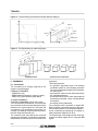
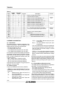
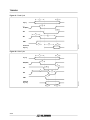
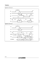
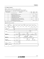
TS68483A HMOS2 ADVANCED GRAPHIC AND ALPHANUMERIC CONTROLLER September 1993 CYF0 B1 B0 CYS Y2 Y1 Y0 NC 67 66 65 64 63 62 61 CYF1 1 HVS/VS 4 68 PC/HS 5 SYNC IN D0 6 BLK D1 7 2 D2 8 3 D3 9 PIN CONNECTIONS ADM6 NC 21 49 ADM5 D13 22 48 ADM4 D14 47 ADM3 D15 23 24 46 ADM2 CS 25 45 ADM1 DS 26 44 ADM0 68483-01.EPS 50 43 20 CLK ADM7 NC 42 51 P3 19 41 Vcc Vss P2 52 40 18 P1 ADM8 D12 39 53 38 17 P0 ADM9 D11 IRQ 54 37 16 A0 ADM10 D10 36 55 35 15 A1 ADM11 D9 A2 56 34 14 A3 ADM12 D8 33 57 A4 13 32 ADM13 D7 A5 58 31 12 A6 ADM14 D6 30 ADM15 59 A7 60 11 29 10 D5 AE D4 28 The TS68483 is an advanced color graphic processor that drastically reduces the CPU software overhead for all graphic tasks in medium and high range graphic applications such as business and personal computer, industrial monitoring system and CAD systems. ORDER CODE : TS68483A 27 DESCRIPTION PLCC68 (Plastic Chip Carrier) NC . .. . . . . .. . FULLY PROGRAMMABLE TIMING GENERATOR ALPHANUMERIC AND GRAPHIC DRAWING CAPABILITY EASY TO USE AND POWERFUL COMMAND SET : - VECTOR, ARC, CIRCLE WITH DOT OR PEN CONCEPT AND PROGRAMMABLE LINE STYLE, - FLEXIBLE AREA FILL COMMAND WITH TILING PATTERN, - VERY FAST BLOCK MOVE OPERATION, - CHARACTER DRAWING COMMAND, ANY SIZE AND FONTS AVAILABLE LARGE FRAME BUFFER ADDRESSING SPACE (8 megabytes) UP TO 16 PLANES OF 2048 x 2048 UP TO 256 COLOR CAPABILITIES MASK BIT PLANES FOR GENERAL CLIPPING PURPOSE FRAME BUFFER CAN BE BUILT WITH STANDARD 64 K OR 256 K DRAM OR DUALPORT-MEMORIES (video-RAM) EXTERNAL SYNCHRONIZATION CAPABILITY ON CHIP VIDEO SHIFT REGISTERS FOR DOT RATE UP TO 18 MEGADOTS/S 8 OR 16-BIT BUS INTERFACE COMPATIBLE WITH MARKET STANDARD MICROPROCESSORS HMOS 2 TECHNOLOGY 68 - PIN PLCC PACKAGE FOR DETAILED INFORMATION, REFER TO TS68483 USER’S MANUAL R/W . . . 1/30 TS68483A PIN DESCRIPTION Name Type Function Description MICROPROCESSOR INTERFACE D (0 : 15) I/O Data Bus These sixteen bidirectional pins provide communication with either an 8 or 16-bit host microprocessor data bus. A (0 : 7) I Address Bus These eigth pins select the internal register to be accessed. The address can be latched by AE for direct connection to address/data multiplexed microprocessor busses. AE I Address Enable When TS68483 is connected to a non-multiplexed microprocessor bus, this input must be wired to VCC. For direct connection to a multiplexed microprocessor bus, the falling edge of AE latches the address on A (0 : 7) pins and the CS input. With an Intel type microprocessor, AE is connected to the processor Address Latch Enable (ALE) signal. DS I Data Strobe Active Low - In non-multiplexed bus mode, DS low enables the bidirectionnal data buffers and latches the A (0 : 7) lines on its high to low transition. Data to be written are latched on the rising edge of this signal. - In multiplexed bus mode, this signal low enables the output data buffers during a read cycle. With intel microprocessors, this pin is connected to the RD signal. R/W I Read/Write - In non-multiplexed bus mode, this signal controls the direction of data flow through the bidirectional data buffers. - In multiplexed bus mode, this signal low enables the input data buffers. The entering data are latched on its rising edge. With Intel microprocessors, this pin is connected to the WR signal. CS I Chip Select This input selects the TS68483 registers for the current bus cycle. A low level corresponds to an asserted chip select. In multiplexed mode, this input is strobed by AE. IRQ O Interrupt Request This active-low open drain output acts to interrupt the microprocessor. MEMORY INTERFACE ADM (0 : 15) I/O Address/Data Memory These multiplexed pins act as address and data bus for display memory interface. CYS O Memory Cycle Start The falling edge of this output indicates the beginning of a memory cycle. Y (0 : 2) O Memory Address These outputs provide the least significant bits of the Y logical address. B (0 : 1) O Bank Number These outputs provide the number of the memory bank to be accessed during the current memory cycle. CYF (0 : 1) O Memory Cycle Status These outputs indicate the nature of the current memory cycle (Read, Write, Refresh, Display). VIDEO INTERFACE P (0 : 3) O Video Shift Register Outputs These four pins correspond to the outputs of the internal video shift registers. PC/HS O Phase Comparator/ Horizontal Sync. This output can be programmed to provide either the phase comparator output or the horizontal sync. signal. HVS/VS O Composite or Vertical Sync. This output can be programmed to provide either the composite sync. signal or the vertical sync. signal. SYNC IN I External Sync Input This input receives an external composite sync. signal to synchronize TS68483. This input must be grounded if not used. BLK O Blanking This output provides the blanking interval information. VCC S Power Supply + 5 V Supply VSS S Ground Ground CLK I Clock Clock Input 2/30 68483-01.TBL OTHER PINS TS68483A BLOCK DIAGRAM MICROPROCESSOR INTERFACE AE, DS D [0: 15] R/W, CS 4 A [0:7] IRQ 8 16 38 R4 R0 R1 R2 R10 R3 43 CLK 2 BLK 5 PC/HS 4 HVS/VS R12 VIDEO VIDEO 3 SYNC IN TIMING V SS INTERFACE GENERATOR 52 R23 ADDRESS VCC 19 DRAWING VIDEO AND ACCESS SHI FT PROCESSOR REGISTERS P [0:3] 21 DATA 32 DATA 32 DISPLAY MEMORY LOGIC 65 CYS CYF [0:1] 3 2 B [0:1] Y [0:2] 16 68483-02.EPS 2 ADM [0:15] DISPLA Y MEMORY INTERFACE Symbol Value Unit VCC* Supply Voltage Parameter – 0.3, 7.0 V Vin* Input Voltage – 0.3, 7.0 V TA Operating Temperature Range 0, 70 °C Tstg Storage Temperature Range – 55, 150 °C PDm Max Power Dissipation 1.5 W * With respect to VSS. Stresses above those hereby listed may cause permanent damage to the device. The ratings are stress ones only and functional operation of the device at these or any conditions beyond those indicated in the operational sections of this specifications is not implied. Exposure to maximum rating conditions for extended periods may affect device reliability. Standard MOS circuits handling procedure should be used to avoid possible damage to the device. 3/30 68483-02.TBL ABSOLUTE MAXIMUM RATINGS TS68483A ELECTRICAL CHARACTERISTICS (VCC = 5.0 V ± 5 %, VSS = 0, TA = TL to TH) (unless otherwise specified) Typ. Max. 5 Unit VCC Supply Voltage 4.75 5.25 V VIL Input Low Voltage – 0.3 0.8 V VIH Input High Voltage 2 VCC V Iin Input Leakage Current 10 µA VOH Output High Voltage (IIoad = – 500 µA) VOL Output Low Voltage IIoad = 4 mA ; ADM (0 : 15), IIoad = 1 mA ; other Outputs 2.4 V 0.4 V PD Power Dissipation Cin Input Capacitance 15 pF ITSI Three State (off state) Input Current 10 µA I - GENERAL OPERATION I.1 - Introduction The TS68483 is an advanced color graphics controller chip. It is directly compatible with most popular 8 or 16-bit microprocessors. Its display memory, containingthe frame buffer and the character generators, may be assembled from standard dynamic RAM components. On-chip video shift registers and fully programmable Video Timing Generator allow the TS68483 to be used in a wide range of terminals or computer design. Additionalinformation on applications can be found in the TS68483 User’s Manual. I.2 - Typical Application Building Blocks In a typical using TS68483, a host processordrives a display unit which drives in turn a color CRT monitor. The display unit consists of four hardware building blocks : - an TS68483 advanced graphics controller, - a display memory (dynamic RAM), - a display memory interface, comprising a few TTL parts, - a CRT interface of CRT drivers. For enhanced graphics, the CRT interface may include a color look-up table circuit. For high pixel rate (over 18 Mpixels/s), the CRT interface must include high speed video shift registers. The display memory interface and organization are discussed in full details in the User’s Manual. I.3 - TS68483 Functions All the TS68483 functions are under the control of the host microprocessor via 24 directly accessible 16-bit registers. These registers are referred to by their decimal index (R0-R23) (see Figure 1). 4/30 Min. 700 mW 68483-03.TBL Parameter Figure 1 : Register Map 15 R0 R1 8 7 0 COMMAND Sx MODE C1 R2 TEXLIN R3 XOR R4 MARGIN COLOR YOR R5 H R6 FPX VIDEO TIMING GENERATOR FPY BKX BKY DWY R9 R10 BPY DWX R7 R8 COMMAND, DRAWING ATTRIBUTES C0 Sy CONF R11 R12 STATUS dy R13 R14 dx SHORT RELATIVE REGISTER Yd R15 Xd R16 DYd R17 DXd R18 RAD R19 STOP R20 Ys R21 Xs R22 DYs R23 DXs DESTINATION POINTER AUXILIARY GEOMETRIC ARGUMENTS SOURCE POINTER I.3.1 - VIDEO TIMING AND DISPLAY PROCESSOR (R4 to R10). The video timing generator is fully programmable : any popular horizontal scanning period from 20 µs to 64 µs may be freely combined with any number 68483-03.EPS Symbol TS68483A of lines per field (up to 1024). The address of the display viewport (this part of the display memory to be actually displayed on the screen) is fully programmable. The display processor provides the display dynamic RAM refresh (see video timing generator section for details). I.3.2 - DRAWING AND ACCESS COMMANDS (R0 to R3, R12 to R23). The 16 remaining registers are used to specify a comprehensive set of commands. The highly orthogonal drawing command set allows the user to ”draw” in the display memory such basic patterns as lines, arcs, polylines, polyarcs, rectangles and characters. Efficient procedures are available for either area filling and tiling or line drawing and texturing. Lines may be drawn with a PEN in order to get thick strokes. Any drawing is specified in a 13 13 2 x 2 drawing coordinate system. To access the display memory, the host microprocessor has an indirect, sequential access to any ”window”. Access commands can be used to load the character generators as well as to load or save arbitrary windows stored in the frame buffer. I.4 - Data Type Definitions PIXEL : this is the smallest color spot displayable on the CRT. PEL : a Picture Element is the coding of a PIXEL in the display memory. The TS68483 can handle 4 different PEL formats : - 4 color bits - short - 4 color bits + 1 mask bit - short masked - 8 color bits - long - 8 color bits + 1 mask bit - long masked DRAWING COORDINATES : (see Figure 2) The drawing commands are specified and computed in a 213 x 213 cyclical coordinate system. The drawing coordinates are clipped and mapped into the 211 x 211 display memory addressing space. Further clipping to the actual frame buffer size may be performed by the user designed memory interface. DISPLAY MEMORY : This is the dedicated memory to the display unit. This memory is addressed as four banks of 4-bit plane each. BIT PLANE : Each bit plane has a maximum capacity of 211 x 211 bits. A byte wide organization of each bit plane is required. MEMORY ADDRESS : (see Figure 3). In order to address one bit in the display memory, the user must specify : - A bank number (2 bits) B = 0 to 3 - A bit plane number (2 bits) Z = 0 to 3 - A Y address (11 bits) Y = 0 to 2047 - An X address (11 bits) X = 0 to 2047 MEMORY WORD : (see Figure 3) A 32-bit memory word can be either read or written during each memory cycle (8 CLK periods), one byte at a time in each bit plane in the addressed bank. The memory bandwidth is in the 6 to 8Mbytes/s range. VIEWPORT : This is any rectangular array of pels located in the display memory. FRAME BUFFER : This is the biggest viewport which can be held in the display memory. The frame buffer maps a window at the origin of the drawing coordinates. A short pel frame buffer may be located in any bank. A long pel frame buffer must be located in the ”bank 0, bank 1” pair. DISPLAY VIEWPORT : This is the viewport which is displayed on screen. MASK BIT PLANE : When masked pels are used, a mask bit plane must be associated to a frame buffer. Mask bit planes may be located in any plane of bank 3. CELL : A CELL is any pattern stored in the display memory as a rectangular array of bit mapped elements. The drawing of any CELL may be specified with a scaling factor. CHARACTER : This is a one bit per element CELL. It may be stored in any bit plane, then colored and drawn in a frame buffer by use of PRINT CHARACTER command. OBJECT : This is a one short pel per element CELL. It may be drawn or loaded in a frame buffer.A source mask bit may be associated to each element. An OBJECT may then be printed in another location by use of a PRINT OBJECT command. PEN : This is the pattern which is repeatedly drawn along the coordinates defined by either a LINE or an ARC command. The PEN may be a DOT (single pel), a CHARACTER or an OBJECT. 5/30 TS68483A Figure 2 : Cyclical Drawing Coordinates to Display Memory Mapping Y 213 BANK3 Z BANK 1 MASK M BITS Y BANK 0 0 0 2 11 2 X 13 1 3 2 4 5 6 7 LONG PELS SHORT PELS X 68483-04.EPS 211 Figure 3 : The Display Memory Addressing Space Z 32 8 8 8 8 7 Y 3 2 BANK 0 THE MEMORY WORD II - COMMANDS II.1 - Introduction The command set is strongly organized in five subset or command types. DRAWING COMMANDS : - LINEAR (line, arc) - AREA (rectangle, trapezium, polygon, polyarc) - PRINT CELL (print character, print object) ACCESS COMMANDS CONTROL COMMANDS (move cursor, abort) The commands are parametered ; this means that any command can be executed with options freely selected out of a given option set. This option set is common for any command of a given type. For example, any drawing command may be parametered for destination mask bit use. The command code also defines the command type and its parameters. A command is completely defined when a value has been set for each of its 6/30 BANK 1 BANK 2 BANK 3 0 4 BANKS OF 4 BIT PLANES EACH arguments. These arguments are : - the geometric arguments given in the drawing coordinate system for every drawing command. They are automatically mapped into the destination frame buffer ; - the parametric values are the values required by the selected parameters ; - the attribute values are the other values required by a drawing command ; colors or scaling factors for example ; - the display memory addresses. The command code is specified in register R0. Before initiating a command execution, each argument must be specified in its dedicated register : an Xd, Yd drawing coordinate pair for example, is always located in registers R14, R15. The monitoring of a command execution is done by reading the status register R12 or using the IRQ signal. 68483-05.EPS 1 X TS68483A Table 1 : Command Set Structure Drawing Mode Up to the Pen Monochrome Type Linear Group Area Drawing Bichrome Polychrome II.2 - Pointers and Geometric Arguments (see Figure 4) Pointers are used to specify main geometric arguments and display memory addresses. II.2.1 - DISPLAY MEMORY ADDRESS A bit in the display memory is addressedby : - a bank number B = 0 to 3 - a plane number Z = 0 to 3 - an X address X = 0 to 2047 - a Y addres Y = 0 to 2047 II.2.2 - DESTINATION POINTER : Registers R14 to R17 This pointer gives the coordinate (Xd, Yd) and dimension (DXd, DYd) of either a line or a window in the drawing coordinate system. These drawing coordinates are easily mapped into a PEL DISPLAY MEMORY address. (X, Y) coordinates are clipped to 11 bits in order to get the Xd, Yd destination pel addresses. A bank number Bd must be explicitly provided to address a destination frame buffer. When long pels are used, Bd must be even. When masked pels are used, the destination mask plane number Zd (implicitly in bank 3) must also be provided. II.2.3 - SOURCE POINTER : Registers R20 to R23. A source cell such as a character, a pen or an object, is addressed by the source pointer in the display memory. A source pointer specifies : - a bank number Bs = 0 to 3 Cell Access 68483-04.TBL Command Line Arc Rectangle Trapezium Polygon Polyarc Print Char Print Object Load Viewport Save Viewport Modify Viewport Move Cursor Abort Management Control - a Ys address Ys = 0 to 2047 - an Xs address ; this address is a byte address so that the 3 LSBs are not specified Xs = 0 to 255 - a cell dimension DXs, DYs - a bit plane address Zs. When a character is addressed, Zs gives the plane number into the bank Bs. When an object is addressed Zs gives the source mask plane number in the bank B3. II.2.4 - NOTES : 1. The TRAPEZIUM command makes a special use of R21. In this case, R21 holds an X1 drawing coordinate which has the same format as Xd. 2. The ARC and POLYARC commands require two extra geometric parameters (RAD and STOP). They are specified in the drawing coordinates system and stored in registers R18, R19. 3. Any drawing command may be parametered to use short incremental dimensions, DXY in register R13 instead of the standard DXd, DYd in the ”R16, R17” register pair (see Figure 5). 4. The access commands use the destination pointer location as a data buffer. The memory addresses and dimension of the access viewport are then specified in the source pointer, independentlyof the data transfer. 5. DXd, DYd and DYs may specify a negative value. In this case, they must be coded by a sign (0 = positive, 1 = negative) and an 11-bit absolute value. 7/30 TS68483A Figure 4 : Pointers 15 13 12 11 10 9 8 7 6 Bank number 13-bit positive value Zd Xd Plane number 13-bit positive value R15 S 4 DESTINATION POINTER Absolute value Bs Ys Bank number 11-bit positive value Xs Character cell plane (PCA) or source mask plane (PVS, PVF) 8-bit positive value S Byte address SOURCE POINTER DYs Sign R23 0 Pel address Zs R22 1 DXd Sign R21 2 Absolute value S R20 3 DYd Sign R17 5 Yd R14 R16 14 Bd Absolute value U DXs Underlined (cell) 11-bit positive value Reserved Don’t care Note : Sign value 68483-06.EPS Only used with TRAPEZIUM command S = 0 positive S = 1 negative + absolute value Figure 5 : Short Dimension Register R13 R13 6 5 S 3 2 1 0 S dy 8/30 4 dx 68483-07.EPS 7 II.3 - Destination Mask and Source Mask A mask bit may be associated to any pel stored in the display memory. II.3.1 - DESTINATION MASK USE (DMU) Any drawing command may be parametered for destination mask use. In this case, any destination pel cannot be modified when its mask bit is reset. TS68483A In other words : - When the destination mask use (DMU) parameter is set : - a pel may be modified when its mask bit is set - a pel cannot be modified when its mask bit is reset. - When the destination mask use (DMU) parameter is cleared : - a pel may be modified, independently of its mask bit value. This provides a very flexible clipping mechanism not restricted to rectangular windows. (See destination pointer section for destination mask bit addressing). II.3.2 - SOURCE MASK USE (SMU) A PRINT OBJECT command may be parametered for source mask use. In this case, the source mask bit associated with any source pel is read first. When its mask bit is cleared, a source pel is considered as transparent.(See source pointer section for source mask bit addressing). In other words : - When the SMU parameter is set, the color of a destination pel, mapped by a given source pel, may take this source color value only when this source bit mask is set. The destination pel keeps its own color value when the source bit mask is cleared. - When the SMU parameter is cleared, a source pel color may be mapped into destination pel color independently of the source bit mask value. The source bit mask acts as a TRANSPARENCY/OPACITY flag which is enabled by SMU. A PRINT OBJECT command may be independently parametered by both SMU and DMU. This provides a very powerful tiling, print object or move mechanism. II.4 - Drawing Attributes Figure 6 : Color Register 6 5 ODD BANK 4 3 2 1 0 EVEN BANK The general drawing attributes are the colors, the drawing mode, and the scaling factor. II.4.1. COLORS : Registers R1 and R2 Two 8-bit color values, C0 and C1, may be specified in registers R1 and R2. The low order 4-bit nibble of a color value is drawn in an even bank. The high order color nibble is drawn in an odd bank. When long pels are used, banks 0 and 1 are generally addressed as the frame buffer. When 68483-08.EPS 7 short pels are used, any bank may hold a frame buffer. In this case, the bank parity selects the color nibble used. (See destination pointer section for bank addressing). II.4.2. DRAWING MODE : Register R0 The drawing mode defines the transforms to be applied to the pels designated by the drawing commands. There are three drawing modes. II.4.3. MONOCHROME MODE Any AREA drawing command, RECTANGLE for instance, defines through its geometric arguments an active set of destination pels, that is to say a set of pels to be modified. When DMU = 1, this active set is further reduced by the masking mechanism to only these destination pels with a bit mask set. The active destination pels are then modified according to two elementary transforms coded in R0. COLOR TRANSFORM : The color value C of each active pel is modified according to one color transform selected out of four : - 00 - printed in C0 : C ← C0 - 01 - printed in C1 : C ← C1 - 10 - printed in ”transparent” : C← C - 11 - complemented : C← C This yields to a reversible marker mode. MASK BIT TRANSFORM : The destination mask bit of each active pel is modified according to one mask transform selected out of four : - 00 - reset bit mask : M ← 0 - 01 - set bit mask : M ← 1 - 10 - no modification : M ← M - 11 - complement bit mask : M ← M This scheme allows the color bits and the mask bit of any pel belonging to the active set to be modified independently. The color transform is performed first. II.4.4 - BICHROME MODE A PRINT CHARACTER command is more complex because it involves two different active sets : FOREGROUND and BACK GROUND. The FOREGROUND is that set of destination pels printed from set elements in the character cell. The BACKGROUND is made of all the remaining pels belonging to the destination window. When DMU = 1, the FOREGROUND and BACK GROUND are further reduced by the destination masking mechanism (see Figure 8). A bichrome drawing mode is defined by 4 elementary and independent transforms (see Figure 7) : - a color transform and a mask transform for the FOREGROUND PELS 9/30 TS68483A set is defined by the cell dimensions (DXs, DYs). Note : when the cell is an object, SMU is not programmable and is implicitly set. A calculated coordinate is active when the rotated LSB linear texture bit in (R3) is set. - a color transform and a mask transform for the BACKGROUND PELS II4.5 - POLYCHROME MODE A print object command defines a source window through the source pointer : When SMU = 0, any pel of this window is active, mapped and clipped to the destination window dimension. When SMU = 1, only pels which have a source mask bit set are active, mapped and clipped to the destination window dimension. In both cases, when DMU = 1, the active source pels are further reducedby the destinationmasking mechanism. Both mask transformsmust be programmed at ”NO MODIFICATION” for correct operations (see Figure 7). II.4.6 - THE LINEAR DRAWING COMMAND CASE A LINE or ARC drawing command may be executed in any drawing mode depending on the PEN. When the pen is a DOT, this pel is printed at each active coordinate according to monochrome mode. When the pen is a CELL, this cell is printed at each active coordinate. In the bichrome mode when the cell is a character, and in the polychrome mode when the cell is an object. For each active coordinates, the active destination Figure 7 : Drawing Mode Register R0 BACKGROUND 7 6 5 FOREGROUND 4 3 2 1 0 REGISTER R0 COLOR MASK 7 6 X X 1 0 5 X : : : : C C C C ← ← ← ← C0 C1 C C 00 01 10 11 : : : : M M M M ← ← ← ← 0 1 M M FOREGROUND 4 X 3 2 1 0 X X X X Monochrome X X X X Bichrome 1 0 Polychrome 68483-09.EPS BACKGROUND 00 01 10 11 Figure 8 : Print Character Command DE STINATION WINDOW CHA RACTER CE LL Y Y SET ELEMENT = 1 (Xd, Yd) DXd > 0 (Xs, Ys) DXs > 0 X X DYs < 0 DYd < 0 ELEMENT =0 MASK BIT = 1 MASK BIT = 0 MAPPED CH ARA CTER WIND OW MAP PED Y Y CHA RA CTER WINDOW (Xd, Yd) (Xd, Yd) X X FOREGROUND BACKGROUND DMU = 0 10/30 DMU = 1 68483-10.EPS NO MODIFICATION TS68483A II.4.7 - SCALING FACTOR AND CELL MAPPING : (see Figures 9 and 10) Figure 9 : Scaling Factor 15 14 13 12 11 10 8 SY SX or SY S 0 0 0 1 1 0 0 1 0 2 1 1 1 1 15 0 0 0 0 16 68483-11.EPS SX R1 9 Any cell may be printed with a scaling factor. This scaling factor is an integer pair Sx, Sy = 1 to 16. This scaling factor is interpreted with the PRINT CHARACTER, PRINT OBJECT and LINEAR commands when the pen is a cell. The AREA or ACCESS or LINEAR (DOT) commands are never scaled. The LINEAR (PEN) command should be used with a scaling factor of 1 because the pen is clipped at DXs, DYs. The scaling factor is first applied to the source cell before mapping and drawing. The drawing and mapping is processed with sign bit of DYd and DYs values (see Figure 10). Notes : - DXs is always positive - The DYs sign mirrors the cell - DXd must be positive with a PRINT CELL command - DXd and DYd may get any sign with a LINEAR DRAWING command. If a pen is used, these signs are then irrelevant to the pen drawing. The pen is mapped with positive increment values. Figure 10 : Cell Mapping versus DYd, DYs SIGN Y Y Y Xd, Yd DXd > 0 X DYd < 0 DYs > 0 DYd > 0 X Xs, Ys DXs > 0 X Xd, Yd Y DXd > 0 Y Y Xd, Yd DXd > 0 X DXs > 0 X DYs < 0 DYd < 0 DYd > 0 68483-12.EPS Xs, Ys X Xd, Yd DXd > 0 11/30 TS68483A II.5 - Command Set Overwiew Figure 11 Dyd DXd II.5.1 - LINEAR DRAWING LINE (Xd, Yd, DXd, DYd). ARC (Xd, Yd, DXd, DYd, RAD, STOP). The curve may be drawn with any pen and with any linear texture (register R3). For each set of computed coordinates, R3 is right rotated and the pen is printed when the shifted bit is set. II.5.2 - AREA DRAWING - RECT (Xd, Yd, DXd, DYd) - TRAPEZIUM (Xd, Yd, DXd, DYd, X1) - POLYGON (Xd, Yd, DXd, DYd) - POLYARC (Xd, Yd, DXd, DYd, RAD, STOP) Either RECT or TRAPEZIUM allows to draw directly all the pels inside the boundary. Any other closed boundaries may be filled by a 3-step process : 1. The mask bits inside a boundary box must be reset by a RECT command. 2. Asequence of mixed POLYGONand POLYARC commands describing the closed boundarysets the mask bits of the pels inside this boundary. 3. Th is a re a ma y th en be p a in t e d b y a RECTANGLE command defined for a bounding box, with destination masking. It may also be tiled by use of a PRINT CELL command. Note : the mask bit of any pel lying on the boundary itself is not guaranteed to be set by step 2. II.5.3 - PRINT CELL COMMANDS PRINT CELL (Xd, Yd, DXd, DYd ; Xs, Ys, DXs, DYs). The cell addressed by Xs, Ys, DXs, DYs is scaled then printed at location Xd, Yd and clipped at the dXd, dYd dimensions. When dXd, dYd is much larger than DXs, DYs the command may be parametered for repeat drawing. These commands may also be parametered for destination mask use. Further more the PRINT OBJECT command may be parametered for source mask use. These commands have a wide range of applications : text drawing, area tiling, print or move objects, scale and move viewports. 12/30 68483-12.EPS PEN Note : an underlined cell is drawn when the MSB of R23 is set. II.5.4 - ACCESS COMMANDS - LOAD VIEWPORT (Xs, Ys, DXs, DYs) - SAVE VIEWPORT (Xs, Ys, DXs, DYs) - MODIFY VIEWPORT (Xs, Ys, DXs, DYs) These commands provide sequential access to a viewport in a frame buffer from the microprocessor data base. Data are transferred to/from the display memory, word sequentially. The R14 to R17 registers are used as a two memory word FIFO (memory word is 8 short pels, i.e. 4 bytes). The source pointer (R20-R23) is used to address the viewport for all access commands. When long pels are used, the command must be executed once more when the bank number in R20 has been updated. II.5.5 - COMMAND EXECUTION Each on-chip 16-bit register has four addresses. One address is used for plain read or write. The other addresses are used to initiate command execution automatically on completion of the register access. This scheme allows the command code and its arguments to be loaded or modified in any other. An incremental line drawing command, for example, may be executed again and again with successive incremental dimensions and whithout need to reload the command code itself. As soon as a command execution is started, the FREE bit is cleared in the STATUS register. This bit is automatically set when the execution is completed. The commands are generally executed only during retrace intervals. However full time execution is possible when either the display is disabled or video RAM components are used. II.5.6 - STATUS REGISTER (see Figure 12) This register holds four read-only status bits : - FREE : this status bit is set when no execution is pending - VS : vertical synchronization state - SEM : this status bit is set when the FIFO memory word is inacessible to the microprocessor during a viewport transfer - NSEM : this status bit is set when the FIFO memory word is accessible to the microprocessor during a viewport transfer. Each of these status bits is maskable. The masked status bits are NORed to the IRQ output pin. TS68483A Figure 12 : Status Register 15 14 13 12 11 10 9 8 STATUS REGISTER R12 MASK NSEM NSEM MASK SEM SEM READ ONLY MASK VS VS MASK FREE FREE 9 8 R12 68483-14.EPS 15 14 13 12 11 10 IRQ III - MICROPROCESSOR INTERFACE III.1 - Introduction The TS68483 is directly compatible with any popu- lar 8 or 16-bit host microprocessor ; either Motorola type (6809, 68008, 68000) or Intel type (8088, 8086). The host microprocessor has direct access to any of the twenty four 16-bit on-chip registers through the microprocessor interface pins : - D(0:15) : 16 bidirectional data pins. - A(0:7) : 8 address inputs - AE, DS, R/ W, CS : 4 control inputs. The twenty four registers are mapped in the host addressing space as 256 byte addresses (see Figure 13) - A(1:5) select one out of 24 registers. - A0 selects the low order byte (A0 = 1) or the high order byte (A0 = 0) of the selected register. - A(6:7) provide the command execution condition. The host microprocessor bus may be either 8 or 16-bits wide and may be address/data multiplexed or not. The two flags MB and BW in the CONFIGURATION register R10 allow the data bus size and multiplexed/non-mutiplexed organization to be specified (see Table 2). Figure 13 : On-chip Address and Byte Packing A7 A6 A5 A4 A3 A2 A1 A0 High/Low Byte Address 16-bit Register ADDRESS Execution Condition 9 8 7 6 5 A0 = 0 4 3 2 1 0 Byte Addressing 68483-15.EPS 15 14 13 12 11 10 A0 = 1 Table 2 : MPU Selection Non Mux Mux Conf. Reg. BW MB TS68483 Pins AE DS R/W AO A (1 : 7) D (8 : 15) D (8 : 15) 16-bit (68000) 0 0 1 UDS or LDS R/W O A (1 : 7) 8-bit (68008) 1 0 1 DS R/W AO A (1 : 7) D (0 : 7) 16-bit (8086) 0 1 ALE RD WR O AD (1 : 7) AD (8 : 15) 8-bit (8088) 1 1 ALE RD WR ADO AD (1 : 7) AD (0 : 7) 13/30 68483-05.TBL Type of MPU Bus TS68483A Figure 14 : Interface with TS68000/68008MPU TS68000 TS68483 D [8:15] D [8:15] 29 VCC D [0:7] D [0:7] 25 CS A [1:7] A [1:7] 28 R/W 26 UDS or LDS D [8:15] 29 VCC D [0:7] D [0:7] 25 CS A [1:7] A [1:7] 28 R/W 26 DS 37 TS68483 68483-16.EPS TS68008 Figure 15 : Interface with 8086/8008 MPU 8086 TS68483 8 AD [8:15] 8 D [8:15] 29 ALE D [0:7] 25 CS A [1:7] 26 RD 28 WR D [8:15] 29 ALE D [0:7] 25 CS A [1:7] 26 RD 28 WR 8 AD [0:7] 7 A [1:7] 37 8088 TS68483 8 8 8 AD [0:7] 37 AD0 14/30 68483-17.EPS 7 TS68483A III.2 - Hardware Recommendations (see Figures 21, 22, 23 and 24) A0-PIN : 1. When using a 16-bit data bus, the A0 input pin must be grounded. No single byte access can be performed. 2. In order to conform with the high byte/low byte on-chip packing, the A0 input pin must be inverted when using an 8-bit bus Intel type microprocessor (8088 for example). A(1:7), D(0:7), D(8:15) pins : 1. With any 8-bit data bus, the D(0:7) and D(8:15) pins must be paired in order to demultiplex the low order data bytes and the high order data bytes. 2. When using address/data multiplexed bus, the D(0:7) pins are paired with A(0:7) in order to demultiplex data from address. AE, DS, R/ W, CS : See pin description. III.3 - SOFTWARE RECOMMENDATIONS 1. The CONFIGURATION register R10 must be first initialized. The BW 15 flag is interpreted by the bus interface to recognize an 8-bit/16-bit data bus. The MB and BW 15 flags are used to decide when to initiate a command execution. 2. Each register byte has 4 addresses in the microp rocessor memory map. These 4 addresses differ only by A(6:7). This scheme allows a 68008 programmer to read or write any d at a type (byte, word, lo ng word) and automatically initiate or not a command execution at the end of this transfer. The transfer lasts one, two or four bus cycles. A 68000 programmer is restricted to only word and long word data types (see Table 3). Address A7 0 0 1 1 Notes : A6 0 1 0 1 Execution Condition no Exec Exec after a Bus Cycle Exec After 2 Bus Cycles Exec after 4 Bus Cycles Data Type Transfer 8-bit Data Bus 16-bit Data Bus Any Type Any Type 1 Byte 1 Word 1 Word 1 Long Word 1 Long Word* ILLEGAL Word transfer must respect word boundary. Long word transfer must respect long word boundary. * Not available with 8088 MPU type. IV - THE VIDEO TIMING GENERATOR RAM REFRESH AND DISPLAY PROCESS IV.1 - Introduction The Video Timing Generator is completelysynchronous with the CLK input, which provides a pixel shift frequency (up to 18MHz). The Video Timing Generator : - delivers the blanking signal (BLK), the horizontal (HS) and vertical (VS) synchronization signals on respective output pins, - schedules the memory time allocated to the display process, dynamic RAM refresh and command execution, - is fully programmable - can be synchronized with an external composite video sync signal connected to the SYNC IN input. These two parameters are internally programmed : - Horizontal sync pulse duration = 7 cycles - Vertical sync pulse duration = 2.5 lines. IV.2 - Scan Parameters (see Table 4 and Figure 26) IV.2.1 - TIMING UNITS The time unit of any vertical parameter is the scan line. The time unit of any horizontal parameter is the memory cycle, which is 8 periods of the CLK input signal. IV.2.3 - PORCH AND MARGIN COLOR During the porch interval, the programmable margin color is displayed on the P(0:3) outputs. The display process may be disabled by setting DPD flag. This will be interpreted as a porch extension. IV.2.2 - BLANKING INTERVAL The blanking interval starts : - at the leading edge of the vertical sync pulse. Vertical blanking interval actual duration is 2.5 lines more than the programmed value. - two cycles before the leading edge of the horizontal sync pulse. The actual horizontal blanking interval duration is 3 cycles more than the programmed value. Note : During the programmed blanking interval, the video output pins P(0:3) are forced low. Note : By process, the value of the block porch must be strictly above 0. 15/30 68483-06.TBL Table 3 : Command Execution Condition TS68483A IV.2.4. MEMORY TIME SHARING (see Figure 16) Figure 16 : Video Programming 2H TL 7T HORIZONTAL BLKX 2T Horizontal Minimum Number of Cycles BKX FFX DWX H 4 3 3 19 1T 3T BKX FPX FRONT PORCH DWX DISPLAY BACK PORCH BLKY FRONT PORCH FPY BLANKING MARGIN DISPLAY DISPLAY DWY BACK PORCH = BPY - 25 25 Lines BLANKING BKY FPY DWY BPY BKY The Video Timing Generator allocates memory cycles to either the display process, RAM refresh or command execution. In this respect, the scan lines per field are split between : the DWY displayable lines. When VRE = 0, Video RAMs are not used. The DWY x DWX cycles in the display interval are allocated to the display process when it is enabled (DPD = 0). When the display process is disabled, these cycles are allocated as for non displayable lines. When VRE = 1, one cycle per display line is allocated to the display process. Other cycles are allocated as for non displayable lines. The last period of the BLKX signal may be used to load the internal video RAM shift register. - the non displayable lines. In one out of nine non displayable lines, DWX cycles are allocated to the refresh process when it is enabled (RFD = 0). - In Float cycle, an external X address must be provided. The Y address is still provided on 16/30 1 1 3 1 ADM(0:7) and Y(0:2), while ADM(8:15) are in high impedance state. IV.2.5. COMMAND ACCESS RATIO This allocation scheme leaves about 50% of the memory bandwidth for command access when programming a standard TV scan. This ratio drops to the 30% range when a better monitor is in use (32µs out of 43µs displayable per line, 360 lines out of 390 for a 60Hz field rate). The higher resolution means more memory accesses in order to edit a given percentage of the screen area. In this case Video RAMs are very helpful to keep 90% of the memory bandwidth available for command access. IV.3 - Display Process The Video Timing Generator allocates memory cycles to the Display Processor in order to read the Display Viewport from memory. The Display Viewport upper left corner address is programmable through DIB, YOR and XOR. The display viewport dimensions are related to the display interval of DWY lines by DWX cycles per field. 68483-18.EPS Vertical Minimum Number of Lines TS68483A IV.3.1 - Y ADDRESSES When INE = 0, the fields are not interlaced. The Y Display Viewport address is initialized with YOR at the first displayable line then decremented by 1 at each scan line. The Display Viewport is thus DWY pel high. When INE = 1, the fields are interlaced. The Y Display Viewport address is initialized as shown in the table below. It is then decremented by two at each scan line. The viewport is thus 2 x DWY pel high. Even Field Odd Field Yor Even Yor Yor + 1 Yor Odd Yor – 1 Yor Y display Viewport address initialization when INE = 1 IV.3.2 - X ADDRESSES AND MODX FLAGS The X Display Viewport address is initialized with XOR at the first displayable cycle of each displayable line. It is then incremented at each subsequent cycle according to MODX flags. MODX1 MODX0 X INCR Video Shift Memory Register Cycle Type 0 0 +1 Internal Read 0 1 +1 External Dummy Read 1 0 +2 External Dummy Read 1 1 External Float In internal mode, the Display Viewport is 8. DWX pel wide. The on-chip video shift register are used. In Dummy read, the memory is read but the on-chip video shift registers are not loaded, instead they retain their margin color. External video shift registers are presumed to be loaded by either 8 pels or 16 pels per cycle according to the programmed increment value. In Float cycle, an external X address must be provided. The Y address is still provided on ADM(0:7) and Y(0:2), while ADM(8:15) are in high impedance state. Note : See Memory Organization and Memory Timing for further details on the memory cycles. IV.3.3 - THE VIDEO RAM CASE (VRE = 1) In this case, the last cycle of the horizontal blanking interval is systematically allocated to the display process for DWY scan lines per field. This cycle bears the scan line address, the bank number and the X address which is always XOR. MODX must be programmed to use external shift register (Dummy read). IV.3.4 - PAN AND TILT The host can tilt or pan the Display Viewport through the frame buffer by modifying YOR or XOR arguments. Panning is performed on 8 pel boundaries. IV.4. Dynamic Ram Refresh No memory cycles are explicity allocated to the RAM refresh when RFD = 1. When VRE = 0 and DPD = 0, the Display Process is supposed to be able to over-refresh dynamic components. This can be done by careful logical to component address mapping. During the remaining non displayable lines, the Display Viewport address continues to be incremented : Y address on each line according to INE, X address initialized by XOR then incremented according to MODX. This Display viewport address is allowed to address the memory for DWX cycles in only one line out of nine for refresh purposes. When VRE = 1 or DPD = 1, any line is processed as a non displayable line with respect to the refresh process. IV.5. Configuration and External Synchronization The R10 register holds eight configuration flags. Six of these flags are dedicated to the Video Timing Generator. - SSP : this flag selects the synchronization output pin configuration : - NPC, NHVS, NBLK : these three flags invert the PC/HS, HVS/VS and BLK outputs respectively. (Ex. : When NBLK = 1 blanking is active high). The SYNC IN input pin provides an external composite synchronization signal input from which a Vertical Sync In (VSI) signal is extracted. The SYNC IN signal is sampled on-chip at CLK frequency. Its rising sampled edge is compared to the leading edge of HS. A PC comparison signal is externally available (see SSP and NPC flags). VSIE : this flag enablesVSI to reset the internal line count. HSIE : this flag enables the rising edge of SYNC IN to actdirectlyon the Video Timing Generator.When the leading edge of HS does not match at 1 clock period a rising edge of SYNC IN, one extended cycle is performed (nine clock periods instead of eight). Flag SSP = 1 SSP = 0 Output Pins PC/HS HVS/VS HS VS PC HVS 17/30 TS68483A Table 4 DWY INE BKY FPY BPY H FPX BKX DWX XOR YOR DIB MODX MC RFD DPD VRE Number of Bits 10 1 5 5 8 6 4 4 7 8 11 2 2 4 1 1 1 Mininmum Values 1 1 1 3 19 3 4 3 Register R9 R8 R8 R7 R6 R6 R8 R8 R7 R4 R5 R4 R9 R4 R7 R7 R8 Description Number of Display lines per Field Interlace Enable when INE = 1 Number of Lines in Vertical Blanking – 2.5 Number of Lines in Vertical Front Porch Number of Lines in Vertical Back Porch + 2.5 Number of Double Cycles per Line Number of Cycles in Horizontal Front Porch Number of Cycles in Horizontal Blanking – 3 Number of Cycles of the Display Window X, Y, and bank logical address in the display memory of the display viewport upper left corner Selection of the X Addressing Mode Margin Color RAM Refresh Disable when RFD = 1 Display Process Disable when DPD = 1 Video RAM Enable When VRE = 1 Function Vertical Scan Horizontal Scan Display Process Memory Time Sharing Note : one cycle = 8 periods of CLK Clock V. MEMORY ORGANIZATION V.1 - Introduction The display memory is logically organized as four banks of 4-bit planes. Thus a bit address in the display memory is given by the quadruplet : - B = bank number, from 0 to 3 - Z = plane number, from 0 to 3 - X = bit address into the plane, from 0 to 2047 - Y = bit address into the plane, from 0 to 2047. In one memory cycle (8 CLK periods), the controller can access a memory word. This 32-bit memory word holds one byte from each plane in a given bank. In order to address this memory word, the controller supplies : - B(0:1) : binary value of the bank number - X(3:10) : binary value of the word address - Y(0:10) : binary value of the word address. Z and X(0:2) are not supplied. They give only a bit address in a memory word. V.2 - Memory Cycles 24 pins are dedicated to the memory interface. - ADM(0:15) : these 16 bidirectional pins are multiplexed three times during a memory cycle (see Figure 25) : TA : address period. Output of the X(3:11) and Y(3:11) address TO : even data period. The even Z bytes are either input or output. T1 : odd data period. The odd Z bytes are either input or output. 18/30 Y(0:2) : three LSB Y address output pins (nonmultiplexed) B(0:1) : two bank address output pins (nonmultiplexed) - CYS : Cycle start strobe output (non-multiplexed). CYS is at CLK/8 frequency. A CYS pulse is delivered only when a command, display or refresh cycle is performed. - CYF(0:1) : Two cycle status outputs (non-multiplexed). Four cycle types are defined : Command Read, Command Write, RAM Refresh, Display Access. Because several options may be selected for RAM refresh and display access by the MODX and VRE flags (see Video Timing Section), there are more than four memory cycle types (see Figure 25 and Table 5). V.3 - Display Memory Desing Overview The display memory implementation is application dependant. The basic parameters are : - the number of pixels to be displayed Nx.Ny - the number of bits per pel - the vertical scanning frequency, which must be picked in the 40Hz to 80Hz range (non interlaced) or in the 60Hz to 80Hz range (interlaced). This yields a rough estimate of the pixel frequency. When the pixel frequency is in the 15 to 18MHz range and 4 bits per pixel or least are required, the on-chip video registers and standard dynamicRAM components may be used. When higher pixel rates 68483-07.TBL Name TS68483A or up to 8 bits per pixel are required, the designer must provide external shift registers. Video RAM components may also be considered. - RAD and CAD Enable signals to the Mapper. V.3.1 - FRAME BUFFER (see Table 6) A byte wide organization of each bit plane is required. Obviously a bit plane must contain the Display Viewport size. A straight organization implements only one bit plane per block. In either case, the user must design : - A memory block. This is the hardware memory building block. It includes the video shift registers if on-chip VSR cannot be used. It implies a RAM component choice. - An Address Mapper, which maps the logical address into hardware address : block selection, Row Address (RAD), Column Address (CAD). - A memory cycle controller. This controller monitors the CYF and CYS output pins from TS68483 and block address from the Mapper. It provides : - The CLK signal to the TS68483 and a shift clock SCLK when external video shift registers are used - RAS, CAS, OE, R/ W signals to the memory blocks It may be cost effective to implement several bit planes per block. Two basic schemes may be used : - One block, one Z : several bit planes, belonging to different banks, but addressed by the same Z, share a given block. There is little time constraint if any. - One block, two Z : two bit planes, belonging to the same bank share a given block. In this case, this block must be accessed twice during a memory cycle. This can be solved by two successive page mode accesses. Table 5 : Memory Cycle Types CYF1 CYF0 1 0 1 1 0 1 0 0 Function Modx Flags 1 0 Multiplexed ADM Cycle Type TA TO T1 Command Read Y,X Z0,Z2 Z1,Z3 Read Command Write Y,X Z0,Z2 Z1,Z3 Write Z0,Z2 Z1,Z3 Read Dummy Read + 1 Display 0 0 0 1 Y,X Y,X Refresh 1 1 0 1 Y,X Y,Hi-Z Dummy Read + 2 Float X 68483-08.TBL Output Pins Refresh : dummy read cycle is performed. 16 k x 8 32 k x 8 64 k x 8 256 k x 8 One Block-one Bit Planes Typical Block Size 512 x 256 512 x 512 1024 x 512 2048 x 1024 One Block-two Bit Planes 256 x 256 512 x 256 512 x 512 68483-09.TBL Table 6 : Frame Buffer Organization COMPONENTS : 64K BITS : 16K x 4 or 64K x 1 256K BITS : 32K x 8, 64K x 4, 256K x 1 VIDEO RAM : 64K x 1, 64K x 4 Table 7 : The Multiplexing Scheme HIGHER BYTES ADMS Multiplexed Pins 15 14 13 12 11 10 9 X 8 TA : Address Period 10 T0 : Even Z Byte Period 7 Z=2 0 3 T1 : Odd Z Byte Period 7 Z=3 0 LOWER BYTES 7 10 6 5 4 Y 3 2 1 0 3 T0 : Even Z Byte Period 7 Z=0 0 T1 : Odd Z Byte Period 7 Z=1 0 19/30 68483-10.TBL ADMS Multiplexed Pins TA : Address Period TS68483A Figure 17 : One Block - One Z ADM [8:15] ADM [0:7] 8 8 8 (T1) 8 (T0) 8 (T1) 8 (T0) B0 B2 B3 Z3 Z2 Z1 Z0 68483-19.EPS B1 Figure 18 : One Block - Two Z ADM [8:15] ADM [0:7] 8 8 Z3 Z2 Z1 68483-20.EPS (T0. T1) = Page mode Z0 Figure 19 7 6 5 4 3 2 1 0 0 1 Z A MEMORY WORD 2 68483-21.EPS 3 X [0:2] V.3.2 - MASKING PLANES Masking planes are very useful for general purpose area filling or clipping. It may be practical to use one or two planes smaller than the color bit plane if they cyclically cover a frame buffer. The masking planes must be in bank 3. V.3.3 - OBJECTS AND CHARACTERS Objects may be located in unused parts of the frame buffer. Character generators can be implemented in any plane of any bank. They can also be implemented in ROM. In this case, plane Z = 1 or 3 offer relaxed 20/30 access time requirements. V.4 - Examples Figure 20. gives the schematic for a 512 x 384 non interlaced application. A CLK signal in the 15 to 18 MHz range should produce a 50 to 60Hz refresh rate. The on-chip video shift registers may be used if no more than four bits per pixel are required. One 64 K x 8 memory block may be implemented using either eight 64 K x 1 or two 64 K x 4 components. One memory block holds two 512 x 384 color bit planes. TS68483A Figure 20 : Memory Organization for 512 x 384 Application ADM [8:15] B [0:1] Y [0:2] 2 ADM [0:7] 3 Y X CYCLE CONTROLLER LATCH BANK ENABLE CAD0 ADSEL MUX DATA Z1/Z3 DATA Z0/Z2 8 64K x 8 64K x 8 MEMORY ADDRESS RAS CAS OE WE BANK 0 64K x 8 64K x 8 Z1 Z1 + 2 BANK 3 384 64K x 8 MEMORY BLOCK 128 One Block through Page Mode SPARED AREA 68483-22.EPS 512 VI - TIMING DIAGRAM VI.1 - Microprocessor Interface TS68483 has an eight bit address bus and a sixteen bit data bus. Little external logic is needed to adapt bus control signals from most of the common multiplexed or non-multiplexed bus microprocessors. Indent Number 1 2 3 4 5 6 7 8 9 10 11 12 Parameter Address Set up Time from CS Data Strobe Width (high) AS Set up Time from CS Data Strobe Width-low (read cycle) Address Hold Time from DS Data Access time from CS (read cycle) DS Inactive to High Impedance State (read cycle) R/W Set up Time from DS DS Width-low (write cycle) CS Set up Time from DS Active (write Cycle) Data in Set up Time from DS active (write cycle) Data in Hold Time from DS Inactive (write cycle) Min. 0 65 0 160 0 10 20 80 0 10 15 Max. 130 80 Unit ns ns ns ns ns ns ns ns ns ns ns ns 21/30 68483-11.TBL UNMUX MODE Microprocessor Interface Timing : A(0:7), D(0:15), AE, DS, CS, R/ W VCC = 5.0V ± 5%, TA = TL to TH , CL = 100pF on D(0:15) Reference levels : VIL = 0.8V and VIH = 2V on all inputs, VOL = 0.4V and VOH = 2.4V on all outputs TS68483A Figure 21 : Read Cycle 1 5 A [0:7] 3 AS (MPU) 3 CS 2 4 DS R/W 6 7 68483-23.EPS 8 DATA OUT D [0:15] Figure 22 : Write Cycle 1 5 A [0:7] 3 AS (MPU) 3 10 CS 2 9 DS 8 DATA IN D [0:15] 11 22/30 12 68483-24.EPS R/W TS68483A MUX MODE Microprocessor Interface Timing : A (0 : 7), D (0 : 15), AE, DS, CS, R/W VCC = 5.0V ± 5 %, TA = TL to TH, CL = 10 pF on D (0 : 15) Reference Levels : VIL = 0.8V and VIH = 2V on All Inputs, VOL = 0.4V and VOH = 2.4V on All Outputs Parameter Min. Max. Unit 1 AE Width High 90 ns 2 Address Set up Time to AE Inactive 55 ns 3 Address and CS Hold Time to AE Inactive 55 ns 4 CS Set up Time to AE Inactive 40 ns 5 DS and R/W High 150 ns 6 DS Width-low (read) 240 ns 7 R/W Width-low (write) 110 8 Data Access Time From DS (read) ns 210 ns 9 Data in Set up time from R/W Inactive (write) 150 10 DS Inactive to High Impedance State (read) 10 ns 11 Data in Hold Time from R/W Inactive (write) 30 ns 12 AE Inactive to DS Active 20 ns 13 AE Inactive to R/W Active 20 ns 14 DS Inactive to AE Active 10 ns 15 R/W Inactive to AE Active 10 ns 16 R/W Inactive to Next Address Valid 100 ns 17 DS Inactive to Next Address Active 100 ns 18 Data in Set up Time from R/W Active (fast write cycle) 10 ns 100 ns 23/30 68483-12.TBL Indent Number TS68483A Figure 23 : Read Cycle 1 AE 4 3 CS 14 6 12 DS 5 16 2 3 A/D 8 10 68483-25.EPS R/W D OUT A Figure 24 : Write Cycle 1 AE 4 3 CS DS 13 17 2 3 9 A/D A 18 FAST WRITE 24/30 A 11 D IN 11 D IN 68483-26.EPS R/W 15 7 5 TS68483A VI.2 - Memory Interface ADM (0 : 15), B (0 : 1), CYF (0 : 1), Y (0 : 2), CYS VCC = 5.0V ± 5 %, TA = T L to TH, CLK Duty Cycle = 50 %, Period T Reference Levels : VIL = 0.8V and VIH = 2V, VOL = 0.4V and VOH = 2.4V Parameter Min. Max. 55 166 Unit 1 TCLK Clock Period 2 Memory Cycle Time (T = 8 X TCLK) ns 3 Output Delay Time from CLK 4 Output Data HI-Z Time from CLK 5 Output Hold Time from CLK 10 ns 6 Input Data Hold Time from CLK (read cycle) 6 ns 7 Input Data Set up Time from CLK (read cycle) 10 8 Input Data HI-Z Time from CLK ns 35 ns 35 ns ns ns TCLK 68483-13.TBL Indent Number Note : All timing is referenced to the rising edge of CLK (see timing diagram 3). Figure 25 : Memory Interface 1 CLK 3 2 5 CYS 3 B [0:1] CYF [0:1] 4 Y [0:2] 3 3 4 ADM [0:15] WRITE CYCLE A (X, Y) D (EVEN Z) 5 ADM [0:15] READ CYCLE A (X, Y) D (ODD Z) 7 5 7 D (EVEN Z) D (ODD Z) 6 ADM [0:15] DUMMY READ CYCLE 6 8 8 A (X, Y) 4 ADM [0:7] A (Y) 68483-27.EPS DISPLAY FLOATING CYCLE ADM [8:15] 25/30 TS68483A VI.3 - Video Interface P0, P1, P2, P3, BLK, HVS/VS, PC/HS VCC = 5.0V ± 5 %, T A = TL to TH, CLK duty cycle = 50% Reference levels : VIL = 0.8V and VIH = 2V, VOL = 0.4V and VOH = 2.4V, CL = 50pF Parameter Min. Max. Unit 166 ns 30 ns 1 TCLK : CLK Period 55 2 CLK High Pulse Width 23 3 Output Delay from CLK Rising Edge 4 CLK Low Pulse Width 23 ns 5 Output Hold Time 10 ns ns 68483-14.TBL Indent Number Figure 26 : Timing Diagram 1 CLK 2 4 3 68483-28.EPS P [0:3] BLK HVS/VS PC/HS 5 Figure 27 : Synchronization Signal Outputs 2HT HS (NPC = 1) 7T 2T Horizontal Sync 7T 1T BLKX MARGIN P [0:3] BKX DWX 25LINES 25LINES Example : BKY+FPY+DWY+BPY = 525 HVS (NHVS = 1) EVEN FIELD : BKY + FPY + DWY + BPY LINES EVEN FIELD BLK (NBLK = 1) Interlaced BKY VS FPY DWY 25LINES BPY 25LINES Example : BKY+FPY+DWY+BPY = 312 for 625 Lines HVS (NHVS = 1) ODD FIELD : BKY + FPY + DWY - BPY 12 LINES EVEN FIELD BLK (NBLK = 1) BKY 26/30 Non Interlaced FPY DWY BPY 68483-29.EPS VS MARGIN FPX TS68483A VII - TABLES VII.1 - Register Map and Command Table Figure 28 15 14 13 12 11 10 9 8 7 6 5 4 SX R1 2 1 0 MODE COMMAND R0 3 SY R2 Odd Bank C0 Even Bank Odd Bank C1 Even Bank TEXLIN R3 XOR R4 0 DIB1 DIB0 MARGIN COLOR YOR R5 H R6 BFY DWX R7 FPX R8 R9 0 R10 BW BKX DPD RFD VRE INE FPY BKY MODX1 MODX0 MB VSIE HSIE NBLK NHVS NPC DWY SYNC R11 R12 STATUS DY S R14 Bd Yd R15 Zd Xd R16 S S DYd R17 S DXd R18 ACW RAD R19 XY R20 QF1 QF0 STOP Bs R21 DX Ys Zs Xs R22 S DYs R23 U DXs : Don’t care : Used or not, according to the command 27/30 68483-30.EPS SOURCE POINTER DEST. POINTER R13 28/30 C E L L A R E A 0 X X X X : XFT = 1 : the source pointer is auto-incremented,X direction first. XFT = 0 : the source pointer is auto-incremented or auto-decremented,Y direction first. : The cell is stepped and repeatedthrough the destination window. When REP = 0, only one cell is printed. REP = 1 68483-31.EPS LEFT = 1 : The cursor is mved left (right if LEF = 0). DWN = 1 : The cursor is mved down (up if DWN = 0). SMU = 1 : The source mask is used. : The source pointer is not auto-incremented,X direction first. X X X X X X X X X X X X X X X X X X X X X X X X X X X X X X X X X X X X X X X X X X X X X X X X X X X X X X X X X X X X X X X X X X X YF YF XF XF Yd Yd + DYd Xd + DXd Ys Yd + DYd Xs Xd Xd + DXd Ys Ys Xs Yd Yd Xd + DXd Xs Yd Xd + DXd YF 1T 1T 4T 3T 3T 2T 2T 2T 4T 15T Yd + DYd 10T Xd + DXd XF Yd + DYd 10T Xd + DXd Xd + DXd 4T 10T CELL + 4T DOT CELL DOT CELL 10T 4T 5T 6T MEMORY WORD MEMORY WORD AREA MEMORY 4T WORD (see Note 1) 4T 15T CELL + 10T 15T 5T 5T Yd + DYd 10T Yd + DYd Xd + DXd Xd Yd + DYd Xd + DXd EXECUTIONTIME END COMMAND CURSOR POSITION INIT Per LOOP Note 1 : For FLL and FLA commands, add 4T and 8T respectively per pel belonging to the boundary. Command execution is performed only out of the display periods. - DXd, DYd and DYs are signed values. - DXs is always positive. - T = memory cycle = 8 CLK clock periods. - For execution time, add to the short pel loop in the table : 1T if DMU = 1 1T if SMU = 1 2T if long pen are used 2T if mask printing is required. Note : With PVF command, any pel with color different from 0 has its source mask implicity set and used. In other words, pels with color value 0 are transparent. X X X X X X X X X X X X X X X X X X X X X X X X X X X X X X X X X X X X X X X X X X X X X X X X X X INC = 1 X X INC = 0 X X X X X X X X X : Initate a polygon or polyarc filling. This parameter should be reset only when the second drawing is not identical to the first one (Ex : first polygon, the polyarc). X X X X X X X X X X X X X X X X BEG = 1 1 0 SRU SRU INC INC INC SRU SRU SRU SRU SRU SRU SRU SRU SRU SRU X X X X X X POINTERS R13 R18 R19 R14 R15 R16 R17 R20 R21 R22 R23 : POL = 0 : the pen is the character cell addressed by the source ponter. POL = 1 : the pen is the object associated with a source mask addressed by the source pointer. 1 0 0 DWN 0 1 0 1 1 SP SP SP SP SP SP SP SP SRU SRU R3 ARGUMENTS R2 R1 R0 PEN = 1 1 0 0 1 1 0 0 DMU DMU DMU DMU DMU DMU DMU DMU DMU DMU SP SP 0 : The pen is a single pel. 1 0 LEF 0 XFT XFT XFT REP REP REP BEG BEG 0 0 0 PEN DMU DMU 1 : Short relative register use (R13). 1 0 1 0 0 0 0 0 SMU 1 0 0 0 PEN 2 PARAMETERS 3 PEN =0 1 0 0 0 0 1 1 1 1 0 1 1 1 1 1 POL 0 POL 0 4 SRU = 1 1 1 1 1 1 1 1 1 0 0 0 1 0 0 1 1 1 0 0 5 : Short pel ; long pel when SP = 0. 1 1 1 1 1 1 1 1 1 0 1 1 1 0 0 0 0 6 CODE SP = 1 BRT NOP NO OPERATION ABORT LRM CDM UP-DOWN MOVE DIAGONALMOVE RMV UDM MODIFY VIEWPORT LEFT-RIGHT MOVE SAV LDV SAVEVIEWPORT LOAD VIEWPORT PVF 1 PVS PRINTOBJECT 1 FLA PCA 0 PRINTCHARACTER 0 1 POLYARC REC RECTANGLE 0 0 FLL PAR PEN ARC POLYGON DAR DOT ARC 0 0 TRA PLI PEN LINE 7 TRAPEZIUM DLI DOT LINE DMU = 1 : Destination mask use. CONTROL CURSOR ACCESS D R A W I N G L I N E P A R MNEM TYPE TS68483A VII.2. Command Table TS68483A Figure 29 : Typical Application HOST MICROPROCESSOR SYSTEM MEMORY 8 OR 16 BITS 4 SYNC CRT INTERFACE SYNC TS68483 CRT CONTROLLER R G MONITOR B 68483-32.EPS DISPLAY MEMORY INTERFACE DISPLAY MEMORY 29/30 TS68483A PACKAGE MECHANICAL DATA 68 PINS - PLASTIC CHIP CARRIER B M M1 1 68 61 17 53 18 52 19 51 F 60 M 2 26 27 34 35 36 E e M1 9 10 44 43 d1 A G (Seating Plane Coplanarity) A B D d1 d2 E e F G M M1 Min. 25.02 24.13 4.2 Millimeters Typ. Max. 25.27 24.33 5.08 Min. 0.985 0.950 0.165 2.54 0.56 22.61 D Inches Typ. Max. 0.995 0.958 0.200 0.100 0.022 23.62 0.890 1.27 0.38 0.930 0.050 0.015 0.101 1.27 1.14 0.004 0.050 0.045 Information furnished is believed to be accurate and reliable. However, SGS-THOMSON Microelectronics assumes no responsibility for the consequences of use of such information nor for any infringement of patents or other rights of third parties which may result from its use. No licence is granted by implication or otherwise under any patent or patent rights of SGS-THOMSON Microelectronics. Specifications mentioned in this publication are subject to change without notice. This publication supersedes and replaces all information previously supplied. SGS-THOMSON Microelectronics products are not authorized for use as critical components in life support devices or systems without express written approval of SGS-THOMSON Microelectronics. 1994 SGS-THOMSON Microelectronics - All Rights Reserved Purchase of I2C Components of SGS-THOMSON Microelectronics, conveys a license under the Philips I2C Patent. Rights to use these components in a I2C system, is granted provided that the system conforms to the I2C Standard Specifications as defined by Philips. SGS-THOMSON Microelectronics GROUP OF COMPANIES Australia - Brazil - China - France - Germany - Hong Kong - Italy - Japan - Korea - Malaysia - Malta - Morocco The Netherlands - Singapore - Spain - Sweden - Switzerland - Taiwan - Thailand - United Kingdom - U.S.A. 30/30 PLCC68.TBL Dimensions PMPLCC68.EPS d2