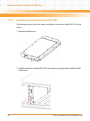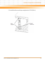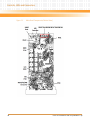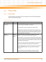
1
Embedded Computing for Business-Critical ContinuityTM iVPX7225 Installation and Use P/N: 6806800S11B November 2013 CopyRight© 2013 Emerson Network Power All rights reserved. Trademarks Emerson, Business-Critical Continuity, Emerson Network Power and the Emerson Network Power logo are trademarks and service marks of Emerson Electric Co. © 2011 Emerson Electric Co. All other product or service names are the property of their respective owners. Intel® is a trademark or registered trademark of Intel Corporation or its subsidiaries in the United States and other countries. Java™ and all other Java-based marks are trademarks or registered trademarks of Sun Microsystems, Inc. in the U.S. and other countries. Microsoft®, Windows® and Windows Me® are registered trademarks of Microsoft Corporation; and Windows XP™ is a trademark of Microsoft Corporation. PICMG®, CompactPCI®, AdvancedTCA™ and the PICMG, CompactPCI and AdvancedTCA logos are registered trademarks of the PCI Industrial Computer Manufacturers Group. UNIX® is a registered trademark of The Open Group in the United States and other countries. Notice While reasonable efforts have been made to assure the accuracy of this document, Emerson assumes no liability resulting from any omissions in this document, or from the use of the information obtained therein. Emerson reserves the right to revise this document and to make changes from time to time in the content hereof without obligation of Emerson to notify any person of such revision or changes. Electronic versions of this material may be read online, downloaded for personal use, or referenced in another document as a URL to a Emerson website. The text itself may not be published commercially in print or electronic form, edited, translated, or otherwise altered without the permission of Emerson, It is possible that this publication may contain reference to or information about Emerson products (machines and programs), programming, or services that are not available in your country. Such references or information must not be construed to mean that Emerson intends to announce such Emerson products, programming, or services in your country. Limited and Restricted Rights Legend If the documentation contained herein is supplied, directly or indirectly, to the U.S. Government, the following notice shall apply unless otherwise agreed to in writing by Emerson. Use, duplication, or disclosure by the Government is subject to restrictions as set forth in subparagraph (b)(3) of the Rights in Technical Data clause at DFARS 252.227-7013 (Nov. 1995) and of the Rights in Noncommercial Computer Software and Documentation clause at DFARS 252.227-7014 (Jun. 1995). Contact Address Emerson Network Power - Embedded Computing Lilienthalstr. 15 85579 Neubiberg/Munich Germany Contents About this Manual . . . . . . . . . . . . . . . . . . . . . . . . . . . . . . . . . . . . . . . . . . . . . . . . . . . . . . . . . . . . . . . . . . . . . . . 15 1 Introduction . . . . . . . . . . . . . . . . . . . . . . . . . . . . . . . . . . . . . . . . . . . . . . . . . . . . . . . . . . . . . . . . . . . . . . . . . 23 1.1 1.2 1.3 1.4 1.5 2 Hardware Preparation and Installation . . . . . . . . . . . . . . . . . . . . . . . . . . . . . . . . . . . . . . . . . . . . . . . . . 31 2.1 2.2 2.3 2.4 2.5 3 Features . . . . . . . . . . . . . . . . . . . . . . . . . . . . . . . . . . . . . . . . . . . . . . . . . . . . . . . . . . . . . . . . . . . . . . . . . . . 23 Standard Compliances . . . . . . . . . . . . . . . . . . . . . . . . . . . . . . . . . . . . . . . . . . . . . . . . . . . . . . . . . . . . . . 25 Mechanical Data . . . . . . . . . . . . . . . . . . . . . . . . . . . . . . . . . . . . . . . . . . . . . . . . . . . . . . . . . . . . . . . . . . . 26 1.3.1 Air Cooled. . . . . . . . . . . . . . . . . . . . . . . . . . . . . . . . . . . . . . . . . . . . . . . . . . . . . . . . . . . . . . . . . . . 26 1.3.2 Conduction Cooled. . . . . . . . . . . . . . . . . . . . . . . . . . . . . . . . . . . . . . . . . . . . . . . . . . . . . . . . . . . 27 Ordering Information . . . . . . . . . . . . . . . . . . . . . . . . . . . . . . . . . . . . . . . . . . . . . . . . . . . . . . . . . . . . . . . 27 1.4.1 Supported Board Models . . . . . . . . . . . . . . . . . . . . . . . . . . . . . . . . . . . . . . . . . . . . . . . . . . . . . . 27 Product Identification . . . . . . . . . . . . . . . . . . . . . . . . . . . . . . . . . . . . . . . . . . . . . . . . . . . . . . . . . . . . . . . 29 Overview . . . . . . . . . . . . . . . . . . . . . . . . . . . . . . . . . . . . . . . . . . . . . . . . . . . . . . . . . . . . . . . . . . . . . . . . . . 31 Unpacking and Inspecting the Board . . . . . . . . . . . . . . . . . . . . . . . . . . . . . . . . . . . . . . . . . . . . . . . . . . 31 Environmental and Power Requirements . . . . . . . . . . . . . . . . . . . . . . . . . . . . . . . . . . . . . . . . . . . . . . 32 2.3.1 Environmental Requirements. . . . . . . . . . . . . . . . . . . . . . . . . . . . . . . . . . . . . . . . . . . . . . . . . . 32 2.3.2 Power Requirements . . . . . . . . . . . . . . . . . . . . . . . . . . . . . . . . . . . . . . . . . . . . . . . . . . . . . . . . . 34 Installing the Accessories . . . . . . . . . . . . . . . . . . . . . . . . . . . . . . . . . . . . . . . . . . . . . . . . . . . . . . . . . . . . 34 2.4.1 Installing the XMC on Air Cooled Board . . . . . . . . . . . . . . . . . . . . . . . . . . . . . . . . . . . . . . . . . 36 2.4.2 Installing the XMC on Conduction Cooled Board . . . . . . . . . . . . . . . . . . . . . . . . . . . . . . . . . 37 2.4.3 Rear Transition Module . . . . . . . . . . . . . . . . . . . . . . . . . . . . . . . . . . . . . . . . . . . . . . . . . . . . . . . 40 Installing and Removing the Board . . . . . . . . . . . . . . . . . . . . . . . . . . . . . . . . . . . . . . . . . . . . . . . . . . . . 41 2.5.1 Installing Air Cooled iVPX7225. . . . . . . . . . . . . . . . . . . . . . . . . . . . . . . . . . . . . . . . . . . . . . . . . 43 2.5.2 Installing Conduction Cooled iVPX7225. . . . . . . . . . . . . . . . . . . . . . . . . . . . . . . . . . . . . . . . . 44 Controls, LEDs and Connectors. . . . . . . . . . . . . . . . . . . . . . . . . . . . . . . . . . . . . . . . . . . . . . . . . . . . . . . . . 47 3.1 3.2 3.3 3.4 Board Layout . . . . . . . . . . . . . . . . . . . . . . . . . . . . . . . . . . . . . . . . . . . . . . . . . . . . . . . . . . . . . . . . . . . . . . . 47 Planar LEDs . . . . . . . . . . . . . . . . . . . . . . . . . . . . . . . . . . . . . . . . . . . . . . . . . . . . . . . . . . . . . . . . . . . . . . . . 49 3.2.1 Debug LEDs . . . . . . . . . . . . . . . . . . . . . . . . . . . . . . . . . . . . . . . . . . . . . . . . . . . . . . . . . . . . . . . . . 49 3.2.2 POST Code LEDs . . . . . . . . . . . . . . . . . . . . . . . . . . . . . . . . . . . . . . . . . . . . . . . . . . . . . . . . . . . . . 50 Front Panel Connectors and LEDs . . . . . . . . . . . . . . . . . . . . . . . . . . . . . . . . . . . . . . . . . . . . . . . . . . . . . 51 Backplane Connectors . . . . . . . . . . . . . . . . . . . . . . . . . . . . . . . . . . . . . . . . . . . . . . . . . . . . . . . . . . . . . . 53 3.4.1 P0 Connector . . . . . . . . . . . . . . . . . . . . . . . . . . . . . . . . . . . . . . . . . . . . . . . . . . . . . . . . . . . . . . . . 53 iVPX7225 Installation and Use (6806800S11B) 3 Contents Contents 3.5 3.6 4 Functional Description . . . . . . . . . . . . . . . . . . . . . . . . . . . . . . . . . . . . . . . . . . . . . . . . . . . . . . . . . . . . . . . . 61 4.1 4.2 4.3 4.4 4.5 4.6 4.7 4.8 4.9 4.10 4.11 4.12 4.13 4.14 4.15 4.16 4.17 4.18 4.19 4.20 4.21 5 Block Diagram . . . . . . . . . . . . . . . . . . . . . . . . . . . . . . . . . . . . . . . . . . . . . . . . . . . . . . . . . . . . . . . . . . . . . 61 Processor . . . . . . . . . . . . . . . . . . . . . . . . . . . . . . . . . . . . . . . . . . . . . . . . . . . . . . . . . . . . . . . . . . . . . . . . . . 62 Chipset . . . . . . . . . . . . . . . . . . . . . . . . . . . . . . . . . . . . . . . . . . . . . . . . . . . . . . . . . . . . . . . . . . . . . . . . . . . . 62 System Memory . . . . . . . . . . . . . . . . . . . . . . . . . . . . . . . . . . . . . . . . . . . . . . . . . . . . . . . . . . . . . . . . . . . . 62 Ethernet Interfaces . . . . . . . . . . . . . . . . . . . . . . . . . . . . . . . . . . . . . . . . . . . . . . . . . . . . . . . . . . . . . . . . . 63 PCI Express . . . . . . . . . . . . . . . . . . . . . . . . . . . . . . . . . . . . . . . . . . . . . . . . . . . . . . . . . . . . . . . . . . . . . . . . 64 SATA . . . . . . . . . . . . . . . . . . . . . . . . . . . . . . . . . . . . . . . . . . . . . . . . . . . . . . . . . . . . . . . . . . . . . . . . . . . . . . 64 USB . . . . . . . . . . . . . . . . . . . . . . . . . . . . . . . . . . . . . . . . . . . . . . . . . . . . . . . . . . . . . . . . . . . . . . . . . . . . . . . 65 Serial COM . . . . . . . . . . . . . . . . . . . . . . . . . . . . . . . . . . . . . . . . . . . . . . . . . . . . . . . . . . . . . . . . . . . . . . . . . 65 Video . . . . . . . . . . . . . . . . . . . . . . . . . . . . . . . . . . . . . . . . . . . . . . . . . . . . . . . . . . . . . . . . . . . . . . . . . . . . . 65 4.10.1 Rear DisplayPort . . . . . . . . . . . . . . . . . . . . . . . . . . . . . . . . . . . . . . . . . . . . . . . . . . . . . . . . . . . . . 65 4.10.2 VGA . . . . . . . . . . . . . . . . . . . . . . . . . . . . . . . . . . . . . . . . . . . . . . . . . . . . . . . . . . . . . . . . . . . . . . . . 65 GPIO . . . . . . . . . . . . . . . . . . . . . . . . . . . . . . . . . . . . . . . . . . . . . . . . . . . . . . . . . . . . . . . . . . . . . . . . . . . . . . 66 SMBus . . . . . . . . . . . . . . . . . . . . . . . . . . . . . . . . . . . . . . . . . . . . . . . . . . . . . . . . . . . . . . . . . . . . . . . . . . . . 66 Boot Flash . . . . . . . . . . . . . . . . . . . . . . . . . . . . . . . . . . . . . . . . . . . . . . . . . . . . . . . . . . . . . . . . . . . . . . . . . 66 NAND Flash . . . . . . . . . . . . . . . . . . . . . . . . . . . . . . . . . . . . . . . . . . . . . . . . . . . . . . . . . . . . . . . . . . . . . . . . 66 FRAM . . . . . . . . . . . . . . . . . . . . . . . . . . . . . . . . . . . . . . . . . . . . . . . . . . . . . . . . . . . . . . . . . . . . . . . . . . . . . 66 Trusted Platform Module . . . . . . . . . . . . . . . . . . . . . . . . . . . . . . . . . . . . . . . . . . . . . . . . . . . . . . . . . . . . 67 Real Time Clock . . . . . . . . . . . . . . . . . . . . . . . . . . . . . . . . . . . . . . . . . . . . . . . . . . . . . . . . . . . . . . . . . . . . 67 Watchdog Timer . . . . . . . . . . . . . . . . . . . . . . . . . . . . . . . . . . . . . . . . . . . . . . . . . . . . . . . . . . . . . . . . . . . 67 XMC Support . . . . . . . . . . . . . . . . . . . . . . . . . . . . . . . . . . . . . . . . . . . . . . . . . . . . . . . . . . . . . . . . . . . . . . 67 Boot Firmware . . . . . . . . . . . . . . . . . . . . . . . . . . . . . . . . . . . . . . . . . . . . . . . . . . . . . . . . . . . . . . . . . . . . . 68 Operating System . . . . . . . . . . . . . . . . . . . . . . . . . . . . . . . . . . . . . . . . . . . . . . . . . . . . . . . . . . . . . . . . . . 68 BIOS . . . . . . . . . . . . . . . . . . . . . . . . . . . . . . . . . . . . . . . . . . . . . . . . . . . . . . . . . . . . . . . . . . . . . . . . . . . . . . . . 69 5.1 5.2 5.3 4 3.4.2 P1 Connector . . . . . . . . . . . . . . . . . . . . . . . . . . . . . . . . . . . . . . . . . . . . . . . . . . . . . . . . . . . . . . . . 54 3.4.3 P2 Connector . . . . . . . . . . . . . . . . . . . . . . . . . . . . . . . . . . . . . . . . . . . . . . . . . . . . . . . . . . . . . . . . 55 XMC Connector . . . . . . . . . . . . . . . . . . . . . . . . . . . . . . . . . . . . . . . . . . . . . . . . . . . . . . . . . . . . . . . . . . . . 56 Switches . . . . . . . . . . . . . . . . . . . . . . . . . . . . . . . . . . . . . . . . . . . . . . . . . . . . . . . . . . . . . . . . . . . . . . . . . . 59 Overview . . . . . . . . . . . . . . . . . . . . . . . . . . . . . . . . . . . . . . . . . . . . . . . . . . . . . . . . . . . . . . . . . . . . . . . . . . 69 Processor Initialization . . . . . . . . . . . . . . . . . . . . . . . . . . . . . . . . . . . . . . . . . . . . . . . . . . . . . . . . . . . . . . 69 Memory Initialization . . . . . . . . . . . . . . . . . . . . . . . . . . . . . . . . . . . . . . . . . . . . . . . . . . . . . . . . . . . . . . . 69 iVPX7225 Installation and Use (6806800S11B) Contents 5.3.1 Serial Presence Detect (SPD) . . . . . . . . . . . . . . . . . . . . . . . . . . . . . . . . . . . . . . . . . . . . . . . . . . 70 5.3.2 Memory Test . . . . . . . . . . . . . . . . . . . . . . . . . . . . . . . . . . . . . . . . . . . . . . . . . . . . . . . . . . . . . . . . 70 5.3.3 ECC Support . . . . . . . . . . . . . . . . . . . . . . . . . . . . . . . . . . . . . . . . . . . . . . . . . . . . . . . . . . . . . . . . 70 5.3.4 DDR3 Refresh Rate . . . . . . . . . . . . . . . . . . . . . . . . . . . . . . . . . . . . . . . . . . . . . . . . . . . . . . . . . . . 70 5.4 Reset . . . . . . . . . . . . . . . . . . . . . . . . . . . . . . . . . . . . . . . . . . . . . . . . . . . . . . . . . . . . . . . . . . . . . . . . . . . . . 70 5.5 PCIe Initialization . . . . . . . . . . . . . . . . . . . . . . . . . . . . . . . . . . . . . . . . . . . . . . . . . . . . . . . . . . . . . . . . . . . 70 5.6 I/O Device Configuration . . . . . . . . . . . . . . . . . . . . . . . . . . . . . . . . . . . . . . . . . . . . . . . . . . . . . . . . . . . . 71 5.7 Boot Options . . . . . . . . . . . . . . . . . . . . . . . . . . . . . . . . . . . . . . . . . . . . . . . . . . . . . . . . . . . . . . . . . . . . . . . 71 5.8 I/O Redirection . . . . . . . . . . . . . . . . . . . . . . . . . . . . . . . . . . . . . . . . . . . . . . . . . . . . . . . . . . . . . . . . . . . . 72 5.9 BIOS Setup Layout . . . . . . . . . . . . . . . . . . . . . . . . . . . . . . . . . . . . . . . . . . . . . . . . . . . . . . . . . . . . . . . . . . 72 5.9.1 Main Menu . . . . . . . . . . . . . . . . . . . . . . . . . . . . . . . . . . . . . . . . . . . . . . . . . . . . . . . . . . . . . . . . . . 73 5.9.2 Boot Features. . . . . . . . . . . . . . . . . . . . . . . . . . . . . . . . . . . . . . . . . . . . . . . . . . . . . . . . . . . . . . . . 74 5.9.3 Advanced Menu . . . . . . . . . . . . . . . . . . . . . . . . . . . . . . . . . . . . . . . . . . . . . . . . . . . . . . . . . . . . . 76 5.9.4 Processor Configuration . . . . . . . . . . . . . . . . . . . . . . . . . . . . . . . . . . . . . . . . . . . . . . . . . . . . . . 78 5.9.5 Processor Power Management. . . . . . . . . . . . . . . . . . . . . . . . . . . . . . . . . . . . . . . . . . . . . . . . . 80 5.9.6 HDD Configuration . . . . . . . . . . . . . . . . . . . . . . . . . . . . . . . . . . . . . . . . . . . . . . . . . . . . . . . . . . . 82 5.9.7 Memory Configuration . . . . . . . . . . . . . . . . . . . . . . . . . . . . . . . . . . . . . . . . . . . . . . . . . . . . . . . 84 5.9.8 System Agent (SA) Configuration . . . . . . . . . . . . . . . . . . . . . . . . . . . . . . . . . . . . . . . . . . . . . . 85 5.9.9 Graphics Configuration . . . . . . . . . . . . . . . . . . . . . . . . . . . . . . . . . . . . . . . . . . . . . . . . . . . . . . . 86 5.9.10 IGD Configuration. . . . . . . . . . . . . . . . . . . . . . . . . . . . . . . . . . . . . . . . . . . . . . . . . . . . . . . . . . . . 87 5.9.11 PEG Port Configuration . . . . . . . . . . . . . . . . . . . . . . . . . . . . . . . . . . . . . . . . . . . . . . . . . . . . . . . 88 5.9.12 South Bridge Configuration . . . . . . . . . . . . . . . . . . . . . . . . . . . . . . . . . . . . . . . . . . . . . . . . . . . 89 5.9.13 SB USB Configuration . . . . . . . . . . . . . . . . . . . . . . . . . . . . . . . . . . . . . . . . . . . . . . . . . . . . . . . . . 90 5.9.14 SB Security Configuration . . . . . . . . . . . . . . . . . . . . . . . . . . . . . . . . . . . . . . . . . . . . . . . . . . . . . 90 5.9.15 Network Configuration . . . . . . . . . . . . . . . . . . . . . . . . . . . . . . . . . . . . . . . . . . . . . . . . . . . . . . . 92 5.9.16 SIO Configuration . . . . . . . . . . . . . . . . . . . . . . . . . . . . . . . . . . . . . . . . . . . . . . . . . . . . . . . . . . . . 93 5.9.17 ME Configuration . . . . . . . . . . . . . . . . . . . . . . . . . . . . . . . . . . . . . . . . . . . . . . . . . . . . . . . . . . . . 94 5.9.18 Thermal Configuration. . . . . . . . . . . . . . . . . . . . . . . . . . . . . . . . . . . . . . . . . . . . . . . . . . . . . . . . 95 5.9.19 Platform Thermal Configuration . . . . . . . . . . . . . . . . . . . . . . . . . . . . . . . . . . . . . . . . . . . . . . . 96 5.9.20 Intel® Rapid Start Technology . . . . . . . . . . . . . . . . . . . . . . . . . . . . . . . . . . . . . . . . . . . . . . . . . 98 5.9.21 iVPX7225 Menu. . . . . . . . . . . . . . . . . . . . . . . . . . . . . . . . . . . . . . . . . . . . . . . . . . . . . . . . . . . . . . 99 5.9.22 Security Menu . . . . . . . . . . . . . . . . . . . . . . . . . . . . . . . . . . . . . . . . . . . . . . . . . . . . . . . . . . . . . . 100 5.9.23 TPM Configuration . . . . . . . . . . . . . . . . . . . . . . . . . . . . . . . . . . . . . . . . . . . . . . . . . . . . . . . . . . 102 5.9.24 Boot Menu . . . . . . . . . . . . . . . . . . . . . . . . . . . . . . . . . . . . . . . . . . . . . . . . . . . . . . . . . . . . . . . . . 103 5.9.25 Exit Menu . . . . . . . . . . . . . . . . . . . . . . . . . . . . . . . . . . . . . . . . . . . . . . . . . . . . . . . . . . . . . . . . . . 104 5.10 BIOS POST Codes . . . . . . . . . . . . . . . . . . . . . . . . . . . . . . . . . . . . . . . . . . . . . . . . . . . . . . . . . . . . . . . . . . 105 iVPX7225 Installation and Use (6806800S11B) 5 Contents Contents 5.11 Memory POST Codes . . . . . . . . . . . . . . . . . . . . . . . . . . . . . . . . . . . . . . . . . . . . . . . . . . . . . . . . . . . . . . . 107 6 Maps and Registers . . . . . . . . . . . . . . . . . . . . . . . . . . . . . . . . . . . . . . . . . . . . . . . . . . . . . . . . . . . . . . . . . . 109 6.1 6.2 7 FPGA Registers . . . . . . . . . . . . . . . . . . . . . . . . . . . . . . . . . . . . . . . . . . . . . . . . . . . . . . . . . . . . . . . . . . . . . . 111 7.1 6 Flash Map . . . . . . . . . . . . . . . . . . . . . . . . . . . . . . . . . . . . . . . . . . . . . . . . . . . . . . . . . . . . . . . . . . . . . . . . 109 BIOS Memory Map . . . . . . . . . . . . . . . . . . . . . . . . . . . . . . . . . . . . . . . . . . . . . . . . . . . . . . . . . . . . . . . . . 109 FPGA Registers . . . . . . . . . . . . . . . . . . . . . . . . . . . . . . . . . . . . . . . . . . . . . . . . . . . . . . . . . . . . . . . . . . . . 111 7.1.1 Blade Revision Register - 0x00 . . . . . . . . . . . . . . . . . . . . . . . . . . . . . . . . . . . . . . . . . . . . . . . . 111 7.1.2 FPGA Major Revision Register - 0x01 . . . . . . . . . . . . . . . . . . . . . . . . . . . . . . . . . . . . . . . . . . . 112 7.1.3 FPGA Minor Revision Register - 0x02. . . . . . . . . . . . . . . . . . . . . . . . . . . . . . . . . . . . . . . . . . . 112 7.1.4 FPGA Date Code Register - 0x04 . . . . . . . . . . . . . . . . . . . . . . . . . . . . . . . . . . . . . . . . . . . . . . 112 7.1.5 FPGA Month Code Register - 0x05. . . . . . . . . . . . . . . . . . . . . . . . . . . . . . . . . . . . . . . . . . . . . 113 7.1.6 FPGA Year Code Register 0x06 . . . . . . . . . . . . . . . . . . . . . . . . . . . . . . . . . . . . . . . . . . . . . . . . 113 7.1.7 FPGA Reset Cause Register - 0x08 . . . . . . . . . . . . . . . . . . . . . . . . . . . . . . . . . . . . . . . . . . . . . 113 7.1.8 Watchdog Control Register - 0x09 . . . . . . . . . . . . . . . . . . . . . . . . . . . . . . . . . . . . . . . . . . . . 115 7.1.9 Watchdog Re-trigger Register - 0x0A . . . . . . . . . . . . . . . . . . . . . . . . . . . . . . . . . . . . . . . . . . 116 7.1.10 Memory Write Protect Register - 0x0B . . . . . . . . . . . . . . . . . . . . . . . . . . . . . . . . . . . . . . . . . 116 7.1.11 Power Good Status 1 Register - 0x0C . . . . . . . . . . . . . . . . . . . . . . . . . . . . . . . . . . . . . . . . . . 118 7.1.12 Power Good Status 2 Register - 0x0D . . . . . . . . . . . . . . . . . . . . . . . . . . . . . . . . . . . . . . . . . . 119 7.1.13 System Status Register - 0x0E. . . . . . . . . . . . . . . . . . . . . . . . . . . . . . . . . . . . . . . . . . . . . . . . . 119 7.1.14 Misc 1 Control and Status Register - 0x10 . . . . . . . . . . . . . . . . . . . . . . . . . . . . . . . . . . . . . . 120 7.1.15 Misc 2 Control and Status Register - 0x11 . . . . . . . . . . . . . . . . . . . . . . . . . . . . . . . . . . . . . . 121 7.1.16 DIP Switch Status Register - 0x14 . . . . . . . . . . . . . . . . . . . . . . . . . . . . . . . . . . . . . . . . . . . . . 122 7.1.17 Misc 3 Control and Status Register - 0x15 . . . . . . . . . . . . . . . . . . . . . . . . . . . . . . . . . . . . . . 123 7.1.18 Boot Control and Status 1 Register - 0x16 . . . . . . . . . . . . . . . . . . . . . . . . . . . . . . . . . . . . . . 124 7.1.19 Boot Control and Status 2 Register - 0x17 . . . . . . . . . . . . . . . . . . . . . . . . . . . . . . . . . . . . . . 125 7.1.20 PCIE Switch Control and Status 1 Register - 0x18 . . . . . . . . . . . . . . . . . . . . . . . . . . . . . . . . 126 7.1.21 PCIE Switch Control and Status 2 Register - 0x19 . . . . . . . . . . . . . . . . . . . . . . . . . . . . . . . . 127 7.1.22 CPU Package Temperature Reading Register - 0x1C . . . . . . . . . . . . . . . . . . . . . . . . . . . . . 128 7.1.23 IPMC Inlet Temperature Sensor Status Register - 0x1D . . . . . . . . . . . . . . . . . . . . . . . . . . . 128 7.1.24 IPMC Outlet Temperature Sensor Status Register - 0x1E . . . . . . . . . . . . . . . . . . . . . . . . . 129 7.1.25 FRAM Page Access Register - 0x20. . . . . . . . . . . . . . . . . . . . . . . . . . . . . . . . . . . . . . . . . . . . . 129 7.1.26 VPX System Register - 0x24 . . . . . . . . . . . . . . . . . . . . . . . . . . . . . . . . . . . . . . . . . . . . . . . . . . 130 iVPX7225 Installation and Use (6806800S11B) Contents 7.2 7.3 A 7.1.27 POST Code Latch Register - 0x28 . . . . . . . . . . . . . . . . . . . . . . . . . . . . . . . . . . . . . . . . . . . . . . 131 7.1.28 BIOS Boot Status Register - 0x2C . . . . . . . . . . . . . . . . . . . . . . . . . . . . . . . . . . . . . . . . . . . . . . 131 FPGA SIO . . . . . . . . . . . . . . . . . . . . . . . . . . . . . . . . . . . . . . . . . . . . . . . . . . . . . . . . . . . . . . . . . . . . . . . . . 131 7.2.1 Super IO Configuration Registers. . . . . . . . . . . . . . . . . . . . . . . . . . . . . . . . . . . . . . . . . . . . . . 132 7.2.1.1 Entering the Configuration State . . . . . . . . . . . . . . . . . . . . . . . . . . . . . . . . . . . . . 132 7.2.1.2 Exiting the Configuration State . . . . . . . . . . . . . . . . . . . . . . . . . . . . . . . . . . . . . . 132 7.2.1.3 Configuration Mode . . . . . . . . . . . . . . . . . . . . . . . . . . . . . . . . . . . . . . . . . . . . . . . . 133 7.2.1.4 Super IO Configuration Registers . . . . . . . . . . . . . . . . . . . . . . . . . . . . . . . . . . . . 133 7.2.1.5 Global Control Configuration Registers . . . . . . . . . . . . . . . . . . . . . . . . . . . . . . . 133 7.2.1.6 Logical Device Configuration Registers . . . . . . . . . . . . . . . . . . . . . . . . . . . . . . . 136 UART Register Overview . . . . . . . . . . . . . . . . . . . . . . . . . . . . . . . . . . . . . . . . . . . . . . . . . . . . . . . . . . . . 139 7.3.1 UART Registers DLAB=0. . . . . . . . . . . . . . . . . . . . . . . . . . . . . . . . . . . . . . . . . . . . . . . . . . . . . . 139 7.3.1.1 Received Buffer Register (RBR) . . . . . . . . . . . . . . . . . . . . . . . . . . . . . . . . . . . . . . 140 7.3.1.2 Transmitter Holding Register (THR) . . . . . . . . . . . . . . . . . . . . . . . . . . . . . . . . . . 140 7.3.1.3 Interrupt Enable Register (IER) . . . . . . . . . . . . . . . . . . . . . . . . . . . . . . . . . . . . . . . 141 7.3.1.4 Interrupt Identification Register (IIR) . . . . . . . . . . . . . . . . . . . . . . . . . . . . . . . . . 142 7.3.1.5 FIFO Control Register (FCR) . . . . . . . . . . . . . . . . . . . . . . . . . . . . . . . . . . . . . . . . . 144 7.3.1.6 Line Control Register (LCR) . . . . . . . . . . . . . . . . . . . . . . . . . . . . . . . . . . . . . . . . . . 145 7.3.1.7 Modem Control Register (MCR) . . . . . . . . . . . . . . . . . . . . . . . . . . . . . . . . . . . . . . 147 7.3.1.8 Line Status Register (LSR) . . . . . . . . . . . . . . . . . . . . . . . . . . . . . . . . . . . . . . . . . . . 148 7.3.1.9 Modem Status Register (MSR) . . . . . . . . . . . . . . . . . . . . . . . . . . . . . . . . . . . . . . . 152 7.3.1.10 Scratch Register (SCR) . . . . . . . . . . . . . . . . . . . . . . . . . . . . . . . . . . . . . . . . . . . . . . 155 7.3.1.11 Programmable Baud Rate Generator . . . . . . . . . . . . . . . . . . . . . . . . . . . . . . . . . 155 Related Documentation . . . . . . . . . . . . . . . . . . . . . . . . . . . . . . . . . . . . . . . . . . . . . . . . . . . . . . . . . . . . . . 157 A.1 A.2 Emerson Network Power - Embedded Computing Documents . . . . . . . . . . . . . . . . . . . . . . . . . 157 Related Specifications . . . . . . . . . . . . . . . . . . . . . . . . . . . . . . . . . . . . . . . . . . . . . . . . . . . . . . . . . . . . . . 158 Safety Notes . . . . . . . . . . . . . . . . . . . . . . . . . . . . . . . . . . . . . . . . . . . . . . . . . . . . . . . . . . . . . . . . . . . . . . . . . . . . 160 Sicherheitshinweise . . . . . . . . . . . . . . . . . . . . . . . . . . . . . . . . . . . . . . . . . . . . . . . . . . . . . . . . . . . . . . . . . . . . . . . 8 iVPX7225 Installation and Use (6806800S11B) 7 Contents Contents 8 iVPX7225 Installation and Use (6806800S11B) List of Tables Table 1-1 Table 1-2 Table 1-3 Table 1-4 Table 1-5 Table 2-1 Table 2-2 Table 3-1 Table 3-2 Table 3-3 Table 3-4 Table 3-5 Table 3-6 Table 3-7 Table 3-8 Table 3-9 Table 6-1 Table 6-2 Table 7-1 Table 7-2 Table 7-3 Table 7-4 Table 7-5 Table 7-6 Table 7-7 Table 7-8 Table 7-9 Table 7-10 Table 7-11 Table 7-12 Table 7-13 Table 7-14 Table 7-15 Table 7-16 Table 7-17 Table 7-18 Key Features of the iVPX7225 . . . . . . . . . . . . . . . . . . . . . . . . . . . . . . . . . . . . . . . . . . . . . . . . . 23 Standard Compliances . . . . . . . . . . . . . . . . . . . . . . . . . . . . . . . . . . . . . . . . . . . . . . . . . . . . . . . 25 Mechanical Data . . . . . . . . . . . . . . . . . . . . . . . . . . . . . . . . . . . . . . . . . . . . . . . . . . . . . . . . . . . . 26 Available Board Variants . . . . . . . . . . . . . . . . . . . . . . . . . . . . . . . . . . . . . . . . . . . . . . . . . . . . . 28 Accessories . . . . . . . . . . . . . . . . . . . . . . . . . . . . . . . . . . . . . . . . . . . . . . . . . . . . . . . . . . . . . . . . . 28 Environmental Requirements . . . . . . . . . . . . . . . . . . . . . . . . . . . . . . . . . . . . . . . . . . . . . . . . . 33 Power Requirements . . . . . . . . . . . . . . . . . . . . . . . . . . . . . . . . . . . . . . . . . . . . . . . . . . . . . . . . 34 Planar LEDs . . . . . . . . . . . . . . . . . . . . . . . . . . . . . . . . . . . . . . . . . . . . . . . . . . . . . . . . . . . . . . . . . 49 POST Code LEDs . . . . . . . . . . . . . . . . . . . . . . . . . . . . . . . . . . . . . . . . . . . . . . . . . . . . . . . . . . . . 50 Face Plate LEDs . . . . . . . . . . . . . . . . . . . . . . . . . . . . . . . . . . . . . . . . . . . . . . . . . . . . . . . . . . . . . 52 P0 Connector Pinout . . . . . . . . . . . . . . . . . . . . . . . . . . . . . . . . . . . . . . . . . . . . . . . . . . . . . . . . 53 P1 Connector Pinout . . . . . . . . . . . . . . . . . . . . . . . . . . . . . . . . . . . . . . . . . . . . . . . . . . . . . . . . 54 P2 Connector Pinout . . . . . . . . . . . . . . . . . . . . . . . . . . . . . . . . . . . . . . . . . . . . . . . . . . . . . . . . 55 XJ15 Connector Pinout . . . . . . . . . . . . . . . . . . . . . . . . . . . . . . . . . . . . . . . . . . . . . . . . . . . . . . 56 XJ16 Connector Pinout . . . . . . . . . . . . . . . . . . . . . . . . . . . . . . . . . . . . . . . . . . . . . . . . . . . . . . 57 S1 Switch Settings . . . . . . . . . . . . . . . . . . . . . . . . . . . . . . . . . . . . . . . . . . . . . . . . . . . . . . . . . . . 59 Flash Map . . . . . . . . . . . . . . . . . . . . . . . . . . . . . . . . . . . . . . . . . . . . . . . . . . . . . . . . . . . . . . . . . 109 BIOS Memory Map . . . . . . . . . . . . . . . . . . . . . . . . . . . . . . . . . . . . . . . . . . . . . . . . . . . . . . . . . 109 Blade Revision Register - 0x00 . . . . . . . . . . . . . . . . . . . . . . . . . . . . . . . . . . . . . . . . . . . . . . . 111 FPGA Major Revision Register - 0x01 . . . . . . . . . . . . . . . . . . . . . . . . . . . . . . . . . . . . . . . . . . 112 FPGA Minor Revision Register - 0x02 . . . . . . . . . . . . . . . . . . . . . . . . . . . . . . . . . . . . . . . . . . 112 FPGA Date Code Register - 0x04 . . . . . . . . . . . . . . . . . . . . . . . . . . . . . . . . . . . . . . . . . . . . . 112 FPGA Month Code Register - 0x05 . . . . . . . . . . . . . . . . . . . . . . . . . . . . . . . . . . . . . . . . . . . . 113 FPGA Year Code Register - 0x06 . . . . . . . . . . . . . . . . . . . . . . . . . . . . . . . . . . . . . . . . . . . . . . 113 FPGA Reset Cause Register - 0x08 . . . . . . . . . . . . . . . . . . . . . . . . . . . . . . . . . . . . . . . . . . . . 113 Watchdog Control Register - 0x09 . . . . . . . . . . . . . . . . . . . . . . . . . . . . . . . . . . . . . . . . . . . . 115 Watchdog Re-trigger Register - 0x0A . . . . . . . . . . . . . . . . . . . . . . . . . . . . . . . . . . . . . . . . . 116 Memory Write Protect Register - 0x0B . . . . . . . . . . . . . . . . . . . . . . . . . . . . . . . . . . . . . . . . 116 Power Good Status 1 Register - 0x0C . . . . . . . . . . . . . . . . . . . . . . . . . . . . . . . . . . . . . . . . . 118 Power Good Status 2 Register - 0x0D . . . . . . . . . . . . . . . . . . . . . . . . . . . . . . . . . . . . . . . . . 119 System Status Register - 0x0E . . . . . . . . . . . . . . . . . . . . . . . . . . . . . . . . . . . . . . . . . . . . . . . . 119 Misc 1 Control and Status Register - 0x10 . . . . . . . . . . . . . . . . . . . . . . . . . . . . . . . . . . . . . 120 Misc 2 Control and Status Register - 0x11 . . . . . . . . . . . . . . . . . . . . . . . . . . . . . . . . . . . . . 121 DIP Switch Status Register - 0x14 . . . . . . . . . . . . . . . . . . . . . . . . . . . . . . . . . . . . . . . . . . . . . 122 Misc 3 Control and Status Register - 0x15 . . . . . . . . . . . . . . . . . . . . . . . . . . . . . . . . . . . . . 123 Boot Control and Status 1 Register - 0x16 . . . . . . . . . . . . . . . . . . . . . . . . . . . . . . . . . . . . . 124 iVPX7225 Installation and Use (6806800S11B) 9 List of Tables Table 7-19 Table 7-20 Table 7-21 Table 7-22 Table 7-23 Table 7-24 Table 7-25 Table 7-26 Table 7-27 Table 7-28 Table 7-29 Table 7-30 Table 7-31 Table 7-32 Table 7-33 Table 7-34 Table 7-35 Table 7-36 Table 7-37 Table 7-38 Table 7-41 Table 7-39 Table 7-40 Table 7-42 Table 7-43 Table 7-44 Table 7-45 Table 7-46 Table 7-47 Table 7-48 Table 7-49 Table 7-50 Table 7-51 Table 7-52 Table 7-53 Table 7-54 10 Boot Control and Status 2 Register - 0x17 . . . . . . . . . . . . . . . . . . . . . . . . . . . . . . . . . . . . .125 PCIE Switch Control and Status 1 Register - 0x18 . . . . . . . . . . . . . . . . . . . . . . . . . . . . . . .126 PCIE Switch Control and Status 2 Register - 0x19 . . . . . . . . . . . . . . . . . . . . . . . . . . . . . . .127 CPU Package Temperature Reading Register - 0x1C . . . . . . . . . . . . . . . . . . . . . . . . . . . . .128 IPMC Inlet Temperature Sensor Status Register - 0x1D . . . . . . . . . . . . . . . . . . . . . . . . . .128 IPMC Outlet Temperature Sensor Status Register - 0x1E . . . . . . . . . . . . . . . . . . . . . . . . .129 FRAM Page Access Register - 0x20 . . . . . . . . . . . . . . . . . . . . . . . . . . . . . . . . . . . . . . . . . . . .129 VPX System Register - 0x24 . . . . . . . . . . . . . . . . . . . . . . . . . . . . . . . . . . . . . . . . . . . . . . . . . .130 POST Code Latch Register - 0x28 . . . . . . . . . . . . . . . . . . . . . . . . . . . . . . . . . . . . . . . . . . . . .131 BIOS Boot Status Register - 0x2C . . . . . . . . . . . . . . . . . . . . . . . . . . . . . . . . . . . . . . . . . . . . .131 Super IO Configuration Index Register . . . . . . . . . . . . . . . . . . . . . . . . . . . . . . . . . . . . . . . .132 Super IO Configuration Data Register . . . . . . . . . . . . . . . . . . . . . . . . . . . . . . . . . . . . . . . . .132 Global Configuration Register Summary . . . . . . . . . . . . . . . . . . . . . . . . . . . . . . . . . . . . . .133 Super IO Logical Device Number Register . . . . . . . . . . . . . . . . . . . . . . . . . . . . . . . . . . . . . .134 Super IO Device Identification Register . . . . . . . . . . . . . . . . . . . . . . . . . . . . . . . . . . . . . . . .134 Super IO Device Revision Register . . . . . . . . . . . . . . . . . . . . . . . . . . . . . . . . . . . . . . . . . . . .134 Super IO LPC Control Register . . . . . . . . . . . . . . . . . . . . . . . . . . . . . . . . . . . . . . . . . . . . . . . .135 Global Super IO SERIRQ and Pre-divide Control Register . . . . . . . . . . . . . . . . . . . . . . . . .135 Logical Device Configuration Register Summary . . . . . . . . . . . . . . . . . . . . . . . . . . . . . . .136 Logical Device Enable Register . . . . . . . . . . . . . . . . . . . . . . . . . . . . . . . . . . . . . . . . . . . . . . .136 Logical Device Common Decode Ranges . . . . . . . . . . . . . . . . . . . . . . . . . . . . . . . . . . . . . .137 Logical Device Base IO Address MSB Register . . . . . . . . . . . . . . . . . . . . . . . . . . . . . . . . . .137 Logical Device Base IO Address LSB Register . . . . . . . . . . . . . . . . . . . . . . . . . . . . . . . . . . .137 Logical Device Primary Interrupt Register . . . . . . . . . . . . . . . . . . . . . . . . . . . . . . . . . . . . . .138 UART Register Overview . . . . . . . . . . . . . . . . . . . . . . . . . . . . . . . . . . . . . . . . . . . . . . . . . . . .139 Receiver Buffer Register (RBR) if DLAB=0 . . . . . . . . . . . . . . . . . . . . . . . . . . . . . . . . . . . . . .140 Transmitter Holding Register (THR) if DLAB=0 . . . . . . . . . . . . . . . . . . . . . . . . . . . . . . . . .140 Interrupt Enable Register (IER), if DLAB=0 . . . . . . . . . . . . . . . . . . . . . . . . . . . . . . . . . . . . .141 UART Interrupt Priorities2 . . . . . . . . . . . . . . . . . . . . . . . . . . . . . . . . . . . . . . . . . . . . . . . . . . .142 Interrupt Identification Register (IIR) . . . . . . . . . . . . . . . . . . . . . . . . . . . . . . . . . . . . . . . . . .142 Interrupt Identification Register Decode . . . . . . . . . . . . . . . . . . . . . . . . . . . . . . . . . . . . . .143 FIFO Control Register (FCR) . . . . . . . . . . . . . . . . . . . . . . . . . . . . . . . . . . . . . . . . . . . . . . . . . .144 Line Control Register (LCR) . . . . . . . . . . . . . . . . . . . . . . . . . . . . . . . . . . . . . . . . . . . . . . . . . .145 Modem Control Register (MCR) . . . . . . . . . . . . . . . . . . . . . . . . . . . . . . . . . . . . . . . . . . . . . .147 Line Status Register (LSR) . . . . . . . . . . . . . . . . . . . . . . . . . . . . . . . . . . . . . . . . . . . . . . . . . . . .149 Modem Status Register (MSR) . . . . . . . . . . . . . . . . . . . . . . . . . . . . . . . . . . . . . . . . . . . . . . .153 iVPX7225 Installation and Use (6806800S11B) List of Tables Table 7-55 Table 7-56 Table 7-57 Table 7-58 Table 7-59 Table 7-60 Table A-1 Table A-2 Scratch Register (LCR) . . . . . . . . . . . . . . . . . . . . . . . . . . . . . . . . . . . . . . . . . . . . . . . . . . . . . . 155 Divisor Latch LSB Register (DLL), if DLAB=1 . . . . . . . . . . . . . . . . . . . . . . . . . . . . . . . . . . . . 156 Divisor Latch MSB Register (DLM), if DLAB=1 . . . . . . . . . . . . . . . . . . . . . . . . . . . . . . . . . . 156 Logical Device 0x74 Reserved Register . . . . . . . . . . . . . . . . . . . . . . . . . . . . . . . . . . . . . . . . 156 Logical Device 0x75 Reserved Register . . . . . . . . . . . . . . . . . . . . . . . . . . . . . . . . . . . . . . . . 156 Logical Device 0xF0 Reserved Register . . . . . . . . . . . . . . . . . . . . . . . . . . . . . . . . . . . . . . . . 156 Emerson Network Power - Embedded Computing Publications . . . . . . . . . . . . . . . . . . 157 Specifications . . . . . . . . . . . . . . . . . . . . . . . . . . . . . . . . . . . . . . . . . . . . . . . . . . . . . . . . . . . . . 158 iVPX7225 Installation and Use (6806800S11B) 11 List of Tables 12 iVPX7225 Installation and Use (6806800S11B) List of Figures Figure 1-1 Figure 1-2 Figure 1-3 Figure 3-1 Figure 3-2 Figure 3-3 Figure 3-4 Figure 3-5 Figure 4-1 Figure 4-2 Figure 4-3 Figure 5-1 Figure 5-2 Figure 5-3 Figure 5-4 Figure 5-5 Figure 5-6 Figure 5-7 Figure 5-8 Figure 5-9 Figure 5-10 Figure 5-11 Figure 5-12 Figure 5-13 Figure 5-14 Figure 5-15 Figure 5-16 Figure 5-17 Figure 5-18 Figure 5-19 Figure 5-20 Figure 5-21 Figure 5-22 Figure 5-23 Figure 5-24 Figure 5-25 iVPX7225 Air Cooled . . . . . . . . . . . . . . . . . . . . . . . . . . . . . . . . . . . . . . . . . . . . . . . . . . . . 26 iVPX7225 Conduction Cooled . . . . . . . . . . . . . . . . . . . . . . . . . . . . . . . . . . . . . . . . . . . . 27 Serial Number Label Location . . . . . . . . . . . . . . . . . . . . . . . . . . . . . . . . . . . . . . . . . . . . . 29 Main Board Components (Top View) . . . . . . . . . . . . . . . . . . . . . . . . . . . . . . . . . . . . . . . 47 Main Board Components (Bottom View) . . . . . . . . . . . . . . . . . . . . . . . . . . . . . . . . . . . 48 Air Cooled Front Panel Connectors and LEDs . . . . . . . . . . . . . . . . . . . . . . . . . . . . . . . . 51 Conduction Cooled Front Panel Connectors and LEDs . . . . . . . . . . . . . . . . . . . . . . . . 51 DIP Switch Location . . . . . . . . . . . . . . . . . . . . . . . . . . . . . . . . . . . . . . . . . . . . . . . . . . . . . 59 iVPX7225 Block Diagram . . . . . . . . . . . . . . . . . . . . . . . . . . . . . . . . . . . . . . . . . . . . . . . . . 61 SLT3-PAY-2F2U-14.2.3 Slot Profile . . . . . . . . . . . . . . . . . . . . . . . . . . . . . . . . . . . . . . . . . 63 SLT3-PAY-1F1F2U-14.2.4 Slot Profile . . . . . . . . . . . . . . . . . . . . . . . . . . . . . . . . . . . . . . . 64 Main Menu . . . . . . . . . . . . . . . . . . . . . . . . . . . . . . . . . . . . . . . . . . . . . . . . . . . . . . . . . . . . . 73 Boot Features . . . . . . . . . . . . . . . . . . . . . . . . . . . . . . . . . . . . . . . . . . . . . . . . . . . . . . . . . . . 74 Advanced Menu . . . . . . . . . . . . . . . . . . . . . . . . . . . . . . . . . . . . . . . . . . . . . . . . . . . . . . . . . 76 Processor Configuration . . . . . . . . . . . . . . . . . . . . . . . . . . . . . . . . . . . . . . . . . . . . . . . . . 78 Processor Power Management . . . . . . . . . . . . . . . . . . . . . . . . . . . . . . . . . . . . . . . . . . . . 80 HDD Configuration . . . . . . . . . . . . . . . . . . . . . . . . . . . . . . . . . . . . . . . . . . . . . . . . . . . . . . 82 Memory Configuration . . . . . . . . . . . . . . . . . . . . . . . . . . . . . . . . . . . . . . . . . . . . . . . . . . 84 System Agent (SA) Configuration . . . . . . . . . . . . . . . . . . . . . . . . . . . . . . . . . . . . . . . . . 85 Graphics Configuration . . . . . . . . . . . . . . . . . . . . . . . . . . . . . . . . . . . . . . . . . . . . . . . . . . 86 IGD Configuration . . . . . . . . . . . . . . . . . . . . . . . . . . . . . . . . . . . . . . . . . . . . . . . . . . . . . . . 87 PEG Port Configuration . . . . . . . . . . . . . . . . . . . . . . . . . . . . . . . . . . . . . . . . . . . . . . . . . . 88 South Bridge Configuration . . . . . . . . . . . . . . . . . . . . . . . . . . . . . . . . . . . . . . . . . . . . . . 89 SB USB Configuration . . . . . . . . . . . . . . . . . . . . . . . . . . . . . . . . . . . . . . . . . . . . . . . . . . . . 90 SB Security Configuration . . . . . . . . . . . . . . . . . . . . . . . . . . . . . . . . . . . . . . . . . . . . . . . . 91 Network Configuration . . . . . . . . . . . . . . . . . . . . . . . . . . . . . . . . . . . . . . . . . . . . . . . . . . 92 SIO Configuration . . . . . . . . . . . . . . . . . . . . . . . . . . . . . . . . . . . . . . . . . . . . . . . . . . . . . . . 93 ME Configuration . . . . . . . . . . . . . . . . . . . . . . . . . . . . . . . . . . . . . . . . . . . . . . . . . . . . . . . 94 Thermal Configuration . . . . . . . . . . . . . . . . . . . . . . . . . . . . . . . . . . . . . . . . . . . . . . . . . . . 95 Platform Thermal Configuration . . . . . . . . . . . . . . . . . . . . . . . . . . . . . . . . . . . . . . . . . . 96 Intel® Rapid Start Technology . . . . . . . . . . . . . . . . . . . . . . . . . . . . . . . . . . . . . . . . . . . . 98 iVPX-7225 Menu . . . . . . . . . . . . . . . . . . . . . . . . . . . . . . . . . . . . . . . . . . . . . . . . . . . . . . . . 99 Security Menu . . . . . . . . . . . . . . . . . . . . . . . . . . . . . . . . . . . . . . . . . . . . . . . . . . . . . . . . . 100 TPM Configuration . . . . . . . . . . . . . . . . . . . . . . . . . . . . . . . . . . . . . . . . . . . . . . . . . . . . . 102 Boot Menu . . . . . . . . . . . . . . . . . . . . . . . . . . . . . . . . . . . . . . . . . . . . . . . . . . . . . . . . . . . . 103 Exit Menu . . . . . . . . . . . . . . . . . . . . . . . . . . . . . . . . . . . . . . . . . . . . . . . . . . . . . . . . . . . . . 104 iVPX7225 Installation and Use (6806800S11B) 13 List of Figures 14 iVPX7225 Installation and Use (6806800S11B) About this Manual Overview of Contents This manual is divided into the following chapters and appendices. Introduction gives an overview of the features of the product, standard compliances, mechanical data, and ordering information. Hardware Preparation and Installation outlines the installation requirements, hardware accessories, switch settings, and installation procedures. Controls, LEDs and Connectors describes external interfaces of the board. This includes connectors and LEDs. Functional Description includes a block diagram and functional description of major components of the product. BIOS provides information on the BIOS Setup Utility. Maps and Registers provides information on the product’s memory maps. FPGA Registers provides information about the FPGA registers. Related Documentation provides a listing of related product documentation, manufacturer’s documents, and industry standard specifications. Safety Notes summarizes the safety instructions in the manual. Sicherheitshinweise is a German translation of the Safety Notes chapter. Abbreviations This document uses the following abbreviations: Abbreviation Description # Indication for LOW active signals 2LM Two-Level Maintenance BIOS Basic Input/Output System BOM Bill of Material CFM Cubic Feet per Minute COM Serial V.24 / V.28 compliant interface iVPX7225 Installation and Use (6806800S11B) 15 About this Manual About this Manual 16 Abbreviation Description CPU Central Processing Unit CRT Cathode Ray Tube DDR Double Data Rate DDR3 Double Data Rate 3 SDRAM is the name of the new DDR memory standard that is being developed as the successor to DDR2 SDRAM. DMI Direct Media Interface - Extension of the standard PCI Express specification with special commands/features added to mimic the legacy Hub Interface, DC coupled DP DisplayPort DRAM Dynamic Random Access Memory DVI Digital Visual Interface ECC Error Correction Code EEPROM Electrically Erasable Programmable Read Only Memory EMC Electro-magnetic Compatibility EMI Electro-magnetic Interference ENP2 Emerson's ENP2 Ruggedization Level ENP4 Emerson's ENP4 Ruggedization Level ESD Electro-static Discharge FPGA Field Programmable Gate Array FSB Front-side Bus FW Firmware FWH Firmware Hub Gb Gigabit(s) GB Gigabyte(s) GbE Gigabit Ethernet Gb/s Gigabits per second Gbps Gigabits per second Gen1 PCI Express Generation 1 supporting 2.5 GT/s Gen2 PCI Express Generation 2 supporting 5.0 GT/s iVPX7225 Installation and Use (6806800S11B) About this Manual Abbreviation Description GHz Gigahertz GPIO General Purpose Input/Output GT/s Gigatransfers per second HD High Definition HDMI High-Definition Multimedia Interface I/O Input/Output I2C Inter Integrated-Circuit Bus (2-wire serial bus and protocol) ICT In-circuit Test IF Interface IPMC Intelligent Platform Management Controller KB Kilobyte(s) Kb Kilobits(s) L2 Cache Level 2 Cache L3 Cache Level 3 Cache LAN Local Area Network LED Light-emitting Diode LFM Linear Feet per Minute LPC Low Pin Count LV Low Version LVDS Low Voltage Differential Signaling MAC Medium Access Controller Mb Megabit(s) Mbl Mobile Processor MB Megabyte(s) Mbps Megabits per second ME Management Engine MHz Megahertz N/A Not Applicable iVPX7225 Installation and Use (6806800S11B) 17 About this Manual About this Manual 18 Abbreviation Description NAND Not AND NEBS Network Equipment Building System NMI Non-maskable Interrupt NVRAM Non-volatile Random Access Memory OEM Original Equipment Manufacturer OS Operating System PCB Printed Circuit Board PCH Platform Controller Hub PCIE PCI-Express PHY Physical layer device (e.g. for Ethernet) RGB Red, Green, Blue RoHS Restriction of Hazardous Substances ROM Read-only Memory RS232 Recommended Standard 232C - interface standard for serial communication RTC Real-Time Clock Rx Receive line (of a duplex serial communication interface) SAS Serial Attached SCSI SATA Serial AT Attachment (high-speed serial interface standard for storage devices) SDRAM Synchronous Dynamic Random Access Memory SDVO Serial Digital Video Out SerDes Serializer / Deserializer SKU Stock Keeping Unit - A unique identifier for a distinct product variant that can be ordered SLC Single-level Cell SMBus System Management Bus SMI System Management Interrupt SPD Serial Presence Detect iVPX7225 Installation and Use (6806800S11B) About this Manual Abbreviation Description SPI Serial Peripheral Interface TBD To be defined TDP Thermal Design Power TPM Trusted Platform Module Tx Transmit line (of a duplex serial communication interface) UART Universal Asynchronous Receiver-Transmitter USB Universal Serial Bus VID Voltage Identification (for Intel CPUs) VPD Vendor Product Data VT Intel® Virtualization Technology - A set of hardware enhancements to Intel server and client platforms that can improve virtualization solutions. VT provides a foundation for widely-deployed virtualization solutions and enables more robust hardware assisted virtualization solution. XCVR Transceiver XDP Run-control Debug Port XMC Switched Mezzanine Card Conventions The following table describes the conventions used throughout this manual. Notation Description 0x00000000 Typical notation for hexadecimal numbers (digits are 0 through F), for example used for addresses and offsets 0b0000 Same for binary numbers (digits are 0 and 1) bold Used to emphasize a word Screen Used for on-screen output and code related elements or commands in body text Courier + Bold Used to characterize user input and to separate it from system output iVPX7225 Installation and Use (6806800S11B) 19 About this Manual About this Manual Notation Description Reference Used for references and for table and figure descriptions File > Exit Notation for selecting a submenu <text> Notation for variables and keys [text] Notation for software buttons to click on the screen and parameter description ... Repeated item for example node 1, node 2, ..., node 12 . Omission of information from example/command that is not necessary at the time being . . .. Ranges, for example: 0..4 means one of the integers 0,1,2,3, and 4 (used in registers) | Logical OR Indicates a hazardous situation which, if not avoided, could result in death or serious injury Indicates a hazardous situation which, if not avoided, may result in minor or moderate injury Indicates a property damage message No danger encountered. Pay attention to important information 20 iVPX7225 Installation and Use (6806800S11B) About this Manual Summary of Changes This manual has been revised and replaces all prior editions. Part Number Publication Date Description 6806800S11A September 2013 Initial version 6806800S11B November 2013 Updated Table 3-4, Table 3-5, Table 3-6, Table 3-7, and Table 3-8 in Controls, LEDs and Connectors. Updated Table 2-2 on page 34. Updated Figure 4-1 on page 61. iVPX7225 Installation and Use (6806800S11B) 21 About this Manual About this Manual 22 iVPX7225 Installation and Use (6806800S11B) Chapter 1 Introduction 1.1 Features The 3U iVPX7225 features the dual-core 3rd generation 2.5 GHz Intel Core I7-3555LE Mobile Processor with integrated graphics and memory controller and the mobile Intel QM77 PCH chipset with leading edge I/O functionality. This high compute density platform offers both high speed fabric connectivity with PCI Express and Gigabit Ethernet control plane connectivity with data transfer rates up to 5Gbps. On board memory includes 8GB DDR3L1600 memory, 4GB embedded USB flash, and 1MB non-volatile Ferroelectric Random Access Memory (FRAM). Additional connectivity includes three USB 2.0 ports, two serial ports, three SATA ports, eight GPIO, Display Port, VGA and one XMC site for maximum flexibility. Table 1-1 Key Features of the iVPX7225 Features Description Processor Dual-core 3rd generation Intel Core i7-3555LE, 2.50 GHz, 4MB Intel Smart Cache, 25 W (TDP) Dual Channel DDR3/3L-1333/1600 memory controller One x16 Gen2 PEG port (Bifurcated to support x8 capable XMC Site and VPX PCIe data plane). Intel QM77 PCH Eight PCI Express root controllers and 8 lanes Gen2 PCIe (max. 5.0 GT/s; Utilization: 1x4 port routed to GigE controller) Six SATA Controllers (Utilization: 3 routed to the backplane, one routed to the XMC Site 14 USB 2.0 host controllers (Utilization: 3 rear USB, 1 embedded USB Flash Controller) Three digital displays (DP/eDP/HDMI/DVI/ Chipset sDVO; Utilization: One (1) DP port (DDPD) routed to backplane) One analog display (CRT/VGA) SPI interface (2 CS#) LPC interface SMBus Programmable interrupt controller, watchdog timer, real-time clock iVPX7225 Installation and Use (6806800S11B) Gigabit Ethernet Controller 10/100/1000BASE-T (unused) 23 Introduction Table 1-1 Key Features of the iVPX7225 Features Description Memory Soldered down 8GB dual-channel DDR3L-1600 memory (4GB/Channel) with ECC User Flash/ NVRAM Memory 4GB embedded USB flash 1 MB FRAM (NVRAM) Boot Flash Memory Redundant UEFI BIOS in dual 8MB SPI flash devices Backplane I/O Two 1000BASE-BX/KX Ethernet (Ultra Thin Pipe control plane) Two PCIe x4 Gen2 (Fat Pipe data plane) – Front Panel I/O One DisplayPort One VGA Three USB 2.0 Three SATA (2x Gen3, 1x Gen2) Two RS-232/RS-422/RS-485 Eight PCH GPIO VITA 46.9 XMC IO Pattern X12d support SMBus IPMC I2C Selective Non-Volatile Memory R/W Overrides RTM control signals Air cooled 24 Either PCIe port may be configured to support NonTransparent bridging (one NT port max) – XMC Front I/O – Reset switch – Status LEDs Conduction cooled – Reset switch – Status LEDs Ethernet Controllers Intel 82580 Ethernet Controller (Ethernet control plane) Optional Transition Modules Mini DisplayPort, VGA, USB 2.0, Ethernet, Serial, I2C, GPIO, SATA, XMC IO, write protect override switches iVPX7225 Installation and Use (6806800S11B) Introduction Table 1-1 Key Features of the iVPX7225 1.2 Features Description Other Features FPGA Watchdog Timer Trusted Platform Module (TPM) Intel vPro Technology capable (supports Intel TXT, VT, and TPM) VITA 46.11 system management IPMI V1.5 compliant Multiple 32-bit timers Temperature sensors Status and user LEDs Reset switch Locking ejector handles Configuration DIP switch Reset switch XMC site (Gen 2 PCIe support; also provisioned for SATA support) BIOS UEFI BIOS IPMC Designed for Draft 0.8 of VITA 46.11 system management for VPX Standard Compliances The following table details the Standard Compliance information. Table 1-2 Standard Compliances Standard Description FCC 47 CFR Part 15, Subpart B (US), Class A EMC requirements ICES-003, Class A (non-residential) VCCI CLASS A (Japan) EN55022 Class A EN55024 AS/NZS CISPR 22, Class A iVPX7225 Installation and Use (6806800S11B) 25 Introduction 1.3 Mechanical Data The following table provides details about the Form-factor and weight of both Air Cooled and Conduction Cooled Assemblies: Table 1-3 Mechanical Data 1.3.1 Feature Air Cooled Conduction Cooled Form-factor Per VITA 48.1 Per VITA 48.2 Weight 0.33 kg (0.75 lb) 0.39 kg (0.86 lb) Air Cooled The following figure shows an Air Cooled type iVPX7225 board. Figure 1-1 26 iVPX7225 Air Cooled iVPX7225 Installation and Use (6806800S11B) Introduction 1.3.2 Conduction Cooled The following figure shows a Conduction Cooled type iVPX7225 board. Figure 1-2 iVPX7225 Conduction Cooled 1.4 Ordering Information 1.4.1 Supported Board Models The following table lists the variants that are available upon release of this publication. As of the printing date of this manual, this guide supports the board models listed below: iVPX7225 Installation and Use (6806800S11B) 27 Introduction Consult your local Emerson sales representative for the availability of other variants. Table 1-4 Available Board Variants Order Number Description iVPX7225-02250822 3U VPX, AIR COOLED, DUAL-CORE 2.5GHZ 3555LE, 8GB DDR3, 1” FP, ENP2 iVPX7225-02250813L 3U VPX, CONDUCTION, DUAL-CORE 2.5GHZ 3555LE, 8GB DDR3,.85” PITCH, ENP3 iVPX7225-02250802 3U VPX, AIR COOLED, DUAL-CORE 2.5GHZ 3555LE, 8GB DDR3,.8” FP, ENP2 iVPX7225-RTM 3U VPX, AIR, RTM FOR iVPX7225,.8” FACEPLATE iVPX7225-RTM-1 3U VPX, AIR COOLED, RTM FOR iVPX7225, 1” FACEPLATE Table 1-5 Accessories 28 Order Number Description SERIAL-MINI-D (30-W2400E01A) Female-to-male micro-mini DB-9to DB9 adapter cable (~12 inches) iVPX7225 Installation and Use (6806800S11B) Introduction 1.5 Product Identification The following graphic shows the location of the serial number label of the iVPX7225 main board. Figure 1-3 Serial Number Label Location iVPX7225 Installation and Use (6806800S11B) 29 Introduction 30 iVPX7225 Installation and Use (6806800S11B) Chapter 2 Hardware Preparation and Installation 2.1 Overview This chapter describes: 2.2 Instructions for inspecting the board Requirements that have to be observed when using the board Installation and removal instructions Unpacking and Inspecting the Board Read all notices and cautions prior to unpacking the product. Damage of Circuits Before touching the board or electronic components, make sure that you are working in an ESD-safe environment. Shipment Inspection To inspect the shipment, perform the following steps. 1. Verify that you have received all items of your shipment which includes the following but are not limited to: Printed Quick Start Guide and Safety Notes iVPX7225 board Any optional items ordered iVPX7225 Installation and Use (6806800S11B) 31 Hardware Preparation and Installation 2. Check for any damage. If there is some damage, report immediately to customer service. 3. Remove the desiccant bag shipped together with the board and dispose properly. The board is thoroughly inspected before shipment. If any damage occurred during transportation or any items are missing, please contact customer service immediately. 2.3 Environmental and Power Requirements The following environmental and power requirements are applicable to the board. 2.3.1 Environmental Requirements The environmental conditions must be tested and proven in the used system configuration. These conditions refer to the surroundings of the board within the user environment. 32 Operating temperatures refer to the temperature of the air circulating around the board (air-cooled) or the temperature of the card-edge (conduction-cooled), and not to the component temperature. To ensure that the operating conditions are met, adequate cooling is required within the shelf environment. The environmental values given in the table below only apply to the board without any accessories. If installing accessories, their environmental requirements must also be taken into account. iVPX7225 Installation and Use (6806800S11B) Hardware Preparation and Installation Product Damage High humidity and condensation on the board surface causes short circuits. Do not operate the board outside the specified environmental limits. Make sure the board is completely dry and there is no moisture on any surface before applying power. Table 2-1 Environmental Requirements Environmental Parameter Air Cooled Cooling Method Forced Air Conduction Cooled Conduction 1 -40 °C to +71 °C 2(card edge) Operating Temperature -40 °C to +71 °C Storage Temperature -50 °C to +100 °C -50 °C to +100 °C Vibration Sine (10 min/Axis) 5G, 15 to 2000 HZ 10G, 15 to 2000 HZ Vibration Random (1 Hr/Axis) 0.04g2/Hz, 15 to 2000 Hz (8GRMS) 3 0.1g2/Hz, 15 to 2000 Hz (12GRMS) 4 Shock 30g/11ms 40g/11ms Humidity to 95% RH non-condensing to 95% RH non-condensing 1. Ambient temperature at sea-level without PMC/XMCs installed, while maintaining >= 80% CPU performance (<=20% frequency down-step or duty-cycle throttling). 2. Measured at card edge, without PMC/XMCs installed, while maintaining >=80% CPU performance (<=20% frequency down-step or duty-cycle throttling). 3. Flat 15-1000Hz, -6db/octave 1000Hz – 2000Hz [MIL-STD 810F Figure 514.5C-17] 4. +3db/octave 15-300Hz, Flat .1g2 300-1000Hz, -6db/octave 1000Hz – 2000Hz [MIL-STD 810F Figure 514.5C-8] iVPX7225 Installation and Use (6806800S11B) 33 Hardware Preparation and Installation 2.3.2 Power Requirements The following table contains the Power requirements: Table 2-2 Power Requirements Voltage Rail Minimum Power Typical Power Maximum Power 5V VPX PWR (VS3) 22W 32W 40W 3.3V Total 4W 5W 6W Minimum Power: Representative of running Linux in a pure text mode (No X11/No GNOME), resting idle the Linux login prompt. Typical Power: Representative of running a mixture of CPU and I/O loads, including exercising memory, local and backplane PCIe traffic, SATA, Gigabit Ethernet, FRAM and USB. Maximum Power: Calculated worst-case power, based on device TDP and is not expected to be reached under normal operation. A CPU-intensive workload could encroach upon this value. All power requirements are specified with “no” XMC populated in the XMC site. The XMC site draws power directly from the VPX backplane. No onboard regulation. In the absence of an XMC, the iVPX7225 draws no power from the VPX 3.3V VS2 rail. However, the “3.3V Total” power specified above includes a VS2 contribution due to the presence of an RTM in the test configuration. The RTM draws 3.3V predominantly from VS2. One can therefore estimate the iVPX7225 “3.3V AUX” power consumption by subtracting the iVPX7225 RTM 3.3V power consumption from the total. The iVPX7225 “3.3V AUX” power consumption is fairly static at 2-3W. Refer iVPX7225 RTM IU Manual for the RTM power consumption specifications. 2.4 Installing the Accessories The following sections contains procedures on how to install the accessories on the iVPX7225 board. Proper alignment of the XMC connector is essential to prevent damage to the XMC module and/or to the mating XMC connector on the iVPX7225. 34 iVPX7225 Installation and Use (6806800S11B) Hardware Preparation and Installation Damage of Circuits Electrostatic discharge and incorrect installation and removal can damage circuits or shorten their life. Before touching the board or electronic components, make sure that you are working in an ESD-safe environment. Product Damage Inserting or removing modules with power applied may result in damage to module components. Before installing or removing additional devices or modules, read the documentation that came with the product. iVPX7225 Installation and Use (6806800S11B) 35 Hardware Preparation and Installation 2.4.1 Installing the XMC on Air Cooled Board Read all notices and follow these steps to install an XMC on Air Cooled iVPX7225. 1. Remove XMC bezel. 2. Install air cooled XMC module. With the XMC mating connectors properly aligned, apply minimal pressure to the XMC module over the connectors until the XMC module is seated to iVPX7225. Install XMC screws as shown below. 36 iVPX7225 Installation and Use (6806800S11B) Hardware Preparation and Installation 2.4.2 Installing the XMC on Conduction Cooled Board Read all notices and follow these steps to install an XMC on the Conduction Cooled iVPX7225. 1. Remove 7 screws and XMC cover. 2. Install conduction cooled XMC module. With the XMC mating connectors properly aligned, apply minimal pressure to the XMC module over the connectors until the XMC module is seated to iVPX7225. iVPX7225 Installation and Use (6806800S11B) 37 Hardware Preparation and Installation 3. Install M2.0 screws as needed by XMC module. 4. Install M2.5 screws as needed by XMC module. 38 iVPX7225 Installation and Use (6806800S11B) Hardware Preparation and Installation 5. Re-install XMC cover and screws. iVPX7225 Installation and Use (6806800S11B) 39 Hardware Preparation and Installation 2.4.3 Rear Transition Module The iVPX7225-RTM does not support hot swap, you should remove power to the rear slot or system before installing the RTM module. Product Damage Installing or removing the product while power is applied damages the product. Power off the rack before installing or removing the product. Product Damage Only use injector handles for board insertion to avoid damage to the front panel and/or PCB. Deformation of the front panel can cause an electrical short or other board malfunction. Board Malfunction Switches marked as “reserved” might carry production-related functions and can cause the board to malfunction if their setting is changed. Do not change settings of switches marked as “reserved”. The setting of switches which are not marked as “reserved” has to be checked and changed before board installation. Installing the RTM 1. Turn off all equipment power and then disconnect the power cable from the power source. 2. Remove the chassis cover as instructed in the equipment user's manual. 3. Remove the filler panel(s) from the appropriate card slot(s) at the rear of the chassis (if the chassis has a rear card cage). 4. Slide the top and bottom edge of the transition module into the rear guide rails of the chassis. 5. Ensure that the lever of the injector/ejector is in the outward position. 40 iVPX7225 Installation and Use (6806800S11B) Hardware Preparation and Installation 6. Slide the transition module into the chassis until resistance is felt. 7. Move the injector/ejector lever in an inward direction. 8. Verify that the transition module is properly seated and secure it to the chassis using the two screws located at the edges of the face plate. 9. Connect the appropriate cables to the transition module. 2.5 Installing and Removing the Board This section describes the recommended procedure for installing the board in a chassis. Make sure to read all warnings and instructions before installing the board. The iVPX7225 does not support hot swap. Remove power to the slot or system and make sure that the serial ports and switches are properly configured. Product Damage Installing or removing the product while power is applied damages the product. Power off the rack before installing or removing the product. Product Damage Only use injector handles for board insertion to avoid damage to the front panel and/or PCB. Deformation of the front panel can cause an electrical short or other board malfunction. Board Malfunction Switches marked as “reserved” might carry production-related functions and can cause the board to malfunction if their setting is changed. Do not change settings of switches marked as “reserved”. The setting of switches which are not marked as “reserved” has to be checked and changed before board installation. iVPX7225 Installation and Use (6806800S11B) 41 Hardware Preparation and Installation Removal To remove the board from the chassis, reverse the procedure and press the red locking tabs (air-cooled) to extract the board. 42 iVPX7225 Installation and Use (6806800S11B) Hardware Preparation and Installation 2.5.1 Installing Air Cooled iVPX7225 The following procedure details the steps in installing an Air Cooled iPVX7225 to the chassis. 1. Insert IVPX7225 into chassis with handle point down. Once handle teeth engage in chassis rails, push handle upward to fully seat board to backplane. 2. Torque front panel screws to chassis. iVPX7225 Installation and Use (6806800S11B) 43 Hardware Preparation and Installation 2.5.2 Installing Conduction Cooled iVPX7225 Te following procedure details the steps in installing an Conduction Cooled iPVX7225 to the chassis. 1. Remove handle screw. 2. Install conduction cooled IVPX7225 into chassis, pressing handle until flush with heat frame. 44 iVPX7225 Installation and Use (6806800S11B) Hardware Preparation and Installation 3. Re-install handle screw and torque wedge locks to 0.7 N-M (6 lb-in). iVPX7225 Installation and Use (6806800S11B) 45 Hardware Preparation and Installation 46 iVPX7225 Installation and Use (6806800S11B) Chapter 3 Controls, LEDs and Connectors 3.1 Board Layout The following graphics show the location of the main board components. Figure 3-1 Main Board Components (Top View) iVPX7225 Installation and Use (6806800S11B) 47 Controls, LEDs and Connectors Figure 3-2 48 Main Board Components (Bottom View) iVPX7225 Installation and Use (6806800S11B) Controls, LEDs and Connectors 3.2 Planar LEDs 3.2.1 Debug LEDs iVPX7225 provides two debug LEDs on the secondary side of the PCB.The following table details the LED status descriptions: Table 3-1 Planar LEDs LED Color Description Power Fail LED (RefDes D7) Red Persistently OFF - All onboard power supplies are good and stable. The power-OK signal (SYS_PWROK) is also asserted. Persistently ON- At least one onboard power supply is failing. Blinking (0.25 seconds ON, 0.25 seconds OFF) - Board has power shut down but also indicates that all the onboard power supplies are up and stable. This will also indicate that the board is waiting for the platform reset signal PLT_RST_L to de-assert. User LED (RefDes D23) Bicolor Yellow and Green Green is persistently ON - Indicates that the platform reset signal (PLTRST_L) is de-asserted and the board starts to boot up. Green is blinking - Indicates that the CPU PROCHOT# signal is asserted. The CPU has reached its maximum junction temperature. If PROCHOT# is persistently asserted, the Green LED will blink in a periodic manner (0.25 seconds ON, 0.25 seconds OFF). Yellow is ON - Indicates that the on-board NAND Flash or SATA device is being accessed (example: OS is booting up from these devices). Yellow is blinking (0.25 seconds ON, 0.25 seconds OFF) - Indicates that the CPU THERMTRIP# signal is asserted and the CPU will stop all execution. Green and Yellow are alternately blinking - Indicates the CPU has experienced a catastrophic error and cannot continue to operate. iVPX7225 Installation and Use (6806800S11B) 49 Controls, LEDs and Connectors 3.2.2 POST Code LEDs The 8-bit POST Code value is flashed on an array of 8 amber LEDs on the secondary side of the PCB. The following table lists bit assignments: Table 3-2 POST Code LEDs 50 Bit RefDes 7 D11 6 D18 5 D10 4 D17 3 D9 2 D16 1 D8 0 D14 iVPX7225 Installation and Use (6806800S11B) Controls, LEDs and Connectors 3.3 Front Panel Connectors and LEDs The front panel provides the following connectors and LEDs. Figure 3-3 Air Cooled Front Panel Connectors and LEDs Figure 3-4 Conduction Cooled Front Panel Connectors and LEDs iVPX7225 Installation and Use (6806800S11B) 51 Controls, LEDs and Connectors The following table contains detailed description of default behavior / user control options for these FP LEDs. Table 3-3 Face Plate LEDs LED# Color Description 1 Red/Amber IPMC controlled LED. The LED state is controllable via the VITA46.11 LED commands. By default, IPMC locally turns on the LED1 when payload becomes activated or deactivated. An IPMI OEM command is provided to override this behavior so that IPMC disables the local control behavior as described above.* 2 Green IPMC controlled LED. The LED state is controllable via the VITA46.11 LED commands. By default, IPMC locally turns off the LED2 when payload becomes activated or deactivated. An IPMI OEM command is provided to override this behavior so that IPMC disables the local control behavior as described above.* 3 Blue IPMC controlled LED. The LED state is controllable via the VITA46.11 LED commands. By default, IPMC locally turns on the LED3 when payload is not activated, and turns off the LED3 when payload is activated. IPMC will also set LED3 to be blinking locally during the de-activation. An IPMI OEM command is provided to override this behavior so that IPMC disables the local control behavior as described above.* *: Refer iVPX7225 Control via IPMI Programmer’s Reference manual for detailed information about OEM commands. The following connectors are available in the front panel: 52 Air cooled – XMC Front I/O – Reset switch – Status LEDs Conduction cooled – Reset switch – Status LEDs iVPX7225 Installation and Use (6806800S11B) Controls, LEDs and Connectors 3.4 Backplane Connectors The board provides the P0, P1 and P2 backplane connectors. 3.4.1 P0 Connector The following table provides the pinout of the P0 connector. Table 3-4 P0 Connector Pinout Pin Row G Row F Row E Row D 1 NC NC NC No Pad Row C 3.3V VPX PWR 2 NC NC NC No Pad 3.3V VPX PWR Row B Row A 3.3V VPX PWR 3.3V VPX PWR 3.3V VPX PWR 3.3V VPX PWR 3 5V VPX PWR 5V VPX PWR 5V VPX PWR No Pad 5V VPX PWR 5V VPX PWR 5V VPX PWR 4 NC NC GND -12V AUX GND SYS_RST_L NVMRO 5 GAP_L GA_L(4) GND 3.3V AUX VPX GND IPMC0 SCL IPMC0 SDA 6 GA_L(3) GA_L(2) GND +12V AUX GND GA_L(1) GA_L(0) 7 JTAG_ TCK GND JTAG_TDO JTAG_TDI GND JTAG_TMS MC_ RST_L (DNP) 8 GND REF_CLK_N REF_CLK_P GND (25Mhz) (25Mhz) NC NC GND iVPX7225 Installation and Use (6806800S11B) 53 Controls, LEDs and Connectors 3.4.2 P1 Connector The following table provides the pinout of the P1 connector. Table 3-5 P1 Connector Pinout 54 Pin Row G Row F 1 GDISCRET GND E1 2 GND PCIE FP1 PCIE FP1 GND LANE 1 TX N LANE 1 TX P 3 VBAT1 GND 4 GND PCIE FP1 PCIE FP1 GND LANE 3 TX N LANE 3 TX P 5 SYS CON L GND (10K PU to 3.3V AUX VPX) 6 GND PCIE FP2 PCIE FP2 GND LANE 1 TX N LANE 1 TX P 7 NC GND 8 GND PCIE FP2 PCIE FP2 GND LANE 3 TX N LANE 3 TX P 9 CRT BLUE GND CRT HSYNC CRT VSYNC GND CRT CLK CRT DATA 10 GND CRT RED GND USB 0 N USB0 P GND 11 IPMC1 SCL GND USB1 N USB1 P GND USB2 N USB2 P 12 GND USB0 PEN Reserved GND NC USB OCP L GND 13 IPMC1 SDA GND GPIO 0 (PCH GPIO 1 (PCH GND GPIO 17) GPIO 22) 14 GND GPIO 4 (PCH GPIO 5 (PCH GND GPIO 68) GPIO 69) CRT GREEN Row E Row D PCIE FP1 PCIE FP1 LANE 0 TX N LANE 0 TX P Row C Row B Row A GND PCIE FP1 PCIE FP1 LANE 0 RX N LANE 0 RX P PCIE FP1 PCIE FP1 GND LANE 1 RX N LANE 1 RX P PCIE FP1 PCIE FP1 GND LANE 2 TX N LANE 2 TX P PCIE FP1 PCIE FP1 LANE 2 RX N LANE 2 RX P PCIE FP1 PCIE FP1 GND LANE 3 RX N LANE 3 RX P PCIE FP2 PCIE FP2 GND LANE 0 TX N LANE 0 TX P PCIE FP2 PCIE FP2 LANE 0 RX N LANE 0 RX P PCIE FP2 PCIE FP2 GND LANE 1 RX N LANE 1 RX P PCIE FP2 PCIE FP2 GND LANE 2 TX N LANE 2 TX P PCIE FP2 PCIE FP2 LANE 2 RX N LANE 2 RX P PCIE FP2 PCIE FP2 GND LANE 3 RX N LANE 3 RX P GPIO 2 (PCH GPIO 3 (PCH GPIO 6) GPIO 7) GPIO 6 (PCH GPIO 7 (PCH GND GPIO 70) GPIO 71) iVPX7225 Installation and Use (6806800S11B) Controls, LEDs and Connectors Table 3-5 P1 Connector Pinout (continued) Pin Row G 15 16 Row F Row E Row D Row C Row B Row A GND MRST L (4.75K PU to 3.3V AUX VPX) ETH LANE 1 TX N ETH LANE 1 TX P GND ETH LANE 1 RX N ETH LANE 1 RX P GND ETH LANE 0 TX P GND ETH LANE 0 RX N ETH LANE 0 RX P GND ETH LANE 0 TX N 1. The iVPX7225 PCH supports a battery-backed real-time clock with 256 bytes of battery-backed RAM. The PCH maintains the time of the day and stores system data as long as the VBAT input remains above 2V (at the iVPX7225 PCH RTC input). In the event that the, system does not provide a voltage at VBAT, there is a diode protected 0.2F SuperCap (C214) onboard the iVPX7225 RTM to maintain operation for short down times. The steady state current draw from the iVPX7225 at VBAT is 6 uA. In the event that VBAT is connected to 3.3V_AUX at the backplane, the RTM SuperCap will discharge more quickly when 3.3V_AUX is removed. This is due to (SYSRESET) terminations present on the VPX backplane. This could result in the loss of RTC and/or system data stored in the iVPX7225 PCH batterybacked RAM. Refer to VITA 46 for additional information on the VBAT bussed signal. 3.4.3 P2 Connector The following table provides the pinout of the P2 connector. Table 3-6 P2 Connector Pinout Pin Row G Row F 1 SPI WP OR L GND 2 GND 3 IPMI WP OR GND L 4 GND 5 6 COM1 RTS TX N Row E Row C Row B Row A COM0 RX CTS COM0 RX N GND COM0 RTS COM0 TX COM1 RTS TX P GND COM1 RX CTS N COM1 RX CTS P GND ETH WP OR L Row D PCIE SW WP OR GND IPMC DEBUG RXD IPMC DEBUG TXD RTM TX DIS VPD WP OR L GND SMB CLK SMB DATA GND NAND WP OR L GND SATA P0 TX P GND SATA P0 RX N SATA P0 RX P GND SATA P1 TX N SATA P1 TX P GND SATA P1 RX N SATA P1 RX P GND SATA P0 TX N iVPX7225 Installation and Use (6806800S11B) 55 Controls, LEDs and Connectors Table 3-6 P2 Connector Pinout (continued) Pin Row G Row F Row E Row D Row C Row B Row A 7 FRAM WP OR L GND SATA P2 TX N SATA P2 TX P GND SATA P2 RX N SATA P2 RX P 8 GND DPD D0 N DPD D0 P GND DPD D1 N DPD D1 P GND 9 DPD HPD GND DPD D2 N DPD D2 P GND DPD D3 N DPD D3 P 10 GND DPD DATA DPD CLK GND DPD AUX N DPD AUX P GND 11 RTM PRSNT GND L 12 GND 13 RTM FP SW GND L 14 GND 15 RTM RST L GND 16 GND 3.5 P2 XMC 12D 1 P2 XMC 12D 1 P GND N P2 XMC 12D P2 XMC 12D 3 P GND 3N P2 XMC 12D 2 N P2 XMC 12D 2 P P2 XMC 12D 4 N P2 XMC 12D 4 P GND P2 XMC 12D 5 P2 XMC 12D 5 P GND N P2 XMC 12D P2 XMC 12D 7 P GND 7N P2 XMC 12D 6 N P2 XMC 12D 6 P P2 XMC 12D 8 N P2 XMC 12D 8 P GND P2 XMC 12D 9 P2 XMC 12D 9 P GND N P2 XMC 12D P2 XMC 12D 11 GND 11 N P P2 XMC 12D 10 P2 XMC 12D 10 N P P2 XMC 12D 12 P2 XMC 12D 12 GND N P XMC Connector The following tables detail the pinout of the XMC on board connector ( XJ15 and XJ16): Table 3-7 XJ15 Connector Pinout Pin Row F Row E Row D Row C Row B Row A 1 5V VPX PWR PEG_L1_RX- PEG_L1_RX+ 3.3V VPX PWR PEG_L0_RX- PEG_L0_RX+ 2 XMC_MRSTI_L (1K PD) GND GND NC GND GND 3 5V VPX PWR PEG_L3_RX- PEG_L3_RX+ 3.3V VPX PWR PEG_L2_RX- PEG_L2_RX+ 4 NC (10K PU to 3.3V VPX PWR GND GND NC GND GND 56 iVPX7225 Installation and Use (6806800S11B) Controls, LEDs and Connectors Table 3-7 XJ15 Connector Pinout (continued) Pin Row F Row E Row D Row C Row B Row A 5 5V VPX PWR PEG_L5_RX- PEG_L5_RX+ 3.3V VPX PWR PEG_L4_RX- PEG_L4_RX+ 6 +12V AUX GND GND NC GND GND 7 5V VPX PWR PEG_L7_RX- PEG_L7_RX+ 3.3V VPX PWR PEG_L6_RX- PEG_L6_RX+ 8 -12V AUX GND GND NC GND GND 9 5V VPX PWR NC NC NC NC NC 10 XMC_GA0 GND GND NC GND GND 11 5V VPX PWR PEG_L1_TX- PEG_L1_TX+ XMC_MBIST_L PEG_L0_TX- PEG_L0_TX+ 12 XMC_PRSNT_L (10K PU to 3.3V VPX PWR) GND GND XMC_GA1 GND GND 13 5V VPX PWR PEG_L3_TX- PEG_L3_TX+ 3.3V AUX VPX PEG_L2_TX- PEG_L2_TX+ 14 IPMC1_SDA GND GND XMC_GA2 GND GND 15 5V VPX PWR PEG_L5_TX- PEG_L5_TX+ NC PEG_L4_TX- PEG_L4_TX+ 16 IPMC1_SCL GND GND XMC_NVMRO GND GND 17 NC PEG_L7_TX- PEG_L7_TX+ NC PEG_L6_TX- PEG_L6_TX+ 18 NC GND GND NC GND GND 19 NC XMC_ROOT0_ L XMC_WAKE_ L NC REFCLK- REFCLK+ Table 3-8 XJ16 Connector Pinout Pin Row F Row E Row D Row C Row B Row A 1 PLX_TDI NC (X8D OPT) NC (X8D OPT) IPMC_TDI SATA_XMC_RX- SATA_XMC_RX+ 2 PLX_TDO GND GND IPMC_TDO GND GND 3 PLX_TMS NC (X8D OPT) NC (X8D OPT) IPMC_TMS NC (X8D OPT) NC (X8D OPT) 4 PLX_TCK GND GND IPMC_TCK GND GND 5 PLX_TRST_L P2XMC 12D 2 P P2XMC 12D 2 N IPMC_RST_L P2XMC 12D 1 P P2XMC 12D 1 N 6 ETH_TDI GND GND PLD_TDI GND GND iVPX7225 Installation and Use (6806800S11B) 57 Controls, LEDs and Connectors Table 3-8 XJ16 Connector Pinout (continued) Pin Row F Row E Row D Row C Row B Row A 7 ETH_TDO P2XMC 12D 4 P P2XMC 12D 4 N PLD_TDO P2XMC 12D 3 P P2XMC 12D 3 N 8 ETH_TMS GND GND PLD_TMS GND GND 9 ETH_TCK P2XMC 12D 6 P P2XMC 12D 6 N PLD_TCK P2XMC 12D 5 P P2XMC 12D 5 N 10 ETH_TRST_L GND GND CPU_TDI GND GND 11 SPI_MOSI NC (X8D OPT) NC (X8D OPT) CPI_TDO SATA_XMC_TX- SATA_XMC_TX+ 12 SPI_MISO GND GND CPU_TMS GND GND 13 SPI0_CS_L NC (X8D OPT) NC (X8D OPT) CPU_TCK NC (X8D OPT) NC (X8D OPT) 14 SPI1_CS_L GND GND CPU_TRST_L GND GND 15 SPI_CLK P2XMC 12D 8 P P2XMC 12D 8 N PCH_TDI P2XMC 12D 7 P P2XMC 12D 7 N 16 SPI_HDR_HOL D0_L GND GND PCH_TDO GND GND 17 SPI_HDR_HOL D1_L P2XMC 12D 10 P P2XMC 12D 10 N PCH_TMS P2XMC 12D 9 P P2XMC 12D 9 N 18 SPI_HDR_PWR GND GND PCH_TCK GND GND 19 CORE_PGOOD P2XMC 12D 12 P P2XMC 12D 12 N +VTT P2XMC 12D 11 P P2XMC 12D 11 N Rows F and C of XJ16 are intended for use with a factory test XMC. These signals may conflict with certain XMC's Rear/User IO signals. A special iVPX7225 factory build option routes 8 additional XMC Differential I/O signals to P2 in lieu of Mini-DP and SATA P2. Refer to the VITA 46.9 X8d Pattern. 58 iVPX7225 Installation and Use (6806800S11B) Controls, LEDs and Connectors 3.6 Switches The following table details the available switches on the board: Table 3-9 S1 Switch Settings S1 ON OFF (DEFAULT) S1.1 LOAD BIOS Defaults Use Saved BIOS Settings S1.2 Select BIOS Flash 1 (Ignored when S1.3 is OFF) Select BIOS Flash 0 (Ignored when S1.3 is OFF) S1.3 Stand-alone Mode (No IPMI) IPMC-enabled Mode S1.4 Reserved for Factory Use Reserved for Factory Use Figure 3-5 DIP Switch Location iVPX7225 Installation and Use (6806800S11B) 59 Controls, LEDs and Connectors 60 iVPX7225 Installation and Use (6806800S11B) Chapter 4 Functional Description 4.1 Block Diagram Figure 4-1 iVPX7225 Block Diagram iVPX7225 Installation and Use (6806800S11B) 61 Functional Description 4.2 Processor iVPX7225 carries the Ivy Bridge-Mbl+ECC BGA, Dual-Core LV (25W TDP) processor. The following list summarizes the features of the processor: 4.3 Dual-core 3rd generation Intel Core i7-3555LE, 2.50 GHz, 4MB Intel Smart cache, 25 W Dual DDR3/3L-1333-1600 memory controller (1600 in this application) Gen3 PCI Express (PCIe) PEG Port (2x8 - Gen2 PCI-E, 5.0 GT/s in this application) x4 DMI interface to platform controller hub (PCH) Chipset iVPX7225 supports Intel QM77 PCH. The following list summarizes the features of the chipset: 4.4 Eight PCI Express root controllers and 8 lanes Gen2 PCIe (max. 5.0 GT/s) Six SATA controllers (two supporting 6Gbps transfer rate) 14 USB host controllers (USB 2.0 in this application) Three digital displays (DP/eDP/HDMI/DVI/sDVO) One analog display (CRT/VGA) SPI interface (2 CS#) LPC interface SMBus Programmable interrupt controller, watchdog timer, real-time clock Gigabit Ethernet controller 10/100/1000BASE-T (Native Gbe Controller unused in this application) System Memory The iVPX7225 includes 8GB ECC protected -DDR3L-1600 Industrial Grade memory (4GB/Channel). The iVPX7225 is produced in a ruggedized memory-down configuration, for more demanding operating environments. 62 iVPX7225 Installation and Use (6806800S11B) Functional Description 4.5 Ethernet Interfaces iVPX7225 provides two 1000BASE-BX ports that are routed to the VPX backplane for operation as Ultra Thin Pipes per VITA 65 SLT3-PAY-2F2U-14.2.3 and SLT3-PAY-1F1F2U-14.2.4 slot profiles. Ethernet is implemented using an Intel 82580 Gigabit Ethernet controller onboard the iVPX7225. PCH PCIe Port 0 (lanes 1-4, configured as x4) is routed to the 82580. When accessed through RTM, in a non-switch backplane configuration, dual PHYs onboard the iVPX7225 RTM convert these control plane interfaces to 1000BASE-T. These are accessible at the dual RJ-45 RTM planar connector, J101. Because the Ethernet interface to the backplane is 1000Base-BX, the associated 1000BaseT ports on the RTM are fixed at 1000Mbit, and cannot auto-negotiate down to 10/100Mbit. Figure 4-2 SLT3-PAY-2F2U-14.2.3 Slot Profile iVPX7225 Installation and Use (6806800S11B) 63 Functional Description Figure 4-3 4.6 SLT3-PAY-1F1F2U-14.2.4 Slot Profile PCI Express iVPX7225 provides two x4 PCI-E Gen 2 ports to the VPX backplane. One of which can be configured as Non-Transparent Bridge. A PLX PEX8617 PCIe Gen2, 5.0 GT/s switch is used to implement the VPX dual FAT Pipe. CPU PEG Port 0 (lanes 0-7) is the host port routed to the PEX. From the factory, PEX Port 3 is configured as a Non-Transparent Bridge while PEX Port 1 is configured as a Transparent bridge. The configuration is determined via EEPROM. PEX Port 1 is routed as PCIE_FP1/DP01 on P1. PEX Port 3 is routed as PCIE_FP2/DP02 on P1. 4.7 SATA iVPX7225 provides two SATA Gen 3 (up to 6Gbit/s) ports and one SATA Gen 2 (up to 3Gbit/s) port routed to the VPX backplane P1 connector and another SATA Gen 2 (up to 3Gbit/s) port routed to the XMC. RTM planar SATA connector, J5 supports SATA Gen2. RTM Front panel e-SATA connector supports SATA Gen2 and SATA Gen 3. The RTM planar SATA connector J4 is Gen3 capable. 64 iVPX7225 Installation and Use (6806800S11B) Functional Description 4.8 USB iVPX7225 provides three USB 2.0 ports routed to the VPX backplane P1 connector, via PCH USB ports 0/1/2 respectively.These interfaces can be accessed via RTM. The RTM on-board mini-USB connectors J2 and J3 and front panel USB connector J1 supports USB 2.0. 4.9 Serial COM iVPX7225 provides two serial ports (both configurable as RS232/422/485) to the VPX backplane. The RTM front panel Micro-Mini DB9 connector J7 provides access to COM0 and planar header P701 provides access to COM1. 4.10 Video Two video interfaces (one digital, one analog) are routed to the backplane.The video interfaces can be accessed through the RTM. The RTM planar mini-DisplayPort connector J801 supports Display Port natively, and can support DVI or HDMI through the use of active DP ->DVI or DP>HDMI adapters. The RTM front panel DE-15F connector provides VGA output. 4.10.1 Rear DisplayPort One DisplayPort digital display interface to the VPX backplane is provided. 4.10.2 VGA One VGA analog display interface to the VPX backplane is provided. iVPX7225 Installation and Use (6806800S11B) 65 Functional Description 4.11 GPIO iVPX7225 provides eight user-defined GPIO pins routed from the PCH to the VPX backplane P2 connector. 4.12 SMBus The board supports a minimum of 2Kb VPD EEPROM attached to the PCH-mastered SMBus. Although available for VPD or general use, this EEPROM is not programmed by the factory. IPMC FRU Data is used in lieu of Vital Product Data in this application. 4.13 Boot Flash iVPX7225 provides two SPI Flash devices, each capable of storing Flash Descriptor, Intel ME firmware, and BIOS images. The SPI Flash devices support a clock rate of up to 50 MHz. The SPI Flash devices are programmed to contain identical boot images for Crisis Recovery purposes, in the event the primary boot image is inadvertently corrupted. 4.14 NAND Flash iVPX7225 supports a 4 GB of on-board user NAND Flash. It is designed to support 8GB for future factory builds. The NAND Flash is accessible via PCH USB Port8 and the SiliconMotionSM3252 High Speed USB 2.0 Flash Memory Controller. 4.15 FRAM The board provides a 1 MB reset/power-cycle persistent indefinitely-writable storage. The FRAM is controlled by the iVPX7225 FPGA and is accessible via PCH LPC interface. FRAM is mapped as 64k-byte window in system I/O space at 0xFE800000. FRAM pages are selected via an FPGA register. 66 iVPX7225 Installation and Use (6806800S11B) Functional Description 4.16 Trusted Platform Module iVPX7225 provides a (Version 1.2 Compatible) Trusted Platform Module. The TPM is implemented with Atmel AT97SC3204. 4.17 Real Time Clock This board supports a battery-backed real-time clock. The PCH contains a Motorola MC146818B-compatible real-time clock with 256 bytes of battery-backed RAM. The real-time clock maintains the time of day and stores system data. The RTC operates on a 32.768 KHz crystal.The VPX VBAT input of the iVPX7225 provides a means to maintain operation when main power is removed. In the event that a battery voltage is not provided at VBAT, there is a diode protected 0.2F SuperCap (C214) onboard the iVPX7225 RTM to maintain operation for short down times. The steady state current draw at VBAT is 6 uA. The minimum hold-up voltage is 2V. Other RTC features include two lockable memory ranges for protection of passwords and/or other system security information as well as a data alarm for scheduling wake up events. 4.18 Watchdog Timer The watchdog timer (WDT) uses an FPGA watchdog implementation, with a programmable timeout (16 milliseconds to 8 minutes). The watchdog may be enabled or disabled via BIOS setup or by software. The BIOS disables the watchdog timer by default. A timeout event causes a board reset. A PCH-integrated WDT is also available for use by software. This timeout interval is not configurable via BIOS setup. 4.19 XMC Support iVPX7225 hosts one XMC site. The XMC site supports an XMC add-on card. A single x8 (or 2x4 configurable) PCI-E Gen 2 root port routed from the CPU PEG Port 1 (x8) or Ports 1 & 2 (2x4), lanes 8-15 to the XMC XJ15 connector is used. The board supports XMC add-on cards with PCI-E link widths of x1, x2, x4, or x8. The board also supports XMC add-on cards with PCI-E Gen 1 and Gen 2 speeds. iVPX7225 Installation and Use (6806800S11B) 67 Functional Description One GEN 2 SATA interface is also made available at the XMC Site XJ16 connector. This interface is wired to PCH SATA Port 5. 4.20 Boot Firmware The boot firmware is capable of booting an image from the following: 4.21 Onboard NAND Flash USB-attached hard/flash drive SATA-attached hard/flash drive Ethernet network boot USB attached removable media such as CD/DVD Operating System iVPX7225 supports the following operating systems: 68 Fedora 17 Linux with 3.6.11 Kernel (or later) WindRiver VxWorks 6.8 SMP or later iVPX7225 Installation and Use (6806800S11B) Chapter 5 BIOS 5.1 Overview The iVPX7225 BIOS is the primary firmware that controls initialization and functional tests on all board components before hand over to the installed OS. It is based on the Phoenix SecureCore Tiano Enhanced BIOS that follows the UEFI standard. The BIOS is built upon the Chief River Platform (Ivy Bridge Processor and Panther Point 2-M PCH) and is supplemented with the Intel ME firmware. 5.2 Processor Initialization The processor has two physical cores with two logical cores on each physical core, totaling four visible cores. Processor P2 will be selected as the BSP, and all four cores will be activated during the DXE phase of BIOS. Each core has a first level (L1) 32 KB instruction and 32 KB data cache and second level (L2) 256 KB shared instruction/data cache. There is a third level (L3) shared instruction/data cache with up to 8 MB that is shared by all cores. The BIOS enables the following processor features by default: 5.3 Intel Hyper Threading (HT) Technology Dynamic Front Side Bus (FSB) Switching Execute Disable (XD) Bit Machine Check Intel SpeedStep Turbo Mode C-States Memory Initialization The iVPX-7225 has a total of 8 GB of physical main memory, where 3 GB is available in the lower 4GB (32-bit) address space for general use. The upper 1GB of 4GB address space is reserved for systems tables and PCI address space. The BIOS sets the max TOLUD (Top of Lower Usable DRAM) to 3 GB by default. iVPX7225 Installation and Use (6806800S11B) 69 BIOS 5.3.1 Serial Presence Detect (SPD) iVPX7225 Serial Presence Detect (SPD) Option ROM (Read Only Memory) is integrated into the onboard Microchip MCP98243 Memory Module Temperature Sensors. Though the iVPX7225 is a memory-down configuration, there are two such devices onboard to provide temperature data as well as the SPD function. One device is connected to each memory channel. Geographically, both sensors are on the primary side of the PCB. 5.3.2 Memory Test The BIOS will execute a short memory test after the Read and Write Training. 5.3.3 ECC Support BIOS will always enable ECC support in the chipset. 5.3.4 DDR3 Refresh Rate BIOS support double data rate 3 synchronous DRAM with 1600 MHz memory speed. Refresh rate is programmed to DDR3 specifications. 5.4 Reset The BIOS can trigger a soft or warm reset by writing the reset control register (RST_CNT) 0xCF9 with 0x04 (soft reset) or 0x06 (hard reset). Global reset can also be done by writing 0x0E. 5.5 PCIe Initialization BIOS supports PCI Express Specification 2.1 and will enumerate all the bridges and devices connected from the processor to PCH PCIe interface: 70 Memory Controller Host-to-PCI Bridge (VID 8086, DID 0104) PCI-to-PCI Bridge (VID 8086, DID 0101) Integrated Graphics Controller (VID 8086, DID 0116) Universal Serial Bus (USB) Controller (VID 8086, DID 1C2D) iVPX7225 Installation and Use (6806800S11B) BIOS 5.6 PCI-to-PCI Bridge (VID 8086, DID 1C10) Universal Serial Bus (USB) Controller (VID 8086, DID 1C26) PCI-to-ISA Bridge (VID 8086, DID 1C43) Mass Storage Controller (VID 8086, DID 1C03) System Management Bus (VID 8086, DID 1C22) PEX 8617 PCI-to-PCI Bridge (VID 10B5, DID 8617) 82580 Ethernet Gigabit Controller (VID 8086, DID 1516) I/O Device Configuration The iVPX7225 has two serial ports routed to the backplane. COM0 and COM1 are also accessible via Rear Transition Module (RTM). COM0 is located on the RTM front panel. A micro-miniDB9 to DB9 adapter cable may be used to connect to a standard port. COM1 is accessible via RTM planar header P701. By default, BIOS ConsoleIO is re-directed to both COM0 and COM1. Default configuration of COM0 is 0x3F8/IRQ4. Default configuration of COM1 is 0x2F8/IRQ3. Each COM port defaults to RS-232 with a date rate of 115200-8-n-1. 5.7 Boot Options The BIOS can boot to any of the following devices and as specified in the boot ordering: USB Devices (onboard or external) SATA Hard Disk SATA Solid State Device (SSD) Network (PXE) Boot Internal EFI Shell iVPX7225 Installation and Use (6806800S11B) 71 BIOS 5.8 I/O Redirection Console redirection is enabled by default. This makes it possible to configure the BIOS Setup Menus via the console even if there is no VGA display present. The default setting of the serial console is set to: Serial Protocol: RS-232 Terminal Type: ANSI BAUD rate: 115200 bps 5.9 BIOS Setup Layout This section displays several useful features of the BIOS Setup menu and its various sub-menus. The features that can be selected are also displayed. 72 iVPX7225 Installation and Use (6806800S11B) BIOS 5.9.1 Main Menu This section displays several useful features of the BIOS Setup menu and its various sub-menus. Figure 5-1 Main Menu The features that can be selected are also displayed. iVPX7225 Installation and Use (6806800S11B) 73 BIOS 5.9.2 Boot Features Figure 5-2 74 Boot Features iVPX7225 Installation and Use (6806800S11B) BIOS Quick Boot will disable splash logo during the BIOS start up in order to improve boot time. Console redirection applies to all COM ports when enabled. Continuous Boot Retry allows the board to keep attempting to boot all bootable devices, with system reset, until an OS is loaded. If Internal Shell is enabled in the boot menu, then Internal Shell will always be loaded. iVPX7225 Installation and Use (6806800S11B) 75 BIOS 5.9.3 Advanced Menu Figure 5-3 76 Advanced Menu iVPX7225 Installation and Use (6806800S11B) BIOS Setting the values on this menu, particularly its sub-menus, with non-default values may cause the board to not perform properly. iVPX7225 Installation and Use (6806800S11B) 77 BIOS 5.9.4 Processor Configuration Figure 5-4 78 Processor Configuration iVPX7225 Installation and Use (6806800S11B) BIOS The number of processor cores and Intel® Hyper Threading Technology can be limited to reduce thermal issue. Intel® Virtualization Technology allows hardware support of Virtualization software, such as virtual machine. iVPX7225 Installation and Use (6806800S11B) 79 BIOS 5.9.5 Processor Power Management Figure 5-5 80 Processor Power Management iVPX7225 Installation and Use (6806800S11B) BIOS Intel SpeedStep allows the OS to adjust the processor speed based on its usage. For example, if the processor is idle, then the processor speed is lowered to reduce power consumption and heat dissipation. Turbo Mode is an on-demand processor performance that will allow the processor to run faster than the base operating speed. C-states define what idle states the processor can be set during system power on. Higher numbers mean deeper sleep to almost power off. iVPX7225 Installation and Use (6806800S11B) 81 BIOS 5.9.6 HDD Configuration Figure 5-6 82 HDD Configuration iVPX7225 Installation and Use (6806800S11B) BIOS Interface combination can be set to AHCI, IDE, or RAID to fit the user's needs. SATA Device Type can be set to HDD or SSD to set specific hard drive performance. iVPX7225 Installation and Use (6806800S11B) 83 BIOS 5.9.7 Memory Configuration Figure 5-7 84 Memory Configuration MRC FastBoot allows the BIOS to skip certain memory testing during POST. iVPX7225 Installation and Use (6806800S11B) BIOS 5.9.8 System Agent (SA) Configuration Figure 5-8 System Agent (SA) Configuration iVPX7225 Installation and Use (6806800S11B) 85 BIOS 5.9.9 Graphics Configuration Figure 5-9 86 Graphics Configuration Graphics settings can be set for performance needs. iVPX7225 Installation and Use (6806800S11B) BIOS 5.9.10 IGD Configuration Figure 5-10 IGD Configuration iVPX7225 Installation and Use (6806800S11B) 87 BIOS 5.9.11 PEG Port Configuration Figure 5-11 88 PEG Port Configuration Individual PEG port can be set to generation I, II, or III. It is mainly for XMC devices that have compatibility issues. PEG ASPM and ASPM L0s can be set accordingly to PCIe devices needs. iVPX7225 Installation and Use (6806800S11B) BIOS 5.9.12 South Bridge Configuration Figure 5-12 South Bridge Configuration iVPX7225 Installation and Use (6806800S11B) 89 BIOS 5.9.13 SB USB Configuration Figure 5-13 SB USB Configuration Built-in USB controllers and individual ports can be manually enabled or disabled. Boot time can be improved by disabling unneeded USB controllers/ports. 5.9.14 SB Security Configuration 90 iVPX7225 Installation and Use (6806800S11B) BIOS Figure 5-14 SB Security Configuration GPIO can be locked to BIOS default settings. Users will not be able to modify GPIO configuration if GPIO Lockdown is enabled. BIOS Lock and Region Protect prevents the user from upgrading the BIOS, thus increases security. If Lock is enabled, it takes precedence over Region Protect, since it locks the entire BIOS region. Region Protect prevents the user from upgrading the BIOS, but it will allow users to modify the BIOS Setup settings. iVPX7225 Installation and Use (6806800S11B) 91 BIOS 5.9.15 Network Configuration Figure 5-15 92 Network Configuration LAN 1 refers to Onboard LAN 1 (Intel GE Slot 0400). LAN 2 refers to Onboard LAN 2 (Intel GE Slot 0401). LAN 3 refers to XMC LAN. Disabling LAN OPROMs can improve boot time. iVPX7225 Installation and Use (6806800S11B) BIOS 5.9.16 SIO Configuration Figure 5-16 SIO Configuration UART1 (COM0) refers to the RTM DB-9 connector. UART2 (COM1) refers to RTM onboard header. UART3 (COM2) refers to the IPMC host interface. UART1 and UART2 can be configured for either RS-232 or RS-422/RS-485 compatibility. iVPX7225 Installation and Use (6806800S11B) 93 BIOS 5.9.17 ME Configuration Figure 5-17 94 ME Configuration Users can enable/disable Intel® Management Engine. iVPX7225 Installation and Use (6806800S11B) BIOS 5.9.18 Thermal Configuration Figure 5-18 Thermal Configuration iVPX7225 Installation and Use (6806800S11B) 95 BIOS 5.9.19 Platform Thermal Configuration Figure 5-19 96 Platform Thermal Configuration iVPX7225 Installation and Use (6806800S11B) BIOS The configuration can be modified to suit the board’s thermal environment. The passive trip point is set above the processor throttling temperature by default so that throttling is done by the hardware rather than OS. iVPX7225 Installation and Use (6806800S11B) 97 BIOS 5.9.20 Intel® Rapid Start Technology Figure 5-20 98 Intel® Rapid Start Technology Enable Intel® Rapid Start Technology to achieve a 6 seconds system resume from deep sleep. An SSD is needed to take full advantage of this feature. iVPX7225 Installation and Use (6806800S11B) BIOS 5.9.21 iVPX7225 Menu Figure 5-21 iVPX-7225 Menu This lists some FPGA register values of interest. Watchdog after POST setting allows the Watchdog timer to cover the OS boot. Watchdog Timeout can be set to 1, 2, 4, or 8 minutes. iVPX7225 Installation and Use (6806800S11B) 99 BIOS 5.9.22 Security Menu Figure 5-22 100 Security Menu iVPX7225 Installation and Use (6806800S11B) BIOS When a supervisor password is configured, password entry is required before entering setup. After configuring a supervisor password, a user password may also be configured. Certain critical features are protected from modification when setup is entered with the user password. If Authenticate User on Boot is enabled, either supervisor or user password will be required to launch a boot option. iVPX7225 Installation and Use (6806800S11B) 101 BIOS 5.9.23 TPM Configuration Figure 5-23 102 TPM Configuration TPM is enabled, but will need to have an action set based on the user's needs. iVPX7225 Installation and Use (6806800S11B) BIOS 5.9.24 Boot Menu Figure 5-24 Boot Menu iVPX7225 Installation and Use (6806800S11B) 103 BIOS 5.9.25 Exit Menu Figure 5-25 104 Exit Menu Load Optimized Defaults will disable USB devices including USB keyboard. Serial console will then need to be enabled to enter setup. iVPX7225 Installation and Use (6806800S11B) BIOS 5.10 BIOS POST Codes BIOS POST code progress can aid in debugging the problem if the BIOS boot process failed. Below is a list of common areas where the BIOS boot process goes through. Description Value(s) ACPI 0x20 - 0x23 AHCI 0x24 - 0x26 I/O Thunk 0x27 Boot 0x28 - 0x2E Console Splitter 0x31 Crisis Recovery 0x32 Crypto 0x33 Device Path 0x36 Disk I/O 0x38 DXE 0x39 Embedded Controller 0x3A - 0x3B Error Log 0x3C File System 0x3D Firmware 0x3E - 0x3F Graphics Console 0x44 HDD Password 0x45 IDE 04B - 0x4D IMPI 0x50 Keyboard Controller 0x52 - 0x54 Memory Test 0x57 Network 0x5A Partition 0x5C PCI Bus 0x5E Runtime 0x65 iVPX7225 Installation and Use (6806800S11B) 105 BIOS 106 Description Value(s) SCSI 0x68 - 0x6A Serial 0x71 SMM 0x74 - 0x77 USB Controller 0x82 - 0x84 CSM 0x8A-0x8F Flash Controller 0x90 - 0x91 SIO 0x92 - 0x93 Hardware Monitor 0x94 Silicon Platform 0x98 - 0x9C Platform 0xA0 - 0xAA On-screen Splash 0xB0 Intel ® vPro, MEBx, TXT 0xBA - 0xBF Winbond W25Q64 Flash Access 0xB3 Intel ® IFFS 0xB4 Intel ® ICC 0xB5 Internal Graphics 0xB6 Intel ® vPro Hotkey and Menu 0xC1 - 0xC2 PCH Init 0xC9 PCH SPI 0xCB PCH SMM 0xCC PCH LPC/USB 0xCD PCH I/O Trap 0xCE PCH SATA/Device ROM 0xCF Dispatch 0xF0 -0xFA No Memory 0xFB Missing Architectural Protocol 0xFF iVPX7225 Installation and Use (6806800S11B) BIOS 5.11 Memory POST Codes Memory POST code progress can aid in debugging the problem if the BIOS boot process failed. Below is a list of common areas where the Memory training process goes through. Description Value(s) SPD 0x20 Init 0x21 Training Progress 0x23 Memory Mapping 0x24 Training Ended 0x27 Frequency Setting 0x39 Write Training 0x2E - 0x32 Read Training 0x31 - 0x32 Command Training 0x33 Memory Configuration 0x40 Configuration Error 0xA5 Memory Mapping Error 0xA8 Memory Reset Error 0xAB Memory Read Error 0xAE Memory Receive Enable Error 0xB1 DQS Read Error 0xB4 Write Error 0xB7 Write Leveling Error 0xBA Write DQDQS Error 0xBD Write Flyby Error 0xC1 Aggressive Training Error 0xC4 Read Aggressive Training Error 0xC7 iVPX7225 Installation and Use (6806800S11B) 107 BIOS 108 Description Value(s) Write Aggressive Training Error 0xCA Turn Around Error 0xCD Data Error 0xD2 Command Training Error 0xD6 Init I/O Default Error 0xD9 ECC Error 0xDB Memory Test Error 0xDE Crosser Error 0xE1 ODT Stretch Error 0xE4 iVPX7225 Installation and Use (6806800S11B) Chapter 6 Maps and Registers 6.1 Flash Map The following table shows the mapping of the entire 8MB flash device and shows the various images that are stored in a specific address location: Table 6-1 Flash Map 6.2 Start (hex) End (hex) Length (hex) Area Name 0x00000000 0x00000FFF 0x00001000 Descriptor Region 0x00001000 0x00002FFF 0x00000000 GbE Region 0x00003000 0x004FFFFF 0x004FD000 ME Region 0x00500000 0x007FFFFF 0x00300000 BIOS Region BIOS Memory Map The following table shows the BIOS Memory Map details. Table 6-2 BIOS Memory Map Device Start End Length S3 Script 0x0009C000 0x0009FFFF 0x4000 Video ROM 0x000C0000 0x000CFFFF 0x10000 SMBIOS Table 0x000E0000 0x000FFFFF 0x20000 Onboard IGD GTT 0x20000000 0x201FFFFF 0x200000 Onboard IGD I/O 0x40004000 0x40004FFF 0x1000 PCI Address Space Starting at: 0xC0000000 - - PCI MMIO 0xF8000000 0xFBFFFFFF 0x4000000 FRAM Page 0xFE800000 0xFE80FFFF 0x10000 I/O APIC 0xFEC00000 0xFEC00FFF 0x1000 EHCI HC 0xFED08000 0xFED08FFF 0x1000 MCH 0xFED10000 0xFED19FFF 0xA000 PCH RCBA 0xFED1C000 0xFED1FFFF 0x4000 iVPX7225 Installation and Use (6806800S11B) 109 Maps and Registers Table 6-2 BIOS Memory Map (continued) 110 Device Start End Length TPM 0xFED45000 0xFED8FFFF 0x4B000 Local APIC 0xFEE00000 0xFEE00FFF 0x1000 BIOS Flash Device 0xFFD00000 0xFFFFFFFF 0x300000 iVPX7225 Installation and Use (6806800S11B) Chapter 7 FPGA Registers 7.1 FPGA Registers This section contains the description and details of the iVPX7225 FPGA local registers. FPGA registers are mapped in I/O space 0x100 + register offset for host access and at I2C address 0x71 for IPMC access. Default values in the register descriptions below indicate the values after board power on. 7.1.1 Blade Revision Register - 0x00 Table 7-1 Blade Revision Register - 0x00 Bit # Description Default LPC Access I2C Access 3:0 Artwork/Hardware Version - RO RO - RO RO 0x0: Rev 1.0 0x1: Rev 1.1 0x2: Rev 1.2 0x3: Rev 1.3 7:4 Variant Type 0xA: Air-cooled variant. 0xC: Conduction-cooled variant. iVPX7225 Installation and Use (6806800S11B) 111 FPGA Registers 7.1.2 FPGA Major Revision Register - 0x01 Table 7-2 FPGA Major Revision Register - 0x01 Bit # Description Default LPC Access I2C Access 7:0 Major Version Register - RO RO Incremented by one for each major release. 7.1.3 FPGA Minor Revision Register - 0x02 Table 7-3 FPGA Minor Revision Register - 0x02 Bit # Description Default LPC Access I2C Access 7:0 Minor Version Register - RO RO Incremented by one for each minor release. 7.1.4 FPGA Date Code Register - 0x04 Table 7-4 FPGA Date Code Register - 0x04 112 Bit # Description Default LPC Access I2C Access 7:0 Date Register - RO RO iVPX7225 Installation and Use (6806800S11B) FPGA Registers 7.1.5 FPGA Month Code Register - 0x05 Table 7-5 FPGA Month Code Register - 0x05 7.1.6 Bit # Description Default LPC Access I2C Access 7:0 Month Register - RO RO FPGA Year Code Register 0x06 Table 7-6 FPGA Year Code Register - 0x06 7.1.7 Bit # Description Default LPC Access I2C Access 7:0 Year Register - RO RO FPGA Reset Cause Register - 0x08 Table 7-7 FPGA Reset Cause Register - 0x08 Bit # Description Default LPC Access I2C Access 0 Reset due to power cycle 0 R/WTC RO 0 R/WTC RO 0 R/WTC RO 0: Reset not due to power cycle. 1: Reset due to power cycle. 1 Reset due to watchdog timeout on BIOS boot failure. 0: Reset not due to watchdog timeout. 1: Reset due to watchdog timeout. 2 Reset due to watchdog timeout on OS failure 0: Reset not due to watchdog timeout. 1: Reset due to watchdog timeout. iVPX7225 Installation and Use (6806800S11B) 113 FPGA Registers Table 7-7 FPGA Reset Cause Register - 0x08 (continued) Bit # Description Default LPC Access I2C Access 3 Reset due to IPMC reset request 0 R/WTC RO 0 R/WTC RO 0 R/WTC RO 0 R/WTC RO 0 R/WTC RO 0: Reset not due to IPMC reset request. 1: Reset due to IPMC reset request. 4 Reset due to front panel push button switch 0: Reset not due to front panel push button switch. 1: Reset due to front panel push button switch. 5 Reset due to RTM front panel push button switch 0: Reset not due to RTM front panel push button switch. 1: Reset due to RTM front panel push button switch. 6 Reset due to CPU Thermal Trip 0: Reset not due to CPU Thermal trip signal. 1: Reset due to CPU Thermal trip signal. 7 Reset due to XDP DBR# 0: Reset not due to XDP DBR# 1: Reset due to XDP DBR# 114 iVPX7225 Installation and Use (6806800S11B) FPGA Registers 7.1.8 Watchdog Control Register - 0x09 Table 7-8 Watchdog Control Register - 0x09 Bit # Description Default LPC Access I2C Access 3:0 Length of Watchdog Timer. The read access will not show the correct data until write data is loaded into watchdog timer (to load, set bit 5 =1 during write). 0xF R/W - 1 R/W - 0000: 16 ms 0001: 32 ms 0010: 64 ms 0011: 128 ms 0100: 256 ms 0101: 512 ms 0110: 1 s 0111: 2 s 1000: 4 s 1001: 8 s 1010: 16 s 1011: 32 s 1100: 1 min 1101: 2 min 1110: 4 min 1111: 8 min 4 Watchdog Enable 0: Watchdog disabled. 1: Watchdog enabled. It is also auto enabled after power on reset and soft reset. iVPX7225 Installation and Use (6806800S11B) 115 FPGA Registers Table 7-8 Watchdog Control Register - 0x09 (continued) Bit # Description Default LPC Access I2C Access 5 Watchdog Load Timer 0 WO - 0 R/W1TC - 0 RO - 0: Don't load watchdog timer. 1: Load watchdog timer. 6 Watchdog NMI Status 0: NMI not asserted. 1: NMI asserted. 7 7.1.9 Reserved Watchdog Re-trigger Register - 0x0A Table 7-9 Watchdog Re-trigger Register - 0x0A Bit # Description Default LPC Access I2C Access 7:0 Watchdog Re-trigger 0x00 WO - Writing data 0xAD re-triggers watchdog 7.1.10 Memory Write Protect Register - 0x0B Table 7-10 Memory Write Protect Register - 0x0B Bit # Description Default LPC Access I2C Access 0 Ethernet Controller SPI ROM 0 R/W RO 0: Device write is allowed unless protected by NVMRO. 1: Device is write protected unless protection is overridden by RTM switch. 116 iVPX7225 Installation and Use (6806800S11B) FPGA Registers Table 7-10 Memory Write Protect Register - 0x0B (continued) Bit # Description Default LPC Access I2C Access 1 FRAM 0 R/W RO 0 R/W RO 0 R/W RO 0 R/W RO 0: Device write is allowed unless protected by NVMRO. 1: Device is write protected unless protection is overridden by RTM switch. 2 IPMC User ROM 0: Device write is allowed unless protected by NVMRO. 1: Device is write protected unless protection is overridden by RTM switch. 3 NAND Flash Controller 0: Device write is allowed unless protected by NVMRO. 1: Device is write protected unless protection is overridden by RTM switch. 4 PCIE Switch SPI ROM 0: Device write is allowed unless protected by NVMRO. 1: Device is write protected unless protection is overridden by RTM switch. 5 Reserved 0 RO RO 6 VPD ROM 0 R/W RO 0 R/W RO 0: Device write is allowed unless protected by NVMRO. 1: Device is write protected unless protection is overridden by RTM switch. 7 XMC 0: Device write is allowed unless protected by NVMRO. 1: Device is write protected. iVPX7225 Installation and Use (6806800S11B) 117 FPGA Registers 7.1.11 Power Good Status 1 Register - 0x0C Table 7-11 Power Good Status 1 Register - 0x0C Bit # Description Default LPC Access I2C Access 0 3.3V PS Power Good indication Ext. RO RO Ext. RO RO Ext. RO RO Ext. RO RO Ext. RO RO Ext. RO RO Ext. RO RO Ext. RO RO 0: 3.3V PS power failure. 1: 3.3V PS power good indication. 1 1.8V PS Power Good indication 0: 1.8V PS power failure. 1: 1.8V PS power good indication. 2 1.5V PS Power Good indication 0: 1.5V PS power failure. 1: 1.5V PS power good indication. 3 1.0V PS Power Good indication 0: 1.0V PS power failure. 1: 1.0V PS power good indication. 4 VTT PS Power Good indication 0: VTT PS power failure. 1: VTT PS power good indication. 5 VSA PS Power Good indication 0: VSA PS power failure. 1: VSA PS power good indication. 6 GFX Core PS Power Good indication 0: GFX Core PS power failure. 1: GFX Core PS power good indication. 7 Core PS Power Good indication 0: Core PS power failure. 1: Core PS power good indication. 118 iVPX7225 Installation and Use (6806800S11B) FPGA Registers 7.1.12 Power Good Status 2 Register - 0x0D Table 7-12 Power Good Status 2 Register - 0x0D Bit # Description Default LPC Access I2C Access 0 5V PS Power Good Indication. Ext. RO RO Ext. RO RO 0 RO RO 0: 5V PS power failure. 1: 5V PS power good indication. 1 2.5V PS Power Good Indication. 0: 2.5V PS power failure. 1: 2.5V PS power good indication. 7:2 Reserved 7.1.13 System Status Register - 0x0E Table 7-13 System Status Register - 0x0E Bit # Description Default LPC Access I2C Access 0 CPU CATERR# Ext. RO - Ext. RO - Ext. RO - Ext. RO - 0: CPU catastrophic error. 1: No CPU catastrophic error. 1 CPU THERMTRIP# 0: CPU thermal trip indication. 1: No CPU thermal trip indication. 2 CPU PROCHOT# 0: CPU processor hot indication. 1: No CPU processor hot indication. 3 PCH S5 Sleep Indication 0: SLP_S5# sleep signal asserted. 1: SLP_S5# sleep signal de-asserted. iVPX7225 Installation and Use (6806800S11B) 119 FPGA Registers Table 7-13 System Status Register - 0x0E (continued) Bit # Description Default LPC Access I2C Access 4 PCH S4 Sleep Indication Ext. RO - Ext. RO - Ext. RO - Ext. RO - 0: SLP_S4# Sleep signal asserted. 1: SLP_S4# Sleep signal de-asserted. 5 PCH S3 Sleep Indication. 0: SLP_S3# sleep signal asserted. 1: SLP_S3# sleep signal de-asserted. 6 PCH Suspend Well Sleep Indication 0: SLP_SUS# sleep signal asserted. 1: SLP_SUS# sleep signal de-asserted. 7 PCH Active Sleep Well Sleep Indication 0: SLP_A# sleep signal asserted. 1: SLP_A# sleep signal de-asserted. 7.1.14 Misc 1 Control and Status Register - 0x10 Table 7-14 Misc 1 Control and Status Register - 0x10 Bit # Description Default LPC Access I2C Access 0 COM0 UART RS232/RS485 Mode Select 0 R/W - 0 R/W - 1 R/W - 0: RS232 interface mode selected 1: RS485/422 interface mode selected 1 COM1 UART RS232/RS485 Mode Select 0: RS232 interface mode selected 1: RS485/422 interface mode selected 2 UART Transceiver Enable 0: Transceiver disabled 1: Transceiver enabled 120 iVPX7225 Installation and Use (6806800S11B) FPGA Registers Table 7-14 Misc 1 Control and Status Register - 0x10 (continued) Bit # Description Default LPC Access I2C Access 3 UART Transceiver Internal Loopback Enable 1 R/W - 0 R/W - 0: Loopback enabled 1: Loopback disabled 4 VPX REFCLK Frequency Select 0: 25 MHz. 1: 100MHz 5 Reserved 0 RO - 6 GDISCRETE1 Power Fail LED Blinking Sync Enable 0 R/W - 0 RO - 0: Function disabled. 1: Function enabled. 7 Reserved 7.1.15 Misc 2 Control and Status Register - 0x11 Table 7-15 Misc 2 Control and Status Register - 0x11 Bit # Description Default LPC Access I2C Access 0 USB Port Power Enable 1 R/W RO Ext. RO RO 0: Port power disabled 1: Port power enabled 1 PCH USB OCP# Status 0: Over-current indication 1: No Over-current indication 2 Reserved 0 RO RO 3 IPMC Watchdog NMI 0 R/W1TC RO 0: NMI not due to IPMC watchdog reset 1: NMI due to IPMC watchdog reset iVPX7225 Installation and Use (6806800S11B) 121 FPGA Registers Table 7-15 Misc 2 Control and Status Register - 0x11 (continued) Bit # Description Default LPC Access I2C Access 4 IPMC NMI 0 R/W1TC RO 0: NMI not due to IPMC NMI 1: NMI due to IPMC NMI 5 IPMC GP Signal (Reserved for future) Ext. RO RO 6 Reserved 0 RO RO 7 User LED Enable 1 R/W RO 0: User, power fail and POST Code LEDs off. 1: Normal functions of user, power fail and POST Code LEDs On. 7.1.16 DIP Switch Status Register - 0x14 Table 7-16 DIP Switch Status Register - 0x14 Bit # Description Default LPC Access I2C Access 0 Standalone Mode Ext. RO - Ext RO - Ext. RO - 0 RO - 0: Board is in standalone mode, IPMI is disabled 1: IPMI is enabled 1 TBSWAP (Boot Bank Switch) 0: Board will boot from Flash 1 (bank B) upon power on if IPMC is not present (bit 0 is zero) 1: Board will boot from Flash 0 (bank A) upon power on if IPMC is not present (bit 0 is zero) 2 Load Default BIOS 0: Load BIOS defaults 1: Use saved BIOS settings 7:3 122 Reserved iVPX7225 Installation and Use (6806800S11B) FPGA Registers 7.1.17 Misc 3 Control and Status Register - 0x15 Table 7-17 Misc 3 Control and Status Register - 0x15 Bit # Description Default LPC Access I2C Access 0 RTM Presence Status Ext. RO RO 1 R/W RO Ext. RO RO Ext. RO RO Ext. RO RO 0 R/W RO 1 R/W RO 0 RO RO 0: RTM is not present. 1: RTM is present. 1 XMC ROOT0# 0: XMC root complex enabled. 1: XMC root complex disabled. 2 XMC MBIST# 0: XMC MBIST on-going. 1: XMC MBIST completed. 3 XMC WAKE# 0: XMC wake requested. 1: No wake request. 4 XMC PRSNT# 0: XMC is not present 1: No wake request 5 FPGA Control Registers Block Write Protect 0: Not write-protected 1: Write-protected 6 CPU PCIE Bifurcation Control 0: x8 x4 x4 1: x8 x8 7 Reserved iVPX7225 Installation and Use (6806800S11B) 123 FPGA Registers 7.1.18 Boot Control and Status 1 Register - 0x16 Table 7-18 Boot Control and Status 1 Register - 0x16 Bit # Description Default LPC Access I2C Access 0 Actual Boot Flash the Board is booted from 0 RO RO 0x0 RO RO 0x0 RO RO 0: SPI Flash 0 1: SPI Flash 1 2:1 Last Boot Success Bits 00: Initial value from cold reset 01: Last boot failed 10: Last boot successful 11: Don’t care 4:3 Failover Count Bits 00: Initial value from cold reset 01: First failover 10: Second fail over 11: Don’t care 5 Reserved. 0 RO RO 6 Software Boot Flash 0 Select 0 R/W RO 0 R/W RO 0: Software has not selected flash 0 for next boot. 1: Software has selected flash 0 for next boot. 7 Software Boot Flash 1 Select 0: Software has not selected flash 1 for next boot. 1: Software has selected flash 1 for next boot. 124 iVPX7225 Installation and Use (6806800S11B) FPGA Registers When IPMI is disabled via on-board DIP switch and Boot Flash Programming Enable (bit 0) in Boot Control and Status Register 2 is enabled, Software Boot Flash Select (bits 6 and 7) can be used to select a FLASH bank for the purpose of programming the bank. When IPMI is disabled via on-board DIP switch, reset of the board will force boot from the selected bank unless it is a power on reset. 7.1.19 Boot Control and Status 2 Register - 0x17 Table 7-19 Boot Control and Status 2 Register - 0x17 Bit # Description Default LPC Access I2C Access 0 Boot Flash Programming Enable 0 R/W RO 0: Disable boot flash programming. 1: Enable selected boot flash programming. Note: When enabled, Current Flash Selection (bit 1) indicates the current bank selection.That means the bank that will be programmed. When IPMI is disabled via on-board DIP switch, the boot FLASH bank selected in bit 6 or 7 of Boot Control and Status Register 1 (0x16) is selected for programming. Otherwise, the current boot bank selected by IPMI is selected. iVPX7225 Installation and Use (6806800S11B) 125 FPGA Registers Table 7-19 Boot Control and Status 2 Register - 0x17 (continued) Bit # Description Default LPC Access I2C Access 1 Current Flash Selection - RO RO 0 RO RO 0: Boot flash 0 is selected. 1: Boot flash 1 is selected. Note: Current FLASH selected is indicated only when Boot Flash Programming Enable is set (enabled). 7:2 Reserved 7.1.20 PCIE Switch Control and Status 1 Register - 0x18 Table 7-20 PCIE Switch Control and Status 1 Register - 0x18 Bit # Description Default LPC Access I2C Access 1:0 Upstream Port Select 0x0 R/W - 0x1 R/W - 0x1 R/W - 00: Port 0 selected 01: Port 1 selected 10: Port 2 selected 11: Port 3 selected 3:2 Non-transparent Upstream Port Select 00: Port 0 selected 01: Port 1 selected 10: Port 2 selected 11: Port 3 selected 5:4 Port Configuration Select 00: x4 x4 x4 x4 01: x8 x4 x4 10: x8 x4 x4 11: Reserved 126 iVPX7225 Installation and Use (6806800S11B) FPGA Registers Table 7-20 PCIE Switch Control and Status 1 Register - 0x18 Bit # Description Default LPC Access I2C Access 6 Interrupt Output Ext. RO - Ext. RO - 0: Interrupt asserted 1: Interrupt de-asserted 7 Fatal Error Detection 0: Fatal error detected 1: No fatal error detected 7.1.21 PCIE Switch Control and Status 2 Register - 0x19 Table 7-21 PCIE Switch Control and Status 2 Register - 0x19 Bit # Description Default LPC Access I2C Access 0 Non-transparent Mode Enable 1 R/W - 1 R/W - 0 R/W - 1 R/W - 1 R/W - 0: NT mode enabled 1: NT mode disabled 1 Non-transparent PCI-PCI Bridge Enable 0: NT PCI-PCI bridge enabled 1: NT PCI-PCI bridge disabled 2 System SMBus Interface Enable 0: Interface enabled 1: Interface disabled 3 Spread Spectrum Clocking Crossing Enable 0: SSC crossing enabled 1: SSC crossing disabled 4 Link Upconfigure Timer Enable 0: Timer enabled 1: Timer disabled iVPX7225 Installation and Use (6806800S11B) 127 FPGA Registers Table 7-21 PCIE Switch Control and Status 2 Register - 0x19 (continued) Bit # Description Default LPC Access I2C Access 5 NT Reset Output Status Ext. RO - 1 R/W - 1 R/W - 0: PLX bridge NT reset is asserted 1: PLX bridge NT reset is de-asserted 6 FPGA SMI# Interrupt Request 0: Interrupt is requested 1: Interrupt is not requested 7 1 KHz Clock Source Select 0: 25 MHz selected to create 1kHz clock. 1: 2KHz selected to create 1Khz clock. 7.1.22 CPU Package Temperature Reading Register - 0x1C Table 7-22 CPU Package Temperature Reading Register - 0x1C Bit # Description Default LPC Access I2C Access 7:0 CPU Package Temperature Reading 0x00 R/W RO In hexadecimal value 7.1.23 IPMC Inlet Temperature Sensor Status Register - 0x1D Table 7-23 IPMC Inlet Temperature Sensor Status Register - 0x1D 128 Bit # Description Default LPC Access I2C Access 0 Reserved 0 RO R/W 1 Reserved 1 RO R/W 2 Reserved 0 RO R/W 3 Reserved 0 RO R/W iVPX7225 Installation and Use (6806800S11B) FPGA Registers Table 7-23 IPMC Inlet Temperature Sensor Status Register - 0x1D (continued) Bit # Description Default LPC Access I2C Access 4 Reserved 0 RO R/W 5 Reserved 0 RO R/W 7:6 Reserved 0x0 RO RO 7.1.24 IPMC Outlet Temperature Sensor Status Register - 0x1E Table 7-24 IPMC Outlet Temperature Sensor Status Register - 0x1E Bit # Description Default LPC Access I2C Access 0 Reserved 0 RO R/W 1 Reserved 1 RO R/W 2 Reserved 0 RO R/W 3 Reserved 0 RO R/W 4 Reserved 0 RO R/W 5 Reserved 0 RO R/W 7:6 Reserved 0x0 RO RO 7.1.25 FRAM Page Access Register - 0x20 Table 7-25 FRAM Page Access Register - 0x20 Bit # Description Default LPC Access I2C Access 3:0 FRAM Page Select 0x00 R/W - 0x0: Page 0 (access first 64K block of FRAM) to 0xF: Page 15 (access last 64K block of FRAM) iVPX7225 Installation and Use (6806800S11B) 129 FPGA Registers Table 7-25 FRAM Page Access Register - 0x20 (continued) Bit # Description Default LPC Access I2C Access 7:3 Reserved 0x0 RO - 7.1.26 VPX System Register - 0x24 Table 7-26 VPX System Register - 0x24 Bit # Description Default LPC Access I2C Access 0 MRST# Mask 0 R/W RO Ext. RO RO Ext. RO RO 0: MRST# input is not masked 1: MRST# input is masked 1 NVMRO 0: NVMRO is cleared by backplane/other boards to logic zero. It will allow all programmable parts on the board to be read or written. 1: NVMRO is set by backplane to logic one. It will allow all programmable parts on the board to be read, but may prohibit write depending upon override switch settings. 2 System Slot 0: Board is installed in system slot 1: Board is installed in non-system slot 5:3 Reserved 0x0 RO RO 6 MRST (Masked Reset) to Backplane 0 WO RO 0 WO RO 0: Masked reset is de-asserted to the backplane 1: Masked reset is generated to the backplane 7 SYS_RST (System Reset) to Backplane 0: System reset is de-asserted to the backplane 1: System reset is generated to the backplane 130 iVPX7225 Installation and Use (6806800S11B) FPGA Registers 7.1.27 POST Code Latch Register - 0x28 Table 7-27 POST Code Latch Register - 0x28 Bit # Description Default LPC Access I2C Access 7:0 Latch and hold POST code data when watchdog timer reset is asserted. Register is cleared to all zero upon power on reset and when register is written with any data 0x00 R/WTC RO 7.1.28 BIOS Boot Status Register - 0x2C Table 7-28 BIOS Boot Status Register - 0x2C 7.2 Bit # Description Default LPC Access I2C Access 7:0 Writing pattern 0x5D indicates BIOS booted successfully. Register is cleared to 0x00 upon platform reset. 0x00 R/W - FPGA SIO iVPX7225 Installation and Use (6806800S11B) 131 FPGA Registers 7.2.1 Super IO Configuration Registers After a LPC Reset (PCI_RST_ is asserted) or “Power Up Reset” the Super IO is in the Run Mode with the UART units disabled. They may be configured using the LPC IO Address Range SIW (INDEX and DATA) by placing the Super IO into Configuration Mode. The BIOS uses these configuration addresses to initialize the logical devices at POST. The INDEX and DATA addresses are effective only when the Super IO is in the Configuration State. When the Super IO is not in the Configuration State, reads return 0xFF and write data is ignored. Table 7-29 Super IO Configuration Index Register LPC I/O Address: 0x4E Bit # Description Default Access 7:0 Index Configuration Index 0xFF LPC: R/W Table 7-30 Super IO Configuration Data Register LPC I/O Address: 0x4F 7.2.1.1 Bit # Description Default Access 7:0 DATA Configuration data 0xFF LPC: R/W Entering the Configuration State The device enters the Configuration State by the following contiguous sequence: 1. Write 80H to Configuration Index Port. 2. Write 86H to Configuration Index Port. 7.2.1.2 Exiting the Configuration State The device exits the Configuration State by the following contiguous sequence: 1. Write 68 to Configuration Index Port. 2. Write 08 to Configuration Index Port. 132 iVPX7225 Installation and Use (6806800S11B) FPGA Registers 7.2.1.3 Configuration Mode The system sets the logical device information and activates desired logical devices trough the INDEX and DATA ports. The desired configuration registers are accessed in two steps: 1. Write the index of the Logical Device Number Configuration Register (i.e., 07) to the INDEX PORT and then write the number of the desired logical device to the DATA PORT. 2. Write the address of the desired configuration register within the logical device to the INDEX PORT and then write or read the configuration register through the DATA PORT. If accessing the Global Configuration Registers, Step 1 is not required. The Super IO returns to the RUN State. Only two states are defined (Run and Configuration). In the Run State the Super IO is always ready to enter the Configuration State. 7.2.1.4 Super IO Configuration Registers Address locations that are not listed are considered reserved register locations. Reads to reserved registers may return non-zero values. Writes to reserved locations may cause system failure. 7.2.1.5 Global Control Configuration Registers The Super IO Global Registers lie in the address range 0x00-0x2F. All eight bits of the ADDRESS Port are used for register selection. All unimplemented registers and bits ignore writes and return zero when read. The INDEX PORT is used to select a configuration register in the chip. The DATA PORT is then used to access the selected register. These registers are accessible only in the Configuration Mode. Table 7-31 Global Configuration Register Summary Index Address Description 0x07 Super IO Logical Device Number 0x20 Super IO Device ID 0x21 Super IO Device Revision iVPX7225 Installation and Use (6806800S11B) 133 FPGA Registers Table 7-31 Global Configuration Register Summary Index Address Description 0x28 Super IO LPC Control 0x29 Super IO SERIRQ Table 7-32 Super IO Logical Device Number Register Index Address: 0x07 Bit # Description Default Access 7:0 Logical Device Number: 0 LPC: R/W 0x04: Logical Device 4 (UART 1Serial Port 1) 0x05: Logical Device 5 (UART 2 Serial Port 2) 0x06: Logical Device 6 (UART 3Serial Port 3) A write to this register selects the current logical device. This allows access to the control and configuration registers for each logical device. Table 7-33 Super IO Device Identification Register Index Address: 0x20 Bit # Description Default Access 7:0 Device ID 0 LPC: R Table 7-34 Super IO Device Revision Register Index Address: 0x21 134 Bit # Description Default Access 7:0 Device Revision 0x01 LPC: R iVPX7225 Installation and Use (6806800S11B) FPGA Registers Table 7-35 Super IO LPC Control Register Index Address: 0x28 Bit # Description Default Access 0 LPC Bus Wait States: 1 LPC: R 0 LPC: R 1: Long wait states (sync 6) 7:1 Reserved Table 7-36 Global Super IO SERIRQ and Pre-divide Control Register Index Address: 0x29 Bit # Description Default Access 0 SERIRQ enable: 0 LPC: R/W 1 LPC: R 10 LPC: R/W 0 LPC: R 0: disabled. Serial interrupts disabled. 1: enabled. Logical devices participate in interrupt generations. 1 SERIRQ Mode: 1: Continuous Mode 3:2 UART Clock pre-divide 00: divide by 1 01: divide by 8 10: divide by 26 (CLK_UART is 48 MHz) 11: Reserved Note: the UART clock is fixed at 48MHz. The default value should not be changed. 7:4 Reserved iVPX7225 Installation and Use (6806800S11B) 135 FPGA Registers 7.2.1.6 Logical Device Configuration Registers Use to access the registers that are assigned to each logical device. The Super IO supports three logical units and has three sets of logical device registers. The two logical devices are UART 1 (Logical Number 4), UART 2(Logical Number 5) and UART 3(Logical Number 6). A separate set (bank) of control and configuration registers exists for each logical device and is selected with the Logical Device Number Register. The INDEX PORT is used to select a specific logical device register. These registers are then accessed through the DATA PORT. The Logical Device registers are accessible only when the SIO is in the Configuration state. Table 7-37 Logical Device Configuration Register Summary Index Address Description 0x30 Enable 0x60 Base IO Address MSB 0x61 Base IO Address LSB 0x70 Primary Interrupt Select 0x74 Reserved 0x75 Reserved 0xF0 Reserved The logical register addresses are shown in the tables below. Table 7-38 Logical Device Enable Register Index Address: 0x30 Bit # Description Default Access 0 Logical Device Enable: 1 LPC: R/W 0 LPC: R 0: disabled. Currently selected device is inactive. 1: enabled. The currently selected device is enabled. 7:1 136 Reserved iVPX7225 Installation and Use (6806800S11B) FPGA Registers Table 7-39 Logical Device Base IO Address MSB Register Index Address: 0x60 Bit # Description Default Access 7:0 Logical Device Base IO Address MSB 0 LPC: R/W Table 7-40 Logical Device Base IO Address LSB Register Index Address: 0x61 Bit # Description Default Access 2:0 Bits 0 to 2 are read only. Decode is on 8 Byte boundary. 0 LPC: R 7:3 Logical Device Base IO Address LSB. (Bits 3 to 7) 0 LPC: R/W Registers 0x60 (MSB) and 0x61 (LSB) set the Logical Device Base IO for this logical device. For example for Base IO address 0x3F8 the content of Register 0x60 is 0x03 and the content of Register 0x61is 0xF8. See table below for default IO addresses: Table 7-41 Logical Device Common Decode Ranges IO Address range Description 0x3F8 – 0x3FF COM1 0x2F8 – 0x2FF COM2 0x2E8 – 0x2EF COM3 iVPX7225 Installation and Use (6806800S11B) 137 FPGA Registers Table 7-42 Logical Device Primary Interrupt Register Index Address: 0x70 Bit # Description Default Access 3:0 Interrupt level is used for Primary Interrupt.: 0 LPC: R/W 0 LPC: R 0x0: no interrupt selected 0x1: IRQ1 0x2: IRQ2 0x3: IRQ3 0x4: IRQ4 0x5: IRQ5 0x6: IRQ6 0x7: IRQ7 0x8: IRQ8 0x9: IRQ9 0xA: IRQ10 0xB: IRQ11 0xC: IRQ12 0xD: IRQ13 0xE: IRQ14 0xF: IRQ15 7:4 Reserved An Interrupt is activated by enabling this device (offset 0x30), setting this register to a nonzero value and setting any combination of bits 0-4 in the corresponding UART IER and the occurrence of the corresponding UART event (i.e. Modem Status Change, Receiver Line Error Condition, Transmit Data Request, Receiver Data Available or Receiver Time Out) and setting the OUT2 bit in the MCR. 138 iVPX7225 Installation and Use (6806800S11B) FPGA Registers 7.3 UART Register Overview The UART units may be mapped via Super IO (LPC bus). Table 7-43 shows the registers and their addresses as offsets of a base address for one of the two UART units. The state of the Divisor Latch Bit (DLAB), which is the MOST significant bit of the Serial Line Control Register (SCR), affects the selection of certain of the UART registers. The DLAB bit must be set high by the system software to access the Baud Rate Generator Divisor Latches (DLL and DLM). Table 7-43 UART Register Overview 7.3.1 LPC IO or Primary I/O Address DLAB Bit value Description Base 0 Receiver Buffer (RBR). Read Only. Base 0 Transmitter Holding (THR). Write Only. Base + 1 0 Interrupt Enable Register (IER) Base + 2 X Interrupt Identification Register (IIR). Read Only. Base + 2 X FIFO Control Register (FCR). Write Only. Base + 3 X Line Control Register (LCR) Base + 4 X Modem Control Register (MCR) Base + 5 X Line Status Register (LCR). Read Only. Base + 6 X Modem Status Register. Read Only. Base + 7 X Scratch Pad Register (SCR) Base 1 Division Latch LSB (DLL) Base + 1 1 Division Latch MSB (DLM) UART Registers DLAB=0 iVPX7225 Installation and Use (6806800S11B) 139 FPGA Registers 7.3.1.1 Received Buffer Register (RBR) In non-FIFO mode, this register holds the character received by the UART's Receive Shift Register. If fewer than eight bits are received, the bits are right-justified and the leading bits are zeroed. Reading the register empties the register and resets the Data Ready (DR) bit in the Line Status Register to zero. Other (error) bits in the Line Status Register are not cleared. In FIFO mode, this register latches the value of the data byte at the top of the FIFO. Table 7-44 Receiver Buffer Register (RBR) if DLAB=0 IO Address: Base 7.3.1.2 Bit # Description Default Access 7:0 Receiver Buffer register (RBR) Undef. R Transmitter Holding Register (THR) This register holds the next data byte to be transmitted. When the Transmit Shift Register becomes empty, the contents of the Transmit Holding Register are loaded into the shift register and the transmit data request (TDRQ) bit in the Line Status Register is set to one. Table 7-45 Transmitter Holding Register (THR) if DLAB=0 IO Address: Base Bit # Description Default Access 7:0 Transmitter Holding Register (THR) Undef. W In FIFO mode, writing to THR puts data to the top of the FIFO. The data at the bottom of the FIFO is loaded to the shift register when it is empty. 140 iVPX7225 Installation and Use (6806800S11B) FPGA Registers 7.3.1.3 Interrupt Enable Register (IER) This register enables four types of interrupts which independently activate the int signal and set a value in the Interrupt Identification Register. Each of the four interrupt types can be disabled by resetting the appropriate bit of the IER register. Similarly, by setting the appropriate bits, selected interrupts can be enabled. Table 7-46 Interrupt Enable Register (IER), if DLAB=0 IO Address: Base +1 Bit # Description Default Access 0 Receive data interrupt enable/disable: 0 R/W 0 R/W 0 R/W 0 R/W 0 R 1: receive data interrupt enabled 0: receive data interrupt disabled 1 Transmitter holding register empty (THRE) interrupt enable/disable 1: THRE interrupt enabled 0: THRE interrupt disabled 2 Receiver line status interrupt enable/disable 1: receiver line status interrupt enabled 0: receiver line status interrupt disabled 3 Modem status interrupt enable/disable: 1: modem status interrupt enabled 0: modem status interrupt disabled 7:4 Reserved iVPX7225 Installation and Use (6806800S11B) 141 FPGA Registers 7.3.1.4 Interrupt Identification Register (IIR) In order to minimize software overhead during data character transfers, the UART prioritizes interrupts into four levels (listed in the below table) and records these in the Interrupt Identification Register. The Interrupt Identification Register (IIR) stores information indicating that a prioritized interrupt is pending and the source of that interrupt. Table 7-47 UART Interrupt Priorities2 Priority Level Interrupt Source 1 (Highest) Receiver Line Status. One or more bits were set. 2 Received Data is available. In FIFO mode, trigger level was reached; in non-FIFO mode, RBR has data. 2 Receiver Time out occurred. It happens in FIFO mode only, when there is data in the receive FIFO but no activity for a time period. 3 Transmitter requests data. In FIFO mode, the transmit FIFO is half or more than half empty; in non-FIFO mode, THR is read already. 4 Modem Status: one or more of the modem input signals has changed state. Table 7-48 Interrupt Identification Register (IIR) IO Address: Base +2 Bit # Description Default Access 0 Interrupt status bit: 1 R 0 R 0 R 1: no interrupt pending 0: interrupt pending 2:1 Interrupt priority level and source: 11: Receiver line status 10: Receiver data available 01: Transmitter holding register empty 00: Modem status 3 Time Out Detected: 0: No time out interrupt is pending 1: Character time-out indication (FIFO mode only) 142 iVPX7225 Installation and Use (6806800S11B) FPGA Registers Table 7-48 Interrupt Identification Register (IIR) IO Address: Base +2 Bit # Description Default Access 5;4 Reserved 0 R 7:6 FIFO Mode Enable bits: 0 R 00: Default mode 01: Reserved 10: Reserved 11: FIFO mode Table 7-49 Interrupt Identification Register Decode Interrupt ID Interrupt Set/Reset Function 3:0 Priority Type Source Reset Control 0b0001 - None No Interrupt is pending - 0b0110 1 Receiver Line Status Overrun Error, Parity Error, Framing Error, Break Interrupt. Reading the Line Status Register. 0b0100 2 Received Data Available Non-FIFO mode: Receive Buffer is full. Non-FIFO mode: Reading the Receiver Buffer Register. FIFO mode: Trigger level was reached. FIFO mode: Reading bytes until Receiver FIFO drops below trigger level or setting RESETRF bit in FCR register. FIFO Mode only: At least 1 character is in receiver FIFO and there was no activity for a time period. Reading the Receiver FIFO or setting RESETRF bit in FCR register 0b1100 Character Timeout indication iVPX7225 Installation and Use (6806800S11B) 143 FPGA Registers Table 7-49 Interrupt Identification Register Decode 7.3.1.5 Interrupt ID Interrupt Set/Reset Function 3:0 Priority Type Source Reset Control 0b0010 3 Transmit FIFO Data Request Non-FIFO mode: Transmit Holding Register Empty Reading the IIR Register (if the source of the interrupt) or writing into the Transmit Holding Register. 0b0000 4 Modern Status Clear to Send, Data Set Ready, Ring Indicator, Received Line Signal Detect Reading the modem status register FIFO Control Register (FCR) FCR is a write-only register that is located at the same address as the IIR (IIR is a read-only register). FCR enables/disables the transmitter/receiver FIFOs, clears the transmitter/receiver FIFOs, and sets the receiver FIFO trigger level. Table 7-50 FIFO Control Register (FCR) IO Address: Base + 2 Bit # Description Default Access 0 FIFO enable/disable: 0 W 0 W 0 W 1: Transmitter and Receiver FIFO enabled 0: FIFO disabled 1 Receiver FIFO reset: 1: Bytes in receiver FIFO and counter are reset. Shift register is not reset (bit is self-clearing) 0: No effect 2 Transmit FIFO reset: 1: Bytes in receiver FIFO and counter are reset. Shift register is not reset (bit is self-clearing) 0: No effect 144 3 Receiver/Transmitter ready. Not supported. 0 W 5:4 Reserved 0 W iVPX7225 Installation and Use (6806800S11B) FPGA Registers Table 7-50 FIFO Control Register (FCR) IO Address: Base + 2 Bit # Description Default Access 7:6 Receiver FIFO interrupt trigger level: 0 W 00: 1 byte 01: 4 bytes 10: 8 bytes 11: 14 bytes 7.3.1.6 Line Control Register (LCR) In the Line Control Register (LCR), the system programmer specifies the format of the asynchronous data communications exchange. The serial data format consists of a start bit (logic 0), five to eight data bits, an optional parity bit, and one or two stop bits (logic 1). The LCR has bits for accessing the Divisor Latch and causing a break condition. The programmer can also read the contents of the Line Control Register. The read capability simplifies system programming and eliminates the need for separate storage in system memory. Table 7-51 Line Control Register (LCR) IO Address: Base +3 Bit # Description Default Access 1:0 Serial character WORD length: 0 R/W 0 R/W 00: 5 bits 01: 6 bits 10: 7 bits 11: 8 bits 2 Stop bit length: 1: 1.5 stop bits for 5 bit WORD length 1: 2 stop bits for 6, 7, and 8 bit WORD length 0: 1 stop bit for any serial character WORD length iVPX7225 Installation and Use (6806800S11B) 145 FPGA Registers Table 7-51 Line Control Register (LCR) (continued) IO Address: Base +3 Bit # Description Default Access 3 Parity enable/disable 0 R/W 0 R/W 0 R/W 0 R/W When bit 3 is set, a parity bit is generated in transmitted data between the last data WORD bit and the first stop bit. In received data, if bit 3 is set, parity is checked. When bit 3 is cleared, no parity is generated or checked.: 1: Parity enabled 0: Parity disabled 4 Parity even/odd When parity is enabled and bit 4 is set, even parity (an even number of logic ones in the data and parity bits) is selected. When parity is disabled and bit 4 is cleared, odd parity (an odd number of logic ones) is selected.: 1: Even parity 0: Odd parity 5 Stick parity When bits 3, 4, and 5 are set, the parity bit is transmitted and checked as cleared. When bits 3 and 5 are set and bit 4 is cleared, the parity bit is transmitted and checked as set. If bit 5 is cleared, stick parity is disabled.: 1: Stick parity enabled 0: Stick parity disabled 6 Break control bit Bit 6 is set to force a break condition, i.e. a condition where TXD is forced to the spacing (cleared) state. When bit 6 is cleared, the break condition is disabled and has no affect on the transmitter logic. It only effects TXD: 1: Break condition enabled 0: Break condition disabled 146 iVPX7225 Installation and Use (6806800S11B) FPGA Registers Table 7-51 Line Control Register (LCR) (continued) IO Address: Base +3 Bit # Description Default Access 7 Divisor latch access bit (DLAB) 0 R/W Bit 7 must be set to access the divisor latches of the baud generator during a read or write. Bit 7 must be cleared during a read or write to access the RBR, THR, or IER.: 1: Access to DLL and DLM registers 0: Access to RBR, THR and IER registers 7.3.1.7 Modem Control Register (MCR) This 8-bit register controls the interface with the modem or data set (or a peripheral device emulating a modem). Table 7-52 Modem Control Register (MCR) IO Address: Base +4 Bit # Description Default Access 0 Data terminal ready (DTR#) output control: 0 R/W 0 R/W 0 R/W 0 R/W 1: DTR# output in low (active) state 0: DTR# output in high state 1 Request to send (RTS#) output control: 1: RTS# output in low (active) state 0: RTS# output in high state 2 User output control signal (OUT1#): 1: OUT1# output in high state 0: OUT1# output in low state Not supported 3 User output control signal (OUT2#): 1: OUT2# output in high state 0: OUT2# output in low state Not supported iVPX7225 Installation and Use (6806800S11B) 147 FPGA Registers Table 7-52 Modem Control Register (MCR) (continued) IO Address: Base +4 Bit # Description Default Access 4 Local loop back diagnostic control 0 R/W 0 R/W 0 R When loop back is activated: Transmitter TXD is set high. Receiver RXD is disconnected. Output of Transmitter Shift register is looped back into the receiver shift register input. Modem control inputs are disconnected Modem control outputs are internally connected to modem control inputs. Modem control outputs are forced to the inactive (high) levels: 1: Loop back mode activated 0: Normal operation 5 Autoflow control enable (AFE): 1: Autoflow control enabled (auto-RTS# and auto-CTS# or auto-CTS# only enabled) 0: Autoflow control disabled 7:6 7.3.1.8 Reserved Line Status Register (LSR) This register provides status information to the processor concerning the data transfers. Bits 5 and 6 are showing information about the transmitter section. The rest of the bits contain information about the receiver. In non-FIFO mode, three of the LSR register bits, parity error, framing error, and break interrupt, show the error status of the character that has just been received. In FIFO mode, these three bits of status are stored with each received character in the FIFO. LSR shows the status bits of the character at the top of the FIFO. When the character at the top of the FIFO has errors, the LSR error bits are set and are not cleared until software reads LSR, even if the character in the FIFO is read and a new character is now at the top of the FIFO. 148 iVPX7225 Installation and Use (6806800S11B) FPGA Registers Bits one through four are the error conditions that produce a receiver line status interrupt when any of the corresponding conditions are detected and the interrupt is enabled. These bits are not cleared by reading the erroneous byte from the FIFO or receive buffer. They are cleared only by reading LSR. In FIFO mode, the line status interrupt occurs only when the erroneous byte is at the top of the FIFO. If the erroneous byte being received is not at the top of the FIFO, an interrupt is generated only after the previous bytes are read and the erroneous byte is moved to the top of the FIFO. Table 7-53 Line Status Register (LSR) IO Address: Base +5 Bit # Description Default Access 0 Receiver data ready (DR) indicator 0 R 0 R DR is set whenever a complete incoming character has been received and transferred into the RBR or the FIFO. DR is cleared by reading all of the data in the RBR or the FIFO: 1: New data received 0: No new data 1 Overrun error (OE) indicator When OE is set, it indicates that before the character in the RBR was read, it was overwritten by the next character transferred into the register. OE is cleared every time the CPU reads the contents of the LSR. If the FIFO mode data continues to fill the FIFO beyond the trigger level, an overrun error occurs only after the FIFO is full and the next character has been completely received in the shift register. An overrun error is indicated to the CPU as soon as it happens. The character in the shift register is overwritten but it is not transferred to the FIFO: 1: Overrun error occurred 0: No overrun error iVPX7225 Installation and Use (6806800S11B) 149 FPGA Registers Table 7-53 Line Status Register (LSR) (continued) IO Address: Base +5 Bit # Description Default Access 2 Parity Error (PE) indicator 0 R 0 R When PE is set, it indicates that the parity of the received data character does not match the parity selected in the LCR (bit 4). PE is cleared every time the CPU reads the contents of the LSR. In the FIFO mode, this error is associated with the particular character in the FIFO to which it applies. This error is revealed to the CPU when its associated character is at the top of the FIFO: 1: Parity error occurred 0: No parity error 3 Framing Error (FE) indicator When FE is set, it indicates that the received character did not have a valid (set) stop bit. FE is cleared every time the CPU reads the contents of the LSR. In the FIFO mode, this error is associated with the particular character in the FIFO to which it applies. This error is revealed to the CPU when its associated character is at the top of the FIFO. The ACE tries to resynchronize after a framing error. To accomplish this, it is assumed that the framing error is due to the next start bit. The ACE samples this start bit twice and then accepts the input data: 1: Framing error occurred 0: No framing error 150 iVPX7225 Installation and Use (6806800S11B) FPGA Registers Table 7-53 Line Status Register (LSR) (continued) IO Address: Base +5 Bit # Description Default Access 4 Break Interrupt (BI) indicator 0 R 1 R When BI is set, it indicates that the received data input was held low for longer than a fullword transmission time. A full-word transmission time is defined as the total time to transmit the start, data, parity, and stop bits. BI is cleared every time the CPU reads the contents of the LSR. In the FIFO mode, this error is associated with the particular character in the FIFO to which it applies. This error is revealed to the CPU when its associated character is at the top of the FIFO. When a break occurs, only one 0 character is loaded into the FIFO. The next character transfer is enabled after RXD goes to the marking state for at least two Receiver CLK samples and then receives the next valid start bit: 1: Full WORD transmission time exceeded 0: Normal operation 5 Transmit Holding Register Empty (THRE) indicator THRE is set when the THR is empty, indicating that the ACE is ready to accept a new character. If the THRE interrupt is enabled when THRE is set, an interrupt is generated. THRE is set when the contents of the THR are transferred to the TSR. THRE is cleared concurrent with the loading of the THR by the CPU. In the FIFO mode, THRE is set when the transmit FIFO is empty; it is cleared when at least one byte is written to the transmit FIFO: 1: THR/Transmit FIFO empty 0: THR/Transmit FIFO contains data iVPX7225 Installation and Use (6806800S11B) 151 FPGA Registers Table 7-53 Line Status Register (LSR) (continued) IO Address: Base +5 Bit # Description Default Access 6 Transmitter Empty (TEMT) indicator 1 R 0 R TEMT bit is set when the THR and the TSR are both empty. When either the THR or the TSR contains a data character, TEMT is cleared. In the FIFO mode, TEMT is set when the transmitter FIFO and shift register are both empty: 1: THR/Transmit FIFO/TSR empty 0: THR/Transmit FIFO/TSR contains data 7 FIFO data error In the FIFO mode, LSR7 is set when there is at least one parity, framing, or break error in the FIFO. It is cleared when the microprocessor reads the LSR and there are no subsequent errors in the FIFO. If FIFO is not used, bit always reads 0: 1: FIFO data error encountered 0: No FIFO error encountered 7.3.1.9 Modem Status Register (MSR) This 8-bit register provides the current state of the control lines from the modem or data set (or a peripheral device emulating a modem) to the processor. In addition to this current state information, four bits of the Modem Status register provide change information. Bits 03:00 are set to a logic 1 when a control input from the Modem changes state. They are reset to logic 0 when the processor reads the Modem Status register. 152 iVPX7225 Installation and Use (6806800S11B) FPGA Registers When bits 0, 1, 2, or 3 are set to logic 1, a Modem Status interrupt is generated if bit 3 of the Interrupt Enable Register is set. Table 7-54 Modem Status Register (MSR) IO Address: Base +6 Bit # Description Default Access 0 Change in clear-to-send (DCTS) indicator 0 R/W 0 R/W 0 R/W DCTS indicates that the CTS# input has changed state since the last time it was read by the CPU. When DCTS is set (autoflow control is not enabled and the modem status interrupt is enabled), a modem status interrupt is generated. When autoflow control is enabled (DCTS is cleared), no interrupt is generated: 1: Change in state of CTS# input since last read 0: No change in state of CTS# input since last read 1 Change in data set ready (DDSR) indicator DDSR indicates that the DSR# input has changed state since the last time it was read by the CPU. When DDSR is set and the modem status interrupt is enabled, a modem status interrupt is generated: 1: Change in state of DSR# input since last read 0: No change in state of DSR# input since last read 2 Trailing edge of the ring indicator (TERI) detector TERI indicates that the RI# input to the chip has changed from a low to a high level. When TERI is set and the modem status interrupt is enabled, a modem status interrupt is generated. Not supported. iVPX7225 Installation and Use (6806800S11B) 153 FPGA Registers Table 7-54 Modem Status Register (MSR) (continued) IO Address: Base +6 Bit # Description Default Access 3 Change in data carrier detect (DDCD) indicator 0 R/W Ext. R Ext. R Ext. R Ext. R DDCD indicates that the DCD# input to the chip has changed state since the last time it was read by the CPU. When DDCD is set and the modem status interrupt is enabled, a modem status interrupt is generated. Not supported. 4 Complement of the clear-to-send (CTS#) input When the Asynchronous Communications Element (ACE) is in diagnostic test mode (LOOP [MCR4] = 1), this bit is equal to the MCR bit 1 (RTS#). 5 Complement of the data set ready (DSR#) input When the ACE is in the diagnostic test mode (LOOP [MCR4] = 1), this bit is equal to the MCR bit 0 (DTR#). 6 Complement of the ring indicator (RI#) input When the ACE is in the diagnostic test mode (LOOP [MCR4] = 1), this bit is equal to the MCR bit 2 (OUT1#). Not supported. 7 Complement of the data carrier detect (DCD#) input When the ACE is in the diagnostic test mode (LOOP [MCR4] = 1), this bit is equal to the MCR bit 3 (OUT2#). Not supported. 154 iVPX7225 Installation and Use (6806800S11B) FPGA Registers 7.3.1.10 Scratch Register (SCR) This 8-bit read/write register has no effect on the UART. It is intended as a scratchpad register for use by the programmer. Table 7-55 Scratch Register (LCR) IO Address: Base +7 Bit # Description Default Access 1:0 Scratch Register (SCR) Cold Reset: 0 R/W The scratch register is an 8 bit register that is intended for the programmer's use as a scratch pad in the sense that it temporarily holds the programmer's data without affecting any other ACE operation. 7.3.1.11 Programmable Baud Rate Generator The UART contains a programmable Baud Rate Generator that is capable of taking the UART_CLK input and dividing it by any divisor from 1 to (2 16 -1). The output frequency of the Baud Rate Generator is 16 times the baud rate. Two 8-bit latches store the divisor in a 16-bit binary format. These Divisor Latches must be loaded during initialization to ensure proper operation of the Baud Rate Generator. If both Divisor Latches are loaded with 0, the 16X output clock is stopped. Upon loading either of the Divisor latches, a 16-bit baud counter is immediately loaded. This prevents long counts on initial load. Access to the Divisor latch can be done with a word write. The UART_CLK is the CLK_UART (48MHz) input divided by the pre-divider set by the Super IO Configuration Register (Offset 0x29). The baud rate of the data shifted in/out of the UART is given by: Baud Rate = UART_CLK / (16X Divisor) For example, if the pre-divider is 26 the UART_CLK is 1.8461538MHz. When the divisor is 12, the baud rate is 9600. A Divisor value of 0 in the Divisor Latch Register is not allowed. iVPX7225 Installation and Use (6806800S11B) 155 FPGA Registers . Table 7-56 Divisor Latch LSB Register (DLL), if DLAB=1 IO Address: Base Bit # Description Default Access 7:0 Division Latch LSB (DLL) Cold Reset: 0 R/W Table 7-57 Divisor Latch MSB Register (DLM), if DLAB=1 IO Address: Base +1 Bit # Description Default Access 7:0 Divisor Latch MSB (DLM) Cold Reset: 0 R/W Table 7-58 Logical Device 0x74 Reserved Register Index Address: Base 0x74 Bit # Description Default Access 7:0 Reserved 0x04 LPC:R Table 7-59 Logical Device 0x75 Reserved Register Index Address: Base 0x75 Bit # Description Default Access 7:0 Reserved 0x04 LPC:R Table 7-60 Logical Device 0xF0 Reserved Register Index Address: 0xF0 156 Bit # Description Default Access 7:0 Reserved 0 LPC: R iVPX7225 Installation and Use (6806800S11B) Appendix A A Related Documentation A.1 Emerson Network Power - Embedded Computing Documents The publications listed below are referenced in this manual. You can obtain electronic copies of Emerson Network Power - Embedded Computing publications by contacting your local Emerson sales office. For released products, you can also visit our Web site for the latest copies of our product documentation. 1. Visit http://www.emersonnetworkpower.com/embeddedcomputing. 2. Under Resources, click Technical Documentation. 3. Enter the manual you are looking for in the search engine. Use either the publication number or the complete name of the product to search for available manuals. Table A-1 Emerson Network Power - Embedded Computing Publications Document Title Publication Number iVPX7225 Control via IPMI Programmer’s Reference 6806800S08 iVPX7225 Quick Start Guide 6806800S14 iVPX7225 Safety Notes 6806800S15 iVPX7225 RTM Quick Start Guide 6806800S36 iVPX7225 RTM Installation and Use 6806800S35 iVPX7225 RTM Safety Notes 6806800S37 iVPX7225 Installation and Use (6806800S11B) 157 Related Documentation A.2 Related Specifications For additional information, refer to the following table for related specifications. As an additional help, a source for the listed document is provided. Please note that, while these sources have been verified, the information is subject to change without notice. Table A-2 Specifications 158 Organization Document VITA 46.0 VPX Base Standard VITA 46.9 PMC/XMC Rear I/O Fabric Signal Mapping on 3U and 6U VPX Modules Standard VITA 46.11 System management for VPX draft Version 0.8 VITA 48.1 Mechanical Specification for Microcomputers Using REDI Air Cooling VITA 48.2 Mechanical Specifications for Microcomputers Using REDI Conduction Cooling Applied to VITA VPX VITA 65.0 OpenVPX™ System Specification Intel Intelligent Platform Management Interface Specification Version 1.5 PICMG Hardware Platform Management IPM Controller Firmware Upgrade Specification Rev 1.0 iVPX7225 Installation and Use (6806800S11B) Related Documentation iVPX7225 Installation and Use (6806800S11B) 159 Safety Notes This section provides warnings that precede potentially dangerous procedures throughout this manual. Instructions contained in the warnings must be followed during all phases of operation, service, and repair of this equipment. You should also employ all other safety precautions necessary for the operation of the equipment in your operating environment. Failure to comply with these precautions or with specific warnings elsewhere in this manual could result in personal injury or damage to the equipment. Emerson intends to provide all necessary information to install and handle the product in this manual. Because of the complexity of this product and its various uses, we do not guarantee that the given information is complete. If you need additional information, ask your Emerson representative. This product is a Safety Extra Low Voltage (SELV) device designed to meet the EN60950-1 requirements for Information Technology Equipment. The use of the product in any other application may require safety evaluation specific to that application. Only personnel trained by Emerson or persons qualified in electronics or electrical engineering are authorized to install, remove or maintain the product. The information given in this manual is meant to complete the knowledge of a specialist and must not be used as replacement for qualified personnel. Keep away from live circuits inside the equipment. Operating personnel must not remove equipment covers. Only factory authorized service personnel or other qualified service personnel is allowed to remove equipment covers for internal subassembly or component replacement or any internal adjustment. Do not install substitute parts or perform any unauthorized modification of the equipment or the warranty may be voided. Contact your local Emerson representative for service and repair to make sure that all safety features are maintained. Emerson and our suppliers take significant steps to make sure that there are no bent pins on the backplane or connector damage to the boards prior to leaving the factory. Bent pins caused by improper installation or by inserting boards with damaged connectors could void the Emerson warranty for the backplane or boards. Use extreme caution when handling, testing, and adjusting this equipment and its components around dangerous voltages that can cause injury or death. iVPX7225 Installation and Use (6806800S11B) 160 Safety Notes System Installation Damage of Circuits Electrostatic discharge and incorrect installation and removal of the product can damage circuits or shorten their life. Before touching the product make sure that your are working in an ESD-safe environment or wear an ESD wrist strap or ESD shoes. Hold the product by its edges and do not touch any components or circuits. Pin Damage Forcing the module into the system may damage connector pins. If the module hangs during insertion, pull it out and insert it again. Damage of the Product and Additional Devices and Modules Incorrect installation or removal of additional devices or modules damages the product or the additional devices or modules. Before installing or removing additional devices or modules, read the respective documentation and use appropriate tools. Operation System Damage During the course of handling, shipping, and assembly, pins, mounting screws, fans and other items can become loose or damaged. Do not operate a damaged shelf, this can cause damage to devices that interact with it. System Overheating Cooling Vents Improper cooling can lead to blade and system damage and can void the manufacturer’s warranty. Always operate the blade in a configuration suitable for proper cooling. Do not obstruct the ventilation of the system. Keep any fresh air intakes of the system enclosure completely clear. Ensure that any fresh air supply is not mixed with hot exhaust from other devices. Ensure that all system slots are populated with either blades, filler blades, or dummy blades. iVPX7225 Installation and Use (6806800S11B) 161 Safety Notes Product Damage High humidity and condensation on surfaces cause short circuits. Do not operate the product outside the specified environmental limits. Make sure the product is completely dry and there is no moisture on any surface before applying power. Expansion and FRU Replacement Product Damage Bent pins or loose components can cause damage to the product, the backplane, or other system components. Carefully inspect the product and the backplane for both pin and component integrity before installation. Personal Injury During operation, hot surfaces may be present on the heat sinks and components of the product. To prevent injury from hot surfaces do not touch any of the exposed components or heat sinks on the product when handling. Use the handle and face plate when removing the product from the enclosure. External Battery or Super Capacitor Data Loss If the external battery (or super capacitor) does not provide enough power anymore, the RTC is initialized and the data in the NVRAM is lost. Data Loss Exchanging the battery (or super capacitor) always results in data loss of the devices which use the battery as power backup. Back up affected data before exchanging the battery (or super capacitor). 162 iVPX7225 Installation and Use (6806800S11B) Safety Notes Environment Environmental Damage Improperly disposing of used products may harm the environment. Always dispose of used products according to your country’s legislation and manufacturer’s instructions. iVPX7225 Installation and Use (6806800S11B) 163 Sicherheitshinweise Dieses Kapitel enthält Hinweise, die potentiell gefährlichen Prozeduren innerhalb dieses Handbuchs vorrangestellt sind. Beachten Sie unbedingt in allen Phasen des Betriebs, der Wartung und der Reparatur des Systems die Anweisungen, die diesen Hinweisen enthalten sind. Sie sollten außerdem alle anderen Vorsichtsmaßnahmen treffen, die für den Betrieb des Systems innerhalb Ihrer Betriebsumgebung notwendig sind. Wenn Sie diese Vorsichtsmaßnahmen oder Sicherheitshinweise, die an anderer Stelle diese Handbuchs enthalten sind, nicht beachten, kann das Verletzungen oder Schäden am System zur Folge haben. Emerson ist darauf bedacht, alle notwendigen Informationen zum Einbau und zum Umgang mit dem System in diesem Handbuch bereit zu stellen. Da es sich jedoch bei dem System um ein komplexes Produkt mit vielfältigen Einsatzmöglichkeiten handelt, können wir die Vollständigkeit der im Handbuch enthaltenen Informationen nicht garantieren. Falls Sie weitere Informationen benötigen sollten, wenden Sie sich bitte an die für Sie zuständige Geschäftsstelle von Emerson. Das Produkt wurde entwickelt, um die Sicherheitsanforderungen für SELV Geräte nach der Norm EN 60950-1 für informationstechnische Einrichtungen zu erfüllen. Die Verwendung des Produkts in einer anderen Anwendung erfordert eine Sicherheitsüberprüfung für diese spezifische Anwendung. Einbau, Wartung und Betrieb dürfen nur von durch Emerson ausgebildetem oder im Bereich Elektronik oder Elektrotechnik qualifiziertem Personal durchgeführt werden. Die in diesem Handbuch enthaltenen Informationen dienen ausschließlich dazu, das Wissen von Fachpersonal zu ergänzen, können dieses jedoch nicht ersetzen. Halten Sie sich von stromführenden Leitungen innerhalb des Systems fern. Entfernen Sie auf keinen Fall die Systemabdeckung. Nur werksseitig zugelassenes Wartungspersonal oder anderweitig qualifiziertes Wartungspersonal darf die Systemabdeckung entfernen, um Systemkomponenten zu ersetzen oder andere Anpassungen vorzunehmen. Installieren Sie keine Ersatzteile oder führen Sie keine unerlaubten Veränderungen am System durch, sonst verfällt die Garantie. Wenden Sie sich für Wartung oder Reparatur bitte an die für Sie zuständige Geschäftsstelle von Emerson. So stellen Sie sicher, dass alle sicherheitsrelevanten Aspekte beachtet werden. Gehen Sie mit äußerster Vorsicht vor, bei der Handhabung, Prüfung und Einstellung dieser Anlagen und deren Komponenten bezueglich gefährliche Spannungen, die zu Verletzungen oder zum Tod führen koennen. iVPX7225 Safety Notes Summary (6806800S11B) 8 Sicherheitshinweise System Installation Beschädigung von Schaltkreisen Elektrostatische Entladung und unsachgemäßer Ein- und Ausbau des Produktes kann Schaltkreise beschädigen oder ihre Lebensdauer verkürzen. Bevor Sie das Produkt oder elektronische Komponenten berühren, vergewissern Sie sich, daß Sie in einem ESD-geschützten Bereich arbeiten. Schäden an Steckern Wenn Sie das Modul mit Gewalt installieren, können die Anschlussstifte in den Steckern beschädigt werden. Falls sich das Modul während der Installation verkantet, ziehen Sie es wieder heraus und führen Sie sie erneut ein. Beschädigung des Produktes und der Zusatzmodule Fehlerhafter Ein- oder Ausbau von Zusatzmodulen führt zu Beschädigung des Produktes oder der Zusatzmodule. Lesen Sie deshalb vor dem Ein- oder Ausbau von Zusatzmodulen die Dokumentation und benutzen Sie angemessenes Werkzeug. Betrieb Beschädigung des Systems Während des Transportes, Zusammenbaus und dem Umgang mit dem System können sich Schrauben, Lüfter oder andere Teile lösen oder beschädigt werden. Nehmen Sie ein beschädigtes System nicht in Betrieb. Sonst können andere Einrichtungen, die mit dem System kommunizieren, beschädigt werden. Überhitzung des Systems Lüftungsöffnungen iVPX7225 Installation and Use (6806800S11B) 9 Sicherheitshinweise Unzureichende Lüftung kann Schäden an Blades und am System verursachen und die Herstellergarantie ungültig werden lassen. Arbeiten mit dem Baord sollten immer in einer eigens gekuehlten und konfigurierten Umgebung erfolgen. Behindern Sie nicht die Belüftung des Systems. Achten Sie darauf, dass alle Luftzugaenge des Systems komplett frei sind. Stellen Sie sicher, dass die zufuehrende Luft nicht mit heissen Gasen von andered Geraeten vermischt wird. Stellen Sie ausserdem sicher, das alle Steckplaetze im System entweder mit Boards, Filler blades oder Dummy Boards belegt sind. Beschädigung des Systems Hohe Luftfeuchtigkeit und Kondensat auf den Oberflächen der Produkte kann zu Kurzschlüssen führen. Betreiben Sie die Produkte nur innerhalb der angegebenen Grenzwerte für die relative Luftfeuchtigkeit und Temperatur und stellen Sie vor dem Einschalten des Stroms sicher, dass sich auf den Produkten kein Kondensat befindet. Erweiterung und FRU Austausch Beschädigung des Produktes Verbogene Stecker oder lose Teile können das Produkt, die Backplane oder andere Systemkomponenten beschädigen. Prüfen Sie das Produkt und die Backplane vor dem Einabau sorgfältig auf verbogene Stecker und lose Teile. Verletzungsgefahr Während des Betriebs können Oberflächen an den Kühlkörpern oder anderen Komponenten sehr heiß werden. Um Verletzungen durch Verbrennung zu vermeiden, berühren Sie während der Arbeit keine Komponenten oder Kühlkörper auf dem Produkt. Fassen Sie das Produkt an den Handles und der Frontblende an, wenn Sie es aus dem System herausnehmen. 10 iVPX7225 Installation and Use (6806800S11B) Sicherheitshinweise Externe Batterie or Super-Kondensator Datenverlust Wenn die externe Batterie (oder super Kondensator) nicht mehr genug Energie zur Verfuegung stellen, wird der RTC initializierd und die Daten in der PCH Batterie-backed RAM sind verloren. Das kommt auch vor, jedesmal wenn das Board aus dem System entfernd wird, und/oder wenn das System kein VBAT zur Verfuegung stellt, und das RTM ist nicht installiert. Datenverlust Austausch der Batterie (oder super Kondensator) verursacht immer einen Datenverlust der Komponente, die diese Batterie als Engergie Backup benutzen. Daten sollten gesichert werden, bevor die Batterie (oder super Kondensator) ausgetauscht wird. Environment Umweltverschmutzung Falsche Entsorgung der Produkte schadet der Umwelt. Entsorgen Sie alte Produkte gemäß der in Ihrem Land gültigen Gesetzgebung und den Empfehlungen des Herstellers. iVPX7225 Installation and Use (6806800S11B) 11 Sicherheitshinweise 12 iVPX7225 Installation and Use (6806800S11B) HOW TO REACH LITERATURE AND TECHNICAL SUPPORT: For literature, training, and technical assistance and support programs, visit www.emersonnetworkpower.com/embeddedcomputing Emerson Network Power. The global leader in enabling Business-Critical Continuity™ AC Power Systems Connectivity DC Power Systems Embedded Computing Embedded Power Integrated Cabinet Solutions www.emersonnetworkpower.com/embeddedcomputing Outside Plant Power Switching & Control Precision Cooling Services Site Monitoring Surge & Signal Protection Emerson, Business-Critical Continuity, Emerson Network Power and the Emerson Network Power logo are trademarks and service marks of Emerson Electric Co. All other product or service names are the property of their respective owners. © 2013 Emerson Electric Co.