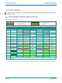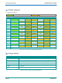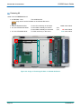
1
VX3230 3U VPX SBC User's Guide CA.DT.A63-1e - September 2010 If it's embedded, it's Kontron. VX3230 User's Guide Preface Revision History Publication Title: VX3230 User's Guide Doc. ID: CA.DT.A63-1e Rev. Brief Description of Changes Date of Issue 1e Support of 1000BASE-BX Ethernet interfaces 09-2010 0e Initial Version 10-2009 Copyright © 2010 Kontron AG. All rights reserved. All data is for information purposes only and not guaranteed for legal purposes. Information has been carefully checked and is believed to be accurate; however, no responsibility is assumed for inaccuracies. Kontron and the Kontron logo and all other trademarks or registered trademarks are the property of their respective owners and are recognized. Specifications are subject to change without notice. Page i CA.DT.A63-1e VX3230 User's Guide Preface Proprietary Note This document contains information proprietary to Kontron. It may not be copied or transmitted by any means, disclosed to others, or stored in any retrieval system or media without the prior written consent of Kontron or one of its authorized agents. The information contained in this document is, to the best of our knowledge, entirely correct. However, Kontron cannot accept liability for any inaccuracies or the consequences thereof, or for any liability arising from the use or application of any circuit, product, or example shown in this document. Kontron reserves the right to change, modify, or improve this document or the product described herein, as seen fit by Kontron without further notice. Trademarks This document may include names, company logos and trademarks, which are registered trademarks and, therefore, proprietary to their respective owners. Environmental Protection Statement This product has been manufactured to satisfy environmental protection requirements where possible. Many of the components used (structural parts, printed circuit boards, connectors, batteries, etc.) are capable of being recycled. Final disposition of this product after its service life must be accomplished in accordance with applicable country, state, or local laws or regulations. The Waste Electrical and Electronic Equipment (WEEE) Directive aims to: > reduce waste arising from electrical and electronic equipment (EEE) > make producers of EEE responsible for the environmental impact of their products, especially when they become waste > encourage separate collection and subsequent treatment, reuse, recovery, recycling and sound environmental disposal of EEE > improve the environmental performance of all those involved during the lifecycle of EEE CA.DT.A63-1e Page ii Preface VX3230 User's Guide Conventions This guide uses several types of notice: Note, Caution, ESD. Note: this notice calls attention to important features or instructions. Caution: this notice alert you to system damage, loss of data, or risk of personal injury. ESD: This banner indicates an Electrostatic Sensitive Device. All numbers are expressed in decimal, except addresses and memory or register data, which are expressed in hexadecimal. The prefix `0x' shows a hexadecimal number, following the `C' programming language convention. The multipliers `k', `M' and `G' have their conventional scientific and engineering meanings of *103, *106 and *109 respectively. The only exception to this is in the description of the size of memory areas, when `K', `M' and `G' mean *210, *220 and *230 respectively. When describing transfer rates, `k' `M' and `G' mean *103, *106 and *109 not *2 10 *2 20 and *2 30. In PowerPC terminology, multiple bit fields are numbered from 0 to n, where 0 is the MSB and n is the LSB. PCI and CompactPCI terminology follows the more familiar convention that bit 0 is the LSB and n is the MSB. Signal names ending with an asterisk (*) or a hash (#) denote active low signals; all other signals are active high. Signal names follow the PICMG 2.0 R3.0 CompactPCI Specification and the PCI Local Bus 2.3 Specification. For Your Safety Your new Kontron product was developed and tested carefully to provide all features necessary to ensure its compliance with electrical safety requirements. It was also designed for a long fault-free life. However, the life expectancy of your product can be drastically reduced by improper treatment during unpacking and installation. Therefore, in the interest of your own safety and of the correct operation of your new Kontron product, you are requested to conform with the following guidelines. High Voltage Safety Instructions Warning! All operations on this device must be carried out by sufficiently skilled personnel only. Caution, Electric Shock! Before installing a not hot-swappable Kontron product into a system always ensure that your mains power is switched off. This applies also to the installation of piggybacks. Serious electrical shock hazards can exist during all installation, repair and maintenance operations with this product. Therefore, always unplug the power cable and any other cables which provide external voltages before performing work. Page iii CA.DT.A63-1e VX3230 User's Guide Preface Special Handling and Unpacking Instructions ESD Sensitive Device! Electronic boards and their components are sensitive to static electricity. Therefore, care must be taken during all handling operations and inspections of this product, in order to ensure product integrity at all times Do not handle this product out of its protective enclosure while it is not used for operational purposes unless it is otherwise protected. Whenever possible, unpack or pack this product only at EOS/ESD safe work stations. Where a safe work station is not guaranteed, it is important for the user to be electrically discharged before touching the product with his/her hands or tools. This is most easily done by touching a metal part of your system housing. It is particularly important to observe standard anti-static precautions when changing piggybacks, ROM devices, jumper settings etc. If the product contains batteries for RTC or memory backup, ensure that the board is not placed on conductive surfaces, including anti-static plastics or sponges. They can cause short circuits and damage the batteries or conductive circuits on the board. General Instructions on Usage In order to maintain Kontron’s product warranty, this product must not be altered or modified in any way. Changes or modifications to the device, which are not explicitly approved by Kontron and described in this manual or received from Kontron’s Technical Support as a special handling instruction, will void your warranty. This device should only be installed in or connected to systems that fulfill all necessary technical and specific environmental requirements. This applies also to the operational temperature range of the specific board version, which must not be exceeded. If batteries are present, their temperature restrictions must be taken into account. In performing all necessary installation and application operations, please follow only the instructions supplied by the present manual. Keep all the original packaging material for future storage or warranty shipments. If it is necessary to store or ship the board, please re-pack it as nearly as possible in the manner in which it was delivered. Special care is necessary when handling or unpacking the product. Please consult the special handling and unpacking instruction on the previous page of this manual. CA.DT.A63-1e Page iv VX3230 User's Guide Table Of Contents Table Of Contents Chapter 1 - Introduction . . . . . . . . . . . . . . . . . . . . . . . . . . . . . . . . . . . . . . . . . . . . . . . . . . . . . . . . . . 1 1.1 Manual Overview . . . . . . . . . . . . . . . . . . . . . . . . . . . . . . . . . . . . . . . . . . . . . . . . . . . . . . . . . . . . . . . . . 1.1.1 Objectives . . . . . . . . . . . . . . . . . . . . . . . . . . . . . . . . . . . . . . . . . . . . . . . . . . . . . . . . . . . . . . . . . . . 1.1.2 Audience . . . . . . . . . . . . . . . . . . . . . . . . . . . . . . . . . . . . . . . . . . . . . . . . . . . . . . . . . . . . . . . . . . . . . 1.1.3 Scope . . . . . . . . . . . . . . . . . . . . . . . . . . . . . . . . . . . . . . . . . . . . . . . . . . . . . . . . . . . . . . . . . . . . . . . 1.1.4 Structure . . . . . . . . . . . . . . . . . . . . . . . . . . . . . . . . . . . . . . . . . . . . . . . . . . . . . . . . . . . . . . . . . . . . . 3 3 3 3 3 1.2 VPX Overview . . . . . . . . . . . . . . . . . . . . . . . . . . . . . . . . . . . . . . . . . . . . . . . . . . . . . . . . . . . . . . . . . . . 4 1.3 Board Overview . . . . . . . . . . . . . . . . . . . . . . . . . . . . . . . . . . . . . . . . . . . . . . . . . . . . . . . . . . . . . . . . . . 1.3.1 Main Features . . . . . . . . . . . . . . . . . . . . . . . . . . . . . . . . . . . . . . . . . . . . . . . . . . . . . . . . . . . . . . . . 1.3.2 Order Code Table . . . . . . . . . . . . . . . . . . . . . . . . . . . . . . . . . . . . . . . . . . . . . . . . . . . . . . . . . . . . . 1.3.3 I/O Interfaces . . . . . . . . . . . . . . . . . . . . . . . . . . . . . . . . . . . . . . . . . . . . . . . . . . . . . . . . . . . . . . . . . 1.3.4 Ethernet Connectivity . . . . . . . . . . . . . . . . . . . . . . . . . . . . . . . . . . . . . . . . . . . . . . . . . . . . . . . . . . 4 4 6 7 9 1.4 Board Diagram . . . . . . . . . . . . . . . . . . . . . . . . . . . . . . . . . . . . . . . . . . . . . . . . . . . . . . . . . . . . . . . . . . . 1.4.1 1.4.2 1.4.3 1.5 11 Functional Block Diagram . . . . . . . . . . . . . . . . . . . . . . . . . . . . . . . . . . . . . . . . . . . . . . . . . . . . . . Front Panel . . . . . . . . . . . . . . . . . . . . . . . . . . . . . . . . . . . . . . . . . . . . . . . . . . . . . . . . . . . . . . . . . . VX3230 Components Layout . . . . . . . . . . . . . . . . . . . . . . . . . . . . . . . . . . . . . . . . . . . . . . . . . . . 11 13 14 Technical Specification . . . . . . . . . . . . . . . . . . . . . . . . . . . . . . . . . . . . . . . . . . . . . . . . . . . . . . . . . . . . 15 1.5.1 MTBF Data . . . . . . . . . . . . . . . . . . . . . . . . . . . . . . . . . . . . . . . . . . . . . . . . . . . . . . . . . . . . . . . . . . . 17 Software Support . . . . . . . . . . . . . . . . . . . . . . . . . . . . . . . . . . . . . . . . . . . . . . . . . . . . . . . . . . . . . . . . . 18 1.7 Standard . . . . . . . . . . . . . . . . . . . . . . . . . . . . . . . . . . . . . . . . . . . . . . . . . . . . . . . . . . . . . . . . . . . . . . . . 1.7.1 Environmental Specifications . . . . . . . . . . . . . . . . . . . . . . . . . . . . . . . . . . . . . . . . . . . . . . . . . . . 19 19 1.8 20 1.6 Related Publications . . . . . . . . . . . . . . . . . . . . . . . . . . . . . . . . . . . . . . . . . . . . . . . . . . . . . . . . . . . . . . Chapter 2 - Functional Description . . . . . . . . . . . . . . . . . . . . . . . . . . . . . . . . . . . . . . . . . . . . . . . . 21 2.1 Processor and System Memory . . . . . . . . . . . . . . . . . . . . . . . . . . . . . . . . . . . . . . . . . . . . . . . . . . . . 2.1.1 Processor . . . . . . . . . . . . . . . . . . . . . . . . . . . . . . . . . . . . . . . . . . . . . . . . . . . . . . . . . . . . . . . . . . . . 2.1.2 System Memory . . . . . . . . . . . . . . . . . . . . . . . . . . . . . . . . . . . . . . . . . . . . . . . . . . . . . . . . . . . . . . 23 23 24 2.2 25 PCI Express Buses . . . . . . . . . . . . . . . . . . . . . . . . . . . . . . . . . . . . . . . . . . . . . . . . . . . . . . . . . . . . . . . 2.2.1 2.2.2 MPC8544 PCI Express Links . . . . . . . . . . . . . . . . . . . . . . . . . . . . . . . . . . . . . . . . . . . . . . . . . . . Internal PCI Express Links . . . . . . . . . . . . . . . . . . . . . . . . . . . . . . . . . . . . . . . . . . . . . . . . . . . . . 25 25 2.3 Storage . . . . . . . . . . . . . . . . . . . . . . . . . . . . . . . . . . . . . . . . . . . . . . . . . . . . . . . . . . . . . . . . . . . . . . . . . 2.3.1 Flash Memory . . . . . . . . . . . . . . . . . . . . . . . . . . . . . . . . . . . . . . . . . . . . . . . . . . . . . . . . . . . . . . . . 2.3.2 Serial EEPROMs . . . . . . . . . . . . . . . . . . . . . . . . . . . . . . . . . . . . . . . . . . . . . . . . . . . . . . . . . . . . . 2.3.3 SPI EEPROM . . . . . . . . . . . . . . . . . . . . . . . . . . . . . . . . . . . . . . . . . . . . . . . . . . . . . . . . . . . . . . . . 2.3.4 NOVRAM . . . . . . . . . . . . . . . . . . . . . . . . . . . . . . . . . . . . . . . . . . . . . . . . . . . . . . . . . . . . . . . . . . . . 2.3.5 Dual Serial ATA . . . . . . . . . . . . . . . . . . . . . . . . . . . . . . . . . . . . . . . . . . . . . . . . . . . . . . . . . . . . . . . 26 26 26 26 26 26 2.4 Peripherals . . . . . . . . . . . . . . . . . . . . . . . . . . . . . . . . . . . . . . . . . . . . . . . . . . . . . . . . . . . . . . . . . . . . . . 2.4.1 Timer . . . . . . . . . . . . . . . . . . . . . . . . . . . . . . . . . . . . . . . . . . . . . . . . . . . . . . . . . . . . . . . . . . . . . . . . 2.4.2 Watchdog Timer . . . . . . . . . . . . . . . . . . . . . . . . . . . . . . . . . . . . . . . . . . . . . . . . . . . . . . . . . . . . . . 27 27 27 2.5 27 Page v System FPGA . . . . . . . . . . . . . . . . . . . . . . . . . . . . . . . . . . . . . . . . . . . . . . . . . . . . . . . . . . . . . . . . . . . CA.DT.A63-1e VX3230 User's Guide Table Of Contents 2.6 I2C Buses . . . . . . . . . . . . . . . . . . . . . . . . . . . . . . . . . . . . . . . . . . . . . . . . . . . . . . . . . . . . . . . . . . . . . . . 2.6.1 Internal I2C Slaves . . . . . . . . . . . . . . . . . . . . . . . . . . . . . . . . . . . . . . . . . . . . . . . . . . . . . . . . . . . . 2.6.2 RTC . . . . . . . . . . . . . . . . . . . . . . . . . . . . . . . . . . . . . . . . . . . . . . . . . . . . . . . . . . . . . . . . . . . . . . . . . 2.6.3 VPD EEPROM . . . . . . . . . . . . . . . . . . . . . . . . . . . . . . . . . . . . . . . . . . . . . . . . . . . . . . . . . . . . . . . 2.6.4 Thermal Sensors . . . . . . . . . . . . . . . . . . . . . . . . . . . . . . . . . . . . . . . . . . . . . . . . . . . . . . . . . . . . . . 2.6.5 Voltage Sensors . . . . . . . . . . . . . . . . . . . . . . . . . . . . . . . . . . . . . . . . . . . . . . . . . . . . . . . . . . . . . . 2.6.6 External SMB Bus . . . . . . . . . . . . . . . . . . . . . . . . . . . . . . . . . . . . . . . . . . . . . . . . . . . . . . . . . . . . . 28 28 28 28 29 31 31 2.7 VX3230 Connectors Layout . . . . . . . . . . . . . . . . . . . . . . . . . . . . . . . . . . . . . . . . . . . . . . . . . . . . . . . . 32 2.8 Board Interfaces . . . . . . . . . . . . . . . . . . . . . . . . . . . . . . . . . . . . . . . . . . . . . . . . . . . . . . . . . . . . . . . . . . 2.8.1 Serial Interfaces . . . . . . . . . . . . . . . . . . . . . . . . . . . . . . . . . . . . . . . . . . . . . . . . . . . . . . . . . . . . . . 2.8.2 USB Interfaces . . . . . . . . . . . . . . . . . . . . . . . . . . . . . . . . . . . . . . . . . . . . . . . . . . . . . . . . . . . . . . . 2.8.3 Gigabit Ethernet Interfaces . . . . . . . . . . . . . . . . . . . . . . . . . . . . . . . . . . . . . . . . . . . . . . . . . . . . . 2.8.3.1 ETH0 and ETH1 Pinouts . . . . . . . . . . . . . . . . . . . . . . . . . . . . . . . . . . . . . . . . . . . . 2.8.4 VPX Bus Interface . . . . . . . . . . . . . . . . . . . . . . . . . . . . . . . . . . . . . . . . . . . . . . . . . . . . . . . . . . . . 2.8.4.1 Board Connectors Identification . . . . . . . . . . . . . . . . . . . . . . . . . . . . . . . . . . . . . . 2.8.4.2 VPX Connectors Description . . . . . . . . . . . . . . . . . . . . . . . . . . . . . . . . . . . . . . . . 2.8.5 PMC J11 Connector Pin Assignment . . . . . . . . . . . . . . . . . . . . . . . . . . . . . . . . . . . . . . . . . . . . 2.8.6 PMC J12 Connector Pin Assignment . . . . . . . . . . . . . . . . . . . . . . . . . . . . . . . . . . . . . . . . . . . . 2.8.7 PMC J14 Connector Pin Assignment . . . . . . . . . . . . . . . . . . . . . . . . . . . . . . . . . . . . . . . . . . . . 2.8.8 PMC Signal Description . . . . . . . . . . . . . . . . . . . . . . . . . . . . . . . . . . . . . . . . . . . . . . . . . . . . . . . . 2.8.9 XMC J15 Connector Pin Assignment . . . . . . . . . . . . . . . . . . . . . . . . . . . . . . . . . . . . . . . . . . . . 2.8.10 XMC Signal Decription . . . . . . . . . . . . . . . . . . . . . . . . . . . . . . . . . . . . . . . . . . . . . . . . . . . . . . . . . 2.8.11 COP Header . . . . . . . . . . . . . . . . . . . . . . . . . . . . . . . . . . . . . . . . . . . . . . . . . . . . . . . . . . . . . . . . . 2.8.12 JTAG Connector . . . . . . . . . . . . . . . . . . . . . . . . . . . . . . . . . . . . . . . . . . . . . . . . . . . . . . . . . . . . . . 33 33 34 37 38 39 39 40 47 47 48 49 51 52 53 53 2.9 XMC/PMC Site . . . . . . . . . . . . . . . . . . . . . . . . . . . . . . . . . . . . . . . . . . . . . . . . . . . . . . . . . . . . . . . . . . . 2.9.1 Signaling Voltage Keying Pin . . . . . . . . . . . . . . . . . . . . . . . . . . . . . . . . . . . . . . . . . . . . . . . . . . . 54 55 Chapter 3 - Installation . . . . . . . . . . . . . . . . . . . . . . . . . . . . . . . . . . . . . . . . . . . . . . . . . . . . . . . . . . . 56 3.1 Safety Requirements . . . . . . . . . . . . . . . . . . . . . . . . . . . . . . . . . . . . . . . . . . . . . . . . . . . . . . . . . . . . . . 56 3.2 Board Identification . . . . . . . . . . . . . . . . . . . . . . . . . . . . . . . . . . . . . . . . . . . . . . . . . . . . . . . . . . . . . . . 57 3.3 Board Configuration . . . . . . . . . . . . . . . . . . . . . . . . . . . . . . . . . . . . . . . . . . . . . . . . . . . . . . . . . . . . . . . 3.3.1 DIP Switch SW1 Description . . . . . . . . . . . . . . . . . . . . . . . . . . . . . . . . . . . . . . . . . . . . . . . . . . . . 59 59 3.4 Package Content . . . . . . . . . . . . . . . . . . . . . . . . . . . . . . . . . . . . . . . . . . . . . . . . . . . . . . . . . . . . . . . . . 60 3.5 Initial Installation Procedures . . . . . . . . . . . . . . . . . . . . . . . . . . . . . . . . . . . . . . . . . . . . . . . . . . . . . . . 61 3.6 Standard Removal Procedure . . . . . . . . . . . . . . . . . . . . . . . . . . . . . . . . . . . . . . . . . . . . . . . . . . . . . . 62 3.7 Installation of Peripheral Devices . . . . . . . . . . . . . . . . . . . . . . . . . . . . . . . . . . . . . . . . . . . . . . . . . . . 3.7.1 USB Device Installation . . . . . . . . . . . . . . . . . . . . . . . . . . . . . . . . . . . . . . . . . . . . . . . . . . . . . . . . 3.7.2 Battery Replacement . . . . . . . . . . . . . . . . . . . . . . . . . . . . . . . . . . . . . . . . . . . . . . . . . . . . . . . . . . 3.7.3 PMC Installation . . . . . . . . . . . . . . . . . . . . . . . . . . . . . . . . . . . . . . . . . . . . . . . . . . . . . . . . . . . . . . 3.7.4 XMC Installation . . . . . . . . . . . . . . . . . . . . . . . . . . . . . . . . . . . . . . . . . . . . . . . . . . . . . . . . . . . . . . 63 63 64 65 67 3.8 68 Software Installation . . . . . . . . . . . . . . . . . . . . . . . . . . . . . . . . . . . . . . . . . . . . . . . . . . . . . . . . . . . . . . CA.DT.A63-1e Page vi Table Of Contents Chapter 4 - VX3230 User's Guide Programming Interface . . . . . . . . . . . . . . . . . . . . . . . . . . . . . . . . . . . . . . . . . . . . . . . . 69 4.1 Interrupt Routing . . . . . . . . . . . . . . . . . . . . . . . . . . . . . . . . . . . . . . . . . . . . . . . . . . . . . . . . . . . . . . . . . 69 4.2 Memory Mapping . . . . . . . . . . . . . . . . . . . . . . . . . . . . . . . . . . . . . . . . . . . . . . . . . . . . . . . . . . . . . . . . . 70 4.3 CPLD System Registers Mapping . . . . . . . . . . . . . . . . . . . . . . . . . . . . . . . . . . . . . . . . . . . . . . . . . . . 71 4.4 CPLD System Registers Description . . . . . . . . . . . . . . . . . . . . . . . . . . . . . . . . . . . . . . . . . . . . . . . . 4.4.1 Firmware POST Code Register . . . . . . . . . . . . . . . . . . . . . . . . . . . . . . . . . . . . . . . . . . . . . . . . . 4.4.2 Debug POST Code Register . . . . . . . . . . . . . . . . . . . . . . . . . . . . . . . . . . . . . . . . . . . . . . . . . . . . 4.4.3 Memory Configuration Register . . . . . . . . . . . . . . . . . . . . . . . . . . . . . . . . . . . . . . . . . . . . . . . . . 4.4.4 Local I2C Command Register . . . . . . . . . . . . . . . . . . . . . . . . . . . . . . . . . . . . . . . . . . . . . . . . . . . 4.4.5 Local I2C Data Register . . . . . . . . . . . . . . . . . . . . . . . . . . . . . . . . . . . . . . . . . . . . . . . . . . . . . . . . 4.4.6 Interface Configuration Register . . . . . . . . . . . . . . . . . . . . . . . . . . . . . . . . . . . . . . . . . . . . . . . . . 4.4.7 Firmware Configuration register . . . . . . . . . . . . . . . . . . . . . . . . . . . . . . . . . . . . . . . . . . . . . . . . . 4.4.8 CPLD Interrupt Register . . . . . . . . . . . . . . . . . . . . . . . . . . . . . . . . . . . . . . . . . . . . . . . . . . . . . . . . 4.4.9 Watchdog Timer Control Register . . . . . . . . . . . . . . . . . . . . . . . . . . . . . . . . . . . . . . . . . . . . . . . 4.4.10 GPIO Interrupt Configuration Register . . . . . . . . . . . . . . . . . . . . . . . . . . . . . . . . . . . . . . . . . . . 4.4.11 Logic Revision Register . . . . . . . . . . . . . . . . . . . . . . . . . . . . . . . . . . . . . . . . . . . . . . . . . . . . . . . . 4.4.12 Host Reset Status Register . . . . . . . . . . . . . . . . . . . . . . . . . . . . . . . . . . . . . . . . . . . . . . . . . . . . . 4.4.13 Host I/O Status Register . . . . . . . . . . . . . . . . . . . . . . . . . . . . . . . . . . . . . . . . . . . . . . . . . . . . . . . 4.4.14 Host I/O Configuration Register . . . . . . . . . . . . . . . . . . . . . . . . . . . . . . . . . . . . . . . . . . . . . . . . . 4.4.15 Board ID Register . . . . . . . . . . . . . . . . . . . . . . . . . . . . . . . . . . . . . . . . . . . . . . . . . . . . . . . . . . . . . 4.4.16 GPIO Status / Command Register . . . . . . . . . . . . . . . . . . . . . . . . . . . . . . . . . . . . . . . . . . . . . . . 4.4.17 GPIO Control Register . . . . . . . . . . . . . . . . . . . . . . . . . . . . . . . . . . . . . . . . . . . . . . . . . . . . . . . . . 4.4.18 User-Specific LED Configuration Register . . . . . . . . . . . . . . . . . . . . . . . . . . . . . . . . . . . . . . . . 4.4.19 User-Specific LED Control Register . . . . . . . . . . . . . . . . . . . . . . . . . . . . . . . . . . . . . . . . . . . . . . 4.4.20 PCI Mode Register . . . . . . . . . . . . . . . . . . . . . . . . . . . . . . . . . . . . . . . . . . . . . . . . . . . . . . . . . . . . 4.4.21 Timer MSB Byte Register . . . . . . . . . . . . . . . . . . . . . . . . . . . . . . . . . . . . . . . . . . . . . . . . . . . . . . 4.4.22 Timer Middle Upper Byte Register . . . . . . . . . . . . . . . . . . . . . . . . . . . . . . . . . . . . . . . . . . . . . . . 4.4.23 Timer Middle Lower Byte Register . . . . . . . . . . . . . . . . . . . . . . . . . . . . . . . . . . . . . . . . . . . . . . . 4.4.24 Timer LSB Byte Register . . . . . . . . . . . . . . . . . . . . . . . . . . . . . . . . . . . . . . . . . . . . . . . . . . . . . . . 4.4.25 Logic Sub-Reviision Register . . . . . . . . . . . . . . . . . . . . . . . . . . . . . . . . . . . . . . . . . . . . . . . . . . . 4.4.26 COM1/2 Configuration Register . . . . . . . . . . . . . . . . . . . . . . . . . . . . . . . . . . . . . . . . . . . . . . . . . 4.4.27 VPX Register . . . . . . . . . . . . . . . . . . . . . . . . . . . . . . . . . . . . . . . . . . . . . . . . . . . . . . . . . . . . . . . . . 4.4.28 VPX Reset Register . . . . . . . . . . . . . . . . . . . . . . . . . . . . . . . . . . . . . . . . . . . . . . . . . . . . . . . . . . . 4.4.29 Geographical Addressing Register . . . . . . . . . . . . . . . . . . . . . . . . . . . . . . . . . . . . . . . . . . . . . . . 4.4.30 VPX Common Clock Register . . . . . . . . . . . . . . . . . . . . . . . . . . . . . . . . . . . . . . . . . . . . . . . . . . . 4.4.31 VPX PCIe Switch Register . . . . . . . . . . . . . . . . . . . . . . . . . . . . . . . . . . . . . . . . . . . . . . . . . . . . . 4.4.32 Open VPX Register . . . . . . . . . . . . . . . . . . . . . . . . . . . . . . . . . . . . . . . . . . . . . . . . . . . . . . . . . . . 4.4.33 GPIO4 Register . . . . . . . . . . . . . . . . . . . . . . . . . . . . . . . . . . . . . . . . . . . . . . . . . . . . . . . . . . . . . . . 72 72 72 73 73 74 74 74 75 76 77 77 78 78 79 79 80 80 81 82 82 83 83 83 83 83 84 85 85 86 86 87 88 89 Chapter 5 - Power Considerations . . . . . . . . . . . . . . . . . . . . . . . . . . . . . . . . . . . . . . . . . . . . . . . . 5.1 System Power . . . . . . . . . . . . . . . . . . . . . . . . . . . . . . . . . . . . . . . . . . . . . . . . . . . . . . . . . . . . . . . . . . . 5.1.1 VX3230 . . . . . . . . . . . . . . . . . . . . . . . . . . . . . . . . . . . . . . . . . . . . . . . . . . . . . . . . . . . . . . . . . . . . . . 5.1.2 Backplane . . . . . . . . . . . . . . . . . . . . . . . . . . . . . . . . . . . . . . . . . . . . . . . . . . . . . . . . . . . . . . . . . . . . 5.1.3 Power Supply Units . . . . . . . . . . . . . . . . . . . . . . . . . . . . . . . . . . . . . . . . . . . . . . . . . . . . . . . . . . . 5.1.3.1 Start-Up Requirement . . . . . . . . . . . . . . . . . . . . . . . . . . . . . . . . . . . . . . . . . . . . . . 5.1.3.2 Power-Up Sequence . . . . . . . . . . . . . . . . . . . . . . . . . . . . . . . . . . . . . . . . . . . . . . . Page vii 90 90 90 90 91 91 91 CA.DT.A63-1e VX3230 User's Guide 5.1.3.3 5.1.3.4 5.1.3.5 Table Of Contents Tolerance . . . . . . . . . . . . . . . . . . . . . . . . . . . . . . . . . . . . . . . . . . . . . . . . . . . . . . . . . Regulation . . . . . . . . . . . . . . . . . . . . . . . . . . . . . . . . . . . . . . . . . . . . . . . . . . . . . . . . Rise Time Diagram . . . . . . . . . . . . . . . . . . . . . . . . . . . . . . . . . . . . . . . . . . . . . . . . . 92 92 93 5.2 Power Consumption . . . . . . . . . . . . . . . . . . . . . . . . . . . . . . . . . . . . . . . . . . . . . . . . . . . . . . . . . . . . . . 5.2.1 Real Applications . . . . . . . . . . . . . . . . . . . . . . . . . . . . . . . . . . . . . . . . . . . . . . . . . . . . . . . . . . . . . 94 94 Chapter 6 - VX3230-RTM Characteristics . . . . . . . . . . . . . . . . . . . . . . . . . . . . . . . . . . . . . . . . . . 95 6.1 Overview . . . . . . . . . . . . . . . . . . . . . . . . . . . . . . . . . . . . . . . . . . . . . . . . . . . . . . . . . . . . . . . . . . . . . . . . 95 6.2 Technical Specifications . . . . . . . . . . . . . . . . . . . . . . . . . . . . . . . . . . . . . . . . . . . . . . . . . . . . . . . . . . . 97 6.3 RTM Configuration . . . . . . . . . . . . . . . . . . . . . . . . . . . . . . . . . . . . . . . . . . . . . . . . . . . . . . . . . . . . . . . 98 6.4 Connectors . . . . . . . . . . . . . . . . . . . . . . . . . . . . . . . . . . . . . . . . . . . . . . . . . . . . . . . . . . . . . . . . . . . . . . 6.4.1 RTM Connectors Identification . . . . . . . . . . . . . . . . . . . . . . . . . . . . . . . . . . . . . . . . . . . . . . . . . . 6.4.2 Front Panel Connectors . . . . . . . . . . . . . . . . . . . . . . . . . . . . . . . . . . . . . . . . . . . . . . . . . . . . . . . . 6.4.3 Onboard Connectors . . . . . . . . . . . . . . . . . . . . . . . . . . . . . . . . . . . . . . . . . . . . . . . . . . . . . . . . . . 99 99 100 101 6.5 Modules Interfaces . . . . . . . . . . . . . . . . . . . . . . . . . . . . . . . . . . . . . . . . . . . . . . . . . . . . . . . . . . . . . . . 6.5.1 COM Interfaces . . . . . . . . . . . . . . . . . . . . . . . . . . . . . . . . . . . . . . . . . . . . . . . . . . . . . . . . . . . . . . 6.5.2 USB Interfaces . . . . . . . . . . . . . . . . . . . . . . . . . . . . . . . . . . . . . . . . . . . . . . . . . . . . . . . . . . . . . . . 6.5.3 Gigabit Ethernet Interfaces . . . . . . . . . . . . . . . . . . . . . . . . . . . . . . . . . . . . . . . . . . . . . . . . . . . . . 6.5.4 Serial ATA Interfaces . . . . . . . . . . . . . . . . . . . . . . . . . . . . . . . . . . . . . . . . . . . . . . . . . . . . . . . . . . 6.5.5 GPIO Connector . . . . . . . . . . . . . . . . . . . . . . . . . . . . . . . . . . . . . . . . . . . . . . . . . . . . . . . . . . . . . . 6.5.6 JTAG Connector . . . . . . . . . . . . . . . . . . . . . . . . . . . . . . . . . . . . . . . . . . . . . . . . . . . . . . . . . . . . . . 6.5.7 I2C System Management Connector . . . . . . . . . . . . . . . . . . . . . . . . . . . . . . . . . . . . . . . . . . . . . 104 104 105 108 109 110 111 112 6.6 Reset . . . . . . . . . . . . . . . . . . . . . . . . . . . . . . . . . . . . . . . . . . . . . . . . . . . . . . . . . . . . . . . . . . . . . . . . . . . 113 6.7 Power Consideration . . . . . . . . . . . . . . . . . . . . . . . . . . . . . . . . . . . . . . . . . . . . . . . . . . . . . . . . . . . . . . 113 6.8 Rear I/O Interfaces 6.8.1 RP2 Connector 6.8.2 RP1 Connector 6.8.3 RP0 Connector ............................................................... ............................................................... ............................................................... ............................................................... 114 115 116 119 6.9 PCI 64 PIM Connector . . . . . . . . . . . . . . . . . . . . . . . . . . . . . . . . . . . . . . . . . . . . . . . . . . . . . . . . . . . . 6.9.1 J10 Connector . . . . . . . . . . . . . . . . . . . . . . . . . . . . . . . . . . . . . . . . . . . . . . . . . . . . . . . . . . . . . . . . 6.9.2 J14 Connector . . . . . . . . . . . . . . . . . . . . . . . . . . . . . . . . . . . . . . . . . . . . . . . . . . . . . . . . . . . . . . . . 121 121 122 Chapter 7 - VX3230-RC Characteristics . . . . . . . . . . . . . . . . . . . . . . . . . . . . . . . . . . . . . . . . . . . . 123 7.1 VX3230-RC Specificities . . . . . . . . . . . . . . . . . . . . . . . . . . . . . . . . . . . . . . . . . . . . . . . . . . . . . . . . . . . 124 7.2 Board Identification . . . . . . . . . . . . . . . . . . . . . . . . . . . . . . . . . . . . . . . . . . . . . . . . . . . . . . . . . . . . . . . 125 7.3 Environmental Specifications . . . . . . . . . . . . . . . . . . . . . . . . . . . . . . . . . . . . . . . . . . . . . . . . . . . . . . . 126 7.4 MTBF Data . . . . . . . . . . . . . . . . . . . . . . . . . . . . . . . . . . . . . . . . . . . . . . . . . . . . . . . . . . . . . . . . . . . . . . 126 7.5 Peripheral Connectivity . . . . . . . . . . . . . . . . . . . . . . . . . . . . . . . . . . . . . . . . . . . . . . . . . . . . . . . . . . . . 127 7.6 XMC/PMC Installation . . . . . . . . . . . . . . . . . . . . . . . . . . . . . . . . . . . . . . . . . . . . . . . . . . . . . . . . . . . . . 128 CA.DT.A63-1e Page viii VX3230 User's Guide Table Of Contents List Of Figures Figure 1: VX3230-SA Overview . . . . . . . . . . . . . . . . . . . . . . . . . . . . . . . . . . . . . . . . . . . . . . . . . . . . . . . . . . . . 2 Figure 2: VX3230 Functional Block Diagram (Type 1) . . . . . . . . . . . . . . . . . . . . . . . . . . . . . . . . . . . . . . . . . 11 Figure 3: VX3230 Functional Block Diagram (Type 2) . . . . . . . . . . . . . . . . . . . . . . . . . . . . . . . . . . . . . . . . . 12 Figure 4: Front Panel Connectors . . . . . . . . . . . . . . . . . . . . . . . . . . . . . . . . . . . . . . . . . . . . . . . . . . . . . . . . . . . 13 Figure 5: Reset Button and LEDs . . . . . . . . . . . . . . . . . . . . . . . . . . . . . . . . . . . . . . . . . . . . . . . . . . . . . . . . . . . 13 Figure 6: VX3230 Components Layout (Top View) . . . . . . . . . . . . . . . . . . . . . . . . . . . . . . . . . . . . . . . . . . . . 14 Figure 7: VX3230 Board Components Layout (Bottom View) . . . . . . . . . . . . . . . . . . . . . . . . . . . . . . . . . . . 14 Figure 8: MPC8544 Block Diagram . . . . . . . . . . . . . . . . . . . . . . . . . . . . . . . . . . . . . . . . . . . . . . . . . . . . . . . . . 24 Figure 9: Location of Board and Processor Sensors . . . . . . . . . . . . . . . . . . . . . . . . . . . . . . . . . . . . . . . . . . . 30 Figure 10: VX3230 Connectors Layout (top) . . . . . . . . . . . . . . . . . . . . . . . . . . . . . . . . . . . . . . . . . . . . . . . . . . 32 Figure 11: Front Panel Connectors Layout . . . . . . . . . . . . . . . . . . . . . . . . . . . . . . . . . . . . . . . . . . . . . . . . . . . 32 Figure 12: Serial Connector . . . . . . . . . . . . . . . . . . . . . . . . . . . . . . . . . . . . . . . . . . . . . . . . . . . . . . . . . . . . . . . . 33 Figure 13: USB Connector . . . . . . . . . . . . . . . . . . . . . . . . . . . . . . . . . . . . . . . . . . . . . . . . . . . . . . . . . . . . . . . . . 35 Figure 14: USB Onboard Connector . . . . . . . . . . . . . . . . . . . . . . . . . . . . . . . . . . . . . . . . . . . . . . . . . . . . . . . . 35 Figure 15: USB Flash Disk Overview . . . . . . . . . . . . . . . . . . . . . . . . . . . . . . . . . . . . . . . . . . . . . . . . . . . . . . . . 36 Figure 16: Dual Gigabit Ethernet Connector . . . . . . . . . . . . . . . . . . . . . . . . . . . . . . . . . . . . . . . . . . . . . . . . . . 37 Figure 17: VPX Connectors . . . . . . . . . . . . . . . . . . . . . . . . . . . . . . . . . . . . . . . . . . . . . . . . . . . . . . . . . . . . . . . . 39 Figure 18: Connector Identification for 3U VPX Board . . . . . . . . . . . . . . . . . . . . . . . . . . . . . . . . . . . . . . . . . 39 Figure 19: COP Header . . . . . . . . . . . . . . . . . . . . . . . . . . . . . . . . . . . . . . . . . . . . . . . . . . . . . . . . . . . . . . . . . . . 53 Figure 20: JTAG Connector . . . . . . . . . . . . . . . . . . . . . . . . . . . . . . . . . . . . . . . . . . . . . . . . . . . . . . . . . . . . . . . . 53 Figure 21: VX3230 Identification (Top Side) . . . . . . . . . . . . . . . . . . . . . . . . . . . . . . . . . . . . . . . . . . . . . . . . . . 57 Figure 22: VX3230 Identification (Bottom Side) . . . . . . . . . . . . . . . . . . . . . . . . . . . . . . . . . . . . . . . . . . . . . . . 58 Figure 23: Board Configuration . . . . . . . . . . . . . . . . . . . . . . . . . . . . . . . . . . . . . . . . . . . . . . . . . . . . . . . . . . . . . 59 Figure 24: USB Flash Disk Bottom View . . . . . . . . . . . . . . . . . . . . . . . . . . . . . . . . . . . . . . . . . . . . . . . . . . . . . 63 Figure 25: USB Flash Installation . . . . . . . . . . . . . . . . . . . . . . . . . . . . . . . . . . . . . . . . . . . . . . . . . . . . . . . . . . . 63 Figure 26: PMC Installation on PMC Site . . . . . . . . . . . . . . . . . . . . . . . . . . . . . . . . . . . . . . . . . . . . . . . . . . . . 66 Figure 27: Example of XMC Board . . . . . . . . . . . . . . . . . . . . . . . . . . . . . . . . . . . . . . . . . . . . . . . . . . . . . . . . . . 67 Figure 28: XMC Installation on XMC Site . . . . . . . . . . . . . . . . . . . . . . . . . . . . . . . . . . . . . . . . . . . . . . . . . . . . 67 Figure 29: Start-Up Ramp of the CP3-SVE180 AC Power Supply . . . . . . . . . . . . . . . . . . . . . . . . . . . . . . . 93 Figure 30: VX3230-RTM Overview . . . . . . . . . . . . . . . . . . . . . . . . . . . . . . . . . . . . . . . . . . . . . . . . . . . . . . . . . . 96 Figure 31: VX3230-RTM MicroSwitch Location . . . . . . . . . . . . . . . . . . . . . . . . . . . . . . . . . . . . . . . . . . . . . . . 98 Figure 32: Connector Identification for 3U RTM . . . . . . . . . . . . . . . . . . . . . . . . . . . . . . . . . . . . . . . . . . . . . . . 99 Figure 33: VX3230-RTM Front Panel Connectors . . . . . . . . . . . . . . . . . . . . . . . . . . . . . . . . . . . . . . . . . . . . . 100 Figure 34: VX3230-RTM Onboard Connectors (PB-VX3-001) . . . . . . . . . . . . . . . . . . . . . . . . . . . . . . . . . . 101 Figure 35: VX3230-RTM Onboard Connectors (PB-VX3-000) . . . . . . . . . . . . . . . . . . . . . . . . . . . . . . . . . . 102 Figure 36: Serial Port Connector . . . . . . . . . . . . . . . . . . . . . . . . . . . . . . . . . . . . . . . . . . . . . . . . . . . . . . . . . . . 104 Figure 37: Front Panel USB Connector . . . . . . . . . . . . . . . . . . . . . . . . . . . . . . . . . . . . . . . . . . . . . . . . . . . . . . 105 Page ix CA.DT.A63-1e VX3230 User's Guide Table Of Contents Figure 38: Onboard USB Connector . . . . . . . . . . . . . . . . . . . . . . . . . . . . . . . . . . . . . . . . . . . . . . . . . . . . . . . . 106 Figure 39: USB Flash Disk Overview . . . . . . . . . . . . . . . . . . . . . . . . . . . . . . . . . . . . . . . . . . . . . . . . . . . . . . . . 106 Figure 40: USB Flash Disk Layout . . . . . . . . . . . . . . . . . . . . . . . . . . . . . . . . . . . . . . . . . . . . . . . . . . . . . . . . . . 107 Figure 41: Gigabit Ethernet Connectors . . . . . . . . . . . . . . . . . . . . . . . . . . . . . . . . . . . . . . . . . . . . . . . . . . . . . 108 Figure 42: Onboard SATA Connectors . . . . . . . . . . . . . . . . . . . . . . . . . . . . . . . . . . . . . . . . . . . . . . . . . . . . . . 109 Figure 43: Onboard GPIO Connector . . . . . . . . . . . . . . . . . . . . . . . . . . . . . . . . . . . . . . . . . . . . . . . . . . . . . . . 110 Figure 44: Onboard JTAG Connector . . . . . . . . . . . . . . . . . . . . . . . . . . . . . . . . . . . . . . . . . . . . . . . . . . . . . . . 111 Figure 45: Onboard JTAG Connector . . . . . . . . . . . . . . . . . . . . . . . . . . . . . . . . . . . . . . . . . . . . . . . . . . . . . . . 112 Figure 46: VX3230-RTM Reset Push Button . . . . . . . . . . . . . . . . . . . . . . . . . . . . . . . . . . . . . . . . . . . . . . . . . 113 Figure 47: Rear I/O VPX Connectors . . . . . . . . . . . . . . . . . . . . . . . . . . . . . . . . . . . . . . . . . . . . . . . . . . . . . . . . 114 Figure 48: VX3230-RC Overview . . . . . . . . . . . . . . . . . . . . . . . . . . . . . . . . . . . . . . . . . . . . . . . . . . . . . . . . . . . 123 Figure 49: VX3230-RC Identification (Top Side) . . . . . . . . . . . . . . . . . . . . . . . . . . . . . . . . . . . . . . . . . . . . . . 125 Figure 50: Standard Anchorage Points on VX3230-RC Board . . . . . . . . . . . . . . . . . . . . . . . . . . . . . . . . . . 128 Figure 51: Additional Anchorage Point on VX3230-RC Board . . . . . . . . . . . . . . . . . . . . . . . . . . . . . . . . . . . 129 Figure 52: Usage of Fastening Kit Ribs on VX3230-RC Board . . . . . . . . . . . . . . . . . . . . . . . . . . . . . . . . . . 130 CA.DT.A63-1e Page x VX3230 User's Guide Table Of Contents List Of Tables Table 1: Order Code . . . . . . . . . . . . . . . . . . . . . . . . . . . . . . . . . . . . . . . . . . . . . . . . . . . . . . . . . . . . . . . . . . . . . . 6 Table 2: Front I/O Interfaces (no PMC/XMC slot Manufacturing Option) . . . . . . . . . . . . . . . . . . . . . . . . . . 7 Table 3: Front I/O Interfaces (PMC/XMC slot Manufacturing Option) . . . . . . . . . . . . . . . . . . . . . . . . . . . . 7 Table 4: Rear I/O Interfaces . . . . . . . . . . . . . . . . . . . . . . . . . . . . . . . . . . . . . . . . . . . . . . . . . . . . . . . . . . . . . . . 7 Table 5: Peripheral Connectivity . . . . . . . . . . . . . . . . . . . . . . . . . . . . . . . . . . . . . . . . . . . . . . . . . . . . . . . . . . . . 8 Table 6: VX3230 Main Specifications . . . . . . . . . . . . . . . . . . . . . . . . . . . . . . . . . . . . . . . . . . . . . . . . . . . . . . . 16 Table 7: VX3230-SAA1N-000 MTBF Data . . . . . . . . . . . . . . . . . . . . . . . . . . . . . . . . . . . . . . . . . . . . . . . . . . . 17 Table 8: VX3230-RC1N-000 MTBF Data . . . . . . . . . . . . . . . . . . . . . . . . . . . . . . . . . . . . . . . . . . . . . . . . . . . . 17 Table 9: Standards . . . . . . . . . . . . . . . . . . . . . . . . . . . . . . . . . . . . . . . . . . . . . . . . . . . . . . . . . . . . . . . . . . . . . . . 19 Table 10: Environmental Specifications . . . . . . . . . . . . . . . . . . . . . . . . . . . . . . . . . . . . . . . . . . . . . . . . . . . . . . 19 Table 11: Related Publications . . . . . . . . . . . . . . . . . . . . . . . . . . . . . . . . . . . . . . . . . . . . . . . . . . . . . . . . . . . . . 20 Table 12: Ports Configuration of the PCI Express Switch . . . . . . . . . . . . . . . . . . . . . . . . . . . . . . . . . . . . . . 25 Table 13: Serial Connector Pin Assignment . . . . . . . . . . . . . . . . . . . . . . . . . . . . . . . . . . . . . . . . . . . . . . . . . . 33 Table 14: Serial Connector Signal Description . . . . . . . . . . . . . . . . . . . . . . . . . . . . . . . . . . . . . . . . . . . . . . . . 33 Table 15: USB Connector Pin Assignment . . . . . . . . . . . . . . . . . . . . . . . . . . . . . . . . . . . . . . . . . . . . . . . . . . . 35 Table 16: USB Onboard Pin Assignment . . . . . . . . . . . . . . . . . . . . . . . . . . . . . . . . . . . . . . . . . . . . . . . . . . . . 35 Table 17: Gigabit Ethernet Connectors ETH0 and ETH1 Pin Assignment . . . . . . . . . . . . . . . . . . . . . . . . 38 Table 18: VPX Connector P0 Wafer Assignment . . . . . . . . . . . . . . . . . . . . . . . . . . . . . . . . . . . . . . . . . . . . . . 40 Table 19: VPX Connector P0 Signal Definition . . . . . . . . . . . . . . . . . . . . . . . . . . . . . . . . . . . . . . . . . . . . . . . . 41 Table 20: VPX Connector P1 Wafer Assignment (10/100/1000BASE6TX Ethernet Manufacturing Option) . . . 42 Table 21: VPX Connector P1 Wafer Assignment (1000BASE-BX Ethernet Manufacturing Option) . . . 43 Table 22: VPX Connector P1 Signal Definition . . . . . . . . . . . . . . . . . . . . . . . . . . . . . . . . . . . . . . . . . . . . . . . . 44 Table 23: USB Port Features . . . . . . . . . . . . . . . . . . . . . . . . . . . . . . . . . . . . . . . . . . . . . . . . . . . . . . . . . . . . . . 45 Table 24: Ethernet Port Features . . . . . . . . . . . . . . . . . . . . . . . . . . . . . . . . . . . . . . . . . . . . . . . . . . . . . . . . . . . 45 Table 25: SATA Port Features . . . . . . . . . . . . . . . . . . . . . . . . . . . . . . . . . . . . . . . . . . . . . . . . . . . . . . . . . . . . . 45 Table 26: VPX Connector P2 Wafer Assignment . . . . . . . . . . . . . . . . . . . . . . . . . . . . . . . . . . . . . . . . . . . . . . 46 Table 27: VPX Connector P2 Signal Definition . . . . . . . . . . . . . . . . . . . . . . . . . . . . . . . . . . . . . . . . . . . . . . . . 46 Table 28: PMC J11 Connector Pin Assignment . . . . . . . . . . . . . . . . . . . . . . . . . . . . . . . . . . . . . . . . . . . . . . . 47 Table 29: PMC J12 Connector Pin Assignment . . . . . . . . . . . . . . . . . . . . . . . . . . . . . . . . . . . . . . . . . . . . . . . 47 Table 30: PMC J14 Connector Pin Assignment . . . . . . . . . . . . . . . . . . . . . . . . . . . . . . . . . . . . . . . . . . . . . . . 48 Table 31: PMC Signal Description . . . . . . . . . . . . . . . . . . . . . . . . . . . . . . . . . . . . . . . . . . . . . . . . . . . . . . . . . . 50 Table 32: XMC J15 Connector Pin Assignment . . . . . . . . . . . . . . . . . . . . . . . . . . . . . . . . . . . . . . . . . . . . . . . 51 Table 33: XMC Signal Description . . . . . . . . . . . . . . . . . . . . . . . . . . . . . . . . . . . . . . . . . . . . . . . . . . . . . . . . . . 52 Table 34: COP Header Pin Assignment . . . . . . . . . . . . . . . . . . . . . . . . . . . . . . . . . . . . . . . . . . . . . . . . . . . . . 53 Table 35: JTAG Connector Pin Assignment . . . . . . . . . . . . . . . . . . . . . . . . . . . . . . . . . . . . . . . . . . . . . . . . . . 53 Table 36: PCI 32 XMC/PMC Site Information . . . . . . . . . . . . . . . . . . . . . . . . . . . . . . . . . . . . . . . . . . . . . . . . . 54 Table 37: Interrupt Routing . . . . . . . . . . . . . . . . . . . . . . . . . . . . . . . . . . . . . . . . . . . . . . . . . . . . . . . . . . . . . . . . 69 Page xi CA.DT.A63-1e VX3230 User's Guide Table Of Contents Table 38: Memory Mapping . . . . . . . . . . . . . . . . . . . . . . . . . . . . . . . . . . . . . . . . . . . . . . . . . . . . . . . . . . . . . . . . 70 Table 39: CPLD System Registers Mapping . . . . . . . . . . . . . . . . . . . . . . . . . . . . . . . . . . . . . . . . . . . . . . . . . . 71 Table 40: User-Specific LED Configuration Register . . . . . . . . . . . . . . . . . . . . . . . . . . . . . . . . . . . . . . . . . . . 81 Table 41: DC Operational Input Voltage Ranges . . . . . . . . . . . . . . . . . . . . . . . . . . . . . . . . . . . . . . . . . . . . . . 90 Table 42: Input Voltage Characteristics . . . . . . . . . . . . . . . . . . . . . . . . . . . . . . . . . . . . . . . . . . . . . . . . . . . . . . 92 Table 43: Power Consumption . . . . . . . . . . . . . . . . . . . . . . . . . . . . . . . . . . . . . . . . . . . . . . . . . . . . . . . . . . . . . 94 Table 45: Order Code . . . . . . . . . . . . . . . . . . . . . . . . . . . . . . . . . . . . . . . . . . . . . . . . . . . . . . . . . . . . . . . . . . . . . 95 Table 46: VX3230-RTM Main Specifications . . . . . . . . . . . . . . . . . . . . . . . . . . . . . . . . . . . . . . . . . . . . . . . . . 97 Table 47: Serial Port Connector Pin Assignment . . . . . . . . . . . . . . . . . . . . . . . . . . . . . . . . . . . . . . . . . . . . . . 104 Table 48: Front Panel USB Connector Pin Assignment . . . . . . . . . . . . . . . . . . . . . . . . . . . . . . . . . . . . . . . . 105 Table 49: Onboard USB Connector Pin Assignment . . . . . . . . . . . . . . . . . . . . . . . . . . . . . . . . . . . . . . . . . . . 106 Table 50: Gigabit Ethernet Connectors Pin Assignment . . . . . . . . . . . . . . . . . . . . . . . . . . . . . . . . . . . . . . . . 108 Table 51: Onboard SATA Connectors Pin Assignment . . . . . . . . . . . . . . . . . . . . . . . . . . . . . . . . . . . . . . . . . 109 Table 52: Onboard GPIO Connector Pin Assignment . . . . . . . . . . . . . . . . . . . . . . . . . . . . . . . . . . . . . . . . . . 110 Table 53: Onboard JTAG Connector Pin Assignment . . . . . . . . . . . . . . . . . . . . . . . . . . . . . . . . . . . . . . . . . . 111 Table 54: Onboard I2C Connector Pin Assignment . . . . . . . . . . . . . . . . . . . . . . . . . . . . . . . . . . . . . . . . . . . . 112 Table 55: Rear I/O VPX Connector RP2 Wafer Assignment . . . . . . . . . . . . . . . . . . . . . . . . . . . . . . . . . . . . 115 Table 56: Rear I/O VPX Connector RP2 Signal Definition . . . . . . . . . . . . . . . . . . . . . . . . . . . . . . . . . . . . . . 115 Table 57: Rear I/O VPX Connector RP1 Wafer Assignment (10/100/1000BASE-TX Ethernet Manufacturing Option) . . . . . . . . . . . . . . . . . . . . . . . . . . . . . . . . . . . . . . . . . . . . . . . . . . . . . . . . . . . . . . . . . . . . . . . 116 Table 58: Rear I/O VPX Connector RP1 Wafer Assignment (1000BASE-BX Ethernet Manufacturing Option) 117 Table 59: Rear I/O VPX Connector RP1 Signal Definition . . . . . . . . . . . . . . . . . . . . . . . . . . . . . . . . . . . . . . 118 Table 60: Rear I/O VPX Connector RP0 Wafer Assignment . . . . . . . . . . . . . . . . . . . . . . . . . . . . . . . . . . . . 119 Table 61: Rear I/O VPX Connector RP0 Signal Definition . . . . . . . . . . . . . . . . . . . . . . . . . . . . . . . . . . . . . . 120 Table 62: VX3230-RC Order Code . . . . . . . . . . . . . . . . . . . . . . . . . . . . . . . . . . . . . . . . . . . . . . . . . . . . . . . . . . 123 Table 63: VX3230-RC Specificities . . . . . . . . . . . . . . . . . . . . . . . . . . . . . . . . . . . . . . . . . . . . . . . . . . . . . . . . . . 124 Table 64: Environmental Specifications . . . . . . . . . . . . . . . . . . . . . . . . . . . . . . . . . . . . . . . . . . . . . . . . . . . . . . 126 Table 65: VX3230-RC11N-000 MTBF Data . . . . . . . . . . . . . . . . . . . . . . . . . . . . . . . . . . . . . . . . . . . . . . . . . . 126 Table 66: Peripheral Connectivity . . . . . . . . . . . . . . . . . . . . . . . . . . . . . . . . . . . . . . . . . . . . . . . . . . . . . . . . . . . 127 CA.DT.A63-1e Page xii VX3230 User's Guide Introduction Chapter 1 - Introduction The VX3230 is a member of the Kontron's VITA 46 VPX range of products. Its 1 GHz 8544 PowerPC processor gives you coolest implementation of a E500 core with plenty of features. With a requirement as low as 18 Watts between -40°C and +85°C, the VX3230 is a major breakthrough for small form factor rugged computers. Applications targeting Vetronics and onboard UAV which operate on a tight power budget will welcome its innovative design. In this document, the term: VX3230 will be associated to the 3U VPX board > VX3230-SA will be associated to the standard commercial version of the board. > VX3230-RC will be associated to the rugged conduction-cooled version of the board. VX3230-RTM CA.DT.A63-1e will be associated to the 3U VPX Rear Transition Module (RTM). Page 1 VX3230 User's Guide Introduction No XMC-PMC Slot Manufacturing Option XMC-PMC Slot Manufacturing Option Figure 1: VX3230-SA Overview Page 2 CA.DT.A63-1e VX3230 User's Guide 1.1 1.1.1 Introduction Manual Overview Objectives This guide provides general information, hardware preparation and installation instructions, operating instructions and a functional description of the VX3230 board. The onboard programming, onboard firmware and other software (e.g. drivers and BSPs) are described in detail in separate guides (see section 1.8 “Related Publications"). As the standard policy for all the Kontron, hardware technical documentation reflects the most recent version of our products. The “Hardware Release Notes" (see section 1.8 “Related Publications") is to help to keep track of various evolutions that have happened during the early steps of the VX3230 ramp-up or later in its lifetime. Functional changes that differ from previous version of the document are identified by a vertical bar in the margin. 1.1.2 Audience This guide is written to cover, as far as possible, the range of people who will handle or use the VX3230, from unpackers/inspectors, through system managers and installation technicians to hardware and software engineers. Most chapters assume a certain amount of knowledge on the subjects of single board computer architecture, interfaces, peripherals, systems, cabling, grounding and communications. 1.1.3 Scope This guide describes all variants of the VX3230 series. It does not cover any PMC modules which are described in specific guides (see section 1.8 “Related Publications"). 1.1.4 Structure This guide is structured in a way that will reflect the sequence of operations from receipt of the board up to getting it working in your system. Each topic is covered in a separate chapter and each chapter begins with a brief introduction that tells you what the chapter contains. In this way, you can skip any chapters that are not applicable or with which you are already familiar. The chapters are: > Chapter 1 - Introduction (this chapter) > Chapter 2 - Functional Description > Chapter 3 - Installation > Chapter 4 - Programming Interface > Chapter 5 - Power and Thermal Considerations > Chapter 6 - VX3230-RTM Characteristics > Chapter 7 - VX3230-RC Characteristics CA.DT.A63-1e Page 3 Introduction 1.2 VX3230 User's Guide VPX Overview VPX (VITA 46) specifications establish a new direction for the next revolution in bus boards. VPX is a proposed ANSI standard which breaks out from the traditional connector scheme of VMEbus to merge the latest in connector and packaging technology with the latest in bus and serial fabric technology. VPX combines best-in-class technologies to assure a very long technology cycle similar to that of the original VMEbus solutions. Traditional parallel VMEbus will continue to be supported by VPX through bridging schemes that assure a solid migration pathway. For further information regarding this standards and its use, visit the home page of the VITA - Open Standards, Open Markets. 1.3 1.3.1 Board Overview Main Features Freescale MPC8544 PowerPC Architecture The VX3230 3U VPX SBC is based on the Freescale MPC8544 integrated host processor, clocked at 1 GHz. The MPC8544 integrates an e500v2 core, built on Power Architecture™ technology, with system logic required for networking, telecommunications, and wireless infrastructure applications. The MPC8544 is a member of the PowerQUICC™III family of devices that combine system-level support for industry-standard interfaces with processors that implement Power Architecture™ technology. The MPC8544 uses the e500 core and high-speed interconnect technology to balance processor performance with I/O system throughput. The e500 core implements embedded resources defined by the Power ISA and provides unprecedented levels of hardware and software debugging support. Additionally, the MPC8544 offers a double-precision floating-point auxiliary processing unit (APU), 256 Kbytes of level-2 cache, two integrated 10/100/1Gb enhanced three-speed Ethernet controllers (eTSECs) with TCP/IP acceleration and classification capabilities, a DDR/DDR2 SDRAM memory controller, a 32-bit PCI controller, a programmable interrupt controller, two I@C controllers, a four-channel DMA controller, a general-purpose I/O port, and dual universal asynchronous receiver/transmitters (DUART). For high speed interconnect, the MPC8544 provides a set of multiplexed pins that support up three PCI Express interfaces. The high level of integration in the MPC8544 helps simplify board design and offers significant bandwidth and performance. Soldered DDR2 Memories with the Support of ECC The MPC8544 provides DDR2 memory controller operating at a rate up to 266 MHz, with 72-bit wide DDR2 SRAM configured with 8 bits for Error-Correcting Code (ECC). The resulting peak memory bandwidth is 4.2 GB/s. Page 4 CA.DT.A63-1e VX3230 User's Guide Introduction Numerous Storage Interface 128 kb of Auto-store, Non-volatile Random Access Memory alllows backup of critical dta when power is removed. Dual redundant 32 Mb NOR Flash is used to store firmware code, and two serial 256 Kbit EEPROMs are dedicated to system and application data storage. An USB 2.0 Flash drive slot is availble onboard supporting low profile USB 2.0 Flash disk modules up to 4 GB. Two SATA II and one USB 2.0 ports available on the P1 backplaen connector. Backplane Switch Available on P1 connector: 4 Two compliant VITA 31.1 Gigabit Ethernet links, 4 One 4x PCI Express link. Extensive I/O Connectivity The VX3230 provides up to two 10/100/1000BASE-TX or 1000BASE-BX Ethernet interfaces, two EIA-232/EIA-485 serial lines, two general purpose I/Os, three USB 2.0 links, two SATA interfaces and one 4x PCI-Express link. Software The VX3230 is delivered with the OpenSource U-Boot firmware. The VX3230 supports Linux Fedora 9 distribution. Contact Kontron for other Operating Systems support. Harsh Environments The VX3230 has been designed using the same PCB for both air and conduction-cooled boards. Builds variants span a complete range of temperature, shock and vibration requirements as specified in the VITA 47 standards. Rear Transition Module The VX3230 supports the VX3230-RTM, a 3U VPX rear Transition Module compliant to Rear Transition Module on VPX standard - VITA 46.10. CA.DT.A63-1e Page 5 VX3230 User's Guide Introduction 1.3.2 Order Code Table Several manufacturing options are available: 4 Air-cooled or rugged conduction-cooled builds 4 XMC/PMC slot or no XMC/PMC slot 4 10/100/1000BASE-TX or 1000BASE-BX Ethernet interfaces Available order codes are listed in table below: Article Order Code Description 3U VPX Air-Cooled Commercial Build SBC VX3230-SA VX3230-SAA1N-000 VX3230 Air-Cooled Commercial Build, 1GB SDRAM, No User Flash, XMC/PMC slot, 10/100/1000BASE-TX Ethernet interfaces VX3230-SA VX3230-SAA1N-001 VX3230 Air-Cooled Commercial Build, 1GB SDRAM, No User Flash, no XMC/PMC slot, 10/100/1000BASE-TX Ethernet interfaces VX3230-SA VX3230-SAA1N-010 VX3230 Air-Cooled Commercial Build, 1GB SDRAM, No User Flash, XMC/PMC slot, 1000BASE-BX Ethernet interfaces VX3230-SA VX3230-SAA1N-011 VX3230 Air-Cooled Commercial Build, 1GB SDRAM, No User Flash, no XMC/PMC slot, 1000BASE-BX Ethernet interfaces 3U VPX Rugged Conduction-Cooled Build SBC VX3230-RC VX3230-RCA1N-000 VX3230 Rugged Conduction-Cooled Build, 1GB SDRAM, No User Flash XMC/PMC slot, 10/100/1000BASE-TX Ethernet interfaces VX3230-RC VX3230-RCA1N-010 VX3230 Rugged Conduction-Cooled Build, 1GB SDRAM, No User Flash XMC/PMC slot, 1000BASE-BX Ethernet interfaces Associated Products VX3230-RTM PB-VX3-000 VX3230 VPX Rear Transition Module (with PIM connectors), 10/100/1000BASE-TX Ethernet interfaces VX3230-RTM PB-VX3-001 VX3230 VPX Rear Transition Module (no PIM connector), 10/100/1000BASE-TX Ethernet interfaces VX3230-RTM PB-VX3-010 VX3230 VPX Rear Transition Module (with PIM connectors), 1000BASE-BX Ethernet interfaces VX3230-RTM PB-VX3-011 VX3230 VPX Rear Transition Module (no PIM connector), 1000BASE-BX Ethernet interfaces FLASH Module FDM-USB-4GB-2MM-IV 4 GB Flash Device, industrial version, conformaly coated FLASH Module FDM-USB-8GB-2MM-IV 8 GB Flash Device, industrial version with conformal coating COP/JTAG Module COP-PN3-B COP JTAG Equipment Kit Rib PMC Fastening kit for a rugged conduction-cooled PMC KIT-RIBPMC1V01-1 Table 1: Order Code Page 6 CA.DT.A63-1e VX3230 User's Guide 1.3.3 Introduction I/O Interfaces Front Interfaces FUNCTION DESCRIPTION Gigabit Ethernet Depenping on Ethernet interfaces manufacturing option: Up to 2 1000BASE-T on RJ-45 connectors Serial 1x EIA-232/485 UART interface, RJ-11 connector USB 1x USB 2.0 interface LEDs 5 LEDS reporting main interfaces activities Reset Board Reset Button Table 2: Front I/O Interfaces (no PMC/XMC slot Manufacturing Option) FUNCTION DESCRIPTION PMC/XMC PMC/XMC slot, 3.3V signaling LEDs 5 LEDS reporting main interfaces activities Reset Board Reset Button Table 3: Front I/O Interfaces (PMC/XMC slot Manufacturing Option) Rear Interfaces FUNCTION DESCRIPTION VPX VPX standard on P0/P1/P2 PMC I/Os 64 bits of I/Os PMC, on P2 Gigabit Ethernet Depending on Ethernet interfaces manufacturing option: Up to 2 1000BASE-T on P1 (VITA 46.9), configurable by firmware or Up to 2 1000BASE-BX on P1 (VITA 46.9), configurable by firmware PCI Express 4x PCI Express x1 on P1 (VITA 46.4) Serial 2x EIA-232/485 serial interfaces on P2, configurable by firmware USB 2x USB ports on P1 (VITA 46.9), configurable by firmware SATA 2x Serial ATA ports on P1 (VITA 46.9) Reset Main reset input available on P0 connector GPIOs 2x user GPIOs on P1 SMB 2x System Management Bus on P0 Table 4: Rear I/O Interfaces CA.DT.A63-1e Page 7 VX3230 User's Guide Introduction Peripheral Connectivity FUNCTION VX3230-SA VX3230-SA VX3230-RTM no PMC/XMC slot PMC/XMC slot Front Panel Onboard Front Panel Onboard Front Panel Onboard Y (x2) - - - Y (x2) - USB0 Y - - - Y - USB1 - Y (Flash mod.) - Y (Flash mod.) SATA - - - - - Y (x2) COM1 - (EIA-232/485) Y - - - Y - COM2 - (EIA-232 /485) - - - - - Y GPIO - - - - - Y (x2) LED Y (x5) - Y (x5) - - - Y - Y - Y - Gigabit Ethernet Reset Button Y (Flash mod.) Table 5: Peripheral Connectivity Page 8 CA.DT.A63-1e VX3230 User's Guide 1.3.4 Introduction Ethernet Connectivity Depending on the Ethernet interface manufacturing option, and > 10/100/1000BASE-TX Ethernet interfaces The Ethernet channels of the MPC8544 can be routed either to the front panel RJ-45 connectors or to the VPX P1 connectors thanks to the use of the LAN Switch (Texas instrument TS3L301). Front panel interface is connected to RJ-45 connectors with magnetics and LEDs. Backplane copper goes to P1 (complying with VITA 46.9 standard) through onboard magnetics. The configuration (front panel or backplane) for each port (ETH0 or ETH1) is set up via the Host I/O Configuration register, see section 4.4.14 page 79. 4 ETH0 and ETH1 LAN Switch (1) ETH0 or ETH1 Front 10/100/1000BASE-TX on front panel Rear 10/100/1000BASE-TX on backplane > 1000BASE-BX Ethernet interfaces The PHY (Marvell 88E1112 transceiver) can also be used in 1000-BASE-BX (serdes) mode to comply with the Open VPX specification. In this mode: 4 The ETH0 10/100/1000BASE-TX (copper) interface is not available anymore on P1 backplane 4 ETH0 and ETH1 1000BASE-BX (serdes) interfaces are routed to P1 backplane (instead of ETH0 copper interface) The PHY has a patented feature to automatically detect and switch between 1000BASE-BX (serdes) and 1000BASE-T (copper) cable detection. It can also be forced to 1000BASE-T (copper) mode, via the Open VPX register, see section 4.4.32 page 88. Thereof, several configurations are available depending on the LAN Switch and PHY configurations: 4 ETH0 LAN Switch (1) Interface Mode (2) ETH0 Front Force 1000BASE-T 10/100/1000BASE-TX on front panel Front Auto-Selection 10/100/1000BASE-TX on front panel or 1000BASE-BX on backplane CA.DT.A63-1e Rear Force 1000BASE-T 1000BASE-BX on backplane Rear Auto-Selection 1000BASE-BX on backplane Page 9 VX3230 User's Guide Introduction 4 ETH1 LAN Switch (1) Interface Mode (2) ETH1 Front Force 1000BASE-T 10/100/1000BASE-TX on front panel Front Auto-Selection 10/100/1000BASE-TX on front panel or 1000BASE-BX on backplane Rear Force 1000BASE-T 10/100/1000BASE-TX on backplane Rear Auto-Selection 10/100/1000BASE-TX on backplane or 1000BASE-BX on backplane (1) Lan Switch configured via the Host I/O Configuration register, see section 4.4.14 page 79. (2) Interface Mode configured via the Open VPX register, see section 4.4.32 page 88. Page 10 CA.DT.A63-1e VX3230 User's Guide 1.4 Introduction Board Diagram The following diagrams provide additional information concerning board functionality and component layout. 1.4.1 Functional Block Diagram Figure 2: VX3230 Functional Block Diagram (Type 1) CA.DT.A63-1e Page 11 VX3230 User's Guide Introduction 2x 10/100/1000BASE-TX or 2x 1000BASE-BX Figure 3: VX3230 Functional Block Diagram (Type 2) Page 12 CA.DT.A63-1e VX3230 User's Guide 1.4.2 Introduction Front Panel Serial COM1 USB Gigabit Ethernet ETH0 ETH1 Figure 4: Front Panel Connectors L1 Reset L2 L3 L4 L5 Figure 5: Reset Button and LEDs Reset Button Status LEDs Default Settings 4 L1 red green Reset Thermal Alert PCI Activity 4 L2 red green CPU Checkstop Local Bus Activity 4 L3 red green Factory Mode SATA Activity 4 L4 red green red + green ETH0 - On: Link 10. ETH0 - On: Link 1000. ETH0 - On: Link 100. Blink: Activity Blink: Activity Blink: Activity 4 L5 red green red + green ETH1 - On: Link 10. ETH1 - On: Link 1000. ETH1 - On: Link 100. Blink: Activity Blink: Activity Blink: Activity CA.DT.A63-1e Page 13 VX3230 User's Guide Introduction 1.4.3 VX3230 Components Layout Figure 6: VX3230 Components Layout (Top View) Figure 7: VX3230 Board Components Layout (Bottom View) Page 14 CA.DT.A63-1e VX3230 User's Guide 1.5 Technical Specification VX3230 P Processor r o c e s s o Cache Structure r & Gigabit Ethernet Controller C h i Memory Controller p s e UARTs t System memory M e Boot Device m User Flash o r EEPROM y O n b o a r d C o n t r o l l e r s Introduction SPECIFICATIONS Freescale MPC8544 running at 1 GHz 32-bit PowerPC E500 Core Double precision embedded scalar and vector floating-point APUs Memory Management Unit (MMU) Integrated Security Engine L1 cache: 32 KB Data + 32 KB Instruction L2 cache: 256 KB Two on-chip, triple-speed Ethernet controllers supporting 10 Mbps, 100 Mbps and 1 Gbps Ethernet/IEEER802.3 networks with SGMII utilization Integrated DDR2 memory controllet with ECC support, up to 533 MHz, 72-bit 2x UART, 16550-style, 4-wires 1 GB of DDR2-533 SDRAM 64-bit wide, ECC support, soldered Secure Boot Support Dual boot storage (automatic boot failover, safe “on-the field” firmware upgrade) 32 Mb soldered NOR flash for U-Boot redundant boot sector Up to 16 GB USB NAND flash with USB flash mezzanine card (optional) 1 serial 256 Kbit EEPROM dedicated to system data 1 serial 256 Kbit EEPROM dedicated to application data NvSRAM 128 kb autostore NvSRAM with hardware autostore Watchdog CPLD connected to the local bus Real Time Clock RV-8564-C2 from Micro-Crystal Switzerland Temperature and Voltage Monitoring LM95231 and LM73 temperature sensors connected to the I@C bus ADS7830I analog to digital converter for voltage monitoring Gigabit Ethernet PHY Two Marvell 88E1112 transceivers with SerDes and Copper media interfaces USB Controller Dual USB Controller NXP ISP1562 SATA Controller Dual SATA Controller Silicon Image Sil3132 Page 1 of 2 CA.DT.A63-1e Page 15 VX3230 User's Guide Introduction VX3230 P MPC8544 - PCI Express (x4) C I MPC8544 - PCI Express (x4) -MPC8544 - PCI Express (x1) E L i n k s I n t e r f a c e s G e n e r a l SPECIFICATIONS x4 PCI Express links connected to PLX PCI-E swtich PEX 8608 x4 PCI Express links connected to XMC slot x1 PCI Express link connected to SATA Controller PEX 8608 - Upstream PCI Express (x4) x4 PCI Express links connected to MPC8544 PEX 8608- PCI Express 4 x1 PCI Express links connected to VPX backplane (P1) or 1 x4 PCI Express link connected to VPX backplane (P1) Front Interfaces Refer to section 1.3.3 “I/O Interfaces” page 7 Rear Interfaces Refer to section 1.3.3 “I/O Interfaces” page 7 PMC/XMC Site 33 MHz / 32-bit PCI or x4 XMC interface (3.3V only) USB Mezzanine Card USB mezzanine card interface compatible with SMART MODULAR product family. Debug Interface JTAG/COP port for emulation probe connection Firmware U-Boot Operating Systems Fedora 9 Mechanical 3U, VPX compliant form factor Power Supply 3.3 V, 5V, +/-12V if required for mezzanine board Power Consumption +5 VDC +3.3 VDC Total Under U-Boot (typical) (maximal) 12.33 W 13.55 W 1.68 W 1.68 W 14 W 15.23 W Under OS (typical) (maximal) 15.74 W 16 W 1.95 W 1.95 W 17.7 W 17.95 W Standard Commercial Environmental Specification Refer to section 1.7.1 “Environmental Specifications" page 19 Rugged Conduction-Cooled Environmental Specification Refer to section 1.7.1 “Environmental Specifications" page 19 Dimensions 99.85 mm x 162.54 mm Board Weight SA environmental class RC environmental class ~ 210g with heat sink ~ 280g with ruggedizer MTBF Refer to section 1.5.1 “MTBF Data" page 17 Page 2 of 2 Table 6: VX3230 Main Specifications For a detailed description of the VX3230-RTM (Rear Transition Module), refer to the Technical Specifications table in Chapter 6 “ VX3230-RTM Characteristics", section 6.2 “Tehcnical Specifications" page 97. Page 16 CA.DT.A63-1e VX3230 User's Guide 1.5.1 Introduction MTBF Data Calculations are made according to the standard MIL-HDBK217F-2 for following types of environment: > Ground Benign (GB) > Air Inhabited Cargo (AIC) > Naval Sheltered (NS), > Air Rotary Wing (ARW) VX3230-SAA1N-000 GB (Hours) VX3230/SA Order Code: VX3230-SAA1N-000 AIC (Hours) NS (Hours) ARW (Hours) 25°C 40°C 40°C 25°C 40°C 55°C 307179 230620 41416 55116 47092 11151 Table 7: VX3230-SAA1N-000 MTBF Data VX3230-RCA1N-000 GB (Hours) VX3230/RC Order Code: VX3230-RCA1N-000 AIC (Hours) NS (Hours) ARW (Hours) 25°C 40°C 40°C 25°C 40°C 55°C 582 211 434 888 82 223 106 714 89 796 21 154 Table 8: VX3230-RC1N-000 MTBF Data CA.DT.A63-1e Page 17 Introduction 1.6 VX3230 User's Guide Software Support Kontron is one of the few cPCI, VME and VPX vendors providing inhouse support for most of the industry-proven real-time operating systems that are currently available. Due to its close relationship with the software manufacturers, Kontron is able to produce and support BSPs and drivers for the latest operating system revisions thereby taking advantage of the changes in technology. Finally, customers possessing a maintenance agreement with Kontron can be guaranteed hotline software support and are supplied with regular software updates. A dedicated web site is also provided for online updates and release downloads. The VX3230 can operate under the following operating system: > Linux Please contact Kontron for further information concerning other operating systems and software support. Page 18 CA.DT.A63-1e VX3230 User's Guide 1.7 Introduction Standard This Kontron product complies with the requirements of the following standards. TYPE ASPECT DESCRIPTION CE Emission EN55022 EN61000-6-3 Immission EN55024 EN61000-6-2 Electrical Safety EN60950-1 Mechanical Mechanical Dimensions IEEE1101.10 Environmental WEEE Waste electrical and electronic equipment RoHS Restriction of the use of certain hazardous substances in electrical and electronic equipment Table 9: Standards 1.7.1 Environmental Specifications ENVIRONMENTAL SPECIFICATIONS SA - Standard Commercial RC - Rugged Conduction-Cooled Conformal Coating Optional Standard Airflow 1.5 m/s without throttling at 55°C N.A. Temperature VITA 47-Class AC1 VITA 47-Class CC4 Cooling Method Convection Conduction Operating 0°C to +55°C -40°C to +85°C Storage -45°C to +85°C -45°C to +85°C Vibration Sine (Operating) 2g / 20-500 Hz acceleration / frequency range 2g / 22-2,000 Hz acceleration / frequency range Random VITA 47-Class V1 VITA 47-Class V3 Shock (Operating) 20g / 11ms peak accel. / shock duration half sine 40g / 11ms peak accel. / shock duration half sine Altitude (Operating) -1,640 to 15,000 ft -1,640 to 50,000 ft Relative Humidity 90% non-condensing 95% non-condensing Table 10: Environmental Specifications CA.DT.A63-1e Page 19 VX3230 User's Guide Introduction 1.8 Related Publications The following publications contain information relating to this product: PRODUCT PUBLICATION VX3230 Boards VX3230 Hardware Release Notes VX3230 U-Boot User Manual VX3230 PBIT User 's Guide VX3230 Releases Notes Fedora 9 VX3230 VxWorks B.S.P. User's Guide CA.DT.A64 SD.DT.F46 SD.DT.F48 SD.DT.F47 SD.DT.F56 EZ3-VX3230 Systems EZ3-VX3230-00-L Quick Start EZ3-VX3230-0P-V Quick Start EZ3-VX3230 Getting Started - EZ3-VX3230-00-L EZ3-VX3230-00-V - EZ3-VX3230-0P-V EZ3-VX3230 Getting Started - EZ3-VX3230-00-1K Wind River VxWorks Live USB Evaluation SD.DT.F53 SD.DT.F61 SD.DT.F52 SD.DT.F68 MPC8544 MPC8544E PowerQUICC™ III Integrated Host Processor Family Reference Manual MPC8544ERM - Rev. 1 -10/2007 Serial ATA Serial ATA 1.0a Specification VITA 38 System Management for VME - ANSI/VITA 38-2003 VITA 46.0 VPX Base Standard - ANSI/VITA 46.0-2007 VITA 46.4 PCI Express® on VPX Fabric Connector - VITA Draft Standard VITA 46.6 Gigabit Ethernet Control Plane on VPX - VITA Draft Standard VITA 46.9 PMC/XMC/Ethernet Signal Mapping to 3U/6U on VPX Modules - VITA Draft Standard VITA 46.10 Rear Transition Module on VPX - ANSI-VITA 46.10-2009 Table 11: Related Publications Page 20 CA.DT.A63-1e VX3230 User's Guide Chapter 2 - Functional Description Functional Description Refer to following sections for detailed information: Section 2.1 page 23 Processor and System Memory > Section 2.1.1 page 23 Processor > Section 2.1.2 page 24 System Memory Section 2.2 page 25 PCI-Express Buses > Section 2.2.1 page 25 MPC8544 PCI Express Links > Section 2.2.2 page 25 Internal PCI Express Links Section 2.3 page 26 Storage > Section 2.3.1 page 26 Flash Memory > Section 2.3.2 page 26 Serial EEPROMs > Section 2.3.3 page 26 SPI EEPROM > Section 2.3.4 page 26 NOVRAM > Section 2.3.5 page 26 Dual Serial ATA Section 2.4 page 27 Peripherals > Section 2.4.1 page 27 Timer > Section 2.4.2 page 27 Watchdog Timer Section 2.5 page 27 System FPGA Section 2.6 page 28 I2C Buses > Section 2.6.1 page 28 Internal I2C Buses > Section 2.6.2 page 28 RTC > Section 2.6.3 page 28 VPD EEPROM > Section 2.6.4 page 29 Thermal Sensor > Section 2.6.5 page 31 Voltage Sensor > Section 2.6.6 page 31 External SM bus Section 2.7 page 32 CA.DT.A63-1e Connectors Layout Page 21 VX3230 User's Guide Functional Description Section 2.8 page 33 Board Interfaces > Section 2.8.1 page 33 Serial Interfaces > Section 2.8.2 page 34 USB Interfaces > Section 2.8.3 page 37 Gigabit Ethernet Interfaces > Section 2.8.4 page 39 VPX Bus Interface 4 Section 2.8.4.1 page 39 Board Connectors Identification 4 Section 2.8.4.2 page 40 VPX Connectors Description > Section 2.8.5 page 47 PMC J11 Connector > Section 2.8.6 page 47 PMC J12 Connector > Section 2.8.7 page 48 PMC J14 Connector > Section 2.8.8 page 49 PMC Signal Description > Section 2.8.9 page 51 XMC J15 Connector > Section 2.8.10 page 52 XMC Signal Description > Section 2.8.11 page 53 COP Connector > Section 2.8.12 page 53 JTAG Connector Section 2.9 page 54 Page 22 PMC Site CA.DT.A63-1e VX3230 User's Guide 2.1 2.1.1 Functional Description Processor and System Memory Processor The VX3230 is build around the Freescale MPC8544 e500 processor. The following list provides an overview of the MPC8544 feature set: > High-performance 32-bit e500 core that implements resources for embedded processors defined by the Power ISA: 4 32-Kbyte L1 instruction cache and 32-Kbyte L1 data cache with parity protection. Caches can be locked entirely or on a per-line basis, with separate locking for instructions and data. 4 Signal-processing engine (SPE) instructions. Extensive instruction set for vector (64-bit) integer and fractional operations. 4 Double-precision (64-bit) floating-point instructions that use the 64-bit GPRs. 4 Embedded vector and scalar single-precision (32-bit) floating-point instructions. 4 36-bit real addressing (up to 64 Gbytes of memory). 4 Memory management unit (MMU) especially designed for embedded applications that support 4-Kbyte–4-Gbyte page sizes. > 256-Kbyte L2 cache/SRAM > Address translation and mapping unit (ATMU) > DDR/DDR2 memory controller > Programmable interrupt controller (PIC) > Dual I@C controllers > Boot sequencer > DUART > Local bus controller (LBC) > Two enhanced three-speed Ethernet controllers (eTSECs) > OCeaN Switch Fabric > Integrated DMA controller > PCI controller > PCI Express interfaces > Power Management > System performance monitor > System access port > IEEE 1149.1 compliant, JTAG boundary scan CA.DT.A63-1e Page 23 VX3230 User's Guide Functional Description Figure 8: MPC8544 Block Diagram 2.1.2 System Memory The VX3230 supports a single-channel (72-bit), registered Doble Data Rate (DDR2) memory with Error Checking and Correcting (ECC). > The DDR2 interface operates at a rate up to 266 MHz resulting in a peak bandwidth of 4.2 GB/s. > The available memory configuration is 1 GB. > ECC is able to correct single-bit errors and detect multiple-bit errors. Page 24 CA.DT.A63-1e VX3230 User's Guide 2.2 2.2.1 Functional Description PCI Express Buses MPC8544 PCI Express Links The MPC8544 provides three flexible high-speed interfaces fully complaint with PCI Express standard: > Two x4 links > One x1 link PCI Express bus interface operates at 2.5 Gbps on each lane resulting in a peak bandwith of 250 MB/s per lane (250 MS/s on RX way and 250 MB/S on TX way). As an example; the bandwidth of a x4 PCI Express link is 1 GB/s (4 x 250 MB/s) per way. The first MPC8544 x4 PCI Express link is routed to P1 connector through a PCI Express Switch (PEX8608). The second MPC8544 x4 PCI Express link is connected to the XMC connector. The first MPC8544 x1 PCI Express link is connected to the dual SATA bridge (Sil3132) 2.2.2 Internal PCI Express Links The PEX8608 is a height lanes / 8 ports PLX PCI Express switch. Max. Link Rate up / down Port Number Link Width Connected to 0 (upstream) x4 1 GB / 1 GB MPC8544 PCi Express 1 1 x1 250 MB / 250 MB P1 VPX connector (port 4) 5 x1 250 MB / 250 MB P1 VPX connector (port 3) 7 x1 250 MB / 250 MB P1 VPX connector (port 2) 9 x1 250 MB / 250 MB P1 VPX connector (port 1) Table 12: Ports Configuration of the PCI Express Switch CA.DT.A63-1e Page 25 Functional Description 2.3 2.3.1 VX3230 User's Guide Storage Flash Memory The VX3230 provides one 4 MB flash device. This flash device (NOR flash) is organized in two partitions of 2 MB which operate as redundant boot devices. The selection of the active boot flash partitions is controlled by a DIP switch. 2.3.2 Serial EEPROMs There are two 256-kbit onboard serial EEPROMS: > One is used for the CPU boot sequencing and is connected to the CPLD (I@C address 0xA8). > One is used to store the Operating System boot parameters and user data and is connectd to the I2C controller (I@C address 0xA0). 2.3.3 SPI EEPROM A serial EEPROM using the Serial Peripheral Interface (SPI) is available and contains the PCI Express switch configuration. 2.3.4 NOVRAM A 128 KB NOVRAM (NOn Volatile Random Access Memory) provides fast, nin-volatile storage of mission state data not to be lost when the power is removed. During standard operations, software applications read and write in the autostore NOVRAM just like in a standard SRAM. Upon detection of a power loss, an autostore cycle is performed and all the 128 KB are automatically moved from the onchip SRAM to the onchip EEPROM using the energy stored in an onboard capacity. At the next system power up, a recall cycle is performed to dump the EEPROM contents back to the SRAM. The number of recall cycles is unlimited. The maximum of store cycles is 500 000, and the data retention period is 20 years at maximum temperature (+85°C). 2.3.5 Dual Serial ATA The VX3230 provides two Serial ATA 1.0 (1.5 Gbps) interfaces based on the Silicon Image Sil3132 component, a two-port PCI Express to Serial ATA controller. The two SATA ports are available on P1 connector. Refer to section 2.8.4.2 “VPX Connector Description ” page 40 for more information on P1 wafer assignment. Page 26 CA.DT.A63-1e VX3230 User's Guide 2.4 Functional Description Peripherals The following standard peripherals are available on the VX3230 board. 2.4.1 Timer The VX3230 is equipped with the following timers: > Real-Time Clock (RTC) The VX3230 is equipped with an onboard high-precision real-time clock RV-8564-C2. it provides a very tight frequency tolerance at low power consumption. This RTC provides a programmable clock output, interrupt output and voltage low detector. All address and data are transferred serially via the I@C bus. The RTC is connected to the second I@C controller of the MPC8544 at I@C address 0x51. 4 Read I@C slave address: A3h 4 Write I@C slave address: A2h 4 Nominal operating voltage: 3.3V 4 Minimal clock operating voltage: 1.2V A 3V RTC backup battery can be equipped in a keystone socket. This battery supports extended temperature range: -40 °C / + 85 °C > Hardware delay timer for short reliable delay times 2.4.2 Watchdog Timer The VX3230 provides a Watchdog Timer that is programmable for a timeout period ranging from 125 ms to 256 s in 12 steps. Failure to trigger the Watchdog Timer in time results in an interrupt or a system reset. In the dual-stage mode, a combination of both interrupt and reset is generated if the Watchdog is not serviced. A hardware status flag will be provided to determine if the Watchdog Timer generated the reset. 2.5 System FPGA The following functions are implemented in the CPLD device: > CPU reset configuration > Power supply monitoring and board reset control > Board registers > LED control port > Watchdog timer > Delay timer > Serial hardware debug port > I@C master interface CA.DT.A63-1e Page 27 VX3230 User's Guide Functional Description 2.6 2.6.1 I2C Buses Internal I2C Slaves The I2C buses controller allows interfacing to a wide number of 2-wire serial standards based on the original I2C concepts. The controller has two multi-master I2C buses (Master and Slave). The master interface is used to drive commands on to the I2C and get responses from other devices. The slave section monitors the I2C and will accept commands that are addressed to it. The slave section can also be put in a monitoring mode, where it will report all activity on the bus but not respond. I2C BUS NAME FUNCTION I2C one VPX SMB 1 I2C two 2.6.2 XMC Switch RTC EEPROM Thermal Sensor Voltage Sensor RTC The VX3230 RTC is based on ther RV-8564-C2 CMOS real-time clock/calendar optimized for low power consumption (-40 °C / +85 °C). This RTC provides a programmable clock output, interrupt output and voltage low detector. An internal timer is also available. All address/data are transferred serially via the I2C bus, at a maximal spped of 400 Kbit/s. The built-in word address register is incremented automatically after each writing or read data byte. The VX3230 RTC includes a built-in crystal oscillating at 32.768 MHz. Crystal accuracy accross temperature: -160 ppm at -40 °C, 0 ppm at 25 °C, -140 ppm at +85 °C. The RTC will be connected to the second I2C controller inside the MPC8544 at I2C address 0X51. Nominal operating voltage 3V3. Minimal clock operating voltage 1.2V A 3V RTC backup battery, BR1225 can be equipped in a keystone socket. This battery support extended temperature range. 2.6.3 VPD EEPROM One M24C256 eeprom (256 kb serial eeprom) contains Vital Product Data. This memory is organized as 8192x8 bits. Page 28 CA.DT.A63-1e VX3230 User's Guide 2.6.4 Functional Description Thermal Sensors Four thermal sensors, located on the I2C bus, are available on the VX3230. > LM95231 CPU sensor: the CPU core temperature is monitored by a LM95231CIMM device, at I2C hardware address 0x2b. This devices uses remote sensing on CPU thermal diode and also indicates local board temperature. This sensor temperature is dedicated to junction processor temperature and check only maximal Tj temperature. Key features: 4 Local temperature accuracy: +/- 3 °C 4 Remote temperature accuracy: +/- 0.75 °C 4 Operating temperature: 0 °C / 125 °C > LM73 board sensor: the board temperature is monitored by three LM73 devices, at I2C hardware addresses 0x48 (#1 top), 0x49 (#2 bottom) and 0x4a (#3 top). Key features: 4 Local temperature accuracy: 4 Operating temperature: CA.DT.A63-1e +/- 2 °C (-40 °C to +150 °C) -40 °C / +150 °C Page 29 VX3230 User's Guide Functional Description Board Sensor #1 (Top) Board Sensor #3 (Top) Processor Sensor (Bottom) Board Sensor #2 (Bottom) Figure 9: Location of Board and Processor Sensors Page 30 CA.DT.A63-1e VX3230 User's Guide 2.6.5 Functional Description Voltage Sensors The ADS7830I, at I2C hardware address 0x4b, is an Analog to Digital Converter with I2C interface used to measure the internal and external power supplies of the VX3230 board. Key features: 4 Accuracy: 8 bits 4 Analog Input 0: VCC 4 Analog Input 1: VDD 4 Analog Input 1: P3V3 4 Analog Input 3: P2V5 4 Analog Input 3: P1V8 4 Analog Input 5: P1V2 4 Analog Input 6: P1V0 4 Analog Input 7: Not Used 4 Analog Input COM: GND 2.6.6 External SMB Bus The VPX backplane supports two SMB buses: 4 SMB one: SM0/SM1 with SM0 the clock line and SM1 the data line 4 SMB two: SM2/SM3 with SM2 the clock line and SM3 the data line The SMB one is directly connected to the internal I2C one bus. The SMB two is connected to the internal I2C two bus through a buffer which is no activated to allow all the local devices to be disconnected from the backplane. Enabling the buffer may cause an I2C address conflict with the local devices if several VX3230 are plugged. CA.DT.A63-1e Page 31 VX3230 User's Guide Functional Description 2.7 VX3230 Connectors Layout CN3 P2 J14 P1 CN5 J12 J11 J15 P0 CN4 Figure 10: VX3230 Connectors Layout (top) Serial COM1 USB Gigabit Ethernet ETH0 ETH1 Figure 11: Front Panel Connectors Layout Page 32 CA.DT.A63-1e VX3230 User's Guide 2.8 2.8.1 Functional Description Board Interfaces Serial Interfaces The VX3230 integrates two 16550 style serial communications ports, S0 and S1. S0 and S1 are also called COM1 and COM2 in PC parlance. COM1 and COM2 are available via the VPX P2 connector. COM1 is also available via the front panel connector. > COM1: EIA-232/485 (simplified RX/TX) port on RJ-11 front panel connector or on the rear P2 connector > COM2: EIA-232/485 (simplified RX/TX) port on the rear P2 connector Each serial port is configurable via the CPLD as EIA-232 or EIA-485. Each port operates in full or half-duplex mode. Slow slew rate is also CPLD-programmable in EIA-485 mode. The signaling level of EIA-485 is compatible with EIA-422, so full duplex EIA-485 may also be used for point-to-point communications with an EIA-422 serial port. Refer to section 2.8.3 “VPX Bus Interface” page 37 for more information on the serial lines wafer assignment on P2 connector. Serial Front Panel PIN SIGNAL 1 RTS/TXDb 2 Shell 3 TXD/TXDa 4 RXD/RXDa 5 GND 6 CTS/RXDb Pin 1 Table 13: Serial Connector Pin Assignment MNEMONIC Pin 6 Figure 12: Serial Connector DESCRIPTION CTS/RXDb EIA-232 Clear-To-Send / EIA-485 Receive Data (pair b) RTS/TXDb EIA-232 Ready-To-Send / EIA-485 Transmit Data (pair b) RXD/RXDa EIA-232Receive Data / EIA-485 Receive Data (pair a) TXD/TXDa EIA-232 Transmit Data / EIA-485 Transmit Data (pair a) GND Ground Shell Chassis Ground Table 14: Serial Connector Signal Description CA.DT.A63-1e Page 33 VX3230 User's Guide Functional Description Serial Cable Designation Serial cable is: 4 RJ-14 (6 pin, 4 conductor) for a simple EIA-232 without handshake support. 4 RJ-12 (6 pin, 6 conductor) for EIA-232 with handshaking. A RJ-12 to DB9/DB25 male or DB9/DB25 female adapter is available from multiple sources, such as: - Kontron Order Code KIT-RJ12DB9 - Triangle Cable http://www.trianglecables.com/db9m-rj12.html Pin Connector DB9 2.8.2 Signal Pin Connector RJ-12 1 RTS 1 2 TXD 3 3 RXD 4 4 CTS 6 5 GND 5 USB Interfaces The VX3230 incorporates one PCI to USB bridge (NXP Philips ISP1562) that provides up to two USB 2.0 ports. > One USB port is available on the front panel or on P1 connector, and selectable by an hardware configuration MUX. > One USB port is available on P1 connector or on an onboard 2 mm pitch HE10 connector dedicated to low profile USB flash mezzanine card (like Intel Zepher card), and selectable by an hardware configuration MUX. Each port provides a +5V output to power external USB devices such as keyboards. Those USB devices are on the PCI bus, forced to 32 bits / 33 MHz. On the USB 2.0 Rear I/O ports, it is strongly recommended to use a cable below 3 meters in length for USB 2.0 devices. The USB 2.0 ports are high-speed, full-speed, and low-speed capable. Hi-speed USB 2.0 allows data transfers of up to 480 Mb/s - 40 times faster than a full-speed USB (USB 1.1). Refer to section 2.8.3 “VPX Bus Interface” page 37 for more information on the USB interfaces wafer assignment on P1 connector. Page 34 CA.DT.A63-1e VX3230 User's Guide Functional Description USB Front Panel PIN SIGNAL FUNCTION I/O 4 1 VCC (1) VCC -- 2 USB_D- Differential USB- I/O 3 USB_D+ Differential USB+ I/O 4 GND GND 1 -- Figure 13: USB Connector Table 15: USB Connector Pin Assignment +5V protected power up to 720 mA continuous, short circuit current limited (1.2 A max.) with thermal shutdown, and automatic restart when short is removed. (1) USB onboard The onboard USB device (CN5 connector) is used to connect an USB Flash Disk (low profile USB flash mezzanine card, like Intel Zepher card). The following figure and table provide pinout information for the onboard USB connector CN5: PIN SIGNAL FUNCTION I/O 1 PWR VCC 3 Data- Differential USB- 4 N.C. Not Connected 5 Data+ Differential USB+ 6 N.C. Not Connected -- 7 GND GND -- 8 N.C. Not Connected -- 10 N.C. Not Connected -- Table 16: USB Onboard Pin Assignment 4 6 8 10 -I/O -I/O 1357 CN5 Figure 14: USB Onboard Connector The USB Flash module is fixed to the board, by using on one side the CN5 connector, and on the other side, a standoff screwed to the VX3230 board and to the USB Flash module. Order Code for the USB flash disk: FDM-USB-xGB-2MM-IV: industrial version with conformal coating for use with rugged versions (x = 4 or 8 GB) Contact Kontron for available capacity. CA.DT.A63-1e Page 35 VX3230 User's Guide Functional Description USB Flash Disk Layout: 4 Maximum space reserved for USB flash disk is 36.9 mm x 26.6 mm (LxW) 4 The distance between connector and screw hole is 27.3 mm~27.9mm 4 Maximum allowable connector height is 3.68 mm Figure 15: USB Flash Disk Overview Page 36 CA.DT.A63-1e VX3230 User's Guide 2.8.3 Functional Description Gigabit Ethernet Interfaces The MPC8544 integrates two triple-speed Ethernet controllers which are associated on the VX3230 board with two external Marvell 88E1112 Ethernet PHY. The Ethernet channels 0 and 1 can either be routed to: 4 the front panel RJ-45 connectors, 4 the VPX P1 connector, thanks to the use of a Texas Instrument TS3L301 LAN Switch. Refer to section 1.3.4 “Ethernet Connectivity” page 9 for more information on the ethernet configuration depending on the ethernet board manufacturing option. Refer to section 2.8.4.2 “VPX Connectors Description” page 40 for more information on the gigabit ethernet wafer assignment on P1 connector. Front Panel Gigabit Ethernet Gigabit Ethernet ETH0 ETH1 1 8 1 8 Figure 16: Dual Gigabit Ethernet Connector The Ethernet transmission can operate effectively using a CAT5 cable with a maximum length of 100 m. The Ethernet connectors are realized as RJ-45 connectors. The interfaces provide automatic detection and switching between 10Base-T, 100Base-TX and 1000Base-T data transmission (Auto-Negotiation). Auto-wire switching for crossed cables is also supported (Auto-MDI/X). CA.DT.A63-1e Page 37 VX3230 User's Guide Functional Description 2.8.3.1 ETH0 and ETH1 Pinouts The ETH0 / ETH1 connectors supply the 10Base-T, 100Base-TX and 1000Base-T interfaces to the Ethernet controller. 10BASE-T 100BASE-TX 1000BASE-T PIN I/O SIGNAL I/O SIGNAL I/O SIGNAL 1 O TX+ O TX+ I/O BI_DA+ 2 O TX- O TX- I/O BI_DA- 3 I RX+ I RX+ I/O BI_DB+ 4 - - - - I/O BI_DC+ 5 - - - - I/O BI_DC- 6 I TX- I RX- I/O BI_DB- 7 - - - - I/O BI_DD+ 8 - - - - I/O BI_DD- Table 17: Gigabit Ethernet Connectors ETH0 and ETH1 Pin Assignment Page 38 CA.DT.A63-1e VX3230 User's Guide 2.8.4 Functional Description VPX Bus Interface The complete VPX connector configuration comprises three connectors named P0, P1 and P2 > P0: one 8-wafer 7-row connector > P1: one 16-wafer 7-row connector > P2: one 16-wafer 7-row connector The VX3230 is not hot-swappable but supports the addition or removal of other boards whilst in a powered-up state. The VX3230 is designed for a VPX bus architecture. P2 16 P1 1 16 P0 1 8 1 Figure 17: VPX Connectors 2.8.4.1 Board Connectors Identification Alignment/Keying Sockets P0 P1 P2 Alignment/Keying Pins Figure 18: Connector Identification for 3U VPX Board CA.DT.A63-1e Page 39 VX3230 User's Guide Functional Description 2.8.4.2 VPX Connectors Description The VX3230 is provided with three VPX bus connectors, P0, P1 and P2 The VX3230 board provides Rear I/O connectivity for special compact systems. When the Rear I/O module is used, the signals may be routed to the Rear I/O module interface. Thus the Rear I/O module makes it much easier to remove the CPU in the rack as there is practically no cabling on the CPU board. The VX3230 Rear I/O provides the following interfaces: > Two USB 2.0 ports P1 > Two Gigabit Ethernet ports without LED signals P1 > Two SATA ports P1 > Two GPIOs P1 > x4 or 4x1 PCI-Express P1 > Two EIA-232 COM ports P2 P0 Wafer Assignment Wafer ROW G ROW F ROW E ROW D ROW C ROW B ROW A 1 +12V +12V +12V N.C. +3V3 +3V3 +3V3 2 +12V +12V +12V N.C. +3V3 +3V3 +3V3 3 +5V +5V +5V N.C. +5V +5V +5V 4 SMB1 CLK SMB1 DAT GND -12V_AUX GND SYSRESET* NVMRO 5 GAP* GA4* GND 3V3_AUX GND SMB0 CLK SMB0 DAT 6 GA3* GA2* GND +12V_AUX GND GA1* GA0* 7 TCK GND TDO TDI GND TMS TRST* 8 GND REF_CLK- REF_CLK+ GND N.C. (RFU) N.C. (RFU) GND CASE GND * signal active when low Table 18: VPX Connector P0 Wafer Assignment Page 40 CA.DT.A63-1e VX3230 User's Guide Functional Description P0 Signal Definition MNEMONIC SIGNAL DEFINITION +12V +12 Volts DC power +/-12V_AUX +/-12 Volts auxiliary power +3V3 +3.3 Volts DC power +5V +5 Volts DC power GA0* to GA4* Geographical Address Inputs 0-4 GAP Geographical Address Parity GND Ground N.C. Not Connected N.C. (RFU) Not Connected (Reserved for Future Use) NVMRO Non-Volatile Memory Read Only. When asserted, prevents any non-volatile memory from being updated. REF_CLK+/- Reference Clock, bussed differentail pair. It enables the entire system to synchronize to a common clock if desired. SMBx System Management Bus x SYSRESET* System Reset TCK JTAG signal - Test Clock TDI JTAG signal - Test Data Input TDO JTAG signal - Test Data Output TMS JTAG signal - Test Mode Select TRST* JTAG signal - Test Reset Table 19: VPX Connector P0 Signal Definition CA.DT.A63-1e Page 41 VX3230 User's Guide Functional Description P1 Wafer Assignment P1 wafer pin assigment, for wafers 13 up to 16, depends on the Ethernet manufacturing option. Refer to Table 20 and Table 21 below. 10/100/1000BASE-TX Ethernet Manufacturing Option > Legend for Table 20: ETHx Gigabit Ethernet port GPIOx GPIO PEX RXLx x4 or 4x1 PCI-Express SATAx Serial ATA port PEX TXLx x4 or 4x1 PCI-Express USBx USB port Wafer ROW G ROW F ROW E ROW D ROW C ROW B ROW A 1 SMB ALERT GND PEX TXL0- PEX TXL0+ GND PEX RXL0- PEX RXL0+ 2 GND PEX TXL1- PEX TXL1+ GND PEX RXL1- PEX RXL1+ GND 3 VBAT GND PEX TXL2- PEX TXL2+ GND PEX RXL2- PEX RXL2+ 4 GND PEX TXL3- PEX TXL3+ GND PEX RXL3- PEX RXL3+ GND 5 SYS_CON* GND Reserved Reserved GND Reserved Reserved 6 GND Reserved Reserved GND Reserved Reserved GND 7 REFCLK0_SE GND Reserved Reserved GND Reserved Reserved 8 GND Reserved Reserved GND Reserved Reserved GND 9 USB0 PWR GND SATA0 TX- SATA0 TX+ GND SATA0 RX- SATA0 RX+ 10 GND SATA1 TX- SATA1 TX+ GND SATA1 RX- SATA1 RX+ GND 11 USB1 PWR GND Reserved Reserved GND Reserved Reserved 12 GND USB0 DA- USB0 DA+ GND USB1 DA- USB1 DA+ GND 13 GPIO1 GND ETH1 BI_DB- ETH1 BI_DB+ GND ETH1 BI_DA- ETH1 BI_DA+ 14 GND ETH1 BI_DD- ETH1 BI_DD+ GND ETH1 BI_DC- ETH1 BI_DC+ GND 15 GPIO2 GND ETH0 BI_DB- ETH0 BI_DB+ GND ETH0 BI_DA- ETH0 BI_DA+ 16 GND ETH0 BI_DD- ETH0 BI_DD+ GND ETH0 BI_DC- ETH0 BIDC+ GND CASE GND * signal active when low Table 20: VPX Connector P1 Wafer Assignment (10/100/1000BASE6TX Ethernet Manufacturing Option) Page 42 CA.DT.A63-1e VX3230 User's Guide Functional Description 1000BASE-BX Ethernet Manufacturing Option > Legend for Table 21: ETHx Gigabit Ethernet port GPIOx GPIO PEX RXLx x4 or 4x1 PCI-Express SATAx Serial ATA port PEX TXLx x4 or 4x1 PCI-Express USBx USB port Wafer ROW G ROW F ROW E ROW D ROW C ROW B ROW A 1 SMB ALERT GND PEX TXL0- PEX TXL0+ GND PEX RXL0- PEX RXL0+ 2 GND PEX TXL1- PEX TXL1+ GND PEX RXL1- PEX RXL1+ GND 3 VBAT GND PEX TXL2- PEX TXL2+ GND PEX RXL2- PEX RXL2+ 4 GND PEX TXL3- PEX TXL3+ GND PEX RXL3- PEX RXL3+ GND 5 SYS_CON* GND Reserved Reserved GND Reserved Reserved 6 GND Reserved Reserved GND Reserved Reserved GND 7 REFCLK0_SE GND Reserved Reserved GND Reserved Reserved 8 GND Reserved Reserved GND Reserved Reserved GND 9 USB0 PWR GND SATA0 TX- SATA0 TX+ GND SATA0 RX- SATA0 RX+ 10 GND SATA1 TX- SATA1 TX+ GND SATA1 RX- SATA1 RX+ GND 11 USB1 PWR GND Reserved Reserved GND Reserved Reserved 12 GND USB0 DA- USB0 DA+ GND USB1 DA- USB1 DA+ GND 13 GPIO1 GND ETH1 BI_DB- ETH1 BI_DB+ GND ETH1 BI_DA- ETH1 BI_DA+ 14 GND ETH1 BI_DD- ETH1 BI_DD+ GND ETH1 BI_DC- ETH1 BI_DC+ GND 15 GPIO2 GND ETH1 TX- ETH1 TX+ GND ETH1 RX- ETH1 RX+ 16 GND ETH0 TX- ETH0 TX+ GND ETH0 RX- ETH0 RX+ GND CASE GND * signal active when low Table 21: VPX Connector P1 Wafer Assignment (1000BASE-BX Ethernet Manufacturing Option) CA.DT.A63-1e Page 43 VX3230 User's Guide Functional Description P1 Signal Definition MNEMONIC SIGNAL DEFINITION ETHx BI_DA+/- 10/100/1000BASE-TX Ethernet x: First pair of Transmit/Receive data. ETHx BI_DB+/- 10/100/1000BASE-TX Ethernet x: Second pair of Transmit/Receive data. ETHx BI_DC+/- 10/100/1000BASE-TX Ethernet x: Third pair of Transmit/Receive data. ETHx BI_DD+/- 10/100/1000BASE-TX Ethernet x: Fourth pair of Transmit/Receive data. ETHx RX+/- 1000BASE-BX Ethernet x: Receive data +/- ETHx TX+/- 1000BASE-BX Ethernet x: Transmit data +/- GND Ground GPIOx General Purpose I/O x N.C. (RFU) Not Connected (Reserved for Future Use) PEX RXLy+/- x4 PCI Express Link - Receive +/- Lane y PEX TXLy+/- x4 PCI Express Link - Transmit +/- Lane y REFCLK0_SE Single Ended Reference Clock Reserved Reserved SATAx RX+/- Serial ATA x Receive +/- SATAx TX+/- Serial ATA x Transmit +/- SMB ALERT System management Bus Alert SYS_CON* System Controller USBx DA+/- Differential Data Pair of USB Line x USBx PWR USB Line x Power VBAT Battery Voltage Table 22: VPX Connector P1 Signal Definition Page 44 CA.DT.A63-1e VX3230 User's Guide Functional Description > USB Interfaces There are up to two independent USB interfaces available as described below: USB PORT CONNECTOR USAGE USB0 USB on the VX3230 (front panel) or CN11-R on the VX3230-RTM (front panel) External USB devices USB1 CN5 on the VX3230 (onboard) or CN21-R on the VX3230-RTM (onboard) USB Flash Table 23: USB Port Features All USB ports may be used at the same time. It is strongly recommended to use cables less than 3 metres in length for the Rear I/O interfaces. > Ethernet Interfaces Gigabit Ethernet signals are available on the Rear I/O interface (ETH0 and ETH1 in above Table). Ethernet PORT CONNECTOR ETH0 ETH0 on the VX3230 (front panel) or CN12-R on the VX3230-RTM (front panel) ETH1 ETH1 on the VX3230 (front panel) or CN13-R on the VX3230-RTM Table 24: Ethernet Port Features > SATA Interface The VX3230 provides two SATA interfaces (SATA0 and SATA1 in above Table). The two SATA ports, SATA0 and SATA1, can be used only on the Rear I/O interface. All SATA ports can be used simultaneously. SATA PORT CONNECTOR USAGE SATA0 CN14-R on the VX3230-RTM External SATA HDD drives, e.g. 2.5" or 3.5" SATA HDDs SATA1 CN15-R on the VX3230-RTM External SATA HDD drives, e.g. 2.5" or 3.5" SATA HDDs Table 25: SATA Port Features CA.DT.A63-1e Page 45 VX3230 User's Guide Functional Description P2 Wafer Assignment > Legend for Table 26: COMx COM port PMCIO xx PMC I/O Wafer Row G Row F Row E Row D Row C Row B Row A 1 COM1 RTS/TXDb GND PMCIO 01 PMCIO 03 GND PMCIO 02 PMCIO 04 2 GND PMCIO 05 PMCIO 07 GND PMCIO 06 PMCIO 08 GND 3 COM1 TXD/TXDa GND PMCIO 09 PMCIO 11 GND PMCIO 10 PMCIO 12 4 GND PMCIO 13 PMCIO 15 GND PMCIO 14 PMCIO 16 GND 5 COM1 CTS/RXDb GND PMCIO 17 PMCIO 19 GND PMCIO 18 PMCIO 20 6 GND PMCIO 21 PMCIO 23 GND PMCIO 22 PMCIO 24 GND 7 COM1 RXD/RXDa GND PMCIO 25 PMCIO 27 GND PMCIO 26 PMCIO 28 8 GND PMCIO 29 PMCIO 31 GND PMCIO 30 PMCIO 32 GND 9 COM2 RTS/TXDb GND PMCIO 33 PMCIO 35 GND PMCIO 34 PMCIO 37 10 GND PMCIO 37 PMCIO 39 GND PMCIO 38 PMCIO 40 GND 11 COM2 TXD/TXDa GND PMCIO 41 PMCIO 43 GND PMCIO 42 PMCIO 44 12 GND PMCIO 45 PMCIO 47 GND PMCIO 46 PMCIO 48 GND 13 COM2 CTS/RXDb GND PMCIO 49 PMCIO 51 GND PMCIO 50 PMCIO 52 14 GND PMCIO 53 PMCIO 55 GND PMCIO 54 PMCIO 56 GND 15 COM2 RXD/RXDa GND PMCIO 57 PMCIO 59 GND PMCIO 58 PMCIO 60 16 GND PMCIO 61 PMCIO 63 GND PMCIO 62 PMCIO 64 GND CASE GND Table 26: VPX Connector P2 Wafer Assignment P2 Signal Definition MNEMONIC SIGNAL DEFINITION COMx CTS/RXDb Channel EIA-232 x Clear To Send / EIA-485 Receive Data (pair b) COMx RTS/TXDb Channel EIA-232 x Ready To Send / EIA-485 Transmit Data (pair b) COMx RXD/RXDa Channel EIA-232 x Receive Data / EIA-485 Receive Data (pair a) COMx TXD/TXDa Channel EIA-232 x Transmit Data / EIA-485 Transmit Data (pair a) GND Ground PMCIO 01 .. 64 I/O 01 through 64 Table 27: VPX Connector P2 Signal Definition Page 46 CA.DT.A63-1e VX3230 User's Guide 2.8.5 Pin Functional Description PMC J11 Connector Pin Assignment Signal Pin Signal Pin Pin Signal N.C. 17 REQ# 33 FRAME# 49 AD[09] 2 -12V 18 +5V 34 GND 50 +5V 3 GND 19 V(I/0) (1) 35 GND 51 GND 4 INTA# 20 AD[31] 36 IRDY# 52 C/BE0# 5 INTB# 21 AD[28] 37 DEVSEL# 53 AD[06] 6 INTC# 22 AD[27] 38 .+5V 54 AD[05] 7 BUSMODE1# 23 AD[25] 39 PCIXCAP 55 AD[04] 8 +5V 24 GND 40 LOCK# 56 GND 9 INTD# 25 GND 41 SDONE# 57 V(I/O) (1) 10 N.C. 26 C/BE3# 42 SBO# 58 AD[03] 11 GND 27 AD[22] 43 PAR 59 AD[02] 12 +3.3V_SUS 28 AD[21] 44 GND 60 AD[01] 13 CLK 29 AD[19] 45 V(I/O) (1) 61 AD[00] 14 GND 30 +5V 46 AD[15] 62 +5V 15 GND 31 V(I/0) (1) 47 AD[12] 63 GND GNT# 32 AD[17] 48 AD[11] 64 REQ64# 1 16 (1) V(I/O) is 3.3V only. Neither PMC site provides a 3.3V keying pin # PCI signals active when low. Signal Table 28: PMC J11 Connector Pin Assignment 2.8.6 PMC J12 Connector Pin Assignment Pin Signal Pin 1 +12V 17 N.C. 2 N.C. 18 GND Signal Pin Signal 33 GND 49 AD[08] 34 IDSEL B (1) 50 +3.3V Pulled to +3.3V via 10K 19 AD[30] 35 TRDY# 51 AD[07] 4 Pulled to +3.3V via 10K 20 AD[29] 36 +3.3V 52 REQ B# (1) 5 Pulled to +3.3V via 10K 21 GND 37 GND 53 +3.3V 6 Ground 22 AD[26] 38 STOP# 54 GNT B# (1) 7 GND 23 AD[24] 39 PERR# 55 PMC-RSVD 8 N.C. 24 +3.3V 40 GND 56 GND 9 N.C. 25 IDSEL 41 +3.3V 57 PMC-RSVD N.C. 26 AD[23] 42 SERR# 58 EREADY 27 +3.3V 43 C/BE1# 59 GND 11 Pulled to +3.3V via 2.7K 12 +3.3V 28 AD[20] 44 GND 60 N.C. 13 RST# 29 AD[18] 45 AD[14] 61 ACK64# 14 GND 30 GND 46 AD[13] 62 +3.3V 15 +3.3V 31 AD[16] 47 M66EN 63 GND GND 32 C/BE2# 48 AD[10] 64 N.C. 16 # Pin 3 10 (1) Signal IDSEL B, REQ B# and GNT B# are provided for use by dual-function PMC modules or processor-PMC modules PCI signals active when low. Table 29: PMC J12 Connector Pin Assignment CA.DT.A63-1e Page 47 VX3230 User's Guide Functional Description 2.8.7 Pin PMC J14 Connector Pin Assignment Signal Pin Signal Pin Signal Pin Signal 1 PMC IO 01 17 PMC IO 17 33 PMC IO 31 49 PMC IO 49 2 PMC IO 02 18 PMC IO 18 34 PMC IO 34 50 PMC IO 50 3 PMC IO 03 19 PMC IO 19 35 PMC IO 35 51 PMC IO 51 4 PMC IO 04 20 PMC IO 20 36 PMC IO 36 52 PMC IO 52 5 PMC IO 05 21 PMC IO 21 37 PMC IO 37 53 PMC IO 53 6 PMC IO 06 22 PMC IO 22 38 PMC IO 38 54 PMC IO 54 7 PMC IO 07 23 PMC IO 23 39 PMC IO 39 55 PMC IO 55 8 PMC IO 08 24 PMC IO 24 40 PMC IO 40 56 PMC IO 56 9 PMC IO 09 25 PMC IO 25 41 PMC IO 41 57 PMC IO 57 10 PMC IO 10 26 PMC IO 26 42 PMC IO 42 58 PMC IO 58 11 PMC IO 11 27 PMC IO 27 43 PMC IO 43 59 PMC IO 59 12 PMC IO 12 28 PMC IO 28 44 PMC IO 44 60 PMC IO 60 13 PMC IO 13 29 PMC IO 29 45 PMC IO 45 61 PMC IO 61 14 PMC IO 14 30 PMC IO 30 46 PMC IO 46 62 PMC IO 62 15 PMC IO 15 31 PMC IO 31 47 PMC IO 47 63 PMC IO 63 16 PMC IO 16 32 PMC IO 32 48 PMC IO 48 64 PMC IO 64 Table 30: PMC J14 Connector Pin Assignment Page 48 CA.DT.A63-1e VX3230 User's Guide 2.8.8 Functional Description PMC Signal Description MNEMONIC SIGNAL DESCRIPTION AD[00] to AD[31] Address/Data bits. Multiplexed address and data bus. ACK64# Acknowledge 64-bit Transfer. Driven low by the device to indicate that the target is willing to transfer data using 64 bits. BUSMODE1# Bus Mode 1. Driven low by a PMC module to indicate that it supports the current bus mode C/BE0# to C/BE1# Command/Byte Enables. During the address phase, these signals specify the type of cycle to carry out on the PCI bus. During the data phase the signals are byte enables that specify the active bytes on the bus. CLK Clock. Except RST*, the 64-bit PCI bus signals are synchronous to 33 or 66 MHz clock. DEVSEL# Device Select. Driven low by a PCI agent to signal that it has decoded its address as the target of the current access. FRAME# FRAME. Driven low by the current master to signal the start and duration of an access. EREADY EREADY. Output of non-monarch PPMCs that indicates it has completed its onboard initialization and can respond to PCI bus enumeration by the monarch via configuration cycles. Input to the monarch PPMC that indicates all non-monarch PPMCs have completed their onboard initializa tion and can respond to PCI bus enumeration by the monarch via configuration cycles. GNT# Grant. Driven low by the arbiter to grant PCI bus ownership to a PCI agent. GNT B# is provided for use by dual-function PMC modules or processor-PMC modules. IDSEL Initialization Device Select. Device chip select during configuration cycles. IDSEL B is provided for use by dual-function PMC modules or processor-PMC modules. INTA# to INTD# Interrupt lines. Level-sensitive, active-low interrupt requests. IRDY# Initiator Ready. Driven low by the initiator to signal its ability to complete the current data phase. LOCK# LOCK. Driven low to indicate an atomic operation that may require multiple transactions to complete. M66EN 66 MHZ Enable. Indicates to a device if the bus segment is operating at 66 or 33 MHz. If it is high then the bus speed is 66 MHz and if it is low then the bus speed is 33 MHz. N.C. This pin is not connected. PAR Parity. Parity protection bit for AD0 to AD31 and C/BE0# to C/BE3#. PERR# Parity Error. Driven low by a PCI agent to signal a parity error. PMC IO 01 to PMC IO 64 64-bit PCI bus PMC 64 signals. Used to transmit I/O signals from PCI 64 PMC connector (J14) to P2 connector. PMC-RSVD Reserved. Do not connect this pin. REQ# Request. Driven low by a PCI agent to request ownership of the PCI bus. REQ B# is provided for use by dual-function PMC modules or processor-PMC modules. REQ64# Request 64-bit Transfer. Driven low by the current bus master, indicates that it desires to transfer data using 64 bits. RST# Reset. Driven low to reset the PCI bus. SBO# Snoop Backoff. Indicates a hit of a modified line asserted. SDONE# Snoop Done. Indicates the status of the snoop for the current access. SERR# System Error. Driven low by a PCI agent to signal a system error. STOP# STOP. Driven low by a PCI target to signal a disconnect or target-abort. TRDY# Target Ready. Driven low by the current target to signal its ability to complete the current data phase. V(I/O) Power supply delivered by the board. On the PCI 64 PMC slots, +3.3 Volts power is supplied. +5 Volts signaling PMCs are not supported. Contact Kontron for more information. Page 1 of 2 CA.DT.A63-1e Page 49 VX3230 User's Guide Functional Description MNEMONIC SIGNAL DESCRIPTION +3.3V +3.3 Volts DC power +5V +5 Volts DC power +12V +12 Volts DC power -12V -12 Volts DC power Page 2 of 2 Table 31: PMC Signal Description Page 50 CA.DT.A63-1e VX3230 User's Guide 2.8.9 Functional Description XMC J15 Connector Pin Assignment One XMC sites is provided to allow the installation of VITA 42.3, PCI-Express mezzanine cards. The signals assignments are as shown in the following table. The encoding for GA[2:0] should not conflict with other SMbus/IPMI devices. Pin Row A Row B Row C Row D Row E Row F 1 PET0p0 2 GND PET0n0 3.3V PET0p1 PET0n1 VPWR (1) GND TRST# GND GND MRSTI# 3 4 PET0p2 PET0n2 3.3V PET0p3 PET0n3 VPWR (1) GND GND TCK GND GND MRSTO# 5 PET0p4 PET0n4 3.3V PET0p5 PET0n5 VPWR (1) 6 GND GND TMS GND GND +12V 7 PET0p6 PET0n6 3.3V PET0p7 PET0n7 VPWR (1) 8 GND GND TDI GND GND -12V 9 RFU RFU N.C. RFU RFU VPWR (1) 10 GND GND TDO GND GND GA0 11 PER0p0 PER0n0 MBIST# PER0p1 PER0n1 12 GND GND GA1 GND GND 13 PER0p2 PER0n2 3.3V AUX PER0p3 PER0n3 VPWR (1) MPRESENT# VPWR (1) 14 GND GND GA2 GND GND MSDA 15 PER0p4 PER0n4 N.C. PER0p5 PER0n5 VPWR (1) 16 GND GND NVMRO GND GND MSCL 17 PER0p6 PER0n6 N.C. PER0p7 PER0n7 N.C. 18 GND GND N.C. GND GND N.C. 19 REFCLK+0 REFCLK-0 N.C. N.C. N.C. N.C. (1) VPWR is connected to +5V via a 0 ohm resistor. The +12V option is available, please contact Kontron for more information on this topic. # Signals active when low. Table 32: XMC J15 Connector Pin Assignment CA.DT.A63-1e Page 51 VX3230 User's Guide Functional Description 2.8.10 XMC Signal Decription MNEMONIC LEGEND SIGNAL DESCRIPTION GA[0..2] I2C channel select. These signals allow a carrier to address a specific XMC slot on an IPMI I2C bus shared by multiple XMCs. GND Ground MBIST XMC Built In Self Test. This signal allows the carrier to determine whether an XMC has completed its built-in self test. MPRESENT Module present. This signal allows the carrier to determine whether an XMC is present. MRSTI XMC Reset In. When this signal is asserted low by the carrier, the mezzanine card shall initialize itself into a known state. MRSTO XMC Reset Out. As input to the carrier, this optional signal provides an input to the carrier’s reset logic in order to support a reset button or other reset source on the XMC. MSCL IPMI I2C serial clock. MSDA IPMI I2C serial data. NVMRO XMC Write Prohibit. When this signal is asserted high, the XMC shall disable writes to non-volatile memory on the XMC. N.C. Not Connected. Do not Used PET0p/n[0..7] Link 0 Differential Transmit. These signals are used by the XMC to receive high-speed protocol-specific data TO the carrier over the PCI Express inter face. PER0p/n[0..7] Link 0 Differential Receive. These signals are used by the XMC to receive high-speed protocol-specific data FROM the carrier over the PCI Express interface. REFCLK+/-0 Differential reference clock for Link 0 PCI Express interface. RFU Reserved for Future Use TCK JTAG Clock. TDI JTAG Data In TDO JTAG Data Out TMS JTAG Mode Select TRST JTAG Reset. VPWR Power pins. These signals carry either +12V or +5V power from the carrier to the XMC. 3.3V 3.3V AUX +/-12V Table 33: XMC Signal Description Page 52 CA.DT.A63-1e VX3230 User's Guide 2.8.11 Functional Description COP Header Pin Signal 1 Pin Signal PPC_TDO 9 2 N.C. 10 N.C. 3 PPC_TDI 11 SRESET# 4 TRSTb 12 N.C. 5 N.C. 13 HRESET# 6 VCC 14 Key Pin 7 PPC_TCK 15 PPC_CHKSTP_OUT# PPC_CHKSTP_IN# 16 GND 8 # PPC_TMS CN4 ÓÓÓÓÓÓÓÓ ÓÓÓÓÓÓÓÓ 2 4 6 8 10 12 14 16 1 3 5 7 9 11 13 15 Signals active when low. Figure 19: COP Header Table 34: COP Header Pin Assignment 2.8.12 JTAG Connector ÓÓÓ ÓÓÓ ÓÓÓ ÓÓÓ ÓÓÓ ÓÓÓ # 2 GND 7 N.C. 3 TDO 8 N.C. 4 VCC 9 TDI 5 TMS 10 GND Signals active when low. 9 7 N.C. 5 6 3 TCK 1 1 8 Signal 6 Pin 4 Signal 2 Pin 10 The CPLD is programmed via the JTAG (CN3) connector. The CPLD is the only device on the JTAG chain. CN3 Table 35: JTAG Connector Pin Assignment CA.DT.A63-1e Figure 20: JTAG Connector Page 53 VX3230 User's Guide Functional Description 2.9 XMC/PMC Site The VX3230 provides one XMC/PMC site: > The PCI 32 XMC/PMC site, 32-bit wide, operates at 33 MHz. Kontron products include standard XMCs/PMCs such as Graphics XMC (XMC-G72), Ethernet XMC (XMC-ETH2). Refer to the Release Notes associated with your operating system for more information about the supported PMC/XMCs. For EMC protection reasons, when not used, the PMC slots are fitted with a blanking plate. Electrostatic Discharge (ESD) can damage components. To avoid ESD damage, the board should be kept in its protective antistatic packaging until it is ready to be installed. During installation make sure to wear an antistatic wrist strap to discharge static electricity. PMC Site can alternately be used as an XMC site with a x4 PCI-Express link to the MPC864x processor. A XMC card installed in this location uses its P5 (J15 on the VX3230) for the Express Link. The installed XMC should provide either front panel I/O or utilize a P4 ( J14 on the VX3230) for I/O. The following table sums up all information concerning the PCI 32 XMC/PMC Site. It gives information needed for software and hardware configuration. FUNCTION VALUE PMC Connectors XMC Connector DESCRIPTION J11 Connects the signals for the 32-bit PCI bus. J12 Connects the signals for the 32-bit PCI bus. J14 Connects the User Defines I/O signals. J15 Connects the signals communications. for the switched V(I/O) Voltage Level +3.3V The signaling voltage of the 32-bit PCI bus is +3.3V. It is not +5V tolerant. The user must check that its PMC type is compatible with this signaling voltage (refer to section 2.9.1 page 55). PCI Bus Mode 32 Bits The 32-bit PCI bus is in 32-bit mode. PCI Bus Rate 33 MHz The 32-bit PCI bus can run at 33 MHz (refer to the Hardware Release Notes for possible restrictions). PCI Interrupts INTA INTB INTC INTD REQ/GNT IDSEL 0 AD[18] Connected to the Interrupt Controller. For single function PMC's Table 36: PCI 32 XMC/PMC Site Information Page 54 CA.DT.A63-1e VX3230 User's Guide 2.9.1 Functional Description Signaling Voltage Keying Pin The 32-bit PCI bus of the VX3230 and the PMC plugged on the 32-bit PCI slot have to operate on the same signaling level. The VX3230 sets the signaling level for the 32-bit PCI bus to +3.3V (i.e. V(I/O)=+3.3V). The V(I/O) pins of the PCI 32 PMC are connected to +3.3V. The distinction between PMC types is the signaling level they use, not the power rails they connect to, nor the component technology they contain. On the VX3230 PCI 32 XMC/PMC slot, only two XMC/PMC types must be intalled: +3.3V PMC ÇÇÇÇÇÇÇÇÇÇÇ ÓÓÓÓÓÓ ÇÇÇÇÇÇÇÇÇÇÇ ÓÓÓÓÓÓ ÓÓÓÓÓ ÓÓÓÓÓ ÇÇÇÇÇÇÇÇÇÇÇ ÓÓÓÓÓÓ ÓÓÓÓÓ ÓÓÓÓÓÓ ÓÓÓÓÓ ÇÇÇÇÇÇÇÇÇÇÇ ÓÓÓÓÓ ÓÓÓÓÓÓ ÇÇÇÇÇÇÇÇÇÇÇ ÓÓÓÓÓÓ ÇÇÇÇÇÇÇÇÇÇÇ ÇÇÇÇÇÇÇÇÇÇÇ ÇÇÇÇÇÇÇÇÇÇÇ It is designed to work only in a +3.3V signaling level and will only have a keying hole. +3.3V Key hole Universal PMC It supports both voltages (+5V and +3.3V). This PMC is capable of detecting the signaling level in use and adapting itself to that environment. It has two keying holes (+5V and +3.3.V) and can, therefore, be plugged into either signaling level. ÇÇÇÇÇÇÇÇÇÇÇ ÇÇÇÇÇÇÇÇÇÇÇ ÓÓÓÓÓ ÇÇÇÇÇÇÇÇÇÇÇ ÓÓÓÓÓ ÓÓÓÓÓÓ ÇÇÇÇÇÇÇÇÇÇÇ ÓÓÓÓÓ ÓÓÓÓÓÓ ÓÓÓÓÓ ÇÇÇÇÇÇÇÇÇÇÇ ÓÓÓÓÓ ÓÓÓÓÓÓ ÓÓÓÓÓ ÇÇÇÇÇÇÇÇÇÇÇ ÓÓÓÓÓ ÇÇÇÇÇÇÇÇÇÇÇ ÇÇÇÇÇÇÇÇÇÇÇ +5V Key hole +3.3V Key hole As no PMC voltage selection key is provided on the board, make sure not to insert a +5V PMC on the board. Failture to observe this restriction may result in damage to the PMC or the VX3230. ÇÇÇÇÇÇÇÇÇÇÇ ÓÓÓÓÓÓ ÇÇÇÇÇÇÇÇÇÇÇ ÓÓÓÓÓÓ ÇÇÇÇÇÇÇÇÇÇÇ ÓÓÓÓÓ ÓÓÓÓÓÓ ÓÓÓÓÓ ÇÇÇÇÇÇÇÇÇÇÇ ÓÓÓÓÓ ÓÓÓÓÓÓ ÓÓÓÓÓ ÇÇÇÇÇÇÇÇÇÇÇ ÓÓÓÓÓ ÓÓÓÓÓÓ ÇÇÇÇÇÇÇÇÇÇÇ ÓÓÓÓÓÓ ÇÇÇÇÇÇÇÇÇÇÇ ÇÇÇÇÇÇÇÇÇÇÇ +5V Key hole CA.DT.A63-1e Page 55 VX3230 User's Guide Installation Chapter 3 - Installation The VX3230 has been designed for easy installation. However, the following standard precautions, installation procedures, and general information must be observed to ensure proper installation and to preclude damage to the board, other system components, or injury to personnel. 3.1 Safety Requirements The following safety precautions must be observed when installing or operating the VX3230. Kontron assumes no responsibility for any damage resulting from failure to comply with these requirements. Due care should be exercised when handling the board due to the fact that the heat sink can get very hot. Do not touch the heat sink when installing or removing the board. In addition, the board should not be placed on any surface or in any form of storage container until such time as the board and heat sink have cooled down to room temperature. This board contains electrostatically sensitive devices. Please observe the necessary precautions to avoid damage to your board: 4 Discharge your clothing before touching the assembly. Tools must be discharged before use. 4 Do not touch components, connector-pins or traces. 4 If working at an anti-static workbench with professional discharging equipment, please do not omit to use it. Page 56 CA.DT.A63-1e VX3230 User's Guide 3.2 Installation Board Identification The VX3230 boards are identified by labels fitted to the top and bottom sides. Top Side A "Order Code" label. B "Serial Number" label. C "Functional Identification" label (Variant + E.C. level) D "CPLD Identification" label. C B A D Figure 21: VX3230 Identification (Top Side) CA.DT.A63-1e Page 57 VX3230 User's Guide Installation Bottom Side E "GbE1 Ethernet Number" label: This number is in hexadecimal. F "GbE2 Ethernet Number" label: This number is in hexadecimal. G "U-Boot Firmware" label. G F E Figure 22: VX3230 Identification (Bottom Side) Page 58 CA.DT.A63-1e VX3230 User's Guide 3.3 Installation Board Configuration VX3020-RC52-G0000 1 2 3 4 ON SW1 Figure 23: Board Configuration One 4-bit DIP switches are available on the VX3230: SW1. 3.3.1 DIP Switch SW1 Description DIP Switch SW1 Function 1 Not used 2 Flash Boot Mode# ON OFF (0) (1) Boot in Rescue Mode Boot in Standard Mode 3 Boot Flash WP# ON OFF (0) (1) Boot Flash Write Protected Boot Flash Write Enabled 4 Factory Mode# ON OFF (0) (1) Factory Mode Normal Mode CA.DT.A63-1e Description Page 59 Installation 3.4 VX3230 User's Guide Package Content The VX3230 is packaged with several components. The packing contents of the VX3230 Series may vary depending on customer requests. > CPU Module 4 Order Code: refer to section 1.3.2 “Order Code Table” page 6 4 Processor specifications differ depending on Order Code 4 Heat sink assembled on the board > Rear Transition Module 4 Order Code: refer to section 1.3.2 “Order Code Table” page 6 > USB Flash Disk Module 4 Order Code: refer to section 1.3.2 “Order Code Table” page 6 > CD-ROM Technical Documentation Page 60 CA.DT.A63-1e VX3230 User's Guide 3.5 Installation Initial Installation Procedures The following procedures are applicable only for the initial installation of the VX3230 in a system. Procedures for standard removal and hot swap operations are found in their respective chapters. To perform an initial installation of the VX3230 in a system proceed as follows: 1. Ensure that the safety requirements indicated in Chapter 3.1 are observed. Failure to comply with the instruction below may cause damage to the board or result in improper system operation. 2. Ensure that the board is properly configured for operation in accordance with application requirements before installing. For information regarding the configuration of the VX3230 refer to Chapter 4. For the installation of VX3230 specific peripheral devices and Rear I/O devices refer to the appropriate chapters in Chapter 3. Care must be taken when applying the procedures below to ensure that neither the VX3230 nor other system boards are physically damaged by the application of these procedures. 3. To install the VX3230 perform the following: 1. Ensure that no power is applied to the system before proceeding. When performing the next step, DO NOT push the board into the backplane connectors. Use the ejector handles to seat the board into the backplane connectors. 2. Carefully insert the board into the slot designated by the application requirements for the board until it makes contact with the backplane connectors. 3. Using the ejector handle, engage the board with the backplane. When the ejector handle is locked, the board is engaged. 4. Fasten the front panel retaining screws. 5. Connect all external interfacing cables to the board as required. 6. Ensure that the board and all required interfacing cables are properly secured. The VX3230 is now ready for operation. For operation of the VX3230, refer to appropriate VX3230 specific software, application, and system documentation. CA.DT.A63-1e Page 61 Installation 3.6 VX3230 User's Guide Standard Removal Procedure To remove the board proceed as follows: 1. Ensure that the safety requirements indicated in Chapter 3.1 are observed. Particular attention must be paid to the warning regarding the heat sink! Care must be taken when applying the procedures below to ensure that neither the VX3230 nor system boards are physically damaged by the application of these procedures. 2. Ensure that no power is applied to the system before proceeding. 3. Disconnect any interfacing cables that may be connected to the board. 4. Unscrew the front panel retaining screws. 5. Disengage the board from the backplane by first unlocking the board ejection handles and then by pressing the handles as required until the board is disengaged. 6. After disengaging the board from the backplane, pull the board out of the slot. Due care should be exercised when handling the board due to the fact that the heat sink can get very hot. Do not touch the heat sink when changing the board. 7. Dispose of the board as required. Page 62 CA.DT.A63-1e VX3230 User's Guide 3.7 Installation Installation of Peripheral Devices The VX3230 is designed to accommodate a variety of peripheral devices whose installation varies considerably. The following chapters provide information regarding installation aspects and not detailed procedures. 3.7.1 USB Device Installation The VX3230 supports all USB plug and play computer peripherals. All USB devices may be connected or removed while the host or other peripherals are powered up. USB Flash Disk Installation The USB Flash module is fixed to the board, by using: to CN5 to screw 4 on one side the CN5 connector, 4 on the other side, a screw (1) maintained on the VX3230 board allows the USB Flash module to be screwed with a nut (2). Figure 24: USB Flash Disk Bottom View (2) Nut W 6 mm (1) Screw Figure 25: USB Flash Installation CA.DT.A63-1e Page 63 VX3230 User's Guide Installation 3.7.2 Battery Replacement The lithium battery must be replaced with an identical battery or a battery type recommended by the manufacturer. Thin plastic tool To replace the battery, proceed as follows: > Turn off power. > Use a thin plastic tool to push the battery outside the safety cache. Push from the right or left top side of the safety cache. > Remove the battery. > Place the new battery in the socket. > Make sure that you insert the battery the right way round. The plus pole must be on the top! Care must be taken to ensure that the battery is correctly replaced. The battery should be replaced only with an identical or equivalent type recommended by the manufacturer. Dispose of used batteries according to the manufacturer's instructions. Page 64 CA.DT.A63-1e VX3230 User's Guide 3.7.3 Installation PMC Installation PMC modules are delivered with a full kit of parts for mounting them, and the user guide for the module normally contains instructions on how to fit the module. The installation of the PMC on the VX3230 conforms to the IEEE P1386.1 standard. To install the XMC/PMC module, refer to Figure 26 to Figure 28 and follow the steps below: To avoid ESD damage, wear an antistatic wrist strap to discharge static electricity while performing any part of the installation that involves touching the VX3230 board or the XMC/PMC. If you can't wear an antistatic wrist strap, touch one hand to the bare metal surface to provide grounding. 1. Place carefully the VX3230 with the backplane connectors facing you on a static dissipative surface connected to a common ground by a low-resistance connection. Do not slide the board over any surface. 2. Remove the blanking plate from the appropriate XMC/PMC slot of the VX3230. 3. Check that the standoffs are attached to the XMC/PMC. 4. Install the XMC/PMC, component-side down, aligning the PCI connectors with their mating connectors on the VX3230 and the XMC connector if available. Press them together so that the friction from the pins holds them together. Insert the standoff plug mounted on the VX3230 into the keyhole. The module's bezel will fill the slot and provide a connection to the module. As no PMC voltage selection key is provided on the board, make sure not to insert a +5V PMC on the board. Failture to observe this restriction may result in damage to the PMC or the VX3230. Refer to section 2.9.1 “Signaling Voltage Keying Pin" page 55 for more information on this topic. +5V Key hole ÇÇÇÇÇÇÇÇÇÇÇ ÓÓÓÓÓÓ ÇÇÇÇÇÇÇÇÇÇÇ ÓÓÓÓÓÓ ÇÇÇÇÇÇÇÇÇÇÇ ÓÓÓÓÓÓ ÓÓÓÓÓ ÓÓÓÓÓ ÇÇÇÇÇÇÇÇÇÇÇ ÓÓÓÓÓ ÓÓÓÓÓ ÓÓÓÓÓÓ ÇÇÇÇÇÇÇÇÇÇÇ ÓÓÓÓÓ ÓÓÓÓÓÓ ÇÇÇÇÇÇÇÇÇÇÇ ÓÓÓÓÓÓ ÇÇÇÇÇÇÇÇÇÇÇ ÇÇÇÇÇÇÇÇÇÇÇ 5. Screw the XMC/PMC in place using the 4 mounting points, on the bottom side of the VX3230 . You need a Phillips screwdriver for this stage. 6. The XMC/PMC attachment is now complete. 7. Insert the VX3230 into the chassis making sure it is plugged into the backplane. CA.DT.A63-1e Page 65 VX3230 User's Guide Installation Figure 26: PMC Installation on PMC Site Page 66 CA.DT.A63-1e VX3230 User's Guide 3.7.4 Installation XMC Installation The XMC board standard is based on the PMC mechanical definition, and occupies the same board area. The XMC board adds one new connector to the connectors already on a PMC. The new connector supports high-speed differential signals for fabric communications. XMC connector Figure 27: Example of XMC Board Figure 28 shows a XMC installation on the PMC/XMC Site. Figure 28: XMC Installation on XMC Site CA.DT.A63-1e Page 67 Installation 3.8 VX3230 User's Guide Software Installation The installation of all onboard peripheral drivers is described in detail in the relevant Driver Kit files or Board Support Packages (BSP). Installation of an operating system is a function of the OS software and is not addressed in this manual. Refer to appropriate OS software documentation for installation. Page 68 CA.DT.A63-1e VX3230 User's Guide Chapter 4 4.1 Programming Interface Programming Interface Interrupt Routing The MPC8544 controller has twelve dedicated interrupt inputs. These inputs are used on the VX3230 board according to the following table: Pin Description IRQ0 Reserved PCIe1 INT1 IRQ1 PCI_INTC# PCIe1 INTB IRQ2 PCI_INTD# PCIe1 INTC IRQ3 PCI_INTA# PCIe1 INTD IRQ4 PCI_INTB# PCIe2 INTA IRQ5 Reserved PCIe2 INTB IRQ6 Reserved PCIe2 INTC IRQ7 Reserved PCIe2 INTD IRQ8 Watchdog Timer PCIe3 INTA IRQ9 Thermal Alert / Timer PCIe3 INTB IRQ10 GPIO Interrupt PCIe3 INTC IRQ11 Reserved PCIe3 INTD Table 37: Interrupt Routing CA.DT.A63-1e Page 69 VX3230 User's Guide Programming Interface 4.2 Memory Mapping LAW - BAT - LCS Description CS0 NOR Flash 0 - Unused CS4 Size Start Address 8 MB 0xFF80_0000 120 MB 0xF800_0000 NvSRAM 64 MB 0xF400_0000 CS3 Onboard Registers 64 MB 0xF000_0000 192 MB 0xE400_0000 - - - Unused 8 1 - PCI Express 2 I/O 16 MB 0xE300_0000 6 2 - PCI Express 1 I/O 16 MB 0xE200_0000 3 0 - PCI I/O 16 MB 0xE100_0000 - - - Unused 15 MB 0xE010_0000 - - - CCSRBAR 1 MB 0xE000_0000 2 0 - PCI MEM 512 MB 0xC000_0000 - - - Unused 224 MB 0xB200_0000 9 3 - PCI Express 3 I/O 16 MB 0xB100_0000 9 3 - PCI Express 3 MEM 16 MB 0xB000_0000 7 1 - PCI Express 2 MEM 512 MB 0x9000_0000 5 2 - PCI Express 1 MEM 256 MB 0x8000_0000 1 F - DDR2 SDRAM 2 GB 0x0000_0000 Table 38: Memory Mapping Page 70 CA.DT.A63-1e VX3230 User's Guide 4.3 Programming Interface CPLD System Registers Mapping Register Address See Firmware POST Code 0xF000_0080 - 0xF000_0081 section 4.4.1 Debug POST Code 0xF000_0084 - 0xF000_0085 section 4.4.2 Memory Configuration 0xF000_0002 section 4.4.3 Local I2C Command 0xF000_0004 section 4.4.4 Local I2C Data 0xF000_0005 section 4.4.5 Reserved 0xF000_0006 Interface Configuration 0xF000_0008 Reserved 0xF000_0009 Firmware Configuration 0xF000_0280 section 4.4.7 CPLD Interrupt 0xF000_0281 section 4.4.8 Watchdog Timer Control 0xF000_0282 section 4.4.9 GPIO Interrupt Configuration 0xF000_0283 section 4.4.10 Logic Revision 0xF000_0284 section 4.4.11 Host Reset Status 0xF000_0285 section 4.4.12 Host I/O Status 0xF000_0286 section 4.4.13 Host I/O Configuration 0xF000_0287 section 4.4.14 Board ID 0xF000_0288 section 4.4.15 GPIO Status / Command 0xF000_0289 section 4.4.16 GPIO Control 0xF000_028A section 4.4.17 User-Specific LED Configuration 0xF000_028B section 4.4.18 Reserved 0xF000_028C User-Specific LED Control 0xF000_028D section 4.4.19 PCI Mode 0xF000_028E section 4.4.20 Timer MSB Byte 0xF000_028F section 4.4.21 Timer MUB Byte 0xF000_0290 section 4.4.22 Timer MLB Byte 0xF000_0291 section 4.4.23 Timer LSB Byte 0xF000_0292 section 4.4.24 Logic Sub-Revision 0xF000_0293 section 4.4.25 COM1/2 Configuration 0xF000_0294 section 4.4.26 VPX 0xF000_0295 section 4.4.27 VPX Reset 0xF000_0296 section 4.4.28 Geographical Addressing 0xF000_0297 section 4.4.29 VPX Common Clock 0xF000_0298 section 4.4.30 VPX PCIe Switch 0xF000_0299 section 4.4.31 Open VPX 0xF000_029A section 4.4.32 GPIO4 0xF000_029B section 4.4.33 section 4.4.6 Table 39: CPLD System Registers Mapping CA.DT.A63-1e Page 71 VX3230 User's Guide Programming Interface 4.4 CPLD System Registers Description 4.4.1 Firmware POST Code Register Firmware Post Code register low REGISTER NAME POST CODE low ADDRESS 0xF000_0080 BIT NAME 7-0 PST DESCRIPTION Default POST code output low byte RESET VALUE ACCESS 0x00 R/W RESET VALUE ACCESS 0x00 R/W RESET VALUE ACCESS 0x00 R/W RESET VALUE ACCESS 0x00 R/W Firmware Post Code register high REGISTER NAME POST CODE low ADDRESS 0xF000_0081 BIT NAME 7-0 PST 4.4.2 DESCRIPTION Default POST code output high byte Debug POST Code Register Debug Post Code register low REGISTER NAME DEBUG POST CODE low ADDRESS 0xF000_0084 BIT NAME 7-0 PST DESCRIPTION Debug POST code output low byte Debug Post Code register high REGISTER NAME DEBUG POST CODE low ADDRESS 0xF000_0085 BIT NAME 7-0 PST Page 72 DESCRIPTION Debug POST code output high byte CA.DT.A63-1e VX3230 User's Guide 4.4.3 Programming Interface Memory Configuration Register This register is used to inform the formware about the characteristics of the memory on the VX3230 board. REGISTER NAME Memory Configuration ADDRESS 0xF000_0002 RESET VALUE ACCESS 0 R DDR2 memory speed: 00 = DDR2 333 MHz / CPU 667 MHz 01 = DDR2 400 MHz / CPU 800 MHz 10 = DDR2 533 MHz / CPU 1067 MHz 11 = DDR2 400 MHz / CPU 1000 MHz N/A R ECC Error Checking and Correcting: 0 = ECC not enabled 1 = ECC enabled N/A R 3 Res. Reserved 0 R 2-1 MEM_SZ Memory size: 00 = reserved 01 = reserved 10 = Chip size 1 Gb 11 = Chip size 2 Gb N/A R 0 MEM_BK Memory bank: 0 = one physical Bank is equipped 1 = two physical banks are populated N/A R RESET VALUE ACCESS BIT NAME 7 Res 6-5 MEM_SP 4 4.4.4 DESCRIPTION Reserved Local I2C Command Register This register control the CPLD system I2C master module of the VX3230 board. REGISTER NAME Local I2C Command ADDRESS 0xF000_0004 BIT NAME DESCRIPTION 7 Strobe/ Busy Read: Busy 0 = Interface is idle 1 = Interface is not idle, no futher access allowed Write: Strobe 0 = Interface is idle 1 = Interface generates condition (defined by ModeBits) 0 R/W 6 SetAck/ GetAck Read: getAck 0 = last recept bit was no acknowledge bit 1 = last recept bit was acknowledge bit Write: setAck 0 = NACK will be sent after next transferred bit 1 = ACK will be sent after next transferred bit 0 R/W Reserved 0 R 00 generate Stop Condition 01 generate Start Condition 10 send byte 11 receive byte 0 R/W 5-2 Res. 1-0 Mode[1:0] CA.DT.A63-1e Page 73 VX3230 User's Guide Programming Interface 4.4.5 Local I2C Data Register REGISTER NAME Local I2C data ADDRESS 0xF000_0005 BIT 7-0 4.4.6 NAME DESCRIPTION I2C_DATA Local I2C bus data ACCESS 0 R/W RESET VALUE ACCESS 1 R RESET VALUE ACCESS 0 R Interface Configuration Register REGISTER NAME Interface Configuration ADDRESS 0xF000_0008 BIT NAME 7-0 Res. 4.4.7 DESCRIPTION Reserved Firmware Configuration register REGISTER NAME Firmware Configuration ADDRESS 0xF000_0280 BIT NAME 7-0 Res. Page 74 RESET VALUE DESCRIPTION Reserved CA.DT.A63-1e VX3230 User's Guide 4.4.8 Programming Interface CPLD Interrupt Register REGISTER NAME CPLD Interrupt ADDRESS 0xF000_0281 BIT NAME 7 TIM 6 DESCRIPTION Timer interrupt 1 = Timer interrupt is occured 0 = No interrupt occurs Writing '1' to this bit clears the bit TEMP_LED Temperature Alert indicator RESET VALUE ACCESS 0 R/W 0 R/W 1 = Temperature Alert indicator is on 0 = Temperature Alert indicator is off Writing '1' to this bit clears the bit 5 SMB SMB_ALERT interrupt 1 = No interrupt occurs 0 = SMB_ALERT is activated Writing '0' to this bit clears the bit 1 R 4 TEMP TEMP_ALERT interrupt 1 = No interrupt occurs 0 = TEMP_ALERT is activated Writing '0' to this bit clears the bit 1 R 0 R/W 0 R/W 0 R/W 0 R/W 3 GPIO3_IRQ GPIO3 interrupt 1 = Interrupt occurs on GPIO1 signal 0 = No interrupt occurs Writing '1' to this bit clears the bit 2 GPIO2_IRQ GPIO2 interrupt 1 = Interrupt occurs on GPIO1 signal 0 = No interrupt occurs Writing '1' to this bit clears the bit 1 GPIO1_IRQ GPIO1 interrupt 1 = Interrupt occurs on GPIO1 signal 0 = No interrupt occurs Writing '1' to this bit clears the bit 0 GPIO0_IRQ GPIO0 interrupt 1 = Interrupt occurs on GPIO0 signal 0 = No interrupt occurs Writing '1' to this bit clears the bit - A GPIOx interrupt causes a rising edge or a high level on IRQ10 signal. - A thermal interrupt (SMB_ALERT or TEMP_ALERT) causes a rising edge or a high level on IRQ9 signal. - When a thermal interrupt occurs, the temperature alert indicator (LED1 in red) is switcghed on until the bit TEMp_LED of the CPLD Interrupt register is cleared. CA.DT.A63-1e Page 75 VX3230 User's Guide Programming Interface 4.4.9 Watchdog Timer Control Register REGISTER NAME Watchdog Timer Control ADDRESS 0xF000_0282 BIT NAME 7 WTE 6-5 DESCRIPTION RESET VALUE ACCESS Watchdog timer expired status bit: 0 R WMD[1:0] Watchdog Mode: 00 = Timer only mode 01 = Reset mode 10 = Interrupt mode 11 = Cascaded mode (dual-stage mode) 00 R/W 4 WEN/WTR Watchdog enable /Watchdog trigger control bit: 0 = Watchdog Timer not enabled 1 = Watchdog Timer enabled / Watchdog Trigger See also WDG_LOCK bit register 0xF000_0287 0 R/W 3-0 WTM Watchdog Timer timeout Time: 0000 = 0.125 s 0001 = 0.25 s 0010 = 0.5 s 0011 = 1 s 0100 = 2 s 0101 = 4 s 0110 = 8 s 0111 = 16 s 1000 = 32 s 1001 = 64 s 1010 = 128 s 1011 = 256 s 1100 = reserved 1101 = reserved 1110 = reserved 1111 = reserved 0 R/W Page 76 CA.DT.A63-1e VX3230 User's Guide 4.4.10 Programming Interface GPIO Interrupt Configuration Register REGISTER NAME GPIO Interrupt Configuration ADDRESS 0xF000_0283 BIT NAME DESCRIPTION RESET VALUE ACCESS 7 GPIO3 sensitivity: 0 = IRQ is activated on a falling edge in edge mode or on level 0 in level mode 1 = IRQ is activated on a rising edge in edge mode or on level 1 in level mode 0 R/W 6 GPIO2 sensitivity: 0 = IRQ is activated on a falling edge in edge mode or on level 0 in level mode 1 = IRQ is activated on a rising edge in edge mode or on level 1 in level mode 0 R/W 5 GPIO1 sensitivity: 0 = IRQ is activated on a falling edge in edge mode or on level 0 in level mode 1 = IRQ is activated on a rising edge in edge mode or on level 1 in level mode 0 R/W 4 GPIO0 sensitivity: 0 = IRQ is activated on a falling edge in edge mode or on level 0 in level mode 1 = IRQ is activated on a rising edge in edge mode or on level 1 in level mode 0 R/W 3 GPIO3 Interrupt mode: 0 = GPIO3 IRQ is in edge mode 1 = GPIO3 IRQ is in level mode 0 R/W 2 GPIO2 Interrupt mode: 0 = GPIO2 IRQ is in edge mode 1 = GPIO2 IRQ is in level mode 0 R/W 1 GPIO1 Interrupt mode: 0 = GPIO1 IRQ is in edge mode 1 = GPIO1 IRQ is in level mode 0 R/W 0 GPIO0 Interrupt mode: 0 = GPIO0 IRQ is in edge mode 1 = GPIO0 IRQ is in level mode 0 R/W IRQSENS [7:4] IRQMODE [3:0] 4.4.11 Logic Revision Register REGISTER NAME Logic Revision Register ADDRESS 0xF000_0284 BIT NAME 7-0 LR[7:0] DESCRIPTION Logic Revision: Start Value = 0x01 RESET VALUE ACCESS N/A R - This revision value starts with 0x01 and will be incremented with each change in hardware as development continues. CA.DT.A63-1e Page 77 VX3230 User's Guide Programming Interface 4.4.12 Host Reset Status Register REGISTER NAME Host Reset Status ADDRESS 0xF000_0285 RESET VALUE ACCESS Power-on host reset detection: 0 = System reset generated by software (warm reset) 1 = System reset generated by power-on (cold reset) N/A R Reserved 00 R System reset function: 0 = VX3230 is running 1 = A reset condition will be generated 0 R/W Reserved 0 R VPXRST VPX Controller reset function: 0 = System reset generated by other reset sources 1 = System reset generated by the VPX Writing a logical ’1’ clears the bit 0 R/W 1 MANRST Manual Button reset function: 0 = System reset generated by other reset sources 1 = System reset generated by the push button Writing a logical ’1’ clears the bit 0 R/W 0 HWRST Watchdog timer resets: 0 = System reset generated by other reset source 1 = System reset generated by Watchdog timer Writing a logical ’1’ clears the bit 0 R/W RESET VALUE ACCESS Factory Mode: 0 = Factory mode is enabled 1 = Factory mode is disabled 0 R Flash Location in Normal Mode 0 = Lower location 1 = Upper location 0 R/W N/A R 0 R BIT NAME 7 PHRST 6-5 Res. 4 SYRST 3 Res. 2 4.4.13 DESCRIPTION Host I/O Status Register REGISTER NAME Host I/O Status ADDRESS 0xF000_0286 BIT NAME 7 FACT. DESCRIPTION 6 F_LOC 5 BFC Boot Flash Configuration 0 = Boot from Rescue Mode 1 = Boot from Normal Mode 4-0 Res. Reserved (1) Page 78 (1) F_LOC is writable only if BFC is in “Normal Mode”. CA.DT.A63-1e VX3230 User's Guide 4.4.14 Programming Interface Host I/O Configuration Register REGISTER NAME Host I/O Configuration ADDRESS 0xF000_0287 BIT NAME 7 RESET VALUE DESCRIPTION WDG_LOCK Lock/Unlock Watchdog: ACCESS 0 R/WO 0 R 0 = watchdog is unlocked and can be stopped for test mode 1 = watchdog is locked after setting WEN bit register 0xF000_0282 Only a board reset can clear WDG_LOCK bit 6-4 Res. Reserved 3 USB1_DIR USB1 Direction 0 = USB Flash 1 = Rear panel 0 R/W 2 USB0_DIR USB1 Direction 0 = Front panel 1 = Rear panel 0 R/W 1 ETH1_LS ETH1 Lan Switch 0 = Front panel 1 = Rear panel 0 R/W 0 ETH0_LS ETH0 Lan Switch 0 = Front panel 1 = Rear panel 0 R/W 4.4.15 Board ID Register REGISTER NAME Board ID ADDRESS 0xF000_0288 BIT NAME 7 BID CA.DT.A63-1e DESCRIPTION Board Identification 0 = VM6250 board 1 = VX3230 board RESET VALUE ACCESS N/A R Page 79 VX3230 User's Guide Programming Interface 4.4.16 GPIO Status / Command Register REGISTER NAME GPIO Status / Command ADDRESS 0xF000_0289 BIT NAME 7-4 Res. DESCRIPTION RESET VALUE ACCESS Reserved 0 R 3 GPIO3 Status in input mode GPIO3 Command in output mode 1 R/W 2 GPIO2 Status in input mode GPIO2 Command in output mode 1 R/W 1 GPIO1 Status in input mode GPIO1 Command in output mode 1 R/W 0 GPIO0 Status in input mode GPIO0 Command in output mode 1 R/W GPIO 4.4.17 GPIO Control Register REGISTER NAME GPIO Control ADDRESS 0xF000_028A BIT NAME DESCRIPTION RESET VALUE ACCESS 7 GPIO3 interrupt activation 0 = GPIO3 interrupt mode is disabled 1 = GPIO3 interrupt mode is enabled 0 R/W 6 GPIO2 interrupt activation 0 = GPIO2 interrupt mode is disabled 1 = GPIO2 interrupt mode is enabled 0 R/W GPIO1 interrupt activation 0 = GPIO1 interrupt mode is disabled 1 = GPIO1 interrupt mode is enabled 0 R/W 4 GPIO0 interrupt activation 0 = GPIO0 interrupt mode is disabled 1 = GPIO0 interrupt mode is enabled 0 R/W 3 GPIO3 mode 0 = GPIO3 is configured in input 1 = GPIO3 is configured in output 0 R/W 2 GPIO2 mode 0 = GPIO2 is configured in input GPIOCTRL 1 = GPIO2 is configured in output 0 R/W GPIO1 mode 0 = GPIO1 is configured in input 1 = GPIO1 is configured in output 0 R/W GPIO0 mode 0 = GPIO0 is configured in input 1 = GPIO0 is configured in output 0 R/W 5 1 0 Page 80 GPIOIRQ [7:4] [3:0] CA.DT.A63-1e VX3230 User's Guide 4.4.18 Programming Interface User-Specific LED Configuration Register The User-Specific LED Configuration Register holds a series of bits defining the onboard configuration for the front panel User-Specific LEDs. REGISTER NAME User-Specific LED Configuration ADDRESS 0xF000_028B BIT NAME 7-4 Res. 3-0 ULCON RESET VALUE ACCESS Reserved 0000 R User-Specific LED Configuration 0000 = Reserved 0001 = Normal Mode (1) 0010 = User Mode (2) 0011 - 1111 = Reserved 0001 R/W DESCRIPTION Table 40: User-Specific LED Configuration Register Regardless of the selected configuration, the User-Specific LEDs are used to signal some fatal onboard hardware errors, such as: 4 ULED0: Board or VPX over temperature alarm (red) 4 ULED1: MPC8544 is stopped in CHECKSTOP state (red) (1) 4 ULED2: Factory mode is activated (red) Configured for Normal Mode, the User-Specific LEDs are dedicated to functions as follows: 4 ULED0: PCI activity (green) 4 ULED1: MPC8641 local bus activity (green) 4 ULED2: LINK SATA activity (green) For further information on reading the 8-Bit POST Code, refer to section 2.3.1, “Front Panel LEDs”. (2) Configured for User Mode, the User-Specific LEDs are dedicated to functions as follows: 4 ULED0: Module LED 0, controlled by user (green/amber/red) 4 ULED1: Module LED 1, controlled by user (green/amber/red) 4 ULED2: Module LED 2, controlled by user (green/amber/red) CA.DT.A63-1e Page 81 VX3230 User's Guide Programming Interface 4.4.19 User-Specific LED Control Register REGISTER NAME User-Specific LED Control ADDRESS 0xF000_028D BIT NAME 7-4 ULCMD 3-0 ULCOL 4.4.20 RESET VALUE ACCESS User-Specific LED command: 0000 = get Module LED 0 0001 = get Module LED 1 0010 = get Module LED 2 0111 = Reserved 1000 = set Module LED 0 1001 = set Module LED 1 1010 = set Module LE 2 1111 = Reserved 0000 R/W User-Specific LED color: 0000 = off 0001 = green 0010 = red 0011 = amber reserved 1001 = green, fast blinking 1010 = red, fast blinking 1011 = amber, fast blinking 0000 R/W RESET VALUE ACCESS 0000 R 0 R 1 R XMC_MPRES# : 0 = XMC board is connected 1 = XMC board is not present 1 R PCI Reset 0 = PCI Reset activated 1 = PCI Reset deactivated 0 R DESCRIPTION PCI Mode Register REGISTER NAME PCI Mode ADDRESS 0xF000_028E BIT NAME DESCRIPTION 7-4 Res. 3 PCI_FREQ 2 PCI_ PCI BUSMODE1: BUSMODE1 0 = PMCB board is connected Reserved PCI Frequency: 0 = PCI frequency equal to 33 MHz 1 = PCI frequency equal to 66 MHz 1 = PPMCB board is not present 1 XMC_MPRES 0 PCI_RST Page 82 CA.DT.A63-1e VX3230 User's Guide 4.4.21 Programming Interface Timer MSB Byte Register REGISTER NAME Timer MSB Byte Register ADDRESS 0xF000_028F BIT NAME 7-0 MSB 4.4.22 DESCRIPTION Counter value RESET VALUE ACCESS 0 R RESET VALUE ACCESS 0 R RESET VALUE ACCESS 0 R RESET VALUE ACCESS 0 R RESET VALUE ACCESS N/A R Timer Middle Upper Byte Register REGISTER NAME Timer Middle Upper Byte Register ADDRESS 0xF000_0290 BIT NAME 7-0 MUB 4.4.23 DESCRIPTION Counter value Timer Middle Lower Byte Register REGISTER NAME Timer Middle LSB Register ADDRESS 0xF000_0291 BIT NAME 7-0 MLB 4.4.24 DESCRIPTION Counter value Timer LSB Byte Register REGISTER NAME Timer LSB Register ADDRESS 0xF000_0292 BIT NAME 7-0 LSB 4.4.25 DESCRIPTION Counter value Logic Sub-Reviision Register REGISTER NAME Logic Sub-Revision ADDRESS 0xF000_0293 BIT NAME 7-0 LSR CA.DT.A63-1e DESCRIPTION Logic Sub-Revision: Start Value = 0x00 Page 83 VX3230 User's Guide Programming Interface 4.4.26 COM1/2 Configuration Register REGISTER NAME COM1/2 Configuration ADDRESS 0xF000_0294 BIT NAME 7 Res. 6-4 COM2 3 Res. 2-0 (1) Page 84 COM1 DESCRIPTION Reserved COM2 Port Function 000 = interface is off 001 = 231, full duplex 010 - 011 = 232, half duplex, RTS# controlled: 1/0 send/receive In the following, s = slew rate: 1/0 = slow/fast. Also, if the port is configured for full duplex mode, the receiver is always on. 10s = 485, full duplex, RTS# controlled: 1/0 = trans mitter off/on 11s = 485, half duplex, RTS# controlled: 1/0 = send/ receive Reserved (1) COM1 Port Function 000 = interface is off 001 = 231, full duplex 010 - 011 = 232, half duplex, RTS# controlled: 1/0 send/receive In the following, s = slew rate: 1/0 = slow/fast. Also, if the port is configured for full duplex mode, the receiver is always on. 10s = 485, full duplex, RTS# controlled: 1/0 = trans mitter off/on 11s = 485, half duplex, RTS# controlled: 1/0 = send/ receive RESET VALUE ACCESS 0 R 001 R/W 0 R 001 R/W In “Rescue Mode” (BFC in Host I/O Status Register = 0), COM1 is forced in EIA-232 full duplex mode. CA.DT.A63-1e VX3230 User's Guide 4.4.27 Programming Interface VPX Register REGISTER NAME VPX register ADDRESS 0xF000_0295 RESET VALUE ACCESS PCIe Switch Non Transparent port activation 0 = Non Transparent port activated 1 = Non Transparent port deactivated 0 R/W PCIe Switch Interrupt 1 R SMB1_ENA SMBUS #1 Activation 0 R/W BIT NAME 7 SW_NT 6 SW_INT1 5 DESCRIPTION 0 = SMB #1 not used 1 = I2C two connected to SMB #1 4 SW_ERR PCIe Switch Fatal Error 0 = Fatal Error generated 1 R 3 NT_RST Non Transparent PCIe Switch reset 0 = Non Transparent reset activated 1 R 2 Res. Reserved 0 R 1 NVMRO VPX NVMRO 0 = All non-volatile memory is write enabled 1 = All non-volatile memory is write protected N/A R/W (1) 1 NVMRO VPX NVMRO 0 = all non-volatile memory is write protected 1 = I2C two connected to SMB #1 N/A R/W (1) 0 SPI_CS PCIe Switch SPI EEPROM 0 = Read allowed 1 = Read not allowed N/A R/W RESET VALUE ACCESS 0 R (1) NVMRO is writable when System controller. 4.4.28 VPX Reset Register REGISTER NAME VPX Reset ADDRESS 0xF000_0296 BIT NAME 7-3 Res. DESCRIPTION Reserved 2 VPX_RST VPX reset 0 = Generate VPX reset (1) 1 R/W 1 VPX2LOC Propagation of VPX reset (SYSRESET*) to the local reset 0 = Reset not propagated 1 = Reset propagated 1 R/W 0 LOC2VPX Propagation of local reset (Toggle Switch) to the VPX reset (SYSRESET*) 0 = Reset not propagated 1 = Reset propagated _________ SYSCON R/W (1) (2) VPX Reset generated only if LOC2VPX = 1 Reset value = 1 when System slot, 0 when Peripheral slot (2) CA.DT.A63-1e Page 85 VX3230 User's Guide Programming Interface 4.4.29 Geographical Addressing Register REGISTER NAME Geographical Addressing ADDRESS 0xF000_0297 RESET VALUE ACCESS N/A R 0 R Geographical Address Parity N/A R Geographical Address N/A R RESET VALUE ACCESS Reserved 0 R BIT NAME 7 SYSCON 6 Res. Reserved 5 GAP 4-0 GA 4.4.30 DESCRIPTION VPX System Controller 0 = System Controller 1 = Not System Controller VPX Common Clock Register REGISTER NAME VPX Common Clock ADDRESS 0xF000_0298 BIT NAME 7-4 Res. 3 CLK_EN1 P1 PCIe VPX Clock[7..4] Generation 0 = Enable 1 = Disable 1 R/W 2 CLK_EN0 P1 PCIe VPX Clock[3..0] Generation 0 = Enable 1 = Disable 1 R/W 1 CLK_OE P0 PCIe VPX Common Clock Activation 0 = Enable 1 = Disable 1 R/W 0 CLK_SEL P0 PCIe VPX Common Clock Direction 0 = Enable 1 = Disable 1 R/W Page 86 DESCRIPTION CA.DT.A63-1e VX3230 User's Guide 4.4.31 Programming Interface VPX PCIe Switch Register REGISTER NAME ADDRESS BIT 0xF000_0298 NAME 7-5 Res. 4 FREQ 3 UPSTRM 2-1 CFG[1:0] 0 SSC (1) DESCRIPTION RESET VALUE ACCESS Reserved 0 R Maximum Link Speed 0 = 2.5 GT/s 1 = 5 GT/s 0 R/W Non Transparent Upstream Port Selection 0 = Port 1 1 = Port 9 1 (1) R Port Configuration 00 = Reserved 01 = x4, x1, x1, x1, x1 10 = x4, x4 11 = Reserved 01 R/W VPX PCIe Switch Dual Clocking Operation 0 = Enable 1 = Disable 1 (2) R/W UPSTRM = 0 when CFG[1:0] = 10, UPSTRM = 1 when CFG[1:0] = 01 CLK_SEL must be set to input whn asserting the dual clock mode. (2) CA.DT.A63-1e Page 87 VX3230 User's Guide Programming Interface 4.4.32 Open VPX Register REGISTER NAME Open VPX Register ADDRESS 0xF000_0298 BIT NAME DESCRIPTION 7 P1G1 VPX P1G1 (Connector VPX P1 pin G1) Status in input mode VPX P1G1 (Connector VPX P1 pin G1) Command in output mode 6 P1G1SENS VPX P1G1 (Connector VPX P1 pin G1) sensitivity: RESET VALUE ACCESS 1 R/W 0 R/W 0 R/W 0 R/W 0 R/W 0 R/W 0 R/W 0 R/W 0 = IRQ is activated on a falling edge in edge mode or on level 0 in level mode 1 = IRQ is activated on a rising edge in edge mode or on level 1 in level mode 5 P1G1MODE VPX P1G1 (Connector VPX P1 pin G1) interrupt mode activation 0 = P1G1 IRQ is in edge mode 1 = P1G1 IRQ is in level mode 4 P1G1IRQ VPX P1G1 (Connector VPX P1 pin G1) interruption: activation 0 = P1G1 IRQ is disabled 1 = P1G1 IRQ is enabled 3 P1G1CTRL VPX P1G1 (Connector VPX P1 pin G1) mode: 0 = P1G1 is configured in input 1 = PIG1 is configured in output 2 MSKR2LOC propagation of VPX Maskable Reset (MaskableReset*) to the local reset 0 = Reset not propagated 1 = Reset propagated 1 ETH1_SRDS ETH1 Interface Mode 0 = Force 1000BASE-T 1 = Auto-Selection 0 ETH0_SRDS ETH0 Interface Mode 0 = Force 1000BASE-T 1 = Auto-Selection Page 88 CA.DT.A63-1e VX3230 User's Guide 4.4.33 Programming Interface GPIO4 Register REGISTER NAME GPIO4 Register ADDRESS 0xF000_0298 BIT 7-5 4 NAME Res. DESCRIPTION Reserved GPIO4_IRQ GPIO4 Interrupt RESET VALUE ACCESS 0 R 0 R/W 0 R/W 1 = Interrupt is occurred on GPIO4 signal 0 = No interrupt occurs Writing ‘1’ to this bit clears the bit. 3 IRQSENS[4] GPIO4 sensitivity 0 = IRQ is activated on a falling edge in edge mode or on level 0 in level mode 1 = IRQ is activated on a rising edge in edge mode or on level 1 in level mode 2 IRQMODE[4] GPIO4 Interrupt mode 0 = GPIO4 IRQ is in edge mode 1 = GPIO4 IRQ is in level mode 0 R/W 1 GPIOIRQ[4] GPIO4 interrupt activation 0 = GPIO4 interrupt mode is disabled 1 = GPIO4 interrupt mode is enabled 0 R/W 0 GPIOCTRL[4] GPIO4 mode 0 = GPIO4 is configured in input 1 = GPIO4 is configured in output 0 R/W CA.DT.A63-1e Page 89 VX3230 User's Guide Power Considerations Chapter 5 5.1 Power Considerations System Power The considerations presented in the ensuing chapters must be taken into account by system integrators when specifying the VX3230 system environment. 5.1.1 VX3230 The VX3230 has been designed for optimal power input and distribution. Still it is necessary to observe certain criteria essential for application stability and reliability. The following table specifies the ranges for the different input power voltages within which the board is functional. The VX3230 is not guaranteed to function if the board is not operated within the prescribed limits. INPUT SUPPLY VOLTAGE ABSOLUTE RANGE +3.3V 3.2V min. to 3.47V max. +5V 4.85V min. to 5.25V max. +12V 11.4V min. to 12.6V max. Table 41: DC Operational Input Voltage Ranges 5.1.2 Backplane Backplanes to be used with the VX3230 must be adequately specified. The backplane must provide optimal power distribution for the +3.3 V, +5 V and +12 V power inputs. It is recommended to use only backplanes which have at least two power planes for the +3.3 V and +5 V voltages. Input power connections to the backplane itself should be carefully specified to ensure a minimum of power loss and to guarantee operational stability. Long input lines, under dimensioned cabling or bridges, high resistance connections, etc. must be avoided. Page 90 CA.DT.A63-1e VX3230 User's Guide 5.1.3 Power Considerations Power Supply Units Power supplies for the VX3230 must be specified with enough reserve for the remaining system consumption. In order to guarantee a stable functionality of the system, it is recommended to provide more power than the system requires. An industrial power supply unit should be able to provide at least twice as much power as the entire system requires. An ATX power supply unit should be able to provide at least three times as much power as the entire system requires. As the design of the VX3230 has been optimized for minimal power consumption, the power supply unit shall be stable even without minimum load. Where possible, power supplies which support voltage sensing should be used. Depending on the system configuration this may require an appropriate backplane. The power supply should be sufficient to allow for die resistance variations. Non-industrial ATX PSUs may require a greater minimum load than a single VX3230 is capable of creating. When a PSU of this type is used, it will not power up correctly and the VX3230 may hangup. The solution is to use an industrial PSU or to add more load to the system. The start-up behavior of VPX power supplies is critical for all new CPU boards. These boards require a defined power of sequence and start-up behavior of the power supply. For information on the required behavior refer to the power supply specifications on the formfactors. org web site and to the VPX specification on the VITA web site (http://www.vita.com) 5.1.3.1 Start-Up Requirement Power supplies must comply with the following guidelines, in order to be used with the VX3230. > Beginning at 10% of the nominal output voltage, the voltage must rise within > 0.1 ms to < 20 ms to the specified regulation range of the voltage. Typically: > 5 ms to < 15 ms. > There must be a smooth and continuous ramp of each DC output voltage from 10% to 90% of the regulation band. > The slope of the turn-on waveform shall be a positive, almost linear voltage increase and have a value from 0 V to nominal Vout. > Maximal power supplies needs during a system start-up: 4 VCC: 1.23A max. during 1.6 milli. sec. 4 VDD: 2.21A max. during 400 micro. sec. 5.1.3.2 Power-Up Sequence The +5 VDC output level must always be equal to or higher than the +3.3 VDC output during power-up and normal operation. The time from +5 VDC until the output reaches its minimum in regulation level and from +3.3 VDC until the output reaches its minimum in regulation level must be < 20 ms. CA.DT.A63-1e Page 91 VX3230 User's Guide Power Considerations 5.1.3.3 Tolerance The tolerance of the voltage lines is described in the VITA specification (VITA 46.0).The recommended measurement point for the voltage is the VPX connector on the CPU board. The following table provides information regarding the required characteristics for each board input voltage. VOLTAGE NOMINAL VALUE TOLERANCE MAX. RIPPLE (P-P) REMARKS 5V +5.0 VDC +5%/-2.5% 50 mV Main voltage 3.3V +3.3 VDC +4.5%/-1.5% 50 mV Main voltage +12V +12 VDC +5%/-5% 50 mV Required for PMC/XMC slot -12V -12 VDC +5%/-5% 50 mV Required for PMC/XMC slot GND Ground, not directly connected to potential earth (PE) Table 42: Input Voltage Characteristics The output voltage overshoot generated during the application (load changes) or during the removal of the input voltage must be less than 5% of the nominal value. No voltage of reverse polarity may be present on any output during turn-on or turn-off. 5.1.3.4 Regulation The power supply shall be unconditionally stable under line, load, unload and transient load conditions including capacitive loads. The operation of the power supply must be consistent even without the minimum load on all output lines. If the main power input is switched off, the supply voltages will not go to 0V instantly. It will take a couple of seconds until capacitors are discharged. If the voltage rises again before it went below a certain level, the circuits may enter a latch-up state where even a hard RESET will not help any more. The system must be switched off for at least 3 seconds before it may be switched on again. If problems still occur, turn off the main power for 30 seconds before turning it on again. Page 92 CA.DT.A63-1e VX3230 User's Guide Power Considerations 5.1.3.5 Rise Time Diagram The following figure illustrates an example of the recommended start-up ramp of a VPX power supply for all Kontron boards delivered up to now. Figure 29: Start-Up Ramp of the CP3-SVE180 AC Power Supply CA.DT.A63-1e Page 93 VX3230 User's Guide Power Considerations 5.2 Power Consumption The goal of this description is to provide a method to calculate the power consumption for the VX3230 and for additional configurations. The processor dissipates the majority of the thermal power. The power consumption tables below list the voltage and power specifications for the VX3230 board. The values were measured using an 5-slot passive VPX backplane. The operating system used was Linux Fedora 9. All measurements were conducted at a temperature of 25°C. The measured values varied, because the power consumption was dependent on processor activity. 5.2.1 Real Applications The following tables indicate the power consumption, using real applications with soldered DDR2 SDRAM. The Power Consumption was measured under: 4 the BIOS 4 Linux IDLE Mode 4 Linux with 100% processor load POWER MPC8544 1 GHz BIOS measured at 25°C MPC85441 . GHz Linux IDEL Mode measured at 25°C MPC85441. GHz Linux 100% Proc. Load measured at 25°C MPC85441. GHz Linux 100% Proc. Load measured at 85°C 5V 13.55W 15.74W 16.00W 16.22W 3.3V 1.68W 1.95W 1.95W 2.77W Total 15.23W 17.69W 17.95W 19W Table 43: Power Consumption Page 94 CA.DT.A63-1e VX3230 User's Guide Chapter 6 6.1 VX3230-RTM Characteristics VX3230-RTM Characteristics Overview The VX3230 provides optional Rear I/O connectivity for peripherals, a feature which may be particularly useful in specialized CompactPCI systems. Some standard PC interfaces are implemented and assigned to the front panel and to the Rear I/O connector J2 on the VX3230. When the VX3230-RTM is used, the signals of some of the main board/front panel connectors may be routed to the module interface. Thus, the VX3230 Rear Transition Module makes it much easier to remove the CPU in the rack as there is practically no cabling on the CPU board. For the system Rear I/O feature a special backplane is necessary. The CPU board with Rear I/O is compatible with all standard CompactPCI passive backplanes with Rear I/O support on the system slot. The VX3230-RTM provides the following functions: > VPX Rear I/O > Two USB 2.0 ports > Two Gigabit Ethernet ports without LED signals > Two COM (Serial) ports > Three SATA ports > Two GPIOs > One Reset Button > One System Management Bus connector > One JTAG connector Several manufacturing options are available: 4 PIM connectors or no PIM connector 4 10/100/1000BASE-TX or 1000BASE-BX Ethernet interfaces Available order codes are listed in table below: Article Order Code Description VX3230-RTM PB-VX3-000 VX3230 VPX Rear Transition Module, with PIM connectors, 10/100/1000BASE-TX Ethernet interfaces VX3230-RTM PB-VX3-001 VX3230 VPX Rear Transition Module, no PIM connector, 10/100/1000BASE-TX Ethernet interfaces VX3230-RTM PB-VX3-010 VX3230 VPX Rear Transition Module; with PIM connectors, 1000BASE-BX Ethernet interfaces VX3230-RTM PB-VX3-011 VX3230 VPX Rear Transition Module, no PIM connector 1000BASE-BX Ethernet interfaces Table 44: Order Code Regarding the Ethernet interfaces manufacturing option, it is strongly recommended to the to use a RTM and a SBC compatible → same ethernet manufacturing option. CA.DT.A63-1e Page 95 VX3230 User's Guide VX3230-RTM Characteristics VX3230-RTM - PB-VX3-001 (no PIM connector) VX3230-RTM - PB-VX3-000 (with PIM connectors) Figure 30: VX3230-RTM Overview Page 96 CA.DT.A63-1e VX3230 User's Guide 6.2 VX3230-RTM Characteristics Technical Specifications VX3230-RTM Front Panel Interfaces Onboard Interfaces SPECIFICATIONS PB-VX3-001 PB-VX3-011 USB One USB 2.0 interface: 4-pin connector - Y Y Ethernet Up to two Gigabit Ethernet interfaces implemented as dual RJ-45 connector without LEDs - Y (x2) Y (x1) ETH1 only COM One serial port (COM1), RS-232 simplified, RJ-11 connector - Y Y Reset One Push Button Y Y Y SATA Three SATA interfaces; SATA1, SATA2 and SATA3 Y (on bottom face) Y Y VPX VPX connector for connecting Rear I/O to the backplane Y (on bottom face) Y Y COM One serial port (COM2) implemented as a RJ-11 onboard connector, RS-232 simplified Y Y Y GPIOs Two General Purpose I/Os Y Y Y USB One USB interface used to connect a Flash disk Y (if no PIM module installed) Y Y SMBus System management - Y Y Y Y Y JTAG General PB-VX3-000 PB-VX3-010 I2C SMB buses Y Y Y PIM PCI 64 PIM connector Y - - Temperature Range Operational: Storage: Climatic Humidity 99% non-condensing Dimensions Dimensions: 99.85 mm x 82.54 mm Board Weight 120g 0_C to +55_C -55_C to +85_C Table 45: VX3230-RTM Main Specifications CA.DT.A63-1e Page 97 VX3230 User's Guide VX3230-RTM Characteristics 6.3 RTM Configuration SW2 ON 1 2 3 4 Figure 31: VX3230-RTM MicroSwitch Location MicroSwitch SW2 FUNCTION DESCRIPTION 1 NVMRO Non-Volatile Memory Read Only ON OFF 2 Reserved Reserved 3 COM1 Differential Termination ON (0) Connect a 100 Ohms parallel termina tion between RXD+ and RXDOFF (1) No differential termination/mode Default setting 4 COM2 Differential Termination ON (0) Connect a 100 Ohms parallel termina tion between RXD+ and RXDOFF (1) No differential termination/ mode Default setting Page 98 (0) (1) Set NVMRO VPX signal to Ground No action on NVMRO VPX signal Default setting CA.DT.A63-1e VX3230 User's Guide 6.4 6.4.1 VX3230-RTM Characteristics Connectors RTM Connectors Identification Alignment/Keying Pins Alignment/Keying Sockets Figure 32: Connector Identification for 3U RTM CA.DT.A63-1e Page 99 VX3230 User's Guide VX3230-RTM Characteristics 6.4.2 Front Panel Connectors SERIAL CN10-R USB 2.0 CN11-R ETH0 ETH1 Gigabit Ethernet CN12-R CN13-R Reset Button VX3230-RTM - PB-VX3-001 Reset Button VX3230-RTM - PB-VX3-000 Figure 33: VX3230-RTM Front Panel Connectors LED 1 to LED 5 are not connected. Page 100 CA.DT.A63-1e VX3230 User's Guide 6.4.3 VX3230-RTM Characteristics Onboard Connectors RP2 RP1 RP0 J10 J14 SATA3 CN16-R I2C CN20-R GPIO CN17-R COM2 SERIAL CN19-R SATA1 CN14-R SATA2 CN15-R USB 2.0 CN21-R JTAG CN18-R COM1 SERIAL CN10-R USB 2.0 CN11-R ETH0 ETH1 Gigabit Ethernet CN12-R CN13-R VX3230-RTM - PB-VX3-001 Figure 34: VX3230-RTM Onboard Connectors (PB-VX3-001) CA.DT.A63-1e Page 101 VX3230 User's Guide VX3230-RTM Characteristics RP2 RP1 J14 RP0 J10 I2C CN20-R GPIO CN17-R JTAG CN18-R VX3230-RTM - PB-VX3-000 SATA2 CN15-R SATA3 CN16-R SATA1 CN14-R COM2 SERIAL CN19-R Figure 35: VX3230-RTM Onboard Connectors (PB-VX3-000) Page 102 CA.DT.A63-1e VX3230 User's Guide VX3230-RTM Characteristics CN10-R, CN19-R See section 6.5.1 "COM Interfaces" page 104 CN11-R, CN21-R See section 6.5.2 "USB Interfaces" page 105 CN12-R, CN13-R See section 6.5.3 "Gigabit Ethernet Interfaces" page 108 CN14-R, CN15-R, CN16-R See section 6.5.4 "Serial ATA Interfaces" page 109 CN17-R See section 6.5.5 "GPIO Connector” page 110 CN18-R See section 6.5.6 "JTAG Connector page 111 CN20-R See section 6.5.7 "I2C SM Connector” page 112 Reset See section 6.6 "Reset" page 113 RP0, RP1, RP2 See section 6.8 "Rear I/O Interfaces" page 114 J10, J14 See section 6.9 "PCI 64 PIM Connector" page 121 CA.DT.A63-1e Page 103 VX3230 User's Guide VX3230-RTM Characteristics 6.5 Modules Interfaces 6.5.1 COM Interfaces The VX3230-RTM provides two COM (COM1 and COM2) ports for connecting devices to the VX3230-RTM. COM1 serial port RJ-11 connector is located on the front panel of the RTM. COM2 serial port RJ-11 connector is located onboard. COM1 - EIA-232/EIA-485 Simplified COM2 - EIA-232/EIA-485 Simplified The following figure and table provide pinout information for: 4 the 6-pin RJ-11 COM1 connector CN10-R located on the board front panel, 4 the 6-pin RJ-11 COM2 connector CN19-R located onboard. PIN SIGNAL FUNCTION 1 RTS/TXDb 2 Shell 3 TXD/TXDa EIA-232 Transmit Data / EIA-485 Transmit Data (pair a) 4 RXD/RXDa EIA-232Receive Data / EIA-485 Receive Data (pair a) 5 GND 6 CTS/RXDb EIA-232 Ready-To-Send / EIA-485 Transmit Data (pair b) Chassis Ground Ground EIA-232 Clear-To-Send / EIA-485 Receive Data (pair b) Table 46: Serial Port Connector Pin Assignment Page 104 CN10-R CN19-R Figure 36: Serial Port Connector CA.DT.A63-1e VX3230 User's Guide 6.5.2 VX3230-RTM Characteristics USB Interfaces There are two USB 2.0 ports available on the VX3230-RTM, each with a maximum transfer rate of 480 Mb/s provided for connecting USB devices. > One interface is available on the VX3230-RTM front panel. One USB peripheral may be connected to this port. To connect more USB devices, an external hub is required. > The second USB interface is onbard and used to connect a Flash disk. USB Front Panel The following figure and table provide pinout information for the CN11-R connector located on the front panel. PIN SIGNAL FUNCTION I/O 1 VCC VCC -- 2 UV0- Differential USB- I/O 3 UV0+ Differential USB+ I/O 4 GND GND CN11-R 4 -- Table 47: Front Panel USB Connector Pin Assignment 1 Figure 37: Front Panel USB Connector The USB host interfaces on the VX3230-RTM can be used with maximum 500 mA continuous load current as specified in the Universal Serial Bus Specification, Revision 2.0. Short-circuit protection is provided. All the signal lines are EMI-filtered. The Rear I/O interface supports the USB 1.1 and USB 2.0 standards. For USB 2.0 it is strongly recommended to use a cable length not exceeding 3 meters. CA.DT.A63-1e Page 105 VX3230 User's Guide VX3230-RTM Characteristics USB Onboard The onboard USB device (CN21-R connector) is used to connect an USB flash disk module. The following figure and table provide pinout information for the onboard USB connector. PIN SIGNAL FUNCTION I/O 1 USB_PWR VCC -- 2 N.C. Not Connected -- 3 USB_D- Differential USB- 4 N.C. Not Connected 5 USB_D+ Differential USB+ 6 N.C. Not Connected -- 7 GND GND -- 8 N.C. Not Connected -- 9 N.C. Not Connected -- 10 N.C. Not Connected -- I/O -I/O 10 9 2 1 CN21-R Figure 38: Onboard USB Connector Table 48: Onboard USB Connector Pin Assignment The USB Flash module is fixed to the board, by using on one side the CN21-R connector, and on the other side, a standoff screwed to the VX3230-RTM board and to the USB Flash module. to CN21-R to standoff Figure 39: USB Flash Disk Overview Order Code for the USB flash disk: FDM-USB-xGB-2MM-IV: industrial version with conformal coating for use with rugged versions (x = 4 or 8 GB) Contact Kontron for available capacity. Page 106 CA.DT.A63-1e VX3230 User's Guide VX3230-RTM Characteristics USB Flash Disk Layout: 4 Maximum space reserved for USB flash disk is 36.9 mm x 26.6 mm (LxW) 4 The distance between connector and screw hole is 27.3 mm~27.9mm 4 Maximum allowable connector height is 3.68 mm Figure 40: USB Flash Disk Layout CA.DT.A63-1e Page 107 VX3230 User's Guide VX3230-RTM Characteristics 6.5.3 Gigabit Ethernet Interfaces The Ethernet connectors are realized as RJ-45 connectors. The interfaces provide automatic detection and switching between 10Base-T, 100Base-TX and 1000Base-T data transmission (Auto-Negotiation). Auto-wire switching for crossed cables is also supported (Auto-MDI/X). Refer to section 1.3.4 “Ethernet Connectivity” page 9 for more information on the ethernet configuration depending on the ethernet board manufacturing option. Regarding the Ethernet interfaces manufacturing option, it is strongly recommended to the to use a RTM and a SBC compatible → same ethernet manufacturing option. VX3230-RTM SPECIFICATIONS Ethernet Front Panel Interfaces Up to two Gigabit Ethernet interfaces implemented as dual RJ-45 connector without LEDs PB-VX3-000 PB-VX3-010 PB-VX3-001 PB-VX3-011 - Y (x2) Y (x1) ETH1 only CN12-R CN13-R 1 8 ETH0 1 8 ETH1 Figure 41: Gigabit Ethernet Connectors The two RJ-45 ethernet ports have identical signal assigment. The Ethernet transmission can operate effectively using a CAT5 cable or higher specifications. MDIX/CROSSED ETHERNET CABLE MDI/STANDARD ETHERNET CABLE 10BASE-T 100BASE-TX 1000BASE-T PIN 10BASE-T 100BASE-TX 1000BASE-T I/O SIG NAL I/O SIGNAL I/O SIGNAL 1 I RX+ I RX+ I/O BI_DB+ BI_DA- 2 I RX- I RX- I/O BI_DB- I/O BI_DB+ 3 O TX+ O TX+ I/O BI_DA+ - I/O BI_DC+ 4 - - - - I/O BI_DD+ - - I/O BI_DC- 5 - - - - I/O BI_DD- TX- I RX- I/O BI_DB- 6 O TX- O TX- I/O BI_DA- - - - - I/O BI_DD+ 7 - - - - I/O BI_DC+ - - - - I/O BI_DD- 8 - - - - I/O BI_DC- I/O SIGNAL I/O SIGNAL I/O SIGNAL O TX+ O TX+ I/O BI_DA+ O TX- O TX- I/O I RX+ I RX+ - - - - - I Table 49: Gigabit Ethernet Connectors Pin Assignment Page 108 CA.DT.A63-1e VX3230 User's Guide 6.5.4 VX3230-RTM Characteristics Serial ATA Interfaces The onboard Serial ATA connectors CN14-R, CN15-R and CN16-R allow the connection of standard HDDs and other Serial ATA devices to the VX3230 Rear Transition Module. The following figure and table provide pinout information for the SATA connectors CN14-R, CN15-R and CN16-R. PIN SIGNAL FUNCTION I/O 1 GND Ground signal -- 2 SATA_TX+ Differential Transmit + O 3 SATA_TX- Differential Transmit - O 4 GND Ground signal -- 5 SATA_RX- Differential Receive - I 6 SATA_RX+ Differential Receive + I 7 GND Groudn Signal -- Table 50: Onboard SATA Connectors Pin Assignment 1 7 CN16-R 7 1 CN14-R CN15-R Figure 42: Onboard SATA Connectors When using a Serial ATA cable, it is recommended to use a special right-angled Serial ATA cable due to possible space limitations within the system. For further information, contact Kontron's Technical Support. CA.DT.A63-1e Page 109 VX3230 User's Guide VX3230-RTM Characteristics 6.5.5 GPIO Connector Routed from RP1 to CN17-R connector (right angle HE10 10-pin connector male). COM1 CTS/RXDb (1) COM1 EIA-232 Clear-To-Send / EIA-485 Receive Data (pair b) 3 GND Ground 4 GND Ground 5 COM2 RXD/RXDa (1) COM2 EIA-232Receive Data / EIA-485 Receive Data (pair a) 6 COM2 CTS/RXDb (1) COM2 EIA-232 Clear-To-Send / EIA-485 Receive Data (pair b) 7 GPIO 1 General Purpose IO 1 8 GND Ground 9 GPIO 2 General Purpose IO 2 10 GND Ground 6 8 10 ÓÓÓ ÓÓÓ ÓÓÓ ÓÓÓ ÓÓÓ ÓÓÓ 7 2 5 COM1 EIA-232Receive Data / EIA-485 Receive Data (pair a) 3 COM1 RXD/RXDa (1) 1 1 9 FUNCTION 4 SIGNAL 2 PIN CN17- R (1) Pins 1, 2, 5 and 6 can be used to populate a specific differential termination for COM1 and COM2 when used in EIA-422 or EIA-485. Table 51: Onboard GPIO Connector Pin Assignment Page 110 Figure 43: Onboard GPIO Connector CA.DT.A63-1e VX3230 User's Guide 6.5.6 VX3230-RTM Characteristics JTAG Connector Routed from RP0 to CN18-R connector (right angle HE10 10-pin connector male). 3 TDO JTAG Test Data Out 4 3.3V sense 5 TMS JTAG Test Mode Select 6 N.C. Not Connected 7 N.C. Not Connected 8 TRST* JTAG Test Reset 9 TDI JTAG Test Data In 10 GND Ground 2 ÓÓÓ ÓÓÓ ÓÓÓ ÓÓÓ ÓÓÓ 9 Ground 7 GND 5 2 3 JTAG Test Clock 1 TCK 4 1 10 FUNCTION 8 SIGNAL 6 PIN CN18- R * signal active when low Table 52: Onboard JTAG Connector Pin Assignment CA.DT.A63-1e Figure 44: Onboard JTAG Connector Page 111 VX3230 User's Guide VX3230-RTM Characteristics 6.5.7 I2C System Management Connector Routed from RP0 to CN20-R connector (right angle HE10 10-pin connector male). PIN SIGNAL FUNCTION 3 GND Ground 4 GND Ground 5 SMB0 DAT SM Bus 0 bi-directional serial data 3 6 SMB1 DAT SM Bus 1 bi-directional serial data 5 7 +3V3_AUX +3.3V auxiliary power supply 7 8 +3V3_AUX +3.3V auxiliary power supply 9 N.C. Not Connected 10 SMB1 ALERT* (1) System Management Bus 1 Alert 9 ÓÓÓ ÓÓÓ ÓÓÓ ÓÓÓ ÓÓÓ ÓÓÓ 10 SM Bus 1 Serial Clock 8 SMB1 CLK 6 2 4 SM Bus 0 Serial Clock 2 SMB0 CLK 1 1 CN20- R * signal active when low (1) SMB1 ALERT* is not defined in the VPX standard and is connected (default) to RESBUS_SE VPX signal. Table 53: Onboard I2C Connector Pin Assignment Page 112 Figure 45: Onboard JTAG Connector CA.DT.A63-1e VX3230 User's Guide 6.6 VX3230-RTM Characteristics Reset Reset Push Button Figure 46: VX3230-RTM Reset Push Button Reset and SW1 Reset Switch The VX3230-RTM generates a system reset signal on the VPX bus at each +5V power-on for a duration of 140 ms to 560 ms. In addition, the front panel reset push button of the VX3230-RTM is used to generate a VPX bus reset with the same minimum duration. LEDs The five LEDs are not connected, and unused. 6.7 Power Consideration Only the 5V main power from the VPX is used. The 3.3V and +12V VPX main power are not used in order to accomodate 6U VPX backplane. Auxiliary VPX voltages 3.3V (I2C connector), +/- 12V (PIM J10 connector) are used. The 3.3V on the J10 connector is regulated from the 5V input through a 1.5A max linear regulators. CA.DT.A63-1e Page 113 VX3230 User's Guide VX3230-RTM Characteristics 6.8 Rear I/O Interfaces The VX3230 Rear Transition Module conducts a wide range of I/O signals through the Rear I/O connectors RP0, RP1 and RP2. > RP0: one 15-wafer 7-row connector > RP1: one 16-wafer 7-row connector > RP2: one 8-wafer 7-row connector To support the Rear I/O feature a special backplane is necessary. Do not plug a Rear I/O configured board in a non-system slot Rear I/O backplane. Failure to comply with the above may result in damage to your board. RP0 2 RP1 16 1 RP2 16 1 8 Figure 47: Rear I/O VPX Connectors The VX3230-RTM provides the following interfaces: > Two USB 2.0 ports (USB1 and USB2 via RP1 connector) > Two Gigabit Ethernet ports without LED signals (ETH0 and ETH1 via RP1 connector) > Three SATA ports (SATA0, SATA1 and SATA2 via RP1 connector) > Two GPIOs (GPIO1 and GPIO2 via RP1 connector) > Two EIA-232/EIA-485 COM ports (COM1 via RP1 connector, COM2 via RP2 connector) Page 114 CA.DT.A63-1e VX3230 User's Guide 6.8.1 VX3230-RTM Characteristics RP2 Connector RP2 Wafer Assignment RPM Wafer ROW G ROW F ROW E ROW D ROW C ROW B ROW A Board Wafer 1 COM2 RTS/TXDb GND PMCIO 33 PMCIO 35 GND PMCIO 34 PMCIO 36 P2 w09 2 GND PMCIO 37 PMCIO 39 GND PMCIO 38 PMCIO 40 GND P2 w10 3 COM2 TXD/TXDa GND PMCIO 41 PMCIO 43 GND PMCIO 42 PMCIO 44 P2 w11 4 GND PMCIO 45 PMCIO 47 GND PMCIO 46 PMCIO 48 GND P2 w12 5 COM2 CTS/RXDb GND PMCIO 49 PMCIO 51 GND PMCIO 50 PMCIO 52 P2 w13 6 GND PMCIO 53 PMCIO 55 GND PMCIO 54 PMCIO 56 GND P2 w14 7 COM2 RXD/RXDa GND PMCIO 57 PMCIO 59 GND PMCIO 58 PMCIO 60 P2 w15 8 GND PMCIO 61 PMCIO 63 GND PMCIO 62 PMCIO 64 GND P2 w16 CASE GND Table 54: Rear I/O VPX Connector RP2 Wafer Assignment RP2 Signal Definition MNEMONIC SIGNAL DEFINITION COM2 CTS/RXDb Channel EIA-232 x Clear To Send / EIA-485 Receive Data (pair b) COM2 RTS/TXDb Channel EIA-232 x Ready To Send / EIA-485 Transmit Data (pair b) COM2 RXD/RXDa Channel EIA-232 x Receive Data / EIA-485 Receive Data (pair a) COM2 TXD/TXDa Channel EIA-232 x Transmit Data / EIA-485 Transmit Data (pair a) GND Ground PMCIO [33..64] PCI PMC signals - I/Os signals from PMC connector (J14) to RP2 connector Table 55: Rear I/O VPX Connector RP2 Signal Definition CA.DT.A63-1e Page 115 VX3230 User's Guide VX3230-RTM Characteristics 6.8.2 RP1 Connector RP1 Wafer Assignment RP1 wafer pin assigment, for wafers 5 up to 8, depends on the Ethernet manufacturing option. Refer to Table 56 and Table 57 below. > Legend for Table 56: ETHx Gigabit Ethernet port GPIOx GPIO COM1 COM1 Serial port SATAx Serial ATA port PMCIO 01..32 PMC I/O USBx USB port RPM Wafer ROW G ROW F ROW E ROW D ROW C ROW B ROW A Board Wafer 1 USB1 PWR GND SATA0 TX- SATA0 TX+ GND SATA0 RX- SATA0 RX+ P1 w09 2 GND SATA1 TX- SATA1 TX+ GND SATA1 RX- SATA1 RX+ GND P1 w10 3 USB2 PWR GND SATA2 TX- SATA2 TX+ GND SATA2 RX- SATA2 RX+ P1 w11 4 GND USB1 DA- USB1 DA+ GND USB2 DA- USB2 DA+ GND P1 w12 5 GPIO1 GND ETH1 BI_DB- ETH1 BI-DB+ GND ETH1 BI_DA- ETH1 BI-DA+ P1 w13 6 GND ETH1 BI_DD- ETH1 BI-DD+ GND ETH1 BI_DC- ETH1 BI_DC+ GND P1 w14 7 GPIO2 GND ETH0 BI_DB- ETH0 BI_DB+ GND ETH0 BI_DA- ETH0 BI_DA+ P1 w15 8 GND ETH0 BI_DD- ETH0 BI_DD+ GND ETH0 BI_DC- ETH0 BI_DC+ GND P1 w16 9 COM1 RTS/TXDb GND PMCIO 01 PMCIO 03 GND PMCIO 02 PMCIO 04 P2 w01 10 GND PMCIO 05 PMCIO 07 GND PMCIO 06 PMCIO 08 GND P2 w02 11 COM1 TXD/TXDa GND PMCIO 09 PMCIO 11 GND PMCIO 10 PMCIO 12 P2 w03 12 GND PMCIO 13 PMCIO 15 GND PMCIO 14 PMCIO 16 GND P2 w04 13 COM1 CTS/RXDb GND PMCIO 17 PMCIO 19 GND PMCIO 18 PMCIO 20 P2 w05 14 GND PMCIO 21 PMCIO 23 GND PMCIO 22 PMCIO 24 GND P2 w06 15 COM1 RXD/RXDa GND PMCIO 25 PMCIO 27 GND PMCIO 26 PMCIO 28 P2 w07 16 GND PMCIO 29 PMCIO 31 GND PMCIO 30 PMCIO 32 GND P2 w08 CASE GND Table 56: Rear I/O VPX Connector RP1 Wafer Assignment (10/100/1000BASE-TX Ethernet Manufacturing Option) Page 116 CA.DT.A63-1e VX3230 User's Guide VX3230-RTM Characteristics > Legend for Table 57: ETHx Gigabit Ethernet port GPIOx GPIO COM1 COM1 Serial port SATAx Serial ATA port PMCIO 01..32 PMC I/O USBx USB port RPM Wafer ROW G ROW F ROW E ROW D ROW C ROW B ROW A Board Wafer 1 USB1 PWR GND SATA0 TX- SATA0 TX+ GND SATA0 RX- SATA0 RX+ P1 w09 2 GND SATA1 TX- SATA1 TX+ GND SATA1 RX- SATA1 RX+ GND P1 w10 3 USB2 PWR GND SATA2 TX- SATA2 TX+ GND SATA2 RX- SATA2 RX+ P1 w11 4 GND USB1 DA- USB1 DA+ GND USB2 DA- USB2 DA+ GND P1 w12 5 GPIO1 GND ETH1 BI_DB- ETH1 BI-DB+ GND ETH1 BI_DA- ETH1 BI-DA+ P1 w13 6 GND ETH1 BI_DD- ETH1 BI-DD+ GND ETH1 BI_DC- ETH1 BI_DC+ GND P1 w14 7 GPIO2 GND ETH1 TX- ETH1 TX+ GND ETH1 RX-- ETH1 RX+ P1 w15 8 GND ETH0 TX- ETH0 TX+ GND ETH0 RX- ETH0 RX+ GND P1 w16 9 COM1 RTS/TXDb GND PMCIO 01 PMCIO 03 GND PMCIO 02 PMCIO 04 P2 w01 10 GND PMCIO 05 PMCIO 07 GND PMCIO 06 PMCIO 08 GND P2 w02 11 COM1 TXD/TXDa GND PMCIO 09 PMCIO 11 GND PMCIO 10 PMCIO 12 P2 w03 12 GND PMCIO 13 PMCIO 15 GND PMCIO 14 PMCIO 16 GND P2 w04 13 COM1 CTS/RXDb GND PMCIO 17 PMCIO 19 GND PMCIO 18 PMCIO 20 P2 w05 14 GND PMCIO 21 PMCIO 23 GND PMCIO 22 PMCIO 24 GND P2 w06 15 COM1 RXD/RXDa GND PMCIO 25 PMCIO 27 GND PMCIO 26 PMCIO 28 P2 w07 16 GND PMCIO 29 PMCIO 31 GND PMCIO 30 PMCIO 32 GND P2 w08 CASE GND Table 57: Rear I/O VPX Connector RP1 Wafer Assignment (1000BASE-BX Ethernet Manufacturing Option) CA.DT.A63-1e Page 117 VX3230-RTM Characteristics VX3230 User's Guide RP1 Signal Definition MNEMONIC SIGNAL DEFINITION COM1 CTS/RXDb Channel EIA-232 x Clear To Send / EIA-485 Receive Data (pair b) COM1 RTS/TXDb Channel EIA-232 x Ready To Send / EIA-485 Transmit Data (pair b) COM1 RXD/RXDa Channel EIA-232 x Receive Data / EIA-485 Receive Data (pair a) COM1 TXD/TXDa Channel EIA-232 x Transmit Data / EIA-485 Transmit Data (pair a) ETHx BI_DA+/- Ethernet x: First pair of Transmit/receive data. ETHx BI_DB+/- Ethernet x: Second pair of Transmit/receive data. ETHx BI_DC+/- Ethernet x: Third pair of Transmit/receive data. ETHx BI_DD+/- Ethernet x: Fourth pair of Transmit/receive data. ETHx RX+/- 1000BASE-BX Ethernet x: Receive data +/- ETHx TX+/- 1000BASE-BX Ethernet x: Transmit data +/- GND Ground GPIO x General Purpose I/O x PMCIO [01..32] SATAx RX+/- Serial ATA x Receive +/- SATAx TX+/- Serial ATA x Transmit +/- USBx DA+/- Differential Data Pair of USB Line x USBx PWR USB Line x Table 58: Rear I/O VPX Connector RP1 Signal Definition Page 118 CA.DT.A63-1e VX3230 User's Guide 6.8.3 VX3230-RTM Characteristics RP0 Connector RP0 Wafer Assignment RPM Wafer ROW G ROW F ROW E ROW D ROW C ROW B ROW A Board Wafer 2 N.C. N.C. N.C. N.C. N.C. N.C. N.C. P0 w02 3 +5V +5V +5V +5V +5V +5V +5V P0 w03 4 SMB1 CLK SMB1 DAT GND -12V_AUX GND SYSRESET* NVMRO P0 w04 5 N.C. N.C. GND 3V3_AUX GND SMB0 CLK SMB0 DAT P0 w05 6 N.C. N.C. GND +12V_AUX GND N.C. N.C. P0 w06 7 TCK GND TDO TDI GND TMS TRST* P0 w07 8 GND N.C. N.C. GND N.C. N.C. GND P0 w08 9 RESBUS_SE GND N.C. N.C. GND N.C. N.C. P1 w01 10 GND N.C. N.C. GND N.C. N.C. GND P1 w02 11 N.C. GND N.C. N.C. GND N.C. N.C. P1 w03 12 GND N.C. N.C. GND N.C. N.C. GND P1 w04 13 N.C. GND N.C. N.C. GND N.C. N.C. P1 w05 14 GND N.C. N.C. GND N.C. N.C. GND P1 w06 15 N.C. GND N.C. N.C. GND N.C. N.C. P1 w07 16 GND N.C. N.C. GND N.C. N.C. GND P1 w08 CASE GND * signal active when low Table 59: Rear I/O VPX Connector RP0 Wafer Assignment CA.DT.A63-1e Page 119 VX3230-RTM Characteristics VX3230 User's Guide RP0 Signal Definition MNEMONIC SIGNAL DEFINITION +/-12V_AUX Auxiliary Power Supplies 3V3_AUX 3.3V Auxiliary Power, System Management +5V +5V Power Input GND Ground NVMRO Non-Volatile Memory Read Only N.C. Not Connected SMBy CLK System Management Bus y - I2C Bus Clock SMBy DAT System Management Bus y - I2C Bus Data SYSRESET* System Reset TCK JTAG signal - Test Clock TDI JTAG signal - Test Data Input TDO JTAG signal - Test Data Output TMS JTAG signal - Test Mode Select TRST* JTAG signal - Test Reset * signal active when low Table 60: Rear I/O VPX Connector RP0 Signal Definition Page 120 CA.DT.A63-1e VX3230 User's Guide 6.9 VX3230-RTM Characteristics PCI 64 PIM Connector 6.9.1 J10 Connector J10 Connector Pin Assignment PIN SIGNAL PIN SIGNAL PIN SIGNAL PIN SIGNAL 01 N.C. 02 +12V_AUX 03 N.C. 04 N.C. 05 +5V 06 N.C. 07 N.C. 08 N.C. 09 N.C. 10 +3.3V 11 N.C. 12 N.C. 13 GND 14 N.C. 15 N.C. 16 N.C. 17 N.C. 18 GND 19 N.C. 20 N.C. 21 +5V 22 N.C. 23 N.C. 24 N.C. 25 N.C. 26 +3.3V 27 N.C. 28 N.C. 29 GND 30 N.C. 31 N.C. 32 N.C. 33 N.C. 34 GND 35 N.C. 36 N.C. 37 +5V 38 N.C. 39 N.C. 40 N.C. 41 N.C. 42 +3.3V 43 N.C. 44 N.C. 45 GND 46 N.C. 47 N.C. 48 N.C. 49 N.C. 50 GND 51 N.C. 52 N.C. 53 +5V 54 N.C. 55 N.C. 56 N.C. 57 N.C. 58 +3.3V 59 N.C. 60 N.C. 61 -12V_AUX 62 N.C. 63 N.C. 64 N.C. Signal Description MNEMONIC DESCRIPTION +/-12V-AUX Auxiliary Power Supplies +3.3V +3.3V Power Input +5V +5V Power Input GND Ground N.C. Not Connected CA.DT.A63-1e Page 121 VX3230 User's Guide VX3230-RTM Characteristics 6.9.2 J14 Connector J14 Connector Pin Assignment PIN SIGNAL FUNCTION 01 PMC64 IO 01 I/O 01 of the motherboard ... ... ... 64 PMC64 IO 64 I/O 64 of the motherboard Page 122 CA.DT.A63-1e VX3230 User's Guide Chapter 7 - VX3230-RC Characteristics VX3230-RC Characteristics Figure 48: VX3230-RC Overview Several manufacturing options are available: 4 10/100/1000BASE-TX or 1000BASE-BX Ethernet interfaces Available order codes are listed in table below: Article ORDER CODE DESCRIPTION 3U VPX Rugged Conduction-Cooled Build SBC VX3230-RC VX3230-RCA1N-000 VX3230 Rugged Conduction-Cooled Build, 1GB SDRAM, No User Flash XMC/PMC slot, 10/100/1000BASE-TX Ethernet interfaces VX3230-RC VX3230-RCA1N-010 VX3230 Rugged Conduction-Cooled Build, 1GB SDRAM, No User Flash XMC/PMC slot, 1000BASE-BX Ethernet interfaces Associated Products Kit Rib PMC KIT-RIBPMC1V01-1 Fastening kit for a rugged conduction-cooled PMC Table 61: VX3230-RC Order Code CA.DT.A63-1e Page 123 VX3230 User's Guide VX3230-RC Characteristics 7.1 VX3230-RC Specificities FUNCTION DESCRIPTION SEE ALSO Battery No battery available onboard Board Identification Specific ruggedizer identification Section 7.2 page 125 Environmental Specifications Environmental specifications depend on environmental class Section 7.3 page 126 Section 1.7.1 page 19 MTBF MTBF depends on the environmental class Section 7.4 page 126 Section 1.5.1 page 17 Peripheral Connectivity No connector available on the board front panel Section 7.5 page 127 Section 7.6 page 128 PMC Installation Table 62: VX3230-RC Specificities Page 124 CA.DT.A63-1e VX3230 User's Guide 7.2 VX3230-RC Characteristics Board Identification The VX3230-RC boards are identified by labels fitted on top and bottom sides. These labels are at the same location and have the same meaning as the VX3230-SA boards (refer to section 3.2 “Board Identification” page 57). In addition, the ruggedizer is identified by: 4 AA 4 AB 4 AC “Ruggedizer Identification” (printed on the ruggedizer) “Ruggedizzer dated from” (printed on the ruggedizer) “Ruggedizer Engineering Change Level” (E.C. Level) label AB - 2009 VX3230 - 1 -V01 27 AC AA A000 Figure 49: VX3230-RC Identification (Top Side) CA.DT.A63-1e Page 125 VX3230 User's Guide VX3230-RC Characteristics 7.3 Environmental Specifications ENVIRONMENTAL SPECIFICATIONS RC - Rugged Conduction-Cooled Conformal Coating Standard Airflow N.A. Temperature VITA 47-Class CC4 Cooling Method Conduction Operating -40°C to +85°C Storage -45°C to +85°C Vibration Sine (Operating) 2g / 22-2,000 Hz acceleration / frequency range Random VITA 47-Class V3 Shock (Operating) 40g / 11ms peak accel. / shock duration half sine Altitude (Operating) -1,640 to 50,000 ft Relative Humidity 95% non-condensing Table 63: Environmental Specifications 7.4 MTBF Data Calculations are made according to the standard MIL-HDBK217F-2 for following types of environment: > Ground Benign (GB) > Air Inhabited Cargo (AIC) > Naval Sheltered (NS), > Air Rotary Wing (ARW) VX3230-RCA1N-000 GB (Hours) VX3230/RC Order Code: VX3230-RCA1N-000 AIC (Hours) NS (Hours) ARW (Hours) 25°C 40°C 40°C 25°C 40°C 55°C 582 211 434 888 82 223 106 714 89 796 21 154 Table 64: VX3230-RC11N-000 MTBF Data Page 126 CA.DT.A63-1e VX3230 User's Guide 7.5 VX3230-RC Characteristics Peripheral Connectivity VX3230-RC PMC/XMC slot FUNCTION Front Panel Onboard Gigabit Ethernet - - USB0 - - USB1 - Y (Flash module) SATA - - COM1 -(EIA-232/485) - - COM2 - (EIA-232 /485) - - GPIO - - LED - - Reset Button - - Table 65: Peripheral Connectivity CA.DT.A63-1e Page 127 VX3230-RC Characteristics 7.6 VX3230 User's Guide XMC/PMC Installation Standard Anchorage Points Attach the XMC/PMC (XMC-ETH2-RC for example) to the VX3230-RC according to the following steps. 1. Check that the standoffs are attached to the XMC/PMC. Align the standoffs and the holes at the front, the middle and the rear of the PMC with the matching holes on the VX3230-RC board. 2. Lower the XMC/PMC component side down, fitting the mezzanine board connectors into their mating connectors on the VX3230-RC. Press them together so that the friction from the pins holds the mezzanine board in place. 3. Screw the XMC/PMC in place using mounting screws (5 at front of the board, 5 in the middle of the board and 2 at the rear of the board). Screws dimension: M2x6mm. Tighten with a torque of 0.383 Nm (0.233 lbf ft). Figure 50 shows the location of the standard anchorage points on an VX3230-RC board. Figure 50: Standard Anchorage Points on VX3230-RC Board Page 128 CA.DT.A63-1e VX3230 User's Guide VX3230-RC Characteristics Additional Anchorage Point In order to satisfy the shock and vibration specifications, foresee an additional anchorage point that could either be the 3.3V keying pin hole. Figure 51 shows the location for an additional anchorage point on an VX3230-RC board. Figure 51: Additional Anchorage Point on VX3230-RC Board CA.DT.A63-1e Page 129 VX3230 User's Guide VX3230-RC Characteristics Fastening Kit Order Code: KIT-RIBPMC1V01-1 4 2x RIB-PMC-1-V01 Two additional ribs Only one rib can be installed on the VX3230-RC board. 4 4x VIS-CZX-M2X5-INOX For the ribs assembly on the board 4 10x VIS-CZX-M2.5X6-INOX For the PMC assembly on the ribs For the PMC assembly on the board 4 10x VIS-CZX-M2X6-INOX black marks below (6x) (4x) For PMC assembly on the board red marks below blue marks below Rib location Figure 52: Usage of Fastening Kit Ribs on VX3230-RC Board Page 130 CA.DT.A63-1e MAILING ADDRESS Kontron Modular Computers S.A.S. 150 rue Marcelin Berthelot - BP 244 ZI TOULON EST 83078 TOULON CEDEX - France TELEPHONE AND E-MAIL +33 (0) 4 98 16 34 00 [email protected] [email protected] For further information about other Kontron products, please visit our Internet web site: www.kontron.com. If it's embedded, it's Kontron.