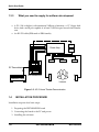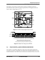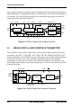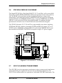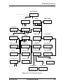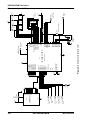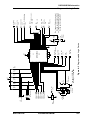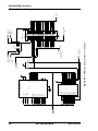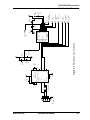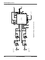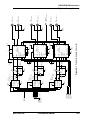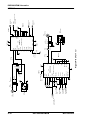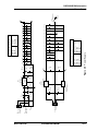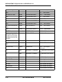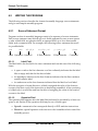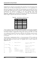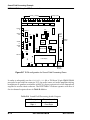
1
DSP56009EVM
User’s Manual
Motorola, Incorporated
Semiconductor Products Sector
DSP Division
6501 William Cannon Drive West
Austin, TX 78735-8598
Introduction
This document supports the DSP56009 Evaluation Module (DSP56009EVM)
including a description of its basic structure and operation, the equipment required
to use it, the specifications of the key components, the provided software (such as the
demonstration code and the software required to develop and debug sophisticated
applications), schematic diagrams, and a parts list. Section 1 is a Quick Start Guide.
Section 2 provides evaluation module specifications. Section 3 provides peripheral
specifications. Section 4 provides schematics for the DSP56009EVM. Section 5
provides PLD equations and schematics and the parts list. Section 6 provides an
example program and information on the debugger. Appendix A documents the
audio pass-through demonstration program provided with the EVM. Appendix B
describes the sound field processing demonstration. Appendix C includes additional
notes for using the Assembler. This document has been designed for users
experienced with DSP development tools. For users with little or no DSP experience,
detailed information is provided in the additional documents supplied with this kit.
OnCE is a trademark of Motorola, Inc.
Motorola reserves the right to make changes without further notice to any products herein. Motorola makes no
warranty, representation or guarantee regarding the suitability of its products for any particular purpose, nor does
Motorola assume any liability arising out of the application or use of any product or circuit, and specifically
disclaims any and all liability, including without limitation consequential or incidental damages. “typical”
parameters which may be provided in Motorola data sheets and/or specifications can and do vary in different
applications and actual performance may vary over time. All operating parameters, including “Typicals” must be
validated for each customer application by customer’s technical experts. Motorola does not convey any license
under its patent rights nor the rights of others. Motorola products are not designed, intended, or authorized for use
as components in systems intended for surgical implant into the body, or other applications intended to support
life, or for any other application in which the failure of the Motorola product could create a situation where personal
injury or death may occur. Should Buyer purchase or use Motorola products for any such unintended or
unauthorized application, Buyer shall indemnify and hold Motorola and its officers, employees, subsidiaries,
affiliates, and distributors harmless against all claims, costs, damages, and expenses, and reasonable attorney
fees arising out of, directly or indirectly, any claim of personal injury or death associated with such unintended or
unauthorized use, even if such claim alleges that Motorola was negligent regarding the design or manufacture of
the part. Motorola and
are registered trademarks of Motorola, Inc. Motorola, Inc. is an Equal
Opportunity/Affirmative Action Employer.
How to reach us:
USA/Europe/Locations Not
Listed:
Motorola Literature Distribution
P.O. Box 20912
Phoenix, Arizona 85036
1 (800) 441-2447 or
1 (602) 303-5454
MFAX:
[email protected]
TOUCHTONE (602) 244-6609
Asia/Pacific:
Motorola Semiconductors H.K. Ltd.
8B Tai Ping Industrial Park
51 Ting Kok Road
Tai Po, N.T., Hong Kong
852-2662928
Japan:
Nippon Motorola Ltd.
Tatsumi-SPD-JLDC
6F Seibu-Butsuryu-Center
3-14-2 Tatsumi Koto-Ku
Tokyo 135, Japan
03-3521-8315
Technical Resource Center:
1 (800) 521-6274
DSP Helpline
[email protected]
Internet:
http://www.motorola-dsp.com
-4
DSP56302EVMUM/AD, Preliminary
MOTOROLA
CONTENTS
SECTION 1
QUICK START GUIDE. . . . . . . . . . . . . . . . . . . . . . . 1-1
1.1
OVERVIEW . . . . . . . . . . . . . . . . . . . . . . . . . . . . . . . . . . . . . . 1-3
1.2
EVALUATION MODULE DESCRIPTION AND FEATURES . 1-3
1.3
EQUIPMENT . . . . . . . . . . . . . . . . . . . . . . . . . . . . . . . . . . . . . 1-4
1.3.1
What you get with the Evaluation Module . . . . . . . . . . . . . 1-4
1.3.2
What you need to supply for AC-3/ProLogic Demonstration .
1-5
1.3.3
What you need to supply for software development . . . . . 1-6
1.4
INSTALLATION PROCEDURE . . . . . . . . . . . . . . . . . . . . . . . 1-6
1.4.1
Preparing the DSP56009EVM . . . . . . . . . . . . . . . . . . . . . . 1-7
1.4.2
Connecting the DSP56009EVM to the PC and Power . . . 1-8
1.4.3
Installing the Software . . . . . . . . . . . . . . . . . . . . . . . . . . . . 1-9
SECTION 2
EVM THEORY OF OPERATION . . . . . . . . . . . . . . . 2-1
2.1
INPUTS AND OUTPUTS . . . . . . . . . . . . . . . . . . . . . . . . . . . . 2-3
2.1.1
Clock Select. . . . . . . . . . . . . . . . . . . . . . . . . . . . . . . . . . . . 2-4
2.1.2
Serial Audio Interface (SAI) . . . . . . . . . . . . . . . . . . . . . . . . 2-4
2.1.3
Sony-Philips digital interface format (SPDIF) . . . . . . . . . . 2-5
2.1.4
Other inputs and Outputs. . . . . . . . . . . . . . . . . . . . . . . . . . 2-5
2.1.5
Operating Mode Selection . . . . . . . . . . . . . . . . . . . . . . . . . 2-6
2.1.6
OnCE™ Port . . . . . . . . . . . . . . . . . . . . . . . . . . . . . . . . . . . 2-6
2.1.7
RS232 Connections and JP1. . . . . . . . . . . . . . . . . . . . . . . 2-7
2.1.8
Operating Modes and SRAM refresh in the 56009 . . . . . . 2-7
2.1.9
Evaluation Module Parts . . . . . . . . . . . . . . . . . . . . . . . . . . 2-7
2.1.10
Power Supplies . . . . . . . . . . . . . . . . . . . . . . . . . . . . . . . . . 2-8
2.1.11
Memory . . . . . . . . . . . . . . . . . . . . . . . . . . . . . . . . . . . . . . . 2-8
SECTION 3
PERIPHERAL SPECIFICATIONS . . . . . . . . . . . . . . 3-1
3.1
CS5390 STEREO ADC . . . . . . . . . . . . . . . . . . . . . . . . . . . . . 3-3
3.2
CS4331 STEREO DAC . . . . . . . . . . . . . . . . . . . . . . . . . . . . . 3-4
3.3
CS3310 STEREO DIGITAL VOLUME CONTROL . . . . . . . . . 3-4
3.4
CS8412 DIGITAL AUDIO INTERFACE RECEIVER . . . . . . . 3-5
MOTOROLA
DSP56009EVMUM
iii
3.5
3.6
3.7
3.8
3.9
CS8402A DIGITAL AUDIO INTERFACE TRANSMITTER . . 3-6
STK10C68 CMOS 2K X 8 NVSRAM . . . . . . . . . . . . . . . . . . . 3-7
SC937-02 AES/EBU TRANSFORMER . . . . . . . . . . . . . . . . . 3-7
LCD PANEL. . . . . . . . . . . . . . . . . . . . . . . . . . . . . . . . . . . . . . 3-8
WIRING FOR KEYPAD . . . . . . . . . . . . . . . . . . . . . . . . . . . . 3-11
SECTION
4
SECTION
5
5.1
5.1.1
5.1.2
5.2
DSP56009EVM SCHEMATICS. . . . . . . . . . . . . . . . 4-1
DSP56009EVM PLD SPECIFICATION AND EVM
PARTS LIST . . . . . . . . . . . . . . . . . . . . . . . . . . . . . .
EPM7032 PLD SPECIFICATIONS . . . . . . . . . . . . . . . . . . . .
PLD Schematics . . . . . . . . . . . . . . . . . . . . . . . . . . . . . . . .
PLD Equations . . . . . . . . . . . . . . . . . . . . . . . . . . . . . . . . .
EVALUATION MODULE PARTS LIST . . . . . . . . . . . . . . . . .
5-1
5-3
5-3
5-5
5-8
SECTION 6
EXAMPLE TEST PROGRAM . . . . . . . . . . . . . . . . . 6-1
6.1
OVERVIEW . . . . . . . . . . . . . . . . . . . . . . . . . . . . . . . . . . . . . . 6-3
6.2
WRITING THE PROGRAM . . . . . . . . . . . . . . . . . . . . . . . . . . 6-4
6.2.1
Source Statement Format . . . . . . . . . . . . . . . . . . . . . . . . . 6-4
6.2.2
Example Program . . . . . . . . . . . . . . . . . . . . . . . . . . . . . . . 6-5
6.3
ASSEMBLING THE PROGRAM . . . . . . . . . . . . . . . . . . . . . . 6-7
6.3.1
Assembler Command Format . . . . . . . . . . . . . . . . . . . . . . 6-7
6.3.2
Assembler Options . . . . . . . . . . . . . . . . . . . . . . . . . . . . . . 6-8
6.3.3
Assembler Directives . . . . . . . . . . . . . . . . . . . . . . . . . . . 6-11
6.3.4
Assembling the Example Program . . . . . . . . . . . . . . . . . 6-16
6.4
MOTOROLA DSP LINKER . . . . . . . . . . . . . . . . . . . . . . . . . 6-16
6.4.1
Linker Options . . . . . . . . . . . . . . . . . . . . . . . . . . . . . . . . . 6-17
6.4.2
Linker Directives . . . . . . . . . . . . . . . . . . . . . . . . . . . . . . . 6-23
6.5
INTRODUCTION TO THE DEBUGGER SOFTWARE . . . . 6-24
6.6
RUNNING THE PROGRAM . . . . . . . . . . . . . . . . . . . . . . . . 6-26
iv
DSP56009EVMUM
MOTOROLA
APPENDIX A
AUDIO PASS-THROUGH EXAMPLE . . . . . . . . . . .A-1
APPENDIX B
SOUND FIELD PROCESSING EXAMPLE . . . . . . .B-1
APPENDIX C
DSP56009EVM MULTIPLEX DEFINTITION . . . . . .C-1
MOTOROLA
DSP56009EVMUM
v
LIST OF FIGURES
Figure 1-1
Evaluation Module Component Layout . . . . . . . . . . . . . . . . . . . . 1-5
Figure 1-2
AC-3 Home Theater Demonstration. . . . . . . . . . . . . . . . . . . . . . . 1-6
Figure 1-3
Connecting the DSP56009EVM Cables. . . . . . . . . . . . . . . . . . . . 1-8
Figure 3-1
CS5390 ADC . . . . . . . . . . . . . . . . . . . . . . . . . . . . . . . . . . . . . . . . 3-3
Figure 3-2
CS4331 DAC . . . . . . . . . . . . . . . . . . . . . . . . . . . . . . . . . . . . . . . . 3-4
Figure 3-3
CS3310 Stereo Digital Volume Control . . . . . . . . . . . . . . . . . . . . 3-5
Figure 3-4
Serial Port Timing for the CS3310 . . . . . . . . . . . . . . . . . . . . . . . . 3-5
Figure 3-5
CS8412 Digital Audio Interface Receiver . . . . . . . . . . . . . . . . . . . 3-6
Figure 3-6
CS8402 Digital Audio Interface Transmitter . . . . . . . . . . . . . . . . . 3-6
Figure 3-7
STK10C68 8K x 8 nvSRAM . . . . . . . . . . . . . . . . . . . . . . . . . . . . . 3-7
Figure 3-8
SC937-02 AES/EBU Transformer . . . . . . . . . . . . . . . . . . . . . . . . 3-8
Figure 3-9
LCD Softswitch Screens. . . . . . . . . . . . . . . . . . . . . . . . . . . . . . . . 3-9
Figure 3-10
Keypad Wiring Diagram . . . . . . . . . . . . . . . . . . . . . . . . . . . . . . . 3-11
Figure 4-1
DSP56009 . . . . . . . . . . . . . . . . . . . . . . . . . . . . . . . . . . . . . . . . . . 4-3
Figure 4-2
Microcontroller and LCD. . . . . . . . . . . . . . . . . . . . . . . . . . . . . . . . 4-4
Figure 4-3
Programmable Logic Device . . . . . . . . . . . . . . . . . . . . . . . . . . . . 4-5
Figure 4-4
SRAM and External Memory Interface. . . . . . . . . . . . . . . . . . . . . 4-6
Figure 4-5
RS-232 and OnCE Interface . . . . . . . . . . . . . . . . . . . . . . . . . . . . 4-7
Figure 4-6
Analog-to-Digital Converter . . . . . . . . . . . . . . . . . . . . . . . . . . . . . 4-8
vi
DSP56009EVMUM
MOTOROLA
Figure 4-7
Digital-to-Analog Converter . . . . . . . . . . . . . . . . . . . . . . . . . . . . . 4-9
Figure 4-8
SPDIF I/O . . . . . . . . . . . . . . . . . . . . . . . . . . . . . . . . . . . . . . . . . 4-10
Figure 4-9
Power Supply . . . . . . . . . . . . . . . . . . . . . . . . . . . . . . . . . . . . . . 4-11
Figure 5-1
PLD Schematic . . . . . . . . . . . . . . . . . . . . . . . . . . . . . . . . . . . . . . 5-4
Figure 6-1
Development Process Flow. . . . . . . . . . . . . . . . . . . . . . . . . . . . . 6-3
Figure 6-2
Example Debugger Window Display . . . . . . . . . . . . . . . . . . . . . 6-25
Figure A-1
Output Interrupt Structure for Analog Input . . . . . . . . . . . . . . . . . A-4
Figure A-2
Output Interrupt Structure for Digital Input. . . . . . . . . . . . . . . . . . A-4
Figure A-3
DSP56009EVM Pass-through Setup. . . . . . . . . . . . . . . . . . . . . . A-6
Figure B-1
Early Reflection DO loop . . . . . . . . . . . . . . . . . . . . . . . . . . . . . . . B-6
Figure B-2
Early Reflection FIR Block (one channel) . . . . . . . . . . . . . . . . . . B-6
Figure B-3
Comb Filter (one of six) . . . . . . . . . . . . . . . . . . . . . . . . . . . . . . . . B-8
Figure B-4
All-pass Filter. . . . . . . . . . . . . . . . . . . . . . . . . . . . . . . . . . . . . . . . B-9
Figure B-5
All-Pass Filter Routine . . . . . . . . . . . . . . . . . . . . . . . . . . . . . . . . . B-9
Figure B-6
De-Correlation Routine . . . . . . . . . . . . . . . . . . . . . . . . . . . . . . . B-11
Figure B-7
EVM configuration for Sound Field Processing Demo . . . . . . . B-12
Figure B-8
Sound Field Processor . . . . . . . . . . . . . . . . . . . . . . . . . . . . . . . B-14
Figure B-9
Sound Field Processor Time Analysis. . . . . . . . . . . . . . . . . . . . B-18
Figure C-1
DSP56009EVM Jumper Setting for Multiplexing . . . . . . . . . . . . . C-5
MOTOROLA
DSP56009EVMUM
vii
LIST OF TABLES
Table 2-1
JP4 Jumpers . . . . . . . . . . . . . . . . . . . . . . . . . . . . . . . . . . . . . . . . 2-3
Table 2-2
JP5 Jumpers . . . . . . . . . . . . . . . . . . . . . . . . . . . . . . . . . . . . . . . . 2-4
Table 2-3
JP3 Jumpers . . . . . . . . . . . . . . . . . . . . . . . . . . . . . . . . . . . . . . . . 2-6
Table 5-1
DSP56009EVM Parts List . . . . . . . . . . . . . . . . . . . . . . . . . . . . . . 5-8
Table A-1
Output sources for audio pass-through . . . . . . . . . . . . . . . . . . . . A-5
Table B-1
Early Reflection FIR Structure . . . . . . . . . . . . . . . . . . . . . . . . . . . B-4
Table B-2
Comb filter loop-back gains . . . . . . . . . . . . . . . . . . . . . . . . . . . . . B-7
Table B-3
De-Correlation All-pass filter gains . . . . . . . . . . . . . . . . . . . . . . B-11
Table B-4
Sound Field Processing Audio Outputs. . . . . . . . . . . . . . . . . . . B-13
Table B-5
X and Y Memory Map for Sound Field Processing Demo . . . . . B-15
Table C-1
DSP56009EVM MUX Cable Pinout. . . . . . . . . . . . . . . . . . . . . . . C-3
MOTOROLA
DSP56009EVMUM
vii
viii
DSP56009EVMUM
MOTOROLA
SECTION 1
QUICK START GUIDE
MOTOROLA
DSP56009EVMUM
1-1
Quick Start Guide
1.1
1.2
1.3
1.3.1
1.3.2
1.3.3
1.4
1.4.1
1.4.2
1.4.3
1-2
OVERVIEW . . . . . . . . . . . . . . . . . . . . . . . . . . . . . . . . . . . . . . . . . .
EVALUATION MODULE DESCRIPTION AND FEATURES . . . . .
EQUIPMENT . . . . . . . . . . . . . . . . . . . . . . . . . . . . . . . . . . . . . . . . .
What you get with the Evaluation Module . . . . . . . . . . . . . . . .
What you need to supply for AC-3/ProLogic Demonstration . .
What you need to supply for software development. . . . . . . . .
INSTALLATION PROCEDURE . . . . . . . . . . . . . . . . . . . . . . . . . . .
Preparing the DSP56009EVM . . . . . . . . . . . . . . . . . . . . . . . . .
Connecting the DSP56009EVM to the PC and Power . . . . . . .
Installing the Software . . . . . . . . . . . . . . . . . . . . . . . . . . . . . . .
DSP56009EVMUM
1-3
1-3
1-4
1-4
1-5
1-6
1-6
1-7
1-8
1-9
MOTOROLA
Quick Start Guide
Overview
1.1
OVERVIEW
This document describes the basic structure, theory, and operation of the
DSP56009EVM (Evaluation Module), the equipment required to use the Evaluation
Module, and the specifications of the key components on the Evaluation Module.
Code samples and self-test code are provided on the accompanying software
diskette. Evaluation Module schematic diagrams and a parts list are included as well.
1.2
EVALUATION MODULE DESCRIPTION AND FEATURES
The DSP56009EVM is a low-cost platform for multichannel digital audio applications
design, prototyping, and development. The fully assembled and tested circuit board
contains:
• 24-bit DSP56009 Digital Signal Processor operating at 81 MHz for Dolby AC-3
and Dolby ProLogic
• 8192 bytes of off-chip SRAM and 8192 bytes of nonvolatile RAM
• Standard 30-pin SIMM slot for easy, inexpensive DRAM expansion
• One 20-bit stereo Analog-to-Digital converter (ADC), three 18-bit stereo
Digital-to-Analog converters (DACs)
• Programmable analog-domain attenuators on the Digital-to-Analog outputs
• RCA jacks for all analog audio Input/Output
• Optical and transformer-isolated electrical SPDIF/CP340 stereo digital audio
inputs and outputs
• 50-pin expansion connector to provide the capability for expansion and/or
substitution of other input/output peripherals, as well as easy interprocessor
communication between Motorola Evaluation Modules
• Socketed MC68HC711E9 (52-pin CLCC microcontroller) to allow the user to
substitute user-programmed microprocessor and prototype custom 68HC711
code (allows connection to MC68HC711 emulation systems)
• 2 × 16 character Liquid Crystal Display (LCD) and four softswitches for user
interface
• Connector provides capability to use optional standard 4 × 4 keypad matrix
• MC68705K1 microcontroller performing RS-232-to-OnCETM port command
conversions
MOTOROLA
DSP56009EVMUM
1-3
Quick Start Guide
Equipment
1.3
EQUIPMENT
The following section gives a brief summary of the equipment required to use the
Evaluation Module, some of which is supplied with the Evaluation Module, and
some of which will have to be supplied by the user.
1.3.1
What you get with the Evaluation Module
• Evaluation Module board (See Figure 1-1)
• 3.5" disk titled ’Debug - Evaluation Module’
• 3.5" disk titled ’DSP56009EVM Demos’
–
PCM Passthrough Files
–
Soundfield Processor Files
–
Example Assembly Language Files (example.asm)
• Debug - Evaluation Module manual
• DSP56000 Family Manual
• DSP56009 User’s Manual
• DSP56009 Technical Data sheet
• DSP56009 Product Brief
• DSP56009 EVM User’s Manual (this document), including Evaluation Module
Schematics and Demonstration software documentation
• Additional relevant documentation may be included in the form of a
READ.ME file on the Evaluation Module Software disk.
1-4
DSP56009EVMUM
MOTOROLA
Quick Start Guide
Equipment
RS
Left 3
Right 3
CS3310
Analog Inputs
Analog Outputs
LS
C
Sub
L
Left 2
Right 2
Left 1
CS4331 CS3310
CS4331
R
Right 1 Right In
CS3310
Left In
CS4331
CS5390
Optical
In
JP5
CS8412
JP3
Optical
Out
JP7
J5
JP2
30-Pin
SIMM
Socket
PLD
CS8402A
J3
J9
DSP
56009
JP4
SPDIF
In
Analog
Power
STK10C68
J18
SPDIF
Out
JP9
SC937-02
J4
JP6
68HC711E9
68HC705K1
JP1
RS-232
OnCETM
LCD Display
Reset
J1
J2
Digital
Power
Infrared
Remote
Receiver
Figure 1-1 Evaluation Module Component Layout
1.3.2
What you need to supply for AC-3/ProLogic
Demonstration
• An AC-3 or PCM bitstream source (i.e. Laserdisc, DAT, CD source, VHS, etc...)
• An audio amplifier driving headphones or speakers as shown on the
following page in Figure 1-2.
• Power supplies: dual 8-12V DC (for analog circuits), 8-15V AC or DC (for
digital circuits)
MOTOROLA
DSP56009EVMUM
1-5
Quick Start Guide
Installation Procedure
1.3.3
What you need to supply for software development
• A PC (-386 or higher) with minimum 2 Mbytes of memory, a 3.5” floppy disk
drive, and a serial port capable of at least 19,200 bits-per-second data transfer
rate.
• An RS-232 cable (DB9 male to DB9 female)
Subwoofer
(powered)
Power Amp
Subwoofer
(unpowered)
RF Demodulator
DSP56009EVM
Laserdisc Player
Listener
Figure 1-2 AC-3 Home Theater Demonstration
1.4
INSTALLATION PROCEDURE
Installation requires four basic steps:
1. Preparing the DSP56009EVM board
2. Connecting the board to the PC and power
3. Installing the software
1-6
DSP56009EVMUM
MOTOROLA
Quick Start Guide
Installation Procedure
4. Testing the installation
1.4.1
Preparing the DSP56009EVM
CAUTION
Because all electronic components are
sensitive to the effects of electrostatic
discharge
(ESD)
damage,
correct
procedures should be used when
handling all components in this kit and
inside the supporting personal computer.
Use the following procedures to minimize
the likelihood of damage due to ESD:
– Always handle all static-sensitive
components only in a protected area,
preferably a lab with conductive
(anti-static) flooring and bench
surfaces.
– Always use grounded wrist straps
when handling sensitive components.
– Never remove components from
anti-static packaging until required for
installation.
– Always transport sensitive
components in anti-static packaging.
MOTOROLA
DSP56009EVMUM
1-7
Quick Start Guide
Installation Procedure
1.4.2
Connecting the DSP56009EVM to the PC and Power
Figure 1-3 shows the interconnection diagram for connecting the PC and the external
power supply to the DSP56009EVM board. Use the following steps to complete cable
connections:
DB9 Interface
Cable
External
±8-12V
Power
PC-compatible
Computer
J4
J3
J2
Connect cable
to RS-232 port
External
+5V
Power
DSP56009EVM
Figure 1-3 Connecting the DSP56009EVM Cables
1. Connect the DB9P end of the RS-232 interface cable to the RS-232 port
connection on the PC.
2. Connect the DB9S end of the cable to J4, shown in Figure 1-1 on page 1-5, on
the DSP56009EVM board. This provides the connection to allow the PC to
control the board function.
3. Make sure that the external power supplies do not have power supplied to
them.
4. Connect the output power connectors into J2 and J3, shown in Figure 1-1
on page 1-5, on the DSP56009EVM board.
5. Apply power to the power supply. The green Power LED will light when
power is correctly applied.
1-8
DSP56009EVMUM
MOTOROLA
Quick Start Guide
Installation Procedure
1.4.3
Installing the Software
The DSP56009EVM demo software includes the following:
• Motorola diskette containing:
–
Demonstration code (passthru, sfpevm09, example)
• Domain Technologies diskette containing the windowed user interface debug
software
Use the following steps to install the software:
1. Insert the Motorola software diskette into the PC diskette drive.
2. If the system is not already running in Windows, start Windows.
3. From Windows, select a DOS window and run the install program. The
general format for the command line of the install program is
install <source>. For example, if your diskette drive is the a: drive, type in
a:install a:. The program installs the software in the default destination
c:\evm56007.
4. Close the DOS window and remove the Motorola software diskette from the
diskette drive. Insert the Domain Technologies diskette labeled Debug-56K
into the drive.
5. From Windows, run the Debugger installation program install.exe on the
diskette. This can be done from the Microsoft Windows Program Manager by
pulling down the File menu, choosing Run, entering a:install on the
command line, and clicking OK.
6. Read the README.TXT if you are installing the Debugger program for the
first time. This provides information in addition to that provided by the
Domain Technologies manual included with this kit.
7. The install program creates a program group called EVM56007 and a program
icon called EVM56007 within Windows. This step completes the software
installation.
MOTOROLA
DSP56009EVMUM
1-9
Quick Start Guide
Installation Procedure
1-10
DSP56009EVMUM
MOTOROLA
SECTION 2
EVALUATION MODULE THEORY OF
OPERATION
MOTOROLA
DSP56009EVMUM
2-1
Evaluation Module Theory of Operation
2.1
2.1.1
2.1.2
2.1.3
2.1.4
2.1.5
2.1.6
2.1.7
2.1.8
2.1.9
2.1.10
2.1.11
2-2
INPUTS AND OUTPUTS. . . . . . . . . . . . . . . . . . . . . . . . . . . .
Clock Select . . . . . . . . . . . . . . . . . . . . . . . . . . . . . . . . . . .
Serial Audio Interface (SAI). . . . . . . . . . . . . . . . . . . . . . . .
Sony-Philips digital interface format (SPDIF) . . . . . . . . . .
Other inputs and Outputs . . . . . . . . . . . . . . . . . . . . . . . . .
Operating Mode Selection. . . . . . . . . . . . . . . . . . . . . . . . .
OnCE™ Port . . . . . . . . . . . . . . . . . . . . . . . . . . . . . . . . . . .
RS232 Connections and JP1 . . . . . . . . . . . . . . . . . . . . . .
Operating Modes and SRAM refresh in the 56009 . . . . . .
Evaluation Module Parts . . . . . . . . . . . . . . . . . . . . . . . . . .
Power Supplies . . . . . . . . . . . . . . . . . . . . . . . . . . . . . . . . .
Memory . . . . . . . . . . . . . . . . . . . . . . . . . . . . . . . . . . . . . . .
DSP56009EVMUM
2-3
2-4
2-4
2-5
2-5
2-6
2-6
2-7
2-7
2-7
2-8
2-8
MOTOROLA
Evaluation Module Theory of Operation
Inputs and Outputs
Refer to Section 4, 56009EVM Schematics, for reference to pinouts and jumper
configurations.
2.1
INPUTS AND OUTPUTS
Analog signals connected to the Evaluation Module inputs are converted to 20 bit
data at the ADC. U19 and U20 attenuate the signal and convert it to Balanced mode.
The ADC has the Select Serial I/O Mode (SMODE) pin pulled high to make the ADC
the SAI receive clock master. When the ADC is in Master mode, the ADC’s Serial
Data Clock (SCLK) and Left/Right Select (L/R) word clock pins are outputs. The
L/R word clock output is the opposite polarity of I2S. It is inverted in the
Programmable Logic Device (PLD) to create true I2S. The ADC receives its
oversampling clock on the Digital Section Clock Input (ICLKD), which is then
internally divided by two, and this signal is provided to the Analog Section Clock
Input (ICLKA). ICLKD can be driven from the 11.2896 MHz clock, the 12.288 MHz
clock, or the 256 × Fs clock produced by the CS8412 AES/EBU Receiver. The Audio
Power Down input (APD) and Digital Power Down input (DPD) pins are wired to
the Cntl_Mute signal of the PLD. When pulled high, the ADC will be muted. When
first pulled low, the ADC will be reset, then it will be enabled.
The other possible input source comes from the SPDIF inputs (J14 for electrical input
and J17 for optical input). Jumper JP4 selects the source (see Table 2-1 below). When
receiving valid SPDIF input, the SPDIF Receiver drives the Master Clock (MCK)
output that is 256 times the Frame Sync frequency of the received data. The CS8412
operates in Mode 3, the I2S Slave mode.
Table 2-1 JP4 Jumpers
Selection
Electric
SPDIF
MOTOROLA
Jumper
Settings
JP4.1 to
JP4.3
JP4.2 to
JP4.4
DSP56009EVMUM
2-3
Evaluation Module Theory of Operation
Inputs and Outputs
Table 2-1 JP4 Jumpers
Selection
Optical
SPDIF
2.1.1
Jumper
Settings
JP4.3 to
JP4.5
JP4.4 to
JP4.6
Clock Select
The Evaluation Module provides a means for the user to select which clock controls
the reception and transmission of digital audio (see Table 2-2 below). JP2 selects the
ADC and DAC clocks which, when jumpered, are set at 44.1 KHz and, when not
jumpered, at 48 KHz. The expansion connector, J5, can be used to directly access the
DSP. The receive SAI bus may be clocked by the selection made at JP2 (44.1 KHz or
48 KHz) or be clocked by the received SPDIF signal. The transmit SAI bus may be
clocked by either the clock selected at JP2 or by the received SPDIF signal. It is the
user’s responsibility to ensure that data is output at the desired rate. See Table 2-2,
below.
Table 2-2 JP5 Jumpers
Receive
/Transm
it
2.1.2
Jumper JP5.1
to JP5.2
Jumper JP5.3
to JP5.4
No Jumper
Rx
Clocked by crystal
–
Clocked by received
SPDIF
Tx
–
Clocked by crystal
Clocked by received
SPDIF
Serial Audio Interface (SAI)
The DSP56009 SAI transmitter drives the six analog outputs and the SPDIF output.
I2S is the Default mode for the DACs. The Master Clock (MCLK) rate for the DACs is
256 × Fs. The dual RC networks after the DACs serve as AC couplers for audio data,
2-4
DSP56009EVMUM
MOTOROLA
Evaluation Module Theory of Operation
Inputs and Outputs
and as low-pass filters to convert the delta-sigma digital output pulses to analog
waveforms.
The digitally controlled analog domain attenuators receive the audio data and
attenuate or amplify the data as determined by the microcontroller. The attenuators
receive the Serial Clock input (SCLK), Serial Data Input (SDATAI), and the Chip
Select/latch (CS) from the microcontroller.
2.1.3
Sony-Philips digital interface format (SPDIF)
The SPDIF transmitter receives data from the DSP through the Serial Data input
(SDATA) using the Frame Sync (FSYNC) and the Serial Data Clock (SCK). The
transmitter outputs SPDIF audio signals through J15 (electrical) and J16 (optical).
Fs_sens from the clock select appears at the expansion connector in order to read the
sampling rate with the DSP’s General Purpose I/O (GPIO1) at J5.41 and also at U21-2
to select the state of the ‘sample-rate’ bits transmitted within the channel status block.
See the SPDIF specification for more information. The channel status bits and block
sync signals (DRcv_Blk, DTrn_Blk, DRcv_CS, and DTrn_CS) are available at J5.43 to
allow the DSP to read one of them, as well. Isolation transformers are used on both
input and output, although they are not strictly required for SPDIF because this
Evaluation Module is intended to be used as a development system.
2.1.4
Other inputs and Outputs
The clock master is derived from one of two sources: the 11.2896 MHz clock or the
12.288 MHz clock. The microcontroller also receives commands from either the soft
switches (S1, S2, S3, or S4) or from the Keypad Expansion Port, J18. The current user
screen or the results of these commands are then displayed by a modular LCD panel
with a 2 × 16 character display. The microcontroller code is capable of driving larger
LCD displays, but all user screens are designed for a 2 × 16 character display.
The MC68HC711E9 communicates with the DSP via the Serial Host Interface (SHI)
port in SPI mode. When SS is pulled low, the microcontroller can write to the DSP.
The MOSI and MISO lines pass control data through the DSP SHI in 24-bit mode.
SCK is the SPI Shift Clock from the DSP. Again, the expansion connector, J5, can be
used to access or intercept host port communications.
MOTOROLA
DSP56009EVMUM
2-5
Evaluation Module Theory of Operation
Inputs and Outputs
The Control_Data, Control_Clock, and Control_Latch lines from the microcontroller
control the digitally controlled analog domain attenuators. The Control_Mute line
mutes the ADC and the DACs; low is muted, high is enabled.
2.1.5
Operating Mode Selection
DSP56009EVM modes can be selected at JP3, as shown in Table 2-3. Once the mode
has been selected, the PLD can receive interrupts from the network attached to J19.
Table 2-3 JP3 Jumpers
Mode
JP3.5 to
JP3.6
JP3.3 to
JP3.4
JP3.1 to
JP3.2
0
X
X
X
1
X
X
-
2
X
-
X
3
X
-
-
4
-
X
X
5
-
X
-
6
-
-
X
7
-
-
-
X = jumper installed; - = no jumper
2.1.6
OnCE™ Port
The OnCETM port interface operates by receiving the serial data from the RS-232
Transceiver and executing commands sent by the host computer. These commands
can reset the DSP, put the DSP in Debug mode, release the DSP from Debug mode,
read and write to the OnCETM port, and read and write to the DSP itself. The serial bit
rate is 19,200 bits/second. The RS-232 serial communications are performed in
software on the MC68705K1. Port A of the MC68705K1 communicates with the DSP,
and Port B communicates with the host computer. The acknowledge signal from the
OnCETM port is a low-going pulse on DS0. Since the 68705K1 is too slow to reliably
2-6
DSP56009EVMUM
MOTOROLA
Evaluation Module Theory of Operation
Inputs and Outputs
catch this very narrow pulse, the pulse is latched in the PLD and the output of the
latch appears on the ACK pin (PA2). When this occurs, the 68705K1 illuminates red
LED D5 to indicate that the DSP is in the Debug mode. For more information on the
OnCE port, see the DSP56000 Family Manual. The reset switch will reset the
microcontroller, which will subsequently reset the DSP56009. The MC68705K1
source and object code are available from the Motorola DSP Division; contact your
local Motorola FAE.
2.1.7
RS232 Connections and JP1
RS-232 is an often-abused standard, and the direction of the signals present on pins 2
and 3 of the DB9 connector do not always conform to the standard. JP1 provides the
user with the ability to reverse these two pin connections without resorting to NULL
Modem adapters or rewiring cable connectors. As shipped, JP1.1 is connected via
shorting jumpers to JP1.3 and JP1.2 is connected to JP1.4. This connects J4.2 to the
OUTPUT of the Evaluation Module’s RS-232 level converter (U4) and J4.3 to the
INPUT of the board’s RS-232 receiver. These directions can be reversed by
reorienting the shorting jumpers and turning them 90 degrees (one-quarter turn),
thereby connecting JP1.1 to JP1.2 and JP1.3 to JP1.4. The user should never need to
rewire an RS-232 connector in order to establish Evaluation Module communications
with a host computer.
2.1.8
Operating Modes and SRAM refresh in the 56009
In Modes 0, 1, 2, and 3 the SRAM is refreshed from the nvRAM and the DSP can
bootstrap from the SRAM via the EMI if a valid Bootstrap mode is used. When in
Modes 4, 5, 6, and 7 the SRAM is not refreshed. Refreshes are not affected by jumpers
on the expansion connector, J5. Jumpers J5.37 and J5.39 must be inserted to have full
DSP control of the SRAM and nvRAM after bootstrap.
2.1.9
Evaluation Module Parts
The parts list of the DSP56009EVM is shown in Section 5.
MOTOROLA
DSP56009EVMUM
2-7
Evaluation Module Theory of Operation
Inputs and Outputs
2.1.10
Power Supplies
The Evaluation Module requires power sources, for both analog and digital circuits,
in order to operate. Bipolar analog power (use a linear power supply for best results)
is received through screw terminals at J3. Digital power is received through screw
terminals at J2 or via a 2.1mm connector (J1). When the power is on, D6 (green LED)
is illuminated. Analog power input may be 8 to 12 volts and digital power input may
be 8 to 15 volts. While the voltage regulator can accommodate higher input voltage
potentials, the added heat dissipation required at these input voltage levels will
result in the regulator becoming dangerously warm, and it is not recommended that
the user subject the board to power inputs in excess of the maximum levels listed.
Note:
2.1.11
Always supply the Evaluation Module with analog power prior to or
simultaneous with the application of digital power. If digital power is
supplied before the analog power, the DACs may go into one of three
possible error modes (no long-term damage to the device will occur), and
will not function correctly. If analog power is supplied first, or if both
analog power and digital power are applied simultaneously, these
problems do not appear and the DACs are properly initialized.
Memory
The Evaluation Module has 8192 bytes each of fast Static RAM (SRAM) and of
nonvolatile RAM (nvRAM). The SRAM operates at zero wait states at a 40 MHz DSP
clock speed, one wait state at 50, 66 MHz and two wait states at 81 MHz. The contents
of the SRAM may be block-loaded into nvRAM and the contents of the nvRAM may
be block- loaded into the SRAM. The lowest 3072 bytes of the nvRAM may also be
used to store code to load into the DSP via EMI bootstrap.
2-8
DSP56009EVMUM
MOTOROLA
SECTION 3
PERIPHERAL SPECIFICATIONS
MOTOROLA
DSP56009EVMUM
3-1
Peripheral Specifications
3.1
3.2
3.3
3.4
3.5
3.6
3.7
3.8
3.9
3-2
CS5390 STEREO ADC . . . . . . . . . . . . . . . . . . . . . . . . . . . . . 3-3
CS4331 STEREO DAC . . . . . . . . . . . . . . . . . . . . . . . . . . . . . 3-4
CS3310 STEREO DIGITAL VOLUME CONTROL . . . . . . . . 3-4
CS8412 DIGITAL AUDIO INTERFACE RECEIVER . . . . . . . 3-5
CS8402A DIGITAL AUDIO INTERFACE TRANSMITTER . . 3-6
STK10C68 CMOS 2K X 8 NVSRAM . . . . . . . . . . . . . . . . . . . 3-7
SC937-02 AES/EBU TRANSFORMER . . . . . . . . . . . . . . . . . 3-7
LCD PANEL. . . . . . . . . . . . . . . . . . . . . . . . . . . . . . . . . . . . . . 3-8
WIRING FOR KEYPAD . . . . . . . . . . . . . . . . . . . . . . . . . . . . 3-11
DSP56009EVMUM
MOTOROLA
Peripheral Specifications
CS5390 Stereo ADC
The following section describes the various peripheral devices used on the
DSP56009EVM and includes any necessary equations and information. Contact
information for the manufacturers of significant peripheral devices is included along
with the parts listing in Section 5.
3.1
CS5390 STEREO ADC
The CS5390 is a complete Analog-to-Digital Converter (ADC) for stereo digital audio
systems. It performs sampling, analog-to-digital conversion and anti-alias filtering,
generating 20-bit values for both left and right inputs in serial form. The output word
rate can be up to 50 kHz per channel.
The CS5390 uses fifth-order, delta-sigma modulation with 64 times oversampling
followed by digital filtering and decimation, which removes the need for an external
anti-alias filter, beyond the simple balanced RC filter formed by R25, R26, and C8
(R31, R32, and C20 for the right channel).
The ADC uses a differential architecture that provides excellent noise rejection. The
CS5390 has a filter passband of DC to 21.7 kHz. The filters are linear phase, have
0.005 dB passband ripple, and greater than 100 dB stopband rejection. The operating
temperature range is 0o to 70o.
ICLKA
APD
28
27
VREF+
VREF-
4
+
-
DAC
25
AGND
26
20
ICLKD
+
-
FSYNC SCLK L/R
19
16
14
13
Serial Output Interface
+
-
LP Filter
S/H
1
OCLKD
5
Voltage Reference
AINLAINL+ 3
AINRAINR+
ACAL
2
22
15
11
12
SDATA
CMODE
SMODE
Digital Decimation
Filter
Comparator
Digital Decimation
Filter
+
-
LP Filter
S/H
DAC
23
VA+
24
VA-
Comparator
Calibration
Microcontroller
7
VL+
9
6
LGND
10
DCAL DPD
Calibration
SRAM
17
VD+
18
DGND
Figure 3-1 CS5390 ADC
MOTOROLA
DSP56009EVMUM
3-3
Peripheral Specifications
CS4331 Stereo DAC
3.2
CS4331 STEREO DAC
The CS4331 is a complete stereo Digital-to-Analog Converter (DAC) with 18-bit
resolution, including interpolation, 1-bit digital-to-analog conversion, and output
analog filtering in an 8-pin package. The CS4331 is based on delta-sigma modulation
where the modulator output controls the reference voltage input to an ultra-linear
analog low-pass filter. This architecture allows for infinite adjustment of sample rate
between 1 kHz and 50 kHz while maintaining linear phase response, simply by
changing the master clock frequency. The CS4331 contains optional on-chip
de-emphasis and operates from a single +5 V power supply.
The CS4331 has a 96 dB dynamic range, less than 0.003% THD, low clock jitter
sensitivity and completely filtered line level outputs that use linear-phase filtering.
.
DEM/SCLK/CONFIG
2
LRCK
SDATAI
AGND VA+
6
7
3
1
Serial Input
Interface
De-emphasis
Voltage Reference
Interpolator
Delta-Sigma
Modulator
DAC
Analog
Low-Pass
Filter
Interpolator
Delta-Sigma
Modulator
DAC
Analog
Low-Pass
Filter
8
5
AOUTL
AOUTR
4
MCLK
Figure 3-2 CS4331 DAC
3.3
CS3310 STEREO DIGITAL VOLUME CONTROL
The CS3310 is a complete stereo digital volume control designed specifically for
audio systems. It features a 16-bit serial interface that controls two independent, low
distortion (0.001% THD + N) audio channels.
The CS3310 includes an array of well-matched resistors and a low-noise active
output stage that is capable of driving a 600 Ω load. A total adjustable range of 127
dB, in 0.5 dB steps, is achieved through 95.5 dB of attenuation and 31.5 dB of gain.
3-4
DSP56009EVMUM
MOTOROLA
Peripheral Specifications
CS8412 Digital Audio Interface Receiver
The simple 3-wire interface provides daisy-chaining of multiple CS3310s for
multi-channel audio systems. The device operates from ±5V supplies and has an
input/output voltage range of ±3.75 V.
AINL 16
14
+
-
M
U
X
AOUTL
8
MUTE
8
1
8
AGNDL 15
AGNDR 10
8
M
U
X
AINR
Control
Register
8
2
16
Serial to
Parallel
Register
+
9
12
13
4
VA+ VA- VD+
3
7
6
ZCEN
CS
SDATAI
SDATAO
SCLK
AOUTR
5
DGND
Figure 3-3 CS3310 Stereo Digital Volume Control
CS
SCLK
SDATAI
R7 R6 R5 R4 R3 R2 R1 R0 L7
L6 L5 L4 L3 L2
L1 L0
SDATAO
R7 R6 R5 R4 R3 R2 R1 R0 L7
L6 L5 L4 L3 L2
L1 L0
L0 = Left Channel Least Significant Bit R0 = Right Channel Least Significant Bit
L7 = Left Channel Most Significant Bit R7 = Right Channel Most Significant Bit
SDATA is latched internally on the rising edge of SCLK
SDATAO transitions after the falling edge of SCLK
SDATAO bits reflect the data previously loaded into the CS3310
Figure 3-4 Serial Port Timing for the CS3310
3.4
CS8412 DIGITAL AUDIO INTERFACE RECEIVER
The CS8412 is a monolithic CMOS device that receives and decodes audio data
according to the AES 3 - 1992, EBU Tech. 3250-E, IEC 958, SPDIF, and EIAJ CP-340
interface standards. The CS8412 receives data from a transmission line, recovers the
MOTOROLA
DSP56009EVMUM
3-5
Peripheral Specifications
CS8402A Digital Audio Interface Transmitter
clock and synchronization signals, and de-multiplexes the audio and non-audio data.
Either differential or single-ended inputs can be decoded. The CS8412 de-multiplexes
the channel, user, and validity data directly to dedicated output pins for the most
commonly needed channel status bits.
VD+
DGND
7
9
RXP
10
RXN
VA+
8
FILT
22
AGND
20
MCK
21
19
Clock & Data
Recovery
RS-422
Receiver
16
CS12/FCK
SEL
6
17 18 24 23
Audio
Serial Port
De-Mux
Mux
13
M3 M2 M1 M0
5
Mux
4
Registers
3
2
1
CO/ Ca/ Cb/ Cc/ Cd/ Ca/
E0 E1 E2 F0 F1 F2
25
26
12
11
1
14
28
SDATA
SCLK
FSYNC
C
U
VERF
15
ERF CBL
Figure 3-5 CS8412 Digital Audio Interface Receiver
3.5
CS8402A DIGITAL AUDIO INTERFACE TRANSMITTER
The CS8402A is a monolithic CMOS device that encodes and transmits audio data
according to the AES 3 - 1992, EBU Tech. 3250-E, IEC 958, SPDIF, and EIAJ CP-340
interface standards. The CS8402A accepts audio and non-audio data and multiplexes
and encodes the data. The audio serial port is double-buffered and capable of
supporting a wide variety of formats. The CS8402A multiplexes the channel, user,
and validity data directly from dedicated input pins for the most commonly needed
channel status bits.
M2 M1 M0
23 22 21
6
SCK
7
FSYNC
8
SDATA
C
U
V
10
11
9
MCK
5
RST
16
Audio
Serial Port
RS422 Driver
MUX
Registers
20
17
TXP
TXN
7
15
Dedicated Channel
Status Bits
24
CBL TRNPT
Figure 3-6 CS8402 Digital Audio Interface Transmitter
3-6
DSP56009EVMUM
MOTOROLA
Peripheral Specifications
STK10C68 CMOS 2k x 8 nvSRAM
3.6
STK10C68 CMOS 2K X 8 NVSRAM
The Simtek STK10C68 is a Fast Static RAM (25, 30, 35, and 45ns), with a nonvolatile
electrically-erasable PROM (EEPROM) element incorporated in each static memory
cell. The SRAM can be read and written an unlimited number of times while
independent, nonvolatile data resides in EEPROM. Data may easily be transferred
from the SRAM to the EEPROM (STORE cycle), or from the EEPROM to the SRAM
(RECALL cycle) using the NE pin (Nonvolatile Enable). It combines the high
performance and ease of use of a fast SRAM with nonvolatile data integrity.
The STK10C68 features 12, 15, 20, and 25 ns output enable access times, hardware
STORE and RECALL initiation, automatic STORE and RECALL timing, 104 or 105
STORE cycles to EEPROM, unlimited RECALL cycles from EEPROM, and 10-year
data retention in EEPROM. The STK10C68 requires a single +5 V power supply.
Input Buffers
A3
A4
A5
A6
A7
A8
A9
A12
EEPROM Array
256 × 256
Store
Static RAM
Recall
Array
256 × 256
Input Buffers
DQ0
DQ1
DQ2
DQ3
DQ4
DQ5
DQ6
DQ7
Column I/O
Column Decoder
Store/
Recall
Control
A0 A1 A2 A10 A11
G
NE
E
W
Figure 3-7 STK10C68 8 K × 8 nvSRAM
3.7
SC937-02 AES/EBU TRANSFORMER
The AES/EBU circuit incorporates a transformer to reject common mode interference
while transmitting the signal with fast rise time and minimum aberration. The
SC937-02 is a surface mount, low capacitance, wide-band AES/EBU transformer. The
MOTOROLA
DSP56009EVMUM
3-7
Peripheral Specifications
LCD Panel
SC937-02 has a very low capacitance shielded winding that reduces both radiated
and received noise coupling and provides decreased jitter and improved audio
quality, especially in noisy environments. EMI compliance and EMI susceptibility are
improved by the use of this type of transformer. The transformer’s ratio is 1:1,
primary inductance is 600 µH, inter-winding capacitance is 1.1 pF, bandwidth is 16
kHz to 100 MHz, and rise-time is 3 ns.
Input
Input Rtn
1
8
2
7
3
6
4
5
Output Rtn
Output
Figure 3-8 SC937-02 AES/EBU Transformer
3.8
LCD PANEL
illustrates the different screens of the LCD panel and the corresponding actions of
the soft switches.
3-8
DSP56009EVMUM
MOTOROLA
Peripheral Specifications
LCD Panel
MAIN MENU
Slct Code/v1.09
Reset always returns here:
AC-3 PCM
AC-3
Master Volume
PCM
Mstr Vol
Pro Noise Mstr
Mstr
+
Logic Seq Vol
AC-3 Vol
-
>+6 dB
Ext
See Right
AC-3
Compression
AC-3
AC-3...
Cmp>Lin
Cst1 Cst2 Lin RF
Lo Dyn Rnge Cntrl
AC-3 DCR
+
-
Ext
Nxt
+
-
Lo> 0.00
Ext
Nxt
LFE
Off
Pro Logic > Off
DRC Logic Nxt
Off
Out
PL3 PL4 Ext
Format > 3/2
AC-3 Information
Stat > OK
Nml
Format > 3/2
3/0 Nxt
Wid
LF
Nxt
C
Nxt
Noise Gen > LF
LS
RS
SW
Nxt
Additional Menu
Noise Sequencer
Surr
Noise Gen > LF
Dly
Ctr
Samp
Dly Rat Ext
Ext Nxt
Sample Rate
Format > 3/2
3/1 3/2
RF
Noise Sequencer
Phtm Nxt
Samp Rat > 48 kHz
Nxt
48
Surround Delay
Continued on New Page
Noise Gen > LF
Output Format
Out
Ext Nxt
Noise Sequencer
Cntr Mode > Nml
1/0 2/0 20PL Nxt
2/1 2/2
Nxt
Pro Logic
On/Off/Auto
Output Format
Out
Auto
Pro Logic > PL4
Info Fmt LFE Nxt
Out
Ext
On
ProLogic
Output Format
LFE Level > On
On
Pro
Additional
Menus
Hi> 0.00
Hi Dyn Rnge Cntrl
AC-3 DCR
Cmp
Pro Logic On/Off
Surr
+
Delay
-
>0 ms
Ext
44.1 32
Ext
Center Delay
Cntr
+
Delay
-
>0 ms
Ext
Figure 3-9 LCD Softswitch Screens
MOTOROLA
DSP56009EVMUM
3-9
Peripheral Specifications
LCD Panel
AC-3 Information
AC-3 Information
AC-3 Information
AC-3 Information
Smp Rat>48 kHz
BS
Lang Cd > 9
Tim Cod > - sec/8
Mod > Main
Ext Nxt
Ext Nxt
Ext Nxt
Ext Nxt
AC-3 Information
AC-3 Information
AC-3 Information
AC-3 Information
BS
C Mx Lv > -3 dB
Lang Cd #2 > 0
Tim Cod > - sec%8
Rat>384 kb/s
Ext Nxt
Ext Nxt
Ext Nxt
Ext Nxt
AC-3 Information
AC-3 Information
AC-3 Information
AC-3 Information
Extra Word > No
S Mx Lv > -3 dB
Rm Typ > -
Tim Cod > - frm
Ext Nxt
Ext Nxt
Ext Nxt
Ext Nxt
AC-3 Information
AC-3 Information
AC-3 Information
AC-3 Information
LFE
Dolby surr> Unk
Mix Lv > -
Tim Cod > - frc
Present > No
Ext Nxt
Ext Nxt
Ext Nxt
Ext Nxt
AC-3 Information
AC-3 Information
AC-3 Information
AC-3 Information
Aud Cod > 3/2
Cpyrght Prot> Yes
Rm Typ #2 > -
Stat > OK
Ext Nxt
Ext Nxt
Ext Nxt
AC-3 Information
AC-3 Information
AC-3 Information
Frm Sz > 768 wds
Original BS > Yes
Mix Lv #2 > -
Ext Nxt
Ext Nxt
Ext Nxt
AC-3 Information
AC-3 Information
AC-3 Information
CRC Sz > 468 wds
Dial Nm > 0
Tim Cod > - hr
Ext Nxt
Ext Nxt
Ext Nxt
AC-3 Information
AC-3 Information
AC-3 Information
BS ID > 8
Dial Nm #2 > 0
Tim Cod > - min
Ext Nxt
3-10
Ext Nxt
Ext Nxt
Back to Smp Rat Menu
Ext Nxt
DSP56009EVMUM
MOTOROLA
Peripheral Specifications
Wiring For Keypad
3.9
WIRING FOR KEYPAD
A wiring diagram for a generic keypad is shown in Figure 3-10. The keypad is not
provided with the DSP56009EVM.
9
8
7
6
Button # 1
5
4
3
Button # 16
2
1
10
MOTOROLA
Figure 3-10 Keypad Wiring Diagram
DSP56009EVMUM
3-11
SECTION 4
DSP56009EVM SCHEMATICS
MOTOROLA
DSP56009EVMUM
4-1
DSP56009EVM Schematics
Figure 4-1
Figure 4-2
Figure 4-3
Figure 4-4
Figure 4-5
Figure 4-6
Figure 4-7
Figure 4-8
Figure 4-9
4-2
DSP56009 . . . . . . . . . . . . . . . . . . . . . . . . . . . . . . . . . . 4-3
Microcontroller and LCD. . . . . . . . . . . . . . . . . . . . . . . . 4-4
Programmable Logic Device . . . . . . . . . . . . . . . . . . . . 4-5
SRAM and External Memory Interface . . . . . . . . . . . . . 4-6
RS-232 and OnCE Interface . . . . . . . . . . . . . . . . . . . . 4-7
Analog-to-Digital Converter . . . . . . . . . . . . . . . . . . . . . 4-8
Digital-to-Analog Converter . . . . . . . . . . . . . . . . . . . . . 4-9
SPDIF I/O . . . . . . . . . . . . . . . . . . . . . . . . . . . . . . . . . . 4-10
Power Supply . . . . . . . . . . . . . . . . . . . . . . . . . . . . . . . 4-11
DSP56009EVMUM
MOTOROLA
MOTOROLA
DSP_MODC
3-B3
DSP_MODB
3-B3
DSP_MODA
3-B3
EMI
3-F3, 5-A4
DSP_RST
3-B4, 2-G3, 4-F3
77
78
2
79
80
3
~MWR
4
5
7
11
12
13
14
16
18
19
20
22
23
24
25
62
63
64
65
67
68
69
71
MA13
MA12
MA11
MA10
MA9
MA8
MA7
MA6
MA5
MA4
MA3
MA2
MA1
MA0
MD7
MD6
MD5
MD4
MD3
MD2
MD1
MD0
~MRAS
~MCAS
DVCC0
DSP56009EVMUM
MD7
MD6
MD5
MD4
MD3
MD2
MD1
MD0
MA14
MA13
MA12
MA11
MA10
MA9
MA8
MA7
MA6
MA5
MA4
MA3
MA2
MA1
MA0
33
32
30
31
27
1
AGND0 8
AGND1 15
AGND2 21
AGND3
17
AVCC1 6
AVCC0
~HREQ 43
SCK/SCL 26
35
MISO/SDA 42
~SS/HA2 41
MOSI/HA0
73
74
75
76
+5V
SDI1
SDI0
SCKR
WSR
56
SDI1
SDI0 57
SCKR 51
WSR 55
GPIO3
GPIO2
GPIO1
GPIO0
SDO2
SDO1
SDO0
SCKT
WST
45
46
47
49
50
SDO2
SDO1
SDO0
SCKT
WST
SGND2 54
SGND1 44
SGND0 34
48
SVCC1 40
SVCC0
+5V
+5V
C1
0.01 µF
Figure 4-1 DSP56009
~MWR
~MCS0
MA17/~MCS1
MA16/~MCS2
MA15/~MCS3
~MRD
PVCC
PCAP
PINIT
PGND
EXTAL
61
DR
DSO 58
DSI/OS0 59
DSCK/OS1 60
+5V
DSP5600 9
~RESET
MODA/~IRQA
MODB/~IRQB
MODC/~NMI
QVCC2
QVCC1
QVCC0
QGND2
QGND1
QGND0
DSP56009
72
DGND1
66 DGND0
70
~MRD
+5V
36
37
38
39
53
28
9
52
29
10
+5V
D_HREQ
D_SCK
D_MISO
D_SS
D_MOSI
GPIO3
GPIO2
GPIO1
GPIO0
R6
10 K
DSP_Clk
3-F2
EXP1
5-G4
/DR
4-F4
DSO
4-F4, 3-F4
DSI/OS0
4-F5
DSCK/OS1
4-F5
7 68 kHz
OnCE Int er f ace
DSP56009EVM Schematics
DSP56009
4-3
4-4
U16
3
Vo
2
DSP56009EVMUM
HC11_GPIO
5-F5
Cntl_Mute
7-G4, 3-D4, 8-B5
Cntl_Latch
7-A6
Cntl_Clk
7-A6
Cntl_Data
7-A6
Vss
1
LCD Panel
2
Vdd
+5V
14
13
12
11
10
9
8
7
6
E5
R/W 4
RS
DB7
DB6
DB5
DB4
DB3
DB2
DB1
DB0
R20
20 K
Contrast
3
1
R8
10 K
E
R/W
RS
PC7
PC6
PC5
PC4
PC3
PC2
PC1
PC0
VRH
STRB/R/~W
PB7/A15
PB6/A14
PB5/A13
PB4/A12
PB3/A11
PB2/A10
PB1/A9
PB0/A8
PC7/A7/D7
PC6/A6/D6
PC5/A5/D5
PC4/A4/D4
PC3/A3/D3
PC2/A2/D2
PC1/A1/D1
PC0/A0/D0
26
Vdd
2 MODB/VSTBY
3 MODA/~LIR
51 VRL
52
6
35
36
37
38
39
40
41
42
16
15
14
13
12
11
10
9
Vss
1
Microcontroller
8
XTAL
STRA/AS
5
E
4
PE7/AN7
PE3/AN3
PE6/AN6
PE2/AN2
PE5/AN5
PE1/AN1
PE4/AN4
PE0/AN4
PD5/~SS
PD4/SCK
PD3/MOSI
PD2/MISO
PD1/TxD
PD0/RxD
1
2
3
4
5
6
7
8
9
+5V
JP9
Configuration
Jumpers
50
49
48
47
46
45
44
43
25
24
23
22
21
20
XIRQ 18
RESET 17
19
IRQ
PA0/IC3 34
PA1/IC2 33
32
PA2/IC1 31
PA3/IC4/OC5/OC1 30
PA4/OC4/OC1 29
PA5/OC3/OC1 28
PA6/OC2/OC1
PA7/PAI/OC1 27
MC68HC711E9
U2
7
EXTAL
HC11_Clk
4-F2
Figure 4-2 Microcontroller and LCD
+5V
RS
R/W
E
PC7
PC6
PC5
PC4
PC3
PC2
PC1
PC0
+5V
4 MHz Cl ock
JP8
1
3
5
7
9
S2
R11
10 K
D_SS
D_SCK
D_MOSI
D_MISO
1 2-pin male header
2
R3 1 0 K
S1
R10
10 K
+5V
2
4
6
8
10
S4
R1
10
IR_Rcv
3-B4
EXP2
7-A3, 3-F3
6-G3, 8-B4
+5V
J18
Keypad exp
S3
R12
10 K
DSP56009EVM Schematics
Microcontroller and LCD
MOTOROLA
MOTOROLA
JP3
Mode Select
1
3
5
DSP56009EVMUM
1
+5V
IR_Rcv
2-F4
Y2
12.288 MHz
Oscillator
1 2 3
1 2 3
Y1
11.2896 MHz
Oscillator
IR Rcv.
U22
Infared Receiver 3
2
+5V
DSP_MODA
1-E3
DSP_MODB
1-E4
DSP_MODC
1-E4
DSP_RST
1-E3, 2-G3, 4-F3
2
4
6
J19
Interrupts
4
3
2
1
R14
10 K
R15
10 K
R5
10 K
R4
10 K
R2
10 K
1
5
6
37
2
7
8
10
11
12
40
14
13
18
19
20
21
22
42
3
33
32
15
35
43
44
23
31
34
38
30
28
27
26
25
39
Fs_sens
5-D2, 8-B5
ACK
4-F4
ACK_RST
4-F4
~Cntl_Mute
6-F4
Cntl_Mute
7-G4, 2-B4, 8-B5
Gnd Gnd Gnd Gnd
24 4 36 16
PLD
EPM7032
U5
17 9 29 41
Vcc Vcc Vcc Vcc
+5V
Tx
R48
10 K
Figure 4-3 Programmable Logic Device
Jumper -11.2896 MHz
No Jumper- 12.288 MHz
JP2
2 Clock Select
1
R1
10 K
+5V
R9
10 K
+5V
2
1
+5V
Rx
4 JP5
Master
Select
3
R57
10 K
~MRD
DSO
1-I4, 4-F4
8412_MCK
8-G1
5390_Clk
6-G2
EMI
5-A4, 1-F5
Rx - Jumper- Clocked by cryst al
No Jumper- Cl ocked by Rcvd SP
Tx - Jumper- Clocked by cryst al
No Jumper- Cl ocked by DSP
GPIO2
WST
SCKT
WSR
~WSR
GPIO3
(768 kHz)
EXP2
7-A3, 5-E4, 2-F4, 8-G2,
6-G3, 8-B4
DSP_Clk
1-H3
ADA_Clk/2
8-C3
ADA_Clk
7-A2
NVRAM_G
5-D6
DSP56009EVM Schematics
Programmable Logic Device
4-5
4-6
EMI
3-F3, 1-F5
2
~MCAS
MA12
MA7
MA6
MA5
MA4
MA3
MA2
MA1
MA0
MD0
MD1
MD2
MA11
MA10
MA9
MA8
MA7
MA6
MA5
MA4
MA3
MA2
MA1
MA0
24
19
18
17
15
14
12
11
8
7
5
4
~MRAS 27
21
~MWR
1
2
3
4
5
6
7
8
9
10
11
12
13
14
A11
A10
A9
A8
A7
A6
A5
A4
A3
A2
A1
A0
DSP56009EVMUM
Vss
22
U15
Vss
9
MOTOROLA
25
23
20
16
13
10
6
3
30
28
27
26
25
24
23
22
21
20
19
18
17
16
15
+5V
Q8 26
28
~CAS8
29
D8
DQ7
DQ6
DQ5
DQ4
DQ3
DQ2
DQ1
DQ0
Vcc
Vcc
1
MD7
MD6
MD5
MD4
MD3
MA10
~MWR
MA13
MA8
MA9
MA11
MD7
MD6
MD5
MD4
MD3
MD2
MD1
MD0
+5V
10 K
R19
+5V
10 K
R45
GPIO3
GPIO2
SDI1
SDI0
SCKR
WSR
SDO2
SDO1
SDO0
SCKT
WST
D_MOSI
D_MISO
D_SS
D_SCK
NVRAM_G
3-F2
7-A3, 3-F3, 2-F4, 8-G2,
6-G3, 8-B4
EXP2
JP7
NAD Select
6
5
4
3
2
1
Figure 4-4 SRAM and External Memory Interface
SRAM/nvRAM
U6
Vcc
~WE
nc
A8
A9
nc
~G
A10
~E
D7
D6
D5
D4
D3
STK10C48
~NE
nc
A7
A6
A5
A4
A3
A2
A1
A0
D0
D1
D2
Vss
~RAS
~CAS
~W
30-Pin SIMM Socket
Fs_sens
3-D6, 8-B5
DTrn_Blk
8-B5
DRcv_Blk
8-G3
49
47
45
43
41
39
37
35
33
31
29
27
25
23
21
19
17
15
13
11
9
7
5
3
1
J5
Expansion
Connector
HC11_GPIO
2-B4
50
48
46
44
42
40
38
36
34
32
30
28
26
24
22
20
18
16
14
12
10
8
6
4
2
+5V
DRcv_CS
8-G3
DTrn_CS
8-B5
SDI1
SDI0
SCKR
WSR
SDO2
SDO1
SDO0
SCKT
WST
D_HREQ
D_MOSI
D_MISO
D_SS
D_SCK
GPIO0
GPIO1
GPIO2
GPIO3
EXP1
1-I4
DSP56009EVM Schematics
SRAM and External Memory Interface
MOTOROLA
J4
OnCE/Host
9
8
7
6
5
4
3
2
1
2
4
JP1
Serial Config
1
3
C5
1 µF
MAX232
U4
16
Vcc
+5V
C2- 5
C2+ 4
R1in
8 R2in
13
7 T2out
C7
1 µF
V6
R2out 9
C6
1 µF
C22
1 µF
Reset
S5
R17
10 K
Figure 4-5 RS-232 and OnCE Interface
Gnd
15
R1out 12
T2in 10
RS-232 Transceiver
14 T1out
T1in 11
3 C1-
2 V+
1 C1+
C4
1 µF
D7
1N5827
+5V
4
1
5
6
7
8
2
3
U24
OSC1 16
RST
OSC2 15
PB1
Vss 14
PB0
Vdd 13
IRQ/Vpp
12
PA7 11
PA0
PA6 10
PA1
PA5 9
PA2
PA4
PA3
OnCE
Controller
MC68705K1
C2
47 pF
HC11_Clk
2-D2
Y3
4 MHz
D5
Deb
Red
R16
1500
+5V
DSP56009EVMUM
DSI/OS0
1-I4
DSCK/OS1
1-I4
ACK
3-D5
ACK_RST
3-D5
DSO
1-I4, 3-F4
/DR
1-I3
DSP_RST
1-E3, 3-B4, 2-G
C3
47 pF
DSP56009EVM Schematics
RS-232 and OnCE Interface
4-7
4-8
DSP56009EVMUM
AGND
2
AGND
2
Ri ght Anal og
I nput
J7
J6
Lef t Anal og
Input
1
1
R27
20 K
R21
20 K
AGND
AGND
3
2
2
U20
2
U19
R28
20 K
1
3
2
R22
20 K
1
3
3
1
1
R29
10 K
R23
10 K
5
6
U20
10 K
R30
U19
7
7
R32
39.2
R31
39.2
R26
39.2
R25
39.2
C11
100 µF
C20
6.8 nF
NPO
C8
6.8 nF
NPO
AGND
27
-AVss
AGND
DPD
10
16
15
14
13
11
DCAL 9
ACAL 5
CMODE
OCLKD 20
FSYNC
SDATA
SCLK
L/~R
17
VD+
SMODE 12
+5V
~Cntl_Mute
3-D5
TST02 21
8
TST01
LGND DGND
6
18
19
ICLKD
CS5390
A/D Converter
U7
23
VA+
VREFVA- AGND APD
1
2
24
VREF+
26 AINR+
25 AINR-
4 AINL-
28
51
7
22
ICLKA VL+
3 AINL+
AGND
AGND
C21
100 µF
0.22 µF
C12
C63
0.01 µF
Figure 4-6 Analog-to-Digital Converter
AGND
AGND
5
6
R24
10 K
+AVcc
R47
SDI0
SCKR
~WSR
7-A3, 3-F
8-G2, 8-B
5
3
DSP56009EVM Schematics
Analog-to-Digital Converter
MOTOROLA
MOTOROLA
SDO2
SDO1
SDO0
SCKT
WST
DSP56009EVMUM
Cntl_Data
2-B3
Cntl_Clk
2-B4
Cntl_Latch
2-B4
EXP2
3-F3, 5-E4, 2-F4, 8-F1,
6-G3, 8-A4
ADA_Clk
3-F2
C66
1 µF
AGND
C14
.0027 µF
AGND
C44
0.1 µF
C18
.0027 µF
AGND
C46
0.1 µF
C16
.0027 µF
AGND
C45
0.1 µF
12
VA+
AOUTL14
+AVcc
AOUTL
ZCEN1
~MUTE8
+AVcc
1
ZCEN
~MUTE8
AGND
-AVss
2 ~CS
AGNDL AGNDRVA- DGND
15
10
13
5
6 SCLK
12
VA+
-AVss
AOUTL14
U11
CS3310
AOUTR11
Dig Vol Cntrl
4
VD+
AGND
7 SDATA0
3 SDATAI
9 AINR
16 AINL
14
+AVcc
AGNDL AGNDRVA- DGND
15
10
13
5
6 SCLK
2 ~CS
12
VA+
-AVss
U13
CS3310
AOUTR11
Dig Vol Cntrl
7 SDATA0
3 SDATAI
9 AINR
16 AINL
4
VD+
AGND
U12
AOUTR11
CS3310
Dig Vol Cntrl
7 SDATA0
3 SDATAI
1
ZCEN
6 SCLK
~MUTE8
2 ~CS
AGNDL AGNDRVA- DGND
15
10
13
5
9 AINR
16 AINL
10
4
VD+
R50
Figure 4-7 Digital-to-Analog Converter
AGND
R52
5 6 K C13
.0027 µF
R38
600
AOUTR5
3 LRCK
AGND
R51
6
56 K
1 SDATAI AOUTL8
2 ~DEM/SCLK
R37
600
AGND
C17
.0027 µF
R56
56 K
R42
600
R41
600
AGND
R54
56 K
C15
.0027 µF
R40
600
R39
600
C28
1 µF
U8
CS4331
D/A Converter
7
4
VA+ MCLK
+AVcc
AGND
1 SDATAI AOUTL8
2 ~DEM/SCLK
C75
1 µF
AOUTR5
3 LRCK
AGND
R55
6
56 K
C74
1 µF
U10
CS4331
D/A Converter
7
4
VA+ MCLK
+AVcc
AGND
1 SDATAI AOUTL8
2 ~DEM/SCLK
C73
1 µF
AOUTR5
3
LRCK
AGND
R53
6
56 K
C72
1 µF
U9
CS4331
D/A Converter
7
4
VA+ MCLK
+AVcc
AGND
AGND
AGND
1
1
1
1
1
1
2
2
2
2
2
2
J9
Right Output 1
J8
Left Output 1
Cntl_Mute
2-B4, 3-D4, 8-B5
J11
Right Output 2
J10
Left Output 2
J13
Right Output 3
J12
Left Output 3
DSP56009EVM Schematics
Digital-to-Analog Converter
4-9
4-10
EXP2
7-A3, 3-F3, 5-E4, 2-F4,
8-F1, 6-G3
DSP56009EVMUM
2
1
4
1
+5V
10 K
R49
8
SDO0
3
24
12
16
4
1
15
11
10
9
6
SCKT
ADA_Clk/2
3-F2
+5V
8
FSYNC
U21
5
MCK
1
3
5
TRNPT/FC1
~C9/~C15
~RST
~C1/FC0
~C6/~C2
~C7/~C3
MOTOROLA
EM1/~C8
EM0/~C9
13
14
2
21
22
23
17
20
+5V
Mode 4
C67
0.1 µF
9
5
20
6
4
3
2
27
25
13
10
R46
1 K
AGND
C27
0.047 µF
C65
0.1 µF
Figure 4-8 SPDIF I/O
GND
18
M0
M1
M2
~PRO
AES/EBU Transmitter
TXN
TXP
19
VD+
+5V
Input Select
2
4
6
JP4
CS8402A
CBL/SBC
U
C/SBF
V
SDATA
SCK
1
2
128Fs
C68
0.1 µF
R7
75
7
2
3
1
2
5
L4
SC937-02
WST
Fibre Optic
Receiver
Cntl_Mute
7-G4, 2-B4, 3-D4
Fs_sens
3-D6, 5-D2
DTrn_Blk
5-D2
DTrn_CS
5-F2
J17
Optical In
J14
CP340 In
C26
0.1 µF
R44
90.9
R43
374
FILT
C0/E0
CA/E1
CB/E2
CC/F0
CD/F1
CE/F2
ERF
U23
7
VD+
DGND
8
+5V
5
3
1
2
6
1
15
14
1
23
24
18
17
16
11
26
12
28
19
WSR
SDI1
SCKR
2
J16
Optical Out
EXP2
7-A3, 3-F3, 5-E4, 2-F4,
6-G3, 8-A4
8412_MCK
3-F4
DRcv_Blk
5-D1
DRcv_CS
5-F1
Mode 3
+5V
256Fs
J15
CP340 Out
CBL
U
C
M0
M1
M2
M3
SEL
FSYNC
Fibre Optic
Transmitter
4
L3
SC937-02
8
1
AGND
AGND
21
SCK
VERF
MCK
SDATA
AES/EBU Receiver
CS8412
CS12/FCK
RXN
RXP
22
VA+
+AVcc +5V
DSP56009EVM Schematics
SPDIF I/O
MOTOROLA
Analog Power
Connector
J3
D4
1N5827
J1
5-20 V AC/DC
Power Input
J2
Power Input
Terminal Block
3
2
1
D3
1N5827
D2
1N5827
D1
1N5827
DSP56009EVMUM
2
1
OUT
U17
3
GND
3
VIN VOUT
1
2
VOUT
GND
Voltage Regulator
VIN
3
C10
1 µF
GROUND
2
MC7805
C9
1 µF
IN
Voltage Regulator
MC7905
U18
C23
100 µF
C64
100 µF
C19
100 µF
1
U14
MC7805
Voltage Regulator
1 µF
C25
1 µF
C24
C50
C55
C49 C51 C52 C53 C54
C57
C56
C59
C58
C60
C61
AGND
C62
C69
C70 C71
1
DGnd
JP6
Ground Connect
2
+5V
C30 C31 C32 C33 C34 C35 C36 C37 C38 C39 C40 C41 C42 C43 C47 C48
Anal og Decoupl i ng Caps —al l 0.1 µF
unl ess ot her w i se not ed
C49, C50- U7
C56 ,C57, C70- U12
C51- U8
C58 ,C59, C71- U13
C52- U9
C60 - U19
C53- U10
C61 - U20
C54, C55,C69- U11 C62 - U23
C29
Figure 4-9 Power Supply
-AVss
+AVcc
D6
Power
Green
R18
1500
L1
Ferrite
Di gi t al dec oupl i ng Caps —al l
0.1 µ F unl es s ot herw i s e not ed
C29- C37- U1 C42- U6
C38- U2
C43- U7
C39- U4
C47- U21
C40,C4 1- U5
C48- U23
DSP56009EVM Schematics
Power Supply
4-11
SECTION 5
DSP56009EVM PLD SPECIFICATION
AND EVM PARTS LIST
MOTOROLA
DSP56009EVMUM
5-1
DSP56009EVM PLD Specification and EVM Parts List
5.1
5.1.1
5.1.2
5.2
5-2
EPM7032 PLD SPECIFICATIONS . . . . . . . . . . . . . . . . . . . .
PLD Schematics . . . . . . . . . . . . . . . . . . . . . . . . . . . . . . . .
PLD Equations . . . . . . . . . . . . . . . . . . . . . . . . . . . . . . . . .
EVALUATION MODULE PARTS LIST . . . . . . . . . . . . . . . . .
DSP56009EVMUM
5-3
5-3
5-5
5-8
MOTOROLA
DSP56009EVM PLD Specification and EVM Parts List
EPM7032 PLD SPecifications
5.1
5.1.1
EPM7032 PLD SPECIFICATIONS
PLD Schematics
The PLD schematic is illustrated on the following page in Figure 5-1.
MOTOROLA
DSP56009EVMUM
5-3
DSP56009EVM PLD Specification and EVM Parts List
EPM7032 PLD SPecifications
DSP_RST
74157
SEL
MODA_SEL
A1
Y1
DSP_MODA
IRQA
B1
Y2
DSP_MODB
MODB_SEL
A2
Y3
DSP_MODC
IRQB
B2
Y4
MODC_SEL
A3
IRQC
B3
EXP2_GPIO2
EXP2_GPIO3
NVRAM_G
A4
B4
GND
Multiplexer
74393
CNTL_MUTE
~CNTL_MUTE
EXP2_~WSR
EXP2_WSR
ADA_Clk
A1
Q1A
A2
Q1B
CLR1
Q1C
EXP2_SCKT
NANDLTCH
DSO
Q1D
Q2A
Q2B
Q2C
Q2D
CLR2
ACK
ACK_RST
EXP2_WST
Counter
clkdiv4
4M_Clk
Clock_in
74393M
1M_Clk
Clock_Out
QA
CKA
clockpr4
12MHz_Clk
11MHz_Clk
InputA
InputB
SelA
SelB
CKR
OutputA
OutputB
QB
QC
QD
DSP_CLK
mux4x1
RCVMASTER_SEL
D3
D2
D1
D0
S1
FS_SENS
S0
ADA_CLK
5390_CLK
TXMASTER_SEL
8412_MCK
Figure 5-1 PLD Schematic
5-4
DSP56009EVMUM
MOTOROLA
DSP56009EVM PLD Specification and EVM Parts List
EPM7032 PLD SPecifications
5.1.2
PLD Equations
The following data represents the PLD equations for the DSP56009EVM:
Device: EPM7032TC44
*************************EQUATIONS*************************
ACK_RST : INPUT;
CNTL_MUTE : INPUT;
DSO
: INPUT;
DSP_RST : INPUT;
EMI_MRD : INPUT;
EXP2_~WSR : INPUT;
FS_SENS : INPUT;
IRQA : INPUT;
IRQB : INPUT;
IRQC : INPUT;
MODA_SEL : INPUT;
MODB_SEL : INPUT;
MODC_SEL : INPUT;
RCVMASTER_SEL : INPUT;
TXMASTER_SEL : INPUT;
4M_Clk : INPUT;
11MHZ_CLK : INPUT;
12MHZ_CLK : INPUT;
8412_MCK : INPUT;
% ACK
= _LC031 %
ACK = LCELL( _EQ001 $ GND);
_EQ001 = _X001;
_X001 = EXP( DSO & _X002);
_X002 = EXP( ACK_RST & _X001);
% ADA_CLK = _LC006 %
ADA_CLK = LCELL( _EQ002 $ GND);
_EQ002 = FS_SENS & !RCVMASTER_SEL & 12MHZ_CLK
# !FS_SENS & RCVMASTER_SEL & 8412_MCK
# !FS_SENS & !RCVMASTER_SEL & 11MHZ_CLK;
MOTOROLA
DSP56009EVMUM
5-5
DSP56009EVM PLD Specification and EVM Parts List
EPM7032 PLD SPecifications
% ADA_Clk/2 = _LC019 %
% ADA_Clk/2 = |74393:15|Q1A %
ADA_Clk/2 = TFFE( VCC, _EQ003, VCC, VCC, VCC);
_EQ003 = _X003 & _X004 & _X005;
_X003 = EXP(!FS_SENS & RCVMASTER_SEL & 8412_MCK);
_X004 = EXP( FS_SENS & !RCVMASTER_SEL & 12MHZ_CLK);
_X005 = EXP(!FS_SENS & !RCVMASTER_SEL & 11MHZ_CLK);
% DSP_CLK = _LC020 %
% DSP_CLK = |74393m:82|QD %
DSP_CLK = TFFE( _EQ004, !12MHZ_CLK, VCC, VCC, VCC);
_EQ004 = _LC009 & _LC014 & _LC027;
% DSP_MODA = _LC010 %
DSP_MODA = LCELL( _EQ005 $ GND);
_EQ005 = DSP_RST & IRQA
# !DSP_RST & MODA_SEL;
% DSP_MODB = _LC011 %
DSP_MODB = LCELL( _EQ006 $ GND);
_EQ006 = DSP_RST & IRQB
# !DSP_RST & MODB_SEL;
% DSP_MODC = _LC012 %
DSP_MODC = LCELL( _EQ007 $ GND);
_EQ007 = DSP_RST & IRQC
# !DSP_RST & MODC_SEL;
% EXP2_GPIO2 = _LC016 %
EXP2_GPIO2 = TRI(_LC016, GLOBAL(!DSP_RST));
_LC016 = LCELL( GND $ GND);
% EXP2_GPIO3 = _LC021 %
EXP2_GPIO3 = TRI(_LC021, GLOBAL(!DSP_RST));
_LC021 = LCELL( GND $ GND);
% EXP2_SCKT = |74393:15|Q1B %
EXP2_SCKT = TRI(_LC002, GLOBAL(!TXMASTER_SEL));
_LC002 = TFFE( ADA_Clk/2, _EQ008, VCC, VCC, VCC);
_EQ008 = _X003 & _X004 & _X005;
% EXP2_WSR = _LC003 %
EXP2_WSR = LCELL(!EXP2_~WSR $ GND);
5-6
DSP56009EVMUM
MOTOROLA
DSP56009EVM PLD Specification and EVM Parts List
EPM7032 PLD SPecifications
% EXP2_WST = |74393:15|Q2D %
EXP2_WST = TRI(_LC017, GLOBAL(!TXMASTER_SEL));
_LC017 = TFFE( _EQ009, !_LC007, VCC, VCC, VCC);
_EQ009 = _LC004 & _LC013 & _LC026;
% NVRAM_G = _LC001 %
NVRAM_G = LCELL( _EQ010 $ GND);
_EQ010 = DSP_RST & EMI_MRD
# !DSP_RST & MODC_SEL;
% 1M_Clk = _LC025 %
% 1M_Clk = |clkdiv4:116|Clock_Out %
1M_Clk = TFFE( VCC, _LC024, VCC, VCC, VCC);
% 5390_CLK = _LC023 %
5390_CLK = LCELL( _EQ011 $ GND);
_EQ011 = FS_SENS & !RCVMASTER_SEL & 12MHZ_CLK
# !FS_SENS & RCVMASTER_SEL & 8412_MCK
# !FS_SENS & !RCVMASTER_SEL & 11MHZ_CLK;
% |clkdiv4:116|:1 %
_LC024 = TFFE( VCC, 4M_Clk, VCC, VCC, VCC);
% |74393:15|Q1C = |74393:15|:5 %
_LC005 = TFFE( _EQ012, _EQ013, VCC, VCC, VCC);
_EQ012 = ADA_Clk/2 & _LC002;
_EQ013 = _X003 & _X004 & _X005;
% |74393:15|Q1D = |74393:15|:9 %
_LC007 = TFFE( _EQ014, _EQ015, VCC, VCC, VCC);
_EQ014 = ADA_Clk/2 & _LC002 & _LC005;
_EQ015 = _X003 & _X004 & _X005;
% |74393:15|Q2A = |74393:15|:28 %
_LC004 = TFFE( VCC, !_LC007, VCC, VCC, VCC);
% |74393:15|Q2B = |74393:15|:29 %
_LC013 = TFFE( _LC004, !_LC007, VCC, VCC, VCC);
% |74393:15|Q2C = |74393:15|:30 %
_LC026 = TFFE( _EQ016, !_LC007, VCC, VCC, VCC);
_EQ016 = _LC004 & _LC013;
MOTOROLA
DSP56009EVMUM
5-7
DSP56009EVM PLD Specification and EVM Parts List
Evaluation Module Parts List
% |74393m:82|QA = |74393m:82|:1 %
_LC014 = TFFE( VCC, !12MHZ_CLK, VCC, VCC, VCC);
% |74393m:82|QB = |74393m:82|:3 %
_LC009 = TFFE( _LC014, !12MHZ_CLK, VCC, VCC, VCC);
% |74393m:82|QC = |74393m:82|:5 %
_LC027 = TFFE( _EQ017, !12MHZ_CLK, VCC, VCC, VCC);
_EQ017 = _LC009 & _LC014;
% ~CNTL_MUTE = _LC029 %
~CNTL_MUTE = LCELL(!CNTL_MUTE $ GND);
5.2
EVALUATION MODULE PARTS LIST
The following four pages contain, in table form, information on the parts and devices
on the Evaluation Module. Contact information for suppliers of key devices, as
indicated by footnote, is also included at the end of the table.
Table 5-1 DSP56009EVM Parts List
Part Designator
Manufacturer
Part Number
Description
U1
Motorola
DSP56009
DSP
U2
Motorola
MC68HC711E9
Microcontroller
U24
Motorola
MC68HC705K1
Microcontroller (OnCE)
U7
Crystal a
CS5390-KS
ADC
U8 U9 U10
Crystal a
CS4331-KS
DAC
U21
Crystal a
CS8402-CS
AES/EBU Transmitter
U23
Crystal a
CS8412-CS
AES/EBU Receiver
U11 U12 U13
Crystal a
CS3310-KS
Digital Volume Controller
5-8
DSP56009EVMUM
MOTOROLA
DSP56009EVM PLD Specification and EVM Parts List
Evaluation Module Parts List
Part Designator
L3 L4
Manufacturer
Scientific
Conversion
Part Number
Description
SC937-02
Audio Isolation Transformer
b
U6
Simtek c
STK1068-S45
SRAM/nVRAM
U16
Hitachi
LM052L
LCD Module
U14 U17
Motorola
MC7805
Voltage Regulator
U18
Motorola
MC7905
Voltage Regulator
U19 U20
Motorola
MC33078
Op-Amp
U5
Altera
EPM7032TC44-12
PLD
D1 D2 D3 D4 D7
Rectron
FM4001
Rectifier, SMD
U4
Maxim
MAX232CSE
RS232 Transceiver
C4 C5 C6 C7 C9 C10
C22 C24 C25
Murata
GRM42-6Y5V105Z16BL
1.0 µF capacitor
C28 C66 C72 C73 C74
C75
TDK
CC1206CY5V335ZTR
3.3 µF capacitor
C1 C63
Murata
GRM42-6XR103K050BD
0.01 µF capacitor
C8 C20
Venkel
C1210C0G500-682JNE
6.8 nF capacitor
C11 C19 C21 C23 C64
Future
SME25T101M6X16LL
100 µF Aluminum Electrolytic capacitor
C2 C3
Murata
GRM42-6C0G470J050B
D
47 pF capacitor
C26 C29 C30 C31 C33
C34 C35 C36 C37 C38
C39 C40 C41 C42 C43
C44 C45 C46 C47 C48
C49 C50 C51 C52 C53
C54 C55 C56 C57 C58
C59 C60 C61 C62 C65
C67 C68 C69 C70 C71
Murata
GRM42-6X7R104K050B
L
0.1 µF capacitor
C27
Venkel
C1206X7R500-473KNE
0.047 µF capacitor
C13 C14 C15 C16 C17
C18
Venkel
C1206X7R500-272KNE
0.0027 µF capacitor
C12
Venkel
C1206X7R500-224KNE
0.22 µF capacitor
MOTOROLA
DSP56009EVMUM
5-9
DSP56009EVM PLD Specification and EVM Parts List
Evaluation Module Parts List
Part Designator
Manufacturer
Part Number
Description
10 Ω 1/4W resistor
R50
R25 R26 R31 R32
Venkel
CR1206-8W-39R2FT
39.2 Ω 1/4W resistor
R47
Venkel
CR1206-8W-51R1FT
51 Ω 1/4W resistor
75 Ω 1/4W resistor
R7
R44
Venkel
CR1206-8W-90R9FT
90.9 Ω 1/4W resistor
R43
Venkel
CR1206-8W-3740FT
374 Ω 1/4W resistor
R37 R38 R39 R40 R41
R42
Future
NRC12F604OTR
604 Ω 1/4W resistor
R46
Future
CRCW1206-102JRT1
1.0 KΩ 1/4W resistor
R16 R18
Newark
44F6300-1.5K
1.5 KΩ 1/4W resistor
R1 R2 R3 R4 R5 R6 R8
R9 R10 R11 R12 R13
R14 R15 R17 R19 R23
R24 R29 R30 R45 R48
R49 R57
Future
CR32-1002F-T
10 KΩ 1/4W resistor
R21 R27
20 kΩ 1/4W resistors
R51 R52 R53 R54 R55
R56
56 kΩ 1/4W resistors
R20 R22 R28
Digikey
D4AA24-ND
20 kΩ 1/4W trimpot
thru-hole
Y1
MMD
MB100HA-11.2896MHz
11.2896 MHz Clock Oscillator
Y2
MMD
MB100HA-12.288MHz
12.288 MHz Clock Oscillator
Y3
Ecliptek
EC2-040-4.000MHz-I
4.0 MHz Crystal
JP2 JP6 JP8
2-pin single row header
J19
4-pin single row header
JP1 JP5
4-pin double row header
JP3 JP4 JP7
6-pin double row header
J18
10-pin double row header
5-10
DSP56009EVMUM
MOTOROLA
DSP56009EVM PLD Specification and EVM Parts List
Evaluation Module Parts List
Part Designator
Manufacturer
Part Number
Description
on PC board for U16
14-pin single row female
header
on PC board for U16
14-pin single row male
header
J5
50-pin double row male
header
on PC board for U15
SIMM socket
J17
Sharp
GP1F32R
Optical Connector-Receive
J16
Sharp
GP1F32T
Optical Connector-Transmit
J1
Mouser
16PJ031
2.1 mm DIN power connector
J4
Mouser
152-3409
PC mount DB9 female connector
J7 J9 J11 J13 J6 J8
J10 J13 J14 J15
Mouser
161-4215
RCA Jack
on PC board for U2
McKensie
PLCC-52P-T
52-pin PLCC socket
J2
2-position terminal block
J3
3-position terminal block
S1 S2 S3 S4 S5
6mm pushbutton switch
D6
Future
HLMP1790
Green LED 2 mA, 1.8 V
D5
Future
HLMP1700
Red LED 2 mA, 1.8 V
U22
Sharp
GP1U56Y
Infrared receiver
L1
Future
BL01RN1-A62
Ferrite
on PC board for U14
TO-220 0.5” compact heat
sink
a.Crystal Semiconductor Corporation, P.O. Box 17847, Austin, TX 78760, (512) 445-7222 Fax: (512) 462-2723
b.Scientific Conversion, Inc., 42 Truman Drive, Novato, CA 94947,(415) 892-2323, Fax: (415) 892-2321
c.Simtek Corporation, 1465 Kelly Johnson Blvd., Colorado Springs, CO 80920, (800) 637-1667, Fax: (719)
531-9481
MOTOROLA
DSP56009EVMUM
5-11
SECTION 6
EXAMPLE TEST PROGRAM
MOTOROLA
DSP56009EVMUM
6-1
Example Test Program
6.1
6.2
6.2.1
6.2.2
6.3
6.3.1
6.3.2
6.3.3
6.3.4
6.4
6.4.1
6.4.2
6.5
6.6
6-2
OVERVIEW . . . . . . . . . . . . . . . . . . . . . . . . . . . . . . . . . . . . . . 6-3
WRITING THE PROGRAM . . . . . . . . . . . . . . . . . . . . . . . . . . 6-4
Source Statement Format . . . . . . . . . . . . . . . . . . . . . . . . . 6-4
Example Program . . . . . . . . . . . . . . . . . . . . . . . . . . . . . . . 6-5
ASSEMBLING THE PROGRAM . . . . . . . . . . . . . . . . . . . . . . 6-7
Assembler Command Format . . . . . . . . . . . . . . . . . . . . . . 6-7
Assembler Options . . . . . . . . . . . . . . . . . . . . . . . . . . . . . . 6-8
Assembler Directives . . . . . . . . . . . . . . . . . . . . . . . . . . . 6-11
Assembling the Example Program . . . . . . . . . . . . . . . . . 6-16
MOTOROLA DSP LINKER . . . . . . . . . . . . . . . . . . . . . . . . . 6-16
Linker Options . . . . . . . . . . . . . . . . . . . . . . . . . . . . . . . . . 6-17
Linker Directives . . . . . . . . . . . . . . . . . . . . . . . . . . . . . . . 6-23
INTRODUCTION TO THE DEBUGGER SOFTWARE . . . . 6-24
RUNNING THE PROGRAM . . . . . . . . . . . . . . . . . . . . . . . . 6-26
DSP56009EVMUM
MOTOROLA
Example Test Program
Overview
6.1
OVERVIEW
This section contains an example that illustrates how to develop a very simple
program for the DSP56009. This example has been designed for users who have little
or no experience with the DSP development tools. The example demonstrates the
form of assembly programs, gives instructions on how to assemble programs, and
shows how the Debugger can be used to verify the operation of programs.
The rounded blocks represent the assembly and object files. The white blocks
represent software programs to assemble and link the assemble programs. The gray
blocks represent hardware products. The following sections give basic information
regarding the assembly program, the Assembler, the Linker and the object files.
Detailed information about these subjects can be found in the Assembler and Linker
manuals provided with the Motorola DSP CLAS software package, available through
your Motorola sales office or distributor. The documentation is also available
through the Motorola DSP internet URL http://www.motorola-dsp.com.
Assembly Program
*.asm
Assembler
Relocatable
Object File
*.cln
Linker
Executable
Object File
*.cld
ADS Command
68HC711E9
Converter Card
DSP56009
DSP56009EVM
Figure 6-1 Development Process Flow
MOTOROLA
DSP56009EVMUM
6-3
Example Test Program
Writing the Program
6.2
WRITING THE PROGRAM
The following sections describe the format of assembly language source statements
and give an example assembly program.
6.2.1
Source Statement Format
Programs written in assembly language consist of a sequence of source statements.
Each source statement may include up to six fields separated by one or more spaces
or tabs: a label field, an operation field, an operand field, up to two data transfer
fields, and a comment field. For example, the following source statement shows all
six possible fields:
trm
mac
x0,y0,a
Label Operation Operand
x:(r0)+,x0
y:(r4)+,y0
X Data Transfer
Y Data Transfer
;Text
Comment
6.2.1.1
Label Field
The label field is the first field of a source statement and can take one of the following
forms:
• A space or tab as the first character on a line ordinarily indicates that the label
files is empty and that the line has no label.
• An alphabetic character as the first character indicates that the line contains a
symbol called a label.
• An underscore as the first character indicated that the label is a local label.
With the exception of some directives, a label is assigned the value of the location
counter of the first word of the instruction or data being assembled. A line consisting
of a label only is a valid line and has the effect of assigning the value of the location
counter to the label.
6.2.1.2
Operation Field
The operation field appears after the label field and must be preceded by at least one
space or tab. Entries in the operation field may be one of three types:
• Opcode—mnemonics that correspond directly to DSP machine instructions
• Directive—special operation codes known to the Assembler which control the
assembly process
6-4
DSP56009EVMUM
MOTOROLA
Example Test Program
Writing the Program
• Macro call—invocation of a previously defined macro which is to be inserted
in place of the macro call
6.2.1.3
Operand Field
The interpretation of the operand field is dependent on the contents of the operation
field. The operand field, if present, must follow the operation field and must be
preceded by at least one space or tab.
6.2.1.4
Data Transfer Fields
Most opcodes can specify one or more data transfers to occur during the execution of
the instruction. These data transfers are indicated by two addressing mode operands
separated by a comma, with no embedded blanks. If two data transfers are specified,
they must be separated by one or more blanks or tabs. Refer to the DSP56000 Family
Manual for a complete discussion of addressing modes that are applicable to data
transfer specifications.
6.2.1.5
Comment Field
Comments are not considered significant to the Assembler, but can be included in the
source file for documentation purposes. A comment field is composed of any
characters that are preceded by a semicolon.
6.2.2
Example Program
This program takes two lists of data, one in X memory, and one in Y memory, and
calculates the sum of the products of the two lists. Calculating the sum of products is
the basis for many DSP functions. Therefore, the DSP56009 has a special instruction
(MAC) that multiplies two values and adds the result to the contents of an
accumulator. This program is provided as example.asm on the DSP56009EVM demos
diskette and is placed in the EVM56007 directory by the installation procedure.
MOTOROLA
DSP56009EVMUM
6-5
Example Test Program
Writing the Program
Example 6-1 Simple DSP56009 Code Example
;*************************************************************
;A SIMPLE PROGRAM: CALCULATING THE SUM OF PRODUCTS
;*************************************************************
PBASE
EQU
$100
;instruct the assembler to replace
;every occurrence of PBASE with $200
XBASE
EQU
$0
;used to define the position of the
;data in X memory
YBASE
EQU
$0
;used to define the position of the
;data in Y memory
;*************************************************************
;X MEMORY
;*************************************************************
org
x:XBASE
;instructs the assembler that we
;are referring to X memory starting
;at location XBASE
list1
dc
$475638,$738301,$92673a,$898978,$091271,$f25067
dc
$987153,$3A8761,$987237,$34b852,$734623,$233763
dc
$f76756,$423423,$324732,$f40029
;*************************************************************
;Y MEMORY
;*************************************************************
org
y:YBASE
;instructs the assembler that we
;are referring to Y memory starting
;at location YBASE
list2
dc
$f98734,$800000,$fedcba,$487327,$957572,$369856
dc
$247978,$8a3407,$734546,$344787,$938482,$304f82
dc
$123456,$657784,$567123,$675634
;*************************************************************
;PROGRAM
;*************************************************************
org
p:0
;put following program in program
;memory starting at location 0
jmp
begin
;p:0 is the reset vector i.e. where
;the DSP looks for instructions
;after a reset
org
p:PBASE
;start the main program at p:PBASE
begin
move
move
clr
move
6-6
#list1,r0 ;set up pointer to start of list1
#list2,r4 ;set up pointer to start of list2
a
;clear accumulator a
x:(r0)+,x0
y:(r4)+,y0
;load the value of X memory pointed
;to by the contents of r0 into x0 and
;post-increment r0
;load the value of Y memory pointed
;to by the contents of r4 into y0 and
;post-increment r4
DSP56009EVMUM
MOTOROLA
Example Test Program
Assembling the Program
Example 6-1 Simple DSP56009 Code Example (Continued)
do
mac
#15,endloop;do 15 times
x0,y0,a
x:(r0)+,x0
y:(r4)+,y0
;multiply and accumulate, and load
;next values
endloop
jmp
*
;this is equivalent to
;label jmp label
;and is therefore a never-ending,
;empty loop
;*************************************************************
;END OF THE SIMPLE PROGRAM
;*************************************************************
6.3
ASSEMBLING THE PROGRAM
The following sections describe the format of the Assembler command, give a list of
Assembler special characters and directives, and give instructions to assemble the
example program.
6.3.1
Assembler Command Format
The Motorola DSP Assembler is included with the DSP56009EVM on the Motorola
3-1/2 inch diskette and can be installed by following the instructions in
Section 1.4.3. The Motorola DSP Assembler is a program that translates assembly
language source statements into object programs compatible with the DSP56009. The
general format of the command line to invoke the Assembler is:
asm56000[options] <filenames>
where asm56000 is the name of the Motorola DSP Assembler program, and
<filenames> is a list of the assembly language programs to be assembled. The
following section describes the Assembler options. To avoid ambiguity, the option
arguments should immediately follow the option letter with no blanks between
them.
MOTOROLA
DSP56009EVMUM
6-7
Example Test Program
Assembling the Program
6.3.2
Assembler Options
-A
This option indicates that the Assembler should run in Absolute mode, generating an
absolute object file when the -B command line option is given. By default, the
Assembler produces a relocatable object file that is subsequently processed by the
Motorola DSP Linker.
-B<objfil>
This option specifies that an object file is to be created for Assembler output. <objfil>
can be any legal operating system filename, including an optional pathname. The
type of object file produced depends on the Assembler operation mode. If the -A
option is supplied on the command line, the Assembler operates in Absolute mode
and generates an absolute object (.cld) file. If there is no -A option on the command
line, the Assembler operates in Relative mode and creates a relocatable object (.cln)
file. If the -B option is not specified, the Assembler will not generate an object file. If
no <objfil> is specified, the Assembler will use the basename (filename without
extension) of the first filename encountered in the source input file list and append
the appropriate file type (.cln or.cld) to the basename. The -B option should be
specified only once.
Example: asm56000 -Bfilter main.asm fft.asm fio.asm
This example assembles the files main.asm, fft.asm, and fio.asm together to produce
the relocatable object file filter.cln.
-D <symbol> <string>
This option replaces all occurrences of <symbol> with <string> in the source files to
be assembled.
Example: asm56000 -DPOINTS 16 prog.asm
This example replaces all occurrences of the symbol POINTS in the program
prog.asm by the string ‘16’.
-EA<errfil> or -EW<errfil>
These options allow the standard error output file to be reassigned on hosts that do
not support error output redirection from the command line. <errfil> must be
present as an argument, but can be any legal operating system filename, including an
6-8
DSP56009EVMUM
MOTOROLA
Example Test Program
Assembling the Program
optional pathname. The -EA option causes the standard error stream to be written to
<errfil>; if <errfil> exists, the output stream is appended to the end of the file. The
-EW option also writes the standard error stream to <errfil>; if <errfil> exists, it will
be overwritten.
Example: asm56000 -EWerrors prog.asm
This example redirects the standard output to the file errors. If the file already exists,
it will be overwritten.
-F<argfil>
This option indicates that the Assembler should read command line input from
<argfil>. <argfil> can be any legal operation system filename, including an optional
pathname. <argfil> is a text file containing further options, arguments, and filenames
to be passed to the Assembler. The arguments in the file need to be separated only by
some form of white space. A semicolon on a line following white space makes the
rest of the line a comment.
Example: asm56000 -Fopts.cmd
This example invokes the Assembler and takes the command line options and source
filenames from the command file opts.cmd.
-G
This option sends the source file line number information to the object file. This
option is valid only in conjunction with the -B command line option. The generated
line number information can be used by debuggers to provide source-level
debugging.
Example: asm56000 -B -Gmyprog.asm
This example assembles the file myprog.asm and sends the source file line number
information to the resulting object file myprog.cln.
-I<pathname>
This option causes the Assembler to look in the directory defined by <pathname> for
any include file not found in the current directory. <pathname> can be any legal
operating system pathname.
Example: asm56000 -I\project\ testprog
MOTOROLA
DSP56009EVMUM
6-9
Example Test Program
Assembling the Program
This example uses IBM PC pathname conventions, and would cause the Assembler
to prefix any include files not found in the current directory with the \project\
pathname.
-L<lstfil>
This option specifies that a listing file is to be created for Assembler output. <lstfil>
can be any legal operating system filename, including an optional pathname. If no
<lstfil> is specified, the Assembler will use the basename (filename without
extension) of the first filename encountered in the source input file list and append
.lst to the basename. The -L option should be specified only once.
Example: asm56000 -L filter.asm gauss.asm
This example assembles the files filter.asm and gauss.ams together to produce a
listing file. Because no filename was given, the output file will be named using the
basename of the first source file, in this case filter, and the listing file will be called
filter.lst.
-M<pathname>
This option causes the Assembler to look in the directory defined by <pathname> for
any macro file not found in the current directory. <pathname> can be any legal
operating system pathname.
Example: asm56000 -Mfftlib\ trans.asm
This example uses IBM PC pathname conventions, and would cause the Assembler
to look in the fftlib subdirectory of the current directory for a file with the name of the
currently invoked marco found in the source file, trans.asm.
-V
This option causes the Assembler to report assembly progress to the standard error
output stream.
-Z
This option causes the Assembler to strip symbol information from the absolute load
file. Normally symbol information is retained in the object file for symbolic
references purposes. This option is only valid with the -A and -B options.
Note:
Multiple options can be used. A typical string might be:
Example: asm56000 -A -B -L -G filename.asm
6-10
DSP56009EVMUM
MOTOROLA
Example Test Program
Assembling the Program
6.3.3
Assembler Directives
In addition to the DSP56009 instruction set, the assembly programs can contain
mnemonic directives that specify auxiliary actions to be performed by the Assembler.
These are the Assembler directives. These directives are not always translated into
machine language. The following sections briefly describe the various types of
Assembler directives.
6.3.3.1
Assembler Significant Characters
There are several one and two character sequences that are significant to the
Assembler. The Assembler significant characters are:
;
- Comment delimiter
;;
- Unreported comment delimiter
\
- Line continuation character or macro dummy argument
concatenation operator
?
- Macro value substitution operator
%
- Macro hex value substitution operator
^
- Macro local label override operator
“
- Macro string delimiter or quoted string DEFINE expansion character
@
- Function delimiter
*
- Location counter substitution
++
- String concatenation operator
[]
- Substring delimiter
<<
- I/O short addressing mode force operator
<
- Short addressing mode force operator
>
- Long addressing mode force operator
#
- Immediate addressing mode operator
#<
- Immediate short addressing mode force operator
#>
- Immediate long addressing mode force operator
MOTOROLA
DSP56009EVMUM
6-11
Example Test Program
Assembling the Program
6.3.3.2
Assembly Control
The directives used for assembly control are:
COMMENT - Start comment lines
DEFINE
- Define substitution string
END
- End of source program
FAIL
- Programmer generated error message
FORCE
- Set operand forcing mode
HIMEM
- Set high memory bounds
INCLUDE
- Include secondary file
LOMEM
- Set low memory bounds
MODE
- Change relocation mode
MSG
- Programmer generated message
ORG
- Initialize memory space and location counters
RADIX
- Change input radix for constants
RDIRECT
- Remove directive or mnemonic from table
SCSJMP
- Set structured control branching mode
SCSREG
- Reassign structured control statement registers
UNDEF
- Undefine DEFINE symbol
WARN
- Programmer generated warning
6-12
DSP56009EVMUM
MOTOROLA
Example Test Program
Assembling the Program
6.3.3.3
Symbol Definition
The directives used to control symbol definition are:
ENDSEC
- End section
EQU
- Equate symbol to a value
GLOBAL
- Global section symbol declaration
GSET
- Set global symbol to a value
LOCAL
- Local section symbol declaration
SECTION
- Start section
SET
- Set symbol to a value
XDEF
- External section symbol definition
XREF
- External section symbol reference
6.3.3.4
Data Definition/Storage Allocation
The directives used to control constant data definition and storage allocation are:
BADDR
- Set buffer address
BSB
- Block storage bit-reverse
BSC
- Block storage of constant
BSM
- Block storage modulo
BUFFER
- Start buffer
DC
- Define constant
DCB
- Define constant byte
DS
- Define storage
DSM
- Define modulo storage
DSR
- Define reverse carry storage
ENDBUF
- End buffer
MOTOROLA
DSP56009EVMUM
6-13
Example Test Program
Assembling the Program
6.3.3.5
Listing Control and Options
The directives used to control the output listing are:
LIST
- List the assembly
LSTCOL
- Set listing field widths
NOLIST
- Stop assembly listing
OPT
- Assembler options
PAGE
- Top of page/size page
PRCTL
- Send control string to printer
STITLE
- Initialize program subtitle
TABS
- Set listing tab stops
TITLE
- Initialize program title
6.3.3.6
Object File Control
The directives used for control of the object file are:
COBJ
- Comment object code
IDENT
- Object code identification record
SYMOBJ
- Write symbol information to object file
6-14
DSP56009EVMUM
MOTOROLA
Example Test Program
Assembling the Program
6.3.3.7
Macros and Conditional Assembly
The directives used for macros and conditional assembly are:
DUP
- Duplicate sequence of source lines
DUPA
- Duplicate sequence with arguments
DUPC
- Duplicate sequence with characters
DUPF
- Duplicate sequence in loop
ENDIF
- End of conditional assembly
ENDM
- End of macro definition
EXITM
- Exit macro
IF
- Conditional assembly directive
MACLIB
- Macro library
MACRO
- Macro definition
PMACRO
- Purge macro definition
6.3.3.8
Structured Programming
The directives used for structured programming are:
.BREAK
- Exit from structured loop construct
.CONTINUE - Continue next iteration of structured loop
.ELSE
- Perform following statements when .IF false
.ENDF
- End of .FOR loop
.ENDI
- End of .IF condition
.ENDL
- End of hardware loop
.ENDW
- End of .WHILE loop
.FOR
- Begin .FOR loop
.IF
- Begin .IF condition
.LOOP
- Begin hardware loop
.REPEAT
- Begin .REPEAT loop
.UNTIL
- End of .REPEAT loop
.WHILE
- Begin .WHILE loop
MOTOROLA
DSP56009EVMUM
6-15
Example Test Program
Motorola DSP Linker
6.3.4
Assembling the Example Program
The Assembler is a MS-DOS based program, thus to use the Assembler you will need
to exit Windows or open a MS-DOS Prompt Window. To assemble the example
program, type asm56000 -a -b -l -g example.asm in the evm007 directory created by
the installation process from Section 1.4.3. This will create two additional files:
example.cld and example.lst. The example.cld file is the absolute object file of the
program, and this is what will be downloaded into the DSP56009. The example.lst
file is the listing file and gives full details of where the program and data will be
placed in the DSP56009 memory.
6.4
MOTOROLA DSP LINKER
Though not needed for our simple example, the Motorola DSP Linker is also
discussed here in the DSP56009EVM User’s Manual. The DSP Linker may be
obtained through your Motorola sales office or distributor. The Motorola DSP Linker
is a program that processes relocatable object files produced by the Motorola DSP
Assembler, generating an absolute executable file that can be downloaded to the
DSP56009. The general format of the command line to invoke the Linker is:
dsplnk [options] <filenames>
where dsplnk is the name of the Motorola DSP Linker program, and <filenames> is a
list of the relocatable object files to be linked. The following section describes the
Linker options. To avoid ambiguity, the option arguments should immediately
follow the option letter with no blanks between them.
6-16
DSP56009EVMUM
MOTOROLA
Example Test Program
Motorola DSP Linker
6.4.1
Linker Options
-A
This option auto-aligns circular buffers. Any modulo or reverse-carry buffers defined
in the object file input sections are relocated independently in order to optimize
placement in memory. Code and data surrounding the buffer are packed to fill the
space formerly occupied by the buffer and any corresponding alignment gaps.
Example: dsplnk -A myprog.cln
This example links the file myprog.cln and optimally aligns any buffers encountered
in the input.
-B<objfil>
This option specifies that an object file is to be created for Linker output. <objfil> can
be any legal operating system filename, including an optional pathname. If no
filename is specified, or if the -B option is not present, the Linker will use the
basename (filename without extension) of the first filename encountered in the input
file list and append .cld to the basename. If the -I option is present (see below), an
explicit filename must be given. This is because if the Linker followed the default
action, it possibly could overwrite one of the existing input files. The -B option
should be specified only once. If the file named in the -B option already exists, it will
be overwritten.
Example: dsplnk -Bfilter.cld main.cln fft.cln fio.cln
In this example, the files main.cln, fft.cln, and fio.cln are linked together to produce
the absolute executable file filter.cld.
-EA<errfil> or -EW<errfil>
These options allow the standard error output file to be reassigned on hosts that do
not support error output redirection from the command line. <errfil> must be
present as an argument, but can be any legal operating system filename, including an
optional pathname. The -EA option causes the standard error stream to be written to
<errfil>; if <errfil> exists, the output stream is appended to the end of the file. The
-EW option also writes the standard error stream to <errfil>; if <errfil> exists it will
be overwritten.
Example: dsplnk -EWerrors myprog.cln
MOTOROLA
DSP56009EVMUM
6-17
Example Test Program
Motorola DSP Linker
This example redirects the standard error output to the file errors. If the file already
exists, it will be overwritten.
-F<argfil>
This option indicates that the Linker should read command line input from <argfil>.
<argfil> can be any legal operating system filename, including an optional
pathname. <argfil> is a text file containing further options, arguments, and filenames
to be passed to the Linker. The arguments in the file need be separated only by some
form of white space. A semicolon on a line following white space makes the rest of
the line a comment.
Example: dsplnk -Fopts.cmd
This example invokes the Linker and takes command line options and input
filenames from the command file opts.cmd.
-G
This option sends source file line number information to the object file. The generated
line number information can be used by debuggers to provide source-level
debugging.
Example: dsplnk -B -Gmyprog.cln
This example links the file myprog.cln and sends source file line number information
to the resulting object file myprog.cld.
-I
The Linker ordinarily produces an absolute executable file as output. When the -I
option is given, the Linker combines the input files into a single relocatable object file
suitable for reprocessing by the Linker. No absolute addresses are assigned and no
errors are issued for unresolved external references. Note that the -B option must be
used when performing incremental linking in order to give an explicit name to the
output file. If the filename were allowed to default, it could overwrite an existing
input file.
Example: dsplnk -I -Bfilter.cln main.cln fft.cln fio.cln
In this example, the files main.cln, fft.cln, and fio.cln are combined to produce the
relocatable object file filter.cln.
6-18
DSP56009EVMUM
MOTOROLA
Example Test Program
Motorola DSP Linker
-L<library>
The Linker ordinarily processes a list of input files, which each contain a single
relocatable code module. If the -L option is encountered, the Linker treats the
following argument as a library file and searches the file for any outstanding
unresolved references. If a module is found in the library that resolves an
outstanding external reference, the module is read from the library and included in
the object file output. The Linker continues to search a library until all external
references are resolved or no more references can be satisfied within the current
library. The Linker searches a library only once, when it is encountered on the
command line. Therefore, the position of the -L option on the command line is
significant.
Example: dsplnk -B filter main fir -Lio
This example illustrates linking with a library. The files main.cln and fir.cln are
combined with any needed modules in the library io.lib to create the file filter.cld.
-M<mapfil>
This option indicates that a map file is to be created. <mapfil> can be any legal
operating system filename, including an optional pathname. If no filename is
specified, the Linker will use the basename (filename without extension) of the first
filename encountered in the input file list and append .map to the basename. If the
-M option is not specified, then the Linker will not generate a map file. The -M option
should be specified only once. If the file named in the -M option already exists, it will
be overwritten.
Example: dsplnk -M filter.cln gauss.cln
In this example, the files filter.cln and gauss.cln are linked together to produce a map
file. Because no filename was given with the -M option, the output file will be named
using the basename of the first input file, in this case filter. The map file will be called
filter.map.
-N
The Linker considers case significant in symbol names. When the -N option is given
the Linker ignores case in symbol names; all symbols are mapped to lower case.
Example: dsplnk -N filter.cln fft.cln fio.cln
MOTOROLA
DSP56009EVMUM
6-19
Example Test Program
Motorola DSP Linker
In this example, the files filter.cln, fft.cln, and fio.cln are linked to produce the
absolute executable file filetr.cld. All symbol references are mapped to lower case.
-O<mem>[<ctr>][<map>]:<origin>
By default, the Linker generates instructions and data for the output file beginning at
absolute location zero for all DSP memory spaces. This option allows the
programmer to redefine the start address for any memory space and associated
location counter. <mem> is one of the single-character memory space identifiers (X,
Y, L, P). The letter may be upper or lower case. The optional <ctr> is a letter
indicating the High (H) or Low (L) location counters. If no counter is specified, the
default counter is used. <map> is also optional and signifies the desired physical
mapping for all relocatable code in the given memory space. It may be I for Internal
memory, E for External memory, R for ROM, A for Port A, and B for Port B. If <map>
is not supplied, then no explicit mapping is presumed. The <origin> is a hexadecimal
number signifying the new relocation address for the given memory space. The -O
option may be specified as many times as needed on the command line. This option
has no effect if incremental linking is being done (see the -I option).
Example: dsplnk -Ope:200 myprog -Lmylib
This example initializes the default P memory counter to hex 200 and maps the
program space to external memory.
-P<pathname>
When the Linker encounters input files, the current directory (or the directory given
in the library specification) is first searched for the file. If it is not found and the -P
option is specified, the Linker prefixes the filename (and optional pathname) of the
file specification with <pathname> and searches the newly formed directory
pathname for the file.The pathname must be a legal operating system pathname. The
-P option may be repeated as many times as desired.
Example: dsplnk -P\project\ testprog
This example uses IBM PC pathname conventions, and would cause the Linker to
prefix any library files not found in the current directory with the \project\
pathname.
-R<ctlfil>
This option indicates that a memory control file is to be read to determine the
placement of sections in DSP memory and other Linker control functions. <ctlfil> can
6-20
DSP56009EVMUM
MOTOROLA
Example Test Program
Motorola DSP Linker
be any legal operating system filename, including an optional pathname. If a
pathname is not specified, an attempt will be made to open the file in the current
directory. If no filename is specified, the Linker will use the basename (filename
without extension) of the first filename encountered in the link input file list and
append .ctl to the basename. If the -R option is not specified, then the Linker will not
use a memory control file. The -R option should be specified only once.
Example: dsplnk -Rproj filter.cln gauss.cln
In this example, the files filter.cln and gauss.cln are linked together using the
memory file proj.ctl.
-U<symbol>
This option allows the declaration of an unresolved reference from the command
line. <symbol> must be specified. This option is useful for creating an undefined
external reference in order to force linking entirely from a library.
Example: dsplnk -Ustart -Lproj.lib
This example declares the symbol start undefined so that it will be resolved by code
within the library proj.lib.
-V
This option causes the Linker to report linking progress (beginning of passes,
opening and closing of input files) to the standard error output stream. This is useful
to insure that link editing is proceeding normally.
Example: dsplnk -V myprog.cln
This example links the file myprog.cln and sends progress lines to the standard error
output.
MOTOROLA
DSP56009EVMUM
6-21
Example Test Program
Motorola DSP Linker
-X<opt>[,<opt>,...,<opt>]
The -X option provides for link time options that alter the standard operation of the
Linker. The options are described below (* means default). All options may be
preceded by NO to reverse their meaning. The -X<opt> sequence can be repeated for
as many options as desired.
Option
Meaning
ABC*
Perform address bounds checking
AEC*
Check form of address expressions
ASC
Enable absolute section bounds checking
CSL
Cumulate section length data
ESO
Do not allocate memory below ordered sections
OVLP
Warn on section overlap
RO
Allow region overlap
RSC*
Enable relative section bounds checking
SVO
Preserve object file on errors
WEX
Add warning count to exit status
Example: dsplnk -XWEX filter.cln fft.cln fio.cln
This example allows the Linker to add the warning count to the exit status so that a
project build will abort on warnings as well as errors.
-Z
This option allows the Linker to strip source file line number and symbol information
from the output file. Symbol information normally is retained for debugging
purposes. This option has no effect if incremental linking is being done (see the -I
option).
Example: dsplnk -Zfilter.cln fft.cln fio.cln
In this example, the files filter.cln, fft.cln, and fio.cln are linked to produce the
absolute object file filter.cln. The output file will contain no symbol or line number
information.
6-22
DSP56009EVMUM
MOTOROLA
Example Test Program
Motorola DSP Linker
6.4.2
Linker Directives
Similar to the Assembler directives, the Linker includes mnemonic directives that
specify auxiliary actions to be performed by the Linker. The following sections
briefly describe the Linker directives.
BALIGN
-Auto-align circular buffers
BASE
- Set region base address
IDENT
- Object module identification
INCLUDE
- Include directive file
MAP
- Map file format control
MEMORY
- Set region high memory address
REGION
- Establish memory region
RESERVE
- Reserve memory block
SBALIGN
- Auto-align section buffers
SECSIZE
- Pad section length
SECTION
- Set section base address
SET
- Set symbol value
SIZSYM
- Set size symbol
START
- Establish start address
SYMBOL
- Set symbol value
MOTOROLA
DSP56009EVMUM
6-23
Example Test Program
Introduction to the Debugger Software
6.5
INTRODUCTION TO THE DEBUGGER SOFTWARE
This section will give a brief introduction of the Domain Technologies Debugger,
detailing only that which is required to work through this example. Full details of the
Debugger and an informative tutorial can be found in the Debug-56K Manual. The
Domain Technologies Debugger is a software development system for the DSP56009.
The Domain Technologies Debugger is included with the DSP56009EVM on the
Domain Technologies 3-1/2 inch diskette and can be installed by following the
instructions in Section 1.4.3. To invoke the Debugger, double-click on the icon
labelled EVM56007 Debugger in the EVM56007 program group that was created
when the Debugger was installed.
The Debugger display will be similar to Figure 6-2, with the screen divided into four
windows: the command window, the data window, the unassembly window, and
the registers window (DSP56303EVM Debugger shown). The command window is
the window selected, which means that key strokes will be placed in the command
window. The command window is where commands are entered. The data window
is used to display DSP56009 data. The unassembly window is used to display the
DSP56009 programs. The next instruction to be executed will be highlighted. The
registers window shows the contents of the DSP56009 internal registers.
6-24
DSP56009EVMUM
MOTOROLA
Example Test Program
Introduction to the Debugger Software
Figure 6-2 Example Debugger Window Display
When the command window is selected as in Figure 6-2, the tool-bar at the top of the
screen contains buttons for the most often used commands. From right to left the
commands are: go, stop, step, jump, automatic update, reset and radix. The go button
runs the DSP56009 from the program counter. The stop button stops the DSP56009.
The step button executes a single instruction. The jump button is similar to the step
button, except that subroutines are treated as one instruction. The automatic update
button turns the automatic screen update mode on, so that the DSP56009 is
interrupted periodically to update the data and registers windows. The reset button
resets the DSP56009. The radix button can be used to change the radix of the selected
window. Other buttons will appear when other windows are selected, and the
function of these buttons can be found in the Debug-56K Manual.
MOTOROLA
DSP56009EVMUM
6-25
Example Test Program
Running the Program
6.6
RUNNING THE PROGRAM
To load the example program developed above into the Debugger, click in the
command window and type load example. The instruction at line 33 will be
highlighted in the unassembly window, as this will be the first instruction to be
executed. However, before we start to execute the program, we should check that the
values we expect to be in data memory are there. To do this, type display x:0 and
display y:0. The data will be displayed in the data window.
To step through the program, type step at the command window prompt. As a
shortcut, you can click on the step button or you can type the start of the command
and press the space bar, and the debugger will complete the remainder of the
command. To repeat the last command, simply press return. As you step through the
code, you will see the registers in the registers window being changed by the
instructions. After each cycle, any register that has been changed will be brightened.
Once you have stepped through the program, ensure that the program has executed
correctly by checking that the result in accumulator a is: $FE 9F2051 6DFCC2.
Stepping through the program like this is good for short programs, but it is
impractical for large complex programs. The way to debug large programs is to set
breakpoints. These are user-defined points at which execution of the code will stop,
allowing the user to step through the section of interest. To set a breakpoint in the
example to check that the values in r0 and r4 are correct before the do loop, type
break p:$106 in the command window. You will see the line before the loop brighten
in the unassembly window, indicating the breakpoint has been set. To point the
DSP56009 back to the start point of the program, type change pc 0. This changes the
program counter such that it is pointing to the reset vector. To start the program
running type go or click on the go button. The DSP56009 will stop when it reaches the
breakpoint, and you will be able to step through the remainder of the code.
To exit the Debugger, type quit at the command prompt.
6-26
DSP56009EVMUM
MOTOROLA
APPENDIX A
AUDIO PASS-THROUGH EXAMPLE
MOTOROLA
DSP56009EVMUM
A-1
Audio Pass-Through Example
A.1
A.2
A.3
A-2
PASS-THROUGH THEORY . . . . . . . . . . . . . . . . . . . . . . . . . A-3
SPDIF INPUT PASS-THROUGH THEORY . . . . . . . . . . . . . A-4
EVM SETUP FOR AUDIO PASS-THROUGH . . . . . . . . . . . . A-5
DSP56009EVMUM
MOTOROLA
Audio Pass-Through Example
Pass-Through Theory
A.1
PASS-THROUGH THEORY
The main program loop of the passthru.asm code serves as a reference guide on
how to pass data into and out of the EVM.
The following describes the operation of the passthru.asm program.
Audio samples are composed of left and right data words that are received and transmitted alternately. The RX_HERE bit is polled until it is set, indicating that a the left
data word is shifted in on the associated serial receive data pin (SDI0 or SDI1) and
transferred to the receive data register (RX0, RX1, or RX2). This bit is cleared after the
word is received.
The left receive interrupt service routine moves the word in the receive data register
into the receive buffer LEFT_AUDIN. The received word is also saved into another
register such as X1. The user's code may be inserted in this section to perform any
necessary audio processing.
The word to be transmitted out, stored in X1 is then moved into the LEFT_AUDOUT
transmit buffer. The left transmit interrupt service routine moves the word in the
transmit buffer into the transmit data register (TX0, TX1, or TX2) and it is shifted out
on the associated serial transmit data pin (SDO0, SDO1, or SDO2).
The right data is received and transmitted similarly. After the right word is received,
the RX_HERE bit is set in the right receive interrupt routine to indicate that the next
data to be received (left data) is a new sample.
The program loops back to the beginning of the main code to receive the next sample.
The illustration shown in Figure A-1 is the interrupt sequence for analog audio input.
MOTOROLA
DSP56009EVMUM
A-3
Audio Pass-Through Example
SPDIF Input Pass-Through Theory
SAI_LFT_TX_IRQ
MOVEP
X:LEFT_AUDOUT,X:TX0
MOVEP
X:LEFT_AUDOUT,X:TX1
MOVEP
X:LEFT_AUDOUT,X:TX2
;movep
x:left_digout,x:tx0
;movep
x:left_digout,x:tx1
;movep
x:left_digout,x:tx2
RTI
;
SAI_RGT_TX_IRQ
MOVEP
X:RIGHT_AUDOUT,X:TX0
MOVEP
X:RIGHT_AUDOUT,X:TX1
MOVEP
X:RIGHT_AUDOUT,X:TX2
;movep
x:right_digout,x:tx0
;movep
x:right_digout,x:tx1
;movep
x:right_digout,x:tx2
RTI
Figure A-1 Output Interrupt Structure for Analog Input
A.2
SPDIF INPUT PASS-THROUGH THEORY
In order to perform the pass-through example with the S/PDIF input instead of the
analog inputs, a few changes must be made to the file, passthru.asm. The structure
already supports digital input buffers, therefore the only change necessary to enable
digital audio input is in the interrupt routines, as shown below in Figure A-2.
SAI_LFT_TX_IRQ
;MOVEP
;MOVEP
;MOVEP
movep
movep
movep
RTI
;
SAI_RGT_TX_IRQ
;MOVEP
;MOVEP
;MOVEP
movep
movep
movep
RTI
X:LEFT_AUDOUT,X:TX0
X:LEFT_AUDOUT,X:TX1
X:LEFT_AUDOUT,X:TX2
x:left_digout,x:tx0
x:left_digout,x:tx1
x:left_digout,x:tx2
X:RIGHT_AUDOUT,X:TX0
X:RIGHT_AUDOUT,X:TX1
X:RIGHT_AUDOUT,X:TX2
x:right_digout,x:tx0
x:right_digout,x:tx1
x:right_digout,x:tx2
Figure A-2 Output Interrupt Structure for Digital Input
A-4
DSP56009EVMUM
MOTOROLA
Audio Pass-Through Example
EVM Setup for Audio Pass-Through
A.3
EVM SETUP FOR AUDIO PASS-THROUGH
The input sources for the respective output channels for the demo, passthru.cld,
are illustrated below in Table A-1. The output channels are specified in the output
interrupt routines, SAI_LFT_TX_IRQ and SAI_RGT_TX_IRQ.
Table A-1 Output sources for audio pass-through
Audio Source
EVM output
Analog Inputs
Left 1
Right 1
Analog Inputs
Left 2
Right 2
Digital Inputs
Left 3
Right 3
The audio pass-through EVM jumper configuration is illustrated below in Figure A-3.
Note that JP5 is configured to clock from the DSP clock and receive analog input data.
Therefore, in order to receive the SPDIF input clock and data the jumper on JP5.3 and
JP5.4 must be removed. Also, note that JP4 is set for non-Optical input.
MOTOROLA
DSP56009EVMUM
A-5
Audio Pass-Through Example
EVM Setup for Audio Pass-Through
RS
Left 3
Right 3
CS3310
Analog Inputs
Analog Outputs
LS
C
Sub
L
Left 2
Right 2
Left 1
CS4331 CS3310
CS4331
R
Right 1 Right In
CS3310
Left In
CS4331
CS5390
Optical
In
JP5
CS8412
JP3
Optical
Out
JP7
J5
JP2
30-Pin
SIMM
Socket
PLD
CS8402A
J3
J9
DSP
56009
JP4
SPDIF
In
Analog
Power
STK10C68
J18
SPDIF
Out
JP9
SC937-02
JP6
68HC711E9
68HC705K1
JP1
RS-232
OnCETM
LCD Display
Reset
J1
J2
Digital
Power
Infrared
Remote
Receiver
Figure A-3 DSP56009EVM Pass-through Setup
A-6
DSP56009EVMUM
MOTOROLA
APPENDIX B
SOUND FIELD PROCESSING EXAMPLE
MOTOROLA
DSP56009EVMUM
B-1
Sound Field Processing Example
B.1
B.2
B.3
B.4
B.5
B.6
B.7
B.8
B.9
B.10
B-2
INTRODUCTION . . . . . . . . . . . . . . . . . . . . . . . . . . . . . . . . . . B-3
EARLY REFLECTIONS. . . . . . . . . . . . . . . . . . . . . . . . . . . . . B-3
DELAY LINE FOR COMBS/REVERBERATION . . . . . . . . . . B-6
COMB FILTER. . . . . . . . . . . . . . . . . . . . . . . . . . . . . . . . . . . . B-7
ALL-PASS FILTER . . . . . . . . . . . . . . . . . . . . . . . . . . . . . . . . B-8
DE-CORRELATION ROUTINE . . . . . . . . . . . . . . . . . . . . . . . B-9
DSP56009EVM SETUP FOR SFP DEMONSTRATION . . . B-11
BLOCK DIAGRAM OF THE SOUND FIELD PROCESSOR B-13
X/Y MEMORY MAP FOR SOUND FIELD PROCESSOR . . B-15
REVERB TIME ANALYSIS . . . . . . . . . . . . . . . . . . . . . . . . . B-17
DSP56009EVMUM
MOTOROLA
Sound Field Processing Example
Introduction
B.1
INTRODUCTION
The phrase “sound field processing” seems to embody a sense of extra space added to
an original sound. With the advent of practical multichannel sound, processing certain
sound fields artificially became attainable and edifies the listening environment when
certain theaters or other settings are replicated in software. In order to create the delay
and reverberation elements that typify certain acoustical spaces, filtering and delay
components must be instituted. Therefore, DSPs ideally might handle even the
toughest simulation.
The soundfield processing example offered here is a design based around studies
performed independently by Manfred Schroeder and James Moorer1. Each provide
important insight into effective algorithms that create artificial reverberation. This
appendix will explain specifically the reverberation blocks inherent in one particular
example; however, this example provides only one of many as defined by Schroeder
and Moorer. This implementation uses filter coefficients collected by Schroeder that
imitate the Boston Concert Hall. A four channel output is generated: left front, right
front, left rear, and right rear; with a summed output feeding the center channel which
may also be lowpass filtered to be used for a subwoofer channel. The complete block
diagram of the system is shown in Figure B-8.
The software to implement this design is provided on the DSP56009 diskette for viewing/editing as SFPEVM09.ASM and for downloading onto the EVM as
SFPEVM09.CLD.The SFPEVM09.ASM may be operated with either a DSP56004,
DSP56007, or DSP56009.
The basic reverberation elements utilized in the file, SFPEVM09.ASM, include an early
reflection FIR filter for each of the four main channels and a reverberation unit
comprised of six parallel comb filters and a single all-pass filter.
This code as written can be implemented on the DSP56009EVM.
B.2
EARLY REFLECTIONS
Schroeder suggested a method for simulating early wall reflections and room
geometry by combining the direct summation of the original signal with a standard
unit reverberator to recreate late echos. The theory proposes that the first gains and
delays simulate the room’s geometry patterned after an FIR (non-recursive) filter
structure; and the unit reverberator/IIR (recursive) filter imitates the decay of the
reverberation once the pulses become inseparable.
1. Moore, James. “About this Reverberation Business.” Computer Music Journal, Vol 3, #2.
MOTOROLA
DSP56009EVMUM
B-3
Sound Field Processing Example
Early Reflections
Implemented in software, the algorithm takes advantage of the SAI (Serial Audio
Interface) and the EMI (External Memory Interface), two of the peripherals on
Motorola’s Symphony™ line of DSPs. The input samples are received by the SAI as
left and right channel data stored in memory. These samples are delayed several
milliseconds and retrieved according to the early reflection offset table
ER_off_buf. ER_off_buf is constructed as a seven-tap FIR section (See
Figure B-1). Table B-1 below illustrates the respective tap and its associated time
delay and gain as patterned after the Boston Concert Hall.
Table B-1 Early Reflection FIR Structure
Tap
Time Delay
Gain
0
0
1.00
1
0.0199
1.02
2
0.0354
0.818
3
0.0389
0.635
4
0.0414
0.719
5
0.0699
0.267
6
0.0796
0.242
Twelve samples are read from the delay line(two channels, left and right, multiplied
by the offset table which is six deep) and four FIR filters are calculated. Reading of
the delayed samples is triggered by writing offset values to the EMI’s EOR0 and
EOR1 registers (as defined by the values in ER_DAx). The FIR filter creates the early
reflection defining the room size and reflective characteristics of the room
environment.
The FIR filter is implemented within a DO loop (instructions 33-70) in which the
offset information is retrieved by a post incrementing pointer, r4, and the left and
right data samples are read via the EDR registers. The DO loop is shown in
Figure B-1 below.
1
clr
2
3 !loop reduce
4
clr
5
6 !loop reduce
7
move
8
move
9
movep
10
movep
11
move
12
B-4
a
#ER_off_buf,r4
;clr acc, offset start
;address in r4.
b
#ER_gains, r1
;clr acc, gains start
;address in r1.
m7,m1
#front,r5
x:(ER_ebar),x:EBAR0
y:(ER_ebar),x:EBAR1
l:(r4)+,x
;set linear
;pointer r5 for samples
;FIR left delay line
;FIR right delay line
;get 1’st stage left and
;right offsets
DSP56009EVMUM
MOTOROLA
Sound Field Processing Example
Early Reflections
13
14
movep
movep
x1,x:EOR0
x0,x:EOR1
;1st stage trigger of left
;1st stage trigger of right
•
•
•
33
do
34
35
move
36
37
movep
38
movep
39
movep
40
movep
41 ; front
42
43
mac
44
45
46
macr
47
48
49
50
mac
51
52
53
macr
54
55
56 ; rear
57
58
mac
59
60
61
macr
62
63
64
mac
65
66
67
macr
68
69
70 end_FIR
71 ; complete the
72
move
73
74
movep
75
movep
76
movep
77
movep
#(nFIR-1),end_FIR ; EMI reading
l:(r4)+,x ; get next stage l & r offsets
x1,x:EOR0
x:EDR0,x1
x0,x:EOR1
x:EDR1,y1
;
;
;
;
x1,y0,a x:(r1)+,x0
b,y:(r5)- ;left from left,
;get left front right gain,
; store right rear
y:(r5),b
; left from right,
; get right front
; right gain,
; get right front
y:(r1)+,y0;right from right,
;get right front left gain,
; store left front
y:(r1),y0 ;right from left,
;get left rear left gain,
; get left rear
x0,y1,a x:(r1),x0
x0,y1,b a,x:(r5)+
x1,y0,b x:(r5)-,a
x1,y0,a x:(r1)+,x0
b,y:(r5)+ ;left from left,
;get left rear right gain,
; store right front
y:(r5),b ;left from right,
;get right rear right gain,
; get right rear
y:(r1)+,y0;right from right,
;get right rear left gain,
; store left rear
y:(r1),y0 ;right from left,
;get left front left gain,
; get left front
x0,y1,a x:(r1),x0
x0,y1,b a,x:(r5)-
x1,y0,b x:(r5)+,a
loop
l:(in_in),x
x1,x:EDR0
x:EDR0,x1
x0,x:EDR1
x:EDR1,y1
next left trigger
get left sample
next right trigger
get right sample
; get l & r delay line samples
;
;
;
;
store l_in (base incremented)
get last left sample
store r_in (base incremented)
get last r sample
Figure B-1 Early Reflection DO loop
MOTOROLA
DSP56009EVMUM
B-5
Sound Field Processing Example
Delay Line for Combs/Reverberation
The early reflection part is constructed such that the first EMI write transfer triggers
are performed in lines 13-14 before the DO loop; therefore, the first delayed EMI
read can occur after the first offsets are retrieved from X and Y memory in line 35
within the DO loop. Following the beginning of the DO loop, a trigger occurs (lines 37
and 39). In the next iteration of the DO loop the corresponding read occurs (lines 38
and 40). Therefore, the final EMI reads transpire at the termination of the loop in
lines 75 and 77 and the final left and right delay line samples are stored in X
memory (line 72).
Each time the loop executes, the left and right samples are multiplied by their
corresponding gains from ER_gains in pointer r1 (lines 43, 46) and routed to the
corresponding output. For instance, the comment in line 43, “; left from left”
signifies that the left FIR multiply is routed to the left output. The comment in line
46, “; left from right” likewise denotes that the right FIR multiply is routed to the
left output. This structure can be explicitly seen in Figure B-8 on page -14. The
pointer, r5, contains the input samples for the early reflections and the pointer, r4,
contains the delay values for the FIR as stated previously.
The block diagram of the early reflection is illustrated in Figure B-2.
19.9ms
x(n)
19.9ms
ER_gains
1.0
35.4ms
38.9ms
15.5ms
3.5ms
1.01
.817
41.4ms
2.5ms
69.9ms
28.5ms
.634
.718
79.6ms
9.7ms
.266
.241
∑
y(n)
Figure B-2 Early Reflection FIR Block (one channel)
B.3
DELAY LINE FOR COMBS/REVERBERATION
This portion of the code acts as the gathering point for the results of the four early reflection FIR blocks for the left front, right front, left rear, and right rear, respectively.
The saved values from each of these processes are summed with averaging weights
and stored in a delay line for use in the following comb filter and all-pass filter blocks,
B-6
DSP56009EVMUM
MOTOROLA
Sound Field Processing Example
Comb Filter
which generate the diffuse reverberation. The timing of the delay is designed to synchronize the inputs to the comb filter section. The summed value is routed to the
center channel.
B.4
COMB FILTER
Following the early reflections, there follows a section of six parallel comb filters that
create diffuse field reverberation. Recursive comb filters provide delay and incorporate feedback, which generate a “toothed” frequency response. Moorer determined
that the gain, g, should be a function of the reverberation time according to the
formula:
g = 1 - 0.366/T where T=reverberation time
(A.1)
The values of the optimal gain in the feedback loop, g1, are determined by the room
humidity versus distance from the source and the sample rate of the system. From
Moorer’s diagrams, the coefficients for a 44.1 kHz sample rate can be discerned.
Larger values of g1 will produce bright reverberation at the onset followed by a
muffled decay. The loopback gain, g2, can be determined by the equation
g2 = g(1-g1)
(A.2)
The total reverberation time for SFPEVM09.ASM is designed for two seconds. Therefore, using (A.1), the overall gain, g, is 0.83. The values of g1 for the seven-tap comb
filter model are shown in Table B-2 below.
Table B-2 Comb filter loop-back gains
Comb #
Delay (in ms)
g1
Comb 1
50
0.45
Comb 2
56
0.47
Comb 3
61
0.49
Comb 4
68
0.51
Comb 5
72
0.52
Comb 6
78
0.54
The block diagram of one of the six comb filter structures is shown in Figure B-3
MOTOROLA
DSP56009EVMUM
B-7
Sound Field Processing Example
All-Pass Filter
below.
∑
x(n)
z -m
y(n)
∑
g2
g1
z -1
Figure B-3 Comb Filter (one of six)
The output of each of the six comb filters is summed and routed to the all-pass filter
portion of the program.
B.5
ALL-PASS FILTER
The all-pass filter has a flat frequency response from 0 Hz to the Nyquist frequency;
however, the phase response delays different frequencies by different amounts. This
provides a very distinct sound approaching a phasing effect. Moorer defines the most
natural sounding unit reverberator to contain a number of comb filters and a single
all-pass filter. He also states that the use of more than six parallel comb filters and one
all-pass filter does not significantly enhance reverberant qualities. Therefore, only a
single all-pass filter is implemented here. The delay must be set to six milliseconds or
less, as longer delays produce what Moorer describes as an audible repetition. The
gain, constant g, of the all-pass filter is 0.7.
The block diagram for the all-pass filter is shown in Figure B-4.
-g1
y(n)
x(n)
∑
z -m
z(n)
y(n-T) 1-g 2
1
∑
v(n)
g1
Figure B-4 All-pass Filter
B-8
DSP56009EVMUM
MOTOROLA
Sound Field Processing Example
De-Correlation Routine
The value z(n), which is the value of the upper gain stage, is computed first, the
delay z-m is accessed from the EDR0 (EMI Data Read register), and v(n) is
computed. The parallel move feature of Motorola’s DSP56K architecture allows this
arithmetic to be achieved in only four instructions, as shown in Figure B-5.
1
2
3
4
5
6
7
move
b,y0
x:(r6)+,x1
mpy
-y0,y1,a
x:(r0),x0
macr
x0,y1,b
(r4)-
macr
x0,x1,a
b,x:(r0)
8
;
;
;
;
;
;
;
transfer x(n) to y0 for
multiplication get 1-k**2 at x1
z(n)=-k*x(n),
get y(n-T) from EDR0 to x0
compute y(n)= x(n)+k*y(n-T)
pointer goes to APF end
compute v(n)=z(n)+(1-k**2)
; *y(n-T),
; store y(n)
Figure B-5 All-Pass Filter Routine
In the above example, r6, points to the COMB_gains, r0 points to the EMI data read
register EDR0, and r4 points to EEcomb, which is the base addresses of the delays.
The final instructions in the routine store the all-pass output v(n) and the base address
(EBAR0) of the latest sample to be passed to the decorrelator and rear delay lines, as
shown in Figure B-6 below. A description of the de-correlator and delay line are
provided in B.6 De-Correlation Routine on page B-9.
The all-pass portion may be set to loop to allow for more multiple filter designs.
However, James Moorer states that this produces only a negligible increase in reverberant quality.
B.6
DE-CORRELATION ROUTINE
The data stream output from the main reverb routine is combined with each of the
separate early reflection values to provide the four discrete outputs: left front, right
front, left rear, and right rear. This routine takes the output of the first early reflection
value and decorrelates the signals from each of the other three channels. The de-correlation is performed by using all-pass filters with different coefficients to adjust the
phase of each channel independently.
The all-pass filter’s delay base and offset values and the gains are saved using pointers
r0 and r4 and then extracted as their manipulation occurs. The instructions:
MOTOROLA
DSP56009EVMUM
B-9
Sound Field Processing Example
De-Correlation Routine
front_right
movep
front_left
x:(r4),x:EBAR0
movep
movep
movep
y:(r4)+,x:EOR0
x:(r4),x:EBAR1
y:(r4)+,x:EOR1
save the front right and left base and offset values from the tables, EEapf_fr and
EEapf_fr and apf_fr_coeffs, respectively. Then the all-pass function is simply implemented as in B.5 All-Pass Filter on page B-8, utilizing the corresponding channel’s
delays (affecting phase only in an all-pass filter).
The de-correlation block diagram is shown in Figure B-6.
-g0
RndA6g
XLF
∑
∑
z-m
g1
∑
LFREV
g1
∑
RFREV
g1
∑
z-m
RRREV
g1
∑
z-m
LRREV
RndA18g
YOUT
g0
-g0
XRF
∑
RndA6g
∑
z-m
RndA18g
YOUT
g0
-g0
RndA6g
XRR
∑
∑
z-m
RndA18g
YOUT
g0
-g0
RndA6g
XLR
YOUT
∑
∑
z-m
RndA18g
g0
Figure B-6 De-Correlation Routine
B-10
DSP56009EVMUM
MOTOROLA
Sound Field Processing Example
DSP56009EVM Setup for SFP Demonstration
The gains of the respective gains for the de-correlation all-pass filters are shown in
Table B-3 below.
Table B-3 De-Correlation All-pass filter gains
B.7
Channel
g0
g1 (1-g02)
LF
0.65
0.58
RF
0.80
0.36
RR
0.75
0.44
LR
0.60
0.64
DSP56009EVM SETUP FOR SFP DEMONSTRATION
The jumper configuration necessary to run the Sound Field Processing demonstration
for the DSP56009EVM is shown below in Figure B-7. Note that JP5 is configured to
clock from the DSP clock and receive analog input data. Therefore, in order to receive
the SPDIF input clock and data the jumper on JP5.3 and JP5.4 must be removed.
MOTOROLA
DSP56009EVMUM
B-11
Sound Field Processing Example
DSP56009EVM Setup for SFP Demonstration
RS
Left 3
Right 3
CS3310
Analog Inputs
Analog Outputs
LS
C
Sub
L
Left 2
Right 2
Left 1
CS4331 CS3310
CS4331
R
Right 1 Right In
CS3310
Left In
CS4331
CS5390
Optical
In
JP5
CS8412
JP3
Optical
Out
JP7
JP2
J5
30-Pin
SIMM
Socket
PLD
CS8402A
J3
J9
DSP
56009
JP4
SPDIF
In
Analog
Power
STK10C68
J18
SPDIF
Out
JP9
SC937-02
JP6
68HC711E9
68HC705K1
JP1
RS-232
OnCETM
LCD Display
Reset
J1
J2
Digital
Power
Infrared
Remote
Receiver
Figure B-7 EVM configuration for Sound Field Processing Demo
In order to adequately run the SFPEVM09.CLD file, a 256 kbyte 30-pin SIMM DRAM
must also be provided at connector U15. An audio source, an audio amplifier driving
headphones or speakers, and cables with RCA/phono connectors for five channels are
required to use the demo software. The SFPEVM09.CLD demo operates with five of
the six channel outputs shown in Table B-4 below.
Table B-4 Sound Field Processing Audio Outputs
B-12
EVM output
Demo channel
Left 1
Right 1
Front Left
Front Right
DSP56009EVMUM
MOTOROLA
Sound Field Processing Example
Block Diagram of the Sound Field Processor
Table B-4 Sound Field Processing Audio Outputs
Left 2
Right 2
N/A
Center
Left 3
Right 3
Rear Left
Rear Right
In order to operate the sound field processing demonstration, open the Debug-EVM
and load the file, SFPEVM09.CLD. Once the object file has downloaded successfully,
type GO in the command window or click on the RUN icon. The demonstration
should now execute.
Macro commands that enable and disable the reverberation routines are provided
with the Sound Field Processing code. The command file, normal.cmd may be input
in the command window of the Domain Debugger as “normal” and the reverberation
will be effectively bypassed. Likewise, the command file, reverb.cmd may be input in
the command window as “reverb” to enable the sound field processor.
B.8
BLOCK DIAGRAM OF THE SOUND FIELD PROCESSOR
The block diagram of the sound field processor utilizing the four aforementioned
blocks is shown in Figure B-8.
MOTOROLA
DSP56009EVMUM
B-13
Left
B-14
Right
R in_in1
Atten.
L in_in1
Atten.
DSP56009EVMUM
∑
R
∑
L
∑
∑
R
∑
R
L
z
L
z
L
-m
MOTOROLA
R
R
R
XLR
L
XRR
L
XRF
R
XLF
L
L
Center Channel
and/or
Subwoofer
∑
T1
∑
∑
∑
∑
∑
∑
z-m
z-m
z-m
z-m
z-m
z-m
z-1
∑
z-1
∑
z-1
∑
z-1
∑
z-1
∑
z-1
∑
COMB FILTER
Figure B-8 Sound Field Processor
∑
R
∑
R
∑
R
∑
R
L
z-m
L
z-m
L
z-m
∑
R
-m
∑
R
∑
R
L
z-m
L
z-m
∑
R
L
z-m
∑
R
-m
z
L
z-m
∑
R
∑
∑
R
-m
z
L
∑
L
∑
R
z-m
L
z-m
∑
R
z-m
L
∑
∑
R
z-m
L
z-m
EARLY REFLECTION
∑
R
L
z
L
z
-m
∑
∑
-m
R
L
L
R
z-m
∑
∑
∑
R
z-m
R
L
L
∑
R
z-m
∑
z-m
R
L
L
∑
∑
z-m
z-m
∑
z-m
∑
ALL-PASS FILTER
∑
YOUT
Sound Field Processing Example
Block Diagram of the Sound Field Processor
Sound Field Processing Example
X/Y Memory Map for Sound Field Processor
B.9
X/Y MEMORY MAP FOR SOUND FIELD PROCESSOR
Table B-5 shows the memory map of the X and Y memories of the DSP546009 running
the SFPEVM09.CLD program.
Table B-5 X and Y Memory Map for Sound Field Processing Demo
Label
Address
X:
Y:
RSRVD5
005b
reserved
reserved
RSRVD4
005a
reserved
reserved
RSRVD3
0059
reserved
reserved
RSRVD2
0058
reserved
reserved
RSRVD1
0057
reserved
reserved
apf_rl_coeffs
0056
APFAgf_RL
APFAg_RL
apf_rr_coeffs
0055
APFAgf_RR
APFAg_RR
apf_fl_coeffs
0054
APFAgf_FL
APFAg_FL
apf_fr_coeffs
0053
APFAgf_FR
APFAg_FR
EEdelay_rl
0052
DLY_RL_base
DLY_RL_OFF
EEdelay_rr
0051
DLY_RR_base
DLY_RR_OFF
EEapf_rl
0050
APF_RL_base
APF_RL_OFF
EEapf_rr
004f
APF_RR_base
APF_RR_OFF
EEapf_fl
004e
APF_FL_base
APF_FL_OFF
EEapf_fr
004d
APF_FR_base
APF_FR_OFF
allpass output stage delay lines
TCOMBS_gain
004c
tCOMBA_gain
tCOMBA_gain
total combs gain
RND_gains
004b
RNDA6g
RNDA18g
APF_gains
004a
APFAgf
APFAg
0049
COMB6g2A
COMB6g1A
0048
COMB5g2A
COMB5g1A
0047
COMB4g2A
COMB4g1A
0046
COMB3g2A
COMB3g1A
0045
COMB2g2A
COMB2g1A
0044
COMB1g2A
COMB1g1A
0043
ERA_RRavg
ERA_RLavg
0042
ERA_FRavg
ERA_FLavg
0041
ERA_RRrg6
ERA_RR1g6
0040
ERA_RLrg6
ERA_RL1g6
003f
ERA_FRrg6
ERA_FR1g6
003e
ERA_FLrg6
ERA_FL1g6
COMB_gains
D_avgs
MOTOROLA
DSP56009EVMUM
Comments
reserved (also END_TABLE1)
output allpass coefficients
rear output delay lines
round gains
allpass filter gains
comb gains
delay line averaging gains
B-15
Sound Field Processing Example
X/Y Memory Map for Sound Field Processor
Table B-5 X and Y Memory Map for Sound Field Processing Demo
003d
ERA_RRrg5
ERA_RR1g5
003c
ERA_RLrg5
ERA_RL1g5
003b
ERA_FRrg5
ERA_FR1g5
003a
ERA_FLrg5
ERA_FL1g65
0039
ERA_RRrg4
ERA_RR1g4
0038
ERA_RLrg4
ERA_RL1g4
0037
ERA_FRrg4
ERA_FR1g4
0036
ERA_FLrg4
ERA_FL1g4
0035
ERA_RRrg3
ERA_RR1g3
0034
ERA_RLrg3
ERA_RL1g3
0033
ERA_FRrg3
ERA_FR1g3
0032
ERA_FLrg3
ERA_FL1g3
0031
ERA_RRrg2
ERA_RR1g2
0030
ERA_RLrg2
ERA_RL1g2
002f
ERA_FRrg2
ERA_FR1g2
002e
ERA_FLrg2
ERA_FL1g2
002d
ERA_RRrg1
ERA_RR1g1
002c
ERA_RLrg1
ERA_RL1g1
002b
ERA_FRrg1
ERA_FR1g1
002a
ERA_FLrg1
ERA_FL1g1
ER_gains
0029
ERA_Ling
ERA_Ring
early reflection gains
EEapf
0028
APF_base
APFA_OFF
allpass filters EBAR and EOR pair
0027
COMB6_base
COMB6A_OFF
0026
COMB5_base
COMB5A_OFF
0025
COMB4_base
COMB4A_OFF
0024
COMB3_base
COMB3A_OFF
0023
COMB2_base
COMB2A_OFF
EEcomb
0022
COMB1_base
COMB1A_OFF
Dcomb_ebar
0021
DL_base
DLA_OFF
0020
ER_OFFA6
ER_OFFA6
001f
ER_OFFA5
ER_OFFA5
001e
ER_OFFA4
ER_OFFA4
001d
ER_OFFA3
ER_OFFA3
001c
ER_OFFA3
ER_OFFA2
ER_off_buf
001b
ER_OFFA2
ER_OFFA1
early reflection EORs
ER_ebar
001a
Left_base
Right_base
early reflection EBARs (also TABLE1)
B-16
DSP56009EVMUM
combs EBARs and EORs
delay line EBAR and EOR (also
Dcomb_eor)
MOTOROLA
Sound Field Processing Example
Reverb Time Analysis
Table B-5 X and Y Memory Map for Sound Field Processing Demo
temp2
0019
temp storage
temp1
0018
temp storage
t3_add
0017
x(left)
control
0016
control flags
mode_timeout
0015
mode change
delay count
shi_mode_new
0014
shi_mode_new
gpio_mode_new
0013
gpio_mode_new
shi_mode_set
0012
shi_mode_set
shi_counter
gpio_mode_set
0011
gpio_mode_set
gpio_counter
apf2s
0010
reserved
2nd allpass filter in series result
apf1s
000f
apf1s
1st allpass filter in series result
APin
000e
y(right)
third transmitter addresses to transmit
mode change delay count
new mode
(double precision)
mode during previous pass
input to allpass filters (also APout)
000d
v(n–6)
000c
v(n–5)
000b
v(n–4)
000a
v(n–3)
0009
v(n–2)
combs_states
0008
v(n–1)
right
0007
front
rear
right channel before output to SAI
left
0006
front
rear
left channel before output to SAI
combs_input
0005
average
input to combs
central_channel
0004
average
pre-input to combs
rear
0003
left
right
rear sample storage
front
0002
left
right
front sample storage
in_in1
0001
left_in
right_in
input samples from the SAI
undisturbed by interrupts
in_in
0000
left_in
right_in
input samples from the SAI
internal comb state for LPF
B.10 REVERB TIME ANALYSIS
The time analysis for the response of the sound field processor is illustrated in
Figure B-9 on the following page. The RT60 (reverberation time) is defined as two
seconds.
MOTOROLA
DSP56009EVMUM
B-17
Sound Field Processing Example
Reverb Time Analysis
early reflection
reverberation
Figure B-9 Sound Field Processor Time Analysis
B-18
DSP56009EVMUM
MOTOROLA
APPENDIX C
DSP56009EVM MULTIPLEX
DEFINITION
MOTOROLA
DSP56009EVMUM
C-1
DSP56009EVM Multiplex Definition
C.1
C.2
C.3
C-2
OVERVIEW . . . . . . . . . . . . . . . . . . . . . . . . . . . . . . . . . . . . . . C-3
MULTIPLEX CABLE SPECIFICATION . . . . . . . . . . . . . . . . . C-3
EVM SETUP FOR MULTIPLEXING . . . . . . . . . . . . . . . . . . . C-4
DSP56009EVMUM
MOTOROLA
DSP56009EVM Multiplex Definition
Overview
C.1
OVERVIEW
Two DSP56009EVMs may be connected together to utilize the memory of two
Symphony DSPs. Six-channel data is multiplexed to SDI0 and SDI1, two of the SAI
transmitters on the DSP of the Transmit EVM. The data is then demultiplexed on the
DSP of the Receive EVM and available as discrete channels for post-processing of
certain decoding algorithms on the Transmit EVM. The file listen.cld must be
downloaded onto the Receive DSP in order to de-multiplex the serial audio stream.
The user’s DSP assembly files may be linked with this source file. A special cable
must be built in order to take advantage of this special function.
C.2
MULTIPLEX CABLE SPECIFICATION
The Mux cable must be connected from jumper block J5 on the Transmit board to J5 on
the Receive board. The cable must be no longer than seven or eight inches (preferably
six inches). There must be ground wires interspersed between each clock and data line
(those marked with an *). Ground connections can be found at pins 1, 2, 11, 12, etc. as
seen in the SRAM and External Memory Interface schematic. The cable must be a
ribbon cable split to carry the WST and SCKT signals and grounds physically separate
from the WSR, SCKR, SDI0, and SDI1 signals and grounds.
Table C-1 DSP56009EVM MUX Cable Pinout
Transmit
Receive
Description
*3-4
*13-14
WST
*5-6
*15-16
SCKT
*14
*4
WSR
*16
*6
SCKR
*18
*8
SDI0
*20
*10
SDI1
7-8
9-10
25-26
27-28
29-30
31-32
37-38
39-40
43-44
MOTOROLA
DSP56009EVMUM
C-3
DSP56009EVM Multiplex Definition
EVM Setup for Multiplexing
Table C-1 DSP56009EVM MUX Cable Pinout
Transmit
Receive
Description
17-18
19-20
21-22
25-26
27-28
29-30
31-32
37-38
39-40
43-44
C.3
EVM SETUP FOR MULTIPLEXING
There are a few differences between the DSP56009EVM’s typical setup and the setup
for multiplexing. JP5 Jumpers must be off on both boards and the JP2 Jumper must be
connected. The SPDIF connector must be input to both boards with an AC-3 demodulated bit-stream.
C-4
DSP56009EVMUM
MOTOROLA
DSP56009EVM Multiplex Definition
EVM Setup for Multiplexing
RS
Left 3
Right 3
CS3310
Analog Inputs
Analog Outputs
LS
C
Sub
L
Left 2
Right 2
Left 1
CS4331 CS3310
CS4331
R
Right 1 Right In
CS3310
Left In
CS4331
CS5390
Optical
In
JP5
CS8412
JP3
Optical
Out
JP7
J5
JP2
30-Pin
SIMM
Socket
PLD
CS8402A
J3
J9
DSP
56009
JP4
SPDIF
In
Analog
Power
STK10C68
J18
SPDIF
Out
JP9
SC937-02
JP6
68HC711E9
68HC705K1
JP1
RS-232
OnCETM
LCD Display
Reset
J1
J2
Digital
Power
Infrared
Remote
Receiver
Figure C-1 DSP56009EVM Jumper Setting for Multiplexing
MOTOROLA
DSP56009EVMUM
C-5