1
Sundance Multiprocessor Technology Limited
User Manual
Form : QCF42
Date : 11 February 2009
Unit / Module Description:
Quad-ADC-14-bit-125Msps System
Unit / Module Number:
SMT784
Document Issue Number:
Issue Date:
Original Author:
C. H. Gray
User Manual
for
SMT784
Sundance Multiprocessor Technology Ltd, Chiltern House,
Waterside, Chesham, Bucks. HP5 1PS.
This document is the property of Sundance and may not be copied
nor communicated to a third party without prior written
permission.
© Sundance Multiprocessor Technology Limited 2009
User Manual SMT784
Last Edited: 19/03/2009 14:12:00
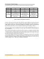
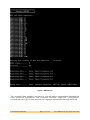
Revision History
Issue
1.0
Changes Made
Original Document
User Manual SMT784
Page 2 of 31
Date
Initials
19/03/09
CHG
Last Edited: 19/03/2009 14:12:00
Table of Contents
1
Introduction ..................................................................................................................... 6
2
Related Documents ........................................................................................................ 7
2.1
Referenced Documents.............................................................................................. 7
2.2
Applicable Documents............................................................................................... 7
3
Acronyms, Abbreviations and Definitions .............................................................. 8
3.1
Acronyms and Abbreviations ................................................................................... 8
3.2
Definitions.................................................................................................................... 8
4
Functional Description.................................................................................................. 9
4.1
5
Block Diagram.............................................................................................................. 9
System Overview.......................................................................................................... 11
5.1
FPGA ............................................................................................................................ 11
5.2
SLB Connector............................................................................................................ 12
5.3
DDR2 ........................................................................................................................... 12
5.4
Front Panel Fibre Optic Modules............................................................................ 12
5.5
Front Panel RJ45 Connector (Ethernet)................................................................. 12
5.6
Front Panel SATA Connectors ................................................................................ 12
5.7
RSL ............................................................................................................................... 12
5.8
Flash ............................................................................................................................ 13
5.9
CPLD and FPGA Configuration ............................................................................... 13
5.10 SHB............................................................................................................................... 13
5.11 LEDs ............................................................................................................................. 13
5.12 Clock Distribution..................................................................................................... 14
5.13 ADS5500 ADCs.......................................................................................................... 15
5.14 Switch 1 Flash Settings ............................................................................................ 17
5.15 ADC Data Flow........................................................................................................... 18
6
Software Interface ........................................................................................................ 19
6.1
Functional Diagram .................................................................................................. 19
6.2
Xilinx PCI Core........................................................................................................... 20
6.3
Software Driver.......................................................................................................... 20
6.4
Carrier Board Registers............................................................................................ 20
7
8
Sample Host Control and Data Capture .................................................................. 21
7.1
Getting Started .......................................................................................................... 21
7.2
Host Control of SMT784 .......................................................................................... 23
7.3
Viewing the Samples ................................................................................................ 24
7.4
Uploading Firmware to Flash.................................................................................. 24
SMT784 Board Layout ................................................................................................. 26
User Manual SMT784
Page 3 of 31
Last Edited: 19/03/2009 14:12:00
8.1
Top Side of SMT700 Carrier.................................................................................... 26
8.2
Bottom Side of SMT700 Carrier.............................................................................. 27
8.3
Top Side of SMT384 Mezzanine............................................................................. 28
8.4
Bottom Side of SMT384 Mezzanine....................................................................... 29
9
Power and Thermal...................................................................................................... 30
9.1
Power Dissipation ..................................................................................................... 30
10
Safety ............................................................................................................................... 31
11
EMC .................................................................................................................................. 31
12
Physical Properties....................................................................................................... 31
13
Ordering Information .................................................................................................. 31
14
EMC .................................................................................................................................. 31
User Manual SMT784
Page 4 of 31
Last Edited: 19/03/2009 14:12:00
Table of Figures
Figure 1: SMT700 Block Diagram ........................................................................................... 9
Figure 2 SMT384 Block Diagram .......................................................................................... 10
Figure 3 JTAG pin-out............................................................................................................ 11
Figure 4 Clock Distribution ................................................................................................... 14
Figure 5 ADC Data Flow ......................................................................................................... 18
Figure 6 Software Interface to Firmware ............................................................................ 19
Figure 7 SMT784.exe ............................................................................................................... 22
Figure 8 ANALYSIS.m.............................................................................................................. 24
Figure 9 Top-sid of SMT700 Carrier ................................................................................... 26
Figure 10 Bottom-side of SMT700 Carrier ......................................................................... 27
Figure 11 Top-side of SMT384 Mezzanine ........................................................................ 28
Figure 12 Bottom-side of SMT384 Mezzanine .................................................................. 29
Figure 13 3U Heat Dissipation .............................................................................................. 30
List of Tables
Table 1 Clock Characteristics ............................................................................................... 15
Table 2 ADC Characteristics ................................................................................................. 16
Table 3 Common Configurations of Switch 1.................................................................... 17
Table 4 Register 0x1C Data Control .................................................................................... 23
User Manual SMT784
Page 5 of 31
Last Edited: 19/03/2009 14:12:00
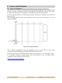
1 Introduction
The SMT784 is a Virtex 5 based PXI form-factor system utilizing Sundance’s
SMT700 carrier board and the SMT384 quad 125MSPS ADC mezzanine board. The
SMT700 implements up to eight 2.5-Gigabit PCI Express lanes, allowing a maximum
data transfer of 2 gigabytes per second. It also implements optionally a 32-bit, 33MHz PCI interface. As a standard, the ADCs are all AC-coupled (RF Transformers),
but can also be optionally DC-coupled (TI opamp THS4509). ADC configuration,
sampling, and transferring modes are set via internal control registers stored inside
the FPGA and accessible via a Comport interface.
The front panel interfaces make inter-system capabilities extremely extensive, while
the ADC’s and configurable clock distribution attached to the mezzanine module
(SMT384) make processing raw data fast and simple to configure.
Together, the SMT784 is a powerful system for capturing and manipulating data at
high speeds.
Main features of system:
•
Xilinx Virtex 5 in an FF1136 package. Supports LX50T/LX85T/SX50T or
LX110T/SX95T.
•
FPGA configuration from flash (64MB) using a Xilinx Coolrunner CPLD.
•
One 64-bit wide data bank of DDR2 memory. The bank uses 4, 16-bit wide
devices. Running this memory at 220MHz provides a maximum access speed
of over 3.5Gbyte/s.
•
Sundance LVDS Bus (SLB) connector for interfacing the SMT700 carrier with
the SMT384 mezzanine. (Future expanded functionality can be achieved as
well by utilizing any one of Sundance’s long line of other mezzanine
modules)
•
Front panel SATA connectors carrying Virtex 5 serial interfaces.
•
Front panel RJ45 for gigabit Ethernet.
•
Front panel Fibre Optic modules carrying Virtex 5 Serial interfaces.
•
Sundance Rocket Serial Link (RSL) connector with 4 serial interfaces.
•
Front panel USB interface to allow re-programming of the flash memory.
•
Four 14-bit, 125MSPS analogue to digital converters.
•
Flexible, on-board, low-jitter clock generation.
•
One external clock, external triggers, and one reference clock via MMCX
connector.
•
All analogue inputs to be connected to 50-ohm sources/loads.
•
Mezzanine module temperature sensors.
User Manual SMT784
Page 6 of 31
Last Edited: 19/03/2009 14:12:00
2 Related Documents
Sundance RSL specification: RSL
Xilinx Virtex5 datasheets: Xilinx Virtex5
Texas Instruments ADS550 ADC datasheet: ADS5500
Analog Devices AD9510 datasheet: AD9510
Sundance High-speed Bus (SHB) specifications: SHB
Sundance LVDS Bus (SLB) specifications: SLB
TIM specifications: TIM
MMCX specifications: Surface Mount MMCX
2.1 Referenced Documents
SMT384 User Manual:
X-Link Documentation:
2.2 Applicable Documents
User Manual SMT784
Last Edited: 19/03/2009 14:12:00
3 Acronyms, Abbreviations and Definitions
3.1 Acronyms and Abbreviations
Sundance commonly used acronyms.
MGT, GTP, RSL are all used (interchangeably) and refer to the FPGA’s high speed
serial links.
3.2 Definitions
User Manual SMT784
Last Edited: 19/03/2009 14:12:00
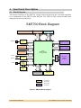
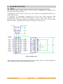
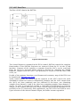
4 Functional Description
4.1 Block Diagram
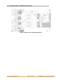
The major elements of the SMT784 can be broken down into the two main modules
it is comprised of: the SMT700 and SMT384. The SMT700 PXIe carrier board block
diagram can be viewed below.
Ext clk
DDR2
1GByte 220MHz
Ethernet
PHY
PXI Control
(Trigger, Clk, etc)
SATA Connectors
2 lanes of RSL
2 x 2.5Gb/s
serial links
SFF Connectors
2 lanes of Fibre
2 x 2.5Gb/s
serial links
Clock
generation
8 x 2.5Gb/s
serial links
1.5GHz SATA
2.5GHz RSL
PXIe ref
32 bit PCI
33/66MHz
(option)
Config
CPLD
& USB
512Mbit
flash
4 x 2.5Gb/s
serial links
USB
PXIe Connector
8 lanes of 2.5Gb/s
FPGA
Virtex5 LXT-50
FF1136 package
SHB
(option)
Ethernet
SLB
64 bit data
19 address
13 control
Custom Front Panel
120 I/O pins
SMT700 Block Diagram
RSL Connector
4 lanes of 2.5Gb/s
LEDs and
Misc. I/O
Front Panel
Connector
Rear Card
Connector
Figure 1: SMT700 Block Diagram
User Manual SMT784
Last Edited: 19/03/2009 14:12:00
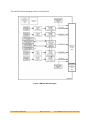
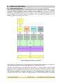
The SMT384 block diagram can be found below.
Figure 2 SMT384 Block Diagram
User Manual SMT784
Page 10 of 31
Last Edited: 19/03/2009 14:12:00
5 System Overview
5.1 FPGA
The SMT784 uses a Xilinx Virtex 5 LXT or SXT to implement in firmware the
interfaces the board provides.
Configuration of the FPGA is from one of two sources: on-board flash memory or a
Xilinx JTAG header.
A connector is specifically dedicated for FPGA and CPLD detection and
programming. Both the CPLD and the FPGA are part of the JTAG chain. A 14position (2x7) connector (2mm) is available and shows TDI, TDO, TCK and TMS
lines, as well as a ground and a reference voltage, as shown below:
Figure 3 JTAG pin-out
This connector has been chosen because it can connect easily to a Xilinx Parallel IV
cable using the ribbon cable provided by Xilinx.
User Manual SMT784
Page 11 of 31
Last Edited: 19/03/2009 14:12:00
5.2 SLB Connector
The SLB connector is the interface used to connect the SMT700 carrier board to the
SMT384 mezzanine module. For a map-out of SLB pin connections specific to this
system, please refer to the SMT384 user guide.
This connector is mounted on the reverse side of the board. The SMT784 occupies
two slots in a rack with the carrier portion of the system residing on the central
card guides (i.e. there will be a whole slot width for the FPGA, memory, etc. - and
another slot with the SMT384 mezzanine.)
5.3 DDR2
Four devices are used to implement this memory.
A 220MHz 64-bit data bus is used to transfer data at over 3.5Gbyte/s. (Xilinx
provides performances of a DDR2 interface as being: 200MHz for a -1 part, 267MHz
for a -2 part and 333MHz for a -3 part.) Future releases of the firmware will allow
for Host application access of the memory provided.
5.4 Front Panel Fibre Optic Modules
Two FPGA serial interfaces are presented here using Stratos Lightwave 568-LxKLT12x modules.
These interfaces support 2.5Gb/s operation.
Note that only one device is fitted as standard due to the fact that the second
module fits on the reverse of the SMT700 PCB. Not all variations of the SMT7xx
series can support two modules.
5.5 Front Panel RJ45 Connector (Ethernet)
A single RJ45 connector provides a 10/100/1000 Ethernet interface. The RJ45
connects directly to a Marvell 88E1116 PHY, which is interfaced to the FPGA.
5.6 Front Panel SATA Connectors
Two SATA-style connectors are provided on the front panel. Each connector carries
a single FPGA serial interface. As standard, these interfaces do NOT provide SATA
connectivity.
5.7 RSL
The LXT/SXT series devices from Xilinx provide up to 16 high-speed (>3Gbps) serial
links.
The SMT784 connects 8 lanes to the PXIe connectors, 4 lanes to an RSL connector,
two lanes to Fibre Modules, and two lanes to front panel SATA connectors.
For FPGAs with only 12 GTPs (high speed serial ports), no lanes are available on the
RSL connector.
The default firmware provides Host access straight to the RSL connectors through
the RSL X-Link interface
User Manual SMT784
Page 12 of 31
Last Edited: 19/03/2009 14:12:00
5.8 Flash
This 64Mbyte memory contains the configuration bit-streams for the FPGA.
The flash contents may be programmed via the PCI/PCIe interface or via USB by
using the SMT6002.
5.9 CPLD and FPGA Configuration
This Xilinx CPLD is capable of configuring the FPGA using data provided from the
flash memory. The CPLD itself should not need to be re-programmed, but if needed
it can only be accessed by JTAG using Xilinx iMPACT.
The CPLD also interfaces to a Cypress USB device. This interface allows an easy
option for upgrading the FPGA configuration stored in flash using the SMT6002.
The USB mechanism to re-program the flash is always present and does not rely on
the FPGA being configured. This can be advantageous if the FPGA configuration has
been updated with a non-working PCI/PCIe interface.
5.10 SHB
Two Sundance SHB connectors are fitted as standard. Each connector has the ability
to carry a 32-bit data bus with a data rate of 133MHz. A dual 16-bit interface
option is also supported.
One SHB is connected directly to the FPGA. To save on pin-count, the second SHB
connector shares the PCI interface signals with the FPGA. For this reason, this SHB
interface and the PCI cannot be operated simultaneously unless a PCI express core is
implemented in firmware.
5.11 LEDs
Two front-panel LED’s are available and connected directly to the FPGA. A heartbeat
signal present indicates the FPGA has been configured correctly.
User Manual SMT784
Page 13 of 31
Last Edited: 19/03/2009 14:12:00
5.12 Clock Distribution
There is one integrated clock generator on the mezzanine module (AD9510 – Analog
Devices). The user can either use this clock (on-board) or provide the module with
an external clock (input via MMCX connector).
ADCs can all receive the same clock or the integer multiple of it (x2, x3……x32), the
maximum being 125MHz for each ADC. This clock can be coming from the onboard VCXO or from an external source.
An extra connector outputs the reference clock for multiple-module systems.
Figure 4 Clock Distribution
The main characteristics of the mezzanine clocks are as follows:
External Reference Input
Input Voltage Level
0.5 – 3.3 Volts peak-to-peak (AC-coupled)
Input Impedance
50-Ohm (Termination implemented at the connector)
Frequency Range
0 – 100 MHz.
External Reference Output
Output Voltage Level
1.6 Volts peak-to-peak (AC-coupled)
Output Impedance
50-Ohm (Termination implemented at the connector)
External Sampling Clock Input
Input Voltage Level
0.5 – 3.3 Volts peak-to-peak (AC-coupled)
Format
Single-ended or differential on option (3.3V LVPECL).
Frequency range
10-125 MHz
External Sampling Clock Output
Output Voltage Level
0-2.4 Volts fixed amplitude.
Output Format
LVTTL
User Manual SMT784
Page 14 of 31
Last Edited: 19/03/2009 14:12:00
External Trigger Inputs
Input Voltage Level
1.5-3.3 Volts peak-to-peak.
Format
DC-coupled and Single-ended (Termination implemented at the
connector). Differential on option (3.3 V PECL).
Impedance
50-Ohm.
Frequency range
62.5 MHz maximum
Delay
Ext. Ref. In to Ext Ref. Out
Ext. Clk In to Ext Clk Out
11ns between J29 and J4
Table 1 Clock Characteristics
5.13 ADS5500 ADCs
The main characteristics of the mezzanine ADC’s are as follows:
Analogue Inputs
AC coupled option. 2.4 Vpp (11.5 dbm – 50Ω) Full scale - AC
coupled via RF transformer.
Input voltage range
DC-coupled option. 1.15 Vpp (Gain amplifier 6dB) centred at 0. DCcoupled via amplifier. Gain can be adjusted to required input amplitude
centred at 0. Min. gain 6dBs, which should allow an input swing +/0.575V as full scale.
Impedance
ADC single-ended inputs are to be connected to a 50Ω source. Source
impedance matching implemented between RF transformers and ADC.
Bandwidth
ADC bandwidth: 750 MHz.
External Reference Input
Input Voltage Level
Input Impedance
0.5 – 3.3 Volts peak-to-peak (AC-coupled)
50-Ohm (Termination implemented at the connector)
0 – 100 MHz.
Frequency Range
External Reference Output
Output Voltage Level
1.6 Volts peak-to-peak (AC-coupled)
Output Impedance
50-Ohm (Termination implemented at the connector)
External Sampling Clock Input
Input Voltage Level
0.5 – 3.3 Volts peak-to-peak (AC-coupled)
Input Format
Single-ended or differential on option (3.3V LVPECL).
Frequency range
10-125 MHz
External Trigger Inputs
Input Voltage Level
User Manual SMT784
1.5-3.3 Volts peak-to-peak.
Page 15 of 31
Last Edited: 19/03/2009 14:12:00
Format
DC-coupled and single-ended (terminated at connector). Differential an
option (3.3 V PECL).
Impedance
50-Ohm.
Frequency range
62.5 MHz maximum
ADCs Output
14-Bits
Output Data Width
Data Format
2’s Complement or offset binary
(Changeable via control register)
SFDR
82dBs maximum (manufacturer)
SNR
70dBs maximum (manufacturer)
Min Sampling Clock
10 MHz (ADC DLL off)
Max Sampling Frequency
125 MHz (ADC DLL on)
Table 2 ADC Characteristics
User Manual SMT784
Page 16 of 31
Last Edited: 19/03/2009 14:12:00
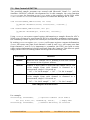
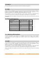
5.14 Switch 1 Flash Settings
The following table represents the various switch settings for switch 1:
POS 4
ON
OFF
OFF
POS 3
ON
OFF
ON
POS 1
Reset
Reset
Reset
Flash
PCB configured to
boot from flash and
allow for serial
RD/WR through PCI
(SMT6002)
FPGA can be
configured via a bitstream uploaded on
the USB link
(Diamond Server)
Flash access is
available for
RD/WR only via
the USB link using
the SMT6002
condition
Table 3 Common Configurations of Switch 1
Switch 1 (SW1) on the front side of the SMT784 controls flash read and write access
for the carrier board, as well as selecting which flash address to boot from. POS 1
sends a hard reset to the CPLD instructing it to reconfigure the FPGA according to
which address in flash is selected. The combined positions of POS 4 and POS 3 tell
the CPLD how the FPGA is to be configured at power up according to Table 3.
After power up, a new bit-stream can be sent via USB by using Diamond Server, or
by first uploading the new firmware to flash with the SMT6002, then performing a
reset with POS 1.
POS 2 selects which address in flash the CPLD is going to configure the FPGA from.
The flash address contents can be viewed and written to by using the SMT6002. POS
2 ON boots from the backup SMT700 firmware (flash address 0x0), while off selects
the SMT784 firmware (flash address 0x800000).
The SMT700 default firmware is provided as a backup bit-stream in the event that
user-modified firmware at address 0x800000 in flash does not work as expected.
Sundance therefore suggests that when writing custom firmware to flash, do not
write to address 0x0 - only write to address 0x800000.
User Manual SMT784
Page 17 of 31
Last Edited: 19/03/2009 14:12:00
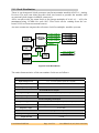
5.15 ADC Data Flow
The flow of ADC data in the SMT784:
Figure 5 ADC Data Flow
The Control Registers contained in the FPGA (control_SMT384) control the complete
functionality of the SMT384. Registers are written to/from the PC via the X-Link
interface. Contents of the registers or samples from the ADC’s can be read back
from the FPGA by choosing which output is desired. By changing the default
firmware, samples from the ADC’s can optionally be routed to the RSL links, SHB,
SATA, etc.
Details of the registers functions, word format and a memory-map of the FPGA can
be found in the SMT384 User Guide.
Serial control signals are routed from the registers to the ADC’s and to the clock
distribution system for desired configuration. Samples and the clock output from
the ADC’s are then combined onto two different 32-bit buses, one containing
samples from channels A and B, the other bus containing samples from channels C
and D. In order to prevent loss of data, a 16K buffer is implemented to feed the
samples to the control_SMT384 block. When control registers are programmed to be
returned to the PC (selected by Host application), the ADC FIFO’s are held in reset.
Upon selection of the desired channel output, the buffer resumes operation.
User Manual SMT784
Page 18 of 31
Last Edited: 19/03/2009 14:12:00
6 Software Interface
6.1 Functional Diagram
The following diagram shows functionally how the SMT784 works. The hashed
portions will be available in future releases of the firmware. The Host accesses a
number of communication resources via the PCI bus. All communication resources
are presented as X-Link software interfaces, and are memory mapped in the
memory space of the Host processor.
Figure 6 Software Interface to Firmware
The firmware inside the FPGA implements the communication interfaces required to
allow the data transfer between the SMT784 and the Host PCI/PCIe.
The host transfers data with the SMT784 using the X-Link. There is one X-Link
instantiated per communication resource (Flash, SMT384, DDR, RSL). All the X-Link
interfaces are connected to the PCI/PCIe core and can be accessed from the Host.
The default firmware currently provides two communication resources types:
Comport and RSL. One Comport X-Link interface is used between the CPLD and
User Manual SMT784
Page 19 of 31
Last Edited: 19/03/2009 14:12:00
Flash to the Host, a second Comport link is used to access the SMT384 registers for
control and data acquisition, and one RSL connects directly to the connector on the
front of the PCB. A more detailed explanation of the communication resources that
Sundance utilizes can be found in the SMT6400 and SMT6500.
A Xilinx PCI/PCIe IP core is used to allow data transfer between the Host machine
and the X-Link.
6.2 Xilinx PCI Core
The PCI core supports target accesses and initiator accesses. Data transfers are
implemented using initiator accesses to ensure maximum bandwidth. For this
purpose a DMA engine is connected to the X-Link and the PCI core to transfer the
data.
The PCI/PXIe interface used in this design was generated by using the Xilinx Core
Generator (core version 4.8) included with ISE 10.1 Foundation software. The user is
free to implement the included netlist into custom firmware, but if there is a need
to re-generate the IP core, the full license must be purchased from Xilinx.
Licensing information and how to purchase this core can be found at the Xilinx
website: www.xilinx.com
6.3 Software Driver
The SMT784 is supported by the SMT6300, providing the Windows driver for the
board.
6.4 Carrier Board Registers
All the addressable resources are located in the BAR1 register.
The communication resources are presented to the host machine as X-Link
interfaces. The addresses of the X-Link and the number of X-Link are available from
the X-Link table of content found in the firmware.
The other registers available in the firmware are the following:
Reset register (BAR1 – 0x00000000)
Writing ‘1’ to the reset register will cause the SMT700 to be reset. The reset is deasserted automatically after a few milliseconds.
X-Link table of content (BAR1 – 0x00001000)
Refer to the X-Link documentation for details concerning the table of content and
for a description of the registers in the X-Link.
User Manual SMT784
Page 20 of 31
Last Edited: 19/03/2009 14:12:00
7 Sample Host Control and Data Capture
7.1 Getting Started
The sample program “SMT784.exe” can get the user started with the equipment by
executing some of the simpler functions available from the SMT784 system.
Setup:
•
Connect the 50-ohm output of a signal generator to the ADC channel inputs
(J3, J6, J7 and J11) on the mezzanine module. (Sundance provides a
convenient, 50-ohm terminated splitter for inputting a single source through
the SMT594.)
•
Turn on the computer. Verify heartbeat signal flashing on the front-panel
LED’s. This is derived from the bus clock and indicates the FPGA is
configured correctly.
•
Execute “SMT784.exe”. This will store a 16K sample capture from each of the
ADC’s to a text file in the same folder as the executable.
The program begins by sending control and configuration words to the four ADC’s
and clock registers inside the FPGA. (The behaviour of these registers is thoroughly
described in the user manual for the SMT384)
The Test Register on the FPGA is then written to verify proper read/write action
over the X-Link Comport. Data is then captured from the ADC’s and stored in text
files relating to the ADC channel. (A_capture.txt, B_capture.txt, etc.)
If the program is successful you should see the following screen:
User Manual SMT784
Page 21 of 31
Last Edited: 19/03/2009 14:12:00
Figure 7 SMT784.exe
The captured data samples can then be viewed and/or manipulated through the
users preferred application. The provided MATLAB script file “ANALYSIS.m”
provides an easy way to load and view the captured information through MATLAB.
User Manual SMT784
Page 22 of 31
Last Edited: 19/03/2009 14:12:00
7.2 Host Control of SMT784
The provided sample program was created with Microsoft Visual C++ and the
Sundance SMT6026 software development kit. In this example, the write function
writeword uses the function HostWrite to write to the registers of the FPGA while
readword uses HostRead to read the registers or data back through the X-Link:
void writeword(HOST_LINK hostlink, int value)
{g_pSmt384->HostWrite(&value, sizeof(value), hostlink);}
void readword(HOST_LINK hostlink, int* ptr)
{g_pSmt384->HostRead(ptr, sizeof(int), hostlink);}
Using readword can return control register information or samples from the ADC’s.
Which type of data to be read from the FPGA is selected by writing to register 0x1C the remaining control registers are exactly as described in the SMT384 User Manual.
By writing 0x0000 to regiser 0x1C, readword will return register contents information,
0x0C00 will return raw data from channels A and B, and 0x800 will return raw data
from channels C and D. It is important to remember the FIFO’s are held at reset
while register information is being read back from the Comport. This allows a quick
empty of the FIFO for reading status and keeps data from being lost.
Word Sent
Function
0x0000
Resets all ADC sample FIFO’s. Reading words back returns
the contents in the registers address.
0x0C00
Channel A and B data is sent from the sample FIFO’s. The
14-bit sample from each channel is returned in a
concatenated, single 32-bit word as:
“00” + “14-bit B sample” + “00” + “14-bit A sample”
0x0800
Channel C and D data is sent from the sample FIFO’s. The
14-bit sample from each channel is returned in a
concatenated, single 32-bit word as:
“00” + “14-bit D sample” + “00” + “14-bit C sample”
Table 4 Register 0x1C Data Control
For example:
writeword(cp, 0x101C0000);
// registers readable (clear FIFO's)
for (k=0; k<255; k++) readword(cp, &value);
writeword(cp, 0x101C0C00);
User Manual SMT784
// Empty FIFO
// Channels A&B binary out selected
Page 23 of 31
Last Edited: 19/03/2009 14:12:00
In this instance, the first writeword places the ADC FIFO’s in reset and configures
the 0x1C register to return register contents information to the Host when a
readword is performed. The looped readword command empties samples remaining
in the FIFO, and the final writeword configures the SMT784 to send samples from
channels A and B in straight binary format to the Host.
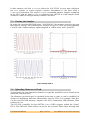
7.3 Viewing the Samples
By using the provided MATLAB script “ANALYSIS.m”, the samples stored on the text
files may be viewed. The following is a zoomed in view of a test run using channels
C and D with a 2MHz analogue signal sampled at 33Mhz and a 4096-point FFT.
Figure 8 ANALYSIS.m
7.4 Uploading Firmware to Flash
A good guide for how Sundance firmware is typically modelled can be found in the
SMT6500 .chm help files.
The firmware provided may be updated from time to time or can be modified as
desired to implement different functionality into the FPGA. For example, data flow
can be stored in DDR memory, output to the SATA connection, SHB, Ethernet, Fibre
transceiver, etc.
The PCI/PCIe controller for the SMT784 is in a VHDL wrapper within the Virtex5
FPGA. The SMT6002 Flash Utility can access the system’s flash either through this
User Manual SMT784
Page 24 of 31
Last Edited: 19/03/2009 14:12:00
PCI/PCIe core or via a USB cable as in the SMT148-FX. Currently this means that a
change to the firmware and hard reset from SW1 will cause the FPGA to reconfigure
from flash and lose the PCI/PCIe interface. The flash can still be accessed at this
point through the USB interface, but if the PCI is to be recognized by the Host again
there must be either a re-boot of the PC or the equipment must be un-installed
then re-installed as follows:
•
Connect a USB cable to the SMT784 and start the SMT6002 Flash Utility for
FPGA-only Modules. The system will appear in the utility as an SMT700
through the PCI interface and as an SMT148-FX through the USB interface.
(The TIM type will appear as an SMT351T-xxxx depending upon type of FPGA
on carrier)
•
Select the interface of choice as noted in the above step (PCI/PCIe or USB).
Two bit-streams will be found in the flash, the first is the default firmware
for the SMT700, while the second bit-stream at address 0x800000 is where
the SMT784 configuration is stored. These are selectable by SW1 POS 2 at
boot.
•
Select the second bit-stream, delete and re-assign the updated or custom
firmware you have designed at user address 0x800000. Select Commit.
•
Once the firmware has been loaded into flash, reset the board using SW1 POS
1 by turning it on, then off to reconfigure the FPGA with the new bit-stream
(check SW1 settings).
•
To make the board visible again to the Host, right-click “My Computer”, and
select “Manage”.
•
Under “Device Manager”, select “SMT700” under “Sundance”. Right click,
disable. (click okay)
•
Right click “SMT700” again, select “enable.”
This will cause the PCI/PCIe address and resource allocation of the device to be
discovered again as an SMT700 with the new firmware installed.
User Manual SMT784
Page 25 of 31
Last Edited: 19/03/2009 14:12:00
8 SMT784 Board Layout
8.1 Top Side of SMT700 Carrier
Figure 9 Top-sid of SMT700 Carrier
User Manual SMT784
Page 26 of 31
Last Edited: 19/03/2009 14:12:00
8.2 Bottom Side of SMT700 Carrier
Figure 10 Bottom-side of SMT700 Carrier
User Manual SMT784
Page 27 of 31
Last Edited: 19/03/2009 14:12:00
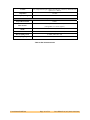
8.3 Top Side of SMT384 Mezzanine
Figure 11 Top-side of SMT384 Mezzanine
Connector name (silkscreen
and schematics)
Description
Location on the board
J3
ADCA Analog Input
Middle / Left
J11
ADCB Analog Input
Middle / Left
J6
ADCC Analog Input
Middle / Right
J7
ADCD Analog Input
Middle / Right
J30
External Reference Input
Top / Left
J29
External Clock Input
Top / Left
J34
External Reference Output
Top / Right
External Clock Output
Top / Right
J24
External Trigger ADCA&B
Bottom / Left
J25
External Trigger ADCC&D
Bottom / Left
J4
User Manual SMT784
Page 28 of 31
Last Edited: 19/03/2009 14:12:00
8.4 Bottom Side of SMT384 Mezzanine
Figure 12 Bottom-side of SMT384 Mezzanine
User Manual SMT784
Page 29 of 31
Last Edited: 19/03/2009 14:12:00
9 Power and Thermal
9.1 Power Dissipation
The PXI Express chassis receiving the SMT784 system should provide enough forced
air flow in order to dissipate the heat generated by the modules. The air flow must
be going against gravity or upwards, as specified in the PXI Specification.
It is also specified that a 3U PXI Express module should not dissipate more than 30
Watts of heat.
The following picture shows the direction of the forced air flow across a 3U PXI
Express module:
Figure 13 3U Heat Dissipation
The estimated maximum power consumption of the Virtex5 FPGA is 22W. This
assumes a design running at 500MHz with all DSP slices used.
All of the devices on the SMT784 derive their power from the +12V PXI power rails.
It is strongly advised, as applications vary considerably, to use the Xilinx power
estimator tools available from this link;
Xilinx Power Design Solutions
User Manual SMT784
Page 30 of 31
Last Edited: 19/03/2009 14:12:00
10 Safety
This module presents no hazard to the user when in normal use.
11 EMC
This module is designed to operate from within an enclosed host system, which is
build to provide EMC shielding. Operation within the EU EMC guidelines is not
guaranteed unless it is installed within an adequate host system.
This module is protected from damage by fast voltage transients originating from
outside the host system which may be introduced through the output cables.
Short circuiting any output to ground does not cause the host PC system to lock up
or reboot.
12 Physical Properties
Dimensions
21cm x 13cm x 4cm
Weight
250g
Supply Voltages
+12V
+5V
+3.3V
-5V
-12V
MTBF
13 Ordering Information
Several variations of this product are available. Various FPGA types, speed grades,
clock speeds and signal coupling are available. Please contact Sundance for further
information.
14 EMC
This module is designed to operate from within an enclosed host system, which is
build to provide EMC shielding. Operation within the EU EMC guidelines is not
guaranteed unless it is installed within an adequate host system.
This module is protected from damage by fast voltage transients originating from
outside the host system which may be introduced through the output cables.
Short circuiting any output to ground does not cause the host PC system to lock up
or reboot.
User Manual SMT784
Page 31 of 31
Last Edited: 19/03/2009 14:12:00