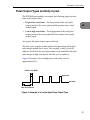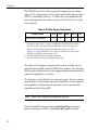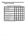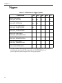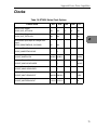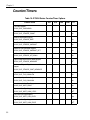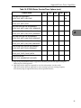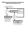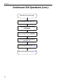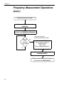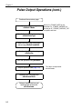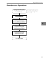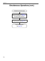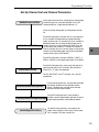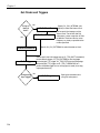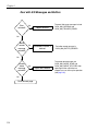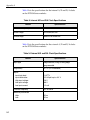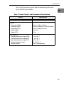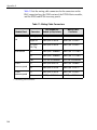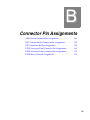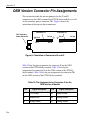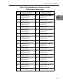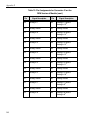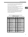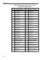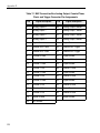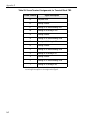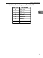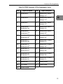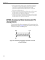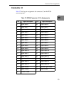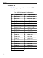
1
UM-19985-E
DT9834 Series
User’s Manual
Fifth Edition
March, 2006
Copyright © 2004-2006 by Data Translation,
Inc.
All rights reserved.
Information furnished by Data Translation, Inc.
is believed to be accurate and reliable; however,
no responsibility is assumed by Data Translation,
Inc. for its use; nor for any infringements of
patents or other rights of third parties which
may result from its use. No license is granted by
implication or otherwise under any patent rights
of Data Translation, Inc.
Use, duplication, or disclosure by the United
States Government is subject to restrictions as set
forth in subparagraph (c)(1)(ii) of the Rights in
Technical Data and Computer software clause at
48 C.F.R, 252.227-7013, or in subparagraph (c)(2)
of the Commercial computer Software Registered Rights clause at 48 C.F.R., 52-227-19 as
applicable. Data Translation, Inc., 100 Locke
Drive, Marlboro, MA 01752
Data Translation, Inc.
100 Locke Drive
Marlboro, MA 01752-1192
(508) 481-3700
www.datatranslation.com
Fax: (508) 481-8620
E-mail: [email protected]
Data Translation® is a registered trademark of
Data Translation, Inc. DT-Open LayersTM,
DataAcq SDKTM, DataAcq OMNI CDTM, DT-LV
LinkTM, DTx-EZTM, and DT VPITM are trademarks
of Data Translation, Inc.
All other brand and product names are
trademarks or registered trademarks of their
respective companies.
Radio and Television Interference
This equipment has been tested and found to comply with CISPR
EN55022 Class A, and EN50082-1 (CE) requirements and also with
the limits for a Class A digital device, pursuant to Part 15 of the FCC
Rules. These limits are designed to provide reasonable protection
against harmful interference when the equipment is operated in a
commercial environment. This equipment generates, uses, and can
radiate radio frequency energy and, if not installed and used in
accordance with the instruction manual, may cause harmful
interference to radio communications. Operation of this equipment in
a residential area is likely to cause harmful interference, in which case
the user will be required to correct the interference at his own
expense.
Changes or modifications to this equipment not expressly approved
by Data Translation could void your authority to operate the
equipment under Part 15 of the FCC Rules.
Note: This product was verified to meet FCC requirements under
test conditions that included use of shielded cables and connectors
between system components. It is important that you use shielded
cables and connectors to reduce the possibility of causing
interference to radio, television, and other electronic devices.
Canadian Department of Communications Statement
This digital apparatus does not exceed the Class A limits for radio
noise emissions from digital apparatus set out in the Radio
Interference Regulations of the Canadian Department of
Communications.
Le présent appareil numérique n’émet pas de bruits radioélectriques
dépassant les limites applicables aux appareils numériques de la class
A prescrites dans le Règlement sur le brouillage radioélectrique
édicté par le Ministère des Communications du Canada.
Table of Contents
About this Manual . . . . . . . . . . . . . . . . . . . . . . . . . . . . . . . . . 11
Intended Audience. . . . . . . . . . . . . . . . . . . . . . . . . . . . . . . . . . . . . . 11
How this Manual is Organized . . . . . . . . . . . . . . . . . . . . . . . . . . . 12
Conventions Used in this Manual . . . . . . . . . . . . . . . . . . . . . . . . . 13
Related Information . . . . . . . . . . . . . . . . . . . . . . . . . . . . . . . . . . . . . 13
Where To Get Help. . . . . . . . . . . . . . . . . . . . . . . . . . . . . . . . . . . . . . 14
Chapter 1: Overview . . . . . . . . . . . . . . . . . . . . . . . . . . . . . . . 15
DT9834 Hardware Features . . . . . . . . . . . . . . . . . . . . . . . . . . . . . . 16
Supported Software . . . . . . . . . . . . . . . . . . . . . . . . . . . . . . . . . . . . . 20
Accessories . . . . . . . . . . . . . . . . . . . . . . . . . . . . . . . . . . . . . . . . . . . . 21
Chapter 2: Principles of Operation . . . . . . . . . . . . . . . . . . . 23
Analog Input Features . . . . . . . . . . . . . . . . . . . . . . . . . . . . . . . . . . . 25
Input Resolution . . . . . . . . . . . . . . . . . . . . . . . . . . . . . . . . . . . . 25
Analog Input Channels . . . . . . . . . . . . . . . . . . . . . . . . . . . . . . 26
Specifying a Single Analog Input Channel . . . . . . . . . . 27
Specifying One or More Analog Input Channels . . . . . 27
Specifying the Digital Input Port in the Analog Input
Channel-Gain List . . . . . . . . . . . . . . . . . . . . . . . . . . . . . . . 29
Specifying Counter/Timers in the Analog Input
Channel-Gain List . . . . . . . . . . . . . . . . . . . . . . . . . . . . . . . 30
Performing Dynamic Digital Output Operations . . . . 32
Input Ranges and Gains . . . . . . . . . . . . . . . . . . . . . . . . . . . . . . 33
Specifying the Gain for a Single Channel . . . . . . . . . . . 34
Specifying the Gain for One or More Channels . . . . . . 34
Input Sample Clock Sources . . . . . . . . . . . . . . . . . . . . . . . . . . 34
Analog Input Conversion Modes . . . . . . . . . . . . . . . . . . . . . . 35
5
Contents
Continuous Scan Mode . . . . . . . . . . . . . . . . . . . . . . . . . . 36
Triggered Scan Mode . . . . . . . . . . . . . . . . . . . . . . . . . . . . 37
Internally Retriggered Scan Mode . . . . . . . . . . . . . . 38
Externally Retriggered Scan Mode. . . . . . . . . . . . . . 39
Input Triggers . . . . . . . . . . . . . . . . . . . . . . . . . . . . . . . . . . . . . . 40
Data Format and Transfer . . . . . . . . . . . . . . . . . . . . . . . . . . . . 41
Error Conditions . . . . . . . . . . . . . . . . . . . . . . . . . . . . . . . . . . . . 43
Analog Output Features . . . . . . . . . . . . . . . . . . . . . . . . . . . . . . . . . 44
Output Resolution. . . . . . . . . . . . . . . . . . . . . . . . . . . . . . . . . . . 44
Analog Output Channels . . . . . . . . . . . . . . . . . . . . . . . . . . . . . 45
Specifying a Single Analog Output Channel . . . . . . . . 45
Specifying Multiple Analog Output Channels and/or the
Digital Output Port . . . . . . . . . . . . . . . . . . . . . . . . . . . . . 45
Output Ranges and Gains . . . . . . . . . . . . . . . . . . . . . . . . . . . . 47
Output Triggers . . . . . . . . . . . . . . . . . . . . . . . . . . . . . . . . . . . . . 47
Output Clocks . . . . . . . . . . . . . . . . . . . . . . . . . . . . . . . . . . . . . . 47
Output Conversion Modes . . . . . . . . . . . . . . . . . . . . . . . . . . . 48
Continuously Paced Analog Output . . . . . . . . . . . . . . . 48
Waveform Generation . . . . . . . . . . . . . . . . . . . . . . . . . . . 50
Data Format and Transfer . . . . . . . . . . . . . . . . . . . . . . . . . . . . 51
Error Conditions . . . . . . . . . . . . . . . . . . . . . . . . . . . . . . . . . . . . 52
Digital I/O Features. . . . . . . . . . . . . . . . . . . . . . . . . . . . . . . . . . . . . 53
Digital I/O Lines . . . . . . . . . . . . . . . . . . . . . . . . . . . . . . . . . . . . 53
Operation Modes. . . . . . . . . . . . . . . . . . . . . . . . . . . . . . . . . . . . 54
Counter/Timer Features . . . . . . . . . . . . . . . . . . . . . . . . . . . . . . . . . 55
C/T Channels . . . . . . . . . . . . . . . . . . . . . . . . . . . . . . . . . . . . . . 55
C/T Clock Sources . . . . . . . . . . . . . . . . . . . . . . . . . . . . . . . . . . 57
Gate Types . . . . . . . . . . . . . . . . . . . . . . . . . . . . . . . . . . . . . . . . . 58
Pulse Output Types and Duty Cycles . . . . . . . . . . . . . . . . . . 59
Counter/Timer Operation Modes . . . . . . . . . . . . . . . . . . . . . 60
6
Contents
Event Counting . . . . . . . . . . . . . . . . . . . . . . . . . . . . . . . . 60
Up/Down Counting . . . . . . . . . . . . . . . . . . . . . . . . . . . . . 61
Frequency Measurement . . . . . . . . . . . . . . . . . . . . . . . . . 61
Edge-to-Edge Measurement . . . . . . . . . . . . . . . . . . . . . . 63
Rate Generation . . . . . . . . . . . . . . . . . . . . . . . . . . . . . . . . . 64
One-Shot . . . . . . . . . . . . . . . . . . . . . . . . . . . . . . . . . . . . . . . 65
Repetitive One-Shot . . . . . . . . . . . . . . . . . . . . . . . . . . . . . 66
Chapter 3: Supported Device Driver Capabilities. . . . . . . . 69
Data Flow. . . . . . . . . . . . . . . . . . . . . . . . . . . . . . . . . . . . . . . . . . . . . . 71
Buffering . . . . . . . . . . . . . . . . . . . . . . . . . . . . . . . . . . . . . . . . . . . . . . 72
DMA . . . . . . . . . . . . . . . . . . . . . . . . . . . . . . . . . . . . . . . . . . . . . . . . . . 73
Triggered Scan Mode . . . . . . . . . . . . . . . . . . . . . . . . . . . . . . . . . . . . 74
Gain . . . . . . . . . . . . . . . . . . . . . . . . . . . . . . . . . . . . . . . . . . . . . . . . . . 75
Synchronous Digital I/O. . . . . . . . . . . . . . . . . . . . . . . . . . . . . . . . . 76
Channels . . . . . . . . . . . . . . . . . . . . . . . . . . . . . . . . . . . . . . . . . . . . . . 76
Filters . . . . . . . . . . . . . . . . . . . . . . . . . . . . . . . . . . . . . . . . . . . . . . . . . 77
Ranges . . . . . . . . . . . . . . . . . . . . . . . . . . . . . . . . . . . . . . . . . . . . . . . . 77
Resolution . . . . . . . . . . . . . . . . . . . . . . . . . . . . . . . . . . . . . . . . . . . . . 77
Triggers . . . . . . . . . . . . . . . . . . . . . . . . . . . . . . . . . . . . . . . . . . . . . . . 78
Clocks . . . . . . . . . . . . . . . . . . . . . . . . . . . . . . . . . . . . . . . . . . . . . . . . . 79
Counter/Timers . . . . . . . . . . . . . . . . . . . . . . . . . . . . . . . . . . . . . . . . 80
Miscellaneous . . . . . . . . . . . . . . . . . . . . . . . . . . . . . . . . . . . . . . . . . . 82
Chapter 4: Programming Flowcharts. . . . . . . . . . . . . . . . . . 83
Single-Value Operations . . . . . . . . . . . . . . . . . . . . . . . . . . . . . . . . . 85
Continuous A/D Operations . . . . . . . . . . . . . . . . . . . . . . . . . . . . . 87
Continuous D/A Operations . . . . . . . . . . . . . . . . . . . . . . . . . . . . . 89
Continuous Digital Input Operations . . . . . . . . . . . . . . . . . . . . . . 91
Continuous Digital Output Operations . . . . . . . . . . . . . . . . . . . . 92
Event Counting Operations . . . . . . . . . . . . . . . . . . . . . . . . . . . . . . 93
7
Contents
Up/Down Counting Operations . . . . . . . . . . . . . . . . . . . . . . . . . 95
Frequency Measurement Operations . . . . . . . . . . . . . . . . . . . . . . 97
Edge-to-Edge Measurement Operations . . . . . . . . . . . . . . . . . . . 99
Pulse Output Operations. . . . . . . . . . . . . . . . . . . . . . . . . . . . . . . . 101
Simultaneous Operations . . . . . . . . . . . . . . . . . . . . . . . . . . . . . . . 103
Chapter 5: Troubleshooting . . . . . . . . . . . . . . . . . . . . . . . . 117
General Checklist . . . . . . . . . . . . . . . . . . . . . . . . . . . . . . . . . . . . . . 118
Technical Support . . . . . . . . . . . . . . . . . . . . . . . . . . . . . . . . . . . . . 122
If Your Module Needs Factory Service . . . . . . . . . . . . . . . . . . . . 123
Chapter 6: Calibration . . . . . . . . . . . . . . . . . . . . . . . . . . . . . 125
Using the Calibration Utility . . . . . . . . . . . . . . . . . . . . . . . . . . . . 127
Calibrating the Analog Input Subsystem . . . . . . . . . . . . . . . . . . 128
Connecting a Precision Voltage Source . . . . . . . . . . . . . . . . 128
Using the Auto-Calibration Procedure . . . . . . . . . . . . . . . . 128
Using the Manual Calibration Procedure . . . . . . . . . . . . . . 129
Calibrating the Analog Output Subsystem . . . . . . . . . . . . . . . . 131
Appendix A: Specifications . . . . . . . . . . . . . . . . . . . . . . . . 133
Appendix B: Connector Pin Assignments . . . . . . . . . . . . 145
OEM Version Connector Pin Assignments. . . . . . . . . . . . . . . . . 146
BNC Connection Box Connector Pin Assignments . . . . . . . . . . 152
Analog Input Connector . . . . . . . . . . . . . . . . . . . . . . . . . . . . 152
Digital I/O Connector . . . . . . . . . . . . . . . . . . . . . . . . . . . . . . 155
Analog Output, Counter/Timer, Clock, and Trigger
Connector . . . . . . . . . . . . . . . . . . . . . . . . . . . . . . . . . . . . . . . . . 157
STP Connection Box Pin Assignments . . . . . . . . . . . . . . . . . . . . 159
Screw Terminal Block TB1 . . . . . . . . . . . . . . . . . . . . . . . . . . . 159
Screw Terminal Block TB2 . . . . . . . . . . . . . . . . . . . . . . . . . . . 160
Screw Terminal Block TB3 . . . . . . . . . . . . . . . . . . . . . . . . . . . 161
8
Contents
Screw Terminal Block TB4 . . . . . . . . . . . . . . . . . . . . . . . . . . . 163
Screw Terminal Block TB5 . . . . . . . . . . . . . . . . . . . . . . . . . . . 164
Screw Terminal Block TB6 . . . . . . . . . . . . . . . . . . . . . . . . . . . 165
Screw Terminal Block TB7 . . . . . . . . . . . . . . . . . . . . . . . . . . . 166
EP353 Accessory Panel Connector Pin Assignments . . . . . . . . 168
Connector J1 . . . . . . . . . . . . . . . . . . . . . . . . . . . . . . . . . . . . . . . 168
Connector J2 . . . . . . . . . . . . . . . . . . . . . . . . . . . . . . . . . . . . . . . 170
EP356 Accessory Panel Connector Pin Assignments . . . . . . . . 172
Connector J1 . . . . . . . . . . . . . . . . . . . . . . . . . . . . . . . . . . . . . . . 173
Connector J2 . . . . . . . . . . . . . . . . . . . . . . . . . . . . . . . . . . . . . . . 174
EP355 Screw Terminal Assignments . . . . . . . . . . . . . . . . . . . . . . 175
Attached to Connector J2 on the OEM Module . . . . . . . . . 175
Attached to Connector J3 on the OEM Module . . . . . . . . . 175
9
Contents
10
About this Manual
This manual describes the features of the DT9834 Series modules, the
capabilities of the DT9834 Series Device Driver, and how to program
the DT9834 Series modules using DT-Open Layers™ software.
Troubleshooting information is also provided.
Note: The DT9834 Series module is available either installed in a
metal BNC connection box, an STP (screw terminal panel)
connection box (for the 32-analog input channel version only), or as
a board-level OEM version that you can install in your own custom
application. If the information in this manual applies to all versions
of the DT9834 Series module, the manual uses the product name
"DT9834 Series module." Otherwise, the specific product name is
mentioned.
Intended Audience
This document is intended for engineers, scientists, technicians, or
others responsible for using and/or programming the DT9834 Series
modules for data acquisition operations in the Microsoft®
Windows® 2000 or Windows XP operating system. It is assumed that
you have some familiarity with data acquisition principles and that
you understand your application.
11
About this Manual
How this Manual is Organized
This manual is organized as follows:
• Chapter 1, “Overview,” describes the major features of the
DT9834 Series module, as well as the supported software and
accessories for the modules.
• Chapter 2, “Principles of Operation,” describes all of the features
of the DT9834 Series module and how to use them in your
application.
• Chapter 3, “Supported Device Driver Capabilities,” lists the data
acquisition subsystems and the associated features accessible
using the DT9834 Series Device Driver.
• Chapter 4, “Programming Flowcharts,” describes the processes
you must follow to program the subsystems of the DT9834 Series
module using DT-Open Layers-compliant software.
• Chapter 5, “Troubleshooting,” provides information that you can
use to resolve problems with the DT9834 Series module and
device driver, should they occur.
• Chapter 6, “Calibration,” describes how to calibrate the analog
I/O circuitry of the DT9834 Series modules.
• Appendix A, “Specifications,” lists the specifications of the
DT9834 Series module.
• Appendix B, “Connector Pin Assignments,” shows the pin
assignments for the connectors and the screw terminal
assignments for the screw terminals on the DT9834 Series
module.
• An index completes this manual.
12
About this Manual
Conventions Used in this Manual
The following conventions are used in this manual:
• Notes provide useful information or information that requires
special emphasis, cautions provide information to help you avoid
losing data or damaging your equipment, and warnings provide
information to help you avoid catastrophic damage to yourself or
your equipment.
• Items that you select or type are shown in bold.
Related Information
Refer to the following documents for more information on using the
DT9834 Series modules:
• Benefits of the Universal Serial Bus for Data Acquisition. This white
paper describes why USB is an attractive alternative for data
acquisition. It is available on the Data Translation web site
(www.datatranslation.com).
• DT9834 Series Getting Started Manual (UM-19983). This manual,
included on the Data Acquisition OMNI CD™, describes the how
to install the DT9834 Series modules and related software.
• DT Measure Foundry Getting Started Manual (UM-19298) and
online help. These documents describe how to use DT Measure
Foundry™ to build drag-and-drop test and measurement
applications for Data Translation® data acquisition devices
without programming.
• DataAcq SDK User’s Manual (UM-18326). For programmers who
are developing their own application programs using the
Microsoft C compiler, this manual describes how to use the
DT-Open Layers DataAcq SDK™ to access the capabilities of
Data Translation data acquisition devices.
13
About this Manual
• DTx-EZ Getting Started Manual (UM-15428). This manual
describes how to use the ActiveX controls provided in DTx-EZ™
to access the capabilities of Data Translation data acquisition
devices in Microsoft Visual Basic® or Visual C++®.
• DT-LV Link Getting Started Manual (UM-15790). This manual
describes how to use DT-LV Link™ with the LabVIEW™
graphical programming language to access the capabilities of
Data Translation data acquisition devices.
• DAQ Adaptor for MATLAB (UM-22024). This document describes
how to use Data Translation’s DAQ Adaptor to provide an
interface between the MATLAB Data Acquisition subsystem
from The MathWorks and Data Translation’s DT-Open Layers
architecture.
• Microsoft Windows 2000 or Windows XP documentation.
• USB web site (http://www.usb.org).
Where To Get Help
Should you run into problems installing or using a DT9834 Series
module, the Data Translation Technical Support Department is
available to provide technical assistance. Refer to Chapter 5 for more
information. If you are outside the United States or Canada, call your
local distributor, whose number is listed on our web site
(www.datatranslation.com).
14
1
Overview
DT9834 Hardware Features . . . . . . . . . . . . . . . . . . . . . . . . . . . . . . 16
Supported Software . . . . . . . . . . . . . . . . . . . . . . . . . . . . . . . . . . . . . 20
Accessories . . . . . . . . . . . . . . . . . . . . . . . . . . . . . . . . . . . . . . . . . . . . 21
15
Chapter 1
DT9834 Hardware Features
The DT9834 Series is a family of high-performance, multifunction
data acquisition modules for the USB (Ver. 2.0 or Ver. 1.1) bus. The
key hardware features of the DT9834 Series modules are as follows:
• Available either installed in a metal BNC connection box, STP
connection box (for the 32-analog input channel version only) or
as a board-level OEM version that you can install in your own
custom application.
• Simultaneous operation of analog input, analog output, digital
I/O, and counter/timer subsystems.
• Analog input subsystem:
− 12-bit or 16-bit A/D converter. The resolution depends on the
model you purchase.
− Throughput rate up to 500 kSamples/s.
− Up to 32 single-ended or 16 differential analog input channels.
The channel type and the number of channels provided
depend on the model you purchase. If you do not intend to
perform analog input operations, you can also purchase a
DT9834 Series module that contains no analog input channels.
− Programmable gain of 1, 2, 4, or 8 provides input ranges of
±10, ±5, ±2.5, and ±1.25 V.
− 1024-location channel-gain list. You can cycle through the
channel-gain list using continuous scan mode or triggered
scan mode. The maximum sampling rate when using the
channel-gain list is 500 kSamples/s.
• Analog output subsystem:
− Four 12-bit or 16-bit D/A converters. The resolution depends
on the model you purchase. If you do not intend to perform
analog output operations, you can also purchase a DT9834
Series module that contains no D/A converters.
− Output rate up to 500 kSamples/s.
16
Overview
− Output range of ±10 V.
− The DACs are deglitched to prevent noise from interfering
with the output signal.
− Output channel list. You can cycle through the output channel
list using continuous output mode or waveform generation
mode. For waveform generation mode, you can
simultaneously update all four DACs at 500 kS/s per channel;
for continuous output mode, you can simultaneously update
all four DACs at 250 kS/s per channel.
• Digital I/O subsystem:
1
1
1
− One digital input port, consisting of 16 digital input lines. You
can program any of the first eight digital input lines to
perform interrupt-on-change operations. You can read the
value of the digital input port using the analog input
channel-gain list.
1
− One digital output port, consisting of 16 digital output lines.
You can output the value of the digital output port using the
output channel list.
1
− An additional dynamic digital output line that changes state
whenever an analog input channel is read.
• Five 32-bit counter/timer (C/T) channels that perform event
counting, up/down counting, frequency measurement,
edge-to-edge measurement, continuous pulse output, one-shot,
and repetitive one-shot operations. You can read the value of one
or more of the C/T channels using the analog input channel-gain
list.
• External or internal clock source.
• Trigger operations using a software command, an analog
threshold value, or an external digital trigger.
• 500 V galvanic isolation barrier that prevents ground loops to
maximize analog signal integrity and protect your computer.
1
1
1
1
17
Chapter 1
The key differences among the DT9834 Series modules are
summarized in Table 1. Note that all modules provide 16 digital
input lines, 16 digital output lines, five counter/timers, and a
throughput rate of up to 500 kSamples/s.
OEM packaging refers to the board-level version; the power supply is
not included.
Table 1: Summary of DT9834 Series Modules
Module
18
Analog Inputs
Analog
Outputs
Resolution
Packaging
DT9834-00-4-12-OEM
None
4
12 bits
OEM
DT9834-00-4-12-BNC
None
4
12 bits
BNCa
DT9834-00-4-16-OEM
None
4
16 bits
OEM
DT9834-00-4-16-BNC
None
4
16 bits
BNCa
DT9834-16-0-12-OEM
16 single-ended
or 8 differentialb
0
12 bits
OEM
DT9834-16-0-12-BNC
16 single-endedc
0
12 bits
BNCd
DT9834-08-0-12-BNC
8 differential
0
12 bits
BNCe
DT9834-16-0-16-OEM
16 SE or 8 DIb
0
16 bits
OEM
DT9834-16-0-16-BNC
16 single-endedc
0
16 bits
BNCd
DT9834-08-0-16-BNC
8 differential
0
16 bits
BNCe
DT9834-16-4-12-OEM
16 SE or 8 DIb
4
12 bits
OEM
DT9834-16-4-12-BNC
16 single-endedc
4
12 bits
BNCf
DT9834-08-4-12-BNC
8 differential
4
12 bits
BNCg
DT9834-16-4-16-OEM
16 SE or 8 DIb
4
16 bits
OEM
Overview
Table 1: Summary of DT9834 Series Modules (cont.)
1
Module
Analog Inputs
Analog
Outputs
DT9834-16-4-16-BNC
16 single-endedc
4
16 bits
BNCf
DT9834-08-4-16-BNC
8 differential
4
16 bits
BNCg
DT9834-32-0-16-STP
32 SE or 16 DIh
0
16 bits
STPi
DT9834-32-0-16-OEM
32 SE or 16 DIb
0
16 bits
OEM
Resolution
Packaging
a. A BNC connection box with no BNCs for analog inputs, 4 BNCs for analog outputs, 1 BNC for
an external DAC clock, and 1 BNC for an external DAC trigger.
b. Software-selectable.
c. For single-ended-only BNC modules, you must specify the 16 single-ended channels through
software; eight differential channels is the default software configuration.
d. A BNC connection box with 16 BNCs for single-ended analog inputs, no BNCs for analog
outputs, 1 BNC for an external A/D clock, and 1 BNC for an external A/D trigger.
e. A BNC connection box with 8 BNCs for differential analog inputs, no BNCs for analog
outputs, 1 BNC for an external A/D clock, and 1 BNC for an external A/D trigger.
f. A BNC connection box with 16 BNCs for single-ended analog inputs, 4 BNCs for analog
outputs, 1 BNC for an external A/D clock, 1 BNC for an external DAC clock, 1 BNC for an
external A/D trigger, and 1 BNC for an external DAC trigger.
g. A BNC connection box with 8 BNCs for differential analog inputs, 4 BNCs for analog outputs,
1 BNC for an external A/D clock, 1 BNC for an external DAC clock, 1 BNC for an external
A/D trigger, and 1 BNC for an external DAC trigger.
h. You access single-ended channels 16 through 31 through the Analog Input connector on the
BNC connection box.
i. An STP connection box with screw terminals for connecting up to 32 single-ended or 16
differential analog inputs, 16 digital inputs, 16 digital outputs, 5 counter/timers, an external
A/D clock, and an external A/D trigger.
1
1
1
1
1
1
1
1
19
Chapter 1
Supported Software
The following software is available for use with the DT9834 Series
modules and is on the Data Acquisition OMNI CD:
• DT9834 Series Device Driver – The device driver allows you to
use a DT9834 Series module with any of the supported software
packages or utilities. Refer to the DT9834 Series Getting Started
Manual (UM-19983) for more information on loading and
configuring the device driver.
• Quick Data Acq application – The Quick Data Acq application
provides a quick way to get up and running using a DT9834
Series module. Using this application, you can verify key features
of the modules, display data on the screen, and save data to disk.
Refer to the DT9834 Series Getting Started Manual (UM-19983) for
more information on using the Quick Data Acq application.
• DT Measure Foundry – An evaluation version of this software is
included or provided via a link on the Data Acquisition OMNI
CD. DT Measure Foundry is a drag-and-drop test and
measurement application builder designed to give you top
performance with ease-of-use development. Order the full
development version of this software package to develop your
own application using real hardware.
• DataAcq SDK – Use the DataAcq SDK if you want to develop
your own application software for the DT9834 Series modules
using the Microsoft C compiler; the DataAcq SDK complies with
the DT-Open Layers standard.
• DTx-EZ – DTx-EZ provides ActiveX controls, which allow you to
access the capabilities of the DT9834 Series modules using
Microsoft Visual Basic or Visual C++; DTx-EZ complies with the
DT-Open Layers standard.
• DAQ Adaptor for MATLAB – Data Translation’s DAQ Adaptor
provides an interface between the MATLAB Data Acquisition
(DAQ) subsystem from The MathWorks and Data Translation’s
DT-Open Layers architecture.
20
Overview
• DT-LV Link – Use DT-LV Link if you want to use the LabVIEW
graphical programming language to access the capabilities of the
DT9834 Series modules.
1
Refer to the Data Translation web site (www.datatranslation.com) for
information about selecting the right software package for your
needs.
1
Accessories
1
You can purchase the following optional items from Data Translation
for use with the OEM version of the DT9834 Series module:
• EP361 – +5V power supply and cable.
• EP353 – Accessory panel that provides one 37-pin, D-sub
connector for attaching analog input signals and one 26-pin
connector for attaching a 5B Series signal conditioning backplane.
• EP355 – Screw terminal panel that provides 14-position screw
terminal blocks for attaching analog input, analog output,
counter/timer, digital I/O, trigger, and clock signals.
1
1
• EP356 – Accessory panel that provides two 37-pin, D-sub
connectors for attaching digital I/O, analog output,
counter/timer, trigger, and clock signals.
1
• EP333 – 2-meter shielded cable with two 37-pin connectors that
connect an EP356 accessory panel to an STP37 screw terminal
panel.
1
• EP360 – 2-meter shielded cable with two 37-pin connectors that
connect either the Analog Input connector on the BNC
connection box or an EP353 accessory panel to an STP37 screw
terminal panel.
1
• STP37 – Screw terminal panel that provides 37 screw terminal
blocks for attaching analog output, counter/timer, digital I/O,
trigger, and clock signals.
1
21
Chapter 1
• 5B01 – 16-channel backplane that accepts 5B Series signal
conditioning modules.
• 5B08 – 8-channel backplane that accepts 5B Series signal
conditioning modules.
• AC1315 – 2-foot, 26-pin female to 26-pin female cable that
connects a 5B Series backplane to the DT9834 Series module.
22
2
Principles of Operation
Analog Input Features . . . . . . . . . . . . . . . . . . . . . . . . . . . . . . . . . . . 25
Analog Output Features . . . . . . . . . . . . . . . . . . . . . . . . . . . . . . . . . 44
Digital I/O Features. . . . . . . . . . . . . . . . . . . . . . . . . . . . . . . . . . . . . 53
Counter/Timer Features . . . . . . . . . . . . . . . . . . . . . . . . . . . . . . . . . 55
23
Chapter 2
Figure 1 shows a block diagram of the DT9834 Series modules.
Analog
Input
Channels
12-Bit or
16-Bit
ADC
Input
MUX
Input
FIFO
Analog
Threshold
Trigger
Programmable
Gain (1, 2, 4, 8)
Dynamic
Digital
Output
Ext. A/D
Trig
ChannelGain List
(1024)
Input
Control
Ext. A/D
Clk
Ext. D/A
Trig
Output
Control
Digital I/O
16 In
8
Ext. A/D Trig
Clock
and
Trigger
Logic
Ext. A/D Clk
Ext. D/A Trig
Ext. D/A Clk
Ext. D/A
Clk
Interrupt
Logic
16
16 Out
5 Clock In
4 Analog Output Channels
12/16-Bit
D/A
12/16-Bit
D/A
12/16-Bit
D/A
5 32-Bit
Counter/
Timers
Output
FIFO
500 V Isolation
Barrier
12/16-Bit
D/A
USB 1.1 or 2.0 Interface
Figure 1: Block Diagram of the DT9834 Series Modules
24
5 Gate In
5 Signal Out
Principles of Operation
Analog Input Features
This section describes the following features of analog input (A/D)
operations on the DT9834 Series module:
• Input resolution, described below
2
2
• Analog input channels, described on page 26
• Input ranges and gains, described on page 33
• Input sample clock sources, described on page 34
• Analog input conversion modes, described on page 35
2
• Input triggers, described on page 40
2
• Data format and transfer, described on page 41
• Error conditions, described on page 43
2
Input Resolution
Table 2 lists the input resolution of the DT9834 Series modules that
support analog input operations. The resolution is fixed at either 12
bits or 16 bits, depending on the module you are using; you cannot
specify the resolution in software.
Table 2: Input Resolution
Module
DT9834-16-0-12-OEM
DT9834-16-0-12-BNC
DT9834-08-0-12-BNC
DT9834-16-4-12-OEM
DT9834-16-4-12-BNC
DT9834-08-4-12-BNC
Resolution
12 bits
Module
DT9834-16-0-16-OEM
DT9834-16-0-16-BNC
DT9834-08-0-16-BNC
DT9834-16-4-16-OEM
DT9834-16-4-16-BNC
DT9834-08-4-16-BNC
DT9834-32-0-16-STP
DT9834-32-0-16-OEM
Resolution
2
2
16 bits
2
2
25
Chapter 2
Analog Input Channels
You can use the analog input channels in one of the following
configurations:
• Single-ended −Single-ended channels are useful when you are
measuring high-level signals, when noise is not significant, when
the source of the input is close to the module, and when all the
input signals are referred to the same common ground.
• Pseudo-Differential −Pseudo-differential channels are useful
when noise or common-mode voltage (the difference between the
ground potentials of the signal source and the ground of the
screw terminal panel or between the grounds of other signals)
exists and when the differential configuration is not suitable for
your application. This option provides less noise rejection than
the differential configuration; however, more analog input
channels are available.
• Differential −Differential channels are useful when you want to
measure low-level signals, when noise is a significant part of the
signal, or when common-mode voltage exists.
The BNC connection box is shipped in either a differential or
single-ended channel configuration. For the STP and OEM versions
of the module, you configure the channel type as single-ended or
differential through software.
Note: For pseudo-differential inputs, specify single-ended in
software; in this case, how you wire these signals determines the
configuration.
26
Principles of Operation
Using the Open Layers Control Panel applet, you can also select
whether to use 10 kΩ termination resistance between the low side of
each differential channel and isolated analog ground. This feature is
particularly useful with floating signal sources. Refer to the DT9834
Series Getting Started Manual for more information about wiring to
inputs and configuring the driver to use bias return termination
resistance.
The DT9834 Series modules can acquire data from a single analog
input channel or from a group of analog input channels. Channels are
numbered 0 to 31 for single-ended and pseudo-differential inputs,
and 0 to 15 for differential inputs.
The following subsections describe how to specify the channels.
2
2
2
2
Specifying a Single Analog Input Channel
The simplest way to acquire data from a single analog input channel
is to specify the channel for a single-value analog input operation
using software; refer to page 35 for more information about
single-value operations.
You can also specify a single channel using the analog input
channel-gain list, described in the next section.
Specifying One or More Analog Input Channels
You can read data from one or more analog input channels using an
analog input channel-gain list. You can group the channels in the list
sequentially (starting either with 0 or with any other analog input
channel) or randomly. You can also specify a single channel or the
same channel more than once in the list.
2
2
2
2
2
27
Chapter 2
Using software, specify the channels in the order you want to sample
them. You can enter up to 1,024 entries in the channel-gain list. The
channels are read in order (using continuously paced scan mode or
triggered scan mode) from the first entry in the list to the last entry in
the list. Refer to page 35 for more information about the supported
conversion modes.
You can also use software to set up a channel-inhibit list. This feature
is useful if you want to discard acquired values from specific entries
in the channel-gain list. Using the channel-inhibit list, you can enable
or disable inhibition for each entry in the channel-gain list. If enabled,
the value is discarded after the channel is read; if disabled, the value
is not discarded after the channel is read.
Notes: If you select an analog input channel as the analog threshold
trigger source, the channel used for this trigger source must be the
first channel specified in the channel-gain list; refer to page 40 for
more information about this trigger source.
The maximum rate at which the module can read the analog input
channels depends on the total number of analog input channels
and/or counter/timer channels (see page 30) in the list, and whether
or not you are reading the digital input port (see the next section).
For example, since the maximum throughput of the analog input
subsystem is 500 kSamples/s, the module can read two analog input
channels at a rate of 250 kSamples/s each or four analog input
channels at a rate of 125 kSamples/s each.
28
Principles of Operation
Specifying the Digital Input Port in the Analog Input
Channel-Gain List
The DT9834 Series modules allow you to read the digital input port
(all 16 digital input lines) using the analog input channel-gain list.
This feature is particularly useful when you want to correlate the
timing of analog and digital events.
To read the digital input port, specify channel 16 or channel 32 in the
analog input channel-gain list. Use channel 16 for modules with 16
single-ended channels or eight differential channels; use channel 32
for modules with 32 single-ended channels or 16 differential
channels. You can enter channel 16 or 32 anywhere in the list, and
you can enter it more than once, if desired.
The digital input port is treated like any other channel in the analog
input channel-gain list; therefore, all the clocking, triggering, and
conversion modes supported for analog input channels are
supported for the digital input port, if you specify them this way.
Note: The maximum rate at which the module can read the digital
input port depends on the total number of analog input channels
(see page 27) and counter/timer channels (see the next section) in
the channel-gain list. For example, since the maximum throughput
of the analog input subsystem is 500 kSamples/s, the module can
read one analog input channel and the digital input port (two
channels/ports) at a rate of 250 kSamples/s each or three analog
input channels and the digital input port (four channels/ports) at a
rate of 125 kSamples/s each.
2
2
2
2
2
2
2
2
2
29
Chapter 2
Specifying Counter/Timers in the Analog Input
Channel-Gain List
The DT9834 Series modules allow you to read the value of one or
more of the five counter/timer channels using the analog input
channel-gain list. This feature is particularly useful when you want to
correlate the timing of analog and counter/timer events.
To read a counter/timer channel, specify the appropriate channel
number in the analog input channel-gain list (refer to Table 3 on page
30). You can enter a channel number anywhere in the list, and you
can enter it more than once, if desired.
You need two channel-gain list entries to read one 32-bit counter
value. The first entry stores the lower 16-bit word, and the second
entry stores the upper 16-bit word. If you need only the lower 16-bit
word, you do not have to include the second entry. The entire 32-bit
count value is latched when the lower 16-bit word is stored. This
prevents the counter/timer from incrementing between samples.
Table 3 lists the channel number(s) to use for each counter/timer.
Table 3: Using Counter/Timers in Analog Input Channel-Gain List
Channel to Specify in
Channel-Gain List for:
Counter/Timer
Channel
30
Description
Modules with
16 SE or 8 DI
Channels
Modules with
32 SE or 16 DI
Channels
C/T_0_LOW
Lower 16 bits (0 to 15) of C/T 0
Channel 17
Channel 33
C/T_0_HI
Upper 16 bits (16 to 31) of C/T 0
Channel 18
Channel 34
C/T_1_LOW
Lower 16 bits (0 to 15) of C/T 1
Channel 19
Channel 35
C/T_1_HI
Upper 16 bits (16 to 31) of C/T 1
Channel 20
Channel 36
C/T_2_LOW
Lower 16 bits (0 to 15) of C/T 2
Channel 21
Channel 37
Principles of Operation
Table 3: Using Counter/Timers in Analog Input Channel-Gain List (cont.)
Channel to Specify in
Channel-Gain List for:
Counter/Timer
Channel
Description
Modules with
16 SE or 8 DI
Channels
Modules with
32 SE or 16 DI
Channels
C/T_2_HI
Upper 16 bits (16 to 31) of C/T 2
Channel 22
Channel 38
C/T_3_LOW
Lower 16 bits (0 to 15) of C/T 3
Channel 23
Channel 39
C/T_3_HI
Upper 16 bits (16 to 31) of C/T 3
Channel 24
Channel 40
C/T_4_LOW
Lower 16 bits (0 to 15) of C/T 4
Channel 25
Channel 41
C/T_4_HI
Upper 16 bits (16 to 31) of C/T 4
Channel 26
Channel 42
The counter/timer channel is treated like any other channel in the
analog input channel-gain list; therefore, all the clocking, triggering,
and conversion modes supported for analog input channels are
supported for the counter/timers, if you specify them this way.
Note: The maximum rate at which the module can read the
counter/timers depends on the total number of counter/timer
channels and analog input channels (see page 27) in the list and
whether or not you are reading the digital input port (see page 29).
For example, since the maximum throughput of the analog input
subsystem is 500 kSamples/s, the module can read one analog input
channel and one counter/timer channel (two channels) at a rate of
250 kSamples/s each or three analog input channels and one
counter/timer channel (four channels) at a rate of 125 kSamples/s
each.
2
2
2
2
2
2
2
2
2
31
Chapter 2
Performing Dynamic Digital Output Operations
Using software, you can enable a synchronous dynamic digital
output operation for the analog input subsystem. This feature is
particularly useful when you want to synchronize and control
external equipment.
One dynamic digital output line is accessible through hardware. This
line is set to a value of 0 on power up; a reset does not affect the value
of the dynamic digital output line. Note that this line is provided in
addition to the other 16 digital output lines; see page 53 for more
information about the digital I/O features.
You specify the value (0 or 1) to write from the dynamic digital
output line using the analog input channel-gain list. A value of 0
indicates a low-level signal; a value of 1 indicates a high-level signal.
As each entry in the channel-gain list is read, the corresponding value
is output to the dynamic digital output line. For example, assume
that dynamic digital output operations are enabled; that the
channel-gain list contains analog input channels 0, 1, 2, and 3; and
that the channel-gain list contains the dynamic digital output values
1, 0, 0, 1. Figure 2 shows this configuration.
Analog Input Channel-Gain List
Analog Input
Channels
Dynamic Digital
Output Values
Values Output from
Dynamic Digital
Output Line
0
1
1
1
0
0
2
0
0
3
1
1
Figure 2: Example Using Dynamic Digital Outputs
32
Principles of Operation
As analog input channel 0 is read, a high-level signal is output to the
dynamic digital output line. As analog input channels 1 and 2 are
read, a low-level signal is output to the dynamic digital output line.
As analog input channel 3 is read, a high-level signal is output to the
dynamic digital output line.
Input Ranges and Gains
Table 4 lists the supported gains and effective bipolar input ranges
for each.
2
2
2
Table 4: Effective Input Range
Gain
Input Range
1
±10 V
2
±5 V
4
±2.5 V
8
±1.25 V
Using software, specify a range of −10 V to +10 V. Note that this is the
range for the entire analog input subsystem, not the range per
channel.
For each channel, choose the gain that has the smallest effective range
that includes the signal you want to measure. For example, if the
range of your analog input signal is ±1.05 V, specify a range of −10 V
to +10 V for the module and use a gain of 8 for the channel; the
effective input range for this channel is then ±1.25 V, which provides
the best sampling accuracy for that channel.
The way you specify gain depends on how you specified the
channels, as described in the following subsections.
2
2
2
2
2
2
33
Chapter 2
Specifying the Gain for a Single Channel
The simplest way to specify gain for a single channel is to specify the
gain for a single-value analog input operation using software; refer to
page 35 for more information about single-value operations.
You can also specify the gain for a single channel using an analog
input channel-gain list, described in the next section.
Specifying the Gain for One or More Channels
You can specify the gain for one or more analog input channels using
an analog input channel-gain list. Using software, set up the
channel-gain list by specifying the gain for each entry in the list.
For example, assume the analog input channel-gain list contains three
entries: channels 5, 6, and 7 and gains 2, 4, and 1. A gain of 2 is
applied to channel 5, a gain of 4 is applied to channel 6, and a gain of
1 is applied to channel 7.
Note: For channel 16 or 32 (the digital input port) and channels 17
through 26 or channels 33 through 42 (the counter/timer channels),
specify a gain of 1.
Input Sample Clock Sources
DT9834 Series modules allow you to use one of the following clock
sources to pace analog input operations:
• Internal A/D clock – Using software, specify the clock source as
internal and the clock frequency at which to pace the operation.
The minimum frequency supported is 0.75 Samples/s; the
maximum frequency supported is 500 kSamples/s.
34
Principles of Operation
According to sampling theory (Nyquist Theorem), specify a
frequency that is at least twice as fast as the input’s highest
frequency component. For example, to accurately sample a
20 kHz signal, specify a sampling frequency of at least 40 kHz.
Doing so avoids an error condition called aliasing, in which high
frequency input components erroneously appear as lower
frequencies after sampling.
• External A/D clock – An external A/D clock is useful when you
want to pace acquisitions at rates not available with the internal
A/D clock or when you want to pace at uneven intervals.
Connect an external A/D clock to the External ADC Clock input
signal on the DT9834 Series module. Conversions start on the
falling edge of the external A/D clock input signal.
Using software, specify the clock source as external. The clock
frequency is always equal to the frequency of the external A/D
sample clock input signal that you connect to the module.
2
2
2
2
2
Note: If you specify channel 16 or 32 (the digital input port) and/or
channels 17 through 26 or channels 33 through 42 (the counter/timer
channels) in the channel-gain list, the input sample clock (internal or
external) also paces the acquisition of the digital input port and/or
counter/timer channels.
Analog Input Conversion Modes
DT9834 Series modules support the following conversion modes:
• Single-value operations are the simplest to use. Using software,
you specify the range, gain, and analog input channel. The
module acquires the data from the specified channel and returns
the data immediately. For a single-value operation, you cannot
specify a clock source, trigger source, scan mode, or buffer.
2
2
2
2
35
Chapter 2
Single-value operations stop automatically when finished; you
cannot stop a single-value operation.
• Scan mode takes full advantage of the capabilities of the DT9834
Series modules. For a scan, you can specify a channel-gain list,
clock source, trigger source, scan mode, buffer, and buffer wrap
mode using software. Two scan modes are supported:
continuous scan mode and triggered scan mode (often called
burst mode). These modes are described in the following
subsections.
Using software, you can stop a scan by performing either an
orderly stop or an abrupt stop. In an orderly stop, the module
finishes acquiring the data, stops all subsequent acquisition, and
transfers the acquired data to host memory; any subsequent
triggers are ignored.
In an abrupt stop, the module stops acquiring samples
immediately; the acquired data is not transferred to host
memory, and any subsequent triggers are ignored.
Continuous Scan Mode
Use continuous scan mode if you want to accurately control the
period between conversions of individual channels in a scan.
When it detects an initial trigger, the module cycles through the
channel-gain list, acquiring and converting the value for each entry in
the list (this process is defined as the scan). The module then wraps to
the start of the channel-gain list and repeats the process continuously
until either the allocated buffers are filled or until you stop the
operation. Refer to page 41 for more information about buffers.
The conversion rate is determined by the frequency of the input
sample clock; refer to page 34 for more information about the input
sample clock. The sample rate, which is the rate at which a single
entry in the channel-gain list is sampled, is determined by the
frequency of the input sample clock divided by the number of entries
in the channel-gain list.
36
Principles of Operation
To select continuous scan mode, use software to specify the data flow
as continuous and to specify the initial trigger (the trigger source that
starts the operation). You can select a software trigger, an external
TTL trigger, or an analog threshold trigger as the initial trigger. Refer
to page 40 for more information about the supported trigger sources.
Figure 3 illustrates continuous scan mode using a channel-gain list
with three entries: channel 0, channel 1, and channel 2. In this
example, analog input data is acquired on each clock pulse of the
input sample clock. When it reaches the end of the channel-gain list,
the module wraps to the beginning of the channel-gain list and
repeats this process. Data is acquired continuously.
Chan 0 Chan 2 Chan 0 Chan 2 Chan 0 Chan 2 Chan 0 Chan 2
Chan 1
Chan 1
Chan 1
Chan 1
Input
Sample
Clock
Data acquired continuously
2
2
2
2
2
Initial trigger event occurs
Figure 3: Continuous Scan Mode
Triggered Scan Mode
Use triggered scan mode if you want to accurately control both the
period between conversions of individual channels in a scan and the
period between each scan. This mode is useful in emulating
simultaneous sample-and-hold and trigger-per-buffer operations.
You can acquire up to 262,144 samples per trigger (256 times per
trigger x 1024-location channel-gain list).
DT9834 Series modules support two triggered scan modes: internally
retriggered and externally retriggered. These modes are described in
the following subsections.
2
2
2
2
37
Chapter 2
Internally Retriggered Scan Mode
In internally retriggered scan mode, the module waits for the initial
trigger to occur. When it detects an initial trigger, the module scans
the analog input channel-gain list a specified number of times (up to
256), and then waits for an internal retrigger to occur. When it detects
an internal retrigger, the module scans the channel-gain list the
specified number of times, and then waits for another internal
retrigger to occur. The process repeats continuously until either the
allocated buffers are filled or you stop the operation; refer to page 41
for more information about buffers.
The sample rate is determined by the frequency of the input sample
clock divided by the number of entries in the channel-gain list; refer
to page 34 for more information about the input sample clock. The
conversion rate of each scan is determined by the frequency of the
internal retrigger clock. The minimum frequency supported is 0.75
Samples/s; the maximum frequency supported is 500 kSamples/s.
Specify the retrigger frequency as follows:
Min. Retrigger = # of CGL entries x # of CGLs per trigger + 2 μs
Period
A/D sample clock frequency
Max. Retrigger =
1
Frequency
Min. Retrigger Period
For example, if you are using 512 channels in the channel-gain list,
scanning the channel-gain list 256 times every trigger or retrigger,
and using an A/D sample clock with a frequency of 100 kHz, set the
maximum retrigger frequency to 0.762 Hz, since
0.762 Hz =
38
1
( 512 * 256) +2 μs
100 kHz
Principles of Operation
To select internally retriggered scan mode, use software to specify the
following parameters:
• Dataflow as continuous
2
• Triggered scan mode usage enabled
• The initial trigger (the trigger source that starts the acquisition)
2
• Retrigger mode as internal
• The number of times to scan per trigger or retrigger (also called
the multiscan count)
• The frequency of the retrigger clock
Externally Retriggered Scan Mode
In externally retriggered scan mode, the module waits for the initial
trigger to occur. When it detects an initial trigger, the module scans
the channel-gain list up to 256 times, and then waits for an external
retrigger to occur.
When the retrigger occurs, the module scans the channel-gain list the
specified number of times, and then waits for another external digital
(TTL) trigger to occur. The process repeats continuously until either
the allocated buffers are filled or you stop the operation; refer to page
41 for more information about buffers.
The conversion rate of each channel is determined by the frequency
of the input sample clock; refer to page 34 for more information about
the input sample clock. The conversion rate of each scan is
determined by the period between external retriggers; therefore, it
cannot be accurately controlled. The module ignores external triggers
that occur while it is acquiring data. Only external retrigger events
that occur when the module is waiting for a retrigger are detected
and acted on.
2
2
2
2
2
2
2
39
Chapter 2
To select externally retriggered scan mode, use software to specify
the following parameters:
• Dataflow as continuous
• Triggered scan mode enabled
• The initial trigger (the trigger source that starts the operation) as
any of the supported trigger sources
• Retrigger mode as an external retrigger (retrigger extra)
• The number of times to scan per trigger or retrigger (also called
the multiscan count)
•
The retrigger source as the external digital (TTL) trigger
Note: If you want to use the external digital (TTL) trigger source as
both the initial trigger and the retrigger source, specify the retrigger
mode as scan-per-trigger. In this case, you do not have to specify the
retrigger source.
Input Triggers
A trigger is an event that occurs based on a specified set of
conditions. Acquisition starts when the module detects the initial
trigger event and stops when the specified number of samples has
been acquired (if the buffer wrap mode is none, described on page
42), or when you stop the operation. Note that when you stop the
operation, the module finishes reading the channel-gain list.
If you are using triggered scan mode, the module continues to
acquire data using the specified retrigger source to clock the
operation. Refer to page 37 for more information about triggered scan
mode.
40
Principles of Operation
The DT9834 Series module supports the following trigger sources:
• Software trigger −A software trigger event occurs when you
start the analog input operation (the computer issues a write to
the module to begin conversions). Using software, specify the
trigger source as a software trigger.
• External digital (TTL) trigger −An external digital (TTL) trigger
event occurs when the DT9834 Series module detects a transition
(high-to-low or low-to-high) on the External ADC Trigger input
signal connected to the module. Using software, specify the
trigger source as a rising-edge external digital trigger (external)
or a falling-edge external digital trigger (extra).
• Analog threshold trigger – An analog threshold trigger event
occurs when the signal on the first channel in the analog input
channel-gain list rises above (low-to-high transition) a
programmable threshold level. Using software, specify the
trigger source as a positive threshold trigger (threshpos).
You can use any one of the 16 analog input channels as the
analog trigger. The analog trigger channel must be the first entry
in the analog input channel-gain list.
You specify the threshold level in the olDaPutSingleValue
function, using D/A subsystem 1. Specify a value between 0 and
255, where 0 equals 0 V and 255 equals +10 V.
Data Format and Transfer
DT9834 Series modules use offset binary data encoding, such as 000
(for 12-bit modules) or 0000 (for 16-bit modules) to represent negative
full-scale, and FFFh (for 12-bit modules) or FFFFh (for 16-bit
modules) to represent positive full-scale. Use software to specify the
data encoding as binary.
The ADC outputs FFFh (for 12-bit modules) or FFFFh (for 16-bit
modules) for above-range signals, and 000 (for 12-bit modules) or
0000 (for 16-bit modules) for below-range signals.
2
2
2
2
2
2
2
2
2
41
Chapter 2
Before you begin acquiring data, you must allocate buffers to hold
the data. A Buffer Done message is returned whenever a buffer is
filled. This allows you to move and/or process the data as needed.
Note: We recommend that you allocate buffers of 1024 samples or
more to optimize the performance of your DT9834 Series module. If
you allocate smaller buffers, the software automatically adjusts the
buffer size to 256 samples/buffer, 512 samples/buffer, or
768 samples/buffer, whichever is closest. The rate at which Buffer
Done messages are returned depends on the buffer size.
We recommend that you allocate a minimum of three buffers for
analog input operations, specifying one of the following buffer wrap
modes in software:
• None – Data is written to multiple allocated input buffers
continuously; when no more empty buffers are available, the
operation stops. If wrap mode is none, the module guarantees
gap-free data.
• Multiple – Data is written to multiple allocated input buffers
continuously; if no more empty buffers are available, the module
overwrites the data in the current buffer, starting with the first
location in the buffer. This process continues indefinitely until
you stop it. If wrap mode is multiple, the module does not
guarantee gap-free data.
42
Principles of Operation
Error Conditions
The DT9834 Series modules can report an error if one of the following
conditions occurs:
• A/D Over Sample – The A/D sample clock rate is too fast. This
error is reported if a new A/D sample clock pulse occurs while
the ADC is busy performing a conversion from the previous A/D
sample clock pulse. The host computer can clear this error. To
avoid this error, use a slower sampling rate.
• Input FIFO Overflow – The analog input data is not being
transferred fast enough to the host computer. The host computer
can clear this error, but the error will continue to be generated if
the Input FIFO is still full. To avoid this error, close other
applications that may be running while you are acquiring data. If
this has no effect, try using a computer with a faster processor or
reduce the sampling rate.
If one of these error conditions occurs, the module stops acquiring
and transferring data to the host computer.
2
2
2
2
2
2
2
2
2
43
Chapter 2
Analog Output Features
This section describes the following features of analog output
operations:
• Output resolution, described below
• Analog output channels, described on page 45
• Output ranges and gains, described on page 47
• Output triggers, described on page 47
• Output clocks, described on page 47
• Data format and transfer, described on page 51
• Error conditions, described on page 52
Output Resolution
Table 2 lists the output resolution of the DT9834 Series modules that
support analog output operations. The resolution is fixed at either 12
bits or 16 bits, depending on the module you are using; you cannot
specify the resolution in software.
Table 5: Output Resolution
Module
DT9834-00-4-12-OEM
DT9834-00-4-12-BNC
DT9834-16-4-12-OEM
DT9834-16-4-12-BNC
DT9834-08-4-12-BNC
44
Resolution
12 bits
Module
DT9834-00-4-16-OEM
DT9834-00-4-16-BNC
DT9834-16-4-16-OEM
DT9834-16-4-16-BNC
DT9834-08-4-16-BNC
Resolution
16 bits
Principles of Operation
Analog Output Channels
The DT9834 Series modules support four DC-level analog output
channels (DAC0, DAC1, DAC2, and DAC3). Refer to the DT9834
Series Getting Started Manual for information about how to wire
analog output signals to the module.
The DACs are deglitched to prevent noise from interfering with the
output signal. They power up to a value of 0 V ±10 mV. Unplugging
the module resets the DACs to 0 V.
The DT9834 Series modules can output data from a single DAC or
sequentially from one or more DACs and/or the digital output port.
The following subsections describe how to specify the DACs/port.
2
2
2
2
Specifying a Single Analog Output Channel
The simplest way to output data from a single DAC is to specify the
channel for a single-value analog output operation using software;
refer to page 48 for more information about single-value operations.
2
You can also specify a single DAC using the output channel list,
described in the next section.
2
Specifying Multiple Analog Output Channels and/or the
Digital Output Port
You can output data from one or more DACs and/or the digital
output port using the output channel list. This feature is particularly
useful when you want to correlate the timing of analog and digital
output events.
2
2
2
45
Chapter 2
Using software, specify the data flow mode as continuous for the
D/A subsystem (described on page 48) and specify the output
channels you want to update, where 0 is DAC0, 1 is DAC1, 2 is
DAC2, 3 is DAC3, and 4 is the digital output port. You can enter a
maximum of 5 entries in the output channel list and the channels
must be in order. Note that you can skip a channel in the list,
however, if you do not want to update it. For example, if you want to
update only DAC3 and the digital output port, specify channels 3 and
4 in the output channel list. If you want to update all the DACs and
the digital output ports, specify channels 0, 1, 2, 3, and 4 in the output
channel list. The channels are output in order from the first entry in
the list to the last entry in the list.
The amount of data that you can output for each channel depends on
how many channels are in the output channel list. For example, if
only one channel is entered in the output channel list, you can output
up to 128K values; if all five channels are entered in the output
channel list, you an output up to 24K values per channel.
Notes: The maximum rate at which the module can update the
output channels depends on the total number of channels in the
output channel list. Since the maximum throughput for each output
channel is 500 kSamples/s, the module can update two output
channels at a rate of 1000 kSamples/s or all five output channels at a
rate of 2.5 MSamples/s.
The digital output port is treated like any other channel in the output
channel list; therefore, all the clocking, triggering, and conversion
modes supported for analog output channels are supported for the
digital output port, if you specify the digital output port in the
output channel list.
46
Principles of Operation
Output Ranges and Gains
Each DAC on the DT9834 Series module can output bipolar analog
output signals in the range of ±10 V.
Through software, specify the range for the entire analog output
subsystem as −10 V to +10 V, and the gain for each DAC as 1.
Output Triggers
A trigger is an event that occurs based on a specified set of
conditions. The DT9834 Series modules support the following output
trigger sources:
• Software trigger – A software trigger event occurs when you
start the analog output operation. Using software, specify the
trigger source as a software trigger.
• External digital (TTL) trigger – An external digital (TTL) trigger
event occurs when the DT9834 Series module detects a transition
(high-to-low or low-to-high) on the External DAC Trigger input
signal connected to the module. Using software, specify the
trigger source as external and the polarity as high-to-low
transition or low-to-high transition.
Output Clocks
DT9834 Series modules allow you to use one of the following clock
sources to pace analog output operations:
2
2
2
2
2
2
2
• Internal DAC clock – Using software, specify the clock source as
internal and the clock frequency at which to pace the operation.
The minimum frequency supported is 0.75 Samples/s; the
maximum frequency supported is 500 kSamples/s.
2
• External DAC clock – An external DAC clock is useful when you
want to pace conversions at rates not available with the output
sample clock or when you want to pace at uneven intervals.
2
47
Chapter 2
Connect an external DAC clock to the External DAC Clock input
signal on the DT9834 Series module. Analog output operations
start on the rising edge of the external DAC clock output signal.
Using software, specify the clock source as external. The clock
frequency is always equal to the frequency of the external DAC
clock output signal that you connect to the module.
Output Conversion Modes
DT9834 Series modules support the following conversion modes:
• Single-value operations are the simplest to use but offer the least
flexibility and efficiency. Use software to specify the analog
output channel that you want to update, and the value to output
from that channel. For a single-value operation, you cannot
specify a clock source, trigger source, or buffer. Single-value
operations stop automatically when finished; you cannot stop a
single-value operation.
• Continuous analog output operations take full advantage of the
capabilities of the DT9834 Series modules. In this mode, you can
specify an output channel list, clock source, trigger source, buffer,
and buffer wrap mode. Two continuous analog output modes are
supported: continuously paced and waveform generation mode.
These modes are described in the following subsections.
Note that in waveform mode, each channel in the output channel
list must write the same number of values, use the same output
clock (refer to page 47), and use the same output trigger (refer to
page 47).
Continuously Paced Analog Output
Use continuously paced analog output mode if you want to
accurately control the period between conversions of individual
channels in the output channel list (refer to page 45 for information
on specifying the output channel list).
48
Principles of Operation
Use software to fill the output buffer with the values that you want to
write to the DACs and to the digital output port, if applicable. For
example, if your output channel list contains only DAC0 and the
digital output port, specify the values in the output buffer as follows:
the first output value for DAC0, the first output value for the digital
output port, the second output value for DAC0, the second output
value for the digital output port, and so on.
When it detects a trigger, the module starts writing the values from
the output buffer to the channels specified in the output channel list.
The operation repeats continuously until either all the data is output
from the buffers (if buffer wrap mode is none) or you stop the
operation (if buffer wrap mode is multiple). Refer to page 51 for more
information about buffer modes.
Make sure that the host computer transfers data to the output
channel list fast enough so that the list does not empty completely;
otherwise, an underrun error results.
To select continuously paced analog output mode, use software to
specify the data flow as continuous, the buffer wrap mode as
multiple or none, and the trigger source as any of the supported
trigger sources. Refer to page 47 for more information about the
supported trigger sources.
To stop a continuously paced analog output operation, you can stop
sending data to the module, letting the module stop when it runs out
of data, or you can perform either an orderly stop or an abrupt stop
using software. In an orderly stop, the module finishes outputting the
specified number of samples, and then stops; all subsequent triggers
are ignored. In an abrupt stop, the module stops outputting samples
immediately; all subsequent triggers are ignored.
2
2
2
2
2
2
2
2
2
49
Chapter 2
Waveform Generation
Use waveform generation mode if you want to output a waveform
repetitively.
The waveform pattern can range from 2 to 120K (122,880) samples if
you specify one output channel, 2 to 60K (61,440) samples for two
output channels, 2 to 40K (40,960) samples for three output channels,
2 to 30K (30,720) samples for four output channels, or 2 to 24K
(24,576) samples for five output channels.
Note: The waveform pattern size must be the same for all output
channels, and the total number of samples must be a multiple of the
total number of output channels.
Use software to fill the output buffer with the values that you want to
write to the channels in the output channel list. For example, if your
output channel list contains only DAC0 and the digital output port,
specify the values in the output buffer as follows: the first output
value for DAC0, the first output value for the digital output port, the
second output value for DAC0, the second output value for the
digital output port, and so on.
When it detects a trigger, the host computer transfers the entire
waveform pattern to the module, and the module starts writing
output values to the output channels, as determined by the output
channel list. Use software to allocate the memory and specify the
waveform pattern.
To select waveform generation mode, use software to specify the data
flow as continuous, the buffer wrap mode as single (refer to page 52),
and the trigger source as any of the supported trigger sources (refer
to page 47).
50
Principles of Operation
Data Format and Transfer
Data from the host computer must use offset binary data encoding
for analog output signals, such as 000 (for 12-bit modules) or 0000 (for
16-bit modules) to represent −10 V, and FFFh (for 12-bit modules) or
FFFFh (for 16-bit modules) to represent +10 V. Using software,
specify the data encoding as binary.
Before you begin writing data to the output channels, you must
allocate and fill buffers with the appropriate data. A Buffer Done
message is returned whenever a buffer is output. This allows you to
output additional data as needed.
Note: Allocate buffers of 1024 samples or more to optimize the
performance of your DT9834 Series module. If you allocate smaller
buffers, the software automatically adjusts the buffer size to 256
samples/buffer, 512 samples/buffer, or 768 samples/buffer,
whichever is closest. The rate at which Buffer Done messages are
returned depends on the buffer size.
Specify one of the following buffer wrap modes in software:
• None −Data is written from multiple output buffers
continuously; when no more buffers of data are available, the
operation stops. If wrap mode is none, the module guarantees
gap-free data; however, the data written may not be what you
expect.
• Multiple − Data is written from multiple output buffers
continuously; when no more buffers of data are available, the
module returns to the first location of the current buffer and
continues writing data. This process continues indefinitely until
you stop it. If wrap mode is multiple, the module does not
guarantee gap-free data.
2
2
2
2
2
2
2
2
2
51
Chapter 2
• Single −Data is written from a single output buffer
continuously; when all the data in the buffer is written, the
module returns to the first location of the buffer and continues
writing data. This process continues indefinitely until you stop it.
If wrap mode is single and the allocated output buffer is equal to
or less than the size of the FIFO on the module, the data is written
once to the module. The module recycles the data, allowing you
to output the same pattern continuously without having to
reload the data from the output channel list.
Note: If the size of your buffers is less than 128K and you stop the
analog output operation, the operation stops after the current buffer
and the next buffer have been output.
Error Conditions
The DT9834 Series modules can report an error if one of the following
conditions occurs:
• Output FIFO Underflow – The output channel list data is not
being sent from the host fast enough. This error is reported if an
output sample clock pulse occurs while the output channel list is
empty. Note that if no new data is available to be output by either
the DACs or the digital output port, the last value placed in the
output channel list continues to be output by the DACs/port.
You can ignore this error when performing a single-value
operation.
• DAC Over Sample error – The output sample clock rate is too
fast. This error is reported if a new output sample clock occurs
while the module is busy loading the next values from the output
channel list into the DACs and/or digital output port. To avoid
this error, try slowing down the D/A clock, using a different
wrap mode, increasing the buffer sizes, or using more buffers.
52
Principles of Operation
Digital I/O Features
This section describes the following features of digital I/O
operations:
• Digital I/O lines, described below
• Operation modes, described on page 54
Digital I/O Lines
DT9834 Series modules support one digital input port, consisting of
16 digital input lines (lines 0 to 15) and one digital output port,
consisting of 16 digital output lines (lines 0 to 15).
You can specify the digital I/O line that you want to read or write in
a single-value digital I/O operation. Refer to page 54 for more
information about single-value operations.
In addition, you can specify the entire digital input port in an analog
input channel-gain list to perform a continuous digital input
operation, or you can specify the entire digital output port in an
output channel list to perform a continuous digital output operation.
Refer to page 54 for more information about continuous digital I/O
operations.
2
2
2
2
2
2
A digital line is high if its value is 1; a digital line is low if its value is
0. On power up or reset, a low value (0) is output from each of the
digital output lines.
2
The DT9834 Series modules allow you to program the first eight
digital input lines to perform interrupt-on-change operations. Refer
to page 54 for more information.
2
The DT9834 Series modules provide a dynamic digital output line
that you can update whenever an analog input channel is read. The
dynamic digital output line is in addition to the 16 digital output
lines. Refer to page 55 for more information.
2
53
Chapter 2
Operation Modes
The DT9834 Series modules support the following digital I/O
operation modes:
• Single-value operations are the simplest to use but offer the least
flexibility and efficiency. You use software to specify the digital
I/O port and a gain of 1 (the gain is ignored). Data is then read
from or written to all the digital I/O lines. For a single-value
operation, you cannot specify a clock or trigger source.
Single-value operations stop automatically when finished; you
cannot stop a single-value operation.
• Continuous digital I/O takes full advantage of the capabilities of
the DT9834 Series modules. You can specify a clock source, scan
mode, trigger source, buffer, and buffer wrap mode for the
operation.
− Digital input – For digital input operations, enter the digital
input port (all 16 digital input lines) as channel 16 or 32 in the
analog input channel-gain list; refer to page 29 for more
information. The input sample clock (internal or external)
paces the reading of the digital input port (as well as the
acquisition of the analog input and counter/timer channels);
refer to page 34 for more information.
− Digital output – For digital output operations, enter the
digital output port (all 16 digital output lines) as channel 4 in
the output channel list; refer to page 45 for more information.
The output clock (internal or external) paces the update of the
digital output port (as well as the update of the analog output
channels); refer to page 47 for more information.
• Interrupt-on-change operations – You can use the Open Layers
Control Panel applet to select any of the first eight digital input
lines to perform interrupt-on-change operations. When any one
of the specified bits changes state, the module reads the entire
16-bit digital input value and generates an interrupt.
54
Principles of Operation
• Dynamic digital output is useful for synchronizing and
controlling external equipment and allows you to output data to
the dynamic digital output line each time an analog input value
is acquired. This mode is programmed through the analog input
subsystem; refer to page 32 for more information.
2
2
Counter/Timer Features
This section describes the following features of counter/timer (C/T)
operations:
2
• C/T channels, described below
• C/T clock sources, described on page 57
• Gate types, described on page 58
2
• Pulse types and duty cycles, described on page 59
• C/T operation modes, described on page 60
2
C/T Channels
The DT9834 Series modules provide five 32-bit counter/timers. The
counters are numbered 0, 1, 2, 3, and 4. Each counter accepts a clock
input signal and gate input signal and outputs a pulse (pulse output
signal), as shown in Figure 4.
2
2
2
2
55
Chapter 2
Clock Input SIgnal
(internal or external)
Counter
Pulse Output Signal
Gate Input Signal
(software or external
input)
Figure 4: Counter/Timer Channel
To specify the counter/timer to use in software, specify the
appropriate C/T subsystem. For example, counter/timer 0
corresponds to C/T subsystem element 0; counter/timer 3
corresponds to C/T subsystem element 3.
Using software, you can also specify one or more of the
counter/timers in the analog input channel-gain list. You need two
channel-gain list entries to read a 32-bit counter value. The first entry
stores the lower 16-bit word, and the second entry stores the upper
16-bit word.
If you need only the lower 16-bit word, you do not have to include
the second entry. The entire 32-bit count value is latched when the
lower 16-bit word is stored. This prevents the counter/timer from
incrementing between samples. Refer to page 30 for more
information about using C/Ts in the channel-gain list.
56
Principles of Operation
C/T Clock Sources
The following clock sources are available for the counter/timers:
• Internal C/T clock – The internal C/T clock always uses an
18 MHz time base. Through software, specify the clock source as
internal, and specify the frequency at which to pace the operation
(this is the frequency of the Counter n Out signal).
• External C/T clock – An external C/T clock is useful when you
want to pace counter/timer operations at rates not available with
the internal C/T clock or if you want to pace at uneven intervals.
The frequency of the external C/T clock can range from .004 Hz
to 9 MHz.
2
2
2
Connect the external clock to the Counter n Clock input signal on
the DT9834 Series module. Counter/timer operations start on the
rising edge of the clock input signal.
2
Using software, specify the clock source as external and specify a
clock divider between 2 and 2,147,483,647.
2
Note: The external C/T clock (the clock connected to the Counter n
Clock input signal) determines how often you want to count events,
measure frequency, or measure the time interval between edges.
2
If you specify a counter/timer in the analog input channel-gain list,
the external A/D clock (the clock connected to the External ADC
Clock input signal) determines how often you want to read the
counter value. Refer to page 34 for more information about the
external A/D clock.
2
2
2
57
Chapter 2
Gate Types
The edge or level of the Counter n Gate signal determines when a
counter/timer operation is enabled. DT9834 Series modules provide
the following gate types:
• None −A software command enables any counter/timer
operation immediately after execution.
• Logic-low level external gate input −Enables a counter/timer
operation when the Counter n Gate signal is low, and disables the
counter/timer operation when the Counter n Gate signal is high.
Note that this gate type is used for event counting and rate
generation modes; refer to page 60 for more information about
these modes.
• Logic-high level external gate input −Enables a counter/timer
operation when the Counter n Gate signal is high, and disables a
counter/timer operation when the Counter n Gate signal is low.
Note that this gate type is used for event counting and rate
generation modes; refer to page 60 for more information about
these modes.
• Falling-edge external gate input −Enables a counter/timer
operation when a high-to-low transition is detected on the
Counter n Gate signal. In software, this is called a low-edge gate
type. Note that this gate type is used for edge-to-edge
measurement, one-shot, and repetitive one-shot mode; refer to
page 60 for more information about these modes.
• Rising-edge external gate input −Enables a counter/timer
operation when a low-to-high transition is detected on the
Counter n Gate signal. In software, this is called a high-edge gate
type. Note that this gate type is used for edge-to-edge
measurement, one-shot, and repetitive one-shot mode; refer to
page 60 for more information about these modes.
Specify the gate type in software.
58
Principles of Operation
Pulse Output Types and Duty Cycles
The DT9834 Series modules can output the following types of pulses
from each counter/timer:
• High-to-low transitions – The low portion of the total pulse
output period is the active portion of the counter/timer clock
output signal.
• Low-to-high transitions – The high portion of the total pulse
output period is the active portion of the counter/timer pulse
output signal.
2
2
2
You specify the pulse output type in software.
The duty cycle (or pulse width) indicates the percentage of the total
pulse output period that is active. For example, a duty cycle of 50
indicates that half of the total pulse output is low and half of the total
pulse output is high. You specify the duty cycle in software.
Figure 5 illustrates a low-to-high pulse with a duty cycle of
approximately 30%.
2
2
2
Active Pulse Width
high pulse
2
low pulse
Total Pulse Period
2
Figure 5: Example of a Low-to-High Pulse Output Type
2
59
Chapter 2
Counter/Timer Operation Modes
DT9834 Series modules support the following counter/timer
operation modes:
• Event counting
• Up/down counting
• Frequency measurement
• Edge-to-edge measurement
• Rate generation
• One-shot
• Repetitive one-shot
Note: The active polarity for each counter/timer operation mode is
software-selectable.
The following subsections describe these modes in more detail.
Event Counting
Use event counting mode if you want to count the number of rising
edges that occur on the Counter n Clock input when the Counter n
Gate signal is active (low-level or high-level). Refer to page 58 for
information about specifying the active gate type.
You can count a maximum of 4,294,967,296 events before the counter
rolls over to 0 and starts counting again.
Using software, specify the counter/timer mode as event counting
(count), the C/T clock source as external, and the active gate type as
low-level or high-level.
60
Principles of Operation
Make sure that the signals are wired appropriately. Refer to the
DT9834 Getting Started Manual for an example of connecting an event
counting application.
Up/Down Counting
Use up/down counting mode if you want to increment or decrement
the number of rising edges that occur on the Counter n Clock input,
depending on the level of the Counter n Gate signal.
If the Counter n Gate signal is high, the C/T increments; if the
specified gate signal is low, the C/T decrements.
2
2
2
Using software, specify the counter/timer mode as up/down
counting (up/down), and the C/T clock source as external. Note that
you do not specify the gate type in software.
2
Make sure that the signals are wired appropriately. Refer to the
DT9834 Getting Started Manual for an example of connecting an
up/down counting application.
2
Note: Initialize the counter/timer so that the C/T never increments
above FFFFFFFFh or decrements below 0.
Frequency Measurement
Use frequency measurement mode if you want to measure the
number of rising edges that occur on the Counter n Clock input over
a specified duration.
Using software, specify the counter/timer mode as frequency
measurement (count) or event counting (count), the clock source as
external, and the time over which to measure the frequency.
2
2
2
2
61
Chapter 2
You can use the Windows timer (which uses a resolution of 1 ms), or
if you need more accuracy than the Windows timer provides, you can
connect a pulse of a known duration (such as a one-shot output of
another user counter) to the Counter n Gate input signal.
If you use a known pulse, use software to set up the counter/timers
as follows:
1.
Set up one of the counter/timers for one-shot mode, specifying
the clock source as internal, the clock frequency, the gate type
that enables the operation as rising edge or falling edge, the
polarity of the output pulse as high-to-low transition or
low-to-high transition, the pulse width, and the duty cycle of the
output pulse.
2.
Set up the counter/timer that will measure the frequency for
event counting mode, specifying the type of clock pulses to count
and the gate type (this should match the pulse output type of the
counter/timer set up for one-shot mode).
3.
Start both counters (pulses are not counted until the active period
of the one-shot pulse is generated).
4.
Read the number of pulses counted. (Allow enough time to
ensure that the active period of the one-shot occurred and that
events have been counted.)
5.
Determine the measurement period using the following
equation:
Measurement period =
6.
1
* Active Pulse Width
Clock Frequency
Determine the frequency of the clock input signal using the
following equation:
Frequency Measurement =
Number of Events
Measurement Period
Make sure that the signals are wired appropriately. One way to wire
a frequency measurement operation is to use the same wiring as an
62
Principles of Operation
event counting application, but not use an external gate signal. Refer
to the DT9834 Getting Started Manual for an example of connecting a
frequency measurement application.
Edge-to-Edge Measurement
Use edge-to-edge measurement mode if you want to measure the
time interval between a specified start edge and a specified stop edge.
2
2
The start edge and the stop edge can occur on the rising edge of the
Counter n Gate input, the falling edge of the Counter n Gate input,
the rising edge of the Counter n Clock input, or the falling edge of the
Counter n Clock input. When the start edge is detected, the
counter/timer starts incrementing, and continues incrementing until
the stop edge is detected. The C/T then stops incrementing until it is
enabled to start another measurement.
2
You can use edge-to-edge measurement to measure the following:
2
• Pulse width of a signal pulse (the amount of time that a signal
pulse is in a high or a low state, or the amount of time between a
rising edge and a falling edge or between a falling edge and a
rising edge). You can calculate the pulse width as follows:
− Pulse width = Number of counts/18 MHz
• Period of a signal pulse (the time between two occurrences of the
same edge - rising edge to rising edge or falling edge to falling
edge). You can calculate the period as follows:
2
2
2
− Period = 1/Frequency
− Period = Number of counts/18 MHz
• Frequency of a signal pulse (the number of periods per second).
You can calculate the frequency as follows:
− Frequency = 18 MHz/Number of Counts
When the operation is complete, you can read the value of the
counter.
2
2
63
Chapter 2
Using software, specify the counter/timer mode as edge-to-edge
measurement mode (measure), the C/T clock source as internal, the
start edge type, and the stop edge type.
Make sure that the signals are wired appropriately. Refer to the
DT9834 Getting Started Manual for an example of connecting an
edge-to-edge measurement application.
Rate Generation
Use rate generation mode to generate a continuous pulse output
signal from the Counter n Out line; this mode is sometimes referred
to as continuous pulse output or pulse train output. You can use this
pulse output signal as an external clock to pace other operations, such
as analog input, analog output, or other counter/timer operations.
The pulse output operation is enabled whenever the Counter n Gate
signal is at the specified level. While the pulse output operation is
enabled, the counter outputs a pulse of the specified type and
frequency continuously. As soon as the operation is disabled, rate
generation stops.
The period of the output pulse is determined by the C/T clock source
(either internal using a clock divider, or external). You can output
pulses using a maximum frequency of 9 MHz (this is the frequency of
the Counter n Out signal). Refer to page 57 for more information
about the C/T clock sources.
Using software, specify the counter/timer mode as rate generation
(rate), the C/T clock source as either internal or external, the clock
divider (for an internal clock), the polarity of the output pulses
(high-to-low transition or low-to-high transition), the duty cycle of
the output pulses, and the active gate type (low-level or high-level).
Refer to page 59 for more information about pulse output signals and
to page 58 for more information about gate types.
64
Principles of Operation
Make sure that the signals are wired appropriately. Refer to the
DT9834 Getting Started Manual for an example of connecting a rate
generation application.
One-Shot
Use one-shot mode to generate a single pulse output signal from the
Counter n Out line when the specified edge is detected on the
Counter n Gate signal. You can use this pulse output signal as an
external digital (TTL) trigger to start other operations, such as analog
input or analog output operations.
After the single pulse is output, the one-shot operation stops. All
subsequent clock input signals and gate input signals are ignored.
The period of the output pulse is determined by the C/T clock source
(either internal using a clock divider, or external). Note that in
one-shot mode, the internal C/T clock is more useful than an external
C/T clock; refer to page 57 for more information about the C/T clock
sources.
Using software, specify the counter/timer mode as one-shot, the
clock source as internal (recommended), the clock divider, the
polarity of the output pulse (high-to-low transition or low-to-high
transition), the duty cycle of the output pulse, and the active gate
type (rising edge or falling edge). Refer to page 59 for more
information about pulse output types and to page 58 for more
information about gate types.
Note: In the case of a one-shot operation, use a duty cycle as close
to 100% as possible to output a pulse immediately. Using a duty
cycle closer to 0% acts as a pulse output delay.
2
2
2
2
2
2
2
2
2
65
Chapter 2
Make sure that the signals are wired appropriately. Refer to the
DT9834 Getting Started Manual for an example of connecting a
one-shot application.
Repetitive One-Shot
Use repetitive one-shot mode to generate a pulse output signal from
the Counter n Out line whenever the specified edge is detected on the
Counter n Gate signal. You can use this mode to clean up a poor clock
input signal by changing its pulse width, and then outputting it.
The module continues to output pulses until you stop the operation.
Note that any Counter n Gate signals that occur while the pulse is
being output are not detected by the module.
The period of the output pulse is determined by the C/T clock source
(either internal using a clock divider, or external). Note that in
repetitive one-shot mode, the internal C/T clock is more useful than
an external clock; refer to page 57 for more information about the
C/T clock sources.
Using software, specify the counter/timer mode as repetitive
one-shot (oneshot-rpt), the polarity of the output pulses (high-to-low
transition or low-to-high transition), the duty cycle of the output
pulses, the C/T clock source as internal (recommended), the clock
divider, and the active gate type (rising edge or falling edge). Refer to
page 59 for more information about pulse output types and to page
58 for more information about gates.
Note: In the case of a repetitive one-shot operation, use a duty cycle
as close to 100% as possible to output a pulse immediately. Using a
duty cycle closer to 0% acts as a pulse output delay.
66
Principles of Operation
Make sure that the signals are wired appropriately. Refer to the
DT9834 Getting Started Manual for an example of connecting a
repetitive one-shot application.
2
2
2
2
2
2
2
2
2
67
Chapter 2
68
3
Supported Device Driver
Capabilities
Data Flow. . . . . . . . . . . . . . . . . . . . . . . . . . . . . . . . . . . . . . . . . . . . . . 71
Buffering . . . . . . . . . . . . . . . . . . . . . . . . . . . . . . . . . . . . . . . . . . . . . . 72
DMA . . . . . . . . . . . . . . . . . . . . . . . . . . . . . . . . . . . . . . . . . . . . . . . . . . 73
Triggered Scan Mode . . . . . . . . . . . . . . . . . . . . . . . . . . . . . . . . . . . . 74
Gain . . . . . . . . . . . . . . . . . . . . . . . . . . . . . . . . . . . . . . . . . . . . . . . . . . 75
Synchronous Digital I/O. . . . . . . . . . . . . . . . . . . . . . . . . . . . . . . . . 76
Channels . . . . . . . . . . . . . . . . . . . . . . . . . . . . . . . . . . . . . . . . . . . . . . 76
Filters . . . . . . . . . . . . . . . . . . . . . . . . . . . . . . . . . . . . . . . . . . . . . . . . . 77
Ranges . . . . . . . . . . . . . . . . . . . . . . . . . . . . . . . . . . . . . . . . . . . . . . . . 77
Resolution . . . . . . . . . . . . . . . . . . . . . . . . . . . . . . . . . . . . . . . . . . . . . 77
Triggers . . . . . . . . . . . . . . . . . . . . . . . . . . . . . . . . . . . . . . . . . . . . . . . 78
Clocks . . . . . . . . . . . . . . . . . . . . . . . . . . . . . . . . . . . . . . . . . . . . . . . . . 79
Counter/Timers . . . . . . . . . . . . . . . . . . . . . . . . . . . . . . . . . . . . . . . . 80
Miscellaneous . . . . . . . . . . . . . . . . . . . . . . . . . . . . . . . . . . . . . . . . . . 82
69
Chapter 3
The DT9834 Series Device Driver provides support for the analog
input (A/D), analog output (D/A), digital input (DIN), digital output
(DOUT), and counter/timer (C/T) subsystems. For information on
how to configure the device driver, refer to the DT9834 Series Getting
Started Manual.
Table 6: DT9834 Series Subsystems
DT9834 Series
Total Subsystems on Module
A/D
D/Aa
DINb
DOUTc
C/T
1
2
1
1
5
a. The first D/A subsystem (Element 0) is used for the analog output voltage.
Element 0 is either 12-bits or 16-bits, depending on the model of the module
that you are using. The output range is ±10V. The second D/A subsystem
(Element 1) is used for the analog input threshold trigger (See “Input
Triggers” on page 40.) Element 1 has a resolution of 8-bits and a range of 0 to
255, where 0 equals 0V and 255 equals +10V.
b. The DIN subsystem contains 16 digital input lines.
c. The DOUT subsystem contains 16 digital output lines.
The tables in this chapter summarize the features available for use
with the DataAcq SDK and the DT9834 Series modules. The DataAcq
SDK provides functions that return support information for specified
subsystem capabilities at run-time.
The first row in each table lists the subsystem types. The first column
in each table lists all possible subsystem capabilities. A description of
each capability is followed by the parameter used to describe that
capability in the DataAcq SDK.
Note: Blank fields represent unsupported options.
The DataAcq SDK uses the functions olDaGetSSCaps (for those
queries starting with OLSSC) and olDaGetSSCapsEx (for those
70
Supported Device Driver Capabilities
queries starting with OLSSCE) to return the supported subsystem
capabilities for a device.
For more information, refer to the description of these functions in
the DataAcq SDK online help. See the DataAcq User’s Manual for
information on launching this help file.
3
3
Data Flow
3
Table 7: DT9834 Series Data Flow Options
DT9834 Series
A/D
D/A
DIN
DOUT
C/T
3
Single-Value Operation Support
OLSSC_SUP_SINGLEVALUE
Yes
Yes
Yes
Yes
Yes
Yes
Yesa
Yesb
Continuous Operation Support
OLSSC_SUP_CONTINUOUS
Yesc
Continuous Operation until Trigger Event Support
OLSSC_SUP_CONTINUOUS_PRETRIG
3
Continuous Operation before & after Trigger Event
OLSSC_SUP_CONTINUOUS_ABOUTTRIG
DT-Connect Support
OLSSC_SUP_DTCONNECT
3
Continuous DT-Connect Support
OLSSC_SUP_DTCONNECT_CONTINUOUS
Burst DT-Connect Support
3
OLSSC_SUP_DTCONNECT_BURST
a. The DIN subsystem supports continuous mode by allowing you to read the digital input port
(all 16 digital input lines) using the analog input channel-gain list.
b. The DOUT subsystem supports continuous mode by allowing you to output data from the
digital output port (all 16 digital output lines) using the output channel list.
c. The C/T subsystem supports continuous mode by allowing you to read the value of one or
more of the five counter/timer channels using the analog input channel-gain list.
3
3
71
Chapter 3
Buffering
Table 8: DT9834 Series Buffering Options
DT9834 Series
A/D
D/A
DIN
DOUT
C/T
Buffer Support
OLSSC_SUP_BUFFERING
Yes
Yes
Yes
Yes
Yes
Yes
Single Buffer Wrap Mode Support
OLSSC_SUP_WRPSINGLE
Yes
Yes
Yes
Multiple Buffer Wrap Mode Support
OLSSC_SUP_WRPMULTIPLE
Inprocess Buffer Flush Support
OLSSC_SUP_INPROCESSFLUSH
Yesa
Waveform Generation Mode Support
OLSSC_SUP_WAVEFORM_MODE
Yes
a. The data from the DT9834 module is transferred to the host in 4,096-byte (2,048-sample)
segments. If the application calls olDaFlushFromBufferInprocess before the module has
transferred 2,048 samples to the host, the buffer on the done queue will contain 0 samples.
Your application program must deal with these situations when flushing an inprocess buffer.
72
Supported Device Driver Capabilities
DMA
3
Table 9: DT9834 Series DMA Options
DT9834 Series
A/D
D/A
DIN
DOUT
C/T
Number of DMA Channels
OLSSC_NUMDMACHANS
0
0
Yes
Yes
0
0
3
0
Supports Gap Free Data with No DMA
OLSSC_SUP_GAPFREE_NODMA
Supports Gap Free Data with Single DMA
3
OLSSC_SUP_GAPFREE_SINGLEDMA
Supports Gap Free Data with Dual DMA
OLSSC_SUP_GAPFREE_DUALDMA
3
3
3
3
3
3
73
Chapter 3
Triggered Scan Mode
Table 10: DT9834 Series Triggered Scan Mode Options
DT9834 Series
A/D
D/A
DIN
DOUT
C/T
Triggered Scan Support
OLSSC_SUP_TRIGSCAN
Yes
Maximum Number of CGL Scans per Trigger
OLSSC_MAXMULTISCAN
256a
0
0
0
0
250 kHz 250 kHz 0
0
0
0.75 Hz 0.75 Hz 0
0
0
Supports Scan per Trigger Event Triggered Scan
OLSSC_SUP_RETRIGGER_SCAN_PER_
TRIGGER
Yes
Supports Internal Retriggered Triggered Scan
OLSSC_SUP_RETRIGGER_INTERNAL
Yes
Extra Retrigger Support
OLSSC_SUP_RETRIGGER_EXTRA
Yes
Maximum Retrigger Frequency
OLSSCE_MAXRETRIGGER
Minimum Retrigger Frequency
OLSSCE_MINRETRIGGER
a. The channel-gain list depth of 1024 entries in conjunction with a multiscan of 256 provides an
effective channel-gain list depth of up to 256K entries.
74
Supported Device Driver Capabilities
Gain
3
Table 11: DT9834 Series Gain Options
DT9834 Series
A/D
D/A
DIN
DOUT
C/T
Maximum Channel-Gain List Depth
OLSSC_CGLDEPTH
1024
5
Yes
Yes
Yes
Yes
1
1
3
0
Sequential Channel-Gain List Support
OLSSC_SUP_SEQUENTIAL_CGL
3
Zero Start Sequential Channel-Gain List Support
OLSSC_SUP_ZEROSEQUENTIAL_CGL
Random Channel-Gain List Support
OLSSC_SUP_RANDOM_CGL
3
Yes
Simultaneous Sample-and-Hold Support
OLSSC_SUP_SIMULTANEOUS_SH
Channel List Inhibit Support
OLSSC_SUP_CHANNELLIST_INHIBIT
3
Yes
Programmable Gain Support
OLSSC_SUP_PROGRAMGAIN
Yes
Number of Gains
OLSSC_NUMGAINS
Noncontiguous Channels in Channel-Gain List
4
1
1
1
0
3
OLSSC_NONCONTIGUOUS_CHANNELNUM
AutoRanging Support
OLSSC_SUP_SINGLEVALUE_AUTORANGE
3
3
3
75
Chapter 3
Synchronous Digital I/O
Table 12: DT9834 Series Synchronous Digital I/O Options
DT9834 Series
A/D
D/A
DIN
DOUT
C/T
Synchronous Digital I/O Support
OLSSC_SUP_SYNCHRONOUS_DIGITALIO
Yes
Maximum Synchronous Digital I/O Value
OLSSC_MAX_DIGITALIOLIST_VALUE
1
65,535
0
0
0
Channels
Table 13: DT9834 Series Channel Options
DT9834 Series
A/D
Number of Channels
27 or
OLSSC_NUMCHANNELS
42a
D/A
DIN
DOUT
C/T
4
1
1
0
16
0
0
0
0
Yes
Yes
Yes
Yes
8
4
1
1
SE Support
OLSSC_SUP_SINGLEENDED
Yes
SE Channels
OLSSC_MAXSECHANS
DI Support
OLSSC_SUP_DIFFERENTIAL
DI Channels
OLSSC_MAXDICHANS
0
DT2896 Channel Expansion Support
OLSSC_SUP_EXP2896
DT727 Channel Expansion
OLSSC_SUP_EXP727
a. For modules with 16 SE or 8 DI channels, channels 0 to 15 read the analog input channels;
channel 16 reads all 16 bits from the DIN subsystem; channels 17 to 26 read the C/T channels.
For modules with 32 SE or 16 DI channels, channels 0 to 31 read the analog input channels;
channel 32 reads all 16 bits from the DIN subsystem; channels 33 to 42 read the C/T channels.
76
Supported Device Driver Capabilities
Filters
3
Table 14: DT9834 Series Filter Options
DT9834 Series
A/D
D/A
DIN
DOUT
C/T
Filter/Channel Support
3
OLSSC_SUP_FILTERPERCHAN
Number of Filters
OLSSC_NUMFILTERS
1
1
1
1
3
0
Ranges
3
Table 15: DT9834 Series Range Options
DT9834 Series
A/D
D/A
DIN
DOUT
C/T
Number of Voltage Ranges
OLSSC_NUMRANGES
1
1
0
0
0
3
Range per Channel Support
OLSSC_SUP_RANGEPERCHANNEL
3
Resolution
3
Table 16: DT9834 Series Resolution Options
DT9834 Series
A/D
D/A
DIN
DOUT
C/T
3
Software Programmable Resolution
OLSSC_SUP_SWRESOLUTION
Number of Resolutions
OLSSC_NUMRESOLUTIONS
1a
1a
1
1
a. Depending on the module that you purchased, the resolution is either 12 bits or 16 bits.
1
3
77
Chapter 3
Triggers
Table 17: DT9834 Series Trigger Options
DT9834 Series
A/D
D/A
DIN
DOUT
C/T
Software Trigger Support
OLSSC_SUP_SOFTTRIG
Yes
Yes
Yesa
Yes
Yes
Yes
Yes
External Trigger Support
OLSSC_SUP_EXTERNTRIG
Yes
Positive Threshold Trigger Support
OLSSC_SUP_THRESHTRIGPOS
Yes
Negative Threshold Trigger Support
OLSSC_SUP_THRESHTRIGNEG
Analog Event Trigger Support
OLSSC_SUP_ANALOGEVENTTRIG
Digital Event Trigger Support
OLSSC_SUP_DIGITALEVENTTRIG
Timer Event Trigger Support
OLSSC_SUP_TIMEREVENTTRIG
Number of Extra Triggers
OLSSC_NUMEXTRATRIGGERS
1
0
0
0
0
a. OL_TRG_EXTERN is the rising-edge external digital (TTL) trigger input; OL_TRG_EXTRA is
the falling-edge digital external (TTL) trigger input; OL_TRG_THRESHPOS is the
positive-edge analog threshold trigger from an analog input channel.
78
Supported Device Driver Capabilities
Clocks
3
Table 18: DT9834 Series Clock Options
DT9834 Series
A/D
D/A
DIN
DOUT
C/T
Internal Clock Support
OLSSC_SUP_INTCLOCK
Yes
Yes
Yes
Yes
No
Yes
0
0
Yes
Yes
3
Yes
External Clock Support
OLSSC_SUP_EXTCLOCK
Yes
Simultaneous Input/Output on a Single Clock
3
Signal
OLSSC_SIMULTANEOUS_CLOCKING
Number of Extra Clocks
OLSSC_NUMEXTRACLOCKS
0
0
0
18 MHz 18 MHz 0
0
18 MHz
1
1
1
1
483,647
1
1
1
1
2
500 kHz 500 kHz 0
0
9 MHz
0.75 Hz 0.75 Hz 0
0
3
Base Clock Frequency
OLSSCE_BASECLOCK
Maximum External Clock Divider
OLSSCE_MAXCLOCKDIVIDER
2,147,
3
Minimum External Clock Divider
OLSSCE_MINCLOCKDIVIDER
Maximum Throughput
OLSSCE_MAXTHROUGHPUT
Minimum Throughput
OLSSCE_MINTHROUGHPUT
3
0.004
Hz
3
3
3
79
Chapter 3
Counter/Timers
Table 19: DT9834 Series Counter/Timer Options
DT9834 Series
A/D
D/A
DIN
DOUT
C/T
Cascading Support
OLSSC_SUP_CASCADING
Event Count Mode Support
OLSSC_SUP_CTMODE_COUNT
Yes
Generate Rate Mode Support
OLSSC_SUP_CTMODE_RATE
Yes
One-Shot Mode Support
OLSSC_SUP_CTMODE_ONESHOT
Yes
Repetitive One-Shot Mode Support
OLSSC_SUP_CTMODE_ONESHOT_RPT
Yes
Up/Down Counting Mode Support
OLSSC_SUP_CTMODE_UP_DOWN
Yes
Edge-to-Edge Measurement Mode Support
OLSSC_SUP_CTMODE_MEASURE
15a
Continuous Edge-to-Edge Measurement Mode
Support
OLSSC_SUP_CTMODE_CONT_MEASURE
High to Low Output Pulse Support
OLSSC_SUP_PLS_HIGH2LOW
Yes
Low to High Output Pulse Support
OLSSC_SUP_PLS_LOW2HIGH
Yes
None (internal) Gate Type Support
OLSSC_SUP_GATE_NONE
Yes
High Level Gate Type Support
OLSSC_SUP_GATE_HIGH_LEVEL
Yesb
Low Level Gate Type Support
OLSSC_SUP_GATE_LOW_LEVEL
Yesb
High Edge Gate Type Support
OLSSC_SUP_GATE_HIGH_EDGE
80
Yesb
Supported Device Driver Capabilities
Table 19: DT9834 Series Counter/Timer Options (cont.)
DT9834 Series
A/D
D/A
DIN
DOUT
C/T
3
Low Edge Gate Type Support
OLSSC_SUP_GATE_LOW_EDGE
Yesb
Level Change Gate Type Support
OLSSC_SUP_GATE_LEVEL
3
High Level Gate Type with Input Debounce
OLSSC_SUP_GATE_HIGH_LEVEL_DEBOUNCE
Low Level Gate Type with Input Debounce Support
OLSSC_SUP_GATE_LOW_LEVEL_DEBOUNCE
3
High Edge Gate Type with Input Debounce
OLSSC_SUP_GATE_HIGH_EDGE_DEBOUNCE
Low Edge Gate Type with Input Debounce Support
OLSSC_SUP_GATE_LOW_EDGE_DEBOUNCE
3
Level Change Gate Type with Input Debounce
OLSSC_SUP_GATE_LEVEL_DEBOUNCE
Fixed Pulse Width Support
OLSSC_SUP_FIXED_PULSE_WIDTH
3
Quadrature Decoder
OLSSC_SUP_QUADRATURE_DECODER
a. Edge-to-edge measurement mode is supported on both the gate and clock signals; rising and
falling edges are both supported.
b. High-edge and low-edge are supported for one-shot and repetitive one-shot modes.
High-level and low-level are supported for event counting, up/down counting, frequency
measurement, edge-to-edge measurement, and rate generation modes.
3
3
3
3
81
Chapter 3
Miscellaneous
Table 20: DT9834 Series Miscellaneous Options
DT9834 Series
A/D
D/A
DIN
DOUT
C/T
Simultaneous Start List Support
OLSSC_SUP_SIMULTANEOUS_START
Yes
Yes
Yes
Yes
Yesa
Yes
Yes
Yes
Pause Operation Support
OLSSC_SUP_PAUSE
Asynchronous Operation Support
OLSSC_SUP_POSTMESSAGE
Yes
Binary Encoding Support
OLSSC_SUP_BINARY
Yes
Yes
Twos Complement Support
OLSSC_SUP_2SCOMP
Interrupt Support
OLSSC_SUP_INTERRUPT
Yes
Yes
FIFO in Data Path Support
OLSSC_SUP_FIFO
Output FIFO Size
128b
OLSSC_FIFO_SIZE_IN_K
Data Processing Capability
OLSSC_SUP_PROCESSOR
Yes
Yes
Yesc
Yesc
Yes
Yes
Yes
Software Calibration Support
OLSSC_SUP_SWCAL
a. The DIN subsystem supports the posting of messages only if the digital input port is
configured for continuous mode and if you used the Open Layers Control Panel applet to
select any of the first eight digital input lines to perform interrupt-on-change operations. The
device driver posts the OLDA_WM_EVENTDONE_WITH_DATA message when a bit
changes state. The 16-bit value of the digital input port is also returned.
b. At the present time, this query is supported for the DT9834 Series modules only. For this
module, the output FIFO size is always 128 K.
c. DT9834 Series modules are calibrated at the factory. If you want to readjust the calibration of
the analog input or analog output circuitry, refer to Chapter 6 starting on page 125.
82
4
Programming Flowcharts
Single-Value Operations . . . . . . . . . . . . . . . . . . . . . . . . . . . . . . . . . 85
Continuous A/D Operations . . . . . . . . . . . . . . . . . . . . . . . . . . . . . 87
Continuous D/A Operations . . . . . . . . . . . . . . . . . . . . . . . . . . . . . 89
Continuous Digital Input Operations . . . . . . . . . . . . . . . . . . . . . . 91
Continuous Digital Output Operations . . . . . . . . . . . . . . . . . . . . 92
Event Counting Operations . . . . . . . . . . . . . . . . . . . . . . . . . . . . . . 93
Up/Down Counting Operations . . . . . . . . . . . . . . . . . . . . . . . . . . 95
Frequency Measurement Operations . . . . . . . . . . . . . . . . . . . . . . 97
Edge-to-Edge Measurement Operations. . . . . . . . . . . . . . . . . . . . 99
Pulse Output Operations. . . . . . . . . . . . . . . . . . . . . . . . . . . . . . . . 101
Simultaneous Operations . . . . . . . . . . . . . . . . . . . . . . . . . . . . . . . 103
83
Chapter 4
The following flowcharts show the steps required to perform data
acquisition operations using DT-Open Layers. For illustration
purposes, the DataAcq SDK functions are shown; however, the
concepts apply to all DT-Open Layers software.
Note that many steps represent several substeps; if you are
unfamiliar with the detailed operations involved with any one step,
refer to the indicated page for detailed information. Optional steps
appear in shaded boxes.
84
Programming Flowcharts
Single-Value Operations
Initialize the device driver and get the
device handle with olDaInitialize.
Get a handle to the subsystem with
olDaGetDASS.
Set the data flow to
OL_DF_SINGLEVALUE using
olDaSetDataFlow.
For A/D subsystem 0 only,
set the range using olDaSetRange.
Configure the subsystem using
olDaConfig.
Go to the next page.
Specify A/D subsystem 0 for an analog input
operation, D/A subsystem 0 for an analog output
operation, DIN subsystem 0 for a digital input
operation, or DOUT subsystem 0 for a digital
output operation.
4
4
4
4
4
4
4
4
4
85
Chapter 4
Single-Value Operations (cont.)
Continued from previous page.
Acquiring
data?
Yes
Acquire a single value using
olDaGetSingleValue.
No
Output a single value using
olDaPutSingleValue.
For the D/A subsystem, the value is
output to the specified channel
(DAC0, DAC1, DAC2, or DAC3)
using a gain of 1. For the DOUT
subsystem, the value is output to
the 16-bit digital output port.
Acquire/
output
another
value?
For the A/D subsystem, read a
single analog input value from
the specified channel (0 to 31 for
single-ended or
pseudo-differential mode or 0 to
15 for differential mode) using
the specified gain (1, 2, 4, or 8).
For the DIN subsystem, read the
value of the 16-bit digital input
port.
Yes
No
Release the subsystem using
olDaReleaseDASS.
Release the driver and terminate the
session using olDaTerminate.
86
Programming Flowcharts
Continuous A/D Operations
Initialize the device driver and get the
device handle with olDaInitialize.
4
4
Get a handle to the A/D subsystem
with olDaGetDASS.
4
Set the data flow using
olDaSetDataFlow.
Set up the analog input
channel-gain list (see page 105).
Set up the clocks and triggers
(see page 106).
Go to the next page.
Specify OL_DF_CONTINUOUS (the
default value).
4
4
4
4
4
4
87
Chapter 4
Continuous A/D Operations (cont.)
Continued from previous page.
Set up triggered scan
(see page 107).
Set up buffering (see page 108).
Configure the subsystem using
olDaConfig.
Start the operation with olDaStart.
Deal with messages and buffers
(see page 110).
Stop the operation (see page 115).
Clean up the operation (see page 116).
88
After you configure the subsystem, you can
use olDaGetClockFrequency to return the
actual frequency of the internal clock; you
can use olDaGetRetriggerFrequency to
return the actual frequency of the internal
retrigger clock.
Programming Flowcharts
Continuous D/A Operations
Initialize the device driver and get the
device handle with olDaInitialize.
4
4
Get a handle to D/A subsystem 0
with olDaGetDASS.
4
Specify OL_DF_CONTINUOUS with
olDaSetDataFlow.
Set up the output channel list
(see page 105).
Set up the clocks and triggers
(see page 106).
Go to the next page.
Continuous mode is the default setting.
4
4
4
4
4
4
89
Chapter 4
Continuous D/A Operations (cont.)
Continued from previous page.
Set up buffering (see page 109).
Configure the subsystem using
olDaConfig.
Start the operation with olDaStart.
Deal with messages and buffers
(see page 110).
Stop the operation (see page 115).
Clean up the operation (see page 116).
90
Programming Flowcharts
Continuous Digital Input Operations
Initialize the device driver and get the
device handle with olDaInitialize.
4
4
Get a handle to A/D subsystem 0
with olDaGetDASS.
Set up the analog input
channel-gain list (see page 105).
Set up the clocks and triggers
(see page 106).
Specify channel 16 or 32 as the digital
input port depending on how many
analog input channels your board
supports; specify a gain of 1.
4
4
Set up buffering (see page 108).
4
Configure the subsystem using
olDaConfig.
4
Start the operation with olDaStart.
4
Deal with messages and buffers
(see page 110).
4
Stop the operation (see page 115).
Clean up the operation (see page 116).
4
91
Chapter 4
Continuous Digital Output Operations
Initialize the device driver and get the
device handle with olDaInitialize.
Get a handle to the D/A subsystem with
olDaGetDASS.
Set up the analog output
channel list (see page 105).
Set up the clocks and triggers
(see page 106).
Set up buffering (see page 109).
Configure the subsystem using
olDaConfig.
Start the operation with olDaStart.
Stop the operation (see page 115).
Clean up the operation (see page 116).
92
Specify channel 4 as the digital
output port; specify a gain of 1.
Programming Flowcharts
Event Counting Operations
Initialize the device driver and get the
device handle with olDaInitialize.
Get a handle to the C/T subsystem with
olDaGetDASS.
4
4
Specify the appropriate C/T
subsystem/element. The DT9834 Series
supports five elements (0, 1, 2, 3, 4).
4
Specify the clock source as
OL_CLK_EXTERNAL using
olDaSetClockSource.
Specify the clock divider using
olDaSetExternalClockDivider.
Specify the gate type as high-level
(OL_GATE_HIGH_LEVEL) or low-level
(OL_GATE_LOW_LEVEL) using
olDaSetGateType
Specify the mode as OL_CTMODE_COUNT
using olDaSetCTMode.
4
Specify a clock divider between 2 (the
default) and 2,147,483,647. The clock
divider determines the frequency at which
to pace the operation (this is the frequency
of the Counter n Out signal).
4
4
4
Configure the subsystem using
olDaConfig.
4
Go to the next page.
4
93
Chapter 4
Event Counting Operations (cont.)
Continued from previous page.
Start the operation using olDaStart.
Read the events counted using
olDaReadEvents.
Yes
Get update
of events
total?
No
Stop the operation (see page 115).
Release each subsystem with
olDaReleaseDASS.
Release the device driver and terminate
the session with olDaTerminate.
94
Programming Flowcharts
Up/Down Counting Operations
Initialize the device driver and get the
device handle with olDaInitialize.
Get a handle to the C/T subsystem with
olDaGetDASS.
4
4
Specify the appropriate C/T
subsystem/element. The DT9834 Series
supports five elements (0, 1, 2, 3, 4).
4
Specify the clock source as
OL_CLK_EXTERNAL using
olDaSetClockSource.
Specify the clock divider using
olDaSetExternalClockDivider.
Specify the mode as
OL_CTMODE_UP_DOWN
using olDaSetCTMode.
Specify a clock divider between 2 (the
default) and 2,147,483,647. The clock
divider determines the frequency at which
to pace the operation (this is the frequency
of the Counter n Out signal).
4
4
4
Configure the subsystem using
olDaConfig.
Go to the next page.
4
4
4
95
Chapter 4
Up/Down Counting Operations (cont.)
Continued from previous page.
Start the operation using olDaStart.
Read the events counted using
olDaReadEvents.
Get update
of events
total?
Yes
No
Stop the operation (see page 115).
Release each subsystem with
olDaReleaseDASS.
Release the device driver and terminate
the session with olDaTerminate.
96
Programming Flowcharts
Frequency Measurement Operations
The following flowchart shows the steps required to perform a
frequency measurement operation using the Windows timer. If you
need more accuracy the Windows timer provides, refer to page 61 of
this manual or to your DataAcq SDK User’s Manual for more
information.
Specify the appropriate C/T
subsystem/element. The DT9834 Series
supports five elements (0, 1, 2, 3, 4).
Specify the clock source as
OL_CLK_EXTERNAL using
olDaSetClockSource.
Specify the clock divider using
olDaSetExternalClockDivider.
Specify the mode as OL_CTMODE_COUNT
using olDaSetCTMode.
4
4
Initialize the device driver and get the
device handle with olDaInitialize.
Get a handle to the C/T subsystem with
olDaGetDASS.
4
4
4
Specify a clock divider between 2 (the
default) and 2,147,483,647. The clock
divider determines the frequency at which
to pace the operation (this is the frequency
of the Counter n Out signal).
4
4
Go to the next page.
4
4
97
Chapter 4
Frequency Measurement Operations
(cont.)
Continued from previous page.
Configure the subsystem using
olDaConfig.
Start the frequency measurement
operation using olDaMeasureFrequency.
Measure
done
message
returned?
No
Message is in the form
OLDA_WM_MEASURE_DONE.
Yes
Use the LongtoFreq (IParam)
macro to get the measured
frequency value:
float = Freq;
Freq = LongtoFreq (IParam);
Release each subsystem with
olDaReleaseDASS.
Release the device driver and terminate
the session with olDaTerminate.
98
Programming Flowcharts
Edge-to-Edge Measurement Operations
Initialize the device driver and get the
device handle with olDaInitialize.
Get a handle to the C/T subsystem with
olDaGetDASS.
4
Specify the appropriate C/T
subsystem/element. The DT9834 Series
supports five elements (0, 1, 2, 3, 4).
4
Specify the mode as
OL_CTMODE_MEASURE
using olDaSetCTMode.
4
Specify the clock source as
OL_CLK_INTERNAL using
olDaSetClockSource.
Specify the start edge
using olDaSetMeasureStartEdge.
Specify the stop edge
using olDaSetMeasureStopEdge.
Configure the subsystem using
olDaConfig.
Go to the next page.
4
4
Specify OL_GATE_RISING for a rising
edge on the Counter n Gate input,
OL_GATE_FALLING for a falling edge on
the Counter n Gate input,
OL_CLOCK_RISING for a rising edge on
the Counter n Clock input, or
OL_CLOCK_FALLING for a falling edge
on the Counter n Clock input.
4
4
4
4
99
Chapter 4
Edge-to-Edge Measurement
Operations (cont.)
Continued from previous page.
Start the operation using olDaStart.
Event
done
message
returned?
No
Yes
The LParam parameter of the
message contains the count.
Release each subsystem with
olDaReleaseDASS.
Release the device driver and terminate
the session with olDaTerminate.
100
Message is in the form
OLDA_WM_EVENT_DONE. Note
that if you want to perform another
edge-to-edge measurement, you
can call olDaStart again or use the
OLDA_WM_EVENT_DONE handler
to call olDaStart again.
Programming Flowcharts
Pulse Output Operations
4
Initialize the device driver and get the
device handle with olDaInitialize.
Get a handle to the C/T subsystem with
olDaGetDASS.
Specify the appropriate C/T
subsystem/element. The DT9834 Series
supports five elements (0, 1, 2, 3, 4).
4
4
Using an
internal clock?
Yes
Specify OL_CLK_INTERNAL
using olDaSetClockSource.
4
No
4
Specify OL_CLK_EXTERNAL
using olDaSetClockSource.
Specify the clock divider using
olDaSetExternalClockDivider
Specify a clock divider
between 2 (the default)
4
and 2,147,483,647.
Specify the gate type using
olDaSetGateType
Go to the next page.
Specify OL_GATE_NONE for a software
(internal) gate, OL_GATE_HIGH_LEVEL
for a high-level gate,
OL_GATE_LOW_LEVEL for a low-level
gate, OL_GATE_HIGH_EDGE for a
high-edge gate, or
OL_GATE_LOW_EDGE for a low-edge
gate.
4
4
4
101
Chapter 4
Pulse Output Operations (cont.)
Continued from previous page.
Specify the mode using
olDaSetCTMode.
Specify OL_CTMODE_RATE for rate
generation, OL_CTMODE_ONESHOT for
one-shot, or OL_CTMODE_ONESHOT_RPT
for repetitive one-shot.
Specify the output pulse type using
olDaSetPulseType.
Specify the duty cycle of the output
pulse using olDaSetPulseWidth.
Configure the subsystem using
olDaConfig.
Start the operation using olDaStart.
Stop the operation (see page 115).
Release each subsystem with
olDaReleaseDASS.
Release the device driver and
terminate the session with
olDaTerminate.
102
This step is not required for
one-shot mode.
Programming Flowcharts
Simultaneous Operations
Configure the A/D and D/A
subsystem that you want to run
simultaneously.
Allocate a simultaneous start list
using olDaGetSSList.
Put each subsystem to be
simultaneously started on the start
list using olDaPutDassToSSList.
Prestart the subsystems on the
simultaneous start list with
olDaSimultaneousPreStart.
Start the subsystems on the
simultaneous start list with
olDaSimultaneousStart.
Go to the next page.
4
See the previous flow diagrams in
this chapter; note that you cannot
perform single-value operations
simultaneously.
4
4
4
4
4
4
4
4
103
Chapter 4
Simultaneous Operations (cont.)
Continued from previous page.
Deal with messages (see page 110 for
analog input operations; see page 113
for analog output operations).
Stop the operation (see page 115).
Clean up the operation
(see page 116).
104
Programming Flowcharts
Set Up Channel List and Channel Parameters
4
olDaSetChannelListSize
Use to specify the size of the analog input or analog output
channel list, gain list, synchronous digital I/O list, and
channel-inhibit lists, if applicable (the default is 1).
Use to set up the analog input or analog output channel
list.
olDaSetChannelListEntry
For the A/D subsystem, channels 0 to 15 or channels 0 to
31 are available in single-ended or pseudo-differential
mode; channels 0 to 7 or channels 0 to 15 are available in
differential mode. You can enter the digital input port as
channel 16 or 32 to achieve continuous digital input. You
can also enter one or more C/T channels as channels 17
to 26 or channels 33 to 42. If you are using an analog input
channel as the threshold trigger, specify the analog input
channel used as entry 0 (the default).
For the D/A subsystem, channels 0 (DAC0), 1 (DAC1), 2
(DAC2), 3 (DAC3), and 4 (digital output port) are available.
olDaSetGainListEntry
For the A/D subsystem only, use to set up the gain list by
specifying the gain for each channel in the channel list.
Gains of 1, 2, 4, and 8 are supported.
For D/A, DIN, DOUT, and C/T channels, use a gain of 1
(the default).
4
4
4
4
4
For the A/D subsystem only, use to enable or disable
(the default) inhibition for the specified channel
entries. If inhibited, the acquired values from the
specified channels are discarded.
4
olDaSetSynchronousDigitalIOUsage
For the A/D subsystem only, use to enable or
disable a dynamic digital output operation. Dynamic
digital output operations are disabled by default.
4
olDaSetDigitalIOListEntry
For the A/D subsystem only, use to specify the
digital value to output as each entry in the channel
list is sampled. The value can be 0 or 1.
4
olDaSetChannelListEntryInhibit
105
Chapter 4
Set Clocks and Triggers
Using an
internal
clock?
Yes
olDaSetClockFrequency
No
olDaSetClockSource
106
Use to specify the frequency of the
internal clock. For the A/D and D/A
subsystems, values range from 0.75 Hz
to 500 kHz. The driver sets the actual
frequency as closely as possible to the
number specified.
Specify OL_CLK_EXTERNAL to select the external clock.
Use to specify the initial trigger source: OL_TRG_SOFT (the default)
for the software trigger, OL_TRG_EXTERN for the rising-edge
external digital (TTL) trigger, OL_TRG_EXTRA for the falling-edge
external digital (TTL) trigger, or OL_TRG_THRESHPOS for a
positive threshold trigger from an analog input channel (for analog
input operations only).
olDaSetTrigger
Using analog
input trigger?
Specify OL_CLK_INTERNAL (the
default) to select the internal clock.
olDaSetClockSource
Yes
olDaPutSingleValue
Specify the threshold value
using D/A subsystem 1.
Programming Flowcharts
Set Up Triggered Scan Mode
4
olDaSetTriggeredScanUsage
Use to specify the retrigger mode
(OL_RETRIGGER_INTERNAL (internal retrigger
clock), OL_RETRIGGER_SCAN_PER_TRIGGER
(retrigger source same as initial trigger source), or
OL_RETRIGGER_EXTRA (external retrigger
source)).
olDaSetRetriggerMode
Using internal
retrigger
mode?
Use to enable triggered scan mode.
Yes
olDaSetRetriggerFrequency
Use to set the frequency of the
retrigger clock (0.75 Hz to
500 kHz). The driver sets the
actual frequency as closely as
possible to the number specified.
4
4
4
No
4
Yes
Using
retrigger extra
mode?
olDaSetRetrigger
No
Use to specify the retrigger source:
OL_TRG_EXTERN for a rising-edge external
digital (TTL) trigger, OL_TRG_EXTRA for a
falling-edge external (TTL) digital trigger, or
OL_TRG_THRESHPOS for a positive
threshold trigger from an analog input
channel.
4
4
olDaSetMultiscanCount
Use to specify the number of times to scan the
channel-gain list per trigger/retrigger (up to 256). The
default value is 1.
4
4
107
Chapter 4
Set Up A/D Buffering
Using main
window to
handle
messages?
Yes
olDaSetWndHandle
Use to specify the window in
which to post messages.
No
olDaSetWrapMode
Use to specify the buffer wrap mode
(OL_WRP_NONE if buffers are not reused,
OL_WRP_ MULTIPLE if all buffers are continuously
reused, or OL_WRP_SINGLE if one buffer is
continuously reused).
olDmAllocBuffer
Use to allocate a buffer of the specified number of
samples; each sample is 2 bytes.
Use to put the buffer on the ready queue.
olDaPutBuffer
Allocate
more
buffers?
108
Yes
A minimum of three buffers is recommended.
Programming Flowcharts
Set Up D/A Buffering
4
Using main
window to
handle
messages?
Yes
olDaSetWndHandle
Use to specify the window in
which to post messages.
4
4
No
olDaSetWrapMode
Use to specify the buffer wrap mode (OL_WRP_NONE if
buffers are not reused, OL_WRP_ MULTIPLE if all buffers
are continuously reused, or OL_WRP_SINGLE if one buffer
is continuously reused).
4
4
olDmAllocBuffer
Use to allocate a buffer of the specified number of
samples; each sample is 2 bytes.
Fill the buffer.
Fill the buffers with the data needed by your output
channel list. Refer to page 45 for more information.
olDmSetValidSamples
Use to specify the valid number of data points in the
buffer.
olDaPutBuffer
4
4
Use to put the buffer on the ready queue.
4
Allocate
more
buffers?
Yes
4
109
Chapter 4
Deal with A/D Messages and Buffers
Error
returned?
Yes
Report the error.
The most likely error messages include
OLDA_WM_OVERRUN and
OLDA_WM_TRIGGER_ERROR.
No
Buffer
reused
message
returned?
Yes
Increment a counter, if
desired.
The buffer reused message is
OLDA_WM_BUFFER_REUSED.
No
Queue
done
message
returned?
Yes
No
Go to the next page.
110
Report the condition.
The queue done messages are
OLDA_WM_QUEUE_DONE and
OLDA_WM_QUEUE_STOPPED. After
reporting that the acquisition has
stopped, you can clean up the operation
(see page 116).
Programming Flowcharts
Deal with A/D Messages and Buffers (cont.)
4
The buffer done message is
OLDA_WM_BUFFER_
DONE. Use olDaGetBuffer
to retrieve the buffer from the
done queue and get a
pointer to the buffer.
Continued from previous page
Buffer done Yes
message
returned?
Process
data?
No
4
Yes
olDaGetBuffer
olDmGetValidSamples
4
No
Use olDmGetValidSamples
to determine the number of
samples in the buffer.
4
olDmCopyFromBuffer
Process the
data/buffer in your
program.
olDaPutBuffer
Wait for
message?
Use olDaPutBuffer to recycle the
buffer so that the subsystem can
fill it again (OL_WRP_NONE or
OL_WRP_MULTIPLE mode only).
See the next page if you want to
transfer data from an inprocess
buffer.
Yes
Return to page 110.
4
4
4
4
4
111
Chapter 4
Transfer Data from an Inprocess Buffer
olDaGetQueueSize
Use to determine the number of buffers on the
inprocess queue (at least one must exist).
olDmAllocBuffer
olDmCallocBuffer
olDmMallocBuffer
Use to allocate a buffer of the specified number of
samples.
olDaFlushFromBufferInprocess
Use to copy the data from the inprocess buffer to
the allocated buffer for immediate processing.
Note that the data from the DT9834 module is
transferred to the host in 2,048-byte segments. If
the application calls
olDaFlushFromBufferInprocess before the
module has transferred 4,096 samples to the host,
the buffer on the done queue will contain 0
samples. Your application program must deal with
these situations when flushing an inprocess buffer.
Deal with messages and
buffers.
The buffer into which inprocess data was copied
was put onto the done queue by the driver,
resulting in an OLDA_WM_BUFFER_DONE
message. See page 110 for more information.
When the inprocess buffer has been filled, it too is
placed on the done queue and an
OLDA_WM_BUFFER_DONE message is posted.
However, the number of valid samples is equal to
the queue’s maximum samples minus what was
copied out.
112
Programming Flowcharts
Deal with D/A Messages and Buffers
4
Error
returned?
Yes
Report the error.
The most likely error messages include
OLDA_WM_UNDERRUN and
OLDA_WM_TRIGGER_ERROR.
No
4
4
Buffer
reused
message
returned?
Yes
Increment a counter, if
desired.
The buffer reused message is
OLDA_WM_BUFFER_REUSED.
4
No
Queue
done
message
returned ?
Yes
Report the condition.
No
Go to the next page.
The queue done messages are
OLDA_WM_QUEUE_DONE and
OLDA_WM_QUEUE_STOPPED. After
reporting that the acquisition has stopped,
you can clean up the operation
(see page 116).
4
4
4
4
4
113
Chapter 4
Deal with D/A Messages and Buffers (cont.)
Continued from previous page
Buffer done
message
returned?
Yes
Use new
data?
No
The buffer done message is
OLDA_WM_BUFFER_
DONE. Use olDaGetBuffer
to retrieve a buffer from the
done queue and get a
pointer to the buffer.
Yes
olDaGetBuffer
Fill the buffer.
No
olDmCopyToBuffer
olDaPutBuffer
Use olDaPutBuffer to recycle the
buffer so that the subsystem can fill it
again (in OL_WRP_NONE or
OL_WRP_MULTIPLE mode only).
IO complete
message
returned?
Yes
The IO complete message is OLDA_WM_IO_COMPLETE.
It is generated when the last data point has been output
from the analog output channel. Note that in some cases,
this message is generated well after the data is transferred
from the buffer (when the OLDA_WM_BUFFER_DONE and
OLDA_WM_QUEUE_DONE messages are generated.
No
Wait for
message?
114
Yes
Return to page 111.
Programming Flowcharts
Stop the Operation
4
Stop in an
orderly
way?
Yes
olDaStop
Waits until the last sample of
the current buffer is filled,
and then stops. The driver
posts a Buffer Done and
Queue Stopped message.
No
4
4
Yes
Reinitialize?
No
olDaAbort
olDaReset
Use olDaAbort and olDaReset to stop the operation
on the subsystem immediately; the valid samples are
marked and the buffer is placed on the done queue.
No messages are generated. In addition, olDaReset
reinitializes the subsystem to the driver’s default
state.
4
4
4
4
4
4
115
Chapter 4
Clean Up the Operation
olDaFlushBuffers
Use to flush all buffers on the ready and/or
inprocess queues to the done queue.
olDaGetQueueSize
Use to determine the number of buffers on the
done queue.
olDaGetBuffer
Use to retrieve each buffer on the done queue.
olDmFreeBuffer
Use to free each buffer retrieved from the done
queue.
More
buffers to
free?
Yes
No
olDaReleaseSSList
For simultaneous operations only, use to
release the simultaneous start list.
olDaReleaseDASS
Use to release each subsystem.
olDaTerminate
116
Use to release the device driver and terminate
the session.
5
Troubleshooting
General Checklist . . . . . . . . . . . . . . . . . . . . . . . . . . . . . . . . . . . . . . 118
Technical Support . . . . . . . . . . . . . . . . . . . . . . . . . . . . . . . . . . . . . . 122
If Your Module Needs Factory Service . . . . . . . . . . . . . . . . . . . . 123
117
Chapter 5
General Checklist
Should you experience problems using a DT9834 Series module, do
the following:
1.
Read all the documentation provided for your product. Make
sure that you have added any “Read This First” information to
your manual and that you have used this information.
2.
Check the Data Acquisition OMNI CD for any README files
and ensure that you have used the latest installation and
configuration information available.
3.
Check that your system meets the requirements stated in the
DT9834 Series Getting Started Manual.
4.
Check that you have installed your hardware properly using the
instructions in the DT9834 Series Getting Started Manual.
5.
Check that you have installed and configured the device driver
properly using the instructions in the DT9834 Series Getting
Started Manual.
6.
Check that you have wired your signals properly using the
instructions in the DT9834 Series Getting Started Manual.
7.
Search the DT Knowledgebase in the Support section of the Data
Translation web site (at www.datatranslation.com) for an answer
to your problem.
If you still experience problems, try using the information in Table 21
to isolate and solve the problem. If you cannot identify the problem,
refer to page 119.
118
Troubleshooting
Table 21: Troubleshooting Problems
Symptom
Module does not
respond.
Intermittent
operation.
Device failure
error reported.
Possible Cause
Possible Solution
The module
configuration is
incorrect.
Check the configuration of your device
driver; see the instructions in the DT9834
Series Getting Started Manual.
The module is
damaged.
Contact Data Translation for technical
support; refer to page 122.
Loose connections or
vibrations exist.
Check your wiring and tighten any loose
connections or cushion vibration sources;
see the instructions in the DT9834 Series
Getting Started Manual.
The module is
overheating.
Check environmental and ambient
temperature; consult the module’s
specifications on page 143 of this manual
and the documentation provided by your
computer manufacturer for more
information.
Electrical noise exists.
Check your wiring and either provide
better shielding or reroute unshielded
wiring; see the instructions in the DT9834
Series Getting Started Manual.
The DT9834 Series
module cannot
communicate with the
Microsoft bus driver
or a problem with the
bus driver exists.
Check your cabling and wiring and tighten
any loose connections; see the
instructions in the DT9834 Series Getting
Started Manual.
The DT9834 Series
module was removed
while an operation
was being performed.
Ensure that your DT9834 Series module
is properly connected; see the instructions
in the DT9834 Series Getting Started
Manual.
5
5
5
5
5
5
5
5
5
119
Chapter 5
Table 21: Troubleshooting Problems (cont.)
Symptom
Data appears to
be invalid.
120
Possible Cause
Possible Solution
An open connection
exists.
Check your wiring and fix any open
connections; see the instructions in the
DT9834 Series Getting Started Manual.
A transducer is not
connected to the
channel being read.
Check the transducer connections; see
the instructions in the DT9834 Series
Getting Started Manual.
The module is set up
for differential inputs
while the transducers
are wired as
single-ended inputs
or vice versa.
Check your wiring and ensure that what
you specify in software matches your
hardware configuration; see the
instructions in the DT9834 Series Getting
Started Manual.
The DT9834 Series
module is out of
calibration.
DT9834 Series modules are calibrated at
the factory. If you want to readjust the
calibration of the analog input or analog
output circuitry, refer to Chapter 6 starting
on page 125.
Troubleshooting
Table 21: Troubleshooting Problems (cont.)
Possible Cause
Possible Solution
5
Computer does
not boot.
The power supply of
the computer is too
small to handle all the
system resources.
Check the power requirements of your
system resources and, if needed, get a
larger power supply; consult the module’s
specifications on page 143 of this manual.
5
USB 2.0 is not
recognized.
Your operating
system does not have
the appropriate
Service Pack
installed.
Ensure that you load the appropriate
Windows Service Pack (version 2 for
Windows XP or version 4 for Windows
2000). If you are unsure of whether you
are using USB 2.0 or USB 1.1, run the
Open Layers Control Panel applet,
described in the DT9834 Series Getting
Started Manual.
Symptom
Standby mode is
enabled on your PC.
For some PCs, you may need to disable
standby mode on your system for proper
USB 2.0 operation. Consult Microsoft for
more information.
5
5
5
5
5
5
5
121
Chapter 5
Technical Support
If you have difficulty using a DT9834 Series module, Data
Translation’s Technical Support Department is available to provide
technical assistance.
If you have difficulty using a DT9832 Series module, Data
Translation’s Technical Support Department is available to provide
technical assistance.
To request technical support, go to our web site at
http://www.datatranslation.com and click on the Support link.
When requesting technical support, be prepared to provide the
following information:
• Your product serial number
• The hardware/software product you need help on
• The version of the OMNI CD you are using
• Your contract number, if applicable
If you are located outside the USA, contact your local distributor; see
our web site (www.datatranslation.com) for the name and telephone
number of your nearest distributor.
122
Troubleshooting
If Your Module Needs Factory Service
If your module must be returned to Data Translation, do the
following:
1.
2.
Record the module’s serial number, and then contact the
Customer Service Department at (508) 481-3700, ext. 1323 (if you
are in the USA) and obtain a Return Material Authorization
(RMA).
5
If you are located outside the USA, call your local distributor for
authorization and shipping instructions; see our web site
(www.datatranslation.com) for the name and telephone number
of your nearest distributor. All return shipments to Data
Translation must be marked with the correct RMA number to
ensure proper processing.
5
Using the original packing materials, if available, package the
module as follows:
− Wrap the module in an electrically conductive plastic
material. Handle with ground protection. A static discharge
can destroy components on the module.
− Place in a secure shipping container.
3.
5
Return the module to the following address, making sure the
RMA number is visible on the outside of the box.
Customer Service Dept.
Data Translation, Inc.
100 Locke Drive
Marlboro, MA 01752-1192
5
5
5
5
5
5
123
Chapter 5
124
6
Calibration
Using the Calibration Utility . . . . . . . . . . . . . . . . . . . . . . . . . . . . 127
Calibrating the Analog Input Subsystem . . . . . . . . . . . . . . . . . . 128
Calibrating the Analog Output Subsystem . . . . . . . . . . . . . . . . 131
125
Chapter 6
DT9834 Series modules are calibrated at the factory and should not
require calibration for initial use. We recommend that you check and,
if necessary, readjust the calibration of the analog input and analog
output circuitry on the DT9834 Series modules every six months
using the DT9834 Calibration Utility.
Note: Ensure that you installed the DT9834 Series Device Driver
prior to using the DT9834 Calibration Utility. Refer to the DT9834
Series Getting Started Manual for more information on installing the
device driver.
This chapter describes how to calibrate the analog input and output
subsystems of DT9834 Series modules using the DT9834 Calibration
Utility.
126
Calibration
Using the Calibration Utility
Start the DT9834 Calibration Utility as follows:
1.
Ensure that you installed the software using the instructions in
the DT9834 Series Getting Started Manual.
2.
Click Start from the Task Bar, and then select Programs | Data
Translation, Inc | Calibration Utilities | DT9834 Calibration
Utility.
The main menu of the DT9834 Series Calibration Utility appears.
3.
Select the module to calibrate, and then click OK.
Once the DT9834 Calibration Utility is running, you can calibrate the
analog input circuitry (either automatically or manually), described
on page 128, or the analog output circuitry of the DT9834 Series
module, described on page 131.
6
6
6
6
6
6
6
6
6
127
Chapter 6
Calibrating the Analog Input Subsystem
This section describes how to use the DT9834 Calibration Utility to
calibrate the analog input subsystem of aDT9834 Series module.
Connecting a Precision Voltage Source
To calibrate the analog input circuitry, you need to connect an
external +9.3750 V precision voltage source to the DT9834 Series
module as follows:
1.
Connect the precision voltage source to Analog In 0 (AD Ch0).
2.
Connect Analog In 1 (AD Ch1) to Analog Input 1 Return.
Using the Auto-Calibration Procedure
Auto-calibration is the easiest to use and is the recommended
calibration method. To auto-calibrate the analog input subsystem, do
the following:
128
1.
Select the A/D Configuration tab of the DT9834 Calibration
Utility.
2.
Set the voltage supply on AD Ch0 to -9.375V.
3.
Click Start Auto Calibration.
A message appears notifying you to verify that -9.375 V is applied to
AD Ch0.
4.
Check that the supplied voltage to AD Ch0 is -9.375V, and then
click OK.
The offset value is calibrated. When the offset calibration is complete, a
message appears notifying you to set the input voltage of AD Ch 0 to
+9.375 V.
5.
Check that the supplied voltage to AD Ch0 is +9.375V, and then
click OK.
The gain value is calibrated. When the gain calibration is complete, a
message appears notifying you to set the input voltage of AD Ch 1 to
0 V.
Calibration
6.
7.
Check that the supplied voltage to AD Ch1 is 0 V, and then click
OK.
The PGA zero value is calibrated and a completion message appears.
6
Click OK to finalize the analog input calibration process.
6
Note: At any time, you can click Restore Factory Settings to reset
the A/D calibration values to their original factory settings. This
process will undo any auto or manual calibration settings.
Using the Manual Calibration Procedure
If you want to manually calibrate the analog input circuitry instead of
auto-calibrating it, do the following:
1.
6
Adjust the offset as follows:
a.
Verify that –9.375V is applied to AD Ch0, and that A/D
Channel Select is set to Channel 0.
The current voltage reading for this channel is displayed in the A/D
Value window.
b. Adjust the offset by entering values between 0 and 255 in the
Offset edit box, or by clicking the up/down buttons until the
A/D Value is –9.3750 V.
2.
6
Adjust the gain as follows:
a.
Verify that 9.375V is applied to AD Ch0, and that A/D
Channel Select is set to Channel 0.
The current voltage reading for this channel is displayed in the A/D
Value window.
b. Adjust the gain by entering values between 0 and 255 in the
Gain edit box, or by clicking the up/down buttons until the
A/D Value is 9.3750 V.
6
6
6
6
6
129
Chapter 6
3.
Adjust the PGA zero value as follows:
a.
Verify that 0 V is applied to AD Ch1, and that A/D Channel
Select is set to Channel (which also sets the gain to 8).
The current voltage reading for this channel is displayed in the A/D
Value window.
b. Adjust the PGA zero value by entering values between 0 and
255 in the PGA Zero edit box, or by clicking the up/down
buttons until the A/D Value is 0.0000.
Note: At any time, you can click Restore Factory Settings to reset
the A/D calibration values to their original factory settings. This
process will undo any auto or manual calibration settings.
Once you have finished this procedure, continue with “Calibrating
the Analog Output Subsystem” on page 131.
130
Calibration
Calibrating the Analog Output Subsystem
This section describes how to use the DT9834 Calibration Utility to
calibrate the analog output subsystem of a DT9834 Series module.
To calibrate the analog output circuitry, you need to connect an
external precision voltmeter to analog output channels 0, 1, 2, and 3
of the DT9834 Series module.
6
6
Do the following to calibrate the analog output circuitry:
1.
Select the D/A Configuration tab of the DT9834 Calibration
Utility.
2.
Connect an external precision voltmeter to Analog Output 0
(DAC Ch0) of the DT9834 Series module.
3.
In the DAC Output Voltage box, select –9.375 V.
4.
Adjust the offset by entering values between 0 and 255 in the
DAC 0 Offset edit box or by clicking the up/down buttons until
the voltmeter reads –9.375 V.
5.
In the DAC Output Voltage box, select 9.375 V.
6.
Adjust the gain by entering values between 0 and 255 in the DAC
0 Gain edit box or by clicking the up/down buttons until the
voltmeter reads 9.375 V.
7.
Connect an external precision voltmeter to Analog Output 1
(DAC Ch1) of the DT9834 Series module.
8.
In the DAC Output Voltage box, select –9.375 V.
9.
Adjust the offset by entering values between 0 and 255 in the
DAC 1 Offset edit box or by clicking the up/down buttons until
the voltmeter reads –9.375 V.
10. In the DAC Output Voltage box, select 9.375 V.
11. Adjust the gain by entering values between 0 and 255 in the DAC
1 Gain edit box or by clicking the up/down buttons until the
voltmeter reads 9.375 V.
6
6
6
6
6
6
6
131
Chapter 6
12. Connect an external precision voltmeter to Analog Output 2
(DAC Ch2) of the DT9834 Series module.
13. In the DAC Output Voltage box, select –9.375 V.
14. Adjust the offset by entering values between 0 and 255 in the
DAC 2 Offset edit box or by clicking the up/down buttons until
the voltmeter reads –9.375 V.
15. In the DAC Output Voltage box, select 9.375 V.
16. Adjust the gain by entering values between 0 and 255 in the DAC
2 Gain edit box or by clicking the up/down buttons until the
voltmeter reads 9.375 V.
17. Connect an external precision voltmeter to Analog Output 3
(DAC Ch3) of the DT9834 Series module.
18. In the DAC Output Voltage box, select –9.375 V.
19. Adjust the offset by entering values between 0 and 255 in the
DAC 3 Offset edit box or by clicking the up/down buttons until
the voltmeter reads –9.375 V.
20. In the DAC Output Voltage box, select 9.375 V.
21. Adjust the gain by entering values between 0 and 255 in the DAC
3 Gain edit box or by clicking the up/down buttons until the
voltmeter reads 9.375 V.
Note: At any time, you can click Restore Factory Settings to reset
the D/A calibration values to their original factory settings. This
process will undo any D/A calibration settings.
Once you have finished this procedure, the analog output circuitry is
calibrated. To close the DT9834 Calibration Utility, click the close box
in the upper right corner of the window.
132
A
Specifications
133
Appendix A
Table 3 lists the specifications for the A/D subsystem on the DT9834
Series modules.
Table 3: A/D Subsystem Specifications
Feature
Number of analog input channelsa
Single-ended:
Pseudo-differential:
Differential:
Up to 32
Up to 32
Up to 16
Number of gains
4 (1, 2, 4, 8)
Resolution
12 bits or 16 bits, depending on the model
of the module that you are usingb
Data encoding
Offset binary
System accuracy, to % of FSR
12-bit resolution
Gain = 1:
Gain = 2:
Gain = 4:
Gain = 8:
16-bit resolution
Gain = 1:
Gain = 2:
Gain = 4:
Gain = 8:
134
Specifications
±0.03%
±0.04%
±0.05%
±0.07%
±0.01%
±0.02%
±0.02%
±0.03%
Range
±10 V, ±5 V, ±2.5 V, ±1.25 V
Nonlinearity
<½ LSB
Differential nonlinearity
½ LSB
Inherent quantizing error
½ LSB
Specifications
Table 3: A/D Subsystem Specifications (cont.)
Feature
Drift
Zero:
Gain:
Differential linearity:
16-bit resolution:
12-bit resolution:
Specifications
±10 μV/° C
±30 ppm of FSR/° C
A
A
±2 ppm of FSR/° C
±3 ppm of FSR/° C
Input impedance
Off channel:
On channel:
100 MΩ, 10 pF
100 MΩ, 100 pF
Input bias current
±20 nA
Common mode voltage
±11 V, maximum
Common mode rejection ratio
16-bit resolution:
12-bit resolution:
80 dB, gain = 1 @ 1 kΩ
74 dB, gain = 1 @ 1 kΩ
Maximum input voltage (without damage)
Power on:
Power off:
±30 V
±20 V
A/D conversion time
2.0 μs
Channel acquisition time (±½ LSB)
1 μs, typical
Sample-and-hold
Aperture uncertainty:
Aperture delay:
0.2 ns, typical
50 ns, typical
Throughput
Single channel:
Multiple channel:
500 kSamples/s
500 kSamples/s ±0.05% per channel
A
A
A
A
A
A
A
135
Appendix A
Table 3: A/D Subsystem Specifications (cont.)
Feature
Specifications
ESD protection
Arc:
Contact:
8 kV
4 kV
Reference
+5 V ±0.010 V
Monotonicity
16-bit resolution:
12-bit resolution:
1 LSB
Yes
a. The channel type and the number of channels available depend on the model you purchase.
b. Of the modules that support analog input operations, models DT9834-16-0-12-OEM,
DT9834-16-0-12-BNC, DT9834-08-0-12-BNC, DT9834-16-4-12-OEM, DT9834-16-4-12-BNC, and
DT9834-08-4-12-BNC have 12-bit resolution; models DT9834-16-0-16-OEM,
DT9834-16-0-16-BNC, DT9834-08-0-16-BNC, DT9834-16-4-16-OEM, DT9834-16-4-16-BNC,
DT9834-08-4-16-BNC, DT9834-32-0-16-STP, and DT9834-32-0-16-OEM have 16-bit resolution.
136
Specifications
Table 4 lists the specifications for the D/A subsystem on the DT9834
Series modules.
A
Table 4: D/A Subsystem Specifications
Feature
Specifications
A
Number of analog output channels
Up to 4
Number of elements
2; element 0 is for the analog output
voltage and element 1 is for the analog
input threshold trigger
A
Resolution
Element 0: 12 bits or 16 bits, depending
on the model of the module that you are
usinga
Element 1: 8 bits
A
Data encoding
Offset binary
Nonlinearity
16-bit resolution:
12-bit resolution:
1.0 LSB
½ LSB
Differential nonlinearity
16-bit resolution:
12-bit resolution:
1.0 LSB
½ LSB
Inherent quantizing error
16-bit resolution:
12-bit resolution:
1.0 LSB
½ LSB
Output range
±10 V
Error
Zero:
Gain:
Adjustable to 0
Adjustable to 0
Drift
Zero (bipolar):
Gain:
±10 ppm of FSR/° C
±30 ppm of FSR/° C
A
A
A
A
A
137
Appendix A
Table 4: D/A Subsystem Specifications (cont.)
Feature
Specifications
Throughput
Waveform generation mode:
Continuously paced analog output mode
500 kSamples/s per channel
500 kSamples/s per channel
FIFO
128 kSamples, total
Current output
±5 mA maximum load
Output impedance
0.1 Ω maximum
Capacitive driver capability
0.004 μF
Protection
Short circuit to analog ground
Power-on voltage
0 V ±10 mV maximum
Settling time to 0.01% of FSR
16-bit resolution:
12-bit resolution:
4.0 μs, 100 mV steps
5.0 μs, 10 V steps
1.0 μs, 100 mV steps
2.0 μs, 10 V steps
Slew rate
10 V/μs
Glitch energy
12 nV/s, typical
ESD protection
Arc:
Contact:
8 kV
4 kV
Monotonicity
16-bit resolution:
12-bit resolution:
1 LSB
Yes
a. Of the modules that support analog output operations, models DT9834-00-4-12-OEM,
DT9834-00-4-12-BNC, DT9834-16-4-12-OEM, DT9834-16-4-12-BNC, and DT9834-08-4-12-BNC
have 12-bit resolution; models DT9834-00-4-16-OEM, DT9834-00-4-16-BNC,
DT9834-16-4-16-OEM, DT9834-16-4-16-BNC, and DT9834-08-4-16-BNC have 16-bit resolution.
138
Specifications
Table 5 lists the specifications for the DIN/DOUT subsystems on the
DT9834 Series modules.
A
Table 5: DIN/DOUT Subsystem Specifications
Feature
Specifications
Number of digital I/O lines
32 (16 digital input, 16 digital output)
Number of ports
2 (16 bits each)
Number of dynamic digital output lines
1
Input termination
Inputs tied to +3.3 V through 15 kΩ pull-up
resistors
Logic family
LVTTL (+5 V tolerance)
Logic sense
Positive true
Inputs
Input type:
Input logic load:
High input voltage:
Low input voltage:
Low input current:
Level-sensitive
1 LVTTL
2.0 V minimum
0.8 V maximum
–0.4 mA maximum
Outputs
Fan out:
High output:
Low output:
High output current:
Low output current:
12 mA
2.0 V minimum
0.8 V maximum
–12 mA maximum
12 mA maximum
Interrupt on change
Yes
Clocked with sample clock
Yes
Software I/O selectable
No
A
A
A
A
A
A
A
A
139
Appendix A
Table 6 lists the specifications for the C/T subsystems on the DT9834
Series modules.
Table 6: C/T Subsystem Specifications
Feature
140
Specifications
Number of counter/timers
5
Resolution
32 bits per channel
Minimum pulse width (minimum
amount of time it takes a C/T to
recognize an input pulse)
55.5 ns
Logic family
LVTTL (+5 V tolerance)
Inputs
Input logic load:
High input voltage:
Low input voltage:
Low input current:
1 LVTTL
2.0 V minimum
0.8 V maximum
–0.4 mA maximum
Outputs
Fan out:
High output:
Low output:
High output current:
Low output current:
12 mA
2.0 V minimum
0.8 V maximum
–12 mA maximum
12 mA maximum
Specifications
Table 7 lists the specifications for the external A/D and D/A triggers
on the DT9834 Series modules.
A
Table 7: External A/D and D/A Trigger Specifications
Feature
Specifications
A
Trigger sources
Internal:
External:
Software-initiated
Software-selectable
Input type
Edge-sensitive
Logic family
LVTTL (+5 V tolerance)
Inputs
Input logic load:
Input termination:
High input voltage:
Low input voltage:
High input current:
Low input current:
1 LVTTL
2.2 kΩ pull-up to +3.3 V
2.0 V minimum
0.8 V maximum
25 μA maximum
–0.25 mA maximum
Minimum pulse width
High:
Low:
25 ns
25 ns
A
Triggering modes
Single scan:
Continuous scan:
Triggered scan:
Yes
Yes
Yes
A
A
A
A
A
A
141
Appendix A
Table 8 lists the specifications for the internal A/D and D/A clocks
on the DT9834 Series modules.
Table 8: Internal A/D and D/A Clock Specifications
Feature
Specifications
Reference frequency
18 MHz
Divisor range
3 to 4,294,967,295
Usable range
0.00210 Hz to 500 kHz
Table 9 lists the specifications for the external A/D and D/A clocks
on the DT9834 Series modules.
Table 9: External A/D and D/A Clock Specifications
Feature
142
Specifications
Input type
Edge-sensitive, rising or falling edge
programmable
Logic family
LVTTL (+5 V tolerance)
Inputs
Input logic load:
Input termination:
High input voltage:
Low input voltage:
Low input current:
1 LVTTL
2.2 kΩ pull-up to +3.3 V
2.0 V
0.8 V
1.2 mA
Oscillator frequency
DC to 9 MHz
Minimum pulse width
High:
Low:
25 ns
25 ns
Specifications
Table 10 lists the power, physical, and environmental specifications
for the DT9834 Series modules.
A
Table 10: Power, Physical, and Environmental Specifications
Feature
Specifications
Power, +5 V
±5% @ 2 A maximum
Physical
Dimensions (OEM):
Dimensions (BNC):
Dimensions (STP):
Weight (OEM):
Weight (STP):
190 mm x 100 mm x 20 mm
184.4 mm x 100 mm (7.30 X 3.94 inches)
216 mm x 106 mm x 51 mm
4.6 ounces
2.1 lbs
Environmental
Operating temperature range (OEM):
Operating temperature range (BNC):
Operating temperature range (STP):
Storage temperature range:
Relative humidity:
0° C to 55° C
0° C to 45° C
0° C to 45° C
−25° C to 85° C
To 95%, noncondensing
A
A
A
A
A
A
A
A
143
Appendix A
Table 11 lists the mating cable connectors for the connectors on the
BNC connection box, the OEM version of the DT9834 Series module,
and the EP353 and EP356 accessory panels.
Table 11: Mating Cable Connectors
Mating Cable
Connector
Connector
BNC connection
box
Analog input
AMP/Tyco 747375-8
AMP/Tyco 747917-2
Digital I/O
AMP/Tyco 747301-8
AMP/Tyco 747916-2
C\T, DAC,
Clk, Trig
AMP/Tyco 747301-8
AMP/Tyco 747916-2
J2
AMP/Tyco 1-104068-8
AMP/Tyco 1-111196-7
J3
AMP/Tyco 1-104068-8
AMP/Tyco 1-111196-7
TB1a
PCD, Inc. ELVH03500
PCD, Inc. ELVP03100
EP353
accessory panel
J1
AMP/Tyco 102321-6
AMP/Tyco 746288-6
J2
AMP/Tyco 747375-8
AMP/Tyco 747917-2
EP356
accessory panel
J1
AMP/Tyco 747301-8
AMP/Tyco 747916-2
J2
AMP/Tyco 747301-8
AMP/Tyco 747916-2
OEM version
a. Secondary power connector.
144
Part Number on
Module (or Equivalent)
Module/Panel
B
Connector Pin Assignments
OEM Version Connector Pin Assignments. . . . . . . . . . . . . . . . . 146
BNC Connection Box Connector Pin Assignments. . . . . . . . . . 152
STP Connection Box Pin Assignments . . . . . . . . . . . . . . . . . . . . 159
EP353 Accessory Panel Connector Pin Assignments . . . . . . . . 168
EP356 Accessory Panel Connector Pin Assignments . . . . . . . . 172
EP355 Screw Terminal Assignments . . . . . . . . . . . . . . . . . . . . . . 175
145
Appendix B
OEM Version Connector Pin Assignments
This section describes the pin assignments for the J2 and J3
connectors on the OEM version of the DT9834 Series modules, as well
as the secondary power connector, TB1. Figure 6 shows the
orientation of the pins on these connectors.
Connector J3
TB1 Secondary
Power Connector
Connector J2
Pin 35
Pin 68
Pin 35
Pin 68
Pin 1
Pin 34
Pin 1
Pin 34
32 1
Figure 6: Orientation of Connectors J2 and J3
Table 12 lists the pin assignments for connector J2 on the OEM
version of the DT9834 Series module. Table 13 lists the pin
assignments for connector J3 on the OEM version of the DT9834
Series module. Table 14 lists the pin assignments for connector TB1
on the OEM version of the DT9834 Series modules.
Table 12: Pin Assignments for Connector J2 on the
OEM Version of Module
Pin
146
Signal Description
Pin
Signal Description
1
+5 V Analog
35
Digital Ground
2
Amplifier Lowa
36
Analog Ground
3
Analog Ground
37
Analog Ground
Connector Pin Assignments
Table 12: Pin Assignments for Connector J2 on the
OEM Version of Module (cont.)
Pin
Signal Description
Pin
B
Signal Description
4
Analog Input 15 /
Analog Input 23b
38
Analog Input 15 Return /
Analog In 31c
5
Analog Ground
39
Analog Ground
6
Analog Input 14 /
Analog Input 22b
40
Analog Input 14 Return /
Analog In 30c
7
Analog Ground
41
Analog Ground
8
Analog Input 13 /
Analog Input 21b
42
Analog Input 13 Return /
Analog In 29c
9
Analog Ground
43
Analog Ground
10
Analog Input 12 /
Analog Input 20b
44
Analog Input 12 Return /
Analog In 28c
11
Analog Ground
45
Analog Ground
12
Analog Input 11 /
Analog Input 19b
46
Analog Input 11 Return /
Analog In 27c
13
Analog Ground
47
Analog Ground
14
Analog Input 10 /
Analog Input 18b
48
Analog Input 10 Return /
Analog In 26c
15
Analog Ground
49
Analog Ground
16
Analog Input 9 /
Analog Input 17b
50
Analog Input 9 Return /
Analog In 25c
17
Analog Ground
51
Analog Ground
18
Analog Input 8 /
Analog Input 16b
52
Analog Input 8 Return /
Analog In 24c
19
Analog Ground
53
Analog Ground
B
B
B
B
B
B
B
B
147
Appendix B
Table 12: Pin Assignments for Connector J2 on the
OEM Version of Module (cont.)
Pin
148
Signal Description
Pin
Signal Description
20
Analog In 7
54
Analog In 7 Return/
Analog In 15d
21
Analog Ground
55
Analog Ground
22
Analog In 6
56
Analog In 6 Return/
Analog In 14a
23
Analog Ground
57
Analog Ground
24
Analog In 5
58
Analog In 5 Return/
Analog In 13a
25
Analog Ground
59
Analog Ground
26
Analog In 4
60
Analog In 4 Return/
Analog In 12a
27
Analog Ground
61
Analog Ground
28
Analog In 3
62
Analog In 3 Return/
Analog In 11a
29
Analog Ground
63
Analog Ground
30
Analog In 2
64
Analog In 2 Return/
Analog In 10a
31
Analog Ground
65
Analog Ground
32
Analog In 1
66
Analog In 1 Return/
Analog In 9a
33
Analog Ground
67
Analog Ground
34
Analog In 0
68
Analog In 0 Return/
Analog In 8a
Connector Pin Assignments
a. If you are using the single-ended or pseudo-differential configuration, ensure
that you connect this signal to analog ground on the module and to analog
ground from your signal source. Refer to Chapter 4 of the DT9834 Series
Getting Started Manual for more information.
b. These pins are used for the DT9834-32-0-16-OEM module only. The first signal
description applies to the differential configuration; the second signal
description applies to the single-ended configuration.
c. These pins are used for the DT9834-32-0-16-OEM module only. The first signal
description (Return) applies to the differential configuration; the second signal
description applies to the single-ended configuration.
d. The first signal description (Return) applies to the differential configuration
for all modules. The second signal description applies to the single-ended
configuration for the DT9834-16-0-12-OEM, DT9834-08-0-12-OEM,
DT9834-16-0-16-OEM, DT9834-08-0-16-OEM, DT9834-16-4-12-OEM, and
DT9834-08-4-12-OEM modules only.
B
B
B
B
Table 13: Pin Assignments for Connector J3 on the
OEM Version of Module
Pin
Signal Description
Pin
Signal Description
1
Counter 4 Out
35
Counter 4 Gate
2
Counter 4 Clock
36
Digital Ground
3
Counter 3 Out
37
Counter 3 Gate
4
Counter 3 Clock
38
Digital Ground
5
Counter 2 Out
39
Counter 2 Gate
6
Counter 2 Clock
40
Digital Ground
7
Counter 1 Out
41
Counter 1 Gate
8
Counter 1 Clock
42
Digital Ground
9
Counter 0 Out
43
Counter 0 Gate
10
Counter 0 Clock
44
Digital Ground
11
Digital Ground
45
Dynamic Digital Out
12
Digital Input 15
46
Digital Out 15
B
B
B
B
B
149
Appendix B
Table 13: Pin Assignments for Connector J3 on the
OEM Version of Module (cont.)
Pin
150
Signal Description
Pin
Signal Description
13
Digital Input 14
47
Digital Out 14
14
Digital Input 13
48
Digital Out 13
15
Digital Input 12
49
Digital Out 12
16
Digital Input 11
50
Digital Out 11
17
Digital Input 10
51
Digital Out 10
18
Digital Input 9
52
Digital Out 9
19
Digital Input 8
53
Digital Out 8
20
Digital Input 7
54
Digital Out 7
21
Digital Input 6
55
Digital Out 6
22
Digital Input 5
56
Digital Out 5
23
Digital Input 4
57
Digital Out 4
24
Digital Input 3
58
Digital Out 3
25
Digital Input 2
59
Digital Out 2
26
Digital Input 1
60
Digital Out 1
27
Digital Input 0
61
Digital Out 0
28
External ADC Clock
62
External ADC Trigger
29
External DAC Clock
63
External DAC Trigger
30
Digital Ground
64
Digital Ground
31
Analog Out 3
65
Analog Out 3 Return
32
Analog Out 2
66
Analog Out 2 Return
33
Analog Out 1
67
Analog Out 1 Return
34
Analog Out 0
68
Analog Out 0 Return
Connector Pin Assignments
Table 14: Pin Assignments for Connector TB1 on the
OEM Version of Module
TB1
Pin Assignment
Signal Description
1
+5 V
2
Ground
3
Shield (Chassis Ground)
B
B
B
B
B
B
B
B
B
151
Appendix B
BNC Connection Box Connector Pin
Assignments
This section describes the pin assignments for the D-sub connectors
on the BNC connection box. Note that the BNC connectors are
labeled on the box.
Analog Input Connector
Figure 7 shows the orientation of the pins on the Analog Input
connector on the BNC connection box.
Pin 19
Pin 1
Pin 37
Pin 20
Figure 7: Orientation of the Analog Input Connector on the
BNC Connection Box
Table 15 lists the pin assignments for the analog input connector on
the BNC connection box.
152
Connector Pin Assignments
Table 15: BNC Connection Box
Analog Input Connector Pin Assignments
Pin
Signal Description
Pin
B
Signal Description
19
No Connect
37
Digital Ground
18
+5 V Analog
36
Analog Ground
17
Amplifier Low
35
Reserved
16
Reserved
34
Reserved
15
Reserved
33
Reserved
14
Reserved
32
Reserved
13
Reserved
31
Reserved
12
Reserved
30
Reserved
11
Reserved
29
Reserved
10
Reserved
28
Reserved
9
Reserved
27
Analog Input 7 Return/
Analog In 15a
8
Analog Input 7
26
Analog Input 6 Return/
Analog In 14a
7
Analog Input 6
25
Analog Input 5 Return/
Analog In 13a
6
Analog Input 5
24
Analog Input 4 Return/
Analog In 12a
5
Analog Input 4
23
Analog Input 3 Return/
Analog In 11a
4
Analog Input 3
22
Analog Input 2 Return/
Analog In 10a
B
B
B
B
B
B
B
B
153
Appendix B
Table 15: BNC Connection Box
Analog Input Connector Pin Assignments (cont.)
Pin
Signal Description
Pin
Signal Description
3
Analog Input 2
21
Analog Input 1 Return/
Analog In 9a
2
Analog Input 1
20
Analog Input 0 Return/
Analog In 8a
1
Analog Input 0
a. Applies to the DT9834-16-0-12-BNC, DT9834-08-0-12-BNC,
DT9834-16-0-16-BNC, DT9834-08-0-16-BNC, DT9834-16-4-12-BNC, and
DT9834-08-4-12-BNC modules only. The first signal description (Return)
applies to the differential configuration. The second signal description applies
to the single-ended configuration.
154
Connector Pin Assignments
Digital I/O Connector
Figure 8 shows the orientation of the pins on the Digital I/O
connector on the BNC connection box.
Pin 1
B
B
Pin 20
B
B
Pin 19
Pin 37
Figure 8: Orientation of the Digital I/O Connector on the
BNC Connection Box
Table 16 lists the pin assignments for the digital I/O connector on the
BNC connection box.
B
B
B
B
B
155
Appendix B
Table 16: BNC Connection Box
Digital I/O Connector Pin Assignments
Pin
156
Signal Description
Pin
Signal Description
1
Digital Input 0
20
Digital Output 0
2
Digital Input 1
21
Digital Output 1
3
Digital Input 2
22
Digital Output 2
4
Digital Input 3
23
Digital Output 3
5
Digital Input 4
24
Digital Output 4
6
Digital Input 5
25
Digital Output 5
7
Digital Input 6
26
Digital Output 6
8
Digital Input 7
27
Digital Output 7
9
Digital Input 8
28
Digital Output 8
10
Digital Input 9
29
Digital Output 9
11
Digital Input 10
30
Digital Output 10
12
Digital Input 11
31
Digital Output 11
13
Digital Input 12
32
Digital Output 12
14
Digital Input 13
33
Digital Output 13
15
Digital Input 14
34
Digital Output 14
16
Digital Input 15
35
Digital Output 15
17
Digital Ground
36
Dynamic Digital Output
18
Digital Ground
37
Digital Ground
19
No Connect
Connector Pin Assignments
Analog Output, Counter/Timer, Clock, and Trigger
Connector
Figure 8 shows the orientation of the pins on the Analog Output,
Counter/Timer, Clock, and Trigger connector on the BNC connection
box.
Pin 1
Pin 20
B
B
B
B
B
Pin 19
Pin 37
Figure 9: Orientation of the Analog Output, Counter/Timer, Clock, and
Trigger Connector on the BNC Connection Box
Table 17 lists the pin assignments for the Analog output,
Counter/timer, Clock, and Trigger connector on the BNC connection
box.
B
B
B
B
157
Appendix B
Table 17: BNC Connection Box Analog Output, Counter/Timer,
Clock, and Trigger Connector Pin Assignments
Pin
158
Signal Description
Pin
Signal Description
1
Analog Output 0
20
Analog Output 0 Return
2
Analog Output 1
21
Analog Output 1 Return
3
Analog Output 2
22
Analog Output 2 Return
4
Analog Output 3
23
Analog Output 3 Return
5
Digital Ground
24
Digital Ground
6
External DAC Clock
25
External DAC Trigger
7
External ADC Clock
26
External ADC Trigger
8
Counter 0 Clock
27
Digital Ground
9
Counter 0 Out
28
Counter 0 Gate
10
Counter 1 Clock
29
Digital Ground
11
Counter 1 Out
30
Counter 1 Gate
12
Counter 2 Clock
31
Digital Ground
13
Counter 2 Out
32
Counter 2 Gate
14
Counter 3 Clock
33
Digital Ground
15
Counter 3 Out
34
Counter 3 Gate
16
Counter 4 Clock
35
Digital Ground
17
Counter 4 Out
36
Counter 4 Gate
18
Digital Ground
37
Digital Ground
19
No Connect
Connector Pin Assignments
STP Connection Box Pin Assignments
This section describes the pin assignments for the screw terminals on
the STP connection box. The STP connection box is used on the
DT9832-32-0-16-STP module only. Note that the screw terminals are
also labeled on the box.
B
B
Screw Terminal Block TB1
TB1 is used to connect analog input signals to the
DT9834-32-0-16-STP module. Table 18 lists the screw terminal
assignments for screw terminal block TB1.
Table 18: Screw Terminal Assignments for Terminal Block TB1
Screw Terminal
B
B
Signal Description
18
Analog Ground
17
Analog In 5 Return/Analog In 13a
16
Analog In 5
15
Analog Ground
14
Analog In 4 Return/Analog In 12a
13
Analog In 4
12
Analog Ground
11
Analog In 3 Return/Analog In 11
10
Analog In 3
9
Analog Ground
8
Analog In 2 Return/Analog In 10a
7
Analog In 2
6
Analog Ground
B
B
B
B
B
159
Appendix B
Table 18: Screw Terminal Assignments for Terminal Block TB1
Screw Terminal
Signal Description
5
Analog In 1 Return/Analog In 9a
4
Analog In 1
3
Analog Ground
2
Analog In 0 Return/Analog In 8a
1
Analog In 0
a. The first signal description is for differential signals; the second
signal description is for single-ended signals.
Screw Terminal Block TB2
TB2 is used to connect analog input signals to the
DT9834-32-0-16-STP module. Table 19 lists the screw terminal
assignments for screw terminal block TB2.
Table 19: Screw Terminal Assignments for Terminal Block TB2
Screw Terminal
160
Signal Description
18
Analog Ground
17
Analog In 11 Return/Analog In 27a
16
Analog In 11/Analog In 19a
15
Analog Ground
14
Analog In 10 Return/Analog In 26a
13
Analog In 10/Analog In 18a
12
Analog Ground
11
Analog In 9 Return/Analog In 25a
10
Analog In 9/Analog In 17a
Connector Pin Assignments
Table 19: Screw Terminal Assignments for Terminal Block TB2
Screw Terminal
Signal Description
9
Analog Ground
8
Analog In 8 Return/Analog In 24a
7
Analog In 8/Analog In 16a
6
Analog Ground
5
Analog In 7 Return/Analog In 15a
4
Analog In 7
3
Analog Ground
2
Analog In 6 Return/Analog In 14a
1
Analog In 6
a. The first signal description is for differential signals; the
second signal description is for single-ended signals.
B
B
B
B
B
Screw Terminal Block TB3
TB 3 is used to connect analog input signals to the
DT9834-32-0-16-STP module. Table 20 lists the screw terminal
assignments for screw terminal block TB3.
Table 20: Screw Terminal Assignments for Terminal Block TB3
Screw Terminal
B
B
Signal Description
18
5 V Analog
17
Digital Ground
16
Analog Ground
15
Analog Ground
14
Amplifier Low
B
B
161
Appendix B
Table 20: Screw Terminal Assignments for Terminal Block TB3
Screw Terminal
Signal Description
13
Amplifier Low
12
Analog Ground
11
Analog In 15 Return/Analog In 31a
10
Analog In 15/Analog In 23a
9
Analog Ground
8
Analog In 14 Return/Analog In 30a
7
Analog In 14/Analog In 22a
6
Analog Ground
5
Analog In 13 Return/Analog In 29a
4
Analog In 13/Analog In 21a
3
Analog Ground
2
Analog In 12 Return/Analog In 28a
1
Analog In 12/Analog In 20a
a. The first signal description is for differential signals; the
second signal description is for single-ended signals.
162
Connector Pin Assignments
Screw Terminal Block TB4
TB4 is used for connecting the external clock and trigger signals to the
DT9834-32-0-16-STP module. Table 21 lists the screw terminal
assignments for screw terminal block TB4.
B
B
Table 21: Screw Terminal Assignments for Terminal Block TB4
Screw Terminal
Signal Description
18
Digital Ground
17
Digital Ground
16
External ADC Trigger
15
Digital Ground
14
External ADC Clock
13
Digital Ground
12
Not Used
11
Not Used
10
Not Used
9
Not Used
8
Not Used
7
Not Used
6
Not Used
5
Not Used
4
Not Used
3
Not Used
2
Not Used
1
Not Used
B
B
B
B
B
B
B
163
Appendix B
Screw Terminal Block TB5
TB5 is used to connect digital inputs signals to the
DT9834-32-0-16-STP module. Table 22 lists the screw terminal
assignments for screw terminal block TB5.
Table 22: Screw Terminal Assignments for Terminal Block TB5
Screw Terminal
164
Signal Description
18
Digital Ground
17
Digital Input 15
16
Digital Input 14
15
Digital Input 13
14
Digital Input 12
13
Digital Input 11
12
Digital Input 10
11
Digital Input 9
10
Digital Input 8
9
Digital Ground
8
Digital Input 7
7
Digital Input 6
6
Digital Input 5
5
Digital Input 4
4
Digital Input 3
3
Digital Input 2
2
Digital Input 1
1
Digital Input 0
Connector Pin Assignments
Screw Terminal Block TB6
TB6 is used to connect digital output signals to the
DT9834-32-0-16-STP module. Table 23 lists the screw terminal
assignments for screw terminal block TB6.
B
B
Table 23: Screw Terminal Assignments for Terminal Block TB6
Screw Terminal
Signal Description
20
Digital Ground
19
Dynamic Digital Output
18
Digital Ground
17
Digital Output 15
16
Digital Output 14
15
Digital Output 13
14
Digital Output 12
13
Digital Output 11
12
Digital Output 10
11
Digital Output 9
10
Digital Output 8
9
Digital Ground
8
Digital Output 7
7
Digital Output 6
6
Digital Output 5
5
Digital Output 4
4
Digital Output 3
B
B
B
B
B
B
B
165
Appendix B
Table 23: Screw Terminal Assignments for Terminal Block TB6
Screw Terminal
Signal Description
3
Digital Output 2
2
Digital Output 1
1
Digital Output 0
Screw Terminal Block TB7
TB7 is used to connect counter/timer signals to the
DT9834-32-0-16-STP module. Table 24 lists the screw terminal
assignments for screw terminal block TB7.
Table 24: Screw Terminal Assignments for Terminal Block TB7
Screw Terminal
166
Signal Description
20
Counter 4 Gate
19
Counter 4 Out
18
Counter 4 Clock
17
Digital Ground
16
Counter 3 Gate
15
Counter 3 Out
14
Counter 3 Clock
13
Digital Ground
12
Counter 2 Gate
11
Counter 2 Out
10
Counter 2 Clock
9
Digital Ground
Connector Pin Assignments
Table 24: Screw Terminal Assignments for Terminal Block TB7
Screw Terminal
Signal Description
8
Counter 1 Gate
7
Counter 1 Out
6
Counter 1 Clock
5
Digital Ground
4
Counter 0 Gate
3
Counter 0 Out
2
Counter 0 Clock
1
Digital Ground
B
B
B
B
B
B
B
B
B
167
Appendix B
EP353 Accessory Panel Connector Pin
Assignments
This section describes the pin assignments for the connectors on the
EP353 accessory panel.
Connector J1
Figure 12 shows the orientation of the pins for connector J1 on the
EP353 panel.
Pin 2
Pin 1
Pin 26
Pin 25
Figure 10: Orientation of the Pins for Connectors J1 on the EP353 Panel
Table 25 lists the pin assignments for connector J1 on the EP353
accessory panel.
168
Connector Pin Assignments
Table 25: EP353 Connector J1 Pin Assignments
Pin
Signal Description
Pin
Signal Description
1
Analog Input 0
2
Analog Input 0 Return /
Analog Input 8a
3
Analog Ground
4
Analog Input 1 Return /
Analog Input 9a
5
Analog Input 1
6
Analog Ground
7
Analog Input 2
8
Analog Input 2 Return /
Analog Input 10a
9
Analog Ground
10
Analog Input 3 Return /
Analog Input 11a
11
Analog Input 3
12
Analog Ground
13
Analog Input 4
14
Analog Input 4 Return /
Analog Input 12a
15
Analog Ground
16
Analog Input 5 Return /
Analog Input 13a
17
Analog Input 5
18
Analog Ground
19
Analog Input 6
20
Analog Input 6 Return /
Analog Input 14a
21
Analog Ground
22
Analog Input 7 Return /
Analog Input 15a
23
Analog Input 7
24
Analog Ground
25
Amplifier Low
26
Reserved
a. The first signal description (Return) applies to the differential configuration
for all modules. The second signal description applies to the single-ended
configuration for all modules.
B
B
B
B
B
B
B
B
B
169
Appendix B
Connector J2
Figure 11 shows the orientation of the pins for connector J2 on the
EP353 panel.
Pin 1
Pin 19
Pin 37
Pin 20
Figure 11: Orientation of the Pins for Connectors J2 on the EP353 Panel
Table 26 lists the pin assignments for connector J2 on the EP353
accessory panel.
Table 26: EP353 Connector J2 Pin Assignments
Pin
170
Signal Description
Pin
Signal Description
1
Analog Input 0
20
Analog Input 0 Return/
Analog In 8a
2
Analog Input 1
21
Analog Input 1 Return/
Analog In 9a
3
Analog Input 2
22
Analog Input 2 Return/
Analog In 10a
4
Analog Input 3
23
Analog Input 3 Return/
Analog In 11a
5
Analog Input 4
24
Analog Input 4 Return/
Analog In 12a
Connector Pin Assignments
Table 26: EP353 Connector J2 Pin Assignments (cont.)
Pin
Signal Description
Pin
Signal Description
6
Analog Input 5
25
Analog Input 5 Return/
Analog In 13a
7
Analog Input 6
26
Analog Input 6 Return/
Analog In 14a
8
Analog Input 7
27
Analog Input 7 Return/
Analog In 15a
9
Analog Input 8 /
Analog Input 16b
28
Analog Input 8 Return /
Analog In 24c
10
Analog Input 9 /
Analog Input 17b
29
Analog Input 9 Return /
Analog In 25c
11
Analog Input 10 /
Analog Input 18b
30
Analog Input 10 Return /
Analog In 26c
12
Analog Input 11 /
Analog Input 19b
31
Analog Input 11 Return /
Analog In 27c
13
Analog Input 12 /
Analog Input 20b
32
Analog Input 12 Return /
Analog In 28c
14
Analog Input 13 /
Analog Input 21b
33
Analog Input 13 Return /
Analog In 29c
15
Analog Input 14 /
Analog Input 22b
34
Analog Input 14 Return /
Analog In 30c
16
Analog Input 15 /
Analog Input 23b
35
Analog Input 15 Return /
Analog In 31c
17
Amplifier Low
36
Analog Ground
18
+5 V Analog
37
Digital Ground
19
Chassis Ground
B
B
B
B
B
B
B
B
B
171
Appendix B
a. The first signal description (Return) applies to the differential configuration
for all modules. The second signal description applies to the single-ended
configuration for the DT9834-16-0-12-OEM, DT9834-08-0-12-OEM,
DT9834-16-0-16-OEM, DT9834-08-0-16-OEM, DT9834-16-4-12-OEM, and
DT9834-08-4-12-OEM modules only.
b. These pins are used for the DT9834-32-0-16-OEM module only. The first signal
description applies to the differential configuration; the second signal
description applies to the single-ended configuration.
c. These pins are used for the DT9834-32-0-16-OEM module only. The first signal
description (Return) applies to the differential configuration; the second signal
description applies to the single-ended configuration.
EP356 Accessory Panel Connector Pin
Assignments
This section describes the pin assignments for the connectors on the
EP356 accessory panel. Figure 12 shows the orientation of the pins for
connectors J1 and J2 on the EP356 panel.
Pin 20
Pin 37
Pin 1
Pin 19
Figure 12: Orientation of the Pins for Connectors J1 and J2
of the EP356 Panel
172
Connector Pin Assignments
Connector J1
Table 27 lists the pin assignments for connector J1 on the EP356
accessory panel.
Table 27: EP356 Connector J1 Pin Assignments
Pin
Signal Description
Pin
B
B
Signal Description
1
Digital Input 0
20
Digital Output 0
2
Digital Input 1
21
Digital Output 1
3
Digital Input 2
22
Digital Output 2
4
Digital Input 3
23
Digital Output 3
5
Digital Input 4
24
Digital Output 4
6
Digital Input 5
25
Digital Output 5
7
Digital Input 6
26
Digital Output 6
8
Digital Input 7
27
Digital Output 7
9
Digital Input 8
28
Digital Output 8
10
Digital Input 9
29
Digital Output 9
11
Digital Input 10
30
Digital Output 10
12
Digital Input 11
31
Digital Output 11
13
Digital Input 12
32
Digital Output 12
14
Digital Input 13
33
Digital Output 13
15
Digital Input 14
34
Digital Output 14
16
Digital Input 15
35
Digital Output 15
17
Digital Ground
36
Dynamic Digital Output
18
Digital Ground
37
Digital Ground
19
Chassis Ground
B
B
B
B
B
B
B
173
Appendix B
Connector J2
Table 28 lists the pin assignments for connector J2 on the EP356
accessory panel.
Table 28: EP356 Connector J2 Pin Assignments
Pin
174
Signal Description
Pin
Signal Description
1
Analog Output 0
20
Analog Output 0 Return
2
Analog Output 1
21
Analog Output 1 Return
3
Analog Output 2
22
Analog Output 2 Return
4
Analog Output 3
23
Analog Output 3 Return
5
Digital Ground
24
Digital Ground
6
External DAC Clock
25
External DAC Trigger
7
External ADC Clock
26
External ADC Trigger
8
Counter 0 Clock
27
Digital Ground
9
Counter 0 Out
28
Counter 0 Gate
10
Counter 1 Clock
29
Digital Ground
11
Counter 1 Out
30
Counter 1 Gate
12
Counter 2 Clock
31
Digital Ground
13
Counter 2 Out
32
Counter 2 Gate
14
Counter 3 Clock
33
Digital Ground
15
Counter 3 Out
34
Counter 3 Gate
16
Counter 4 Clock
35
Digital Ground
17
Counter 4 Out
36
Counter 4 Gate
18
Digital Ground
37
Digital Ground
19
Chassis Ground
Connector Pin Assignments
EP355 Screw Terminal Assignments
The EP355 screw terminal panel is used with the OEM version of the
DT9834 Series module. The screw terminal assignments depend on
whether the EP355 is attached to connector J2 or connector J3 on the
OEM module.
B
B
Attached to Connector J2 on the OEM Module
The screw terminal assignments correspond to the pin assignments
on the J2 connector on the OEM version of the DT9834 Series module
itself. Refer to Table 12 on page 146, using the pin numbers to
reference the screw terminals on the EP355.
B
B
Attached to Connector J3 on the OEM Module
The screw terminal assignments correspond to the pin assignments
on the J3 connector on the OEM version of the DT9834 Series module
itself. Refer to Table 13 on page 149, using the pin numbers to
reference the screw terminals on the EP355.
B
B
B
B
B
175
Appendix B
176
Index
Numerics
5B01 backplane 22
5B08 backplane 22
A
A/D Over Sample error 43
A/D subsystem specifications 134
aborting an operation 115
AC1315 cable 22
accessories 21
aliasing 35
analog input
calibrating 128
channel-gain list for analog input
channels 27
channel-gain list for counter/timers
30
channel-gain list for digital input
port 29
channels 26
continuous operations 36
conversion modes 35
data format and transfer 41
differential configuration 26
error conditions 43
gain 33
pseudo-differential configuration 26
ranges 33
resolution 25
sample clock sources 34
single-ended configuration 26
single-ended operations 35
triggers 40
analog output
calibrating 131
channel list 45
channels 45
clock sources 47
continuous operations 48
conversion modes 48
data format and transfer 51
error conditions 52
gain 47
ranges 47
resolution 44
single-value operations 48
subsystem specifications 137
analog threshold trigger 41
applet, Open Layers Control Panel 27,
54, 82, 121
applications
DT Measure Foundry 20
DT-LV Link 21
Quick Data Acq 20
B
base clock frequency 79
binary data encoding 82
BNC connection box connector pin
assignments 152, 159
buffers 72, 108, 109
cleaning up 116
dealing with for A/D operations 110
dealing with for D/A operations 113
177
Index
inprocess flush 72
multiple wrap mode 72, 108, 109
setting up for A/D operations 108
setting up for D/A operations 109
single wrap mode 72, 108, 109
transferring from inprocess 112
waveform generation mode 72
C
C/C++ programs 20
C/T, see counter/timer 140
cables, AC1315 22
calibrating the module
analog input subsystem 128
analog output subsystem 131
running the calibration utility 127
calibration 82
CGL, see channel-gain list 75
channel type
differential 76
single-ended 76
channel-gain list 105
depth 75
for analog input channels 27
for counter/timers 30
for digital input port 29
inhibiting 75, 105
random 75
sequential 75
zero start 75
channel-inhibit list 28
channels
analog input 26
analog output 45
counter/timer 55
digital I/O 53
178
number of 76
setting up parameters for 105
cleaning up an operation 116
clock divider 93, 95, 97, 101
clock sources
analog input 34
analog output 47
counter/timer 57
clocks
base frequency 79
clock divider 93, 95, 97, 101
external 79, 106
frequency 106
internal 79, 93, 95, 97, 99, 101, 106
maximum external clock divider 79
maximum throughput 79
minimum external clock divider 79
minimum throughput 79
number of extra 79
setting parameters for analog input
operations 106
simultaneous 79
specifications 142
connector J2 pin assignments
OEM version 146
connector J3 pin assignments, OEM
version 146
connector pin assignments
BNC connection box 152, 159
EP353 168
EP356 172, 173
connector TB1 pin assignments, OEM
version 146
continuous analog input
externally retriggered scan mode 39
how to perform 87
internally retriggered scan mode 38
Index
post-trigger 71
pre-trigger 71
scan operations 36
continuous analog output 71
continuously paced 48
how to perform 89
waveform generation mode 50
continuous counter/timer 71
continuous digital I/O 54, 71
how to perform digital input 91
how to perform digital output 92
Control Panel applet 27, 54, 82, 121
conversion modes
continuous analog output 48
continuous scan mode 36
digital I/O 54
externally retriggered scan 39
internally retriggered scan 38
scan 36
single-value analog input 35
single-value analog output 48
conversion rate 36, 38, 39
counter/timer
channels 55, 76
clock sources 57, 79
edge-to-edge measurement mode 80
event counting 80
gate types 58
high-edge gate type 80
high-level gate type 80
high-to-low output pulse 80
in analog input channel-gain list 30
internal gate type 80
low-edge gate type 81
low-level gate type 80
low-to-high output pulse 80
one-shot mode 80
quadrature decoder 81
rate generation mode 80
repetitive one-shot mode 80
subsystem specifications 140
up/down counting 80
counting events 60, 61
customer service 123
D
D/A, see analog output 137
DAC Over Sample error 52
data encoding 41, 51, 82
data flow modes
continuous analog input operations
87
continuous analog output operations
89
continuous C/T 71
continuous digital input 71
continuous post-trigger 71
continuous pre-trigger 71
single-value 71
single-value operations 85
data format and transfer
analog input 41
analog output 51
data processing 82
DataAcq SDK 20
device driver 20
differential channels 26, 76
digital I/O 53
lines 53
operation modes 54
subsystem specifications 139
synchronous 105
digital input port 54
179
Index
in analog input channel-gain list 29
digital output line, dynamic 32, 55
digital output port 54
in output channel list 45
digital trigger 41, 47
DT Measure Foundry 20
DT9834 Series Device Driver 20
DT-LV Link 21
DTx-EZ 20
duty cycle 59
dynamic digital output 32, 55
E
edge-to-edge measurement mode 63,
80
encoding data 41, 51
environmental specifications 143
EP353 accessory panel connector pin
assignments 168
EP355 screw terminal assignments 175
EP356 accessory panel connector pin
assignments 172, 173
errors
analog input 43, 110
analog output 52, 113
over sample 43, 52
overflow 43
underflow 52
event counting 60, 80
how to perform 93, 95, 99
external clock 57, 79, 106
external clock divider
maximum 79
minimum 79
external digital trigger 41, 47, 78
externally retriggered scan mode 39
180
extra retrigger 74
F
factory service 123
features 16
formatting data
analog input 41
analog output 51
frequency
base clock 79
external A/D clock 35
external C/T clock 57
external DAC clock 48
internal A/D clock 34, 79, 106
internal A/D sample clock 79
internal C/T clock 57, 79
internal DAC clock 47
internal retrigger clock 74
output pulse 63
retrigger 107
frequency measurement 61
how to perform 97
G
gain
analog input 33
analog output 47
number of 75
gap-free data 73
gate type 58, 93, 101
high-edge 80
high-level 80
internal 80
low-edge 81
low-level 80
Index
generating pulses 64, 65, 66
H
hardware features 16
high-edge gate type 80
high-level gate type 80
I
inhibiting channel-gain list 105
inprocess buffers 72, 112
input
channels 26
ranges 33
resolution 25
sample clock sources 34
input configuration
differential analog 26
pseudo-differential analog 26
single-ended analog 26
Input FIFO Overflow error 43
internal
clock 57, 79, 93, 95, 97, 99, 101, 106
gate type 80
retrigger 74
internally retriggered scan mode 38
interrupt-on-change operations 54
interrupts 82
J
J2 connector pin assignments
OEM version 146
J3 connector pin assignments
OEM version 146
L
LabVIEW 21
lines, digital I/O 53
LongtoFreq macro 98
low-edge gate type 81
low-level gate type 80
M
macro 98
measuring frequency 61
measuring pulses 63
messages
dealing with for A/D operations 110
dealing with for D/A operations 113
error 110, 113
multiple buffer wrap mode 72, 108,
109
multiple channels
analog input 27
analog output 45
N
number of
differential channels 76
DMA channels 73
extra clocks 79
extra triggers 78
filters 77
gains 75
I/O channels 76
resolutions 77
scans per trigger 74
single-ended channels 76
voltage ranges 77
Nyquist Theorem 35
181
Index
O
OEM version
connector J2 pin assignments 146
connector J3 pin assignments 146
connector TB1 pin assignments 146
OLDA_WM_BUFFER_ DONE 112
OLDA_WM_BUFFER_DONE 111, 114
OLDA_WM_BUFFER_REUSED 110,
113
OLDA_WM_IO_COMPLETE 114
OLDA_WM_OVERRUN 110
OLDA_WM_QUEUE_DONE 110, 113
OLDA_WM_QUEUE_STOPPED 110,
113
OLDA_WM_TRIGGER_ERROR 110,
113
OLDA_WM_UNDERRUN 113
olDaAbort 115
olDaConfig
in continuous A/D operations 88
in continuous D/A operations 90, 91,
92
in event counting operations 93, 95,
99
in frequency measurement
operations 98
in pulse output operations 102
in single-value operations 85
olDaFlushBuffers 116
olDaFlushFromBufferInprocess 112
olDaGetBuffer 111, 114, 116
olDaGetDASS
in continuous A/D operations 87
in continuous D/A operations 89, 91,
92
in event counting operations 93, 95,
99
182
in frequency measurement
operations 97
in pulse output operations 101
in single-value operations 85
olDaGetQueueSize 112, 116
olDaGetSingleValue 86
olDaGetSSCaps 70
olDaGetSSCapsEx 70
olDaGetSSList 103
olDaInitialize
in continuous A/D operations 87
in continuous D/A operations 89, 91,
92
in event counting operations 93, 95,
99
in frequency measurement
operations 97
in pulse output operations 101
in single-value operations 85
olDaMeasureFrequency 98
olDaPutBuffer 108, 109, 111, 114
olDaPutDassToSSList 103
olDaPutSingleValue 86, 106
olDaReadEvents 94, 96
olDaReleaseDASS
in continuous A/D operations 116
in continuous D/A operations 116
in event counting operations 94, 96,
100
in frequency measurement
operations 98
in pulse output operations 102
in single-value operations 86
olDaReleaseSSList 116
olDaReset 115
olDaSetChannelListEntry 105
olDaSetChannelListEntryInhibit 105
Index
olDaSetChannelListSize 105
olDaSetClockFrequency 106
olDaSetClockSource 93, 95, 97, 99,
101, 106
olDaSetCTMode
in event counting operations 93, 95,
99
in frequency measurement
operations 97
in pulse output operations 102
olDaSetDataFlow
in continuous A/D operations 87
in continuous D/A operations 89
in single-value operations 85
olDaSetDigitalIOListEntry 105
olDaSetExternalClockDivider 93, 95,
97, 101
olDaSetGainListEntry 105
olDaSetGateType 93, 101
olDaSetMeasureStartEdge 99
olDaSetMeasureStopEdge 99
olDaSetMultiscanCount 107
olDaSetPulseType 102
olDaSetPulseWidth 102
olDaSetRange, in single-value
operations 85
olDaSetRetrigger 107
olDaSetRetriggerFrequency 107
olDaSetRetriggerMode 107
olDaSetSynchronousDigitalIOUsage
105
olDaSetTrigger 106
olDaSetTriggeredScanUsage 107
olDaSetWndHandle 108, 109
olDaSetWrapMode 108, 109
olDaSimultaneousPreStart 103
olDaSimultaneousStart 103
olDaStart
in continuous A/D operations 88
in continuous D/A operations 90, 91,
92
in event counting operations 94, 96,
100
in pulse output operations 102
olDaStop 115
olDaTerminate
in continuous A/D operations 116
in continuous D/A operations 116
in event counting operations 94, 96,
100
in frequency measurement
operations 98
in pulse output operations 102
in single-value operations 86
olDmAllocBuffer 108, 109, 112
olDmCallocBuffer 112
olDmCopyFromBuffer 111
olDmCopyToBuffer 114
olDmFreeBuffer 116
olDmGetValidSamples 111
olDmMallocBuffer 112
olDmSetValidSamples 109
OLSSC_CGLDEPTH 75
OLSSC_FIFO_SIZE_IN_K 82
OLSSC_MAX_DIGITALIOLIST_VAL
UE 76
OLSSC_MAXDICHANS 76
OLSSC_MAXMULTISCAN 74
OLSSC_MAXSECHANS 76
OLSSC_NUMCHANNELS 76
OLSSC_NUMDMACHANS 73
OLSSC_NUMEXTRACLOCKS 79
OLSSC_NUMEXTRATRIGGERS 78
OLSSC_NUMFILTERS 77
183
Index
OLSSC_NUMGAINS 75
OLSSC_NUMRANGES 77
OLSSC_NUMRESOLUTIONS 77
OLSSC_SUP_BINARY 82
OLSSC_SUP_BUFFERING 72
OLSSC_SUP_CHANNELLIST_
INHIBIT 75
OLSSC_SUP_CONTINUOUS 71
OLSSC_SUP_CONTINUOUS_PRETRI
G 71
OLSSC_SUP_CTMODE_COUNT 80
OLSSC_SUP_CTMODE_MEASURE
80
OLSSC_SUP_CTMODE_ONESHOT
80
OLSSC_SUP_CTMODE_ONESHOT_
RPT 80
OLSSC_SUP_CTMODE_RATE 80
OLSSC_SUP_CTMODE_UP_DOWN
80
OLSSC_SUP_DIFFERENTIAL 76
OLSSC_SUP_EXTCLOCK 79
OLSSC_SUP_EXTERNTRIG 78
OLSSC_SUP_GAPFREE_NODMA 73
OLSSC_SUP_GATE_HIGH_EDGE 80
OLSSC_SUP_GATE_HIGH_LEVEL 80
OLSSC_SUP_GATE_LOW_EDGE 81
OLSSC_SUP_GATE_LOW_LEVEL 80
OLSSC_SUP_GATE_NONE 80
OLSSC_SUP_INPROCESSFLUSH 72
OLSSC_SUP_INTCLOCK 79
OLSSC_SUP_INTERRUPT 82
OLSSC_SUP_PLS_HIGH2LOW 80
OLSSC_SUP_PLS_LOW2HIGH 80
OLSSC_SUP_POSTMESSAGE 82
OLSSC_SUP_PROCESSOR 82
OLSSC_SUP_PROGRAMGAIN 75
184
OLSSC_SUP_RANDOM_CGL 75
OLSSC_SUP_RETRIGGER_EXTRA 74
OLSSC_SUP_RETRIGGER_INTERNA
L 74
OLSSC_SUP_RETRIGGER_SCAN_
PER_TRIGGER 74
OLSSC_SUP_SEQUENTIAL_CGL 75
OLSSC_SUP_SIMULTANEOUS_CLO
CKING 79
OLSSC_SUP_SIMULTANEOUS_STA
RT 82
OLSSC_SUP_SINGLEENDED 76
OLSSC_SUP_SINGLEVALUE 71
OLSSC_SUP_SOFTTRIG 78
OLSSC_SUP_SWCAL 82
OLSSC_SUP_SYNCHRONOUS_
DIGITALIO 76
OLSSC_SUP_THRESHTRIGPOS 78
OLSSC_SUP_TRIGSCAN 74
OLSSC_SUP_WRPMULTIPLE 72
OLSSC_SUP_WRPSINGLE 72
OLSSC_SUP_ZEROSEQUENTIAL_C
GL 75
OLSSCE_BASECLOCK 79
OLSSCE_MAX_THROUGHPUT 79
OLSSCE_MAXCLOCKDIVIDER 79
OLSSCE_MAXRETRIGGER 74
OLSSCE_MIN_THROUGHPUT 79
OLSSCE_MINCLOCKDIVIDER 79
OLSSCE_MINRETRIGGER 74
one-shot pulse output 65, 80
Open Layers Control Panel applet 27,
54, 82, 121
operation modes
continuous digital I/O 54
continuous scan 36
externally retriggered scan 39
Index
internally retriggered scan 38
single-value analog input 35
single-value analog output 48
single-value digital I/O 54
triggered scan 37
waveform generation 50
output
channel list 45
clock sources 47
pulses 80
ranges 47
Output FIFO Underflow error 52
outputting pulses 64, 65, 66
over sample error 43, 52
overflow error 43
P
period 63
physical specifications 143
pin assignments
OEM version connector J2 146
OEM version connector J3 146
OEM version connector TB1 146
ports, digital I/O 53
positive threshold trigger 78
post-trigger acquisition mode 71
power specifications 143
pre-trigger acquisition mode 71
programmable gain 75
pseudo-differential inputs 26
pulse output
how to perform 101
one-shot 65
rate generation 64
repetitive one-shot 66
types 59
pulse width 59, 63
Q
quadrature decoder 81
Quick Data Acq application 20
R
random channel-gain list 75
ranges
analog input 33
analog output 47
number of 77
rate generation 64, 80
repetitive one-shot pulse output 66, 80
resetting an operation 115
resolution
analog input 25
analog output 44
number of 77
retrigger clock frequency 74, 107
retriggered scan mode 38, 39, 107
returning boards to the factory 123
RMA 123
S
sample clock sources 34
sample rate 36, 38
scan mode
externally retriggered 39
internally retriggered 38
scan operations, analog input 36
scan per trigger 74
screw terminal assignments, EP355 175
SDK 20
185
Index
sequential channel-gain list 75
service and support procedure 122
signal conditioning backplanes
5B01 22
5B08 22
simultaneous clocking 79
simultaneous operations 103
simultaneous start list 82
single buffer wrap mode 72, 108, 109
single channel
analog input 27
analog output 45
single-ended channels 26, 76
number of 76
single-value operations 71, 85
analog input 35
analog output 48
digital I/O 54
how to perform 85
software packages 20, 21
software trigger 41, 47, 78
specifications 133
analog input 134
analog output 137
clocks 142
counter/timer specifications 140
digital I/O 139
environmental 143
physical 143
power 143
triggers 141
stopping an operation 36, 49, 115
synchronous digital I/O 76, 105
maximum value 76
T
TB1 connector pin assignments
OEM version 146
technical support 122
threshold trigger 78
throughput
maximum 79
minimum 79
transferring data
analog input 41
analog output 51
triggered scan 37, 74, 107
extra retrigger 74
internal retrigger 74
number of scans per trigger 74
retrigger frequency 74
scan per trigger 74
setting up 107
triggers 106, 107
analog input 40
analog threshold 41, 78
external 41, 47, 78
number of extra 78
setting parameters for 106
software 41, 47, 78
specifications 141
troubleshooting
procedure 118
service and support procedure 122
troubleshooting table 119
TTL trigger 41, 47
U
underflow error 52
units, counter/timer 55
up/down counting 61, 80
186
Index
V
Visual Basic programs 20
Visual C++ programs 20
voltage ranges 33
number of 77
W
waveform generation mode 50
wrap mode 108, 109
analog input 42
analog output 51
writing programs
in C/C++ 20
in Visual Basic 20
in Visual C++ 20
Z
zero start sequential channel-gain list
75
187
Index
188