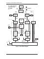
1
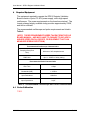
User Manual – DDR II Register Validation Board
Integrated Device Technology
DDR II Register Validation Board User Manual
Document Name:
DDR II Register Validation Board User Manual
Prepared by:
Chris Macaraeg
Revision:
0.7
Date:
September 6, 2003
Copyright © Integrated Device Technology Inc.
Copyright © Integrated Device Technology Inc. (IDT). All rights reserved. This document contains
information that is proprietary to IDT Inc. Use, transfer, or other duplication without the expressed
written consent of IDT, Inc. is strictly prohibited.
9/6/2003
1 of 30
User Manual – DDR II Register Validation Board
,QWURGXFWLRQ
The DDR II Register Validation Board is a standalone test fixture that
was designed to provide testing and validation for the DDRII
SSTU32864 register in an environment that simulates actual usage. It
requires no additional equipment except a PC-ATX power supply, and
a high-speed oscilloscope. The devices to be tested must be mounted
on a DIMM or other DIMM socket compatible test board. The board
will accept functional DIMMs, or DIMMs that have been modified
especially for designated tests.
While it is not the goal of the test fixture to test unbuffered DIMMs,
these devices can also be plugged into the test socket. It is also not
the goal to test PLL operation on the board, but all clocks are provided
to the DIMM, along with spread spectrum capability if the user wishes
to examine those areas.
9/6/2003
2 of 30
User Manual – DDR II Register Validation Board
6\VWHP)HDWXUHV
The register validation board was designed to drive a DDRII DIMM in a
standard DDRII DIMM socket. The intended purpose of the board is
testing of the SSTU32864 registers on the DIMM. The test capabilities
include the following:
1. Provision for virtually any addressing pattern. Up to 256 patterns can
be implemented, with 512 vectors per pattern.
2. Setup and hold time testing of the DIMM register. The address sent
to the DIMM can be skewed relative to the clock in 10ps increments,
allowing the user to determine the exact point of DIMM failure due to
setup/hold time violations.
3. CKE, ODT, and CS operation relative to clock. These signals are
skewed independently of the clock and address to allow testing of
setup/hold time.
4. Reset recovery. A test vector controls the reset input to the DIMM; it
can be toggled in the midst of a pattern to determine the time
required to complete a reset.
5. Corner voltage testing on the DIMM VDD voltage pins. VDD on the
DIMM can be set to any point between 1.7V and 1.9V.
6. Corner voltage testing on the DIMM VREF pin. VREF on the DIMM
can be set to any point between 800mV and 1.07V
7. Provision for driving the board clocks with an external signal source.
8. Capability to enable or disable Spread Spectrum Clocking (SSC)
modulation if the on-board clock source is used.
9. Up to 266MHz operation.
10. Simultaneous switching delay testing.
11. Noise and signal integrity testing.
9/6/2003
3 of 30
User Manual – DDR II Register Validation Board
&RQILJXUDEOH)XQFWLRQV
Before testing begins, the user must configure the board properly. All
of the functions on the board that must be configured, and the default
settings that the board is shipped with are listed in Table 1.
PCB Label
Adjustment
1
Location
Values
CDC960_SPREAD
S5-7
0 = disabled
1 = enabled
1
MREFSEL
S5-3
0 = CDC960
1 = External Source
0
CDC960_FS[2:0]
S5- [6-4]
101b = 133MHz
100b = 100 MHz
101b
DIMM Control
5
Register Delay
CTL_DLY[10:0]
S5- [2:0],
S4- [7:0]
DIMM Address
6
Register Delay
ADDR_DLY[10:0]
S7- [2:0],
S6- [7:0]
W1
W1
PATTERN[7:0]
S3- [7:0]
Function
Spread
Spectrum
Clocking
Enable
Clock Source
Select
CDC960
Frequency
4
Select
FLASH/PROM
Select
Test Pattern
Select
DIMM VREF
Adjustment
DIMM VDD
Adjustment
DIMM 900mV
ADJUST
DIMM 1.8V
ADJUST
R23
R1
Default
3
setting
2
0000000000b = min
delay
1xxxxxxxxxb = max
delay
0000000000b = min
delay
1xxxxxxxxxb = max
delay
A-B = PROM
B-C = FLASH
See Table 4
00010000000b
00010000000b
A-B
00000000b
800mV to 1.07V
(potentiometer)
1.7V to 1.9V
(potentiometer)
900mV
1.8V
Table 1: User Configurable Functions and Default Values
1
If multiple switches are listed the first is the MSB, the last is the LSB.
“1” = switch open, “0” = switch close.
3
“1” = switch open, “0” = switch close.
4
Switch settings not listed in the table are not supported. The DIMM clock frequencies are double the CDC960
clock frequency.
5
Minimum delay is nominally 2.2ps; additional delay is approximately 10ps per step. Refer to On Semicconductor
MC100EP195 data sheet.
6
Minimum delay is nominally 2.2ps; additional delay is approximately 10ps per step. Refer to On Semicconductor
MC100EP195 data sheet.
2
9/6/2003
4 of 30
User Manual – DDR II Register Validation Board
&RQILJXUDEOH)XQFWLRQ'HWDLOV
This section contains a detailed discussion of the configurable
functions.
6SUHDG6SHFWUXP&ORFNLQJ
The DDR II Validation Board contains a Texas Instruments CDC960
Clock Synthesizer/Driver that is used to provide an on-board clock
source to the circuitry. This device includes Spread Spectrum
Clocking (SSC) with a 0.5% downspread for reduced EMI. The IDT
5T2110 Differential Clock Driver will pass on the CDC960’s SSC
modulation to the registers under test on the DIMM.
This board has the capability to enable or disable SSC modulation on
the CDC960.
6HOHFWDEOH&ORFN6RXUFH
There may be occasions where the user would like to drive the board’s
clocks with a frequency that is not supported by the CDC960. In this
case, differential SMA connectors are provided for the user to connect
an external differential clock source.
This board has the capability to select between the CDC960’s
differential clock outputs, and the external clock source through the
SMA connectors.
If an external clock source is used, it’s frequency must not exceed
135MHz, nor be less than 50MHz. If it does, board operation is not
guaranteed. In addition, if SSC modulation is desired, the external
clock source must provide it.
&'&)UHTXHQF\6HOHFW
The TI CDC960 has the capability to provide multiple frequencies to
the board. Currently, however, only the 100MHz and 133MHz
frequencies are supported. These clocks are doubled in frequency by
the IDT 5T2110 devices, so the DIMM clocks will actually be 200MHz
or 266MHz.
',00&RQWURODQG'DWD5HJLVWHU'HOD\
Test patterns drive the DIMM control and address lines through
separate Control and Data registers, as shown in Table 3. The two
registers are driven by separate clocks that can be individually delayed
in time by 2.2ns to 12.2ns relative to the DIMM clocks. By adjusting
either the control register clock, the data register clock, or both
simultaneously, the user could:
9/6/2003
5 of 30
User Manual – DDR II Register Validation Board
•
Test setup and hold times of the address and control relative to
the DIMM clock,
•
Test setup and hold times of the address only, while keeping the
control bits within spec, or
•
Test setup and hold times of the control bits only, while keeping
the address bits within spec.
)/$6+RU3520VHOHFW
The DDR II Register Validation Board is designed to accept either
4Mbit FLASH or PROM as the nonvolatile storage device for the test
patterns. However, one pin is defined differently between the FLASH
and PROM. A jumper is provided to select the correct pin
configuration. This function will be set at the factory and is dependent
upon which device the board is populated with. This function never
needs to be changed by the user.
7HVW3DWWHUQ6HOHFW
Up to 256 test patterns can be supported by the DDR II Register
Validation Board. The test pattern is selected by configuring the
proper switches. See Section 11 for more details.
',0095()$GMXVWPHQW
This board has the capability to adjust the VREF input to the DIMM.
This will not affect the VREF inputs on any device on the DDR II
Register Validation Board; it only affects the VREF pin on the DIMM.
To adjust VREF to the DIMM, the board must be powered on, the
potentiometer at location R52 adjusted, and the voltage checked with a
DVM.
',009''$GMXVWPHQW
This board has the capability to adjust the VDD power supply input to
the DIMM. This will not affect the power inputs to any device on the
DDR II Register Validation Board; it only affects the VDD pins on the
DIMM.
To adjust VDD to the DIMM, the board must be powered on, the
potentiometer at location R53 adjusted, and the voltage checked with a
DVM.
9/6/2003
6 of 30
User Manual – DDR II Register Validation Board
5HTXLUHG(TXLSPHQW
The equipment required to operate the DDR II Register Validation
Board consists of just a PC-ATX power supply, and a high-speed
oscilloscope. The power requirements on the board are minimal. The
lowest-powered supply available today provides approximately 230W,
and this is sufficient.
The recommended oscilloscope and probe requirements are listed in
Table 2.
(NOTE: THESE REQUIREMENTS WERE TAKEN FROM THE OLD
BOARD MANUAL, AND MAY HAVE TO CHANGE TO INCLUDE A
HIGHER SPEED OSCILLOSCOPE, OR EQUIPMENT THAT CAN
MEASURE SPREAD SPECTRUM)
Recommended Oscilloscope Characteristics
Sampling Rate (Real
Time)
Minimum of 4G samples/second
RMS Jitter
< 6ps +/- 0.005% of delay setting
Recommended Probe Characteristics
Rise Time
<140ps
Bandwidth (3dB)
> 2.5GHz
Input Resistance
100kOhm
Input Capacitance
0.6pF
Table 2: Recommended Oscilloscope and Probe Characteristics
3UREH&DOLEUDWLRQ
T.B.D.
9/6/2003
7 of 30
User Manual – DDR II Register Validation Board
%RDUG6HWXS
Install the DIMM in the test socket; insert the ATX power supply
connector into the appropriate connector on the board. The DIMM
must be installed or removed from its test socket only when the power
is off.
After the DIMM and power supply are installed, flipping S2 switch to
the “on” position will turn on the board power.
9/6/2003
8 of 30
User Manual – DDR II Register Validation Board
%RDUG,QLWLDOL]DWLRQ With the board powered on, select the Initialization Pattern (see Table
1 and Table 4), and then depress the Master Reset switch. This will
initialize the SDRAMs on the DDR II DIMM (if they are installed) and
place the board in a state where it is ready to be used.
The initialization step must be executed after the power is turned on. If
the power to the board is cycled, the initialization step must be rerun.
If the Synchronization Pattern is run (see Section 7.2), then the
initialization step must be run again afterwards.
9/6/2003
9 of 30
User Manual – DDR II Register Validation Board
&RQILJXULQJWKH9DOLGDWLRQ%RDUGIRU7HVW
Before testing can begin, the delay lines and variable voltages on the
board must be set up.
6HWWLQJ8SWKH9DULDEOH9ROWDJHV
On the DDR II Register Validation Board, the DIMM VDD and VREF
voltages are adjustable.
The user will determine what level to set these voltages to. The
ranges for these voltages are listed in Table 1.
6HWWLQJ8SWKH'HOD\/LQHV
The delay lines must also be configured such that the address and
control presented to the SSTU32864 registers on the DIMM meet the
specified setup and hold times (see the appropriate data sheet for the
timing specifications).
A test pattern has been implemented to assist in setting up the delay
lines. This is the Synchronization Pattern (see Table 4). This pattern
will pulse the data and control bits simultaneously every 32 clock
cycles. This will assist in not only aligning the control and data register
outputs with the clock, but also aligning the two registers with each
other.
To configure the Data Register delay line so that the data signals meet
the setup and hold times, the user must simultaneously probe the
clock pin and one of the data pins on the SSTU32864. If the timing is
not as desired, then the DIMM Data Register Delay must be changed
to suit by modifying the appropriate switches (see Table 1). After the
timing has been adjusted and verified, the remaining data bits can be
checked – the bit-to-bit skew for the data signals will be approximately
10ps maximum.
9/6/2003
10 of 30
User Manual – DDR II Register Validation Board
After this process is completed for the Data Register, the same
process must be executed to set up the Control Register delay line.
Once the Data Register and Control Register delay lines are set up, it
is recommended that the switch settings be recorded so they can be
used as a baseline setting for future tests.
The steps for configuring the registers are listed below.
1. Install the DIMM and power supply as described in Section 5.
Turn the power on.
2. Set the appropriate switches to select the Synchronization
Pattern (see Table 1 and Table 4). When configuring the delay
lines after power up, it is not necessary to run the Initialization
Pattern.
3. Depress the Master Switch button to load and run the
Synchronization Pattern.
4. Set up the oscilloscope to probe an appropriate data bit and
clock on the DIMM. If the timing is not correct, adjust S6 and S7
until the desired timing is attained.
5. Set up the oscilloscope to probe an appropriate control bit and
clock on the DIMM. If the timing is not correct, adjust S4 and S5
until the desired timing is attained. Normally, the control and
data bits would be aligned, but this is entirely up to the user.
6. Rerun the Initialization Pattern to place the SDRAMs in a known
state (see Section 6).
The board is now ready to be used.
9/6/2003
11 of 30
User Manual – DDR II Register Validation Board
5XQQLQJD7HVW
After setting up the board (Section 5), initializing it (Section 6), and
configuring it (Section 7), testing can begin. Testing the board
consists of two parts – selecting the Test Pattern, and adjusting the
register delay lines and checking the results.
6HOHFWLQJWKH7HVW3DWWHUQ
To select the Test Pattern, set S3 to the proper value for the desired
Test Pattern (see Table 1 and Table 4). Then, depress the Master
Reset button.
$GMXVWLQJWKH5HJLVWHU'HOD\/LQHVDQG&KHFNLQJWKH5HVXOWV
The recommended procedure for this operation is as follows:
1. Connect the oscilloscope to the clock, at least one register input
bit, and the corresponding register output bit(s). The only way
to verify test results with the DDR II Register Validation Board is
visually.
2. Check on the oscilloscope that the register input waveform
looks similar to the register output waveform, but delayed by
one clock cycle. If this is not the case, then the delay lines were
not configured properly, and a timing parameter is being
violated. The delay lines should be reconfigured (see Section
7.2).
3. If the input and output waveforms do look similar, then adjust
the delay line timing, moving the input waveform in the direction
that would test the desired timing parameter.
4. After each delay line adjustment, the register output should be
checked on the oscilloscope, and the timing parameter being
validated (for example setup or hold time) should be recorded.
5. When the register output no longer matches the register input
waveforms (ignoring the one clock cycle skew), a failure has
occurred and the timing specification limit has been reached.
The last recorded timing parameter is the limit of the device.
If the register output still matches the register input waveforms,
then no failure has occurred. Step 3 must be repeated until a
failure occurs.
9/6/2003
12 of 30
User Manual – DDR II Register Validation Board
If a fine timing resolution is required, it could take a long time to step
through enough delays to find where the device fails (since the delay
increments would be small). To save time, it is recommended that the
delay line adjustment start out as a relatively large delay (for example
160ps) until a failure occurs. When a failure is found, the delay can be
set back to the last known good delay, and Step 3 above repeated
using smaller increments (for example 10ps or 20ps).
The amount of the increment depends upon the desired timing
resolution. If 100ps resolution is required, then an increment of 40ps
will probably suffice. If 50ps or finer resolution is required, then an
increment of 20ps or 10ps could be used.
Keep in mind that the minimum “step” of the delay line is equivalent to
approximately 10ps. Also, the delay line has an overall delay of
approximately 2.2ns to 12.2ns, so it is very easy to delay a signal
multiple clock cycles with the delay line.
Also, when adjusting the switch settings and multiple switches have to
be flipped to obtain the proper increment, always change the MSB
switch bit last. If the MSB bit is not switched last, a false error may
occur due to the switches being momentarily set to a longer delay.
9/6/2003
13 of 30
User Manual – DDR II Register Validation Board
7KHRU\RI2SHUDWLRQ
A Master Reset pulse will initiate the driving of test patterns onto the
DDR II DIMM. A Master Reset pulse can be created in two ways:
either by powering on the board, or by depressing the START
BUTTON.
For the following discussions, refer to the Block Diagram in 1. Note
that all signal names used in this document refer to the board
schematics, and not necessarily the block diagram.
9/6/2003
14 of 30
User Manual – DDR II Register Validation Board
PLL/REGISTER
VALIDATION
DIFF
LVTTL
BOARD
TI CDC960
CLK SYNTH
DIFFERENTIAL
SMA INPUTS
133MHz
Rev 11
IDT
5T2110
PLL CLK DRVR
eHSTL
133MHz
DIPSW
ON SEMI
MC100EP195
PROG DL
LVEPECL
133MHz
HSTL, 133MHz
HSTL, 133MHz
HSTL, 133MHz
A
ALTERA
7256B
EPLD
CTL
IDT
5T2110
PLL CLK DRVR
CTL
WC
RC
IDT
D DDR/SDR
FIFO
(DATA)
Q
DIPSW
HSTL
SSTL, 266MHz
SSTL, 266MHz
SSTL, 266MHz
SSTL, 266MHz
RC
WC
IDT
DDR/SDR D
FIFO
(CONTROL)
Q
IDT
5T2110
PLL CLK DRVR
D
HSTL, 266MHz
HSTL, 266MHz
Vref1 = 1.08V
HSTL, 133MHz
HSTL, 133MHz
IDT
5T2110
PLL CLK DRVR
HSTL
Vref2
Vref2
SSTU32864
Vref3
(Adj.)
DIPSW
AT27040
PROM
Vref1 = 1.08V
1.7V-1.9V
Adjust. VDD
eHSTL
133MHz
ON SEMI
MC100EP195
PROG DL
LVEPECL
133MHz
START
BUTTON
eHSTL
133MHz
DCS, DCKE,
DODT, RST#
SSTL
SSTU32864
RAS#, CAS#,
WE#, ADDR
SSTL
900mV =
VTT2
LOAD
DIFF SSTL,
266MHz
DDR II DIMM SOCKET
Figure 1: Board Block Diagram
9/6/2003
15 of 30
User Manual – DDR II Register Validation Board
When a Master Reset pulse occurs, the EPLD will pass the
configuration on the 8-position DIP-switch onto the upper 8 bits of the
PROM address bus to “select” a pattern stored in the PROM. The
value of the 8-position DIP-switch is meant to be static while a test is
being conducted. If the configuration of the DIP-switch is modified, the
Start Button must be depressed again to load the new pattern and
begin a new test.
A Pattern Word will then be read out of the PROM. A Pattern Word is
defined as all the test bits that will be output to the DIMM’s I/O pins
during a given clock cycle. Each test pattern consists of 512 Pattern
Words. Since the Pattern Word is 32-bits wide, and the PROM is only
8-bits wide, the Pattern Word will be read out of the PROM 8 bits at a
time.
9/6/2003
16 of 30
User Manual – DDR II Register Validation Board
For a mapping of the Pattern Word contents to the DDR II DIMM I/O
pins, refer to Section 9.1
When an entire 32-bit Pattern Word has been read out of the PROM
and buffered in the EPLD, it will be written into the Data and Control
FIFOs, and the next Pattern word will be read from the PROM. This
process will continue until the 512 Pattern Words have been stored in
the FIFOs.
After the entire test pattern has been written into the FIFOs, a state
machine within the EPLD will then place the FIFOs in the test mode,
where the FIFOs are continuously read. The 512-word test pattern is
repeated continuously by use of the MARK and RETRANSMIT pins of
the FIFOs. For information on the test patterns, refer to Section 11.
The test will be continuously run (driving the same pattern onto the
DIMM pins continuously) until the START BUTTON is depressed
again.
0DSSLQJRI),)2,QSXWWR',00,QSXW
The field defined as CFIFO_DIN in the Pattern Word drives the input of
the Control FIFO, and the fields defined as DFIFO_DIN in the Pattern
Word drive the input of the Data FIFO. The output pins of both FIFOs
(called CFIFO_DOUT and DFIFO_DOUT) then drive the on-board
SSTU32864 registers that then drive the DIMM. The mapping of these
FIFO input bits to the DDR II DIMM I/O pins, including which of the two
FIFOs and registers drive these signals, is shown in Table 3.
9/6/2003
17 of 30
User Manual – DDR II Register Validation Board
FIFO
FIFO INPUT SIGNAL
Register
DDR II DIMM Pin
CFIFO_DIN[6]
RESET#
CFIFO_DIN[5]
S1#
CFIFO_DIN[4]
CONTROL
DATA
CKE1
CONTROL
CFIFO_DIN[3]
ODT1
CFIFO_DIN[2]
S0#
CFIFO_DIN[1]
CKE0
CFIFO_DIN[0]
ODT0
DFIFO_DIN[21]
A15
DFIFO_DIN[20]
A14
DFIFO_DIN[19]
A13
DFIFO_DIN[18]
A12
DFIFO_DIN[17]
A11
DFIFO_DIN[16]
A10
DFIFO_DIN[15]
A9
DFIFO_DIN[14]
A8
DFIFO_DIN[13]
A7
DFIFO_DIN[12]
A6
DFIFO_DIN[11]
DATA
DFIFO_DIN[10]
A5
A4
DFIFO_DIN[9]
A3
DFIFO_DIN[8]
A2
DFIFO_DIN[7]
A1
DFIFO_DIN[6]
A0
DFIFO_DIN[5]
BA2
DFIFO_DIN[4]
BA1
DFIFO_DIN[3]
BA0
DFIFO_DIN[2]
WE#
DFIFO_DIN[1]
RAS#
DFIFO_DIN[0]
CAS#
Table 3: DDR II DIMM Pin Mapping
9/6/2003
18 of 30
User Manual – DDR II Register Validation Board
''5,,6'5$0,QLWLDOL]DWLRQ3DWWHUQ
The purpose of the Initialization Pattern is to place the DDR II DIMM’s
SDRAMs into a known state before testing begins.
To initialize the SDRAMs, first the Initialization Pattern must be
selected using the DIP-switches (see Table 4). Then, a Master Reset
pulse must be generated as discussed in Section 9. When this is
done, the initialization pattern will be driven onto the DIMM I/O pins.
The Initialization pattern consists of the following steps to place the
DRAMs into the idle state:
1. Drive all DIMM inputs low while Master Reset is low. This will be about 2ms.
2. A NOP command will be applied to the DIMM and CKE[1:0] will be driven
high.
3. Wait 400ns.
4. A PRECHARGE ALL command will be applied to the DIMM.
5. An EMRS (Extended Mode Register Set) command will be applied to
enable the DLL.
6. An MRS (Mode Register Set) command will be applied to reset the DLL
and program the operating parameters.
7. A PRECHARGE ALL command will be applied.
8. Two AUTO-REFRESH commands will be applied.
9. An MRS command will be applied to initialize device operation.
10. An EMRS OCD Default command will be applied followed by an EMRS
OCD Calibration Exit command.
After this sequence occurs, the DRAMs will be in the idle state and
ready for testing.
9/6/2003
19 of 30
User Manual – DDR II Register Validation Board
3DWWHUQ'HILQLWLRQV
As mentioned earlier, an 8-position DIP-switch selects the test pattern
stored within the PROM by driving the upper 8-bits of the PROM
address bus (through the EPLD). The outputs of the DIP-switch are
called PATTERN [7:0] in the schematics.
Each test pattern is 512 Pattern Words long, and is stored in 2048
contiguous locations (bytes) in the PROM. Therefore, during the FIFO
loading period, the lower 11 bits of the PROM are driven by the EPLD
to address these 2048 locations.
The currently defined patterns are shown in Table 4.
9/6/2003
20 of 30
User Manual – DDR II Register Validation Board
PATTERN
[7:0]
Pattern Name
0x00
No Activity or
Zero
0x01
Initialization
0x02
0x03
Synchronization
Reset Recovery
Description
Places all zeros on the
address bus all the
time. SDRAMs are
inactive.
Goes through an
initialization
sequence to place the
DDR DRAMs in the
idle state. This is
done once.
All bits will pulse
high every 8th clock
cycle. This will assist
in synchronization
between the control
and address registers.
Identical to the
Walking One
(SDRAM Read)
pattern, except that
the RESET* pin to
the DIMM will be
toggled every 8 clock
cycles during the
burst read.
Places all zeros on the
address bus all the
time. SDRAMs are
inactive.
The Number of
switching bits will
increase with each
clock cycle
0x04 – 0x3F
No Activity or
Zero
0x40
ISI Pattern
(Register Only)
0x41
Walking “1”
(Register Only)
Walks a “1” through
the address bus.
0x42
Walking “0”
(Register Only)
Walks a “0” through
the address bus.
9/6/2003
Example
00000000
00000000
00000000
N/A
11111111
00000000
00000000
00000000
00000001
00000010
00000100
00001000
00000000
00000000
00000000
00000000
10101010
11001100
11100011
11110000
00000001
00000010
00000100
00001000
11111110
11111101
11111011
11110111
21 of 30
User Manual – DDR II Register Validation Board
0x43
0x44
0x45
0x46
0x47
0x48
0x49
0x4A
0x4B
0x4C
All Bits Toggling
(Register Only)
All Bits Toggling,
A15 and S1#
Inverted (Register
Only)
A15 and S1#
Switching,
Remainder Ones
(Register Only)
A15 and S1#
Switching,
Remainder Zeroes
(Register Only)
Every bit will
continuously toggle
simultaneously
between “1” and “0”
All bits will toggle
simultaneously, but
one bit will be
inverted from the rest.
One bit will be
toggling; the rest will
be “1” always.
One bit will be
toggling; the rest will
be “0” always.
The bit under test will
remain at a logic 1
level; all other bits
will toggle.
The bit under test will
Ground Bounce on
remain at a logic 0
A15 and S1#
level; all other bits
(Register Only)
will toggle.
The bit under test will
VDD Bounce on
remain at a logic 1
A3 and S1#
level; all other bits
(Register Only)
will toggle.
The bit under test will
Ground Bounce on
remain at a logic 0
A3 and S1#
level; all other bits
(Register Only)
will toggle.
The bit under test will
VDD Bounce on
remain at a logic 1
A4 and S1#
level; all other bits
(Register Only)
will toggle.
The bit under test will
Ground Bounce on
remain at a logic 0
A4 and S1#
level; all other bits
(Register Only)
will toggle.
VDD Bounce on
A15 and S1#
(Register Only)
9/6/2003
11111111
00000000
11111111
00000000
011111111
10000000
01111111
10000000
11111111
01111111
11111111
01111111
00000000
10000000
00000000
10000000
11111111
10000000
11111111
10000000
01111111
00000000
01111111
00000000
11111111
10000000
11111111
10000000
01111111
00000000
01111111
00000000
11111111
10000000
11111111
10000000
01111111
00000000
01111111
00000000
22 of 30
User Manual – DDR II Register Validation Board
0x4D
0x4E
0x4F
0x50
0x51
0x52
Every other bit will
continuously toggle
simultaneously
between “1” and “0”
Every other bit will
Half Bits Toggling continuously toggle
(Register Only)
simultaneously
between “1” and “0”
A4 is the victim with
“1” and “0”, A7, A8,
CrossTalk on
A12, A13 are
A4
aggressors PRBS
(Register Only)
(511 length). A0, A3,
A14, A15 have
PRBS# to limit SSO
A0 is the victim with
“1” and “0”, A0, A13,
CrossTalk on
A14, A15 are
A0
aggressors PRBS
(Register Only)
(511 length). A4, A9,
A12, A12 have
PRBS# to limit SSO
A11 is the victim with
“1” and “0”, A9, A10,
CrossTalk on
A14, A15 are
A11
aggressors PRBS
(Register Only)
(511 length). A0, A6,
A8, A13 have PRBS#
to limit SSO.
BA0 is the victim
with “1” and “0”, A1,
CrossTalk on
A2, ODT1, CAS are
BA0
aggressors PRBS
(Register Only)
(511 length). A5, A6,
BA1, BA2 have
PRBS# to limit SSO.
Half Bits Toggling
(Register Only)
0x53
CrossTalk
Reference
(Register Only)
“1” and “0” pattern
on A0, A4, A11 and
BA0
0x54
All Bits Toggling,
except A8 and
A13 (Register
Only)
All bits will toggle
simultaneously,
except A8 and A13.
9/6/2003
01010101
00000000
01010101
00000000
10101010
00000000
10101010
00000000
01111111
10000000
01111111
10000000
01111111
10000000
01111111
10000000
01111111
10000000
01111111
10000000
01111111
10000000
01111111
10000000
00000000
10000000
00000000
10000000
01111111
00000000
01111111
00000000
23 of 30
User Manual – DDR II Register Validation Board
0x55
All Bits Toggling,
A15 and S1#
inverted, (Register
Only)
All bits will toggle
simultaneously, but
A15 and S1# will be
inverted from the rest.
A8 and A13 will
remain “0”.
Places all zeros on the
address bus all the
time. SDRAMs are
inactive.
The Number of
switching bits will
increase with each
clock cycle
0x56 – 0x7F
No Activity or
Zero
0x80
ISI Pattern
(SDRAM Read)
0x81
Walking “1”
(SDRAM Read)
Walks a “1” through
the address bus.
0x82
Walking “1”
(SDRAM Write)
Walks a “1” through
the address bus.
0x83
Walking “0”
(SDRAM Read)
Walks a “0” through
the address bus.
0x84
Walking “0”
(SDRAM Write)
Walks a “0” through
the address bus.
0x85
All Bits Toggling
(SDRAM Read)
0x86
All Bits Toggling
(SDRAM Write)
0x87
All Bits Toggling,
A5 Inverted
(SDRAM Read)
0x88
All Bits Toggling,
A5 Inverted
(SDRAM Write)
Every bit will
continuously toggle
simultaneously
between “1” and “0”
Every bit will
continuously toggle
simultaneously
between “1” and “0”
All bits will toggle
simultaneously, but
one bit will be
inverted from the rest.
All bits will toggle
simultaneously, but
one bit will be
inverted from the rest.
9/6/2003
01111111
10000000
01111111
10000000
00000000
00000000
00000000
00000000
10101010
11001100
11100011
11110000
00000001
00000010
00000100
00001000
00000001
00000010
00000100
00001000
11111110
11111101
11111011
11110111
11111110
11111101
11111011
11110111
11111111
00000000
11111111
00000000
11111111
00000000
11111111
00000000
011111111
10000000
01111111
10000000
011111111
10000000
01111111
10000000
24 of 30
User Manual – DDR II Register Validation Board
0x89
A15 Switching,
Remainder Ones
(SDRAM Read)
One bit will be
toggling; the rest will
be “1” always.
0x8A
A15 Switching,
Remainder Ones
(SDRAM Write)
One bit will be
toggling; the rest will
be “1” always.
0x8B
A15 Switching,
Remainder Zeroes
(SDRAM Read)
One bit will be
toggling; the rest will
be “0” always.
0x8C
A15 Switching,
Remainder Zeroes
(SDRAM Write)
One bit will be
toggling; the rest will
be “0” always.
0x8D
0x8E
0x8F
0x90
0x91 – 0xBF
0xC0 – 0xFF
The bit under test will
remain at a logic 1
level; all other bits
will toggle.
The bit under test will
VDD Bounce on
remain at a logic 1
A15 (SDRAM
level; all other bits
Write)
will toggle.
The bit under test will
Ground Bounce on
remain at a logic 0
A15 (SDRAM
level; all other bits
Read)
will toggle.
The bit under test will
Ground Bounce on
remain at a logic 0
A15 (SDRAM
level; all other bits
Write)
will toggle.
Places all zeros on the
No Activity or
address bus all the
Zero
time. SDRAMs are
inactive.
VDD Bounce on
A15 (SDRAM
Read)
Undefined
N/A
9/6/2003
11111111
01111111
11111111
01111111
11111111
01111111
11111111
01111111
00000000
10000000
00000000
10000000
00000000
10000000
00000000
10000000
11111111
10000000
11111111
10000000
11111111
10000000
11111111
10000000
01111111
00000000
01111111
00000000
01111111
00000000
01111111
00000000
00000000
00000000
00000000
00000000
N/A
25 of 30
User Manual – DDR II Register Validation Board
Table 4: Test Pattern Definitions
Notes:
1. All patterns, except for Initialization, will be repeated until the
Master Reset button is depressed to reload a new pattern and
begin a new test.
2. In the “Example” column, an 8-bit bus is shown. On this board, the
patterns will be extended across all 16 address and 3 bank address
bits (A[15:0] and BA[2:0]).
3. ODT[1:0] will toggle during each test (CKE[1:0], S[1:0], RAS*,
CAS*, and WE* will be controlled to apply burst read and burst
write patterns to the DRAMs.
9/6/2003
26 of 30
User Manual – DDR II Register Validation Board
%RDUG&KDUDFWHULVWLFV
This section contains information related to design of the Printed
Circuit Board.
7UDFH/HQJWK0DWFKLQJ
There are three groups of signals that were routed such that the trace
lengths within the group match very closely. Note that matching the
lengths of one group to another is not necessary, since the timing for
each group will be skewed relative to the other groups using the
register delay lines.
All traces not mentioned in this section are also impedance controlled
to 60 ohms +/- 10%. However, except for differential clock pairs being
matched within the pair, they are not length matched.
',00&ORFNV
The three differential DIMM clock pairs are length matched and
impedance controlled (both single-ended and differentially). The
differential pair lengths are not more than 0.5mm different in length
(within a pair). Of the six differential traces (3 pairs), they vary in
length from 4.61 inches to 4.67 inches. The single-ended impedance
is 60 ohms +/- 10%. The differential impedance is 120 ohms +/- 10%.
An additional differential clock reference pair is provided for probing. It
is approximately 1.50 inches longer than the three clock pairs driving
the DIMMs, and like the other three pairs is routed on an inner layer.
However, this reference pair does not drive the DIMM – it drives an onboard 120-ohm differential terminator with a load capacitor on each
terminal. The additional length (the reference clock pair is
approximately 6.15 inches in length) emulates the line lengths of the
DIMM connector plus the line length on the DIMM PCB, along with the
loading on the DIMM.
',00$GGUHVV
The DIMM address lines are length matched and impedance
controlled. The lengths vary between 2.30 inches and 2.23 inches.
The impedance is 60 ohms +/- 10%.
',00&RQWURO
The DIMM control lines are length matched and impedance controlled.
The lengths vary between 2.19 and 2.15 inches. The impedance is 60
ohms +/- 10%.
9/6/2003
27 of 30
User Manual – DDR II Register Validation Board
8QEXIIHUHG',00&ORFN5HIHUHQFH1HWV
A DDR II SDRAM Registered DIMM will have one differential clock
input pair, while an unbuffered DIMM has an additional two differential
clock input pairs. The DDRI II Register Validation Board drives all
three differential clock pairs.
&URVV6HFWLRQ
The DDR II Register Validation Board has a 12-layer stackup.
9/6/2003
28 of 30
User Manual – DDR II Register Validation Board
$GGLWLRQDO,QIRUPDWLRQ
Additional details concerning the design that may be of useful to the
owner of this board are included in this section.
3RZHU8S6HTXHQFLQJ
The power up sequencing of the different planes on the board is
guaranteed by design. The 900mV supply (VTT) is generated by a
voltage regulator that inputs the 1.8V (VDD) supply and uses an
internal resistor divider network to divide the input voltage by two to
create the output voltage. The output voltage follows the input voltage
when it is being powered up and down, so VTT can never be greater
than VDD.
',005HVHW
The RESET* pin on the SDRAM DIMM socket is driven by the Control
Register (see Table 3). This signal is completely controlled by the test
patterns. Currently, the only test pattern that will toggle RESET* is the
Initialization Pattern (see Table 4). Other patterns that incorporate
RESET* will be implemented in the future.
9/6/2003
29 of 30
User Manual – DDR II Register Validation Board
5HYLVLRQ+LVWRU\
Version
0.01
0.02
Data
11/15/02
11/18/02
0.02a
0.03
01/07/03
01/27/03
0.04
0.05
2/13/03
3/27/03
0.06
4/30/03
0.07
9/6/03
Initials
Comments
CM
Document creation.
CM
Add Reset Recovery pattern, modify block
diagram. Add Board Characteristics section
(Section 12). Added notes on maximum and
minimum operating frequencies.
CM
Remove PROM configuration details.
CM
Restore PROM configuration details. Add
column in Table 1 for PCB labeling. Remove
the reference in Table 4 to all bits being
sequenced. Change “data” to “address” in
Table 4.
CM
Latest release.
CM
Update Table 4 to add test patterns 0x49
through 0x4C
JS
Update Table 4 to add test patterns 0x4D
through 0x4E
JS
Update Table 4 to add test patterns 0x4F
through 0x55
9/6/2003
30 of 30