1
Archive
Document
This electronic manual was created by scanning a
printed document, then processing the file using
character-recognition software.
Please be aware that this process may have
introduced minor errors. For critical applications,
use of a printed manual is recommended.
WARNINGS, CAUTIONS, AND NOTES AS USED IN THIS PUBLICATION
/ WARNING /
Warning notices are used in this publication to emphasize that hazardous voltages, currents, temperatures,
or other conditions that could cause personal injury exist in this equipment or may be associated with its
use.
I n situations where inattention could cause either. personal injury or damage to equipment,
notice is used.
a Warning
Caution notices are used where equipment might be damaged if care is not taken.
NOTE
Notes merely call attention to information that is especially significant to understanding and operating the
equipment.
This document is based on information available at the time of its publication. While efforts have been made to be accurate,
the information contained in this document does not purport to cover all details or variations in hardware or software, nor to
provide for every possible contingency in connection with installation, operation, and maintenance, Features may be
described which are not present in all hardware and software systems. GE Fanuc Automation assumes no obligation of
notice to holders of this document with respect to changes subsequently made.
GE Fanuc Automation makes no representation or warranty, expressed, implied or statutory with respect to, and assumes no
responsibility for the accuracy, completeness, sufficiency, or usefulness of the information contained herein. No warranties
of merchantability or fitness for purpose shall apply.
The following are trademarks for products of GE Fanuc Automation North America, Inc.
Access 90
Alarm M a s t e r
CIMPLICITY
CIMSTAR
GEnet
Genius
Helpmate
Logicmaster
Modelmaster
ProLoop
PROMACRO
Series One
SeriesThree
Series Five
Series Six
@Copyright 1990 GE Fanuc AutomationNorth
All Rights Reserved.
Series 90
VuMaster
Workmaster
Preface
GFK-0248
The Bus Controller for the Series Five Programmable Logic Controller (PLC) is the required interface
between a Series Five(tm) PLC and a Genius(tm) I/O network. This manual describes the functions of the
Bus Controller and how it is interfaces the Genius I/O system to the Series Five Programmable Logic
Controller. The factory set default configuration for the Bus Controller allows you to have your system
up and running in a minimum of time.
Content of This Manual
Chapter 1. Introduction: This chapter provides an overview of the features and functions of the Bus
Controller for the Series Five Programmable Logic Controller. Included is a discussion
of the factory defaults that should satisfy the application requirements for many users
with no further configuration of the Bus Controller.
Chapter 2. The Genius Network: This chapter describes the Genius network as used with the Series
Five PLC. This includes Series Five PLC compatibility with Genius I/O blocks, and
CPU to CPU communications through a Global communications network.
Chapter 3. Installation and Setup:
This chapter describes the installation and setup procedures
required to use a Series Five Genius Bus Controller in your Series Five PLC system.
Chapter 4. Operation with RD/WR CCM Devices:
This chapter describes how to use the Read
CCM and Write CCM instructions in a Series Five PLC Genius network to communicate
with other Series Five PLC systems with Genius I/O Bus Controllers.
Chapter 5. Troubleshooting: This chapter provides basic troubleshooting information to help you to
quickly solve any problems which may occur with operation of the Bus Controller.
Appendix A. Diagnostic
Information: This Appendix provides information about the Genius I/O
diagnostics, including information on construction and contents of the fault table. It also
describes fault reporting functions. Default Genius I/O Diagnostics are described with
the contents of the default registers listed for your information.
Appendix B. Scratch Pad Memory Map for Genius Bus Controller Setup Parameters:
Defini-
tions of Genius Bus Controller setup parameters and their location in Scratch Pad
memory are listed in this Appendix.
Appendix C. Datagram Transmission between Series Five and Series Six PLCs:
Provides an
example of using the TRANSFER instruction for datagram transmission between Series
Five and Series Six PLCs.
Appendix D. Switch BSM Datagram Command From a Series Five PLC:
Provides an example of
sending a BSM switch command from a Series Five PLC.
Appendix E. Setup Differences Based on CPU Revisions:
Describes differences in setup procedures depending on the revision level of the Series Five CPU.
Related Publications
GFK-0122 - Series Five (tm) Programmable Controller User’s Manual
GFK-0023 - Logicmaster(tm) 5 Programming and Documentation Software User’s manual
GFK-0181 - Series Five(tm) Operator Interface Unit User’s Manual
GFK-0171 - Series Six (tm) Bus Controller User’s Manual
GEK-90486 - Genius(tm) I/O System User’s Manual
iv
Preface
Content
V
CHAPTER 1.
INTRODUCTION
Product Summary
Using Genius I/O with a Series Five PLC
Purpose of the Genius Bus Controller
Bus Controller Description
LEDs
Bus Controller Specifications
CHAPTER 2.
THE GENIUS NETWORK
Introduction
Genius I/O Serial Bus
The Bus Scan
Typical Genius I/O Bus
Interfacing With Genius Networks
The Serial Bus Address
Starting Reference Address
Supporting Genius Communications Between CPUs
Datagrams
Global Data Communications
Combining Global Data Communications and I/O Control
Redundancy
Dual Bus Redundancy
Dual Controller Redundancy
CHAPTER 3.
l-l
l-l
l-2
l-2
l-3
l-4
2-1
2-2
2-2
2-2
2-3
2-3
2-3
2-4
2-4
2-5
2-5
2-5
2-5
2-6
INSTALLATION AND SETUP
Bus Controller Location in a System
Bus Controller Installation and Configuration
Selection of Serial Bus Address
Selection of Serial Bus Baud Rate
Setting the Outputs Enable DIP Switch
Using a Bus Controller with Default Setup Conditions
Installing the Bus Controller
Configuration with Logicmaster 5
Operation with Genius I/O Blocks
Genius I/O Block Setup Procedures
Enabling and Changing Global Data Values
Changing the Global Data Setup
Configuration Parameters for Global Data Communications
Entering GBC Setup Parameters With the OIU
Editing GBC Setup Parameters With Logicmaster 5 Software
Displaying the Bus Controller Setup Screen
Bus Controller Setup Key Summary
Setup Ranges
Reference Address
Global Data and Transmit Data Lengths
General System Information
Series Five CPU Scratchpad Genius Definitions
3-l
3-1
3-2
3-2
3-3
3-3
3-3
3-4
3-4
3-5
3-8
3-8
3-9
3-9
3-9
3-9
3-10
3-10
3-11
3-11
3-12
3-13
vi
Content
GFK-0248
CHAPTER 4.
OPERATION WITH RD/WR CCM INSTRUCTIONS
Introduction
Use of Read CCM and Write CCM to Communicate with
Other CPUs
Read/Write CCM
Example of Reading from a Remote CPU:
Example of Writing to a Remote Series Five PLC with a
Genius Bus Controller.
CHAPTER 5.
Diagnostic Information
Bus Controller Diagnostic Information
Default Genius I/O Diagnostic Fault Configuration
Registers for Default Configuration
Data Entered in Fault Tables
APPENDIX B.
APPENDIX C.
4-3
5-l
5-l
5-l
5-2
5-2
5-2
5-3
5-4
5-5
5-6
5-6
5-6
5-7
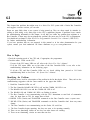
Troubleshooting
How to Begin
Identifying the Problem
APPENDIX A.
4-l
4-2
4-3
OPERATION WITH GENIUS I/O DIAGNOSTICS
Introduction
User Interface to Genius I/O Diagnostics
Displaying the Genius I/O Diagnostics Screen
Fault Table Display
Contents of Fault Table
Special Registers, Contacts, and Coils for Genius I/O
Operation
Special Registers
Internal Coils
Clear All Faults and Pulse Test Function
Device Loss
Device Addition
Address Conflict
Internal Contacts
CHAPTER 6.
4-l
Scratch Pad Memory Map for Genius Bus Controller Setup
Parameters
Datagram Transmission Between Series Five and Series Six
PLCs
6-1
6-l
A-l
A-l
A-l
A-2
A-2
B-l
Datagram Format
The TRANSFER Command
Sending Datagrams - Series Five PLC to Series Six PLC
Relay Ladder Diagram Example
C-l
c-2
c-3
C-4
C-8
APPENDIX D.
Switch BSM Datagram Command From a Series Five PLC
D-l
APPENDIX E.
Setup Differences Based on CPU Revisions
E-l
E-l
E-l
Compatibilities
Restrictions
Differences in Operation Between CPU Revision B and
Later Revision CPUs
E-2
Figures
Vii
Figure
l-l
l-2
2-l
2-2
2-3
2-4
3-1
Example of Bus Controller Interface to Genius I/O
Bus Controller for the Series Five PLC
Typical Genius Network for I/O Control
Genius I/O Serial Bus Token Passing
Genius I/O Serial Bus Scan
Genius Network for CPU to CPU Communications
Bus Controller Installation in a CPU Base Unit
1-2
l-3
2-1
2-2
2-2
2-4
3-4
Tables
viii
Table
3-l
3-2
3-3
3-4
3-5
4-l
5-l
5-2
Genius I/O Reference Address Assignment
Valid Bus Controller Setup Ranges
Global Data And Transmit Data Lengths
Datagram Mapping
Genius Information in CPU Scratchpad
CCM/CPU Mapping
Registers for Genius I/O Diagnostics
Internal Coils for Genius I/O Diagnostics
3-5
3-10
3-11
3-12
3-13
4-l
5-3
5-4
1-l
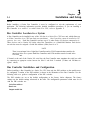
Product Summary
This manual describes the Bus Controller (catalog number IC655BEM510)
for the GE Fanuc Series
(tm)
Five
Programmable Logic Controller (PLC). The Bus Controller is the Series Five PLC link to a
Genius(tm) I/O system communications network. The following capabilities are available through the use
of the Genius network with the Series Five PLC.
- Compatibility with GE Fanuc Genius I/O blocks including discrete, analog, high speed counter, and
PowerTRAC.
- Communications between Series Five PLCs (via RD CCM and WR CCM instructions). This allows
general purpose communications between up to 32 Series Five PLCs at a low priority level.
- Global data sharing with up to 31 other Series Five CPUs, and other compatible GE Fanuc products.
This allows high priority data to be transmitted automatically to other devices on the bus.
- General purpose low priority communications with other devices which support Genius datagrams.
- Redundant CPU configurations.
Genius I/O blocks are configured using the Genius I/O Hand-Held Monitor (HHM), and the global
communications configuration requires only setting the Serial Bus Address (SBA), global data location,
and data transmit length for each Bus Controller. The HHM must be catalog number IC660HHM501C,
version 3.0, or later for use with a Series Five PLC system. This version of the HHM allows you to
select the Series Five PLC for HHM operations.
Genius system setup may be done with Logicrnaster 5 or the Series Five Operator Interface Unit (OIU).
It is possible to use any of the Il+, 12+, Ol+, or O2+ tables, or registers for Genius I/U blocks, or for
CPU to CPU data transfers. Additionally, communications with GE Fanuc Series Six PLCs and other
GE Fanuc devices is possible through the global communications setup.
For more information on the Genius I/O system operation, and setup, refer to the following manuals:
GEK-90486 - Genius(tm) I/O System User’s Manual
GFK-017 1 - Series Six(tm) Bus Controller User’s Manual
GFK-0023 - Logicmaster(tm) 5 Progr amming and Documentation Software User’s Manual
GFK-0181 - Series Five(tm) Operator Interface Unit User’s manual
Included in this chapter is an introduction to the Bus Controller for the Series Five PLC, its purpose in
the system, a physical description of the Bus Controller, including specifications, and configuration and
installation requirements.
Using Genius I/O with a Series Five PLC
Genius I/O phase A products cannot be used in a Series Five PLC system where any of the following
features are used: Global data, Datagrams (including RD CCM WR CCM instructions used with the
Bus Controller), baud rates other than 153.6K baud (standard), redundancy, or multiple controllers on
the same bus. To program Genius I/O blocks in the I2+ and O2+ tables, and in the register tables, you
must have version 3.0 of the Genius I/O Hand-Held Monitor. Genius I/O phase B products allow use of
the above features.
Introduction
l-2
GFK-0248
Systems which use phase A blocks are limited to a single Series Five CPU and Bus Controller connected
to Genius I/O blocks. This is not a restriction when using phase B blocks.
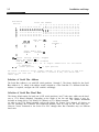
Purpose of the Genius Bus Controller
The Bus Controller functions as the interface between the Series Five PLC and the Genius I/O serial bus.
A Bus Controller provides a variety of communications capabilities on the network. The purpose of the
network determines which of those capabilities are used. If the network consists of only standard I/O
control, the Genius communications network automatically provides communications between devices
on the bus. In this instance, no special ladder logic programming is required.
If Global communications is to be a feature of the network, you must specify Genius Bus Controller
reference address and Global Data Length through either Logicmaster 5 software or the Series Five
Operator Interface Unit.
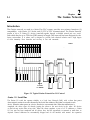
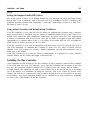
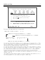
HAND-HELD
MONITOR
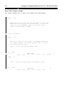
COMMUNICATIONS
BUS
-I/O BLOCKS
I
Figure 1-l. Example of Bus Controller Interface to Genius I/O
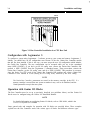
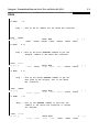
Bus Controller Description
A Bus Controller for the Series Five PLC is a single module consisting of a daughter board and mother
board. The Bus Controller plugs into a single I/O slot in a Series Five CPU base unit. There is one DIP
(Dual-In-Line) switch pack, consisting of 8 switches, requiring configuration by the user at installation
(if the factory default configuration is not sufficient for your application). Two LEDs on the top front of
the module provide a visual indication of the health of the module, and status of the communications
link.
The front of the module has a terminal block with four screw connections which provide the connecting
link to the Genius I/O serial bus. This group of connections is also provided on all Genius I/O blocks.
A 9-pin connector provides a connection to the serial bus for the Genius I/O Hand-Held Monitor
(HHM).
CiFK-0248
nnnnnnnnn
/
n.._lroFEN
m.cLosED
Figure 1-2. Bus Controller for the Series Five PLC
LEDs
The two LEDs on the front of the Genius Bus Controller module provide a visual indication of its
operating status. Both LEDs should be on during normal operation.
BDOK
COMM OK
Shows the status of the Genius Bus Controller. This LED blinks during powerup
diagnostics.
Shows the status of the Genius serial bus. This LED is on steadily when the bus is
operating properly. It blinks for intermittent bus errors and is off for a failed bus. It is
also off when no configuration has been received from the CPU.
For more detailed information on troubleshooting with the LEDs, refer to Chapter 7 in this manual.
Introduction
l-4
GFK-0248
Bus Controller Specifications
Specifications for the Bus Controller and Genius I/O network are given in the following table.
Operational:
Power Requirements
Size
Weight
LEDs
Number of Devices on Bus
Bus Type
Isolation
Baud Rates
Bus Scan Time
Communications
Environmental:
Operating Temperature
Storage Temperature
Humidity
Atmosphere
Vibration
Shock
Radio Frequency Interference
Genius Network:
Modulation Technique
Data Encoding
Isolation
Signal to Noise Ratio
Cable
Network Topology
Termination
Error Checking
Network Access
500 ma at +5 V dc, from Series Five PLC power supply
9.8” (250mm) H x 1.8” (45mm) W x 5.1”(129mm) D
1.8 lbs (815 grams)
BD OK (Board OK), COMM OK (Communications OK)
Up to 32
Shielded, twisted pair cable or Twinax
1500 volts between devices on the bus
153.6K baud standard, 153.6K baud extended, 76.8K baud,
38.4K baud
3 ms minimum, 10 ms typical, 400 ms maximum (actual
bus scan time can be observed in CPU registers 4041
through 4048).
Transmit Global Data from I/O or registers for peer-to-peer
communications Receive Directed Data from other CPUs
on the network Transmit and Receive Datagrams.
0°C to +60°C (32°F to 140°F)
-20°C to +70°C (-4°F to 158°F)
5% to 95% (non-condensing)
No corrosive gases
Mil-std 81OC method 514.2, Rank (F)
Mil-std 81OC method 516.2
FCC Class A, part 15, subpart J
FSK, 0/460.8 Khz (maximum), (153.6K baud)
Each bit is encoded into three dipulses majority voted at the
receiver to correct any single dipulse errors. A dipulse is
an AC code consisting of a positive then negative
excursion of voltage. Dipulses are individually sampled
to reject low and high frequency interference.
2000 volts Hi-pot J500 volts transient common mode
rejection
60 db
Single twisted pair plus shield or Twinax Length up to
2000 feet (606) meters at 153.6K baud standard, up to
7500 feet (2280 meters) at 38.4K baud - depending on
type of cable used.
Daisy-chained bus
Matched resistance at both ends of bus (75/150 ohms).
CRC check for each message
Token passing with implicit token aud fast token recovery
algorithms Implicit token ensures that devices
transitioning on-line or off-line do not disturb the
operation of other nodes. Fast token recovery restores
device access following system transients.
Chapter
2
The Genius Network
2-1
GFK-0248
Introduction
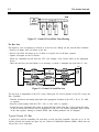
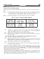
The Genius network, as used in a Series Five PLC system, provides two primary functions: (1)
compatibility with Genius I/O blocks, and (2) CPU to CPU communications. The Genius Network
consists of up to 32 Genius I/O devices, connected together through a shielded, twisted pair on a serial
link which may be up to 7500 feet (2283 meters) in length. This network has been designed for the
factory environment. It is robust, and is designed to provide both electrical isolation and a high degree
of noise immunity. Error detection and recovery is fast and automatic.
a42434
UP TO
8 LOCAL
I/O BASES
Figure 2-l. Typical Genius Network for I/O Control
Genius I/O Serial Bus
The Genius I/O serial bus operates similarly to a Local Area Network (LAN), with a token that passes
from station to station in an order dictated by the Serial Bus Address (SBA) that is assigned to each
device. When the token passes to a device, that device can transmit data. When the transmission is
completed, the device signs off, thereby passing the token to the next device in the order. All devices
on the bus may receive data at any time. When the token completes a pass of all 32 addresses, a Genius
I/O bus scan has been completed and all devices have had the opportunity to transmit as much data as
required. Unused addresses are automatically skipped and do not interfere with normal bus operation.
2-2
The Genius Network
GFK-0248
??
?
Figure 2-2. Genius I/O Serial Bus Token Passing
The Bus Scan
This repetitive cycle of operation is referred to as the bus scan. During the bus scan the Bus Controller:
-
Receives all inputs from I/O blocks on the bus.
Receives any faults and stores up to 15 faults in a special area of the data ‘registers.
Updates all outputs on the I/O blocks.
Sends any command received from the CPU (for example, Clear Circuit Fault) to the appropriate
device.
- Times the total bus scan and adjusts it, as necessary, to ensure a minimum bus scan time of 3 ms.
a4256
4
INPUTS
4
t persweep
PLC
,
OUTPUTS
b
1 perswsop
DtAQNOSTtCS
Autometicelty, one psr sweep (max )
COMMANDS
b
t pers-v(-1
viaoutputwe+1 pwwindow ,
BUS
CONTFK)LLER
- - - - -
‘ I
r
storege
I
I( -imum - “I!
L- - - - -
.
tNPUtS
Automaticalty, each bus scan
OUTPUTS
l/O
+ BLOCK
To wkted bkxks
DIABNOSTICS
Automatically,one per SGm ( max )
COMMANDS
On CPU bgic command
Limit: 1 Datagram per scan
b
Figure 2-3. Genius I/O Serial Bus Scan
The bus scan is independent of the CPU sweep. During the I/O service portions of the CPU sweep, the
Bus Controller:
- Transfers all discrete and analog input data to the appropriate locations in the CPU’s Il+ or I2+ table,
or registers.
- Receives current outputs from the CPU’s Ol+ or O2+ table, or registers.
- Accepts any new commands and reports its status and that of the serial bus. It also reports the status
of the I/O blocks and provides any new diagnostics to the CPU. By default, diagnostics data is stored
in the data registers, starting at location R3850 (this default parameter can be changed).
Typical Genius I/O Bus
A typical bus used for controlling I/O must have at least one Bus Controller, can have up to 30 I/O
devices (blocks) and usually has space for one Genius I/O Hand-Held Monitor (HHM), which does not
always have to be connected.
The Genius Network
2-3
A Genius I/O bus used for CPU-to-CPU communications may have up to 32 Bus Controller-like
devices, although 8 or fewer is more typical. One space is usually reserved for use by the Genius I/O
Hand-Held Monitor.
Interfacing With Genius Networks
Genius I/O blocks are available in a variety of models, and offer compatibility with many field devices,
both input and output. To be used in a Series Five PLC control system, the Genius I/O bus must be
connected to a Bus Controller (Genius Bus Controller) in a Series Five PLC. The Bus Controller must
be located in a Series Five CPU base unit, and a CPU base unit can accommodate up to 8 Bus
Controllers.
The Serial Bus Address
As mentioned earlier, each device on the bus must be assigned a unique Serial Bus Address (also called
Device Number or Block Number), To assign a Device Number to a Genius I/O block, the HHM must
be connected directly to the block, then the address can be programmed through the HHM’s Program
Block ID screen. Once programmed, the address is stored in the block’s non-volatile memory and never
has to be reprogrammed. The Serial Bus Address of the Genius Bus Controller is determined by the
setting of the DIP switches on the smaller (daughter) board, which is a part of the Genius Bus Controller
module.
Starting Reference Address
In order for the Series Five PLC to operate with I/O blocks via its Input (I+) and Output (O+) tables, and
registers, each block must be assigned a starting reference address using the Genius Hand-Held Monitor.
The number of references used will vary from block to block. The reference addresses assigned to a
block cause that block to occupy the same space in both the I+ and O+ tables independent of block type
or block configuration. If there is no output data or less output data than input data, then the input data
transmitted by the block determines the total number of references used, and the reverse is true if the
output data is larger than the input data.
Reference addresses assigned must not overlap or conflict with any references assigned to other devices
connected to the Series Five PLC. The HHM, version 3.0 (or later), will perform all of these checks
automatically for a Bus Controller connected to a Series Five PLC, when the HOST CPU Selected is
Series Five. It is not possible to automatically check for conflicts with other I/O devices, or even blocks
on separate Genius I/O buses. The user must assume this responsibility.
Other configuration elements may be configured for each block, using the HHM, as required for your
particular application. However, as far as system operation is concerned, only the Serial Bus Address
and the Reference Address are required. For further information on configuration of Genius I/O
blocks, refer to GEK-90486, the Genius I/O System User’s Manual.
2-4
The Genius Network
GFK-0248
Supporting Genius Communications Between CPUs
In addition to the handling of I/O data, there are two other forms of Genius communications. They are
referred to as Datagrams and Global Genius communications.
a42435
MULTIPLE
SERIES FIVE CPU’S
I
-
P
-s
L
I
F
n
L
-
P
&s
L
I
F
1
0
-
0
- uo-
- uo-
Figure 2-4. Genius Network for CPU to CPU Communications
Datagrams
Datagrams are designed to handle infrequent messages, such as fault reports. Since it is important to
know whether this type of message gets through to the intended receiver, each message is ACKnowledged on receipt. If an ACK is not received, it causes the transmitting device to retry or inform the host
of an error condition.
As supported in the Series Five PLC, datagrams allow reading or writing of any CPU table memory
from another CPU. Refer to the RD CCM and WR CCM instructions for further information. This
information can be found later in this manual, and in GFK-0023, Logicmaster5 Programming and
Documentation Software User’s Manual.
Report Fault datagrams are handled automatically by Genius I/O diagnostic software in the Series Five
CPU and Logicmaster 5 (version 2.01 or later). Datagrams can also be used in conjunction with the
TRANSFER instruction.
The Genius Network
2-5
GFK-0248
Global Data Communications
Global Data communications are designed to handle repetitive data exchanges between CPUs attached
to a single Genius I/O bus. A Genius Bus Controller configured to perform Global Data communications will transmit the contents of a group of registers, extracted from the PLC in which the Genius Bus
Controller is located, each time it gets its turn on the Genius I/O bus. This transmission is broadcast to
all other devices on the bus. Each Global Data device on the bus will transfer the contents of the
message to a corresponding location in the memory of its host PLC or CPU. Because of this scheme,
the group of registers from the originating Series Five PLC may be copied to all other PLCs and/or
CPUs on a regular basis for their internal use.
Combining Global Data Communications and I/O Control
There are basically no restrictions preventing the mixing of Genius I/O control and Global Data
communications on a single Genius I/O bus. However, the system performance must be carefully
examined before the two are mixed. The user should be aware that inputs from blocks are effectively
sent as Global Data. As such, any inputs on a bus will be seen by all Genius Bus Controllers on that
bus. This happens regardless of which Genius Bus Controller is sending outputs.
The update rate of an I/O system is generally a sensitive performance parameter. Contributions to the
bus scan time vary from block to block and are detailed in the Genius I/O System User’s Manual.
Typical Genius I/O busses require 10 to 20 ms per bus scan at the fastest data rates (153.6 Kbaud). Each
Global Data device on the bus will add 1.3 ms for the default (eight register) scheme described above.
A 64 register Global Data transmission will take 9.4 ms at 153.6 Kbaud.
NOTE
Since the Genius I/O update rates are significantly affected by the addition of Global Data
devices, it is very important to carefully examine the impact of mixing the two.
Redundancy
Bus Controllers support two forms of redundancy: dual bus redundancy and dual controller redundancy.
Dual Bus Redundancy
Dual bus redundancy allows a Genius I/O system to be wired to continue operation even if a cable is cut
or disconnected. In this type of system, two Genius Bus Controllers are used, each connected to
separate Genius I/O cables. Both cables are wired to a Bus Switching Module (BSM), catalog number
IC660BSM120, which allows only one cable to be connected to the I/O blocks downstream from it.
With this scheme, the I/O blocks are under control of only one Genius Bus Controller at any given time.
The BSM may be switched by the PLC or the HHM for the purpose of exercising its ability to switch
busses. It will also be switched automatically by the I/O block to which it is attached (the BSM
Controller), if communications between the controlling Genius Bus Controller and the block is disrupted
for three consecutive Genius I/O bus scans.
If a bus switch occurs for any reason, the controlling Genius Bus Controller will experience a loss of
block for each I/O block affected by the switch. The second Genius Bus Controller will experience an
identical number of block additions. If the two Genius Bus Controllers are connected to the same PLC,
which is the normal case, the transition from one bus to the other will be marked only by the burst of
loss and addition of block diagnostics. If the two Genius Bus Controllers are in different PLCs, the
responsibility for controlling the blocks will also move from one PLC to another.
2-6
The Genius Network
GFK-0248
Dual Controller Redundancy
Dual controller redundancy is intended to allow blocks to continue operation even following the loss of
a PLC and/or Genius Bus Controller. To set up such a system, two PLCs, each having one Genius Bus
Controller, are wired together on a single Genius I/O bus along with the I/O blocks. The Serial Bus
Addresses of the Genius Bus Controllers must be 30 and 31. Each I/O block automatically transfers all
diagnostic messages to both Genius Bus Controllers. Each I/O block on the bus must be configured to
accept data from the two Genius Bus Controllers. This is done using the HHM CPU Redundancy menu,
which provides two options: Hot Standby Mode and Duplex Mode.
Hot Standby Mode
All blocks with output circuit capability (analog and discrete) have the option of running in the Hot
Standby mode. In this mode, the output data from the Genius Bus Controller at SBA 31 is used in
preference to the data from the Genius Bus Controller at SBA 30, until such time as data ceases to come
down from the Genius Bus Controller at SBA 31, Immediately, the blocks start using the output data
being transferred by the Genius Bus Controller at SBA 30, and will continue to do so until data is again
available from the Genius Bus Controller at SBA 31.
Duplex Redundancy Mode
Discrete blocks have a second option,
commanded state from the two Genius
set to the commanded state. If the two
is decided by the Duplex Default State,
follows the CPU Redundancy menu).
called the Duplex Redundancy mode. Per output circuit, the
Bus Controllers is compared. If they are identical, the circuit is
Genius Bus Controllers command different output states, the tie
which is preprogrammed into the block by the HHM (this menu
Chapter
3
Installation and Setup
3-l
GFK-0248
Before installing a Genius Bus Controller, it must be configured to suit the requirements of your
application. The following information provides detailed installation procedures. If you are installing a
Bus Controller in a version C or earlier Series Five CPU, refer to Appendix E.
Bus Controller Location in a System
A Bus Controller can be installed in any of the I/O slots in a Series Five CPU base unit, which allows up
to 8 Bus Controllers in a CPU base unit (see note below). Bus Controllers cannot be installed in I/O
expansion base units. Each Bus Controller can have up to 31 other Genius I/O devices connected to it.
These devices can be Genius I/O blocks, other Bus Controllers, or a Hand-Held Monitor. Each device
on each bus must be assigned a Serial Bus Address (SBA) from 0 to 31.
NOTE
There is a maximum limit of eight Bus Controllers and/or CCM Communications modules for
any given Series Five system. Both Bus Controllers and CCM modules must be located in the
CPU base unit.
If located at the end of the Genius I/O serial bus, the Bus Controller must terminate the serial bus cable
by connecting an appropriate resistor between the Serial 1 and Serial 2 terminals (75 Ohms and 150 Ohms are
typical values).
Bus Controller Installation and Configuration
Before installing a Bus Controller in a Series Five CPU base unit, the DIP switches on the module must
be configured. Location of the DIP switches is shown in the illustration of the Bus Controller. Use the
following table as a guide to configuration of the DIP switches.
The DIP switches are set to the default configuration at the factory before shipment. The factory
settings are the default settings referenced in the table. The configuration parameters which must be set
with the DIP switches are:
Serial bus address
Baud rate
Output enable bits
Installation and Setup
3-2
GFK-0248
DIP Switch
Position
Serial Bus Address
11 111 1 1
0 1 2 3 4 5 6 7 8 9 0 1 2 34 5 6
0X0X0X0X0X0X 0 x 0 x o
o o x x o o x x o o x x 00x x o
o o o o x x x x o o o o x x x x o
o o o o o o o o x x x x x x x x o
0 0 0 0 0 0 0 0 0 0 0 0 000 o x
153.6K
Extended
Baud Rate (W
76.8
38.4
*
1
7
x
o
o
o
x
1
8
o
x
o
o
x
1
9
x
x
o
o
x
2
0
o
o
x
o
x
2
1
x
o
x
o
x
2
2
o
x
x
o
x
2
3
x
x
x
o
x
2
4
o
o
o
x
x
2
5
x
o
o
x
x
2
6
o
x
o
x
x
2
7
x
x
o
x
x
2
8
o
o
x
x
x
2
9
x
o
x
x
x
3
0
o
x
x
x
x
3
1
x
x
x
x
x
153.6
Standard *
X
0
X
0
X
X
0
0
Output Enable Bits
Disabled *
Enabled
X
*
s
X=
0
Default settings (factory shipped)
Serial Bus Address = 31
Baud Rate = 153.6 Kbaud (standard)
Outputs Disabled (i.e., all 32 outputs enabled bits are initialized
to "disabled".
0 - 0 (open position)
1 {closed position)
DIP switch 8 should be closed (outputs enabled) if bus controller is used with
revision C and later CPU. If used with a revision B CPU, this switch must
remain open.
Selection of Serial Bus Address
The Serial Bus Address is set with DIP switch positions 1 through 5. The factory default for the Serial
BUS Address is 31, which is the address usually assigned to a Bus Controller. If a different Serial Bus
Address is required, configure the DIP switches accordingly.
Selection of Serial Bus Baud Rate
The factory default setting for baud rate is DIP switch positions 6 and 7 both open, which sets the baud
rate to 153.6 Kbaud (standard). Depending on the length of the bus and other factors, it may be
desirable to change this to 76.8 Kbaud, 38.4 Kbaud, or 153.6 Kbaud extended. For detailed information
on when to use 153.6 Kbaud extended, refer to the Genius I/O System User’s Manual. All devices on
one bus (including Bus Controller and Hand-Held Monitor) must be setup for the same baud rate.
However, busses connected to the Series Five PLC through other Bus Controllers may use different
baud rates.
Installation
and Setup
3-3
GFK-0248
Setting the Outputs Enable DIP Switch
DIP switch position 8 causes all 32 Outputs Enabled bits (see discussion on setting the Output Enable
Bits on page 3-6) to be initialized. Later in the power cycle it is overridden by the PLC, according to the
parameters previously specified with Logicmaster 5 or the OIU. When using a revision C or later CPU,
this switch is always set ON.
Using a Bus Controller with Default Setup Conditions
If the Bus Controller is to be used only with I/O blocks, no additional Bus Controller setup is required,
however blocks must be configured using the Genius I/O Hand-Held Monitor (refer to the G e n i u s I/O
System User’s Manual for block configuration information). No special Series Five CPU programming
is needed to communicate with the I/O blocks. Once the I/O blocks are assigned a status table address
corresponding to a reference address in the I+ or O+ tables, or the register table, the CPU will update the
blocks during its normal processing of the I/O tables.
If the Bus Controller is to be used to communicate with other Series Five CPUs using the RD CCM or
WR CCM instructions, no additional Bus Controller or Series Five CPU setup is required, however
additions to the logic program are necessary. Detailed information on using these instructions can be
found later in this manual.
If the Bus Controller is to be used for Global Communications, it is necessary to set the controller
reference address and the Global data length as described later.
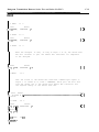
Installing the Bus Controller
After configuring the DIP switches for the Bus Controller (or Bus Controllers), install the Bus Controller
in one of the eight slots in the CPU base unit. Up to eight Bus Controllers can be installed in the CPU
base unit. Bus Controllers cannot be installed in I/O expansion base units. Ensure that the module
is seated properly, then tighten the two captive screw fasteners, one at the top rear and one at the bottom
rear of the module. For information on wiring the serial bus, refer to the Genius I/O System User’s
Manual. The serial bus is connected to the Bus Controller through the four screw terminals on the front
of the module. The Genius Hand-Held Monitor can be connected to the Bus Controller by connecting
its cable to the 9-pin connector on the Bus Controller.
Installation and Setup
3-4
GFK-0248
a42731
i
Figure 3-l. Bus Controller Installation in a CPU Base Unit
Configuration with Logicmaster 5
To configure a system using Logicmaster 5 software, power-up your system and connect Logicmaster 5.
Initially, you should have an I/O configuration error because of the new Genius Bus Controller module
that has just been installed. If this is the case, you must accept the new I/O configuration which includes
the Genius Bus Controller. The new configuration can be accepted while you are in the scratchpad
menu (NEW CONFIG). If you don’t get an I/O config error, remove the Genius Bus Controller, and
perform a NEW CONFIG from the Logicmaster 5 scratchpad menu. Then power-down, reinsert the
Genius Bus Controller, get the I/O config error, and do a NEW CONFIG. This procedure is necessary
since the Series Five CPU reads all the Genius Bus Controller DIP switches only when a Genius Bus
Controller is first inserted in a slot (causing an I/O Config error), followed by the New Config.
NOTE
The Genius Bus Controller parameters are stored in the memory cartridge in the CPU. If a
memory cartridge is moved from one system to another it may need to be initialized, and the
Genius parameters set-up in the new system.
Operation with Genius I/O Blocks
The Bus Controller must be set up as previously described (see guidelines below), and the Genius I/O
blocks must be configured using the Genius I/O Hand-Held Monitor.
NOTE
For detailed information on configuring Genius l/O blocks, refer to GEK-90486, which is the
G e n i u s I/O System User’s manual.
Some general rules and examples for operation with I/O blocks are provided below. These examples
explain how the Bus Controller works with various types of blocks and different reference types.
Installation and Setup
3-5
GFK-0248
Genius I/O Block Setup Procedures
Genius I/O blocks can be assigned CPU addresses in the IO1+ or 102+ tables as well as in the register
tables.
Step 1:
Note that the Serial Bus Address of the Genius Bus ControIIer is as described earlier in this
chapter. Blocks must be assigned different addresses. Also check that DIP switch 8 is in
the Enabled position to allow immediate operation with Genius I/O blocks.
Step 2:
Assign reference addresses for the blocks using the rules below as guidelines.
Table 3-l. Genius I/O Reference Address Assignment
STATUS TABLE
ADDRESS
DESIRED BY USER
DECIMAL FORMAT)
STATUS TABLE
ABSOLUTE ADDRESS
(DECIMAL FORMAT)
101+0001 to 101+1024
102+0001 to 102+1024
R 0 0 0 0 l to R04096
R04097 to R 16384 *
0001to 1024
1025 to 2047
32769 to 36864
32865 to 49152 *
STATUS TABLE
ABSOLUTE ADDRESS
(HEXADECIMAL FORMAT)
0 0 0 l H to 03F9H
0401H to 07F9H
800lH to 9000H
900lH to C000H *
* Valid only for CPUs having 16K of registers installed
Rule 1 - Equal space is always used in the I+ and O+ tables, even if blocks are configured as
input-only or output-only (see rules below for register tables). It is recommended that
blocks with configurable points be set as “combo” blocks.
Rule 2 - Addresses used are the greater of input data length or output data length.
Rule 3 - Analog blocks are not multiplexed. A 4 input/2 output analog block will occupy 64 points in
both I and 0 tables.
Rules 4 through 7 apply when Genius Blocks are being mapped into CPU registers.
Rule 4 - Registers are assigned to inputs first, then outputs.
Rule 5 - Inputs and outputs will not be in the same register. If there is an odd number of bytes for the
length, the last byte is contained in the eight Least Significant Bits (Iower byte), and the eight
Most Significant Bits (upper byte) are not used (contain zeros).
Rule 6 - Whole registers (16 bits) are used, even for eight point blocks.
Rule 7 - The total address range occupied by the block is the sum of the number of input registers plus
the number of output registers used.
For example, 101+0001 corresponds to Genius I/O Reference address 00001, and IO2+000l corresponds to 01025. Register R0000l corresponds to 32769. For Genius I/O blocks assigned to I/O tables,
address plus range length cannot exceed the maximum address +l. For Registers, the address plus both
lengths cannot exceed the maximum address +l. This is because you cannot specify a starting address
and a length that goes beyond the end of the table space.
It should be noted that I/O points mapped into the IOl+ and IO2+ tables can be overridden, but I/O
points mapped into the register table cannot be overridden. Depending on your application, it may be
better to map blocks which occupy large amounts of space, such as analog, high speed counter, and
power monitor, into the register table rather than the IO+ tables.
3-6
Installation and Setup
GFK-0248
Examples of Address Assignments
Example 1: A 4I/20 Analog block assigned to 11+0001 (reference = 0 0 0 l ) occupies 64 references in
both I+ and 0+, i.e. 11+0001 through 0064 and 0 l + 0 0 0 l through 0064 (although bits 01+0033 through
0l+0064 contain no useful data). This is because there is more input data than output data, and each of
the four input channels uses 16 bits.
Example 2: A 4I/20 Analog block assigned to R 0 0 0 1 occupies R 0 0 0 1 through R00004 for the 4 Input
channels, and R 0 0 0 5 and R 0 0 0 0 6 for each of the output channels.
Step 3:
Set the block configuration using the HHM, version 3 or greater (refer to the Genius I/O
User’s manual for detailed information).
After the blocks have been properly configured, they are accessed in the user’s logic program at the
references assigned to them with the Hand-Held Monitor. If the blocks have been assigned an address
corresponding to a reference in the I+/O+ tables, the block I/O points may be overridden using
Logicmaster 5 or the Operator Interface Unit. If blocks have been assigned a reference address
corresponding to a location in the register table, the I/O points cannot be overridden by Logicmaster 5 or
the OIU.
Individual circuits can be forced on or off (or to values selected by the user, if the circuit is analog)
using the HHM. Only when circuits are not forced, will blocks drive outputs to the state present in the
O+ tables. Genius I/O blocks always use exactly the same number of points in the I+ and O+ tables,
whether or not there are physical inputs and outputs to match. The number of circuits used varies from
block to block, but is always the larger of the number of inputs or outputs used by the block.
Step 4:
Set the Output Enable bits.
Depending on your Genius I/O system configuration, it may be necessary to reset some of the output
enable bits for each active Serial Bus Address on each bus. These bits should have defaulted to “on”
during the first power cycle of the Genius Bus Controller. If multiple Genius Bus Controllers are used
on the same bus, the output enable bits must be set so that only one of the bus controllers has its outputs
enabled to any single Serial Bus Address.
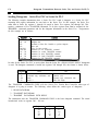
The output enable setup is done using Logicmaster 5 or the OIU. A field of 32 bits is presented for each
Genius Bus Controller. Each bit corresponds to the enable/disable status of one of the Serial Bus
Addresses. If the bit is set to 1, that Serial Bus Address is enabled, if a 0 it is disabled. The Genius
setup screen is as shown.
Installation and Setup
3-7
GFK-0248
L
CPW:RUN/ENBL/UNLOCKED
CPU ID: 1
G E N I U S
SLOT
0
1
2
3
4
5
B U S
EQUIVALENT
STATUS
TABLE
ADDRESS
LM NOTEQ CPU
LM:ONLINE
C O N T R O L L E R
GLOBAL
DATA
LOCAL
REFERENCE
GLOBAL
DATA
TRANSMIT
LENGTH
11:59:36
S E T U P
(FUTURE)
RECEIVE
DIRECTED
LENGTH
SBA
OUTPUT
ENABLE BITS
15-00
31-16
F437
FFFl
Do not fill in any of these columns if all
you are interested
in is using Genius I/O b l o c k s
These
global
c o l u m n s are important if you are
data.
using
-
6
7
PRESS HELP KEY FOR LIST OF VALID RANGES
NOTE :
FOR APPLICATIONS WITH A SINGLE CONTROLLER PER BUS, THE LOCAL
REFERENCE, TRANSMIT, AND DIRECTED LENGTH SHOULD BE S E T TO 0.
STORE
CLEAR
CALC
LOAD
lFM CPU 2TO CPU3 CPU 4 REF
5
6
7
8
SETUP
DIAG
The format of the output enable bits is as shown below:
Sample data as shown on screen =
I
F437 FFFl
Enable bit for Serial Bus Address 31, 1 = enabled
Enable bit for Serial Bus Address 20, 0 = disabled
v1111 0100 0011 ;u1
F
4
3
7
1111 1111 1111 0001 <--F
F
F
1
Enable bit for Serial Bus Address 0, 1 = enabled
You must decide which Serial Bus Addresses need to be enabled and set the appropriate bit to a 1. Then
enter the resulting number as hexadecimal data. Data (0000 - FFFF) is entered at the cursor location,
and stored to the CPU using the Logicmaster 5 STORE TO CPU softkey.
If a Genius Bus Controller is being used with Genius I/O blocks, and no other controllers are on the bus,
the output enable bits will default to the ENABLE position (FFFFH); no further setup is required in this
case. Unused Serial Bus Addresses can have their output enable bit set to a 1 with no difficulties.
If multiple Genius Bus Controllers are being used on the same bus, outputs to any single Serial Bus
Address can be enabled only on one controller, and requires the appropriate bit to be reset to 0 at all
controllers, except one.
After disabling the desired Serial Bus Addresses by setting the appropriate output enable bits to 0 or 1,
the following capabilities have been enabled, and require no further setup.
Installation and Setup
3-8
GFK-0248
1. Operation with Genius I/O blocks (the blocks must be configured using the Genius Hand-Held
Monitor, but no further Series Five setup is required). As noted previously, a block address of 1 1024 will map the block in the IOl+ tables. A block address of 1025 - 2047 will map the block in
the IO2+ tables. A block address of 32768 or above will map the block into the register table.
2. General purpose communications between Series Five CPUs by use of the RD CCM and WR CCM
user logic commands. These commands can be used with the Genius Bus Controller as well as with
the CCM Master Module. This capability provides true peer to peer operation under user logic
control. It is normally used to exchange lower priority data which does not need to be updated on
each Genius bus scan.
3. General purpose communications to many different GE Fanuc products through the Genius
Datagram capability (refer to Appendices C and D for examples).
Enabling and Changing Global Data Values
Global Data is a convenient way to allow CPUs to communicate automatically. It may be used on the
.
same bus that uses Genius I/O, or on a separate bus by itself.
Once it is properly configured global data is automatically sent by the CPU to all compatible devices on
the Genius bus. Global data will automaticalIy be received and stored with no setup required. Global
data setup is not required when using the Series Five only to drive Genius blocks.
For example, if your local CPU is set up with a global data reference of 32869 (Register l00), and
global data transmit length of 10, then registers 100 through 109 will be transmitted on each Genius bus
scan to all devices on the bus capable of receiving global data transmissions. If another Series Five
CPU, or a Series Six CPU is active on the Genius bus, they will see R l 0 0 through R109 data from your
local CPU appear in their register tables at the same locations. Only the transmitting (broadcasting)
device needs to be set up since reception is automatic.
NOTE
Care must be taken to ensure that more than one bus controller is not broadcasting from the same
status table addresses.
Changing the Global Data Setup
The Genius Bus Controller setup may be altered through either the Bus Controller Setup menu in
Logicmaster 5, or sub-menu 91 - Set Genius Bus ControlIer, in the Series Five Operator Interface Unit
(OIU). Changing the Global Data Transmit Length and/or the status table address affects the Global
Data transmitted by the Genius Bus Controller. A Global Data Transmit Length of zero stops Global
data transmissions. The maximum transmission length is 64 registers. These same menus in
Logicmaster 5 or the OIU may be used to set up a Genius Bus Controller at any address (0 - 31) as a
Global Data device.
InstaIIation and Setup
3-9
Configuration Parameters for Global Data Communications
Parameters that must be configured to allow Global data are:
Reference (status table) address of the Genius Bus Controller
Broadcast data length for the Genius Bus Controller
Refer to Table 3-2 for a list of the valid Bus Controller ranges for the parameters listed above.
Entering GBC Setup Parameters With the OIU
When using the Operator Interface Unit, the required Genius Bus Controller setup parameters are
entered by accessing sub-menu 91 and following the prompts displayed on the LCD screen. Valid
ranges for each of the required parameters are listed in Table 3-2. Refer to GFK-0181, the Series Five
Operator Interface Unit User’s Manual, for further details.
Editing GBC Setup Parameters With Logicmaster 5 Software
If communication with the CPU is established, the setup values of the Bus Controller are automatically
loaded from the CPU. These setup values can be displayed and/or edited and then stored back to the
CPU. This section explains how to display and edit these setup values.
Displaying the Bus Controller Setup Screen
When the GENIUS BUS CONTROLLER SETUP (F5) key is pressed from the Setup/Diagnostic
Functions menu, the Genius Bus Controller Setup screen will appear. Genius Bus Controller setup data
will be loaded from the CPU if communication has been established.
CPU:RUN/ENBL/UNLOCKED
G E N I U S
SLOT
0
1
2
3
4
5
6
7
EQUIVALENT
STATUS
TABLE
ADDRESS
ROlOO
CPU ID: 1
B U S
LM NOTEQ CPU
C O N T R O L L E R
GLOBAL
DATA
LOCAL
REFERENCE
GLOBAL
DATA
TRANSMIT
LENGTH
32869
10
Fill
and
in
this
column
LM:ONLINE
S E T U P
(FUTURE)
RECEIVE
DIRECTED
LENGTH
0
Not
SBA
OUTPUT
ENABLE BITS
31-16 15-00
F437
Not
Used
this
column
11:59:36
FFFl
Used
for
global
data
leave
at 0.
for
global
data
Set-up
for blocks.
PRESS HELP KEY FOR LIST OF VALID RANGES
NOTE :
FOR APPLICATIONS WITH A SINGLE CONTROLLER PER BUS, THE LOCAL
REFERENCE,
TRANSMIT, AND DIRECTED LENGTH SHOULD BE SET TO 0.
LOAD
STORE
CLEAR
CALC
lFM CPU2 TO CPU3 CPU 4 REF
5
6
7
SETUP
8 DIAG
3-10
Installation and Setup
GFK-0248
Bus Controller Setup Key Summary
The Genius Bus Controller Setup screen displays the following function keys:
LOAD FM CPU (Fl): Select LOAD FROM CPU to load Bus Controller setup values from the CPU.
STORE TO CPU (F2):
Select STORE TO CPU to store the Bus Controller setup values to the CPU.
CLEAR CPU (F3):
Select CLEAR CPU to clear the Bus Controller setup values in the CPU.
CALC REF (F4): Select CALCULATE REFERENCE to display the CPU table addresses which
correspond to the Genius Bus Controller reference addresses.
SETUP & DIAG (F5):
Select SETUP & DIAGNOSTICS to return to the Setup and Diagnostic
Functions menu.
STORE and CLEAR functions require that the CPU be stopped and the Logicmaster system be on-line.
You must also confirm the initiation of a LOAD, STORE, or CLEAR operation.
The Up, Down, Right, and Left cursor keys are used to select a field to be edited. Move the cursor to a
particular field, and enter the values. All values are expressed as decimal numbers, except the Output
Enable field, which is hexadecimal values. Leading zeros are not necessary.
The Clear key is used to blank the selected field, while the Delete key removes only the last digit
entered. Since the addresses used are Genius I/O Reference addresses, you can press the CALC REF
(F4) key to update the left column, which shows the corresponding CPU table addresses.
Setup Ranges
It is necessary to select the starting table address of the local CPU/Bus Controller in the global memory
map. Using the following table, which lists the valid setup ranges of the Bus Controller, select the
desired starting location of the data to be transmitted to the other units. This number is entered in the
GENIUS DATA LOCAL REFERENCE field. The number of bits or words to be transmitted is then
entered in the GLOBAL DATA TRANSMIT LENGTH field. The RECEIVE DIRECTED LENGTH
should remain at 0, and the applicable OUTPUT ENABLE BITS should be set as described earlier if this
bus controller will also be controlling Genius outputs.
The reference address range determines which of two address types is used. Bit addressing is used for
I/O table data, and word addressing is used for register data. The length is entered in bits for bit
addresses (I/O table data) and words for word addresses (register data). Bit-related values (I/O
addresses and lengths) will be rounded to byte boundaries when stored to the CPU.
Table 3-2. Valid Bus Controller Setup Ranges
GLOBAL DATA
Bit
Bit
word
word
00001
01025
32769
32769
-
01024
02048
36864
49152
EQUIVALENT
STATUS TABLE
IOl+000l
1O2+0001
R0000l R0000l -
ADDRESS
GLOBAL DATA
TRANSMIT
LENGTH
- I01+1024
- 102+1024
R04096 (4KREG)
R16384 (16K REG)
0000 - 1024 bits
0000 - 1024 bits
0000-0064words
0000 - 0064 words
3-11
Installation and Setup
Where: IOl+xxxx addresses = the I/O number.
102+xxxx addresses = the I/O number + 1024.
Reference address for registers = register number plus 32768.
Reference Address
When using the Operator Interface Unit, the Series Five PLC table addresses are entered in the
following format: Il+XXXX, 01+XXXX, I2+XXXX, or O2+XXXX. This is the same format used to
display references of combination Genius I/O blocks in the Genius I/O Diagnostics screen of
Logicmaster 5. When using Logicmaster 5, the status table reference address must be entered directly.
By using the CONV REF softkey, the status table reference address is translated to a table reference on
the Logicmaster 5 screen.
The correspondence between the table values and the nearest byte boundary to get the logical address.
Global Data and Transmit Data Lengths
.
Global and transmit data lengths are expressed as the number of bits of data to be transferred. Bit
reference tables (I+/O+ tables) are entered as the number of bits of broadcast or directed data to be
transferred. The OIU or Logicmaster 5 converts these user entered values to bytes (value is divided by
eight and rounded up). Word reference addresses are entered as the number of registers to be transferred.
The OIU or Logicmaster 5 converts the number of registers specified to bytes (two times the value
entered).
Table 3-3. Global Data And Transmit Data Lengths
CONVERTED VALUE
WRITTEN
TO SCRATCH PAD
DATA LENGTH
ENTERED
BY USER
I
0 to 64 Registers
I
0 to 80H Bytes
0 to 80H Bytes
Data lengths are expressed as the number of registers or I/O points to be transferred. Range checking of
the field contents is performed when a STORE to CPU (F2) function is selected. If an error is found, it
must be corrected and the STORE TO CPU function initiated again.
NOTE
Addresses and lengths of l/O points (IOl+ and 1O2+ tables) are adjusted to byte boundaries when
stored to the CPU.
The procedures described above should be done for each unit in the global communications network. It
is necessary to ensure that the start address + length for each unit does not overlap a table boundary, and
does not overlap the configuration of any other units in the network.
Setup of global data is now complete. The CPU at which these settings were made will now broadcast
I/O data or registers starting at the global data local reference for the length specified in the global data
transmit length.
3-12
Installation and Setup
GFK-0248
General System Information
1. The CPU INITIALIZE function will reset all Genius setup parameters to 0, and set output enable
bits to disable.
2. The DIP switches on the Genius Bus Controller module are only read when a newly registered
Genius Bus Controller has been detected. From that point on, the CPU uses the output enable and
baud rate settings that Logicmaster 5 or the OIU have established. If a Genius Bus Controller
module is removed from a slot, and “unregistered” with a NEW CONFIG command, then it is
reinstalled and re-registered with another NEW CONFIG command, the DIP switch will be read
again at this point. Note that the Genius Bus Controller settings are stored in the CPU memory
cartridge. This cartridge may need to be re-initialized if it is moved to another CPU with a different
Genius configuration.
3. Note that Genius I/O blocks occupy space in both I+ and O+ tables, even if the block is programmed as input only, or output only. Also, analog blocks’ data is not multiplexed as it is on Series Six
Genius applications.
4. After Genius I/O blocks have had their I/O reference addresses changed, it is necessary to power
cycle the blocks to have the new address recognized.
5. The Genius Hand-Held Monitor does not need to have its output enable bit set to work on the bus,
and it will have a reference address of 32767.
6. There is not an internal address conflict check between addresses to which Genius blocks have been
assigned, and addresses that global data is using. Be sure that incoming global data does not
overwrite data coming from blocks.
7. When a datagram is sent to the Series Five CPU, the address map is different than with Series Six.
For example, the target address for a Series Six could be 0000H 0040H. The address consists is of
the format WX YZ where Y is always 0, and ZW is the address, and X is not used. For the Series
Five, Y MUST BE 85H. The Series Five internal address would be ZW. To read register 1 from a
Series Five CPU, you need to use address 0000H 8500H. Register 2 would be 0200H 8500H. The
formula for the register address is (Register number - 1 ) x 2. For register 1000, the address would
be 1998 decimal (07CEH), and the address field would be CE00H 8507H.
The Series Five internal mapping FOR DATAGRAMS is as follows:
Table 3-4. Datagram Mapping
I
Range and Reference Numbers
Rl - R16384
Il+l to I1+1024
I2+1 to I2+1024
Ol+l to 02+1024
11 to 11024
O1 to 01024
O1-l to 02-1024
I1-l to I1-512
I
Series Five Internal Address
(ZW above)
0000H to 7FFFH
8 0 0 0 H to 807FH
8080H to 80FFH
8 1 0 0 H to 81FFH
8200H to 827FH
827FH to 82FFH
8300H to 83FFH
8500H to 85FFH
Refer to Appendix C for a detailed example of using datagrams.
3-13
Installation and Setup
GFK-0248
8. When using a TRANSFER command in a Series Five logic program to access Series Five internal
memories, the above offset address applies. However, the source and target addresses would be of
the format
8005H OFFSET, e.g. for I1,
8005H 8200H.
The TRANSFER command can be used to send datagrams to other Genius devices. Refer to Appendix
D for more details on this use of the TRANSFER command. Also, refer to the TRANSFER instruction
definition in the Logicmaster 5 Progr amming and Software Documentation User’s Manual, GFK-0023,
for more details.
Series Five CPU Scratchpad Genius Definitions
The Series Five CPU scratchpad contains Genius related information. This information is updated only
after a bus controller has just been accepted into the I/O configuration.
The following table is a list of this Genius information in the scratchpad. It is not necessary to use any
of this data for normal Genius operation.
Table 3-5. Genius Information in CPU Scratchpad
Scratchpad Relative
Address (Byte)
256H
257H
258H
259H
25AH
25BH
25CH
25DH
25EH
25FH
26OH
261H
262H to 26DH
26EH to 279H
27AH to 285H
286H to 291H
292H to 29DH
29EH to 2A9H
2AAH to 2B5H
Definition
0 (slot number)
Serial bus address of Genius Bus Controller in slot 0 ( 0-31)
Status table address - 1st byte
Status table address - 2nd byte
Number of Inputs to broadcast (Global data)
Number of Outputs to receive (future)
Data rate
Unused
Output enable bits - SBA O-7
Output enable bits - SBA 8- 15
Output enable bits - SBA 16-23
Output enable bits - SBA 24-31
1 (slot number) - above information repeated for slot 1
2 (slot number) - above information repeated for slot 2
3 (slot number) - above information repeated for slot 3
4 (slot number) - above information repeated for slot 4
5 (slot number) - above information repeated for slot 5
6 (slot number} - above information repeated for slot 6
7 (slot number) - above information repeated for slot 7
Chapter
4
Operation with RD/WR CCM Instructions
GFK-0248
Introduction
This chapter describes the use of the Read CCM and Write CCM instructions in a Genius network to
communicate with other Series Five PLC systems with Genius Bus Controllers.
Use of Read CCM and Write CCM to Communicate with Other CPUs
The Read (RD) CCM and Write (WR) CCM instructions provide a user friendly method to obtain
information from another CPU, or send data to another CPU. These instructions can be used with either
the CCM Communications module to any CCM slave device, or, as presented here, with the Genius Bus
Controller to another Series Five CPU with a Genius Bus Controller. When used with the Bus
Controller, the underlying mechanism for the data transfer is through datagrams. These instructions can
be used to obtain CPU table information as listed in the following table.
Table 4-1. CCM/CPU Mapping
Range
Table Name
Registers
Il+ Inputs
I2+ Inputs
Local Inputs
special Inputs
Ol+ outputs
O2+ outputs
Local outputs
Internal coils
Internal coils
scratch Pad *
User Logic
and Reference
Numbers
R0000l-R16384 (for 16k reg)
ROOOOl -R04096 (for 4k reg)
Il+000l to I1+1024
I2+0001 to I2+1024
I0001 to I1024
Il-0001 to II-0512
O1+0001 to 01+1024
O2+0001 to O2+1024
0000l to 01024
01-0001 to 01-1024
02-0001 to 02-1024
0000 to 09OOH
0000 to 16,383
offset values
000lH-4000H
000lH-1000H
0001H-0080H
0081H-0100H
0l0lH-0180H
018lH-0lC0H
000lH-0080H
0081H-0100H
010lH-0l80H
0181H-0200H
0201H-0280H
OOOO-09OOH
OOOO-3FFFH
Target
Memory
Type for
Table
1
1
2
2
2
2
3
3
3
3
3
6
7
Target
Memory
Type for
Override
N/A
N/A
4
4
4
N/A
5
5
5
5
5
N/A
N/A
Data Format
2 Bytes/Register
2 Bytes/Register
8 Inputs/Byte
8 Inputs/Byte
8 Inputs/Byte
8 Inputs/Byte
8 Outputs/Byte
8 Outputs/Byte
8 Outputs/Byte
8 hputs/Byte
8 Outputs/Byte
1 Byte/Byte
2 Bytes/Word
H=Hexadecimal
* Extreme care must be used when writing to any Scratch Pad location area This is not recommended without
specific information from GE Fanuc.
NOTE
The Genius version of RD/WR CCM cannot be used in conjunction with Series Six programmable controllers (although this can be done when using CCM modules). Refer to Appendix D
for an example of datagram communications between a Series Five PLC and a Series Six PLC.
4-2
Operation with RD/WR CCM Instructions
GFK-0248
Read/Write CCM
The following discussion provides more information on the Read CCM and Write CCM instructions.
Examples of their use are also provided. The Read CCM and Write CCM instructions move data to and
from the Series Five Genius Bus Controller. You can use the READ CCM instruction to request data
from a remote Series Five PLC through the Bus Controller to a data register buffer in the local CPU.
With the Write CCM instruction, you can send data from the local CPU through the Bus Controller to a
remote Series Five CPU with a Bus Controller. Each of these instructions has a single register operand
which specifies the starting address of a block of six registers containing the following information:
Slot number of the local Bus Controller.
Target Address (Serial Bus Address)
Target memory type.
Starting address within the memory type of the remote target device.
Length of the data to be transferred.
Starting register in the local CPU for the data buffer.
Symbology :
R*tkakt**
R*****
-pDCCMI-
or
-(WRCCMJ-
Operation:
Before execution, the following registers must contain the data listed below. (Refer to the previous table
for information on CCM/CPU mapping.)
Read CCM:
R***“* = Slot number of Genius Bus Controller.
+1= Serial Bus Address (SBA) of the remote Genius Bus Controller.
+2+3=
+4=
+5==
CCM memory type to read from (see CCM/CPU Mapping, Table 5-l).
Start address in target.
Length to read (registers).
Maximum length is 64.
First register in local receive buffer.
Write CCM:
Rtk*‘*** 3 Slot number of Genius Bus Controller.
+1= Serial Bus Address (SBA) of the remote Genius Bus Controller.
+2=CMmeoryt
+2=
+3+4+5-
Type to write to (see CCM/CPU Mapping table 5-l).
Start address in target.
Length to write (registers), Maximum length is 64.
First register in local transmit buffer.
After execution, the receive data buffer register pointed to by R***** +5 will contain the data from the
remote CPU.
Special internal bits affected are 11-0081 to I1-0204, and 11-0045 for the Bus Controller. Refer to page
5-7 for a description of these bits.
4-3
Operation with RD/WR CCM Instructions
GFK-0248
Example of Reading from a Remote CPU:
To read inputs 10017 through 10048 from the remote Series Five PLC with a Bus Controller module with
SBA 28:
1. Preset the registers with the following data:
R0100l
R01002
R01003
R01004
R01005
R01006
=
=
=
=
=
=
05
28
02
103H
02
0200
(slot number of local Bus Controller module)
(SBA of remote Bus Controller)
(memory type = input table)
(start address for input table, 10017)
(number of words to fetch; also, length of data buffer)
o start at register R0200)
(data buffer t
2. Execute the following:
ROlOOl
-pDCCMI-
3. During execution, status bit I1-0091 will indicate the transfer status for slot 5:
0
= done
l= executing
Status bit Il-0092 will indicate the error status for slot 5:
1= error
0 = OK
The data buffer for this example will contain the following data:
R00200 = 0002
R00201 = 0004
(inputs
(inputs
17,
33,
19-32 are
34, 36-48
0,
are
input 0018 is
1)
0, input 35 = 1)
Example of Writing to a Remote Series Five PLC with a Genius Bus Controller:
To write data buffer (R00220 - 00222) to outputs 1 - 48 through a remote Series Five PLC with a Bus
Controller module with SBA 25 (the local Bus Controller module is in slot 2):
1. Load R00220 - 00222 with the data to be sent.
2. Preset the registers as follows:
R00501
ROO502
R00503
R00504
R00505
R00506
=
=
=
=
=
=
02
25
03
0l0lH
03
220
(local Bus Controller module is in slot 2)
(target SBA)
(target memory type = output table)
(starting address for outputs l-48)
(number of words to send)
(start data buffer at register 220)
3. Execute the following:
R00501
-IWRCCMI-
4. During execution, status bit Il-0085 will indicate the transfer status for slot 2:
0
= done
1= executing
Status bit I1-0086 will indicate the error status for slot 2:
0 = OK
1 = error
Chapter
5-l
5
Operation with Genius I/O Diagnostics
Introduction
The purpose of the Genius I/O Diagnostics function in a Series Five PLC control system is to find faults
in the Genius I/O system. The types of faults detected by the Genius I/O Diagnostics include:
-
Failure of a Bus Controller module in the CPU base unit.
Excessive bus communication errors.
Address conflicts
Circuit faults reported by devices on the bus through Report Fault datagrams.
Add or loss of device. This is optional through user programming.
In addition to reporting faults, the Genius I/O diagnostic routines allow the user to send Clear All Faults
and Pulse Test datagrams to all appropriate devices on the bus.
User Interface to Genius I/O Diagnostics
The user interface to the Genius I/O diagnostic function is through the Logicmaster 5 diagnostic screen,
registers, and internal coils. The user program, OIU, or Logicmaster 5 can manipulate the internal coils
to enable/disable the Genius I/O diagnostics, send Clear All Faults and Pulse Test messages to Genius
I/O devices, and indicate to the CPU diagnostic firmware if the addition or loss of a block should be
reported as a fault. The diagnostic routine formats the fault information, time stamps it, and places it in
the register table in the appropriate location. When diagnostics are enabled, the routine is executed each
sweep when the CPU is in the RUN or RUN DISABLED modes. The diagnostic routine is not executed
in STOP mode.
Logicmaster 5 interprets the fault data in the registers and displays a formatted table with the fault
location, text messages describing the fault, and a time indicating when the fault was logged. The
registers are also available to other devices, such as the Series Five ASCII/BASIC Module, which can be
programmed to print reports or display the information on an Operator Interface Terminal.
Displaying the Genius I/O Diagnostics Screen
The Genius I/O diagnostics collects and formats fault information and stores it in the fault table in
register memory if O2-1024 has been set to a 1. Ten registers are used to report each fault. The
maximum number of faults that can be handled by the diagnostic routine is 255.
Operation with Genius I/O Diagnostics
5-2
GFK-0248
Fault Table Display
The Logicmaster 5 software reads the fault table and displays pertinent information, including location
and type of fault detected, fault description, and a time stamp of when the fault was detected. A n
example of the Logicmaster 5 screen for the fault table is shown below.
15:58:45
LM:OFFLINz
G E N I U S
I/O
F A U L T
T A B L E
TOTAL FAULTS: 06
TOP FAULT DISPLAYED: 01
SLOT
NO.
0
0
REFERENCE
ADDRESS
CIRC.
NO.
I01+0009
0
I01+0001
101+0145
0
IOl+lO45
08
0
NEXT
1 PAGE
PREV
2 PAGE
FAULT
DEVICE
ADDITION
DEVICE
ADDITION
ADDRESS
CONFLICT
CIRCUfT FAULT
DEVICE LOSS
DEVICE ADDITION
CLEAR
SFAULTS
4
FAULT
FAULT
TYPE
CATEGORY
TOP
DESCRIPTION
DISCRXTE
SBOTTOM
MON DAY HR:MN:SC
Jm;
m
m
m
JT;IN
J-m
OPEN WIRB
6
27 08:36:51
27 08:36:52
27 08:36:52
27 08:36:52
27 08:44:35
27 10:35:23
SETUP
8C DIAG
7
Contents of Fault Table
When the Genius I/O diagnostics detects a fault, an entry is generated in the fault table in CPU registers.
The ten registers which make up a fault table entry are organized as shown below:
R10
Register
R9
\
R8
R7
/
time
stamp
\
R6
R5
/
category, type,
description
R4
R3
R2
Rl
/
\
I/O address
The contents of registers 2,3,4,5,6, and 7 of the fault table entry vary depending on the fault category.
The data in registers 1, 8, 9, and 10 of the fault table entry is fixed. The details of the fault entries,
which can be found in Appendix A, are not critical to most Genius I/O users.
Special Registers, Contacts, and Coils for Genius I/O Operation
The Series Five CPU provides diagnostic and status information to the user through special registers,
contacts, and coils. Many of these diagnostic aids are relevant to Genius I/O operation. In addition,
setup of some Genius I/O parameters and commands is done through these special bits and registers.
5-3
Operation with Genius I/O Diagnostics
t+
GFK-0248
Special Registers
The special registers used for Genius I/O diagnostics and other Genius I/O functions are described
below.
R3850 through R3999
R4041
= These registers are the default registers which are used
to store Genius I/O diagnostic fault information.
R4048 = These registers contain the Genius I/O bus scan times for the
Bus Controllers contained in slots 0 - 7 in the
CPU base unit.
through
On power-up, the CPU writes default values into three registers: R4049, R4050, and R4051. The
function of these registers is described in the following table.
Table 5-l. Registers for Genius I/O Diagnostics
WRITTEN
BY
REGISTER CPU USER
DEFINITION
R04049
X
X
START OF FAULT TABLE - This register contains the starting register address of
the fault table. It is initialized by the CPU at power-up to 3850D (Decimal). The
user program can change the starting address of the fault table from the default
value. The CPU only reads this register when the ENABLE GENIUS
DIAGNOSTICS bit (O2-1024) transitions from CLEARED to SET, or during
power-up if the CPU is in RUN or RUN DISABLED mode and the ENABLE
GENIUS DIAGNOSTICS bit is SET.
R04050
X
X
LENGTH OF FAULT TABLE - This register contains the maximum number of
faults which the CPU will place in the fault table. It is initialized by the CPU at
power-up to 15D. The user program can change the fault table length from the
default value. The CPU only reads this register when the ENABLE GENIUS
DIAGNOSTICS bit (O2-1024) transitions from CLEARED to SET, or during
power-up if the CPU is in RUN or RUN DISABLED mode and the ENABLE
GENIUS DIAGNOSTICS bit is SET.
The maximum number of faults which can be stored is 255. If the value of this
register is greater than 255, the CPU will use 255 as the LENGTH OF FAULT
TABLE value.
R04051
X
X
NUMBER OF FAULTS - This register contains the number of faults which are in
the fault table. It is initialized by the CPU at power-up to zero. The CPU uses this
value as a pointer to the register where the next fault will be stored. The user
program can change the value of this register. The CPU reads the register each
sweep when diagnostics are enabled and the CPU is in RUN or RUN DISABLED
mode.
5-4
Operation with Genius I/O Diagnostics
GFK-O248
R4057 through R4064 - These registers contain the status table address of a bus
conflict, if one exists.
R4057
R4058
R4059
R4060
R4061
R4062
R4063
R4064
-
refers
refers
refers
refers
refers
refers
refers
refers
to
to
to
to
to
to
to
to
the
the
the
the
the
the
the
the
Bus
Bus
Bus
Bus
Bus
Bus
Bus
Bus
Controller
Controller
Controller
Controller
Controller
Controller
Controller
Controller
in
in
in
in
in
in
in
in
slot
slot
slot
slot
slot
slot
slot
slot
0
1
2
3
4
5
6
7
NOTE
If a CCM Communications module is installed in any of the above slots, these registers are used
for unformatted receiving, instead of the use described above.
Internal Coils
The operation of the internal coils used for Genius I/O diagnostics is described in the following table.
Table 5-2. Internal Coils for Genius I/O Diagnostics
WRITTEN
BY
REFERENCE CPU USER
O2-1019
X
DEFINITION
SETUP ERROR - If set, the data in registers RO4049 - RO4051 is incorrect, The
register data is only checked when the ENABLE GENIUS DIAGNOSTICS bit
(O2-1024) transitions from CLEARFD to SET, or during power-up if the CPU is
in RUN or RUN DISABLED mode and the ENABLE GENIUS DIAGNOSTICS
bit is SET.
If a SETUP ERROR exists, the Genius I/O diagnostic routine is not executed.
O2-1020
O2-1021
X
X
FAULT TABLE OVERFLOW - If SET this bit indicates a fault table overflow
exists. An overflow occurs if the value of the NUMBER OF FAULTS register
(R04051) is greater than the value of the LENGTH OF FAULT TABLE register
(R4050). This bit remains set as long as the overflow condition exists. The CPU
will CLEAR the bit when there is no overflow condition. If diagnostics are
enabled this bit will be updated every sweep when the CPU is in the RUN or
RUN DISABLED mode.
X
PULSE TEST- If set, the CPU will send a PULSE TEST datagram to all logged
in devices in the system. The CPU monitors this bit, and if it is SET the CPU
will direct a PULSE TEST datagram to each logged-in device in the system (a
maximum of one PULSE TEST datagram is sent by each bus controller in the
system per CPU sweep). When the PULSE TEST datagram has been sent to all
devices in the system, the CPU will CLEAR this bit.
5-5
Operation with Genius I/O Diagnostics
GFK-0248
Table 5-2. Internal Coils for Genius I/O Diagnostics - Continued
WRITTEN
BY
DEFINITION
REFERENCE CPU USER
If diagnostics are enabled, this bit will be checked every sweep when the CPU is
in the RUN or RUN DISABLED mode, except when the pulse test or clear all
faults function is in progress. If the PULSE TEST bit and the CLEAR ALL
FAULTS bit are SET at the same time, the clear all faults function will be
performed first.
O2-1022
021023
X
X
CLEAR ALL FAULTS - This bit, when set initiates a Clear All Faults command
to all logged in devices in the system. The CPU monitors this bit, and if it is SET
the CPU will CLEAR the NUMBER OF FAULTS register (R04051). The CPU
will then direct a CLEAR ALL FAULTS datagram to each logged-in device in the
system (a maximum of one CLEAR ALL FAULTS datagram is sent by each Bus
Controller in the system per CPU sweep). When the CLEAR ALL FAULTS
datagram has been sent to all devices in the system, the CPU will CLEAR this bit.
If diagnostics are enabled, this bit will be checked every sweep when the CPU is
in the RUN or RUN DISABLED mode, except when the pulse test or clear all
faults function is in progress. If the PULSE TEST bit and the CLEAR ALL
FAULTS bit are SET at the same time, the clear all faults function will be
performed.
X
REPORT ADD/LOSS OF BLOCK AS FAULT - If this bit is SET the addition or
loss of a device in the system will be reported as a fault in the fault table,
otherwise these conditions are not entered into the fault table.
If diagnostics are enabled, this bit will be checked every sweep when the CPU is
in the RUN or RUN DISABLED mode.
O2-1024
X
ENABLE GENIUS DIAGNOSTICS - If this bit is SET then Genius I/O
diagnostics will be processed by the CPU. If the bit is CLEARED, then the
Genius I/O diagnostics routine. is not executed, and the CPU wiIl not write to
internal outputs O2-1019 through O2-1022.
This bit will be checked every sweep when the CPU is in the RUN or RUN
Disabled mode.
Clear All Faults and Pulse Test Function
CLEAR ALL FAULTS and PULSE TEST are datagrams. If a Genius I/O device has fault reporting
enabled it sends a REPORT FAULT datagram when a fault is first detected. The datagram for a
particular fault condition is only sent once (even if the fault lasts for multiple Genius I/O bus scans).
When a device receives a CLEAR ALL FAULTS message it clears all its internal fault condition flags.
As new or previously existing faults are detected, they set the internal fault condition flags which will
cause the appropriate REPORT FAULT datagrams to be be transmitted. Fault conditions which have
been corrected will prevent the corresponding REPORT FAULT datagram from being repeated;
CLEAR FAULT must be sent to the block to allow the block to report a re-occurrence of a previously
reported fault.
5-6
Operation with Genius I/O Diagnostics
The CLEAR ALL FAULTS function can be used to determine if a fault condition has been corrected. If
the fault condition still exists, the device will report it again after the CLEAR ALL FAULTS datagram
has been processed. Logicmaster 5 will display the fault as described previously.
The PULSE TEST function is applicable only to selected discrete blocks. When a discrete device
receives a PULSE TEST datagram it initiates the test if it has been configured with pulse test enabled.
If diagnostics are enabled and the CPU is not in the process of executing a pulse test or clear all fault
request, it will check the PULSE TEST bit (O2-1021) and the CLEAR ALL FAULTS bit O2-1022)
each time the Genius I/O diagnostic routine is executed. If both bits are zero no action is taken. If one of
the bits is set the CPU will initiate the indicated function. If the PULSE TEST bit and the CLEAR ALL
FAULTS bit are SET at the same time, the clear all faults function will be performed first. When the
CPU is performing the pulse test or clear all faults function it will not check the PULSE TEST and
CLEAR ALL FAULTS bits. When the clear all faults or pulse test function is complete the CPU will
clear the appropriate bit (O2-1021 or O2-1022).
Device Loss
During the Bus Controller service, which occurs each sweep, the CPU performs a check for
loss/addition of devices from the bus. If bit O2-1023 is set, the CPU will build a fault table entry or
each device that was lost from the bus. If O2-1023 is not set, the CPU will not build a fault table entry
for loss of device.
A loss of device means that the Bus Controller has logged out a device because no Broadcast Control
Message has been received from it for three successive Genius I/O bus scans.
Device Addition
During the Bus Controller service, which occurs each sweep, the CPU performs a check for
loss/addition of devices from the bus. If bit 024023 is set, the CPU will build a fault table entry for
each device that was logged in by the Bus Controller, AND did not have an address conflict. If 02-1023
is not set then the CPU will not build a fault table entry for addition of device.
An addition of a device means that the Bus Controller has logged in a new device, and the CPU
reference address conflict check did not find a conflict.
Address Conflict
If a device has logged in with a reference address that conflicts with a device already on the same
Genius I/O bus, an Address Conflict fault will be reported. The CPU is not exchanging control data
with this device (its input data is not being transferred to the I+ tables or registers, and the output
disabled bit is set to inhibit transmission of 0+ or register data to the device). For each conflicting
device a fault table entry is made by the CPU.
5-7
Operation with Genius I/O Diagnostics
Internal Contacts
In addition to the registers and coils described above, two groups of internal contacts have special
meaning when used with the Genius I/O system.
I1-0081 through I1-0096
- Indicate completion status of Read/Write CCM
transmission for slots 0 through 7 of the CPU
base unit. Definitions for each contact reference are
as shown below. Each slot has two references
associated with it, and each reference has two
possible conditions. The first reference indicates
if the module in that slot is not executing (0) or
executing (l), and the second indicates completion
with no error (0) or with error (1).
Slot Number
Slot 0
Slot 1
Slot 2
Slot 3
Slot 4
Slot 5
Slot 6
Slot 7
Reference
I1-0081
I1-0082
Il-0083
I1-0084
I1-0085
I1-0086
I1-0087
I1-0088
I1-0089
I1-0090
Il-0091
Il-0092
I1-0093
I1-0094
I1-0095
I1-0096
Status
not
executing/executing
no error/error
not
executing/executing
no error/error+
not
executing/executing
no error/error
not
executing/executing
no error/error
not
executing/executing
no error/error
not
executing/executing
no error/error
not execut ing/executing
no error/error
not
executing/executing
no error/error
I1-0209 through II-464 - These contacts provide a "node active" map for slot
O/Serial Bus Address 0 through slot 7/Serial Bus
Address 31.
I1-0209 indicates status for slot 0, SBA 0
.
.
.
.
.
.
.
.
.
I1-0464 indicates status for slot 7, SBA 31
GFK-0248
This chapter lists problems that might occur in a Series Five PLC system with a Genius Bus Controller,
and suggests corrective actions you can take.
Errors are most likely when a new system is being started up. They are often caused by mistakes in
cabling or field wiring, or by faulty logic in the CPU’s application program. If problems occur, consult
the troubleshooting information in this chapter. It will help you isolate any problem that originates in a
Bus Controller. If these steps do not pinpoint the problem, the cause may lie in the CPU or programmer.
You should refer to chapter 5 of the Series Five Programmable Controller User’s Manual (GFK-0122)
for further troubleshooting information.
If you have questions that are not answered in this manual or in the other documentation for your
system, contact your local authorized GE Fanuc distributor or go to www.gefanuc.com.
How to Begin
- Check the operating mode of the CPU and, if appropriate, the programmer.
- Check the status LEDs on the CPU.
- If some of the CPU status LEDs are off, refer to the Series Five User’s Manual.
- If all the CPU status LEDs are on but either of the Bus Controller LEDs is not, refer to the
troubleshooting information on the following pages.
- If all the CPU and Bus Controller LEDs are on, check cabling then proceed to I/O block
troubleshooting. Refer to the Genius I/O System User’s Manual.
Identifying the Problem
If a problem occurs, look for a description of the problem in the list that begins below. Then, refer to the
troubleshooting suggestion with the same number on the pages that follow.
1.
2.
3.
4.
5.
Both Bus Controller LEDs are off.
The Bus Controller BOARD OK LED is off and the COMM OK LED is on.
The BOARD OK LED is on and the COMM OK LED is off.
The BOARD OK and COMM OK LEDs are flashing in unison.
The Bus Controller is not communicating with the CPU. Intermittent or total lack of communications. No input data at CPU. No output data at block.
4. RD/WR CCM (Genius) and TRANSFER comman ds to the Bus Controller cause a syntax error.
7. RD/WR CCM (Genius) and TRANSFER commands to the Bus Controller don’t show any status
change.
8. The Bus Controller is not communicating on the Genius I/O serial bus.
9. The Bus Controller begins operating, but does not seem to be operating normally,
10. There are no functioning circuits on one bus, but other busses are working.
11. There are no functioning circuits on more than one bus.
Troubleshooting
6-2
GFK-0248
12. The CPU system shuts down with parity errors after operating for a short time, or after changing the
system configuration.
13. Communications on the bus are intermittent or lacking.
14. One of the following occurs:
a. The Bus Controller COMM OK light flashes excessively.
b. There are delays on the bus.
c. Addition of Block/Loss of Block diagnostics occur repeatedly although no blocks are actually
being added or removed.
Problems 1 - 4
1. Both Bus Controller LEDs are off.
- The Bus Controller is probably not receiving enough power from the rack or the power supply.
Be sure the board is seated properly.
- Replace the Bus Controller module.
2. The Bus Controller BOARD OK LED is off and the COMM OK LED is on.
- Be sure the Bus Controller is installed in the correct slot.
- Be sure the Serial Bus Address is set properly with the DIP switches on the Bus Controller.
- Reseat the board.
- Replace the Bus Controller module.
3. The BOARD OK LED is on and the COMM OK LED is off or blinking.
- Check for correct cable type and length.
- Check for correct terminating impedance at both ends of the bus.
- Be sure the cable is daisy-chained.
- Be sure wires to the Serial 1 and Serial 2 terminals are not crossed.
- Look for a broken cable.
4. The BOARD OK LED and COMM OK LEDs are flashing in unison.
- The Bus Controller detects another device on the same bus using the same Serial Bus Address.
Change the Serial Bus Address of one of the two.
Problems 5 - 8
5. The Bus Controller is not communicating with the CPU.
- This may indicate a programming or address assignment error. Also, check the CPU operating
mode. Check particularly for overlapping addresses with other modules in the CPU base unit.
This includes blocks controlled by other Bus Controllers in the CPU base unit.
6. RD/WR CCM and TRANSFER commands to the Bus Controller cause a syntax error.
- Check the command format.
7. RD/WR CCM and TRANSFER commands to the Bus Controller don’t show any status change.
- A command is being sent to a non-existent Bus Controller. Power flows through the RDCCM or
WRCCM instruction, but the status doesn’t change.
Troubleshooting
6-3
8. The Bus Controller is not communicating on the Genius I/O serial bus.
- Two devices on the same bus may have been configured with the same Device Number. Check
this using the Hand-Held Monitor. Note that a Phase B Bus Controller will not communicate on a
bus if its assigned Device Number is already used by another device. However, both the Unit OK
and the COMM OK LEDs will be blinking together.
- Be sure wires to the Serial l/Serial 2 terminals on the module are not crossed or shorted together
or to ground.
- Check the baud rate.
- Check the Device Number (serial bus address) assigned to the Bus Controller against the intended
Device Number from your records of system configuration. New Bus Controllers are shipped
from the factory already set up to use Device Number 31.
- Use the HHM to compare Device Numbers and Reference Numbers.
- Check the Bus Controller’s Outputs Disabled bits using Read Configuration command to the Bus
Controller. Also check Bus Controller output #l (Disable All Outputs).
Problems 9 - 12
9. The Bus Controller begins operating, but does not seem to be operating normally.
- Be sure serial bus wiring has been completed in a daisy chain fashion.
- Make sure the communications cable is not close to high voltage wiring.
- Look for a broken cable. Check for intermittent cable breaks andconnections.
- Ensure that cable shielding is properly installed and grounded (see chapter 6 of the Genius I/O
System User’s Manual).
10. There are no functioning circuits on one bus, but other busses are operating normally.
- From the CPU, see if the Bus Controller has its Outputs Disabled. This selectable feature allows a
module to receive inputs, but not to send outputs. See chapter 4 for more information.
- Check to see if the Bus Controller is properly installed, seated properly, and receiving power.
- Check the on-board DIP switches.
- Pull out the Bus Controller and reinsert.
- Check for loose communications cable connections or breakage.
- If necessary, replace the Bus Controller.
11. There are no functioning circuits on more than one bus.
- Refer to Chapter 5 of the Series Five User’s Manual for troubleshooting information.
12. The CPU system shuts down with parity errors after operating for a short time, or after changing the
system configuration.
- There may be duplicate or overlapping I/O references coming from different busses.
- Unplug one Bus Controller, refer to the configuration worksheets, and use the HHM to read
Reference Numbers. If necessary, check other buses the same way.
- Verify that no conventional I/O module has reference numbers that overlap references assigned to
Genius I/O devices.
Troubleshooting
6-4
GFK-0248
Problems 13 - 14
13. Communications on the bus are intermittent or lacking.
- This may be caused by mixed baud rates. To check this, power up blocks one at a time and look
at their respective baud rates using the HHM. If you find different baud rates, they must be
changed. All devices on the bus must use the same baud rate. Any change to baud rates in blocks
will not take effect until block power is cycled.
- For Phase A devices, check for duplicate Block Numbers. Power devices up one at a time and
confirm Block Numbers using the HHM.
- The terminating resistors on the bus may be missing or incorrectly chosen or placed. Check
terminators at ends of the bus for correct resistance value. BSM cluster “stubs” should not be
terminated.
- The cable may be too long. Shorten the cable or configure all devices on the bus to use a lower
baud rate. Refer to chapter 5 of the Genius I/O System User’s Manual for more information about
cabling and baud rate selection.
- Wires may be open, shorted, or reversed. Check all bus electrical connections.
14. The COMM OK light on the Bus Controller blinks excessively, and/or
there are propagation delays on the bus, and/or
the bus is operating, but the CPU repeatedly receives Addition of Block and/or
Loss of Block diagnostics.
- There is excessive ambient noise on the bus. This can be corrected by lowering the baud rate,
rerouting the communications cable, or shielding the source of the electrical noise. The proper
solution to these problems will depend on the application. Refer to chapter 5 of the Genius I/O
System User’s Manual for information on cabling, baud rates, and ambient electrical noise.
A-1
Appendix A
Diagnostic Information
Bus Controller Diagnostic Information
The Bus Controller provides the user with a powerful tool through an extensive set of diagnostics
reported to the CPU. The Bus Controller sends diagnostic reports to the CPU, which provide Bus
ControlIer status, and serial bus status. It also sends diagnostic messages from Genius I/O blocks on the
serial bus. These messages provide an indication of block and individual I/O circuit faults. Once it is
received by the CPU, this diagnostic information is available to the ladder logic program.
Diagnostic information from the CPU can be displayed on a CRT using Logicmaster 5 software.
Default Genius I/O Diagnostic Fault Configuration
The default configuration for Genius I/O diagnostic fault data reported by the Bus Controller to the
CPU, is that this data is stored in a reserved group of data registers, R3850 through R3999, which is
referred to as the Genius I/O fault table. Certain parameters for the fault table are stored in registers
R4049, R4050, and R4051 (refer to chapter 6). The CPU initializes this fault table only if the user has
enabled the Genius I/O Diagnostics function using Logicmaster 5, and has not changed the default
parameters.
Since the reserved registers can be accessed by the CPU, Logicmaster 5, the Operator Interface Unit,
and user logic, care must be taken to ensure that user logic does not overwrite these registers when the
Genius I/O Diagnostics function is enabled.
The default Genius I/O Fault Table can record a maximum of 15 faults, with each fault using 10
registers. The information recorded in these registers is interpreted by Logicmaster 5 and displayed in
the GENIUS I/O FAULT TABLE screen on the programming device.
A-2
Diagnostic
Information
GFK-0248
Registers for Default Configuration
Ten registers are reserved for recording each of the 15 faults. The first fault is recorded in registers 3850
through 3859, the second in registers 3860 through 3869, through to the fifteenth fault being recorded in
registers 3990 through 3999. The registers which comprise the default configuration fur the fault table
are shown below.
Start
Length
Number
Fault
Fault
Fault
Fault
Fault
Fault
Fault
Fault
Fault
Fault
Fault
Fault
Fault
Fault
Fault
of Table
of Table
of Faults
1 Data
2 Data
3 Data
4 Data
5 Data
6 Data
7 Data
8 Data
9 Data
10 Data
11 Data
12 Data
13 Data
14 Data
15 Data
Fault
Content
of
Register
Registers
R4049
R4050
R4051
R3850
R3860
R3870
R3880
R3890
R3900
R3910
R3920
R3930
R3940
R3950
R3960
R3970
R3980
R3990
C
R3851
R3861
R3871
R3881
R3891
R3901
R3911
R3921
R3931
R3941
R3951
R3961
R3971
R3981
R3991
R3852
R3862
R3872
R3882
R3892
R3902
R3912
R3922
R3932
R3942
R3952
R3962
R3972
R3982
R3992
3
2
I/O
Address
R3853
R3863
R3873
R3883
R3893
R3903
R3913
R3923
R3933
R3943
R3953
R3963
R3973
R3983
R3993
R3854
R3864
R3874
R3884
R3894
R3904
R3914
R3924
R3934
R3944
R3954
R3964
R3974
R3984
R3994
R3855
R3865
R3875
R3885
R3895
R3905
R3915
R3925
R3935
R3945
R3955
R3965
R3975
R3985
R3995
R3856
R3866
R3876
R3886
R3896
R3906
R3916
R3926
R3936
R3946
R3956
R3966
R3976
R3986
R3996
R3857
R3867
R3877
R3887
R3897
R3907
R3917
R3927
R3937
R3947
R3957
R3967
R3977
R3987
R3997
\- 8
4 /
Category Type
Description
R3858
R3868
R3878
R3888
R3898
R3908
R3918
R3928
R3938
R3948
R3958
R3968
R3978
R3988
R3998
- 9
l
Time
R3859
R3869
R3879
R3889
R3899
R3909
R3919
R9929
R3939
R3949
R3959
R3969
R3979
R3989
R3999
- 1 UJ
Stamp
Data Entered in Fault Tables
The CPU records information for each fault in registers as shown above. The I/O address where the
fault was detected is recorded in registers 1 through 4 of each fault table entry. Fault category, type of
fault, and fault description are recorded in registers 5 through 7 of each fault table entry.
The time stamp of when the fault was detected is recorded in registers 8 through 10 of each fault table
entry. Each bit, unless cleared, in the registers contains useful information as shown below.
I/O Address - Registers 1 Through 4
The I/O address, where the fault occurred is stored in registers 1 through 4.
Register
1
2
3
4
Bits
00 - 02
03 - 15
00-09
10
11
12 - 15
00 - 03
04 - 15
00- 15
Address Data
Slot number of the Bus Controller reporting the fault (valid range 0 - 7).
Unused, set to logic 0
I/O address of failed point (valid range 1 - 1024)
Input point block fault
Output point block fault
I/O channel (valid 1 or 2)
Circuit or analog channel offset (valid range (0 - 15)
Unused, set to logic 0
Unused, set to logic 0
Diagnostic
Information
A-3
Fault Category - Register 5
The fault category is stored in register 5, bits 8 through 13.
Bit
8
Fault Category
Genius Bus Controller fault - Indicates a Bus Controller module failure.
During the Bus Controller service routine the CPU reads the Board OK byte in the Bus Controller status
table. This check is even made if diagnostics are not enabled. If the byte is not equal to one then a Bus
Controller fault exists. The CPU will discontinue service to this Bus Controller until the Board OK byte is a
one. Once this error has been reported in the fault table, another fault table entry for this same error is not
generated unless one of the following conditions occur:
- Power Cycle
- Stop to Run transition
- Board OK bit goes to a one (OK) and then to a zero again.
9
Serial Bus Error - Excessive bus communications errors are occurring.
If more than ten bus communications errors occur during a ten seconds period, the CPU will report a Bus
Error fault (if diagnostics are enabled). The Bus Controller provides an indication of excessive bus errors in
byte 3, bit 2 of the interrupt status table (address 0895H). If this bit is a one, then a bus error should be
reported (if diagnostics are enabled). Once a bus error has been reported, the error should not be reported
again unless the bit transitions to a zero and then to a one again.
10
11
12
13
Circuit Fault - Genius I/O block point or channel problem.
Loss of Module - A device has logged out.
Addition of Module - A device has logged in with no address conflict.
Address Conflict - A device has logged in that conflicts with a device already on the bus. The CPU is not
communicating with this device. Its input data is not being transferred to the I1+ tables, and the output
disabled bit in the bus controller’s shared RAM is set to inhibit transmission of O+ table data to the device.
EEPROM Failure
14
Fault Type - Register 6
A value in bits 0 through 3 of register 6 contain a value which represents the possible fault type.
value
0000
0001
0010
0011
0100
1001
Fault Type
Block Headend Fault
Discrete (circuit number, range 1 - 16)
Analog circuit
Reserved for future use
Analog (thermocouple, RTD, strain gauge
Discrete (circuit number, range 17 - 32)
A-4
Diagnostic Information
GFK-0248
Fault Description - Registers 5, 6, 7
The fault description is stored in registers 5, 6, and 7. The registers, bits used, and definitions are based
on the fault type as defied in register 6, bits 0 through 3.
Fault Type 0000 - The fault description for the block type is recorded by setting the appropriate bit of
register 5.
Bit
6
7
8
Fault Description
Calibration Data Lost
Shared RAM
Internal Circuit Fault
Fault Type 0001 - The fault descriptions for discrete points 1 - 16 are recorded by setting one or more
bits in the high byte of register 6.
Bit
Fault Description
8
9
10
11
12
13
Loss of I/O Power (Isolated block only)
Short Circuit
Overload
No Load (if output), Open Wire (if input)
Over Temp
Switch Failed
Fault Type 0010 - Descriptions for analog type faults are recorded by setting one or more bits in the low
byte of register 7.
Bit
0
1
2
3
4
5
6
7
Fault Description
Input Low Alarm
Input High Alarm
Input Underrange
Input Overrange
Input Open wire
Output Underrange
Output Overrange
Reserved
Fault Type 0011 - Reserved for future use.
Fault Type 0100 - The descriptions for low level analog input-only block faults are recorded by setting
one or more bits in the low byte of register 5.
Bit
0
1
2
3
4
5
6
7
Fault Description
Input Low Alarm
Input High Alarm
Input Underrange
Input Overrange
Input Open wire
Input Wiring Error
Internal Channel Fault
Input Channel Short
Diagnostic Information
A-5
Fault Type 1001 - The fault descriptions for discrete points 17 - 32 are recorded by setting one or more
bits in the low byte of register 5.
Bit
1
2
3
4
5
Fault Description
Short Circuit
Overload
No Load (if output),
Over Temp
Switch Failed
Open Wire (if input)
Time Stamp
The CPU records the time and date that the fault was captured in registers 8,9, and 10 of the fault table
entry. This information is available from registers 4087 through 4093.
Register
8
9
10
Bits
0-7
8 - 15
0-7
8 - 15
0 - 17
8 - 15
Description
Seconds
Minutes
Hours
Day
Month
Year
Range Of Value
00 through 59
00 through 59
00 through 23
01 through 31
01 through 12
00 through 99
Appendix B
Scratch Pad Memory Map for Genius Bus Controller Setup
Parameters
The Genius Bus Controller setup parameters are stored in an area of Scratch Pad memory from 256H to
2B5H. The parameters for each CPU base unit slot that may contain a Bus Controller are stored in
twelve consecutive bytes, starting with slot 0 in Scratch Pad memory location 256H, and continuing
consecutively through slot 7. The format for the parameters for each slot is shown in the following
table.
Scratch Pad Location
Offset + 0 (1)
1
2
3
4
5
6
7
8
9
A
B
content
Slot Number
Serial Bus Address
Reference Address (LSB) * (2)
Reference Address (MSB) *
Broadcast Data Length (Bytes) *
Directed Data Length (Bytes) *
Baud Rate
- Not Used Output Enabled for SBA 7 to 0 *
Output Enabled for SBA 15 to 8 *
Output Enabled for SBA 23 to 16 *
Output Enabled for SBA 31 to 24 *
(1) Offset = 256H +(slot number x OCH).
(2) Only locations with an * next to them are written by
Logicmaster 5 or the OIU to Scratch Pad memory.
C-l
Appendix C
Datagram Transmission Between Series Five and Series Six
PLCs
Since the Series Five PLC has the capability to pass Genius Global Data over a Genius bus with very
little setup, sending datagrams between CPUs is often not necessary. If datagram transfers are required
between two or more Series Five CPUs, the commands RDCCM (Read CCM) and WR CCM (Write
CCM) should be used. These commands are simple and require little code. Refer to Chapter 5 in this
manual for details on these commands. It is still a simple transmission if the Series Six CPU or PCIM
(IBM PC Interface Module) wants to initiate a datagram to the Series Five CPU. However if the Series
Five CPU must initiate a datagram to a Series Six CPU or the PCIM, then the TRANSFER command
must be used.
The TRANSFER command is easy to use but requires a lot of preloading of registers containing the
datagram information. This appendix gives a brief explanation of the TRANSFER instruction,
register definition and setup, and an example of relay ladder logic needed to send a datagram to a Series
Six requesting register data to be sent to the Series Five. Also included is a description of the
information necessary for a Series Six CPU or PCIM to request data from the Series Five CPU.
The Series Five CPU and smart module memory is divided into areas called segments. Each slot in the
rack is assigned a segment number. Within each segment there is an offset that starts at 0 and identifies
the specific location within a segment. The upper address is a segment number and the lower address is
an offset. The segment of memory where all Series Five CPU and smart module RAM resides is in the
8000H area; the exact location being determined by the slot in which the module is installed. The CPU
is always in the CPU slot and its segment address is 8005H. The segment addresses for the rest of the
slots are: 8006H for slot 0 through 800DH for slot 7.
The lower address is the offset within the segment. The offsets for areas in the Series Five Genius Bus
Controller module are listed below:
Offset
0882 - 0891
0892 - 08Al
08C2
08C3 - 08Dl
08D2 - 09Cl
09C2 - OA47
1E00-1EFF
Name
Setup Table
Status Table
Command
Command Block
Output Area
Input Area
Device Config
Description
Genius Bus Controller configuration parameters
Bus status information
Genius Bus Controller execution command code
Datagram command field
Datagram data field for Transm it commands
Information from incoming datagrams stored here
Table containing bus configuration data
Datagram Transmission Between Series Five and Series Six PLCs
C-2
GFK-0248
The offsets for the CPU must be calculated based on the starting memory address of the register and I/O
structures. For example the starting offset address of Series Five register memory is 0. The following
procedure can be used to determine the offset for a specific location in register memory. This example
uses register 200.
((Register Number) - 1) x 2 = Decimal offset.
Convert Decimal offset to hexadecimal and
Example
- Calculating register 200
((200)-l)
add to starting offset address.
offset address
x 2 = 398 + 0 = 18EH
The segment and offset memory map for the Series Five CPU is shown below:
Reference
Rl - R16384
Il+000l - 11+1024
I2+0001- I2+1024
O1+0001 - O1+1024
O2+0001 - O2+1024
10001 - 11024
00001 - 01024
01-0001 - 01-1024
02-0001 - 02-1024
11-0001 - 11-0512
Segment
Offset
8005H
8005H
8005H
8005H
8005H
8005H
8005H
8005H
8005H
8005H
OOOOH
8OOOH
8080H
8 1OOH
8180H
8200H
8280H
83OOH
8380H
85OOH
Memory Map
Segment - o f f s e t
8005H
8005H
8005H
8005H
8005H
8005H
8005H
8005H
8005H
8005H
7FFFH
807FFH
8OFFH
817FH
81FFH
827FH
82FFH
837FH
83F’FH
853FH
Datagram Format
If the Series Six CPU or PCIM wants data from the Series Five CPU, a datagram must be sent. The
formats for datagrams are discussed in GEK-90486, the Genius I/O System User’s Manual, and
GFK-0074, the Genius I/O PCIM User’s Manual. In the datagram the target address is the Series Five
CPU memory. The data for that address is shown below:
TARGET ADDRESS
I
00
I
85
OFFSET MSB
OFFSET LSB
The upper two bytes are always the same; the lower two bytes are the actual location in memory of the
desired data. This type of transmission would not require any programming in the Series Five. The
movement of data in and out of memory locations would be totally handled by the Series Five CPU and
Genius Bus Controller as a background task.
Datagram Transmission Between Series Five and Series Six PLCs
GFK-0248
The TRANSFER Command
For the Series Five CPU to request data from a Series Six CPU or PCIM, a TRANSFER command must
be used in the Series Five relay ladder diagram to initiate a datagram and send it via the Series Five
Genius Bus Controller. The TRANSFER command sends a predefined amount of data from one
memory location to another. It does not perform the actual datagram sending or receiving. The transfer
command takes the datagram command programmed in the CPU and sends it to the Genius Bus
Controller for action or vice versa. The TRANSFER command has one parameter; a register. This
register is the first register in a string of five consecutive registers that contain the source address,
destination address, and number of bytes to be transferred. The format is shown below:
Register
Register
Register
Register
Register
(X)
(X+1)
(X+2)
(X+3)
(x+4)
Source
Source
Target
Target
Length
-------------------
Upper
Lower
Upper
Lower
To generate a datagram requires a minimum of three TRANSFER instructions.
1. The first TRANSFER command sends the datagram command to the Genius Bus Controller.
2. The second command sends the data associated with the datagram to the Genius Bus Controller.
3. The third TRANSFER sends a command to the Genius Bus Controller to execute the datagram.
A description of the datagram can be found in the Genius I/O System User’s Manual, or the Genius I/O
PCIM User’s Manual. The data must be placed into consecutive bytes. This is easily done by loading
the datagrarn information into consecutive registers. The source address would be the absolute address
of the first register with the datagram information. The target address would be an absolute address in
the Genius Bus Controller and the number of bytes would be the number of command or data bytes.
The third TRANSFER command sends a signal to the Genius Bus Controller to execute the datagram.
Once the datagram is generated, a TRANSFER command must be used to check the status of the
datagram; if data is being received by the Series Five, another TRANSFER command is needed to send
the data to the CPU memory. A minimum of 4 TRANSFER instructions is needed to complete
communications. A fifth TRANSFER command is needed only if data is coming into the Series Five.
Datagram Transmission Between Series Five and Series Six PLCs
C-4
GFK-O248
Sending Datagrams - Series Five PLC to Series Six PLC
The following example demonstrates how a Series Five PLC sends a datagram to a Series Six PLC
requesting that register information be sent back to the Series Five. In this example, the Series Five
wants data in Series Six registers 1 through 10 stored in Series Five registers 240 through 249. This
requires a minimum of five TRANSFER commands. To do this, registers must first be assigned for the
TRANSFER command parameters and for the datagrarn information in the Series Five. Assignments
for this example are as follows:
200 - 209
210 - 219
220
230
240-249
300-309
310 - 319
320 - 329
330 - 339
340-349
datagram command
datagram data
command to Genius Bus Controller to perform datagram
status code
Series Six data received
parameters for first TRANSFER command
parameters for second TRANSFER command
parameters for third TRANSFER command
parameters for fourth TRANSFER command
parameters for fifth TRANSFER command
In order for the Series Five PLC to receive data from the Series Six a READ DEVICE REPLY datagram
is used. The datagram command is loaded into registers 200 through 209; the format is shown below:
I Register I
200
201
202
203
MSB
LSB
I
Destination Serial Bus address
Transmitted reply sub-function code
Priority
Always 0
I
Transfer command code
Function code
Expected reply sub-function code
Data field length
The TRANSFER COMMAND CODE tells the Series Five Genius Bus Controller what type of
datagram it is going to execute. The following values define the various types of datagrams:
1 - READ DATAGRAM
2 - TRANSMIT DATAGRAM
3 - TRANSMlT DATAGRAM WITH REPLY
The information after the TRANSFER COMMAND CODE is the basic datagrarn command. The actual
hexadecimal codes in registers 200 - 209 are:
t
Register
200
201
202
203
1
MSB
IF
1E
00
00
1
LSB
03
20
1F
06
1
Datagram Transmission Between Series Five and Series Six PLCs
C-5
GFK-0248
Registers 204 through 209 are not used in this example. Registers 210 through 219 contain the data
fields or address areas for the actual transfer. The format for the address area is shown below:
Register
210
211
212
MSB
LSB
LSB of source address
LSB of destination address
Number of bytes to transfer
Always 0
MSB of source address
MSB of destination address
In this example program the source address is the absolute address of the register memory in the Series
Six PLC that is to be sent to the Series Five PLC. The destination address is the location in the Series
Five PLC where the data will be transferred. This address will always be the same for the Series Five
PLC; 8000H. The address is actually a control code that identifies the destination as a Series Five PLC.
In the example program, the actual hexadecimal codes in registers 210 through 219 are shown below:
Registers 213 through 219 are not used in this example. The last information that will get transferred to
the Series Five Genius Bus Controller is the signal for the Genius Bus Controller to perform the
datagram. A value of 1 transferred to the Genius Bus Controller after all the datagram information has
been sent will cause execution of the datagram. For this example a value of 1 is placed in register 220.
After all the information about the datagram is set up in registers, the data must be transferred to the
Genius Bus Controller. This is where the actual TRANSFER command comes in. The first TRANSFER sends the bus datagram command to the Genius Bus Controller. The source starting address is
register 200 and the destination address is the Command Block area of the Genius Bus Controller. The
length of the datagram information stored starting in register 200 is 7 bytes. Starting in register 300, the
following information is stored:
1 Register
300
301
302
303
304
MSB
LSB
80
01
80
08
00
05
8E
06
c3
07
C-6
Datagram Transmission Between Series Five and Series Six PLCs
GFK-0248
The second TRANSFER command sends the data field of the datagram to the Genius Bus Controller.
The source address for the data field is register 210 and the destination address is the Output Area. The
length of the data field is stored in six bytes starting at register 210. The TRANSFER command data
starting in register 310 is listed below:
Register
MSB
LSB
310
311
312
313
80
01
80
08
05
A2
06
D2
The third TRANSFER command sends the command to perform the datagram. The source address for
the command is in register 220 and the destination address is the command byte in the Genius Bus
Controller. The length of the command is one byte. The TRANSFER command data, starting in
register 320, is listed below:
Register
MSB
LSB
320
321
322
323
324
80
01
80
08
00
05
B6
06
C2
01
The datagram has now been sent to the Series Six. Now the Series Five PLC must wait for a reply. To
find out if a reply has been sent, the CPU must monitor the Genius Bus Controller. The Command byte
contains the status in the Genius Bus Controller. If the Command byte contains a value of 4, the
datagram was successful. However, if it contains a value or 8 or 10, the datagrarn must be sent again.
To get this Command byte, the CPU must perform another TRANSFER command. In this example the
status will be put into register 230. This means that the source address is the Genius Bus Controller
Command byte and the destination address is register 230. The length is 1 byte. Following is the
TRANSFER command data starting in register 330:
Register
330
331
332
333
334
MSB
LSB
80
08
80
01
00
06
C2
05
CA
01
*
Datagram Transmission Between Series Five and Series Six PLCs
c-7
GFK-0248
After verifying that the datagram has successfully transferred, the register data sent from the Series Six
PLC. to the Series Five PLC must be transferred from the Genius Bus Controller to the CPU. This is the
final TRANSFER command needed. The source address is the Input Area in the Genius Bus Controller
and the destination address is register 240. The length is 20 bytes since the Series Six PLC sent data
from 10 registers. The TRANSFER command data starts in register 340 and is shown below:
Register
MSB
340
341
342
343
344
80
09
80
01
00
!
LSB
06
C2
05
DE
14
I
Datagram Transmission Between Series Five and Series Six PLCs
C-8
GFK-0248
Relay Ladder Diagram Example
This example described above is shown in the following relay ladder diagram.
<< RUNG
0 >>
This program has the Series Five ask for Registers l-10 in the
hows the
Series Six to be sent over via the Genius LAN.
It s
correct use of the TRANSFER command in the Series Five to
execute a Genius datagram command.
Start of Program ]-
+I
<<
RUNG
1 >>
The first 8 rungs gets the datagram and TRANSFER command data
For testing purposes Input 1 is used
into register memory.
to initiate the block moves.
Rung 1 - Sets up the datagram
10001
R00200
+--] [--- [
+07939
<< RUNG
+07712
command codes.
BLOCK
+00031
MOVE
+00006
]-
+00000
+00000
(
)
(
)
+00000
2 >>
Rung 2 - Sets up the data field of the datagram
10001
R00210
+--] [ --- [
I
+00000
+00064
BLOCK MOVE
+05248
+00000
command.
]+00000
+00000
+00000
Datagram Transmission Between Series Five and Series Six PLCs
<< RUNG
3 >>
Rung 3 - Sets up the GO command
10001
R00220
+--] [--- [
+00001
<< RUNG
C-9
+00000
for the Genius Bus Controller.
BLOCK MOVE
+00000 +00000
+00000
+00000
]+00000
(
)
]+00000
(
)
(
)
4 >>
Rung 4 - Sets up the first TRANSFER command to get the
datagram command to the Genius Bus Controller.
R00300
10001
+--] [--- [
-32763
<< RUNG
+00398
BLOCK MOVE
-32762 +02243
+00007
+00000
5 >>
Rung 5 - Sets up the second TRANSFER command to get the
data field of the datagram over to the Genius
Bus Controller.
10001
R00310
+---] [---[
-32763
<< RUNG
+00418
BLOCK MOVE
-32762 +02258
]+00006
+OOOOO
+OOOOO
6 >>
Rung 6 - Sets up the TRANSFER command to send over the
command to the Genius Bus Controller to execute
the datagram.
I0001
R00320
+--] [--- [
I
-32763
+00438
BLOCK MOVE
-32762 +02242
+0000l
+00000
]+00000
(
)
Datagram Transmission Between Series Five and Series Six PLCs
GFK-0248
7 >>
Rung 7 - Sets up the TRANSFER command to continually poll
the status of the Genius Bus Controller for completion
of the datagram.
10001
R00330
+--] [--- [
-32762
<< RUNG
+02242
BLOCK MOVE
-32763 +00458
]+00001
+00000
(
)
+00000
8 >>
Rung 8 - Sets up the TRANSFER command to get the data sent
from the Series Six to the Genius Bus Controller of
the Series Five into the Series Five CPU.
10001
R00340
+--] [--- [
-32762
<< RUNG
+02498
BLOCK MOVE
-32763 +00478
]+00020
+00000
(
1)
+00000
9 >>
This rung causes Output 2 to turn on once when Input 2 turns on
which causes the first 3 TRANSFER commands to execute.
After
the third TRANSFER command, the datagram from the Series Five to
the Series Six is executed.
10002
+--] I ---------------------------------------------------------------------
<< RUNG
1
00002
+-] [--- [
I
10 >>
R00300
TRANSFER
]-
00002
(OS)
Datagram Transmission Between Series Five and Series Six PLCs
<< RUNG
00002
+--] [--- [
<< RUNG
00002
+-I [--- [
<< RUNG
C-11
11 >>
R00310
TRANSFER
]-
(
1
(
1
12 >>
R00320
TRANSFER
]-
13 >>
After the datagram is sent, as long is Input 2 is on, the Series Five
CPU will continue to poll the Genius Bus Controller for completion
of the datagram.
1
10002
+-I [--- [
<<RUNG
R00330
TRANSFER
)-
(
1
14 >>
Once the status of the Genius Bus Controller command byte equals 4,
Output 1 is turned on to cause a TRANSFER, which puts the data sent
from the Series Six to the Series Five Genius Bus Controller into
the register memory of the Series Five CPU.
I
+[
ROO230
Const
A EQUAL B ] ---------1---1--------------------------------------------+00004
<< RUNG
00001
+--3
I--+[
15 >>
R00340
TRANSFER ]-
( 10003 (
+--3 [--+
<< RUNG
+[ENDSW]-
00001
(
)
16 >>
(
1
D-l
Appendix D
Switch BSM Datagram Command From a Series Five PLC
This appendix provides an example of sending a BSM (Genius I/O Bus Switching Module) switch
command from a Series Five PLC.
I
I0001
+---I
[ ------------------cc____c_______________------
00001
(OS)
00001
CONST
R335
R330
+---I [----------[ A MOVE B I-------[ TRANSFER ]0
( )
00001
CONST
R335
CONST
01-0001
+---I [-------- [ SHIFT RT N MATRIX LEN I-----------( )
3
1
01-0001
+--] [-----we---
03-0001
+--I [-----------
R300
[ TRANSFER ] --
R310
[ TRANSFER ] --
01-0001
R320
+--I [ ----------- [ TRANSFER ] --
One-shot to send
datagram only 1 time.
Test GBC command blk
to see if GBC busy.
If not busy, initiate
3 transfers.
Write the datagram target SBA, type,
length, etc. to the GBC.
Put the BSM switch command in the
GBC data area.
Tell the GBC to initiate the datagraxn.
Set registers as follows prior to execution of the above logic:
Register
R200
R201
R202
Data
lFO2H
IC2OH
OlOOH
Byte 1 = target SBA, byte 2 = 02H (send datagram)
Byte I= Subfunction code for switch BSM, byte 2 = 20 (PLC)
Byte 1 = data Length, byte 2 = priority
R210
0000H
OOOlH
(fox Bus A) This is the datagram
(for Bus B)
R220
000lH
1 = the GBC “go command” to send the datagram
R300
R301
R302
R303
R304
8005H
018EH
8006H
08C3H
From S5 register
200 - this number is (200-1)*2 = 398 decimal
To the GBC in slot 0 (MSB=80H, LSB = slot number of GBC + 6),
at address 8C3 of the GBC,
Move 6 bytes, in this case R.200 thru lR202.
R310
R311
R312
R313
8005H
OlA2H
8006H
08D2H
From S5 register
210 - this number is (210-1)*2 = 418 decimal
To the GBC in slot 0 (MSB=80H, LSB = slot number of GBC + 6),
at address 8D2H of the GBC,
Defnition
data field
Switch BSM Datagram Command From a Series Five PLC
D-2
GlX-0248
Register
R314
Data
000lH
Definition
Move the contents of the LSB (1 byte) of R210.
R320
R321
R322
R323
R324
8005H
OlB6H
8006H
08C2H
000lH
From S5 Register
220 - this number is (220-1)*2 = 438 decimaL
To the GBC in slot 0 (MSB=80H, LSB = slot number of GBC + 6),
at address 8C2H of the GBC,
Move the contents of the LSB (1 byte) of R220.
R330
R331
R332
R333
R334
8006H
08C2H
8005H
029CH
0002H
From GBC in slot 0,
GBC address 8C2H,
To S5 Register
335 (this number is (3351)*2 = 668 decimal.
Move the contents of 2 bytes (this is the busy status of the GBC)
El
GFK-O248
Appendix E
Setup Differences Based on CPU Revisions
The setup procedure for the Genius network is quite different depending on the CPU revision level. For
revision B CPUs, it was NOT necessary to configure global data, but it WAS necessary to enable the
output bits on a node by node basis.
On revision C or later CPUs, it IS necessary to configure global data, but the output enable bits default
to the on state, which is more convenient for setup with blocks. Details of the setup procedure for
revision C CPUs and later are covered below.
Compatibilities
To operate properly with the Genius network, you need the following:
-
Series Five CPU revision B or later; revision 3.0/2.X or later, (revision D or later is recommended);
Series Five Genius Bus Controller revision B or later;
Genius Hand-Held monitor version 3.2 or later;
Logicmaster 5 version 2.01 or later.
If you do not have the above revisions, parts or all of your Genius related configuration will not work
properly.
Restrictions
With the version 3.0 CPU, you cannot have Genius diagnostics enabled at the same tirne as RD CCM
and WR CCM are active with the Genius Bus Controller. In addition, with this CPU, the Genius Bus
Controller worked properly only in slot 0. For this reason, revision D or later is recommended.
A CPU firmware upgrade kit IC655UPG500
revision.
is avaiIable to bring your CPU firmware to the latest
Also, you can never have phase A Genius blocks in a system where ANY Genius phase B features are to
be used. This means that if you have phase A blocks in a system, you cannot use the following:
- Global Data
- Baud rates other than 153.6K
- Redundancy
- Multiple controllers on the same bus
- Datagrams (including RD CCM, WR CCM functions)
If you want to use phase A blocks, you must not attempt to use the above features. This restiction is not
related to version levels of the CPU, or any other device, this is a Genius I/O system limitation.
E-2
Setup Differences Based on CPU Revisions
GFK-0248
Differences in Operation Between CPU Revision B
and Later Revision CPUs
The revision B CPU defaults to the following states:
- RD/WR CCM allowed (low priority S5 to S5);
- Global Data status table address set in register table, address depending on the serial bus address
assigned to the controller (in the range of R0017 to R0080);
- Global data length set to 8 registers (enabled global data from R17-80);
- Serial bus address output enable bits set to disabled;
This allowed automatic operation of global data with no end user interaction, but was inconvenient when
using blocks.
The revision B CPU has been replaced with revision D and will not be described further. All further
discussion assumes a revision D CPU or later.
Later revision CPUs default to the following states:
- RD/WR CCM allowed (Low priority S5 to S5);
- Global data address set to 0 (disables global data);
- Global data length set to 0 (disables global data);
- Serial bus address output enable bits set to enabled.
This allows easier setup with Genius blocks, but requires you to establish setup parameters for global
data if this function is desired. These defaults disable the automatic overwriting of registers R17 to R80
which occurred in the revision B CPU.
Index
I-l
A
Address Conflict, 5-6
B
BSM Datagram Example, D-l
Bus Controller Description, l-2
Bus Controller Diagnostic Information, A-l
Bus Controller Installation and
Configuration, 3 - 1
Bus Controller Setup Key Summary, 3-10
C
Changing the Global Data Setup, 3-8
Clear All Faults and Pulse Test Function, 5-5
Combining Global Data Communications and
I/O Control, 2-5
Command, TRANSFER, C-l
Command, TRANSFER, Ladder Logic, C-8
Configuration Parameters for Global Data
communications, 3-9
Contents of Fault Table, 5-2
Duplex Redundancy Mode, 2-6
E
Editing GBC Setup Parameters With
Logicmaster 5 Software, 3-9
Example of Reading from a Remote CPU:, 4-3
Example of Writing to a Remote Series Five
PLC with a Genius Bus Controllers, 4-3
Examples of Address Assignments, 3-6
F
Fault
Fault
Fault
Fault
Category - Register 5, A-3
Description - Registers 5, 6, 7, A-4
Table Display, 5-2
Type - Register 6, A-3
G
Genius
Genius
Global
Global
I/O Block Setup Procedures, 3-5
I/O Serial Bus, 2-l
Data and Transmit Data Lengths, 3-l I
Data Communications, 2-5
D
Data Entered in Fault Tables, A-2
Datagram Example, Between Series
Five/Six, C-l
Datagram Example, BSM, D-l
Datagram Format, C-2
Datagrams, 2-4
Default Genius I/O Diagnostic Fault
Configuration, A-l
Device Addition, 5-6
Device Loss, 5-6
Displaying the Bus Controller Setup
Screen, 3-9
Displaying the Genius I/0 Diagnostics
Screen, 5-l
Dual Bus Redundancy, 2-5
Dual Controller Redundancy, 2-6
Hot Standby Mode, 2-6
I
I/O Address - Registers 1 Through 4, A-2
Interfacing With Genius Networks, 2-3
Internal Coils, 5-4
Introduction, 2-1,4-l, 5-l
L
Ladder Logic, TRANSFER Command, C-8
LEDs, 1-3,6-l
Index
x-2
0
Troubleshooting, 6-1
Typical Genius I/O Bus, 2-2
Operation, 4-2
U
P
Product Summary l-l
Purpose of the Genius Bus Controller, l-2
R
Read/write CCM, 4-2
Redundancy, 2-5
Reference Address, 3- 11
Registers for Default Configuration, A-2
Related Publications, iii
Relay Ladder Logic for TRANSFER
Command, C-8
S
Selection of Serial Bus Address, 3-2
Selection of Serial Bus Baud Rate, 3-2
Sending Datagrams, Example of, C-4
Setting the Outputs Enable DIP Switch, 3-3
Setup Ranges, 3-10
Special Registers, 5-3
Special Registers, Contacts, and Coils for
Genius I/O Operation, 5-2
Starting Reference Address, 2-3
Supporting Genius Communications Between
CPUS, 2-4
Symbology, 4-2
The Bus Scan, 2-2
The Serial Bus Address,
Time Stamp, A-5
TRANSFER Command,
TRANSFER Command,
TRANSFER Command,
Logic, C-8
2-3
C-3
Example of, C-l
Relay Ladder
Use of Read CCM and Write CCM to
Communicate with Other CPUs, 4-l
User Interface to Genius I/O Diagnostics, 5-l
Using a Bus Controller with Default Setup
Conditions, 3-3
Using Genius I/O with a Series Five PLC, l- 1
GE Fanuc Automation North America, Inc., Charlottesville, Virginia