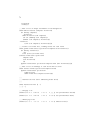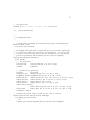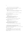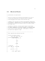
1
A Study of
the Feasibility of Verifying
a Commercial DSP
Kenneth L. Albin, Robert S. Boyer,
Warren A. Hunt, Jr., Lawrence M. Smith,
Darrell R. Word
email: [email protected]
Computational Logic, Inc.
1717 West Sixth Street, Suite 290
Austin, Texas 78703-4776
TEL: +1 512 322 9951
FAX: +1 512 322 0656
CLI
COMPUTATIONAL
LOGIC
INCORPORATED
The views and conclusions contained in this document are those of the authors and should not be interpreted as
representing the official policies, either expressed or implied, of Computational Logic, Inc.
Contents
1 Introduction
1
2 DSP Facets Considered from the Verification
2.1 Verification . . . . . . . . . . . . . . . . . . .
2.2 Complexities in DSP Machine Architecture . .
2.3 Cache . . . . . . . . . . . . . . . . . . . . . .
2.4 Block Repeat . . . . . . . . . . . . . . . . . .
2.5 Timers . . . . . . . . . . . . . . . . . . . . . .
2.6 Parallelism . . . . . . . . . . . . . . . . . . . .
2.6.1 Simplest Sort of Parallelism . . . . . .
2.6.2 Multiprocessor Interface . . . . . . . .
2.7 Powerful Addressing Modes . . . . . . . . . .
2.8 Floating Point . . . . . . . . . . . . . . . . . .
2.9 Interrupts . . . . . . . . . . . . . . . . . . . .
2.10 Secure Mode . . . . . . . . . . . . . . . . . . .
2.11 Delayed Branches . . . . . . . . . . . . . . . .
2.12 Pipelines . . . . . . . . . . . . . . . . . . . . .
Perspective
. . . . . . . .
. . . . . . . .
. . . . . . . .
. . . . . . . .
. . . . . . . .
. . . . . . . .
. . . . . . . .
. . . . . . . .
. . . . . . . .
. . . . . . . .
. . . . . . . .
. . . . . . . .
. . . . . . . .
. . . . . . . .
3 The Motorola 56100 Core Processor — A Case
Formalization
3.1 Pipeline-Step function . . . . . . . . . . . . . . . .
3.2 Register Transfer Language Notation . . . . . . . .
3.2.1 RTL Description . . . . . . . . . . . . . . .
3.2.2 Symbolic Evaluation of an RTL Constant . .
3.2.3 Structural Data-flow Constraints . . . . . .
3.3 Declarative Opcode Parsing . . . . . . . . . . . . .
3.4 Modeling State with Association Lists . . . . . . .
i
.
.
.
.
.
.
.
.
.
.
.
.
.
.
3
3
4
7
8
9
10
10
10
11
11
13
13
14
15
Study in
.
.
.
.
.
.
.
.
.
.
.
.
.
.
.
.
.
.
.
.
.
.
.
.
.
.
.
.
.
.
.
.
.
.
.
.
.
.
.
.
.
.
18
19
20
21
21
22
22
23
ii
3.5
The Specification . . . . . . . . . . . . . . . . . . . . . . . . . 23
4 A DSP Challenge — A Power Switching Circuit
4.1 Abstract Power-Supply Specification . . . . . . . . . . . . .
4.2 The Power-Supply Design . . . . . . . . . . . . . . . . . . .
4.3 Functional Circuit Description . . . . . . . . . . . . . . . . .
4.3.1 Control Objectives . . . . . . . . . . . . . . . . . . .
4.3.2 Principle of Operation . . . . . . . . . . . . . . . . .
4.4 Circuit Mathematical Relations . . . . . . . . . . . . . . . .
4.4.1 Circuit Equations . . . . . . . . . . . . . . . . . . . .
4.4.2 Pertinent Solutions . . . . . . . . . . . . . . . . . . .
4.4.3 Variable Duty-Cycle Switch Mode . . . . . . . . . . .
4.4.4 Operational Constraints . . . . . . . . . . . . . . . .
4.4.5 General Considerations . . . . . . . . . . . . . . . . .
4.5 Current Control Scheme . . . . . . . . . . . . . . . . . . . .
4.5.1 Timing . . . . . . . . . . . . . . . . . . . . . . . . . .
4.5.2 Control Procedure . . . . . . . . . . . . . . . . . . .
4.5.3 Further Discussion . . . . . . . . . . . . . . . . . . .
4.6 Voltage Control Scheme . . . . . . . . . . . . . . . . . . . .
4.6.1 Timing . . . . . . . . . . . . . . . . . . . . . . . . . .
4.6.2 Control Procedure . . . . . . . . . . . . . . . . . . .
4.6.3 Further Discussion . . . . . . . . . . . . . . . . . . .
4.7 Overall Control System Considerations . . . . . . . . . . . .
4.8 Component and Parameter Considerations . . . . . . . . . .
4.8.1 Analytical Solution Discussion . . . . . . . . . . . . .
4.8.2 Some Typical Practical Values . . . . . . . . . . . . .
4.8.3 Proposed Sample Periods . . . . . . . . . . . . . . . .
4.8.4 Solutions to Differential Equations for Output Voltage
vo . . . . . . . . . . . . . . . . . . . . . . . . . . . . .
4.9 Conclusions . . . . . . . . . . . . . . . . . . . . . . . . . . .
5 Conclusions
.
.
.
.
.
.
.
.
.
.
.
.
.
.
.
.
.
.
.
.
.
.
.
.
24
28
29
30
32
32
36
36
37
38
39
40
40
40
42
43
43
43
45
45
46
47
47
49
49
. 50
. 51
52
A Formal Specification of Subset of a Motorola 56100 Core Processor
54
A.1 Utility.Events . . . . . . . . . . . . . . . . . . . . . . . . . . . 55
A.2 Memory.Events . . . . . . . . . . . . . . . . . . . . . . . . . . 56
iii
A.3 Eval-expr.Events . . . . . . . . . . . . . . . . . . . . . . . . . 57
A.4 Decode.Events . . . . . . . . . . . . . . . . . . . . . . . . . . . 64
A.5 56k-state.Events . . . . . . . . . . . . . . . . . . . . . . . . . . 75
B Equipment
80
Chapter 1
Introduction
We report here on some aspects of the feasibility of verifying computing systems based upon a commercial Digital Signal Processor (DSP). We undertake this investigation from the perspective and background of the successful
formal verification of the FM9001 [9] processor, one of the few processors
that has been formally verified. We seek to identify those aspects of commercial DSPs that could make their verification difficult. In this report we
specifically consider two widely-used commercial DSPs, the Texas Instruments TMS320C3s [5] and the Motorola DSP 56100 family [1, 2, 3]. We shall
subsequently refer to these as the TI and Motorola DSPs.
In many respects, a DSP resembles a typical microprocessor, such as one
might find at the heart of a work station. Fundamentally, a DSP is a computing device constructed in the paradigm of the von Neumann machine.
However, a DSP typically provides faster execution speed than a microprocessor of the same cost, and this increased speed is obtained by making
certain “sacrifices.”
One example of sacrifice is the absence, on a DSP, of a distinction between
user mode and executive mode: one imagines a DSP running a dedicated,
fixed application in a single address space, rather than running a multitude of
programs for many users, each in a separate address space. Another example
of such a sacrifice is the exposure of the programmer of a DSP to the details
of certain internal operations of the processor, ‘ugly details’ from which the
applications programmer of a typical work station microprocessor is often
protected. This exposure is characterized, in a DSP manual, by a number
of ‘warnings’ of actions the programmer can take to foul up the processor.
1
2
By not investing the silicon resources to hide ‘ugly details’ or to protect
the user from ‘dangerous’ activities, the DSP manufacturer can offer higher
throughput. Here is a typical example of a warning, for the TI processor:
Do not read and write reserved words of the TMS320C3x memory
space and reserved peripheral bus addresses. Doing so may cause
the TMS320C3x to halt operation and require a system reset to
restart. ([5] p. 3–12.)
In Chapter 2 we examine a number of the features of DSPs that distinguish
them from typical microprocessors, and we consider the impact of these features upon the verification process. In Chapter 3 we describe a formalization
of a substantial subset of the Motorola processor. In Chapter 4 we discuss a
possible application for DSPs that we believe will provide a excellent vehicle
for advancing the science of verification in the DSP context. In Chapter 5
we present our conclusions. In Appendix A we present a formal specification
of a subset of the Motorola chip in the Nqthm logic [7].
Chapter 2
DSP Facets Considered from
the Verification Perspective
2.1
Verification
The word ‘verification’ has at least two different meanings in the computing
industry. The most commonly used meaning is close to ‘testing,’ as in the
phrase “V&V” – verification and validation. In this report, however, we
use the word ‘verification’ to mean a formal proof, mechanically checked by
an automated reasoning system, that an ‘implementation’ of a computing
system corresponds to its ‘specification.’ The words ‘implementation’ and
‘specification’ are themselves subject to multiple interpretations – in fact
one person’s implementation can be another person’s specification. So it
is best, perhaps, to understand that, formally, speaking, a verification is
merely a formal proof that two different abstract views (or levels or models)
of a computing system correspond to one another in some precisely specified
sense.
There is such a thing as trivial, vacuous, degenerate verification: if the
two abstract levels are ‘too close together,’ then a verification can be nothing
more than a tautology, a triviality such as x = x. Ideally, system verification
should proceed from (a) a very low level, such as the depositing and removing
of various chemicals to a silicon wafer, up to (b) the application level at which
the system is seen by the end user. In the case of a DSP, the top level might
take the form of a formal manual suitable for use by machine coders and
3
4
by those who wish to connect the processor, via its external pins, to other
devices.
Currently formal, mechanical verification technology has not yet delved
nearly as low as the etching of rectangles on silicon. Instead, we take, for the
purposes of this report, as the low level the process independent, digital level
of ‘gates and registers,’ the level taken in the successful FM9001 verification
effort. It remains a great challenge to the field of formal verification to
penetrate to the ‘switch’ level and below. But such research is likely to be
highly ‘process’ dependent and hence of transient value.
At the upper level, the FM9001 project demonstrated that a chip could
be described at a level suitable for a compiler writer (e.g., Piton[10]). In fact,
a number of pieces of software have been proved correct (cf. [14]) on layers
built rigorously on top of the FM9001. Using a similar style of upper level
processor description, a substantial part of the user subset of the Motorola
MC68020 (cf., [8]) has been formally specified and a number of pieces of
software have been proved correct based upon this specification.
The characterization of an FM9001 in terms of its pins, i.e., in such a
way that the formal description of the chip could be used to connect it to
other chips, is still underway and a practical demonstration of the suitability
of this description for use within other formally described systems has not
yet been undertaken. It remains a serious challenge to formal verification
to produce a ‘board level proof,’ i.e., a proof of a system consisting of the
wiring together of a collection of chips, each of which has been itself formally
verified.
2.2
Complexities in DSP Machine Architecture
To summarize the remainder of this chapter, we believe that it is probably
feasible (that is, it is within the state of the art, not requiring research breakthroughs) to describe a DSP chip at the same top and bottom levels at which
the FM9001 was described and to do a formal proof of the correspondence of
these two levels. However, for reasons upon which we shall elaborate (essentially issues concerning pipelines, asynchrony, and floating point operations)
we are concerned that verifying software systems built on top of such a DSP
5
description as we can currently imagine will be problematic. To put the matter in a more positive light, we believe it remains a major research challenge
to develop a suitable style for logically describing certain DSP features in
such a way that the programmer can rationally build upon them in a formal way. Among other things, this development will require the disciplined
construction of levels of abstraction that will permit a reasonable handling
of the multiple processes that are implicitly present in the DSP descriptions
we have examined.
Software verification has frequently been practiced in a world with the
following very simplified character, a character that derives from the first
description of the first von Neumann machine (cf. [13]):
• At each moment there is a single global ‘state,’ which is given as a
function from some fixed set of integers (called the ‘addresses’) to a
set of integers of a bounded size (say all nonnegative integers less than
232 ).
• One address is singled out as the program counter.
• The machine architecture is given as a step function from states to
states. Typically, the step function is described in a way that keys on
the ‘current’ contents of the program counter (the next instruction),
whose contents lead to the examination of the contents of a few other
addresses. And typically, the ‘next’ state differs from the previous state
only in ‘changing’ the value of the state function at a few addresses,
especially including that of the program counter, which is often advanced simply to point to the next address. Most importantly, all of
the ‘effects’ take place ‘in an instant,’ and simultaneously.
There are several distinguishing features of the foregoing model that are
given up in the DSP world. The fundamental reason that the simplicity of
the foregoing model is abandoned is to permit the programmer to obtain
increased throughput.
• Because of pipelining, one abandons the very simple idea that there is
a single instruction to be executed ‘next.’ Rather, there are conceptually several instructions that are being executed in parallel, and the
‘semantics’ of these instructions is given independently, and in such a
6
way that they can ‘interfere’ with one another, leading to a rather contentious, complex overall picture. Some DSPs expose the pipeline to
the programmer more than others. The TI processor attempts to resolve conflicts mechanically by delaying conflicting instructions, except
in a few cases such as conflicts over the program counter in delayed
branches, for which true collisions, and hence nonsense, are possible.
The Motorola processor relies more upon warnings to the programmer.
• Similarly, with the palpable ‘on chip’ presence of multiple operating
units in the DSP world, we lose the sense that there is ‘just one thing
going on.’ Not only is the handling of interrupts fundamental in DSP
applications, but a Direct Memory Access (DMA) unit may be moving
data while the main DSP processor is also moving data. Furthermore,
various ‘buses’ may be written by an Arithmetic Logic Unit (ALU) or
Program Control Unit both of which must be viewed by the programmer as somewhat independent agents whose actions may be in conflict
with one another.
It should be noted that our ‘complaints’ about DSPs are not necessarily
unique to DSPs. It is perhaps the case that every DSP feature that we
describe below can be found on some conventional processor. However, on a
conventional microprocessor, there is usually the concept of ‘user mode’ which
hides most if not all ‘dangerous’ operations from the user. It is thus possible,
for many application programs coded for a typical microprocessor, to reason
in terms of an idealized von Neumann machine because such an abstraction
is enforced in the hardware. But on a DSP, because there is no notion of
a protected user process and no true hardware enforced abstraction, it is
apparently currently necessary to consider the possibility of many parallel,
complex events that are not normally considered in software verification.
Every line of code in a DSP must be ‘trusted.’
Having summarized our conclusions about the feasibility of DSP verification, we now descend into some details. Each subsequent section in
this chapter concerns some very specific detail about some especially DSPoriented feature. In many sections, we conclude by identifying a challenging
verification project that we believe could be undertaken to explore methods
for dealing with the facet in question.
7
2.3
Cache
A cache is a key part of efficient memory management because it makes
it possible for references to some addresses to be made extremely quickly.
An architecture with a cache is defined and implemented in such a way
that whenever the contents of some memory address are desired (often only
for the purpose of obtaining an instruction), a (presumably rapid) initial
examination is made to see whether the contents of that address are already
stored in a place more quickly accessible than in the ‘main memory.’ In the
TI chip there is a 64x32 bit instruction cache on the chip. The programmer
for the TI chip is exhorted to ‘turn on’ the cache to obtain greatly increased
performance. The ‘peril’ of a cache is its ‘consistency.’ Here is an example
warning on this subject, taken from the TI manual, [5] p. 3–22.
Take care when using self-modifying code. If an instruction resides in cache and the corresponding location in primary memory
is modified, the copy of the instruction in cache is not modified.
A top-level specification for a DSP can be augmented with a cache (such
as in the TI DSP) by merely adding to the instruction fetch part of the description something such as “to get an instruction, first look in the cache
for a ‘hit’ before looking in main memory.” Since the chip is (presumably)
actually implemented precisely in such a fashion, verification of the architectural description will not be a major added burden. However, to make
use of such a formal description in a formal proof about a software application, it will be necessary to do something that is the equivalent of always
‘carrying along’ an invariant that asserts that the cache is ‘consistent.’ But
greatly complicating the situation is the fact that at least some of the time,
e.g., when a program is being loaded, the cache may well NOT be consistent. To deal with this logical complexity in an efficient fashion, it will be
conceptually necessary to formalize a level of abstraction above which the
cache really is invisible and the cache modifying instructions are inaccessible
or defined to be conceptually erroneous. Below that level of abstraction, it
will be necessary for program specifications to carry around some sort of invariant (a) indicating that the cache is accurate, or mostly accurate and (b)
characterizing the cache state (cache values, freeze bit, clear bit, enable bits).
An invariant stating that the cache is up-to-date will be delicately broken
8
during any changing of instructions in memory, so a proof of an instruction
modifying program will be an interesting challenge.
If a level of abstraction hiding the cache can be developed without hardware support, then there should be no cost in the proof of correctness of
ordinary application programs. However, it is difficult for us now to see
how a level of abstraction can be developed without hardware protection
that prohibits an arbitrary application program from using a cache affecting
instruction. As a consequence, it will not be possible in DSP system verification to reason about the result of running an arbitrary subroutine. Instead,
any code to be called will have to be governed by a condition that, throughout its evaluation, a cache operation never happens. This may be a difficult
condition to formalize.
2.4
Block Repeat
On the TI chip there is an instruction called RPTB, an allegedly ‘no cost’
looping mechanism, something not found on the simplest von Neumann machines. Via this instruction, one can execute a contiguous sequence of instructions repeatedly, for a specified number of times. There are similar
mechanisms on the Motorola chip for repeatedly executing instructions. Conceptually, a repeat instruction is easy to formalize. Basically we only require
(a) a few more registers in the state – a ‘repeat mode’ bit and some three
registers containing count, first, and last address information and (b) a few
lines added to the architecture description, lines that roughly say that if the
repeat mode bit is on and the current instruction is that indicated by the
‘last’ repeat register, then the next instruction should be taken from the
‘first’ repeat register, rather than from the natural next instruction, and the
repeat counter should be decremented. Since the implementation for such
an instruction presumably corresponds closely to that of the specification,
verification should not be difficult.
At the level of the system program verifier, however, a negative impact
of the presence of a repeat instruction is that this will make ‘lemmas’ used
in proofs about the effects of single instructions much more complex. On a
typical microprocessor, a typical instruction (say a move) does what it does
(moves some data) and then updates the program counter. There is likely
to be a separate lemma for each instruction for any machine for which one
9
is trying to verify programs. Because of the presence of a repeat mode, each
such lemma will be considerably complicated by the addition of a phrase
such as ‘if the repeat mode bit is off, then set the program counter to the
next instruction, and otherwise, if the current instruction is the last repeat
instruction, then set the program counter to the first repeat instruction and
decrement and test the counter, else set the program counter to the next
instruction.’
An additional problem with repeat instructions is that in some cases
they are not interruptable, potentially causing wildy varying response times
to interrupts.
2.5
Timers
Both TI and Motorola processors offer ‘timers.’ A timer is a device that
can count the number of ‘ticks’ of a given clocking device and force an interrupt when a certain specified number of ticks has occurred. There are
some difficulties with interrupts which are discussed in Section 2.9. An interrupt caused by a timer does not present any new or basic difficulties over
interrupts in general.
However, there is one fundamental issue raised by timers that we now
discuss: the frequency of the ‘ticking.’ If the clocking of a timer is from
an off-chip clock, a clock that is of a frequency fundamentally independent
from that of the main clock driving the processor, we then enter into a
fundamentally new, and deeply difficult area for mechanical formal methods,
an area in which little work has been done. (The only work in this area
of which we are aware is NASA Langley’s long study, via several groups,
including Computational Logic, of the problem of clock synchronization.) In
principle, the only method for modeling truly independent clocks is to adopt
as one’s basic notion of time not the ticking of a digital clock, but rather
the time of the physicists, modeled by the real numbers. In the absence of
a single synchronizing clock, one can imagine that separate clocks ‘drift’ in
ways that can only be explained with a continuous (or otherwise infinitely
dense) model.
Unfortunately, the state of verification is such that proving theorems
about continuous phenomena is still in its infancy. It would be a challenge
simply to describe, within a formalization of the continuous and of two in-
10
dependent clocks, the behavior of a DSP timer causing a single interrupt.
2.6
Parallelism
While the idea of formalizing and proving theorems about a DSP with an
asynchronously driven timer is certainly a major challenge, we wish to emphasize that not all aspects of parallel execution on a DSP are problematic.
2.6.1
Simplest Sort of Parallelism
Both the TI and Motorola processors have a feature whereby for some instructions it is possible to specify that ‘for free’ certain ‘moves’ also take
place in parallel. Although the parallelism of such instructions might seem
to raise a conceptual difficulty, nevertheless, because such instructions are
basically synchronous we do not see them causing any sort of problem not
already raised by an ordinary instruction.
For example, in the Motorola manual we see a typical instruction presented as:
Opcode
MAC
Operands
X0,Y0,A
X Bus Data
X:(RO)+,X0
G Bus Data
X:(R3)+,Y0
This instruction specifies not only a multiply with accumulate (MAC)
but simultaneously two move instructions, one on the ‘X Bus’ and one on
the ‘G Bus.’ While one can easily read this as three instructions executing in
parallel, if one makes the assumption that all of the destinations to which assignments are being made are disjoint, then one can view such an instruction
as simply a complicated single instruction, one that stores values at several
different locations.
2.6.2
Multiprocessor Interface
True asynchrony, on the other hand is something that can be difficult. So
difficult is this subject that the possibility of precise, accurate informal discussion is somewhat in doubt! One of the foremost experts on the verification
of parallel algorithms, Les Lamport, remarked (private communication) that
11
in a very high percentage of cases, published proofs of the correctness of
parallel algorithms have errors.
In contrast to the above mentioned notion of simple, extra, parallel, synchronous assignments, which can be handled by current formal methods without much difficulty, and in contrast to the rather profound difficulty of truly
asynchronous clocks, the middle ground of typical computing parallelism
seems a feasible research challenge.
In fact, the TI processor provides (p. 6–10) a number of instructions (e.g.,
SIGI) explicitly added to permit the definition of synchronization primitives
such as Dijkstra’s famous P & V. It remains a good research challenge to verify the correctness of the operation of parallel processes using synchronization
primitives.
2.7
Powerful Addressing Modes
DSP chips provide some ‘addressing modes’ that are not found on simpler
chips. Two good examples of such modes are the (a) circular mode ([5], p.
5-24) and (b) the bit-reversed mode ([5], p. 5-29). The former permits the
rapid computation of filters and the latter permits the rapid computation
of FFTs, both common in signal processing applications. Although such
modes are rather complicated to describe, we believe that the verification of
an algorithm that uses such addressing modes will be no more difficult than
the verification of a similar algorithm running on a machine without such
modes but employing additional instructions to fetch the equivalent memory
locations.
2.8
Floating Point
Although the subject of floating point arithmetic was not addressed by name
in the Statement of Work for this research contract, we feel it would be remiss
not to mention this topic.
One of the key purposes of DSP chips is to do what are called scientific computations, i.e., computations that compute finite approximations to
values of continuous functions. (Often, the exact input value at which it is
desired to compute a function’s value is known only approximately, so an ap-
12
proximate output value is justified by the vagueness of the input in addition
to the desire for the high speed with which approximations can be computed.)
Although floating point has been used from the earliest days of digital computing, the use of floating point has always been under challenge, even by
such a giant as von Neumann himself. Turing Award winner V. Kahan, father
of the IEEE floating point standard, remarked once (private communication)
that only a handful of floating point algorithms had ever been verified with
the degree of rigor that ‘sort’ routines were commonly verified. The reason
is simple: reasoning about floating point algorithms is very, very hard.
There have been several attempts to do verification for floating point
algorithms, and the current situation is very difficult. It seems that proving
even the correctness of a sine program on a commercial processor is at or just
beyond the state of the art. In order to get to the point at which floating
point applications can be verified, we will need progress in the following areas:
• A formalization of the floating point unit of the given processor.
• A mechanized, formal theory of the continuous.
• A mechanized, formal theory of truncation.
• A mechanized, formal theory of round-off.
• Basic work for the common transcendental function, e.g., sine and cosine.
Of the foregoing items, the first seems something that could be easily
undertaken in the current state of the art. The others seem somewhat difficult simply because there is so much serious formal mathematics involved,
probably person-decades of labor.
Although the IEEE floating point standard has been adopted by most
manufacturers, TI is one company that is resistant to the adoption of the
standard. [5] p. 11-38. “In order to achieve higher efficiency in the hardware
implementation, the TMS320C3x uses a floating-point format that differs
from the IEEE standard.” This will mean that much work that must necessarily be done for the IEEE standard will probably have to be duplicated for
handing TI processors.
13
2.9
Interrupts
Under a normal operating system, the typical user application can be coded
as if there were no interrupts. This luxury is afforded by the hardware implementation of memory protection and the executive/user mode distinction.
Because a DSP is commonly used to deal with communications that are
arriving from the outside, the use of interrupts is common in DSP programming.
It should not be very difficult to formalize and verify the interrupt instructions of a DSP. After all, the formalization of interrupts can be added
with a reasonable number of lines right at the top of the instruction execution cycle, such as “If there is an signal on a given pin, then take the next
instruction from some fixed location n, otherwise proceed as usual to process
the next instruction.”
What will be extremely difficult, however, will be to verify the software
that ‘handles’ such interrupts. We know of only one effort in this direction,
namely the work of Bevier[6], in which he verifies a 500 line operating system kernel coordinating a fixed number of processes, simple communication
between the processes, and context switching on a clock interrupt. Doing a
similar project for a commercial DSP, where no memory protection is possible, would be a challenge! Dealing with a commercial CPU should lead to
the consideration of a host of problems that are entirely new in verification.
Consider, just as an example, the notion of ‘lost interrupt’:
The logic currently gives the CPU write priority; consequently,
the asserted interrupt may be lost. [5] p. 6–23.
How, one can ask naively, does one begin to model formally a lost interrupt?
Formal verification has, to the best of our knowledge, not yet considered the
difficult task of proving the correctness of a system in which instructions may
be lost! Is it possible?
2.10
Secure Mode
An interesting aspect of the Motorola chip not found on conventional microprocessors is its ‘secure mode,’ a mode in which it is supposedly not possible
for a user to find out details about the ROM on the chip in less than 1064
14
years ([1] p. 17–6). Essentially, this security feature provides a hardware password scheme. It would be a great challenge to state (and, an even greater
challenge to prove) that a chip is indeed secure in this sense. One especially
significant novelty in such a proof would be the attempt to formalize all the
stimuli that a chip could be given. In verification, it is extremely common
to take a subset of a problem, not its entirety. But it would obviously be of
limited value to attempt a security proof that left out some significant kinds
of stimuli that might be given the chip. To strive for a totally comprehensive
specification of a chip would indeed be a challenge for formalization.
2.11
Delayed Branches
One aspect of modern microprocessor architecture that visibly departs from
the simple von Neumann machine is the notion of the delayed branch, which
is simply a goto that happens, not right after its execution begins, but later.
Typically, the delayed branch comes with a warning to the programmer that,
for a certain number of following instructions, it is illegal to use instructions
that modify the program counter (other than the nominal advance to the next
instruction). For example, on the TI machine, the delayed branch instruction
comes with the warning:
[The delayed branch instruction] allows the three instructions after the delayed branch to be fetched before the program counter
is modified. The effect is a single-cycle branch. . . .
None of the three instructions that follow a delayed branch can
be Bcond, BcondD, . . . , RPTS, IDLE.
Formalizing this restriction is an entirely new frontier for verification!
The notion of the ‘previous instructions executed’ is not even available in the
typical, simple von Neumann machine architecture. So how, in the absence
of the notion of ‘the previous instructions,’ can one even formalize such a
warning instruction?
The best answer to this question of which we are currently aware comes
in the next section on pipelines. It is precisely because instructions are
actually being processed in a pipeline that a restriction such as the previous
is imposed. Directly representing the pipeline in the formal architecture
provides a formal approach to handling such restrictions.
15
2.12
Pipelines
The idea of using a pipeline in an architecture is old – at least as old as
Seymour Cray’s machines of the late 1960’s. In the traditional von Neumann
machine architecture, one instruction is executed at a time. In reality, during
the physical execution of such an instruction, there are typically phases, such
as fetch, decode, and execution. In a processor, these phases may well be
accomplished by physically separated parts of the processor, leaving most
of the processor idle while only one part is ‘doing something.’ The idea of
pipelining consists of processing several instructions at a time, keeping all (or,
at least, many) parts of the chip busy. At any moment, there is a sequence of
instructions under execution, but each instruction is undergoing a different
phase of its evaluation.
On the Motorola machine, the pipeline is particularly visible to the programmer. Six pages (7-1 to 7-6) of the manual [1] are devoted to the ‘pipeline
effect,’ which is to say, to methods that the programmer can inadvertently
use that will result in unexpected, bad results! The problem is that although the various phases of the execution of an instruction may be largely
independent, they are not totally independent, and therefore processing one
instruction through one phase while processing another instruction through
another phase may in some cases, which are always to be avoided, cause fatal
interference.
We have made a serious step forward in formalizing architectures by building a model of the Motorola chip in which the pipeline is explicitly represented (see Appendix A). Under our model, the simple von Neumannesque
state is expanded to include a sequence (in the Motorola case of length 3) of
instructions that are currently being executed. Of these three instructions,
it is the last whose execution will be completed in the current cycle. At
the end of the current cycle, the third instruction will be removed from the
sequence and the first and second will be shifted to the second and third locations respectively. The first instruction will be filled with a new instruction
from memory. By explicitly representing the pipeline several things are now
possible that were formerly difficult:
• We can define an architecture that prohibits, by entering a fictional
error state, any sort of instruction, e.g., one that modifies the program
counter, if it enters the pipeline while a delayed branch is also in the
16
pipeline.
• We can explicitly describe the effects of the various phases of instruction
execution, we can compute these effects separately, and then examine
these effects to look for ‘pipeline effects,’ i.e., undesirable collisions.
In calculating the effects of phases of the instruction execution, we have
been led to the hypothesization of the existence of certain undocumented
registers. In his model of the Motorola chip, he predicts most of the pipeline
effects as the outcome of attempts at simultaneous assignments to these hidden registers and to the visible registers. His model even predicts a ‘pipeline
effect’ for some combinations of instructions for which explicit warnings in
the Motorola manual do not exist. Using a Motorola development system
(see Appendix B) under this contract, we have investigated some of these
predictions.
It is, of course, in the long run, desirable not to have formalizers, such as
ourselves, guess about the internals of the architecture of a DSP by reading
the manual. It seems clear that in the natural evolution of the verification
of DSPs that a formal characterization of the pipeline’s behavior will be
given by DSP manufacturers. One great advantage of having formalizers
involved reasonably early in the verification stage is the increased possibility
that the resulting processor will have a formal model that is intelligible and
accurate. Currently, architecture manuals that describe pipeline effects are
simply annotated with warnings against prohibited activities, such as:
Insert two NOP instructions immediately prior to the TRAPcond
instruction. . . . This eliminates opportunity for any pipeline conflicts in the immediately preceding instructions and enables the
conditional trap instruction to execute without delays. [5] p. 6–23
The idea of verifying software on a pipelined machine is certainly very
interesting. It is sufficiently novel that is difficult to predict whether it will
be easy or hard, but we suspect it will be very hard. It is common in the
verification of software for a typical von Neumann machine to develop a clear
picture about the semantics of a single instruction. In the case of verifying
code for a pipelined machine, there will be an initial temptation to develop,
similarly, lemmas for the N L possible states of the pipeline, where L is the
length of the pipeline and N is the number of instructions. However, such a
17
temptation will be quickly overcome by a calculation of the sheer number of
such possible states.
For a report on the verification of a pipelined microprocessor, see [12].
Chapter 3
The Motorola 56100 Core
Processor — A Case Study in
Formalization
In this chapter we present our effort at formalizing a portion of the core
processor used in Motorola 56116, 56156, and 56166 DSPs, which we will
refer to as the DSP56100 core processor or just the DSP56100. This study
was undertaken to explore difficulties that may arise in the specification and
verification of a DSP that were not present in our microprocessor verification
experience.
The Motorola DSP56100 family is the simplest Motorola DSP line and
has an architecture fairly representative of commercial DSPs:
• a three-stage visible pipeline,
• parallel operations within an instruction,
• complex instruction endcoding,
• specialized address generation, and
• complex data transfers (sign-extension, rounding, etc.)
While relatively simple by DSP standards, the DSP56100 is significantly
more complex than any microprocessors that have been formally specified to
18
19
date. An attempt has been made to identify methods for dealing with the
complexity inherit in the DSP while making the specification accessible to
engineers. Four approaches that we investigated are discussed in the following
sections:
• modeling a pipeline step instead of an instruction step,
• describing side-effects with RTL expressions,
• pattern matching and table lookup for instruction decoding, and
• nested association list represention of processor state.
3.1
Pipeline-Step function
Formal processor specifications generally have been based on an instruction
step function that computes the next state from the existing state as a result
of executing one instruction. With pipelined machines, however, more than
one instruction executes at a time and in some cases the instructions in the
pipeline may interfere with each other. In these cases it is not possible to
write a next-state specification by considering a single instruction in isolation.
The only formal specification of a pipe-lined architecture in the literature
is the Mini-Cayuga [12]. While dealing with latency in control transfers, the
Mini-Cayuga design used hardware interlocks to prevent interference between
instructions.
In the case of the DSP56100 family, there is a “visible pipeline;” that is,
there are no hardware interlocks to keep instructions from interfering with
other instructions in the pipeline. Motorola attempts to provide the traditional von Neumann view by putting checks for interference in the assembler,
and putting case studies and proscriptions in the data book. Following Motorola’s lead, one could write a predicate to check for interfering instruction
sequences to use with a step function which considers instructions in isolation. However, such a predicate would be difficult to write and the step
function would not accurately model the effects of exceptions.
Alternatively, the pipeline can be modeled at a lower level with a step
function which advances the pipeline one stage and all instructions in the
pipeline are used to compute the next state. This is the approach we selected.
20
In our model, each instruction has associated with it lists of state modifications expressed explicitly in a register transfer language (RTL) discussed
below for both the decode and execute stages of the pipeline. By gathering
up decode actions associated with the instruction in the decode stage, the execute actions assoicated with the instruction in the execute stage, and actions
necessary to advance the pipeline, we have a complete list of state changes
which can be applied to create the next state. The specification of the step
function that gathers the RTL expressions and evaluates them to compute
the next state can be found in Appendix A.5. Explicitly representing state
changes makes the detection of pipeline effects due to latency or resource
contention straight-forward. We have used the Motorola 56156 simulator
and ADS56000 to compare predictions of pipeline behavior in circumstances
which are not clearly defined in the User’s Manual.
3.2
Register Transfer Language Notation
To describe the interactions of the pipeline, we have developed an RTL, and
an associated interpreter for this language, in the Nqthm logic. Because an
RTL interpreter is used to apply the state changes indicated, the part of
the specification which determines the next state is separated from the part
which applies the changes to produce the next state. This separation makes
RTL notation a convenient and compact way of describing the many state
changes that occur in parallel in DSPs.
Although there are advantages to formally specifying a processor using
an RTL notation and an interpreter, code proofs are likely to be more difficult than if the processor specification had been written directly in a formal
specification language. In our experience, defining a purpose-built RTL for
the task at hand allows us to more directly address the problem we wish to
study.
The RTL used in this specification was defined as needed and is not a
complete language design. The RTL uses an abstract syntax, but if this idea
is worth pursuing it would probably be worthwhile to parse an infix concrete
syntax more familiar to engineers. One of the most interesting possiblities
is the use of a subset of VHDL since it is becoming more commonly used
for this in industry. CLI has an ongoing research effort investigating the
formalization of VHDL.
21
3.2.1
RTL Description
The RTL interpreter used in this specification is very primitive and we have
extended just as required for this effort. As an example, Nqthm code is used
to compute sources and destinations for code templates in much the same
way that the DSP56100 Family Manual uses table lookups of field values to
instantiate its RTL statements. These actions are quite simple and could be
incorporated into the RTL itself.
The actions described by the RTL are quite simple:
• parallel assignments;
• bit/field operations; and
• if-then-else, case but no looping, recursion, etc.
A macro or function capability for expressing common RTL expressions
would be helpful.
The syntax of the current RTL is described at the beginning of Appendix
A.3. Statements in the current RTL are three element lists: the state component to be modified, the string ‘‘I<=”, and an expression for the new
value. The second element is syntactic sugar added in an attempt to improve readability. If the first element of a list expression is the name of a
built-in function, the following list elements are evaluated and passed to the
built-in function. If the first element is not a built-in function name, the
expression is interpreted as the address of a state component.
A token can be assigned to and referenced as a temporary holder of the
values of common subexpressions. Because of the simple-mindedness of the
interpreter, the common subexpressions themselves may not contain temporary values.
3.2.2
Symbolic Evaluation of an RTL Constant
In the verification the FM9001 [9] we specified the netlist as a data constant
instead of a Nqthm expression. The meaning of the netlist was provided
by an interpreter. Similarly, a processor specification could be considered
a data constant that could be interpreted to compute the next state. By
evaluating the “DSP constant” with only the pipeline portion of the state,
the constant could be simplified to obtain the RTL expressions associated
22
with the instructions in the pipeline. Adding the parts of state that affect
the mode of operation (rounding, limiting, etc.) would yield simpler RTL
expressions, perhaps similar to the data book expressions.
3.2.3
Structural Data-flow Constraints
The Motorola data book does not attempt to describe all of the transformations that occur during an instruction’s data transfers (sign extension,
truncation, limiting, etc.), but rather includes them in a separate section.
Including all of these details in an instruction specification makes all the details explicit, but it tends to obscure the main operation. This can be seen
in the parallel move decodings given in Appendix A.4.
When using a data book, programmers are expected to assume a certain
mode of operation and understand the transformations that the mode implies. Formally specifying these data path assumptions separate from the
instruction specifications themselves would allow more compact instruction
specifications and would be more likely to be correct than if the transformations have to be explicit on every transfer.
Rather than building the datapath dependent transformations into a more
general purpose interpreter, perhaps the transformations should be expressed
in a graph constant. As the interpreter processes the RTL expressions, it
could look up applicable data transformations. A RTL expression specifying
the overall connectivity of the architecture seems likely to prove useful for
other purposes as well.
3.3
Declarative Opcode Parsing
Most formally specified microprocessors have had extremely simple instruction encoding. Commercial microprocessors often have much more complicated encoding [8]. It can be difficult to determine if a formal model of the
instruction encoding has been specified correctly.
An attempt has been made here to specify instruction encoding in a
manner similar to that found in the Motorola data books. As shown for a
few instructions in Appendix A.4, an opcode pattern is specified with each
bit position being a one, zero, or field identifier. Associated with each pattern
23
are sets of RTL statements which are parameterized with field values from
matched opcodes.
In this implementation, each pattern in a list is compared with the opcode
until a pattern is found where the ones and zeros in the patterns match the
corresponding bits in the opcode. The field values from the opcode are then
collected and used in instantiating the associated RTL statement templates.
This approach is currently more cryptic than it needs to be because a
mixture of RTL and Nqthm is used. A decoding facility built into an RTL
could make instruction decoding clearer. Or, a readable notation could be
processed by Lisp macros into a form more convenient for verification.
3.4
Modeling State with Association Lists
While we were creating the DSP56100 specification, it was useful to use association lists instead of just Boolean bit vectors for representing new states.
The processor state was modeled with nested association lists, and simple
functions were written to access and modify selected components in the state.
These functions can be found in Appendices A.3 and A.4.
Processor states are often formally specified as list structures, with destructors written to access state components positionally. Using association
lists eliminates the dependency on position of a component within the state
list structure, allowing state components to be added without affecting the
rest of the specification. By adding updated state components onto the front
of the list, the updated state contains previous values as a sort of history
trace derived by executing the specification.
3.5
The Specification
In Appendix A are the formal specifications we have developed. The last
defined function, step, is the top level entry point. This function takes one
argument, state, and returns a new state, the result of simulating the 56100
for one pipe step.
Chapter 4
A DSP Challenge — A Power
Switching Circuit
For the most part, work on verification has been concerned with the internals of computing systems. By this we mean to include things such as sorting
routines, operating systems, and compilers. However, the ultimate objective
of verification must be concerned with the behavior of an end application,
which is often far removed from such ‘computer science’ notions as sorting
and compiling. The interaction of a computing device with an external environment is an especially challenging aspect of verification because a theorem
that states that a computing device correctly interacts with such an environment must necessarily include a formalization of the external environment
in question. The formalization of external environments is a major challenge
for verification.
DSPs provide an ideal setting in which to study verification because DSPs
are typically used in real-time applications involving such external environments as electromagnetic waves used in communication. Here we describe an
end-to-end DSP application: a DSP-controlled switching power supply. The
specification of this system is satisfyingly simple, the input energy minus the
internal conversion losses equals the output energy. The power supply we
present here produces a symmetric dual-rail output when given two equal
amplitude input sine waves. The design is intended for the input frequency
to be 60 Hertz, but the power supply would work for a range of frequencies
around 60 Hertz (47–75 Hertz). This dual-rail power supply can be thought
of as two independent power supplies; our analysis presented here is mostly
24
25
confined to a single rail. We believe that the proposed DSP-controlled powersupply application provides an excellent vehicle for studying verification.
Although we have not perfomed a verification of the power-supply design
discussed below (nor have we even fully specified it in Nqthm,) we believe
that it is possible to expand our coverage of the “design space” by including aspects of the DSP environment that include the power-supply design.
Although the verification of a computer system that computes some final
state from another initial state is difficult enough, we imagine that many of
the design errors are actually introduced during the process of converting
the abstract specification of the power supply into the actual components
along with its control function. For instace, the (abbreviated) specification
of our power supply, given later, is just that the output energy equals the
input enengy minus some conversion losses. In what is presented below, we
describe our power supply and how the DSP controller can influence the energy transfers in the power supply by controlling the width of a pulse-width
controlled switch. The differential equations that describe the operation of
the power supply are presented as a series of difference equations whose solution can be determined in a piece-wise sense. The verification question posed
is, given these difference equations and the expection that they will be solved
in a piece-wise sense, could we prove that some program code in the DSP
attached to this power-supply design solves the difference equations in such
a manner that this power supply meets its design objectives.
To use the Boyer-Moore theorem prover to prove the correctness of the
implementation of the difference equations it would be necessary to represent the abstract power-supply specification, a specification of the controlling
DSP, an interface specification for the DSP system to the power supply, a
representation of the program code needed to implement the power-supply
control algorithm, and the power-supply design (represented as a set of difference equations). Then, we believe that it would be possible to prove the
correctness of the design with respect to its specification. We believe this
kind of approach, although beyond the current state-of-the-art, is a critical
research area. The current practice of engineering the design from something
like the specification given in Equation 4.2 involves a design approach similar
to the approach we used to invent our design. We modeled our design using
the circuit simulator SPICE [11] and tried some cases; however, it was not
possible using SPICE to represent the control algorithm or the DSP and its
interface to the power supply, and the number of cases we tried with SPICE
26
was unsatisfying small. Not only do we want a single system where we can
model the entire system, we want a system where it is possible to prove the
correctness of the model with respect to its specification. We have attempted
to state some of the proof obligations using the Nqthm system. Due to the
lack of real numbers, even representing the specification is difficult. We were
able to invent a specification where we have discretized voltages into natural
numbers representing millivolts. A similar approach was used to represent
the currents. We are not able, with Nqthm, to represent an integral—again
though, it is possible to define an approximation.
For instance, consider the specification of the sine function. Since Nqthm
only offers natural numbers, we scaled the result that sine produces by 1000.
A partial definition of sine is given below where we have divided the interval
from 0 to π into 50 segments.
Definition.
(sin-table x)
=
(case x ( 0
0)
( 1
63)
( 2 125)
( 3 187)
( 4 249)
...
(21 969)
(22 982)
(23 992)
(24 998)
(25 1000)
(26 998)
(27 992)
...
(48 125)
(49
63)
(otherwise 0)))
To determine the value of a sine wave at any point in time, we constructed
the following definition.
27
Definition.
(a-10-volt-in-milli-volts-sine-wave
=
(times 10
;;
(times 1000
;;
(let ((zero-to-2-pi
;;
(remainder time 100)))
(if (lessp zero-to-2-pi 50)
(sin-table zero-to-2-pi) ;;
(minus (sin-table (difference
time)
Times 10 volts
Conversion to millivolts
100 segments for 0 to 2pi
Sine function
zero-to-2-pi 50)))))))
Constantly having to invent mechanisms to convert the problem into a
Nqthm form is both a curse and an eye-opener. It is quite difficult always to
have to convert some kind of continuous process into a discrete form; however,
this process clearly points out the interface between the discrete digital world
of the DSP and the continuous environment of the power supply. It is our
belief that during the actual design of a DSP-controlled device that it is quite
difficult to translate the abstract specification into a working design along
with a working control algorithm.
The top-level Nqthm specification of the power-supply system we represented is shown, where v-in, i-in, v-out, and i-out are lists of values containing a number of discrete voltage and currents over time. (efficiency)
is a minimum efficiency we permit the power supply to provide. The function various-conditions is a catch-all function that describes various constraints for the input and output voltages and currents. sin-p is a function
that recognizes a sine wave, and power-delivered is a function for computing the power being delivered by a voltage-current pair. The conclusion
of the theorem states that the switching power-supply “function” switcher
produces at least as much power as there is in the input derated by the
constant (efficiency).
Lemma. Top-Level-Theorem
(implies
(and (various-conditions v-in i-in v-out i-out)
(sine-p v-in))
(let ((spec-power-output (times (efficiency)
(power-delivered v-in i-in)))
(output-v-i (switcher v-in i-in)))
28
(let ((v-out (car output-v-i))
(i-out (cadr output-v-i)))
(let ((switcher-power-output (power-delivered v-out i-out)))
(leq spec-power-output
switcher-power-output))))))
In the cases where we are attempting to model the continuous domain
with Nqthm there is often something unsatisfying about our specifications.
This is due to the lack of rationals and other mathematical tools commonly
found in a calculus book. But, the discrete formulation is necessary for the
DSP and its interfaces. In fact, we have found Nqthm very useful for reasoning about and proving properties of microprocessors and their programs.
Even in face of the difficulties, it is very satisfying to believe that we could
specify the environment of a real-time control problem and be in a position
to consider a proof.
4.1
Abstract Power-Supply Specification
Our power supply design is meant to address two aspects of building a power
supply: source load-factor control and output regulation. By continually
analyzing the load presented to the power supply and the input voltage,
the DSP shown in our design can be programmed both to provide output
regulation and to load the power supply input in such a way that the input
current is proportional to the input voltage. By keeping the input current
proportional to the input voltage during each input cycle, the load presented
to the power supply input source appears purely “resistive” in nature. The
power factor of a power supply that accepts an AC input determines how
much of the available input power can be delivered (minus conversion losses)
to the load. The power factor is computed by integrating (over some time
interval) the product of the input voltage times the input current and dividing
that by the integral (over the same time interval) of the product of the input
voltage and an input current, where the input current is determined by a
resistive load only if a single frequency sinusoid or if a different resistor is
used for each harmonic. The actual definition of the power factor PF is given
below.
< vi >
< vi >
√
PF = √
(4.1)
=
2
2
vrms irms
<v > <i >
29
Consider the block diagram of the power supply shown in Figure 4.1. AC
energy is supplied to the power-supply input and DC energy is delivered to
the power-supply load. The abstract specification for the power supply is by
Equation 4.2.
< vin (t)iin (t) > cef f iciency =< vout (t)iout (t) >
4.2
(4.2)
The Power-Supply Design
Our power-supply design expects to be driven by a sinusoidal source voltage;
and the circuit is devised to provide for control of the instantaneous input
current in such a manner that it is proprotional to the input voltage. Current
is thus controlled so that the power supply input has a unity power factor
and (near) zero harmonic distortion. The power supply stage provides a
DC output voltage with some voltage regulation and with a small ripple
component. This output is intended to drive a subsequent regulator stage as
required for final output.
Figure 4.1 shows a block diagram of the system. The DC Power Supply Input Stage provides dual balanced outputs with respect to a common
ground. The power inputs are independent sinusoidal voltage sources, which
normally would be transformer secondary windings. Analog signals from the
supply are interfaced to a DSP Based Controller which samples selected signals from the power supply circuit and drives output signals to effect the
control.
The following sections describe a particular circuit construction to implement the said control functions; descriptions of the mathematical circuit
relations and control algorithms are presented and discussed. For the sake of
clarity, the analysis is presented in terms of a simplified form of the circuit,
with assumed ideal components. In this manner, the concepts and essential
mechanisms are preserved without the unnecessary complexities introduced
by the second order properties of non-ideal components. The analysis also
focuses on just the upper half, or positive output section, of the dual power
supply, since the two sections of the power supply are of similar construction
and functionality. The considerations toward extension of the analysis for
real components and for the full system are also discussed.
In the process of devising the circuit constructions for the subject scheme,
30
+
vg +
~
vo
R
Switching Power Supply
vga +~
Analogue
Sense (6)
Ra
voa
Switch
Drive (2)
DSP-based Controller
Figure 4.1: Power Supply Block Diagram
SPICE model simulations were run, in addition to piecewise mathematical
analysis, in order to confirm the functional concepts of the circuits.
As a general note on the circuit and math notation used in this report:
unless otherwise indicated, lower-case letters are used to signify voltage and
current as a function of time t; and upper-case letters are used for frequency
domain functions and constants. Signals for the negative supply section are
referenced by like symbols with an ‘a’ appended to the subscripts. Time
averaging of the function x is indicated by < x >, implying arithemtic averaging over a moving time window of length W , which should be specified in
conjuction with the expression.
4.3
Functional Circuit Description
Figure 4.2 shows the circuit construction for the positive output section of the
dual power supply, and the following discussions will focus principally on that
circuit. The complementary negative output section is of similar construction
and behavior; and its analysis is the same with proper observance of the
component orientations and parameter polarities appropriate to the negative
output function of the lower section. Both supply sections are referenced to
31
v
1
L
vs
i
1
D1
+
ig
D3
D5
is
D3
SDR
~
vo
io
i
D
i
C
Q
vg
voa
D4
C
R (load)
vr
v
1
i
1
vo
SDR
DSP-based Controller
Figure 4.2: Power Supply Circuit Diagram, (+) section only
the system ground indicated. The source is considered to be a 60 Hz sine
wave.
The power input to the circuit is provided by the sine source vg through
the full-wave rectifier bridge made by diodes D1 through D4. The rectified
output voltage v1 becomes the source for the subsequent circuitry. The output voltage vo drives a DC load with an equivalent resistance R, and a filter
capacitor C provides for charge storage and serves to filter the output vo .
The controlled current is i1 , and the current control function is effected primarily by the portion of the circuit comprised by the inductor L, the switch
Q, and the diode D5, with the lower terminal of switch Q connected to an
appropriate reference source voa . The switch voltage vs is controlled by driving the switch full-on or full-off by the switch drive signal SDR. The small
resistor r is provided as a current shunt to measure the current i1 ; otherwise,
the effect of r on the circuit is ignored.
The DSP-based Controller, under software control, samples the analog
signals v1 , i1 , and vo and outputs the switch drive signal SDR.
32
4.3.1
Control Objectives
The primary control objective is to produce a current i1 that is approximately
proportional to v1 and related by a positive real number proportionality
constant k1 . Thus i1 as controlled approximates a full-wave rectified sine
wave, and its value ig reflected in the source vg is sinusoidal and in-phase
with vg . A secondary control objective is to maintain the average output
voltage Vo to be approximately equal to a desired level Vout . This is done
by setting k1 to a value which causes the input power P1 to be equal to the
output power Po resulting from Vout (minus any circuit losses).
For a conventional power supply circuit, the input current is not proportional to input voltage, but rather it normally occurs in short duration
bursts or pulses during the portions of the sine cycle where the source voltage is greater than the voltage on the output filter driven by the rectifier.
Such operation can be inefficient, low in power-factor, and high in harmonic
distortion of the input current.
The transfer of power from a time-varying input voltage source to an output DC voltage level necessarily requires a non-linear transformation whose
characteristics vary with input to output voltage differential. It is, however,
feasible to effect such power transfer while constraining the input current to
be proportional to the source voltage, as is the purpose of the subject control
circuit.
4.3.2
Principle of Operation
The current i1 is related to the voltage across the inductor L by the following
differential equation:
Lpi1 = (v1 − vs ) = vL
(4.3)
where p is the differential operator representing differentiation with respect
to time d()
. The voltage v1 is an impressed source, and vs is a controlled
dt
variable. Therefore, it is apparent from Equation 4.3 that by controlling vs
the time-derivative of i1 can be controlled, and thus, i1 can be controlled to
any arbitrary function which has a finite derivative and one for which vs has
sufficient range. vs must range above and below v1 by an amount required
to produce the appropriate value of vL .
To examine the representative behavior of vs , consider the case illustrated
in Figure 4.3, with vs treated as an instantaneously controlled function and
33
i
1
v
1
+
~
vs
L
v = |30 sin(2
1
tT)|
L = 0.005 H
i =k v
1
11
+40
v
1
v
i
1, 1
i
1
0
v = Lpi
L
1
+40
v
L
0
-40
vs = v - v
1 L
+40
vs
0
-40
0
T/2
T
Time t
Figure 4.3: Voltage & Current Time Functions
3T/2
34
with the following input voltage and current conditions:
vg = Ag sin(wt + q)
(4.4)
v1 = |vg |
i1 = k1 v1
where w is the radian frequency and q is the phase. Plots of the required
vL and vs functions are shown in Figure 4.3. Note that vL must undergo a
positive offset transition once each half-cycle to accommodate the cusp in
v1 at zero volts. The positive value in vL at this point requires that vs be
able to range to a negative value during a time interval after each cusp. It is
also evident from the expressions that vs must be able to range positive to a
value somewhat greater than the peak value of v1 . Thus the control circuit
must be able to produce this required effective range in vs . Solutions for the
required positive and negative extents of vs are given in a later section of the
report.
The control mechanism in the circuit of Figure 4.2 drives switch Q in
the binary states of full-on (zero switch resistance) or full-off (infinite switch
resistance), thus avoiding unnecessary resistive power loss in the control element Q. When Q is on, vs = voa ; whereas when Q is off, vs = vo , since the
inductor current is positive and must flow through D5 to vo . Thus vs ranges
from voa to vo with discrete transitions as Q is switched. Furthermore, it is
important to note that the influence of vs on i1 is through a time integral,
derived from Equation 4.3 as:
i1 = (1/L)(1/p)(v1 − vs ) + i1 (0+)
(4.5)
where, (1/p) is a time integral operator, and i1 (0+) is the initial current at
the start of the integral. Thus, excursions in vs are averaged by the integral,
and an effective value vse can be produced by appropriate switching of vs
between its two discrete values. The error deviation in i1 can be arbitrarily
reduced by reducing the switching time intervals. The limits on the range
of vse are vo and voa respectively. It is then apparent that for vo > voa , vo
must be greater than the peak value of v1 , and voa must be negative, both
by appropriate margins which depend on the circuit conditions.
Various control algorithms could be devised to control i1 via Q. For
example, one might have the controller monitor i1 and switch Q on or off
35
at any given time, depending on the i1 error. In this mode, the controller
would continually make decisions about the instantaneous state of Q. As an
alternate approach, Q can be driven on/off by a constant period function with
a variable duty cycle which is adjusted to control vse . The latter approach
requires less real-time attention by the controller.
For the scheme described in this report, the latter approach above is used.
The switch Q is driven by a constant period, variable duty signal SDR which
is supplied as an output from the controller and used to set the required vse .
The current i1 , a continuous function, flows either through the switch Q
to voa or through D5 to vo , depending on the state of Q. Power is transformed
from v1 to vo on an essentially continuous basis throughout the line power
cycle by a periodic energy transfer mechanism occurring at the switching
period for Q. While Q is on, energy is transferred to storage in the inductor
L; then, while Q is off, energy is transferred from L to the output vo . All the
while, the average of current i1 is constrained to be proportional to v1 .
For a complete dual power supply with positive output vo and negative
output voa , the complementary outputs provide convenient mutual sources for
the switch reference voltage: voa for the vo supply, and vo for the voa supply.
Switches Q and Qa , respectively, are driven by controller outputs SDR and
SDRa . It should be also noted here that for such a mutual interconnection,
the switch current for one supply results in an additional output load current
for the other, and this also results in a means of cross-communication in the
control functions. However, there is ideally no net power dissipation due
to the switch currents, and the control cross-talk can be arbitrarily reduced
by increasing the filter capacitor C to reduce the direct influence of switch
currents on vo and voa . It is straightforward to include this switch current
influence in the circuit solutions; however, it is a non-essential aspect of the
control mechanisms, and is omitted for the study described herein. The
reference voa is treated as a source maintained as the negative of vo .
The controller for a full dual supply and for the scheme described here
would input the additional analog signals v1a , i1a , and voa , and would output
the additional signal SDRa . The following sections provide a more complete
and formal description of the circuit mathematical relations and the control
schemes to be applied.
36
4.4
Circuit Mathematical Relations
The circuit is described mathematically by the time-domain differential equations. Some are general for the circuit, and some are piecewise and depend on
the state of the switch Q. The set of equations is consolidated in the following, with dependence on Q indicated where appropriate. Reference is made
to Figure 4.2 for the circuit diagram and for signal and parameter notations.
The time differential operator p is used in the following expressions.
4.4.1
Circuit Equations
The following list of circuit equations includes the source voltage vg and v1
(indirect source), the branch current equations, and the pertinent branch
currents expressed in terms of node voltages. The conditions imposed by the
Q switch state are indicated. The branch currents is and iD are not expressed
individually in terms of node voltages; however, one of these currents is
always zero while the other is equal to i1 , and the solution makes use of this
fact. The source voltages are:
vg = Ag sin(wt + q)
(4.6)
v1 = |vg |
(4.7)
where w = 2πf , f = 60Hz, and 1/f = T . The branch current relations at
nodes v1 , vs , and vo , are respectively:
i1 = |ig |
(4.8)
i1 = is + iD
(4.9)
iD = iC + io
(4.10)
where iD = 0 when Q is on and is = 0 when Q is off. The currents in terms
of node voltages are given below.
(v1 − vs ) = Lpi1
(4.11)
iC = Cpvo
(4.12)
io = vo /R
(4.13)
37
The current shunt expression for i1 is:
vr = i1 r.
(4.14)
Voltage vs when Q is switched on and off respectively is:
4.4.2
vs = voa
(4.15)
vs = vo .
(4.16)
Pertinent Solutions
Solutions that are pertinent to the control scheme can be obtained from the
above equation set.
The current i1 is expressed in terms of its derivative as shown in Equation 4.11 as:
pi1 = (1/L)(v1 − vs )
(4.17)
where vs = voa when Q is on, and when Q is switched off then vs = vo . This
is the principal relationship to be used in the current control mechanism. No
further analytical solution to this equation is required, since it is implemented
as a difference equation in the control algorithm and is inherently solved in
real time by the control process.
The output voltage vo can be obtained for the two states of Q as solutions
to the following differential equations which are derived from the basic set of
relations:
When switch Q is on, i1 = is and io = −iC , and there is no current transfer
through D5. The output voltage is expressed by the following relation from
Equations 4.10, 4.12, and 4.13:
Cpvo = vo /R.
(4.18)
When switch Q is off, i1 = iC + io , and all of current i1 is transferred
through D5 to the output. The output voltage for this case is expressed by
the relation from Equations 4.9, 4.11, 4.12, and 4.13:
(1/L)(1/p)(v1 − vo ) + i1 (0+) = Cpvo + (1/R)vo .
(4.19)
Solutions for Equations 4.18 and 4.19 are presented in the Section 4.8.4.
Although the solutions are useful for design purposes in assessing circuit time
constants and assigning component values, they are not actually needed for
the subject control scheme, since vo is directly measured in the process.
38
vs ,i
1
vo
i
1
vse
Time t
0
vs
voa
toff
ton
Ts
on
SDR
off
Time t
Fixed Switch Period --
Ts
Variable Duty-Cycle --
Sd = t off / Ts
Figure 4.4: Switch Q Voltage
4.4.3
Variable Duty-Cycle Switch Mode
If Q is operated in a constant period variable duty-cycle mode, circuit relations can be written in terms of the effective values of certain voltage and
current signals.
For this case, the switching function SDR is assumed to be described
as shown in Figure 4.4. A constant period Ts is used, where Ts << T
(assuming T is the power frequency period) such that the switching time is
fast compared to variations in the source voltage. Switch Q is on and off
for the time intervals ton and tof f , respectively, where ton + tof f = Ts . The
39
duty-cycle, which is the percentage of time that vs is high (Q-off), is defined
as:
Sd = (tof f /Ts ).
(4.20)
Since vs switches between vo and voa , the average or effective value of vs over
a switching cycle can be expressed as:
vse =< vs >= (vo tof f + voa ton )/Ts = Sd(vo − voa ) + voa .
(4.21)
From this relation, the duty-cycle can be determined from vse as:
Sd = (vse − voa )/(vo − voa ).
(4.22)
It is useful to express the currents iD and is in terms of duty-cycle Sd
in the following approximate relationships, assuming i1 is relatively constant
over the interval Ts :
iD ≈ Sdi1
(4.23)
is ≈ (1 − Sd)i1 .
This defines the relative distribution of input current i1 between the output
and the reference source. An approximate expression for input current i1 can
now be written in terms of the effective switch voltage vse as follows:
(v1 − vse ) = Lpi1 .
(4.24)
Equation 4.24 is the main relation used in the current control process, with
the variable duty-cylce switching mode.
4.4.4
Operational Constraints
The following constraining equations are applied in the control process in
order to define the relationships i1 to v1 and k1 to V0 , where V0 =< v0 > is
the average output voltage averaged over several cycles T :
i1 = k1 v1
(4.25)
P1 = Po
(4.26)
and
or
< v1 i1 >=< (vo )2 /R >
40
(averaged over several cycles T ) assuming no circuit losses. Combining Equations 4.25 and 4.26, and using Equation 4.7 we get:
(Ag 2 k1 )/2 = Vo 2 /R
(4.27)
k1 = (2Vo 2 )/(Ag 2 R).
Equation 4.25 requires the input current to be proportional to source voltage
with an equivalent input conductance k1 . The power conservation expressed
by Equation [3-20] is then used to produce Equation 4.27, which relates k1
to the average output voltage Vo .
4.4.5
General Considerations
Note on output voltage notation. The power-supply output voltage has
a DC component plus ripple components related to the AC power frequency
and the control functions. The amplitude of the ripple could be made arbitrarily small, but a practical power supply will have a small amount of
ripple.
The current and voltage control process involve the average output voltage Vo =< vo >, and the symbol Vo is used in the math expressions to
represent the average voltage as a function of time. The desired value of Vo
is Vof f , which is a reference input to the process.
4.5
Current Control Scheme
This section describes the algorithm and procedure for controlling the input
current i1 . Reference is made to Figure 4.5, which shows a graphical summary
of the scheme.
4.5.1
Timing
The controller reads data and writes control information on a periodic sequence with a period of Tx , where Ts < Tx << T . The sample events occur
at times t = ti , where i = 0, 1, 2, . . . n − 1, n, n + 1, . . . , and Tx = tn+1 − tn . In
general, data is acquired and processed, and control information is written.
A control write latency time Tc would normally be included in the access
41
Apply Current Slope Correction
(based on Ei at t )
1
n
i i
1, x
ix - Desired Current
Current
Ei
1
{
i 1 Actual Current
Time t
tn-1
tn
tn+1
Tc
Tx
Controller
Read/Write
Sequence
R W
R W
R W
R W
Time t
Tx - Control Sample Period
Tc - Control Write Latency
(assume Tc =0)
Ts < Tx << T
Figure 4.5: Current Control Timing & Correction Scheme
42
timing to allow for processing delay; however, for this discussion, Tc = 0 is
assumed for simplicity. In addition to present samples, past samples are kept
as necessary for computation of time derivative information.
4.5.2
Control Procedure
The control objective is to cause a current — voltage relationship i1 = k1 v1 .
This is accomplished as follows: new signals are read at time tn ; the desired
current ix = k1 v1 is determined and projected to time tn+1 ; the i1 corrective
slope pi1 is estimated to achieve i1 = ix at time tn+1 if control is initiated
at tn ; correction is applied by writing the appropriate duty-cycle value Sd
at time tn ; and the cycle is repeated. The value of k1 is set for the desired
output voltage Vout .
The following is an iterative step sequence for current control. For the
initialization phase, i.e., the initial power-up, run the system for 10 to 20
cycles of the power line period T with no switch drive (switch Q off) until the
output voltage vo stabilizes. Read the signals for several cycles to establish
history. Begin the control sequence with step 1.
1. Begin control cycle — Read v1 (tn ), i1 (tn ), vo (tn ).
2. Determine the desired current and project to tn+1 —
ix (tn+1 ) = k1 v1 (tn+1 ) = k1 [v1 (tn ) + pv1 (tn )Tx ]
ix (tn+1 ) = k1 [2v1 (tn ) − v1 (tn−1 )]
3. Estimate the correction slope for i1 to produce zero error at tn+1 with
correction applied at tn —
• Error: Ei1 (tn ) = ix (tn+1 ) − i1 (tn ).
• Correction:
pi1 (tn ) = Ei1 (tn )/Tx
= (1/Tx )([2v1 (tn ) − v1 (tn−1 )]k1 − i1 (tn ))
4. Determine vse for correction using Equation 4.24 —
vse (tn ) = v1 (tn ) − Lpi1 (tn ).
43
5. Determine switch duty-cycle Sd for correction using Equation 4.22 —
Sd(tn ) = (vse (tn ) − voa (tn ))/(vo (tn ) − voa (tn )).
6. Write control information Sd at time tn .
7. Repeat sequence beginning at step 1 for n = n + 1.
4.5.3
Further Discussion
The hardware control mechanism offers a means to control the current rate of
change pi1 through the switch duty-cycle parameter Sd. There are numerous
schemes which could be used to manipulate Sd, and experimentation with
alternate schemes is warranted. The procedure described here is thought
to offer the benefit of rapid convergence when perturbed. The order and
behavior of the overall control system can be tailored and influenced by the
scheme used and thus by the software applied, offering considerable flexibility
to shape the system behavior and to address various system stability issues.
4.6
Voltage Control Scheme
This section describes the algorithm and procedure for controlling the output voltage vo . Reference is made to Figure 4.6, which shows a graphical
summary of the scheme.
4.6.1
Timing
The controller reads data and writes control information on a periodic sequence with a period of Tv , where Tv >> T . The sample events occur at
times t = ti , where i = 0, 1, 2, . . . j − 1, j, j + 1, . . . , and Tv = tj+1 − tj .
In general, data is acquired and processed, and control information is written. Due to the relatively long sample period Tv , the control write latency
time is considered to be of negligible duration and is considered here to be
zero. Past samples are kept as necessary for computation of time derivative
information.
44
Vo
Avg. Output
Voltage
Time t
t
j-1
t
j
t
j+1
Tv
Controller
R/W
Read/Write
Sequence
o Estimate R for existing Vo,k .
1
Compute new k for new Vo .
1
R/W
R/W
R/W
Time t
Tv - Control Sample Period
Tv > T
o Apply new k .
1
Figure 4.6: Voltage Control Timing & Corretion Scheme
45
4.6.2
Control Procedure
The control objective is to cause the average output voltage < Vo > to equal
the desired output Vout while properly controlling the current i1 . In summary,
this is accomplished in the following way: compute the average output voltage
Vo (tj−1 ) =< vo >, averaged over the prior Tv interval; determine effective
load resistance R(tj−1 ) from Vo and the existing value of k1 (tj−1 ); determine
a new value of k1 (tj ) using the desired output voltage Vout and R(tj−1 ); apply
new value of k1 in the current control loop.
The following is an iterative step sequence for voltage control. During
the initialization phase (on initial power-up), use k1 based on the desired
Vout and the nominal expected load resistance R. Read signals for several
cycles to establish the data history. Start the control with step (1):
1. Begin control cycle — compute Vo (tj−1 ) =< vo > averaged over the
interval (tj−1 , tj ).
2. Estimate load resistance from Equation 4.27 —
R(tj−1 ) = 2Vo2 (tj−1 )/(A2g k1 (tj−1 ))
3. Compute a new value of k1 from Equation 4.27 —
k1 (tj ) = 2(Vout )2 /(A2g R(tj−1 ))
4. Apply new k1 (tj ) at time tj .
5. Repeat the sequence beginning at step 1 for j = j + 1.
4.6.3
Further Discussion
The hardware control mechanism offers a means to control the voltage by
setting the value of the input conductance k1 used in the current control
function. The current control scheme requires only that k1 be a positive
real number, and its magnitude is related to the output voltage vo through
the power conservation from input to output. There are numerous alternate
schemes which could be employed to manipulate k1 to control the voltage,
and experimentation is warranted. For example, one could incrementally
46
Sample Period Ts
Source Period T
(60Hz)
v
1
ix
i =k v
x
11
k
1
Ei
1
+
-
i
1
Load R
i
1
Sd
Sd = F (ei )
1 1
i =F (Sd)
1 2
Sample Period Tx
Sample Period Tv
EVo
k =F (EVo )
1 4
vo
v =F (i ,R)
o 31
Vo
-
+
Vo =<vo>
avg over Tv
Ts < Tx << T < Tv
Vout
Figure 4.7: Block Diagram of Control System
step k1 up or down to minimize the output voltage error, without involving
any projections of what the value should be. The scheme described here
is thought to offer faster convergence and better stability. The order and
behavior of the voltage control loop can be almost completely determined by
the software driven control scheme, offering flexibility in the design of the
control system.
4.7
Overall Control System Considerations
The power supply control processes for the combined current and voltage
control can be represented as a servo control system with two feed-back
loops as shown in the block diagram of Figure 4.7. The system model shown
inputs the source voltage v1 and outputs the output voltage vo . The reference
input Vout is the desired value for the average output voltage. The system is
in general a non-linear sampled-data type system.
Some of the functional blocks of the system involve sampled data processes, and the predominant sample period for each block and loop is shown
for convenient reference and to indicate the relative speed of the action for
each portion of the system. In the controller design, it is of course necessary
to address the sampling considerations to insure that the Nyquist criterion
is met.
As with any feed-back system, the design must consider the order and
47
stability of the closed loop system. Such issues are peripheral to the main
purpose of this present study and are not addressed specifically in this present
paper. In general, a non-linear sampled-data multi-loop type system is very
difficult to analyze in any complete sense because there is no single comprehensive analytical process to use. Instead, it is normally necessary to use a
piecewise approach. For this system, however, the loop considerations should
not present much difficulty, as the control functions are relatively simple and
there is a wide separation in speed between the two control loops. Also, a
major benefit to the design and analysis of this control system is offered by
the fact that its behavior is predominantly determined by the characteristics
of the controller, and thus by software.
4.8
Component and Parameter Considerations
This section addresses some design considerations pertaining to circuit component and parameter values required for proper operation. The items of
particular of particular concern are:
• the range of voltage vs on switch Q;
• the size of inductor L; and
• the size of capacitor C.
4.8.1
Analytical Solution Discussion
For L and vs , the governing requirement is the ability to produce the appropriate current time derivative pi1 over a complete cycle of the source
voltage. Conditions repeat for each half-cycle, therefore it is only necessary
to examine an interval of time T /2 to evaluate the requirements.
The voltage vs in terms of L can be examined over the range 0 <= t <=
T /2 by combining the expressions:
to get:
i1 = v1 k1 = k1 Ag sin(wt)
(4.28)
v1 − vs = Lpi1
(4.29)
vs (t) = Ag sin(wt) − wLk1 Ag cos(wt).
(4.30)
48
Setting pvs = 0 and solving for t yields the value t = mxt for maximum
value of vs or mxvs as:
mxt = (1/w) arctan(−1/wLk1 )
(4.31)
The maximum value is then found as:
mxvs = vs (mxt).
(4.32)
The minimum value for vs can be found at t = 0 and is given as:
mnvs = vs (0) = −wLk1 Ag .
(4.33)
The values for Ag and k1 are independently determined on the basis of
the required input voltage, output voltage, and load. Thus, given a value for
L, mxvs and mnvs are determined. A larger value of L requires larger values
of mxvs and mnvs . A range of L values would be suitable, and the choice of
L can be influenced by various considerations of practicality. In general, for a
given set of port conditions (i.e. voltage and power level) a value of L should
be chosen to yield a reasonable voltage margin between the peak value of v1
and the output vo . The switch voltage maximum and minimum values are
determined by and are equal to the output voltages, with allowance made
for ripple in the outputs; thus the minimum value for vo and the maximum
value for voa are:
min(vo ) = mxvs
(4.34)
max(voa ) = vnvs .
Therefore, where the output voltages are set by other considerations, it is
necessary to adjust L or Ag to solve Equations 4.32 and 4.33 above. It
should be noted that for proper operation of the circuit, the output voltage
must always be greater in magnitude than the peak value of the source v1
(and likewise for v1a ).
The principal consideration for the capacitor value C is in limiting the
output voltage ripple. Since C affects the ripple, and thus the extremes on
output voltage, its selection can be somewhat interrelated with the selection
of L. However, an appropriate design procedure would be to decide on an
acceptable ripple and use it in selecting both L and C. The relationship
between C and the output voltage vo is complex, but it can be found in the
49
solutions to Equations 4.18 and 4.19 which define the output voltage vo (t)
for the conditions of switch Q on and off, respectively. For reference, the
two differential equation solutions are given in Section 4.8.4, with no further
reduction in the solutions for C presented here.
Although an analytical solution is possible for the circuit values, in some
cases, it is more practical and entirely appropriate to approximate the solutions or to set them by trial with approximations as a guide. The C value,
for example can be approximated by assuming that the charge on C has to
support the output current for a time period of T with the change in voltage
limited to the specified peak to peak ripple. The following equation, with
average output current Io , would apply:
Ripple = Io T /C.
(4.35)
In addition, it is desirable to avoid a condition of LC resonance at the line
power frequency (w = 377). Thus C should be subject to:
C > 1/(w 2L).
(4.36)
The value of C can be larger than required without operational consequence.
4.8.2
Some Typical Practical Values
To offer an example of typical values for the above parameters, the following
set is functional, as determined by SPICE models:
Ag
Vo
Voa
k1
L
C
R
4.8.3
=
=
=
=
=
=
=
30V
50V (average)
−50V (average)
5mho
0.002H
5000uF
10ohm
Proposed Sample Periods
The sample periods to use can depend on numerous consideration, including various circuit parameters as well as desired accuracy and resolution of
50
the controlled quantities. The following values are proposed for an example, and the values are thought to be reasonable for most practical circuit
implmentation, where the power input period is T = 1/60.
Ts
= 40µS
(25 kHz switch rate)
Tx = 1/6000 = 167µS (100 samples per cycle T )
Tv = 1/600 = 1.67mS (one sample per 10 T )
Other considerations, such as synchronism with the power input and between
sampling operations, might become important for some circumstances to
improve control accuracy.
4.8.4
Solutions to Differential Equations for Output
Voltage vo
The following solutions are for Equations 4.18 and 4.19, which describe the
output voltage vo for the switch Q conditions of on and off, respectively.
They are presented here for reference. The solutions are not needed for the
current and voltage control schemes described in this paper; however, they
are useful for circuit design considerations.
The solutions were obtained by use of Laplace transformation, and they
are presented without the intermediate steps.
For switch Q on beginning at t = 0 Equation 4.18 (Cpvo = vo /R) provides
the solution:
vo = vo (0+)e−(1/RC)t
(4.37)
where, vo (0+) is the initial voltage at t = 0. For switch Q off beginning at
t = 0 Equation 4.19 given below
(1/L)(1/p)(v1 − vo ) + i1 (0+) = Cpvo + (1/R)vo
provides the solution:
vo = v1 [1 − (e−at ) cosh(bt) − (a/b)(e−at ) sinh(bt)]
+vo (0+)[(e−at ) cosh(bt) − (a/b)(e−at ) sinh(bt)]
+io (0+)(1/Cb)(e−at ) sinh(bt)
(4.38)
51
where, vo (0+) and io (0+) are initial conditions, and sinh and cosh are the
hyperbolic sin and cos functions. The parameters a and b are given by:
a = (1/2RC)
b=
(4.39)
q
(1/2RC)2 − (1/LC)
It should be noted that for typical circuit parameters, b might have an imaginary value, and the sinh and cosh functions would reduce to sin and cos
functions, respectively.
4.9
Conclusions
We hope that this chapter has expressed our belief that formal methods can
be used, not only to model a DSP, but also its application environment. We
believe that the process of mentally converting an abstract specification of
a real-time control problem into a working design is a complex and difficult
task. By expanding use of formal methods to include the application environment, many important design decisions can be subjected to the rigor of a
formal analysis. This is an important new research area and we believe the
formalization of such a design process to be of fundamental importance.
Chapter 5
Conclusions
We conclude from our study that it is probably feasible, i.e., within the
state of the art, not requiring research breakthroughs, to describe and to
verify a DSP chip at the same top and bottom levels at which the FM9001
was described and to do a formal proof of the correspondence of these two
levels. Yet, we are concerned that verifying software systems built on top
of such a DSP description as we can currently imagine will be problematic.
To put the matter in a more positive light, we believe it remains a major
research challenge to develop a suitable style for logically describing certain
DSP features in such a way that the programmer can rationally build upon
them in a formal way. Among other things, this development will require the
disciplined construction of levels of abstraction that will permit a reasonable
handling of the multiple processes that are implicitly present in the DSP
descriptions we have examined.
It is difficult to quantify the amount of effort that will be required to
verify an actual commercial design. Even though we studied the TI and
Motorola DSP families, we did not have detailed internal design information.
Thus, it is difficult for us to make level-of-effort predictions for specifying and
verifying a commercial DSP. In light of this, though, we can make some estimates based upon our FM9001 experience. The DSP 56100 core appear to
be implemented with about 500,000 transistors. This is more than 20 times
the number of transistors required to implement the FM9001. About 150,000
transistors appear to be dedicated to internal RAM and ROM; the verification of these devices should not be difficult due to their internal regularity.
The DSP ALU and the data address controller are both roughly the same
52
53
size and they are both larger and more complicated than the FM9001 ALU.
Again, these do seem feasible to verify, and by applying more of the kind
of effort used to verify the FM9001 we believe that the DSP ALU and data
address controller could be verified. The Motorola DSP 56100 serial interface
controllers are fairly complicated; we do not have a basis for estimating how
much effort would be required to verify these devices. Excluding the serial
interface controllers, we believe that to fully specify and mechanically verify
the DSP 56100 core processor would require 3 to 4 times as much work as
the FM9001 verification (which was about 4 man years); thus on the order
of 10 to 15 man-years of effort — this assumes that we can get the Motorola
design information required for our approach to function. However, the Motorola chip is much larger than the FM9001 and this estimate is may be too
low. Also, the productivity of the people performing the specification and
verification makes a material difference in the amount of man-effort required.
Certainly, the numbers above are for experienced verification “engineers” and
not merely any available engineer.
We have presented a formalization of the user visible level of the Motorola
processor, demonstrating that some of the features unique to DSPs can be
formally modelled. In particular, we have demonstrated that it is possible to
formalize the pipeline of the Motorola processor.
We have described a model DSP application, a switching power supply,
which we propose as a vehicle for further study of the difficult problem of verifying DSP-based computing systems that interact with the external world.
Appendix A
Formal Specification of Subset
of a Motorola 56100 Core
Processor
In this appendix, we present Nqthm[7] formulas that comprise a formal specification for a subset of a commercial DSP chip, the core processor of the
Motorola 56100 family. These formal specifications have been processed by
Nqthm, and hence we know that certain standard rules followed in regular
mathematical practice are observed in the following definitions.
54
55
A.1
Utility.Events
;;; stolen from fm9001 stuff
;;; from intro.events
(defn nth (n list)
(if (zerop n)
(car list)
(nth (sub1 n) (cdr list))))
(defn rev1 (x sponge)
(if (nlistp x)
sponge
(rev1 (cdr x) (cons (car x) sponge))))
(defn reverse (x)
(rev1 x nil))
;;; adapted from hard-specs.events (boolean vector changed to bit vector)
(defn bits-to-nat (x)
(if (nlistp x)
0
(plus (if (zerop (car x)) 0 1)
(times 2 (bits-to-nat (cdr x))))))
(defn nat-to-bits (n x)
(if (zerop n)
nil
(cons (remainder x 2)
(nat-to-bits (sub1 n) (quotient x 2)))))
(defn nat-to-bits-big-endian (n x)
(reverse (nat-to-bits n x)))
56
A.2
Memory.Events
;;;
;;; memory definitions
;;;
;;;
memory is an a-list
(defn put (address data mem)
(cons (cons address data)
mem))
(defn get (address mem)
(if (listp (assoc address mem))
(cdr (assoc address mem))
’unk)) ; so, words not previously written are ’unknown
;;; different implementations of read and write can be used
(defn read (address mem)
(get address mem))
(defn write (address word mem)
(put address word mem))
57
A.3
Eval-expr.Events
;;;
;;; generic expression interpreter
;;;
;;; functions to take a list of state changes and apply them to a state
;;;
;;; alists are the most straight-forward state, but could also separate
;;; the tags from the data and have a template for the structure.
;;;The syntax is basically
;;;
;;; drtl-assignment = "(" <address> "I<=" <drtl-expr> ")"
;;;
| "(" <temporary> "<=" <temp-expr> ")"
;;; <destination> = <address>
;;; <address> = "(" <addr-expr> ... <addr-expr> ")"
;;; <addr-expr> = <alist-key> | <address> | <number>
;;;
<alist-key> = <non-numeric-token>
;;; <drtl-expr> = <number>
;;;
| <temporary>
;;;
| "(" <drtl-op> <drtl-expr> ... <drtl-expr> ")"
;;;
| <address>
;;; <temp-expr> = <number>
;;;
| "(" <drtl-op> <temp-expr> ... <temp-expr> ")"
;;;
| <address>
;;;
<temporary> = <non-numeric-token>
;;;
<drtl-op> = "rtl-add" | "and" | "bit" | ...
;;; note: the temp-expr kludge is to make ordering temp evaluation
;;;
simple - since temps can’t be used in temp-expr’s, just
;;;
evaluate the temp assignments first
;;; note: assumes no embedded operations, just state component references
(defn access-state-component-1 (address state whole-state)
(if (nlistp address)
state
(if (nlistp (car address))
(access-state-component-1 (cdr address)
(read (car address) state)
whole-state)
(access-state-component-1 (cdr address)
(read (access-state-component-1 (car address)
58
whole-state
whole-state)
state)
whole-state))))
(defn access-state-component (address state)
(access-state-component-1 address state state))
;;;
;;; drtl utility operations expecting bit-vectors
;;;
;;; note: these functions are dumb about vector length
(defn bit-and (arg1 arg2)
(if (nlistp arg1)
nil
(cons (if (or (zerop (car arg1)) (zerop (car arg2))) 0 1)
(bit-and (cdr arg1) (cdr arg2)))))
(defn bit-or (arg1 arg2)
(if (nlistp arg1)
nil
(cons (if (and (zerop (car arg1)) (zerop (car arg2))) 0 1)
(bit-or (cdr arg1) (cdr arg2)))))
(defn bit-not (arg)
(if (nlistp arg)
nil
(cons (zerop (car arg))
(bit-not (cdr arg)))))
(defn bit (bit-number nat)
;;; don’t need to compute bits beyond bit to test
(nth bit-number (nat-to-bits bit-number nat)))
(defn bit-fill (n bit-value)
(if (zerop n)
nil
(cons bit-value
(bit-fill (sub1 n) bit-value))))
;;; expected conversions are:
59
;;; 8 to 16, 16 to 40, 32 to 40
;;; 40 bit results are returned as a composite of accumulator registers
(defn sign-extend (old-length new-length nat)
(case old-length
(8 (if (zerop (bit 7 nat))
nat
(plus #xFF00 nat)))
(16 ‘((2 . ,(if (zerop (bit 15 nat)) 0 #xFF)) (1 . nat) (0 . 0)))
(32 ‘(append (2 . ,(if (zerop (bit 15 nat)) 0 #xFF)) nat))
(otherwise ’unk)))
;;;
;;; drtl utility operations expecting naturals
;;;
(defn ones-fill (bits)
(if (nlistp bits)
nil
(cons 1 (ones-fill (cdr bits)))))
;;; creates a mask with 0’s until the first 1 is found, then all 1’s
(defn mask-maker (bits)
(if (nlistp bits)
nil
(if (zerop (car bits))
(cons 0 (mask-maker (cdr bits)))
(ones-fill bits))))
;;; pass bit-vector to mask-maker in big-endian order
(defn mod-mask (size m-value)
(bits-to-nat (reverse (mask-maker (reverse (nat-to-bits size m-value))))))
;;; really shouldn’t be an operator, but OK for now
;;; compare upper bits to detect wrap-around
;;; if *after adjustment* the upper bits are the same as initially, it wrapped
(defn wrap-p (r-value n-value m-value)
(let ((mask (bit-not (mod-mask 16 m-value)))
(adjusted-value (if (zerop (bit 15 n-value)) ;;; positive n?
;;; adjust by subtracting modulus
(difference (plus r-value n-value)
(plus m-value 1))
;;; adjust by adding modulus
(plus (plus r-value n-value)
(plus m-value 1)))))
60
(equal (bit-and (nat-to-bits 16 mask) (nat-to-bits 16 r-value))
(bit-and (nat-to-bits 16 mask) (nat-to-bits 16 adjusted-value)))))
;;;
;;; expression evaluation
;;;
;;; new operators must be added to this case statement
;;; note: the hokey -op notation is an attempt to make instr specs readable
(defn eval-expr (expr init-state new-state)
(if (nlistp expr)
(if (numberp expr)
expr ;;; return number’s value
(if (equal expr nil)
’unk
(access-state-component ‘(temp ,expr) new-state)))
(case (car expr)
;;; note: and presently limited to two args
(and (and (eval-expr (cadr expr) init-state new-state)
(eval-expr (caddr expr) init-state new-state)))
(or (or (eval-expr (cadr expr) init-state new-state)
(eval-expr (caddr expr) init-state new-state)))
(not (not (eval-expr (cadr expr) init-state new-state)))
(if (if (eval-expr (cadr expr) init-state new-state)
(eval-expr (caddr expr) init-state new-state)
(eval-expr (cadddr expr) init-state new-state)))
(zerop (zerop (eval-expr (cadr expr) init-state new-state)))
(equal (equal (eval-expr (cadr expr) init-state new-state)
(eval-expr (caddr expr) init-state new-state)))
(geq (geq (eval-expr (cadr expr) init-state new-state)
(eval-expr (caddr expr) init-state new-state)))
;;; for bit operations, convert to args bits and result to natural
(se
(bits-to-nat
(sign-extend (eval-expr (cadr expr) init-state new-state)
(eval-expr (caddr expr) init-state new-state)
(nat-to-bits
(eval-expr (cadr expr) init-state new-state)
(eval-expr (cadddr expr) init-state new-state)))))
(bit (bit (eval-expr (cadr expr) init-state new-state)
(eval-expr (caddr expr) init-state new-state)))
(trunc (bits-to-nat
(nat-to-bits (eval-expr (cadr expr) init-state new-state)
(eval-expr (caddr expr) init-state new-state))))
61
(bit-and
(bits-to-nat
(bit-and
(nat-to-bits (eval-expr (cadr expr) init-state new-state)
(eval-expr (caddr expr) init-state new-state))
(nat-to-bits (eval-expr (cadr expr) init-state new-state)
(eval-expr (cadddr expr) init-state new-state)))))
(bit-or
(bits-to-nat
(bit-or
(nat-to-bits (eval-expr (cadr expr) init-state new-state)
(eval-expr (caddr expr) init-state new-state))
(nat-to-bits (eval-expr (cadr expr) init-state new-state)
(eval-expr (cadddr expr) init-state new-state)))))
(bit-not
(bits-to-nat
(bit-not
(nat-to-bits (eval-expr (cadr expr) init-state new-state)
(eval-expr (caddr expr) init-state new-state)))))
(rev
(bits-to-nat
(reverse
(nat-to-bits (eval-expr (cadr expr) init-state new-state)
(eval-expr (caddr expr) init-state new-state)))))
(wrap-p (wrap-p (eval-expr (cadr expr) init-state new-state)
(eval-expr (caddr expr) init-state new-state)
(eval-expr (cadddr expr) init-state new-state)))
(rtl-add (plus (eval-expr (cadr expr) init-state new-state)
(eval-expr (caddr expr) init-state new-state)))
(otherwise (access-state-component expr init-state))))) ;;; address
;;;;;;;;;;;;;;;;;;;;;;;;;;;;;;;;;;;;;;;;;;;;
;;; note: assumes no embedded operations, just state component references
(defn modify-state-component-1 (address data state init-state whole-state)
(if (nlistp address) ;;; at leaf (data) node?
data
(if (nlistp (car address)) ;;; component name?
(write (car address)
(modify-state-component-1 (cdr address)
data
(read (car address) state)
62
init-state
whole-state)
state)
(write (access-state-component (car address) init-state) ;;; indirect
(modify-state-component-1 (cdr address)
data
(read (access-state-component
(car address)
whole-state) ;;; modify latest
state)
init-state
whole-state)
state))))
(defn modify-state-component (address data init-state state)
(if (and (litatom address) (not (equal address nil))) ;;; temp?
(modify-state-component-1 ‘(temp ,address)
data state init-state state)
(modify-state-component-1 address data state init-state state)))
;;; recurse on side-effect list
(defn operate-1 (expr-list init-state new-state)
(if (nlistp expr-list)
new-state
(operate-1 (cdr expr-list)
init-state
(modify-state-component (caar expr-list)
(eval-expr (caddar expr-list)
init-state
new-state)
init-state
new-state))))
;;;;;;;;;;;;;;;;;;;;;;;;;;;;;;;;;;;;;;;;;;;;;;;;;;;;;;;;;;;;;;;;;;;;
;;; order side-effect list so temps are calculated first
;;; note: dumb implementation - just bring temps to front of eval list
(defn order-exprs (temp-list drtl-list expr-list)
(if (nlistp expr-list)
(append temp-list drtl-list)
(if (nlistp (caar expr-list)) ;;; assigning temp?
(order-exprs (cons (car expr-list) temp-list)
drtl-list
(cdr expr-list))
63
(order-exprs temp-list
(cons (car expr-list) drtl-list)
(cdr expr-list)))))
;;; process a list of side-effect expressions and return a modified state
(defn operate (expr-list state)
;;; wipe out temps (if any) from last step before starting
(let ((clean-state (write ’temp nil state))
(ordered-expr-list (order-exprs nil nil expr-list)))
(operate-1 ordered-expr-list clean-state clean-state)))
;;; recurses on cdr’s of cons pairs
(defn pp-state-1 (abridged-state state)
(if (nlistp state)
abridged-state
(pp-state-1 (if (assoc (caar state) abridged-state)
abridged-state
(append abridged-state
(if (nlistp (cdar state))
(list (car state))
(list (cons (caar state)
(pp-state-1 nil (cdar state)))))))
(cdr state))))
(defn pp-state (state)
(pp-state-1 nil state))
64
A.4
;;;
;;;
;;;
;;;
;;;
;;;
;;;
;;;
;;;
Decode.Events
code and data to decode 56100 instructions
Only a handful of instructions have been specified, but a detailed
specification has been developed of the parallel move facility
which is available for many instructions. Currently,
shifting and the S status bit have not been implemented, but
the remainder of the features which have been specify serve to
illustrate the level of complexity found throughout the processor.
;;; Much of the following is Nqthm functions which return RTL templates
;;; corresponding to the RTL-like notation from the data book or functions
;;; which perform the equivalent of a data book table lookup.
;;;
;;; alu destination (and non-destination) decoding
;;;
(defn fout (fout)
(if (zerop fout)
’(a)
’(b)))
;;; note: source a is chosen if there is no data alu op?
(defn fbar (fout)
(if (zerop fout)
’(b)
’(a)))
(defn fbar1 (fout)
(if (zerop fout)
’(b 1)
’(a 1)))
;;;
;;; address generation code (corresponds roughly to AGU)
;;;
;;; returns a list of decode stage actions
;;; note: since Mn contains modulus - 1, for incrementing
;;;
modulus = Mn + 1
65
;;;
- modulus = 1’s complement of Mn
(defn addr-update-template (n r)
‘( (update*
I<=
(trunc 16 (if (zerop (m ,r))
;;; reverse-carry
(rev 16 (rtl-add (rev 16 (r ,r)) (rev 16 ,n)))
(if (equal (m ,r) #xFFFF)
;;; linear
(rtl-add (r ,r) ,n)
(if (zerop (bit 15 (m ,r)))
;;; modulo
(if (wrap-p (r ,r) ,n (m ,r))
(if (zerop (bit 15 ,n)) ;;; positive n?
(rtl-add (rtl-add (r ,r) ,n)
(bit-not 16 (m ,r)))
(rtl-add (rtl-add (r ,r) ,n)
(rtl-add (m ,r) 1)))
(rtl-add (r ,r) ,n))
;;; linear if no wrap
unk)))))
;;; "reserved"
((r ,r) I<= update*)
;;; note: sr_v: p 4-3 says modulo only, p A-56 says linear or modulo
((agu sr_v) I<= (if (equal (m ,r) #xFFFF) ;;; linear
(overflow-p (r ,r) ,n)
(if (and (not (zerop (m ,r)))
(zerop (bit 15 (m ,r))))
(wrap-p (r ,r) ,n (m ,r))
0))) ;;; else clear
((agu sr_z) I<= (zerop (trunc 16 update*)))
((agu sr_n) I<= (and (not (zerop (m ,r))) ;;; not reverse-carry
(bit 15 update*)))
))
(defn addr-update (z r)
(let ((n (if (zerop z) 1 ‘(n ,r))))
(addr-update-template n r)))
(defn addr-update-dec (z r)
(let ((n (if (zerop z) #xffff ‘(n ,r)))) ;;; -1 or Nn
(addr-update-template n r)))
;;;
;;; parallel move field decoding functions
;;; (corresponds to section on parallel moves in the data book)
;;;
;;; no parallel move page a-129
66
;;; (0 1 0 0
1 0 1 0
o o o o
o o o o)
(defn no-move () ’( () () normal ) )
;;; register to register parallel move page a-131
;;; (0 1 0 0
i i i i
o o o o
o o o o)
(defn regreg-sd (i fout)
(cdr
(assoc i
;;; note: data book is not clear if or how limiting
;;; occurs during accumulator to accumulator moves
‘((#x0 . ( (,(fbar fout) I<= (se 16 40 (x 0))) ))
(#x1 . ( (,(fbar fout) I<= (se 16 40 (y 0))) ))
(#x2 . ( (,(fbar fout) I<= (se 16 40 (x 1))) ))
(#x3 . ( (,(fbar fout) I<= (se 16 40 (y 1))) ))
(#x4 . ( ((x 0)
I<= (lmt (a)) )
(xfr-lmt*
I<= (limit-p (a))) ))
(#x5 . ( ((y 0)
I<= (lmt (b)) )
(xfr-lmt*
I<= (limit-p (b))) ))
(#x6 . ( ((x 0)
I<= (a 0)) ))
(#x7 . ( ((y 0)
I<= (b 0)) ))
(#x8 . ( (,(fbar fout) I<= ,fout) ))
(#x9 . ( (,(fbar fout) I<= ,fout) ))
(#xa . ( ((unk)
I<= unk)
(xfr-lmt*
I<= unk) ))
(#xb . ( ((unk)
I<= unk)
(xfr-lmt*
I<= unk) ))
(#xc . ( ((x 1)
I<= (lmt (a)) )
(xfr-lmt*
I<= (limit-p (a))) ))
(#xd . ( ((y 1)
I<= (lmt (b)) )
(xfr-lmt*
I<= (limit-p (b))) ))
(#xe . ( ((x 1)
I<= (a 0)) ))
(#xf . ( ((y 1)
I<= (b 0)) )) ))))
(defn regreg-decode (i fout)
‘( ()
,(regreg-sd i fout)
normal) )
;;; address register update page a-133
;;; (0 0 1 1
0 z r r
o o o o
o o o o)
(defn regupdate-decode (z r)
‘( ,(addr-update-dec z r)
()
67
normal) )
;;; x memory data move page a-135
;;; (1 m r r
h h h w
o o o o
o o o o)
;;; from source/destination table page a-135
(defn xmove-src (h)
(cdr (assoc h ’((0 . ( (xdb* I<= (x 0)) ))
(1 . ( (xdb* I<= (y 0)) ))
(2 . ( (xdb* I<= (x 1)) ))
(3 . ( (xdb* I<= (y 1)) ))
(4 . ( (xdb* I<= (lmt (a))) (xfr-lmt* I<= (limit-p (a))) ))
(5 . ( (xdb* I<= (lmt (b))) (xfr-lmt* I<= (limit-p (b))) ))
(6 . ( (xdb* I<= (a 0)) ))
(7 . ( (xdb* I<= (b 0)) )) ))))
(defn xmove-dst
(cdr (assoc h
(1 . ( ((y 0)
(2 . ( ((x 1)
(3 . ( ((y 1)
(4 . ( ((a)
(5 . ( ((b)
(6 . ( ((a 0)
(7 . ( ((b 0)
(h)
’((0 . ( ((x 0) I<= xdb*)) )
I<= xdb*)) )
I<= xdb*)) )
I<= xdb*)) )
I<= (se 16 40 xdb*)) ))
I<= (se 16 40 xdb*)) ))
I<= xdb*)) )
I<= xdb*)) ) ))))
(defn xmove-decode (m r h w)
(if (zerop w)
; x memory read?
‘( ( ( (xab1) I<= (r ,r) ) . ,(addr-update m r))
( ( xdb* I<= (xmem (xab1)) ) . ,(xmove-dst h))
normal)
‘( ( ( (xab1) I<= (r ,r) ) . ,(addr-update m r))
( ( (xmem (xab1)) I<= xdb* ) . ,(xmove-src h))
normal) ))
;;; x memory move special form
;;; (0 1 0 1
h h h w
o o o o
o o o o)
(defn xmove-decode-1 (h w fout)
(if (zerop w)
; x memory read?
‘( ( ( (xab1) I<= ,(fbar1 fout) ) )
( ( xdb* I<= (xmem (xab1)) ) . ,(xmove-dst h))
normal)
68
‘( ( ( (xab1) I<= ,(fbar1 fout) ) )
( ( (xmem (xab1)) I<= xdb* ) . ,(xmove-src h))
normal) ))
;;; x memory w/short displacement page a-137
;;; (0 0 0 0
0 1 0 1
b b b b
b b b b)
;;; (x x x x
h h h w
o o o o
o o o o) ; 2nd word
(defn xmove-short-1 (b)
‘( ( ((temp) I<= (trunc 16 (rtl-add (r 2) (se 8 16 ,b)))))
( () )
first-of-two ) ) ;;; set up sequencing for second word
(defn xmove-short-2 (h w)
(if (zerop w)
; x memory read?
‘( ( (xab1) I<= (temp) )
( ( xdb* I<= (xmem (xab1)) ) . ,(xmove-dst h))
normal )
‘( ( (xab1) I<= (temp) )
( ( (xmem (xab1)) I<= xdb* ) . ,(xmove-src h))
normal ) ))
;;; x memory write and register move
;;; (0 0 0 1
0 1 1 k
r r d d
o o o o)
(defn xmove-dd (k)
(cdr (assoc k ‘((0 . (x 0))
(1 . (y 0))
(2 . (x 1))
(3 . (y 1))))))
(defn xmove-write-reg-move (k r d)
‘( ( ( (xab1) I<= (r ,r) ) . ,(addr-update 1 r) ) ;;; 1 means +Nn
( ( xdb* I<= (lmt ,(fbar k)) )
( (xmem (xab1)) I<= xdb* )
( xfr-lmt* I<= (limit-p ,(fbar k)) )
( ,(fbar k) I<= (se 16 40 ,(xmove-dd d)) ))
normal ) )
;;; dual x memory read
;;; note: x and u are part of opcode
;;; (0 1 1 m
m k k k
x r r u
o o o o)
69
(defn xmove-d1 (k fout)
(cdr (assoc k ‘((0 . ( ,(fbar fout) I<= (se 16 40 xdb*) ) )
(1 . ( (y 0) I<= xdb* ) )
(2 . ( (x 1) I<= xdb* ) )
(3 . ( (y 1) I<= xdb* ) )
(4 . ( (x 0) I<= xdb* ) )
(5 . ( (y 0) I<= xdb* ) )
(6 . ( ,(fbar fout) I<= (se 16 40 xdb*) ) ) ;;; limit?
(7 . ( (y 1) I<= xdb* ) ) ))))
(defn xmove-d2 (k)
(cdr (assoc k ’((0 . (x 0))
(1 . (x 0))
(2 . (x 0))
(3 . (x 0))
(4 . (x 1))
(5 . (x 1))
(6 . (y 0))
(7 . (x 1)) ))))
(defn xmove-ea2 (m)
(cdr (assoc m ’((0 . (trunc 16 (rtl-add (r 3) 1)))
(1 . (trunc 16 (rtl-add (r 3) (n 3))))
(2 . (trunc 16 (rtl-add (r 3) 1)))
(3 . (trunc 16 (rtl-add (r 3) (n 3)))) ))))
(defn xmove-dual (m
‘( ( ( (xab2) I<=
( (r 3) I<=
( (xab1) I<=
k r fout)
(r 3) )
,(xmove-ea2 m) )
(r ,r) ) . ,(addr-update m r) )
( ( xdb* I<= (xmem (xab1)) )
,(xmove-d1 k fout)
( gdb* I<= (xmem (xab2)) )
( ,(xmove-d2 k) I<= gdb* ) )
normal))
;;;
;;; alu decoding functions
;;;
;;; assumes 40-bit adds
(defn one-par-op (j fout)
(cdr (assoc j ‘((#x0 . (,(fbar fout) . ,(fout fout)))
70
(#x1
(#x2
(#x3
(#x4
(#x5
(#x6
(#x7
.
.
.
.
.
.
.
’unk)
((se 32
((se 32
((se 16
((se 16
((se 16
((se 16
40
40
40
40
40
40
(x)) .
(y)) .
(x 0))
(y 0))
(x 1))
(y 1))
,(fout fout)))
,(fout fout)))
. ,(fout fout)))
. ,(fout fout)))
. ,(fout fout)))
. ,(fout fout)))) )))
(defn one-par-add (j fout)
(let ((s (car (one-par-op j fout)))
(d (cdr (one-par-op j fout))))
‘( ()
( ( alu-out* I<= (rtl-add ,s ,d) )
( ,d
I<= (trunc 40 alu-out*))
( (ccr n) I<= (bit 39 alu-out*) )
( (ccr z) I<= (zerop (trunc 40 alu-out*)) )
( (ccr v) I<= (overflow-p ,s ,d alu-out*) )
( (ccr c) I<= (bit 40 alu-out*) ) ))))
(defn two-par-op (u fout)
(cdr (assoc u ‘((#x0 . ((se 16 40 (x 0)) . ,(fout fout)))
(#x1 . ((se 16 40 (y 0)) . ,(fout fout)))
(#x2 . ((se 16 40 (x 1)) . ,(fout fout)))
(#x3 . ((se 16 40 (y 1)) . ,(fout fout)))
(#x4 . ’unk)
(#x5 . ’unk)
(#x6 . ’unk)
(#x7 . ’unk)
(#x8 . ’unk)
(#x9 . ’unk)
(#xa . ’unk)
(#xb . ’unk)
(#xc . (,(fbar fout) . ,(fout fout)))
(#xd . ’unk)
(#xe . ’unk)
(#xf . ’unk) ) )))
(defn two-par-add (j fout)
(let ((s (car (two-par-op j fout)))
(d (cdr (two-par-op j fout))))
‘( ()
( ( alu-out* I<= (rtl-add ,s ,d) )
( ,d
I<= (trunc 40 alu-out*))
71
(
(
(
(
(ccr
(ccr
(ccr
(ccr
n)
z)
v)
c)
I<=
I<=
I<=
I<=
(bit 39 alu-out*) )
(zerop (trunc 40 alu-out*)) )
(overflow-p ,s ,d alu-out*) )
(bit 40 alu-out*) ) ))))
;;;
;;; chkaau
;;;
(defn chkaau
’( ()
( ((ccr
((ccr
((ccr
()
n) I<= (agu sr_n))
z) I<= (agu sr_z))
v) I<= (agu sr_v)) )))
;;;;;;;;;;;;;;;;;;;;;;;;;;;;;;;;;;;;;;;;;;;;;;;;;;;;;;;;;;;
;;;
;;; decoding function
;;;
(defn match-bits-p (opcode-bit template-bit)
(or (equal opcode-bit template-bit)
; (matching 0s or 1s)
(and (not (equal template-bit 0))
; (matching field in template)
(not (equal template-bit 1)))))
(defn match-opcode-p (opcode-bits template-bits)
(if (nlistp opcode-bits)
T
(if (match-bits-p (car opcode-bits) (car template-bits))
(match-opcode-p (cdr opcode-bits) (cdr template-bits))
F)))
;;; return an alist of field designating letter and the field value
(defn extract-field-value (opcode-bits template-bits field-char accum)
(if (nlistp template-bits)
accum
(if (equal (car template-bits) field-char) ; still in field
(extract-field-value (cdr opcode-bits)
(cdr template-bits)
field-char
(plus (times 2 accum) (car opcode-bits)))
(extract-field-value (cdr opcode-bits)
; skip non-fields
(cdr template-bits)
72
field-char
accum))))
;;; make a list of unique non-numeric field designators
(defn make-field-list (template field-list)
(if (nlistp template)
field-list
(make-field-list (cdr template)
(if (or (numberp (car template))
(member (car template) field-list))
field-list
(cons (car template) field-list)))))
;;; recurse over field list, finding values for each field
(defn gather-field-values (opcode-word template-word field-list)
(if (nlistp field-list)
nil
(cons (cons (car field-list)
(extract-field-value opcode-word
template-word
(car field-list)
0))
(gather-field-values opcode-word template-word (cdr field-list)))))
;;; make a list of bindings of each field and its value
(defn extract-fields (opcode-word template-word)
(gather-field-values opcode-word
template-word
(make-field-list template-word nil)))
;;;
;;; instructions list (uses addressing modes above)
;;;
(defn instruction-list () ’(
;;; [...]
;;; add page a-20
(normal (1 m r r
h h h w
0 0 0 0
f j j j) one-par-add xmove-decode)
(normal (0 1 1 m
m k k k
0 r r u
f u u u) two-par-add xmove-dual)
;;; chkaau page A-58
(normal (0 0 0 0
0 0 0 0
0 0 0 0
0 1 0 0) chkaau no-move)
73
;;; nop page A-170
(normal (0 0 0 0
0 0 0 0
0 0 0 0
0 0 0 0) no-move)
)) ; end of instructions
;;;
;;; decoding functions
;;;
;;; look-up value of binding associated with an opcode field identifier
(defn lu (name alist)
(cdr (assoc name alist)))
;;; This Nqthm functions mimics an RTL function call (or macro expansion)
;;; to allow more compact specification of instructions. lu, the lookup
;;; function, retrieve field values from the binding list so they may be
;;; passed as parameters and ultimately used to fill in templates.
(defn decode-dispatch (fn-name l)
(case fn-name
;;; alu operations
(one-par-add
(one-par-add (lu ’j l) (lu ’f l)))
(two-par-add
(two-par-add (lu ’u l) (lu ’f l)))
(chkaau
(chkaau))
;;; parallel move operations
(no-move
(no-move))
(regreg-decode
(regreg-decode (lu ’i l) (lu ’f l)))
(regupdate-decode (regupdate-decode (lu ’z l) (lu ’r l)))
(xmove-decode
(xmove-decode (lu ’m l) (lu ’r l) (lu ’h l) (lu ’w l)))
(xmove-decode-1 (xmove-decode-1 (lu ’h l) (lu ’w l) (lu ’f l)))
(xmove-short-1
(xmove-short-1 (lu ’b l)))
(xmove-short-2
(xmove-short-2 (lu ’h l) (lu ’w l)))
(xmove-write-reg-move
(xmove-write-reg-move (lu ’k l) (lu ’r l) (lu ’d l)))
(xmove-dual
(xmove-dual (lu ’m l) (lu ’k l) (lu ’r l) (lu ’f l)))
(otherwise ’unk) ))
;;; retrieve the decode stage actions for the list of "macros"
(defn decode-actions (decode-fn-list bindings)
(if (nlistp decode-fn-list)
nil
(append (car (decode-dispatch (car decode-fn-list) bindings))
74
(decode-actions (cdr decode-fn-list) bindings))))
;;; retrieve the execute stage actions for the list of "macros"
(defn execute-actions (decode-fn-list bindings)
(if (nlistp decode-fn-list)
nil
(append (cadr (decode-dispatch (car decode-fn-list) bindings))
(execute-actions (cdr decode-fn-list) bindings))))
;;; given an expanded opcode and mode, return the associated RTL
;;; for the given pipe stage
(defn extract-decode-ops (mode bit-list instr-list)
(if (nlistp instr-list)
’unk
(if (and (equal mode (caar instr-list))
(match-opcode-p bit-list (cadar instr-list)))
(decode-actions (cddar instr-list)
(extract-fields bit-list (cadar instr-list)))
(extract-decode-ops mode bit-list (cdr instr-list)))))
(defn extract-execute-ops (mode bit-list instr-list)
(if (nlistp instr-list)
’unk
(if (and (equal mode (caar instr-list))
(match-opcode-p bit-list (cadar instr-list)))
(execute-actions (cddar instr-list)
(extract-fields bit-list (cadar instr-list)))
(extract-execute-ops mode bit-list (cdr instr-list)))))
;;; convenience function for retrieving RTL actions associated
;;; with the opcode in a given stage of the pipeline
(defn parse-instruction (pipe-stage state)
(let ((mode (access-state-component ‘(pipe ,pipe-stage mode) state))
(opcode (nat-to-bits-big-endian
16
(access-state-component ‘(pipe ,pipe-stage opcode) state))))
(case pipe-stage
(decode (extract-decode-ops mode opcode (instruction-list)))
(execute (extract-execute-ops mode opcode (instruction-list)))
(otherwise ’unk) ) ))
75
A.5
56k-state.Events
;;;
;;; partial 56100 core specification
;;;
;;; This file contains the step functions which gathers up the list of
;;; actions from instructions in the pipeline and for the pipeline
;;; itself and applies the actions to create the next step.
;;;
;;;
;;;
;;;
Currently, this code models one and two-word sequential instructions
and interrupts. Expanding this to cover DO, REP and jump instructions
would nest the if-then-else constructs deeper, but would not change
the overall flow.
;;;
;;;
;;;
;;;
;;;
Although not shown here, external signals would be modeled using
the oracle technique that was used in the FM9001 to model wait-states
for memory transactions. This can be thought of as including in the
state a list for each external input. Each element of a list is
the value of the input for a step.
;;;;;;;;;;;;;;;;;;;;;;;;;;;;;;;;;;;;;;;;;;;;;;;;;;;;;;;;;;;;;;;;;;;;
;;;
;;; what a pipeline data structure looks like:
;;;
;;; from the environment parameter:
;;;
reset, irqa, irqb, timer, etc.
;;; from the internal signals:
;;;
illegal instruction, swi
;;;
|
;;;
V
;;;
(int)
;;;
|
;;;
V
;;;
[int#]
;;;
|
;;; do,rep,stop,
V
;;; wait, jump, etc. [int-addr]
;;;
-----+
|
;;;
V
V
;;;
pc+1->+-------->+
;;;
V
V
;;;
[ pc ] pmem( ) [mode]
;;;
|
|
|
76
;;;
V
V
V
;;;
[ pc ] [opcode] [mode]
;;;
|
|
|
;;;
V
V
V
;;;
[ pc ] [opcode] [mode]
;;;
;;;;;;;;;;;;;;;;;;;;;;;;;;;;;;;;;;;;;;;;;;;;;;;;;;;;;;;;;;;;;;;;;;;;
;;; detect the aborting of the decode stage instruction
(defn abort (state)
(and (equal (access-state-component ’(pipe fetch mode) state)
’int-1)
(or (equal (access-state-component ’(pipe decode mode) state)
’control)
(equal (access-state-component ’(pipe decode mode) state)
’first-of-two))))
;;; Returns a list of state changes to be performed due to the
;;; decoding the opcodes in the pipe stages. Note that if an
;;; instruction is aborted, it must not have any decode actions.
(defn state-updates (state)
(append (if (not (abort state))
(parse-instruction ’decode state)
nil)
(parse-instruction ’execute state)))
;;; This function returns a constant which can be interpreted to
;;; determine a state’s highest priority interrupt, its associated
;;; address, and whether its priority is high enough to override
;;; the normal execution.
(defn int-controller ()
’( ;;; find the highest priority interrupt
( int-number*
I<= (if (input reset)
0
(if (control illegal-instruction)
1
(if (control stack-error)
2
(if (control swi)
4
(if (input irqa)
5
(if (input irqb)
6
77
(if (input irqc) ;;; 56166 only
7
;;; serial interrupts omitted
(if (timer overflow)
16
;;; timer compare
17)))))))) )
;;; host interrupts omitted
( ipl*
I<= (plus (times 2 (bit 1 (sr mr)))
(bit 0 (sr mr))) )
( (pipe int number)
I<= (if (pipe int pending)
(pipe int number)
int-number* ) )
;;; disabled during interrupts until second opcode has been executed
( (pipe int enable)
I<= (if (pipe int pending)
0 ;;; disable during processing
(if (equal (pipe execute mode) int-2)
1 ;;; done, so reenable interrupts
(pipe int enable))) ) ;;; hold state
;;; set interrupt pending if enabled and at or above the ipl level;
;;; clear after second interrupt vector address has been generated
( (pipe int pending) I<= (or (and (pipe int pending)
(not (equal (pipe fetch mode) int-2)))
(and (pipe int enable)
(geq int-number* ipl*))) )
( int-addr*
( (pipe int addr)
I<= (times (pipe int number) 2) )
I<= int-addr* ) ) )
;;; Return a constant that will update the main three pipe stages.
(defn pipe-updates ()
’( ( (pab)
I<= (if (equal (pipe fetch mode) int-1)
(trunc 16 (rtl-add (pipe int addr) 1))
(if (equal (pipe fetch mode) int-2)
(trunc 16 (rtl-add (pipe fetch pc) 1))
(if (pipe int pending)
int-addr*
(trunc 16 (rtl-add (pipe fetch pc)
1))))) )
( pdb*
I<= (pmem (pab)) ) ;;; fetch everytime
78
( (pipe fetch mode)
I<= (if (equal (pipe fetch mode) int-1)
int-2
(if (equal (pipe fetch mode) int-2)
normal
(if (pipe int pending)
int-1
normal))) )
;;; The opcode in the decode stage is aborted if the interrupt immediately
;;; follows a control flow change instructions or if the interrupt is
;;; recognized between the words of a two word instruction.
( abort*
I<= (and (equal (pipe fetch mode) int-1)
(or (equal (pipe decode mode) control)
(equal (pipe decode mode)
first-of-two))) )
;;; linear code and interrupts only (no jumps, etc.)
;;; (which also means no slow interrupts)
;;; normally increment, but backup pc if the instruction before the
;;; interrupt is aborted, otherwise hold during interrupts
( (pipe fetch pc)
I<= (if abort*
(pipe decode pc) ;;; back up pc if aborted
(if (or (equal (pipe fetch mode) int-1)
(equal (pipe fetch mode) int-2))
(pipe fetch pc) ;;; hold during ints
(trunc 16 (rtl-add (pipe fetch pc) 1)))) )
;;; two word instructions basically stall until the second word is read
( (pipe decode pc)
I<= (if (and (equal (pipe decode mode)
first-of-two)
(not abort*))
(pipe decode pc) ;;; hold for immediate
(pipe fetch pc)) ) ;;; opcode being fetched
( (pipe decode opcode) I<= (if (and (equal (pipe decode mode)
first-of-two)
(not abort*))
(pipe decode opcode) ;;;hold for immediate
pdb*) ) ;;; opcode being fetched
;;; fetched opcode’s mode unless fetching word-2 (immediate constant),
79
( (pipe decode mode)
first-of-two)
(not abort*))
normal
(pipe fetch mode)) )
I<= (if (and (equal (pipe decode mode)
( (pipe execute pc)
I<= (pipe decode pc) )
( (pipe execute mode) I<= (pipe decode mode) )
( (pipe execute opcode) I<= (if (or abort*
(equal (pipe decode mode)
first-of-two))
#x0000
;;; replace with nop
(pipe decode opcode)) ) ;;; normal
))
;;; execute mode unused?
;;; Build a list of all updates and do all at once.
;;; Peripherals (other state machines) would get added here.
;;; note: code not in place to deal with oracles.
(defn step (state)
(operate (append (int-controller)
(append (state-updates state)
(pipe-updates)))
state))
Appendix B
Equipment
Under this contract, we purchased a Sparc work station. Motorola has loaned
us a DSP56000 Application Development System[4], which we have connected
to the purchased work station, and which we have used to perform experiments on a Motorola DSP 56156, investigating ‘pipeline effects.’ The Application Development System makes it relatively easy, from the work station,
to load programs into, execute, interrupt, and otherwise monitor DSP chips,
such as those in the Motorola 56100 family. Some of the results presented
elsehwere in this paper were obtained using this Motorola development system.
80
Bibliography
[1] DSP56166 Digital Signal
DSP56116UM/AD. 1990.
Processor
User’s
Manual.
Motorola.
[2] DSP56166 Digital Signal Processor User’s Manual. Motorola. 1993.
[3] DSP56100 Family User’s Manual. Motorola. 1993.
[4] DSP56000ADS Application Development System Reference Manual.
REV 4. Motorola. 1991.
[5] TMS320C3x User’s Guide. Texas Instruments. 1992.
[6] W.R. Bevier. Kit and the Short Stack. Journal of Automated Reasoning,
Volume 5, Number 4. December 1989. pp. 519–530.
[7] R. S. Boyer and J Strother Moore. A Computational Logic Handbook.
Academic Press. 1988.
[8] R. S. Boyer and Y. Yu. Automated Correctness Proofs of Machine Code
Programs for a Commercial Microprocessor. Proceedings of the 11th International Conference on Automated Deduction, Lecture Notes in Computer Science 607, ed. D. Kapur. Springer-Verlag. 1992. pp. 416–430.
[9] W.A. Hunt, Jr. and B. C. Brock. A Formal HDL and its use in the
FM9001 Verification. Philosophical Transactions of the Royal Society of
London, Volume 339. 1992. pp. 35–47.
[10] J. S. Moore. A Mechanically Verified Language Implementation. Journal
of Automated Reasoning, Volume 5, Number 4. 1989. pp. 461–492.
81
82
[11] T. Quarles, A. R. Newton, D. O. Pederson, A. Sangiovanii-Vincentelli.
SPICE 3B1 User’s Guide. Department of Electrical Engineering and
Computer Sciences, University of California, Berkeley, California. April
27, 1987.
[12] M. Srivas and M. Bickford. Formal Verification of a Pipelined Microprocessor. IEEE Software. September, 1990. pp. 52–64.
[13] J. von Neumann. Planning and Coding of Problems for an Electronic
Computing Instrument. John von Neumann, Collected Works, Volume
5. Pergamon Press. 1961. pp. 34-235.
[14] Matthew Wilding. A Mechanically Verified Application for a Mechanically Verified Environment. In Fifth Conference on Computer-Aided Verification, Lecture Notes in Computer Science. Springer-Verlag. 1993. CLI
Technical Report 78.