1
MELSEC AnS series
Programmable Controller
User´s Manual
I/O Modules
Art.No.: 49765
981123
IB (NA) 66541-G
MITSUBISHI ELECTRIC EUROPE B.V.
FACTORY AUTOMATION
● SAFETY PRECAUTIONS ●
(Read these precautions before using.)
When using Mitsubishi equipment, thoroughly read this manual and the associated manuals
introduced in this manual.
Also pay careful attention to safety and handle the module properly.These precautions apply only
to Mitsubishi equipment. Refer to the CPU module user’s manual for a description of the PC
system safety precautions.
These ● SAFETY PRECAUTIONS ● classify the safety precautions into two categories:
“DANGER” and “CAUTION”.
DANGER
CAUTION
Procedures which may lead to a dangerous condition and cause death
or serious injury if not carried out properly.
Procedures which may lead to a dangerous condition and cause
superficial to medium injury, or physical damage only, if not carried out
properly.
Depending on circumestances, procedures indicated by
serious results.
CAUTION may also be linked to
In any case, it is important to follow the directions for usage.
Store this manual in a safe place so that you can take it out and read it whenever necessary.
Always forward it to the end user.
[DESIGN PRECAUTIONS]
DANGER
• Install a safety circuit external to the PC that keeps the entire system safe even when there
are problems with the external power supply or the PC module. Otherwise, trouble could
result from erroneous output or erroneous operation.
(1) Outside the PC, construct mechanical damage preventing interlock circuits such as
emergency stop, protective circuits positioning upper and lower limits switches and
interlocking forward/reverse operations.
(2) When the PC detects the following problems, it will stop calculation and turn off all output.
• The power supply module has and over current protection equipment and over voltage
protection equipment.
• The PC CPUs self diagnostic functions, such as the watchdog timer error, detect
problems. In addition, all output will be turned on when there are problems that the PC
CPU cannot detect, such as in the I/O controller. Build a fail safe circuit exterior to the
PC that will make sure the equipment operates safely at such times. Refer to Section
8.1 of this user’s manual for example fail safe circuits.
Refer to this user’s manual for example fail safe circuits.
(3) Output could be left on or off when there is trouble in the output module relay or
transistor. So build an external monitoring circuit that will monitor any single output that
could cause serious trouble.
• When overcurrent which exceeds the rating or caused by short-circuited load flows in the
output module for a long time, it may cause smoke or fire. To prevent this, configure an
external safety circuit, such as fuse.
• Build a circuit that turns on the external power supply when the PC main mosule power is
turned on. If the external power supply is turned on first, it could result in erroneous output
or erroneous operation.
CAUTION
• Do not bunch the control wires or communication cables with the main circuit or power wires,
or install them close to each other. They should be installed 100mm (3.94inch) or more from
each other. Not doing so could result in noise that would cause erroneous operation.
[INSTALLATION PRECAUTIONSDANGER]
CAUTION
• Use the PC in an environment that meets to the general specifications contained in this
manual. Using the PC in an environment outside the range of the general specifications
could result in electric shock, fire, erroneous operation, and damage to or deterioration of
the product.
• Install so that the pegs on the bottom of the module fit securely into the base unit peg holes
and use the specified torque to tighten the module’s fixing screws. Not installing the module
correctly could result in erroneous operation, damage, or pieces of the product falling.
Tightening the screws too far may cause damages to the screws and/or the module,
resulting in fallout, short circuits, or malfunctions.
• Do not directly touch the module’s conductive parts or electronic components. Doing so
could cause erroneous operation or damage of the module.
[WIRING PRECAUTIONS]
DANGER
• Completely turn off the external power supply when installing or placing wiring. Not
completely turning off all power could result in electric shock or damage to the product.
• When turning of the power supply or operating the module after installation or wiring work,
be sure that the module’s terminal covers are correctly attached. Not attaching the terminal
cover could result in electric shock.
CAUTION
• Be sure to ground the FG terminals and LG terminals to the protective ground conductor.
Not doing so could result in electric shock or erroneous operation.
• When wiring in the PC, be sure that it is done correctly by checking the product’s rated
voltage and the terminal layout. Connecting a power supply that is different from the rating
or incorrectly wiring the product could result in fire or damage.
• Tighten the terminal screws to with the specified torque. If the terminal screws are loosen, it
could result in short circuits, fire or erroneous operation.
Tightening the terminal screws too far may cause damages to the screws and /or the
module, resulting in fallout, short circuits, or malfunctions.
• Be sure there are no foreign substances such as sawdust or wiring debris inside the
module.Such debris could cause fires, damage, or erroneous operation.
• External connections shall be crimped or pressure welded with the specified tools, or
correctly soldered. For information regarding the crimping and pressure welding tools, refer
to the I/O module’s user’s manual. Imperfect connections could result in short circuit, fires,
or erroneous operation.
[STARTUP AND MAINTENANCE PRECAUTIONS]
DANGER
• Do not touch the terminals while the power is ON. Doing so could cause shock or erroneous
operation.
• Switch all phases of the external power supply off when cleaning the module or tightening
the terminal screws. Not doing so could result in electric shock. If the screws are too tight, it
may cause falling, short circuit or erroneous operation due to damage of the screws or
modules.
CAUTION
• Do not disassemble or modify the modules.
Doing so could cause trouble, erroneous operation, injury, or fire.
• Switch all phases of the external power supply off before mounting or removing the module.
If you do not switch off the external power supply, it will cause failure or malfunction of the
module.
[DISPOSAL PRECAUTIONS]
CAUTION
• When disposing of this product, treat it as industrial waste
REVISIONS
* The manual number is given on the bottom left of the back cover.
Print Date
*Manual Number
Revision
Feb.,1995
IB (NA) 66541-A
First edition
Nov.,1995
IB (NA) 66541-B
Addition of models
A1SX10EU, A1SX20EU, A1SY10EU, A1SY14EU,
A1SY18AEU, A1SY28EU
Correction
INTRODUCTION, CONTENTS, Manuals, Page 1-2, 1-3,
1-4, 4-7, 4-8
Jul.,1996
IB (NA) 66541-C
Correction
Section 4.2
Sep.,1996
IB (NA) 66541-D
Correction
Section 3.2, 4.1.1, 4.1.2, 4.1.3
Mar.,1997
IB (NA) 66541-E
Addition
A6TB 36 , A6TB 54 ,A6TBX70 , Chapter 5
Correction
Section 4.2.1, 4.2.2
Sep.,1997
IB (NA) 66541-F
Addition
SAFETY PRECAUTIONS, Section 1.1, 1.2
Correction
CONTENTS, Section 1.2, 2.1 to 2.4, 2.8, 3.1 to 3.5, 3.8 to
3.11, 3.13, 4.1.2 to 4.1.5, 4.2.2, 5.1, 6.1, 6.2, Chapter 7,
APPENDICES
Dec.,1997
IB (NA) 66541-G
Addition
Section 1.2, 3.15 (A1SY81EP)
Correction
SAFETY PRECAUTIONS, CONTENTS, APPENDICES
CONTENTS
1.
NOTES ON SELECTING INPUT AND OUTPUT MODULES. . . . . . . . . . . . . . . . . . . 1 – 1 ~ 1 – 8
2.
INPUT MODULE SPECIFICATIONS . . . . . . . . . . . . . . . . . . . . . . . . . . . . . . . . . . . . 2 – 1 ~ 2 – 11
2.1
2.2
2.3
2.4
2.5
2.6
2.7
2.8
2.9
2.10
2.11
3.
OUTPUT MODULE SPECIFICATIONS . . . . . . . . . . . . . . . . . . . . . . . . . . . . . . . . . . 3 – 1 ~ 3 – 20
3.1
3.2
3.3
3.4
3.5
3.6
3.7
3.8
3.9
3.10
3.11
3.12
3.13
3.14
3.15
3.16
3.17
3.18
3.19
4.
A1SX10 AC Input Module . . . . . . . . . . . . . . . . . . . . . . . . . . . . . . . . . . . . . . . . . . . . . . . . 2 – 1
A1SX10EU AC Input Module . . . . . . . . . . . . . . . . . . . . . . . . . . . . . . . . . . . . . . . . . . . . . 2 – 2
A1SX20 AC Input Module . . . . . . . . . . . . . . . . . . . . . . . . . . . . . . . . . . . . . . . . . . . . . . . 2 – 3
A1SX20EU AC Input Module . . . . . . . . . . . . . . . . . . . . . . . . . . . . . . . . . . . . . . . . . . . . . 2 – 4
A1SX30 DC/AC Input Module . . . . . . . . . . . . . . . . . . . . . . . . . . . . . . . . . . . . . . . . . . . . . 2 – 5
A1SX40(S1/S2) DC Input Module (Sink Type) . . . . . . . . . . . . . . . . . . . . . . . . . . . . . . . . 2 – 6
A1SX41(S2) DC Input Module (Sink Type) . . . . . . . . . . . . . . . . . . . . . . . . . . . . . . . . . . . 2 – 7
A1SX42(S2) DC Input Module (Sink Type) . . . . . . . . . . . . . . . . . . . . . . . . . . . . . . . . . . . 2 – 8
A1SX71 DC Input Module (Sink/Source Common Type) . . . . . . . . . . . . . . . . . . . . . . . . 2 – 9
A1SX80(S1/S2) DC Input Module (Sink/Source Common Type) . . . . . . . . . . . . . . . . . 2 – 10
A1SX81(S2) DC Input Module (Sink/Source Common Type) . . . . . . . . . . . . . . . . . . . . 2 – 11
A1SY10 Contact Output Module . . . . . . . . . . . . . . . . . . . . . . . . . . . . . . . . . . . . . . . . . . 3 – 1
A1SY10EU Contact Output Module . . . . . . . . . . . . . . . . . . . . . . . . . . . . . . . . . . . . . . . . 3 – 2
A1SY14EU Contact Output Module . . . . . . . . . . . . . . . . . . . . . . . . . . . . . . . . . . . . . . . . 3 – 3
A1SY18A Contact Output Module (All Points Independent) . . . . . . . . . . . . . . . . . . . . . . 3 – 4
A1SY18AEU Contact Output Modules (All Points Independent). . . . . . . . . . . . . . . . . . . 3 – 5
A1SY22 Triac Output Module . . . . . . . . . . . . . . . . . . . . . . . . . . . . . . . . . . . . . . . . . . . . . 3 – 6
A1SY28A Triac Output Module (All Points Independent) . . . . . . . . . . . . . . . . . . . . . . . . 3 – 7
A1SY28AEU Triac Output Module . . . . . . . . . . . . . . . . . . . . . . . . . . . . . . . . . . . . . . . . . 3 – 8
A1SY40 Transistor Output Module (Sink Type) . . . . . . . . . . . . . . . . . . . . . . . . . . . . . . . 3 – 9
A1SY41 Transistor Output Module (Sink Type) . . . . . . . . . . . . . . . . . . . . . . . . . . . . . . 3 – 10
A1SY42 Transistor Output Module (Sink Type) . . . . . . . . . . . . . . . . . . . . . . . . . . . . . . 3 – 11
A1SY50 Transistor Output Module (Sink Type) . . . . . . . . . . . . . . . . . . . . . . . . . . . . . . 3 – 13
A1SY60 Transistor Output Module (Sink Type) . . . . . . . . . . . . . . . . . . . . . . . . . . . . . . 3 – 14
A1SY60E Transistor Output Module (Source Type) . . . . . . . . . . . . . . . . . . . . . . . . . . . 3 – 15
A1SY68A Transistor Output Module (Sink/Source Common Type
(All Points Independent)). . . . . . . . . . . . . . . . . . . . . . . . . . . . . . . . . . . . . . . . . . . . . . . . 3 – 16
A1SY71 Transistor Output Module (Sink Type) . . . . . . . . . . . . . . . . . . . . . . . . . . . . . . 3 – 17
A1SY80 Transistor Output Module (Source Type) . . . . . . . . . . . . . . . . . . . . . . . . . . . . 3 – 18
A1SY81 Transistor Output Module (Source Type) . . . . . . . . . . . . . . . . . . . . . . . . . . . . 3 – 19
A1SY81EP Circuit Protection Provided Transistor Output Module (Source Type) . . . . 3 – 20
INPUT/OUTPUT COMPOSITE MODULE SPECIFICATIONS . . . . . . . . . . . . . . . . . 4 – 1 ~ 4 – 12
4.1
Input/Output Composite Module Specifications . . . . . . . . . . . . . . . . . . . . . . . . . . . . . . . 4 – 1
4.1.1 A1SH42 input/output module . . . . . . . . . . . . . . . . . . . . . . . . . . . . . . . . . . . . . . . 4 – 1
4.1.2
A1SX48Y18 I/O module (24 VDC input (sink type), relay contact output) . . . . . 4 – 3
4.1.3
4.1.4
A1SX48Y58 I/O module (24 VDC input (sink type),
12/24 VDC transistor output) . . . . . . . . . . . . . . . . . . . . . . . . . . . . . . . . . . . . . . . 4 – 5
A1SJ-56DT I/O module. . . . . . . . . . . . . . . . . . . . . . . . . . . . . . . . . . . . . . . . . . . . 4 – 7
4.1.5
A1SJ-56DR I/O module . . . . . . . . . . . . . . . . . . . . . . . . . . . . . . . . . . . . . . . . . . . 4 – 8
–i–
4.2
Dynamic Input/Output Module Specifications . . . . . . . . . . . . . . . . . . . . . . . . . . . . . . . . . 4 – 9
4.2.1 A1S42X dynamic input module. . . . . . . . . . . . . . . . . . . . . . . . . . . . . . . . . . . . . . 4 – 9
4.2.2
5.
SPECIFICATIONS OF CONNECTOR/TERMINAL BLOCK
CONVERTOR MODULES. . . . . . . . . . . . . . . . . . . . . . . . . . . . . . . . . . . . . . . . . . . . . . 5 – 1 ~ 5 – 5
5.1
5.2
6.
A1S42Y dynamic output module. . . . . . . . . . . . . . . . . . . . . . . . . . . . . . . . . . . . 4 – 11
Specifications of Connector/Terminal Block Convertor Modules . . . . . . . . . . . . . . . . . . 5 – 1
Connector/Terminal Block Convertor Module Connection Diagrams . . . . . . . . . . . . . . . 5 – 2
5.2.1 A6TBXY36 . . . . . . . . . . . . . . . . . . . . . . . . . . . . . . . . . . . . . . . . . . . . . . . . . . . . . 5 – 2
5.2.2
A6TBXY54 . . . . . . . . . . . . . . . . . . . . . . . . . . . . . . . . . . . . . . . . . . . . . . . . . . . . . 5 – 2
5.2.3
A6TBX70. . . . . . . . . . . . . . . . . . . . . . . . . . . . . . . . . . . . . . . . . . . . . . . . . . . . . . . 5 – 3
5.2.4
A6TBX36-E . . . . . . . . . . . . . . . . . . . . . . . . . . . . . . . . . . . . . . . . . . . . . . . . . . . . . 5 – 3
5.2.5
A6TBY36-E . . . . . . . . . . . . . . . . . . . . . . . . . . . . . . . . . . . . . . . . . . . . . . . . . . . . . 5 – 4
5.2.6
A6TBX54-E . . . . . . . . . . . . . . . . . . . . . . . . . . . . . . . . . . . . . . . . . . . . . . . . . . . . . 5 – 4
5.2.7
A6TBY54-E . . . . . . . . . . . . . . . . . . . . . . . . . . . . . . . . . . . . . . . . . . . . . . . . . . . . . 5 – 5
5.2.8
A6TBX70-E . . . . . . . . . . . . . . . . . . . . . . . . . . . . . . . . . . . . . . . . . . . . . . . . . . . . . 5 – 5
BLANK COVER, DUMMY MODULE SPECIFICATIONS. . . . . . . . . . . . . . . . . . . . . . . . . . . . . 6 – 1
6.1
6.2
Blank Cover (A1SG60), Dummy Module (A1SG62) Specifications . . . . . . . . . . . . . . . . 6 – 1
Setting the Occupying Number of Inputs/Outputs for A1SG62 . . . . . . . . . . . . . . . . . . . . 6 – 1
7.
NAMES OF PARTS AND SETTINGS . . . . . . . . . . . . . . . . . . . . . . . . . . . . . . . . . . . . 7 – 1 ~ 7 – 6
8.
I/O CONNECTION TROUBLESHOOTING . . . . . . . . . . . . . . . . . . . . . . . . . . . . . . . . . 8 – 1 ~ 8 – 3
8.1
8.2
Input Circuit Troubleshooting . . . . . . . . . . . . . . . . . . . . . . . . . . . . . . . . . . . . . . . . . . . . . 8 – 1
Output Circuit Failures and Corrective Action . . . . . . . . . . . . . . . . . . . . . . . . . . . . . . . . . 8 – 3
APPENDICES . . . . . . . . . . . . . . . . . . . . . . . . . . . . . . . . . . . . . . . . . . . . . . . . . . . . . . APP – 1 ~ APP – 8
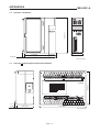
APPENDIX1 OUTSIDE DIMENSIONS . . . . . . . . . . . . . . . . . . . . . . . . . . . . . . . . . . . . . . . . . . . APP – 1
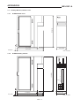
1.1 Input/Output Modules . . . . . . . . . . . . . . . . . . . . . . . . . . . . . . . . . . . . . . . . . . . . . . . . . . APP – 1
1.1.1
Terminal base connecting type . . . . . . . . . . . . . . . . . . . . . . . . . . . . . . . . . . . APP – 1
1.1.2
40-pin connector type . . . . . . . . . . . . . . . . . . . . . . . . . . . . . . . . . . . . . . . . . . APP – 1
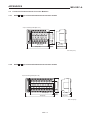
1.1.3
37-pin D sub-connector type 32-input/output module . . . . . . . . . . . . . . . . . . APP – 2
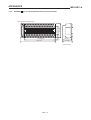
1.2 Dynamic I/O Module. . . . . . . . . . . . . . . . . . . . . . . . . . . . . . . . . . . . . . . . . . . . . . . . . . . APP – 3
1.3 A1SJ-56 Input/Output Combination Module. . . . . . . . . . . . . . . . . . . . . . . . . . . . . . . . . APP – 3
1.4 Dummy Module, Blank Cover. . . . . . . . . . . . . . . . . . . . . . . . . . . . . . . . . . . . . . . . . . . . APP – 4
1.4.1
A1SG60 blank cover . . . . . . . . . . . . . . . . . . . . . . . . . . . . . . . . . . . . . . . . . . . APP – 4
1.4.2
A1SG62 dummy module. . . . . . . . . . . . . . . . . . . . . . . . . . . . . . . . . . . . . . . . APP – 4
1.5 Connector/Terminal Block Convertor Modules. . . . . . . . . . . . . . . . . . . . . . . . . . . . . . . APP – 5
1.5.1
A6TB 36
type connector/terminal block convertor module. . . . . . . . . . . . APP – 5
1.5.2
A6TB 54
type connector/terminal block convertor module. . . . . . . . . . . . APP – 5
1.5.3
A6TBX70
type connector/terminal block convertor module . . . . . . . . . . . . APP – 6
– ii –
1.6 40-Pin Connectors . . . . . . . . . . . . . . . . . . . . . . . . . . . . . . . . . . . . . . . . . . . . . . . . . . . . APP – 7
1.6.1
A6CON1 soldering-type 40-pin connector, A6CON2 crimp-contact-type
40-pin connector . . . . . . . . . . . . . . . . . . . . . . . . . . . . . . . . . . . . . . . . . . . . . . APP – 7
1.6.2
A6CON3 pressure-displacement-type 40-pin connector . . . . . . . . . . . . . . . APP – 7
1.7 Pin D Sub-Connectors . . . . . . . . . . . . . . . . . . . . . . . . . . . . . . . . . . . . . . . . . . . . . . . . . APP – 8
1.7.1
A6CON1E soldering type 37-pin D sub-connector
A6CON2E crimp-contact-type 37-pin D sub-connector . . . . . . . . . . . . . . . . APP – 8
1.7.2
A6CON3E pressure-displacement-type 37-pin D sub-connector . . . . . . . . . APP – 8
– iii –
Manuals
The following manuals are also relevant to this product.
Related manuals
• A1SJCPU (S3) User’s (Hardware) (IB-66469)
This manual describes the cautions on handling, connection to I/O modules,
and error codes of A1SJCPU (S3).
• A1S/A1SC24-R2/A2S/A2ASCPU (S1/S30) User’s (Hardware) (IB-66468)
This manual describes the cautions on handling, connection to I/O modules,
and error codes of A1S, A1SC24-R2, A2S and A2ASCPU (S1/S30).
1. NOTES ON SELECTING INPUT AND OUTPUT MODULES
1.
MELSEC-A
NOTES ON SELECTING INPUT AND OUTPUT MODULES
(1)
It is recommended that a triac output module be used with a load that is
frequently opened and closed or with a coil load (e.g. an electromagnet)
that has a large capacity or a low power factor.
(If a contact output module is used, its service life will be shorter than
specified.)
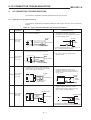
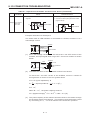
(2)
If an inductive L load is driven by an output module, it must be switched
ON for 1 second or longer and switched OFF for 1 second or longer.
(3)
If a counter or timer which has a DC-DC converter as a load is used with
an A1SY40, A1SY41, or A1SY42 output module, a fault may be caused
in the output module due to periodic rush currents when it is turned ON
or during operation.
To prevent failure due to rush current, connect a resistor or an
inductance to the load in series or use an A1SY50 whose maximum load
current is larger.
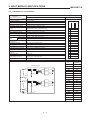
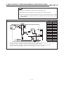
Resistor
Output
module
(4)
Inductance
Load
Load
Output
module
Fuses installed in output modules cannot be replaced. They are
principally designed to protect external wiring if the module outputs are
shorted.
Therefore, output modules may not be protected from a short circuit.
If an output module becomes faulty due to any cause other than a short
circuit, its fuse may not function.
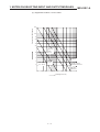
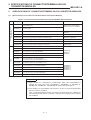
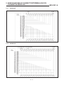
(5)
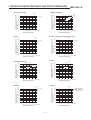
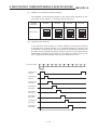
The number of signals which can be turned ON simultaneously in an
input module varies according to the input voltage and ambient
temperature. Select the number of the simultaneous ON signals by
referring to the charts on the next page.
1–1
1. NOTES ON SELECTING INPUT AND OUTPUT MODULES
A1SX20, A1SX20EU
49°C
↓
(%)
100
90
80
70
60
50
40
30
20
10
0
(%)
100
90
80
70
60
50
40
30
20
10
Number of simultaneous ON
input signals (%)
Number of simultaneous ON
input signals (%)
A1SX10, A1SX10EU
132 VAC
60%
10
20
30
40
0
50 55 (°C)
Ambient temperature
Number of simultaneous ON
input signals (%)
Number of simultaneous ON
input signals (%)
10
20
30
40
200
VAC
50 55 (°C)
A1SX41, A1SX41-S2, A1SX81, A1SX81-S2
52°C
↓
(%)
100
90
80
70
60
50
40
30
20
10
0
26.4 VAC
75%
10
20
30
40
0
50 55 (°C)
0
Number of simultaneous ON
input signals (%)
33°C
↓
24
VDC
26.4
VDC
50%
47%
20
10
20
30
40
50 55 (°C)
30
40
37°C 46°C
↓
↓
(%)
100
90
80
70
60
50
40
30
20
10
0
50 55 (°C)
26.4
VDC
24
VDC
65%
40%
10
20
30
40
50 55 (°C)
Ambient temperature
Ambient temperature
A1SX80-S1
Number of simultaneous ON
input signals (%)
A1SH42
53°C
↓
(%)
100
90
80
70
60
50
40
30
20
10
0
60%
A1SX71
23°C
↓
10
26.4 VDC
Ambient temperature
A1SX42, A1SX42-S2
(%)
100
90
80
70
60
50
40
30
20
10
43°C
↓
(%)
100
90
80
70
60
50
40
30
20
10
Ambient temperature
Number of simultaneous ON
input signals (%)
220
VAC
240
264VAC
VAC
Ambient temperature
A1SX30
Number of simultaneous ON
input signals (%)
MELSEC-A
26.4 VDC
85%
10
20
30
40
0
50 55 (°C)
44°C
↓
(%)
100
90
80
70
60
50
40
30
20
10
60%
10
20
30
40
Ambient temperature
Ambient temperature
1–2
Input : 26.4 VDC
(Output : 26.4 VDC,
1.6 A /common)
50 55 (°C)
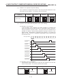
1. NOTES ON SELECTING INPUT AND OUTPUT MODULES
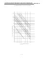
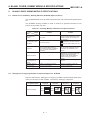
A1SY28A
8
Number of output points (%)
A1SJ-56DT
(A)
132 VAC
Load voltage
26.4 VAC
4
2
0
10
20
30
40
0
50 55 (°C)
(6)
48°C
↓
(%)
100
90
80
70
60
50
40
30
20
10
26.4 VDC
75%
10
20
30
40
50 55 (°C)
Ambient temperature
Ambient temperature
The chart below shows the service life of relay output modules.
Select the appropriate modules, considering the direction given in (1).
(a) Applicable module: A1SY10, A1SY10EU, A1SJ-56DR, A1SX48Y18
200
Service life (x10000 times)
Total output current
6
MELSEC-A
100
70
50
30
DC
20
AC
10
120 VAC COS φ=1
30 VDC T=0 ms
240 VAC COS φ=1
120 VAC COS φ=0.4
240 VAC COS φ=0.4
7
5
3
30 VDC T=7 ms
100 - 120 VDC T=7 - 40 ms
2
30 VDC T=40 ms
0.1
0.2
0.3
0.5 0.7
1.0
2.0
3.0
Switching current (A)
1–3
5.0
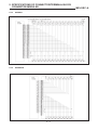
1. NOTES ON SELECTING INPUT AND OUTPUT MODULES
MELSEC-A
(b) Applicable module: A1SY14AEU
Service life (x 10000 times)
200
100
70
50
30
20
30 VDC T=7
ms,
240 VAC
COS φ=0.4
10
7
5
120 VDC
COS φ=1
30 VDC
T=7 ms
3
100 - 120V
T=7 - 40 ms
2
30 VDC T=0 ms
240 VDC COS φ=0.4
120 VDC
COS φ=0.4
0.1
0.2
0.3
0.5 0.7
1.0
2.0
3.0
Switching current (A)
1–4
5.0
1. NOTES ON SELECTING INPUT AND OUTPUT MODULES
MELSEC-A
(c) Applicable module: A1SY18A, A1SY18AEU
200
100
70
50
Service life (x 10000 times)
30
30 VDC T=0 ms
20
120 VAC COSφ=1
240 VAC COSφ=1
10
7
5
100 to 120 VDC
T=7 to 40 ms
30 VDC T=7 ms
3
120 VAC COSφ=0.4
240 VAC COSφ=0.4
2
30 VDC T=40 ms
1
0.5
0.7
1.0
2.0
3.0
Switching current (A)
1–5
5.0
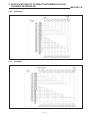
1. NOTES ON SELECTING INPUT AND OUTPUT MODULES
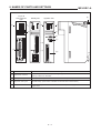
(7)
MELSEC-A
The common current of an A1SY60 varies according to ambient
temperature. Select a common current referring to the chart shown
below.
A1SY60 derating curve
4A/1 common
Ta = 25°C
3.6A/1 common
↓
Ta = 45°C
•
↓
•
common
• 3.2A/1
Ta = 55°C
(A)
Common current
4
3
2
1
0
10
(8)
20
30
40
Ambient temperature
50
55 (°C)
The A1SX41 and A1SX42 input modules and the A1SY41 and A1SY42
output modules are supplied with soldering-type 40-pin connectors.
40-pin connectors of the pressure-displacement type and crimp contact
type are also available. Tools for the pressure-displacement and crimp
contact type connectors must be procured from the following suppliers:
(a) Soldering-type 40-pin connector
Model name
: A6CON1
(b) Crimp-contact-type 40-pin connector
Model name
: A6CON2
Tool
: Fujitsu
Applicable wire size
: AWG #24 to 28
FCN-363-T005/H
(c) Pressure-displacement-type 40-pin connector
Model name
: A6CON3
Tool
: Fujitsu
FCN-367T-T012/H (locator plate)
FCN-707T-T001/H (cable cutter)
FCN-707T-T101/H (hand press)
Applicable wire size
: AWG #28 (twisted)
AWG #30 (single wire)
1–6
1. NOTES ON SELECTING INPUT AND OUTPUT MODULES
MELSEC-A
(d) Supplier’s offices:
Fujitsu Limited
North and South America:
Fujitsu Component of America, Inc.
3545 North First Street, San Jose, CA 95134-1804 U.S.A.
Phone: (408) 922-9000
Telex: (910) 338-0190
Fax: (408) 428-0640
Europe:
Fujitsu Microelectronik GmbH
Am Siebestein 6-10 6072, Dreieich-Buchschtag, F.R. Germany
Phone: (061) 03-690-0
Telex: 411963
Fax: (061) 03-690-122
Asia:
Fujitsu Microelectronics Asia PTE, Limited
#06-04 to #06-07 Plaza, By The Park, No.51 Bras Basah Road,
Singapore 0719
Phone: 336-1600
Telex: 55573
Fax: 336-1609
(9)
The 37-pin D sub-connector for the A1SX81 and A1SY81 is a solderingtype connector. Crimp-contact-type and pressure-displacement type 37pin D sub-connectors are also available. Tools for the crimp-contact-type
and pressure-displacement connectors must be procured by the user.
(a) Soldering-type 37-pin D sub-connector
Model name
: A6CON1E
(b) Crimp-contact-type 37-pin D sub-connector
Model name
: A6CON2E
Tool
: AMP 90312-1
Applicable wire size
: AWG #20 to 24
(c) Pressure-displacement-type 37-pin D sub-connector
Model name
: A6CON3E
Tool
: AMP
91257-1 (die set)
91220-1 (cable cutter)
91085-2 (hand press)
Applicable wire size
: AWG #28 (twisted)
AWG #30 (single wire)
1–7
1. NOTES ON SELECTING INPUT AND OUTPUT MODULES
MELSEC-A
(d) Contact for enquiries about tools for crimp-contact and pressuredisplacemet-type cables
(The tools cited above are only examples: for more details, enquire
at the contact given below.)
AMP Incorporated
Americas:
Worldwide Headquarters of AMP Incorporated
Harrisburg, PA, U.S.A
Phone: (717) 564-0100
Fax: (717) 986-7813
Far East:
AMP Singapore Pte. Ltd.
Singapore
Phone: (65) 482-0311
Fax: (65) 482-1012
Europe:
AMP Deutschland G.m.b.H.
Langen, Germany
Phone: (49) 6103-7090
Fax: (49) 6103-709223
(10) W h e n u s i n g A 1 S X 1 0 E U , A 1 S X 2 0 E U , A 1 S Y 1 0 E U , A 1 S Y 1 4 E U ,
A1SY28EU, etc., if the wires are connected to the terminal block without
using solderless terminals, observe the following points.
(a) Bare the end of insulated wires to expose about 6 to 8 mm of naked
wire.
When making connections, ensure that bared wire does project from
the terminal block. If it does, it may close the gap to a distance
shorter than that required for insulation between the terminals.
Terminal block
(barrier)
Insulation
Bared length: 6 to 8 mm (0.24 to 0.31 in.)
Treatment of end of wire
Connection to the terminal block
(viewed from side)
(b) If twisted wire is used, make sure that is does not unravel.
(11) The noise resistance specification for I/O modules is the stipulated noise
voltage applied with a noise simulator with a noise amplitude of 1µs and
noise frequency of 25 to 60 Hz.
1–8
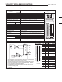
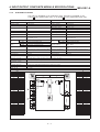
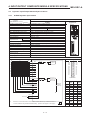
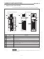
2. INPUT MODULE SPECIFICATIONS
2.
INPUT MODULE SPECIFICATIONS
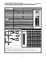
2.1
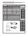
A1SX10 AC Input Module
MELSEC-A
Model
AC Input Module
Specifications
A1SX10
Number of input points
Appearance
16 points
Isolation method
Photocoupler
Rated input voltage
100 to 120 VAC 50/60 Hz
Rated input current
Approx. 6 mA (100 VAC 60 Hz)
Operating voltage range
85 to 132 VAC (50/60 Hz ±5%)
Max. simultaneous input
points
100% simultaneously ON (at 110 VAC)
60% simultaneously ON (at 132 VAC)
A 1SX10
0
1
2
3
4
5
6
7
Inrush current
Max. 200 mA, within 1 ms (132 VAC)
ON voltage/ON current
80 VAC or higher/5 mA or higher
0
OFF voltage/OFF current
30 VAC or lower/1 mA or lower
1
Input impedance
Approx. 18 kΩ (60 Hz), Approx. 21 kΩ (50 Hz)
2
OFF → ON
20 ms or less (100 VAC 60 Hz)
3
ON → OFF
35 ms or less (100 VAC 60 Hz)
4
Common terminal
arrangement
16 points/common (common terminals: TB9, TB18)
5
Operating indicator
ON state is indicated (LEDs)
External connections
20-point terminal block connector (M3.5 x 7 screws)
Applicable wire size
0.75 to 1.25 mm 2
Applicable solderless
terminals
R1.25-3.5, R2-3.5
RAV1.25-3.5, RAV2-3.5
Accessories
None
B
Insulatoin withstand voltage
1500 VAC
C
Noise immunity
1000 VAC
D
Internal current
consumption (5 VDC)
50 mA (TYP, all points ON)
Weight kg (lb)
0.21 (0.46)
Response
time
8
9
A
B
C
D
E
F
6
7
8
9
A
E
F
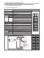
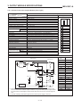
External Connections
Internal circuit
LED
TB1
R
R
R
Internal
circuit
TB8
A
TB9
TB10
LED
R
R
R
Internal circuit
Terminal
No.
Signal Name
TB1
X00
TB2
X01
TB3
X02
TB4
X03
TB5
X04
TB6
X05
TB7
X06
TB8
X07
TB9
COM
TB10
X08
TB11
X09
TB12
X0A
TB13
X0B
TB14
X0C
TB15
X0D
TB17
TB16
X0E
TB18
TB17
X0F
A
100 VAC
2–1
TB18
COM
TB19
Vacant
TB20
Vacant
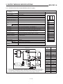
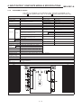
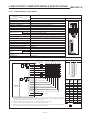
2. INPUT MODULE SPECIFICATIONS
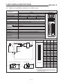
2.2
MELSEC-A
A1SX10EU AC Input Module
Model
AC Input Module
Specifications
A1SX10EU
Number of input points
Appearance
16 points
Insulation method
Photocoupler
Rated input voltage
100 to 120 VAC 50/60 Hz
A 1SX10EU
Rated input current
Approx. 7 mA (120 VAC 60 Hz)
Operating voltage range
85 to 132 VAC (50/60 Hz ±5%)
Max. simultaneous input
points
100% simultaneously ON
0
1
2
3
4
5
6
7
Inrudh current
Max. 200 mA, within 1 ms (132 VAC)
ON voltage/ON current
80 VAC or higher/5 mA or higher
0
OFF voltage/OFF current
30 VAC or lower/1 mA or lower
1
Input impedance
Approx. 18 kΩ (60 Hz), Approx. 21 kΩ (50 Hz)
2
OFF → ON
20 ms or less (100 VAC 60 Hz)
3
ON → OFF
35 ms or less (100 VAC 60 Hz)
4
Response
time
8
9
A
B
C
D
E
F
5
Common terminal
arrangement
16 points/common (common terminals: TB9, TB18)
Operating indicator
ON state is indicated (LEDs)
7
External connections
20-point terminal block connector (M3.5 x 7 screws)
8
Applicable wire size
0.75 to 1.25 mm 2
9
Applicable crimp terminals
RAV1.25-3.5 (AWG15 to AWG19)
A
Accessories
None
6
B
Insulation withstand
voltage
1780 VAC
Noise immunity
1000 VAC
Internal current
consumption (5 VDC)
50 mA (TYP, all points ON)
Weight kg (lb)
0.21 (0.46)
C
D
E
F
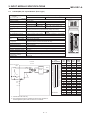
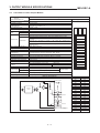
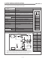
External Connections
Internal circuit
TB1
LED
R
R
R
Internal
circuit
TB8
A
TB9
TB10
LED
R
R
R
Internal
circuit
TB17
TB18
A
100 VAC
2–2
Terminal
No.
Signal Name
TB1
X00
TB2
X01
TB3
X02
TB4
X03
TB5
X04
TB6
X05
TB7
X06
TB8
X07
TB9
COM
TB10
X08
TB11
X09
TB12
X0A
TB13
X0B
TB14
X0C
TB15
X0D
TB16
X0E
TB17
X0F
TB18
COM
TB19
Vacant
TB20
Vacant
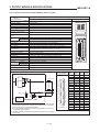
2. INPUT MODULE SPECIFICATIONS
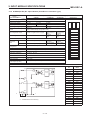
2.3
MELSEC-A
A1SX20 AC Input Module
Model
AC Input Module
Specifications
A1SX20
Number of input points
Appearance
16 points
Isolation method
Photocoupler
Rated input voltage
200 to 240 VAC 50/60 Hz
A 1SX20
0
1
2
3
4
5
6
7
Rated input current
Approx. 9 mA (200 VAC 60 Hz)
Operating voltage range
170 to 264 VAC (50/60 Hz ±5%)
Max. simultaneous input
points
60% simultaneously ON (at 220 VAC)
Inrush current
Max. 500 mA, within 1 ms (264 VAC)
ON voltage/ON current
80 VAC or higher/4 mA or higher
OFF voltage/OFF current
30 VAC or lower/1 mA or lower
Input impedance
Approx. 22 kΩ (60 Hz), Approx. 27 kΩ (50 Hz)
Response
time
OFF → ON
30 ms or less (200 VAC 60 Hz)
ON → OFF
55 ms or less (200 VAC 60 Hz)
8
9
A
B
C
D
E
F
0
1
2
3
4
5
Common terminal
arrangement
16 points/common (common terminals: TB9, TB18)
6
Operating indicator
ON state is indicated (LEDs)
7
External connections
20-point terminal block connector (M3.5 x 7 screws)
8
Applicable wire size
0.75 to 1.25 mm 2
9
Applicable solderless
terminals
R1.25-3.5, R2-3.5
RAV1.25-3.5, RAV2-3.5
A
Accessories
None
C
Insulation withstand voltage
1500 VAC
D
Noise immunity
1500 VAC
E
Internal current
consumption (5 VDC)
50 mA (TYP, all points ON)
F
Weight kg (lb)
0.23 (0.50)
B
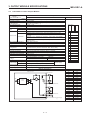
External Connections
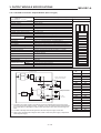
Internal circuit
LED
TB1
R
R
R
Internal
circuit
TB8
A
TB9
TB10
LED
R
R
R
Internal circuit
TB17
TB18
A
200 VAC
2–3
Terminal
No.
Signal Name
TB1
X00
TB2
X01
TB3
X02
TB4
X03
TB5
X04
TB6
X05
TB7
X06
TB8
X07
TB9
COM
TB10
X08
TB11
X09
TB12
X0A
TB13
X0B
TB14
X0C
TB15
X0D
TB16
X0E
TB17
X0F
TB18
COM
TB19
Vacant
TB20
Vacant
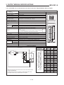
2. INPUT MODULE SPECIFICATIONS
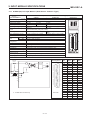
2.4
MELSEC-A
A1SX20EU AC Input Module
Model
AC Input Module
Specifications
A1SX20EU
Number of input points
Appearance
16 points
Insulation method
Photocoupler
Rated input voltage
200 to 240 VAC 50/60 Hz
A 1SX20EU
Rated input current
Approx. 11 mA (240 VAC 60 Hz)
Operating voltage range
170 to 264 VAC (50/60 Hz ±5%)
Max. simultaneous input
points
60% simultaneously ON (at 220 VAC)
0
1
2
3
4
5
6
7
Inrush current
Max. 500 mA, within 1 ms (264 VAC)
ON voltage/ON current
80 VAC or higher/4 mA or higher
0
OFF voltage/OFF current
30 VAC or lower/1 mA or lower
1
Input impedance
Approx. 22 kΩ (60 Hz), Approx. 27 kΩ (50 Hz)
2
OFF → ON
30 ms or less (200 VAC 60 Hz)
3
ON → OFF
55 ms or less (200 VAC 60 Hz)
4
Response
time
8
9
A
B
C
D
E
F
5
Common terminal
arrangement
16 points/common (common terminals: TB9, TB18)
Operating indicator
ON state is indicated (LEDs)
7
External connections
20-point terminal block connector (M3.5 x 7 screws)
8
Applicable wire size
0.75 to 1.25 mm 2
9
Applicable crimp terminals
RAV1.25-3.5 (AWG15 to AWG19)
A
Accessories
6
None
B
Insulation withstand
voltage
2830 VAC
C
Noise immunity
1000 VAC
Internal current
consumption (5 VDC)
50 mA (TYP, all points ON)
Weight kg (lb)
0.23 (0.50)
D
E
F
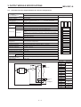
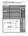
External Connections
Internal circuit
TB1
LED
R
R
R
Internal
circuit
TB8
A
TB9
TB10
LED
R
R
R
Internal
circuit
TB17
TB18
A
200 VAC
2–4
Terminal
No.
Signal Name
TB1
X00
TB2
X01
TB3
X02
TB4
X03
TB5
X04
TB6
X05
TB7
X06
TB8
X07
TB9
COM
TB10
X08
TB11
X09
TB12
X0A
TB13
X0B
TB14
X0C
TB15
X0D
TB16
X0E
TB17
X0F
TB18
COM
TB19
Vacant
TB20
Vacant
2. INPUT MODULE SPECIFICATIONS
2.5
MELSEC-A
A1SX30 DC/AC Input Module
Model
DC/AC Input Module
Specifications
A1SX30
Number of input points
16 points
Isolation method
Photocoupler
Appearance
Rated input voltage
12/24 VDC
Rated input current
4.2 mA (12 VDC/VAC), 8.6 mA (24 VDC/VAC)
12/24 VAC 50/60 Hz
Operating voltage range
10.2 to 26.4 VDC
(ripple: less than 5%)
Max. simultaneous input
points
75% simultaneously ON (at 26.4 VDC)
A 1SX30
0
1
2
3
4
5
6
7
10.2 to 26.4 VAC
(50/60 Hz ±5%)
ON voltage/ON current
7 VDC/AC or higher/2 mA or higher
OFF voltage/OFF current
2.7 VDC/AC or lower/0.7 mA or lower
0
Input impedance
Approx. 2.7 kΩ
1
Response
time
OFF → ON
20 ms or less
(12/24 VDC )
25 ms or less
(12/24 VAC 60Hz)
2
ON → OFF
20 ms or less
(12/24 VDC )
20 ms or less
(12/24 VAC 60Hz)
4
8
9
A
B
C
D
E
F
3
5
Common terminal
arrangement
16 points/common (common terminals: TB9, TB18)
Operating indicator
ON state is indicated (LEDs)
7
External connections
20-point terminal block connector (M3.5 x 7 screws)
8
Applicable wire size
0.75 to 1.25 mm 2
9
Applicable solderless
terminals
R1.25-3.5, R2-3.5
RAV1.25-3.5, RAV2-3.5
A
Accessories
None
6
B
C
Insulation withstand voltage
500 VAC
Noise immunity
1500 VAC
Internal current
consumption (5 VDC)
50 mA (TYP, all points ON)
Weight kg (lb)
0.2 (0.44)
D
E
F
External Connections
Internal circuit
TB1
LED
R
R
R
Internal
circuit
TB8
A
TB9
TB10
LED
R
R
R
Internal circuit
Terminal No.
Signal Name
TB1
X00
TB2
X01
TB3
X02
TB4
X03
TB5
X04
TB6
X05
TB7
X06
TB8
X07
TB9
COM
TB10
X08
TB11
X09
TB12
X0A
TB13
X0B
TB14
X0C
TB17
TB15
X0D
AC/TB18
DC
TB16
X0E
A
2–5
TB17
X0F
TB18
COM
TB19
Vacant
TB20
Vacant
2. INPUT MODULE SPECIFICATIONS
2.6
MELSEC-A
A1SX40(S1/S2) DC Input Module (Sink Type)
Model
DC Input Module (Sink Type)
Specifications
A1SX40
A1SX40-S1
A1SX40-S2
Appearance
Number of input points 16 points
Isolation method
Photocoupler
Rated input voltage
12 VDC
24 VDC
24 VDC
Rated input current
Approx. 3 mA
Approx. 7 mA
Approx. 7 mA
Operating voltage
range
10.2 to 26.4 VDC (ripple: less 19.2 to 26.4 VDC (ripple: less than 5%)
than 5%)
Max. simultaneous
input points
100% simultaneously ON (at 26.4 VDC)
ON voltage/ON
current
8 VDC or higher/2 mA or
higher
OFF voltage/OFF
current
4 VDC or lower/1 mA or lower 6.5 VDC or lower/1.7 mA or lower
Input resistance
Approx. 3.3 kΩ
14 VDC or higher/4
mA or higher
A 1SX40
8
9
A
B
C
D
E
F
14 VDC or higher/3.5
mA or higher
0
1
2
Response
time
ON → OFF
10 ms or less (24 VDC)
0.1 ms or less
(24 VDC)
10 ms or less
(24 VDC)
10 ms or less (24 VDC)
0.2 ms or less
(24 VDC)
10 ms or less
(24 VDC)
Common terminal
arrangement
16 points/common (common terminals: TB9, TB18)
Operating indicator
ON state is indicated (LEDs)
External connections
20-point terminal block connector (M3.5 x 7 screws)
Applicable wire size
0.75 to 1.25 mm 2
Applicable solderless
terminals
R1.25-3.5, R2-3.5
RAV1.25-3.5, RAV2-3.5
OFF → ON
0
1
2
3
4
5
6
7
3
4
5
6
7
8
9
A
B
C
Accessories
None
Insulatoin withstand
voltage
500 VAC
Noise immunity
500 VAC
Internal current
consumption (5 VDC)
50 mA (TYP, all points ON)
Weight kg (lb)
0.2(0.44)
D
E
F
External Connections
Internal circuit
LED
TB1
R
R
Internal circuit
TB8
A
TB9
TB10
LED
R
R
Internal circuit
TB17
TB18
−
+
*1 12/24
VDC
*1: A1SX40-S1/S2 is 24 VDC only.
A
2–6
Terminal
No.
Signal
Name
TB1
TB2
TB3
TB4
TB5
TB6
TB7
TB8
TB9
TB10
TB11
TB12
TB13
TB14
TB15
TB16
TB17
TB18
TB19
TB20
X00
X01
X02
X03
X04
X05
X06
X07
COM
X08
X09
X0A
X0B
X0C
X0D
X0E
X0F
COM
Vacant
Vacant
2. INPUT MODULE SPECIFICATIONS
2.7
MELSEC-A
A1SX41(S2) DC Input Module (Sink Type)
Model
DC Input Module (Sink Type)
Specifications
A1SX41
A1SX41-S2
Number of input points
32 points
Isolation method
Photocoupler
Rated input voltage
12 VDC
24 VDC
Rated input current
Approx. 3 mA
Approx. 7 mA
Appearance
A 1SX41
24 VDC
Approx. 7 mA
Operating voltage range
10.2 to 26.4 VDC (ripple: less
than 5%)
Max. simultaneous input
points
60% (20 points/common) simultaneously ON (at 26.4 VDC)
ON voltage/ON current
8 VDC or higher/2 mA or higher
14 VDC or higher/3.5 mA or
higher
OFF voltage/OFF current
4 VDC or lower/1 mA or lower
6.5 VDC or lower/1.7 mA or lower
Input resistance
Approx. 3.3 kΩ
OFF → ON
Response
time
ON → OFF
19.2 to 26.4 VDC (ripple: less
than 5%)
10 ms or less (24 VDC)
10 ms or less (24 VDC)
Common terminal
arrangement
32 points/common (common terminals: B1, B2)
Operating indicator
ON state is indicated (LEDs)
External connections
40-pin connector
Applicable wire size
0.3 mm 2
Accessories
Connector (1 pce.) for external wiring (soldering type)
Insulatoin withstand voltage
500 VAC
Noise immunity
500 VAC
Internal current
consumption (5 VDC)
80 mA (TYP, all points ON)
Weight kg (lb)
0.21(0.46)
External Connections
Pin
Arrangement
Internal
circuit
External switch
B20
R
R
Internal
circuit
LED
A5
–
+
B2
*1 12/24 VDC
B1
A2
A1
B20
B19
B18
B17
B16
B15
B14
B13
B12
B11
B10
B9
B8
B7
B6
B5
B4
B3
B2
B1
Front view
*1: A1SX42-S2 is 24 VDC only.
*2: The arrangement of pins A and B shown above is the opposite of
the arrangement of pins of the connector on the module.
2–7
A20
A19
A18
A17
A16
A15
A14
A13
A12
A11
A10
A9
A8
A7
A6
A5
A4
A3
A2
A1
Pin
No.
Signal
Name
(FH)
Pin
No.
Signal
Name
(FH)
B20
B19
B18
B17
B16
B15
B14
B13
B12
B11
B10
B9
B8
B7
B6
B5
B4
B3
B2
B1
X00
X01
X02
X03
X04
X05
X06
X07
X08
X09
X0A
X0B
X0C
X0D
X0E
X0F
Vacant
Vacant
COM
COM
A20
A19
A18
A17
A16
A15
A14
A13
A12
A11
A10
A9
A8
A7
A6
A5
A4
A3
A2
A1
X10
X11
X12
X13
X14
X15
X16
X17
X18
X19
X1A
X1B
X1C
X1D
X1E
X1F
Vacant
Vacant
Vacant
Vacant
2. INPUT MODULE SPECIFICATIONS
2.8
MELSEC-A
A1SX42(S2) DC Input Module (Sink Type)
DC Input Module (Sink Type)
Model
A1SX42
Specifications
A1SX42-S2
Appearance
Number of input points
64 points
Isolation method
Photocoupler
Rated input voltage
12 VDC
24 VDC
Rated input current
Approx. 2 mA
Approx. 5 mA
Operating voltage range
10.2 to 26.4 VDC (ripple: less
than 5%)
Max. simultaneous input
points
50% (16 points/common) simultaneously ON (at 24 VDC)
ON voltage/ON current
8 VDC or higher/2 mA or higher
17.5 VDC or higher/3.5 mA or
higher
OFF voltage/OFF current
4 VDC or lower/0.6 mA or lower
7 VDC or lower/1.7 mA or lower
Input resistance
Approx. 5 kΩ
Approx. 4.7 kΩ
Response
time
A 1SX42
OFF → ON
10 ms or less (24 VDC)
ON → OFF
10 ms or less (24 VDC)
24 VDC
Approx. 5 mA
19.2 to 26.4 VDC (ripple: less
than 5%)
Common terminal
arrangement
32 points/common (common terminals: 1B1, 1B2, 2B1, 2B2)
Operating indicator
ON state is indicated (LEDs), 32-bit indication by switch
External connections
40-pin connector
Applicable wire size
0.3 mm 2
Accessories
Connectors (2 pces.) for external wiring (soldering type)
Insulatoin withstand voltage
500 VAC
Noise immunity
500 VAC
Internal current
consumption (5 VDC)
90 mA (TYP, all points ON)
Weight kg (lb)
0.28(0.62)
External Connections
Internal circuit
Pin Arrangement
External
switch
R
R
Internal
circuit
LED
1A5
1B2
*1 12/24 VDC
1B1
1A2
1A1
2B20
2A5
– + 2B2
*1 12/24 VDC
2B1
2A2
Left side
(first-half)
Indication
switching
circuit
Right side
(second-half) Indication
switching
*2
R
Internal
R
circuit
B20
B19
B18
B17
B16
B15
B14
B13
B12
B11
B10
B9
B8
B7
B6
B5
B4
B3
B2
B1
A20
A19
A18
A17
A16
A15
A14
A13
A12
A11
A10
A9
A8
A7
A6
A5
A4
A3
A2
A1
2A1
*1
Front view
Signal
Signal
Signal
Signal
Pin No. Name Pin No. Name Pin No. Name Pin No. Name
(FH)
(FH)
(SH)
(SH)
1B20
X00
1A20
X10
2B20
X20
2A20
X30
1B19
X01
1A19
X11
2B19
X21
2A19
X31
1B18
X02
1A18
X12
2B18
X22
2A18
X32
1B17
X03
1A17
X13
2B17
X23
2A17
X33
1B16
X04
1A16
X14
2B16
X24
2A16
X34
1B15
X05
1A15
X15
2B15
X25
2A15
X35
1B14
X06
1A14
X16
2B14
X26
2A14
X36
1B13
X07
1A13
X17
2B13
X27
2A13
X37
1B12
X08
1A12
X18
2B12
X28
2A12
X38
1B11
X09
1A11
X19
2B11
X29
2A11
X39
1B10
X0A
1A10
X1A
2B10
X2A
2A10
X3A
1B9
X0B
1A9
X1B
2B9
X2B
2A9
X3B
1B8
X0C
1A8
X1C
2B8
X2C
2A8
X3C
1B7
X0D
1A7
X1D
2B7
X2D
2A7
X3D
1B6
X0E
1A6
X1E
2B6
X2E
2A6
X3E
1B5
X0F
1A5
X1F
2B5
X2F
2A5
X3F
1B4
Vacant
1A4
Vacant
2B4
Vacant
2A4
Vacant
1B3
Vacant
1A3
Vacant
2B3
Vacant
2A3
Vacant
1B2
COM1
1A2
Vacant
2B2
COM2
2A2
Vacant
1B1
COM1
1A1
Vacant
2B1
COM2
2A1
Vacant
*1: A1SX42-S2 is 24 VDC only.
*2: In the pin number column, the pins beginning with “1[ ][ ]” are left connector pins and those beginning with “2[ ][ ]” are right
connector pins.
*3: When the switch is set to the left side position, the status of the first-half devices (X00 to X1F) is displayed by the LEDs.
When it is set to the right side, the status of the second-half devices (X20 to X3F) is displayed by the LEDs.
*4: The arrangement of pins A and B shown above is the opposite of the arrangement of pins of the connector on the module.
2–8
2. INPUT MODULE SPECIFICATIONS
2.9
MELSEC-A
A1SX71 DC Input Module (Sink/Source Common Type)
DC Input Module (Sink/Source Common Type)
Model
A1SX71
Specifications
Number of input points
32 points
Isolation method
Photocoupler
Appearance
A 1SX71
Rated input voltage
5 VDC
12 VDC
24 VDC *1
Rated input current
1.2 mA
3.3 mA
7 mA
Operating voltage range
4.5 to 26.4 VDC (ripple: less than 5%)
Max. simultaneous input
points
65% (20 points/common) simultaneously ON (at 24 VDC)
ON voltage/ON current
3.5 VDC or higher/1 mA or higher
OFF voltage/OFF current
1.0 VDC or lower/0.1 mA or lower
Input resistance
Response
time
Approx. 3.5 kΩ
OFF → ON
1.5 ms or less
ON → OFF
3 ms or less
Common terminal
arrangement
32 points/common (common terminals: B1, B2)
Operating indicator
ON state is indicated (LEDs)
External connections
40-pin connector
Applicable wire size
0.3 mm 2
Accessories
Connector (1 pce.) for external wiring (soldering type)
Insulatoin withstand voltage
500 VAC
Noise immunity
250 VAC
Internal current
consumption (5 VDC)
75 mA (TYP, all points ON)
Weight kg (lb)
0.19 (0.42)
DC4.5/13.2V
A1SX71
External Connections
Open collector (Sink)
Pin
Arrangement
Internal circuit
B20
R
Internal
circuit
R
LED
B2
– +
5/12/24 VDC
B1
A2
A1
TTL, LS-TTL, CMOS buffer (Sink)
B20
+
+
−
5/12 VDC
B2
A20
A19
A18
A17
A16
A15
A14
A13
A12
A11
A10
A9
A8
A7
A6
A5
A4
A3
A2
A1
Sensor (Source)
B20
5 VDC
B20
B19
B18
B17
B16
B15
B14
B13
B12
B11
B10
B9
B8
B7
B6
B5
B4
B3
B2
B1
−
B2
2–9
Front view
Pin
No.
Signal
Name
Pin
No.
Signal
Name
B20
X00
A20
X10
B19
X01
A19
X11
B18
X02
A18
X12
B17
X03
A17
X13
B16
X04
A16
X14
B15
X05
A15
X15
B14
X06
A14
X16
B13
X07
A13
X17
B12
X08
A12
X18
B11
X09
A11
X19
B10
X0A
A10
X1A
B9
X0B
A9
X1B
B8
X0C
A8
X1C
B7
X0D
A7
X1D
B6
X0E
A6
X1E
B5
X0F
A5
X1F
B4
Vacant
A4
Vacant
B3
Vacant
A3
Vacant
B2
COM
A2
Vacant
B1
COM
A1
Vacant
*1: 24 VDC can be used with hardware version B and
later versions.
*2: The arrangement of pins A and B shown above is
the opposite of the arrangement of pins of the connector on the module.
2. INPUT MODULE SPECIFICATIONS
MELSEC-A
2.10 A1SX80(S1/S2) DC Input Module (Sink/Source Common Type)
DC Input Module (Sink/Source Common Type)
Model
A1SX80
Specifications
A1SX80-S1
A1SX80-S2
Number of input points
16 points
Isolation method
Photocoupler
Rated input voltage
12 VDC
24 VDC
24 VDC
Rated input current
Approx. 3 mA
Approx. 7 mA
Approx. 7 mA
Operating voltage range
10.2 to 26.4 VDC (ripple: less
than 5%)
Max. simultaneous input
points
100% simultaneously ON (at 26.4 VDC)
ON voltage/ON current
8 VDC or higher/2 mA or higher
17 VDC or
higher/5 mA or
higher
OFF voltage/OFF current
4 VDC or lower/1 mA or lower
6 VDC or
5 VDC or
lower/1.7 mA or lower/1.7 mA or
lower
lower
Input resistance
Approx. 3.3 kΩ
OFF → ON
Response
time
ON → OFF
Appearance
A 1SX80
0
1
2
3
4
5
6
7
19.2 to 26.4 VDC (ripple: less
than 5%)
13 VDC or
higher/3.5 mA
or higher
8
9
A
B
C
D
E
F
0
1
2
3
4
10 ms or less (24 VDC)
0.4 ms or less
(24 VDC)
10 ms or less
(24 VDC)
10 ms or less (24 VDC)
0.5 ms or less
(24 VDC)
10 ms or less
(24 VDC)
Common terminal
arrangement
16 points/common (common terminals: TB9, TB18)
Operating indicator
ON state is indicated (LEDs)
5
6
7
8
9
A
External connections
20-point terminal block connector (M3.5 x 7 screws)
Applicable wire size
0.75 to 1.25 mm 2
Applicable solderless
termials
R1.25-3.5, R2-3.5
RAV1.25-3.5, RAV2-3.5
Accessories
None
E
Insulatoin withstand voltage
500 VAC
F
Noise immunity
1000 VAC
Internal current
consumption (5 VDC)
50 mA (TYP, all points ON)
Weight kg (lb)
0.2(0.44)
B
C
D
External Connections
Internal circuit
TB1
LED
R
R
Internal
circuit
TB8
A
TB9
LED
TB10
R
R
*1
Internal
circuit
Terminal
No.
Signal
Name
TB1
X00
TB2
X01
TB3
X02
TB4
X03
TB5
X04
TB6
X05
TB7
X06
TB8
X07
TB9
COM
TB10
X08
TB11
X09
TB12
X0A
TB17
TB13
X0B
12/24 VDC
− + TB18
TB14
X0C
TB15
X0D
TB16
X0E
+
A
−
*1: A1SX80-S1/S2 is 24 VDC only.
2 – 10
TB17
X0F
TB18
COM
TB19
Vacant
TB20
Vacant
2. INPUT MODULE SPECIFICATIONS
MELSEC-A
2.11 A1SX81(S2) DC Input Module (Sink/Source Common Type)
DC Input Module (Sink/Source Common Type)
Model
A1SX81
Specifications
Number of input points
32 points
Isolation method
Photocoupler
A1SX81-S2
Appearance
A 1SX81
Rated input voltage
12 VDC
24 VDC
24 VDC
Rated input current
Approx. 3 mA
Approx. 7 mA
Approx. 7 mA
Operating voltage range
10.2 to 26.4 VDC (ripple: less
than 5%)
Max. simultaneous input
points
60% simultaneously ON (at 26.4 VDC)
ON voltage/ON current
8 VDC or higher/2 mA or higher
13 VDC or higher/3.5 mA or
higher
OFF voltage/OFF current
4 VDC or lower/1 mA or lower
6 VDC or lower/1.7 mA or lower
Input resistance
Approx. 3.3 kΩ
Response
time
OFF → ON
10 ms or less (24 VDC)
ON → OFF
10 ms or less (24 VDC)
19.2 to 26.4 VDC (ripple: less
than 5%)
Common terminal
arrangement
32 points/common (common terminals: 17, 18, 36)
Operating indicator
ON state is indicated (LEDs)
External connections
37-pin D sub-connector
Applicable wire size
0.3 mm 2
Accessories
Connector (1 pce.) for external wiring (soldering type)
Insulatoin withstand voltage
500 VAC
Noise immunity
1000 VAC
Internal current
consumption (5 VDC)
80 mA (TYP, all points ON)
Weight kg (lb)
0.24(0.53)
External Connections
Pin
Arrangement
Internal circuit
External
switch
1
R
R
Internal
circuit
LED
20
21
22
23
24
25
26
27
28
29
30
31
32
33
34
35
36
37
35
+
−
−
+
17
34
*1 12/24 VDC 18
37
19
Front view
*1: A1SX81-S2 is 24 VDC only.
2 – 11
1
2
3
4
5
6
7
8
9
10
11
12
13
14
15
16
17
18
19
Pin
No.
Signal
Name
Pin
No.
Signal
Name
1
X00
9
X10
20
X01
28
X11
2
X02
10
X12
21
X03
29
X13
3
X04
11
X14
22
X05
30
X15
4
X06
12
X16
23
X07
31
X17
5
X08
13
X18
24
X09
32
X19
6
X0A
14
X1A
25
X0B
33
X1B
7
X0C
15
X1C
26
X0D
34
X1D
8
X0E
16
X1E
27
X0F
35
X1F
17
COM
37
Vacant
36
COM
19
Vacant
18
COM
3. OUTPUT MODULE SPECIFICATIONS
3.
OUTPUT MODULE SPECIFICATIONS
3.1
A1SY10 Contact Output Module
Contact Output Module
Model
A1SY10
Specifications
Number of output points
Isolation method
Switching rated
voltage/current
Min. switching load
Max. switching voltage
OFF → ON
Response
time
ON → OFF
Mechanical
Service life
MELSEC-A
Electrical
Max. switching frequency
Surge absorber
Fuse
Common terminal
arrangement
Operating indicator
External connections
Applicable wire size
Applicable solderless
terminals
Accessories
Insulatoin withstand voltage
Noise immunity
Voltage
External
power supply Current
Internal current
consumption (5 VDC)
Weight kg (lb)
Appearance
16 points
Photocoupler
24 VDC 2 A (load resistance)
/1 point, 8 A/common
240 VAC 2 A (COSφ = 1)
5 VDC 1 mA
264 VAC 125 VDC
10 ms or less
12 ms or less
More than 20 million times
Switching rated voltage/current More than 100000 times
200 VAC 1.5 A, 240 VAC 1 A (COSφ = 0.7) More than 100000
times or more
200 VAC 1 A, 240 VAC 0.5 A (COSφ = 0.35) More than 100000
times
24 VDC 1 A, 100 VDC 0.1 A (L/R = 7 ms) More than 100000 times
3600 times per hour
None
None
A 1SY10
0
1
2
3
4
5
6
7
8
9
A
B
C
D
E
F
0
1
2
3
4
5
6
7
8 points/common (common terminals: TB9, TB18)
8
ON state is indicated (LEDs)
20-point terminal block connector (M3.5 x 7 screws)
0.75 to 1.25 mm 2
R1.25-3.5 R2-3.5
RAV1.25-3.5 RAV2-3.5
None
1500 VAC
1000 VAC
24 VDC ±10%, Ripple voltage: 4VP-P or less
90 mA (TYP 24 VDC all points ON)
9
A
B
C
D
E
F
120 mA (TYP, all points ON)
0.25 (0.55)
External Connections
Internal circuit
External load
1
L
RA
LED
Internal
circuit
8
L
9
100/200 VAC
10
L
17
L
100/200 VAC
24 VDC
18
19
+
20
3–1
–
External power
supply
Terminal No.
Signal Name
TB1
Y00
TB2
Y01
TB3
Y02
TB4
Y03
TB5
Y04
TB6
Y05
TB7
Y06
TB8
Y07
TB9
COM1
TB10
Y08
TB11
Y09
TB12
Y0A
TB13
Y0B
TB14
Y0C
TB15
Y0D
TB16
Y0E
TB17
Y0F
TB18
COM2
TB19
24 VDC
TB20
0V
3. OUTPUT MODULE SPECIFICATIONS
3.2
MELSEC-A
A1SY10EU Contact Output Module
Contact Output Module
Model
A1SY10EU
Specifications
Number of output points
Insulation method
Switching rated
voltage/current
Min. switching load
Max. switching voltage
OFF → ON
Response
time
ON → OFF
Mechanical
Service life
Electrical
Max. switching frequency
Surge absorber
Fuse
Common terminal
arrangement
Operating indicator
External connections
Applicable wire size
Applicable crimp terminals
Accessories
Insulation withstand
voltage
Noise immunity
External
power supply
Voltage
Current
Internal current
consumption (5 VDC)
Weight kg (lb)
Appearance
16 points
Photocoupler
24 VDC 2 A (load resistance)
/1 point, 8 A/common
120 VAC 2 A (COSφ = 1)
5 VDC 1 mA
132 VAC 125 VDC
10 ms or less
12 ms or less
More than 20 million times or more
Switching rated voltage/current More than 200000 times or more
100 VAC 2A, 120 VAC 2 A (COSφ = 0.7) More than 200000 times
or more
100 VAC 2A, 120 VAC 2 A (COSφ = 0.35) More than 100000 times
or more
24 VDC 1 .5A, 100 VDC 0.1 A (L/R = 7 ms) More than 100000
times or more
3600 times per hour
None
None
A 1SY10EU
0
1
2
3
4
5
6
7
8
9
A
B
C
D
E
F
0
1
2
3
4
5
6
7
8 points/common (common terminals: TB9, TB18)
ON state is indicated (LEDs)
20-point terminal block connector (M3.5 x 7 screws)
0.75 to 1.25 mm 2 (AWG16 to AWG19)
RAV1.25-3.5
None
AC terminals-Relay coil, 5 VAC
1780 VAC
Relay coil, 5 VAC
500 VAC
1000 VAC
24 VDC ±10%, Ripple voltage: 4VP-P or less
Must be a SELV
power supply
90 mA (TYP 24 VDC all points ON)
8
9
A
B
C
D
E
F
120 mA (TYP, all points ON)
0.25 (0.55)
External Connections
Internal circuit
External load
1
L
RA
LED
Internal
circuit
8
L
9
100 VAC
10
L
17
L
18
19
+
–
100 VAC
24 VDC
20
3–2
External power
supply
Terminal No.
Signal Name
TB1
Y00
TB2
Y01
TB3
Y02
TB4
Y03
TB5
Y04
TB6
Y05
TB7
Y06
TB8
Y07
TB9
COM1
TB10
Y08
TB11
Y09
TB12
Y0A
TB13
Y0B
TB14
Y0C
TB15
Y0D
TB16
Y0E
TB17
Y0F
TB18
COM2
TB19
24 VDC
TB20
0V
3. OUTPUT MODULE SPECIFICATIONS
3.3
MELSEC-A
A1SY14EU Contact Output Module
Contact Output Module
Model
A1SY14EU
Specifications
Number of output points
Insulation method
Switching rated
voltage/current
Min. switching load
Max. switching voltage
OFF → ON
Response
time
ON → OFF
Mechanical
Service life
Electrical
Max. switching frequency
Surge absorber
Fuse
Common terminal
arrangement
Operating indicator
External connections
Applicable wire size
Applicable crimp terminals
Accessories
Insulation withstand
voltage
Noise immunity
External
power supply
Voltage
Current
Internal current
consumption (5 VDC)
Weight kg (lb)
Appearance
12 points (number of occupied I/O points : 16 points)
Photocoupler
24 VDC 2 A (load resistance)
/1 point, 8 A/common
240 VAC 2 A (COSφ = 1)
5 VDC 1 mA
264VAC 125 VDC
10 ms or less
12 ms or less
More than 20 million times or more
Switching rated voltage/current More than 200000 times or more
200 VAC 2A, 240VAC 1.8 A (COSφ = 0.7) More than 200000 times
or more
200 VAC 1.1A, 240VAC 0.9 A (COSφ = 0.35) More than 200000
times or more
24 VDC 1.1A, 100 VDC 0.1 A (L/R = 7 ms) More than 200000
times or more
3600 times per hour
None
None
4 points/common (common terminals: TB5, TB10, TB15)
A 1SY14EU
0
1
2
3
4
5
6
7
8
9
A
B
0
1
2
3
4
5
6
7
8
ON state is indicated (LEDs)
20-point terminal block connector (M3.5 x 7 screws)
0.75 to 1.25 mm 2 (AWG16 to AWG19)
RAV1.25-3.5
None
AC terminals-Relay coil, 5VAC
2830VAC
Relay coil, 5VAC
500VAC
1000VAC
24 VDC ±10%, Ripple voltage: 4VP-P or less
Must be a SELV
power supply
100 mA (TYP 24 VDC all points ON)
9
A
B
C
D
E
F
120 mA (TYP, all points ON)
0.25 (0.55)
External Connections
Internal circuit
External load
1
L
RA
LED
4
Internal
circuit
L
5
100/200 VAC
11
L
14
L
15
19
+
–
100/200 VAC
24VDC
20
3–3
External power supply
()
Terminal No.
Signal Name
TB1
Y00
TB2
Y01
TB3
Y02
TB4
Y03
TB5
COM1
TB6
Y04
TB7
Y05
TB8
Y06
TB9
Y07
TB10
COM2
TB11
Y08
TB12
Y09
TB13
Y0A
TB14
Y0B
TB15
COM3
TB16
Vacant
TB17
Vacant
TB18
Vacant
TB19
24 VDC
TB20
0V
3. OUTPUT MODULE SPECIFICATIONS
3.4
MELSEC-A
A1SY18A Contact Output Module (All Points Independent)
Contact Output Module
Model
A1SY18A
Specifications
Number of output points
Isolation method
Switching rated
voltage/current
Min. switching load
Max. switching voltage
OFF → ON
Response
time
ON → OFF
Mechanical
Service life
Electrical
Max. switching frequency
Surge absorber
Fuse
Common terminal
arrangement
Operating indicator
External connections
Applicable wire size
Applicable solderless
terminals
Accessories
Insulatoin withstand voltage
Noise immunity
Voltage
External
power supply Current
Internal current
consumption (5 VDC)
Weight kg (lb)
Appearance
8 points (number of occupied I/O points : 16 points)
Photocoupler
24 VDC 2 A/point (load resistance)
24 VDC 8A/module
240 VAC 2 A/point (COSφ = 1)
240 VAC 8A/module
5 VDC 1 mA
264 VAC 125 VDC
10 ms or less
12 ms or less
More than 20 million times
Switching rated voltage/current More than 200000 times
200 VAC 1.5 A, 240 VAC 1 A (COSφ = 0.7) More than 200000
times
200 VAC 0.75 A, 240 VAC 0.5 A (COSφ = 0.35) More than 200000
times or more
24 VDC 1 A, 100 VDC 0.1 A (L/R = 7 ms) More than 200000 times
3600 times per hour
None
None
A 1SY18A
0
1
2
3
4
5
6
7
8
9
A
B
C
D
E
F
0
1
2
3
4
5
6
7
None (all points independent)
8
ON state is indicated (LEDs)
20-point terminal block connector (M3.5 × 7 screws)
0.75 to 1.25 mm 2
R1.25-3.5 R2-3.5
RAV1.25-3.5 RAV2-3.5
None
1500 VAC
1000 VAC
24 VDC ±10%, Ripple voltage: 4VP-P or less
75 mA (TYP, 24 VDC all points ON)
9
A
B
C
D
E
F
240 mA (TYP, all points ON)
0.25 (0.55)
External Connections
Terminal No.
Internal circuit
TB1
External load
1
L
2
TB3
TB4
100/200 VAC
RA
LED
TB2
TB5
TB6
Internal
circuit
TB7
TB8
TB9
TB10
TB11
15
TB12
L
TB13
16
19 +
20
−
100/200 VAC
24 VDC
External power
supply
TB14
TB15
TB16
TB17
3–4
Signal Name
Y00
Y01
Y02
Y03
Y04
Y05
Y06
Y07
Vacant
TB18
Vacant
TB19
24 VDC
TB20
0V
3. OUTPUT MODULE SPECIFICATIONS
3.5
MELSEC-A
A1SY18AEU Contact Output Modules (All Points Independent)
Contact Output Module
Model
A1SY18AEU
Specifications
Number of output points
Insulation method
Switching rated
voltage/current
Min. switching load
Max. switching voltage
OFF → ON
Response
time
ON → OFF
Mechanical
Service life
Electrical
Max. switching frequency
Surge absorber
Fuse
Common terminal
arrangement
Operating indicator
External connections
Applicable wire size
Applicable crimp terminals
Accessories
Insulation withstand
voltage
Noise immunity
External
power supply
Voltage
Current
Internal current
consumption (5 VDC)
Weight kg (lb)
Appearance
8 points (number of occupied I/O points : 16 points)
Photocoupler
24 VDC 2 A (load resistance)
/1 point
240 VAC 2 A (COSφ = 1)
5 VDC 1 mA
264VAC 125 VDC
10 ms or less
12 ms or less
More than 20 million times or more
Switching rated voltage/current More than 200000 times or more
200 VAC 1.5 A, 240VAC 1 A (COSφ = 0.7) More than 200000
times or more
200 VAC 1 A, 240VAC 0.5 A (COSφ = 0.35) More than 200000
times or more
24 VDC 1 A, 100 VDC 0.1 A (L/R = 7 ms) More than 200000 times
or more
3600 times per hour
None
None
A 1SY18AEU
0
1
2
3
4
5
6
7
0
1
2
3
4
5
6
7
None (all points independent)
ON state is indicated (LEDs)
20-point terminal block connector (M3.5 x 7 screws)
0.75 to 1.25 mm 2 (AWG16 to AWG19)
RAV1.25-3.5
None
AC terminals-Relay coil, 5VAC
2830VAC
Relay coil, 5VAC
500VAC
1000VAC
24 VDC ±10%, Ripple voltage: 4VP-P or less
Must be a SELV
power supply
75 mA (TYP 24 VDC all points ON)
8
9
A
B
C
D
E
F
240 mA (TYP, all points ON)
0.25 (0.55)
External Connections
Terminal No.
Internal circuit
External load
TB2
1
TB3
L
2
TB4
100/200 VAC
RA
LED
TB1
TB5
TB6
Internal
circuit
TB7
TB8
TB9
TB10
TB11
TB12
15
L
TB13
16
TB14
19 +
−
100/200 VAC
24 VDC
20
3–5
TB15
TB16
TB17
External power supply
Signal Name
Y00
Y01
Y02
Y03
Y04
Y05
Y06
Y07
Vacant
TB18
Vacant
TB19
24 VDC
TB20
0V
3. OUTPUT MODULE SPECIFICATIONS
3.6
MELSEC-A
A1SY22 Triac Output Module
Triac Output Module
Model
A1SY22
Specifications
Number of output points
Isolation method
Rated load voltage
Max. load voltage
Max. load current
Min. load voltage/current
Max. allowed rush current
Leakage current at OFF
circuit
Max. voltage drop at ON
circuit
OFF → ON
Response
time
ON → OFF
Surge absorber
Fuse rating
Fuse capacity
Error display
Common terminal
arrangement
Operating indicator
External connections
Applicable wire size
Applicable solderless
terminals
Accessories
Insulatoin withstand voltage
Noise immunity
Voltage
External
power supply Current
Internal current
consumption (5 VDC)
Weight kg (lb)
Appearance
16 points
Photocoupler
100 to 240 VAC 50/60 Hz ±3 Hz
264 VAC
0.6 A/point, 2.4 A/common
24 VAC 100 mA, 100 VAC 10 mA, 240 VAC 20 mA
20 A 10 ms or less, 8 A 100 ms or less
A 1SY22
0
1
2
3
4
5
6
7
ERR
8
9
A
B
C
D
E
F
1.5 mA (120 VAC 60 Hz), 3mA (240 VAC 60 Hz)
1.5 VAC or less (0.1 to 0.6 A), 1.8 VAC or less (50 to 100 mA), 2
VAC or less (10 to 50 mA)
1 ms or less
0.5 CYCLE + 1 ms or less
CR absorber (0.01 µF + 47 Ω)
5 A (1 piece/common), not replaceable *1
70 A
LED goes ON when fuse blows: signal output to PC CPU *2
0
1
2
3
4
5
6
8 points/common (common terminals: TB9, TB19)
7
ON state is indicated (LEDs)
20-point terminal block connector (M3.5 x 7 screws)
0.75 to 1.25 mm 2
R1.25-3.5, R2-3.5
RAV1.25-3.5, RAV2-3.5
None
1500 VAC
1500 VAC
100 to 240 VAC (85 to 264 VAC)
2 mA (TYP 200 VAC/common)
8
9
A
B
C
D
E
F
270 mA (TYP, all points ON)
0.24 (0.53)
External Connections
Internal circuit
External load
1
L
Surge absorber
LED
Internal
circuit
R
Triac
Fuse 5 A
8
L
9
R
ERR. LED
100/200 VAC
10
11
L
Error
detecting
circuit
18
R
R
TB1
Y00
TB2
Y01
TB3
TB4
Y02
Y03
TB5
Y04
TB6
TB7
Y05
Y06
TB8
TB9
Y07
COM1
TB10
TB11
100/200 VAC
Y08
Y09
20
TB13
TB14
Y0A
Y0B
100/200 VAC
TB15
Y0C
TB16
TB17
Y0D
Y0E
19
*1 : The fuse in the output module is provided to prevent the external wiring from burning
in the event of a short in the module’s output. Therefore, it may not be able to protect output devices.
If an output device is damaged in a failure mode other than a short circuit, the fuse
might not blow.
*2 : The ERR. indicating LED will also light when the external power supply is shut OFF.
3–6
Signal Name
TB12
L
Fuse 5 A
Terminal
No.
TB18
Y0F
TB19
TB20
COM2
100/200 VAC
3. OUTPUT MODULE SPECIFICATIONS
3.7
MELSEC-A
A1SY28A Triac Output Module (All Points Independent)
Triac Output Module
Model
A1SY28A
Specifications
Number of output points
Isolation method
Rated load voltage
Max. load voltage
Max. load current
Min. load voltage/current
Max. allowed rush current
Leakage current at OFF
circuit
Max. voltage drop at ON
circuit
OFF → ON
Response
time
ON → OFF
Surge absorber
Fuse rating
Common terminal
arrangement
Operating indicator
External connections
Applicable wire size
Applicable solderless
terminals
Accessories
Insulatoin withstand voltage
Noise immunity
External power supply
Internal current
consumption (5 VDC)
Weight kg (lb)
Appearance
8 points (number of occupied I/O points : 16 points)
Photocoupler
100 to 240 VAC 50/60 Hz ±3 Hz
264 VAC
1 A/point, 4 A/module(132 VAC), 2 A/module(264 VAC)
24 VAC 100 mA, 100 VAC 55 mA, 24 VAC 55 mA
25 A 10 ms or less, 10 A 100 ms or less
A 1SY28A
0
1
2
3
4
5
6
7
8
9
A
B
C
D
E
F
1.5 mA (120 VAC 60 Hz), 3mA (240 VAC 60 Hz)
0
1.5 VAC or less (0.2 to 1 A), 1.8 VAC or less (0.1 to 0.2 A),
3 VAC or less (55 to 100 mA)
1 ms or less
0.5 CYCLE + 1 ms or less
CR absorber (0.01 µF + 47 Ω), Varistor (387 to 473 V)
None
1
2
3
4
5
6
None (all points independent)
7
ON state is indicated (LEDs)
20-point terminal block connector (M3.5 × 7 screws)
0.75 to 1.25 mm 2
R1.25-3.5, R2-3.5
RAV1.25-3.5, RAV2-3.5
None
1500 VAC
1500 VAC
None
8
9
A
B
C
D
E
F
130 mA (TYP, all points ON)
0.25 (0.55)
External Connections
Terminal
No.
Internal circuit
Surge absorber
External load
TB1
L
LED
Internal
circuit
TB2
R
Triac
TB2
Surge absorber
100/200 VAC
External load
TB15
L
LED
Internal
circuit
TB1
Y01
TB5
TB6
Y02
TB7
TB8
Y03
TB9
TB12
TB16
Triac
100/200 VAC
TB13
TB14
TB15
3–7
Y00
TB3
TB4
TB10
TB11
R
Signal Name
Y04
Y05
Y06
Y07
TB16
TB17
Vacant
TB18
Vacant
TB19
TB20
Vacant
Vacant
3. OUTPUT MODULE SPECIFICATIONS
3.8
MELSEC-A
A1SY28AEU Triac Output Module
Triac Output Module
Model
A1SY28AEU
Specifications
Number of output points
Insulation method
Rated load voltage
Max. load voltage
Max. load current
Min. load voltage/current
Max. input current
Leakage current at OFF
circuit
Max. voltage drop at ON
circuit
OFF → ON
Response
time
ON → OFF
Surge absorber
Fuse rating
Common terminal
arrangement
Operating indicator
External connections
Applicable wire size
Applicable crimp terminals
Accessories
Insulation withstand
voltage
Noise immunity
Internal current
consumption (5 VDC)
Weight kg (lb)
Appearance
8 points (number of occupied I/O points : 16 points)
Photocoupler
100 to 240 VAC 50/60 Hz ±3 Hz
264 VAC
0.6 A/point, 1.9 A/common
24 VAC 15 mA, 120 VAC 15 mA, 240 VAC 15 mA
30 A 10 ms or less, 15 A 100 ms or less
A 1SY28AEU
0
1
2
3
4
5
6
7
0
1.5 mA (240 VAC 60 Hz)
1
2
1.5 VAC or less (15mA to 1 A)
3
1 ms or less
0.5 CYCLE + 1 ms or less
Built-in CR absorber (0.01 µF + 47 Ω)
None
4
5
6
4 points/common (common terminals: TB8, TB16)
7
8
ON state is indicated (LEDs)
20-point terminal block connector (M3.5 × 7 screws)
0.75 to 1.25 mm 2 (AWG16 to AWG19)
RAV1.25-3.5
None
9
A
B
C
D
2830VAC
E
1000VAC
F
270 mA (TYP, all points ON)
0.24 (0.53)
External Connections
Internal circuit
External load
Surge absorber
1
L
Internal
circuit
R
7
L
8
100/200 VAC
Surge absorber
LED
9
L
Internal
circuit
R
15
L
16
100/200 VAC
3–8
Terminal
No.
Signal Name
TB1
TB2
Y00
Vacant
TB3
Y01
TB4
TB5
TB6
Vacant
Y02
Vacant
TB7
Y03
TB8
TB9
COM1
Y04
TB10
Vacant
TB11
TB12
TB13
Y05
Vacant
Y06
TB14
TB15
Vacant
Y07
TB16
COM2
TB17
TB18
Vacant
Vacant
TB19
Vacant
TB20
Vacant
3. OUTPUT MODULE SPECIFICATIONS
3.9
MELSEC-A
A1SY40 Transistor Output Module (Sink Type)
Transistor Output Module (Sink Type)
Model
A1SY40
Specifications
Number of output points
Isolation method
Rated load voltage
Operating voltage range
Max. load current
Max. allowed rush current
Leakage current at OFF
circuit
Max. voltage drop at ON
circuit
OFF → ON
Response
time
ON → OFF
Surge absorber
Fuse rating
Fuse capacity
Error display
Common terminal
arrangement
Operating indicator
External connections
Applicable wire size
Applicable solderless
terminals
Accessories
Insulatoin withstand voltage
Noise immunity
Voltage
External
power supply Current
Internal current
consumption (5 VDC)
Weight kg (lb)
Appearance
16 points
Photocoupler
12/24 VDC
10.2 to 30 VDC (peak voltage 30 VDC)
0.1 A/point, 0.8 A/common
0.4 A 10 ms or less
A 1SY40
0
1
2
3
4
5
6
7
ERR
8
9
A
B
C
D
E
F
0.1 mA or less
1.0 VDC (TYP) 0.1 A, 2.5 VDC (MAX) 0.1 A
0
2 ms or less
2 ms or less (resistive load)
Zener diode
Fuse 1.6 A (1 piece/common), not replaceable *1
50 A
LED goes ON when fuse blows: signal output to PC CPU *2
1
8 points/common (common terminals: TB10, TB20)
7
ON state is indicated (LEDs)
20-point terminal block connector (M3.5 x 7 screws)
0.75 to 1.25 mm 2
R1.25-3.5, R2-3.5
RAV1.25-3.5, RAV2-3.5
None
500 VAC
500 VAC
12/24 VDC (10.2 to 30 VDC)
8 mA (TYP 24 VDC/common)
8
2
3
4
5
6
9
A
B
C
D
E
F
270 mA (TYP, all points ON)
0.19 (0.42)
External Connections
1
L
LED
Internal
circuit
8
R
L
9
10 –
Fuse 1.6 A
R
+
12/24 VDC
11
L
ERR. LED
18
L
19
R
R
Error
detecting
circuit
20
Fuse 1.6 A
–
+
12/24 VDC
*1 : The fuse in the output module is provided to prevent the external wiring from
burning in the event of a short in the module’s output. Therefore, it may not be
able to protect output devices.
If an output device is damaged in a failure mode other than a short circuit, the fuse
might not blow.
*2 : The ERR. indicating LED will also light when the external power supply is shut OFF.
3–9
Terminal
No.
Signal Name
TB1
TB2
Y00
Y01
TB3
Y02
TB4
TB5
Y03
Y04
TB6
Y05
TB7
TB8
TB9
Y06
Y07
12/24 VDC
TB10
COM1
TB11
TB12
Y08
Y09
TB13
Y0A
TB14
TB15
TB16
Y0B
Y0C
Y0D
TB17
TB18
Y0E
Y0F
TB19
12/24 VDC
TB20
COM2
3. OUTPUT MODULE SPECIFICATIONS
MELSEC-A
3.10 A1SY41 Transistor Output Module (Sink Type)
Transistor Output Module (Sink type)
Model
A1SY41
Specifications
Number of output points
Isolation method
Rated load voltage
Operating voltage range
Max. load current
Max. allowed rush current
Leakage current at OFF
circuit
Max. voltage drop at ON
circuit
OFF → ON
Response
time
ON → OFF
Surge absorber
Fuse rating
Fuse capacity
Error display
Common terminal
arrangement
Operating indicator
External connections
Applicable wire size
Accessories
Insulatoin withstand voltage
Noise immunity
Voltage
External
power supply Current
Internal current
consumption (5 VDC)
Weight kg (lb)
Appearance
32 points
Photocoupler
12/24 VDC
10.2 to 30 VDC (peak voltage 30 VDC)
0.1 A/point, 2 A/common
0.4 A 10 ms or less
A 1SY41
0.1 mA or less
1.0 VDC (TYP) 0.1 A, 2.5 VDC (MAX) 0.1 A
2 ms or less
2 ms or less (resistive load)
Zener diode
Fuse 3.2 A (1 piece/common), not replaceable *3
50 A
LED goes ON when fuse blows: signal output to PC CPU *4
32 points/common (common terminals: A1, A2)
ON state is indicated (LEDs)
40-pin connector
0.3 mm 2
Connector (1 pce.) for external wiring (soldering type)
500 VAC
500 VAC
12/24 VDC (10.2 to 30 VDC)
8 mA (TYP 24 VDC/common)
500 mA (TYP, all points ON)
0.21 (0.46)
External Connections
Pin
Arrangement
Internal circuit
Pin
No.
Signal
Name
(FH)
Pin
No.
Signal
Name
(FH)
B20
Y00
A20
Y10
B19
B18
B17
Y01
Y02
Y03
A19
A18
A17
Y11
Y12
Y13
B16
Y04
A16
Y14
B15
B14
Y05
Y06
A15
A14
Y15
Y16
B13
Y07
A13
Y17
B12
B11
B10
Y08
Y09
Y0A
A12
A11
A10
Y18
Y19
Y1A
B9
Y0B
A9
Y1B
B8
B7
Y0C
Y0D
A8
A7
Y1C
Y1D
B6
Y0E
A6
Y1E
B5
B4
Y0F
Vacant
A5
A4
Y1F
Vacant
B3
Vacant
12/24
VDC
A3
Vacant
A2
COM
A1
COM
External load
LED
L
B20
R
ERR. LED
L
B2
A2
R
Error
detecting
circuit
R
Fuse
3.2 A
–
+
12/24 VDC
*1 : The arrangement of pins A and B shown above is the opposite
of the arrangement of pins of the connector on the module.
*2 : A1SY41 is supplied with a soldering-type connector (Fujitsu).
Model name : FCN-361J040-AU (connector)
FCN-360C040-B (cover)
*3 : The fuse in the output module is provided to prevent the external
wiring from burning in the event of a short in the module’s
output. Therefore, it may not be able to protect output devices.
If an output device is damaged in a failure mode other than a
short circuit, the fuse might not blow.
*4 : The ERR. indicating LED will also light when the external power
supply is shut OFF.
3 – 10
B20
B19
B18
B17
B16
B15
B14
B13
B12
B11
B10
B9
B8
B7
B6
B5
B4
B3
B2
B1
Front view
A20
A19
A18
A17
A16
A15
A14
A13
A12
A11
A10
A9
A8
A7
A6
A5
A4
A3
A2
A1
B2
B1
12/24
VDC
3. OUTPUT MODULE SPECIFICATIONS
MELSEC-A
3.11 A1SY42 Transistor Output Module (Sink Type)
Transistor Output Module (Sink Type)
Model
A1SY42
Specifications
Number of output points
Isolation method
Photocoupler
Rated load voltage
12/24 VDC
Operating voltage range
10.2 to 30 VDC (peak voltage 30 VDC)
A 1SY42
Max. load current
0.1 A/point, 1.6 A/common
Max. allowed rush current
0.4 A 10 ms or less
Leakage current at OFF
circuit
0.1 mA or less
Max. voltage drop at ON
circuit
1.0 VDC (TYP) 0.1 A, 2.5 VDC (MAX) 0.1 A
Response
time
Appearance
64 points
OFF → ON
2 ms or less
ON → OFF
2 ms or less (resistive load)
Surge absorber
Zener diode
Fuse rating
Fuse 3.2 A (1 piece/common), not replaceable *3
Fuse capacity
50 A
Error display
LED goes ON when fuse blows: signal output to PC CPU *4
Common terminal
arrangement
32 points/common (common terminals: 1A1, 1A2, 2A1, 2A2)
Operating indicator
ON state is indicated (LEDs), 32-bit indication by switch
External connections
40-pin connector
Applicable wire size
0.3 mm 2
Accessories
Connectors (2 pces.) for external wiring (soldering type)
Insulation withstand voltage
500 VAC
Noise immunity
500 VAC
External
power supply
Voltage
12/24 VDC (10.2 to 30 VDC)
Current
8 mA (TYP 24 VDC/common)
Internal current consumption
(5 VDC)
930 mA (TYP, all points ON)
Weight kg (lb)
0.27 (0.59)
External Connections
External
load
Internal circuit
1B20
L
Internal
circuit
Indication select switch
Left side
(first-half)
LED
1A5
L
R
I n d ic a tio n
sw itch in g cir -
1B2
1B1
Right side
(second-half)
1A2
1A1 − +
Fuse 3.2 A
2B20
12/24 VDC
L
Internal
circuit
2A5
L
ERR. LED
R
2B2
2B1
Error
detectin g cir -
2A2
2A1
Fuse 3.2 A
3 – 11
−
+
12/24 VDC
3. OUTPUT MODULE SPECIFICATIONS
Pin
Arrangement
B20
B19
B18
B17
B16
B15
B14
B13
B12
B11
B10
B9
B8
B7
B6
B5
B4
B3
B2
B1
Front view
A20
A19
A18
A17
A16
A15
A14
A13
A12
A11
A10
A9
A8
A7
A6
A5
A4
A3
A2
A1
MELSEC-A
Pin No.
Signal
Name (FH)
Pin No.
Signal
Name (FH)
Pin No.
Signal
Name (LH)
Pin No.
Signal
Name (LH)
1B20
1B19
Y00
Y01
1A20
1A19
Y10
Y11
2B20
2B19
Y20
Y21
2A20
2A19
Y30
Y31
1B18
Y02
1A18
Y12
2B18
Y22
2A18
Y32
1B17
1B16
Y03
Y04
1A17
1A16
Y13
Y14
2B17
2B16
Y23
Y24
2A17
2A16
Y33
Y34
1B15
Y05
1A15
Y15
2B15
Y25
2A15
Y35
1B14
1B13
Y06
Y07
1A14
1A13
Y16
Y17
2B14
2B13
Y26
Y27
2A14
2A13
Y36
Y37
1B12
Y08
1A12
Y18
2B12
Y28
2A12
Y38
1B11
1B10
Y09
Y0A
1A11
1A10
Y19
Y1A
2B11
2B10
Y29
Y2A
2A11
2A10
Y39
Y3A
1B9
Y0B
1A9
Y1B
2B9
Y2B
2A9
Y3B
1B8
1B7
Y0C
Y0D
1A8
1A7
Y1C
Y1D
2B8
2B7
Y2C
Y2D
2A8
2A7
Y3C
Y3D
1B6
1B5
Y0E
Y0F
1A6
1A5
Y1E
Y1F
2B6
2B5
Y2E
Y2F
2A6
2A5
Y3E
Y3F
1B4
1B3
Vacant
Vacant
1A4
1A3
Vacant
Vacant
2B4
2B3
Vacant
Vacant
2A4
2A3
Vacant
Vacant
1B2
12/24 VDC
1A2
COM1
2B2
12/24 VDC
2A2
COM2
1B1
12/24 VDC
1A1
COM1
2B1
12/24 VDC
2A1
COM2
*1 : In the pin number column, the pins beginning with “1
” are left connector pins and those beginning with “2
” are right
connector pins.
*2 : When the switch is set to the left side position, the status of the first-half devices (Y00 to Y1F) is displayed by the LEDs.
When it is set to the right side, the status of the second-half devices (Y20 to Y3F) is displayed by the LEDs.
*3 : The fuse in the output module is provided to prevent the external wiring from burning in the event of a short in the module’s output. Therefore, it may not be able to protect output devices.
If an output device is damaged in a failure mode other than a short circuit, the fuse might not blow.
*4 : The ERR. indicating LED will also light when the external power supply is shut OFF.
*5 : The arrangement of pins A and B shown above is the opposite of the arrangement of pins of the connector on the module.
3 – 12
3. OUTPUT MODULE SPECIFICATIONS
MELSEC-A
3.12 A1SY50 Transistor Output Module (Sink Type)
Transistor Output Module (Sink Type)
Model
A1SY50
Specifications
Number of output points
Isolation method
Photocoupler
Rated load voltage
12/24 VDC
Operating voltage range
10.2 to 30 VDC (peak voltage 30 VDC)
A 1SY50
Max. load current
0.5 A/point, 2 A/common
Max. allowed rush current
4 A 10 ms or less
Leakage current at OFF circuit
0.1 mA or less
Max. voltage drop at ON circuit
Appearance
16 points
0
1
2
3
4
5
6
7
0.9 VDC (TYP) 0.5 A, 1.5 VDC (MAX) 0.5 A
OFF → ON
2 ms or less
0
ON → OFF
2 ms or less (resistive load)
1
Surge absorber
Zener diode
2
Fuse rating
Fuse 3.2 A (1 piece/common), not replaceable *1
3
Fuse capacity
50 A
4
Error display
LED goes ON when fuse blows: signal output to PC CPU *2
5
Common terminal arrangement
8 points/common (common terminals: TB10, TB20)
6
Operating indicator
ON state is indicated (LEDs)
7
External connections
20-point terminal block connector (M3.5 x 7 screws)
8
Applicable wire size
0.75 to 1.25 mm 2
9
Applicable solderless
terminals
R1.25-3.5 R2-3.5
RAV1.25-3.5 RAV2-3.5
A
Accessories
None
Response time
Insulation withstand voltage
500 VAC
Noise immunity
500 VAC
External power supply
ERR
8
9
A
B
C
D
E
F
B
C
D
E
Voltage
12/24 VDC (10.2 to 30 VDC)
Current
60 mA (TYP 24 VDC/common)
Internal current consumption (5
VDC)
120 mA (TYP, all points ON)
Weight kg (lb)
0.2 (0.44)
F
External Connections
Internal circuit
External load
Surge absorber
LED
1
L
Internal
circuit
R
8
L
9
10 – +
R
12/24 VDC
11
L
Fuse 3.2 A
ERR. LED
18
L
19
R
Error
detecting
circuit
20 –
+
R
Fuse 3.2 A
12/24 VDC
*1 : The fuse in the output module is provided to prevent the external wiring from burning in the
event of a short in the module’s output. Therefore, it may not be able to protect output devices.
If an output device is damaged in a failure mode other than a short circuit, the fuse might not
blow.
*2 : The ERR. indicating LED will also light when the external power supply is shut OFF.
3 – 13
Terminal
No.
Signal Name
TB1
Y00
TB2
Y01
TB3
TB4
Y02
Y03
TB5
Y04
TB6
TB7
TB8
Y05
Y06
Y07
TB9
TB10
12/24 VDC
COM1
TB11
Y08
TB12
TB13
Y09
Y0A
TB14
Y0B
TB15
TB16
TB17
Y0C
Y0D
Y0E
TB18
Y0F
TB19
TB20
12/24 VDC
COM2
3. OUTPUT MODULE SPECIFICATIONS
MELSEC-A
3.13 A1SY60 Transistor Output Module (Sink Type)
Transistor Output Module (Sink Type)
Model
A1SY60
Specifications
Number of output points
16 points
Isolation method
Photocoupler
Appearance
A 1SY60
Rated load voltage
24 VDC
Operating voltage range
21.6 to 26.4 VDC (peak voltage 26.4 VDC)
Max. load current
2 A/point, 4 A/common (Ta=25°C), 1.8 A/point, 3.6 A/common
(Ta=45°C), 1.6 A/point, 3.2 A/common (Ta=55°C)
Max. allowed rush current
8 A 10 ms or less
Leakage current at OFF circuit
0.1 mA or less
Max. voltage drop at ON circuit
0
1
2
3
4
5
6
7
0.9 VDC (TYP) 2 A, 1.5 VDC (MAX) 0.5 A
OFF → ON
2 ms or less
0
ON → OFF
2 ms or less (resistive load)
1
Zener diode
2
Fuse rating
Fuse 5 A (1 piece/common), not replaceable *1
3
Fuse capacity
50 A
4
Error display
LED goes ON when fuse blows: signal output to PC CPU *2
5
Common terminal arrangement
8 points/common (common terminals: TB10, TB20)
6
Operating indicator
ON state is indicated (LEDs)
7
External connections
20-point terminal block connector (M3.5 x 7 screws)
8
Applicable wire size
0.75 to 1.25 mm 2
9
Applicable solderless
terminals
R1.25-3.5 R2-3.5
RAV1.25-3.5 RAV2-3.5
A
Accessories
None
Response time
Surge absorber
B
C
Insulation withstand voltage
500 VAC
Noise immunity
500 VAC
External power supply
ERR
8
9
A
B
C
D
E
F
D
Voltage
24 VDC (21.6 to 26.4 VDC)
Current
15 mA (TYP 24 VDC/common)
Internal current consumption (5 VDC)
120 mA (TYP, all points ON)
Weight kg (lb)
0.25 (0.55)
E
F
External Connections
External load
Internal circuit
1
LED
L
Internal
circuit
R
8
L
9
10
R
–
+
24 VDC
11
L
Fuse 5 A
ERR. LED
18
L
19
R
Error
detecting
circuit
20 –
+
R
Fuse 5 A
24 VDC
*1 : The fuse in the output module is provided to prevent the external wiring from burning in the
event of a short in the module’s output. Therefore, it may not be able to protect output devices.
If an output device is damaged in a failure mode other than a short circuit, the fuse might not
blow.
*2 : The ERR. indicating LED will also light when the external power supply is shut OFF.
3 – 14
Terminal
No.
Signal Name
TB1
Y00
TB2
Y01
TB3
TB4
Y02
Y03
TB5
Y04
TB6
TB7
TB8
Y05
Y06
Y07
TB9
TB10
24 VDC
COM1
TB11
Y08
TB12
TB13
Y09
Y0A
TB14
Y0B
TB15
TB16
TB17
Y0C
Y0D
Y0E
TB18
Y0F
TB19
TB20
24 VDC
COM2
3. OUTPUT MODULE SPECIFICATIONS
MELSEC-A
3.14 A1SY60E Transistor Output Module (Source Type)
Transistor Output Module (Source Type)
Model
A1SY60E
Specifications
Number of output points
16 points
Isolation method
Photocoupler
Appearance
A 1SY60E
Rated load voltage
5/12/24 VDC
Operating voltage range
4.5 to 26.4 VDC (peak voltage 26.4 VDC)
Max. load current
2 A/point (condition:τ = L/R ≤ 2.5 ms), 4 A/common
Max. allowed rush current
8 A 10 ms or less
Leakage current at OFF circuit
0.1 mA or less
Max. voltage drop at ON circuit
0
1
2
3
4
5
6
7
0.2 VDC (MAX) 1 A, 0.4 VDC (MAX) 2 A
OFF → ON
3 ms or less
0
ON → OFF
10 ms or less (resistive load)
1
Surge absorber
Zener diode
2
Fuse rating
Fuse 7 A (1 piece/common), not replaceable *1
3
Fuse capacity
300 A
4
Error display
LED goes ON when fuse blows: signal output to PC CPU *2
5
Common terminal arrangement
8 points/common (common terminals: TB9, TB19)
6
Operating indicator
ON state is indicated (LEDs)
External connections
20-point terminal block connector (M3.5 x 7 screws)
Applicable wire size
0.75 to 1.25 mm 2
Applicable solderless terminals
R1.25-3.5 R2-3.5
RAV1.25-3.5 RAV2-3.5
Accessories
None
B
Insulation withstand voltage
500 VAC
C
Noise immunity
500 VAC
D
Voltage
12/24 VDC (10.2 to 26.4 VDC)*3
E
Current
10 mA (TYP 24 VDC/common)
F
Response time
External power supply
ERR
8
9
A
B
C
D
E
F
7
8
9
Internal current consumption (5 VDC)
200 mA (TYP, all points ON)
Weight kg (lb)
0.2 (0.44)
A
External Connections
Terminal
No.
Signal Name
TB1
TB2
Y00
Y01
When 12/24 VDC load
voltage is connected
TB3
Y02
L
TB4
TB5
Y03
Y04
TB6
Y05
TB7
TB8
Y06
Y07
TB9
TB10
COM1
0V
TB11
TB12
Y08
Y09
Internal circuit
Internal
circuit
LED
1
8
L
Fuse 7 A
R
9
10 12/24 VDC
L
ERR.LED
Error
detecting
circuit
When 5 VDC load
voltage is connected
R
18
Fuse 7 A
L
19
5 VDC
TB13
Y0A
20
12/24 VDC
TB14
TB15
Y0B
Y0C
TB16
Y0D
TB17
TB18
Y0E
Y0F
TB19
COM2
TB20
0V
R
*1 The fuse in the output module is provided to prevent the external wiring from burning in the
event of a short in the module’s output. Therefore, it may not be able to protect output devices.
If an output device is damaged in a failure mode other than a short circuit, the fuse might not
blow.
*2 The ERR. indicating LED will also light when the external power supply is shut OFF.
*3 When 5 VDC operating load voltage is used, another 12/24 VDC power supply is required for
external power supply.
3 – 15
3. OUTPUT MODULE SPECIFICATIONS
MELSEC-A
3.15 A1SY68A Transistor Output Module (Sink/Source Common Type (All Points
Independent))
Transistor Output Module
Model
A1SY68A
Specifications
Appearance
Number of output points
8 points (number of occupied I/O points : 16 points)
Isolation method
Photocoupler
Rated load voltage
5/12/24/48 VDC
Operating voltage range
4.5 to 52.8 VDC
A 1SY68A
0
1
2
3
4
5
6
7
Max. load current
2 A/point
Max. allowed rush current
8 A 10 ms or less
Leakage current at OFF circuit
0.1 mA or less
0
Max. voltage drop at ON circuit
0.4 VDC (MAX) 2 A
1
OFF → ON
3 ms or less
2
ON → OFF
10 ms or less (resistive load)
Response time
8
9
A
B
C
D
E
F
3
4
Surge absorber
Zener diode
Common terminal arrangement
None (all points independent)
Operating indicator
ON state is indicated (LEDs)
7
External connections
20-point terminal block connector (M3.5 x 7 screws)
8
Applicable wire size
0.75 to 1.25 mm 2
9
Applicable solderless terminals
R1.25-3.5 R2-3.5
RAV1.25-3.5 RAV2-3.5
A
Insulation withstand voltage
500 VAC
C
Noise immunity
500 VAC
D
External power supply
None
E
Internal current consumption (5 VDC)
110 mA
F
Weight kg (lb)
0.2 (0.44)
5
6
B
External Connections
Terminal
No.
Internal circuit
Sink
External load
Surge absorber
L
TB1
TB2
TB3
TB4
LED
Internal
circuit
TB5
R
1
−
+
TB6
TB7
TB8
Source
2
−
+
TB9
TB10
TB11
TB12
R
TB13
L
TB14
TB15
TB16
3 – 16
Signal Name
Y00
Y01
Y02
Y03
Y04
Y05
Y06
Y07
TB17
Vacant
TB18
Vacant
TB19
Vacant
TB20
Vacant
3. OUTPUT MODULE SPECIFICATIONS
MELSEC-A
3.16 A1SY71 Transistor Output Module (Sink Type)
Transistor Output Module (for TTL, CMOS : Sink Type)
Model
A1SY71
Specifications
Number of output points
32 points
Isolation method
Photocoupler
Appearance
A 1SY71
Rated load voltage
5/12 VDC
Operating voltage range
4.5 to 15 VDC
Max. load current
16 mA/point, 256 mA/common
Max. allowed rush current
40 mA 10 ms or less
Leakage current at OFF circuit
V OH : 3.5 VDC (V CC = 5 VDC, I OH = 0.4 mA)
Max. voltage drop at ON circuit
Response time
V OL : 0.3 VDC
OFF → ON
1 ms or less
ON → OFF
1 ms or less (resistive load)
Surge absorber
None
Fuse rating
Fuse 1.6 A (1 piece/common), not replaceable *2
Fuse capacity
50 A
Error display
LED goes ON when fuse blows: signal output to PC CPU *3
Common terminal arrangement
32 points/common (common terminals: A1, A2)
Operating indicator
ON state is indicated (LEDs)
External connections
40-pin connector
Applicable wire size
0.3 mm 2
Accessories
Connector (1 pcs.) for external wiring (soldering type)
Insulation withstand voltage
500 VAC
Noise immunity
500 VAC
External power supply
Voltage
5/12 VDC (4.5 to 15 VDC)
Current
150 mA (TYP 12 VDC/common)
Internal current consumption (5
VDC)
400 mA (TYP, all points ON)
Weight kg (lb)
0.19 (0.42)
External Connections
Pin
Arrangement
Internal circuit
3.3 kΩ
External load
LED
L
B20
Internal
circuit
R
ERR. LED
L
B2
A2
R
Error
detecting
circuit
R
Fuse
1.6 A
–
+
5/12 VDC
*1 : The arrangement of pins A and B shown above is the opposite of the arrangement of pins of the connector on the module.
*2 : The fuse in the output module is provided to prevent the external wiring
from burning in the event of a short in the module’s output. Therefore,
it may not be able to protect output devices.
If an output device is damaged in a failure mode other than a short circuit, the fuse might not blow.
*3 : The ERR. indicating LED will also light when the external power supply
is shut OFF.
3 – 17
B20
B19
B18
B17
B16
B15
B14
B13
B12
B11
B10
B9
B8
B7
B6
B5
B4
B3
B2
B1
A20
A19
A18
A17
A16
A15
A14
A13
A12
A11
A10
A9
A8
A7
A6
A5
A4
A3
A2
A1
Front view
Pin
No.
Signal
Name
Pin
No.
Signal
Name
B20
Y00
A20
Y10
B19
B18
Y01
Y02
A19
A18
Y11
Y12
B17
Y03
A17
Y13
B16
B15
Y04
Y05
A16
A15
Y14
Y15
B14
B13
Y06
Y07
A14
A13
Y16
Y17
B12
B11
Y08
Y09
A12
A11
Y18
Y19
B10
Y0A
A10
Y1A
B9
B8
Y0B
Y0C
A9
A8
Y1B
Y1C
B7
Y0D
A7
Y1D
B6
B5
Y0E
Y0F
A6
A5
Y1E
Y1F
B4
Vacant
A4
Vacant
B3
B2
Vacant
5/12 VDC
A3
A2
Vacant
COM
B1
5/12 VDC
A1
COM
3. OUTPUT MODULE SPECIFICATIONS
MELSEC-A
3.17 A1SY80 Transistor Output Module (Source Type)
Transistor Output Module (Source Type)
Model
A1SY80
Specifications
Number of output points
Appearance
16 points
Isolation method
Photocoupler
Rated load voltage
12/24 VDC
Operating voltage range
10.2 to 30 VDC (peak voltage 30 VDC)
A 1SY80
0
1
2
3
4
5
6
7
Max. load current
0.8 A/point, 3.2 A/common
Max. allowed rush current
8 A 10 ms or less
Leakage current at OFF
circuit
0.1 mA or less
Max. voltage drop at ON
circuit
1.5 VDC (MAX) 0.8 A
0
OFF → ON
2 ms or less
1
ON → OFF
2 ms or less (resistive load)
2
Surge absorber
Zener diode
3
Fuse rating
Fuse 5 A (1 piece/common), not replaceable *1
4
Fuse capacity
50 A
5
Error display
LED goes ON when fuse blows: signal output to PC CPU *2
6
Common terminal
arrangement
8 points/common (common terminals: TB9, TB19)
7
Operating indicator
ON state is indicated (LEDs)
External connections
20-point terminal block connector (M3.5 x 7 screws)
Response
time
8
9
A
2
Applicable wire size
0.75 to 1.25 mm
Applicable solderless
terminals
R1.25-3.5 R2-3.5
RAV1.25-3.5 RAV2-3.5
C
Accessories
None
D
Insulation withstand voltage
500 VAC
E
Noise immunity
500 VAC
F
External
power supply
ERR
8
9
A
B
C
D
E
F
B
Voltage
12/24 VDC (10.2 to 30 VDC)
Current
20 mA (TYP 24 VDC/common)
Internal current consumption
(5 VDC)
120 mA (TYP, all points ON)
Weight kg (lb)
0.2 (0.44)
External Connections
Internal circuit
Surge absorber
External load
R
1
L
LED
Internal
circuit
8
L
Fuse 5 A
9 +
–
12/24
VDC
10
R
L
Error
detecting
circuit
R
ERR.
LED
18
Fuse 5 A
R
19
20
L
+ –
12/24
VDC
*1 : The fuse in the output module is provided to prevent the external wiring from burning in the
event of a short in the module’s output. Therefore, it may not be able to protect output devices.
If an output device is damaged in a failure mode other than a short circuit, the fuse might not blow.
*2 : The ERR. indicating LED will also light when the external power supply is shut OFF.
3 – 18
Terminal
No.
Signal Name
TB1
TB2
TB3
Y00
Y01
Y02
TB4
Y03
TB5
TB6
Y04
Y05
TB7
Y06
TB8
TB9
TB10
Y07
COM1
0V
TB11
TB12
Y08
Y09
TB13
Y0A
TB14
TB15
Y0B
Y0C
TB16
Y0D
TB17
TB18
TB19
Y0E
Y0F
COM2
TB20
0V
3. OUTPUT MODULE SPECIFICATIONS
MELSEC-A
3.18 A1SY81 Transistor Output Module (Source Type)
Transistor Output Module (Source Type)
Model
A1SY81
Specifications
Number of output points
A 1SY81
Isolation method
Photocoupler
Rated load voltage
12/24 VDC
Operating voltage range
10.2 to 30 VDC (peak voltage 30 VDC)
Max. load current
0.1 A/point, 2 A/common
Max. allowed rush current
0.4 A 10 ms or less
Leakage current at OFF
circuit
0.1 mA or less
Max. voltage drop at ON
circuit
1.0 VDC (TYP) 0.1 A, 2.5 VDC (MAX) 0.1 A
Response
time
Appearance
32 points
OFF → ON
2 ms or less
ON → OFF
2 ms or less (resistive load)
Surge absorber
Zener diode
Fuse rating
Fuse 3.2 A (1 piece/common), not replaceable *1
Fuse breaking capacity
50 A
Error display
LED goes ON when fuse blows: signal output to PC CPU *2
Common terminal
arrangement
32 points/common (common terminals: 17, 18, 36)
Operating indicator
ON state is indicated (LEDs)
External connections
37-pin D sub-connector
Applicable wire size
0.3 mm 2
Accessories
Connector (1 pce.) for external wiring (soldering type)
Insulation withstand voltage
500 VAC
Noise immunity
500 VAC
External
power supply
Voltage
12/24 VDC (10.2 to 30 VDC)
Current
8 mA (TYP 24 VDC/common)
Internal current consumption
(5 VDC)
500 mA (TYP, all points ON)
Weight kg (lb)
0.23 (0.51)
External Connections
Pin
Arrangement
Internal circuit
External load
LED
20
Internal
circuit
L
35
L
17, 18,
36
ERR. LED
Fuse 3.2 A
R
R
+
–
12/24 VDC
19, 37
Error
detecting
circuit
*1 : The fuse in the output module is provided to prevent the external wiring
from burning in the event of a short in the module’s output. Therefore,
it may not be able to protect output devices.
If an output device is damaged in a failure mode other than a short circuit, the fuse might not blow.
*2 : The ERR. indicating LED will also light when the external power supply
is shut OFF.
3 – 19
20
21
22
23
24
25
26
27
28
29
30
31
32
33
34
35
36
37
1
2
3
4
5
6
7
8
9
10
11
12
13
14
15
16
17
18
19
Front view
Pin
No.
Signal
Name
Pin
No.
Signal
Name
Y10
1
Y00
9
20
Y01
28
Y11
2
21
Y02
Y03
10
29
Y12
Y13
3
Y04
11
Y14
22
4
23
Y05
Y06
Y07
30
12
31
Y15
Y16
Y17
5
24
Y08
Y09
13
32
Y18
Y19
6
Y0A
14
Y1A
25
7
Y0B
Y0C
33
15
Y1B
Y1C
26
Y0D
34
Y1D
8
27
17
Y0E
Y0F
COM
16
35
37
Y1E
Y1F
0V
36
COM
19
0V
18
COM
3. OUTPUT MODULE SPECIFICATIONS
MELSEC-A
3.19 A1SY81EP Circuit Protection Provided Transistor Output Module (Source Type)
Transistor Output Module (Source Type)
Model
A1SY81EP
Specifications
Number of output points
32 points
Isolation method
Photocoupler
A 1SY81EP
Rated load voltage
12/24 VDC
Operating load voltage range
10.2 to 26.4 VDC
Max. load current
0.1 A/point, 2 A/common (Ta = 25 °C),
0.05 A/point, 1.6 A/common (Ta = 55 °C)
Max. inrush current
No limit (short protect)
Leakage current at OFF
circuit
0.1 mA or lower
Max. voltage drop at ON
circuit
3.5 VDC (0.1 A Max.), 2.5 VDC (0.1 A Min.)
Response
time
OFF → ON
0.5 ms or less
ON → OFF
1.5 ms or less (resistive load)
Surge absorber
Appearance
Clamping diode
Provided (thermal and short-circuit protect)
Thermal protect is detected in 8 points module (Y0 to 7, 8, to F, 10 to
17, 18 to 1F).
When thermal protect occurs at an 8 points of 1 common, output of all
points for corresponded common terminal is turned OFF.
Protect
Protect detection indication
None (signal not output to a PC CPU.)
Protect reset
Automatic reset (reset by canceling thermal protect)
Common method
32 points/common (common terminals: 17, 18, 36)
Operating indicator
ON state is indicated (LEDs)
External connections
37-pin D sub-connector
Applicable wire size
0.3 mm 2
Accessories
Connector (1 pcs.) for external wiring (soldering type)
External
power supply
Voltage
12/24 VDC (10.2 to 26.4 VDC)
Current
80 mA (TYP. 24 VDC/common)
Internal current consumption
(5 VDC)
500 mA (TYP. all points ON)
Weight kg (lb)
0.25 (0.55)
External Connections
Pin
Arrangement
Internal circuit
LED
Internal
circuit
External load
1
L
35
L
–
17 +
18
12/24
36
19 VDC
37
* Make sure that output short-circuits do not occur at more than three
outputs simultaneously.
If output short-circuits occur in three or outputs at the same time,
the output element may be deteriorated or corrupted.
3 – 20
20
21
22
23
24
25
26
27
28
29
30
31
32
33
34
35
36
37
1
2
3
4
5
6
7
8
9
10
11
12
13
14
15
16
17
18
19
Front view
Pin
No.
Signal
Name
Pin
No.
Signal
Name
1
Y00
9
Y10
20
2
Y01
Y02
28
10
Y11
Y12
21
Y03
29
Y13
3
22
Y04
Y05
11
30
Y14
Y15
4
23
Y06
Y07
12
31
Y16
Y17
5
24
Y08
Y09
13
32
Y18
Y19
6
Y0A
14
Y1A
25
7
Y0B
Y0C
33
15
Y1B
Y1C
26
Y0D
34
Y1D
8
27
Y0E
Y0F
16
35
Y1E
Y1F
17
COM
37
0V
36
18
COM
COM
19
0V
4. INPUT/OUTPUT COMPOSITE MODULE SPECIFICATIONS
4.
INPUT/OUTPUT COMPOSITE MODULE SPECIFICATIONS
4.1
Input/Output Composite Module Specifications
4.1.1
MELSEC-A
A1SH42 input/output module
Model
Input/Output Composite Module
Specifications
Number of input points
Isolation method
Rated input voltage
Rated input current
Operating voltage range
Max. simultaneous input
points
ON voltage/ON current
OFF voltage/OFF current
Input resistance
OFF → ON
Response
time
ON → OFF
Common method
Insulatoin withstand voltage
Noise immunity
Input Specifications
Appearance
32 points
Photocoupler
12 VDC
24 VDC
Approx. 2 mA
Approx. 5 mA
10.2 to 26.4 VDC (ripple: less than 5%)
60% (20 points/common) simultaneously ON (at 24 VDC)
8 VDC or higher/2 mA or higher
4 VDC or lower/0.6 mA or lower
Approx. 5 kΩ
10 ms or less (24 VDC)
10 ms or less (24 VDC)
32 points/common (common terminals: 1B1, 1B2)
500 VAC
500 VAC
A 1SH42
A
0
1
2
3
4
5
6
7
8
9
A
B
C
D
E
F
0
1
2
3
4
5
6
7
8
9
A
B
C
D
E
F
ERR
B
Output Specifications
Number of output points
Isolation method
Rated input voltage
Operating voltage range
Max. load current
Max. allowed rush current
Leakage current at OFF
circuit
Max. voltage drop at ON
circuit
OFF → ON
Response
time
ON → OFF
Surge absorber
Fuse rating
Fuse capacity
Error display
Common method
Insulatoin withstand voltage
Noise immunity
Voltage
External
power supply
Current
32 points
Photocoupler
12/24 VDC
10.2 to 30 VDC (peak voltage 30 VDC)
0.1 A/point, 1.6 A/common
0.4 A 10 ms or less
Number of I/O points
Operating indicator
External connections
Applicable wire size
Accessories
Internal current
consumption (5 VDC)
Weight kg (lb)
32 (I/O allocation is set as a 32-point output module)
ON state is indicated (LEDs), 32-bit indication by switch
40-pin connector
0.3 mm 2
Connector (2 cps.) for external wiring (soldering type)
DIS.
F
L
0.1 mA or less
1.0 VDC (TYP) 0.1 A, 2.5 VDC (MAX) 0.1 A
2 ms or less
2 ms or less (resistive load)
Zener diode
Fuse 3.2 A (1 piece/common), not replaceable *3
50 A
LED goes ON when fuse blows: signal output to PC CPU *4
32 points/common (common terminals: 2A1, 2A2)
500 VAC
500 VAC
12/24 VDC (10.2 to 30 VDC)
8 mA (TYP 24 VDC/common)
F
L
DC12/24V 2/5 mA 0.1 mA A1SH42
Common Specifications
500 mA (TYP, all points ON)
0.27 (0.59)
POINT
If using an A1SH42, observe the following points.
(1) Set the I/O control mode of the PC CPU to the direct mode.
(2)
If the I/O control mode of the PC CPU is set to the refresh mode, install input
modules or special function modules at the both sides of the A1SH42.
4–1
4. INPUT/OUTPUT COMPOSITE MODULE SPECIFICATIONS
MELSEC-A
External Connections
Pin Arrangement
Pin No.
Signal
Name
(FH)
Pin No.
Signal
Name
(FH)
Pin No.
Signal
Name
(LH)
Pin No.
Signal
Name
(LH)
1B20
X00
1A20
X10
2B20
Y00
2A20
Y10
1B19
X01
1A19
X11
2B19
Y01
2A19
Y11
1B18
X02
1A18
X12
2B18
Y02
2A18
Y12
1B17
X03
1A17
X13
2B17
Y03
2A17
Y13
1B16
X04
1A16
X14
2B16
Y04
2A16
Y14
1B15
X05
1A15
X15
2B15
Y05
2A15
Y15
1B14
X06
1A14
X16
2B14
Y06
2A14
Y16
1B13
X07
1A13
X17
2B13
Y07
2A13
Y17
1B12
X08
1A12
X18
2B12
Y08
2A12
Y18
1B11
X09
1A11
X19
2B11
Y09
2A11
Y19
1B10
X0A
1A10
X1A
2B10
Y0A
2A10
Y1A
1B9
X0B
1A9
X1B
2B9
Y0B
2A9
Y1B
1B8
X0C
1A8
X1C
2B8
Y0C
2A8
Y1C
1B7
X0D
1A7
X1D
2B7
Y0D
2A7
Y1D
1B6
X0E
1A6
X1E
2B6
Y0E
2A6
Y1E
1B5
X0F
1A5
X1F
2B5
Y0F
2A5
Y1F
1B4
Vacant
1A4
Vacant
2B4
Vacant
2A4
Vacant
1B3
Vacant
1A3
Vacant
2B3
Vacant
2A3
Vacant
1B2
12/24
VDC
1A2
Vacant
2B2
12/24
VDC
2A2
COM2
1B1
12/24
VDC
2B1
12/24
VDC
2A1
COM2
A20
A19
A18
A17
A16
A15
A14
A13
A12
A11
A10
A9
A8
A7
A6
A5
A4
A3
A2
A1
B20
B19
B18
B17
B16
B15
B14
B13
B12
B11
B10
B9
B8
B7
B6
B5
B4
B3
B2
B1
Front view
1A1
Vacant
Internal circuit
External switch
R
1B20
Internal
circuit
R
LED
1A5
−
+ 1B2
12/24 VDC
Indication switching
circuit
Left side (first-half)
Right side (secondhalf)
1B1
1A2
Indication switching *2
1A1
*1
2B20
External load
L
Internal
circuit
to
2A5
L
ERR.LED
R
2B2
2B1
Error
detecting
circuit
2A2
2A1
Fuse 3.2 A
*1 :
*2 :
*3 :
*4 :
*5 :
*1
−
+
12/24 VDC
In the pin number column, the pins beginning with “1
” are left connector pins and those beginning with “2
”
are right connector pins.
When the switch is set to the left side position, the status of the first-half devices (X00 to X1F) is displayed by the
LEDs.
When it is set to the right side, the status of the second-half devices (Y00 to Y1F) is displayed by the LEDs.
The fuse in the output module is provided to prevent the external wiring from burning in the event of a short in the
module’s output. Therefore, it may not be able to protect output devices.
If an output device is damaged in a failure mode other than a short circuit, the fuse might not blow.
The ERR. indicating LED will also light when the external power supply is shut OFF.
The A and B pin nmber rows shown here are transposed with respect to the diagram of the A and B rows which is
printed on the module. Remember that the A row pin numbers correspond to the B row of the module.
4–2
4. INPUT/OUTPUT CONPOSITE MODULE SPECIFICATIONS
4.1.2
MELSEC-A
A1SX48Y18 I/O module (24 VDC input (sink type), relay contact output)
Input/Output Composite Module
Model
Specifications
Input Specifications
Number of input points
8 points
Isolation method
Photocoupler
Rated input voltage
24 VDC
Rated input current
Approx. 7 mA
Operating voltage range
19.2 to 26.4 VDC (ripple: less than 5%)
Max. simultaneous input
points
100% simultaneously ON (at 26.4 VDC)
ON voltage/ON current
14 VDC or higher/3.5 mA or higher
OFF voltage/OFF current
6.5 VDC or lower/1.7 mA or lower
Input resistance
Response
time
OFF → ON
ON → OFF
Input method
Approx. 3.3 kΩ
10 ms or less (24 VDC)
10 ms or less (24 VDC)
Sink input (method by which the input current flows out)
Common method
8 points/common (common terminals: TB9)
Insulatoin withstand voltage
1500 VAC
Noise immunity
1000 VAC
Output Specifications
Number of output points
8 points
Isolation method
Photocoupler
Rated switching voltage
and current
24 VDC 2 A (resistive load) 240 VAC 2A (COSφ=1)/point, 8
A/common
Minimum switching load
5 VDC 1mA
Maximum switching voltage
Response
time
Service life
Appearance
A 1SX48Y
0
1
2
3
4
5
6
7
264 VAC 125 VDC
0
OFF → ON
10 ms or less
1
ON → OFF
12 ms or less (resistive load)
2
Mechanical
20,000,000 times of switching or over
3
At rated switching voltage and current loads
100,000 times of switching or over
4
At 200 VAC 1.5 A, 240 VAC 1 A (COSφ=0.7)
100,000 times of switching or over
6
Electrical
At 200 VAC 1 A, 240 VAC 0.5 A (COSφ=0.35)
100,000 times of switching or over
At 24 VDC 1 A, 100 VDC 0.1 A (L/R = 7 ms)
100,000 times of switching or over
5
7
8
9
A
Maximum switching
frequency
3600 times/hour
Surge absorber
Not provided
C
Fuse
External
power supply
(relay coil
drive)
B
None
D
Voltage
24 VDC ±10%, ripple voltage: 4 V P-P or less
E
Current
45 mA (TYP. 24 VDC all points ON)
Common method
8 points/common (common terminal: TB18)
Insulatoin withstand voltage
500 VAC
Noise immunity
500 VAC
Operation indicator
Provided (The LED lights when the input/output is ON.)
Common Specifications
External wiring connection
method
20-point terminal block connector (M3.5 x 7 screw)
Applicable cable size
0.75 to 1.25 mm 2
Applicable solderless
terminal
R1.25-3.5, R2-3.5
RAV1.25-3.5, RAV2-3.5
Accessories
None
Internal current
consumption (5 VDC)
85 mA (TYP. all points ON)
Weight kg (lb)
0.225 (0.495)
Number of I/O points
16 points (Make I/O allocation as a 16-point output module.)
4–3
F
18
8
9
A
B
C
D
E
F
4. INPUT/OUTPUT CONPOSITE MODULE SPECIFICATIONS
MELSEC-A
POINT
If using an A1SX48Y18, observe the following points.
(1) Set the I/O control mode of the PC CPU to the direct mode.
(2) If the I/O control mode of the PC CPU is set to the refresh mode, install
input modules or special function modules at the both sides of the
A1SX48Y18.
External Connections
4–4
Pin No.
Signal Name
TB1
X00
TB2
X01
TB3
X02
TB4
X03
TB5
X04
TB6
X05
TB7
X06
TB8
X07
TB9
COM1
TB10
Y08
TB11
Y09
TB12
Y0A
TB13
Y0B
TB14
Y0C
TB15
Y0D
TB16
Y0E
TB17
Y0F
TB18
COM2
TB19
24 VDC
TB20
0 V
4. INPUT/OUTPUT CONPOSITE MODULE SPECIFICATIONS
4.1.3
MELSEC-A
A1SX48Y58 I/O module (24 VDC input (sink type), 12/24 VDC transistor output)
Input/Output Composite Module
Model
Specifications
Input Specifications
Number of input points
8 points
Isolation method
Photocoupler
Rated input voltage
24 VDC
Rated input current
Approx. 7 mA
Operating voltage range
19.2 to 26.4 VDC (ripple: less than 5%)
Max. simultaneous input
points
100% simultaneously ON (at 26.4 VDC)
ON voltage/ON current
14 VDC or higher/3.5 mA or higher
OFF voltage/OFF current
6.5 VDC or lower/1.7 mA or lower
Input resistance
Response
time
Approx. 3.3 kΩ
OFF → ON
10 ms or less (24 VDC)
ON → OFF
10 ms or less (24 VDC)
Input method
Appearance
A 1SX48Y
0
1
2
3
4
5
6
7
Sink input
Common method
8 points/common (common terminals: TB9)
Insulatoin withstand voltage
500 VAC
Noise immunity
500 VAC
Number of output points
8 points
Isolation method
Photocoupler
Rated load voltage
12/24 VDC
Operating voltage range
10.2 to 30 VDC (peak voltage 30 VDC)
Maximum load current
0.5 A/point, 2 A/common
Maximum inrush current
4 A 10 ms or less
Leakage current at OFF
circuit
0.1 mA or less
Maximum voltage drop at
ON circuit
0.9 VDC (TYP.) 0.5 A 1.5 VDC (MAX.) 0.5 A
Output Specifications
Response
time
0
1
2
3
4
5
6
7
8
9
OFF → ON
2 ms or less
ON → OFF
A
2 ms or less (resistive load)
B
Surge absorber
Zener diode
C
Fuse rating
Fuse 3.2 A (1 per common) Not replaceable *1
D
Fuse breaking capacity
5.0 A
E
Error display
LED goes ON when fuse blows: signal output to PC CPU *2
F
External power supply
(relay coil drive)
Voltage
12/24 VDC (10.2 to 30 VDC)
Current
60 mA (TYP. 24 VDC per common)
Common method
8 points/common (common terminal: TB19)
Insulatoin withstand voltage
500 VAC
Noise immunity
500 VAC
Operation indicator
Provided (The LED lights when the input/output is ON.)
Common Specifications
External wiring connection
method
20-point terminal block connector (M3.5 x 7 screw)
Applicable cable size
0.75 to 1.25 mm 2
Applicable solderless
terminal
R1.25-3.5, R2-3.5
RAV1.25-3.5, RAV2-3.5
Accessories
None
Internal current
consumption (5 VDC)
60 mA (TYP. all points ON)
Weight kg (lb)
0.2 (0.44)
Number of I/O points
16 points (Make I/O allocation as a 16-point output module.)
4–5
58
ERR
8
9
A
B
C
D
E
F
4. INPUT/OUTPUT CONPOSITE MODULE SPECIFICATIONS
MELSEC-A
POINT
If using an A1SX48Y58, observe the following points.
(1) Set the I/O control mode of the PC CPU to the direct mode.
(2) If the I/O control mode of the PC CPU is set to the refresh mode, install
input modules or special function modules at the both sides of the
A1SX48Y58.
External Connections
12/24 VDC
*1 :
*2 :
Pin No.
Signal Name
TB1
X00
TB2
X01
TB3
X02
TB4
X03
TB5
X04
TB6
X05
TB7
X06
TB8
X07
TB9
COM1
TB10
Y08
TB11
Y09
TB12
Y0A
TB13
Y0B
TB14
Y0C
TB15
Y0D
TB16
Y0E
TB17
Y0F
TB18
12/24 VDC
TB19
COM2
TB20
Vacant
The fuse in the output module is provided to prevent the external wiring from burning in the event of a short in
the module’s output. Therefore, it may not be able to protect output devices.
If an output device is damaged in a failure mode other than a short circuit, the fuse might not blow.
The ERR. indicating LED will also light when the external power supply is shut OFF.
4–6
4. INPUT/OUTPUT CONPOSITE MODULE SPECIFICATIONS
4.1.4
MELSEC-A
A1SJ-56DT I/O module
Can only be installed on an A1SJCPU (S3). Cannot be installed on an
A1S3 B (S1) (main base unit), or an A1S6 B (S1) (extension base unit).
Output Specifications
Input Specifications
Number of output points
24 points
Number of input points
32 points
Isolation method
Photocoupler
Isolation method
Photocoupler
Rated load voltage
24 VDC
Rated input voltage
24 VDC
Operating load voltage range
19.2 to 30 VDC (peak voltage: 30 VDC)
Rated input current
Approx. 7 mA
Operating voltage range
19.2 to 26.4 VDC (ripple: less than 5%)
Maximum load current
0.5 A/point, 4 A/common
ON voltage/ON current
14 VDC or higher/3.5 mA or higher
Maximum inrush current
4 A 10 ms or less
OFF voltage/OFF current
6.5 VDC or lower/1.7 mA or lower
Leakage current at OFF
circuit
0.1mA or less
Input resistance
Approx. 3.3 KΩ
Maximum voltage drop at OFF
circuit
0.9 V (TYP.) 0.5 A
1.5 V (MAX.) 0.5 A
Input method
Sink input (method by which the input
current flows out)
OFF → ON
2 ms or less
ON → OFF
2 ms or less (resistive load)
Response
time
Response
time
External power
supply
Voltage
24 VDC (19.2 to 30 VDC)
Current
60 mA (TYP. 24 VDC/common)
OFF → ON
10 ms or less (24 VDC)
ON → OFF
10 ms or less (24 VDC)
Common method
16 points/common (common terminal:
TB17, TB34)
Surge absorber
Zener diode
Operating indicator
Provided (the LED lights when the input is
ON.)
Common method
8 points/common (common terminal: TB10,
TB20, TB30)
Maximum simultaneous
input points
60 % (10 points/common)simultaneously
ON
Insulatoin withstand voltage
500 VAC
Insulatoin withstand voltage 500 VAC
Noise immunity
500 VAC
Noise immunity
Operating indicator
Provided (the LED lights when the output is
ON.)
Number of I/O points
128 points (slot 0: output, 64 points; slots 1 to 4: vacant, 16 points)
Internal current
consumption (5 VDC)
220 mA (TYP. all points ON)
500 VAC
External wiring connection me- 34-point terminal block connector (M3.5 x 6 screw), 2 connectors
thod
Applicable cable size
0.75 to 2 mm 2 (Applicable tightening torque 69 N•cm {7 kg•cm})
Applicable solderless terminal
R1.25-3.5, R2-3.5 RAV1.25-3.5, RAV2-3.5
Weight kg (lb)
0.7 (1.54)
External Connections
IN
Signal Name
OUT
Pin No.
Signal Name
TB1
TB2
TB3
TB4
TB5
TB6
TB7
TB8
TB9
TB10
TB11
TB12
TB13
TB14
TB15
TB16
TB17
TB18
TB19
TB20
TB21
TB22
TB23
TB24
TB25
TB26
TB27
TB28
TB29
TB30
TB31
TB32
TB33
TB34
X00
X01
X02
X03
X04
X05
X06
X07
X08
X09
X0A
X0B
X0C
X0D
X0E
X0F
COM1
X10
X11
X12
X13
X14
X15
X16
X17
X18
X19
X1A
X1B
X1C
X1D
X1E
X1F
COM2
Y20
Y21
Y22
Y23
Y24
Y25
Y26
Y27
24 VDC
COM3
Y28
Y29
Y2A
Y2B
Y2C
Y2D
Y2E
Y2F
24 VDC
COM4
Y30
Y31
Y32
Y33
Y34
Y35
Y36
Y37
24 VDC
COM5
NC
NC
NC
FG
4–7
Pin No.
TB1
TB2
TB3
TB4
TB5
TB6
TB7
TB8
TB9
TB10
TB11
TB12
TB13
TB14
TB15
TB16
TB17
TB18
TB19
TB20
TB21
TB22
TB23
TB24
TB25
TB26
TB27
TB28
TB29
TB30
TB31
TB32
TB33
TB34
4. INPUT/OUTPUT CONPOSITE MODULE SPECIFICATIONS
4.1.5
MELSEC-A
A1SJ-56DR I/O module
Can only be installed on an A1SJCPU (S3). Cannot be installed on an
A1S3 B (S1) (main base unit), or an A1S6 B (S1) (extension base unit).
Output Specifications
Input Specifications
Number of output points
24 points
Number of input points
Isolation method
Photocoupler
Isolation method
Photocoupler
Rated switching voltage
and current
24 VDC 2 A (resistive load) 240 VAC 2A
(COSφ=1)/point, 5 A/common
Rated input voltage
24 VDC
Rated input current
Approx. 7 mA
Minimum swithcing load
5 VDC 1 mA
Operating voltage range
19.2 to 26.4 VDC (ripple: less than 5%)
Max. switching voltage
264 VAC 125 VDC
ON voltage/ON current
14 VDC or higher/3.5 mA or higher
Max. switching frequency
Mechanical
Service life
Electrical
Response
time
32 points
3600 times/hour
OFF voltage/OFF current
6.5 VDC or lower/1.7 mA or lower
20,000,000 times of switching or over
Input resistance
Approx. 3.3 KΩ
At rated switching voltage and current loads
100,000 times of switching or over
Input method
Sink input (method by which the input
current flows out)
At 200 VAC 1.5 A, 240 VAC 1 A (COSφ=0.7)
100,000 times of switching or over
Response
time
OFF → ON
ON → OFF
10 ms or less (24 VDC)
10 ms or less (24 VDC)
At 200 VAC 1 A, 240 VAC 0.5 A (COSφ=0.35)
100,000 times of switching or over
Common method
16 points/common (common terminal:
TB17, TB34)
At 24 VDC 1 A, 100 VDC 0.1 A (L/R = 7 ms)
100,000 times of switching or over
Operating indicator
Provided (the LED lights when the input is
ON.)
OFF → ON
10 ms or less
ON → OFF
12 ms or less
Maximum simultaneous
input points
60 % (10 points/common)simultaneously
ON
Insulatoin withstand voltage
1500 VAC
Insulatoin withstand
voltage
500 VAC
Noise immunity
1500 VAC
Noise immunity
500 VAC
External power
supply (relay
coil drive)
Voltage
24 VDC ±10%, ripple voltage: 4 V P-P or less
Current
140 mA (TYP. 24 VDC all points ON)
Surge absorber
None
Common method
8 points/common (common terminal: TB9, TB18,
TB27)
Operating indicator
Provided (the LED lights when the output is ON.)
Number of I/O points
128 points (slot 0: output, 64 points; slots 1 to 4: vacant, 16 points)
Internal current
consumption (5 VDC)
220 mA (TYP. all points ON)
External wiring connection method
34-point terminal block connector (M3.5 x 6 screw), 2 connectors
Applicable cable size
0.75 to 2 mm 2 (Applicable tightening torque 69 N•cm {7 kg•cm})
Applicable solderless terminal
R1.25-3.5, R2-3.5
RAV1.25-3.5, RAV2-3.5
Weight kg (lb)
0.8 (1.76)
External Connections
OUT
Pin No.
Signal Name
TB1
TB2
TB3
TB4
TB5
TB6
TB7
TB8
TB9
TB10
TB11
TB12
TB13
TB14
TB15
TB16
TB17
TB18
TB19
TB20
TB21
TB22
TB23
TB24
TB25
TB26
TB27
TB28
TB29
TB30
TB31
TB32
IN
Signal Name
Y20
Y21
Y22
Y23
Y24
Y25
Y26
Y27
COM3
NC
Y28
Y29
Y2A
Y2B
Y2C
Y2D
Y2E
Y2F
COM4
NC
Y30
Y31
Y32
Y33
Y34
Y35
Y36
Y37
COM5
NC
NC
24 VDC
X00
X01
X02
X03
X04
X05
X06
X07
X08
X09
X0A
X0B
X0C
X0D
X0E
X0F
COM1
X10
X11
X12
X13
X14
X15
X16
X17
X18
X19
X1A
X1B
X1C
X1D
X1E
4–8
Pin No.
TB1
TB2
TB3
TB4
TB5
TB6
TB7
TB8
TB9
TB10
TB11
TB12
TB13
TB14
TB15
TB16
TB17
TB18
TB19
TB20
TB21
TB22
TB23
TB24
TB25
TB26
TB27
TB28
TB29
TB30
TB31
TB32
4. INPUT/OUTPUT COMPOSITE MODULE SPECIFICATIONS
4.2
MELSEC-A
Dynamic Input/Output Module Specifications
4.2.1
A1S42X dynamic input module
Model
Dynamic Input Module
Specifications
A1S42X
Appearance
Number of input points *1
16/32/48/64 points (switch setting)
Isolation method
Photocoupler
Rated input voltage
12 VDC
24 VDC
Rated input current
Approx. 4 mA
Approx. 9 mA
Operating voltage range
10.2 to 26.4 VDC (ripple : less than 5 %)
Max. simultaneous input points
100 % simultaneously ON (at 26.4 VDC)
ON voltage/ON current
8 VDC or higher/2 mA or higher
OFF voltage/OFF current
4 VDC or lower/1 mA or lower
Input resistance
Response time
A 1SX42
Approx. 2.4 kΩ
OFF → ON
0.4 ms or less (24 VDC)
ON → OFF
0.4 ms or less (24 VDC)
Dynamic scan cycle
13.3 ms
Operating indicator
On state is indicated (LEDs), 32-bit indication by switch
External connections
24-pin connector
Applicable wire size
0.3 mm 2
Accessories
Connector (1 pce.) for external wiring (soldering type)
Insulatoin withstand voltage
500 VAC
Noise immunity
500 VAC
Internal current
consumption (5 VDC)
80 mA (TYP, all points ON)
Weight kg (lb)
0.18 (0.40)
External Connections
Pin No.
Input terminals
PIn Arrangement
X38 X30 X28 X20 X18 X10 X08 X00
B12
XD0
A12
XD1
B11
XD2
A11
XD3
B10
XD4
A10
XD5
Internal
circuit
R R
X39 X31 X29 X21 X19 X11 X09 X01
B12
B11
B10
B9
B8
B7
B6
B5
B4
B3
B2
B1
X3A X32 X2A X22 X1A X12 X0A X02
X3B X33 X2B X23 X1B X13 X0B X03
X3C X34 X2C X24 X1C X14 X0C X04
X3D X35 X2D X25 X1D X15 X0D X05
X3E X36 X2E X26 X1E X16 X0E X06
B9
XD6
A9
XD7
B8
XSCN0
A8
XSCN1
B7
XSCN2
A7
XSCN3
B6
XSCN4
X3F X37 X2F X27 X1F X17 X0F X07
+
12/24 VDC
*1
−
Front view
Internal
circuit
R
A12
A11
A10
A9
A8
A7
A6
A5
A4
A3
A2
A1
Pin No.
Scanned
internally
at 1/8 duty
Signal
Name
Pin No.
Signal
Name
B12
XD0
A12
XD1
B11
XD2
A11
XD3
XD5
A6
XSCN5
B10
XD4
A10
B5
XSCN6
B9
XD6
A9
XD7
A5
XSCN7
B8
XSCN0
A8
XSCN1
B7
XSCN2
A7
XSCN3
B6
XSCN4
A6
XSCN5
B5
XSCN6
A5
XSCN7
B4
Vacant
A4
Vacant
B3
12/24
VDC
A3
12/24
VDC
B2
0V
A2
0V
B1
FG
A1
FG
B3, A3
B2, A2
Be sure to connect a diode to each switch if there will be any occasions where 2
or more switches are pressed simultaneously. (Refer to the figure on the right.)
4–9
4. INPUT/OUTPUT COMPOSITE MODULE SPECIFICATIONS
(1)
MELSEC-A
Number of occupied I/O points setting
The Number of occupied I/O points is set by the DIP switches on the
front face of the module. It is factory-set to 64 points.
32 points
(2)
48 points
64 points
SW
SW
SW
1
1
1
1
2
2
2
2
ON
ON
SW
ON
Switch setting
16 points
ON
Number of
occupied
I/O points
Dynamic scan method
In the dynamic scan method, the whole number of occupied I/O points
is divided into several groups of a specified number of points, and
processed in several scans. 64 input points are divided into 8 groups of
8 points, and processed group by group as shown in the figure below.
Regardless of whether the number of occupied I/O points is set at 16,
32, or 48 points, the dynamic scan cycle is fixed at 13.3 ms.
Scan by A1S42X
1 scan
Processing of
X0 to X7
Processing of
X8 to XF
Processing of
X10 to X17
Processing of
X18 to X1F
Processing of
X20 to X27
Processing of
X28 to X2F
Processing of
X30 to X37
Processing of
X38 to X3F
13.3 ms
4 – 10
4. INPUT/OUTPUT COMPOSITE MODULE SPECIFICATIONS
4.2.2
MELSEC-A
A1S42Y dynamic output module
Model
Dynamic Output Module
Specifications
A1S42Y
Number of output points
Appearance
16/32/48/64 points (switch setting)
Isolation method
Photocoupler
Rated load voltage
12/24 VDC
Operating voltage range
10.2 to 26.4 VDC (ripple : less than 5 %)
Max. load current
0.1 A/point
A 1S42Y
Leakage current at OFF circuit
0.1 mA or less
Max. voltage drop at ON circuit
Source : 1.1 VDC, Sink : 1.5 VDC
Response time
OFF → ON
2 ms or less (resistive load)
ON → OFF
2 ms or less (resistive load)
Fuse rating
Fuse 1.6 A, not replaceable *1
Fuse capacity
50 A
Error display
LED goes ON when fuse blows : signal output to PC CPU
*2
Operating indicator
On state is indicated (LEDs), 32-bit indication by switch
External connections
24-pin connector
Applicable wire size
0.3 mm 2
Accessories
Connector (1 pce.) for external wiring (soldering type)
Insulatoin withstand voltage
500 VAC
Noise immunity
500 VAC
External power
supply
Voltage
12/24 VDC (10.2 to 26.4 VDC)
Current
8 mA (TYP, 24 VDC/common)
Internal current consumption
(5 VDC)
100 mA (TYP, all points ON)
Weight kg (lb)
0.19 (0.42)
External Connections
Pin No.
A1S42Y
Internal
circuit
YD0
R
YD1
A12
YD2
B11
YD3
A11
YD4
B10
YD5
Internal
circuit
YD6
Y00
Y08
Y10
Y18
Y20
Y28
Y30
Y38
Y01
Y09
Y11
Y19
Y21
Y29
Y31
Y39
Y02
Y0A
Y12
Y1A
Y22
Y2A
Y32
Y3A
Y03
Y0B
Y13
Y1B
Y23
Y2B
Y33
Y3B
Y1C
Y24
Y2C
Y34
Y3C
Y04
Y0C
Y14
Y05
Y0D
Y15
Y1D
Y25
Y2D
Y35
Y3D
Y06
Y0E
Y16
Y1E
Y26
Y2E
Y36
Y3E
Y07
Y0F
Y17
Y1F
Y27
Y2F
Y37
Y3F
B12
B11
B10
B9
B8
B7
B6
B5
B4
B3
B2
B1
A10
B9
YD7
A9
YSCN0
B8
YSCN1
A8
YSCN2
B7
YSCN3
YSCN4
A12
A11
A10
A9
A8
A7
A6
A5
A4
A3
A2
A1
Front view
R
R
Scanned
internally
at 1/8 duty
B12
PIn Arrangement
Output terminals
*3
Resistance for
restricting LED
current
Pin No.
Signal
Name
(FH)
Pin No.
Signal
Nane
(FH)
A7
B12
YD0
A12
YD1
B6
B11
YD2
A11
YD3
YSCN5
A6
B10
YD4
A10
YD5
YSCN6
B5
B9
YD6
A9
YD7
YSCN7
A5
B8
YSCN0
A8
YSCN1
+
B7
YSCN2
A7
YSCN3
- 12/24 VDC
B6
YSCN4
A6
YSCN5
B5
YSCN6
A5
YSCN7
B4
Vacant
A4
Vacant
B3
12/24
VDC
A3
12/24
VDC
B2
0V
A2
0V
B1
Vacant
A1
Vacant
B3, A3
B2, A2
*1 The fuse in the output module is provided to prevent the external wiring from burning in the event of a short in
the module’s output. Therefore, it may not be able to protect output devices. If an output device is damaged
in a failure mode other than a short circuit, the fuse might not blow.
*2 The ERR. indicating LED will also light when the external power supply is shut OFF.
*3 Install the resistance for restricting LED current outside the A1S42Y module.
*4 The power supply voltage(24/12 VDC) is applied to the reverse direction of the LED. If the opposite voltage
resistance is not sufficient, connect a diode for serial protection to each LED.
4 – 11
4. INPUT/OUTPUT COMPOSITE MODULE SPECIFICATIONS
(1)
MELSEC-A
Number of occupied I/O points setting
The number of occupied I/O points is set using the DIP switches on the
front face of the module. It is factory-set to 64 points.
Number of
occupied I/O points
16 points
32 points
48 points
64 points
SW
SW
SW
SW
1
1
1
1
2
2
2
2
ON
ON
Dynamic scan method and dynamic scan cycle setting
(a) Dynamic scan method
In the dynamic scan method, the whole number of occupied I/O
points is divided into several groups of a specified number of points,
and processed in several scans. 64 input points are divided into 8
groups of 8 points, and processed group by group as shown in the
figure below. Regardless of whether the number of occupied I/O
points is set at 16, 32, or 48 points, the dynamic scan cycle is fixed
at 13.3/106.7 ms.
Scan by A1S42Y
1 scan
Processing of
Y0 to Y7
Processing of
Y8 to YF
Processing of
Y10 to Y17
Processing of
Y18 to Y1F
Processing of
Y20 to Y27
Processing of
Y28 to Y2F
Processing of
Y30 to Y37
Processing of
Y38 to Y3F
13.3 ms (FAST mode)/106.7 ms (SLOW mode)
(b) Dynamic scan cycle setting
The dynamic scan cycle is set using the DIP switches on the rear
face of the module. It is factory-set to FAST mode.
FAST mode
SLOW mode
SW
Module top
4 – 12
ON 1
2
2
SW
ON 1
(2)
ON
ON
Switch setting
Module top
5. SPECIFICATIONS OF CONNECTOR/TERMINAL BLOCK
CONVERTOR MODULES
MELSEC-A
5.
SPECIFICATIONS OF CONNECTOR/TERMINAL BLOCK CONVERTOR MODULES
5.1
Specifications of Connector/Terminal Block Convertor Modules
Table 5.1 Connector/Terminal Block Convertor Module Specifications
Cable
Connector/terminal block
converter unit
Type
Details
Applicable Models
A6TBXY36
For sink type input modules and sink type output modules
(standard type)
A6TBXY54
For sink type input modules and sink type output modules
(2-wire type)
A6TBX70
For sink type input modules (3-wire type)
A1SX41(S2), A1SX42(S2),
A1SH42
A6TBX36-E
For source type input modules (standard type)
A1SX81(S2)
A6TBY36-E
For source type output modules (standard type)
A1SY81, A1SY81EP
A6TBX54-E
For source type input modules (2-wire type)
A1SX81(S2)
A6TBY54-E
For source type output modules (2-wire type)
A1SY81
A6TBX70-E
For source type input modules (3-wire type)
A1SX81(S2)
AC05TB
0.5 m (19.69 in.), for sink modules
AC10TB
1 m (39.37 in.), for sink modules
AC20TB
2 m (78.74 in.), for sink modules
AC30TB
3 m (118.11 in.), for sink modules
AC50TB
5 m (196.85 in.), for sink modules
AC80TB
8 m (314.96 in.), for sink modules
(common current not exceeding 0.5 A)
AC100TB
10 m (393.7 in.), for sink modules
(common current not exceeding 0.5 A)
AC05TB-E
0.5 m (19.69 in.), for source modules
AC10TB-E
1 m (39.37 in.), for source modules
AC20TB-E
2 m (78.74 in.), for source modules
AC30TB-E
3 m (118.11 in.), for source modules
AC50TB-E
5 m (196.85 in.), for source modules
A1SX41(S2), A1SX42(S2),
A1SY41, A1SY42, A1SH42
A6TBXY36
ATBXY54
A6TBX70
A6TBX36-E
A6TBY36-E
A6TBX54-E
A6TBY54-E
A6TBX70-E
INPORTANT
(1) The A1SX81 is a sink/source combination type, but nevertheless it
should be used only with A6TBX36-E, A6TBX54, or A6TB70-E.
A6TBXY36, A6TBXY54, and A6TBX70 cannot be used with it.
(2) The number of connectable I/O points is 32 for all connector/terminal
block convertor modules.
Two connector/terminal block convertor modules and two cables for
connector/terminal block convertor modules are required for 64-point
I/O modules.
5–1
5. SPECIFICATIONS OF CONNECTOR/TERMINAL BLOCK
CONVERTOR MODULES
5.2
5.2.1
Connector/Terminal Block Convertor Module Connection Diagrams
A6TBXY36
(a) When connecting an input module
(b) When connecting an output module
5.2.2
A6TBXY54
(a) When connecting an input module
(b) When connecting an output module
5–2
MELSEC-A
5. SPECIFICATIONS OF CONNECTOR/TERMINAL BLOCK
CONVERTOR MODULES
5.2.3
A6TBX70
5.2.4
A6TBX36-E
5–3
MELSEC-A
5. SPECIFICATIONS OF CONNECTOR/TERMINAL BLOCK
CONVERTOR MODULES
5.2.5
A6TBY36-E
5.2.6
A6TBX54-E
5–4
MELSEC-A
5. SPECIFICATIONS OF CONNECTOR/TERMINAL BLOCK
CONVERTOR MODULES
5.2.7
A6TBY54-E
5.2.8
A6TBX70-E
5–5
MELSEC-A
6. BLANK COVER, DUMMY MODULE SPECIFICATIONS
6.
BLANK COVER, DUMMY MODULE SPECIFICATIONS
6.1
Blank Cover (A1SG60), Dummy Module (A1SG62) Specifications
MELSEC-A
The A1SG60 blank cover is used to protect base unit vacant slots against dust
etc.
The A1SG62 dummy module is used to reserve a specified number of I/O
points at any base unit slot.
Table 6.1 Dummy Module, Blank Cover Specifications
Model
A1SG60
Item
6.2
A1SG62
Occupied I/O
points
16 points
Max. 64 (16, 32, 48, or 64
points can be selected by using
a select switch on the front of
the module.)
I/O allocation specification
16 vacant points
input (X) points
Designate the number of points
set with the select switch in the
Purpose
Used as a dust preventive cover
for an unused slot where no
input/output module is installed
(e. g., a vacant slot between
modules).
A module used to reserve 16,
32, 48, or 64 points for an I/O
module to be installed in the
future.
Other functions
—
Equipped with simulation
switches for 16 points beginning
with the head I/O number:
inputs can be turned ON/OFF
without using any external
switch.
Internal current
consumption (5
VDC)
—
60 mA
Outside dimensions (mm)(in)
130(H) x 34.5(W) x 93.6 (D)
(5.12 x 1.36 x 3.69)
130(H) x 34.5(W) x 93.6 (D)
(5.12 x 1.36 x 3.69)
Weight (kg)(lb)
0.08 (0.18)
0.13 (0.29)
Setting the Occupying Number of Inputs/Outputs for A1SG62
Set the switches for setting the occupying number inputs/outputs (DIP switches) on the front of the module. The factory setting is 16 points.
Occupying number
of inputs/outputs
16 points
32 points
48 points
64 points
SW1
SW1
SW1
SW1
SW2
SW2
SW2
SW2
Switch settings
6–1
6. NAMES OF PARTS AND SETTINGS
37-pin D
sub-connector
type
(1)
(1)
Dummy unit
MELSEC-A
(8)
Dynamic scan
(12)
(5)
(1)
(5)
(7)
(6)
(11)
(10)
(11)
(13)
A1SG62
No.
Name
Description
(10)
Simulation switches
Used for input simulation. 16 points beginning with the head I/O number of the
dummy module are allocated.
(11)
Occupied I/O points
16, 32, 48, or 64 points can be selected for the occupied I/O points.
(12)
Dynamic scan cycle
Used to set the dynamic scan cycle at 13.3 msec (FAST mode) or 106.7 msec
(SLOW mode). (This switch is located on the rear face of the module.)
(13)
24-pin connector
Used for the dynamic scan I/O module to connect a power supply cable and I/O
signal wires.
6–2
(9)
6. NAMES OF PARTS AND SETTINGS
MELSEC-A
A1SJ-56
(2)
(4)
(1)
(3)
No.
(5)
Name
Description
(1)
I/O indicator LED
Indicates the ON/OFF state of input and output. Indicates the ON state when it is lit.
0 to 1F: input X0 to 1F, 20 to 37: Y20 to 37
(2)
Terminal block
Used to connect a power cable and input cables.
(3)
Terminal block
Used to connect a power cable and output cables.
(4)
Module mounting screw
Used to fix the module to the base unit.
(5)
Module mounting hook
Engages with the mounting hole in the base unit to secure the module.
6–3
7. NAMES OF PARTS AND SETTINGS
7.
MELSEC-A
NAMES OF PARTS AND SETTINGS
The figures and table below show the names of the parts of I/O modules.
Terminal block connecting type
40-pin connector type
(1)
(1)
(1)
(5)
(2)
(5)
(6)
(4)
(4)
(3)
No.
Name
Description
(1)
I/O indicator LED
Indicates the ON/OFF state of input and output. Indicates the ON state when it is lit.
(2)
Terminal block
Used to connect a power cable and I/O cables. (M3.5 screw)
(3)
Terminal cover
Covers the terminals. Terminal symbols can be written on the card attached to the
inside of the cover.
(4)
40-pin connector
For 32-I/O and 64-I/O modules. Used to connect a power cable and I/O cables.
(5)
Symbol card cover
Symbol card cover
(6)
Indicator select switch
Used to switch the LED indication for the first-half 32 I/Os or for the second-half 32
I/Os of a 64-I/O module.
(7)
37-pin D sub connector
For 32-I/O and 64-I/O modules. Used to connect a power cable and I/O signal cables.
(8)
Module mounting screw
Used to fix the module to the base unit.
(9)
Module mounting hook
Engages with the mounting hole in the base unit to secure the module.
REMARK
When removing the terminal symbol card, lift up the edge of the card a little to pull it out of the
terminal cover smoothly.
7–1
7. NAMES OF PARTS AND SETTINGS
37-pin D
sub-connector
type
(1)
(1)
Dummy unit
MELSEC-A
(8)
Dynamic scan
(12)
(5)
(1)
(5)
(7)
(6)
(11)
(10)
(11)
(13)
A1SG62
No.
Name
Description
(10)
Simulation switches
Used for input simulation. 16 points beginning with the head I/O number of the
dummy module are allocated.
(11)
Occupied I/O points
16, 32, 48, or 64 points can be selected for the occupied I/O points.
(12)
Dynamic scan cycle
Used to set the dynamic scan cycle at 13.3 msec (FAST mode) or 106.7 msec
(SLOW mode). (This switch is located on the rear face of the module.)
(13)
24-pin connector
Used for the dynamic scan I/O module to connect a power supply cable and I/O
signal wires.
7–2
(9)
7. NAMES OF PARTS AND SETTINGS
MELSEC-A
A1SJ-56
(2)
(4)
(1)
(3)
No.
(5)
Name
Description
(1)
I/O indicator LED
Indicates the ON/OFF state of input and output. Indicates the ON state when it is lit.
0 to 1F: input X0 to 1F, 20 to 37: Y20 to 37
(2)
Terminal block
Used to connect a power cable and input cables.
(3)
Terminal block
Used to connect a power cable and output cables.
(4)
Module mounting screw
Used to fix the module to the base unit.
(5)
Module mounting hook
Engages with the mounting hole in the base unit to secure the module.
7–3
7. NAMES OF PARTS AND SETTINGS
MELSEC-A
A6TB 36
(1)
(2)
(3)
(4)
(2)
No.
(1)
Name
Description
(1)
Panel mounting hole
Panel mounting hole (for M4 screws)
(2)
Terminal block
Terminal block that connects power supply and signal wires
(3)
40-pin connector
40-pin connector for a 32-point module; connects power supply and input signal wires
(4)
Module fixing hooks
Hooks for mounting on a DIN rail
7–4
7. NAMES OF PARTS AND SETTINGS
MELSEC-A
A6TB 54
(2)
(1)
(3)
(4)
(2)
No.
(1)
Name
Description
(1)
Panel mounting hole
Panel mounting hole (for M4 screws)
(2)
Terminal block
Terminal block that connects power supply and signal wires
(3)
40-pin connector
40-pin connector for a 32-point module; connects power supply and input signal wires
(4)
Module fixing hooks
Hooks for mounting on a DIN rail
7–5
7. NAMES OF PARTS AND SETTINGS
MELSEC-A
A6TBX70
(1)
(2)
(3)
(4)
(2)
No.
(1)
Name
Description
(1)
Panel mounting hole
Panel mounting hole (for M4 screws)
(2)
Terminal block
Terminal block that connects power supply and signal wires
(3)
40-pin connector
40-pin connector for a 32-point module; connects power supply and input signal wires
(4)
Module fixing hooks
Hooks for mounting on a DIN rail
7–6
8. I/O CONNECTION TROUBLESHOOTING
8.
MELSEC-A
I/O CONNECTION TROUBLESHOOTING
This section explains possible problems with I/O circuits.
8.1
Input Circuit Troubleshooting
This section describes possible problems with input circuits, and corrective
action.
Table 8.1 Input Circuit Problems and Corrective Action
Condition
Cause
Corrective Action
• Leakage current of input switch (e.g. drive
by non-contact switch).
Input signal
Example
does not
1
turn OFF.
• Connect an appropriate resistor which
will make the voltage across the
terminals of the input module lower than
the OFF voltage value.
AC input
C
R
Input module
Leakage current
AC input
C
R
Input
module
Power supply
It is recommended to use 0.1 to 0.47 µF + 47 to
120 Ω (1/2 W) for the CR constant.
• Drive by a limit switch with neon lamp.
AC input
Input signal
Example
does not
2
turn OFF.
Leakage
current
• Same as Example 1.
• Or make up another independent
display circuit.
Input module
Power supply
• Leakage current due to line capacity of
wiring cable. (Line capacity C of twisted
pair wire is approx. 100 PF/m).
Input signal
Example
does not
3
turn OFF.
AC input
• Same as Example 1.
• However, leakage current is not
generated when the power supply is
located in the input equipment side as
shown below.
AC input
Leakage
current
Input module
Input
module
Power supply
Power Supply
• Drive by switch with LED indicator.
• Connect a register which will make the
voltage between the input module
terminal and common higher than the
OFF voltage, as shown below.
DC input (sink)
Input signal
Example
does not
4
turn OFF.
Leakage
current
DC input (sink)
Input module
Resistor
Input
module
* An example calculation of a value for a
connected resistor is given on the following page.
8–1
8. I/O CONNECTION TROUBLESHOOTING
MELSEC-A
Table 8.1 Input Circuit Problems and Corrective Action (Continued)
Condition
Cause
Corrective Action
• Use only one power supply.
• Sneak path due to the use of two power
supplies.
Input signal
Example
does not
5
turn OFF.
E1
L
E2
• Connect a sneak path prevention diode.
(Figure below)
Input module
E1
L
Input module
E2
E1 > E2
Example calculation for Example 4
The switch with an LED indicator is connected to A1SX40, and there is a 4
mA leakage current.
A1SX40
Leakage
current 4 mA
3.6 kΩ
(1)
Input module
24 VDC
Since the leakage current does not reach the 1 mA OFF current of the
A1SX40, the input signal does not go OFF. Connect a resistor as shown
below:
A1SX40
4 mA
Iz=1 mA
IR=3 mA
3.6 kΩ
(2)
R
Z
Input impedance
3.3 kΩ
24 VDC
Calculate the value of the connected resistor R as follows:
To reach the 1 mA OFF current of the A1SX40, connect a resistor R
through which a current of 3 mA or greater flows.
I R :I Z = Z (input impedance): R
R≤
IZ
1
× ( input impedance) = × 3.3 = 1.1 [kΩ]
IR
3
R<1.1 kΩ
When R = 1 kΩ, the power capacity must be:
W = (applied voltage) 2 ÷ R = 26.4 2 ÷ 1000 = 0.7 (W)
(3)
The power capacity of the resistor should be three to five times as large
as the actual power consumption. The problem can therefore be solved
by connecting a 1 kΩ, 2 to 3 W resistor to the terminal in question.
8–2
8. I/O CONNECTION TROUBLESHOOTING
8.2
MELSEC-A
Output Circuit Failures and Corrective Action
This section describes possible problems with output circuits, and corrective
action.
Table 8.2 Output Circuit Failures and Corrective Action
Condition
Cause
Corrective Action
• Load is half-wave rectified inside (in some
cases, this is true of a solenoid).
A1SY22
Output module
When the
output is
OFF,
Example
excessive
1
voltage is
applied to
the load.
D1
(1)
Load
If a resistor is used in this way, it
does not pose a problem to the
output element. But it may cause
the diode, which is built into the load,
to deteriorate, resulting in a fire, etc.
(2)
Resistor
• When the polarity of the power supply is as
shown in (1), C is charged. When the
polarity is as shown in (2), the voltage
charged in C plus the line voltage are
applied across D1. Max. voltage is approx.
2.2E.
• Leakage current due to built-in noise
suppression
The load
does not
Example
turn OFF
2
(triac
output).
• Connect a resistor several tens to
hundreds of kΩ across the load.
A1SY22
Output module
Load
• Connect C and R across the load.
When the wiring distance from the
output card to the load is long, there
may be a leakage current due to the
line capacity.
Load
Leakage current
Resistor
Load
When the
load is a
CR type
Example timer, time
3
constant
fluctuates
(triac
output).
• Drive the relay using a contact and
drive the C-R type timer using the same
contact.
Some timers have half-wave rectified
internal circuits. Therefore, take the
precautions indicated in the example.
A1SY22
Output module
CR timer
Leakage current
Resistor
CR timer
Calculate the CR constant
depending on the load.
8–3
APPENDICES
MELSEC-A
APPENDICES
APPENDIX 1 OUTSIDE DIMENSIONS
1.1
Terminal base connecting type
130 (5.12)
1.1.1
Input/Output Modules
93.6 (3.69)
6.5 (0.26)
34.5 (1.36)
Unit: mm (inch)
40-pin connector type
(1)
32-input/output module
130 (5.12)
1.1.2
6.5 (0.26)
22 (0.78)
71.6 (2.82)
93.6 (3.69)
34.5 (1.36)
23
(0.91)
APP – 1
Unit: mm (inch)
APPENDICES
MELSEC-A
64-input/output module
130 (5.12)
(2)
71.6 (2.82)
93.6 (3.69)
6.5 (0.26)
22 (0.87)
34.5 (1.36)
24
(0.95)
Unit: mm (inch)
37-pin D sub-connector type 32-input/output module
130 (5.12)
1.1.3
6.5 (0.26)
71.6 (2.82)
93.6 (3.69)
22 (0.87)
34.5 (1.36)
24
(0.95)
Unit: mm (inch)
APP – 2
APPENDICES
Dynamic I/O Module
130 (5.12)
1.2
MELSEC-A
71.6 (2.82)
93.6 (3.69)
6.5 (0.26)
34.5 (1.36)
22 (0.87)
Unit: mm (inch)
1.3
A1SJ-56
Input/Output Combination Module
130 (5.12)
A 1 SJ-56DT
6.5
(0.26)
174.5 (6.87)
65.6 (2.58)
Unit: mm (inch)
APP – 3
APPENDICES
1.4
Dummy Module, Blank Cover
A1SG60 blank cover
130 (5.12)
1.4.1
MELSEC-A
71.6 (2.82)
6.5 (0.26)
1.4.2
22 (0.87)
34.5 (1.36)
93.6 (3.69)
Unit: mm (inch)
A1SG62 dummy module
A1SG62
8
9
A
B
C
D
E
F
0
1
2
3
4
5
6
7
INPUT
130 (5.12)
OFF
ON
0
1
2
3
4
5
6
7
8
9
A
B
C
D
E
F
DUMMY POINT
SW1
SW2
POINT SETTING
SW1
16
SW2
SW1
32
SW2
48
64
SW1
SW2
SW1
SW2
A1SG62
71.6 (2.82)
6.5 (0.26)
22 (0.87)
93.6 (3.69)
34.5 (1.36)
Unit: mm (inch)
APP – 4
APPENDICES
1.5
1.5.1
MELSEC-A
Connector/Terminal Block Convertor Modules
A6TB 36
type connector/terminal block convertor module
78.5 (3.06)
17.3
(0.67)
44 (1.71)
2-φ4.5 mounting holes (M4 x 25 )
89.6 (3.49)
120 (4.68)
48 (1.87)
5.5
(0.21)
52 (2.03)
Unit: mm (inch)
type connector/terminal block convertor module
78.5 (3.06)
2-φ4.5 mounting holes (M4 x 25 )
44 (1.71)
A6TB 54
17.3
(0.67)
1.5.2
124.6 (4.86)
155 (6.05)
5.5
(0.21)
48 (1.87)
52 (2.03)
Unit: mm (inch)
APP – 5
APPENDICES
A6TBX70
type connector/terminal block convertor module
78.5 (3.06)
44 (1.71)
2-φ4.5 mounting holes (M4 x 25)
17.3
(0.67)
1.5.3
MELSEC-A
159.6 (6.22)
190 (7.41)
5.5
(0.21)
48 (1.87)
52 (2.03)
Unit: mm (inch)
APP – 6
APPENDICES
1.6
1.6.1
MELSEC-A
40-Pin Connectors
A6CON1 soldering-type 40-pin connector, A6CON2 crimp-contact-type 40-pin connector
14 (0.55)or less
46 (1.81)
72.72 (2.86)
1.6.2
Unit: mm (inch)
A6CON3 pressure-displacement-type 40-pin connector
69.48 (2.74)
8.25 (0.32)
22.5 (0.89)
10 (0.39)
Unit: mm (inch)
APP – 7
APPENDICES
1.7
1.7.1
MELSEC-A
Pin D Sub-Connectors
A6CON1E soldering type 37-pin D sub-connector
A6CON2E crimp-contact-type 37-pin D sub-connector
Unit: mm (inch)
1.7.2
A6CON3E pressure-displacement-type 37-pin D sub-connector
Unit: mm (inch)
APP – 8