1
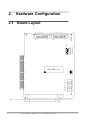
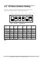
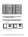
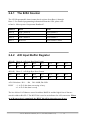
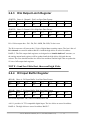
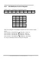
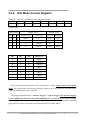
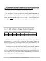
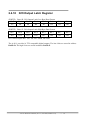
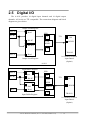
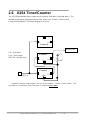
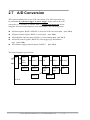
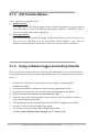
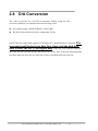
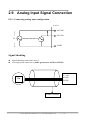
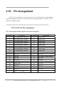
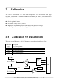
A-8111
Hardware User’s Manual
Warranty
All products manufactured by ICP DAS are warranted against defective materials for a
period of one year from the date of delivery to the original purchaser.
Warning
ICP DAS assume no liability for damage consequent to the use of this product. ICP
DAS reserves the right to change this manual at any time without notice. The information
furnished by ICP DAS is believed to be accurate and reliable. However, ICP DAS assumes
no responsibility for its use, or for any infringements of patents or other rights of third
parties resulting from its use.
Copyright
Copyright 1997 by ICP DAS. All rights are reserved.
Trademark
The names used for identification only may be registered trademarks of their respective
companies.
License
The user can use, modify and backup this software
on a single machine.
The user may not reproduce, transfer or distribute this software, or any copy, in whole or in
part.
A-8111 Hardware Manual (Ver.1.2, Jul/2006, IPH-017-12)
----
1
Table of Contents
1.
Introduction___________________________________________________________ 4
1.1
General
1.2
Features _______________________________________________________________ 4
Description ____________________________________________________ 4
1.3
Specifications ___________________________________________________________ 5
1.3.1
Power Consumption :________________________________________________________ 5
1.3.2
Analog Inputs______________________________________________________________ 5
1.3.3
A/D Converter _____________________________________________________________ 5
1.3.4
DA Converter______________________________________________________________ 6
1.3.5
Digital I/O ________________________________________________________________ 6
1.3.6
Interrupt Channel ___________________________________________________________ 6
1.3.7
Programmable Timer/Counter _________________________________________________ 7
2.
1.4
Applications ____________________________________________________________ 7
1.5
Product Check List ______________________________________________________ 7
Hardware Configuration ________________________________________________ 8
2.1
Board Layout___________________________________________________________ 8
2.2
I/O Base Address Setting _________________________________________________ 9
2.3
Jumper Setting ________________________________________________________ 10
2.3.1
JP1 : D/A Internal Reference Voltage Selection __________________________________ 10
2.4
I/O Register Address____________________________________________________ 11
2.4.1
8254 Counter _____________________________________________________________ 12
2.4.2
2.4.3
2.4.4
2.4.5
2.4.6
2.4.7
2.4.8
2.4.9
2.4.10
A/D Input Buffer Register ___________________________________________________ 12
D/A Output Latch Register __________________________________________________ 13
D/I Input Buffer Register ____________________________________________________ 13
Clear Interrupt Request _____________________________________________________ 14
A/D Gain Control Register __________________________________________________ 14
A/D Multiplex Control Register_______________________________________________ 15
A/D Mode Control Register__________________________________________________ 16
A/D Software Trigger Control Register_________________________________________ 17
D/O Output Latch Register ________________________________________________ 18
2.5
Digital I/O ____________________________________________________________ 19
2.6
8254 Timer/Counter ____________________________________________________ 20
2.7
A/D Conversion ________________________________________________________ 21
2.7.1
A/D conversion flow _______________________________________________________ 22
A-8111 Hardware Manual (Ver.1.2, Jul/2006, IPH-017-12)
----
2
2.7.2
2.7.3
2.7.4
A/D Conversion Trigger Modes ______________________________________________ 22
A/D Transfer Modes _______________________________________________________ 23
Using software trigger and polling transfer ______________________________________ 23
2.8
D/A Conversion ________________________________________________________ 24
2.9
Analog Input Signal Connection __________________________________________ 25
2.10
Pin Assignment ________________________________________________________ 26
Daughter Board ______________________________________________________________ 28
2.10.1
2.10.2
2.10.3
3.
DN-20 for Analog input / output ____________________________________________ 28
DB-16P for Digital input __________________________________________________ 28
DB-16R for Digital output _________________________________________________ 28
Calibration___________________________________________________________ 29
3.1
Calibration VR Description ______________________________________________ 29
3.2
D/A Calibration Steps ___________________________________________________ 30
3.3
A/D Calibration Steps ___________________________________________________ 30
A-8111 Hardware Manual (Ver.1.2, Jul/2006, IPH-017-12)
----
3
1.
Introduction
1.1 General Description
The A-8111 is a high performance, multifunction analog, and digital I/O board for the
PC AT compatible computer. The A-8111 provides programmable gain. (1, 2, 4, 8, 16) The
A-8111 contains a 12-bit ADC with up to 8 single-ended analog inputs. The maximum
sample rate of the A/D converter is about 30K sample/sec. There is a 12-bit DAC with
voltage outputs, 16 channels of TTL-compatible digital input, and 16 channels of
TTL-compatible digital output.
1.2 Features
z
z
z
z
z
z
z
z
The maximum sample rate of the A/D converter is about 30 K sample/sec
Software selective input ranges
PC AT compatible ISA bus
A/D trigger mode: software trigger, pacer trigger
8 single-ended analog input signals
Programmable gain: 1, 2, 4, 8, 16
Input range: ±5V, ±2.5V, ±1.25V, ±0.625V, ±0.3125V
1 channel 12-bit D/A voltage output, 0~5V or 0~10V
16 digital input /16 digital output (TTL compatible)
Interrupt handling
A-8111 Hardware Manual (Ver.1.2, Jul/2006, IPH-017-12)
----
4
1.3 Specifications
1.3.1
Power Consumption
z
z
z
+5V @300mA maximum
+12V @60mA maximum
-12V @30mA maximum
z
Operating temperature: 0°C ~ 50°C
1.3.2
z
z
z
z
z
Channels: 8 single-ended
Input range: (software programmable)
Bipolar: ±5V, ±2.5V, ±1.25V, ±0.625V, ±0.3125V
Input current: 250 nA max (125 nA typical) at 25°C
On chip sample and hold
Over voltage: continuous single channel to 70Vp-p
1.3.3
z
z
z
z
Analog Inputs
A/D Converter
Type: successive approximation, Burr Brown ADS 774
Conversion time: 8 micro sec.
Accuracy: ± 1 bit
Resolution: 12 bits
A-8111 Hardware Manual (Ver.1.2, Jul/2006, IPH-017-12)
----
5
1.3.4
z
z
z
z
z
z
DA Converter
Channels : 1 independent
Type : 12 bit multiplying , Analog device AD-7948
Linearity : ± 1/2 bit
Output range : 0~5V or 0~10V jumper selected , may be used with other AC
or DC reference input Maximum output limit ± 10V
Output drive : ± 5mA
settling time : 0.6 microseconds to 0.01% for full scale step
1.3.5 Digital I/O
z
z
Output port : 16 bits, TTL compatible
Input port : 16 bits, TTL compatible
1.3.6
z
z
Interrupt Channel
Level : 3,4,5,6,7 jumper selectable
Enable : Via control register
A-8111 Hardware Manual (Ver.1.2, Jul/2006, IPH-017-12)
----
6
1.3.7
z
z
z
z
z
Type : 82C54 -8 programmable timer/counter
Counters: The counter1 and counter2 are cascaded as a 32 bits pacer timer.
Pacer output : 0.00047Hz to 0.5MHz
Input ,gate : TTL compatible
Internal Clock : 2M Hz
1.3.8
z
z
z
z
z
z
z
z
Programmable Timer/Counter
Applications
Signal analysis
FFT & frequency analysis
Transient analysis
Production test
Process control
Vibration analysis
Energy management
Industrial and lab. measurement and control
1.4 Product Check List
In addition to this manual, the package includes the following items:
z A-8111 multifunction card
z A-8111 utility diskette
Attention !
If any of these items is missing or damaged, contact the dealer who
provided you with this product. Save the shipping materials and
carton in case you want to ship or store the product in the future.
A-8111 Hardware Manual (Ver.1.2, Jul/2006, IPH-017-12)
----
7
2.
Hardware Configuration
2.1 Board Layout
C N3 D/C O UT
1
19
1
19
C N2 D/C IN
8111
2
20
2
20
BASS ADDRESS
ON
1 2 3 4 5 6
A ( 9 8 7 6 5 4)
SW1
A31
BB A D S-774
P1
JP1
JP2
VR1 VR2 VR3 VR4 VR5
A1
CN1
----
ANA I/0
A-8111 Hardware Manual (Ver.1.2, Jul/2006, IPH-017-12)
8
2.2 I/O Base Address Setting
The A-8111 occupies 16 consecutive locations in I/O address space. The base
address is set by DIP switch SW1. The default address is 0x220.
A9
A8
A7
A6
A5
A4`
1
2
3
4
5
6
ON
SW1 : BASE
BASE
ADDR
ADDRESS
A9
A8
A7
A6
A5
A4
200-20F
OFF
ON
ON
ON
ON
ON
210-21F
OFF
ON
ON
ON
ON
OFF
220-22F(;)
OFF
ON
ON
ON
OFF
ON
230-23F
OFF
ON
ON
ON
OFF
OFF
:
:
:
:
:
:
:
300-30F
OFF
OFF
ON
ON
ON
ON
:
:
:
:
:
:
:
3F0-3FF
OFF
OFF
OFF
OFF
OFF
OFF
(;) : default base address is 0x220
A-8111 Hardware Manual (Ver.1.2, Jul/2006, IPH-017-12)
----
9
The PC I/O port mapping is given below.
ADDRESS
Device
ADDRESS DEVICE
000-1FF
PC reserved
320-32F
XT Hard Disk
200-20F
Game/control
378-37F
Parallel Printer
210-21F
XT Expansion Unit
380-38F
SDLC
238-23F
Bus Mouse/Alt. Bus Mouse 3A0-3AF
SDLC
278-27F
Parallel Printer
3B0-3BF
MDA/Parallel Printer
2B0-2DF
EGA
3C0-3CF
EGA
2E0-2E7
AT GPIB
3D0-3DF
CGA
2E8-2EF
Serial Port
3E8-3EF
Serial Port
2F8-2FF
Serial Port
3F0-3F7
Floppy Disk
300-31F
Prototype Card
3F8-3FF
Serial Port
2.3 Jumper Setting
2.3.1
JP1 : D/A Internal Reference Voltage
Selection
Reference
Voltage
-5V
(Default)
(-10V)
JP1
(-5V)
JP2
Reference
Voltage
-10V
(-10V)
JP1
(-5V)
JP2
Select (-5V) : D/A voltage output = 0 to 5V
Select (-10V) : D/A voltage output = 0 to 10V
A-8111 Hardware Manual (Ver.1.2, Jul/2006, IPH-017-12)
----
10
2.4 I/O Register Address
The A-8111 occupies 16 consecutive PC I/O addresses. The following table
lists the registers and their locations.
Address
Read
Write
Base+0
8254 Counter 0
8254 Counter 0
Base+1
8254 Counter 1
8254 Counter 1
Base+2
8254 Counter 2
8254 Counter 2
Base+3
Reserved
8254 Counter Control
Base+4
A/D Low Byte
D/A Channel 0 Low Byte
Base+5
A/D High Byte
D/A Channel 0 High Byte
Base+6
DI Low Byte
Reserved
Base+7
DI High Byte
Reserved
Base+8
Reserved
A/D Clear Interrupt Request
Base+9
Reserved
A/D Gain Control
Base+A
Reserved
A/D Multiplexer Control
Base+B
Reserved
A/D Mode Control
Base+C
Reserved
A/D Software Trigger Control
Base+D
Reserved
DO Low Byte
Base+E
Reserved
DO High Byte
Base+F
Reserved
Reserved
A-8111 Hardware Manual (Ver.1.2, Jul/2006, IPH-017-12)
----
11
2.4.1
The 8254 Counter
The 8254 Programmable timer/counter has 4 registers from Base+0 through
Base+3. For detailed programming information about the 8254, please refer
to Intel‘s “Microsystem Components Handbook”.
Address
Read
Write
Base+0
8254 Counter 0
8254 Counter 0
Base+1
8254 Counter 1
8254 Counter 1
Base+2
8254 Counter 2
8254 Counter 2
Base+3
Reserved
8254 Counter Control
2.4.2 A/D Input Buffer Register
(READ)
Base+4 : A/D Low Byte Data Format
Bit 7
Bit 6
Bit 5
Bit 4
Bit 3
Bit 2
Bit 1
Bit 0
D7
D6
D5
D4
D3
D2
D1
D0
(READ)
Base+5 : A/D High Byte Data Format
Bit 7
Bit 6
Bit 5
Bit 4
Bit 3
Bit 2
Bit 1
Bit 0
0
0
0
BUSY
D11
D10
D9
D8
A/D 12 bits data : D11…..D0, D11=MSB, D0=LSB
BUSY =1 : A/D 12 bits data converting is busy.
=0 : A/D 12 bits data is ready
The low 8 bits of A/D data are stored in address BASE+4 and the high 4 bits of data are
stored in address BASE+5. The BUSY bit is used as an indicator for A/D conversion. When
an A/D conversion is completed, the BUSY bit will be cleared to zero (Low).
A-8111 Hardware Manual (Ver.1.2, Jul/2006, IPH-017-12)
----
12
2.4.3 D/A Output Latch Register
(WRITE)
Base+4 : Channel 1 D/A Low Byte Data Format
Bit 7
Bit 6
Bit 5
Bit 4
Bit 3
Bit 2
Bit 1
Bit 0
D7
D6
D5
D4
D3
D2
D1
D0
(WRITE)
Base+5 :Channel 1 D/A High Byte Data Format
Bit 7
Bit 6
Bit 5
Bit 4
Bit 3
Bit 2
Bit 1
Bit 0
X
X
X
X
D11
D10
D9
D8
D/A 12 bits output data : D11..D0, D11=MSB, D0=LSB, X=don‘t care
The D/A converter will convert the 12 bits of digital data to analog output. The low 8 bits of
D/A channel are stored in address BASE+4 with the high 4 bits are stored in address
BASE+5. The D/A output latch registers are designed as a “double buffered” structure, so
the analog output latch registers will be updated until the high 4 bits of digital data are
written. The users should send the low 8 bits first and then send the high 4 bits to update the
12 bits of AD output latch registers
NOTE : Send low 8 bits first, then send high 4 bits.
2.4.4 D/I Input Buffer Register
(READ)
Base+6 : D/I Input Buffer Low Byte Data Format
Bit 7
Bit 6
Bit 5
Bit 4
Bit 3
Bit 2
Bit 1
Bit 0
D7
D6
D5
D4
D3
D2
D1
D0
(READ)
Base+7 : D/I Input Buffer High Byte Data Format
Bit 7
Bit 6
Bit 5
Bit 4
Bit 3
Bit 2
Bit 1
Bit 0
D15
D14
D13
D12
D11
D10
D9
D8
D/I 16 bits input data : D15..D0, D15=MSB, D0=LSB
A-8111 provides 16 TTL compatible digital input. The low 8 bits are stored in address
BASE+6. The high 8 bits are stored in address BASE+7.
A-8111 Hardware Manual (Ver.1.2, Jul/2006, IPH-017-12)
----
13
2.4.5
Clear Interrupt Request
(WRITE)
Base+8 : Clear Interrupt Request Format
Bit 7
Bit 6
Bit 5
Bit 4
Bit 3
Bit 2
Bit 1
Bit 0
X
X
X
X
X
X
X
X
X=don‘t care, XXXXXXXX=any 8 bits data is validate
If A-8111 is working in the interrupt transfer mode, an on-board hardware status bit will be
set after each A/D conversion. This bit must be cleared by the software before next
hardware interrupt. Writing any value to address BASE+8 will clear this hardware bit and
the hardware will generate another interrupt when next the A/D conversion is completed.
2.4.6 A/D Gain Control Register
(WRITE)
Base+9 : A/D Gain Control Register Format
Y
Bit 6
Bit 5
Bit 4
Bit 3
Bit 2
Bit 1
Bit 0
X
X
X
X
X
GAIN2
GAIN1
GAIN0
The only difference between the A-8111 and the A-8111 is the GAIN control function. The
A-8111 provides a gain factor of 1/2/4/8/16. The gain controls register control the gain of
the A/D input signal. Bipolar/Unipolar will affect the gain factor.
NOTE : If the gain control code is changed, the hardware needs to have extra gain
settling time. The gain settling time is different for different gain control code. The
software driver does not monitor the gain settling time, so the user needs to delay the
gain settling time if the gain changed.
A-8111 GAIN CONTROL CODE TABLE
GAIN
Input Range
GAIN2 GAIN1
GAIN0
Settling Time
1
+/- 5V
0
0
0
2.1 us
2
+/- 2.5V
0
0
1
2.5 us
4
+/- 1.25V
0
1
0
2.7 us
8
+/- 0.625V
0
1
1
3.6 us
16
+/- 0.3125V
1
0
0
4.1 us
A-8111 Hardware Manual (Ver.1.2, Jul/2006, IPH-017-12)
----
14
2.4.7 A/D Multiplex Control Register
(WRITE)
Base+A : A/D Multilexer Control Register Format
Bit 7
Bit 6
Bit 5
Bit 4
Bit 3
Bit 2
Bit 1
Bit 0
X
X
X
X
X
D2
D1
D0
A/D input channel selection data =3 bits : D2..D0, D2=MSB, D0=LSB, X=don‘t care
Channel Bit_2
Bit_1
Bit_0
0
0
0
0
1
0
0
1
2
0
1
0
3
0
1
1
4
1
0
0
5
1
0
1
6
1
1
0
7
1
1
1
NOTE: The settling time of the multiplexer depends on the source resistance of input
sources.
Source resistance =About 0.1K ohm Î Settling time = About 3 us.
Source resistance =About 1K ohm Î Settling time = About 5 us.
Source resistance =About 10K ohm Î Settling time = About 10 us.
Source resistance =About 100K ohm Î Settling time = About 100 us.
Sec 2.4.6 gives information about how to delay the settling time.
A-8111 Hardware Manual (Ver.1.2, Jul/2006, IPH-017-12)
----
15
2.4.8 A/D Mode Control Register
(WRITE)
Base+B : A/D Mode Control Register Format
Bit 7
Bit 6
Bit 5
Bit 4
Bit 3
Bit 2
Bit 1
Bit 0
X
SI2
SI1
SI0
X
D2
D1
D0
X=don‘t care
Mode Select
D2 D1 D0
Trigger Type
Transfer Type
Software Trig
Pacer Trig
Software Interrupt
0
0
0
Select
X
Select
X
0
0
1
Select
X
Select
X
0
1
0
X
Select
X
X
1
1
0
X
Select
Select
Select
X=disable
SI2
SI1
SI0
IRQ Level
0
0
0
IRQ2
0
0
1
Not used
0
1
0
IRQ2
0
1
1
IRQ3
1
0
0
IRQ4
1
0
1
IRQ5
1
1
0
IRQ6
1
1
1
IRQ7
The A/D conversion operation can be divided into 2 stages, trigger stage and transfer
stage. The trigger stage will generate a trigger signal to the A/D converter and the transfer
stage will transfer the results to the CPU.
The trigger method may be a software trigger or a pacer trigger. The software trigger
is very simple but can not control the sampling rate very precisely. In software trigger
mode, the program issues a software trigger command (sec. 2.4.9) any time needed. Then the
program will poll the A/D status bit until the BUSY bit is 0 (sec. 2.4.2).
A-8111 Hardware Manual (Ver.1.2, Jul/2006, IPH-017-12)
----
16
The pacer trigger can control the sampling rate very precisely. So the converted
data can be used to reconstruct the waveform of the analog input signal. In pacer trigger
mode, the pacer timer will periodically generate trigger signals to the A/D converter. This
converted data can be transfer to the CPU by polling or interrupt transfer method.
The software driver provides two date transfer methods: polling or interrupt. The
polling subroutine, A-8111_AD_PollingVar() or A-8111_AD_PollingArray(), sets the A/D
mode control register to 0x10. This control word means software trigger and polling
transfer. The interrupt subroutine, A-8111_AD_INT_START(…), sets the A/D mode control
mode register to 0x06. This control word means pacer trigger and interrupt transfer.
2.4.9 A/D Software Trigger Control Register
(WRITE)
Base+C : A/D Software Trigger Control Register Format
Bit 7
Bit 6
Bit 5
Bit 4
Bit 3
Bit 2
Bit 1
Bit 0
X
X
X
X
X
X
X
X
X=don‘t care, XXXXXXXX=any 8 bits data is validate
The A/D converter can be triggered by software trigger or pacer trigger. Detailed
information is given in sec.2.4.8 and 2.7. Writing any value to address BASE+C will
generate a trigger pulse to the A/D converter and initiate an A/D conversion operation. The
address BASE+5 offers a BUSY bit to indicate that an A/D conversion is complete.
The software driver uses this control word to detect the A-8111 hardware board. The
software initiates a software trigger and checks the BUSY bit. If the BUSY bit cannot
clear to zero in a fixed time, the software driver will return an error message. If there is an
error in the I/O BASE address checking procedure, the driver will determent that there is no
A-8111 existing with the I//O Base address. A-8111_CheckAddress() is used to detect the
A-8111 with the specified I/O BASE is existing or not.
A-8111 Hardware Manual (Ver.1.2, Jul/2006, IPH-017-12)
----
17
2.4.10 D/O Output Latch Register
(WRITE)
Base+D : D/O Output Latch Low Byte Data Format
Bit 7
Bit 6
Bit 5
Bit 4
Bit 3
Bit 2
Bit 1
Bit 0
D7
D6
D5
D4
D3
D2
D1
D0
(WRITE)
Base+E : D/O Output Latch High Byte Data Format
Bit 7
Bit 6
Bit 5
Bit 4
Bit 3
Bit 2
Bit 1
Bit 0
D15
D14
D13
D12
D11
D10
D9
D8
D/O 16 bits output data : D15..D0, D15=MSB, D0=LSB
The A-8111 provides 16 TTL compatible digital outputs. The low 8 bits are stored in address
BASE+D. The high 8 bits are stored in address BASE+E
A-8111 Hardware Manual (Ver.1.2, Jul/2006, IPH-017-12)
----
18
2.5 Digital I/O
The A-8111 provides 16 digital input channels and 16 digital output
channels. All levels are TTL compatible. The connections diagram and block
diagram are given below:
Output Latch Register
Base+D
Read
D0..D7
CN3
1..8
D0..D7
TTL
DO
DGND
17..18
DGND
D8..D15
9..16
TB-9185
Base+E
Read
16-Channel Isolation
Input Board
(Option)
Output Latch Register
A-8111
Input Buffer Register
CN2
Base+6
Read
D0..D7
A-8111
D0..D7
1..8
TTL
DI
17..18
DGND
DGND
D8..D15
Base+7
Strobe 20
Read
9..16
TB-9182
Input Buffer Register
16-Channel Isolation
Input Board
(Option)
A-8111 Hardware Manual (Ver.1.2, Jul/2006, IPH-017-12)
----
19
2.6 8254 Timer/Counter
The 8254 Programmable timer/counter has 4 resgisters from Base+0 through Base+3. For
detailed programming information about 8254, please refer to Intel‘s “Microsystem
Components Handbook”.The block diagram is as below.
Gate
Cin
Cout
Counter 0
PACER CLK
Cin : clock input
Cout : clock output
INTCLK : internal clock
VCC
Counter 1
Cin
Gate
Cout
10K
Counter 2
2M
INTCLK
Cin
Gate
Cout
Counter0, counter1 and counter2 are all 16 bit counters. Counter 1 and counter 2 are
cascaded as a 32 bit timer. The 32bit timer is used as a pacer timer.
A-8111 Hardware Manual (Ver.1.2, Jul/2006, IPH-017-12)
----
20
2.7 A/D Conversion
This section explains how to use A/D conversions. The A/D conversion can
be performed by software trigger or pacer trigger. At the end of the A/D
conversion, it is possible to transfer data by polling and interrupt before
using the A/D conversion function; users should notice the following issues:
z
z
z
z
z
A/D data register, BASE+4/BASE+5, stores the A/D conversion data (sec. 2.4.2)
A/D gain control register, BASE+9, select gain (sec. 2.4.6)
A/D multiplex control register, BASE+A, select analog input (sec. 2.4.7)
A/D mode control register, BASE+B, select trigger type and transfer
type (sec. 2.4.8)
A/D software trigger control register, BASE+C (sec. 2.4.9)
The block diagram is given below:
CN1
7 to 0
Multiplexer
Gain
control
12 bits
A/D
Buffer
Memory
Base+A
Base+9
Trigger
Logic
Transfer
Logic
CPU
Base+C
Base+B
A-8111
A-8111 Hardware Manual (Ver.1.2, Jul/2006, IPH-017-12)
----
21
2.7.1 A/D conversion flow
Then the user must decide which A/D conversion mode will be used. The software driver
supports two different modes. The user can control the A/D conversion by polling mode very
easily (sec. 2.4.9). It is recommended to use the software driver if using pacer mode.
The analog input signals come from CN1.
The multiplexer can accept 8 single-ended lines into the gain control module. The gain
control module also needs settling time if the gain control code changed. Because the DOS
software doesn’t monitor the settling time, the user should reserve enough settling time
if switching from one channel to the next (sec. 2.4.6).
The output of the gain control module feeds into the A/D converter. The A/D converter
needs a trigger signal to start an A/D conversion cycle. The A-8111 supports software
trigger or pacer trigger mode.
2.7.2 A/D Conversion Trigger Modes
A-8111 supports two trigger modes.
1 : Software Trigger :
Writes any value to the A/D software trigger control register, BASE+C, will initiate an
A/D conversion cycle. This mode is very simple but very difficult to control the
sampling rate.
2 : Pacer Trigger Mode :
The block diagram of the pacer timer is shown in section 2.6. The pacer timer can give
very precise sampling rates.
A-8111 Hardware Manual (Ver.1.2, Jul/2006, IPH-017-12)
----
22
2.7.3
A/D Transfer Modes
A-8111 supports two transfer modes.
1 : polling transfer :
This mode can be used with all trigger modes. Detailed information is given in section
2.4.8. The software scans A/D high byte data register, BASE+5, until BUSY_BIT=0.
The low byte data is also ready in BASE+4.
2 : interrupt transfer :
This mode can be used with pacer trigger. Detailed information is given in section 2.4.8.
The user can set the IRQ level by “A/D Mode Control Register”. (Sec. 2.4.8) A
hardware interrupt signal is sent to the PC when an A/D conversion is completed.
2.7.4 Using software trigger and polling transfer
If the user needs to directly control the A/D converter without the A-8111 software driver, it
is recommended to use software trigger and polling transfer. The program steps are listed as
below:
1.
2.
3.
4.
5.
6.
7.
8.
Send 0x10 to A/D mode control register (software trigger + polling transfer)
(refer to sec. 2.4.8).
Send channel number to multiplexer control register (refer to sec. 2.4.7).
Send the gain control code value to gain control register (refer to sec. 2.4.6).
Delay the settling time (refer to sec. 2.4.6 and sec. 2.4.6).
Send any value to the software trigger control register in order to generate a software
rigger signal (refer to sec. 2.4.9).
Scan the BUSY bit of the A/D high byte data until BUSY=0 (refer to sec. 2.4.2).
Read the 12 bits of A/D data (refer to sec. 2.4.2).
Convert these 12 bits of binary data to floating point value
(refer to A-8111 DOS Software Manual, sec. 4.7 and sec. 4.8)
A-8111 Hardware Manual (Ver.1.2, Jul/2006, IPH-017-12)
----
23
2.8 D/A Conversion
The A-8111 provides one 12 bit D/A converters. Before using the D/A
conversion function, user should notice the following issues:
z
z
D/A output register, BASE+4/BASE+5 (sec. 2.4.3).
JP1/JP2 selects internal reference voltage (sec. 2.3.1).
NOTE: The DA output latch registers are designed as a “double buffered” structure. The
user must send the low byte data first, then send the high byte
data to store the DA 12 bit digital data. If the user only sends the high byte
data, then the low byte data will be still the previous value. Also, if the user sends high byte
first then sends low byte, the low byte data of DA is still held in the previous one.
A-8111 Hardware Manual (Ver.1.2, Jul/2006, IPH-017-12)
----
24
2.9 Analog Input Signal Connection
FG1 : Connecting analog input configuration
A-8111
A/D CH0
A/D CHn
Es
AGND
Signal Shielding
z
z
Signal shielding connections in Fig1
Use single-point connection to frame ground (not AGND or DGND)
A- 8111
AGND
DGND
Vin
Frame Ground
A-8111 Hardware Manual (Ver.1.2, Jul/2006, IPH-017-12)
----
25
2.10 Pin Assignment
The A-8111 provides three connectors. Connect 1, CN1 functions for analog input &
analog output input. Connector 2, CN2, functions as 16 digital outputs. Connector 3, CN3,
function as a digital output.
CN1/CN2/CN3 Pin Assignment
CN1: Analog input/Analog output/Connect Pin Assignment.
Pin Number
Description
Pin Number
Description
1
A/D Analog Input Channel 0
20
Analog GND
2
A/D Analog Input Channel 1
21
Analog GND
3
A/D Analog Input Channel 2
22
Analog GND
4
A/D Analog Input Channel 3
23
Analog GND
5
A/D Analog Input Channel 4
24
Analog GND
6
A/D Analog Input Channel 5
25
Analog GND
7
A/D Analog Input Channel 6
26
Analog GND
8
A/D Analog Input Channel 7
27
Analog GND
9
Not Used
28
Not Used
10
Not Used
29
Not Used
11
Not Used
30
D/A Analog Voltage output
12
Not Used
31
Not Used
13
Not Used
32
Not Used
14
Analog GND
33
Not Used
15
Analog GND
34
Not Used
16
Not Used
35
Not Used
17
Not Used
36
Not Used
18
Not Used
37
Not Used
19
PCB’s
+ 5V output
A-8111 Hardware Manual (Ver.1.2, Jul/2006, IPH-017-12)
----
26
CN2: Analog input/Analog output/Connect Pin Assignment.
Pin Number
Description
Pin Number
Description
1
Digital Input 0/TTL
2
Digital Input 1/TTL
3
Digital Input 2/TTL
4
Digital Input 3/TTL
5
Digital Input 4/TTL
6
Digital Input 5/TTL
7
Digital Input 6/TTL
8
Digital Input 7/TTL
9
Digital Input 8/TTL
10
Digital Input 9/TTL
11
Digital Input 10/TTL
12
Digital Input 11/TTL
13
Digital Input 12/TTL
14
Digital Input 13/TTL
15
Digital Input 14/TTL
16
Digital Input 15/TTL
17
PCB’s GND output
18
PCB’s GND output
19
PCB’s
20
STROBE
+ 5V output
CN3: Analog input/Analog output/Connect Pin Assignment.
Pin Number
Description
Pin Number
Description
1
Digital output 0/TTL
2
Digital output 1/TTL
3
Digital output 2/TTL
4
Digital output 3/TTL
5
Digital output 4/TTL
6
Digital output 5/TTL
7
Digital output 6/TTL
8
Digital output 7/TTL
9
Digital output 8/TTL
10
Digital output 9/TTL
11
Digital output 10/TTL
12
Digital output 11/TTL
13
Digital output 12/TTL
14
Digital output 13/TTL
15
Digital output 14/TTL
16
Digital output 15/TTL
17
PCB’s GND output
18
PCB’s GND output
19
PCB’s
20
PCB’s
+ 5V output
A-8111 Hardware Manual (Ver.1.2, Jul/2006, IPH-017-12)
+12V output
----
27
2.11Daughter Board
The A-8111 can be connected with many different daughter boards. The function of these
daughter boards is described as follows.
2.11.1
CA-4002
The CA-4002 is a 37pin D-Sub male connector. It can directly connect to a 37 pin D-sub
connector.
2.11.2
DB-16P
The DB-16P is a 16 channel isolated digital input board. The A-8111 provides a 16
channel, non-isolated, TTL-compatible digital inputs from CN2. If connecting to the DB-16P,
the A-8111 can provide 16 channels of isolated digital input signals. Isolation can protect the
PC if an abnormal input signal is occurs.
2.11.3
DB-16R
The DB-16R provides a 16-channel SPDT relay output. The A-8111 provides a 16
channel, TTL-compatible digital output from CN3. If connecting to the DB-16R, the A-8111
can provide a 16-channel relay output to control power devices.
2.11.4
DB-37
The DB-37 is a general-purpose screw terminal board. It provides a 37-pin connector.
This board directly connects to a 37-pin D-sub connector. It is suitable for easy signal
connection and measurement.
A-8111 Hardware Manual (Ver.1.2, Jul/2006, IPH-017-12)
----
28
3.
Calibration
The A-8111 is calibrated to its best state of operation. For environments with large
vibration, recalibration is recommended. Before calibrating the A-8111, users should have
the following items:
z
z
z
One 6-digit multi-meter.
One stable voltage source (4.9988V)
Diagnostic program: this program is included in the delivered package
and will guide the user to in proceeding with the calibration.
3.1 Calibration VR Description
There are seven VRs on the A-8111. Calibration is needed to adjust all seven VRs.
VR Num. Description
VR1
D/A Gain adjustment
VR2
D/A Offset adjustment
VR3
A/D Offset adjustment
VR4
A/D's Gain adjustment
VR5
A/D‘s PGA(Programmable Gain Amplifier) Offset Adjustment
VR4
8 ch.
Mux
PGA
A/D Converter
CN1
VR3
VR5
VR2
VR1
D/A Converter
O.P.
A-8111 Hardware Manual (Ver.1.2, Jul/2006, IPH-017-12)
----
29
3.2 D/A Calibration Steps
1.
2.
3.
4.
5.
Run A8111CAL.EXE
Connect D/A channel0,, pin 30 of CN1 to DVM
Adjust VR1 until DVM=5.0000V
Press “Enter" key
Adjust VR2 until DVM=0.0000V
3.3 A/D Calibration Steps
1. Press “Enter" key
2. Connot A/D Channel 0 to analog ground, CN1-Pin1 to CN1-Pin20.
3. Input stable DC 4.9988V to A/d channel 1, pin2 of CN1.
4. Connect DVM to TP1(-) & (+).
5. Adjust VR5 until DVM=0.0000V.
6. Press <Enter> Key.
7. Adjust VR4 until A/D data shows 4094 or 4095.
8. Press <Enter> Key
9. Adjust VR3 until A/D data shows 2047 or 2048.
10. Repeat step_3 to step_11 until:
A/D channel 0 input 4.9988VÎA/D reading 4094 or 4095.
A/D channel 0 input 0 V
ÎA/D reading 2047 or 2048.
11. Press <Enter> Key.
3.4
DI/O Testing
12. Use 20-pin flat cable (CA-2010, CA-2020 Option) to link CN2 to CN3.
13. Press <Enter> Key.
A-8111 Hardware Manual (Ver.1.2, Jul/2006, IPH-017-12)
----
30