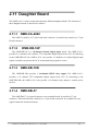
1
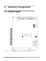
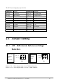
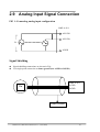
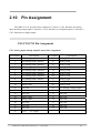
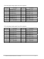
User’s Guide
Shop online at
www.omega.com
e-mail: [email protected]
OME-A8111 ISA-BUS
Multi-Functional Board
Hardware Manual
OMEGAnet ® Online Service
www.omega.com
Internet e-mail
[email protected]
Servicing North America:
USA:
ISO 9001 Certified
Canada:
One Omega Drive, P.O. Box 4047
Stamford CT 06907-0047
TEL: (203) 359-1660
e-mail: [email protected]
976 Bergar
Laval (Quebec) H7L 5A1, Canada
TEL: (514) 856-6928
e-mail: [email protected]
FAX: (203) 359-7700
FAX: (514) 856-6886
For immediate technical or application assistance:
USA and Canada: Sales Service: 1-800-826-6342 / 1-800-TC-OMEGA®
Customer Service: 1-800-622-2378 / 1-800-622-BEST®
Engineering Service: 1-800-872-9436 / 1-800-USA-WHEN®
TELEX: 996404 EASYLINK: 62968934 CABLE: OMEGA
Mexico:
En Español: (001) 203-359-7803
FAX: (001) 203-359-7807
e-mail: [email protected]
[email protected]
Servicing Europe:
Benelux:
Postbus 8034, 1180 LA Amstelveen, The Netherlands
TEL: +31 (0)20 3472121
FAX: +31 (0)20 6434643
Toll Free in Benelux: 0800 0993344
e-mail: [email protected]
Czech Republic:
Frystatska 184, 733 01 Karviná, Czech Republic
TEL: +420 (0)59 6311899
FAX: +420 (0)59 6311114
Toll Free: 0800-1-66342
e-mail: [email protected]
France:
11, rue Jacques Cartier, 78280 Guyancourt, France
TEL: +33 (0)1 61 37 29 00
FAX: +33 (0)1 30 57 54 27
Toll Free in France: 0800 466 342
e-mail: [email protected]
Germany/Austria: Daimlerstrasse 26, D-75392 Deckenpfronn, Germany
TEL: +49 (0)7056 9398-0
Toll Free in Germany: 0800 639 7678
e-mail: [email protected]
United Kingdom:
ISO 9002 Certified
FAX: +49 (0)7056 9398-29
One Omega Drive, River Bend Technology Centre
Northbank, Irlam, Manchester
M44 5BD United Kingdom
TEL: +44 (0)161 777 6611
FAX: +44 (0)161 777 6622
Toll Free in United Kingdom: 0800-488-488
e-mail: [email protected]
It is the policy of OMEGA to comply with all worldwide safety and EMC/EMI regulations that
apply. OMEGA is constantly pursuing certification of its products to the European New Approach
Directives. OMEGA will add the CE mark to every appropriate device upon certification.
The information contained in this document is believed to be correct, but OMEGA Engineering, Inc. accepts
no liability for any errors it contains, and reserves the right to alter specifications without notice.
WARNING: These products are not designed for use in, and should not be used for, patient-connected applications.
OME-A-8111
Hardware User’s Manual
OME-A-8111 Hardware Manual (ver.1.1, Jul/2003)
1
Table of Contents
1.
Introduction_________________________________________________________ 4
1.1
General Description ___________________________________________________ 4
1.2
Features _____________________________________________________________ 4
1.3
Specifications _________________________________________________________ 5
1.3.1
Power Consumption _________________________________________________________ 5
1.3.2
Analog Inputs ______________________________________________________________ 5
1.3.3
A/D Converter _____________________________________________________________ 5
1.3.4
DA Converter ______________________________________________________________ 6
1.3.5
Digital I/O_________________________________________________________________ 6
1.3.6
Interrupt Channel ___________________________________________________________ 6
1.3.7
Programmable Timer/Counter _________________________________________________ 7
1.3.8
Applications _______________________________________________________________ 7
1.4
2.
Product Check List ____________________________________________________ 7
Hardware Configuration ______________________________________________ 8
2.1
Board Layout_________________________________________________________ 8
2.2
I/O Base Address Setting _______________________________________________ 9
2.3
Jumper Setting ______________________________________________________ 10
2.3.1
2.4
JP1 : D/A Internal Reference Voltage Selection_____________________________________ 10
I/O Register Address__________________________________________________ 11
2.4.1
The 8254 Counter __________________________________________________________ 12
2.4.2
A/D Input Buffer Register ___________________________________________________ 12
2.4.3
D/A Output Latch Register ___________________________________________________ 13
2.4.4
D/I Input Buffer Register ____________________________________________________ 13
2.4.5
Clear Interrupt Request______________________________________________________ 14
2.4.6
A/D Gain Control Register ___________________________________________________ 14
2.4.7
A/D Multiplex Control Register _______________________________________________ 15
2.4.8
A/D Mode Control Register __________________________________________________ 16
2.4.9
A/D Software Trigger Control Register _________________________________________ 17
2.4.10
D/O Output Latch Register __________________________________________________ 18
2.5
Digital I/O __________________________________________________________ 19
2.6
8254 Timer/Counter __________________________________________________ 20
2.7
A/D Conversion ______________________________________________________ 21
2.7.1
A/D conversion flow__________________________________________________________ 22
OME-A-8111 Hardware Manual (ver.1.1, Jul/2003)
2
3.
2.7.2
A/D Conversion Trigger Modes _______________________________________________ 22
2.7.3
A/D Transfer Modes ________________________________________________________ 23
2.7.4
Using software trigger and polling transfer ______________________________________ 23
2.8
D/A Conversion ______________________________________________________ 24
2.9
Analog Input Signal Connection ________________________________________ 25
2.10
Pin Assignment ________________________________________________________ 26
2.11
Daughter Board________________________________________________________ 28
2.11.1
OME-CA-4002 _________________________________________________________ 28
2.11.2
OME-DB-16P __________________________________________________________ 28
2.11.3
OME-DB-16R __________________________________________________________ 28
2.11.4
OME-DB-37 ___________________________________________________________ 28
Calibration___________________________________________________________ 29
3.1
Calibration VR Description ______________________________________________ 29
3.2
D/A Calibration Steps ___________________________________________________ 30
3.3
A/D Calibration Steps ___________________________________________________ 30
3.4
DI/O Testing __________________________________________________________ 30
OME-A-8111 Hardware Manual (ver.1.1, Jul/2003)
3
1.
Introduction
1.1 General Description
The OME-A-8111 is a high performance, multifunction (analog and digital I/O) board
for the PC AT compatible computer with the ISA bus. The OME-A-8111 provides
programmable gain (1, 2, 4, 8 and 16). The OME-A-8111 contains a 12-bit ADC with up to 8
single-ended analog inputs. The maximum sample rate of the A/D converter is about 30K
sample/sec. There is a 12-bit DAC with voltage outputs, 16 channels of TTL-compatible
digital input, and 16 channels of TTL-compatible digital output.
1.2 Features
z
z
z
z
z
z
z
z
The maximum sample rate of the A/D converter is about 30 K sample/sec
Software selective input ranges
PC AT compatible ISA bus
A/D trigger mode: software trigger, pacer trigger
8 single-ended analog input channels:
Programmable gain: 1, 2, 4, 8, 16
Input range: ±5 V, ±2.5 V, ±1.25 V, ±0.625 V, ±0.3125 V
1 output channel: 12-bit D/A voltage output, 0~5 V or 0~10 V
16 digital inputs /16 digital outputs (TTL compatible)
Interrupt handling
OME-A-8111 Hardware Manual (ver.1.1, Jul/2003)
4
1.3 Specifications
1.3.1
Power Consumption
z
z
z
+5V @ 300 mA maximum
+12V @ 60 mA maximum
-12V @ 30 mA maximum
z
Operating temperature: 0°C ~ 50°C
1.3.2
z
z
z
z
z
Channels: 8 single-ended
Input range: (software programmable)
Bipolar: ±5 V, ±2.5 V, ±1.25 V, ±0.625 V, ±0.3125 V
Input current: 250 nA max (125 nA typical) at 25°C
On-chip sample and hold
Over voltage: continuous single channel to 70Vp-p
1.3.3
z
z
z
z
Analog Inputs
A/D Converter
Type: successive approximation, Burr Brown ADS 774
Conversion time: 8 µ sec.
Accuracy: ± 1 bit
Resolution: 12-bit
OME-A-8111 Hardware Manual (ver.1.1, Jul/2003)
5
1.3.4
z
z
z
z
z
z
DA Converter
Channels : 1 independent
Type : 12-bit multiplying , Analog device AD-7948
Linearity : ± 1/2 bit
Output Range : 0~5 V or 0~10 V jumper selected , may be used with other AC
or DC reference input. Maximum output limit ± 10V
Output Drive : ± 5 mA
Settling Time : 0.6 microseconds to 0.01% for full scale step
1.3.5 Digital I/O
z
z
Output port
Input port
1.3.6
z
z
: 16 bits, TTL compatible
: 16 bits, TTL compatible
Interrupt Channel
Level : 3,4,5,6,7 jumper selectable
Enable : Via control register
OME-A-8111 Hardware Manual (ver.1.1, Jul/2003)
6
1.3.7
z
z
z
z
z
Type : 82C54 -8 programmable timer/counter
Counters: The counter1 and counter2 are cascaded as a 32-bit pacer timer.
Pacer output : 0.00047 Hz to 0.5 MHz
Input Gate : TTL compatible
Internal Clock : 2 MHz
1.3.8
z
z
z
z
z
z
z
z
Programmable Timer/Counter
Applications
Signal analysis
FFT & frequency analysis
Transient analysis
Production test
Process control
Vibration analysis
Energy management
Industrial and laboratory measurement and control
1.4 Product Check List
In addition to this manual, the package includes the following items:
z OME-A-8111 multifunction card
z OME-A-8111 utility diskette/CD ROM
OME-A-8111 Hardware Manual (ver.1.1, Jul/2003)
7
2.
Hardware Configuration
2.1 Board Layout
8111
2
20
C N3 D/C O UT
1
19
2
20
1
19
C N2 D/C IN
BASS ADDRESS
ON
1 2 3 4 5 6
A ( 9 8 7 6 5 4)
SW1
A31
BB A D S-774
P1
JP1
JP2
VR1 VR2 VR3 VR4 VR5
A1
CN1
ANA I/0
OME-A-8111 Hardware Manual (ver.1.1, Jul/2003)
8
2.2 I/O Base Address Setting
The OME-A-8111 occupies 16 consecutive locations in I/O address space. The base
address is set by DIP switch SW1. The default address is 0x220 as shown below:
A9
A8
A7
A6
A5
A4
ON
1
2
3
4
5
6
SW1 : BASE ADDRESS
BASE ADDR
A9
A8
A7
A6
A5
A4
200-20F
OFF
ON
ON
ON
ON
ON
210-21F
OFF
ON
ON
ON
ON
OFF
220-22F(;)
OFF
ON
ON
ON
OFF
ON
230-23F
OFF
ON
ON
ON
OFF
OFF
:
:
:
:
:
:
:
300-30F
OFF
OFF
ON
ON
ON
ON
:
:
:
:
:
:
:
3F0-3FF
OFF
OFF
OFF
OFF
OFF
(;): default base address is 0x220
OME-A-8111 Hardware Manual (ver.1.1, Jul/2003)
9
The PC I/O port mapping is given below.
ADDRESS DEVICE
ADDRESS DEVICE
000-1FF
PC reserved
320-32F
XT Hard Disk
200-20F
Game/control
378-37F
Parallel Printer
210-21F
XT Expansion Unit
380-38F
SDLC
238-23F
Bus Mouse/Alt. Bus Mouse 3A0-3AF
SDLC
278-27F
Parallel Printer
3B0-3BF
MDA/Parallel Printer
2B0-2DF
EGA
3C0-3CF
EGA
2E0-2E7
AT GPIB
3D0-3DF
CGA
2E8-2EF
Serial Port
3E8-3EF
Serial Port
2F8-2FF
Serial Port
3F0-3F7
Floppy Disk
300-31F
Prototype Card
3F8-3FF
Serial Port
2.3 Jumper Setting
2.3.1
JP1 : D/A Internal Reference Voltage
Selection
Reference
Voltage
-5 V
(Default)
Reference
Voltage
-10 V
(-10 V)
(-5 V)
JP1
(-10 V)
(-5 V)
JP1
Select (-5 V) : D/A voltage output = 0 to 5 V (both channels)
Select (-10 V) : D/A voltage output = 0 to 10 V (both channels)
OME-A-8111 Hardware Manual (ver.1.1, Jul/2003)
10
2.4 I/O Register Address
The OME-A-8111 occupies 16 consecutive PC I/O addresses. The following
table lists the registers and their locations.
Address
Read
Write
Base+0
8254 Counter 0
8254 Counter 0
Base+1
8254 Counter 1
8254 Counter 1
Base+2
8254 Counter 2
8254 Counter 2
Base+3
Reserved
8254 Counter Control
Base+4
A/D Low Byte
D/A Channel 0 Low Byte
Base+5
A/D High Byte
D/A Channel 0 High Byte
Base+6
DI Low Byte
Reserved
Base+7
DI High Byte
Reserved
Base+8
Reserved
A/D Clear Interrupt Request
Base+9
Reserved
A/D Gain Control
Base+A
Reserved
A/D Multiplexer Control
Base+B
Reserved
A/D Mode Control
Base+C
Reserved
A/D Software Trigger Control
Base+D
Reserved
DO Low Byte
Base+E
Reserved
DO High Byte
Base+F
Reserved
Reserved
OME-A-8111 Hardware Manual (ver.1.1, Jul/2003)
11
2.4.1
The 8254 Counter
The 8254 Programmable timer/counter has 4 registers from Base+0 through
Base+3. For detailed programming information about the 8254, please refer
to Intel‘s “Microsystem Components Handbook”.
Address
Read
Write
Base+0
8254 Counter 0
8254 Counter 0
Base+1
8254 Counter 1
8254 Counter 1
Base+2
8254 Counter 2
8254 Counter 2
Base+3
Reserved
8254 Counter Control
2.4.2
A/D Input Buffer Register
(READ)
Base+4: A/D Low Byte Data Format
Bit 7
Bit 6
Bit 5
Bit 4
Bit 3
Bit 2
Bit 1
Bit 0
D7
D6
D5
D4
D3
D2
D1
D0
(READ)
Base+5: A/D High Byte Data Format
Bit 7
Bit 6
Bit 5
Bit 4
Bit 3
Bit 2
Bit 1
Bit 0
0
0
0
READY D11
D10
D9
D8
A/D 12 bit data: D11…..D0, D11 = MSB, D0 = LSB
READY = 1: A/D 12 bits data not ready
= 0: A/D 12 bits data is ready
The low 8 bits of A/D data are stored in address BASE+4 and the high 4 bits of data are
stored in address BASE+5. The READY bit is used as an indicator for A/D conversion.
When a A/D conversion is completed, the READY bit will be cleared to zero (Low).
OME-A-8111 Hardware Manual (ver.1.1, Jul/2003)
12
2.4.3
D/A Output Latch Register
(WRITE)
Base+4: Channel 1 D/A Low Byte Data Format
Bit 7
Bit 6
Bit 5
Bit 4
Bit 3
Bit 2
Bit 1
Bit 0
D7
D6
D5
D4
D3
D2
D1
D0
(WRITE)
Base+5: Channel 1 D/A High Byte Data Format
Bit 7
Bit 6
Bit 5
Bit 4
Bit 3
Bit 2
Bit 1
Bit 0
X
X
X
X
D11
D10
D9
D8
D/A 12 bit output data: D11…D0, D11 = MSB, D0 = LSB, X = don‘t care
The D/A converter will convert the 12 bits of digital data to analog output. The low 8 bits of
D/A channel are stored in address BASE+4 with the high 4 bits are stored in address
BASE+5. The D/A output latch registers are designed as a “double buffered” structure, so
the analog output latch registers will be updated until the high 4 bits of digital data are
written. The users should send the low 8 bits first and then send the high 4 bits to update the
12 bits of AD output latch registers
NOTE: Send low 8 bits first, then send high 4 bits.
2.4.4
D/I Input Buffer Register
(READ)
Base+6: D/I Input Buffer Low Byte Data Format
Bit 7
Bit 6
Bit 5
Bit 4
Bit 3
Bit 2
Bit 1
Bit 0
D7
D6
D5
D4
D3
D2
D1
D0
(READ)
Base+7: D/I Input Buffer High Byte Data Format
Bit 7
Bit 6
Bit 5
Bit 4
Bit 3
Bit 2
Bit 1
Bit 0
D15
D14
D13
D12
D11
D10
D9
D8
D/I 16 bit input data: D15…D0, D15 = MSB, D0 = LSB
OME-A-8111 provides 16 TTL compatible digital inputs. The low 8 bits are stored in
address BASE+6. The high 8 bits are stored in address BASE+7.
OME-A-8111 Hardware Manual (ver.1.1, Jul/2003)
13
2.4.5
Clear Interrupt Request
(WRITE)
Base+8: Clear Interrupt Request Format
Bit 7
Bit 6
Bit 5
Bit 4
Bit 3
Bit 2
Bit 1
Bit 0
X
X
X
X
X
X
X
X
X = don‘t care, XXXXXXXX = any 8 bit data is valid
If OME-A-8111 is working in the interrupt transfer mode, an on-board hardware status bit
will be set after each A/D conversion. This bit must be cleared by the software before next
hardware interrupt. Writing any value to address BASE+8 will clear this hardware bit and
the hardware will generate another interrupt when next the A/D conversion is completed.
2.4.6
A/D Gain Control Register
(WRITE)
Base+9: A/D Gain Control Register Format
Y
Bit 6
Bit 5
Bit 4
Bit 3
Bit 2
Bit 1
Bit 0
X
X
X
X
X
GAIN2
GAIN1
GAIN0
The OME-A-8111 provides a gain factor of 1/2/4/8/16. The gain controls register control
the gain of the A/D input signal. Bipolar/Unipolar will affect the gain factor.
NOTE : If the gain control code is changed, the hardware needs to have extra gain
settling time. The gain settling time is different for different gain control code. The
software driver does not monitor the gain settling time, so the user needs to delay the
gain settling time if the gain changed.
OME-A-8111 GAIN CONTROL CODE TABLE
GAIN
Input Range
GAIN2 GAIN1
GAIN0
Settling Time
1
+/- 5V
0
0
0
2.1 µs
2
+/- 2.5V
0
0
1
2.5 µs
4
+/- 1.25V
0
1
0
2.7 µs
8
+/- 0.0625V
0
1
1
3.6 µs
16
+/- 0.03125V
1
0
0
4.1 µs
OME-A-8111 Hardware Manual (ver.1.1, Jul/2003)
14
2.4.7
A/D Multiplex Control Register
(WRITE)
Base+A : A/D Multiplexer Control Register Format
Bit 7
Bit 6
Bit 5
Bit 4
Bit 3
Bit 2
Bit 1
Bit 0
X
X
X
X
X
D2
D1
D0
A/D input channel selection data =3 bits: D2...D0, D2=MSB, D0=LSB, X=don‘t care
Channel Bit_2
Bit_1
Bit_0
0
0
0
0
1
0
0
1
2
0
1
0
3
0
1
1
4
1
0
0
5
1
0
1
6
1
1
0
7
1
1
1
NOTE: The settling time of the multiplexer depends on the source resistance of input
sources.
Approx. Source resistance = 0.1 KΩ Î Approx. Settling time = 3 µs.
Approx. Source resistance = 1 KΩ Î Approx. Settling time = 5 µs.
Approx. Source resistance = 10 KΩ Î Approx. Settling time = 10 µs.
Approx. Source resistance = 100 KΩ Î Approx. Settling time = 100 µs.
Sec 2.4.6 gives information about settling time delay.
OME-A-8111 Hardware Manual (ver.1.1, Jul/2003)
15
2.4.8
A/D Mode Control Register
(WRITE)
Base+B : A/D Mode Control Register Format
Bit 7
Bit 6
Bit 5
Bit 4
Bit 3
Bit 2
Bit 1
Bit 0
X
SI2
SI1
SI0
X
D2
D1
D0
X=don‘t care
Mode Select
D2 D1 D0
Trigger Type
Transfer Type
Software Trig
Pacer Trig
Software Interrupt
0
0
0
Select
X
Select
X
0
0
1
Select
X
Select
X
0
1
0
X
Select
X
X
1
1
0
X
Select
Select
Select
X=disable
SI2
SI1
SI0
IRQ Level
0
0
0
IRQ2
0
0
1
Not used
0
1
0
IRQ2
0
1
1
IRQ3
1
0
0
IRQ4
1
0
1
IRQ5
1
1
0
IRQ6
1
1
1
IRQ7
The A/D conversion operation can be divided into 2 stages, trigger stage and transfer
stage. The trigger stage will generate a trigger signal to the A/D converter and the transfer
stage will transfer the results to the CPU.
The trigger method may be an internal trigger or an external trigger. The internal
trigger can be a software trigger or a pacer trigger. The software trigger is very simple
but can not control the sampling rate very precisely. In software trigger mode, the
program issues a software trigger command (sec. 2.4.9) any time needed. Then the program
will poll the A/D status bit until the ready bit is 0 (sec. 2.4.2).
OME-A-8111 Hardware Manual (ver.1.1, Jul/2003)
16
The pacer trigger can control the sampling rate very precisely. So the converted
data can be used to reconstruct the waveform of the analog input signal. In pacer trigger
mode, the pacer timer will periodically generate trigger signals to the A/D converter. This
converted data can be transfer to the CPU by polling or interrupt or DMA transfer method.
The software driver provides three polling or interrupt-transfer methods. The polling
subroutine, A8111_AD_PollingVar() or A822_AD_PollingArray(), sets the A/D mode
control register to 0x01. This control word means software trigger and polling transfer. The
interrupt subroutine, A822_AD_INT_START(…), sets the A/D mode control mode register
to ox06. This control word means pacer trigger and interrupt transfer. The interrupt
subroutine, A822_AD_DMA_START(…), sets the A/D mode control register to 0x06 This
control word means pacer trigger and DMA transfer.
2.4.9
A/D Software Trigger Control Register
(WRITE)
Base+C : A/D Software Trigger Control Register Format
Bit 7
Bit 6
Bit 5
Bit 4
Bit 3
Bit 2
Bit 1
Bit 0
X
X
X
X
X
X
X
X
X=don‘t care, XXXXXXXX=any 8 bits data is validate
The A/D converter can be triggered by software trigger or pacer trigger. Detailed
information is given in sec.2.4.8 and 2.7. Writing any value to address BASE+C will
generate a trigger pulse to the A/D converter and initiate an A/D conversion operation. The
address BASE+5 offers a ready bit to indicate that an A/D conversion is complete.
The software driver uses this control word to detect the OME-A-8111 hardware board.
The software initiates a software trigger and checks the ready bit. If the ready bit cannot
clear to zero in a fixed time, the software driver will return an error message. If there is an
error in the I/O BASE address setting, the ready bit will not be cleared to zero. The software
driver, A8111_CheckAddress(), uses this method to detect the status of the I/O BASE
address setting.
OME-A-8111 Hardware Manual (ver.1.1, Jul/2003)
17
2.4.10
D/O Output Latch Register
(WRITE)
Base+D: D/O Output Latch Low Byte Data Format
Bit 7
Bit 6
Bit 5
Bit 4
Bit 3
Bit 2
Bit 1
Bit 0
D7
D6
D5
D4
D3
D2
D1
D0
(WRITE)
Base+E: D/O Output Latch High Byte Data Format
Bit 7
Bit 6
Bit 5
Bit 4
Bit 3
Bit 2
Bit 1
Bit 0
D15
D14
D13
D12
D11
D10
D9
D8
D/O 16 bits output data: D15...D0, D15=MSB, D0=LSB
The OME-A-8111 provides 16 TTL compatible digital outputs. The low 8 bits are stored in
address BASE+D. The high 8 bits are stored in address BASE+E
OME-A-8111 Hardware Manual (ver.1.1, Jul/2003)
18
2.5 Digital I/O
The OME-A-8111 provides 16 digital input channels and 16 digital output
channels. All levels are TTL compatible. The connections diagram and block
diagram are given below:
Output Latch Register
Base+D
Read
CN3
D0...D7
1...8
D0...D7
TTL
DGND
17...18
DGND
D8...D15
DO
9...16
OME-DB-16R
Base+E
Read
16-Channel Isolated
Input Board
(Option)
Output Latch Register
OME-A-8111
Input Buffer Register
OME-A-8111
Base+6
Read
D0...D7
D0...D7
D8...D15
Base+7
CN2
1...8
TTL
17...18
DGND
Strobe 20
DI
DGND
Read
9...16
Input Buffer Register
OME-DB-16P
16-Channel Isolated
Input Board
(Option)
OME-A-8111 Hardware Manual (ver.1.1, Jul/2003)
19
2.6 8254 Timer/Counter
The 8254 Programmable timer/counter has 4 registers from Base+0 through Base+3. For
detailed programming information about 8254, please refer to Intel‘s “Microsystem
Components Handbook”. The block diagram is as below.
Gate
Cin
Cout
Counter 0
PACER CLK
Cin: clock input
Cout: clock output
INTCLK: internal clock
VCC
Counter 1
Cin
Gate
Cout
10K
Counter 2
2M
INTCLK
Cin
Gate
Cout
Counter0, counter1 and counter2 are all 16 bit counters. Counter 1 and counter 2 cascade
as a 32-bit timer. The 32-bit timer is used as a pacer timer.
OME-A-8111 Hardware Manual (ver.1.1, Jul/2003)
20
2.7 A/D Conversion
This section explains how to perform A/D conversions. The A/D conversion
can be performed by software trigger by pacer trigger. At the end of the
A/D conversion, it is possible to transfer data by polling and interrupt
before using the A/D conversion function; users should notice the following
issues:
z
z
z
z
A/D data register, BASE+4/BASE+5, stores the A/D conversion data (sec. 2.4.2)
A/D gain control register, BASE+9, select gain (sec. 2.4.6)
(sec. 2.4.7)
A/D multiplex control register, BASE+A, select analog input
A/D mode control register, BASE+B, select trigger type and transfer
type (sec. 2.4.8)
z
A/D software trigger control register, BASE+C
(sec. 2.4.9)
The block diagram is given below:
CN1
7 to 0
Multiplexer
Gain
Control
12 bits
A/D
Buffer
Memory
Base+A
Base+9
Trigger
Logic
Transfer
Logic
CPU
Base+C
Base+B
OME-A-8111
OME-A-8111 Hardware Manual (ver.1.1, Jul/2003)
21
2.7.1 A/D conversion flow
Then the user must decide which A/D conversion mode will be used. The software driver
supports three different modes. The user can control the A/D conversion by polling mode
very easily (sec. 2.4.9). It is recommended to use the software driver if using interrupt or
DMA mode.
The analog input signals come from CN1.
The multiplexer can accept 8 single-ended lines into the gain control module. The gain
control module also needs settling time if the gain control code changed. Because the
software doesn’t monitor the settling time, the user should reserve enough settling time
if switching from one channel to the next (sec. 2.4.6).
The output of the gain control module feeds into the A/D converter. The A/D converter
needs a trigger signal to start an A/D conversion cycle. The OME-A-8111 supports
software trigger or pacer trigger mode.
2.7.2
A/D Conversion Trigger Modes
OME-A-8111 supports two trigger modes.
1 : Software Trigger :
Writes any value to the A/D software trigger control register, BASE+A, will initiate an
A/D conversion cycle. This mode is very simple but very difficult to control the
sampling rate.
2 : Pacer Trigger Mode :
The block diagram of the pacer timer is shown in section 2.6. The pacer timer can give
very precise sampling rates.
OME-A-8111 Hardware Manual (ver.1.1, Jul/2003)
22
2.7.3
A/D Transfer Modes
OME-A-8111 supports two transfer modes.
1 : polling transfer :
This mode can be used with all trigger modes. Detailed information is given in section
2.4.8.The software scans A/D high byte data register, BASE+5, until
READY_BIT=0.The low byte data is also ready in BASE+4.
2 : interrupt transfer :
This mode can be used with pacer trigger or external trigger. Detailed information is
given in section 2.4.8.The user can set the IRQ level by register mode. A hardware
interrupt signal is sent to the PC when an A/D conversion is completed.
2.7.4
Using software trigger and polling transfer
If the user needs to directly control the A/D converter without the OME-A-8111 software
driver, it is recommended to use software trigger and polling transfer. The program steps are
listed as below:
1.
2.
3.
4.
5.
6.
7.
8.
Send 0x01 to A/D mode control register (software trigger + polling transfer)
(refer to sec. 2.4.8).
Send channel number to multiplexer control register (refer to sec. 2.4.7).
Send the gain control code value to gain control register (refer to sec. 2.4.6).
Delay the settling time (refer to sec. 2.4.6 and sec. 2.4.6).
Send any value to the software trigger control register in order to generate a software
rigger signal (refer to sec. 2.4.9).
Scan the READY bit of the A/D high byte data until READY=0 (refer to sec. 2.4.2).
Read the 12 bits of A/D data (refer to sec. 2.4.2).
Convert these 12 bits of binary data to floating point value
(refer to OME-A-8111 DOS Software Manual, sec. 4.7 and sec. 4.8)
OME-A-8111 Hardware Manual (ver.1.1, Jul/2003)
23
2.8 D/A Conversion
The OME-A-8111 provides two 12-bit D/A converters. Before using the
D/A conversion function, user should notice the following issues:
z
z
D/A output register, BASE+4/BASE+5/BASE+6/BASE+7 (sec. 2.4.3).
JP1/JP2 selects internal/external reference voltage (sec. 2.4.1).
NOTE: The DA output latch registers are designed as a “double buffered” structure. The
user must send the low byte data first, then send the high byte
data to store the DA 12-bit digital data. If the user only sends the high byte
data, then the low byte data will be still the previous value. Also, if the user sends high byte
first then sends low byte, the low byte data of DA is still held in the previous one.
OME-A-8111 Hardware Manual (ver.1.1, Jul/2003)
24
2.9 Analog Input Signal Connection
FIG 1: Connecting analog input configuration
OME-A-8111
A/D CH0
A/D CHn
Es
AGND
Signal Shielding
z
z
Signal shielding connections are shown in Fig1.
Use single-point connection to frame ground (not AGND or DGND)
OME-A-8111
AGND
DGND
Vin
Frame Ground
OME-A-8111 Hardware Manual (ver.1.1, Jul/2003)
25
2.10 Pin Assignment
The OME-A-8111 provides three connectors. Connect 1, CN1 functions for analog
input & analog output input. Connector 2, CN2, functions as 16 digital outputs. Connector 3,
CN3, function as a digital output.
CN1/CN2/CN3 Pin Assignment
CN1: Analog input/Analog output/Connect Pin Assignment.
Pin Number
Description
Pin Number
Description
1
A/D Analog Input Channel 0
20
Analog GND
2
A/D Analog Input Channel 1
21
Analog GND
3
A/D Analog Input Channel 2
22
Analog GND
4
A/D Analog Input Channel 3
23
Analog GND
5
A/D Analog Input Channel 4
24
Analog GND
6
A/D Analog Input Channel 5
25
Analog GND
7
A/D Analog Input Channel 6
26
Analog GND
8
A/D Analog Input Channel 7
27
Analog GND
9
Not Used
28
Analog GND
10
Analog GND
29
Analog GND
11
Not Used
30
D/A Analog Voltage output
12
Not Used
31
Not Used
13
Not Used
32
Not Used
14
Analog GND
33
Not Used
15
Analog GND
34
Not Used
16
Not Used
35
Not Used
17
Not Used
36
Not Used
18
Not Used
37
Not Used
19
PCB’s
+ 5V output
OME-A-8111 Hardware Manual (ver.1.1, Jul/2003)
26
CN2: Analog input/Analog output/Connect Pin Assignment.
Pin Number
Description
Pin Number
Description
1
Digital Input 0/TTL
2
Digital Input 1/TTL
3
Digital Input 2/TTL
4
Digital Input 3/TTL
5
Digital Input 4/TTL
6
Digital Input 5/TTL
7
Digital Input 6/TTL
8
Digital Input 7/TTL
9
Digital Input 8/TTL
10
Digital Input 9/TTL
11
Digital Input 10/TTL
12
Digital Input 11/TTL
13
Digital Input 12/TTL
14
Digital Input 13/TTL
15
Digital Input 14/TTL
16
Digital Input 15/TTL
17
PCB’s GND output
18
PCB’s GND output
19
PCB’s
20
STROBE
+ 5V output
CN3: Analog input/Analog output/Connect Pin Assignment.
Pin Number
Description
Pin Number
Description
1
Digital output 0/TTL
2
Digital output 1/TTL
3
Digital output 2/TTL
4
Digital output 3/TTL
5
Digital output 4/TTL
6
Digital output 5/TTL
7
Digital output 6/TTL
8
Digital output 7/TTL
9
Digital output 8/TTL
10
Digital output 9/TTL
11
Digital output 10/TTL
12
Digital output 11/TTL
13
Digital output 12/TTL
14
Digital output 13/TTL
15
Digital output 14/TTL
16
Digital output 15/TTL
17
PCB’s GND output
18
PCB’s GND output
19
PCB’s
20
PCB’s
+ 5V output
OME-A-8111 Hardware Manual (ver.1.1, Jul/2003)
+12V output
27
2.11 Daughter Board
The OME-A-8111 can be connected with many different daughter boards. The function of
these daughter boards is described as follows.
2.11.1
OME-CA-4002
The OME-CA-4002 is a 37-pin D-Sub male connector. It can directly connect to a 37-pin
D-sub connector.
2.11.2
OME-DB-16P
The OME-DB-16P is a 16-channel isolated digital input board. The OME-A-8111
provides a 16 channel, non-isolated, TTL-compatible digital inputs from CN2. If connecting
to the OME-DB-16P, the OME-A-8111 can provide 16 channels of isolated digital input
signals. Isolation can protect the PC if an abnormal input signal is occurs.
2.11.3
OME-DB-16R
The OME-DB-16R provides a 16-channel SPDT relay output. The OME-A-8111
provides a 16 channel, TTL-compatible digital output from CN3. If connecting to the
OME-DB-16R, the OME-A-8111 can provide a 16-channel relay output to control power
devices.
2.11.4
OME-DB-37
The OME-DB-37 is a general-purpose screw terminal board. It provides a 37-pin
connector. This board directly connects to a 37-pin D-sub connector. It is suitable for easy
signal connection and measurement.
OME-A-8111 Hardware Manual (ver.1.1, Jul/2003)
28
3.
Calibration
The OME-A-8111 is calibrated to its best state of operation. For environments with large
vibration, recalibration is recommended. Before calibrating the OME-A-8111, users should
have the following items:
z
z
z
One 6-digit multi-meter.
One stable voltage source (4.9988V)
Diagnostic program: this program is included in the delivered package
and will guide the user to in proceeding with the calibration.
3.1 Calibration VR Description
There are seven VRs on the OME-A-8111. Calibration is needed to adjust all seven VRs.
VR Num. Description
VR1
D/A Gain adjustment
VR2
D/A Offset adjustment
VR3
A/D Offset adjustment
VR4
A/D's Gain adjustment
VR5
A/D‘s PGA(Programmable Gain Amplifier) Offset Adjustment
VR4
8 ch.
Mux
PGA
A/D Converter
CN1
VR3
VR1
VR5
D/A Converter
OME-A-8111 Hardware Manual (ver.1.1, Jul/2003)
VR2
O.P.
29
3.2 D/A Calibration Steps
1.
2.
3.
4.
5.
Run A8111CAL.EXE
Connect D/A channel0,, pin 30 of CN1 to DVM
Adjust VR1 until DVM=5.0000V
Press “Enter" key
Adjust VR2 until DVM=0.0000V
3.3 A/D Calibration Steps
1. Press “Enter" key
2. Connot A/D Channel 0 to analog ground, CN1-Pin1 to CN1-Pin20.
3. Input stable DC 4.9988V to A/d channel 1, pin2 of CN1.
4. Connect DVM to TP1(-) & (+).
5. Adjust VR5 until DVM=0.0000V.
6. Press <Enter> Key.
7. Adjust VR4 until A/D data shows 4094 or 4095.
8. Press <Enter> Key
9. Adjust VR3 until A/D data shows 2047 or 2048.
10. Repeat step_3 to step_11 until:
A/D channel 0 input 4.9988VÎA/D reading 4094 or 4095.
A/D channel 0 input 0 V
ÎA/D reading 2047 or 2048.
11. Press <Enter> Key.
3.4
DI/O Testing
12. Use 20-pin flat cable (OME-CA-2010, OME-CA-2020 Option) to link CN2 to CN3.
13. Press <Enter> Key.
OME-A-8111 Hardware Manual (ver.1.1, Jul/2003)
30
WARRANTY/DISCLAIMER
OMEGA ENGINEERING, INC. warrants this unit to be free of defects in materials and workmanship for a
period of 13 months from date of purchase. OMEGA’s WARRANTY adds an additional one (1) month
grace period to the normal one (1) year product warranty to cover handling and shipping time. This
ensures that OMEGA’s customers receive maximum coverage on each product.
If the unit malfunctions, it must be returned to the factory for evaluation. OMEGA’s Customer Service
Department will issue an Authorized Return (AR) number immediately upon phone or written request.
Upon examination by OMEGA, if the unit is found to be defective, it will be repaired or replaced at no
charge. OMEGA’s WARRANTY does not apply to defects resulting from any action of the purchaser,
including but not limited to mishandling, improper interfacing, operation outside of design limits,
improper repair, or unauthorized modification. This WARRANTY is VOID if the unit shows evidence of
having been tampered with or shows evidence of having been damaged as a result of excessive corrosion;
or current, heat, moisture or vibration; improper specification; misapplication; misuse or other operating
conditions outside of OMEGA’s control. Components which wear are not warranted, including but not
limited to contact points, fuses, and triacs.
OMEGA is pleased to offer suggestions on the use of its various products. However,
OMEGA neither assumes responsibility for any omissions or errors nor assumes liability for any
damages that result from the use of its products in accordance with information provided by
OMEGA, either verbal or written. OMEGA warrants only that the parts manufactured by it will be
as specified and free of defects. OMEGA MAKES NO OTHER WARRANTIES OR
REPRESENTATIONS OF ANY KIND WHATSOEVER, EXPRESS OR IMPLIED, EXCEPT THAT OF TITLE,
AND ALL IMPLIED WARRANTIES INCLUDING ANY WARRANTY OF MERCHANTABILITY AND
FITNESS FOR A PARTICULAR PURPOSE ARE HEREBY DISCLAIMED. LIMITATION OF
LIABILITY: The remedies of purchaser set forth herein are exclusive, and the total liability of
OMEGA with respect to this order, whether based on contract, warranty, negligence,
indemnification, strict liability or otherwise, shall not exceed the purchase price of the
component upon which liability is based. In no event shall OMEGA be liable for
consequential, incidental or special damages.
CONDITIONS: Equipment sold by OMEGA is not intended to be used, nor shall it be used: (1) as a “Basic
Component” under 10 CFR 21 (NRC), used in or with any nuclear installation or activity; or (2) in medical
applications or used on humans. Should any Product(s) be used in or with any nuclear installation or
activity, medical application, used on humans, or misused in any way, OMEGA assumes no responsibility
as set forth in our basic WARRANTY/ DISCLAIMER language, and, additionally, purchaser will indemnify
OMEGA and hold OMEGA harmless from any liability or damage whatsoever arising out of the use of the
Product(s) in such a manner.
RETURN REQUESTS/INQUIRIES
Direct all warranty and repair requests/inquiries to the OMEGA Customer Service Department. BEFORE
RETURNING ANY PRODUCT(S) TO OMEGA, PURCHASER MUST OBTAIN AN AUTHORIZED RETURN
(AR) NUMBER FROM OMEGA’S CUSTOMER SERVICE DEPARTMENT (IN ORDER TO AVOID
PROCESSING DELAYS). The assigned AR number should then be marked on the outside of the return
package and on any correspondence.
The purchaser is responsible for shipping charges, freight, insurance and proper packaging to prevent
breakage in transit.
FOR WARRANTY RETURNS, please have the
following information available BEFORE
contacting OMEGA:
1. Purchase Order number under which the product
was PURCHASED,
2. Model and serial number of the product under
warranty, and
3. Repair instructions and/or specific problems
relative to the product.
FOR NON-WARRANTY REPAIRS, consult OMEGA
for current repair charges. Have the following
information available BEFORE contacting OMEGA:
1. Purchase Order number to cover the COST
of the repair,
2. Model and serial number of the product, and
3. Repair instructions and/or specific problems
relative to the product.
OMEGA’s policy is to make running changes, not model changes, whenever an improvement is possible. This affords
our customers the latest in technology and engineering.
OMEGA is a registered trademark of OMEGA ENGINEERING, INC.
© Copyright 2002 OMEGA ENGINEERING, INC. All rights reserved. This document may not be copied, photocopied,
reproduced, translated, or reduced to any electronic medium or machine-readable form, in whole or in part, without the
prior written consent of OMEGA ENGINEERING, INC.
Where Do I Find Everything I Need for
Process Measurement and Control?
OMEGA…Of Course!
Shop online at www.omega.com
TEMPERATURE
Thermocouple, RTD & Thermistor Probes, Connectors, Panels & Assemblies
Wire: Thermocouple, RTD & Thermistor
Calibrators & Ice Point References
Recorders, Controllers & Process Monitors
Infrared Pyrometers
PRESSURE, STRAIN AND FORCE
Transducers & Strain Gages
Load Cells & Pressure Gages
Displacement Transducers
Instrumentation & Accessories
FLOW/LEVEL
Rotameters, Gas Mass Flowmeters & Flow Computers
Air Velocity Indicators
Turbine/Paddlewheel Systems
Totalizers & Batch Controllers
pH/CONDUCTIVITY
pH Electrodes, Testers & Accessories
Benchtop/Laboratory Meters
Controllers, Calibrators, Simulators & Pumps
Industrial pH & Conductivity Equipment
DATA ACQUISITION
Data Acquisition & Engineering Software
Communications-Based Acquisition Systems
Plug-in Cards for Apple, IBM & Compatibles
Datalogging Systems
Recorders, Printers & Plotters
HEATERS
Heating Cable
Cartridge & Strip Heaters
Immersion & Band Heaters
Flexible Heaters
Laboratory Heaters
ENVIRONMENTAL
MONITORING AND CONTROL
Metering & Control Instrumentation
Refractometers
Pumps & Tubing
Air, Soil & Water Monitors
Industrial Water & Wastewater Treatment
pH, Conductivity & Dissolved Oxygen Instruments
M4029/0104