1
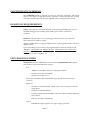
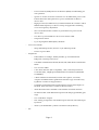
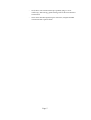
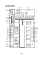
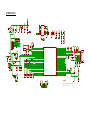
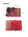
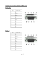
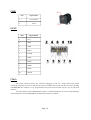
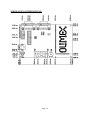
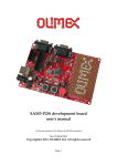
SAM3-P256 development board user's manual All boards produced by Olimex are ROHS compliant Rev. C, September 2014 Copyright(c) 2011, OLIMEX Ltd, All rights reserved Page 1 INTRODUCTION: Atmel's ATSAM3S4BA-AU is a member of a series of Flash microcontrollers based on the high performance 32-bit ARM Cortex-M3 RISC processor. It operates at a maximum speed of 64 MHz and features a 256 Kbyte Flash and a 48 Kbyte SRAM, Full Speed USB Device port with embedded transceiver, a High Speed MCI for SDIO/SD/MMC, an External Bus Interface featuring a Static Memory Controller providing connection to SRAM, PSRAM, NOR Flash and NAND Flash, 2x USARTs, 2xUARTs, 2xTWIs, 3xSPI, an I2S, as well as 1 PWM timer, 6x general-purpose 16-bit timers, an RTC, an ADC, a 12-bit DAC and an analog comparator. SAM3-P256 has JTAG, UEXT, USB and two RS232 connectors, power jack, potentiometer, two user buttons, two status LEDs, power-on led, reset button and prototype area for all microcontroller's ports. All this gives the customer chance to build a wide range of applications. BOARD FEATURES: Microcontroller: ATSAM3S4BA-AU. standard JTAG connector with ARM 2×10 pin layout for programming/debugging with ARM-JTAG USB connector Two channel RS232 interface and drivers SD/MMC card connector two buttons trimpot connected to ADC thermistor connected to ADC two status LEDs on board voltage regulator 3.3V with up to 800mA current single power supply: 6VDC or 4.5 VAC required power supply LED RESET circuit RESET button 12.000 Mhz crystal on socket UEXT connector prototype area for all microcontroller's ports PCB: FR-4, 1.5 mm (0,062"), red soldermask, silkscreen component print Dimensions: 120×80 mm (4.72×3.15") Page 2 ELECTROSTATIC WARNING: The SAM3-P256 board is shipped in protective anti-static packaging. The board must not be subject to high electrostatic potentials. General practice for working with static sensitive devices should be applied when working with this board. BOARD USE REQUIREMENTS: Cables: The cable you will need depends on the programmer/debugger you use. OLIMEX debuggers need USB type B to USB type A cable to connect to a computer. Hardware: The best idea is to use a debugger made by Atmel, since the main microcontroller is made by Atmel. Another reliable choice is Segger's JLINK which is well-supported works with most ARM products. If you are looking for open-source development please check the Olimex-made debuggers: ARM-USB-OCD, ARM-USB-TINY, ARM-USB-OCD-H, ARM-USBTINY-H if you work with OpenOCD, IAR EW for ARM, Rowley Crossworks for ARM, CooCox, GCC compilers, etc. PROCESSOR FEATURES: SAM3-P256 board use ARM-based microcontroller ATSAM3S4BA-AU LQFP64 from Atmel Corporation with these features: Core ARM® Cortex®-M3 revision 2.0 running at 64 MHz Memory Protection Unit (MPU) Thumb®-2 instruction set Pin-to-pin compatible with AT91SAM7S legacy products (48- and 64-pin versions) Memories 256 Kbytes embedded Flash, 128-bit wide access, memory accelerator, single plane 48 Kbytes embedded SRAM 16 Kbytes ROM with embedded bootloader routines (UART, USB) and IAP routines Memory Protection Unit (MPU) System Embedded voltage regulator for single supply operation Page 3 Power-on-Reset (POR), Brown-out Detector (BOD) and Watchdog for safe operation Quartz or ceramic resonator oscillators: 3 to 20 MHz main power with Failure Detection and optional low power 32.768 kHz for RTC or device clock High precision 8/12 MHz factory trimmed internal RC oscillator with 4 MHz default frequency for device startup. In-application trimming access for frequency adjustment Slow Clock Internal RC oscillator as permanent low-power mode device clock Two PLLs up to 130 MHz for device clock and for USB Temperature Sensor Up to 22 peripheral DMA (PDC) channels Low Power Modes Sleep and Backup modes, down to 3 μA in Backup mode Ultra low power RTC Peripherals USB 2.0 Device: 12 Mbps, 2668 byte FIFO, up to 8 bidirectional Endpoints. On-Chip Transceiver 2 USARTs with ISO7816, IrDA®, RS-485, SPI, Manchester and Modem Mode Two 2-wire UARTs 2 Two Wire Interface (I2C compatible), 1 SPI, 1 Serial Synchronous Controller (I2S), 1 High Speed Multimedia Card Interface (SDIO/SD Card/MMC) 3 Three-Channel 16-bit Timer/Counter with capture, waveform, compare and PWM mode. Quadrature Decoder Logic and 2-bit Gray Up/Down Counter for Stepper Motor 4-channel 16-bit PWM with Complementary Output, Fault Input, 12bit Dead Time Generator Counter for Motor Control 32-bit Real-time Timer and RTC with calendar and alarm features 10-channel ADC with differential input mode and programmable gain stage Two 12-bit DAC outputs One Analog Comparator with flexible input selection, Selectable input hysteresis 32-bit Cyclic Redundancy Check Calculation Unit (CRCCU) I/O Page 4 47 I/O lines with external interrupt capability (edge or level sensitivity), debouncing, glitch filtering and on-die Series Resistor Termination Three 32-bit Parallel Input/Output Controllers, Peripheral DMA assisted Parallel Capture Mode Page 5 BLOCK DIAGRAM: Page 6 MEMORY MAP: Page 7 SCHEMATIC: AVCC AVDD VR1(3.3V) LM1117IMPX-ADJ G1 IN DB104(SMD) ADJ/GND R1 3.3V C1 1 100n 3.3V OUT R2 240/1% 3 PWR_LED PWR D1 C5 C7 6VDC 4.5VAC C6 R4 390/1% NA 470uF/16VDC C4 4 100n R3 5 560 47uF/6.3V AGND R5 0R R0OUT AGND RXD1 R8 R9 T0IN 11 TXD1 10 330 330 12 9 U1 MAX3232 C1+ C1- V+ 2 V- 6 C2 100n C3 100n C2+ C2- RS232_0/D TX0OUT T1OUT14 T2OUT7 T1IN T2IN TX1OUT R1IN 13 R2IN 8 R1OUT R2OUT 1 2 6 3 7 RX0IN 4 8 RX1IN 5 9 3.3V RS232_1 6 RX1IN 3 7 4 8 5 9 GREEN 2 1 4 3 6 5 8 7 10 9 12 11 14 13 16 15 18 17 20 19 R14 R15 R16 47K 47K 47K R17 47K R18 3.3V 3.3V TCK 0 R21 0 1x2 3.3V VCC RESET 1x2 2 R22 U2 MCP130T 1 RST PB4 PB5 TDO (NA)47K 57 DM_PUP C12 100n Q1 C22 R40 330K 15p C23 15p PB13 59 R41 330K C25 C26 C27 C28 1n 2.2uF 100n 100n (NA)IRLML6402 C29 C30 PA15/TF/TIOA1/PWML3/WKUP14/PIODCEN1 20 PA16/TK/TIOB1/PWML2/WKUP15/PIODCEN2 19 CP PA17/TD/PCK1/PWMH3/AD0 9 PA18/RD/PCK2/A14/AD1 10 PA19/RK/PWML0/A15/AD2/WKUP9 13 LED2 PA20/RF/PWML1/A16/AD3/WKUP10 16 PA21/RXD1/PCK1/AD8 11 B2 RXD1 R37 PA22/TXD1/NPCS3/NCS2/AD9 14 PA23/SCK1/PWMH0/A19/PIODCCLK 15 TXD1 33K PA24/RTS1/PWMH1/A20/PIODC0 23 PA25/CTS1/PWMH2/A23/PIODC1 25 USB_D 2 3.3V DP_PUP CP R31 R34 PA25 R38 2K 1x2 PA30/PWML2/NPCS2/MCDA0/WKUP11/PIODC6 42 PA31/NPCS1/PCK2/MCDA1/PIODC7 52 PA30 NPCS1 3.3V 3.3V VREF PA31 R42 0 GND3 60 PB3/UTXD1/PCK2/AD7 6 GND4 C24 PB0 PB1 100n AD4 PB2 PB3 AN_TR 10K TH1 TERMISTOR AD5 R44 R45 NA(47K) 10K 3.3V 3.3V 3.3V DP_PUP NA(100) UEXT R47 4.7K R48 4.7K 1 2 TXD1 3 4 RXD1 TWCK 5 6 TWD MISO 7 8 MOSI SPCK 9 10 NPCS1 BH10S Made by Olimex LTD, Bulgaria, 2013 https://www.olimex.com DAT0/DO DAT1/RES DAT2/RES C15 CP1 CP2 SD-CARD 47uF/6.3V 3.3V VREF_P 3.3V PA29 VSS2 9 15 PA23 PA28 CLK/SCLK 8 0 PA27 VDD 7 47K 47K 13 B1 PA26 CMD/DI VSS1 5 R35 LED1 WP CD/DAT3/CS 4 6 R30 PA28/DSR1/TCLK1/MCCDA/PIODC4 38 PA29/RI1/TCLK2/MCCK/PIODC5 41 PB1/PWMH1/AD5 4 PB2/URXD1/NPCS2/WKUP12/AD6 5 GND2 46 470nH MISO PA15 WP2 3 L1 47K ATSAM3S4BA-AU R46 MOSI SPCK 3.3V PA26/DCD1/TIOA2/MCDA2/PIODC2 26 PA27/DTR1/TIOB2/MCDA3/PIODC3 37 ADVREF 1 PB0/PWMH0/AD4 3 GND1 17 100n 100n SPCK VDDCORE3 2 FET2 1 VDDCORE2 54 NA(1.5K) SPCK VDDCORE1 24 R43 MOSI VDDPLL 12 3.3V MOSI VDDOUT 64 GND PB14/NPCS1/PWMH3/DAC1 PA13/MOSI/PWMH2 22 PA14/SPCK/PWMH3/WKUP8 21 VDDIO3 8 PA11 PA12 PA13 PA14 WP1 14 NPCS0 3.3V MISO VDDIO2 58 PA9 PA10 NPCS0 VDDIO1 45 PA8 MISO PB13/PWML2/PCK0/DAC0 18 C19 100n SD/MMC 2K R26 NPCS0 VDDIN 33K 10 PA5 PA6 PA11/NPCS0/PWMH0/WKUP7 28 PA12/MISO/PWMH1 27 PB8/XOUT R25 33K R0OUT PA4 PA7 DM_PUP R24 0 T0IN PA3 PB11/DDP PB9/XIN 61 12MHz/SMD C17 100n C20 100n 27R USB_B 10n 62 PA7/RTS0/PWMH3/XIN32 32 PA8/CTS0/ADTRG/WKUP5/XOUT32 31 PA2 PA9/URXD0/NPCS1/PWMFI0/WKUP6 30 PA10/UTXD0/NPCS2 29 PB10/DDM 7 C18 100n R39 PB6/TMS/SWDIO 63 C14 2.2uF C16 27R C21 C13 10p C11 10p PB5/TWCK1/PWML0/WKUP13/TDO/TRACESWO 51 56 3.3V PB4/TWD1/PWMH2/TDI 49 R23 PA1 TWD TWCK PA5/RXD0/NPCS3/WKUP4 35 PA6/TXD0/PCK0 34 PB7/TCK/SWCLK 33 R28 33p PA3/TWD0/NPCS3 43 PA4/TWCK0/TCLK0/WKUP3 36 JTAGSEL 53 TDI RESET R36 PB12/PWML1/ERASE 50 TMS 100n NRST 55 TCK 1x3 1x3 PA0 3.3V WP TXD0/DTXD RXD0/DRXD C9 NA (NA)100 4 B2 PA0/PWMH0/TIOA0/A17/WKUP0 48 PA1/PWMH1/TIOB0/A18/WKUP1 47 PA2/PWMH2/SCK0/DATRG/WKUP2 44 TST 39 PB12 RST GND NA(IRLML6402) C10 3 B1 U3 40 FET1 R33 2 330 3.3V 1 TEST RST 15K SHIELD R13 330 R20 NA 2 1 BDS 10K PB14 1 R12 LED2 LED2 3.3V TDO RST (NA)1.5K USB 1 TMS R19 R29 22K 2 LED1 LED1 TDI RTCK R27 R32 1 560 1x2 2 3.3V RST USB_D 10K B2 47K 2 +5V 1x2 GND 15 R7 10K R11 560 U1PWR VCC C8 100n TRST JTAG +5V_USB YELLOW B1 3.3V 16 3.3V R6 R10 3.3V 3.3V 3.3V 1 TX1OUT 2 BOARD LAYOUT: Page 9 POWER SUPPLY CIRCUIT: SAM3-P256 is typically power supplied with 6 VDC via Power jack, but it can be also power supplied via USB with +5V. The programmed board power consumption is about 100 mA with all peripherals enabled. RESET CIRCUIT: SAM3-P256 reset circuit includes U2 (MCP130T), R22 (10k), pin 15 of JTAG connector, ATSAM3S4BA-AU pin 39 (NRST) and RESET button. CLOCK CIRCUIT: Quartz crystal Q1 12.000 MHz is connected to ATSAM3S4BA-AU pin 61 (XOUT) and pin 62 (XIN). JUMPER DESCRIPTION: BDS: This jumper, when is closed, connects ATSAM3S4BA-AU pin 50 (JTAGSEL) to VCC. The JTAGSEL pin is used to select the JTAG boundary scan when asserted at a high level. When this jumper is opened, normal mode is enabled. Default state is opened. TEST: This jumper, when is closed, connects ATSAM3S4BA-AU pin 40 (TST) to VCC. The TST pin is used for JTAG Boundary Scan Manufacturing Test or Fast Flash programming mode. When this jumper is opened, normal mode is enabled. Default state is opened. LED1: This jumper, when is closed, connects GREEN led to ATSAM3S4BA-AU pin 10 (PA18/RD/PCK2/A14/AD1). When this jumper is opened GREEN led is not connected. Default state is closed. LED2: This jumper, when is closed, connects YELLOW led to ATSAM3S4BA-AU pin 9 (PA17/TD/PCK1/PWMH3/AD0). When this jumper is opened YELLOW led is not connected. Default state is closed. Page 10 VREF_P: This jumper, when is closed, ATSAM3S4BA-AU pin1 (ADVREF) is connected to VCC (3.3V). When this jumper is opened, ATSAM3S4BA-AU pin1 (ADVREF) is connected to VREF pin. Default state is closed. RXD0/DRXD: This jumper, when is in position RXD0, R0OUT is connected to ATSAM3S4BA-AU pin 35 (PA5/RXD0), i.e. RS232_0/D is connected to RXD0. When this jumper is in position DRXD, R0OUT is connected to ATSAM3S4BA-AU pin 30 (PA9/URXD0), i.e. RS232_0/D is connected to DRXD. This is used in programming mode via COM Port using SAM-BA tool. Default state is RXD0 shorted. TXD0/DTXD: This jumper, when is in position TXD0, T0IN is connected to ATSAM3S4BA-AU pin 34 (PA6/TXD0), i.e. RS232_0/D is connected to TXD0. When this jumper is in position DTXD, T0IN is connected to ATSAM3S4BA-AU pin 29 (PA10/UTXD0), i.e. RS232_0/D is connected to DTXD. This is used in programming mode via COM Port using SAM-BA tool. Default state is TXD0 shorted. Page 11 Description for programming via RS232_0/D COM port, or USB port using SAM-BA software: Using SAM-BA software ATSAM3S4BA-AU can be programmed via COM port (with external power supply only), or via USB port (with USB power supply only). Before being able to use SAM-BA, a recovery procedure, which consists of copying the SAM-BA Boot Assistant into Flash must be performed as follows: 1.Power down the ATSAM3S4BA-AU 2.Short ATSAM3S4BA-AU pin 55 (PB12/ERASE) with 3.3V (you may do this shorting R20) by 3.Power up the ATSAM3S4BA-AU 4.Power down the ATSAM3S4BA-AU 5.Remove the short between ATSAM3S4BA-AU and 3.3V (R20) 6.Power up the ATSAM3S4BA-AU Note: For programming via COM port, you must set jumpers RXD0/DRXD and TXD0/DTXD, according to jumpers description above, and the USB should not be plugged in. INPUT/OUTPUT: Status Led (green) with name GREEN connected via jumper LED1 to ATSAM3S4BA-AU pin 10 (PA18/RD/PCK2/A14/AD1).. Status Led (yellow) with name YELLOW connected via jumper LED2 to ATSAM3S4BA-AU pin 9 (PA17/TD/PCK1/PWMH3/AD0). Power-on LED (red) with name PWR_LED – this LED shows that +3.3V is applied to the board. User button with name B1 connected to ATSAM3S4BA-AU pin 13 (PA19/RK/PWML0/A15/AD2/WKUP9). User button with name B2 connected to ATSAM3S4BA-AU pin 16 (PA20/RF/PWML1/A16/AD3/WKUP10). User button with name RESET connected to ATSAM3S4BA-AU pin 39 (NRST). Trimpot with name AN_TR connected to ATSAM3S4BA-AU pin 3 (PB0/AD4). Thermistor with name TH1 connected to ATSAM3S4BA-AU pin 4 (PB1/AD5). Page 12 EXTERNAL CONNECTORS DESCRIPTION: RS232_0/D: Pin # Signal Name 1 NC 2 TX0OUT 3 RX0IN 4 NC 5 GND 6 NC 7 NC 8 NC 9 NC RS232_1: Pin # Signal Name 1 NC 2 TX1OUT 3 RX1IN 4 NC 5 GND 6 NC 7 NC 8 NC 9 NC Page 13 PWR: Pin # Signal Name 1 Power Input 2 GND UEXT: Pin # Signal Name 1 VCC 2 GND 3 TXD1 4 RXD1 5 TWCK 6 TWD 7 MISO 8 MOSI 9 SPCK 10 NPCS1 JTAG: The JTAG connector allows the software debugger to talk via a JTAG (Joint Test Action Group) port directly to the core. Instructions may be inserted and executed by the core thus allowing ATSAM3S4BA-AU memory to be programmed with code and executed step by step by the host software. For more details refer to IEEE Standard 1149.1 – 1990 Standard Test Access Port and Boundary Scan Architecture and ATSAM3S4BA-AU datasheets and users manual. Page 14 Pin # Signal Name Pin # Signal Name 1 VCC 2 VCC 3 TRST 4 GND 5 TDI 6 GND 7 TMS 8 GND 9 TCK 10 GND 11 RTCK 12 GND 13 TDO 14 GND 15 RST 16 GND 17 NC 18 GND 19 NC 20 GND USB: Pin # Signal Name 1 +5V_USB 2 DDM 3 DDP 4 GND Page 15 SD/MMC: Pin # Signal Name Pin # Signal Name 1 NPCS0 2 MOSI 3 GND (VSS1) 4 VDD 5 SPCK 6 GND (VSS2) 7 MISO 8 Via R31 (47k) to 3.3V 9 Via R34 (47k) to 3.3V 10 WP 11 Via R26 (2k) to GND 12 Via R38 (2k) to GND 13 CP 14 Via R26 (2k) to GND 15 Via R38 (2k) to GND Page 16 Prototype area: NC – Not connected. Page 17 MECHANICAL DIMENSIONS: Page 18 AVAILABLE DEMO SOFTWARE: The demo package available at the Software section of SAM3-P256's page features the following examples: Getting started – demonstrates use of LEDs, User buttons, Interrupts and Timers ADC demo – demonstrates use of analog peripherals on board SD card demo – demonstrates use of low level SD card routines USB demo – demonstrates use of USB device as a mouse Page 19 ORDER CODE: SAM3-P256 – assembled and tested board How to order? You can order directly from our web ship or purchase from any of our distributors. The list of Olimex distributors might be found here: https://www.olimex.com/Distributors Check our web site https://www.olimex.com/ for more info. Revision history: Board's Revision: Rev. Initial, July 2010 Manual's Revision Rev. A, released May 2011 Rev. B, released March 2013 Rev. C, released September 2014 Page 20 DISCLAIMER © 2013 Olimex Ltd. Olimex®, logo and combinations thereof, are registered trademarks of Olimex Ltd. Other product names may be trademarks of others and the rights belong to their respective owners. The information in this document is provided in connection with Olimex products. No license, express or implied or otherwise, to any intellectual property right is granted by this document or in connection with the sale of Olimex products. The Hardware project is released under the Creative Commons Attribution-Share Alike 3.0 United States License. You may reproduce it for both your own personal use, and for commercial use. You will have to provide a link to the original creator of the project https://www.olimex.com on any documentation or website. You may also modify the files, but you must then release them as well under the same terms. Credit can be attributed through a link to the creator website: https://www.olimex.com The software is released under GPL. It is possible that the pictures in this manual differ from the latest revision of the board. The product described in this document is subject to continuous development and improvements. All particulars of the product and its use contained in this document are given by OLIMEX in good faith. However all warranties implied or expressed including but not limited to implied warranties of merchantability or fitness for purpose are excluded. This document is intended only to assist the reader in the use of the product. OLIMEX Ltd. shall not be liable for any loss or damage arising from the use of any information in this document or any error or omission in such information or any incorrect use of the product. This evaluation board/kit is intended for use for engineering development, demonstration, or evaluation purposes only and is not considered by OLIMEX to be a finished end-product fit for general consumer use. Persons handling the product must have electronics training and observe good engineering practice standards. As such, the goods being provided are not intended to be complete in terms of required design-, marketing-, and/or manufacturing-related protective considerations, including product safety and environmental measures typically found in end products that incorporate such semiconductor components or circuit boards. Olimex currently deals with a variety of customers for products, and therefore our arrangement with the user is not exclusive. Olimex assumes no liability for applications assistance, customer product design, software performance, or infringement of patents or services described herein. THERE IS NO WARRANTY FOR THE DESIGN MATERIALS AND THE COMPONENTS USED TO CREATE SAM3-P256. THEY ARE CONSIDERED SUITABLE ONLY FOR SAM3-P256. Page 21