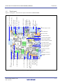
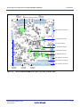
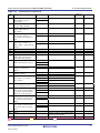
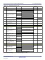
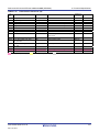
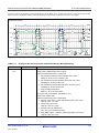
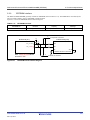
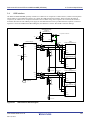
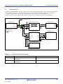
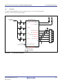
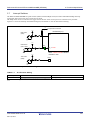
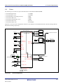
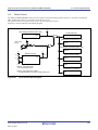
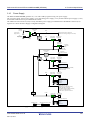
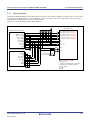
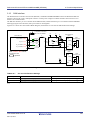
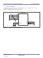
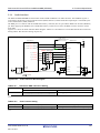
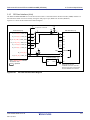
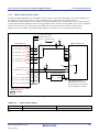
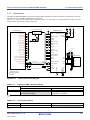
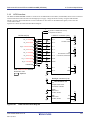
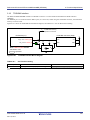
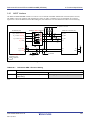
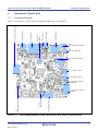
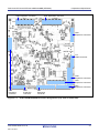
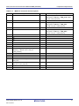
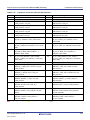
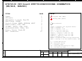
1
User’s Manual
R7S72100 CPU board
32
RTK772100BC00000BR
(GENMAI)
User's Manual
Renesas Microcomputer
RZ/A Series
All information contained in these materials, including products and product specifications,
represents information on the product at the time of publication and is subject to change by
Renesas Electronics Corporation without notice. Please review the latest information published by
Renesas Electronics Corporation through various means, including the Renesas Electronics
Corporation website (http://www.renesas.com).
www.renesas.com
Rev.0.08
2013.12
Notice
1.
Descriptions of circuits, software and other related information in this document are provided only to illustrate the operation of
semiconductor products and application examples. You are fully responsible for the incorporation of these circuits, software,
and information in the design of your equipment. Renesas Electronics assumes no responsibility for any losses incurred by you
or third parties arising from the use of these circuits, software, or information.
2.
Renesas Electronics has used reasonable care in preparing the information included in this document, but Renesas Electronics
does not warrant that such information is error free. Renesas Electronics assumes no liability whatsoever for any damages
incurred by you resulting from errors in or omissions from the information included herein.
3.
Renesas Electronics does not assume any liability for infringement of patents, copyrights, or other intellectual property rights of
third parties by or arising from the use of Renesas Electronics products or technical information described in this document. No
license, express, implied or otherwise, is granted hereby under any patents, copyrights or other intellectual property rights of
Renesas Electronics or others.
4.
You should not alter, modify, copy, or otherwise misappropriate any Renesas Electronics product, whether in whole or in part.
Renesas Electronics assumes no responsibility for any losses incurred by you or third parties arising from such alteration,
modification, copy or otherwise misappropriation of Renesas Electronics product.
5.
Renesas Electronics products are classified according to the following two quality grades: “Standard” and “High Quality”. The
recommended applications for each Renesas Electronics product depends on the product’s quality grade, as indicated below.
“Standard”:
Computers; office equipment; communications equipment; test and measurement equipment; audio and visual
equipment; home electronic appliances; machine tools; personal electronic equipment; and industrial robots etc.
“High Quality”: Transportation equipment (automobiles, trains, ships, etc.); traffic control systems; anti-disaster systems; anticrime systems; and safety equipment etc.
Renesas Electronics products are neither intended nor authorized for use in products or systems that may pose a direct threat to
human life or bodily injury (artificial life support devices or systems, surgical implantations etc.), or may cause serious property
damages (nuclear reactor control systems, military equipment etc.). You must check the quality grade of each Renesas
Electronics product before using it in a particular application. You may not use any Renesas Electronics product for any
application for which it is not intended. Renesas Electronics shall not be in any way liable for any damages or losses incurred
by you or third parties arising from the use of any Renesas Electronics product for which the product is not intended by Renesas
Electronics.
6.
You should use the Renesas Electronics products described in this document within the range specified by Renesas Electronics,
especially with respect to the maximum rating, operating supply voltage range, movement power voltage range, heat radiation
characteristics, installation and other product characteristics. Renesas Electronics shall have no liability for malfunctions or
damages arising out of the use of Renesas Electronics products beyond such specified ranges.
7.
Although Renesas Electronics endeavors to improve the quality and reliability of its products, semiconductor products have
specific characteristics such as the occurrence of failure at a certain rate and malfunctions under certain use conditions. Further,
Renesas Electronics products are not subject to radiation resistance design. Please be sure to implement safety measures to
guard them against the possibility of physical injury, and injury or damage caused by fire in the event of the failure of a Renesas
Electronics product, such as safety design for hardware and software including but not limited to redundancy, fire control and
malfunction prevention, appropriate treatment for aging degradation or any other appropriate measures. Because the evaluation
of microcomputer software alone is very difficult, please evaluate the safety of the final products or systems manufactured by
you.
8.
Please contact a Renesas Electronics sales office for details as to environmental matters such as the environmental compatibility
of each Renesas Electronics product. Please use Renesas Electronics products in compliance with all applicable laws and
regulations that regulate the inclusion or use of controlled substances, including without limitation, the EU RoHS Directive.
Renesas Electronics assumes no liability for damages or losses occurring as a result of your noncompliance with applicable laws
and regulations.
9.
Renesas Electronics products and technology may not be used for or incorporated into any products or systems whose
manufacture, use, or sale is prohibited under any applicable domestic or foreign laws or regulations. You should not use
Renesas Electronics products or technology described in this document for any purpose relating to military applications or use
by the military, including but not limited to the development of weapons of mass destruction. When exporting the Renesas
Electronics products or technology described in this document, you should comply with the applicable export control laws and
regulations and follow the procedures required by such laws and regulations.
10. It is the responsibility of the buyer or distributor of Renesas Electronics products, who distributes, disposes of, or otherwise
places the product with a third party, to notify such third party in advance of the contents and conditions set forth in this
document, Renesas Electronics assumes no responsibility for any losses incurred by you or third parties as a result of
unauthorized use of Renesas Electronics products.
11. This document may not be reproduced or duplicated in any form, in whole or in part, without prior written consent of Renesas
Electronics.
12. Please contact a Renesas Electronics sales office if you have any questions regarding the information contained in this document
or Renesas Electronics products, or if you have any other inquiries.
(Note 1) “Renesas Electronics” as used in this document means Renesas Electronics Corporation and also includes its majorityowned subsidiaries.
(Note 2) “Renesas Electronics product(s)” means any product developed or manufactured by or for Renesas Electronics.
(2012.4)
WEEE Directive
Renesas development tools and products are directly covered by the European Union's Waste
Electrical and Electronic Equipment, (WEEE), Directive 2002/96/EC.
As a result, this equipment, including all accessories, must not be disposed of as household
waste but through your locally recognised recycling or disposal schemes.
As part of our commitment to environmental responsibility Renesas also offers to take back the
equipment and has implemented a Tools Product Recycling Program for customers in Europe.
This allows you to return equipment to Renesas for disposal through our approved Producer
Compliance Scheme.
To register for the program, click here "http://www.renesas.com/weee".
About This Manual
1. Purpose and Target Readers
This manual is designed to provide the user with an understanding of the functions and operating specifications of this
extension board. A basic knowledge of electrical circuits, logical circuits, and microcomputers (MCUs) is necessary in
order to use this manual.
This manual is composed of an overview of the CPU board; its functional and operational specifications.
Carefully read all notes described in the body of text in the manual.
The Revision History summarizes the modifications and additions to the previous versions. Refer to the text of the manual
for details.
The following document applies to the R7S72100 CPU board RTK772100BC00000BR.
Document Type
User's Manual
Description
Document Title
Describes functional specifications
R7S72100 CPU board
(devices, memory maps, electrical
RTK772100BC00000BR
characteristics), and operational
User's Manual
Document No.
This publication
specifications (connectors, and
switches)
The following documents apply to the RZ/A1H group. Make sure to refer to the latest version of these documents which
can be obtained from Renesas Electronics website.
Document Type
Description
Application note
Applications, sample programs, etc.
RENESAS TECHNICAL
Information regarding product
UPDATE
specifications, documents, etc.
Document Title
Document No.
Available on Renesas Electronics website
2. Frequently Used Abbreviations and Acronyms
ACIA
Asynchronous Communication Interface Adapter
bps
Bits per second
CRC
Cyclic Redundancy Check
DMA
Direct Memory Access
DMAC
Direct Memory Access Controller
GSM
Global System for Mobile Communications
Hi-Z
High Impedance
IEBus
Inter Equipment bus
I/O
Input/Output
IrDA
Infrared Data Association
LSB
Least Significant Bit
MSB
Most Significant Bit
NC
Non-Connection
PLL
Phase Locked Loop
PWM
Pulse Width Modulation
SFR
Special Function Registers
SIM
Subscriber Identity Module
UART
Universal Asynchronous Receiver/Transmitter
VCO
Voltage Controlled Oscillator
All trademarks and registered trademarks are the property of their respective owners.
Table of Contents
1.
2.
Overview.................................................................................................................................................... 1-1
1.1
Overview ......................................................................................................................................................... 1-1
1.2
System Configuration ...................................................................................................................................... 1-2
1.3
External Specifications .................................................................................................................................... 1-3
1.4
Exterior Appearance ........................................................................................................................................ 1-5
1.5
Parts Layout..................................................................................................................................................... 1-7
1.6
Memory Map ................................................................................................................................................. 1-11
1.7
Absolute Maximum Ratings .......................................................................................................................... 1-12
1.8
Operating Conditions..................................................................................................................................... 1-12
Functional Specification............................................................................................................................. 2-1
2.1
Functions Overview......................................................................................................................................... 2-1
2.2
CPU ................................................................................................................................................................. 2-2
2.2.1
R7S72100 Overview............................................................................................................................... 2-2
2.2.2
R7S72100 Pin Functions ........................................................................................................................ 2-2
2.2.3
RTK772100BC00000BR Module Applicability................................................................................... 2-16
2.3
Memories ....................................................................................................................................................... 2-17
2.3.1
R7S72100 On-Chip RAM .................................................................................................................... 2-17
2.3.2
NOR Flash Memory Interface .............................................................................................................. 2-17
2.3.3
SDRAM Interface ................................................................................................................................. 2-20
2.3.4
Serial Flash Memory Interface.............................................................................................................. 2-24
2.3.5
NAND Flash Memory Interface ........................................................................................................... 2-26
2.3.6
EEPROM Interface ............................................................................................................................... 2-27
2.4
USB Interface ................................................................................................................................................ 2-28
2.5
Serial Interface............................................................................................................................................... 2-30
2.6
I/O Ports......................................................................................................................................................... 2-31
2.7
Interrupt Switches.......................................................................................................................................... 2-32
2.8
Clocks ............................................................................................................................................................ 2-33
2.9
Reset Control ................................................................................................................................................. 2-35
2.10
Power Supply................................................................................................................................................. 2-36
2.11
Debug Interface ............................................................................................................................................. 2-37
2.12
CAN Interface................................................................................................................................................ 2-38
2.13
Video Input Interface ..................................................................................................................................... 2-39
2.14
Audio Interface .............................................................................................................................................. 2-40
3.
2.15
SD Card Interface (4-bit) ............................................................................................................................... 2-41
2.16
MMC Card Interface (8-bit) .......................................................................................................................... 2-42
2.17
LAN Interface................................................................................................................................................ 2-43
2.18
LVDS Interface.............................................................................................................................................. 2-44
2.19
TOSLINK Interface ....................................................................................................................................... 2-45
2.20
MOST Interface ............................................................................................................................................. 2-46
Operational Specification........................................................................................................................... 3-1
3.1
Connector Overview ........................................................................................................................................ 3-1
3.1.1
RCA Connector for Video Input (J1)...................................................................................................... 3-3
3.1.2
MOST I/F Connector (J3)....................................................................................................................... 3-4
3.1.3
Mic-in Pin Jack Assignments (J4) .......................................................................................................... 3-6
3.1.4
Lineout Pin Jack (J6) .............................................................................................................................. 3-7
3.1.5
USB Connectors (J5 and J8) ................................................................................................................... 3-8
3.1.6
LAN Connector (J10) ........................................................................................................................... 3-10
3.1.7
SD Card Slot (J11)................................................................................................................................ 3-11
3.1.8
MMC Card Slot (J15) ........................................................................................................................... 3-12
3.1.9
CAN Connectors (J12 and J13) ............................................................................................................ 3-13
3.1.10
LVDS Connectors (J14 and J16) .......................................................................................................... 3-14
3.1.11
TOSLINK Connector (U26) ................................................................................................................. 3-16
3.1.12
Serial Port Connectors (J17 and J19).................................................................................................... 3-17
3.1.13
UDI Connectors (J21 and J22).............................................................................................................. 3-18
3.1.14
Power Supply Connectors (J23 and J25) .............................................................................................. 3-20
3.1.15
External Power Supply Connectors (J24 and J26 to J28) ..................................................................... 3-21
3.1.16
Expansion Connectors (CN1 to CN9)................................................................................................... 3-23
3.2
Operation Parts Layout .................................................................................................................................. 3-32
3.2.1
Jumpers (JP1 to JP15, JP18, JP19 and JP21)........................................................................................ 3-33
3.2.2
Switches and LEDs............................................................................................................................... 3-36
3.3
Dimensions .................................................................................................................................................... 3-39
Appendix RTK772100BC00000BR Schematics...................................................................................................1
R7S72100 CPU board RTK772100BC00000BR (GENMAI)
1.
Overview
1.1
Overview
1. Overview
RTK772100BC00000BR is a CPU board to evaluate functions and performance of Renesas Electronics RISC
microcomputer R7S72100 and to execute development and evaluation of its application software. The features of the
R7S72100 CPU board are described below.
• The following external memories are generally included.
- NOR flash memory: 64MB×2 (16-bit bus connection)
- SDRAM: 64MB×2 (16-bit bus connection)
- Serial flash memory: 64MB×3
- EEPROM: 16KB×1
• Any of NOR flash memory, serial flash memory, SD controller on-chip NAND flash memory, and MMC controller
on-chip NAND flash memory can be selected as a boot memory.
• A serial port connector (RS-232C or USB Mini-B), USB connectors, CAN connectors, SD card slot, MMC card slot,
RCA connector for video input, and MOST I/F connector are generally included as the R7S72100 peripheral function
interface.
• An audio CODEC is included to enable advance development of the audio system.
• The USB connectors generally include the series A receptacles. The board pattern enables the Mini-B receptacles to
be implemented for the USB host/function module evaluation.
• A LAN connector is generally included to enable software development or evaluation using the Ethernet.
• Data bus, address bus and on-chip peripheral function pins of the R7S72100 are all connected to the expansion
connectors to enable timing evaluation with the peripheral devices using measurement instrument, or development of
expansion board for its application.
• The ARM JTAG 20 and the CoreSight 20 are mounted to connect with the R7S72100 user debug interface.
R20UT2596EJ0008 Rev.0.08
Dec. 19, 2013
1-1
R7S72100 CPU board RTK772100BC00000BR (GENMAI)
1.2
1. Overview
System Configuration
Figure 1.1 shows the System Configuration using RTK772100BC00000BR.
Host computer
*
Debugger
*
ICE
LAN
Micro
SD card headphone MMC card
JTAG
DC12V
output
AC adapter
(accessory)
or
DC12V output
Stabilized
power supply
(over 3A)
MOST
*
RCA
R7S72100
USB
LVDS
R7S72100 CPU board
RTK772100BC00000BR
USB serial
Serial port
CAN TOSLINK
Figure 1.1
* These items are not included. Please purchase them separately.
System Configuration using RTK772100BC00000BR
R20UT2596EJ0008 Rev.0.08
Dec. 19, 2013
1-2
R7S72100 CPU board RTK772100BC00000BR (GENMAI)
1.3
1. Overview
External Specifications
Table 1.1 and Table 1.2 list the RTK772100BC00000BR External Specifications.
Table 1.1
RTK772100BC00000BR External Specifications (1)
Item
CPU
Memories
Description
R7S72100
• Input (XIN) clock: 13.33MHz
• CPU clock (Iφ): Up to 400MHz
• Image process clock (Gφ): Up to 266.67MHz
• Internal bus clock (Bφ): Up to 133.33MHz
• External bus clock (CKIO): Up to 66.67MHz
• Peripheral clock 1 (P1φ): Up to 66.67MHz
• Peripheral clock 0 (P0φ): Up to 33.33MHz
• On-chip memory
Large-capacity on-chip RAM: 10MB
External memory: 128KB
Instruction cache: 32KB
Operand cache: 32KB
• Power supply voltage: 1.18V (internal), 3.3V (I/O)
• 324-pin BGA 0.8mm pitch (package code: PRBG0324GA-A)
• NOR flash memory: 64MB×2
- Spansion S29GL512S10T
• SDRAM: 64MB×2
- ISSI IS42S16320B-75
• Serial flash memories: 64MB×3
- Spansion S25FL512SDPM
• NAND flash memory: 512MB×1 (implementable board pattern)
- Spansion S34ML04G100TFI
• EEPROM: 16KB×1
Connectors
•
•
•
•
•
•
•
•
•
•
•
•
•
LEDs
•
•
•
R20UT2596EJ0008 Rev.0.08
Dec. 19, 2013
- Renesas R1EX24128ASAS0A
USB series A receptacles: 2 (can be changed to Mini-B receptacles)
LAN connector (RJ-45)
SD card slot (4-bit)
MMC card slot (8-bit)
Audio I/O mini jacks (φ3.5): 2
RCA connector for image input (4 input)
CAN port connectors (3-pin, pin header): 2
TOSLINK connector (for SPDIF connection)
MOST I/F connector
Serial port connector (D-Sub 9-pin and USB Mini-B can be switched)
User debug interface connector (ARM JTAG 20, CoreSight 20): 1 for each
Expansion connectors: 34-pin×1, 30-pin×4, 20-pin×4 (partially mounted)
DC power jack
Power supply LED: 1
User LEDs: 2
LAN status LEDs: 3
1-3
R7S72100 CPU board RTK772100BC00000BR (GENMAI)
Table 1.2
1. Overview
RTK772100BC00000BR External Specifications (2)
Item
Switches
Board specification
R20UT2596EJ0008 Rev.0.08
Dec. 19, 2013
Description
• Reset switch: 1
• User switches: 3 (NMI, IRQ6*, TEST)
• Toggle switch: 1 (IRQ6*)
*parallel connection
• DIP switch for system setting: 6/package×1
• DIP switch for I/F setting: 4/package×1
• DIP switch for Ethernet PHY setting: 8/package×1
• Dimensions: 175mm×155mm
• Mounting form: 6 layered double-sided
• Number of board: 1
1-4
R7S72100 CPU board RTK772100BC00000BR (GENMAI)
1.4
1. Overview
Exterior Appearance
Figure 1.2 shows the RTK772100BC00000BR Exterior Appearance.
Figure 1.2
RTK772100BC00000BR Exterior Appearance
R20UT2596EJ0008 Rev.0.08
Dec. 19, 2013
1-5
R7S72100 CPU board RTK772100BC00000BR (GENMAI)
1. Overview
Figure 1.3 shows the RTK772100BC00000BR Block Diagram.
ICE
50Ω
UDI
RESET
NMI
IRQ6
100Ω
RJ-45
Pin Header
(3pin)
SD Card
Slot
PHY
uPD60610
INTC
MII:8
CAN
Transceiver
4
75Ω
DVDEC
RCA×4
RCA×2
(VIN2)
ETHER
RSCAN
LVDS
R7S72100
(324BGA)
ch0
USB
100Ω
LVDS
Output
90Ω
USB×2
SDHI
MMC Card
Slot
4
ch1
MMC
8
MIC
SSIF
SSIF0 AudioCodec
(WM8978)
MLB
MOST I/F
Board
HP
ch2
SCIF
RIIC
EEPROM
(16KB)
SCIF2
Tx, Rx
RS-232C
Transceiver
Dsub-9
ch2
RL78/G1C-S
NAND
(512MB)
Serial Flash
(64MB×2)
Serial Flash
(64MB)
8
8
4
USB
Mini-B
FLCTL
SPIBSC
SPIBSC
TOSLINK
(TODX)
RSPDIF
BSC
16bit
CS0
NOR
(64MB)
CS1
NOR
(64MB)
CS2
SDRAM
(64MB)
CS3
SDRAM
(64MB)
*Memory capacity unit : Byte
External
Connector
Bootable
Figure 1.3
Optional
Dedicated
connector
Expansion
connector
RTK772100BC00000BR Block Diagram
R20UT2596EJ0008 Rev.0.08
Dec. 19, 2013
1-6
R7S72100 CPU board RTK772100BC00000BR (GENMAI)
1.5
1. Overview
Parts Layout
SW2:
DIP switch for I/F
setting
J15: MMC card slot
X8: Audio oscillator
(22.5792MHz)
J4: Mic-in pin jack
U19: Audio CODEC
J6: Lineout pin jack
J3: MOST I/F connector
J11: SD card slot
X10: PHY oscillator (25MHz)
U20: Ethernet PHY
J10: LAN connector
SW3:
DIP switch for PHY setting
J1:
RCA connector for image input
Figure 1.4 and Figure 1.5 show the Parts Layout of the RTK772100BC00000BR.
J23:
12V power supply connector
J25:
12V AC adapter jack
SW4: Power switch
J21, J22:UDI connectors
X7: Video resonator (27MHz)
X5: USB oscillator (48MHz)
X1: EXTAL oscillator (13.33MHz)
U1
R7S72100
J5, J7: USB connectors
X2: RTC resonator (32.768kHz)
X4: RTC oscillator (4MHz)
J8, J9: USB connectors
U4
SDRAM
J19: Serial port connector
(USB Mini-B)
U28:
USB serial conversion IC
Figure 1.4
SW7: Toggle switch
SW8: Test switch
SW5: NMI switch
SW6: IRQ6 switch
U26: TOSLINK connector
SW1:
DIP switch for system setting
X9: LCD oscillator (optional)
J12, J13: CAN connectors
U2: NOR flash memory
SW9: Reset switch
J16:
LVDS backlight connector
J17: Serial port connector
(D-Sub9)
RTK772100BC00000BR Parts Layout (Top View of Component Side)
R20UT2596EJ0008 Rev.0.08
Dec. 19, 2013
1-7
R7S72100 CPU board RTK772100BC00000BR (GENMAI)
CN6:
Expansion
connector
1. Overview
CN7:
U9:
Expansion
NAND flash memory (optional) connector
CN8: Expansion connector
U7: Serial flash memory
J14: LVDS connector
U6: Serial flash memory
U5
SDRAM
U8: Serial flash memory
U3: NOR flash memory
CN9: Expansion connector
CN2: Expansion connector
CN1: Expansion connector
CN5:
Expansion
connector
Figure 1.5
CN4:
Expansion
connector
CN3:
Expansion
connector
RTK772100BC00000BR Parts Layout (Top View of Solder Side)
R20UT2596EJ0008 Rev.0.08
Dec. 19, 2013
1-8
R7S72100 CPU board RTK772100BC00000BR (GENMAI)
1. Overview
Table 1.3 and Table 1.4 list the Main Parts of the RTK772100BC00000BR.
Table 1.3
RTK772100BC00000BR Main Parts (1) IC
Part Number
Part Name
Type (Manufacturer)
Recommended Optional Parts
U1
CPU
R7S72100 (Renesas)
U2, U3
NOR flash memory
S29GL512S10T (Spansion)
U4, U5
U6 to U8
SDRAM
Serial flash memory
S25FL512SDPM (Spansion)
U9
NAND flash memory
Optional
U10
EEPROM
R1EX24128ASAS0A (Renesas)
U19
Audio CODEC
WM8978 (Wolfson)
U20
Ethernet PHY
U21, U24
CAN transceiver
uPD60610 (Renesas)
HA13721RPJE (Renesas)
U27
RS-232C transceiver
MAX3222CPW (TI)
U28
USB serial conversion IC
U30
5V regulator
RL78/G1C-S (Renesas)
LM20343 (TI)
12V → 5V
U32
3.3V regulator
LM2833X (TI)
5V → 3.3V
U34
1.18V regulator
LM2830Z (TI)
5V → 1.18V
U35
Vref reference voltage supply
LM4132 (TI)
5V → 3.3V
U33
Reset IC
RNA51957BFP (Renesas)
X1
XIN oscillator (socket mounted)
SG-8002DC-13.3333MHz (Epson)
X2
RTC resonator
MC-306 32.768KHz (Epson)
X4
RTC oscillator
SG8002CA_4MHz (Epson)
X5
USB oscillator (socket mounted)
SG8002DC_48MHz (Epson)
X7
Video recorder resonator
FA-128_27MHz (Epson)
X8
Audio oscillator (socket mounted)
SG8002DC_22.5792MHz (Epson)
X9
LCD oscillator (socket mounted)
Optional
X10
Ethernet PHY oscillator
X11
USB
serial
conversion
IS42S16320B-75 (ISSI)
S34ML04G100TFI (Spansion)
SG-8002DC (Epson)
SG8002CA_25MHz (Epson)
IC DSX321G_12MHz (KDS)
resonator
R20UT2596EJ0008 Rev.0.08
Dec. 19, 2013
1-9
R7S72100 CPU board RTK772100BC00000BR (GENMAI)
Table 1.4
Part Number
CN1, CN4,
1. Overview
RTK772100BC00000BR Main Parts (2) Connectors
Part Name
Type (Manufacturer)
Expansion connectors (20-pin)
HIF3FC-20PA-2.54DSA (HRS)
Recommended Optional Parts
CN1 is optional.
CN2, CN3
Expansion connectors (30-pin)
HIF3FC-30PA-2.54DSA (HRS)
CN3 is optional.
CN6, CN9
Expansion connectors (30-pin)
HTSS-115-01-L-DV (Samtec)
CN5, CN8
Surface mount type
CN7
Expansion connectors (34-pin)
HTSS-117-01-L-DV (Samtec)
Surface mount type
J1
RCA connector for video input
J3
MOST I/F connector
T5857 (EMUDEN)
QSH-020-01-L-D-DP-A (Samtec)
J4
Mic-in pin jack
HSJ1456-010320 (Hoshiden)
J6
Lineout pin jack
HSJ1456-010320 (Hoshiden)
J5, J8
USB series A receptacles
UBA-4R-D14T-4D (JST)
J7, J9
USB Mini-B receptacles
Optional
J10
LAN connector (RJ-45)
TLA-6T718 (TDK)
J11
SD card slot
DM1AA-SF-PEJ (HRS)
4-bit
J15
MMC card slot
7SDMM-X0-2211-B (KINGCONN)
8-bit
J12, J13
CAN connectors
B3P-SHF-1AA (JST)
J14
LVDS connector
DF14A-20P-1.25H (HRS)
J17
Serial port connector
XM2C-0942-132L (OMRON)
D-sub 9-pin
J19
Serial port connector
USB Mini-B
J21
ETM connector (20-pin)
54819-0572 (MOLEX)
FTSH-110-01 (Samtec)
J22
JTAG connector (20-pin)
HIF3FC-20PA-2.54DSA (HRS)
ARM JTAG 20
J25
DC power jack
LGP6531-0700F (SMK)
J24,
External power supply connectors
Optional
TOSLINK connector
TODX2951 (Toshiba)
54819-0572 (MOLEX)
CoreSight 20
A2-2PA-2.54DSA (HRS)
J26 to J28
U26
R20UT2596EJ0008 Rev.0.08
Dec. 19, 2013
1-10
R7S72100 CPU board RTK772100BC00000BR (GENMAI)
1.6
1. Overview
Memory Map
Figure 1.6 shows the R7S72100 Memory Map.
Logical
address
H'0000 0000
R7S72100 logical space
CS0 space: 64MB
H'0400 0000
RTK772100BC00000BR
memory map
NOR flash memory (64MB)
16 bit bus
CS1 space: 64MB
NOR flash memory (64MB)
16 bit bus
CS2 space: 64MB
SDRAM (64MB)
16 bit bus
CS3 space: 64MB
SDRAM (64MB)
16 bit bus
CS4 space: 64MB
User area
CS5 space: 64MB
User area
SPI multi I/O bus space 1: 64MB
Serial flash memory (64MB)
SPI multi I/O bus space 2: 64MB
Serial flash memory (64MB)
H'0800 0000
H'0C00 0000
H'1000 0000
H'1400 0000
H'1800 0000
H'1C00 0000
H'2000 0000
Large-capacity on-chip RAM (10MB)
H'20A0 0000
H'4000 0000
Others: 512MB
Reserved area
(Unusable)
CS0 to CS5 spaces,
SPI multi I/O bus space
(Mirror space)
H'6000 0000
H'60A0 0000
Others: 2560MB
(Mirror space)
CS0 to CS5 spaces,
SPI multi I/O bus space
(Mirror space)
Large-capacity on-chip RAM (10MB)
(Mirror space)
On-chip peripheral module, Reserved area
H'FFFF FFFF
Figure 1.6
R7S72100 Memory Map
R20UT2596EJ0008 Rev.0.08
Dec. 19, 2013
1-11
R7S72100 CPU board RTK772100BC00000BR (GENMAI)
1.7
1. Overview
Absolute Maximum Ratings
Table 1.5 lists the RTK772100BC00000BR Absolute Maximum Ratings.
Table 1.5
RTK772100BC00000BR Absolute Maximum Ratings
Symbol
Item
12Vcc
5Vcc
*1
Value
12V system power supply voltage
-0.3V to 15V
Remarks
Vss reference
5V system power supply voltage
-0.3V to 6.25V
Vss reference
VBUS *2
VBUS voltage
-0.3V to 5.5V
Vss reference
3Vcc *3
3.3V system power supply voltage
-0.3V to 4.6V
Vss reference
AVcc *4
Analog 3.3V system power supply
-0.3V to 4.6V
AVss reference
1.18V system power supply voltage
-0.3V to 1.7V
Vss reference
Operating ambient temperature *6
0°C to 50°C
Do not expose to condensation or corrosive gases.
-10°C to 60°C
Do not expose to condensation or corrosive gases.
voltage
*5
1.18Vcc
Topr
Tstg
Storage ambient temperature
[Note] *1
*2
*3
*4
*5
*6
1.8
*6
When providing 5V system power supply directly from the external power supply connector.
When providing VBUS power supply directly from the external power supply connector.
When providing 3.3V system power supply directly from the external power supply connector.
When providing analog 3.3V system power supply directly from the external power supply connector.
When providing 1.18V system power supply directly from the external power supply connector.
The ambient temperature is the air temperature immediate to the board.
Operating Conditions
Table 1.6 lists the RTK772100BC00000BR Operating Conditions.
Table 1.6
RTK772100BC00000BR Operating Conditions
Symbol
Item
Value
Remarks
12Vcc
12V system power supply voltage
10.8V to 13.2V
Vss reference
5Vcc *1
5V system power supply voltage
4.5V to 5.5V
Vss reference
3Vcc *2
3.3V system power supply voltage
3.0V to 3.6V
Vss reference
Analog 3.3V system power supply
3.0V to 3.6V
Vss reference
AVcc
*3
voltage
1.18Vcc *4
-
1.18V system power supply voltage
Maximum consumption voltage
1.10V to 1.26V
Up to 3A
Vss reference
Total value of 12V, 5V, 3.3V and 1.18V system
power supplies
Topr
[Note] *1
*2
*3
*4
*5
Operating ambient temperature *5
0°C to 40°C
Do not expose to condensation or corrosive gases.
When providing 5V system power supply directly from the external power supply connector.
When providing 3.3V system power supply directly from the external power supply connector.
When providing analog 3.3V system power supply directly from the external power supply connector.
When providing 1.18V system power supply directly from the external power supply connector.
The ambient temperature is the air temperature immediate to the board.
R20UT2596EJ0008 Rev.0.08
Dec. 19, 2013
1-12
R7S72100 CPU board RTK772100BC00000BR (GENMAI)
2.
Functional Specification
2.1
Functions Overview
2. Functional Specification
Table2.1.1 lists the RTK772100BC00000BR Function Modules.
Table2.1.1
RTK772100BC00000BR Function Modules
Section
2.2
Function
CPU
Description
• R7S72100
・Input (XIN) clock: 13.33MHz
・Bus clock: Up to 66.67MHz
・CPU clock: Up to 400MHz
2.3
Memories
• On-chip memory
・Large-capacity on-chip RAM: 10MB
・External memory: 128KB
z NOR flash memory: 64MB×2
・Spansion S29GL512S10T
z SDRAM: 64MB×2
・ISSI IS42S16320B-75
z Serial flash memory: 64MB×3
・Spansion S25FL512SDPM
z NAND flash memory: Board pattern which enables to implement 512MB
・Spansion S34ML04G100TFI
z EEPROM: 16KB×1
・Renesas R1EX24128ASAS0A
2.4
USB Interface
2.5
Serial Interface
• Connection between the R7S72100 USB2.0 host/function module and the USB connector.
• Connection between the R7S72100 FIFO on-chip serial communication interface (SCIF)
and 1) the D-Sub 9 connector, or 2) the USB Mini-B connector.
2.6
I/O Ports
2.7
Interrupt Switches
• Connection between the R7S72100 I/O ports and the LEDs and DIP switches.
• Connection between the R7S72100 NMI pin, IRQ6 pin and TEST pin and the push
switches.
2.8
Clocks
2.9
Reset Control
2.10
Power Supply
2.11
Debug Interface
2.12
CAN Interface
• System clock configuration
• Reset control for the device on the RTK772100BC00000BR
• The RTK772100BC00000BR system power supply configuration
• Connection between the R7S72100 user debug interface and the connectors.
• Connection between the R7S72100 controller area network (RSCAN) and the CAN
transceiver.
2.13
Video Input Interface
2.14
Audio Interface
2.15
SD Card Interface
(4-bit)
2.16
MMC Card Interface
(8-bit)
2.17
LAN Interface
2.18
LVDS Interface
2.19
TOSLINK Interface
2.20
MOST Interface
-
Operating
specifications
R20UT2596EJ0008 Rev.0.08
Dec. 19, 2013
• Connection between the R7S72100 digital video decoder and the RCA connector.
• Connection between the R7S72100 and the audio CODEC (WM8978).
• Connection between the R7S72100 SD host interface (SDHI) channel 0 and MMC host
interface (MMCIF) and the SD card slot.
• Connection between the R7S72100 SD host interface (SDHI) channel 1 and MMC host
interface (MMCIF) and the MMC card slot.
• Connection between the R7S72100 Ethernet controller (ETHER) and the Ethernet PHY.
• Connection between the R7S72100 and the LVDS I/F connector.
• Connection between the R7S72100 and the TOSLINK connector.
• Connection between the R7S72100 media local bus (MLB) and the MOST I/F connector.
• Connectors, switcheds and LEDs
(described in Chapter 3)
2-1
R7S72100 CPU board RTK772100BC00000BR (GENMAI)
2.2
2. Functional Specification
CPU
2.2.1
R7S72100 Overview
The RTK772100BC00000BR includes a 32-bit RISC microcomputer R7S72100 which runs at a maximum CPU clock
frequency of 400MHz.
2.2.2
R7S72100 Pin Functions
Table 2.2.1 to Table2.2.11 list the R7S72100 pin functions used in the RTK772100BC00000BR.
Table 2.2.1
Pin
No.
R7S72100 Pin Functions (1)
Pin Name
A1
Vss
A2
P6_4 / D4 / LCD1_DATA12 /
Function
D4
Description
Expansion
Connector
Data bus
CN1-15
Connected to DIPSW as a clock selection
-
Remarks
CRx2 / IRQ3 / RTS5 / RSPCK1 /
DV0_DATA20
A3
P0_3 / MD_CLKS
MD_CLKS
SW1-5
input
A4
P11_0 / DV0_DATA12 / TIOC4A /
DV0_DATA12
SCK6 / LCD0_DATA7 / VIO_D12
LCD0_DATA7
Used on option board
CN9-28
P9_6 / LCD1_DATA22 /
SPBIO20_0
SPBIO20_0 / SSIWS2 / RTS1 /
Connected to serial flash memory 1
CN9-24
LCD1_DATA22
Used on option board
P9_3 / LCD1_DATA19 /
SPBSSL_0
Connected to serial flash memroy 1 and 2
SPBSSL_0 / TxD1
LCD1_DATA19
Used on option board
P5_9 / WE2/DQMUL / ET_MDC /
ET_MDC
Connected to Ethernet PHY
DV0_VSYNC / IRQ2 / CRx1 /
CRx1
Connected to CAN transceiver
JP4: 1-2
IERxD / LCD1_DATA16
P5_9
Used on option board
JP4: Open
VIO_D12
A5
CS5
A6
A7
CN9-19
JP7: Short
CN9-16
JP4: 2-3
JP7: Open
IERxD
LCD1_DATA16
A8
Vss
A9
P5_6 / TXOUT0P /
TXOUT0P
Connected to LCD panel for LVDS
-
LCD1_DATA6 / LCD0_DATA22 /
LCD1_DATA6
Used on option board
CN9-8
DV1_DATA6 / TxD6 / IRQ6 /
DV1_DATA6
SPDIF_IN / DV0_DATA14
A10
P5_2 / TXOUT2P /
TXOUT2P
Connected to LCD panel for LVDS
-
LCD1_DATA2 / LCD0_DATA18 /
LCD1_DATA2
Used on option board
CN9-4
DV1_DATA2 / SCK3 / TIOC1B /
DV1_DATA2
MOSI3
A11
P5_0 / TXCLKOUTP /
TXCLKOUTP
Connected to LCD panel for LVDS
-
LCD1_DATA0 / LCD0_DATA16 /
LCD1_DATA0
Used on option board
CN9-2
DV1_DATA0 / TxD4 / TIOC0A /
DV1_DATA0
Channel 1 input pin 2 of Composit Video,
-
RSPCK3
A12
Vss
A13
VIN2B
Blanking,and Sync (CVBS)
A14
VDAVss
A15
VIN2A
Channel 0 input pin 2 of Composit Video,
-
Blanking, and Sync (CVBS)
A16
P0_2 / MD_CLK
MD_CLK
Connected to DIPSW as a clock mode
-
SW1-4
input
: 3.3V systempower supply,
R20UT2596EJ0008 Rev.0.08
Dec. 19, 2013
: 1.18V system power supply,
: GND
2-2
R7S72100 CPU board RTK772100BC00000BR (GENMAI)
Table 2.2.2
Pin
No.
A17
2. Functional Specification
R7S72100 Pin Functions (2)
Pin Name
Function
P1_6 / SCL3 / DV1_VSYNC /
SCL3
IERxD / IRQ6 / VIO_D12 /
DV1_VSYNC
Description
Expansion
Connector
Used on option board
CN8-20
SDA1
Connected to TH7
CN8-15
SCL0
Used on option board
CN8-14
P2_13 / D29 / SSL00 /
SPBIO11_0
Connected to serial flash memory 2
CN8-7
DV0_DATA13 / SPBIO11_0 /
LCD1_DATA13
Used on option board
Remarks
DV0_DATA12
A18
P1_3 / SDA1 / DV0_DATA19 /
ET_COL / IRQ3 / ADTRG
A19
P1_0 / SCL0 / DV0_DATA16 /
TCLKA / IRQ0 / VIO_VD /
DV0_VSYNC
A20
CTx3 / SCK0 / LCD1_DATA13 /
IRQ7
A21
P2_12 / D28 / RSPCK0 /
SPBIO01_0
Connected to serial flash memory 2
DV0_DATA12 / SPBIO01_0 /
LCD1_DATA12
Used on option board
D0
Data bus
CN1-20
P11_2 / DV0_DATA14 / TIOC4C /
DV0_DATA14
Used on option board
CN9-30
RxD6 / LCD0_DATA5 / VIO_D14
LCD0_DATA5
CN9-23
CN8-8
CRx3 / IRQ6 / LCD1_DATA12 /
TIOC1B
A22
Vss
B1
Vcc
B2
Vss
B3
P6_0 / D0 / LCD1_DATA8 /
LRXD0 / DV0_CLK / TIOC1A /
IRQ5 / RxD3 / DV0_DATA16
B4
VIO_D14
B5
P9_7 / LCD1_DATA23 /
SPBIO30_0
Connected to serial flash memory 1
SPBIO30_0 / SSIDATA2 /
LCD1_DATA23
Used on option board
TIOC1A
B6
B7
P9_4 / LCD1_DATA20 /
SPBIO00_0
Connected to serial flash memory 1
SPBIO00_0 / RxD1
LCD1_DATA20
Used on option board
P5_10 / WE3/DQMUU/AH /
P5_10
Connected to TH3
DV0_HSYNC / CTx1 / IETxD /
CTx1
Connected to CAN transceiver
LCD1_DATA17
IETxD
Used on option board
CN9-22
CN9-15
LCD1_DATA17
B8
B9
P5_8 / LCD0_EXTCLK / IRQ0 /
CS2
Connected to CS pin of SDRAM 2
DV1_CLK / DV0_CLK / CS2
CN9-11
LCD0_EXTCLK
Used on option board
P5_7 / TXOUT0M /
TXOUT0M
Connected to LCD panel for LVDS
-
LCD1_DATA7 / LCD0_DATA23 /
LCD1_DATA7
Used on option board
CN9-7
DV1_DATA7 / RxD6 / TIOC0D /
DV1_DATA7
SPDIF_OUT / DV0_DATA15
B10
P5_3 / TXOUT2M /
TXOUT2M
Connected to LCD panel for LVDS
-
LCD1_DATA3 / LCD0_DATA19 /
LCD1_DATA3
Used on option board
CN9-3
DV1_DATA3 / TxD3 / TIOC3C /
DV1_DATA3
MISO3
B11
P5_1 / TXCLKOUTM /
TXCLKOUTM
Connected to LCD panel for LVDS
-
LCD1_DATA1 / LCD0_DATA17 /
LCD1_DATA1
Used on option board
CN9-1
DV1_DATA1 / RxD4 / TIOC0B /
DV1_DATA1
Channel 1 input pin 1 of Composit Video,
-
SSL30
B12
Vss
B13
VIN1B
Blanking, and Sync (CVBS)
B14
VDAVcc
: 3.3V systempower supply,
R20UT2596EJ0008 Rev.0.08
Dec. 19, 2013
: 1.18V system power supply,
: GND
2-3
R7S72100 CPU board RTK772100BC00000BR (GENMAI)
Table 2.2.3
Pin
No.
B15
2. Functional Specification
R7S72100 Pin Functions (3)
Pin Name
Function
VIN1A
Description
Channel 0 input pin 1 of Composit Video,
Expansion
Connector
Remarks
-
Blanking, and Sync (CVBS)
B16
P1_7 / SDA3 / DV1_HSYNC /
SDA3
LRXD0 / IRQ7 / VIO_D13 /
DV1_HSYNC
Used on option board
CN8-19
Connected to EEPROM
CN8-18
DV0_DATA13
B17
P1_4 / SCL2 / DV0_CLK / CRx1 /
SCL2
IRQ4 / CAN_CLK
B18
B19
Used on option board
P1_2 / SCL1 / DV0_DATA18 /
SCL1
Connected to TH6
FRB / IRQ2 / LCD1_EXTCLK
FRB
Connected to NAND flash memory
P2_15 / D31 / MISO0 /
SPBIO31_0
Connected to serial flash memory 2
DV0_DATA15 / SPBIO31_0 /
LCD1_DATA15
Used on option board
CN8-16
CN8-9
CAN_CLK / RxD0 /
LCD1_DATA15 / IRQ1
B20
PVcc
B21
Vss
B22
P2_10 / D26 / ET_RXD2 /
ET_RXD2
Connected to Ethernet PHY
-
SW2-1: ON
DV0_DATA10 / SSIRxD0 /
LTXD0
Used on option board
CN7-34
SW2-1: OFF
LTXD0 / LCD1_DATA10 /
LCD1_DATA10
D5
Data bus
CN1-14
D2
Data bus
CN1-18
Used on option board
CN9-29
Used on option board
CN9-27
CN9-21
VIO_D10/MOSI4
C1
P6_5 / D5 / LCD1_DATA13 /
CTx2 / SCK5 / SSL10 /
DV0_DATA21
C2
Vcc
C3
Vss
C4
P6_2 / D2 / LCD1_DATA10 /
LRXD1 / IRQ7 / TCLKA /
TIOC2A / RxD2 / DV0_DATA18
C5
P11_3 / DV0_DATA15 / TIOC4D /
DV0_DATA15
LCD0_DATA4 / VIO_D15
LCD0_DATA4
P11_1 / DV0_DATA13 / TIOC4B /
DV0_DATA13
TxD6 / LCD0_DATA6 / VIO_D13
LCD0_DATA6
VIO_D15
C6
VIO_D13
C7
P9_5 / LCD1_DATA21 /
SPBIO10_0
Connected to serial flash memory 1
SPBIO10_0 / SSISCK2 / CTS1 /
LCD1_DATA21
Used on option board
P9_2 / LCD1_DATA18 /
SPBCLK_0
Connected to serial flash memroy 1 and 2
SPBCLK_0 / LTXD0 / SCK1 / A0
LCD1_DATA18
Used on option board
CS4
C8
CN9-20
C9
Vss
C10
P5_5 / TXOUT1M /
TXOUT1M
Connected to LCD panel for LVDS
-
LCD1_DATA5 / LCD0_DATA21 /
FCE
Connected to NAND flash memory
CN9-5
TIOC0C / FCE / DV0_DATA13
LCD1_DATA5
Used on option board
P5_4 / TXOUT1P /
TXOUT1P
Connected to LCD panel for LVDS
-
LCD1_DATA4 / LCD0_DATA20 /
LCD1_DATA4
Used on option board
CN9-6
DV1_DATA4 / RxD3 / TIOC3D /
DV1_DATA4
A/D converter BOTTOM reference voltage
-
DV1_DATA5 / AUDIO_XOUT /
R110:
Mounted
DV1_DATA5
C11
DV0_DATA12
C12
LVDSAPVcc
C13
VRM
pin for video signal input
: 3.3V systempower supply,
R20UT2596EJ0008 Rev.0.08
Dec. 19, 2013
: 1.18V system power supply,
: GND
2-4
R7S72100 CPU board RTK772100BC00000BR (GENMAI)
Table 2.2.4
Pin
No.
C14
2. Functional Specification
R7S72100 Pin Functions (4)
Pin Name
Function
REXT
Description
A/D converter reference voltage pin for
Expansion
Connector
-
Remarks
22k Ω±1%
video signal input
C15
C16
Vss
P1_5 / SDA2 / DV1_CLK / CRx4 /
SDA2
IRQ5 / VIO_CLK /
C17
Connected to EEPROM
CN8-17
Used on option board
LCD1_EXTCLK
DV1_CLK
P1_1 / SDA0 / DV0_DATA17 /
SDA0
Used on option board
CN8-13
CN8-10
TCLKC / IRQ1 / VIO_HD /
DV0_HSYNC
C18
P2_14 / D30 / MOSI0 /
SPBIO21_0
Connected to serial flash memory 2
DV0_DATA14 / SPBIO21_0 /
LCD1_DATA14
Used on option board
CRx4 / TxD0 / LCD1_DATA14 /
IRQ0
C19
PVcc
C20
Vss
C21
C22
P2_9 / D25 / ET_RXD1 /
ET_RXD1
Connected to Ethernet PHY
-
SW2-1: ON
DV0_DATA9 / SSIWS0 / LRXD0 /
LRXD0
Used on option board
CN7-31
SW2-1: OFF
LCD1_DATA9 / VIO_D9 / SSL40
LCD1_DATA9
P2_7 / D23 / ET_TXD3 /
ET_TXD3
Connected to Ethernet PHY
-
SW2-1: ON
DV0_DATA7 / SSITxD5 /
SSITxD5
Used on option board
CN7-29
SW2-1: OFF
D7
Data bus
CN1-12
D6
Data bus
CN1-13
D3
Data bus
CN1-17
D1
Data bus
CN1-19
IETxD/RTS1 / VIO_D7 /
LCD0_DATA23
D1
P6_7 / D7 / LCD1_DATA15 /
LCD0_TCON6 / RxD5 / MISO1 /
DV0_DATA23
D2
P6_6 / D6 / LCD1_DATA14 /
LCD0_TCON5 / TxD5 / MOSI1 /
DV0_DATA22
D3
Vcc
D4
Vss
D5
P6_3 / D3 / LCD1_DATA11 /
LTXD1 / IRQ2 / CTS5 / TIOC2B /
TxD2 / DV0_DATA19
D6
P6_1 / D1 / LCD1_DATA9 /
LTXD0 / IRQ4 / TIOC1B /
SSIDATA4 / TxD3 / DV0_DATA17
D7
PVcc
D8
PVcc
D9
LVDSPLLVcc
D10
Vss
D11
LVDSREFRIN
D12
LVDSAPVcc
D13
Vcc
D14
VRP
-
A/D converter TOP reference voltage pin
5.6k Ω±1%
-
for video signal input
D15
Vss
D16
PVcc
D17
PVcc
D18
PVcc
D19
Vss
: 3.3V systempower supply,
R20UT2596EJ0008 Rev.0.08
Dec. 19, 2013
: 1.18V system power supply,
: GND
2-5
R7S72100 CPU board RTK772100BC00000BR (GENMAI)
Table2.2.5
Pin
No.
D20
2. Functional Specification
R7S72100 Pin Functions (5)
Pin Name
Function
Description
Expansion
Connector
Remarks
P2_8 / D24 / ET_RXD0 /
ET_RXD0
Connected to Ethernet PHY
-
SW2-1: ON
DV0_DATA8 /SSISCK0 /
LCD1_DATA8
Used on option board
CN7-32
SW2-1: OFF
Used on option board
CN7-11
Used on option board
CN7-12
LCD0_TCON6 / LCD1_DATA8 /
VIO_D8 / RSPCK4
D21
D22
E1
P10_15 / DV0_DATA11 /
DV0_DATA11
SSITxD1 / MISO0 /
LCD0_DATA8
LCD0_DATA8 / VIO_D11
VIO_D11
P10_14 / DV0_DATA10 /
DV0_DATA10
SSIRxD1 / MOSI0 /
LCD0_DATA9
LCD0_DATA9 / VIO_D10
VIO_D10
P6_10 / D10 / DV0_DATA14 /
D10
Data bus
CN1-8
D9
Data bus
CN1-9
D8
Data bus
CN1-10
LCD0_TCON5 / RxD0 /
LCD0_DATA2 / IRQ2
E2
P6_9 / D9 / DV0_DATA13 /
TxD0 / LCD0_DATA1 / IRQ1
E3
P6_8 / D8 / DV0_DATA12 /
CAN_CLK / SCK0 /
LCD0_DATA0 / IRQ0
E4
Vcc
E19
P2_11 / D27 / ET_RXD3 /
ET_RXD3
Connected to Ethernet PHY
-
SW2-1: ON
DV0_DATA11 /SSITxD0 /
P2_11
Used on option board
CN7-33
SW2-1: OFF
TIOC1A / LCD1_DATA11 /
LCD1_DATA11
VIO_D11 / MISO4
E20
P2_6 / D22 / ET_TXD2 /
ET_TXD2
Connected to Ethernet PHY
-
SW2-1: ON
DV0_DATA6 / SSIRxD5 / RxD1 /
SSIRxD5
Used on option board
CN7-30
SW2-1: OFF
P10_12 / DV0_DATA8 /
DV0_DATA8
Used on option board
CN7-10
SSISCK1 / RSPCK0 /
LCD0_DATA11
VIO_D6 / LCD0_DATA22
E21
E22
LCD0_DATA11 / VIO_D8
VIO_D8
P2_5 / D21 / ET_TXD1 /
ET_TXD1
Connected to Ethernet PHY
-
SW2-1: ON
DV0_DATA5 / SSIWS5 /
SSIWS5
Used on option board
CN7-27
SW2-1: OFF
D14
Data bus
CN1-3
D13
Data bus
CN1-4
D11
Data bus
CN1-7
SPBSSL_1 / TxD1 / VIO_D5 /
LCD0_DATA21
F1
P6_14 / D14 / DV0_DATA22 /
TxD6 / LCD0_DATA6 / IRQ6
F2
P6_13 / D13 / DV0_DATA21 /
SCK6 / RXD1 / LCD0_DATA5 /
IRQ5
F3
P6_11 / D11 / DV0_DATA15 /
LCD0_TCON6 / SCK1 /
LCD0_DATA3 / IRQ3
F4
F19
Vcc
P2_4 / D20 / ET_TXD0 /
ET_TXD0
Connected to Ethernet PHY
-
SW2-1: ON
DV0_DATA4 / SSISCK5 /
SSISCK5
Used on option board
CN7-28
SW2-1: OFF
Used on option board
CN7-9
SPBCLK_1 / SCK1 / VIO_D4 /
LCD0_DATA20
F20
P10_13 / DV0_DATA9 /
DV0_DATA9
SSIWS1 / SSL00 /
LCD0_DATA10
LCD0_DATA10 / VIO_D9
VIO_D9
: 3.3V systempower supply,
R20UT2596EJ0008 Rev.0.08
Dec. 19, 2013
: 1.18V system power supply,
: GND,
2-6
R7S72100 CPU board RTK772100BC00000BR (GENMAI)
Table2.2.6
Pin
No.
F21
2. Functional Specification
R7S72100 Pin Functions (6)
Pin Name
Function
Expansion
Connector
Description
Remarks
P2_2 / D18 / ET_TXEN /
ET_TXEN
Connected to Ethernet PHY
-
SW2-1: ON
DV0_DATA2 / SPBIO20_1 /
MLB_SIG
Connected to MOST I/F connector
CN7-26
SW2-1: OFF
CN7-19
MLB_SIG / TIOC2B / VIO_D2 /
LCD0_DATA18
F22
P4_15 / LCD0_DATA23 /
SD_D2_0
Connected to SD card slot DAT2 pin
LCD1_TCON2 / SD_D2_0 /
LCD1_TCON2
Used on option board
MMC_D2 / SPBIO31_1 /
SSITxD3
SSITxD3 / RxD2 / IRQ7
G1
P11_13 / CTx1 / SSL10 /
LCD0_TCON1
Used on option board
CN2-19
LCD0_TCON2
Used on option board
CN2-20
D15
Data bus
CN1-2
D12
Data bus
CN1-5
P4_14 / LCD0_DATA22 /
SD_D3_0
Connected to SD card slot
CN7-20
LCD1_TCON1 / SD_D3_0 /
LCD1_TCON1
Used on option board
LCD0_TCON4 / MMC_D5 /
LCD0_TCON1
G2
P11_12 / CRx1 / RSPCK1 /
IRQ3 / MMC_D4 / LCD0_TCON2
G3
P6_15 / D15 / DV0_DATA23 /
RxD6 / LCD0_DATA7 / IRQ7
G4
P6_12 / D12 / DV0_DATA20 /
TXD1 / LCD0_DATA4 / IRQ4
G19
MMC_D3 / SPBIO21_1 /
SSIRxD3 / TxD2 / IRQ6
G20
P2_3 / D19 / ET_CRS /
ET_CRS
Connected to Ethernet PHY
DV0_DATA3 / SPBIO30_1 /
P2_3
Connected
IERxD / CTS1 / VIO_D3 /
to
MOST
I/F
connector
-
SW2-1: ON
CN7-25
SW2-1: OFF
(resetcontrol)
LCD0_DATA19
G21
P4_13 / LCD0_DATA21 /
SD_CMD_0
Connected to SD card slot
LCD1_TCON0 / SD_CMD_0 /
LCD1_TCON0
Used on option board
MMC_CMD / SPBIO11_1 /
SSIWS3
CN7-17
SSIWS3 / RxD1 / IRQ5
G22
H1
Vss
P7_2 / RAS / DV0_DATA18 /
RAS
Connected to SDRAM 1 and 2
ET_TXER / RXD4 / CRx2 /
CN2-28
CRx2
Connected to CAN transceiver
CS3
Connected to SDRAM 2
CN2-29
LCD0_TCON0
Used on option board
CN2-18
MD_BOOT2
Connected to DIPSW as a boot mode input
CN2-30
SCK4 / LTXD0 / TIOC0A
CS0
Connected to NOR flash memroy 1
P4_11 / LCD0_DATA19 /
SD_D0_0
Connected to SD card slot
LCD1_TCON6 / SD_D0_0 /
LCD1_TCON6
Used on option board
Used on option board
CN7-7
Used on option board
CN7-8
JP1: Open
JP1: Short
SSIWS1 / TIOC0C
H2
P7_1 / CS3 / DV0_DATA17 /
ET_TXCLK / TXD4 / DV0_CLK /
SSISCK1 / TIOC0B
H3
P11_14 / SPDIF_IN / MOSI1 /
LCD0_TCON5 / MMC_D6 /
LCD0_TCON0
H4
P7_0 / MD_BOOT2 / CS0 /
DV0_DATA16 / ET_MDC /
H19
SW1-3
JP5: 1-2
JP5: 2-3
CN7-15
MMC_D0 / SSITxD5 / CTx4 /
SCK1 / IRQ3
H20
H21
P10_11 / DV0_DATA7 / TIOC2B /
DV0_DATA7
ET_RXD3 / LCD0_DATA12 /
LCD0_DATA12
VIO_D7
VIO_D7
P10_10 / DV0_DATA6 / TIOC2A /
DV0_DATA6
ET_RXD2 / LCD0_DATA13 /
LCD0_DATA13
VIO_D6
VIO_D6
: 3.3V systempower supply,
R20UT2596EJ0008 Rev.0.08
Dec. 19, 2013
: 1.18V system power supply,
: GND
2-7
R7S72100 CPU board RTK772100BC00000BR (GENMAI)
Table2.2.7
Pin
No.
H22
2. Functional Specification
R7S72100 Pin Functions (7)
Pin Name
Function
Description
P4_12 / LCD0_DATA20 /
SD_CLK_0
Connected to SD card slot
LCD1_CLK / SD_CLK_0 /
LCD1_CLK
Used on option board
MMC_CLK / SPBIO10_1 /
SSISCK3
Expansion
Connector
Remarks
CN7-18
SSISCK3 / TxD1 / IRQ4
J1
P7_5 / RD/WR / DV0_DATA21 /
RD/WR
Connected to SDRAM 1 and 2
ET_TXD1 / RXD7 / SSISCK2 /
RxD7
Used on option board
CN2-25
P7_4 / CKE / DV0_DATA20 /
CKE
Connected to SDRAM 1 and 2
ET_TXD0 / TXD7 / SSITxD1 /
TxD7
Used on option board
P7_3 / CAS / DV0_DATA19 /
CAS
Connected to SDRAM 1 and 2
ET_TXEN / SCK7 / CTx2 /
CTx2
Connected to CAN transceiver
LCD0_CLK
Used on option board
CN2-17
Used on option board
CN7-5
Used on option board
CN7-6
CN7-16
TIOC1B
J2
CN2-26
TIOC1A
J3
CN2-27
SSIRxD1 / TIOC0D
J4
P11_15 / SPDIF_OUT / MISO1 /
IRQ1 / MMC_D7 / LCD0_CLK
J9
Vss
J10
Vss
J11
Vss
J12
Vss
J13
Vss
J14
Vss
J19
Vcc
J20
P10_9 / DV0_DATA5 / TIOC1B /
DV0_DATA5
ET_RXD1 / LCD0_DATA14 /
LCD0_DATA14
J21
J22
VIO_D5
VIO_D5
P10_8 / DV0_DATA4 / TIOC1A /
DV0_DATA4
ET_RXD0 / LCD0_DATA15 /
LCD0_DATA15
VIO_D4
VIO_D4
P4_10 / LCD0_DATA18 /
SD_D1_0
Connected to SD card slot
LCD1_TCON5 / SD_D1_0 /
LCD1_TCON5
Used on option board
A1
Address bus
CN3-30
WE1/DQMLU
Connected to SDRAM 1 and 2
CN2-23
MMC_D1 / SSIRxD5 / RxD0 /
IRQ2
K1
P7_9 / A1 / SSIWS3 / ET_RXD0 /
CTx0 / TIOC3B / IRQ0
K2
P7_7 / WE1/DQMLU /
DV0_DATA23 / ET_TXD3 /
K3
Connected to NOR flash memory 1 and 2
RTS7 / SSIDATA2 / TIOC2B
RTS7
Used on option board
P7_6 / WE0/DQMLL /
WE0/DQMLL
Connected to SDRAM 1 and 2
DV0_DATA22 / ET_TXD2 /
CTS7
Used on option board
CN2-24
CTS7 / SSIWS2 / TIOC2A
K4
P7_8 / RD / SSISCK3 / CRx0 /
RD
Connected to NOR flash memory 1 and 2
TIOC3A / IRQ1
P7_8
Used on option board
K9
Vss
K10
Vss
K11
Vss
K12
Vss
K13
Vss
K14
Vss
K19
Vcc
: 3.3V systempower supply,
R20UT2596EJ0008 Rev.0.08
Dec. 19, 2013
: 1.18V system power supply,
CN2-22
: GND
2-8
R7S72100 CPU board RTK772100BC00000BR (GENMAI)
Table2.2.8
Pin
No.
K20
2. Functional Specification
R7S72100 Pin Functions (8)
Pin Name
Function
Description
P4_8 / LCD0_DATA16 /
SD_CD_0
Connected to SD card slot
LCD1_TCON3 / SD_CD_0 /
LCD1_TCON3
Used on option board
P4_9 / LCD0_DATA17 /
SD_WP_0
Connected to SD card slot
LCD1_TCON4 / SD_WP_0 /
LCD1_TCON4
Used on option board
Expansion
Connector
Remarks
CN7-14
MMC_CD / SSISCK5 / CTx2 /
SCK0 / IRQ0
K21
CN7-13
SSIWS5 / CRx2 / TxD0 / IRQ1
K22
P2_1 / D17 / ET_TXER /
ET_TXER
Connected to Ethernet PHY
-
SW2-1: ON
DV0_DATA1 / SPBIO10_1 /
MLB_DAT
Connected to MOST I/F connector
CN7-23
SW2-1: OFF
P11_5 / DV0_DATA17 /
DV0_DATA17
Used on option board
CN2-13
SD_WP_0 / SSIWS4 /
SSIWS4
LCD0_DATA2
LCD0_DATA2
P7_11 / A3 / SSITxD3 /
A3
Address bus
CN3-28
A2
Address bus
CN3-29
Used on option board
CN2-14
Connected to audio CODEC (WM8978)
-
SW2-2: ON
CN6-29
SW2-2: OFF
MLB_DAT / TIOC2A / VIO_D1 /
LCD0_DATA17
L1
L2
ET_RXD2 / CRx1 / TIOC3D /
IRQ3
L3
P7_10 / A2 / SSIRxD3 /
ET_RXD1 / CTx1 / TIOC3C /
IRQ2
L4
P11_4 / DV0_DATA16 /
DV0_DATA16
SD_CD_0 / SSISCK4 /
SSISCK4
MMC_CD / LCD0_DATA3
LCD0_DATA3
L9
Vss
L10
Vss
L11
Vss
L12
Vss
L13
Vss
L14
Vss
L19
PVcc
L20
P4_7 / LCD0_DATA15 / MISO1 /
SSITxD0
TIOC4D / PWM2H / SSITxD0 /
DV0_DATA15
L21
P2_0 / D16 / ET_TXCLK /
ET_TXCLK
Connected to Ethernet PHY
-
SW2-1: ON
DV0_DATA0 / SPBIO00_1 /
MLB_CLK
Connected to MOST I/F connector
CN7-24
SW2-1: OFF
SSIRxD0
Connected to audio CODEC (WM8978)
-
SW2-2: ON
CN6-30
SW2-2: OFF
MLB_CLK / IRQ5 / VIO_D0 /
LCD0_DATA16
L22
P4_6 / LCD0_DATA14 / MOSI1 /
TIOC4C / PWM2G / SSIRxD0 /
DV0_DATA14
M1
P7_12 / A4 / SSISCK4 /
A4
Address bus
CN3-27
P11_6 / DV0_DATA18 /
DV0_DATA18
Used on option board
CN2-12
SD_D1_0 / SSIDATA4 /
SSIDATA4
Used on option board
CN2-11
ET_RXD3 / TIOC4A / IRQ4
M2
M3
MMC_D1 / LCD0_DATA1
LCD0_DATA1
P11_7 / DV0_DATA19 /
DV0_DATA19
SD_D0_0 / CTS5 / MMC_D0 /
LCD0_DATA0
LCD0_DATA0
M4
Vcc
M9
Vss
M10
Vss
M11
Vss
: 3.3V systempower supply,
R20UT2596EJ0008 Rev.0.08
Dec. 19, 2013
: 1.18V system power supply,
: GND
2-9
R7S72100 CPU board RTK772100BC00000BR (GENMAI)
Table2.2.9
2. Functional Specification
R7S72100 Pin Functions (9)
Pin
No.
Pin Name
M12
Vss
M13
Vss
M14
Vss
M19
PVcc
M20
P4_5 / LCD0_DATA13 / SSL10 /
Function
SSIWS0
Description
Connected to audio CODEC (WM8978)
TIOC4B / PWM2F / SSIWS0 /
Expansion
Connector
Remarks
-
SW2-2: ON
CN6-27
SW2-2: OFF
-
SW2-2: ON
CN6-28
SW2-2: OFF
DV0_DATA13
M21
P4_4 / LCD0_DATA12 /
SSISCK0
Connected to audio CODEC (WM8978)
RSPCK1 / TIOC4A / PWM2E /
SSISCK0 / DV0_DATA12
M22
N1
P10_7 / DV0_DATA3 / TIOC0D /
DV0_DATA3
PWM2H / ET_TXD3 /
LCD0_DATA16
Used on option board
CN6-23
LCD0_DATA16 / VIO_D3
VIO_D3
P7_13 / A5 / SSIWS4 /
A5
Address bus
CN3-26
A6
Address bus
CN3-25
A7
Address bus
CN3-24
P10_4 / DV0_DATA0 / TIOC0A /
DV0_DATA0
Used on option board
CN6-22
PWM2E / ET_TXD0 /
LCD0_DATA19
Used on option board
CN6-21
Used on option board
CN6-24
CN6-17
ET_MDIO / TIOC4B / IRQ5
N2
P7_14 / A6 / SSIDATA4 /
ET_CRS / TIOC4C / IRQ6
N3
P7_15 / A7 / RSPCK0 /
ET_RXCLK / CTS5 / SCI_TXD0 /
TIOC4D
N4
PVcc
N9
Vss
N10
Vss
N11
Vss
N12
Vss
N13
Vss
N14
Vss
N19
N20
N21
N22
LCD0_DATA19 / VIO_D0
VIO_D0
P10_5 / DV0_DATA1 / TIOC0B /
DV0_DATA1
PWM2F / ET_TXD1 /
LCD0_DATA18
LCD0_DATA18 / VIO_D1
VIO_D1
P10_6 / DV0_DATA2 / TIOC0C /
DV0_DATA2
PWM2G / ET_TXD2 /
LCD0_DATA17
LCD0_DATA17 / VIO_D2
VIO_D2
P4_3 / LCD0_DATA11 / TIOC0D /
FWE
Connected to NAND flash memory
FWE / CTx3 / RxD2 / MISO4 /
MMC_D7
Connected to MMC card slot
MMC_D7
MISO4
Connected to audio CODEC (WM8978)
P8_0 / A8 / SSL00 / ET_RXER /
A8
Address bus
CN3-23
A9
Address bus
CN3-21
A10
Address bus
CN3-20
Used on option board
P1
SCK5 / SCI_SCK0
P2
P8_1 / A9 / MOSI0 / ET_RXDV /
TXD5 / SCI_RXD0
P3
P8_2 / A10 / MISO0 / RXD5 /
IRQ0
P4
PVcc
P9
Vss
P10
Vss
P11
Vss
P12
Vss
P13
Vss
: 3.3V systempower supply,
R20UT2596EJ0008 Rev.0.08
Dec. 19, 2013
: 1.18V system power supply,
: GND
2-10
R7S72100 CPU board RTK772100BC00000BR (GENMAI)
Table2.2.10
R7S72100 Pin Functions (10)
Pin
No.
P14
2. Functional Specification
Pin Name
Function
Description
Expansion
Connector
Remarks
Vss
P19
Vss
P20
P4_0 / LCD0_DATA8 / TIOC0A /
FRE
Connected to NAND flash memory
FRE / RSPCK4 / MMC_D4
MMC_D4
Connected to MMC card slot
RSPCK4
Connected to audio CODEC (WM8978)
P4_2 / LCD0_DATA10 / TIOC0C /
FALE
Connected to NAND flash memory
FALE / CRx3 / TxD2 / MOSI4 /
MMC_D6
Connected to MMC card slot
MMC_D6
MOSI4
Connected to audio CODEC (WM8978)
P4_1 / LCD0_DATA9 / TIOC0B /
FCLE
Connected to NAND flash memory
FCLE / SCK2 / SSL40 / MMC_D5
MMC_D5
Connected to MMC card slot
SSL40
Connected to audio CODEC (WM8978)
P8_3 / A11 / DV1_DATA0 /
A11
Address bus
CN3-19
A12
Address bus
CN3-18
A13
Address bus
CN3-17
CN6-11
CN6-16
Used on option board
P21
CN6-18
Used on option board
P22
R1
CN6-15
JP10: Open
JP10: Short
RSPCK2 / RTS5 / IRQ1 / SCK2
R2
P8_4 / A12 / DV1_DATA1 /
SSL20 / IERxD / RxD2
R3
P8_5 / A13 / DV1_DATA2 /
MOSI2
R4
Vcc
R19
Vcc
R20
R21
P3_15 / LCD0_DATA7 / NAF7 /
NAF7
Connected to NAND flash memory
TRACECTL / SD_D2_1 /
SD_D2_1
Connected to MMC card slot
MMC_D2
MMC_D2
P3_14 / LCD0_DATA6 / NAF6 /
NAF6
Connected to NAND flash memory
TRACECLK / SD_D3_1 /
SD_D3_1
Connected to MMC card slot
MMC_D3
MMC_D3
P3_13 / LCD0_DATA5 / NAF5 /
NAF5
Connected to NAND flash memory
AUDIO_XOUT / SD_CMD_1 /
SD_CMD_1
Connected to MMC card slot
TRACECLK
R22
T1
MMC_CMD
MMC_CMD
P11_8 / DV0_DATA20 /
DV0_DATA20
SD_CLK_0 / RTS5 / MMC_CLK /
LCD0_TCON6
CN6-12
Connected to UDI connector
CN6-9
Used on option board
CN2-8
Used on option board
CN2-7
Used on option board
CN2-6
CN6-4
LCD0_TCON6
T2
P11_9 / DV0_DATA21 /
DV0_DATA21
SD_CMD_0 / SCK5 /
LCD0_TCON5
MMC_CMD / LCD0_TCON5
T3
P11_10 / DV0_DATA22 /
DV0_DATA22
SD_D3_0 / TxD5 / MMC_D3 /
LCD0_TCON4
LCD0_TCON4
T4
Vcc
T19
Vcc
T20
P3_10 / LCD0_DATA2 / NAF2 /
NAF2
Connected to NAND flash memory
TRACEDATA2 / TIOC4C /
SD_D1_1
Connected to MMC card slot
SD_D1_1 / MMC_D1
MMC_D1
TRACEDATA2
T21
Connected to UDI connector
P3_11 / LCD0_DATA3 / NAF3 /
NAF3
Connected to NAND flash memory
TRACEDATA3 / TIOC4D /
SD_D0_1
Connected to MMC card slot
SD_D0_1 / MMC_D
MMC_D0
TRACEDATA3
: 3.3V systempower supply,
R20UT2596EJ0008 Rev.0.08
Dec. 19, 2013
CN6-3
Connected to UDI connector
: 1.18V system power supply,
: GND
2-11
R7S72100 CPU board RTK772100BC00000BR (GENMAI)
Table2.2.11
R7S72100 Pin Functions (11)
Pin
No.
T22
2. Functional Specification
Pin Name
Function
Description
P3_12 / LCD0_DATA4 / NAF4 /
NAF4
Connected to NAND flash memory
SD_CLK_1 / MMC_CLK
SD_CLK_1
Connected to MMC card slot
Expansion
Connector
Remarks
CN6-10
MMC_CLK
U1
U2
Vss
P8_6 / A14 / DV1_DATA3 /
A14
Address bus
CN3-16
P11_11 / DV0_DATA23 /
DV0_DATA23
Used on option board
CN2-5
SD_D2_0 / RxD5 / MMC_D2 /
LCD0_TCON3
A15
Address bus
CN3-15
TD0
Test data output
-
Test clock
-
Connected to SDRAM 1 and 2
CN2-2
CN3-14
MISO2 / IETxD / TxD2
U3
LCD0_TCON3
U4
P8_7 / A15 / DV1_DATA4 /
AUDIO_XOUT / IRQ5 / ET_COL
U19
Vcc
U20
JP0_1 / TDO
U21
TCK
U22
Vss
V1
CKIO
V2
P8_8 / A16 / DV1_DATA5 /
A16
Address bus
SPBIO00_1 / SPDIF_IN /
SPDIF_IN
Connected to TOSLINK connector
P8_9 / A17 / DV1_DATA6 /
A17
Address bus
SPBIO10_1 / SPDIF_OUT /
SPDIF_OUT
Connected to TOSLINK connector
JP2: 1-2
JP2: 2-3
TIOC1A / PWM1A / TxD3 /
SSISCK5
V3
CN3-12
TIOC1B / PWM1B / RxD3 /
SSIWS5
V4
P8_13 / A21 / SPBSSL_1 /
A21
Address bus
TIOC3D / TXD5 / PWM1F /
SPBSSL_1
Connected to serial flash memory 3
CN3-8
JP8: Open
JP8: Short
SGOUT_3 / SSIWS4
V19
P3_8 / LCD0_DATA0 / NAF0 /
NAF0
Connected to NAND flash memory
TRACEDATA0 / TIOC4A /
SD_CD_1
Connected to MMC card slot
SD_CD_1 / MMC_CD
MMC_CD
TRACEDATA0
V20
TRST#
V21
JP0_0 / TDI
V22
TMS
TDI
CN6-2
Connected to UDI connector
Initialization signal input pin
-
Test data input
-
Test mode select
CN3-11
W1
Vss
W2
P8_10 / A18 / DV1_DATA7 /
A18
Address bus
SPBIO20_1 / TIOC3A / CTx4 /
SPBIO20_1
Connected to serial flash memory 3
P8_11 / A19 / SPBIO30_1 /
A19
Address bus
TIOC3B / RxD5 / PWM1D /
SPBIO30_1
Connected to serial flash memory 3
PWM1C / SGOUT_0 / SSITxD5
W3
CN3-10
SGOUT_1 / DV0_CLK
W4
PVcc
W5
PVcc
W6
PVcc
W7
Vss
W8
Vss
W9
Vcc
W10
Vcc
W11
Vss
W12
PVcc
W13
PVcc
W14
PLLVcc
: 3.3V systempower supply,
R20UT2596EJ0008 Rev.0.08
Dec. 19, 2013
: 1.18V system power supply,
: GND
2-12
R7S72100 CPU board RTK772100BC00000BR (GENMAI)
Table2.2.12
2. Functional Specification
R7S72100 Pin Functions (12)
Pin
No.
Pin Name
Function
Description
Expansion
Connector
W15
Vss
W16
Vss
W17
AVss
CN5-13, 14
W18
AVcc
CN5-9, 10
W19
PVcc
W20
P3_9 / LCD0_DATA1 / NAF1 /
NAF1
Connected to NAND flash memory
TRACEDATA1 / TIOC4B /
SD_WP_1
Connected to MMC card slot
SD_WP_1 / IRQ6
TRACEDATA1
CN6-1
Connected to UDI connector
W21
AUDIO_X2
Open
-
W22
AUDIO_X1
Connected to audio external clock
CN3-9
Y1
Remarks
bus
22.5792MHz
P8_12 / A20 / SPBCLK_1 /
A20
Address
TIOC3C / SCK5 / PWM1E /
SPBCLK_1
Connected to serial flash memory 3
P8_14 / A22 / SPBIO01_0 /
A22
Address bus
SPBIO00_1 / TIOC2A / RSPCK2 /
SPBIO01_0
Connected to serial flash memory 3
LCD1_EXTCLK
Connected to external clock for LCD panel
CS1
Connected to NOR flash memory 2
P3_4 / LCD0_TCON3 /
ET_RXCLK
Connected to Ethernet PHY
-
SW2-1: ON
ET_RXCLK / SSISCK1 /
SSISCK1
Used on option board
CN4-12
SW2-1: OFF
AUDIO_XOUT2 / SCI_SCK0 /
SCI_SCK0
Used on option board
CN4-18
Connected to D-sub 9-pin connector via
CN4-8
SGOUT_2 / SSISCK4
Y2
CN3-7
PWM1G / TxD4 / SSIDATA4
Y3
PVcc
Y4
P3_7 / LCD0_TCON6 / SSITxD1 /
CN4-13
SCI_CTS0/RTS0 / TIOC3D /
Empty socket
JP6: 1-2
LCD1_EXTCLK /
JP6: 2-3
CS1 / WDTOVF
Y5
Y6
Y7
TIOC3A / SCK3
SCK3
P10_2 / DV0_HSYNC / TCLKC /
DV0_HSYNC
PWM2C / ET_TXEN /
LCD0_DATA21
LCD0_DATA21 / VIO_HD
VIO_HD
P3_2 / LCD0_TCON1 /
RxD2
ET_TXEN / RxD2 / SCI_RXD1 /
RS-232C transceiver
TEND0 / PWM2C / MOSI3
Connected to USB mini-B connector via
JP12: 1-2
JP12: 2-3
USB serial conversion IC
Y8
RES#
Connected to reset input switch
CN4-2
Y9
NMI
Connected to non-maskable interrupt
CN4-1
switch
Y10
Vss
Y11
VBUSIN1
USB channel 1VBUS input
-
JP11
CN5-17, 18
JP9
Y12
VBUSIN0
USB channel 0VBUS input
Y13
USBAVcc
Transceiver analog core power supply
Y14
Vss
Y15
P0_0 / MD_BOOT0
MD_BOOT0
Connected to DIPSW as a boot mode input
-
SW1-1
Y16
P0_1 / MD_BOOT1
MD_BOOT1
Connected to DIPSW as a boot mode input
-
SW1-2
Y17
P1_10 / AN2 / IRQ4 / TCLKB
AN2
Used on option board
CN5-16
P1_13 / AN5 / DV0_HSYNC /
P1_13
Used on option board
CN5-11
P1_15
Connected to Ethernet PHY (INT / GPIO4)
CN5-7
Y18
WAIT
Y19
P1_15 / AN7
Y20
PVcc
Y21
VIDEO_X2
Open
-
Y22
VIDEO_X1
Connects external clock for video decoder
-
AA1
P8_15 / A23 / SPBIO11_0 /
A23
Address bus
CN3-6
SPBIO10_1 / TIOC2B / SSL20 /
SPBIO11_0
Connected to serial flash memory 3
27MHz
PWM1H / RxD4
AA2
PVcc
: 3.3V systempower supply,
R20UT2596EJ0008 Rev.0.08
Dec. 19, 2013
: 1.18V system power supply,
: GND
2-13
R7S72100 CPU board RTK772100BC00000BR (GENMAI)
Table2.2.13
Pin
No.
AA3
2. Functional Specification
R7S72100 Pin Functions (13)
Pin Name
Function
P9_1 / A25 / SPBIO31_0 / CRx0 /
Description
Expansion
Connector
Remarks
A25
Address bus
CN3-3
P3_5 / LCD0_TCON4 /
ET_RXER
Connected to Ethernet PHY
-
SW2-1: ON
ET_RXER / SSIWS1 /
SSIWS1
Used on option board
CN4-11
SW2-1: OFF
AUDIO_XOUT3 / SCI_TXD0 /
SCI_TXD0
TIOC3B / TxD3
TxD3
P10_1 / DV0_VSYNC / TCLKB /
DV0_VSYNC
Used on option board
CN4-19
PWM2B / ET_TXER /
LCD0_DATA22
LCD0_DATA22 / VIO_VD
VIO_VD
IRQ0 / MISO2
AA4
AA5
AA6
P3_3 / LCD0_TCON2 /
ET_MDIO
Connected to Ethernet PHY
-
SW2-1: ON
ET_MDIO / IRQ4 / BS /
P3_3
Used on option board
CN4-7
SW2-1: OFF
IRQ6
Connected to interrupt switch
-
JP3: 1-2
Used on option board
CN4-5
JP3: 2-3
Connects RTC resonator
-
32.768KHz
Open
-
SCI_CTS1 / RTS1 / DACK0 /
PWM2D / MISO3
AA7
P3_1 / LCD0_TCON0 /
ET_TXER / IRQ6 / TxD2 /
SCI_TXD1 / AUDIO_CLK /
AUDIO_CLK
PWM2B / SSL30
AA8
RTC_X2
AA9
P0_5 / RTC_X4
AA10
Vss
AA11
DM_1
USB channel 1 differential signal D- data
-
AA12
DP_0
USB channel 0 differential sibnal D+ data
-
AA13
REFRIN
Reference input
-
AA14
Vss
AA15
USB_X2
Open
-
AA16
XTAL
Open
-
AA17
P1_8 / AN0 / IRQ2 / DREQ0 /
AN0
Used on option board
CN5-20
RTC_X4
5.6k Ω±1%
VIO_D14 / DV0_DATA14
AA18
P1_11 / AN3 / IRQ5 / TCLKD
AN3
Used on option board
CN5-15
AA19
P1_14 / AN6 / ET_COL
ET_COL
Connected to Ethernet PHY
CN5-8
AA20
AVcc
AA21
PVcc
AA22
BSCANP
CN5-9, 10
Connected to DIPSW as a pin for boundary
-
SW2-3
scan mode setting
AB1
PVcc
AB2
P9_0 / A24 / SPBIO21_0 / CTx0 /
A24
Address bus
CN3-5
P3_6 / LCD0_TCON5 /
ET_RXDV
Connected to Ethernet PHY
-
SW2-1: ON
ET_RXDV / SSIRxD1 /
SSIRxD1
Used on option board
CN4-14
SW2-1: OFF
Used on option board
CN4-20
Used on option board
CN4-17
Connected to D-sub 9-pin via RS-232C
CN4-6
TCLKC / MOSI2
AB3
SCI_RXD0 / TIOC3C / RxD3
SCI_RXD0
RxD3
AB4
AB5
AB6
AB7
P10_0 / DV0_CLK / TCLKA /
DV0_CLK
PWM2A / ET_TXCLK /
LCD0_DATA23
LCD0_DATA23 / VIO_CLK
VIO_CLK
P10_3 / TCLKD / PWM2D /
LCD0_DATA20
ET_CRS / LCD0_DATA20 /
P10_3
VIO_FLD
P3_0 / LCD0_CLK /
TxD2
ET_TXCLK / IRQ2 / SCK2 /
transceiver
SCI_SCK1 / TxD2 / PWM2A /
Connected to USB mini-B connector via
RSPCK3
USB serial conversion IC
JP13: 1-2
JP13: 2-3
Vss
: 3.3V systempower supply,
R20UT2596EJ0008 Rev.0.08
Dec. 19, 2013
: 1.18V system power supply,
: GND
2-14
R7S72100 CPU board RTK772100BC00000BR (GENMAI)
Table2.2.14
2. Functional Specification
R7S72100 Pin Functions (14)
Pin
No.
Pin Name
AB8
RTC_X1
AB9
P0_4 / RTC_X3
AB10
Vss
AB11
Function
Description
Expansion
Connector
Remarks
Conntects RTC resonator
-
32.768KHz
Connects RTC external clock
-
4MHz
DP_1
USB channel 1 differential signal D+ data
-
AB12
DM_0
USB channel 0 differential signal D- data
-
AB13
Vss
AB14
USBAPVcc
Transceiver analog pin power supply
AB15
USB_X1
Connects USB external clock
-
48MHz
AB16
EXTAL
Connects crystal resonator as a system
-
13.33MHz
RTC_X3
clock source
AB17
Vss
AB18
P1_9 / AN1 / IRQ3 / VIO_D15 /
AN1
Used on option board
CN5-19
P1_12
Used on option board
CN5-12
DV0_DATA15
AB19
P1_12 / AN4 / DV0_VSYNC /
VIO_FLD
AB20
AVss
AB21
AVref
AB22
Vss
: 3.3V systempower supply,
R20UT2596EJ0008 Rev.0.08
Dec. 19, 2013
CN5-13, 14
ADC analog reference voltage
: 1.18V system power supply,
: GND
2-15
R7S72100 CPU board RTK772100BC00000BR (GENMAI)
2.2.3
2. Functional Specification
RTK772100BC00000BR Module Applicability
Table2.2.15 lists the RTK772100BC00000BR Module Applicability. The symbol of "Y" in the table indicates that both
modules can be used in combination, and the "N" indicates that combination use is not applicable.
Table2.2.15
RTK772100BC00000BR Module Applicability
RTK772100BC00000BR
BSC
U2
BSC
U3
BSC
BSC
U4
U5
SPIBSC
U6, U7
SPIBSC
U8
FLCTL
RIIC
USB
ETHER
DVDEC
VDC5
SSIF, RSPI
RSCAN
RSCAN
SDHI0,
MMCIF
SDHI1,
MMCIF
LVDS
RSPDIF
MLB
UDI
UDI
INTC
SCIF
U9
U10
J5, J8
U20
J1
X9
U19
U21
U24
NOR flash memory 1
(connected with CS0)
NOR flash memory 2
(connected with CS1)
SDRAM1 (connected with CS2)
SDRAM2 (connected with CS3)
Serial flash memory 1 and 2
(connected with SPIBSC0)
Serial flash memory 3
(connected with SPIBSC1)
NAND flash memory
EEPROM
USB
Ethernet
Video input
LCD output (LCD1_EXTCLK)
Audio CODEC
CAN1
CAN2
J11
SD card slot (4-bit)
Y Y Y Y N Y Y Y Y Y Y Y Y Y Y Y Y N Y Y Y Y Y
Y
Y Y Y N Y Y Y Y Y *1 Y Y Y Y Y Y N Y Y Y Y Y
Y Y
Y Y Y Y Y Y Y Y Y Y Y N Y Y Y Y Y Y Y Y Y
Y Y Y
Y Y Y Y Y Y Y Y Y Y N Y Y Y Y Y Y Y Y Y
Y Y Y Y
Y Y Y Y Y Y Y Y Y Y Y Y Y Y Y Y Y Y Y
N N Y Y Y
Y
Y
Y
Y
Y
Y
Y
Y
Y
Y
Y
Y
Y
Y
*1
Y
Y
Y
Y
Y
Y
Y
Y
Y
Y
Y
N
Y
Y
Y
Y
Y
Y
Y
Y
N
Y
Y
Y
Y
Y
Y
Y
Y
Y
Y Y Y Y Y Y Y Y Y Y Y Y Y Y Y Y Y Y
Y
Y
Y
Y
Y
Y
Y
Y
Y
Y
Y
Y
Y
Y
N
Y
Y
Y Y
Y
Y
Y Y
Y Y
Y Y
Y Y
Y Y
Y Y
Y Y Y N
Y Y Y Y
Y Y Y Y
Y Y Y
Y
Y Y
Y Y
Y
Y Y Y
N Y Y Y
Y Y Y Y
Y
Y
Y
N
Y
Y
Y
Y
Y
Y
Y
Y
Y
Y
Y
Y
Y
Y
Y
Y
Y
Y
Y
Y
Y
Y Y Y Y Y Y Y Y Y Y Y Y Y Y Y
J15
MMC card slot (8-bit)
Y Y Y Y Y Y N Y Y Y Y Y N Y Y Y
LVDS output
TOSLINK
MOST
CoreSight 20
ARM JTAG 20
IRQ6 switch
Serial port
Y
N
Y
Y
Y
Y
Y
Y
N
Y
Y
Y
Y
Y
Y
Y
Y
Y
Y
Y
Y
Y
Y
Y
Y
Y
Y
Y
Y
Y
Y
Y
Y
Y
Y
Y
Y
Y
Y
Y
Y
Y
N
Y
Y
N
Y
Y
Y
Y
Y
Y
Y
Y
Y
Y
Y
Y
Y
Y
Y
Y
Y
Y
Y
N
Y
Y
Y
Y
Y
Y
Y
Y
Y
Y
Y
Y
Y
Y
Y
Y
Y
Y
Y
Y
Y
Y
Y
Y
Y
Y
Y
Y
Y
Y
Y
Y
Y
Y
Y
Y
Y
Y
Y
N
Y
Y
Y
Y
Y
N
Y
Y
N
Y
Y
Y
Y
Y
Y
Y
Y
Y
Y
Y
Y
Y
Y
Y
Y
Y
Y
Y
Y
N
Y
Y
Y
Y
Y
N
Y
Y
Y
Y
Y
Y
Y
Y
Y
Y
Y
Y
Y
Y
Y
Y
Y
Y
Y
Y
Y
Y
Y
Y
Y
Y
Y
Y
Y
Y
Y
Y
Y
Y Y Y N Y Y Y
Y
Y
Y
N
Y
Y
Y
Y
Y
Y
Y
Y
Y
Y Y
Y
Y
Y Y
Y Y
Y Y
Y Y
Y Y Y Y
Y Y Y Y
Y Y Y Y
N Y Y
N
Y Y
Y Y
Y
Y Y Y
*1: P3_7 / CS1 / LCD1_EXTCLK is a common terminal. When LCD1_EXTCLK is not used, it may be used in combination.
Dec. 19, 2013
Y
Y
Y
Y
Y
Y
Y
Y
Y
Y Y Y Y Y Y Y Y
J14
U26
J3
J21
J22
SW6
J17, J19
R20UT2596EJ0008 Rev.0.08
Serial port
IRQ6 switch
ARM JTAG 20
CoreSight 20
MOST
TOSLINK
LVDS output
MMC card slot
SD card slot
CAN2
CAN1
Audio CODEC
LCD output
Video input
Ethernet
USB
EEPROM
NAND flash memory
Serial flash memory 3
Serial flash memory 1 and 2
SDRAM2
SDRAM1
Module Name
NOR flash memory 2
R7S72100
Peripheral Part No.
Function
NOR flash memory 1
RTK772100BC00000BR
2-16
R7S72100 CPU board RTK772100BC00000BR (GENMAI)
2.3
2. Functional Specification
Memories
The RTK772100BC00000BR includes NOR flash memory, SDRAM, serial memory and EEPROM as external memories
other than the R7S72100 on-chip RAM. The details are described as follows.
2.3.1
R7S72100 On-Chip RAM
The R7S72100 includes a 2MB high-speed RAM with high-speed access, a 10MB large-capacity on-chip RAM, and a
128KB data-retention RAM as on-chip memories.
2.3.2
NOR Flash Memory Interface
The RTK772100BC00000BR generally includes two NOR flash memories (listed in Table2.3.1) to store the user program.
The NOR flash memories are controlled by the bus state controller (BSC) which is embedded in the R7S72100. The NOR
flash memories and the BSC are connected by 16-bit bus width.
The R7S72100 address pins (A23 to A18) are in common with the SPI multi I/O interface (SPIBSC) channel 1 pin. When
applying the NOR flash memories, the serial flash memory 3 cannot be used. JP8 should be disconnected.
The R7S72100 address pin (A16) is in common with the Renesasn SPDIF interface (RSPDIF) pin. When applying the NOR
flash memories, the TOSLINK connector cannot be used.
Figure 2.3.1 shows the NOR Flash Memory Block Diagram, and Table2.3.2 lists the JP2, JP5, JP6 and JP8 Function
Settings.
Table2.3.1
NOR Flash Memory Overview
NOR No.
Bus Size
Capacity
Access Time
S29GL512S10T
16 bits
64MB (16 bits×32M words)
100ns
R20UT2596EJ0008 Rev.0.08
Dec. 19, 2013
2-17
R7S72100 CPU board RTK772100BC00000BR (GENMAI)
45
1
6
2. Functional Specification
To expansion connectors
A17: To TOSLINK connector
A23-A18: To serial flash memory 3
A21
R7S72100 (U1)
P6_15-P6_0 / D15-D0
P9_1-0 & P8_15-13 / A25-A21
P8_12-9 / A20-A17
P8_8 / A16 / SPDIF_IN
P8_7-0 & P7_15-9 / A15-A1
P7_0 / MD_BOOT2 / CS0#
P7_8 / RD#
SPBSSL_1
JP8
NOR flash memory 1 (U2)
16
DQ15-DQ0
5
A24-A20
4
A19-A16
JP2
1
2
3
A15
To TOSLINK connector
3.3V
15
A14-A0
2
3
1
CE#
JP5
OE#
3.3V
P7_6 / WE0# / DQMLL
P3_7 / LCD1_EXTCLK / CS1#
2
3
1
WE#
RY/BY#
WP#
RESET#
NC
RES#
JP6
NOR flash memory 2 (U3)
Socket(X9)
CLK
3.3V
Note: Letters in Red indicate
functions in use.
: Optional
DQ15-DQ0
A24-A20, A15
3.3V
DIP
SW1-3
A19-A16, A14-A0
3.3V
CE#
3.3V
OE#
3.3V
Figure 2.3.1
Table2.3.2
WE#
RY/BY#
WP#
RESET#
NC
RES#
NOR Flash Memory Block Diagram
JP2, JP5, JP6 and JP8 Function Settings
Jumper
1-2
2-3 or Open
JP2
Use P8_8 as A16 output pin (initial setting)
Use P8_8 as SPDIF_IN input pin
JP5
Use P7_0 as MD_BOOT2 input pin
Use P7_0 as CS0 output pin (initial setting)
JP6
Use P3_7 as LCD1_EXTCLK input pin
Use P3_7 as CS1 output pin (initial setting)
JP8
Use P8_13 as SPBSSL_1 output pin
Use P8_13 as A21 output pin (initial setting)
indicates setting function.
R20UT2596EJ0008 Rev.0.08
Dec. 19, 2013
2-18
R7S72100 CPU board RTK772100BC00000BR (GENMAI)
2. Functional Specification
Figure2.3.2 shows the Esample of NOR Flash Memory Write/Read Access Timing, and Table2.3.3 lists the Setting for Bus
State Controller (NOR Flash Memory Writing/Reading) when the R7S72100 bus block runs at 66.67MHz.
[Write/Read Timing]
Write1
Th
Write2
T1 Tw1 Tw2 Tw3 Tw4 Tw5 Tw6 T2
Tf Taw1 Th
Read1
T1 Tw1 Tw2 Tw3 Tw4 Tw5 Tw6 T2
Tf Taw1 Th
T1 Tw1 Tw2 Tw3 Tw4 Tw5 Tw6 T2
Tf
CKIO
tWC
tAD1
tAD1
tAD1
tCSD1
tCSD1
tAD1
tAD1
tAD1
tRC
A25-A1
tCSD1
tCSD1
tCSD1
tCSD1
CSn#
tRSD
tRSD
RD#
tWP
tWED1
tWED1
tWED1
tWED1
tAH
tAS
tCS
tAH
tCH
tWPH
tAS
tCH
tOEH
tWP
WE0#
tDS
tWDD1
D15-D0
tWDH1
tDH
tWDD1
DATA
Figure2.3.2
Table2.3.3
tDS
tWDH1
tDH
tOE
tCE
tAAC
DATA
tDF
tDF
tRDS1
tRDH1
DATA
Esample of NOR Flash Memory Write/Read Access Timing
Setting for Bus State Controller (NOR Flash Memory Writing/Reading)
User Area
Target Device
CS0
S29GL512S10T
CS1
Setting for Bus State Controller
CSn space bus control register (CSnBCR) (n=0, 1):
Initial value: H'36DB 0C00 (in boot mode 0)
Recommended setting value: H'1000 0C00
• Idle specification between write-read/write-write cycles:
•
IWW[2:0] = B'001; insert 1 address cycle
Idle specification between different space read-write cycles:
•
IWRWD[2:0] = B'000; No idle cycle
Idle specification between identical space read-write cycles:
•
IWRWS[2:0] = B'000; No idle cycle
Data bus width specification:
BSZ[1:0] = B'10; 16-bit bus width
CSn space wait control register (CSnWCR) (n=0, 1):
Initial value: H'0000 0500
Recommended setting value: H'0000 0B40
• Address, CSn# assert → RD#, WEn# assert delay cycle counts:
•
SW[1:0] = B'01; 1.5 cycles
Access wait cycle counts:
•
WR[3:0] = B'0110; 6 cycles
External wait mask specification:
•
WM = B'1; Ignore external wait input
RD#, WEn# negate → Address, CSn# negate delay cycle counts:
HW[1:0] = B'00; 0.5 cycles
R20UT2596EJ0008 Rev.0.08
Dec. 19, 2013
2-19
R7S72100 CPU board RTK772100BC00000BR (GENMAI)
2.3.3
2. Functional Specification
SDRAM Interface
The RTK772100BC00000BR generally includes two SDRAMs (listed in Table 2.2.4) as external SDRAM. The SDRAMs
are controlled by the bus state controller (BSC) which is embedded in the R7S72100. The SDRAMs and the BSC are
connected by 16-bit width. The RAS output pin is in common with the CRx2 input pin, and therefore JP1 must be set when
using the SDRAMs.
Figure2.3.3 shows the SDRAM Block Diagram, and Table2.3.5 lists the JP1 Function Setting.
Table2.3.4
SDRAM Overview
Spec.
Contents
Part number
IS42S16320B-75
Composition
64MB (8M words×16 bits×4 banks)×2
Capacity
64MB
Access time
7.5ns
CAS latency
Refresh interval
2 (system clock:66.67MHz)
8192 refresh cycles every 64 ms
Low address
A12-A0
Column address
A9-A0
Bank counts
4-bank operation controlled by BA0 and BA1
R20UT2596EJ0008 Rev.0.08
Dec. 19, 2013
2-20
R7S72100 CPU board RTK772100BC00000BR (GENMAI)
32
40
R7S72100 (U1)
2
2. Functional Specification
D15-0, A15-1, WE0: To NOR flash memories
To expansion connectors
SDRAM1 (U4)
To CAN transceiver
16
P6_15-P6_0 / D15-D0
DQ15-DQ4
2
P8_7-P8_6 / A15-A14
BA1-BA0
6
P8_5-P8_0 / A13-A8
A12-A7
7
P7_15-P7_9 / A7-A1
A6-A0
CLK
CKIO
P7_5 / RD/WR#
WE#
P7_6 / WE0# / DQMLL
LDQM
P7_7 / WE1#/DQMLU
UDQM
JP1
P7_2 / CRx2 / RAS#
RAS#
P7_3 / CTx2 / CAS#
CAS#
3.3V
P7_4 / CKE
CKE
P5_8 / CS2#
CS#
P7_1 / CS3#
SDRAM2 (U5)
Note: Letters in Red indicate
functions in use.
DQ15-DQ4
: Optional
BA1-BA0
A12-A7
A6-A0
3.3V
CLK
3.3V
WE#
3.3V
LDQM
3.3V
UDQM
3.3V
RAS#
3.3V
CAS#
3.3V
CKE
CS#
Figure2.3.3
SDRAM Block Diagram
R20UT2596EJ0008 Rev.0.08
Dec. 19, 2013
2-21
R7S72100 CPU board RTK772100BC00000BR (GENMAI)
Table2.3.5
JP1 Function Setting
1-2 (Short)
Jumper
JP1
2. Functional Specification
None (Open)
Use P7_2 as CRx2 input pin
Use P7_2 as RAS output pin (initial setting)
indicates setting function.
Figure2.3.4 shows the Example of SDRAM Single Read/Write Timing, and Table2.3.6 lists the Setting for Bus State
Controller (SDRAM Reading/Writing) when the R7S72100 bus clock runs at a frequency of 66.67MHz.
SDRAM SINGLE READ
SDRAM SINGLE WRITE
tRC
tRC
tRAS
tRP
tRAS
tRP
tRCD
tDPL
tDAL
ACT
Tr
Trw1
Trw2
READA
Tc1
Tcw
Td1
Tde
ACT
Tr
Tap
Trw1
Trw2
WRITEA
Tc1
Trw11
Trw12
Tap
ACT
Tr
CKIO
CKE
tSI
tSI
tHI
tCSD1
tHI
tCSD1
tCSD1
tCSD1
CSn#
tRASD1
tHI
tSI
tRASD1
tRASD1
tRASD1
RAS#
tHI
tSI
tCASD1
tCASD1
tCASD1
tCASD1
CAS#
tRWD1
tRWD1
RD/WR#
tDQMD1
tDQMD1
tDQMD1
tDQMD1
DQMLU-LL
tAD1
tAD1
tAD1
tAD1
tAD1
tAD1
tAD1
tAD1
tAD1
tAD1
tAD1
tAD1
tAD1
tAD1
tAD1
tAD1
tAD1
tAD1
A13-A1(A12-A0)
A11(A10/AP)
15,A14(BA1,0)
tLZ
tAC
Data
D15-0
Figure2.3.4
tHI
tSI
tWDD2
tWDH2
Example of SDRAM Single Read/Write Timing
R20UT2596EJ0008 Rev.0.08
Dec. 19, 2013
tRDS2
tRDH2
tOH
tOHZ
2-22
R7S72100 CPU board RTK772100BC00000BR (GENMAI)
Table2.3.6
2. Functional Specification
Setting for Bus State Controller (SDRAM Reading/Writing)
User Area
Target Device
CS2
IS42S16320B-75
CS3
Setting for Bus State Controller
CSn space bus control register (CSnBCR) (n=2, 3):
Initial value: H'36DB 0C00
Recommended setting value: H'0000 4C00
• Memory specification:
•
TYPE[2:0] = B'100; SDRAM
Data bus width specification:
BSZ[1:0] = B'10; 16-bit bus width
CSn space wait control regisiter (CSnWCR) (n=2, 3):
Initial value: H'0000 0500
Recommended setting value: H'0000 0480 (CS2), H'0000 2492 (CS3)
• Wait cycle counts for precharge completion:
•
WTRP[1:0] = B'01; 1 cycle
ACTV command → Wait cycle counts between READ(A)/WRITE(A) commands:
•
WTRCD[1:0] = B'01; 1 cycle
Area 3CAS latency:
•
A3CL[1:0] = B'01; 2 cycles
Wait cycle counts for precharge activation:
•
TRWL[1:0] = B'10; 2 cycles
REF command/self refresh cancellation →
Idle cycle counts between ACTV/REF/MRS commands:
WTRC[1:0] = B'10; 5 cycles
SDRAM control regiter (SDCR):
Initial value: H'0000 0000
Recommended setting value: H'0012 0812
• Refresh control:
RFSH = B'1; Execute refresh
• Refresh control:
RMODE = B'0; Auto refresh
• Bank active mode:
BACTV = B'0; Auto precharge mode
• Area 3 low address bit counts:
A3ROW[1:0] = B'10; 13 bits
• Area 3 column address bit counts:
A3COL[1:0] = B'10; 10 bits
Refresh timer control/status register (RTCSR):
Initial value: H'0000 0000
Recommended setting value: H'A55A 0010
• Clock select:
•
CKS[2:0] = B'010; CKIOΦ/16
Refresh counts:
RRC[2:0] = B'000; 1 time
Refresh time constant register (RTCOR):
Initial value: H'0000 0000
Recommended setting value: H'A55A 0020
1 cycle: 240nsec (66.67MHz/16=4.166875MHz)
Refresh request interval for this SDRAM: 7.8125µsec/time
7.8125µsec /240nsec = 32(0x20) cycles/ refresh
R20UT2596EJ0008 Rev.0.08
Dec. 19, 2013
2-23
R7S72100 CPU board RTK772100BC00000BR (GENMAI)
2.3.4
2. Functional Specification
Serial Flash Memory Interface
The RTK772100BC00000BR generally includes three serial flash memories, which are controlled by the SPI multi I/O
buscontroller (SPIBSC) embedded in theR7S72100. The data (program) is read out from the serial flash memory 1 at the
time of booting (boot mode 3).
The 8-bit width can be achieved by concurrent access to the serial flash memory 1 and 2. The CS pin of the serial flash
memory 3 is in common with address A21. When using the flash memory 3, the NOR flash memory can not be used.
When using the serial flash memory 3 SPBCLK at a frequency of 66.67MHz, R41 should be removed from the board.
Figure2.3.5 shows the Serial Flash Memory Interface Block Diagram, and Table2.3.8 lists the JP7 and JP8 Function
Settings.
Table2.3.7
Serial Flash Memory Overview
Part No.
Serial flash No.
Connection interface for the R7S72100
Capacity
Package
U6, U7
U8
S25FL512SDPM
10-wire system serial (SPIBSC)
64MB×2
16-pin SOIC
S25FL512SDPM
6-wire system serial (SPIBSC)
64MB
16-pin SOIC
6
16
A23-A18: To NOR flash memories
To expansion connectors
R7S72100 (U1)
Serial flash memory 1 (U6)
10
3.3V
CLK_0
CLK_0
P9_2 / SPBCLK_0
SCK
3.3V
CS_0
CS_0
P9_3 / SPBSSL_0
CS#
JP7
3.3V
IO7_0
P2_15 / SPBIO31_0
IO0_0
SI/IO0
3.3V
P2_14 / SPBIO21_0
IO6_0
IO1_0
P2_13 / SPBIO11_0
IO5_0
IO2_0
WP#/IO2
P2_12 / SPBIO01_0
IO4_0
IO3_0
HOLD#/IO3
P9_7 / SPBIO30_0
IO3_0
P9_6 / SPBIO20_0
IO2_0
P9_5 / SPBIO10_0
IO1_0
SO/IO1
3.3V
3.3V
CLK_0
SCK
3.3V
CS_0
CS#
IO0_0
P9_4 / SPBIO00_0
3.3V
6
IO4_0
SI/IO0
3.3V
IO5_0
CLK_1
P8_12 / A20 / SPBCLK_1
SO/IO1
3.3V
IO6_0
WP#/IO2
IO7_0
HOLD#/IO3
CS_1
P8_13 / A21 / SPBSSL_1
JP8
P8_11 / A19 / SPBIO30_1
IO3_1
P8_10 / A18 / SPBIO20_1
IO2_1
P8_15 / A23 / SPBIO10_1
IO1_1
P8_14 / A22 / SPBIO00_1
IO0_1
Serial flash memory 2 (U7)
3.3V
3.3V
Serial flash memory 3 (U8)
3.3V
CLK_1
SCK
3.3V
CS_1
CS#
3.3V
IO0_1
Note: Letters in Red indicate
functions in use.
: Optional
Figure2.3.5
IO1_1
SO/IO1
3.3V
IO2_1
WP#/IO2
IO3_1
HOLD#/IO3
Serial Flash Memory Interface Block Diagram
R20UT2596EJ0008 Rev.0.08
Dec. 19, 2013
SI/IO0
3.3V
2-24
R7S72100 CPU board RTK772100BC00000BR (GENMAI)
Table2.3.8
2. Functional Specification
JP7 and JP8 Function Settings
Jumper
Short
Open
JP7
Use P9_3 as SPBSSL_0 output pin (initial setting)
Use P9_3 on option board
JP8
Use P8_13 as SPBSSL_1 output pin
Use P8_13 as A21 output pin (initial setting)
indicates setting function.
R20UT2596EJ0008 Rev.0.08
Dec. 19, 2013
2-25
R7S72100 CPU board RTK772100BC00000BR (GENMAI)
2.3.5
2. Functional Specification
NAND Flash Memory Interface
The RTK772100BC00000BR has a board pattern which enables to mount a NAND flash memory (listed in Table2.3.9).
The NAND flash memory is control by the NAND flash memory controller (FLCTL) embedded in the R7S72100.
The FLCTL pin is in common with the pins for SD host interface (SDHI) channel 1 and MMC host interface (MMCIF),
Renesas serial peripheral interface (RSPI) channel 4, and LVDS interface. When using the NAND flash memory, the MMC
card slot, audio interface and the LVDS interface can not be used. JP10 should be set for the use of NAND flash memory.
Figure2.3.6 shows the NAND Flash Memory Interface Block Diagram, and Table2.3.10 lists the JP10 Function Setting.
Table2.3.9
NAND Flash Memory Overview
Nand No.
Bus Size
Capacity
Access Time
S34ML04G100TFI
8 bits
512MB (8 bits×512M words)
Random: 25µs (Max)
Sequential: 25ns (Min)
12
3
To MMC card slot
To audio CODEC
14
To expansion connectors
R7S72100 (U1)
S34ML04G1 (U9)
8
P3_15-P3_8 / NAF7-NAF0
3.3V
I/O7-I/O0
WE#
P4_3 / MMC_D7 / FWE
ALE
P4_2 / MMC_D6 / MOSI4 / FALE
JP10
3.3V
CLE
P4_1 / MMC_D5 / SSL40 / FCLE
RE#
P4_0 / MMC_D4 / RSPCK4 / FRE
3.3V
WP#
3.3V
3.3V
P5_5 / TXOUT1M / FCE#
CE#
P1_2 / SCL1 / FRB
R/B#
Note: Letters in Red indicate
functions in use.
To LVDS I/F
: Optional
Figure2.3.6
NAND Flash Memory Interface Block Diagram
Table2.3.10
JP10 Function Setting
Jumper
JP10
1-2 (Short)
Use P4_1 as SSL40 output pin (initial setting)
None (Open)
Use P4_1 as FCLE output pin or MMC_D5 I/O pin
indicates setting function.
R20UT2596EJ0008 Rev.0.08
Dec. 19, 2013
2-26
R7S72100 CPU board RTK772100BC00000BR (GENMAI)
2.3.6
2. Functional Specification
EEPROM Interface
The RTK772100BC00000BR generally includes an EEPROM (listed in Table2.3.11). The EEPROM is controlled by the
I2C bus interface (RIIC) which is embedded in the R7S72100.
Figure2.3.7 shows the EEPROM Interface Block Diagram.
Table2.3.11
EEPROM Overview
EEPROM No.
Interface
Capacity
Package
R1EX24128ASAS0A
2-wire system serial (RIIC)
16KB (16K words×8 bits)
8-pin SOP
2
R7S72100 (U1)
To expansion connectors
3.3V
R1EX24128 (U10)
16KB
3.3V
P1_5 / SDA2
SDA
P1_4 / SCL2
SCL
WP
A2-A0
Address: RD=0xA1, WR=0xA0
Note: Letters in Red indicate
functions in use.
Figure2.3.7
To MOST I/F connector
EEPROM Interface Block Diagram
R20UT2596EJ0008 Rev.0.08
Dec. 19, 2013
2
2-27
R7S72100 CPU board RTK772100BC00000BR (GENMAI)
2.4
2. Functional Specification
USB Interface
The RTK772100BC00000BR generally includes two USB series A receptacles as USB connector, and has a board pattern
which enables to mount Mini-B receptacles to evaluate the USB host/function modules. When mounting the Mini-B
receptacles, the USB series A receptacles should be removed. When using such receptacles as a function, JP9 and JP11
should be disconnected. The VBUS power supply for the USB channel 0 can be provided from the expansion connectors.
Figure2.4.1 shows the USB Interface Block Diagram, and Table2.4.1 lists the JP9 and JP11 Function Settings.
5V
0Ω
IN1
IN2
150µF
FLG1
FLG2
EN1
EN2
To expansion connectors
JP9
2
TP3
OUT1
3
1
TP4
VBUS power supply
control IC
MIC2026 (U17)
OUT2
150µF
R7S72100 (U1)
JP11
BLM21PG600SN1
Socket (X5)
CLK
USB_X1
VBUS0
USB_X2
DP0
NC
DM0
VBus
100Ω
48MHz
1
2
4
3
USB
Series A receptacle (J5)
D+
DGND
FRAME
USB
Mini-B receptacle (J7)
REFRIN
5.6KΩ±1%
HN6.2Z4MFA
USBAPVss
VBus
D+
DGND
FRAME
BLM21PG600SN1
VBUS1
DP1
DM1
2
4
3
USB
Series A receptacle (J8)
VBus
100Ω
1
BLM21PG600SN1
D+
DGND
: Optional
FRAME
HN6.2Z4MFA
USB
Mini-B receptacle (J9)
VBus
D+
DGND
FRAME
BLM21PG600SN1
Figure2.4.1
USB Interface Block Diagram
R20UT2596EJ0008 Rev.0.08
Dec. 19, 2013
2-28
R7S72100 CPU board RTK772100BC00000BR (GENMAI)
Table2.4.1
JP9 and JP11 Function Settings
Jumper
JP9
JP11
1-2
None
2-3
Provide VBUS0 power supply
Do not provide VBUS0 power
Profide VBUS0 power supply
(initial setting)
supply
from expansion connectors
Provide VBUS1 power supply
Do not provide VBUS1 power
(initial setting)
supply
R20UT2596EJ0008 Rev.0.08
Dec. 19, 2013
2. Functional Specification
-
2-29
R7S72100 CPU board RTK772100BC00000BR (GENMAI)
2.5
2. Functional Specification
Serial Interface
The RTK772100BC00000BR connects the FIFO on-chip serial communication interface (SCIF) channel 2 in the R7S72100
to 1) the D-Sub 9-pin connector via the RS-232C transceiver, and 2) to the USB Mini-B connector via the USB serial
conversion IC (RL78/G1C-S). JP12 or JP13 should be set to connect to either 1 or 2 mentioned above.
Figure2.5.1 shows the Serial Interface Block Diagram, and Table2.5.1 lists the JP12 and JP13 Function Settings.
To expansion connectors
3.3V
R7S72100 (U1)
RS-232C transceiver (U27)
P3_0 / TxD2
JP13 1
2
3
P3_2 / RxD2
JP12 1
2
3
TIN
D-Sub 9-pin (J17)
TOUT
TXD
DTR#
DSR#
RIN
RXD
RTS#
CTS#
3.3V
ROUT
SHDN#
RES#
Note: Letters in Red indicate
functions in use.
: Optional
RL78/G1C-S (U28)
P50 / RxD0
USB Mini-B (J19)
D+
UDP0
VDD
VDD
P51 / TxD0
P40 / TOOL0
D-
UDM0
VDD
UVBUS
100Ω
1µF
RESET#
VBUS
1µF
VDD
UVDD
0.33µF
E1 connector (J20)
TOOL0 (dedicated single wire UART)
RESET#
Figure2.5.1
Serial Interface Block Diagram
Table2.5.1
JP12 and JP13 Function Settings
Jumper
JP12
1-2
Connect P3_2 / RxD2 to RS-232C transceiver
2-3
Connect P3_2 / RxD2 to USB serial conversion IC
(initial setting)
JP13
Connect P3_0 / TxD2 to RS-232C transceiver
Connect P3_0 / TxD2 to USB serial conversion IC
(initial setting)
R20UT2596EJ0008 Rev.0.08
Dec. 19, 2013
2-30
R7S72100 CPU board RTK772100BC00000BR (GENMAI)
2.6
2. Functional Specification
I/O Ports
The RTK772100BC00000BR connects the R7S72100 I/O ports to the switches and the LEDs.
Figure2.6.1 shows the I/O Ports Block Diagram.
3.3V
To expansion
connectors
4
AVcc
AN0
R7S72100 (U1)
P1_11 / AN3
P4_10 / SD_D1_0
3.3V
1.5KΩ
1.5KΩ
LED1
LED2
P4_11 / SD_D0_0
AVcc
AN1
3.3V
P1_10 / AN2
SW1
3.3V
AN2
1
P0_0 / MD_BOOT0
AVcc
3.3V
P1_9 / AN1
2
P0_1 / MD_BOOT1
3.3V
3
P7_0 / CS0 / MD_BOOT2
3.3V
AVcc
4
P0_2 / MD_CLK
3.3V
AN3
P1_8 / AN0
P0_3 / MD_CLKS
Vss
No input
protection circuit
5
6
P1_15-P1-12 / AN7-AN4
Note: Letters in Red indicate
functions in use.
: Optional
Figure2.6.1
I/O Ports Block Diagram
R20UT2596EJ0008 Rev.0.08
Dec. 19, 2013
2-31
R7S72100 CPU board RTK772100BC00000BR (GENMAI)
2.7
2. Functional Specification
Interrupt Switches
The RTK772100BC00000BR has push switches (NMI switch and IRQ6 switch) for R7S72100 NMI and IRQ6 interrupt
signal input and a push switch (test switch) for test signal.
The IRQ6 switch is also connected to the toggle switch. The test switch is left open to be connected to any terminal.
Figure2.7.1 shows the Interrupt Switch Block Diagram, and Table2.7.1 lists the JP3 Function Setting.
2
To expansion connectors
3.3V
R7S72100 (U1)
NMI switch
(SW5)
NMI
+
3.3V
IRQ6 switch
(SW7, SW6)
JP3
3
1
2
P3_1 / IRQ6
+
Note: Letters in Red indicates
function in use.
3.3V
Test switch
(SW8)
TP22
+
Figure2.7.1
Table2.7.1
Interrupt Switch Block Diagram
JP3 Function Setting
Jumper
JP3
1-2
Use P3_1 as IRQ6 input pin (initial setting)
2-3
Use P3_1 on option board
Indicates setting function.
R20UT2596EJ0008 Rev.0.08
Dec. 19, 2013
2-32
R7S72100 CPU board RTK772100BC00000BR (GENMAI)
2.8
2. Functional Specification
Clocks
The following seven clocks are input in the R7S72100 on the RTK772100BC00000BR.
•
•
•
•
•
•
•
R7S72100 Input clock
R7S72100 RTC clock
R7S72100 RTC clock (high precision)
R7S72100 USB clock
R7S72100 Video decoder clock
R7S72100 LCD clock
R7S72100 Audio clock
: 13.33MHz
: 32.768kHz
: 4MHz
: 48MHz
: 27MHz
: Optional
: 22.5792MHz
Figure2.8.1 shows the Clock Configuration. Table2.8.1 and Table2.8.2 list the DIP Switch SW1 Function Settings and the
JP6 Function Setting respectively.
SDRAM1 (U4)
R7S72100 (U1)
Socket (X1)
CLK
PLL
EXTAL
13.33MHz
NC
CLK
4
SDRAM2 (U5)
CKIO
CLK
XTAL
To expansion connectors
RTC_X1
32.768kHz
RTC_X2
Clock Buffer (U16)
(X2)
(X8)
CLK
(X4)
CLK
22.5792MHz
P0_4/ RTC_X3
4MHz
NC
P0_5 / RTC_X4
CLK4
CLK3
CLK2
CLK1
CLKOUT
NC
DFF
WM8978 (U19)
1/2
MCLK
AUDIO_X1
AUDIO_X2
Socket (X5)
CLK
REF
NC
USB_X1
48MHz
NC
USB_X2
VIDEO_X1
VIDEO_X2
27MHz
(X7)
Socket (X9)
CLK
JP6
1
3
2
P4_12 / LCD1_CLK / SD_CLK_0
P3_7 / LCD1_EXTCLK / CS1
To NOR flash memory
P5_0 / TXCLKOUTP
3.3V
P5_1 / TXCLKOUTM
To SD card slot
LVDS connector
CLKIN+
CLKIN-
P0_2 / MD_CLK
DIP
SW1-4
3.3V
P0_3 / MD_CLKS
DIP
SW1-5
Note: Letters in Red indicate
functions in use.
: Optional
Figure2.8.1
Clock Configuration
R20UT2596EJ0008 Rev.0.08
Dec. 19, 2013
2-33
R7S72100 CPU board RTK772100BC00000BR (GENMAI)
Table2.8.1
2. Functional Specification
DIP Switch SW1 Function Settings
DIP Switch
Function
ON
OFF
SW1-4
Receive EXTAL input as input clock (initial setting)
Receive USB_X1 input as input clock
SW1-5
Set SSCG function OFF (initial setting)
Set SSCG fuction ON
Table2.8.2
JP6 Function Setting
Jumper
JP6
1-2
Use P3_7 as LCD1_EXTCLK input pin*
2-3
Use P3_7 as CS1 output pin (initial setting)
Indicates setting function.
*: When using P3_7 as LCD1_EXTCLK input pin, an oscillator should be mounted to X9.
R20UT2596EJ0008 Rev.0.08
Dec. 19, 2013
2-34
R7S72100 CPU board RTK772100BC00000BR (GENMAI)
2.9
2. Functional Specification
Reset Control
The RTK772100BC00000BR controls the reset signals connected to the R7S72100, memories, connectors, the Ethernet
PHY, the RS-232C transceiver and others by using the reset IC.
The system reset has two types of resets; power on reset and reset by switch.
Figure2.9.1 shows the Reset Control Block Diagram.
3.3V
User debug interfaces (J21, J22)
R7S72100 (U1)
nSRST
RES#
3.3V
NOR flash memories (U2, U3)
Reset switch
(SW9)
RESET#
+
Serial flash memories (U6 to U8)
RESET#
3.3V
3.3V
Reset IC (U33)
15kΩ
IN
10kΩ
4.7kΩ
OUT
0Ω
Cd
0.1µF
Ethernet PHY (U20)
RESETB
RS-232C transceiver(U27)
SHDN#
Reset IC output delay time
tpd=0.34×Cd(pF)=34ms
Reset IC output detection voltage
1.20×(Ra+Rb)/Rb=1.20×(15kΩ+10kΩ)/10kΩ=3.0V
Figure2.9.1
RES#
Reset Control Block Diagram
R20UT2596EJ0008 Rev.0.08
Dec. 19, 2013
Expansion connectors
2-35
R7S72100 CPU board RTK772100BC00000BR (GENMAI)
2.10
2. Functional Specification
Power Supply
The RTK772100BC00000BR generates 5V, 3.3V and 1.18B by regurator using 12V power supply.
The 5V power supply, the I/O power supply (3.3V), the analog power supply (3.3V), and the internal power supply (1.18V)
for the R7S72100 can also be provided from the outside.
The USB serial convertsion IC (U28) is run by the VBUS power supply provided from the USB Mini-B connector (J19).
Figure2.10.1 shows the Power Supply Configuration Diagram.
Power switch
(SW4)
DC power
jack (J25)
System power
supply (DC12V)
D12V
Backlight power supply for LVDS panel
Expansion connectors (generating 8V for CD deck)
Vss
12V
external power
supply (J23)
Vss
12V→5V
Power select
jumper
(JP14)
D5V
Power select
jumper(JP15)
5V
external power
supply (J24)
Vss
Power select
jumper (JP9)
Expansion
connectors
USB (VBUS0)
USB (VBUS1), CAN,
Expansion connectors
Constant voltage
regulator
R7S72100
(analog reference voltage)
5V→3.3V
5V→3.3V
A3.3V
AVref
Power select
jumper (JP19)
A3.3V
external power
supply (J27)
AVss
R7S72100 (analog 3.3V)
AVcc
VDAVcc
Audio CODEC: WM8978 (AVDD, SPKVDD)
Ethernet PHY: uPD60610 (VDDA)
Expansion connectors
D3.3V
Power select
jumper (JP18)
D3.3V
external power
supply (J26)
Vss
R7S72100 (digital 3.3V)
PVcc
USBDPVcc
LVDSAPVcc
USBAPVcc
SDRAM, NOR flash memory
Serial flash memory, NAND flash memory
EEPROM, RS-232C, Clock buffer
Audio CODEC: WM8978 8 (DBVDD, DCVDD)
Ethernet PHY: uPD60610 (VDDIO)
SD/MMC card slot, expansion connectors
5V→
1.18V
D1.18V
Power select
jumper (JP21)
1.18V
external power
supply (J28)
Vss
R7S72100 (1.18V system)
Vcc
USBAVcc
USB Mini-B (J19)
VBUS
Figure2.10.1
VDD
PLLVcc
LVDSPLLVcc
Power Supply Configuration Diagram
R20UT2596EJ0008 Rev.0.08
Dec. 19, 2013
USB serial conversion IC (U38)
2-36
R7S72100 CPU board RTK772100BC00000BR (GENMAI)
2.11
2. Functional Specification
Debug Interface
The RTK772100BC00000BR has the ARM JTAG 20 connector (J22) and the CoreSight 20 connector (J21) to connect with
the R7S72100 user debug interface. The CoreSight 20 connector cannot be connected in JTAG mode. When connecting in
JTAG mode, the ARM JTAG 20 connector should be used.
Figure2.11.1 shows the Debug Interface Block Diagram.
3.3V
R7S72100 (U1)
CoreSight 20 connector (J21)
10kΩ
22Ω
RTCK / TraceClk
P3_15 / MMC_D2 / NAF7 / TRACECTL
P3_14 / MMC_D3 / NAF6 / TRACECLK
DBGACK / TraceD3
P3_11 / MMC_D0 / NAF3 / TRACEDATA3
DBGRQ / TraceD2
P3_10 / MMC_D1 / NAF2 / TRACEDATA2
nTRST / TraceD1
P3_9 / SD_WP_1 / NAF1 / TRACEDATA1
SWO / TraceD0
P3_8 / MMC_CD / NAF0 / TRACEDATA0
TCK / SWCLK
TCK
TMS / SWDIO
TMS
JP0_1 / TDO
TDO / SWO
NC / TDI
JP0_0 / TDI
nSRST
TRST#
ARM JTAG 20 connector (J22)
RES#
DBGRQ
DBGACK
RTCK
Reset IC (U33)
Reset switch (SW9)
TCK / SWCLK
TMS / SWDIO
TDO / SWO
TDI
nTRST
nSRST
Note: Letters in Red indicate
functions in use.
*: Refer to the debugger user’s manual for
the details about connecting method.
: Optional
Figure2.11.1
Debug Interface Block Diagram
R20UT2596EJ0008 Rev.0.08
Dec. 19, 2013
2-37
R7S72100 CPU board RTK772100BC00000BR (GENMAI)
2.12
2. Functional Specification
CAN Interface
The R7S72100 has controller area network (RSCAN). The RTK772100BC00000BR connects the R7S72100 RSCAN
channel 1 and 2 to the 3-pin 2.5mm pitch connector via the power voltage level shifter and the CAN transceiver IC to
enable CAN communication.
The RSCAN channel 1 pin is in common the the Ethernet PHY, and the channel 2 pin is in common with the SDRAMs.
When applying the CAN interface, these pins cannot be used together.
Figure2.12.1 shows the CAN interface Block Diagram, and Table2.12.1 lists the JP1 and JP4 Function Settings.
4
To expansion connectors
2
RAS, CAS: To SDRAM
R7S72100 (U1)
P5_9 / MDC / CRx1
2
3
1
P5_10 / CTx1
JP1
VCCA
Ether PHY
CRx1
CTx1
CAN transceiver
(U21)
5V
CRx1
CRx2
VCCB
A0
22kΩ
5V
B0
A1
B1
RXD
22kΩ
1
CANH
2
3
CANL
22kΩ
CTx2
TXD
CAN transceiver
(U24)
Note: Letters in Red indicate
functions in use.
: Optional
RXD
CANH
CANL
CTx2
Figure2.12.1
CAN interface Block Diagram
Table2.12.1
JP1 and JP4 Function Settings
1-2
22kΩ
CAN
connector (J13)
1
2
3.3V
Jumper
CAN
connector (J12)
3.3V
DIR
CRx2
CTx1
P7_3 / CAS# / CTx2
5V
4
JP4
P7_2 / RAS# / CRx2
3.3V
3
TXD
None or 2-3
JP1
Use P7_2 as CRx2 input pin
Use P7_2 as RAS output pin (initial setting)
JP4
Use P5_9 as CRx1 input pin
Use P5_9 as MDC output pin (initial setting)
Indicates setting function.
R20UT2596EJ0008 Rev.0.08
Dec. 19, 2013
2-38
R7S72100 CPU board RTK772100BC00000BR (GENMAI)
2.13
2. Functional Specification
Video Input Interface
The R7S72100 has digital video decoder function, which enables direct input of the composit video signal (CVBS).
The RTK772100BC00000BR has a RCA connector for CVBS input.
Figure2.13.1 shows the Video Input Interface Block Diagram.
R7S72100 (U1)
J1
0.1µF
0.1µF
75Ω
75Ω
0.1µF
75Ω
0.1µF
VIN1A
VIN2A
VIN1B
VIN2B
75Ω
22kΩ±1%
BIAS
VIDEO_X1
VRP
VIDEO_X2
VRM
27MHz
0.1µF
0.1µF
2.2µF
0.1µF
(X7)
Figure2.13.1
Video Input Interface Block Diagram
R20UT2596EJ0008 Rev.0.08
Dec. 19, 2013
2-39
R7S72100 CPU board RTK772100BC00000BR (GENMAI)
2.14
2. Functional Specification
Audio Interface
The RTK772100BC00000BR has the Wolfson audio CODEC WM8978 as an audio interface. The WM8978 register is
controlled by the Renesas serial peripheral interface (RSPI) channel 4, and the audio data input/output is controlled by the
serial sound interface (SSIF) channel 0.
The RSPI pin is in common with the NAND flash memory controller (FLCTL) pin and the MMC host interface (MMCIF)
pin. When applying the WM8978, the NAND flash memory cannot be used. Also, the MMC card slot cannot be used in
8-bit mode.
Figure2.14.1 shows the Audio Interface Block Diagram. Table2.14.1 and Table2.14.2 list the DIP Switch SW2-2 Function
Setting and the JP10 Function Setting respectively.
To MMC card slot,
NAND flash memory, and
external connectors
3
R7S72100 (U1)
SCLK
P4_0 / FRE / RSPCK4 / MMC_D4
3.3V
WM8978(U19)
MODE
3.3V
SDIN
P4_2 / FALE / MOSI4 / MMC_D6
JP10
P4_1 / FCLE / SSL40 / MMC_D5
CSB/GPIO1
WM8978 / Option select
P4_4 / SSISCK0
1A
P4_5 / SSIWS0
2A
P4_6 / SSIRxD0
3A
P4_7 / SSITxD0
4A
1B1
BCLK
1B2
2B1
LRC
2B2
3B1
ADCDAT
3B2
4B1
4B2
MUX
OE#
DACDAT
1/2
MCLK
S
Clock Buffer (U16)
L2/GPIO2
AUDIO_X1
DIP
SW2-2
J4
LOUT1
MICBIAS
J6
R2/GPIO3
Note: Letters in Red indicate functions in
use.
ROUT1
+
CLK
22.5792MHz
CLKPUT
CLK4
REF
CLK3
CLK2
CLK1
+
(X8)
PE0/SCL0/AUDIO_CLK/IRQ0
AUDIO_X2
+
3.3V
NC
: Optional
Figure2.14.1
Table2.14.1
Audio Interface Block Diagram
DIP Switch SW2-2 Function Setting
DIP Switch
Function
ON
SW2-2
Use P4_4[7:4] as SSIF pin (initial setting)
OFF
Use P4_4[7:4] on option board
Indicates setting function.
Table2.14.2
JP10 Function Setting
Jumper
JP10
1-2 (Short)
Use P4_1 as SSL40 output pin (initial setting)
None (Open)
Use P4_1 as FCLE output pin or MMC_D5 I/O pin
Indicates setting function.
R20UT2596EJ0008 Rev.0.08
Dec. 19, 2013
2-40
R7S72100 CPU board RTK772100BC00000BR (GENMAI)
2.15
2. Functional Specification
SD Card Interface (4-bit)
The RTK772100BC00000BR has a 4-bit SD card slot which is connected with the SD host interface (SDHI) channel 0 in
the R7S72100. MMC card can be used by setting the dual-purpose pin, MMC host interface (MMCIF).
Figure2.15.1 shows the SD Card Interface Block Diagram.
8
R7S72100 (U1)
CVDD
5
P4_15 / SD_D2_0 / MMC_D2
DAT2
P4_14 / SD_D3_0 / MMC_D3
CVDD
To expansion connectors
SD card slot (J11)
22kΩ
22kΩ
CLK
CLK
DAT3
CMD
CMD
P4_13 / SD_CMD_0 / MMC_CMD
CMD
DAT0
DAT0
P4_12 / SD_CLK_0 / MMC_CLK
CLK
DAT1
DAT1
P4_11 / SD_D0_0 / MMC_D0
DAT0
DAT2
DAT2
P4_10 / SD_D1_0 / MMC_D1
DAT1
DAT3
DAT3
3.3 V
GND
COMMON
3.3 V
P4_9 / SD_WP_0
P4_8 / SD_CD_0 / MMC_CD
22kΩ
WP
22kΩ
CD
LTC1471 (U23)
Note: Letters in Red indicate
functions in use.
: Optional
AEN
AOUT
CVDD
VDD
When inserting SD card:
COMMON and CD are conducted.
When removing card write protection:
WP and COMMON are conducted.
Figure2.15.1
SD Card Interface Block Diagram
R20UT2596EJ0008 Rev.0.08
Dec. 19, 2013
2-41
R7S72100 CPU board RTK772100BC00000BR (GENMAI)
2.16
2. Functional Specification
MMC Card Interface (8-bit)
The RTK772100BC00000BR has an 8-bit MMC card slot, which is connected with the MMC host interface (MMCIF) in
the R7S72100. SD card can be used by setting the dual-porpose pin, SD host interface (SDHI) channel 1.
The MMCIF pin and the SDHI pin are in common with the NAND falsh memory controller (FLCTL) pin and the Renesas
serial peripheral interface (RSPI) pin. When inserting the MMC card or the SD card to the MMC card slot, the NAND flash
memory cannot be used. Also, when applying the MMC card in 8-bit mode, the audio interface cannot be used.
Figure2.16.1 shows the MMC Card Interface Block Diagram, and Table2.16.1 lists the JP10 Function Setting.
12
12
3
To expansion connectors
To NAND flash memory
P4_2-P4_0: To audio CODEC
P4_1
JP10
R7S72100 (U1)
9
P3_15 / SD_D2_1 / MMC_D2 /
DAT2
NAF7
P3_14 / SD_D3_1 / MMC_D3 /
NAF6
P3_13 / SD_CMD_1 / MMC_CMD
/ NAF5
P3_12 / SD_CLK_1 / MMC_CLK /
CLK
NAF4
P3_11 / SD_D0_1 / MMC_D0 /
DAT0
NAF3
P3_10 / SD_D1_1 / MMC_D1 /
DAT1
CVDD
SSL40
CVDD
MMC card slot (J15)
22kΩ
22kΩ
CLK
CLK
DAT3
CMD
CMD
CMD
DAT0
DAT1
DAT2
DAT3
DAT4
DAT5
DAT6
DAT7
DAT0
DAT1
DAT2
DAT3
DAT4
DAT5
DAT6
DAT7
NAF2
3.3 V
GND
COMMON
3.3 V
22kΩ
P3_9 / SD_WP_1 / NAF1
P3_8 / SD_CD_1 / MMC_CD /
WP
22kΩ
NAF0
P4_3 / MMC_D7 / FWE
DAT7
P4_2 / MMC_D6 / FALE / MOSI4
DAT6
P4_1 / MMC_D5 / FCLE / SSL40
DAT5
P4_0 / MMC_D4 / FRE / RSPCK4
DAT4
CD
LTC1471 (U23)
BEN
BOUT
CVDD
VDD
When inserting MMC card:
COMMON and CD are conducted.
When removing card write protection:
WP and COMMON are conducted.
Note: Letters in Red indicate
functions in use.
: Optional
Figure2.16.1
Table2.16.1
MMC Card Interface Block Diagram
JP10 Function Setting
Jumper
JP10
1-2 (Short)
Use P4_1 as SSL40 output pin (initial setting)
None (Open)
Use P4_1 as FCLE output pin or MMC_D5 I/O pin
Indicates setting function.
R20UT2596EJ0008 Rev.0.08
Dec. 19, 2013
2-42
R7S72100 CPU board RTK772100BC00000BR (GENMAI)
2.17
2. Functional Specification
LAN Interface
The RTK772100BC00000BR has the Renesas Ethernet PHY μPD60610 to enable the Ethernet communication using the
Ethernet controller (ETHER) embedded in the R7S72100.
Figure2.17.1 shows the LAN Interface Block Diagram. Table2.17.1 and Table2.17.2 list the DIP Switch SW2-1 Function
Setting and the JP4 Function Setting respectively.
3.3V
Ethernet / MOST selection
16
A
B1
MUX×4
OE#
S
R7S72100 (U1)
P3_6 / RXDV
RXDV
P3_5 / RXER
RXER
P3_4 / RXCLK
3.3V
RXCLK
RxD3
P2_10 / RxD[2]
RxD2
P2_9 / RxD[1]
RxD1
P2_8 / RxD[0]
RxD0
P2_7 / TxD[3]
TxD3
P2_6 / TxD[2]
MDIO
MDC
MDC
RXCLK
P0LINKLED / GPIO0
510Ω
510Ω
LED3
LED4
LED5
INT / GPIO4
P0RXCLK / GPIO3
GPIO14
RXER
P0RXERR
RXDV
P0RXDV
RxD3
P0RXD3 / GPIO7
RxD2
P0RXD2 / GPIO8
RxD1
P0RXD1
RxD0
P0RXD0
TxD2
TXCLK
P0TXCLK
P2_5 / TxD[1]
TxD1
TXER
P0TXERR / GPIO9
P2_4 / TxD[0]
TxD0
TXEN
P0TXEN
TxD3
P2_3 / CRS
CRS
P0TXD3 / GPIO10
TxD2
P2_2 / TXEN / MLB_SIG
TXEN
P0TXD2 / GPIO11
TxD1
P2_1 / TXER / MLB_DAT
TXER
P0TXD1
TXP
TD+
TxD0
P0TXD0
TXN
TD-
COL
P0COLSD / GPIO19
RXP
RD+
CRS
P0CRS / GPIO6
RXN
RD-
P2_0 / TXCLK / MLB_CLK
DIP
SW2-1
TXCLK
P5_9 / MDC / CRx1
P1_14 / COL
P1_15
2
1
3
JP4
MDC
COL
(X10)
CLK
INT
To expansion connectors
Note: Letters in Red indicate
functions in use.
NC
RES#
A3V
10Ω×2
RJ-45 (J10)
RCT
XCLK1
RESETB
12.4kΩ-1%
0.01µF×2
22kΩ×3
LAN Interface Block Diagram
DIP Switch SW2-1 Function Setting
DIP Switch
Function
ON
SW2-1
A3V
XCLK0
: Optional
Table2.17.1
49.9Ω×4
TCT
To CAN transceiver
25MHz
Figure2.17.1
INT
P2_11 / RxD[3]
MDIO
3.3V
510Ω
ATP
TEST
REGOFFD
MDIO
μPD60610 (U20)
EXTRES
P3_3 / MDIO
3.3V
3.3V
OFF
Use P3_[6:3] and P2_[11:0] as Ethernet PHY
Use P3_[6:3] and P2_[11:0] as MOST control pin
control pin (initial setting)
and expansion connectors
Indicates setting function.
Table2.17.2
JP4 Function Setting
Jumper
JP4
1-2
Use P5_9 as CRx1 input pin
2-3
Use P5_9 as MDC output pin (initial setting)
Indicates setting function.
R20UT2596EJ0008 Rev.0.08
Dec. 19, 2013
2-43
R7S72100 CPU board RTK772100BC00000BR (GENMAI)
2.18
2. Functional Specification
LVDS Interface
The RTK772100BC00000BR includes a connector for the Mitsubishi LCD module (AA104XD02) which can be connected
with the R7S72100 LDVS interface.The backlight power supply voltage should be raised by using the TDK-lambda
DC-DC converter ALD-414012PJ126 or ALD-514012PJ134. If it effects on the differential signals, remove the 0Ω
resistors RE0 to RE7.
Figure2.18.1 shows the LDVS Interface Block Diagram.
1
P5_5/FCE: To NAND flash memory
8
To expansion connectors
R7S72100 (U1)
P5_7 / TXOUT0M
LVDS I/ F connector (J14)
RL7
RE7
MODE
Low:6bit, Hi:8bit
Link 0100Ω
P5_6 / TXOUT0P
RL6
RE6
P5_5 / TXOUT1M / FCE
RL5
RE5
Link 0+
Link 13.3V
100Ω
P5_4 / TXOUT1P
RL4
RE4
P5_3 / TXOUT2M
RL3
RE3
Link 1+
Link 2100Ω
P5_2 / TXOUT2P
RL2
RE2
P5_1 / TXCLKOUTM
RL1
RE1
P5_0 / TXCLKOUTP
LVDSREFRIN
Link 2+
CLKINCLKIN+
3.3V
3.3V
680Ω
Note: Letters in Red indicate
functions in use.
: Optional
SC
Scan direction control.
Low:Normal, Hi:Reverse
100Ω
RL0
RE0
5.6kΩ±1%
3.3V
Link 3-
Vcc
Link 3+
GND
620Ω
12V
Backlight connector (J16)
BM14B-SRSS-TB
Vrmt
Backlight enable control.
Low:Disable, Hi:Enable
Vbr/Rbr
PWM control.
12V
2.5V:Min, 0V:Max
ADIM
ADIM control.
2.5V:Min, 0V:Max
Figure2.18.1
GND
LDVS Interface Block Diagram
R20UT2596EJ0008 Rev.0.08
Dec. 19, 2013
Vcc
2-44
R7S72100 CPU board RTK772100BC00000BR (GENMAI)
2.19
2. Functional Specification
TOSLINK Interface
The RTK772100BC00000BR includes a TOSLINK connector to connect the R7S72100 Renesas SPDIF interface
(RSPDIF).
The RSPDIF pin is in common with the address pins (A17 and A16). When using the TOSLINK connector, the NOR flash
memory can not be used.
Figure2.19.1 shows the TOSLINK Interface Block Diagram, and Table2.19.1 lists the JP2 Function Setting.
2
To NOR flash memory,
expansion connectors
R7S72100 (U1)
TOSLINK connector (U26)
P8_9 / A17 / SPDIF_OUT
P8_8 / A16 / SPDIF_IN
2
1
3
3.3V
5V
VCCA
VCCB
TOTX
Vcc
TORX
GND
5V
JP2
A
Note: Letters in Red indicate
functions in use.
B
DIR
: Optional
Figure2.19.1
Table2.19.1
TOSLINK Interface Block Diagram
JP2 Function Setting
Jumper
JP2
1-2
Use P8_8 as A16 output pin (initial setting)
2-3
Use P8_8 as SPDIF_IN input pin
Indicates setting function.
R20UT2596EJ0008 Rev.0.08
Dec. 19, 2013
2-45
R7S72100 CPU board RTK772100BC00000BR (GENMAI)
2.20
2. Functional Specification
MOST Interface
The RTK772100BC00000BR includes a connector to be connected with SMSC MOST PHY I/F board (OS81110/2+0).
The MOST control pin isinmmon with the Ethernet control pin. SW2-1 should be set to use the MOST I/F connector.
Figure2.20.1 shows the MOST Interface Block Diagram, and Table2.20.1 lists the DIP Switch SW2-1 Function Setting.
6
R7S72100 (U1)
To expansion connectors
Ethernet / MOST selection
1A
P2_0 / TXCLK / MLB_CLK
1B2
2B1
2A
P2_1 / TXER / MLB_DAT
P2_3 / CRS
47kΩ
3B2
4B1
4A
MLB_CLK
47kΩ
2B2
3B1
3A
P2_2 / TXEN / MLB_SIG
MOST I/F connector (J3)
1B1
47kΩ
4B2
MLB_DAT
MLB_SIG
RST
MUX
OE#
3.3V
S
3.3V
3.3V
P1_5 / SDA2
SDA
Vcc
SCL
GND
3.3V
P1_4 / SCL2
2
Note: Letters in Red indicate
functions in use.
DIP
SW2-1
To EEPROM
: Optional
Figure2.20.1
Table2.20.1
MOST Interface Block Diagram
DIP Switch SW2-1 Function Setting
DIP Switch
Function
ON
SW2-1
Use P2_[3:0] as Ethernet PHY control pin
OFF
Use P2_[3:0] as MOST control pin
(initial setting)
Indicates setting function.
R20UT2596EJ0008 Rev.0.08
Dec. 19, 2013
2-46
R7S72100 CPU board RTK772100BC00000BR (GENMAI)
3.
Operational Specification
3.1
Connector Overview
3.Operational Specification
J15: MMC card slot
J6: Lineout pin jack
J4: Mic-in pin jack
J3: MOST I/F
connector
J11: SD card slot
J10: LAN connector
J1:
RCA connector for video input
Figure 3.1.1and Figure 3.1.2 show the RTK772100BC00000BR Connector Assignments.
J23:
12V power supply connector
J25:
12V AC adapter jack
J21, J22: UDI connectors
J5, J7: USB connectors
J8, J9: USB connectors
J19: Serial port connector
(USB Mini-B)
Figure 3.1.1
RTK772100BC00000BR Connector Assignments (Top View of Component Side)
R20UT2596EJ0008 Rev.0.08
Dec. 19, 2013
U26: TOSLINK connector
J12, J13:
CAN connectors
J16:
LVDS backlight connector
J17: Serial port connector
(D-Sub9)
3-1
R7S72100 CPU board RTK772100BC00000BR (GENMAI)
CN6: Expansion connector
3.Operational Specification
CN7: Expansion connector
CN8:
Expansion connector
J14:
LVDS connector
CN9:
Expansion connector
CN2:
Expansion connector
CN1:
Expansion connector
CN5:
Expansion
connector
Figure 3.1.2
CN4:
Expansion
connector
RTK772100BC00000BR Connector Assignments (Top View of Solder Side)
R20UT2596EJ0008 Rev.0.08
Dec. 19, 2013
CN3:
Expansion
connector
3-2
R7S72100 CPU board RTK772100BC00000BR (GENMAI)
3.1.1
3.Operational Specification
RCA Connector for Video Input (J1)
The RTK772100BC00000BR has a RCA connector for video input (J1).
Figure3.1.3 shows the RCA Connector for Video Input Pin Assignments, and Table3.1.1 lists the RCA Connector for Video
Input Pin Descriptions.
Top view of
component side
6
1
5
2
3
4
J1
Side view
Figure3.1.3
Table3.1.1
1
3
2
4
RCA Connector for Video Input Pin Assignments
RCA Connector for Video Input Pin Descriptions
Pin No.
Signal Name
1
VIN1A
2
VIN2A
3
VIN1B
4
VIN2B
5
GND (AVss)
6
GND (AVss)
R20UT2596EJ0008 Rev.0.08
Dec. 19, 2013
3-3
R7S72100 CPU board RTK772100BC00000BR (GENMAI)
3.1.2
3.Operational Specification
MOST I/F Connector (J3)
The RTK772100BC00000BR has a connector to connect with the SMSC MOST I/F board (J3).
Figure3.1.4 shows the MOST I/F Connector Pin Assignments, and Table3.1.2 lists the MOST I/F Connector Pin
Descriptions.
Top view of
component side
J3
Figure3.1.4
39
2
1
MOST I/F Connector Pin Assignments
R20UT2596EJ0008 Rev.0.08
Dec. 19, 2013
40
3-4
R7S72100 CPU board RTK772100BC00000BR (GENMAI)
Table3.1.2
MOST I/F Connector Pin Descriptions
Pin No.
1
3.Operational Specification
Signal Name
NC
Pin No.
2
Signal Name
MLB_CLK (P2_0 / D16 / ET_TXCLK /
DV0_DATA0 / SPBIO00_1 / MLB_CLK / IRQ5 /
VIO_D0 / LCD0_DATA16)
3
NC
4
NC
5
NC
6
MLB_SIG (P2_2 / D18 / ET_TXEN /
DV0_DATA2 / SPBIO20_1 / MLB_SIG /
TIOC2B / VIO_D2 / LCD0_DATA18)
7
9
NC
8
NC
NC
10
MLB_DAT (P2_1 / D17 / ET_TXER /
DV0_DATA1 / SPBIO10_1 / MLB_DAT /
TIOC2A / VIO_D1 / LCD0_DATA17)
11
NC
12
NC
13
NC
14
NC
15
NC
16
NC
17
NC
18
NC
19
NC
20
NC
21
NC
22
NC
23
NC
RESETB (P2_3 / D19 / ET_CRS / DV0_DATA3 /
24
NC
26
NC
25
SPBIO30_1 / IERxD / CTS1 / VIO_D3 /
LCD0_DATA19)
27
NC
28
NC
29
NC
30
NC
31
NC
SCL (P1_4 / SCL2 / DV0_CLK / CRx1 / IRQ4 /
32
NC
34
NC
36
NC
33
CAN_CLK
35
SDA (P1_5 / SDA2 / DV1_CLK / CRx4 / IRQ5 /
VIO_CLK / LCD1_EXTCLK)
37
+3.3V
38
+3.3V
39
+3.3V
40
NC
Note: Bold letters indicate setting functions.
R20UT2596EJ0008 Rev.0.08
Dec. 19, 2013
3-5
R7S72100 CPU board RTK772100BC00000BR (GENMAI)
3.1.3
3.Operational Specification
Mic-in Pin Jack Assignments (J4)
The RTK772100BC00000BR has a mic-in pin jack (J4).
Figure3.1.5 shows the Mic-in Pin Jack Pin Assignments, and Table3.1.3 lists the Mic-in Pin Jack Pin Descriptions.
Top view of
component side
4
4
2
3
2
3
1
J6
Figure3.1.5
Table3.1.3
1
J4
Mic-in Pin Jack Pin Assignments
Mic-in Pin Jack Pin Descriptions
Pin No.
Signal Name
1
GND (AVss)
2
L2 (A/D converter Lch analog input pin)
3
R2 (A/D converter Rch analog input pin)
4
NC
R20UT2596EJ0008 Rev.0.08
Dec. 19, 2013
3-6
R7S72100 CPU board RTK772100BC00000BR (GENMAI)
3.1.4
3.Operational Specification
Lineout Pin Jack (J6)
The RTK772100BC00000BR has a lineout pin jack (J6).
Figure3.1.6 shows the Lineout Pin Jack Pin Assignments, and Table3.1.4 lists the Lineout Pin Jack Pin Descriptions.
Top view of
component side
4
4
2
3
2
3
1
J6
Figure3.1.6
Table3.1.4
1
J4
Lineout Pin Jack Pin Assignments
Lineout Pin Jack Pin Descriptions
Pin No.
Signal Name
1
GND (AVss)
2
LOUT1 (D/A converter Lch analog output pin)
3
ROUT1 (D/A converter Rch analog output pin)
4
NC
R20UT2596EJ0008 Rev.0.08
Dec. 19, 2013
3-7
R7S72100 CPU board RTK772100BC00000BR (GENMAI)
3.1.5
3.Operational Specification
USB Connectors (J5 and J8)
The RTK772100BC00000BR has two series A receptacles (J5 and J8), but Mini-B receptacles (J7 and J9) are also
applicable for this board. When using the Mini-B receptacles, the series A receptacles should be removed. Refer to Table
1.4 of Chapter 1 for the parts of Mini-B receptacles.
Figure3.1.7 and Figure3.1.8 show the Pin Assignments for Series A Receptacle and Mini-B receptacle respectively.
Table3.1.5 and Table3.1.6 list the Pin Descriptions for Series A Receptacle and Mini-B Receptacle respectively.
Figure3.1.7
Table3.1.5
Series A Receptacle Pin Assignments
Series A Receptacle Pin Descriptions
Pin No.
Signal Name
J8
J5
1
VBUS (VBUS1)
VBUS (VBUS0)
2
DM (DM1)
DM (DM0)
3
DP (DP1)
DP (DP0)
4
GND (Vss)
GND (Vss)
R20UT2596EJ0008 Rev.0.08
Dec. 19, 2013
3-8
R7S72100 CPU board RTK772100BC00000BR (GENMAI)
Top view of
component side
3.Operational Specification
12345
12345
J9
J7
Side veiw
Figure3.1.8
Table3.1.6
Mini-B Receptacle Pin Assignments
Mini-B Receptacle Pin Descriptions
Pin
Signal Names
J9
J7
1
VBUS (VBUS1)
VBUS (VBUS0)
2
DM (DM1)
DM (DM0)
3
DP (DP1)
DP (DP0)
4
ID (Connected to test pin TP10)
ID (Connected to test pin TP5)
5
GND (Vss)
GND (Vss)
R20UT2596EJ0008 Rev.0.08
Dec. 19, 2013
3-9
R7S72100 CPU board RTK772100BC00000BR (GENMAI)
3.1.6
3.Operational Specification
LAN Connector (J10)
The RTK772100BC00000BR has a LAN connector (J10).
Figure3.1.9 shows the LAN Connector Pin Assignments, and Table3.1.7 lists the LAN Connector Pin Descriptions.
Top view of
component side
2468
1357
J10
Side view
Figure3.1.9
Table3.1.7
LAN Connector Pin Assignments
LAN Connector Pin Descriptions
Pin No.
Signal Name
Pin No.
Signal Name
1
TD+ (P0TXP)
2
TD- (P0TXN)
3
TCT
4
RD+ (P0RXP)
5
RD- (P0RXN)
6
RCT
7
NC
8
GND (AVss)
R20UT2596EJ0008 Rev.0.08
Dec. 19, 2013
3-10
R7S72100 CPU board RTK772100BC00000BR (GENMAI)
3.1.7
3.Operational Specification
SD Card Slot (J11)
The RTK772100BC00000BR has a SD card slot (J11).
Figure3.1.10 shows the SD Card Slot Pin Assignments, and Table3.1.8 lists the SD Card Slot Pin Descriptions.
Top view of
component side
8 6 4 2 9
7 5 3 1
11
J11
10
12
Figure3.1.10
Table3.1.8
SD Card Slot Pin Assignments
SD Card Slot Pin Descriptions
Pin No.
1
Signal Name
Pin No.
DAT3 (P4_14 / LCD0_DATA22 / LCD1_TCON1 /
2
SSIWS3 / RxD1 / IRQ5)
TxD2 / IRQ6)
5
CMD (P4_13 / LCD0_DATA21 / LCD1_TCON0 /
SD_CMD_0 / MMC_CMD / SPBIO11_1 /
SD_D3_0 / MMC_D3 / SPBIO21_1 / SSIRxD3 /
3
Signal Name
GND (Vss)
4
+3.3V
CLK (P4_12 / LCD0_DATA20 / LCD1_CLK /
6
GND (Vss)
SD_CLK_0 / MMC_CLK / SPBIO10_1 /
SSISCK3 / TxD1 / IRQ4)
7
DAT0 (P4_11 / LCD0_DATA19 / LCD1_TCON6 /
8
DAT1 (P4_10 / LCD0_DATA18 / LCD1_TCON5 /
SD_D1_0 / MMC_D1 / SSIRxD5 / RxD0 / IRQ2)
SD_D0_0 / MMC_D0 / SSITxD5 / CTx4 / SCK1 /
IRQ3)
9
DAT2 (P4_15 / LCD0_DATA23 / LCD1_TCON2 /
10
WP (P4_9 / LCD0_DATA17 / LCD1_TCON4 /
SD_WP_0 / SSIWS5 / CRx2 / TxD0 / IRQ1)
SD_D2_0 / MMC_D2 / SPBIO31_1 / SSITxD3 /
RxD2 / IRQ7)
11
CD (P4_8 / LCD0_DATA16 / LCD1_TCON3 /
12
COMMON (Vss)
SD_CD_0 / MMC_CD / SSISCK5 / CTx2 /
SCK0 / IRQ0)
Note: Bold letters indicate setting functions.
R20UT2596EJ0008 Rev.0.08
Dec. 19, 2013
3-11
R7S72100 CPU board RTK772100BC00000BR (GENMAI)
3.1.8
3.Operational Specification
MMC Card Slot (J15)
The RTK772100BC00000BR has a MMC card slot (J15).
Figure3.1.11 shows the MMC Card Slot Pin Assignments, and Table3.1.9 lists the MMC Card Slot Pin Descriptions.
Top view of
component side
15
11 10
8 13 12
7 14 5 4 3 2 1 9
J15
Figure3.1.11
Table3.1.9
MMC Card Slot Pin Assignments
MMC Card Slot Pin Descriptions
Pin No.
1
Signal Name
DAT3 (P3_14 / LCD0_DATA6 / NAF6 /
Pin No.
2
TRACECLK / SD_D3_1 / MMC_D3)
3
5
GND (Vss)
SCLK (P3_12 / LCD0_DATA4 / NAF4 /
Signal Name
CMD (P3_13 / LCD0_DATA5 / NAF5 /
AUDIO_XOUT / SD_CMD_1 / MMC_CMD)
4
+3.3V
6
-
SD_CLK_1 / MMC_CLK)
7
DAT0 (P3_11 / LCD0_DATA3 / NAF3 /
8
MMC_D1)
MMC_D0)
9
DAT2 (P3_15 / LCD0_DATA7 / NAF7 /
10
TRACECTL / SD_D2_1 / MMC_D2)
11
DAT5 (P4_1 / LCD0_DATA9 / TIOC0B / FCLE /
DAT7 (P4_3 / LCD0_DATA11 / TIOC0D / FWE /
CTx3 / RxD2 / MISO4 / MMC_D7)
DAT4 (P4_0 / LCD0_DATA8 / TIOC0A / FRE /
RSPCK4 / MMC_D4)
12
SCK2 / SSL40 / MMC_D5)
13
DAT1 (P3_10 / LCD0_DATA2 / NAF2 /
TRACEDATA2 / TIOC4C / SD_D1_1 /
TRACEDATA3 / TIOC4D / SD_D0_1 /
DAT6 (P4_2 / LCD0_DATA10 / TIOC0C / FALE /
CRx3 / TxD2 / MOSI4 / MMC_D6)
14
CD (P3_8 / LCD0_DATA0 / NAF0 /
TRACEDATA0 / TIOC4A / SD_CD_1 /
MMC_CD)
15
WP (P3_9 / LCD0_DATA1 / NAF1 /
TRACEDATA1 / TIOC4B / SD_WP_1 / IRQ6)
Note: Bold letters indicate setting functions.
R20UT2596EJ0008 Rev.0.08
Dec. 19, 2013
3-12
R7S72100 CPU board RTK772100BC00000BR (GENMAI)
3.1.9
3.Operational Specification
CAN Connectors (J12 and J13)
The RTK772100BC00000BR has two CAN connectors (J12 and J13).
Figure3.1.12 shows the CAN Connector Pin Assignments, and Table3.1.10 lists the CAN Connector Pin Descriptions.
Top view of
component side
J13
1
Figure3.1.12
Table3.1.10
3
J12
1
3
CAN Connector Pin Assignments
CAN Connector Pin Descriptions
Pin No.
Signal Name
J13 (CAN2)
J12 (CAN1)
1
CANH
CANH
2
GND (Vss)
GND (Vss)
3
CANL
CANL
R20UT2596EJ0008 Rev.0.08
Dec. 19, 2013
3-13
R7S72100 CPU board RTK772100BC00000BR (GENMAI)
3.1.10
3.Operational Specification
LVDS Connectors (J14 and J16)
The RTK772100BC00000BR has a LVDS I/F connector (J14) to connect the Mitsubishi LCD panel AA104XD02 and the
TDK Lambda DC-DC converter ALD-414012PJ126 or ALD-514012PJ134 connector (J16) for backlight power supply.
Figure3.1.13 and Figure3.1.14 show the Pin Assignments for LVDS I/F Connector and Backlight Power Supply Connector
respectively. Table3.1.11 and Table3.1.12 list the Pin Descriptions for LVDS I/F Connector and Backlight Power Supply
Connector respectively.
Top view of
solder side
2 4
1 3
20
19
J14
Figure3.1.13
Table3.1.11
LVDS I/F Connector Pin Assignments
LVDS I/F Connector Pin Descriptions
Pin No.
Signal Name
1
+3.3V
2
+3.3V
3
GND (Vss)
4
GND (Vss)
5
Link0- (P5_7 / TXOUT0M / LCD1_DATA7 / LCD0_DATA23 / DV1_DATA7 / RxD6 / TIOC0D / SPDIF_OUT /
DV0_DATA15)
6
Link0+ (P5_6 / TXOUT0P / LCD1_DATA6 / LCD0_DATA22 / DV1_DATA6 / TxD6 / IRQ6 / SPDIF_IN /
DV0_DATA14)
7
8
GND (Vss)
Link1- (P5_5 / TXOUT1M / LCD1_DATA5 / LCD0_DATA21 / DV1_DATA5 / AUDIO_XOUT / TIOC0C / FCE /
DV0_DATA13)
9
Link1+ (P5_4 / TXOUT1P / LCD1_DATA4 / LCD0_DATA20 / DV1_DATA4 / RxD3 / TIOC3D / DV0_DATA12)
10
GND (Vss)
11
Link2- (P5_3 / TXOUT2M / LCD1_DATA3 / LCD0_DATA19 / DV1_DATA3 / TxD3 / TIOC3C / MISO3)
12
Link2+ (P5_2 / TXOUT2P / LCD1_DATA2 / LCD0_DATA18 / DV1_DATA2 / SCK3 / TIOC1B / MOSI3)
13
GND (Vss)
14
CLKIN- (P5_1 / TXCLKOUTM / LCD1_DATA1 / LCD0_DATA17 / DV1_DATA1 / RxD4 / TIOC0B / SSL30)
15
CLKIN+ (P5_0 / TXCLKOUTP / LCD1_DATA0 / LCD0_DATA16 / DV1_DATA0 / TxD4 / TIOC0A / RSPCK3)
16
GND (Vss)
17
Link3- (Connected to +3.3V via 680Ω resistor)
18
Link3+ (Connected to Vss via 620Ω resistor)
19
MODE (Connected to Vss via 22kΩ resistor)
20
SC (Connected to Vss via 22kΩ resistor)
Note: Bold letters indicate setting functions.
R20UT2596EJ0008 Rev.0.08
Dec. 19, 2013
3-14
R7S72100 CPU board RTK772100BC00000BR (GENMAI)
3.Operational Specification
Top view of
component side
14
13
4 2
3 1
J16
Figure3.1.14
Table3.1.12
Backlight Power Supply Connector Pin Assignments
Backlight Power Supply Connector Pin Descriptions
Pin No.
Signal Name
1
+12V
2
+12V
3
+12V
4
+12V
5
+12V
6
GND (Vss)
7
GND (Vss)
8
GND (Vss)
9
GND (Vss)
10
GND (Vss)
11
Vrmt (Connected to +3.3V via 1kΩ resistor)
12
Vbr/Rbr (Connected to Vss via 22kΩ resistor)
13
ADIM (Connected to Vss via 22kΩ resistor)
14
Vst (Connected to Vss via 22kΩ resistor)
R20UT2596EJ0008 Rev.0.08
Dec. 19, 2013
3-15
R7S72100 CPU board RTK772100BC00000BR (GENMAI)
3.1.11
3.Operational Specification
TOSLINK Connector (U26)
The RTK772100BC00000BR has a TOSLINK connector (U26) for digital audio.
Figure3.1.15 shows the TOSLINK Connector Pin Descriptions, and Table3.1.13 lists the TOSLINK Connector Pin
Descriptions.
Top view of
component side
U26
Side view
9
10
87 65 43 21
Figure3.1.15
Table3.1.13
TOSLINK Connector Pin Assignments
TOSLINK Connector Pin Descriptions
Pin No.
1
Signal Name
RX (P8_8 / A16 / DV1_DATA5 / SPBIO00_1 /
Pin No.
Signal Name
2
GND (Vss)
SPDIF_IN / TIOC1A / PWM1A / TxD3 /
SSISCK5)
3
+5V
4
GND (Vss)
5
GND (Vss)
6
LED (Connected to +5V via 1.2kΩ resistor)
7
+5V
8
TX (P8_9 / A17 / DV1_DATA6 / SPBIO10_1 /
SPDIF_OUT / TIOC1B / PWM1B / RxD3 /
SSIWS5)
Note: Bold letters indicate setting functions.
R20UT2596EJ0008 Rev.0.08
Dec. 19, 2013
3-16
R7S72100 CPU board RTK772100BC00000BR (GENMAI)
3.1.12
3.Operational Specification
Serial Port Connectors (J17 and J19)
The RTK772100BC00000BR has two types of serial port connectors (J17 for Dsub-9, J19 for USB Mini-B).
Figure3.1.16 shows the Serial Port Connector Pin Assignments. Table3.1.14 and Table3.1.15 list the Pin Descriptions for
J17 and J19.
Top view of
component side
1 2 3 4 5
12345
6 7 8 9
J17
Side view
J19
1 2 3 4 5
6 7 8 9
Figure3.1.16
Table3.1.14
Serial Port Connector Pin Assignments
Serial Port Connector (J17) Pin Descriptions
Pin No.
1
2
Signal Name
Pin No.
Signal Name
NC
6
DSR#
RXD (P3_2 / LCD0_TCON1 / ET_TXEN / RxD2 /
7
RTS#
8
CTS#
9
NC
SCI_RXD1 / TEND0 / PWM2C / MOSI3)
3
TXD (P3_0 / LCD0_CLK / ET_TXCLK / IRQ2 /
SCK2 / SCI_SCK1 / TxD2 / PWM2A / RSPCK3)
4
DTR#
5
GND (Vss)
Note: Bold letters indicate setting functions.
Pin 4 to 6, 7 and 8 are connected by using loopback.
Table3.1.15
Serial Port Connector (J19) Pin Descriptions
Pin No.
1
Signal Name
VBUS (UVBUS)
2
DM (UDM0)
3
DP (UDP0)
4
ID (NC)
5
GND (Vss)
R20UT2596EJ0008 Rev.0.08
Dec. 19, 2013
3-17
R7S72100 CPU board RTK772100BC00000BR (GENMAI)
3.1.13
3.Operational Specification
UDI Connectors (J21 and J22)
The RTK772100BC00000BR has the CoreSight 20 connector with 1.27mm (J21) and the ARM JTAG 20 connector with
2.54mm (J22) to connect the ICE (In Circuit Emulator).
Figure3.1.17 shows the UDI Connector Pin Assignments. Table3.1.16 and Table3.1.17 list the Pin Descriptions for UDI
Connectors (J21 and J22).
Top view of
component side
J21
20
2
J22
19
1 2
1
19 20
Figure3.1.17
Table3.1.16
UDI Connector Pin Assignments
CoreSight 20 Connector (J21) Pin Descriptions
Pin No.
Signal Name
Pin No.
Signal Name
1
+3.3V
2
TMS/SWDIO
3
GND (Vss)
4
TCK/SWCLK
5
GND (Vss)
6
TDO/SWO
7
KEY (NC)
8
TDI
9
GND (Vss)
10
nSRST (RES#)
11
NC
12
RTCK/TraceCLK (P3_14 / LCD0_DATA6 /
NAF6 / TRACECLK / SD_D3_1 / MMC_D3)
13
NC
14
SWO/TraceD0 (P3_8 / LCD0_DATA0 / NAF0 /
TRACEDATA0 / TIOC4A / SD_CD_1 /
MMC_CD)
15
GND (Vss)
16
nTRST/TraceD1 (P3_9 / LCD0_DATA1 / NAF1 /
TRACEDATA1 / TIOC4B / SD_WP_1 / IRQ6)
17
GND (Vss)
18
DBGRQ/TraceD2 (P3_10 / LCD0_DATA2 /
NAF2 / TRACEDATA2 / TIOC4C / SD_D1_1 /
MMC_D1)
19
GND (Vss)
20
DBGACK/TaceD3 (P3_11 / LCD0_DATA3 /
NAF3 / TRACEDATA3 / TIOC4D / SD_D0_1 /
MMC_D0)
Note: Bold letters indicate setting functions.
R20UT2596EJ0008 Rev.0.08
Dec. 19, 2013
3-18
R7S72100 CPU board RTK772100BC00000BR (GENMAI)
Table3.1.17
3.Operational Specification
ARM JTAG 20 Connector (J22) Pin Descriptions
Pin No.
Signal Name
Pin No.
Signal Name
1
+3.3V
2
+3.3V
3
nTRST (TRST#)
4
GND (Vss)
5
TDI
6
GND (Vss)
7
TMS/SWDIO
8
GND (Vss)
9
TCK/SWCLK
10
GND (Vss)
11
RTCK
12
GND (Vss)
GND (Vss)
13
TDO/SWO
14
15
nSRST (RES#)
16
GND (Vss)
17
DBGRQ (Connected to Vss via 10kΩ resistor)
18
GND (Vss)
19
DBGACK (Connected to Vss via 10kΩ resistor)
20
GND (Vss)
R20UT2596EJ0008 Rev.0.08
Dec. 19, 2013
3-19
R7S72100 CPU board RTK772100BC00000BR (GENMAI)
3.1.14
3.Operational Specification
Power Supply Connectors (J23 and J25)
The RTK772100BC00000BR has a 3-pin connector (J23) and an AC adapter jack (J25) for system power supply.
Figure3.1.18 shows the Power Supply Connector Pin Assignments. Table3.1.18 and Table3.1.19 list the Power Supply
Connector Pin Descriptions for J23 and J25.
Top view of
component side
J23
3 2 1
4
J25
2
Figure3.1.18
Table3.1.18
3
Power Supply Connector Pin Assignments
Power Supply Connector (J23) Pin Descriptions
Pin No.
Signal Name
1
+12V
2
NC
3
GND (Vss)
Table3.1.19
Power Supply Connector (J25) Pin Descriptions
Pin No.
Signal Name
1
NC (without pins)
2
+12V
3
GND (Vss)
4
GND (Vss)
R20UT2596EJ0008 Rev.0.08
Dec. 19, 2013
3-20
R7S72100 CPU board RTK772100BC00000BR (GENMAI)
3.1.15
3.Operational Specification
External Power Supply Connectors (J24 and J26 to J28)
The RTK772100BC00000BR has a board pattern which enables external power supply connectors (J24, J26 to J28) to be
mounted in order to provide digital 5V, digital 3.3V, analog 3.3V and digital 1.18V directly from the outside. The internal
power supply and the external power supply are switched at the jumpers, JP15, JP18, JP19, and JP21.
Figure3.1.19 shows the External Power Supply Connector Pin Assignments. Table3.1.20 to Table3.1.23 list the Pin
Descriptions for External Power Supply Connectors (JP15, JP18, JP19 and JP21).
JP19 J27
2
1
1
3
Top view of
component side
JP18
J26
1
JP15 3
J24 3
1
2
Figure3.1.19
JP21
1
3
J28
1 2
External Power Supply Connector Pin Assignments
R20UT2596EJ0008 Rev.0.08
Dec. 19, 2013
1
2
1
3-21
R7S72100 CPU board RTK772100BC00000BR (GENMAI)
Table3.1.20
Digital 5V External Power Supply Connector (J24) Pin Descriptions
Pin No.
1
Signal Name
+5V
Table3.1.21
+3.3V
+3.3V
GND (Vss)
Pin No.
2
Signal Name
+1.18V
R20UT2596EJ0008 Rev.0.08
Dec. 19, 2013
Signal Name
Signal Name
GND (AVss)
Digital 1.18V External Power Supply Connector (J28) Pin Descriptions
Pin No.
1
Pin No.
2
Signal Name
Table3.1.23
GND (Vss)
Analog 3.3V External Power Supply Connector (J27) Pin Descriptions
Pin No.
1
Signal Name
Digital 3.3V External Power Supply Connector (J26) Pin Descriptions
Signal Name
Table3.1.22
Pin No.
2
Pin No.
1
3.Operational Specification
Pin No.
2
Signal Name
GND (Vss)
3-22
R7S72100 CPU board RTK772100BC00000BR (GENMAI)
3.1.16
3.Operational Specification
Expansion Connectors (CN1 to CN9)
The RTK772100BC00000BR has through holes which enables the expansion connectors (CN1 to CN9) to be mounted.
Figure3.1.20 shows the Expansion Connector Pin Assignments. Table3.1.24 to Table3.1.32 list the Expansion Connector
Pin Descriptions.
CN6: Expansion connector
CN7: Expansion connector
2
30
2
34
1
29
1
33
2
1
CN8: Expansion connector
1
2
19
20
20
19
1
2
CN9: Expansion connector
2
1
CN5:
Expansion
connector
Figure3.1.20
20
19
CN4:
Expansion
connector
1
30
1
29
CN3:
Expansion
connector
30
2
29
1
30
20
CN2: Expansion connector
CN1: Expansion connector
19
Expansion Connector Pin Assignments
R20UT2596EJ0008 Rev.0.08
Dec. 19, 2013
2
2
3-23
R7S72100 CPU board RTK772100BC00000BR (GENMAI)
Table3.1.24
3.Operational Specification
Expansion Connector (CN1) Pin Descriptions 1
Pin No.
Signal Name
Pin No.
1
5VCC
2
3
P6_14 / D14 / DV0_DATA22 / TxD6 /
4
Signal Name
P6_15 / D15 / DV0_DATA23 / RxD6 /
LCD0_DATA7 / IRQ7
LCD0_DATA6 / IRQ6
5
P6_13 / D13 / DV0_DATA21 / SCK6 / RXD1 /
LCD0_DATA5 / IRQ5
P6_12 / D12 / DV0_DATA20 / TXD1 /
6
3VCC
8
P6_10 / D10 / DV0_DATA14 / LCD0_TCON5 /
LCD0_DATA4 / IRQ4
7
P6_11 / D11 / DV0_DATA15 / LCD0_TCON6 /
SCK1 / LCD0_DATA3 / IRQ3
9
P6_9 / D9 / DV0_DATA13 / TxD0 /
RxD0 / LCD0_DATA2 / IRQ2
10
LCD0_DATA1 / IRQ1
11
P6_8 / D8 / DV0_DATA12 / CAN_CLK / SCK0 /
LCD0_DATA0 / IRQ0
Vss
12
P6_7 / D7 / LCD1_DATA15 / LCD0_TCON6 /
RxD5 / MISO1 / DV0_DATA23
13
P6_6 / D6 / LCD1_DATA14 / LCD0_TCON5 /
14
TxD5 / MOSI1 / DV0_DATA22
15
P6_4 / D4 / LCD1_DATA12 / CRx2 / IRQ3 /
P6_5 / D5 / LCD1_DATA13 / CTx2 / SCK5 /
SSL10 / DV0_DATA21
16
Vss
18
P6_2 / D2 / LCD1_DATA10 / LRXD1 / IRQ7 /
RTS5 / RSPCK1 / DV0_DATA20
17
P6_3 / D3 / LCD1_DATA11 / LTXD1 / IRQ2 /
CTS5 / TIOC2B / TxD2 / DV0_DATA19
19
P6_1 / D1 / LCD1_DATA9 / LTXD0 / IRQ4 /
TCLKA / TIOC2A / RxD2 / DV0_DATA18
20
TIOC1B / SSIDATA4 / TxD3 / DV0_DATA17
: 5V system power supply,
R20UT2596EJ0008 Rev.0.08
Dec. 19, 2013
: 3.3V system power supply, and
P6_0 / D0 / LCD1_DATA8 / LRXD0 / DV0_CLK /
TIOC1A / IRQ5 / RxD3 / DV0_DATA16
: GND
3-24
R7S72100 CPU board RTK772100BC00000BR (GENMAI)
Table3.1.25
3.Operational Specification
Expansion Connector (CN2) Pin Descriptions 2
Pin No.
Signal Name
Pin No.
Signal Name
1
Vss
2
CKIO
3
Vss
4
Vss
5
P11_11 / DV0_DATA23 / SD_D2_0 / RxD5 /
6
P11_10 / DV0_DATA22 / SD_D3_0 / TxD5 /
MMC_D2 / LCD0_TCON3
7
P11_9 / DV0_DATA21 / SD_CMD_0 / SCK5 /
MMC_D3 / LCD0_TCON4
8
P11_8 / DV0_DATA20 / SD_CLK_0 / RTS5 /
MMC_CMD / LCD0_TCON5
MMC_CLK / LCD0_TCON6
9
3VCC
10
3VCC
11
P11_7 / DV0_DATA19 / SD_D0_0 / CTS5 /
12
P11_6 / DV0_DATA18 / SD_D1_0 / SSIDATA4 /
MMC_D0 / LCD0_DATA0
13
P11_5 / DV0_DATA17 / SD_WP_0 / SSIWS4 /
MMC_D1 / LCD0_DATA1
14
LCD0_DATA2
15
17
MMC_CD / LCD0_DATA3
3VCC
16
P11_15 / SPDIF_OUT / MISO1 / IRQ1 /
18
MMC_D7 / LCD0_CLK
19
23
P11_13 / CTx1 / SSL10 / LCD0_TCON4 /
20
22
P7_7 / WE1/DQMLU / DV0_DATA23 /
24
P7_5 / RD/WR / DV0_DATA21 / ET_TXD1 /
P7_3 / CAS / DV0_DATA19 / ET_TXEN /
26
P7_1 / CS3 / DV0_DATA17 / ET_TXCLK /
28
R20UT2596EJ0008 Rev.0.08
Dec. 19, 2013
P7_6 / WE0/DQMLL / DV0_DATA22 /
P7_4 / CKE / DV0_DATA20 / ET_TXD0 / TXD7 /
P7_2 / RAS / DV0_DATA18 / ET_TXER / RXD4 /
CRx2 / SSIWS1 / TIOC0C
30
TXD4 / DV0_CLK / SSISCK1 / TIOC0B
: 5V system power supply,
P7_8 / RD / SSISCK3 / CRx0 / TIOC3A / IRQ1
SSITxD1 / TIOC1A
SCK7 / CTx2 / SSIRxD1 / TIOC0D
29
P11_12 / CRx1 / RSPCK1 / IRQ3 / MMC_D4 /
ET_TXD2 / CTS7 / SSIWS2 / TIOC2A
RXD7 / SSISCK2 / TIOC1B
27
P11_14 / SPDIF_IN / MOSI1 / LCD0_TCON5 /
LCD0_TCON2
Vss
ET_TXD3 / RTS7 / SSIDATA2 / TIOC2B
25
3VCC
MMC_D6 / LCD0_TCON0
MMC_D5 / LCD0_TCON1
21
P11_4 / DV0_DATA16 / SD_CD_0 / SSISCK4 /
: 3.3V system power supply, and
P7_0 / MD_BOOT2 / CS0 / DV0_DATA16 /
ET_MDC / SCK4 / LTXD0 / TIOC0A
: GND
3-25
R7S72100 CPU board RTK772100BC00000BR (GENMAI)
Table3.1.26
Expansion Connector (CN3) Pin Descriptions 3
Pin No.
1
3
3.Operational Specification
Signal Name
Pin No.
Signal Name
NC
2
NC
P9_1 / A25 / SPBIO31_0 / CRx0 / IRQ0 /
4
Vss
MISO2
5
P9_0 / A24 / SPBIO21_0 / CTx0 / TCLKC /
6
MOSI2
7
P8_15 / A23 / SPBIO11_0 / SPBIO10_1 /
TIOC2B / SSL20 / PWM1H / RxD4
P8_14 / A22 / SPBIO01_0 / SPBIO00_1 /
8
P8_13 / A21 / SPBSSL_1 / TIOC3D / TXD5 /
PWM1F / SGOUT_3 / SSIWS4
TIOC2A / RSPCK2 / PWM1G / TxD4 /
SSIDATA4
9
P8_12 / A20 / SPBCLK_1 / TIOC3C / SCK5 /
10
PWM1E / SGOUT_2 / SSISCK4
11
P8_10 / A18 / DV1_DATA7 / SPBIO20_1 /
P8_11 / A19 / SPBIO30_1 / TIOC3B / RxD5 /
PWM1D / SGOUT_1 / DV0_CLK
12
P8_9 / A17 / DV1_DATA6 / SPBIO10_1 /
SPDIF_OUT / TIOC1B / PWM1B / RxD3 /
TIOC3A / CTx4 / PWM1C / SGOUT_0 /
SSIWS5
SSITxD5
13
Vss
14
15
P8_7 / A15 / DV1_DATA4 / AUDIO_XOUT /
16
P8_8 / A16 / DV1_DATA5 / SPBIO00_1 /
SPDIF_IN / TIOC1A / PWM1A / TxD3 / SSISCK5
IRQ5 / ET_COL
17
P8_6 / A14 / DV1_DATA3 / MISO2 / IETxD /
TxD2
P8_5 / A13 / DV1_DATA2 / MOSI2
18
P8_4 / A12 / DV1_DATA1 / SSL20 / IERxD /
RxD2
19
P8_3 / A11 / DV1_DATA0 / RSPCK2 / RTS5 /
20
P8_2 / A10 / MISO0 / RXD5 / IRQ0
22
Vss
IRQ1 / SCK2
21
P8_1 / A9 / MOSI0 / ET_RXDV / TXD5 /
SCI_RXD0
23
P8_0 / A8 / SSL00 / ET_RXER / SCK5 /
24
SCI_SCK0
25
P7_14 / A6 / SSIDATA4 / ET_CRS / TIOC4C /
26
IRQ6
27
P7_12 / A4 / SSISCK4 / ET_RXD3 / TIOC4A /
28
30
TIOC3C / IRQ2
R20UT2596EJ0008 Rev.0.08
Dec. 19, 2013
P7_11 / A3 / SSITxD3 / ET_RXD2 / CRx1 /
TIOC3D / IRQ3
P7_10 / A2 / SSIRxD3 / ET_RXD1 / CTx1 /
: 5V system power supply,
P7_13 / A5 / SSIWS4 / ET_MDIO / TIOC4B /
IRQ5
IRQ4
29
P7_15 / A7 / RSPCK0 / ET_RXCLK / CTS5 /
SCI_TXD0 / TIOC4D
P7_9 / A1 / SSIWS3 / ET_RXD0 / CTx0 /
TIOC3B / IRQ0
: 3.3V system power supply, and
: GND
3-26
R7S72100 CPU board RTK772100BC00000BR (GENMAI)
Table3.1.27
3.Operational Specification
Expansion Connector (CN4) Pin Descriptions 4
Pin No.
Signal Name
Pin No.
Signal Name
1
NMI
2
RES#
3
NC
4
NC
5
P3_1 / LCD0_TCON0 / ET_TXER / IRQ6 /
6
P3_0 / LCD0_CLK / ET_TXCLK / IRQ2 / SCK2 /
TxD2 / SCI_TXD1 / AUDIO_CLK / PWM2B /
SCI_SCK1 / TxD2 / PWM2A / RSPCK3
SSL30
7
P3_3 / LCD0_TCON2 / ET_MDIO / IRQ4 / BS /
8
SCI_CTS1 / RTS1 / DACK0 / PWM2D / MISO3
P3_2 / LCD0_TCON1 / ET_TXEN / RxD2 /
SCI_RXD1 / TEND0 / PWM2C / MOSI3
9
Vss
10
Vss
11
P3_5 / LCD0_TCON4 / ET_RXER / SSIWS1 /
12
P3_4 / LCD0_TCON3 / ET_RXCLK / SSISCK1 /
AUDIO_XOUT3 / SCI_TXD0 / TIOC3B / TxD3
13
P3_7 / LCD0_TCON6 / SSITxD1 /
AUDIO_XOUT2 / SCI_SCK0 / TIOC3A / SCK3
14
LCD1_EXTCLK / SCI_CTS0/RTS0 / TIOC3D /
P3_6 / LCD0_TCON5 / ET_RXDV / SSIRxD1 /
SCI_RXD0 / TIOC3C / RxD3
CS1 / WDTOVF
15
Vss
16
Vss
17
P10_3 / TCLKD / PWM2D / ET_CRS /
18
P10_2 / DV0_HSYNC / TCLKC / PWM2C /
LCD0_DATA20 / VIO_FLD
19
P10_1 / DV0_VSYNC / TCLKB / PWM2B /
ET_TXEN / LCD0_DATA21 / VIO_HD
20
ET_TXER / LCD0_DATA22 / VIO_VD
: 5V system power supply,
Table3.1.28
P10_0 / DV0_CLK / TCLKA / PWM2A /
ET_TXCLK / LCD0_DATA23 / VIO_CLK
: 3.3V system power supply, and
: GND
Expansion Connector (CN5) Pin Descriptions 5
Pin No.
Signal Name
Pin No.
Signal Name
1
+12V
2
+12V
3
+12V
4
+12V
5
+12V
6
+12V
7
P1_15 / AN7
8
P1_14 / AN6 / ET_COL
9
AVcc
10
AVcc
11
P1_13 / AN5 / DV0_HSYNC / WAIT
12
P1_12 / AN4 / DV0_VSYNC / VIO_FLD
13
AVss
14
AVss
15
P1_11 / AN3 / IRQ5 / TCLKD
16
P1_10 / AN2 / IRQ4 / TCLKB
17
VBUS
18
VBUS
19
P1_9 / AN1 / IRQ3 / VIO_D15 / DV0_DATA15
20
P1_8 / AN0 / IRQ2 / DREQ0 / VIO_D14 /
DV0_DATA14
: 5V system power supply,
R20UT2596EJ0008 Rev.0.08
Dec. 19, 2013
: 3.3V system power supply, and
: GND
3-27
R7S72100 CPU board RTK772100BC00000BR (GENMAI)
Table3.1.29
Expansion Connector (CN6) Pin Descriptions 6
Pin No.
1
3.Operational Specification
Signal Name
P3_9 / LCD0_DATA1 / NAF1 / TRACEDATA1 /
Pin No.
2
TIOC4B / SD_WP_1 / IRQ6
3
P3_11 / LCD0_DATA3 / NAF3 / TRACEDATA3 /
Signal Name
P3_8 / LCD0_DATA0 / NAF0 / TRACEDATA0 /
TIOC4A / SD_CD_1 / MMC_CD
4
P3_10 / LCD0_DATA2 / NAF2 / TRACEDATA2 /
6
5VCC
TIOC4D / SD_D0_1 / MMC_D0
TIOC4C / SD_D1_1 / MMC_D1
5
5VCC
7
5VCC
8
5VCC
9
P3_13 / LCD0_DATA5 / NAF5 / AUDIO_XOUT /
10
P3_12 / LCD0_DATA4 / NAF4 / SD_CLK_1 /
SD_CMD_1 / MMC_CMD
11
P3_15 / LCD0_DATA7 / NAF7 / TRACECTRL /
MMC_CLK
12
SD_D2_1 / MMC_D2
P3_14 / LCD0_DATA6 / NAF6 / TRACECLK /
SD_D3_1 / MMC_D3
13
3VCC
14
3VCC
15
P4_1 / LCD0_DATA9 / TIOC0B / FCLE / SCK2 /
16
P4_0 / LCD0_DATA8 / TIOC0A / FRE /
SSL40 / MMC_D5
17
RSPCK4 / MMC_D4
P4_3 / LCD0_DATA11 / TIOC0D / FWE / CTx3 /
18
RxD2 / MISO4 / MMC_D7
P4_2 / LCD0_DATA10 / TIOC0C / FALE / CRx3 /
TxD2 / MOSI4 / MMC_D6
19
Vss
20
Vss
21
P10_5 / DV0_DATA1 / TIOC0B / PWM2F /
22
P10_4 / DV0_DATA0 / TIOC0A / PWM2E /
ET_TXD1 / LCD0_DATA18 / VIO_D1
23
P10_7 / DV0_DATA3 / TIOC0D / PWM2H /
ET_TXD0 / LCD0_DATA19 / VIO_D0
24
ET_TXD3 / LCD0_DATA16 / VIO_D3
25
27
ET_TXD2 / LCD0_DATA17 / VIO_D2
Vss
26
P4_5 / LCD0_DATA13 / SSL10 / TIOC4B /
28
PWM2F / SSIWS0 / DV0_DATA13
29
P4_7 / LCD0_DATA15 / MISO1 / TIOC4D /
R20UT2596EJ0008 Rev.0.08
Dec. 19, 2013
Vss
P4_4 / LCD0_DATA12 / RSPCK1 / TIOC4A /
PWM2E / SSISCK0 / DV0_DATA12
30
PWM2H / SSITxD0 / DV0_DATA15
: 5V system power supply,
P10_6 / DV0_DATA2 / TIOC0C / PWM2G /
: 3.3V system power supply, and
P4_6 / LCD0_DATA14 / MOSI1 / TIOC4C /
PWM2G / SSIRxD0 / DV0_DATA14
: GND
3-28
R7S72100 CPU board RTK772100BC00000BR (GENMAI)
Table3.1.30
3.Operational Specification
Expansion Connector (CN7) Pin Descriptions 7
Pin No.
Signal Name
Pin No.
Signal Name
1
AUDIO_XTAL1
2
AUDIO_XTAL2
3
Vss
4
Vss
5
P10_9 / DV0_DATA5 / TIOC1B / ET_RXD1 /
6
P10_8 / DV0_DATA4 / TIOC1A / ET_RXD0 /
LCD0_DATA14 / VIO_D5
7
P10_11 / DV0_DATA7 / TIOC2B / ET_RXD3 /
LCD0_DATA15 / VIO_D4
8
LCD0_DATA12 / VIO_D7
9
P10_13 / DV0_DATA9 / SSIWS1 / SSL00 /
LCD0_DATA13 / VIO_D6
10
LCD0_DATA10 / VIO_D9
11
P10_15 / DV0_DATA11 / SSITxD1 / MISO0 /
P4_9 / LCD0_DATA17 / LCD1_TCON4 /
P10_12 / DV0_DATA8 / SSISCK1 / RSPCK0 /
LCD0_DATA11 / VIO_D8
12
LCD0_DATA8 / VIO_D11
13
P10_10 / DV0_DATA6 / TIOC2A / ET_RXD2 /
P10_14 / DV0_DATA10 / SSIRxD1 / MOSI0 /
LCD0_DATA9 / VIO_D10
14
SD_WP_0 / SSIWS5 / CRx2 / TxD0 / IRQ1
P4_8 / LCD0_DATA16 / LCD1_TCON3 /
SD_CD_0 / MMC_CD / SSISCK5 / CTx2 /
SCK0 / IRQ0
15
P4_11 / LCD0_DATA19 / LCD1_TCON6 /
16
P4_10 / LCD0_DATA18 / LCD1_TCON5 /
SD_D1_0 / MMC_D1 / SSIRxD5 / RxD0 / IRQ2
SD_D0_0 / MMC_D0 / SSITxD5 / CTx4 / SCK1 /
IRQ3
17
19
21
23
P4_13 / LCD0_DATA21 / LCD1_TCON0 /
18
SD_CLK_0 / MMC_CLK / SPBIO10_1 /
SSIWS3 / RxD1 / IRQ5
SSISCK3 / TxD1 / IRQ4
P4_15 / LCD0_DATA23 / LCD1_TCON2 /
20
SD_D3_0 / MMC_D3 / SPBIO21_1 / SSIRxD3 /
RxD2 / IRQ7
TxD2 / IRQ6
Vss
22
P2_1 / D17 / ET_TXER / DV0_DATA1 /
24
29
Vss
P2_0 / D16 / ET_TXCLK / DV0_DATA0 /
SPBIO00_1 / MLB_CLK / IRQ5 / VIO_D0 /
LCD0_DATA16
LCD0_DATA17
27
P4_14 / LCD0_DATA22 / LCD1_TCON1 /
SD_D2_0 / MMC_D2 / SPBIO31_1 / SSITxD3 /
SPBIO10_1 / MLB_DAT / TIOC2A / VIO_D1 /
25
P4_12 / LCD0_DATA20 / LCD1_CLK /
SD_CMD_0 / MMC_CMD / SPBIO11_1 /
P2_3 / D19 / ET_CRS / DV0_DATA3 /
26
P2_2 / D18 / ET_TXEN / DV0_DATA2 /
SPBIO30_1 / IERxD / CTS1 / VIO_D3 /
SPBIO20_1 / MLB_SIG / TIOC2B / VIO_D2 /
LCD0_DATA19
LCD0_DATA18
P2_5 / D21 / ET_TXD1 / DV0_DATA5 /
28
P2_4 / D20 / ET_TXD0 / DV0_DATA4 /
SSIWS5 / SPBSSL_1 / TxD1 / VIO_D5 /
SSISCK5 / SPBCLK_1 / SCK1 / VIO_D4 /
LCD0_DATA21
LCD0_DATA20
P2_7 / D23 / ET_TXD3 / DV0_DATA7 /
30
P2_6 / D22 / ET_TXD2 / DV0_DATA6 /
SSIRxD5 / RxD1 / VIO_D6 / LCD0_DATA22
SSITxD5 / IETxD / RTS1 / VIO_D7 /
LCD0_DATA23
31
33
P2_9 / D25 / ET_RXD1 / DV0_DATA9 /
32
P2_8 / D24 / ET_RXD0 / DV0_DATA8 /
SSIWS0 / LRXD0 / LCD1_DATA9 / VIO_D9 /
SSISCK0 / LCD0_TCON6 / LCD1_DATA8 /
SSL40
VIO_D8 / RSPCK4
P2_11 / D27 / ET_RXD3 / DV0_DATA11 /
34
P2_10 / D26 / ET_RXD2 / DV0_DATA10 /
SSITxD0 / TIOC1A / LCD1_DATA11 /
SSIRxD0 / LTXD0 / LCD1_DATA10 /
VIO_D11 / MISO4
VIO_D10 / MOSI4
: 5V system power supply,
R20UT2596EJ0008 Rev.0.08
Dec. 19, 2013
: 3.3V system power supply, and
: GND
3-29
R7S72100 CPU board RTK772100BC00000BR (GENMAI)
Table3.1.31
3.Operational Specification
Expansion Connector (CN8) Pin Descriptions 8
Pin No.
Signal Name
Pin No.
1
P3_4 / LCD0_TCON3 / ET_RXCLK / SSISCK1 /
2
AUDIO_XOUT2 / SCI_SCK0 / TIOC3A / SCK3
3
P3_6 / LCD0_TCON5 / ET_RXDV / SSIRxD1 /
7
SCI_CTS1 / RTS1 / DACK0 / PWM2D / MISO3
P3_5 / LCD0_TCON4 / ET_RXER / SSIWS1 /
3VCC
6
3VCC
P2_13 / D29 / SSL00 / DV0_DATA13 /
8
AUDIO_XOUT3 / SCI_TXD0 / TIOC3B / TxD3
TIOC1B
IRQ7
11
13
P2_15 / D31 / MISO0 / DV0_DATA15 /
10
SPBIO21_0 / CRx4 / TxD0 / LCD1_DATA14 /
LCD1_DATA15 / IRQ1
IRQ0
Vss
12
P1_1 / SDA0 / DV0_DATA17 / TCLKC / IRQ1 /
14
P1_3 / SDA1 / DV0_DATA19 / ET_COL / IRQ3 /
16
P1_5 / SDA2 / DV1_CLK / CRx4 / IRQ5 /
P1_7 / SDA3 / DV1_HSYNC / LRXD0 / IRQ7 /
18
R20UT2596EJ0008 Rev.0.08
Dec. 19, 2013
P1_2 / SCL1 / DV0_DATA18 / FRB / IRQ2 /
P1_4 / SCL2 / DV0_CLK / CRx1 / IRQ4 /
CAN_CLK
20
VIO_D13 / DV0_DATA13
: 5V system power supply,
P1_0 / SCL0 / DV0_DATA16 / TCLKA / IRQ0 /
LCD1_EXTCLK
VIO_CLK / LCD1_EXTCLK
19
Vss
VIO_VD / DV0_VSYNC
ADTRG
17
P2_14 / D30 / MOSI0 / DV0_DATA14 /
SPBIO31_0 / CAN_CLK / RxD0 /
VIO_HD / DV0_HSYNC
15
P2_12 / D28 / RSPCK0 / DV0_DATA12 /
SPBIO01_0 / CRx3 / IRQ6 / LCD1_DATA12 /
SPBIO11_0 / CTx3 / SCK0 / LCD1_DATA13 /
9
P3_3 / LCD0_TCON2 / ET_MDIO / IRQ4 / BS /
4
SCI_RXD0 / TIOC3C / RxD3
5
Signal Name
: 3.3V system power supply, and
P1_6 / SCL3 / DV1_VSYNC / IERxD / IRQ6 /
VIO_D12 / DV0_DATA12
: GND
3-30
R7S72100 CPU board RTK772100BC00000BR (GENMAI)
Table3.1.32
Expansion Connector (CN9) Pin Descriptions 9
Pin No.
1
3
3.Operational Specification
Signal Name
P5_1 / TXCLKOUTM / LCD1_DATA1 /
Pin No.
2
LCD0_DATA16 / DV1_DATA0 / TxD4 / TIOC0A /
TIOC0B / SSL30
RSPCK3
P5_3 / TXOUT2M / LCD1_DATA3 /
4
P5_2 / TXOUT2P / LCD1_DATA2 /
LCD0_DATA18 / DV1_DATA2 / SCK3 /
TIOC1B / MOSI3
TIOC3C / MISO3
7
P5_0 / TXCLKOUTP / LCD1_DATA0 /
LCD0_DATA17 / DV1_DATA1 / RxD4 /
LCD0_DATA19 / DV1_DATA3 / TxD3 /
5
Signal Name
P5_5 / TXOUT1M / LCD1_DATA5 /
6
P5_4 / TXOUT1P / LCD1_DATA4 /
LCD0_DATA21 / DV1_DATA5 / AUDIO_XOUT /
LCD0_DATA20 / DV1_DATA4 / RxD3 /
TIOC0C / FCE / DV0_DATA13
TIOC3D / DV0_DATA12
P5_7 / TXOUT0M / LCD1_DATA7 /
8
P5_6 / TXOUT0P / LCD1_DATA6 /
LCD0_DATA22 / DV1_DATA6 / TxD6 / IRQ6 /
LCD0_DATA23 / DV1_DATA7 / RxD6 /
SPDIF_IN / DV0_DATA14
TIOC0D / SPDIF_OUT / DV0_DATA15
9
Vss
10
Vss
11
P5_8 / LCD0_EXTCLK / IRQ0 / DV1_CLK /
12
Vss
Vss
14
Vss
P5_10 / WE3/DQMUU/AH / DV0_HSYNC /
16
DV0_CLK / CS2
13
15
CTx1 / IETxD / LCD1_DATA17
P5_9 / WE2/DQMUL / ET_MDC /
DV0_VSYNC / IRQ2 / CRx1 / IERxD /
LCD1_DATA16
17
Vss
18
19
P9_3 / LCD1_DATA19 / SPBSSL_0 / TxD1
20
Vss
P9_2 / LCD1_DATA18 / SPBCLK_0 / LTXD0 /
SCK1 / A0
21
P9_5 / LCD1_DATA21 / SPBIO10_0 /
22
P9_4 / LCD1_DATA20 / SPBIO00_0 / RxD1
24
P9_6 / LCD1_DATA22 / SPBIO20_0 / SSIWS2 /
SSISCK2 / CTS1 / CS4
23
P9_7 / LCD1_DATA23 / SPBIO30_0 /
SSIDATA2 / TIOC1A
25
27
RTS1 / CS5
3VCC
26
P11_1 / DV0_DATA13 / TIOC4B / TxD6 /
28
LCD0_DATA6 / VIO_D13
29
P11_3 / DV0_DATA15 / TIOC4D /
R20UT2596EJ0008 Rev.0.08
Dec. 19, 2013
P11_0 / DV0_DATA12 / TIOC4A / SCK6 /
LCD0_DATA7 / VIO_D12
30
LCD0_DATA4 / VIO_D15
: 5V system power supply,
3VCC
: 3.3V system power supply, and
P11_2 / DV0_DATA14 / TIOC4C / RxD6 /
LCD0_DATA5 / VIO_D14
: GND
3-31
R7S72100 CPU board RTK772100BC00000BR (GENMAI)
3.2
3.Operational Specification
Operation Parts Layout
SW2:
DIP switch for I/F setting
JP8: SSL_1/A21 switch jumper
JP10:
SSL40/MMC_D5 switch jumper
LED1, LED2: User LEDs
JP7:
SSL_0 connection jumper
LED3 to LED5:
LAN status LEDs
SW3:
DIP switch for PHY setting
Figure3.2.1 shows the RTK772100BC00000BR Operation Parts Layout.
Top view of
component side
JP14:
System power supply select jumper
LED6: Power LED
SW4: Power switch
JP19:
Avcc power select jumper
JP9:
VBUS0 power select jumper
JP18:
PVcc power select jumper
JP11:
VBUS1 power select jumper
JP21:
Vcc power select jumper
JP15:
5V power select jumper
Figure3.2.1
SW7: Toggle switch
SW8: Test switch
SW6: IRQ6 switch
SW5: NMI switch
SW1:
DIP switch for system setting
JP3: IRQ6 select jumper
JP6:
LCD_EXTCLK/CS1 switch jumper
JP1: CRx2/RAS switch jumper
JP5:
MD_BOOT2/CS0 switch jumper
RTK772100BC00000BR Operation Parts Layout
R20UT2596EJ0008 Rev.0.08
Dec. 19, 2013
JP2: A16/SPDIF_IN switch jumper
JP4: CRx1/MDC switch jumper
SW9: Reset switch
JP13: TxD2 select jumper
JP12: RxD2 select jumper
3-32
R7S72100 CPU board RTK772100BC00000BR (GENMAI)
3.2.1
3.Operational Specification
Jumpers (JP1 to JP15, JP18, JP19 and JP21)
The RTK772100BC00000BR has 18 jumpers for system setting.
Figure3.2.2 shows the RTK772100BC00000BR System Setting Jumper Assignments. Table3.2.1 to Table3.2.3 list the
Jumper Settings.
JP14
1
3
Top view of
component side
JP10
JP19
1
3
JP9
1
JP18
1
JP7
JP4
3
1
JP8
JP2 JP5
1
3 3
JP6
1
JP15
3
1
3
JP21
1
3
JP11
3
3 1
JP1
Figure3.2.2
RTK772100BC00000BR System Setting Jumper Assignments.
R20UT2596EJ0008 Rev.0.08
Dec. 19, 2013
JP3 JP12 JP13
3
3
3 1
1
1
3-33
R7S72100 CPU board RTK772100BC00000BR (GENMAI)
Table3.2.1
3.Operational Specification
Jumper Setting for Switching Multifunctional pins (JP1 to JP8, JP10, JP12 and JP13)
Jumper
Setting
Function
JP1
1-2
RAS/CRx2
None (open)
JP2
1-2
Connected to NOR flash memories (U2 and U3) as A16 output pin
A16/SPDIF_IN
2-3
Connected to TOSLINK connector (U26) as SPDIF_IN input pin
JP3
1-2
Connected to IRQ6 switch (SW6) asIRQ6 input pin
IRQ6/Ext
2-3
Connected to expansion connectors (CN4 to CN5)
Connected to CAN transceiver (U21) as CRx1 input pin
Connected to CAN transceiver IC (U24) as CRx2 input pin
Connected to SDRAM (U4 and U5) as RAS output pin
JP4
1-2
CRx1/ET_MDC
2-3
Connected to Ethernet PHY (U29) as ET_MDC output pin
JP5
1-2
Connected to DIP switch for system setting (SW-3) as MD_BOOT2 input pin
MD_BOOT2/CS0
2-3
Connected to NOR flash memory 1 (U2) as CS0 output pin
JP6
1-2
Connected to Crystal oscillator (X9) as LCD1_EXTCLK input pin
LCD1_EXTCLK/CS1
2-3
Connected to NOR flash memory 2 (U3) as U3CS1 output pin
JP7
1-2
Connected to serial flash memories (U6 and U7) as SPBSSL_0 output pin
SPBSSL_0/Ext
None (open)
Connected to expansion connectors (CN9 to CN19)
JP8
1-2
Connected to serial flash memory (U8) as SPBSSL_1 output pin
SPBSSL_1/A21
None (open)
Connected to NOR flash memory (U2 and U3) as A21 output pin
JP10
1-2
SSL40/
None (open)
FCLE/MMC_D5
Connected to audio CODEC (U19) as SSL40 output pins
Connected to NAND flash memory (U9) as FCLE output pin
Connected to MMC card slot (J15) as MMC_D5 I/O pin
JP12
1-2
Connected to RS-232C transceiver (U27) as RxD2 input pin
for RxD2
2-3
Connected to USB serial converter IC (U28) as RxD2 input pin
JP13
1-2
Connected s to RS-232C transceiver (U27) as TxD2 output pin
for TxD2
2-3
Connected to USB serial converter IC (U28) as TxD2 output pin
connection
connection
indicates initial setting.
Note: The power of the board should be off when changing the jumpers.
Table3.2.2
Jumper
Jumper Setting for USB VBUS Power Supply (JP9 and JP11)
Setting
JP9
1-2
for USB ch0
None (open)
2-3
Function
Used USB ch0 in host mode (Provides VBUS0 power supply)
Used USB ch0 in function mode (Does not provide VBUS0 power supply)
Used USB ch0 in host mode (Provides VBUS0 power supply from expansion
connectors)
JP11
1-2
for USB ch1
None (open)
Used USB ch1 in host mode (Provides VBUS1 power supply)
Used USB ch1 in function mode (Does not provide VBUS1 power supply)
indicates initial setting.
Note: The power of the board should be off when changing the jumpers.
R20UT2596EJ0008 Rev.0.08
Dec. 19, 2013
3-34
R7S72100 CPU board RTK772100BC00000BR (GENMAI)
Table3.2.3
3.Operational Specification
Jumper Setting for Power Select (JP14, JP1, JP18, JP19 and JP21)
Jumper
Setting
Function
JP14
1-2
Provides system power supply from J23
for system power
2-3
Provides system power supply from J25 (using AC adapter)
supply
JP15
1-2
Provides 5V power supply from U30 (Internal power supply)
for 5V power
2-3
Provides 5V power supply from J24. (External power supply)
JP18
1-2
Provides R7S72100 digital 3.3V power supply from U32 (Internal power supply)
for D3.3V power
2-3
Provides R7S72100 digital 3.3V power supply from J26 (External power supply)
JP19
1-2
Provides R7S72100 analog 3.3V power supply from U32 (Internal power supply)
for A3.3V power
2-3
Provides R7S72100 analog 3.3V power supply from J27 (External power supply)
supply
supply
supply
JP21
1-2
Provides R7S72100 1.18V power supply from U34 (Internal power supply)
for 1.18V power
2-3
Provides R7S72100 1.18V power supply from J28 (External power supply)
supply
indicates initial setting.
Note: The power of the board should be off when changing the jumpers.
R20UT2596EJ0008 Rev.0.08
Dec. 19, 2013
3-35
R7S72100 CPU board RTK772100BC00000BR (GENMAI)
3.2.2
3.Operational Specification
Switches and LEDs
The RTK772100BC00000BR includes nine switches and six LEDs.
Figure3.2.3 shows the RTK772100BC00000BR Switches, LED Pin Assignments. Table3.2.5 to Table3.2.7 list the Function
Descriptions for DIP switches, and Table3.2.8 lists the Descriptions of RTK772100BC00000BR LEDs.
LED1
LED2
SW3
LED6
LED3
LED4
LED5
SW4
SW2
Top view of
component side
SW9
SW1
SW6
SW5
Figure3.2.3
SW8
RTK772100BC00000BR Switches, LED Pin Assignments
R20UT2596EJ0008 Rev.0.08
Dec. 19, 2013
SW7
3-36
R7S72100 CPU board RTK772100BC00000BR (GENMAI)
Table3.2.4
3.Operational Specification
RTK772100BC00000BR Switches
No.
Function
SW1
Remarks
DIP switch for system setting (6/package)
Refer to Table3.2.5 for more details
SW2
DIP switch for I/F setting (4/package)
Refer to Table3.2.6 for more details
SW3
DIP switch for Ethernet PHY setting (8/package)
Refer to Table3.2.7 for more details
SW4
Power supply switch
-
SW5
NMI switch
Refer to Section 2.7 for more details
SW6
IRQ6 switch
SW7
IRQ6 toggle switch
SW8
TEST switch
SW9
Reset switch
Table3.2.5
Refer to Section 2.9 for more details
Function Descriptions of DIP Switch for System Setting (SW1)
No.
Function
SW1-1
OFF
MD_BOOT0 = "H"
MD_BOOT0
ON
MD_BOOT0 = "L"
SW1-2
OFF
MD_BOOT1 = "H"
MD_BOOT1
ON
MD_BOOT1 = "L"
Remarks
Boot mode
MD_BOOT[2:0]
0 (B'*00)
1 (B'*10)
3 (B'101)
4 (B'011)
5 (B'111)
Boot device
NOR flash memory (bus width 16-bit)
NOR flash memory (bus width 32-bit)
Serial flash memory
eSD
eMMC
SW1-3
OFF
MD_BOOT2 = "H"
MD_BOOT2
ON
MD_BOOT2 = "L"
SW1-4
OFF
MD_CLK = "H"
Inputs system clock from USB_X1
MD_CLK
ON
MD_CLK = "L"
Inputs system clock from EXTAL
SW1-5
OFF
MD_CLKS = "H"
SSCG operation ON
MD_CLKS
ON
MD_CLKS = "L"
SSCG operation OFF
SW1-6
OFF
Sets without reference to setting
ON
indicates initial setting.
Table3.2.6
Function Descriptions of DIP Switch for I/F Setting (SW2)
No.
SW2-1
Function
OFF
LAN#/MLB,EXT = "H"
Remarks
Connected to MOST I/F connector (J3) and expansion
P2_[11:0], P3_[6:3]
for connection
destination
ON
LAN#/MLB,EXT = "L"
Connected to Ethernet PHY (U20)
connectors
SW2-2
OFF
SSIF#/EXT = "H"
Connected to expansion connectors
P4_[7:4]
for connection
destination
ON
SSIF#/EXT = "L"
Connected to audio CODEC (U19)
SW2-3
OFF
BSCANP = "H"
Boundary scan operation
Normal operation
BSCANP
ON
BSCANP = "L"
SW2-4
OFF
TP2 = "H"
TP2
ON
TP2 = "L"
indicates initial setting.
R20UT2596EJ0008 Rev.0.08
Dec. 19, 2013
3-37
R7S72100 CPU board RTK772100BC00000BR (GENMAI)
Table3.2.7
3.Operational Specification
Function Descriptions of DIP Switch for Ethernet PHY Setting (SW3)
No.
Function
Remarks
SW3-1
OFF
P0RXD3 = "H"
Autoneg enabled, 100BaseT
Autoneg
ON
P0RXD3 = "L"
Autoneg disabled, 100BaseT
SW3-2
OFF
P0RXD2 = "H"
If Autoneg disabled : Full Duplex
Duplex
If Autoneg enabled : Forced Full Duplex in parallel detect
ON
P0RXD2 = "L"
If Autoneg disabled : Half Duplex
If Autoneg enabled : Parallel detect ends in half duplex mode
SW3-3
OFF
P0RXCLK = "H"
Quick Autoneg
If Autoneg enabled : Quick Autonegotiation, shortest times
If Autoneg disabled : Special Isolate. In this mode the PHYs will
not set up a link unless programmed and enabled through the
SMI.
ON
P0RXCLK = "L"
Disable Quick Autonegotiation
SW3-4
OFF
P0RXERR = "H"
Configure MII Interface
Interface
ON
P0RXERR = "L"
Configure RMII Interface
SW3-5
OFF
P0TXCLK = "H"
Fast Mode, Only "J" required for Start of Frame detection.
Frame detection
Do not use in RMII Mode.
ON
P0TXCLK = "L"
Standard Mode, "JK" required for Start of Frame detection.
SW3-6
OFF
P0CRS = "H"
AUTOMDI-X enabled
AUTOMDI-X
ON
P0CRS = "L"
AUTOMDI-X disabled
SW3-7
OFF
P0RXD0 = "L"
Configures the upper two bits N and M of the PHY addresses.
PHY Address0
ON
P0RXD0 = "H"
00: device uses address 00xxx for SMI
SW3-8
OFF
P0RXD1 = "L"
01: device uses address 01xxx for SMI
PHY Address1
ON
P0RXD1 = "H"
10: device uses address 10xxx for SMI
11: device uses address 11xxx for SMI
indicates initial setting.
Table3.2.8
Descriptions of RTK772100BC00000BR LEDs
No.
Color
LED1
Yellow
User LED (Lights up when P4_10 outputs "L")
LED2
Yellow
User LED (Lights up when P4_11 outputs "L")
LED3
Green
LAN status LED (LinkA: lights up when linked up)
LED4
Green
LAN status LED (ACT: blinks when communicating)
LED5
Green
LAN status LED (FD: lights up in full duplex communication)
LED6
Blue
R20UT2596EJ0008 Rev.0.08
Dec. 19, 2013
Function
Power supply LED (Lights up when 12V power is supplied)
3-38
R7S72100 CPU board RTK772100BC00000BR (GENMAI)
3.3
3.Operational Specification
Dimensions
Figure3.3.1 and Figure3.3.2 show the RTK772100BC00000BR Dimensions of Top View of Component Side.
Figure3.3.3 shows the RTK772100BC00000BR Dimensions of Perspective View of Component Side.
[Top View of Component Side]
Figure3.3.1
RTK772100BC00000BR Dimensions 1 (Top View of Component Side)
R20UT2596EJ0008 Rev.0.08
Dec. 19, 2013
Unit: mm
3-39
R7S72100 CPU board RTK772100BC00000BR (GENMAI)
[Top View of Component Side]
Figure3.3.2
Unit: mm
RTK772100BC00000BR Dimensions 2 (Top View of Component Side)
R20UT2596EJ0008 Rev.0.08
Dec. 19, 2013
3.Operational Specification
3-40
R7S72100 CPU board RTK772100BC00000BR (GENMAI)
[Perspective View of Component Side]
Figure3.3.3
Unit: mm
RTK772100BC00000BR Dimensions 3 (Perspective View of Component Side)
R20UT2596EJ0008 Rev.0.08
Dec. 19, 2013
3.Operational Specification
3-41
R7S72100 CPU board RTK772100BC00000BR (GENMAI)
3.Operational Specification
This page intentionally left blank
R20UT2596EJ0008 Rev.0.08
Dec. 19, 2013
3-42
R7S72100 CPU board RTK772100BC00000BR (GENMAI)
Appendix
Appendix RTK772100BC00000BR Schematics
R20UT2596EJ0008 Rev.0.08
Dec. 19, 2013
Appendix-1
R7S72100 CPU board RTK772100BC00000BR (GENMAI)
R20UT2596EJ0008 Rev.0.08
Dec. 19, 2013
Appendix
Appendix-2
1
2
3
4
5
R7S72100 CPU board RTK772100BC00000BR SCHEMATICS
(RZ/A1H, BGA324)
A
A
TITLE
PAGE
Index
CPU-main
CPU-power & clock, Dip-SW
NOR-flash, SDRAM
Serial-flash, NAND, EEPROM, MOST
Audio-codec, USB, LAN
SD/MMC, SPDIF, CAN, LVDS
Serial(RS-232C, USB), UDI
Power, Reset, Push-SW
Ext. Connector
B
Note:
1
2
3
4
5
6
7
8
9
10
Digital GND (GND)
Analog GND (AVss)
B
Not mounted
12VCC = Digital 12V (System Power)
5VCC = Digital 5V
3VCC = Digital 3.3V
PVcc = 3.3V for CPU I/O
Vcc = 1.18V for CPU Core
PLLVcc = Digital 1.18V for PLL
USBAPVcc = Analog 3.3V for USB
USBAVcc = Analog 1.18V for USB
AVcc = Analog 3.3V
AVref = 3.3V for ADC Voltage Reference
AN3V = Analog 3.3V for Audio-codec, LAN
C
R
RA
C
CE
CP
=
=
=
=
=
C
Fixed Resistors
Resistor Array
Ceramic Caps
Tantalum Electrolytic Caps
Decoupling Caps
D
D
CHANGE
Renesas Solutions Corp.
DRAWN
SCALE
DATE
1
2
CHECKED
DESIGNED
INDEX
( 1
/ 10
)
D-RTK772100BC00000BR_C-A-R03
13-12-19
3
APPROVED
RTK772100BC00000BR
4
5
4
2.2kΩ
2.2kΩ
2.2kΩ
2.2kΩ
2.2kΩ
2.2kΩ
2.2kΩ
2.2kΩ
P1_0
P1_1
P1_2
P1_3
P1_4
P1_5
P1_6
P1_7
[5,10] P9_[7:2]
P9_2
P9_3
P9_4
P9_5
P9_6
P9_7
[5,6,10] P1_[15:0]
AVcc
P1[11:8]
D1
RB520S-30
C
P1_8
P18
R9
100Ω
D2
RB520S-30
C1
0.1µF
AVcc
D3
RB520S-30
P1_9
ADC
P1_0
P1_1
P1_2
P1_3
P1_4
P1_5
P1_6
P1_7
P1_12
P1_13
P1_14
P1_15
P18
P19
P110
P111
C8
A6
B6
C7
A5
B5
A19
C17
B18
A18
B17
C16
A17
B16
AB19
Y18
AA19
Y19
AA17
AB18
Y17
AA18
P19
R10
100Ω
D4
RB520S-30
P11_0/DV0_DATA12/TIOC4A/SCK6/LCD0_DATA7/VIO_D12
P11_1/DV0_DATA13/TIOC4B/TxD6/LCD0_DATA6/VIO_D13
P11_2/DV0_DATA14/TIOC4C/RxD6/LCD0_DATA5/VIO_D14
P11_3/DV0_DATA15/TIOC4D/LCD0_DATA4/VIO_D15
P11_4/DV0_DATA16/SD_CD_0/SSISCK4/MMC_CD/LCD0_DATA3
P11_5/DV0_DATA17/SD_WP_0/SSIWS4/LCD0_DATA2
P11_6/DV0_DATA18/SD_D1_0/SSIDATA4/MMC_D1/LCD0_DATA1
P11_7/DV0_DATA19/SD_D0_0/CTS5/MMC_D0/LCD0_DATA0
P11_8/DV0_DATA20/SD_CLK_0/RTS5/MMC_CLK/LCD0_TCON6
P11_9/DV0_DATA21/SD_CMD_0/SCK5/MMC_CMD/LCD0_TCON5
P11_10/DV0_DATA22/SD_D3_0/TxD5/MMC_D3/LCD0_TCON4
P11_11/DV0_DATA23/SD_D2_0/RxD5/MMC_D2/LCD0_TCON3
P11_12/CRx1/RSPCK1/IRQ3/MMC_D4/LCD0_TCON2
P11_13/CTx1/SSL10/LCD0_TCON4/MMC_D5/LCD0_TCON1
P11_14/SPDIF_IN/MOSI1/LCD0_TCON5/MMC_D6/LCD0_TCON0
P11_15/SPDIF_OUT/MISO1/IRQ1/MMC_D7/LCD0_CLK
P9_2/LCD1_DATA18/SPBCLK_0/LTXD0/SCK1/A0
P9_3/LCD1_DATA19/SPBSSL_0/TxD1
P9_4/LCD1_DATA20/SPBIO00_0/RxD1
P9_5/LCD1_DATA21/SPBIO10_0/SSISCK2/CTS1/CS4
P9_6/LCD1_DATA22/SPBIO20_0/SSIWS2/RTS1/CS5
P9_7/LCD1_DATA23/SPBIO30_0/SSIDATA2/TIOC1A
P1_0/SCL0/DV0_DATA16/TCLKA/IRQ0/VIO_VD/DV0_VSYNC
P1_1/SDA0/DV0_DATA17/TCLKC/IRQ1/VIO_HD/DV0_HSYNC
P1_2/SCL1/DV0_DATA18/FRB/IRQ2/LCD1_EXTCLK
P1_3/SDA1/DV0_DATA19/ET_COL/IRQ3/ADTRG
P1_4/SCL2/DV0_CLK/CRx1/IRQ4/CAN_CLK
P1_5/SDA2/DV1_CLK/CRx4/IRQ5/VIO_CLK/LCD1_EXTCLK
P1_6/SCL3/DV1_VSYNC/IERxD/IRQ6/VIO_D12/DV0_DATA12
P1_7/SDA3/DV1_HSYNC/LRXD0/IRQ7/VIO_D13/DV0_DATA13
P1_12/AN4/DV0_VSYNC/VIO_FLD
P1_13/AN5/DV0_HSYNC/WAIT
P1_14/AN6/ET_COL
P1_15/AN7
P1_8/AN0/IRQ2/DREQ0/VIO_D14/DV0_DATA14
P1_9/AN1/IRQ3/VIO_D15/DV0_DATA15
P1_10/AN2/IRQ4/TCLKB
P1_11/AN3/IRQ5/TCLKD
P6_0/D0/LCD1_DATA8/LRXD0/DV0_CLK/TIOC1A/IRQ5/RxD3/DV0_DATA16
P6_1/D1/LCD1_DATA9/LTXD0/IRQ4/TIOC1B/SSIDATA4/TxD3/DV0_DATA17
P6_2/D2/LCD1_DATA10/LRXD1/IRQ7/TCLKA/TIOC2A/RxD2/DV0_DATA18
P6_3/D3/LCD1_DATA11/LTXD1/IRQ2/CTS5/TIOC2B/TxD2/DV0_DATA19
P6_4/D4/LCD1_DATA12/CRx2/IRQ3/RTS5/RSPCK1/DV0_DATA20
P6_5/D5/LCD1_DATA13/CTx2/SCK5/SSL10/DV0_DATA21
P6_6/D6/LCD1_DATA14/LCD0_TCON5/TxD5/MOSI1/DV0_DATA22
P6_7/D7/LCD1_DATA15/LCD0_TCON6/RxD5/MISO1/DV0_DATA23
P6_8/D8/DV0_DATA12/CAN_CLK/SCK0/LCD0_DATA0/IRQ0
P6_9/D9/DV0_DATA13/TxD0/LCD0_DATA1/IRQ1
P6_10/D10/DV0_DATA14/LCD0_TCON5/RxD0/LCD0_DATA2/IRQ2
P6_11/D11/DV0_DATA15/LCD0_TCON6/SCK1/LCD0_DATA3/IRQ3
P6_12/D12/DV0_DATA20/TXD1/LCD0_DATA4/IRQ4
P6_13/D13/DV0_DATA21/SCK6/RXD1/LCD0_DATA5/IRQ5
P6_14/D14/DV0_DATA22/TxD6/LCD0_DATA6/IRQ6
P6_15/D15/DV0_DATA23/RxD6/LCD0_DATA7/IRQ7
C2
0.1µF
AVcc
D5
RB520S-30
P1_10
D6
RB520S-30
C3
0.1µF
AVcc
D7
RB520S-30
P111
R12
100Ω
D8
RB520S-30
B
A4
C6
B4
C5
L4
L1
M2
M3
T1
T2
T3
U3
G2
G1
H3
J4
P11_0
P11_1
P11_2
P11_3
P11_4
P11_5
P11_6
P11_7
P11_8
P11_9
P11_10
P11_11
P11_12
P11_13
P11_14
P11_15
B3
D6
C4
D5
A2
C1
D2
D1
E3
E2
E1
F3
G4
F2
F1
G3
P6_0
P6_1
P6_2
P6_3
P6_4
P6_5
P6_6
P6_7
P6_8
P6_9
P6_10
P6_11
P6_12
P6_13
P6_14
P6_15
AB6
Y7
Y4
V19
W20
T20
T21
T22
R22
R21
R20
AA6
Y5
AA4
AB3
P3_0
P3_2
P3_7
P3_8
P3_9
P3_10
P3_11
P3_12
P3_13
P3_14
P3_15
P33
P34
P35
P36
C4
0.1µF
3B2
4B1
4A
P5[7:0]
[7] P5_0/TXCLKOUTP
[7] P5_1/TXCLKOUTM
[7] P5_2/TXOUT2P
[7] P5_3/TXOUT2M
[7] P5_4/TXOUT1P
[7] P5_5/TXOUT1M
[7] P5_6/TXOUT0P
[7] P5_7/TXOUT0M
P5_0 R13
R14
0Ω
0Ω
P50
P5_1 R15
R16
0Ω
0Ω
P51
P5_2 R19
R17
0Ω
0Ω
P52
P5_3 R18
R20
0Ω
0Ω
P53
P5_4 R21
R22
0Ω
0Ω
P54
P5_5 R23
R24
0Ω
0Ω
P55
P5_6 R25
R26
0Ω
0Ω
P56
P5_7 R27
R29
0Ω
0Ω
P57
[7] P5_9/CRx1
[6] P5_9/MDC
1
P5_8
P5_9
P5_10
P50
P51
P52
P53
P54
P55
P56
P57
B8
A7
B7
A11
B11
A10
B10
C11
C10
A9
B9
P5_8/LCD0_EXTCLK/IRQ0/DV1_CLK/DV0_CLK/CS2
P5_9/WE2/DQMUL/ET_MDC/DV0_VSYNC/IRQ2/CRx1/IERxD/LCD1_DATA16
P5_10/WE3/DQMUU/AH/DV0_HSYNC/CTx1/IETxD/LCD1_DATA17
P5_0/TXCLKOUTP/LCD1_DATA0/LCD0_DATA16/DV1_DATA0/TxD4/TIOC0A/RSPCK3
P5_1/TXCLKOUTM/LCD1_DATA1/LCD0_DATA17/DV1_DATA1/RxD4/TIOC0B/SSL30
P5_2/TXOUT2P/LCD1_DATA2/LCD0_DATA18/DV1_DATA2/SCK3/TIOC1B/MOSI3
P5_3/TXOUT2M/LCD1_DATA3/LCD0_DATA19/DV1_DATA3/TxD3/TIOC3C/MISO3
P5_4/TXOUT1P/LCD1_DATA4/LCD0_DATA20/DV1_DATA4/RxD3/TIOC3D/DV0_DATA12
P5_5/TXOUT1M/LCD1_DATA5/LCD0_DATA21/DV1_DATA5/AUDIO_XOUT/TIOC0C/FCE/DV0_DATA13
P5_6/TXOUT0P/LCD1_DATA6/LCD0_DATA22/DV1_DATA6/TxD6/IRQ6/SPDIF_IN/DV0_DATA14
P5_7/TXOUT0M/LCD1_DATA7/LCD0_DATA23/DV1_DATA7/RxD6/TIOC0D/SPDIF_OUT/DV0_DATA15
P3_1/LCD0_TCON0/ET_TXER/IRQ6/TxD2/SCI_TXD1/AUDIO_CLK/PWM2B/SSL30
AA7
P11_[15:0] [10]
3VCC
LED1
SML-311YT
R28
1.5kΩ
JP4
2
3
LED2
SML-311YT
P5_9
R30
1.5kΩ
OE
GND
P25
7
P26
9
P27
12
1B1
1A
1B2
2B1
2A
2B2
3B1
3A
3B2
4B1
4A
4B2
3VCC
10
14
P2_2
13
P2_3
P2_1/TXER [6]
P2_2/TXEN [6]
P2_3/CRS [6]
8
2
3
5
P2_4
6
11
P2_5
10
14
P2_6
13
P2_7
P2_4/TxD[0]
[6]
P2_5/TxD[1]
[6]
P2_6/TxD[2]
[6]
P2_7/TxD[3]
[6]
P2_8/RxD[0]
[6]
P2_9/RxD[1]
[6]
MUX
16
Vcc
CP2
0.1µF
GND
8
U13
SN74CB3Q3257
Texas Instruments
4
P28
7
P29
P6_[15:0] [4]
Data
P210
9
P211
12
1B1
1A
1B2
2B1
2A
2B2
3B1
3A
3B2
4B1
4A
4B2
3VCC
2
3
5
P2_8
6
11
P2_9
10
14
P2_10
13
P2_11
P2_10/RxD[2]
[6]
P2_11/RxD[3]
[6]
16
Vcc
CP3
0.1µF
GND
8
P3_[15:0] [4,5,7,8,10]
U14
SN74CB3Q3257
Texas Instruments
P33
4
P34
7
9
P35
12
P36
1B1
1A
1B2
2B1
2A
2B2
3B1
3A
3B2
4B1
4A
4B2
3VCC
2
P3_3/MDIO [6]
3
5
P3_3
6
11
P3_4
10
14
P3_5
13
P3_6
P3_4/RXCLK [6]
P3_5/RXER [6]
P3_6/RXDV [6]
MUX
16
Vcc
1
GND
8
B
[3] SW2-1
P3_1
2
P3_1/IRQ6 [9]
P4_[15:0] [5,6,7,10]
U15
SN74CB3Q3257
Texas Instruments
P4_0
P4_1
P4_2
P4_3
P4_8
P4_9
P4_10
P4_11
P4_12
P4_13
P4_14
P4_15
P44
P45
P46
P47
P44
4
P45
7
P46
9
P47
12
1B1
1A
1B2
2B1
2A
2B2
3B1
3A
3B2
4B1
4A
4B2
3VCC
2
P4_4/SSISCK0
3
5
P4_4
6
11
P4_5
10
14
P4_6
13
P4_7
P4_5/SSIWS0
[6]
[6]
P4_6/SSIRxD0
[6]
P4_7/SSITxD0
[6]
MUX
16
CP5
0.1µF
P4_10
P4_10/SD_D1_0/(LED1)
P4_11
P4_11/SD_D0_0/(LED2)
Vcc
GND
8
[3] SW2-2
HWP-3P-G
A
A
CHANGE
Renesas Solutions Corp.
DRAWN
CHECKED
DESIGNED
APPROVED
RTK772100BC00000BR
CPU-main
( 2
/ 10 )
SCALE
DATE
5
C
MUX
1
P20
P22
P21
N22
K20
K21
J22
H19
H22
G21
G19
F22
M21
M20
L22
L20
P2_1
U12
SN74CB3Q3257
Texas Instruments
4
P4[7:4]
P4_0/LCD0_DATA8/TIOC0A/FRE/RSPCK4/MMC_D4
P4_1/LCD0_DATA9/TIOC0B/FCLE/SCK2/SSL40/MMC_D5
P4_2/LCD0_DATA10/TIOC0C/FALE/CRx3/TxD2/MOSI4/MMC_D6
P4_3/LCD0_DATA11/TIOC0D/FWE/CTx3/RxD2/MISO4/MMC_D7
P4_8/LCD0_DATA16/LCD1_TCON3/SD_CD_0/MMC_CD/SSISCK5/CTx2/SCK0/IRQ0
P4_9/LCD0_DATA17/LCD1_TCON4/SD_WP_0/SSIWS5/CRx2/TxD0/IRQ1
P4_10/LCD0_DATA18/LCD1_TCON5/SD_D1_0/MMC_D1/SSIRxD5/RxD0/IRQ2
P4_11/LCD0_DATA19/LCD1_TCON6/SD_D0_0/MMC_D0/SSITxD5/CTx4/SCK1/IRQ3
P4_12/LCD0_DATA20/LCD1_CLK/SD_CLK_0/MMC_CLK/SPBIO10_1/SSISCK3/TxD1/IRQ4
P4_13/LCD0_DATA21/LCD1_TCON0/SD_CMD_0/MMC_CMD/SPBIO11_1/SSIWS3/RxD1/IRQ5
P4_14/LCD0_DATA22/LCD1_TCON1/SD_D3_0/MMC_D3/SPBIO21_1/SSIRxD3/TxD2/IRQ6
P4_15/LCD0_DATA23/LCD1_TCON2/SD_D2_0/MMC_D2/SPBIO31_1/SSITxD3/RxD2/IRQ7
P4_4/LCD0_DATA12/RSPCK1/TIOC4A/PWM2E/SSISCK0/DV0_DATA12
P4_5/LCD0_DATA13/SSL10/TIOC4B/PWM2F/SSIWS0/DV0_DATA13
P4_6/LCD0_DATA14/MOSI1/TIOC4C/PWM2G/SSIRxD0/DV0_DATA14
P4_7/LCD0_DATA15/MISO1/TIOC4D/PWM2H/SSITxD0/DV0_DATA15
6
11
15
1
CP1
0.1µF
P24
JP3
HWP-3P-G
3
P5_[10:0]
P2_0
D
S
Vcc
CP4
0.1µF
[4,5,7,8,10]
4B2
P2_0/TXCLK [6]
3
5
MUX
16
P3[6:3]
P3_0/LCD0_CLK/ET_TXCLK/IRQ2/SCK2/SCI_SCK1/TxD2/PWM2A/RSPCK3
P3_2/LCD0_TCON1/ET_TXEN/RxD2/SCI_RXD1/TEND0/PWM2C/MOSI3
P3_7/LCD0_TCON6/SSITxD1/LCD1_EXTCLK/SCI_CTS0/RTS0/TIOC3D/CS1/WDTOVF
P3_8/LCD0_DATA0/NAF0/TRACEDATA0/TIOC4A/SD_CD_1/MMC_CD
P3_9/LCD0_DATA1/NAF1/TRACEDATA1/TIOC4B/SD_WP_1/IRQ6
P3_10/LCD0_DATA2/NAF2/TRACEDATA2/TIOC4C/SD_D1_1/MMC_D1
P3_11/LCD0_DATA3/NAF3/TRACEDATA3/TIOC4D/SD_D0_1/MMC_D0
P3_12/LCD0_DATA4/NAF4/SD_CLK_1/MMC_CLK
P3_13/LCD0_DATA5/NAF5/AUDIO_XOUT/SD_CMD_1/MMC_CMD
P3_14/LCD0_DATA6/NAF6/TRACECLK/SD_D3_1/MMC_D3
P3_15/LCD0_DATA7/NAF7/TRACECTRL/SD_D2_1/MMC_D2
P3_3/LCD0_TCON2/ET_MDIO/IRQ4/BS/SCI_CTS1/RTS1/DACK0/PWM2D/MISO3
P3_4/LCD0_TCON3/ET_RXCLK/SSISCK1/AUDIO_XOUT2/SCI_SCK0/TIOC3A/SCK3
P3_5/LCD0_TCON4/ET_RXER/SSIWS1/AUDIO_XOUT3/SCI_TXD0/TIOC3B/TxD3
P3_6/LCD0_TCON5/ET_RXDV/SSIRxD1/SCI_RXD0/TIOC3C/RxD3
P110
R11
100Ω
P1_11
P10_0
P10_1
P10_2
P10_3
P10_4
P10_5
P10_6
P10_7
P10_8
P10_9
P10_10
P10_11
P10_12
P10_13
P10_14
P10_15
2B2
3B1
3A
3VCC
P10_[15:0] [10]
AB4
AA5
Y6
AB5
N19
N20
N21
M22
J21
J20
H21
H20
E21
F20
D22
D21
12
P23
2A
OE
R1
R2
R3
R4
R5
R6
R7
R8
9
1B2
2B1
OE
3VCC
P22
1B1
1A
OE
[5] P8_12/SPBCLK_1
7
OE
R41
22Ω
4
P21
15
A20
P10_0/DV0_CLK/TCLKA/PWM2A/ET_TXCLK/LCD0_DATA23/VIO_CLK
P10_1/DV0_VSYNC/TCLKB/PWM2B/ET_TXER/LCD0_DATA22/VIO_VD
P10_2/DV0_HSYNC/TCLKC/PWM2C/ET_TXEN/LCD0_DATA21/VIO_HD
P10_3/TCLKD/PWM2D/ET_CRS/LCD0_DATA20/VIO_FLD
P10_4/DV0_DATA0/TIOC0A/PWM2E/ET_TXD0/LCD0_DATA19/VIO_D0
P10_5/DV0_DATA1/TIOC0B/PWM2F/ET_TXD1/LCD0_DATA18/VIO_D1
P10_6/DV0_DATA2/TIOC0C/PWM2G/ET_TXD2/LCD0_DATA17/VIO_D2
P10_7/DV0_DATA3/TIOC0D/PWM2H/ET_TXD3/LCD0_DATA16/VIO_D3
P10_8/DV0_DATA4/TIOC1A/ET_RXD0/LCD0_DATA15/VIO_D4
P10_9/DV0_DATA5/TIOC1B/ET_RXD1/LCD0_DATA14/VIO_D5
P10_10/DV0_DATA6/TIOC2A/ET_RXD2/LCD0_DATA13/VIO_D6
P10_11/DV0_DATA7/TIOC2B/ET_RXD3/LCD0_DATA12/VIO_D7
P10_12/DV0_DATA8/SSISCK1/RSPCK0/LCD0_DATA11/VIO_D8
P10_13/DV0_DATA9/SSIWS1/SSL00/LCD0_DATA10/VIO_D9
P10_14/DV0_DATA10/SSIRxD1/MOSI0/LCD0_DATA9/VIO_D10
P10_15/DV0_DATA11/SSITxD1/MISO0/LCD0_DATA8/VIO_D11
P20
2
15
2
[7] P8_8/SPDIF_IN
P7_9/A1/SSIWS3/ET_RXD0/CTx0/TIOC3B/IRQ0
P7_10/A2/SSIRxD3/ET_RXD1/CTx1/TIOC3C/IRQ2
P7_11/A3/SSITxD3/ET_RXD2/CRx1/TIOC3D/IRQ3
P7_12/A4/SSISCK4/ET_RXD3/TIOC4A/IRQ4
P7_13/A5/SSIWS4/ET_MDIO/TIOC4B/IRQ5
P7_14/A6/SSIDATA4/ET_CRS/TIOC4C/IRQ6
P7_15/A7/RSPCK0/ET_RXCLK/CTS5/SCI_TXD0/TIOC4D
P8_0/A8/SSL00/ET_RXER/SCK5/SCI_SCK0
P8_1/A9/MOSI0/ET_RXDV/TXD5/SCI_RXD0
P8_2/A10/MISO0/RXD5/IRQ0
P8_3/A11/DV1_DATA0/RSPCK2/RTS5/IRQ1/SCK2
P8_4/A12/DV1_DATA1/SSL20/IERxD/RxD2
P8_5/A13/DV1_DATA2/MOSI2
P8_6/A14/DV1_DATA3/MISO2/IETxD/TxD2
P8_7/A15/DV1_DATA4/AUDIO_XOUT/IRQ5/ET_COL
P8_9/A17/DV1_DATA6/SPBIO10_1/SPDIF_OUT/TIOC1B/PWM1B/RxD3/SSIWS5
P8_10/A18/DV1_DATA7/SPBIO20_1/TIOC3A/CTx4/PWM1C/SGOUT_0/SSITxD5
P8_11/A19/SPBIO30_1/TIOC3B/RxD5/PWM1D/SGOUT_1/DV0_CLK
P8_13/A21/SPBSSL_1/TIOC3D/TXD5/PWM1F/SGOUT_3/SSIWS4
P8_14/A22/SPBIO01_0/SPBIO00_1/TIOC2A/RSPCK2/PWM1G/TxD4/SSIDATA4
P8_15/A23/SPBIO11_0/SPBIO10_1/TIOC2B/SSL20/PWM1H/RxD4
P9_0/A24/SPBIO21_0/CTx0/TCLKC/MOSI2
P9_1/A25/SPBIO31_0/CRx0/IRQ0/MISO2
P8_8/A16/DV1_DATA5/SPBIO00_1/SPDIF_IN/TIOC1A/PWM1A/TxD3/SSISCK5
P8_12/A20/SPBCLK_1/TIOC3C/SCK5/PWM1E/SGOUT_2/SSISCK4
U11
SN74CB3Q3257
Texas Instruments
P2_12
P2_13
P2_14
P2_15
P20
P21
P22
P23
P24
P25
P26
P27
P28
P29
P210
P211
15
JP2
HWP-3P-G
3
K1
L3
L2
M1
N1
N2
N3
P1
P2
P3
R1
R2
R3
U2
U4
V3
W2
W3
V4
Y2
AA1
AB2
AA3
V2
Y1
A21
A20
C18
B19
L21
K22
F21
G20
F19
E22
E20
C22
D20
C21
B22
E19
15
1
A1
A2
A3
A4
A5
A6
A7
A8
A9
A10
A11
A12
A13
A14
A15
A17
A18
A19
A21
A22
A23
A24
A25
P2_12/D28/RSPCK0/DV0_DATA12/SPBIO01_0/CRx3/IRQ6/LCD1_DATA12/TIOC1B
P2_13/D29/SSL00/DV0_DATA13/SPBIO11_0/CTx3/SCK0/LCD1_DATA13/IRQ7
P2_14/D30/MOSI0/DV0_DATA14/SPBIO21_0/CRx4/TxD0/LCD1_DATA14/IRQ0
P2_15/D31/MISO0/DV0_DATA15/SPBIO31_0/CAN_CLK/RxD0/LCD1_DATA15/IRQ1
P2_0/D16/ET_TXCLK/DV0_DATA0/SPBIO00_1/MLB_CLK/IRQ5/VIO_D0/LCD0_DATA16
P2_1/D17/ET_TXER/DV0_DATA1/SPBIO10_1/MLB_DAT/TIOC2A/VIO_D1/LCD0_DATA17
P2_2/D18/ET_TXEN/DV0_DATA2/SPBIO20_1/MLB_SIG/TIOC2B/VIO_D2/LCD0_DATA18
P2_3/D19/ET_CRS/DV0_DATA3/SPBIO30_1/IERxD/CTS1/VIO_D3/LCD0_DATA19
P2_4/D20/ET_TXD0/DV0_DATA4/SSISCK5/SPBCLK_1/SCK1/VIO_D4/LCD0_DATA20
P2_5/D21/ET_TXD1/DV0_DATA5/SSIWS5/SPBSSL_1/TxD1/VIO_D5/LCD0_DATA21
P2_6/D22/ET_TXD2/DV0_DATA6/SSIRxD5/RxD1/VIO_D6/LCD0_DATA22
P2_7/D23/ET_TXD3/DV0_DATA7/SSITxD5/IETxD/RTS1/VIO_D7/LCD0_DATA23
P2_8/D24/ET_RXD0/DV0_DATA8/SSISCK0/LCD0_TCON6/LCD1_DATA8/VIO_D8/RSPCK4
P2_9/D25/ET_RXD1/DV0_DATA9/SSIWS0/LRXD0/LCD1_DATA9/VIO_D9/SSL40
P2_10/D26/ET_RXD2/DV0_DATA10/SSIRxD0/LTXD0/LCD1_DATA10/VIO_D10/MOSI4
P2_11/D27/ET_RXD3/DV0_DATA11/SSITxD0/TIOC1A/LCD1_DATA11/VIO_D11/MISO4
S
D
P2_[15:0] [5,10]
P2[11:0]
P7_0/MD_BOOT2/CS0/DV0_DATA16/ET_MDC/SCK4/LTXD0/TIOC0A
P7_1/CS3/DV0_DATA17/ET_TXCLK/TXD4/DV0_CLK/SSISCK1/TIOC0B
P7_2/RAS/DV0_DATA18/ET_TXER/RXD4/CRx2/SSIWS1/TIOC0C
P7_3/CAS/DV0_DATA19/ET_TXEN/SCK7/CTx2/SSIRxD1/TIOC0D
P7_4/CKE/DV0_DATA20/ET_TXD0/TXD7/SSITxD1/TIOC1A
P7_5/RD/WR/DV0_DATA21/ET_TXD1/RXD7/SSISCK2/TIOC1B
P7_6/WE0/DQMLL/DV0_DATA22/ET_TXD2/CTS7/SSIWS2/TIOC2A
P7_7/WE1/DQMLU/DV0_DATA23/ET_TXD3/RTS7/SSIDATA2/TIOC2B
P7_8/RD/SSISCK3/CRx0/TIOC3A/IRQ1
1
A[25:1]
H4
H2
H1
J3
J2
J1
K3
K2
K4
S
HWP-2P-G
P7_0
P7_1
P7_2
P7_3
P7_4
P7_5
P7_6
P7_7
P7_8
1
P7_2
[7] P7_2/CRx2
A16
1
S
P7_[8:0]
JP1
[4,5,7,10]
2
S
[4,7,10]
3
U1A
RZ/A1H_BGA324
Renesas
1
5
4
D-RTK772100BC00000BR_C-A-R03
13-12-19
3
2
1
5
4
R31
18Ω
C6
10pF
VDAVcc
CP23
0.1µF
GND OE
1
GND OE
XR2A-0811-N
1
R39
18Ω
8
4
AB15
AA15
R40
18Ω
C63
8pF
X8
SG-8002DC_22.5792MHz
5
VCC OUT
GND OE
USB_X1
USB_X2
VRP
R55
1kΩ
1
U16
CY2305SC-1H Cypress
8 R51
REF
CLKOUT 3
CLK1 2
R50
3VCC
CLK2 5
22Ω
CLK3
6
7
VDD
CLK4
CP47
0.1µF
VBUSIN0
DM_0
DP_0
VIDEO_X1
VIDEO_X2
VBUSIN1
DM_1
DP_1
REFRIN
1
GND
3VCC
VIN1A
VIN2A
VIN1B
VIN2B
Y22
Y21
4
C62
8pF
2
X7
FA-128_27MHz
3
1
P0_4/RTC_X3
P0_5/RTC_X4
VRM
REXT
R48
1MΩ
+ CE7
4.7µF/10V
R34
0Ω
AB9
AA9
X5
SG-8002DC_48MHz
8
5
VCC OUT
4
22Ω W22
W21
AUDIO_X1
AUDIO_X2
TRST
JP0_0/TDI
JP0_1/TDO
TMS
TCK
[10] AUDIO_XTAL1
[10] AUDIO_XTAL2
[6] WM8978/MCLK
R59
R60
R61
[4] CKIO_SD1
[4] CKIO_SD2
[10] CKIO_CN
22Ω
22Ω
22Ω
LVDSREFRIN
V1
Vss69
Vss70
BSCANP
CKIO
B15
A15
C7
0.1µF
B13
A13
C9
0.1µF
C8
C10
C13
C14
Y12
AB12
AA12
Y11
AA11
AB11
AA13
V20
V21
U20
V22
U21
Y9
Y8
D11
C12
0.1µF
C14
2.2µF
0.1µF
0.1µF
VIN3
VIN4
C13
0.1µF
D
_22kΩ
22kΩ
22kΩ
22kΩ
22kΩ
22kΩ
R32
R35
R33
R36
R37
R38
VIN[4:1]
VIN1
VIN2
C11
0.1µF
D14
12
11
10
9
8
7
J1
T5857
EMUDEN
VIN1 1
3
VIN3
VIN2 2
4
VIN4
R47
22kΩ-1%
VBUS0 [6]
DM0 [6]
DP0 [6]
USB
VBUS1 [6]
DM1 [6]
DP1 [6]
R49
5.6kΩ-1%
3VCC
TRST# [8]
TDI [8]
TDO [8]
TMS [8]
TCK [8]
JTAG
C
NMI [9,10]
RES# [4,5,6,8,10]
Interrupt
R58
5.6kΩ-1%
Y10
C9
AA22
R63
R64
PVcc1
PVcc2
PVcc3
PVcc4
PVcc5
PVcc6
PVcc7
PVcc8
PVcc9
PVcc10
PVcc11
PVcc12
PVcc13
PVcc14
PVcc15
PVcc16
PVcc17
PVcc18
PVcc19
PVcc20
PVcc21
PVcc22
NMI
RES
R52
R53
R54
PVcc
B20
C19
D7
D8
D16
D17
D18
L19
M19
N4
P4
W4
W5
W6
W12
W13
W19
Y3
Y20
AA2
AA21
AB1
[4] P7_0/MD_BOOT2
A16
A3
B12
C5
10pF
X4
SG-8002CA_4MHz
3
VCC OUT
2
3VCC
CP46
0.1µF
3VCC
W17
AB20
B
22kΩ
22kΩ
22kΩ
22kΩ
B
Vss1
Vss2
Vss3
Vss4
Vss5
Vss6
Vss7
Vss8
Vss9
Vss10
Vss11
Vss12
Vss13
Vss14
Vss15
Vss16
Vss17
Vss18
Vss19
Vss20
Vss21
Vss22
Vss23
Vss24
Vss25
Vss26
Vss27
Vss28
Vss29
Vss30
Vss31
Vss32
Vss33
Vss34
Vss35
Vss36
Vss37
Vss38
Vss39
Vss40
Vss41
Vss42
Vss43
Vss44
Vss45
Vss46
Vss47
Vss48
Vss49
Vss50
Vss51
Vss52
Vss53
Vss54
Vss55
Vss56
Vss57
Vss58
Vss59
Vss60
Vss61
Vss62
Vss63
Vss64
Vss65
Vss66
Vss67
CP21
0.1µF
P0_2/MD_CLK
P0_3/MD_CLKS
Vss68
4
C
VDAVss
B1
C2
D3
D13
E4
F4
J19
K19
M4
R4
R19
T4
T19
U19
W9
W10
0.1µF/1005
0.1µF/1005
0.1µF/1005
0.1µF/1005
0.1µF/1005
0.1µF/1005
0.1µF/1005
0.1µF/1005
0.1µF/1005
0.1µF/1005
0.1µF/1005
0.1µF/1005
0.1µF/1005
0.1µF/1005
0.1µF/1005
0.1µF/1005
A1
A8
A12
A22
B2
B21
C3
C15
C20
D4
D10
D15
D19
G22
J9
J10
J11
J12
J13
J14
K9
K10
K11
K12
K13
K14
L9
L10
L11
L12
L13
L14
M9
M10
M11
M12
M13
M14
N9
N10
N11
N12
N13
N14
P9
P10
P11
P12
P13
P14
P19
U1
U22
W1
W7
W8
W11
W15
W16
Y14
AA10
AA14
AB7
AB10
AB13
AB17
AB22
Vcc
Vcc1
Vcc2
Vcc3
Vcc4
Vcc5
Vcc6
Vcc7
Vcc8
Vcc9
Vcc10
Vcc11
Vcc12
Vcc13
Vcc14
Vcc15
Vcc16
CP25
CP26
CP27
CP28
CP35
CP36
CP37
CP38
CP29
CP39
CP30
CP31
CP40
CP32
CP41
CP33
CP22
0.1µF
A14
0.1µF/1005
0.1µF/1005
0.1µF/1005
0.1µF/1005
0.1µF/1005
0.1µF/1005
0.1µF/1005
0.1µF/1005
0.1µF/1005
0.1µF/1005
0.1µF/1005
0.1µF/1005
0.1µF/1005
0.1µF/1005
0.1µF/1005
0.1µF/1005
0.1µF/1005
0.1µF/1005
0.1µF/1005
0.1µF/1005
0.1µF/1005
0.1µF/1005
22µF/10V
4
RTC_X1
RTC_X2
+ CE8
4.7µF/10V
CP48
CP67
CP49
CP50
CP51
CP52
CP53
CP68
CP54
CP55
CP56
CP57
CP69
CP58
CP70
CP71
CP59
CP60
CP61
CP62
CP63
CP72
+ CE3
3VCC
VDAVcc
AVss1
AVss2
B14
AB8
AA8
X2
MC-306 32.768KHz
5
1
1
2
3
4
5
6
6
GND OE
SW1
A6S-6104
OMRON
Y15
Y16
_22kΩ
_22kΩ
4
P0_0/MD_BOOT0
P0_1/MD_BOOT1
_0.33µF
CP6
0.1µF
EXTAL
XTAL
R56
R57
+ CE6
4.7µF/10V
U1B
RZ/A1H_BGA324
C59
CP10
0.001µF
AB16
AA16
0Ω
0Ω
CP9
0.01µF
X1
SG-8002DC_13.3333MHz
5
VCC OUT
[2] SW2-1
[2] SW2-2
TP2
R65
R66
R67
R68
CP16
0.1µF
8
75Ω
75Ω
75Ω
75Ω
10µF/16V
3VCC
R42
R43
R44
R45
+ CE2
22µF/10V
USBAPVcc
22Ω
22Ω
22Ω
+ CE5
LVDSAPVcc
CP17
D
LVDSPLLVcc
W14
D9
C12
D12
0.1µF/1005
0.1µF/1005
USBAPVcc
3VCC
PLLVcc
CP13
CP14
PLLVcc
LVDSPLLVcc
LVDSAPVcc1
LVDSAPVcc2
AB14
1
AVcc
0.1µF/1005
CP8
0.001µF
CP12
10µF/16V
CP7
0.01µF
AB21
W18
AA20
0.1µF/1005
22µF/10V
CP15
0.1µF
AVref
AVcc1
AVcc2
CP19
+ CE1
2
AVref
USBAVcc
0.1µF/1005
0.1µF/1005
+ CE4
U1C
RZ/A1H_BGA324
0.1µF/1005
Y13
CP18
CP11
USBAVcc
3
SW2
A6S-4104
OMRON
1
2
3
4
8
7
6
5
Vcc
+ CE9
+ CE10
220µF/6.3V
220µF/6.3V
A
A
CHANGE
Renesas Solutions Corp.
DRAWN
CHECKED
DESIGNED
APPROVED
RTK772100BC00000BR
CPU-power & clock, Dip-SW
( 3
/ 10 )
SCALE
DATE
5
4
D-RTK772100BC00000BR_C-A-R03
13-12-19
3
2
1
1
3
4
5
A[25:1]
A[25:1]
P5_[10:0]
P5_[10:0]
P7_[8:0]
[2,7,10] P7_[8:0]
D[15:0]
[2] P6_[15:0]
1
2
3
4
MNR14_22kΩ
RA5
8
7
6
5
P6_11
P6_10
P6_9
P6_8
1
2
3
4
MNR14_22Ω
RA6
8
7
6
5
D11
D10
D9
D8
P6_12
P6_13
P6_14
P6_15
1
2
3
4
MNR14_22kΩ
RA7
8
7
6
5
P6_15
P6_14
P6_13
P6_12
1
2
3
4
MNR14_22Ω
RA8
8
7
6
5
D15
D14
D13
D12
3VCC
MNR14_22Ω
[3] P7_0/MD_BOOT2
P7_8/RD
P7_6/WE0/DQMLL
P7_8
P7_6
2
3
32
34
13
DQ15
DQ14
DQ13
DQ12
DQ11
DQ10
DQ9
DQ8
DQ7
DQ6
DQ5
DQ4
DQ3
DQ2
DQ1
DQ0
RFU1
RFU2
RFU3
DNU
RY/BY
CE
OE
WE
51
49
47
45
42
40
38
36
50
48
46
44
41
39
37
35
D15
D14
D13
D12
D11
D10
D9
D8
D7
D6
D5
D4
D3
D2
D1
D0
3VCC
27
30
53
28
17
RESET
WP
VCC
A15
A14
A13
A12
A11
A10
A9
A8
A7
A6
A5
A4
A3
A2
A1
21
20
36
35
22
34
33
32
31
30
29
26
25
24
23
19
18
17
16
P5_8/CS2
P7_2/RAS/CRx2
P7_3/CAS/CTx2
P7_5/RDWR
P5_8
P7_2
P7_3
P7_5
P7_7/DQMLU
P7_6/WE0/DQMLL
P7_7
P7_6
39
15
P7_4/CKE
P7_4
37
38
R70
0Ω
[3] CKIO_SD1
3VCC
VIO
14
16
RES#
U4
IS42S16320B
ISSI
NC(A25)
A24
A23
A22
A21
A20
A19
A18
A17
A16
A15
A14
A13
A12
A11
A10
A9
A8
A7
A6
A5
A4
A3
A2
A1
A0
29
43
33
52
[3,5,6,8,10]
P7_0
R71
R72
JP5
HWP-3P-G
1
P7_0/MD_BOOT2/CS0
A25
A24
A23
A22
A21
A20
A19
A18
A17
A16
A15
A14
A13
A12
A11
A10
A9
A8
A7
A6
A5
A4
A3
A2
A1
55
56
1
2
15
12
11
18
19
54
3
4
5
6
7
8
9
10
20
21
22
23
24
25
26
31
BA1
BA0
A12
A11
A10
A9
A8
A7
A6
A5
A4
A3
A2
A1
A0
DQ15
DQ14
DQ13
DQ12
DQ11
DQ10
DQ9
DQ8
DQ7
DQ6
DQ5
DQ4
DQ3
DQ2
DQ1
DQ0
CS
RAS
CAS
WE
NC
53
51
50
48
47
45
44
42
13
11
10
8
7
5
4
2
A
D15
D14
D13
D12
D11
D10
D9
D8
D7
D6
D5
D4
D3
D2
D1
D0
40
3VCC
DQMU
DQML
VDD
VDD
VDD
CKE
CLK
VDDQ
VDDQ
VDDQ
VDDQ
1
14
27
3VCC
3
9
43
49
B
+ CE12
4.7µF/10V
0.1µF
0.1µF
0.1µF
0.1µF
D7
D6
D5
D4
SDRAM1 (64MB)
U2
S29GL512S-56
Spansion
0.1µF
0.1µF
0.1µF
P6_8
P6_9
P6_10
P6_11
MNR14_22kΩ
1
2
3
4
NOR-flash1 (64MB)
CP79
CP80
CP81
CP82
1
2
3
4
P6_7
P6_6
P6_5
P6_4
MNR14_22Ω
RA4
8
7
6
5
CP76
CP77
CP78
P6_4
P6_5
P6_6
P6_7
MNR14_22kΩ
RA3
8
7
6
5
A
D[15:0] [10]
VSSQ
VSSQ
VSSQ
VSSQ
D3
D2
D1
D0
VSS
VSS
VSS
8
7
6
5
6
12
46
52
RA2
28
41
54
1
2
3
4
22kΩ
P6_3
P6_2
P6_1
P6_0
R69
3VCC
C16
8
7
6
5
0.1µF
0.1µF
RA1
VSS
VSS
1
2
3
4
22kΩ
22kΩ
P6_0
P6_1
P6_2
P6_3
_18pF
[2,5,7,10]
[2,5,7,8,10]
2
+ CE11
4.7µF/10V
B
SDRAM2 (64MB)
U5
IS42S16320B
ISSI
3VCC
8
CP94
0.1µF
4
X9
_SG-8002DC
VCC OUT
GND OE
XR2A-0811-N
5
1
VIO
VCC
A25
A24
A23
A22
A21
A16
R89
R90
R91
R92
R93
R94
22kΩ
22kΩ
22kΩ
22kΩ
22kΩ
22kΩ
A20
R324
_22kΩ
VDD
VDD
VDD
CKE
CLK
28
41
54
29
3VCC
DQMU
DQML
VDDQ
VDDQ
VDDQ
VDDQ
1
14
27
3VCC
3
9
43
49
R86
R87
C17
3VCC
40
0.1µF
0.1µF
0.1µF
0.1µF
22kΩ
17
NC
D15
D14
D13
D12
D11
D10
D9
D8
D7
D6
D5
D4
D3
D2
D1
D0
0.1µF
0.1µF
0.1µF
22kΩ
22kΩ
22kΩ
22kΩ
22kΩ
22kΩ
37
38
[3] CKIO_SD2
CS
RAS
CAS
WE
53
51
50
48
47
45
44
42
13
11
10
8
7
5
4
2
CP88
CP90
CP89
CP91
27
30
53
28
_22kΩ
_22kΩ
_18pF
RY/BY
CE
OE
WE
RESET
WP
19
18
17
16
DQ15
DQ14
DQ13
DQ12
DQ11
DQ10
DQ9
DQ8
DQ7
DQ6
DQ5
DQ4
DQ3
DQ2
DQ1
DQ0
VSSQ
VSSQ
VSSQ
VSSQ
_22kΩ
R74
R75
R76
R77
R78
R79
0Ω
R73
R80
39
15
RFU1
RFU2
RFU3
DNU
C
+ CE13
4.7µF/10V
43
1
R88
18Ω
P7_1
BA1
BA0
A12
A11
A10
A9
A8
A7
A6
A5
A4
A3
A2
A1
A0
CP85
CP86
CP87
2
P3_7
P7_1/CS3
21
20
36
35
22
34
33
32
31
30
29
26
25
24
23
+ CE14
4.7µF/10V
CP92
CP93
P3_7/LCD1_EXTCLK/CS1
14
16
JP6
HWP-3P-G
3
3VCC
R85
P3_[15:0]
D15
D14
D13
D12
D11
D10
D9
D8
D7
D6
D5
D4
D3
D2
D1
D0
33
52
[2,5,7,8,10]
32
34
13
DQ15
DQ14
DQ13
DQ12
DQ11
DQ10
DQ9
DQ8
DQ7
DQ6
DQ5
DQ4
DQ3
DQ2
DQ1
DQ0
51
49
47
45
42
40
38
36
50
48
46
44
41
39
37
35
0.1µF
0.1µF
C
NC(A25)
A24
A23
A22
A21
A20
A19
A18
A17
A16
A15
A14
A13
A12
A11
A10
A9
A8
A7
A6
A5
A4
A3
A2
A1
A0
VSS
VSS
R81
R82
R83
R84
22kΩ
22kΩ
22kΩ
22kΩ
3VCC
A25
A24
A23
A22
A21
A20
A19
A18
A17
A16
A15
A14
A13
A12
A11
A10
A9
A8
A7
A6
A5
A4
A3
A2
A1
55
56
1
2
15
12
11
18
19
54
3
4
5
6
7
8
9
10
20
21
22
23
24
25
26
31
A15
A14
A13
A12
A11
A10
A9
A8
A7
A6
A5
A4
A3
A2
A1
6
12
46
52
U3
S29GL512S-56
Spansion
VSS
VSS
VSS
CP83
CP84
NOR-flash2 (64MB)
D
D
CHANGE
Renesas Solutions Corp.
DRAWN
CHECKED
DESIGNED
APPROVED
RTK772100BC00000BR
NOR-flash, SDRAM
( 4
/ 10 )
SCALE
DATE
1
2
D-RTK772100BC00000BR_C-A-R03
13-12-19
3
4
5
5
4
3
2
1
[2,10] P2_[15:0]
R99
16
7
15
8
9
1
3
14
JP7
HWP-2P-G
RES#
SCK
CS#
SI/IO0
SO/IO1
WP#/IO2
HOLD#/IO3
RESET#/RFU
VIO/RFU
22kΩ
22kΩ
22kΩ
22kΩ
22kΩ
NAND-flash (512MB)
P5_[10:0]
3VCC
VCC
DNU1
DNU2
DNU3
DNU4
RFU
NC
VSS
2
4
5
11
12
6
13
10
P3_15/NAF7/MMC_D2
P3_14/NAF6/TRACECLK/MMC_D3
P3_13/NAF5/MMC_CMD
P3_12/NAF4/MMC_CLK
P3_11/NAF3/TRACEDATA3/MMC_D0
P3_10/NAF2/TRACEDATA2/MMC_D1
P3_9/NAF1/TRACEDATA1/SD_WP_1
P3_8/NAF0/TRACEDATA0/MMC_CD
CP95
0.1µF
0Ω
22kΩ
22kΩ
22kΩ
22kΩ
22kΩ
22kΩ
22Ω
3VCC
P4_3/FWE/MMC_D7
P4_2/FALE/MOSI4/MMC_D6
P4_1/FCLE/SSL40/MMC_D5
P4_0/FRE/RSPCK4/MMC_D4
P4_3
P4_2
P4_1
P4_0
P1_2/SCL1/FRB
P5_5/TXOUT1M/FCE
P1_2
P5_5
R106
R107
R108
R109
R111
R112
R105
R319
P2_12/SPBIO01_0
P2_13/SPBIO11_0
P2_14/SPBIO21_0
P2_15/SPBIO31_0
16
7
15
8
9
1
3
14
P2_12
P2_13
P2_14
P2_15
SCK
CS#
SI/IO0
SO/IO1
WP#/IO2
HOLD#/IO3
RESET#/RFU
VIO/RFU
2
4
5
11
12
6
13
10
A21
A22
A23
A18
A19
R322
JP8
22Ω
U8
S25FL512S-16
Spansion
R119
R120
P8_12/A20/SPBCLK_1
P8_13/A21/SPBSSL_1
P8_14/A22/SPBIO00_1
P8_15/A23/SPBIO10_1
P8_10/A18/SPBIO20_1
P8_11/A19/SPBIO30_1
16
7
15
8
9
1
3
14
HWP-2P-G
SCK
CS#
SI/IO0
SO/IO1
WP#/IO2
HOLD#/IO3
RESET#/RFU
VIO/RFU
0Ω
0Ω
R115
R116
0Ω
0Ω
37
12
34
39
I/O7
I/O6
I/O5
I/O4
I/O3
I/O2
I/O1
I/O0
WE
ALE
CLE
RE
R/B
CE
WP
27
28
33
NC18
NC19
NC20
Vss1
Vss2
Vss3(ONFI)
Vss4(ONFI)
35
38
NC22
NC23
40
45
46
47
NC25
NC26
NC27
NC28
0.1µF
0.1µF
0.1µF
0.1µF
VCC1
VCC2
VCC3(ONFI)
VCC4(ONFI)
D
1
2
3
4
5
6
10
11
14
15
20
21
22
23
24
26
NC1
NC2
NC3
NC4
NC5
NC6
NC7
NC8
NC9
NC10
NC11
NC12
NC13
NC14
NC15
NC16
+
CP97
CP98
CP99
CP100
_22kΩ
_22kΩ
22kΩ
22kΩ
22kΩ
22kΩ
Serial-flash3(64MB)
A[25:1]
R117
R118
R121
R122
[2,4,7,10]
R113
R114
13
36
25
48
CP96
0.1µF
CE15
4.7µF/10V
C
19
3VCC
3VCC
[2] P8_12/SPBCLK_1
7
9
0Ω
3VCC
VCC
DNU1
DNU2
DNU3
DNU4
RFU
NC
VSS
U9
_S34ML04G1
Spansion
44
43
42
41
32
31
30
29
18
17
16
8
R110
Serial-flash2(64MB)
U7
S25FL512S-16
Spansion
P3_15
P3_14
P3_13
P3_12
P3_11
P3_10
P3_9
P3_8
C
3VCC
VCC
DNU1
DNU2
DNU3
DNU4
RFU
NC
VSS
2
4
5
11
12
6
13
10
MOST50
3VCC
P2_3/ET_CRS/(RESETB)
P2_3
P1_4
P1_5
CP103
CP102
B
P2_0
P2_0/MLB_CLK
P2_2
P2_2/MLB_SIG
P2_1
P2_1/MLB_DAT
+ CE16
4.7µF/10V
B
CP104
0.1µF
0.1µF
P1_4/SCL2
P1_5/SDA2
3VCC
J3
QSH-020-01-L-D-DP-A
Samtec
1
2
3
4
5
6
7
8
9
10
11
12
13
14
15
16
17
18
19
20
21
22
23
24
25
26
27
28
29
30
31
32
33
34
35
36
37
38
39
40
41 FG
FG 42
43 FG
FG 44
CP101
0.1µF
47kΩ
47kΩ
47kΩ
22Ω
U6
S25FL512S-16
Spansion
[2,4,7,8,10]
R123
R124
R125
R320
P4_[15:0]
0.1µF
[3,4,6,8,10]
P9_2
P9_3
P9_4
P9_5
P9_6
P9_7
R321
R95
R96
R97
R98
P9_2/SPBCLK_0
P9_3/SPBSSL_0
P9_4/SPBIO00_0
P9_5/SPBIO10_0
P9_6/SPBIO20_0
P9_7/SPBIO30_0
P3_[15:0]
[2,6,7,10]
[2,6,10] P1_[15:0]
Serial-flash1(64MB)
[2,10] P9_[7:2]
D
[2,4,7,8,10]
R100
R101
R102
R103
R104
22kΩ
3VCC
_22kΩ
22kΩ
22kΩ
22kΩ
22kΩ
3VCC
EEPROM(16KB)
P1_4/SCL2
P1_4
R126
0Ω
P1_5/SDA2
P1_5
R127
0Ω
7
3VCC
TH1
TH2
P5_10/CTx1/(RESETB)
P5_10
U10
R1EX24128ASA00A
RENESAS
3
SCL
A2 2
A1 1
5
SDA
A0
6
TH8
2.54mm
TH7
TH3
TH6
TH4
TH5
R128
22kΩ
4
3VCC
WP
VSS
VCC
8
CP105
0.1µF
P1_3
P1_3/SDA1
P1_2
P1_2/SCL1/FRB
3VCC
CP106
0.1µF
15.24mm
A
A
CHANGE
Renesas Solutions Corp.
DRAWN
CHECKED
DESIGNED
APPROVED
RTK772100BC00000BR
S-falsh, NAND, MOST, EEPROM
( 5
/ 10 )
SCALE
DATE
5
4
D-RTK772100BC00000BR_C-A-R03
13-12-19
3
2
1
5
4
3
2
1
5VCC
_0Ω
R130
0Ω
U17
MIC-2026-2YM
MICREL
3VCC
C18
0.1µF
C19
0.1µF
C20
0.1µF
C21
0.1µF
TP3
2
TP4
3
4
47kΩ
220pF
47kΩ
220pF
47kΩ
220pF
C25
R135
C23
R136
C22
R134
C24
R133
+
2.2kΩ
2.2kΩ
R138
C27
1µF
J5
UBA-4R-D14T-4D
JST
1
2
3
4
CE23
47µF/10V
25
23
22
21
1
4
R145 220Ω
R147 220Ω
AN3V
5
ID
1
2
3
5
_HZM6.2Z4MFA
D9
VBus
DD+
GND
FG3
FG2
FG1
FRAME
4
TP5
USB_ID
9
8
7
6
+
L3
_L600
C
2
C
3VCC
+
FRAME
7
6
J7
_54819-0572
MOLEX
J6
3
1
FG2
FG1
3
29
47µF/10V
5
CE22
1
30
VBus
DD+
GND
USB Mini-B
[3] DP0
HSJ1456-010320
2
4
0.1µF
47kΩ
10µF/16V
47kΩ
R143
CE25
R142
0.1µF
24
DGND
AGND
12
CE26
4.7µF/10V
OUT4
0.1µF
C31
CP112
OUT3
28
+
33
PAD
P4_[15:0]
C30
0.1µF
CSB/GPIO1
19
20
10µF/16V
ROUT2
USB Socket-A
_L600
L2
_DLW21HN900SQ2
CE24
LOUT2
VMID
L1
100Ω
[3] DM0
CP111
15
J4
0.1µF
27
HSJ1456-010320
2
4
CP110
JP10
ROUT1
JP9
HWP-3P-G
R139
0.1µF
LOUT1
R146
22kΩ
R137
26
14
DBVDD
SDIN
HWP-2P-G
[2,5,7,10]
SPKVDD
AUXR
5
CP107 + CE20
0.1µF
150µF/16V
C26
1µF
CP109
R144
P4_1
AUXL
SCLK
3VCC
C32
_18pF
P4_1/FCLE/SSL40/MMC_D5
MODE
OUTB
+ CE17
150µF/16V
6
20kΩ
17
ENB
7
6
D
3
1
220pF
16
P4_2
R2/GPIO3
GND
[3] VBUS0
C29
1µF
4
C34
P4_0
P4_2/FALE/MOSI4/MMC_D6
RIP
ADCDAT
C28
1µF
5
20kΩ
P4_0/FRE/RSPCK4/MMC_D4
RIN
LRC
3
220pF
9
18
L2/GPIO2
DACDAT
1
R149
R141
22Ω
BCLK
2
C33
TP9
7
LIP
R148
TP8
[2] P4_6/SSIRxD0
_22kΩ
10
LIN
32
+
TP7
MICBIAS
IN
FLGB
22µF/10V
CE21
4.7µF/10V
+
[2] P4_7/SSITxD0
8
WM8978GEFL/V
MCLK
SPKGND
22kΩ
R308
22Ω
R309
22Ω
R310
22Ω
[2] P4_4/SSISCK0
[2] P4_5/SSIWS0
R140
TP6
DCVDD
4
U19
11
3VCC
CE19
+
+
22µF/10V
CP108
0.1µF
13
CE18
8
31
VCC
47kΩ
3VCC
CLR
PR
AVDD
22kΩ 6
22kΩ 7
GND
R131
R132
D
220pF
3VCC
FLGA
4
AN3V
R307
22Ω
1
3
5
VBUS
2
Q
Q
OUTA
2
D
CP
ENA
3
2
1
[3] WM8978/MCLK
Audio CODEC
8
2
1
U18
NL17SZ74
On Semiconductor
3
R129
1
JP11
HWP-2P-G
4
2
X10
SG-8002CA_25MHz
3
VCC OUT
GND OE
1
25MHz : MII mode
50MHz : RMII mode
XCLK0
XCLK1
R183
18Ω
AVOUT15
VDDA15
VDDAPLL
DVOUT15
VDD15
J8
UBA-4R-D14T-4D
JST
1
2
3
4
2
1
0.01µF
0.01µF
_10pF
_10pF
_10pF
_10pF
FRAME
7
6
5
3
ID
2
1
2
3
5
_HZM6.2Z4MFA
D10
VBus
DD+
GND
FG3
FG2
FG1
FRAME
4
TP10
USB_ID
9
8
7
6
B
9
10
L6
_L600
C40
C42
C39
C41
C37
C38
4
5
1
TD+
TDTCT
RD+
RDRCT
N.C. FG
GND FG
FG2
FG1
J9
_54819-0572
MOLEX
J10
TLA-6T718
TDK
1
2
3
4
5
6
7
8
VBus
DD+
GND
USB Mini-B
3
4
L5
_DLW21HN900SQ2
10Ω-1%
10Ω-1%
R161
R162
49.9Ω-1/4W
49.9Ω-1/4W
330Ω
R156
R159
R157
R160
49.9Ω-1/4W
49.9Ω-1/4W
330Ω
R152
SML-310MT
SML-310MT R153
LED5
19
31
38
AN3V
10
46
45
9
47
37
11
+
+
+
0.1µF
10µF/16V
3VCC
CP121
0.1µF
VDD33ESD
VDDA33REG
C36
1µF
+
CP120
CE30
PU
PU
PU
PU
PU
PU
PD
PD
RESETB
USB Socket-A
_L600
100Ω
C35
1µF
R172
0Ω
VDDIO
VDDIO
VDDIO
0.1µF
0.1µF
10µF/16V
:
:
:
:
:
:
:
:
[3] VBUS1
[3] DP1
6
7
3VCC
P0TXCLK
P0TXEN
P0TXD0
P0TXD1
P0TXD2 / GPIO11
P0TXD3 / GPIO10
P0TXERR / GPIO9
L4
R150
B'0000
LinkA (GPIO0)
FD (GPIO14)
MUX 100BT/10BT (Not used)
Activity (GPIO4)
AN3V
CP118
CP119
CE29
32
33
P0RXP
P0RXN
:
:
:
:
:
[3] DM1
3
4
0.1µF
0.1µF
10µF/16V
P2_11/RxD[3]
P2_10/RxD[2]
P3_4/RXCLK
P3_5/RXER
P2_0/TXCLK
P2_3/CRS
P2_8/RxD[0]
P2_9/RxD[1]
40
R173
0Ω
RES#
P0TXP
P0TXN
0.1µF
0.1µF
0.1µF
10µF/16V
[3,4,5,8,10]
16
15
14
13
12
11
10
9
P0RXCLK / GPIO3
P0RXDV
P0RXD0
P0RXD1
P0RXD2 / GPIO8
P0RXD3 / GPIO7
P0RXERR
12
15
34
CP113
CP114
CP115
CE27
1
2
3
4
5
6
7
8
30
25
26
27
28
29
35
_22kΩ
4.7kΩ
4.7kΩ
4.7kΩ
4.7kΩ
4.7kΩ
4.7kΩ
4.7kΩ
4.7kΩ
22Ω
P0LINKLED / GPIO0
INT / GPIO4
GPIO14
P0AGND
P0AGND
GNDAREF
GNDAPLL
SW3
A6HF-8102
OMRON
R174
R176
R175
R177
R178
R180
R181
R182
R171
R179
3VCC
16
23
22
21
18
17
24
GNDIO
GNDIO
[2] P2_0/TXCLK
[2] P2_2/TXEN
[2] P2_4/TxD[0]
[2] P2_5/TxD[1]
[2] P2_6/TxD[2]
[2] P2_7/TxD[3]
[2] P2_1/TXER
22Ω
22Ω
22Ω
22Ω
22Ω
22Ω
22Ω
P0CRS / GPIO6
P0COLSD / GPIO19
5
8
43
48
B
R164
R165
R166
R167
R168
R169
R170
MDC
MDIO
EXTRES
ATP
TEST
REGOFFD
[2] P3_4/RXCLK
[2] P3_6/RXDV
[2] P2_8/RxD[0]
[2] P2_9/RxD[1]
[2] P2_10/RxD[2]
[2] P2_11/RxD[3]
[2] P3_5/RXER
39
42
12.4kΩ, 1% 1
2
22kΩ
41
22kΩ
44
22kΩ
P1_14
22Ω
22Ω
20
36
13
14
R158
R163
LED_MODE
LED0
LED1
LED2
LED3
R184
R185
R186
R187
R154
P1_14/COL
Green
Orange
Red
Yellow
U20
uPD60610
Renesas
[2] P5_9/MDC
[2] P3_3/MDIO
[2] P2_3/CRS
:
:
:
:
22Ω
Ethernet
SML-310MT
SML-310DT
SML-310VT
SML-310YT
R155
1.5kΩ
3VCC
LED4
P1_15
CP116
CP117
CE28
P1_15/(INT)
LED3
[2,5,10] P1_[15:0]
SML-310MT R151
330Ω
3VCC
EXTRES : Must be connect to GND via 12.4Kohm resister
REGOFFD : Regulator disable for digital, Hi: Regulator OFF, Low: ON
ATP, TEST : Must be connect to GND
A
A
CHANGE
Renesas Solutions Corp.
DRAWN
CHECKED
DESIGNED
APPROVED
RTK772100BC00000BR
Audio-codec, LAN, USB
( 6
/ 10 )
SCALE
DATE
5
4
D-RTK772100BC00000BR_C-A-R03
13-12-19
3
2
1
1
2
P4_[15:0]
22kΩ
22kΩ
[2,5,6,10]
[2,4,5,8,10]
P4_12
1
2
3
4
5
6
7
8
9
A
P4_11/SD_D0_0/(LED2)
P4_10/SD_D1_0/(LED1)
P4_15/SD_D2_0
P4_11
P4_10
P4_15
P4_9/SD_WP_0
P4_8/SD_CD_0
P4_9
P4_8
R199
R200
P5_[10:0]
[2,4,10]
5
5VCC
3VCC
P7_[8:0]
J11
DM1AA-SF-PEJ
HRS
CVCC1
R194
R195
P4_12/SD_CLK_0
R189
R190
R191
R192
R193
P4_14
P4_13
R188
SD Card Slot
P4_14/SD_D3_0
P4_13/SD_CMD_0
4
3VCC
22kΩ
22kΩ
22kΩ
22kΩ
22kΩ
P3_[15:0]
_22kΩ
CVCC1
[2,4,5,8,10]
3
10
11
12
22Ω
22Ω
C43
0.1µF
P5_10
P5_10/CTx1/(RESETB)
CD/DAT3
CMD
VSS1
VDD
CLK
VSS2
DAT0
DAT1
DAT2
R197
22kΩ
R196
22kΩ
1
4
5
CAN1
U21
HA13721RPJE
Renesas
TxD
VCC
RxD
NC
GND
MODE
CANH
CANL
13
14
15
16
PAD1
PAD2
PAD3
PAD4
W_Protect
Card_Detect
COMMON
5VCC
3
2
8
7
CP122
0.1µF
6
R198
120Ω-1/4W
J12
1
2
3
B3P-SHF-1AA(LF)(SN)
JST
3.3V<-5V
U22
SN74LVC2T45DCT
TI
3VCC
1
2
3
4
[2] P5_9/CRx1
[2] P7_2/CRx2
P7_2/RAS/CRx2
CP123
0.1µF
VCCA
A0
A1
GND
VCCB
B0
B1
DIR
A
5VCC
8
7
6
5
CP124
0.1µF
SD/MMC Card Power Control
U23
LTC1471
LT
3VCC
OUT
Hi-Z
3.3V
5V
Hi-Z
+
CP128
0.1µF
10kΩ
5
+
WP
CD
3
680Ω
_22kΩ
_22kΩ
R208
R206
R207
100Ω-1%
100Ω-1%
R318
100Ω-1%
[2] P5_3/TXOUT2M
[2] P5_2/TXOUT2P
[2] P5_1/TXCLKOUTM
[2] P5_0/TXCLKOUTP
16
17
PAD1
PAD2
R223
R224
C
3VCC
LED
Operation
B data to A bus
A data to B bus
1kΩ
3
7
R227
VCC1
VCC2
22kΩ
22kΩ
22kΩ
0.1µF
0.1µF
0.1µF
0.1µF
0.1µF
R228
R229
R230
CP135
CP136
CP137
CP138
CP139
6
TX
RX
J16
BM14B-SRSS-TB
JST
1
2
3
4
5
6
7
8
9
10
11
12
13
14
CP133
CP134
DIR
L
H
21 FG
22 FG
12VCC
0.1µF
0.1µF
1.2kΩ
8
1
FG1
FG2
CP132
0.1µF
A17
U26
TODX2951
Toshiba
2
4
5
CP131
0.1µF
P8_9/A17/SPDIF_OUT
P8_8/A16/SPDIF_IN
3.3V
3.3V
GND
GND
Link0Link0+
GND
Link1Link1+
GND
Link2Link2+
GND
CLKINCLKIN+
GND
Link3Link3+
MODE (Low=6bit, Hi=8bit)
SC (Low=Normal, Hi=Reverse)
LVDS Backlight
L7
VLCF4020T-470MR39
TDK
SPDIF
GND1
GND2
GND3
[2] P8_8/SPDIF_IN
5VCC
6
R203
120Ω-1/4W
J13
1
2
3
5VCC
9
10
3VCC
U25
SN74LVC1T45DCK
TI
1
6
3 VCCA VCCB 4
B 5
2 A
GND
DIR
R226
3.3V<-5V
0.1µF
0.1µF
VSS
5VCC
A[25:1]
CP125
0.1µF
CP129
CP130
DAT0
DAT1
DAT2
DAT3
DAT4
DAT5
DAT6
DAT7
C44
0.1µF
C
[2,4,5,10]
2
8
7
J14
DF14A-20P-1.25H
HRS
1
2
3
4
5
6
7
8
9
10
11
12
13
14
15
16
17
18
19
20
[2] P5_5/TXOUT1M
[2] P5_4/TXOUT1P
4
620Ω
VDD
R317
100Ω-1%
15
14
NC
GND
MODE
CANH
LVDS
3VCC
[2] P5_7/TXOUT0M
[2] P5_6/TXOUT0P
CVCC2
SCLK
CMD
R316
R315
22Ω
22Ω
VCC
RxD
B
22kΩ
22kΩ
R221
R222
TxD
5VCC
3
B3P-SHF-1AA(LF)(SN)
22kΩ
22kΩ
P3_9
P3_8
7
8
9
1
10
11
12
13
U24
HA13721RPJE
Renesas
CANL
R225
P3_9/NAF1/TRACEDATA1/SD_WP_1
P3_8/NAF0/TRACEDATA0/MMC_CD
5
2
1
CAN2
3VCC
J15
7SDMM-X0-2211-B
KINGCONN
R219
R220
P3_11
P3_10
P3_15
P3_14
P4_0
P4_1
P4_2
P4_3
R209
R216
R210
R217
R211
R212
R213
R214
R218
P3_11/NAF3/TRACEDATA3/MMC_D0
P3_10/NAF2/TRACEDATA2/MMC_D1
P3_15/NAF7/MMC_D2
P3_14/NAF6/TRACECLK/MMC_D3
P4_0/FRE/RSPCK4/MMC_D4
P4_1/FCLE/SSL40/MMC_D5
P4_2/FALE/MOSI4/MMC_D6
P4_3/FWE/MMC_D7
R215
P3_12
P3_13
P7_3
4
MMC Card Slot
P3_12/NAF4/MMC_CLK
P3_13/NAF5/MMC_CMD
R202
22kΩ
R201
22kΩ
R205
10kΩ
A3VIN1
A3VIN2
B3VIN1
B3VIN2
A5VIN
B5VIN
EN1
0
1
0
1
P7_3/CAS/CTx2
1µF/16V
BOUT1
BOUT2
EN0
0
0
1
1
3VCC
22kΩ
22kΩ
22kΩ
22kΩ
22kΩ
22kΩ
22kΩ
22kΩ
22kΩ
_22kΩ
CVCC2
CP127
0.1µF
8
9
CE32
2
10
CP126
0.1µF
B
5VCC
CVCC2
1µF/16V
14
15
6
7
BEN1
BEN0
CVCC1
1
16
AOUT1
AOUT2
R204
11
12
AEN1
AEN0
CE31
3
4
GND
GND
5VCC
5
13
3VCC
12V
12V
12V
12V
12V
GND
GND
GND
GND
GND
Vrmt (Backlight Control : 0-0.4V or Open=Disable, 2.5V-Vin=Enable)
Vbr/Rbr (PWM Control : 2.5V=Min, 0V=Max)
ADIM (ADIM Control : 2.5V=Min, 0V=Max)
Vst (Status)
15
FG
16
FG
D
D
CHANGE
Renesas Solutions Corp.
DRAWN
CHECKED
DESIGNED
APPROVED
RTK772100BC00000BR
SD/MMC, SPDIF, CAN, LVDS
( 7
/ 10 )
SCALE
DATE
1
2
D-RTK772100BC00000BR_C-A-R03
13-12-19
3
4
5
4
3
1
3VCC
P3_[15:0]
Dsub9
22kΩ
22kΩ
HWP-3P-G
1
2
_22kΩ
C46
0.1µF 4
5
3
3
R238
U37B
HD74LV1GW17A
4
R325
22kΩ
19
GND
18
USB Mini-B
U37C
HD74LV1GW17A
Renesas
J19
54819-0572
VDD
P137 / INTP0
P60 / SCLA0
P61 / SDAA0
P62
P31 / TI03 / TO03 / INTP4 / PCLBUZ0
P70 / PCLBUZ1
P30 / INTP3 / SCK00 / SCL00 / (TI03) / (TO03) / (PCLBUZ0)
P17 / TI02 / TO02
P16 / TI01 / TO01 / INTP5
IC1
IC2
P40 / TOOL0
P24 / ANI4
P23 / ANI3
P22 / ANI2
P21 / ANI1 / AVREFM
RESET#
P20 / ANI0 / AVREFP
P01 / ANI16 / TO00 / INTP9 / SCK01 / SCL01 / (SCLA0)
P00 / ANI17 / TI00 / INTP8 / SI01 / SDA01 / (SDAA0)
P120 / ANI19 / SO01 / (PCLBUZ1)
VDD
UVDD
22Ω
R256
R257
R258
R259
R260
22Ω
22Ω
22Ω
22Ω
22Ω
2
TMS [3]
TCK [3]
TDO [3]
TDI [3]
P3_14
P3_8
P3_9
P3_10
P3_11
_10kΩ
_10kΩ
_10kΩ
CP195
0.1µF
1
2
1
J20
_7614-5002-PL
3M
2
4
6
8
10
12
14
VDD
GND
RFU
RESET_IN
Vdd
RESET_OUT
GND
GND
R247
100kΩ
CP142
0.1µF
VDD
CP143
0.1µF
8
21
+ CE35
10µF/16V
U36
HD74LV1G08A
2
ARM JTAG 20
J22
HIF3FC-20PA-2.54DSA
HRS
2 NC
4
6
8
10
12
14
16
18
20
3VCC
TRST# [3]
R266
0Ω
CP147
0.1µF
CP148
0.1µF
[9]
R268
R269
R270
10kΩ
10kΩ
10kΩ
RFU
1
RFU
3
TOOL0
5
RFU
7
EMVdd
9
RFU
11
RESET_OUT 13
3VCC
4
R263
R264
R265
R262
_10kΩ
3VCC
R267
_22Ω
C
B
R323
10kΩ
VTref
1
nTRST
3
TDI
5
TMS/SWDIO 7
TCK/SWCLK 9
RTCK
11
TDO/SWO 13
nSRST
15
DBGRQ
17
DBGACK
19
4
9
8
7
6
P3_14/NAF6/TRACECLK/MMC_D3
P3_8/TRACEDATA0
P3_9/NAF1/TRACEDATA1/SD_WP_1
P3_10/NAF2/TRACEDATA2/MMC_D1
P3_11/NAF3/TRACEDATA3/MMC_D0
R261
_0Ω
3VCC
FG3
FG2
FG1
FRAME
CP145
CP144
R255
VBus
DD+
GND
VDD
R246
1kΩ
1µF
_22Ω
ID
1
2
3
5
E1
VDD
C54
R248
R249
R250
R251
R252
R253
R311
R254
100Ω
VDD
6
7
CP196
0.1µF
5
CP146
0.1µF
TMS/SWDIO
TCK/SWCLK
TDO/SWO
TDI
nSRST
RTCK/TraceClk
SWO/TraceD0
nTRST/TraceD1
DBGRQ/TraceD2
DBGACK/TraceD3
R242
22
23
24
1µF
UVBUS
UDM0
UDP0
3
B
VTref 1
GND 3
GND 5
KEY 7
GND 9
NC 11
NC 13
GND 15
GND 17
GND 19
J21
FTSH-110-01
Samtec
2
4
6
8
10
12
14
16
18
20
10
11
3VCC
CoreSight 20
3VCC
FG
CP140 + CE34
0.1µF
4.7µF/10V
P121 / X1
P122 / X2 / EXCLK
25
26
27
28
29
30
31
32
5
5
VDD
2
0.1µF
P51 / INTP2 / SO00 / TXD0 / TOOLTXD / (TI01) / (TO01)
P50 / INTP1 / SI00 / RXD0 / TOOLRXD / SDA00 / (TI02) / (TO02)
9
10
11
12
13
14
17
18
19
20
R245
22kΩ
CP197
0.1µF
10kΩ
10kΩ
10kΩ
10kΩ
10kΩ
10kΩ
10kΩ
EN
SHDN
3
R244
560Ω
R326
22kΩ
3VCC
VCC
1
20
C51
8pF
U38C
HD74LV1GW17A
Renesas
C47
C2-
5
4
U38B
HD74LV1GW17A
3
4
3VCC
7
U28
RL78/G1C-S
Renesas
C50
8pF
[3,4,5,6,10]
0.1µF
10kΩ
RES#
C45
D
R312
4
2
V-
RxD0
3
C1C2+
16
15
X11
DSX321G_12MHz
U39
HD74LV1G08A
V+
TxD0
REGC
VSS
5
0Ω
R243
1MΩ
3VCC
1
nSRST
C1+
16
9
17
8
_0.1µF
R240
R1IN
R2IN
T1OUT
T2OUT
1µF
_22kΩ
CP198
0.1µF
C
[9]
2
C48
0.1µF 6
P5_4/TXOUT1P
P5_0/TXCLKOUTP
NC
RST
R239
_0Ω
R1OUT
R2OUT
T1IN
T2IN
3
3VCC
P5_4
P5_0
C58
_1µF
15
10
13
12
C52
JP13
3
5
9
4
8
3
7
2
6
1
U27
MAX3222E
MAXIM
TTL
RS-232
C49
CP141
_0.1µF
2
R328
22kΩ
J18
_HIF3B-10PA-2.54DSA
HRS
2
4
6
8
10
P3_0
R327
22kΩ
R241
_10kΩ
1
3
5
7
9
P3_2
P3_0/TxD2
U37A
HD74LV1GW17A
6
1
P5_1
P5_3
P5_2
P3_2/RxD2
HWP-3P-G
1
U38A
HD74LV1GW17A
1
6
R233
R234
R235
3VCC
P5_1/TXCLKOUTM
P5_3/TXOUT2M
P5_2/TXOUT2P
DBI
VCC
JP12
R237
_10kΩ
3VCC
_10kΩ
_10kΩ
_10kΩ
3VCC
R231
R232
P5_[10:0]
R236
[2,4,5,7,10]
D
J17
XM2C-0942-132L
OMRON
C53
[2,4,5,7,10]
2
0.33µF
0.1µF
5
nTRST
A
A
CHANGE
Renesas Solutions Corp.
DRAWN
CHECKED
DESIGNED
APPROVED
RTK772100BC00000BR
Serial (RS-232C, USB), UDI
( 8
/ 10 )
SCALE
DATE
5
4
D-RTK772100BC00000BR_C-A-R03
13-12-19
3
2
1
CP153
22µF/50V
VIN1
VIN2
VIN3
VIN4
EN
BOOT
FB
VCC
PGOOD
CP154
0.1µF
CP155
22µF/50V
J27
ExAVcc
ExAVcc AN3V
1
2
1
3
4
+ CE40
4.7µF/10V
150mΩ
R282
ExVcc
C57
R283
ExVcc 1.18V
1
2
1
CP152
0.1µF
JP21
HWP-3P-G
CE47
10µF/16V
2
AVcc
TP20
AVcc
JP22
A2-2PA-2.54DSA
2
R290
10Ω
10kΩ
CP163
0.22µF
1
2
VIND1
VIND2
VINC
EN
C60
_0.47µF
R291
10.2kΩ
5
FB
U29C
HD74LV1GW17A
Renesas
U31C
HD74LV1GW17A
Renesas
CP160
0.1µF
3VCC
R285
U31A
R284 HD74LV1GW17A
10kΩ
1
6
R286
220Ω
0Ω
TP22
TEST
+ CE46
2.2µF/10V
SW8
B3S-1000
Vcc
LVDSPLLVcc
L10
BLM21PG300SN1D
TP23
Vcc
B
TP15
LVDSPLLVcc
CP151
0.1µF
3VCC
Reset
SWITCH
PLLVcc
CP150
0.1µF
R299
+ CE49
47µF/10V
Board fixed hole.
220µF/6.3V
CP159
0.1µF
+ CE44
CP199
0.1µF
U31B
R289 HD74LV1GW17A
10kΩ
3
4
R329
220Ω
TP21
USBAVcc
3VCC
1
0Ω
U40
HD74LV1G08A
4
2
SW9
B3S-1000
USBAVcc
L14
BLM21PG300SN1D
+ CE45
D11
CMS06
Toshiba
3VCC
3VCC
TEST
SWITCH
TP14
PLLVcc
R294
2.26kΩ
P3_1/IRQ6 [2]
TP12
VDAVcc
TP24
3.3V
CP162
0.047µF
0Ω
+ CE41
2.2µF/10V
VDAVcc
3VCC
7
8
SW1
SW2
SGND
NC
PGND
DAP
R292
R293
L15
LTF5022T-1R2N4R2
TDK
3
4
6
11
CP161
22µF/50V
L8
BLM21PG300SN1D
+ CE48
4.7µF/10V
47mΩ
SW7
FT1D-2M-Z
L9
BLM21PG300SN1D
U32
LM2833X
TI
9
10
USBAPVcc
CP149
0.1µF
5V -> 3.3V
5VCC
SW6
B3S-1000
CP156
0.1µF
Vcc
1
U29A
R276 HD74LV1GW17A
10kΩ
1
6
R278
220Ω
CP157
0.1µF
+ CE43
4.7µF/10V
300mΩ
R277
TP19
USBAPVcc
AVcc
3
+
_A2-2PA-2.54DSA
JST
JP20
A2-2PA-2.54DSA
2
TP17
LVDSAPVcc
/* 1.18V-1A */
R = ((3.2*1.18V)/(100*(1.18V*1A)))*0.95
= 30.4mR -> 47mR (Min.)
Vf = 47mR * 1A = 47mV
1.18V External
J28
1
3
CE42
10µF/16V
_A2-2PA-2.54DSA
JST
CP158
1µF
JP19
HWP-3P-G
2
+
0.0068µF
L11
BLM21PG300SN1D
TP16
PVcc
IRQ6
SWITCH
LVDSAPVcc
/* 3.3V-100mA */
R = ((3.2*3.3V)/(100*(3.3V*100mA)))*0.95
= 304mR -> 300mR
Vf = 300mR * 100mA = 30mV
A3.3V External
R314
11.8kΩ
18
3
C56
0.0068µF
R287
R288
B
R280
62kΩ
R279
PVcc
L13
BLM21PG300SN1D
TP18
5V
17
2
1
4
4.75kΩ-1% 20
102kΩ-1% 9
10
11
12
21
19
SS/TRK
COMP
RT
GND1
GND2
GND3
AGND
EP
R281
_10kΩ
SW1
SW2
SW3
SW4
7
8
13
14
JP17
A2-2PA-2.54DSA
2
3
CE39
10µF/16V
3VCC
PVcc
1
+ CE38
2.2µF/10V
5
2
NMI [3,10]
A
5V
49.9kΩ
5
6
15
16
L12
SLF10145T-150M2R2
TDK
JP18
HWP-3P-G
0Ω
2
1
+
U30
LM20343
TI
SW5
B3S-1000
5
ExPVcc 3VCC
1
2
_A2-2PA-2.54DSA
JST
12V -> 5V
+ CE37
10µF/16V
47mΩ
U29B
R271 HD74LV1GW17A
10kΩ
3
4
R273
220Ω
2
ExPVcc
12VCC
R272
/* 3.3V-200mA */
R = ((3.2*3.3V)/(100*(3.3V*200mA)))*0.95
= 152mR -> 150mR
Vf = 150mR * 200mA = 30mV
3.3V External
J26
R275
TP13
5VCC
5
CE36
10µF/16V
LED6
UB1111C
STANLEY
BLUE
J25
LGP6531-0700
2
4
3
2
3
+
_A2-2PA-2.54DSA
JST
JP16
A2-2PA-2.54DSA
1
2
3
4
A
1
3VCC
NMI
SWITCH
5VCC
1
2
AC
Adaptor
R274
5.1kΩ
1
2
JP15
HWP-3P-G
3
4
C55
22µF/50V
J24
5V
1
2
TP11
12V
Ex5V
3
4
2
3
Ex5V
+ CE53
2.2µF/10V
nSRST
[8]
1
2
1
5V External
12VCC
SW4
MS-12AAH1
1
2
3
1
2
JP14
XG8V-0334
5
3
Power
Switch
J23
S3B-XH-A
1
+12V 2
NC 3
GND
4
1
Power
Connector
3
5V-3A
R = ((3.2*5V)/(100*(5V*3A)))*0.95
= 10.13mR -> 47mR
Vf = 47mR * 3A = 141mV
3
2
2
1
220µF/6.3V
MH1
Power On Reset
3VCC
for Corner x 4 (M3)
HOLE
HOLE
TP25
AN3V
2
MH3
AGND-DGND
CP165
0.1µF
C
R295
HOLE
MH4
5V -> 1.18V
U34
LM2830Z
TI
+ CE50
10µF/16V
R301
10kΩ
4
L17
LTF5022T-2R2N3R2
TDK
VIN
SW
GND
5
EN
FB
2
5VCC
C61
_0.47µF
R302
9.53kΩ
3
R300
10kΩ
0Ω
1.18V
HOLE
TP26
GND
TP27
1.18V
1
+ CE51
10µF/16V
+ CE52
220µF/6.3V
R297
4.7kΩ
8
7
R296
15kΩ
GND
VCC
NC
NC NC
CP164
0.1µF
AN3V
OUT
IN
4
L16
BLM21PG300SN1D
Cd
6
R298
0Ω
5
nTRST
[8]
1
3
MH2
3VCC
U33
RNA51957BFP
C
CP166
0.1µF
J29
XG8S-0331
OMRON
1
2
3
MH5
for MOST I/F Connector (M2.5)
HOLE
D12
CMS06
Toshiba
R303
10kΩ
Anti-resonant Capacitor
0.1µF
0.1µF
0.1µF
0.1µF
0.1µF
0.1µF
0.1µF
0.1µF
0.1µF
0.1µF
0.1µF
0.1µF
0.1µF
0.1µF
0.1µF
0.1µF
0.1µF
0.1µF
0.1µF
0.1µF
0.1µF
0.1µF
0.1µF
0.1µF
0.1µF
0.1µF
0.1µF
CQ35
CQ36
CQ37
CQ38
CQ39
CQ40
CQ41
CQ42
CQ43
CQ44
CQ45
CQ46
CQ47
CQ48
CQ49
CQ50
CQ51
CQ52
CQ53
CQ54
CQ55
1
5VCC
CQ29
CQ30
CQ31
CQ32
CQ33
CQ34
5
AVcc
0.1µF
0.1µF
0.1µF
0.1µF
0.1µF
0.1µF
0.1µF
0.1µF
0.1µF
0.1µF
NC
3VCC
0.1µF
Vref
AN3V
CQ18
CQ19
CQ20
CQ21
CQ22
CQ23
CQ24
CQ25
CQ26
CQ27
EN
PVcc
CQ17
Vin
A grade : 0.05%, 10 ppm
B grade : 0.1%, 20 ppm
CP168
0.1µF
2
3
GND
4
CP167
0.1µF
AVref
0.1µF
0.1µF
0.1µF
0.1µF
0.1µF
0.1µF
0.1µF
0.1µF
0.1µF
0.1µF
0.1µF
0.1µF
0.1µF
0.1µF
0.1µF
0.1µF
0.1µF
U35
LM4132
NS
5VCC
CQ1
CQ2
CQ3
CQ4
CQ5
CQ6
CQ7
CQ8
CQ9
CQ10
CQ11
CQ12
CQ13
CQ14
CQ15
CQ16
CQ28
12VCC
ADC Voltage Reference
D
D
CHANGE
Renesas Solutions Corp.
DRAWN
CHECKED
DESIGNED
APPROVED
RTK772100BC00000BR
Power, Reset, SW
( 9
/ 10 )
SCALE
DATE
1
2
D-RTK772100BC00000BR_C-A-R03
13-12-19
3
4
5
1
2
3
4
5
[2,5,6] P1_[15:0]
[2,4,5,7,8]
[2] P11_[15:0]
[2] P10_[15:0]
[2,4,7] P7_[8:0]
[2,4,5,7,8]
P3_[15:0]
[2,5,6,7]
P5_[10:0]
P4_[15:0]
[2,5] P2_[15:0]
[2,5] P9_[7:2]
P3_9
P3_11
0.1µF
CN8
3VCC
HIF3FC-20PA-2.54DSA
HRS
2
4
6
8
10
12
14
16
18
20
0.1µF
0.1µF
0.1µF
0.1µF
1
3
5
7
9
11
13
15
17
19
A
5VCC
P3_8
P3_10
P3_12
P3_14
3VCC
P4_0
P4_2
P3_4
P3_6
P10_4
P10_6
P2_13
P2_15
P4_4
P4_6
P1_1
P1_3
P1_5
P1_7
P3_3
P3_5
P2_12
P2_14
P1_0
P1_2
P1_4
P1_6
B
CP192
P10_9
P10_11
P10_13
P10_15
P4_9
P4_11
P4_13
P4_15
P2_1 R304
P2_3
P2_5
P2_7
P2_9
P2_11
0Ω
1
3
5
7
9
11
13
15
17
19
21
23
25
27
29
31
33
CN7
HTSS-117-01-L-DV
Samtec
2
4
6
8
10
12
14
16
18
20
22
24
26
28
30
32
34
0.1µF
P11_0
P11_2
CP190
P9_2
P9_4
P9_6
0.1µF
P5_9
[3] AUDIO_XTAL1
CP191
P1_9
CP189
P11_1
P11_3
0.1µF
P9_3
P9_5
P9_7
0.1µF
0.1µF
P5_10
P4_5
P4_7
CP185
P5_8
P10_5
P10_7
P5_0
P5_2
P5_4
P5_6
CP183
CP184
B
3VCC
3VCC
0.1µF
1
3
5
7
9
11
13
15
17
19
21
23
25
27
29
P5_1
P5_3
P5_5
P5_7
P1_11
CP169
CP170
CP171
CP172
5VCC 3VCC
P4_1
P4_3
CN9
HTSS-115-01-L-DV
Samtec
2
4
6
8
10
12
14
16
18
20
22
24
26
28
30
1
3
5
7
9
11
13
15
17
19
21
23
25
27
29
CN6
HTSS-115-01-L-DV
Samtec
2
4
6
8
10
12
14
16
18
20
22
24
26
28
30
P1_13
P10_2
P10_0
0.1µF
P10_3
P10_1
P1_15
P3_4
P3_6
CP175
CP176
CP177
CP178
P11_14
P11_12
P7_8
P7_6
P7_4
P7_2
P7_0
P3_0
P3_2
CP174
P3_5
P3_7
CN5
AVcc VBUS 12VCC
HIF3FC-20PA-2.54DSA
HRS
2
4
6
8
P1_14
10
12
P1_12
14
16
P1_10
18
20
P1_8
0.1µF
P3_1
P3_3
P11_6
P11_4
1
3
5
7
9
11
13
15
17
19
12VCC VBUS AVcc
RES# [3,4,5,6,8]
0.1µF
0.1µF
0.1µF
0.1µF
P11_10
P11_8
P3_13
P3_15
3VCC
CN4
HIF3FC-20PA-2.54DSA
HRS
2
4
6
8
10
12
14
16
18
20
CP173
[3,9] NMI
CP181
CP182
CP179
CP180
0.1µF
0.1µF
P7_7
P7_5
P7_3
P7_1
[3]
0.1µF
0.1µF
P11_15
P11_13
CKIO_CN
0.1µF
P11_7
P11_5
1
3
5
7
9
11
13
15
17
19
3VCC
CP187
CP188
P11_11
P11_9
CN2
HIF3FC-30PA-2.54DSA
HRS
2
4
6
8
10
12
14
16
18
20
22
24
26
28
30
0.1µF
0.1µF
1
3
5
7
9
11
13
15
17
19
21
23
25
27
29
CP186
3VCC
A
AUDIO_XTAL2 [3]
P10_8
P10_10
P10_12
P10_14
P4_8
P4_10
P4_12
P4_14
R305
R306
0Ω
0Ω
P2_0
P2_2
P2_4
P2_6
P2_8
P2_10
C
C
[4] D[15:0]
[2,4,5,7]
A[25:1]
Data (P6)
5VCC
1
3
5
7
9
11
13
15
17
19
D14
D12
D11
D9
0.1µF
0.1µF
CP193
CP194
D6
D4
D3
D1
Address
CN1
3VCC
_HIF3FC-20PA-2.54DSA
HRS
2
D15
4
D13
6
8
D10
10
D8
12
D7
14
D5
16
18
D2
20
D0
A25
A24
A22
A20
A18
A15
A13
A11
A9
A8
A6
A4
A2
1
3
5
7
9
11
13
15
17
19
21
23
25
27
29
CN3
_HIF3FC-30PA-2.54DSA
HRS
2
4
6
8
10
12
14
16
18
20
22
24
26
28
30
A23
A21
A19
A17
A16
A14
A12
A10
A7
A5
A3
A1
D
D
CHANGE
Renesas Solutions Corp.
DRAWN
CHECKED
DESIGNED
APPROVED
RTK772100BC00000BR
Ext. Connector
( 10 / 10 )
SCALE
DATE
1
2
D-RTK772100BC00000BR_C-A-R03
13-12-19
3
4
5
REVISION HISTORY
R7S72100 CPU board RTK772100BC00000BR User's Manual
Rev.
Date
Description
0.01
Jul. 6, 2012
-
First edition
0.02
Jul. 31, 2012
-
Review specifications.
0.03
Dec. 12, 2012
-
0.04
Apr. 26, 2013
-
0.05
May. 21, 2013
-
Correct the erroneous descriptions.
0.06
Jun. 6, 2013
-
Add a general name "GENMAI" for the board.
0.07
Oct. 18, 2013
-
Correct the erroneous descriptions.
0.08
Dec. 19, 2013
2-36
Page
Summary
Correct the erroneous descriptions.
Revise the items pointed out when deciding the details.
Correct the erroneous descriptions.
Review the pin names and part structures.
Correct the erroneous descriptions.
Correct the erroneous descriptions.
Update the schematics.
Figure2.10.1 Error correction
(5V channel and R7S72100 power supply section were reviewed.)
Appendix
Update the schematics.
R7S72100 CPU board RTK772100BC00000BR User's Manual
Publication Date: Dec. 19, 2013
Rev.0.08
Published by: Renesas Electronics Corporation
http://www.renesas.com
SALES OFFICES
Refer to "http://www.renesas.com/" for the latest and detailed information.
Renesas Electronics America Inc.
2880 Scott Boulevard Santa Clara, CA 95050-2554, U.S.A.
Tel: +1-408-588-6000, Fax: +1-408-588-6130
Renesas Electronics Canada Limited
1101 Nicholson Road, Newmarket, Ontario L3Y 9C3, Canada
Tel: +1-905-898-5441, Fax: +1-905-898-3220
Renesas Electronics Europe Limited
Dukes Meadow, Millboard Road, Bourne End, Buckinghamshire, SL8 5FH, U.K
Tel: +44-1628-651-700, Fax: +44-1628-651-804
Renesas Electronics Europe GmbH
Arcadiastrasse 10, 40472 Düsseldorf, Germany
Tel: +49-211-65030, Fax: +49-211-6503-1327
Renesas Electronics (China) Co., Ltd.
7th Floor, Quantum Plaza, No.27 ZhiChunLu Haidian District, Beijing 100083, P.R.China
Tel: +86-10-8235-1155, Fax: +86-10-8235-7679
Renesas Electronics (Shanghai) Co., Ltd.
Unit 204, 205, AZIA Center, No.1233 Lujiazui Ring Rd., Pudong District, Shanghai 200120, China
Tel: +86-21-5877-1818, Fax: +86-21-6887-7858 / -7898
Renesas Electronics Hong Kong Limited
Unit 1601-1613, 16/F., Tower 2, Grand Century Place, 193 Prince Edward Road West, Mongkok, Kowloon, Hong Kong
Tel: +852-2886-9318, Fax: +852 2886-9022/9044
Renesas Electronics Taiwan Co., Ltd.
13F, No. 363, Fu Shing North Road, Taipei, Taiwan
Tel: +886-2-8175-9600, Fax: +886 2-8175-9670
Renesas Electronics Singapore Pte. Ltd.
80 Bendemeer Road, Unit #06-02 Hyflux Innovation Centre Singapore 339949
Tel: +65-6213-0200, Fax: +65-6213-0300
Renesas Electronics Malaysia Sdn.Bhd.
Unit 906, Block B, Menara Amcorp, Amcorp Trade Centre, No. 18, Jln Persiaran Barat, 46050 Petaling Jaya, Selangor Darul Ehsan, Malaysia
Tel: +60-3-7955-9390, Fax: +60-3-7955-9510
Renesas Electronics Korea Co., Ltd.
11F., Samik Lavied' or Bldg., 720-2 Yeoksam-Dong, Kangnam-Ku, Seoul 135-080, Korea
Tel: +82-2-558-3737, Fax: +82-2-558-5141
© 2013 Renesas Electronics Corporation. All rights reserved.
Colophon 1.3
16
R7S72100 CPU board
RTK772100BC00000BR
(GENMAI)
User's Manual
R20UT2596EJ0008