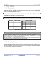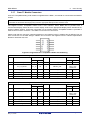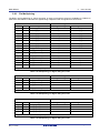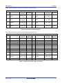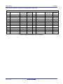
1
User's Manual 32 RZ/A1H Group Renesas Starter Kit+ User’s Manual For e2 studio (ASSAM) RENESAS MCU Family / RZ/A1 Series All information contained in these materials, including products and product specifications, represents information on the product at the time of publication and is subject to change by Renesas Electronics Corporation without notice. Please review the latest information published by Renesas Electronics Corporation through various means, including the Renesas Electronics Corporation website (http://www.renesas.com). Rev. 2.00 May 2015 Notice 1. Descriptions of circuits, software and other related information in this document are provided only to illustrate the operation of semiconductor products and application examples. You are fully responsible for the incorporation of these circuits, software, and information in the design of your equipment. Renesas Electronics assumes no responsibility for any losses incurred by you or third parties arising from the use of these circuits, software, or information. 2. Renesas Electronics has used reasonable care in preparing the information included in this document, but Renesas Electronics does not warrant that such information is error free. Renesas Electronics assumes no liability whatsoever for any damages incurred by you resulting from errors in or omissions from the information included herein. 3. Renesas Electronics does not assume any liability for infringement of patents, copyrights, or other intellectual property rights of third parties by or arising from the use of Renesas Electronics products or technical information described in this document. No license, express, implied or otherwise, is granted hereby under any patents, copyrights or other intellectual property rights of Renesas Electronics or others. 4. You should not alter, modify, copy, or otherwise misappropriate any Renesas Electronics product, whether in whole or in part. Renesas Electronics assumes no responsibility for any losses incurred by you or third parties arising from such alteration, modification, copy or otherwise misappropriation of Renesas Electronics product. 5. Renesas Electronics products are classified according to the following two quality grades: “Standard” and “High Quality”. The recommended applications for each Renesas Electronics product depends on the product’s quality grade, as indicated below. “Standard”: Computers; office equipment; communications equipment; test and measurement equipment; audio and visual equipment; home electronic appliances; machine tools; personal electronic equipment; and industrial robots etc. “High Quality”: Transportation equipment (automobiles, trains, ships, etc.); traffic control systems; anti-disaster systems; anticrime systems; and safety equipment etc. Renesas Electronics products are neither intended nor authorized for use in products or systems that may pose a direct threat to human life or bodily injury (artificial life support devices or systems, surgical implantations etc.), or may cause serious property damages (nuclear reactor control systems, military equipment etc.). You must check the quality grade of each Renesas Electronics product before using it in a particular application. You may not use any Renesas Electronics product for any application for which it is not intended. Renesas Electronics shall not be in any way liable for any damages or losses incurred by you or third parties arising from the use of any Renesas Electronics product for which the product is not intended by Renesas Electronics. 6. You should use the Renesas Electronics products described in this document within the range specified by Renesas Electronics, especially with respect to the maximum rating, operating supply voltage range, movement power voltage range, heat radiation characteristics, installation and other product characteristics. Renesas Electronics shall have no liability for malfunctions or damages arising out of the use of Renesas Electronics products beyond such specified ranges. 7. Although Renesas Electronics endeavors to improve the quality and reliability of its products, semiconductor products have specific characteristics such as the occurrence of failure at a certain rate and malfunctions under certain use conditions. Further, Renesas Electronics products are not subject to radiation resistance design. Please be sure to implement safety measures to guard them against the possibility of physical injury, and injury or damage caused by fire in the event of the failure of a Renesas Electronics product, such as safety design for hardware and software including but not limited to redundancy, fire control and malfunction prevention, appropriate treatment for aging degradation or any other appropriate measures. Because the evaluation of microcomputer software alone is very difficult, please evaluate the safety of the final products or systems manufactured by you. 8. Please contact a Renesas Electronics sales office for details as to environmental matters such as the environmental compatibility of each Renesas Electronics product. Please use Renesas Electronics products in compliance with all applicable laws and regulations that regulate the inclusion or use of controlled substances, including without limitation, the EU RoHS Directive. Renesas Electronics assumes no liability for damages or losses occurring as a result of your noncompliance with applicable laws and regulations. 9. Renesas Electronics products and technology may not be used for or incorporated into any products or systems whose manufacture, use, or sale is prohibited under any applicable domestic or foreign laws or regulations. You should not use Renesas Electronics products or technology described in this document for any purpose relating to military applications or use by the military, including but not limited to the development of weapons of mass destruction. When exporting the Renesas Electronics products or technology described in this document, you should comply with the applicable export control laws and regulations and follow the procedures required by such laws and regulations. 10. It is the responsibility of the buyer or distributor of Renesas Electronics products, who distributes, disposes of, or otherwise places the product with a third party, to notify such third party in advance of the contents and conditions set forth in this document, Renesas Electronics assumes no responsibility for any losses incurred by you or third parties as a result of unauthorized use of Renesas Electronics products. 11. This document may not be reproduced or duplicated in any form, in whole or in part, without prior written consent of Renesas Electronics. 12. Please contact a Renesas Electronics sales office if you have any questions regarding the information contained in this document or Renesas Electronics products, or if you have any other inquiries. (Note 1) “Renesas Electronics” as used in this document means Renesas Electronics Corporation and also includes its majority owned subsidiaries. (Note 2) “Renesas Electronics product(s)” means any product developed or manufactured by or for Renesas Electronics. (2012.4) General Precautions in the Handling of MPU/MCU Products The following usage notes are applicable to all MPU/MCU products from Renesas. For detailed usage notes on the products covered by this document, refer to the relevant sections of the document as well as any technical updates that have been issued for the products. 1. Handling of Unused Pins Handle unused pins in accordance with the directions given under Handling of Unused Pins in the manual. The input pins of CMOS products are generally in the high-impedance state. In operation with an unused pin in the open-circuit state, extra electromagnetic noise is induced in the vicinity of LSI, an associated shoot-through current flows internally, and malfunctions occur due to the false recognition of the pin state as an input signal become possible. Unused pins should be handled as described under Handling of Unused Pins in the manual. 2. Processing at Power-on The state of the product is undefined at the moment when power is supplied. The states of internal circuits in the LSI are indeterminate and the states of register settings and pins are undefined at the moment when power is supplied. In a finished product where the reset signal is applied to the external reset pin, the states of pins are not guaranteed from the moment when power is supplied until the reset process is completed. In a similar way, the states of pins in a product that is reset by an on-chip power-on reset function are not guaranteed from the moment when power is supplied until the power reaches the level at which resetting has been specified. 3. Prohibition of Access to Reserved Addresses Access to reserved addresses is prohibited. The reserved addresses are provided for the possible future expansion of functions. Do not access these addresses; the correct operation of LSI is not guaranteed if they are accessed. 4. Clock Signals After applying a reset, only release the reset line after the operating clock signal has become stable. When switching the clock signal during program execution, wait until the target clock signal has stabilized. When the clock signal is generated with an external resonator (or from an external oscillator) during a reset, ensure that the reset line is only released after full stabilization of the clock signal. Moreover, when switching to a clock signal produced with an external resonator (or by an external oscillator) while program execution is in progress, wait until the target clock signal is stable. 5. Differences between Products Before changing from one product to another, i.e. to a product with a different part number, confirm that the change will not lead to problems. The characteristics of an MPU or MCU in the same group but having a different part number may differ in terms of the internal memory capacity, layout pattern, and other factors, which can affect the ranges of electrical characteristics, such as characteristic values, operating margins, immunity to noise, and amount of radiated noise. When changing to a product with a different part number, implement a system-evaluation test for the given product. Disclaimer By using this Renesas Starter Kit (RSK), the user accepts the following terms: The RSK is not guaranteed to be error free, and the entire risk as to the results and performance of the RSK is assumed by the User. The RSK is provided by Renesas on an “as is” basis without warranty of any kind whether express or implied, including but not limited to the implied warranties of satisfactory quality, fitness for a particular purpose, title and non-infringement of intellectual property rights with regard to the RSK. Renesas expressly disclaims all such warranties. Renesas or its affiliates shall in no event be liable for any loss of profit, loss of data, loss of contract, loss of business, damage to reputation or goodwill, any economic loss, any reprogramming or recall costs (whether the foregoing losses are direct or indirect) nor shall Renesas or its affiliates be liable for any other direct or indirect special, incidental or consequential damages arising out of or in relation to the use of this RSK, even if Renesas or its affiliates have been advised of the possibility of such damages. Precautions The following precautions should be observed when operating any RSK product: This Renesas Starter Kit is only intended for use in a laboratory environment under ambient temperature and humidity conditions. A safe separation distance should be used between this and any sensitive equipment. Its use outside the laboratory, classroom, study area or similar such area invalidates conformity with the protection requirements of the Electromagnetic Compatibility Directive and could lead to prosecution. The product generates, uses, and can radiate radio frequency energy and may cause harmful interference to radio communications. However, there is no guarantee that interference will not occur in a particular installation. If this equipment causes harmful interference to radio or television reception, which can be determined by turning the equipment off or on, you are encouraged to try to correct the interference by one or more of the following measures; • ensure attached cables do not lie across the equipment • reorient the receiving antenna • increase the distance between the equipment and the receiver • connect the equipment into an outlet on a circuit different from that which the receiver is connected • power down the equipment when not in use • consult the dealer or an experienced radio/TV technician for help NOTE: It is recommended that wherever possible shielded interface cables are used. The product is potentially susceptible to certain EMC phenomena. To mitigate against them it is recommended that the following measures be undertaken; • The user is advised that mobile phones should not be used within 10m of the product when in use. • The user is advised to take ESD precautions when handling the equipment. The Renesas Starter Kit does not represent an ideal reference design for an end product and does not fulfil the regulatory standards for an end product. General Precautions in the Handling of MPU/MCU Products The following usage notes are applicable to all MPU/MCU products from Renesas. For detailed usage notes on the products covered by this document, refer to the relevant sections of the document as well as any technical updates that have been issued for the products. 1. Handling of Unused Pins Handle unused pins in accord with the directions given under Handling of Unused Pins in the manual. − The input pins of CMOS products are generally in the high-impedance state. In operation with an unused pin in the open-circuit state, extra electromagnetic noise is induced in the vicinity of LSI, an associated shoot-through current flows internally, and malfunctions occur due to the false recognition of the pin state as an input signal become possible. Unused pins should be handled as described under Handling of Unused Pins in the manual. 2. Processing at Power-on The state of the product is undefined at the moment when power is supplied. − The states of internal circuits in the LSI are indeterminate and the states of register settings and pins are undefined at the moment when power is supplied. In a finished product where the reset signal is applied to the external reset pin, the states of pins are not guaranteed from the moment when power is supplied until the reset process is completed. In a similar way, the states of pins in a product that is reset by an on-chip power-on reset function are not guaranteed from the moment when power is supplied until the power reaches the level at which resetting has been specified. 3. Prohibition of Access to Reserved Addresses Access to reserved addresses is prohibited. − The reserved addresses are provided for the possible future expansion of functions. Do not access these addresses; the correct operation of LSI is not guaranteed if they are accessed. 4. Clock Signals After applying a reset, only release the reset line after the operating clock signal has become stable. When switching the clock signal during program execution, wait until the target clock signal has stabilized. − When the clock signal is generated with an external resonator (or from an external oscillator) during a reset, ensure that the reset line is only released after full stabilization of the clock signal. Moreover, when switching to a clock signal produced with an external resonator (or by an external oscillator) while program execution is in progress, wait until the target clock signal is stable. 5. Differences between Products Before changing from one product to another, i.e. to a product with a different part number, confirm that the change will not lead to problems. − The characteristics of an MPU or MCU in the same group but having a different part number may differ in terms of the internal memory capacity, layout pattern, and other factors, which can affect the ranges of electrical characteristics, such as characteristic values, operating margins, immunity to noise, and amount of radiated noise. When changing to a product with a different part number, implement a system-evaluation test for the given product. How to Use This Manual 1. Purpose and Target Readers This manual is designed to provide the user with an understanding of the RSK+ hardware functionality, and electrical characteristics. It is intended for users designing sample code on the RSK+ platform, using the many different incorporated peripheral devices. The manual comprises of an overview of the capabilities of the RSK+ product, but does not intend to be a guide to embedded programming or hardware design. Further details regarding setting up the RSK+ and development environment can found in the tutorial manual. Particular attention should be paid to the precautionary notes when using the manual. These notes occur within the body of the text, at the end of each section, and in the Usage Notes section. The revision history summarizes the locations of revisions and additions. It does not list all revisions. Refer to the text of the manual for details. The following documents apply to the RZ/A1HH Group. Make sure to refer to the latest versions of these documents. The newest versions of the documents listed may be obtained from the Renesas Electronics Web site. Document Type User’s Manual Description Describes the technical details of the RSK hardware. Document Title RSK+RZA1H Document No. R20UT3007EG User’s Manual Tutorial Manual Provides a guide to setting up RSK environment, running sample code and debugging programs. RSK+RZ/A1H Tutorial Manual R20UT3008EG Quick Start Guide Provides simple instructions to setup the RSK and run the first sample, on a single A4 sheet. RSK+RZA1H R20UT3006EG Full detail circuit schematics of the RSK. RSK+RZA1H Schematics Quick Start Guide R20UT2586EG Schematics Hardware Manual Provides technical details of the RZ/A1H microcontroller. RZ/A1HH Group User’s Manual: Hardware R01UH0403EJ 2. List of Abbreviations and Acronyms Abbreviation Full Form ACIA Asynchronous Communications Interface Adapter bps CRC bits per second Cyclic Redundancy Check DMA DMAC Direct Memory Access Direct Memory Access Controller GSM Hi-Z Global System for Mobile Communications High Impedance IEBus Inter Equipment Bus I/O Input/Output IrDA LSB Infrared Data Association Least Significant Bit MSB NC Most Significant Bit Non-Connect PLL PWM Phase Locked Loop Pulse Width Modulation SFR SIM Special Function Register Subscriber Identity Module UART VCO Universal Asynchronous Receiver/Transmitter Voltage Controlled Oscillator Abbreviation Full Form ADC e2 studio Analog-to-Digital Converter Renesas Eclipse Embedded Studio Integrated Debugging Environment EMC ESD Electromagnetic Compatibility Electrostatic Discharge I2C, IIC Philips™ Inter-Integrated Circuit Connection Bus IRQ Interrupt Request J-LINK On-chip Debugger KR Key Return LCD Liquid Crystal Display LED Light Emitting Diode MCU Micro-controller Unit n/a Not applicable n/c Not connected PC Personal Computer QSPI Quad Serial Programming Interface RSK Renesas Starter Kit RSK+ Renesas Starter Kit + (denotes extra functionality over standard RSK) SAU Serial Array Unit SEGGER JLink-Lite On-chip Debugger SPI Serial Peripheral Interface USB Universal Serial Bus All trademarks and registered trademarks are the property of their respective owners. Table of Contents 1. Overview.......................................................................................................................... 10 1.1 1.2 Purpose .................................................................................................................................................... 10 Features ................................................................................................................................................... 10 2. Power Supply .................................................................................................................. 11 2.1 2.2 Requirements ........................................................................................................................................... 11 Power-Up Behaviour ................................................................................................................................ 11 3. Board Layout ................................................................................................................... 12 3.1 3.2 Component Layout ................................................................................................................................... 12 Board Dimensions .................................................................................................................................... 13 4. Connectivity ..................................................................................................................... 14 4.1 4.2 Internal RSK Connections........................................................................................................................ 14 Debugger Connections ............................................................................................................................ 15 5. User Circuitry ................................................................................................................... 16 5.1 5.2 5.3 5.4 5.5 5.6 5.7 5.8 5.9 5.10 5.11 5.12 5.13 5.14 5.15 5.16 5.17 5.18 5.19 5.20 Potentiometer ........................................................................................................................................... 16 Clock Circuit ............................................................................................................................................. 16 RCA Video Input ...................................................................................................................................... 16 Switches ................................................................................................................................................... 16 Port Expander .......................................................................................................................................... 17 CAN.......................................................................................................................................................... 17 SD/MMC................................................................................................................................................... 18 SDRAM / NOR Flash ............................................................................................................................... 18 NAND Flash ............................................................................................................................................. 19 Dual QSPI Flash ...................................................................................................................................... 19 Universal Serial Bus (USB) ...................................................................................................................... 22 Ethernet & EEPROM ............................................................................................................................... 23 LEDs ........................................................................................................................................................ 24 Reset Circuit ............................................................................................................................................ 24 Audio ........................................................................................................................................................ 24 USB Serial Port ........................................................................................................................................ 25 Pmod™ Module Connectors .................................................................................................................... 28 TFT LCD Panel Connector ...................................................................................................................... 29 LVDS ........................................................................................................................................................ 31 Pin Multiplexing ........................................................................................................................................ 32 6. Configuration ................................................................................................................... 33 6.1 6.2 6.3 6.4 6.5 Modifying the RSK ................................................................................................................................... 33 Power Supply Configuration .................................................................................................................... 39 Ethernet Configuration ............................................................................................................................. 39 Jumper Link Configuration ....................................................................................................................... 40 MCU Boot and Oscillator Configuration ................................................................................................... 41 7. Headers ........................................................................................................................... 42 7.1 Application Headers ................................................................................................................................. 42 8. Code Development .......................................................................................................... 46 8.1 8.2 8.3 8.4 8.5 Overview .................................................................................................................................................. 46 Mode Support .......................................................................................................................................... 46 Compiler Restrictions ............................................................................................................................... 46 Debugger Support .................................................................................................................................... 46 Address Space ......................................................................................................................................... 47 9. Additional Information ...................................................................................................... 48 10. Appendix A Component Layout and Board Dimensions................................................. 49 RSK+RZA1H RENESAS STARTER KIT+ R20UT3007EG0200 Rev. 2.00 May 17, 2015 1. Overview 1.1 Purpose This RSK is an evaluation tool for Renesas microcontrollers. This manual describes the technical details of the RSK hardware. The Quick Start Guide and Tutorial Manual provide details of the software installation and debugging environment. 1.2 Features This RSK provides an evaluation of the following features: • Renesas microcontroller programming • User code debugging • User circuitry such as switches, LEDs and a potentiometer • Sample application • Sample peripheral device initialisation code The RSK board contains all the circuitry required for microcontroller operation. R20UT3007EG0200 Rev. 2.00 May 17, 2015 Page 10 of 53 RSK+RZA1H 2. Power Supply 2. Power Supply 2.1 Requirements This RSK is supplied with a SEGGER JLink-Lite debugger. This board is supplied with a 5Vdc supply using a 5.0mm barrel power jack. The board can operate with a supply of up to 12Vdc if required, with appropriate changes to jumper settings as detailed in Table 2.1. Ensure to check the three pin PWR_SEL jumper settings prior to connecting the power supply. Details of the power supply requirements for the RSK , and configuration are shown in Table 2-1 below. The default RSK power configuration is shown in bold, blue text. It is essential that if a 12V supply is used that PWR_SEL is NOT linked on pins 2-3 or an overvoltage will be applied to the MCU and associated devices, resulting in likely destruction of the whole board CN5 Setting PWR_SEL Setting Regulator IC Output IC 12V 5V Pin1-2 shorted Pin2-3 shorted Voltage Power Name IC5 5V BOARD_5V IC4 3.3V BOARD_VCC IC21 1.18V CORE_VCC IC36 3.3V AVREF Table 2.1: Main Power Supply Requirements The main power supply connected to PWR1 should supply a minimum of 5W to ensure full functionality. When designing an RZ/A1H MCU into a new board, it should be noted that if the 3.3V supply is valid and the 1.18V core supply is not, then MCU input and output ports will be in an undefined state until the 1.18V core supply is valid. When designing the MCU power sequencing during board hardware design it is strongly advised to ensure that the 1.18V supply is valid before the 3.3V. The 1.18V core supply on the RSK+RZA1H board is valid before the 3.3V supply, so on the RSK+RZA1H the input/output ports remain in a defined state during the power up period. 2.2 Power-Up Behaviour When the RSK is purchased, the RSK board has the ‘Release’ or stand-alone code from the example tutorial software pre-programmed into the Renesas microcontroller. On powering up the board the LEDs will start to flash. After 200 flashes or after pressing any switch, the text on the LCD display will change and the LED0 will begin to flash at a rate controlled by the potentiometer. R20UT3007EG0200 Rev. 2.00 May 17, 2015 Page 11 of 53 RSK+RZA1H 4. Connectivity 3. Board Layout 3.1 Component Layout Figure 3-1 below shows the top component layout of the board. Figure 3.1: Board Layout R20UT3007EG0200 Rev. 2.00 May 17, 2015 Page 12 of 53 RSK+RZA1H 3.2 4. Connectivity Board Dimensions See Appendix A R20UT3007EG0200 Rev. 2.00 May 17, 2015 Page 13 of 53 RSK+RZA1H 4. Connectivity 4. Connectivity 4.1 Internal RSK Connections The diagram below shows the RSK board components and their connectivity to the MCU. Line IN PMODTM interface 2 channels Audio CODEC Line Out USB / Serial Interface SDRAM 64MB / 512Mb 4x User LEDs 3x Power LEDs PORTS NOR Flash 64MB / 512Mb SDCARD Slot MMCCARD Slot BUS QSPI Flash 128MB / 1Gb Composite Video 2x Channels NAND Flash 256MB / 2Gb NAND Filters CVin RZA1 IIC EEPROM 16kB Ethernet MAC Storage USB CAN 2 channels Digital video Connector (MIL) (8 or 16 bit possible) Selected 8 bit SIM Card Pads Only – Not fitted CMOS Camera Interface Connector Only – No Camera USB MII RMII RGB888 Ethernet RGB888 to LVDS LVDS JTAG LVDS (HDMI) Debugger JLINK 20pin ULINK2 20pin ETM SSI Interface (Pin header only) SPDIF 1xHost/Function (default as Host) 1xFunction/Host (default as Function) External display Panel 7" Projective Capacitive touch 800 X 480 Figure 4.1: Internal RSK Block Diagram R20UT3007EG0200 Rev. 2.00 May 17, 2015 Page 14 of 53 RSK+RZA1H 4.2 4. Connectivity Debugger Connections The diagram below shows the connections between the RSK, SEGGER JLink-Lite debugger and the host PC. User Interface Cable USB Cable SEGGER Jlink-Lite RSK Host PC Figure 4.2: Debugger Connection Diagram R20UT3007EG0200 Rev. 2.00 May 17, 2015 Page 15 of 53 RSK+RZA1H 5. User Circuitry 5. User Circuitry 5.1 Potentiometer A single-turn potentiometer, RV1, is connected as a potential divider to analogue input AN7, P1_15, pin Y19. The potentiometer can be used to create a voltage between AVCC and AD_Ground. The potentiometer is fitted to offer an easy method of supplying a variable analogue input to the microcontroller. It does not necessarily reflect the accuracy of the controller’s ADC. Refer to the RZ/A1H Group Hardware Manual for further details. 5.2 Clock Circuit Clock circuits are fitted to the RSK+ to generate the required clock signals to drive the MCU, and associated peripherals. Refer to the RZ/A1H Group Hardware Manual for details regarding the clock signal requirements, and the RSK+RZA1H board schematics for information regarding the clock circuitry in use on the RSK+. Details of the oscillators fitted to the board are listed in Table 5-1 below. Crystal/Oscillator Function Default Placement Frequency Device Package OSC2 Main MCU oscillator. Fitted 13.333MHz SOJ 4Pin OSC1 Audio oscillator. Fitted 22.5792MHz TXC_TD_2P5X2 OSC3 Video oscillator. Fitted 27.000MHz QFN4 X6 RTC 1 clock Fitted 32.768kHz ABS06 X3 RTC 2 clock Fitted 4.000MHz HC-49 X4 USB Clock Fitted 48.000MHz FA-238 Table 5.1: Oscillators 5.3 RCA Video Input The RSK+ board provides two channels of RCA video input to the RZ/A1H MCU, on connectors CN38 and CN39. These connect to the RSK+RZA1H MCU on pins VIN1A, B15 and VIN2A, A15 respectively, via 100nF decoupling capacitors. Refer to the RSK+RZA1H board schematics for further information. 5.4 Switches There are five switches located on the RSK+ board. The function of each switch and its connection is shown in Table 5-2. For further information regarding switch connectivity, refer to the RSK+RZA1H schematics. Switch Function MCU Port Pin RES When pressed, the microcontroller is reset. RES# Y8 SW1 Connects to an IRQ input for user controls. IRQ3 (P1_9) AB18 SW2 Connects to an IRQ input for user controls. IRQ2 (P1_8) AA17 SW3 Connects to an IRQ input for user controls. IRQ5 (P1_11) AA18 NMI Connects to the non-maskable input for user controls. NMI Y9 Table 5.2: Switch Connections R20UT3007EG0200 Rev. 2.00 May 17, 2015 Page 16 of 53 RSK+RZA1H 5.5 5. User Circuitry Port Expander The RSK+ board utilises two port expander ICs, IC34 and IC35 in order to provide more I/O signals. These devices are the CAT9554 from On Semiconductor. For further information on these devices visit the On Semiconductor website at www.onsemi.com. 2 The port expanders provide 8 parallel I/O lines each, which can be accessed via an I C/SMBus serial 2 connection. On the RSK+ board, they are able to be accessed at different addresses on I C channel 3 on the 2 MCU. The I C logical address for IC34 is 0x40 and IC35 is 0x41. Table 5.3 details the signal connections to IC34 and Table 5.4 details the signal connections to IC35. Port Number Signal name Function 0 LED1 LED output control. Output low = ON, output high = OFF 1 LED2 LED output control. Output low = ON, output high = OFF 2 LED3 LED output control. Output low = ON, output high = OFF 3 NOR_A25 Bit #25 of NOR Flash Addressing 4 PMOD1_RST Reset line for PMOD Channel 1 5 PMOD2_RST Reset line for PMOD Channel 2 6 SD_CONN_PWR_EN Power supply enable for external SD card connection 7 SD_MMC_PWR_EN Power supply enable for MMC card connection Table 5.3: Port Expander IC34 Connection Details Port Number Signal name Function 0 PX1_EN0 Multiplex control for LCD/DV Data Lines. Low = LCD, High = DV 1 PX1_EN1 Multiplex control for Ethernet/general Data Lines. Low = general, High = Ethernet. 2 TFT_CS Chip select for TFT 3 PX1_EN3 Multiplex control for PWM timer channels and audio codec IC14 serial ADC/DAC I/O lines. 4 USB_OVR_CURRENT Signal from USB power controller indicating overcurrent condition. 5 USB_PWR_ENA Enable USB power supply for channel 0 6 USB_PWR_ENB Enable USB power supply for channel 1 7 PX1_EN7 Multiplex control for Address bus line A18-A21 and sound generator outputs SGOUT0-4. Table 5.4: Port Expander IC35 Connection Details 5.6 CAN There are two CAN channels which connect to the MCU as listed in Table 5.5. CAN Signal Function MCU Port Pin CAN_CTX1 CAN Channel 1 Transmit P5_10 B7 CAN_CRX1 CAN Channel 1 Receive P5_9 A7 CAN_CTX2 CAN Channel 2 Transmit P7_3 J3 CAN_CRX2 CAN Channel 2 Receive P7_2 H1 Table 5.5: CAN Connection R20UT3007EG0200 Rev. 2.00 May 17, 2015 Page 17 of 53 RSK+RZA1H 5.7 5. User Circuitry SD/MMC The RSK+ board provides an SD/MMC card socket, CN1. The connections are detailed in Table 5.6. Signal Function MCU Port Pin NAF1_TRACED1_SMWP1 Write Protect P3_9 W20 NAF0_TRACED0_SMCD Card Detect P3_8 V19 NAF5_SMCMD Command I/O P3_13 R22 NAF4_SMCLK Clock P3_12 T22 NAF3_TRACED3_SMD0 Data 0 P3_11 T21 NAF2_TRACED2_SMD1 Data 1 P3_10 T20 NAF7_SMD2 Data 2 P3_15 R20 NAF6_TRACECLK_SMD3 Data 3 P3_14 R21 P4_0_FRE_MMCD4 Data 4 P4_0 P20 P4_1_FCLE_MMCD5 Data 5 P4_1 P22 P4_2_FALE_MMCD6 Data 6 P4_2 P21 P4_3_FWE_MMCD7 Data 7 P4_3 N22 Table 5.6: SD/MMC Connection Note that it is not possible to boot from an SD card that is connected to the SD/MMC connector CN1. This is because the connector utilises channel 1 of the SD controller integrated in the RZ/A1H MCU. For further information, refer to the hardware manual, table 3.1. 5.8 SDRAM / NOR Flash The RSK+ board provides 32MByte SDRAM, IC24 and 16MByte NOR Flash, IC23 connected to the address / data buses. Note that the SDRAM as fitted on the RSK+ board is configured in hardware to use the Chip Select line CS2. The BSC module within the RZ/A1H MCU assumes a second SDRAM device will be connected also to CS3. As such it is necessary that the BSC within the RZ/A1H MCU is configured to use both CS2 and CS3 as SDRAM, even though a second SDRAM is not present on CS3, and that CS3 is not used on the expansion headers. As such option link R164 must NOT be fitted, to prevent bus conflicts. By default this link is not fitted, as this port pin is configured for LED0. For other external memory mapped devices, chip select CS1 remains available for use. This is a known limitation of the RSK+ board. For new applications with only one SDRAM it is recommended to connect the SDRAM to CS3, which will allow single SDRAM use without issue. See the hardware manual Bus State Controller section 8.4.3 CS2WCR(SDRAM) , p171 for further details. Note that the NOR Flash is configured to operate on the bus control line CS0. In order for this to operate Jumper link JP18 and resistor link R314 (fitted as default) must be connected. Refer to the RSK+RZA1H board schematics for further information. R20UT3007EG0200 Rev. 2.00 May 17, 2015 Page 18 of 53 RSK+RZA1H 5.9 5. User Circuitry NAND Flash The connections of the NAND FLASH are detailed in Table 5.7. Signal Function MCU Port Pin NAF0_TRACED0_SMCD IO line 0 P3_8 V19 NAF1_TRACED1_SMWP1 IO line 1 P3_9 W20 NAF2_TRACED2_SMD1 IO line 2 P3_10 T20 NAF3_TRACED3_SMD0 IO line 3 P3_11 T21 NAF4_SMCLK IO line 4 P3_12 T22 NAF5_SMCMD IO line 5 P3_13 R22 NAF6_TRACECLK_SMD3 IO line 6 P3_14 R21 NAF7_SMD2 IO line 7 P3_15 R20 P4_3_FWE_MMCD7 Write Enable P4_3 N22 P4_2_FALE_MMCD6 Address latch Enable P4_2 P21 P4_1_FCLE_MMCD5 Command Latch Enable P4_1 P22 P4_0_FRE_MMCD4 Read Enable P4_0 P20 P1_2_FRB Ready Busy P1_2 B18 FCE_NAND Chip Enable P5_5 C10 RESET2_N Write Protect Connected to reset circuit Table 5.7: NAND Flash Connection To enable boot for the NAND FLASH, set SW6 pins 1/2/3 to OFF. The NAND device is 256MByte in size, however, it should be noted however, that only 64MByte is addressable. Refer to section 6.1.5 for further details. 5.10 Dual QSPI Flash The RSK+ board provides two 64MByte Serial Flash memory ICs, IC25 and IC26, which connect to the RZ/A1H MCU via the SPI Multi I/O Bus Controller. Signal Connections are detailed in Table 5.8 below. Signal Function MCU Port Pin SPBCLK_0 Serial Clock (Common) P9_2 C8 P9_3_SPBSSL_0 Chip Select (Common) P9_3 A6 RESET_N Device Reset (Common) P9_4_SPBIO00_0 Serial Input / IO_0 (IC26 Device 0) P9_4 B6 P9_5_SPBIO10_0 Serial Output / IO_1 (IC26 Device 0) P9_5 C7 P9_6_SPBIO20_0 Write Protect / IO_2 (IC26 Device 0) P9_6 A5 P9_7_SPBIO30_0 Hold / IO_3 (IC26 Device 0) P9_7 B5 P2_12_SPBIO01_0 Serial Input / IO_0 (IC25 Device 1) P2_12 A21 P2_13_SPBIO11_0 Serial Output / IO_1 (IC25 Device 1) P2_13 A20 P2_14_SPBIO21_0 Write Protect / IO_2 (IC25 Device 1) P2_14 C18 P2_15_SPBIO31_0_IRQ1 Hold / IO_3 (IC25 Device 1) P2_15 B19 Connected to reset circuit Table 5.8: SPI Flash Connection R20UT3007EG0200 Rev. 2.00 May 17, 2015 Page 19 of 53 RSK+RZA1H 5.10.1 5. User Circuitry QSPI Modes of Operation There are several modes of operation of the QSPI memory in conjunction with the serial memory controller in the RZ/A1H MCU. On the RSK+ board, there are two QSPI memory devices, attached to ports 0 and 1, of the Multi I/O SPI controller’s channel 0. Channel 1 is used for other functions. SPI multi I/O bus controller IC26 (Serial Flash 0) SPBSSL_0 CS# SPBCLK_0 SCK SPBMO0_0/SPBIO00_0 SPBMI0_0/SPBIO10_0 SI / IO0 SO / IO1 SPBIO20_0 SPBIO30_0 W# / IO2 PORT 0 HOLD# / IO3 Channel 0 IC25 (Serial Flash 1) CS# SCK SI / IO0 SO / IO1 SPBMO1_0/SPBIO01_0 SPBMI1_0/SPBIO11_0 PORT 1 SPBIO21_0 SPBIO31_0 W# / IO2 HOLD# / IO3 SPBSSL_1 SPBCLK_1 SPBMO0_1/SPBIO00_1 PORT 0 SPBMI0_1/SPBIO10_1 SPBIO20_1 SPBIO30_1 Channel 1 PORT 1 SPBMO1_1/SPBIO01_1 SPBMI1_1/SPBIO11_1 SPBIO21_1 SPBIO31_1 Figure 5.1: RZ/A1H SPI multi I/O controller. Each QSPI memory device can support one, two or four simultaneous serial lines of I/O. Furthermore, the controller allows each channel’s ports to work in parallel, providing up to eight simultaneous serial lines of I/O in dual QSPI mode. During the QSPI boot mode Port 0 is used and is accessed using only the clock, SPBMO0 and SPBMI0 signals (Single bit Single channel). SPBSSL SPBCLK Channel 0 Port 0 x T7 T6 T5 T4 T3 T2 T1 T0 x x R7 R6 R5 R4 R3 R2 R1 R0 x Serial Flash SPBMO0 SPBMI0 Figure 5.2: Single bit single channel operation mode. R20UT3007EG0200 Rev. 2.00 May 17, 2015 Page 20 of 53 RSK+RZA1H 5. User Circuitry It is important to recognise that these eight lines are serial inputs, and are not operating on the same byte, but successive bytes. When operating over the two ports it should be noted that the memory structure is fundamentally different from single channel operation, as lines 1-4 are working with the memory on Port 0 and 5-8 are working with Port 1. Figure 5.3 attempts to show this visually. Single Channel Mode Serial Flash 0 Byte13 Byte14 Byte15 Byte16 Byte9 Byte10 Byte11 Byte12 Byte5 Byte6 Byte7 Byte8 Byte1 Byte2 Byte3 Byte4 PORT 0 Byte13 Byte14 Byte15 Byte16 Byte9 Byte10 Byte11 Byte12 Byte5 Byte6 Byte7 Byte8 Byte1 Byte2 Byte3 Byte4 Serial Flash 1 PORT 1 NOT ACCESSED Dual Channel Mode Serial Flash 0 Byte9 Byte10 Byte11 Byte12 Byte1 Byte2 Byte3 Byte4 PORT 0 Byte9 Byte10 Byte11 Byte12 Byte1 Byte2 Byte3 Byte4 Serial Flash 1 Byte13 Byte14 Byte15 Byte16 Byte5 Byte6 Byte7 Byte8 PORT 1 Byte13 Byte14 Byte15 Byte16 Byte5 Byte6 Byte7 Byte8 Figure 5.3: Memory access of Single and Dual Mode QSPI Operation. The consequence of this is that data stored in QSPI FLASH needs to be accessed in the same manner as it has been programmed in. If data is accessed in Single QSPI mode when it has been programmed in Dual QSPI mode, then every fourth group of four bytes will be missing. Conversely data accessed in Dual Channel mode when it has been programmed in Single Channel mode will have blocks of four bytes from the other port inserted between every fourth byte of correct data. R20UT3007EG0200 Rev. 2.00 May 17, 2015 Page 21 of 53 RSK+RZA1H 5.11 5. User Circuitry Universal Serial Bus (USB) This RSK+ board is fitted with two channels of USB. Each channel can operate as either a host or as a function device. Channel 0 is by default configured as USB Function and the connector and jumper link settings for the channel 0 power supply are shown in Table 5.10. Channel 1 is by default configured as USB Host and the connector and jumper link settings for the Channel 1 power supply are shown in Table 5.12. The signal connections to the MCU for Channel 0 and Channel 1 are detailed in Table 5.9 and Table 5.11 respectively. Note: Default settings are shown in bold, blue text USB Signal Function MCU Port Pin DP0 Positive differential data signal. DP0 AA12 DM0 Negative differential data signal. DM0 AB12 VBUS0 Cable monitor pin. VBUSIN0 Y12 USB_PWR_ENA VBUS power supply enable. Port Expander 2 IO[5] – See Table 5.4 USB_OVR_CURRENT Over-current detection signal Port Expander 2 IO[4] – See Table 5.4 Table 5.9: USB0 Module MCU Connections Operation as USB Function Operation as USB Host Fit Connector CN6 Power from Connector CN6 Fit Connector CN8 Do Not Fit Connector CN8 Link JP11 pins 2 and 3 Do Not Fit Connector CN6 Power from RSK Link JP11 pins 1 and 2 Table 5.10: USB0 Module Connector and Power Settings USB Signal Function MCU Port Pin DP1 Positive differential data signal. DP1 AB11 DM1 Negative differential data signal. DM1 AA11 VBUS1 Cable monitor pin. VBUSIN1 Y11 USB_PWR_ENB VBUS power supply enable. Port Expander 2 IO[6] – See Table 5.4 USB_OVR_CURRENT Over-current detection signal Port Expander 2 IO[4] – See Table 5.4 Table 5.11: USB1 Module MCU Connections Operation as USB Host Operation as USB Function Fit Connector CN8 Do Not Fit Connector CN6 Power from RSK Link JP11 pins 1 and 2 Fit Connector CN6 Do Not Fit Connector CN8 Power from Connector CN6 Link JP11 pins 2 and 3 Table 5.12: USB1 Module Connector and Power Settings Note: • • When evaluating OTG, ensure to replace the default USB connector (USB0_D) with a USB Micro-AB connector. Connectors such as the one manufactured by Hirose Electric with part number ZX62R-AB-5P, can be used. R20UT3007EG0200 Rev. 2.00 May 17, 2015 Page 22 of 53 RSK+RZA1H 5.12 5. User Circuitry Ethernet & EEPROM This RSK+ board is fitted with an Ethernet connection. The connections from the Ethernet driver IC, IC12, are detailed in Table 5.13. Refer to the RZ/A1H board schematics for further information. MCU Signal Port Pin ET_MDC P5_9* A7 ET_MDIO P3_3 (**Multiplexed) AA6 ET_IRQ P4_14 IRQ6 G19 ET_RXCLK P3_4 (**Multiplexed) Y5 ET_RXD3 P2_11 (**Multiplexed) E19 ET_RXD2 P2_10 (**Multiplexed) B22 ET_RXD1 P2_9 (**Multiplexed) C21 ET_RXD0 P2_8 (**Multiplexed) D20 ET_RXDV P3_6 (**Multiplexed) AB3 ET_RXER P3_5 (**Multiplexed) AA4 ET_TXEN P2_2 (**Multiplexed) F21 ET_TXD0 P2_4 (**Multiplexed) F19 ET_TXD1 P2_5 (**Multiplexed) E22 ET_TXD2 P2_6 (**Multiplexed) E20 ET_TXD3 P2_7 (**Multiplexed) C22 ET_TXCLK P2_0 (**Multiplexed) L21 ET_TXER P2_1 (**Multiplexed) K22 ET_CRS P2_3 (**Multiplexed) G20 RESET2_N Connected to reset circuit ET_COL P1_14 AA19 *This pin is connected to the MCU via link R105. Refer to section 6.1.8 for further details. **These pins are connected to the MCU via a multiplexer IC IC29. Set Signal PX1_EN1 High to connect these signals to the MCU. See section 5.20 for further details of the multiplexing on the RSK+ board. Table 5.13: Ethernet Connection A 2KByte EEPROM is fitted in order to store the MAC address for the Ethernet connection. This can be 2 accessed via I C channel 3, with address 0xA0. Connection details are described in Table 5.14 below. 2 I C Signal MCU Function SDA3 Serial Data Line SCL3 Clock Line Port Pin P1_7 B16 P1_6 A17 2 Table 5.14: EEPROM Connection on I C Channel 3 There is an eight-way configuration DIP switch, SW4, which is used to determine Ethernet settings on the RSK+ board. Refer to section 6.3 for further details. R20UT3007EG0200 Rev. 2.00 May 17, 2015 Page 23 of 53 RSK+RZA1H 5.13 5. User Circuitry LEDs There are ten LEDs on the RSK. The function of each LED, its colour and connection are shown in Table 5.15. LED Colour Function MCU Port Pin POWER_IN Green Indicates the status of the power connected to CN4. - - POWER Green Indicates the status of the BOARD_5V (5V) power rail. - - POWER Green Indicates the status of the BOARD_VCC (3.3V) power rail. - - LED0 Green User operated LED. P7_1 H2 LED1 Orange User operated LED. * * LED2 Red User operated LED. * * LED3 Red User operated LED. * * LED4 Yellow Ethernet Indication - - LED5 Green Ethernet Indication - - LED6 Green Ethernet Indication - - *These LEDs are connected to port expander IC34’s I/O pin. See section 5.5 for further details. Table 5.15: LED Connections 5.14 Reset Circuit A reset control circuit is fitted to the RSK+ to generate the required reset signal, and is triggered from the RES switch, power supply monitor and debugger connection. Refer to the RZ/A1H hardware manual for details regarding the reset signal timing requirements and the RSK+ schematics for information regarding the reset circuitry in use on the board. 5.15 Audio The RSK+ board provides audio input via a 3.5mm Stereo jack, CN19 and audio output via 3.5mm stereo jack CN20. It also incorporates an audio codec device, IC14 which is linked to the MCU via the signals described in Table 5.16 Signal Function MCU Port Pin SCL3 Clock Line P1_6 A17 SDA3 Serial Data Line P1_7 B16 IRQ_AUDIO Hardware IRQ P3_1 AA7 SSIWS0 Digital Audio Left-Right Clock IO P4_5* M20 SSISCK0 Digital Audio Bit Clock P4_4* M21 SSIRXD0 Digital Audio Serial Data ADC Output P4_6* L22 SSITXD0 Digital Audio Serial Data DAC Input P4_7* L20 *Connection to ports via multiplexer IC30. See section 5.20 for more details. Table 5.16: Audio Codec Connections R20UT3007EG0200 Rev. 2.00 May 17, 2015 Page 24 of 53 RSK+RZA1H 5.16 5. User Circuitry USB Serial Port A USB serial port implemented in another Renesas low power microcontroller (RL78/G1C) is fitted on the RSK+ to the microcontroller Serial Communications Interface (SCI) module. Multiple options are provided to allow re-use of the serial interface. Connections between the USB to Serial converter and the microcontroller are listed in Table 5.17 below. Signal Name Function MCU Port Pin P3_0_TXD2 External SCI Transmit Signal P3_0 AB6 P3_2_RXD2 External SCI Receive Signal. P3_2 Y7 G1C_CTS Clear To Send P1_8 AA17 G1C_RTS Request to Send P4_14 G19 Table 5.17: Serial Port Connections When the RSK+ is first connected to a PC running Windows with the USB/Serial connection, the PC will look for a driver. This driver is installed during the installation process, so the PC should be able to find it. The PC will report that it is installing for a driver and then report that a driver has been installed successfully, as shown in Figure 5.4. The exact messages may vary depending upon operating system. Figure 5.4 USB-Serial Windows Installation message 5.16.1 Reading the Virtual COM Port Number In order for the PC to be able to communicate with the RSK+ board via the USB virtual COM port, the correct COM port number must be determined. If the COM port number is not known, follow this process: 1. Connect the PC to the serial/USB port. 2. On the PC, go to StartControl PanelDevice Manager. Go to the “Ports (COM & LPT)” section and the COM port should be listed there. To verify the correct port, the USB cable can be disconnected and re-connected to show the COM port appearing and disappearing. Figure 5.5 Device Manager Ports R20UT3007EG0200 Rev. 2.00 May 17, 2015 Page 25 of 53 RSK+RZA1H 5.16.2 5. User Circuitry Changing the Virtual COM Port Number Some PC applications will only work with particular COM port numbers. COM port numbers for the RSK+ serial/USB are assigned automatically at the time of first connection to the PC. It is possible to assign a different value manually. The procedure to do this is as follows: 1. Right-click the USB-Serial port in device manager and select “Properties” Figure 5.6 Device Manager Port Properties 2. Select the “Port Settings” tab and click “Advanced…” Figure 5.7 Device Manager Port Settings R20UT3007EG0200 Rev. 2.00 May 17, 2015 Page 26 of 53 RSK+RZA1H 5. User Circuitry 3. Select the new COM port from the drop down list. Bear in mind that the “in use” label on various ports listed may not actually mean that port is in use at this current point in time. Figure 5.8 Device Manager Advanced Port Settings Click OK to complete the process. R20UT3007EG0200 Rev. 2.00 May 17, 2015 Page 27 of 53 RSK+RZA1H 5.17 5. User Circuitry Pmod™ Module Connectors A Pmod™ Compatible debug LCD module is supplied with the RSK+, and should be connected to the PMOD1 header. Care should be taken when installing the LCD module to ensure pins are not bent or damaged. The LCD module is vulnerable to electrostatic discharge (ESD); therefore appropriate ESD protection should be used. The Digilent Pmod™ Compatible header uses a SPI interface. Some RSKs will be provided with a monochrome display, others will have a colour display. Code for the appropriate display will be included in the product software support. Connection information for the Digilent Pmod™ Compatible header is provided in Table 5.18 for Pmod™ connector 1 and Table 5.19 for Pmod™ connector 2. Please note that the connector numbering adheres to the Digilent Pmod™ standard and is different from all other connectors on the RSK designs. Details can be found in the Digilent Pmod™ Interface Specification Revision: November 20, 2011. Figure 5.9: Digilent Pmod™ Compatible Header Pin Numbering Digilent Pmod™ Compatible Header Connections Pin 1 Circuit Net Name PMOD1_CS MCU Pin Port Pin P1_4 B17 7 Circuit Net Name PMOD_INT 2 MCU Port Pin P1_3 A18 P11_14_MOSI1 P11_14 H3 8 PMOD1_RST Port Expander 1 IO[4] – See section 5.5 3 P11_15_MISO1 P11_15 J4 9 PMOD_PIN9 P4_15 F22 4 P11_12_RSPCK1 P11_12 G2 10 PMOD_PIN10 P3_7 Y4 5 GROUND - - 11 GROUND - - 6 Board_Vcc - - 12 Board_Vcc - - Table 5.18: PMOD1 Header Connections Digilent Pmod™ Compatible Header Connections Pin Circuit Net Name MCU Pin Port Pin C16 1 PMOD2_CS P1_5 2 P11_14_MOSI1 P11_14 Circuit Net Name 7 PMOD_INT 8 PMOD2_RST H3 MCU Port Pin P1_3 A18 Port Expander 1 IO[5] – See section 5.5 3 P11_15_MISO1 P11_15 J4 9 PMOD_PIN9 P4_15 F22 4 P11_12_RSPCK1 P11_12 G2 10 PMOD_PIN10 P3_7 Y4 5 GROUND - - 11 GROUND - - 6 Board_Vcc - - 12 Board_Vcc - - Table 5.19: PMOD2 Header Connections R20UT3007EG0200 Rev. 2.00 May 17, 2015 Page 28 of 53 RSK+RZA1H 5.18 5. User Circuitry TFT LCD Panel Connector A TFT display can connect to the RSK+ board, via connector CN44. The signals route to the MCU via multiplexers IC37 and IC38 as described by Table 5.20.Refer to the schematic for further information. Connector CN44 Pin Signal 1 MCU Port Pin P11_7_LCD0DATA0 P11_7 M3 2 P11_6_LCD0DATA1 P11_6 M2 3 P11_5_LCD0DATA2 P11_5 L1 4 P11_4_LCD0DATA3 P11_4 L4 5 P11_3_LCD0DATA4 P11_3 C5 6 P11_2_LCD0DATA5 P11_2 B4 7 P11_1_LCD0DATA6 P11_1 C6 8 P11_0_LCD0DATA7 P11_0 A4 9 P10_15_LCD0DATA8 P10_15 D21 10 P10_14_LCD0DATA9 P10_14 D22 11 P10_13_LCD0DATA10 P10_13 F20 12 P10_12_LCD0DATA11 P10_12 E21 13 P10_11_LCD0DATA12 P10_11 H20 14 P10_10_LCD0DATA13 P10_10 H21 15 P10_9_LCD0DATA14 P10_9 J20 16 P10_8_LCD0DATA15 P10_8 J21 17 P10_7_LCD0DATA16 P10_7 M22 18 P10_6_LCD0DATA17 P10_6 N21 19 P10_5_LCD0DATA18 P10_5 N20 20 P10_4_LCD0DATA19 P10_4 N19 21 P10_3_LCD0DATA20 P10_3 AB5 22 P10_2_LCD0DATA21 P10_2 Y6 23 P10_1_LCD0DATA22 P10_1 AA5 24 P10_0_LCD0DATA23 P10_0 AB4 25 RESET2_N 26 P11_15_LCD0CLK P11_15 J4 27 P11_12_LCD0TCON2 P11_12 G2 28 P11_11_LCD0TCON3 P11_11 U3 29 P11_10_LCD0TCON4 P11_10 T3 30 P11_13_LCD0TCON1 P11_13 G1 31 P11_14_LCD0TCON0 P11_14 H3 32 P11_9_LCD0TCON5 P11_9 T2 33 P11_8_LCD0TCON6 P11_8 T1 34 BL_PWM_CTRL P3_1 (IRQ6) AA7 Connected to reset circuit Table 5.20: TFT Signal Connections R20UT3007EG0200 Rev. 2.00 May 17, 2015 Page 29 of 53 RSK+RZA1H 5. Connector CN44 Pin Signal 35 NC User Circuitry MCU Port Pin 36 NC 37 SDA0 P1_1 C17 38 SCL0 P1_0 A19 39 TP_INT P4_9 K21 40 P11_12_RSPCK1 P11_12 G2 41 P11_14_MOSI1 P11_14 H3 42 P11_15_MISO1 P11_15 J4 43 TFT_CS Port Expander 2 [2] – See section 5.5 N/A 44 NC 45 BOARD_VCC 46 BOARD_VCC 47 GROUND 48 GROUND 49 BOARD_5V 50 BOARD_5V Table 5.20: TFT Signal Connections (continued) R20UT3007EG0200 Rev. 2.00 May 17, 2015 Page 30 of 53 RSK+RZA1H 5.19 5. User Circuitry LVDS The RSK+ board provides an LVDS interface, from connector CN17. Connection details to the MCU are described in Table 5.21. Connector CN17 Pin Signal 1 BOARD_VCC 2 BOARD_VCC 3 Function MCU Port Pin 3,3V Power supplied to external display N/A N/A 3,3V Power supplied to external display N/A N/A GROUND GROUND connection for the external display. N/A N/A 4 GROUND GROUND connection for the external display. N/A N/A 5 P5_7_TXOUT0M LVDS Channel 0 Minus Line P5_7 B9 6 P5_6_TXOUT0P LVDS Channel 0 Positive Line P5_6 A9 7 GROUND Isolates neighbouring pairs of data signals N/A N/A 8 P5_5_TXOUT1M LVDS Channel 1 Minus Line P5_5 C10 LVDS Channel 1 Positive Line P5_4 C11 Isolates neighbouring pairs of data signals N/A N/A 9 P5_4_TXOUT1P_X 10 GROUND 11 P5_3_TXOUT2M LVDS Channel 2 Minus Line P5_3 B10 12 P5_2_TXOUT2P LVDS Channel 2 Positive Line P5_2 A10 13 GROUND Isolates neighbouring pairs of data signals N/A N/A 14 P5_0_TXCLKOUTP LVDS Clock Positive Line P5_0 A11 15 P5_1_TXCLKOUTM LVDS Clock Minus Line P5_1 B11 16 GROUND Isolates neighbouring pairs of data signals N/A N/A 17 BOARD_VCC *1 N/A N/A GROUND *1 N/A N/A Used to configure the external display in *2 6 bit mode when pulled low. N/A N/A N/A N/A 18 19 GROUND 20 BOARD_VCC This pin is used to display the image normal (low signal) or *3 inverse (high signal). Table 5.21: LVDS Connections *1. Enables writing to LVDS displays that have 8-bit data pairs. This differential pair is not used since the RZ/A1H device only has six differential LVDS data lines. As a result, the unused pins on the external display are wired so that the pair have constant opposing signals (3.3V and GROUND) as required. *2. This pin is the ‘Mode’ signal on the external display. It is configured low to signal to the display that it will be used in 6-bit mode. *3. This pin must be pulled low or high on the external display board’s design. R20UT3007EG0200 Rev. 2.00 May 17, 2015 Page 31 of 53 RSK+RZA1H 5.20 5. User Circuitry Pin Multiplexing The RSK+ uses multiplexing on various channels, in order to increase the amount of available I/O. Table 5.22, Table 5.23 and Table 5.24 describe the signals being multiplexed and the signals that control them. MCU Signal Routed to MCU Port Pin Signal PX1_EN1* = High PX1_EN1* = Low P2_0 L21 P2_0_ETTXCLK ET_TXCLK P2_0_IO0 P2_1 K22 P2_1_ETTXER ET_TXER P2_1_IO1 P2_2 F21 P2_2_ETTXEN ET_TXEN P2_1_IO2 P2_3 G20 P2_3_ETCRS ET_CRS P2_1_IO3 P2_4 F19 P2_4_ETTXD0 ET_TXD0 P2_1_IO4 P2_5 E22 P2_5_ETTXD1 ET_TXD1 P2_1_IO5 P2_6 E20 P2_6_ETTXD2 ET_TXD2 P2_1_IO6 P2_7 C22 P2_7_ETTXD3 ET_TXD3 P2_1_IO7 P2_8 D20 P2_8_ETTRXD0_RSPCK4 ET_RXD0 RSPCK4 P2_9 C21 P2_9_ETRXD1_SSL40 ET_RXD1 SSL40 P2_10 B22 P2_10_ETRXD2_MOSI4 ET_RXD2 MOSI4 P2_11 E19 P2_11_ETRXD3_MISO4 ET_RXD3 MISO4 P3_3 AA6 P3_3_ETMDIO_SCICTS1 ET_MDIO SIM_RESET P3_4 Y5 P3_4_ETRXCLK_SCISCK0 ET_RXCLK SIM_CLK P3_5 AA4 P3_5_ETRXER_SCITXD0 ET_RXER SIM_TXD P3_6 AB3 P3_6_ETRXDV_SCIRXD0 ET_RXDV SIM_RXD *PX1_EN1 is connected to the MCU via port expander IC35. See section 5.5 for further details. Table 5.22: Multiplexing for Signal PX1_EN1, IC29 MCU Signal Routed to MCU Port Pin Signal PX1_EN3* = High PX1_EN3* = Low P4_4 M21 P4_4_SSISCK0_PWM2E PWM2E SSISCK0 P4_5 M20 P4_5_SSIWS0_PWM2F PWM2F SSIWS0 P4_6 L22 P4_6_SSIRXD0_PWM2G PWM2G SSIRXD0 P4_7 L20 P4_7_SSITXD0_PWM2H PWM2H SSITXD0 *PX1_EN3 is connected to the MCU via port expander IC35. See section 5.5 for further details. Table 5.23: Multiplexing for Signal PX1_EN3, IC30 MCU Signal Routed to MCU Port Pin Signal PX1_EN7* = High PX1_EN7* = Low P8_10 W2 P8_10_A18_SGOUT0 SGOUT0 A18 P8_11 W3 P8_11_A19_SGOUT1 SGOUT1 A19 P8_12 Y1 P8_12_A20_SGOUT2 SGOUT2 A20 P8_13 V4 P8_13_A21_SGOUT3 SGOUT3 A21 *PX1_EN7 is connected to the MCU via port expander IC35. See section 5.5 for further details. Table 5.24: Multiplexing for Signal PX1_EN7, IC20 R20UT3007EG0200 Rev. 2.00 May 17, 2015 Page 32 of 53 RSK+RZA1H 6. Configuration 6. Configuration 6.1 Modifying the RSK This section lists the option links that are used to modify the way RSK+ operates in order to access different configurations. Configurations are made by modifying link resistors or headers with movable jumpers. Table 6-1 below shows the RSK+RZ/A1H default configuration with respect to the peripheral functionality. Bold, blue text indicates the default configuration that the RSK is supplied with. It is noted that certain peripheral functions are disabled by default, as shown in Table 6.1 in the column entitled Secondary Function. It is possible to activate these disabled peripherals, but at the expense of the default peripheral functions as shown in the Table. Refer to the sections cited in the Table in order to perform any required modifications. When removing soldered components, always ensure that the RSK is not exposed to a soldering iron for intervals greater than five seconds. This is to avoid damage to nearby components mounted on the board. When modifying a link resistor, always check the related option links to ensure there is no possible signal contention or short circuits. Because many of the MCU’s pins are multiplexed, some of the peripherals must be used exclusively. Refer to RZ/A1H Group Hardware Manual and RSK+RZA1H schematics for further information. Primary Function Secondary Function See Section(s) Switches Various IRQ, Analog lines on Application headers 6.1.1 LEDs Timer channel TIOC0B, external bus chip select CS3 6.1.1 Various SD, switch and IRQ functions USB / Serial RTS & CTS handshaking 6.1.9 SP/DIF* LVDS Channel 0 6.1.2 SDRAM CAN Channel 2, timer channel TIOC1B 6.1.3 NOR FLASH Timer channel TIOC3A 6.1.4 NAND FLASH LVDS Channel 1 6.1.5 QSPI FLASH Bus Address Line A0 6.1.6 CAN Channel 1 Some Ethernet lines, Misc. Connector CN15 6.1.7 Ethernet ADC Line for App header, CAN channel 1 6.1.8 Audio Codec IRQ for port expander / TFT Backlight Control 6.1.11 LVDS* SP/DIF 6.1.12 PMOD Interfaces Various SD / Timer and Application Header signals 6.1.13 SD Card SD card interface 6.1.14 TFT Serial TXD0 / SD Card Write Protect 6.1.10 Table 6.1: RSK Default Configuration by Function * The primary and secondary functions depend on the port pin these two functions share. A link resistor is a 0Ω surface mount resistor, which is used to short or isolate parts of a circuit. Option links are listed in the following sections, detailing their function when fitted or removed. Refer to the component placement diagram (Figure 3.3, Figure 3.4) to locate the option links and jumpers. Bold, blue text indicates the default configuration that the RSK is supplied with. R20UT3007EG0200 Rev. 2.00 May 17, 2015 Page 33 of 53 RSK+RZA1H 6.1.1 6. Configuration Switches, Potentiometer and LED Table 6.2 details the option links associated with the user switches, pot and LEDs. MCU Function Exclusive Function Header Connection Header Pin Fit Remove R114 R421 JA1 Pin23 R114 --- JA1 Pin10 R421 --- R162 R163 R86 JA2 Pin23 JA2-B Pin23 R163 ----- R420 R189 R423 JA5 Pin10 R189 --- JA1 Pin12 R423 --- Port Pin Signal Fit Remove 1_9 AB18 SW1 R192 AA17 SW2 SW1 1_8 SW2 SW3 1_11 AA18 SW3 POT 1_15 Y19 ADPOT R161 R347 JA1 Pin9 R347 --- LED0 7_1 H2 LED0 R328 R181 R164 JA5 Pin14 R181 --- Table 6.2: Option Link configuration for user switches, pot and LEDs Switch bank SW4 is used to control the functionality of the Ethernet connection. Please refer to section 6.3 Ethernet Configuration on page 39 for further information. Switch bank SW6 is used to control the boot options. Please refer to section 6.5 MCU Boot and Oscillator Configuration on page 41 for further information. 6.1.2 SP/DIF Table 6.3 details the option links associated with SP/DIF. MCU Function Exclusive Function Header Connection Port Pin Signal Fit Remove Header Pin Fit Remove 5_6 A9 SPDIF_IN CN3 R169 R170 --- --- --- 5_7 B9 SPDIF_OUT R183 R182 --- --- --- SP/DIF Table 6.3: Option Link configuration for SP/DIF 6.1.3 SDRAM Table 6.4 details the option links associated with the SDRAM. MCU Function SDRAM Exclusive Function Header Connection Port Pin Signal Fit Remove Header Pin Fit Remove 7_3 J3 CAS_SDRAM R173 R174 --- --- --- 7_2 H1 RAS_SDRAM R4 R18 --- --- --- 7_5 J1 WR_SDRAM R146 R158 --- --- --- 7_4 J2 CKE_SDRAM R115 --- --- --- --- Table 6.4: Option Link configuration for SDRAM R20UT3007EG0200 Rev. 2.00 May 17, 2015 Page 34 of 53 RSK+RZA1H 6.1.4 6. Configuration NOR FLASH Table 6.5 details the option links associated with the NOR FLASH. MCU Function NOR FLASH Exclusive Function Header Connection Port Pin Signal Fit Remove Header Pin Fit Remove 7_8 K4 RD_NOR R155 R159 JA2 Pin20 R159 --- Table 6.5: Option Link configuration for NOR FLASH 6.1.5 NAND FLASH Table 6.6 details the option links associated with the NAND FLASH. MCU Function NAND FLASH Exclusive Function Header Connection Port Pin Signal Fit Remove Header Pin Fit Remove 5_5 C10 FCE_NAND R167 R168 --- --- --- Table 6.6: Option Link configuration for NAND FLASH 6.1.6 QSPI FLASH Table 6.7 details the option links associated with the QSPI FLASH. MCU Function QSPI FLASH Exclusive Function Header Connection Port Pin Signal Fit Remove Header Pin Fit Remove 9_2 C8 SPBCLK_0 R373 R378 --- --- --- Table 6.7: Option Link configuration for QSPI FLASH 6.1.7 CAN Channels Table 6.8 details the option links associated with the CAN interface. MCU Function Exclusive Function Header Connection Port Pin Signal Fit Remove Header Pin Fit Remove CAN CHANNEL 1 5_10 B7 CAN_CTX1 R206 R207 JA5 Pin5 --- --- 5_9 A7 CAN_CRX1 R104 R105 JA5 Pin6 --- --- CAN CHANNEL 2 7_3 J3 CAN_CTX2 R174 R173 JA5 Pin7 --- --- 7_2 H1 CAN_CRX2 R18 R4 JA5 Pin8 --- --- Table 6.8: Option Link configuration for CAN R20UT3007EG0200 Rev. 2.00 May 17, 2015 Page 35 of 53 RSK+RZA1H 6.1.8 6. Configuration Ethernet Table 6.9 details the option links associated with the Ethernet Functionality. MCU Function Ethernet Exclusive Function Header Connection Port Pin Signal Fit Remove Header Pin Fit Remove 1_14 AA19 ET_COL R270 R278 JA5 Pin3 R278 --- 5_9 A7 ET_MDC R105 R104 JA5 Pin6 R104 R105 --- Table 6.9: Option Link configuration for Ethernet 6.1.9 USB/Serial Table 6.10 details the option links associated with the USB/Serial Interface. MCU Function Exclusive Function Header Connection Port Pin Signal Fit Remove Header Pin Fit Remove 4_14 G19 G1C_RTS R190 R177 R178 --- --- --- 1_8 AA17 G1C_CTS R86 R162 R163 JA2 Pin23 JA2-B Pin23 R163 R86 --- USB/Serial Table 6.10: Option Link configuration for USB/Serial 6.1.10 TFT Table 6.11 details the option links associated with the TFT display connection. MCU Function TFT Exclusive Function Port Pin Signal Fit 4_9 K21 TP_INT R384 1_1 C17 SDA0 R302 Header Connection Remove R289 R290 R304 Header Pin Fit Remove --- --- --- --- --- --- Table 6.11: Option Link configuration for TFT R20UT3007EG0200 Rev. 2.00 May 17, 2015 Page 36 of 53 RSK+RZA1H 6.1.11 6. Configuration Audio Codec Table 6.12 details the option links associated with the Audio Codec. MCU Function Audio Audio – Line In Exclusive Function Port Pin Signal Fit Remove Header Pin Fit Remove 3_1 AA7 IRQ_AUDIO R106 R107 R186 --- --- --- --- --- LINEIN1 R129 R130 CN19 Pin2 *1 --- --- --- --- LINEIN2 R131 R132 CN19Pin3 *1 --- --- --- --- JACKSNS R323 R324 --Audio – Mic In *1 Header Connection --- MICL R130 R129 --- --- MICR R132 R131 --- --- JACKSNS R324 R323 --- --- --- CN19 Pin2 *1 --- --- CN19Pin3 *1 --- --- --- --- --- CN20 Pin3 *1 --- --- --- --- Audio Headphone o/p ----- --- HPL R135 R136 CN20 Pin2 *1 --- --- LOUTR R134 R133 CN20 Pin3 *1 Audio – Line Out --- --- --- --- LOUTL R136 R135 CN20 Pin2 *1 --- --- Audio Input Gnd --- --- MICGND R319 R320 CN20 Pin1 R319 R320 --- --- AUDIO_GND R320 R319 CN20 Pin1 R320 R319 HPR --- R133 R134 Via 1uF Decoupling Capacitor Table 6.12: Option Link configuration for the Audio Codec 6.1.12 LVDS Table 6.13 details the option links associated with the LVDS functionality. MCU Function Exclusive Function Header Connection Port Pin Signal Fit Remove Header Pin Fit Remove LVDS Channel 0 5_6 A9 P5_6_TXOUT0P R170 R169 CN17 Pin6 R170 R169 5_7 B9 P5_7_TXOUT0M R182 R183 CN17 Pin5 R182 R183 LVDS Channel 1 5_4 C11 P5_4_TXOUT1P_X R432 --- CN17 Pin9 R432 --- 5_5 C10 P5_5_TXOUT1M R168 R167 CN17 Pin8 R168 R167 Table 6.13: Option Link configuration for LVDS R20UT3007EG0200 Rev. 2.00 May 17, 2015 Page 37 of 53 RSK+RZA1H 6.1.13 6. Configuration Pmod™ Interfaces Table 6.14 details the option links associated with the Pmod™ Interfaces. MCU Function Exclusive Function Header Connection Port Pin Signal Fit Remove Header Pin Fit Remove 3_7 Y4 PMOD_PIN10 R171 R227 R144 CN25 Pin10 CN26 Pin10 R171 --- 1_4 B17 PMOD1_CS R301 --- CN25 Pin1 R301 --- 4_15 F22 PMOD_PIN9 R175 R176 CN25 Pin9 CN26 Pin9 R175 --- 1_3 A18 PMOD_INT R305 R247 CN25 Pin7 CN26 Pin7 R305 --- 3_7 Y4 PMOD_PIN10 R171 R227 R144 CN25 Pin10 CN26 Pin10 R171 --- 1_5 C16 PMOD2_CS R303 --- CN26 Pin1 R303 --- 4_15 F22 PMOD_PIN9 R175 R176 CN25 Pin9 CN26 Pin9 R175 --- 1_3 A18 PMOD_INT R305 R247 CN25 Pin7 CN26 Pin7 R305 --- PMOD1 PMOD2 Table 6.14: Option Link configuration for PMOD 6.1.14 SD Card Table 6.11 details the option links associated with SD card connector CN2. Note that the SD card connector CN2 is not fitted as standard. MCU Function Exclusive Function Header Connection Port Pin Signal Fit Remove Header Pin Fit Remove 4_9 K21 SD_WP_EXT R290 R384 R289 CN2 Pin2 R290 --- 4_8 K20 SD_CD_EXT R306 R300 CN2 Pin3 R306 --- 4_13 G21 SD_CMD_EXT R180 R179 CN2 Pin4 R180 --- 4_12 H22 SD_CLK_EXT R311 R309 CN2 Pin5 R311 --- 4_11 H19 SD_D0_EXT R315 R313 CN2 Pin6 R315 --- 4_10 J22 SD_D1_EXT R294 R293 CN2 Pin7 R294 --- 4_15 F22 SD_D2_EXT R176 R175 CN2 Pin8 R176 --- 4_14 G19 SD_D3_EXT R178 R177 R190 CN2 Pin9 R178 --- SD Card Table 6.15: Option Link configuration for SD Card CN2 R20UT3007EG0200 Rev. 2.00 May 17, 2015 Page 38 of 53 RSK+RZA1H 6.2 6. Configuration Power Supply Configuration Power to the RSK+RZA1H board should be applied to connector CN5, from a 5mm diameter centre positive plug, at either 5Vdc or 12Vdc. The header PWR_SEL is used to select operation from a 12V or 5V supply. It is essential that if a 12V supply is used that PWR_SEL is NOT linked on pins 2-3 or an overvoltage will be applied to the MCU and associated devices, resulting in likely destruction of the whole board. Table 6.16 describes the jumper settings for the PWR_SEL header PWR_SEL Select Input power voltage setting Link 1-2 Link 2-3** 12V supply 5V supply ** Do NOT connect a 12V input source to the RSK+ when PWR_SEL jumper is set to link pins 2-3 Table 6.16: PWR_SEL Header Configuration There are 2 headers available that can be used to measure the current taken by the MCU during operation. JP4 can be used to measure the MCU core current and JP6 can be used to measure current drawn by the MCU port pins, by shorting them via a current meter. In order to use these functions, it is necessary to remove links R24 and R26 respectively. Table 6.17 provides a summary. JP4 MCU Core Current Measurement Remove R24 and short JP4 with meter to measure MCU core current. JP6 MCU Port Pins Current Measurement Remove R26 and short JP6 with meter to measure MCU port pin current. Table 6.17: MCU Current Measurement Headers 6.3 Ethernet Configuration Table 6.18 below details the options configurable for the Ethernet function via the 8-way DIP switch SW4. SW4 LAN Strap Option Off On Signal name 1 Auto MDI-X Enable 1 0 ET_CRS 2 Q-Autoneg Enable 1 0 ET_RXCLK 3 Phy Adr0 0 1 ET_RXD0 4 Phy Adr1 0 1 ET_RXD1 5 Full/Half # 1 0 ET_RXD2 6 Autoneg EN 1 0 ET_RXD3 7 MII/RMII # 1 0 ET_RXER 8 Fast (J) / Std (JK) 1 0 ET_TXCLK Table 6.18: Ethernet configuration via SW4 R20UT3007EG0200 Rev. 2.00 May 17, 2015 Page 39 of 53 RSK+RZA1H 6. Configuration 6.4 Jumper Link Configuration Table 6.19 describes the jumper link option configurations available on the RSK+RZA1H board. JP1 Enable SIM card 2 way communication (or TX only) Open Link 2 way communication enabled TXD and RXD connected to SIM JP3 TXD to SIM only Write protect NAND FLASH IC27 Jumper Position Link 1-2 Link 2-3 (R233 Not Fitted)** NAND FLASH IC27 not write protected NAND FLASH IC27 write protected ** Do NOT short pins 2 and 3 of JP3 when R233 is fitted (which is default configuration) JP4 MCU Core Current Measurement Remove R24 and short JP4 with meter to measure MCU core current. JP5 Disable Ethernet MAC EEPROM write protection IC11 Link open EEPROM IC11 write unprotected EEPROM IC11 write protected JP6 MCU Port Pins Current Measurement Remove R26 and short JP6 with meter to measure MCU port pin current. JP11 USB VBUS power select Link 1-2 Link 2-3 BOARD_5V VBUS JP12 USB VBUS1 power select Link 1-2 Link 2-3 BOARD_5V Power from connector, CN9 pin1 (VBUS1) JP18 NOR Flash Chip Enable Link Open NOR Flash active on CS0 NOR Flash inactive JP21 Defining Function of BSCANP pin on RZ/A1H MCU MCU Jumper Position Port Pin BSCANP AA22 linked Normal Operation (Pin held low) PWR_SEL open Boundary Scan (Pin pulled up to BOARD_VCC via R264 22K resistor) Select Input power voltage setting Link 1-2 Link 2-3** 12V 5V ** Do NOT connect a 12V input source to the RSK+ when PWR_SEL jumper is set to link pins 2-3 Table 6.19: Jumper Option descriptions R20UT3007EG0200 Rev. 2.00 May 17, 2015 Page 40 of 53 RSK+RZA1H 6.5 6. Configuration MCU Boot and Oscillator Configuration The six-way DIP switch, SW6 provides some configuration options for the RZ/A1H MCU. Switches 1, 2 and 3 are used to set the boot mode of the RZ/A1H. Table 6.20 provides details of the available modes and the corresponding switch settings. Due to pull-up resistors in the circuit, a “1” is produced when the corresponding switch position is OFF, and a “0” is produced when it is ON. MD_BOOT0 SW6-1 0 ON MD_BOOT1 SW6-2 0 ON MD_BOOT2 SW6-3 * JP18 SHORT 0 ON 1 OFF * SHORT 1 OFF 0 ON 1 OFF * 1 OFF 1 OFF 0 ON * 1 OFF 1 OFF 1 OFF * Boot Mode Boot mode 0 (CS0-space 16-bit booting) Boots the LSI from memory (bus width: 16 bits) connected to the CS0 space. Uses NOR flash (IC23). Boot mode 1 (CS0-space 32-bit booting) Boots the LSI from memory (bus width: 32 bits) connected to the CS0 space. Not supported on RSK+. Boot mode 3 (serial flash booting) Boots the LSI from the serial flash memory connected to the SPI multi I/O bus space. The only way of booting this LSI chip is from channel 0 (P9_2 to P9_5) in this mode. Uses QSPI flash (IC26 only). Boot mode 4 (eSD booting) Boots the LSI from the NAND flash memory with the SD controller. The only way of booting this LSI chip is from channel 0 (P4_10 to P4_15) in this mode. Not supported on RSK+. Boot mode 5 (eMMC booting) Boots the LSI from the NAND flash memory with the MMC controller. The only way of booting this LSI chip is from channel 0 (P3_10 to P3_15) in this mode. Uses NAND flash (IC27). Table 6.20: MCU Boot Modes Note that it is not possible to boot from an SD card that is connected to the SD/MMC connector CN1. This is because the connector utilises channel 1 of the SD controller, which can only boot from channel 0. For further information, refer to the hardware manual, Table 3.1 (note column order is transposed cf. Table 6.20). SW6-4 ON OFF Clock Signal Source EXTAL (Uses OSC2, 13.33MHz.) USB_X1 (Uses X4, 48MHz.) Table 6.21: Clock Signal Source SW6-5 ON Spread Spectrum Clock Generator (SSCG) Mode Enables the SSCG function of the MCU’s internal PLL circuit. This function attempts to reduce EMI peak levels by slightly modulating the output frequency. Disables the SSCG function. Table 6.22: Spread Spectrum Clock Generator (SSCG) Mode OFF SW6-6 is for test purposes only (default is ON). R20UT3007EG0200 Rev. 2.00 May 17, 2015 Page 41 of 53 RSK+RZA1H 7. Headers 7. Headers 7.1 Application Headers This RSK+ is fitted with application headers, which can be used to connect compatible Renesas application devices or as easy access to MCU pins. The following tables provide details of the pin connections of these headers. Some pins will require link resistors to be fitted in order to make the connection to the specified MCU pin. These resistors are also documented in the tables, highlighted in bold, blue if they are fitted by default, or normal text if they are not fitted as standard. Table 7.1 below lists the connections of the application header, JA1. Application Header JA1, JA1-B Pin Header Name 1 3 5 7 9 11 13 CON_5V CON_3V3 CON_AVCC CON_AVREF ADPOT_CN AN2 OPEN 15 P2_0_IO0 17 P2_2_IO2 19 P2_4_IO4 21 P2_6_IO6 23 IRQ3 25 JA1_SDA3 MCU Pin Link Required Pin --------P1_15, Y19 P1_10, Y17 R27 R25 R116 R13 R347 R422 2 4 6 8 10 12 14 0V 0V CON_AVSS ADTRG AN1 AN3 OPEN --- 16 P2_1_IO1 --- 18 P2_3_IO3 --- 20 P2_5_IO5 --- 22 P2_7_IO7 R114 R141 R209 24 OPEN 26 JA1_SCL3 P2_0, L21 (Set PX1_EN1 = 1) P2_2, F21 (Set PX1_EN1 = 1) P2_4, F19 (Set PX1_EN1 = 1) P2_6, E20 (Set PX1_EN1 = 1) P1_9, AB18 P1_7, B16 Header Name MCU Pin Link Required ------P1_3, A18 P1_9, AB18 P1_11, AA18 ----R153 R247 R421 R423 P2_1, K22 (Set PX1_EN1 = 1) P2_3, G20 (Set PX1_EN1 = 1) P2_5, E22 (Set PX1_EN1 = 1) P2_7, C22 (Set PX1_EN1 = 1) P1_6, A17 --- --- --- --- R140 R208 Table 7.1: Application Header JA1 Connections R20UT3007EG0200 Rev. 2.00 May 17, 2015 Page 42 of 53 RSK+RZA1H 7. Headers Table 7.2 below lists the connections of the application header, JA2. Application Header JA2, JA2-B Pin 1 3 5 7 9 11 13 15 17 19 21 23 25 Header Name RESET2_N NMI IRQ0 OPEN IRQ1 OPEN OPEN OPEN OPEN OPEN TCLKB IRQ2 OPEN Link Required Pin Port, Pin MCU --Y9 P1_0, A19 ----R372 P1_1, C17 R304 P1_10, Y17 P1_8, AA17 R188 R163 2 4 6 8 10 12 14 16 18 20 22 24 26 Header Name CON_EXTAL 0V TXD0 RXD0 SCK0 OPEN OPEN OPEN OPEN TIOC3A TIOC3D OPEN OPEN Port, Pin MCU Link Required AB16 --P4_9, K21 P4_10, J22 P4_8, K20 R112 --R289 R293 R300 P7_8, K4 P3_7, Y4 R159 R144 Table 7.2: Application Header JA2 Connections Table 7.3 below lists the connections of the application header, JA3. Note that address lines BA23-BA25 are manifested on Connector CN15, as detailed in Table 7.4. Application Header JA3, JA3-B Pin 1 3 5 7 9 11 13 15 17 19 21 23 25 27 29 31 33 35 37 39 41 43 45 47 49 Header Name BA0 BA2 BA4 BA6 BA8 BA10 BA12 BA14 BD0 BD2 BD4 BD6 BRD BCS1 BD8 BD10 BD12 BD14 BA16 BA18 BA20 BA22 BWAIT BWE1_DQMLU BCAS Link Required Pin Port, Pin MCU P9_2, C8 P7-10, L3 P7_12, M1 P7_14, N2 P8_0, P1 P8_2, P3 P8_4, R2 P8_6, U2 P6_0, B3 P6_2, C4 P6_4, A2 P6_6, D2 P7_8, K4 P3_7, Y4 P6_8, E3 P6_10, E1 P6_12, G4 P6_14, F1 P8_8, V2 P8_10, W2 P8_12, Y1 P8_14, Y2 P1_13, Y18 P7_7, K2 P7_3, J3 R378 ----------------------R155 R227 --------------------R173 2 4 6 8 10 12 14 16 18 20 22 24 26 28 30 32 34 36 38 40 42 44 46 48 50 Header Name BA1 BA3 BA5 BA7 BA9 BA11 BA13 BA15 BD1 BD3 BD5 BD7 BWR BCS3 BD9 BD11 BD13 BD15 BA17 BA19 BA21 BCKIO BCKE BWE0_DQMLL BRAS Port, Pin MCU Link Required P7_9, K1 P7_11, L2 P7_13, N1 P7_15, N3 P8_1, P2 P8_3, R1 P8_5, R3 P8_7, U4 P6_1, D6 P6_3, D5 P6_5, C1 P6_7, D1 P7_5, J1 P7_1, H2 P6_9, E2 P6_11, F3 P6_13, F2 P6_15, G3 P8_9, V3 P8_11, W3 P8_13, V4 CKIO, V1 P7_4, J2 P7_6, K3 P7_2, H1 ------------------------R146 R164 ----------------R115 ----- Table 7.3: Application Header JA3 Connections R20UT3007EG0200 Rev. 2.00 May 17, 2015 Page 43 of 53 RSK+RZA1H 7. Headers Table 7.4 below lists the connections of the Misc. Connector CN15. Misc. Connector CN15 Pin Header Name MCU Port, Pin 1 MISO4 3 MOSI4 5 RSPCK4 7 SSL40 P2_11, E19 (Set PX1_EN1 = 1) P2_10, B22 (Set PX1_EN1 = 1) P2_8, D20 (Set PX1_EN1 = 1) P2_9, C21 (Set PX1_EN1 = 1) Link Required Pin --- 2 --- Header Name Port, Pin MCU Link Required BA23 P8_15, AA1 --- 4 BA24 P9_0, AB2 --- --- 6 BA25 P9_1, AA3 --- --- 8 P5B_10 P5_10, B7 R207 MCU Port, Pin Link Required Table 7.4: Connector CN15 Connections Table 7.5 below lists the connections of the application header, JA5. Application Header JA5, JA5-B Pin Header Name Link Required Pin Port, Pin MCU Header Name 1 AN4 P1_12, AB19 R307 2 OPEN 3 AN6 P1_14, AA19 R278 4 OPEN 5 CAN_CTX1 P5-10, B7 R206 6 CAN_CRX1 P5_9, A7 R104 7 CAN_CTX2 P7_3, J3 R174 8 CAN_CRX2 P7_2, H1 R18 9 IRQ4 P1_10, Y17 R193 10 IRQ5 P1_11, AA18 R189 P7_0, H4 R326 P7_1, H2 R181 P4_5, M20 --- 11 OPEN 13 TIOC0A 12 OPEN 14 TIOC0B 15 OPEN 16 OPEN 17 OPEN 18 OPEN 19 P4_4, M21 PWM2E 21 23 (Mux on IC30) P4_6, L22 PWM2G OPEN --- (Mux on IC30) 20 PWM2F --- (Mux on IC30) P4_7, L20 22 PWM2H 24 OPEN --- (Mux on IC30) Table 7.5: Application Header JA5 Connections R20UT3007EG0200 Rev. 2.00 May 17, 2015 Page 44 of 53 RSK+RZA1H 7. Headers Table 7.6 below lists the connections of the application header, JA6. Application Header JA6, JA6-B Pin Header Name MCU Port, Pin Link Required Pin Header Name 1 OPEN 2 OPEN 3 OPEN 4 OPEN 5 OPEN 6 OPEN 7 OPEN 8 OPEN 9 TXD1 P4_12, H22 R309 10 OPEN 11 SCK1 P4_11, H19 R313 12 RXD1 13 OPEN 14 OPEN 15 OPEN 16 OPEN 17 OPEN 18 OPEN 19 OPEN 20 OPEN 21 OPEN 22 OPEN 23 OPEN 24 OPEN Port, Pin MCU Link Required P4_13, G21 R179 Table 7.6: Application Header JA6 Connections R20UT3007EG0200 Rev. 2.00 May 17, 2015 Page 45 of 53 RSK+RZA1H 8. Code Development 8. Code Development 8.1 Overview For all code debugging using Renesas software tools, the RSK+ board must be connected to a PC via a Segger JLink-Lite debugger, which is supplied with this RSK+ product. 8.2 Mode Support The RZ/A1H microcontroller supports five boot modes which includes booting from memory connected to the CS0 space, serial flash memory, the NAND flash memory with an SD controller, and the NAND flash memory with an MMC controller. 8.3 Compiler Restrictions The version of the compiler provided with this RSK is a fully functional GNU compiler, used in RSK+RZA1H sample projects. Support for the GNU NONE Compiler is available from http://www.kpitgnutools.com 8.4 Debugger Support The RSK+ board is supplied with a Segger JLink-Lite Debugger. Please refer to the Segger website for further information www.segger.com. R20UT3007EG0200 Rev. 2.00 May 17, 2015 Page 46 of 53 RSK+RZA1H 8.5 8. Code Development Address Space Figure 8.1 below details the address space of the MCU. This diagram is based on the Hardware Manual version 1.0. For further details, refer to the RZ/A1H Group Hardware Manual. 1. 2. 3. 4. 5. To enable SDRAM, JP18 must be open and SW6 #3 must be in the ON position (CS0_MBOOT2 low) To enable NOR FLASH, JP18 must be shorted and SW6 #3 must be in the ON position (CS0_MBBOOT2 low) To enable QSPI, JP18 must be shorted and SW6’s switches (SW6.1 – SW6.6) need to be set to: OFF, ON, OFF, ON, ON, ON. Note that SDRAM and NOR FLASH cannot be enabled at the same time. Device is 256MByte, but only 64MByte is addressable. Figure 8.1: RZ/A1H Address Map On RSK Board R20UT3007EG0200 Rev. 2.00 May 17, 2015 Page 47 of 53 RSK+RZA1H 9. Additional Information 9. Additional Information Technical Support 2 For details on how to use e studio, refer to 2 the help file by opening e studio, then selecting Help > Help Contents from the menu bar. For information about the RZ/A1H series microcontrollers refer to the RZ/A1H Group Hardware Manual. For information about the RZ assembly language, refer to the RZ Series Software Manual. Technical Contact Details Please refer to the contact details listed in section 10 of the “Quick Start Guide” General information on Renesas Microcontrollers can be found on the Renesas website at: http://www.renesas.com/ Trademarks All brand or product names used in this manual are trademarks or registered trademarks of their respective companies or organisations. Copyright This document may be, wholly or partially, subject to change without notice. All rights reserved. Duplication of this document, either in whole or part is prohibited without the written permission of Renesas Electronics Europe Limited. © 2014 Renesas Electronics Europe Limited. All rights reserved. © 2014 Renesas Electronics Corporation. All rights reserved. © 2014 Renesas Solutions Corp. All rights reserved. R20UT3007EG0200 Rev. 2.00 May 17, 2015 Page 48 of 53 10. Appendix A Component Layout and Board Dimensions For the following renderings the following statements are true: Board dimensions and connector positions. All the through-hole connectors are on a common 0.1 inch grid for easy interfacing. Component placement of individual components on the top-side PCB. Component placement of individual components on the underside of the PCB. ART FILM - t6877dim NOTES 18.99 1. REMOVE 2. IF THIS 6.29 3. IS R3 4. CN25 C153 R201 CN8 THE PLANE. CODE TO BE APPLICABLE TO FLEX/FLEX ADDED TO AFTER THIS BOARD CONTAINS TRACK AND TRACK CN9 TP8 C155 R319 C212 R339 R325 R327 R337 R329 R335 R331 R81 R333 R200 R340 R338 R336 R111 TP9 C154 R332 R30 R83 R82 C156 TP23 C182 SECONDARY ASSEMBLY. ADDED SIDES SUGGESTED ON A WITH ETCH PLANE, NO OR THERMAL RELIEF. SILKSCREEN RIGIDS) TO BE ADDED IN ETCH. ENSURING AREAS IMPEDANCE CONTROLLED FOR DIFFERENTIAL ARE INDICATED. 1 GAP AND SIZES 10 = 90ohm TRACKS 0.125mm TRACK - 0.125mm +/-10% ARE AS FOLLOWS GAP AND LAYERS 1 GAP LAYERS 3 AND SIZES 10 FOR 100ohm DIFFERENTIAL +/-10% = 0.100mm TRACK - 0.125mm GAP ARE AS FOLLOWS = 0.100mm TRACK - 0.125mm GAP R320 R129 R341 C213 R310 R312 TP40 TO PADS. APPEARS R29 R202 C100 R203 C101 R187 R213 R214 R261 10 R211 R259 R204 (NOT BE DATE LAYER SIZE TP4 30x6.7 CN26 CN17 CN39 AND INNER (ZERO) CONTACT VISIBILITY LAYERS CN38 0 DIRECT CODE CAN OF (4 PLACES) 1 RES A RATING THEY (4 PLACES) NON-FUNCTIONAL APERTURE VENDOR UL D=3.3 ALL AN R342 R130 CN19 TRACK SIZES LAYER 1 FOR 50ohms +/-10% SINGLE ENDED ARE AS FOLLOWS R321 R265 R230 C160 R99 t6877l4.art t6877l5.art 115.75 CN18 C197 C200 C199 D4 C165 133.4 CORE t6877l9.art Layer 9 PRE-PREG Layer 10 Solder t6877l10.art Resist t6877r10.art Silkscreen t6877s10.art Solder Paste t6877p10.art CN12 Refer to build document:- T6877_Build_Info.pdf C175 L14 2x1.25 R58 R59 R57 R55 R56 TP22 PWR_SEL LED9 SW4 R77 LED8 CN5 R71 LED7 R160 R66 R7 R195 2.6x1.1 R9 R21 R19 C77 C75 C74 R12 IC5 C69 D1 C94 C65 C329 D5 C344 C345 L2 TP39 R51 R118 R117 R120 RV1 C102 IC2 C68 MR4 t6877l8.art Layer 8 C180 R64 R54 R53 R52 R381 R147 C331 C261 C71 TP20 CN3 t6877l7.art PRE-PREG MR29 C70 C260 CORE Layer 7 88.7 C179 C178 C177 C176 C164 C167 R61 R6 C328 120.75 R143 R124 R142 R121 R65 R46 R45 C90 C173 R62 t6877l6.art Layer 6 C190 C181 R145 C166 R190 R177 R178 R11 R10 C72 C110 MR28 TP1 R8 IC4 C327 PRE-PREG TP12 SW6 JP18 128.4 CN10 CN11 R34 R32 R50 2x1.25 R31 L10 R33 IC8 C158 C159 IC10 R123 C191 R27 LED5 TP14 L3 R383 MR25 R75 t6877l3.art Layer 5 IC13 D10 R48 R49 R47 R153 LED4 LED6 C73 C88 C89 IC33 MR10 IC35 C318 MR13 MR14 IC34 R194 MR24 R215 MR23 R74 t6877l2.art PRE-PREG D8 IC28 R40 R380 R181 R328 R164 R166 R165 MR22 67.11 C214 C106 C157 R228 R185 CN15 R116 C295 R4 R18 R378 R373 R115 C186 MR21 R73 R231 R232 X2 IC15 C230 IC29 R174 R173 R106 R186 R107 R422 R193 C294 C228 MR20 R80 R72 t6877l1.art Layer 4 R122 R60 IC19 D6 t6877r1.art CORE D11 C189 R79 t6877s1.art Resist Layer 3 C198 TP21 R78 Silkscreen Layer 2 MR27 MR26 IC22 R76 t6877p1.art PRE-PREG R125 JA3 R191 t6877profile.art Layer 1 C231 IC16 R113 Profile Solder Paste Solder R184 R148 44.25 File Name Board R3 C194 C285 IC23 MR19 CN44 107.75 CN20 C193 R20 C289 R188 MR8 R282 C224 C226 IC38 MR18 101.4 C211 C201 JA1 C284 X3 R227 R171 R144 R149 R158 R155 R159 R146 C337 MR6 R271 C292 C58 R248 R246 R326 R314 R86 R162 R163 C34 R104 R105 X6 IC18 MR5 NMI 7 SW3 R135 R136 CORE TP38 C83 R269 R63 SW2 TRACK R96 L12 TP29 TP28 TP16 SW1 TRACK 0.150mm TP27 C336 C334 R70 C210 C209 CN14 CN13 C4 C84 C9 C6 C1 IC1 RB4 MR17 109.02 C206 C333 JP1 C184 R347 C290 X4 R272 C81 C259 IC20 R161 C286 TP30 TP26 C227 MR16 JA2 150 2x1.25 R139 R206 R207 R307 C288 R346 R273 R112 TP24 TP31 R250 C275 TP17 MR31 R154 R156 R249 R167 TP36 R432 MR15 143 R141 R138 JP5 R345 C15 C279 R169 C281 C278 R266 C280 C335 LED3 R134 C218 C219 C276 CN45 R69 0.140mm = IC9 OSC2 2x1.25 LED2 R133 C217 R39 JA5 R189 R278 R14 R270 R377 C320 R298 R15 R274 R183 C225 C223 IC37 R168 R423 OSC1 R209 R301 R208 R303 R305 R247 R302 R304 R182 R68 = SEE NOTE 3 JP21 C76 L4 L11 2x1.25 2x1.25 C59 C60 R372 R330 R384 R179 R180 R175 R176 C323 TP37 TP25 LED1 C208 R196 2.6x1.1 R264 TP18 R67 8 R132 C216 TP45 OSC3 TP34 TP32 R170 R420 R114 R421 R192 C282 C53 R306 R300 R311 R309 R313 R315 C80 TP13 R344 R343 JP4 R290 R289 R293 R294 R25 TP15 R376 MR33 C305 JA6 C322 R26 IC26 LED0 AND C215 C163 R24 JP6 TP35 3 L7 R287 C317 LAYERS R322 IC14 IC11 D7 R281 TP41 R323 TP11 C91 R283 L15 TP10 C42 IC21 C339 R23 C338 R212 MR34 CN41 CN40 C265 R22 C266 IC25 R127 R131 R324 R140 C313 R13 C86 IC36 R17 C304 C319 IC30 R16 C232 2x1.25 L13 R157 R85 R84 R299 C332 C321 R316 R126 C202 C183 L6 TP19 R97 C203 JP3 TP33 C204 JP11 JP12 IC7 C205 IC31 IC6 CN2 CN16 TP6 TP2 3.75 7 31.68 76.13 78.65 105.35 120.58 145.99 173 180 Board Info. Minimum Track 0.10mm Minimum Gap Minimum Pad 0.10mm Size 0.50mm SMD Pads Top SMD Gold Pads Fingers Finger MATERIAL:EPOXY IPC GLASS 4101/24 BOARD LAMINATE TO (Minimum) E.G.IS410,IS420,370HR Time to Destruction T260 30 Minutes Plus FINISHED PANEL 0.05 or (TD) THICKNESS TO BE 1.6 mm PCB TO:- FINISH:- 1. IMMERSION Equiv = 3 - Au/ELECTROLESS - 0.12 um 6 um GOLD GOLD SPEC.:Ni FINGER SOLDER CONNECTOR ELECTROLYTIC GOLD REQUIRES PLATING APPLY RESIST:- TO BOTH COLOUR - TOLERANCES:- SIDES BOARD GREEN PLATED RSK THICKNESS +/- HOLES +/- TO IPC-4552 Silver THICKNESS 3 - 5 um. PROCESS - COMPONENT PHOTO IMAGABLE IDENT:- 3. IMMERSION Tin PLATED HOLE HOLES CENTRES OVERALL 0.2 - 0.4 um TO IPC-4553 NON DIMENSIONS +/- 0.05mm +/- 0.10mm +/- 0.20mm COLOUR TO BE TOP SIDE - IPC-A-600 CLASS 2 0.8 - 1.2 um BOTTOM SIDE IPC-6012 CLASS 2 TO IPC-4554 PROCESS - WHITE - UNLESS OTHERWISE WHITE PHOTO D012222 ART FILM - t6877dim BOARD ISSUE RENESAS ELECTRONICS Size DUKES 4 MEADOW, EUROPE MILLBOARD DRAWING BUCKS. STATED REF- T6877 24-10-13 01628 651839 SL8 5FH FAX:- 0 X X.XXmm Y X.XXmm LTD ROAD BOURNE END MANUFACTURING ALS IMAGABLE RZA1H Pad 779 Total 10% 0.075mm NICKEL 2. IMMERSION + 2341 Bottom R231 R232 C157 C160 R99 R228 R33 IC8 C158 R31 CN13 C211 2x1.25 R347 R161 C290 C286 R250 MR31 R169 C4 C84 C1 C9 C6 R154 R156 R167 R249 C81 C284 C292 C58 R248 R246 R326 R314 C194 R20 D8 C200 C199 C197 MR8 R40 IC28 R185 R116 CN15 IC15 C230 R188 R193 R422 R107 R106 R186 R173 R174 IC29 R227 R171 R144 R155 R159 R149 R158 R146 R184 R125 CN10 R143 R124 R142 R121 JA1 R32 CN11 R34 IC10 C159 MR6 R271 R105 C34 R104 C259 CN18 C106 C201 R3 R273 R112 C278 C279 R266 R282 C224 C231 D4 D10 R48 R49 R27 C294 R47 R153 IC38 C190 C191 R50 C210 C209 R265 C214 C213 C202 C203 C204 C205 C206 C15 R346 C288 R307 C184 CN14 R345 R206 R207 R230 C212 R339 R325 R327 R337 R329 R335 C333 JP1 JP5 R278 R270 R377 C320 R15 R14 R298 C76 L4 R274 L11 2x1.25 2x1.25 C59 C60 R209 R208 C276 R183 R86 RB4 R65 C181 R145 C166 R190 R177 R178 C295 R4 R18 R378 R373 R115 C228 C164 C173 C167 C165 C179 C178 C177 C176 R46 R45 C90 R380 R181 R328 R164 R166 R64 C180 C175 R59 2x1.25 L14 R58 R57 R56 R55 R54 R53 R52 C88 C89 R11 R10 C72 C110 MR28 MR10 IC33 C318 IC35 R383 R381 R147 R9 R195 2.6x1.1 R21 R19 C74 IC5 R12 C69 C94 C65 C331 R7 C261 D1 D5 C329 C344 C345 TP39 R51 R118 R117 R120 RV1 C102 IC2 C68 R331 R81 R139 R138 R39 C53 R306 C80 R300 R311 R309 R313 R315 R372 R330 R301 R303 R305 R247 R302 R304 R162 R163 C227 R66 R160 C70 R333 R200 R141 R140 C163 OSC1 JA5 R189 R423 R420 R114 R421 R192 R290 R289 R293 R294 R25 R384 R180 R179 R175 R176 C225 IC37 C223 MR14 MR25 ASSEMBLY TOP LAYER R340 C91 R343 C282 R344 R376 MR33 C305 R165 MR13 IC34 R194 LED9 R215 MR24 D012222 ISSUE 4 R61 R148 TP22 MR23 C189 R62 C186 R60 JA3 MR22 RSK + RZA1 PCB R338 IC30 C313 R13 IC36 C86 C42 IC21 C339 R23 C338 R212 R22 C266 C265 MR34 C226 R63 MR21 TP21 CN12 IC16 CN16 CN2 C215 R17 C304 JA2 MR20 TP6 TP2 R336 R332 R111 R16 C232 R157 L13 2x1.25 R84 R85 C332 JA6 C322 LED5 R123 MR19 LED6 IC13 MR18 TP20 LED4 R77 PWR_SEL C155 R30 C183 CN41 MR17 TP16 X2 MR16 ART FILM - t6877a1 R96 2x1.25 R29 C100 C101 R213 R214 R211 R187 R82 C182 R310 IC11 R130 R312 R299 C323 MR15 T6877 A.L.S. JOB No. DATE 24/10/13 DRN. BY A.W. EUROPE c 2013 ELECTRONICS RENESAS MR5 MR4 CN3 R269 R136 C319 C328 TP29 TP28 C75 C71 C327 MR27 MR26 CN44 NMI SW3 R272 C77 D6 L2 R75 R74 R73 R72 SW2 SW1 C260 R80 LED7 R6 R70 R79 R78 R76 LED8 L3 TP12 TP14 MR29 IC22 C193 X3 SW4 TP1 IC19 OSC2 C219 C208 CN5 R113 TP38 C83 2x1.25 D11 IC18 R8 LED3 R69 R191 R264 C198 CN45 L12 TP26 X4 R324 C321 TP34 TP32 TP45 CN40 TP18 R196 2.6x1.1 OSC3 R122 C336 C334 TP31 C285 C289 C337 C335 TP27 TP36 R432 TP17 IC4 JP18 LED2 R68 R24 IC9 TP37 TP24 TP25 JP21 R287 X6 IC20 IC1 R168 JP4 R26 TP13 JP6 TP30 C281 R170 C280 TP15 IC26 C275 R182 SW6 LED1 R67 D7 R281 IC23 TP41 L7 R283 R135 CN20 R134 C218 IC14 R133 R127 L15 C217 IC25 R132 R97 C216 R126 R322 TP11 TP10 R316 R323 L6 TP19 R319 TP9 R83 C154 CN19 R342 R320 TP23 R131 TP33 JP12 IC7 C156 JP3 JP11 IC31 IC6 CN9 TP8 CN8 R129 R341 TP40 R201 R202 R203 R204 C73 C317 R261 R259 R71 LED0 TP35 C153 RES TP4 CN25 CN26 CN17 CN39 CN38 L10 ART FILM - t6877a1 R321 30x6.7 C185 MR2 R2 CN1 R28 MR3 R101 R119 R88 R92 R94 R109 R110 MR1 C196 C92 C229 C195 C300 C93 C293 C192 MR7 R42 R44 R41 C169 R308 R35 X1 C162 C172 C66 R172 C67 R318 CN7 D3 2.6x1.1 C306 R100 R108 R1 R102 R87 R91 R93 C25 R90 R95 C20 C188 C22 CN4 R137 VIEW C21 C29 C38 IC24 FROM C64 R5 IC3 C61 C62 TP43 R43 C171 C298 IC12 C299 JA1-B C41 C39 C296 C174 R151 C57 C45 C47 MR12 R98 C277 R150 C33 C30 C24 C36 C26 C48 C35 C32 C40 C301 MP4 C310 2.6x1.1 C309 2.6x1.1 C308 2.6x1.1 C307 IC27 R36 R37 C56 R431 C44 C302 C297 MR9 C10 C8 L8 C237 C236 R233 JA5-B C7 C87 L9 2x1.25 C17 C16 C13 C11 C14 C12 C51 C49 C3 C303 EUROPE c 2013 C235 C238 C147 C5 C2 C31 C43 C78 C37 ART FILM - t6877a10 R297 C27 C55 C18 C50 C52 C82 R89 C54 C79 C46 L5 2x1.25 JA2-B DATE 24/10/13 DRN. BY A.W. R205 C151 C146 R152 JA6-B T6877 No. JOB A.L.S. LAYER BOTTOM ASSEMBLY 4 ISSUE D012222 PCB RZA1 + THIS RSK ELECTRONICS RENESAS R128 C150 C152 C85 2x1.25 ART FILM - t6877a10 TP5 MP3 CN6 MP1 D2 TP42 R103 C28 C23 C19 IC17 C222 C63 TP7 SIDE C221 C220 R38 C161 C187 JA3-B MR11 MR32 L1 TP44 MP2 TP3 REVISION HISTORY Rev. RSK RZ/A1H User’s Manual Date Description Page 1.00 Oct 06, 2014 2.00 May 17, 2015 3.2, 5.16 Summary First Edition issued Improved Image quality, minor corrections Renesas Starter Kit Manual: User’s Manual Publication Date: Rev. 2.00 May 17, 2015 Published by: Renesas Electronics Corporation http://www.renesas.com SALES OFFICES Refer to "http://www.renesas.com/" for the latest and detailed information. Renesas Electronics America Inc. 2801 Scott Boulevard Santa Clara, CA 95050-2549, U.S.A. Tel: +1-408-588-6000, Fax: +1-408-588-6130 Renesas Electronics Canada Limited 1101 Nicholson Road, Newmarket, Ontario L3Y 9C3, Canada Tel: +1-905-898-5441, Fax: +1-905-898-3220 Renesas Electronics Europe Limited Dukes Meadow, Millboard Road, Bourne End, Buckinghamshire, SL8 5FH, U.K Tel: +44-1628-651-700, Fax: +44-1628-651-804 Renesas Electronics Europe GmbH Arcadiastrasse 10, 40472 Düsseldorf, Germany Tel: +49-211-65030, Fax: +49-211-6503-1327 Renesas Electronics (China) Co., Ltd. Room 1709, Quantum Plaza, No.27 ZhiChunLu Haidian District, Beijing 100191, P.R.China Tel: +86-10-8235-1155, Fax: +86-10-8235-7679 Renesas Electronics (Shanghai) Co., Ltd. Unit 301, Tower A, Central Towers, 555 LanGao Rd., Putuo District, Shanghai, P. R. China 200333 Tel: +86-21-2226-0888, Fax: +86-21-2226-0999 Renesas Electronics Hong Kong Limited Unit 1601-1613, 16/F., Tower 2, Grand Century Place, 193 Prince Edward Road West, Mongkok, Kowloon, Hong Kong Tel: +852-2886-9318, Fax: +852 2886-9022/9044 Renesas Electronics Taiwan Co., Ltd. 13F, No. 363, Fu Shing North Road, Taipei, Taiwan Tel: +886-2-8175-9600, Fax: +886 2-8175-9670 Renesas Electronics Singapore Pte. Ltd. 80 Bendemeer Road, Unit #06-02 Hyflux Innovation Centre Singapore 339949 Tel: +65-6213-0200, Fax: +65-6213-0300 Renesas Electronics Malaysia Sdn.Bhd. Unit 906, Block B, Menara Amcorp, Amcorp Trade Centre, No. 18, Jln Persiaran Barat, 46050 Petaling Jaya, Selangor Darul Ehsan, Malaysia Tel: +60-3-7955-9390, Fax: +60-3-7955-9510 Renesas Electronics Korea Co., Ltd. 12F., 234 Teheran-ro, Gangnam-Gu, Seoul, 135-080, Korea Tel: +82-2-558-3737, Fax: +82-2-558-5141 © 2014 Renesas Electronics Corporation. All rights reserved. Colophon 3.0 RZ/A1H Group R20UT3007EG0200